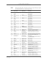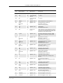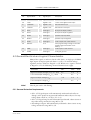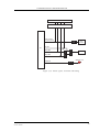
1
GR47/GR48
Integrator’s Manual
Product Photo/Illustration
The GR47 described in this manual conforms to the Radio and Telecommunications
Terminal Equipment (R&TTE) directive 99/5/EC with requirements covering EMC
directive 89/336/EEC and Low Voltage directive 73/23/EEC. The product fulfils the
requirements according to 3GPP TS 51.010-1, EN 301 489-7 and EN60950.
SAR statement: This product is intended to be used with the antenna or other radiating
element at least 20 cm away from any part of the human body.
The information contained in this document is the proprietary information of
Sony Ericsson Mobile Communications International.The contents are confidential
and any disclosure to persons other than the officers, employees, agents or subcontractors
of the owner or licensee of this document, without the prior written consent of
SonyEricsson Mobile Communications International, is strictly prohibited. Further,
no portion of this publication may be reproduced, stored in a retrieval system, or
transmitted in any form or by any means, electronic or mechanical, including
photocopying and recording, without the prior written consent of Sony Ericsson Mobile
Communications International, the copyright holder.
First edition (May 2003)
Sony Ericsson Mobile Communications International publishes this manual without
making any warranty as to the content contained herein. Further Sony Ericsson Mobile
Communications International reserves the right to make modifications, additions and
deletions to this manual due to typographical errors, inaccurate information, or
improvements to programs and/or equipment at any time and without notice. Such
changes will, nevertheless be incorporated into new editions of this manual.
All rights reserved.
© Sony Ericsson Mobile Communications International, 2003
Publication number: LZT 123 7589 R1A
Printed in UK
Contents
Overview ................................................................................................................... 5
1.
Introduction .............................................................................................................. 6
Target Users ................................................................................................................ 6
Prerequisites................................................................................................................ 6
Manual Structure......................................................................................................... 6
2.
GR47/GR48 Radio Devices ...................................................................................... 7
About the GR47/GR48 Family ................................................................................... 7
Radio Devices in a Communication System ................................................................. 7
Features ....................................................................................................................... 9
Service and Support ................................................................................................... 12
Precautions................................................................................................................ 13
3.
Abbreviations.......................................................................................................... 14
Integrating the Radio Device ................................................................................ 16
4.
Mechanical Description .......................................................................................... 17
Interface Description ................................................................................................. 17
Physical Dimensions.................................................................................................. 18
5.
System Connector Interface ................................................................................... 19
Overview ................................................................................................................... 19
General Electrical and Logical Characteristics ............................................................ 22
Grounds .................................................................................................................... 23
VCC - Regulated Power Supply Input ....................................................................... 23
Battery Charging Input (CHG_IN) ........................................................................... 24
Turning the Radio Device ON/OFF and the External Power Signal........................... 25
Analogue Audio ........................................................................................................ 29
PCM Digital Audio ................................................................................................... 33
Serial Data Interfaces ................................................................................................. 36
SIM Card Related Signals .......................................................................................... 40
Service/Programming ................................................................................................ 41
Buzzer ....................................................................................................................... 42
LED .......................................................................................................................... 42
General Purpose Digital I/O Ports ............................................................................. 43
Extended I/O capabilities .......................................................................................... 44
General Purpose Analogue I/O Ports ......................................................................... 45
External I 2C Serial Control Bus................................................................................. 48
TX_ON - Burst Transmission ................................................................................... 49
LZT 123 7589 R1A
Real Time Clock........................................................................................................ 49
6.
Antenna Connector................................................................................................. 51
7.
Keyboard Interface ................................................................................................. 52
IO#/KEYROW# ....................................................................................................... 52
KEYCOL# ................................................................................................................ 52
8.
Hints for Integrating the Radio Device................................................................. 54
Safety Advice and Precautions ................................................................................... 54
Installation of the Radio Device................................................................................. 56
Antenna .................................................................................................................... 58
9.
Embedded Applications ......................................................................................... 60
Features ..................................................................................................................... 60
Implementation......................................................................................................... 60
10. TCP/IP Stack........................................................................................................... 62
Implementation......................................................................................................... 62
11. Technical Data ........................................................................................................ 63
12. Declaration of Conformity...................................................................................... 65
Developer’s Kit ....................................................................................................... 66
13. Introduction to the Developer’s Kit ...................................................................... 67
Contents of the Kit.................................................................................................... 67
General Functioning of the Kit.................................................................................. 68
14. Using the Developer’s Kit...................................................................................... 71
Start up Check List .................................................................................................... 72
Developer’s Board Overlay......................................................................................... 73
Jumpers..................................................................................................................... 74
Switches .................................................................................................................... 78
Headers ..................................................................................................................... 79
Connectors ................................................................................................................ 80
LED Indicators .......................................................................................................... 82
System Connector Pin Assignments........................................................................... 83
LZT 123 7589 R1A
Overview
Product Photo/Illustration
1. Introduction
1.1 Target Users
The GR47 and GR48 radio devices are designed to be integrated into
machine-to-machine or man-to-machine communications applications.
They are intended to be used by manufacturers, system integrators,
applications developers and developers of wireless communications
equipment.
1.2 Prerequisites
It is assumed that the person integrating the radio device into an
application has a basic understanding of the following:
• GSM networking;
• Wireless communication and antennas (aerials);
• AT commands;
• ITU-T standard V.24/V.28;
• Micro controllers and programming;
• Electronic hardware design.
1.3 Manual Structure
The manual is composed of three parts:
Part 1- Overview
This section provides a broad overview of the GR47/GR48 family and
includes a list of abbreviations used in the manual.
Part 2 - Integrating the Radio Device
This section describes each of the signals available on the GR47/GR48
radio devices, along with mechanical information. The section also
provides you with design guidelines and explains what is needed to
commercialise an application from a regulatory point of view.
Part 3 - Developer’s Kit
This section lists the contents of the Developer’s Kit and provides the
information to setup and use the equipment.
6
LZT 123 7589 R1A
2. GR47/GR48 RADIO DEVICES
2. GR47/GR48 Radio Devices
2.1 About the GR47/GR48 Family
Two radio devices make up the family; GR47 and GR48, for use in the
E-GSM900/GSM1800 and GSM850/GSM1900 bands respectively.
1RWH
This manual refers to the GR47 and GR48 as radio devices. If there is a
difference in the functionality of the radio devices the GR47 and GR48
information will be listed separately.
The products belong to a new generation of Sony Ericsson radio devices,
and are intended to be used in machine-to-machine applications and manto-machine applications. They are used when there is a need to send and
receive data (by SMS, CSD, HSCSD, or GPRS), and make voice calls over
the GSM network.
The radio devices can either have applications embedded onto them or they
can be used as the engine in an application created by the customer. The
radio device can send and receive data when a script is executed, the script
can be run internally from the radio device itself or from a micro-controller.
A typical application, involves a micro-controller and a radio device, in
which the micro-controller sends AT commands to the radio device via an
RS232 communications link.
2.2 Radio Devices in a Communication System
Figures 2.1 and 2.2 illustrate the main blocks of a wireless communication
system using the radio device. Figure 2.1 shows the communication system
when the script is embedded on the radio device and figure 2.2 shows the
communication system when a micro-controller is used. They also show the
communication principles of the system and the interface between the
radio device and the application. The definitions in the figures, as used
elsewhere in this manual, are in accordance with the recommendations of
GSM 07.07.
• The MS (mobile station) represents the radio device and SIM card. The
radio device excluding SIM card, is known as the ME (mobile
equipment).
• The DTE (data terminal equipment) is the controlling application. This
can be either an external host or an internal embedded application.
• The DCE (data circuit terminating equipment) is the serial
communication interface of the MS.
7
LZT 123 7589 R1A
2. GR47/GR48 RADIO DEVICES
.
GSM NETWORK
MS
GR47 / GR48
SIM
SYSTEM CONNECTOR
POWER
SUPPLY
GSM
ENGINE
STATUS &
RESPONSE
DCE
EMBEDDED
APPLICATION
DTE
‘AT’ COMMAND
CONTROL
Figure 2.1 Main Blocks in a Wireless System (embedded application)
GSM NETWORK
MS
GR47 / GR48
SIM
EXTERNAL
APPLICATION
MS STATUS &
RESPONSE
SYSTEM CONNECTOR
POWER
SUPPLY
GSM
ENGINE
DCE
DTE
DTE
‘AT’ COMMAND
CONTROL M
Figure 2.2 Main Blocks in a Wireless System (external micro-controller)
In accordance with the recommendations of ITU-T (International
Telecommunication Union - Telecommunications Standardisation Sector)
V.24, the TE communicates with the MS over a serial interface.
8
LZT 123 7589 R1A
2. GR47/GR48 RADIO DEVICES
The functions of the radio device follow the recommendations provided by
ETSI (European Telecommunications Standards Institute) and ITU-T.
ETSI specifies a set of AT commands for controlling the GSM element of
the radio device; these commands are supplemented by Sony Ericsson
specific commands.
To find out how to work with AT commands, see the AT Commands
Manual.
2.3 Features
The radio device performs a set of telecom services (TS) according to GSM
standard phase 2+, ETSI and ITU-T. The functions of the radio device are
implemented by issuing AT commands over a serial interface.
2.3.1 Types of Mobile Station
GR47 and GR48 are dual band mobile stations with the characteristics
shown in the tables below.
GR47
E-GSM 900
GSM 1800
Frequency Range (MHz)
TX: 880-915
RX: 925-960
TX: 1710-1785
RX: 1805-1880
Channel spacing
200 kHz
200 kHz
Number of channels
174 carriers *8 time slots
374 carriers *8 time slots
Modulation
GMSK
GMSK
TX phase accuracy
< 5º RMS phase error (burst)
< 5º RMS phase error (burst)
Duplex spacing
45 MHz
95 MHz
Receiver sensitivity at
antenna connector
< –102 dBm
< –102 dBm
Transmitter output power at
antenna connector
Class 4
2 W (33 dBm)
Class 1
1 W (30 dBm)
Automatic hand-over between E-GSM 900 and GSM 1800
GR48
GSM 850
GSM 1900
Frequency Range (MHz)
TX: 824-849
RX: 869-894
TX: 1850-1910
RX: 1930-1990
Channel spacing
200 kHz
200 kHz
Number of channels
124 carriers *8 time slots
299 carriers *8 time slots
Modulation
GMSK
GMSK
TX Phase Accuracy
< 5º RMS phase error (burst)
< 5º RMS phase error (burst)
9
LZT 123 7589 R1A
2. GR47/GR48 RADIO DEVICES
GR48
GSM 850
GSM 1900
Duplex spacing
45 MHz
80 MHz
Receiver sensitivity at
antenna connector
< –102 dBm
< –102 dBm
Transmitter output power
at antenna connector
Class 4
2W (33 dBm)
Class 1
1 W (30 dBm)
Automatic hand-over between GSM 850 and GSM 1900
2.3.2 Short Message Service
The radio device supports the following SMS services:
• Sending; MO (mobile-originated) with both PDU (protocol data unit)
and text mode supported.
• Receiving; MT (mobile-terminated) with both PDU and text mode
supported.
• CBM (cell broadcast message); a service in which a message is sent to all
subscribers located in one or more specific cells in the GSM network
(for example, traffic reports).
• SMS STATUS REPORT according to GSM 03.40.
The maximum length of an SMS message is 160 characters when using
7-bit encoding. For 8-bit data, the maximum length is 140 characters. The
radio device supports up to six concatenated messages to extend this
function. Concatenation is disabled if CNMI 3,2 is set (See the AT
Commands Manual for further details).
2.3.3 Voice Calls
The radio device offers the capability of MO (mobile originated) and MT
(mobile terminated) voice calls, as well as supporting emergency calls.
Multi-party, call waiting and call divert features are available. Some of
these features are network-operator specific.
For the inter-connection of audio, the radio device offers both single ended
and balanced analogue input and output lines. Direct interface to the
digital PCM (pulse code modulation) bus used within the radio device is
available, thus by-passing the internal analogue circuitry.
The radio devices support HR, FR and EFR vocoders.The GR48 also
supports the Adaptive Multi Rate (AMR) type of vocoder.
10
LZT 123 7589 R1A
2. GR47/GR48 RADIO DEVICES
2.3.4 Data
The radio device supports the following data protocols:
• *356*HQHUDO3DFNHW5DGLR6HUYLFH
The radio devices are Class B terminals. The radio devices are GPRS
4+1 enabled, which are capable of receiving at a maximum of four
timeslots per frame (down link), and transmitting in one timeslot per
frame (up link).
• &6'&LUFXLW6ZLWFKHG'DWD
The radio devices are capable of establishing a CSD communication at
9.6 kbps.
• +6&6'+LJK6SHHG&LUFXLW6ZLWFKHG'DWD
The radio devices support HSCSD communication, with one timeslot
per frame capacity in the up link and two timeslots per frame capacity
in the down link (2+1).
2.3.5 SIM Card
An external SIM card with 3 V or 5 V technology, can be connected to the
radio device via its 60-pin system connector.
2.3.6 Power Consumption
GSM 850 and E-GSM 900
GSM 1800 and GSM 1900
1RWH
Idle Mode
Transmit/Operation
Voice/CSD
< 5 mA
< 250 mA (< 2 A peak)
Data (GPRS 4+1)
< 5 mA
< 350 mA (< 2 A peak)
Voice/CSD
< 5 mA
< 250 mA (<1.75 A peak)
Data (GPRS 4+1)
< 5 mA
< 350 mA (<1.75 A peak)
The power consumption during transmission is measured at maximum
transmitted power.
2.3.7 Other Features
These include:
• 07.10 multiplexing.
• GPS interoperability.
• SIM application tool kit, class 2 release 96 compliant.
• Embedded application
• On board TCP/IP stack
• E-OTD (Supported by GR48)
11
LZT 123 7589 R1A
2. GR47/GR48 RADIO DEVICES
2.4 Service and Support
2.4.1 Web Pages
Visit our web site for the following information:
• where to buy radio devices or for recommendations concerning
accessories and components;
• the telephone number for customer support in your region;
• FAQs (frequently asked questions).
The web site address is:
http://www.SonyEricsson.com/M2M
2.4.2 Integrator’s Manual
This manual provides you with all of the information you need to integrate
the radio device into your application.
2.4.3 AT Commands Manual
The AT Commands Manual provides you with all the AT commands you
can use with your radio device. AT commands are in logical groups and
contain the command, a description of its functionality and an example of
use.
2.4.4 M2mpower Application Guide
The M2mpower Application Guide provides you with all the information
you need to build an application using the M2mpower support
environment. This manual is supplied as part of the M2mpower package.
2.4.5 Developer’s Kit
Sony Ericsson provides the developer’s kit to get you started quickly. The
kit includes the necessary hardware required to begin the development of
an application. It includes the following:
• GSM radio device, GR47 or GR48;
• This Integrator’s Manual;
• Developer’s kit hardware;
• Developer’s kit accessories;
– Power supply
– RS232 cable
– Headset
– Antenna.
12
LZT 123 7589 R1A
2. GR47/GR48 RADIO DEVICES
All the user needs to provide, is a computer or micro-controller and the
expertise to use AT commands.
2.5 Precautions
The radio devices are ESD protected up to 4K V contact and 8K V air
discharge. It is recommended that you follow electronic device handling
precautions when working with any electronic device system to ensure no
damage occurs to the host or the radio device. In “Integrating the Radio
Device”, page 16 you will find more information about safety and product
care. Do not exceed the environmental and electrical limits as specified in
“Technical Data”, page 63.
13
LZT 123 7589 R1A
3. ABBREVIATIONS
3. Abbreviations
Abbreviation
Explanations
AMR
Adaptive Multi Rate
ATMS
Audio to Mobile Station
AFMS
Audio from Mobile Station
CBM
Cell Broadcast Message
CBS
Cell Broadcast Service
CSD
Circuit Switched Data
DCE
Data Circuit Terminating Equipment
DK
Developer’s Kit
DTE
Data Terminal Equipment
DTMF
Dual Tone Multi Frequency
EA
Embedded Application
EFR
Enhanced Full Rate
EMC
Electro-Magnetic Compatibility
E-OTD
Enhanced Observed Time Difference
ETSI
European Telecommunication Standards Institute
FR
Full Rate
GPRS
General Packet Radio Service
GPS
Global Positioning System
GSM
Global System for Mobile Communication
HR
Half Rate
HSCSD
High Speed Circuit Switched Data
IDE
Integrated Development Environment
IP
Internet Protocol
ITU-T
International Telecommunication Union - Telecommunications
Standardisation Sector
M2mpower
Sony Ericssons powerful support environment
ME
Mobile Equipment
MMCX
Micro Miniature Coax
MO
Mobile Originated
MS
Mobile Station
MT
Mobile Terminated
PCM
Pulse Code Modulation
14
LZT 123 7589 R1A
3. ABBREVIATIONS
Abbreviation
Explanations
PDU
Protocol Data Unit
RF
Radio Frequency
RFU
Reserved for Future Use
RLP
Radio Link Protocol
RTC
Real Time Clock
SDP
Service Discovery Protocol
SIM
Subscriber Identity Module
SMS
Short Message Service
TCP
Transport Control Protocol
UDP
User Datagram Protocol
15
LZT 123 7589 R1A
Integrating the Radio Device
Product Photo/Illustration
4. Mechanical Description
4.1 Interface Description
The pictures below show the mechanical design of the radio device along
with the positions of the different connectors and mounting holes. The
radio device is protected with AISI 304 stainless steel covers that meet the
environmental and EMC requirements.
Figure 4.1 Radio Device viewed from below
Figure 4.2 Radio Device, viewed from above
Please note the following:
• Mounting holes positioned at the corners make it possible to securely
bolt the radio device into your application.
17
LZT 123 7589 R1A
4. MECHANICAL DESCRIPTION
• Keypad, display, microphone, speaker and battery are not part of the
radio device.
• The SIM card is mounted in your application, external to the radio
device.
• The System Connector is a 60-pin, standard 0.05 in (1.27 mm) pitch
type. The pins and their electrical characteristics are described in
5. System Connector Interface, page 19.
• Information about the Antenna Connector is found in
6. Antenna Connector, page 51.
4.2 Physical Dimensions
2.20 (4x)
2.86
4.78
3.80
2.05
7.15 2.90
4.60
3.00
2.80
50.00
33.00
30.20
2.30
9.00
46.40
1.80
Figure 4.3 Dimensions of the Radio Device
Measurements are given in millimetres. See also Technical Data, page 63.
18
LZT 123 7589 R1A
5. System Connector Interface
5.1 Overview
Electrical connections to the radio device (except the antenna), are made
through the System Connector Interface. The system connector is a 60-pin,
standard 0.05 in (1.27 mm) pitch device.
The system connector allows both board-to-board and board-to-cable
connections to be made. Use a board-board connector to connect the radio
device directly to a PCB, and a board-cable connector to connect the radio
device via a cable.
Figure 5.1 below shows the numbering of the connector pins.
A ground connection is provided at the mounting hole next to the RF
connector on the radio device as shown below. Connect this ground point
to the DGND pins of the radio device by the shortest, low-impedance path
possible. The purpose of this connection is to allow any antenna ESD
strikes to bypass the radio device’s internal ground path.
Ground
connection
Pin 59
Pin 1
Pin 60
Pin 2
Figure 5.1 Radio Device, viewed from underneath
The following table gives the pin assignments for the system connector
interface and a short description for each signal.
19
LZT 123 7589 R1A
5. SYSTEM CONNECTOR INTERFACE
1RWH
Under the heading “Dir” in the table, radio device input and output signals
are indicated by the letters I and O respectively.
Pin
Signal Name
Dir
Signal Type
Description
1
VCC
-
Supply
Power supply
2
DGND
-
-
Digital ground
3
VCC
-
Supply
Power supply
4
DGND
-
-
Digital ground
5
VCC
-
Supply
Power supply
6
DGND
-
-
Digital ground
7
VCC
-
Supply
Power supply
8
DGND
-
-
Digital ground
9
VCC
-
Supply
Power supply
10
DGND
-
-
Digital ground
11
CHG_IN
-
Battery
charge power
Battery charging
12
DGND
-
-
Digital ground
13
IO5
ADC4
I/0
I
Digital 2.75V
Analogue
General purpose input/output 5
Analogue to digital converter 4
14
ON/OFF
I
Internal pull
up, open drain
Turns the radio device on and off.
15
SIMVCC
-
Digital 3 V/5 V
SIM card power supply. Power output
from radio device for SIM Card
16
SIMPRESENCE
I
Internal pull
up, open drain
SIM Presence
A “1” indicates that the SIM is missing; a
“0” that it is inserted
17
SIMRST
O
Digital 3 V/5 V
SIM card reset
18
SIMDATA
I/O
Digital 3 V/5 V
SIM card data
19
SIMCLK
O
Digital 3 V/5 V
SIM card clock
20
DAC
O
Analogue
Digital to analogue converter
21
IO1
KEYROW2
I/O
I
Digital 2.75V
General purpose input/output 1
Keyboard row 2
22
IO2
ADC5
I/O
I
Digital 2.75V
Analogue
General purpose input/output 2
Analogue to digital converter 5
23
IO3
KEYROW3
I/O
I
Digital 2.75V
General purpose input/output 3
Keyboard row 3
24
IO4
KEYROW4
I/O
I
Digital 2.75V
General purpose input/output 4
Keyboard row 4
25
VRTC
I
Supply 1.8V
Supply for real time clock
26
ADC1
I
Analogue
Analogue to digital converter 1
27
ADC2
I
Analogue
Analogue to digital converter 2
20
LZT 123 7589 R1A
5. SYSTEM CONNECTOR INTERFACE
Pin
Signal Name
Dir
Signal Type
Description
28
ADC3
I
Analogue
Analogue to digital converter 3
29
SDA
I/O
2.75V, internal
pull up
I 2 C data
30
SCL
O
2.75V, internal
pull up
I 2 C clock
31
BUZZER
O
Digital 2.75V
Buzzer output from radio device
32
OUT3
KEYCOL3
DSR
O
O
O
Digital 2.75V
General purpose output 3
Keyboard column 3
Data set ready (UART1)
33
LED
IO6
O
I/O
Digital 2.75V
Flashing LED
General purpose I/O 6
34
VIO
O
Power Out
2.75 V
Radio device power indication. VIO is a
2.75 V at 75 mA output supply that can
be used to power external circuitry that
interfaces to the radio device
35
TX_ON
O
Digital 2.75V
This output indicates when the GSM
radio device is going to transmit the
burst
36
RI
KEYCOL2
O2
O
O
O
Digital 2.75V
Ring Indicator (UART1)
Keyboard column 2
General purpose output 2
37
DTR
KEYROW1
IN1
I
I
I
Digital 2.75V
Data Terminal Ready (UART1)
Keyboard row 1
General purpose input 1
38
DCD
KEYCOL1
O1
O
O
O
Digital 2.75V
Data Carrier Detect (UART1)
Keyboard column 1
General purpose output 1
39
RTS
IO9
I
I/O
Digital 2.75V
Request To Send (UART1)
General purpose I/O 9
40
CTS
KEYCOL4
O4
O
O
O
Digital 2.75V
Clear To Send (UART1)
Keyboard column 4
General purpose output 4
41
TD
I
Digital 2.75V
Transmitted Data (UART1).
Data from DTE (host) to DCE (radio
device).
42
RD
O
Digital 2.75V
Received Data (UART1).
Data from DCE (radio device) to DTE
(host).
43
TD3
I/O7
I
I/O
Digital 2.75V
Transmitted data (UART3)
General purpose I/O 7
44
RD3
I/O8
O
I/O
Digital 2.75V
Received data (UART3)
General purpose I/O 8
45
TD2
I
Digital 2.75V
Transmitted data (UART2).
Used for flashing the memory.
46
RD2
O
Digital 2.75V
Received data (UART2).
Used for flashing the memory.
47
PCMULD
I
Digital 2.75V
DSP PCM digital audio input
48
PCMDLD
O
Digital 2.75V
DSP PCM digital audio output
21
LZT 123 7589 R1A
5. SYSTEM CONNECTOR INTERFACE
Pin
Signal Name
Dir
Signal Type
Description
49
PCMO
O
Digital 2.75V
Codec PCM digital audio output
50
PCMI
I
Digital 2.75V
Codec PCM digital audio input
51
PCMSYNC
O
Digital 2.75V
DSP PCM frame sync
52
PCMCLK
O
Digital 2.75V
DSP PCM clock output
53
MICP
I
Analogue
Microphone Input positive
54
MICN
I
Analogue
Microphone Input negative
55
BEARP
O
Analogue
Speaker output positive
56
BEARN
O
Analogue
Speaker output negative
57
AFMS
O
Analogue
Audio output from radio device
58
SERVICE
I
2.7V
Flash programming voltage for the MS.
Enable logger information if not
flashing.
59
ATMS
I
Analogue
Audio input to radio device
60
AGND
-
Analogue
Analogue ground
5.2 General Electrical and Logical Characteristics
Many of the signals, as indicated in the table above, are high-speed CMOS
logic inputs or outputs powered from a 2.75 V ± 5 % internal voltage
regulator, and are defined as Digital 2.75 V. Whenever a signal is defined
as Digital 2.75 V, the following electrical characteristics apply.
1RWH
Parameter
Min.
Max.
Units
High Level Output Voltage (VOH), Io = –2mA
2.2
2.75
V
Low Level Output Voltage (VOL), Io = 2mA
0
0.6
V
High Level Input Voltage (VIH)
1.93
2.75
V
Low Level Input voltage (VIL)
0
0.5
V
Unused pins can be left floating.
5.2.1 General Protection Requirements
• All 2.75 V digital inputs will continuously withstand and suffer no
damage in the power-on or power-off condition when subjected to any
voltage from - 0.5 V to 3.47 V (3.3 V + 5 %).
• All 2.75 V digital outputs will continuously withstand a short circuit to
any other voltage within the range 0 V to 3 V.
• All analogue outputs will continuously withstand a short circuit to any
voltage within the range 0 V to 3 V.
22
LZT 123 7589 R1A
5. SYSTEM CONNECTOR INTERFACE
• The SIM output signals and the SIMVCC supply will continuously
withstand a short circuit to any voltage within the range 0 V to 4.1V.
5.3 Grounds
Pin
Signal
Description
2, 4, 6, 8, 10, 12
DGND
Digital ground
60
AGND
Analogue ground
There are two ground connections in the radio device, AGND (analogue
ground) and DGND (digital ground). Pin assignments are shown in the
table above.
1RWH
AGND and DGND are connected at a single point inside the radio device.
They must not be joined together in your application.
5.3.1 Analogue Ground - AGND
AGND is the return signal, or analogue audio reference, for ATMS (Audio
To Mobile Station) and AFMS (Audio From Mobile Station). It is
connected to the DGND inside the radio device only. The application must
not connect DGND and AGND.
Parameter
Limit
Imax
≅12.5 mA
5.3.2 Digital Ground - DGND
DGND is the reference or return signal for all system interface digital
signals and is also the d.c. return for SERVICE and the power supply, VCC.
Connect all DGND pins together in your application in order to carry the
current drawn by the radio device.
Parameter
Per Pin
Total (5 Pins)
Imax
< 6.0A
< 3.0A
Iavg
< 100mA
< 600mA
5.4 VCC - Regulated Power Supply Input
Pins
Signal
Description
1, 3, 5, 7, 9
VCC
regulated power supply input
Power is supplied to the radio device VCC pins, from an external source.
23
LZT 123 7589 R1A
5. SYSTEM CONNECTOR INTERFACE
Connect all VCC pins together in your application in order to carry the
current drawn by the radio device.
The electrical characteristics for VCC are shown in the table below.
Parameter
Mode
Limit
Vcc supply voltage
Nominal
3.6 V
Tolerance
including ripple a
3.4 V - 4.0 V
Over-voltage limit
5.5 V
Maximum ripple
< 100 mV @ <200 kHz;
< 20 mV @ > 200 kHz
Burst transmission
200 mV
Maximum allowable voltage
drop
Current drawn, at full TX
power
< 500 mA (average)
< 2 A (peak)
a. Measured at system connector pins.
1RWH
The radio device has no internal capacitance to supply the large current
peaks during GSM burst transmission. We recommend you follow these
general guidelines:
• Fit a low ESR electrolytic capacitor close to the radio device:
> 1,000 µF;
< 100 mΩ ESR.
• Make sure power supply to radio device line resistance is < 200 mΩ.
5.5 Battery Charging Input (CHG_IN)
For battery powered applications, the radio device has a connection to aid
and support battery charging. The typical design where this may be
applicable is to power the radio device directly from a battery source
connected to VCC (pins 1, 3, 5, 7, 9) and to provide a 5V dc power source
(600mA max) to the CHG_IN connection (pin 11). The radio device can
control an internal switching FET which creates a charging pathway to the
battery. While power is provided at CHG_IN, the battery charge can be
maintained. If the power should fail or be removed at CHG_IN, the
application will be supported by the battery alone. When CHG_IN
voltage returns, the battery charging and maintenance will commence once
more.
&DXWLRQ
Battery charging algorithms are unique to different battery types. Sony
Ericsson Mobile Communications will not accept any responsibility or
liability for damage, product failures, even death or injury occurring as a
result of incompatible battery and charging algorithms being applied
without their prior knowledge and consent.
24
LZT 123 7589 R1A
5. SYSTEM CONNECTOR INTERFACE
Safety considerations should be taken into account. For example,
monitoring the temperature of the battery. If the temperature of the
battery exceeds its specification limits, battery charging must be stopped
immediately. If the battery temperature continues to rise the application
should be suspended or the battery disconnected.
1RWH
When charging Lithium batteries, the battery pack must have an internal
protection circuit in accordance with the manufacturer’s instructions.
5.6 Turning the Radio Device ON/OFF and the External Power Signal
Turning the Radio Device On
tO
VCC
tON
tPULSE
ON/OFF
ON/OFF pulled
up internally
through 39kΩ
tPRST
tVIO
VIO
Software running…
tCTS
CTS
Figure 5.2 On timings and VIO performance
Symbol
Parameters
Conditions
Min.
Typ
Max
Unit
t
Reference time
when VCC is
within working
limits (1)
VCC > 3.2V
ON/OFF = VCC
-
-
-
-
t21
Time after t0
when the ON/
OFF pulse can
begin
VCC > 3.2V
0
-
-
ms
25
LZT 123 7589 R1A
5. SYSTEM CONNECTOR INTERFACE
t9,2
Time after start of
ON/OFF pulse
when VIO is
active
VCC > 3.2V
-
45.0
-
ms
t38/6(
Application ON/
OFF pulse width
ON/OFF held low
until detected
by software
400
500
-
ms
t3567
Internal Poweron reset signal
initiates software
100
-
200
ms
t&76
Time when
software
controlled CTS
signal indicates
module READY
-
0.35
3.0(2)
s
CTS signal
configured for
RS232 hardware
flow control, not
GPIO pin
(1)
The GR47 measures the voltage at VCC during the power-up sequence.
It is important that both VCC and ON/OFF reach a minimum of 3.2V before
the ON/OFF low pulse is initiated.
(2)
In SERVICE mode.
26
LZT 123 7589 R1A
5. SYSTEM CONNECTOR INTERFACE
Turning the Radio Device Off
tPULSE
tOFF
ON/OFF
VIO
tSPD
Figure 5.3 Off timings and VIO performance
(2) It is a requirement from most GSM network providers that GSM products
properly detach from the network during a power-down sequence. In
order to achieve this it is important that the VCC supply is not removed or
turned off before VIO has been deactivated by the module.
27
LZT 123 7589 R1A
5. SYSTEM CONNECTOR INTERFACE
Hard Shutdown Sequence
tPULSE
ON/OFF
tHSD
VIO
Figure 5.4 Hard Shutdown Sequence
Symbol
Parameters
t+6'
Time to complete
hardware
shutdown
t38/6(
Application ON/
OFF pulse width
Conditions
ON/OFF low
until VIO is
disabled
Min.
Typ
Max
Unit
2
-
11
s
t+6'
10
-
s
(4) To implement the Hard Shutdown of the GR47, the ON/OFF pulse must
be held low until the sequence is complete. Ensure that ON/OFF is not
released before VIO has been deactivated by the module.
5.6.1 VIO - 2.75V Supply
VIO provides an output voltage derived from an internal 2.75V regulator.
Its electrical characteristics are shown below.
Parameter
Min.
Typ.
Max.
Units
Output Voltage (Iload = 50 mA)
2.70
2.75
2.85
V
75
mA
Load current
You can use this output for the following:
• to indicate that the radio device is powered;
• to power interface circuits, external to the radio device.
28
LZT 123 7589 R1A
5. SYSTEM CONNECTOR INTERFACE
5.7 Analogue Audio
Pin
Signal
Dir
Description
57
AFMS
O
Audio from mobile station
59
ATMS
I
Audio to mobile station
60
AGND
-
Ground (return) for analogue audio
ATMS is the audio input, and AFMS is the audio output, of the radio
device. These signals can be used in car kit mode.
There are three factory-set audio profiles:
• portable handsfree
• handset
• car kit
Portable handsfree is the factory-set default profile. The modification,
configuration, manipulation and storage of audio profiles is achieved with
the AT*E2EAMS (Audio Profile Modification) and AT*E2APR (Audio
Profile).
5.7.1 Audio To Mobile Station - ATMS
ATMS is the analogue audio input to the radio device. Internally, the signal
is sent to the CODEC (COder/DECoder), where it is converted to digital
audio in PCM (Pulse Code Modulation) format. The encoded audio is sent
to PCMOUT via the internal PCM bus.
ATMS provides a DC bias when it is used as the microphone input in
Portable Hands-free applications. All other sources must be a.c.-coupled to
avoid attenuation of low frequencies, and to prevent incorrect biasing or
damage to the ATMS input. Use a capacitor greater than the value shown
in the table below.
The ATMS input is a passive network followed by the transmit part of the
CODEC.
Parameter
Limit
Application driving impedance (0.3 - 3.5 kHz)
≤ 300 Ω
AC coupling capacitance
≥ 1 µF
Radio device input impedance (0.3 - 3.5 kHz)
> 50 kΩ
Low frequency cut-off (- 3 dB)
300 Hz ± 50 Hz
High frequency cut-off (– 3 dB)
> 3500 Hz ± 50 Hz
Output d.c. bias level
0V
car kit mode
Additional Gain in car kit mode
28.5 dB
29
LZT 123 7589 R1A
5. SYSTEM CONNECTOR INTERFACE
The following tables show the nominal PGA (programming gain settings).
For more information see the relevant AT commands.
Maximum input voltage limit: 245 mVrms
Input
Input (mVrms)
TXAGC (dB)
AUX AMP
gain
PCMOUT (dBm0)
ATMS
245
0
13
3
Maximum input level at MICI, 61.4 mVrms output at
PCMOUT = 3 dBm0
Input
Differential
input (mVrms)
TXAGC (dB)
AUX AMP
gain
PCMOUT (dBm0)
MICN
MICP
61.4
0
25
3
Output at AFMS for 3 dBm0 at PCMIN
Input
dBm0
RXPGA
Volume
control (dB)
AFMS (mVrms)
PCMIN
3
0
0
436
Output at BEARN/BEARP for 3 dBm0 at PCMIN
Input
dBm0
RXPGA
Volume
control (dB)
BEAR (mVrms)
PCMIN
3
0
0
388
5.7.2 Audio From Mobile Station - AFMS
AFMS is the analogue audio output from the radio device and may be used
to drive a speaker or the ear-piece in a car kit.
PCM digital audio signals, entering the radio device through the PCMIN
pin, are translated to analogue signals by the CODEC. See 5.8 PCM Digital
Audio, page 33 for further information.
The table below shows the audio signal levels for AFMS.
Parameter
Limit
Speaker impedance
64 Ω to 1 kΩ
30
LZT 123 7589 R1A
5. SYSTEM CONNECTOR INTERFACE
Parameter
Limit
Output Capacitance
2.2 µF ±10 %
Levels (THD < 5 %)
Drive capability into 5 kΩ
(0.3 - 3.5 kHz)
> 2.4 Vp-p
Drive capability into 1.5 kΩ
(0.3 - 3.5 kHz)
> 2.2 Vp-p
Drive capability into 150 Ω
(at 1 kHz)
> 1.3 Vp-p
5.7.3 Microphone Signals
Pin
Speaker signals
Dir
Function
53
MICP
I
Microphone positive input
54
MICN
I
Microphone negative input
MICP and MICN are balanced differential microphone input pins. These
inputs are compatible with an electret microphone. The microphone
contains an FET buffer with an open drain output, which is supplied with
at least +2 V relative to ground by the radio device as shown below.
2 - 2.5V
@ 1mA
CODEC
1k
MICP
68nF
68nF
MICN
GR47
1k
AGND
Figure 5.5 Microphone connections to the radio device
31
LZT 123 7589 R1A
5. SYSTEM CONNECTOR INTERFACE
5.7.4 Speaker Signals
Pin
Speaker signals
Dir
Function
55
BEARP
O
Speaker positive output
56
BEARN
O
Speaker negative output
BEARP and BEARN are the speaker output pins. These are
differential-mode outputs. The electrical characteristics are given in the
table below.
Parameter
Limit
Output level (differential)
≥ 4.0 VSS
Output level (dynamic load = 32 Ω)
≥ 2.8 VSS
Gain PCMIN(5) to BEARP/BEARN (differential)
– 9 dB ± 1
Distortion at 1 kHz and maximum output level
≤5%
Offset, BEARP to BEARN
± 30 mV
Ear-piece mute-switch attenuation
≥ 40 dB
(5)
See PCMIN signal in 5.8 PCM Digital Audio, page 33.
The following table shows the ear piece impedances that can be connected
to BEARP and BEARN.
Ear piece model
Impedance
Tolerance
Dynamic ear piece
[32 Ω + 800 µH] // 100 pF
± 20 %
Dynamic ear piece
[150 Ω + 800 µH] // 100 pF
± 20 %
Piezo ear piece
1 kΩ + 60 nF
± 20 %
32
LZT 123 7589 R1A
5. SYSTEM CONNECTOR INTERFACE
5.8 PCM Digital Audio
Pin
Signal
Dir
Function
52
PCMCLK
O
PCM clock
51
PCMSYNC
O
PCM frame sync
47
PCMULD
I
PCM audio input to DSP
48
PCMDLD
O
PCM audio output from DSP
50
PCMIN
I
PCM audio input to Codec
49
PCMOUT
O
PCM audio output to Codec
Figure 5.6 shows the PCM (Pulse Code Modulation) digital audio
connection for external devices. These connections can be used to process
PCM digital audio signals, bypassing the radio device’s internal analogue
audio CODEC.
GR47
PCMSYNC & PCMCLK
DSP
PCMDLD
PCMIN
PCMULD
PCMOUT
CODEC
System connector
Link for internal
digital-audio processing
Analogue
audio
signals
Figure 5.6 Pin connections to digital audio
1RWH
When no external audio processing is performed, the following pins must
be connected together:
• PCMDLD to PCMIN
• PCMULD to PCMOUT
Electrical characteristics
Digital 2.75 V CMOS input/output electrical characteristics apply.
33
LZT 123 7589 R1A
5. SYSTEM CONNECTOR INTERFACE
5.8.1 PCM Data Format
All of the radio device’s PCM signals, including signals between its
CODEC and DSP conform to the PCM data I/O format of the industry
standard DSP from Texas Instruments.
PCMCLK (bit clock) and PCMSYNC (frame synchronisation) are both
generated by the DSP within the radio device.
The DSP within the radio device is the master therefore all external PCM
clocks and data from external devices must be synchronized to it
13-Bit PCM Mode
Bit
Contents
D15 to D14
Equal to D13
D13 to D1
Two’s complement of the 13-bit PCM
D0
LSB, not used
The radio device implements 13-bit PCM with the 13-bit data embedded
in a 16-bit word within a 24-bit frame (see Figure 5.8). Each PCM word
contains 16-bits: D0 to D15. D13 to D1 is the two’s complement value of
the 13-bit PCM, with D13 as the sign bit. D14 and D15 are always set to
be equivalent with D13. D0, the LSB, is not used as shown in Figure 5.7
below.
= D13
13 bit PCM
MSB D14 D13 D12 D11 D10 D9
D8
D7
D6
D0
D5
D4
D3
D2
D1 LSB
16 bit data word
Figure 5.7 16-bit data word format
16-Bit PCM Mode
Bit
Contents
D15 - D0
Two’s complement
The frame format is equal to the one shown in Figure 5.7, but with D15,
D14 and D0 filled with significant bits. D15 to D0 is the two’s
complement value of the 16-bit PCM with bit 15 as the sign bit.
34
LZT 123 7589 R1A
5. SYSTEM CONNECTOR INTERFACE
PCM Timing Diagrams
The PCM timing is shown in Figure 5.8 below and it is seen that the CPU
has 45 µs to serve an interrupt and setup data channels. Data is sent on the
falling edge of the sync pulse. The data bits in PCMULD and PCMDLD
are aligned so that the MSB in each word occurs on the same clock edge as
shown in Figure 5.9.
125 µs
Clk
Sync
45 µs
Data
Figure 5.8 16-bit word within 24-bit frame
PCM signal timing is shown in Figure 5.9. The signals characteristics are
described in the tables following Figure 5.9.
PCMCLK
tPSS
PCMSYN
PCMIN
tPSH
tDSH
tDSL
MSB
D14
D13
tPDLP
PCMOUT
X
MSB
D14
D13
Figure 5.9 PCM Timing Diagram
Name
Description
Typ.
Unit
tPSS
PCMSYN (setup) to PCMCLK (fall)
2.5
µs
tPSH
PCMSYN pulse length
5
µs
tDSL
PCMI (setup) to PCMCLK (fall)
2.5
µs
tDSH
PCMI (hold) from PCMCLK (fall)
2.5
µs
tPDLP
PCMO valid from PCMCLK (rise)
2.5
µs
Name
Description
Typ.
Unit
FPCMCLK
PCM clock frequency
200
kHz
TPCMCLK
PCM clock period with 50/50 mark space ratio
5
µs
FPCMSYN
PCM sync frequency
8
kHz
35
LZT 123 7589 R1A
5. SYSTEM CONNECTOR INTERFACE
Typical Rise/Fall times
Rise Time
Fall Time
Unit
PCMCLK
19
18
ns
PCMSYN
19
15
ns
PCMOUT
900
900
ns
PCMDLD
20
19
ns
5.9 Serial Data Interfaces
Pin
Signal
Dir
Description
RS232
CCITT Nº
41
TD
I
Serial data to radio device (UART1)
103
42
RD
O
Serial data from radio device (UART1)
104
39
RTS
IO9
I
I/O
Request To Send (UART1)
General purpose input/output 9
105
40
CTS
KeyCOL4
O4
O
O
O
Clear To Send (UART1)
Key column 4
General purpose output 4
106
37
DTR
KeyROW1
IN1
I
I
Data Terminal Ready (UART1)
Keyboard row 1
General purpose input 1
108.2
32
DSR
KeyCOL3
O3
O
O
O
Data Set Ready (UART)
Key column 3
General purpose output 3
107
38
DCD
KeyCOL 1
O1
O
O
O
Data Carrier Detect (UART1)
Key column 1
General purpose output 1
109
36
RI
KeyCOL 2
O2
O
O
O
Ring Indicator (UART1)
Key Column 2
General output 2
125
45
TD2
I
Transmitted Data (UART2)
46
RD2
O
Received Data (UART2)
43
TD3
I
Transmitted Data (UART3)
44
RD3
O
Received Data (UART3)
The serial channels, consisting of three UARTs, are asynchronous
communication links to the application or accessory units.
• UART1 has RS-232 functionality and is used for all on- and off -line
communication.
• UART2 behaves as a general-purpose serial data link. For example, it
can be used for GPS, downloading software and receiving logging
information.
• UART3 behaves as a general-purpose serial data link. It can be used by
an embedded application.
36
LZT 123 7589 R1A
5. SYSTEM CONNECTOR INTERFACE
Digital 2.75 V CMOS input/output electrical characteristics apply.
The standard character format consists of 1 start bit, 8 bit data, no parity
and 1 stop bit. In all, there are 10 bits per character.
5.9.1 UART1 (RS232) - RD, TD, RTS, CTS, DTR, DSR, DCD and RI
UART1 signals conform to a 9-pin RS232 (V.24) serial port.
1RWH
UART1 signal levels do not match standard RS232 (V.28) levels. The
relationship between the levels is shown in the table below.
RS232 level
RD, TD
RTS, CTS, DTR, DSR, DCD, RI
CMOS level
<– 3V
1
OFF
> 1.93 V
>+3V
0
ON
< 0.80 V
Conversion between the radio device CMOS levels and RS232 levels can be
achieved using a standard interface IC, such as the Maxim Integrated
Products MAX3237.
5.9.2 Serial Data Signals - RD, TD
The default baud rate is 9.6 kbits/s, however higher bit rates of up to
460 kbits/s are supported, set by an AT command. UART1 starts at a rate
of 9.6 kbits/s in standard AT command mode. The radio device also
supports GSM 07.10 multiplexing protocol and starts when the
appropriate command is sent.
Serial Data From Radio Device (RD)
RD is an output signal that the radio device uses to send data via UART1
to the application.
Parameter
Limit
Application load resistance
< 100 kΩ
Application load capacitance
< 100 pF
Serial Data To Radio Device (TD)
TD is an input signal, used by the application to send data via UART1 to
the radio device.
Parameter
Limit
Application driving impedance
< 100 Ω
Input capacitance
1nF
Input resistance
100 kΩ to 2.75 V
37
LZT 123 7589 R1A
5. SYSTEM CONNECTOR INTERFACE
5.9.3 Control Signals - RTS, CTS, DTR, DSR, DCD, RI
UART1 control signals are active low and need a standard interface IC,
such as the MAX3237, to generate standard RS232 levels.
UART1 converted signals, together with DGND, RD and TD form a
9-pin RS232 data port.
RTS and CTS are capable of transmitting at 1/10th of the data transmission
speed for data rates up to 460 kbit/s (byte-oriented flow control
mechanism).
1RWH
When hardware flow control is not used in communications between the
application and the radio device, RTS and CTS must be connected to each
other at the radio device.
Switching times for RTS and CTS
The table below shows the switching times.
Parameter
Limit
Time from Low to High level
< 2 µs
Time from High to Low level
< 2 µs
Request to Send (RTS)
Used to condition the DCE for data transmission. The default level is high
by internal pull up.
The application must pull RTS low to enable data transmission from the
radio device. Similarly, the radio device asserts CTS low, indicating it is
ready to receive data transmission from the host.
Parameter
Limit
Application driving impedance
< 100 Ω
Input capacitance
< 2 nF
Input resistance (pull-up)
100 kΩ to DGND
Clear To Send (CTS)
CTS is asserted by the DCE to indicate that the host (DTE) may transmit
data. When CTS is high, the host (DTE) is not permitted to transmit data.
The table below shows the load characteristics for this signal.
Parameter
Limit
Application load capacitance
< 500 pF
Application load resistance
≥ 1 MΩ
38
LZT 123 7589 R1A
5. SYSTEM CONNECTOR INTERFACE
Data Terminal Ready (DTR)
DTR indicates that the DTE is ready to receive data. It also acts as a
hardware ‘hang-up’, terminating calls when switched high. The signal is
active low. You can define the exact behaviour of DTR with an AT
command.
Data Set Ready (DSR)
DSR indicates that the DCE is ready to receive data. The signal is active
low.
Data Carrier Detect (DCD)
DCD indicates that the DCE is receiving a valid carrier (data signal) when
low.
Ring Indicator (RI)
RI indicates that a ringing signal is being received by the DCE when low.
You can define the exact behaviour of RI with an AT command.
5.9.4 UART2 - TD2, RD2
UART 2 consists of a full duplex serial communication port with
transmission and reception lines.
This communication port works in a mode called Operation and
Maintenance.
Operation and Maintenance mode works in combination with the
SERVICE signal. Two events are possible if the SERVICE signal is active
when the radio device is turned on. These are:
• the radio device is reprogrammed if UART2 is connected to a computer
running Sony Ericsson update software;
• the radio device enters logging mode and sends data to UART2 if no
reprogramming information is received.
Timing and electrical signals characteristics are the same as for UART1,
TD and RD, except for maximum baud rate which could increase to
921 kbps.
Transmitted Data 2 (TD2)
TD2 is used by the application to send data to the radio device via UART2.
It has the same electrical characteristics as TD.
Received Data 2 (RD2)
RD2 is used to send data to the application via UART2. It has the same
electrical characteristics as RD.
39
LZT 123 7589 R1A
5. SYSTEM CONNECTOR INTERFACE
5.9.5 UART3 - TD3, RD3
UART3 is a full duplex serial communication port with transmission and
reception lines. It has the same timing and electrical signal characteristics
as UART1, TD and RD.
Transmitted Data 3 (TD3)
TD3 is used by your application to send data to the radio device via
UART3.
Received Data 3 (RD3)
RD3 is used to send data to your application via UART3.
5.10 SIM Card Related Signals
Pin
Signal
Dir
Description
15
SIMVCC
-
SIM card power supply
16
SIMPRESENCE
I
SIM card presence
17
SIMRST
O
SIM card reset
19
SIMCLK
O
SIM card clock
18
SIMDATA
I/O
SIM card data
These connections allow you to communicate with the SIM card holder in
your application.
1RWH
The distance between the SIM card holder and the radio device can be up
to 25cm.
This SIM interface allows the use of 3 V and 5 V SIM cards. By default it
works on 3 V levels but will automatically switch to 5 V, if a 5 V SIM card
is fitted.
SIM voltage levels, as shown in the following table, are dependent on the
type of SIM card detected by the radio device.
Signal
Parameter
Mode
Min.
Typ.
Max.
Unit
SIMVCC
SIM supply voltage
3V
2.7
3.0
3.3
V
5V
4.5
5.0
5.5
V
3V
2.1
3.0
V
5V
3.5
5.0
V
3V
0
0.9
V
5V
0
1.5
V
SIMDAT
High Level Input
voltage (V )
,+
SIMDAT
Low Level Input
voltage (V )
,/
40
LZT 123 7589 R1A
5. SYSTEM CONNECTOR INTERFACE
Signal
Parameter
Mode
Min.
SIMDAT
High Level Output
voltage (V )
3V
2+
SIMDAT
Low Level Output
voltage (V )
2/
SIMCLK
SIMRST
High Level Output
voltage (V )
SIMCLK
SIMRST
Low Level Output
voltage (V )
2+
2/
Typ.
Max.
Unit
2.7
3.0
V
5V
4.7
5.0
V
3V
0
0.2
V
5V
0
0.2
V
3V
2.4
3.0
V
5V
4.4
5.0
V
3V
0
0.35
V
5V
0
0.3
V
5.10.1 SIM Detection - SIMPRESENCE
SIMPRESENCE is used to determine whether a SIM card has been inserted
into or removed from the SIM card holder. You should normally wire it to
the “card inserted switch” of the SIM card holder, but different
implementations are possible.
When left open, an internal pull-up resistor maintains the signal high and
means “SIM card missing” to the radio device. When pulled low the radio
device assumes a SIM card is inserted.
SIMPRESENCE is a Digital 2.75V CMOS input with the following
electrical characteristics.
Parameter
Min.
Pull-up resistance (at 2.75 V)
100
Typ.
Low Level Input voltage (SIM inserted)
High Level Input voltage (SIM missing)
1RWH
> 1.93
Max.
Units
kΩ
0.80
V
2.75
V
To meet regulatory approvals SIMPRESENCE must be implemented.
5.11 Service/Programming
Pin
Signal
Dir
Description
58
SERVICE
I
Flash programming voltage
When the SERVICE input signal is active the radio device will:
• be reprogrammed if data is received through UART2 from a computer
running Sony Ericsson reprogramming software;
• or it will output logging data on UART2.
41
LZT 123 7589 R1A
5. SYSTEM CONNECTOR INTERFACE
The electrical characteristics are given below. The signal reference is
DGND.
Mode
SERVICE Voltage (V)
Min.
Typ.
Normal Operation
Service/enable
programming
1.9
2.75V
Absolute maximum
voltage
Drive Capacity
Max.
0.8
-
3.6
> 1 mA
13.5
5.12 Buzzer
Pin
Signal
Dir
Description
31
BUZZER
O
Buzzer output from radio device
Connecting the BUZZER signal to an inverting transistor-buffer followed
by a piezoelectric transducer enables the radio device to play preprogrammed melodies or sounds.
5.13 LED
Pin
Signal
Dir
Description
33
LED
O
LED Output from radio device
The LED states shown below, are hard coded.
LED indication
Operational status
No indication
No power or in the OFF state
Green, steady
Power on, not connected to a network
Green, blinking
Power on, connected to a network
42
LZT 123 7589 R1A
5. SYSTEM CONNECTOR INTERFACE
The following circuit can be used to connect an LED.
VCC
330
LED
GR47/48
DGND
10k
BC817
10k
Figure 5.10 Electrical connections for the LED
5.14 General Purpose Digital I/O Ports
Pin
I/O port
signal
Default
signal
Description
21
IO1
IO1
Programmable Input/Output 1
KEYRow2
22
IO2
IO2
Programmable Input/Output 2
ADC5
23
IO3
IO3
Programmable Input/Output 3
KEYRow3
24
IO4
IO4
Programmable Input/Output 4
KEYRow4
13
IO5
IO5
Programmable Input/Output 5
ADC4
33
IO6
LED
Programmable Input/Output 6/LED
43
IO7
TD3
Programmable Input/Output 7/TD3
44
IO8
RD3
Programmable Input/Output 8/RD3
39
IO9
RTS
Programmable Input/Output 9/RTS
37
IN1
DTR
Programmable Input 1
Data Terminal Ready
32
OUT3
DSR
Programmable Output 3/DSR
36
OUT2
RI
Programmable Output 2/RI
Ring Indicator
38
OUT1
DCD
Programmable Output 1/DCD
Data Carrier Detect
40
OUT4
CTS
Programmable Input/Output 4/CTS
Signals which have an entry in the Default Signal column in the above table
are multiplexed.
43
LZT 123 7589 R1A
5. SYSTEM CONNECTOR INTERFACE
The operational modes of multiplexed signals are controlled by AT
commands and also by intrinsic functions available to an embedded
The following table gives you the input impedance. These values only
apply when the ports are configured as input signals.
1RWHV
Parameter
Min.
Typ.
Max.
Units
Input impedance (pull-up)
50
100
120
kΩ
I/O6 (LED) doesn’t have an internal pull up. If this pin is configured as an
input, it should not be left floating.
I/O7 (TD3) has a pull down instead of a pull up.
5.15 Extended I/O capabilities
To increase flexibility and variety of radio device peripherals, the RS232
hardware flow control shares its physical interface with the keypad
scanning interface and the extended general purpose I/O capability. This
sharing means that it is not feasible to operate all these features
concurrently, however, with care, dynamic switching from one feature to
another is possible.
Using Embedded Applications
When a particular I/O feature is required, the user sets the state of the
relevant I/O blocks by disabling one set before enabling others.
The radio device checks the state of the I/O when the user requests a new
function. The new function is rejected if the current function is not released
first.
1RWH
Only the states of I/O1 - I/O5 are retained for the next power up. For
example, inputs remain as inputs and outputs remain as outputs. The
voltage of a defined output pin will still drop to 0 Volts in the radio device
power down state.
5.15.1 LED/IO6 Capabilities
The LED function pin can be used as a general purpose digital I/O when
the flashing LED function is not required. However, this pin does not have
an on-board pull-up resistor. It is required that an external pull-up or pulldown resistor be provided by the host circuitry when either not used or
when used as a digital input.
44
LZT 123 7589 R1A
5. SYSTEM CONNECTOR INTERFACE
5.15.2 I#/O#
If pins labelled I# and O# are not being used for an alternative function
they may be used for general purpose inputs or outputs respectively. The
inputs have an on-board 100k pull-up resistor and the outputs are driven
rail-to-rail at 2.75V levels.
5.15.3 UART3/IO#
The UART3 pins have been given alternative functions as general purpose
I/O, both pins may be used for either input or output. However, the TX
pin has a 100kΩ pull-down resistor to ground and the RX pin has a 100kΩ
pull-up resistor to 2.75V. This must be taken into consideration when
designing the host circuit.
5.15.4 IO#/ADC#
To increase analog input capabilities, the radio device optimises the I/O by
multiplexing or sharing different features on single pins. There are two
digital I/O pins which now have an additional ADC input. When
configured as digital I/O, the software will not read the voltages at the two
new ADC inputs. When configured as ADC inputs the software will
configure the digital I/O pins as input or high impedance tri-state. In this
state any applied voltage between 0V and 2.75V can be read as an 8 bit
value.
Because the additional ADC inputs (ADC4 and ADC5) are common with
digital I/O, the input circuit of the ADC is not the same as for the original
circuits ADC1-3. It is important to understand the input structure of the
pin so that the correct analog voltage is read by the application.
5.16 General Purpose Analogue I/O Ports
Pin
Signal
Dir
Description
20
DAC
O
Digital to analogue conversion output
26
ADC1
I
Analogue to digital conversion input 1
27
ADC2
I
Analogue to digital conversion input 2
28
ADC3
I
Analogue to digital conversion input 3
13
ADC4 (I/O5)
I (I/O)
Analogue to digital conversion input 4
22
ADC5 (I/O2)
I (I/O)
Analogue to digital conversion input 5
The radio device is able to convert digital to analogue signals and vice
versa.
45
LZT 123 7589 R1A
5. SYSTEM CONNECTOR INTERFACE
5.16.1 Digital to Analogue Converter - DAC
The DAC is an 8-bit converter. Conversion takes place when an AT
command is sent to the radio device. The radio device sends the resulting
analogue value to the DAC pin.
Tolerance on this internal voltage is ± 5 %
DAC output electrical characteristics are given in the following table.
Parameter
Limit
Units
Resolution
8
Bits
Output voltage for code = 0
(2.75(6) x 0.05) ± 0.05
V
Output voltage for code = 255
(2.75(6) x 0.95) ± 0.05
V
Nominal step size
(2.75(6) x 0.9)/256
mV
Absolute error(7)
≤ ± 0.5
mV
Output wide-band noise and clock
feed-through 0 - 1.1 MHz
≤ 0.5
mVrms
Power-supply rejection ratio 50 Hz - 10 kHz
≥ 40
dB
Conversion rate ± 0.5 LSB
≤ 2 (Load A)(8)
ms
≤ 50 (Load B)(8)
ms
Output buffer impedance when disabled
≥ 50
kΩ
Output current source or sink
≥1
mA
Current consumption (active)
≤ 1.0
mA
(6)
Tolerance on this internal voltage is ± 5 %
Referred to the ideal conversion characteristic.
(8)
See Figure 5.11, page 46
(7)
DAC
100 - 200pF
100k
Load A
1k
Load B
DGND
DAC
10nF
1nF
DGND
Figure 5.11 DAC loads
46
LZT 123 7589 R1A
5. SYSTEM CONNECTOR INTERFACE
5.16.2 Analogue to Digital Converters 1, 2 and 3 - ADCx
The ADC is an 8-bit converter. An analogue value applied to any of the
ADC pins is converted and stored in a register inside the radio device.
When the appropriate AT command is received by the radio device, the
digital value stored in the register is read.
ADC electrical characteristics are shown in the table below.
(9)
Tolerance on this internal voltage is ±5%
5.16.3 Analogue to Digital Converters 4 and 5 - IOx/ADCx
To increase analog input capabilities, the GR47 optimises the I/O by
multiplexing or sharing different features on single pins. There are two
ADC inputs which share system connector pins with digital I/O signals.
When configured as digital I/O, the software will not read the voltages at
the two new ADC inputs. When configured as ADC inputs the software
will configure the digital I/O pins as input or high impedance tri-state. In
this state any applied voltage between 0V and 2.75V can be read as an 8
bit value.
Because the ADC inputs, ADC4 and ADC5, are common with digital I/O,
the input circuit of these Adds is not the same as for the circuits ADC1,
ADC2 and ADC3. It is important to understand the input structure of the
pin so that the correct analog voltage is read by the application (at position
’A’ in Figure 5.12 below). The input structure is provided in Figure 5.12.
It consists of a 100kΩ pull-up to 2.75V followed by a series 10kΩ and 1nF
capacitor to ground which make a low pass filter with a 3dB roll-off at
47
LZT 123 7589 R1A
5. SYSTEM CONNECTOR INTERFACE
1RWH
If the voltage of the signal to be measured may be altered by the internal
circuitry of this shared signal, then the application should use ADC1,
ADC2 or ADC3 instead.
2.75V
2.75V
1MΩ
100kΩ
10kΩ
A
ADC
10#/ADC#
1nF
Analog IC
Figure 5.12 Input circuit for combined digital I/O and ADC pins
5.17 External I 2C Serial Control Bus
Pin
Signal
Dir
Description
29
SDA
I/O
I 2 C serial data
30
SCL
O
I 2 C serial clock
The I 2 C bus is controlled by embedded application script commands.
The external I 2 C bus consists of two signals, SDA and SCL. This bus is
isolated from the radio device’s internal I 2 C bus to ensure proper operation
of the radio device, in the event of the external I 2 C bus being damaged.
Transmit
operation
The electrical characteristics are shown below.
Parameter
Min.
Frequency I 2 C CLK
81.25
High or low I 2 C CLK
1.2
Delay time after falling edge of I 2 C
CLK
308
Hold time after falling edge of I 2 C
CLK
0
Typ.
Max.
Units
400
kHz
µs
3081230
ns
ns
48
LZT 123 7589 R1A
5. SYSTEM CONNECTOR INTERFACE
Parameter
Min.
Typ.
Receive
operation
Frequency I 2 C CLK
Max.
Units
400
kHz
High or low I 2 C CLK
1.2
µs
Delay time after falling edge of I 2 C
CLK
100
ns
Hold time after falling edge of I 2 C
CLK
0
ns
5.18 TX_ON - Burst Transmission
Pin
Signal
Dir
Description
35
TX_ON
O
GSM radio device to transmit
Burst transmission is the time when a GSM transceiver unit is transmitting
RF signals. TX_ON indicates the radio device is going into transmission
mode.
5.19 Real Time Clock
Pin
Signal
Dir
Description
25
VRTC
-
Voltage for the Real Time Clock
The Real Time Clock (RTC) provides the main microprocessor with a
time-of-day calendar and alarm, and a one-hundred-year calendar. Its
accuracy is shown in the table below
Parameter
Min.
Typ.
Max.
Units
RTC accuracy
25°C
8 (21)
20 (52)
ppm (s/month)
RTC accuracy
extreme
temperatures
89 (231)
101 (262)
ppm (s/month)
The Real Time Clock operates in two modes when connected to a separate
power supply:
• RTC normal mode: the radio device is in ON or OFF mode and it is
supplied with power (VCC is applied).
• RTC back-up mode: VCC is disconnected and the RTC is maintained
by a separate backup power supply connected to the VRTC input (see
Figure 5.13 below).
Backup power is provided by a capacitor, golden-capacitor or battery in
your application and must be connected to the VRTC pin. During RTC
normal operation, the back up source will be charged.
49
LZT 123 7589 R1A
5. SYSTEM CONNECTOR INTERFACE
In back-up mode, the back-up source must provide enough power for RTC
operation. Refer to the table for the amount of current required.
The following table shows voltage characteristics for both modes.
Parameter
Min.
Typ.
Max.
Units
Supply Voltage RTC (normal mode charging the capacitor)
1.6
1.8
2.0
V
Supply Voltage RTC (back-up mode Capacitor provides the current)
1.0
1.8
2.0
V
5.0
10.0
µA
Current drawn
If the voltage drops below 1.0 V in back-up mode, the RTC will stop
working. The following diagram shows the RTC connections.
VRTC
+
Backup
supply
GR47
DGND
Figure 5.13 RTC connections
50
LZT 123 7589 R1A
6. ANTENNA CONNECTOR
6. Antenna Connector
The radio device’s antenna connector allows transmission of the radio
frequency (RF) signals from the radio device to an external customersupplied antenna. The connector is a micro-miniature coaxial MMCX
surface mounted component. A number of suitable MMCX type, mating
plugs are available from the following manufacturers;
• Amphenol;
• Suhner;
• IMS Connector Systems.
The nominal impedance of the antenna interface is 50Ω.
51
LZT 123 7589 R1A
7. KEYBOARD INTERFACE
7. Keyboard Interface
To increase I/O capabilities, the radio device optimises the I/O by
multiplexing or sharing different features on single pins. The I/O has been
extended to allow simple interfacing of a matrix keypad.
7.1 IO#/KEYROW#
When configured for keypad operation the software will configure the digital I/O pins as input or high impedance tri-state. In this state, the keypad
matrix row can be read from the KEYROW# inputs. These pins have a
100kΩ pull-up to 2.75V and the rows are considered activated when the
voltage is pulled low by the external keypad switches.
7.2 KEYCOL#
The keypad matrix column drivers share functionality with the RS232
hardware flow control signals.
In addition to the keypad column outputs it is possible to use a direct
ground connection as an additional column driver, which is interpreted as
column zero.
Simply connect one keypad column directly to ground. When a key in this
column is depressed KEYROW# is activated.
Thus it is possible to create a variety of keypad matrix sizes from single
column to five columns wide.
Finally, a standard keypad matrix directly connects the rows to the
columns whenever a key is depressed. In order to avoid short circuits if
multiple keys are pressed simultaneously, the column drivers must be
open-collector. This must be achieved with external transistors as the logic
drive from the radio device is rail-to-rail. Suitable transistors for this
interface are of the type with built in bias resistors between base and
emitter.
52
LZT 123 7589 R1A
7. KEYBOARD INTERFACE
The method of connection is shown below.
KEYROW#
GR47
1
2
3
4
5
6
RN1107
KEYCOL#
RN1107
RN1107
Figure 7.1 Keyboard matrix connections
1RWH
This matrix pattern may be repeated up to 5 columns and 4 rows (one
column will use a ground connection as a virtual column driver).
Examples of suitable transistors are:
Brand
Part Number
Toshiba
RN1107 (as shown)
On SEMI
DTC114YET1
Philips
PDTC114YE
ROHM
DTC114YETL
53
LZT 123 7589 R1A
8. HINTS FOR INTEGRATING THE RADIO DEVICE
8. Hints for Integrating the Radio Device
This chapter gives you advice and helpful hints on how to integrate the
radio device into your application from a hardware perspective.
Please read and consider the information under the following headings
before starting your integration work:
• Safety advice and precautions.
• Installation of the radio device.
• Antenna.
8.1 Safety Advice and Precautions
8.1.1 General
• Always ensure that use of the radio device is permitted. The radio
device may present a hazard if used in proximity to personal medical
electronic devices. As a rule, the radio device must not be used in
hospitals, airports or planes.
• You are responsible for observing your country’s safety standards, and
where applicable the relevant wiring rules.
• Never use the radio device at a gas station, refuelling point, blasting
area or in any other environment where explosives may be present.
• Operating the radio device close to other electronic devices, such as
antennas, television sets, and radios may cause electromagnetic
interference.
• Never try to dismantle the radio device yourself. There are no
components inside the radio device that can be serviced by the user. If
you attempt to dismantle the radio device, you may invalidate the
warranty.
• To protect the power supply cables and meet the fire safety
requirements, it is recommended that the electrical circuits are supplied
with a power regulator. The power regulator should be placed as close
to the terminals of the power supply as possible.
• Do not connect any incompatible component or product to the radio
device.
1RWH
Sony Ericsson does not warrant against defects, non-conformities or
deviations caused thereby.
• The connection/disconnection method for the development board is by
means of the DC power jack. For this reason, the mains supply should
be situated close to the development board and be easily accessible.
54
LZT 123 7589 R1A
8. HINTS FOR INTEGRATING THE RADIO DEVICE
8.1.2 SIM Card
• Before handling the SIM card in your application, ensure that you are
not charged with static electricity. Use proper precautions to avoid
electrostatic discharges. The radio device must be switched off before
the SIM card is installed in your application.
• When the SIM card hatch is opened, the SIM card connectors lie
exposed under the SIM card holder. CAUTION: Do not touch these
connectors! If you do, you may release an electrical discharge that could
damage the radio device or the SIM card.
• When designing your application, the SIM card’s accessibility should
be taken into account. We always recommend that you have the SIM
card protected by a PIN code. This will ensure that the SIM card cannot
be used by an unauthorized person.
8.1.3 Antenna
• If the antenna is to be mounted outside, consider the risk of lightning.
Follow the instructions provided by the antenna manufacturer.
• Never connect more than one radio device to a single antenna. The
radio device can be damaged by radio frequency energy from the
transmitter of another radio device.
• Like any mobile station, the antenna of the radio device emits radio
frequency energy. To avoid EMI (electromagnetic interference), you
must determine whether the application itself, or equipment in the
application’s proximity, needs further protection against radio emission
and the disturbances it might cause. Protection is secured either by
shielding the surrounding electronics or by moving the antenna away
from the electronics and the external signals cable.
• The radio device and antenna may be damaged if either come into
contact with ground potentials other than the one in your application.
Beware, ground potential are not always what they appear to be.
• In the final application, the antenna must be positioned more than
20 cm away from human bodies. When this rule cannot be applied, the
application designer is responsible for providing the SAR measurement
test report and declaration.
• Even if SAR measurements are not required, it is considered good
practice to insert a warning in any manual produced, indicating it is a
radio product and that care should be taken.
55
LZT 123 7589 R1A
8. HINTS FOR INTEGRATING THE RADIO DEVICE
8.2 Installation of the Radio Device
8.2.1 Where to Install the Radio Device
There are several conditions which need to be taken into consideration
when designing your application as they might affect the radio device and
its function. They are:
Environmental Conditions
The radio device must be installed so that the environmental conditions
stated in the Technical Data chapter, such as temperature, humidity and
vibration are satisfied. Additionally, the electrical specifications in the
Technical Data section must not be exceeded.
Signal Strength
The radio device has to be placed in a way that ensures sufficient signal
strength. To improve signal strength, the antenna can be moved to another
position. Signal strength may depend on how close the radio device is to a
radio base station. You must ensure that the location at which you intend
to use the radio device, is within the network coverage area.
Degradation in signal strength can be the result of a disturbance from
another source, for example an electronic device in the immediate vicinity.
More information about possible communication disturbances can be
found in section 8.3.5, page 59.
When an application is completed, you can verify signal strength by
issuing the AT command AT+CSQ. See the AT Commands Manual for
further details.
7LS
Before installing the radio device, use an ordinary mobile telephone to
check a possible location for it. In determining the location for the radio
device and antenna, you should consider signal strength as well as cable
length
Connection of Components to Radio Device
The integrator is responsible for the final integrated system. Incorrectly
designed or installed, external components may cause radiation limits to be
exceeded. For instance, improperly made connections or improperly
installed antennas can disturb the network and lead to malfunctions in the
radio device or equipment.
Network and Subscription
• Before your application is used, you must ensure that your chosen
network provides the necessary telecommunication services. Contact
your service provider to obtain the necessary information.
56
LZT 123 7589 R1A
8. HINTS FOR INTEGRATING THE RADIO DEVICE
• If you intend to use SMS in the application, ensure this is included in
your (voice) subscription.
• Consider the choice of the supplementary services described in section
2.3.2 Short Message Service, page 10.
8.2.2 How to Install the Radio Device
Power Supply
• Use a high-quality power supply cable with low resistance. This ensures
that the voltages at the connector pins are within the allowed range,
even during the maximum peak current. An electrolytic capacitor
should be placed close to the power supply pins of the radio device to
supply the peak currents during burst transmission. See 5.4 VCC Regulated Power Supply Input, page 23.
• See section 5.2.1 General Protection Requirements, page 22.
Grounds
A ground connection is provided at the mounting hole next to the RF
connector on the radio device (see Figure 5.1, page 19). Connect this
ground point to the DGND pins of the radio device by the shortest, lowimpedance path possible. The purpose of this connection is to allow any
ESD picked up by the antenna to bypass the radio device’s internal ground
path.
1RWH
It is recommended that you use a cable with a maximum resistance of 5 mΩ
for the ground connection.
1RWH
AGND and DGND are connected at a single point inside the radio device.
They must not be joined together in your application.
Audio
Use a coupling capacitor in ATMS line if the application does not use the
radio device’s bias voltage. See also Figure 5.5 Microphone connections to
the radio device, page 31.
Software Upgrade
To upgrade the software, the system connector must be accessible in your
application. The pins SERVICE, TD2, RD2 and the power signals are used
for this purpose. Please contact customer support for more details.
57
LZT 123 7589 R1A
8. HINTS FOR INTEGRATING THE RADIO DEVICE
8.3 Antenna
8.3.1 General
The antenna is the component in your system that maintains the radio link
between the network and the radio device. Since the antenna transmits and
receives electromagnetic energy, its efficient function will depend on:
• the type of antenna (for example, circular or directional);
• the placement of the antenna;
• communication disturbances in the vicinity in which the antenna
operates.
In the sections below, issues concerning antenna type, antenna placement,
antenna cable, and possible communication disturbances are addressed.
In any event, you should contact your local antenna manufacturer for
additional information concerning antenna type, cables, connectors,
antenna placement, and the surrounding area. You should also determine
whether the antenna needs to be grounded or not. Your local antenna
manufacturer might be able to design a special antenna suitable for your
the application.
8.3.2 Antenna Type
Make sure that you choose the right type of antenna for the radio device.
Consider the following requirements:
• the antenna must be designed for the dual frequency bands in use:
E-GSM900/GSM1800 for the GR47 and
GSM 850/GSM1900 for the GR48;
• the impedance of the antenna and antenna cable must be 50 Ω;
• the antenna output-power handling must be a minimum of 2 W;
• the VSWR value should be less than 3:1 to avoid damage to the radio
device.
8.3.3 Antenna Placement
The antenna should be placed away from electronic devices or other
antennas. The recommended minimum distance between adjacent
antennas, operating in a similar radio frequency band, is at least 50 cm.
If signal strength is weak, it is useful to face a directional antenna at the
closest radio base station. This can increase the strength of the signal
received by the radio device.
The radio device’s peak output power can reach 2 W. RF field strength
varies with antenna type and distance. At 10 cm from the antenna the field
strength may be up to 70 V/m and at 1m it will have reduced to 7 V/m.
58
LZT 123 7589 R1A
8. HINTS FOR INTEGRATING THE RADIO DEVICE
In general, CE-marked products for residential and commercial areas, and
light industry can withstand a minimum of 3 V/m.
8.3.4 The Antenna Cable
Use 50 Ω impedance low-loss cable and high-quality 50 Ω impedance
connectors (frequency range up to 2 GHz) to avoid RF losses. Ensure that
the antenna cable is as short as possible.
The Voltage Standing-Wave Ratio (VSWR) may depend on the
effectiveness of the antenna, cable and connectors. In addition, if you use an
adapter between the antenna cable and the antenna connector, it is crucial
that the antenna cable is a high-quality, low-loss cable.
Minimize the use of extension cables, connectors and adapters. Each
additional cable, connector or adapter causes a loss of signal power.
8.3.5 Possible Communication Disturbances
Possible communication disturbances include the following:
• Noise can be caused by electronic devices and radio transmitters.
• Path-loss occurs as the strength of the received signal steadily decreases
in proportion to the distance from the transmitter.
• Shadowing is a form of environmental attenuation of radio signals
caused by hills, buildings, trees or even vehicles. This can be a
particular problem inside buildings, especially if the walls are thick and
reinforced.
• Multi-path fading is a sudden decrease or increase in the signal
strength. This is the result of interference caused when direct and
reflected signals reach the antenna simultaneously. Surfaces such as
buildings, streets, vehicles, etc., can reflect signals.
• Hand-over occurs as you move from one cell to another in the GSM
network. Your mobile application call is transferred from one cell to the
next. Hand-over can briefly interfere with communication and may
cause a delay, or at worst, a disruption.
59
LZT 123 7589 R1A
9. EMBEDDED APPLICATIONS
9. Embedded Applications
The radio device has the capability to store and run customer written code
in the form of a script during the processor’s idle time, through the use of
an on board interpreter.
9.1 Features
Main features of embedded applications are as follows.
• C based scripting language (Sony Ericsson specific);
• Over the air upgrade of scripts (NOT GSM software);
• Library of intrinsic functions;
• 2 scripts can be stored in the memory at any time but only 1 can be
active.
9.2 Implementation
The radio device has up to 44k of space available for storage of two scripts
in the scripting language and 25k of operating RAM. Structures included
in this language are:
• If - then - else statements
• While loops
• For loops
All hardware interfaces that are normally available to the radio device
through the AT commands are available to the embedded application.
Further drivers have been written such as M bus, keypad, SPI and I2C for
use by the embedded application (EA) through the use of the I/O pins.
9.2.1 Limitations
Since the radio device is processing the script using its own memory,
limitations are placed onto the scripts that are run.
• A direct comparison cannot be made to a fully compiled C program in
terms of size but a gauge of script size is that if each line were 128
characters long in the script then the script could be 350 lines long.
• Processing power is something that needs to be considered as the script
is run as a low priority process within the software. However, controller
mode stops GSM operation and provides all the processing power for
the script to be run. See the M2mpower Application Guide for more
details.
• Code cannot be ported directly from an existing application and loaded
directly onto the radio device. It must be re written in the Sony
Ericsson Mobile script language so that the radio device interpreter can
function correctly.
60
LZT 123 7589 R1A
9. EMBEDDED APPLICATIONS
9.2.2 M2mpower IDE (Integrated Development Environment)
The IDE is a Windows based package which allows the user to write,
simulate, debug and download the application into a radio device with the
embedded application (EA) software. The standard version is designed to
run on Windows XP and 2000, other versions are available for 98 if
required.
The M2mpower Application Guide is available for implementing
applications using the developer’s kit and the embedded application (EA)
functionality.
This is a required package to be able to implement an embedded
application (EA).
For further information please contact Sony Ericsson Mobile
Communications customer support.
61
LZT 123 7589 R1A
10. TCP/IP STACK
10. TCP/IP Stack
An on board IP/TCP/UDP stack has been integrated into the software
negating the need for the customer to implement one in their own code
base.
This is only accessible by using an embedded applications (see section 9)
using intrinsic functions.
10.1 Implementation
The following types of commands allow various functions:
• Open/closing IP connection - Negotiates/closes a dynamic IP address
with the web server.
• Send/Receive TCP packets - Performs all TCP operations to send and
receive packets.
• Send/Receive UDP packets - Performs all UDP operations to send and
receive packets.
• Resolve URL to an IP address - Similar to nslookup command in DOS
When the unit is set up and controlled using the embedded applications
either the embedded applications or an external application can generate
data to be sent and pass it to the radio device for transmission.
This effectively provides a transparent communication link from the
application to an internet server over GPRS.
62
LZT 123 7589 R1A
11. TECHNICAL DATA
11. Technical Data
Mechanical Specifications
Maximum length
50 mm
Maximum width
33 mm
Maximum thickness
6.82 mm(excluding connector pins and top
of antenna connector)
Weight
18.5 g
Power supply voltage, normal operation
Voltage
3.6 V nominal (3.4 V - 4.0 V)
Ripple
< 100 mV @ <200 kHz; < 20 mV @ > 200 kHz
Voltage must always stay within a normal operating range, ripple included
Power consumption
Voice/CSD: < 250 mA (< 2 A peak)
Data (GPRS 4+1); < 350 mA (< 2 A peak)
Idle mode: < 5 mA
Switched off: < 100 µA
Radio specifications
Frequency range
GR47: E-GSM 900 MHz and GSM 1800 MHz (dual
band)
GR48: GSM 850 MHz and GSM 1900 MHz (dual
band)
Maximum RF output
power
GR47: 900 MHz, Class 4, 2 W; 1800 MHz Class 1, 1 W
Antenna impedance
50 Ω
GR48: 850 MHz, Class 4, 2W; 1900 MHz Class 1, 1 W
SIM card
3 V or 5 V
Support of external SIM card
63
LZT 123 7589 R1A
11. TECHNICAL DATA
Environmental specifications
Operating temperature
range (full specification)
-10 °C to +55 °C
Operating temperature
range (working)
-30 °C to +75 °C
Storage temperature
range
-40 °C to +85 °C
Maximum relative
humidity
95 % at +40 °C
Stationary vibration,
sinusoidal
Displacement: 7.5 mm
Acceleration amplitude: 20 m/s² and 40 m/s²
Frequency range: 2-8 Hz, 8-200 Hz, 200-500 Hz
Stationary vibration,
random
Acceleration spectral density (m²/s²):
0.96, 2.88, 0.96
Frequency range:
5-10 Hz, 10-200 Hz, 200-500 Hz, 60 min/axis
Non-stationary vibration,
including shock
Shock response spectrum I, peak acceleration:
3 shocks in each axis and direction;
300 m/s², 11 ms
Shock response spectrum II, peak acceleration:
3 shocks in each axis and direction;
1000 m/s², 6 ms
Bump
Acceleration: 250 m/s²
Free fall transportation
1.2 m
Rolling pitching
transportation
Angle: ±35 degrees; period: 8 s
Static load
10 kPa
Low air pressure/high air
pressure
70 kPa/106 kPa
Data Storage
SMS storage capacity
40 in ME
In addition, the unit can handle as many
SMS as the SIM can store
Phone book capacity
100
64
LZT 123 7589 R1A
12. DECLARATION OF CONFORMITY
12. Declaration of Conformity
65
LZT 123 7589 R1A
Developer’s Kit
Product Photo/Illustration
13. Introduction to the Developer’s Kit
The developer’s kit for the radio devices is designed to get you started
quickly. It contains all the hardware you will need to begin the
development of an application. The only items you need to provide are; a
computer, a SIM card and network subscription, and a knowledge of
programming with AT commands.
1RWH
Before connecting up and using the developer’s kit, we strongly
recommend you read “Integrating the Radio Device”, page 16 and all of
this section. There are many switches, jumpers and connector options in
the developer’s kit. A knowledge of the functionality of the radio device is
therefore essential before you start altering the hardware settings.
The main hardware in the developer’s kit is a box, containing a board onto
which you plug the radio device. Connectors, switches, jumpers and SIM
card holder are provided to allow you to configure and access all the
functions of the radio device.
13.1 Contents of the Kit
Please take the time to check the contents of your kit against the list shown
below. If any of the items are missing contact your supplier immediately.
Developer’s kit - Part Number DPY 102 225
Description
Product Number
Radio Device:
GR47 or
GR48
DPY 102 220
DPY 102 222
GR47/GR48 developer’s kit (box and
development board)
KRY 101 1919
1
Switched mode PSU 12 V d.c.
BML 161 1014
1
UK mains plug
KRY 111 087
1
European mains plug
KRY 111 086
1
USA mains plug
KRY 111 088
1
9 pin serial connector cable
RPM 113 7796
1
Headset
RLF 501 40
1
Quad band antenna
KRE 101 1970
1
Data carrier/CD-ROM containing:
Software Manual;
Integrator’s Manual
LZY 214 2583
1
DRAFT
LZT 123 7589 R1A
Qty
1
67
13. INTRODUCTION TO THE DEVELOPER’S KIT
13.2 General Functioning of the Kit
The following block diagrams are provided to help you understand the
general principles of operation of the developer’s kit.
You can use the kit’s connectors to access and control the radio device (all
switches and jumpers in their default positions).
Figure 13.1 shows the various on-board voltages and how they are fed to
the radio device and other circuitry. The developer’s board is powered by
an external power supply connected to Vcc, see below. The power to the
so.4(rce.t)]TJ/92 1 Tf13.69 52817 TD0.0012 Tc-0.0012 Tw[(Figure 13.1 Ppower sup
68
LZT 123 7589 R1A
13. INTRODUCTION TO THE DEVELOPER’S KIT
Figure 13.2, Figure 13.3 and Figure 13.4 show how various signals are
routed on the developer’s board. Thicker lines indicate multiple signals.
X3
X2
3V6
VIO
On/Off
On/Off &
PSU Control
GPIO
X1
Status LED
LED
DAC / ADC 1 - 5
I2C
I2C
GPIO
TX_ON
SIM
SIM
Header
VRTC
SIM
Figure 13.2 Miscellaneous signals, connection and routing
ATMS
MIC
3.5mm socket
AFMS
EAR
3.5mm socket
X1
MICN, MICP, BEARN, BEARP
Handset
RJ9 connector
BUZZER
PCM
Buzzer
PCM
6 pin header
Figure 13.3 Audio signals, connection and routing
69
LZT 123 7589 R1A
13. INTRODUCTION TO THE DEVELOPER’S KIT
X3
X2
DSR, RI, DTR,
CTS, RTS, DCD
X1
UART1
Flow
Control
TD, RD
TD2, RD2
UART
TD3, RD3
SERVICE
SERVICE LED
Figure 13.4 Comms signals, connection and routing
70
LZT 123 7589 R1A
14. USING THE DEVELOPER’S KIT
14. Using the Developer’s Kit
This section provides you with the information needed to setup and use the
developer’s kit. Before changing switch and jumper settings, refer to “14.3
Jumpers”, page 74.
Front and rear views of the developer’s kit are shown below. Use a flat blade
screwdriver to unhinge the side clips of the kit and lift the plastic lid off to
access the inside.
EXT VCC
RF
Figure 14.1 Front view
Figure 14.2 Rear view
71
LZT 123 7589 R1A
14. USING THE DEVELOPER’S KIT
14.1 Start up Check List
To use the developer’s kit in standard format check the following:
• With the case lid removed, make sure the radio device is plugged into
X1 and the RF lead is connected to the MMCX socket of the radio
device;
• Add your SIM card;
• Check the jumpers are in their default positions. Refer to Figure 14.3;
• Connect the serial cable between your computer and the UART
connector on the rear panel;
• Connect the antenna to the RF connector on the front panel;
• Connect the audio equipment if required;
• Plug the external power supply into the socket marked 5-32V DC on
the rear panel;
• Switch Vcc to INT;
• Push ON/OFF for at least 2 seconds until the yellow VIO LED is on.
Your developer’s kit should now be operational and ready to receive AT
commands.
72
LZT 123 7589 R1A
14. USING THE DEVELOPER’S KIT
14.2 Developer’s Board Overlay
D21
Figure 14.3 shows the developer’s board, including the position of all the
connectors, switches and jumpers (default positions).
X8
X6
SHDN
ATMS
GND
WAKE
RD2 RD3
3V6
U8
BAUD
PCM
ULD
DIS
PORT
SRVC
U1
C15
+
IN
SYN
CLK
SHDN
BUZZER
OUT
TO_IN
DLD
VRTC
X5
X9
SW1
SW2
TD2 TD3
CHG GND EXT
X4
U4
INT EXT
X7
U7
A0
A1
A2
LS1
X2
40
X3
2
39
1
40
2
C0
R1
C1
R2
C2
R3
C3
R4
P1
P2
P3
P4
P5
P6
P7
U5
SonyEricsson
1
P0
SERIAL NUMBER
TD
DCD
RTS
CTS
DTR
RI
LED
DATA
39
INT
SCL
PR#
GND
VPP
DAT
RST
CLK
DSR
SIM
VCC
GND
C4
Figure 14.3 Developer’s board overlay
73
LZT 123 7589 R1A
14. USING THE DEVELOPER’S KIT
14.3 Jumpers
All jumpers are located on the developer’s board (see “Developer’s board
overlay”, page 73).
3RZHUDQG&RQWURO
Jumper
Default
Description
INT/EXT
INT
Selects which voltage path supplies the DK support
circuitry (not the supply to the radio device).
INT selects power from the internal +3.6V DC supply.
EXT selects power from the EXT VCC connector.
TO_IN
-
With jumper TO_IN fitted, the DK and the radio device
will automatically power-up as soon as power is
applied to DC Jack X9.
SHDN
-
With jumper SHDN fitted, the internal +3.6V power
supply will be disabled.
Note: There is a second jumper labelled ’SHDN’ which
is in the UART area (by X4).
VRTC
Fitted
This jumper connects the DK real-time-clock backup
capacitor to the VRTC pin of the radio device.
8$57
Jumper
Default
Description
SRVC
-
When fitted, the module will be operated in ’Service’
mode enabling system-status logging from the radio
device.The red ‘Service’ LED will be illuminated.
PORT
-
When fitted, switches the serial port from the 'AT'
command port UART1 to UART2/UART3.
Note: Use the PORT jumper link in conjunction with
links “TD2/TD3” and “RD2/RD3” to select between
UART2/UART3.
TD2/TD3
-
This dual jumper selects the TD (Transmit Data) line for
either UART2 or UART3 as the alternative serial port
when jumper 'PORT' is fitted. The jumper connects
TD2 or TD3 to the centre pin to make the selection.
See “Connectors”, page 80 for more details.
Note: When UART2 or UART3 is used via the
application connector, the TD2 or TD3 jumper must
be removed to avoid circuit conflicts within the DK.
RD2/RD3
-
This dual jumper selects the RD (Receive Data) line
for either UART2 or UART3 as the alternative serial port
when jumper 'PORT' is fitted. The jumper connects
RD2 or RD3 to the centre pin to make the selection.
See “Connectors”, page 80 for more details.
Note: When UART2 or UART3 is used via the
application connector, the RD2 or RD3 jumper must
be removed to avoid circuit conflicts within the DK.
74
LZT 123 7589 R1A
14. USING THE DEVELOPER’S KIT
Jumper
Default
Description
DIS
-
When fitted, the serial port driver IC disables the
receiver buffers that normally drive UART signals into
the radio device. This will prevent the radio device
from receiving data through the serial port.
WAKE
-
When fitted, the radio device will automatically
power-up when the UART DTR signal is driven high.
This allows a convenient mechanism for an external
host computer to switch on the module. The DTR
signal must be driven low or negative before the
module can be switched off under software
command.
Note: If DTR is not driven low or negative and the host
computer commands the module to shut-down, the
DTR signal in its high state will immediately indicate
that the module is to switch back on.
BAUD
-
When fitted, this jumper allows the serial port driver IC
to operate at baud rates in excess of 250 kbps and
up to 1 Mbps.
Note: There will be an increase in current
consumption with this option selected.
SHDN
-
When fitted, the serial port IC is forced into a low
power state with the internal transmitters disabled. In
the shut-down state the radio device will still receive
commands but any transmission attempts from the
radio device will be blocked by the serial port IC.
Notes:
In the shut-down state all the hardware flow control
transmitters will be switched off. In order to send
commands to the radio device in this state, the host
computer must also have hardware flow control
switched off.
There is a second jumper labelled ’SHDN’ which is in
the Power Supply area (adjacent to U7).
75
LZT 123 7589 R1A
14. USING THE DEVELOPER’S KIT
$XGLRDQG3&0
Jumper
Default
Description
ULD
To OUT
To enable analog audio microphone path ULD must
be connected to OUT using the jumper.
OUT
To ULD
To enable analog audio microphone path OUT must
be connected to ULD using the jumper.
DLD
To IN
To enable analog audio earpiece path DLD must be
connected to IN using the jumper.
In
To DLD
To enable analog audio earpiece path IN must be
connected to DLD using the jumper.
SYN
-
This is an output connection for the PCM
synchronisation signal from the radio device.
CLK
-
This is an output connection for the PCM clock signal
from the radio device.
BUZZER
Fitted
When fitted, this link enables the DK buzzer driver
circuitry.
Jumper
Default
Description
DSR
Fitted
Connects serial port flow control signal DSR between
UART connector X4 and radio device.
Note: DSR is a dual function signal from the radio
device. When this signal is being used for any other
purpose (e.g. Keypad or application specific through
X2 or X3), this jumper must be removed.
RI
Fitted
Connects serial port control signal RI between UART
connector X4 and radio device.
Note: RI is a dual function signal from the radio
device. When this signal is being used for any other
purpose (e.g. Keypad or application specific through
X2 or X3), this jumper must be removed.
DTR
Fitted
Connects serial port flow control signal DTR between
0LVFHOODQHRXV
76
LZT 123 7589 R1A
14. USING THE DEVELOPER’S KIT
DCD
Fitted
Connects serial port control signal DCD between
UART connector X4 and radio device.
Note: DCD is a dual function signal from the radio
device. When this signal is being used for any other
purpose (e.g. Keypad or application specific through
X2 or X3), this jumper must be removed.
TD
Fitted
Connects serial port Transmit Data signal TD between
UART connector X4 and radio device.
Note: It is only valid to have one Transmit Data buffer
in the circuit. If TD is driven by the application
through connector X2 or X3, this jumper must be
removed to avoid circuit conflicts.
LED
Fitted
When fitted, this enables the STATUS LED to be
illuminated by signal LED from the radio device.
Note: LED is a dual function signal in the radio
device. When this signal is being used for any other
purpose (e.g. application specific I/O through X2 or
X3), it is recommended that this jumper is removed to
avoid circuit conflicts or unexpected circuit
behavior.
SCL
-
When fitted, connects the I2C clock signal from the
radio device to the GPIO interface IC, U5.
Note: Use the address selectors A0-A2 to set GPIO
interface I2C address. Ensure that the selected
address is unique to all I2C devices using SCL and
SDA from radio device.
DATA
-
When fitted, connects the I2C data signal from the
radio device to the GPIO interface IC, U5.
Note: Use the address selectors A0-A2 to set GPIO
interface I2C address. Ensure that the selected
address is unique to all I2C devices using SCL and
SDA from radio device.
A0
-
When fitted, connects address pin A0 of IC U5 to
logic high. When the jumper is not fitted, address A0
is held to logic low by the DK.
Note: IC U5 address range is 0x70 to 0x7F.
A1
-
When fitted, connects address pin A1 of IC U5 to
logic high. When the jumper is not fitted, address A1
is held to logic low by the DK.
Note: IC U5 address range is 0x70 to 0x7F.
A2
-
When fitted, connects address pin A2 of IC U5 to
logic high. When the jumper is not fitted, address A2
is held to logic low by the DK.
Note: IC U5 address range is 0x70 to 0x7F.
77
LZT 123 7589 R1A
14. USING THE DEVELOPER’S KIT
14.4 Switches
All switches are mounted on the front panel of the developer’s box.
Switch
Default
Description
Vcc
(SW1)
N/C
This switch chooses the voltage source that the radio
device will use. The default state N/C makes the
voltage path to the radio device open circuit.
Choosing INT connects the internal +3.6V DC supply
to the VCC pins of the radio device. Choosing EXT
connects the external +3.6V DC supply to the VCC
pins of the radio device.
Note: The external +3.6V DC supply is a user provided
source through the EXT VCC connector.
ON/OFF
(SW2)
-
This is a momentary push-button switch to enable the
user to manually turn the module on and off. The
radio device is turned on by pressing and holding the
ON/OFF switch for at least 1 second before
releasing.The radio device is turned off by pressing
and holding the ON/OFF switch for at least 2 second
before releasing. The module will detect the OFF
request and the software will perform all the
necessary shutdown tasks (e.g. SIM power
management and network detach) before the VIO
LED is extinguished.
Note: In the event of the radio device locking up and
being unrecoverable under software control, the ON/
OFF switch provides an alternative HARD SHUTDOWN
control. To initiate the HARD SHUTDOWN feature press
and hold the ON/OFF switch for at least 10 seconds or
until the module powers down and VIO LED is no
longer illuminated.
78
LZT 123 7589 R1A
14. USING THE DEVELOPER’S KIT
14.5 Headers
Header
Connections
Description
PCM
ULD, DLD,
OUT, IN, SYN,
CLK
Carries digital audio PCM signals for access by
user application.
Note: In order for analog audio to be created
internally by the radio device, signal ULD must
be connected to OUT for the MIC path and
signal DLD must be connected to IN for the EAR
path.
SIM
VCC, RST,
CLK, VPP,
DAT, PR#,
GND
This connector allows access to the SIM
interface signals. These test points are
connected in parallel with SIM connector ’X5’.
Note: If this header is used to attach to an
external SIM, an internal SIM fitted into
connector ’X5’ must be removed.
KEYPAD
C0, C1, C2,
C3, C4, R1,
R2, R3, R4
This header provides all the connections
required to connect to a standard 20 key (5
columns x 4 rows) keypad matrix. ’C#’ are output
drivers to connect to keypad columns. ’R#’ are
input receivers to connect to keypad rows.
Note: C0 is a virtual keypad column driver and is
simply a connection to ground. C0 therefore
does not appear on the radio device as a
keypad driver output. The keypad interface
recognises when the rows (R1-R4) are
connected logic ’low’. If this is registered while
the columns (C1-C4) are idle then it is accepted
that the ’active’ column is C0 (column zero).
I2C GPIO
P0, P1, P2, P3,
P4, P5, P6, P7,
INT
This header provides a general purpose I/O port
from the I2C to GPIO interface. P0-P7 are the 8
bits of the data port. INT is the interrupt output of
the interface. The interface IC which drives
these signals is part number PCF8574AT from
Philips Semiconductor.
ATMS
ATMS
In addition to being able to feed in a
microphone signal from an alternative source,
this pin can be used to answer an incoming
telephone call. By momentarily connecting this
signal to GND when an incoming call is ’ringing’,
the radio device will ’answer’ the call.
GND
GND
These two headers can be used as the signal
reference ground for test and measurement.
79
LZT 123 7589 R1A
14. USING THE DEVELOPER’S KIT
14.6 Connectors
Connector
Type
Description
RADIO
DEVICE
‘X1’
60 PinDual
Row0.05”
pitch
The radio device is 'plugged-in' to the
development kit. This allows direct connection
of the module to the development board.
APPLICATION
‘X2’
40 PinDual
Row0.1”
pitch
This 40-pin connector is compatible with
standard 0.1" pitch mating connectors and
with 0.05" pitch IDC ribbon cable connectors.
This allows the user a range of connection
methods to interface to the application. This
connector is wired in parallel with application
connector 'X3', which can be used for test
probing or to wire patch alternative signals into
the four 'N/C' pins.
APPLICATION
’X3’
40 PinDual
Row0.1”
pitch
This 40-pin connector is compatible with
standard 0.1" pitch mating connectors and
with 0.05" pitch IDC ribbon cable connectors.
This allows the user a range of connection
methods to interface to the application. This
connector is wired in parallel with application
connector 'X2', which can be used for test
probing or to wire patch alternative signals into
the four 'N/C' pins.
UART
'X4’
9-pin D
Female
Socket
This is a full 9-pin RS232 compatible
communication port. Using jumpers on the DK,
this connector may be used for UART1, UART2
or UART3 of the
radio device.
Note: UART2 and
UART3 of the radio
DCD
1
device are
DSR
6
considered 3-wire
RD
2
interface only. The
RTS
7
hardware flow and
3
TD
8
CTS
other control
DTR
4
signals which are
RI
9
passed through this
5
connector are only
relevant when used
with UART1.
SIM
'X5’
Latch and
lift style
holder with
integral SIM
detect
contact
This is a standard holder for a GSM SIM card.
The top piece slides towards “Open” and then
lifts to release or insert the SIM card using the
integral guide rails. To close, lower the pivoting
top piece flush with the bottom piece and slide
the top towards “Lock”.
80
LZT 123 7589 R1A
14. USING THE DEVELOPER’S KIT
Connector
Type
Description
Handset
‘X6’
RJ9 socket
Connector for a standard
telephone handset. Carries
signals from the balanced
outputs BEARN and BEARP and
to the balanced inputs MICN
and MICP. To enable an analog
audio link it is necessary to link
PCM signals “ULD to OUT” and
“DLD to IN” using jumper links on the PCM
header.
Note: The PCM links to enable analog audio
are fitted by default but may have been
removed during customer development. There
will be no analog audio without these links.
Please check carefully.
EAR
'X7'
3.5mm
Stereo
JackSocket
This is a standard unbalanced audio output
(AFMS) which is compatible with a standard
PC-style stereo headset.
Note: This MONO audio signal is fed to both left
and right channels of the stereo connector. To
enable this analog audio link it is necessary to
link PCM signal DLD to signal IN using a jumper
link on the PCM header.
Note: The PCM links to enable analog audio
are fitted by default but may have been
removed during customer development. There
will be no analog audio without these links.
Please check carefully.
ear
1234
ground
MIC
'X8'
3.5mm
Stereo
JackSocket
This is a standard unbalanced audio input
(ATMS) which is compatible with a standard
PC-style microphone.
Note: Microphone bias voltage is provided
through this connector in the range 2.0VDC to
2.5VDC.To enable this analog audio link it is
necessary to link PCM signal ULD to signal IN
using a jumper link on the PCM header.
Note: The PCM links to enable analog audio
are fitted by default but may have been
removed during customer development. There
will be no analog audio without these links.
Please check carefully.
mic
ground
5 - 32V DC
'X9'
2.1mm DC
Jack Socket
ear
mic
Allows connection of an
external power supply in the
voltage range +5.0VDC to
+32.0VDC at 4 Watts.
81
LZT 123 7589 R1A
14. USING THE DEVELOPER’S KIT
Connector
Type
Description
EXT VCC
3 pin
Circular
This connector carries three signals:
EXT VCC (1);
CHG_IN (3);
GND (2).
(These signals are wired into PCB
holes labelled EXT, CHG, GND
1
2
respectively).EXT VCC must be a
+3.6VDC source capable of
3
supplying up to 2.0A. This can be
a battery source.CHG_IN can be
a +5.0VDC source capable of
supplying 600mA maximum.GND is the ground
reference to be used by the external supplies.
Note: If battery charging is enabled the
charging source must be capable of supplying
the required charging current but the charging
current must not exceed 500mA.
RF
SMA Panel
Socket
Connect the supplied antenna.
14.7 LED Indicators
LED
(Colour)
Location
Description
Status
(Green)
Front Panel
This LED is enabled by fitting the “LED”
jumper link (located between the internal
power supply and the keypad header).The
LED is driven on by a signal from the radio
device pin 33 (LED/IO6).When the radio
device connection “LED/IO6” is configured
as the LED driver this LED signifies the module
and network status as follows;
ON - Module cannot connect to a network.
FLASHING - MODULE has SIM fitted and is
locked onto a valid GSM network.
VIO
(Yellow)
Front Panel
This LED is illuminated when the radio device
is switched on. The module outputs
+2.75VDC on signal VIO (pin 34).
SRVC
(Red)
PCB
When the SRVC jumper link is fitted and the
DK has +3.6VDC power, this LED illuminates
to indicate that SERVICE mode is activated.
3V6
(Green)
PCB
When the DK has +3.6VDC power, this LED
will illuminate.
Note: The DK +3.6V and the radio device
VCC inputs are connected through switch
VCC (SW1) on the front panel. The 3V6 LED
does NOT indicate that the module has
power applied to its VCC connections.
82
LZT 123 7589 R1A
14. USING THE DEVELOPER’S KIT
14.8 System Connector Pin Assignments
Refer to the table below when monitoring signals on, or connecting to, X1.
The table shows the system-connector pin assignments for the radio
devices. See “System Connector Interface”, page 19for more details.
1
VCC
DGND
2
3
VCC
DGND
4
5
VCC
DGND
6
7
VCC
DGND
8
9
VCC
DGND
10
11
CHG_IN
DGND
12
13
IO5/ADC4
ON/OFF
14
15
SIMVCC
SIMPRESENCE
16
17
SIMRST
SIMDAT
18
19
SIMCLK
DAC
20
21
IO1/KEYROW2
IO2/ADC5
22
23
IO3/KEYROW3
IO4/KEYROW4
24
25
VRTC
ADC1
26
27
ADC2
ADC3
28
29
SDA
SCL
30
31
BUZZER
DSR/O3/KEYCOL3
32
33
LED/IO6
VIO
34
35
TX_ON
RI/O2/KEYCOL2
36
37
DTR/IN1/KEYROW1
DCD/O1/KEYCOL1
38
39
RTS/IO9
CTS/O4/KEYCOL4
40
41
TD
RD
42
43
TD3/IO7
RD3/IO8
44
45
TD2
RD2
46
47
PCMULD
PCMDLD
48
49
PCMOUT
PCMIN
50
51
PCMSYNC
PCMCLK
52
53
MICP
MICN
54
55
BEARP
BEARN
56
57
AFMS
SERVICE
58
59
ATMS
AGND
60
Figure 14.4 System connector pin assignments
83
LZT 123 7589 R1A
D21
14. USING THE DEVELOPER’S KIT
INT EXT
U8
ULD
DLD
OUT
IN
SYN
CLK
2
60
PCM
X5
59
+3.6V internal
power supply
1
BUZZER
SIM
CHG GND EXT
SW2
UART
X9
SW1
Audio
A0
A1
A2
Buzzer
GND
PR#
DAT
GND
RST
CLK
VPP
VCC
39
TD
DCD
RTS
CTS
DTR
RI
LED
DSR
SIM
INT
1
X2
X3
Application
interface
Keypad
interface
C2
R3
C3
R4
C4
P0
P1
P2
P3
I2C to
GPIO
X1 pin numbering viewed from the front of the developer's kit.
Figure 14.5 Pin Orientation and Board assignments
VCC
DGND
ON/OFF
HR_IN
IO1 / KEYROW2
IO3 / KEYROW3
VIO
IO5 / ADC4
ADC2
DAC
LED / IO6
SDA
DGND
RX
RTS / IO9
DSR / KEYCOL3 / OUT3
DCD / KEYCOL1 / OUT1
TX2
TX3
n/c
1
3
5
7
9
11
13
15
17
19
21
23
25
27
29
31
33
35
37
39
2
4
6
8
10
12
14
16
18
20
22
24
26
28
30
32
34
36
38
40
VCC
DGND
TO IN
n/c
IO2 / ADC5
IO4 / KEYROW4
DGND
ADC1
ADC3
DGND
TXON
SCL
n/c
TX
CTS / KEYCOL4 / OUT4
RI / KEYCOL2 / OUT2
DTR / KEYROW1
RX2
RX3
n/c
Figure 14.6 Application Interface Connector (X2 and X3) - Pin Assignment
84
LZT 123 7589 R1A