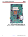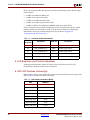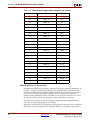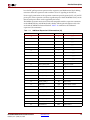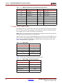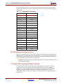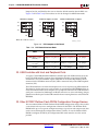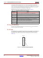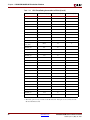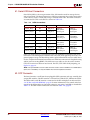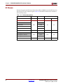
1
ML505/ML506/ML507
ML505/ML506/M
L507 Evaluation
Evaluation
Platform
Platform
User Guide [optional]
UG347 (v3.1.2) May 16, 2011 [optional]
R
R
Xilinx is disclosing this user guide, manual, release note, and/or specification (the "Documentation") to you solely for use in the development
of designs to operate with Xilinx hardware devices. You may not reproduce, distribute, republish, download, display, post, or transmit the
Documentation in any form or by any means including, but not limited to, electronic, mechanical, photocopying, recording, or otherwise,
without the prior written consent of Xilinx. Xilinx expressly disclaims any liability arising out of your use of the Documentation. Xilinx reserves
the right, at its sole discretion, to change the Documentation without notice at any time. Xilinx assumes no obligation to correct any errors
contained in the Documentation, or to advise you of any corrections or updates. Xilinx expressly disclaims any liability in connection with
technical support or assistance that may be provided to you in connection with the Information.
THE DOCUMENTATION IS DISCLOSED TO YOU “AS-IS” WITH NO WARRANTY OF ANY KIND. XILINX MAKES NO OTHER
WARRANTIES, WHETHER EXPRESS, IMPLIED, OR STATUTORY, REGARDING THE DOCUMENTATION, INCLUDING ANY
WARRANTIES OF MERCHANTABILITY, FITNESS FOR A PARTICULAR PURPOSE, OR NONINFRINGEMENT OF THIRD-PARTY
RIGHTS. IN NO EVENT WILL XILINX BE LIABLE FOR ANY CONSEQUENTIAL, INDIRECT, EXEMPLARY, SPECIAL, OR INCIDENTAL
DAMAGES, INCLUDING ANY LOSS OF DATA OR LOST PROFITS, ARISING FROM YOUR USE OF THE DOCUMENTATION.
© 2006–2011 Xilinx, Inc. All rights reserved.
XILINX, the Xilinx logo, the Brand Window, and other designated brands included herein are trademarks of Xilinx, Inc. PCI, PCI-SIG,
PCI EXPRESS, PCIE, PCI-X, PCI HOT PLUG, MINI PCI, EXPRESSMODULE, and the PCI, PCI-X, PCI HOT PLUG, and MINI PC design
marks are trademarks, registered trademarks, and/or service marks of PCI-SIG. All other trademarks are the property of their respective
owners.
Revision History
The following table shows the revision history for this document.
Date
Version
11/29/06
1.0
Revision
Initial Xilinx release.
Added “44. Soft Touch Landing Pad,” page 48
12/01/06
1.1
Corrected Table 1-6, page 21
Added Table 1-13, page 26
Added new paragraph to “36. VGA Input Video Codec,” page 37
01/09/06
1.2
Enhanced Table 1-3, page 19
Corrected Table 1-31, page 47
Updated document to include ML506 board
Corrected Table 1-31, page 47
02/16/07
2.0
Enhanced Figure 1-5, page 34
Expanded “26. AC Adapter and Input Power Switch/Jack,” page 34
Added Figure B-1, page 57
Updated “Features,” page 11
03/21/07
2.1
Swapped Table 1-3, page 19 with Table 1-24, page 42 for better placement of information
Updated description for Table 1-25, page 43
Updated Table 1-31, page 47 (see table notes)
04/17/07
2.2
06/28/07
2.3
10/30/07
2.4
Corrected GTP/GTX tile location in Table 1-24, page 42
Corrected J5 pin 28 in Table 1-11, page 25
Updated Table 1-31, page 47 for XAUI/SRIO support
Update Appendix C, “References”Table 1-11, page 25
Added sections on “MIG Compliance,” page 18 and “45. System Monitor,” page 49
ML505/ML506/ML507 Evaluation Platform
www.xilinx.com
UG347 (v3.1.2) May 16, 2011
Date
Version
Revision
Updated document to include ML507 board.
05/19/08
3.0
Added notes for Figure 1-7, page 39 and Table 1-21, page 39.
Updated Appendix C, “References.”
Updated link in Appendix C, “References.”
07/21/08
3.0.1
11/10/08
3.1
10/07/09
3.1.1
Minor typographical edit.
05/16/11
3.1.2
Edited typo in title of Table 1-5, page 20.
UG347 (v3.1.2) May 16, 2011
Updated Appendix A, “Board Revisions.”
Added content to “17. System ACE and CompactFlash Connector,” page 28 and
“Configuration Options,” page 53. Updated Platform Flash memory to Platform Flash
PROM throughout.
www.xilinx.com
ML505/ML506/ML507 Evaluation Platform
ML505/ML506/ML507 Evaluation Platform
www.xilinx.com
UG347 (v3.1.2) May 16, 2011
Table of Contents
Preface: About This Guide
Guide Contents . . . . . . . . . . . . . . . . . . . . . . . . . . . . . . . . . . . . . . . . . . . . . . . . . . . . . . . . . . . . . .
Additional Documentation . . . . . . . . . . . . . . . . . . . . . . . . . . . . . . . . . . . . . . . . . . . . . . . . . . .
Additional Support Resources . . . . . . . . . . . . . . . . . . . . . . . . . . . . . . . . . . . . . . . . . . . . . . . .
Typographical Conventions . . . . . . . . . . . . . . . . . . . . . . . . . . . . . . . . . . . . . . . . . . . . . . . . . .
7
7
8
8
Online Document . . . . . . . . . . . . . . . . . . . . . . . . . . . . . . . . . . . . . . . . . . . . . . . . . . . . . . . . . . 9
Overview . . . . . . . . . . . . . . . . . . . . . . . . . . . . . . . . . . . . . . . . . . . . . . . . . . . . . . . . . . . . . . . . . . . 11
Features . . . . . . . . . . . . . . . . . . . . . . . . . . . . . . . . . . . . . . . . . . . . . . . . . . . . . . . . . . . . . . . . .
Package Contents . . . . . . . . . . . . . . . . . . . . . . . . . . . . . . . . . . . . . . . . . . . . . . . . . . . . . . . . .
Additional Information . . . . . . . . . . . . . . . . . . . . . . . . . . . . . . . . . . . . . . . . . . . . . . . . . . . .
Block Diagram . . . . . . . . . . . . . . . . . . . . . . . . . . . . . . . . . . . . . . . . . . . . . . . . . . . . . . . . . . .
11
13
13
14
Related Xilinx Documents . . . . . . . . . . . . . . . . . . . . . . . . . . . . . . . . . . . . . . . . . . . . . . . . . . . 14
Detailed Description . . . . . . . . . . . . . . . . . . . . . . . . . . . . . . . . . . . . . . . . . . . . . . . . . . . . . . . . 15
1. Virtex-5 FPGA . . . . . . . . . . . . . . . . . . . . . . . . . . . . . . . . . . . . . . . . . . . . . . . . . . . . . . . . .
Configuration . . . . . . . . . . . . . . . . . . . . . . . . . . . . . . . . . . . . . . . . . . . . . . . . . . . . . . . . .
I/O Voltage Rails . . . . . . . . . . . . . . . . . . . . . . . . . . . . . . . . . . . . . . . . . . . . . . . . . . . . . .
Digitally Controlled Impedance . . . . . . . . . . . . . . . . . . . . . . . . . . . . . . . . . . . . . . . . . . .
2. DDR2 SODIMM . . . . . . . . . . . . . . . . . . . . . . . . . . . . . . . . . . . . . . . . . . . . . . . . . . . . . . . .
MIG Compliance . . . . . . . . . . . . . . . . . . . . . . . . . . . . . . . . . . . . . . . . . . . . . . . . . . . . . . .
DDR2 Memory Expansion . . . . . . . . . . . . . . . . . . . . . . . . . . . . . . . . . . . . . . . . . . . . . . .
DDR2 Clock Signal . . . . . . . . . . . . . . . . . . . . . . . . . . . . . . . . . . . . . . . . . . . . . . . . . . . . .
DDR2 Signaling . . . . . . . . . . . . . . . . . . . . . . . . . . . . . . . . . . . . . . . . . . . . . . . . . . . . . . .
3. Differential Clock Input and Output with SMA Connectors . . . . . . . . . . . . . . . . . .
4. Oscillators . . . . . . . . . . . . . . . . . . . . . . . . . . . . . . . . . . . . . . . . . . . . . . . . . . . . . . . . . . . . .
5. LCD Brightness and Contrast Adjustment . . . . . . . . . . . . . . . . . . . . . . . . . . . . . . . . .
6. GPIO DIP Switches (Active-High). . . . . . . . . . . . . . . . . . . . . . . . . . . . . . . . . . . . . . . . .
7. User and Error LEDs (Active-High) . . . . . . . . . . . . . . . . . . . . . . . . . . . . . . . . . . . . . . .
8. User Pushbuttons (Active-High) . . . . . . . . . . . . . . . . . . . . . . . . . . . . . . . . . . . . . . . . . .
9. CPU Reset Button (Active-Low) . . . . . . . . . . . . . . . . . . . . . . . . . . . . . . . . . . . . . . . . . .
10. XGI Expansion Headers . . . . . . . . . . . . . . . . . . . . . . . . . . . . . . . . . . . . . . . . . . . . . . . .
Differential Expansion I/O Connectors . . . . . . . . . . . . . . . . . . . . . . . . . . . . . . . . . . . . .
Single-Ended Expansion I/O Connectors . . . . . . . . . . . . . . . . . . . . . . . . . . . . . . . . . . . .
Other Expansion I/O Connectors . . . . . . . . . . . . . . . . . . . . . . . . . . . . . . . . . . . . . . . . . .
11. Stereo AC97 Audio Codec . . . . . . . . . . . . . . . . . . . . . . . . . . . . . . . . . . . . . . . . . . . . . .
12. RS-232 Serial Port . . . . . . . . . . . . . . . . . . . . . . . . . . . . . . . . . . . . . . . . . . . . . . . . . . . . . .
13. 16-Character x 2-Line LCD . . . . . . . . . . . . . . . . . . . . . . . . . . . . . . . . . . . . . . . . . . . . . .
14. IIC Bus with 8-Kb EEPROM . . . . . . . . . . . . . . . . . . . . . . . . . . . . . . . . . . . . . . . . . . . . .
15. DVI Connector . . . . . . . . . . . . . . . . . . . . . . . . . . . . . . . . . . . . . . . . . . . . . . . . . . . . . . . .
16. PS/2 Mouse and Keyboard Ports . . . . . . . . . . . . . . . . . . . . . . . . . . . . . . . . . . . . . . . .
17. System ACE and CompactFlash Connector . . . . . . . . . . . . . . . . . . . . . . . . . . . . . . . .
18. ZBT Synchronous SRAM . . . . . . . . . . . . . . . . . . . . . . . . . . . . . . . . . . . . . . . . . . . . . . .
19. Linear Flash Chips . . . . . . . . . . . . . . . . . . . . . . . . . . . . . . . . . . . . . . . . . . . . . . . . . . . . .
20. Xilinx XC95144XL CPLD . . . . . . . . . . . . . . . . . . . . . . . . . . . . . . . . . . . . . . . . . . . . . . . .
21. 10/100/1000 Tri-Speed Ethernet PHY . . . . . . . . . . . . . . . . . . . . . . . . . . . . . . . . . . . .
22. USB Controller with Host and Peripheral Ports . . . . . . . . . . . . . . . . . . . . . . . . . . . .
23. Xilinx XCF32P Platform Flash PROM Configuration Storage Devices . . . . . . . . .
ML505/ML506/ML507 Evaluation Platform
UG347 (v3.1.2) May 16, 2011
www.xilinx.com
17
17
17
18
18
18
19
19
19
19
19
20
20
21
22
22
22
22
23
24
26
27
27
27
27
28
28
30
30
30
31
32
32
5
R
24. JTAG Configuration Port . . . . . . . . . . . . . . . . . . . . . . . . . . . . . . . . . . . . . . . . . . . . . . .
25. Onboard Power Supplies . . . . . . . . . . . . . . . . . . . . . . . . . . . . . . . . . . . . . . . . . . . . . . .
26. AC Adapter and Input Power Switch/Jack . . . . . . . . . . . . . . . . . . . . . . . . . . . . . . . .
27. Power Indicator LED . . . . . . . . . . . . . . . . . . . . . . . . . . . . . . . . . . . . . . . . . . . . . . . . . . .
28. DONE LED . . . . . . . . . . . . . . . . . . . . . . . . . . . . . . . . . . . . . . . . . . . . . . . . . . . . . . . . . . .
29. INIT LED . . . . . . . . . . . . . . . . . . . . . . . . . . . . . . . . . . . . . . . . . . . . . . . . . . . . . . . . . . . . .
30. Program Switch . . . . . . . . . . . . . . . . . . . . . . . . . . . . . . . . . . . . . . . . . . . . . . . . . . . . . . .
31. Configuration Address and Mode DIP Switches . . . . . . . . . . . . . . . . . . . . . . . . . . .
32. Encryption Key Battery . . . . . . . . . . . . . . . . . . . . . . . . . . . . . . . . . . . . . . . . . . . . . . . . .
33. SPI Flash . . . . . . . . . . . . . . . . . . . . . . . . . . . . . . . . . . . . . . . . . . . . . . . . . . . . . . . . . . . . .
34. IIC Fan Controller and Temperature/Voltage Monitor . . . . . . . . . . . . . . . . . . . . . .
35. Piezo . . . . . . . . . . . . . . . . . . . . . . . . . . . . . . . . . . . . . . . . . . . . . . . . . . . . . . . . . . . . . . . . .
36. VGA Input Video Codec . . . . . . . . . . . . . . . . . . . . . . . . . . . . . . . . . . . . . . . . . . . . . . . .
37. JTAG Trace/Debug . . . . . . . . . . . . . . . . . . . . . . . . . . . . . . . . . . . . . . . . . . . . . . . . . . . .
CPU Debug Description . . . . . . . . . . . . . . . . . . . . . . . . . . . . . . . . . . . . . . . . . . . . . . . . .
CPU JTAG Header Pinout . . . . . . . . . . . . . . . . . . . . . . . . . . . . . . . . . . . . . . . . . . . . . . .
CPU JTAG Connection to FPGA . . . . . . . . . . . . . . . . . . . . . . . . . . . . . . . . . . . . . . . . . . .
38. Rotary Encoder . . . . . . . . . . . . . . . . . . . . . . . . . . . . . . . . . . . . . . . . . . . . . . . . . . . . . . . .
39. Differential GTP/GTX Input and Output with SMA Connectors . . . . . . . . . . . . .
40. PCI Express Interface . . . . . . . . . . . . . . . . . . . . . . . . . . . . . . . . . . . . . . . . . . . . . . . . . . .
41. Serial-ATA Host Connectors . . . . . . . . . . . . . . . . . . . . . . . . . . . . . . . . . . . . . . . . . . . .
42. SFP Connector . . . . . . . . . . . . . . . . . . . . . . . . . . . . . . . . . . . . . . . . . . . . . . . . . . . . . . . .
43. GTP/GTX Clocking Circuitry . . . . . . . . . . . . . . . . . . . . . . . . . . . . . . . . . . . . . . . . . . .
Overview . . . . . . . . . . . . . . . . . . . . . . . . . . . . . . . . . . . . . . . . . . . . . . . . . . . . . . . . . . . .
Frequency Synthesizer for SFP/SMA GTP/GTX Transceiver Clocking . . . . . . . . . . . . .
SATA GTP/GTX Transceiver Clock Generation. . . . . . . . . . . . . . . . . . . . . . . . . . . . . . .
SGMII / Loopback GTP/GTX Transceiver Clock Generation . . . . . . . . . . . . . . . . . . . .
44. Soft Touch Landing Pad . . . . . . . . . . . . . . . . . . . . . . . . . . . . . . . . . . . . . . . . . . . . . . . .
45. System Monitor . . . . . . . . . . . . . . . . . . . . . . . . . . . . . . . . . . . . . . . . . . . . . . . . . . . . . . .
33
33
34
34
35
35
35
35
36
36
37
37
37
38
38
41
41
42
42
43
44
44
46
46
46
47
47
48
49
IIC Buses . . . . . . . . . . . . . . . . . . . . . . . . . . . . . . . . . . . . . . . . . . . . . . . . . . . . . . . . . . . . . . . . . . . 52
Configuration Options . . . . . . . . . . . . . . . . . . . . . . . . . . . . . . . . . . . . . . . . . . . . . . . . . . . . . . 53
JTAG (Xilinx Download Cable and System ACE Controller) Configuration . . . . . . .
Platform Flash PROM Configuration . . . . . . . . . . . . . . . . . . . . . . . . . . . . . . . . . . . . . . . .
Linear Flash Memory Configuration . . . . . . . . . . . . . . . . . . . . . . . . . . . . . . . . . . . . . . . .
SPI Flash Memory Configuration . . . . . . . . . . . . . . . . . . . . . . . . . . . . . . . . . . . . . . . . . . .
53
54
54
54
Appendix A: Board Revisions
Appendix B: Programming the IDT Clock Chip
Overview . . . . . . . . . . . . . . . . . . . . . . . . . . . . . . . . . . . . . . . . . . . . . . . . . . . . . . . . . . . . . . . . . . . 57
Downloading to the ML50x Board . . . . . . . . . . . . . . . . . . . . . . . . . . . . . . . . . . . . . . . . . . . 57
Appendix C: References
6
www.xilinx.com
ML505/ML506/ML507 Evaluation Platform
UG347 (v3.1.2) May 16, 2011
R
Preface
About This Guide
The ML50x evaluation platforms enable designers to investigate and experiment with
features of Virtex®-5 FPGAs. This user guide describes the features and operation of the
ML505 (LXT), ML506 (SXT), and ML507 (FXT) Evaluation Platforms.
Guide Contents
This manual contains the following chapters:
•
Chapter 1, “ML505/ML506/ML507 Evaluation Platform,”provides details on the
board components
•
Appendix A, “Board Revisions,” details the differences between board revisions
•
Appendix B, “Programming the IDT Clock Chip,” shows how to restore the default
factory settings for the clock chip on the ML50x boards
•
Appendix C, “References”
Additional Documentation
The following documents are also available for download at
http://www.xilinx.com/virtex5.
•
Virtex-5 FPGA Family Overview
The features and product selection of the Virtex-5 FPGA family are outlined in this
overview.
•
Virtex-5 FPGA Data Sheet: DC and Switching Characteristics
This data sheet contains the DC and Switching Characteristic specifications for the
Virtex-5 FPGA family.
•
Virtex-5 FPGA User Guide
This user guide includes chapters on:
♦
Clocking Resources
♦
Clock Management Technology (CMT)
♦
Phase-Locked Loops (PLLs)
♦
Block RAM and FIFO memory
♦
Configurable Logic Blocks (CLBs)
♦
SelectIO™ Resources
♦
I/O Logic Resources
♦
Advanced I/O Logic Resources
ML505/ML506/ML507 Evaluation Platform
UG347 (v3.1.2) May 16, 2011
www.xilinx.com
7
R
Preface: About This Guide
•
Virtex-5 FPGA RocketIO GTP/GTX Transceiver User Guide
This guide describes the RocketIO™ GTP/GTX transceivers available in the Virtex-5
LXT and SXT platform devices.
•
Virtex-5 FPGA Tri-Mode Ethernet Media Access Controller User Guide
This user guide describes the dedicated Tri-Mode Ethernet Media Access Controller
available in the Virtex-5 LXT and SXT platform devices.
•
Virtex-5 FPGA Integrated Endpoint Block User Guide for PCI Express Designs
This user guide describes the integrated Endpoint blocks in the Virtex-5 LXT and SXT
platform devices for PCI Express® designs.
•
XtremeDSP Design Considerations
This guide describes the XtremeDSP. slice and includes reference designs for using the
DSP48E.
•
Virtex-5 FPGA Configuration User Guide
This all-encompassing configuration guide includes chapters on configuration
interfaces (serial and SelectMAP), bitstream encryption, Boundary-Scan and JTAG
configuration, reconfiguration techniques, and readback through the SelectMAP and
JTAG interfaces.
•
Virtex-5 FPGA System Monitor User Guide
The System Monitor functionality available in all the Virtex-5 devices is outlined in
this guide.
•
Virtex-5 FPGA Packaging and Pinout Specification
This specification includes the tables for device/package combinations and maximum
I/Os, pin definitions, pinout tables, pinout diagrams, mechanical drawings, and
thermal specifications.
Additional Support Resources
To search the database of silicon and software questions and answers, or to create a
technical support case in WebCase, see the Xilinx website at:
http://www.xilinx.com/support.
Typographical Conventions
This document uses the following typographical conventions. An example illustrates each
convention.
Convention
Meaning or Use
Example
References to other documents
See the Virtex-5 Configuration
Guide for more information.
Emphasis in text
The address (F) is asserted after
clock event 2.
Indicates a link to a web page.
http://www.xilinx.com/virtex5
Italic font
Underlined Text
8
www.xilinx.com
ML505/ML506/ML507 Evaluation Platform
UG347 (v3.1.2) May 16, 2011
R
Typographical Conventions
Online Document
The following conventions are used in this document:
Convention
Meaning or Use
Example
Blue text
Cross-reference link to a
location in the current
document
See the section “Additional
Documentation” for details.
Red text
Cross-reference link to a
location in another document
See Figure 5 in the Virtex-5 Data
Sheet
Blue, underlined text
Hyperlink to a website (URL)
Go to http://www.xilinx.com
for the latest documentation.
ML505/ML506/ML507 Evaluation Platform
UG347 (v3.1.2) May 16, 2011
www.xilinx.com
9
R
Preface: About This Guide
10
www.xilinx.com
ML505/ML506/ML507 Evaluation Platform
UG347 (v3.1.2) May 16, 2011
R
Chapter 1
ML505/ML506/ML507 Evaluation
Platform
Overview
ML505, ML506, and ML507 Evaluation Platforms (referred to as ML50x in this guide)
enable designers to investigate and experiment with features of the Virtex-5 LXT, SXT, and
FXT FPGAs. This user guide describes the features and operation of these platforms.
Although the ML50x platforms provide access to the Virtex-5 FPGA RocketIO™ GTP and
GTX transceivers, these boards are only intended for evaluation purposes, not for
transceiver characterization.
The ML505, ML506, and ML507 platforms use the same printed-circuit board (PCB). See
Appendix A, “Board Revisions” for distinguishing characteristics.
Features
•
Xilinx Virtex-5 FPGA
♦
XC5VLX50T-1FFG1136 (ML505)
♦
XC5VSX50T-1FFG1136 (ML506)
♦
XC5VFX70T-1FFG1136 (ML507)
•
Two Xilinx XCF32P Platform Flash PROMs (32 Mb each) for storing large device
configurations
•
Xilinx System ACE™ CompactFlash configuration controller with Type I
CompactFlash connector
•
Xilinx XC95144XL CPLD for glue logic
•
64-bit wide, 256-MB DDR2 small outline DIMM (SODIMM), compatible with EDK
supported IP and software drivers
•
Clocking
♦
Programmable system clock generator chip
♦
One open 3.3V clock oscillator socket
♦
External clocking via SMAs (two differential pairs)
•
General purpose DIP switches (8), LEDs (8), pushbuttons, and rotary encoder
•
Expansion header with 32 single-ended I/O, 16 LVDS-capable differential pairs,
14 spare I/Os shared with buttons and LEDs, power, JTAG chain expansion
capability, and IIC bus expansion
•
Stereo AC97 audio codec with line-in, line-out, 50-mW headphone, microphone-in
jacks, SPDIF digital audio jacks, and piezo audio transducer
ML505/ML506/ML507 Evaluation Platform
UG347 (v3.1.2) May 16, 2011
www.xilinx.com
11
R
Chapter 1: ML505/ML506/ML507 Evaluation Platform
12
•
RS-232 serial port, DB9 and header for second serial port
•
16-character x 2-line LCD display
•
One 8-Kb IIC EEPROM and other IIC capable devices
•
PS/2 mouse and keyboard connectors
•
Video input/output
♦
Video input (VGA)
♦
Video output DVI connector (VGA supported with included adapter)
•
ZBT synchronous SRAM, 9 Mb on 32-bit data bus with four parity bits
•
Intel P30 StrataFlash linear flash chip (32 MB)
•
Serial Peripheral Interface (SPI) flash (2 MB)
•
10/100/1000 tri-speed Ethernet PHY transceiver and RJ-45 with support for MII,
GMII, RGMII, and SGMII Ethernet PHY interfaces
•
USB interface chip with host and peripheral ports
•
Rechargeable lithium battery to hold FPGA encryption keys
•
JTAG configuration port for use with Parallel Cable III, Parallel Cable IV, or Platform
USB download cable
•
Onboard power supplies for all necessary voltages
•
Temperature and voltage monitoring chip with fan controller
•
5V @ 6A AC adapter
•
Power indicator LED
•
MII, GMII, RGMII, and SGMII Ethernet PHY Interfaces
•
GTP/GTX: SFP (1000Base-X)
•
GTP/GTX: SMA (RX and TX Differential Pairs)
•
GTP/GTX: SGMII
•
GTP/GTX: PCI Express® (PCIe™) edge connector (x1 Endpoint)
•
GTP/GTX: SATA (dual host connections) with loopback cable
•
GTP/GTX: Clock synthesis ICs
•
Mictor trace port
•
BDM debug port
•
Soft touch port
•
System monitor
www.xilinx.com
ML505/ML506/ML507 Evaluation Platform
UG347 (v3.1.2) May 16, 2011
R
Overview
Package Contents
•
Xilinx Virtex-5 FPGA ML50x Evaluation Platform
•
System ACE CompactFlash card
•
Power supply
•
DVI to VGA adaptor
Additional Information
Additional information and support material is located at:
•
ML505 - http://www.xilinx.com/ml505
•
ML506 - http://www.xilinx.com/ml506
•
ML507 - http://www.xilinx.com/ml507
This information includes:
•
Current version of this user guide in PDF format
•
Example design files for demonstration of Virtex-5 FPGA features and technology
•
Demonstration hardware and software configuration files for the System ACE
controller, Platform Flash PROM configuration storage device, CPLD, and linear flash
chips
•
MicroBlaze™ EDK reference design files
•
Full schematics in PDF format and ViewDraw schematic format
•
PC board layout in Allegro PCB format
•
Gerber files for the PC board (Many free or shareware Gerber file viewers are
available on the internet for viewing and printing these files.)
•
Additional documentation, errata, frequently asked questions, and the latest news
For information about the Virtex-5 family of FPGA devices, including product highlights,
data sheets, user guides, and application notes, see the Virtex-5 FPGA website at
www.xilinx.com/virtex5. Additional information is available from the data sheets and
application notes from the component manufacturers.
ML505/ML506/ML507 Evaluation Platform
UG347 (v3.1.2) May 16, 2011
www.xilinx.com
13
R
Chapter 1: ML505/ML506/ML507 Evaluation Platform
Block Diagram
Figure 1-1 shows a block diagram of the ML50x Evaluation Platform (board).
PC4
JTAG
CF
CPLD
Misc. Glue Logic
System ACE
Controller
32
16
Flash
USB
Controller
JTAG
Sync
SRAM
SPI
10/100/1000
Ethernet PHY
Platform Flash
Digital Audio
Master Serial
JTAG
Slave Serial
SelectMap
SPI Cfg
BPI Flash Cfg
Piezo/Speaker
RJ-45
DDR2
SO-DIMM
16
GPIO
(Button/LED/DIP Switch)
Host
Peripheral
Peripheral
AC97
Audio CODEC
16
32
32
Line Out /
Headphone
Mic In / Line In
VGA Input
Codec
PLL Clock Generator
Plus User Oscillator
DVI Output
Codec
System Monitor
Virtex-5
LXT/SXT/FXT
FPGA
SMA
(Differential In/Out Clocks)
RS-232 XCVR
JTAG
16 X 32
Character LCD
User IIC Bus
XGI Header
GTP: 4 SMA
Serial
Battery and
Fan Header
Dual PS/2
GTP: 2 Serial ATA
DVI-I Video Out
IIC EEPROM
GTP: 4 SFP
GTP: PCIe 1x
UG347_03_110807
Figure 1-1:
Virtex-5 FPGA ML50x Evaluation Platform Block Diagram
Related Xilinx Documents
Prior to using the ML50x Evaluation Platform, users should be familiar with Xilinx
resources. See Appendix C, “References” for direct links to Xilinx documentation. See the
following locations for additional documentation on Xilinx tools and solutions:
14
•
EDK: www.xilinx.com/edk
•
ISE: www.xilinx.com/ise
•
Answer Browser: www.xilinx.com/support
•
Intellectual Property: www.xilinx.com/ipcenter
www.xilinx.com
ML505/ML506/ML507 Evaluation Platform
UG347 (v3.1.2) May 16, 2011
R
Detailed Description
Detailed Description
The ML505 Evaluation Platform is shown in Figure 1-2 (front) and Figure 1-3, page 16
(back). The numbered sections on the pages following the figures contain details on each
feature.
10
38
27
6
26
4
35
3
Diff Output Pair
8
44
32
5
11
1
13
28
29
45
7
12
34
25
39
Keybd
37
9
41
16
Mouse
40
31
System ACE Reset
24
30
22
3
36
21
Diff Input Pair
15
UG347_01_102907
Figure 1-2:
ML505/ML506/ML507 Evaluation Platform
UG347 (v3.1.2) May 16, 2011
Detailed Description of Virtex-5 FPGA ML505 Components (Front)
www.xilinx.com
15
R
Chapter 1: ML505/ML506/ML507 Evaluation Platform
14
33
2
23
43
17
UG347_02_112906
Figure 1-3:
Detailed Description of Virtex-5 FPGA ML505 Components (Back)
Note: The label on the CompactFlash (CF) card shipped with your board might differ from the one
shown.
16
www.xilinx.com
ML505/ML506/ML507 Evaluation Platform
UG347 (v3.1.2) May 16, 2011
R
Detailed Description
1. Virtex-5 FPGA
A Xilinx Virtex-5 FPGA is installed on the board. See Appendix A, “Board Revisions” for
device details.
Configuration
The board supports configuration in all modes: JTAG, Master Serial, Slave Serial, Master
SelectMAP, Slave SelectMAP, Byte-wide Peripheral Interface (BPI) Up, BPI Down, and SPI
modes. See the “Configuration Options,” page 53 section for more information.
I/O Voltage Rails
Table 1-1 summarizes the FPGA I/O voltage rail and the voltages applied to each bank.
Table 1-1:
I/O Voltage Rail of FPGA Banks
FPGA Bank
I/O Voltage Rail
0
3.3V
1
3.3V
2
3.3V
3
2.5V no DCI
4
3.3V no DCI
5 (1)
3.3V DCI with 49.9Ω resistors installed
6
3.3V (unused)
11
User selectable as 2.5V or 3.3V using jumper J20
12
3.3V DCI with 49.9Ω resistors installed
13
User selectable as 2.5V or 3.3V using jumper J20
15
1.8V DCI with 49.9Ω resistors installed
17
1.8V DCI with 49.9Ω resistors installed
18
3.3V no DCI
19
1.8V DCI with 49.9Ω resistors installed
20
3.3V DCI with 49.9Ω resistors installed
21
1.8V DCI with 49.9Ω resistors installed
22
3.3V DCI with 49.9Ω resistors installed
23 (1)
3.3V DCI with 49.9Ω resistors installed
25
3.3V (unused)
Notes:
1. Banks 5 and 23 are available on the ML507 only.
ML505/ML506/ML507 Evaluation Platform
UG347 (v3.1.2) May 16, 2011
www.xilinx.com
17
R
Chapter 1: ML505/ML506/ML507 Evaluation Platform
Digitally Controlled Impedance
Some FPGA banks can support the digitally controlled impedance (DCI) feature in
Virtex-5 FPGAs. Support for DCI is summarized in Table 1-2.
Table 1-2:
DCI Capability of FPGA Bank
FPGA Bank
DCI Capability
1
Not supported
2
Not supported
3
Not supported
4
Not supported
11
Yes, 49.9Ω resistors are installed
12
Not supported
13
Yes, 49.9Ω resistors are installed
14
Yes, 49.9Ω resistors are installed
15
Yes, 49.9Ω resistors are installed
16
Yes, 49.9Ω resistors are installed
17
Yes, 49.9Ω resistors are installed
18
Not supported
21
Yes, 49.9Ω resistors are installed
2. DDR2 SODIMM
The ML50x platform is shipped with a single-rank unregistered 256 MB SODIMM. The
DDR2 SODIMM used is generally a Micron MT4HTF3264HY-53E or similar module. Serial
Presence Detect (SPD) using an IIC interface to the DDR DIMM is also supported with the
FPGA.
Note: The board is only tested for DDR2 SDRAM operation at a 400 MHz data rate. Faster data
rates might be possible but are not tested.
MIG Compliance
The ML50x DDR2 interface is MIG pinout compliant. The MIG DDR2 routing guidelines
outlined in the Xilinx Memory Interface Generator (MIG) User Guide [Ref 17] have been
achieved.
The board’s DDR2 SODIMM memory interface is designed to the requirements defined by
the MIG User Guide using the MIG tool. The MIG documentation requires that designers
follow the MIG pinout and layout guidelines. The MIG tool generates and ensures that the
proper FPGA I/O pin selections are made in support of the board’s DDR2 interface. The
initial pin selection for the board was modified and then re-verified to meet the MIG
pinout requirements. To ensure a robust interface, the ML50x DDR2 layout incorporates
matched trace lengths for data signals to the corresponding data strobe signal as defined in
the MIG user guide. See Appendix C, “References” for links to additional information
about MIG and Virtex-5 FPGAs in general.
18
www.xilinx.com
ML505/ML506/ML507 Evaluation Platform
UG347 (v3.1.2) May 16, 2011
R
Detailed Description
DDR2 Memory Expansion
The DDR2 interface support user installation of SODIMM modules with more memory
since higher order address and chip select signals are also routed from the SODIMM to the
FPGA.
DDR2 Clock Signal
Two matched length pairs of DDR2 clock signals are broadcast from the FPGA to the
SODIMM. The FPGA design is responsible for driving both clock pairs with low skew. The
delay on the clock trace is designed to match the delay of the other DDR2 control signals.
DDR2 Signaling
All DDR2 SDRAM control signals are terminated through 47Ω resistors to a 0.9V VTT
reference voltage. The FPGA DDR2 interface supports SSTL18 signaling and all DDR2
signals are controlled impedance. The DDR2 data, mask, and strobe signals are matched
length within byte groups. The ODT functionality of the SODIMM should be utilized.
3. Differential Clock Input and Output with SMA Connectors
High-precision clock signals can be input to the FPGA using differential clock signals
brought in through 50Ω SMA connectors. This allows an external function generator or
other clock source to drive the differential clock inputs that directly feed the global clock
input pins of the FPGA. The FPGA can be configured to present a 100Ω termination
impedance.
A differential clock output from the FPGA is driven out through an LVDS clock
multiplexer (U12) onto a second pair of SMA connectors (J12 and J13). This allows the
FPGA to drive a precision clock to an external device such as a piece of test equipment.
Table 1-3 summarizes the differential SMA clock pin connections.
Table 1-3:
Differential SMA Clock Connections
Connector
Clock Name
FPGA Pin
J10
SMA_DIFF_CLK_IN_P
H14
J11
SMA_DIFF_CLK_IN_N
H15
J12 (1)
SMA_DIFF_CLK_OUT_P
J20
J13 (1)
SMA_DIFF_CLK_OUT_N
J21
ML505/ML506
ML507
GTP1 of
GTP_X0Y4
receive pair
GTX1 of
GTP1 of
GTP_X0Y4
transmit pair
GTX1 of
GTX_X0Y5
transmit pair
GTX_X0Y5
receive pair
Notes:
1. When jumper J54 (located near the battery) is not shunted (default), the FPGA differential clock output
is selected on U12 and driven out to the SMA connectors, J12 and J13.
4. Oscillators
The board has one crystal oscillator socket (X1) wired for standard LVTTL-type oscillators.
It connects to the FPGA clock pin as shown in Table 1-4, page 20. The X1 socket is
populated with a 100-MHz oscillator and is powered by the 3.3V supply.
The board also provides an IDT5V9885 (U8) EEPROM programmable clock generator
device. This device is used to generate a variety of clocks to the board peripherals and
ML505/ML506/ML507 Evaluation Platform
UG347 (v3.1.2) May 16, 2011
www.xilinx.com
19
R
Chapter 1: ML505/ML506/ML507 Evaluation Platform
FPGA. The programmable clock generator provides the following factory default singleended outputs:
•
25 MHz to the Ethernet PHY (U16)
•
14 MHz to the audio codec (U22)
•
27 MHz to the USB Controller (U23)
•
33 MHz to the Xilinx System ACE CF (U2)
•
33 MHz, 27 MHz, and a differential 200 MHz clock to the Xilinx FPGA
If users change the factory default configuration of the clock generator chip, the related
reference design material might not work as designed. Instructions for returning the
IDT5V9885 to the factory default configuration are provided in Appendix B,
“Programming the IDT Clock Chip.”
Table 1-4:
Oscillator Socket Connections
Reference
Designator
Clock Name
FPGA Pin
X1
USER_CLK
AH15
100 MHz single-ended
U8
CLK_33MHZ_FPGA
AH17
33 MHz single-ended
U8
CLK_27MHZ_FPGA
AG18
27 MHz single-ended
U8
CLK_FPGA_P
L19
200 MHz differential pair (pos)
U8
CLK_FPGA_N
K19
200 MHz differential pair (neg)
Description
5. LCD Brightness and Contrast Adjustment
Turning potentiometer R87 adjusts the image contrast of the character LCD. The
potentiometer should be turned with a screwdriver.
6. GPIO DIP Switches (Active-High)
Eight general-purpose (active-High) DIP switches are connected to the user I/O pins of the
FPGA. Table 1-5 summarizes these connections.
Table 1-5:
20
DIP Switch Connections (SW8)
SW4
FPGA Pin
GPIO_DIP_SW1
U25
GPIO_DIP_SW2
AG27
GPIO_DIP_SW3
AF25
GPIO_DIP_SW4
AF26
GPIO_DIP_SW5
AE27
GPIO_DIP_SW6
AE26
GPIO_DIP_SW7
AC25
GPIO_DIP_SW8
AC24
www.xilinx.com
ML505/ML506/ML507 Evaluation Platform
UG347 (v3.1.2) May 16, 2011
R
Detailed Description
7. User and Error LEDs (Active-High)
There are a total of 15 active-High LEDs directly controllable by the FPGA:
•
Eight green LEDs are general purpose LEDs arranged in a row
•
Five green LEDs are positioned next to the North-East-South-West-Center-oriented
pushbuttons (only the center one is cited in Figure 1-2, page 15)
•
Two red LEDs are intended to be used for signaling error conditions, such as bus
errors, but can be used for any other purpose
Some LEDs are buffered through the CPLD to allow the LED signals to be used as higherperformance I/O by way of the XGI expansion connector. Table 1-6 summarizes the LED
definitions and connections.
Table 1-6:
User and Error LED Connections
Reference
Designator
Label/Definition
Color
FPGA Pin
Buffered
DS20
LED North
Green
AF13
Yes
DS21
LED East
Green
AG23
Yes
DS22
LED South
Green
AG12
Yes
DS23
LED West
Green
AF23
Yes
DS24
LED Center
Green
E8
Yes
DS17
GPIO LED 0
Green
H18
Yes
DS16
GPIO LED 1
Green
L18
Yes
DS15
GPIO LED 2
Green
G15
Yes
DS14
GPIO LED 3
Green
AD26
No
DS13
GPIO LED 4
Green
G16
Yes
DS12
GPIO LED 5
Green
AD25
No
DS11
GPIO LED 6
Green
AD24
No
DS10
GPIO LED 7
Green
AE24
No
DS6
Error 1
Red
F6
No
DS6
Error 2
Red
T10
No
ML505/ML506/ML507 Evaluation Platform
UG347 (v3.1.2) May 16, 2011
www.xilinx.com
21
R
Chapter 1: ML505/ML506/ML507 Evaluation Platform
8. User Pushbuttons (Active-High)
Five active-High user pushbuttons are available for general purpose usage and are
arranged in a North-East-South-West-Center orientation (only the center one is cited in
Figure 1-2, page 15). Table 1-7 summarizes the user pushbutton connections.
Table 1-7:
User Pushbutton Connections
Reference
Designator
Label/Definition
FPGA Pin
SW10
N (GPIO North)
U8
SW11
S (GPIO South)
V8
SW12
E (GPIO East)
AK7
SW13
W (GPIO West)
AJ7
SW14
C (GPIO Center)
AJ6
9. CPU Reset Button (Active-Low)
The CPU reset button is an active-Low pushbutton and is used as a system or user reset
button. This pushbutton switch is wired only to an FPGA I/O pin so it can also be used as
a general-purpose pushbutton switch (Table 1-8).
Table 1-8:
CPU Reset Connections
Reference
Designator
Label/Definition
FPGA Pin
SW7
CPU RESET
E9
10. XGI Expansion Headers
The board contains expansion headers for easy expansion or adaptation of the board for
other applications. The expansion connectors use standard 0.1-inch headers. The
expansion connectors contain connections to single-ended and differential FPGA I/Os,
ground, 2.5V/3.3V/5V power, JTAG chain, and the IIC bus. All signals on connectors J4
and J6 have matched length traces that are matched to each other.
Differential Expansion I/O Connectors
Header J4 contains 16 pairs of differential signal connections to the FPGA I/Os. This
permits the signals on this connector to carry high-speed differential signals, such as LVDS
data. All differential signals are routed with 100Ω differential trace impedance. Matched
length traces are used across all differential signals on J5. Consequently, these signals
connect to the FPGA I/O, and they can be used as independent single-ended nets. The
VCCIO of these signals can be set to 2.5V or 3.3V by setting jumper J20. Table 1-9, page 23
summarizes the differential connections on this expansion I/O connector.
22
www.xilinx.com
ML505/ML506/ML507 Evaluation Platform
UG347 (v3.1.2) May 16, 2011
R
Detailed Description
Table 1-9:
Expansion I/O Differential Connections (J4)
J4 Differential Pin Pair
Schematic Net Name
FPGA Pin
Pos
Neg
Pos
Neg
Pos
Neg
4
2
HDR2_4
HDR2_2
L34
K34
8
6
HDR2_8
HDR2_6
K33
K32
12
10
HDR2_12
HDR2_10
P32
N32
16
14
HDR2_16
HDR2_14
T33
R34
20
18
HDR2_20
HDR2_18
R33
R32
24
22
HDR2_24
HDR2_22
U33
T34
28
26
HDR2_28
HDR2_26
U32
U31
32
30
HDR2_32
HDR2_30
V32
V33
36
34
HDR2_36
HDR2_34
W34
V34
40
38
HDR2_40
HDR2_38
Y33
AA33
44
42
HDR2_44
HDR2_42
AF34
AE34
48
46
HDR2_48
HDR2_46
AF33
AE33
52
50
HDR2_52
HDR2_50
AC34
AD34
56
54
HDR2_56
HDR2_54
AC32
AB32
60
58
HDR2_60
HDR2_58
AC33
AB33
64
62
HDR2_64
HDR2_62
AN32
AP32
Single-Ended Expansion I/O Connectors
Header J6 contains 32 single-ended signal connections to the FPGA I/Os. This permits the
signals on this connector to carry high-speed, single-ended data. All single-ended signals
on connector J6 are matched length traces. The VCCIO of these signals can be set to 2.5V or
3.3V by setting jumper J20. Table 1-10 summarizes the single-ended connections on this
expansion I/O connector.
Table 1-10:
Expansion I/O Single-Ended Connections (J6)
J6 Pin
Schematic Net Name
FPGA Pin
2
HDR1_2
H33
4
HDR1_4
F34
6
HDR1_6
H34
8
HDR1_8
G33
10
HDR1_10
G32
12
HDR1_12
H32
14
HDR1_14
J32
16
HDR1_16
J34
ML505/ML506/ML507 Evaluation Platform
UG347 (v3.1.2) May 16, 2011
www.xilinx.com
23
R
Chapter 1: ML505/ML506/ML507 Evaluation Platform
Table 1-10:
Expansion I/O Single-Ended Connections (J6) (Cont’d)
J6 Pin
Schematic Net Name
FPGA Pin
18
HDR1_18
L33
20
HDR1_20
M32
22
HDR1_22
P34
24
HDR1_24
N34
26
HDR1_26
AA34
28
HDR1_28
AD32
30
HDR1_30
Y34
32
HDR1_32
Y32
34
HDR1_34
W32
36
HDR1_36
AH34
38
HDR1_38
AE32
40
HDR1_40
AG32
42
HDR1_42
AH32
44
HDR1_44
AK34
46
HDR1_46
AK33
48
HDR1_48
AJ32
50
HDR1_50
AK32
52
HDR1_52
AL34
54
HDR1_54
AL33
56
HDR1_56
AM33
58
HDR1_58
AJ34
60
HDR1_60
AM32
62
HDR1_62
AN34
64
HDR1_64
AN33
Other Expansion I/O Connectors
In addition to the high-speed I/O paths, additional I/O signals and power connections are
available to support expansion cards plugged into the ML50x board. Fourteen I/O pins
from the general-purpose pushbutton switches and LEDs on the board are connected to
expansion connector J5. This permits additional I/Os to connect to the expansion
connector if the pushbutton switches and LEDs are not used. The connection also allows
the expansion card to utilize the pushbutton switches and LEDs on the board.
The expansion connector also allows the board's JTAG chain to be extended onto the
expansion card by setting jumper J21 accordingly.
The IIC bus on the board is also extended onto the expansion connector to allow additional
IIC devices to be bused together. If the expansion IIC bus is to be utilized, the user must
24
www.xilinx.com
ML505/ML506/ML507 Evaluation Platform
UG347 (v3.1.2) May 16, 2011
R
Detailed Description
have the IIC pull-up resistors present on the expansion card. Bidirectional level shifting
transistors allow the expansion card to utilize 2.5V to 5V signaling on the IIC bus.
Power supply connections to the expansion connectors provide ground, 2.5V, 3.3V, and 5V
power pins. If the expansion card draws significant power from the ML50x board, ensure
that the total power draw can be supplied by the board.
The ML50x expansion connector is backward compatible with the expansion connectors
on the ML40x, ML32x, and ML42x boards, thereby allowing their daughter cards to be
used with the ML50x Evaluation Platform. Table 1-11 summarizes the additional
expansion I/O connections.
Table 1-11:
Additional Expansion I/O Connections (J5)
J5 Pin
Label
FPGA Pin
Description
1
VCC5
–
5V Power Supply
2
VCC5
–
5V Power Supply
3
VCC5
–
5V Power Supply
4
VCC5
–
5V Power Supply
5
NC
–
Not Connected
6
VCC3V3
–
3.3V Power Supply
7
VCC3V3
–
3.3V Power Supply
8
VCC3V3
–
3.3V Power Supply
9
VCC3V3
–
3.3V Power Supply
10
NC
–
Not Connected
11
FPGA_EXP_TMS
–
Expansion TMS
12
FPGA_EXP_TCK
–
Expansion TCK
13
FPGA_EXP_TDO
–
Expansion TDO
14
FPGA_EXP_TDI
–
Expansion TDI
15
GPIO_LED_N
16
SW3 (N)
U8
GPIO Switch North
17
GPIO_LED_C
E8
LED Center
18
SW14 (C)
AJ6
GPIO Switch Center
19
GPIO_LED_W
20
SW13 (W)
21
GPIO_LED_S
22
SW11 (S)
23
GPIO_LED_E
AG23
LED East
24
SW12 (E)
AK7
GPIO Switch East
25
GPIOLED 0
H18
GPIO LED 0
ML505/ML506/ML507 Evaluation Platform
UG347 (v3.1.2) May 16, 2011
www.xilinx.com
AF13
AF23
AJ7
AG12
V8
LED North
LED West
GPIO Switch West
LED South
GPIO Switch South
25
R
Chapter 1: ML505/ML506/ML507 Evaluation Platform
Table 1-11:
Additional Expansion I/O Connections (J5) (Cont’d)
J5 Pin
Label
FPGA Pin
Description
26
GPIOLED 1
L18
GPIO LED 1
27
GPIOLED 2
G15
GPIO LED 2
28
GPIOLED 4
G16
GPIO LED 4
29
NC
-
Not Connected
30
NC
-
Not Connected
31
IIC_SCL_EXP
F9
Expansion IIC SCL
32
IIC_SDA_EXP
F8
Expansion IIC SDA
11. Stereo AC97 Audio Codec
The ML50x board has an AC97 audio codec (U22) to permit audio processing. The Analog
Devices AD1981 Audio Codec supports stereo 16-bit audio with up to 48-kHz sampling.
The sampling rate for record and playback can be different.
Note: The reset for the AC97 codec is shared with the reset signal for the flash memory chips and
is designed to be asserted at power-on or at system reset.
Separate audio jacks are provided for Microphone, Line In, Line Out, and Headphone. All
jacks are stereo except for Microphone. The Headphone jack is driven by the audio codec's
internal 50-mW amplifier. The SPDIF jack supplies digital audio output from the codec.
Table 1-12 summarizes the audio jacks.
Table 1-12:
Audio Jacks
Reference Designator
Function
P10
Microphone - In
P11
Analog Line - In
P12
Analog Line - Out
P13
Headphone - Out
P14
SPDIF - Out
Table 1-13 shows the control pins for the AC 97 audio codec.
Table 1-13:
Audio Codec Control Connections
Net Name
26
FPGA Pin
AUDIO_BIT_CLK
AF18
AUDIO_SDATA_IN
AE18
AUDIO_SDATA_OUT
AG16
AUDIO_SYNC
AF19
FLASH_AUDIO_RESET_B
AG17
www.xilinx.com
ML505/ML506/ML507 Evaluation Platform
UG347 (v3.1.2) May 16, 2011
R
Detailed Description
12. RS-232 Serial Port
The ML50x board contains one male DB-9 RS-232 serial port, allowing the FPGA to
communicate serial data with another device. The serial port is wired as a host (DCE)
device. Therefore, a null modem cable is normally required to connect the board to the
serial port on a computer. The serial port is designed to operate up to 115200 Bd. An
interface chip is used to shift the voltage level between FPGA and RS-232 signals.
Note: The FPGA is connected only to the TX and RX data pins on the serial port. Therefore, other
RS-232 signals, including hardware flow-control signals, are not used. Flow control should be
disabled when communicating with a computer.
A secondary serial interface is available by using header J61 to support debug of the USB
controller chip. Header J61 brings out RS-232 voltage level signals for ground, TX data, and
RX data.
13. 16-Character x 2-Line LCD
The ML50x board has a 16-character x 2-line LCD (Tianma TM162VBA6) on the board to
display text information. Potentiometer R87 adjusts the contrast of the LCD. The data
interface to the LCD is connected to the FPGA to support 4-bit mode only. The CPLD is
used to shift the voltage level between the FPGA and the LCD. The LCD module has a
connector that allows the LCD to be removed from the board to access to the components
below it.
Caution! Care should be taken not to scratch or damage the surface of the LCD window.
14. IIC Bus with 8-Kb EEPROM
An IIC EEPROM (STMicroelectronics M24C08) is provided on the board to store nonvolatile data such as an Ethernet MAC address. The EEPROM write protect is disabled on
the board. IIC bus pull-up resistors are provided on the board.
The IIC bus is extended to the expansion connector so that the user can add additional IIC
devices and share the IIC controller in the FPGA. If the expansion IIC bus is to be utilized,
the user must have additional IIC pull-up resistors present on the expansion card.
Bidirectional level shifting transistors allow the expansion card to utilize 2.5V to 5V
signaling on IIC.
15. DVI Connector
A DVI connector (P7) is present on the board to support an external video monitor. The
DVI circuitry utilizes a Chrontel CH7301C capable of 1600 X 1200 resolution with 24-bit
color. The video interface chip drives both the digital and analog signals to the DVI
connector. A DVI monitor can be connected to the board directly. A VGA monitor can also
be connected to the board using the supplied DVI-to-VGA adaptor. The Chrontel
CH7301C is controlled by way of the video IIC bus.
ML505/ML506/ML507 Evaluation Platform
UG347 (v3.1.2) May 16, 2011
www.xilinx.com
27
R
Chapter 1: ML505/ML506/ML507 Evaluation Platform
The DVI connector (Table 1-14) supports the IIC protocol to allow the board to read the
monitor’s configuration parameters. These parameters can be read by the FPGA using the
VGA IIC bus.
Table 1-14:
DVI Controller Connections
Net Name
FPGA Pin
DVI_D[0]
AB8
DVI_D[1]
AC8
DVI_D[2]
AN12
DVI_D[3]
AP12
DVI_D[4]
AA9
DVI_D[5]
AA8
DVI_D[6]
AM13
DVI_D[7]
AN13
DVI_D[8]
AA10
DVI_D[9]
AB10
DVI_D[10]
AP14
DVI_D[11]
AN14
DVI_XCLK_P
AL11
DVI_XCLK_N
AL10
DVI_HSYNC
AM12
DVI_VSYNC
AM11
DVI_DE
AE8
DVI_RESET_B
AK6
16. PS/2 Mouse and Keyboard Ports
The board contains two PS/2 ports: one for a mouse (P5) and the other for a keyboard (P4).
Bidirectional level shifting transistors allow the FPGA's 1.8V I/O to interface with the 5V
I/O of the PS/2 ports. The PS/2 ports on the board are powered directly by the main 5V
power jack, which also powers the rest of the board.
Caution! Care must be taken to ensure that the power load of any attached PS/2 devices does
not overload the AC adapter.
17. System ACE and CompactFlash Connector
The Xilinx System ACE CompactFlash (CF) configuration controller allows a Type I
CompactFlash card to program the FPGA through the JTAG port. Both hardware and
software data can be downloaded through the JTAG port. The System ACE controller
supports up to eight configuration images on a single CompactFlash card. The
configuration address switches allow the user to choose which of the eight configuration
images to use.
28
www.xilinx.com
ML505/ML506/ML507 Evaluation Platform
UG347 (v3.1.2) May 16, 2011
R
Detailed Description
The CompactFlash card shipped with the board is correctly formatted to enable the
System ACE CF controller to access the data stored in the card. The System ACE CF
controller requires a FAT16 file system, with only one reserved sector permitted, and a
sector-per-cluster size of more than one (UnitSize greater than 512). The FAT16 file system
supports partitions of up to 2 GB. If multiple partitions are used, the System ACE directory
structure must reside in the first partition on the CompactFlash, with the xilinx.sys file
located in the root directory. The xilinx.sys file is used by the System ACE CF
controller to define the project directory structure, which consists of one main folder
containing eight sub-folders used to store the eight ACE files containing the configuration
images. Only one ACE file should exist within each sub-folder. All folder names must be
compliant to the DOS 8.3 short filename format. This means that the folder names can be
up to eight characters long, and cannot contain the following reserved characters: < > “ /
\ |. This DOS 8.3 filename restriction does not apply to the actual ACE file names. Other
folders and files may also coexist with the System ACE CF project within the FAT16
partition. However, the root directory must not contain more than a total of 16 folder
and/or file entries, including deleted entries.
When ejecting or unplugging the CompactFlash device, it is important to safely stop any
read or write access to the CompactFlash device to avoid data corruption. If the
CompactFlash file system becomes corrupted, a copy of the original demonstration image
(as shipped with the board), as well as instructions for re-imaging the CompactFlash card
to restore the original demonstration image are available online:
•
ML505 - http://www.xilinx.com/products/boards/ml505/images.htm
•
ML506 - http://www.xilinx.com/products/boards/ml506/images.htm
•
ML507 - http://www.xilinx.com/products/boards/ml507/images.htm
Within the demonstration image, Configuration Image 6 (cfg6) My Own ACE File is reserved
as a placeholder to be replaced by a user design. After creating a new ACE file, the ACE file
can be copied from your computer to the ML50x\cfg6 directory on the CompactFlash card
using a CompactFlash programmer (USB CompactFlash reader/writer devices or PC card
adapters are available at computer stores). For step-by-step instructions on how to create a
new ACE file from an FPGA bitstream (and ELF file) using XMD and the genace.tcl
script, See the My Own ACE File section in the ML505/ML506/ML507 Getting Started Tutorial
[Ref 1] as well as the Stand-Alone Software Applications section in the ML505/ML506/ML507
Reference Design User Guide [Ref 2].
System ACE error and status LEDs indicate the operational state of the System ACE
controller:
•
A blinking red error LED indicates that no CompactFlash card is present
•
A solid red error LED indicates an error condition during configuration
•
A blinking green status LED indicates a configuration operation is ongoing
•
A solid green status LED indicates a successful download
Every time a CompactFlash card is inserted into the System ACE socket, a configuration
operation is initiated. Pressing the System ACE reset button re-programs the FPGA.
Note: System ACE configuration is enabled by way of a DIP switch. See “31. Configuration Address
and Mode DIP Switches.”
The board also features a System ACE failsafe mode. In this mode, if the System ACE
controller detects a failed configuration attempt, it automatically reboots back to a
predefined configuration image. The failsafe mode is enabled by inserting two jumpers
across J18 and J19 (in horizontal or vertical orientation).
ML505/ML506/ML507 Evaluation Platform
UG347 (v3.1.2) May 16, 2011
www.xilinx.com
29
R
Chapter 1: ML505/ML506/ML507 Evaluation Platform
Caution! Use caution when inserting a CompactFlash card with exposed metallic surfaces.
Improper insertion can cause a short with the traces or components on the board.
The System ACE MPU port is connected to the FPGA. This connection allows the FPGA to
use the System ACE controller to reconfigure the system or access the CompactFlash card
as a generic FAT file system. The data bus for the System ACE MPU port is shared with the
USB controller.
18. ZBT Synchronous SRAM
The ZBT synchronous SRAM (ISSI IS61NLP25636A-200TQL) provides high-speed, lowlatency external memory to the FPGA. The memory is organized as 256K x 36 bits. This
organization provides for a 32-bit data bus with support for four parity bits. The ZBT
SRAM is located under the removable LCD and is not visible in Figure 1-2, page 15.
Note: The SRAM and FLASH memory share the same data bus.
19. Linear Flash Chips
A NOR linear flash device (Intel JS28F256P30T95) is installed on the board to provide
32 MB of flash memory. This memory provides non-volatile storage of data, software, or
bitstreams. The flash chip is 16 bits wide and shares its data bus with SRAM. The flash
memory can also be used to program the FPGA.
Note: The reset for the AC97 Codec is shared with the reset signal for the flash memory chips and
is designed to be asserted at power-on or at system reset.
20. Xilinx XC95144XL CPLD
A Xilinx XC95144XL CPLD provides general-purpose glue logic for the board. The CPLD
is located under the removable LCD and is not visible in Figure 1-2, page 15. The CPLD is
programmed from the main JTAG chain of the board. The CPLD is mainly used to
implement level translators, simple gates, and buffers.
30
www.xilinx.com
ML505/ML506/ML507 Evaluation Platform
UG347 (v3.1.2) May 16, 2011
R
Detailed Description
21. 10/100/1000 Tri-Speed Ethernet PHY
The board contains a Marvell Alaska PHY device (88E1111) operating at
10/100/1000 Mb/s. The board supports MII, GMII, RGMII, and SGMII interface modes
with the FPGA. The PHY is connected to a Halo HFJ11-1G01E RJ-45 connector with built-in
magnetics. The PHY is configured to default at power-on or reset to the settings shown in
Table 1-15. These settings can be overwritten via software. All modes are selectable by the
jumpers as shown in Table 1-15.
Table 1-15:
Board Connections for PHY Configuration Pins
Config Pin
Connection on
Board
CONFIG0
VCC 2.5V
PHYADR[2] = 1
PHYADR[1] = 1
PHYADR[0] = 1
CONFIG1
Ground
ENA_PAUSE = 0
PHYADR[4] = 0
PHYADR[3] = 0
CONFIG2
VCC 2.5V
ANEG[3] = 1
ANEG[2] = 1
ANEG[1] = 1
CONFIG3
VCC 2.5V
ANEG[0] = 1
ENA_XC = 1
DIS_125 = 1
CONFIG4
VCC 2.5V or
LED_DUPLEX or
LED_LINK1000
(Set by J23 and J24)
HWCFG_MODE[2] = 0 or
1 (Set by J23 and J24)
HWCFG_MODE[1] = 1
HWCFG_MODE[0] = 1
DIS_FC = 1
DIS_SLEEP = 1
HWCFG_MODE[3] = 1
SEL_BDT = 0
INT_POL = 1
75/50Ω = 0
CONFIG5
VCC 2.5V or
LED_LINK10
Bit[2]
Definition and Value
Bit[1]
Definition and Value
Bit[0]
Definition and Value
(Set by J22)
CONFIG6
LED_RX
ML505/ML506/ML507 Evaluation Platform
UG347 (v3.1.2) May 16, 2011
www.xilinx.com
31
R
Chapter 1: ML505/ML506/ML507 Evaluation Platform
Jumpers J22, J23, and J24 allow the user to select the default interface that the PHY uses
(Figure 1-4 and Table 1-16). The interface can also be changed via MDIO commands.
GMII/MII to copper
SGMII to copper; no clock
RGMII; modified MII in copper
J22
J22
J22
J23
J23
J23
J24
J24
J24
J56
J56
J56
Note: J56 = SATA Clock Select
UG347_05_112706
Figure 1-4:
Table 1-16:
PHY Jumpers on the Board
PHY Default Interface Mode
Jumper Settings
Mode
J22
J23
J24
GMII/MII to copper
(default)
Jumper over pins 1-2
Jumper over pins 1-2
No jumper
SGMII to copper,
no clock
Jumper over pins 2-3
Jumper over pins 2-3
No jumper
RGMII
Jumper over pins 1-2
No jumper
Jumper on
22. USB Controller with Host and Peripheral Ports
A Cypress CY7C67300 embedded USB host controller provides USB connectivity for the
board. The USB controller supports host and peripheral modes of operation. The USB
controller has two serial interface engines (SIE) that can be used independently. SIE1 is
connected to the USB Host connector (P18). SIE2 is connected only to the USB Peripheral
connector (P17).
The USB controller has an internal microprocessor to assist in processing USB commands.
The firmware for this processor can be stored in its own dedicated IIC EEPROM (U28) or
can be downloaded from a host computer via a peripheral connector. The USB controller's
serial port is connected to J30 through an RS-232 transceiver to assist with debug. Jumper
J50 can be installed to prevent the USB controller from executing firmware stored in the IIC
EEPROM.
23. Xilinx XCF32P Platform Flash PROM Configuration Storage Devices
The two onboard Xilinx XCF32P Platform Flash PROM configuration storage devices offer
a convenient and easy-to-use configuration solution for the FPGA. The Platform Flash
PROM holds up to two separate configuration images (up to four with compression) that
can be accessed through the configuration address switches. To use the Platform Flash
PROM to configure the FPGA, the configuration DIP switch must be set to the correct
position.
32
www.xilinx.com
ML505/ML506/ML507 Evaluation Platform
UG347 (v3.1.2) May 16, 2011
R
Detailed Description
The Platform Flash PROM can program the FPGA by using the master or slave
configuration in serial or parallel (SelectMap) modes. The Platform Flash PROM is
programmed using Xilinx iMPACT software through the board’s JTAG chain. See the
“Configuration Options,” page 53 section for more information.
24. JTAG Configuration Port
The JTAG configuration port for the board (J1) allows for device programming and FPGA
debug. The JTAG port supports the Xilinx Parallel Cable III, Parallel Cable IV, or Platform
USB cable products. Third-party configuration products might also be available. The JTAG
chain can also be extended to an expansion board by setting jumper J21 accordingly. See
the “Configuration Options,” page 53 section for more information.
25. Onboard Power Supplies
Power supply circuitry on the board generates 0.9V, 1.0V, 1.8V, 2.5V, and 3.3V voltages to
power the components on the board. The 1.0V, 1.8V, and 3.3V supplies are driven by Texas
Instruments PTH08T2 switching power regulators. These regulators are driven with a
400 kHz clock so they run synchronous to each other, reducing noise caused by beat
frequencies. The clocks sent to each regulator are also out of phase to reduce reflected noise
at the input. In addition, the board utilizes the regulators’ turbo trans feature to improve
output transient response.
The diagram in Figure 1-5, page 34 shows the power supply architecture and maximum
current handling on each supply. The typical operating currents are significantly below the
maximum capable. The board is normally shipped with a 15W power supply, which
should be sufficient for most applications.
ML505/ML506/ML507 Evaluation Platform
UG347 (v3.1.2) May 16, 2011
www.xilinx.com
33
R
Chapter 1: ML505/ML506/ML507 Evaluation Platform
To USB and PS/2
P20
5V Brick
6A
1.0V
PT Host 220W
16A Switching Regulator
To FPGA Core
J15
3.3V
PT Host 240W
10A Switching Regulator
SW1
+5V
Off
TPS74401
3A LDO
2.5V
TPS74401
3A LDO
2.5V
To FPGA I/O
To FPGA VCCAUX
On
TPS74401
3A LDO
1.2V
TPS74401
3A LDO
1.2V for GTP; 1.0V for G
To GTP/GTX AVTT
To GTP/GTX AVCC PLL
To FPGA I/O
PT Host 240W
10A Switching Regulator
TPS74401
3A LDO
1.0V
To GTP/GTX AVCC
1.8V
To DDR2 SODIMM
and PROMs
TPS51100
3A LDO
0.9V
TPS51100
3A LDO
0.9V
To VTTVREF
To VTTDDR
UG347_05_050908
Figure 1-5: Power Supply Diagram
26. AC Adapter and Input Power Switch/Jack
The board can be powered by one of two 5V sources; P20, a 2.1 mm x 5.5 mm barrel type
plug (center positive) and J15, a Personal Computer (PC) type disk drive connector. The
barrel type plug connects to the 30W (5V @ 6A) power brick provided with the board while
the PC disk drive connector is provided for users who want to power their board while it
is installed inside a PC chassis. For applications requiring additional power, such as the
use of expansion cards drawing significant power, a larger AC adapter might be required.
If a different AC adapter is used, its load regulation should be less than 10% or better than
±10%. The power switch, SW1, turns the board on and off by controlling the 5V supply to
the board as shown in Figure 1-5, page 34.
Note: Never apply power to the power brick connector (P20) and the PC disk drive connector (J15)
at the same time as this will result in damage to the board.
27. Power Indicator LED
The PWR Good LED lights when the 5V supply is applied.
34
www.xilinx.com
ML505/ML506/ML507 Evaluation Platform
UG347 (v3.1.2) May 16, 2011
R
Detailed Description
28. DONE LED
The DONE LED indicates the status of the DONE pin on the FPGA. It should be lighted
when the FPGA is successfully configured.
29. INIT LED
The INIT LED lights upon power-up to indicate that the FPGA has successfully powered
up and completed its internal power-on process.
30. Program Switch
This switch grounds the FPGA's Prog pin when pressed. This action clears the FPGA.
31. Configuration Address and Mode DIP Switches
The 8-position DIP switch (SW3) sets the address and mode of configuration. It also
enables fallback configuration of the Platform Flash PROM and enables System ACE
configuration. Table 1-17 lists the function of each switch.
Table 1-17:
Configuration Address DIP Switch Settings
Switch (SW3)
Function
1
Config Address [2].
2
Config Address [1].
3
Config Address [0].
4
MODE [2].
5
MODE [1].
6
MODE [0].
7
Platform Flash PROM Fallback (On = Enable, Off = Disable).(1)
8
System ACE Configuration (On = Enable, Off = Disable). When enabled,
the System ACE controller configures the FPGA from the CF card
whenever a card is inserted or the SYSACE RESET button is pressed.
Notes:
1. Reserved for future use. Not currently implemented.
ML505/ML506/ML507 Evaluation Platform
UG347 (v3.1.2) May 16, 2011
www.xilinx.com
35
R
Chapter 1: ML505/ML506/ML507 Evaluation Platform
Configuration Address [2:0] allows the user to select among multiple configuration
images. For System ACE configuration, up to eight possible configurations can be stored
on a CF card. The Platform Flash PROM and Linear Flash can hold up to four separate
bitstreams that can be chosen by Configuration Address [2:0].
Mode[2:0] selects the FPGA configuration mode according to Table 1-18.
Table 1-18:
Configuration Mode DIP Switch Settings
Mode[2:0]
Mode
000
Master Serial (Platform Flash PROM, up to four configurations)
001
SPI (One configuration)
010
BPI Up (Parallel NOR Flash, up to four configurations)
011
BPI Down (Parallel NOR Flash, up to four configurations)
100
Master SelectMAP (Platform Flash PROM, up to four configurations)
101
JTAG (PC4, System ACE up to eight configurations)
110
Slave SelectMAP (Platform Flash PROM, up to four configurations)
111
Slave Serial (Platform Flash PROM, up to four configurations)
32. Encryption Key Battery
An onboard rechargeable lithium battery is connected to the VBATT pin of the FPGA to
hold the encryption key for the FPGA.
33. SPI Flash
The ML50x board has a 32-Mb SPI Flash (ST Microelectronics M25P32). The SPI Flash can
be used for FPGA configuration or to hold user data. The SPI Flash can be in-system
programmed using a Xilinx download cable with flying leads attached to header J2
(Figure 1-6).
SPI Prog
J2
1
INIT
TMS
TDI
TDO
TCK
GND
VCC3V3
UG347_09_021407
Figure 1-6:
36
J2 SPI Flash Programming Header
www.xilinx.com
ML505/ML506/ML507 Evaluation Platform
UG347 (v3.1.2) May 16, 2011
R
Detailed Description
34. IIC Fan Controller and Temperature/Voltage Monitor
Onboard temperature and voltage monitoring and control is handled by an Analog
Devices ADT7476A chip. This chip is controlled via IIC and can provide the following
functions:
•
Measure the voltage of 5V, 3.3V, 1.8V, and 1.0V supplies
•
Measure FPGA temperature via DXP/DXN pins on the FPGA
•
Measure ambient temperature
•
Read power good status signals from 2.5V linear regulators
•
PWM control of fan speed
•
Fan Tachometer readings
•
Generate interrupts/alarms based on readings
Connector J31 is a keyed three-pin fan header similar to those found in computers. It is
designed to support a 5V DC fan. To bypass the fan controller chip and operate the fan at
full speed, the user can populate connector J32.
For high-power operating conditions, a heatsink and/or fan for the FPGA can be
accommodated on the board. The board does not ship with a heatsink/fan unit but can
accommodate one (for example, Calgreg Electronics Smart-CLIP family of heatsink/fan
assemblies).
35. Piezo
A piezo audio transducer (Table 1-19) is provided to allow simple beeps, tones, and songs
to be played. The piezo is driven by a transistor controlled by the FPGA.
Table 1-19:
Piezo Connection
Name
FPGA Pin
piezo
G30
36. VGA Input Video Codec
The DB15HD connector (P8) on the board supports connectivity to an external VGA
source. The VGA input codec circuitry utilizes an Analog Devices AD9980 device (U19).
The AD9980 is an 8-bit 95 MSPS interface optimized for capturing YPbPr video and RGB
graphics signals. Its 95 MSPS encode rate supports HDTV video modes and graphics
resolutions up to XGA (1024 × 768 at 85 Hz). The Analog Devices AD9980 device is
controlled by way of the Video IIC bus.
Table 1-20 shows the connections for the VGA input video codec.
Table 1-20:
VGA Interface Connections
Net Name
FPGA Pin
VGA_IN_RED0
AG5
VGA_IN_RED1
AF5
VGA_IN_RED2
W7
VGA_IN_RED3
V7
VGA_IN_RED4
AH5
ML505/ML506/ML507 Evaluation Platform
UG347 (v3.1.2) May 16, 2011
www.xilinx.com
37
R
Chapter 1: ML505/ML506/ML507 Evaluation Platform
Table 1-20:
VGA Interface Connections (Cont’d)
Net Name
FPGA Pin
VGA_IN_RED5
AG6
VGA_IN_RED6
Y11
VGA_IN_RED7
W11
VGA_IN_GREEN0
Y8
VGA_IN_GREEN1
Y9
VGA_IN_GREEN2
AD4
VGA_IN_GREEN3
AD5
VGA_IN_GREEN4
AA6
VGA_IN_GREEN5
Y7
VGA_IN_GREEN6
AD6
VGA_IN_GREEN7
AE6
VGA_IN_BLUE0
AC4
VGA_IN_BLUE1
AC5
VGA_IN_BLUE2
AB6
VGA_IN_BLUE3
AB7
VGA_IN_BLUE4
AA5
VGA_IN_BLUE5
AB5
VGA_IN_BLUE6
AC7
VGA_IN_BLUE7
AD7
VGA_IN_CLAMP
AH7
VGA_IN_COAST
AG7
VGA_IN_EVEN_B
W6
VGA_IN_VSOUT
Y6
VGA_IN_HSOUT
AE7
VGA_IN_SOGOUT
AF6
37. JTAG Trace/Debug
CPU Debug Description
External-debug mode can be used to alter normal program execution. It provides the
ability to debug both system hardware and software. External-debug mode supports
setting of multiple breakpoints, as well as monitoring processor status. Access to processor
debugging resources is available through the CPU JTAG port (J51) providing the
appropriate connections to the FPGA fabric are in place.
38
www.xilinx.com
ML505/ML506/ML507 Evaluation Platform
UG347 (v3.1.2) May 16, 2011
R
Detailed Description
The JTAG debug port supports the four required JTAG signals: TCK, TMS, TDI, and TDO.
It also implements the optional TRST signal. The frequency of the JTAG clock signal can
range from 0 MHz (DC) to one-half of the processor clock frequency. The JTAG debug port
logic is reset at the same time the system is reset, using TRST. When TRST is asserted, the
JTAG TAP controller returns to the test-logic reset state.
Figure 1-7 shows a 38-pin Mictor connector that combines the CPU Trace and the CPU
Debug interfaces for high-speed, controlled-impedance signaling.
Note: MICTOR_* pins are only available on the ML507 board. These pins are not connected on the
ML505 and ML506 boards.
Mictor 38 (P22)
2.5V
37
35
33
31
29
27
25
23
21
19
17
15
13
11
9
7
5
3
1
38
36
34
32
30
28
26
24
22
20
18
16
14
12
10
8
6
4
2
TRC_TS6
TRC_TS5
TRC_TS4
TRC_TS3
TRC_TS2E
TRC_TS1E
TRC_TS2O
TRC_TS1O
MICTOR_22
MICTOR_20
MICTOR_18
MICTOR_16
TRC_VSENSE NC
NC
NC
TRC_CLK
NC
NC
GND, G1, G2, G3, G4, G5
Figure 1-7:
MICTOR_37
MICTOR_35
MICTOR_33
MICTOR_31
MICTOR_29
MICTOR_27
MICTOR_25
MICTOR_23
CPU_TRST
FPGA_CS0_B
CPU_TMS
CPU_TCK
NC
CPU_TDO
NC
NC
NC
PC4_HALT_B
MICTOR_5
UG347_06_011008
Combined Trace/Debug Connector Pinout
Table 1-21 shows the CPU trace/debug connections from P22 to the FPGA and BDM.
Table 1-21:
CPU Trace/Debug Connection to FPGA
Pin Name (1)
FPGA Pin (U1)
Mictor Pin (P22)
-
NC
1
-
NC
2
-
3
-
NC
4
MICTOR_5
A24
5
TRC_CLK
AD9
6
PC4_HALT_B
(CPU_HALT_N)
W9
7
-
NC
8
ML505/ML506/ML507 Evaluation Platform
UG347 (v3.1.2) May 16, 2011
BDM Pin (J51)
www.xilinx.com
11
39
R
Chapter 1: ML505/ML506/ML507 Evaluation Platform
Table 1-21:
CPU Trace/Debug Connection to FPGA (Cont’d)
Pin Name (1)
FPGA Pin (U1)
Mictor Pin (P22)
-
NC
9
-
NC
10
CPU_TDO
E7
11
-
12
-
NC
13
-
NC
14
CPU_TCK
E6
15
MICTOR_16
B18
16
CPU_TMS
U10
17
MICTOR_18
B17
18
FPGA_CS0_B
(CPU_TDI)
AF21
19
MICTOR_20
B16
20
CPU_TRST
V10
21
MICTOR_22
B15
22
MICTOR_23
A23
23
TRC_TS1O
AF10
24
MICTOR_25
A21
25
TRC_TS2O
AF9
26
MICTOR_27
A20
27
TRC_TS1E
AK9
28
MICTOR_29
A19
29
TRC_TS2E
AK8
30
MICTOR_31
A18
31
TRC_TS3
AJ11
32
MICTOR_33
A16
33
AK11
34
A15
35
AD11
36
A14
37
AD10
38
TRC_VSENSE
TRC_TS4
MICTOR_35
TRC_TS5
MICTOR_37
TRC_TS6
BDM Pin (J51)
1
7
9
3
4
Notes:
1. MICTOR_* pins are only available on the ML507 board. These pins are not connected on the
ML505 and ML506 boards.
40
www.xilinx.com
ML505/ML506/ML507 Evaluation Platform
UG347 (v3.1.2) May 16, 2011
R
Detailed Description
CPU JTAG Header Pinout
Figure 1-8 shows J12, the 16-pin header that can be used to debug the software operating in
the CPU with debug tools such as Parallel Cable IV or third party tools.
CPU_TMS
CPU_HALT_N
J12
CPU_TCK
CPU_TDI
CPU_TDO
15
1
16
2
GND
CPU_TRST_N
CPU_VSENSE
UG347_07_111505
Figure 1-8: CPU JTAG Header (J12)
CPU JTAG Connection to FPGA
The connections between the CPU JTAG header (J12) and the FPGA are shown in
Table 1-22. These are attached to the PowerPC® 440 processor JTAG debug resources using
normal FPGA routing resources. The JTAG debug resources are not hard-wired to
particular pins and are available for attachment in the FPGA fabric, making it possible to
route these signals to the preferred FPGA pins.
Table 1-22:
CPU JTAG Connection to FPGA
Pin Name
FPGA Pin (U1)
Connector Pin (J12)
E7
1
AF21
3
V10
4
CPU_TCK
E6
7
CPU_TMS
U10
9
PC4_HALT_B
(CPU_HALT_N)
W9
11
CPU_TDO
FPGA_SC0_B (CPU_TDI)
CPU_TRST_N
ML505/ML506/ML507 Evaluation Platform
UG347 (v3.1.2) May 16, 2011
www.xilinx.com
41
R
Chapter 1: ML505/ML506/ML507 Evaluation Platform
38. Rotary Encoder
The board provides connectivity to a rotary encoder (Panasonic EVQWK4001) with 15
detents, pushbutton, and two phase output signals for direction of rotation interpretation.
One complete revolution of the rotary wheel produces 15 pulses that are output on nets
FPGA_ROTARY_INCA and FPGA_ROTARY_INCB. Pushing the rotary wheel laterally
causes a momentary switch closure on the FPGA_ROTARY_PUSH output. The rotary
encoder circuit is wired so that all switch closures result in an active-High output.
Table 1-23 shows the connections for the rotary encoder.
Table 1-23:
Rotary Encoder Connections
Name
FPGA Pin (U1)
FPGA_ROTARY_INCA
AH30
FPGA_ROTARY_INCB
AG30
FPGA_ROTARY_PUSH
AH29
39. Differential GTP/GTX Input and Output with SMA Connectors
Four SMA connectors (Rosenberger 32K153-400E3) provide a convenient and easily
accessible method of interfacing to GTP/GTX transceivers s for general-purpose
connectivity. The SMAs are designed and laid out to provide high-quality GTP/GTX
connections for speeds up to 3.125 Gb/s. Although the ML50x provides access to the
GTP/GTX transceivers, the board is not intended for transceiver characterization.
The transmit pair is connected directly from the FPGA to the SMA connectors while the
receive pair is connected to the FPGA via series AC coupling capacitors. If a DC-coupled
receive-side connection is desired, these capacitors can be replaced with 0Ω 0402-size
resistors. Table 1-24 shows the GTP transceiver pairs available through the SMA
connectors.
Table 1-24:
42
GTP Pairs through SMA Connectors
Pin Name
FPGA Pin
Connector
SMA_RX_P
K1
J43
SMA_RX_N
J1
J42
SMA_TX_P
L2
J45
SMA_TX_N
K2
J44
www.xilinx.com
ML505/ML506
GTP1 of
GTP_X0Y4
receive pair
GTP1 of
GTP_X0Y4
receive pair
ML507
GTX1 of
GTX_X0Y5
receive pair
GTX1 of
GTX_X0Y5
receive pair
ML505/ML506/ML507 Evaluation Platform
UG347 (v3.1.2) May 16, 2011
R
Detailed Description
40. PCI Express Interface
Table 1-25 shows the PCIe connector (P21) that provides single-lane access through the
RocketIO transceivers to the Virtex-5 FPGA integrated Endpoint block for PCIe designs.
See the Virtex-5 FPGA Integrated Endpoint Block User Guide for PCI Express Designs [Ref 11] for
more information.
Table 1-25:
PCIe Connection to FPGA
FPGA Pin
(U1)
Edge
Connector Pin
(P21)
PCIE_RX_N
AF1
B15
PCIE_RX_P
AE1
B14
PCIE_TX_N
AE2
A17
PCIE_TX_P
AD2
A16
PCIE_CLK_N
AF3
A14
PCIE_CLK_P
AF4
A13
PCIE_PRSNT_B
AF24
A1, B17
PCIE_PERST_B
-
A11
Integrated Endpoint block reset signal
available on CPLD
PCIE_WAKE_B
-
B11
Integrated Endpoint block wake signal
available on CPLD
Pin Name
Description
Integrated Endpoint block receive pair
Integrated Endpoint block transmit pair
Integrated Endpoint block differential
clock pair from PCIe edge connector
Integrated Endpoint block present signal
Notes:
1. For ML505/ML506 platforms, access is through GTP0 of GTP_X0Y1.
2. For ML507 platforms, access is through GTX0 of GTX_X0Y2.
ML505/ML506/ML507 Evaluation Platform
UG347 (v3.1.2) May 16, 2011
www.xilinx.com
43
R
Chapter 1: ML505/ML506/ML507 Evaluation Platform
41. Serial-ATA Host Connectors
Serial-ATA (SATA) is the next generation of the ATA interface used for storage devices
such as hard disks. The board contains two SATA host connectors that can be connected to
a SATA device (such as a hard disk) using a standard SATA cable. The SATA connectors
are connected to GTPs on the FPGA as shown in Table 1-26.
Table 1-26:
SATA Connections
Pin Name
FPGA Pin (U1) Connector Pin
SATA1_RX_P
W1
J40, pin 6
SATA1_RX_N
Y1
J40, pin 5
SATA1_TX_P
V2
J40, pin 2
SATA1_TX_N
W2
J40, pin 3
SATA2_RX_P
AB1
J41, pin 6
SATA2_RX_N
AA1
J41, pin 5
SATA2_TX_P
AC2
J41, pin 2
SATA2_TX_N
AB2
J41, pin 3
ML505/ML506
ML507
GTP0 of
GTP_X0Y2
receive pair
GTX0 of
GTX_X0Y3
receive pair
GTP0 of
GTP_X0Y2
transmit pair
GTX0 of
transmit pair
GTP1 of
GTP_X0Y2
receive pair
GTX1 of
GTX_X0Y3
receive pair
GTP1 of
GTP_X0Y2
transmit pair
GTX1 of
GTX_X0Y3
GTX_X0Y3
transmit pair
SATA can also be used as a convenient and low cost medium for connecting GTP/GTX
transceivers. The SATA physical interface can carry GTP/GTX signals up to 1.5 Gb/s for
general-purpose usage. The board ships with a special Xilinx SATA crossover cable that is
used as a loopback connection between the two SATA host connectors for loopback testing
and bit error rate testing (BERT). The SATA crossover cable can also be used to connect
GTP/GTX transceivers between two boards. For GTP/GTX SATA clock jumpering, see
Figure 1-4, page 32.
Note: The special SATA crossover cable cannot be used to connect a SATA host to a SATA device
(that is, PC to hard disk). It is only intended for host-to-host loopback connections.
42. SFP Connector
The board contains a small form-factor pluggable (SFP) connector and cage assembly that
accepts SFP modules. The SFP interface is connected to GTP0 of GTP_X0Y4 on the FPGA.
The SFP module serial ID interface is connected to the IIC multiplexer on the board (See
“14. IIC Bus with 8-Kb EEPROM,” page 27 for more information). The control and status
signals for the SFP module are connected to jumpers, test points, and LEDs as described in
Table 1-27. The SFP module connections are shown in Table 1-28, page 45.
44
www.xilinx.com
ML505/ML506/ML507 Evaluation Platform
UG347 (v3.1.2) May 16, 2011
R
Detailed Description
Table 1-27:
Configuration for SFP Module Control and Status Signals
SFP Control/Status Signal
Board Connection
Test Point TP20
• High = Fault
• Low = Normal Operation
SFP TX FAULT
Jumper J82
• Jumper Off = SFP Enabled
• Jumper On = SFP Disabled
SFP TX DISABLE
Test Point TP21
• High = Module Not Present
• Low = Module Present
SFP MOD DETECT
Jumper J81
• Jumper Off = Full Bandwidth
• Jumper On = Reduced Bandwidth
SFP RT SEL
Test Point TP22
• High = Loss of Receiver Signal
• Low = Normal Operation
SFP LOS
LED DS40
• LED Off = Loss of Receiver Signal
• LED On = Normal Operation
Table 1-28:
SFP Module Connections
SFP Signal
FPGA Pin (U1)
Description
CLKBUF_Q0_P
H4
CLKBUF_Q0_N
H3
SFP_RX_P
G1
Receive pair.
H1
• ML505/ML506: GTP0 of GTP_X0Y4
• ML507: GTX0 of GTX_X0Y5
F2
Transmit pair.
G2
• ML505/ML506: GTP0 of GTP_X0Y4
• ML507: GTX0 of GTX_X0Y5
SFP_RX_N
SFP_TX_P
SFP_TX_N
ML505/ML506/ML507 Evaluation Platform
UG347 (v3.1.2) May 16, 2011
AC-coupled, LVDS, GTP REFCLK pair.
www.xilinx.com
45
R
Chapter 1: ML505/ML506/ML507 Evaluation Platform
43. GTP/GTX Clocking Circuitry
Overview
Low jitter LVDS clock sources on the board provide high-quality reference clocks for the
GTP/GTX transceivers. Different clock sources are provided to support each of the
transceiver interfaces on the board. Table 1-29 provides a summary of the GTP clock
sources. Table 1-29 provides a summary of the GTX clock sources.
Table 1-29:
GTP Clock Sources (ML505/ML506)
GTP Pairs
Frequency
GTP REFCLK Diff Pair
GTP Tile
Location
Positive
Negative
GTP0
GTP1
SFP
SMA
Variable
GTP_X0Y4
H4
H3
SATA1
SATA2
75 or 150 MHz
GTP_X0Y2
Y4
Y3
SGMII
Loopback
125 MHz
GTP_X0Y3
P4
P3
PCIe (1)
Loopback
100 MHz
GTP_X0Y1
AF4
AF3
Notes:
1. Driven by an external PCIe source through the PCIe edge connector (P21); not driven internally.
Table 1-30:
GTX Clock Sources (ML507)
GTX Pairs
Frequency
GTX REFCLK Diff Pair
GTX Tile
Location
Positive
Negative
GTX0
GTX1
SFP
SMA
Variable
GTX_X0Y5
H4
H3
SATA1
SATA2
75 or 150 MHz
GTX_X0Y3
Y4
Y3
SGMII
Loopback
125 MHz
GTX_X0Y4
P4
P3
PCIe (1)
Loopback
100 MHz
GTX_X0Y2
AF4
AF3
Notes:
1. Driven by an external PCIe source through the PCIe edge connector (P21); not driven internally.
Frequency Synthesizer for SFP/SMA GTP/GTX Transceiver Clocking
An Integrated Circuit Systems ICS843001-21 frequency synthesizer chip offers flexible,
low-jitter clock generation for the GTP/GTX pair connected to SFP and SMA interfaces.
The ICS843001-21 is connected to a 19.44-MHz crystal and a socketed 25-MHz oscillator
(X5).
DIP switches (SW6) enable the user to select clock source and frequency synthesis options
to generate a number of commonly used frequencies for applications, such as Gigabit
Ethernet and SONET (see Table 1-31, page 47). For other frequencies, consult the
ICS843001-21 data sheet for more information. The 25-MHz oscillator is socketed to allow
the user to change the oscillator frequency and use the entire range of possible synthesized
frequency outputs.
46
www.xilinx.com
ML505/ML506/ML507 Evaluation Platform
UG347 (v3.1.2) May 16, 2011
R
Table 1-31:
Detailed Description
Configurations for Clock Source and Frequency Options
DIP Switch SW6 [1:8] Value
Input Ref
Clock
M2 SEL1 SEL0
(MHz)
M Divider N Divider
Value
Value
VCO
(MHz)
Output
Frequency
(MHz)
Application
N0
N1
N2
M0
M1
1
1
0
0
0
1
0
1
19.44
32
4
622.08
155.52
SONET
0
1
1
0
0
1
0
1
19.44
32
8
622.08
77.76
SONET
0
0
0
0
0
1
0
1
19.44
32
1
622.08
622.08
SONET
1
0
0
0
0
1
0
1
19.44
32
2
622.08
311.04
SONET
0
0
1
1
1
0
1
0
25
25
5
625
125
Gigabit Ethernet
1
1
1
1
1
0
1
0
25
25
10
625
62.5
Gigabit Ethernet
1
0
1
0
1
0
1
0
25
24
6
600
100
PCI Express
1
1
0
0
1
0
1
0
25
24
4
600
150 (1)
SATA
0
1
1
0
1
0
1
0
25
24
8
600
75
SATA
1
1
0
1
1
0
1
0
25
25
4
625
156.25
XAUI/SRIO
Notes:
1. Factory default setting.
2. A 1 equates to the DIP switch in the on position.
3. For Fibre Channel support, see Answer Record 24918.
The native output of the ICS843001-21 is LVPECL, so a resistor network is present to
change the voltage swing to LVDS levels. The LVDS output is then multiplexed out
through Series AC coupling capacitors to allow the clock input of the FPGA to set the
common mode voltage.
SATA GTP/GTX Transceiver Clock Generation
An Integrated Circuit Systems ICS844051-1 chip generates a high-quality, low-jitter,
75-MHz or 150-MHz LVDS clock from an inexpensive 25-MHz crystal oscillator. This clock
is sent to the GTP/GTX transceiver driving the SATA connectors. Jumper J56 sets the
SATA GTP/GTX transceiver clock frequency (see Table 1-32). Series AC coupling
capacitors are also present to allow the clock input of the FPGA to set the common mode
voltage.
Table 1-32:
Configuration for SATA GTP/GTX Clock Signals
SATA Clock Signal
Board Connection
Jumper J56
SATA Clock Frequency
• Jumper Off = 75 MHz
• Jumper On = 150 MHz
SGMII / Loopback GTP/GTX Transceiver Clock Generation
An Integrated Circuit Systems ICS844021I chip generates a high-quality, low-jitter,
125-MHz LVDS clock from an inexpensive 25-MHz crystal oscillator. This clock is sent to
the GTPs driving the SGMII or onboard loopback interfaces. Series AC coupling capacitors
are also present to allow the clock input of the FPGA to set the common mode voltage.
ML505/ML506/ML507 Evaluation Platform
UG347 (v3.1.2) May 16, 2011
www.xilinx.com
47
R
Chapter 1: ML505/ML506/ML507 Evaluation Platform
44. Soft Touch Landing Pad
An Agilent Pro Series soft touch landing pad is available for use with a logic analyzer. The
landing pad is designed for use with the Agilent E5404/06A 34-channel single-ended
probe. The soft touch landing pad shares some pins with the XGI header. Signals that the
user wants to probe can be connected to header pin signals specified in Table 1-33. For
more information about soft touch connectors, see www.agilent.com/find/softtouch.
Table 1-33:
Landing Pad Signals on XGI Header
Pad Number
48
Header Pin
FPGA Pin
A1
HDR1_2
H33
A2
HDR1_4
F34
A3
GND
N/A
A4
HDR1_10
G32
A5
HDR1_12
H32
A6
GND
N/A
A7
HDR2_36_SM_15_P
W34
A8
HDR2_34_SM_15_N
V34
A9
GND
N/A
A10
HDR1_22
P34
A11
HDR1_24
N34
A12
GND
N/A
A13
HDR1_30
Y34
A14
HDR1_32
Y32
A15
GND
N/A
A16
HDR1_38
AE32
A17
HDR1_40
AG32
A18
GND
N/A
A19
HDR1_46
AK33
A20
HDR1_48
AJ32
A21
GND
N/A
A22
HDR1_50
AK32
A23
HDR1_52
AL34
A24
GND
N/A
A25
HDR1_58
AJ34
A26
HDR1_60
AM32
A27
GND
N/A
B1
GND
N/A
www.xilinx.com
ML505/ML506/ML507 Evaluation Platform
UG347 (v3.1.2) May 16, 2011
R
Detailed Description
Table 1-33:
Landing Pad Signals on XGI Header (Cont’d)
Pad Number
Header Pin
FPGA Pin
B2
HDR1_6
H34
B3
HDR1_8
G33
B4
GND
N/A
B5
HDR1_14
J32
B6
HDR1_16
J34
B7
GND
N/A
B8
HDR1_18
L33
B9
HDR1_20
M32
B10
GND
N/A
B11
HDR1_26
AA34
B12
HDR1_28
AD32
B13
GND
N/A
B14
HDR1_34
W32
B15
HDR1_36
AH34
B16
GND
N/A
B17
HDR1_42
AH32
B18
HDR1_44
AK34
B19
GND
N/A
B20
HDR2_42_SM_14_N
AE34
B21
HDR2_44_SM_14_P
AF34
B22
GND
N/A
B23
HDR1_54
AL33
B24
HDR1_56
AM33
B25
GND
N/A
B26
HDR1_62
AN34
B27
HDR1_64
AN33
45. System Monitor
The ML50x supports both the dedicated and the auxiliary analog inputs to the Virtex-5
FPGA System Monitor block. The VP and VN pins shown in Table 1-34, page 50 are the
dedicated pins, whereas the VAUXP[x], VAUXN[x] represent the 16 user-selectable
auxiliary analog input channels. The ML50x PCB layout for the VP and VN pins is
designed using differential pairs and anti-alias filtering in close proximity to the FPGA as
recommended in the Virtex-5 FPGA System Monitor User Guide [Ref 14]. Please note that the
circuitry connected to the 16 AUX channels on the ML50x are connected in a non-optimal
fashion as they are implemented without anti-alias filtering at the FPGA. This tradeoff was
ML505/ML506/ML507 Evaluation Platform
UG347 (v3.1.2) May 16, 2011
www.xilinx.com
49
R
Chapter 1: ML505/ML506/ML507 Evaluation Platform
made as the AUX channels are also used as general-purpose I/O on the XGI connectors
(see “10. XGI Expansion Headers,” page 22 for additional details). The AUX channels are
still available for use with the System Monitor functions, but they will not attain the
performance level of the dedicated analog input as noted in the Virtex-5 FPGA System
Monitor User Guide. Access to the dedicated analog input pairs (VP/VN) is provided
through pins 9 and 10 of the System Monitor Header (J9). See Table 1-34.
The Virtex-5 FPGA System Monitor function is built around a 10-bit, 200-kSPS
(kilosamples per second) Analog-to-Digital Converter (ADC). When combined with a
number of on-chip sensors, the ADC is used to measure FPGA physical operating
parameters like on-chip power supply voltages and die temperatures. Access to external
voltages is provided through a dedicated analog-input pair (VP/VN) and 16 user
selectable analog inputs, known as auxiliary analog inputs (VAUXP[15:0], VAUXN[15:0]).
The System Monitor is fully functional on power up, and measurement data can be
accessed via the JTAG port pre-configuration. The Xilinx ChipScope™ Pro tool [Ref 24]
provides access to the System Monitor over the JTAG port. The System Monitor control
logic implements some common monitoring features. For example, an automatic channel
sequencer allows a user-defined selection of parameters to be automatically monitored,
and user-programmable averaging is enabled to ensure robust noise-free measurements.
The System Monitor also provides user-programmable alarm thresholds for the on-chip
sensors. Thus, if an on-chip monitored parameter moves outside the user-specified
operating range, an alarm logic output becomes active. In addition to monitoring the onchip temperature for user-defined applications, the System Monitor issues a special alarm
called Over-Temperature (OT) if the FPGA temperature becomes critical (> 125°C). The
over-temperature signal is deactivated when the device temperature falls below a userspecified lower limit. If the FPGA power-down feature is enabled, the FPGA enters power
down when the OT signal becomes active. The FPGA powers up again when the alarm is
deactivated.
For additional information about the System Monitor, see
http://www.xilinx.com/systemmonitor and consult the Virtex-5 FPGA System Monitor
User Guide [Ref 14]. Table 1-34 shows the System Monitor connections.
Table 1-34:
System Monitor Connections
External Input
50
FPGA Pin
Header Pin
Schematic Net Name
VN
V17
J9-10
FPGA_V_N
VP
U18
J9-9
FPGA_V_P
VAUXN[0]
AE34
J4-42
HDR2_42_SM_14_N
VAUXP[0]
AF34
J4-44
HDR2_44_SM_14_P
VAUXN[1]
AE33
J4-46
HDR2_46_SM_12_N
VAUXP[1]
AF33
J4-48
HDR2_48_SM_12_P
VAUXN[2]
AB33
J4-58
HDR2_58_SM_4_N
VAUXP[2]
AC33
J4-60
HDR2_60_SM_4_P
VAUXN[3]
AB32
J4-54
HDR2_54_SM_13_N
VAUXP[3]
AC32
J4-56
HDR2_56_SM_13_P
VAUXN[4]
AD34
J4-50
HDR2_50_SM_5_N
VAUXP[4]
AC34
J4-52
HDR2_52_SM_5_P
www.xilinx.com
ML505/ML506/ML507 Evaluation Platform
UG347 (v3.1.2) May 16, 2011
R
Detailed Description
Table 1-34:
System Monitor Connections (Cont’d)
External Input
FPGA Pin
Header Pin
Schematic Net Name
VAUXN[5]
Y34
J6-30
HDR1_30
VAUXP[5]
AA34
J6-26
HDR1_26
VAUXN[6]
AA33
J4-38
HDR2_38_SM_6_N
VAUXP[6]
Y33
J4-40
HDR2_40_SM_6_P
VAUXN[7]
V34
J4-34
HDR2_34_SM_15_N
VAUXP[7]
W34
J4-36
HDR2_36_SM_15_P
VAUXN[8]
V33
J4-30
HDR2_30_DIFF_3_N
VAUXP[8]
V32
J4-32
HDR2_32_DIFF_3_P
VAUXN[9]
U31
J4-26
HDR2_26_SM_11_N
VAUXP[9]
U32
J4-28
HDR2_28_SM_11_P
VAUXN[10]
T34
J4-22
HDR2_22_SM_10_N
VAUXP[10]
U33
J4-24
HDR2_24_SM_10_P
VAUXN[11]
R32
J4-18
HDR2_18_DIFF_2_N
VAUXP[11]
R33
J4-20
HDR2_20_DIFF_2_P
VAUXN[12]
R34
J4-14
HDR2_14_DIFF_1_N
VAUXP[12]
T33
J4-16
HDR2_16_DIFF_1_P
VAUXN[13]
N32
J4-10
HDR2_10_DIFF_0_N
VAUXP[13]
P32
J4-12
HDR2_12_DIFF_0_P
VAUXN[14]
K32
J4-6
HDR2_6_SM_7_N
VAUXP[14]
K33
J4-8
HDR2_8_SM_7_P
VAUXN[15]
K34
J4-2
HDR2_2_SM_8_N
VAUXP[15]
L34
J4-4
HDR2_4_SM_8_P
ML505/ML506/ML507 Evaluation Platform
UG347 (v3.1.2) May 16, 2011
www.xilinx.com
51
R
Chapter 1: ML505/ML506/ML507 Evaluation Platform
IIC Buses
The board supports four IIC buses; Main, Video, SFP, and DDR2. Each of the IIC buses has
1K pull-ups on its SCL and SDA signals. Table 1-35 describes the IIC devices attached to
each of the four buses.
Table 1-35:
IIC Bus Connections
IIC
Device
Bus Name
Address
EEPROM IC
0x50
Fan Controller IC
0x2C
Clock Gen IC
Main
0x6A
Clock Gen IC
0x6A
Expansion Hdr
N/A
SFP Cage
SFP
DVI Output: Codec IC
DVI Output: Connector
DDR2
N/A
SCL
SDA
F9
F8
R26
U28
U27
T29
E29
F29
0x76
Video
VGA Input: Codec IC
52
FPGA Pins
N/A
0x4C
DDR2 SPD
www.xilinx.com
0x50
ML505/ML506/ML507 Evaluation Platform
UG347 (v3.1.2) May 16, 2011
R
Configuration Options
Configuration Options
The FPGA on the ML50x Evaluation Platform can be configured by the following major
devices:
•
Xilinx download cable (JTAG)
•
System ACE controller (JTAG)
•
Two Platform Flash PROMs
•
Linear Flash memory
•
SPI Flash memory
The following section provides an overview of the possible ways the FPGA can be
configured.
JTAG (Xilinx Download Cable and System ACE Controller) Configuration
The FPGA, two Platform Flash PROMs, and CPLD can be configured through the JTAG
port. The JTAG chain of the board is illustrated in Figure 1-9.
PC4
Connector
Platform Flash Memories
TDI
TDO
U4
TDI
TDO
U5
CPLD
TDI
TDO
System ACE
Controller
TSTTDI
CFGTDO
TSTDO
CFGTDI
U3
FPGA
TDI TDO
U1
TDI
J5
1
2
3
J1
U2
Figure 1-9:
Expansion
J21
TDO
UG347_08_112706
JTAG Chain
The chain starts at the PC4 connector and goes through the Platform Flash PROMs, the
CPLD, the System ACE controller, the FPGA, and an optional extension of the chain to the
expansion card. Jumper J21 determines if the JTAG chain should be extended to the
expansion card.
The JTAG chain can be used to program the FPGA and access the FPGA for hardware and
software debug. The JTAG chain is also used to program the Platform Flash PROM and the
CPLD.
The PC4 JTAG connection to the JTAG chain allows a host computer to download
bitstreams to the FPGA using the iMPACT software tool. PC4 also allows debug tools such
as the ChipScope Pro Analyzer or a software debugger to access the FPGA.
The System ACE controller can also program the FPGA through the JTAG port. Using an
inserted CompactFlash card, configuration information can be stored and played out to
the FPGA. The System ACE controller supports up to eight configuration images that can
selected using the three configuration address DIP switches. Under FPGA control, the
System ACE chip can be instructed to reconfigure to any of the eight configuration images.
The configuration mode should be set to 101. Jumper J21 should exclude the expansion
card from the JTAG chain, and switch SW3, pin 8 should be ON to use System ACE
configuration. When set correctly, the System ACE controller programs the FPGA upon
power-up if a CompactFlash card is present or whenever a CompactFlash card is inserted.
ML505/ML506/ML507 Evaluation Platform
UG347 (v3.1.2) May 16, 2011
www.xilinx.com
53
R
Chapter 1: ML505/ML506/ML507 Evaluation Platform
Pressing the System ACE reset button also causes the System ACE controller to program
the FPGA if a CompactFlash card is present.
Platform Flash PROM Configuration
The Platform Flash PROMs can also be used to program the FPGA. A Platform Flash
PROM can hold up to two configuration images (up to four with compression), which are
selectable by the two least significant bits of the configuration address DIP switches.
The board is wired so the Platform Flash PROM can download bitstreams in Master Serial,
Slave Serial, Master SelectMAP (parallel), or Slave SelectMAP (parallel) modes. Using the
iMPACT tool to program the Platform Flash PROM, the user has the option to select which
of the four modes to use for programming the FPGA. The configuration mode DIP
switches on the board must be set to match the programming method being used by the
Platform Flash PROM.
When set correctly, the Platform Flash PROM programs the FPGA upon power-up or
whenever the Prog button is pressed.
Linear Flash Memory Configuration
Data stored in the linear flash can be used to program the FPGA (BPI mode). Up to four
configuration images can theoretically be supported.
The configuration mode DIP switches on the board must be set to 010 for BPI_up or 011
for BPI_down.
When set correctly, the FPGA is programmed upon power-up or whenever the Prog button
is pressed.
SPI Flash Memory Configuration
Data stored in SPI can be used to program the FPGA. The configuration mode DIP
switches must be set to 001 for SPI configuration.
When set correctly, the FPGA is programmed upon power-up or whenever the Prog button
is pressed.
54
www.xilinx.com
ML505/ML506/ML507 Evaluation Platform
UG347 (v3.1.2) May 16, 2011
R
Appendix A
Board Revisions
This appendix describes the major differences in the ML50x platforms (Table A-1).
Table A-1:
Platform
ML505
ML506
ML507
ML50x Platform Details
Device
Package
PCB
Product Revision
XC5VLX50T-1C
1FFG1136
Rev A
0483688-03 and up
XC5VLX50T-1CES
1FFG1136
Rev A
0483688-01
0483688-02
XC5VSX50T-1C
1FFG1136
Rev A
0483729-03 and up
XC5VSX50T-1CES
1FFG1136
Rev A
0483729-01
0483729-02
XC5VFX70T-1CES
1FFG1136
Rev A
0483906-01 and up
Description
ML505 is an LXT platform
that supports RocketIO GTP
transceivers. (1)
ML506 is an SXT platform
that supports RocketIO GTP
transceivers . (1)
ML507 is an FXT platform
that supports RocketIO GTX
transceivers. (2)
Notes:
1. Where AVCC_PLL voltage is set to 1.2V. (R176 = 2.43K 1%; R177 = 4.99K 1%)
2. Where AVCC_PLL voltage is set to 1.0V. (R176 = 1.13K 1%; R177 = 4.53K 1%)
ML505/ML506/ML507 Evaluation Platform
UG347 (v3.1.2) May 16, 2011
www.xilinx.com
55
R
56
www.xilinx.com
ML505/ML506/ML507 Evaluation Platform
UG347 (v3.1.2) May 16, 2011
R
Appendix B
Programming the IDT Clock Chip
Overview
The ML50x evaluation boards feature an Integrated Device Technology (IDT) 3.3V
EEPROM Programmable Clock Generator that is pre-programmed at the factory. In the
event the chip programming is changed, the instructions in this appendix show how to
return the clock chip to its factory default settings using the following equipment:
•
Xilinx download cable
•
JTAG flying wires
Downloading to the ML50x Board
1.
Connect a Xilinx download cable to the board using flying leads connected to jumper
J3 (Figure B-1).
CLK Prog
J3
1
TMS
TDI
TDO
TCK
GND
3.3V
UG347_apdx_a_02_020807
Figure B-1:
J3 IDT5V9885 JTAG Connector
2.
Click Start ∅ iMPACT.
3.
Click Boundary Scan.
4.
Right-click Add Xilinx Device…
5.
Locate the SVF file (ML50X_clock_setup.svf in the example shown in Figure B-2,
page 58) and click Open.
Note: The ML50X_clock_setup.svf file is available on the ML50x product page.
6.
Right-click on the device and select Execute XSVF/SVF.
ML505/ML506/ML507 Evaluation Platform
UG347 (v3.1.2) May 16, 2011
www.xilinx.com
57
R
UG347_apdx_a_01_112706
Figure B-2:
58
Programming the IDT5V9885 on the ML50x Using iMPACT
7.
To finish programming the chip, cycle the power by turning off the board power
switch.
8.
After turning the board back on, verify that the clock frequencies are correct.
www.xilinx.com
ML505/ML506/ML507 Evaluation Platform
UG347 (v3.1.2) May 16, 2011
R
Appendix C
References
Documents specific to the ML50x Evaluation Platform:
1.
UG348, ML505/ML506/ML507 Getting Started Tutorial.
2.
3.
UG349, ML505/ML506/ML507 Reference Design User Guide.
Lab Resources: ML505, ML506, ML507.
Documents supporting Virtex-5 FPGAs:
4.
DS100, Virtex-5 FPGA Family Overview.
5.
DS202, Virtex-5 FPGA Data Sheet: DC and Switching Characteristics.
6.
UG190, Virtex-5 FPGA User Guide.
7.
UG200, Embedded Processor Block in Virtex-5 FPGAs Reference Guide.
8.
UG196, Virtex-5 FPGA RocketIO GTP Transceiver User Guide.
9.
UG198, Virtex-5 FPGA RocketIO GTX Transceiver User Guide.
10. UG194, Virtex-5 FPGA Tri-Mode Ethernet Media Access Controller User Guide.
11. UG197, Virtex-5 FPGA Integrated Endpoint Block User Guide for PCI Express Designs.
12. UG193, XtremeDSP Design Considerations.
13. UG191, Virtex-5 FPGA Configuration User Guide.
14. UG192, Virtex-5 FPGA System Monitor User Guide.
15. UG195, Virtex-5 FPGA Packaging and Pinout Specification.
The Xilinx Memory Solutions Web page offers the following material supporting the
Memory Interface Generator (MIG) tool:
16. WP260, Memory Interfaces Made Easy with Xilinx FPGAs and the Memory Interface Generator.
17. UG086, Xilinx Memory Interface Generator (MIG) User Guide (for registered users).
18. Demos on Demand, Memory Interface Solutions with Xilinx FPGAs.
19. Xilinx Support - Memory Interface Resources (for registered users).
Resources for PCB Design:
20. UG203, Virtex-5 FPGA PCB Designer’s Guide.
21. UG112, Device Package User Guide.
22. UG195, Virtex-5 FPGA Package and Pinout Specification.
23. Xilinx Technology Solutions Web page for PCB design considerations:
♦
Memory Solutions
♦
Signal Integrity
♦
Power Solutions
ML505/ML506/ML507 Evaluation Platform
UG347 (v3.1.2) May 16, 2011
www.xilinx.com
59
R
The Xilinx ChipScope Pro Tool Web page offers the following material supporting the
ChipScope Pro Analyzer:
24. UG029, ChipScope Pro Software and Cores User Guide.
25. UG213, ChipScope Pro Serial I/O Toolkit User Guide.
60
www.xilinx.com
ML505/ML506/ML507 Evaluation Platform
UG347 (v3.1.2) May 16, 2011