1
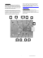
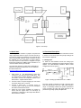
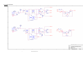
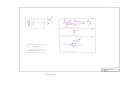
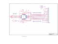
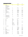
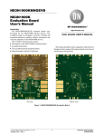
June 2009 Rev 0.9 National Semiconductor Evaluation Board User’s Guide ADC10DV200, 10-Bit, 200 Msps A/D Converter ADC11DV200, 11-Bit, 200 Msps A/D Converter © 2009 National Semiconductor Corporation. 1 http://www.national.com Table of Contents 1.0 Introduction ......................................................................................................................................... 3 2.0 Board Assembly .................................................................................................................................. 3 3.0 Quick Start........................................................................................................................................... 4 4.0 Functional Description ........................................................................................................................ 4 4.1 Analog Input ......................................................................................................................... 4 4.2 ADC reference circuitry ........................................................................................................ 5 4.3 ADC clock circuit ................................................................................................................. 5 4.4 Digital Data Output ............................................................................................................... 5 4.5 Data Format/ Duty Cycle Stabilizer ..................................................................................... 5 4.6 Power Supply Connections ................................................................................................... 5 5.0 Installing the ADC10DV200 Evaluation Board .................................................................................. 5 6.0 Hardware Schematic............................................................................................................................ 6 7.0 Evaluation Board Layout..................................................................................................................... 12 8.0 Evaluation Board Bill of Materials...................................................................................................... 15 A1.0 Operating in the Computer Mode ..................................................................................................... 17 A2.0 Summary Tables of Test Points, Connectors, and Jumper Settings................................................. 17 A2.1 Test Points .......................................................................................................................... 17 A2.2 Connectors.......................................................................................................................... 17 A2.3 Jumper settings ................................................................................................................... 17 A2.4 Clock Circuit Solder Jumper settings ................................................................................. 18 2 http://www.national.com frequency domain plot, shows dynamic performance in the form of SNR, SINAD, THD and SFDR. The latest WaveVision hardware and software is available through the National Semiconductor website: http://www.national.com/store/view_item/index.html?nsid= WAVEVSN+BRD+5.1 1.0 Introduction This Evaluation Board may be used to evaluate the ADC10DV200, or ADC11DV200. The ADC is one of a family of 10 and 11 bit converters that provides data at rates of up to 200MHz. Further reference in this manual to the ADC10DV200 is meant to also include the other listed parts unless otherwise specified 2.0 Board Assembly The ADC10DV200 Evaluation Board comes preassembled. Refer to the Bill of Materials in Section 8 for a description of components, to Figure 1 for major component placement and to Section 6 for the Evaluation Board schematic. The evaluation board is designed to be used with the WaveVision5™ Data Capture Board which is connected to a personal computer through a USB port and running WaveVision5™ software, operating under Microsoft Windows. The software can perform an FFT on the captured data upon command and, in addition to a JR507 +5V J301 Channel B Input ADC10DV200 or ADC11DV200 J201 CLK JP401 PDA WV5 Connector J302 Channel A Input J101 VREF J401 DF/DCS JP401 PDA Figure 1. Major Component and Jumper Locations 3 http://www.national.com Figure 2. Test Set up 3.0 Quick Start 4.0 Functional Description Refer to Figure 1 for locations of jumpers, test points and major components. Refer to Figure 2 for the test set up. The board is configured by default to use a external clock source and internal reference. Refer to Section 4.0 and the Appendix for more information on jumper settings. The input network of this board is configured for input frequencies greater than 70MHz. Refer to Section 4.1 for more information about input networks. The ADC10DV200 Evaluation Board schematic is shown in Section 6. A list of test points and jumper settings can be found in the Appendix. You must have version 5.0 or later of the WaveVision™ software to properly test this board. You can download the latest version from: http://www.national.com/analog/adc/wavevision5 1. 2. 3. 4. Apply power to the WaveVision5™ board and connect it to the computer using a USB cable. See the WaveVision5™ Board Manual for operation of that board. Connect the evaluation board to the WaveVision™ Digital Interface Board. Connect a clean +5V power supply to pin 2 of Power Connector JR507. Pin 1 is ground. Connect a signal from a 50-Ohm source to connector J301 or J302. Be sure to use a bandpass filter before the Evaluation Board. Adjust the input signal amplitude as needed to ensure that the signal does not over-range by examinining a histogram of the output data with the WaveVision5™ software. 4 4.1 Analog Input To obtain the best distortion results the analog input network must be optimized for the signal frequency being applied. The ADC10DV200 Evaluation Board comes configured as seen in Figure 3. Figure 3. Analog Input Network for FIN > 70MHz The input network is intended to accept a low-noise sine wave and will perform well over a wide input frequency range. To accurately evaluate the dynamic performance of this converter, the input test signal will have to be passed through a high-quality bandpass filter. http://www.national.com Input signals can also be amplified using an onboard LMH6517 DVGA (U601). To use the DVGA, some components must be installed and some removed. The following components must be installed: R651-R656. The following components must be removed: R302, R303, R309, and R310. Then connect signals from a 50-Ohm source to connectors J601 and J607. 4.2 ADC reference circuitry The ADC10DV200 can use an internal or external voltage reference. The internal reference is selectable between a 0.75V or 0.5V reference. External references can be set from 0.2V to 1.4V. This Evaluation Board is configured to use the internal 0.75V reference. should be connected to the Signal Input SMA connectors J301 or J302. When evaluating dynamic performance, an appropriate signal generator (such as the HP8644B or the R&S SME-03) with 50 Ohm source impedance should be connected to the Analog Input connector through an appropriate bandpass filter as even the best signal generator available can not produce a signal pure enough to evaluate the dynamic performance of an ADC. If this board is used in conjunction with the WaveVision5™ Data Capture Board and WaveVision5™ software, a USB must be connected between the Data Capture Board Board and the host. See the WaveVision5™ Data Capture Board manual for details. 4.3 ADC clock circuit Components can be installed or removed to select the path of the clock to the ADC. While not as convenient as pin-type jumpers, these introduce less distortion into the clock signal. Care must be taken to provide a high quality low jitter clock source. A single ended input clock can be buffered by U203 (NC7SV125) and applied to the ADC’s clock input pin. Or U203 can be bypassed and the input clock pin driven directly. A differential clock can also be applied to the ADC’s clock input pins through U201 (ETC-1-13). Refer to Appendix A to configure the clock for your application. The Evaluation Board is configured by default to use a single ended clock to drive the input pins directly. 4.4 Digital Data Output The LVDS digital output data is available for probing at test points TP601 through TP624. The signals are also available at the WaveVision™ (WV5) connector J602. 4.5 Data Format/ Duty Cycle Stabilizer Output data format and the duty cycle stabilizer (DCS) are controlled by jumper J401. Shorting pins 1-2 of J401 sets the output format to offset binary with DCS On. This is the default setting. Shorting pins 3-4 of J401 sets the output format to 2’s complement with DCS Off. Shorting pins 5-6 of J401 sets the output format to offset binary with DCS Off. Shorting pins 7-8 of J401 sets the output format to 2’s complement with DCS On. 4.6 Power Supply Connections Power to this board is supplied through power connector J507. The only supply needed is +5V at pin 2 plus ground at pin 1. Voltage and current requirements for the ADC10DV200 Evaluation Board are: +5.0V at 500 mA 5.0 Installing the ADC10DV200 Evaluation Board The evaluation board requires power supplies as described in Section 4.6. An appropriate signal source 5 http://www.national.com 6.0 Hardware Schematic 6 http://www.national.com 7 http://www.national.com 8 http://www.national.com 9 http://www.national.com 10 http://www.national.com 11 http://www.national.com 7.0 Evaluation Board Layout Layer 1 : Component Side Layer 2 : Ground 12 http://www.national.com Layer 3 : Ground Layer 4 : Power 13 http://www.national.com Layer 5 : Ground Layer 6 : Circuit Side 14 http://www.national.com 8.0 Evaluation Board Bill of Materials Item Qty Reference Part Part Number Vendor .1uF PCC1762CT Digi-Key .1uF 490-1318-1 Digi-Key .01uF PCC1784CT Digi-Key ______________________________________________ 1 15 C201,C220, C301,C302,C313,C314, C315,C316,C504,C509,C514, C518,C547,C549,C551 3 8 C305,C309,C311, C312,C318,C322,C324,C325, 4 10 C218,C502,C505,C507,C510, C512,C515,C548,C550,C552 5 1 C219 1uF PCC2224CT Digi-Key 6 2 C307,C320 27pF PCC270CQCT Digi-Key 7 2 C310,C323 .1uF PCC2336CT Digi-Key 8 4 C401,C402,C403,C627 .1uF PCC1828CT Digi-Key 9 3 C501,C506,C511 4.7uF PCC1842CT Digi-Key 10 6 C503,C508,C513,C544,C545, 10uF PCC1894CT Digi-Key 22uF 399-3717-1 Digi-Key C546 11 1 C516 12 1 C517 10uF 399-3705-1 Digi-Key 13 9 C520,C522,C524,C526,C528, .1uF PCC2146CT Digi-Key 14 10 C521,C523,C525,C527,C529, .01uF PCC2270CT Digi-Key BAT54 BAT54-FDICT Digi-Key C530,C532,C534,C536 C531,C533,C535,C537,C538 ______________________________________________ 18 3 D501,D502,D503 ______________________________________________ 19 1 JP204 HEADER 2 N/A 20 1 JP401 V_PDA S1011E-2 21 1 JP402 V_PDB S1011E-2 22 1 JR507 +5V 277-1150 23 1 J101 VREF S2011E-3 24 1 J201 EXT. CLK ARFX1231 25 1 J301 ANALOG IN B ARFX1231 Digi-Key Digi-Key 26 1 J302 ANALOG IN A ARFX1231 27 1 J401 DF/DCS S2011E-4 29 1 J602 CONN 60 PIN HMZD 6469028-1 Digi-Key 31 4 L501,L502,L503,L504 10UH 490-1055-1 Digi-Key ______________________________________________ 34 1 R101 3.3K 311-3.3KARCT Digi-Key 35 1 R103 20K 3296y-203LF Digi-Key 37 1 R106 10K 311-10KGRCT Digi-Key 38 1 R201 49.9 P49.9HCT Digi-Key 39 2 R202,R203 1K P1.00KHCT Digi-Key 40 6 R218,R219,R304,R311,R313, 24.9 P24.9LCT Digi-Key Digi-Key R316 41 2 R220,R221 10K P10.0KHCT 42 2 R224,R225 0 311-0.0GRCT Digi-Key 43 4 R302,R303,R309,R310 30 311-30JRCT Digi-Key 44 4 R305,R307,R312,R314 0 311-0.0JRCT Digi-Key 45 2 R306,R315 49.9 311-49.9HRCT Digi-Key 15 http://www.national.com 46 3 R401,R404,R405 10K 311-10KARCT Digi-Key 47 2 R402,R403 5.1K 311-5.1KARCT Digi-Key 70 6 TP501,TP502,TP503,TP504, GND 5002K Digi-Key 71 1 TP507 VA 5002K Digi-Key 72 1 TP508 VD 5002K Digi-Key 73 1 TP509 VCLK 5002K Digi-Key 74 1 TP510 VDR 5002K Digi-Key 100 4 T301,T305,T302,T306 ETC1-1-13 ETC1-1-13 Richardson 102 1 U1 ADC10DV200 (or ADC11DV200) ADC10DV200CISQ or ADC11DV200CISQ TP505,TP506 104 1 U203 NC7SV125 NC7SV125P5X Mouser 105 3 U501,U502,U503 LP2989LV-1.8 LP2989AIM-1.8 Digi-Keys 107 1 U606 24C02/SO8 511-M24C02-WMN6P Mouser DO NOT POPULATE 100 1 U201 ETC1-1-13 ETC1-1-13 Richardson 101 2 T307,T308 MABACT0040 MABACT0040 Richardson 36 3 R105,R301,R308 DNP 42 2 R222,R223 0 311-0.0GRCT Digi-Key 2 3 C213,C214,C215 DNP 3 2 C216,C217 .1uF 490-1318-1 Digi-Key Digi-Key 1 4 C210,C211,C212,C221 .1uF PCC1762CT 106 1 U601 LMH6517 LMH6517SQ National 28 1 J601 INPUT A WM5534 Digi-Key 30 1 J607 INPUT B WM5534 Digi-Key 48 4 R601,R602,R640,R642 DNP 56 2 SW1,SW2 SW DIP-8 GH7176 Digi-Key 99 2 T1,T2 TCM4-19+ TCM4-19+ Mini-Circuits 50 18 R611,R612,R613,R614,R615, 20K P20.0KLCT Digi-Key 10K 311-10KJRCT Digi-Key R616,R617,R618,R627,R628, R629,R630,R631,R632,R633, R634,R637,R638 49 16 R603,R604,R605,R606,R607, R608,R609,R610,R619,R620, R621,R622,R623,R624,R625, R626 51 2 R635,R636 10K 311-10.0KLCT Digi-Key 32 4 L601,L602,L604,L605 129nH 495-3433-1 Digi-Key 33 2 L603,L606 1nH Digi-Key 44 4 R653,R654,R655,R656 0 311-0.0JRCT 52 2 R639,R641 0 311-0.0JRCT Digi-Key 53 4 R643,R644,R645,R646 49.9 311-49.9LCT Digi-Key Digi-Key 54 4 R647,R648,R649,R650 100 311-100JCT 55 2 R651,R652 10 311-10JRCT Digi-Key 3 10 C601,C602,C603,C604,C605, .1uF 490-1318-1 Digi-Key 15 8 C610,C612,C613,C614,C615, 0.01uF PCC103BQCT Digi-Key 16 2 C617,C618 15pF PCC150CQCT Digi-Key 17 2 C624,C626 1uF PCC2364CT Digi-Key 6 4 C619,C620,C621,C622 27pF PCC270CQCT Digi-Key C606,C607,C608,C609,C611 C616,C623,C625 16 http://www.national.com APPENDIX A1.0 Operating in the Computer Mode The ADC10DV200 Evaluation Board is compatible with the WaveVision5™ Data Capture Board and WaveVision5™ software. You can download the latest version from: http://www.national.com/analog/adc/wavevision5 When connected to the WaveVision5™ Board, data capture is easily controlled from a personal computer operating in the Windows environment. The data samples that are captured can be observed on the PC video monitor in the time and frequency domains. The FFT analysis of the captured data yields insight into system noise and distortion sources and estimates of ADC dynamic performance such as SINAD, SNR and THD. A2.0 Summary Tables of Test Points, Connectors, and Jumper Settings A2.1 Test Points Test Points on the ADC10DV200 Evaluation Board Voltage Signal Name VA VD VDR VCLK Measure at TP507 TP508 TP510 TP509 Nominal Voltage (V) 1.8 1.8 1.8 1.8 Voltage Limits (V) 1.7 to 1.9 1.7 to 1.9 1.7 to 1.9 1.7 to 1.9 A2.2 Connectors JR507 Connector - Power Supply Connections 1 GND Power Supply Ground 2 +5V +5V Power Supply A2.3 Jumper settings Note: Default settings are in bold JP401 : Power Down Channel A Connect 1-2 Channel A is in power down mode 1-2 OPEN Channel A is in normal operation JP402 : Power Down Channel B Connect 1-2 Channel B is in power down mode 1-2 OPEN Channel B is in normal operation J401 : Output Data Format and Duty Cycle Stabilizer Connect 1-2 Output format is offset binary, DCS is On Connect 3-4 Output format is 2’s complement, DCS is Off Connect 5-6 Output format is offset binary, DCS is Off Connect 7-8 Output format is 2’s complement, DCS is On 17 http://www.national.com A2.4 Clock Circuit Solder Jumper settings Components can be installed or removed to select the path of the clock to the ADC. While not as convenient as pin-type jumpers, these introduce less distortion into the clock signal. Termination A: Differential Sinusoid Termination B: Single Ended Sinusoid Termination C: Single Ended Square Install C210, C216, and C217 Remove R223, R224, R225, and JP204 Install R222 and R223 Remove C210, C216, C217, R224, R225 and JP204 Install R223, R224, R225, and JP204 Remove C210, C216, C217, and R222 18 http://www.national.com BY USING THIS PRODUCT, YOU ARE AGREEING TO BE BOUND BY THE TERMS AND CONDITIONS OF NATIONAL SEMICONDUCTOR'S END USER LICENSE AGREEMENT. DO NOT USE THIS PRODUCT UNTIL YOU HAVE READ AND AGREED TO THE TERMS AND CONDITIONS OF THAT AGREEMENT. IF YOU DO NOT AGREE WITH THEM, CONTACT THE VENDOR WITHIN TEN (10) DAYS OF RECEIPT FOR INSTRUCTIONS ON RETURN OF THE UNUSED PRODUCT FOR A REFUND OF THE PURCHASE PRICE PAID, IF ANY. The ADC10DV200 Evaluation Boards are intended for product evaluation purposes only and are not intended for resale to end consumers, is not authorized for such use and is not designed for compliance with European EMC Directive 89/336/EEC, or for compliance with any other electromagnetic compatibility requirements. National Semiconductor Corporation does not assume any responsibility for use of any circuitry or software supplied or described. No circuit patent licenses are implied. LIFE SUPPORT POLICY NATIONAL'S PRODUCTS ARE NOT AUTHORIZED FOR USE AS CRITICAL COMPONENTS IN LIFE SUPPORT DEVICES OR SYSTEMS WITHOUT THE EXPRESS WRITTEN APPROVAL OF THE PRESIDENT OF NATIONAL SEMICONDUCTOR CORPORATION. As used herein: 1. Life support devices or systems are devices or systems which, (a) are intended for surgical implant into the body, or (b) support or sustain life, and whose failure to perform, when properly used in accordance with instructions for use provided in the labeling, can be reasonably expected to result in a significant injury to the user. National Semiconductor Corporation Americas Tel: 1-800-272-9959 Fax: 1-800-737-7018 Email: [email protected] 2. A critical component is any component in a life support device or system whose failure to perform can be reasonably expected to cause the failure of the life support device or system, or to affect its safety or effectiveness. National Semiconductor Europe Fax: +49 (0) 1 80-530 85 86 Email: [email protected] Deutsch Tel: +49 (0) 699508 6208 English Tel: +49 (0) 870 24 0 2171 Français Tel: +49 (0) 141 91 8790 National Semiconductor Asia Pacific Customer Response Group Tel: 65-2544466 Fax: 65-2504466 Email:[email protected] National Semiconductor Japan Ltd. Tel: 81-3-5639-7560 Fax: 81-3-5639-7507 www.national.com National does not assume any responsibility for any circuitry described, no circuit patent licenses are implied and National reserves the right at any time without notice to change said circuitry and specifications. 19 http://www.national.com IMPORTANT NOTICE Texas Instruments Incorporated and its subsidiaries (TI) reserve the right to make corrections, modifications, enhancements, improvements, and other changes to its products and services at any time and to discontinue any product or service without notice. Customers should obtain the latest relevant information before placing orders and should verify that such information is current and complete. All products are sold subject to TI’s terms and conditions of sale supplied at the time of order acknowledgment. TI warrants performance of its hardware products to the specifications applicable at the time of sale in accordance with TI’s standard warranty. Testing and other quality control techniques are used to the extent TI deems necessary to support this warranty. Except where mandated by government requirements, testing of all parameters of each product is not necessarily performed. TI assumes no liability for applications assistance or customer product design. Customers are responsible for their products and applications using TI components. To minimize the risks associated with customer products and applications, customers should provide adequate design and operating safeguards. TI does not warrant or represent that any license, either express or implied, is granted under any TI patent right, copyright, mask work right, or other TI intellectual property right relating to any combination, machine, or process in which TI products or services are used. Information published by TI regarding third-party products or services does not constitute a license from TI to use such products or services or a warranty or endorsement thereof. Use of such information may require a license from a third party under the patents or other intellectual property of the third party, or a license from TI under the patents or other intellectual property of TI. Reproduction of TI information in TI data books or data sheets is permissible only if reproduction is without alteration and is accompanied by all associated warranties, conditions, limitations, and notices. Reproduction of this information with alteration is an unfair and deceptive business practice. TI is not responsible or liable for such altered documentation. Information of third parties may be subject to additional restrictions. Resale of TI products or services with statements different from or beyond the parameters stated by TI for that product or service voids all express and any implied warranties for the associated TI product or service and is an unfair and deceptive business practice. TI is not responsible or liable for any such statements. TI products are not authorized for use in safety-critical applications (such as life support) where a failure of the TI product would reasonably be expected to cause severe personal injury or death, unless officers of the parties have executed an agreement specifically governing such use. Buyers represent that they have all necessary expertise in the safety and regulatory ramifications of their applications, and acknowledge and agree that they are solely responsible for all legal, regulatory and safety-related requirements concerning their products and any use of TI products in such safety-critical applications, notwithstanding any applications-related information or support that may be provided by TI. Further, Buyers must fully indemnify TI and its representatives against any damages arising out of the use of TI products in such safety-critical applications. TI products are neither designed nor intended for use in military/aerospace applications or environments unless the TI products are specifically designated by TI as military-grade or "enhanced plastic." Only products designated by TI as military-grade meet military specifications. Buyers acknowledge and agree that any such use of TI products which TI has not designated as military-grade is solely at the Buyer's risk, and that they are solely responsible for compliance with all legal and regulatory requirements in connection with such use. TI products are neither designed nor intended for use in automotive applications or environments unless the specific TI products are designated by TI as compliant with ISO/TS 16949 requirements. Buyers acknowledge and agree that, if they use any non-designated products in automotive applications, TI will not be responsible for any failure to meet such requirements. Following are URLs where you can obtain information on other Texas Instruments products and application solutions: Products Applications Audio www.ti.com/audio Automotive and Transportation www.ti.com/automotive Amplifiers amplifier.ti.com Communications and Telecom www.ti.com/communications Data Converters dataconverter.ti.com Computers and Peripherals www.ti.com/computers DLP® Products www.dlp.com Consumer Electronics www.ti.com/consumer-apps DSP dsp.ti.com Energy and Lighting www.ti.com/energy Clocks and Timers www.ti.com/clocks Industrial www.ti.com/industrial Interface interface.ti.com Medical www.ti.com/medical Logic logic.ti.com Security www.ti.com/security Power Mgmt power.ti.com Space, Avionics and Defense www.ti.com/space-avionics-defense Microcontrollers microcontroller.ti.com Video and Imaging www.ti.com/video RFID www.ti-rfid.com OMAP Mobile Processors www.ti.com/omap Wireless Connectivity www.ti.com/wirelessconnectivity TI E2E Community Home Page e2e.ti.com Mailing Address: Texas Instruments, Post Office Box 655303, Dallas, Texas 75265 Copyright © 2012, Texas Instruments Incorporated