1
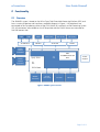
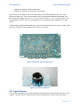
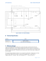
GIMME2 User Guide
Document revision: 5
Date [dd.mm.yyyy]: 05.06.2013
af inventions
Use
Us e r G uide G imme2
imme2
1 Document
Document revisions
Revision
1
2
Date [DD.MM.YY]
20.12.12
07.02.13
3
4
5
14.02.13
18.02.13
05.06.13
Changes
Initial version
Added mechanical drawing and board
revision section.
Added component information
Added BOOT_MODE Jumper description
Extended description of boot mode
jumper options
Added reference design QSPI
programming sequence
Page 2 of 12
af inventions
Use
Us e r G uide G imme2
imme2
2 Functionality
Functionality
2.1 Overview
The GIMME2 system is based on the Xilinx Zynq-7000 Extensible Processing Platform (EPP) and
hosts a variety of devices and interfaces, see block diagram in Figure 1. All peripherals are
connected to the Zynq device, either to the FPGA fabric (PL) or directly to the Processing System
(PS). All connectors are available on the PCB top side and the CMOS sensors are mounted on
the PCB bottom side.
USB0
USB1
USB2
2x USB-Serial
GE0 (RJ45)
USB PHY
ZynQ 7020
PS
FE0 (RJ45)
FE PHY
2x GE PHY
CMOS
camera
OV10810
CMOS
camera
OV10810
GE1 (RJ45)
APU
2x ARM Cortex-A9
CPU
Power
supplies
PL
FPGA fabric
MEM1
2Gb DDR3
MEM0
4Gb DDR3
microSD
QSPI flash
Figure 1 GIMME2 system overview
Page 3 of 12
af inventions
Use
Us e r G uide G imme2
imme2
3 Components
omponents
In Figure 2 shows the Gimme2 PCB top side.
Figure 2 Gimme2 PCB top side
3.1 Connector positions
Figure 3 GIMME2 connectors and mounting holes
Page 4 of 12
af inventions
Use
Us e r G uide G imme2
imme2
3.2 Connector overview
Please note the pin 1 identifiers in Figure 1.
Designator Function
Connector type
P1
P2
P4
P5
P6
P7
RJ45
RJ45
USB Micro-AB
USB Micro-AB
USB Micro-AB
Shrouded pin header, 2x10, 2.54mm
pitch
Molex 502570-0893
Shrouded pin header, 2x10, 2.54mm
pitch
Molex 87832-1420
P13
Gigabit Ethernet 0 (GE0)
Fast Ethernet 0 (FE0)
USB on-the-go / host /device (USB2)
USB UART device (USB0 - UART0)
USB UART device (USB1 – UART1)
ARM PJTAG debug connector
(ARM_PJTAG), access through Zynq PL
µSD connector
ARM JTAG debug connector
(ARM_JTAG)
Xilinx JTAG connector, same as
ARM_JTAG
Power supply connector (+24V)
P14
P23
P26
P27
P28
P29
P30
FPGA GPIO 1.5V
Gigabit Ethernet 1 (GE1)
Boot mode jumper (BOOT_MODE[4])
Boot mode jumper (BOOT_MODE[3])
Boot mode jumper (BOOT_MODE[2])
Boot mode jumper (BOOT_MODE[1])
FPGA GPIO 2.5V
P8
P10
P11
Phoenix Contact: MC 1,5/ 2-GF-3,81 –
1827868
Pin header, 2x8, 2.54mm pitch
RJ45
Pin header, 1x3, 2.54mm pitch
Pin header, 1x3, 2.54mm pitch
Pin header, 1x3, 2.54mm pitch
Pin header, 1x3, 2.54mm pitch
Pin header, 2x8, 2.54mm pitch
3.3 Connector pinouts
In this section the pinouts of the GIMME2 board connectors are listed. All Ethernet and USB
connectors have standard pinouts.
3.3.1 P7 – ARM PJTAG debug connector
The P7 ARM debug connector pinout is listed in the table below.
Pin
1
3
5
7
9
11
13
15
17
19
Function
VREF (3.3V from board)
nTRST (unused)
TDI
TMS
TCK
RTCK (unused)
TDO
nSRST (ARM soft reset)
DBGRQ (unused)
DBBACK (unused)
Pin
2
4
6
8
10
12
14
16
18
20
Function
Not connected
GND
GND
GND
GND
GND
GND
GND
GND
GND
Note that the PJTAG chain is routed through Zynq PL FPGA fabric and a suitable bitstream must
be loaded before operating this JTAG chain. The Zynq pinout for these signals are listed in the
table below:
Net
ARM_PJTAG_TCK
ARM_PJTAG_TMS
Zynq Pad
Y9
U9
Page 5 of 12
af inventions
ARM_PJTAG_TDI
ARM_PJTAG_TDO
Use
Us e r G uide G imme2
imme2
V9
V7
3.3.2 P10 – ARM JTAG debug connector
The P10 ARM debug connector controls the dedicated JTAG chain pins of the Zynq, granting
access to both ARM cores and PL logic. This connector is connected parallel to the Xilinx JTAG
programmer connector P11 and only one of these connectors should be used at a time. The P10
pinout is listed in the table below:
Pin
1
3
5
7
9
11
13
15
17
19
Function
VREF (3.3V from board)
nTRST (unused)
TDI
TMS
TCK
RTCK (unused)
TDO
nSRST (ARM soft reset)
DBGRQ (unused)
DBBACK (unused)
Pin
2
4
6
8
10
12
14
16
18
20
Function
Function
Not connected
GND
GND
GND
GND
GND
GND
GND
GND
GND
3.3.3 P11 – Xilinx JTAG programmer connector
The P10 ARM debug connector controls the dedicated JTAG chain pins of the Zynq, granting
access to both ARM cores and PL logic. This connector is connected parallel to the ARM JTAG
debug connector P10 and only one of these connectors should be used at a time. The P11 Xilinx
programmer connector has the following standard pinout:
Pin
1
3
5
7
9
11
13
Function
GND
GND
GND
GND
GND
GND
GND
Pin
2
4
6
8
10
12
14
Function
VREF (3.3V from board)
TMS
TCK
TDO
TDI
Not connected
nSRST (ARM soft reset)
3.3.4 P13 power
po wer supply connector
The 12VDC to 24VDC supply voltage should be applied to the P13 connector with the pinout:
Pin
1
2
Function
VIN+
GND
3.3.5 P14 FPGA GPIO 1 .5V connector
The 1.5V GPIO signals are available through the P14 connector. All GPIOs have a series resistor
of approx.. 50 Ohms and ESD protection diodes to prevent damage to the input and output
buffers of the Zynq device, however care should be taken not to expose these pins to
overvoltage conditions. The pinout of the P14 connector is listed below:
Page 6 of 12
af inventions
Pin
1
3
5
7
9
11
13
15
Use
Us e r G uide G imme2
imme2
Function
GPIO_6
GPIO_7
GPIO_8
GPIO_9
GPIO_10
GPIO_11
GPIO_12
GPIO_13
Pin
2
4
6
8
10
12
14
16
Function
GND
GND
GND
GND
GND
GND
GND
GND
3.3.6 P26 – P29 boot mode jumpers
The boot mode jumpers select the Zynq PS boot mode. A jumper should be placed between the
pins 1+2 to assert (logic ‘1’) the corresponding boot mode bit. To deassert (logic ‘0’), a jumper
should be placed between the pins 2+3. The mapping of connectors to boot mode bits is listed
in the table below:
Connector
P26
P27
P28
P29
Boot Mode Bit
BOOT_MOD[4]
BOOT_MOD[3]
BOOT_MOD[2]
BOOT_MOD[1]
Configuration
‘0’ => PLL used, ‘1’ => PLL bypassed
‘0’ => cascaded JTAG, ‘1’ => independent JTAG
BOOT_MODE[2..1]:
“00” => Boot from JTAG
“10” => Boot from Quad-SPI
“11” => Boot from SD
The boot mode jumpers are shown connecting pins 2+3 (logic ‘0’) in Figure 4. The bit
BOOT_MODE[0] is always pulled low (‘0’).
Figure 4 Boot mode jumpers in position „0000“
3.3.7 P30 FPGA GPIO 2.5V connector
The 2.5V GPIO signals, as well as the on board 2.5V and 3.3V power rails are available through
the P30 connector. Note that the signals GPIO_0 and GPIO_1 are also used to power the LED3
and LED4. All GPIOs have a series resistor of approx.. 50 Ohms and ESD protection diodes to
prevent damage to the input and output buffers of the Zynq device, however care should be
taken not to expose these pins to overvoltage conditions. The pinout of the P30 connector is
listed below:
Pin
Function
Pin
Function
Page 7 of 12
af inventions
1
3
5
7
9
11
13
15
GPIO_0
GPIO_1
GPIO_2
GPIO_3
GPIO_4
GPIO_5
VCC2.5
VCC3.3
Use
Us e r G uide G imme2
imme2
2
4
6
8
10
12
14
16
GND
GND
GND
GND
GND
GND
GND
GND
3.4 PSPS-MEM DDR3 bank
The memory controller of the Zynq PS is connected to two x16 DDR3 devices, offering a
maximum transfer rate of 2x533=1066MT/s. The 32 bit interface enables a max theoretical
throughput of approx. 34.1 Gbit/s.
3.5 PLPL-MEM DDR3 bank
The Zynq PL is connected to one x16 DDR3 device, offering a maximum transfer rate of
2x400=800MT/s. The 16 bit interface enables a max theoretical throughput of approx.
12.8 Gbit/s. The Xilinx MIG offers an easy configurable DDR3 memory controller that can be
used with this memory device. The PL-MEM memory bank can be used for image or signal
processing purposes without sharing memory bandwidth with the PS.
3.6 QSPI Flash
The QSPI flash device is connected to the Quad SPI 0 bank of the MIO bank 0 and can be used
as boot memory. The linear addressing mode supports a maximum of 16MB memory space
using a single 4x QSPI device.
3.7 µSD Slot
The µSD slot is connected to the SDIO 1 controller in MIO bank 0 that is compatible to the
SD2.0 specification.
3.8 CMOS Sensors
The OV10810 cmos sensors are mounted on the bottom side of the PCB, see Figure 5,
separated by a distance of 70 mm. A Lensation CS-mount, CH303015-20M, can be installed to
support optical lenses, see Figure 6.
CMOS sensor key features:
•
•
•
•
•
•
•
•
Native 16:9 high res sensor, active array size 4320x2432
1.4µm x 1.4µm pixel (optical size of 1/2.5”)
10 MP at 30 fps, 5 MP at 60 fps max image transfer rate
Scan mode: progressive, shutter: rolling shutter
Programmable lens correction, 2-D defective pixel canceling, real-time raw scaling
Automatic image control functions:
o Automatic white balance (AWB)
o Automatic band filter (ABF)
o Automatic black level calibration (ABLC)
Programmable controls for frame rate, 16-zone size/position/weigth control, mirror and
flip, cropping, windowing and panning
Support for black sun cancellation
Page 8 of 12
af inventions
•
•
Use
Us e r G uide G imme2
imme2
Support for video or snapshot operations
Support for horizontal and vertical sub-sampling
Each sensor is connected to the PL of the Zynq by 8 LVDS/MIPI differential data lines and 2
differential clock lines. The OV10810 devices can be configured to different bandwidth and
communication modes, like LVDS x1, x2, x4, x8 lanes or MIPI x1, x2, x3, x4, x6, x8 lanes. In x8
lane operation, the data lanes can be divided into two x4 groups, each supplied with a clock
signal.
Configuration is performed through the 2-wire SCCB interface and the I/O signals VSYNC, HREF,
FREX and STROBE are connected to the PL fabric of the Zynq.
Figure 5 Gimme2 back side with CMOS sensors
Figure 6 CS mount for camera lens
3.9 Gigabit Ethernet
The 10/100/1000Mbps Ethernet ports are both connected to the hard IP Ethernet MACs of the
Zynq PS. The PHYs share a common MDC bus for configuration, the GE0 port accessible at
Page 9 of 12
af inventions
Use
Us e r G uide G imme2
imme2
address 0x0 and the GE1 port at address 0x1. Both PHYs are hardwired to the board PowerOn_Reset (POR).
3.10 Fast Ethernet
The 10/100Mbps port is connected to the PL fabric of the Zynq with an MII interface. This port is
provided for industrial Ethernet communication protocols. A subset of these pins can be used for
RGMII operation. The fast Ethernet PHY has a dedicated MDC bus, also routed to the Zynq PL.
3.11 USB
The USB controller in the Zynq PS is connected to an Exar USB transceiver, accessible through
the “USB2” connector P4. This USB2.0 port supports device/host and USB-on-the-go operation.
The “USB0” and “USB1” ports are Exar USB UARTs connected to the Zynq PL.
3.12 Reset PushPush-buttons
There are two reset push-buttons on the board, the POR button and the SRST button. The POR
button is combined with the power good signal from the power supplies to form a Power-OnReset signal that is routed to the POR input of the Zynq PS. The POR is also used to reset all
Ethernet PHYs and the USB transceiver.
The SRST is a soft reset button which is connected to the Zynq PS srst input.
3.13 GPIOs
The connectors P14 and P30 carry GPIOs from the Zynq PL. These bidirectional signals are
protected by external ESD protection diode arrays and series resistors, however care should be
taken when connecting this signals to external signal sources.
The P14 GPIOs are connected to the 1.5V IO-bank and the P30 GPIOs are connected to a 2.5V
bank, see sections 3.3.5 and 3.3.7.
3.14 Mounting holes
The 3.2mm mounting holes M3, M4, M5 and M6 can be used to fasten the board to a case.
These holes are plated and are electrically connected to the shields and cages of the Ethernet
and USB connectors. See section Power Supply for more information on grounding.
The 3.2mm mounting holes M7 and M8 can be used for a heatsink, the Zynq chip is centered
between the holes. Alternatively, an add-on board connecting to the GPIO headers P14 and P30
could be fastened using these mounting holes. These holes are not plated.
Each CMOS sensor has two 2.2mm mounting holes for a Lensation CH303015-20M CS-Mount
Lens Holder.
4 Power supply
The board can be supplied by a regulated DC supply voltage between 12V and 24V. An
undervoltage lockout protection will prevent the board from operating at low voltages. The
supply should be able to deliver 18W.
5 Mechanical drawing
In Figure 7 the sizes and positions of mounting holes are shown.
Page 10 of 12
af inventions
Use
Us e r G uide G imme2
imme2
Figure 7 Gimme2 v1.0 mechanical drawing
6 Technical Specification
Specification
Property
Power consumption
Physical size
Operating environ.
Value
<18W @ 24V supply
130mm x 82mm
0°C to 40°C, non-condensing
7 Reference designs
There are two board reference design that can be used to get started with the Gimme2
application development. The first reference design contains basic interface test components
and comes with a basic bsp generated by the Xilinx SDK. The test software runs without OS and
performs simple board tests. The top entity and the constraint files can be used as template for
any new design.
The second reference design includes a Linux image for the QSPI flash. To boot the Linux from
the QSPI flash, follow the instruction in the Xilinx user guide UG873 “Zynq-7000 All
Programmable SoC: Concepts, Tools, and Techniques (CTT)”. The basic steps are:
Page 11 of 12
af inventions
•
•
•
•
•
•
•
•
Use
Us e r G uide G imme2
imme2
Connect the host computer to the Gimme2 USB0 port for access to serial port.
Program a valid FPGA bitstream that connects the PS UART to USB0 to the FPGA fabric
using a USB Platform Cable and Xilinx Impact software.
Start the XMD console in Xilinx SDK
Follow the instructions from Xilinx user guide UG873:
From the XMD prompt, do the following:
o Type connect arm hw to connect with the PS section CPU.
o Type source <Project Dir>/ps7_init.tcl
o Type ps7_init to initialize the PS section.
o Type init_user to enable level shifters between PS to PL and clear fabric port
resets.
o Type dow <Project Dir>/u-boot.elf to download the Linux U-Boot to the QSPI
Flash.
o Type dow -data u_boot.bin 0x08000000 to download the Linux bootable image
to the target memory at location 0x08000000. Note: You just downloaded the
binary executable to DDR memory. You can download the binary executable to
any address in DDR memory.
o Type con to start execution of U-Boot.On the serial terminal, the autoboot
countdown message appears: Hit any key to stop autoboot: 3
In the serial console, Press Enter. Automatic booting from U-Boot stops and the U-Boot
command prompt appears on the serial terminal.
Do the following steps to program U-Boot with the bootable image:
o At the prompt, type sf probe 0 0 0 to select the QSPI Flash.
o Type sf erase 0 0x01000000 to erase the Flash data. This command completely
erases 16 MB of on-board QSPI Flash memory.
o Type sf write 0x08000000 0 0xFFFFFF to write the boot image on the QSPI Flash.
Note that you already copied the bootable image at DDR location 0x08000000.
This command copied the data, of the size equivalent to the bootable image size,
from DDR to QSPI location 0x0. For this example, because you have 16 MB of
Flash memory, you copied 16 MB of data. You can change the argument to
adjust the bootable image size.
Power off the board.
8 Board revisions
8.1 v1.0
8.1.1 Zynq CES
The Gimme2 v1.0 boards host Zynq engineering samples (CES). Please see the Xilinx Zynq CES
errata for details. Important: Due to the Zynq errata, the PS DDR3 memory controller can not
use the external voltage reference and the XPS-System must be configured to use the internal
voltage reference.
8.2 v2.0
The v2.0 revision features the Zynq 7020 production devices.
Page 12 of 12