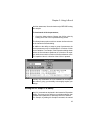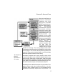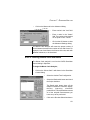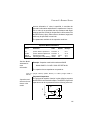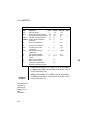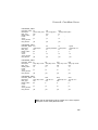
1
Personal Computer Circuit Design Tools ISSPICE4 USER’S GUIDE VOLUME 1 © copyright intusoft 1988-2001 879 West 190th Street, Suite 100 Gardena, Ca. 90248-4223 Tel. (310) 329-3295 Fax (310) 329-9864 email - [email protected] Web - www.intusoft.com intusoft provides this manual “as is" without warranty of any kind, either expressed or implied, including but not limited to the implied warranties of merchantability and fitness for a particular purpose. This publication may contain technical inaccuracies or typographical errors. Changes are periodically made to the information herein; these changes will be incorporated in new editions of this publication. Copyright intusoft, 1988-2001. All Rights Reserved. No part of this publication may be reproduced, transmitted, transcribed, stored in a retrieval system, or translated into any language in any form by any means without written permission from Intusoft. IsSpice4 is based on Berkeley SPICE 3F.2, which was developed by the Department of Electrical Engineering and Computer Sciences, University of California, Berkeley CA and XSPICE, which was developed by Georgia Tech Research Corp., Georgia Institute of Technology, Atlanta Georgia, 30332-0800 Portions of IsSpice4 have been developed at Universite Catholique de Louvain in Belgium, University of Illinois in U.S.A., and Macquarie University in Australia. Many thanks to Benjamin Iniguez, Pablo Menu, Anthony Parker and Christophe Basso for their contributions to IsSpice4’s models. Portions of this manual have been previously published in EDN Magazine. is a trademark of intusoft Intusoft, the Intusoft logo, ICAPS, ICAP, ICAP/4, IsSpice, IsSpice4, SpiceNet, IntuScope, Test Designer, and IsEd are trademarks of Intusoft, Inc. Pspice is a registered trademark of OrCAD corp. All company/product names are trademarks/registered trademarks of their respective owners. All company/product names are trademarks/registered trademarks of their respective owners. Windows and Windows NT are trademarks of Microsoft Corporation. Printed in the U.S.A. ii rev. 02/01 Contents Volume 1 Chapter 1 Chapter 1- 8 Introduction 1 2 Chapter 2 Using IsSpice4 11 11 12 12 14 15 16 16 18 18 20 21 23 25 26 28 Chapter 3 About IsSpice4 SPICE 2/IsSpice4 Differences IsSpice4 Overview Starting IsSpice4 Quitting IsSpice4 The IsSpice4 Display Simulation Control Dialog Saving Windows Positions Starting, Stopping and Pausing The Simulation Scaling, Adding and Deleting Waveforms Saving Vectors For Real-Time Viewing Interactive Circuit Measurements (Not Avail. in ICAP/4Rx) Saving and Viewing Past Simulation Data Sweeping Circuit Parameters (Not Avail. in ICAP/4Rx) Sweeping Groups of Parameters (Not Avail. in ICAP/4Rx) Adding An ICL Script To A Sweep Scripting: Introduction to ICL Viewing Waveforms In More Detail Analysis Types 29 30 30 30 31 31 32 33 34 Analysis Summary Code Models And Analysis Types ICL - Interactive Command Language DC Operating Point Analysis DC Small Signal Transfer Function DC Sweep Analysis Sensitivity Analysis (Not Available in ICAP/4Rx) AC Analysis Noise Analysis (Not Available in ICAP/4Rx) iii TABLE OF CONTENTS 35 36 36 37 37 38 39 40 42 43 44 46 Chapter 4 Mixed-Mode Simulation 47 49 49 50 51 52 53 54 55 56 56 57 Chapter 5 IsSpice4 Netlist Netlist Structure The Title and .END lines ICL Statements and Control Block Analysis Control Statements Output Control Statements Circuit Topology Definition MODEL Statements Subcircuit Netlist Miscellaneous Netlist Statements Delimiters and the Comma IsSpice4 Netlist Construction IsSpice4 Output Files Code Model Netlist Structure Extended Syntax 79 81 iv Mixed-Mode Simulation Overview Native Digital Simulation (Not Available in ICAP/4Rx) States, Logic Levels and Strengths Events and Event Scheduling Gate Delays Rise and Fall Times Node Types and Translation Analog and Digital Interfaces Mixing Digital and Analog Circuitry Viewing Digital Data Creating Digital Stimulus Reducing Circuit Complexity Netlist Definition 59 60 61 61 62 62 64 67 68 70 70 71 72 74 Chapter 6 Distortion Analysis (Not Available in ICAP/4Rx) Pole-Zero Analysis Transient Analysis Transient Initial Conditions How IsSpice4 Runs A Transient Analysis Output Data And Aliasing Changing The Simulation Accuracy Simulation Stability Fourier Analysis (Not Available in ICAP/4Rx) Temperature Analysis Simulation Templates (Not Available in ICAP/4Rx) References Introduction Parameter Passing 83 84 86 87 88 89 90 92 94 95 96 97 98 99 100 Chapter 7 .PARAM Syntax PARAM Rules and Limitations Parameterized Expressions Entering .PARAM Statements Entering Parameterized Expressions Passing Parameters To Subcircuits Default Subcircuit Parameters Parameter Passing Example DEFINE DEFINE Rules and Limitations DEFINE Example INCLUDE INCLUDE Example INCLUDE Rules and Limitations Subcircuit and Model Hierarchy Extended Analyses 103 105 108 108 108 109 111 114 116 116 118 118 118 118 120 121 122 124 124 124 124 125 125 127 127 128 128 Introduction Data Reduction Programs Exiting To ICAPS Pausing A Program Pre-Stored Program Files Programming Do’s And Don’ts Tolerances Subcircuit Parameter Tolerances Toleranced Value Generation Monte Carlo Analysis (Not Available in ICAP/4Rx) Performing A Monte Carlo Analysis (ICL Scripted) STEP 1: A Working Circuit STEP 2: Adding Tolerances STEP 3: Setting Up The Measurements STEP 4: Defining Lots and Cases STEP 5: Running a Monte Carlo Simulation Viewing the Results Performing A Monte Carlo Analysis (IntuScope Program) STEP 1: A Working Circuit STEP 2: Adding Tolerances STEP 3: Running a Nominal Case STEP 4: Making a Data Reduction Program STEP 5: Running a Monte Carlo Simulation Parameter Passing, Special Instances Formatting the Reduced Data STEP 6: Analyzing the Monte Carlo Analysis Data Curve Families v TABLE OF CONTENTS 129 129 131 131 133 135 Chapter 8 Element Syntax 137 138 140 143 144 145 146 150 152 155 157 160 164 166 167 167 167 168 168 169 169 173 174 177 178 181 183 185 187 188 192 194 198 210 215 217 vi Circuit Optimization (Not Available in ICAP/4Rx) Optimizer Preparation Running The Optimizer Optimizer Output Single and Multi-Parameter Sweeps (Not Avail. in ICAP/4Rx) Error Messages and Solutions IsSpice4 Syntax Notation Resistors/Semiconductor Resistors Capacitors/Semiconductor Capacitors Inductors Coupled Inductors Ideal Transmission Lines Lossy Transmission Lines Uniformly Distributed RC/RD Transmission Lines Switches (with Hysteresis) Switch (Smooth Transition) Independent Voltage Sources Transient Signal Generators Independent Current Sources Analog Behavioral Modeling Linear Dependent Sources Voltage-Controlled Voltage Sources Current-Controlled Current Sources Current Controlled Voltage Sources Voltage-Controlled Current Sources Nonlinear Dependent Sources In-line Equations, Expressions, And Functions Using Time, Frequency, and Temperature in Expressions Behavioral Modeling Issues Nonlinear Elements Boolean Logic Expressions If-Then-Else Expressions Device Models Statements .Model Statement Diodes Bipolar Junction Transistors Junction Field-Effect Transistors GaAs Field Effect Transistors - MESFETs Metal Oxide Field Effect Transistors - MOSFETs BSIM3 Version 3.1 Level 8 Parameters EPLF-EKV 2.6 MOSFET Model BSIM4 Version 4.1.0 Level 14 Parameters 227 227 228 229 Volume 2 Chapter 9 Subcircuits Subcircuit Call Statement .Subckt Statement .Ends Statement Chapter 9 - Appendices Code Model Syntax 231 232 234 235 236 240 242 246 248 250 252 254 259 262 264 266 268 270 272 276 277 279 281 282 283 285 287 289 289 290 291 292 Introduction The Port Table The Parameter Table Analog Code Models Magnetic Core Differentiator Fully Depleted SOI Mosfet Hysteresis Block Inductive Coupling Limiter Controlled One-Shot Table Models Laplace (s-Domain) Transfer Function Slew Rate Block Controlled Sine Wave Oscillator Controlled Square Wave Oscillator Controlled Triangle Wave Oscillator Smooth Transition Switch Repeating Piece-Wise Linear Source Hybrid Code Models and Node Bridges Digital-to-Analog Node Bridge Analog-to-Digital Node Bridge Digital-to-Real Node Bridge Real-to-Analog Node Bridge Analog-to-Real Node Bridge Controlled Digital Oscillator Controlled Digital PWM Real Code Models Z-Transform Block (Real) Gain Block (Real) Digital Code Models Buffer vii 293 294 295 296 297 298 299 300 301 302 303 304 305 307 309 311 313 315 317 321 323 326 328 Inverter And Nand Or Nor Xor Xnor Tristate Pullup Pulldown Open Collector Open Emitter D Flip Flop JK Flip Flop Toggle Flip Flop Set-Reset Flip Flop D Latch Set-Reset Latch State Machine Frequency Divider RAM Digital Source MIDI Digitally Controlled Oscillator Chapter 10 Analysis Syntax 329 330 331 332 332 333 334 336 339 341 342 343 344 345 349 349 351 359 360 360 361 viii Analysis Notation .DC - DC Sweep Analysis .OP - Operating Point .TF - Transfer Function .Nodeset - Initial Node Voltages .AC - Small-Signal Frequency Analysis .Noise - Small-Signal Noise Analysis .Disto - Small-Signal Distortion Analysis Sensitivity Analysis .PZ - Pole-Zero Analysis .Tran - Transient Analysis .IC - Transient Initial Conditions .Four - Fourier Analysis .Print - Output Statement .Plot - Output Statement .View - Real Time Waveform Display .Options - Program Defaults Analyses At Different Temperatures Title and End Statements Continuation and Comment Lines References Chapter 11 Interactive Command Language 363 365 366 372 379 379 380 ICL - What Is It? The Interactive Command Language ICL Function Summary Listing ICL Command Summary Listing Simulation Templates & Directives IntuScope5 Commands Using ICL Scripts 387 387 389 391 391 392 392 396 396 399 401 402 403 403 Solving SPICE Convergence Problems What is Convergence? (or in my case, Non-Convergence) General Discussion IsSpice4 - New Convergence Algorithms Non-Convergence Error Messages/Indications Convergence Solutions DC Convergence Solutions DC Sweep Convergence Solutions Transient Convergence Solutions Modeling Tips Repetitive And Switching Simulations Other Convergence Helpers Special Cases SPICE 3 Convergence Helpers 405 Device and Model Parameters 406 406 414 IsSpice4 Error and Warning Messages Errors Warnings Appendix A Appendix B Appendix C Index I -XXVII ix Personal Computer Circuit Design Tools ISSPICE4 USER’S GUIDE VOLUME 2 © copyright intusoft 1988-2001 P.O.Box 710 San Pedro, Ca. 90733-0710 Tel. (310) 833-0710 Fax (310) 833-9658 email - [email protected] Web - www.intusoft.com intusoft provides this manual “as is" without warranty of any kind, either expressed or implied, including but not limited to the implied warranties of merchantability and fitness for a particular purpose. This publication may contain technical inaccuracies or typographical errors. Changes are periodically made to the information herein; these changes will be incorporated in new editions of this publication. Copyright intusoft, 1988-2001. All Rights Reserved. No part of this publication may be reproduced, transmitted, transcribed, stored in a retrieval system, or translated into any language in any form by any means without written permission from Intusoft. IsSpice4 is based on Berkeley SPICE 3F.2, which was developed by the Department of Electrical Engineering and Computer Sciences, University of California, Berkeley CA and XSPICE, which was developed by Georgia Tech Research Corp., Georgia Institute of Technology, Atlanta Georgia, 30332-0800 Portions of IsSpice4 have been developed at Universite Catholique de Louvain in Belgium, University of Illinois in U.S.A., and Macquarie University in Australia. Many thanks to Benjamin Iniguez, Pablo Menu, Anthony Parker and Christophe Basso for their contributions to IsSpice4’s models. Portions of this manual have been previously published in EDN Magazine. is a trademark of intusoft Intusoft, the Intusoft logo, ICAPS, ICAP, ICAP/4, IsSpice, IsSpice4, SpiceNet, IntuScope, Test Designer, and IsEd are trademarks of Intusoft, Inc. Pspice is a registered trademark of OrCAD corp. All company/product names are trademarks/registered trademarks of their respective owners. All company/product names are trademarks/registered trademarks of their respective owners. Windows and Windows NT are trademarks of Microsoft Corporation. Printed in the U.S.A. ii rev. 02/01 Contents Volume 1 Chapter 1 Chapter 1- 8 Introduction 1 2 Chapter 2 Using IsSpice4 11 11 12 12 14 15 16 16 18 18 20 21 23 25 26 28 Chapter 3 About IsSpice4 SPICE 2/IsSpice4 Differences IsSpice4 Overview Starting IsSpice4 Quitting IsSpice4 The IsSpice4 Display Simulation Control Dialog Saving Windows Positions Starting, Stopping and Pausing The Simulation Scaling, Adding and Deleting Waveforms Saving Vectors For Real-Time Viewing Interactive Circuit Measurements (Not Avail. in ICAP/4Rx) Saving and Viewing Past Simulation Data Sweeping Circuit Parameters (Not Avail. in ICAP/4Rx) Sweeping Groups of Parameters (Not Avail. in ICAP/4Rx) Adding An ICL Script To A Sweep Scripting: Introduction to ICL Viewing Waveforms In More Detail Analysis Types 29 30 30 30 31 31 32 33 34 Analysis Summary Code Models And Analysis Types ICL - Interactive Command Language DC Operating Point Analysis DC Small Signal Transfer Function DC Sweep Analysis Sensitivity Analysis (Not Available in ICAP/4Rx) AC Analysis Noise Analysis (Not Available in ICAP/4Rx) iii TABLE OF CONTENTS 35 36 36 37 37 38 39 40 42 43 44 46 Chapter 4 Mixed-Mode Simulation 47 49 49 50 51 52 53 54 55 56 56 57 Chapter 5 IsSpice4 Netlist Netlist Structure The Title and .END lines ICL Statements and Control Block Analysis Control Statements Output Control Statements Circuit Topology Definition MODEL Statements Subcircuit Netlist Miscellaneous Netlist Statements Delimiters and the Comma IsSpice4 Netlist Construction IsSpice4 Output Files Code Model Netlist Structure Extended Syntax 79 81 iv Mixed-Mode Simulation Overview Native Digital Simulation (Not Available in ICAP/4Rx) States, Logic Levels and Strengths Events and Event Scheduling Gate Delays Rise and Fall Times Node Types and Translation Analog and Digital Interfaces Mixing Digital and Analog Circuitry Viewing Digital Data Creating Digital Stimulus Reducing Circuit Complexity Netlist Definition 59 60 61 61 62 62 64 67 68 70 70 71 72 74 Chapter 6 Distortion Analysis (Not Available in ICAP/4Rx) Pole-Zero Analysis Transient Analysis Transient Initial Conditions How IsSpice4 Runs A Transient Analysis Output Data And Aliasing Changing The Simulation Accuracy Simulation Stability Fourier Analysis (Not Available in ICAP/4Rx) Temperature Analysis Simulation Templates (Not Available in ICAP/4Rx) References Introduction Parameter Passing 83 84 86 87 88 89 90 92 94 95 96 97 98 99 100 Chapter 7 .PARAM Syntax PARAM Rules and Limitations Parameterized Expressions Entering .PARAM Statements Entering Parameterized Expressions Passing Parameters To Subcircuits Default Subcircuit Parameters Parameter Passing Example DEFINE DEFINE Rules and Limitations DEFINE Example INCLUDE INCLUDE Example INCLUDE Rules and Limitations Subcircuit and Model Hierarchy Extended Analyses 103 105 108 108 108 109 111 114 116 116 118 118 118 118 120 121 122 124 124 124 124 125 125 127 127 128 128 Introduction Data Reduction Programs Exiting To ICAPS Pausing A Program Pre-Stored Program Files Programming Do’s And Don’ts Tolerances Subcircuit Parameter Tolerances Toleranced Value Generation Monte Carlo Analysis (Not Available in ICAP/4Rx) Performing A Monte Carlo Analysis (ICL Scripted) STEP 1: A Working Circuit STEP 2: Adding Tolerances STEP 3: Setting Up The Measurements STEP 4: Defining Lots and Cases STEP 5: Running a Monte Carlo Simulation Viewing the Results Performing A Monte Carlo Analysis (IntuScope Program) STEP 1: A Working Circuit STEP 2: Adding Tolerances STEP 3: Running a Nominal Case STEP 4: Making a Data Reduction Program STEP 5: Running a Monte Carlo Simulation Parameter Passing, Special Instances Formatting the Reduced Data STEP 6: Analyzing the Monte Carlo Analysis Data Curve Families v TABLE OF CONTENTS 129 129 131 131 133 135 Chapter 8 Element Syntax 137 138 140 143 144 145 146 150 152 155 157 160 164 166 167 167 167 168 168 169 169 173 174 177 178 181 183 185 187 188 192 194 198 210 215 217 vi Circuit Optimization (Not Available in ICAP/4Rx) Optimizer Preparation Running The Optimizer Optimizer Output Single and Multi-Parameter Sweeps (Not Avail. in ICAP/4Rx) Error Messages and Solutions IsSpice4 Syntax Notation Resistors/Semiconductor Resistors Capacitors/Semiconductor Capacitors Inductors Coupled Inductors Ideal Transmission Lines Lossy Transmission Lines Uniformly Distributed RC/RD Transmission Lines Switches (with Hysteresis) Switch (Smooth Transition) Independent Voltage Sources Transient Signal Generators Independent Current Sources Analog Behavioral Modeling Linear Dependent Sources Voltage-Controlled Voltage Sources Current-Controlled Current Sources Current Controlled Voltage Sources Voltage-Controlled Current Sources Nonlinear Dependent Sources In-line Equations, Expressions, And Functions Using Time, Frequency, and Temperature in Expressions Behavioral Modeling Issues Nonlinear Elements Boolean Logic Expressions If-Then-Else Expressions Device Models Statements .Model Statement Diodes Bipolar Junction Transistors Junction Field-Effect Transistors GaAs Field Effect Transistors - MESFETs Metal Oxide Field Effect Transistors - MOSFETs BSIM3 Version 3.1 Level 8 Parameters EPLF-EKV 2.6 MOSFET Model BSIM4 Version 4.1.0 Level 14 Parameters 227 227 228 229 Volume 2 Chapter 9 Subcircuits Subcircuit Call Statement .Subckt Statement .Ends Statement Chapter 9 - Appendices Code Model Syntax 231 232 234 235 236 240 242 246 248 250 252 254 259 262 264 266 268 270 272 276 277 279 281 282 283 285 287 289 289 290 291 292 Introduction The Port Table The Parameter Table Analog Code Models Magnetic Core Differentiator Fully Depleted SOI Mosfet Hysteresis Block Inductive Coupling Limiter Controlled One-Shot Table Models Laplace (s-Domain) Transfer Function Slew Rate Block Controlled Sine Wave Oscillator Controlled Square Wave Oscillator Controlled Triangle Wave Oscillator Smooth Transition Switch Repeating Piece-Wise Linear Source Hybrid Code Models and Node Bridges Digital-to-Analog Node Bridge Analog-to-Digital Node Bridge Digital-to-Real Node Bridge Real-to-Analog Node Bridge Analog-to-Real Node Bridge Controlled Digital Oscillator Controlled Digital PWM Real Code Models Z-Transform Block (Real) Gain Block (Real) Digital Code Models Buffer vii 293 294 295 296 297 298 299 300 301 302 303 304 305 307 309 311 313 315 317 321 323 326 328 Inverter And Nand Or Nor Xor Xnor Tristate Pullup Pulldown Open Collector Open Emitter D Flip Flop JK Flip Flop Toggle Flip Flop Set-Reset Flip Flop D Latch Set-Reset Latch State Machine Frequency Divider RAM Digital Source MIDI Digitally Controlled Oscillator Chapter 10 Analysis Syntax 329 330 331 332 332 333 334 336 339 341 342 343 344 345 349 349 351 359 360 360 361 viii Analysis Notation .DC - DC Sweep Analysis .OP - Operating Point .TF - Transfer Function .Nodeset - Initial Node Voltages .AC - Small-Signal Frequency Analysis .Noise - Small-Signal Noise Analysis .Disto - Small-Signal Distortion Analysis Sensitivity Analysis .PZ - Pole-Zero Analysis .Tran - Transient Analysis .IC - Transient Initial Conditions .Four - Fourier Analysis .Print - Output Statement .Plot - Output Statement .View - Real Time Waveform Display .Options - Program Defaults Analyses At Different Temperatures Title and End Statements Continuation and Comment Lines References Chapter 11 Interactive Command Language 363 365 366 372 379 379 380 ICL - What Is It? The Interactive Command Language ICL Function Summary Listing ICL Command Summary Listing Simulation Templates & Directives IntuScope5 Commands Using ICL Scripts 387 387 389 391 391 392 392 396 396 399 401 402 403 403 Solving SPICE Convergence Problems What is Convergence? (or in my case, Non-Convergence) General Discussion IsSpice4 - New Convergence Algorithms Non-Convergence Error Messages/Indications Convergence Solutions DC Convergence Solutions DC Sweep Convergence Solutions Transient Convergence Solutions Modeling Tips Repetitive And Switching Simulations Other Convergence Helpers Special Cases SPICE 3 Convergence Helpers 405 Device and Model Parameters 406 406 414 IsSpice4 Error and Warning Messages Errors Warnings Appendix A Appendix B Appendix C Index I -XXVII ix CHAPTER 1 - INTRODUCTION About IsSpice4 Berkeley SPICE 3A.7 was released in 1984. It was one of the first attempts by the University of California at Berkeley to enhance the standard version of SPICE used around the world, SPICE 2G.6. Since that time, “version 3” has gone through a number of major revisions. However, it was not until version 3E.2, which was released in early 1992, that there was a viable replacement for SPICE 2G.6. This is due to the fact that 3E.2 was the first version of Berkeley SPICE 3 to contain virtually all of the capabilities of SPICE 2G.6. IsSpice3 was the first SPICE program to be based on SPICE 3E.2 when it was released in 1992. Some SPICE vendors have chosen to upgrade their SPICE 2G.6 versions by adding pieces of SPICE 3. Intusoft has chosen to provide a simple and powerful one-step upgrade to the new standard in simulation. With IsSpice4, Intusoft has added a variety of interactive features, making it the only SPICE 3 simulator with truly interactive performance. The latest revision of IsSpice4 now includes a number of extensions available in XSPICE, a derivative of Berkeley SPICE produced at the Georgia Institute of Technology. In addition to porting SPICE 3 to the PC, Intusoft has added enhancements above and beyond the Berkeley version. The following pages detail some of the differences between Intusoft’s implementation, IsSpice4, which is currently based on Berkeley SPICE 3F.5, and previous versions of SPICE. 1 SPICE 2/ISSPICE4 DIFFERENCES SPICE 2/IsSpice4 Differences IsSpice4 is a derivative of Berkeley SPICE 3F.5. There are a number of major differences between IsSpice4, past IsSpice versions, and competitive versions of SPICE. Please take a moment to read through the following sections about the program differences, especially the “Error Checking” section. User Interface The Windows version of IsSpice4 is a (WIN32s) 32-bit program and requires Windows 95/98, or Windows NT/2000/ME. IsSpice4 is completely interactive. Simulations can be started, stopped, paused and resumed on demand. New analyses can be run at any time. Virtually any component or model parameter can be hand tweaked, individually or in groups, and the circuit can be instantly resimulated. Voltage, current, and power dissipation waveforms may be displayed at any time. IsSpice4 contains hot links to schematic entry programs and IntuScope, allowing simulation data to be available to the schematic for interactive cross-probing, or to the post-processor for instant display even during an analysis. IsSpice4 displays multiple waveforms from the AC, DC, Transient, Distortion, and Noise analyses while the simulation runs. This is in contrast to other SPICE versions which display only the timestep and the data for one node voltage or branch current. The number of waveforms that can be displayed is dependent upon the resolution supported by your PC. IsSpice4 contains a powerful set of interactive language (ICL) commands that provide access to Print Expressions, Device parameter summaries, Simulation Breakpoints, and Control loops. Complete “Simulation Scripts” can be written to perform multiple analyses, check for Simulation Breakpoints, and alter various parameters between each analysis. 2 CHAPTER 1 - INTRODUCTION Netlist Construction A new Display function located on the Options Menu of SpiceNet, allows the quick toggle on/off capability for Pin Numbers, Part Labels, Node numbers and Labels, OP Values, Waveforms and Artwork. A new Find function, located on the Edit Menu of SpiceNet, allows you to find and highlight any part and/or node in your drawing. A Yes/No option was added to the Test Point Part Properties Dialog to automatically generate .PRINT statements for distortion analysis. The Place Subdrawing Dialog now sorts folders and directories alphanumerically. SpiceNet now allows the simulation of read-only drawing (.DWG) files. The MakeDB utility now automatically opens the log file if an error has occured during the parts database compilation process. The Update Cache function was improved so that it now recognizes additional model library file changes such as changes in mechanical properties information. AC cross-probing of primative device current is now supported. Model names and reference designations can use more than 8 characters. IsSpice4 input netlists may be in upper or lower case, or a mixture of both. Note: entries such as R1 and r1 are equivalent. IsSpice4 accepts names in place of node numbers. Negative capacitor and inductor values may be used. 3 SPICE 2/ISSPICE4 DIFFERENCES Commas are not always used as delimiters. When a comma appears within a set of parentheses, it will be interpreted as a comma. Commas which are not enclosed in parentheses will be treated as spaces. IsSpice4 automatically converts SPICE 2 dependent source (E, F, G, H) polynomial syntax to the (B) nonlinear dependent source syntax, allowing backward compatibility with any model library using dependent sources. Improved support for parameter passing including .PARAM statements, multiple level passing of parameters, and expressions in the main circuit. Error Checking Errors are placed in the Errors and Status window and in a file with the same name as the input netlist and the extension .ERR. For example, if the input is Sample.Cir, the error file will be Sample.Err. Some errors may also be repeated in the IsSpice4 output file. If the simulation aborts or the data looks drastically incorrect, you should check the filename.ERR file for a summary listing of errors. This is in contrast to SPICE 2, which places the errors in the output file. New EKV Model Addition of the EPLF-EKV 2.6 MOSFET model , a scalable and compact MOSFET model ideal for use in the design and simulation of low-voltage, low-current analog, and mixed analog-digital circuits using submicron CMOS technologies. New BSIM 4 Model This model addresses many issues in modeling sub-0.13 micron CMOS technology and RF high-speed CMOS circuit simulation. BSIM4.0.0 has the following major improvements and additions over BSIM3v3: • An accurate new model of the intrinsic input resistance for both RF, high-frequency analog and high-speed digital application. 4 CHAPTER 1 - INTRODUCTION • Flexible substrate resistance network for RF modeling. • A new accurate channel thermal noise model and a noise partition model for the induced gate noise. • A non-quasi-static (NQS) model that is consistent with the Rg-based RF model and a consistent AC model that ac counts for the NQS effect in both transconductances and capacitances. • An accurate gate direct tunneling model. • A comprehensive and versatile geometry-dependent para sitics model for various source/drain connections and multifinger devices. • Improved model for steep vertical retrograde doping pro files. • Better model for pocket-implanted devices in Vth, bulk charge effect model, and Rout. New Models Written in C Code models are a new type of SPICE model, created using a publicly available AHDL (Analog Hardware Description Language) based on the C programming language. The code describing the model’s behavior is linked to the simulator via an external DLL file rather than being bound within the executable program. This allows new primitive models to be added to the simulator, and old models changed, without having to recompile IsSpice4. You can add your own code models to IsSpice4 using the Intusoft Code Modeling Kit. The modeling kit produces a DLL which can be read by any IsSpice4 program. Over 40 new analog, digital, and mixed analog/digital code models are included in IsSpice4. New or Improved SPICE Elements A variety of new analog behavioral capabilities are included in IsSpice4. The nonlinear dependent source element (B) allows you to access in-line equations using algebraic, trigonometric or transcendental operators, node voltages and currents. IfThen-Else functions and Boolean logic expressions, useful for mixed-mode simulation, can also be entered directly. 5 SPICE 2/ISSPICE4 DIFFERENCES A variety of new models are included in the IsSpice4 program: • • Lossy transmission line model using a distributed approach (RC, RG, LC, and RLC combinations) Uniformly distributed RC/RD transmission line model • Additional GaAs Mesfet models based on Statz, CurtisEttenburg and others • Mosfet models (BSIM4v0, 3v3.1, Level 6-8, FD SOI) • Smooth transition switch • Voltage and current-controlled switches with hysteresis • Semiconductor resistor and capacitor .MODEL statements • Improved MOSFET level 2 model (capacitance response) • New JFET model (several new parameters) • Improved lossless transmission line model (Dynamic breakpoint table with minimum breakpoint spacing control) New or Improved Analysis Capabilities* IsSpice4 includes a 12-state digital logic simulator which provides Native Mixed-Mode simulation capability. Event-driven simulation algorithms are also provided for real data, which allows sampled data filters to be simulated. A VSECTOL option has been added for accurate simulation of fast pulses. DCCONV and TRANCONV options have been added to help hard to converge circuits in dc and transient analysis. The ACCT flag, used to produce a summary listing of accounting and simulation related information, now also results in a listing of parts statistics for the circuit. You can ask IsSpice4 to stop the simulation when a voltage, current, or a computed device parameter meets a particular 6 CHAPTER 1 - INTRODUCTION condition. Simulation Breakpoints can be used to test for a variety of conditions including device breakdown, safe operating area, and time-dependent events, all while the simulation is running. Tolerances are now allowed in parameter passing. Pole-Zero transfer function analysis has been added. RSS, EVA, Worst Case and Sensitivity analyses are available. The individual operating temperature of a single device can be set to a different value than the overall circuit temperature. This allows simulation of a “hot” component. Temperature sweeps can be run for virtually any parameter. Improvements have been made in the DC analysis and distortion analysis (all active components have distortion). The DC and transient convergence properties of IsSpice4 have been greatly improved through the addition or enhancement of: • • • • • Gmin stepping/Source Stepping algorithms Independent Supply Ramping algorithms* Improved program defaults, LIMPTS/ITL5 no longer needed Alternate UIC algorithm Automatic conductance from every node to ground Enhanced Program Output Features Real-time viewing and printing of a wide variety of computed device parameters such as device power dissipation, inductor flux, BJT Vbe, and FET transconductance, to name a few. (For BOTH the operating point AND the Transient analysis, see Appendix B in the on-line help for a full summary listing) Access to ALL node voltages, the power dissipation of any component, and the current through any component, without the need for extra voltage sources. Expressions using voltages, currents, computed device parameters and a variety of mathematical functions can be 7 SPICE 2/ISSPICE4 DIFFERENCES viewed on-screen immediately after the IsSpice4 run, or saved to the output file for viewing in IntuScope. Computed device parameters, voltages, currents and expressions are all available for devices which are within subcircuits. Powerful “Show” and “Showmod” functions provide summary printouts of device and model operating point information. Additions over Berkeley SPICE 3F.5 In addition to the enhancements over the Berkeley SPICE 2G.6 version, Intusoft has added a number of major features to IsSpice4 that are not found in Berkeley SPICE 3F.5. A graphical interface that allows the user to easily interact with the simulator and pop-up help menus to support all of the SPICE 3, Nutmeg, and ICL commands. IsSpice4 features “Real-Time View Windows” that display voltage, current and computed device parameters from the AC, DC, Transient, Distortion, and Noise analyses as the program runs. A new control statement, “.VIEW”, has been added to provide control of the waveform scaling. XSPICE enhancements including: full native mixed-mode simulation, support for user-defined C subroutines (Code Models), AHDL language based on C, and over 40 new code model primitives. The Nutmeg and SPICE3 interactive control commands (Alias, Alter, Let, Save, Set, Show, Showmod, Stop, and Control Loop) have been vastly augmented. The SPICE 3 B element (arbitrary dependent source) supports Boolean logic expressions and an If-Then-Else statement which is useful for a variety of functions, including table-type representations. A new JFET and HEMT model (Parker model) based on the work of Macquarie University in Australia has been added. 8 CHAPTER 1 - INTRODUCTION A model current convergence test has been added. This may make convergence more difficult in some cases, but eliminates the need for the "OFF" keyword in many instances. The Lossy Transmission Line has frequency dependence (skin effect/dielectric loss) in the time and frequency domains. R, L, C, B, and O expressions can use frequency, time and temperature. B elements accept expressions which are functions of device currents in the time and frequency domains. Element Syntax Changes Temperature coefficients are no longer included on the resistor call line. Resistor temperature coefficients are now inserted in a resistor .MODEL statement. The MOSFET parameter XQC is ignored since an improved Meyer capacitance model is used all of the time. Control Statement Syntax Changes The .NOISE and .DISTO statements have new syntax requirements. SPICE 2 .NOISE and .DISTO syntax is not compatible. See the .NOISE and .DISTO syntax in Chapter 10 for more information. The .TEMP statement is not recognized. To change the circuit temperature, use the .OPTIONS TEMP= parameter or the set temp = ICL command. Multiple runs at several temperatures are fully supported. In addition, a different temperature can be set on each individual device during a single simulation. Several .OPTIONS parameters have been added to support the “Real-Time View Windows” and the Boolean logic expressions in the analog behavioral element B. See the .OPTIONS statement for more information. 9 Several .OPTIONS parameters have been added to support the native mixed-mode simulation features. Obsolete SPICE 2 Functions Polynomial capacitors/inductors (using the POLY keyword) are not supported, although polynomial elements can be created using behavioral expressions, subcircuits, the new B element or code models. Several unnecessary .OPTIONS parameters (ITL5, LIMPTS, etc.) have also been removed. Several separate input circuit netlists may not be included in the same input file and simulated batch style. 10 Using ISSPICE4 Chapter 2 - Using ISSPICE4 IsSpice4 Overview IsSpice4 is a totally new version of SPICE, unlike any analog/ mixed-signal simulator you have run before. This chapter will describe the interface of IsSpice4 and its features. A complete tutorial on IsSpice4 can be found in the Getting Started book. Starting IsSpice4 To run IsSpice4; • Select the Simulate function from the ACTIONS menu in the schematic, text editor, or IntuScope. The ACTIONS menu is located in all programs. If IsSpice4 is running, the ACTIONS Simulate function will simply transfer you to IsSpice4. If you are running a simulation using only a netlist (‘Use Text Netlist’ in the ICAP_4 Start menu) you can launch a simulation by clicking the Launch Spice icon in the ICAPS Program Selector dialog. It will always close the current IsSpice4 simulation and rerun a simulation from the beginning. 11 STARTING ISSPICE4 Initially, IsSpice4 will load the SPICE netlist and run the simulations which are designated in the netlist just like previous versions of IsSpice. Once the initial simulation is complete, the Simulation Control dialog will be displayed, and you will be able to interact with the simulation. Quitting IsSpice4 To Quit IsSpice4; • Select Quit from the FILE menu. Quitting IsSpice4 will result in the creation of a standard SPICE output file. The IsSpice4 Display Simulation Control Dialog Error/Output Windows Real Time Waveform Display Script Window The IsSpice4 display presents several different windows: a Real-Time display, a Simulation Control dialog, and Error and Output Windows. The Simulation Control window has several buttons that can activate other windows. They are described later in this chapter. The Real-Time display shows the circuit performance as the simulation runs. At the top of the display is a status line that begins with a status character that alternates between a “+” and a “-” sign. This “pulse” let’s you know that the simulation is proceeding normally. 12 Chapter 2 - Using ISSPICE4 ICAP/4Rx does not support some of the interactive IsSpice4 features. The Simulation Control dialog will appear different in ICAP/4Rx. Waveform Display The order of waveform display is AC, DC, Transient, Distortion, and then Noise. If more than one analysis is run, data from the AC analysis will be displayed first, then the DC, and so on. IsSpice4 will try to display all of the waveforms listed in the .PRINT and .VIEW and ICL view statements. Print Expressions made with the ICL alias function will be displayed after each analysis is complete. The screen will be filled with waveforms as the simulation progresses, until no more room is available. IsSpice4 will run all of the analyses requested in the netlist, even if the screen is filled with waveforms. Any waveforms not displayed can still be viewed by scrolling the display window. On the PC, the initial number of waveforms displayed depends on the graphics resolution. The higher the resolution, the more waveforms you can display. Note: Waveforms will not appear unless an AC, DC, Transient, Distortion, or Noise analysis is run. Also, if the .TRAN TSTART parameter (delayed data taking time) is specified, waveforms will not appear until after the TSTART time (when data is being recorded). Until that time, a status bar will display the progress of the simulation. Press Control T or select Auto Scale Waveforms from the OPTIONS menu in order to rescale all of the Real Time waveforms. Important Note: If you wish to stop the simulation you may press the Esc key. The simulation will halt at the current timepoint and save all the data up until that point. Note, Error Messages: If the simulation status character blinks with a “?” sign, an error has been encountered in the simulation. IsSpice4 places error messages in the Error window and in a separate file in order to make them easier to view. This is different than SPICE 2 programs which place error messages at various points in the output file. When an error occurs, you should look in the error file, called Filename.ERR, for the error message. Filename is the name of the file that you are simulating. Next to the status character is a status field that indicates what analysis is currently being performed. Error messages will be placed under the analysis banner during which they occurred. 13 THE ISSPICE4 DISPLAY Warnings and Errors are displayed in the Errors Window and stored in the .ERR file. The Errors and Status window provides simulation information. The Output window functions in a manner similar to the traditional SPICE output file. Data produced by statements (.PRINT analysis) in the netlist will be stored in the output file when IsSpice4 is closed. Data produced by statements which are entered into the Simulation Control dialog’s script window will be displayed in the Output window. Simulation Control Dialog ICAP/4Rx does not support some of the interactive IsSpice4 features (as indicated). The Simulation Control dialog in ICAP/4Rx will be different. The Simulation Control dialog is used to control the simulation flow, provide access to past simulation data, and provide access to the interactive stimulus features. The Simulation Control dialog is displayed only after the initial simulation is completed or aborted. Mode section: The currently active analysis type (last analysis run) is always checked. You can change the active analysis simply by clicking on the desired button. The waveforms for the analysis, if any exist, will be recalled. (The Noise, Disto, and Sens modes are not available in ICAP/4Rx.) Plots pop-up and Accumulate Plots: The Plots pop-up dialog contains pointers to the available sets of waveform vectors. Waveform vector sets are saved for each of the initial analyses performed. The Accumulate Plots option will determine if a new vector set is created for each succeeding analysis run. Stimulus Button (Not available in ICAP/4Rx): Invokes the Stimulus Picker dialog, allowing you to select a single part value or model parameter to sweep. Expression Button (Not available in ICAP/4Rx): Invokes the Stimulus Picker dialog, allowing you to select a group of parts or model parameters to sweep. Measure Button (Not available in ICAP/4Rx): Invokes the Select Measurement Parameters dialog, allowing you to select a portion of the circuit to monitor. 14 Chapter 2 - Using ISSPICE4 Text can be entered and edited in the Script window (cut, copy, paste) using the keyboard control keys (^x, ^c, ^v). ICL Script Window Simulation Control Dialog Command Button (Not available in ICAP/4Rx): Invokes a separate script window, allowing you to run a simulation script. This is useful for entering single ICL commands when the normal script window is being used. Persistence (Not available in ICAP/4Rx): The number of waveforms displayed in each graph when a parameter(s) is swept. Use Save Preferences to save the window positions. Script Atoms: A pull-down menu containing all the available Interactive Command Language (ICL) functions. Script Window: A text window in which any number of ICL functions can be entered and interactively executed. Control Buttons (Not available in ICAP/4Rx): The Start, Stop, Pause, Resume, and Abort buttons control the simulation flow. Saving Windows Positions Each of the main IsSpice4 windows can be positioned and resized. Once you have found a comfortable arrangement for your screen size and resolution, you should save the setup by 15 SAVING WINDOWS POSITIONS selecting the Save Preferences function under the IsSpice4 Edit menu. On the PC, the Auto Size Windows function under the Windows menu will automatically cause the Waveform, Error and Output windows to fill the IsSpice4 window. Starting, Stopping and Pausing The Simulation Note: Not available in ICAP/4Rx The Start, Pause, Resume, and Abort buttons are used to control the IsSpice4 simulation. One or more of these buttons may be gray at a particular time if its function cannot be performed. The Start button clears the Real-Time display and immediately runs the last performed analysis. It does not reload the starting netlist. Abort stops the current simulation and halts all future simulations if any are scheduled. Note: The Pause button does not need to be pressed in order to interact with the simulator. Scaling, Adding and Deleting Waveforms Before, during or after a simulation, you can alter the Real-Time waveform display by rescaling, adding, or deleting waveforms. Any saved waveform (described in the next section on Saving Vectors) can be displayed. Initially, vectors from the .PRINT and .VIEW statements will be displayed. Note: only waveforms from the active analysis can be scaled, added, or deleted. For example, if transient is the active analysis, you will only be able to rescale, add, or delete waveform vectors which are saved for the transient analysis. To rescale all waveforms; • 16 Press Control T. This works at any time for the current analysis. Chapter 2 - Using ISSPICE4 Double-click on a waveform to bring up the Waveform Scaling dialog Press Control T or select Auto Scale Waveforms from the OPTIONS menu in order to rescale all of the Real Time waveforms. To rescale a waveform at any time; • Double-click on the waveform. The Waveform Scaling dialog will be displayed. Click the Auto button to autoscale the waveform or enter the desired scaling. To delete a waveform; • Double-click on the waveform at any time. Click the Delete button. Select OK. The waveform will be removed the next time the analysis is run. To add a waveform; • Double-click on an empty area of the display. Enter the vector name into the Node: field. Adjust the scaling. Select OK. Waveforms specified in the .PRINT statement are displayed using a default scaling set via the .OPTIONS parameters Vscale, Iscale, and Logscale. Waveforms with a .VIEW or ICL view statement will use the scaling values specified on the view line. 17 SAVING VECTORS FOR REAL TIME VIEWING Saving Vectors For Real-Time Viewing Important Note: The SpiceNet schematic entry program automatically saves all of the top-level circuit node voltages, and key device currents and power dissipations. Issuing the ∗#save all allcur allpow statement is NOT normally necessary!! IsSpice4 allows all voltages, currents through components, and computed device parameters to be viewed in real-time as ∗#save all long as they have been saved. The ICL command “∗ allcur allpow” must be issued in order for all the voltages, currents, and power dissipations to be available. Otherwise, only the vectors listed in the .PRINT/.VIEW statements, or ICL save/view/alias statements will be available. Print Expressions which are made with the alias function are also saved, and will be displayed immediately after the simulation is complete. To save all the voltages; • Enter the following statement into the IsSpice4 netlist: ∗#save all The save allcur and allpow keywords can be used to save all device currents and power dissipations. You can also activate the save function by using the Simulation Setup dialog found in the schematic. However, this can take up a great deal of memory for large circuits. The device and model parameters listed in Appendix B (in the on-line help) can only be saved for viewing with the ICL save function. The desired parameters must be specifically listed, for example: ∗#save q1[vbe] m2[gm] Interactive Circuit Measurements (Not Available in ICAP/4Rx) The operating point of the circuit can greatly affect the simulation results, especially for the AC analysis. With this in mind, the Measurements dialog can be used to examine the numerical values of different circuit parameters. The values for the node voltages and branch currents can be displayed for the operating point of the circuit or while an analysis is running. For device and model parameters, the operating point values will initially 18 Chapter 2 - Using ISSPICE4 Measurements dialog be displayed. They can then be updated at any time by clicking the Refresh button. Note: the real-time waveforms for the selected quantities do not have to be displayed in order for the values to be seen. To choose a parameter(s) to measure; The Copy button places the contents of the Measurements dialog in the Clipboard. • Click the Measure button in the Simulation Control dialog. The Select Measurement Parameters dialog will be displayed. • Click on the desired topic (main nodes, subcircuit nodes, current branches, or device reference designations). The available list of parameters will be displayed. • Double-click on the desired parameter(s). When you have chosen all of the parameters that you want, click the Make button. • Click the Refresh button to see the current values. The next time an analysis is run, the selected values will be updated. 19 SAVING AND VIEWING PAST SIMULATION DATA Saving and Viewing Past Simulation Data A plot name will be given to each analysis during the initial simulation. Some analyses, such as noise and distortion, produce multiple plots. A plot refers to the set of vectors saved with each analysis. The names are listed under the Plots popup menu in the Simulation Control dialog. Future analyses will replace the vector set which was most recently simulated unless the “Accumulate Plots” option is checked. For example, if AC and transient analyses are initially run, then the ac2 and tran2 plot vectors will be available. If another transient analysis is run, its data will replace the original tran2 data. If the Accumulate Plots option is checked, a new plot name, tran3, will be created to point to the new transient vector set. To save the vectors associated with a single analysis; • Check the Accumulate Plots option. As subsequent simulations are run, each set of vectors will be given a new plot name. To review the data from a past analysis; • Pull down the Plots pop-up and select the desired vector set. Once a vector is saved, it can be recalled as if it were just simulated. This includes the ability to cross-probe vectors from your schematic entry program and view them in IntuScope. 20 Chapter 2 - Using ISSPICE4 Note, Memory Usage: After the initial simulation is performed, little or no additional memory will be used unless the Accumulate Plots option is checked. Using the save all allcur allpow option along with the Accumulate Plots option, can cause large amounts of memory to be used. Sweeping Circuit Parameters (Not Available in ICAP/4Rx) The interactive stimulus feature can be accessed any time, even when a simulation is running. The interactive stimulus feature of IsSpice4 allows virtually any circuit parameter to be changed at any time, and a simulation to be immediately rerun. To select a device/model parameter for sweeping; • Click the Stimulus button in the Simulation Control dialog. The Stimulus Picker dialog will be displayed. • Click on the desired reference designation or model name on the left. The available list of parameters to change will be displayed on the right. • Double-click on the desired parameter or click on the parameter and click OK. Stimulus Picker dialog The Interactive Stimulus dialog will be displayed. Note: The find field can be used to find a particular entry in lieu of scrolling. 21 SWEEPING CIRCUIT PARAMETERS An asterisk in the Set button indicates that the circuit has not been simulated with the displayed value. Interactive Stimulus dialog The current value of the parameter will be displayed in the Interactive Stimulus dialog. To set a new parameter value; • Either type the desired value or use the arrows. The arrows at the center will change the value slightly while the arrows on the ends will change the value greatly. The left arrow moves the value down while the right arrows move the value up. Each arrow changes the value by a difference of one order of magnitude, thus providing a total control range of 5 orders of magnitude up or down. To change the range of magnitudes that the arrows control; 22 • Click on the center dot. You can then move the dotted box to a new set of magnitudes. • Click the dot to go back to the Interactive Stimulus function. Chapter 2 - Using ISSPICE4 To run an analysis with the new parameter value; • You may have as many Stimulus dialogs open as you like. Click the Set button. When the parameter value is changed, the Set button will have an asterisk which indicates that a simulation with this new value has not yet been run. Clicking the Set button runs the last analysis with the new value. To hand-tweak a parameter value; • Check the Always button. Change the parameter value by holding down one of the Stimulus dialog arrows. If the Always button is checked, the analysis will be run as soon as the value is changed. If the mouse button is held down, the parameter will be changed and a new analysis will run as soon as the old analysis is completed. In this way, it is possible to control a circuit variable and watch the waveforms change. Sweeping Groups of Parameters (Not Available in ICAP/4Rx) The Expression dialog works in a manner which is similar to the Interactive Stimulus dialog. However, several circuit variables may be swept in tandem. To select a group of device/model parameters for sweeping; • Click on the Expression button in the Simulation Control dialog. The Select Expression Parameters dialog will be displayed. • Click on the desired reference designation or model name on the left. The available list of parameters to change will be displayed at the bottom of the dialog. • Double-click on the desired parameter(s). Then click the Make button. 23 SWEEPING GROUPS OF PARAMETERS Interactive Expression dialog The Interactive Expression dialog will be displayed. Note: You may choose any combination of parameters. The Make button will construct the Interactive Expression dialog with each circuit parameter multiplied by a control vector, for example, CtrlVec1. When the CtrlVec1 value is changed, all of the circuit parameters will be changed based on this value using the ICL Alter function. To set a new CtrlVec value; • Either type the desired value or use the arrows. The arrows will behave in a manner similar to those in the Interactive Stimulus dialog. To run an analysis with the new CtrlVec value; • Click the Set button. When the CtrlVec value is changed, the Set button will have an asterisk in it, indicating that a simulation with this new value has not yet been run. Clicking the Set button runs the last analysis with all of the Alter variables set to the new value. In other words, the Interactive Expression dialog will run all of 24 Chapter 2 - Using ISSPICE4 the Alter statements, like a simulation script, BEFORE running the analysis. To hand-tweak all of the parameters; • Check the Always button. Change the CtrlVec value by holding down one of the Expression dialog arrows. The Always button option works in a manner similar to the one in the Interactive Stimulus dialog. In addition to the ability to sweep a group of parameters, the circuit parameters may be independent or functions of other circuit variables. For example, in the Expression dialog shown below, the first resistance parameter is a function of an equation, while the second is a function of the first resistance value. The capacitor value is a function of the CtrlVec1 squared. Virtually any combination of circuit variables can be swept in this manner, giving you the ability to thoroughly explore your design. Adding An ICL Script To A Sweep Any ICL command can be placed in the Interactive Expression dialog. This gives you the ability to run multiple analyses, alter multiple sets of parameters, and easily build curve families. For example, by adding the Sendplot command, the named 25 ADDING AN ICL SCRIPT TO A SWEEP Any ICL command can be entered into the Expression dialog. vector will be sent to IntuScope each time the CtrlVec1 is changed, automatically building a curve family. The ICL Sendplot function sends the named waveform to IntuScope. Important Note: Since the contents of the Interactive Expression dialog will run BEFORE the analysis, the sendplot waveforms will be from the PREVIOUS analysis. Scripting: Introduction to ICL See the ICL chapter in this manual for more information. The DoScript button in the Simulation Control dialog is used to run the Interactive Command Language functions which have been typed into the Simulation Control dialog’s Script window. ICL functions can also be entered in the IsSpice and IntuScope5 Command windows, the Expressions window, or in the input netlist’s control block. The Script Atoms pop-up contains all of the available ICL functions, which include most of the traditional SPICE analysis functions. Some of the tasks you can perform include: • • • • • 26 Interactively run different analyses Put static reference data points on a graph (points) Set Simulation Breakpoints (stop) Display detailed operating point information (show/showmod) Set up simulation loops to create curve families Chapter 2 - Using ISSPICE4 Script Atoms pop-up dialog Scripts may be run individually or in groups. They can also be saved to a text file for later use. repeat 10 tran 1n 100n alter @r1[reis stop when v(5) end Script Window Help dialog for the Show function The text in the Script, Output, and Help windows can be edited (cut, copy, paste) using the keyboard control keys (^x, ^c, ^v). To get help on an ICL function; • Select the Script Atoms pop-up and select the desired function. When a function is selected, a help dialog will be displayed. All of the information in the fields of the dialog can be copied to the Edit: field at the bottom. The OK button causes the Edit: field contents to be copied to the script window at the cursor position. To run a simulation script; • Click the DoScript button. The contents of the script window will be executed. 27 SCRIPTING: INTRODUCTION TO ICL Viewing Waveforms In More Detail In some cases, the detail of the Real-Time display will not be sufficient. In these instances, IntuScope can be used to view the waveforms in greater detail. While IsSpice4 is running, IntuScope has access to all of the vectors that have been saved. There are two ways to get a waveform in IntuScope. The first is in IsSpice4 and sends the waveform to IntuScope. To send a waveform to IntuScope; The sendplot syntax is covered in the ICL chapter. 28 • Click in the Script window and type “sendplot” name, where name is the name of the vector you want to send. • Click the DoScript button. The waveform will be sent to IntuScope and displayed. The second method, which is covered in the Design Entry and Data Analysis manual, is to be in IntuScope and get the waveforms from IsSpice4 using the IsSpice WFMS... function. Note: the Measurements dialog or the output file may be used to view the numerical values of the simulation data. Analysis Types CHAPTER 3 - ANALYSIS TYPES Analysis Summary Listed below are the various types of analyses that IsSpice4 can perform. They are listed under the general type of analysis to which they apply. Each line contains the IsSpice4 keyword, shown on the left, and a brief explanation. Note that all control statements in the main netlist begin with a dot, while control statements in the ICL block or in the Simulation Control script window do not. ICAP/4Rx Note: The .FOUR, .NOISE, .DISTO, .TF, .SENS, Monte Carlo, Optimization, and Failure analyses and Simulation Templates are NOT available in ICAP/4Rx. DC Analyses DC...DC Analysis - DC sweep of an independent voltage or current source OP...DC Operating Point - Small-signal bias solution TF...Transfer Function - DC transfer function with input/output impedances SENS...Sensitivity Analysis - DC small-signal sensitivity AC (Small-Signal) Analyses AC...AC Analysis - Frequency response/Bode plot NOISE...Noise Analysis - Output, equivalent input, and component noise DISTO...Distortion Analysis - Harmonic/Intermodulation distortion PZ...Pole Zero - Pole/Zero transfer functions SENS...Sensitivity Analysis - AC small-signal sensitivity Transient Analyses TRAN...Transient Analysis - Nonlinear time domain response FOUR....Fourier Analysis - Harmonic analysis with THD Temperature Analyses OPTIONS TEMP...Circuit and element temperature variations ICL - Interactive Command Language User-defined command scripts that drive IsSpice4. The ICL includes over 60 different commands and functions Simulation Templates - ICL Command Scripts Sensitivity, RSS, EVA (Extreme Value), and Worst Case, running for the Transient, AC, DC, and Operating point analyses 29 ANALYSIS SUMMARY Code Models And Analysis Types Code models that use the event-driven simulator in IsSpice4 (digital, real), cannot be used in an AC analysis. There are 2 basic types of code models which are supplied with IsSpice4; analog and event-driven. A code model may be classified by looking at its input and output nodes, which may be of the analog or event-driven type. Event-driven node types can be further subdivided into digital, real, integer, and userdefined. A hybrid model is one that uses two or more node types. Event-driven models are simulated by an event-driven algorithm. The analog and hybrid models that use analog nodes are simulated by the SPICE 3 algorithm. Both algorithms are included in IsSpice4. Analog code models should only be used in the operating point, DC sweep, AC and transient analyses. Event-driven code models, including hybrid models, can only be used in operating point, DC sweep, and transient analyses. There is no provision for using AC analysis with event-driven code models. Other analysis types, such as noise or distortion, are not supported at this time. ICL - Interactive Command Language See Chapter 11 for more information on ICL. IsSpice4 contains a scripting language that includes functions for simulation control (such as breakpoints and loops), functions for output control (such as print, show and alias), and all of the standard analysis operations. For more information, see Chapter 11. DC Operating Point Analysis .OP will cause a DC operating point to be printed. 30 Produces the operating point of the circuit, including node voltages and voltage source currents. The DC analysis portion of IsSpice4 determines the quiescent DC operating point of the circuit with inductors shorted and capacitors opened. A DC analysis, known as the “Initial Tran- CHAPTER 3 - ANALYSIS TYPES Use the ICL Show and Showmod commands to get additional operating point information. sient Solution”, is automatically performed prior to a transient analysis to determine the transient initial conditions. A DC analysis, known as the “Small Signal Bias Solution”, is performed prior to an AC small-signal analysis to determine the linearized, small-signal models for all nonlinear devices. It should be noted that these two operating point calculations may be different, depending on the DC and transient stimulus used. DC Small Signal Transfer Function The .TF statement controls the transfer function analysis. The .TF function produces the DC value of the transfer function between any output node and any input source, along with the input resistance looking into the circuit at the source, and the output resistance looking into the output node. This analysis computes the small signal ratio of the output node to the input source and the input and output impedances. Any nonlinear models, such as diodes or transistors, are first linearized based on the DC bias point, and then the small signal DC analysis is carried out. DC Sweep Analysis See the .DC syntax in Chapter 10 for more information. See the .PRINT statement for more information on getting data out of the DC sweep analysis. Produces a series of DC operating points by sweeping one independent source, or two sources in a nested loop. The .DC function is a special subset of the DC analysis feature. It is used to perform a series of DC operating points by sweeping voltage and/or current sources and performing a DC operating point at each step value of the source(s). At each step, the DC voltages, currents, and computed device/model parameters can be recorded. The .DC line defines which sources will be swept, and in what increments. One or two sources can be involved in the DC sweep. If two are involved, the first source will be swept over its range for each value of the second source. This option is useful for obtaining semiconductor device output characteristics or calculating load lines. 31 SENSITIVITY ANALYSIS Sensitivity Analysis (Not Available in ICAP/4Rx) Produces the Operating Point, DC, AC, and Transient sensitivities of any output variable with respect to all circuit parameters, or, the sensitivities of any circuit parameter with respect to any output variable. See Chapter 10 for more info on sensitivity analysis. See Simulation Templates in this chapter for more info on sensitivity, RSS, EVA, and worst case analysis. 32 There are two sensitivity analysis approaches; traditional SPICE and Simulation Templates. Sensitivity is useful when trying to find worst-case circuit operation. By finding the most sensitive components and moving their values accordingly, the circuit’s performance can be evaluated. The traditional SPICE form of the sensitivity analysis uses the direct approach [3-1] to support sensitivity calculations for the DC and AC analyses. The DC sensitivity is with respect to the DC operating point. IsSpice4 calculates the difference in an output variable, either a node voltage or a branch current, by perturbating each parameter of each device independently. Since the method is a numerical approximation, the results may demonstrate second-order effects in highly sensitive components, or may fail to show very low but nonzero sensitivity. Since each variable is perturbated by a small fraction of its value, zero-valued parameters are not analyzed. The output, consisting of the sensitivity of all circuit parameters (values and model parameters) with respect to a named voltage or current, is placed in the IsSpice4 output file. IsSpice4 supports a more powerful sensitivity analysis using Simulation Templates. AC, DC, Transient, and OP related sensitivities may be obtained for large parameter perturbations using this method. In addition, this version is more flexible and allows more sorting and output options. For example, you can get the sensitivity of any circuit parameter with respect to any output measurement (maximum, minimum, or rise time for any voltage, current, power dissipation waveform, etc.) as well as the opposite; the sensitivity of any output measurement with respect to any circuit parameter. RSS, EVA, and Worst Case options are also available when using Simulation Templates. This is the preferred method for sensitivity analysis. CHAPTER 3 - ANALYSIS TYPES AC Analysis Generates a frequency response/Bode plot of the circuit. Magnitude, phase, real, or imaginary data is produced. The AC analysis in IsSpice4 computes the small signal response of the circuit. Output variables are recorded as a function of frequency. The .AC statement controls the AC analysis. Before the AC analysis is performed, IsSpice4 first computes the DC operating point of the circuit. It then determines the linearized, small-signal models for all of the nonlinear devices in the circuit, based on this operating point. The resultant linear circuit is then analyzed over the specified range of frequencies. Therefore, it is important to establish the proper DC circuit biasing in order for the AC analysis to produce useful data. For example, biasing an op-amp in its linear range will give different AC results than if the op-amp is saturated. DC Bias Note: It should be noted that the small-signal bias point is determined by the DC values on the independent source rather than the initial transient signal generator values. See the .PRINT statement for more information on getting data out of the AC analysis. The desired output of an AC small-signal analysis is usually a transfer function (voltage gain, transimpedance, etc). If the circuit has only one AC input (normal case), then that input is traditionally set to unity magnitude and zero phase. By doing so, the output variables have the same value as the transfer function. For example, if the input is a voltage source with magnitude 1, then the output node voltages would equal gain: Gain = Vout/Vin which equals Vout, with Vin = 1. Although the AC analysis performs a sinusoidal steady-state analysis, it should not be confused with a transient (time domain) analysis using a large signal SINE wave. The AC analysis is a small-signal analysis where all nonlinearities are linearized. For instance, if the DC biasing of a transistor gain stage produces a gain of ten, then the gain will remain ten no 33 AC ANALYSIS See the voltage source syntax in Chapter 8 for information on AC analysis stimulus. matter what the input. If 1 is the input, then 10 is the output. If 100 is the input, then 1000 is the output. The gain is linearized. Under nonlinear conditions, however, the gain of the transistor will roll off as the input is increased. The “VName 1 0 SIN.....” stimulus is only used for time-domain analyses, and should not be confused with the “Vname 1 0 AC 1” AC stimulus. Frequency Mixing Note: The AC analysis is a single frequency analysis. Only one frequency is analyzed at a time. Therefore, circuits performing signal mixing will not benefit from the AC analysis. In order to see frequency mixing, you will have to run a transient analysis and convert the output waveforms into the frequency domain using a Fourier transform. Noise Analysis (Not Available in ICAP/4Rx) The .NOISE statement controls the noise analysis. See the .PRINT statement for more information on getting data from the noise analysis. 34 Produces the output and equivalent input noise over a specified range of frequencies, as well as the noise generated by active components and resistors. The noise analysis computes the integrated noise contributions for each noise generating element in the circuit over the frequency range which is specified in the Noise statement. It also calculates the level of input noise from the specified input source which is required to generate the equivalent output noise at the specified output node. The calculated value of the noise corresponds to the spectral density of the circuit variable. After calculating the spectral densities, the noise analysis integrates these values over the specified frequency range in order to determine the total noise voltage or total noise current. The particular output variables are defined by the Noise analysis statement. Noise data is stored in the output file in two forms. One is for the noise spectral density curves, INOISE and ONOISE, and the other is for the total integrated noise over the specified frequency range. All noise voltages/currents are in squared units (V2/Hz and A2/Hz for spectral density, V2 and A2 for integrated noise) to maintain consistency and prevent confusion. CHAPTER 3 - ANALYSIS TYPES The types of noise contributions are thermal noise from resistors, whether they are discrete or internal ohmic semiconductor resistances, and shot and flicker noise from semiconductors. Each noise source is assumed to be statistically uncorrelated to the other noise sources in the circuit. Each noise source value is calculated independently. The total noise is the RMS sum of the individual noise contributions. Distortion Analysis (Not Available in ICAP/4Rx) Distortion analysis is useful for investigating small amounts of distortion which are normally unresolvable in the transient analysis. The .DISTO statement controls the distortion analysis. Produces small signal steady-state harmonic and intermodulation distortion data. The distortion analysis computes the steady-state harmonic and intermodulation products for small input signal magnitudes. Distortion analyses can be performed using linear devices and the following semiconductors; diode, BJT, JFET, MOSFET and MESFET. If there are switches present in the circuit, the analysis will continue to be accurate if the switches do not change state under the small excitations which are used for distortion calculations. In the distortion analysis, a multidimensional Volterra series analysis is solved using a multidimensional Taylor series to represent the nonlinearities at a specific circuit operating point. Terms up to the third order are used in the series expansions. One of the advantages of the Volterra series technique is that it computes distortions at mix frequencies symbolically (i.e. n F1 ± m F2). It is possible, therefore, to obtain the strengths of distortion components accurately even if the separation between them is very small. The disadvantage is, of course, that if two of the mix frequencies coincide, the results are not merged together and presented. However, this could be done as a post-processing step in the IntuScope program. You will have to keep track of the mix frequencies and add the distortions at coinciding mix frequencies together. 35 POLE-ZERO ANALYSIS Pole-Zero Analysis Produces the poles and/or zeros of a transfer function. The .PZ statement controls the pole-zero analysis. The pole-zero analysis computes the poles and/or zeros of a small-signal AC transfer function. The program first computes the DC operating point and, like the AC analysis, determines the linearized, small-signal models for all of the nonlinear devices in the circuit. The circuit is then analyzed to find the poles and zeros. The pole-zero analysis works with resistors, capacitors, inductors, linear-controlled sources, independent sources, BJTs, MOSFETs, JFETs, MESFETs, and diodes. Transmission lines are not supported. Two types of transfer functions are allowed, VOL and CUR: VOL represents (output voltage)/(input voltage) and CUR represents (output voltage)/(input current). These two types of transfer functions cover all cases. For each transfer function, you can find the poles, zeros, or both. This feature is provided mainly because if there is a non-convergence in finding poles or zeros, then at least the other can be found. The input and output ports are specified as two pairs of nodes. Thus, there is complete freedom regarding the output and input ports and the type of transfer function. The results of the pole-zero analysis may be found in the output file. The method used in the analysis is a suboptimal numerical approach. For large circuits, it may take a long time or fail to find all of the poles and zeros. For some circuits, particularly those with active devices and op-amp macro models, the method may become lost and find an excessive number of poles and zeros. Transient Analysis Runs a nonlinear time domain simulation. 36 The transient analysis computes the circuit response as a function of time over any time interval. Output data, including node voltages and voltage source currents, can be recorded using the .PRINT or .PLOT statements. During a transient CHAPTER 3 - ANALYSIS TYPES analysis, any number of independent sources may have active time-varying stimulus signals. The .TRAN statement controls the transient analysis. The transient time interval is specified on a TRAN control line using the parameters TSTEP, TSTOP, TSTART, and TMAX to control the data printout step, total analysis time, start of data recording time, and maximum internal timestep, respectively. In earlier versions of IsSpice, two techniques were used to control the simulation timestep: iteration count and truncation error (default). In IsSpice4, the iteration count method has been eliminated. Transient Initial Conditions The initial voltages and currents are automatically determined by a DC operating point analysis called the “Initial Transient Solution”. This operating point is performed before the transient analysis begins, and may be different than the small-signal bias solution. All sources which are not time-dependent (for example, power supplies) are set to their DC value, while sources that are time-varying are set to their initial values. See the .IC statement in Chapter 10 for more information. UIC (use initial conditions) is an optional keyword in the .TRAN statement that causes IsSpice4 to skip the initial transient solution which is normally performed prior to the transient analysis. If this keyword is included, IsSpice4 uses the values which have been specified using “IC =” values on the various elements, and .IC statements, as the sole source for initial conditions. The transient analysis will start with these values. The first set of valid node voltages will be placed in the output file under the “Initial Transient Solution” banner in order to provide information on the initial state of the transient analysis. How IsSpice4 Runs A Transient Analysis IsSpice4 accurately computes transient events via a variable timestep control algorithm. During a simulation, the rate at which the time progresses will vary in order to maintain a 37 HOW ISSPICE4 RUNS A TRANSIENT ANALYSIS specific accuracy. For example, when capacitor voltages and inductor currents are changing very little, the program will take larger timesteps. If the timesteps were fixed at the shortest possible timestep, then the simulation could run hundreds or even thousands of times longer than necessary. The use of a variable timestep is one of the major breakthroughs that SPICE has brought to the world of circuit simulation. The “Timestep Too Small” error trap is set to 10-9 times TMAX. RELTOL controls the simulation timestep. The default timestep selection algorithm uses an estimate of the Local Truncation Error (LTE) of integration. The LTE is the estimate of the error between the real answer and the answer which is produced by the current integration method, either Trapezoidal or Gear. When the LTE is too large, the timestep is reduced. If the timestep is reduced below 10-9 times the maximum timestep, the simulation will be aborted. The error message “Timestep Too Small” will be reported. The maximum time allowed can be altered by adjusting the TMAX parameter in the .TRAN control statement. When the LTE is determined to be too small, the timestep is allowed to increase up to the maximum time step. The LTE is overestimated by a factor of 7 for timestep increases, thereby causing a hysteresis in the timestep control. TRTOL in the .OPTIONS control statement sets the LTE overestimate. The default of TRTOL=7 was selected in order to give the fastest simulation time for a number of test cases. Changing TRTOL is not recommended. RELTOL is the .OPTIONS control parameter that sets the LTE. Note: VNTOL, CHGTOL and ABSTOL will also affect the selection, however, since only the largest of these error terms is used for the timestep change, RELTOL is usually the dominant parameter. Output Data And Aliasing In IsSpice4, output is recorded at each TSTEP interval which is specified in the .TRAN control statement. This time is not the same as the computational timestep. The computation can be 38 CHAPTER 3 - ANALYSIS TYPES proceeding at either shorter or longer intervals than TSTEP. To get the output values, the program uses linear interpolation of the data to produce a uniformly spaced output for each TSTEP. The default linear interpolation can be changed to a higher order using the .OPTIONS INTERPORDER parameter. TSTEP in the TRAN statement must be small enough to resolve the highest frequencies. Use the TMAX parameter in the TRAN statement to reduce the maximum time step. The maximum frequency that can be resolved in the simulation output data is set by the Nyquist criteria at 1/(2∗TSTEP). If higher frequencies are present in the simulation, perhaps due to oscillation or ringing, they will be viewed incorrectly as lower frequencies when the data is plotted. The simulation, however, proceeds at the timesteps which are needed to resolve the higher frequencies, even if the recorded data will alias the real response. The maximum timestep can be too long to resolve even transient driving functions. The transient signal generators in IsSpice4 do not make contributions to Local Truncation Error, LTE. A sine wave, for example, could go through a large portion of a cycle or even several cycles between timesteps. The linear interpolation algorithm would lead to inaccuracies or even nonsense if this condition were allowed. To counteract the problems associated with large timesteps and aliasing, you should use the VSECTOL option. The argument of VSECTOL lets the largest error in volts-seconds possible between time steps. VSECTOL reduces the time step if the product of the absolute value of the error in predicted voltage and the time step exceeds the VSECTOL specification. Using VSECTOL to control the time step produces higher accuracy during the turn-off transition and uses less computational resources when there is no switching activity. Changing The Simulation Accuracy Increasing RELTOL can dramatically increase simulation speed. When circuits become very complex, the highest frequency at any given time will control the timestep. If accuracy related to that activity is less important, then the overall simulation accuracy will not be compromised by increasing RELTOL. For a 39 CHANGING THE SIMULATION ACCURACY stable simulation, the steady-state circuit values will not be changed by increasing RELTOL. Increasing RELTOL to greater than .03 will usually have adverse effects on simulation stability, making it impossible to arrive at a steady-state solution. If you set VSECTOL then you can effectively change the time step control to VSECTOL, increasing RELTOL to .01 and disable model bypass by setting BYPASS=0. Increase RELTOL to .01 to speed the simulation and eliminate “Timestep Too Small” errors. For Example: The figure below illustrates the effect of timestep control on simulation results. All traces have the same y-scaling and all of the simulations used trapezoidal integration. The top trace shows the true results. The second trace illustrates the degradation in simulation stability which is caused by increasing RELTOL to .03. The third trace illustrates the aliasing caused by making the output resolution too coarse. Variations in RELTOL and TSTEP R1 10 1 0 1 RELTOL = .001, TSTEP=25U L1 1M 2 3 2 0 V1 PULSE C1 1U RELTOL = .03, TSTEP=25U 0 3 RELTOL = .001, TSTEP=100U 0 200U 600U 1.00M TIME in Secs 1.40M 1.80M Simulation Stability 40 The transient simulation uses variable timesteps and nonlinear equations to solve for circuit values. Numerical solution of these circuit equations introduces potential instability in the mathematical description. The combination of variable timesteps and nonlinear circuit equations has no known stability criteria. CHAPTER 3 - ANALYSIS TYPES Ringing or oscillation can result from the degradation in stability which is caused by numerical integration and its associated errors. Limit cycles have been observed in many simulation outputs at very small levels. In some cases, the limit cycles may become significant and it will be up to the designer to distinguish between numerical artifacts and true circuit behavior. Gear Integration can be selected using the .OPTIONS METHOD=GEAR parameter. If the output is sampled at a high enough frequency, then reduction in RELTOL will produce more accurate results. RELTOL is small enough when further reductions fail to produce significant changes in data. D1 DN5811 1 4 2 L1 10U V1 PULSE Trapezoidal,1 RELTOL=.001 R1 270 Gear, 2 RELTOL=.001 3 C1 150P Trapezoidal, 3 RELTOL=.0001 Variations in Trapezoidal and Gear Integration and RELTOL 162.4U 162.6U 162.8U TIME in Secs 163.0U 163.2U Changing from the default trapezoidal integration to the Gear method will frequently improve stability when inductors and switches such as diodes are present. The figure above illustrates the increased accuracy which is provided by the Gear integration method for the same RELTOL. Trapezoidal integration produced the same results in less time when RELTOL was reduced to .0001. In larger circuits, the smaller value of RELTOL will frequently result in “Timestep Too Small” errors. The next figure uses the same circuit as the figure shown above, except the damping R-C network has been removed. 41 SIMULATION STABILITY This is a common configuration in power circuits. The high frequency ringing will cause small time steps and use excessive computational time on an unimportant performance parameter. Increasing RELTOL with the GEAR integration produces errors in the direction of a more stable numerical solution, while trapezoidal integration tends to produce a less stable solution. It is for this reason that GEAR integration with a large RELTOL provides superior results for power circuitry. D1 DN5811 1 1 2 L1 10U V1 PULSE Trapezoidal, RELTOL=.001 2 Gear, RELTOL=.001 Variations in Trapezoidal and Gear Integration 108.0U 128.0U 148.0U TIME in Secs 168.0U 188.0U Fourier Analysis (Not Available in ICAP/4Rx) Produces the magnitude and phase vs. frequency response for the DC and first 9 harmonics, plus the total harmonic distortion. The Fourier analysis determines the DC component plus the first 9 AC frequency and phase components. Also, the normalized frequency and phase are printed along with the total harmonic distortion. Several output variables may be listed for each Fourier analysis which is performed. The total harmonic distortion is the square root of the sum of the squares of the second through ninth normalized harmonics times 100, and expressed as a percent, 42 CHAPTER 3 - ANALYSIS TYPES é 9 R 2ù æ ö %THD = ê å ç m ÷ ú * 100 ê m - 2è R1 ø ú ë û Care must be taken when performing a Fourier analysis. Since IsSpice4 is actually performing a Discrete Fourier Transform, all of the problems associated with taking a DFT on a nonperiodic waveform are applicable. A more flexible version of the Fourier analysis is available through the use of the ICL Fourier function and in the IntuScope waveform processing program. This version allow for a variable number of harmonics and complex expressions, as opposed to being limited to node voltages. Temperature Analysis IsSpice4 allows you to vary the temperature of the circuit or a particular element. See the .OPTIONS TEMP parameter in Chapter 10 for more info on changing the circuit temperature. See the Getting Started book for more info on temperature sweeps. IsSpice4 simulates circuits at a nominal temperature of 27 deg C (.OPTIONS TEMP=). The temperature at which device model parameters are calculated is also set to a default of 27 deg C (.OPTIONS TNOM=). Both of these values can be changed. In addition, the temperature at which model parameters were calculated, as well as the simulation temperature for an individual device, can also be set. This allows IsSpice4 to simulate temperature gradients, as well as a “hot” device. Global temperature changes are performed with .OPTIONS parameters, while individual device temperatures are set directly on the device call line or in the .model statement. Temperature dependent support is provided for resistors, diodes, JFETs, BJTs, and level 1, 2, and 3 MOSFETs. MOSFETs which use the BSIM models have an alternate temperature dependency scheme which adjusts all of the model parameters before they are input to IsSpice4. For details on the BSIM temperature adjustment, see [3-2,3]. 43 TEMPERATURE ANALYSIS The equations which describe the temperature dependence of the various model parameters can be found under the syntax of the appropriate element. Simulation Templates (Not Available in ICAP/4Rx) IsSpice4 allows you to create and run advanced analyses using a series of ICL commands in a script file. ICL Scripts are set up using ICAP/ 4Windows Simulation Control Dialog’s Measurement Wizard (in the Measurements tab). SPICE simulators operate on a netlist and perform a standard set of simulations; AC, DC, Transient, etc. Normally these analyses are performed once and then control is passed back to the user. By adding a script based control language, you can command the simulator to perform multiple analyses as well as process the simulation results. This automation can result in huge time savings and the elimination of many repetitive manual operations. The ICL script features of IsSpice4 give you this capability. What’s been missing, until now, is the ability to create new analysis types. The analysis types that have been most often requested are based on transient sensitivities: RSS (Root Summed Square), EVA (Extreme Value Analysis), and worst case analysis. In theory, each of these analyses can be performed using scripts; however, the scripts would have to be specialized for each circuit. Simulation Templates were invented by Intusoft to integrate ICL scripts with the netlist building function in the schematic capture tool in order to make new analysis types that apply to any circuit design. Simulation Templates are ICL scripts that have additional embedded instructions that tell the schematic netlister function where to insert design specific information into the ICL script stream. Template files are text files with a .SCP extension. They are located in the Script folder under SPICE8 (by default). 44 CHAPTER 3 - ANALYSIS TYPES As shown in the figure, the schematic netlist builder combines the circuit description (standard SPICE syntax) with userdefined measurements. The user-defined measurements perform automated waveform analysis (previously done manually in the IntuScope post processing tool). The measurements are specified in the ICAPS Simulation Control dialog’s Measurements tab. When a Simulation Template based analysis is requested, the schematic reads the template .SCP file and uses the embedded instructions to construct an ICL script specific for the design. The resulting IsSpice4 netlist, which contains the circuit description and complete ICL script, is then sent to IsSpice4. The results of the simulation are placed in the output file. They can be viewed with IsEd, or the Results dialog within the ICAPS Simulation Control dialog. See Chapter 11 for more information on ICL scripts. Simulation Templates can be easily edited to create custom report formats and even to modify the analysis based on your special needs. Extensions to optimization, what-if and sneak circuit analysis are possible. Templates that perform Worst Case, RSS, EVA, and Sensitivity measurements using OP, AC, DC and Transient analysis are included with IsSpice4. Expanding these traditional analyses using Simulation Templates requires single valued measurements (i.e. rise time, maximum value, average value, etc.) to be available for the perturbation (sensitivity) analyses that are performed. The 45 SIMULATION TEMPLATES user-defined measurement capability is used to make these easily applicable to analyses that produce vector data, such as a transient analysis. For example, we can speak of the sensitivity of the output’s rise time with respect to the change of a parameter value. The sensitivity of the entire output vector would be possible to compute, but we couldn’t mathematically identify the best output vector - while we could identify characteristics such as the smallest rise time or the greatest standard deviation. These scalar results are needed in order to make decisions about their relation to parameter values, and to use that decision to find parameter values that correspond with a goal; for example, to make a best or worst result. For more detail on Simulation Templates, including how they work and instructions on how to create your own scripts, please see the on-line HTML based help. Access to this help is available from the schematic’s on-line help, IsSpice4’s on-line help, and the Intusoft web site. References 46 [3-1] Umakanta, Choudhury, “Sensitivity Analysis in SPICE3”, Master Report, University of California, Berkeley, December 1988. [3-2] Soyeon Park, “Analysis and SPICE implementation of High Temperature Effects on MOSFET”, Master’s thesis, University of California, Berkeley, December 1986. [3-3] Clement Szeto, “Simulator of Temperature Effects in MOSFETs (STEIM)”, Master’s thesis, University of California, Berkeley, May 1988. CHAPTER 4 - MIXED-MODE SIMULATION Mixed-Mode Simulation Mixed-Mode Simulation Overview Modern circuits often contain a mixture of analog and digital circuits. To simulate these circuits efficiently, a combination of analog and digital simulation techniques is required. IsSpice4 supports three ways to model mixed-mode circuits. • Exact transistor representations • Boolean Logic Expressions • Digital Primitives using an Embedded Logic Simulator Exact representations are used in the analysis of analog circuits such as an IC where a close inspection of its I/O characteristics is needed, or for signal integrity problems where accurate waveforms are desired. They are created using subcircuit macro models. Boolean logic expressions are delayless functions that are used to provide efficient logic signal processing in an analog environment. They are created using the B element. These two modeling techniques use analog algorithms to provide the solution. The third method involves the use of digital primitive elements and the native event-driven simulation algorithm which is built into IsSpice4. Digital circuit simulation differs from analog circuit simulation in several respects, but the primary difference is that a solution of Kirchoff’s laws is not required. Instead, the simulator only determines whether a change in the logic state of a node has occurred and then propagates this change to connected ele47 DIGITAL SIMULATION OVERVIEW ments. Such a change is called an “event”. When an event occurs, the simulator examines only those circuit elements that are affected by the event. By comparison, analog simulators iteratively solve for the behavior of the entire circuit because of the forward and reverse transmission properties of analog components. This difference results in a considerable computational advantage for digital circuit simulators, which is reflected in the significantly greater speed of digital simulations. Therefore, it is vastly more efficient to simulate the digital portions of a design with a digital simulator, and the analog sections with SPICE. Only in cases where the two are inextricably dependent should a mixed approach be undertaken. Two basic methods of implementing mixed-mode simulation are the “native mode” and “glued mode” approaches. Native mode simulators implement both analog and digital algorithms in the same executable, and use one input netlist. Unlike SPICE 3, which is designed mainly for analog simulation and is based exclusively on matrix solution techniques, IsSpice4 includes BOTH analog and event-driven simulation capabilities in the same executable. Thus, designs that contain significant portions of digital circuitry can be efficiently simulated together with the analog components. The event-driven algorithm in IsSpice4 is general purpose and supports non-digital types of data. For example, elements can use real or integer values. Because the event-driven algorithm is faster than the standard SPICE matrix solution algorithm, reduced simulation time for circuits that include these elements occurs, as compared to a simulation of the same circuit using only analog models. Glued mode simulators actually link two separate simulators, one analog and the other digital. This type of simulator must define an input/output protocol so that the two executables can communicate with each other effectively. The communication constraints tend to reduce the speed, and sometimes the accuracy of the complete simulator. On the other hand, the glued approach allows the component models for the separate executables to be used without modification. 48 CHAPTER 4 - MIXED-MODE SIMULATION Native Digital Simulation The following 4 sections describe the event-driven simulator with relation to digital code models. Hence, it is sometimes referred to as a digital simulator even though the same algorithm processes all types of event-driven nodes. Most of the discussions center around how digital simulation is performed and digital values are processed. With the exception of how digital states are characterized, the information also applies to other user-defined node types such as real or integer. States, Logic Levels and Strengths The logic simulator in IsSpice4 is a 12-state digital simulator. A state refers to the value of a digital node. A state is characterized by a logic level and a strength. IsSpice4's digital simulator contains 3 logic levels and 4 strengths. Hence, the digital simulator is referred to as a 12-state simulator. Logic Levels There are three logic levels used to describe the state of a digital node. They are: 0 Low 1 High U Unknown These logic levels do not correspond to any particular voltage. A Low has no analog voltage representation within the digital simulation. Special bridges, discussed in subsequent sections, are used to translate between analog voltages and logic levels. Strengths There are four strengths which are used to further describe the state of a digital node. They are: s STRONG r RESISTIVE z HI_IMPEDANCE u UNDETERMINED 49 STATES, LOGIC LEVELS AND STRENGTHS Each of these strengths represents an output classification of a digital element. A STRONG strength represents the output which is expected from a standard bistate totem pole output. A HI_IMPEDANCE strength represents the output from an open collector device or a disabled tristate device. An UNDETERMINED strength represents an output which is generated by an unknown enable input for tristate devices. A RESISTIVE strength falls between the strength of a Strong, Low impedance, and a High impedance, disabled output. This strength would be equivalent to the on state of an open collector, pulled up to a high state. When you combine the logic level with the strength, you obtain a value, referred to as the state, for a digital node. The digital simulator uses the states of all nodes attached to an input to determine the final controlling state of the input. Digital values are specified, for digital input sources or state machines, as the logic level followed by the strength. Hence, you will use 0s to represent a Strong logic 0, or 1z to represent a high disabled tristate condition. Events and Event Scheduling An event is defined as any change in the state of a digital node. Input to a digital circuit is typically a list of desired logic states for particular digital nodes and the time in which these states are to occur. This event list is called an event schedule. As the digital simulation is performed, one or more of the scheduled events will produce other events that will be added to the schedule. The event-driven portion of the simulation stops when all events have been processed. For purely digital circuits, the digital source produces the set of events which are to be scheduled. Additional events are scheduled depending on the activity of the circuit. For mixed-mode simulations, events are scheduled by any combination of digital sources and/or analog signals fed to the 50 CHAPTER 4 - MIXED-MODE SIMULATION digital circuitry through the use of a special device called an Analog-to-Digital node bridge (A-to-D). Briefly, this device generates a logic level output with a STRONG strength which depends on the input signal and the bridge’s model definition. The state and the time in which it was generated are passed to the digital simulator and scheduled as an event. Gate Delays IsSpice4 uses an ideal delay model which is also known as the transmission line, or group delay model. This type of model propagates the input directly to the output, delayed by the time specified in the element’s model statement. Most digital models allow separate rise and fall delays. As an example, the output of a simple buffer circuit is shown. The rise delay and fall delay were both specified as 4µs. The delay of an output event from an input event is formed by adding the device’s delay to the start of the input event. The resulting event is an exact representation of the input event delayed by the time specified in the device's model statement. A buffer containing a 4µs rise and fall delay. 0 Input Rise Delay 4µs V(1) VIN Output Fall Delay 4µs V(2) VOUT 1 2 X1 BUFFER 0 V1 PULSE 1.00U 3.00U 5.00U 7.00U Time in Secs 9.00U 51 GATE DELAYS When interfacing analog signals, delays can be accumulated through the A-to-D interface model. In this case, a rise delay is accumulated from the time the analog input signal reaches the in_low model parameter. A fall delay is accumulated from the time the analog signal reaches the in_high model parameter. Rise and Fall Times Rise and fall times are specified as 0% to 100% values, not 10% to 90% values. Rise and fall times are analog artifacts of digital circuits. As such, they are not included in the digital simulator or in any of the digital models. All rise and fall times are added during the Digital-to-Analog conversion made by the (D-to-A) node bridges. All rise and fall times are implemented as linear transitions from the defined high to low voltage, and do not represent the 10%90% slope, but rather the 0%-100% slope. Rise and fall times are added after all delays have been accumulated. Rise Time 1µs 0 100% Input Output Rise Delay 4µs 0 1.00U 52 1 2 0% 3.00U 5.00U 7.00U Time in Secs 9.00U CHAPTER 4 - MIXED-MODE SIMULATION Node Types and Translation Before you develop a mixed-mode circuit, it is important to understand how analog and event-driven models are connected. Every element has one or more input and/or output ports. Each port is characterized by a node type. IsSpice4 contains two basic node types; analog, which connects to the SPICE 3 simulation kernel, and event-driven which connects to the discrete event-driven simulator. Event-driven, nodes can be subdivided into digital, real, integer, and user-defined types. Real node types use double-precision floating point data. They are useful for evaluating sampled-data filters and systems. Integer node types use integer data. They are useful for evaluating round-off error effects in sampled-data systems. The Intusoft Code Modeling Kit allows you to define alternate node types that operate with the event-driven algorithm. These “User-Defined Nodes” allow code models to pass arbitrary data structures without having to worry about conversion to a predefined node type. IsSpice4’s digital simulation is actually implemented as a special case of this User-Defined Node capability, where the digital state is defined by a data structure that holds a Boolean logic state and a strength value. All IsSpice4 elements are classified by their node types. Hence, all traditional SPICE 3 elements are classified as analog because they have analog node types. Code models may be analog, event-driven, or both (a hybrid) depending on their node types. For example, digital code models have only digital inputs and outputs. In order to connect elements with different node types, a translational element known as a bridge must be used. The schematic will insert the correct bridge if the model or subcircuit entry in the library contains the ∗FAMILY syntax extension. See the SpiceNet help on “Library Structure” for more information. For example, to connect an analog element to a digital element, you must use an analog to digital (A-to-D) node bridge. 53 ANALOG AND DIGITAL INTERFACES Analog and Digital Interfaces Node bridges are inserted by the schematic for digital parts taken from the ICAP/4 libraries. When analog elements are mixed with digital elements, special connections between the two must be made. These connections must be capable of translating continuous time analog signals to and from discrete digital states. Special components called Analog-to-Digital (A-to-D) and Digital-to-Analog (D-to-A) Node Bridges are used for this task. These node bridges are the key to effective mixed-mode simulation. Translating Analog to Digital (A-to-D) The Analog-to-digital (A-to-D) bridge is used to translate a continuous time analog signal into a discrete digital event. The A-to-D produces a STRONG digital event with a logic level determined by the input signal and the in_low and in_high model parameters. If the input analog signal falls between in_low and in_high, an undefined state is generated. These values are analogous to the VIH and VIL parameters used to describe the input of TTL gates. The delays, rise_delay and fall_delay, associated with this model, are accumulated after the voltages, in_low or in_high respectively, have been reached. The input to the A-to-D is a high impedance path and does not load the circuit. The input can be any voltage or current. Translating Digital to Analog (D-to-A) The Digital-to-Analog (D-to-A) bridge is used to translate a discrete digital event into a continuous analog signal. The D-toA outputs an analog value of out_low for a logic 0 input, and out_high for a logic 1 input. The output change has a t_rise, or t_fall, implemented as a linear transition. Any undetermined input generates an analog output voltage equal to the out_undef parameter. The output of a digital gate is essentially a voltage source with infinite driving capabilities. Note: The arrow in the A2D and D2A schematic symbols indicates the signal direction. For example, for the A2D the input signal must be analog. An error will result if you try to connect the digital side of the A2D to a digital output. 54 CHAPTER 4 - MIXED-MODE SIMULATION Mixing Digital and Analog Circuitry Node Bridges must be used when connecting any analog node to any kind of event-driven node. In order to speed a mixed-mode simulation, every attempt should be made to minimize the use of A-to-D and D-to-A elements. Large groups of digital elements should be connected together directly. The interface change between analog and digital circuitry should only be made when absolutely necessary. Each D-to-A element will introduce a set of break points around the minimum and maximum voltage in order to provide a smooth transition and to aid convergence. Inserting excessive D-to-As will add excessive numbers of breakpoints, increasing memory use and decreasing simulation speed. A similar problem arises when A-to-Ds are used excessively. In order to ensure that an event is triggered accurately, the values at the inputs of A-to-Ds are checked at every recorded time point. It is easy to see that if numerous A-to-Ds are used, the simulation will spend a great deal of time checking to see if an event should be generated. As an example, the circuit on top shows a hypothetical set of connections. The circuit on the bottom shows how the circuit would actually be drawn in a schematic. Note the use of bridges at each analog-digital interface. The arrow in the A2D and D2A symbols indicates the signal direction. You can’t use an A2D as a D2A by flipping it!!! VCC VEE Analog-Digital Interface VCC A D VEE A D A D D A A D 55 VIEWING DIGITAL DATA Viewing Digital Data For digital nodes, the SpiceNet schematic will automatically insert a D-to-A node bridge if you put a test point on a digital node. If you are working from a netlist you will have to insert the bridges manually. The following schematic shows where the schematic would insert node bridges. Note that even though the bridges are inserted, the will not be shown on the schematic. They will however, be represented in the IsSpice4 netlist. Digital Pullup logic 1 Analog Node w/ test point D A Analog Source A D Dsrc D A Digital Nodes Analog Ground Digital Pulldown logic 0 Once the D2A symbol is connected to the digital node, a normal test point symbol, or IsSpice4 .PRINT statement can be added. No load is required on the output of the D-to-A. Creating Digital Stimulus You can not use independent or dependent voltage or current sources to drive digital circuits. This is because you can not connect an analog node directly to a digital node. There are several ways to create digital stimulus. 1) Use the Digital Source or Digital Oscillator (DVCO) code models. The digital source requires an external text file describing the stimulus (See the Code Model Syntax chapter). The digital source can produce data for any number of bits. 2) Use any analog type of stimulus, or signal. SpiceNet will automatically connect an A-to-D node bridge between the source and the digital circuitry. 3) Use the Pullup and Pulldown code models for logic 1 and logic 0 stimulus. 56 CHAPTER 4 - MIXED-MODE SIMULATION Referring to the schematic in the previous section, notice how the analog source and A-to-D are used to drive the nand gate on the left. The DSRC symbol represents a single bit digital source. Other predefined symbols are available and other bit configurations can easily be created. Notice the pullup and pulldown symbols. They can be used whenever a steady logic 1 or 0 stimulus is required. Reducing Circuit Complexity The state machine code model can be easily configured to represent a wide variety of clocked combinational digital circuitry. One method of increasing the efficiency of the simulation is to take advantage of the state machine element. This code model can be used to replace large sections of clocked combinational circuitry, such as a counter, with an equivalent, but much faster, representation. For instance, a 4 state up-down counter, as shown, can be simulated with a single state machine model, essentially replacing the flip-flops and control gates that would normally be required. The state machine code model is configured by an initialization (text) file that is read when the circuit file is loaded by IsSpice4. The file should be stored in your working directory. The format for the file is given as; Present State Outputs Inputs Destination State Thus in order to describe the up-down counter represented by the following state diagram; Input 0 Input 1 State 0 Outputs 0,0 Input 0 Input 1 Input 1 State 1 State 2 State 3 Outputs 0,1 Outputs 1,0 Outputs 1,1 Input 0 Input 0 Input 1 57 REDUCING CIRCUIT COMPLEXITY See the State Machine in the Code Model Syntax chapter. Strengths s=strong u=undetermined r=resistive z=hi_impedance The state initialization file would look something like; *Present *State Outputs Input(s) Destination @this State 0 0s 0s 0 1 -> -> 3 1 1 0s 1z 0 1 -> -> 0 2 2 1z 0s 0 1 -> -> 1 3 3 1z 1z 0 1 -> -> 2 0 The output levels that are to be assumed by the state machine are defined by the logic level and output strength. In this case, the outputs are 0s, representing a STRONG low digital signal, and 1z, representing a high enabled tristate digital signal. All of the available logic levels and strengths are discussed in the States, Logic Levels and Strengths section at the beginning of this chapter. 58 Netlist Definition CHAPTER 5 - NETLIST DESCRIPTION IsSpice4 Netlist A circuit is described to IsSpice4 by a netlist. A netlist is a standard text file which contains several types of statements that describe the circuit and tell the simulator what to do. These statements fall under the following categories: Element Descriptions, Analysis Control, Device Modeling, Output Control, ICL functions, Simulation Templates, and Miscellaneous statements used for netlist construction. 59 ISSPICE4 NETLIST Element description statements contain the device type, nodal connectivity, and parameter values. A typical element description statement for a resistor is: First letter defines the device type First letter + a name makes a unique ref-des Circuit connectivity is defined by the node numbers Rload Valid reference designations include: R1, QName, and M3n01. 4 Descriptive value fields 9 100k Analysis control statements determine what type of analysis the simulator will perform and how the data will be collected. There is also access to a variety of internal program defaults through the .OPTIONS and ICL Set statements. A typical control statement to run a transient analysis is: .tran 1u 200u In addition to the parameters on the Element Description line, device modeling statements are required to further describe some elements. A typical .Model statement for a diode is: Designates a model definition A descriptive name used to refer to the model call .MODEL DIODE Parameters which describe the device D(IS=1e-14 BV=6) Output Control is specified through the use of .PRINT, .PLOT, and .VIEW statements. Most, but not all analysis control statements require one of these statements to generate results. Output can also be generated using the ICL Save, Print, View, Show, and Showmod commands. Netlist Structure Text may be in upper or lower case. 60 The statements in the main part of the IsSpice4 netlist can be in any order. However, the statements in the ICL control block are order dependent. There are six essential statements that must be present in order to perform a simulation: CHAPTER 5 - NETLIST DESCRIPTION .Control ... ... .Endc Main Netlist { Title Line ICL Control Block Analysis Control Statements Output Control Statements Proper Circuit Topology Stimulus or Power .END Statement The Title and .END lines The first line must be a title line. All netlists must have a title line and a .END line. The title is the first line in the netlist. Any circuit information on this line will be ignored by IsSpice4. The .END statement must be the last line in the netlist. This marks the end of the circuit description. ICL Statements and Control Block The ICL block must be at the top of the netlist before IsSpice4 “dot” control statements and after the title. ICL stands for Interactive Command Language. It is an extension of the basic set of functions that run SPICE language and provides expanded printing/data output capabilities, Simulation Breakpoints, and multiple analysis loops. ICL statements can be entered directly in IsSpice4’s simulation control dialog’s Script window or run batch-style from the input netlist. The IntuScope5 waveform analyzer also uses ICL commands. If the IsSpice4 Script window is used, the ICL statements can be run interactively. This allows easy script debugging. The ICL section of the netlist begins with a “.control” line and ends with a “.endc” line. Standard IsSpice4 “dot” control statements should be placed after the ICL block. ICL statements can also be issued one at a time in the netlist, without the .control and .endc wrappers, simply by placing “∗#” before the command. The usage of ICL functions is explained in Chapter 11. The syntax reference guide for all ICL functions can be found in the on-line help. 61 ANALYSIS CONTROL STATEMENTS Analysis Control Statements Analysis control statements can be included in the ICL control block or the Simulation Control dialog. The group of statements used to specify what type of analyses will be performed are called “control statements”. These statements begin with a dot, “.”, followed by a control statement directive. For Example: .AC DEC 10 1HZ 1MEGHZ .TRAN .1US 10US .OPTIONS RELTOL=.01 Run an AC Analysis Run a Transient Analysis Change Default Options Note: The statements required to run a particular analysis will vary. For a transfer function, only the .TF statement is needed. For a DC analysis, only the .DC and .PRINT DC statements are needed. However, for some analysis types, such as the AC or distortion analysis, an independent source with the proper stimulus, along with a control statement for the analysis type and a control statement to collect data, must all be present for the analysis to run properly. For example, to run an AC analysis, there must be a .AC statement and a .PRINT AC statement , as well as the AC keyword on at least one independent source. Output Control Statements Output for analog nodes is obtained by including one or more of the following control statements in the netlist: .PRINT, .PLOT or .VIEW. ICL commands can also be used to create output. Digital and other types of event driven nodes must be translated to analog nodes before output can be generated. For more information, please refer to the Viewing Digital Output section in the Mixed-Mode Simulation chapter. PRINT and PLOT The .PRINT and .PLOT statements are used to generate scalar and vector data in the output file. Data for the following quantities can be saved: node voltages, device currents, computed device parameters, and math expressions containing aforementioned quantities. Most major analysis types (AC, DC, 62 CHAPTER 5 - NETLIST DESCRIPTION The @notation is used to reference computed device parameters listed in the IsSpice4 on-line help. #:XName is the syntax used to reference subcircuits. The .VIEW statement overrides the default scaling values set by the .OPTIONS VSCALE, ISCALE, and LOGSCALE parameters. TRAN) require at least one print or plot statement to appear in the netlist. Typical .PRINT statements are: Designates tabular output data Specifies that the output is for a DC or transient analysis .PRINT .PRINT DC TRAN Voltages, currents, and device parameters can be recorded V(1) I(V1) @M1[gm] V(12:XSUB) Node voltages are recorded with respect to ground unless a voltage difference is specified. Therefore, specifying V(3,0) is invalid. A voltage difference is specified by including two nodes separated by a comma within parentheses. For example, .print tran V(3,4) will generate the voltage difference between nodes 3 and 4. VIEW The .VIEW control statement is used to scale a waveform which is shown in the real-time simulation display. One or more of these statements can appear in the netlist. Only one vector is scaled by each statement. A typical .VIEW statement for a transient analysis is: Designates graphical output .VIEW Specifies that the output is for a transient analysis Specifies which node to scale TRAN V(1) Specifies lower and upper scaling -1 1 Measuring Current Current can be measured through any device and for semiconductor junctions. Voltage sources are not required as in SPICE 2 programs. Subcircuit currents can also be measured. Example: Measuring Semiconductor Currents .PRINT TRAN @q2[ie] @m1[id] Example: Device Currents .PRINT TRAN @r1[i] @Lcore[i] The above examples measure the BJT emitter, MOSFET drain, resistor, and inductor currents. 63 CIRCUIT TOPOLOGY DEFINITION Print Expressions Mathematical combinations of any set of PRINT vectors can be saved in the output file. A variety of built-in math functions are also available. Please refer to the ICL let and alias commands discussed in Chapter 11 for more information. Circuit Topology Definition Digital and other types of code models have special netlist requirements. Please refer to the Using Code Models section in this chapter. ISSPICE4 allows ref-des names with more than 8 characters. The topology of a circuit is defined by Device Description statements. These statements will define a device type, its nodal connections and any parameters necessary to describe the device. Digital models, and other code models, have special netlist requirements. See the Using Code Models section. Device Types The type of device, either passive, active, code model, or subcircuit, is specified by the first letter of the name given in the Device Description statement. This is also referred to as the reference designation, or ref-des. Device Rload 1 2 100 Qin1 2 4 5 Spnp VIN 10 0 5V A1 22 25 s_001 Xcomp 2 3 5 6 10 11 LM311 Definition defines a 100Ω resistor calls a transistor named Spnp defines a 5 volt voltage source calls the code model s_001 calls a subcircuit named LM311 In the above examples, the first letter of the ref-des in each line is used to define the type of device. The rest of the ref-des is used to make the element description unique. Any alphanumeric string can be placed after the first letter. You can not use duplicate reference designations. Node Connections All connections between devices are determined by node numbers, or node names, given on the Device Description statement. Nodes can be defined by any alphanumeric string. However, positive integers are usually used for clarity. For example, the voltage source on the next page is defined by: 64 CHAPTER 5 - NETLIST DESCRIPTION In VM1 1 2 where V defines a voltage source, VM1 is the unique ref-des name, and the source is connected between nodes 1 and 2. A connection is made by assigning the same node number or node name to the devices you want to connect. For example, the circuit to the left would generate the following lines: 1 VM1 VM1 1 2 R1 1 In 100k L1 2 Out 10u 2 Out Notice the use of the node names In and Out to describe the top connection of the resistor and the bottom connection of the inductor. A component must have a connection for each input or output terminal defined for the device. By definition, a resistor has two terminals. Hence, a node must be assigned to each of these terminals. Exceptions for Node Names To avoid any conflicts, names should be restricted to alphanumeric characters. Characters and names that are used in IsSpice4 statements, such as “+, /, ?, |, -, ~, &, sin, abs, TIME, FREQ, TEMP, SET, TRAN, STOP, or SHOW, etc. should not be used for node names. It is recommended that SPICE 2 style limitations such as names beginning with a letter instead of a number, are maintained. For example, it would be better to call a node “A1” rather than “1A” so that the 1A could not be accidently confused with a value of one Ampere. When generating output for a node voltage, it is important to note that a node name must appear on the .PRINT line without parentheses or the V voltage designator. This is different from a node number specification. The example below generates voltages for the node number 33 and the node name “output”: Correct .PRINT TRAN output V(33) Incorrect .PRINT TRAN V(output) V(33) 65 CIRCUIT TOPOLOGY DEFINITION Node names are used differently in the .PRINT statement than in other control statements. Ground, node 0, is only used for analog devices. For a logic 0 (digital ground), digital devices should use the pulldown code model. For the B dependent source, or in any control statement other than the .PRINT statement, node names are referenced the same as node numbers. For example, V(node_name). Correct B1 1 2 V = V(output) Incorrect B1 1 2 V = output Ground Node 0 is reserved by IsSpice4 to represent ground, whether it is in the main circuit or in a subcircuit. Every circuit must have at least one connection to ground. Note: Unlike SPICE 2, IsSpice4 does not require a DC path to ground for every node, although this is generally a good rule of thumb. Component Values and Model Names After declaring the proper device type and node connections, the final step is to give the device an appropriate value or values. Most devices require at least one parameter. For example, a definition for a resistor would be: RF 23 1 100k where the resistor RF is connected between nodes 23 and 1 and has a value of 100kΩ. Numerical entries can use an integer format, floating point ‘E’ format, and be scaled by attaching one of the following entries: T ......... 1E12 G ........ 1E9 MEG ... 1E6 K ........ 1E3 M ........ 1E-3 MIL ..... 25.4E-6 U ........ 1E-6 N ........ 1E-9 P ......... 1E-12 F ......... 1E-15 Units following the scaling parameter are ignored as long as they are connected to the value and not separated by any field delimiters (spaces, commas, etc.). For example, the numbers 1000, 1000.0, 1K, 1KV, 1KOHM, and 1E3 are all equivalent numerical representations. 66 CHAPTER 5 - NETLIST DESCRIPTION Negative values are allowed. 4 Note: Resistors, capacitors, and inductors can accept negative values. Certain devices require a model name as a parameter. Model names can be upper or lower case. Any additional parameters can be added on the line separated by delimiters. The example to the left would be defined by; D1 4 22 DIODE D1 DIODE 22 The line describes a diode, D1, connected between nodes 4 and 22, calling a model named “DIODE”. To make this call to a diode complete, there must be a .MODEL statement somewhere in the netlist to define the model “DIODE”. Note: Unlike in SPICE 2, model names can have more than eight characters and begin with a number. However, for backward compatibility with SPICE 2, this feature shouldn’t be used. MODEL Statements All code models, including digital elements, require a .Model statement. The .MODEL statement contains a list of parameters that define a device’s behavior. The parameters are inserted into equations which are evaluated during each analysis. A .MODEL statement consists of the .MODEL keyword, followed by a field containing a unique model name, a keyword describing the type of model, and the parameters used to describe the device. An example would be: Designates a model statement .MODEL Name given to identify the model DN4148 Specifies a diode model type D List of diode parameters (IS=8E-13 BV=6) Here, the model name is “DN4148”. The “D” entry shows that the model statement describes a diode. And finally, the parameters IS and BV describe the diode’s behavior. The parameter 67 .MODEL STATEMENT list will vary, but any parameters aren’t listed will be set to their default values. The .MODEL statement must be called by a diode Device Description line, for example: D1 2 34 DN4148 Multiple diodes may refer to a single model statement. Model Information In Subcircuits In order to refer to input and computed model parameters inside subcircuits, IsSpice4 uses the following syntax: Model Parameters - ref-des_name:Xname1:Xname2:... : [Param_name] The Showmod function is described in Chapter 11. where Xname1 and Xname2 are the names, including the letter X on the subcircuit call line, and ref-des is the name including the keyletter on the device call line. For example, to output the model parameters from the model called by J1, we would use the following: .control ; Beginning of ICL control block op showmod J1:X1 ; Displays the model parameters for the .endc ; JFET J1 in subcircuit X1 Subcircuit Netlist A subcircuit is a set of components that describe a subsystem or component that can not be defined with a single device description line. Subcircuits are constructed by encompassing a netlist that describes the circuit with a .SUBCKT statement at the beginning, and a .ENDS statement at the end. The .SUBCKT line contains the name of the subcircuit and the node numbers that connect to the input and output points in the subcircuit. The format is: .SUBCKT [name] [nodes] The .ENDS statement marks the end of a subcircuit description. 68 CHAPTER 5 - NETLIST DESCRIPTION For example, the following describes an RC subcircuit; .SUBCKT RC 1 2 R1 1 2 100K C1 2 0 10P .ENDS The components R1 and C1 define the subcircuit. The subcircuit has two external connections at nodes 1 and 2. Notice that node 0 is used inside the subcircuit. This node 0 and node 0 in the main circuit both represent ground. This subcircuit would be called in the main circuit netlist by the statement; XRC 22 44 RC where nodes 22 and 44 in the main circuit would connect to nodes 1 and 2 in the subcircuit. Node and Device Information In Subcircuits In order to refer to nodes and computed device parameters inside subcircuits, IsSpice4 uses the following syntax: Node Voltages V(node:Xname1:Xname2:...) Device Parameters - ref-des_name:Xname1:Xname2:...[Param_name] See the on-line help for more information on Device parameters. where Xname1 and Xname2 are the names, including the letter X on the subcircuit call line, ref-des is the name including the keyletter, and Param_name is the name of an input or output device parameter (See Appendix B). For example, to print the subcircuit voltage at node 2 and the current in resistor R1, we would use the following: XSUB In Out TEST ; Call to subcircuit .SUBCKT TEST 1 3 R1 1 2 1K L2 2 3 1UH C3 3 0 1P .ENDS .PRINT TRAN V(2:XSUB) @R1:XSUB[i] ; Print statement 69 MISCELLANEOUS NETLIST STATEMENTS Miscellaneous Netlist Statements Comment Comment lines are ignored by the IsSpice4 simulator. Any line beginning with an asterisk, “∗”, is considered a comment line. Any text at the end of a line which is preceded by a semicolon is considered an in-line comment. Comment lines can be inserted anywhere in the netlist, and have absolutely no effect on the simulation. For Example: ∗ This is a comment line R1 1 0 10 ; This is an in-line comment There is no specific limit to the number of continuation lines that can be used in IsSpice4. Continuation line In certain circumstances, in may be necessary to use more than one line to describe a statement. A plus sign, “+” in the first column is used to signify a continuation line. Any line with a “+” in the first column will be interpreted as part of the preceding line. There is no limit to the number of continuation lines. For Example: Vin 1 0 pwl 0 1 10u -1 20u 1 30u -1 40u 1 50u -1 + 60 1 70u -1 80u 1 90u -1 100u 1 110u 0 Delimiters and the Comma Spaces, new lines, the equal sign, comma, a right parentheses or a left parentheses are all evaluated as delimiters and are used to separate various fields in a netlist. A special exception is made for the comma. A comma is evaluated as a comma when it is inside a set of parentheses. It is used as a delimiter everywhere else. For example, “.PRINT TRAN V(1,2)” will evaluate the comma as a comma and record the difference between the voltages. The statement “.PRINT TRAN V(1),V(2)” will evaluate the comma as a delimiter and produce the voltage at node 1 and the voltage at node 2. 70 CHAPTER 5 - NETLIST DESCRIPTION IsSpice4 Netlist Construction Title ICL Control Block Simulator and Output Control Circuit Description Models .END Now that the format of the different lines has been briefly discussed, it is time to discuss the construction of the netlist itself. As stated earlier, IsSpice4 can appear in any order except for the title, the ICL control block, and the .END statement. These three items are position-dependent. A typical netlist is shown below. SAMPLE CIRCUIT .control save all op show q1 q2 .endc .AC DEC 10 1 1G .TRAN 1N 100N .OPTIONS ACCT .PRINT AC I(V3) IP(V3) .PRINT TRAN V(4) I(V3) V(7) V(8) V1 1 0 AC 1 PULSE 0 1 0 0 0 50N C1 1 2 .01U R1 2 7 390 Q1 3 7 0 QN2222 Q2 11 3 5 QN2222 Q3 8 5 4 QN2222 R2 7 5 390 R3 4 0 50 R4 5 0 390 V2 6 0 -2 R5 6 7 820 V3 9 8 D1 11 9 DLASER R6 11 3 750 V4 11 0 5 .MODEL QN2222 NPN(IS=1.9E-14 BF=150 VAF=100 + IKF=.175 ISE=5E-11 NE=2.5 BR=7.5 VAR=6.38 + IKR=.012 ISC=1.9E-13 NC=1.2 RC=.4 XTB=1.5 + CJE=26PF TF=.5E-9 CJC=11PF TR=30E-9 + KF=3.2E-16 AF=1.0) .MODEL DLASER D N=2 .END 71 ISSPICE4 OUTPUT FILES IsSpice4 Output Files The output file from IsSpice4 is compatible with output files generated by Berkeley SPICE version 2. Data is stored in the same tabular and printer-plot formats. For major analysis types, the only differences are in the structure of the analysis banners and the addition of an index column for tabular .PRINT data. IsSpice4 output files have the same name as the input file, but the file extension “.out” replaces the input file extension “.cir”. An additional feature of IsSpice4 is that a complete netlist, with all subcircuits flattened, can be saved in the output file if the .OPTIONS parameter LIST is inserted. This can be quite useful for troubleshooting subcircuits. The flattened netlist format is: device ref des : Xname1 : Xname2 : ... For example: rp:x1 7 9 10k rxx:x1 7 0 10meg rp:x2 7 9 10k rxx:x2 7 0 10meg The first line refers to the resistor “rp” in the subcircuit which is called by X1. The last entry refers to the resistor “rxx” in the subcircuit called by X2. In addition, node voltages for subcircuit nodes will also use this extended syntax. For example: V(10:x1) V(11:x1) .... V(10:x2) V(11:x2) V(12:x2) -2.16891e-08 -2.16891e-08 2.745771e-03 -1.85348e-08 -1.85348e-08 The first line refers to the node voltage of node 10 in subcircuit 1. The last line refers to the voltage at node 12 in subcircuit 2. 72 CHAPTER 5 - NETLIST DESCRIPTION Note: Reference designators that only have the IsSpice4 keyletter but no name will have an underscore appended to the name. For example, the inductor in .Subckt Test 1 2 3 L 1 2 10u R1 2 3 1 .Ends would be referred to as @L_. Hence, the flux for this element would be obtained by @L_:Xname...[flux]. Simulation Template Output Output data produced Simulation Template based analyses (RSS, EVA, Worst Case, and Sensitivity) is placed in the output file. The output data format is controlled by the scripts in the template file. These may be modified using any text editor. Tabular Output Data Index The tabular output data produced by the .PRINT statement will include a column called Index. The Index column contains a number for each data point that is equal to the location in the vector. The index value is used by various ICL commands to access data within a print vector. Error And Warning Messages All error and warning messages encountered during the simulation will be placed in the Errors and Status Window. Since some of the errors can cause a simulation to abort, the error and warning messages are also placed in a separate file with the same name as the input file and the file extension “.ERR”. For example, errors in SAMPLE.CIR are placed in a file called SAMPLE.ERR. This is different than SPICE 2, which placed error and warning messages somewhat randomly in the output file. Important Note: If there are any problems with the simulation, the data appears to be in error, or if there is a flashing question mark symbol at the upper left corner of the IsSpice4 screen, you should check the .ERR file for messages. 73 CODE MODEL NETLIST STRUCTURE Code Model Netlist Structure IsSpice4 includes a special set of C code language based elements. These “code models” can be used like any standard SPICE primitive device (Diode, BJT, etc.). Code models, however, use a slightly different netlist syntax. All code model call lines begin with the letter “A” and require a companion .Model statement. Like SPICE semiconductors, more than one code model can use a previously defined .Model statement. The following example demonstrates the use of the limiter code model; A1 1 2 limit1 .Model limit1 limit(in_offset=.1 gain=2.5 out_lower_limit=-5 + out_upper_limit=5 limit_range-.1 fraction=FALSE) The expected node order for each code model call line can be found in the Port Table which are given for each device in the Code Model Syntax chapter. The Port table describes the types of inputs that can be used to drive the device and the default input type. For example, the default input type for the limit code model is a voltage. All the model parameters for each code model and their defaults, if any, are described in the Parameters Table and in the Code Model Syntax chapter. Node Connections Code models can have any combination of three different types of nodal connections; single-ended (ground referenced), differential, or vector. A single-ended node consists of a normal SPICE node designation. A differential node is specified by grouping two nodes in parentheses, such as; a (1 2) 3 limit1 The parentheses indicate that the input to the element is a differential signal V(1)-V(2). Vector nodes are a bus type connection and are normally used on digital code models. For 74 CHAPTER 5 - NETLIST DESCRIPTION Square braces, [ ], are used to enclose vector input nodes. example, there is only one Nand code model, but it supports a vector type input. This allows the model to simulate any input configuration, for example, a 3-input Nand gate. Anand [1 2 3] 4 nand3 Node 4 is a single-ended output. Node Modifiers The types of inputs that can be used for a particular code model are specified in the model’s Port Table. The default port type entry specifies the type of input signal expected if no port modifier is present. To use an alternate type of input, one of the modifiers listed in the following Port Modifiers table can be inserted preceding the node number. Note: the alternate input must still be one of the types listed in the “allowed types” entry of the Port table. Port Modifier Symbol %v %i %g %h %d %vnam %vd %id %gd %hd Interpretation represents a single-ended voltage port - one node name or number is expected for each port. represents a single-ended current port - one node name or number is expected for each port. represents a single-ended voltage-input, current-output (VCCS) port - one node name or number is expected for each port. This type of port is automatically an input/output. represents a single-ended current-input, voltage-output (CCVS) port - one node name or number is expected for each port. This type of port is automatically an input/output. represents a digital port - one node name or number is expected for each port. This type of port may be either an input or an output. represents the name of a voltage source, the current through the source is taken as the input. represents a differential voltage port - two node names or numbers are expected for each port. represents a differential current port - two node names or numbers are expected for each port. represents a differential VCCS port - two node names or numbers are expected for each port. represents a differential CCVS port - two node names or numbers are expected for each port. 75 CODE MODEL NETLIST STRUCTURE A port modifier symbol is not required if the default-type input signal is used, which is normally the case. Non-default port types (for multi-input or multi-output vector ports) must be specified by placing one of the symbols in front of each vector port. If all ports of a vector port are to be declared as having the same non-default type, then a symbol may be specified immediately prior to the opening bracket of the vector. The following examples should make this clear: Example 1: - Specifies two differential voltage connections, one to nodes 1 & 2, and one to nodes 3 & 4. %vd [1 2 3 4] Example 2: - Specifies two single-ended connections to node 1 and node 2, and one differential connection to nodes 3 & 4. %v [1 2 %vd 3 4] Example 3: - Identical to the previous example except that parenthesis are added for additional clarity. %v [1 2 %vd(3 4)] Example 4: - Specifies that the node numbers are to be treated in the default type fashion for the particular model. If this model had “v” default-port type, then this notation would represent four single-ended voltage connections. [1 2 3 4] Example 5: - Normally the Table model uses a voltage input and a voltage output. Using the syntax below the table model would take an input voltage at node 1 and output the current between nodes 2 to 3. A2 1 %id(2 3) Table .Model Table pwl(xy_array=...) 76 CHAPTER 5 - NETLIST DESCRIPTION Example 6: - Normally the limiter model uses a voltage input and a voltage output. Using the syntax below, the limiter model would take the current flowing through the source named VCC and output a differential voltage across nodes 2 to 3. A2 %vnam(VCC) %vd(2 3) Limiter .Model Limiter limit(gain=...) NULL Connections The literal string “null”, when included in a node list, is interpreted as no connection at that input to the model. “Null” is only allowed if the Null_Allowed value in the Port Table is “yes”. “Null” is not allowed as the name of a model’s input or output if the model only has one input or one output. Also, “null” should only be used to indicate a missing connection for a code model; use on other ISSPICE4 components is not interpreted as a missing connection, but will be interpreted as a node name. An example of the use of the null would be: A1 1 2 NULL NULL 3 4 DFF ∗ data clk nset nreset out nout .MODEL DFF d_dff (...) With the null key word added, connections to the nset and nreset pins of the D flip flop are not required. This feature is useful when setting up alternate configurations of code models in subcircuit macro models. Inverting Digital Nodes The tilde, “~”, when added to a digital node name, specifies that the logical value of that node is inverted prior to being passed to the code model. This allows for simple inversion of input and output polarities of a digital model in order to handle logically equivalent cases and others that frequently arise in digital system design. The following example defines a NAND gate, one input of which is inverted: A1 [~1 2] 3 Nand2 .Model Nand2 d_nand (rise_delay=1n...) 77 CODE MODEL NETLIST STRUCTURE 78 Extended Syntax CHAPTER 6 - EXTENDED SYNTAX Introduction By extending the normal SPICE syntax, several new capabilities have been added to the standard IsSpice4 capabilities. These include the ability to: • • • • • • Call models and subcircuits from library files Pass parameters to the main circuit and to subcircuits Define and substitute expressions for keywords Perform statistical yield analysis Sweep component and parameter values Optimize component and parameter values based on objective functions. These syntax extensions are made compatible with IsSpice4 and other Berkeley compatible SPICE versions by processing the input netlist through a series of preprocessors. These preprocessors are; INCLUDE, DEFINE, PARAM, OPT and MONTE. The MONTE and OPT programs, which are used for defining component and parameter tolerances for performing a Monte Carlo analysis and for performing parameter sweeps and optimizations, will be covered in detail in a later chapter. Most of these syntax extensions are handled automatically by the ICAPS program and you do not need to be concerned with their individual operation; only the syntax extensions. 79 INTRODUCTION INCLUDE The INCLUDE function searches stored model library files (ASCII) for all subcircuits and device models that are not already in your input netlist. The appropriate models and subcircuits are automatically appended to the IsSpice4 netlist, allowing you to perform circuit simulation without having to worry about entering complicated model statements or debugging subcircuit models and complex circuit hierarchies. Nested subcircuits and models are allowed. A simple open architecture library structure has been setup to facilitate maintenance and the addition of user-defined IsSpice4 models. INCLUDE can also be used to insert an entire file into your netlist. DEFINE The DEFINE function allows complicated expressions and statements to be defined by single keywords. These keywords can then be used throughout the netlist to decrease typing time and ease circuit debugging. Define statements may be placed anywhere in the netlist and will cause user-defined expressions to be substituted for keywords. PARAM The PARAM function is used to pass parameters into the main circuit and to subcircuits. They may then be used as-is or inserted into mathematical expressions. The mathematical expressions will then be evaluated using the passed parameters and replaced with a resultant value. Error checking performed by these three preprocessors is only relative to the extended syntax. IsSpice4 will still error check the circuit topology and syntax. 80 CHAPTER 6 - EXTENDED SYNTAX Parameter Passing There are several ways to model electronic components for use with the SPICE circuit simulation program. Each has several advantages and disadvantages. Intusoft has pioneered a number of different modeling techniques, enabling the SPICE user to have the maximum flexibility and power when modeling components. This section describes one of those modeling techniques, a technique called Parameter Passing. Many electronic devices can be represented through the use of equations which are based on known or measured values. It would be helpful if these equations could be incorporated into a SPICE model and the model's behavior controlled by supplying the dependent variables. This is exactly what Parameter Passing accomplishes. Parameters can be passed from a .PARAM statement to the main circuit or to subcircuits via the X subcircuit call line. Parameters can also be passed directly from a subcircuit call line (X line) into a subcircuit. In both cases, parameters passed into a subcircuit can be further passed to another subcircuit down the hierarchy. Parameters can be used alone or as part of an expression. Example, Parameter Passing To The Main Circuit: .PARAM T1=1U T2=5U V1 1 0 Pulse 0 1 0 {T1} {2∗T1} {T2} {3∗T2} After parameters are passed and evaluated V1 1 0 Pulse 0 1 0 1U 2U 5U 15U 81 PARAMETER PASSING Example, Parameter Passing To Subcircuits: X1 1 2 3 4 XFMR {RATIO=3} Subcircuit syntax before evaluation .SUBCKT XFMR 1 2 3 4 RP 1 2 1MEG E1 5 4 1 2 {RATIO} ; parameterized expression in curly braces F1 1 2 VM {RATIO ∗ 2} RS 6 3 1U VM 5 6 .ENDS Subcircuit after parameters are passed and evaluated .SUBCKT XFMR 1 2 3 4 RP 1 2 1MEG E1 5 4 1 2 3 F1 1 2 VM 6 RS 6 3 1U VM 5 6 .ENDS In the example, you can see that the subcircuit model for the transformer, XFMR, can represent many different transformers by merely changing the value of RATIO. Therefore, it is not necessary to construct a different subcircuit for every turns ratio. The turns ratio can be set at runtime and the PARAM function will take care of passing the parameter and generating calculating the correct values. Parameter passing can be turned off using the Advanced button in the ICAPS Simulation Control dialog. 82 CHAPTER 6 - EXTENDED SYNTAX The Standard (Std.) tab contains two check boxes; one for Include (including models/subcircuits from libraries) and one for Param (Parameter Passing). When checked, the Param function will run prior to any simulation passing any parameter lists to the subcircuits and constructing the proper netlist. .PARAM Syntax Format: .PARAM name1 = value1 ... namen = valuen .PARAM name1 = { expression1 } ... + namen = { expressionn } Examples: .PARAM VCC = 12V, VEE = -12V .PARAM Freq=10K, Period={1/FREQ}, TRISE = {period/100} .PARAM .PARAM .PARAM .PARAM B element expressions are detailed in Chapter 8. PI = 3.14159, TWO_PI = {2 ∗ 3.14159} TEST = 1, Phase = 90 K1 = {10 ∗ Sin(Test) / 1 + TEST/180} K2 = {TEST < 1 ? PI : Exp(Test^2) ∗ 5K} PARAM Expressions Expression Evaluates to {TEST} 1 with TEST = 1 {TEST/100} .001 with TEST = 1 {TEST + 1K ∗ TEST} 1001 with TEST = 1 {TEST > 0 ? 1K : 0} 1k with TEST greater than 0, else = 0 The .PARAM statement defines the value of a parameter. A parameter name can be used in place of most numeric values in the circuit description or passed into a subcircuit. Parameters can be constants, or expressions involving other parameters. Param expressions may also take on the same form and features of analog behavioral element expressions including In-Line Equations and If-Then-Else statements. 83 .PARAM SYNTAX Name cannot begin with a number. The parameter values must be either constants or expressions. Curly braces are optional for constants or single parameters, but mandatory for all expressions. Expression can contain constants, parameters, or mathematical operators similar to the B element. The .PARAM statements are order independent but parameter values must be completely defined such that all expressions can be evaluated to a resultant numeric value. A .PARAM statement can be used inside a subcircuit definition to establish local subcircuit parameters. Parameters can be values or expressions. Parameter evaluation is not order dependent. However, all values must be defined for all expressions. Parameters and parameterized equations can be used in just about any facet of the design including but not limited to: all numeric element properties (including transmission lines and polynomials), analysis statements (.AC, Tran, ICL), and independent sources (PWL, etc.). Note: The IsSpice4 parameter passing syntax is compatible with the PSpice PARAMS:, .PARAM, and parameterized expression syntax. PARAM Rules and Limitations The PARAM function evaluates expressions in the main circuit or in subcircuits using .PARAM statement variables, passed parameters or default parameters. Expressions may be as complex or as simple as desired. Several rules follow; 84 • Parameters defined in the main circuit file are applied to all subcircuits. Parameters defined in a subcircuit apply only within the subcircuit definition. Passed parameters override all other parameters of the same name. • Parameters on the X subcircuit call line override parameter defaults on the .SUBCKT line. .SUBCKT line parameters override .PARAM values. .PARAM values override if no X line or .SUBCKT line parameters exist. CHAPTER 6 - EXTENDED SYNTAX • The standard evaluation hierarchy is used, that is, items in parentheses are evaluated first, followed by ^, /, ∗, -, and +. The resulting value is inserted using engineering notation with 5 digit precision; for example, 1.3257MEG. • Unlike IsSpice4, spaces are ignored. They are not used as delimiters within an expression. • Recursive parameter values are not allowed, for example .Param N = N+1. • You may pass unused parameters, however, each parameter which is used within an expression must be assigned a value or have a default value. • Parameters passed into subcircuits must be accounted for with .PARAM statement(s), put on the subcircuit call line in curly braces or appear in the subcircuit’s default listings. • Expressions to be evaluated in the .PARAM statements, in a part’s property field, or in a subcircuit listing must also be placed inside curly braces. • Default parameters are placed on the .SUBCKT definition line. All of the parameters should have defaults. If a default value is not available you can use “???” as a default. • Parameters are available only within the subcircuit definition in which they appear. If a .PARAM is defined in the main netlist it is available in all subcircuits. • Passed parameters will take precedence over default parameters. Error checking PARAM provides error checking that is limited to parameter evaluation problems. Error messages are displayed on the screen, and in some cases are inserted in the .CKT file. 85 PARAMETERIZED EXPRESSIONS Parameterized Expressions Parameters or Expressions using parameters must appear within curly braces “ { } “in order to be evaluated. For example; .Subckt sub 1 2 PARAMS: Rval=1 Rval 1 2 {Rval} .ends In the above subcircuit the variable Rval within the curly braces will be substituted with a value of 1. The reference designator will be unaffected. .Subckt sub 1 2 PARAMS: PARAM1=2u X1 1 2 3 NextSub PARAMS: PARAM1 = {PARAM1} .ENDS In the above subcircuit, the variable PARAM1 within the curly braces will be substituted with 2u. The parameter PARAM1 for subcircuit NextSub will not be modified. Likewise, .Subckt sub 1 2 PARAMS: PARAM1=2u X1 1 2 3 NextSub {PARAM1 = {PARAM1}} .ENDS should produce the same results. Local subcircuit parameters (PARAMS: or .PARAM) supersede global parameters (.PARAM parameters defined in the main netlist) of the same name. Expressions in the main circuit are treated the same as expressions in subcircuits. Expressions can take the form of a mathematical equation or an If-Then-Else expression and can contain parameters, algebraic operators, a number of predefined math functions as described in the B element syntax. 86 CHAPTER 6 - EXTENDED SYNTAX Main Circuit Expression Examples; R2 1 0 {Rnom/2} C3 2 0 {V*psch*psch/beta} ic={p0/psch} .MODEL Diode D IS={V1-I1/(V2-I2)} BV={Vmax*1.5} Where Rnom, V, psch, and beta are defined in a .PARAM statement. In R, L, C, and B elements parameterized expressions can be used inside of the behavioral equations. This allows you to mix parameters with circuit quantities like voltages, currents, and device power dissipations. For example; R1 1 0 R= {p0-pvac} ∗ ({vtot}-v(100)^{gamma}) B1 1 0 V = {Tr}∗v(tm1) + {Ts-Tr}∗v(tm2) Note the use of the R=, C= etc., when an equation is utilized that contains a circuit/simulation dependent quantity. Entering .PARAM Statements .PARAM statements can be entered in the Simulation Setup dialog in the User Statements area or in the Advanced subdialog in the ICAPS Simulation control dialog as shown below. All statements entered into these dialogs will appear in the IsSpice4 netlist. 87 ENTERING PARAMETERIZED EXPRESSIONS Entering Parameterized Expressions To enter a parameterized expression in a numeric property field; • Click in the desired field. • Enter the expression. Make sure the proper syntax is used and that you place the curly braces properly around parameters and expressions. Normally, any Properties field that accepts a numeric value (part value, model parameter) can except a parameterized expression. Note: For this example, the Test and PI parameters must be defined in a .PARAM statement. The is done in the Parameters tab (located in the Advanced dialog). The Advanced dialog is accessed from the ACTIONS menu ICAPS Simulation Control dialog. 88 CHAPTER 6 - EXTENDED SYNTAX Passing Parameters To Subcircuits Subcircuit calling statement syntax: Xname N1 N2 ... N# subname + {P1=val1 or expr1 ... Pj=valj or exprn} where P1 through Pj are parameters passed to the subcircuit. There are two ways to pass parameters into a subcircuit. a) Parameters may be defined with a .PARAM statement either in the main circuit (ICAPS Simulation Control dialog Advanced subdialog) or inside the .SUBCKT netlist. If .PARAM statements are located in both places, the .PARAM statement in the subcircuit netlist takes precedence. b) By stating the parameters on the subcircuit call line (X line). The following forms are all valid. x1 1 2 3 Subname {var1=expr var2=val2 … varn = valn } x1 1 2 3 Subname {var1=val1 var2=expr … + varn = valn} x1 1 2 3 Subname + {var1=val1 var2=val2 … varn = valn } x1 1 2 3 Subname PARAMS: var1=val1 … varn = valn x1 1 2 3 Subname PARAMS: var1=val1 var2=val2 … + varn = {expr} x1 1 2 3 Subname + PARAMS: var1=val1 var2={expr}… varn = valn Note: A parameter can be a single parameter or a parameterized expression. However, the parameters must be previously defined in a .PARAM statement or in the subcircuit that the subcircuit call line is used in, so that a value can be passed to the subcircuit. 89 PASSING PARAMETERS TO SUBCIRCUITS Parameters can be passed through multiple levels of a subcircuit’s hierarchy. For example, .PARAM Varmain = 1, Varmain2=1 .SUBCKT Subname 1 2 3 x1 1 2 3 Subname2 {var1=varmain } .ENDS .SUBCKT Subname2 1 2 3 x1 1 2 3 Subname3 {var2=var1 var3=varmain2} .ENDS Any number of variables can be accommodated. .PARAM expressions are evaluated before the passing function is called if possible. Any number of continuation lines can be used. To enter a value for a passed parameter using SpiceNet; • Click in the desired field in the subcircuit’s properties dialog. • Enter the value. Select Apply or OK. ??? indicates that a value must entered. The default parameter value will be listed next to the parameter if one is available. Default Subcircuit Parameters Default subcircuit parameters can be predefined on the subcircuit definition line. If a value is passed in by the calling X line, it will override the default value. Defaults can appear in curly braces on the .Subckt line or after the “PARAMS:” keyword. Syntax: .SUBCKT subname N1 ... N# {DP1=val1 ... DPj=valj} .SUBCKT subname N1 ... N# {DP1=expr} where D1 through Dj are default parameters, val# is a valid SPICE number, and expr is a valid expression. Curly braces around an expression in the default list are optional. 90 CHAPTER 6 - EXTENDED SYNTAX Example: .SUBCKT XFMR 1 2 3 4 {RATIO=1} SpiceNet Notes: If “???” (3 question marks) are used as a default parameter, then 3 question marks will appear in the part’s properties dialog in SpiceNet and the user will be forced to enter a value before the part can be simulated. It is also important that each parameter be represented by a default value or set of 3 question marks. SpiceNet uses the defaults to compile a list of the available parameters for the part’s properties dialog. If a parameter is not represented in the default list it will not be shown in the properties dialog. Below are some examples of different syntax variations: Expressions used in conjunction with the PARAMS: keyword must be surrounded by curly braces. .Subckt Subname 1 2 3 {var1=val1 var2=expr … varn=valn} .Subckt Subname 1 2 3 {var1=??? var2=val2 … + varn=valn} .Subckt Subname 1 2 3 + {var1=val1 var2=val2 … varn=valn} .Subckt Subname 1 2 3 + {var1=val1 var2=val2 … + varn=???} .Subckt Subname 1 2 3 PARAMS: var1={expr} var2=??? … + varn=valn .Subckt Subname 1 2 3 PARAMS: var1=val1 var2=val2 … + varn=valn .Subckt Subname 1 2 3 + PARAMS: var1=expr var2={expr} … varn=valn .Subckt Subname 1 2 3 + PARAMS: var1=val1 var2=val2 … + varn=valn 91 PARAMETER PASSING EXAMPLE Parameter Passing Example As an example, we will consider a semiconductor resistor subcircuit model. The subcircuit call is; X1 1 2 RSUB {WIDTH=10U RPERSQ=1KOHMS} The subcircuit contains; Netlist Before PARAM .SUBCKT RSUB 1 2 {WIDTH=2U} R1 1 2 {RPERSQ ∗ (WIDTH^2)/1E-12} .ENDS The subcircuit call, X1, calls the subcircuit and passes two parameters, WIDTH and RPERSQ, into the subcircuit. The resistance value R1 will be calculated based on the equation which is shown next. After running a simulation, all of the extended syntax is transformed into IsSpice4 syntax by evaluating the expression(s) and then replacing each one with a value. For example; X1 1 2 RSUB#0 ∗{WIDTH=10U RPERSQ=1KOHMS} Netlist After PARAM .SUBCKT RSUB#0 1 2 R1 1 2 100.00K .ENDS The passed parameters are left in the final IsSpice4 input file on a comment line below the subcircuit call. After a simulation is run, the subcircuit names will have a sharp sign and a number appended to them in order to make them unique. If two RSUBs are called with different sets of parameters, then two different subcircuit representations will be created automatically. For example: X1 1 2 RSUB {WIDTH=50U RPERSQ=100OHMS} X2 3 4 RSUB {WIDTH=10U RPERSQ=1KOHMS} 92 CHAPTER 6 - EXTENDED SYNTAX will produce: X1 1 2 RSUB#0 ∗{WIDTH=50U RPERSQ=100OHMS} X2 3 4 RSUB#1 ∗{WIDTH=10U RPERSQ=1KOHMS} .SUBCKT RSUB#0 1 2 R1 1 2 250.00K .ENDS .SUBCKT RSUB#1 1 2 R1 1 2 100.00K .ENDS Each subcircuit call with a different parameter list will automatically create a new subcircuit. If all subcircuit calls use the same parameter list, only one subcircuit will be generated for all calls. 93 DEFINE DEFINE DEFINE allows a text string to be replaced with another text string within the netlist. This function can be used to easily change model names that are used numerous times, or to easily shorten long phrases. Syntax: ∗DEFINE variable name = substitute text string ∗DEFINE variable name = /substitute text string Example: ∗DEFINE DUT=MPSA42 In the example, every occurrence of the string “DUT” will be replaced by its substitute text string “MPSA42”. The expression “substitute text string” may contain any characters. The substituted text is comprised of all the characters following the “=” equals sign up until a carriage return is encountered. The “/” causes the define string to apply to the entire netlist rather than for only one include pass, resulting in a “global define”. 94 ∗DEFINE statements are erased as they are performed, in order to eliminate duplicate substitutions, unless a forward slash is placed before the substitute string. The Define keywords are erased by changing the “D” in the ∗DEFINE to a lower case “d”. If there are ∗DEFINE statements inside any subcircuits, the DEFINE statements in the deepest subcircuits are processed and removed first. The IsSpice4 comment delimiter, ∗, is used to make the INCLUDE and DEFINE commands compatible with IsSpice4; that is, it remains in the netlist, but is ignored when an IsSpice4 analysis is run. The DEFINE function is run whenever the INCLUDE program is run. CHAPTER 6 - EXTENDED SYNTAX DEFINE Rules and Limitations Define is part of the ICAPS program. • DEFINE statements are only processed in a forward direction. Define statements are usually placed at the beginning of the netlist in order to apply them to all subsequent entries. • Be careful of what you are substituting. The variable name must be unique so that inadvertent substitutions are avoided. • The variable name cannot start with a number. • The DEFINE statement cannot longer than one line long. • All characters before the “=” must be found. • All characters following the “=” sign, the substitution string, will be replaced. 95 DEFINE EXAMPLE DEFINE Example To use a ∗DEFINE statement; • Place a ∗DEFINE statement in the input netlist. Example: ∗DEFINE WIDTH=5U Define Syntax • Place the word WIDTH in the netlist. Example: M1 1 2 3 4 WIDTH M2 7 8 9 10 WIDTH M20 34 45 23 12 WIDTH Before DEFINE • Select the Simulation Control... function from the ICAPS ACTIONS menu. Make sure the “Include Libraries” option is checked in the dialog. • Perform a simulation. The DEFINE function will be run automatically before the INCLUDE function is run. After the netlist preprocessing is finished, the netlist will be submitted to IsSpice4. After DEFINE M1 1 2 3 4 5U M2 7 8 9 10 5U M20 34 45 23 12 5U The defined string WIDTH was substituted with the definition which was given in the ∗DEFINE statement. 96 CHAPTER 6 - EXTENDED SYNTAX INCLUDE See Working with Model Libraries or the on-line help, for more info on constructing model library files. The ∗INCLUDE statement is used to access models or subcircuits which are located in a library file, or insert an entire file into the netlist. In general, the schematic program will include the subcircuits and models for all top-level components in the SPICE netlist it produces. Additional INCLUDE statements are normally only required when other nested subcircuits and models must be included. In this case a ∗INCLUDE statement should be inserted into the subcircuit entry after the .ENDS line. When a simulation is run, the INCLUDE function searches the referenced library (extension .LIB) and places the appropriate models and subcircuits into the netlist automatically. If the extension is anything but .LIB, the entire contents of the file will be inserted just after the ∗INCLUDE line. The INCLUDE feature is only active when the “Include Libraries” option is checked in the ICAPS Simulation Control Advanced dialog. Syntax: ∗INCLUDE filename.lib ∗INCLUDE filename.xxx Example: ∗INCLUDE USER.LIB Note: The following items are necessary for INCLUDE to operate; • The proper call statement for the device must be used. (i.e. A, C, D, J, M, O, Q, R, S, W, etc. or subcircuit, X) • A ∗INCLUDE statement must be present and must point to the library which contains the called devices. • The “Include Libraries” option (default on) must be activated. 97 INCLUDE EXAMPLE INCLUDE Example As an example, consider the following call to a 2N2222 BJT. Q1 10 15 20 QN2222 Model Call The model name, QN2222, is the name of the library entry that contains the description of the transistor. The model is located in the library BJTN.LIB. The ∗INCLUDE BJTN.LIB statement would retrieve the model from the BJTN library; Netlist Before INCLUDE SAMPLE NETLIST *INCLUDE BJTN.LIB .DC VCE 0 15 .5 IB 100U 1M 100U .PRINT DC I(VC) IB 0 1 Q1 2 1 0 QN2222 VC 3 2 VCE 3 0 .END When the simulation is run, the model library BJTN.LIB will be searched for the QN2222 model statement which will be inserted into the final netlist. Netlist After INCLUDE SAMPLE NETLIST *INCLUDE BJTN.LIB .MODEL QN2222 NPN (IS=15.2F NF=1 BF=105 VAF=98.5 IKF=.5 + ISE=8.2P NE=2 BR=4 NR=1 VAR=20 IKR=.225 RE=.373 RB=1.49 + RC=.149 XTB=1.5 CJE=35.5P CJC=12.2P TF=500P TR=85N) * Motorola 30 Volt .8 Amp 300 MHz SiNPN Transistor .DC VCE 0 15 .5 IB 100U 1M 100U .PRINT DC I(VC) IB 0 1 Q1 2 1 0 QN2222 VC 3 2 VCE 3 0 .END Important Note: The Include operation is normally completed AUTOMATICALLY by the schematic entry program. You do not have to type ∗INCLUDE statements. 98 CHAPTER 6 - EXTENDED SYNTAX INCLUDE Rules and Limitations When INCLUDE is run, the netlist is loaded and the specified libraries are searched for unresolved subcircuit or model references in the order in which they appear in the netlist. Each library will be searched repeatedly until no additional references can be resolved in that library. The process is then repeated for succeeding libraries. The program runs until a pass is made with no unresolved references. Libraries may cause additional unresolved references to occur if your subcircuits call other subcircuits or models. It is best to resolve those references within the same library. The following guidelines should be observed when using the Include feature: • A ∗INCLUDE statement is REQUIRED if your subcircuit calls other subcircuits or models. • A ∗INCLUDE statement must exist in order to extract a model from a library. • The library (.LIB) file must conform to the format as discussed later in this chapter. • ∗INCLUDE statements may be placed within subcircuits, but all nested subcircuits should be located in the same library. • The subcircuit or model is inserted into the netlist, starting at the “.SUBCKT” or “.MODEL” line, and encompasses all text prior to the next row of five asterisks. • Only one INCLUDE statement is required for each library. • The “Include Libraries” option in the ICAPS Simulation Control Advanced dialog must be activated. 99 SUBCIRCUIT AND MODEL HIERARCHY Subcircuit and Model Hierarchy IsSpice4 subcircuits and models can be used within a circuit hierarchy. The rules by which subcircuits and models are found when they are called from your source netlist allow subcircuits to contain private subcircuit and model names. That is, a model or subcircuit contained within a hierarchy is exclusive to that hierarchy and cannot be used by another. This concept allows you to build complex circuits without having to worry about using the same names in different subcircuits. When a subcircuit is called, IsSpice4 will first search within the calling subcircuit for any subcircuit reference, then it will search back one level, if any, to the calling subcircuit and then through other subcircuits until it reaches the location where the original call was made. The same rule is applied to model statements. You can look at the hierarchy as a tree with branches, similar to a DOS directory tree. The subcircuit search extends to other subcircuits on the same branch, but not for models or subcircuits which are within other subcircuits on the same branch. When a subcircuit calls another subcircuit, the references (models, subcircuits and elements) in the called subcircuit are private and therefore cannot be referenced by the calling circuit. The concept of a hierarchy allows you to reuse a model or subcircuit for different parts of your circuit, providing accessibility problems have been eliminated. IsSpice4 will internally flatten the hierarchy so that there is a separate entry for each instance of a device. Libraries can contain unresolved references, for example, a subcircuit could reference a model or another subcircuit that is in a separate library. It is best to resolve these nested groupings within the library in order to simplify debugging and speed the processing by INCLUDE. 100 CHAPTER 6 - EXTENDED SYNTAX Main Circuit Netlist .SUBCKT#1 .SUBCKT#2 .MODEL A .ENDS#2 .MODEL B .ENDS#1 .SUBCKT#3 .MODEL C .ENDS#3 .MODEL D Model A is private to Subcircuit#2 Models B and D are accessible Model C is not accessible Only models B and D are accessible to Subcircuit #1 Only models C and D are accessible to subcircuit #3 Only model D is accessible to the main circuit 101 SUBCIRCUIT AND MODEL HIERARCHY 102 Extended Analyses CHAPTER 7 - EXTENDED ANALYSIS Introduction This chapter deals with the process of performing Monte Carlo Analyses, Circuit Optimization and batch style parameter sweeping. Examples are given in order to explain these analyses. The Monte Carlo, Optimization, Batch Style parameter sweeping and Failure analyses are NOT available in ICAP/4Rx. Monte Carlo analysis is the evaluation of circuit performance based on the statistical variations of parameter tolerances. Monte Carlo analysis is vital to predicting how a circuit, whose component values vary in the real world, will perform when it is actually fabricated. During a Monte Carlo analysis circuit and model parameters with tolerances are varied and a simulation is run. The simulation results are processed by one of two methods and then the next case is run. The simplest processing method uses ICL script measurements. The second processing method uses an IntuScope data reduction program (See next section). Results may include a curve family, but more importantly, you have the option of reducing the mass of data down to specific measurements. Method #1 - Scripted Measurements Advantages and Disadvantages (See Figure #1) • Runs Fast, all cases simulated within one IsSpice4 session • Measurements are programmed via the Measurement Wizard (ICAPS Simulation Control dialog Measurements Tab) • Much easier to measure many quantities (voltage current, etc.) • Any measurement is possible including user written scripts • Tolerance of non-converging cases (data from cases that do not converge are not used) • Results are displayed in the Results dialog as mean and 3 sigma values ONLY. (Results dialog is accessed from the ICAPS Simulation Control dialog in the schematic) • No curve families or individual case results are available. 103 INTRODUCTION Figure #1 - Method #1 Scripted Measurements The diagram shows the general program flow for the Monte Carlo analysis capabilities of ICAP/4 using ICL scripted measurements. This method uses an ICL script to analyze the output from each case run All of the simulations are performed during one IsSpice4 simulation pass. The results are gathered and sent to the schematic for display in the Results dialog. Method #2 - IntuScope Data Reduction Program Advantages and Disadvantages (See Figure #2) • Runs Slower, after each case is simulated by IsSpice4 IntuScope processes the data and then restarts IsSpice for the next case • Measurements are programmed by recording an IntuScope “macro” (a series of IntuScope actions) • Any measurement is possible • Measurement results are displayed in IntuScope as a waveform • Curve families or individual case results are available • Curve family and measurement results can be post processed Circuit Optimization provides the ability to optimize a single parameter value for virtually any single circuit objective function. Any IsSpice4 parameter, including component and model parameter values, can be varied in an attempt to maximize a user-defined objective function. Batch style parameter sweeping is an extension of circuit optimization. It is different from the parameter sweeping that can be performed with the Interactive Stimulus feature, sche104 CHAPTER 7 - EXTENDED ANALYSIS Figure #2 - Method #2 IntuScope data reduction program The diagram shows the general program flow for the extended analysis capabilities of ICAP/4. This diagram applies to Optimization, Parameter Sweeping, and one of the two methods for performing Monte Carlo analysis. This method is used if you want to create a curve family or use IntuScope to process the simulation results of each case. Four methods are available for parameter sweeping: Interactive, Simulation Scripts, Curve Family, and Batch. matic Alter curve family feature, or the Simulation Scripts capability. With batch style parameter sweeping, a component value or model parameter is stepped and an IsSpice4 simulation is performed for each value. That part is the same. The difference is that the IntuScope data processor is then used to examine and store the simulation results from each run. The advantage of this method is that IntuScope is available to perform complex manipulations on the output data (rise/fall time, propagation delay, etc.). The limitation is that the process is not interactive, and only one or two parameters can be swept at a time. Data Reduction Programs A vital part of the Monte Carlo, Circuit Optimization, and parameter sweeping functions is the data reduction program. A data reduction program is simply a special case of an IntuScope macro program. Macro programs are combinations of keystrokes, operations, and menu selections which are stored in order to perform one or more specific functions repeatedly. 105 DATA REDUCTION PROGRAMS Monte Carlo, parameter sweeping, and Circuit Optimization analyses are each made up of a series of simulations. In order to eliminate the need to save and analyze every output file, a program, which is known as a data reduction program, must be created. The data reduction program is run after each simulation, and is used to extract only that data which is of interest. This allows summarized results to be readily available at the end of the analysis so that further data processing steps are not required. To make a useful data reduction program, all desired measurements on the nominal case waveforms must be placed in the accumulator and saved. Curve families can also be saved. As the analysis runs, the measurements are accumulated into a temporary data file. After the analysis is complete, an IsSpice4like output file will be created and you will then be able to view a graph of the saved measurements or the saved curve families. Measurements are preferable to a curve family because the measurements can be specified exactly, whereas the curve family will have to be further analyzed to extract information. Unlike other SPICE simulators, the measurements that can be recorded are not limited to simple maximums, minimums, and curve families. Any performance criteria may be specified and recorded. The type and number of measurements are completely controlled by the user-created data reduction program file which has access to virtually all of IntuScope’s functions. In addition to the general pitfalls which are related to program creation (they’re listed in the Do’s and Don’ts section), the following procedures must be followed in order to create a proper data reduction program file. 106 CHAPTER 7 - EXTENDED ANALYSIS Creating A Data Reduction Program For a Monte Carlo analysis using the IntuScope data reduction program method, you MUST save the data reduction program (.P1 file) in the project_name subdirectory in the working project directory. • Run a nominal simulation. • Run IntuScope. • Immediately upon entering IntuScope, select the Actions “Record a Program...” function. • Perform the operations that place the desired measurement value into the accumulator. These operations may include keystrokes and menu function selections (see Programming Do's and Don'ts in the next section). For each measurement you wish to save, • Put the desired measurement into the Waveform Calculator's accumulator, then press the letter “o” (toOutput function). • The Text Label dialog box will be displayed. Enter a descriptive name, and then select OK to accept the measurement. Note: When saving a curve family, it is not necessary to get a measurement into the accumulator or to press the letter “o”. • After recording all desired measurements, select the ACTIONS Exit to ICAPS function. A dialog will tell you that your next selection must be the ACTIONS End Program function. When Exit to ICAPS is encountered during the program playback, IntuScope will stop processing the output file and cause the next case to be run. • Select OK, then select the ACTIONS End Program function. • Then the Save Program File dialog will be displayed. Select OK to save the program as “project_name.P1”. Do not change the program name. Save the file in the working project directory. • Quit IntuScope. • The data reduction program is now created, and you are ready to run the full Monte Carlo, parameter sweep, or circuit optimization analysis. The output file, “Monte.OUT”, which holds the saved measurements from a Monte Carlo analysis, will be in the Monte Carlo subdirectory. The output file for parameter sweeps and circuit optimizations, “project_name.OUT”, will be in the working directory. 107 EXITING TO ICAPS Exiting To ICAPS The Exit to ICAPS function will be active and available only during the recording of a program. If the function is selected, the program will quit IntuScope and return to ICAPS at the point in the program's playback in which the Exit to ICAPS function is encountered. This function is primarily used at the end of a program which is used in a Monte Carlo, parameter sweep, or circuit optimization analysis. Pausing A Program The Pause function, listed under the ACTIONS menu, will be ungreyed and available only during the recording of a program. If the Pause function is selected during record mode, a stoppage of the program file will result when the pause is encountered during the playback of the program. The user will have to select the Resume function from the ACTIONS menu or press Ctrl-A in order to continue the program file. The Resume function will be listed in the ACTIONS menu, replacing the Pause menu item, during a program’s playback after the Pause function has been executed. Pre-Stored Program Files There are a number of useful, ready-to-use programs that are provided with IntuScope. They are stored in the IntuScope directory/folder, and have filenames Name.p#. They appear in the ACTIONS Run a Program submenu, and can be used during the creation of a data reduction program. The list includes: Program Name ACMargin.p0 GroupDly.p1 PolyDraw.p2 108 Description Gain margin/Phase margin Group delay Nth order polynomial regression and curve generation CHAPTER 7 - EXTENDED ANALYSIS Propadel.p3 Propagation delay time from average value of first edge (WFM. 1) to average value of next edge (WFM. 2) RiseFall.p4 10% to 90% rise or fall transition time SavScale.p5 Saves the scale of the active waveform in memory so that another waveform can read the scaling and both waveforms can be displayed using the same scaling SetScale.p6 Sets the scale of the active waveform to the scale of the waveform that was active when the SavScale program was performed LinkXscl.p7 Sets the X axis scale of the active waveform to the scale of the waveform that was active when the SavScale program was performed CurveFam.p8 Creates a curve family representation during a Monte Carlo, Parameter Sweep, or Circuit Optimization MaxValue.p9 Places the max value in the stack and the corresponding time or frequency into the accumulator Programming Do’s And Don’ts Most of IntuScope’s operations are available for use in a program file. The only major exceptions have to do with using the mouse button to activate different features, and the use of functions that activate dialog windows. Menu Functions Most menu functions may be used in a program file. Functions should be performed by selecting them from a menu using the mouse. This is in contrast to performing a menu function using a command key combination or by typing “;” and the function name. Since menus do not pull down during the running of a program file, selection of a function using the mouse will execute the fastest. Selecting menu functions that will bring up a dialog window, during the recording of a program file, should be avoided because certain actions performed while a dialog window is displayed will not be recorded. The only dialog window that may be accessed in a program file are the Open Graph, Save Graph, and Select X-Y dialogs. 109 PROGRAMMING DO'S AND DON'TS Functions which would transfer control to another program under ICAPS, such as the ACTIONS Simulate function, can not be used. This is because once control is transferred, there would be no way to get back to IntuScope. The “Exit to ICAPS” function, which is performed at the end of a program file, is the only exception. Number of Actions Up to 500 keystrokes, mouse clicks, or menu functions can be used in a program file. Clicking in a Window Any operation that requires the clicking of the mouse button should be avoided. If possible, use an equivalent method for the operation, such as a function key to move a cursor, or the tab key to move between data fields in the Scaling window. Using the mouse button in the graph window will produce unreliable and unpredictable results for different screen resolutions. Mouse button clicks will be recorded, but because of varying screen resolutions, there is no way to know where a particular window will be, relative to a mouse click. A program developed for an EGA monitor may not run on a VGA monitor. However, programs which use mouse clicks should be able to run on another machine which has the same video resolution. Selecting Windows Selection of different windows should be performed by using the WINDOWS menu. Clicking in a window to activate the window should be avoided. Remember, however, that selecting a particular graph window in the WINDOWS menu may not yield reliable results, due to the fact that graph window names may not be in the same menu position during every IntuScope session. If the program that you are recording is going to be run on the same PC, then you can select a graph window using the mouse, as discussed in the “Clicking in a Window” section. Selecting Waveforms Waveforms should be selected by typing the waveform number and then pressing the letter w. You should not 110 CHAPTER 7 - EXTENDED ANALYSIS select a waveform by pointing at it and clicking the mouse button. Moving Cursors with the Mouse The caution against use of the mouse button also applies to cursor movement. During normal operations, it is normal and advisable to move the cursors using the mouse. However, using the mouse to move a cursor during program recording will produce unreliable results because the cursor location is dependent upon the waveform data, which may vary from run to run. Excessive movement of the waveform cursors can also slow down the execution of your program. To move a cursor to a particular X or Y value, you should use the menu commands under the CALCULATOR Cursor submenu. Remember, the cursors do not have to be visible in order to be used. They are always functioning. Nesting Programs Any program can call another program. This type of program nesting is allowed only for one level. Hence, while recording a program it is possible to call another program to perform other functions. However, this nested program can not call another program. After the nested program has completed, the parent program can then call another program. Tolerances The MONTE CARLO options are in the Advanced subdialog. It can be access from the ICAPS dialog in the schematic. Tolerances can be entered as a percent (e.g. 10%) or as an absolute value (e.g. .314). Tolerances define the 3 sigma points for the specified distribution (default Gaussian). You can specify both lot and case tolerances using the .TOL statement. If you do then the simulator will compute a lot tolerance (once for each lot) and the sum (the case tolerance for each simulation case). Lot and case tolerances are set in the Properties dialog for a specific part. You can create an indirect Lot/Case tolerance 111 TOLERANCES reference name in the Tolerance dialog. This is located under the Advanced subdialog which is in the ICAPS Simulation Control dialog. Example of the tolerance format; IsSpice4 Statement R1 1 2 1K TOL=10% R2 3 4 .01 TOL=.001 ±3 sigma value .900K to 1.1K .009 to .011 .MODEL TRAN NPN (BF=100 TOL=10% ...) gives BF between 90 and 110 Tolerances are evaluated when each Monte Carlo analysis case is performed. Note: The distinction between a percentage tolerance and an absolute value tolerance is very important. An error in the declaration of a tolerance will lead to unexpected results. To place a tolerance on a device or model parameter; • Double click on the part in the schematic to open its Properties dialog. Click on the Tolerance/Sweep tab. • Click on the Lot or Case field for the desired parameter. • Enter a tolerance. Don’t forget the required % character if the tolerance is a percentage. Select OK. To create an indirect Lot/Case tolerance name; 112 • Open the ICAPS Simulation Control dialog from the Actions menu in the schematic. Click the Advanced button. • Click the Tolerance button. • Enter “.Tol name Lot=#1% Case=#2%” into the text field where name is tolerance reference name and #1 and #2 are the Lot and Case percentages. • Click the Add button. An example is shown. • Click OK. CHAPTER 7 - EXTENDED ANALYSIS Tolerances correspond to the 3 sigma (± 99.87%) value. To use the indirect Lot/Case tolerance name; • Double-click on a part. Select the Tolerance/Sweep tab. • Click on the Case field for the desired parameter. • Enter the tolerance name. Click OK. An example is shown next. 113 SUBCIRCUIT PARAMETER TOLERANCES Subcircuit Parameter Tolerances In some instances, it may be necessary to place tolerances on parameters that are passed to subcircuits. Notice that the tolerance value appears here. Don’t forget the required % character. To place a tolerance on a passed subcircuit parameter; • Double-click on the part, click on the Tolerance/Sweep tab. Select the desired passed parameter and enter a tolerance. To place a tolerance on a subcircuit parameter that isn’t passed-in; • 114 Double-click on the part. In the Label tab, double-click on the value field beside the .SUBCKT parameter. CHAPTER 7 - EXTENDED ANALYSIS • Enter the desired tolerance value in the Edit Subcircuit dialog, directly beside the subcircuit parameter value that you want to tolerance. Varying Subcircuit Tolerances It may also be advantageous to make a component into a subcircuit in order to scale the component tolerances more easily. Example: The partial netlist below shows the subcircuit MIRROR which has two resistors which are assigned tolerances. For subcircuit X1, we will produce a Lot/Dev distribution. For subcircuit X2, we will simply provide a device tolerance for each resistor value. Change this: SAMPLE NETLIST X1 1 2 MIRROR X2 5 6 MIRROR ∗∗∗∗∗ .SUBCKT MIRROR 1 3 R1 1 2 1K R2 2 3 1K .ENDS Components getting tolerances To this: .TOL and TOL= syntax can be used together in the same circuit, if necessary. .PARAM R1T=1K Tol=10% R2T=1K Tol=5% .TOL NRES LOT=30% DEV=2% X1 1 2 3 MIRROR {R1=1K Tol=NRES R2=1K Tol=10%} X2 5 6 8 MIRROR {R1=R1T R2=R2T } .SUBCKT MIRROR 1 2 3 Format to pass R1 1 2 {R1} toleranced R2 5 6 {R2} parameters .ENDS In the example, R1 and R2 in X1 will be given a value that is adjusted by the tolerance before they are passed into the subcircuit. Each time the mirror subcircuit using these parameters is called, a different subcircuit representation will be automatically created with different values for R1 and R2, because the resistors will each have a different value and a different ratio, both dependent on the statistics. For X2, all of the 115 SUBCIRCUIT PARAMETER TOLERANCES R1 and R2 values for all of the subcircuits that use the .PARAM parameters will have the same values. Monte Carlo Analysis Using IntuScope Data Reduction Program: In order for passed parameters with tolerances to work, the Monte Carlo tolerance must be evaluated BEFORE the parameters are passed to the subcircuit. To make this sequence of operations occur, the “Param after Monte” option must be checked in the ICAPS Advanced Settings dialog in the Monte Tab. Monte Carlo Using Scripted Measurements: Setting the Param After Monte switch is not necessary when performing scripted Monte Carlo analysis. All subcircuit descriptions are given unique statistics. Toleranced Value Generation The default random number generator makes a Gaussian distribution by summing 12 uniformly distributed random numbers, a process that tends to produce a Gaussian distribution according to the Central Limit Theorem of probability theory. Monte Carlo Analysis (Not Available in ICAP/4Rx) The process of performing a Monte Carlo analysis begins by developing a working circuit description. After making sure that the circuit topology is correct, component or model parameter value(s) may be given a tolerance. The tolerance corresponds to the 3 sigma (± 99.87%) value that the parameter may take on under real world conditions. During the analysis, parameter values will be toleranced based on a Gaussian statistical model. Initially, a standard simulation run is performed. The circuit simulation is described as standard because all of the component values will be at their nominal levels. Then you must define what type of measurements you want to record during the 116 CHAPTER 7 - EXTENDED ANALYSIS analysis. Two methods are available; scripted measurements or the IntuScope data reduction program. The statistical analysis of the circuit is performed by building the circuit description repeatedly using different parameter values for the toleranced components or model parameters. Each circuit is simulated by IsSpice4 and then analyzed by the userdefined measurements. After all of the circuits have been simulated, the results can be viewed in the Results dialog (if you chose scripted measurements) or IntuScope (if you chose the data reduction program). 117 PERFORMING A MONTE CARLO ANALYSIS (METHOD #1) Performing A Monte Carlo Analysis (Method #1) The following steps will guide you through the actions which are necessary in order to perform a Monte Carlo analysis which uses scripted measurements. It is a general explanation. STEP 1: A Working Circuit Start ICAPS and obtain a working version of the circuit. Note that if a particular case does not simulate to completion during the Monte Carlo analysis, the result will be not used in the final statistics. STEP 2: Adding Tolerances The next step is to place tolerances on the parameters that you wish to vary during the Monte Carlo analysis. Any value, component values, model parameters or parameters passed into a subcircuit, can have a tolerance. Tolerances are placed in the Tolerance/Sweep tab in the Part Properties Dialog. STEP 3: Setting Up The Measurements Before a Monte Carlo analysis can be run, you must decide what you want to measure. The measurements are setup using the Measurement wizard in the schematic. Most measurements such as rise time, maximum, and pk-to-pk can be set up with just a few mouse clicks. You also have the ability to write your own ICL scripts to make a measurement. (See Chapter 11) Note: The details associated with scripted measurements are covered in detail in the schematic’s on-line help. You can view the on-line help by pressing F1 when any Measurement Wizard dialog is displayed. This method of Monte Carlo analysis does NOT produce a curve family. Only the mean and 3 sigma value of each measurement will be calculated. 118 CHAPTER 7 - EXTENDED ANALYSIS To setup a Monte Carlo Scripted Measurement; • Select the ICAPS function from SpiceNet’s Actions menu. • Select the Measurements tab. • Select the configuration and analysis type you want to add a measurement to. For example, • Click the Add button to add a measurement. This will start the Measurement Wizard. • Make sure the proper Simulation, Configuration, Setup and Method entries are selected. Click Next. The example screen images show Tran, Closed Loop, Standard, and Function, respectively. • Click the Next button to display the Cursor Wizard dialog. 119 SETTING UP THE MEASUREMENTS The Cursor Wizard dialog allows you to position cursors to make cursor relative measurements. It starts with the command “homeCursors” which sets the cursors at the beginning and end points of the analysis (x axis, in this case with Tran selected as the analysis, Time). For this overview, we will leave the cursors at the default locations and make a measurement that includes the entire x axis span. • Click the Next button to go to the final Wizard dialog. In this dialog you can select which voltages, currents, and power dissipations you want to record. The example shows several voltages. • Select the waveforms you want to measure from the Vector List. • From the drop-down list under functions, select the type of measurement you would like to make on all of the selected waveforms. The last dialog on the previous page shows several voltages selected along with the pk_pk function. The final Measurements tab settings are shown to the left. • Select Finish. Change back to the Main tab. You can add as many different measurements on as many different vectors as desired. STEP 4: Defining Lots and Cases To define how many lots and cases to run; 120 • Select the ICAPS function from SpiceNet’s Actions menu. • Click on the “Advanced...” button. CHAPTER 7 - EXTENDED ANALYSIS • Click on the Monte tab in the Advanced dialog. • Enter a value in the “Lots” field. • Enter a value in the “Cases” field. The number of simulations run is equal to Lots * Cases. • Click on the OK button to close the Advanced Settings dialog. The Monte Carlo analysis will create the proper number of circuit instances based on the number of Lots and Cases. For example, Lots=2 and Cases=4 will cause 8 circuits, each with different tolerances, to be simulated. STEP 5: Running a Monte Carlo Simulation The Monte Carlo analysis is run from the ICAPS Simulation Control dialog in SpiceNet. To begin the Monte Carlo Analysis; • Click on the “Monte Carlo” radio button in the Simulation Control dialog. • Select the desired Test Configuration. • Select the Batch radio button and check the Script checkbox. The Batch radio button shuts off the IsSpice4 interactive waveform display, thereby improving simulation performance. The script checkbox causes all of the scripted measurements you have set up to be performed. • Click on the Simulate Selections button. 121 RUNNING A MONTE CARLO SIMULATION • A dialog will be displayed, asking you if it is OK to perform the requested number of simulations. Select Yes if the number is correct. You will see a Simulation Status as the analysis proceeds. After the last case is simulated, you will be asked “Do you want to run a standard reference simulation.” This is a simulation with all of the parameter values set to their nominal values. Running this simulation can be useful if you will be setting test limits on your scripted measurements. If you are just reviewing the Monte Carlo statistics, you do not have to run the reference simulation. • Select Yes or No as desired. Viewing the Results The measurements are automatically fedback to the SpiceNet program for display when the Monte Carlo analysis is finished (or aborted). The mean and 3 sigma values are recorded for each measurement vector. To view the scripted Monte Carlo mean and 3 sigma results; • Go to the ICAPS Simulation Control dialog. • Click the Results button. • Click one of the measurement names to see its results. The Results dialog is used for looking at scripted measurement results. Scripted measurements and the Results dialog can be used for any analysis. Please see Tutorial 5 “Monte Carlo and RSS Analysis” and Tutorial 7, “Design Validation and Automated Measurements” in the Getting Started book for more information. For the Monte Carlo analysis, there are data columns for the measured (last simulated) value, mean, and 3 sigma values. 122 CHAPTER 7 - EXTENDED ANALYSIS The other columns, Meter, Pass/Fail, Min, Nominal, Max, are useful if you have set limits on the measured vector. Please see the on-line help (press F1 in the Results dialog) for more information on setting test limits. You may have to scroll to the right or reduce some of the column widths in order to see the mean and 3 sigma values for each measured vector. 123 PERFORMING A MONTE CARLO ANALYSIS Performing a Monte Carlo Analysis (Method #2) The following steps will guide you through the actions which are necessary in order to perform a Monte Carlo analysis which uses the IntuScope data reduction program. It is a general explanation. After becoming familiar with the general steps required, it is recommended that you complete the tutorial example (Tutorial #5 - Monte Carlo ) in the Getting Started guide before you attempt your own Monte Carlo analysis. STEP 1: A Working Circuit Start ICAPS and obtain a working version of the circuit. Be certain that the circuit configuration is valid for the range of Monte Carlo parameter values that the tolerances will produce. If a particular case does not simulate to completion during the Monte Carlo analysis, the analysis may be halted. It is possible to create simulations that will fail to run for certain cases. STEP 2: Adding Tolerances The next step is to place tolerances on the parameters that you wish to vary during the Monte Carlo analysis. Any value, component values, model parameters or parameters passed into a subcircuit, can have a tolerance. Tolerances are placed in the Tolerance/Sweep tab in the Part Properties Dialog. STEP 3: Running a Nominal Case A nominal case must be run in order to get a nominal output file. The nominal output file will be used when the Monte Carlo analysis data reduction program is created. The data reduction program is needed in order to perform the actual Monte Carlo analysis. 124 CHAPTER 7 - EXTENDED ANALYSIS To run a nominal Monte Carlo Case; • Select the ICAPS function from the Actions menu. • Select (highlight) the desired configuration in the Configurations window. • Click on the “Standard” Mode radio button, and click the Simulate Selections button. STEP 4: Making a Data Reduction Program The IntuScope data reduction program (.P1 file) MUST be saved in the project_name subdirectory under the working directory. A data reduction program is a set of user-defined instructions that record information during each case run. The data reduction program is needed to reduce the amount of data that is actually saved by the simulations. Hence, only the information that is recorded by the data reduction program will be preserved throughout the analysis. All output files, except for the last, will be destroyed. If all outputs were saved, your hard disk could quite easily fill up. Since the use of the IntuScope program is an essential link in the Monte Carlo analysis, it is recommended that you fully understand IntuScope before proceeding with this chapter. Caution: Opening a new window during the IntuScope data reduction program file will cause the number of opened windows to equal the number of case runs. This can cause IntuScope to use a great deal of memory. Therefore, avoid opening new windows while recording the data reduction program. STEP 5: Running a Monte Carlo Simulation The actual Monte Carlo analysis is run from the ICAPS Simulation Control dialog after the IntuScope data reduction program is recorded. The Monte Carlo analysis will begin by creating the proper number of circuit instances based on the 125 RUNNING A MONTE CARLO SIMULATION number of Lots and Cases. For example, Lots=2 and Cases=4 will cause 8 circuits, each with different tolerances, to be created. All of the Monte Carlo source files are saved with a numbering convention which is used to identify lot and case runs (L#C#). To define how many lots and cases to run; • Select the ICAPS function from SpiceNet’s Actions menu. • Click on the “Advanced...” button. • Click on the Monte tab. • Enter a value in the “Lots” field. • Enter a value in the “Cases” field. The number of simulations run is equal to Lots ∗ Cases. • Click on the OK button to close the Advanced Settings dialog. To begin the Monte Carlo Analysis; • Click on the “Monte Carlo” radio button in the Simulation Control dialog. • Select the desired configuration. • Click on the Simulate Selections button. You will see the analysis proceed on the screen. 126 CHAPTER 7 - EXTENDED ANALYSIS Parameter Passing, Special Instances If you are passing parameters to a subcircuit, then the “Param” option must be checked. If, however, you are passing a parameter that has a tolerance placed on it, then you must check the “Param after Monte” option. If you don’t, the parameter will first be passed to the subcircuit and any equations in the subcircuit will be evaluated before the Monte program can evaluate the parameter’s tolerance. This will cause an incorrect result - the same parameter will be used for every case. Formatting the Reduced Data ICAPS takes the measurements which have been created by the IntuScope data reduction program, and makes an IsSpice4 compatible output file called Monte.Out. The data in each column corresponds to each measurement. Each measurement is given a one word header name (taken from the IntuScope toOutput dialog). This is done as the data reduction program is being recorded in IntuScope. The output file is placed in the folder/directory which is created by the Monte Carlo analysis. Monte.Out - Monte Carlo Analysis Output File 1 2 3 4 5 6 7 8 9 10 11 12 13 14 Monte Carlo Analysis of Circuit Name . PRINT TRAN COL1 COL2 COL3 COL4 COL5 COL6 COL7 COL8 .END Measurement 1 Line Numbers Measurement 2 TRANSIENT ANALYSIS Count COL1 1 -5.81562E1 1 -4.91562E1 COL2 2.54859E5 3.46759E5 COL3 -4.78983E1 -3.19687E1 COL4 1.18758E5 1.56675E5 127 ANALYZING THE MONTE CARLO ANALYSIS DATA STEP 6: Analyzing the Monte Carlo Analysis Data IntuScope includes both probability and histogram grids for statistical data analysis. Launch Scope icon After the Monte Carlo analysis is finished, you will want to look at the data which was gathered by the process. When the Monte Carlo analysis is finished, you will be left at the ICAPS Simulation Control dialog. To view the Monte Carlo data after a Monte Carlo analysis; • Click on OK to dismiss the Simulation Control dialog. • Click on the Launch Scope icon. The curve family of waveforms will appear in the IntuScope graph. To view the results in the Monte.Out file, which holds the results of the Monte Carlo analysis, select the “Select Source Data...” function in the Waveforms menu, and open the Monte.Out file which is located in the “project_name” folder under the working project directory. Curve Families Curve families are created automatically during a Monte Carlo analysis if a waveform is displayed during the data reduction program. This is because IntuScope remains opened, and the displayed waveforms accumulate on the graph. 128 CHAPTER 7 - EXTENDED ANALYSIS Circuit Optimization (Not Available in ICAP/4Rx) A minimum objective function can also be found by finding 1 divided by the objective function. The Intusoft Optimizer performs optimization of an objective function by automatically varying one circuit variable over a range of values. The Optimizer is set to find the maximum of the objective function to within 1% of the optimal value, after 10 case runs. The objective function is measured by automatically running an IsSpice4 simulation followed by an IntuScope data reduction program. The IntuScope data reduction program is a user-generated keystroke macro that contains the definition of the objective function. The user-selected circuit variable is adjusted during the optimization to cause the objective function to be maximized. A range of input values for the circuit variable must be initially specified over which the objective function is assumed to be unimodal; that is, the derivative may be zero only at the desired maximum. Optimizer Preparation To prepare to run the Optimizer; • The Optimizer options are in the ICAPS dialog. Record the data reduction program and save it in the working project directory. While several measurements may be recorded during the program, the last measurement recorded using the “o toOutput” function defines the objective function that will be optimized. • Select the Schematic function from IntuScope’s Actions menu to go back to the schematic. • Double-click on the part whose parameter will be optimized. • Click on the Tolerance/Sweep tab. 129 OPTIMIZER PREPARATION • Select the desired field of the parameter that you want to sweep, and enter the name of the variable, rather than a value (e.g. rvary), in the “Outer>>” column. You can sweep device or model parameters. VERY IMPORTANT NOTE: the variable_name must NOT be set to a reference designation. The optimizer directly substitutes the Value in place of the variable name. If a reference designation is used, it will be replaced with a number, and the IsSpice4 program will respond with an error. It should be noted that because the optimization is not limited to a reference designation (built-in IsSpice4 elements), virtually any circuit parameter can be optimized because of this text substitution methodology. Note: Only one variable can be optimized at a time. However, you may sweep one circuit variable while optimizing another. 130 • Select the ICAPS function from SpiceNet’s Actions menu. • Click on the “Advanced...” button. Click on the Optimizer tab. • Enter the desired Start and Stop values, and then enter the variable name in the Parameter field. • Click on the OK button to dismiss the Advanced Settings dialog. CHAPTER 7 - EXTENDED ANALYSIS Running The Optimizer The first optimizer case is similar to a nominal Monte Carlo analysis except ICAPS will choose Valuemin (minimum specified value) instead of the mean value for the variable name. An output file will be generated. To run the Optimizer; • Click on the “Optimizer” radio button in the Simulation Control dialog. • Select the desired configuration. • Click on the Simulate Selections button. The circuit optimization will now begin. You will see the analysis proceed on the screen. The reduced data will be formatted and placed under the TRANSIENT banner in the output file which has the same name as the active project. Optimizer Output Note: Although a number of IntuScope measurements can be recorded during an optimization, the last measurement will be used as the objective function to be optimized. Performing a circuit optimization is very similar to the Monte Carlo analysis. Below is a typical output of an Optimizer run. The 10 runs, 1-10, have been run using a data reduction program which measures peak-peak values, with 6 digit accuracy, of a voltage in a laser driver circuit. The output will contain only the information which is relevant to the optimization, and will be placed under the transient analysis banner. RVARY is the value of the circuit variable that was used in the optimization. Pk_Pk is the value of the measured voltage in the laser driver circuit. From the output, you can see that the maximum occurs when RVARY is equal to 517.604Ω. 131 OPTIMIZER OUTPUT Optimizer Analysis of SAMPLE.ckt .PRINT TRAN RVARY Pk_Pk .END TRANSIENT ANALYSIS See Chapters 2 and 11 for other parameter sweeping methods. RVARY Pk_Pk 1 2 3 4 5 6 7 8 9 10 6.56230E2 4.43769E2 7.87538E2 5.75077E2 5.24922E2 4.93924E2 5.44080E2 5.13082E2 5.05764E2 5.17604E2 616.020M 614.400M 611.290M 619.360M 621.230M 620.640M 620.730M 621.290M 621.160M 621.310M Optimized value of Circuit Variable Maximum value of Objective Function Although the optimization function is limited to a single function optimization, a second parameter can be swept during the optimization to perform a combined sweep-optimization analysis. The parameter to be optimized (inner loop variable) will be swept through its range for each value of the other parameter (outer loop variable). Any circuit parameters may be swept. The required steps are identical to those of an Optimization, but in addition, you must: • 132 Count Define a second parameter variable (outer loop variable) which will be swept, and enter its Start, Stop, Step, and Parameter values in the “Loop(optional)” column in the Advanced Setting’s Optimizer tab. CHAPTER 7 - EXTENDED ANALYSIS Single and Multi-Parameter Sweeps (Not Available in ICAP/4Rx) Any single circuit parameter may be swept through a predefined range, using a symmetrical increment or decrement value. The Sweep function is in the ICAPS dialog. To sweep a single circuit parameter; • After running a nominal case run, record the data reduction program and save it in the working project directory. • Select the Schematic function from IntuScope’s Actions menu to go back to the schematic. • Double-click on the part whose parameter will be swept. • Click on the Tolerance/Sweep tab. • Select the desired parameter’s value field, and enter the name of the variable, rather than a value (e.g. Router), in the “Outer>>” column. VERY IMPORTANT NOTE: the variable_name must NOT be set to a reference designation. The sweep function directly substitutes the Value in place of the variable name. If a reference designation is used, it will be replaced with a number, and the IsSpice4 program will respond with an error. • Select the ICAPS function from SpiceNet’s Actions menu. • Click on the “Advanced...” button. • Click on the Sweep tab. 133 SINGLE AND MULTI-PARAMETER SWEEPS • Enter the desired Outer loop Start, Stop, and Step values, and then enter the variable name in the Parameter field. • Click on the OK button to dismiss the Advanced Settings dialog. • Then Click on the “Sweep” radio button in the Simulation Control dialog. • Select the desired configuration. • Click on the Simulate Selections button to begin the analysis. Two parameters may also be swept in a nested loop by simply defining two parameter sweep variables, and using the Sweep function. The second parameter (the inner loop variable) will be swept through its range for each value of the first parameter (the outer loop variable). To sweep two parameters; Sweeping two circuit parameters requires the same steps as sweeping a single parameter, with the following additions: • 134 Select the second desired parameter’s value field, and enter the name of the variable, rather than a value (e.g. Rinner), in the “Inner>>” column. CHAPTER 7 - EXTENDED ANALYSIS • Enter the desired Inner loop Start, Stop, and Step values, and then enter its variable name in the Parameter field. Error Messages and Solutions For a Monte Carlo, Circuit Optimization, or Parameter Sweep analysis to run, each case must result in a valid simulation. The Monte Carlo tolerances, and optimized/swept circuit variables must produce circuits that converge and simulate without errors. If an error (non-convergence or IsSpice4 syntax error) occurs during an IsSpice4 simulation, the dialog “Spice aborted” will be displayed and the analysis will be halted. You can check the .ERR IsSpice4 error file located in the project folder or in the Monte Carlo folder for more information about why IsSpice4 aborted. • Enough memory must be available in both the IsSpice4 and IntuScope programs in order to complete the run. If at any time during a simulation IsSpice4 runs out of memory, the “Spice aborted” dialog will appear and the analysis will halt. If, at any time during the data reduction program, IntuScope runs out of memory or generates an error dialog, the “Scope failure” dialog will appear and the analysis will be halted. Therefore, care should be taken when recording a data reduction program. Avoid opening more that one waveform graph 135 ERROR MESSAGES AND SOLUTIONS window in the data reduction program, and avoid displaying large quantities of waveforms, or waveforms which have an excessive number of data points. • The data reduction program must have the correct name, and it must reside in the correct location. The data reduction program files for Optimization and Parameter Sweep analyses must be stored in the working project directory, and must have the same name as the working project, with the extension .P1, e.g. for a design named OPTIMIZ.DWG, the data reduction program file name must be OPTIMIZ.P1, and it must reside in the same directory as the OPTIMIZ.DWG file. The data reduction program files for Monte Carlo analyses must be stored in the Monte Carlo subdirectory under the working project directory, and it must have the same name as the working project, with the extension .P1, e.g. for a design named MYMONTE.DWG, the data reduction program file name must be MYMONTE.P1, and it must reside in the MYMONTE subdirectory in the directory where the MYMONTE.DWG file is located. 136 CHAPTER 8 - ELEMENT SYNTAX Element Syntax IsSpice4 Syntax Notation IsSpice4 also accepts statements from the Interactive Command Language described in Chapter 11. Format: Rname N1 N2 value Examples: R1 1 2 1KOHM QLONGNAME 15 BASE 0 QN2222 Format statements similar to the one above are used throughout this chapter to define IsSpice4 netlist syntax. Items in capital letters must appear exactly as shown. • For example, the “R” in Rname. Items in italics must be replaced by user-defined data. • For example, the node numbers “N1” and “N2”, and the value of the resistor, value. The description and examples will further clarify the required data. 137 ISSPICE4 SYNTAX NOTATION Square brackets identify optional fields. When either one option OR another is required, the optional fields are separated by the word “or”. For example: Vname N+ N- [ [DC] value ] + [AC magval [phaseval] ] + [PULSE v1 v2 [ td [ tr [ tf [ pw [per]]]]]] or [SIN vo va [ freq [ td [ kd ]]]] In the voltage source statement, any combination of the three options, DC value, [ [DC] value ], AC value, [AC magval [phaseval] ], or any one of the transient signal generators, (PULSE, SIN, PWL , etc.), can be selected. If a DC value is entered, the DC keyword is optional. Note that the DC keyword is nested inside the value parameter field, indicating that it is optional. For transient signal generators, the “or” indicates that only one of the options may be used. Resistors/Semiconductor Resistors Resistors can have expressions [Expr] for their value. See the Analog Behavioral Modeling Section for more information. 138 Format: Rname N1 N2 [value] or [Expr] [M=value] [modname L=length [W=width]] [TEMP=t] Examples: R1 1 2 1K RS 15 32 r= 1K+1K∗sqrt(time) + 5∗temp RMOD 3 7 RMODEL L=10u W=1u The resistor name must start with the letter R. N1 and N2 are the element nodes. The resistance value may be positive or negative, but not zero. Behavioral expressions may be used. M is the multiplicity factor which simulates parallel resistors. The modname field refers to a resistor .MODEL statement. The information contained in the model statement is used for modeling temperature effects and for the calculation of the resistance value from geometric and process information. If value is specified, it overrides the geometric information and defines the resistance. If an expression or value is not specified, then the modname and length must be specified. If width is not CHAPTER 8 - ELEMENT SYNTAX specified, then it will be taken from the DEFW value. The optional TEMP value is the temperature at which this particular resistor operates. It overrides the default temperature specification which is set by the .OPTIONS TEMP parameter. The parameters available in the resistor model are: Resistor Model Parameters Name Parameter Units TC1 TC2 RSH DEFW NARROW TNOM 1st order temperature coeff. 1/deg.C 2nd order temperature coeff. 1/deg.C2 sheet resistance W / default width meters narrowing due to side etching meters parameter measurement temp. deg. C Default Example 0.0 0.0 10e-6 0.0 27 50 2e-6 1e-7 50 Example:Resistor model with modname=RMOD L - NARROW R = RSH See the .Model for Wstatement - NARROW more information. In IsSpice4, temperature coefficients are specified using a resistor .MODEL statement. .Model RMOD R RSH=5 DEFW=100 The sheet resistance is used with the narrowing parameter NARROW and L and W from the resistor line to determine the nominal resistance by the formula: DEFW, in the resistor .model statement, is used to supply a default value for W if one is not specified on the device line. If either RSH or L is not specified, then the standard default resistance value of 1k is used. After the nominal resistance is calculated, it is adjusted for temperature by the formula: R (T) = R (TNOM) ∗ (1 + TC1 ∗ ∆T + TC2 ∗ ∆T2) where ∆T = T - Tnom and Tnom = Nominal temperature, 27deg.C by default. Tnom can be changed using the .OPTIONS statement. T is the analysis temperature set by the TEMP parameter in the .OPTIONS statement. 139 CAPACITORS/SEMICONDUCTOR RESISTORS To add temperature coefficients to a resistor; See the .OPTIONS statement or the ICL Set command for more information on changing the circuit temperature. • Specify the resistor with a model name and a nominal value, for example; R1 1 0 1K RMOD • Construct a .MODEL statement with temperature coefficients, for example; .MODEL RMOD R (TC1=.01 TC2=1E-6) The model type of resistor is designated by the R in the .MODEL statement. SPICE 2 Note: The method of specifying temperature coefficients in a resistor .MODEL statement is different than the syntax used in Berkeley SPICE 2. Capacitors/Semiconductor Capacitors UIC must be present in the .TRAN line for the IC= parameter to be used as an initial condition. Capacitors can have expressions [Expr] for their value. See the Analog Behavioral Modeling section for more information. 140 Format: Cname N+ N- [value] or [Expr] [M=value] [modname L=length [W=width]] [IC=v] Example: CLOAD 5 0 10UF CMOD 3 7 CMODEL L=10u W=1u C1 8 0 .01UF IC=10V cin 2 0 c =1u+1P ∗ fReQ^2 N+ and N- are the positive and negative nodes. The capacitance value can be negative or positive, but not zero. The node polarity is used to reference an optional initial condition in the transient analysis. It is assigned using IC=v to make the initial voltage across the capacitor, V(N+) - V(N-), equal to v. M is the multiplicity factor which simulates parallel capacitors. The modname value refers to a capacitor .MODEL statement. The information contained in the model statement is used for the calculation of the capacitance value from geometric and CHAPTER 8 - ELEMENT SYNTAX process information. If value is specified, it overrides the geometric information and defines the capacitance. If expression or value is not specified, then the modname and length must be specified. If width is not specified, it will be taken from the DEFW value (10µm). Either value or modname, length, and width may be specified, but not both. The parameters available in the capacitor model are: Capacitor Model Parameters Name Parameter Units Default Example CJ CJSW DEFW NARROW junction bottom capacitance junction sidewall capacitance default device width narrowing due to side etching F/meters2 F/meters meters meters 0 0 10e-6 0.0 5e-5 2e-11 2e-6 1e-7 See the .Model statement for more information. Example: Capacitor model with modname=CMOD .Model CMOD C CJ=2NF CJSW=1PF DEFW=2U The capacitor has a capacitance computed as: CAP = CJ ∗ (Length - Narrow) ∗ (Width - Narrow) + 2 ∗ CJSW ∗ (Length + Width - 2 Narrow) Capacitors and inductors do not have a noise model. Polynomial Capacitors The polynomial capacitor function in other IsSpice programs and SPICE 2 is not included in IsSpice. The SPICE 2 polynomial capacitance can be represented with the following subcircuit: 1 + V - 3 I + VC C - B 2 141 CAPACITORS/SEMICONDUCTOR CAPACITORS The circuit is described by the following equations: V = VC - B(V) B(V) = Q0 + Q1∗V + Q2∗V2 + ... d(VC) = I/C dt = d(V + E(V)) C(V) = C∗[1 + Q1 + 2∗Q2∗V + 3∗Q3∗V2 + ...] = P0 + P1∗V + P2∗V2 Where P0, ... Pj are the polynomials that will be used in the capacitor POLY description and Q0,... Qj are used in the B element. For example, the SPICE 2 capacitor description, C 1 2 POLY Value P0 P1 P2... is replaced by: XC 1 2 POLYC {P0=val1 P1=val2 P2=val3...} The polynomial capacitor equivalent circuit is built into the following subcircuit. The polynomial capacitor which is created with this subcircuit works for the AC, DC, and Transient analysis types. .SUBCKT POLYC 1 2 C 1 3 {P0} B 2 3 v=v(1,2)^2∗{P1/(2∗P0)} + v(1,2)^3∗{P2/(3∗P0)} + v(1,2)^4∗{P3/(4∗P0)} ... .ENDS To use the subcircuit, replace the expressions in curly braces with the proper values which are taken from the standard polynomial coefficients. Note: a capacitor whose capacitance is dependent on voltage, or another circuit quantity, can be more easily created with the behavioral expressions capability. For example, a polynomial capacitor could be described as: c1 2 0 C = P0 + P1∗V(3) + P2∗V(3)^2+ ... where P0, P1..., are replaced with the polynomial coefficients and V(3) is the controlling voltage. 142 CHAPTER 8 - ELEMENT SYNTAX Inductors See the Analog Behavioral Modeling section for more information on the expressions capabilities. Current flow is considered to have a positive magnitude when it flows into the plus node of a IsSpice4 element. Format: Lname N+ N- value or [Expr] [IC=i ] [M=value] Example: L5 5 3 10UHY L1 8 0 .01HY IC=10MA LiF 2 0 L = v(3) > 1 ? 0.1U : 1U Lf 1 2 L= 1n + sqrt(Freq) Lm 1 0 L = 1U+2∗V(3) + I(R1) Lt 2 0 l=0.1p + 1m∗temp + 10u∗temp^2 a) b) c) d) The inductor name must start with the letter L. N+ and N- are the positive and negative nodes. Value can be negative or positive, but not zero. Inductors can have an expression for the inductance value. For example, a) shows a If-Then-Else expression, If V(3) is greater than 1V then LIF=0.1µH, otherwise LIF=1µH. b) describes a frequency dependent inductor. Note that the Freq value is zero during the transient analysis, hence the addition of 1n to the square root term. c) describes a voltage and current dependent inductor while d) describes a temperature dependent inductor. All of these forms may be used for capacitors and resistors as well. Current flows from the positive node, through the inductor, to the negative node. Polarity is used to reference initial conditions. Initial conditions for the transient analysis are assigned using the IC= value to make the initial current equal to i. The UIC keyword must be present in the .TRAN statement for the IC to be used at the start of the transient analysis. M is the multiplicity factor which simulates parallel inductors. Polynomial inductors can be created with the behavioral expressions feature in IsSpice4. For example, a polynomial inductor could be described as: L1 2 0 L = P0 + P1∗I(V1) + P2∗I(V1)^2+ ... where P0, P1..., are replaced with the polynomial coefficients and I(V1) is the controlling current. 143 COUPLED INDUCTORS Coupled Inductors Coupled inductors may need a small nonzero initial condition, on the L line, in order to aid the DC operating point and the start of a transient simulation. Format: Kname1 Lname2 Lname3 value Example: K12 L1 L2 .9999 The coupling element name begins with K. Two inductors are referenced in the statement. The standard dot convention determines the polarity. The positive inductor nodes (first node in the L statement) carry the dot. Current flowing into a dot will flow out of the other dot, or voltage seen across one inductor will be reflected to the other inductor with the dots having the same voltage polarity. The coupling coefficient, value, must be less than 1 and greater than 0. + V1 L1 - L2 i1 Coupled inductors are governed by the following behavior. A IsSpice4 transformer; its equivalent circuit and related equations i2 + V2 - M = K L1* L 2 di1 di2 +M dt dt di1 di2 V2 = M + L2 dt dt V1 = L1 If K Le Le 1:N Lm If K ® 1 L1 = Lm L 2 = N 2 L1 Le K = 1Lm The equivalent circuit, using discrete leakage and magnetizing inductances and an ideal transformer, is shown to the right. If multiple inductors are coupled, all combinations of coupling must be specified. Multiple winding transformers can be simulated in this manner. 144 CHAPTER 8 - ELEMENT SYNTAX Multiple coupled inductors must include all combinations of coupling. For example: L1 4 5 L2 5 6 L3 8 9 K12 L1 K23 L2 K13 L1 Represents: 1UH 2UH 3UH L2 .999 L3 .95 L3 .995 4 8 L1 5 L3 L2 6 9 Ideal Transmission Lines See the .OPTIONS parameter Minbreak for more information on reducing the simulation runtime when using ideal transmission lines. Format: Tname N1 N2 N3 N4 Z0=value + [TD=val2 ] or [F=freq [NL=nlen ] ] + [IC=v1, i1, v2, i2] Example: T1 1 0 2 0 Z0=50 TD=25NS T2 1 2 3 0 Z0=75 F=100MEG Transmission line names must begin with the letter T. N1 and N2 are the nodes at port 1. N3 and N4 are the nodes at port 2. The transmission line length must be specified either in terms of delay time, or frequency and wavelength. Z0 specifies the characteristic impedance and TD specifies the time for a wave to propagate from port 1 to port 2. The optional specification of transmission line length using F and NL can replace the TD specification. F is a frequency and NL is the normalized electrical length of the transmission line with respect to the wavelength in the line at frequency F. If NL is omitted, it defaults to .25, a quarter wavelength. One of the two forms for expressing the line length must be specified. Either port of the transmission line may be left unconnected in order to study the effects of open-circuited transmission lines. An unconnected dummy node number can be used to fill the syntax requirements, but both ports must still have a DC path to ground. The optional initial condition specification consists of the voltage and current at each of the transmission line ports. The initial conditions (if any) apply only if the UIC option is specified on the .TRAN line. 145 LOOSY TRANSMISSION LINES The ideal T-line is a bidirectional delay line. It models only one propagating mode. If all four nodes are distinct in the actual circuit, then two modes may be excited. To simulate such a situation, two transmission-line elements are required. Note: Use of the lossy transmission line with zero loss (R=0, G=0) may be more accurate than the lossless transmission line, due to its superior implementation. Lossy Transmission Lines For a typical propagation delay of 125ps/ inch, if Z is the impedance of the transmission line, then L=Z∗125p C=125p/Z Z=impedance and LEN is the length, in inches. R Format: Oname N1 N2 N3 N4 modname Example: O23 1 0 2 0 LOSSYMOD Oconnect 10 5 20 5 Interconnect The lossy transmission line begins with the letter O. N1 and N2 are the nodes at port 1; N3 and N4 are the nodes at port 2. The O element uses the two-port LTRA model and can represent single conductor lossy transmission lines. It models a uniform distributed RLCG transmission line. The RC case may also be modeled using the URC model. However, the LTRA model is usually faster and more accurate. The operation of the LTRA model is based on the convolution of the transmission line’s impulse responses with its inputs [reference 10-11]. L Lossy transmission line section C G The LTRA model takes a number of parameters, some of which must be provided, and some of which are optional. The Resistance and conductance terms can have expressions for their values. Example: 2.6kM of 26AWG Twisted Pair wire: R and G vary with frequency: .Model PE4MM LTRA L=680U C=45N LEN=2.6 + R=268.0 ∗ ABS((1 + FREQ / 1.3922E6)^0.493) +G=2.4E-10 ∗ ABS((1 + FREQ / 5.2137)^0.87) 146 CHAPTER 8 - ELEMENT SYNTAX Lossy Transmission Line Model Parameters Name Parameter Units/type R resistance/length W /length L G C LEN REL ABS NOSTEPLIMIT inductance/length henrys/len conductance/length mhos/len capacitance/length farads/len length of line any length breakpoint control none breakpoint control none don't limit timestep flag to less than the line delay NOCONTROL don’t do complex flag timestep control LININTERP use linear flag interpolation MIXEDINTERP use linear when flag quadratic seems bad QUADINTERP use quadratic flag interpolation COMPACTREL special reltol for none history compaction COMPACTABS special abstol for none history compaction TRUNCNR use Newton-Raphson flag method for timestep control TRUNCDONTCUT don’t limit timestep to flag keep impulse response errors low The R and G parameters can have expressions for their values. See the Analog Behavioral Modeling Section for more info. Default Example 0.0 0.2 0.0 0.0 0.0 none 1 1 not set 9.13e-9 0.0 3.65e-12 1.0 0.5 5 nosteplimit not set nocontrol not set lininterp not set set set quadinterp RELTOL 1.0e-3 ABSTOL 1.0e-9 not set truncnr not set - Example: 24 inch lossy line with L=9.13nH/inch, C=3.65pF/ inch, and R=.2/ /inch: .Model Lline Ltra rel=1 r=.2 g=0 l=9.13e-9 c=3.65e-12 len=24 compactrel=1.0e-3 compactabs=1.0E-14 Example: lossless line L=9.13nH/inch and C=3.65pF/inch: .Model Lfive Ltra rel=10 r=0 g=0 l=9.13e-9 c=3.65e-12 len=.2 steplimit quadinterp nocontrol 147 LOSSY TRANSIMISSION LINES The following types of lines are implemented in IsSpice4: RLCG (uniform transmission line with resistive and conductance losses), RC (uniform RC line), LC (lossless transmission line), and RG (distributed series resistance and parallel conductance only). Parameter Explanation The values of R, L, G, and C are specified per unit length, where LEN is the length of the line. LEN must be specified. For example, if LEN is .5 and R is specified in 1 line will be 1/2 cm long and have .5 /cm, then the resistance. REL and ABS are quantities that control the setting of breakpoints. The option which is most effective for increasing simulation speed is REL. The default value of 1 is usually safe from the viewpoint of accuracy, but occasionally increases computation time. A value of greater than 2 eliminates all breakpoints, and may be worth trying depending on the nature of the rest of the circuit. However, keep in mind that it might not be safe from the viewpoint of accuracy. Breakpoints may usually be eliminated or reduced if it is expected that the circuit will not display sharp discontinuities. Values between 0 and 1 are usually not required, but may be used for setting many breakpoints. NOSTEPLIMIT is a flag that removes the default restriction of limiting timesteps to less than the line delay in the RLC case. STEPLIMIT (default) forces the timestep to be limited to .8 times the delay of the transmission line. NOCONTROL is a flag that prevents the default limiting of the timestep, based on convolution error criteria in the RLC and RC cases. This speeds up simulation but may reduce the accuracy of results in some cases. TRUNCDONTCUT is a flag that removes the default cutting of the timestep to limit errors in the actual calculation of impulse responserelated quantities. NOCONTROL, TRUNCDONTCUT and NOSTEPLIMIT tend to increase speed at the expense of accuracy. 148 W CHAPTER 8 - ELEMENT SYNTAX LININTERP is a flag that, when specified, will use linear interpolation instead of the default quadratic interpolation (QUADINTERP) for calculating delayed signals. MIXEDINTERP is a flag that, when specified, causes ViewAnalog to judge whether or not quadratic interpolation is applicable. If it is not, ViewAnalog uses linear interpolation; otherwise it uses the default quadratic interpolation. COMPACTREL and COMPACTABS are quantities that control the compaction of the past history of values stored for convolution. The legal range is between 0 and 1. Larger values of these parameters will lower the accuracy, but will usually increase simulation speed. These parameters are to be used with the TRYTOCOMPACT option, described in the .OPTIONS section. If TRYTOCOMPACT is not specified in the .OPTIONS statement, history compaction is not attempted and the accuracy is high. W TRUNCNR is a flag that turns on the use of Newton-Raphson iterations to determine an appropriate timestep in the timestep control routines. The default is a trial-and-error procedure which cuts the previous timestep in half. Multiple Coupled Lossy Lines A utility program, called “Multidec”, is included in the MISC-PR subdirectory. Multidec produces SPICE compatible subcircuit representations of multiconductor coupled lossy transmission lines in terms of uncoupled (single) simple lossy lines. A batch file and a readme file are also included, and explain the operation of the program in detail. Generic Model for Microstrip Style Interconnect Geometric Values: 2µm thick (hth), 11µm wide (wth), 1m long (lth), and 10µm (d) above the ground. (Note: Subcircuit parameters are shown in parentheses.) Material: aluminum - resistivity (sigma) = 2.74e-8 -m Constants: ( MKS units) SiO2 dielectric, (er) =3.7 er0 = 8.85p , µ0 = 4e-7 ∗ p, speed of light in free space = v0 = 1/sqrt(µ0 ∗ er0) = 2.9986e8 149 RC/RD TRANSMISSION LINES Line parameter calculations (per meter): Capacitance: parallel plate C = er ∗ er0 ∗ Area1 / d = 3.7 ∗ 8.85p ∗ 11µ ∗ 1 / 10µ = 36.02e-12 F/m + 30% (for fringing effects) = 46.8 pF/m C_freespace = C0 = C/er = 46.8p/3.7 = 12.65 pF/m v0 = 2.9986e8 = 1/sqrt(L∗C0) => L = 1/(C0 ∗ v02) L = 1/(12.65p ∗ 8.9916e16) = 0.8792 µH/m R = sigma ∗ lth / Area2 = 2.74e-8 ∗ 1 / (11µ ∗ 2µ) = 1245.45 For microstrip lines that are very wide (w-> ×) the line will behave like a parallel plate capacitor. Equations in the { }'s perform the line parameter calculations for any set of geometric values. /m Resulting Transmission line parameters: Nominal z0 = sqrt(L/C) = 137/ , td = sqrt(LC) = 6.4ns/m XLINE 2 0 3 0 LLINEG {SIGMA=2.74E-8 D=10U ER=3.7 + ER0=8.85P LTH=1 WTH=11U HTH=2U LEN=.16} ∗ 16cm line length .SUBCKT LLINEG 1 3 {ER0=8.85P} O1 1 0 3 0 LOSSY .MODEL LOSSY LTRA rel=1.8 len={LEN}m + r={SIGMA∗LTH/(WTH∗HTH)}ohms/m g=0 + l={1/(1.3∗ER0∗(LTH∗WTH)/D∗(2.9986E8^2))}H/m + c={1.3∗ER∗ER0∗(LTH∗WTH)/D}F/m .ENDS Uniformly Distributed RC/RD Transmission Lines Format: Uname N1 N2 N3 modname L=len [N=lumps] Example: U1 1 2 0 URCMOD L=50U URC2 1 12 2 UMODL l=1MIL N=6 The uniformly distributed lossy RC line begins with the letter U. N1 and N2 are the two element nodes for the RC line. N3 is the capacitance node. Modname is the lossy RC line's model name. Len is the length of the RC line in meters. Lumps, if specified, is the number of lumped segments used to model the RC line. 150 W CHAPTER 8 - ELEMENT SYNTAX The URC model is derived from a model which was proposed by L. Gertzberrg in 1974. The model is created by using a subcircuit type expansion of the URC line into a network of lumped RC segments with internally generated nodes. The RC segments are in a geometric progression, increasing toward the middle of the URC line, with K as a proportionality constant. The number of lumped segments used, N, if not specified on the URC line, is determined by the following formula: RC/RD Transmission Line Model Parameters Name W Parameter Units Default Example K FMAX Hz 1.5 1.0G 1.2 6.5Meg 1000 10 ISPERL saturation current per unit length F/m A/m RSPERL diode resistance per unit length propagation constant maximum frequency R C æ K - 1 ö ùof interest 2pL2 ç ÷ú é log ê Fmax L L è K ø ûresistance per unit length ë RPERL N= log K CPERL capacitance per unit length /m /m 1e-12 10pF 0 0 - Example: RC model with modname=TLINE .Model TLINE URC K=1 FMAX=100MEG RPERL=1 + CPREL=10PF The URC line will be comprised of resistor and capacitor segments unless the ISPERL parameter is given a nonzero value. In this case, the capacitors are replaced with reversebiased diodes with a zero-bias junction capacitance which is equivalent to the capacitance replaced, a saturation current of ISPERL amps per meter of transmission line, and an optional series resistance which is equal to RSPERL ohms per meter. 151 SWITCHES Switches (with Hysteresis) IsSpice4 contains 4 types of switches, S element (switch with hysteresis), B element switches, subcircuit switches, and a smooth transition switch (see next section). The S/W element switches is equivalent to the Berkeley SPICE 3 switch. 152 Format: Format: Sname N+ N- NC+ NC- modname [ON] [OFF] Wname N+ N- vname modname [ON] [OFF] Example: S1 1 2 3 4 switch1 ON s2 5 6 3 0 SM2 off SWITCH1 1 2 10 0 Smodel1 w1 1 2 VCLOCK Switch W2 3 0 VRAMP SM1 ON wreset 5 6 Vclock Lossysw OFF The voltage-controlled switch begins with the letter S. The current-controlled switch begins with the letter W. N+ and Nrepresent the connections to the switch terminals. The model name, modname, is mandatory, while the initial conditions are optional. For the voltage-controlled switch, nodes NC+ and NCare the positive and negative controlling nodes, respectively. For the current-controlled switch, the controlling current is the current through the specified voltage source. The direction of the positive controlling current flow is from the plus node, through the named voltage source, to the negative node. ON or OFF options specify the switch state for the DC operating point. The switch model allows an almost ideal switch to be described in IsSpice4. The switch is not quite ideal, in that the resistance can not change from 0 to infinity, but must always have a finite positive value. By proper selection of the on and off resistances, they can be effectively zero and infinity in comparison to other circuit elements. The switch has hysteresis as described by the VH and IH parameters. For example, the voltage-controlled switch will be in the on state, with a resistance RON, at VT+VH. The switch will be in the off state, with a resistance ROFF, at VT-VH. The same applies for the current-controlled switch with IT and IH. CHAPTER 8 - ELEMENT SYNTAX ∗See the description of the .OPTIONS GMIN parameter. Its default value results in an off resistance of 1.0E+12 . Switch Model Parameters Name Parameter Units Default Switch VT VH IT IH threshold voltage hysteresis voltage threshold current hysteresis current Volts Volts Amps Amps 0.0 0.0 0.0 0.0 S S W W RON ROFF on resistance off resistance 1.0 1/GMIN both ∗both W Example:Voltage-controlled Switch modname=SMOD, on resistance=1µ , off resistance=1k , on/off voltage=2V .Model SMOD SW RON=1U ROFF=1K VT=2V W Using a range of RON to ROFF of greater than is not 1E+12 recommended. Example:Voltage-controlled Switch modname=SMOD, default resistances, on voltage=5V, off voltage=3V .Model SMOD SW VT=4V VH=1V Example:Current-controlled Switch modname=CSMOD, on resistance 100 , off resistance 1Meg , on/off current 3mA .Model SMOD CSW RON=100 ROFF=1MEG IT=3M The use of an ideal element that is highly nonlinear, such as a switch, can cause large discontinuities to occur in the circuit node voltages. The rapid voltage change associated with a switch changing state can cause numerical roundoff or tolerance problems which lead to erroneous results or timestep difficulties. You can improve the situation even further by taking the following steps: Set the switch impedances only high and low enough to be negligible with respect to other elements in the circuit. Using switch impedances that are close to “ideal” under all circumstances will aggravate the discontinuity problem. Of course, when modeling real devices such as MOSFETS, the on resistance should be adjusted to a realistic level, depending on the size of the device being modeled. 153 SWITCHES If a wide range of ON to OFF resistance must be used (ROFF/ RON >1E+12), then the tolerance on errors allowed during the transient analysis should be decreased by specifying the .OPTIONS TRTOL parameter to be less than the default value of 7.0. When switches are placed around capacitors, the .OPTIONS CHGTOL parameters should also be reduced. Suggested values for these two options are 1.0 and 1E-16, respectively. These changes inform ViewAnalog to be more careful near the switch points so that no errors are made due to the rapid change in the circuit response. There are two other ways to model a switching function, both of which have the added advantage of a smoother transition region between the on and off states. The first uses a subcircuit approach with a dependent source, and the second uses the analog behavioral B element with in-line equations. The following subcircuits are stored in the Device.Lib library file. Generic Switch Subcircuit The generic switch is actually a voltage-controlled resistor. It can, therefore, be used as a switch or a potentiometer. The switch is created with a voltage-controlled current source (G element) which is tied back onto itself. The netlist is shown next. The switch is a voltagecontrolled resistor. ∗OPEN WHEN V(3) = 0, ∗CLOSED WHEN V(3) < > 0 ∗ON RESISTANCE = 1 / V(3) ∗OFF RESISTANCE IS 1E12 .SUBCKT SWITCH 1 2 3 R1 1 2 1E12 G1 1 2 POLY(2) 1 2 3 0 0 0 0 0 1 .ENDS The switch is very simple to use. Applying zero volts to the control input (node 3) opens the switch. The open resistance is 1E12 ohms = R1. It may be changed if desired. Applying any voltage to the switch control input, node 3, closes the switch and gives it a resistance of 1/V(3). For example, applying a voltage pulse 0 to 1 volt to the control input will change the resistance of port 1 to port 2 from 1E12 to 1 ohm. This switch model does not have any hysteresis. 154 CHAPTER 8 - ELEMENT SYNTAX Switch (Smooth Transition) The smooth transition switch is equivalent to the built-in Pspice® switch. Format: Aname N+ N- NC+ NC- modname Example: A1 1 2 3 4 Switch .Model Switch Vswitch IsSpice4 includes a special voltage-controlled switch with a smooth on-off transition region. This is in contrast to the Berkeley SPICE switch which has hysteresis. N+ and Nrepresent the connections to the switch terminals. The model name, modname, is mandatory. NC+ and NC- are the positive and negative controlling nodes, respectively. Smooth Transition Switches The Berkeley SPICE switch in IsSpice4 changes resistance rapidly when the threshold (VT+VH or VT-VH) is reached. As stated earlier, this may cause convergence problems. Therefore, this switch, which has a continuously changing resistance between the on and off voltage thresholds, can be substitued. W The smooth transition switch is C Code Model; hence its keyletter is an “A”. Switch Model Parameters Name Parameter Units Default VON VOFF ON voltage OFF voltage Volts Volts 1.0 0.0 RON ON resistance 1.0 ROFF OFF resistance 1.0E6 Example: .Model SMOD VSWTICH RON=1U VON=2V Smooth Transition (B element) Switches Shown next are generic models for several switches whose resistance changes gradually between the on and off voltage thresholds. Since the models are implemented with a single B element, they run very quickly. However, they are still not as fast as the built-in switches. The PSW1 switch emulates the code model switch outlined above while the second switch uses an 155 SWITCHES A variety of smooth transition switches using B element are available in under Switches in the Parts Browser dialog. The parameter SC can be varied to change the transition slope. 156 exponential transition region function. The subcircuit connections are the same as for the S and W switches: Out+ (1), Out(2), Vctrl+ (3), Vctrl- (4). A graph of the different switch responses is shown above. Smooth Transition switch, Von > Voff Case .SUBCKT PSW1 1 2 3 4 {RON=1 ROFF=1MEG VON=1 VOFF=0} ∗If VC > VON then RS=RON, If VC < VOFF then RS=ROFF, ∗ else RS 1MEG B1 1 2 I=V(3,4) < {VOFF} ? V(1,2)/{ROFF} : V(3,4) > {VON} ? + V(1,2)/{RON} : V(1,2)/ (EXP(LN({(RON∗ROFF)^.5}) + + (3 ∗ LN({RON/ROFF}) ∗ (V(3,4) - {(VON+VOFF)/2}) / + {2 ∗ (VON-VOFF)}) - (2 ∗ LN({RON/ROFF}) ∗ + (V(3,4) - {(VON+VOFF)/2})^3 / {(VON-VOFF)^3} ))) .ENDS Fermi Probability Function .SUBCKT EXPSW 1 2 3 4 {RON=1 ROFF=1MEG VON=1 + VOFF=0 SC=20} B1 1 2 I=V(1,2)/({RON} + ({ROFF-RON}/(1 + EXP({SC} ∗ + (V(3,4)/{(VON+VOFF)/2} - 1)))) ) .ENDS CHAPTER 8 - ELEMENT SYNTAX Independent Voltage Sources Format: Operating Point AC/Noise analysis Distortion analysis Transient analysis Vname N+ N+ [ [DC] value ] + [AC magval [phaseval] ] + [DISTOF1 [F1magval [F1phaseval]]] + [DISTOF2 [F2magval [F2phaseval]]] + [PULSE v1 v2 [ td [ tr [ tf [ pw [per [delay*]]]]]]] or [SIN vo va [ freq [ td [ kd [delay*]]]]] or [EXP v1 v2 [ td1 [ t1 [ td2 [ t2 ]]]]] or [PWL t1 v1 t2 v2... tn vn] or [SFFM vo va freq [ mdi [ fs [delay*]]]] Example: DC operating point value=5V, transient 5V constant power supply. Note: The DC keyword is optional. VCC 5 0 5V VCC 5 0 DC 5V Example: Current meter. Value for DC operating point, AC, and transient analysis is 0V. Impedance: 0 W . VM1 2 3 See the Alternating Current Stimulus section for more information on AC analysis stimulus requirements. Example: Stimulus for the AC analysis. Used for frequency response and Bode plots. DC Operating point/transient analysis value, 0V. VIN 1 0 AC 1 Example: Stimulus for the transient analysis only. Not to be used for AC/frequency response analysis. DC operating point value, 1V. Transient sinusoidal large signal waveforms with 1V offset and 5V peak value, 1MegHz frequency. VIN 13 2 SIN 1 5 1MEG Example: DC value 1V, AC magnitude 1, transient step from 0 at t0- to 1 at t0+, initial transient value is 0. VIN 1 0 DC 1 AC 1 PULSE 0 1 157 INDEPENDENT VOLTAGE SOURCES Example: AC magnitude value=1, DISTOF1 magnitude=1 (default), DISTOF2 magnitude=.001. VIN1 1 5 AC 1 DISTOF1 DISTOF2 0.001 Independent voltage source names begin with the letter V. N+ and N- are the positive and negative nodes. Sources can be assigned values for the DC (operating point), AC, Noise, Distortion, and Transient analyses on the same line. Current Flow Positive current is assumed to flow into the positive node, through the source, and out the negative node. Initially, this may appear contrary to standard practice, but this convention is maintained for all ViewAnalog elements. Keep this fact in mind when measuring current flow with a voltage source. The initial transient value overrides the DC value during the initial transient operating point. At least one source must have the AC keyword in order for the AC and Noise analyses to be performed. 158 DC (Operating Point) Value The DC value is used for both the DC and transient analyses if no time-varying transient stimulus is specified. If the source value is time-invariant (e.g., a power supply), then the value may be preceded by the letters DC. Note, the DC sweep analysis (.DC) overrides this value. The DC value, if present, will be used as the operating point value for the AC analysis, while the initial transient source value will be used for the initial transient solution. If no DC value is given, the initial transient value will be used for the DC operating point. AC/Noise Analysis Value Magval is the AC magnitude and phaseval is the AC phase, in degrees. The source is set to this value only during the AC and Noise analyses. The defaults for magval and phaseval are 1 and 0 degrees, respectively. The AC keyword must be present for the source to be used as a stimulus in the AC/Noise analyses. The AC parameter is used for the AC small signal frequency and noise analyses only, so its value will not be related to nonlinear or saturation characteristics. The AC magnitude value is usually set to 1 so that the node voltage data from the .PRINT AC statement is equal to the circuit gain (Gain = Voutput/Vin which equals Voutput when Vin = 1). CHAPTER 8 - ELEMENT SYNTAX At least one source must have the DISTOF1 and/ or DISTOF2 keywords for the distortion analysis to be performed. Note that voltage sources need not be grounded. Distortion Analysis Value DISTOF1 and DISTOF2 are the keywords that specify the independent source distortion stimulus at the frequencies F1 and F2, respectively (See the description of the .DISTO statement). The keywords may be followed by optional magnitude and phase values. Like the AC values, the default values of the magnitude and phase for distortion stimulus are 1.0 and 0.0 degrees, respectively. Measuring Current Voltage sources can be used to measure current flow in a circuit branch. Voltage sources used solely as current meters have no value. The specification for reading the current through a voltage source during a particular analysis is determined by the .PRINT statement. As mentioned above, positive current flow in all IsSpice4 elements, including voltage sources, is from the positive node to the negative node. The orientation of the voltage source will, therefore, determine the polarity of the measured current. To measure current in a circuit without affecting the circuit operation; Voltage sources have a default value of zero for all analyses. • Insert a zero-valued voltage source into the branch through which you would like to measure the current. For example, “VM1 1 2” will measure the current flowing from node 1 to node 2. “.PRINT TRAN I(VM1)” will save the value of the current through the source for the transient analysis. The source will have no effect on the circuit operation since it represents a short circuit. Alternating Current Stimulus The inclusion of the proper circuit stimulus is important if you want the correct results from IsSpice4. One particular area that is commonly misunderstood is the difference between the “AC 1” AC/noise analysis stimulus and the “SIN” transient signal generator, explained in the next section. Although both provide a sinusoidal stimulus, they have vastly different uses. The AC 1 stimulus is used solely to produce a stimulus for the frequency 159 response analysis. The magnitude will not have a nonlinear effect on the reuslts because all of the device models are linearized before the frequency repsonse is performed. In contrast, the amplitude of the SIN wave stimulus can have a dramatic effect on the circuit operation during the transient analysis because nonlinear responses are included. In summary: s The AC1 keyword is used for the small-signal linear AC and noise analyses only. Use it if you want to obtain the frequency response, Bode plot output or circuit noise. VIN1 0 AC 1 - For AC Analysis s The SIN stimulus is used for nonlinear transient analysis only. Use it if you want a large singal sinusoidal time-domain stimulus. The SIN stimulus does not have any effect during the AC analysis. VIN1 0 SIN 0 1 1kHz - For Transient Analysis Transient Signal Generators Note: Other Transient Signal Generators are available via the Parts Browser dialog under !Generators. 160 There are five independent transient signal functions: pulse, exponential, sinusoidal, piecewise linear, and single-frequency FM. The syntax for these generators can be specified together with stimuli for other analysis types ona singleindependent source line (See voltage source examples). However, only one of the transient signal generators (PULSE, SIN, EXP, PWL or SFFM) can be selected for each source. Some of the parameters int he transient signal generators must be entered, while some of the parameters have defaults which are based on the TSTEP and TSTOP values. The values of TSTEP and TSTOP are defined in the .TRAN statement. CHAPTER 8 - ELEMENT SYNTAX Format: PULSE v2 v2 td tr tf pw per Generates a continuous periodic pulse train. The pulse period, per, does not include the initial delay, td. Parameters Units Default v1 v2 td tr tf pw per delay Volts Volts Sec Sec Volts Sec Sec degrees None None TSTEP TSTEP None TSTOP TSTOP 0 Initial Value Pulsed Value Delay Time Rise Time Fall Time Pulse Width Period phase delay For example, the waveform above was generated with: V1 1 0 PULSE 0 1 100N 40N 90N 200N 390N v = vo + va * esp ((td - t) * kd) * sin(2pf * (t - td)) For example, a triangle wave: V1 1 0 PULSE 0 1 0N 100N 100N 1P 200N Format: SIN vo va freq td kd Generates an optionally damped sine wave described by the following equations: Time 0 to TD TD to TSTOP Value vo Parameters vo va freq td kd delay Units Offset Volts Peak Amplitude Volts Frequency Hz DelayTime Sec Damping coeff. Sec-1 phase delay degrees Default None None 1/TSTOP 0 None 0 161 TRANSIENT SIGNAL GENERATORS SIN is used for time-domain analyses, not frequencydomain. For example, the waveform above was generated with the following statement (0 to 1 volt, 10kHz, 50µs delay): V1 1 0 SIN 0 1 10E3 50U 10E3 For example, a sine wave with an offset of 5 Volts, peak amplitude of 2 Volts, and a 1kHz frequency: V1 1 0 SIN 5 2 1K Format: EXP v1 v2 td1 t1 td2 t2 Generates an exponentially tapered pulse which is described by the following table: Time Value 0 to td1 v1 td1 to td2 v1+ (v2 - v1)[1- e td2 to TSTOP - (t - td 2) ù - (t - td1) ù é é + (v1 - v 2) ê1 - e v1 + (v 2 - v1) ê1 - e úû ú t1 t2 ë ë û v2 t1 t2 v1 1 td1 td2 Values with no default MUST BE SPECIFIED. - (t -td1) ] t1 Parameters Units Default v1 v2 td1 t1 td2 t2 Volts Volts Sec Sec Sec Sec None None 0 TSTEP td1 + TSTEP TSTEP Initial Value Pulsed Value Rise Delay Time Rise Time Constant Fall Delay Time Fall Time Constant For example, the waveform to the left was generated with the following statement: V2 3 0 EXP 0 1 30N 25N 200N 100N Format: PWL t1 v1 t2 v2 ..... tn vn 162 CHAPTER 8 - ELEMENT SYNTAX 0 A piecewise linear function is generated using straight lines between points. Each pair of values (tn, vn) specifies that the value of the source is vn (in Volts) at time = tn. The value of the source at intermediate values of time is determined by linear interpolation on the input values. The waveform value will remain at vn from tn to TSTOP. 1 t3,v3 M tn,vn M M t2,v2 0 For example, the waveform to the left was generated with the following statement: t1,v1 V1 2 0 PWL 0 0 10N 0 100N 1 150N 1 225N .5 250N .7 See the “PWL Source” code Note: Any number of continuation lines can be used to create model for a long PWL waveform representations. repeating PWL function. Format: SFFM vo va freq mdi fs Generates a single frequency FM modulated signal described by the following equations. v+vo+va * sin ((2 π freq *t) + mdi * sin (2 π fs * t)) va Parameter Units vo va freq mdi fs delay Volts Volts Hz Default 0 1 M vo 0 Offset Amplitude Carrier frequency Modulation index Signal frequency phase delay None None 1 / TSTOP 0 Hz 1 / TSTOP degrees 0 For example, the waveform to the left was generated with the following statement: V2 3 0 SFFM 0 1 16MEG 4 2MEG 163 INDEPENDENT CURRENT SOURCES Independent Current Sources Format: Operating Point AC/Noise analysis Distortion analysis Transient analysis Example: 1 1 - + + I1 0 1 Iname N+ N+ [ [DC] value ] + [AC magval [phaseval] ] + [DISTOF1 [F1magval [F1phaseval]]] + [DISTOF2 [F2magval [F2phaseval]]] + [PULSE i1 i2 [ td [ tr [ tf [ pw [per [delay*]]]]]]] or [SIN io ia [ freq [ td [ kd [delay*]]]]] or [EXP i1 i2 [ td1 [ t1 [ td2 [ t2 ]]]]] or [PWL t1 i1 t2 i2... tn in] or [SFFM io ia freq [ mdi [ fs [delay*]]]] IIN 1 0 DC 0 PULSE 0 1MA ISRC 5 0 5MA IIN 13 2 0.001 AC 1 SIN (0 1 1MEG) ICARRIER 1 0 DISTOF1 0.1 -90.0 IMODULATOR 2 0 DISTOF2 0.01 Independent current source names begin with the letter I. N+ and N- are the positive and negative nodes. Sources can be assigned values for the DC (operating point), AC, Noise, Distortion, and Transient analyses. The independent current source is very similar in syntax and function to the independent voltage source. For more examples and information on the transient current signal generators, see the syntax examples in the independent voltage source section. Current Flow Positive current is assumed to flow from the positive node, through the source, to the negative node. A current source of positive value will force current to flow into the N+ node, through the source, and out of the N- node. DC (Operating Point) Value The DC value is used for both the DC and transient analyses if no time-varying transient stimulus is specified. If the source value is time-invariant (e.g., a stiff current source), then the value may optionally be preceded by the letters DC. Note the 164 CHAPTER 8 - ELEMENT SYNTAX DC sweep analysis (.DC) overrides this value. If the DC value is present, it will be used in the small signal bias solution which is calculated prior to the AC analysis. Otherwise, the initial transient value will be used for both the small signal bias solution and the initial transient solution. AC Analysis Value magval is the AC magnitude and phaseval is the AC phase, in degrees. The source is set to this value only during the AC and Noise analyses. The defaults for magval and phaseval are 1 and 0 degrees, respectively. Note, the AC keyword must be present for the source to be used as a stimulus in the AC and Noise analyses. If the source is not an AC small-signal input, the keyword AC should be omitted. The AC parameter is used for small-signal analysis so that its value is not related to saturation characteristics. The AC value is usually set to 1 so that the node voltage data from the .PRINT AC is equal to impedance (Impedance = Voutput/Iin = Voutput with Iin = 1). At least one source must have the DISTOF1 and/ or DISTOF2 keywords in order to perform the distortion analysis. Distortion Analysis Value DISTOF1 and DISTOF2 are the keywords that specify that the independent source has distortion inputs at the frequencies F1 and F2, respectively (See the description of the .DISTO card). The keywords may be followed by optional magnitude and phase values. Like the AC values, the default values of the magnitude and phase for distortion stimuli are 1.0 and 0.0 degrees, respectively. Transient Analysis Value Similar to the voltage source, there are five independent transient signal functions: pulse, exponential, sinusoidal, piecewise linear, and single-frequency FM. The syntax for these generators can be specified together with stimulus for the other analysis types on a single dependent source line (See voltage source examples). However, only one of the transient signal generators can be selected for each source. Some of the parameters in the transient signal generators must be entered, while some of the parameters have defaults which are based on the TSTEP and TSTOP values. The values of TSTEP and TSTOP are defined in the .TRAN statement. 165 ANALOG BEHAVIORAL MODELING Analog Behavioral Modeling The Analog Behavioral Model (ABM) capabilities in IsSpice4 give you the flexibility to describe electronic, mechanical, and physical processes in terms of transfer functions. IsSpice4 is compatible with the SPICE 2 polynomial syntax. The ABM features of IsSpice4 are implemented using either linear dependent sources (keyletters E, F, G, or H) or the nonlinear dependent source (keyletter B). SPICE 2 Syntax Note: the SPICE 2 syntax for E, F, G, and H elements, which provides nonlinear polynomial functions, is compatible with IsSpice4, but is not described here. This backward compatibility is made possible because IsSpice4 automatically converts the SPICE2 nonlinear polynomial syntax to the IsSpice4 nonlinear dependent source syntax which is used by the B element. Use of the B element is encouraged because its syntax is much more flexible. Linear sources are useful for creating linear functions of voltage and current. The main features of the nonlinear dependent source include: 166 • Nonlinear functions of voltage/current where the functions can use trigonometric, transcendental, and algebraic operators, system variables, and node voltages and device currents in an equation-based format. The system variables include Time, Temperature, and Frequency. • Boolean logic expressions which are useful for simulating a variety of digital logic gates and functions. • If-Then-Else expressions which are useful for simulating digital logic gates, limiters, comparators, and switches. CHAPTER 8 - ELEMENT SYNTAX Linear Dependent Sources Note: in-line equations can not be used in linear sources; only in the nonlinear source. IsSpice4 allows circuits to contain linear dependent sources which is characterized by any of the four equations: i = g ∗ v, v = e ∗ v, i = f ∗ i, and v = h ∗ i where g, e, f, and h are constants representing transconductance, voltage gain, current gain, and transresistance, respectively. Note: When using SPICE 2 polynomial syntax, avoid the use of “0.0” as a coefficient. Only “0” should be used. Voltage-Controlled Voltage Sources IsSpice4 does not require a resistor to be placed on the input to a voltagecontrolled source, like SPICE 2, in order to satisfy the requirement of two connections at every node. Format: Ename N+ N- NC+ NC- value Example: E1 3 4 2 1 1.5 The element name must start with the letter E. N+ and N- are the positive and negative output nodes. NC+ and NC- are the positive and negative controlling nodes. Value is the voltage gain. The input to the voltage-controlled source has an infinite impedance. It draws no current. The output voltage is computed as follows: Vout= value * Vin, where V(N+,N-)=Vout and V(NC+,NC-)=Vin. Current-Controlled Current Sources Format: Fname N+ N- VName value Example: F1 3 4 VCC 2M The element name must start with the letter F. N+ and N- are the positive and negative output nodes. Current flow is from the 167 CURRENT CONTROLLED CURRENT SOURCES positive node to the negative node. VName is the voltage source whose current controls the output. VName must be the same as the voltage source's reference designation. Value is the current gain. The output current is computed as follows: Iout = value * Iin where I flowing from node N+ to N-=Iout and I(VName)=Iin. Current Controlled Voltage Sources Initial conditions are not accepted on dependent sources. Use the .NODESET and .IC statements to establish initial values. Format: Hname N+ N- VName value Example: H1 3 4 VCC 2M W The name must start with the letter H. N+ and N- are the positive and negative output nodes. Current flow is from the positive node to the negative node. VName is the voltage source whose current controls the output. VName must be the same as the voltage source's reference designation. Value is the transresistance (in ohms). The output voltage is computed as Vout = value * Iin follows: where V(N+,N-)=Vout and I(VName)=Iin. Voltage-Controlled Current Sources Format: Gname N+ N- NC+ NC- value Example: G1 2 3 5 0 10000UMHOS The name must start with the letter G. N+ and N- are the positive and negative output nodes. Current flows from the positive node to the negative node. NC+ and NC- are the positive and negative controlling nodes. Value is the transconductance (in mhos). The output current is computed as follows: Iout = value * Vin where I flowing from node N+ to N-=Iout and V(NC+,NC-)=Vin. 168 CHAPTER 8 - ELEMENT SYNTAX Nonlinear Dependent Sources Format: Bname N+ N- [I=Expr] [V=Expr] Example: B1 0 1 I=cos(v(1)+sin(v(2)) B21 0 V=ln(cos(log(v(1,2)^2)))-v(3)^4+v(2)^v(1) B3 1 2 I=17 B4 out+ out- V=exp(pi^i(vdd)) The nonlinear source must begin with the letter B. N+ and Nare the positive and negative nodes, respectively. The values of the V and I parameters determine the voltages and currents across and through the device, respectively. There is no distinction between current controlled and voltage-controlled sources for the B element. If I= is given, then the device’s output is a current source. If V= is given, the device’s output is a voltage source. One and only one of these parameters must be given. AC Analysis Note: The small-signal AC behavior of the B source is a linear dependent source with a gain constant which is equal to the derivative(s) of the source at the DC operating point. (See the Behavioral Modeling Issues section) In-line Equations, Expressions, And Functions The B source allows an instantaneous transfer function to be written as a mathematical function using standard notation. The expressions, [Expr], can use algebraic, transcendental, or trigonometric functions, node voltages, device currents, and frequency, time, and temperature. The expressions can also be used on resistors, capacitors, inductors, and the R and G model parameters of the lossy transmission line. The output of the B source can be a voltage or current. 169 IN-LINE EQUATIONS, EXPRESSION, AND FUNCTIONS The following functions of real variables are defined: Analog Behavioral Functions, Part 1 Function abs(x) acos(x) acosh(x) asin(x) asinh(x) atan(x) atanh(x) atan2(y,x) cos(x) cosh(x) exp(x) expl(x,L) ln(x) The analog behavioral functions, as shown in the Function column, can be used in any B element expression. Function log(x) max(x,y) min(x,y) pwr(x,y) pwrs(x,y) sin(x) sinh(x) sqrt(x) sinh(x) sgn(x) stp(x) tan(x) tanh(x) Symbol/Description |x| absolute value cos-1(x) result in radians cosh-1(x) result in radians sin-1(x) result in radians sinh-1(x) result in radians tan-1(x) result in radians tanh-1(x) result in radians tan-1(y/x) result in radians cos(x) x in radians x in radians cosh (x) ex exponential ex ex with limits ln(x) (log base e Symbol/Description log(x) log base 10 Maximum of x and y Minimum of x and y |x|y +|x|y if x>0 -|x|y if x<0 sin (x) x in radians sinh(x) x in radians x1/2 square root sinh(x) x in radians sgn(x) signum, ± 1 1 if x>=0.0 0 if x<=0.0 tan(x) x in radians tanh(x) x in radians Real variables consist of numbers, voltages, device currents, and the key words “time”, “temp”, or “freq”. The following operations and constants are defined: + - ∗ / ^ unary - e, π If the argument of log, ln, or sqrt becomes less than zero, the absolute value of the argument is used. If a divisor becomes zero or the argument of log or ln becomes zero, an error will result. Other problems may occur when the argument for a function in a partial derivative enters a region where that function is undefined. Note: Do not use a plus sign (+) in front of positive numbers, for this will be interpreted as an addition operation. Advanced Analog Behavioral Functions Several more complex functions have been added for use in expressions. The operating point and transient behavior (Description field) and small signal behavior (AC, Noise, Distortion analyses) are summarized next. 170 CHAPTER 8 - ELEMENT SYNTAX Analog Behavioral Functions, Part 2 Function Description Small Signal Behavior CEIL(x) smallest integer not less linearized as than x or mag(x) if x is complex FLOOR(x) largest integer not greater linearized as than x or mag(x) if x is complex INT(x) integer part of x or mag(x) if x is complex linearized as FRAC(x) fractional part of x or mag(x) if x is complex linearized as MOD2(x) floating-point remainder of linearized as x/2 or mag(x)/2 if x is complex SINC(x) sin(x)/x d ((x x))CEIL ( x) dx linearized as MAG(x) magnitude of x or M(x) linearized as PHS(x) phase of x in degrees or P(x) linearized as REAL(x) real part of x or R(x) linearized as d ( x) FLOOR ( x) dx d ( x ) INT ( x ) dx d ( x) FRAC( x) dx d ( x ) MOD 2( x ) dx d x cos( x ) - sin( x ) (x) dx x2 d 1 ( x) 2 dx x +1 d (x) dx IMAG(x) imaginary part of x linearized as 0, i.e. no AC value or IMG(x) RAND(x) a random number between linearized as 0, i.e. no AC value 0 and x is generated every time this function is called (i.e. every iteration) RANDC(x) same as RAND(x), except linearized as 0, i.e. no AC value that the first random number generated will remain constant throughout the simulation 171 IN-LINE EQUATIONS, EXPRESSION, AND FUNCTIONS Random Numbers and Waveforms The random numbers generated by the Rand and Randc functions use a uniform distribution. For random noise, use of the PWL C code model will provide superior results. The PWL code model allows standard PWL sequences to be repeated. The PWL points are taken from an external file. This makes stimulus data from other programs easily accessible. The PWL code model also produces random noise, but has been written so that it runs faster than the internal SPICE PWL source. Additional Operators A modulus operator can be used between any two variables and/or constants in an expression. Its functionality in transient and AC analysis is described below. Operator Description AC Analysis x%y ( x ) + ( y ) ÷( x % y ) floating-point remainder linearized as ç dx ø è dx of x/y or mag(x)/mag(y) if x and/or y are complex æd d ö Expression Examples using Different Functions b1 3 0 v = phs(1.0e3 / (freq+1k)) ; frequency gain block L1 2 0 v = v(1) ∗ int(rand(5.25)) ; randomly varying inductor r1 2 3 r = 1000+1000 ∗ exp(V(3)) ; voltage-controlled resistor b1 3 0 v = (3.5 ∗ v(2)+2.25) % (1.25∗v(2)+2.0) b1 2 0 v = int(mod2(v(1))) b2 3 0 v = frac(mod2(v(1))) STP Function The unit step function can be used to suppress a value until a given amount of time has passed. Ex, V(1)∗STP(10ns-TIME) gives a value of 0.0 until 10ns has passed and then give a value of V(1). Using branch currents in expressions IsSpice4 expressions support two types of branch currents: Currents through voltage source elements a) Linear Independent Voltage Sources, V b) Nonlinear dependent sources (with V=), B 172 CHAPTER 8 - ELEMENT SYNTAX c) Voltage-controlled Voltage Sources, E d) Current Controlled Voltage Sources, H Currents through non-voltage source elements a) Capacitors, C b) Current Controlled Current Sources, F c) Current Controlled Switches, W d) Diodes, D e) Inductors, L f) Resistors, R g) Voltage-controlled Switches, S h) Voltage-controlled Current Sources, G Expression Examples using Currents b3 5 0 v = 1p + (i(c1) / (freq ∗ 1U))^2 b1 3 0 I = log(i(g1)) ∗ exp(i(r1)) b1 2 0 v = i(d1) c1 2 0 c = exp(v(1)) ∗ i(c2) r7 4 5 r = 1k + 1k ∗ i(vin) L2 5 0 L = 0.1u + 0.1m ∗ i(r1) Using Time, Frequency, and Temperature in Expressions You can now specify simulation time, simulation frequency and/ or circuit temperature as a variable in an expression. The keyword TIME specifies the instantaneous time, FREQ specifies the current AC analysis frequency, and TEMP specifies the temperature as listed in the .OPTIONS TEMP= value (default =27). The effects of these variables in transient and AC analysis are summarized below. Variable TIME FREQ TEMP Description Current simulator time in seconds, 0 in the AC analysis Current simulator frequency in radians, 0 in the Transient analysis Circuit temperature in degrees C as specified in the .OPTIONS statement; default = 27, same for both the AC and Transient analyses 173 USING TIME, FREQUENCY, AND TEMPERATURE IN EXPRESSIONS Expression Examples using Temp, Time, and Freq b1 3 4 I = 2.0 ∗ v(1)^0.5 + 3.0∗v(2)∗time + v(2)∗sqrt(temp) b2 2 0 V = 6.283e3/(freq+6.283e3) b1 1 0 V = time ∗ V(10) Note: Use Mag(Freq) rt 1 2 r= 1.0e3 + 1.0e3 ∗ sqrt(time) + 2.0 ∗ log(temp) when using R1 2 0 R=1 + 1K ∗ int(TIME) FREQ in an IfThen-Else Lte 1 2 r= 10u + 1n ∗ sqrt(mag(Freq)) ∗ sqrt(temp) expression. c2 2 0 c =1u + 1p ∗ sqrt(mag(Freq)) + 1.0e-6 ∗ log(temp) Time Subcircuit To get time into an expression or represented as a node voltage for other purposes, you can also integrate the current from a constant current source with a capacitor and use the resulting voltage to represent time. Don’t forget to set the initial voltage across the capacitor and use UIC in the .TRAN statement. For example, node Tvalue = time: I1 0 Tvalue 1 C1 Tvalue 0 1 IC=0 R1 Tvalue 0 1E12 Behavioral Modeling Issues Element Values If you use current or voltage to control the value of a component, you need to be careful to first have a default value so if the controlling value is 0, then the component value will not be 0. For example, R1 1 2 r = I(vin) ∗ 100 should be R1 1 2 r = 50 + I(vin) ∗ 100 If R1 1 2 r = I(vin) ∗ 100 is used and the current in VIN is zero, then the error message “R1 set to 1000” will be issued and the value of R1 will be set to 1K. Whenever the current in Vin becomes nonzero, then the value of R1 will change appropriately. The same goes for use of the time and freq variables. For 174 CHAPTER 8 - ELEMENT SYNTAX the AC analysis, the output of b1, b1 1 0 V = time ∗ V(10), is zero. A more appropriate usage might be b1 1 0 V = 1+ time ∗ V(10) Division Be careful when performing division. Care should be taken to prevent the denominator from becoming zero, otherwise a nonconvergence may result. For example, in B4 7 8 I=V(2) / V(4), if V(4) should become zero during the DC operating point or transient analysis, the circuit may fail to converge. Exponential With Limits Frequently, as in the above B element, an exponential function is required. In order to keep the value of the exponential from becoming too large and causing convergence problems, a special exponential function has been included in IsSpice4, EXPL. The format is EXPL(function,limit_value). For example: B1 1 0 v= expl(v(3),50) will produce an output voltage that is exponential until v(3)=50. Above 50, the output of the B element will become a straight line. Branch Currents IsSpice4 expressions support two types of branch currents: currents through voltage source elements, and currents through non-voltage source elements (shown previously). The main difference between these two groups is that the currents through voltage source elements are added as a circuit variable to the circuit equations, and are calculated along with the node voltages. However, the currents through non-voltage source elements are not added to the circuit equations as an independent variable, mainly to keep the matrix small, reduce memory usage, and reduce simulation time. For example, the current through a resistor at each iteration can easily be calculated from the corresponding node voltages and the resistance value. There is no need to add this current to the circuit equations as an independent variable. As far as transient analysis is concerned, there is no difference between the above mentioned currents. Some currents are solved for and some are calculated at each iteration. AC analysis requires us to distinguish between these two types of 175 BEHAVIORAL MODELING ISSUES currents. Since the currents through voltage elements are actual circuit variables to be solved for, they are linearized around the operating point similar to all node voltages. The currents through non-voltage source elements are not circuit variables, thus we do not need to linearize the expressions which involve only these types of variables (similarly for the variable FREQ). These expressions are calculated at each iteration. This important distinction has one interesting consequence. IsSpice4 can handle nonlinear expressions in the AC analysis, as long as these expressions contain the current through non-voltage source elements, and FREQ. Note that any node voltage expression can easily be translated into a current and frequency expression, as illustrated in the following example. Example - AC Behavior Test Circuit — Current Expressions VIN 1 0 AC 1 R1 1 2 1K C1 2 0 1U B1 3 0 V = V(2) ∗ V(2) ; capacitor voltage squared, ∗ In the AC analysis V(3) is zero B2 4 0 V = (I(C1) / (FREQ ∗ 1U))^2 ; generally i = v∗jwc ∗ for capacitors, V=I(c)/jw ∗ 1UF, ∗ V(4)=V(2)^2, then you can Print mag, phase, real or ∗ Imag of V(4). B3 5 0 V = I(C1) ∗ I(C1); this does the complex math .AC DEC 20 1 1MEG .PRINT AC V(2) V(3) V(4) .END Since the operating point yields v(2)=0, the B1 expression is linearized around zero volts. This results in a constant zero value for node 3 in the AC analysis. However, the expression in B2 contains only FREQ and the current through a nonvoltage source element, namely C1, and is not linearized. This means that the AC voltage at node 4 is the square of the voltage across C1. Note that the current through the capacitor is translated into the voltage across it in the B2 expression. 176 CHAPTER 8 - ELEMENT SYNTAX Nonlinear Elements In addition to the expressions feature, nonlinear capacitors, resistors, and inductors may be created with the B element. Nonlinear resistors are obvious. Nonlinear capacitors and inductors are implemented with their linear counterparts by a change of variables implemented with the nonlinear dependent source. The following subcircuit will implement a nonlinear capacitor: .Subckt Nonlinear cap pos neg Bx 1 0 v=f(v(pos,neg)) ; calculate f(input voltage) Cx 2 0 1 ; linear capacitance ∗Vx: Ammeter to measure current into the capacitor Vx 2 1 DC 0Volts ∗Drive the current through Cx back into the circuits Fx pos neg Vx 1 .Ends For example, a sigmoidal capacitance characteristic could be described by the following: .SUBCKT MISD 1 2 3 {M=2 VT=3} ∗ Anode Cathode Charge Test Point B2 4 0 V= V(1,2) ∗1/( 1 + exp^({M} ∗ (V(2,1) + ({VT})))) V1 4 3 0 C1 3 0 {CO} F1 1 2 V1 1 .ENDS Nonlinear inductors are similar. Several nonlinear resistor examples are shown in the Switches section. Note: Nonlinear resistors, capacitors, and inductors can also be generated, in some cases more easily, by putting the expression directly on the element line. For example: C1 3 0 C = {Co} ∗ 1/( 1 + exp^({M} ∗ (V(2,1) + ({VT}))) 177 BOOLEAN LOGIC EXPRESSIONS Boolean Logic Expressions The examples describe a 3input Nand gate, an inverter, and a 2-input Or gate. Format: Bname N+ N- [V=Expr] Example: b1 4 0 v = ~(v(1) & v(2) & v(3)) B1 invout 0 v= ~v(2) b1 3 4 v = v(1) | v(2) The nonlinear dependent source element may be used to create models of digital logic functions. This is accomplished by including Boolean operators in the [Expr] function. The expression [Expr] may consist of Boolean operators and any of the functions in the Analog Behavioral Functions section. There is virtually no limit to the length or complexity of the expressions that can be used. The following operations are defined for the Boolean logic options: & - And .OPTIONS parameters control the default logic levels. | - Or ~ - Not There are three .OPTIONS parameters that control the default threshold and logic 1/0 output levels. They are: Lone Value for logic one default =3.5 Lzero Value for logic zero default=.3 Lthresh Value for logic threshold default=1.5 For example: .OPTIONS LONE=5 LZERO=0 LTHRESH=2.5 would reset the logic one level to 5V, logic zero to 0 volts, and the logic threshold to 2.5V. The expression is evaluated at each internal time point and if the result is greater than the threshold (Lthresh), the output voltage is set to a logic one (Lone). If the result is less than the threshold, the output voltage is set to a logic zero (Lzero). The derivative of a boolean function is taken as zero. 178 AC Analysis Note: The small-signal AC behavior of the Boolean expression is a linear dependent source, or sources, with a proportionality constant which is equal to the derivative (or derivatives) of the source at the DC operating point. CHAPTER 8 - ELEMENT SYNTAX Caution: Digital Logic With Feedback The Boolean logic expressions are ideal delay-free functions. When creating digital functions, you should keep this in mind and add realistic delays wherever possible. In circuits with feedback, it is almost always necessary to add a delay to each gate. Otherwise, the continuously evaluated Boolean expressions may not converge to a solution. Initial conditions may also be needed in order to properly initialize bistable circuits. The IC= keyword on the capacitor, the .IC command, and the UIC keyword in the .TRAN statement are used for this purpose. For example, see the following D Flip-Flop circuit. To add delay to a gate, insert an RC combination to the output. This will give the gate some rise/fall time and delay. For example: b1 4 0 v = v(1) & v(2) r1 4 0 1 c1 4 0 .87nF IC=0 2-Input And RC Delay IC = Optional Initial Condition Note: If you set up a series of gates as subcircuits, you can use the parameter passing feature to pass initial conditions to the gate. Example: Flip-Flop DFLOP .TRAN .25U 10U *ALIAS V(1)=VQ *ALIAS V(2)=VQN .PRINT TRAN V(1) V(2) V(3) V(10) V(12) X4 1 7 6 2 NAND3 {IC=0} X6 4 5 2 1 NAND3 {IC=1} X7 8 7 12 3 NAND3 {IC=1} X8 4 9 3 8 NAND3 {IC=0} X9 10 7 2 9 NAND3 {IC=1} X10 3 12 9 10 NAND3 {IC=0} VCLK 12 0 3.5 PULSE 3.5 0 0 0 0 1U 2U V6 7 0 PULSE 0 3.5 V4 4 0 3.5 179 BOOLEAN LOGIC EXPRESSIONS *Flip-Flop CONTINUED V7 3 5 -.25 V8 10 6 -.25 .subckt nand3 1 2 3 4 b1 44 0 v = ~(v(1)&v(2)&v(3)) r 4 44 1 c 4 0 100n IC={IC} .ends .end Caution: Internal Time Step Aliasing Digital gate models in IsSpice4 have a continuous output. This is different from the discontinuous output which is seen in logic simulators. The Boolean functions are evaluated on a continuous basis, but since they do not have any inherent capacitive delays, they do not contribute to IsSpice4's control of the time step. And, since the internal time step in ViewAnalog occurs at varying intervals, it may be necessary to clamp down on the timestep in order to see the exact time that a switching transition occurs. To make sure the timestep does not get too large; • Include the TMAX parameter in the .TRAN statement. It is difficult to give an estimate of what percentage of the TSTEP value the TMAX value should have. It will be different for different circuit topologies. However, setting the TMAX value from 1/10 to 1/2 of the TSTEP value will typically provide adequate resolution if enough data points are taken. For example: Run the A-to-D circuit in the If-Then-Else section with and without the TMAX parameter. 180 CHAPTER 8 - ELEMENT SYNTAX If-Then-Else Expressions Format: Bname N+ N- V=EVALUATION ? OUTPUT_VALUE1 or EXPRESSION : OUTPUT_VALUE2 or EXPRESSION More Simply: Bname N+ N- V=if EVALUATION is true then v(N+,N-)=OUTPUT_VALUE1 else v(N+,N-)=OUTPUT_VALUE2 Note: Spaces should be included before and after the “?” and “:” symbols. Also, V= may be substituted with I=. The [Expr] field in the nonlinear dependent source element may be inserted with an If-Then-Else clause that has a wide variety of uses. EVALUATION, OUTPUT_VALUE, and EXPRESSION may consist of any combination of the functions or operators listed in the In-line Equations and Functions section or boolean operators. There is virtually no limit to the length or complexity of the expressions that can be used. The EVALUATION expression can use greater than “>” or less than “<” test. Equal is not allowed. Extended “If-then-else” expressions can also be used. For example: Bname N+ N- V=if EVALUATION1 is true then if EVALUATION2 is true v(N+,N-)=OUTPUT_VALUE1 else v(N+,N-)=OUTPUT_VALUE2 Bname N+ N- V=if EVALUATION1 is true then v(N+,N-)=OUTPUT_VALUE1 else if EVALUATION2 is true v(N+,N-)=OUTPUT_VALUE2: else OUTPUT_VALUE3 AC Analysis Note: The small-signal AC behavior of the nonlinear source is a linear dependent source (or sources) with a proportionality constant equal to the derivative (or derivatives) 181 IF-THEN-ELSE EXPRESSIONS of the source at the DC operating point. The If-then-else function does not have a derivative. However, the output expression or function selected by the If-then-else test is differentiated. If-Then-Else Examples 3 input nand gate with user defined levels b1 4 0 v=v(1) > 1.5 ? v(2) > 1.5 ? v(3) > 1.5 ? 0.3 : 3.5 If v(1) is greater than 1.5 then if v(2) is greater than 1.5 then if v(3) is greater than 1.5 then v(4)=0.3 else v(4)=3.5 Limiter b1 2 0 v=v(1) < .5 ? v(1)∗.5 + .25 : v(1) > 1.53 ? 1.54 : v(1) If v(1) is less than .5 then v(2)=v(1)∗.5+2.5 else if v(1) is greater than 1.53, then v(2)=1.54 else v(2)=v(1) Comparator b1 3 0 v=v(1,2) < 0 ? 5 : .1 If voltage difference v(1)-v(2) is less than 0, then v(3)=5V, else v(3)=.1V Switch b1 2 0 v=v(vctrl) < 0 ? v(3) : v(4) If vctrl is less than 0, then v(2)=v(3), else v(2)=v(4) Note: Use Mag(Freq) when using FREQ in an IfThen-Else expression. 182 If-Then-Else Examples Using Behavioral Modeling Functions r1 3 5 r = abs(v(2)) > 0 ? abs(v(2)) : 1 rin 1 2 r = v(3,4) > 1 ? 1K ∗ (1+rand(2.0)) : 1K ∗ (1+rand(2.0)) L1 1 2 L = I(r1) > 1 ? 1K : 250 ∗ log(temp) cin 2 0 c = abs(v(3)) > 1 ? 0.1U : 1U ∗ log(temp) Example: A-D Converter Circuit A to D converter test vin 1 0 pulse 0 2 0 1u 0 1u .tran 10n 1u 0 1n x1 1 2 10 adc x2 2 3 11 adc x3 3 4 12 adc x4 4 5 13 adc x5 5 6 14 adc x6 6 7 15 adc CHAPTER 8 - ELEMENT SYNTAX x7 7 8 16 adc x8 8 9 17 adc .print tran v(10) v(11) v(12) v(13) v(14) v(15) v(16) v(17) .print tran v(1) v(2) v(3) v(4) v(5) v(6) v(7) v(8) .subckt adc in out bin b1 bin 0 v= (v(in) > 1) ? 1 : 0 b2 out 0 v= 2 ∗ (v(in) - v(bin)) .ends .end The A-to-D module consists of : .subckt adc in out bin <- Input, Output, Binary level b1 bin 0 v= (v(in) > 1) ? 1 : 0 <- Test - if v(in) is greater than 1, then binary output bin=1, else bin=0 b2 out 0 v= 2∗(v(in) - v(bin)) <- Output of A-to-D subcircuit .ends = 2 ∗ (v(in)-v(bin)) Device Models Statements The model parameters associated with Code Models are described in the next chapter. The passive elements described thus far typically require only a few parameter values. Even those devices which use a .MODEL statement (resistor, capacitor, lossy transmission line) can be defined with a simple set of parameters. However, code models and semiconductor devices included in ViewAnalog require many parameter values to describe their behavior. Often, the same device may be used in several places in the circuit. For these reasons, model parameters which describe a semiconductor are defined on a separate .MODEL line. The use of a semiconductor, or code model requires two steps. First, each device must be called. The calling statement starts with the device’s keyletter and reference designation name, then the nodes to which the device is connected, and finally the device’s model name. The second step uses a .MODEL statement to define the parameters that describe the device. The model name is used to link the device call line with its respective .MODEL definition statement. This scheme alleviates the need to specify all of the model parameters on each device call line. 183 DEVICE MODEL STATEMENTS Other optional parameters may be specified on the calling line for some devices. These include geometric factors and initial conditions. The area factor, available on some semiconductor call lines, determines the number of equivalent parallel devices of the specified model. Not all of the model parameters are affected. The affected parameters are marked under the heading ‘area’ in the following model parameter tables with either an asterisk, if the area multiplies the parameter value, or a / sign, if the area divides the parameter value. For the MOSFET call line, several geometric factors associated with the channel and the drain and source diffusions maybe specified. Two different forms of initial conditions may be specified for some devices. The first form is included to improve the DC convergence for circuits that contain more than one stable state. If a device call line contains the OFF keyword, then the DC operating point is determined with the terminal voltages for that device set to zero. After convergence is obtained, the program continues iterating to obtain the exact value for the terminal voltages. If a circuit has more than one stable DC state, the OFF keyword can be used to force the solution to correspond to a desired state. If a device is specified OFF when the device is conducting, the program will still obtain the correct solution (assuming the solutions converge) but additional iterations will be required since the program must independently converge to two separate solutions. The .NODESET line serves a purpose similar to the OFF option. The .NODESET statement is easier to apply and is the preferred means to aid convergence, although it does require the specification of a voltage value, whereas the OFF keyword does not. The second form of initial conditions are for use with the transient analysis. These are true ‘initial conditions’, as opposed to the convergence aids above. When issued along with the UIC keyword in the .TRAN statement, the IC= values will be used for the terminal voltages with which the transient analysis will start. See the description of the .IC line and the .TRAN line for a detailed explanation of initial conditions. 184 CHAPTER 8 - ELEMENT SYNTAX .Model Statement Format: .MODEL modname TYPE(pn1=pv1 pn2=pv2..) Examples: .MODEL MOD1 NPN (BF=50 IS=1E-13 VAF=50) .MODEL CONNECT LTRA (R=0.2 + L=9.13nC=3.65pF LEN=5 STEPLIMIT + REL=2 COMPACTREL=1.0e-4) The .MODEL line specifies a set of model parameters which are referenced by one or more element statements. Modname is the model name used to connect the .MODEL statement to the calling element. Model names may begin with a number, but it is best to follow the SPICE 2 convention of beginning a model name with the same letter as the calling element (e.g. D for Diode, Q for BJT). TYPE is one of the following types: Note: this list does not contain the code model ‘types’ which are described in the next chapter. Type C R CSW SW LTRA URC D NJF PJF NMOS PMOS NPN PNP NMF PMF Keyletter C R W S O U D J J M M Q Q Z Z Device Capacitor Resistor Current-controlled switch Voltage-controlled switch Lossy RLCG transmission line Uniformly Distributed RC/RD T-line Diode N-channel JFET P-channel JFET N-channel MOSFET P-channel MOSFET NPN BJT PNP BJT N-channel MESFET P-channel MESFET Parameter values are defined by appending the parameter name, as given with each model type, followed by an equal sign and the parameter value. Model parameters which are not given a value are assigned the default values. 185 .MODEL STATEMENTS The format used to call a device and define its behavior is: General Format: Device Call Statement .Model Definition Statement Format: Keylettername Node Numbers modelname .MODEL modelname TYPE (parameters) For example, to call a diode, we would use the statement: D1 1 0 DN4148 To define the D1 element, we would use the statement: .MODEL DN4148 D(RS=.8 CJO=4PF IS=7E-09 N=2 + VJ=.6V TT=6E-09 M=.45 BV=100V) Notice how the model name DN4148 links the calling statement with the definition. Also, note that the model name does NOT define what kind of element the device is calling. For example, just because a Q1 element has a model name of 2N2222, that does not mean that the Q1 device is an NPN BJT. The type must say NPN. An element is defined by the type value and the model parameter values. For some devices, the method of defining the type of device with the TYPE parameter is redundant. For example, the diode call above can only have one type, D. Any other type value will be considered an error. For a Q keyletter, however, either a PNP or an NPN type is acceptable. Once a keyletter is used to call a model name, the type must agree, otherwise, an error will result. 186 CHAPTER 8 - ELEMENT SYNTAX Diodes See the “Working with Model Libraries” book for the diode's equations. Format: Dname NA NC modname [area] [OFF] [IC=vd ] + [TEMP=t ] [M=value] Examples: DBRIDGE 2 10 DIODE1 OFF DCLMP 3 7 DMOD 3 IC=0.2V TEMP=50 Node NA is the anode and node NC is the cathode. Modname is the model name, area is the area factor (default 1.0), and OFF indicates an (optional) initial condition on the device for DC analysis. The (optional) initial condition specification using IC =vd, the voltage across the diode, is intended for use with the UIC option. It should be used when you desire a specific starting condition, other than the operating point value, at the beginning of the transient analysis. The (optional) TEMP value is the temperature at which this device is to operate, and overrides the temperature specification in the .OPTIONS statement. M is the multiplicity factor which simulates parallel devices. Diode Model Parameters Name Parameter Units Default Example Area IS saturation current A 1.0e-14 1.0e-14 * RS N TT CJO VJ M EG ohmic resistance emission coefficient transit-time zero-bias junction capacitance junction potential grading coefficient activation energy 0 1 0 0 1 0.5 1.11 XTI saturation-current temp. exp. - 3.0 10 1.0 0.1Ns 2pF 0.6 0.5 1.11 Si 0.69 Sbd 0.67 Ge 3.0 jn 2.0 Sbd / sec F V eV KF AF FC flicker noise coefficient flicker noise exponent coefficient for forward-bias depletion capacitance formula reverse breakdown voltage current at breakdown voltage parameter measurement temp. - 0 1 0.5 V A deg C ∞ 1.0e-3 27 BV IBV TNOM W * 40.0 * 50 187 BIPOLAR JUNCTION TRANSISTORS The symbols * or /, in the area column, indicate whether the parameter is multiplied or divided by the area. The diode is modeled using an ohmic resistance in series with a diode. The DC characteristics of the diode are determined by the parameters IS, N and RS. Charge storage effects are modeled by a transit time, TT, and a nonlinear depletion layer capacitance which is determined by the parameters CJO, VJ, and M . The temperature dependence of the saturation current is defined by the parameters EG, the energy gap, and XTI, the saturation current temperature exponent. Reverse breakdown is modeled by an exponential increase in the reverse diode current and is determined by the parameters BV and IBV (both are positive numbers). Sample Models: .MODEL DN4001 D (Is=5.86E-06 N=1.70 Bv=6.66E+01 + IBV=.5u RS=36.2m Cjo=5.21E-11 Vj=.34 M=.38 TT=5.04u) ∗ 50 Volt 1.00 Amp 3.50 us Si Rectifier Diode 07-01-1990 .MODEL DN753 D(RS=4.68 BV=6.10 CJO=346P TT=50N + M=.33 VJ=.75 IS=1E-11 N=1.27 IBV=20MA) ∗ 1N753, 6.2 Volt Zener Diode Bipolar Junction Transistors See the Working with Model Libraries book for BJT equations. 188 Format: Qname NC NB NE [NS] modname [area] [OFF] + [IC=vbe,vce] [TEMP=t] [M=value] Examples: Q23 10 24 13 QMOD IC=0.6,5.0 Q50A 11 26 4 20 MOD1 All transistor calls begin with the letter Q. NC, NB, and NE are the collector, base, and emitter nodes, respectively. NS is the (optional) substrate node. If unspecified, ground is used. Modname is the model name, area is the area factor, and OFF indicates an (optional) initial condition on the device for the DC analysis. If the area factor is omitted, a value of 1.0 is assumed. The symbols * or /, in the area column, indicate whether the parameter is multiplied or divided by the area. The (optional) initial condition specification, using IC =vbe,vce, is intended for CHAPTER 8 - ELEMENT SYNTAX use with the UIC option on the .TRAN statement. It should be used when you desire a specific initial condition, other than the operating point value, at the beginning of the transient analysis. The (optional) TEMP value is the temperature at which this device is to operate, and overrides the temperature specification in the .OPTIONS statement. M is the multiplicity factor which simulates parallel devices. The * or / symbols in the area column indicate whether the parameter is multiplied or divided by the area. The BJT Model The bipolar junction transistor model in IsSpice4 is an adaptation of the integral charge control model of Gummel and Poon. This modified Gummel-Poon model extends the original model to include several effects at high bias levels. The model will automatically simplify to the Ebers-Moll model when certain parameters are not specified. The BJT parameters used in the modified Gummel-Poon model are listed below. The parameter names which were used in earlier versions of SPICE are still accepted. BJT Model Parameters Name Parameter Units Default Example Area IS BF NF transport saturation current ideal maximum forward beta forward current emission coefficient forward Early voltage corner for forward beta high current roll-off B-E leakage saturation current B-E leakage emission coefficient ideal maximum reverse beta reverse current emission coefficient reverse Early voltage corner for reverse beta high current roll-off coefficient A - 1e-16 100 1.0 1e-15 200 1.75 * V A ∞ ∞ 200 0.01 A - 0 1.5 1 1 1e-13 2 0.1 1 V A ∞⋅ ∞ 200 0.01 VAF IKF ISE NE BR NR VAR IKR * * * 189 BIPOLAR JUNCTION TRANSISTORS BJT Model Parameters, continued ISC NC B-C leakage saturation current B-C leakage emission RB zero bias base resistance IRB current where base resistance falls halfway to its min value RBM minimum base resistance at A A 0 2 1e-13 1.5 * 0 100 / ∞ 0.1 * RB 10 / high currents RE emitter resistance 0 1 / RC CJE collector resistance B-E zero-bias depletion capacitance B-E built-in potential B-E junction exponential factor ideal forward transit time coefficient for bias dependence of TF voltage describing VBC dependence of TF high-current parameter for effect on TF excess phase at freq=1/(TF∗2π) Hz B-C zero-bias depletion capacitance B-C built-in potential B-C junction exponential factor fraction of B-C depletion capacitance connected to internal base node ideal reverse transit time zero-bias collector-substrate capacitance substrate junction built-in potential substrate junction exponential factor forward and reverse beta temperature exponent energy gap for temperature effect on IS F 0 0 10 2pF / * V sec - 0.75 0.33 0 0 0.6 0.5 0.1ns V ∞ A 0 VJE MJE TF XTF VTF ITF PTF CJC VJC MJC XCJC TR CJS VJS MJS XTB EG 190 W * degrees 0 F 0 2pF V - 0.75 0.33 1 0.5 0.5 sec F 0 0 10nS 2pF V 0.75 - 0 - 0 eV 1.11 0.5 * * CHAPTER 8 - ELEMENT SYNTAX BJT Model Parameters, continued XTI temperature exponent for effect on IS - 3 KF AF FC flicker-noise coefficient flicker-noise exponent coefficient for forward-bias depletion capacitance formula parameter measurement temp. - 0 1 0.5 °C 27 TNOM See the .IC line description for a better way to set transient initial conditions. 50 The DC response is defined by the parameters IS, BF, NF, ISE, IKF, and NE, which determine the forward current gain characteristics. The parameters IS, BR, NR, ISC, IKR, and NC determine the reverse current gain characteristics. VAF and VAR determine the output conductance for the forward and reverse regions. Three ohmic resistances RB, RC, and RE are available. RB can be current dependent using the IRB and RBM parameters. Base charge storage is modeled by forward and reverse transit times, TF and TR. The forward transit time TF can be bias dependent, using the XTF, VTF, and ITF parameters. Nonlinear depletion layer capacitances are determined by CJE, VJE, and MJE for the B-E junction, CJC, VJC, and MJC for the B-C junction and CJS, VJS, and MJS for the C-S junction. The temperature dependence of the saturation current, IS, is determined by the energy-gap, EG, and the saturation current temperature exponent, XTI. Additionally, base current temperature dependence is modeled by the beta temperature exponent, XTB. .MODEL QN2222 NPN (IS=15.2F NF=1 BF=105 VAF=98.5 + IKF=.5 ISE=8.2P NE=2 BR=4 NR=1 VAR=20 IKR=.225 + RE=.373 RB=1.49 RC=.149 XTB=1.5 CJE=35.5P CJC=12.2P + TF=500P TR=85N) ∗ 30 Volt .8 Amp 300 MHz SiNPN Transistor .MODEL QN2904 PNP (IS=381F NF=1 BF=51.5 VAF=113 + IKF=.14 ISE=46.1P NE=2 BR=4 NR=1 VAR=20 IKR=.21 + RE=.552 RB=2.21 RC=.221 XTB=1.5 CJE=15.6P CJC=20.8P + TF=636P TR=63.7N) ∗ 40 Volt .6 Amp 250 MHz SiPNP Transistor 191 JUNCTION FIELD-EFFECT TRANSISTORS Junction Field-Effect Transistors See the description of the .IC line for a better way to set initial conditions. Format: Jname ND NBG NS modname [area] [OFF] [IC=vds,vgs] [TEMP=t] Examples: J1 7 2 3 JM1 OFF Calls to the JFET begin with the letter J. ND, NG, and NS are the drain, gate, and source nodes, respectively. Modname is the model name, area is the area factor, and OFF indicates an (optional) initial condition on the device for DC analysis. If the area factor is omitted, a value of 1.0 is assumed. The symbols * or / in the area column indicate whether the parameter is multiplied or divided by the area. The (optional) initial condition specification, using IC=vds, vgs, is intended for use with the UIC option on the .TRAN line. It should be used when you desire a specific starting condition, other than the operating point value, at the beginning of the transient analysis. The (optional) TEMP value is the temperature at which the device operates, and overrides the .OPTIONS TEMP value. M is the multiplicity factor which simulates parallel devices. See Working with Model Libraries book for the JFET equations. 192 JFET Models There are two models associated with the JFET. The Berkeley JFET model is derived from the FET model of Shichman and Hodges. The DC characteristics are defined by the parameters VTO and BETA, which determine the variation of drain current with gate voltage. LAMBDA determines the output conductance and IS the saturation current of the two gate junctions. Two ohmic resistances, RD and RS, are included. Charge storage is modeled by nonlinear depletion layer capacitances for both gate junctions, which vary as the -1/2 power of junction voltage (M fixed at .5), and are defined by the parameters CGS, CGD, and PB. A new doping profile parameter, B, was added in SPICE 3F. The JFET can also emulate a GaAs MESFET depending on the parameters used. The Parker-Skellern model was developed by Macquarie University in Sydney Australia. It contains several new model parameters that provide greatly improved DC, AC, and transient performance. See ref. 10-1, 10-2, and 10-3. CHAPTER 8 - ELEMENT SYNTAX JFET Model Parameters Name W Parameter Units Default Example Basic DC Parameters B doping profile parameter∗∗ BETA transconductance parameter A/V2 DELTA coef of thermal current 1/W reduction∗ IBD breakdown current of diode A junction∗ IS gate junction saturation A current LAMBDA channel length modulation 1/V parameter LFGAMMA drain feedback parameter∗ 1/V MXI saturation potential modulation∗ N gate junction ideality factor∗ P power law (triode region)∗ RD drain ohmic resistance RS source ohmic resistance VBD breakdown potential of diode V junction∗ VST critical potential for V subthreshold conduction∗ VTO threshold voltage V XI velocity saturation index∗ Z exponent of velocity sat. formula∗ Charge Storage Parameters CGS zero-bias G-S junction F capacitance CGD zero-bias G-D junction F capacitance PB gate junction potential V FC coefficient for forward-bias depletion capacitance formula XC amount of cap. reduced at pinch-off∗ (used when CMOD=2) CMOD select capacitance model to use∗ (1=Berkeley JFET, 2=Statz model) Area 1 1e-4 0 1.1 1e-3 5 * / 0 1e-7 * 1e-14 1e-12 * 0 0.05 0 0 0.01 0 1 2 0 0 1 1.5 2.4 2.5 2.5 3 0.025 0.12 -2.0 1e+3 2 -2.5 0.3 2 0 5pF * 0 1pF * 1 0.5 0.6 0 0.2 1 2 / / 193 GAAS FIELD-EFFECT TRANSISTORS Frequency Dependent Parameters HFGAMMA high freq. drain feedback parameter∗ TAU drain feedback relaxation time∗ TAUD thermal relaxation time∗ 1/V 0 0.08 sec 0 0.001 sec 0 1e-6 Temperature/Noise Parameters TNOM KF AF parameter measurement temperature flicker noise coefficient flicker noise exponent degC 27 50 - 1e-15 1 0 1 ∗∗ Berkeley SPICE 3F parameters, ∗ Parker-Sekellern MESFET parameters; Macquarie University, See references [10-1,2, and 3] for more information about the Macquarie MESFET model parameters. .MODEL BF510 NJF (VTO=-.8 BETA=2.8M LAMBDA=15.5M + RD=4.04 RS=3.63 IS=11.8F PB=1 FC=.5 CGS=8.95P + CGD=995F) ∗ 20 Volt 30M Amp 28.8 ohm Dep-Mode N-Channel J-FET .MODEL J175 PJF (VTO=-4.90 BETA=3.6M LAMBDA=6.89M + RD=14 RS=14.6 IS=3.51F PB=1 FC=.5 CGS=12.5P + CGD=16.5P KF=5.3434E-16 AF=1) ∗ 45 Volt 20M Amp 100 ohm Dep-Mode P-Channel J-FET GaAs Field Effect Transistors - MESFETs See the Working with Model Libraries book for the MESFET equations. 194 Format: Zname ND NG NS modname area] [OFF] [IC=vds, vgs] [M=value] Examples: Z1 1 7 2 ZM1 OFF Calls to the MESFET begin with the letter Z. ND, NG, and NS are the drain, gate, and source nodes, respectively. Modname is the model name, area is the area factor, and OFF indicates an (optional) initial condition on the device for DC analysis. If the area factor is omitted, a value of 1.0 is assumed. The symbols * or / in the area column indicate whether the parameter is multiplied or divided by the area. The (optional) initial condition specification, using IC=vds, vgs, is intended for use with the CHAPTER 8 - ELEMENT SYNTAX UIC option on the .TRAN line. It should be used when you desire a specific initial condition, other than the operating point value, at the beginning of the transient analysis. See the description of the .IC line for a better way to set initial conditions. M is the multiplicity factor which simulates parallel devices. The MESFET Models IsSpice4 contains several MESFET models, each differentiated by the Level parameter. LEVEL = 1 -> LEVEL = 2 -> LEVEL = 3 -> LEVEL = 4 -> Statz Model, reference [10-10], Default Level Anadigics Corp. “NICE” MESFET Model HEMT Model, Maquarie University [10-13, 10-14] HEMT2 Model, Maquarie University Level 1 is derived from the GaAs FET model of Statz and is the same as in Berkeley SPICE 3. It is the default model level selected if no level=# model parameter is detected. It is modeled as an intrinsic FET with ohmic resistances in series with the drain and source. The DC characteristics are defined by the parameters VTO, B, and BETA, which determine the variation of drain current with gate voltage, ALPHA, which determines saturation voltage, and LAMBDA, which determines the output conductance. Two ohmic resistances, RD and RS, are included. Charge storage is modeled by total gate charge as a function of gate-drain and gate-source voltages and is defined by the parameters CGS, CGD, and PB. 195 STATZ MESFETS Statz MESFET Model Parameters Name VTO BETA B ALPHA LAMBDA Parameter Units pinch-off voltage V transconductance parameter A/V2 doping tail extending parameter 1/V saturation voltage parameter 1/V channel length modulation 1/V parameter RD drain ohmic resistance 0 100 / RS source ohmic resistance 0 100 / CGS zero-bias G-S junction capacitance zero-bias G-D junction capacitance gate junction potential gate junction saturation current flicker noise coefficient flicker noise exponent coefficient for forward-bias depletion capacitance formula F 0 .1pF * F 0 .05pF * V A 1 1e-14 0.6 1e-14 * - 0 1 0.5 CGD PB IS KF AF FC Default -2.0 1e-4 0.3 2 0 Example -2.0 1e-3 0.3 2 1e-4 Area * * * .MODEL NE760 NMF (VTO=-1 BETA=.1275 B=.3 ALPHA=2 + LAMBDA=15.5M RD=5.45 RS=4.88 IS=19.8P PB=1 FC=.2 + CGS=.34P CGD=.03P) Statz Model Examples See references in Volume 2, at the end of Chapter 10 for more information. 196 .MODEL NE710 NMF (VTO=-2 BETA=.047 B=.3 ALPHA=2 + LAMBDA=15.5M RD=1.13 RS=1.94 IS=7.31P PB=1 FC=.2 + CGS=.45P CGD=.1P) W CHAPTER 8 - ELEMENT SYNTAX HEMT Model Parameters Name a b c level ma mb length alpha malpha vpoly vgg vpoly ec vsat mvpoly mvgg mvpoly mec mvsat n gamma mgamma eta meta mlambda mvto mlinpow linpow cgsp cgdp Parameter 1st electron density parameter 2DEG MESFET Doping tail or 2nd electron density parameter 2DEG 3rd electron density parameter 2DEG Order of ns polynomial 2DEG 1st electron density parameter Parasitic MESFET 2nd electron density parameter Parasitic MESFET Gate length Saturation voltage parameter or Vdss adjustment factor mVdss adjustment factor Order of Vdss polynomial 2DEG Root of Vdss polynomial 2DEG Vdss polynomial adjustment factor 2DEG Critical electric field for velocity saturation 2DEG Saturated electron velocity 2DEG Order of mVdss polynomial Parasitic MESFET Root of mVdss polynomial Parasitic MESFET mVdss polynomial adjustment factor Parasitic MESFET Critical electric field for velocity saturation Parasitic MESFET Saturated electron velocity Parasitic MESFET Emission coefficient Vds-saturation smoothing parameter for capacitance 2DEG Vds-saturation smoothing parameter for capacitance Parasitic MESFET Second gate effect parameter 2DEG Second gate effect parameter Parasitic MESFET Par. MESFET channel length modulation parm. Pinch-off voltage Parasitic MESFET Power for linear region approximation Parasitic MESFET Power for linear region approximation G-S Peripheral capacitance G-D Peripheral capacitance 197 METAL OXIDE FIELD EFFECT TRANSISTORS - MOSFETS Metal Oxide Field Effect Transistors - MOSFETs 198 Format: Mname ND NG NS NB modname + [L=lenval] [W=wval] [AD=adval] [AS=asval] + [PD=pdval] [PS=psval] [NRD=nrdval] + [NRS=nrsval] [OFF] [IC=vds,vgs,vbs] [TEMP=t] +[M=value] Examples: M1 24 2 0 20 TYPE1 M31 2 17 6 10 MODM L=5U W=2U M1 2 9 3 0 MOD1 L=10U W=5U AD=100P +AS=100P PD=40U PS=40U Mosfet calls begin with the letter M. ND, NG, NS, and NB are the drain, gate, source, and bulk (substrate) nodes, respectively. Modname is the model name. L and W are the channel length and width, in meters. AD and AS are the areas of the drain and source diffusions, in meters2. Note that the suffix ‘U’ specifies microns (1E-6 m) and ‘P’ sq-microns (1E-12 m2). If any of L, W, AD, or AS values are not specified, then the default values are used. The use of defaults simplifies input file preparation, as well as the editing required if the device geometries are to be changed. The .OPTIONS parameters DEFL, DEFW, DEFAD, and DEFAS can be used to set the default values for the L, W, AD, and AS parameters, respectively. PD and PS are the perimeters of the drain and source junctions, in meters. NRD and NRS designate the equivalent number of squares of the drain and source diffusions; these values multiply the sheet resistance RSH specified on the .MODEL statement giving the parasitic series drain and source resistance values. PD and PS default to zero, while NRD and NRS default to 1. OFF indicates an initial condition for DC analysis. The initial condition specification, using IC=vds,vgs,vbs, is intended for use with the UIC option on the .TRAN line. It should be used when you desire a specific initial condition, other than the operating point value, at the beginning of the transient analysis. The (optional) TEMP value is the temperature at which this device is to operate and overrides the temperature specification in the .OPTIONS statement.M is the multiplicity factor which simulates parallel devices. The temperature specification is only valid for model levels 1, 2, 3, and 6. It is not valid for the BSIM models. CHAPTER 8 - ELEMENT SYNTAX The MOSFET Models IsSpice4 provides a variety of MOS models, which differ widely in behavior. The level parameter specifies the model to be used, except in the case of the C Code model which uses an alternate model type and keyletter: LEVEL = 1 -> Shichman-Hodges LEVEL = 2 -> MOS2 (as described in reference [10-4]) LEVEL = 3 -> MOS3, a semi-empirical model (see reference [10-4]) LEVEL = 4 -> BSIM 1 (as described in reference [10-5]) LEVEL = 5 -> BSIM 2 (as described in reference [10-6]) LEVEL = 6 -> MOS6 (as described in reference [10-7]) LEVEL =7 -> BSIM3v2 (as described in reference [10-12]) LEVEL =8 -> BSIM3v3.1 (as described in reference [10-12]) LEVEL =9 -> EPLF-EKV V 2.6 LEVEL =14 -> BSIM4V4.1 AHDL Model -> Fully Depleted SOI MOSFET C Code Model [9-1. 9-2. 9-3] Berkeley SPICE Level 1, 2, and 3 The DC characteristics of the level 1 through level 3 MOSFETs are defined by the device parameters VTO, KP, LAMBDA, PHI and GAMMA. These parameters are computed by ViewAnalog if the process parameters (NSUB, TOX,..., etc.) are given, but userspecified values always override the computed values. VTO is positive for enhancement mode and negative for depletion mode N-channel devices. VTO is negative for enhancement mode and positive for depletion mode P-channel devices. Charge storage is modeled by: • Three constant capacitors, CGSO, CGDO, and CGBO which represent overlap capacitances, • The nonlinear thin-oxide capacitance, which is distributed among the gate, source, drain, and bulk regions, and • The nonlinear depletion-layer capacitances for both substrate junctions, divided into bottom and periphery capacitances. These capacitors vary as the MJ and MJSW power of the junction voltage, respectively, and are determined by the parameters CBD, CBS, CJ, CJSW, MJ, MJSW and PB. 199 METAL OXIDE FIELD EFFECT TRANSISTORS - MOSFETS Charge storage effects are modeled by the piecewise linear voltage-dependent capacitance model by Meyer (see references [6-1, 6-11] in Working with Model Libraries). The thin-oxide charge storage effects are treated differently for the level 1 model. These voltage-dependent capacitances are included only if TOX is specified and they are represented using Meyer’s formulation. The Meyer model used in other versions of SPICE 2 is not the original Meyer model proposed for SPICE 2, but a variation (see reference [6-8] in Working with Model Libraries). Unfortunately, the modifications, which were intended to include bulk voltage effects, cause the gate-drain and gate-source capacitances to be discontinuous when Vds crosses zero, thus causing a number of convergence problems. Additionally, due to the fact that the Meyer model did not conserve charge, the Ward Dutton charge conserving model (see reference[6-4] of the Working with Model Libraries book) was added as an option. In IsSpice4, the MOSFET capacitance model has been replaced with the original Meyer model. This should solve many of the “Timestep too small” problems encountered in SPICE 2. At this time, there is no charge conserving model in IsSpice4. Therefore, the XQC parameter, which triggered use of the Ward Dutton model, is not valid. There is some overlap among the parameters describing the junctions, e.g. the reverse current can be input either as IS (in A) or as JS (in A/m2). Whereas the first is an absolute value, the second is multiplied by AD and AS to give the reverse current of the drain and source junctions, respectively. This methodology has been chosen since there is no sense in always relating junction characteristics with AD and AS entered on the device call line; the areas can be defaulted using the .OPTIONS statement. The same idea also applies to the zero-bias junction capacitances, CBD and CBS (in F), on one hand, and CJ (in F/ m2) on the other. The parasitic drain and source series resistances can be expressed as either RD and RS (in ohms), or RSH (in ohms/sq.), with the latter multiplied by the number of squares, NRD and NRS, entered on the device call line. 200 CHAPTER 8 - ELEMENT SYNTAX A discontinuity in the MOS level 3 model with respect to the KAPPA parameter has been corrected. Since this fix may affect parameter fitting, the .OPTIONS parameter “BADMOS3” can be set to use the old MOS level 3 model. MOSFET Level 1, 2, & 3 Model Parameters W Name Parameter Units Default Example LEVEL VTO KP GAMMA PHI LAMBDA model index zero-bias threshold voltage transconductance parameter bulk threshold parameter surface potential channel-length modulation (MOS1 and MOS2 only) drain ohmic resistance V A/V2 V.5 V V-1 1 0.0 2e-5 0.0 0.6 0.0 1.0 3.1e-5 0.37 0.65 0.02 / 0.0 source ohmic resistance / 0.0 zero-bias B-D junction capacitance zero-bias B-S junction capacitance bulk junction saturation current bulk junction potential gate-source overlap capacitance per meter channel width gate-drain overlap capacitance per meter channel width gate-bulk overlap capacitance per meter channel length F 0.0 20fF F 0.0 20fF A V F/m 1e-14 0.8 0.0 1e-15 0.87 4e-11 F/m 0.0 4e-11 F/m 0.0 2e-10 / 0.0 10.0 0.0 2e-4 0.5 0.5 0.0 1e-9 RD 1.0 RS 1.0 CBD CBS IS PB CGSO CGDO CGBO RSH CJ MJ CJSW MJSW drain and source diffusion sheet resistance zero-bias bulk junction bottom F/m2 cap. per sq-meter of junction area bulk junction bottom grading coefficient zero-bias bulk junction sidewall F/m cap. per meter of junction perimeter bulk junction sidewall grading coefficient 0.50(level 1) 0.33(level 2, 3) 201 METAL OXIDE FIELD EFFECT TRANSISTORS - MOSFETS MOSFET Level 1, 2, & 3 Model Parameters, continued Name Parameter Units Default Example JS bulk junction saturation current per sq-meter of junction area oxide thickness substrate doping surface state density fast surface state density type of gate material: +1 opposite to substrate -1 same as substrate 0 Al gate metallurgical junction depth lateral diffusion surface mobility critical field for mobility degradation (MOS2 only) critical field exponent in mobility degradation (MOS2 only) transverse field coefficient (mobility) (deleted for MOS2) maximum drift velocity of carriers total channel charge (fixed and mobile) coefficient (MOS2 only) flicker noise coefficient flicker noise exponent coefficient for forward-bias depletion capacitance formula width effect on threshold voltage (MOS2 and MOS3) mobility modulation (MOS3 only) static feedback (MOS3 only) saturation field factor (MOS3 only) alpha (MOS3 only) depletion layer width (MOS3 only) parameter measurement temp. A/m 0 1e-8 meter cm-3 cm-2 cm-2 - 1e-7 0.0 0.0 0.0 1.0 1e-7 4e15 1e10 1e10 meter meter cm2/V-s V/cm 0.0 0.0 600 1e4 1u 0.8u 700 1e4 - 0.0 0.1 - 0.0 0.3 m/s - 0.0 1.0 5e4 5.0 - 0.0 1.0 0.5 1e-26 1.2 - 0.0 1.0 V-1 °C 0.0 0.0 0.2 0.0 0.0 27 0.1 1.0 0.5 50 TOX NSUB NSS NFS TPG XJ LD UO UCRIT UEXP UTRA VMAX NEFF KF AF FC DELTA THETA ETA KAPPA ALPHA XD TNOM 2 .MODEL SST211 NMOS (LEVEL=1 VTO=0.8 KP=1E-02 + GAMMA=5.E-06 PHI=0.75 LAMBDA=1.40E-02 RD=3.00E+01 + RS=3.60E+01 IS=3.25E-14 CBD=5.13E-12 CBS=6.16E-12 PB=0.80 + MJ=.46 TOX=3.00E-07 CGSO=3.60E-09 CGDO=3.00E-09 + CGBO=2.34E-08) 202 CHAPTER 8 - ELEMENT SYNTAX .MODEL NMOSIS NMOS LEVEL=2 LD=0.25U TOX=429E-10 + NSUB=5.3087E+15 VTO=0.796 KP=4.991E-5 GAMMA=0.5215 + PHI=0.6 UO=620.030 UEXP=0.1695 UCRIT=76799.6 + DELTA=4.4485 VMAX=1E+5 XJ=0.25U LAMBDA=1.6208E-2 + NFS=2.06E+11 NEFF=1 NSS=1E+10 TPG=1 RSH=30.94 + CGDO=3.0185E-10 CGSO=3.0185E-10 CGBO=3.8275E-10 + CJ=1.0159E-4 MJ=0.6306 CJSW=4.744E-10 MJSW=.315 PB=0.8 Sample Models 2 µm CMOS Level 2 Models supplied by MOSIS® : .MODEL PMOSIS PMOS LEVEL=2 LD=0.25U TOX=429E-10 + NSUB=5.3093E+15 VTO=-0.8078 KP=2.157E-5 GAMMA=.5216 + PHI=0.6 UO=267.981 UEXP=0.1297 UCRIT=5000 + DELTA=1.3792 VMAX=1E+5 XJ=0.25U LAMBDA=2.724E-2 + NFS=2.77E+11 NEFF=1.001 NSS=1E+10 TPG=-1 RSH=89.08 + CGDO=3.0185E-10 CGSO=3.0185E-10 CGBO=4.054E-10 + CJ=2.3837E-04 MJ=0.5353 CJSW=2.76E-10 MJSW=0.253 PB=0.8 .MODEL VN0603L NMOS (LEVEL=3 VTO=2.5 KP=.23 + GAMMA=1.93U THETA=.24 PHI=.75 LAMBDA=1.25M RD=.49 + RS=.49 IS=62.5F PB=.8 MJ=.46 CBD=544.4P CBS=753P + CGSO=4.5U CGDO=320N CGBO=760N) Pw PL W input P =effective Po + = W + - DW Leffective Weffective Berkeley Short-Channel IGFET Model (BSIM1, 2, and 3) The BSIM (level 4, 5, and 7/8) parameter values are obtained from process characterization, and can be generated automatically. For BSIM1/2 Ref. [10-5] in Working with Model Libraries describes a means of generating a ‘process’ file that can be converted into a sequence of .MODEL lines for inclusion in an IsSpice4 circuit file. Parameters marked in the table with an * in the l/w column also have corresponding parameters with a length and width dependency. For example, VFB (flat-band voltage), with units of Volts, has 2 related parameters, LVFB and WVFB, which have units of Volt-µmeter The formula: is used to evaluate the parameter value for the actual device specified with: Leffective = Linput - DL and 203 METAL OXIDE FIELD EFFECT TRANSISTORS - MOSFETS Note that unlike the other models in IsSpice4, the BSIM models are designed for use with a process characterization system that provides all the parameters. Therefore, there are no defaults for the parameters and leaving one parameter out is considered an error. See ref. [10-5] for more information. MOSFET BSIM 1 (Level 4) Model Parameters Name VFB PHI K1 K2 ETA MUZ DL DW U0 Parameter flat-band voltage strong inversion surface potential body effect coefficient drain/source depletion charge sharing coefficient zero-bias drain-induced barrier lowering coefficient zero-bias mobility (at Vds=0 Vgs=Vth) channel length reduction channel width reduction zero-bias transverse-field mobility degradation coefficient U1 zero-bias velocity saturation coefficient X2MZ sens. of mobility to substrate bias at vds=0 X2E sens. of drain induced barrier lowering effect to substrate bias X3E sens. of drain induced barrier lowering effect to drain bias at Vds=Vdd X2U0 sens. of transverse field mobility degradation effect to substrate bias X2U1 sens. of velocity saturation effect to substrate bias X3U1 sens. of velocity saturation effect on drain bias at Vds=Vdd MUS mobility at zero substrate bias and Vds=Vdd X2MS sens. of mobility to substrate bias at Vds=Vdd X3MS sens. of mobility to drain bias at Vds=Vdd TOX gate oxide thickness TEMP temperature at which parameters were measured VDD measurement bias range (for MUS) CGDO gate-drain overlap cap. per meter channel width CGSO gate-source overlap cap. per meter channel width CGBO gate-bulk overlap cap. per meter channel length XPART gate-oxide capacitance charge model flag N0 zero-bias subthreshold slope coefficient 204 Units l/w V V V.5 cm2/V-s µm µm V-1 * * * * * µm/V cm2/V2-s V-1 * * * V-1 * V-2 * µm/V2 µm/V2 * * cm2/V2-s cm2/V2-s cm2/V2-s µm °C V F/m F/m F/m - * * * * CHAPTER 8 - ELEMENT SYNTAX MOSFET BSIM 1 (Level 4) Model Parameters Name NB ND W Parameter sens. of subthreshold slope to substrate bias sens. of subthreshold slope to drain bias RSH drain and source diffusion sheet resistance JS PB MJ PBSW MJSW CJ CJSW WDF DELL source-drain junction current density built-in potential of source-drain junction grading coefficient of source-drain junction bottom built in potential of source-drain junction sidewall grading coefficient of source-drain junction sidewall source-drain junction capacitance per unit area source-drain junction sidewall cap. per unit length source-drain junction default width source-drain junction length reduction Units - l/w * * / A/m2 V V F/m2 F/m m m XPART:XPART+0selects a 40/60 drain/source charge partition in saturation, while XPART=1 selects a 0/100 drain/source charge partition BSIM3 is a physical model and is based on a coherent quasi two-dimensional analysis of the MOSFET device structure, taking into account the effects of device geometry and process parameters. In other words, dependencies of important geometry and process parameters such as channel length, channel width, gate oxide thickness, junction depth, substrate doping concentration, etc. are built into the model. BSIM3 allows users to accurately model MOSFET behavior over a wide range of existing technologies and predict the behavior for future technologies. See http://www-device.eecs.berkeley.edu/intro.html for more information on BSIM3. The BSIM3v3 (version 3.1) model has been extensively modified from previous releases and is the recommended version. Some of the modifications that are not found in version 2 are: • A single I-V expression is used to model current and output conductance characteristics for subthreshold, strong inversion, linear, and saturation regions. This formulation guarantees continuity for Ids, Gds, Gm and their derivatives for all Vgs and Vds bias conditions. 205 METAL OXIDE FIELD EFFECT TRANSISTORS - MOSFETS • There are new width dependencies for bulk charge and source/ drain resistance, Rds. This greatly enhances the accuracy of the model for narrow width devices. • dw and dl dependencies are available for different Wdrawn and Ldrawn devices. This improves the model’s ability to fit a variety of W/L ratios with a single set of parameters. • New capacitance equations improve the modeling of short and narrow geometry devices. • New relaxation time model for characterizing the non-quasi-static effect of MOS circuits for improved transient behavior. MOSFET BSIM 2 (Level 5) Model Parameters Name Parameter l/w VFB PHI K1 K2 ETA0 ETAB flat-band voltage strong inversion surface potential body effect coefficient drain/source depletion charge sharing coefficient zero-bias drain-induced barrier lowering coefficient sens. of drain induced barrier lowering effect to substrate bias channel length reduction channel width reduction low-field mobility (at Vds=0 Vgs=Vth) sens. of mobility to substrate bias at vds=0 mobility at zero substrate bias and Vds=Vdd sens. of mobility to substrate bias at Vds=Vdd Vds dependence of MU in tanh term sens. of mobility to substrate bias at Vds=vdd sens. of mobility to gate bias Vds dependence of MU in linear term sens. of mobility to substrate bias at Vds=vdd sens. of mobility to gate bias Vds dependence of MU in linear term sens. of mobility to substrate bias at Vds=vdd sens. of mobility to gate bias * * * * * * DL DW MU0 MU0B MUS0 MUSB MU20 MU2B MU2G MU30 MU3B MU3G MU40 MU4B MU4G 206 * * * * * * * * * * * * CHAPTER 8 - ELEMENT SYNTAX MOSFET BSIM 2 (Level 5) Model Parameters, continued Name UA0 Parameter zero-bias transverse-field linear mobility degradation coefficient UAB sens. of transverse field mobility degradation effect to substrate bias UB0 zero-bias transverse-field quadratic mobility degradation coefficient UBB sens. of transverse field mobility degradation effect to substrate bias U10 zero-bias velocity saturation coefficient U1B sens. of velocity saturation effect to substrate bias U1D sens. of velocity saturation effect to drain bias N0 zero-bias subthreshold slope coefficient ND sens. of subthreshold slope to drain bias VOF0 Threshold voltage offset at Vds, Vbs=0 VOFB sens. of voltage offset to substrate bias VOFD sens. of voltage offset to drain bias AI0 pre-factor of hot-electron effect AIB sens. of pre-factor effect to substrate bias BI0 exponential factor of hot-electron effect BIB sens. of exponential factor to substrate bias VGHIGHupper bound of the cubic spline function VGLOW lower bound of the cubic spline function TOX gate oxide thickness TEMP temperature at which parameters were measured VDD measurement bias range VGG measurement bias range VBB measurement bias range CGDO gate-drain overlap cap. per meter channel width CGSO gate-source overlap cap. per meter channel width CGBO gate-bulk overlap cap. per meter channel length XPART gate-oxide capacitance charge model flag RSH drain and source diffusion sheet resistance JS source-drain junction current density PB built-in potential of source-drain junction MJ grading coefficient of source-drain junction PBSW built-in potential of source-drain junction sidewall MJSW grading coefficient of source-drain junction sidewall CJ source-drain junction capacitance per unit area l/w * * * * * * * * * * * * * * * * * * 207 MOSFET LEVEL 6 MODEL PARAMETERS MOSFET BSIM 2 (Level 5) Model Parameters, continued Name CJSW WDF DELL Parameter source-drain junction sidewall cap. per unit length source-drain junction default width source-drain junction length reduction l/w XPART If XPART= 0 selects a 40/60 drain/source charge partition in saturation, while XPART = 1 selects a 0/100 drain/source charge partition. MOSFET Level 6 Model Parameters Name Parameter Units Default Example VTO KV NV KC NC NVTH PS zero-bias threshold voltage saturation voltage factor saturation voltage coefficient saturation current factor saturation current coefficient threshold voltage coefficient saturation current modification parameter bulk threshold parameter bulk threshold parameter1 static feedback effect parameter surface potential channel-length modulation channel-length modulation 0 channel-length modulation 1 drain ohmic resistance source ohmic resistance zero-bias B-D junction cap. zero-bias B-S junction cap. bulk junction saturation current bulk junction potential gate-source overlap capacitance per meter channel width gate-drain overlap capacitance per meter channel width gate-bulk overlap capacitance per meter channel length drain and source diffusion sheet resistance zero-bias bulk junction bottom cap. per sq-meter of junction area bulk junction bottom grading coefficient V V V 0.0 2.0 0.5 5e-5 1 0.5 0.0 0.6 0.9 0.87 3.8e-5 1.2 0.6 0.0 V.5 V.5 V.5 V V-1 V-1 V-1 Ω Ω F F A V F/m 0.0 0.0 0.0 0.6 0.0 0.0 0.0 0.0 0.0 0.0 0.0 1e-14 0.8 0.0 0.6 0.37 0.37 1.0 0.02 0.06 0.003 1.0 1.0 20fF 20fF 1e-15 0.87 4e-10 F/m 0.0 4e-10 F/m 0.0 2e-10 Ω/ 0.0 10.0 F/m2 0.0 2e-4 - 0.5 0.429 GAMMA GAMMA1 SIGMA PHI LAMBDA LAMBDA0 LAMBDA1 RD RS CBD CBS IS PB CGSO CGDO CGBO RSH CJ MJ 208 CHAPTER 8 - ELEMENT SYNTAX MOSFET Level 6 Model Parameters, continued CJSW MJSW JS LD TOX UO FC TPG NSUB NSS TNOM zero-bias bulk junction sidewall F/m cap. per meter of junction perimeter bulk junction sidewall grading coefficient bulk junction saturation current A/m2 per sq-meter of junction area lateral diffusion meter oxide thickness meter surface mobility cm2/V-s coefficient for forward-bias depletion capacitance formula type of gate material: +1 opp. to substrate -1 same as substrate 0 Al gate substrate doping cm-3 surface state density cm-2 parameter measurement temp. °C Sample Models Level 6 Models: 0.0 1e-10 0.5 0.35 1e-8 0.0 1e-7 600 0.5 0.28u 1.9e-8 700 1.0 0.0 0.0 27 4e15 1e10 50 The level 6 model describes a simple, general purpose model. that is valid for short channel Mosfets with channel lengths down to ≈.25µm, GaAs FETs, and resistance inserted Mosfets. The model is superior in speed to the level 3 model, running about 3 times faster. For more information, see reference [6-7] of the Working with Model Libraries book. .MODEL N10L5 NMOS (LEVEL=6 TPG=1 KC=3.8921e-05 + NC=1.1739 KV=0.91602 NV=0.87225 + LAMBDA0=0.013333 LAMBDA1=0.0046901 VT0=0.69486 + GAMMA=0.60309 PHI=1 TOX=1.98E-08 + LD=0.1U NSUB=4.99E+16 NSS=0 CJ=4.091E-4 + MJ=0.307 PB=1.0 CJSW=3.078E-10 MJSW=1.0E-2 + CGSO=3.93E-10 CGDO=3.93E-10 BSIM3 Note: BSIM3 version 2 model parameters are not listed in the manual. Only the lastest BSIM3 (version 3.1) parameters are listed here. In addition to the instance parameters listed on page 206, the following additional instance parameters may be used for BSIM3 models. Name NQSMOD Parameter Non-quasi-static model selector 209 BSIM3 VERSION 3.1 LEVEL 8 PARAMETERS BSIM3 Version 3.1 Level 8, continued MOSFET, BSIM3 Version 3.1 Level 8 Model Parameters Parameter Description Default Unit Used in IsSpice4 Model Control Parameters level BSIM3v3 model selector 8 none mobmod Mobility model selector 1 none capmod Flag for the short channel capacitance model 2 none nqsmod Flag for the NQS model 0 none noimod Noise model selector 1 none For noimode=1 Spice2 fliker noise model+ Spice2 thermal noise model For noimode=2 BSIM3 fliker noise model+ BSIM3 thermal noise model For noimode=3 BSIM3 fliker noise model+ Spice2 thermal noise model For noimode=4 Spice2 fliker noise model+ BSIM3 thermal noise model Nqsmod Non-quasi-static model selector paramchk Parameter Warning Checking off version BSIM3 version number 3.1 DC Parameters vth0 Threshold voltage @Vbs=0 for large L. Typically Vth0 > 0 for NMOSFET and Vth0 < 0 for PMOSFET k1 First-order body effect coefficient k2 Second-order body effect coefficient k3 Narrow width coefficient k3b Body effect coefficient of K3 w0 Narrow width parameter nlx Lateral non-uniform doping coefficient vbm Maximum applied body bias in Vth calculation dvt0 First coeff. of short channel effect on Vth dvt1 Second coeff. of short channel effect on Vth dvt2 Body-bias coeff. of short channel effect on Vth dvt0w First coefficient of narrow width effect on Vth at small L dvt1w Second coefficient of narrow width effect on Vth at small L dvt2w Body-bias coefficient of narrow width effect on Vth at small L u0 Mobility at Temp=Tnom NMOSFET Mobility at Temp=Tnom PMOSFET ua First-order mobility degradation coefficient ub Second-order mobility degradation coefficient Body-effect of mobility degradation coefficient uc 210 0.7 for NMOS -0.7 for PMOS V V 0 0 80 0 2.5E-6 1.74E-7 -3 2.2 0.53 -0.032 0 1/2 V none none 1/V m m V none none 1/V none 5.3E6 1/m -0.032 1/V 0.067 0.025 2.25E-9 5.87E-19 2 m /Vs 2 m /Vs m/V 2 (m/V) CHAPTER 8 - ELEMENT SYNTAX BSIM3 Version 3.1 Level 8, continued Parameter vsat a0 ags b0 b1 keta a1 a2 rdsw prwb prwg wr wint lint dwg dwb voff nfactor eta0 etab dsub cit cdsc cdscb cdscd pclm pdiblc1 pdiblc2 pdiblcb drout pscbe1 pscbe2 pvag delta Description Default Mobmod=1,2: -4.65E-11 Mobmod=3: -0.0465 Saturation velocity at Temp=Tnom 8.0E4 Bulk charge effect coefficient for channel length 1 Gate bias coefficient of Abulk 0 Bulk charge effect coefficient for channel width 0 Bulk charge effect width offset 0 Body-bias coefficient of the bulk charge effect -0.047 First non-saturation factor 0 Second non-saturation factor 1 Parasitic resistance per unit width 0 Body effect coefficient of Rdsw 0 Gate bias effect coefficient of Rdsw 0 Width offset from Weff for Rds calculation 1 Width offset fitting param from I-V w/o bias 0 Length offset fitting param from I-V w/o bias 0 Coefficient of Weff’s gate dependence 0 Coefficient of Weff’s substrate body bias 0 dependence Offset voltage in the subthreshold region -0.08 at large W and L Subthreshold swing factor 1 DIBL coefficient in the subthreshold region 0.08 Body-bias coeff for the subthreshold DIBL effect -0.07 DIBL coeff exponent in subthreshold region 0.56 (drout) Interface trap capacitance 0 Drain/source to channel coupling capacitance 2.4E-4 Body-bias sensitivity of Cdsc 0 Drain-bias sensitivity of Cdsc 0 Channel length modulation parameter 1.3 First output resistance DIBL effect 0.39 correction parameter Second output resistance DIBL effect 0.0086 correction parameter Body effect coefficient of DIBL 0 correction parameters L dependence coefficient of the DIBL 0.56 correction parameter in Rout First substrate current body-effect parameter 4.24E8 Second substrate current body-effect parameter 1.0E-5 Gate dependence of early voltage 0 Effective Vds parameter 0.01 Unit 2 m/V 2 m/V m/sec none 1/V m m 1/V 1/V none Ω - µmWr -1/2 V 1/V none m m m/V 1/2 m/V V none none 1/V none 2 F/m 2 F/m 2 F/Vm 2 F/Vm none none none 1/V none V/m m/V none V 211 BSIM3 VERSION 3.1 LEVEL 8 PARAMETERS BSIM3 Version 3.1 Level 8, continued Parameter ngate alpha0 beta0 rsh jssw js Description Poly gate doping concentration First parameter of impact ionization current Second parameter of impact ionization current Source-drain sheet resistance Sidewall saturation current density Source-drain junction saturation current Default 0 0 30 0 0 1.0E-4 AC and Capacitance Parameters xpart Charge partitioning rate flag 0 (calculated) cgs0 Non LDD region source-gate overlap capacitance per channel length (calculated) cgd0 Non LDD region drain-gate overlap capacitance per channel length cgb0 Gate bulk overlap capacitance 2 ∗ Dwe ∗ Cox per unit channel length cj Source and drain bottom junction 5.0E-4 mj Bottom junction capacitance grating coefficient 0.5 mjsw Source/Drain side junction capacitance 0.33 grading coefficient cjsw Source/Drain side junction capacitance 5.0E-10 cjswg Source/drain gate side wall junction cap. 5E-10 (Cjsw) mjswg Source/drain gate side wall junction 0.33 (Mjsw) grading coefficient pbsw Source/Drain side junction built-in potential 1 pb Bottom junction built-in potential 1 pbswg Source/drain gate side wall junction 1.0 (Pbsw) built-in potential cgsl Light doped source-gate region overlap cap.0 cgdl Light doped drain-gate region overlap cap. 0 ckappa Coefficient for lightly doped region overlap 0.6 fringing field capacitance cf Fringing field capacitance 7.3E-11(calculated) clc Constant term for the short channel mode 0.1E-6 cle Exponential term for the short channel mode 0.6 dlc Length offset fitting parameter from C-V 0 (lint) dwc Width offset fitting parameter from C-V 0 (wint) vfb Flat-band voltage parameter (for capmod=0) -1 NQS Model Parameters elm Elmore constant of the channel 212 5 Unit -3 cm m/V V Ω/square A/m A/m2 none F/m F/m F/m F/m 2 none F/m 2 none V V V F/m F/m F/m F/m m none m m V none CHAPTER 8 - ELEMENT SYNTAX BSIM3 Version 3.1 Level 8, continued Parameter Description W and L Parameters wl Coefficient of length dependence for width offset wln Power of length dependence of width offset ww Coefficient of width dependence for width offset wwn Power of width dependence of width offset wwL Coefficient of length and width cross term for width offset ll Coefficient of length dependence for length offset Power of length dependence for length offset lln lw Coefficient of width dependence for length offset lwn Power of width dependence for length offset lwL Coefficient of length and width cross term for length offset ub1 Temperature coefficient for Ub uc1 Temperature coefficient for Uc Mobmod=1,2: Mobmod=3: at Temperature coefficient for saturation velocity Default Unit 0 m 1 0 none mWwn 1 0 none mWwn+Wln 0 m 1 0 1 0 none Lwn m none mLwn+Lln -7.61E-18 (m/V) -5.6E-11 -0.056 3.3E4 2 m/V 2 m/V m/sec o 27 C -1.5 -0.11 0 none V V∗m 0.022 none 4.31E-9 m/V -7.61E-18 (m/V) -5.6E-11 -0.056 3.3E4 0 1 3.0 2 m/V 2 m/V m/sec Ω− µm none none Wln Lln 2 Temperature Effect Parameters tnom ute kt1 kt1L kt2 ua1 ub1 uc1 at prt nj xti Temperature at which parameters are extracted Mobility temperature exponent Temperature coefficient for threshold voltage Channel length sensitivity of the temperature coefficient for threshold voltage Body-bias coefficient of the Vth temperature effect Temperature coefficient for Ua Temperature coefficient for Ub Temperature coefficient for Uc Mobmod=1,2: Mobmod=3: Temperature coefficient for saturation velocity Temperature coefficient for Rdsw Emission coefficient of junction Junction current temperature exponent coefficient 2 213 EPLF-EKV 2.6 MOSFET MODEL BSIM3 Version 3.1 Level 8, continued Parameter Description Noise Model Parameters Noia Noise parameter A Noib Noise parameter B Noic Noise parameter C em af ef kf Saturated field Flicker frequency exponent for noimod=1 Flicker frequency exponent for noimod=2 Flicker noise parameter for noimod=1 Default Unit NMOS 1.0E20 PMOS 9.9E18 NMOS 5.0E4 PMOS 2.4E3 NMOS -1.4E-12 PMOS -1.4E-12 4.1E7 1 1 0 none V/m none none none 1.50E-8 1.50E-7 0 (calculated) 0 (calculated) 1.7E17 6.0E16 0 1.55E-7 m m 1/2 V 1/2 V 3 1/cm 3 1/cm V m 0 1 0 1 1 m m m m none none none Process Parameters tox xj gamma1 gamma2 nch nsub vbx xt Gate oxide thickness Junction depth Body-effect coefficient near the surface Body-effect coefficient in the bulk Channel doping concentration Substrate doping concentration Vbs at which the depletion region width=xt Doping depth Bound Parameters lmin lmax wmin wmax binunit Minimum channel length Maximum channel length Minimum channel width Maximum channel width Bin unit selector The BSIM3 model still retains the same basic physical properties of version 2.0. For example, effects like threshold voltage roll-off, non-uniform doping effect, mobility reduction due to vertical field, carrier velocity saturation, channel-length modulation, drain induced- barrier lowering, substrate current-induced body effect, subthreshold conduction, and parasitic resistance effects are all included. The BSIM3 version yields a more continuous behavior and facilitates faster convergence. 214 CHAPTER 8 - ELEMENT SYNTAX EPLF-EKV 2.6 LEVEL 9 MOSFET Model The EPLF-EKV 2.6 LEVEL 9MOSFET model is scalable and compact for use in the design and simulation of low-voltage, lowcurrent analog, and mixed analog-digital circuits using submicron CMOS technologies. The EKV MOSFET model is built on fundamental physical properties of the MOS structure. It is formulated as a ’single expression’, which preserves continuity of first- and higherorder derivatives with respect to any terminal voltage, in the entire range of validity of the model. These physical effects are included in the 2.6 model version: • Basic geometrical and process related aspects: oxide thickness, junction depth, effective channel length and width. • Effects of doping profile and substrate effect. • Modeling of weak, moderate and strong inversion behavior. • Modeling of mobility effects due to vertical field. • Short-channel effects for velocity saturation, channel-length modulation (CLM), source and drain charge-sharing (including for narrow channel widths), reverse short-channel effect (RSCE). • Modeling of substrate current due to impact ionization. • Quasistatic charge-based dynamic model. • Thermal and flicker noise modeling. • First-order non-quasistatic model for the transadmittances. • Temperature effects. • Short-distance geometry- and bias-dependent device matching. The EKV model was developed by the Electronics Laboratories of the Swiss Federal Institute of Technology in Lausanne. 215 EPLF-EKV 2.6 MOSFET MODEL EPLF-EKV V. 2.6 LEVEL9 MOSFET MODEL Symbols Description Model Control Parameters af Flicker noise exponent bex Mobility temperature exponent cbd B-D p-n capacitance cbs B-S p-n capacitance cgbo Gate-bulk overlap capacitance cgdo Gate-drain overlap capacitance cgso Gate-source overlap capacitance cj Bottom p-n capacitance per area cjsw Sidewall p-n grading coefficient cox Gate oxide capacitance dl Channel length correction dw Channel width correction e0 New mobility reduction coefficient ekvint Interpolation function selector fc Forward p-n capacitance coefficient Default Unit 1 -1.5 0 0 0 0 0 0 0 0.0007 0 0 1e+012 0 0.5 --F F F F F F/m2 F/m F/m2 m m V/m --- 1 0 3e+008 0.0009 1/m V/m 1/k V gamma iba ibb ibbt ibn is js jsw kf kp lambda leta lk mj Body effect parameter First impact ionization coefficient Second impact ionization coefficient Temperature coefficient for ibb Saturation voltage factor for impact ionization Bulk p-n saturation current Bulk p-n bottom saturation current per area Bulk p-n sidewall saturation current per length Flicker noise coefficient Transductance parameter Depletion length coefficient Short channel coefficient RSCE characteristic length Forward p-n capacitance coefficient 1 -- 1e-014 0 0 0 5e-005 0.5 0.1 2.9e-007 0.5 A A/m2 A/m -A/V2 --- mjsw n nlevel nqs pb pbsw phi q0 rd rdc Sidewall p-n capacitance per length Emission coefficient Noise level selector Non-Quasi-Static operation switch Bulk p-n junction potential Bulk sidewall p-n junction potential Bulk Fermi potential RSCE excess charge Drain ohmic resistance Drain contact resistance 0.33 1 1 0 0.8 0.8 0.7 0 0 0 216 m -F/m ---V V V Ω Ω A· s / m2 CHAPTER 8 - ELEMENT SYNTAX EPLF-EKV V. 2.6 LEVEL9 MOSFET MODEL Symbols Description Model Control Parameters Default Unit rs rsc rsh satlim tcv theta tnom tr1 tr2 tt ucex ucrit vto weta xj xti 0 0 0 54.6 0.001 0 27 0 0 0 0.8 1e+008 0.5 0.25 1e-007 3 Ω Ω Ω Source ohmic resistance Source contact resistance Drain, source sheet resistance Ratio defining the saturation limit Threshold voltage temperature coefficient Mobility reduction coefficient Parameter measurement temperature First order temperature coefficient Second order temperature coefficient Bulk p-n transit time Longitudinal critical field temperature coefficient Longitudinal critical field Nominal threshold voltage Narrow channel effect coefficient Junction depth Junction current temperature exponent -V/K -°C --sec -V/m V -m -- BSIM 4 MODELS BSIM4 Note: Not all BSIM4 ,v 4.2 parameters are listed. Note that the L, W, and P-dependence for each listed parameter are not included. In addition to the instance listed on page 206, the following additional instance parameters may be used for BSIM4 models. Name Description acnqsmod AC NQS model selector geomod Geometry dependent parasitics model selector m Scaling factor min Minimize either D or S nf Number of fingers rbdb Body resistance rbodymod Distributed body R model selector rbpd Body resistance rbps Body resistance Default 0 Unit -- 0 0 ---- 0 50 50 ---- 217 MOSFET, BSIM4 VERSION 4.2 LEVEL 14 MODEL PARAMETERS rdsb rgatemod rgeomod trnqsmod Body resistance 50 Gate resistance model selector 0 S/D resistance and contact model selector Transient NQS model selector 0 ---- MOSFET, BSIM4 Version 4.2 Level 14 Model Parameters Symbols Description Default Unit Model acnqsmod binunit capmod diomod fnoimod geomod igbmod level mobmod paramchk permod rbodymod rdsmod rgatemod tnoimod trnqsmod version Control Parameters AC NQS model selector Bin unit selector Capacitance model selector Diode IV model selector Flicker noise model selector Geometry dependent parasitics Gate-to-body Ig model selector BSIM4 model selector Mobility model selector Model parameter checking Pd and Ps model selector Distributed body R model selector Bias-dependent S/D resistance Gate R model selector Thermal noise model selector Transient NQS model selector BSIM4 version number 0 1 2 1 0 0 0 14 0 1 1 0 0 0 0 0 4.1.0 ------------------ 1 0 1 0 0 0.43 0.35 0.43 0.43 0 0 -1/V --1/V ----m/V -- DC Parameters a0 a1 a2 agidl ags aigbacc aigbinv aigc aigsd alpha0 alpha1 218 Non-uniform depletion width effect coefficient First non-saturation effect coefficient Second non-saturation effect coefficient Pre-exponential constant for GIDL Gate bias coefficient of Abulk Parameter for Igb Parameter for Igb Parameter for Igc Parameter for Igs, d First substrate current model parameter Second substrate current model parameter CHAPTER 8 - ELEMENT SYNTAX MOSFET, BSIM4 Version 4.2 Level 14 Model Parameters Symbols Model b0 b1 beta0 bgidl bigbacc bigbinv bigc bigsd bvd bvs cdsc cdscb cdscd cgidl cigbacc cigbinv cigc cigsd cit delta dmcg dmcgt dmci dmdg drout dsub dvt0 dvt0w dvt1 dvt1w dvt2 dvt2w Description Control Parameters Abulk narrow width parameter Abulk narrow width parameter Second substrate current model param. Exponential constant for GIDL Parameter for Igb Parameter for Igb Parameter for Igc Parameter for Igs, d Drain diode breakdown voltage Source diode breakdown voltage Drain/Source & channel coupling capacit. Body-bias dependence of cdsc Drain-bias dependence of cdsc Body-bias dependence of GIDL Parameter for Igb Parameter for Igb Parameter for Igc Parameter for Igs, d Interface state capacitance Effective Vds parameter Distance of mid-contact to gate edge Distance of mid-contact to gate edge in test structures Distance of mid-contact to isolation Distance of mid-diffusion to gate edge DIBL coefficient of output resistance DIBL coefficient in the subthreshold region Short channel effect coefficient Narrow width coefficient Short channel effect coeff. Narrow width coeff. Short channel effect coeff. Narrow width coeff. Default Unit 0 0 30 2.3e+009 0.054 0.03 0.054 0.054 10 10 0.00024 0 0 0.5 0.075 0.006 0.075 0.075 0 0.01 0 m m V -----V V 2 F/m 2 F/Vm 2 F/Vm --- 0 0 0 0.56 0.56 2.2 0 0.53 5.3e+006 -0.032 -0.032 --------1/m 1/V 1/V ------- 219 MOSFET, BSIM4 VERSION 4.2 LEVEL 14 MODEL PARAMETERS MOSFET, BSIM4 Version 4.2 Level 14 Model Parameters, continued DC Parameters Default eigbinv Parameter for the Si bandgap for Igbinv 0.8 eta0 Subthreshold region DIBL coefficient 0.08 etab Subthreshold region DIBL coefficient -0.07 eu Mobility exponent 1.67 fprout Rout degradation coeff. for pocket devices 0 gbmin Minimum body conductance 1e-012 ijthdfwd Forward drain diode forward limiting current 0.1 ijthdrev Reverse drain diode forward limiting current 0.1 ijthsfwd Forward source diode forward limiting current 0.1 ijthsrev Reverse source diode forward limiting current 0.1 Bottom source junction reverse saturation current density 0.0001 jss Gate edge source junction reverse saturation current density 0 jswgs jsws Isolation edge sidewall source junction reverse 0 saturation current density k1 First-order body effect coefficient 0 k2 Bulk effect coefficient 2 0 k3 Narrow width coefficient 80 k3b Body effect coefficient of k3 0 keta Body-bias coefficient of non-uniform depletion -0.047 lpe0 Equivalent length of pocket region at zero bias 0 Equivalent length of pocket region accounting for body bias 0 lpeb minv Fitting parameter for moderate invertion in Vgsteff 0 nfactor Subthreshold swing coefficient 1 ngate Poly-gate doping concentration 0 ngcon Number of gate contacts 1 nigbacc Parameter for Igbacc slope 1 nigbinv Parameter for Igbinv slope1 3 nigc Parameter for Igc slope 1 njs Source junction emission parameter 1 ntox Exponent for Tox ratio 1 pbs Source junction built-in potential 1 pclm Channel length modulation coefficient 1.3 pdiblc1 First output drain-induced barrier lowering 0.39 pdiblc2 Second output drain-induced barrier 0.0086 pdiblcb Body-effect on drain-induced barrier 0 220 Unit -------------V1/2 --1/V ----------------1/V CHAPTER 8 - ELEMENT SYNTAX MOSFET, BSIM4 Version 4.2 Level 14 Model Parameters, continued W DC Parameters, continued pdits Coefficient for drain-induced Vth shifts pditsl Length dependence of drain-induced Vth shifts pditsd Vds dependence od drain-induced Vth shifts pigcd Parameter for Igc partition poxedge Factor for the gate edge Tox prwb Body effect on parasitic resistance prwg Gate-bias effect on parasitic resistance First substrate current body-effect coefficient pscbe1 pscbe2 Second substrate current body-effect coefficient Gate dependence of output resisance parameter pvag Resistance between bNode and dbNode rbdb rbpb Resistance between bNodePrime and bNode Resistance between bNodePrime and bNode rbpd Resistance between bNodePrime and sbNode rbps rbsb Resistance between bNode and sbNode Default 0 0 0 0 0 0 1 4.24e+008 1e-005 0 50 50 50 50 50 rdsw Source-drain resistance per width 200 rdswmin rdw rdwmin rsh rshg Source-drain resistance per width at high Vg Drain resistance per width Drain resistance per width at high Vg Source-drain sheet resistance Gate sheet resistance 0 100 0 0 0.1 rsw rswmin ua ub uc vbm voff voffl voffcv vsat vth0 w0 Source resistance per width Source resistance per width at high Vg Linear gate dependence of mobility Quadratic gate dependence of mobility Body-bias dependence of mobility Maximum body voltage Threshold voltage offset Length dependence parameter for the Vth offset C-V lateral shift parameter Saturation velocity at tnom Threshold voltage Narrow width effect parameter 100 0 1e-009 1e-019 -4.65e-011 -3 -0.08 0 0 8e+004 0.7 2.5e-006 Unit -----V-1/2 1/V V/m m/V ------- W -µm Wr ------ /square -m/V m/V (m/V)2 V V ---V -- 221 MOSFET, BSIM4 VERSION 4.2 LEVEL 14 MODEL PARAMETERS MOSFET, BSIM4 Version 4.2 Level 14 Model Parameters, continued DC Parameters, continued xgl Variation in Ldrawn Distance from gate contact center to device edge xgw Fitting parameter for drain diode breakdown current xjbvd xjbvs Fitting parameter for source diode breakdown current xpart Channel charge partitioning xrcrg1 First fitting parameter the bias-dependent Rg Second fitting parameter the bias-dependent Rg xrcrg2 Default 0 0 1 1 0 12 1 Unit -------- AC and Capacitance Parameters acde cf cgbo cgdo cgdl cgsl cgso cjd cjs -cjswd cjswgd cjswgs cjsws ckappad ckappas clc cle dlc dlcig dwc dwj jsd jswd jswgd mjd mjs 222 Exponential coefficient for finite charge thickness 1 Fringe capacitance parameter 1.08e-010 Gate-bulk overlap capacitanc per length 0 Gate-drain overlap capacitance per width 1.04e-009 New C-V model parameter 0 New C-V model parameter 0 Gate-source overlap capacitance per width 1.04e-009 Drain bottom junction capacitance per unit area 0.0005 Source bottom (gate side) junction capacitance per unit area -F/m F/m F/m ----0.0005 Drain sidewall junction capacitance per unit periphery Drain (gate side) sidewall junction capacitance per unit Source (gate side) sidewall junction capacitance per unit Source sidewall junction capacitance per unit periphery D/G overlap C-V parameter S/G overlap C-V parameter Vdsat parameter for C-V model Vdsat parameter for C-V model Delta L for C-V model Delta L for Ig model Delta W for C-V model Delta W for S/D junctions Bottom drain junction reverse saturation current density Isolation edge sidewall drain junction reverse saturation current density Gate edge drain junction reverse saturation current density Drain bottom junction capacitance grading coefficient Source bottom junction capacitance grading coefficient 5e-010 5e-010 5e-010 5e-010 0.6 0.6 1e-007 0.6 0 0 0 0 ----F/m F/m m none m -m -- 0.0001 -- 0 0 0.5 0.5 ----- CHAPTER 8 - ELEMENT SYNTAX MOSFET, BSIM4 Version 4.2 Level 14 Model Parameters, continued AC and Capacitance Parameters, continued mjswd mjswgd mjswgs mjsws mjswsd moin njd noff pbd pbswd pbswgd pbswgs pbsws vfb vfbcv Default Drain sidewall junction capacitance grading coefficient 0.33 Drain (gate side) sidewall junction capacitance grading coefficient 0.33 Source (gate side) sidewall junction capacitance grading coefficient 0.33 Source sidewall junction capacitance grading coefficient 0.33 Drain (gate side) sidewall junction capacitance grading coefficient 0.33 Coefficient for gate-bias dependent surface potential 15 Drain junction emission coefficient 1 C-V turn-on/off parameter 1 Drain junction built-in potential 1 Drain sidewall junction capacitance built-in potential 1 Drain (gate side) sidewall junction capacitance built-in potential1 Source (gate side) side wall junction built-in potential 1 Source sidewall junction capacitance built-in potential 1 Flat-band voltage (for capmod=0) 0 Flat band voltage (for capmod=0 only) -1 Unit ---------------- W and L Parameters dwb dwg lint ll llc lln lw lwc lwl lwlc lwn wint wl wlc wln wr ww wwc Width reduction parameter Width reduction parameter Length reduction parameter Length reduction parameter Length reduction parameter for CV Length reduction parameter Length reduction parameter Length reduction parameter for CV Length reduction parameter Length reduction parameter for CV Length reduction parameter Width reduction parameter Width reduction parameter Width reduction parameter for CV Power of length dependence of width offset Width dependence of rds Width reduction parameter Width reduction parameter for CV 0 0 0 0 0 1 0 0 0 0 1 0 0 0 1 1 0 0 ------mLwn -- mLwn+Lln ---mWln ----mWwn 223 MOSFET, BSIM4 VERSION 4.2 LEVEL 14 MODEL PARAMETERS MOSFET, BSIM4 Version 4.2 Level 14 Model Parameters, continued wwl wwlc wwn xw xl Coefficient of length and width cross term Width reduction parameter for CV Width reduction parameter W offset for channel width due to mask/etch effect L offset for channel length due to mask/etch effect 0 0 1 ---- 0 0 --- Temperature Effect Parameters Default at kt1 kt1L kt2 prt tcj tcjsw tcjswg tnom tpb tpbsw tpbswg u0 ua1 ub1 uc1 ute xtid xtis 3.3e+004 -0.11 0 0.022 0 0 0 0 300 (deg C) 0 0 0 .0067 1E-09 -1e-018 -5.6E-11 -1.5 3 Temperature coefficient for saturation velocity Temperature coefficient of Vth Channel length sensitivity of the temperature Body-coefficient of kt1 Temperature coefficient of parasitic resistance Temperature coefficient of cj Temperature coefficient of cjsw Temperature coefficient of cjswg Parameter measurement temperature Temperature coefficient of pb Temperature coefficient of pbsw Temperature coefficient of pbswg Low-field mobility at Tnom Temperature coefficient of ua Temperature coefficient of ub Temperature coefficient of uc Temperature coefficient of mobility Drain junction current temperature exponent Source junction current temperature exponent coefficient for threshold voltage Noise Model Parameters af Flicker frequency exponent for noimod=1 ef Flicker noise frequency exponent em Flicker noise parameter kf Flicker noise coefficient noia Flicker noise parameter noib Flicker noise parameter noic Flicker noise parameter ntnoi Thermal noise parameter 1 tnoia Thermal noise parameter 1.5 tnoib Thermal noise parameter 224 3 1 1 41000000 0 6.25E+41 3.12E+26 8.75E+09 --3.5 Unit -V V*m -------------------V/m ----- -- CHAPTER 8 - ELEMENT SYNTAX MOSFET, BSIM4 Version 4.2 Level 14 Model Parameters, continued Process Parameters dtox Defined as (toxe - toxp) Dielectric constant of the gate oxide relative to vacuum epsrox gamma1 Vth body coefficient gamma2 Vth body coefficient ndep Channel doping concentration at the depletion edge ngate Poly-gate doping concentration nsd S/D doping concentration nsub Substrate doping concentration phin Adjusting parameter for surface potential due to non-uniform vertical doping toxe Electrical gate oxide thickness in meters toxm Gate oxide thickness at which parameters are extracted toxp Physical gate oxide thickness in meters toxref Target tox value vbx Vth transition body voltage xj Junction depth in meters xt Doping depth Bound Parameters lmax Maximum length for the model lmin Minimum length for the model wmax Maximum width for the model wmin Minimum width for the model 0 3.9 0 0 1.7E17 0 1e+020 6e+016 --V1/2 V1/2 -cm-3 -1/cm3 0 3e-009 -m 3e-009 3e-009 3e-009 0 1.5e-007 1.5e-007 m m m V m m 1 0 1 0 m m m m Fully-Depleted SOI MOS Model The Fdsoi model is a new fully-depleted (FD) SOI MOSFET model. The model is charge conserving and presents an infinite order of continuity for all the small and large signal parameters. This is a very desirable property for a model to have and it is required in order to obtain good for a good performance in circuit analysis. The Fdsoi model is the first semiconductor model ever implemented as a C code (XDL) model. It is stored in SOIMOS.DLL in the IS directory. This device has four terminals: front gate, back gate, source and drain. The FD SOI MOSFET has been proven to exhibit clear advantages over bulk MOSFETs, especially in low-power circuits [9-2]. The model consists of an intrinsic part and an 225 SUBCIRCUITS Fully-Depleted SOI MOSFET 226 Name Description Default w l tof tob tb nsub u0 temp rd nit vthf vthfi af snt sigma kappa ld qof qob ats vsat ldiff llat wd af1 af2 mob ene sat kv kaf kaf1 kaf2 kvth ca dvthl dkap dene icgf vfbf vfbb ics icgb icd q0 channel width channel length front oxide thickness back oxide thickness film thickness film doping zero-bias mobility temperature drain/source resistance interface states charge strong inversion threshold voltage weak inversion threshold voltage mobility degradation parameter weak/strong inversion smoothness DIBL/DICE parameter back bias parameter charactersitic length front oxide trapped charge back trapped charge density triode/saturation smoothness saturation velocity diffusion length lateral diffusion length diffusion width Phonon scattering parameter surface roughness parameter mobility model option subthreshold slope velocity saturation model option temp. dependence of vsat temp. dependence of af temp. dependence of af1 temp. dependence of af2 temp. dependence of vthf control parameter vthf reduction on 1 kappa dependence on 1 ene dependence on 1 init. Vgf front flat-band voltage back flat-band voltage init. vs init. vgb init. vd inversion charge density at threshold 2u 2u 3.5n 40n 8n 8e10 6e-2 300 0 0 0.5 0.5 1.5e-8 1 0 -0.6 1e-7 0 0 6 1e5 0.0 0.0 0.0 0.0 0.0 0.0 0.0 0.0 1.0 1.0 1.0 1.0 0.0 0.0 0.0 0.0 1.0 (0 PMOS) 0.1 (0 PMOS) 0 0 0 (5 PMOS) 0 (5 PMOS) 1 (3 PMOS, limit @ 10) -0.2 CHAPTER 8 - ELEMENT SYNTAX extrinsic part. The intrinsic part is determined by the channel current (from source to drain) and the intrinsic charges at the four terminals, which are written as explicit continuous functions of bias. The effect of the parasitic drain-source resistance is included in the intrinsic model. The total charge expressions are obtained using the quasi-static approximation. The intrinsic capacitances are obtained by differentiation of the total charges with respect to the applied bias. The transient currents flowing into the terminals are expressed as time derivatives of the terminal charges. The extrinsic part of the model consists of the overlap and junction capacitances. References detailing the model are listed in Chapter 9 in the section dealing with the FD SOI MOS code model. Subcircuits A subcircuit that consists of IsSpice4 elements can be called and defined in a manner similar to device models. The subcircuit is defined in the input netlist by a group of element statements; ViewAnalog then automatically inserts the group of elements whenever the subcircuit is called. There is no limit to the size or complexity of subcircuits, and subcircuits may contain other subcircuits. Subcircuit calls may not be recursive. Subcircuit Call Statement IsSpice4 allows nested subcircuits. Format: Xname N1 [N2 N3 ...] subname Examples: X1 1 2 3 4 5 OPAMP Subcircuit calls begin with the letter X. Nodes are listed in the same order in which they are defined in the .SUBCKT statement, and refer to connections within the subcircuit. The subcircuit name, subname, is specified after the node list. Subcircuit Connectivity Note: The order of the connections in the calling statement (X) must match the order of the connections in the subcircuit statement (.SUBCKT) exactly in terms of number and position. An error will result if the number 227 SUBCIRCUITS of connections are not equal. Incorrect simulation results will be generated if the order does not correspond, since the connections will be crossed. For example, node N1 in the X line must be the same I/O point referrenced by node N1 in the .SUBCKT line. .Subckt Statement Use the .OPTIONS LIST command to see the full IsSpice 4 netlist. Format: .SUBCKT subnam N1 [N2 N3 ...] Examples: .SUBCKT OPAMP 1 2 3 4 A subcircuit definition begins with a .SUBCKT line. Subname is the subcircuit name, and N1, N2, ... are the nodes referenced in the subcircuit that you want to connect to the calling (X) statement. Unlike in SPICE 2, node zero may be included on the .SUBCKT line, as well as on the (X) calling line. The group of element lines which immediately follow the .SUBCKT line define the subcircuit. The last line in a subcircuit description must be the .ENDS statement. Control statements may not appear within a subcircuit definition; however, subcircuit definitions may contain anything else, including other subcircuit definitions, device models, and subcircuit calls. Note that any device models or subcircuit definitions which are included as part of a subcircuit definition are strictly local (i.e., such models and definitions can not be used outside of the subcircuit definition). Also, any element nodes which are not included on the .SUBCKT line are strictly local, with the exception of 0 (ground), which is always global. When a circuit is parsed before simulation, all devices and local nodes in the subcircuit are renamed as: device keyletter:X call name:ref-des name X call name1:X call name 2:...:node For example, a resistor (R1 1 0 1K) in the subcircuit XOP will be listed as “R:OP:1 1 0 1K”. Nodes in subcircuits are viewed the 228 CHAPTER 8 - ELEMENT SYNTAX same way. For example, .PRINT DC V(SUB:5) will print node 5 in the subcircuit called by XSUB. Nested subcircuit instances will have multiple qualifiers separated by colon. To see the “flattened” subcircuit listing, use the .OPTIONS LIST function. The complete netlist will appear in the IsSpice4 output file. .Ends Statement Format: .ENDS [subname] Examples: .ENDS OPAMP This line must be the last one in any subcircuit definition. The subcircuit name, if included, indicates which subcircuit definition is being terminated; if omitted, all subcircuits being defined are terminated. The name is required only when nested subcircuit definitions are being defined. Since subcircuits can be listed sequentially, with the same effect, it is not recommended that subcircuits be nested. For example, Recommended .SUBCKT . .ENDS .SUBCKT . .ENDS .SUBCKT . .ENDS Not Recommended .SUBCKT .SUBCKT .SUBCKT .ENDS .ENDS .ENDS 229 230 Code Model Syntax CHAPTER 9 - CODE MODEL SYNTAX Introduction (Windows Only) This chapter is divided into sections containing analog, hybrid (analog/real/digital interfaces), and digital code models. The syntax used here follows the same format as the previous chapter. Format: Aname N1 N2 value Examples: A1 [1 2] 3 nor .model nor d_nor(....) A1 1 2 Mygain .model Mygain gain(...) • • • • All code models use the reference designation letter “A”. All code models require a .model statement Items in capital letters must appear exactly as shown. Items in italics must be replaced by user-defined data. The relationship between the code model call line (i.e. A1 1 2 Mygain) and the .Model line (i.e. .Model Mygain gain(...)) is discussed in detail in the Device Model Statements section in the previous chapter. Since each code model requires a .Model statement, an example is provided after the call line. In addition to syntax information, two tables are included for each model. The Port table contains all the information about the input and output connections of the device. The Parameter table contains all of the information about the device’s model parameters. 231 THE PORT TABLE The Port Table The following list contains a brief explanation of the values in the Port table. These entries completely describe the connections for a code model. Any entry that does not require a value will contain a hyphen “-”. Port Name The internal name used to represent the port. This name is used only within the simulator and is not important for netlist construction. Description A brief text description of the purpose and function of the port. Direction The intended data flow direction of the port. The value will be; in for input only, out for output only, or inout for both input and/ or output. Default_Type The default signal type that will be expected at the port. This can be one of the following: Type d g gd h hd i id v vd vnam Description digital conductance (VCCS) differential conductance (VCCS) resistance (CCVS) differential resistance (CCVS) current differential current voltage differential voltage voltage source name Direction in or out inout inout inout inout in or out in or out in or out in or out in Allowed_Types The signal types that are allowed at the port. One or more of the values listed in the table above will be present. 232 CHAPTER 9 - CODE MODEL SYNTAX Vector This entry is either a “Yes” or “No”. No signifies a single connection. Yes means that a variable number of connections, similar to a bus, can be made to the port. If this value is YES, the vector bounds field will contain limits for the number of connections. A vector connection is identified by grouping the nodes within square braces such as [1 2 3 4]. An example call line for a NAND gate would look like: A1 [1 2 3 4] 5 NAND .MODEL NAND D_NAND(... parameters ...) Vector_Bounds The lower and upper limit on the number of connections that can be made if vector connections are allowed. Null_Allowed This entry is either a YES or NO. YES means the port may be left unconnected. NO means a connection is required. The string “NULL” is used as a placeholder on the call line. It replaces the node number and indicates an unconnected port. The ports listed in the port table appear in the order required by the device’s call line. Referring to the Default_Type, Vector, and Vector_Bounds fields below, the device requires that the input is a digital vector with at least 2 nodes. Both input and output ports are required. For example, A1 [1 2] 3 ModName would be a valid call line. Port Table Port Name: Description: Direction: Default_Type: Allowed_Types: Vector: Vector_Bounds: Null_Allowed: in “input” in d [d] yes [2 -] no out “output” out d [d] no no 233 THE PARAMETER TABLE The Parameter Table The following list contains an brief explanation of the values that are present in the Parameter table. These entries describe the parameters needed to create a .Model statement for a code model. The entries can appear in any order. Any entry that does not require a value will contain a hyphen “-”. Parameter_Name The name of the parameter. Description A text description of the purpose and function of the parameter. Data_Type The type of value that the parameter will accept. Valid data types are boolean, complex, int, real, and string. Default_Value The default value used by the model if no value is entered. If Null_Allowed is YES, and there is no default value, the model parameter will not be used. Limits Specifies the limits for parameter values. A range of values is specified by enclosing the upper and lower limits in square braces separated by a space. For example, [2 10] would limit the model parameter to values between 2 and 10, inclusive. If the upper or lower bound is unconstrained then a hyphen is used. For example, [10 -] limits the parameter to all values greater than or equal to 10. Vector If this value is TRUE, or YES, then a vector (set of parameter values) is expected. A vector parameter may contain values separated by spaces, commas or parentheses, and must be enclosed in square braces. For example, den_array=[0 10 100] or cntrl_freq_array=[0,10k 1,20k 2,100k]. 234 CHAPTER 9 - CODE MODEL SYNTAX Vector_Bounds This parameter specifies the limits for a vector model parameter. The first entry specifies the minimum number of values required. Null_Allowed A value of TRUE, or YES, means that the parameter can be left unstated. If it is set to FALSE, or NO, a value must be entered. Analog Code Models Analog code models operate using continuous voltages and currents like traditional SPICE models. Their inputs and outputs all use the analog node type. No special translational bridges are required to interconnect these elements unless a connection is being made to a real or digital node type. The following analog models are supplied with ISSPICE4. The Vswitch model is also discussed in Chapter 8. Model Type Core D_dt Fdsoin/Fdsoip Hyst Lcouple Limit Oneshot Pwl Pwl2 S_xfer Slew Sine Square Triangle Vsrc_pwl Vswitch Device Magnetic Core Time-derivative Fully depleted SOI Mosfet N/P channel Hysteresis Inductive coupling Limiter Controlled oneshot Table Model with slope extension Table Model with limiting s-domain transfer function Slew rate follower Controlled sine wave oscillator Controlled square wave oscillator Controlled triangle wave oscillator Repeating piece-wise linear source Smooth transition Switch 235 MAGNETIC CORE Magnetic Core Format: Aname (plus minus) modname .Model modname core(pn1=pv1 pn2=pv2..) Example: A2 (3 4) iron_core .Model iron_core core(area = 0.01 length = 0.01 + hb_array = [-1000 -1000...)]... ) This model is used as a building block to create a wide variety of magnetic circuit models. This function is normally used in conjunction with the inductive coupling model (lcouple) to build systems which emulate the behavior of linear and nonlinear magnetic components. There are two fundamental modes of operation for this magnetic core model; the pwl mode and the hysteresis mode. The default is pwl mode. PWL Mode (mode = 1) The core model in PWL mode takes a voltage input which it treats as a magnetomotive force (mmf) value. This value is divided by the total effective length (length model parameter) of the core to produce a value for the magnetic field Intensity, H. This value of H is then used to find the corresponding flux density, B, using the piecewise linear relationship described by the HB_array data pairs. B is then multiplied by the crosssectional area (area model parameter) of the core to find the flux value. The flux is then output as a current. The pertinent mathematical equations are listed below: H = mmf/L, where L=length and H=ampere-turns/meter The B value is derived from a piecewise linear transfer function described to the model via the HB_array data pairs. This transfer function DOES NOT include hysteretic effects. The final current allowed to flow through the core is equal to Φ. Φ =BA, where A=area 236 CHAPTER 9 - CODE MODEL SYNTAX This value is in turn used by an Lcouple model to obtain a value for the voltage which is reflected back across its terminals to the driving electrical circuit. The following example netlist shows the use of two Lcouple models and one core model to produce a simple primary/ secondary transformer. A1 (2 0) (3 0) primary .Model primary lcouple (num_turns = 155) A2 (3 4) iron_core .Model iron_core core (HB_array = [-1000,-3.13M -500,-2.63M -375,-2.33M + -250,-1.93M -188,-1.5M -125,-.625M -63,-.25M 0,0 63,.25M 125,.625M + 188,1.5M 250,1.93M 375,2.33M 500,2.63M 1000,3.13M] area = 0.01 + length = 0.01) A3 (5 0) (4 0) secondary .Model secondary lcouple (num_turns = 310) HYSTERESIS Mode (mode = 2) The core model in hysteresis mode takes as an input a voltage which it treats as a magnetomotive force (mmf) value. This value is used as an input to the equivalent of a hysteresis code model block. The parameters defining the input low and high values, the output low and high values, and the amount of hysteresis are as defined in the hysteresis model. The output from this mode, as in PWL mode, is a current value which is seen across the core. An example of the core model used in this fashion is shown below: A1 (2 0) (3 0) primary .Model primary lcouple (num_turns = 155) A2 (3 4) iron_core .Model iron_core core (mode = 2 in_low=-7.0 in_high=7.0 + out_lower_limit=-2.5e-4 out_upper_limit=2.5e-4 hyst = 2.3 ) A3 (5 0) (4 0) secondary .Model secondary lcouple (num_turns = 310) One final note about the two core models: certain parameters are available in one mode, but not in the other. The in_low, out_lower_limit, out_upper_limit, and hysteresis parameters are not available in PWL mode. The HB_array, area, and length parameters are not available in Hysteresis mode. The input_domain and fraction parameters are common to both 237 MAGNETIC CORE modes although their behavior is somewhat different. For an explanation of the input_domain and fraction values for Hysteresis mode, please refer to the hysteresis (HYST) code model discussion. 238 Port Table Port_Name: Description: Direction: Default_Type: Allowed_Types: Vector: Vector_Bounds: Null_Allowed: mc “magnetic core” inout gd [g,gd] no no Parameter Table Parameter_Name: Description: Data_Type: Default_Value: Limits: Vector: Vector_Bounds: Null_Allowed: HB_array “field-flux desity array” real yes [2 -] no Parameter_Name: Description: Data_Type: Default_Value: Limits: Vector: Vector_Bounds: Null_Allowed: area “cross-sectional area” real no no Parameter_Name: Description: Data_Type: Default_Value: Limits: Vector: Vector_Bounds: Null_Allowed: input_domain “input sm. domain” real 0.01 [1e-12 0.5] no yes length “core length” real no no fraction “smoothing switch” boolean TRUE no yes CHAPTER 9 - CODE MODEL SYNTAX Parameter_Name: Description: Data_Type: Default_Value: Limits: Vector: Vector_Bounds: Null_Allowed: mode “mode switch (1 = pwl, 2 = hyst)” int 1 [1 2] no yes Parameter_Name: Description: Data_Type: Default_Value: Limits: Vector: Vector_Bounds: Null_Allowed: in_low “input low value” real 0.0 no yes Parameter_Name: Description: Data_Type: Default_Value: Limits: Vector: Vector_Bounds: Null_Allowed: hyst “hysteresis” real 0.1 [0 -] no yes in_high “input high value” real 1.0 no yes out_lower_limit “output lower limit” real 0.0 no yes out_upper_limit “output upper limit” real 1.0 no yes 239 DIFFERENTIATOR Differentiator Format: Aname Input Output modname .Model modname d_dt(pn1=pv1) Example: A12 7 12 slope_gen .Model slope_gen d_dt(out_offset=0.0 gain=1.0 + out_lower_limit=1e-12 out_upper_limit=1e12 + limit_range=1e-9) The differentiator block is a simple derivative stage that approximates the time derivative of an input signal by calculating the incremental slope of the input since the previous timepoint. The block also includes gain and offset parameters to allow for tailoring of the required signal, and output upper and lower limits to prevent convergence errors resulting from excessively large output values. The incremental value of output below the output_upper_limit and above the output_lower_limit at which smoothing begins is specified via the limit_range parameter. Note: In the AC analysis, the value returned is equal to the radian frequency of analysis multiplied by the gain. It is not recommended that the model be used to provide integration through the use of a feedback loop. The Laplace code model can be used to provide the integration function (1/s). Port Table Port Name: Description: Direction: Default_Type: Allowed_Types: Vector: Vector_Bounds: Null_Allowed: 240 in “input” in v [v,vd,i,id,vnam] no no out “output” out v [v,vd,i,id] no no CHAPTER 9 - CODE MODEL SYNTAX Parameter Table Parameter_Name: Description: Data_Type: Default_Value: Limits: Vector: Vector_Bounds: Null_Allowed: gain “gain” real 1.0 no yes out_offset “output offset” real 0.0 no yes Parameter_Name: Description: Data_Type: Default_Value: Limits: Vector: Vector_Bounds: Null_Allowed: out_lower_limit “output lower limit” real no yes out_upper_limit “output upper limit” real no yes Parameter_Name: Description: Data_Type: Default_Value: Limits: Vector: Vector_Bounds: Null_Allowed: limit_range “smoothing limit range” real 1.0e-6 no yes 241 FULLY DEPLETED SOI MOSFET Fully Depleted SOI Mosfet Format: Aname Drain Gate Source BackGate modname .Model modname fdsoin (pn1=pv1) - NMOS .Model modname fdsoip (pn1=pv1) - PMOS Example: A1 1 2 3 4 Fdsoin .MODEL Fdsoin Fdsoin(w=5e-6 l=5e-6 tof=34e-9 tob=450e-9 + tb=75e-9 nsub=8e22 u0=6.1e-2 temp=298 rd=0 nit=0 + vthf=0.8 vthfi=0.8 af=1e-8 snt=1 q0=0 sigma=0 + kappa=3.2e-2 ld=0.9e-7 qof=0 qob=0 ats=6 vsat=1e5 + ldiff = 4e-6 llat=0.3e-6 wd=0.5e-6 icgf=4 vfbf=0 vfbb=0 + ics=0 icgb=0 q0=0 ) The Fdsoi models represent a new fully-depleted (FD) SOI MOSFET (NMOS and PMOS versions). The model is charge conserving and presents an infinite order of continuity for all the small and large signal parameters. This device has four terminals: front gate, back gate, source and drain. The FD SOI MOSFET has been proven to exhibit clear advantages over bulk MOSFETs, especially in low-power circuits [9-2]. The model consists of an intrinsic part and an extrinsic part. The intrinsic part is determined by the channel current (from source to drain) and the intrinsic charges at the four terminals, which are written as explicit continuous functions of bias. The effect of the parasitic drain-source resistance is included in the intrinsic model. The total charge expressions are obtained using the quasi-static approximation. The intrinsic capacitances are obtained by differentiation of the total charges with respect to the applied bias. The transient currents flowing into the terminals are expressed as time derivatives of the terminal charges. The extrinsic part of the model consists of the overlap and junction capacitances. [9-1] J. -P. Colinge, Silicon-on-Insulator Technology: Materials to VLSI, Norwell, MA: Kluwer, 242 CHAPTER 9 - CODE MODEL SYNTAX [9-2] J. P. Colinge, J. P. Eggermont, D. Flandre, P. Francis and P. Jespers. “Potential of SOI for analog and mixed analog-digital low-power applications”, Proc. ISSCC’95, pp. 194-195, February 1995. [9-3] B. Iniguez, L. F. Ferreira, B. Gentinne and D. Flandre, “A PhysicallyBased Continuous Fully-Depleted SOI MOSFET Model for Analog Applications”, IEEE Trans. on Electron Devices, vol. 43, no. 4, April 1996. Port Table Port_Name: Description: Direction: Default_Type: Allowed_Types: Vector: Vector_Bounds: Null_Allowed: drain “drain” inout g [g v i ] no no fgate “front gate” inout g [g,v,i] no no source “source” inout g [g,v,i] no no bgate “back gate” inout g [g,v,i] no no PARAMETER_TABLE: Parameter_Name: w Description: “width” Data_Type: real Default_Value: 2e-6 Limits: Vector: no Vector_Bounds: Null_Allowed: yes l “length” real 2e-6 no yes tof “front oxide tk.” real 3.5e-9 no yes tob “back oxide tk.” real 40e-9 no yes PARAMETER_TABLE: Parameter_Name: tb Description: “film tk.” Data_Type: real Default_Value: 8e-9 Limits: Vector: no Vector_Bounds: Null_Allowed: yes nsub “film doping” real 8e10 no yes u0 “zero-bias mob.” real 6e-2 no yes temp “temp” real 300 no yes PARAMETER_TABLE: Parameter_Name: vfbf Description: “front f-b voltage” Data_Type: real Default_Value: 0 Limits: Vector: no Vector_Bounds: Null_Allowed: yes vfbb “back f-b volt.” real 0 no yes rd “drain/src res” real 0 no yes nit “int. states charge” real 0 no yes 243 FULLY DEPLETED SOI MOSFET PARAMETER_TABLE: Parameter_Name: vthf Description: “sinv. th. volt.” Data_Type: real Default_Value: 0.5 Limits: Vector: no Vector_Bounds: Null_Allowed: yes vthfi “weak inv. th. volt.” real 0.5 no yes vsat “satuation vel.” real 1e5 no yes af “mobility degradation” real 1.5e-8 no yes PARAMETER_TABLE: Parameter_Name: snt ats Description: “w/sinv. smoth”“triode/sat. smooth” Data_Type: real real Default_Value: 1 6 Limits: Vector: no no Vector_Bounds: Null_Allowed: yes yes sigma “DIBL/DICE” real 0 no yes kappa “back bias” real -0.6 no yes PARAMETER_TABLE: Parameter_Name: ld Description: “ch. length” Data_Type: real Default_Value: 1e-7 Limits: Vector: no Vector_Bounds: Null_Allowed: yes qof “ft. oxide trap cd” real 0 no yes qob “bk trapped cd” real 0 no yes q0 “inv. charge density at th.” real -0.2 no yes PARAMETER_TABLE: Parameter_Name: icgf Description: “init. vgf” Data_Type: real Default_Value: 0.1 Limits: Vector: no Vector_Bounds: Null_Allowed: yes icgb “init. vgb” real 0.0 no yes icd “init. vd” real 1 no yes ics “init. vs” real 0 no yes PARAMETER_TABLE: Parameter_Name: llat ldiff Description: “lat. diff. len.” “diff. length” Data_Type: real real Default_Value: 0.0 0.0 Limits: Vector: no no Vector_Bounds: Null_Allowed: yes yes 244 wd “diff. width” real 0 no yes CHAPTER 9 - CODE MODEL SYNTAX PARAMETER_TABLE: Parameter_Name: af1 Description: “phonon scat. parm” Data_Type: real Default_Value: 0.0 Limits: Vector: no Vector_Bounds: Null_Allowed: yes af2 “surf. rough parm” real 0.0 no yes mob “mobility model option” int 0 no yes PARAMETER_TABLE: Parameter_Name: ene Description: “subth. slope” Data_Type: real Default_Value: 0.0 Limits: Vector: no Vector_Bounds: Null_Allowed: yes sat “velocity saturation” int 0 no yes ca “control parm.” int 0 no yes sigmal “sigma dep. on l” real 0 no yes kaf1 “temp. dep. of af1” real 1.0 yes kaf2 “temp. dep. of af2” real 1.0 - no - yes dkap “kappa dep. on l” real 0 no yes dene “ene dep. on l” real 0 no yes PARAMETER_TABLE: Parameter_Name: kv Description: “temp. dep. of vsat” Data_Type: real Default_Value: 1.0 Limits: Vector: no Vector_Bounds: Null_Allowed: yes kaf “temp dep. of kaf” real 1.0 no yes PARAMETER_TABLE: Parameter_Name: kvth Description: “temp. dep. of vthf” Data_Type: real Default_Value: 0.0 Limits: Vector: no Vector_Bounds: Null_Allowed: yes dvthl “vthf red. on l” real 0 no yes no Note: See the SOI Mosfet syntax in Chapter 8 for a more complete description of each model parameter name. 245 HYSTERESIS BLOCK Hysteresis Block Format: Aname Input Output modname .Model modname hyst(pn1=pv1) Example: A11 1 2 schmitt1 .Model schmitt1 hyst(in_low=0.7 in_high=2.4 + hyst=0.5 out_lower_limit=0.5 + out_upper_limit=3.0 + input_domain=0.01 fraction=TRUE) The hysteresis block is a simple buffer stage that provides hysteresis of the output with respect to the input. The in_low and in_high parameter values specify the center voltage or current about which the hysteresis effect operates. The output values are limited to out_lower_limit and out_upper_limit. The value of the model parameter hyst is added to the in_low and in_high points in order to specify the points at which the slope of the hysteresis function would normally change abruptly as the input transitions from a low to a high value. Likewise, the value of hyst is subtracted from the in_high and in_low values in order to specify the points at which the slope of the hysteresis function would normally change abruptly as the input transitions from a high to a low value. Input_domain defines the increment below and above the corner points within which smoothing of the d(out)/d(in) values occur. This prevents abrupt changes in d(out)/d(in) which prevents convergence problems. (in_high+hyst),out_upper_limit ○ (in_high-hyst),out_upper_limit ○ ○ in_high ○ hyst The hysteresis (hyst) is symmetrical about in_low and in_high ○ in_low ○ ○ This figure represents the input/output hysteresis loop created by the hyst code model. (in_low-hyst),out_lower_limit 246 (in_low+hyst),out_lower_limit CHAPTER 9 - CODE MODEL SYNTAX Port Table Port Name: Description: Direction: Default_Type: Allowed_Types: Vector: Vector_Bounds: Null_Allowed: in “input” in v [v,vd,i,id,vnam] no no out “output” out v [v,vd,i,id] no no Parameter Table Parameter_Name: Description: Data_Type: Default_Value: Limits: Vector: Vector_Bounds: Null_Allowed: in_low “input low value” real 0.0 no yes in_high “input high value” real 1.0 no yes Parameter_Name: Description: Data_Type: Default_Value: Limits: Vector: Vector_Bounds: Null_Allowed: hyst “hysteresis” real 0.1 [0.0 -] no yes out_lower_limit “output lower limit” real 0.0 no yes Parameter_Name: Description: Data_Type: Default_Value: Limits: Vector: Vector_Bounds: Null_Allowed: out_upper_limit “output upper limit” real 1.0 no yes input_domain “input smoothing domain” real 0.01 no yes Parameter_Name: Description: Data_Type: Default_Value: Limits: Vector: Vector_Bounds: Null_Allowed: fraction “smoothing switch” boolean TRUE no yes 247 INDUCTIVE COUPLING Inductive Coupling Format: Aname (Input Nodes N1 N2) + (Output Nodes N3 N4) modname .Model modname lcouple(pn1=pv1) Example: A150 (7 0) (9 10) lcouple1 .Model lcouple1 lcouple(num_turns=10.0) This model is used as a building block to create a wide variety of inductive and magnetic circuit models. This function is normally used in conjunction with the magnetic core model, but can also be used with resistors, hysteresis blocks, etc. to build systems which emulate the behavior of linear and nonlinear components. This model takes a current as the input to port L (input nodes N1 N2). This current value is multiplied by the num_turns value to produce an output voltage representing the magnetomotive force. When Lcouple is connected to the magnetic core model, or to a resistive device, a current will flow. This current value, which is modulated by whatever Lcouple is connected to, is used by Lcouple to calculate a voltage “seen” at the input. The voltage is a function of the derivative with respect to time of the current value seen at the output port, mmf_out. The most common use for Lcouple is as a building block of transformer models. To create a transformer with a single input and a single output, you would use two Lcouple models plus one core model. See the Magnetic Core model for more information. 248 CHAPTER 9 - CODE MODEL SYNTAX Port Table Port_Name: Description: Direction: Default_Type: Allowed_Types: Vector: Vector_Bounds: Null_Allowed: L “inductor” inout hd [h,hd] no no Parameter Table Parameter_Name: Description: Data_Type: Default_Value: Limits: Vector: Vector_Bounds: Null_Allowed: num_turns “number of inductor turns” real 1.0 no yes mmf_out “mmf output (in ampere-turns)” inout hd [hd] no no 249 LIMITER Limiter Format: Aname Input Output modname .Model modname limit(pn1=pv1 pn2=pv2..) Example: A5 1 2 limit5 .Model limit5 limit( in_offset=0.1 gain=2.0 + out_lower_limit=-1.0 out_upper_limit=1.0 + limit_range=0.10 fraction=FALSE) The Limiter is a single input, single output function similar to the gain block. However, the output of the Limiter function is restricted to the range specified by the out_lower and out_upper limits. This model will operate in DC, AC and Transient analysis modes. The linear range of the output is BELOW (out_upper_limit limit_range) and ABOVE (out_lower_limit + limit_range). In this range, the output = gain ∗ (in_offset + input). Smoothing of the output begins in the regions between the bounds of the linear range and the upper and lower limits defined in the model. If fraction is FALSE, then the limit_range value is interpreted as an absolute value. If fraction is TRUE, the limit_range is given by: limit_range = limit_range ∗ (out_upper_limit -out_lower_limit). For the example above, the output will begin to smooth out at ±0.9 volts. Port Table Port Name: Description: Direction: Default_Type: Allowed_Types: Vector: Vector_Bounds: Null_Allowed: 250 in “input” in v [v,vd,i,id,vnam] no no out “output” out v [v,vd,i,id] no no CHAPTER 9 - CODE MODEL SYNTAX Parameter Table Parameter_Name: Description: Data_Type: Default_Value: Limits: Vector: Vector_Bounds: Null_Allowed: Parameter_Name: Description: Data_Type: Default_Value: Limits: Vector: Vector_Bounds: Null_Allowed: Parameter_Name: Description: Data_Type: Default_Value: Limits: Vector: Vector_Bounds: Null_Allowed: in_offset “input offset” real 0.0 no yes gain “gain” real 1.0 no yes limit_range “smoothing limit range” real 1.0e-6 no yes out_lower_limit “output lower limit” real 0.0 no yes out_upper_limit “output upper limit” real 1.0 no yes fraction “smoothing switch” boolean FALSE no yes 251 CONTROLLED ONE-SHOT Controlled One-Shot Format: If the input is between two points in the cntl_pw_array, the output pulse width is determined by the linear interpolation between the two input points. See the Table Model for more information. 252 Aname Clk Control_Input Clear Output modname .Model modname oneshot(pn1=pv1 pn2=pv2..) Example: Ain 1 2 3 4 one .Model one oneshot(out_low = 0 out_high = 4.5 duty_cycle =.9 + cntl_pw_array = [-1,1U 0,1U 10,.1M 11,.1M] clk_trig = 0.9 + pos_edge_trig = False rise_delay = 20N fall_delay = 35N) The one-shot takes an input voltage, or current, as the independent variable in the piecewise linear curve described by the coordinate points of the cntl_pw_array parameters. From the curve, a pulse width is determined, and the oscillator will output a pulse of that width. The pulse will be delayed by the delay value and have the specified output values and rise and fall times. If the model parameter pos_edge_trig is TRUE (default), the one-shot is triggered by a rising clock edge at the value of clk_trig. If pos_edge_trig is FALSE, the one-shot will be triggered on the falling edge. The retrig parameter specifies whether or not the one-shot can be retriggered. By default, the oneshot cannot be retriggered. Set the retrig parameter to TRUE in order to retrigger this oneshot. Port Table Port Name: Description: Direction: Default_Type: Allowed_Types: Vector: Vector_Bounds: Null_Allowed: clk “clock input” in v [v,vd,i,id,vnam] no no cntl_in “control input” in v [v,vd,i,id,vnam] no yes Port Name: Description: Direction: Default_Type: Allowed_Types: Vector: Vector_Bounds: Null_Allowed: clear “clear signal” in v [v,vd,i,id,vnam] no yes out “output” out v [v,vd,i,id] no no CHAPTER 9 - CODE MODEL SYNTAX Parameter Table Parameter_Name: Description: Data_Type: Default_Value: Limits: Vector: Vector_Bounds: Null_Allowed: Parameter_Name: Description: Data_Type: Default_Value: Limits: Vector: Vector_Bounds: Null_Allowed: clk_trig “clock trigger value” real 0.5 no no cntl_pw_array “control/pw array” real yes [2 -] no Parameter_Name: Description: Data_Type: Default_Value: Limits: Vector: Vector_Bounds: Null_Allowed: Parameter_Name: Description: Data_Type: Default_Value: Limits: Vector: Vector_Bounds: Null_Allowed: out_low “output low value” real 0.0 no yes rise_delay “delay from trig.” real 1.0e-9 no yes fall_delay “delay from pw” real 1.0e-9 no yes pos_edge_trig “pos/neg edge trigger switch” boolean TRUE no no out_high “output high value” real 1.0 no yes rise_time “output rise time” real 1.0e-9 no yes fall_time “output fall time” real 1.0e-9 no yes retrig “retrigger switch” boolean FALSE no yes ○ ○ ○ ○ ○ ○ ○ ○ rise_time fall_time 5.00U 15.0U ○ ○ ○ ○ 0 Trigger ○ ○ ○ fall_delay ○ ○ pulse width ○ ○ rise_delay ○ ○ ○ ○ 0 25.0U 35.0U 45.0U 253 TABLE MODEL Table Models Table Model With Slope Extension Format: Aname Input Output modname .Model modname pwl(pn1=pv1 pn2=pv2..) Example: A7 2 4 xfer_cntl1 .Model xfer_cntl1 pwl( xy_array=[-2.0 -0.2 -1.0 + 0.2 2.0 0.1 4.0 2.0 5.0 10.0] input_domain=0.05 + fraction=TRUE) Table Model With Limiting Format: Aname Input Output modname .Model modname pwl2(pn1=pv1 pn2=pv2..) Example: A7 2 4 table2 .Model table2 pwl2( xy_array=[-1 -1 0 0 + 1 1] input_domain=0.1 + fraction=FALSE) The table models (or piece-wise linear controlled sources) are single-input, single-output functions similar to the gain block. However, the output of the table models are not necessarily linear for all input values. Instead, they follow an I/O relationship specified via the xy_array coordinates in their .Model statement. The model name for the table model with slope extension is PWL. The model name for the table model with limiting is PWL2. The xy_array values represent coordinate points on the x and y axes, respectively. There may be as few as two pairs specified, or as many pairs as memory and simulation speed allow. 254 CHAPTER 9 - CODE MODEL SYNTAX This permits you to approximate a nonlinear function by entering multiple input-output coordinate points. Two aspects of the table model warrant special attention. These are the handling of endpoints and the smoothing of the described transfer function near coordinate points. In order to produce output for input values outside of the bounds of the PWL function, the table model extends the slope found between the lowest two coordinate pairs and the highest two coordinate pairs. This has the effect of making the transfer function completely linear for an input less than xy_array[0,0] and greater than xy_array[n,n]. It also has the potentially subtle effect of unrealistically causing an output to reach a very large or small value for large inputs. Note: The PWL table model does not inherently provide a limiting capability. PWL2, which has limiting, can be used if limiting outside the table value range is desired. For output values corresponding to input values outside of the bounds of the PWL2 function, the table model limits the output value to the endpoint values (0 value slope) found below the lowest coordinate pair and above the highest coordinate pair. This has the effect of limiting the transfer function output inputs less than xy_array[0,0] and greater than xy_array[n,n]. In order to diminish the potential for nonconvergence when using the PWL block, a form of smoothing around the xy_array coordinate points is necessary. This is due to the iterative nature of the simulator and its reliance on smooth first derivatives of transfer functions in order to arrive at a matrix solution. Consequently, the “input_domain” and “fraction” parameters 255 TABLE MODEL are included to provide some control over the amount and nature of the smoothing performed. “Fraction” is a switch that is either TRUE or FALSE. When TRUE, the simulator assumes that the specified input_domain value is to be interpreted as a fractional figure. Otherwise, it is interpreted as an absolute value. Thus, if fraction is TRUE and input_domain=0.10, the simulator assumes that the smoothing radius about each coordinate point is equal to 10% of the length of either the x array segment above each coordinate point, or the x array segment below each coordinate point. The specific segment length chosen will be the smallest of these two for each coordinate point. If fraction is FALSE and input=0.10, the simulator will begin smoothing the transfer function at 0.10V (or amperes) below each x array coordinate, and will continue the smoothing process for another 0.10 volts (or amperes) above each x array coordinate point. Since overlap of smoothing domains is not allowed, the model checks to ensure that the specified input_domain value is not excessive. One subtle consequence of the use of the fraction=TRUE feature of the table model is that, in certain cases, you may inadvertently create extreme smoothing of functions by choosing inappropriate coordinate value points. This can be demonstrated by considering a function described by three coordinate pairs, such as (-1,-1), (1,1), and (2,1). In this case, with a 10% input_domain=0.10), you would expect to see rounding to occur between in=0.9 and in=1.1, and nowhere else. On the other hand, if you were to specify the same function using the coordinate pairs (-100,-100), (1,1) and (201,1), you would find that rounding occurs between in=-19 and in=21. Clearly in the latter case, the smoothing might cause an excessive divergence from the intended linearity above and below in=1. 256 CHAPTER 9 - CODE MODEL SYNTAX Using Table Models From Other SPICE Programs Other SPICE programs may use a similar format for table-type models. If the data points are in an X,Y sequence you can simply: • Select and copy the points from the existing netlist in any text editor. • Then edit the SPICE model library file containing the table code model or the Properties dialog for the table code model. • You can paste in the data points into the xy_array model parameter field. 257 TABLE MODEL 258 Port Table Port_Name: Description: Direction: Default_Type: Allowed_Types: Vector: Vector_Bounds: Null_Allowed: in “input” in v [v,vd,i,id,vnam] no no Parameter Table Parameter_Name: Description: Data_Type: Default_Value: Limits: Vector: Vector_Bounds: Null_Allowed: xy_array “xy-element array” real yes [2 -] no Parameter_Name: Description: Data_Type: Default_Value: Limits: Vector: Vector_Bounds: Null_Allowed: input_domain “input sm. domain” real 0.01 [1e-12 0.5] no yes out “output” out v [v,vd,i,id] no no fraction “smoothing switch” boolean TRUE no yes CHAPTER 9 - CODE MODEL SYNTAX Laplace (s-Domain) Transfer Function Format: Aname Input Output modname .Model modname s_xfer(pn1=pv1 pn2=pv2..) Example: A12 1 2 Cheby3K .Model Cheby3K s_xfer(in_offset=0.0 + gain=1.0 num_coeff=[1.0] + den_coeff=[1.0 1.42562 1.51620]) The s-domain transfer function is a single-input, single-output Laplace transfer function that provides flexible modeling of the frequency-domain characteristics of a signal. The code model may be configured to produce an arbitrary s-domain transfer function with the following restrictions: • 0.13971 · The degree of the numerator polynomial cannot exceed that of the denominator polynomial in the variable “s”. s 2 + .074641 • The coefficients for a polynomial must be stated explicitly. s 2 + 0.99894s + 0.011701 That is, if a coefficient is zero, it must be included as an input to the num_coeff or den_coeff vector. The order of the coefficient parameters is from the highestpowered term, decreasing to the lowest. Thus, for the coefficient parameters specified below, the equation in “s” is shown: .Model filter s_xfer(gain=0.139713 num_coeff=[1 0 0.074641] + den_coeff=[1 0.99894 0.011701]) ...specifies a transfer function of the form... The s-domain transfer function includes gain and input offset parameters which allow tailoring of the required signal. There are no limits on the internal signal values or on the output value 259 LAPLACE (S-DOMAIN) TRANSFER FUNCTION of the s-domain transfer function, so you are cautioned to specify gain and coefficient values that will not cause the model to produce excessively large values. The denorm_freq term allows you to specify coefficients for a normalized filter (i.e. one in which the frequency of interest is 1 rad/s). Once these coefficients are included, specifying the denormalized frequency value “shifts” the corner frequency to the actual one of interest. As an example, the following transfer function describes a Chebyshev lowpass filter with a corner (passband) frequency of 1 rad/s: 1 s + 1.09773s + 1.10251 2 In order to define an s_xfer model for the above equation, but with the corner frequency equal to 1500 rad/s (9425 Hz), the following model line will be needed: .Model cheby1 s_xfer(num_coeff=[1] + den_coeff=[1 1.09773 1.10251] denorm_freq=1500) Similar results could have been achieved by performing the denormalization prior to specification of the coefficients, and setting denorm_freq to a value of 1.0 (or not specifying the frequency, since the default is 1.0 rad/s). Note that frequencies are always specified in RADIANS/SECOND. Port Table Port Name: Description: Direction: Default_Type: Allowed_Types: Vector: Vector_Bounds: Null_Allowed: 260 in “input” in v [v,vd,i,id] no no out “output” out v [v,vd,i,id] no no CHAPTER 9 - CODE MODEL SYNTAX Parameter Table Parameter_Name: Description: Data_Type: Default_Value: Limits: Vector: Vector_Bounds: Null_Allowed: Parameter_Name: Description: Data_Type: Default_Value: Limits: Vector: Vector_Bounds: Null_Allowed: Parameter_Name: Description: Data_Type: Default_Value: Limits: Vector: Vector_Bounds: Null_Allowed: in_offset “input offset” real 0.0 no yes den_coeff “denominator coeff” real yes [1 -] no gain “gain” real 1.0 no yes num_coeff “numerator coeff” real yes [1 -] no out_ic “output initial value” real no yes denorm_freq “denormalized corner freq.(radians)” real 1.0 no yes 261 SLEW RATE BLOCK Slew Rate Block For more detail on the piecewise linear response, see the Table code model. Format: Aname Input Output modname .Model modname slew(pn1=pv1 pn2=pv2..) Example: A15 1 2 slew1 .Model slew1 slew(rise_slope=0.5U + fall_slope=1U ) This function is a simple slew rate block that limits the absolute slope of the output with respect to time. The actual slew rate effects of over-driving an amplifier circuit can be accurately modeled by cascading the amplifier with this model. The units used to describe the maximum rising and falling slope values are expressed in volts, or amperes, per second. Thus a desired slew rate of 0.5 V/µs will be expressed as 0.5e+6, etc. The slew rate block will continue to raise or lower its output until the difference between the input and the output values are zero. Thereafter, it will resume following the input signal, unless the slope again exceeds its rise or fall slope limits. The range input specifies a smoothing region above or below the input value. Whenever the model is slewing and the output comes to within the input + or - the range value, the partial derivative of the output with respect to the input will begin to smoothly transition from 0.0 to 1.0. When the model is no longer slewing (output = input), dout/din will equal 1.0. Port Table Port Name: Description: Direction: Default_Type: Allowed_Types: Vector: Vector_Bounds: Null_Allowed: 262 in “input” in v [v,vd,i,id,vnam] no no out “output” out v [v,vd,i,id] no no CHAPTER 9 - CODE MODEL SYNTAX Parameter Table Parameter_Name: Description: Data_Type: Default_Value: Limits: Vector: Vector_Bounds: Null_Allowed: rise_slope “max rising slope” real 1.0e9 no yes fall_slope “max falling slope” real 1.0e9 no yes 263 CONTROLLED SINE WAVE OSCILLATOR Controlled Sine Wave Oscillator Format: Aname Control_Input Output modname .Model modname sine(pn1=pv1 pn2=pv2..) Example: Asine 1 2 in_sine .Model in_sine sine( out_low = -5 out_high = 5 + cntl_freq_array = [-1,10 0,10 5,1K 6,1K]) The controlled sine wave oscillator takes an input voltage, or current value, and uses it as the independent variable in the piecewise linear curve described by the coordinate points of the cntl_freq_array model parameter. From the curve and the input signal, a frequency value is determined, and the oscillator will output a sine wave at that frequency with peak values described by out_low and out_high. If the input is between two points in the cntl_freq_array, the output frequency is determined by the linear interpolation between the two points. The cntl_freq array values represent coordinate points on the x and y axes, and normally represent voltage and frequency pairings. There may be as few as two pairs specified, or as many as memory and simulation speed allow. This permits you to accurately approximate a nonlinear function of frequency by entering multiple input-output coordinate points. Cntl_freq arrays with 2 x, y points will yield a linear variation of frequency with respect to the control input. Greater array sizes will yield a piecewise linear response. Port Table Port Name: Description: Direction: Default_Type: Allowed_Types: Vector: Vector_Bounds: Null_Allowed: 264 cntl_in “control input” in v [v,vd,i,id,vnam] no no out “output” out v [v,vd,i,id] no no CHAPTER 9 - CODE MODEL SYNTAX Parameter Table Parameter_Name: Description: Data_Type: Default_Value: Limits: Vector: Vector_Bounds: Null_Allowed: Parameter_Name: Description: Data_Type: Default_Value: Limits: Vector: Vector_Bounds: Null_Allowed: cntl_freq_array “control/freq array” real 0.0 yes [2 -] no out_low “peak low value” real -1.0 no yes out_high “peak high value” real 1.0 no yes 265 CONTROLLED SQUARE WAVE OSCILLATOR Controlled Square Wave Oscillator Format: Aname Control_Input Output modname .Model modname square(pn1=pv1 pn2=pv2..) Example: Ain 1 2 pul .Model pul square(out_low = 0 out_high = 4.5 + cntl_freq_array = [-1,10 0,10 5,1K 6,1K] + rise_time = 1U fall_time = 2U + duty_cycle = 0.2) The controlled square wave oscillator is characterized by the values of out_low, out_high, duty_cycle, rise_time, and fall_time. It takes an input voltage, or current, and uses it as the independent variable in the piecewise linear curve which is described by the coordinate points of the cntl_freq_array parameter. The oscillator will output a square wave at the frequency described by the curve and the input signal. If the input is between two points in the cntl_freq_array, the output frequency is determined by the linear interpolation between the two points. The cntl_freq array values represent coordinate points on the x and y axes, respectively, and normally represent voltage and frequency, or current and frequency pairings. Port Table Port Name: Description: Direction: Default_Type: Allowed_Types: Vector: Vector_Bounds: Null_Allowed: 266 cntl_in “control input” in v [v,vd,i,id, vnam] no no out “output” out v [v,vd,i,id] no no CHAPTER 9 - CODE MODEL SYNTAX Parameter Table Parameter_Name: Description: Data_Type: Default_Value: Limits: Vector: Vector_Bounds: Null_Allowed: cntl_freq_array “control/freq array” real yes [2 -] no Parameter_Name: Description: Data_Type: Default_Value: Limits: Vector: Vector_Bounds: Null_Allowed: out_low “peak low value” real -1.0 no yes Parameter_Name: Description: Data_Type: Default_Value: Limits: Vector: Vector_Bounds: Null_Allowed: duty_cycle “duty cycle” real 0.5 [1e-6 0.999999] no yes out_high “peak high value” real 1.0 no yes rise_time “rise time” real 1.0e-9 no yes fall_time “fall time” real 1.0e-9 no yes 267 CONTROLLED TRIANGLE WAVE OSCILLATOR Controlled Triangle Wave Oscillator Format: Aname Control_Input Output modname .Model modname triangle(pn1=pv1 pn2=pv2..) Example: Ain 1 2 ramp .Model ramp triangle(out_low = -5 out_high = 5.0 + cntl_freq_array = [-1,10 0,10 5,1K 6,1K] + duty_cycle = 0.9) The controlled triangle wave oscillator is characterized by the values out_low, out_high and rise_duty. Its input is either a voltage or current. This value is used as the independent variable in the piecewise linear curve described by the coordinate points of the cntl_freq_array parameter. The cntl_freq array values represent coordinate points on the x and y axes, respectively, and normally represent voltage and frequency, or current and frequency pairings. From an input signal and the curve, a frequency value is determined, and the oscillator will output a triangle wave at that frequency. If the input is between two points in the cntl_freq_array, the output frequency is determined via linear interpolation between the two points. Port Table Port Name: Description: Direction: Default_Type: Allowed_Types: Vector: Vector_Bounds: Null_Allowed: 268 cntl_in “control input” in v [v,vd,i,id,vnam] no no out “output” out v [v,vd,i,id] no no CHAPTER 9 - CODE MODEL SYNTAX Parameter Table Parameter_Name: Description: Data_Type: Default_Value: Limits: Vector: Vector_Bounds: Null_Allowed: Parameter_Name: Description: Data_Type: Default_Value: Limits: Vector: Vector_Bounds: Null_Allowed: cntl_freq_array “control/freq array” real yes [2 -] no out_low “peak low value” real -1.0 no yes duty_cycle “rise time duty cycle” real 0.5 [1e-6 0.999999] no yes out_high “peak high value” real 1.0 no yes 269 SMOOTH TRANSITION SWITCH Smooth Transition Switch Format: Aname Output Nodes N1 N2 + Input_Controlling_Nodes N3 N4 modname .Model modname vswitch(pn1=pv1...) Example: Atest1 1 2 sw1 .Model sw1 vswitch(ron=1 roff=1meg ) The model provides a voltage controlled impedance with a smooth (continuous derivatives) transition region between the on and off states. The on and off impedances are defined by ron and roff respectively. 270 Port Table Port_Name: Description: Direction: Default_Type: Allowed_Types: Vector: Vector_Bounds: Null_Allowed: out “output” inout gd [gd] no no in “input” inout gd [gd] no no Parameter Table Parameter_Name: Description: Data_Type: Default_Value: Limits: Vector: Vector_Bounds: Null_Allowed: ron “on resistance” real 1.0 no yes roff “off resistance” real 1.0e6 no yes CHAPTER 9 - CODE MODEL SYNTAX Parameter_Name: Description: Data_Type: Default_Value: Limits: Vector: Vector_Bounds: Null_Allowed: von “on voltage” real 1.0 no yes voff “off voltage” real 0.0 no yes 271 REPEATING PIECE-WISE LINEAR SOURCE Repeating Piece-Wise Linear Source Format: Aname Output N1 modname .Model modname vsrc_pwl(pn1=pv1...) Example: Atest1 1 2 vsrc .MODEL vsrc vsrc_pwl( + input_file=C:\User\Long.txt repeat=False) .MODEL vsrc vsrc_pwl(input_file=mine.txt) This code model reads a file containing piece-wise linear data point pairs and outputs the data as a voltage or current (two versions, one with voltage output and one with current output are included in ICAP/4). The data file is defined by the input_file parameter. The “repeat” parameter allows you to repeat the data stream (if it equals True”, default case) for the duration of the transient analysis. A repeat value of “False” causes the pwl values to be run once. The model type is defined as vsrc_pwl. PWL file Format/Definition The pwl file has the following format/definition: The pwl file can be located anywhere. The filename can have any extension. All text on a single line, following an ∗ (asterisk) or ; (semicolon), is considered a comment. Each line is read separately and is trimmed of white spaces and + symbols before the data point reading begins. The following search scheme is employed for the pwl file: • • • • • 272 Where the code model tells it to, i.e. the path stated in the input_file model parameter. In the working directory, i.e. the location of the .ckt or .cir file being simulated. In the directory pointed to by ICAPSDir\pr, where ICAPSDir is the ICAPS environment variable. In the directory pointed to by IS@@@, where IS@@@ is the network environment variable. In the directory where Spice4.Exe (IsSpice4) is located. CHAPTER 9 - CODE MODEL SYNTAX Note: this is the same search scheme use by all code models that access text files. White spaces are defined as spaces, commas, tabs, and left and right parentheses. Data points must be in time, value pairs. These pairs must be consecutive from the top of the file to the bottom, i.e. time must increase monotonically. Comment Characters Comment characters can be overridden using the following syntax: [Comment chars] “∗;” This statement can appear anywhere in the file. The characters defined between the quotation marks will replace the default comment characters mentioned previously. The new comment characters will be valid from the point the line is inserted to the end of the file, or another [Comment chars] line is inserted. The following example would replace ∗ and ; with | (pipe) as the only valid comment character. [Commant chars] “|” Delimiter Characters White space can be overridden using the following syntax: [Delimiter chars] “,()” This statement can appear anywhere in the file. The characters defined between the quotation marks will replace the default white space characters mentioned previously. The new white space characters will be valid from the point the line is inserted to the end of the file, or another [Delimiter chars] line is inserted. The following example would be valid using the default model settings: (time,voltage) (time,voltage) (time,voltage) (time,voltage) (time,voltage) (time,voltage) 273 REPEATING PIECE-WISE LINEAR SOURCE If you were to insert, [Delimiter char] “” You would not be able to use the time voltage pairings just shown. Errors Checking The model checks for an even number of point pairs (both x nd y values), invalid characters in a line, and non-increasing time. In each case where an error is found the filename and line number will be displayed in the IsSpice4 error file. 274 Port Table Port_Name: Description: Direction: Default_Type: Allowed_Types: Vector: Vector_Bounds: Null_Allowed: out “output” out v [v,vd,i,id] no no Parameter Table Parameter_Name: Description: Data_Type: Default_Value: Limits: Vector: Vector_Bounds: Null_Allowed: input_file “input filename” string “source.txt” no no Parameter Table Parameter_Name: Description: Data_Type: Default_Value: Limits: Vector: Vector_Bounds: Null_Allowed: repeat “repeat” boolean TRUE no yes CHAPTER 9 - CODE MODEL SYNTAX Sample PWL Files * An example pwl file [Comment chars] “*|” [Delimieter chars] “,()” * A really long test + 0.000000 0 0.000500 27 0.042000 27 0.042500 0 |more comments + (0.050000,0) (0.050500,27) (0.092000,27) (0.092500,0) ... ... * Another example pwl file (some pairs with spaces, some with tabs) 0.0 1.0 1.0u 2.0 2.0u 3.0 3.0u 4.0 4.0u 3.0 5.0u 0.0 275 HYBRID CODE MODELS AND NODE BRIDGES Hybrid Code Models and Node Bridges ISSPICE4 is a mixed-mode simulator which contain both analog and event-driven simulators. This means that any simulation may contain components that are analog, event-driven, or a combination of both. During a mixed-mode simulation, the analog and the event-driven elements and simulation algorithms must communicate between each other. The simulator communication is handled by ISSPICE4. See Chapter 4 for information on node types. Elements are classified as analog, event-driven (digital, real, user-defined), or hybrid (analog and event-driven) based on their node types. Each input or output is of a specific type. ISSPICE4 models may have either analog or event-driven node types. An element that uses both analog and event-driven nodal connections is called a “hybrid”. Elements which use different node types must communicate through special elements called “Node Bridges”. The following hybrids and node bridges are supplied with ISSPICE4. Model Type Dac_bridge Adc_bridge D_to_real Real_to_v V_to_Real D_osc D_pwm 276 Device Digital-to-Analog Node Bridge Analog-to-Digital Node Bridge Digital-to-Real Node Bridge Real-to-Analog Node Bridge Analog-to-Real Node Bridge Controlled Digital Oscillator Controlled Digital Pulse Width Modulator CHAPTER 9 - CODE MODEL SYNTAX Digital-to-Analog Node Bridge Format: Aname [Inputs N1.Nn-1] [Outputs Nn Nn+1.] modname .Model modname dac_bridge(pn1=pv1....) Example: Abridge1 [7] [2] dac1 .Model dac1 dac_bridge(out_low = 0.7 + out_high = 3.5 out_undef = 2.2 + input_load = 5.0P t_rise = 50N f_fall = 20N) The digital-to-analog bridge is the first of two node bridges which were designed to transfer digital, event-driven, information to analog values and back again. The second device is the analog-to-digital bridge. The input to a D-to-A bridge is a digital state from a digital node. This value, by definition, may only be 0, 1 or U. The D-to-A bridge then outputs the value “out_low”, “out_high” or “out_undef”, or ramps linearly toward one of these “final” values from its current analog output level. The speed at which this ramping occurs depends on the values of “t_rise” and “t_fall”. These parameters are interpreted by the model such that the rise or fall slope generated is always constant. The dac_bridge determines the presence of the out_undef parameter. If this parameter is not specified, and if the out_high and out_low values are specified, then out_undef is assigned the value of the arithmetic mean of out_high and out_low. This simplifies coding of output buffers, where typically a logic family will include an out_low and out_high voltage, but not an out_undef value. Since the D-to-A bridge accepts vector connections, multiple signals can be translated with a single bridge. For example, a two input two output D-to-A bridge could be written as: “Abridge2 [a x] [b y] dac2”. This model also posts an input load value (in farads) based on the parameter input_load. However, the output of this model does not respond to the total loading seen at its output. 277 DIGITAL-TO-ANALOG NODE BRIDGE 278 Port Table Port Name: Description: Direction: Default_Type: Allowed_Types: Vector: Vector_Bounds: Null_Allowed: in “input” in d [d] yes no Parameter Table Parameter_Name: Description: Data_type: Default_Value: Limits: Vector: Vector_Bounds: Null_Allowed: out_low “analog output for ‘ZERO’ digital input” real 0.0 no yes Parameter_Name: Description: Data_Type: Default_Value: Limits: Vector: Vector_Bounds: Null_Allowed: out_high “analog output for ‘ONE’ digital input” real 1.0 no yes out “output” out v [v,vd,i,id,d] yes no Parameter_Name: Description: Data_Type: Default_Value: Limits: Vector: Vector_Bounds: Null_Allowed: out_undef “analog output for ‘U’ input” real (out_high - out_low)/2 no yes input_load “input load (F)” real 1.0e-12 no yes Parameter_Name: Description: Data_Type: Default_Value: Limits: Vector: Vector_Bounds: Null_Allowed: t_rise “rise time” real 1.0e-9 [1e-12 -] no yes t_fall “fall time” real 1.0e-9 [1e-12 -] no yes CHAPTER 9 - CODE MODEL SYNTAX Analog-to-Digital Node Bridge Format: Aname [Inputs N1.Nn-1] [Outputs Nn Nn+1.] modname .Model modname adc_bridge(pn1=pv1...) Example: Abridge2 [1] [8] adc1 .Model adc_buff adc_bridge(in_low = 0.3 + in_high = 3.5 rise_delay=10n) The adc_bridge is one of two node bridges which have been designed to allow transfer of analog information to digital values and back again. The second device is the dac_bridge. The input to an A-to-D bridge is an analog value from an analog node. This value, by definition, may be in the form of a voltage, or a current. If the input value is less than or equal to in_low, then a digital output value of “0” is generated. If the input is greater than or equal to in_high, a digital output value of “1” is generated. If neither of these is true, then a digital “UNKNOWN” state is generated. Note that unlike the case of the D-to-A bridge, no ramping time or delay is associated with the A-to-D bridge. Rather, the continuous ramping of the input value provides for any associated delays in the digitized signal. Since the A-to-D bridge accepts vector connections, multiple signals can be translated with a single bridge. For example, a two-input two-output A-to-D bridge could be written as: “Abridge2 [a x] [b y] adc2”. Port Table Port Name: Description: Direction: Default_Type: Allowed_Types: Vector: Vector_Bounds: Null_Allowed: in “input” in v [v,vd,i,id,d,vnam] yes no out “output” out d [d] yes no 279 ANALOG-TO-DIGITAL NODE BRIDGE 280 Parameter Table Parameter_Name: Description: Data_Type: Default_Value: Limits: Vector: Vector_Bounds: Null_Allowed: in_low “maximum 0-valued analog input” real 0.1 no yes Parameter_Name: Description: Data_Type: Default_Value: Limits: Vector: Vector_Bounds: Null_Allowed: in_high “minimum 1-valued analog input” real 0.9 no yes Parameter_Name: Description: Data_Type: Default_Value: Limits: Vector: Vector_Bounds: Null_Allowed: rise_delay “rise delay” real 1.0e-9 [1.0e-12 -] no yes fall_delay “fall delay” real 1.0e-9 [1.0e-12 -] no yes CHAPTER 9 - CODE MODEL SYNTAX Digital-to-Real Node Bridge Format: Aname Input Enable Output modname .Model modname d_to_real(pn1=pv1 pn2=pv2) Example: Atest1 1 2 3 d_to_real .Model adc1 d_to_real(zero = 0.1 one=.9 + delay=5N) The digital-to-real bridge translates digital states into real values. It accepts a digital value, 0, 1, or U, and creates a realvalued output from the zero or one model parameters after the specified delay. If the input is unknown, then the mean of the zero and one values is used as output. The second node is an enable which should be set to 0 (disable) or 1 (enable). Port Table Port_Name: Description: Direction: Default_Type: Allowed_Types: Vector: Vector_Bounds: Null_Allowed: in “input” in d [d] no no enable “enable” in d [d] no yes out “output” out real [real] no no Parameter Table Parameter_Name: Description: Data_Type: Default_Value: Limits: Vector: Vector_Bounds: Null_Allowed: zero “value for 0” real 0.0 no yes one “value for 1” real 1.0 no yes delay “delay” real 1e-9 [1e-15 -] no yes 281 REAL-TO-ANALOG NODE BRIDGE Real-to-Analog Node Bridge Format: Aname Input Output modname .Model modname real_to_v(pn1=pv1...) Example: Atest1 1 2 rtv .Model rtv real_to_v(gain = 1 transition_time=2N) The real-to-analog bridge translates real values to analog voltages. It accepts a real value and creates an analog output that reflects the input, multiplied by the gain factor over the transition time. 282 Port Table Port_Name: Description: Direction: Default_Type: Allowed_Types: Vector: Vector_Bounds: Null_Allowed: in “input” in real [real] no no out “output” out v [v, vd, i, id] no no Parameter Table Parameter_Name: Description: Data_Type: Default_Value: Limits: Vector: Vector_Bounds: Null_Allowed: gain “gain” real 1.0 no yes transition_time “output transition time” real 1e-9 [1e-15 -] no yes CHAPTER 9 - CODE MODEL SYNTAX Analog-to-Real Node Bridge Format: Aname Input Clock Output modname .Model modname a_to_r2(pn1=pv1...) Example: Atest1 1 2 rtv .Model rtv a_to_r2(gain = 1 transition_time=2N) The analog to real bridge is designed to translate analog voltages to real values. It accepts an analog value and creates a real output that reflects the input multiplied by the gain factor. This model is essentialy an Impulse Sampler of the form: ¥ x(t) ¥ x’(t) c(t) where x(t) is a continuous input signal and c(t) is a impulse modulator with c(t) = Σ σ(t-nT) from The output x’(t) is: to Σ x(nT) σ(t-nT) from - to where x(t) is an analog port, c(t) is a digital port, and x’(t) is a real port The input, x(t) is sampled at every positive clock edge, c(t). This sample is multiplied by the gain parameter to create the output. The output of this device is delayed one clock period, T. 283 ANALOG-TO-REAL NODE BRIDGE 284 Port Table Port_Name: Description: Direction: Default_Type: Allowed_Types: Vector: Vector_Bounds: Null_Allowed: in “input” in v [v] no no clk “clock” in d [d] no no Parameter Table Parameter_Name: Description: Data_Type: Default_Value: Limits: Vector: Vector_Bounds: Null_Allowed: gain “gain” real 1.0 no yes clk_delay “delay at clk” real 1e-9 [1e-15 -] no yes out “output” out real2 [real2] no no CHAPTER 9 - CODE MODEL SYNTAX Controlled Digital Oscillator Format: Aname Control_Input Output modname .Model modname d_osc(pn1=pv1 pn2=pv2...) Example: A5 1 8 var_clock .Model var_clock d_osc( + cntl_freq_array = [-2,1K -1,1K 1,10K 2,10K] + duty_cycle = 0.4 init_phase = 180.0 + rise_delay = 10N fall_delay=8N) The digital oscillator is a hybrid model which accepts an analog voltage or current input. This input is compared with the voltage-to-frequency transfer characteristic specified by the cntl_freq_array coordinate pairs, and obtains a frequency which represents a linear interpolation of those pairs. A digital signal is then produced with this fundamental frequency. The cntl_freq array values represent coordinate points on the x and y axes, respectively, and normally represent voltage and frequency pairings. There may be as few as two pairs specified, or as many as memory and simulation speed allow. This permits you to very finely approximate a nonlinear function of frequency by entering multiple input-output coordinate points. Cntl_freq arrays with 2 x, y points will yield a linear variation of frequency with respect to the control input. Greater array sizes will yield a piecewise linear response. The output waveform has rise and fall delays which can be specified independently. The duty cycle and the initial phase of the waveform may also be set. Port Table Port Name: Description: Direction: Default_Type: Allowed_Types: Vector: Vector_Bounds: Null_Allowed: cntl_in “control input” in v [v,vd,i,id] no no out “output” out d [d] no no 285 CONTROLLED DIGITAL OSCILLATOR Parameter Table Parameter_Name: Description: Data_Type: Default_Value: Limits: Vector: Vector_Bounds: Null_Allowed: 286 cntl_freq_array “control/freq array” real yes [2 -] no Parameter_Name: Description: Data_Type: Default_Value: Limits: Vector: Vector_Bounds: Null_Allowed: duty_cycle “duty cycle” real 0.5 [1e-6 0.999999] no yes init_phase “initial phase of output” real 0 [-180.0 +360.0] no yes Parameter_Name: Description: Data_Type: Default_Value: Limits: Vector: Vector_Bounds: Null_Allowed: rise_delay “rise delay” real 1e-9 [0 -] no yes fall_delay “fall delay” real 1e-9 [0 -] no yes CHAPTER 9 - CODE MODEL SYNTAX Controlled Digital PWM Format: Aname Input Output modname .Model modname d_pwm(pn1= pv1 pn2= pv2...) Example: A5 1 8 pwm .Model pwm d_pwm (cntl_pw_array = [0 .1 1 .9] + frequency = 1meg rise_delay = 10N + fall_delay=8N) The digital pulse width modulator (PWM) is a hybrid code model. It accepts an analog voltage or current input signal. This input is compared with the piece-wise linear voltage-to-pulse width transfer characteristic specified by the cntl_pw_array coordinate pairs, and obtains a pulse width which represents a linear interpolation of those pairs. A digital signal is then produced with this pulse width at the frequency specified by the frequency parameter. The cntl_pw_array values represent coordinate points on the x and y axes, respectively, and normally represent voltage and frequency pairings. There may be as few as two pairs specified, or as many as memory and simulation speed allow. This permits you to very finely approximate a nonlinear function of control signal versus pulse width by entering multiple inputoutput coordinate points. Cntl_pw arrays with 2 x, y points will yield a linear variation of frequency with respect to the control input. Greater array sizes will yield a piece-wise linear response. The output waveform has rise and fall delays which can be specified independently. 287 288 Port Table Port Name: Description: Direction: Default_Type: Allowed_Types: Vector: Vector_Bounds: Null_Allowed: cntl_in “control input” in v [v,vd,i,id] no no Parameter Table Parameter_Name: Description: Data_Type: Default_Value: Limits: Vector: Vector_Bounds: Null_Allowed: cntl_freq_array “control/freq array” real yes [2 -] no Parameter_Name: Description: Data_Type: Default_Value: Limits: Vector: Vector_Bounds: Null_Allowed: duty_cycle “duty cycle” real 0.5 [0.01 0.99] no yes Parameter_Name: Description: Data_Type: Default_Value: Limits: Vector: Vector_Bounds: Null_Allowed: rise_delay “rise delay” real 1e-9 [0 -] no yes out “output” out d [d] no no fall_delay “fall delay” real 1e-9 [0 -] no yes CHAPTER 9 - CODE MODEL SYNTAX Real Code Models Real models differ from analog models in that they only store continuous real values, not complex values, and are processed by the event-driven simulation algorithm. The following real models are provided with ISSPICE4. Model Type real_delay real_gain Device Z-Transform Gain Block Z-Transform Block (Real) Format: Aname Input Clock Output modname .Model modname real_delay(pn1=pv1) Example: Atest1 1 2 3 delay .Model delay real_delay(delay = 1u) This hybrid block performs a unit delay specified by the delay model parameter. The second node must be a digital signal, while the first and last must be connected to real node types. Port Table Port_Name: Description: Direction: Default_Type: Allowed_Types: Vector: Vector_Bounds: Null_Allowed: in “input” in real [real] no no Parameter Table Parameter_Name: Description: Data_Type: Default_Value: Limits: Vector: Vector_Bounds: Null_Allowed: delay “delay from clk to out” real 1e-9 [1e-15 -] no yes clk “clock” in d [d] no no out “output” out real [real] no no 289 GAIN BLOCK (REAL) Gain Block (Real) Format: Aname Input Output modname .Model modname real_gain(pn1=pv1) Example: Atest1 1 2 gain1 .Model gain1 real_gain(in_offset=.1 gain=1 + delay=10N IC=1) This element provides a simple gain function for a real-valued input. The output = gain ∗ (input + in_offset) + out_offset and is delayed by the delay model parameter. 290 Port Table Port_Name: Description: Direction: Default_Type: Allowed_Types: Vector: Vector_Bounds: Null_Allowed: in “input” in real [real] no no out “output” out real [real] no no Parameter Table Parameter_Name: Description: Data_Type: Default_Value: Limits: Vector: Vector_Bounds: Null_Allowed: in_offset “input offset” real 0.0 no yes gain “gain” real 1.0 no yes Parameter_Name: Description: Data_Type: Default_Value: Limits: Vector: Vector_Bounds: Null_Allowed: delay “delay” real 1.0e-9 no yes ic “initial condition” real 0.0 no yes out_offset “output offset” real 0.0 no yes CHAPTER 9 - CODE MODEL SYNTAX Digital Code Models All digital code models are processed by the event-driven simulator in IsSpice4. All digital nodes are initialized to ZERO at the start of a simulation. All of the basic digital gates, flip-flops, and latches drive their outputs with a STRONG digital signal strength. In general, any unknown, or floating input will cause an output to be unknown. Most digital elements allow their rising and falling delays to be independently set. The digital models post an input load value (in farads) which are based on the parameter input_load. The outputs of these models DO NOT, however, respond to the total loading it sees on their output. Unless undefined, they will always drive their outputs strongly with the delays specified by the delay-related model parameters. Note: In order to communicate with analog, real, or other userdefined node types, node bridges must be used. The following digital code models are included with ISSPICE4: Model Type D_buffer D_Inverter D_And D_Nand D_Or D_Nor D_Xor D_Xnor D_Tristate D_Pullup D_Pulldown D_Open_C D_Open_E Device Buffer Inverter And Nand Or Nor Xor Xnor Tristate Pullup Pulldown Open Collector Open Emitter Model Type D_DFF D_JKFF D_TFF D_SRFF D_Dlatch D_SRlatch D_State D_FDIV D_Ram D_Source NCO Device D Flip Flop JK Flip Flop Toggle Flip Flop Set-Reset Flip Flop D Latch Set-Reset Latch State Machine Frequency Divider RAM Digital Source MIDI Digitally controlled oscillator 291 BUFFER Buffer Format: Aname Input Output modname .Model modname d_buffer(pn1=pv1...) Example: A1 1 8 buff1 .Model buff1 d_buffer(rise_delay = 0.5N + fall_delay = 0.3N input_load = 0.5P) The buffer is a single-input, single-output buffer which produces a time-delayed copy of its input. Port Table Port Name: Description: Direction: Default_Type: Allowed_Types: Vector: Vector_Bounds: Null_Allowed: Parameter Table Parameter_Name: Description: Data_Type: Default_Value: Limits: Vector: Vector_Bounds: Null_Allowed: 292 in “input” in d [d] no no rise_delay “rise delay” real 1.0e-9 [1.0e-12 -] no yes out “output” out d [d] no no fall_delay “fall delay” real 1.0e-9 [1.0e-12 -] no yes input_load “input load value (F)” real 1.0e-12 no yes CHAPTER 9 - CODE MODEL SYNTAX Inverter Format: Aname Input Output modname .Model modname d_inverter(pn1=pv1...) Example: A1 1 8 inv1 .Model inv1 d_inverter(rise_delay = 0.5N + fall_delay = 0.3N input_load = 0.5P) The inverter is a single-input, single-output inverter which produces an inverted, time-delayed copy of its input. Port Table Port Name: Description: Direction: Default_Type: Allowed_Types: Vector: Vector_Bounds: Null_Allowed: Parameter Table Parameter_Name: Description: Data_Type: Default_Value: Limits: Vector: Vector_Bounds: Null_Allowed: in “input” in d [d] no no rise_delay “rise delay” real 1.0e-9 [1.0e-12 -] no yes out “output” out d [d] no no fall_delay “fall delay” real 1.0e-9 [1.0e-12 -] no yes input_load “input load value (F)” real 1.0e-12 no yes 293 AND And Format: Aname [Input Bus Nodes: N1 N2..Nn] + Output: Nn+1 modname .Model modname d_and(pn1=pv1...) Example: A6 [1 2] 8 and1 .Model and1 d_and(rise_delay = 0.5N + fall_delay = 0.3N input_load = 0.5P) The and gate is an n-input, single-output gate which produces an active 1 value if, and only if, all of its inputs are also 1 values. If one or more of the inputs is a 0, the output will also be a 0. If neither of these conditions exists, the output will be unknown. Note that since the input port type is a vector, any number of inputs may be specified. Port Table Port Name: Description: Direction: Default_Type: Allowed_Types: Vector: Vector_Bounds: Null_Allowed: Parameter Table Parameter_Name: Description: Data_Type: Default_Value: Limits: Vector: Vector_Bounds: Null_Allowed: 294 in “input” in d [d] yes [2 -] no rise_delay “rise delay” real 1.0e-9 [1.0e-12 -] no yes out “output” out d [d] no no fall_delay “fall delay” real 1.0e-9 [1.0e-12 -] no yes input_load “input load value (F)” real 1.0e-12 no yes CHAPTER 9 - CODE MODEL SYNTAX Nand Format: Aname [Input Bus Nodes: N1 N2..Nn] + Output: Nn+1 modname .Model modname d_nand(pn1=pv1...) Example: A1 [1 2 3] 8 nand1 .Model nand1 d_nand(rise_delay = 0.5N + fall_delay = 0.3N input_load = 0.5P) The nand gate is an n-input, single-output gate which produces an active 0 value if and only if all of its inputs are 1. If one or more of the inputs is a 1, the output will be a 0. If neither of these conditions exists, the output will be unknown. Since the input port type is a vector, any number of inputs may be specified. Port Table Port Name: Description: Direction: Default_Type: Allowed_Types: Vector: Vector_Bounds: Null_Allowed: Parameter Table Parameter_Name: Description: Data_Type: Default_Value: Limits: Vector: Vector_Bounds: Null_Allowed: in “input” in d [d] yes [2 -] no rise_delay “rise delay” real 1.0e-9 [1.0e-12 -] no yes out “output” out d [d] no no fall_delay “fall delay” real 1.0e-9 [1.0e-12 -] no yes input_load “input load value (F)” real 1.0e-12 no yes 295 OR Or Format: Aname [Input Bus Nodes: N1 N2..Nn] + Output: Nn+1 modname .Model modname d_or(pn1=pv1...) Example: A1 [1 2 3] 8 or1 .Model or1 d_or(rise_delay = 0.5N + fall_delay = 0.3N input_load = 0.5P) The or gate is an n-input, single-output gate which produces an active 1 if at least one of its inputs is a 1. The gate produces a 0 value if all inputs are 0. If neither of these two conditions exists, the output is unknown. Note that since the input port type is a vector, any number of inputs may be specified. Port Table Port Name: Description: Direction: Default_Type: Allowed_Types: Vector: Vector_Bounds: Null_Allowed: Parameter Table Parameter_Name: Description: Data_Type: Default_Value: Limits: Vector: Vector_Bounds: Null_Allowed: 296 in “input” in d [d] yes [2 -] no rise_delay “rise delay” real 1.0e-9 [1.0e-12 -] no yes out “output” out d [d] no no fall_delay “fall delay” real 1.0e-9 [1.0e-12 -] no yes input_load “input load value (F)” real 1.0e-12 no yes CHAPTER 9 - CODE MODEL SYNTAX Nor Format: Aname [Input Bus Nodes: N1 N2..Nn] + Output: Nn+1 modname .Model modname d_nor(pn1=pv1...) Example: Anor12 [1 2 3 4] 8 nor12 .Model nor12 d_or(rise_delay = 0.5N + fall_delay = 0.3N input_load = 0.5P) The nor gate is an n-input, single-output gate which produces an active 0 value if at least one of its inputs is a 1 value. The gate produces a 1 value if all inputs are 0; if neither of these two conditions exists, the output is unknown. Since the input port type is a vector, any number of inputs may be specified. Port Table Port Name: Description: Direction: Default_Type: Allowed_Types: Vector: Vector_Bounds: Null_Allowed: Parameter Table Parameter_Name: Description: Data_Type: Default_Value: Limits: Vector: Vector_Bounds: Null_Allowed: in “input” in d [d] yes [2 -] no rise_delay “rise delay” real 1.0e-9 [1.0e-12 -] no yes out “output” out d [d] no no fall_delay “fall delay” real 1.0e-9 [1.0e-12 -] no yes input_load “input load value (F)” real 1.0e-12 no yes 297 XOR Xor Format: Aname [Input Bus Nodes: N1 N2..Nn] + Output: Nn+1 modname .Model modname d_xor(pn1=pv1...) Example: A9 [1 2] 8 xor3 .Model xor3 d_xor(rise_delay = 0.5N + fall_delay = 0.3N input_load = 0.5P) The xor gate is an n-input, single-output gate which produces an active 1 value if an odd number of its inputs are 1 values. Note that since the input port type is a vector, any number of inputs may be specified. Port Table Port Name: Description: Direction: Default_Type: Allowed_Types: Vector: Vector_Bounds: Null_Allowed: Parameter Table Parameter_Name: Description: Data_Type: Default_Value: Limits: Vector: Vector_Bounds: Null_Allowed: 298 in “input” in d [d] yes [2 -] no rise_delay “rise delay” real 1.0e-9 [1.0e-12 -] no yes out “output” out d [d] no no fall_delay “fall delay” real 1.0e-9 [1.0e-12 -] no yes input_load “input load value (F)” real 1.0e-12 no yes CHAPTER 9 - CODE MODEL SYNTAX Xnor Format: Aname [Input Bus Nodes: N1 N2..Nn] + Output: Nn+1 modname .Model modname d_xnor(pn1=pv1...) Example: a9 [1 2] 8 xnor3 .Model xnor3 d_xnor(rise_delay = 0.5N + fall_delay = 0.3N input_load = 0.5P) The xnor gate is an n-input, single-output gate which produces an active 0 value if an odd number of its inputs are 1 values. It produces a 1 output when an even number of 1 values occurs on its inputs. Note that since the input port type is a vector, any number of inputs may be specified. Port Table Port Name: Description: Direction: Default_Type: Allowed_Types: Vector: Vector_Bounds: Null_Allowed: Parameter Table Parameter_Name: Description: Data_Type: Default_Value: Limits: Vector: Vector_Bounds: Null_Allowed: in “input” in d [d] yes [2 -] no rise_delay “rise delay” real 1.0e-9 [1.0e-12 -] no yes out “output” out d [d] no no fall_delay “fall delay” real 1.0e-9 [1.0e-12 -] no yes input_load “input load value (F)” real 1.0e-12 no yes 299 TRISTATE Tristate Any UNKNOWN or floating input causes the output to become UNKNOWN. Any UNKNOWN input on the enable line causes the output to become an UNDETERMINED strength. Format: Aname Input Enable Output modname .Model modname d_tristate(pn1=pv1...) Example: A1 1 2 8 tri7 .Model tri7 ](delay = 0.5N + input_load = 0.5P enable_load = 0.5P) The tristate is a simple tristate gate which can be configured to allow for open-collector behavior, as well as standard tristate behavior. The state of the input line is reflected in the output. The state seen on the enable line determines the strength of the output. Thus, a ONE forces the output to its state with a STRONG strength. A ZERO forces the output to go to a HI_IMPEDANCE strength. The delays associated with an output state or strength change cannot be specified independently, nor can they be specified independently for rise or fall conditions. Other gate models may be used to provide such delays, if needed. Port Table Port Name: Description: Direction: Default_Type: Allowed_Types: Vector: Vector_Bounds: Null_Allowed: Parameter Table Parameter_Name: Description: Data_Type: Default_Value: Limits: Vector: Vector_Bounds: Null_Allowed: 300 in “input” in d [d] no no delay “delay” real 1.0e-9 [1.0e-12 -] no yes enable “enable” in d [d] no no input_load “input load value (F)” real 1.0e-12 no yes out “output” out d [d] no no enable_load “enable load value (F)” real 1.0e-12 no yes CHAPTER 9 - CODE MODEL SYNTAX Pullup Format: Aname Output modname .Model modname d_pullup(pn1=pv1) Example: A2 9 pullup1 .Model pullup1 d_pullup(load = 20P) The pullup resistor is a device that emulates the behavior of an analog resistance value which is tied to a high voltage level. The pullup may be used in conjunction with tristate buffers to provide open-collector wired “or” constructs, or any other logical constructs which rely on a resistive pullup which is common to many tristated output devices. Note: The output of this device is a logical 1. Hence, this device may be connected to any digital node that requires a constant high state. Port Table Port Name: Description: Direction: Default_Type: Allowed_Types: Vector: Vector_Bounds: Null_Allowed: out “output” out d [d] no no Parameter Table Parameter_Name: Description: Data_Type: Default_Value: Limits: Vector: Vector_Bounds: Null_Allowed: load “load value (F)” real 1.0e-12 no yes 301 PULLDOWN Pulldown Format: Aname Output modname .Model modname d_pulldown(pn1=pv1) Example: A4 9 pulldown1 .Model pulldown1 d_pulldown(load = 20P) The pulldown resistor is a device which emulates the behavior of an analog resistance value which is tied to a low voltage level. The pulldown may be used in conjunction with tristate buffers to provide open-collector wired “or” constructs, or any other logical constructs which rely on a resistive pulldown which is common to many tristated output devices. The output of this device is a logical 0. Hence, this device may be connected to any digital node that requires a constant low state. 302 Port Table Port Name: Description: Direction: Default_Type: Allowed_Types: Vector: Vector_Bounds: Null_Allowed: out “output” out d [d] no no Parameter Table Parameter_Name: Description: Data_Type: Default_Value: Limits: Vector: Vector_Bounds: Null_Allowed: load “load value (F)” real 1.0e-12 no yes CHAPTER 9 - CODE MODEL SYNTAX Open Collector Format: Aname Input Output modname .Model modname d_open_c(pn1=pv1...) Example: A4 9 10 openc .Model openc d_open_c(open_delay=5n fall_delay=10n) If the input to this device is a 1 then the output is a 1, with a HI_IMPEDANCE strength. If the input is a 0, then the output is a STRONG 0, otherwise, the output strength is UNDETERMINED. The falling (fall_delay) and rising (open_delay) delays may be specified independently. Port Table Port_Name: Description: Direction: Default_Type: Allowed_Types: Vector: Vector_Bounds: Null_Allowed: Parameter Table Parameter_Name: Description: Data_Type: Default_Value: Limits: Vector: Vector_Bounds: Null_Allowed: in “input” in d [d] no no open_delay “open delay” real 1.0e-9 [1e-12 -] no yes out “output” out d [d] no no fall_delay “fall delay” real 1.0e-9 [1e-12 -] no yes input_load “input load value (F)” real 1.0e-12 no yes 303 OPEN EMITTER Open Emitter Format: Aname Input Output modname .Model modname d_open_e(pn1=pv1 pn2=pv2..) Example: a4 9 10 opene .Model opene d_open_e(rise_delay=10n...) If the input to this device is a 1, then the output is a 1 with a STRONG. If the input is a 0, then the output is a HI_IMPEDANCE 0, otherwise, the output strength is UNDETERMINED. The falling (open_delay) and rising (rise_delay) delays may be specified independently. Port Table Port_Name: Description: Direction: Default_Type: Allowed_Types: Vector: Vector_Bounds: Null_Allowed: Parameter Table Parameter_Name: Description: Data_Type: Default_Value: Limits: Vector: Vector_Bounds: Null_Allowed: 304 in “input” in d [d] no no rise_delay “rise delay” real 1.0e-9 [1e-12 -] no yes out “output” out d [d] no no open_delay “open delay” real 1.0e-9 [1e-12 -] no yes input_load “input load value (F)” real 1.0e-12 no yes CHAPTER 9 - CODE MODEL SYNTAX D Flip Flop Format: Aname Data_Input Clock Nset Nreset Data_Out + Inverted_Data_Out modname .Model modname d_dff(pn1=pv1...) Example: A7 1 2 3 4 5 6 dflop1 .Model flop1 d_dff(clk_delay = 13.0n + nset_delay = 25.0n nreset_delay = 27.0n + ic = 2 rise_delay = 10.0n fall_delay = 3n) The d-type flip flop is a one-bit, edge-triggered storage element which stores data whenever the clk input line transitions from 0 to 1. In addition, asynchronous set and reset signals exist, and each of the three methods of changing the stored output of the d-flip flop have separate load values and delays associated with them. Additionally, you may specify separate rise and fall delays that are added to those specified for the input lines. These allow for more faithful reproduction of the output characteristics of different IC fabrication technologies. Any UNKNOWN input on the set or reset lines immediately results in an UNKNOWN output. Port Table Port Name: Description: Direction: Default_Type: Allowed_Types: Vector: Vector_Bounds: Null_Allowed: Port Name: Description: Direction: Default_Type: Allowed_Types: Vector: Vector_Bounds: Null_Allowed: data “input data” in d [d] no no clk “clock” in d [d] no no out “data output” out d [d] no yes nset “asynch. ~set” in d [d] no yes nreset “asynch. ~reset” in d [d] no yes Nout “inverted data output” out d [d] no yes 305 D FLIP FLOP 306 Parameter Table Parameter_Name: Description: Data_Type: Default_Value: Limits: Vector: Vector_Bounds: Null_Allowed: clk_delay “delay from clk” real 1.0e-9 [1.0e-12 -] no yes Parameter_Name: Description: Data_Type: Default_Value: Limits: Vector: Vector_Bounds: Null_Allowed: ic “output initial state” int 0 [0 2] no yes nset_delay “delay from set” real 1.0e-9 [1.0e-12 -] no yes data_load “data load (F)” real 1.0e-12 no yes nreset_delay “delay from reset” real 1.0e-9 [1.0e-12 -] no yes clk_load “clk load (F)” real 1.0e-12 no yes Parameter_Name: Description: Data_Type: Default_Value: Limits: Vector: Vector_Bounds: Null_Allowed: nset_load “set load value (F)” real 1.0e-12 no yes nreset_load “reset load (F)” real 1.0e-12 no yes Parameter_Name: Description: Data_Type: Default_Value: Limits: Vector: Vector_Bounds: Null_Allowed: rise_delay “rise delay” real 1.0e-9 [1.0e-12 -] no yes fall_delay “fall delay” real 1.0e-9 [1.0e-12 -] no yes CHAPTER 9 - CODE MODEL SYNTAX JK Flip Flop Format: Aname J_Input K_Input Clock Set Reset + Data_Out Inverted_Data_Out modname .Model modname d_jkff(pn1=pv1...) Example: A8 1 2 3 4 5 6 7 jkflop2 .Model flop2 d_jkff(clk_delay = 13.0n + set_delay = 25.0n reset_delay = 27.0n + ic = 2 rise_delay = 10.0n fall_delay = 3n) The jk-type flip flop is a one-bit, edge-triggered storage element which will store data whenever the clk input line transitions from low to high. In addition, asynchronous set and reset signals exist, and each of the three methods of changing the stored output of the jk-flip flop have separate load values and delays associated with them. Additionally, you may specify separate rise and fall delays that are added to those specified for the input lines. This allows for a more faithful reproduction of the output characteristics of different IC fabrication technologies. Any UNKNOWN inputs, other than j or k, cause the output to become UNKNOWN automatically. Port Table Port Name: Description: Direction: Default_Type: Allowed_Types: Vector: Vector_Bounds: Null_Allowed: Port Name: Description: Direction: Default_Type: Allowed_Types: Vector: Vector_Bounds Null_Allowed: j “j input” in d [d] no no k “k input” in d [d] no no clk “clock” in d [d] no no out “data output” out d [d] no yes set “asynch. set” in d [d] no yes reset “asynch. reset” in d [d] no yes Nout “inverted data output” out d [d] no yes 307 JK FLIP FLOP Parameter Table Parameter_Name: Description: Data_Type: Default_Value: Limits: Vector: Vector_Bounds: Null_Allowed: Parameter_Name: Description: Data_Type: Default_Value: Limits: Vector: Vector_Bounds: Null_Allowed: 308 clk_delay “delay from clk” real 1.0e-9 [1.0e-12 -] no yes set_delay “delay from set” real 1.0e-9 [1.0e-12 -] no yes ic “output initial state” int 0 [0 2] no yes jk_load “j,k load (F)” real 1.0e-12 no yes reset_delay “delay from reset” real 1.0e-9 [1.0e-12 -] no yes clk_load “clk load (F)” real 1.0e-12 no yes Parameter_Name: Description: Data_Type: Default_Value: Limits: Vector: Vector_Bounds: Null_Allowed: set_load “set load value (F)” real 1.0e-12 no yes reset_load “reset load (F)” real 1.0e-12 no yes Parameter_Name: Description: Data_Type: Default_Value: Limits: Vector: Vector_Bounds: Null_Allowed: rise_delay “rise delay” real 1.0e-9 [1.0e-12 -] no yes fall_delay “fall delay” real 1.0e-9 [1.0e-12 -] no yes CHAPTER 9 - CODE MODEL SYNTAX Toggle Flip Flop Any UNKNOWN inputs other than t immediately cause the output to become UNKNOWN. Format: Aname T_Input Clock Set Reset Data_Out + Inverted_Data_Out modname .Model modname d_tff(pn1=pv1...) Example: A8 2 12 4 5 6 3 tflop3 .Model flop3 d_tff(clk_delay = 13.0n ic = 2 + set_delay = 25.0n reset_delay = 27.0n + rise_delay = 10n fall_delay = 3n t_load = 0.2p) The toggle-type flip flop is a one-bit, edge-triggered storage element which will toggle its current state whenever the clk input line transitions from 0 to 1. In addition, asynchronous set and reset signals exist, and each of the three methods of changing the stored output of the t-flip flop have separate load values and delays associated with them. Additionally, you may specify separate rise and fall delay values that are added to those specified for the input lines. This allows for a more faithful reproduction of the output characteristics of different IC fabrication technologies. Port Table Port Name: Description: Direction: Default_Type: Allowed_Types: Vector: Vector_Bounds: Null_Allowed: Port Name: Description: Direction: Default_Type: Allowed_Types: Vector: Vector_Bounds: Null_Allowed: t “toggle input” in d [d] no no clk “clock” in d [d] no no out “data output” out d [d] no yes set “asynch. set” in d [d] no yes reset “asynch. reset” in d [d] no yes Nout “inverted data output” out d [d] no yes 309 TOGGLE FLIP FLOP 310 Parameter Table Parameter_Name: Description: Data_Type: Default_Value: Limits: Vector: Vector_Bounds Null_Allowed: clk_delay “delay from clk” real 1.0e-9 [1.0e-12 -] no yes Parameter_Name: Description: Data_Type: Default_Value: Limits: Vector: Vector_Bounds: Null_Allowed: ic “output initial state” int 0 [0 2] no yes set_delay “delay from set” real 1.0e-9 [1.0e-12 -] no yes reset_delay “delay from reset” real 1.0e-9 [1.0e-12 -] no yes t_load “toggle load (F)” real 1.0e-12 no yes clk_load “clk load (F)” real 1.0e-12 no yes Parameter_Name: Description: Data_Type: Default_Value: Limits: Vector: Vector_Bounds: Null_Allowed: set_load “set load value (F)” real 1.0e-12 no yes reset_load “reset load (F)” real 1.0e-12 no yes Parameter_Name: Description: Data_Type: Default_Value: Limits: Vector: Vector_Bounds: Null_Allowed: rise_delay “rise delay” real 1.0e-9 [1.0e-12 -] no yes fall_delay “fall delay” real 1.0e-9 [1.0e-12 -] no yes CHAPTER 9 - CODE MODEL SYNTAX Set-Reset Flip Flop Format: Aname S_Input R_Input Clock Set Reset + Data_Out Inverted_Data_Out modname .Model modname d_srff(pn1=pv1...) Example: A8 2 12 4 5 6 3 14 srflop7 .Model flop7 d_srff(clk_delay = 13.0n + set_delay = 25.0n reset_delay = 27.0n + ic = 2 rise_delay = 10.0n fall_delay = 3n) The set-reset type flip flop is a one-bit, edge-triggered storage element which will store data whenever the clk input line transitions from 0 to 1. The stored value (i.e., the “out” value) will depend on the s and r inputs, and will be: out=ONE out=ZERO out=previous value out=UNKNOWN if s=ONE and r=ZERO; if s=ZERO and r=ONE; if s=ZERO and r=ZERO; if s=ONE and r=ONE; In addition, asynchronous set and reset signals exist, and each of the three methods of changing the stored output of the setreset flip flop has separate load values and delays associated with them. You may also specify separate rise and fall delay values that are added to those specified for the input lines. This allows for a more faithful reproduction of the output characteristics of different IC fabrication technologies. Any UNKNOWN inputs, other than s and r, immediately cause the output to become UNKNOWN. Port Table Port Name: Description: Direction: Default_Type: Allowed_Types: Vector: Vector_Bounds: Null_Allowed: s “set” in d [d] no no r “reset” in d [d] no no clk “clock” in d [d] no no set “asynch. set” in d [d] no yes reset “asynch. reset” in d [d] no yes 311 SET-RESET FLIP FLOP Port Name: Description: Direction: Default_Type: Allowed_Types: Vector: Vector_Bounds: Null_Allowed: Parameter Table Parameter_Name: Description: Data_Type: Default_Value: Limits: Vector: Vector_Bounds: Null_Allowed: clk_delay “clk delay” real 1.0e-9 [1.0e-12 -] no yes Parameter_Name: Description: Data_Type: Default_Value: Limits: Vector: Vector_Bounds: Null_Allowed: ic “output initial state” int 0 [0 2] no yes Parameter_Name: Description: Data_Type: Default_Value: Limits: Vector: Vector_Bounds: Null_Allowed: 312 out “data output” out d [d] no yes set_load “a.set load (F)” real 1.0e-12 no yes Nout “inverted data output” out d [d] no yes set_delay “set delay” real 1.0e-9 [1.0e-12 -] no yes reset_delay “reset delay” real 1.0e-9 [1.0e-12 -] no yes sr_load “s r load (F)” real 1.0e-12 no yes reset_load “a.reset load (F)” real 1.0e-12 no yes clk_load “clk load (F)” real 1.0e-12 no yes rise_delay “rise delay” real 1.0e-9 [1.0e-12 -] no yes fall_delay “fall delay” real 1.0e-9 [1.0e-12 -] no yes CHAPTER 9 - CODE MODEL SYNTAX D Latch Format: Aname Data_Input Enable Set Reset Data_Out + Inverted_Data_Out modname .Model modname d_dlatch(pn1=pv1...) Example: A4 12 4 5 6 3 14 dlatch1 .Model latch1 d_dlatch(data_delay = 13n + enable_delay = 22n set_delay = 25n + reset_delay = 27n ic = 2 rise_delay = 10n + fall_delay = 3n) The d-type latch is a one-bit, level-sensitive storage element which will output the value on the data line when the enable input line is high. The value on the data line is held on the out line when the enable line is low. In addition, asynchronous set and reset signals exist, and each of the four methods of changing the stored output of the D latch (i.e., data changing with enable=ONE, enable changing to ONE from ZERO with a new value on data, raising set and raising reset) has separate delays associated with them. You may also specify separate rise and fall delays that are added to those specified for the input lines. This allows for a more faithful reproduction of the output characteristics of different IC fabrication technologies. Any UNKNOWN inputs, other than on the data line when enable=ZERO, cause the output to become UNKNOWN. Port Table Port Name: Description: Direction: Default_Type: Allowed_Types: Vector: Vector_Bounds: Null_Allowed: data “data in” in d [d] no no enable “enable in” in d [d] no no set “set” in d [d] no yes reset “reset” in d [d] no yes 313 D LATCH Port Name: Description: Direction: Default_Type: Allowed_Types: Vector: Vector_Bounds: Null_Allowed: Parameter Table Parameter_Name: Description: Data_Type: Default_Value: Limits: Vector: Vector_Bounds: Null_Allowed: Parameter_Name: Description: Data_Type: Default_Value: Limits: Vector: Vector_Bounds: Null_Allowed: Parameter_Name: Description: Data_Type: Default_Value: Limits: Vector: Vector_Bounds: Null_Allowed: 314 out “data output” out d [d] no yes data_delay “data delay” real 1.0e-9 [1.0e-12 -] no yes enable_delay “enable delay” real 1.0e-9 [1.0e-12 -] no yes ic “output initial state” int 0 [0 2] no yes set_load “set load (F)” real 1.0e-12 no yes Nout “inverter data output” out d [d] no yes set_delay “s delay” real 1.0e-9 [1.0e-12 -] no yes data_load “data load (F)” real 1.0e-12 no yes reset_load “reset load (F)” real 1.0e-12 no yes reset_delay “r delay” real 1.0e-9 [1.0e-12 -] no yes enable_load “enable load (F)” real 1.0e-12 no yes rise_delay “rise delay” real 1.0e-9 [1.0e-12 -] no yes fall_delay “fall delay” real 1.0e-9 [1.0e-12 -] no yes CHAPTER 9 - CODE MODEL SYNTAX Set-Reset Latch Format: Aname S_In R_In Enable Set Reset Data_Out + Inverted_Data_Out modname .Model modname d_srlatch(pn1=pv1...) Example: A4 12 4 5 6 3 14 16 srlatch2 .Model latch2 d_srlatch(sr_delay = 13n + enable_delay = 22n set_delay = 25n + reset_delay = 27n ic = 2 rise_delay = 10n) The set-reset type latch is a one-bit, level-sensitive storage element which will output the value dictated by the state of the s and r pins whenever the enable input line is high. This value is held at the output whenever the enable line is low. The particular value chosen is as shown below: s=ZERO, r=ZERO s=ZERO, r=ONE s=ONE, r=ZERO s=ONE, r=ONE out=no change in output out=ZERO out=ONE out=UNKNOWN Asynchronous set and reset signals exist, and each of the four methods of changing the stored output of the set-reset latch (i.e., s/r combination changing with enable=ONE, enable changing to ONE from ZERO with an output-changing combination of s and r, raising set and raising reset) have separate delays associated with them. You may also specify separate rise and fall delays which are added to those specified for the input lines. This allows for a more faithful reproduction of the output characteristics of different IC fabrication technologies. Port Table Port Name: Description: Direction: Default_Type: Allowed_Types: Vector: Vector_Bounds: Null_Allowed: s “set” in d [d] no no r “reset” in d [d] no no enable “enable” in d [d] no no set “asynch set” in d [d] no yes reset “asynch reset” in d [d] no yes 315 SET-RESET LATCH Port Name: Description: Direction: Default_Type: Allowed_Types: Vector: Vector_Bounds: Null_Allowed: Parameter Table Parameter_Name: Description: Data_Type: Default_Value: Limits: Vector: Vector_Bounds: Null_Allowed: Parameter_Name: Description: Data_Type: Default_Value: Limits: Vector: Vector_Bounds: Null_Allowed: Parameter_Name: Description: Data_Type: Default_Value: Limits: Vector: Vector_Bounds: Null_Allowed: Parameter_Name: Description: Data_Type: Default_Value: Limits: Vector: Vector_Bounds: Null_Allowed: 316 out “data output” out d [d] no no sr_delay “s/r delay” real 1.0e-9 [1.0e-12 -] no yes Nout “inverted data output” out d [d] no no enable_delay “enable delay” real 1.0e-9 [1.0e-12 -] no yes reset_delay “asynch r delay” real 1.0e-9 [1.0e-12 -] no yes sr_load “s/r input loads (F)” real 1.0e-12 no yes reset_load “reset load (F)” real 1.0e-12 no yes set_delay “asynch s delay” real 1.0e-9 [1.0e-12 -] no yes ic “output initial state” int 0 [0 2] no yes enable_load “enable load (F)” real 1.0e-12 no yes rise_delay “rise delay” real 1.0e-9 [1.0e-12 -] no yes set_load “set load (F)” real 1.0e-12 no yes fall_delay “fall delay” real 1.0e-9 [1.0e-12 -] no yes CHAPTER 9 - CODE MODEL SYNTAX State Machine Format: Aname [Input Bus Nodes: N1... Nn-2] Clock + Reset [Out Bus Nodes: Nn+1... Nm] + modname .Model modname d_state(pn1=pv1...) Example: A4 [2 3 4 5] 1 12 [22 23 24 25 26 27 28 29] state1 .Model state1 d_state(clk_delay = 13N + reset_delay = 27N state_file = newstate.txt + reset_state = 2) The state machine provides for straight forward descriptions of clocked combinational logic blocks with a variable number of inputs and outputs and an unlimited number of states. The model can be configured to behave as virtually any type of counter or clocked combinational logic block and can be used to replace very large sections of digital circuits with an identically functional but faster representation. The inputs consist of a vector set of inputs, a single clock, a single reset line, and a vector set of outputs. The clk_delay parameter specifies the time after the POSITIVE clk signal edge that the outputs will transition. The reset_delay parameter specifies the time after the POSITIVE reset signal edge that the outputs will transition to the state number defined by the reset_state parameter. The state machine is configured through the use of a separate ASCII state definition text file. This file should be located in your current working directory. It can be created and edited with any text editor such as Word, DOS Edit, or ISEd. The filename is arbitrary but must match the state_file model parameter string. You may add a path to the file, i.e. “C:\MyFiles\mewstate.txt”. The search path for the state transition file takes the following route; first IsSpice4 looks in the explicit path, if one is stated, then it looks in you current working directory, then it looks in the directory designated by the ISLIB environment variable, if one 317 STATE MACHINE is entered, and lastly IsSpice4 looks in the IsSpice4 executable directory (SPICE8\IS). The file defines all states to be understood by the model, plus input bit combinations which trigger changes in state. An example state file is shown next. This is an example state input file that defines a simple 2-bit counter (2 outputs) with one input signal. The value of this input determines whether the counter counts up (in = 1) or down (in = 0). When used with the example on the previous page, this file would be saved as “newstate.txt”. ∗ This is an example state input file ∗ which define a 2-bit up/down counter. ∗The entries have been spaced for easy reading ∗Present Outputs Input(s) Destination ∗State @this State Strengths s=strong u=undetermined r=resistive z=hi_impedance 0 0s 0s 0 1 3 1 1 0s 1z 0 1 0 2 2 1z 0s 0 1 1 3 3 1z 1z 0 1 2 0 Input(s) are those input signals which when clocked by a positive edge on the clk input, will give the states listed in the Destination column. For example, if the machine is in the 1 state and the input is a 1, then at the next positive clk edge, the outputs will be set to 1z and 0s (state 2). Several attributes of the above file structure should be noted. First, ALL LINES IN THE FILE MUST BE ONE OF FOUR TYPES. These are: 318 CHAPTER 9 - CODE MODEL SYNTAX A header line, which is a complete description of the current state, the outputs corresponding to that state, an input value, and the state which the model will assume if that input is encountered. The first line of a state definition must ALWAYS be a header line. A continuation line, which is a partial description of a state, consisting of an input value and the state that the model will assume if that input is encountered. Note that continuation lines may only be used after the initial header line definition for a state. A line containing nothing but white space (space, formfeed, newline, carriage return, tab, vertical tab). A comment, beginning with a “∗” in the first column. A line which is not one of the above will cause a file-loading error. In the example shown, white space (any combination of blanks, tabs, commas) is used to separate values, and the characters “->” are used to underline the state transition which is implied by the input which precedes it. This particular character is not critical, and may be replaced with any other character or non-broken combination of characters (e.g. “==>”, “>>”, “:”, etc.) The order of the output and input bits in the file is important; the first column is always interpreted as the “zeroth” bit of input and output. Thus, in the file above, the output from state 1 sets out[0] to “0s”, and out[1] to “1z”. The state numbers don’t need to be in any particular order, but a state definition which consists of the sum total of all lines which define the state, its outputs, and all methods by which a state can be exited, must be made on contiguous line numbers. A single state definition cannot be broken into sub-blocks and distributed randomly throughout the file. On the other hand, the state definition may be broken up by as many comment lines as you desire. 319 STATE MACHINE Port Table Port Name: Description: Direction: Default_Type: Allowed_Types: Vector: Vector_Bounds: Null_Allowed: in “input” in d [d] yes [1 -] yes clk “clock” in d [d] no no Parameter Table Parameter_Name: Description: Data_Type: Default_Value: Limits: Vector: Vector_Bounds: Null_Allowed: clk_delay “CLK delay” real 1.0e-9 [1.0e-12 -] no yes reset_delay “RESET delay” real 1.0e-9 [1.0e-12 -] no yes Parameter_Name: Description: Data_Type: Default_Value: Limits: Vector: Vector_Bounds: Null_Allowed: input_load “input load (F)” real 1.0e-12 no yes Parameter_Name: Description: Data_Type: Default_Value: Limits: Vector: Vector_Bounds: Null_Allowed: 320 reset “reset” in d [d] no yes out “output” out d [d] yes [1 -] no state_file “state definition file name” string “state.txt” no no clk_load “clock load (F)” real 1.0e-12 no yes reset_load “reset load (F)” real 1.0e-12 no yes reset_state “default state on RESET & at DC” int 0 no no CHAPTER 9 - CODE MODEL SYNTAX Frequency Divider Format: Aname Freq_Input Freq_Output modname .Model modname d_fdiv(pn1=pv1...) Example: A4 3 7 divider .Model divider d_fdiv(div_factor=5 high_cycles=3 + i_count = 4 rise_delay = 23n fall_delay = 9n) The frequency divider is a programmable step-down divider which accepts an arbitrary divisor (div_factor), a duty-cycle term (high_cycles), and an initial count value (i_count). The generated output is synchronized to the rising edges of the input signal. The rise and fall delay of the output may also be specified independently. Port Table Port Name: Description: Direction: Default_Type: Allowed_Types: Vector: Vector_Bounds: Null_Allowed: freq_in “freq. input” in d [d] no no freq_out “freq. output” out d [d] no no Parameter Table Parameter_Name: Description: Data_Type: Default_Value: Limits: Vector: Vector_Bounds: Null_Allowed: div_factor “divide factor” int 2 [1 -] no yes high_cycles “# of cycles for high out” int 1 [1 -] no yes 321 FREQUENCY DIVIDER Parameter_Name: Description: Data_Type: Default_Value: Limits: Vector: Vector_Bounds: Null_Allowed: Parameter_Name: Description: Data_Type: Default_Value: Limits: Vector: Vector_Bounds: Null_Allowed: 322 i_count “divider initial count value” int 0 [0 -] no yes rise_delay “rise delay” real 1.0e-9 [1.0e-12 -] no yes freq_in_load “freq_in load (F)” real 1.0e-12 no yes fall_delay “fall delay” real 1.0e-9 [1.0e-12 -] no yes CHAPTER 9 - CODE MODEL SYNTAX RAM Format: Aname [Data_In Nodes: N1... Nn-2] + [Data_Out Nodes: Nn-1... Nn] + [Address Nodes: Nn+1... Nm-1] + Write_Enable [Select Nodes: Nm+1... Nz] + modname .Model modname d_ram(pn1=pv1...) Example: A4 [3 4 5 6] [3 4 5 6] [12 13 14 15 16 17 18 19] 30 + [22 23 24] ram2 .Model ram2 d_ram(select_value = 2 ic = 1 + read_delay = 80n) RAM is an M-wide, N-deep random access memory element with programmable select lines, tristated data out lines, and a single write/read line. The width of the RAM words (M) is set by the number of inputs detected by the d_ram code model. The depth of the RAM (N) is set by the number of address lines which are input to the device. The value of N is related to the number of address input lines (P) by the following equation: 2P = N There is no reset line for the device. However, an initial value for all bits may be specified by setting the ic parameter to either 0 or 1. When reading, a word from the ram output will not appear until read_delay is satisfied. Separate rise and fall delays are not supported for this device. UNKNOWN inputs on the address lines are not allowed during a write. In the event that an address line does indeed go unknown during a write, THE ENTIRE CONTENTS OF THE RAM WILL BECOME UNKNOWN. This is in contrast to the data_in lines which become unknown during a write; in that case, only the selected word will be corrupted, and it will be corrected once the data lines settle back to a known value. 323 RAM Protection is added to the write_en line such that extended UNKNOWN values on that line are interpreted as ZERO values. This is the equivalent of a read operation and will not corrupt the contents of the RAM. A similar mechanism exists for the select lines. If they are unknown, then it is assumed that the chip is not selected. Detailed timing-checking routines are not provided in this model, other than for the enable_delay and select_delay restrictions on read operations. You are advised, therefore, to carefully check the timing into and out of the RAM for correct read and write cycle times, setup and hold times, etc. for the particular device you are attempting to model. Port Table Port Name: Description: Direction: Default_Type: Allowed_Types: Vector: Vector_Bounds: Null_Allowed: Port Name: Description: Direction: Default_Type: Allowed_Types: Vector: Vector_Bounds: Null_Allowed: data_in “data input line(s)” in d [d] yes [1 -] no address “address input line(s)” in d [d] yes [1 -] no Parameter Table Parameter_Name: Description: Data_Type: Default_Value: Limits: 324 data_out “data output line(s)” out d [d] yes [1 -] no write_en “write enable line” in d [d] no no select_value “decimal active value for select line comparison” int 1 [0 32767] select “chip select line(s)” in d [d] yes [1 16] no ic “initial bit state @ dc” int 2 [0 2] CHAPTER 9 - CODE MODEL SYNTAX Vector: Vector_Bounds: Null_Allowed: Parameter Table Parameter_Name: Description: Data_Type: Default_Value: Limits: Vector: Vector_Bounds: Null_Allowed: no yes no yes read_delay “read delay from address/select/write_en active” real 100.0e-9 [1.0e-12 -] no yes Parameter_Name: Description: Data_Type: Default_Value: Limits: Vector: Vector_Bounds: Null_Allowed: data_load “data_in load (F)” real 1.0e-12 no yes Parameter_Name: Description: Data_Type: Default_Value: Limits: Vector: Vector_Bounds: Null_Allowed: enable_load “enable line load value (F)” real 1.0e-12 no yes select_load “select load value (F)” real 1.0e-12 no yes address_load “addr. load (F)” real 1.0e-12 no yes 325 DIGITAL SOURCE Digital Source Format: Aname [N1...Nn] modname .Model modname d_source(pn1=pv1...) Example: A1 [1 2 3 4 5 6 7 8] input .Model input d_source(input_file = source.txt) The digital source provides for straightforward descriptions of digital signal vectors in a tabular format. The model reads input from an ASCII text file and, at the times specified in the file, generates the inputs along with the strengths listed. This file should be located in your current working directory. It can be created and edited with any text editor such as Word, DOS Edit, or IsEd. The filename is arbitrary, but must match the input_file model parameter string. The format of the input file is as shown below. Comment lines are delineated via a single “∗” character in the first column of a line. Strengths s=strong u=undetermined r=resistive z=hi_impedance *This is an example state input file * T c n n n . . . * i l o o o . . . * m o d d d . . . * e c e e e . . . * k a b c . . . 0.0000 1.234e-9 1.376e-9 2.5e-7 2.506e-7 5.0e-7 Uu 0s 0s 1s 1s 0s Uu 1s 0s 0s 1s 1s Us 1s 1s 1s 1s 1s Uu 0z 0z 0z 0z 0z . . . . . . . . . . . . . . . . . . Note that in the example shown, white space (any combination of blanks, tabs, commas) is used to separate the time and strength/state tokens. The order of the input columns is important. The first column is always interpreted as “time”. The remaining columns are the desired outputs, and must match the order of the output nodes on the call line. 326 CHAPTER 9 - CODE MODEL SYNTAX A non-commented line which does not contain enough tokens to completely define all outputs for the digital source will cause an error. Also, time values must increase monotonically or an error will result in reading the source file. Errors will also occur if a line in the source file is neither a comment nor a vector line. The only exception to this is in the case of a line which is completely blank. Port Table Port Name: Description: Direction: Default_Type: Allowed_Types: Vector: Vector_Bounds: Null_Allowed: Parameter Table Parameter_Name: Description: Data_Type: Default_Value: Limits: Vector: Vector_Bounds: Null_Allowed: out “output” out d [d] yes no input_file “input filename” string “source.txt” no no input_load “input load (F)” real 1.0e-12 no no 327 MIDI DIGITALLY CONTROLLED OSCILLATOR MIDI Digitally Controlled Oscillator Format: Aname [Input Control Nodes: N1 N7] Output N8 + modname .Model modname nco(pn1=pv1...) Example: Atest1 1 2 nco1 .Model nco1 nco(delay=1.0N Mult_Factor=16 ) The MIDI VCO (NCO model) is an oscillator that produces a square wave whose frequency is based on a digital input. Both the input and output ports are vectors, but the input must consist of seven bits (MIDI note). MIDI notes are numbered between zero and 127 (Bit 1 is the MSB). Note: number zero corresponds to a C 5 octaves below middle C. There are 12 notes per octave, so a middle C (which is 261.62 Hz) is note number 60. A440 (A above middle C) is note number 69, and so forth. Square waves of different frequencies can be produced by changing the bit pattern and the mult_factor. 328 Port Table Port_Name: Description: Direction: Default_Type: Allowed_Types: Vector: Vector_Bounds: Null_Allowed: in “program input” in d [d] yes [7 7] no out “oscillator output” out d [d] no no Parameter Table Parameter_Name: Description: Data_Type: Default_Value: Limits: Vector: Vector_Bounds: Null_Allowed: delay “output delay” real 1e-9 [1e-15 -] no yes mult_factor “freq multiplier” real 1 [1e-9 -] no yes Analysis Syntax CHAPTER 10 - ANALYSIS SYNTAX Analysis Notation This chapter contains a complete list of the commands that control IsSpice4. The syntax used here follows the same format as that of the previous chapter. Format: .PRINT type var1 [var2 ... varn] .AC [DEC] [OCT] [LIN] np fstart fstop Examples: .PRINT TRAN V(1) .AC DEC 10 10 10MEG The dot, “.” preceding the command is required for all commands. Any exceptions are clearly stated. Items in italics must be replaced by user-defined data. • For example, for the .PRINT statement, type, var1, var2, and so on, would be replaced with user-defined data. The following description and examples will further clarify the required data. 329 .OP - OPERATING POINT .DC - DC Sweep Analysis Format: .DC src start stop del [src2 start2 stop2 del2] Examples: .DC VIN 0.25 5.0 0.25 .DC VDS 0 10 .5 VGS 0 5 1 .DC VCE 0 10 .25 IB 0 10U 1U Summary: The .DC statement is a special subset of IsSpice4’s DC analysis features. It is used to perform a series of DC operating points by sweeping voltage and/or current sources and performing a DC operating point at each step value of the source(s). At each step, voltages, currents, and a variety of device/model parameters can be recorded. Syntax: The .DC line defines the source which is to be swept, and the sweep limits. Src is the name of the independent voltage or current source which will be swept. Start, stop, and del are the first, last, and incremental values, respectively. The first example will cause the value of the voltage source VIN to be swept from 0.25 Volts to 5.0 Volts in increments of 0.25 Volts. A second source (src2) may optionally be specified with associated sweep parameters (second example). In this case, the first source, VDS, will be swept over its range for each value of the second source, VGS. The .DC statement overrides any DC voltage which is specified in the actual voltage/current source statement. The DC voltage on the V or I line will be used during the AC analysis and unless there is a transient specification, during the transient analysis. But when the DC sweep is run, the values which are specified in the .DC statement will prevail. Getting Output: To generate output, the .DC statement must be accompanied by a .PRINT or .VIEW statement. Acceptable output variables are voltages, currents and computed device/ model parameters. For example, .PRINT DC V(4) @R1[i], which was used with the first example .DC statement above, will yield VIN vs. V(4) and VIN vs. the current through R1. 330 CHAPTER 10 - ANALYSIS SYNTAX .OP - Operating Point Format: The .OP statement should be used to obtain the DC operating point if no other analysis is run. .OP Summary: The inclusion of this line in an input file will force IsSpice4 to determine the quiescent DC operating point of the circuit with inductors shorted and capacitors opened. An operating point is automatically calculated prior to a transient analysis to determine the transient initial conditions, and prior to an AC, noise, or distortion analysis in order to determine the linearized, small-signal models for nonlinear devices. If a transient analysis is run with the UIC option, no DC operating point will be performed unless an AC analysis is run. Syntax: .OP forces a DC operating point. The .OP data is listed in the output file. ICL commands like Show and Showmod may be executed from the Simulation Control dialog in the script window. Getting Output: The operating point voltages for all nodes and voltage source currents are recorded in the output file when a .OP statement is included in the netlist. If no .OP is included, then only the voltages for the top-level circuit nodes will be saved in the output file. The operating point values for voltages, currents, and device/model parameters can also be viewed interactively by accessing the Select Measurements dialog from the IsSpice4 Simulation Control window. Getting Device/Model Parameter Information There are two functions, Show and Showmod, which provide access to the operating point information (SPICE 2 style) associated with devices and models. The Show and Showmod commands are explained in Chapter 11. Appendix B lists all of the device and model parameters that are available. The following example will give the operating point information for the entire circuit. .control <- beginning of control block op <- performs an operating point show all <- saves operating point info on all devices .endc <- end of control block 331 .AC - SMALL-SIGNAL FREQUENCY ANALYSIS .TF - Transfer Function Format: .TF output input Examples: .TF V(5,3) VIN .TF I(VLOAD) VIN Summary: The .TF statement produces the value of the DC transfer function between any output node and any independent source, along with the resistance at the input and output. Syntax: Output is the small-signal output variable and can be any node number or name using the format v(#) or v(name). Input is the small-signal input independent source. The .TF data is listed in the output file. Getting Output: .TF generates output without the need for a .PRINT statement. For the first example, IsSpice4 would compute the DC transfer function ratio of V(5,3) to VIN, the input impedance looking into the circuit at VIN, and the output impedance measured across nodes 5 and 3. .Nodeset - Initial Node Voltages See Appendix A for more information on solving convergence problems. Format: .NODESET V(n1)=val1 [...V(nj)=valj] Examples: .NODESET V(3)=5V Summary: The .NODESET statement is used to specify the node voltage values for the first pass of the DC operating point analysis. The voltage suggestions are then released and the Newton-Raphson iteration process continues to a stable DC solution. The voltage values help IsSpice4 find the DC operating point. This statement may be necessary for convergence on bistable or astable circuits. Syntax: The .NODESET line defines the voltage nodes and their associated values. The node specification may use any node number or name with the format v(#) or v(name). 332 CHAPTER 10 - ANALYSIS SYNTAX .AC - Small-Signal Frequency Analysis Format: See the Independent source syntax for more information. .AC [DEC] [OCT] [LIN] np fstart fstop Special Requirement: The AC analysis requires at least one voltage or current source in the circuit to have the AC magval (magnitude value) stimulus. For example: V1 1 0 AC 1. Examples: .AC DEC 10 1 10K .AC OCT 10 1K 100MEG .AC LIN 100 1 100HZ Summary: This analysis computes a small-signal linear frequency analysis with all nonlinear parameters linearized about the circuit's DC operating point. The magnitude, phase, real , or imaginary values of any voltage, current, or device/model parameter can be recorded. The AC magnitude value in the voltage/current source statement should normally be set to one. Syntax: The .AC statement is used to define the frequency band to simulate, as well as the method for recording data. Data may be recorded by octave, by decade, or linearly over the entire spectrum. The recording method is determined by the keyword, DEC, OCT, or LIN, which is specified. Only one keyword may be specified. The number of frequency points is determined by the np value. For example, DEC 10 will record 10 points per decade. LIN 100 will record 100 points over the entire frequency span. Fstart is the starting frequency in Hz, and fstop is the final frequency in Hz. As stated above, at least one independent source must have the AC keyword. The stimulus magnitude is normally set to 1 so that output variables have the same value as the transfer function of the output variable with respect to the input. In some cases, such as filter design, it is customary to set the AC magnitude to 2. This is so the combination of the voltage source and matching source impedance deliver a 1 volt magnitude to the circuit. 333 .NOISE - SMALL-SIGNAL NOISE ANALYSIS See the .PRINT statement for more information on postfix notation. Getting Output: To generate output, the .AC statement must be accompanied by a .PRINT or .VIEW statement. Outputs may be voltages, currents, or device/model parameters. The magnitude, magnitude in dB, phase, real, or imaginary values of these quantities can be recorded using the .PRINT AC statement along with various postfix notation. For example, .PRINT AC V(5) VDB(5) VP(5) VR(5) VI(5) will record all the types of data for node 5 vs. frequency. Note: V(5) is equivalent to the SPICE 2 notation VM(5) (magnitude of V(5)). The VM notation is not accepted by IsSpice4. Other combinations can be formed with the ICL Alias function: .control alias vmagdiff mag(v(4) - v(3)) <- magnitude of the voltage difference alias realdiv real(v(4) - v(3)) / imag(v(1)) <- Real(V4,3)/Imaginary(V(1)) .endc .PRINT AC VMAGDIFF REALDIV <- Save the data in the output file Note: Only the magnitude waveforms which are stated in the .PRINT/.VIEW AC statements, and in the ICL view statements, are displayed in real time. The displayed waveforms will be shown with DB scaling, therefore it is not necessary to use the DB notation (VDB(5)). .Noise - Small-Signal Noise Analysis Format: Note: This syntax differs from that used in previous IsSpice versions. 334 .NOISE V(output [,ref]) src [DEC] [LIN] [OCT] + np fstart fstop [ptspersummary] Special Requirement: The noise analysis requires at least one voltage or current source in the circuit to have the AC magval (magnitude value) stimulus. For example: V1 1 0 AC 1. It is strongly advised that you set the AC magnitude equal to 1, since the analysis is linear and is not affected by source amplitude. Examples: .NOISE V(5) VIN DEC 10 1kHZ 100MEGHz .NOISE V(5,3) V1 OCT 8 1.0 1.0E6 1 CHAPTER 10 - ANALYSIS SYNTAX The noise analysis requires the presence of the AC keyword. The noise analysis does not require an AC analysis. In IsSpice4, see the NOISETEMP option to set the temperature for noise calculations. Summary: The noise analysis calculates the noise contributions from resistors and active devices with respect to an output node voltage. It also calculates the level of input noise from the specified input source which will generate the equivalent output noise. This is performed for every frequency point in a specified range. A report on the total noise which is contributed by each noise source is available in the output file. Syntax: Output is the node at which the total output noise is desired; if ref is specified, then the noise voltage (V(output)V(ref)) is calculated. By default, ref is assumed to be ground. Src is the name of an independent source to which the input noise is referred. Np, fstart and fstop are .AC type parameters which specify the frequency range over which the noise data will be calculated and the number of data points which will be collected. Ptspersummary is an optional flag; if included, it causes the total noise contributions of each noise source in the circuit, over the specified frequency range, to be produced. Note: In SPICE 2, the .NOISE analysis was done in conjunction with the AC analysis. In IsSpice4, the noise analysis does not require a .AC statement. Also in SPICE2, the .NOISE analysis uses an overall circuit temperature value. In IsSpice4, individual part temperatures are used in NOISE calculations unless option .NOISETEMP is set in which case the overall circuit temperature is used. Getting Output: To generate output, the noise statement must be accompanied by a .PRINT NOISE INOISE ONOISE statement. The print statement produces the noise spectral density input and output curves over the specified frequency range. Set Ptspersummary to 1 to generate the total noise contributions from each source. All noise voltages/currents are in squared units (V2/Hz and A2/Hz for spectral density, V2 and A2 for integrated noise) to maintain consistency. Plots Pop-up: As stated above, two kinds of analyses are performed when a .NOISE analysis is requested; noise spectral density curves and the total integrated noise contributions from each component. Therefore, the Plots pop-up in the Simulation Control window will show two plot entries, one for each analysis. 335 .DISTO - SMALL-SIGNAL DISTORTION ANALYSIS .Disto - Small-Signal Distortion Analysis Format: .DISTO [DEC] [OCT] [LIN] np fstart fstop + [f2overf1] Special Requirement: The distortion analysis requires at least one voltage or current source in the circuit to have either the DISTOF1 or DISTOF2 keywords, or both. If the DISTOF1 or DISTOF2 keywords are missing from the description of an independent source, then that source is assumed to have no input at the corresponding frequency. The default values of the magnitude and phase are 1.0 and 0.0 degrees, respectively. At least one source in the circuit must have the DISTOF# stimulus in order to give the analysis meaning. For example: V1 1 0 DISTOF1 1 DISTOF2 0.01. Examples: .DISTO DEC 10 1kHz 100MHz .DISTO OCT 10 1kHz 100MHz 0.9 .DISTO LIN 1 1MEG 100MHz 0.9 Summary: The distortion analysis computes the steady-state harmonic or the intermodulation products for small input signal magnitudes. Syntax: The .DISTO statement is used to define the frequency band to simulate, the method for recording data, and the choice between a harmonic or spectral analysis. Np, fstart and fstop are .AC type parameters that specify the frequency range over which the distortion data will be calculated, and the number of data points. If The F2OVERF1 Value Is Not Present In .DISTO If the optional parameter f2overf1 is not specified, .DISTO performs a harmonic analysis i.e., it analyzes the distortion in the circuit using only a single input frequency, F1. The frequency is swept as specified by values in the .DISTO statement exactly as in the .AC statement. More than one input source may have the DISTOF1 magnitude/phase values, but in this case, any DISTOF2 values are ignored. Note: A value of 1 (as a 336 CHAPTER 10 - ANALYSIS SYNTAX complex distortion output) signifies Cos(2∗þ∗(2∗F1)∗t) at a frequency of 2∗F1 and Cos(2∗þ∗(3∗F1)∗t) at a frequency 3∗F1. This uses the convention that 1, at the input fundamental frequency, is equivalent to Cos(2∗þ∗F1∗t). If F2OVERF1 Is Present If the optional parameter f2overf1 is specified, .DISTO performs a spectral analysis. The value of f2overf1 must be a real number between (and not equal to) 0.0 and 1.0. The circuit will be simulated with sinusoidal inputs at two different frequencies, F1 and F2. F1 is swept according to the .DISTO statement options exactly as in the .AC statement. F2 is kept fixed, at a single frequency, as F1 is swept. The value of F2 is equal to (f2overf1 ∗fstart). Each independent source in the circuit may potentially have two (superimposed) sinusoidal values for distortion, at the frequencies F1 and F2. The magnitude and phase of the F1 component are specified by the arguments of the DISTOF1 keyword in the independent source statement. The magnitude and phase of the F2 component are specified by the DISTOF2 keyword and associated arguments. Setting A Value For F2OVERF1 It should be noted that the number f2overf1 should ideally be an irrational number. Since this is not possible in practice, efforts should be made to keep the denominator in its fractional representation as large as possible, certainly above 3, for accurate results (i.e., if f2overf1 is represented as a fraction, A/ B, where A and B are integers with no common factors, B should be as large as possible). Note that A < B because f2overf1 is constrained to be < 1. To illustrate why, consider the cases where f2overf1 is 49/100 and 1/2. In a spectral analysis, the outputs are at F1 + F2, F1 - F2 and 2 ∗ F1 - F2. In the latter case, F1 - F2 = F2, so the result at the F1 - F2 component is erroneous because of the strong fundamental F2 component at the same frequency. Also, F1 + F2 = 2 ∗ F1 - F2 in the latter case, and each result is erroneous individually. This problem is not present in the case where f2overf1 = 49/100, because F1 - F2 = 51/100 F1 <> 49/100 F1 = F2. In this case, there will be two very closely spaced frequency components at F2 and F1 - F2. 337 .DISTO - SMALL-SIGNAL DISTORTION ANALYSIS Getting Output: To generate output, the DISTO statement must be accompanied by a .PRINT DISTO statement. If f2overf1 is not present, the .PRINT DISTO statement will record information about the values of the voltages, currents, and device/ model parameters at the 2nd and 3rd harmonic frequencies (2 ∗ F1 and 3 ∗ F1), vs. the input frequency F1. If f2overf1 is present, the .PRINT DISTO statement produces data for the voltages, currents, and device parameters at the intermodulation product frequencies F1 + F2, F1 - F2, and (2 ∗ F1) - F2 vs. the swept frequency, F1. Normally, in the harmonic analysis case, one is interested primarily in the magnitude of the harmonic components, so the magnitude of the AC distortion values are generated by the distortion analysis. It should be noted that these are the AC values of the actual harmonic components, and are not equal to HD2 and HD3 (2nd/3rd harmonic distortion). To obtain HD2 and HD3, you must divide by the corresponding AC magnitude values at F1, obtained from the .AC analysis. Magnitude, magnitude(in dB), phase, real, and imaginary data formats are all available for both the spectral and harmonic analyses in a manner similar to the AC analysis. For example, .PRINT DISTO V(5) VDB(5) VP(5) VR(5) VI(5) will record all of the types of distortion data for node 5 vs. frequency. See the AC and .PRINT sections for additional examples. Plots Pop-up: As stated above, two kinds of analyses are available when a .DISTO analysis is requested; harmonic distortion and intermodulation distortion. Therefore, the Plots pop-up in the Simulation Control window will show two or three plot entries, depending on which analysis is run. Intermodulation distortion produces three plots (f1+f2, f1-f2, and 2f1-f2), harmonic distortion produces two plots (2nd & 3rd harmonics). 338 CHAPTER 10 - ANALYSIS SYNTAX Sensitivity Analysis Format: .control sens output sens output ac [dec] [oct] [lin] NP Fstart Fstop print all .endc ∗#sens output ∗#sens output ac [dec] [oct] [lin] NP Fstart Fstop ∗#print all Example: .control sens v(4) sens v(8) ac dec 1 100k 100meg print all .endc Summary: There are two ways to perform sensitivity analysis; with the traditional SPICE method and with Simulation Templates. Simulation Templates are the preferred method and offer significant advantages in output format, analysis support and overall analysis flexibility. For more details on Simulation Templates, including how they work and instructions on how to create your own scripts, please see the on-line help in SpiceNet. The traditional SPICE sensitivity analysis is explained here. The sens command runs a dc or ac sensitivity analysis. Output can only be a node voltage or the current through a voltage source. The first form will produce the DC sensitivity of various component and model parameters to output. The second form will produce the AC sensitivity of various component and model parameters to output. Output information is produced via the print command. Model and device parameters with zero value are not evaluated during the sensitivity analysis. Syntax: The sensitivity analysis can be performed for both the DC operating point and for the AC analysis. The sens control statement can only be used in its ICL form. There is no “dot” 339 SENSITIVITY ANALYSIS ICL script commands can be entered directly into the Simulation Setup dialog in the schematic. form. Therefore you can run the traditional SPICE sensitivity analysis in one of three ways; from IsSpice4 in the Simulation Control script window, the ICL control block, or as a standalone ICL statement. Both of the ICL formats are shown at the start of this section. Getting Output: The sensitivity analysis must be performed using ICL commands. Therefore, an ICL print statement must also be used. To print the sensitivity with respect to a component value, simply state the reference designation. For an input device parameter, the syntax is ref-des.param_name. For an input model parameter, the syntax is ref-des.m.param_name. For example: sens v(4) ; Run DC Sensitivity print all ; Data for all device/model parameters sens v(4) dec 10 1K 100K ; Run AC Sensitivity print r1 q1.area q1.m.bf ; Data for r1 and q1 area/beta The output for the ICL print all function results in three columns of data in the IsSpice4 output file. The columns are: Element name (including the model parameter), Element Value, and Element sensitivity. The list is sorted by the Element name. Other sorting and output formats are available when using Simulation Templates. 340 CHAPTER 10 - ANALYSIS SYNTAX .PZ - Pole-Zero Analysis Format: .PZ N1 N2 N3 N4 cur [pol] [zer] [pz] .PZ N1 N2 N3 N4 vol [pol] [zer] [pz] Examples: .PZ 4 0 5 0 VOL PZ .PZ 1 0 3 0 CUR POL .PZ 2 3 5 4 VOL ZER Summary: The pole-zero analysis computes the poles and/or zeros of the small-signal AC transfer function from any input to any output. The PZ option is normally selected to generate both poles and zeros. Syntax: Cur stands for a transfer function of the type (output voltage)/(input current) while vol stands for a transfer function of the type (output voltage)/(input voltage). These two types of transfer functions cover all of the cases and allow the poles/ zeros of functions like input/output impedance and voltage gain to be found. Pol stands for pole analysis only, zer for zero analysis only, and pz for both. This feature is provided because if there is a nonconvergence in finding poles or zeros, then at least the other can be found. The input and output ports are specified as two pairs of nodes where N1 and N2 are the two input nodes and N3 and N4 are the two output nodes. Getting Output: .PZ generates results in the output file without the need for a .PRINT statement. For the first example, IsSpice4 will compute poles and zeros of the transfer function between node 4 and node 5. 341 .TRAN - TRANSIENT ANALYSIS .Tran - Transient Analysis Format: .TRAN tstep tstop [tstart [tmax] ] [UIC] Examples: .TRAN 50NS 1US .TRAN 10N 10U 9U 1N UIC Summary: The transient analysis computes the circuit response as a function of time over a user-specified time interval. The initial conditions are normally determined by a DC analysis called the initial transient solution. The UIC option may be used to allow the simulation to begin from a user-specified state. Data is taken in tstep increments from time 0, or tstart, to the time tstop. Syntax: The transient time interval and the data printout step are specified on the .TRAN control line. Output data for tabular (.PRINT) and line-printer (.PLOT) output is recorded in tstep time increments. Tstop is the total analysis time. Tstart is an optional alternate starting time. If tstart is omitted, data will be recorded starting at time zero. If tstart is specified, the circuit is analyzed normally in the interval of [zero to tstart], but no outputs are stored. In the interval [tstart to tstop], the circuit is analyzed and outputs are stored in tstep increments. Note, the transient analysis always begins at time zero regardless of the tstart value. There is no way to skip from time 0 to a specific time and then begin the analysis. Tmax is the maximum step size IsSpice4 uses to calculate the circuit response. The IsSpice4 default is (tstop - tstart)/50.0. Tmax guarantees a computing interval (time between internally calculated points) which is smaller than the default. UIC (use initial conditions) is an optional keyword that tells IsSpice4 not to solve for the quiescent operating point before beginning the transient analysis. If this keyword is specified, IsSpice4 uses the values specified using “IC =...” on the various elements as the initial transient condition and proceeds with the analysis. If an .IC line has been given, then the node voltages on the .IC line are also used to compute the initial conditions for the devices. 342 CHAPTER 10 - ANALYSIS SYNTAX Integration Algorithm Note: The transient analysis uses Trapezoidal integration as the default method for calculation. Gear integration may be selected via the .OPTIONS Method=Gear parameter. Getting Output: To generate output, the .TRAN statement must be accompanied by a .PRINT or .VIEW statement. Outputs may be voltages, currents, or device/model parameters. For example, .PRINT TRAN V(5) @R2[i] @q1[vbe] @M5[id] would record all the time domain data for node 5, the current through R2, the Vbe voltage of Q1, and the drain current in M5. .IC - Transient Initial Conditions Format: .IC V(N1)=val1 ... V(Nj)=valj Examples: .IC V(3)=6.8V V(4)=1.25V V(5)=-3.12V Summary: The .IC statement is used for setting initial conditions for the transient analysis. Note: .IC should not be confused with .NODESET, which is only used to help DC convergence. Syntax: .IC works two ways, depending on whether or not UIC is present in the .TRAN control statement. If the UIC statement is present: The transient initial conditions are computed using the specified node voltages. The transient analysis will begin with the specified values. Any IC=value specifications, located on the device call statements, will take precedence over the .IC values. If the UIC statement is not present: The program solves for the initial transient operating point, using these values as a forced initial condition. The constraints are lifted when the transient analysis is started. 343 .PRINT - OUTPUT STATEMENT .Four - Fourier Analysis Format: .FOUR freq var1 [ var2 ... varn] Examples: .FOUR 100KHZ V(4,5) I(VM1) Summary: The Fourier analysis computes the magnitude, phase, and normalized magnitude and phase, of the DC and first 9 harmonics for each specified output variable. The computational interval is from (tstop - period) to tstop. Numerical accuracy limits the value of this analysis to rather high values of distortion, usually greater than .1%, which is the default computational accuracy. Syntax: The value of tstop is defined in the .TRAN control statement. Period is computed as 1 / freq. The output variables, var1 ... varn, are the nodes on which the analysis is performed. Getting Output: The output of the Fourier analysis is stored in the output file. In order to make sure that any transient residues are removed for the signal, several periods of freq should be processed . Alternate Fourier Analysis: Another more flexible version of the Fourier analysis is available through the use of the ICL Fourier command. Please see Chapter 11 for more information. 344 CHAPTER 10 - ANALYSIS SYNTAX .Print - Output Statement In IsSpice4, extra voltage sources DO NOT have to be added in order to measure branch currents. Format: .PRINT type var1 [var2 ... varn] The following examples show the different types of data that can be saved in the output file or viewed in real time. Example: Node voltages, currents, and node names through devices. These may be used with any analysis type parameter. .PRINT TRAN V(2) V(Vout) @r3[i] @Q1[ICC] @M5[ID] @d2[id] Node names can be stated as either name or V(Name); Vout or V(Vout). Example: Device and Model Parameters. These may be used with any analysis type parameter. .PRINT TRAN @Q1[VBE] @m1[gm] @d1[charge] @r1[p] Example: For the AC and distortion analyses, the following postfix letters can be added to the V or I variables. The designation V(#) gives the magnitude of V(#). Postfix letter R I P DB Output real part imaginary part phase 20∗log(Magnitude) Example IR(V2) VI(10,3) VP(2) VDB(1) .PRINT AC V(1) VP(1) VDB(1) VR(1) VI(1) .PRINT DISTO I(V1) IP(V1) IDB(V1) IR(V1) II(V1) Example: Noise Analysis. The noise print statement only accepts two vectors, inoise and onoise. .PRINT V(node#,node#) outputs the nodal voltage difference. .PRINT NOISE INOISE ONOISE Example: Sensitivity Analysis. The sensitivity analysis must be performed within the ICL control block or script window. Therefore, an ICL print statement must also be used. The syntax for the sensitivity print statement is slightly different than the normal 345 .PRINT - OUTPUT STATEMENT print statement. As with all ICL print statements, a type parameter is not needed because the print statement applies only to the active analysis. To print the sensitivity with respect to a component value, simply state the reference designation. For an input device parameter, the syntax is ref-des.param_name. For an input model parameter, the syntax is refdes.m.param_name. For example: sens v(4) <- DC Sensitivity print all <- Sensitivity data for all parameters sens v(4) dec 10 1K 100K <- AC Sensitivity print r1 q1.area q1.m.bf <- Sensitivity data for r1 and q1 Summary: The .PRINT statement selects which voltages, currents, and device/model parameters will be saved in the output file and viewed in real time. Data is saved using a tabular format with columns which are separated by spaces. Syntax: The type parameter must be one of the following analysis types: AC, DC, TRAN, NOISE or DISTO. Output variables begin with a V if they describe a node number, or an I if they describe a voltage source reference designation, or an @ if they refer to a device/model parameters. Output variables may also be node names. ICL Control Block/Script Window Note: When the .PRINT statement is used in the netlist, vectors for voltages, currents, or device/model parameters are automatically saved and displayed in real time. This contrasts the condition when an ICL print statement, or any other statement that uses a voltage, current, device/model parameter, is used within the control block. In this case, the named vectors must be saved using the save statement, and views must be created with the view statement. For example, .PRINT TRAN V(5) would save and display node 5 in real time. To perform this same function in the ICL control block, use the following: See Chapter 11 for more information. 346 .control save v(5) view tran v(5) tran 1n 100n print v(5) .endc CHAPTER 10 - ANALYSIS SYNTAX Node Name Note: In the .PRINT statement, node names are specified without any parentheses (VOUT). This is in contrast to other control statements where node names are specified like any other node number (V(VOUT)). Postfix letters can not be used with node names. Node names should not be confused with Alias names which are created via the ICL alias statement, and used to reduce the complexity of expressions, or ∗Alias statements which are used to associate a user defined name with a node number in the IntuScope analysis program. Useful parameters include device power, transistor VBE, and FET gm. Be careful not to use alias names that are ICL or IsSpice4 functions or keywords such as Phase, Pulse, Time, Temp, etc. Printing Device and Model Parameters A wide variety of device and model parameters can be stored in the output file and displayed in real time. The available parameters are listed in Appendix B. Parameters come in two types, device and model, and each parameter can be input only, output only, or input and output. Obviously, printing input or input/ output parameters is of little value except for verification purposes. Currents through all devices and the power dissipation of all devices is available, including those in subcircuits. No extra voltage sources are needed to measure current. Printing Aliases The syntax for printing computed device parameters, subcircuit information, and print expressions can become complex. An ICL alias command is available to reduce these complex phrases to simple, easy-to-remember names. Note: all the alias statements listed below MUST be placed inside the ICL control block or the script window, while the .PRINT statements are located outside of the control block in the input netlist. Example: Simple Alias examples in a control block control alias voutput v(5) <- Alias of a node name alias vsubnode v(1:X5) <- Alias of a subcircuit node alias r1power @r1[p] <- Alias of a computed parameter .endc .PRINT VOUTPUT VSUBNODE R1POWER Important Note: Alias names should be limited to less than 15 characters, which is the limit of the name display in IntuScope. 347 .PLOT - OUTPUT STATEMENT Print expression data is displayed after the analysis is run. Alias statements go in the ICL control block between the .control and .endc lines or in the Simulation Control dialog's script window. See the .SUBCKT statement and Chapter 5 for more information on subcircuit notation. 348 Printing Expressions IsSpice4 allows various combinations of voltages, currents and device/model parameters to be combined in mathematical expressions. The expressions can contain the above quantities and may use any of the available math functions described in Chapter 11. These expressions are supported by the ICL alias, let and view commands. However, in order to save the expression, data in the output file, a .PRINT statement is necessary. Example: Print Expressions alias vtest (v(4)-v(3)) ∗ V(5) alias stuff v(4) ∗ @r4[i] - @q3[p] alias magdif mag(v(4) - v(3)) alias phdif ph(v(4)) - ph(v(3)) .PRINT TRAN VTEST STUFF .PRINT AC MAGDIF PHDIF <- Alias of a node equation <- Alias w/device parameters <- Alias of AC expressions <- Alias of AC expressions AC Print Note: The data from device/model parameters contains both real and imaginary parts. When used in expressions, the appropriate forms of the vectors should be used throughout. For example, “mag(v(4)) ∗ mag(@r4[i])” will produce a magnitude response, whereas “v(4) ∗ @r4[i]”, will produce answers with real and imaginary parts. Printing Subcircuit Data IsSpice4 allows access to all of the data inside a subcircuit. Example: Subcircuit Information .PRINT TRAN V(5:X2) V(1:XSUB) <- Subcircuit voltages .PRINT TRAN @L1:X2[I] @Q1:X5[ICC] <- Subcircuit currents Real Time Display Most items in the .PRINT statement are also displayed in real time as the simulation runs. The following items can not be displayed as the simulation runs: phase, real, or imaginary data from the AC and distortion analyses, sensitivity analysis data, and Print Expressions from any analysis. Print expression data will, however, be immediately displayed after the analysis has been run. CHAPTER 10 - ANALYSIS SYNTAX .Plot - Output Statement Format: .PLOT type var1 [pl1, pu1] + [var2 [pl2, pu2]] ... [varn [pln, pun]] Examples: .PLOT TRAN V(1) 0 1 Summary: The .PLOT statement is used to generate lineprinter plots in the output file, using ASCII characters. Syntax: The .PLOT syntax is the same as the .PRINT syntax for the various analysis types and output variables. The pl and pu parameters are optional lower and upper plot limits. Automatic scaling is used if pl and pu are not specified. Plots which are generated in this manner will not produce tabular data and, therefore, cannot be used by graphics postprocessors such as IntuScope. .View - Real Time Waveform Display The .VIEW statement does not save data in the output file. Format: .VIEW type var1 minvalue maxvalue Examples: .VIEW TRAN V(5) 0 10 .VIEW TRAN @R1[I] 0 2 .VIEW AC V(5) -50 20 .VIEW DC I(V5) -.1 .1 Summary: When IsSpice4 runs, waveforms from the .PRINT, .VIEW, and ICL view statements will be displayed as the simulation runs. The progression of the analyses and hence, the waveform display, is: AC, DC, Transient, Distortion, then Noise. All waveforms for which there is a .PRINT, .VIEW, or ICL view statement will be displayed with the limitation that the total number of waveforms will be determined by your screen resolution . All of the distortion analysis products are displayed on one graph. 349 .OPTIONS - PROGRAM DEFAULTS Syntax: The .VIEW function is used to set the on-screen scaling for a waveform to something other than the default values determined by the .OPTIONS statement. The type parameter can be AC, DC, TRAN, NOISE, or DISTO. The var1 parameter can be a voltage, current, or device/model parameter. The minvalue and maxvalue determine the graph scaling. The default scaling for the Transient and DC analyses is ±2V (Node voltages) or ±25mA (Voltage source currents) about the first data point. For AC, Noise and Distortion analyses, the default scaling is ±60dB about the first data point. All AC, Noise and Distortion waveforms are automatically scaled in dB units. The default scaling values are used for all waveforms which are specified in the .PRINT AC, DC, Disto, Noise or TRAN statements, unless a specific .VIEW statement is present. The default .OPTIONS parameters for the real time waveform display are as follows: .OPTIONS Parameter ISCALE VSCALE LOGSCALE Default ±.025Amps ±2Volts 60 (in dB) Use Current waveforms Voltage waveforms AC waveforms For example: .OPTIONS VSCALE=5V will set the scaling for all DC and Transient waveforms to ±5V about the first data point. The ICL alias command may be used to display the voltage difference. See the Printing Expressions section under .PRINT. 350 The .VIEW statement does not support voltage differences, i.e. .PRINT TRAN V(2,3). One node voltage or voltage source current is allowed per VIEW line. The .VIEW AC statement only supports V(#) designations and plots the data automatically in dB. VM(#), VDB(#), phase VP(#) postfix notation are not supported. Bad View Syntax Note: The appearance of a blank space on the screen, where a waveform should be, indicates that one of the .PRINT, .VIEW, or ICL view statements has an incorrect node number, node name, or device/model parameter specification. CHAPTER 10 - ANALYSIS SYNTAX .Options - Program Defaults Format: .OPTIONS [option name] [option name=val] Examples: .OPTIONS ACCT RELTOL=.01 Summary: The .OPTIONS statement is used to set or change various program options. Syntax: There are two kinds of options: options with a value and options without a value, also known as flags. Flag options can simply be listed on the .OPTIONS line. The options may be listed in any order. In addition, several .OPTIONS statements can be specified in the netlist. The following options are recognized by IsSpice4. Simulation Parameters ABSTOL=x Default=1E-12A Example: Abstol=1E-10 Resets the absolute current error tolerance of the program. It is recommended that this value is not altered. However, if currents over 1A are encountered, setting ABSTOL to eight orders of magnitude below the average current can alleviate convergence problems. ALTINIT=x Default=0 Example: Altinit=1 Causes the initial method used for starting the transient analysis, when the UIC keyword is set, to be bypassed in favor of an alternate algorithm. The alternate algorithm is normally invoked automatically if the initial algorithm fails. You can also set this parameter to a value between 10 and 30. The value corresponds to the exponent of the initial timestep used to get the transient analysis started (i.e. Altinit=10 -> 1E-10seconds). CHGTOL=x Default=1E-14C Resets the charge tolerance (in coulombs). DCCONV Use this option for circuits which have difficulty with DC convergence.DCCONV sets the following values: ramptime = 10e-9; rshunt = 100 meg. 351 .OPTIONS - PROGRAM DEFAULTS GMIN=x Default=1E-12Ω-1 Resets the value of GMIN, the minimum conductance used in any circuit branch. ITL1=x Default=100 Example: Itl1=300 Resets the limit to the number of DC Newton-Raphson iterations that IsSpice4 will perform before declaring “No convergence in DC analysis”. If this limit is reached without convergence, IsSpice4 will automatically invoke the built-in Gmin stepping and Source Stepping algorithms to achieve convergence. Setting ITL1 to 300 can help to achieve DC convergence if a failure occurs. ITL2=x Default=50 Example: Itl2=100 Resets the DC transfer curve iteration limit to the number of DC Newton-Raphson iterations that IsSpice4 will perform at each step of the sweep before declaring “No convergence in the DC sweep analysis”. Setting ITL2 to 100 can help the .DC analysis to converge if a failure occurs. ITL3 and ITL5 are no longer used in IsSpice4. ITL4=x Default=10 Example: Itl4=100 Sets the number of steps for each transient time point. Setting ITL4 to 100 can help solve “Time step too small” errors in the transient analysis. ITL6=x Default=10 Example: Itl6=100 Sets the number of steps for the source stepping DC convergence algorithm. Source stepping is automatically invoked if the Gmin stepping algorithm fails. Therefore, it should not be necessary to change this value. This option is called “Gminsteps” in SPICE3 programs. MAXORD=x Default=2 Example: Maxord=6 Sets the maximum order for integration if the Gear integration method is selected. The value must be between 2 and 6. METHOD=Gear Default=TRAP Placing Method=Gear on the .OPTIONS line causes IsSpice4 to use Gear integration. Trapezoidal integration is used if Gear is not specified. 352 CHAPTER 10 - ANALYSIS SYNTAX Minbreak speeds up Transmission line simulations. MINSTEP=x Default=none Example: MINSTEP=1n The value of MINSTEP is used as the minimum time at which the internal data is accumulated during a simulation. Since the internal data is determined by the activity of the circuit and not the .TRAN statement, the “snap” turn off of a diode during a power simulation can cause data to be collected at frequencies which are much higher than the frequency of interest. MINSTEP is used to reduce the extraneous data collected internally and reduce the amount of memory used by a simulation. When setting MINSTEP, please note that the higher frequency data will be folded into the new sampling interval and appear as lower frequency oscillation. Try using MINBREAK=-1 to reduce memory use if you are not using transmission lines. MINBREAK=x Default=off Example: Minbreak=5N Sets the minimum time between transient breakpoints. Minbreak is used to speed up the simulation of circuits which contain ideal transmission lines. Increasing the minbreak time will speed up the simulation at the expense of accuracy. For adequate accuracy and best speed, it is recommended that the minbreak value be set to about 1/4 of the time of the smallest transmission line delay. The method used to simulate circuits using ideal transmission lines has been completely changed from the process used in SPICE 2. The result is greatly increased speed and much smaller memory usage. The minbreak value can be used to further increase the speed of the analysis. *If MINBREAK is set to -1, IsSpice4 will not save any time information prior to the value set for TSTART on the .TRAN line. For long delayed simulations, this will reduce the amount of memory used by a simulation. If the simulation contains transmission lines, this parameter should not be used. MULTITHREAD=x Default=1 Example: Multithread=2 The number of multithreaded circuits. NOISETEMP Default=off Example: Noisetemp If .NOISETEMP is set, then overall circuit temperature is used in noise calculations. Otherwise, each part’s individual temperature is used in the NOISE calculation. NOOPITER Default Flag State=Off Causes the simulation to go directly to gmin stepping and bypass the standard operating point routine. 353 .OPTIONS - PROGRAM DEFAULTS NUMDGT=x Default=6 Example: Numdgt=9 Controls the number of digits after the decimal place for data which is stored in the output file. PIVREL=x Default=1E-3 Resets the relative ratio between the largest column entry and an acceptable pivot value. PIVTOL=x Default=1E-13 Resets the absolute minimum value for a matrix entry which is accepted as a pivot. RELTOL=x Default=.001 Example: Reltol=.01 Resets the relative error tolerance of the simulation. The default value is 0.001 (0.1 percent). This is the most important parameter for control of the simulation accuracy. It is recommended that RELTOL be set to no larger than .01. Use of the .01 value is recommended in order to speed up the simulation. Results should not be noticeably affected. RSHUNT Default=Off Example: RSHUNT=1MEG * When entered, this value is used as a shunt resistance to ground from every analog node. RAMPTIME=x Default=0 Example: Ramptime=10u * The time which is used to ramp the supply voltage for a transient analysis. This parameter can be useful for aiding convergence for circuits that are initially unstable, by realistically modeling the turn-on time of power supplies. TRANCONV Helps with transient convergence. Use to avoid time step too small errors.TRANCONV sets these values: abstol = 50 µ; vntol = 50 µ ; reltol = 0.01; and method = gear TNOM = x Default=27°C Example: Tnom=0 Resets the temperature at which model parameters were calculated. Any TNOM values which are stated in .MODEL statements will override this value. TEMP = x Default=27°C Example: Temp=75 Sets the temperature at which the entire circuit will be simulated. 354 CHAPTER 10 - ANALYSIS SYNTAX Any temperature values which are specifically stated on an element will override this value. TRTOL = x Default=7 Resets the transient error tolerance. The default value is 7.0. This parameter is an estimate of the factor by which IsSpice4 overestimates the actual truncation error. It is recommended that this value is not changed. TRYTOCOMPACT Default Flag State=Off Applicable only to the LTRA model. When specified, the simulator tries to condense a lossy transmission lines’ past history of input voltages and currents. VNTOL=x Default=1E-6 Example: Vntol=1E-4 Resets the absolute voltage error tolerance of the program. The default value is 1 µvolt. It is recommended that this value is not altered. However, if voltages over 100V are encountered, setting VNTOL to eight orders of magnitude below the average voltage can alleviate convergence problems. VSECTOL=x Default=0 Example: Vsectol=1E-9 Volts per second tolerance for large immediate changes in voltages. Use this option if you have fast moving pulses with large changes in voltage levels. Aids with convergence and accuracy. Mixed-Mode Options NOOPALTER=x Default Flag State=On Causes analog/event alternations during a DC operating point to be disabled. AUTOPARTIAL=x Default Flag State=Off Causes the partial derivatives for each code model to be computed by IsSpice4. Typically, you will provide the partial derivative computation in the code model and leave this option off in order to increase the speed of computations. MAXOPALTER=x Default=300 Example: Maxopalter=500 Maximum number of analog/event alternations for a DC operating point before nonconvergence is reported. The default value of this option is determined by the circuit and depends on the number and type of code models present. 355 .OPTIONS - PROGRAM DEFAULTS MAXEVTITER=x Default=300 Example: Maxevtiter=500 Maximum number of event iterations for each analysis point before nonconvergence is reported. The default value of this option is determined by the circuit and depends on the number and type of code models present. CONVLIMIT=x Default Flag State=Off Enables convergence assistance for code models. CONVSTEP=x Default=0.25 Example: Convstep=.1 The fractional steps allowed by code model inputs between iterations. CONVABSSTEP=x Default=0.1 Example: Conabsvstep=.05 The absolute steps allowed by code model inputs between iterations. Model Options BADMOS3 Default Flag State=Off Causes the old SPICE 3E version of the MOS3 model, with the “kappa” discontinuity, to be used. BYPASS Default Flag State=On The implementation of the inactive device bypass algorithm which is found in SPICE 2 programs has been greatly improved in IsSpice4. Inactive device bypass is a technique which is used to speed up the simulation by reusing the terminal conditions of devices which have not changed significantly during the past evaluation period. Turning the device bypass off will slow down the simulation, and is therefore not recommended. CML=x Default=none Sets the path to the named code model DLL file. DEFAD=x Default=0 Resets the value for MOS drain diffusion area. The parameter in the MOSFET M element statement is AD. This statement will cause the value of AD to have a default value other than 0. 356 DEFAS=x Default=0 Resets the value for MOS source diffusion area. The parameter in the MOSFET M element statement is AS. This statement will cause the value of AS to have a default value other than 0. CHAPTER 10 - ANALYSIS SYNTAX DEFL=x Default=100µm Resets the value for MOS channel length. The parameter in the MOSFET M element statement is L. This statement will cause the value of L to have a default value other than 100µm. DEFW=x Default=100µm Resets the value for MOS channel width. The parameter in the MOSFET M element statement is W. This statement will cause the value of W to have a default value other than 100µm. OLDLIMIT Default Flag State=Off Use SPICE 2 MOSFET limiting Screen/File Output Options ACCT Default Flag State=Off The ACCT flag is used to produce a summary listing of accounting and simulation related information. The data is stored at the end of the output file. Information highlights include: operating temperature, number of iterations for various operations, and simulation time for various analyses. INTERPORDER=x Default=1 Example: Interporder=2 Sets the interpolation order which is used for the calculation of data from the raw internal IsSpice4 data. ISCALE=x Default=.025Amps Example: Iscale=1 Sets the default scaling for current waveforms displayed in the IsSpice4 real-time view graphs. LIST Default Flag State=Off The LIST option causes the actual netlist, simulated by IsSpice4, to be placed in the output file. This netlist may be different than the user-generated netlist. The subcircuits will be flattened and any SPICE 2 polynomial syntax for the E, F, G, or H elements will be translated into B elements. LOGSCALE=x Default=60 (in dB) Example: Logscale=20 Sets the default log scaling for AC waveforms which are displayed in the IsSpice4 real time view graphs. 357 .OPTIONS - PROGRAM DEFAULTS VSCALE=x Default=2Volts Example: Vscale=15 Sets the default scaling for voltage waveforms which are displayed in the IsSpice4 real time view graphs. Boolean Options LONE = x Default=3.5 Example: Lone=5 Sets the value for the logic 1 state which is used in the analog behavioral element (B) with boolean expressions. When a boolean expression is evaluated as true (logic 1), the output of the B element will be this value. LZERO = x Default=.3 Example: Lzero=0 Sets the value for the logic 0 state which is used in the analog behavioral element (B) with boolean expressions. When a boolean expression is evaluated as false (logic 0), the output of the B element will be this value. LTHRESH = x Default=1.5 Example: LTHRESH=2.5 Sets the value for the logic threshold which is used in the analog behavioral element (B) with boolean expressions. Below this voltage level, a voltage will be evaluated as a zero. Above this level, a voltage will be evaluated as a one. Changes From SPICE 2 The following parameters are not recognized by IsSpice4: ITL5 (The transient analysis total iteration limit is unlimited in IsSpice4), LIMPTS (There is no programmed default ceiling to the number of data points that IsSpice4 will save), LVLTIM (The transient algorithm which uses iteration control is not implemented in IsSpice4), NOMOD, and NOPAGE. 358 CHAPTER 10 - ANALYSIS SYNTAX Analyses At Different Temperatures See the individual device syntax for more information on temperaturerelated parameters. Format: .OPTIONS TEMP=tempval Example: .OPTIONS TEMP=50 TNOM=0 .MODEL QMOD NPN (TNOM=10) Q1 1 2 3 QN2222 TEMP=75 Summary: Temperature effects are built into the behavior of all active elements. Resistors can be made temperature dependent if temperature coefficients are inserted into a resistor .MODEL statement. To simulate a change in temperature for the entire circuit, a new temperature can be placed on the .OPTIONS line via the TEMP parameter. To simulate a change in temperature for an active element or a resistor, simply state the temperature on the device call line. Note, you may need to adjust certain temperature related parameters in some device models. See the device’s model parameters for more information. Syntax: All input data for IsSpice4’s model parameters is assumed to have been measured at a temperature of 27°C unless it is globally changed for all models via the .OPTIONS TNOM parameter, or locally changed for a single model via the .MODEL TNOM parameter. The circuit simulation is performed at a temperature of 27°C unless it is globally changed via the .OPTIONS TEMP= parameter, or locally changed on a single element via the TEMP= specification. Simulating At Multiple Temperatures The simplest method for performing temperature sweeps is by using the Alter tool and associated dialog in the schematic. Please see the on-line help or the Getting Started manual for more information on the Alter function. Modifying the circuit temperature via the .OPTIONS TEMP value is different than the method used in SPICE 2 based simulators. Use of the single .OPTIONS TEMP value replaces 359 ANALYSES AT DIFFERENT TEMPERATURES the SPICE 2 syntax which used a separate .TEMP statement. See the Analysis control section in Chapter 11 for an explanation of running analyses at different temperatures using ICL scripts. Getting Output: After the temperature is set, either on an element or for the whole circuit, the analysis results will be produced in the same manner as usual except that the specified temperature effects will be included. Title and End Statements Format: Examples: .END ANALOG BICMOS ASIC Test Circuit For Power Supply The title line must be the first line in the input file. In IsSpice4, there can only be one title line and one complete circuit description in a file. The .END statement is the last in the circuit definition. Continuation and Comment Lines Examples: .MODEL QN2222 NPN + (BF=150 IS=1E-12) ∗Subcircuit connections are .... R1 1 0 10K ; Snubbing resistor Continuation lines begin with a + sign in the first column. The contents of the line are appended to the line directly preceding the continuation line. Comments are used to document various aspects of the circuit netlist. They may be included anywhere in the netlist. 360 CHAPTER 10 - ANALYSIS SYNTAX References [10-1] A.J. McCamant, G.D. McCormack, D.H Smith, “An Improved GaAs Mesfet Model for SPICE”, IEEE Trans. on Microwave Theory and Techniques, vol. 38, no. 6, June 1990 [10-2] A. E. Parker, D.J. Skellern, “An Improved FET Model for Computer Simulation”, IEEE Transactions on CAD vol. 9 no. 5 May, 1990 [10-3] A. E. Parker, D.J. Skellern, “Improved MESFET Characterisation for Analog Circuit Design and Analysis”, 1992 IEEE GaAs IC Symposium Technical Digest, pp.225-228, Miami Beach, October, 1992 [10-4] A. Vladimirescu and S. Liu, “The Simulation of MOS Intregrated Circuits Using SPICE2”, ERL Memo No. ERL M80/7, Electronics Research Laboratory, University of California, Berkeley, October 1980. [10-5] B.J. Sheu, D.L. Scharfetter, and P.K. Ko, “SPICE2 Implementation of BSIM”, ERL Memo No. ERL M85/42, Electronics Research Laboratory, University of California, Berkeley, May 1985. [10-6] Min-Chie Jeng, “Design and Modeling of Deep-Submicrometer MOSFETs”, ERL Memo Nos. ERL M90/90, Electronics Research Laboratory, University of California, Berkeley, October 1990. [10-7] T. Sakurai and A.R. Newton, “A Simple MOSFET Model for Circuit Analysis and its application to CMOS gate delay analysis and seriesconnected MOSFET Structure”, ERL Memo No. ERL M90/19, Electronics Research Laboratory, University of California, Berkeley, March 1990. [10-8] T. Quarles, “Analysis of Performance and Convergence issues for Circuit Simulation”, ERL Memo No. ERL M89/42, Electronics Research Laboratory, University of California, Berkeley, April 1989. [10-9] R. Saleh, A. Yang, Editors, “Simulation and Modeling”, IEE Circuits and Devices, vol. 8 no. 3, pp. 7-8 and 49, May 1992 [10-10] H. Statz et al., “GaAs FET Device and Circuit Simulation in SPICE”, IEEE Transactions on Electron Devices, V34, Number 2, February, 1987 pp160-169. [10-11] J.S. Roychowdhury and D.O. Pederson, “Efficient Transient Simulation of Lossy Interconnect”, Proceedings of the 28th ACM/IEEE Design Automation Conference, June 17-21 1991, San Francisco. 361 REFERENCES [10-12] "BSIM3v3 Manual", Department of Electrical Engineering and Computer Science, U.C. Berkeley, CA 94720, 1995 [10-13] D.R. Webster, A. E. Parker, D.G. Haigh, “HEMT Model based on the Parker Skellern MESFET Model”, IEE Electronics Letters, Vol. 32, No. 5 29th Feb. 1996, pp.493-494 [10-14] D.R. Webster, D.G. Haigh, M Darvishzadeh, “Improved Total Charge Capacitor Model for Short Channel MESFETs”, IEEE Microwave and Guided Wave Letters, Vol. 6, No. 10, Oct. 1996, pp. 351-353 362 CHAPTER 11 - ICL Interactive Command Language Important Note: This chapter is an introduction to ICL Scripting. Complete help on Simulation Templates and all ICL functions and commands is available from the on-line help system. ICL - What Is It? The Interactive Command Language, ICL, is a SPICE 3 language extension that enhances the abilities of traditional Berkeley SPICE and provides advanced interactive and batch-style control of the simulator. The ICL allows Simulation Breakpoints, parameter value changes, print aliases and expressions, computed model parameters, and control loops to be used in the simulation. Complete simulation scripts, or test procedures, combining any number of these commands can also be created. For instance, the ICL stop statement can determine if the power in a device has exceeded a value. If the value is exceeded, the simulation can be stopped and a message can be posted. ICL commands can be inserted directly into the IsSpice4 Simulation Control dialog’s Script window, Expression window, or Command window, and into the netlist inside a control block. The control block is placed at the top of a standard IsSpice4 netlist after the title and before any “dot” analysis statements. The control block is a section of the netlist reserved for ICL commands and begins with the line “.control” and ends with the line “.endc”. Single line ICL commands can also be inserted in the netlist by placing the ∗# characters at the beginning of the line. The .control and .endc lines are not needed when ICL commands are used directly in IsSpice4. All output generated by ICL statements (print, show, etc.) in the Script, Expression, and Command windows is directed to the IsSpice4 Output window. All ICL statements in the input netlist generate output in the output file. Contrary to the traditional SPICE syntax, execution of ICL statements is ORDER DEPENDENT. 363 ICL - WHAT IS IT? Simulation Breakpoints and Control Loops The ICL provides a new dimension in analysis with the introduction of Simulation Breakpoints. Breakpoints are commands that can be set for any simulation to monitor circuit behavior. The simulation will halt when the breakpoint condition is satisfied. Breakpoints are set with the STOP command. The STOP command accepts a vector expression as an argument and evaluates the expression continuously during the simulation. When the argument evaluates true, the simulation halts. A simple example is; stop when v(7) > 4.5 In this case, the simulation will stop when the voltage at node 7 exceeds 4.5 volts. In addition to the STOP command, control loops are available that allow multiple simulations to be performed. With the control loops, circuit behavior can be monitored, circuit parameters varied, and simulations rerun, all during a single simulation session. Output commands executed from the IsSpice4 Script window direct output to the IsSpice4 Output Window. Simulation Output Output for expressions containing any node voltage, current, or device/model parameter can be displayed and recorded. For example, a node difference can be obtained by simply stating alias vdiff v(1)-v(2) The alias name can then be used in the standard .PRINT command to obtain the desired output in the output file. View and let commands are available to allow parameters or expressions to be viewed in real time, but not printed or saved to the output file. This allows a parameter to be investigated without increasing the memory needed to create the output file. Model Parameter Output The show and showmod commands produce operating point information for devices and models. 364 CHAPTER 11 - ICL The Interactive Command Language ICL commands can be placed in the Script, Expression, or Command windows, or between the .control and .endc statements. A simplified control block in the input netlist is; Each netlist may only contain one control block. .control ... commands .endc Important Note: .control and .endc statements are only required for an ICL control block in the input netlist. They are NOT required for the Script, Expression, or Command windows. The control block should be positioned at the beginning of the IsSpice4 input file description. Individual ICL statements can also be put into the input netlist by placing a ∗# in front of them. For example. ∗#OP ∗#sens V(4) ∗#print all Order Dependency ICL commands are position sensitive because they are executed in the order in which they are encountered. In general, commands should be issued in the following order; Save vectors Alias statements View statements Stop Breakpoints or Control Loops Analysis control statements Let statements Alter statements Output statements A more detailed treatment of the control block is given in the Using the Control Block section later in this chapter. 365 THE INTERACTIVE COMMAND LANGUAGE Vectors Data is saved in the form of vectors. Vectors are generated with the save, alias, let or .PRINT commands. This will create a vector for use as an argument in future ICL commands and/or to print output in an IntuScope compatible format. TIME and FREQ are reserved vector names and represent the default time and frequency vectors for the last analysis. The save, alias, and let commands are used to create vectors for simulation control command arguments. They are also used to save vectors for schematic cross-probing and display in IntuScope. Vectors may be assigned to a previously defined vector, a floating- point number (a scalar), or a list such as [P1 P2 ... Pn], which is a vector of length n. A number may be written in any format acceptable to IsSpice4, such as 14.6MEG or -1.231E-4. A vector name beginning with the ‘@’ symbol is a reference to an internal device or model parameter. If the vector name is of the form @name[param], name must be a device reference designation and param must be a valid parameter for the specified reference designation. Appendix B lists all available device and model parameters. You can also use this notation: param (name). For example i(ri) is the same as @ri[i]. Vectors are referenced by their names. To reference items within a vector, the following syntax is used: The linearize command converts data onto a uniform time scale. vec[n] or vec[m, n] The first notation refers to the n’th element of vec. The second notation refers to all of the elements of vec which fall between the m’th and the n’th element, inclusive. If n is less than m, the order of the elements in the result is reversed. All data in the output file is accompanied by an index column which represents the location of each data point in the output vector. For the AC and DC analyses, and their associated subanalyses, all data is directly related to the analysis control statement. Hence, to find a location simply use the analysis 366 CHAPTER 11 - ICL control parameters to calculate the position, or refer to the index column from a previous simulation. For a transient analysis, all vectors contain data according to a dynamic time scale. This time scale will contain more data in the transition locations and less data in other areas. When the vector is printed, all values are linearized onto a uniform time scale based on the TSTEP value. Note: a vector must be linearized (with the linearize command) before data can be accessed via an index. For expressions that return a vector, the notation expr [n m], where n and m are numbers, denotes the range of elements from expr between n and m. The notation expr [n] denotes the n’th element of expr. If m is less than n, the order of the elements in the vector is reversed. Functions There are two types of functions; predefined or user defined macros. Function arguments may be scalar or vector quantities. There should be no spaces before or after the > or < signs. Use of the synonyms ge and le is recommended. The functions max(x,y) and min(x,y) produce maximum and minimum vector envelopes if x and y are vectors. Macros are defined with the function command. For example; function max(x,y) (x > y) ∗ x + (x <= y) ∗ y function min(x,y) (x < y) ∗ x + (x >= y) ∗ y function sdev(vec) sqrt(mean(vec∗vec) - mean(vec)^2) The macro “max(x,y)” accepts the scalar arguments x and y and returns the larger value. The arguments x and y can be scalar or vector quantities. For example, larger = max(v(8),v(7)) In general, all operations and functions will work on either real or complex values. However, operations such as the logarithm of a negative number will yield errors. All functions and operations operate pointwise on their arguments unless otherwise described. Hence, where appropriate, the argument, arg, can be either a vector or a scalar. The complete set of functions, including their description and format, is available in the on-line help and on the Intusoft web site. A brief description is available in the next section. 367 THE INTERACTIVE COMMAND LANGUAGE Trigonometric functions will treat arg as radians unless the variable “units” is set to degrees. See the SET function for more details. Function Examples: sin(3.1415) mag(v(3)+v(2)) sqrt(v(34)) norm(v(8)) exp(@r2[i]) deriv(V(3)) Expressions Expressions are used to produce information to make a decision or to calculate vector output that is not readily available from the simulation. An expression may consist of any combination of vectors, scalars and functions. The equations and functions can be constructed using any combination of the following operators: +, -, ∗, /, ^, % and ,. % The modulo operator. The result is the remainder when the first number is divided by the second. Note that both arguments are rounded down to the nearest integer before the operation is performed. , Functions can be used in any ICL statement. The comma operator has two meanings: if it is present in the argument list of a function, it serves to separate the arguments. When used in the term x, y it is synonymous with x + j(y). Such a construction may not be used in the argument list to a macro function. For example; 3,5 = 3+j5 max(3,5) determines the larger of 3 or 5 Logical operations symbol & | ! Relational operations symbol synonym < lt > gt >= ge <= le = eq <> ne 368 definition and or not definition less than greater than greater than or equal less than or equal equal not equal CHAPTER 11 - ICL Logical and relational operators are available for constructing expressions in breakpoints, control loops, and If-Then-Else statements. When used in an algebraic expression, they work as they do in the C programming language, and produce values of 0 or 1. and or & - 1 if both operands are nonzero, 0 otherwise. not or ! - 1 if the operand is 0, 0 otherwise. or or | - 1 if either of the two operands is 1, 0 otherwise. Relational operators can be substituted for the synonyms listed beside them. These synonyms are useful when the symbols such as < and > become confused with IO redirection such as in the max function example. Examples: while mean(v(5)) > 45m & mean(v(4)) > 45m if v(4) <= @r3[i]∗@r3[resistance] Note: The “=” operator should not be used with the stop command. This comparison should only be made with values that can truly be equal. Data points calculated during a transient simulation are a discrete set of numbers which are unlikely to ever be exactly equal to a predefined value. Variables Additional information used for simulation control is obtained through the use of variables. There are many variables that have special meaning to ISSPICE4. A variable is manipulated with the ICL set command. All predefined variables are listed under the set command. In addition to the variables listed, all .OPTIONS parameters are considered variables and can be changed with the set command. Examples: set temp=125 set units=degrees print $temp $units set global circuit temperature to 125°C set trig function units to degrees print the variable values 369 ICL FUNCTION SUMMARY LISTING ICL Function Summary Listing See the on-line help for complete information and details on ICL Scripts and Simulation Templates. 370 Mathematical Functions Arg may be a scalar or a vector. abs(arg) db(arg) ceil deriv, differentiate (arg) - The absolute value of arg. - Decibels (20.0 ∗ log base 10 of arg). - Returns the ceiling of the vector. - Calculates the derivative of the vector with respect to the current plot scale. (The derivative uses numerical differentiation by interpolating a polynomial of “polydegree” order. If polydegree, a set variable, is not set, the order defaults to 1.) May also be written as differentiate(vec). exp(arg) - e to the arg power. floor - Returns the floor of the vector. im, imag(arg) - Returns the imaginary part of a complex vector in a real vector. May also be written as im(vec). j(arg) - arg multiplied by sqrt(-1) ln(arg) - The natural logarithm (base e) of arg. log, log10 (arg) - The logarithm (base 10) of the arg. May also be written as log10(vec). mag, magnitude (arg) - Returns the magnitude of a complex vector in a real vector. May also be written as magnitude(vec. ph, phase (arg) - Returns the phase of a complex vector in a real vector (expressed in degrees). May also be written as phase(vec). pulse - Returns a vector that is the length of the default vector that is unit for the number of points in its argument and zero thereafter. re, real(arg) - Returns the real part of a complex vector in a real vector. May also be written as re(vec) rnd(arg) - Returns a value equal to a random number between 0 and the corresponding element of the argument. sqrt(arg) - The square root of arg. vector(arg) - Returns a vector consisting of the integers from 0 up to the magnitude of its argument. CHAPTER 11 - ICL Trigonometric Functions atan(arg) cos(arg) sin(arg) tan(arg) - The inverse tangent of arg The cosine of arg The sin of arg The tangent of arg Cursor Relative Functions These functions evaluate the vector between cursor 0 and cursor 1 or utilize one or more of the cursors. getcursorx getcursory getcursory0 getcursory1 max mean, average min pk_pk rms stddev tfall trise - Returns the value of the cursor (x-axis scale). - Function with 2 arguments, vec and cursor number returns the value of the vector identified by the cursor number. - Returns the vector value corresponding to cursor 0 for vector (v(1)). - Returns the vector value corresponding to cursor 1 for vector (v(1)). - Maximum value - Average value, by integration - Minimum value - Peak to peak - Root mean square - Standard deviation (rms with average removed). - The 10-90% transition using cursor 0 and cursor 1 to define initial and final value. - The 10-90% transition using cursor 0 and cursor 1 to define initial and final value. Vector Functions The following functions require a single vector argument except as noted. alias♦ diff♦ display♦ finalvalue initialvalue interpolate - Generates an alias name for vector or vector expression. - Compare vectors from different plots. - Prints a summary. - The last value of a vector. - The initial value of a vector. - Rescales a vector from another plot to the current plot. 371 ICL FUNCTION SUMMARY LISTING isdef length nextplot See the on-line help for complete information and details on ICL Scripts and Simulation Templates. nextvector norm operatingpoint phaseextend pos sameplot unitvec(arg) - Returns 0 if the argument is not a vector, else returns 1. - Returns the length of the vector. - Enumerates a plot list, the first plot’s vector is returned; if the argument is null, null is returned at the end. The return value is an alias to the plot scale. You should not use plot the resolution operator, plot.pl, for this vector. - Enumerates a vector list, the first vector is returned if the argument is null, null is returned at the end. The return value is an alias to the vector. If you use the plot resolution operator, refplot.nv, then you will enumerate the refplot vectors. - The elements of the argument are all multiplied by the inverse of the largest argument (i.e., the largest magnitude will be 1). - Returns the magnitude of the first element. - Extends phase past +-180 degrees, assumes the initial phase is within the +-180 degree boundary. - Returns a vector whose values are 1 if the corresponding element of the vector has a non-0 real part, and 0 otherwise. - Returns 1 if a vector is in the current plot. - Returns a vector consisting of all 1’s, with length equal to the magnitude of the argument. ICL Command Summary Listing Output Commands The following commands are used to produce output. header nopoints points probe/csdf save 372 - Prints header information to the XSPICE code model interface. - Removes reference points previously placed on one or more plots by the points command. - Places data points on the IsSpice4 screen. - Prints vectors in a CSDF style output. - Saves a vector for later use. CHAPTER 11 - ICL sendplot show showmod view write♦ - Displays a vector in IntuScope. - Prints out operating point information for models. - Prints out model parameter information. - Assigns a vector to a real time view window. - Writes raw data to a file. Analysis Commands All of the standard SPICE analysis commands (AC, DC, TRAN, NOISE, DISTO, SENS, etc.) are available in the ICL. ac dc disto fftinit♦ filter♦ fourier freqtotime♦ noise op poly♦ pwl♦ pz rotate♦ sens tf timetofreq♦ timetowave♦ tran ♦ - Performs an ac analysis - Performs a dc sweep analysis - Computes the steady-state harmonic (no f2overf1 value) or intermodulation products - Initialize the FFT sin/cos table for a 2^radix data length. - Filters a vector by numpoints using a triangular shaped weighted average. - Performs a fourier analysis. - Performs a fourier transform from frequency to time. - Performs a noise analysis. - Determines the operating point of the circuit. - Calculates polynomial coefficients for best fit to the specified vector. - Makes spice compatible piecewise linear listing in the output window. - Finds the pole and zeros of an ac transfer function. - Rotates a vector by numpoints, left if numpoints is negative. - Performs an ac or dc sensitivity analysis. - Performs a transfer function analysis. - Performs a fourier transform from time to frequency. - Performs an in place wavelet transform using daub4 wave function. - Performs a time domain analysis. Used in IntuScope5. 373 ICL COMMAND SUMMARY LISTING wavetotime♦ - Performs an in place inverse wavelet transform using daub4 wave function. - Sets all values of the vector less than the limit to zero. wavefilter♦ Simulation Commands The commands in this section control the simulation flow. The breakpoint command can accept vector based arguments. These arguments can be simple comparisons or complicated expressions. delete freqtotime - Deletes a specified breakpoint. - Performs a fourier transform from frequency to time. - Terminates a simulation. - Continues a simulation after a stop. - Runs a script that was previously saved. - Displays the currently active breakpoints and traces. - Iterates the simulation n number times, or once. - Set a simulation breakpoint. - Identifies a problem node or device. quit resume runs status step stop where Vector Commands The following commands are used to operate on vectors. alias♦ copy♦ destroy♦ diff♦ display♦ function♦ functionundef♦let♦ linearize♦ 374 ♦ - - Generates an alias name for vector or vector expression. - Copies a vector to the current plot, interpolating all vectors in the current plot. - Throws away all the data in the plot. - Displays the difference between the vectors from two different simulations. - Outputs a list of the currently available vectors. Defines a function. Undefines a function. Produces a new vector from an existing vector or expression. Formats transient vector data onto a Used in IntuScope5. CHAPTER 11 - ICL nextplot sort unalias unlet♦ linear scale. - Returns an alias for the scale of the next plot or null if no more plots. - Sorts vectors by name or value in ascending or descending order. - Removes an alias - Removes a let. Circuit Commands The following commands can be used inside or outside a control loop to change the value of a component or model parameter. alter - Changes a component or model parameter value. alterparam - Alter parameter value by the expression value. echo♦ - Stores text in the output file. listing♦ - Prints the input netlist. load♦ - Loads data, previously stored using write. nameplot♦ - Changes the name of the current plot. newplot♦ - Creates a new plot with a default scale [optional copy] nextparam♦ - Select next parameter with tolerance, if null gets first one with tol. runs♦ - Runs a script that was previously saved. rusage - Outputs current resource usage information. set♦ - Set changes the value of the word given, i.e., filetype, fourgridsize, nfreqs, nobreak, noasciiplotvalue, noprintscale, polydegree, printmode, rewind, spicedigits, units, width and colwidth below. colwidth♦ - Controls the column width for printtext. - Controls the write command file format. filetype♦ fourgridsize♦- Number of points in the fixed grid used for interpolating when performing Fourier analysis in the control block. noasciiplotvalue♦ - Don’t print the first vector plotted to the left when doing an ASCII plot. - Print continuous ASCII output plots without nobreak♦ page break. nfreqs♦ - The number of frequencies to compute in the Fourier analysis (Defaults to 10) ♦ Used in IntuScope5. 375 ICL COMMAND SUMMARY LISTING noprintscale♦ - Don’t print the X-axis scale in the leftmost column when printing tabular data. polydegree♦ - The degree of the polynomial that the Fourier command uses. printmode♦ - Changes the behavior of the print command. rewind♦ - Sets the output file pointer to the beginning of the file so that the input netlist and other information is not included. spicedigits♦ - Sets the scientific data precision used for printout and display. - If this is set to “degrees”, then all trig funcunits♦ tions will use degrees, otherwise, radians are used. width♦ - Sets the width of the page used for the tabular int data and ASCII plots. setparam - Sets the current parameter. setplot♦ - Sets the currently active plot ot the plot with the given plotname. unalterparam♦ - Restore parameter value to the nominal value. unset♦ - Clears a variable. version - Prints the version number. Control Loop Commands Control loops are used to perform a series of analyses. All loops require an end statement. The control loop commands can accept vector based arguments. These arguments can be simple comparisons or complicated expressions. Any combination of analysis, circuit, and control loop commands can be grouped together in a script to perform multiple simulations. break♦ continue dowhile♦ else end♦ foreach♦ 376 ♦ - Breaks out of a block function. - Continues a loop to the next argument. - Executes the statements between the dowhile and end lines while the condition is true; condition test after the loop is executed. - Goes with the if command. - Ends a clock function. - Do the commands between the foreach and the end lines once for each value listed. Used in IntuScope5. CHAPTER 11 - ICL goto♦ if♦ See Chapter 3 for an overview of Simulation Templates. - Goes to a label. - Execute the ...commands... if the condition is true. If-Then-Else♦ - Allows a decision to be made. - Creates a place for the goto to go. label♦ repeat♦ - Repeat the statements between the repeat and end lines, n number or times, or forever. - Execute the statements between the while while♦ and end lines while the condition is true. Parameter Manipulation getparam nextparam nextvector null param tolerance - Returns the value of a param identified by vec. - Enumerates parameters that have tolerances - Returns an alias for the next vector, null if none or the first vector. - A special vector that can be used in an expression without being declared. - A special vector used to identify an instance or model parameter. - Returns the tolerance of a parameter. Inter-Process Communication (IPC) Commands The following commands are used for inter-process communication. errorstop setquery switch - Halts a remote script on errors and send the error message to the designated process. - Redirects output from this script to the named program. - Redirects output from this script to the named program. Cursor Control Commands The following commands are used for cursor control. homecursors♦ movecursorleft♦ ♦ - Sets a cursor 0 to the beginning and cursor 1 to the end of data. - Move cursor to the left to value for named vector. Used in IntuScope5. 377 ICL COMMAND SUMMARY LISTING movecursorright♦- Move cursor to the right to value for named vector. - Sets a cursor, identified by cursor number, setcursor♦ to a value. setnthtrigger♦ - Same as setTrigger, but repeat num times. settrigger♦ - Advance the cursor to time when vector goes through value +- change with specified slope. Print Commands The following commands are used for print communication. print♦ printcursors♦ printevent printname♦ - printplot printstatus♦ - printtext♦ printtol printval♦ printvector♦ - Print un-interpolated values for a saved Prints vectors in a SPICE 2 style output. Print all cursor values. Print digital events for a digital node. Select next parameter with tolerance, if null gets first one with tol. Print plot name in which the vector belongs. Print simulation status to stdErr and status window. Prints text strings in columns. Prints the parameter tolerance value. Prints vector data. vector. Simulation Templates & Directives 378 A Simulation Template is an ICL script that has embedded instructions telling the netlist builder in the schematic capture tool where to insert design specific information. It is used to expand SPICE beyond the traditional limitations of the basic AC, DC, and Transient analyses by allowing parameter variations and multiple analysis passes to be run under one analysis umbrella. The following directives are available to be used in Simulation Template files (∗.SCP) along with all ICL commands. Please see the on-line help for complete information and details on Simulation Templates. #include - Inserts the named file into the script stream. #mprint - Generates “print” commands for user-defined measurements from the saved vectors. ♦ Used in IntuScope5. CHAPTER 11 - ICL #noprint - Eliminates the “print” statements generated by SpiceNet in order to minimize the amount of memory required during multiple analysis passes. #nosave - Eliminates the save commands generated by SpiceNet in order to minimize the amount of memory required during multiple analysis passes. #simulation - Generates the simulation control statements. (Tran, AC, DC, etc.) #tolerance - Makes a netlist with tolerances taken from SpiceNet. #vector - Generates save commands from the userdefined measurement vector list. IntuScope5 Commands The following commands are used in IntuScope 5 only. - Copies the specified trace from the current graph document to another graph document. loadaccumulator - Loads the accumulator with a singleelement vector. linearize - Formats transient vector data onto a linear scale. makelabel - Positions a cursor at a vectors data value. movelabel - Moves most recent label to (x,y) in 0.1% of window size (lower-left label to upper-left window). newplot - When a trace is plotted, a new plot, using a no argument default plot name will be created for it. newplot - When a trace is plotted, a new plot, using a one argument given plot name will be created for it. plot - Plots the named vector in the active plot. plotf - Plots the named vector in the active plot and formats the vectors name. printunits - Prints a vector’s units in the output window. rename - Renames the specified vector, which must be in the currently active plot. setdoc - Makes the specified graph document the active document. setlabel - Sets the border, transparent, rotated, or justify properties of the last label added. setlabeltype - Changes the next labels font to plain text from rich text. copytodoc 379 USING ICL SCRIPTS setmargins setsource setunits setvec setscaletype settracecolor settracestyle setxlimits setylimits - Sets the top, bottom, left, and right margins of the current document in tenths of an inch. - Specifies the desired source for new data. - Sets a vector’s units. - Makes the specified vector the active vector, and its plot the active plot. - Sets the types of the current plot’s x- and yaxis scales to linear or logarithmic. - Sets the color of all currently selected traces. - Sets the style of all currently selected traces. - Sets the minimum and maximum x-axis value range for the currently active trace. - Sets the minimum and maximum y-axis value range for the currently active trace. Using ICL Scripts Simple ICL Scripts The simplest use of a script is to create an alias for an expression to use with the .PRINT command. To establish an alias; • Enter the alias command in the IsSpice4 Simulation Control dialog’s Script window. alias vout 20 ∗ sqrt(v(8)) ∗ @r1[i] • Add the alias name in a second line under the alias line. view tran vout 380 • Click the DoScript button to execute the script. The vout waveform will be displayed after the next simulation is run. • To place the same items in a control block, enter the following statements into the input netlist or type them into the Simulation Setup dialog’s User Statement’s field in the schematic: CHAPTER 11 - ICL .control alias output 20 ∗ sqrt(v(8)) ∗ @r1[i] view tran output .endc When a simulation is run, the control block script will be executed automatically. To establish a Simulation Breakpoint; • Place a stop command in the IsSpice4 Simulation Control dialog’s Script window. stop when v(8) < 10m • Run a simulation by clicking the Start button. These steps will produce a breakpoint when v(8) < 10m. Output will be generated up until the breakpoint is reached. It is simple to include breakpoints in the input netlist. • In the Simulation Setup dialog in the schematic, enter the following statement into the User Statement’s field. ∗#stop when v(8) < 10m When the simulation is run the breakpoint will be in effect. It should be noted that the Stress Alarms feature in ICAP/4 can also monitor circuit status without forcing the simulator to pause. Running Analyses from the Input Netlist The next step of complexity is encountered when an analysis must be run from within the control block. In this case, the “dot” analysis control commands must be moved into the control block from the netlist. The only exception is the .PRINT command. Although the ICL print command can be used to store data in the output file, the .PRINT command outside the control block is required to produce vectors that can be read by IntuScope. 381 USING ICL SCRIPTS The basic steps for creating a control block simulation are: • • • • • • Issue a save command to save the desired output vectors Issue view commands to set up the real time display Issue stop breakpoint commands Issue the analysis control command Create new vector formats with the let command Use the print command to store the simulation output For example: .control save v(8) view tran v(8) tran 1n 250n let test = v(8)^2 .endc .PRINT TRAN V(8) TEST The control block above performs a simple transient analysis. Although not terribly exciting, it forms the foundation for more complex simulations. Commands in the control block are executed in the order they are listed and are performed before any dot commands outside of the control block. Therefore, swapping the tran and the let commands will result in an error. Temperature Simulations Performing an analysis at three different temperatures requires a progression of simulations. To obtain output that can be viewed in IntuScope, each waveform must have a unique name. This can be set up quite easily with the alias command. Consider the following control block; Output File Data Input Netlist .control save all allcur allpow view ac v(5) set temp=-55 alias v55m v(5) ac dec 10 100k 100meg print v55m set temp=55 382 CHAPTER 11 - ICL alias v55 v(5) ac dec 10 100k 100meg print v55 set temp=125 alias v125 v(5) ac dec 10 100k 100meg print v125 .endc ∗.PRINT AC V55M V55 V125 • The first command encountered within the control block is the save command. This line saves all voltages, currents, and device power dissipations. The save command must be present once the analysis is moved into the control block so that output vectors are created for the desired output variables. • The next command is the view command. Since the analysis has been moved into the control block, the real time display (typically resulting from the .PRINT) will not occur. Hence, the view command is issued. • Next, the set command is used to set the .OPTIONS parameter TEMP (global circuit temperature). As with the previous two commands, once the analysis is moved inside the control block, the options must be altered with the set command. At this point, the analysis is performed. Notice that the syntax is identical to the standard .AC command. • • An alias is then established for the node voltage v(5). This alias produces a unique header for the data at each temperature. • A print statement produces tabular output for the temperature run by printing the alias. • To create a curve family in IntuScope, the previous two steps can be replaced with the ICL sendplot command. From here, the syntax is repeated for each temperature. 383 USING ICL SCRIPTS • Finally, a .PRINT line is placed outside the control block for compatibility with the IntuScope Waveforms menu for the tabulated data. The .PRINT line is commented out with an asterisk to stop the data from being redundantly stored in the output file. If a curve family is created, then the ∗.PRINT statement is not needed. Multiple Analyses and Breakpoints The most straightforward implementation of a breakpoint was discussed earlier. When an analysis control statement is added, the simulation becomes more robust. This is because the simulation is not terminated at the breakpoint. It is merely paused until another command restarts the simulation, or the simulation is aborted. In the following script, the simple simulation and breakpoint are combined. stop when @r1[i] > 10m tran 1n 250n print all delete all stop when @r1[i] > 15m resume The delete command removes the breakpoint established by the stop command and allows the simulation to continue. Simulation Loop In the following script, a loop is generated in which a resistor value is swept and a diode’s mean power dissipation is monitored. The control block is established with the repeat command and will execute the loop commands 10 times or until the break command is encountered. save all allcur allpow view tran @d3[p] repeat 10 tran 1n 150n if mean(@d3[p]) > 15m alter @r17[resistance]=@r17[resistance]+50 print mean(@d3[p]) 384 CHAPTER 11 - ICL else print @r17[resistance] mean(@d3[p]) break end if end repeat The 10 parameter on the repeat line could have been removed. However, by limiting the number of times the loop is performed, a safety net is established allowing the simulation to terminate within a reasonable time. A while or dowhile loop would produce similar results using the condition in the If statement. Note that the if, while and dowhile loops will only check the power dissipation after the analysis is complete. Hence, the need to reduce the power dissipation vector to a scalar quantity with the mean function. Other functions such as RMS and standard deviation can be defined using the mean function (see the ICL function command in the Vector section). To check the instantaneous power dissipation during the simulation, a stop breakpoint command is required. Calculating Harmonics The circuit contains two sin sources that are multiplied together with a B element. The script sets up several variables and then moves imaginary cursors into position in order to record the proper mean values of the waveforms. (The mean function is one of several cursor relative functions outlined previously in this chapter.) The rest of the script calculates and prints the frequency and associated harmonic. ∗ How to calculate Harmonic components with ICL v1 1 0 1 sin 0 1 1K r1 1 0 1 v2 2 0 1 sin 0 1 2K r2 2 0 1 b2 5 0 v = v(1)∗v(2) r3 5 0 1 .control view tran V(5) tran 1u 2m 0 1u ; do transient analysis mintime = 0.1u ; minimum window edge 385 maxtime = 2m ; maximum window edge frequency = 1K ; base frequency maxfreq = 6K ; max frequncy of interest delta = 1K ; frequency increment dowhile (frequency < maxfreq) ; go through all frequency values setcursor(0, mintime) ; move cursor 0 to the min window edge setcursor(1, maxtime) ; move cursor 1 to the max window edge vsin = v(5)∗sin(2∗180∗frequency∗TIME) Vcos = v(5)∗cos(2∗180∗frequency∗TIME) vsinmean = mean(vsin) ; calculate harmonic vcosmean = mean(vcos) harmonic = sqrt(vsinmean∗vsinmean+vcosmean∗vcosmean) print frequency print harmonic ; print results frequency = frequency + delta ; increment frequency end .endc .PRINT TRAN V(1) V(2) V(5) .END 386 Appendices APPENDICES Appendix A: Solving SPICE Convergence Problems See the Convergence Wizard for more help with solving convergence problems. The following techniques on solving convergence problems are taken from various sources including: [1] [2] [3] [4] [5] [6] [7] Meares, L.G., Hymowitz C.E. “SIMULATING WITH SPICE”, Intusoft, 1988 Muller, K.H. ”A SPICE COOKBOOK”, Intusoft, 1990 Meares, L.G., Hymowitz C.E. “SPICE APPLICATIONS HANDBOOK”, Intusoft, 1990 Intusoft Newsletters, various dates from 1986 to present The Designer's Guide to SPIC and Spectre, Kenneth S. Kundert, Kluwer Academic Publishers, 1995 The SPICE Book, Andrei Vladimirescu, John Wiley & Sons Inc,, 1994 Inside SPICE, Ron Kielkowski, McGraw-Hill, Inc. 1994 What is Convergence? (or in my case, Non-Convergence) The answer to a nonlinear problem, such as those in the SPICE DC and Transient analyses, is found via an iterative solution. For example, IsSpice4 makes an initial guess at the circuit’s node voltages and then, using the circuit conductances, calculates the mesh currents. The currents are then used to recalculate the node voltages, and the cycle begins again. This 387 WHAT IS CONVERGENCE? continues until all of the node voltages settle to values which are within specific tolerance limits. These limits can be altered using various .Options parameters such as Reltol, Vntol, and Abstol. If the node voltages do not settle down within a certain number of iterations, the DC analysis will issue an error message such as “No convergence in DC analysis”, “Singular Matrix”, or “Gmin/Source Stepping Failed”. SPICE will then terminate the run because both the AC and transient analyses require an initial stable operating point in order to proceed. During the transient analysis, this iterative process is repeated for each individual time step. If the node voltages do not settle down, the time step is reduced and SPICE tries again to determine the node voltages. If the time step is reduced beyond a specific fraction of the total analysis time, the transient analysis will issue the error message, “Time step too small,” and the analysis will be halted. Problems come in all shapes, sizes, and disguises, but convergence problems are usually related to one of the following: s s s Circuit Topology Device Modeling Simulator Setup The DC analysis may fail to converge because of incorrect initial voltage estimates, model discontinuities, unstable/bistable operation, or unrealistic circuit impedances. Transient analysis failures are usually due to model discontinuities or unrealistic circuit, source, or parasitic modeling. In general, you will have problems if the impedances, or impedance changes, do not remain reasonable. Convergence problems will result if the impedances in your circuit are too high or too low. The various solutions to convergence problems fall under one of two types. Some are simply band-aids which merely attempt to fix the symptom by adjusting the simulator options. Other solutions actually affect the true cause of the convergence problems. 388 APPENDICES The following techniques can be used to resolve 90 to 95% of all convergence problems. When a convergence problem is encountered, you should start with the first suggestion and proceed with the subsequent suggestions until convergence is achieved. The suggestions are structured so that they can be incrementally added to the simulation. The sequence is also defined so that the initial suggestions will be of the most benefit. Note that suggestions which involve simulation options may simply mask the underlying circuit instabilities. Invariably, you will find that once the circuit is properly modeled, many of the “options” fixes will no longer be required! General Discussion Many power electronics convergence problems can be solved with two option parameters, Gmin and Rshunt. The Gmin option is available in all SPICE 2 and 3 programs. Gmin is the minimum conductance across all semiconductor junctions. The conductance is used to keep the matrix well conditioned. Its default value is 1E-12mhos. Setting Gmin to a value between 1n and 10n will often solve convergence problems. Setting Gmin to a value which is greater than 10n may cause convergence problems. The Rshunt option causes IsSpice4 to insert a resistor from every node in the circuit to ground. Rshunt is available only in programs such as IsSpice4 that have incorporated the XSPICE enhancements [36]. Setting Rshunt to a value between 100MEG and 1G will typically help. Setting Rshunt to a value of 100K may cause convergence problems. SPICE does not always converge when relaxed tolerances are used. One of the most common problems is the incorrect use of the ".Options" parameters. For example, setting the tolerance option, Reltol, to a value which is greater than .01 will often cause convergence problems. The default numerical integration method is the Trapezoidal method. Some circuits will converge better during the transient analysis when the Gear integration method is used. You can 389 WHAT IS CONVERGENCE? invoke Gear integration by adding the statement, .OPTIONS METHOD=GEAR. The Gear method works well for most power electronics simulations. Setting the value of Abstol to 1u will help in the case of circuits that have currents which are larger than several amps. Again, do not overdo this option. Setting Abstol to a value which is greater than 1u will cause more convergence problems than it will solve. After you’ve performed a number of simulations, you will discover the options which work best for your circuits. You can save the .Options line in a text file and use the “.INC filename” command to import the text file. This will allow you to save several .Options lines in text files and explore the use of different sets of options. If all else fails, you can almost always get a circuit to simulate in a transient simulation if you begin with a zero voltage/zero current state. This makes sense if you consider the fact that the simulation always starts with the assumption that all voltages and currents are zero. The simulator can almost always track the nodes from a zero condition. Running the simulation will often help uncover the cause of the convergence failure. The above recommendation is only true if your circuit is constructed properly and the netlist is syntactically correct. Most of the time, minor mistakes are the cause of convergence problems. Error messages will help you track down the problems, however, a good technique is to visually scan each line of the netlist and look for anomalies. It may be tedious, but it’s a proven way to weed out mistakes. Not all convergence failures are a result of the SPICE software! Convergence failures may identify many circuit problems. Check your circuits carefully, and don’t be too quick to blame the software. 390 If you’ve tried everything you can think of, and you still can’t get your circuit to converge, you may contact Intusoft’s Technical Support staff at [email protected] We can also be reached on the Internet at http://www.intusoft.com. APPENDICES IsSpice4 - New Convergence Algorithms In addition to automatically invoking the traditional source stepping algorithm, IsSpice4 contains a superior algorithm called “Gmin Stepping”. This algorithm uses a constant minimal junction conductance which keeps the sparse matrix well conditioned, and a separate variable conductance to ground at each node, which serves as a DC convergence aid. The variable conductances cause the solution to converge more quickly. They are then reduced, and the solution is re-computed. The solution is eventually found with a sufficiently small conductance. Then the conductance is removed entirely in order to obtain a final solution. This technique has proven to work very well, and IsSpice4 selects it automatically when convergence problems occur. The suggestion (made in a number of textbooks) of increasing the .Options Gmin value in order to solve DC and operating point convergence problems is performed automatically by this new algorithm. Gmin may still be increased (relaxed) for the entire simulation by setting the .Options Gmin value, but this should only be done as a last resort. Non-Convergence Error Messages/Indications The following is a list of the key error messages which indicate that convergence has not occurred. In most cases, SPICE 3 will also indicate the element or node that is the source of the failure. This is a feature which is not found in most other SPICE 2 simulators. s DC Analysis (which includes the .OP analysis and the small signal bias solution which is performed prior to the AC analysis or Initial transient solution which is calculated prior to the Transient analysis) - “No Convergence in DC analysis”, or “PIVTOL Error”. SPICE 3 programs such as IsSpice4 issue a “Gmin/Source Stepping Failed” or “Singular Matrix” message. 391 DC CONVERGENCE SOLUTIONS s DC Sweep Analysis (.DC) - “No Convergence in DC analysis at Step = xxx.” s Transient Analysis (.TRAN) - “Internal timestep too small.” Convergence Solutions Important Note: The suggestions below are applicable to most SPICE programs, especially if they are Berkeley SPICE 3 compatible. If several .Options parameters are used, you can put them on the same line and separate them with spaces. DC Convergence Solutions See the Convergence Wizard for more help with solving convergence problems. 392 0. Check the circuit topology and connectivity. “.Options LIST” will provide a nice summary printout of the nodal connections. It produces a flattened netlist of the entire circuit in the output file. If you are using the SpiceNet schematic entry program, you should perform a “ReNet” to insure that unique node numbers and reference designations are being used and that all circuit elements are properly connected. Common mistakes and problems: s Make sure that all of the circuit connections are valid. Check for incorrect node numbering or dangling nodes. Also, verify component polarity. s Make sure you didn’t use the letter O instead of a zero (0). s Check for syntax mistakes. Make sure that you used the correct SPICE units (i.e. MEG instead of M(milli) for 1E6). s Make sure that there’s a DC path from every node to ground. s Make sure that there are at least two connections at every node. s Make sure that there are no loops of inductors or voltage sources. s Make sure that there are no series capacitors or current sources. s Place the ground (node 0) somewhere in the circuit. Be careful when you use floating grounds; you may need to connect a large resistor from the floating node to ground. APPENDICES s s s s s Make sure that voltage/current generators use realistic values, and verify that the syntax is correct. Make sure that dependent source gains are correct, and that B element expressions are reasonable. If you are using division in an expression, verify that division by zero cannot occur. Make sure that there are no unrealistic model parameters; especially if you have manually entered the model into the netlist. Make sure that all resistors have a value. In SPICE 3, resistors without values are given a default value of 1 kOhm. Negative capacitor and inductor values are allowed in SPICE 3. They will not be flagged as an error, but can cause timestep problems, depending on the topology of the circuit. 1. Increase ITL1 to 400 in the .OPTIONS statement. Example: .OPTIONS ITL1=400 This increases the number of DC iterations that IsSpice4 will perform before it gives up. In all but the most complex circuits, further increases in ITL1 won’t typically aid convergence. 2. Set ITL6 =100 in the .OPTIONS statement. (ITL6 is only used for SPICE 2 based simulators). Srcsteps is used for SPICE 3 simulators. Example: .OPTIONS SRCSTEPS=100 This invokes the source stepping algorithm. The value is the number of steps. This step is unnecessary for IsSpice4 users, since source stepping is automatically invoked after both the default method and the Gmin stepping algorithms have been attempted. Note for SPICE 2 users: this is an undocumented Berkeley SPICE 2G option. Source stepping sets all of the stimulus functions (voltage sources, etc.) to a near zero value in the hopes of easing the calculation of the operating point solution. When a solution is found, the stimulus sources are increased toward their final DC 393 DC CONVERGENCE SOLUTIONS values, and another operating point is calculated using the previous solution as a “seed”. This process continues until the sources are at the full DC values and an operating point in produced. 3. Add .NODESETs Example: .NODESET V(6)=0 View the node voltage/branch current table in the output file. SPICE 3 produces one even if the circuit does not converge. Add .NODESET values for the top level circuit nodes (not the subcircuit nodes) that have unrealistic values. You do not need to nodeset every node. Use a .NODESET value of 0V if you do not have a better estimation of the proper DC voltage. Caution is warranted, however, for an inaccurate Nodeset value may cause undesirable results. 4. Add resistors and use the OFF keyword. Example: D1 1 2 DMOD OFF RD1 1 2 100MEG Add resistors across diodes in order to simulate leakage. Add resistors across MOSFET drain-to-source connections to simulate realistic channel impedances. This will make the impedances reasonable so that they will be neither too high nor too low. Add ohmic resistances (RC, RB, RE) to transistors. Use the .Options statement to Reduce Gmin by an order of magnitude. Next, you can also add the OFF keyword to semiconductors (especially diodes) that may be causing convergence problems. The OFF keyword tells IsSpice4 to first solve the operating point with the device turned off. Then the device is turned on, and the previous operating point is used as a starting condition for the final operating point calculation. 5. Use PULSE statements to turn on DC power supplies. Example: VCC 1 0 15 DC becomes VCC 1 0 PULSE 0 15 This allows the user to selectively turn on specific power supplies. This is sometimes known as the “Pseudo-Transient” start-up method. Use a reasonable rise time in the PULSE statement to simulate realistic turn on. For example, 394 APPENDICES V1 1 0 PULSE 0 5 0 1U will provide a 5 volt supply with a turn on time of 1 µs. The first value after the 5 (in this case, 0) is the turn-on delay, which can be used to allow the circuit to stabilize before the power supply is applied. 6. Set RSHUNT=xxx in the .OPTIONS statement. Example: .OPTIONS RSHUNT=100MEG The Rshunt option places a resistor, of the specified value, from every node in the circuit to ground. Note: if this works, you have indeed changed the operation of the circuit, so make sure that you verify the results carefully. 7. Add UIC (Use Initial Conditions) to the .TRAN statement. Example: .TRAN .1N 100N UIC Insert the UIC keyword in the .TRAN statement. Use Initial Conditions (UIC) will cause SPICE to completely bypass the bias point calculation. You should add any applicable .IC and IC= initial conditions statements to assist in the initial stages of the transient analysis. Be careful when you set initial conditions, for a poor setting may cause convergence difficulties. AC Analysis Note: Solutions 5 through 7 should be used only as a last resort, because they will not produce a valid DC operating point for the circuit (all supplies may not be turned On and circuit may not be properly biased). Therefore, you cannot use solutions 5-7 if you want to perform an AC analysis, because the AC analysis must be proceeded by a valid operating point solution. However, if your goal is to proceed to the transient analysis, then solutions 5-7 may help you and may possibly uncover the hidden problems which plague the DC analysis. 395 DC SWEEP CONVERGENCE SOLUTIONS DC Sweep Convergence Solutions 0. Check circuit topology and connectivity. This item is the same as item 0 in the DC analysis. 1. Set ITL2=100 in the .OPTIONS statement. Example: .OPTIONS ITL2=100 This increases the number of DC iterations that SPICE will attempt before it gives up. 2. Increase or decrease the step values which are used in the .DC sweep. Example: .DC VCC 0 1 .1 becomes .DC VCC 0 1 .01 Discontinuities in the SPICE models can cause convergence problems. The use of larger steps may help to bypass the discontinuities, while the use of smaller steps may help IsSpice4 find the intermediate answers which will be used to find the point which doesn’t converge. 3. Do not use the DC sweep analysis. Example: .DC VCC 0 5 .1 VCC 1 0 becomes .TRAN .01 1 VCC 1 0 PULSE 0 5 0 1 In many cases, it is preferable to use the transient analysis to ramp the appropriate voltage and/or current sources. The transient analysis tends to be more robust, and is sometimes faster. Transient Convergence Solutions 0. Check circuit topology and connectivity. This item is the same as item 0 in the DC analysis. 1. Set RELTOL=.01 in the .OPTIONS statement. Example: .OPTIONS RELTOL=.01 This option is encouraged for most simulations, since the reduction of Reltol can increase the simulation speed by 10 to 396 APPENDICES 50%. Only a minor loss in accuracy usually results. A useful recommendation is to set Reltol to .01 for initial simulations, and then reset it to its default value of .001 when you have the simulation running the way you like it and a more accurate answer is required. Setting Reltol to a value less than .001 is generally not required. 2. Reduce the accuracy of ABSTOL/VNTOL if current/ voltage levels allow it. Example: . OPTION ABSTOL=1N VNTOL=1M Abstol and Vntol should be set to about 8 orders of magnitude below the level of the maximum voltage and current. The default values are Abstol=1pA and Vntol=1µV. These values are generally associated with IC designs. 3. Set ITL4=500 in the .OPTIONS statement. Example: .OPTIONS ITL4=500 This increases the number of transient iterations that SPICE will attempt at each time point before it gives up. Values which are greater than 500 won’t usually bring convergence. 4. Realistically Model Your Circuit; add parasitics, especially stray/junction capacitance. The idea here is to smooth any strong nonlinearities or discontinuities. This may be accomplished via the addition of capacitance to various nodes and verifying that all semiconductor junctions have capacitance. Other tips include: s s s s s Use RC snubbers around diodes. Add Capacitance for all semiconductor junctions (3pF for diodes, 5pF for BJTs if no specific value is known). Add realistic circuit and element parasitics. Watch the Real-time display (If you have IsSpice4) and look for waveforms that transition vertically (up or down) at the point during which the analysis halts. These are the key nodes which you should examine for problems. If the .Model definition for the part doesn’t reflect the behavior of the device, use a subcircuit representation. This is especially important for RF and power devices such as RF BJTs and power MOSFETs. Many vendors cheat and try to “force fit” the SPICE .MODEL statement in order 397 TRANSIENT CONVERGENCE SOLUTIONS to represent a device’s behavior. This is a sure sign that the vendor has skimped on quality in favor of quantity. Primitive .MODEL statements CAN NOT be used to model most devices above 200MEGHz because of the effect of package parasitics. And .MODEL statements CAN NOT be used to model most power devices because of their extreme nonlinear behavior. In particular, if your vendor uses a .MODEL statement to model a power MOSFET, throw away the model. It’s almost certainly useless for transient analysis. 5. Reduce the rise/fall times of the PULSE sources. Example: VCC 1 0 PULSE 0 1 0 0 0 becomes VCC 1 0 PULSE 0 1 0 1U 1U Again, we are trying to smooth strong nonlinearities. The pulse times should be realistic, not ideal. If no rise or fall time values are given, or if 0 is specified, the rise and fall times will be set to the TSTEP value in the .TRAN statement. 6. Use the .OPTIONS RAMPTIME=xxx statement to ramp up all of the sources. Example: .OPTIONS RAMPTIME=10NS Ramptime causes all the independent sources to be ramped up from zero to their initial values at the beginning of the transient analysis. The time is specified by the user. This may be quite helpful if you’re having trouble getting the transient analysis to start. Remember to give enough time for the sources to ramp up. If a ramp time is too short, it may cause disturbances that require a long time to settle, or may even cause further convergence problems. 7. Add UIC (Use Initial Conditions) to the .TRAN line. Example: .TRAN .1N 100N UIC If you are having trouble getting the transient analysis to start because the DC operating point can’t be calculated, insert the UIC keyword in the .TRAN statement. UIC will cause SPICE to completely bypass the DC analysis. You should add any applicable .IC and IC= initial conditions statements to assist in the initial stages of the transient analysis. Be careful when you 398 APPENDICES set initial conditions, for a poor setting may cause convergence difficulties. (See the Altinit and Ramptime options for more help with UIC cases). 8. Change the integration method to Gear (See also Special Cases below). Example: .OPTIONS METHOD=GEAR This option causes SPICE 3 to use Gear integration to solve the transient equations, as opposed to the default method of trapezoidal integration. The use of the Gear integration method should be coupled with a reduction in the Reltol value. This will produce answers which approach a more stable numerical solution. Trapezoidal integration tends to produce a less stable solution which can produce spurious oscillations. Gear integration often produces superior results for power circuitry simulations, due to the fact that high frequency ringing and long simulation periods are often encountered. Gear integration is very valuable, especially for Power Supply designers. It is included in all IsSpice4 versions. Many popular versions of SPICE, including Pspice™, Hspice™ and Electronics Workbench™ do NOT let you set this valuable and important option. 6. Use the VSECTOL argument to enable the largest error in volts-seconds possible between time steps. Example: .OPTIONS VSECTOL=50NS VSECTOL reduces the time step if the product of the absolute value of the error in predicted voltage and the itme step exceeds the VSECTOL specification. Using VSECTOL to control the time step produces higher accuracy during the turn-off transition and uses less computational resources when there is no switching activity. Modeling Tips Device modeling is one of the hardest steps encountered in the circuit simulation process. It requires not only an understanding of the device’s physical and electrical properties, but also a 399 MODELING TIPS detailed knowledge of the particular circuit application. Nevertheless, the problems of device modeling are not insurmountable. A good first-cut model can be obtained from data sheet information and quick calculations, so the designer can have an accurate device model for a wide range of applications. Data sheet information is generally very conservative, yet it provides a good first-cut of a device model. In order to obtain the best results for circuit modeling, follow the rule: “Use the simplest model possible”. In general, the SPICE component models have default values that produce reasonable first order results. Here are some helpful tips: s s s s s s s s s 400 Don’t make your models any more complicated than they need to be. Overcomplicating a model will only cause it to run more slowly, and will increase the likelihood of an error. Remember: modeling is a compromise. Don’t be afraid to test your models, especially the ones you did not create. Create subcircuits which can be run and debugged independently. Simulation is just like being at the bench. If the simulation of the entire circuit fails, you should break it apart and use simple test circuits to verify the operation of each component or section. Document the models as you create them. If you don’t use a model often, you might forget how to use it. Be careful when you models which have been produced by hardware vendors. Many have syntactical errors, and certainly DO NOT fully reflect the characteristics of the real part. Check the documentation for a list of characteristics which are supported by the model. Semiconductor models should always include junction capacitance and the transit time (AC charge storage) parameters. If the .Model definition for a large geometry device doesn’t reflect the behavior of the device, use a subcircuit representation. Be careful when using behavioral models for power devices. Many SPICE vendors try to pass off power semiconductor models using behavioral modeling techniques. Most APPENDICES SPICE vendors do not have the expertise to create sophisticated subcircuit representations. Behavioral models have their place, but in the case of power devices, they will usually NOT exhibit many important second order effects. s And lastly, there is no substitute for knowing what you’re doing!! Intusoft makes available an inexpensive modeling program. The program, called SpiceMod, is an easy-to-use utility that makes semiconductor models (Diode, Zener Diode, BJT, Power BJT, Darlington BJT, MOSFET, Power MOSFET, JFET, Triac, IGBT, SCR) from data sheet parameters. The models work with ANY SPICE simulator. It has two distinct advantages: 1) It allows you to make a SPICE model based on your design specifications. For example, you can make a model for 1A 100V diode. You can then simulate your circuit and refine the boundaries for the type of part required. You can assign the actual part number at a later time. This eliminates the need for your SPICE vendor to supply models for every possible part number. 2) Models are created from data sheet values. If you do not have all of the parameters, SpiceMod will estimate the data you do not have, based on the data you do have. Therefore, it never leaves key SPICE parameters (capacitance, transit time, etc.) at their default values. The use of these default values is the simplest way to make a good model useless. SpiceMod is highly recommended. Repetitive And Switching Simulations Switching simulations refer to simulations which have a significant number of repetitive cycles, such as those found in SMPS simulations. Simulations such as these can experience a large number of rejected timepoints. Rejected timepoints are due to the fact that SPICE has a dynamically varying timestep which is controlled by constant tolerance values (Reltol, Abstol, 401 REPRTITIVE AND SWITCHING SIMULATIONS Vntol). An event that occurs during each cycle, such as the switching of a power semiconductor, can trigger a reduction in the timestep value. This is caused by the fact that SPICE attempts to maintain a specific accuracy, and adjusts the timestep in order to accomplish this task. The timestep is increased after the event, until the next cycle, when it is again reduced. This timestep hysteresis can cause an excessive number of unnecessary calculations. To correct this problem, we can regress to a SPICE version 1 methodology and force the simulator to have a fixed timestep value. To force the timestep to be a fixed value, set the Trtol value to 100, i.e. .OPTIONS TRTOL=100. The default value is 7. The Trtol parameter controls how far ahead in time SPICE tries to jump. The value of 100 causes SPICE to try to jump far ahead. Then set the Tmax value in the .TRAN statement to a value which is between 1/10 and 1/100 of the switching cycle period (.TRAN tStep tStop tStart TMAX). This has the opposite effect; it forces the timestep to be limited. Together, they effectively lock the simulator timestep to a value which is between 1/10 and 1/100 of the switching cycle period, and eliminate virtually all of the rejected timepoints. These settings can result in over a 100% increase in speed! Note: In order to verify the number of accepted and rejected timepoints, you may issue the .OPTIONS ACCT parameter and view the data at the end of the output file. Other Convergence Helpers For those users who are using a version of SPICE which is based on Berkeley SPICE 3, such as IsSpice4, several other options are also available: 1. Gminsteps (DC Convergence) Example: .OPTIONS GMINSTEPS=200 The Gminsteps option adjusts the number of Gmin increments that will be used during the DC analysis. Gmin stepping is invoked automatically when there is a convergence prob402 APPENDICES lem. Gmin stepping is a new algorithm in SPICE 3 that greatly improves DC convergence. 2. ALTINIT function (Transient Convergence with UIC) Example: . OPTION ALTINIT=10 Setting Altinit to 1 causes an alternate (more lenient) algorithm to be used when the UIC keyword is issued in the .TRAN statement. Normally, this alternate algorithm is automatically invoked when the default method fails. A number other than 1 refers to the initial timestep jump which will be used to determine the first timepoint. The default value is 1E-20 seconds. It can be varied from 1E-10 to 1E-30 seconds. The value of 1E10 (i.e. Altinit=10) will reduce the accuracy of the first timepoint, but will make it easier for IsSpice4 to start the transient simulation. The Altinit option is unique to IsSpice4. Special Cases Mosfets - Check the connectivity. Connecting two gates together, but to nothing else, will give a PIVTOL/Singular matrix error. Check the model Level parameter. SPICE 2 programs do not behave properly when Mosfets of different levels are used in the same simulation. SPICE 3 Convergence Helpers For those users who are running a version of SPICE based on Berkeley SPICE 3, several other options are also available. 1. Gminsteps (DC Convergence) - Same as ITL6 Example: .OPTIONS GMINSTEPS=200 The Gminsteps option adjusts the number of increments that Gmin will be stepped during the DC analysis. Gmin stepping is invoked automatically when there is a convergence problem. Gmin stepping is a new algorithm in IsSpice4 that greatly improves DC convergence. 403 SPICE3 CONVERGENCE HELPERS 2. ALTINIT function (Transient Convergence) Example:.OPTIONS ALTINIT=1 Setting ALTINIT to one causes the default algorithm used when the UIC (use initial condition) keyword is issued in the .TRAN to be bypassed in favor of a second more lenient algorithm. Normally, the second algorithm is automatically invoked when the default method fails. 404 APPENDICES Appendix B: Device and Model Parameters The Device and Model Parameter tables summarize all the input and output parameters available for each of the devices and models in IsSpice4. The tables can be found in the on-line help. Use the Search button to locate the “device parameters” topic or the type of device you are interested in. Help on the device’s parameter list will be available. Both Parameter names and descriptions are stored. There are up to three different sections for each type of device (Input-only, Input-Output, and Output-only). Some devices will also have a set of model parameters. Input parameters to devices and models are simply parameters that can occur on a device or model definition line in the form of “keyword” (such as the BJT device area parameter) or “keyword=value” (such as BF=100, the BJT beta parameter). These parameters can be set by the ICL alter command. Output parameters are computed measurements that provide information about a device or model. These parameters are specified as “@device[keyword]” and are available for the most recent point computed or, if specified in a .PRINT or ICL save statement, for an entire simulation as a normal output vector. See the .PRINT and ICL alter, save, view, show, showmod and print functions for more information. Some variables are listed as both input and output, and their output simply returns the value stated in the netlist, or the default value after the simulation has been run. Many such input variables are available as output variables in a different format, such as the initial condition vectors which can be retrieved as individual initial condition values. Finally, internally derived values are for output only and are provided mainly for transient and operating point output purposes. 405 APPENDIX C - IsSpice4 ERROR AND WARNING MESSAGES Appendix C: IsSpice4 Error and Warning Messages The following error and warning messages are arranged alphabetically under two headers, Errors and Warnings. A brief explanation accompanies each message. It should be noted that IsSpice4 does not abort a simulation just because an error is encountered. Instead, an message is placed in an error file and displayed in the Errors window. IsSpice4 tries to complete the simulation unless a serious error is encountered. Frequently, this will allow analyses not affected by the error to run properly. This is different from SPICE 2 programs where any error immediately stopped the simulation. IsSpice4 will notify you that an error has occurred by blinking a question mark in the simulation status field (upper left corner of the screen). You may choose to abort the simulation or let it continue. The real time waveform displays can be used as an indication of the simulation's validity. When running from ICAPS, the error file will automatically be opened using the IsEd text editor if an error is detected during simulation. Errors Error: .TRAN step time less than or equal to zero This error will occur when the TSTEP parameter in the .TRAN statement is less than or equal to zero. Error: length too small to interpolate This error will occur when there is no raw internal data to interpolate. This can happen if an analysis does not run because of a syntax error in the control statement. For example, the following line, with an incorrect TSTART parameter, will generate this message; .tran 1n 100n 0 100 406 APPENDICES Error: no such subcircuit: <name> This means that a subcircuit call line appears for a subcircuit that is not defined in the netlist. For instance, if the line “X1 2 3 4 SWT” appears in the netlist, but there is no subcircuit definition (.SUBCKT) for SWT. Error: no such vector This error will appear when a .PRINT statement is not included for an analysis type being run. For instance, if an AC analysis was run and there was no .PRINT AC in the circuit netlist this error message would appear. This error can also occur if a .PRINT statement contains a reference to a non-existent node or voltage source. Error: realloc This error will occur when there is not enough contiguous memory left for the IsSpice4 to use. The memory use meter will display all the available memory, not available contiguous memory. Therefore, it is very likely the memory use meter will show memory left even though it may not be able to be used. Error: unable to find definition of model <name> - default assumed This error message will appear if there is no .MODEL statement for a model name referenced on a device call line. This will happen if the model, name, was misspelled in either the .MODEL statement or the call line. This can also occur if the wrong number of nodes is given for a device, because IsSpice4 may assume that the model name is a node number or an extra node number is the model name. For instance, D1 1 3 9 9 DLASER will generate; Error unable to find definition of model 9 - default assumed. Note: Since the BJT model has an optional substrate node a misspelled model name may be interpreted as an node name for the substrate node. In this case, the following may occur. The lines; 407 ERRORS Q1 1 2 3 qn .MODEL qn1 NPN will generate the error message; unable to find definition for model - default assumed warning: singular matrix check nodes qn and qn The string “qn” was assumed to be the optional substrate node and the model name was assumed to be missing. Error: unimplemented control card This is caused by a misspelled or unknown control statement. For example; .trn 1n 100n Error: unknown model type <name> - ignored This error is caused by use of an unknown model type name. For a list of the valid model types, see the .MODEL statement syntax. For instance, .MODEL SWT S(RON=1 ROFF=100) would generate the message .MODEL SWT S(RON=1 ROFF=100) unknown model type s - ignored This is notifying you that the input file has a reference to a nonexistent model type, “s”. The correct type should have been SW. Error: unknown device type This means that the keyletter in the reference designation is unknown. This is commonly caused by a typographical error. For example, the following line was meant to call a lossy transmission line; p1 1 2 3 4 lossy 408 APPENDICES The key letter for the lossy line element is “o” not “p”. Since the keyletter “p” does not represent any device, IsSpice4 issues the error message. Error: unknown parameter on <name> - ignored This error message will appear when a misspelled or incorrect parameter is found. The name of the control statement that contains the bad parameter will appear in the error message. For example, the line below; .tran 1n 100ns ons 10ns will generate the error message Error: unknown parameter on .tran - ignored The “o” (supposed to be a zero) is not a valid entry and was ignored. Fatal error: DCtrCurv: source <name> not in circuit This error will appear when the voltage or current source referenced in a .DC statement does not appear in the circuit netlist. The string <name> will be replaced with the voltage source reference designation that can not be found in the circuit netlist. Fatal error: <name> : lossy line length must be specified The “len” parameter in the .MODEL statement for a lossy transmission line must be specified. The string <name> will be replaced with the model name of the incorrect transmission line .MODEL statement. Fatal error: <name> : <combination> line not supported yet You have constructed a lossy transmission line using a combination of R, L, C, and G that is not supported. <name> is the name of the lossy model and <combination> is the combination that is not supported. 409 ERRORS Fatal error: <name> : transmission line z0 must be given This error message is stating that the transmission line has no characteristic impedance specified. The string <name> will be replaced with the reference designation of the incomplete transmission line. Error: Scalar port expected, [ found A scalar connection was expected for a particular port on the code model, but the symbol [ which is used to begin a vector connection list was found. Error: Unexpected ] A ] was found where is was not expected. Most likely caused by a missing [. Error: Unexpected [ - Arrays of arrays not allowed A [ character was found within an array list already begun with another [ character. Error: Tilde not allowed on analog nodes The tilde character was found on an analog connection. This symbol, which performs state inversion, is only allowed on digital nodes and on User-Defined Nodes only if the node type definition allows it. Error: Not enough ports An insufficient number of node connections was supplied on the instance line. Check the Interface Specification File for the model to determine the required connections and their types. Error: Expected node identifier A special token (e.g. [ ] < > ...) was found when not expected. Error: model: <name> - Array parameter expected - No array delimiter found An array (vector) parameter was expected on the .model card, but enclosing [ ] characters were not found to delimit its values. 410 APPENDICES Error: model: <name> - Unexpected end of model card The end of the indicated .model line was reached before all required information was supplied. Error: model: <name> - Array parameter must have at least one value An array parameter was encountered that had no values. Error: model: <name> - Bad boolean value A bad value was supplied for a Boolean. Value used must be TRUE, FALSE, T, or F. Code Model Errors Code Model core: Magnetic Core limit_error: CORE: This message occurs whenever the input_domain value is an absolute value and the H coordinate points are spaced too closely together (overlap of the smoothing regions will occur unless the H values are redefined). Code Model d_osc: Digital Oscillator d_osc_negative_freq_error: D_OSC: The extrapolated value for frequency has been found to be negative... Lower frequency level has been clamped to 0.0 Hz. Occurs whenever a control voltage is input to a model which would ordinarily (given the specified control/freq coordinate points) cause that model to attempt to generate an output oscillating at zero frequency. In this case, the output will be clamped to some DC value until the control voltage returns to more reasonable value. Code Model d_source: Digital Source loading_error: D_SOURCE: source.txt file was not read successfully. This message occurs whenever the d_source model has experienced any difficulty in loading the source.txt (or user-specified) file. This will occur with any of the following problems: 411 CODE MODEL ERRORS • Width of a vector line of the source file is incorrect. • A timepoint value is duplicated or is otherwise not monotonically increasing. • One of the output values was not a valid 12-state value (0s, 1s, Us, 0r, 1r, Ur, 0z, 1z, Uz, 0u,1u, Uu). Code Model d_state: State Machine loading_error: D_STATE: state.in file was not read successfully. The most common cause of this problem is a trailing blank line in the state.in file This error occurs when the state.in file (or user-named state machine input file) has not been read successfully. This is due to one of the following: • The counted number of tokens in one of the file’s input lines does not equal that required to define either a state header or a continuation line (Note that all comment lines are ignored, so these will never cause the error to occur). • An output state value was defined using a symbol which was invalid (i.e., it was not one of the following: 0s, 1s, Us, 0r, 1r, Ur, 0z, 1z, Uz, 0u, 1u, Uu). • An input value was defined using a symbol which was invalid (i.e., it was not one of the following: 0, 1, X, or x). Code Model d_state: State Machine index_error: D_STATE: An error exists in the ordering of states values in the states->state[] array. This is usually caused by noncontiguous state definitions in the state.in file This error is caused by the different state definitions in the input file being non-contiguous. In general, it will refer to the different states not being defined uniquely, or being “broken up” in some fashion within the state.in file. 412 APPENDICES Code Model oneshot oneshot_pw_clamp: ONESHOT: Extrapolated Pulse-Width Limited to zero This error indicates that for the current control input, a pulsewidth of less than zero is indicated. The model will consequently limit the pulse width to zero until the control input returns to a more reasonable value. Code Model pwl limit_error: PWL: This error message indicates that the pwl model has an absolute value for its input_domain, and that the x_array coordinates are so close together that the required smoothing regions would overlap. To fix the problem, you can either spread the x_array coordinates out or make the input_domain value smaller. Code Model s_xfer num_size_error: S_XFER: Numerator coefficient array size greater than denominator coefficient array size. This error message indicates that the order of the numerator polynomial specified is greater than that of the denominator. For the s_xfer model, the orders of numerator and denominator polynomials must be equal, or the order of the denominator polynomial must be greater than that of the numerator. Code Model sine, square, or triangle Source_name: Extrapolated frequency limited to 1e-16 Hz This error occurs whenever the controlling input value is such that the output frequency ordinarily would be set to a negative value. Consequently, the output frequency has been clamped to a near-zero value. 413 WARNINGS Warnings Warning: .options card unsupported This is caused by an obsolete or misspelled parameter in the .OPTIONS statement. Warning: .TEMP card obsolete - use .options TEMP and TNOM The .TEMP card supported by SPICE2 simulators is not supported by IsSpice4. The circuit temperature is set using the .OPTIONS TEMP parameter. The temperature at which the model parameters were calculated at, TNOM, is also set in the .OPTIONS statement. See Chapter 10 for the correct syntax. Warning: <name> : no DC value, transient time 0 used This message notifies you that the voltage source referenced by the string <name> has no DC voltage value for an initial DC operating point calculation. This is acceptable because IsSpice4 will use the initial transient voltage, or if no transient statement exists, a value of 0, when determining the initial DC operating point. Warning: can’t parse <name> : ignored This warning is caused by a typographical error in the input circuit netlist. Check the netlist for correct syntax. The string, <name>, will display the character string that was not read into the IsSpice4 program properly. Warning: device already exists, existing one being used This is caused by a duplicate reference designation. For example, the existence of two resistor statements beginning with “R1”. IsSpice4 will use the only one of the elements. Check the netlist and make sure each reference designation is unique. Warning: singular matrix: check node <name> and <name2> This warning can be caused by a node that is not connected to anything. Check the netlist for dangling nodes. The string <name>, and <name2> will be replaced by the node numbers creating the singularity. 414 APPENDICES Warning: Gmin stepping failed This warning will occur if a stable DC operating point can not be found. The Gmin stepping algorithm in automatically invoked if the a DC operating point can not be found within ITL1 NewtonRaphson iterations. If Gmin stepping fails, the source stepping algorithm is invoked. This error can also occur if the element connections are not correct. See the warning, “singular matrix:” Warning: source stepping filed. This warning message is similar to the one given for Gmin stepping. If a DC operating point can not be found after running the Gmin and source stepping algorithms, IsSpice4 will abort the analysis. At this point you should check the circuit connections for validity and increase the ITL1 value in the .OPTIONS statement before rerunning the simulation. Warning: time step to small This warning is caused by the simulator's inability to find a stable answer. Most often this is due to unrealistic circuit modeling or impedances. At this point you should check to see that all of the device models have junction capacitance added, increase the ITL4 value in the .OPTIONS statement, and set RELTOL, also in the .OPTIONS statement, to .01 before rerunning the simulation. Warning: too few nodes: <name> This warning is caused by incorrect syntax. Check the input circuit netlist. The string, <name>, will contain the character string that has too few nodes. Search for the string in the input netlist and correct any mistakes. Warning: Singular matrix Trying alternate initialization Occurs during a solution of initial conditions when using the UIC parameter on the .TRAN line. This error means that inaccurate initial conditions are carrying infinite current. (i.e. parallel capacitors with different initial conditions) The resulting initialization will not be the exact value specified. 415 416 Index Symbols !, ICL 368 # directives 378 % 368 %v 75 %vd 75 & 178 ICL 368 * 70 *# 365 + 70, 360 simulation status 12 -> 319 . 62 .AC, syntax 333 .CKT, errors 85 .control 61, 348, 363 .DC 31 syntax 330 .DISTO 9 syntax 336 .END 61 simple example 71 .endc 61, 348, 363 .ENDS 68, 229 .ERR 4, 13, 73 .FOUR, syntax 344 .IC, syntax 343 .MODEL 99, 183 capacitor 140 definition 185 description 60, 67 example 98 LTRA, losy T-line 146 resistor 139 sw/csw, switch 153, 155 URC, T-line 151 .NODESET syntax 332 .NOISE 9 syntax 334 .OP 30 syntax 331 .OPTIONS 9, 43 BADMOS3 201 LIST 72 syntax 351 TEMP 173 .OUT 72 .p# 108 .PARAM 81, 84, 89 syntax 83 .PLOT 60, 62 syntax 349 .PRINT 13, 18, 60, 62 current 63, 159 data access 72 digital 56 DISTO 338 node names 65, 347 scripts 381 subcircuit data 69, 348 syntax 345 vector generation 366 voltage difference 70, 345 .PZ, syntax 341 .SCP 44, 45 .SUBCKT 68, 99 syntax 228 .TEMP 9, 414 .TF 31 syntax 332 .TRAN syntax 342 .VIEW 8, 13, 18, 60, 63 default scaling 350 syntax 349 : 181 ; 70, 109 < 368 <= 368 <> 368 = 368, 369 I > 368 >= 368 ? 13, 181 ??? 85, 91 @ 63, 348, 366 @device[keyword] 405 [ ] 410 [] 138 \ 104, 138 | 178 ICL 368 ~ 77, 178, 410 0 66 0, low 49 1, high 49 3 sigma 118 A A-D Converter circuit 182 A-to-D 54 a_to_r2 283 ABM 166, 170 abort 16 ABS 146, 148 abs 170 abs(arg) 370 absolute value tolerance 112 ABSTOL 38, 351 AC RSS, EVA, Worst Case 45 AC analysis 29, 30, 33 behavioral expressions 175 code models 240 frequency 173 input 158 ACCT 357 Accumulate Plots 14, 20 accuracy 39 ACMargin.p0 108 II active analysis 16 AD 198 adc_bridge 276, 279 Advanced dialog 112 Advanced Settings dialog 121 Advanced subdialog passed parameters 87 alias 334, 347, 365, 380 vector 372 aliasing 38, 180 all 18 allcur 18 Allowed_Types 232 allpow 18 Alter 105 alter 24, 365, 375 alternate initialization 415 alternating current 157 alterparam 375 ALTINIT 352, 404 Always button 25 Anadigics Corp. 195 analog code models 30, 231, 235 elements 276 ground 66 signal translation 54 Analog Behavioral Functions 170 Analog Behavioral Modeling 5, 166, 170 analog to real 283 analysis AC 33 AC syntax 333 code models 30 Control 59 control loops 376 control statements 60, 62 convergence 38 DC Operating Point 30 DC sweep 31 DC syntax 330 DC transfer function 31 Distortion 35 Distortion syntax 336 Fourier 42, 43, 344 frequency mixing 34 from ICL, example 346 harmonic 336 ICL temperature loops 382 initial conditions 343 list of types 29 model description 67 Monte Carlo 103, 116 multiple 384 Noise 34 Noise syntax 334 Operating Point 331 Optimization 103, 129 output control 62 Parameter Sweeping 103 past data 20 Pole-Zero 36 Pole-Zero syntax 341 Sensitivity 32, 339 example 346 simulation options 351 spectral 337 temperature 43, 359 transfer function syntax 332 Transient 36 Transient Initial Conditions 37 Transient syntax 342 analysis statements passed parameters 84 and 178, 294 ICL 368 area dependance 184 array errors 410 artifacts, numerical 41 AS 198 asynchronous 305, 311 atan(arg) 371 Auto button 17 autopartial 355 average 371 B B element 47, 166, 385 flip-flop 179 If-Then-Else 181 example 182 in-line equations 169 node names 66 timestep control 180 BADMOS3 201, 356 Batch radio button 121 behavioral element expressions 83 Behavioral expressions lossy lines 146 resistors 138 behavioral expressions AC analysis 175 capacitors 142 inductors 143 behavioral functions 170 behavioral modeling 5, 166 behavioral Modeling Issues 174 behavioral models Laplace 259 table 254 Bipolar Junction Transistor 188, 192 model parameters 189, 190, 191 Bode plot 29, 157 boolean 178, 411 functions 180 logic expressions 47 branch currents 172, 175 break 376 breakpoints 2, 7, 364, 369, 381 d-to-a 55 multiple 384 bridge 54, 56, 276 A-to-D 279 A-to-R 283 III D-to-A 277 D-to-R 281 R-to-A 282 BSIM 1 6, 195, 199, 203 BSIM 2 199 BSIM3 parameters 210, 218, 219, 220, 221, 222, 223, 224, 225 BSIM3v2 199 BSIM3v3.1 199 BSIM4 4 buffer 292 BYPASS 356 C can’t parse 414 capacitive loading 277, 291 capacitor 140 expressions 140 model parameters 141 nonlinear 177 polynomial 10, 141 sigmoidal 177 case sensitivity 60 cases 120, 121, 126 CCCS 167 CCVS 168 CEIL 171 characteristic impedance 144 charge conserving 242 Chebyshev 260 CHGTOL 38, 154, 351 circuit connections 60, 65 description, example 71 simulation 47 subcircuit access 69 temperature 173, 354, 383 topology 64 Circuit Optimization 104 circuit parameters tolerances 103 IV clipboard 19 cntl_freq array 264 cntl_pw_array 252 code model adc_bridge 279 analyses 30 and 294 buffer 292 call line 74 core 236 d flip flop 305 d latch 313 definition 74 differentiator 240, 242 digital oscillator 285 digital source 326 digital to real bridge 281 error messages 410 frequency divider 321 hysteresis block 246 inductive coupling 248 inverter 293 jk flip flop 307 limiter 250 MIDI 328 nand 294 netlist requirements 64 nor 297 oneshot 252 open collector 303 open emitter 304 or 296 parameter table 234 pulldown 302 pullup 301 RAM 323 real 289 real delay 289 real gain 290 real to analog bridge 282 s-domain transfer function 259 sine 264 slew 262 square 266 sr flip flop 311 sr latch 315 state machine 57 syntax 74, 231, 329 table model 254 toggle flip flop 309 triangle 268 tristate 300 types 30 xnor 299 xor 298 code models search scheme 272 comma 4, 70 ICL 368 Command button 15 comment 70 digital source 326 state machine 319 COMPACTABS 146, 149 COMPACTREL 146, 149 comparator 182 component 60 negative values 3 scaling values 66 connecting digital elements 55 connection 65 code models 74 port 233 continuation line 70, 360 state machine 319 continue 376 control block 18, 363, 381 example 384 loops 2, 364, 369, 376 statements 62, 71 control block 365, 380 controlled digital pulse width modulator 276 controlled digital PWM 287 convergence 7 DC 332, 352 definition 387 error messages/Indications 391 problems/solutions 387 solutions to DC 392 SPICE 3 helpers 403 transient 354 transient solutions 396 Copy button 19 core 235, 236 error message 411 cos(arg) 371 counter example 318 coupled inductor 144 transmission lines 149 coupling coefficient 144 cross-probing 2, 20, 366 csdf 372 CtrlVec 24 CUR 36 curly braces 86 current meter 157 real time display 18 current controlled current sources 167 current controlled switch 152 current flow 143, 158, 164 current measurement 63 current plot 372 current source dependent 166 functions 166 independent 164 voltage controlled 167 cursor movement 111 cursor relative functions 371 V Cursor Wizard 119 cursors 385 curve families 103 curve family 106, 118, 128, 383 CurveFam.p8 109 D D 67 d flip flop 305 d latch 313 D-to-A 54 d_and 294 d_buffer 292 d_dff 305 d_dlatch 313 d_dt 235, 240 d_fdiv 321 d_inverter 293 d_jkff 307 d_nand 294 d_open_c 303 d_open_e 304 d_or 296, 297 d_osc 276, 285 error message 411 d_pulldown 302 d_pullup 301 D_pwm 276 d_pwm 287 d_ram 323 d_source 326 error message 411 d_srff 311 d_srlatch 315 d_state 317 error message 412 d_tff 309 d_to_real 276, 281 d_xnor 299 d_xor 298 D2A symbol 56 VI dac_bridge 276, 277 data aliasing 38 availability 375 available vectors 374 delayed, TSTART 13 device/model 373 distortion 338 fourier 344 generating output 345 ICL function 367 ICL print 346 ICL vectors 366 interpolation 374, 379 linearization 374, 379 Monte Carlo 128 format 122, 127 Noise 335 Optimization format 131 output file 72 output raw 373 output statements 60 output syntax 345 output to IntuScope 28 Pole-Zero 340, 341 saving past plots 20 sendplot 373 tabular output 73 transient 343 vector creation 374 viewing data 349 data reduction program 105, 125 creating 107 Exit to ICAPS 108 Data_Type parameter table 234 db(arg) 370 DC RSS, EVA, Worst Case 45 DC analysis convergence erorrs 391 convergence solutions 392 input 158 operating point 30 sweep 31 sweep convergence solutions 396 DCtrCurv: source 409 decibels 370 DEFAD 198, 356 DEFAS 198, 356 default input type 74 port type 75 subcircuit parameters 90 Default_Type port table 232 Default_Value parameter table 234 DEFINE 79, 80, 94 example 96 explanation 80 rules and limitations 95 syntax 94 DEFL 198, 357 DEFW 198, 357 degree, laplace 259 delay 51 current source 164 digital 291 SFFM source 163 voltage source 157 delimiters 4, 70 denorm_freq 260 denormalization 260 dependent source 4, 166, 167 nonlinear 169 derivative 235, 240 Description parameter table 234 port table 232 device connection 65 currents 169 modeling 59 tolerance 112 types 60, 64 device/model parameters 331, 373 @ 366 availability 405 display 18 ICL output 364 DFT 43 dialog Expression 23 Interactive Stimulus 21, 24 Plots pop-up 14 Select Measurement Parameters 14, 19 Simulation Control 14 Stimulus Control 19 Stimulus Picker 14 Waveform Scaling 17 diff 374 differential connections 76 node 74 port 75 differentiator 240, 242 digital .OPTIONS 178 code models 231, 291 elements 276 event translation 54 getting output 62 ground 66 nodes 77, 291 ONE 301 oscillator 56, 285 oscillator, error message 411 output 56 output strength 291 simulation 49 events 50 implementation 53 source 50, 326 source, error message 411 VII stimulus 56 time-delay 292 to analog bridge 277 to real bridge 281 values 50, 58 ZERO 302 digital gates 166 feedback 179 timestep control 180 Diode 187 model parameters 187 Direction, port table 232 directory, digital source 326 discontinuity 201 display 374 available vectors 18 ICL view 373 model/device paramerters 18 real time 348 real time OPTIONS 350 real time scaling 350 real time syntax 349 waveform scaling 16 window 13 window position 15 DISTO 29, 373 Distortion analysis 29, 35, 336 code models 30 input 159 divider, frequency 321 division 175 DoScript button 26 dot 62 dowhile 376 DSRC symbol 57 DtoA 52 duty cycle 285 E earth 66 Edit: 27 element description 59, 60 VIII element properties parameters 84 element values 174 endpoints 255 entering numbers 66 EPLF-EKV MOSFET model 4, 215 eq 368 equations 5 error ? 13 checking 4 code models 410 digital source 327 error file 73 message display 13 messages 73, 406 messages for convergence 391 Monte Carlo 135 parameter passing 85 window 14 errorstops 377 Esc key 13 EVA 7, 32, 44 output 73 event 48, 49, 50 a-to-d 55 event-driven algorithm 48 code models 30 elements 276 node types 30 nodes 53 example counter 318 null 77 passed parameters 89, 91 port modifiers 76 state machine 57, 318 table model 76 Exit to ICAPS function 108 EXP 162 expl 170 exponential 170 Exponential With Limits 175 expression inductors 143 Expression button 14, 23 Expression dialog 23 expressions 64, 140 B element 166 branch currents 172 ICL 368 lossy line 146 parameters 81 EXPSW 156 extensions .ERR 4, 13 .p# 108 F F 66, 144 fall time 52, 371 falling delays 291 FD SOI MOSFET 242 feedback digital gates 179 fermi probability switch 156 file digital source 326 loading error 319 state machine input 318 finalvalue 371 flip-flop 179 d 305 jk 307 sr 311 t 309 floating inputs 291 FLOOR 171 flux density 236 foreach 376 format digital source 326 state machine 57, 318 FOUR 29 fourgridsize 375 Fourier analysis 42, 344, 375 FRAC 171 fraction 250, 255 FREQ 173, 366 frequency dependence 146 divider 321 domain 259 expressions 169 gain block 172 mixing 34 modulation 163 response 157 fully-depleted MOSFET 225 function 374 definition 367 ICL 367 ICL examples 368 functionundef 374 G G 66 GaAs Field Effect Transistors 194 MESFET 6 GaAs MESFET model parameters 196 gain, real code model 290 gate delays 51 gaussian 116 ge 368 gear 38, 41, 343, 352 generating output 62, 345 generator controlled oneshot 252 digital 56, 326 digital source 326 MIDI oscillator 328 sine wave 264 square wave 266 IX triangle wave 268 Gertzberrg 151 getcursor 371 getcursorx 371 getcursory 371 getcursor0 371 getcursor1 371 getparam 377 global parameters 86 glued mode 48 GMIN 352 stepping 7 stepping failed 415 steps 403 goto 377 graphics resolution 13 ground 66 digital 66 GroupDly.p1 108 gt 368 Gummel-Poon 189 H hand tweak 23 harmonic analysis 336 distortion 29, 42, 338 frequencies 338 harmonics 385 HB_array 236 header line 319 help 15, 27 HEMT Model 195 HI_IMPEDANCE 49, 303 high state 49, 301 Hodges 193 homecursors 120 hybrid 54 code models 231 digital oscillator 285 elements 276 model 30 X real delay 289 hyst 235, 246 hysteresis 152, 235 block 246 mode 236 model 237 I IC= 37, 179 ICAP/4 MONTE and OPT 111 ICAP/4Rx 29 ICAPS environment variable 272 ICAPSDir 272 ICL 29, 363 control block 61, 71 display control 13 expressions 368 function examples 368 functions 59, 367 logical operations 368 order dependancy 363, 365 output control 363 relational operators 368 script introduction 26, 28 scripts and sweeps 25 simulation output 364 structure 60 structure definition 365 temperature 9 variables 369 vectors 366 ICL script 45 ICL script measurements 103 ICL Scripts 44 ICL scripts measurements 118 ICL statements *# 365 Ideal Transmission Line 144 If-Then-Else 83, 166, 181 examples 182 ICL 369 ICL function 377 If-Then-Else expression inductors 143 IMAG 171 imag(arg) 370 imaginary 345 impedance 270 in-line comment 70 in-line equations 83, 169 in_high 54 in_low 54 INCLUDE 79, 80, 97 example 98 explanation 80 rules and limitations 99 include 378 independent current sources 164 independent sources passed parameters 84 Independent Voltage Source 157 indexing a vector 366 inductive coupling 235, 248 core connection 236 inductor 143 coupled 144 nonlinear 177 polynomial 10, 143 initial count 321 node voltages 332 phase 285 simulation 12 initial conditions 179, 343 transient 37 initialization, digital nodes 291 initialvalue 371 INOISE 335 input AC, current 165 alternating currrent 159 current 164 distortion, current 165 exponential 162 functions 166 PWL 162 SFFM 163 transient, current 165 input load 277, 291 input_domain 255 input_file 272 digital source 326 state machine 317 INT 171 integer nodes 53 integration 38, 41, 240, 343, 352 inter-process communication 377 Interactive Command Language 26, 30, 363, 365 measurements 18 Stimulus dialog 21, 24 sweeping 21 interactive stimulus 104 interconnect 149 interface, analog/digital 54 intermodulation 336 distortion 29 interpolation 39 INTERPORDER 39, 357 IntuScope data from sendplot 26 data reduction program 103 sendplot 373 Intusoft Newsletters 387 inversion 77 inverter 293 IS@@@ 272 ISCALE 17, 350, 357 IsEd 326 ISPERL 151 IsSpice4 2 algorithms 30 XI displays 2 netlist 363 preprocessing 79 quitting 12 screen display 12 Simulation control dialog passed parameters 87 starting 11 window display 16 ITL1 352 ITL2 352 ITL4 352 ITL5 7, 358 ITL6 352 J j(arg) 370 JFET 6, 8, 192 model parameters 193 model types 193 jk flip flop 307 K K 66 KAPPA parameter 201 L L 198 label 377 laplace 240, 259 error message 413 latch d 313 sr 315 Launch Spice icon 11 lcouple 235, 248 le 368 LEN 146 length to small to interpolate 406 length(vector) 372 let 365, 374 vector generation 366 XII Level 8 parameters 210, 219, 222, 223, 224, 225 level-sensitive 313, 315 library files 79 including 97 limit 235, 250 limiter 182, 235, 250, 255 limiting 254 Limits, Parameter Table 234 LIMPTS 7 linear dependent sources 166, 167 linearization 366 linearize 374, 379 LININTERP 146, 149 LinkXscl.p7 109 LIST 72, 228, 357 listings 375 ln(arg) 370 ln(x) 170 local truncation error 38 log(arg) 370 log(x) 170 logarithm 370 logic 166 0 56, 302 1 56, 301 level 49 logical operations, ICL 368 LOGSCALE 17, 350, 358 LONE 358 lossy transmission line 146, 409 model parameters 146 lot/case tolerance 111, 112 lots 120, 121, 126 low state 49, 302 lt 368 LTE 38 LTHRESH 358 LTRA 146 LZERO 358 M M 66 MAG 171 mag(arg) 370 magnetic circuit models 248 core 235, 236 field Intensity 236 magnetic core error message 411 magnetomotive force 236 magnitude 345 main circuit parameters 81 Main tab 120 Make button 24 Maquarie University 195 mathematical function 169 max 371 max(x,y) 170 maximum 118 MAXORD 352 MaxValue.p9 109 mean 118, 371 Measure button 14, 19 measurement current 157 interactive 18 making 19 Measurement Wizard 103, 118 measurements scripted 118 Measurements tab 45, 119 measuring current 63, 159 MEG 66 memory 379 curve families 128 display hints 18 extended analyses 135 multiple plots 21 thermometer 13 use meter 13 MESFET 6, 194 model definition 195 model parameters 196 Metal Oxide FET 198, 215 Meter 123 METHOD 352 Meyer 200 microstrip 149, 150 middle C 328 MIDI VCO 328 MIL 66 min 371 min(x,y) 170 MINBREAK 144, 353 MISD 177 mixed-mode simulation 53, 55, 276 MIXEDINTERP 146, 149 MOD2 171 Mode: 14 model 100 call 98 error 411 frequency domain 259 including 97 JFET 6, 8 name 66, 67 names 3 parameters 405 simple example 71 statements 67 subcircuit parameter 68 model parameter tolerance 112 Model Parameters BSIM3v31 210, 218, 219, 220, 221, 222, 223, 224, 225 model parameters BJT 189, 190, 191 BSIM1 204, 205 BSIM2 206, 207, 208 diode 187 JFET 193 XIII MESFET 196 MOSFET Level 1, 2, & 3 201 MOSFET level 6 208 SOI MOSFET 225 tolerances 103 models table 254 modulo 368 modulus operator 172 Monte Carlo 79, 103 analysis 116 data 128 data format 122, 127 data reduction programs 106 distribution 116 error messages 135 file naming 120, 121, 124, 125 memory 135 Parameter Passing 114, 127 scripted 118 scripted measurements 103 syntax 111 Monte Carlo radio button 121 Monte tab 121 Monte.OUT 107 MOS level 3 201 MOS2 199 MOS3 199 MOS6 199 MOSFET 198, 215 BSIM1 model parameters 204, 205 BSIM2 model parameters 206, 207, 208 BSIM3 model parameters 210, 218, 219 capacitance 200 capacitance model 9 convergence 403 level 1, 2 & 3 parameters 201 level 2 6 level 6 6 level 6 model parameters 208 XIV model definition 199 SOI model paramters 225 mprint 378 mult_factor 328 multiple winding transformers 144 musical notes 328 N N 66 N1 137 N2 137 naming nodes 65 nand 182, 294 native mode 48 natural logarithm 370 nco 328 ne 368 negative component values 3, 67 netlist 48, 59 code models 64, 74 comments 70 complete example 71 construction 3 continuation line 70 interactive listing 375 structure 60 subcircuit access 68 Newton-Raphson 332 nextparam 377 nextplot 372, 375 nextvector 372, 377 NICE MESFET model 195 NL 144 no DC value 414 no such vector 407 NOCONTROL 146, 148 nodal connectivity 60 node 0 66 bridge 53, 54, 56, 276, 277, 291 bridge, a-to-d 51, 279 bridge, d-to-a 52 bridge, stimulus 56 classification 30 differential 74 inverting 77 list 77 modifiers 75 names 3, 65 order 74 types 53, 276 vector 74 voltages 169 Noise analysis 34, 334 code models 30 input 158 Nominal 123 Nominal Monte Carlo 125 non-voltage source elements 175 nonlinear capacitor 177 elements 177 function 255 inductor 177 resistor 177 nonlinear dependent source 4, 5, 166 node names 66 nonlinear dependent sources 169 noopalter 355 noopiter 355 nopoints 372 noprint 379 noprintscale 376 nor 297 norm(vector) 372 nosave 379 NOSTEPLIMIT 146, 148 not 178 ICL 368 NRD 198 nreset_delay 306 NRS 198 nset_delay 306 null 77, 377 Null_Allowed 77 parameter table 235 port table 233 num_turns 248 numbers 66 NUMDGT 353 numerator coefficient 413 numerical artifacts 41 notation 66 Nyquist 39 O objective function 129 OFF 184 on-line help device parameters 405 ONE 301 oneshot 235, 252 error message 413 ONOISE 335 open collector 50, 300, 303 open emitter 304 open_delay 303, 304 Operating Point analysis 18, 30, 164 code models 30 device/model output 373 ICL 364 information 373 input 158 value 158 OPT 79 Optimization 79, 103, 129 data format 131 data reduction programs 106 error messages 135 XV memory 135 multiple parameter 133 performing 131 syntax 129 OPTIONS 29 or 178, 296 ICL 368 order dependencies 60, 365 oscillation 39 oscillator 235 digital 285, 328 sine 264 out_high 54 out_low 54 out_undef 277 output 365 .PRINT 13 aliases 347 aliasing 375 available vectors 374 buffers 277 circuit accounting 357 code models 62 control 59 data 73 device/model 373 device/model parameters 347 digital 56 distortion 338 enhanced features 7 file 72 fourier 344 generating 13, 18, 62, 345 getting AC 334 ICL creation 370, 372 ICL, device/model 364 ICL function manip. 367 ICL print 346 ICL, script 363 ICL simulations 364 ICL variables 369 ICL vectors 366 XVI interactive circuit list 375 interpolated 374, 379 linearization 374, 379 measuring current 157 Monte Carlo 122, 127 multiple temperatures 360 noise 335 Optimization 131 plot 349 Pole-Zero 340, 341 Print Expressions 64 printing 345 printing expressions 348 raw data 373 real time display 348 real time syntax 349 sendplot 373 sensitivity 345 sensitivity example 346 subcircuit data 348 syntax 345 transient 343 vector creation 375 viewing 349 window 14 output data RSS, EVA, Worst Case 73 P P 66 PARAM 79 explanation 80 param 377 PARAM expressions 83 PARAM function 82 parameter tolerance 377 parameter passing 79, 81 errors 85 example 81, 92 Monte Carlo 114, 127 rules and limitations 84 syntax 89 turning on and off 82 parameter sweeping 79, 103 alter command 375 data reduction programs 106 error messages 135 memory 135 multiple parameters 133 parameter table 231, 234 parameter tolerance 378 Parameter_Name 234 Parameterized Expressions 86 entering 88 PARAMS: 84 part description 60 Pass/Fail 123 path 317 pausing a simulation 16 PD 198 peak-to-peak 118 percentage tolerance 112 Persistence 15 ph(arg) 370 phase 345 phaseextend 371 PHS 171 piece-wise linear 254 piece-wise linear source 272 repeating 235 PIVREL 354 PIVTOL 354 placing a tolerance 112 plot 372 plots, multiple 20 Plots pop-up 14, 20 points 372, 374 Pole-Zero analysis 36, 341 POLY 10 polydegree 376 PolyDraw.p2 108 polynomial capacitor 9, 141 inductor 9 polynomials passed parameters 84 port modifier 75 null 233 table 74 port table 231 Port_Name 232 pos(vector) 372 pos_edge_trig 252 potentiometer 154 power circuits 41 preprocessing 80 primitives digital 47 printing 62 .PRINT 13, 71 D-to-A bridge 277 expressions 2, 64, 348 ICL 60 ICL command 381 output 345 real time expressions 18 subcircuit nodes 69 printmode 376 probe/csdf 372 program defaults 351 programs data reduction 105, 125 Do's and Don'ts 109 Exit to ICAPS 108 nesting 111 pausing 108 pre-stored 108 Propadel.p3 109 propagation delay 51 properties field 88 PS 198 PSpice parameter passing 84 Pspice table models 257 PSW1 156 XVII Ptspersummary 335 pulldown 56, 302 digital ground 66 pullup 56, 301 pulse width modulator 276, 287 pwl 235, 254 C code model 172 error message 413 mode 236 syntax 162 pwl file 272 PWL function 255 pwr(x,y) 170 pwrs(x,y) 170 PZ 29 Q QUADINTERP 146 quare root 170 quarter wavelength 144 question marks 91 quit 374 R RAM 323 ramptime 354 RAND 171 RANDC 171 random numbers 172 randomly varying inductor 172 REAL 171 real 281 AC output 345 code model 289 elements 276 nodes 53 to analog bridge 282 real output 283 real time display 12, 348, 349, 373 user generated data 372, 374 XVIII windows 8 Real variables 170 real(arg) 370 real_delay 289 real_gain 290 real_to_v 276, 282 realloc 407 reference designation 3, 60, 366 code models 231 simple letter expansion 73 REL 146, 148 relational operations ICL 368 RELTOL 38, 39, 41, 354 repeat 377 Repeating Piece-Wise Linear Source 272 Repeating piece-wise linear source 235 resistive 49 resistor 138 expressions 138 model parameters 139 nonlinear 177 pulldown 302 pullup 301 SPICE 2 140 temperature coeff. 9, 139 resource information 375 Results dialog 103, 122 resume 16, 374 retrig 252 rewind 376 rise time 52, 371 RiseFall.p4 109 rising delays 291 RLCG transmission line 146 rms 371 rshunt 355 RSPERL 151 RSS 7, 32, 44 output 73 rusage 375 S s, strong 49 s-domain transfer function 235, 259 s_xfer 235, 259 error message 413 sameplot 372 save 365 save command 383 SavScale.p5 109 scaling numeric entry 66 real time display 350 Scope failure 135 screen display 15 script atoms 15, 26 example 382 help 27 introduction 26, 28 running a simulaiton 27 window 15, 26 script checkbox 121 Script directory 44 scripted measurement setup 119 scripted measurements 103 scripted Monte Carlo 118 search scheme code models 272 Select Measurement Parameters dialog 14, 19 semiconductor .MODEL description 60 area dependance 184 BJT 188, 192 capacitor 6, 140 device call 186 device models 183 diode 187 JFET 192 JFET model types 193 MESFET 194 MOSFET 198, 215 resistor 6, 138 sendplot 373 sens 29 Sensitivity 7 output 73 sensitivity 44 Sensitivity analysis 32, 339 output 346 set 374 button 23 command 369, 383 setquery 377 SetScale.p6 109 SFFM 163 sgn(x) 170 sheet resistance 139 Shichman 193 Shichman-Hodges 195, 199 show 60, 331, 373 showmod 60, 331, 373 subcircuit model access 68 sigma 116 sigmoidal capacitance 177 signal types 232 simulation ? 13 abort 16 aborting, Esc. key 13 AC 33 AC syntax 333 accuracy 39 analysis types 29 batch 10 breakpoint 2, 7 changing values 22 circuit description 60, 64 example 71 continue, ICL 374 control 14 control loops 376 control statements 62 example 71 convergence 7 XIX Ctrlvec 24 DC convergnce solutions 392 DC sweep 31 DC syntax 330 delayed status 13 digital 49 directive 379 Distortion 35 Distortion syntax 336 example script 382 Fourier 42, 43 fourier 344 from ICL example 346 help 27 ICL breakpoints and loops 364 ICL temperature loops 382 initial 12 initial conditions 343 integration methods 41 interactive sweeping 21 loop 384 memory use 21 mixed-mode 55 model description 67 Monte Carlo 116 multiple analysis 384 multiple breakpoint 384 multiple input 10 multiple parameter sweeps 23 multiple simulation data 20 netlist 59 Noise 34 Noise syntax 334 operating point 30 operating point syntax 331 Optimization 129 options 351 output control 62 XX output expressions 64 output to IntuScope 28 part description 60 pausing 16 performance 57 Pole-Zero 36 syntax 341 power circuits 38, 41 quit, ICL 374 resource use 375 running from a script 27 semiconductor description 60 sensitivity 32, 339 simple example 346 stability 40 starting 16 status 12, 14 stopping 16 subcircuit access 69 sweep curve family 25 temperature 7, 43, 359 time step too small 38 timestep selection 41 transfer function 31 syntax 332 Transient 36 Transient computation 37 Transient syntax 342 Simulation Control dialog 14, 19 Simulation Setup 381 Simulation Setup dialog passed parameters 87 Simulation Template 378 output 73 Simulation Templates 29, 32, 44, 45, 46, 339, 363 simulator communication 276 simulator time 173 sin(arg) 371 SINC 171 sine 264 error message 413 wave oscillator 235 singular matrix 66, 414 sinusoidal source 157 slew rate block 262 slew rate follower 235 slope extension 254 small signal behavior 170 Small-Signal Frequency Analysis 333 smooth transition switch 270, 272 smoothing 250 table model 255 SOI MOSFET 225, 242 SOI.DLL 225 source controlled oneshot 252 digital 56, 326 error message 411 digital oscillator 285 MIDI oscillator 328 repeating pwl 235, 272 sine wave 264 square wave 266 triangle wave 268 source stepping 7, 415 spectral analysis 337 SPICE 2 obsolete functions 10 polynomial cap. 141 syntax 9 temperature coeff. 140 SPICE 2G.6 1 SPICE 3 363 SPICE 3 Convergence Helpers 403 SPICE 3A.7 1 SPICE 3E.2 1 SPICE 3F.2 8 Spice Applications Handbook 387 Spice4.Exe code models 272 spicedigits 376 SpiceNet Add button 119 Advanced Settings dialog 121 Batch radio button 121 Cursor Wizard 119 Measurement Wizard 119 Monte Carlo radio button 121 Monte tab 121 passed parameters 90 Results dialog 122 script checkbox 121 sqrt(arg) 370 square 266 error message 413 wave oscillator 235 square root 170 sr flip flop 311 latch 315 stability 40 starting a simulation 16 state 47, 50 state machine digital values 50 entering data 58 error message 412 example 57 syntax 58 state.in error message 412 statistical model 116 statistical yield analysis 79 statistics 122 status line 12 Statz 6, 195 Statz Model 195 stddev 371 step 374 step-down divider 321 stimulus AC 158 AC, current 165 XXI current 164 DC 158 digital 56 distortion 159 distortion, current 165 exponential 162 functions 166 Noise 158 PWL 162 SFFM 163 transient, current 165 Stimulus button 14 Stimulus Picker dialog 14 stop 365 stop command 364, 369 stopping a simulation 16 storage element 305, 307, 311 level-sensitive 313, 315 STP 172 strength 49, 291 digital source 326 strong 49 subcircuit 100 call statement 227 definition 227 expanded notation 228 expanded syntax 69 getting output from 348 nesting 229 netlist description 68 notation 63, 68 output 8 parameter passing 81 parameters 86 defaults 90 simple example 69 sweep 21 adding ICL scripts 25 and sendplot 25 Ctrlvec 24 curve family 25 device/model parameters 21 XXII entering values 22 group of parameters 23 output to IntuScope 25 parameter selection 14 switch 152, 182, 270, 377 Fermi Probability 156 generic subcircuit 154 model parameters 153, 155 use notes 153 symbols digital 57 syntax code models 74, 231, 329 ViewAnalog 137 T T 66 table model 235, 254 error message 413 example 76 Table Models 254 tan(arg) 371 TD 144 TEMP 9, 43, 173, 354 temperature 7 analysis 43 circuit 383 coeff. 9, 139, 140 expressions 169 ICL 369 ICL simulation loops 382 syntax 359 template models 81 text file digital source 326 text strings 378 TF 29 tfall 371 THD 42 tilde 77, 410 TIME 173, 366 time 172 expressions 169 time delay digital 292 transmission line 144 time step too small 415 Time Subcircuit 174 timestep 39 control 153, 180 default control 342 selection 38 too small 38, 200 title 61, 71, 360 TMAX 38, 180 TNOM 354 toggle, flip flop 309 tolerance 112, 377, 378, 379 reference name 111 Tolerance dialog 112 too few nodes 415 topology 64 TRAN 29 transcendental 166 Transfer Function 31, 169, 259, 332 transfer function 255 transformer 82, 144 model 248 multiple winding 144 Transient RSS, EVA, Worst Case 45 Transient analysis 36, 342 code models 30 computation 37 convergence 38 initial conditions 37 translational bridges 54, 56 transmission line 409 coupled 149 ideal 144 lossy 146, 160 lossy model parameters 146 lossy/URC 6 microstrip 149 RC/RD, URC 150 RLCG 146 URC parameters 151 transmission lines passed parameters 84 trapezoidal 38, 41, 343, 352 triangle 268 error message 413 wave oscillator 235 trigonmetric functions 170 trigonometric 166 trise 371 tristate 50, 300 buffers 301, 302 TRTOL 38, 154, 355 TRUNCDONTCUT 146, 148 TRUNCNR 146, 149 TRYTOCOMPACT 355 TSTART 13 TSTEP 38 linearization 367 U U 66 u, UNDETERMINED 49 U, UNKNOWN 49 UIC 37, 179, 343 unalias 375 unalterparam 377 UNDETERMINED 303 unit step function 172 units 376 unitvec(arg) 372 unknown device type 408 unknown inputs 291 unlet 375 unresolved model 100 unset 376 URC 151 user defined nodes 53 user interface 2 User Statements area XXIII passed parameters 87 user-defined measurements 45, 378 V values 66 variable resistor 154 variables, ICL 369 VCCS 168 VCO error message 413 MIDI 328 sine 264 square 266 triangle 268 VCVS 167 vector 366, 379 @ 366 alaising 375 assignment/creation 366 available set, plots 14 creation 374, 375 display 16 for multiple simulations 20 function definition 374 indexing 366 length 372 linearization 366 nodes 74 normalization 372 output description 73 parameter table 234 port table 233 reference 366 saved status 374 saving 18 vector functions 371 Vector List 120 Vector_Bounds parameter table 235 port table 233 version 376 view 365, 373 XXIV ICL 60 output 349 viewing past plots 20 VNTOL 38, 355 VOL 36 voltage difference 70, 345 differential 76 real time display 18 voltage controlled resistor 154, 172 switch 152 voltage sources 167 voltage controlled switch 270 voltage source AC/Noise 158 current controlled 168 DC, operating point 158 dependent 166 digital 56 distortion 159 elements 175 functions 166 independent 157 repeating 235, 272 voltage controlled 167 VSCALE 17, 350, 358 Vscr_pwl 235 vsrc_pwl 272 vswitch 270, 272 W W 198 Ward Dutton 200 warning 414 messages 73, 406 waveform adding 16, 17 autoscale 17 availability 16 available plots 14 availablility 18 deleting 16, 17 display order 13 model/device 18 number displayed 13 output to IntuScope 28 scaling 16 Scaling dialog 17 selection 110 sendplot 28 viewing detail 28 visible Macintosh 2 PC 2 wavelength 144 while 377 width 376 window Error 14 Output 14 saving position 15 wired “or” 301, 302 working directory 57, 326 code models 272 Worst Case 7, 32 output 73 worst case 44 write 373 X xnor 299 xor 298 XQC 9 xy_array 254 Z z, hi_impedance 49 Z, MESFET 194 z-transform 289 Z0 144, 410 ZERO 302 XXV XXVI XXVII XXVIII XXIX XXX XXXI XXXII XXXIII XXXIV XXXV XXXVI XXXVII XXXVIII XXXIX XL XLI