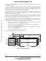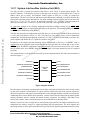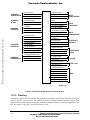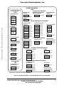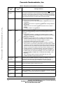
1
Freescale Semiconductor, Inc. SA14-2053-00 (IBM Order Number) MPC604E/D (Motorola Order Number) 1/96 REV 1 O IC EM R, O CT U ND C IN . S E L A CMicroprocessor PowerPC 604e RISC S EE R Technical Summary F BY D This document provides an E overview of the PowerPC 604e microprocessor features, V I including a block diagram showing the major functional components. It provides CH the 604e implementation complies with the PowerPC information about R how A This document is divided into two parts: architecture definition. Advance Information • Part 1,“PowerPC 604e Microprocessor Overview,” provides an overview of the 604e features, including a block diagram showing the major functional components. • Part 2, “PowerPC 604e Microprocessor: Implementation,” gives specific details about the implementation of the 604e as a 32-bit member of the PowerPC processor family. In this document, the term “604e” is used as an abbreviation for the phrase “PowerPC 604e microprocessor” and “604” is an abbreviation for the phrase “PowerPC 604 microprocessor.” The PowerPC 604e microprocessors are available from IBM as PPC604e and from Motorola as MPC604e. The PowerPC name, the PowerPC logotype, PowerPC 604, and PowerPC 604e, are trademarks of International Business Machines Corporation, used by Motorola under license from International Business Machines Corporation. This document contains information on a new product under development by Motorola and IBM. Motorola and IBM reserve the right to change or discontinue this product without notice. Motorola Inc., 1996. All rights reserved. Portions hereof International Business Machines Corporation, 1991–1996. All rights reserved. For More Information On This Product, Go to: www.freescale.com 604e Technical Summary Freescale Semiconductor, Inc... Freescale Semiconductor, Inc. Part 1 PowerPC 604e Microprocessor Overview This section describes the features of the 604e, provides a block diagram showing the major functional units, and describes briefly how those units interact. Freescale Semiconductor, Inc... The 604e is an implementation of the PowerPC family of reduced instruction set computer (RISC) microprocessors. The 604e implements the PowerPC architecture as it is specified for 32-bit addressing, which provides 32-bit effective (logical) addresses, integer data types of 8, 16, and 32 bits, and floatingpoint data types of 32 and 64 bits (single-precision and double-precision). For 64-bit PowerPC implementations, the PowerPC architecture provides additional 64-bit integer data types, 64-bit addressing, and related features. C. N The 604e is a superscalar processor capable of issuing four instructions simultaneously. , I As many as seven R instructions can finish execution in parallel. The 604e has seven execution units that can operate in parallel: TO C • Floating-point unit (FPU) DU • Branch processing unit (BPU) N O • Condition register unit (CRU) IC M • Load/store unit (LSU) SE • Three integer units (IUs): LE A — Two single-cycle integer units (SCIUs) SC E — One multiple-cycle integer unitE(MCIU) FR This parallel design, combined with BYthe PowerPC architecture’s specification of uniform instructions that D allows for rapid execution times, E yields high efficiency and throughput. The 604e’s rename buffers, V reservation stations, dynamic branch prediction, and completion unit increase instruction throughput, HI and ensure a precise exception model. (Note that the PowerPC architecture guarantee in-order completion, C R specification refersAto all exceptions as interrupts.) The 604e has separate memory management units (MMUs) and separate 32-Kbyte on-chip caches for instructions and data. The 604e implements two 128-entry, two-way set associative translation lookaside buffers (TLBs), one for instructions and one for data, and provides support for demand-paged virtual memory address translation and variable-sized block translation. The TLBs and the cache use least-recently used (LRU) replacement algorithms. The 604e has a 64-bit external data bus and a 32-bit address bus. The 604e interface protocol allows multiple masters to compete for system resources through a central external arbiter. Additionally, on-chip snooping logic maintains data cache coherency for multiprocessor applications. The 604e supports single-beat and burst data transfers for memory accesses and memory-mapped I/O accesses. The 604e uses an advanced, 2.5-V CMOS process technology and is fully compatible with TTL devices. 1.1 PowerPC 604e Microprocessor Features This section summarizes features of the 604e’s implementation of the PowerPC architecture. Figure 1 provides a block diagram showing features of the 604e. Note that this is a conceptual block diagram intended to show the basic features rather than an attempt to show how these features are physically implemented on the chip. 2 PowerPC 604e RISC Microprocessor Technical Summary For More Information On This Product, Go to: www.freescale.com PowerPC 604e RISC Microprocessor Technical Summary For More Information On This Product, Go to: www.freescale.com 16-Entry Reorder Buffer 64-BIT DATA BUS Finish Load Queue 32 Bit 32 Bit DTLB SRs DBAT Array D MMU + 64 Bit 64 Bit Rename Buffers (8) 64 Bit Tags 64 Bit R, O CT U ND 32-Kbyte D Cache 128 Bit * + FPSCR / FloatingPoint Unit BUS INTERFACE UNIT 32-Kbyte I Cache IBAT Array 128 Bit I MMU Tags ITLB SRs Reservation Station (2 Entry) C IN 32-BIT ADDRESS BUS Store Queue 32 Bit EA Calculation Load/Store Unit Condition Register Logical Unit Reservation Station (2 Entry) FPR File O IC EM COMPLETION UNIT 32 Bit / + * + 32 Bit S * Single-Cycle Integer Units BHT LE A SC / MultipleCycle Integer Unit Reservation Station (2 Entry) 32 Bit Dispatch Unit EE R F Rename Buffers (12) GPR File BY Reservation Station (2 Entry) 128 Bit CTR LR Reservation Station (2 Entry) ED V I Reservation Station (2 Entry) JTAG/COP Interface Instruction Queue (8 word) BTAC CR File Rename Buffers (8) INSTRUCTION UNIT Branch Processing Unit CH R A Clock Multiplier Time Base Counter/Decrementer Fetcher 64 Bit Freescale Semiconductor, Inc... Freescale Semiconductor, Inc. . Figure 1. Block Diagram 3 Freescale Semiconductor, Inc. 1.1.1 New Features of the PowerPC 604e Processor Features of the 604e that are not implemented in the 604 are as follows: • Additional special-purpose registers — HID1 provides four read-only PLL_CFG bits for indicating the processor/bus clock ratio. — Three additional registers to support the performance monitor—MMCR1 is a second control register that includes bits to support the use of two additional counter registers, PMC3 and PMC4. • Instruction execution . split into a — Separate units for branch and condition register (CR) instructions. The BPU isCnow N CR logical unit and a branch unit, which makes it possible for branch instructions to execute ,I R and resolve before preceding CR logical instructions. The 604e can O still only dispatch one CR T logical or branch instruction per cycle, but it can execute both branch C and CR logical U instructions at the same time. D Freescale Semiconductor, Inc... N — Branch correction in decode stage. Branch correctionCinOthe decode stage can now predict I registers if no updates of the count and branches whose target is taken from the count or link M link register are pending. This saves at least one SEcycle on branch correction when the Move to E Special-Purpose Register (mtspr) instruction L can be sufficiently separated from the branch that uses the special-purpose register (SPR) CAas a target address. S — Ability to disable the branch target EE address cache (BTAC)—HID0[30] has been defined to R allow the BTAC to be disabled. F When HID0[30] is set, the BTAC contents are invalidated and the BTAC behaves as ifBitYwere empty. New entries cannot be added until the BTAC is enabled. • Improvements to cache EDimplementation IV — 32-Kbyte split CH data and instruction caches. Like the 604, both caches are four-way set R associative; A however, each cache has twice as many sets, logically separated into 128 sets of odd lines and 128 sets of even lines. — Data cache line-fill buffer forwarding. In the 604 only the critical double word of a burst operation was made available to the requesting unit at the time it was burst into the line-fill buffer. Subsequent data was unavailable until the cache block was filled. On the 604e, subsequent data is also made available as it arrives in the line-fill buffer. — Additional cache copyback buffers. The 604e implements three copyback write buffers (as opposed to one in the 604). Having multiple copyback buffers provides the ability for certain instructions to take fuller advantage of the pipelined system bus to provide more efficient handling of cache copyback, block invalidate operations caused by the Data Cache Block Flush (dcbf) instruction, and cache block clean operations resulting from the Data Cache Block Store (dcbst) instruction. — Coherency support for instruction fetching. Instruction fetching coherency is controlled by HID0[23]. In the default mode, HID0[23] is 0, GBL is not asserted for instruction accesses, as is the case with the 604. If the bit is set, and instruction translation is enabled (MSR[IR] = 1), the GBL signal is set to reflect the M bit for this page or block. If instruction translation is disabled (MSR[IR] = 0), the GBL signal is asserted. • System interface operation — The 604e has the same pin configuration as the 604; however, on the 604e Vdd and AVdd must be tied to 2.5 Vdc and OVdd must be tied to 3.3 Vdc. The 604e uses split voltage planes, and for replacement compatibility, 604/604e designs should provide both 2.5-V and 3.3-V planes and the ability to tie those two planes together and disable the 2.5-V plane for operation with a 604. 4 PowerPC 604e RISC Microprocessor Technical Summary For More Information On This Product, Go to: www.freescale.com Freescale Semiconductor, Inc. — Support for additional processor/bus clock ratios (5:2 and 4:1). Configuration of the processor/ bus clock ratios is displayed through a new 604e-specific register, HID1. — To support the changes in the clocking configuration, different precharge timings for the ABB, DBB, ARTRY, and SHD signals are implemented internally by the processor. The precharge timings for ARTRY and SHD can be disabled by setting HID0[7]. — No-DRTRY mode. In addition to the normal and fast L2 modes implemented on the 604, a noDRTRY mode is implemented on the 604e that improves performance on read operations for systems that do not use the DRTRY signal. No-DRTRY mode makes read data available to the processor one bus clock cycle sooner than in normal mode. In no-DRTRY mode, the DRTRY signal is no longer sampled as part of a qualified bus grant. Freescale Semiconductor, Inc... • • . Full hardware support for little-endian accesses. Little-endian accesses take alignment NC exceptions I , boundary require for only the same set of causes as big-endian accesses. Accesses that cross aRword O two accesses with the lower-addressed word accessed first. T Additional enhancements to the performance monitor. UC D N O IC 1.1.2 Overview of the PowerPC 604e Microprocessor Features M E S Major features of the 604e are as follows: E L • High-performance, superscalar microprocessor CA S — As many as four instructions can E E be issued per clock R F can start executing per clock (including three integer — As many as seven instructions instructions) BY ED — Single-clock-cycle execution for most instructions V I • Seven independent CH execution units and two register files R A — BPU featuring dynamic branch prediction – Two-entry reservation station – Out-of-order execution through two branches – Shares dispatch bus with CRU – 64-entry fully-associative branch target address cache (BTAC). In the 604e, the BTAC can be disabled and invalidated. – 512-entry branch history table (BHT) with two bits per entry for four levels of prediction— not-taken, strongly not-taken, taken, strongly taken — Condition register logical unit – Two-entry reservation station – Shares dispatch bus with BPU — Two single-cycle IUs (SCIUs) and one multiple-cycle IU (MCIU) – Instructions that execute in the SCIU take one cycle to execute; most instructions that execute in the MCIU take multiple cycles to execute. – Each SCIU has a two-entry reservation station to minimize stalls – The MCIU has a single-entry reservation station and provides early exit (three cycles) for 16- x 32-bit and overflow operations. – Thirty-two GPRs for integer operands PowerPC 604e RISC Microprocessor Technical Summary For More Information On This Product, Go to: www.freescale.com 5 Freescale Semiconductor, Inc. — Three-stage floating-point unit (FPU) – Fully IEEE 754-1985-compliant FPU for both single- and double-precision operations – Supports non-IEEE mode for time-critical operations – Fully pipelined, single-pass double-precision design – Hardware support for denormalized numbers – Two-entry reservation station to minimize stalls – Thirty-two 64-bit FPRs for single- or double-precision operands — Load/store unit (LSU) – Two-entry reservation station to minimize stalls R, O CT – Dedicated adder performs EA calculations U – Performs alignment and precision conversion for floating-point data ND O ICdata – Performs alignment and sign extension for integer M – Four-entry finish load queue (FLQ) provides SEload miss buffering E – Six-entry store queue AL C – Supports both big- and little-endian ES modes E Rename buffers FR — Twelve GPR rename buffers BY D — Eight FPR rename VEbuffers I — Eight condition CH register (CR) rename buffers R A The 604e rename buffers are described in Section 1.2.7, “Rename Buffers.” C IN . Freescale Semiconductor, Inc... – Single-cycle, pipelined cache access • • Completion unit — The completion unit retires an instruction from the 16-entry reorder buffer when all instructions ahead of it have been completed and the instruction has finished execution. — Guarantees sequential programming model (precise exception model) — Monitors all dispatched instructions and retires them in order — Tracks unresolved branches and flushes executed, dispatched, and fetched instructions if branch is mispredicted — Retires as many as four instructions per clock • Separate on-chip instruction and data caches (Harvard architecture) — 32-Kbyte, four-way set-associative instruction and data caches — LRU replacement algorithm — 32-byte (eight-word) cache block size — Physically indexed/physical tags. (Note that the PowerPC architecture refers to physical address space as real address space.) — Cache write-back or write-through operation programmable on a per page or per block basis — Instruction cache can provide four instructions per clock; data cache can provide two words per clock — Caches can be disabled in software 6 PowerPC 604e RISC Microprocessor Technical Summary For More Information On This Product, Go to: www.freescale.com Freescale Semiconductor, Inc. — Caches can be locked — Parity checking performed on both caches — Data cache coherency (MESI) maintained in hardware — Secondary data cache support provided — Instruction cache coherency maintained in hardware — Data cache line-fill buffer forwarding. In the 604 only the critical double word of the cache block was made available to the requesting unit at the time it was burst into the line-fill buffer. Subsequent data was unavailable until the cache block was filled. On the 604e, subsequent data is also made available as it arrives in the line-fill buffer. Freescale Semiconductor, Inc... • Separate memory management units (MMUs) for instructions and data , C IN . — Address translation facilities for 4-Kbyte page size, variable block size, OR and 256-Mbyte T segment size C DU N O — TLBs are hardware reloadable (that is, the page table ICsearch is performed in hardware) M — Separate IBATs and DBATs (four each) also defined SE as SPRs — Separate instruction and data translation lookaside buffers (TLBs) LE A C — LRU replacement algorithm ES E — 52-bit virtual address; 32-bit R F physical address Bus interface features include BYthe following: D — Selectable processor-to-bus clock frequency ratios (1:1, 3:2, 2:1, 5:2, 3:1, and 4:1) VE I — A 64-bit split-transaction external data bus with burst transfers CH R A for address pipelining and limited out-of-order bus transactions — Support — Both TLBs are 128-entry and two-way set associative • — Four burst write queues—three for cache copyback operations and one for snoop push operations — Two single-beat write queues — Additional signals and signal redefinition for direct-store operations — Provides a data streaming mode that allows consecutive burst read data transfers to occur without intervening dead cycles. This mode also disables data retry operations. — No-DRTRY mode eliminates the DRTRY signal from the qualified bus grant and allows read operations. This improves performance on read operations for systems that do not use the DRTRY signal. No-DRTRY mode makes read data available to the processor one bus clock cycle sooner than if normal mode is used. • Multiprocessing support features include the following: — Hardware enforced, four-state cache coherency protocol (MESI) for data cache. Bits are provided in the instruction cache to indicate only whether a cache block is valid or invalid. — Separate port into data cache tags for bus snooping — Load/store with reservation instruction pair for atomic memory references, semaphores, and other multiprocessor operations • Power management — NAP mode supports full shut down and snooping — Operating voltage of 2.5 ± 0.3 V PowerPC 604e RISC Microprocessor Technical Summary For More Information On This Product, Go to: www.freescale.com 7 Freescale Semiconductor, Inc. • Performance monitor can be used to help in debugging system designs and improving software efficiency, especially in multiprocessor systems. • In-system testability and debugging features through JTAG boundary-scan capability 1.2 PowerPC 604e Microprocessor Hardware Implementation C. N Note that Figure 2 provides a more detailed block diagram than that presented in Figure 1—showing the , I and R additional data paths that contribute to the improved efficiency in instruction execution more clearly TO shows the relationships between execution units and their associated register C files. DU N O Branch Dispatch Unit IC correction Fetch Unit (Four-instruction EM S dispatch) LE A Instruction dispatch buses SC E E GPR FRoperand buses Y BGPR result buses D E FPR operand buses V I CH CR result bus FPR result buses R A RS(1) RS(2) CRU BPU SCIU MCIU LSU SCIU RS(2) FPU 32 FPRs RS(2) FPR Rename Buffers RS(2) RS(2) 32 GPRs RS(2) GPR Rename Buffers Freescale Semiconductor, Inc... This section provides an overview of the 604e’s hardware implementation, including descriptions of the functional units, shown in Figure 2, the cache implementation, MMU, and the system interface. Result status buses Completion Unit 32-Kbyte data cache 4-way, 8 words/block Result buses Operand buses Figure 2. Block Diagram—Internal Data Paths 8 PowerPC 604e RISC Microprocessor Technical Summary For More Information On This Product, Go to: www.freescale.com Freescale Semiconductor, Inc. 1.2.1 Instruction Flow Several units on the 604e ensure the proper flow of instructions and operands and guarantee the correct update of the architectural machine state. These units include the following: • Fetch unit—Using the next sequential address or the address supplied by the BPU when a branch is predicted or resolved, the fetch unit supplies instructions to the eight-word instruction buffer. • Dispatch unit—The decode/dispatch unit decodes instructions and dispatches them to the appropriate execution unit. During dispatch, operands are provided to the execution unit (or reservation station) from the register files, rename buffers, and result buses. • Branch processing unit (BPU)—Provides the fetcher with predicted target instructions when a branch is predicted (and a mispredict recovery address if a branch is incorrectly predicted). C. Freescale Semiconductor, Inc... • • IN , and flow control Condition register unit (CRU)—The CRU executes all condition register logical OR register or branch instructions. The CRU shares the dispatch bus with the BPU only one T condition instruction can be issued per clock cycle. UC D N in program order and controls Completion unit—The completion unit retires executed instructions O the updating of the architectural machine state. IC SE M LE A The fetch unit provides instructions to the eight-entry SC instruction queue by accessing the on-chip instruction E cache. Typically, the fetch unit continues fetching sequentially as many as four instructions at a time. E R F The address of the next instruction toYbe fetched is determined by several conditions, which are prioritized B as follows: ED V 1. Detection of an exception. Instruction fetching begins at the exception vector. HI C 2. The BPU recovers from an incorrect prediction when a branch instruction is in the execute stage. AR Undispatched instructions are flushed and fetching begins at the correct target address. 1.2.2 Fetch Unit 3. The BPU recovers from an incorrect prediction when a branch instruction is in the dispatch stage. Subsequent instructions are flushed and fetching begins at the correct target address. 4. The BPU recovers from an incorrect prediction when a branch instruction is in the decode stage. Subsequent instructions are flushed and fetching begins at the correct target address. 5. A fetch address is found in the BTAC. As a cache block is fetched, the branch target address cache (BTAC) and the branch history table (BHT) are searched with the fetch address. If it is found in the BTAC, the target address from the BTAC is the first candidate for being the next fetch address. 6. If none of the previous conditions exists, the instruction is fetched from the next sequential address. 1.2.3 Decode/Dispatch Unit The decode/dispatch unit provides the logic for decoding instructions and issuing them to the appropriate execution unit. The eight-entry instruction queue consists of two four-entry queues—a decode queue (DEQ) and a dispatch queue (DISQ). The decode logic decodes the four instructions in the decode queue. For many branch instructions, these decoded instructions along with the bits in the BHT, are used during the decode stage for branch correction. The dispatch logic decodes the instructions in the DISQ for possible dispatch. The dispatch logic resolves unconditional branch instructions and predicts conditional branch instructions using the branch decode logic, the BHT, and values in the CTR. PowerPC 604e RISC Microprocessor Technical Summary For More Information On This Product, Go to: www.freescale.com 9 Freescale Semiconductor, Inc. The 512-entry BHT provides two bits per entry, indicating four levels of dynamic prediction—strongly nottaken, not-taken, taken, and strongly taken. The history of a branch’s direction is maintained in these two bits. Each time a branch is taken the value is incremented (with a maximum value of three meaning stronglytaken); when it is not taken, the bit value is decremented (with a minimum value of zero meaning strongly not-taken). If the current value predicts taken and the next branch is taken again, the BHT entry then predicts strongly taken. If the next branch is not taken, the BHT then predicts taken. Freescale Semiconductor, Inc... The dispatch logic also allocates each instruction to the appropriate execution unit. A reorder buffer (ROB) entry is allocated for each instruction, and dependency checking is done between the instructions in the dispatch queue. The rename buffers are searched for the operands as the operands are fetched from the register file. Operands that are written by other instructions ahead of this one in the dispatch queue are given C. the tag of that instruction’s rename buffer; otherwise, the rename buffer or register fileNsupplies either the I operand or a tag. As instructions are dispatched, the fetch unit is notified that the ,dispatch queue can be R O updated with more instructions. T 1.2.4 Branch Processing Unit (BPU) O UC D N IC All branches, including unconditional The BPU handles prediction and recovery for branch instructions. M E conditions are resolved and they can be branches, are placed in a two-entry reservation station Suntil E executed. At that point, branch instructions are executed in order and the completion unit is notified whether L A the prediction was correct. C S Unlike the 604, the 604e has a separate unit EEfor executing condition register logical instructions, which R makes it possible for branch instructionsFto execute and resolve before a preceding CR logical instruction. The 604e can still only dispatch one BYCR logical or branch instruction per cycle, but it can execute both D branch and CR logical instructions E at the same time. IV Branch correction in the H C decode stage in the 604e can predict branches whose target is taken from the count or link registers if A noRupdates of the count and link register are pending. This saves at least one cycle on branch correction when the mtspr instruction can be sufficiently separated from the branch that uses the SPR as a target address. HID0[30] has been defined to allow the BTAC to be disabled. When HID0[30] is set, the BTAC contents are invalidated and that BTAC behaves as if it were empty. New entries cannot be added until the BTAC is enabled. The BPU shares a dispatch bus with the condition register. 1.2.5 Condition Register Unit (CRU) Condition register logical instructions are executed by the CRU, which shares the dispatch bus with the BPU. The CRU has its own two-entry reservation station. The 604e can still only dispatch one CR logical or branch instruction per cycle, but it can execute both branch and CR logical instructions at the same time. 1.2.6 Completion Unit The completion unit retires executed instructions from the reorder buffer (ROB) in the completion unit and updates register files and control registers. The completion unit recognizes exception conditions and discards any operations being performed on subsequent instructions in program order. The completion unit can quickly remove instructions from a mispredicted branch, and the decode/dispatch unit begins dispatching from the correct path. 10 PowerPC 604e RISC Microprocessor Technical Summary For More Information On This Product, Go to: www.freescale.com Freescale Semiconductor, Inc. The instruction is retired from the reorder buffer when it has finished execution and all instructions ahead of it have been completed. The instruction’s result is written into the appropriate register file and is removed from the rename buffers at or after completion. At completion, the 604e also updates any other resource affected by this instruction. Several instructions can complete simultaneously. Most exception conditions are recognized at completion time. 1.2.7 Rename Buffers To avoid contention for a given register location, the 604e provides rename registers for storing instruction results before the completion unit commits them to the architected register. Twelve rename registers are provided for the GPRs, eight for the FPRs, and eight for the condition register. GPRs are described in C. “FloatingSection 2.1.1.1, “General-Purpose Registers (GPRs),” FPRs are described in SectionN2.1.1.2, , I“Condition Register Point Registers (FPRs),” and the condition register is described in Section 2.1.1.3, R (CR).” TO Freescale Semiconductor, Inc... C U When the dispatch unit dispatches an instruction to its execution unit, itDallocates a rename register for the N results of that instruction. The dispatch unit also provides a tag to the execution unit identifying the result O C I that should be used as the operand. When the proper result is returned to the rename buffer it is latched into EM the reservation station. When all operands are available inSthe reservation station, the execution can begin. E The completion unit does not transfer instruction results AL from the rename registers to the registers until any C branch conditions preceding it in the completionSqueue are resolved and the instruction itself is retired from the completion queue without exceptions.EIfEa branch is found to have been incorrectly predicted, all R instructions following the branch areFflushed from the completion queue and any results of those instructions are flushed from the rename BY registers. ED V I 1.2.8 Execution HUnits C The following sections AR describe the 604e’s arithmetic execution units—the two single-cycle integer units (SCIUs), the multiple cycle integer unit (MCIU), and the FPU. When the reservation station sees the proper result being written back, it will grab it directly from one of the result buses. Once all operands are in the reservation station for an instruction, it is eligible to be executed. Reservation stations temporarily store dispatched instructions that cannot be executed until all of the source operands are valid. 1.2.8.1 Integer Units (IUs) The two SCIUs and one MCIU execute all integer instructions. These are shown in Figure 1 and Figure 2. Each IU has a dedicated result bus that connects to rename buffers and to all reservation stations. Each SCIU has a two-entry reservation station and the MCIU has a single-entry reservation station to reduce stalls. A reservation station can receive instructions from the decode/dispatch unit and operands from the GPRs, the rename buffers, or the result buses. Each SCIU consists of three single-cycle subunits—a fast adder/comparator, a subunit for logical operations, and a subunit for performing rotates, shifts, and count-leading-zero operations. These subunits handle all one-cycle arithmetic instructions; only one subunit can execute an instruction at a time. The MCIU consists of a 32-bit integer multiplier/divider. The multiplier supports early exit on 16- x 32-bit operations, and is responsible for executing the Move from Special-Purpose Register (mfspr) and Move to Special-Purpose Register (mtspr) instructions, which are used to read and write special-purpose registers. Note that the load and store instructions that update their address base register (specified by the rA operand) pass the update results on the MCIU’s result bus. Otherwise, the MCIU’s result bus is dedicated to MCIU operations. PowerPC 604e RISC Microprocessor Technical Summary For More Information On This Product, Go to: www.freescale.com 11 Freescale Semiconductor, Inc. 1.2.8.2 Floating-Point Unit (FPU) The FPU, shown in Figure 1 and Figure 2, is a single-pass, double-precision execution unit; that is, most single- and double-precision operations require only a single pass, with a latency of three cycles. As the decode/dispatch unit issues instructions to the FPU’s two reservation stations, source operand data may be accessed from the FPRs, the floating-point rename buffers, or the result buses. Results in turn are written to the floating-point rename buffers and to the reservation stations and are made available to subsequent instructions. Instructions are executed from the reservation station in dispatch order. Freescale Semiconductor, Inc... 1.2.8.3 Load/Store Unit (LSU) The LSU, shown in Figure 1 and Figure 2, transfers data between the data cache and the result C. buses, which N route data to other execution units. The LSU supports the address generation and handles , I any alignment for R transfers to and from system memory. Note that the 604e provides additional O hardware support for T misaligned little-endian accesses over previous versions of the 604. In the 604e, the conditions that cause UC an alignment exception to be taken are the same regardless of whether theDprocessor is in big- or little-endian N mode. When two accesses are required, the lower addressed word (in the current addressing mode) is O IC accessed first. EM S load/store The LSU also supports cache control instructions and multiple/string instructions. As noted LEaddress register pass their results on the MCIU’s above, load and store instructions that update the A base result bus. This is the only exception to the dedicated SC use of result buses. EE The LSU includes a 32-bit adder dedicated FR for EA calculation. Data alignment logic manipulates data to support aligned or misaligned transfers BY with the data cache. The LSU’s load and store queues are used to buffer instructions that have been executed and are waiting to be completed. The queues are used to monitor D data dependencies generated VEby data forwarding and out-of-order instruction execution ensuring a I sequential model. CH R The LSU allows A load operations to precede pending store operations and resolves any dependencies incurred when a pending store is to the same address as the load. If such a dependency exists, the LSU delays the load operation until the correct data can be forwarded. If only the low-order 12 bits of the EAs match, both addresses may be aliases for the same physical address, in which case, the load operation is delayed until the store has been written back to the cache, ensuring that the load operation retrieves the correct data. The LSU does not allow the following operations to be performed on unresolved branches: • • Store operations Loading of noncacheable data or cache miss operations 1.2.9 Memory Management Units (MMUs) The primary functions of the MMUs are to translate logical (effective) addresses to physical addresses for memory accesses, I/O accesses (most I/O accesses are assumed to be memory-mapped), and direct-store accesses, and to provide access protection on blocks and pages of memory. The PowerPC MMUs and exception model support demand-paged virtual memory. Virtual memory management permits execution of programs larger than the size of physical memory; demand-paged implies that individual pages are loaded into physical memory from system memory only when they are first accessed by an executing program. The hashed page table is a variable-sized data structure that defines the mapping between virtual page numbers and physical page numbers. The page table size is a power of 2, and its starting address is a multiple of its size. 12 PowerPC 604e RISC Microprocessor Technical Summary For More Information On This Product, Go to: www.freescale.com Freescale Semiconductor, Inc. Address translations are enabled by setting bits in the MSR—MSR[IR] enables instruction address translations and MSR[DR] enables data address translations. The 604e’s MMUs support up to 4 Petabytes (252) of virtual memory and 4 Gigabytes (232) of physical memory. The MMUs support block address translations, direct-store segments, and page translation of memory segments. Referenced and changed status are maintained by the processor for each page to assist implementation of a demand-paged virtual memory system. Separate but identical translation logic is implemented for data accesses and for instruction accesses. The 604e implements two 128-entry, two-way set-associative translation lookaside buffers (TLBs), one for instructions and one for data. These TLBs can be accessed simultaneously. . R, O The PowerPC architecture does not define hardware aspects of cache implementations. For example, T Carchitecture), whereas the 604e implements separate data and instruction caches (Harvard other processors U may use a unified cache, or no cache at all. The PowerPC architecture NDdefines the unit of coherency as a O cache block, which for the 604e is a 32-byte (eight-word) line. IC M PowerPC implementations can control the following memory SE access modes on a page or block basis: LE • Write-back/write-through mode A SC • Caching-inhibited mode E E • Memory coherency FR Y for out-of-order execution) • Guarded memory (preventsBaccess D E 1.2.10.1 InstructionIVCache H The 604e’s 32-Kbyte,Cfour-way set-associative instruction cache is physically indexed. Within a single R A cache provides up to four instructions. cycle, the instruction 1.2.10 Cache Implementation Freescale Semiconductor, Inc... C IN The 604e provides coherency checking for instruction fetches. Instruction fetching coherency is controlled by a HID0[23]. In the default mode, HID0[23] is 0, the GBL signal is not asserted for instruction accesses on the bus, as is the case with the 604. If the bit is set and instruction translation is enabled (MSR[IR] = 1), the GBL signal is set to reflect the M bit for this page or block. If HID0[23] is set and instruction translation is disabled (MSR[IR] = 0), the GBL signal is asserted and coherency is maintained in the instruction cache. The PowerPC architecture defines a special set of instructions for managing the instruction cache. The instruction cache can be invalidated entirely or on a cache-block basis. The instruction cache can be disabled and invalidated by setting the HID0[16] and HID0[20] bits, respectively. The instruction cache can be locked by setting HID0[18]. 1.2.10.2 Data Cache The 604e’s data cache is a 32-Kbyte, four-way set associative cache. It is a physically-indexed, nonblocking, write-back cache with hardware support for reloading on cache misses. Within one cycle, the data cache provides double-word access to the LSU. Note that the 604e provides additional support for data cache line-fill buffer forwarding. In the 604 only the critical double word of a burst operation was made available to the requesting unit at the time it was burst into the line-fill buffer. Subsequent data was unavailable until the cache block was filled. On the 604e, subsequent data is also made available as it arrives in the line-fill buffer. The 604e implements three copyback write buffers (as opposed to one in the 604). Having multiple copyback buffers provides the ability for certain instructions to take fuller advantage of the pipelined system bus to provide more efficient handling of cache copyback, block invalidate operations caused by the data PowerPC 604e RISC Microprocessor Technical Summary For More Information On This Product, Go to: www.freescale.com 13 Freescale Semiconductor, Inc. cache block flush (dcbf) instruction, and cache block clean operations resulting from the data cache block store (dcbst) instruction. To ensure cache coherency, the 604e data cache supports the four-state MESI (modified/exclusive/shared/ invalid) protocol. The data cache tags are dual-ported, so the process of snooping does not affect other transactions on the system interface. If a snoop hit occurs, the LSU is blocked internally for one cycle to allow the eight-word block of data to be copied to the writeback buffer. Like the instruction cache, the data cache can be invalidated all at once or on a per cache block basis. The data cache can be disabled and invalidated by setting the HID0[17] and HID0[21] bits, respectively. The data cache can be locked by setting HID0[19]. . Freescale Semiconductor, Inc... Each cache line contains eight contiguous words from memory that are loaded from an eight-word boundary NC I , (that is, bits A27–A31 of the physical addresses are zero); thus, a cache line never crosses a page boundary. R Accesses that cross a page boundary can incur a performance penalty. TO UC To ensure coherency among caches in a multiprocessor (or multiple caching-device) implementation, the ND 604e implements the MESI protocol on a per cache-block basis.OMESI stands for modified/exclusive/ IC as follows: shared/invalid. These four states indicate the state of the cacheMblock • • • • E S Modified (M)—The cache block is modified with E respect to system memory; that is, data for this L address is valid only in the cache and not inAsystem memory. C Exclusive (E)—This cache block holds ESvalid data that is identical to the data at this address in E system memory. No other cache has R this data. F Shared (S)—This cache block BY holds valid data that is identical to this address in system memory and at least one other caching device. D E IV block does not hold valid data. Invalid (I)—ThisHcache RC Figure 3 describesA the cache unit organization on the 604e. 256 Sets Block 0 Address Tag 0 State Words 0–7 Block 1 Address Tag 1 State Words 0–7 Block 2 Address Tag 2 State Words 0–7 Block 3 Address Tag 3 State Words 0–7 8 Words/Block Figure 3. Cache Unit Organization 14 PowerPC 604e RISC Microprocessor Technical Summary For More Information On This Product, Go to: www.freescale.com Freescale Semiconductor, Inc. 1.2.11 System Interface/Bus Interface Unit (BIU) The 604e provides a versatile bus interface that allows a wide variety of system design options. The interface includes a 72-bit data bus (64 bits of data and 8 bits of parity), a 36-bit address bus (32 bits of address and 4 bits of parity), and sufficient control signals to allow for a variety of system-level optimizations. The 604e uses one-beat and four-beat data transactions, although it is possible for other bus participants to perform longer data transfers. The 604e clocking structure supports processor-to-bus clock ratios of 1:1, 3:2, 2:1, 5:2, 3:1, and 4:1, as described in Section 1.2.12, “Clocking.” Note that support for processor/bus clock ratios 5:2 and 4:1 is specific to the 604e and is not supported in the 604. To support the changes in the clocking configuration, different precharge timings for the ABB, DBB, ARTRY, and SHD signals are implemented internally by the processor. The precharge timings C. for ARTRY N and SHD can be disabled by setting HID0[7]. I Freescale Semiconductor, Inc... R, The 604e has the same pin configuration as the 604; however, on the 604e Vdd TOand AVdd must be tied to C 2.5 Vdc and OVdd must be tied to 3.3 Vdc. The 604e uses split voltage planes, and for replacement U D compatibility, 604/604e designs should provide both 2.5-V and 3.3-V N planes and the ability to tie those two O planes together and disable the 2.5-V plane for operation with a 604. C I M E In addition to the normal and data-streaming modes implemented on the 604, a no-DRTRY mode is S implemented on the 604e that improves performanceLE on read operations for systems that do not use the DRTRY signal. No-DRTRY mode makes read data CAavailable to the processor one bus clock cycle sooner S than in normal mode. In no-DRTRY mode, the E DRTRY signal is no longer sampled as part of a qualified bus grant. RE Y F The system interface is specific forBeach PowerPC processor implementation. The 604e system interface is shown in Figure 4. ED IV H C AR ADDRESS DATA DATA ARBITRATION ADDRESS ARBITRATION PowerPC 604e Processor ADDRESS START ADDRESS TRANSFER DATA TRANSFER DATA TERMINATION TRANSFER ATTRIBUTE PROCESSOR STATE ADDRESS TERMINATION TEST AND CONTROL CLOCKS +3.3 V +2.5 V Figure 4. System Interface Four-beat burst-read memory operations that load an eight-word cache block into one of the on-chip caches are the most common bus transactions in typical systems, followed by burst-write memory operations, direct-store operations, and single-beat (noncacheable or write-through) memory read and write operations. Additionally, there can be address-only operations, variants of the burst and single-beat operations (global memory operations that are snooped and atomic memory operations, for example), and address retry activity (for example, when a snooped read access hits a modified line in the data cache). Memory accesses can occur in single-beat or four-beat burst data transfers. The address and data buses are independent for memory accesses to support pipelining and split transactions. The 604e supports bus pipelining and out-of-order split-bus transactions. In general, the bus-pipelining mechanism allows as many PowerPC 604e RISC Microprocessor Technical Summary For More Information On This Product, Go to: www.freescale.com 15 Freescale Semiconductor, Inc. as three address tenures to be outstanding before a data tenure is initiated. Address tenures for address-only transactions can exceed this limit. Typically, memory accesses are weakly-ordered. Sequences of operations, including load/store string/ multiple instructions, do not necessarily complete in the same order in which they began—maximizing the efficiency of the bus without sacrificing coherency of the data. The 604e allows load operations to precede store operations (except when a dependency exists, of course). In addition, the 604e provides a separate queue for snoop push operations so these operations can access the bus ahead of previously queued operations. The 604e dynamically optimizes run-time ordering of load/store traffic to improve overall performance. Freescale Semiconductor, Inc... . write In addition, the 604e implements a data bus write-only signal (DBWO) that can be used forCreordering N I on a given operations. Asserting DBWO causes the first write operation to occur before any read, operations processor. Although this may be used with any write operations, it can also be used ORto reorder a snoop push T operation. C U Access to the system interface is granted through an external arbitration NDmechanism that allows devices to O compete for bus mastership. This arbitration mechanism is flexible, IC allowing the 604e to be integrated into M systems that use various fairness and bus-parking procedures to avoid arbitration overhead. Additional SE multiprocessor support is provided through coherency mechanisms that provide snooping, external control E L of the on-chip caches and TLBs, and support for a secondary cache. The PowerPC architecture provides the CA /stwcx.) for atomic memory references and other load/store with reservation instruction pair (S lwarx operations useful in multiprocessor implementations. EE FR The following sections describe the Y B 604e bus support for memory and direct-store operations. Note that some signals perform different functions depending upon the addressing protocol used. D VE I H 1.2.11.1 MemoryCAccesses R A Memory accesses allow transfer sizes of 8, 16, 24, 32, 40, 48, 56, or 64 bits in one bus clock cycle. Data transfers occur in either single-beat transactions or four-beat burst transactions. A single-beat transaction transfers as much as 64 bits. Single-beat transactions are caused by noncached accesses that access memory directly (that is, reads and writes when caching is disabled, caching-inhibited accesses, and stores in writethrough mode). Burst transactions, which always transfer an entire cache block (32 bytes), are initiated when a block in the cache is read from or written to memory. Additionally, the 604e supports address-only transactions used to invalidate entries in other processors’ TLBs and caches. Typically I/O accesses are performed using the same protocol as memory accesses. 1.2.11.2 Signals The 604e’s signals are grouped as follows: 16 • Address arbitration signals—The 604e uses these signals to arbitrate for address bus mastership. • Address start signals—These signals indicate that a bus master has begun a transaction on the address bus. • Address transfer signals—These signals, which consist of the address bus, address parity, and address parity error signals, are used to transfer the address and to ensure the integrity of the transfer. • Transfer attribute signals—These signals provide information about the type of transfer, such as the transfer size and whether the transaction is bursted, write-through, or caching-inhibited. • Address termination signals—These signals are used to acknowledge the end of the address phase of the transaction. They also indicate whether a condition exists that requires the address phase to be repeated. PowerPC 604e RISC Microprocessor Technical Summary For More Information On This Product, Go to: www.freescale.com Freescale Semiconductor, Inc. • Data arbitration signals—The 604e uses these signals to arbitrate for data bus mastership. • Data transfer signals—These signals, which consist of the data bus, data parity, and data parity error signals, are used to transfer the data and to ensure the integrity of the transfer. • Data termination signals—Data termination signals are required after each data beat in a data transfer. In a single-beat transaction, the data termination signals also indicate the end of the tenure, while in burst accesses, the data termination signals apply to individual beats and indicate the end of the tenure only after the final data beat. They also indicate whether a condition exists that requires the data phase to be repeated. • Interrupt signals—These signals include the interrupt signal, checkstop signals, and both soft- and hard-reset signals. These signals are used to interrupt and, under various conditions,. to reset the processor. NC Freescale Semiconductor, Inc... • • • • ,I Processor state signals—These two signals are used to set the reservation coherency bit and set the R TO size of the 604e’s output buffers. C Miscellaneous signals—These signals are used in conjunction with DU such resources as secondary N caches and the time base facility. O IC COP interface signals—The common on-chip processor EM (COP) unit is the master clock control unit and it provides a serial interface to the system for S performing built-in self test (BIST). E L clock frequency. These signals can also be used Clock signals—These signals determine theAsystem C to synchronize multiprocessor systems.S EE R F NOTE A bar over a signal BYname indicates that the signal is active low—for D example, ARTRY E (address retry) and TS (transfer start). Active-low V I signals are H referred to as asserted (active) when they are low and negated C when they are high. Signals that are not active-low, such as AP0–AP3 AR bus parity signals) and TT0–TT4 (transfer type signals) are (address referred to as asserted when they are high and negated when they are low. 1.2.11.3 Signal Configuration Figure 5 illustrates the logical pin configuration of the 604e, showing how the signals are grouped. PowerPC 604e RISC Microprocessor Technical Summary For More Information On This Product, Go to: www.freescale.com 17 Freescale Semiconductor, Inc. ADDRESS ARBITRATION ADDRESS START Freescale Semiconductor, Inc... ADDRESS TRANSFER TRANSFER ATTRIBUTE BUS REQUEST 1 1 DATA BUS GRANT BUS GRANT 1 1 DATA BUS WRITE ONLY DATA BUS BUSY ADDRESS BUS BUSY 1 1 TRANSFER START 1 64 EXTENDED TRANSFER START 1 8 DATA PARITY 1 DATA PARITY ERROR 1 DATA BUS DISABLE 1 SYSTEM MANAGEMENT 1 CHECKSTOP INPUT_ 1 CHECKSTOP_OUTPUT_ 1 RESERVATION 1 HARD RESET 1 1 SYSTEM CLOCK 1 1 CLOCK OUT 4 TEST ACCESS PORT 1 TEST DATA OUT ADDRESS 32 ADDRESS PARITY 4 ADDRESS PARITY ERROR TRANSFER TYPE 5 TRANSFER CODE 3 TRANSFER SIZE 3 TRANSFER BURST 1 CACHE INHIBIT WRITE THROUGH EE R CACHE SET MEMBER F BY ADDRESS ACKNOWLEDGE ED V ADDRESS RETRY HI C SHARED AR GLOBAL ADDRESS TERMINATION 1 LE A 1 SC 1 1 2 1 DATA ARBITRATION DATA DATA TRANSFER C. N TRANSFER ACKNOWLEDGE 1 ,I R DATA DATA RETRY O 1 T TERMINATION C ACK 1 TRANSFER ERROR U ND INTERRUPT O 1 IC INTERRUPT 1 MSYSTEM RESET SIGNALS S1 E MACHINE CHECK_ CLOCK 1 ENABLE TIMEBASE 2 DRIVER MODE 1 1 JTAG / COP L2_INT MISC RUN 1 HALTED 4 PLL CONFIG ANALOG VDD 1 PROCESSOR STATE TOTAL: 171 Figure 5. PowerPC 604e Microprocessor Signal Groups 1.2.12 Clocking The 604e has a phase-locked loop (PLL) that generates the internal processor clock. The input, or reference signal, to the PLL is the bus clock. The feedback in the PLL guarantees that the processor clock is phase locked to the bus clock, regardless of process variations, temperature changes, or parasitic capacitances. The PLL also ensures a 50% duty cycle for the processor clock. 18 PowerPC 604e RISC Microprocessor Technical Summary For More Information On This Product, Go to: www.freescale.com Freescale Semiconductor, Inc. The 604e supports the following processor-to-bus clock frequency ratios—1:1, 3:2, 2:1, 5:2, 3:1, and 4:1, although not all ratios are available for all frequencies. Configuration of the processor/bus clock ratios is displayed through a 604e-specific register, HID1. Part 2 PowerPC 604e Microprocessor: Implementation Freescale Semiconductor, Inc... The PowerPC architecture is derived from the IBM POWER architecture (Performance Optimized with Enhanced RISC architecture). The PowerPC architecture shares the benefits of the POWER architecture optimized for single-chip implementations. The PowerPC architecture design facilitates parallel instruction execution and is scalable to take advantage of future technological gains. C. IN , This section describes the PowerPC architecture in general, and specific details about OR the implementation T of the 604e as a low-power, 32-bit member of the PowerPC processor family. C DUthe 604e shares with the • Features—Section 2.1, “Features,” describes general featuresN that O PowerPC microprocessor family. IC • Registers and programming model—Section 2.1.1, “Registers and Programming Model,” describes EM S the registers for the operating environment architecture common among PowerPC processors and E L describes the programming model. It also describes the additional registers that are unique to the A C 604e. ES E • Instruction set and addressing modes—Section 2.1.2, “Instruction Set and Addressing Modes,” R F describes the PowerPC instruction set and addressing modes for the PowerPC operating BYdefines and describes the PowerPC instructions implemented in the environment architecture, and ED 604e. V HI • Exception model—Section 2.1.3, “Exception Model,” describes the exception model of the C R PowerPC operating environment architecture and the differences in the 604e exception model. A • Instruction timing—Section 2.1.4, “Instruction Timing,” provides a general description of the instruction timing provided by the parallel execution supported by the PowerPC architecture and the 604e. 2.1 Features The 604e is a high-performance, superscalar PowerPC implementation of the PowerPC architecture. Like other PowerPC processors, it adheres to the PowerPC architecture specifications but also has additional features not defined by the architecture. These features do not affect software compatibility. The PowerPC architecture allows optimizing compilers to schedule instructions to maximize performance through efficient use of the PowerPC instruction set and register model. The multiple, independent execution units in the 604e allow compilers to maximize parallelism and instruction throughput. Compilers that take advantage of the flexibility of the PowerPC architecture can additionally optimize instruction processing of the PowerPC processors. The following sections summarize the features of the 604e, including both those that are defined by the architecture and those that are unique to the 604e implementation. PowerPC 604e RISC Microprocessor Technical Summary For More Information On This Product, Go to: www.freescale.com 19 Freescale Semiconductor, Inc. The PowerPC architecture consists of the following layers, and adherence to the PowerPC architecture can be measured in terms of which of the following levels of the architecture is implemented: • PowerPC user instruction set architecture (UISA)—Defines the base user-level instruction set, userlevel registers, data types, floating-point exception model, memory models for a uniprocessor environment, and programming model for a uniprocessor environment. • PowerPC virtual environment architecture (VEA)—Describes the memory model for a multiprocessor environment, defines cache control instructions, and describes other aspects of virtual environments. Implementations that conform to the VEA also adhere to the UISA, but may not necessarily adhere to the OEA. • PowerPC operating environment architecture (OEA)—Defines the memory management model, C. supervisor-level registers, synchronization requirements, and the exception model. N ,I Implementations that conform to the OEA also adhere to the UISA and theRVEA. Freescale Semiconductor, Inc... TO For more information, refer to the PowerPC RISC Microprocessor UCFamily: The Programming D Environments user’s manual. N O IC Note that the PowerPC architecture The 604e complies to all three levels of the PowerPC architecture. M defines additional instructions for 64-bit data types. These instructions cause an illegal instruction exception SE E on the 604e. PowerPC processors are allowed to have L features that are implementation-specific features that A fall outside, but do not conflict with, the PowerPCCarchitecture specification. Examples of features that are S specific to the 604e include the performance monitor and nap mode. E E FR 2.1.1 Registers and Programming Model BY D The PowerPC architecture defines register-to-register operations for most computational instructions. VE I Source operands for these instructions are accessed from the registers or are provided as immediate values H C embedded in the instruction opcode. The three-register instruction format allows specification of a target AR register distinct from the two source operands. Load and store instructions transfer data between registers and memory. During normal execution, a program can access the registers, shown in Figure 6, depending on the program’s access privilege (supervisor or user, determined by the privilege-level (PR) bit in the machine state register (MSR)). Note that registers such as the general-purpose registers (GPRs) and floating-point registers (FPRs) are accessed through operands that are part of the instructions. Access to registers can be explicit (that is, through the use of specific instructions for that purpose such as Move to Special-Purpose Register (mtspr) and Move from Special-Purpose Register (mfspr) instructions) or implicitly as the part of the execution of an instruction. Some registers are accessed both explicitly and implicitly. The numbers to the left of the SPRs indicate the number that is used in the syntax of the instruction operands to access the register. Figure 6 shows the registers implemented in the 604e, indicating those that are defined by the PowerPC architecture and those that are 604e-specific. Note that these are all of these registers except the FPRs are 32-bits wide. 20 PowerPC 604e RISC Microprocessor Technical Summary For More Information On This Product, Go to: www.freescale.com Freescale Semiconductor, Inc. SUPERVISOR MODEL OEA Configuration Registers USER MODEL UISA General-Purpose Registers MSR GPR0 HID0 PLL Configuration Register1 SPR 1008 HID1 SPR 1009 Processor Version Register GPR1 . C N Memory Management Registers ,I R Instruction BAT Data BAT Registers O Registers Segment Registers CT DBAT0U SPRU 536 SR0 IBAT0U SPR 528 D DBAT0L N SPR 537 SR1 IBAT0L SPR 529 O DBAT1U IC SPR 538 IBAT1U SPR 530 M DBAT1L SPR 539 IBAT1L SPR 531 SEDBAT2U SPR 540 SR15 E SPR 532 L IBAT2U DBAT2L SPR 541 A SDR1 IBAT2L SPRC 533 S DBAT3U SPR 542 IBAT3U EE SPR 534 SDR1 SPR 25 DBAT3L SPR 543 R F SPR 535 IBAT3L BY PVR GPR31 Freescale Semiconductor, Inc... Hardware Implementation Dependent Register1 Machine State Register Floating-Point Registers FPR0 FPR1 FPR31 Condition Register CR H ED Performance Monitor Counters1 V I Floating-Point Status RC and Control ARegister FPSCR SPR 287 Performance Monitor Sampled Data/ Instruction Address1 Monitor Control1 PMC1 SPR 953 MMCR0 SPR 952 SDA SPR959 PMC2 SPR 954 MMCR1 SPR 956 SIA SPR 955 PMC3 SPR 957 PMC4 SPR 958 XER Exception Handling Registers XER SPR 1 DAR Link Register LR Data Address Register SPR 8 SPRGs SPRG0 Count Register CTR SPR 9 USER MODEL VEA Time Base Facility (For Reading) TBL TBR 268 TBU TBR 269 SPR 272 DSISR SPR 18 Save and Restore Registers SPRG1 SPR 273 SRR0 SPR 26 SPRG2 SPR 274 SRR1 SPR 27 SPRG3 SPR 275 Miscellaneous Registers Time Base Facility (For Writing) TBL SPR 284 TBU SPR 285 Instruction Address Breakpoint Register1 IABR 1 604e-specific—not SPR 19 DSISR SPR 1010 Decrementer DEC SPR 22 External Access Register (Optional) EAR SPR 282 defined by the PowerPC architecture Figure 6. Programming Model—PowerPC 604e Microprocessor Registers PowerPC 604e RISC Microprocessor Technical Summary For More Information On This Product, Go to: www.freescale.com 21 Freescale Semiconductor, Inc. PowerPC processors have two levels of privilege—supervisor mode of operation (typically used by the operating environment) and one that corresponds to the user mode of operation (used by application software). As shown in Figure 6, the programming model incorporates 32 GPRs, 32 FPRs, special-purpose registers (SPRs), and several miscellaneous registers. Note that each PowerPC implementation has its own unique set of implementation-dependent registers that are typically used for debugging, configuration, and other implementation-specific operations. Some registers are accessible only by supervisor-level software. This division allows the operating system to control the application environment (providing virtual memory and protecting operating-system and critical machine resources). Instructions that control the state of the processor, the address translation mechanism, and supervisor registers can be executed only when the processor is in supervisor . mode. C Freescale Semiconductor, Inc... N The following sections summarize the PowerPC registers that are implemented in the , I604e. OR T 2.1.1.1 General-Purpose Registers (GPRs) UC(GPRs). These registers are D The PowerPC architecture defines 32 user-level, general-purpose registers N either 32 bits wide in 32-bit PowerPC implementations andO 64 bits wide in 64-bit PowerPC IC provide a way to buffer data intended implementations. The 604e also has 12 GPR rename buffers, M which for the GPRs, reducing stalls when the results of one instruction SE are required by a subsequent instruction. E The use of rename buffers is not defined by the PowerPC L architecture, and they are transparent to the user Aassociated with respect to the architecture. The GPRs and their rename buffers serve as the data source or C S E destination for instructions executed in the IUs. E FR 2.1.1.2 Floating-Point Registers (FPRs) BY D The PowerPC architecture also defines 32 floating-point registers (FPRs). These 64-bit registers typically VEtarget operands for user-level, floating-point instructions. As with the GPRs, are used to provide source and I H the 604e also has eightCFPR rename buffers, which provide a way to buffer data intended for the FPRs, R A the results of one instruction are required by a subsequent instruction. The rename reducing stalls when buffers are not defined by the PowerPC architecture. The FPRs and their associated rename buffers can contain data objects of either single- or double-precision floating-point formats. 2.1.1.3 Condition Register (CR) The CR is a 32-bit user-level register that consists of eight four-bit fields that reflect the results of certain operations, such as move, integer and floating-point compare, arithmetic, and logical instructions, and provide a mechanism for testing and branching. The 604e also has eight CR rename buffers, which provide a way to buffer data intended for the CR. The rename buffers are not defined by the PowerPC architecture. 2.1.1.4 Floating-Point Status and Control Register (FPSCR) The floating-point status and control register (FPSCR) is a user-level register that contains all exception signal bits, exception summary bits, exception enable bits, and rounding control bits needed for compliance with the IEEE 754 standard. 2.1.1.5 Machine State Register (MSR) The machine state register (MSR) is a supervisor-level register that defines the state of the processor. The contents of this register are saved when an exception is taken and restored when the exception handling completes. The 604e implements the MSR as a 32-bit register; 64-bit PowerPC processors use a 64-bit MSR that provide a superset of the 32-bit functionality. 22 PowerPC 604e RISC Microprocessor Technical Summary For More Information On This Product, Go to: www.freescale.com Freescale Semiconductor, Inc. 2.1.1.6 Segment Registers (SRs) For memory management, 32-bit PowerPC implementations use sixteen 32-bit segment registers (SRs). 2.1.1.7 Special-Purpose Registers (SPRs) The PowerPC operating environment architecture defines numerous special-purpose registers that serve a variety of functions, such as providing controls, indicating status, configuring the processor, and performing special operations. Some SPRs are accessed implicitly as part of executing certain instructions. All SPRs can be accessed by using the move to/from special purpose register instructions, mtspr and mfspr. In the 604e, all SPRs are 32 bits wide. 2.1.1.8 User-Level SPRs C IN . R, O CT target address and to hold • Link register (LR)—The link register can be used to provide the branch U the return address after branch and link instructions. The LR is 32 bits wide. ND O • Count register (CTR)—The CTR is decremented and tested IC automatically as a result of branch and M count instructions. The CTR is 32 bits wide. SE E • XER—The 32-bit XER contains the integer carry and overflow bits. AL C • The time base registers (TBL and TBU)Scan be read by user-level software, but can be written to only by supervisor-level software. EE FR Y 2.1.1.9 Supervisor-LevelBSPRs D The 604e also contains SPRs that E can be accessed only by supervisor-level software. These registers consist V I of the following: H RC defines the cause of data access and alignment exceptions. • The 32-bitADSISR Freescale Semiconductor, Inc... The following SPRs are accessible by user-level software: • The data address register (DAR) is a 32-bit register that holds the address of an access after an alignment or DSI exception. • Decrementer register (DEC) is a 32-bit decrementing counter that provides a mechanism for causing a decrementer exception after a programmable delay. In the 604e, the decrementer frequency is 1/4th of the bus clock frequency (as is the time base frequency). • The 32-bit SDR1 register specifies the page table format used in logical-to-physical address translation for pages. • The machine status save/restore register 0 (SRR0) is a 32-bit register that is used by the 604e for saving the address of the instruction that caused the exception, and the address to return to when a Return from Interrupt (rfi) instruction is executed. • The machine status save/restore register 1 (SRR1) is a 32-bit register used to save machine status on exceptions and to restore machine status when an rfi instruction is executed. • SPRG0–SPRG3 registers are 32-bit registers provided for operating system use. • The external access register (EAR) is a 32-bit register that controls access to the external control facility through the External Control In Word Indexed (eciwx) and External Control Out Word Indexed (ecowx) instructions. • The processor version register (PVR) is a 32-bit, read-only register that identifies the version (model) and revision level of the PowerPC processor. • The time base registers (TBL and TBU) together provide a 64-bit time base register. The registers are implemented as a 64-bit counter, with the least-significant bit being the most frequently incremented. The PowerPC architecture defines that the time base frequency be provided as a PowerPC 604e RISC Microprocessor Technical Summary For More Information On This Product, Go to: www.freescale.com 23 Freescale Semiconductor, Inc. subdivision of the processor clock frequency. In the 604e. the time base frequency is 1/4th of the bus clock frequency (as is the decrementer frequency). Counting is enabled by the Time Base Enable (TBE) signal. • Block address translation (BAT) registers—The PowerPC architecture defines 16 BAT registers, divided into four pairs of data BATs (DBATs) and four pairs of instruction BATs (IBATs). • Data address breakpoint register (DABR)—This register, defined as optional by the PowerPC architecture, can be used to cause a breakpoint exception to occur if a specified data address is encountered. The 604e includes the following registers not defined by the PowerPC architecture: • Freescale Semiconductor, Inc... • • • • • • . Instruction address breakpoint register (IABR)—This register can be used to cause NC a breakpoint I exception to occur if a specified instruction address is encountered. R, Oused to control various Hardware implementation-dependent register 0 (HID0)—This registerTis C functions within the 604e, such as enabling checkstop conditions,U locking, enabling, and D and invalidating the instruction and data caches. Additional bits defined in the HID0 register disable the N O fetches, and for disabling the BTAC, control whether coherency is maintained for instruction IC default precharge values for the shared (SHD) and address EM retry (ARTRY) signals. S Hardware implementation-dependent register 1E(HID1)—This register, which is not implemented L in the 604, is used to display the PLL configuration. CA S Processor identification register (PIR)—The PIR is a supervisor-level register that has a rightEE R justified, four-bit field that holdsFa processor identification tag used to identify a particular 604e. Y processor in multiple-master implementations. This tag is used to identify the B D registers (PMC1–PMC4). The counters are used to record the number Performance monitor E counter V I has occurred. PMC3 and PMC4 are not implemented in the 604. of times a certain event H C PerformanceRmonitor control registers (MMCR0 and MMCR1)—These registers are used for A enabling various performance monitoring interrupt conditions and establishes the function of the counters. MMCR1 is not implemented in the 604. Sampled instruction address and sampled data address registers (SIA and SDA)—These registers hold the addresses for instruction and data used by the performance monitoring interrupt. Note that while it is not guaranteed that the implementation of HID registers is consistent among PowerPC processors, other processors may be implemented with similar or identical HID registers. 2.1.2 Instruction Set and Addressing Modes The following subsections describe the PowerPC instruction set and addressing modes in general. 2.1.2.1 PowerPC Instruction Set and Addressing Modes All PowerPC instructions are encoded as single-word (32-bit) opcodes. Instruction formats are consistent among all instruction types, permitting efficient decoding to occur in parallel with operand accesses. This fixed instruction length and consistent format greatly simplifies instruction pipelining. 2.1.2.1.1 Instruction Set The 604e implements the entire PowerPC instruction set (for 32-bit implementations) and most optional PowerPC instructions. The PowerPC instructions can be grouped into the following general categories: • Integer instructions—These include computational and logical instructions. — Integer arithmetic instructions — Integer compare instructions 24 PowerPC 604e RISC Microprocessor Technical Summary For More Information On This Product, Go to: www.freescale.com Freescale Semiconductor, Inc. — Logical instructions — Integer rotate and shift instructions • Floating-point instructions—These include floating-point computational instructions, as well as instructions that affect the FPSCR. Floating-point instructions include the following: Freescale Semiconductor, Inc... — — — — — — — Floating-point arithmetic instructions Floating-point multiply/add instructions Floating-point rounding and conversion instructions Floating-point compare instructions Floating-point move instructions C. Floating-point status and control instructions N I Optional floating-point instructions (listed with the optional instructions R, below) TO The 604e supports all IEEE 754-1985 floating-point data types (normalized, denormalized, NaN, UC D zero, and infinity) in hardware, eliminating the latency incurred by software exception routines. N O The PowerPC architecture also supports a non-IEEE mode, ICcontrolled by a bit in the FPSCR. In this M operations are not required to conform mode, denormalized numbers, NaNs, and some IEEEEinvalid S all single-precision arithmetic instructions are to IEEE standards and can execute faster. NoteEthat L performed using a double-precision format.AThe floating-point pipeline is a single-pass implementation for double-precision products. SC Except for divide instructions, a single-precision E instruction using only single-precision RE operands in double-precision format performs the same as its double-precision equivalent.F • Y B include integer and floating-point load and store instructions. Load/store instructions—These D — — — — • E Integer load and IVstore instructions H Integer load RC and store multiple instructions A Integer load and store string instructions Floating-point load and store Flow control instructions—These include branching instructions, condition register logical instructions, trap instructions, and other instructions that affect the instruction flow. — Branch and trap instructions — System call and rfi instructions — Condition register logical instructions • Synchronization instructions—The PowerPC architecture defines instructions for memory synchronizing, especially useful for multiprocessing: — Load and store with reservation instructions—These UISA-defined instructions provide primitives for synchronization operations such as test and set, compare and swap, and compare memory. — The Synchronize (sync) instruction—This UISA-defined instruction is useful for synchronizing load and store operations on a memory bus that is shared by multiple devices. — The Enforce In-Order Execution of I/O (eieio) instruction—The eieio instruction, defined by the VEA, can be used instead of the sync instruction when only memory references seen by I/O devices need to be ordered. — The Instruction Synchronize (isync) instruction waits until all previous instructions have completed and discards and then refetches any subsequent instructions to ensure that those instructions complete in the context established by the previous instructions. PowerPC 604e RISC Microprocessor Technical Summary For More Information On This Product, Go to: www.freescale.com 25 Freescale Semiconductor, Inc. — The TLB Synchronize (tlbsync) instruction ensures that all tlbie instructions previously executed by the processor that issued the tlbsync instruction have completed. • Processor control instructions—These instructions are used for synchronizing memory accesses and managing caches, TLBs, and segment registers. These instructions include Move to/from Special-Purpose Register instructions (mtspr and mfspr). • Memory/cache control instructions—These instructions provide control of caches, TLBs, and segment registers. — User- and supervisor-level cache instructions — Segment register manipulation instructions — Translation lookaside buffer management instructions Freescale Semiconductor, Inc... • C IN . , Optional instructions—the 604e implements the following optional instructions: — The eciwx/ecowx instruction pair TO C — The TLB Synchronize (tlbsync) instruction DU N — Optional graphics instructions: CO I – Store Floating-Point as Integer Word Indexed M (stfiwx) E – Floating Reciprocal Estimate Single (fres)S LE (frsqrte) – Floating Reciprocal Square Root Estimate A C – Floating Select (fsel) ES R RE F does not indicate which execution unit executes a particular Note that this grouping of the instructions Y instruction or group of instructions.B ED Integer instructions operateIV on byte, half-word, and word operands. Floating-point instructions operate on H single-precision (one word) C and double-precision (one double word) floating-point operands. The PowerPC architecture uses instructions that are four bytes long and word-aligned. It provides for byte, half-word, and AR word operand loads and stores between memory and a set of 32 GPRs. It also provides for word and doubleword operand loads and stores between memory and a set of 32 FPRs. Computational instructions do not modify memory. To use a memory operand in a computation and then modify the same or another memory location, the memory contents must be loaded into a register, modified, and then written back to the target location with specific store instructions. PowerPC processors follow the program flow when they are in the normal execution state. However, the flow of instructions can be interrupted directly by the execution of an instruction or by an asynchronous event. Either kind of exception may cause one of several components of the system software to be invoked. 2.1.2.1.2 Calculating Effective Addresses The effective address (EA) is the 32-bit address computed by the processor when executing a memory access or branch instruction or when fetching the next sequential instruction. The PowerPC architecture supports two simple memory addressing modes: • • EA = (rA|0) + offset (including offset = 0) (register indirect with immediate index) EA = (rA|0) + rB (register indirect with index) These simple addressing modes allow efficient address generation for memory accesses. Calculation of the effective address for aligned transfers occurs in a single clock cycle. For a memory access instruction, if the sum of the effective address and the operand length exceeds the maximum effective address, the storage operand is considered to wrap around from the maximum effective address to effective address 0. 26 PowerPC 604e RISC Microprocessor Technical Summary For More Information On This Product, Go to: www.freescale.com Freescale Semiconductor, Inc. Effective address computations for both data and instruction accesses use 32-bit unsigned binary arithmetic. A carry from bit 0 is ignored in the 604e. 2.1.3 Exception Model The following subsections describe the PowerPC exception model and the 604e implementation, respectively. The PowerPC exception mechanism allows the processor to change to supervisor state as a result of external signals, errors, or unusual conditions arising in the execution of instructions. When exceptions occur, information about the state of the processor is saved to various registers and the processor begins execution at an address (exception vector) predetermined for each exception and the processor changes C. to supervisor N mode. ,I Freescale Semiconductor, Inc... R O specific condition may Although multiple exception conditions can map to a single exception vector, aT more C be determined by examining a register associated with the exception—for U example, the DSISR and the FPSCR. Additionally, specific exception conditions can be explicitly enabled ND or disabled by software. CO I in program order; therefore, although a The PowerPC architecture requires that exceptions be handled M E particular PowerPC processor may recognize exception S conditions out of order, exceptions are handled E strictly in order. When an instruction-caused exception is recognized, any unexecuted instructions that L appear earlier in the instruction stream, including CAany that have not yet entered the execute state, are S required to complete before the exception is EEtaken. Any exceptions caused by those instructions must be R handled first. Likewise, exceptions thatF are asynchronous and precise are recognized when they occur (unless they are masked) and the reorder BY buffer is drained. The address of the next sequential instruction is saved in SRR0 so execution canDresume in the correct context when the exception handler returns control E to the interrupted process. IV H C Unless a catastrophicRcondition causes a system reset or machine check exception, only one exception is A handled at a time. If, for example, a single instruction encounters multiple exception conditions, those conditions are encountered sequentially. After the exception handler handles an exception, the instruction execution continues until the next exception condition is encountered. This method of recognizing and handling exception conditions sequentially guarantees that exceptions are recoverable. Exception handlers should save the information stored in SRR0 and SRR1 early to prevent the program state from being lost due to a system reset or machine check exception or to an instruction-caused exception in the exception handler. The PowerPC architecture supports four types of exceptions: • Synchronous, precise—These are caused by instructions. All instruction-caused exceptions are handled precisely; that is, the machine state at the time the exception occurs is known and can be completely restored. • Synchronous, imprecise—The PowerPC architecture defines two imprecise floating-point exception modes, recoverable and nonrecoverable. The 604e implements only the imprecise, nonrecoverable mode. The imprecise, recoverable mode is treated as the precise mode in the 604e. PowerPC 604e RISC Microprocessor Technical Summary For More Information On This Product, Go to: www.freescale.com 27 Freescale Semiconductor, Inc. • Asynchronous—The OEA portion of the PowerPC architecture defines two types of asynchronous exceptions: — Asynchronous, maskable—The PowerPC architecture defines the external interrupt and decrementer interrupt which are maskable and asynchronous exceptions. In the 604e, and in many PowerPC processors, the hardware interrupt is generated by the assertion of the Interrupt (INT) signal, which is not defined by the architecture. In addition, the 604e implements one additional interrupt, the system management interrupt, which performs similarly to the external interrupt, and is generated by the assertion of the System Management Interrupt (SMI) signal. When these exceptions occur, their handling is postponed until all instructions, and any exceptions associated with those instructions, complete execution. Freescale Semiconductor, Inc... C. — Asynchronous, nonmaskable—There are two nonmaskable asynchronousIexceptions that are N , imprecise: system reset and machine check exceptions. Note that the OEA portion of the R O PowerPC architecture, which defines how these exceptions work, does not define the causes or CT the signals used to cause these exceptions. These exceptions may not be recoverable, or may U provide a limited degree of recoverability for diagnostic purpose. ND CO I register (MSR)—FE0 and FE1—that The PowerPC architecture defines two bits in the machineM state determine how floating-point exceptions are handled. There SEare four combinations of bit settings, of which E the 604e implements three. These are as follows: L • • • A Ignore exceptions mode (FE0 = FE1 = 0). SCIn this mode, the instruction dispatch logic feeds the FPU E as fast as possible and the FPU usesEan internal pipeline to allow overlapped execution of FR instructions. In this mode, floating-point exception conditions return a predefined value instead of causing an exception. BY D Precise interrupt mode VE(FE0 = 1; FE1 = x). This mode includes both the precise mode and imprecise I recoverable mode CHdefined in the PowerPC architecture. In this mode, a floating-point instruction that causes aRfloating-point exception brings the machine to a precise state. In doing so, the 604e A takes floating-point exceptions as defined by the PowerPC architecture. Imprecise nonrecoverable mode (FE0 = 0; FE1 = 1). In this mode, when a floating-point instruction causes a floating point exception, the save restore register 0 (SRR0) may point to an instruction following the instruction that caused the exception. The 604e exception classes are shown in Table 1. Table 1. Exception Classifications Type Exception Asynchronous/nonmaskable Machine check System reset Asynchronous/maskable External interrupt Decrementer System management interrupt (not defined by the PowerPC architecture) Synchronous/precise Instruction-caused exceptions Synchronous/imprecise Floating-point exceptions (imprecise nonrecoverable mode) 28 PowerPC 604e RISC Microprocessor Technical Summary For More Information On This Product, Go to: www.freescale.com Freescale Semiconductor, Inc. The 604e’s exceptions, and conditions that cause them, are listed in Table 2. Table 2. Exceptions and Conditions Freescale Semiconductor, Inc... Exception Type Vector Offset (hex) Causing Conditions Reserved 00000 — System reset 00100 A system reset is caused by the assertion of either the soft or hard reset signal. Machine check 00200 A machine check exception is signaled by the assertion of a qualified TEA . If the indication on the 604e bus, or the machine check input (MCP) signal. Cwhen MSR[ME] is cleared, the processor enters the checkstop state one of N I , these signals is asserted. Note that MSR[ME] is cleared when an exception is R taken. The machine check exception is also causedO by parity errors on the T address or data bus or in the instruction or dataCcaches. U The assertion of the TEA signal is determined ND by load and store operations initiated by the processor; however, it O is expected that the TEA signal would be IC that a memory parity error or an used by a memory controller to M indicate E has occurred. uncorrectable memory ECCSerror E exception is imprecise with respect to the Note that the machineL check A instruction that originated the bus operation. C ES The cause E Rof a DSI exception can be determined by the bit settings in the DSISR,Flisted as follows: 0BY Set if a load or store instruction results in a direct-store exception; otherwise cleared. D VE 1 Set if the translation of an attempted access is not found in the primary I table entry group (PTEG), or in the rehashed secondary PTEG, or in the CH range of a BAT register; otherwise cleared. R A 4 Set if a memory access is not permitted by the page or DBAT protection mechanism; otherwise cleared. 5 If SR[T] = 1, set by an eciwx, ecowx, lwarx, or stwcx. instruction; otherwise cleared. Set by an eciwx or ecowx instruction if the access is to an address that is marked as write-through. 6 Set for a store operation and cleared for a load operation. 9 Set if an EA matches the address in the DABR while in one of the three compare modes. 10 Set if the segment table search fails to find a translation for the effective address; otherwise cleared. 11 Set if eciwx or ecowx is used and EAR[E] is cleared. DSI 00300 ISI 00400 An ISI exception is caused when an instruction fetch cannot be performed for any of the following reasons: • The effective address cannot be translated. That is, a page fault occurred for this part of the translation, so an ISI exception must be taken to retrieve the translation from a storage device such as a hard disk drive. • The fetch access is to a direct-store segment. • The fetch access violates memory protection. If the key bits (Ks and Kp) in the segment register and the PP bits in the PTE or IBAT are set to prohibit read access, instructions cannot be fetched from this location. • An attempt is made to fetch an instruction from a segment configured as noexecute; that is, SR[N] = 1. • An attempt is made to fetch an instruction from a block or page configured as guarded, that is the G bit is set and translation is enabled, MSR[IR] = 1. PowerPC 604e RISC Microprocessor Technical Summary For More Information On This Product, Go to: www.freescale.com 29 Freescale Semiconductor, Inc. Table 2. Exceptions and Conditions (Continued) Freescale Semiconductor, Inc... Exception Type Vector Offset (hex) Causing Conditions External interrupt 00500 An external interrupt occurs when the external interrupt signal, INT, is asserted. This signal is expected to remain asserted until the exception handler begins execution. Once the signal is detected, the 604e stops dispatching instructions and waits for all dispatched instructions to complete. Any exceptions associated with dispatched instructions are taken before the interrupt is taken. Alignment 00600 An alignment exception is caused when the processor cannot perform a memory access for the following reasons: C. N • A floating-point load, store, lmw, stmw, lwarx, or stwcx. instruction is not ,I word-aligned. R • A dcbz instruction refers to a page that is marked TOeither caching-inhibited or C write-through. • A dcbz instruction has executed when the DU604e data cache is locked or N disabled. O • An ecowx or eciwx is not word-aligned. IC Program 00700 Floating-point unavailable 00800 A floating-point unavailable exception is caused by an attempt to execute a floating-point instruction (including floating-point load, store, and move instructions) when the floating-point available bit is disabled (MSR[FP] = 0). Decrementer 00900 The decrementer exception occurs when the most significant bit of the decrementer (DEC) register transitions from 0 to 1. Reserved 00A00–00BFF Not implemented on the 604e. System call 00C00 A system call exception occurs when a System Call (sc) instruction is executed. Trace 00D00 Either the MSR[SE] = 1 and any instruction (except rfi) successfully completed or MSR[BE] = 1 and a branch instruction is completed. Floating-point assist 00E00 Defined by the PowerPC architecture, but not implemented on the 604e. 30 EM S by one of the following exception conditions, A program exception is caused E which correspond to bit settings in SRR1 and arise during execution of an L A instruction: C • Floating-point ESexceptions—A floating-point enabled exception condition E causes an exception when FPSCR[FEX] is set and depends on the values in FR and MSR[FE1]. MSR[FE0] Y is set by the execution of a floating-point instruction that BFPSCR[FEX] D causes an enabled exception or by the execution of a “move to FPSCR” VE instruction that results in both an exception condition bit and its I corresponding enable bit being set in the FPSCR. CH R • Illegal instruction—An illegal instruction program exception is generated A when execution of an instruction is attempted with an illegal opcode or illegal combination of opcode and extended opcode fields or when execution of an optional instruction not provided in the specific implementation is attempted (these do not include those optional instructions that are treated as no-ops). • Privileged instruction—A privileged instruction type program exception is generated when the execution of a privileged instruction is attempted and the MSR register user privilege bit, MSR[PR], is set. This exception is also generated for mtspr or mfspr with an invalid SPR field if SPR[0] = 1 and MSR[PR] = 1. • Trap—A trap type program exception is generated when any of the conditions specified in a trap instruction is met. PowerPC 604e RISC Microprocessor Technical Summary For More Information On This Product, Go to: www.freescale.com Freescale Semiconductor, Inc. Table 2. Exceptions and Conditions (Continued) Freescale Semiconductor, Inc... Exception Type Vector Offset (hex) Causing Conditions Reserved 00E10–00EFF Not implemented on the 604e. Performance monitoring interrupt 00F00 The performance monitoring interrupt is a 604e-specific exception and is used with the 604e performance monitor, described in Section 2.3, “Performance Monitor.” The performance monitoring facility can be enabled to signal an exception when the value in one of the performance monitor counter registers (PMC1– PMC4) goes negative. The conditions that can cause this exception be C. orcan enabled or disabled in the monitor mode control registers (MMCR0 MMCR1). N I , EE bit is cleared, Although the exception condition may occur when theR MSR O the actual interrupt is masked by the EE bit and cannot be taken until the EE bit CT is set. Reserved Instruction address breakpoint System management interrupt Reserved Reserved DU N 01000–012FF — O IC 01300 An instruction address breakpoint exception occurs when the address (bits 0 to EMinstruction 29) in the IABR matches the to complete in the completion unit, Snext E(bit 30) is set to 1. and the IABR enable bit L CA interrupt is caused when MSR[EE] = 1 and the SMI S 01400 A system management E input signalE is asserted. This exception is provided for use with the nap mode, R which is Fdescribed in Section 2.2, “Power Management—Nap Mode.” Y B 01500-02FFF D— VE Reserved, implementation-specific exceptions. These are not implemented in I 01000–02FFF CH the 604e. R A 2.1.4 Instruction Timing As shown in Figure 7, the common pipeline of the 604e has six stages through which all instructions must pass. Some instructions occupy multiple stages simultaneously and some individual execution units have additional stages. For example, the floating-point pipeline consists of three stages through which all floating-point instructions must pass. PowerPC 604e RISC Microprocessor Technical Summary For More Information On This Product, Go to: www.freescale.com 31 Freescale Semiconductor, Inc. Fetch (IF) Decode (ID) Dispatch (DS) Freescale Semiconductor, Inc... (Four-instruction dispatch per clock in any combination) SCIU1 SCIU2 MCIU FPU LE A SC CH R A ED V I BY S R, O CT BPU CPU U ND O IC M E C. N Execute Stage I LSU EE Complete (C) R F Writeback (W) Figure 7. Pipeline Diagram The common pipeline stages are as follows: • Instruction fetch (IF)—During the IF stage, the fetch unit loads the decode queue (DEQ) with instructions from the instruction cache and determines from what address the next instruction should be fetched. • Instruction decode (ID)—During the ID stage, all time-critical decoding is performed on instructions in the dispatch queue (DISQ). The remaining decode operations are performed during the instruction dispatch stage. • Instruction dispatch (DS)—During the dispatch stage, the decoding that is not time-critical is performed on the instructions provided by the previous ID stage. Logic associated with this stage determines when an instruction can be dispatched to the appropriate execution unit. At the end of the DS stage, instructions and their operands are latched into the execution input latches or into the unit’s reservation station. Logic in this stage allocates resources such as the rename registers and reorder buffer entries. • Execute (E)—While the execution stage is viewed as a common stage in the 604e instruction pipeline, the instruction flow is split among the seven execution units, some of which consist of multiple pipelines. An instruction may enter the execute stage from either the dispatch stage or the execution unit’s dedicated reservation station. At the end of the execute stage, the execution unit writes the results into the appropriate rename buffer entry and notifies the completion stage that the instruction has finished execution. 32 PowerPC 604e RISC Microprocessor Technical Summary For More Information On This Product, Go to: www.freescale.com Freescale Semiconductor, Inc. The execution unit reports any internal exceptions to the completion stage and continues execution, regardless of the exception. Under some circumstances, results can be written directly to the target registers, bypassing the rename buffers. • Complete (C)—The completion stage ensures that the correct machine state is maintained by monitoring instructions in the completion buffer and the status of instruction in the execute stage. When instructions complete, they are removed from the reorder buffer (ROB). Results may be written back from the rename buffers to the register as early as the complete stage. If the completion logic detects an instruction containing exception status or if a branch has been mispredicted, all subsequent instructions are cancelled, any results in rename buffers are discarded, and instructions are fetched from the correct instruction stream. The CR, CTR, and LR are also updated during the complete stage. Freescale Semiconductor, Inc... • , C IN . Writeback (W)—The writeback stage is used to write back any information ORfrom the rename buffers T that was not written back during the complete stage. C DU N integer multiply operations. The All instructions are fully pipelined except for divide operations and some O integer multiplier is a three-stage pipeline. Integer divide instructions IC iterate in stage two of the multiplier. M SPR operations can execute in the MCIU in parallel with multiply and divide operations. E S The floating-point pipeline has three stages. Floating-point LE divide operations iterate in the first stage. CA S E E 2.2 Power Management—Nap Mode FR The 604e provides a power-saving BYmode, called nap mode, in which all internal processing and bus D operation is suspended. Software initiates nap mode by setting the MSR[POW] bit. After this bit is set, the VE and waits for all activity in progress, including active and pending bus I 604e suspends instruction dispatch CHIt then powers down the internal clocks, and indicates nap mode by asserting the transactions, to complete. R A HALTED output signal. When the 604e is in nap mode, all internal activity stops except for decrementer, time base, and interrupt logic, and the 604e does not snoop bus activity unless the system asserts the RUN input signal. Asserting the RUN signal causes the HALTED signal to be negated. Nap mode is exited (clocks resume and MSR[POW] cleared) when any asynchronous exception is detected. 2.3 Performance Monitor The 604e incorporates a performance monitor facility that system designers can use to help bring up, debug, and optimize software performance, especially in multiprocessing systems. The performance monitor is a software-accessible mechanism that provides detailed information concerning the dispatch, execution, completion, and memory access of PowerPC instructions. A performance monitor control register (MMCR0 or MMCR1) can be used to specify the conditions for which a performance monitoring interrupt is taken. For example, one such condition is associated with one of the counter registers (PMC1–PMC4) incrementing until the most significant bit indicates a negative value. Additionally, the sampled instruction address and sampled data address registers (SIA and SDA) are used to hold addresses for instruction and data related to the performance monitoring interrupt. PowerPC 604e RISC Microprocessor Technical Summary For More Information On This Product, Go to: www.freescale.com 33 Freescale Semiconductor, Inc. Freescale Semiconductor, Inc... C IN . R, O CT U Information in this document is provided solely to enable system and software implementers to use PowerPC microprocessors. There are no express or implied copyright or patent licenses granted hereunder by Motorola or IBM to design, modify the design NDof, or fabricate circuits based on the information in this document. O IC The PowerPC 604e microprocessor embodies the intellectual property of Motorola and ofM IBM. However, neither Motorola nor IBM assumes any responsibility or liability as to any aspects of the performance, operation, or other attributes of the microprocessor as marketed by the other party or by any third party. Neither SE Motorola nor IBM is to be considered an agent or representative of the other, and neither has assumed, created, or granted hereby any right or authority to the E other, or to any third party, to assume or create any express or implied obligations L on its behalf. Information such as data sheets, as well as sales terms and Abetween conditions such as prices, schedules, and support, for the product may vary as parties selling the product. Accordingly, customers wishing to learn more C S that party. information about the products as marketed by a given party should contact E E and/or any of the products as described herein without further notice. NOTHING IN THIS Both Motorola and IBM reserve the right to modify this document FR DOCUMENT, NOR IN ANY OF THE ERRATA SHEETS, DATA SHEETS, AND OTHER SUPPORTING DOCUMENTATION, SHALL BE INTERPRETED AS THE CONVEYANCE BY MOTOROLA OR IBM OF AN EXPRESS BY WARRANTY OF ANY KIND OR IMPLIED WARRANTY, REPRESENTATION, OR GUARANTEE REGARDING THE MERCHANTABILITY OR FITNESS OF THE PRODUCTS FOR ANY PARTICULAR PURPOSE. Neither Motorola nor IBM assumes any D liability or obligation for damages of any kind arising out of the application or use of these materials. Any warranty or other obligations as to the products described VE party herein shall be undertaken solely by the marketing to the customer, under a separate sale agreement between the marketing party and the customer. In the I H is assumed by Motorola, IBM, or the marketing party for any damages, actual or otherwise. absence of such an agreement, no liability C Rvary in different applications. All operating parameters, including “Typicals,” must be validated for each customer application “Typical” parameters can and Ado by customer’s technical experts. Neither Motorola nor IBM convey any license under their respective intellectual property rights nor the rights of others. Neither Motorola nor IBM makes any claim, warranty, or representation, express or implied, that the products described in this document are designed, intended, or authorized for use as components in systems intended for surgical implant into the body, or other applications intended to support or sustain life, or for any other application in which the failure of the product could create a situation where personal injury or death may occur. Should customer purchase or use the products for any such unintended or unauthorized application, customer shall indemnify and hold Motorola and IBM and their respective officers, employees, subsidiaries, affiliates, and distributors harmless against all claims, costs, damages, and expenses, and reasonable attorney fees arising out of, directly or indirectly, any claim of personal injury or death associated with such unintended or unauthorized use, even if such claim alleges that Motorola or IBM was negligent regarding the design or manufacture of the part. Motorola and are registered trademarks of Motorola, Inc. Motorola, Inc. is an Equal Opportunity/Affirmative Action Employer. IBM, the IBM logo, and IBM Microelectronics are registered trademarks of International Business Machines Corporation. The PowerPC name, the PowerPC logotype, PowerPC 604, and PowerPC 604e are trademarks of International Business Machines Corporation, used by Motorola under license from International Business Machines Corporation. International Business Machines Corporation is an Equal Opportunity/Affirmative Action Employer. International Business Machines Corporation: IBM Microelectronics Division, 1580 Route 52, Bldg. 504, Hopewell Junction, NY 12533-6531; Tel. (800) PowerPC World Wide Web Address: http://www.chips.ibm.com/products/ppc http://www.ibm.com Motorola Literature Distribution Centers: USA/EUROPE: Motorola Literature Distribution; P.O. Box 20912; Phoenix, Arizona 85036; Tel.: 1-800-441-2447 JAPAN: Nippon Motorola Ltd.; Tatsumi-SPD-JLDC, Toshikatsu Otsuki, 6F SeibuButsuryu-Center, 3-14-2 Tatsumi Koto-Ku, Tokyo 135, Japan; Tel.: 03-3521-8315 HONG KONG: Motorola Semiconductors H.K. Ltd.; 8B Tai Ping Industrial Park, 51 Ting Kok Road, Tai Po, N.T., Hong Kong; Tel.: 852-26629298 MFAX: [email protected]; TOUCHTONE (602) 244-6609 INTERNET: http://Design-NET.com Technical Information: Motorola Inc. SPS Customer Support Center; (800) 521-6274. Document Comments: FAX (512) 891-2638, Attn: RISC Applications Engineering. World Wide Web Address: http://www.mot.com/powerpc/ For More Information On This Product, Go to: www.freescale.com