1
rtVAX 300 Hardware User’s Guide
Order Number: EK–382AB–UG–002
This manual contains technical and physical specifications of the rtVAX 300
processor and information necessary for configuring it into host and target
configurations—that is, information on the following interfaces: memory
system, console and boot ROM, network interconnect, and I/O device.
Revision/Update Information:
This manual supersedes the rtVAX 300
Hardware User’s Guide, EK–382AA–UG–
001.
Software Revision:
VAXELN Version 4.2
Hardware Revision:
rtVAX 300 Version C1
Firmware Revision:
Version 1.1
Digital Equipment Corporation
Maynard, Massachusetts
First Printing, May 1990
Revised, April 1991
The information in this document is subject to change without notice and should not be
construed as a commitment by Digital Equipment Corporation.
Digital Equipment Corporation assumes no responsibility for any errors that may appear in this
document.
Any software described in this document is furnished under a license and may be used or copied
only in accordance with the terms of such license. No responsibility is assumed for the use or
reliability of software or equipment that is not supplied by Digital Equipment Corporation or its
affiliated companies.
Restricted Rights: Use, duplication, or disclosure by the U.S. Government is subject to
restrictions as set forth in subparagraph (c)(1)(ii) of the Rights in Technical Data and Computer
Software clause at DFARS 252.227–7013.
© Digital Equipment Corporation 1990, 1991.
All rights reserved. Printed in U.S.A.
The following are trademarks of Digital Equipment Corporation: DDCMP, DEC, DECnet,
DECnet–VAX, DECwindows, DELUA, DEQNA, DEUNA, DSSI, IVAX, MicroVAX, PDP, Q22-bus,
RQDX, RQDX, rtVAX 300, ThinWire, VAX, VAXcluster, VAX DOCUMENT, VAXELN, VMS, and
the DIGITAL Logo.
IBM PC/AT is a registered trademark of the International Business Machines Corporation.
PROMLINK is a registered trademark of the DATA I/O Corporation.
S1537
This document was prepared with VAX DOCUMENT, Version 1.2.
Contents
Preface . . . . . . . . . . . . . . . . . . . . . . . . . . . . . . . . . . . . . . . . . . . . . . . . . . . . .
xix
1 Overview of the rtVAX 300 Processor
1.1
1.2
1.3
1.4
1.5
Central Processor . . . . . . .
Floating-Point Accelerator
Ethernet Coprocessor . . . .
System Support Functions
Resident Firmware . . . . .
.
.
.
.
.
.
.
.
.
.
.
.
.
.
.
.
.
.
.
.
.
.
.
.
.
.
.
.
.
.
.
.
.
.
.
.
.
.
.
.
.
.
.
.
.
.
.
.
.
.
.
.
.
.
.
.
.
.
.
.
.
.
.
.
.
.
.
.
.
.
.
.
.
.
.
.
.
.
.
.
.
.
.
.
.
.
.
.
.
.
.
.
.
.
.
.
.
.
.
.
.
.
.
.
.
.
.
.
.
.
.
.
.
.
.
.
.
.
.
.
.
.
.
.
.
.
.
.
.
.
.
.
.
.
.
.
.
.
.
.
.
.
.
.
.
.
.
.
.
.
1–2
1–2
1–3
1–3
1–3
Functional Description . . . . . . . . . . . . . . . .
Architecture Summary . . . . . . . . . . . . .
CPU and CFPA . . . . . . . . . . . . . . . . . .
ROM and Reserved Memory Locations
Network Interface . . . . . . . . . . . . . . . .
Decode and Control Logic . . . . . . . . . . .
Interrupt Structure . . . . . . . . . . . . . . .
DMA Structure . . . . . . . . . . . . . . . . . .
Interval Timer . . . . . . . . . . . . . . . . . . .
Internal Cache . . . . . . . . . . . . . . . . . . .
Minimum Hardware Configuration . . . . . .
System RAM . . . . . . . . . . . . . . . . . . . .
Console . . . . . . . . . . . . . . . . . . . . . . . .
Bus Connections . . . . . . . . . . . . . . . . . . . . .
Power Connections . . . . . . . . . . . . . . . .
Reset and Power-Up Requirements . . .
Power-Down Sequencing: Power-Fail . .
Pin and Signal Description . . . . . . . . . . . .
Data and Address Bus . . . . . . . . . . . . .
Ethernet Connections . . . . . . . . . . . . . .
Bus Control Signals . . . . . . . . . . . . . . .
.
.
.
.
.
.
.
.
.
.
.
.
.
.
.
.
.
.
.
.
.
.
.
.
.
.
.
.
.
.
.
.
.
.
.
.
.
.
.
.
.
.
.
.
.
.
.
.
.
.
.
.
.
.
.
.
.
.
.
.
.
.
.
.
.
.
.
.
.
.
.
.
.
.
.
.
.
.
.
.
.
.
.
.
.
.
.
.
.
.
.
.
.
.
.
.
.
.
.
.
.
.
.
.
.
.
.
.
.
.
.
.
.
.
.
.
.
.
.
.
.
.
.
.
.
.
.
.
.
.
.
.
.
.
.
.
.
.
.
.
.
.
.
.
.
.
.
.
.
.
.
.
.
.
.
.
.
.
.
.
.
.
.
.
.
.
.
.
.
.
.
.
.
.
.
.
.
.
.
.
.
.
.
.
.
.
.
.
.
.
.
.
.
.
.
.
.
.
.
.
.
.
.
.
.
.
.
.
.
.
.
.
.
.
.
.
.
.
.
.
.
.
.
.
.
.
.
.
.
.
.
.
.
.
.
.
.
.
.
.
.
.
.
.
.
.
.
.
.
.
.
.
.
.
.
.
.
.
.
.
.
.
.
.
.
.
.
.
.
.
.
.
.
.
.
.
.
.
.
.
.
.
.
.
.
.
.
.
.
.
.
.
.
.
.
.
.
.
.
.
.
.
.
.
.
.
.
.
.
.
.
.
.
.
.
.
.
.
.
.
.
.
.
.
.
.
.
.
.
.
.
.
.
.
.
.
.
.
.
.
.
.
.
.
.
.
.
.
.
.
.
.
.
.
.
.
.
2–1
2–2
2–2
2–2
2–2
2–4
2–4
2–4
2–4
2–5
2–5
2–5
2–5
2–6
2–6
2–6
2–7
2–8
2–11
2–12
2–14
2 Technical Specification
2.1
2.1.1
2.1.2
2.1.3
2.1.4
2.1.5
2.1.6
2.1.7
2.1.8
2.1.9
2.2
2.2.1
2.2.2
2.3
2.3.1
2.3.2
2.3.3
2.4
2.4.1
2.4.2
2.4.3
iii
2.4.4
Bus Retry Cycles . . . . . . . . . . . . . . . . . . . . . . . .
2.4.5
Status and Parity Control Signals . . . . . . . . . . .
2.4.6
Interrupt Control . . . . . . . . . . . . . . . . . . . . . . . .
2.4.7
DMA Control Signals . . . . . . . . . . . . . . . . . . . . .
2.4.8
System Control Signals . . . . . . . . . . . . . . . . . . .
2.4.9
Clock Signals . . . . . . . . . . . . . . . . . . . . . . . . . . .
2.4.10
Power Supply Connections . . . . . . . . . . . . . . . . .
2.5
Memory and I/O Space . . . . . . . . . . . . . . . . . . . . . . .
2.5.1
Address Decode and Boot ROM . . . . . . . . . . . . .
2.5.2
Boot ROM . . . . . . . . . . . . . . . . . . . . . . . . . . . . .
2.5.3
Programming the User ROMs . . . . . . . . . . . . . .
2.5.4
Network Interface Registers . . . . . . . . . . . . . . .
2.5.5
Board-Level Initialization and Diagnostic ROMs
2.6
Bus Cycles and Protocols . . . . . . . . . . . . . . . . . . . . .
2.6.1
Microcycle Definition . . . . . . . . . . . . . . . . . . . . .
2.6.2
Single-Transfer Read Cycle . . . . . . . . . . . . . . . .
2.6.3
Quadword-Transfer Read Cycle . . . . . . . . . . . . .
2.6.4
Octaword-Transfer Read Cycle . . . . . . . . . . . . . .
2.6.5
Single-Transfer Write Cycle . . . . . . . . . . . . . . . .
2.6.6
Octaword-Transfer Write Cycle . . . . . . . . . . . . .
2.6.7
Interrupt Acknowledge Cycle . . . . . . . . . . . . . . .
2.6.8
External IPR Cycles . . . . . . . . . . . . . . . . . . . . . .
2.6.8.1
External IPR Read Cycle . . . . . . . . . . . . . . .
2.6.8.2
External IPR Write Cycle . . . . . . . . . . . . . . .
2.6.9
Internal Cycles . . . . . . . . . . . . . . . . . . . . . . . . . .
2.6.10
DMA Cycle . . . . . . . . . . . . . . . . . . . . . . . . . . . . .
2.6.11
Cache Invalidate Cycle . . . . . . . . . . . . . . . . . . . .
.
.
.
.
.
.
.
.
.
.
.
.
.
.
.
.
.
.
.
.
.
.
.
.
.
.
.
.
.
.
.
.
.
.
.
.
.
.
.
.
.
.
.
.
.
.
.
.
.
.
.
.
.
.
.
.
.
.
.
.
.
.
.
.
.
.
.
.
.
.
.
.
.
.
.
.
.
.
.
.
.
.
.
.
.
.
.
.
.
.
.
.
.
.
.
.
.
.
.
.
.
.
.
.
.
.
.
.
.
.
.
.
.
.
.
.
.
.
.
.
.
.
.
.
.
.
.
.
.
.
.
.
.
.
.
.
.
.
.
.
.
.
.
.
.
.
.
.
.
.
.
.
.
.
.
.
.
.
.
.
.
.
.
.
.
.
.
.
.
.
.
.
.
.
.
.
.
.
.
.
.
.
.
.
.
.
.
.
.
.
.
.
.
.
.
.
.
.
.
.
.
.
.
.
.
.
.
.
.
.
.
.
.
.
.
.
.
.
.
.
.
.
.
.
.
.
.
.
.
.
.
.
.
.
.
.
.
.
.
.
.
.
.
.
.
.
.
.
.
.
.
.
.
.
.
.
.
.
.
.
.
.
.
.
.
.
.
.
.
.
2–17
2–17
2–19
2–19
2–20
2–20
2–21
2–21
2–23
2–23
2–24
2–24
2–24
2–25
2–25
2–25
2–27
2–30
2–33
2–35
2–36
2–38
2–38
2–40
2–41
2–41
2–43
.
.
.
.
.
.
.
.
.
.
.
.
.
.
.
.
.
.
.
.
.
.
.
.
.
.
.
.
.
.
.
.
.
.
.
.
.
.
.
.
.
.
.
.
.
.
.
.
.
.
.
.
.
.
.
.
.
.
.
.
.
.
.
.
.
.
.
.
.
.
.
.
.
.
.
.
.
.
.
.
.
.
.
.
.
.
.
.
.
.
.
.
.
.
.
.
.
.
.
.
.
.
.
.
.
.
.
.
.
.
3–2
3–2
3–2
3–3
3–5
3–5
3–6
3–7
3–10
3–11
3–11
3 Hardware Architecture
3.1
Central Processor . . . . . . . . . . . . . . . . . . . . . . .
3.1.1
Data Types . . . . . . . . . . . . . . . . . . . . . . . . .
3.1.2
Instruction Set . . . . . . . . . . . . . . . . . . . . . .
3.1.3
Microcode-Assisted Emulated Instructions .
3.1.4
Processor State . . . . . . . . . . . . . . . . . . . . .
3.1.4.1
General Purpose Registers . . . . . . . . . .
3.1.4.2
Processor Status Longword . . . . . . . . .
3.1.4.3
Internal Processor Registers . . . . . . . .
3.1.5
Interval Timer . . . . . . . . . . . . . . . . . . . . . .
3.1.6
ROM Address Space . . . . . . . . . . . . . . . . . .
3.1.7
Resident Firmware Operation . . . . . . . . . .
iv
.
.
.
.
.
.
.
.
.
.
.
.
.
.
.
.
.
.
.
.
.
.
.
.
.
.
.
.
.
.
.
.
.
.
.
.
.
.
.
.
.
.
.
.
3.1.8
Memory Management . . . . . . . . . . . . . . . . . . . . . . . . .
3.1.8.1
Translation Buffer . . . . . . . . . . . . . . . . . . . . . . . . .
3.1.8.2
Memory Management Control Registers . . . . . . . .
3.1.9
Exceptions and Interrupts . . . . . . . . . . . . . . . . . . . . . .
3.1.10
Interrupt Control . . . . . . . . . . . . . . . . . . . . . . . . . . . . .
3.1.11
Internal Hardware Interrupts . . . . . . . . . . . . . . . . . . .
3.1.12
Dispatching Interrupts: Vectors . . . . . . . . . . . . . . . . . .
3.1.12.1
Interrupt Action . . . . . . . . . . . . . . . . . . . . . . . . . . .
3.1.12.2
Halting the Processor . . . . . . . . . . . . . . . . . . . . . . .
3.1.12.3
Exceptions . . . . . . . . . . . . . . . . . . . . . . . . . . . . . . .
3.1.12.4
Information Saved on a Machine Check Exception
3.1.12.5
System Control Block . . . . . . . . . . . . . . . . . . . . . . .
3.1.12.6
Hardware Detected Errors . . . . . . . . . . . . . . . . . . .
3.1.12.7
Hardware Halt Procedure . . . . . . . . . . . . . . . . . . .
3.1.13
System Identification . . . . . . . . . . . . . . . . . . . . . . . . . .
3.1.14
CPU References . . . . . . . . . . . . . . . . . . . . . . . . . . . . . .
3.1.14.1
Instruction-Stream Read References . . . . . . . . . . .
3.1.14.2
Data-Stream Read References . . . . . . . . . . . . . . . .
3.1.14.3
Write References . . . . . . . . . . . . . . . . . . . . . . . . . .
3.2
Floating-Point Accelerator . . . . . . . . . . . . . . . . . . . . . . . . .
3.2.1
Floating-Point Accelerator Instructions . . . . . . . . . . . .
3.2.2
Floating-Point Accelerator Data Types . . . . . . . . . . . . .
3.3
Cache Memory . . . . . . . . . . . . . . . . . . . . . . . . . . . . . . . . . .
3.3.1
Cacheable References . . . . . . . . . . . . . . . . . . . . . . . . . .
3.3.2
Internal Cache . . . . . . . . . . . . . . . . . . . . . . . . . . . . . . .
3.3.2.1
Internal Cache Organization . . . . . . . . . . . . . . . . .
3.3.2.2
Internal Cache Address Translation . . . . . . . . . . . .
3.3.2.3
Internal Cache Data Block Allocation . . . . . . . . . .
3.3.2.4
Internal Cache Behavior on Writes . . . . . . . . . . . .
3.3.2.5
Cache Disable Register . . . . . . . . . . . . . . . . . . . . .
3.3.2.6
Memory System Error Register . . . . . . . . . . . . . . .
3.3.2.7
Internal Cache Error Detection . . . . . . . . . . . . . . .
3.4
Hardware Initialization . . . . . . . . . . . . . . . . . . . . . . . . . . .
3.4.1
Power-Up Initialization . . . . . . . . . . . . . . . . . . . . . . . .
3.4.2
I/O Bus Initialization . . . . . . . . . . . . . . . . . . . . . . . . . .
3.4.3
Processor Initialization . . . . . . . . . . . . . . . . . . . . . . . .
3.5
Console Interface Registers . . . . . . . . . . . . . . . . . . . . . . . .
3.5.1
Boot Register . . . . . . . . . . . . . . . . . . . . . . . . . . . . . . . .
3.5.2
Console DUART Register . . . . . . . . . . . . . . . . . . . . . . .
3.5.3
Memory System Control/Status Register . . . . . . . . . . .
3.5.4
Status LED Register . . . . . . . . . . . . . . . . . . . . . . . . . .
3.6
Ethernet Coprocessor . . . . . . . . . . . . . . . . . . . . . . . . . . . . .
.
.
.
.
.
.
.
.
.
.
.
.
.
.
.
.
.
.
.
.
.
.
.
.
.
.
.
.
.
.
.
.
.
.
.
.
.
.
.
.
.
.
.
.
.
.
.
.
.
.
.
.
.
.
.
.
.
.
.
.
.
.
.
.
.
.
.
.
.
.
.
.
.
.
.
.
.
.
.
.
.
.
.
.
.
.
.
.
.
.
.
.
.
.
.
.
.
.
.
.
.
.
.
.
.
.
.
.
.
.
.
.
.
.
.
.
.
.
.
.
.
.
.
.
.
.
.
.
.
.
.
.
.
.
.
.
.
.
.
.
.
.
.
.
.
.
.
.
.
.
.
.
.
.
.
.
.
.
.
.
.
.
.
.
.
.
.
.
.
.
.
.
.
.
.
.
.
.
.
.
.
.
.
.
.
.
.
.
.
.
.
.
.
.
.
.
.
.
.
.
.
.
.
.
.
.
.
.
.
.
3–11
3–11
3–12
3–13
3–14
3–14
3–14
3–14
3–16
3–17
3–19
3–24
3–27
3–27
3–29
3–29
3–29
3–30
3–30
3–30
3–31
3–31
3–31
3–31
3–32
3–32
3–33
3–34
3–35
3–36
3–38
3–39
3–40
3–40
3–41
3–41
3–41
3–41
3–42
3–43
3–45
3–46
v
3.6.1
3.6.1.1
3.6.1.2
3.6.1.3
3.6.1.4
3.6.1.5
3.6.1.6
3.6.1.7
3.6.1.8
3.6.1.9
3.6.1.10
3.6.1.11
3.6.2
3.6.2.1
3.6.2.2
3.6.2.3
3.6.2.3.1
3.6.2.3.2
3.6.2.3.3
3.6.2.3.4
3.6.2.3.5
3.6.3
3.6.3.1
3.6.3.2
3.6.4
3.6.4.1
3.6.4.2
3.6.5
3.6.5.1
3.6.5.2
3.6.5.2.1
3.6.5.2.2
3.6.5.2.3
Control/Status Registers . . . . . . . . . . . . . . . . . . . . . . . . .
Vector Address, IPL, Sync/Asynch (CSR0) . . . . . . . . .
Transmit/Receive Polling Demands (CSR1, CSR2) . . .
Descriptor List Addresses (CSR3, CSR4) . . . . . . . . . .
Status Register (CSR5) . . . . . . . . . . . . . . . . . . . . . . .
Command and Mode Register (CSR6) . . . . . . . . . . . .
System Base Register (CSR7) . . . . . . . . . . . . . . . . . .
Watchdog Timer Register (CSR9) . . . . . . . . . . . . . . . .
Revision Number and Missed Frame Count (CSR10) .
Boot Message Registers (CSR11, CSR12, CSR13) . . . .
Breakpoint Address Register (CSR14) . . . . . . . . . . . .
Monitor Command Register (CSR15) . . . . . . . . . . . . .
Descriptor and Buffer Formats . . . . . . . . . . . . . . . . . . . .
Receive Descriptors . . . . . . . . . . . . . . . . . . . . . . . . . .
Transmit Descriptors . . . . . . . . . . . . . . . . . . . . . . . . .
Setup Frame . . . . . . . . . . . . . . . . . . . . . . . . . . . . . . .
First Setup Frame . . . . . . . . . . . . . . . . . . . . . . . .
Subsequent Setup Frame . . . . . . . . . . . . . . . . . . .
Setup Frame Descriptor . . . . . . . . . . . . . . . . . . . .
Perfect Filtering Setup Frame Buffer . . . . . . . . .
Imperfect Filtering Setup Frame Buffer . . . . . . .
Operation . . . . . . . . . . . . . . . . . . . . . . . . . . . . . . . . . . . . .
Hardware and Software Reset . . . . . . . . . . . . . . . . . .
Interrupts . . . . . . . . . . . . . . . . . . . . . . . . . . . . . . . . .
Serial Interface . . . . . . . . . . . . . . . . . . . . . . . . . . . . . . . .
Transmit Mode . . . . . . . . . . . . . . . . . . . . . . . . . . . . . .
Receive Mode . . . . . . . . . . . . . . . . . . . . . . . . . . . . . . .
Diagnostics and Testing . . . . . . . . . . . . . . . . . . . . . . . . . .
Error Reporting . . . . . . . . . . . . . . . . . . . . . . . . . . . . .
On-Chip Diagnostics . . . . . . . . . . . . . . . . . . . . . . . . .
Internal Self-Test . . . . . . . . . . . . . . . . . . . . . . . . .
Loopback Modes . . . . . . . . . . . . . . . . . . . . . . . . . .
Time Domain Reflectometer . . . . . . . . . . . . . . . . .
.
.
.
.
.
.
.
.
.
.
.
.
.
.
.
.
.
.
.
.
.
.
.
.
.
.
.
.
.
.
.
.
.
.
.
.
.
.
.
.
.
.
.
.
.
.
.
.
.
.
.
.
.
.
.
.
.
.
.
.
.
.
.
.
.
.
.
.
.
.
.
.
.
.
.
.
.
.
.
.
.
.
.
.
.
.
.
.
.
.
.
.
.
.
.
.
.
.
.
3–47
3–48
3–50
3–51
3–52
3–57
3–61
3–62
3–63
3–64
3–64
3–65
3–66
3–67
3–73
3–78
3–79
3–79
3–79
3–81
3–83
3–85
3–87
3–88
3–88
3–89
3–89
3–89
3–89
3–90
3–90
3–90
3–91
.
.
.
.
.
.
.
.
.
.
.
.
.
.
.
.
.
.
.
.
.
4–2
4–2
4–4
4–6
4–7
4–7
4–8
4 FIRMWARE
4.1
4.1.1
4.1.2
4.2
4.2.1
4.2.2
4.2.3
vi
System Firmware ROM Format .
System ROM Part Format . .
System ROM Set Format . . .
System Firmware Entry . . . . . . .
Restart . . . . . . . . . . . . . . . . .
Boot . . . . . . . . . . . . . . . . . . .
Halt . . . . . . . . . . . . . . . . . . .
.
.
.
.
.
.
.
.
.
.
.
.
.
.
.
.
.
.
.
.
.
.
.
.
.
.
.
.
.
.
.
.
.
.
.
.
.
.
.
.
.
.
.
.
.
.
.
.
.
.
.
.
.
.
.
.
.
.
.
.
.
.
.
.
.
.
.
.
.
.
.
.
.
.
.
.
.
.
.
.
.
.
.
.
.
.
.
.
.
.
.
.
.
.
.
.
.
.
.
.
.
.
.
.
.
.
.
.
.
.
.
.
.
.
.
.
.
.
.
.
.
.
.
.
.
.
.
.
.
.
.
.
.
.
.
.
.
.
.
.
.
.
.
.
.
.
.
.
.
.
.
.
.
.
4.3
Console Program . . . . . . . . . . . . . . . . . . . . . . . . . . . .
4.3.1
Entering the Console Program . . . . . . . . . . . . . . .
4.3.2
Compatible Console Interface . . . . . . . . . . . . . . . .
4.3.3
Entering and Exiting from Console Mode . . . . . .
4.3.4
Console Keys . . . . . . . . . . . . . . . . . . . . . . . . . . . .
4.3.5
Console Command Syntax . . . . . . . . . . . . . . . . . .
4.3.6
Console Commands . . . . . . . . . . . . . . . . . . . . . . .
4.3.6.1
Boot . . . . . . . . . . . . . . . . . . . . . . . . . . . . . . . .
4.3.6.2
Continue . . . . . . . . . . . . . . . . . . . . . . . . . . . .
4.3.6.3
Deposit . . . . . . . . . . . . . . . . . . . . . . . . . . . . . .
4.3.6.4
Examine . . . . . . . . . . . . . . . . . . . . . . . . . . . . .
4.3.6.5
Find . . . . . . . . . . . . . . . . . . . . . . . . . . . . . . . .
4.3.6.6
Halt . . . . . . . . . . . . . . . . . . . . . . . . . . . . . . . .
4.3.6.7
Help . . . . . . . . . . . . . . . . . . . . . . . . . . . . . . . .
4.3.6.8
Initialize . . . . . . . . . . . . . . . . . . . . . . . . . . . .
4.3.6.9
Repeat . . . . . . . . . . . . . . . . . . . . . . . . . . . . . .
4.3.6.10
Set . . . . . . . . . . . . . . . . . . . . . . . . . . . . . . . . .
4.3.6.11
Show . . . . . . . . . . . . . . . . . . . . . . . . . . . . . . .
4.3.6.12
Start . . . . . . . . . . . . . . . . . . . . . . . . . . . . . . .
4.3.6.13
Test . . . . . . . . . . . . . . . . . . . . . . . . . . . . . . . .
4.3.6.14
Unjam . . . . . . . . . . . . . . . . . . . . . . . . . . . . . .
4.3.6.15
Transfer . . . . . . . . . . . . . . . . . . . . . . . . . . . . .
4.3.6.16
! (Comment) . . . . . . . . . . . . . . . . . . . . . . . . . .
4.3.7
Supported Boot Devices . . . . . . . . . . . . . . . . . . . .
4.3.8
Console Program Messages . . . . . . . . . . . . . . . . .
4.3.9
Console Device . . . . . . . . . . . . . . . . . . . . . . . . . . .
4.3.10
Capabilities of Console Terminals . . . . . . . . . . . .
4.3.11
Console Entry and Exit . . . . . . . . . . . . . . . . . . . .
4.4
Entity-Based Module and Ethernet Listener . . . . . . .
4.5
Startup Messages . . . . . . . . . . . . . . . . . . . . . . . . . . . .
4.5.1
Power-On Display . . . . . . . . . . . . . . . . . . . . . . . .
4.5.2
Boot Countdown Description . . . . . . . . . . . . . . . .
4.5.3
Halt Action . . . . . . . . . . . . . . . . . . . . . . . . . . . . .
4.5.4
Boot Device . . . . . . . . . . . . . . . . . . . . . . . . . . . . .
4.5.5
Boot Flags . . . . . . . . . . . . . . . . . . . . . . . . . . . . . .
4.6
Hardware CSRs Referenced by the Firmware . . . . . .
4.6.1
Power-On Configuration Register . . . . . . . . . . . . .
4.6.2
External I/O Bus Reset Register . . . . . . . . . . . . .
4.7
Diagnostic Test List . . . . . . . . . . . . . . . . . . . . . . . . . .
4.8
User-Defined Board-Level Boot and Diagnostic ROM
.
.
.
.
.
.
.
.
.
.
.
.
.
.
.
.
.
.
.
.
.
.
.
.
.
.
.
.
.
.
.
.
.
.
.
.
.
.
.
.
.
.
.
.
.
.
.
.
.
.
.
.
.
.
.
.
.
.
.
.
.
.
.
.
.
.
.
.
.
.
.
.
.
.
.
.
.
.
.
.
.
.
.
.
.
.
.
.
.
.
.
.
.
.
.
.
.
.
.
.
.
.
.
.
.
.
.
.
.
.
.
.
.
.
.
.
.
.
.
.
.
.
.
.
.
.
.
.
.
.
.
.
.
.
.
.
.
.
.
.
.
.
.
.
.
.
.
.
.
.
.
.
.
.
.
.
.
.
.
.
.
.
.
.
.
.
.
.
.
.
.
.
.
.
.
.
.
.
.
.
.
.
.
.
.
.
.
.
.
.
.
.
.
.
.
.
.
.
.
.
.
.
.
.
.
.
.
.
.
.
.
.
.
.
.
.
.
.
.
.
.
.
.
.
.
.
.
.
.
.
.
.
.
.
.
.
.
.
.
.
.
.
.
.
.
.
.
.
.
.
.
.
.
.
.
.
.
.
.
.
.
.
.
.
.
.
.
.
.
.
.
.
.
.
.
.
.
.
.
.
.
.
.
.
.
.
.
.
.
.
.
.
.
.
.
.
.
.
.
.
.
.
.
.
.
.
.
.
.
.
.
.
.
.
.
.
.
.
.
.
.
.
.
.
.
.
.
.
.
.
.
.
.
.
.
.
.
.
.
.
.
.
.
.
.
.
.
.
.
.
.
.
.
.
.
.
.
.
.
.
4–8
4–8
4–9
4–9
4–9
4–11
4–11
4–11
4–12
4–12
4–15
4–15
4–15
4–16
4–16
4–17
4–17
4–18
4–19
4–19
4–20
4–20
4–21
4–21
4–21
4–24
4–24
4–24
4–25
4–26
4–26
4–27
4–28
4–28
4–28
4–29
4–29
4–29
4–29
4–34
vii
4.8.1
Optional User Initialization Routine . . . . . . . . . . . . . . . . . . .
4.8.1.1
Optional Initialization Routine . . . . . . . . . . . . . . . . . . . .
4.8.1.2
System Scratch RAM . . . . . . . . . . . . . . . . . . . . . . . . . . . .
4.8.1.2.1
SCR$A_SAVE_CONSOLE . . . . . . . . . . . . . . . . . . . . .
4.8.1.2.2
SCR$A_RESTORE_CONSOLE . . . . . . . . . . . . . . . . .
4.8.1.3
Input Parameters . . . . . . . . . . . . . . . . . . . . . . . . . . . . . . .
4.8.1.4
Memory Bitmap Descriptor Format . . . . . . . . . . . . . . . . .
4.8.2
Optional User-Supplied Diagnostic Routines . . . . . . . . . . . . .
4.8.2.1
Self-Test Routine Input Parameters . . . . . . . . . . . . . . . . .
4.8.2.2
Self-Test Routine Output . . . . . . . . . . . . . . . . . . . . . . . . .
4.8.3
Linking the User Initialization/User Test ROM . . . . . . . . . . .
4.9
Creation and Down-Line Loading of Test Programs . . . . . . . . . . .
4.9.1
User-Supplied Test Procedures . . . . . . . . . . . . . . . . . . . . . . . .
4.9.2
Writing Test Programs . . . . . . . . . . . . . . . . . . . . . . . . . . . . . .
4.9.3
Using MOP to Run Test Programs . . . . . . . . . . . . . . . . . . . . .
4.10
Serial-Line Boot Directions . . . . . . . . . . . . . . . . . . . . . . . . . . . . .
4.11
ROM Bootstrap Operations . . . . . . . . . . . . . . . . . . . . . . . . . . . . .
4.11.1
Booting from Cached ROM Address Space . . . . . . . . . . . . . . .
4.11.2
Booting from ROM I/O Address Space . . . . . . . . . . . . . . . . . .
4–34
4–36
4–36
4–41
4–41
4–41
4–42
4–42
4–43
4–43
4–44
4–44
4–44
4–44
4–45
4–46
4–48
4–50
4–50
5 Memory System Interface
5.1
5.2
5.3
5.4
5.5
5.6
5.7
5.8
5.9
5.9.1
5.9.2
5.9.3
5.9.4
5.9.5
5.9.6
5.9.7
5.9.8
5.10
5.10.1
5.10.2
viii
Memory Speed and Performance . . . . . . . . . . . . . . . . . . . . . . . . .
Static and Dynamic RAMs . . . . . . . . . . . . . . . . . . . . . . . . . . . . . .
Basic Memory Interface . . . . . . . . . . . . . . . . . . . . . . . . . . . . . . . .
Cycle Status Codes . . . . . . . . . . . . . . . . . . . . . . . . . . . . . . . . . . . .
Byte Mask Lines . . . . . . . . . . . . . . . . . . . . . . . . . . . . . . . . . . . . .
Data Parity Checking . . . . . . . . . . . . . . . . . . . . . . . . . . . . . . . . . .
Internal Cache Control . . . . . . . . . . . . . . . . . . . . . . . . . . . . . . . .
Memory Management Unit . . . . . . . . . . . . . . . . . . . . . . . . . . . . .
Memory System Design Example . . . . . . . . . . . . . . . . . . . . . . . . .
Address Decoder . . . . . . . . . . . . . . . . . . . . . . . . . . . . . . . . . .
Address Latches . . . . . . . . . . . . . . . . . . . . . . . . . . . . . . . . . . .
DRAM Memory Refresh . . . . . . . . . . . . . . . . . . . . . . . . . . . . .
DRAM Row and Column Address Multiplexer . . . . . . . . . . . .
4M-Byte DRAM Array . . . . . . . . . . . . . . . . . . . . . . . . . . . . . .
DRAM Terminating Resistors . . . . . . . . . . . . . . . . . . . . . . . .
DRAM Data Latches . . . . . . . . . . . . . . . . . . . . . . . . . . . . . . .
Memory Controller State Machine . . . . . . . . . . . . . . . . . . . . .
Memory Timing Considerations . . . . . . . . . . . . . . . . . . . . . . . . . .
Calculating Memory Access Time . . . . . . . . . . . . . . . . . . . . . .
State Machine Input Setup Time . . . . . . . . . . . . . . . . . . . . . .
5–1
5–2
5–2
5–4
5–5
5–7
5–8
5–9
5–9
5–11
5–12
5–12
5–13
5–15
5–16
5–17
5–17
5–21
5–21
5–22
Memory Subsystem Longword and Quadword Read Cycle
Timing . . . . . . . . . . . . . . . . . . . . . . . . . . . . . . . . . . . . . . . . . .
5.10.3.1
Calculating DRAM Row Address Setup Time . . . . . . . . . .
5.10.3.2
Calculating DRAM Row Address Hold Time . . . . . . . . . .
5.10.3.3
Calculating DRAM Column Address Setup Time . . . . . . .
5.10.3.4
Calculating DRAM Column Address Hold Time . . . . . . . .
5.10.4
Memory Subsystem Octaword Write Cycle Timing . . . . . . . . .
5.10.4.1
Calculating Data In Setup Time . . . . . . . . . . . . . . . . . . .
5.10.4.2
Calculating Data In Hold Time . . . . . . . . . . . . . . . . . . . .
5.10.5
Memory Subsystem Refresh Timing . . . . . . . . . . . . . . . . . . . .
5.10.6
RAS Precharge Time . . . . . . . . . . . . . . . . . . . . . . . . . . . . . . .
5.10.7
DAL Bus Turnoff Time . . . . . . . . . . . . . . . . . . . . . . . . . . . . . .
5.11
Memory System Illustrations and Programmable Array Logic . . .
5.11.1
Application Module Address Decoder PAL . . . . . . . . . . . . . . .
5.11.2
Memory Subsystem Sequencer State Machine PAL . . . . . . . .
5.10.3
5–23
5–26
5–27
5–27
5–27
5–28
5–28
5–28
5–30
5–30
5–31
5–32
5–32
5–42
6 Console and Boot ROM Interface
6.1
Console System Interface . . . . . . . . . . . . . . . . . . . . . . . . . . . . . . .
6.1.1
Console Access . . . . . . . . . . . . . . . . . . . . . . . . . . . . . . . . . . . .
6.1.2
Console State Machine . . . . . . . . . . . . . . . . . . . . . . . . . . . . . .
6.1.3
Console Interrupt Acknowledge Cycles . . . . . . . . . . . . . . . . .
6.1.4
Console Timing Parameters . . . . . . . . . . . . . . . . . . . . . . . . . .
6.1.4.1
Console Address Setup and Hold Times . . . . . . . . . . . . . .
6.1.4.2
Console Data Turn-Off Time . . . . . . . . . . . . . . . . . . . . . .
6.1.4.3
Console Read Cycle Timing Analysis . . . . . . . . . . . . . . . .
6.1.4.4
Console Write Cycle and Data In Setup and Hold Timing
Analysis . . . . . . . . . . . . . . . . . . . . . . . . . . . . . . . . . . . . . .
6.1.5
Console Oscillator . . . . . . . . . . . . . . . . . . . . . . . . . . . . . . . . .
6.1.6
Line Drivers and Receivers . . . . . . . . . . . . . . . . . . . . . . . . . .
6.1.7
Console Break Key Support . . . . . . . . . . . . . . . . . . . . . . . . . .
6.2
Booting from External ROM . . . . . . . . . . . . . . . . . . . . . . . . . . . .
6.2.1
Base Address of External ROM . . . . . . . . . . . . . . . . . . . . . . .
6.2.2
Programming the Boot ROMs . . . . . . . . . . . . . . . . . . . . . . . .
6.2.3
Boot ROM Interface Design . . . . . . . . . . . . . . . . . . . . . . . . . .
6.2.4
Boot ROM Address Decoder . . . . . . . . . . . . . . . . . . . . . . . . . .
6.2.5
ROM Address Latch . . . . . . . . . . . . . . . . . . . . . . . . . . . . . . . .
6.2.6
ROM Read Cycle Timing . . . . . . . . . . . . . . . . . . . . . . . . . . . .
6.2.7
ROM Turn-Off Time . . . . . . . . . . . . . . . . . . . . . . . . . . . . . . . .
6.2.8
ROM Speed vs. rtVAX 300 Performance . . . . . . . . . . . . . . . .
6.3
rtVAX 300 Processor Status LED Register . . . . . . . . . . . . . . . . . .
6.4
Console Interface and Boot ROM Illustrations and
Programmable Array Logic . . . . . . . . . . . . . . . . . . . . . . . . . . . . .
6–1
6–3
6–4
6–4
6–6
6–7
6–9
6–9
6–10
6–11
6–11
6–11
6–12
6–12
6–12
6–13
6–14
6–14
6–14
6–18
6–18
6–19
6–19
ix
6.4.1
6.4.2
6.4.3
Application Module Address Decoder PAL . . . . . . . . . . . . . . .
Console Sequencer State Machine PAL . . . . . . . . . . . . . . . . .
Interrupt Decoder PAL . . . . . . . . . . . . . . . . . . . . . . . . . . . . . .
6–19
6–29
6–34
7 Network Interconnect Interface
7.1
DECnet Communications . . . . . . . . . . . . . . . . . . . . . . . . . . . . . . .
7.2
Ethernet Interface . . . . . . . . . . . . . . . . . . . . . . . . . . . . . . . . . . . .
7.3
Thickwire Network Interconnect . . . . . . . . . . . . . . . . . . . . . . . . .
7.4
ThinWire Support . . . . . . . . . . . . . . . . . . . . . . . . . . . . . . . . . . . .
7.5
Ethernet Coprocessor Registers . . . . . . . . . . . . . . . . . . . . . . . . . .
7.6
Hardware Implementation Example . . . . . . . . . . . . . . . . . . . . . .
7.6.1
Ethernet Interface: An Overview . . . . . . . . . . . . . . . . . . . . . .
7.6.1.1
Functions of the Ethernet Interface . . . . . . . . . . . . . . . . .
7.6.1.2
DP8392 Transceiver Chip . . . . . . . . . . . . . . . . . . . . . . . . .
7.6.1.2.1
Transceiver Chip . . . . . . . . . . . . . . . . . . . . . . . . . . . .
7.6.1.2.2
Interface . . . . . . . . . . . . . . . . . . . . . . . . . . . . . . . . . . .
7.6.2
Implementation of Design . . . . . . . . . . . . . . . . . . . . . . . . . . .
7.6.2.1
ThinWire Transceiver . . . . . . . . . . . . . . . . . . . . . . . . . . . .
7.6.2.2
Layout Requirements . . . . . . . . . . . . . . . . . . . . . . . . . . . .
7.6.2.3
Typical Ethernet Board Parts List . . . . . . . . . . . . . . . . . .
7.6.2.4
DC/DC Converter . . . . . . . . . . . . . . . . . . . . . . . . . . . . . . .
7.6.3
Ethernet Interface: Detailed Design Considerations . . . . . . .
7.6.3.1
Differential Signals . . . . . . . . . . . . . . . . . . . . . . . . . . . . .
7.6.3.2
DP8392 Transceiver . . . . . . . . . . . . . . . . . . . . . . . . . . . . .
7.6.3.2.1
External Components . . . . . . . . . . . . . . . . . . . . . . . . .
7.6.3.2.2
Layout Considerations . . . . . . . . . . . . . . . . . . . . . . . .
7.6.3.2.3
Additional ThinWire Application Hints . . . . . . . . . . .
7.6.3.3
Power . . . . . . . . . . . . . . . . . . . . . . . . . . . . . . . . . . . . . . . .
7.6.3.4
Grounding . . . . . . . . . . . . . . . . . . . . . . . . . . . . . . . . . . . .
7.6.3.5
Isolation Boundary . . . . . . . . . . . . . . . . . . . . . . . . . . . . . .
7–1
7–2
7–3
7–3
7–4
7–5
7–5
7–6
7–7
7–7
7–8
7–9
7–9
7–11
7–11
7–12
7–14
7–14
7–14
7–14
7–15
7–17
7–19
7–20
7–21
8 I/O Device Interfacing
8.1
8.1.1
8.1.2
8.1.3
8.2
8.2.1
8.2.2
8.3
x
I/O Device Mapping . . . . . . . . . . . . . . . . . . . . . . . . . . . . . .
Address Latch . . . . . . . . . . . . . . . . . . . . . . . . . . . . . . .
Address Decoding . . . . . . . . . . . . . . . . . . . . . . . . . . . . .
I/O Access: Cache Control, Data Parity, and I/O Cycle
Types . . . . . . . . . . . . . . . . . . . . . . . . . . . . . . . . . . . . . .
rtVAX 300 Interrupt Structure . . . . . . . . . . . . . . . . . . . . . .
Interrupt Daisy-Chaining . . . . . . . . . . . . . . . . . . . . . . .
Interrupt Vector . . . . . . . . . . . . . . . . . . . . . . . . . . . . . .
General Bus Interfacing Techniques . . . . . . . . . . . . . . . . .
.....
.....
.....
8–1
8–1
8–2
.
.
.
.
.
8–3
8–4
8–5
8–6
8–6
.
.
.
.
.
.
.
.
.
.
.
.
.
.
.
.
.
.
.
.
Bus Errors . . . . . . . . . . . . . . . . . . . . . . . . . . . . . . . . .
Using the rtVAX 300 as a Bus Master . . . . . . . . . . . .
Using the rtVAX 300 as a Bus Slave . . . . . . . . . . . . .
Building a DMA Engine for the rtVAX 300 . . . . . . . .
DMA Device Mapping Registers . . . . . . . . . . . . . . . . . . . .
Q22-bus to Main Memory Address Translation . . . . .
Q22-bus Map Registers . . . . . . . . . . . . . . . . . . . . . . .
Dual-Ported Memory . . . . . . . . . . . . . . . . . . . . . . . . .
rtVAX 300 to Digital Signal Processor (DSP) Application
Example . . . . . . . . . . . . . . . . . . . . . . . . . . . . . . . . . . . . . .
8.5.1
DSP Private Memory . . . . . . . . . . . . . . . . . . . . . . . . .
8.5.2
4K Words of DSP Private RAM . . . . . . . . . . . . . . . . .
8.5.3
DSP 4K-Word Private Initialization ROM . . . . . . . . .
8.5.4
DSP DMA Cycles . . . . . . . . . . . . . . . . . . . . . . . . . . . .
8.5.5
Control and Status Register . . . . . . . . . . . . . . . . . . . .
8.5.5.1
1-Way Mirror Register . . . . . . . . . . . . . . . . . . . . .
8.5.5.2
Interrupt, Reset, and Hold Bits . . . . . . . . . . . . . .
8.5.6
DMA Base Address Register . . . . . . . . . . . . . . . . . . .
8.6
Reset/Power-Up . . . . . . . . . . . . . . . . . . . . . . . . . . . . . . . .
8.7
Halting the Processor . . . . . . . . . . . . . . . . . . . . . . . . . . . .
8.8
I/O System Illustrations . . . . . . . . . . . . . . . . . . . . . . . . . .
.
.
.
.
.
.
.
.
.
.
.
.
.
.
.
.
.
.
.
.
.
.
.
.
.
.
.
.
.
.
.
.
.
.
.
.
.
.
.
.
.
.
.
.
.
.
.
.
8–7
8–7
8–8
8–8
8–9
8–13
8–13
8–14
.
.
.
.
.
.
.
.
.
.
.
.
.
.
.
.
.
.
.
.
.
.
.
.
.
.
.
.
.
.
.
.
.
.
.
.
.
.
.
.
.
.
.
.
.
.
.
.
.
.
.
.
.
.
.
.
.
.
.
.
.
.
.
.
.
.
.
.
.
.
.
.
8–15
8–17
8–18
8–18
8–18
8–19
8–19
8–24
8–24
8–24
8–26
8–27
Physical Characteristics . . . . . . . . . . . . . . . . . . . . . . . . . . . . . . . .
Electrical Characteristics . . . . . . . . . . . . . . . . . . . . . . . . . . . . . . .
Environmental Characteristics . . . . . . . . . . . . . . . . . . . . . . . . . . .
A–1
A–7
A–10
8.3.1
8.3.2
8.3.3
8.3.4
8.4
8.4.1
8.4.2
8.4.3
8.5
A Physical, Electrical, and Environmental Characteristics
A.1
A.2
A.3
B Acronyms
C Address Assignments
D User Boot/Diagnostic ROM Sample
xi
E Sample C Program to Build Setup Frame Buffer
Examples
3–1
3–2
4–1
4–2
4–3
4–4
4–5
E–1
Perfect Filtering Buffer . . . . . . . . . . . . . . . . . .
Imperfect Filtering Buffer . . . . . . . . . . . . . . . .
Firmware Dispatch Code . . . . . . . . . . . . . . . . .
Sample Power-On Display . . . . . . . . . . . . . . . .
Sample Halt Action Display . . . . . . . . . . . . . . .
Self-Looping Test Program . . . . . . . . . . . . . . . .
Setting Up the Network to Run Test Programs
Hash Filtering Setup Frame Buffer Creation C
........
........
........
........
........
........
........
Program
.
.
.
.
.
.
.
.
.
.
.
.
.
.
.
.
.
.
.
.
.
.
.
.
3–83
3–85
4–6
4–26
4–28
4–45
4–46
E–1
.
.
.
.
.
.
.
.
.
.
.
.
.
.
.
.
.
.
.
.
.
.
.
.
.
.
.
.
.
.
.
.
.
.
.
.
.
.
.
.
.
.
.
.
.
.
.
.
.
.
.
.
.
.
.
.
.
.
.
.
.
.
.
.
.
.
2–3
2–6
2–7
2–11
2–13
2–22
2–23
2–25
2–26
2–29
2–32
2–35
2–37
2–39
2–42
2–43
2–44
2–45
3–6
3–10
3–16
3–20
Figures
2–1
2–2
2–3
2–4
2–5
2–6
2–7
2–8
2–9
2–10
2–11
2–12
2–13
2–14
2–15
2–16
2–17
2–18
3–1
3–2
3–3
3–4
xii
rtVAX 300 Block Diagram . . . . . . . . . . . . . . . . . . .
Typical rtVAX 300 Environment . . . . . . . . . . . . . .
Timing Cycle for Reset Function . . . . . . . . . . . . . .
rtVAX 300 Pin Layout . . . . . . . . . . . . . . . . . . . . . .
Thickwire Connections . . . . . . . . . . . . . . . . . . . . . .
rtVAX 300 Memory and I/O Space . . . . . . . . . . . . .
rtVAX 300 Memory Bank Organization . . . . . . . . .
Microcycle Timing . . . . . . . . . . . . . . . . . . . . . . . . .
Single-Transfer Read Cycle Timing . . . . . . . . . . . .
Quadword-Transfer Read Cycle Timing . . . . . . . . .
Octaword-Transfer Read Cycle Timing . . . . . . . . . .
Single-Transfer Write Cycle Timing . . . . . . . . . . . .
Octaword-Transfer Write Cycle Timing . . . . . . . . .
Interrupt Acknowledge Cycle . . . . . . . . . . . . . . . . .
Internal Read or Write Cycle . . . . . . . . . . . . . . . . .
DMA Cycle . . . . . . . . . . . . . . . . . . . . . . . . . . . . . . .
Octaword Cache Invalidate Cycle . . . . . . . . . . . . . .
Quadword Cache Invalidate Cycle . . . . . . . . . . . . .
Processor Status Longword . . . . . . . . . . . . . . . . . .
Interval Timer . . . . . . . . . . . . . . . . . . . . . . . . . . . .
Interrupt Registers . . . . . . . . . . . . . . . . . . . . . . . .
Information Saved on a Machine Check Exception
.
.
.
.
.
.
.
.
.
.
.
.
.
.
.
.
.
.
.
.
.
.
.
.
.
.
.
.
.
.
.
.
.
.
.
.
.
.
.
.
.
.
.
.
.
.
.
.
.
.
.
.
.
.
.
.
.
.
.
.
.
.
.
.
.
.
.
.
.
.
.
.
.
.
.
.
.
.
.
.
.
.
.
.
.
.
.
.
.
.
.
.
.
.
.
.
.
.
.
.
.
.
.
.
.
.
.
.
.
.
3–5
3–6
3–7
3–8
3–9
3–10
3–11
3–12
3–13
3–14
3–15
3–16
3–17
3–18
3–19
3–20
3–21
3–22
3–23
3–24
3–25
3–26
3–27
3–28
3–29
3–30
3–31
3–32
4–1
4–2
4–3
4–4
4–5
4–6
4–7
4–8
4–9
System Control Block Base Register . . . . . . . . .
System Identification Register . . . . . . . . . . . . . .
Internal Cache Organization . . . . . . . . . . . . . . .
Internal Cache Entry . . . . . . . . . . . . . . . . . . . . .
Internal Cache Tag Block . . . . . . . . . . . . . . . . . .
Internal Cache Data Block . . . . . . . . . . . . . . . . .
Internal Cache Address Translation . . . . . . . . . .
Cache Disable Register . . . . . . . . . . . . . . . . . . .
Memory System Error Register . . . . . . . . . . . . .
Boot Register . . . . . . . . . . . . . . . . . . . . . . . . . . .
Memory System Control/Status Register . . . . . .
LED Display/Status Register . . . . . . . . . . . . . . .
Ethernet Coprocessor Block Diagram . . . . . . . . .
CSR0 Format . . . . . . . . . . . . . . . . . . . . . . . . . . .
CSR1/CSR2 Format . . . . . . . . . . . . . . . . . . . . . .
CSR3/CSR4 Format . . . . . . . . . . . . . . . . . . . . . .
CSR5 Format . . . . . . . . . . . . . . . . . . . . . . . . . . .
CSR6 Format . . . . . . . . . . . . . . . . . . . . . . . . . . .
CSR7 Format . . . . . . . . . . . . . . . . . . . . . . . . . . .
CSR9 Format . . . . . . . . . . . . . . . . . . . . . . . . . . .
CSR10 Format . . . . . . . . . . . . . . . . . . . . . . . . . .
CSR14 Format . . . . . . . . . . . . . . . . . . . . . . . . . .
CSR15 Format . . . . . . . . . . . . . . . . . . . . . . . . . .
Receive Descriptor Format . . . . . . . . . . . . . . . . .
Transmit Descriptor Format . . . . . . . . . . . . . . .
Setup Frame Descriptor Format . . . . . . . . . . . .
Perfect Filtering Setup Frame Buffer Format . .
Imperfect Filtering Setup Frame Buffer Format
System ROM Format . . . . . . . . . . . . . . . . . . . . .
System ROM Part . . . . . . . . . . . . . . . . . . . . . . .
System ROM Set Data . . . . . . . . . . . . . . . . . . . .
System Type Register . . . . . . . . . . . . . . . . . . . . .
Help Display . . . . . . . . . . . . . . . . . . . . . . . . . . .
User Boot/Diagnostic ROM . . . . . . . . . . . . . . . .
Console Mailbox Register (CPMBX) Offset 0016 .
DUART and Display Status . . . . . . . . . . . . . . . .
Default Boot Device Register (BOOTDEV) . . . . .
.
.
.
.
.
.
.
.
.
.
.
.
.
.
.
.
.
.
.
.
.
.
.
.
.
.
.
.
.
.
.
.
.
.
.
.
.
.
.
.
.
.
.
.
.
.
.
.
.
.
.
.
.
.
.
.
.
.
.
.
.
.
.
.
.
.
.
.
.
.
.
.
.
.
.
.
.
.
.
.
.
.
.
.
.
.
.
.
.
.
.
.
.
.
.
.
.
.
.
.
.
.
.
.
.
.
.
.
.
.
.
.
.
.
.
.
.
.
.
.
.
.
.
.
.
.
.
.
.
.
.
.
.
.
.
.
.
.
.
.
.
.
.
.
.
.
.
.
.
.
.
.
.
.
.
.
.
.
.
.
.
.
.
.
.
.
.
.
.
.
.
.
.
.
.
.
.
.
.
.
.
.
.
.
.
.
.
.
.
.
.
.
.
.
.
.
.
.
.
.
.
.
.
.
.
.
.
.
.
.
.
.
.
.
.
.
.
.
.
.
.
.
.
.
.
.
.
.
.
.
.
.
.
.
.
.
.
.
.
.
.
.
.
.
.
.
.
.
.
.
.
.
.
.
.
.
.
.
.
.
.
.
.
.
.
.
.
.
.
.
.
.
.
.
.
.
.
.
.
.
.
.
.
.
.
.
.
.
.
.
.
.
.
.
.
.
.
.
.
.
.
.
.
.
.
.
.
.
.
.
.
.
.
.
.
.
.
.
.
.
.
.
.
.
.
.
.
.
.
.
.
.
.
.
.
.
.
.
.
.
.
.
.
.
.
.
.
.
.
.
.
.
.
.
.
.
.
.
.
.
.
.
.
.
.
.
.
.
.
.
3–25
3–29
3–32
3–33
3–33
3–33
3–35
3–36
3–38
3–42
3–44
3–45
3–47
3–49
3–50
3–52
3–52
3–57
3–62
3–62
3–63
3–65
3–65
3–68
3–73
3–80
3–82
3–84
4–2
4–3
4–4
4–5
4–16
4–35
4–36
4–38
4–39
xiii
4–10
4–11
5–1
5–2
5–3
5–4
5–5
5–6
5–7
5–8
5–9
5–10
5–11
5–12
5–13
5–14
5–15
6–1
6–2
6–3
6–4
6–5
6–6
6–7
6–8
6–9
6–10
6–11
6–12
6–13
7–1
7–2
7–3
xiv
Memory Bitmap Descriptor . . . . . . . . . . . . . . . . . . . . . . . .
ROM Boot Block . . . . . . . . . . . . . . . . . . . . . . . . . . . . . . . . .
Memory Organization . . . . . . . . . . . . . . . . . . . . . . . . . . . .
Sample Design: Memory Subsystem Functional Diagram .
Sample Design: DRAM Address Path . . . . . . . . . . . . . . . .
Sample Design: Memory Controller Sequence . . . . . . . . . .
Sample Design: Memory Controller Longword Timing . . .
Sample Design: Memory Controller Octaword Read Cycle
Timing . . . . . . . . . . . . . . . . . . . . . . . . . . . . . . . . . . . . . . . .
Sample Design: Memory Controller Octaword Write Cycle
Timing . . . . . . . . . . . . . . . . . . . . . . . . . . . . . . . . . . . . . . . .
Sample Design: Memory Controller Refresh Timing . . . . .
Sample Design: Address Decoder and Power-On Reset . . .
RAM Memory Map . . . . . . . . . . . . . . . . . . . . . . . . . . . . . . .
Sample Design: Address Latches . . . . . . . . . . . . . . . . . . .
Sample Design: Memory Controller . . . . . . . . . . . . . . . . .
Sample Design: DRAM Memory Array (1) . . . . . . . . . . . . .
Sample Design: DRAM Memory Array (2) . . . . . . . . . . . . .
Sample Design: RAM Data Latches . . . . . . . . . . . . . . . . . .
Sample Design: Console Terminal Interface Block
Diagram . . . . . . . . . . . . . . . . . . . . . . . . . . . . . . . . . . . . . . .
Sample Design: Console Cycle Sequence . . . . . . . . . . . . . .
Sample Design: Interrupt Acknowledge Cycle Timing . . . .
Sample Design: Console Read and Write Cycle Timing . . .
Sample Design: Boot ROM Functional Block Diagram . . .
Sample Design: Address Decoder . . . . . . . . . . . . . . . . . . . .
Sample Design: Address Latches . . . . . . . . . . . . . . . . . . .
Sample Design: ROM Read Cycle Timing . . . . . . . . . . . . .
Sample Design: Processor Status Display . . . . . . . . . . . . .
Sample Design: Console Interface . . . . . . . . . . . . . . . . . . .
Sample Design: User Boot ROM Bank 1 with Drivers . . . .
Sample Design: User Boot ROM Bank 2 . . . . . . . . . . . . . .
Application Module Address Decoder Memory Map . . . . .
Network Interconnect: Controller Block Diagram . . . . . . .
Network Interconnect: Isolation Transformer and
Jumpers . . . . . . . . . . . . . . . . . . . . . . . . . . . . . . . . . . . . . . .
Network Interconnect: Ethernet Interface Block Diagram .
.
.
.
.
.
.
.
.
.
.
.
.
.
.
4–42
4–49
5–6
5–10
5–14
5–19
5–24
..
5–25
.
.
.
.
.
.
.
.
.
.
.
.
.
.
.
.
.
.
5–29
5–31
5–33
5–35
5–36
5–37
5–39
5–40
5–41
.
.
.
.
.
.
.
.
.
.
.
.
.
.
.
.
.
.
.
.
.
.
.
.
.
.
.
.
6–3
6–5
6–6
6–8
6–13
6–15
6–16
6–17
6–20
6–22
6–24
6–26
6–27
7–3
..
..
7–4
7–6
7–4
7–5
7–6
7–7
7–8
8–1
8–2
8–3
8–4
8–5
8–6
8–7
8–8
8–9
8–10
8–11
8–12
8–13
8–14
8–15
8–16
8–17
8–18
8–19
8–20
8–21
8–22
8–23
8–24
8–25
Network Interconnect: DP8392 Chip Block Diagram . . . . . . .
Network Interconnect: Transceiver, BNC Connector, and AUI
Connector . . . . . . . . . . . . . . . . . . . . . . . . . . . . . . . . . . . . . . . .
Network Interconnect: DC/DC Converter . . . . . . . . . . . . . . .
Network Interconnect: Layout of ThinWire Medium
Interface . . . . . . . . . . . . . . . . . . . . . . . . . . . . . . . . . . . . . . . . .
Network Interconnect: Heat Spreader . . . . . . . . . . . . . . . . . .
I/O Device Interfacing: Address Latches . . . . . . . . . . . . . . . .
I/O Device Interfacing: Address Decoding Block Diagram . . .
I/O Device Interfacing: Interrupt Daisy-Chain Block
Diagram . . . . . . . . . . . . . . . . . . . . . . . . . . . . . . . . . . . . . . . . .
I/O Device Interfacing: DMA Read Cycle Timing . . . . . . . . . .
Q22-bus to Main Memory Address Translation . . . . . . . . . . .
Q22-bus Map Register . . . . . . . . . . . . . . . . . . . . . . . . . . . . . .
I/O Device Interfacing: DSP and rtVAX 300 Processor
Interface Block Diagram . . . . . . . . . . . . . . . . . . . . . . . . . . . .
I/O Device Interfacing: DMA State Machine Sequence . . . . .
I/O Device Interfacing: DMA Write Cycle Timing . . . . . . . . .
I/O Device Interfacing: Reset Timer Logic . . . . . . . . . . . . . . .
I/O Device Interfacing: HALT Logic . . . . . . . . . . . . . . . . . . . .
I/O Device Interfacing: Address Decoder and Power-On
Reset . . . . . . . . . . . . . . . . . . . . . . . . . . . . . . . . . . . . . . . . . . .
I/O Device Interfacing: Address Latches . . . . . . . . . . . . . . . .
I/O Device Interfacing: DRAM Address Path . . . . . . . . . . . .
I/O Device Interfacing: Memory Controller . . . . . . . . . . . . . .
I/O Device Interfacing: DRAM Memory Array (1) . . . . . . . . .
I/O Device Interfacing: DRAM Memory Array (2) . . . . . . . . .
I/O Device Interfacing: RAM Data Latches . . . . . . . . . . . . . .
I/O Device Interfacing: Console Interface . . . . . . . . . . . . . . .
I/O Device Interfacing: User Boot ROM Bank 1 with Drivers
................................................
I/O Device Interfacing: User Boot ROM Bank 2 . . . . . . . . . .
I/O Device Interfacing: DSP and Private RAM . . . . . . . . . . .
I/O Device Interfacing: DSP PGM Loader ROM . . . . . . . . . .
I/O Device Interfacing: DSP DMA Transceiver and Parity
Generator . . . . . . . . . . . . . . . . . . . . . . . . . . . . . . . . . . . . . . .
I/O Device Interfacing: DMA Address Drivers . . . . . . . . . . .
7–8
7–10
7–13
7–17
7–18
8–2
8–3
8–6
8–10
8–12
8–14
8–16
8–20
8–22
8–25
8–26
8–28
8–29
8–30
8–31
8–33
8–34
8–35
8–37
8–39
8–41
8–43
8–45
8–47
8–49
xv
8–26
8–27
8–28
8–29
8–30
8–31
8–32
A–1
A–2
A–3
A–4
I/O Device Interfacing: VAX-to-DSP 1-Way Mirror
Register . . . . . . . . . . . . . . . . . . . . . . . . . . . . . . . . . . . . .
I/O Device Interfacing: rtVAX 300 and DSP CSR . . . . .
I/O Device Interfacing: DSP DMA Controller . . . . . . . .
I/O Device Interfacing: D/A and A/D Interface . . . . . . .
I/O Device Interfacing: rtVAX 300 ThinWire/Thickwire
Network Connections . . . . . . . . . . . . . . . . . . . . . . . . . .
I/O Device Interfacing: rtVAX 300 I/O Pin Connectors .
I/O Device Interfacing: Decoupling Caps . . . . . . . . . . . .
rtVAX 300 Mechanical Drawing . . . . . . . . . . . . . . . . . . .
rtVAX 300 Top View . . . . . . . . . . . . . . . . . . . . . . . . . . . .
rtVAX 300 Bottom View . . . . . . . . . . . . . . . . . . . . . . . . .
rtVAX 300 Side View . . . . . . . . . . . . . . . . . . . . . . . . . . .
.
.
.
.
.
.
.
.
.
.
.
.
.
.
.
.
8–51
8–53
8–55
8–57
.
.
.
.
.
.
.
.
.
.
.
.
.
.
.
.
.
.
.
.
.
.
.
.
.
.
.
.
8–59
8–61
8–63
A–3
A–4
A–5
A–6
Bus Interface Signals . . . . . . . . . . . . . . . . . . . . . . . . . . . . .
rtVAX 300 Processor Pin Description . . . . . . . . . . . . . . . . .
DAL Lines . . . . . . . . . . . . . . . . . . . . . . . . . . . . . . . . . . . . .
Byte Masks . . . . . . . . . . . . . . . . . . . . . . . . . . . . . . . . . . . .
rtVAX 300 Bus Status Signals . . . . . . . . . . . . . . . . . . . . . .
Interrupt Priority Assignments . . . . . . . . . . . . . . . . . . . . .
rtVAX 300 Responses to a Quadword-Transfer Read Cycle
rtVAX 300 Responses to Octaword-Transfer Read Cycle . .
Microcode-Assisted Emulated Instructions . . . . . . . . . . . . .
Processor Status Longword Bit Map . . . . . . . . . . . . . . . . .
Internal Processor Registers . . . . . . . . . . . . . . . . . . . . . . .
Interrupts . . . . . . . . . . . . . . . . . . . . . . . . . . . . . . . . . . . . .
Exceptions . . . . . . . . . . . . . . . . . . . . . . . . . . . . . . . . . . . . .
System Control Block Format . . . . . . . . . . . . . . . . . . . . . .
Nonmaskable Interrupts That Can Cause a Halt . . . . . . . .
Exceptions That Can Cause a Halt . . . . . . . . . . . . . . . . . .
System Identification Register Fields . . . . . . . . . . . . . . . . .
Cache Disable Register Fields . . . . . . . . . . . . . . . . . . . . . .
Memory System Error Register Fields . . . . . . . . . . . . . . . .
Boot Options . . . . . . . . . . . . . . . . . . . . . . . . . . . . . . . . . . .
Console Registers SCN 2681 DUART . . . . . . . . . . . . . . . . .
.
.
.
.
.
.
.
.
.
.
.
.
.
.
.
.
.
.
.
.
.
.
.
.
.
.
.
.
.
.
.
.
.
.
.
.
.
.
.
.
.
.
2–8
2–9
2–12
2–14
2–18
2–19
2–30
2–33
3–3
3–6
3–8
3–15
3–18
3–25
3–28
3–28
3–29
3–36
3–39
3–42
3–43
Tables
2–1
2–2
2–3
2–4
2–5
2–6
2–7
2–8
3–1
3–2
3–3
3–4
3–5
3–6
3–7
3–8
3–9
3–10
3–11
3–12
3–13
xvi
3–14
3–15
3–16
3–17
3–18
3–19
3–20
3–21
3–22
3–23
3–24
3–25
3–26
3–27
3–28
3–29
3–30
3–31
3–32
3–33
3–34
3–35
3–36
3–37
3–38
3–39
3–40
3–41
3–42
4–1
4–2
4–3
4–4
4–5
4–6
4–7
4–8
Memory System Control/Status Register Fields . . . . . .
LED Display/Status Register Fields . . . . . . . . . . . . . . .
LED Display Chart . . . . . . . . . . . . . . . . . . . . . . . . . . .
Ethernet Coprocessor Registers . . . . . . . . . . . . . . . . . .
CSR0 Bits . . . . . . . . . . . . . . . . . . . . . . . . . . . . . . . . . .
CSR1 Bits . . . . . . . . . . . . . . . . . . . . . . . . . . . . . . . . . .
CSR2 Bits . . . . . . . . . . . . . . . . . . . . . . . . . . . . . . . . . .
CSR3/CSR4 Bits . . . . . . . . . . . . . . . . . . . . . . . . . . . . . .
CSR5 Bits . . . . . . . . . . . . . . . . . . . . . . . . . . . . . . . . . .
CSR6 Bits . . . . . . . . . . . . . . . . . . . . . . . . . . . . . . . . . .
CSR7 Bits . . . . . . . . . . . . . . . . . . . . . . . . . . . . . . . . . .
CSR9 Bits . . . . . . . . . . . . . . . . . . . . . . . . . . . . . . . . . .
CSR10 Bits . . . . . . . . . . . . . . . . . . . . . . . . . . . . . . . . .
CSR11, CSR12, CSR13 Bits . . . . . . . . . . . . . . . . . . . . .
CSR14 Bits . . . . . . . . . . . . . . . . . . . . . . . . . . . . . . . . .
CSR15 Bits . . . . . . . . . . . . . . . . . . . . . . . . . . . . . . . . .
RDES0 Fields . . . . . . . . . . . . . . . . . . . . . . . . . . . . . . . .
RDES1 Fields . . . . . . . . . . . . . . . . . . . . . . . . . . . . . . . .
RDES2 Fields . . . . . . . . . . . . . . . . . . . . . . . . . . . . . . . .
RDES3 Fields . . . . . . . . . . . . . . . . . . . . . . . . . . . . . . . .
Receive Descriptor Status Validity . . . . . . . . . . . . . . . .
TDES0 Fields . . . . . . . . . . . . . . . . . . . . . . . . . . . . . . . .
TDES1 Fields . . . . . . . . . . . . . . . . . . . . . . . . . . . . . . . .
TDES2 Fields . . . . . . . . . . . . . . . . . . . . . . . . . . . . . . . .
TDES3 Fields . . . . . . . . . . . . . . . . . . . . . . . . . . . . . . . .
Transmit Descriptor Status Validity . . . . . . . . . . . . . . .
Setup Frame Descriptor Bits . . . . . . . . . . . . . . . . . . . .
Ethernet Coprocessor CSR Nonzero Fields After Reset
Ethernet Coprocessor Summary of Reported Errors . . .
System Type Register Fields . . . . . . . . . . . . . . . . . . . .
Firmware Error Messages . . . . . . . . . . . . . . . . . . . . . .
Countdown Status Codes . . . . . . . . . . . . . . . . . . . . . . .
Boot Countdown Indications . . . . . . . . . . . . . . . . . . . .
LED Test Number Code List . . . . . . . . . . . . . . . . . . . .
Scratch RAM Offset Definitions . . . . . . . . . . . . . . . . . .
Console Mailbox Register Fields . . . . . . . . . . . . . . . . .
DUART and Display Status Register Fields . . . . . . . . .
.
.
.
.
.
.
.
.
.
.
.
.
.
.
.
.
.
.
.
.
.
.
.
.
.
.
.
.
.
.
.
.
.
.
.
.
.
.
.
.
.
.
.
.
.
.
.
.
.
.
.
.
.
.
.
.
.
.
.
.
.
.
.
.
.
.
.
.
.
.
.
.
.
.
.
.
.
.
.
.
.
.
.
.
.
.
.
.
.
.
.
.
.
.
.
.
.
.
.
.
.
.
.
.
.
.
.
.
.
.
.
.
.
.
.
.
.
.
.
.
.
.
.
.
.
.
.
.
.
.
.
.
.
.
.
.
.
.
.
.
.
.
.
.
.
.
.
.
.
.
.
.
.
.
.
.
.
.
.
.
.
.
.
.
.
.
.
.
.
.
.
.
.
.
.
.
.
.
.
.
.
.
.
.
.
3–44
3–45
3–46
3–48
3–49
3–50
3–51
3–52
3–53
3–57
3–62
3–63
3–64
3–64
3–65
3–66
3–68
3–71
3–72
3–72
3–72
3–73
3–75
3–77
3–78
3–78
3–80
3–87
3–90
4–5
4–22
4–26
4–27
4–30
4–36
4–37
4–39
xvii
4–9
5–1
5–2
5–3
5–4
5–5
5–6
5–7
5–8
5–9
5–10
5–11
6–1
6–2
6–3
6–4
6–5
6–6
6–7
7–1
7–2
8–1
8–2
8–3
A–1
A–2
A–3
C–1
C–2
C–3
xviii
Default Boot Device Register Fields . . . . . . . . . . . . . . . . . .
rtVAX 300 Data Transfer and Bus Cycle Types . . . . . . . . .
rtVAX 300 DAL Parity and Byte Masks . . . . . . . . . . . . . . .
rtVAX 300 CSDP<4:0> IPR and IACK Codes . . . . . . . . . . .
Memory Read Cycle Selection . . . . . . . . . . . . . . . . . . . . . .
Quadword and Octaword Read Cycle Transfers . . . . . . . . .
Memory Controller Setup Times . . . . . . . . . . . . . . . . . . . .
DRAM Timing Parameters for 80 ns Page Mode 1M Bit x
1. . . . . . . . . . . . . . . . . . . . . . . . . . . . . . . . . . . . . . . . . . . . .
DRAM CAS Before RAS Refresh Timing Parameters . . . .
Application Module Address Decoder PAL . . . . . . . . . . . . .
Application Module Address Decoder Equations . . . . . . . .
Memory Subsystem Sequencer State Machine PAL . . . . . .
SCN 2681 DUART Timing Parameters . . . . . . . . . . . . . . .
Typical ROM Access Time . . . . . . . . . . . . . . . . . . . . . . . . .
Application Module Address Decoder . . . . . . . . . . . . . . . . .
Decoder Equations . . . . . . . . . . . . . . . . . . . . . . . . . . . . . . .
Console Sequencer State Machine PAL . . . . . . . . . . . . . . .
Interrupt Decoder . . . . . . . . . . . . . . . . . . . . . . . . . . . . . . .
Interrupt Decoder PAL Equations . . . . . . . . . . . . . . . . . . .
MAU Signals Description . . . . . . . . . . . . . . . . . . . . . . . . . .
Ethernet Board Parts List . . . . . . . . . . . . . . . . . . . . . . . . .
Response to Bus Errors and DAL Parity Errors . . . . . . . .
Q22-bus Map Register Bits . . . . . . . . . . . . . . . . . . . . . . . .
TMS320C25 Digital Signal Processor Memory Map . . . . . .
Recommended Operating Conditions . . . . . . . . . . . . . . . . .
DC Characteristics . . . . . . . . . . . . . . . . . . . . . . . . . . . . . . .
AC Characteristics . . . . . . . . . . . . . . . . . . . . . . . . . . . . . . .
Memory Space Address Assignment . . . . . . . . . . . . . . . . . .
Input/Output Space . . . . . . . . . . . . . . . . . . . . . . . . . . . . . .
Local Register Input/Output Space . . . . . . . . . . . . . . . . . .
.
.
.
.
.
.
.
.
.
.
.
.
.
.
4–40
5–4
5–7
5–11
5–15
5–20
5–22
.
.
.
.
.
.
.
.
.
.
.
.
.
.
.
.
.
.
.
.
.
.
.
.
.
.
.
.
.
.
.
.
.
.
.
.
.
.
.
.
.
.
.
.
.
.
5–26
5–30
5–34
5–35
5–42
6–7
6–15
6–21
6–28
6–29
6–34
6–36
7–7
7–11
8–7
8–14
8–17
A–7
A–7
A–8
C–1
C–1
C–2
Preface
The rtVAX 300 is a target processor designed to be embedded in a Digital
Equipment Corporation computing network. The rtVAX 300 processor permits
the coupling of realtime instruments, peripheral devices, sensors, and similar
devices to DECnet, VAX computers, servers, workstations, and terminals. The
rtVAX 300 processor is also compatible with DECwindows applications.
The rtVAX 300 is the minimal hardware that you apply by adding required
memory, I/O devices, interrupt logic, and peripheral chips in order to customize
it to the specific application that you have designed. You can also interface
your own proprietary LSI/VLSI custom integrated circuits to your design,
because the rtVAX 300 permits direct access to its microprocessor bus.
Intended Audience
This book is intended for hardware and software technical personnel who
design and program subsystems and hardware configurations based on
the rtVAX 300 processor. Readers should be familiar with the information
presented in the VAX Architecture Reference Manual.
Document Structure
This document consists of eight chapters and five appendixes:
•
Chapter 1, Overview of the rtVAX 300 Processor, provides brief descriptions
of the central processor, floating-point accelerator, Ethernet coprocessor,
system support functions, and resident firmware.
•
Chapter 2, Technical Specification, provides a functional description of
the rtVAX 300 and describes the minimum hardware configuration, bus
connections, pin and signal descriptions, memory and I/O space map and
registers, and bus cycles and protocols.
•
Chapter 3, Hardware Architecture, contains more detailed information on
the central processor, floating-point accelerator, cache memory, hardware
initialization, console interface registers, and Ethernet coprocessor.
xix
xx
•
Chapter 4, Firmware, describes the system firmware ROM format, system
firmware entry, console program, entity-based module and Ethernet
listener, startup messages, hardware CSRs referenced by the rtVAX
300 firmware, a diagnostic test list, user-defined board-level boot and
diagnostic ROMS, creation and down-line loading of test programs, and
ROM bootstrap operations.
•
Chapter 5, Memory System Interface, describes memory speed and
performance, static and dynamic RAMs, basic memory interface, cycle
status codes, byte mask lines, data parity checking, internal cache control,
memory management unit, a memory system design example, memory
timing considerations, memory system illustrations, and programmable
array logic.
•
Chapter 6, Console and Boot ROM Interface, discusses console system
interface, booting from external ROM, the processor status LED register,
console interface and boot ROM illustrations, and programmable array
logic.
•
Chapter 7, Network Interconnect Interface, describes the rtVAX 300
DECnet communications, Ethernet interface, thickwire network
interconnect, ThinWire support, Ethernet coprocessor registers, and a
hardware implementation example.
•
Chapter 8, I/O Device Interfacing, discusses I/O device mapping,
the interrupt structure, general bus interfacing techniques, DMA
device mapping registers, an rtVAX 300-to-digital signal processor
application example, reset/power-up, halting the processor, and I/O system
illustrations.
•
Appendix A describes the physical, electrical, and environmental
characteristics of the rtVAX 300 processor.
•
Appendix B lists and defines acronyms used frequently in this guide.
•
Appendix C lists address assignments for memory space, input/output
space, and local register input/output space.
•
Appendix D supplies user boot/diagnostic firmware routines.
•
Appendix E contains a C program that builds a setup frame buffer for the
hashing filtering mode.
Conventions
This manual adheres to the following numbering and signal-naming
conventions.
Numbering Conventions
All computer addresses are hexadecimal numbers; for example, address
10000000 denotes 1000000016 . All other numbers are decimal-based, unless
otherwise specified.
Digital Signal-Naming Conventions
A signal name begins with a letter may end with either an H or L.
•
H means that the signal is active high—that is, the signal voltage is
between 2.4V and 5.0V.
•
L means that the signal is active low—that is, the signal voltage is between
0.0V and 0.8V.
The term ‘‘Asserted’’ means that a signal voltage is within the active voltage
range for that signal. For example, the signal AS L is an active low signal; if
this signal is asserted, a voltage between 0.0V and 0.8V is present.
All voltages are specified with respect to the +5V power supply ground that is
used to power the rtVAX 300: 1 is equivalent to high; 0 is equivalent to low.
Signal buses are specified by the following notation:
Signal_Name<HIGHEST_BIT_IN_BUS:LOWEST_BIT_IN_BUS> assertion
For example, the signal DAL<31:00> H represents a 32-bit-wide bus named
DAL, whose bits are numbers 0 to 31; each signal in this bus is active high.
Therefore, if bit number 5 of this bus is connected to a gate, the signal name
for that bit is DAL<05> H.
Associated Documents
•
Leonard, Timothy E., ed. VAX Architecture Reference Manual. Bedford,
MA: The Digital Press, 1987.
•
Levy, Henry M., and Eckhouse, Richard H., Jr. Computer Programming
and Architecture: The VAX. 2d ed. Bedford, MA: The Digital Press, 1989.
•
rtVAX 300 Programmer’s Guide
•
VAXELN–rtVAX 300 Supplement
xxi
rtVAX 300 Test Box
You can order an rtVAX 300 test box and User’s Guide from Design Analysis
Associates. The Design Analysis Associates part number for the text box is
DAA–20RTVX–01.
The address for Design Analysis Associates is:
Design Analysis Associates, Inc.
75 West 100 South
Logan, UT 84321 U.S.A.
Phone: (801) 753–2212
FAX: (801) 753–7669
xxii
1
Overview of the rtVAX 300 Processor
The rtVAX 300 is a realtime target processor that is adaptable to running
applications that benefit from a fully supported network connection. Designed
to be embedded in a robust computing network, the rtVAX 300 processor is
a 117 mm x 79 mm (4.61" x 3.11") module encapsulated in a black painted
metallic cover.
The rtVAX 300 processor is intended to work in the following situations:
•
Distributed applications that are part of a Digital computing network
•
Customized, embedded, standalone hardware
•
Remote data acquisition and computing platform that can be linked to use
Digital data communication message protocol (DDCMP) serial lines
•
Applications that use proprietary I/O buses and industry-standard buses,
such as the VME bus or the IBM PC/AT®
•
Applications that interface with industry-standard LSI/VLSI peripheral
chips
The rtVAX 300 processor is the basic hardware element that you extend to
handle your application, adding only the memory and I/O devices that you
need.
Many facets of the final system, from memory and I/O to power and packaging,
are under your control.
When a Signetics 2681 dual universal asynchronous receiver/transmitter (SCN
2681 DUART)™ serial-line chip is added to its configuration, the rtVAX 300
processor can support a console terminal.
® IBM PC/AT is a registered trademark of the International Business Machines
Corporation.
™ SCN is a trademark of the Signetics Corporation.
Overview of the rtVAX 300 Processor 1–1
1.1 Central Processor
The central processor is implemented by using Digital’s CVAX chip. This chip
contains about 180,000 transistors and supports full VAX memory management
and a 4G-byte virtual address space.
The CVAX chip contains all VAX visible general purpose registers (GPRs), a
1K-byte instruction/data cache, all memory management hardware, including
a 28-entry translation buffer, and several system registers—such as the cache
disable register (CADR), memory system error register (MSER), and system
control block base register (SCBB).
The CVAX chip provides the following functions:
•
Fetches all VAX instructions
•
Executes 181 VAX instructions
•
Assists in the execution of 21 additional instructions
•
Passes 70 floating-point instructions to the CFPA chip
The remaining 32 VAX instructions (including H-floating and octaword) must
be emulated in macrocode.
The CVAX chip provides the following subset of the VAX data types:
•
Byte
•
Word
•
Longword
•
Quadword
•
Character-string
•
Variable-length bit field
Macrocode emulation can provide support for the remaining VAX data types.
The cache is a 1K-byte, 2-way associative, write-through cache memory that is
implemented within the CVAX chip.
1.2 Floating-Point Accelerator
The floating-point accelerator is implemented by the CVAX floating-point
accelerator (CFPA) chip. The CFPA chip contains about 60,000 transistors and
executes 70 floating-point instructions. The CFPA chip receives operations code
information from the CVAX chip and receives operands directly from memory
or from the CVAX chip. The floating-point result is always returned to the
CVAX chip.
1–2 Overview of the rtVAX 300 Processor
1.3 Ethernet Coprocessor
The rtVAX 300 processor contains the second-generation Ethernet coprocessor
(SGEC) chip and can pass data and instructions to and from other stations on
a network without processor intervention.
The Ethernet coprocessor has the following attributes:
•
Supports ThinWire and thickwire Ethernet interfaces to the rtVAX 300
processor
•
Contains 16 control and status registers (CSRs) that control its operation
•
Resets hardware and software and handles interrupts
•
Supports the full IEEE 802.3 frame encapsulation and media access control
•
Supports three levels of testing and diagnostics
1.4 System Support Functions
System support functions provided by the rtVAX 300 processor include:
•
Halt/boot-request arbitration logic
•
Interval timer with 10 ms interrupts
•
Flexible interface to the rtVAX 300 processor’s DAL bus
•
Ethernet Thickwire connections
•
Control logic to attach a console terminal
1.5 Resident Firmware
The resident firmware consists of 256K bytes of ROM. The firmware gains
control when the processor halts; it contains programs that provide the
following services:
•
Board initialization
•
Power-up self-testing of the rtVAX 300 processor and its attached memory
system
•
Emulation of a subset of the VAX standard console (automatic/manual
bootstrap and a simple command language for examining/altering the state
of the processor)
•
Booting from ROM, network, or DECnet DDCMP
Overview of the rtVAX 300 Processor 1–3
The rtVAX 300’s firmware interface is extensible: you can use it to add your
own power-up initialization and self-test diagnostics.
1–4 Overview of the rtVAX 300 Processor
2
Technical Specification
This chapter discusses the technical specifications of the rtVAX 300 processor,
covering the following subjects:
•
Functional description (Section 2.1)
•
Minimum hardware configuration (Section 2.2)
•
Bus connections (Section 2.3)
•
Pin and signal description (Section 2.4)
•
Memory and I/O space (Section 2.5)
•
Bus cycles and protocols (Section 2.6)
2.1 Functional Description
The functional description of the rtVAX 300 processor consists of the following:
•
Architecture summary (Section 2.1.1)
•
Processor and floating-point accelerator (Section 2.1.2)
•
ROM and reserved memory locations (Section 2.1.3)
•
Network Interface (Section 2.1.4)
•
Decode and control logic (Section 2.1.5)
•
Interrupt structure (Section 2.1.6)
•
DMA structure (Section 2.1.7)
•
Interval timer (Section 2.1.8)
•
Internal cache (Section 2.1.9)
Technical Specification 2–1
2.1.1 Architecture Summary
Based on Digital’s CVAX microprocessor chip, the rtVAX 300 processor contains
an Ethernet coprocessor, a floating-point accelerator, an interval timer, control
logic, and a diagnostic and boot ROM. Figure 2–1 shows a block diagram of the
rtVAX 300 processor.
The rtVAX 300 processor provides a common interface to the user logic as
close to the CVAX microprocessor bus interface as possible. The rtVAX 300
processor can access up to 510M bytes of physical memory; 256M bytes are
read/write memory, and 254M bytes are read/only memory. All memory is
directly accessible by its Ethernet coprocessor and is cacheable by the CVAX.
The rtVAX 300 also provides access to 512M bytes for I/O space and 254M
bytes for a boot ROM. All accesses in I/O space are not cached.
2.1.2 CPU and CFPA
The processor on the rtVAX 300 is Digital’s CVAX chip with its associated
CVAX floating-point accelerator (CFPA). The rtVAX 300 runs VAXELN software
based on the VAX instruction set. The VMS and ULTRIX operating systems
are not supported on the rtVAX 300.
2.1.3 ROM and Reserved Memory Locations
The upper 2M bytes of memory space are reserved for Digital. The lowest 2M
bytes of I/O space are the rtVAX 300 local register I/O space intended for the
user. The rtVAX 300 processor stores in I/O space its self-diagnostic routines,
console emulation program, other routines that it needs to boot bootstrapsupported devices, registers, and the Network ID ROM. The rtVAX 300 tester,
console serial-line unit (SLU), and board-level initialization and diagnostic
ROMs can also use a portion of this I/O space.
2.1.4 Network Interface
The Ethernet controller, or Network Interface (NI), shown in Figure 2–1,
connects the rtVAX 300 processor to the Ethernet. It consists of the Ethernet
coprocessor, which interfaces to the CVAX chip data and address line (DAL) bus
and the serial interface adapter (SIA), to allow users to connect to Ethernet.
Details of the connection to Thickwire and ThinWire Ethernet are in Chapter 7.
The Ethernet coprocessor can perform direct memory access (DMA) to any
location in memory space. This controller is programmed by reading from,
and writing to, a set of registers in the Ethernet coprocessor, SGEC. (Refer to
Section 2.5.)
2–2 Technical Specification
Figure 2–1 rtVAX 300 Block Diagram
CLKA
CLKB
CLKIN
CLK20
IRQ<3:0>
IRQ<1>
CSDP<4>
CSDP<3:0>
BM<3:0>
CVAX
IACK
BM and
CSDP
Buffers
rtVAX 300 Connector Pins
Interrupt
Arb. Logic
IRQ
Ethernet
Coprocessor
SIA
DAL<31:00>
NI_DMG
DAL
Buffers
NI_DMR
DMR
DMG
DMA
Arb. Logic
USER_DMG
Buff
USER_DMR
System
and NI
ROMs
Boot
Reg.
Decode
Logic
AS, DS
Buff
CFPA
CCTL, RDY, ERR...
MLO-006367
Technical Specification 2–3
2.1.5 Decode and Control Logic
The control logic consists of state machines responsible for the following: RDY
signal generation for the ROMs, DMA and interrupt arbitration between DMA
devices and the Ethernet coprocessor, and decoding internal addresses to
control the output buffer direction and to assert CSDP<4> L.
The control logic also provides the counters for generating the timeout error
signal and the 10 ms interval timer interrupt.
2.1.6 Interrupt Structure
The rtVAX 300 processor has access to the four interrupt request lines that the
CVAX chip uses. Interrupt request line 1 (IPL 1516 ) is daisy-chained to the
user through the Ethernet coprocessor, giving the Ethernet controller a higher
priority than devices connected to this line.
Interrupt acknowledge cycles responding to the Ethernet coprocessor are
marked as internal cycles and are indicated by the assertion of CSDP<4> L.
Hardware external to the rtVAX 300 processor should ignore such cycles.
2.1.7 DMA Structure
The rtVAX 300 processor issues a DMA grant signal that is daisy-chained to
the user through the Ethernet coprocessor, giving the Ethernet controller the
highest DMA priority.
The rtVAX 300 processor relinquishes the bus once it grants DMA control to
the user hardware. However, the rtVAX 300 processor monitors the AS line,
the CCTL line, and the DAL lines to invalidate the appropriate cache entries
during DMA write cycles, if the CCTL line is asserted.
Note
A DMA device should not hold the rtVAX 300 bus for more than 6 µs.
If such a device requires the bus for a longer time, it should relinquish
the rtVAX 300 DAL lines by deasserting DMR L and request it again.
2.1.8 Interval Timer
The interval timer generates a 50% duty cycle 100 Hz TTL square wave.
This signal interrupts the CVAX once every 10 ms for VAXELN system clock
updates.
2–4 Technical Specification
2.1.9 Internal Cache
The CVAX has a 1K-byte write-through cache as part of the CVAX chip.
Chapter 3 describes the organization of this cache.
2.2 Minimum Hardware Configuration
The rtVAX 300 processor is a platform that requires hardware to be usable.
Section 2.2.1 and Section 2.2.2 lists the minimum hardware requirements
needed for the rtVAX 300 processor.
2.2.1 System RAM
The rtVAX 300 processor contains no RAM. However, in order for the rtVAX
300 processor to run its power-on self-test diagnostics successfully and issue
the console program prompt, the processor needs at least 64K bytes of RAM.
Under DECnet Phase IV, at least 512K bytes are needed to boot a VAXELN
system image with the Ethernet driver, local and remote debuggers, and a
200K-byte user application. The RAM resides in VAX memory space beginning
at physical address 00000000.
2.2.2 Console
The rtVAX 300 processor needs no console. However, a console port is required
in order for the processor to use the console emulation program, report errors
and warnings, and display system crashes.
The rtVAX 300 processor supports the Signetics 2681 dual universal
asynchronous receiver/transmitter (SCN 2681 DUART) or a compatible
device as a console interface. The data lines of the SCN 2681 DUART should
be connected to the DAL<07:00> H lines. When the DUART is read from or
written to, the BM<0> L line should be asserted. The rtVAX 300 processor
uses channel A of the DUART for the console. Channel B is available and can
be used by the application, for example to load an application image over serial
lines. A VAXELN device driver supports both channels.
The console (IPL 1416 ) is associated with interrupt request line IRQ<0> and
the vector 02C016 .
The control logic has assigned locations for the registers that the SCN 2681
DUART uses. These registers are decoded/assigned addresses in the reserved
portion of I/O space. (Table 3–13 lists the physical address of each register.
Chapter 6 contains details on how to connect the SCN 2681 DUART to the
rtVAX 300.)
Technical Specification 2–5
2.3 Bus Connections
Figure 2–2 shows a typical interface configuration of the rtVAX 300 processor
and includes control signals and bus connections. All signals are TTL levels,
except for the Ethernet differential pairs.
Figure 2–2 Typical rtVAX 300 Environment
rtVAX 300
Thickwire
Network
Backbone
M
A
U
DAL<31:00>
UserDefined
Hardware
Isolation
Transformer
Console
Control
Lines
MLO-006368
2.3.1 Power Connections
The rtVAX 300 processor requires a +5V/2A DC power supply. Seven pins are
provided to connect to +5V, and seven pins for +5V return. The four mounting
holes can also serve as a ground connection. The power decoupling and proper
ground connections are very important. (Refer to Section A.2 for detailed
information.
2.3.2 Reset and Power-Up Requirements
Asserting the RST L signal for a minimum of 30 clock periods resets the
rtVAX 300 processor. This line must be deasserted within the specified time
before the rising edge of CLKA. Figure 2–3 shows the timing cycle of the reset
function.
2–6 Technical Specification
Figure 2–3 Timing Cycle for Reset Function
P1
CLKA
CLKB
33
31
RST
35
32
AS
DS
DMG
36
DAL
BM
WR
DPE
CSDP
MLO-004389
Note
Timing diagrams within this manual often contain circled numbers;
Table A–3 explains their meanings.
2.3.3 Power-Down Sequencing: Power-Fail
The system power supply conditions external power and transforms it for use
by the processor. When external power fails, the power supply requests a
power-fail interrupt of the processor by asserting the PWRFL L signal. The
PWRFL L signal is a maskable interrupt at IPL 1E16 .
The power supply must continue to provide power to the processor for at least
2 ms after the interrupt is requested, in order to allow the operating system
to save state. When the power supply can no longer provide power to the
processor, the processor halts through the assertion of the HLT L signal. (Refer
to Appendix A for a summary of electrical characteristics.)
Section 2.4.8 and Table 2–1 define the PWRFL L control signal and its
functions.
Technical Specification 2–7
2.4 Pin and Signal Description
This section briefly describes the input-output signals and power and ground
connections of the rtVAX 300 processor. Table 2–1 lists bus and interface
signals and their functions. Table 2–2 lists pin assignments; Figure 2–4 shows
the pin layout.
Table 2–1 Bus Interface Signals
Signal
Meaning
+5V
+5V power supply
AS L
Address strobe
BM<3:0> L
Byte masks
BOOT<3:0> L
Boot select pins
BTREQ L
Ethernet coprocessor boot request signal
CCTL L
Cache control, for cache invalidation and selective caching
CLK20
20 MHz clock output
CLKA/CLKB
CPU clock outputs
CLKIN
System clock input signal
COL+/COL–
Ethernet collision detect differential pair
CSDP<4:0> L
Control status/data parity
DAL<31:00> H
Data and address lines
DMG L
Direct memory grant
DMR L
Direct memory request
DPE L
Data parity enable
DS L
Data strobe
ERR L
Bus error input
GND
+5V ground (return)
HLT L
Halt processor interrupt
INTIM
10 ms timer—100 Hz 50% duty cycle output
IRQ<3:0> L
Interrupt request
PWRFL L
Powerfail
RCV+/RCV–
Ethernet receive data differential pair
(continued on next page)
2–8 Technical Specification
Table 2–1 (Cont.) Bus Interface Signals
Signal
Meaning
RDY L
Bus ready input
RST L
Reset input
WR L
Read/write
XMT+/XMT–
Ethernet transmit data differential pair
Table 2–2 rtVAX 300 Processor Pin Description
Pin
Signal
In/
Out
Definition/Function
A1, A15, A31, B6,
B14, B32, B50
GND
–
+5V ground return
A2, A16, A32, B5,
B13, B31, B49
+5V
–
+5V DC power
A6–A3
BOOT<3:0> L
I
Defines the boot device
A7
BTREQ L
OD
Remote Ethernet boot request from the
coprocessor
A8
INTIM
O
100 Hz interval timer clock output
A12–A9
BM<3:0> L
O/Z
Byte masks
A13
DMG L
O
DMA grant
A14
DMR L
I
DMA request
A17
RST L
I
Reset
A18
HLT L
I
Halt processor
A19
PWRFL L
I
Indicates loss of AC power
A24–A21
IRQ<3:0> L
I
User-defined interrupt request lines
A25
CCTL L
I
Cache control
A26
RDY L
I/O/Z
Bus ready
A27
ERR L
I/O/Z
Bus error
A28
DS L
O/Z
Data strobe
A29
WR L
O/Z
Read/Write
A30
AS L
O/Z
Address strobe
(continued on next page)
Technical Specification 2–9
Table 2–2 (Cont.) rtVAX 300 Processor Pin Description
In/
Out
Pin
Signal
Definition/Function
A36
XMT–
O
Thickwire transmit data –
A38
XMT+
O
Thickwire transmit data +
A40
RCV–
I
Thickwire receive data –
A42
RCV+
I
Thickwire receive data +
A44
COL–
I
Thickwire collision detect –
A46
COL+
I
Thickwire collision detect +
B1
CLKIN
I
System clock input
B2
CLKA
O
Clock A output
B3
CLK20
O
20 MHz clock output
B4
CLKB
O
Clock B output
B10–B7
CSDP<3:0> L
I/O/Z
Control status and parity information
B11
CSDP<4> L
O/Z
Ethernet interrupt acknowledge cycle
B12
DPE L
I/O/Z
Data Parity Enable
B48–B33,
B30–B15
DAL<31:00>
H
I/O/Z
Data and address multiplexed bus
Note
All TTL inputs have an internal 2K pull-up (except CLKIN). Signal
designations are as follows:
Signal
Designation
Meaning
I
Input
O
Output
OD
Open-drain bidirectional
Z
Tri-stateable bidirectional
All outputs are driven by the ACTQ 244 or ACTQ 245 buffers.
2–10 Technical Specification
Figure 2–4 rtVAX 300 Pin Layout
View of Application Board Socket
A
1 2
B
1 2
+5V
BOOT<1>
BOOT<3>
INTIM
BM<1>
BM<3>
DMR
+5V
HLT
blank keypin
IRQ<1>
IRQ<3>
RDY
DS
AS
+5V
reserved
XMTXMT+
RCVRCV+
COLCOL+
reserved
reserved
GND
BOOT<0>
BOOT<2>
BTREQ
BM<0>
BM<2>
DMG
GND
RST
PWRFL
IRQ<0>
IRQ<2>
CCTL
ERR
WR
GND
reserved
reserved
reserved
reserved
reserved
reserved
reserved
reserved
reserved
49 50
CLKIN
CLK20
+5V
CSDP<0>
CSDP<2>
CSDP<4>
+5V
DAL<00>
DAL<02>
DAL<04>
DAL<06>
DAL<08>
DAL<10>
DAL<12>
DAL<14>
+5V
DAL<16>
DAL<18>
DAL<20>
DAL<22>
DAL<24>
DAL<26>
DAL<28>
DAL<30>
+5V
CLKA
CLKB
GND
CSDP<1>
CSDP<3>
DPE
GND
DAL<01>
DAL<03>
DAL<05>
DAL<07>
DAL<09>
DAL<11>
DAL<13>
DAL<15>
GND
DAL<17>
DAL<19>
DAL<21>
DAL<23>
DAL<25>
DAL<27>
DAL<29>
DAL<31>
GND
49 50
MLO-006378
2.4.1 Data and Address Bus
The data and address lines, DAL<31:00> H (I/O/Z), form a time-multiplexed
bidirectional bus that transfers address, data, and other information during
bus cycles.
During the address portion of a bus cycle, the following occurs:
•
DAL<31:30> H provide information on the type of cycle, as indicated in
Table 2–3.
Technical Specification 2–11
•
DAL<29> H is asserted when the rtVAX 300 processor accesses I/O space;
otherwise, it is deasserted.
•
DAL<28:02> H provide the physical address of the device being accessed.
•
DAL<01:00> H are reserved.
Table 2–3 DAL Lines
DAL<31> H
DAL<30> H
Description
0
1
Longword read/write
1
0
Quadword read (Quadword writes do not occur)
1
1
Octaword read/write
During the data portion of a bus cycle, the DAL lines carry data to or from the
user hardware.
2.4.2 Ethernet Connections
The rtVAX 300 processor allows you to connect to Ethernet by means of
standard Thickwire connections through a 75 µH isolation transformer, as
shown in Figure 2–5. Connection to ThinWire is also straightforward. (For
more information, refer to Chapter 7.)
Signals are as follows:
•
Collision Detect (COL+, COL–) (non-TTL)
This differential pair of wires connects through a user-supplied isolation
transformer to a user-supplied 15-pin D-sub connector, when the rtVAX
300 processor is connected to a media attachment unit (MAU) with a
transceiver cable. See Figure 2–5. These two signals are used for the
collision detect. The rtVAX 300 supplies 78 termination on these lines.
Chapter 7 discusses this connection in greater detail.
•
Receive (RCV+, RCV–) (non-TTL)
This differential pair of wires connects through a user-supplied isolation
transformer to a user-supplied 15-pin D-sub connector, when the rtVAX
300 processor is connected to a media attachement unit (MAU) with a
transceiver cable. The rtVAX 300 supplies 78 termination on these lines.
See Figure 2–5.
2–12 Technical Specification
•
Transmit (XMT+, XMT–) (non-TTL)
This differential pair of wires connects through a user-supplied isolation
transformer to a user-supplied 15-pin D-sub connector, when the rtVAX
300 processor is connected to a media attachement unti (MAU) with a
transceiver cable. See Figure 2–5.
Figure 2–5 Thickwire Connections
8 Chassis GND
15 Not Connected
7 Not Connected
14 Chassis GND
6 Reference GND
13 +12V Source
5 RCV +
12 RCV −
4 Chassis GND
11 Chassis GND
3 XMT +
10 XMT −
2 COL +
9 COL −
1 Chassis GND
15−Pin D−Sub (Female) View
MLO−004391
Technical Specification 2–13
2.4.3 Bus Control Signals
Bus control signals are as follows:
•
Address Strobe (AS L) (O/Z)
This signal indicates that valid address information is available on the
DAL<29:02> H bus, and valid status information is on the BM<3:0> L,
CSDP<4:0> L, and WR L lines. The leading edge of this signal can be used
to latch the address and status information.
Note
BM<3:0> L must be latched during quadword and longword cycles and
must flow through during octaword access cycles.
During a DMA transfer, the rtVAX 300 processor uses the assertion of AS
L to latch the DMA address, which is used in a cache invalidate cycle when
CCTL L is asserted.
•
Data Strobe (DS L) (O/Z)
This signal indicates that the DAL<31:00> H and CSDP<3:0> L lines are
free to receive data and parity information during a read cycle or that
valid data is on the DAL<31:00> H lines and valid parity on CSDP<3:0> L
during a write cycle.
•
Byte Masks (BM<3:0> L) (O/Z)
These signals indicate which bytes of the DAL lines contain valid data, as
listed in Table 2–4.
Table 2–4 Byte Masks
Byte Mask
Description
Data Byte
BM<0> L
Low byte of low word
DAL<07:00> H
BM<1> L
High byte of low word
DAL<15:08> H
BM<2> L
Low byte of high word
DAL<23:16> H
BM<3> L
High byte of high word
DAL<31:24> H
For a read cycle, byte masks indicate which bytes of the DAL lines must
have data driven onto them; for a write cycle, they indicate which bytes
of the DAL lines contain valid data. Lines BM<3:0> L are valid when
the AS L signal is asserted during quadword and longword access cycles.
Octaword transfer cycles require that these lines not be latched.
2–14 Technical Specification
•
Write/Read (WR L) (O/Z)
This signal specifies the direction of a data transfer on the DAL bus
for the current bus cycle. When the signal is asserted, the rtVAX 300
processor is performing a write operation; when the signal is deasserted, it
is performing a read operation or interrupt acknowledge cycle. The WR L
signal is valid when AS L is asserted.
Technical Specification 2–15
•
Ready (RDY L) (I/O/Z)
External logic asserts this signal to indicate the completion of the current
bus cycle. When this signal is not asserted, the rtVAX 300 processor
extends the current bus cycle for a slower memory or peripheral device.
The RDY L or ERR L signal must be asserted to end the current bus
cycle. These signals must be driven by tri-state drivers. Both signals can
be asserted simultaneously to force the rtVAX 300 processor to retry the
current bus cycle.
During internal cycles (CSDP<4> L asserted), the rtVAX 300 processor
drives RDY L high. The rtVAX 300 processor asserts RDY L before the end
of an internal cycle. The rtVAX 300 processor does not drive the RDY L
signal on non-internal cycles.
Note
During quadword cache invalidate cycles, AS L must remain asserted
for at least 250 ns, which equates to a 4-microcycle write cycle. (Two
wait states must be added.) Memory systems faster than 400 ns must
delay cache invalidate write cycles at least two microcycles by holding
off the assertion of RDY L. Slower memory systems already adhere
to the minimum AS L assertion requirement during cache invalidate
cycles. Write cycles that do not involve cache invalidation (CCTL L not
asserted) and read cycles can occur without wait states.
•
Error (ERR L) (I/O/Z)
External logic asserts this signal to indicate an error associated with
the current bus cycle and to end the bus cycle. The rtVAX 300 processor
asserts this signal when a bus timeout condition occurs. Either the ERR L
or the RDY L signal must be asserted to end the current bus cycle. RDY L
and ERR L are synchronous inputs and must be asserted within the timing
values specified in Section 2.6.
Note
The rtVAX 300 processor has an internal timer that aborts any read
or write cycle if an RDY L or an ERR L signal is not received from
16 to 32 µs after AS L is asserted. This provides for the bus timeout
feature and prevents the rtVAX 300 processor from hanging when
communicating with a nonexistent or faulty memory or I/O device.
2–16 Technical Specification
•
Cache Control Signal (CCTL L) (I)
During a DMA cycle, the assertion of this signal by external logic initiates
a conditional cache invalidate cycle. The internal Ethernet controller also
asserts this signal during DMA write cycles.
During an rtVAX 300 read cycle, this signal is asserted to prevent the
accessed data from being stored in the internal cache memory of the rtVAX
300. CCTL L is level-sensitive and must be asserted synchronously with
the timing sampling point for the rtVAX 300 processor read cycle.
2.4.4 Bus Retry Cycles
External hardware can force the rtVAX 300 processor to retry the current bus
cycle by asserting both RDY L and ERR L at the same time. This has no effect
on the current bus cycle, and the data are transferred later, when the cycle is
successfully retried. Only longword and quadword processor access cycles can
be retried; octaword and Ethernet controller cycles cannot be retried.
2.4.5 Status and Parity Control Signals
Status and parity control signals are as follows:
•
Data Parity Enable (DPE L) (I/O/Z)
This signal controls the checking and generation of data parity. During an
rtVAX 300 read cycle or an interrupt acknowledge cycle, DPE L is asserted
by external logic to enable data parity checking by the rtVAX 300. During
an rtVAX 300 write cycle, the rtVAX 300 asserts DPE L to indicate to
external logic that valid parity information is on CSDP<3:0> L.
•
Control Status and Data Parity (CSDP<4:0> L) (I/O/Z)
These lines transfer cycle status and data parity information between the
rtVAX 300 processor and external devices. During the first part of the
bus cycle, CSDP<4:0> L and WR L provide status information about the
current bus cycle, as listed in Table 2–5. CSDP<3> L indicates the set
in internal cache memory that is being allocated during a cacheable read
operation and is undefined during all other bus cycles. CSDP<3> L is
asserted to specify set 1 and negated to specify set 2.
Technical Specification 2–17
Table 2–5 rtVAX 300 Bus Status Signals
CSDP
WR L
<4> L
<2> L
<1> L
<0> L
L
Bus Cycle Type
H
H
L
L
Request D-stream read
H
H
L
L
H
Reserved
H
H
L
H
L
External IPR read
H
H
L
H
H
External interrupt acknowledge
H
H
H
L
L
Request I-stream read
H
H
H
L
H
Demand D-stream read (lock)
H
H
H
H
L
Demand D-stream read (modify intent)
H
H
H
H
H
Demand D-stream read (no lock or
modify intent)
L
H
L
L
L
Reserved
L
H
L
L
H
Reserved
L
H
L
H
L
External IPR write
L
H
L
H
H
Reserved for use by DMA devices
L
H
H
L
L
Reserved
L
H
H
L
H
Write unlock
L
H
H
H
L
Reserved
L
H
H
H
H
Write no unlock
X
L
X
X
X
Reserved (rtVAX 300 internal interrupt
acknowledge cycle only)
During the second part of the bus cycle, the CSDP<3:0> L lines are used
to transfer byte parity information for the DAL line data during a read or
write cycle. During the read cycle, the rtVAX 300 processor checks parity
on all four bytes, regardless of the assertion of the BM<3:0> L signals. On
a write cycle, the rtVAX 300 generates data parity on the CSDP<3:0> L
lines.
2–18 Technical Specification
2.4.6 Interrupt Control
The IRQ<3:0> L lines are asynchronous interrupt request lines. External logic
uses them to indicate interrupt requests to the CVAX. The rtVAX 300 samples
the lines every microcycle, and they must stay asserted until the end of the
interrupt acknowledge cycle.
Although the rtVAX 300 processor’s Ethernet coprocessor shares IRQ<1> L on
the CVAX, the coprocessor is serviced before the user interrupt. Table 2–6 lists
the interrupt priority level (IPL) assignments as they relate to IRQ<0> L and
IRQ<1> L.
Table 2–6 Interrupt Priority Assignments
IRQ L
IPL16
Device
IRQ<0>
14
User-defined, shared with external console
IRQ<1>
15
User-defined, shared with the Ethernet coprocessor
IRQ<2>
16
User-defined, shared with the interval timer
IRQ<3>
17
User-defined
2.4.7 DMA Control Signals
DMA control signals are as follows:
•
DMA Request (DMR L) (I)
External logic uses this signal to request control of the DAL bus and its
related control signals.
•
DMA Grant (DMG L) (O)
This signal indicates that the rtVAX 300 processor has granted the use of
the DAL bus and its related control signals.
Note
Both DMA request and DMA grant signals are daisy-chained from
the CVAX processor through the Ethernet coprocessor chip inside the
rtVAX 300 to the user-defined hardware. Therefore, the Ethernet
coprocessor has the first priority for a DMA. In addition, to prevent
Ethernet FIFO overflows, a user device cannot remain bus master
longer than 6 µs.
Technical Specification 2–19
2.4.8 System Control Signals
System control signals are as follows:
•
Reset (RST L) (I)
This signal initializes the rtVAX 300 processor to a known state. This line
must be asserted on power-up.
•
Halt (HLT L) (I)
This signal causes a nonmaskable interrupt at IPL 1F16 that causes
the rtVAX 300 processor to enter the console emulation program in
the firmware. This signal is negative-edge-triggered and internally
synchronized.
•
Power Failure (PWRFL L) (I)
This signal allows external logic to notify the rtVAX 300 of a power failure.
The rtVAX 300 processor samples the signal every microcycle. The PWRFL
L signal generates an interrupt at IPL 1E16 . This interrupt is internally
acknowledged by the rtVAX 300 and does not use an interrupt acknowledge
bus cycle. This signal is edge-sensitive and internally synchronized.
•
Boot (BOOT<3:0> L) (I)
These pins determine the default boot actions of the rtVAX 300. These
signals are pulled up internally and default to 1. When a pin is low, it
registers a 0. (See Table 3–12 for different allowable boot devices.)
•
Boot Requests (BTREQ L) (OD)
This signal is asserted low once a valid trigger request is received over the
Ethernet from a host system. This lead is gated with a board-level remote
trigger enable signal and fed into the HLT L signal.
2.4.9 Clock Signals
Clock signals are as follows:
•
20 MHz Clock Output (CLK20) (O)
This taps into the internal oscillator and can be fed back into CLKIN to
drive the rtVAX 300.
Note
Use this signal only to drive CLKIN.
2–20 Technical Specification
•
System Clock Input (CLKIN) (I)
This system clock input must be a TTL-compatible oscillator at a maximum
frequency of 20 MHz. A lower frequency clock can be used to lower power
consumption or to match the processor to slower memory devices. The duty
cycle must be 50%.
•
Basic Clock Output (CLKA) (O)
This TTL buffered clock must be used to synchronize the rtVAX 300
external logic and the CPU bus cycles. This clock provides the P1 and P3
timing reference.
Note
In the following two items, all timing is referenced to CLKA and CLKB.
•
Basic Clock Output (CLKB) (O)
This TTL buffered clock must be used to synchronize the rtVAX 300
system. This clock provides the P2 and P4 timing reference.
•
10 ms Interval Timer (INTIM) (O)
This signal produces a 10 ms TTL square wave (50% duty cycle).
2.4.10 Power Supply Connections
Power supply connections are as follows:
•
+5V DC power (+5V)
•
Reference ground, +5V return (GND)
2.5 Memory and I/O Space
The rtVAX 300 processor can access 510M bytes (256 R/W and 254 R/O) of
memory space and an I/O space of 512M bytes. The Ethernet coprocessor has
direct DMA access to all of memory space.
2M bytes of the rtVAX 300 processor’s ROM space and 2M bytes of I/O space
are reserved for the diagnostic ROM, registers, and special reserved areas.
2M bytes of I/O space are used for local registers. (Refer to Appendix C.)
Figure 2–6 shows the partitioning and layout of memory. In addition to the
registers shown in Figure 2–6, the rtVAX 300 processor contains internal
processor registers, as described in Chapter 3. Table 3–3 lists and describes
internal processor registers.
Technical Specification 2–21
Figure 2–6 rtVAX 300 Memory and I/O Space
LED Status Register
201FFFFF
201FFFFC
Memory System CSR
20110004
20110000
Console Registers
2010003F
20100000
3FFFFFFF
User I/O
Space
200FFFFF
20200000
201FFFFF
20000000
1FFFFFFF
User Boot
or Diagnostic
ROM
Local Register I/O
Reserved
1FE00000
1FDFFFFF
Boot ROMs
20080000
2007FFFF
Boot Register
20040000
2003FFFF
2003FFEC
NI ID ROM
2001007F
20010000
Ethernet Registers
2000803F
20008000
Cache
ROM
10000000
0FFFFFFF
System RAM
00000000
20000000
MLO−006366
The rtVAX 300 accesses memory in bytes, words (2 bytes), longwords (4 bytes),
quadwords (8 bytes), or octawords (16 bytes). However, quadword and octaword
accesses are restricted to the system RAM portion of the memory space.
The rtVAX 300 read/write memory is organized into four banks, as shown
in Figure 2–7. The rtVAX 300 issues longword addresses on the DAL bus.
You can read from or write to any byte of any memory location by using the
different byte mask signals.
2–22 Technical Specification
Figure 2–7 rtVAX 300 Memory Bank Organization
Bank 3
Bank 2
Bank 1
Bank 0
DAL <31:24>
DAL <23:16>
DAL <15:08>
DAL <07:00>
BM<3>
BM<2>
BM<1>
BM<0>
MLO-006369
2.5.1 Address Decode and Boot ROM
The internal ROM address latch logic latches the address on the DAL bus
and drives it on the ROM address bus to the boot and diagnostic ROMs, the
Network Interface address decode logic, and the Network Interface address
ROMs. The ROM address decode logic decodes the address on the DAL bus to
provide control signals for the ROMs and the boot register.
2.5.2 Boot ROM
The boot ROM contains the boot drivers, self-test diagnostics, and console
emulation program. It also accesses the registers used by the Ethernet
coprocessor and the registers used by the user-provided console ports.
The boot register is a read-only register that resides at address 2003FFEC.
The firmware reads this register on power-up to determine the default boot
device and whether or not to enable remote console and remote trigger. (For
additional information on the boot ROM, refer to Figure 3–14.
Technical Specification 2–23
2.5.3 Programming the User ROMs
The system file generated by the VAXELN System Builder (EBUILD) command
is first down-line loaded by using the network as the booting device on the
rtVAX 300 target. You can use the remote and local debuggers to debug the
application software. Once the application software is running correctly, you
should generate a new system file by selecting the ROM as the boot method
and then run the resulting .SYS file through the PROMLINK1 program to
create a loadable file for the EPROM burner. The ROMs are then inserted
into the EPROM programmer, programmed, and then inserted into their
correct sockets. Then, the BOOT pins <2:0> L can be connected as shown in
Table 3–12, and the rtVAX 300 will boot from these ROMs.
2.5.4 Network Interface Registers
The Network Interface on the rtVAX 300 is programmed by reading from and
writing to a set of 16 Ethernet coprocessor registers located from 20008000 to
2000803F.
In addition to the 16 registers, the Ethernet ID ROM, providing the physical
network address for the rtVAX 300, is located from 20010000 to 2001007F.
For detailed information on programming the Ethernet coprocessor chip, see
Chapter 3.
2.5.5 Board-Level Initialization and Diagnostic ROMs
I/O space locations 20080000 through 200FFFFF are reserved for use by the
board-level initialization and diagnostic ROMs. After the firmware finishes
executing the processor, CFPA, and ROM self-tests, it checks for an external
ROM mapped to 20080000. If the ROMs exist, control is transferred to them.
They can then perform board-level initialization and diagnostics, define a
new boot device, and execute the RET instruction to return to the internal
firmware for memory testing and bootstrapping. If user/boot diagnostic ROMs
do not exist, the rtVAX 300-resident firmware continues with memory tests and
bootstrapping. Chapter 4 provides further programming information.
1
PROMLINK is a registered trademark of the DATA I/O Corporation.
2–24 Technical Specification
2.6 Bus Cycles and Protocols
The rtVAX 300 processor performs bus cycles when one of the following occurs:
•
The CVAX is reading or writing information to or from memory, internal or
external ROM, internal or external registers, the Ethernet coprocessor, or
any other external memory or peripheral device.
•
The Ethernet coprocessor is reading from or writing to external RAM.
•
The CVAX is acknowledging an interrupt internal or external to the rtVAX
300.
2.6.1 Microcycle Definition
A microcycle is the basic timing unit for a CVAX bus cycle. A microcycle is
defined as four clock phases, as shown in Figure 2–8. A microcycle equals two
CLKIN cycles.
Figure 2–8 Microcycle Timing
1 microcycle
CLKA
CLKB
P1
50 ns
P3
P2
P1
P4
P3
P2
P1
P4
P3
P2
MLO-004395
2.6.2 Single-Transfer Read Cycle
Both the CVAX and the Ethernet coprocessor inside the rtVAX 300 can initiate
a single-transfer read cycle. This cycle requires at least two microcycles;
microcycles can be added in increments of one microcycle. Figure 2–9 shows
the timing of a single-transfer read cycle.
Note
I/O space read references always occur as single-transfer read cycles.
Technical Specification 2–25
Figure 2–9 Single-Transfer Read Cycle Timing
CLKA
P1
CLKB
P3
P2
P1
P3
P4
P1
P2
3
2
P4
P2
15
4
7
9
Address
DAL
P3
Data
10
DPE
8
CCTL
Cycle Type
CSDP
Parity
1
14
AS
6
13
DS
5
16
Byte Mask
BM
2
17
WR
11
12
RDY,ERR
MLO-004396
The sequence of events is as follows:
1. The CVAX transfers the physical address onto the DAL<29:02> H lines.
The DAL<31:30> H lines are set to 012 to indicate a single longword
transfer.
2. The BM<3:0> L and CSDP<4:0> L lines are asserted as required, and the
WR L line is negated.
3. The CVAX asserts AS L, validating CSDP L, BM L, WR L, and address
information.
2–26 Technical Specification
4. The CVAX asserts DS L to indicate that the DAL lines are available to
receive the incoming data.
5. The CVAX checks for a complete cycle once every two phases starting at
the next possible P1 rising edge. External logic indicates that the cycle is
complete by one of the following three responses:
a. If no error occurs, external logic places the requested data on the
DAL<31:00> H lines and parity information on CSDP<3:0> L, asserts
DPE L if parity is to be checked, and asserts RDY L while ERR L
is deasserted. If the CVAX detects a parity error, appropriate error
information is logged in the memory system error register (MSER); the
CVAX ignores the data on the DAL<31:00> H lines and generates a
machine check if the cycle was a demand read cycle.
b. If a bus error occurs, external logic asserts ERR L with RDY L
deasserted. The CVAX ignores the data on the DAL<31:00> H lines
and generates a machine check if the cycle was a demand read cycle.
An error is recognized only if RDY L is deasserted for two consecutive
P1 sample points.
c.
External logic can request a retry of the cycle by asserting RDY L and
ERR L. Certain request read cycles do not reissue a bus cycle if they
are retried. Specifically, if the retry occurs on a prefetch reference,
the operation may not be reissued because the processor may execute
a branch operation before the prefetch can be retried. In addition,
Ethernet controller cycles cannot be retried.
6. The CVAX completes the cycle by deasserting DS L and AS L.
2.6.3 Quadword-Transfer Read Cycle
During a quadword-transfer read cycle, the CVAX reads two longwords from
main memory. A quadword-transfer read requires at least three microcycles.
Each longword transfer may be increased in increments of one microcycle. The
sequence of events of a quadword-transfer read cycle is as follows:
1. The CVAX transfers the physical address of the preferred longword onto
the DAL<29:02> H lines. This address can be aligned with either of the
two longwords of the quadword. DAL <02> H indicates whether the upper
or lower longword is transferred first. DAL<31:30> H lines are set to 102
to indicate a quadword transfer. The CVAX sends an address of only the
initial longword (preferred). The address of the second associated longword
(cache fill) is implied and, therefore, is not transferred. External logic can
generate the implied address simply by inverting bit 02 of the preferred
address.
Technical Specification 2–27
2. BM<3:0> L and CSDP<4:0> L are asserted as required, and WR L is
negated.
3. The CVAX asserts AS L, validating CSDP<4:0> L, BM<3:0> L, WR L, and
address information on DAL<31:02> H.
4. DS L is asserted for each data transfer to indicate that the DAL lines are
available to receive the incoming data.
5. The CVAX checks for a complete cycle once every microcycle, after each
longword cycle, starting at the next possible P1 rising edge. External
logic indicates that the cycle is complete by one of the following three
responses:
a. If no error occurs, external logic places the requested data on the
DAL<31:00> H lines and parity information on CSDP<3:0> L, asserts
DPE L if parity is to be checked, asserts CCTL L if data caching is to
be disabled, and asserts RDY L while ERR L is deasserted for each
data transfer. The CVAX reads the data and parity information and
deasserts DS L for every transfer. If the caching is prevented (CCTL L
asserted), the cycle immediately terminates without reading the second
longword. If the CVAX detects a parity error, the appropriate error
information is logged in the MSER; the CVAX ignores the data on the
DAL<31:00> H lines and generates a machine check if the cycle was
a demand read. If a parity error is detected on the first longword, the
CVAX performs the second data transfer and ignores all the data.
b. If an error occurs on either longword, external logic asserts ERR L with
RDY L deasserted. The CVAX ignores the data on the DAL<31:00> H
lines, terminates the cycle without reading any additional data, and
generates a machine check if the cycle was a demand read. Only the
first transfer can be a demand cycle. An error is recognized only if RDY
L is deasserted for two consecutive P1 sample points.
c.
External logic can request a retry of the cycle by asserting RDY L and
ERR L. If the retry occurs during the second longword transfer, the
read cycle is not reissued.
6. The CVAX completes the cycle by deasserting DS L and AS L.
Figure 2–10 illustrates quadword-transfer read cycle timing, and Table 2–7
shows responses to this cycle.
2–28 Technical Specification
Figure 2–10 Quadword-Transfer Read Cycle Timing
CLKA
CLKB
P1
P3
P2
P1
P3
P4
P1
P2
3
2
P4
4
7
P1
P4
P2
P3
P2
15
9
Address
DAL
P3
7
Data
9
Data
10
10
DPE
8
8
Parity
Parity
CCTL
Cycle Type
CSDP
14
1
AS
6
DS
5
13
6
13
16
Byte Mask
BM
2
17
WR
11
12
11
12
RDY,ERR
MLO-004397
Technical Specification 2–29
Table 2–7 rtVAX 300 Responses to a Quadword-Transfer Read Cycle
CCTL L
RDY L
ERR L
Parity
Error
Action for First Reference
Action for Second
Reference
X
H
H
X
Wait for data.
Wait for data.
X
H
L
X
Machine check if demand
read. Invalidate cache
entry. No second reference.
No machine check.
Invalidate cache entry.
H
L
H
H
No machine check. Update
cache. Proceed to second
reference.
No machine check. Update
cache.
L
L
H
H
No machine check.
Invalidate cache entry.
No second reference.
No machine check. Update
cache.
H
L
H
L
Machine check if demand
read. Invalidate cache
entry. Log error in MSER.
No second reference.
No machine check.
Invalidate cache entry.
Log error in MSER.
L
L
H
L
Machine check if demand
read. Invalidate cache
entry. Log error in MSER.
No second reference.
No machine check.
Invalidate cache entry.
Log error in MSER.
X
L
L
X
No machine check. No
cache change. No second
reference-retry.
No machine check.
Invalidate cache entry.
No retry.
2.6.4 Octaword-Transfer Read Cycle
During an octaword-transfer read cycle, the rtVAX 300 reads four consecutive
longwords, supplying the address of the first longword, only. An octawordtransfer read cycle requires at least nine microcycles. Only the Ethernet
coprocessor initiates octaword-transfer reads. The sequence of events of an
octaword-transfer read is as follows:
1. The rtVAX 300 transfers the physical address of the preferred longword
onto the DAL<29:02> H lines. This address is always octaword-aligned,
and lines DAL<03:02> H are always zero. The DAL<31:30> H lines are set
to 112 to indicate an octaword transfer. The rtVAX 300 sends an address
of only the initial longword (preferred). All other associated addresses are
implied and, therefore, are not transferred. These implied addresses are
generated by incrementing the count on address bits 2 and 3.
2. Lines CSDP<4:0> L are 1X1112 (demand read), and lines BM<3:0> L are
asserted as required; WR L is negated.
2–30 Technical Specification
3. The rtVAX 300 asserts AS L, validating lines CSDP<4:0> L, BM<3:0> L,
WR L, and the address information on DAL<29:02> H.
4. Line DS L is asserted for each data transfer to indicate that the DAL lines
are available to receive the incoming data. BM<3:0> L are changed with
each assertion of DS.
5. The rtVAX 300 checks for a complete cycle after slipping one microcycle.
This is done once every microcycle, starting at the second possible P1 rising
edge. External logic indicates that the cycle is complete by one of the
following three responses:
a. If no error occurs, external logic places the requested data on the
DAL<31:00> H lines and parity information on CSDP<3:0> L, asserts
DPE L if parity is to be checked, and asserts RDY L while ERR L is
deasserted for each data transfer. The rtVAX 300 reads the data and
parity information and deasserts DS L for every transfer. If the rtVAX
300 detects a parity error, the processor is interrupted, and the rtVAX
300 ignores the data on the DAL<31:00> H lines and terminates the
cycle.
b. If an error occurs on any longword, external logic asserts ERR L with
RDY L deasserted. The rtVAX 300 ignores the data on the DAL<31:00>
H lines and terminates the cycle without reading any additional data.
c.
External logic cannot request a retry of the cycle for octaword-transfer
reads.
6. The rtVAX 300 completes the cycle by deasserting DS L and AS L.
Figure 2–11 illustrates octaword-transfer read cycle timing, and Table 2–8
shows responses to this cycle.
Technical Specification 2–31
Figure 2–11 Octaword-Transfer Read Cycle Timing
MLO-004398.ps–turnpage
2–32 Technical Specification
Table 2–8 rtVAX 300 Responses to Octaword-Transfer Read Cycle
CCTL L
RDY L
ERR L
Parity
Error
Action for First Reference
Action for
Other References
X
H
H
X
Wait for data.
Wait for data.
X
H
L
X
Cycle is aborted after end of
reading current longword.
Cycle is aborted after
end of reading current
longword.
H
L
H
H
Proceed to second reference.
Proceed to next longword
reference.
X
L
H
L
Interrupt processor. Abort
cycle.
Interrupt processor. Abort
cycle.
X
L
L
X
Finish reading longword.
Abort cycle. No retry.
Finish reading longword.
Abort cycle. No retry.
2.6.5 Single-Transfer Write Cycle
Figure 2–12 illustrates single-transfer write cycle timing.
During an rtVAX 300 single-transfer write cycle, the rtVAX 300 writes one
longword to the main memory or to an I/O device. An rtVAX 300 write cycle
requires at least two microcycles. Each transfer can be increased in increments
of one microcycle. The sequence of events of an rtVAX 300 write cycle is as
follows:
1. The rtVAX 300 transfers the physical address onto the DAL<29:02> H
lines. The DAL<31:30> H lines are set to 012 to indicate a single longword
transfer.
2. BM<3:0> L and CSDP<4:0> L are asserted as required, and WR L is
asserted.
3. The rtVAX 300 asserts AS L, validating CSDP<4:0> L, BM<3:0> L, WR L,
and the address information on DAL<29:02> H.
4. The rtVAX 300 transfers the output data on the DAL<31:00> H lines and
byte parity information onto CSDP<3:0> L, and CSDP<4> L is deasserted.
The rtVAX 300 then asserts DPE L to indicate that valid parity information
is available and asserts DS L to indicate that the DAL lines contain valid
data.
Technical Specification 2–33
5. The rtVAX 300 checks for a complete cycle once every two phases starting
at the second possible P1 rising edge. External logic indicates that the
cycle is complete by one of the following three responses:
a. If no error occurs, external logic reads the DAL line’s data and asserts
RDY L while ERR L is deasserted.
b. If an error occurs, external logic asserts ERR L with RDY L deasserted.
The rtVAX 300 generates a machine check. An error is recognized only
if RDY L is deasserted for two consecutive P1 sample points.
c.
External logic can request a retry of the cycle by asserting RDY L and
ERR L. DAL arbitration occurs after the write operation is terminated.
6. The rtVAX 300 completes the cycle by deasserting DS L and AS L.
Notes
1. I/O space writes always occur as single-transfer write cycles.
2. The Ethernet controller can issue longword write cycles. To
maintain CPU cache consistency, it asserts CCTL L at the beginning
of the write cycle to start a quadword cache invalidation cycle. Cache
invalidation cycles require a minimum of four microcycles; therefore, if
CCTL L is asserted at the beginning of the cycle, the memory system
must add two wait states (a total cycle time of 400 ns) to the cycle by
holding off the assertion of RDY L. If CCTL L is not asserted at the
beginning of the cycle, this is a CPU longword write cycle and zero- or
1- wait state (200 or 300 ns) memory access can be applied.
2–34 Technical Specification
Figure 2–12 Single-Transfer Write Cycle Timing
CLKA
CLKB
P1
P3
P2
P1
P4
P3
P1
P2
2
P4
3
P2
2
3
Address
DAL
P3
Data
18
19
DPE
Parity
Cycle Type
CSDP
1
14
AS
6
13
DS
5
16
Byte Mask
BM
2
17
WR
11
12
RDY,ERR
MLO-004399
2.6.6 Octaword-Transfer Write Cycle
Figure 2–13 illustrates octaword-transfer write cycle timing.
During an octaword-transfer write cycle, the rtVAX 300 writes four consecutive
longwords, supplying the address of the first longword, only. An octawordtransfer write cycle requires at least nine microcycles.
Only the Ethernet coprocessor initiates octaword-transfer. The sequence of
events of an octaword-transfer write is as follows:
1. The rtVAX 300 transfers the physical address of the preferred longword
onto the DAL<29:02> H lines. This address is always octaword-aligned.
DAL<03:02> H are always zero. The DAL<31:30> H lines are set to 112
Technical Specification 2–35
to indicate an octaword transfer. The rtVAX 300 sends an address only
of the initial longword (preferred). The address of all other associated
addresses are implied and, therefore, are not transferred. These addresses
are generated by incrementing the count on address bits 2 and 3.
2. The CSDP<4:0> L lines are 1X1112 (write no unlock); the BM<3:0> L lines
are asserted as required, and WR L is asserted.
3. The rtVAX 300 asserts AS L, validating CSDP<4:0> L, BM<3:0> L, WR L,
and the address information on DAL<29:02> H.
4. The rtVAX 300 drives the DAL<31:00> H lines with valid data, places
parity information on CSDP<3:0> L, and CSDP<4> L remains deasserted.
The rtVAX 300 then asserts DS L, to indicate that the DAL lines contain
valid data, and DPE L, to indicate that CSDP<3:0> L contain valid parity
information. BM<3:0> L are changed as required with each assertion of DS
L.
5. The rtVAX 300 checks for a complete cycle once every microcycle, starting
at the second possible P1 rising edge. External logic indicates that the
cycle is complete by one of the following three responses:
a. If no error occurs, external logic asserts RDY L while ERR L is
deasserted for each data transfer.
b. If an error occurs on any longword, external logic asserts ERR L with
RDY L deasserted. The rtVAX 300 continues the octaword write with
BM<3:0> L set to 1, and only then completes the cycle.
c.
External logic cannot request a retry of the cycle for octaword transfer
reads.
6. The rtVAX 300 completes the cycle by deasserting DS L and AS L.
2.6.7 Interrupt Acknowledge Cycle
An interrupt acknowledge cycle sequence is similar to a single-transfer read
cycle. The sequence of events follows:
1. During the address portion of the cycle, DAL<06:02> H transfers the IPL
of the interrupt being acknowledged. The DAL<31:30> H lines are set to
012 , and the DAL<29:07> H and DAL<01:00> H lines are set to 0.
2–36 Technical Specification
Figure 2–13 Octaword-Transfer Write Cycle Timing
MLO-004400.ps–turnpage
Technical Specification 2–37
2. During the data portion of the cycle, external logic should transfer vector
information on the DAL lines. Lines DAL<15:02> H contain the vector
offset within the system control block. The new processor status longword
priority level is determined either by the external interrupt request level
that caused the interrupt or by DAL<00> H. If DAL<00> H is 0, the new
IPL is determined by the interrupt being serviced; otherwise, the new IPL
is changed to 1716 . Lines DAL<31:16> H and DAL<01> H are ignored.
3. Assertion of ERR L and RDY L in the proper sequence causes the rtVAX
300 to abort or retry the cycle. An abort or a data parity error causes the
rtVAX 300 to ignore the data being read and to release the bus at the end
of the cycle. This results in a passive release of the interrupt.
Figure 2–14 illustrates interrupt acknowledge cycle timing.
2.6.8 External IPR Cycles
Section 2.6.8.1 and Section 2.6.8.2 discuss external IPR cycles.
2.6.8.1 External IPR Read Cycle
An external processor register read cycle is initiated when an MFPR
(move from processor register) instruction reads a category 3 processor
register. (Section 3.1.4.3 defines processor register categories.) The only
IPR register that should be implemented externally is IPR 3716 . This is the
I/O reset register, and any write to this register should reset all external
devices. Implementing any other IPR externally may cause future software
incompatibilities.
The external processor register read cycle protocol is the same as that of a
single-transfer CPU read cycle, as shown in Figure 2–9. However, CSDP<2:0>
L reads 0102 , indicating an external IPR cycle. This cycle requires at least two
microcycles and can be extended in increments of one microcycle. The sequence
of events for an external processor register read cycle is as follows:
1. The rtVAX 300 transfers the processor register onto DAL<07:02> H, and
DAL<31:30> H are set to 012 to indicate longword transfer. DAL<29:08> H
and DAL<1:0> H are zero.
2. BM<3:0> L are all asserted, CSDP<2:0> L read 0102 , DAL<29:08> H and
DAL<10:01> H are zero, and WR L is unasserted.
3. The rtVAX 300 asserts AS L, indicating that the register number, BM<3:0>
L, CSDP<3:0> L, and WR L are valid and can be latched.
2–38 Technical Specification
Figure 2–14 Interrupt Acknowledge Cycle
CLKA
CLKB
P1
P3
P2
P1
P4
P3
P1
P2
3
2
P4
P2
15
4
7
9
IPL of Interrupt
DAL
P3
Vector
10
DPE
8
37
CCTL
CSDP<4>
Internal Cyc
CSDP
<3:0>
Parity
Cycle Type
1
14
AS
6
13
DS
5
16
Byte Mask
BM
2
17
WR
11
12
RDY,ERR
MLO-004401
4. The rtVAX 300 asserts DS L to indicate that DAL are available to receive
incoming data.
5. The rtVAX 300 checks for a complete cycle once every two clock cycles,
starting at the next possible P1. The response of external logic is as
follows:
a. If the processor register is implemented, external logic transfers the
required data on DAL<31:00> H, asserts DPE L if parity is to be
Technical Specification 2–39
checked, and asserts RDY L with ERR L deasserted. The rtVAX 300
reads the data from DAL<31:00> H.
b. If the processor register is not implemented, external logic asserts
ERR L with RDY L deasserted. The rtVAX 300 ignores the data on
DAL<31:00> H and internally forces the result to zero. A detected
parity error will force the result to zero and is not reported. Therefore,
it is recommended that DPE L remain asserted during a processor
register read. The unimplemented response will be recognized only
if RDY L is deasserted for two consecutive P1 sample points. If this
response (ERR L asserted and RDY L deasserted) is detected at the
first P1 sample point but RDY L is asserted at the second P1 sample
point, the cycle will terminate according to the retry protocol.
c.
To request a retry, external logic asserts both RDY L and ERR L. DAL
arbitration occurs after the initial read cycle is terminated.
6. The rtVAX 300 completes the cycle by deasserting AS L and DS L.
2.6.8.2 External IPR Write Cycle
An external processor register write cycle is initiated when an MTPR
(move to processor register) instruction writes a category 3 processor
register. (Section 3.1.4.3 defines processor register categories.) The only
IPR register that should be implemented externally is IPR 3716 . This is the
I/O reset register, and any write to this register should reset all external
devices. Implementing any other IPR externally may cause future software
incompatibilities.
An external processor register write cycle protocol is the same as an rtVAX
300 write cycle, as shown in Figure 2–12. However, CSDP<2:0> L reads 0102 ,
indicating an external IPR cycle. The cycle requires at least two microcycles
and may be extended in increments of one microcycle. The sequence of events
for an external processor register write cycle is as follows:
1. The rtVAX 300 transfers the processor register number onto DAL<07:02>
H, and DAL<31:30> H are set to 01 to indicate a longword transfer.
DAL<28:08> H and DAL<1:0> H are zero.
2. BM<3:0> L are all asserted, CSDP<2:0> L read 0102 , and WR L is asserted.
3. The rtVAX 300 asserts AS L to indicate that the register number, BM<3:0>
L, CSDP<3:0> L, and WR L are valid and can be latched.
4. The rtVAX 300 transfers the data onto DAL<31:00> H and asserts DS L to
indicate that the DAL contains valid data.
2–40 Technical Specification
5. The rtVAX 300 checks for a completed cycle once every two clock phases,
starting at the next possible P1. The response of the external logic is as
follows:
a. If the processor register is implemented, external logic reads the data
from DAL and asserts RDY L while ERR L is deasserted.
b. If the processor register is not implemented, external logic responds
either as if the register is unimplemented by asserting ERR L when
RDY L is deasserted or as if the register is implemented by asserting
RDY L with ERR L deasserted. Both responses have the same effect
and no special action is taken. The unimplemented response indicates
no special action only if RDY L is deasserted for two consecutive P1
sample points. If this response is detected at the first P1 sample point,
but RDY L is asserted at the second P1 sample point, the cycle will
terminate according to the retry protocol.
c.
To request a retry, external logic asserts both RDY L and ERR L. DAL
arbitration occurs after the initial write cycle is terminated.
6. The rtVAX 300 completes the cycle by asserting AS L and DS L.
2.6.9 Internal Cycles
The internal cycles start off as regular read/write cycles. However, by the end
of the address portion of the cycle, all data lines are undefined. The beginning
of an internal cycle is indicated by an address within the reserved space or the
assertion of CSDP<4> L. The end of the cycle is indicated by the deassertion of
AS L. See Figure 2–15.
2.6.10 DMA Cycle
The rtVAX 300 can relinquish the DAL lines and related control signals upon
request from an external DMA device or other processor. The sequence is as
follows:
1. The external device requests control of the bus by asserting DMR L.
2. Once the rtVAX 300 finishes the current bus cycle and no pending DMA
requests are present from the Ethernet coprocessor, the rtVAX 300 causes
the DAL<31:00> H lines, AS L, DS L, WR L, BM<3:0> L, and CSDP<4:0>
L to become high impedance and asserts DMG L. DAL bus arbitration
occurs at the end of each bus cycle, so that DMA devices can intervene
between bus retry cycles.
Technical Specification 2–41
Figure 2–15 Internal Read or Write Cycle
CLKA
CLKB
P1
P3
P1
P2
P3
P4
P1
P2
2
P4
P1
P3
P2
P4
P3
P2
3
Address
DAL
DPE
Cycle Type
CSDP
14
1
AS
DS
5
BM
2
WR
11
12
11
12
ERR,RDY
MLO-004402
3. To return bus control to the rtVAX 300, the external device deasserts DMR
L, and the rtVAX 300 responds by deasserting DMG L and returning to
regular bus cycles. The rtVAX 300 does not invalidate cache entries, unless
the CCTL L line is asserted appropriately.
Figure 2–16 illustrates DMA cycle timing.
Note
If an external DMA device remains DAL bus master longer than 6
seconds, the Ethernet coprocessor FIFO may overflow when receiving
packets. See Figure 2–16.
2–42 Technical Specification
Figure 2–16 DMA Cycle
CLKA
P1
P3
P2
CLKB
P1
P4
24
P3
P2
P1
P4
P3
P2
25
30
DMR
P1
P3
P4
P2
24
25
P1
P4
P3
P1
P4
P2
P3
P2
27
20
22
DMG
DS (from DMA device)
DS, AS, DBE,
DPE, WR, BM
21
21
23
23
CSDP
DAL
MLO-004403
2.6.11 Cache Invalidate Cycle
External logic initiates a conditional cache invalidate cycle to allow the CVAX
to detect and invalidate stale data stored in cache. A cache invalidate cycle
requires at least four microcycles. The sequence of events is as follows:
1. After DMG L is asserted, external logic drives the address on the
DAL<31:00> H lines and asserts AS L to latch the address into the
rtVAX 300. External logic should also assert CCTL L to start the cache
invalidate cycle.
2. The rtVAX 300 invalidates the quadword entry selected by the DMA
address if the location is stored in cache.
3. External logic deasserts CCTL L and optionally reasserts CCTL L to
conditionally invalidate the alternate quadword formed by inverting
DAL<03> H. This allows external logic to detect and invalidate stale data
stored in any naturally aligned octaword.
4. The cycle ends when external logic deasserts CCTL L and AS L.
If a cache parity error is detected during a conditional cache invalidate cycle,
no machine check is generated, no invalidate occurs, and the error is logged in
the MSER.
Technical Specification 2–43
Figure 2–17 illustrates the octaword cache invalidate cycle. Figure 2–18
illustrates the quadword cache invalidate cycle.
Figure 2–17 Octaword Cache Invalidate Cycle
P1
CLKA
CLKB
P4
P1 P3
P3
P2
P4
P1
P4
P3
P2
P3 P3
P1
P4
P2
P3
P4
27
24
24
25
CCTL
25
28
28
38
AS
26
29
DAL
DMA
ADD
MLO-006379
2–44 Technical Specification
Figure 2–18 Quadword Cache Invalidate Cycle
P1
CLKA
CLKB
P4
24
P1 P3
P3
P2
P4
P1
P4
P3
P2
P3 P3
P1
P4
P2
P3
P4
25
CCTL
28
28
39
AS
26
29
DAL
DMA
ADD
MLO-006329
Technical Specification 2–45
3
Hardware Architecture
This chapter discusses the hardware architecture features of the rtVAX 300
processor. The VAX Architecture Reference Manual discusses VAX hardware
architecture in general and in detail.
The rtVAX 300 processor implements a compatible subset of the VAX
architecture. Visible machine state consists of virtual and physical memory, 16
general purpose registers, the processor status word, and 16 system registers.
The instruction set architecture responds to all 304 native-mode VAX
instructions. Of these, 251 are implemented in the microprocessor, and the
remaining 53 instructions may be implemented through software emulation, of
which 21 are assisted by the chip’s microcode.
All VAX data types are recognized. Of these, nine are implemented in the
microprocessor: byte, word, longword, and quadword integers; variable length
bit fields, variable length character strings, single precision, double precision,
and extended double precision floating-point numbers. The remaining data
types are supported through software emulation.
This chapter discusses the following topics:
•
Central processor (Section 3.1)
•
Floating-point accelerator (Section 3.2)
•
Cache memory (Section 3.3)
•
Hardware Initialization (Section 3.4)
•
Console interface registers (Section 3.5)
•
Ethernet coprocessor (Section 3.6)
Hardware Architecture 3–1
3.1 Central Processor
The central processor of the rtVAX 300 supports the CVAX chip subset (plus
six additional string instructions) of the VAX instruction set and data types
and full VAX memory management. It is implemented by a single VLSI chip
called the CVAX.
3.1.1 Data Types
The rtVAX 300 processor supports the following subset of VAX data types:
•
Byte
•
Word
•
Longword
•
Quadword
•
Character string
•
Variable length bit field
Macrocode emulation can provide support for the remaining VAX data types.
3.1.2 Instruction Set
The rtVAX 300 processor implements the following subset of VAX instruction
set types in microcode:
•
Integer arithmetic and logical
•
Address
•
Variable length bit field
•
Control
•
Procedure call
•
Miscellaneous
•
Queue
•
Character string moves (MOVC3, MOVC5, CMPC3 CMPC5, LOCC,
SCANC, SKPC, and SPANC)
•
Operating system support
•
F_floating
•
G_floating
•
D_floating
3–2 Hardware Architecture
The rtVAX 300 CVAX chip provides special microcode assistance to aid the
macrocode emulation of the following instruction groups:
•
Character string (except MOVC3, MOVC5, CMPC3, CMPC5, LOCC,
SCANC, SKPC, and SPANC)
•
Decimal string
•
CRC
•
EDITPC
•
H_floating
Octaword instruction groups are not implemented but may be emulated by
macrocode.
3.1.3 Microcode-Assisted Emulated Instructions
The rtVAX 300 processor provides microcode assistance for the emulation of
these instructions by system software. The processor processes the operand
specifiers, creates a standard argument list, and takes an emulated instruction
fault. Table 3–1 describes microcode-assisted emulated instructions.
Table 3–1 Microcode-Assisted Emulated Instructions
OP
Mnemonic and Arguments
Description
nzvc
Exceptions1
20
ADDP4 addlen.rw, addaddr.ab,
sumlen.rw, sumaddr.ab
Add packed 4-operand
***0
rsv, dov
21
ADDP6 add1len.rw, add1addr.ab,
add2len.rw, add2addr.ab,
sumlen.rw, sumaddr.ab
Add packed 6-operand
***0
rsv, dov
F8
ASHP cnt.rb, srclen.rw,
srcaddr.ab, round.rb, dstlen.rw,
dstaddr.ab
Arithmetic shift and
round packed
***0
rsv, dov
35
CMPP3 len.rw, src1addr.ab,
src2addr.ab
Compare packed 3operand
**00
37
CMPP4 src1len.rw, src1addr.ab,
src2len.rw, src2addr.ab
Compare packed 4operand
**00
0B
CRC tbl.ab, inicrc.rl, strlen.rw,
stream.ab
Calculate cyclic
redundancy check
**00
1
rsv = reserved operand fault; iov = integer overflow trap; dov = decimal overflow trap; ddvz = decimal
divide by zero trap.
(continued on next page)
Hardware Architecture 3–3
Table 3–1 (Cont.) Microcode-Assisted Emulated Instructions
OP
Mnemonic and Arguments
Description
nzvc
Exceptions1
F9
CVTLP src.rl, dstlen.rw,
dstaddr.ab
Convert long to packed
***0
rsv, dov
36
CVTPL srclen.rw, srcaddr.ab,
dst.wl
Convert packed to long
***0
rsv, iov
08
CVTPS srclen.rw, srcaddr.ab,
dstlen.rw, dstaddr.ab
Convert packed to leading
separate
***0
rsv, dov
09
CVTSP srclen.rw, srcaddr.,
dstlen.rw, dstaddr.ab
Convert leading separate
to packed
***0
rsv, dov
24
CVTPT srclen.rw, srcaddr.ab,
tbladdr.ab, dstlen.rw, dstaddr.ab
Convert packed to trailing
***0
rsv, dov
26
CVTTP srclen.rw, srcaddr.ab,
tbladdr.ab, dstlen.rw, dstaddr.ab
Convert packed to trailing
***0
rsv, dov
27
DIVP divrlen.rw, divraddr.ab,
divdlen.rw, quolen.rw,
quoaddr.ab
Divide packed
***0
rsv, dov, ddvz
38
EDITPC srclen.rw, srcaddr.ab,
pattern.ab, dstaddr.ab
Edit packed to character
string
****
rsv, dov
39
MATCHC objlen.rw, objaddr.ab,
srclen.rw, srcaddr.ab
Match characters
0*00
34
MOVP len.rw, srcaddr.ab,
dstaddr.ab
Move packed
**00
2E
MOVTC srclen.rw, srcaddr.ab,
fill.rb, tbladdr.ab, dstlen.rw,
dstaddr.ab
Move translated
characters
**0*
2F
MOVTUC srclen.rw, srcaddr.ab,
esc.rb, tbladdr.ab, dstlen.rw,
dstaddr.ab
Move translated until
character
****
25
MULP mulrlen.rw, mulraddr.ab,
muldlen.rw, muldaddr.ab,
prodlen.rw, prodaddr.ab
Multiply packed
***0
rsv, dov
22
SUBP4 sublen.rw, subaddr.ab,
diflen.rw, difaddr.ab
Subtract packed
4-operand
***0
rsv, dov
1
rsv = reserved operand fault; iov = integer overflow trap; dov = decimal overflow trap; ddvz = decimal
divide by zero trap.
(continued on next page)
3–4 Hardware Architecture
Table 3–1 (Cont.) Microcode-Assisted Emulated Instructions
OP
Mnemonic and Arguments
Description
nzvc
Exceptions1
23
SUBP6 sublen.rw, subaddr.ab,
minlen.rw, minaddr.ab, diflen.rw,
difaddr.ab
Subtract packed
6-operand
***0
rsv, dov
1
rsv = reserved operand fault; iov = integer overflow trap; dov = decimal overflow trap; ddvz = decimal
divide by zero trap.
3.1.4 Processor State
The processor state is stored in processor registers rather than in memory.
The processor state is composed of 16 general purpose registers (GPRs), the
processor status longword (PSL), and the internal processor registers (IPRs).
Nonprivileged software can access the GPRs and the processor status word
(bits <15:00> of the PSL). Only privileged software can access the IPRs
and bits <31:16> of the PSL. The IPRs are explicitly accessible only by the
move to processor register (MTPR) and move from processor register (MFPR)
instructions, which can be executed only while running in kernel mode.
3.1.4.1 General Purpose Registers
The rtVAX 300 implements 16 general purpose registers as specified in the VAX
Architecture Reference Manual. These registers are used for temporary storage,
as accumulators, and as base and index registers for addressing. These
registers are denoted R0 through R15. The bits of a register are numbered
from the right <0> through <31>.
Certain of these registers have been assigned special meaning by the VAX
architecture.
•
R15 is the program counter (PC). The PC contains the address of the next
instruction byte of the program.
•
R14 is the stack pointer (SP). The SP contains the address of the top of the
processor defined stack.
•
R13 is the frame pointer (FP). The VAX procedure call convention builds
a data structure on the stack called a stack frame. The FP contains the
address of the base of this data structure.
•
R12 is the argument pointer (AP). The VAX procedure call convention uses
a data structure called an argument list. The AP contains the address of
the base of this data structure.
Consult the VAX Architecture Reference Manual for more information on the
operation and use of these registers.
Hardware Architecture 3–5
3.1.4.2 Processor Status Longword
The processor status longword (PSL) is implemented as specified in the VAX
Architecture Reference Manual, which should be consulted for a detailed
description of the operation of this register. The PSL is saved on the stack
when an exception or interrupt occurs and is saved in the process control
block (PCB) on a process context switch. Nonprivileged software can access
bits <15:00>; only privileged software can access bits <31:16>. Processor
initialization sets the PSL to 041F000016 . Figure 3–1 shows the format of the
processor status longword; Table 3–2 describes the fields within the PSL.
Figure 3–1 Processor Status Longword
3130292827 26 25 24 23 22 21 20
CT
0
MP
I
S
16 15
IPL
0
08 07 06 05 04 03 02 01 00
0
DF I
TNZ VC
V UV
PRV MOD
CUR MOD
FPD
MLO−004406
Table 3–2 Processor Status Longword Bit Map
Data Bit
Definition
<31>
Compatibility mode (CM). Reads as zero. The rtVAX 300 does not
support compatibility mode.
<30>
Trace pending (TP).
<29:28>
Unused. Must be written as zero.
<27>
First part done (FPD).
<26>
Interrupt stack (IS).
<25:24>
Current mode (CUR).
<23:22>
Previous mode (PRV).
<21>
Unused. Must be written as zero.
<20:16>
Interrupt priority level (IPL).
<15:8>
Unused. Must be written as zero.
(continued on next page)
3–6 Hardware Architecture
Table 3–2 (Cont.) Processor Status Longword Bit Map
Data Bit
Definition
<7>
Decimal overflow trap enable (DV). Has no effect on rtVAX 300
hardware. Can be used by macrocode which emulates VAX decimal
instructions.
<6>
Floating underflow fault enable (FU).
<5>
Integer overflow trap enable (IV).
<4>
Trace trap enable (T).
<3>
Negative condition code (N).
<2>
Zero condition code (Z).
<1>
Overflow condition code (V).
<0>
Carry condition code (C).
3.1.4.3 Internal Processor Registers
The rtVAX 300 IPRs can be accessed by using the MFPR and MTPR privileged
instructions. Each IPR falls into one of the following categories:
1. Implemented by rtVAX 300 (in the CVAX chip) as specified in the VAX
Architecture Reference Manual.
2. Implemented by rtVAX 300 (and all designs that use the CVAX chip)
uniquely.
3. Not implemented, timed out by the DAL bus timer after 32 µs. Read as 0.
NOP on write.
4. Access not allowed; accesses result in a reserved operand fault.
5. Accessible, but not fully implemented. Accesses yield unpredictable results.
6. Externally implemented on application module.
Table 3–3 lists each rtVAX 300 IPR, its mnemonic, its access type (read or
write), and its category number.
Hardware Architecture 3–7
Table 3–3 Internal Processor Registers
Decimal
Hex
Register
Mnemonic
Type
Category1
0
0
Kernel stack pointer
KSP
r/w
1
1
1
Executive stack pointer
ESP
r/w
1
2
2
Supervisor stack pointer
SSP
r/w
1
3
3
User stack pointer
USP
r/w
1
4
4
Interrupt stack pointer
ISP
r/w
1
7:5
7:5
Reserved
8
8
P0 base register
9
9
10
A
11
3
P0BR
r/w
1
P0 length register
P0LR
r/w
1
P1 base register
P1BR
r/w
1
B
P1 length register
P1LR
r/w
1
12
C
System base register
SBR
r/w
1
13
D
System length register
SLR
r/w
1
15:14
F:E
Reserved
16
10
Process control block base
17
11
System control block base
SCBB
r/w
1
18
12
Interrupt priority level
IPL
r/w
1I
19
13
AST level
ASTLVL
r/w
1I
20
14
Software interrupt request
SIRR
w
1
21
15
Software interrupt summary
SISR
r/w
1I
23:22
17:16
Reserved
24
18
Interval clock control/status
ICCS
r/w
2I
25
19
Next interval count
NICR
w
3
26
1A
Interval count
ICR
r
3
27
1B
Time-of-year clock register
TODR
r/w
3
28
1C
Console storage receiver status
CSRS
r/w
5I
29
1D
Console storage receiver data
CSRD
r
5I
30
1E
Console storage transmit
status
CSTS
r/w
5I
1
3
PCBB
r/w
1
3
I = register initialized on power-up and by negation of RST when the processor is halted.
(continued on next page)
3–8 Hardware Architecture
Table 3–3 (Cont.) Internal Processor Registers
Decimal
Hex
Register
Mnemonic
Type
Category1
31
1F
Console storage transmit data
CSTD
w
5I
32
20
Console receiver control/status
RXCS
r/w
3
33
21
Console receiver data buffer
RXDB
r
3
34
22
Console transmit control/status
TXCS
r/w
3
35
23
Console transmit data buffer
TXDB
w
3
36
24
Translation buffer disable
TBDR
r/w
3
37
25
Cache disable
CADR
r/w
2I
38
26
Machine check error summary
MCESR
r/w
3
39
27
Memory system error
MSER
r/w
2I
41:40
29:28
Reserved
42
2A
Console saved PC
SAVPC
r
2
43
2B
Console saved PSL
SAVPSL
r
2
47:44
2F:2C Reserved
48
30
SBI Fault/status
SBIFS
r/w
3
49
31
SBI silo
SBIS
r
3
50
32
SBI silo comparator
SBISC
r/w
3
51
33
SBI maintenance
SBIMT
r/w
3
52
34
SBI error
SBIER
r/w
3
53
35
SBI timeout address
SBITA
r
3
54
36
SBI quadword clear
SBIQC
w
3
55
37
I/O bus reset
IORESET
w
6
56
38
Memory management enable
MAPEN
r/w
1
57
39
TB invalidate all
TBIA
w
1
58
3A
TB invalidate single
TBIS
w
1
59
3B
TB data
TBDATA
r/w
3
60
3C
Microprogram break
MBRK
r/w
3
61
3D
Performance monitor enable
PMR
r/w
3
62
3E
System identification
SID
r
1
1
3
3
I = register initialized on power-up and by negation of RST when the processor is halted.
(continued on next page)
Hardware Architecture 3–9
Table 3–3 (Cont.) Internal Processor Registers
Decimal
Hex
Register
Mnemonic
Type
Category1
63
3F
Translation buffer check
TBCHK
w
1
127:64
7F:40
Reserved
1
4
I = register initialized on power-up and by negation of RST when the processor is halted.
3.1.5 Interval Timer
The rtVAX 300 interval timer, IPR 24, is implemented according to the VAX
Architecture Reference Manual for subset processors. The interval clock
control/status register (ICCS) is implemented as the standard subset of the
standard VAX ICCS in the CVAX chip; NICR and ICR are not implemented
(Figure 3–2).
Figure 3–2 Interval Timer
31
00
07 06 05
0
I
E
0
:ICCS
MLO−004570
Bit
Definition
<31:07>
Unused. Read as zeros, must be written as zeros.
<06>
Interrupt enable (IE). Read/write. This bit enables and disables the
interval timer interrupts. When the bit is set, an interval timer interrupt
is requested every 10 ms with an error of less than 0.01 percent. When
the bit is clear, interval timer interrupts are disabled. This bit is cleared
on power-up.
<05:00>
Unused. Read as zeros, must be written as zeros.
Interval timer requests are posted at IPL 1616 with a vector of C016 . The
interval timer is the highest priority device at this IPL.
3–10 Hardware Architecture
3.1.6 ROM Address Space
The entire 128K-byte boot and diagnostic ROM may be read from ROM space
(addresses 20040000 through 2007FFFF). Writes to this space result in a
machine check.
Any I-stream read from the halt mode ROM space places the rtVAX 300 in halt
mode. The CVAX processor is protected from further halts.
3.1.7 Resident Firmware Operation
The rtVAX 300 resident firmware can be entered by transferring program
control to location 20040000.
Section 3.1.9 lists the various halt conditions that cause the CVAX processor to
transfer program control to location 20040000.
When running, the rtVAX 300-resident firmware provides the services expected
of a VAX console system. In particular, the following services are available:
•
Bootstrap following processor halts or initial power-up
•
An interactive command language allowing the user to examine and alter
the state of the processor
•
Diagnostic tests executed on power-up that check out the CVAX processor,
the memory system and the Ethernet coprocessor
3.1.8 Memory Management
The rtVAX 300 implements full VAX memory management as defined in the
VAX Architecture Reference Manual. System space addresses are virtually
mapped through single-level page tables, and process space addresses are
virtually mapped through 2-level page tables. Refer to the VAX Architecture
Reference Manual for descriptions of the virtual to physical address translation
process and the format for VAX page table entries (PTEs).
3.1.8.1 Translation Buffer
To reduce the overhead associated with translating virtual addresses to
physical addresses, the rtVAX 300 processor employs a 28-entry, fully
associative translation buffer for caching VAX PTEs in modified form. Each
entry can store a modified PTE for translating virtual addresses in either the
VAX process space or VAX system space. The translation buffer is flushed
whenever memory management is enabled or disabled, for example, by writes
to IPR 56, when any page table base or length registers are modified, for
example, by writes to IPRs 8 to 13, and by writing to IPR 57 (TBIA) or IPR 58
(TBIS).
Hardware Architecture 3–11
Each entry is divided into two parts: a 23-bit tag register and a 31-bit PTE
register. The tag register stores the virtual page number (VPN) of the virtual
page that the corresponding PTE register maps; the PTE register stores the
21-bit PFN field, the PTE.V bit, the PTE.M bit and an 8-bit partially decoded
representation of the 4-bit VAX PTE PROT field, from the corresponding VAX
PTE, and a translation buffer valid (TB.V) bit.
During virtual to physical address translation, the contents of the 28 tag
registers are compared with the virtual page number field (bits <31:9>) of
the virtual address of the reference. If there is a match with one of the
tag registers, a translation buffer hit has occurred, and the contents of the
corresponding PTE register are used for the translation.
If there is no match, the translation buffer does not contain the necessary
VAX PTE information to translate the address of the reference, and the PTE
must be fetched from memory. Upon fetching the PTE, the translation buffer
is updated by replacing the entry that is selected by the replacement pointer.
Since this pointer is moved to the next sequential translation buffer entry
whenever it is pointing to an entry that is accessed, the replacement algorithm
is not last used (NLU).
3.1.8.2 Memory Management Control Registers
Four IPRs control the memory management unit (MMU): IPR 56 (MAPEN),
IPR 57 (TBIA), IPR 58 (TBIS), and IPR 63 (TBCHK).
Memory management can be enabled/disabled through IPR 56 (MAPEN).
Writing 0 to this register with an MTPR instruction disables memory
management; writing a 1 enables memory management. Writes to this register
flush the translation buffer. To determine whether or not memory management
is enabled, IPR 56 is read by the MFPR instruction. Translation buffer entries
that map a particular virtual address can be invalidated by using the MTPR
instruction to write the virtual address to IPR 58 (TBIS).
Note
Whenever software changes a valid PTE for the system or current
process region, or a system PTE that maps any part of the current
process page table, all process pages mapped by the PTE must be
invalidated in the translation buffer.
The entire translation buffer can be invalidated by using the MTPR instruction
to write a 0 to IPR 57 (TBIA).
3–12 Hardware Architecture
The translation buffer can be checked to see if it contains a valid translation
for a particular virtual page by using the MTPR instruction to write a virtual
address within that page to IPR 63 (TBCHK). If the translation buffer contains
a valid translation for the page, the condition code V bit (bit <1> of the PSL) is
set.
Note
The TBIS, TBIA, and TBCHK IPRs are write only. The operation of a
MFPR instruction from any of these registers is undefined.
3.1.9 Exceptions and Interrupts
Both exceptions and interrupts divert execution from the normal flow of
control. An exception is caused by the execution of the current instruction
and is typically handled by the current process, for example, an arithmetic
overflow; an interrupt is caused by some activity outside the current process
and typically transfers control outside the process, for example, an interrupt
from an external hardware device).
The following events cause interrupts:
•
HLT L (nonmaskable)
•
PWRFL L (IPL 1E16 )
•
Interrupt from a peripheral device received on IRQ<3:0> L (IPL 1416 to
IPL 1716 ):
Console DUART (IPL 1416 )
Ethernet coprocessor (IPL 1516 )
Interval Timer (IPL 1616 )
•
•
Software interrupt invoked by MTPR src,_#SIRR (IPL 0116 to 0F16 )
AST delivery when REI restores a PSL with a mode ASTLVL (IPL 0216 )
Each device has a separate interrupt vector location in the system control block
(SCB). Thus, interrupt service routines do not need to poll devices in order
to determine which device interrupted. The vector address for each device is
determined by hardware.
To reduce interrupt overhead, no memory mapping information is changed
when an interrupt occurs. Thus, the instructions, data, and contents of the
interrupt vector for an interrupt service routine must be in the system address
space or present in every process at the same address.
Hardware Architecture 3–13
3.1.10 Interrupt Control
The IRQ<3:0> L, HLT L, and PWRFL L inputs to the processor and three
registers control the hardware interrupt system. Asserting any of the input
pins generates an interrupt at the hardware level given in Table 3–4. The
three registers are used to control the software interrupt system.
3.1.11 Internal Hardware Interrupts
The rtVAX 300 10 ms interval timer interrupts at IPL 1616 , and the Ethernet
coprocessor can interrupt the rtVAX 300 at IPL 1516 . These interrupts have
higher priority than IRQ<2> L and IRQ<1> L, which also interrupt at IPL 1616
and IPL 1516 .
3.1.12 Dispatching Interrupts: Vectors
The system control block is a page-aligned table containing the vectors used
to dispatch exceptions and interrupts to the appropriate service routines.
Only device vectors in the range of 10016 to 7FFC16 should be used, except
by devices emulating console storage and terminal hardware. The console
reserves vectors 02C0 to 02CC and interrupts at IPL 1416 by means of IRQ<0>
L.
The rtVAX 300 internal Ethernet coprocessor can interrupt at IPL 1516 . This
interrupt is daisy-chained to the external interrupt request IRQ<1> L and
is serviced before IRQ<1> L. The vector is set by writing to the Ethernet
coprocessor CSR0 register at location 20180000.
3.1.12.1 Interrupt Action
Interrupts can be divided into two classes: nonmaskable, and maskable.
Nonmaskable interrupts cause a halt through the hardware halt procedure
which saves the PC, PSL, MAPEN<0>, and a halt code in IPRs, raises the
processor IPL to 1F16 , and then passes control to the resident firmware. The
firmware dispatches the interrupt to the appropriate service routine, based on
the halt code and hardware event indicators. Nonmaskable interrupts cannot
be blocked by raising the processor IPL, but can be blocked by running out
of the halt protected address space (except those nonmaskable interrupts that
generate a halt code of 3). Nonmaskable interrupts with a halt code of 3 cannot
be blocked since this halt code is generated after a hardware reset.
Maskable interrupts save the PC and PSL, raise the processor IPL to the
priority level of the interrupt (except for vectors with DAL<0> H set to 1,
where the processor IPL is set to 1716 , independent of the level at which the
interrupt was received), and dispatch the interrupt to the appropriate service
routine through the SCB.
3–14 Hardware Architecture
Table 3–4 lists the various interrupt conditions for the rtVAX 300 plus their
associated priority levels and SCB offsets.
Table 3–4 Interrupts
Priority Level16
Interrupt Condition
SCB Offset
Nonmaskable
Reset asserted
1
HLT L asserted
2
1F
Unused
1E
PWRFL L asserted
1D–18
Unused
17
IRQ<3> L asserted
Device vector on DAL<15:02> H
16
Interval timer interrupt
C0
15
14
0C
IRQ<2> L asserted
Device vector on DAL<15:02> H
Ethernet coprocessor
interrupt
Vector placed in Ethernet coprocessor
CSR0
IRQ<1> L asserted
Device vector on DAL<15:02> H
Console terminal
02C0
IRQ<0> L asserted
Device vector on DAL<15:02> H
13–10
Unused
0F–01
Software interrupt
requests
84–BC
1
This condition forces execution to the resident firmware’s dispatcher with a halt code of 3
(hardware reset).
2
This condition forces execution to the resident firmware’s dispatcher with a halt code of 2 (external
halt).
Note
If the external device sets DAL<00> H of the vector that it places
on the bus, the rtVAX 300 processor raises the IPL to 1716 after
responding to interrupts generated by the assertion of IRQ<3> L,
IRQ<2> L, IRQ<1> L, or IRQ<0> L. The rtVAX 300 maintains the IPL
at the priority of the interrupt, if DAL<00> H is zero.
Hardware Architecture 3–15
Three IPRs control the interrupt system: IPR 18, the interrupt priority level
register (IPL), IPR 20, the software interrupt request register (SIRR), and
IPR 21, the software interrupt summary register (SISR). The IPL is used
for loading the processor priority. The SIRR is used for generating software
interrupt requests. The SISR records pending software interrupt requests at
levels 1 through 15. Figure 3–3 shows the format of these registers. Refer
to the VAX Architecture Reference Manual for more information on these
registers.
Figure 3–3 Interrupt Registers
31
Ignored, Returns 0
31
PSL<20:16>
04 03
Ignored
31
00
0504
:IPL
00
Request :SIRR
1615
00
Pending Software Interrupts 0 :SISR
F EDCBA 9 8 7 6 5 4 3 2 1
MLO−004407
3.1.12.2 Halting the Processor
The rtVAX 300 is a dynamic device and cannot be halted by disabling its clock
input (CLKIN). The CPU is halted either by executing the HALT instruction in
kernel mode or by asserting the HLT L signal.
Assertion of the HLT L signal results in the execution of a nonmaskable
interrupt by the CPU. HLT L is edge-sensitive and must be asserted for at
least two microcycles to guarantee its being sensed by the CPU. In order for
another HLT L to be recognized, HLT L must be deasserted for at least two
microcycles. A break detection circuit may be added to the console receive line
to assert the HLT line when the console break key is depressed. (Chapter 6
gives details of and illustrates this circuit.)
When in the HALT position, the RUN/HALT switch (S1) sets a flip-flop which
asserts the HLT L output to the rtVAX 300 processor, as shown in Figure 8–11.
This causes the rtVAX 300 to enter a halt routine and to store the content
of certain rtVAX 300 registers. This is a momentary contact switch that is
normally in the RUN position.
3–16 Hardware Architecture
Execution of the HALT instruction or assertion of HLT L causes the execution
of macroinstructions to be suspended and the restart process to be entered.
The initiation of the restart process is under control of the processor microcode,
which saves the processor state and passes control to the internal boot and
diagnostic ROMs beginning at physical address 20040000. These ROMs
implement the console emulation program and give control to the console,
displaying the >>> prompt when a halt condition is detected.
3.1.12.3 Exceptions
There are three types of exceptions;
•
Trap
•
Fault
•
Abort
A trap is an exception that occurs at the end of the instruction that caused
the exception. After an instruction traps, the PC saved on the stack is the
address of the next instruction that would normally have been executed, and
the instruction can be restarted.
A fault is an exception that occurs during an instruction and leaves the
registers and memory in a consistent state, such that the elimination of
the fault condition and restarting the instruction gives correct results. After
an instruction faults, the PC saved on the stack points to the instruction that
faulted.
An abort is an exception that occurs during an instruction and leaves the value
of the registers and memory unpredictable, such that the instruction cannot
necessarily be correctly restarted, completed, simulated, or undone. After an
instruction aborts, the PC saved on the stack points to the instruction that
was aborted, which may or may not be the instruction that caused the abort;
the instruction may or may not be restarted, depending on the class of the
exception and the contents of the parameters that were saved.
Exceptions are grouped into six classes:
•
Arithmetic
•
Memory management
•
Operand reference
•
Instruction execution
•
Tracing
•
System failure
Hardware Architecture 3–17
Table 3–5 lists exceptions by class. Exceptions save the PC and PSL, and
in some cases, one or more parameters, on the stack. Most exceptions do
not change the IPL of the processor (except the exceptions in serious system
failures class, which set the processor IPL to 1F16 ) and cause the exception
to be dispatched to the appropriate service routine through the SCB (except
for the interrupt stack not valid exception, and exceptions that occur while an
interrupt or another exception are being serviced, which cause the exception to
be dispatched to the appropriate service routine by the resident firmware).
The VAX Architecture Reference Manual describes the exceptions listed in
Table 3–5 (except machine check) in greater detail. Section 3.1.12.4 describes
the machine check exception in greater detail. Table 3–8 in Section 3.1.12.7
describes exceptions that can occur while an interrupt or another exception are
being serviced.
Table 3–5 Exceptions
SCB Offset16
Type
Meaning
Arithmetic Trap and Fault
34
Trap
Integer overflow
34
Trap
Integer divide-by-zero
34
Trap
Subscript range
34
Fault
Floating overflow
34
Fault
Floating divide-by-zero
34
Fault
Floating underflow
Memory Management Exceptions
20
Fault
Access control violation
24
Fault
Translation not valid
Operand Reference Exceptions
1C
Fault
Reserved addressing mode
18
Abort
Reserved operand fault
Instruction Execution Exceptions
10
Fault
Reserved/privileged instruction
C8
Trap
Instruction emulation
CC
Fault
Suspended emulator
(continued on next page)
3–18 Hardware Architecture
Table 3–5 (Cont.) Exceptions
SCB Offset16
Type
Meaning
40–4C
Trap
Change mode (CHMK, CHME, CHMS, CHMU)
2C
Fault
Breakpoint
Tracing Exception
28
Fault
Trace
System Failure Exceptions
1
Abort
Interrupt stack not valid
08
Abort
Kernel stack not valid
04
Abort
Machine check
04
2
DAL bus parity errors
04
2
Internal cache parity errors
04
2
ERR L asserted without RDY L
04
2
DAL bus timeout errors
1
Dispatched by resident firmware rather than through the SCB.
2
Handled through machine check.
3.1.12.4 Information Saved on a Machine Check Exception
In response to a machine check exception, the PSL, PC, four parameters, and a
byte count are pushed onto the stack, as shown in Figure 3–4.
Hardware Architecture 3–19
Figure 3–4 Information Saved on a Machine Check Exception
Byte Count (00000010 HEX)
:SP
Machine Check Code
Most Recent Virtual Address
Internal State Information 1
Internal State Information 2
PC
PSL
MLO−004408
Byte Count
Byte count <31:00> indicates the number of bytes of information that follow on
the stack (excluding the PC and PSL).
Machine Check Code Parameter
Machine check code <31:00> indicates the type of machine check that occurred.
Possible machine check codes and their associated causes follow:
•
Floating-point errors indicate that the floating-point accelerator (CFPA)
chip detected an error while communicating with the CVAX processor chip
during the execution of a floating-point instruction. The most likely causes
of these types of machine checks are: a problem internal to the CVAX
processor chip; a problem internal to the CFPA; or a problem with the
interconnect between the two chips. Machine checks due to floating-point
errors may be recoverable, depending on the state of the VAX can’t restart
flag (captured in internal state information 2 <15>) and the first part done
flag (captured in PSL <27>). If the first part done flag is set, the error
is recoverable. If the first part done flag is cleared, then the VAX can’t
restart flag must also be cleared for the error to be recoverable; otherwise,
the error is unrecoverable, and depending on the current mode, either
the current process or the operating system should be terminated. The
information pushed onto the stack by this type of machine check is from
the instruction that caused the machine check.
3–20 Hardware Architecture
•
•
Code16
Error Description
1
The CFPA chip detected a protocol error while attempting to execute a
floating-point instruction.
2
The CFPA chip detected a reserved instruction while attempting to
execute a floating-point instruction.
3
The CFPA chip returned an illegal status code while attempting to execute
a floating-point instruction. (CPSTA<1:0>=102 )
4
The CFPA chip returned an illegal status code while attempting to execute
a floating-point instruction. (CPSTA<1:0>=102 )
Memory management errors indicate that the microcode in the CVAX
processor chip detected an impossible situation while performing memory
management functions. The most likely cause of this type of a machine
check is a problem internal to the CVAX chip. Machine checks due
to memory management errors are nonrecoverable. Depending on the
current mode, either the current process or the operating system should
be terminated. The state of the P0BR, P0LR, P1BR, P1LR, SBR, and SLR
should be logged.
Code16
Error Description
5
The calculated virtual address for a process PTE was in the P0 space
instead of in the system space when the CVAX processor attempted to
access a process PTE after a translation buffer miss.
6
The calculated virtual address space for a process PTE was in the P1
space instead of in the system space when the CVAX processor attempted
to access a process PTE after a translation buffer miss.
7
The calculated virtual address for a process PTE was in the P0 space
instead of in the system space when the CVAX processor attempted to
access a process PTE to change the PTE<M> bit before writing to a
previously unmodified page.
8
The calculated virtual address for a process PTE was in the P1 space
instead of in the system space when the CVAX processor attempted to
access a process PTE to change the PTE<M> bit before writing to a
previously unmodified page.
Interrupt errors indicate that the interrupt controller in the CVAX
processor requested a hardware interrupt at an unused hardware IPL.
The most likely cause of this type of a machine check is a problem
internal to the CVAX chip. Machine checks due to unused IPL errors
are nonrecoverable. A nonvectored interrupt generated by a serious error
condition (memory error, power fail, or processor halt) has probably been
lost. Execution of the operating system should be terminated.
Hardware Architecture 3–21
•
•
•
Code16
Error Description
9
A hardware interrupt was requested at an unused IPL.
Microcode errors indicate that the microcode detected an impossible
situation during instruction execution. Note that most erroneous branches
in the CVAX processor microcode cause random microinstructions to be
executed. The most likely cause of this type of machine check is a problem
internal to the CVAX chip. Machine checks due to microcode errors are
nonrecoverable. Depending on the current mode, either the current process
or the operating system should be terminated.
Code16
Error Description
A
An impossible state was detected during an MOVC3 or MOVC5
instruction (not move forward, move backward, or fill).
Read errors indicate that an error was detected when the CVAX processor
tried to read from the internal cache, main memory, or an external I/O
device. The most likely cause of this type of machine check must be
determined from the state of the MSER. Machine checks due to read errors
may be recoverable, depending on the state of the VAX can’t restart flag
(captured in internal state information 2 <15>) and the first part done
flag (captured in PSL <27>). If the first part done flag is set, the error
is recoverable. If the first part done flag is cleared, then the VAX can’t
restart flag must also be cleared for the error to be recoverable; otherwise,
the error is unrecoverable and depending on the current mode, either
the current process or the operating system should be terminated. The
information pushed onto the stack by this type of machine check is from
the instruction that caused the machine check.
Code16
Error Description
80
An error occurred while reading an operand, a process page table entry
during address translation, or on any read generated as part of an
interlocked instruction.
81
An error occurred while reading a system page table entry during address
translation, a process control block entry during a context switch, or a
system control block entry while processing an interrupt.
Write errors indicate that an error was detected when the CVAX processor
tried to write to either the internal cache, the main memory, or an external
I/O device. The most likely cause of this type of machine check must be
determined from the state of the MSER. Machine checks due to write
3–22 Hardware Architecture
errors are nonrecoverable, because the processor can perform many read
operations out of the internal cache before a write operation completes. For
this reason, the information that is pushed onto the stack by this type of
machine check cannot be guaranteed to be from the instruction that caused
the machine check.
Code16
Error Description
82
An error occurred while writing an operand, or a process page table entry to
change the PTE<M> bit before writing a previously unmodified page.
83
An error occurred while writing a system page table entry to change the
PTE<M> bit before writing a previously unmodified page, or while writing
a process control block (PCB) entry during a context switch or during the
execution of instructions that modify any stack pointers stored in the PCB.
Most Recent Virtual Address Parameter
Most recent virtual address <31:00> captures the contents of the virtual
address pointer register at the time of the machine check. If a machine check
other than machine check 81 occurs on a read operation, this field represents
the virtual address of the location that is being read when the error occurs,
plus four. If machine check 81 occurs, this field represents the physical address
of the location that is being read when the error occurs, plus four.
If a machine check other than machine check 83 occurs on a write operation,
this field represents the virtual address of a location that is being referenced
either when the error occurs, or sometime after, plus four. If a machine check
83 occurs, this field represents the physical address of the location that was
being referenced either when the error occurs, or sometime after, plus four. In
other words, if the machine check occurs on a write operation, the contents of
this field cannot be used for error recovery.
Internal State Information 1 Parameter
Internal state information 1 is divided into four fields. The contents of these
fields are described as follows:
•
<31:24> captures the opcode of the instruction that was being read or
executed at the time of the machine check.
•
<23:16> captures the internal state of the CVAX processor chip at the
time of the machine check. The four most significant bits are equal to
<1111>, and the four least significant bits contain highest priority software
interrupt <3:0>.
Hardware Architecture 3–23
•
<15:08> captures the state of CADR<07:00> at the time of the machine
check. See Section 3.3.2.5 for an interpretation of the contents of this
register.
•
<07:00> captures the state of the MSER<07:00> at the time of the machine
check. See Section 3.3.2.6 for an interpretation of the contents of this
register.
Internal State Information 2
Internal state information 2 is divided into five fields. The contents of these
fields are described as follows:
•
<31:24> captures the internal state of the CVAX processor chip at the time
of the machine check. This field contains SC register <7:0>.
•
<23:16> captures the internal state of the CVAX processor chip at the
time of the machine check. The two most significant bits are equal to 11
(binary), and the six least significant bits contain state flags <5:0>.
•
<15> captures the state of the VAX can’t restart flag at the time of the
machine check.
•
<14:08> captures the internal state of the CVAX processor chip at the time
of the machine check. The three most significant bits are equal to 111
(binary), and the four least significant bits contain ALU condition codes.
•
<07:00> captures the offset between the virtual address of the start of the
instruction being executed at the time of the machine check (saved PC) and
the virtual address of the location being accessed (PC) at the time of the
machine check.
PC
PC<31:00> captures the virtual address of the start of the instruction being
executed at the time of the machine check.
PSL
PSL<31:00> captures the contents of the PSL at the time of the machine check.
3.1.12.5 System Control Block
The system control block (SCB) consists of at least two pages in memory that
contain the vectors by which interrupts and exceptions are dispatched to the
appropriate service routines. IPR 17, the system control block base register
(SCBB), points to the SCB. Figure 3–5 represents the SCB; Table 3–6 describes
its format.
3–24 Hardware Architecture
Figure 3–5 System Control Block Base Register
313029
0
09 08
00
Physical Longword Address of PCB
0
:SCBB
MLO−004409
Table 3–6 System Control Block Format
SCB
Offset16
Interrupt/Exception
Name
00
Unused
04
Machine check
Abort
4
Parameters depend on error
type
08
Kernel stack not valid
Abort
0
Must be serviced on
interrupt stack
0C
Power fail
Interrupt 0
IPL is raised to 1E16
10
Reserved/privileged
instruction
Fault
0
14
Customer reserved
instruction
Fault
0
XFC instruction
18
Reserved operand
Fault/
abort
0
Not always recoverable
1C
Reserved addressing
mode
Fault
0
20
Access control violation
Fault
2
Parameters are virtual
address, status code
24
Translation not valid
Fault
2
Parameters are virtual
address, status code
28
Trace pending (TP)
Fault
0
2C
Breakpoint instruction
Fault
0
30
Unused
34
Arithmetic
Type
Parameter
Notes
IRQ passive release on other
VAX systems
Compatibility mode in other
VAX processors
Trap
/Fault
1
Parameter is type code
(continued on next page)
Hardware Architecture 3–25
Table 3–6 (Cont.) System Control Block Format
SCB
Offset16
Interrupt/Exception
Name
Type
Parameter
38:3C
Unused
40
CHMK
Trap
1
Parameter is signextended operand word
44
CHME
Trap
1
Parameter is signextended operand word
48
CHMS
Trap
1
Parameter is signextended operand word
4C
CHMU
Trap
1
Parameter is signextended operand word
50:80
Unused
84
Software level 1
Interrupt 0
88
Software level 2
Interrupt 0
Ordinarily used for AST
delivery
8C
Software level 3
Interrupt 0
Ordinarily used for process
scheduling
90:BC
Software levels 4–15
Interrupt 0
C0
Interval timer
Interrupt 0
IPL is 1616 (INTIM)
C4
Unused
C8
Emulation start
Fault
10
Same mode exception,
FPD=0; parameters are
opcode, PC, specifiers
CC
Emulation continue
Fault
0
Same mode exception,
FPD=1: no parameters
D0:DC
Unused
E0:EC
Reserved for customer or
CSS use
F0:FC
Unused
100:1FC
Adapter vectors
200:7FFC Device vectors
3–26 Hardware Architecture
Notes
Reserved to Digital
Interrupt 0
Not implemented by the
rtVAX 300
Interrupt 0
Correspond to DAL
bus vectors placed on
DAL<15:02> H
3.1.12.6 Hardware Detected Errors
The rtVAX 300 can detect three types of error conditions during program
execution:
•
DAL bus parity errors indicated by MSER<6> (on a read) being set. (This
error cannot be distinguished if detected during a read reference.)
•
Internal cache tag parity errors indicated by MSER<0> being set.
•
Internal cache data parity errors indicated by MSER<1> being set.
3.1.12.7 Hardware Halt Procedure
The hardware halt procedure is the mechanism by which the hardware assists
the firmware in emulating a processor halt. The hardware halt procedure
saves the current value of the PC in IPR 42 (SAVPC), and the current value
of the PSL, MAPEN<0>, and a halt code in IPR 43 (SAVPSL). The current
stack pointer is saved in the appropriate internal register. The PSL is set to
041F0000 (IPL=1F16 , kernel mode, using the interrupt stack), and the current
stack pointer is loaded from the interrupt stack pointer. Control then passes
to the resident firmware at physical address 20040000 with the state of the
processor as follows:
Register
New Contents
SAVPC
Saved PC
SAVPSL<31:16>, <07:00>
Saved PSL<31:16, 07:00>
SAVPSL<15>
Saved MAPEN<0>
SAVPSL<14>
Valid PSL flag (unknown for halt code of 3)
SAVPSL<13:8>
Saved restart code
SP
Current interrupt stack
PSL
041F0000
PC
20040000
MAPEN
0
ICCS
0 (for a halt code of 3)
MSER
0 (for a halt code of 3)
CADR
0 (for a halt code of 3, internal cache is also flushed)
SISR
0 (for a halt code of 3)
ASTLVL
0 (for a halt code of 3)
All else
Undefined
Hardware Architecture 3–27
The firmware uses the halt code in combination with any hardware event
indicators to dispatch the execution or interrupt that caused the halt to the
appropriate firmware routine (either console emulation, power-up, reboot, or
restart). Table 3–7 and Table 3–8 list the interrupts and exceptions that can
cause halts along with their corresponding halt codes and event indicators.
Table 3–7 Nonmaskable Interrupts That Can Cause a Halt
Halt Code
Interrupt Condition
2
External Halt (CVAX HALT pin asserted)
3
Hardware Reset (CVAX RESET pin negated)
Table 3–8 Exceptions That Can Cause a Halt
Halt Code
Exception Condition
6
Halt instruction executed in kernel mode.
Exceptions While Servicing an Interrupt or Exception
4
Interrupt stack not valid during exception.
5
Machine check during normal exception.
7
SCB vector bits<1:0> = 11.
8
SCB vector bits<1:0> = 10.
A
CHMx executed while on interrupt stack.
B
CHMx executed to the interrupt stack.
10
ACV or TNV during machine check exception.
11
ACV or TNV during kernel stack not valid exception.
12
Machine check during machine check exception.
13
Machine check during kernel stack not valid exception.
19
PSL<26:24> = 101 during interrupt or exception.
1A
PSL<26:24> = 110 during interrupt or exception.
1B
PSL<26:24> = 111 during interrupt or exception.
1D
PSL<26:24> = 101 during REI.
1E
PSL<26:24> = 110 during REI.
1F
PSL<26:24> = 111 during REI.
3–28 Hardware Architecture
3.1.13 System Identification
The system identification register (SID), IPR 62, is a 32-bit read-only register
implemented in the CVAX chip, as specified in the VAX Architecture Reference
Manual. This register identifies the processor type and its microcode revision
level. Figure 3–6 shows the system identification register; Table 3–9 describes
its fields.
Figure 3–6 System Identification Register
24 23
31
Type
08 07
Reserved
00
Microcode
Revision
MLO−004410
Table 3–9 System Identification Register Fields
Data Bit
Definition
<31:24>
Processor type (TYPE). This field always reads as A
the processor is implemented using the CVAX chip.
<23:08>
Reserved for future use.
<07:00>
Microcode revision (MICROCODE REV.). This field reflects the
microcode revision level of the CVAX chip.
16 ,
indicating that
3.1.14 CPU References
All references by the CVAX processor can be classified into one of three groups:
•
Request instruction-stream read references
•
Demand data-stream read references
•
Write references
3.1.14.1 Instruction-Stream Read References
The CVAX processor has an instruction prefetcher with a 12-byte (3 longword)
instruction prefetch queue (IPQ) for prefetching program instructions from
either cache or main memory. Whenever there is an empty longword in the
IPQ and the prefetcher is not halted due to an error, the instruction prefetcher
generates an aligned longword, request instruction-stream (I-stream) read
reference.
Hardware Architecture 3–29
3.1.14.2 Data-Stream Read References
Whenever data is immediately needed by the CVAX processor to continue
processing, a demand data-stream (D-stream) read reference is generated.
More specifically, demand D-stream references are generated on operand, page
table entry (PTE), system control block (SCB), and process control block (PCB)
references.
When interlocked instructions, such as branch on bit set and set interlock
(BBSSI) are executed, a demand D-stream read-lock reference is generated.
Since the CVAX processor does not impose any restrictions on data alignment
(other than the aligned operands of the ADAWI and interlocked queue
instructions) and since memory can be accessed only one aligned longword at
a time, all data read references are translated into an appropriate combination
of masked and nonmasked, aligned longword read references.
If the required data is a byte, a word within a longword, or an aligned
longword, then a single, aligned longword, demand D-stream read reference is
generated. If the required data is a word that crosses a longword boundary,
or an unaligned longword, then two successive aligned longword demand Dstream read references are generated. Data larger than a longword is divided
into a number of successive aligned longword demand D-stream reads, with no
optimization.
3.1.14.3 Write References
Whenever data is stored or moved, a write reference is generated. Since the
CVAX processor does not impose any restrictions on data alignment (other than
the aligned operands of the ADAWI and interlocked queue instructions) and
since memory can be accessed only one aligned longword at a time, all data
write references are translated into an appropriate combination of masked and
nonmasked aligned longword write references.
If the required data is a byte, a word within a longword, or an aligned
longword, then a single, aligned longword, write reference is generated. If
the required data is a word that crosses a longword boundary, or an unaligned
longword, then two successive aligned longword write references are generated.
Data larger than a longword is divided into a number of successive aligned
longword writes.
3.2 Floating-Point Accelerator
The floating-point accelerator is implemented in a single VLSI chip.
3–30 Hardware Architecture
3.2.1 Floating-Point Accelerator Instructions
The floating-point accelerator processes F_floating, D_floating, and G_floating
format instructions and accelerates the execution of MULL, DIVL, and EMUL
integer instructions.
3.2.2 Floating-Point Accelerator Data Types
The rtVAX 300 floating-point accelerator supports byte, word, longword,
quadword, F_floating, D_floating, and G_floating data types. The H_floating
data type is not supported, but may be implemented by macrocode emulation.
3.3 Cache Memory
To maximize CVAX processor performance, the rtVAX 300 incorporates a
1K-byte cache implemented within the CVAX chip.
3.3.1 Cacheable References
Any reference that can be stored by the internal cache is called a cacheable
reference. The internal cache stores CVAX processor read references to the
VAX memory space (bit <29> of the physical address equals 0) only. It does not
cache I/O space references or DMA references by external devices, including
the Ethernet coprocessor. The type(s) of CVAX processor references that can
be cached— either request instruction stream (I-stream) read references,
or demand data stream (D-stream) read references other than read-lock
references—is determined by the state of cache disable register CADR<5:4>.
The normal operating mode is for both I-stream and D-stream references to be
stored.
Whenever the CVAX processor generates a noncacheable reference, a single
longword reference of the same type is generated on the DAL bus.
Whenever the CVAX processor generates a cacheable reference stored in the
internal cache, no reference is generated on the DAL bus.
Whenever the CVAX processor generates a cacheable reference not stored
in the internal cache, a quadword transfer is generated on the DAL bus. If
the CVAX processor reference is a request I-stream read, then the quadword
transfer consists of two indivisible longword transfers, the first being a request
I-stream read (prefetch), and the second being a request I-stream read (fill). If
the CVAX processor reference is a demand D-stream read, then the quadword
transfer consists of two indivisible longword transfers, the first being a demand
D-stream read, and the second being a request D-stream read (fill).
Hardware Architecture 3–31
3.3.2 Internal Cache
The rtVAX 300 includes a 1K-byte, 2-way associative, write through internal
cache with a 100 ns cycle time. CVAX processor read references access one
longword at a time; CVAX processor writes access one byte at a time. A single
parity bit is generated, stored, and checked for each byte of data and each tag.
The internal cache can be enabled/disabled by setting/clearing the appropriate
bits in the CADR. The internal cache is flushed by any write to the CADR, as
long as cache is not in diagnostic mode.
3.3.2.1 Internal Cache Organization
The internal cache is divided into two independent storage arrays called set
1 and set 2. Each set contains a 64-row by 22-bit tag array and a 64-row by
72-bit data array. Figure 3–7 shows the organization of the two sets.
Figure 3–7 Internal Cache Organization
Set 1
64
Rows
64 by 22−Bit
Tag Array
Set 2
64 by 72−Bit
Data Array
64 by 22−Bit
Tag Array
64 by 72−Bit
Data Array
Cache
Entry
93
72 71
00
93
72 71
00
MLO−004411
A row within a set corresponds to a cache entry, so there are 64 entries in each
set and a total of 128 entries in the entire cache. Each entry contains a 22-bit
tag block and a 72-bit (8-byte) data block. Figure 3–8 shows the organization
of a cache entry.
3–32 Hardware Architecture
Figure 3–8 Internal Cache Entry
93
00
7271
Tag Block
Data Block
MLO−004412
A tag block consists of a parity bit, a valid bit, and a 20-bit tag. Figure 3–9
shows the organization of a tag block.
Figure 3–9 Internal Cache Tag Block
21 20 19
00
PV
Tag
Parity Bit
Valid Bit
MLO−004413
A data block consists of 8 bytes of data, each with an associated parity bit. The
total data capacity of the cache is 128 8-byte blocks, or 1024 bytes. Figure 3–10
shows the organization of a data block.
Figure 3–10 Internal Cache Data Block
Data Bits
63
56
55
48
47
40
39
32
31
24
23
16
15
08
07
00
P Byte 7 P Byte 6 P Byte 5 P Byte 4 P Byte 3 P Byte 2 P Byte 1 P Byte 0
07
06
05
04
03
02
01
00
Parity Bits
MLO−004414
3.3.2.2 Internal Cache Address Translation
Whenever the CVAX processor requires an instruction or data, the contents of
the internal cache are checked to determine if the referenced location is stored
there. The cache contents are checked by translating the physical address as
follows:
•
On noncacheable references, the reference is never stored in the cache, so
an internal cache miss occurs and a single longword reference is generated
on the DAL bus.
Hardware Architecture 3–33
•
On cacheable references, the physical address must be translated to
determine if the contents of the referenced location resides in the cache.
The cache index field, bits <8:3> of the physical address, is used to select
one of the 64 rows of the cache, with each row containing a single entry
from each set. The cache tag field, bits <28:9> of the physical address, is
then compared to the tag block of the entry from both sets in the selected
row.
If a match occurs with the tag block of one of the set entries and the valid bit
within the entry is set, the cache contains the contents of the referenced
location, and a cache hit occurs. On a cache hit, the set match signals
generated by the compare operation select the data block from the appropriate
set. The cache displacement field, bits <2:0> of the physical address, is used
to select the byte(s) within the block. No DAL bus transfers are initiated on
CVAX processor references that hit the internal cache.
If no match occurs, the cache does not contain the contents of the referenced
location, and a cache miss occurs. In this case, the data must be obtained
from either second-level cache or the main memory controller, so a quadword
transfer is initiated on the DAL bus (Figure 3–11).
3.3.2.3 Internal Cache Data Block Allocation
Cacheable references that miss the internal cache initiate a quadword read on
the DAL bus. When the requested quadword is supplied by either the secondlevel cache or the main memory controller, the requested longword is passed on
to the CVAX processor, and a data block is allocated in the cache to store the
entire quadword.
Because the cache is 2-way associative, only two data blocks (one in each set)
can be allocated to a given quadword. These two data blocks are determined
by the cache index field of the address of the quadword, which selects a unique
row within the cache. Selection of a data block within the row (for example, set
selection) for storing the new entry is random.
Since the rtVAX 300 supports 256M bytes (32M quadwords) of physical
memory, up to 512K quadwords share each row (two data blocks) of the cache.
Contiguous programs larger than 512 bytes or any noncontiguous programs
separated by 512 bytes have a 50 percent chance of overwriting themselves
when cache data blocks are allocated for the first time for data separated by
512 bytes (one page). After six allocations, there is a 97 percent probability
that both sets in a row will be filled.
3–34 Hardware Architecture
Figure 3–11 Internal Cache Address Translation
2928
09 08
03 02
00
Cache Tag
Cache Index
I/O Space
Cache Displacement
Valid Bit
Valid Bit
Set 1
Set 2
20−Bit
64−Bit
Tag Data Block
Set 1Match?
20−Bit
64−Bit
Tag Data Block
Set
Data
2Match?
MLO−004567
3.3.2.4 Internal Cache Behavior on Writes
On CVAX processor-generated write references, the internal cache is write
through. All CVAX processor write references that hit the internal cache cause
the contents of the referenced location in main memory to be updated as well
as the copy in the cache.
On DMA write references that hit the internal cache, the cache entry
containing the copy of the referenced location is invalidated. If the internal
cache is configured to store only I-stream references, then the entire internal
cache is also flushed whenever an REI instruction is executed. (The VAX
architecture requires that an REI instruction be executed before executing
instructions out of a page of memory that has been updated.)
Hardware Architecture 3–35
3.3.2.5 Cache Disable Register
The cache disable register (CADR), IPR 37, controls the internal cache, and is
unique to processor designs that use the CVAX chip. Figure 3–12 shows the
cache disable register, and Table 3–10 lists its fields.
Figure 3–12 Cache Disable Register
31
08 07 06 05 04 03 02 01 00
0
SS I D
WD
2 1 SS 1 1 WI
EEEE
PA
MLO−004568
Table 3–10 Cache Disable Register Fields
Data Bit
Definition
<31:08>
Unused. Always read as zeros. Writes have no effect.
<07:06>
These bits are used selectively to enable or disable each set within the
cache.
<07>
S2E. Read/write. When set, set 2 of the cache is enabled. When
cleared, set 2 of the cache is disabled. Cleared on power-up by the
negation of RST L.
<06>
S1E. Read/write. When set, set 1 of the cache is enabled. When
cleared, set 1 of the cache is disabled. Cleared on power-up by the
negation of RST L.
<05:04>
These bits are used selectively to enable or disable storing I-stream
and D-stream references in the cache.
<05>
ISE. Read/write. When set, I-stream memory space references are
stored in cache, if it is enabled; when cleared, they are not stored in
cache. Cleared on power-up by the negation of RST L.
<04>
DSE. Read/write. When set, D-stream memory space references are
stored in cache, if it is enabled; when cleared, they are not stored in
cache. Cleared on power-up by the negation of RST L.
<03:02>
Unused. Always read as 1s.
<01>
Write wrong parity (WWP). Read/write. When set, incorrect parity
is stored in the internal cache whenever it is written. When cleared,
correct parity is stored in the cache whenever the cache is written.
Cleared on power-up by the negation of RST L.
(continued on next page)
3–36 Hardware Architecture
Table 3–10 (Cont.) Cache Disable Register Fields
Data Bit
Definition
<00>
Diagnostic mode (DIA). Read/write. When set, the internal cache is in
diagnostic mode, and writes to the CADR will not cause the internal
cache to be flushed. When cleared, the cache is in normal operating
mode, writes to the CADR cause the internal cache to be flushed, (all
valid bits set to the invalid state), and the internal cache is configured
for write-through operation.
Note
The internal cache can be disabled either by disabling both set 1 and
set 2 (clearing CADR<07:06>) or by not storing either I-stream or
D-stream references (clearing CADR<05:04>).
For maximum performance, the cache should be configured to store both Iand D-stream references. I-stream only mode suffers from a degradation in
performance from what would normally be expected relative to I- and D-stream
mode and D-stream only mode, because invalidation of cache entries due to
writes to memory by a DMA device are handled less efficiently.
In I-stream only mode, the entire internal cache is flushed whenever an REI
instruction is executed. The VAX Architecture Reference Manual states that
an REI instruction must be executed before executing instructions out of a
page of memory that has been updated, whereas in the other two modes of
operation, cache entries are invalidated on an individual basis, only if a DMA
write operation results in a cache hit.
CVAX processor write references with a longword destination (for example,
MOVL) write the data into main memory (if it exists), as well as invalidate the
corresponding cache entry, irrespective of whether or not a cache hit occurred.
CVAX processor write references with a quadword destination (for example,
MOVQ) write the data into main memory (if it exists) and cause the second
longword of the quadword to be written into the longword of the cache data
array that corresponds to the address of the first longword of the destination,
irrespective of whether or not a cache hit occurred.
The data in the longword of the cache data array that corresponds to the
address of the second longword of the destination remains unaltered. In
addition, errors generated during write references, which would normally
cause a machine check, are ignored; they do not generate a machine check trap
or prevent data from being stored in the cache.
Hardware Architecture 3–37
Diagnostic mode is intended to allow the internal cache tag store to be fully
tested without requiring 512M bytes of main memory. This mode makes it
possible for the tag block in a particular cache entry to be written with any
pattern by executing a MOVQ instruction with bits <28:9> of the destination
address equal to the desired pattern.
Two MOVQ instructions, one with a quadword aligned destination address and
one with the next longword aligned destination address, are required to write
to both longwords in the data block of a cache entry. Diagnostic mode does not
affect read references.
Note
At least one read reference must occur between all write references
made in diagnostic mode. Diagnostic mode should be selected when one
and only one of the two sets is enabled. Operation of this mode with
both sets enabled or both sets disabled yields unpredictable results.
3.3.2.6 Memory System Error Register
The memory system error register (MSER), IPR 39, records the occurrence of
internal cache hits, as well as parity errors on the DAL bus in the cache. This
register is unique to CVAX processor designs. MSER<6:4,1:0> are peculiar in
the sense that they remain set until explicitly cleared. Each bit is set on the
first occurrence of the error it logs and remains set for subsequent occurrences
of that error. The MSER is explicitly cleared through the MTPR instruction
irrespective of the write data. Figure 3–13 shows the memory system error
register; Table 3–11 lists its fields.
Figure 3–13 Memory System Error Register
31
08 0706 05 04 03 02 01 00
0
M
DT
H DM
C C 0 0 A A :MSER
MA
L DC
TG
MLO−004569
3–38 Hardware Architecture
Table 3–11 Memory System Error Register Fields
Data Bit
Definition
<31:08>
Unused. Always read as zero. Writes have no effect.
<07>
Hit/miss (HM). Read only. Writes have no effect. Cleared on all
cacheable references that hit the internal cache. Set on all cacheable
references that miss the internal cache. Cleared on power-up by the
negation of RST L.
<06>
DAL parity error (DAL). Read/write to clear. Set whenever a DAL bus
parity error is detected. Cleared on power-up by the negation of RST
L.
<05>
Machine check (MCD). DAL parity error. Read/write to clear. Set
whenever a DAL bus data parity error causes a machine check.
These errors generate machine checks only on demand D-stream read
references. Cleared on power-up by the negation of RST L.
<04>
Machine check (MCC). Internal cache parity error. Read/write to
clear. Set whenever an internal cache parity error in the tag or data
store causes a machine check. These errors generate machine checks
only on demand D-stream read references. Cleared on power-up by
the negation of RST L.
<03:02>
Unused. Always read as zero. Writes have no effect.
<01>
Data parity error (DAT). Read/write to clear. Set when a parity
error is detected in the data store of the internal cache. Cleared on
power-up by the negation of RST L.
<00>
Tag parity error (TAG). Read/write to clear. Set when a parity error is
detected in the tag store of the internal cache. Cleared on power-up
by the negation of RST L.
3.3.2.7 Internal Cache Error Detection
Both the tag and data arrays in the internal cache are protected by parity.
Each 8-bit byte of data and the 20-bit tag are stored with an associated parity
bit. The valid bit in the tag is not covered by parity. Odd data bytes are stored
with odd parity; even data bytes are stored with even parity. The tag is stored
with odd parity.
The stored parity is valid only when the valid bit associated with the internal
cache entry is set. Tag and data parity (on the entire longword) are checked on
read references that hit the internal cache, but only tag parity is checked on
CPU and DMA write references that hit the internal cache.
Hardware Architecture 3–39
The action taken following the detection of an internal cache parity error
depends on the reference type:
•
During a demand D-stream read reference, the entire internal cache is
flushed, the CADR is cleared (which disables the first level cache and
causes the second-level cache to ignore all read operations). The cause of
the error is logged in MSER<4:0>, and a machine check abort is initiated.
•
During a request I-stream read reference, the entire internal cache is
flushed (unless CADR<0> is set), the cause of the error is logged in
MSER<1:0>, the prefetch is halted, but no machine check abort occurs,
and both caches remain enabled.
•
During a masked or nonmasked write reference, the entire internal cache
is flushed (unless CADR<0> is set), the cause of the error is logged in
MSER<0> (only tag parity is checked on CVAX processor writes that hit
the internal cache), there is no effect on CVAX processor execution, and
both caches remain enabled.
•
During a DMA write reference, the cause of the error is logged in
MSER<0> (only tag parity is checked on DMA writes that hit the internal
cache), there is no effect on CVAX processor execution, both caches remain
enabled, and no invalidate operation occurs.
3.4 Hardware Initialization
The VAX architecture defines three kinds of hardware initialization:
•
Power-up
•
I/O bus
•
Processor
3.4.1 Power-Up Initialization
Power-up initialization occurs when power is restored and includes a hardware
reset, an I/O bus initialization, a processor initialization, and initialization
of several registers, as defined in the VAX Architecture Reference Manual. In
addition to initializing these registers, the rtVAX 300 firmware also configures
main memory and the local I/O space registers.
An rtVAX 300 hardware reset occurs on power-up and the assertion of RST
L. A hardware reset initiates the hardware halt procedure (Section 3.1.12.7)
with a halt code of 03. The reset also initializes some IPRs and most I/O space
registers to a known state. Those IPRs that are affected by a hardware reset
3–40 Hardware Architecture
are noted in Section 3.1.4.3. The effect a hardware reset has on I/O space
registers is documented in the description of the registers.
3.4.2 I/O Bus Initialization
An I/O bus initialization occurs on power-up, the assertion of RST L when
the processor is halted, or as the result of an MTPR to IPR 55 (IORESET) or
console UNJAM command.
The I/O bus reset register (IORESET), IPR 55, is implemented externally on
the rtVAX 300 application hardware. An MTPR of any value to IORESET
causes an I/O bus initialization.
3.4.3 Processor Initialization
A processor initialization occurs on power-up, on the assertion of RST L when
the processor is halted, as the result of a console INITIALIZE command, and
after a halt caused by an error condition.
3.5 Console Interface Registers
The following tables and figures list and show hardware registers that the
rtVAX 300 processor references:
•
Boot register (Section 3.5.1)
•
Console registers for SCN 2681 DUART (Section 3.5.2)
•
Memory system control/status register (Section 3.5.3)
•
LED display/status register (Section 3.5.4
(Appendix C contains tables of rtVAX 300 address assignments.)
3.5.1 Boot Register
The Boot register is read once by the firmware when the system is powered on
or reset. Bits <3:0> define the initial value of bits <3:0> of the boot action cell.
This register is decoded by the rtVAX 300, and BOOT<3:0> L are used for the
contents of this register. If the user does not connect these pins, their default
value is 1. Figure 3–14 shows the boot register; Table 3–12 lists boot options
as they relate to register contents.
Hardware Architecture 3–41
Figure 3–14 Boot Register
31
04 03 02 01 00
Reserved
Remote Trigger/Console
Power−On Boot Action
MLO−006371
Table 3–12 Boot Options
Register Bit Setting
<3> L
<2> L
<1> L
<0> L
Device
Action
X
L
L
L
–
No boot performed. rtVAX 300 enters
console mode, executing the console
emulation program.
X
L
L
H
PRA0
Boot from ROM at location 10000000
in memory space.
X
L
H
L
PRB0
Boot from ROM in I/O space.
X
L
H
H
PRB1
Copy ROM from I/O space to memory
space, and then boot.
X
H
L
L
CSB0
DECnet DDCMP boot using Channel
B of DUART at 1200 bps.
X
H
L
H
CSB1
DECnet DDCMP boot using Channel
B of DUART at 2400 bps.
X
H
H
L
CSB2
DECnet DDCMP boot using Channel
B of DUART at 9600 bps.
X
H
H
H
EZA0
Boot from Ethernet using standard
MOP protocol.
L
X
X
X
–
Enable remote console and remote
triggering.
3.5.2 Console DUART Register
Table 3–13 lists the addresses for the console registers and their functions.
3–42 Hardware Architecture
Table 3–13 Console Registers SCN 2681 DUART
Address
Read Function
Write Function
20100000
Channel A mode registers (MRA1,
MRA2)
Channel A mode registers (MRA1,
MRA2)
20100004
Channel A status register (SRA)
Channel A clock select register
(CSRA)
20100008
Reserved register
Channel A command register (CRA)
2010000C
Channel A receive holding register
(RHRA)
Channel A transmit holding register
(THRA)
20100010
Input port change register (IPCR)
Auxiliary control register (ACR)
20100014
Channel A/B interrupt status
register (ISR)
Channel A/B interrupt mask register
(IMR)
20100018
Counter/timer interval register
upper (CTU)
Counter/timer interval register upper
(CTUR)
2010001C
Counter/timer interval register
lower (CTL)
Counter/timer interval register lower
(CTLR)
20100020
Channel B mode register (MRB1,
MRB2)
Channel B mode register (MRB1,
MRB2)
20100024
Channel B status register (SRB)
Channel B clock select register
(CSRB)
20100028
Reserved register
Channel B command register (CRB)
2010002C
Channel B receive holding register
(RHRB)
Channel B transmit holding register
(THRB)
20100030
Reserved register
Reserved register
20100034
Input port register
Output port configuration register
(OPCR)
20100038
Start counter command register
Set output port bits command
register
2010003C
Stop counter command register
Reset output port bits command
register
3.5.3 Memory System Control/Status Register
To support systems with multiple processors sharing the same memory,
the rtVAX 300’s automatic memory system testing can be disabled. Digital
recommends that the memory testing be enabled, so that the firmware can
build a realistic page frame bitmap. Disabling the memory tests has the
advantage that self-tests will finish very quickly; however, the disadvantage of
doing this is that the page frame bitmap that is built lists all pages as ‘‘good.’’
The firmware will not have tested each page, and bad pages will not have been
Hardware Architecture 3–43
found and might be used by the VAXELN kernel. In addition, if parity or ECC
memory has been implemented, read cycles to locations that have not been
written to will cause parity error machine checks.
An external memory system control/status (MSCR) register located at physical
address 20110000 can optionally be implemented to disable memory tests.
The optional memory system control/status register (MSCR) is mapped to
location 20110000; it contains 1 bit. If this register is not implemented, the
rtVAX 300 uses the default bit value of 1, enabling memory tests and disabling
processor restart. Figure 3–15 shows the layout of this register; Table 3–14
describes its bit structure.
Figure 3–15 Memory System Control/Status Register
31
20110000
02 0100
Undefined and Not Used
1
Enable Memory Tests
MLO−006348
Table 3–14 Memory System Control/Status Register Fields
Bit
Description
<31:02> Not used.
<01>
Set if memory test is to be performed on power-up; cleared when test is not to
be performed. If the register is not implemented, the default is 1.
<00>
Not used.
Note
Digital does not recommend that the memory tests be disabled. If they
are disabled, parity errors can occur when an uninitialized memory
location is being read, and an untested page frame number bit map will
be generated.
3–44 Hardware Architecture
3.5.4 Status LED Register
The rtVAX 300 allows you to connect a processor status LED display to display
the status of self-test and diagnostic routines. The rtVAX 300 will continue its
self-test routines if this optional register does not exist. The first digit indicates
the current state of the system; the second digit depends on the status of the
first digit. This register is mapped to the word location 201FFFFE.
Figure 3–16 shows the layout of this register. Table 3–15 describes its bit
structure. Table 3–16 is a LED Display chart.
Figure 3–16 LED Display/Status Register
31
201FFFFC
26 25 24 23 22 21 20 19 18 17 16 15
Reserved
00
Reserved
BLANK_LED_B
BLANK_LED_A
LED_B<3>
LED_B<2>
LED_B<1>
LED_B<0>
LED_A<3>
LED_A<2>
LED_A<1>
LED_A<0>
MLO−004509
Table 3–15 LED Display/Status Register Fields
Bit
Description
BLANK_LED_B
Blank or turn off the most significant LED display digit: 1 means
blank or disable this display digit; 0 means to enable this display
digit.
BLANK_LED_A
Blank or turn off the least significant LED display digit: 1 means
blank or disable this display digit; 0 means enable this display
digit.
LED_B<3:0>
The 4-bit binary hexadecimal code to be displayed on the most
significant LED display. Note that these signals are inverted.
LED_A<3:0>
The 4-bit binary hexadecimal code to be displayed on the least
significant LED display. Note that these signals are inverted.
Hardware Architecture 3–45
Table 3–16 LED Display Chart
LED<3:0>
BLANK
HEX code displayed
0000
0
F
0001
0
E
0010
0
D
0011
0
C
0100
0
B
0101
0
A
0110
0
9
0111
0
8
1000
0
7
1001
0
6
1010
0
5
1011
0
4
1100
0
3
1101
0
2
1110
0
1
1111
0
0
XXXX
1
Blanked
3.6 Ethernet Coprocessor
The Ethernet coprocessor supports the Ethernet interface to the rtVAX 300
processor. Figure 3–17 shows a block diagram of this function. This section
provides an overview of the following:
•
Control/status registers (Section 3.6.1)
•
Descriptors and buffers format (Section 3.6.2)
•
Operation (Section 3.6.3)
•
Serial interface (Section 3.6.4)
•
Diagnostics and testing (Section 3.6.5)
3–46 Hardware Architecture
Figure 3–17 Ethernet Coprocessor Block Diagram
16
DAL<31:00>
RX
AS
DS
16
Receive
Machine
Receive
FIFO
BM/TEST<3:0>
RCLK
RXEN
WR
CCTL
RDY
IOP
CLSN
ERR
CSDP<3:0>
DPE
Bus
Interface
Unit
16
16
Transmit
FIFO
DMR
TX
Transmit
Machine
DMGI
TCLK
IRQ
TXEN
IAKEI
16
IAKEO
Internal IOP Bus
CSL
BTREQ
To All Blocks
ROM
RAM
TSM
CLKA
Clocks
CLKB
RESET
MLO−004415
3.6.1 Control/Status Registers
The Ethernet coprocessor contains 16 CSRs, found at locations 20008000
through 2000803F, that are used to control its operation. The CSRs are located
in the I/O address space. The register addresses must be longword-aligned and
can be accessed only by using longword instructions. The CSRs are divided
into two groups: physical CSRs and virtual CSRs. The assigned locations for
the registers are defined in Table 3–17.
You program the Ethernet interface by reading and writing to these registers.
The network ID ROM provides the physical network address for the rtVAX 300
at 20008040 to 200080BF.
The physical CSRs are CSR0 through CSR7 and CSR15. These registers are
physically present in the Ethernet coprocessor and are directly accessed by
the rtVAX 300 processor. The rtVAX 300 processor can access these registers
by a single longword instruction. The rtVAX 300 perceives no delay, and the
Hardware Architecture 3–47
instruction completes immediately. The physical CSRs contain most of the
commonly used features of the Ethernet coprocessor.
The virtual CSRs are CSR8 through CSR14. These registers are not directly
accessible to the rtVAX 300 processor. When the rtVAX 300 processor accesses
one of these registers, the Ethernet coprocessor controls access to these
registers by fetching the requested information from on-chip memory and
passing it to the rtVAX 300 processor. Table 3–17 lists and describes Ethernet
coprocessor registers.
Table 3–17 Ethernet Coprocessor Registers
Address
Register
Name
20008000 CSR0
Vector Address, IPL, Sync/Async (see Section 3.6.1.1)
20008004 CSR1
Transmit Polling Demand (see Section 3.6.1.2)
20008008 CSR2
Receive Polling Demand (see Section 3.6.1.2)
2000800C CSR3
Receive List Address (see Section 3.6.1.3)
20008010 CSR4
Transmit List Address (see Section 3.6.1.3)
20008014 CSR5
Status Register (see Section 3.6.1.4)
20008018 CSR6
Command and Mode Register (see Section 3.6.1.5)
2000801C CSR7
System Base Register (see Section 3.6.1.6)
20008020 CSR8
Reserved
20008024 CSR9
Watchdog Timer Register (see Section 3.6.1.7)
20008028 CSR10
Revision Number and Missed Frame Count (see Section 3.6.1.8)
2000802C CSR11
Boot Message Register (see Section 3.6.1.9)
20008030 CSR12
Boot Message Register (see Section 3.6.1.9)
20008034 CSR13
Boot Message Register (see Section 3.6.1.9)
20008038 CSR14
Breakpoint Address Register (see Section 3.6.1.10)
2000803C CSR15
Monitor Command Register (see Section 3.6.1.11)
3.6.1.1 Vector Address, IPL, Sync/Asynch (CSR0)
This register must be the first one written by the rtVAX 300, because the
Ethernet coprocessor may generate an interrupt on parity errors during rtVAX
300 writes to CSRs.
Caution
A parity error that occurs while the rtVAX 300 is writing to CSR0 may
cause an rtVAX 300 failure due to an erroneous interrupt vector. To
3–48 Hardware Architecture
protect against failure, CSR0 is written as follows while IPL 1616 is
disabled:
1. Write CSR0.
2. Read CSR0.
3. Compare value read to value written. If values mismatch, repeat
step 2.
4. Read CSR5 and examine CSR5<04> for pending parity interrupt.
Should an interrupt be pending, write CSR5 to clear it.
Figure 3–18 shows the format of CSR0; Table 3–18 describes its bit structure.
Figure 3–18 CSR0 Format
3130 29 28 27 26 25 24 23 22 21 20 19 18 17 16 15
IP
S
1 1 1 1 1 1 1 1 1 1 1 1 1
A
02 01 00
Interrupt Vector
1 1 :CSR0
MLO−004416
Table 3–18 CSR0 Bits
Bit
Name Access
Description
15:00
IV
Interrupt Vector—During an interrupt acknowledge cycle
for an Ethernet coprocessor interrupt, the Ethernet
coprocessor drives this value on the rtVAX 300 bus
DAL<31:00> H pins.
R/W
DAL <31:16> and <01:00> H are set to 0. DAL<01:00> H
are ignored when CSR0 is written, and set to 1 when read.
29
SA
R/W
Sync/Asynch—This bit determines the Ethernet coprocessor
operating mode when it is the bus master. When this bit
is set, the Ethernet coprocessor operates as a synchronous
device; when clear, as an asynchronous device.
(continued on next page)
Hardware Architecture 3–49
Table 3–18 (Cont.) CSR0 Bits
Bit
Name Access
Description
31:30
IP
Interrupt Priority—Is the rtVAX 300 interrupt priority
level at which the Ethernet coprocessor interrupts.
R/W
IP
IPL16
00
14
01
15
10
16
11
17
3.6.1.2 Transmit/Receive Polling Demands (CSR1, CSR2)
Figure 3–19 shows the format of both CSR1 and CSR2. Table 3–19 describes
the CSR1 bit structure; Table 3–20 describes the bit structure of CSR2.
Figure 3–19 CSR1/CSR2 Format
3130 29 28 27 26 25 24 23 22 21 20 19 18 17 16 15 14 13 12 11 10 09 08 07 06 05 04 03 02 0100
1 1 1 1 1 1 1 1 1 1 1 1 1 1 1 1 1 1 1 1 1 1 1 1 1 1 1 1 1 1 1
P :CSR1
D and
:CSR2
MLO−004417
Table 3–19 CSR1 Bits
Bit
Name Access
Description
00
PD
Transmit Polling Demand—Checks the transmit list for
frames to be transmitted.
R/W
The PD value is meaningless.
3–50 Hardware Architecture
Table 3–20 CSR2 Bits
Bit
Name Access
Description
00
PD
Receive Polling Demand—Checks the receive list for receive
descriptors to be acquired.
R/W
The PD value is meaningless.
3.6.1.3 Descriptor List Addresses (CSR3, CSR4)
The two descriptor list heads address registers are identical in function: one
is used for the transmit buffer descriptors and one for the receive buffer
descriptors. In both cases, the registers point the Ethernet coprocessor to the
start of the appropriate buffer descriptor list.
The descriptor lists reside in rtVAX 300 physical memory space and must be
longword-aligned.
Note
For best performance, Digital recommends that the descriptor lists be
octaword-aligned.
Caution
Initially, these registers must be written before the respective Start
command is given (see Section 3.6.1.5); otherwise, the respective
process remains in the stopped state. New list head addresses are
acceptable only while the respective process is in the stopped or
suspended states. Addresses written while the respective process is
in the running state are ignored and discarded.
If the rtVAX 300 attempts to read any of these registers before writing to them,
the Ethernet coprocessor responds with unpredictable values. Figure 3–20
shows the format of the descriptor list; Table 3–21 describes its bit structure.
Hardware Architecture 3–51
Figure 3–20 CSR3/CSR4 Format
3130 29
02 0100
0 0
Start of Receive List − RBA
0 0 :CSR3
0 0
Start of Transmit List − TBA
0 0 :CSR4
0 = ignored by the SGEC
MLO−004418
Table 3–21 CSR3/CSR4 Bits
Register
Bit
Name
Access
Description
CSR3
29:00
RBA
R/W
A 30-bit rtVAX 300 physical address of the start of
the receive list.
CSR4
29:00
TBA
R/W
A 30-bit rtVAX 300 physical address of the start of
the transmit list.
Note
The descriptor lists must be longword-aligned.
3.6.1.4 Status Register (CSR5)
This register contains all the status bits that the Ethernet coprocessor reports
to the rtVAX 300. Figure 3–21 shows the format of CSR5; Table 3–22 describes
its bit structure.
Figure 3–21 CSR5 Format
3130 29
I S
DF
26 25 24 23 22 21 20 19 18 17 16 15 14 13 12 11 10 09 08 07 06 05 04 03 02 0100
SS
TS RS 1 1 1 OM
D
B T RM R R T I
1 1 1 1 1 1 1 1
:CSR5
N
O WW E U I I S
MLO−004419
3–52 Hardware Architecture
Table 3–22 CSR5 Bits
Bit
Name Access
Description
00
IS
R/W1
Interrupt Summary—The logical OR of CSR5<06:01>.
01
TI
R/W1
Transmit Interrupt—When set, indicates one of the
following:
•
Either all the frames in the transmit list have been
transmitted (next descriptor owned by the rtVAX
300), or a frame transmission was aborted due to a
locally induced error. The port driver must scan the
list of descriptors to determine the exact cause. The
transmission process is placed in the suspended state.
Chapter 5 explains the transmission process state
transitions. To resume processing transmit descriptors,
the port driver must issue the Poll Demand command.
•
A frame transmission completed, and TDES1<24> was
set. The transmission process remains in the running
state, unless the next descriptor is owned by the rtVAX
300 or the frame transmission aborted due to an error.
In the latter cases, the transmission process is placed
in the suspended state.
02
RI
R/W1
Receive Interrupt—When set, indicates that a frame has
been placed on the receive list. Frame specific status
information was posted in the descriptor. The reception
process remains in the running state.
03
RU
R/W1
Receive Buffer Unavailable—When set, indicates that
the rtVAX 300 owns next descriptor on the receive list
and could not be acquired by the Ethernet coprocessor. The
reception process is placed in the suspended state. Once set
by the Ethernet coprocessor, this bit will not be set again
until a poll demand is issued and the Ethernet coprocessor
encounters a descriptor that it cannot acquire. To resume
processing receive descriptors, the rtVAX 300 must issue
the poll demand command.
(continued on next page)
Hardware Architecture 3–53
Table 3–22 (Cont.) CSR5 Bits
Bit
Name Access
Description
04
ME
Memory Error—Is set when any of the following occurs:
R/W1
•
Ethernet coprocessor is the DAL bus master, and the
ERR L pin is asserted by external logic (generally
indicative of a memory problem)
•
Parity error detected on an rtVAX 300-to-Ethernet
coprocessor CSR write or Ethernet coprocessor read
from memory
When Memory Error is set, reception and transmission
processes are aborted and placed in the stopped state.
Note: At this point, port driver must issue a Reset
command and rewrite all CSRs.
05
RW
R/W1
Receive Watchdog Timer Interrupt—When set, indicates
that the receive watchdog timer has timed out, indicating
that some other node is transmitting overlength packets
on the network. Current frame reception is aborted, and
RDES0<14> and RDES0<08> are set. Bit CSR5<02> is
also set. The reception process remains in the running
state.
06
TW
R/W1
Transmit Watchdog Timer Interrupt—When set, indicates
that the transmit watchdog timer has timed out, indicating
that the Ethernet coprocessor transmitter was transmitting
overlength packets. The transmission process is aborted
and placed in the stopped state. (Also reported into the Tx
descriptor status TDES0<14> flag).
07
BO
R/W1
Boot Message—When set, indicates that the Ethernet
coprocessor has detected a boot message on the serial line
and has set the external pin BOOT L.
16
DN
R
Done—When set, indicates that the Ethernet coprocessor
has completed a requested virtual CSR access. After a
reset, this bit is set.
(continued on next page)
3–54 Hardware Architecture
Table 3–22 (Cont.) CSR5 Bits
Bit
Name Access
Description
18:17
OM
Operating Mode—These bits indicate the current Ethernet
coprocessor operating mode, as follows:
23:22
RS
R
R
Value
Meaning
00
Normal operating mode.
01
Internal Loopback—Indicates that the Ethernet
coprocessor is disengaged from the Ethernet
wire. Frames from the transmit list are looped
back to the receive list, subject to address
filtering.
10
External Loopback—Indicates that the Ethernet
coprocessor is working in full duplex mode.
Frames from the transmit list are transmitted
on the Ethernet wire and are looped back to the
receive list, subject to address filtering.
11
Diagnostic Mode—Explained in Section 3.6.5.2.
Reception Process State—Indicates the current state of the
reception process, as follows:
Value
Meaning
00
Stopped
01
Running
10
Suspended
Section 3.6.4.2 explains the reception process operation and
state transitions.
(continued on next page)
Hardware Architecture 3–55
Table 3–22 (Cont.) CSR5 Bits
Bit
Name Access
Description
25:24
TS
Transmission Process State—Indicates the current state of
the transmission process, as follows:
R
Value
Meaning
00
Stopped
01
Running
10
Suspended
Section 3.6.4.1 explains the transmission process operation
and state transitions.
29:26
SS
R
Self-Test Status—The self-test completion code (valid only
if CSR5<30> is set) is as follows:
Value
Meaning
0001
ROM error
0010
RAM error
0011
Address filter RAM error
0100
Transmit FIFO error
0101
Receive FIFO error
0110
Special Loopback error
Note: Self-test takes 25 ms to complete.
30
SF
R
Self-Test Failed—When set, indicates that the Ethernet
coprocessor self-test has failed. The self-test completion
code bits indicate the failure type.
31
ID
R
Initialization Done—When set, indicates that the Ethernet
coprocessor has completed the initialization (reset and
self-test) sequences and is ready for further commands.
When clear, indicates that the Ethernet coprocessor is
performing the initialization sequence and ignoring all
commands. After the initialization sequence completes, the
transmission and reception processes are in the stopped
state.
3–56 Hardware Architecture
3.6.1.5 Command and Mode Register (CSR6)
This register is used to establish operating modes and for port driver
commands. Figure 3–22 shows the format of CSR6; Table 3–23 describes
its bit structure.
Figure 3–22 CSR6 Format
3130 29 28
R I
r
EE
25 24
BL
21 20 19 18
1 1 1 1
16 15
12 11 10 09 08 07 06 05 04 03 02 0100
BS
SS
DF
P
r r r 1 1 1 1
OM
r r
AF r :CSR6
EE
TR
CC
B
MLO−004420
Table 3–23 CSR6 Bits
Bit
Name Access
Description
2:1
AF
Address Filtering mode—Defines the way incoming frames
will be address filtered:
R/W
Value
Meaning
00
Normal. Incoming frames will be filtered
according to the values of the SDES1<25> and
SDES1<26> bits of the setup frame descriptor.
01
Promiscuous. All incoming frames will be
passed to the rtVAX 300, regardless of the
SDES1<25> bit value.
10
All Multicast. All incoming frames with
Multicast destination addresses will be passed
to the rtVAX 300. Incoming frames with
individual destination addresses will be filtered
according to the SDES1<25> bit value.
11
Unused. Reserved.
(continued on next page)
Hardware Architecture 3–57
Table 3–23 (Cont.) CSR6 Bits
Bit
Name Access
Description
3
PB
Pass Bad Frames mode—When set, the Ethernet
coprocessor passes frames that have been damaged by
collisions or are too short due to premature reception
termination. Both events should have occurred within
the collision window (64 bytes), or else other errors are
reported.
R/W
When clear, these frames are discarded and never show up
in the rtVAX 300 receive buffers.
Note: Pass Bad Frames is subject to the address filtering
mode; that is, to monitor the network, this mode must be
set together with the promiscuous address filtering mode.
6
FC
R/W
Force Collision mode—Allows the collision logic to be
tested. This chip must be in internal loopback mode for FC
to be valid. If this bit is set, a collision is forced during the
next transmission attempt. This results in 16 transmission
attempts with excessive collision reported in the transmit
descriptor.
7
DC
R/W
Disable Data Chaining mode—When set, no data chaining
occurs in reception; frames no longer than the current
receive buffer are truncated. RDES0<09:08> are always
set. The frame length returned in RDES0<30:16> is the
true length of the nontruncated frame, while RDES0<10>
indicates that the frame has been truncated due to the
buffer overflow.
When clear, frames too long for the current receive buffer
are transferred to the next buffer(s) in the receive list.
(continued on next page)
3–58 Hardware Architecture
Table 3–23 (Cont.) CSR6 Bits
Bit
Name Access
Description
9:8
OM
Operating Mode—Determine the Ethernet coprocessor
main operating mode:
R/W
Value
Meaning
00
Normal operating mode.
01
Internal loopback. The Ethernet coprocessor
will loop back buffers from the transmit list.
The data will be passed from the transmit logic
back to the receive logic. The receive logic will
treat the looped frame as it would any other
frame, and subject it to the address filtering and
validity check process.
10
External loopback. The Ethernet coprocessor
transmits normally and will enable its receive
logic to its own transmissions. The receive logic
will treat the looped frame as it would any other
frame, and subject it to the address filtering and
validity check process.
11
Reserved for diagnostics.
(continued on next page)
Hardware Architecture 3–59
Table 3–23 (Cont.) CSR6 Bits
Bit
Name Access
Description
10
SR
Start/Stop Reception command—When set, the Reception
process is placed in the running state, the Ethernet
Coprocessor attempts to acquire a descriptor from the
receive list and process incoming frames. Descriptor
acquisition is attempted from the current position in the
list, the address set by CSR3, or the position retained when
the Rx process was previously stopped. If no descriptor
can be acquired, the Reception process enters the suspend
state.
R/W
The Start Reception command is honored only when the
Reception process is in the stopped state. The first time
this command is issued, an additional requirement is that
CSR3 has already been written to, else the Reception
process will remain in the stopped state.
When cleared, the Reception process is placed in the
stopped state after completing reception of the current
frame. The next descriptor position in the receive list is
saved and becomes the current position after reception is
restarted. The Stop Reception command is honored only
when the Reception process is in the running or suspended
state.
11
ST
R/W
Start/Stop Transmission command—When set, the
transmission process is placed in the running state, and
the Ethernet coprocessor checks for a frame to transmit at
the transmit list at the current position, the address set by
CSR4, or the position retained when the Tx process was
previously stopped. If it does not find a frame to transmit,
the transmission process enters the suspend state. The
Start Transmission command is honored only when the
transmission process is in the stopped state. The first time
this command is issued, an additional requirement is that
CSR4 has already been written to, else the transmission
process will remain in the stopped state.
When cleared the transmission process is placed in the
stopped state after completing transmission of the current
frame. The next descriptor position in the transmit list is
saved and becomes the current position after transmission
is restarted.
The Stop Transmission command is honored only when the
transmission process is in the running or suspended states.
(continued on next page)
3–60 Hardware Architecture
Table 3–23 (Cont.) CSR6 Bits
Bit
Name Access
Description
19
SE
R/W
Single_Cycle Enable mode—When set, the Ethernet
coprocessor transfers only a single longword or an octaword
in a single DMA burst on the rtVAX 300 bus.
20
BE
R/W
Boot Message Enable mode—When set, enables the boot
message recognition. When the Ethernet coprocessor
recognizes an incoming boot message on the serial line,
CSR5<07> is set and the external pin BOOT L is asserted
for a duration of 6*T cycles (of the rtVAX 300 clock).
28:25
BL
R/W
Burst Limit mode—Specifies the maximum number of
longwords to be transferred in a single DMA burst on the
rtVAX 300 bus.
When CSR6<19> is cleared, permissible values are 1,2,4,
and 8; when set, the only permissible values are 1 and 4,
and a value of 2 or 8 is respectively forced to 1 or 4.
After initialization, the burst limit is set to 1.
30
IE
R/W
Interrupt Enable mode—When set, setting of CSR5<06:01>
generates an interrupt.
31
RE
R/W
Reset command—When set, the Ethernet coprocessor
aborts all processes and starts the reset sequence. After
completing the reset and self-test sequence, the Ethernet
coprocessor sets bit CRS5<31>. Clearing this bit has no
effect.
Note: The CSR5<05> value is unpredictable on read after
hardware reset.
3.6.1.6 System Base Register (CSR7)
This CSR contains the physical starting address of the rtVAX 300 system page
table. This register must be loaded by rtVAX 300 software before any address
translation occurs so that memory will not be corrupted.
Figure 3–23 shows the format of CSR7; Table 3–24 describes its bit structure.
Hardware Architecture 3–61
Figure 3–23 CSR7 Format
3130 29
00
0 0
System Base Address
:CSR7
MLO−004421
Table 3–24 CSR7 Bits
Bit
Name Access
Description
29:00
SB
System base address—The physical starting address of the
rtVAX 300 System Page Table. Not used if VA (Virtual
Addressing) is cleared in all descriptors.
R/W
Caution: This register should be loaded only once after a
reset. Subsequent modifications of this register may cause
unpredictable results.
3.6.1.7 Watchdog Timer Register (CSR9)
The Ethernet coprocessor has two timers that restrict the length of time during
which the chip can receive or transmit. These watchdog timers are enabled
by default and assume the default values after hardware or software resets.
Figure 3–24 shows the format of the watchdog timer register; Table 3–25
describes its bit structure.
Figure 3–24 CSR9 Format
31
16 15
Receive Watchdog Time−Out − RT
00
Transmit Watchdog Time−Out − TT :CSR9
MLO−004422
3–62 Hardware Architecture
Table 3–25 CSR9 Bits
Bit
Name Access
Description
15:00
TT
R/W
Transmit Watchdog Time-Out—The transmit watchdog
timer protects the network against Ethernet coprocessor
transmissions of overlength packets. If the transmitter
stays on for TT 3 16 cycles of the serial clock, the Ethernet
coprocessor cuts off the transmitter and sets the CSR5<06>
bit. If the timer is set to zero, it never times out. The value
of TT is an unsigned integer. With a 10 MHz serial clock,
this provides a range of 1.6 µs to 100 ms. The default value
is 1250, corresponding to 2 ms.
31:16
RT
R/W
Receive Watchdog Time-Out—The receive watchdog timer
protects the rtVAX 300 microprocessor against other
transmitters sending overlength packets on the network. If
the receiver stays on for RT 3 16 cycles of the serial clock,
the Ethernet coprocessor cuts off reception and sets the
CSR5<05> bit. If the timer is set to zero, it will never time
out. The value of RT is an unsigned integer. With a 10
MHz serial clock, this provides a range of 1.6 µs to 100 ms.
The default value is 1250, corresponding to 2 ms.
Note: An Rx or Tx watchdog value between 1 and 44 is
forced to the minimum time-out value of 45 (72 µs).
3.6.1.8 Revision Number and Missed Frame Count (CSR10)
This register contains a missed frame counter and Ethernet coprocessor
identification information. Figure 3–25 shows the format of CSR10; Table 3–26
describes its bit structure.
Figure 3–25 CSR10 Format
31
24 23
28 27
DIN
0
20 19
HRN
16 15
FRN
00
MFC
:CSR10
MLO−006383
Hardware Architecture 3–63
Table 3–26 CSR10 Bits
Bit
Name Access
Description
15:00
MFC
R
Missed Frame Count—Counter for the number of frames
that were discarded and lost because rtVAX 300 receive
buffers were unavailable. The counter is cleared when read
by the rtVAX 300.
19:16
FRN
R
Firmware Revision Number—Stores the internal firmware
revision number for this particular Ethernet coprocessor.
23:20
HRN
R
Hardware Revision Number—Stores the revision number
for this particular Ethernet coprocessor.
27:24
31:28
Reserved. Read as zeros.
DIN
R
Chip Identification Number—Determines whether this is
an SGEC or an SGEC-compatible device.
3.6.1.9 Boot Message Registers (CSR11, CSR12, CSR13)
These registers contain the boot message verification and processor fields;
Table 3–27 describes their bit structure.
Table 3–27 CSR11, CSR12, CSR13 Bits
Register
Bit
Name
Access
Description
CSR11
31:00
VRF<31:00>
R/W
Boot Message Verification field <31:00>
CSR12
31:00
VRF<63:32>
R/W
Boot Message Verification field <63:32>
CSR13
07:00
PRC
R/W
Boot Message Processor field
3.6.1.10 Breakpoint Address Register (CSR14)
This register contains the breakpoint address that causes the internal
microprocessor to jump to a patch address. This register, in conjunction with
the diagnostic descriptors, allows software patches. Figure 3–26 shows the
format of CSR14; Table 3–28 describes its bit structure.
3–64 Hardware Architecture
Figure 3–26 CSR14 Format
3130
B
E
16 15
Code Restart Address − CRA
00
Breakpoint Address − BPA
:CSR14
MLO−004424
Table 3–28 CSR14 Bits
Bit
Name Access
Description
15:00
BPA
R/W
Breakpoint Address—The internal processor address at
which the program will halt and jump to the RAM-loaded
code.
30:16
CRA
R/W
Code Restart Address—The first address in the internal
ROM to which the internal processor jumps after a
breakpoint occurs.
31
BE
R/W
When set, breakpoint is enabled.
3.6.1.11 Monitor Command Register (CSR15)
This register is a physical CSR. It contains the bits that select the internal
test block operation mode. Figure 3–27 shows the format of CSR15; Table 3–29
describes its bit structure.
Figure 3–27 CSR15 Format
31
16 15 14 13 12 11 10 09 08 07 06 05 04 03 02 0100
Address / Data
S
B
QAD
u u u u u u u u u u u u :CSR15
T
S
MLO−004425
Hardware Architecture 3–65
Table 3–29 CSR15 Bits
Bit
Name
Access
Description
12
BS
W
Bus Select—When set, the monitoring is applied
on the internal Address_bus. Meaningful only
in test mode (TSM=1). When reset, the internal
Data_bus is monitored on the external test pins
BM_L/TEST<03:00>.
14:13
QAD
W
Quad Select bits—Meaningful only in test mode
(TSM=1). These bits define the specific 4 bits
of the internal Data_bus or Address_bus which
are monitored on the external test pins BM_L
/TEST<03:00>.
QAD
Bits
00
<03:00>
01
<07:04>
10
<11:08>
11
<15:12>
15
ST
W
Start Read—When set, starts the Examine
cycle: the data addressed by CSR15<31:16> is
fetched and stored into the same register field.
Reset by hardware at the end of the operation.
31:16
ADDR/DATA
R/W
Address/Data—Before the Examine cycle starts,
it points to the location to be read; 3 cycles after
the assertion of CSR15<15>, it contains the
read data.
3.6.2 Descriptor and Buffer Formats
The Ethernet coprocessor transfers frame data to and from receive and
transmit buffers in rtVAX 300 memory. These buffers are pointed to by
descriptors, also resident in rtVAX 300 memory.
There are two descriptor lists: one for receive and one for transmit. The
starting address of each list is written into CSRs 3 and 4, respectively.
A descriptor list is a forward-linked (either implicitly or explicitly) list of
descriptors, the last of which may point back to the first entry, thus creating a
ring structure. Explicit chaining of descriptors, through setting xDES1<31> is
called descriptor chaining. The descriptor lists reside in VAX physical memory
address space.
3–66 Hardware Architecture
Note
The Ethernet coprocessor first reads the descriptors, ignoring all
unused bits regardless of their state. The only word that the Ethernet
coprocessor writes back is the first word (xDES0) of each descriptor.
Unused bits in xDES0 are written as 0. Unused bits in xDES1,
xDES2, and xDES3 may be used by the port driver, and the Ethernet
coprocessor will never disturb them.
A data buffer can contain an entire frame or part of a frame, but it cannot
contain more than a single frame. Buffers contain only data; buffer status is
contained in the descriptor. The term data chaining refers to frames spanning
multiple data buffers. Data chaining can be enabled or disabled, in reception,
through CSR6<07>. Data buffers reside in VAX memory space, either physical
or virtual.
Notes
1. The virtual to physical address translation is based on the
assumption that PTEs are locked in the rtVAX 300 memory during
time the Ethernet coprocessor owns the related buffer.
2. For best performance in virtual addressing mode, PPTE (Processor
Page Table Entry) vectors must not cross a page of the PPTE table.
3.6.2.1 Receive Descriptors
Figure 3–28 shows the format of Receive Descriptors; Table 3–30 through
Table 3–33 describe the RDESx bit structures. The RDES0 word contains
received frame status, length, and descriptor ownership information.
Hardware Architecture 3–67
Figure 3–28 Receive Descriptor Format
31 30 29 28 27 26 25 24 23 22 21 20 19 18 17 16 15 14 13 12 11 10 09 08 07 06 05 04 03 02 01 00
O
W
FRAME LENGTH - FL
C V V
A A T u
u u u u u u u u u u u u
BUFFER SIZE - BS
u
u u
E L
S E
T D C O
R B F L T C F
F O S S L S T 0 N B E F
RDES0
u u u u
u u u u u u u u
RDES1
u u u u
u u
DT
u
u u u u
RDES2
PAGE OFFSET - PO
BUFFER SVAPTE / PAPTE / PHYSICAL ADDRESS - SV/PV/PA
u
RDES3
0 - SGEC writes as " 0 "
u - Ignored by the SGEC on read , never written
Table 3–30 RDES0 Fields
Bit
Name
Description
00
OF
Overflow—When set, indicates received data in this descriptor’s
buffer was corrupted due to internal FIFO overflow. This will
generally occur if Ethernet coprocessor requests are not granted
before the internal receive FIFO fills up.
01
CE
CRC Error—When set, indicates that a CRC error has occurred on
the received frame.
(continued on next page)
3–68 Hardware Architecture
Table 3–30 (Cont.) RDES0 Fields
Bit
Name
Description
02
DB
Dribbling Bits—When set, indicates the frame contained a noninteger multiple of eight bits. This error will be reported only if
the number of dribbling bits in the last byte is greater than two.
Meaningless if RDES0<06> or RDES0<11> are set.
The CRC check is performed independent of this error; however, only
whole bytes are run through the CRC logic. Consequently, received
frames with up to six dribbling bits will have this bit set, but if
RDES0<01> (or another error indicator) is not set, these frames
should be considered valid:
RDES0<01>
RDES0<02>
Error
0
0
None
0
1
None
1
0
CRC error
1
1
Alignment error
03
TN
Translation Not Valid—When set, indicates that a translation error
occurred when the Ethernet coprocessor was translating a VAX
virtual buffer address. It will only set if RDES1<30> was set. The
Reception process remains in the running state and attempts to
acquire the next descriptor.
05
FT
Frame Type—When set, indicates the frame is an Ethernet type
frame (Frame Length Field > 1500). When clear, indicates the frame
is an IEEE 802.3 type frame. Meaningless for Runt frames < 14
bytes.
06
CS
Collision Seen—When set, indicates the frame was damaged by a
collision that occurred after the 64 bytes following the SFD.
07
TL
Frame Too Long—When set, indicates the frame length exceeds the
maximum Ethernet specified size of 1518 bytes.
Note: Frame Too Long is only a frame length indication and does not
cause any frame truncation.
08
LS
Last Segment—When set, indicates that this buffer contains the last
segment of a frame and status information is valid.
09
FS
First Segment—When set, indicates that this buffer contains the
first segment of a frame.
(continued on next page)
Hardware Architecture 3–69
Table 3–30 (Cont.) RDES0 Fields
Bit
Name
Description
10
BO
Buffer overflow—When set, indicates that the frame has been
truncated due to a buffer too small to fit the frame size. This bit
may be set only if data chaining is disabled (CSR6<07> = 1).
11
RF
Runt Frame—When set, indicates that this frame was damaged by
a collision or premature termination before the collision window
had passed. Runt frames will only be passed on to the rtVAX 300 if
CSR6<03> is set. Meaningless if RDES0<00> is set.
13:12
DT
Data Type—Indicates the type of frame the buffer contains, according
to the following table:
Value
Meaning
00
Serial received frame.
01
Internally looped back frame.
10
Externally looped back frame , Serial received frame.
(The Ethernet coprocessor does not differentiate between
looped back and serial received frames. Therefore, this
information is global and reflects only CSR6<09:08>).
14
LE
Length Error—When set, indicates a frame truncation caused by one
of the following:
•
The frame segment does not fit within the current buffer and
the Ethernet coprocessor does not own the next descriptor. The
frame is truncated.
•
The Receive Watchdog timer expired. CSR5<05> is also set.
15
ES
Error Summary—The logical OR of RDES0 bits 00, 01, 03, 06, 07,
11, 14.
30:16
FL
Frame Length—The length in bytes of the received frame.
Meaningless if RDES0<14> is set.
31
OW
Own bit—When set, indicates the descriptor is owned by the
Ethernet coprocessor. When cleared, indicates the descriptor is
owned by the rtVAX 300 The Ethernet coprocessor clears this bit
upon completing processing of the descriptor and its associated
buffer.
3–70 Hardware Architecture
Table 3–31 RDES1 Fields
Bit
Name
Descriptor
29
VT
Virtual Type—In case of virtual addressing (RDES1<30> = 1),
indicates the type of virtual address translation. When clear, the
buffer address RDES3 is interpreted as a SVAPTE (System Virtual
Address of the Page Table Entry). When set, the buffer address is
interpreted as a PAPTE (Physical Address of the Page Table Entry).
Meaningful only if RDES1<30> is set.
30
VA
Virtual Addressing—When set, RDES3 is interpreted as a virtual
address. The type of virtual address translation is determined by
the RDES1<29> bit. The Ethernet coprocessor uses RDES3 and
RDES2<08:00> to perform a VAX virtual address translation process
to obtain the physical address of the buffer. When clear, RDES3 is
interpreted as the actual physical address of the buffer:
31
CA
30
29
Addressing Mode
0
x
Physical
1
0
Virtual - SVAPTE
1
1
Virtual - PAPTE
Chain Address—When set, RDES3 is interpreted as another
descriptor’s VAX physical address. This allows the Ethernet
coprocessor to process multiple, noncontiguous descriptor lists and
explicitly "chain" the lists. Note that contiguous descriptors are
implicitly chained.
In contrast to what is done for a Rx buffer descriptor, the Ethernet
coprocessor clears neither the ownership bit RDES0<31> nor any
other bit of RDES0 of the chain descriptor after processing.
To protect against infinite loop, a chain descriptor pointing back
to itself considered owned by the rtVAX 300, regardless of the
ownership bit state.
Hardware Architecture 3–71
Table 3–32 RDES2 Fields
Bit
Name
Descriptor
08:00
PO
Page Offset—The byte offset of the buffer within the page.
Meaningful only if RDES1<30> is set.
Note: Receive buffers must be word-aligned.
30:16
BS
Buffer Size—The size, in bytes, of the data buffer.
Note: Receive buffers size must be an even number of bytes, not
shorter than 16 bytes.
Table 3–33 RDES3 Fields
Bit
Name
Descriptor
31:00
SV/PV/PA
SVAPTE/PAPTE/Physical Address—When RDES1<30> is
set, RDES3 is interpreted as the address of the Page Table
Entry and used in the virtual address translation process.
The type of the address System Virtual address (SVAPTE) or
Physical Address (PAPTE) is determined by RDES1<29>. When
RDES1<30> is clear, RDES3 is interpreted as the physical
address of the buffer. When RDES1<31> is set, RDES3 is
interpreted as the VAX physical address of another descriptor.
Note: Receive buffers must be word-aligned.
Table 3–34 summarizes the validity of the Receive Descriptor status bits
regarding the reception completion status.
Table 3–34 Receive Descriptor Status Validity
Reception
Status
Rx Status Report
RF TL CS FT DB CE (ES,LE,BO,DT,FS,LS,FL,TN,OF)
Overflow
X
V
X
V
X
X
V
Collision after 512 bits
V
V
V
V
X
X
V
Runt frame
V
V
V
V
X
X
V
Runt frame < 14 bytes
V
V
V
X
X
X
V
Watchdog timeout
V
V
X
V
X
X
V
V—Valid
X—Meaningless
3–72 Hardware Architecture
3.6.2.2 Transmit Descriptors
Figure 3–29 shows the format of Transmit Descriptors; Table 3–35 through
Table 3–38 describe the TDESx bit structures. The TDES0 word contains
transmitted frame status and descriptor ownership information.
Figure 3–29 Transmit Descriptor Format
31 30 29 28 27 26 25 24 23 22 21 20 19 18 17 16 15 14 13 12 11 10 09 08 07 06 05 04 03 02 01 00
O
W
C V
A A
TIME DOMAIN REFLECTOMETER - TDR
DT
A F L I V
C S S C T u u u u u u u
BUFFER SIZE - BS
u
u u
E T 0 L L N L E H
S O
E O C C C F
CC
T U D
N F E
TDES0
u u u u
u u u u u u u u
u u u u
TDES1
u u u u
u u
u
PAGE OFFSET - PO
BUFFER SVAPTE / PAPTE / PHYSICAL ADDRESS - SV/PV/PA
TDES2
TDES3
0 - SGEC writes as " 0 "
u - Ignored by the SGEC on read , never written
Table 3–35 TDES0 Fields
Bit
Name
Description
00
DE
Deferred—When set, indicates that the Ethernet coprocessor had to
defer while trying to transmit a frame. This condition occurs if the
channel is busy when the Ethernet coprocessor is ready to transmit.
01
UF
Underflow Error—When set, indicates that the transmitter has
truncated a message due to data late from memory. This bit
indicates that the Ethernet coprocessor encountered an empty
transmit FIFO while in the midst of transmitting a frame. The
Transmission process enters the suspended state and sets CSR5<01>.
02
TN
Translation Not Valid—When set, indicates that a translation error
occurred when the Ethernet coprocessor was translating a VAX
virtual buffer address. It may only set if TDES1<30> was set. The
Transmission process enters the suspended state and sets CSR5<01>.
(continued on next page)
Hardware Architecture 3–73
Table 3–35 (Cont.) TDES0 Fields
Bit
Name
Description
06:03
CC
Collision Count—A 4-bit counter indicating the number of collisions
that occurred before the transmission attempt succeeded or failed.
Meaningless when TDES0<08> is also set.
07
HF
Heartbeat Fail—When set, indicates Heartbeat Collision Check
failure (the transceiver failed to return a collision pulse as a check
after the transmission. Some transceivers do not generate heartbeat,
and so will always have this bit set. If the transceiver does support
it, it indicates transceiver failure.) Meaningless if TDES0<01> is set.
08
EC
Excessive Collisions—When set, indicates that the transmission was
aborted because 16 successive collisions occurred while attempting to
transmit the current frame.
09
LC
Late Collision—When set, indicates frame transmission was aborted
due to a late collision. Meaningless if TDES0<01> is set.
10
NC
No Carrier—When set, indicates the carrier signal from the
transceiver was not present during transmission (possible problem in
the transceiver or transceiver cable).
Meaningless in internal loopback mode (CSR5<18:17>=1).
11
LO
12
LE
Loss of Carrier—When set, indicates loss of carrier during
transmission (possible short circuit in the Ethernet cable).
Meaningless in internal loopback mode (CSR5<18:17>=1).
Length Error—When set, indicates one of the following:
•
Descriptor unavailable (owned by the rtVAX 300) in the middle
of data chained descriptors.
•
Zero length buffer in the middle of data chained descriptors.
•
Setup or Diagnostic descriptors (Data type TDES1<29:28> <> 0)
in the middle of data chained descriptors.
•
Incorrect order of first_segment TDES1<26> and last_segment
TDES1<25> descriptors in the descriptor list.
The Transmission process enters the suspended state and sets
CSR5<01>.
(continued on next page)
3–74 Hardware Architecture
Table 3–35 (Cont.) TDES0 Fields
Bit
Name
Description
14
TO
Transmit Watchdog Timeout—When set, indicates that the transmit
watchdog timer has timed out, indicating that the Ethernet
coprocessor transmitter was babbling. The interrupt CSR5<06>
is set and the Transmission process is aborted and placed in the
stopped state.
15
ES
Error Summary—The logical OR of 01, 02, 08, 09, 10, 11, 12, 14.
29:16
TDR
Time Domain Reflectometer—This is a count of bit time and is useful
for locating a fault on the cable using the velocity of propagation
on the cable. Valid only if TDES0<08> is also set. Two excessive
collisions in a row with the same 620 TDR values indicate a possible
cable open.
31
OW
Own bit—When set, indicates the descriptor is owned by the
Ethernet coprocessor. When cleared, indicates the descriptor is
owned by the rtVAX 300. The Ethernet coprocessor clears this bit
upon completing processing of the descriptor and its associated
buffer.
Table 3–36 TDES1 Fields
Bit
Name
Descriptor
23
VT
Virtual Type—In case of virtual addressing (TDES1<30> = 1),
indicates the type of virtual address translation. When clear, the
buffer address TDES3 is interpreted as a SVAPTE (System Virtual
Address of the Page Table Entry). When set, the buffer address is
interpreted as a PAPTE (Physical Address of the Page Table Entry).
Meaningful only if TDES1<30> is set.
24
IC
Interrupt on Completion—When set, the Ethernet coprocessor sets
CSR5<01> after this frame has been transmitted. To take effect, this
bit must be set in the descriptor where bit 25 is set.
25
LS
Last Segment—When set, indicates that the buffer contains the last
segment of a frame.
26
FS
First Segment—When set, indicates that the buffer contains the first
segment of a frame.
(continued on next page)
Hardware Architecture 3–75
Table 3–36 (Cont.) TDES1 Fields
Bit
Name
Descriptor
27
AC
Add CRC disable—When set, the Ethernet coprocessor will not
append the CRC to the end of the transmitted frame. To take effect,
this bit must be set in the descriptor where bit 26 is set.
Note: If the transmitted frame is shorter than 64 bytes, the Ethernet
coprocessor adds the padding field and the CRC regardless of the
<AC> flag.
29:28
30
DT
VA
Data Type—Indicates the type of data that the buffer contains,
according to the following table:
Value
Meaning
00
Normal transmit frame data
10
Setup frame - Refer to Section 3.6.2.3.
11
Diagnostic frame - (Refer to Section 3.6.5).
Virtual Addressing—When set, TDES3 is interpreted as a virtual
address. The type of virtual address translation is determined by
the TDES1<23> bit. The Ethernet coprocessor uses TDES3 and
TDES2<08:00> to perform a VAX virtual address translation process
to obtain the physical address of the buffer. When clear, TDES3 is
interpreted as the actual physical address of the buffer:
VA
VT
Addressing Mode
0
x
Physical
1
0
Virtual—SVAPTE
1
1
Virtual—PAPTE
(continued on next page)
3–76 Hardware Architecture
Table 3–36 (Cont.) TDES1 Fields
Bit
Name
Descriptor
31
CA
Chain Address—When set, TDES3 is interpreted as another
descriptor’s VAX physical address. This allows the Ethernet
coprocessor to process multiple, noncontiguous descriptor lists and
explicitly "chain" the lists. Note that contiguous descriptors are
implicitly chained.
In contrast to what is done for a Rx buffer descriptor, the Ethernet
coprocessor clears neither the ownership bit RDES0<31> nor any
other bit of RDES0 of the chain descriptor after processing.
To protect against infinite loop, a chain descriptor pointing back to
itself is considered owned by rtVAX 300, regardless of the ownership
bit state.
Table 3–37 TDES2 Fields
Bit
Name
Descriptor
08:00
PO
Page Offset—The byte offset of the buffer within the page.
Meaningful only if TDES1<30> is set.
Note: Transmit buffers may start on arbitrary byte boundaries.
30:16
BS
Buffer Size—The size, in bytes, of the data buffer. If this field is
0, the Ethernet coprocessor ignores this buffer. The frame size is
the sum of all buffer size fields of the frame segments (between and
including the descriptors having TDES1<26> and TDES1<25> set.)
Note: If the port driver wishes to suppress transmission of a frame,
this field must be set to 0 in all descriptors comprising the frame and
prior to the Ethernet coprocessor acquiring them. If this rule is not
adhered to, corrupted frames might be transmitted.
Hardware Architecture 3–77
Table 3–38 TDES3 Fields
Bit
Name
Descriptor
31:00
SV/PV/PA
SVAPTE/PAPTE/Physical Address—When TDES1<30> is
set, TDES3 is interpreted as the address of the Page Table
Entry and used in the virtual address translation process.
The type of the address System Virtual address (SVAPTE)
or Physical Address (PAPTE) is determined by TDES1<23>.
When TDES1<30> is clear, TDES3 is interpreted as the
physical address of the buffer. When TDES1<31> is set,
TDES3 is interpreted as the VAX physical address of another
descriptor.
Note: Transmit buffers may start on arbitrary byte
boundaries.
Table 3–39 summarizes the validity of the Transmit Descriptor status bits
regarding the transmission completion status.
Table 3–39 Transmit Descriptor Status Validity
Transmission
Tx Status Report
Status
LO NC LC EC HF CC (ES,TO,LE,TN,UF,DE)
Underflow
X
X
V
V
X
V
V
Excessive collisions
V
V
V
V
V
X
V
Watchdog timeout
X
V
X
X
X
V
V
Internal Loopback
X
X
V
V
X
V
V
V - Valid
X - Meaningless
3.6.2.3 Setup Frame
A setup frame defines the Ethernet coprocessor Ethernet destination addresses.
These addresses filter all incoming frames. The setup frame is never
transmitted over the Ethernet nor looped back to the receive list. While
the setup frame is being processed, the receiver logic temporarily disengages
from the Ethernet wire. The setup frame size is always 128 bytes and must
be wholly contained in a single transmit buffer. There are two types of setup
frames:
•
Perfect Filtering addresses (16) list
3–78 Hardware Architecture
•
Imperfect Filtering hash bucket (512) heads + one physical address
3.6.2.3.1 First Setup Frame A setup frame must be queued, that is, placed
in the transmit list with Ethernet coprocessor ownership, to the Ethernet
coprocessor before the reception process is started, except when the Ethernet
coprocessor is in promiscuous reception mode.
Note
The self-test completes with the Ethernet coprocessor Address filtering
table fully set to 0. A reception process started without loading a
setup frame rejects all incoming frames except those with a destination
physical address = 00000016 .
3.6.2.3.2 Subsequent Setup Frame Subsequent setup frames may be queued
to the Ethernet coprocessor regardless of the reception process state. The only
requirement for the setup frame to be processed, is that the transmission
process be in the running state. The setup frame is processed after all
preceding frames have been transmitted and after the current frame reception,
if any, is completed.
The setup frame does not affect the reception process state, but during the
setup frame processing, the Ethernet coprocessor is disengaged from the
Ethernet wire.
3.6.2.3.3 Setup Frame Descriptor Setup frame descriptors are in a 4longword format, as shown in Figure 3–30; Table 3–40 describes the SDECx bit
structure.
Hardware Architecture 3–79
Figure 3–30 Setup Frame Descriptor Format
31 30 29 28 27 26 25 24 23 22 21 20 19 18 17 16 15 14 13 12 11 10 09 08 07 06 05 04 03 02 01 00
O
0 0 0 0 0 0
W
0 u
DT
u
u
u
u
0 0 0 0
0 0 0
0 0
E
S
0
0 0 0
S
E
0 0 0 0 0
0 0 0
0 0
SDES0
I H I
F P C u u u u u u u u
u u u u
u u u u u u u u
u u u u
SDES1
BUFFER SIZE - BS
u u u u
u u u u u u u u
u u u u
SDES2
u
SDES3
SETUP BUFFER PHYSICAL ADDRESS - PA
0 - SGEC writes as " 0 " (SDES0 only)
u - Ignored by the SGEC on read , never written
Table 3–40 Setup Frame Descriptor Bits
Word
Bit
Name
Description
SDES0
13
SE
Setup Error—When set, indicates the setup frame
buffer size in not 128 bytes.
15
ES
Error Summary—Set when bit 13 is set.
31
OW
Own bit—When set, indicates that the descriptor is
owned by the Ethernet coprocessor. When cleared,
indicates that the descriptor is owned by the rtVAX
300. The Ethernet coprocessor clears this bit upon
completing processing of the descriptor and its
associated buffer.
24
IC
Interrupt on Completion—When set, the Ethernet
coprocessor sets CSR5<01> after this setup frame has
been processed.
25
HP
Hash/Perfect filtering mode—When set, the Ethernet
coprocessor interprets the setup frame as a hash table
and does imperfect address filtering. The imperfect
mode is useful when there are more than 16 multicast
addresses to listen to.
SDES1
When clear, the Ethernet coprocessor does a perfect
address filter of incoming frames according to the
addresses specified in the setup frame.
(continued on next page)
3–80 Hardware Architecture
Table 3–40 (Cont.) Setup Frame Descriptor Bits
Word
Bit
Name
Description
26
IF
Inverse filtering—When set, the Ethernet coprocessor
does inverse filtering: the Ethernet coprocessor
receives incoming frames with destination address
not matching the perfect addresses and rejects frames
with destination address matching one of the perfect
addresses.
Meaningful only for Perfect_filtering (SDES1<25>=0),
while Promiscuous and All_Multicast modes are not
selected (CSR6<02:01>=0).
29:28
DT
Data Type—Must be 2 to indicate setup frame.
SDES2
30:16
BS
Buffer Size—Must be 128.
SDES3
29:1
PA
Physical Address—Physical address of setup buffer.
Note: Setup buffers must be word-aligned.
3.6.2.3.4 Perfect Filtering Setup Frame Buffer This section describes how
the Ethernet coprocessor interprets a setup frame buffer when SDES1<25> is
clear.
The Ethernet coprocessor can store sixteen 48-bit Ethernet destination
addresses. It compares the addresses of any incoming frame to these, and
based on the status of Inverse_Filtering flag SDES1<26>, rejects those that
•
Do not match, if SDES1<26> = 0
•
Match, if SDES1<26> = 1
The setup frame must always supply all 16 addresses. Any mix of physical and
multicast addresses can be used. Unused addresses should be duplicates of one
of the valid addresses. The addresses are formatted as shown in Figure 3–31.
Hardware Architecture 3–81
Figure 3–31 Perfect Filtering Setup Frame Buffer Format
bytes
<3:0>
<7:4>
31
16 15
0
PHYSICAL_ADDRESS 00
XXXXXXXXXXXXXXX
<- INDIVIDUAL / GROUP bit
PHYSICAL_ADDRESS 01
XXXXXXXXXXXXXXX
Address <31:00>
Address <47:32>
PHYSICAL_ADDRESS 02
XXXXXXXXXXXXXXX
PHYSICAL_ADDRESS 03
XXXXXXXXXXXXXXX
PHYSICAL_ADDRESS 04
XXXXXXXXXXXXXXX
PHYSICAL_ADDRESS 05
.
.
.
PHYSICAL_ADDRESS 13
XXXXXXXXXXXXXXX
PHYSICAL_ADDRESS 14
XXXXXXXXXXXXXXX
PHYSICAL_ADDRESS 15
XXXXXXXXXXXXXXX
<123:120>
<127:124>
XXXXXX = don’t care
The low-order bit of the low-order byte is the address’s multicast bit.
Example 3–1 illustrates a Perfect Filtering Setup buffer fragment.
3–82 Hardware Architecture
Example 3–1 Perfect Filtering Buffer
Ethernet addresses to be filtered:
1
A8-09-65-12-34-76
09-BC-87-DE-03-15
.
.
.
2
Setup frame buffer fragment:
126509A8
00007634
DE87BC09
00001503
.
.
.
1
Ethernet multicast addresses written according to the IEEE 802
specification for address display
2
Those two addresses as they would appear in the buffer
3.6.2.3.5 Imperfect Filtering Setup Frame Buffer This section describes how
the Ethernet coprocessor interprets a setup frame buffer when SDES1<25> is
set.
The Ethernet coprocessor can store 512 bits, serving as hash bucket heads,
and one physical 48-bit Ethernet address. Incoming frames with multicast
destination addresses are subjected to the imperfect filtering. Frames with
physical destination addresses are checked against the single physical address.
For any incoming frame with a multicast destination address, the Ethernet
coprocessor applies the standard Ethernet CRC function to the first six bytes
containing the destination address, and then uses the least significant nine bits
of the result as a bit index into the table. If the indexed bit is set, the frame is
accepted; if it is cleared, the frame is rejected.
This filtering mode is called imperfect, because multicast frames not addressed
to this station may slip through, but it still reduces the number of frames that
the rtVAX 300 must process.
Figure 3–32 shows the format for the hash table and the physical address.
Hardware Architecture 3–83
Figure 3–32 Imperfect Filtering Setup Frame Buffer Format
31
bytes
<3:0>
<7:4>
16 15
0
HASH_FILTER 00
HASH_FILTER 01
HASH_FILTER 02
HASH_FILTER 03
.
.
.
HASH_FILTER 14
<63:60>
HASH_FILTER 15
PHYSICAL ADDRESS
XX XX X X X X X
<67:64>
<71:68>
<75:72>
<- INDIVIDUAL / GROUP bit
XX XX X X X X X XX XX X X X X X XX XX X
XX XX X X X X X XX XX X X X X X XX XX X
XX XX X X X X X XX XX X X X X X XX XX X
XX XX X X X X X XX XX X X X X X XX XX X
XX XX X X X X X XX XX X X X X X XX XX X
XX XX X X X X X XX XX X X X X X XX XX X
.
.
.
XX XX X X X X X XX XX X X X X X XX XX X
XX XX X X X X X XX XX X X X X X XX XX X
<127:120>
XXXXXXXX = don’t care
Bits are sequentially numbered from right to left and down the table. For
example, if the destination address CRC<8:0> is 33, the Ethernet coprocessor
examines bit 1 in the second longword.
Example 3–2 illustrates an Imperfect Filtering Setup frame buffer.
Appendix E shows a C program to compute the setup frame buffer for the
hashing filtering mode.
3–84 Hardware Architecture
Example 3–2 Imperfect Filtering Buffer
Ethernet addresses to be filtered:
1
25-00-25-00-27-00
A3-C5-62-3F-25-87
D9-C2-C0-99-0B-82
7D-48-4D-FD-CC-0A
E7-C1-96-36-89-DD
61-CC-28-55-D3-C7
6B-46-0A-55-2D-7E
2
A8-12-34-35-76-08
Setup frame buffer:
00000000
10000000
00000000
00000000
00000000
40000000
00000080
00100000
00000000
10000000
00000000
00000000
00000000
00010000
00000000
00400000
4
353412A8
00000876
3
1
Ethernet multicast addresses written according to the IEEE 802
specification for address display
2
An Ethernet physical address
3
The first part of an Imperfect Filter Setup frame buffer with set bits for the
1 multicast addresses
4
The second part of the buffer with the 2 physical address
3.6.3 Operation
A program in rtVAX 300 memory called the port driver controls the operation
of the Ethernet coprocessor. The Ethernet coprocessor and the port driver
communicate through two data structures:
•
Command and Status Registers (CSRs)—These registers are located in the
Ethernet coprocessor and mapped in the rtVAX 300 processor’s I/O address
Hardware Architecture 3–85
space. The CSRs are used for initialization, global pointers, command
transfer, and global error reporting.
•
Descriptor Lists and Data Buffers—These are collectively called the host
communication area and are located in rtVAX 300 memory. These lists
and buffers handle the actions and status reporting related to buffer
management.
The Ethernet coprocessor can be viewed as two independent, concurrently
executing processes: reception and transmission. These processes are started
after the Ethernet coprocessor completes its initialization sequence. Once
started, these processes alternate between three states: stopped, running, or
suspended. State transitions take place as a result of port driver commands or
the occurrence of selected external events.
A simple programming sequence of the chip can be summarized as follows:
1. After power-up or reset, verify that self-test completed successfully.
2. Load CSRs with major parameters, such as the system base register,
interrupt vector, address filtering mode.
3. Create transmit and receive lists, and load CSRs to identify them to the
Ethernet coprocessor.
4. Place a setup frame in the transmit list to load the internal reception
address filtering table.
5. Start receive and transmit processes by placing them in the Running state.
6. Wait for Ethernet coprocessor interrupts.
7. Issue a Polling Demand command if either the receive or transmit process
enters the suspended state. This is done after correcting the cause of the
process suspension.
The following sections describe Ethernet coprocessor operation:
•
Hardware and software reset (Section 3.6.3.1)
•
Interrupts (Section 3.6.3.2)
3–86 Hardware Architecture
3.6.3.1 Hardware and Software Reset
The Ethernet coprocessor responds to two types of reset commands: a
hardware reset through the RESET L pin, and a software reset command
triggered by setting CSR6<31>. In both cases, the Ethernet coprocessor aborts
all ongoing processing and starts the reset sequence. The Ethernet coprocessor
restarts and reinitializes all internal states and registers. No internal states
are retained, no descriptors are owned, and all rtVAX 300 visible registers are
set to 0, except where otherwise noted.
Note
The Ethernet coprocessor does not explicitly disown any owned
descriptors; so a descriptor’s Own bits might be left in a state indicating
Ethernet coprocessor ownership.
Table 3–41 lists the CSR fields that are not set to 0 after reset.
Table 3–41 Ethernet Coprocessor CSR Nonzero Fields After Reset
Field
Value
CSR3
Unpredictable
CSR4
Unpredictable
CSR5<16>
1
CSR6<28:25>
1
CSR6<31>
Unpredictable after hardware reset; 1 after software reset
CSR7
Unpredictable
CSR9
RT = TT = 1250
After the reset sequence completes, the Ethernet coprocessor executes the
self-test procedure to do basic sanity checking. After the self-test completes,
the Ethernet coprocessor sets the initialization done flag CSR5<31>. The selftest completion status bits CSR5<30> and CSR5<29:26> indicate whether the
self-test failed and the reason for the failure.
Note
Self-test takes 25 ms to complete.
Hardware Architecture 3–87
If the self-test completes successfully, the Ethernet coprocessor is ready to
accept further rtVAX 300 commands. Both the reception and transmission
processes are placed in the stopped state.
Successive reset commands (either hardware or software) may be issued. The
only restriction is that Ethernet coprocessor CSRs should not be accessed
during a 1 µsecond period following the reset. Access during this period will
result in a CP–BUS timeout error. Access to Ethernet coprocessor CSRs during
the self-test are permitted: only CSR5 reads should be performed.
3.6.3.2 Interrupts
Various events generate interrupts. CSR5 contains all the status bits that may
cause an interrupt, provided CSR6<30> is set. The port driver must clear the
interrupt bits (by writing a 1 to the bit position) to enable further interrupts
from the same source.
Interrupts are not queued, and if the interrupting event recurs before the
port driver has responded to it, no additional interrupts are generated. For
example, CSR5<02> indicates that one or more frames were delivered to rtVAX
300 memory. The port driver should scan all descriptors, from its last recorded
position up to the first description owned by the Ethernet coprocessor.
An interrupt is generated only once for simultaneous, multiple interrupting
events. The port driver must scan CSR5 for the interrupt cause(s). The
interrupt will not be regenerated, unless a new interrupting event occurs after
the rtVAX 300 acknowledged the previous one, and provided the port driver
cleared the appropriate CSR5 bit(s).
For example, CSR5<01> and CSR5<02> may both be set, the rtVAX 300
acknowledges the interrupt, and the port driver begins executing by reading
CSR5. Now CSR5<03> sets. The port driver writes back its copy of CSR5,
clearing CSR5<01> and CSR5<02>. After the rtVAX 300 IPL is lowered below
the Ethernet coprocessor level, another interrupt will be delivered with the
CSR5<03> bit set.
Should the port driver clear all CSR5 set interrupt bits before the interrupt
has been acknowledged, the interrupt will be suppressed.
3.6.4 Serial Interface
The Ethernet coprocessor supports the full IEEE 802.3 frame encapsulation
and media access control (MAC). The Ethernet coprocessor functions in a send
and receive half-duplex mode and is in either the transmit or receive mode.
The exception to this is when the Ethernet coprocessor is in one of its loopback
modes which operate in full duplex.
3–88 Hardware Architecture
3.6.4.1 Transmit Mode
In transmit mode, the Ethernet coprocessor initiates a DMA cycle to access
data from the transmit buffer in rtVAX 300 memory to assemble a packet to be
transmitted on the network. It then adds a preamble and start frame delimiter
(SFD) pattern to the beginning of the data, calculates and appends a cyclic
redundancy check (CRC) value, if enabled, to the data to make the packet.
After the packet is assembled, the Ethernet coprocessor waits for MAC to allow
transmission on the network. When transmission is enabled, the Ethernet
coprocessor serializes the data and sends it to the serial interface adapter
(SIA).
3.6.4.2 Receive Mode
In receive mode, the decoded serial data and clock are fed to the Ethernet
coprocessor from the external SIA. The Ethernet coprocessor uses the decoded
clock to read the data into its internal FIFO receive buffer. The data is
deserialized, and the destination address is checked. If the message is for
the Ethernet coprocessor, a CRC value for the received data is calculated and
compared to the CRC checksum at the end of the frame. If there is a CRC
error, an error bit is set in the receive descriptor. The Ethernet coprocessor
notifies the rtVAX 300 processor of all received frames, including those with
CRC errors and framing errors. Frames less than 64 bytes long are not
delivered to the rtVAX 300 processor, unless the Ethernet coprocessor is
programmed to do so.
3.6.5 Diagnostics and Testing
The Ethernet coprocessor supports three levels of testing and diagnostics:
•
First Level—Error reporting during normal operation
•
Second Level—In system software controlled diagnostic features
•
Third Level—Hardware diagnostic mode, which allows access to the
internal data paths of the Ethernet coprocessor
3.6.5.1 Error Reporting
The Ethernet coprocessor reports error conditions that relate to the network
as a whole or to individual data frames. Network related errors are recorded
as flags in one or more of the Ethernet coprocessor’s CSRs and result in an
interrupt being posted to the rtVAX 300 CVAX processor. Frame related errors
are written to the descriptor entries of the corresponding frame. Table 3–42
lists reported errors by class.
Hardware Architecture 3–89
Table 3–42 Ethernet Coprocessor Summary of Reported Errors
Classification
Error
System Errors
Memory Error
Serial Interface
Errors
Collision Fail
Transmit Watchdog Timeout
Receive Watchdog Timeout
Loss of Carrier
Frame Errors
CRC Error
Framing Error
Overflow/Underflow Error
Translation Error
Late Collision Error
Frame less than 64 bytes long
3.6.5.2 On-Chip Diagnostics
The Ethernet coprocessor contains extensive on-chip diagnostics. These
diagnostics include an internal self-test, loopback modes, and a time domain
reflectometer.
3.6.5.2.1 Internal Self-Test The Ethernet coprocessor’s self-test is run after
a reset of the chip. The internal self-test checks the operation of the following
sections of the Ethernet coprocessor:
•
Internal ROM
•
Internal RAM
•
Transmit FIFO
•
Receive FIFO
•
Address Recognition RAM
3.6.5.2.2 Loopback Modes The self-test performs a local loopback test. The
Ethernet coprocessor supports these loopback modes: internal loopback and
external loopback. Internal loopback mode permits the testing of Ethernet
coprocessor logic that includes frame length checking, CRC generation and
checking, and descriptor management, for example, chaining and virtual
address translation. External loopback mode provides a loopback capability
on an active Ethernet or IEEE 802.3 network. This mode places the Ethernet
coprocessor in full duplex operation in which it receives its own transmissions.
In either loopback mode, the rtVAX 300 software must:
•
Build the data frame that is to be transmitted
3–90 Hardware Architecture
•
Provide a receive buffer for the looped data that is to be returned to the
rtVAX 300 processor
Loopback operation is selected by the operating mode bits (CSR6<09:08>).
3.6.5.2.3 Time Domain Reflectometer The Ethernet coprocessor has a time
domain reflectometer (TDR) to help find faults on the Ethernet cable. The TDR
detects shorts and opens on the cable that result in reflections on the cable.
Hardware Architecture 3–91
4
FIRMWARE
The rtVAX 300 processor firmware contains the following components:
•
A subset of the VAX console program
•
Power-on and Ethernet self-tests
•
Bootstrap for booting from Ethernet, serial lines, or PROM
The rtVAX 300 processor uses the clock interrupt for various timers. Portions
of the code run at IPL 1516 to allow clock interrupts. No other interrupts are
used.
The rtVAX 300 system firmware is the software in the system ROM. The
corresponding firmware sections provide these functions:
•
Power-on self-test—Tests the base system and the optional console at
power-on
•
System configuration—Handles integration of the optional console and
memory with the base system by accessing external devices, sizing memory,
and checking for console hardware registers
•
Dispatcher—Handles entry to the system ROM by booting or entering the
console emulation program
•
Bootstrap—Loads the next level of software, that is, the VAXELN realtime
executive
•
Console emulation program—Emulates a subset of the VAX standard
console program
This chapter discusses the following topics:
•
System firmware ROM format (Section 4.1)
•
System firmware entry (Section 4.2)
•
Console program (Section 4.3)
•
Entity-based module and Ethernet listener (Section 4.4)
FIRMWARE 4–1
•
Startup messages (Section 4.5)
•
Hardware CSRs referenced by rtVAX 300 firmware (Section 4.6)
•
Diagnostic test list (Section 4.7)
•
Board-level initialization ROM (Section 4.8)
•
System scratch RAM (Section 4.8.1.2)
•
Creation and down-line loading of test programs (Section 4.9)
•
Serial-line boot directions (Section 4.10)
•
ROM Bootstrap Operations (Section 4.11)
4.1 System Firmware ROM Format
The base rtVAX 300 firmware is contained in four 8-bit-wide ROMs; this
provides a full 32-bit memory data path. Figure 4–1 shows the system ROM
format.
Figure 4–1 System ROM Format
24
31
23
16
15
08
07
00
Byte 3
Byte 2
Byte 1
Byte 0
Byte 7
Byte 6
Byte 5
Byte 4
MLO−004499
System firmware ROMs require two types of information: some information is
required on a per-byte basis for ease of manufacture and development; the bulk
of the information (software and tables) is supplied by the set of ROM parts.
4.1.1 System ROM Part Format
The following features are provided for each ROM part, that is, for each of
the four ROM chips. These features simplify development and manufacture of
ROM parts. The first two bytes (00 and 01) of each chip are reserved for data
used within the context of the full set of chips. The ROM set data start on a
longword boundary. Byte addressing is the address within the isolated chip,
not the address in the system firmware ROM address space nor the address
within the ROM set. The information presented in Figure 4–2 represents the
data within each byte of the system ROM space. The data are replicated for
each byte of the devices associated with the system ROM.
4–2 FIRMWARE
Figure 4–2 System ROM Part
07
00
Reserved for ROM Set Data
Byte 0
Reserved for ROM Set Data
Byte 1
Version Low Byte
Byte 2
ROM Byte Number
Byte 3
Manufacturing Check Data (5516 )
Byte 4
Manufacturing Check Data (AA 16)
Byte 5
Manufacturing Check Data (3316 )
Byte 6
Manufacturing Check Data (0016 )
Byte 7
Reserved for ROM Set Data
Byte 8
Checksum
Last
Byte
MLO−004500
Contents are as follows:
•
Version (byte 02)—Contains the version number of the console code for the
rtVAX 300 system firmware. The same value appears in each of the four
ROM parts, so that a set of chips may be verified to be compatible with a
high level of confidence.
•
ROM byte number (byte 03)—Indicates the position of the byte among the
set of ROMs used to implement the firmware. This is equal to the low two
bits of the physical address of the first byte in this ROM part. This value
ranges from 0 to 3.
•
Manufacturing check data (bytes 04 through 07)—May be used for a quick
verification of the ROM. The data are 5516 , AA16 , 3316 , and 0016 .
•
Checksum (last byte)—Each ROM byte contains a simple additive
checksum in its last word. The system adds all bytes, modulus 256, and
stores the negative value of the sum for each ROM.
FIRMWARE 4–3
4.1.2 System ROM Set Format
The following data are meaningful only within the context of the collated set
of ROMs. All information in the system firmware ROM memory is positionindependent. Figure 4–3 shows the ROM set data.
Figure 4–3 System ROM Set Data
31
16 15
00
Processor Restart Address
20040000 (Set)
SYS_TYPE
20040004 (Set)
Vers
Vers
Vers
Vers
20040008 (Byte)
03 16
02 16
01 16
00 16
2004000C (Byte)
55 16
55 16
55 16
55 16
20040010 (Byte)
AA16
AA16
AA16
AA16
20040014 (Byte)
33 16
33 16
33 16
33 16
20040018 (Byte)
00 16
00 16
00 16
00 16
2004001C (Byte)
Checksum
Callable Routines (Memory Test)
20040020 (Set)
Rest of ROM Set Data and Code
20040080 (Set)
Checksum
Checksum
Checksum
Last
Longword (Word)
MLO−004501
These physical addresses in the rtVAX 300 base system ROM set are fixed, as
follows:
•
20040000 (processor restart address)—The rtVAX 300 hardware begins
execution at address 20040000 on one of the following conditions:
–
At power-on.
–
On execution of a HALT instruction.
–
On assertion of the EXT HLT line, for example, when a break signal
is received from the user-supplied console device or the HALT button is
pressed.
4–4 FIRMWARE
–
On processor detection of severe corruption of its operating environment corruption. The processor is forced into kernel mode at IPL 1F16 ,
and mapping is disabled, so that all addresses are physical. 1
•
20040004 (SYS_TYPE)—This is the system type register. The value
representing the rtVAX 300 is 09nn0002, where nn is a 2-bit quantity
representing the major and minor revisions. The high byte is always 09,
representing the rtVAX 300. The next byte contains two 4-bit quantities
identifying the major and minor version of the resident firmware. The
lowest byte (2) identifies the rtVAX 300 as a single-user system. Figure 4–4
shows the system type register; Table 4–1 lists its fields.
•
20040008 (reserved for ROM part data)—24 bytes (6 bytes in each of the 4
system ROMs) are reserved for information contained in each ROM byte.
Section 4.1.1 lists the information contained in each ROM byte.
Figure 4–4 System Type Register
31
24 23
Type
2019
Maj
1615
Min
08 07
Reserved
00
Bitmask
MLO−004423
Table 4–1 System Type Register Fields
Data Bit
Definition
<31:24>
System processor type of the rtVAX 300. This field is 0916 .
<23:20>
Firmware Revision Version Major ID. This field is 0116 for the rtVAX
300 Firmware Version V1.0.
<19:16>
Firmware Revision Version Minor ID. This field is 0016 for the rtVAX
300 Firmware Version V1.0.
<15:08>
Reserved. This field is 0016 for the rtVAX 300 Firmware Version V1.0.
<07:00>
Licensing bitmask. Unused. The value of this field is 0216 , indicating
a single user system.
1
The actual contents at the location 20040000 is a branch instruction.
FIRMWARE 4–5
4.2 System Firmware Entry
The firmware checks for a power-on entry to see if it should execute the
power-on self-test. If the firmware finds no power-on entry, it passes control
to the dispatch code shown in Example 4–1, which examines, and dispatches
according to, the halt code set by the hardware at entry, the halt action fields
stored internally, and the restart in progress and bootstrap in progress bits.
Example 4–1 Firmware Dispatch Code
if halt code = power on
then (CPMBX<hlt_act> = 03
CPMBX<hlt_swx> = 03
BOOTDEV<2:0> = BOOT<2:0>
if user_init code present then call user_init code
if BOOTDEV<2:0> = 0
then halt
else boot according to BOOTDEV<2:0>
endif
)
elseif halt code = external halt
then halt
else
(case CPMBX<hlt_act>
0: (CPMBX<hlt_act>=CPMBX<hlt_swx>
restart
)
1: (CPMBX<hlt_act>=CPMBX<hlt_swx>
restart
)
2: (CPMBX<hlt_act>=CPMBX<hlt_swx>
boot
)
3: (CPMBX<hlt_act>=CPMBX<hlt_swx>
halt
)
)
endif
(continued on next page)
4–6 FIRMWARE
Example 4–1 (Cont.) Firmware Dispatch Code
restart: if restart in progress
then (display ’restart error’ message
boot
)
else (set restart in progress
do restart 1
)
endif
boot:
if bootstrap in progress
then (display ’boot error’ message
halt
)
else (set bootstrap in progress
do boot 2
)
endif
halt: do halt 3
1
See Section 4.2.1
2
See Section 4.2.2
3
See Section 4.2.3
4.2.1 Restart
The restart operation searches system memory for a restart parameter block
(RPB). This data structure is constructed by the VAXELN operating system
or by the console program. If a valid RPB is found, the operating system is
restarted at an address specified in the RPB. An internal flag indicating restart
in progress is set to prevent repeated attempts to restart a failing operating
system. A system restart can occur as the result of a processor halt.
4.2.2 Boot
The system firmware can load and start (bootstrap) an operating system. The
firmware searches for a section of correctly functioning system memory large
enough to hold a primary bootstrap program. If the firmware finds such a
section of memory, it loads and starts the primary bootstrap.
The primary bootstrap then loads and starts the operating system. An internal
flag indicating that a bootstrap is in progress is set to prevent repeated
attempts to boot the operating system when one attempt has already failed.
FIRMWARE 4–7
System bootstrap occurs when the operator enters a BOOT command or when
the processor halts.
4.2.3 Halt
The console (Halt) program interprets commands entered on the console
terminal and controls the processor operation. The following people may use
console terminal:
•
An operator to boot the operating system
•
A customer service engineer to maintain the system
•
A system user to communicate with running programs
The processor can halt on one of the following conditions:
•
An operator command
•
A serious system error
•
A HALT instruction
•
Assertion of the HLT line
•
Boot failure
Although users may employ the console program to develop software, this
is not a goal of its implementation. The operator may put the system in an
inconsistent state by using console commands. The operation of the processor
in such a state is undefined.
4.3 Console Program
This section discusses the operator interface to the firmware console program.
The console program operates an optional user-supplied terminal through the
Signetics 2681 Serial-Line Unit (SCN 2681 DUART) chip or its equivalent.
4.3.1 Entering the Console Program
The rtVAX 300 operates normally in program I/O mode. The mode is set to
console I/O mode by one of the following methods:
•
Kernel HALT occurs: the rtVAX 300 is running in kernel program mode, a
program executes the HALT instruction, and the default recovery action is
specified to halt.
•
Boot operation fails and the default action is set for Boot/Halt.
•
The boot operation fails, and the default recovery action is set for
Restart/Boot/Halt.
4–8 FIRMWARE
•
The operating environment is severely corrupted: the processor forces a
processor restart when it detects one of several events indicating severe
corruption of its operating environment. The system firmware treats this
like a processor restart caused by a kernel mode HALT.
•
The system powers on: the Boot Register bits 2:0 are specified to be Halt,
or the boot switch is set for a boot option and the boot operation fails.
•
Boot fails for any reason.
•
External HALT: the external HLT line to the rtVAX 300 is asserted at any
time. This line is typically connected to a user-supplied HALT button.
4.3.2 Compatible Console Interface
The rtVAX 300 ROM code includes console support similar to that supported
by the rest of Digital’s VAX product line.
4.3.3 Entering and Exiting from Console Mode
Normal operation of the rtVAX 300 is in program I/O mode. The mode is set to
console I/O mode by one of the methods described in Section 4.2.
You issue the BOOT, START, or CONTINUE console command to exit from
console I/O mode.
Caution
The operator can put the system in an inconsistent state by issuing
console commands. Processor operation in such a state is undefined.
If power fails, the rtVAX 300 processor enters the power-off state and
loses all context, that is, memory and register contents.
4.3.4 Console Keys
The rtVAX 300 console I/O program responds to the following keys and signals:
Note
During execution of the XFER console command, data directed to and
from the console are interpreted as binary data and thus may not be
interpreted as described below.
•
Return ends a command line. No action is taken on a command until after
it is terminated by a carriage return. A null line terminated by a carraige
FIRMWARE 4–9
return is treated as a valid, null command. No action is taken, and the
console reprompts for input. Carriage return is echoed as <CR><LF>.
•
Delete deletes the last character that the operator previously typed. The
previous character is erased from the screen and the cursor is restored to
its previous position.
•
aborts processing of the current command, if control has not been
passed to another program, such as the system-level diagnostics. The
console program echoes this key as ^C.
•
Ctrl/O causes the console to ignore transmissions to its terminal until the
next Ctrl/O is entered. This key is echoed as ^O when it disables output but
is not echoed when it reenables output. Output is reenabled if the console
prints an error message or prompts for a command from the terminal.
Displaying a REPEAT command does not reenable output. When output is
reenabled for reading a command, the console prompt is displayed. Output
is also enabled by entering program I/O mode, and then pressing Ctrl/C .
•
Ctrl/Q resumes output to
Ctrl/S . Additional Ctrl/Q s
•
Ctrl/S
Ctrl/Q
•
Ctrl/U causes the console to echo ^U<CR> and deletes the entire line. If Ctrl/U
is pressed on an empty line, it is echoed, and the console displays (>>>) to
prompt for another command.
•
Ctrl/R causes the console to echo <CR> <LF> followed by the current command
line. This function can be used to improve the readability of a command
line that has been heavily edited. When Ctrl/C is pressed as part of a
command line, the console deletes the line, as it does with Ctrl/U .
•
Break allows the system to enter console I/O mode upon receipt of the
BREAK signal; you must supply circuitry to assert the EXT HLT line if the
received signal goes into the spacing state for more than 100 ms. The SCN
2681 DUART does not support BREAK processing directly. (Chapter 6
gives a circuit example.)
Ctrl/C
stops output to the console terminal until
are not echoed.
BREAK
4–10 FIRMWARE
the console terminal that has been stopped by
are ignored. Ctrl/Q and Ctrl/S are not echoed.
is echoed as ^C.
Ctrl/Q
is pressed.
Ctrl/S
and
4.3.5 Console Command Syntax
The console program prompt is three right angles (>>>) on a new line.
1
The following restrictions apply to console commands:
•
They are limited to 80 characters. Characters entered after the 80th
character replace the last character in the buffer. Though characters so
lost may be displayed on the Console display, they will not be included in
the actual command line.
•
The command interpreter is case-insensitive. The lowercase ASCII
characters ‘‘a’’ through ‘‘z’’ are treated as uppercase characters.
•
The parser rejects characters with codes greater than 7F16 . These
characters are acceptable in comments.
•
Type-ahead is not supported. Characters received before the console
prompt is displayed are checked for control characters, such as, Ctrl/S ,
Ctrl/Q , and Ctrl/C , but otherwise discarded.
4.3.6 Console Commands
The rtVAX 300 console program supports the commands described in the
following sections.
4.3.6.1 Boot
B[OOT] [/[R5:]<DATUM>] [<device-name>[:]]
The console program loads an operating system. If the load is successful, the
operating system is started.
•
Qualifier
The qualifier is of the form /<DATUM>, where <DATUM> is a hexadecimal
value passed as a longword in register five (R5) to the bootstrap program.
This value is used as boot flags by the loaded code. An equivalent qualifier
takes the form /R5:<DATUM> for backward compatibility. Refer to the
specification of the loaded operating system for a detailed list of other
used flags. The rtVAX 300 system firmware interprets only bit 9 of this
longword. If bit 9 is set, the firmware immediately halts before transferring
control to the booted code. The rtVAX 300 system firmware uses none of
the other bits.
•
1
Device Name
The character sequence is 0D16 , 0A16 , 0D16 , 3E16 , 3E16 , 3E16 , 2016 (which is <CR>, <LF>,
’>>>’, <SP>); this character string can be used by host software executing a binary
load on the special attached terminal port to determine when it may respond.
<CR>,
FIRMWARE 4–11
The name of the boot device is passed to the bootstrap routine in register
zero (R0). The name is of the form ddcu, where dd is a 2-letter device
mnemonic, c is an optional 1-letter adapter designator, and u is a 1-digit
decimal unit number. The console program accepts lowercase letters, but
converts the name to uppercase. A terminating colon on the device name
is acceptable, but not required; this character is not passed to the loaded
code.
Section 4.3.7 lists boot devices and their corresponding mnemonics.
4.3.6.2 Continue
C[ONTINUE]
The console I/O mode is exited. Operation returns to (or begins in) program
mode at the PC value either saved when console I/O mode was entered or
entered by the operator using the DEPOSIT command.
Note
The interrupt stack pointer (ISP) must contain a valid virtual or
physical address of RAM memory for this command to work. Two
longwords are pushed on the interrupt stack. If the interrupt stack
contains an invalid address, the following message is displayed:
?04 ISP ERR
4.3.6.3 Deposit
D[EPOSIT] [/<QUALIFIER>]
<ADDRESS> <DATUM>
The specified datum is written to the specified address.
•
Qualifiers
–
Access (size) qualifiers
/B—byte
/W—word
/L—longword
–
Address qualifiers
/V—virtual memory
/P—physical memory
/I—internal register
/G—general purpose register
/M—machine register
4–12 FIRMWARE
–
Miscellaneous qualifiers
/N:<COUNT>—repeat count
/U—unprotect
In the absence of an access or address qualifier, the previous qualifier is
used. Specification of conflicting qualifiers is an error, and an appropriate
error message is displayed; the command is ignored.
The effect of miscellaneous qualifiers /U and /N does not persist beyond the
command in which they are typed.
The /U (unprotect) qualifier allows access to almost any address. Without
the /U switch, a protected deposit or examine can only access memory that
is reflected in the PFN map or physical addresses between 20000000 and
3FFFFFFF.
•
Address—The address is specified in hexadecimal. A missing address is
treated as a +. Supported symbolic addresses are as follows:
–
* is the location last referenced in an examine or deposit operation.
–
@ is the location addressed by the last location referenced in an
examine or deposit operation. This reference cannot be to a general
register.
–
+ is the location immediately following the last location referenced in
an examine or deposit operation. For references to physical or virtual
memory spaces, the location referenced is the last address, plus the size
of the last reference (1 for byte, 2 for word, 4 for longword).
–
– is the location immediately preceding the last location referenced in
an examine or deposit operation. For references to physical or virtual
memory spaces, the location referenced is the last address, minus the
size of the last reference (1 for byte, 2 for word, 4 for longword).
The following limited set of mnemonic addresses is supported:
ASTLVL
AST level register
CADR
Cache disable register
ESP
Executive mode stack pointer
ICCS
Interval clock control register
IPL
Interrupt priority level register
ISP
Interrupt stack pointer
KSP
Kernel mode stack pointer
FIRMWARE 4–13
MAPEN
Memory management enable register
MSER
Memory system error register
P0BR
P0 base register
P0LR
P0 length register
P1BR
P1 base register
P1LR
P1 length register
PCBB
Process control block base address register
PC
Program counter
PSL
Program status longword
R<n>
General register (n = a decimal number 0 through 15)
SAVPC
Saved PC register—read only, ignored on write
SAVPSL
Saved PSL register—read only, ignored on write
SBR
System base register
SCBB
System control block base register
SID
System identification register
SIRR
Software interrupt request register
SISR
Software interrupt summary register
SLR
System length register
SP
Stack pointer
SSP
Supervisor mode stack pointer
TBCHK
Translation buffer check register
TBIA
Translation invalidate all register
TBIS
Translation invalidate single register
USP
User mode stack pointer
The rtVAX 300 system firmware maintains shadow copies of many
processor registers, because reference to the actual registers would
interfere with the operation of the rtVAX 300 firmware. Data accessible
only through their shadow copies are general registers R0 through R15, the
PSL, and internal registers MAPEN, ICCS, SCBB, IPL, MSER, and CADR.
Access of any stack pointer may involve the current stack pointer (R14),
the shadow copy of the stack pointer, and the internal registers.
4–14 FIRMWARE
Notes
1. The shadow copy replaces the actual copy at console exit.
2. Upon entry of the ROM code, the IPR CADR is not correctly
saved; however, if the IPR CADR is changed by a DEPOSIT
command, the value added by the DEPOSIT command is
restored.
•
Datum—The datum is specified as a hexadecimal number. A missing
datum is treated as a zero entry.
4.3.6.4 Examine
E[XAMINE] [/<QUALIFIER>] [<ADDRESS>]
The contents of the specified address are displayed in hexadecimal.
•
Qualifiers—Supported qualifiers are the same as the DEPOSIT command.
•
Address—The address specification is the same as the DEPOSIT command.
4.3.6.5 Find
F[IND] [<QUALIFIER
LIST>]
The console searches the system memory starting at physical address zero
for a page-aligned 256K-byte section of main memory or a restart parameter
block (RPB). If the segment or block is found, its address plus 512 is left in
the SP; otherwise, an error message is issued, and the contents of the SP are
unpredictable. If no qualifier is specified, /MEMORY is assumed.
Valid qualifiers are:
•
/MEMORY—Search memory for a page-aligned 128K-byte segment of good
memory.
•
/RPB—Search memory for a restart parameter block. The search leaves
memory unchanged. SP contains the address of the RPB+20016 .
4.3.6.6 Halt
H[ALT]
A halt message is displayed, followed by the console prompt.
FIRMWARE 4–15
4.3.6.7 Help
HE[LP]
Supported console commands are listed along with supported parameters and
available options. Figure 4–5 illustrates the Help screen.
Figure 4–5 Help Display
>>> help
DEPOSIT [{ /B | /W | /L }] [{ /P | /V | /I }] [/U] [/N:<n>]
[{ <addr> | <sym> | + | - | * | @ } [<datum>]]
EXAMINE [{ /B | /W | /L }] [{ /P | /V | /I }] [/U] [/N:<n>]
[{ <addr> | <sym> | + | - | * | @ }]
SET BOOT <ddcu>
SET BFLG <bflg>
SET HALT <0-3>
SET TRIG <0-1>
SHOW { BOOT | BFLG | ETHER | HALT | MEM | TRIG }
INITIALIZE
UNJAM
BOOT [/[R5:]<bflg>] { EZA0 | PRA0 | PRBx | CSBx }
CONTINUE
START <addr>
REPEAT <cmd>
TEST <n>
FIND [{ /MEM | /RPB }]
XFER <addr> <cnt> ...
HALT
HELP
>>>
<endmark>
The Help display is intended to aid the user and does not provide a complete
description of the commands.
4.3.6.8 Initialize
I[NITIALIZE]
A processor initialization is performed. The following registers are set (all
values in hexadecimal):
4–16 FIRMWARE
PSL
041F0000
ASTLVL
4
SISR
0
ICCS
0
MAPEN
0
CADR
0
PC
200
ISP
200
All other registers are unpredictable.
4.3.6.9 Repeat
R[EPEAT]
<COMMAND>
The console program repeatedly executes the specified command. Repeated
execution of a command stops when the operator types Ctrl/C or when any
abnormal circumstance occurs. Any console command may be specified for the
command.
4.3.6.10 Set
SE[T]
<PARAMETER-NAME> <VALUE>
Note
All saved values are lost on power failure or reset.
Set the console parameter to the indicated value. The following console
parameters and their acceptable values are defined:
•
BOOT—Sets the default boot device. The value must be a valid boot device
name, as specified in Table 4–9 in the device field.
•
BFLG—Set the default boot flags. The value must be a hexadecimal
number of up to eight characters. The value that is entered is not checked
for validity.
•
HALT—Set the default halt action and halt switch codes. This code
specifies the default action the console should take for all error halts
and halt instructions.
FIRMWARE 4–17
•
TRIG—Set remote trigger to be enabled or disabled. This allows a remote
system to request a local boot of the system. If the Ethernet self-test has
failed, then this command is illegal. The power-on condition for this is
determined by BOOT<3>.
4.3.6.11 Show
SH[OW]
<PARAMETER-NAME>
The indicated console parameter is displayed.
•
BOOT—Displays the default boot device as defined above. If no boot device
has been specified, the field appears as four dots (....).
•
BFLG—Displays the default boot flags. If no default flags have been
specified, then 00000000 is displayed.
•
HALT—Shows the default halt action code.
•
ETHER or ETHERNET—Displays the hardware Ethernet address. The
Ethernet address ROM is validated and is displayed as ID YY–YY–YY–YY–
YY–YY, where YY is a valid 2-digit hexadecimal number. If the Ethernet
address ROM is invalid, then ID XX–XX–XX–XX–XX–XX is displayed to
indicate that the Ethernet address ROM is invalid.
•
MOP—Shows the state of the enable network listener bit. If the returned
value is 0, the network listener is disabled; if 1, the listener is enabled.
•
MEM—Displays information concerning the rtVAX 300 system memory.
The format of the display is:
>>> SHOW MEM
00400000
00000000
003FD400:003FFFFF
The first 8-character field displays the total amount of memory in the
system, including the console data structures. The second 8-character field
shows the first address of 256K bytes of contiguous memory. The final line
of the display shows the address range of the area of memory that is not
available to the operating system. This includes the area of memory that
is reserved for use by the console program. This field will be repeated as
many times as needed to display all address ranges that are not available
to the operating system.
4–18 FIRMWARE
•
TRIG—Shows the state of remote trigger enable. If the returned value is 0,
remote triggers are not allowed; if 1, remote triggers are allowed, provided
the remote trigger password is set correctly.
Note
The symbols used in the SET and SHOW commands must be entered
as shown; however, they can be entered in lowercase and uppercase.
The spelling of each symbol is critical.
4.3.6.12 Start
S[TART]
<ADDRESS>
The console starts executing instructions at the specified address. The address
is treated within the context of the user’s memory management mode (physical
or virtual).
If no address is given, the current saved PC is used. The START command is
equivalent to a DEPOSIT PC followed by a CONTINUE. No initialization is
performed.
Note
The interrupt stack pointer (ISP) must contain a valid virtual or
physical address of RAM memory for this command to work. Two
longwords are pushed on the interrupt stack. If the interrupt stack
contains an invalid address, the following message is displayed:
?04 ISP ERR
Also note that the ISP is undefined after a power-up or reset.
The INITIALIZE command can be used to initialize the ISP and the
rest of the processor.
4.3.6.13 Test
T[EST]
<PARAMETER1> [<PARAMETER2>]
This command invokes extended diagnostics and utilities. Tests 116 through
716 are onboard power-up tests, tests 816 through E16 are user-supplied powerup tests. (Refer to Table 4–5 for a list of test numbers and their meanings.)
FIRMWARE 4–19
4.3.6.14 Unjam
U[NJAM]
This command provides a system reset. The status of all devices returns to a
known, initial state—that is, registers are reset to 0, and logic is reset to state
0.
This operation is implemented on the rtVAX 300 by invoking the hardware
IORESET, and calling UNJAM routines for the Ethernet interface and the
console serial-line unit, if present. The user is responsibile for decoding the
IORESET processor register to produce a reset signal and for using this signal
to reset the user’s devices. Any device that may interrupt the rtVAX 300 at
IPL 1616 or IPL 1716 must be reset in this fashion. The user cannot reasonably
expect to continue from an UNJAM command.
4.3.6.15 Transfer
X[FER] <ADDRESS>
<COUNT> <CR> <CHECKSUM> <DATA STREAM> <CHECKSUM>
This command transfers binary data to and from physical memory. It is
intended for use only by host software, through an attached console terminal,
serial port Channel A. Do not expect to be able to type this command from
a keyboard. Note that XON/XOFF line spacing is disabled during the binary
transfer: these characters are treated as binary data when they occur in the
binary data stream.
•
address—Specifies the physical address that the binary data are
transferred to or from. It is specified as a hexadecimal number.
•
count—Specifies the number of bytes to be transferred. The count is
expressed as an 8-bit hexadecimal number. If the high-order bit of the
count longword is 1, the data are transferred (read) from physical memory
to the console terminal; if it is 0, the data are transferred (written) from
the console terminal to physical memory.
•
CR—Carriage Return
•
checksum—Specifies the two’s complement checksum of the command
string or data stream. The checksum is one byte of data expressed as a
2-digit hexadecimal number.
•
data stream—"Count" bytes of binary data.
4–20 FIRMWARE
4.3.6.16 ! (Comment)
! <COMMENT>
<COMMAND>
! (comment)
The exclamation pointprefixes a comment, wherever it appears on the line; the
remainder of the line is ignored.
4.3.7 Supported Boot Devices
The boot device names that you can use to boot the rtVAX 300 processor are as
follows:
1. EZA0—Ethernet
2. PRA0—System ROM in memory space, starting at physical address
10000000
3. PRB0—System ROM in I/O Space, starting at physical address 20200000
4. PRB1—System ROM in I/O Space, copied to system memory
5. CSB0—Channel B on SCN 2681 DUART at 1200 bps
6. CSB1—Channel B on SCN 2681 DUART at 2400 bps
7. CSB2—Channel B on SCN 2681 DUART at 9600 bps
If no device name and/or qualifiers are given on the BOOT command, the
console uses the value determined by BOOT<2:0>.
4.3.8 Console Program Messages
Error messages consist of a 2-digit hexadecimal number prefaced by a question
mark and an abbreviated text message. Error message numbers are in the
range 0016 through 7F16 .
Section 4.5 discusses and illustrates startup messages that can be displayed
during power-on initialization. Table 4–2 lists and describes firmware error
messages.
FIRMWARE 4–21
Table 4–2 Firmware Error Messages
Code16
Message Text
Description
02
?02 EXT HLT
The external HLT line was asserted.
04
?04 ISP ERR
The interrupt stack was inaccessible or invalid
during the processing of an interrupt or exception.
05
?05 DBL ERR1
A machine check occurred while the processor was
trying to report a machine check.
06
?06 HLT INST
A kernel mode HALT instruction was executed.
07
?07 SCB ERR3
SCB interrupt vector bits <1:0> equaled 3.
08
?08 SCB ERR2
SCB interrupt vector bits <1:0> equaled 2.
0A
?0A CHM FR ISTK
A change mode instruction was executed when
PSL<IS> was set.
0B
?0B CHM TO ISTK
The exception vector for the change mode had bit 0
set.
0C
?0C SCB RD ERR
A hard memory error occurred while the processor
was trying to read an exception or interrupt vector.
10
?10 MCHK AV
An access violation or invalid translation occurred
during the processing of a machine check.
11
?11 KSP AV
An access violation or invalid translation occurred
during the processing of an invalid kernel stack
pointer exception.
12
?12 DBL ERR2
A machine check occurred while the processor was
trying to report a machine check.
13
?13 DBL ERR3
A machine check occurred while the processor was
trying to report a machine check.
19
?19 PSL EXC5
PSL<26:24> = 5 on an interrupt or exception.
1A
?1B PSL EXC6
PSL<26:24> = 6 on an interrupt or exception.
1B
?1B PSL EXC7
PSL<26:24> = 7 on an interrupt or exception.
1D
?1D PSL EXC7
PSL<26:24> = 5 on an REI.
1E
?1E PSL EXC7
PSL<26:24> = 6 on an REI.
1F
?1F PSL EXC7
PSL<26:24> = 7 on an REI.
21
?21 CORRPTN
Console memory corrupted.
(continued on next page)
4–22 FIRMWARE
Table 4–2 (Cont.) Firmware Error Messages
Code16
Message Text
Description
22
?22 ILL REF
The requested reference would violate virtual
memory protection, the address is not mapped, the
reference is invalid in the specified address space, or
the value is invalid in the specified destination.
23
?23 ILL CMD
The command string cannot be parsed.
24
?24 INV DGT
The number has an invalid digit.
25
?25 LTL
The command was too large for the console to buffer.
The message is issued only after the receipt of the
terminating carriage return.
26
?26 ILL ADR
The specified address falls outside the limits of the
addressing space.
27
?27 VAL TOO LRG
The specified value does not fit in the destination.
28
?28 SW CONF
Switches conflict.
29
?29 UNK SW
The switch is unrecognized.
2A
?2A UNK SYM
The symbolic address in the Examine or Deposit
command is unrecognized.
2B
?2B CHKSM
The command or data checksum on the Xfer
command is invalid.
2C
?2C HLTED
The operator entered a Halt command.
2D
?2D FND ERR
The FIND command failed to find the RPB or 64K
bytes of good memory.
2E
?2E TMOUT
During an Xfer command, data failed to arrive in
the expected time.
2F
?2F MEM ERR
A parity or other memory error occurred.
30
?30 UNXINT
Unexpected interrupt or exception. For some
interrupts, this message is followed by the PC,
PSL and interrupt vector.
83
BOOT SYS
This is the bootstrapping message.
84
FAIL
This is the general failure message.
85
RESTART SYS
This is the restarting system software message.
86
RMT TRGGR
This is the remote trigger request message.
FIRMWARE 4–23
4.3.9 Console Device
The console program operates an optional attached terminal connected through
a serial port. The attached terminal may be an ASCII video terminal, for
example a VT100 or VT220, or a host computer running special software.
The existence of a console is determined by the following test performed at
power-on:
•
Check the physical address 20100000 for a nonexistent memory error
(NXM) timeout. If a timeout occurs, no console is available for use.
•
The SCN 2681 DUART device is initialized, and the console port (Channel
A) is initialized to 9600 bps, no parity, 8 bits/character, and 1 stop bit.
•
The secondary serial line (Channel B) is not initialized at this time.
•
No check is made to determine whether a device is on the other end of the
cable.
4.3.10 Capabilities of Console Terminals
Console terminals for the rtVAX 300 must support at least USASCII
graphic character encoding. The terminal may optionally support the DEC
Multinational Character Set, which is a superset of USASCII. National
replacement character sets are not supported.
Characters normally transmitted by the Console program are the USASCII
graphic characters 2116 (!) through 7E16 (~), the space character 2016 , and
control characters 0D16 (CR), 0A16 (LF), and 0816 (BS, a backspace character).
4.3.11 Console Entry and Exit
The system firmware must do several things when it enters and exits from
console mode to ensure that the console window is displayed correctly.
Attached Terminals When present, the attached terminal on serial port
Channel A is expected to be operable at all times. The console support
firmware does not attempt to alter the state of these terminals or the serial
port through which they are connected. At entry to the console mode, firmware
calls the operating system’s SAVE routine (SCR$A_SAVE_CONSOLE), if
supplied, and the console prompt is displayed; at exit, firmware calls the
operating system’s RESTORE routine (SCR$A_RESTORE_CONSOLE), if
supplied.
Firmware sends an XON character (1116 ) to the attached terminal at entry to
console mode to try to eliminate a hung line condition; these include, for the
VT200 series: keyboard locked, executing Device Control String (for example,
ReGIS, SIXEL), Tektronix mode, local mode, and Set-Up.
4–24 FIRMWARE
4.4 Entity-Based Module and Ethernet Listener
The Ethernet maintenance operation protocol (MOP) module supports MOP
Version 3 and Version 4 functions. The hardware device type of the rtVAX 300
in the MOP SYSID hardware code field is 10516 .
The Ethernet listener polls the Ethernet subsystem for receipt of packets.
Once a packet has been received, the listener code inspects the packet protocol
in order to determine the actions to take. Important protocols are as follows:
•
MOP loopback packet (protocol 90–00) for Ethernet connectivity testing.
The listener forwards or loops back a MOP loopback packet.
•
DECnet SYSID request packet (protocol 60–02, type 5) for sizing the
network. The listener generates a DECnet SYSID.
•
Ethernet counters request packet (protocol 60–02, type 9) for checking the
performance of the system on the Ethernet. The listener generates an
Ethernet counters packet.
•
DECnet bootstrap trigger packet (protocol 60–01, type 6) for forcing the
rtVAX 300 system to enter its bootstrap sequence. This packet must
include an 8-byte password, and remote trigger must be enabled, in order
to initiate the bootstrap process. The listener processes a down-line loaded
system image.
•
DECnet assistance volunteer packet (protocol 60–01, type 3) for the case
where the console program has failed an attempt at booting over the
Ethernet.
The listener is established when an initialization routine sets up a pointer
in the scratch RAM area to the listener’s starting address. The initialization
routine is established when the Ethernet subsystem self-test passes and sets
up the pointer in scratch RAM to the initialization routine’s starting address.
The initialization routine is called by the UNJAM routine, or at power-up
time prior to the console program startup, unless the MOP flag is set to 0.
This routine establishes the Ethernet controller data structures (transmit and
receive descriptor rings, data buffers) and some scratch area for the listener to
maintain pointers and counters.
If the protocol is one of those described above, the listener code takes the
appropriate action. If the protocol is unsupported, for example, DECnet
routing updates, the packet is disregarded.
FIRMWARE 4–25
4.5 Startup Messages
The console displays messages and menus, some during power-up and others
when the operator issues commands at the console terminal. The latter depend
on entries in the console memory.
4.5.1 Power-On Display
This display is intended to give a complete, but abbreviated, account of the
results of the power-on initialization. The display includes the board name and
firmware version, a hexadecimal countdown list of test modules (F through
1) with a quick summary of the status of each, and an expanded status
report of those test modules for which error or status information is available.
Example 4–2 shows a sample power-on display.
Example 4–2 Sample Power-On Display
E...D...C...B...A...9...8...
rtVAX 300 Vn.m
>>>
where:
n is the major version number
m is the minor version number
In the countdown line, each test number is followed by a status character and
two periods. Table 4–3 lists the status codes and their meanings.
Table 4–3 Countdown Status Codes
Code
Meaning
.
Test completed without fatal error
?
Fatal error detected in test
_
Test determined option is missing
*
The return status of a user-supplied test was not 1 (test passes), 0 (test failed),
or –1 (option not present)
4–26 FIRMWARE
4.5.2 Boot Countdown Description
When the rtVAX 300 is loading an operating system, the LED display and
the console display, if they exist, indicate the progress of the boot. Table 4–4
explains the meanings the LED displays and console messages.
Table 4–4 Boot Countdown Indications
LED
Console
Display16 Message
Meaning
02
2...
The bootstrap code has started; no valid load host or ROM
boot block has been located yet.
01
1...
For ROM boots, the ROM boot block has been located, and
if the ROM is to be copied to memory, this procedure has
started.
For Ethernet and serial line boots, a host system has offered
to down-line load an operating system to the rtVAX 300 and
load of the operating system has started.
00
0...
The load of the operating system from the host or copying
/verification of ROM is complete, and control is being
transferred to the loaded operating system.
When the system is booted, a positive indication of boot status is returned in
the processor LED display and on the console terminal. The loaded firmware
may be an operating system, or a secondary loader.
•
The name of the boot device appears on the console terminal.
•
The value 2 appears on the console terminal, and the processor LEDs, to
indicate that the bootstrap device is about to be accessed.
•
The value 1 appears on the console terminal, and the processor LEDs, to
indicate that the rtVAX 300 firmware has found the secondary bootstrap
image on the boot device, and is now reading the image into physical
memory
•
–
For ROM boots, the ROM boot block has been located and copied to
memory, if the boot device was PRB1.
–
For Ethernet and Serial-Line boots, a host system has volunteered and
is downline loading the rtVAX 300 system.
The value 0 appears on the console terminal, and the processor LEDs, to
indicate that the rtVAX 300 resident firmware is now transferring control
to the operating system or secondary bootstrap.
FIRMWARE 4–27
A typical console display during the boot process is:
-EZA0
2..1..0..
This illustrates a boot from the Ethernet. Other boot devices would be
displayed, depending on the seeting of the user boot register.
4.5.3 Halt Action
The operator may inspect and possibly modify the console fields used during
processor restarts by using the console SET/SHOW HALT command, for
example:
Example 4–3 Sample Halt Action Display
>>> SET HALT
2 ? >>> 3
>>>
See Section 4.2.1 for more information.
4.5.4 Boot Device
The operator may inspect the console field used for the default boot device and
modify it by using the console SET/SHOW BOOT command, for example:
>>> SET BOOT
EZA0 ? >>>
>>>
See Section 4.2.2 for more information. This field is initialized from the boot
register upon reset or power-up. When there is no default for the boot device,
it is displayed as four periods. To clear the field, enter a period at the prompt.
4.5.5 Boot Flags
The operator may inspect and possibly modify the console field used as default
boot flags for system image boot by using the console SET/SHOW BFLG
command, for example:
>>> SET BFLG
00000000 ? >>> 10
>>>
See Section 4.3.6.1 for information on the Boot command. This field is zeroed
upon power-up or reset.
4–28 FIRMWARE
4.6 Hardware CSRs Referenced by the Firmware
The following sections illustrate and discuss the hardware CSRs referenced by
the firmware.
4.6.1 Power-On Configuration Register
Figure 3–14 shows this register, which the firmware reads once.
4.6.2 External I/O Bus Reset Register
When you connect the rtVAX 300 to a bus, such as the VME bus, it is useful for
the rtVAX 300 to be able to reset that bus and its peripherals under program
control. The console Unjam command provides this facility, because it writes
to IPR 3716 , the I/O bus reset register. It is not implemented within the rtVAX
300 processor module.
However, if you need an external bus reset signal, external board-level logic
should decode the external-internal processor register write cycle to IPR 3716
and assert the I/O bus reset line when any write is performed to that register
location. Any user devices that may interrupt at IPL 1616 or 1716 must
implement IORESET, and the device must disable all interrupts upon receiving
IORESET.
There are no bit assignments for the external bus reset I/O register. The I/O
bus reset should be performed after any write to IPR 3716 .
4.7 Diagnostic Test List
Tests are listed in the order they are executed upon restart. Tests are executed
implicitly by a power-up/restart condition or explicitly by a console >>> TEST
nn command, where nn is the hexadecimal test number. Table 4–5 lists
LED-displayed test numbers and their meanings.
Each test has the following features:
•
When called from the console, it supports loop-on-test, loop-on-error,
halt-on-error, and continue-on-error.
•
It has two levels of subtests:
–
The functional unit of the device under test
–
The particular function of the subunit being tested
FIRMWARE 4–29
Table 4–5 LED Test Number Code List
Test
LED
No.
Code16
0
Description
Initialization test. This test is not user selectable.
FF
Power up value, this is the value set on power up. It indicates
that there is power on the module. If the display remains at this
value, the rtVAX 300 is unable to execute the first few instructions
correctly.
FE
The first few instructions have completed. The rtVAX 300 can write
to the display register.
FD
Special value used for the rtVAX 300 HALT test in the tester box.
This value is used only when the using the rtVAX 300 tester box.
FC
Special value used for the rtVAX 300 HALT test in the tester box.
This value is used only when the using the rtVAX 300 tester box.
FB
The actual presence of the LED display is verified.
F8
Value set when User Initialization ROM entry point is called.
F7-F1
Reserved for use by the User’s Initialization ROM.
F0
The preliminary initialization is completed. Basic rtVAX 300
instructions work and it is possible to communicate off the chip.
1
rtVAX 300 ROM verification, LED tests and checksum. Verify the
ROM checksum, the high and low bytes of ROM are the same
version, and ROM test patterns are correct. If the Tester is present
the LED registers are verified. This may be the only means to
display errors.
EF
The ROM high and low byte identification words are incorrect.
EE
ROM version numbers don’t match.
ED
ROM test patterns are incorrect.
EC
ROM checksum is incorrect.
E0
ROM tests exited successfully.
2
Memory Test Codes DF, DE, DD, and D1 are displayed by the
Scratch Memory tests that find, and verify, RAM used by ROM code
and locate, verify and initialize RAM for use by the console data
structures. The RAM is tested with a bit pattern test, an address
test and cleared to 0.
DF
No memory present.
DE
Memory could not be cleared.
(continued on next page)
4–30 FIRMWARE
Table 4–5 (Cont.) LED Test Number Code List
Test
LED
No.
Code16
Description
DD
Sizing Memory.
D8
Full Memory Test - Clearing Memory.
D7
Full Memory Test - Memory Addressing Test.
D6
Full Memory Test - Test Each Page of Memory.
D5
Full Memory Test - Test Page Boundaries.
D1
Sizing Memory completed.
D0
Scratch memory initialized and is usable.
3
Console channel routine, channel existence and verification. Check
to see if a console device responds to the console address. If found,
the unit is tested to verify its operation. Operation of the device’s
CSR addresses is verified, characters are looped back, the interrupt
feature is exercised. The console will be used after this point if it
exists and is functional.
CF
Console not found. All output directed to console discarded (Not
necessarily a failure.).
CE
Console detected.
CD
Reserved.
C9
Initialization of Ethernet coprocessor after selftests.
C8
UNJAM function after selftests.
C7
Performing automatic restart/boot/halt action according to Boot
Register.
4
Not implemented at this time.
5
Floating-Point Accelerator Test. The different groups of floatingpoint instructions, including F, D, G float adds, subtracts, multiplies,
comparisons and divides are tested and verified with known results.
This verifies the operation of the CFPA.
AF
MOVF instructions.
AE
MNEGF instructions.
AD
ACBF instructions.
AC
ADDF2/ADDF3 instructions.
AB
CMPF instructions.
(continued on next page)
FIRMWARE 4–31
Table 4–5 (Cont.) LED Test Number Code List
Test
LED
No.
Code16
Description
AA
CVTFD/CVTFG instructions.
A9
CVTFB/CVTFW/CVTFL/CVTRFL instructions.
A8
CVTBF/CVTWF/CVTLF instructions.
A7
DIVF2/DIVF3 instructions.
A6
EMODF instructions.
A5
MULF2/MULF3 instructions.
A4
POLYF instructions.
A3
SUBF2/SUBF3 instructions.
A2
TSTF instructions.
A0
CFPA tests Passed.
6
Interval Timer Test. Verify the on-board interval timer interrupt
signal exists, does generate interrupts when enabled, and is accurate.
9F
Interval timer interrupts when disabled via IPL.
9E
Interval timer doesn’t interrupt.
9D
Time between interrupts is too short or isn’t consistent.
9C
Interval timer interrupts when disabled via ICCS IPR.
90
Interval timer tests passed.
7
Ethernet Test. Tests that the Ethernet interface is functional, and
that the Ethernet network ID ROM contains a valid network address
and correct checksum. The Ethernet tests consist of the Ethernet
selftest, an Ethernet sanity test, internal and external loop-back
testing of the Ethernet, address filter testing and several others.
This test will determine if the Ethernet can be used for booting. This
is the final selftest.
8F
Ethernet sanity test failed.
8E
ROM network ID address test failed.
8D
Ethernet internal loop-back failed.
8C
Ethernet collision test failed.
8B
Multicast Addressing Test failed.
8A
CRC Test failed.
(continued on next page)
4–32 FIRMWARE
Table 4–5 (Cont.) LED Test Number Code List
Test
LED
No.
Code16
Description
89
Frame Type Test failed.
88
Virtual Mode Test failed.
80
Ethernet tests passed.
The remaining tests are reserved for the user application specific test ROMs and are not part of
the rtVAX 300.
8
7F-70
User-supplied Test 8
9
6F-60
User-supplied Test 9
A
5F-50
User-supplied Test A
B
4F-40
User-supplied Test B
C
3F-30
User-supplied Test C
D
2F-20
User-supplied Test D
E
1F-10
User-supplied Test E
All of the routines below are in the rtVAX 300:
–
System boot. This is not a test. If other tests pass, the system either
boots or enters console mode, as determined by the Boot Register
setting.
05
System is awaiting, or executing, a console command.
03
Console Restore Procedure, called before control is transferred to
user’s code, by CONTINUE command.
02
Attempting boot.
01
Boot host found, or ROM bootblock located.
00
Control passed to downline loaded code or external ROM code.
Once control is passed to the loaded code, the state LEDs will only have meaning as defined by
that code.)
Caution
User code may modify the display without affecting the ROM code.
However, such modifications may cause confusion, if the user believes
the status was caused by the ROM code.
FIRMWARE 4–33
4.8 User-Defined Board-Level Boot and Diagnostic ROM
An optional, user-defined initialization routine and up to seven user-defined
self-test routines can be located in user ROM. This 32-bit-wide user ROM is
located at a starting address of 20080000 of physical I/O space. This ROM
is optional and is not necessary for the normal operation of the firmware
initialization and self-test routines.
On power-up, the firmware runs preliminary self-tests and then checks to see
if a ROM exists at location 20080000. If a ROM responds to that address,
the console program checks for a user-supplied ROM initialization routine in
user ROM before executing the full self-tests. If the routine is found, the ROM
initialization routine is called.
Once the rtVAX 300 firmware regains control from the user ROM initialization
routine, the rtVAX 300 completes its self-test.
If the ROM exists at location 20080000, it is checked again for user-supplied
self-test routines; these routines are executed, and the system attempts to boot
or to enter console mode, depending on the setting of the BOOT<2:0> lines.
The longword at ROM address 2008001C contains the address of the user’s
initialization procedure. The 7 longwords starting at ROM address 20080020
contain the physical addresses of the seven test routines. The physical address
of these routines must be in the range of 20080040 to 200FFFFC, or be 0. A
value of 0 for the physical address indicates that this routine does not exist.
Figure 4–6 shows the layout of this ROM. Refer to Appendix D for a template
of these routines.
4.8.1 Optional User Initialization Routine
Routines in the initialization ROM can initialize any of the user-supplied
devices to a known state and use the interrupt stack for variable storage.
The only requirement is that the processor context be restored according as
described in the VAX calling standard after these ROMs exit. 1
1
Registers R2 to R15, the interrupt stack, and all IPRs, must be preserved. The VAX
Architecture Reference Manual describes this standard.
4–34 FIRMWARE
Figure 4–6 User Boot/Diagnostic ROM
31
200F.FFFC
Board Level
Initialization ROM
16 15
LED Display
Range
0
2008.0040
Board Level Initialization Code Along
With Diagnostics Testing Code
All code segments restore processor
context and end with RET.
2008.003C
Reserved, Must be 0
2008.0038
Physical Address of Test # E
(1F−10)
2008.0034
Physical Address of Test # D
(2F−20)
2008.0030
Physical Address of Test # C
(3Fh−30h)
2008.002C
Physical Address of Test # B
(4Fh−40h)
2008.0028
Physical Address of Test # A
(5Fh−50h)
2008.0024
Physical Address of Test # 9
(6Fh−60h)
2008.0020
Physical Address of Test # 8
(7Fh−70h)
2008.001C
Physical Address of Init Code
(F8h−F0h)
2008.0018
Reserved, Must be 0
2008.0014
Reserved, Must be 0
2008.0010
Any Value
2008.000C
Any Value
2008.0008
Must be 20202020 16
2008.0004
Rom Byte Number (0302010016 )
2008.0000
Any Value
31
Must be 310116
16 15
0
MLO−006375
The CALLG/CALLS instruction is used to call the ROM routines and the RET
instruction to return from them. You must follow the VAX calling standard
and therefore save registers R2 to R11. If you use R2 to R11 in the routine,
specify them in the procedure entry mask. Registers R12 to R15 are specially
handled by CALLx/RET and need not concern users writing code according to
the standard. The procedures are called at IPL 1F16 with memory mapping
disabled.
FIRMWARE 4–35
4.8.1.1 Optional Initialization Routine
•
The user’s devices are optionally placed in a known state before self-test is
run.
•
The console mailbox is optionally modified.
4.8.1.2 System Scratch RAM
The rtVAX 300 system firmware acquires a number of pages of RAM memory at
power-on initialization. These pages are marked ‘‘bad’’ in the memory bitmap
to prevent higher-level software from modifying their data indiscriminately.
Table 4–6 lists the offsets in the scratch RAM to parameters and variables of
interest to operating system or option ROM developers.
Table 4–6 Scratch RAM Offset Definitions
Offset16
Name
00
Console Program Mailbox
01
Display/console existence
02
Boot register
03
Reserved
04
SCR$A_RESTORE_CONSOLE
08
SCR$A_SAVE_CONSOLE
Figure 4–7 shows the layout of the console mailbox register, and Table 4–7
describes its fields. Figure 4–8 shows the layout of the console DUART and
display status, and Table 4–8 describes its fields. Figure 4–9 shows the layout
of the default boot device register, and Table 4–9 describes its fields.
Figure 4–7 Console Mailbox Register (CPMBX) Offset 0016
07
06
TRIG
RMT
05
04
HLT_SWX
03
02
01
00
RIP
BIP
HLT_ACT
MLO−004503
4–36 FIRMWARE
Table 4–7 Console Mailbox Register Fields
Field
Description
TRIG
A 1-bit field that indicates that remote triggers are allowed and that
the trigger password can be changed. If this bit is set, remote trigger is
allowed and the network trigger password can be set.
This field is initialized upon power-up/reset to the value of the MOP bit of
the Boot Flags byte after the user’s initialization routine (if any) is called.
RMT
A 1-bit field that enables or disables the action of the MOP remote
console. If that bit is set to 1, all functions support by the MOP remote
console are enabled. Refer to Section 4.4 for details of the supported
functions.
This field is initialized upon power-up/reset to the value of the MOP bit of
the Boot Flags byte after the user’s initialization routine (if any) is called.
HLT_SWX
A 2-bit halt switch field used to encode permanently the desired console
action when a processor halt occurs (except externally generated halts
brought about by the assertion of the EXT HALT line). The action taken
is indicated below:
0 — Restart; if that fails, boot; if that fails, halt.
1 — Restart; if that fails, boot; if that fails, halt.
2 — Boot; if that fails, halt.
3 — Halt.
This field is initialized upon power-up/reset to the value 2 (BOOT)
before the user’s initialization routine (if any) is called. This field
may be inspected and modified by using the SET/SHOW HALT console
commands.
At entry to the console, this value is moved to the HLT_ACT field, except
for externally generated halts.
(continued on next page)
FIRMWARE 4–37
Table 4–7 (Cont.) Console Mailbox Register Fields
Field
Description
RIP
A 1-bit field that serves as the restart in progress flag. The bit is set
when the console attempts a restart. If it is already set, the restart
attempt is abandoned, an error message is displayed, and a boot is
attempted.
This field is cleared at power-on. It is also cleared at entry to the Console
(halt) program, after any attempts at restart and/or boot.
BIP
A 1-bit field that serves as the bootstrap in progress flag. The bit is set
when the console attempts a cold restart. If the bit is already set, the
bootstrap attempt is abandoned, an error message is displayed, and the
Console (halt) program is executed.
This field is cleared at power-on. It is also cleared at entry to the Console
(halt) program, after any attempt to boot.
HLT_ACT
A 2-bit field that temporarily encodes the action that the console is to
take when the next processor halt occurs (except for externally generated
halts, such as BREAK and assertion of the HLT signal). The action taken
is as described for HLT_SWX above.
This field is copied from the HLT_SWX field at power-on, upon execution
of the SET/SHOW HALT console commands, and at entry to the console.
Figure 4–8 DUART and Display Status
07
06
05
04
03
Reserved to Console Code
02
01
00
DISP
SLU
MLO−004504
4–38 FIRMWARE
Table 4–8 DUART and Display Status Register Fields
Field
Description
DISP
A 1-bit field used by the console code to determine if the hexadecimal display
at address 201FFFFE is present. If the bit is set, that address responded,
and the display is assumed to exist. If the bit is clear, there was no hardware
response to that address.
User-supplied tests and booted images may test this bit to determine if the
display register exists.
This field is initialized at every entry to the console program.
DUART A 1-bit field used by the console code to determine if the SCN 2681 console
DUART and secondary DUART at address 20100000 are present. If the bit is
set, the address responded and preliminary tests determined that the console
DUART was usable. If the bit is clear, either there was no hardware response
to that address or the DUART tests determined that there was not a usable
DUART present.
User-supplied tests and booted images may test this bit to determine if the
console DUART and secondary DUART are present and usable.
This field is initialized at every entry to the console program.
Figure 4–9 Default Boot Device Register (BOOTDEV)
07
06
Reserved
05
04
03
MEMTST
Res.
02
01
00
BOOT
MLO−004505
FIRMWARE 4–39
Table 4–9 Default Boot Device Register Fields
Field
Description
<2:0>
A 3-bit field used to determine the default boot action of the rtVAX 300 when
it executes a boot sequence. This field is temporarily overridden by a BOOT
command with an explicit device specified. Possible field meanings are as
follows:
BOOTDEV
Device
Boot Action
000
....
No boot performed; system enters or remains in
HALT mode.
001
PRA0
Boot from ROM in system memory space. The
firmware searches for a boot block starting at
physical address 10000000 every 16K bytes until
it finds the boot block or has reached the address
1FDFC000.
010
PRB0
Boot from ROM in I/O space. The firmware
searches for a boot block starting at physical
address 20200000 at each 512 byte boundary, until
it finds the boot block or has made 256 attempts.
011
PRB1
Boot from ROM in I/O space after copy. The same
action as the PRB0 boot is taken, except the
contents of ROM are copied into RAM memory
address before control is transferred, and then
control is transferred to the RAM copy.
100
CSB0
DECnet DDCMP boot. The secondary DUART
on the SCN 2681 is initialized to 1200 bps and a
DDCMP MOP load function is executed. See the
DDCMP specification for more details. The SCN
2681 console DUART must be supplied by the user
for this to work.
101
CSB1
DECnet DDCMP boot. Same as CSB0 except the
secondary DUART is initialized to 2400 bps.
110
CSB2
DECnet DDCMP boot. Same as CSB0 except the
secondary DUART is initialized to 9600 bps.
111
EZA0
Boot from Ethernet. The standard MOP protocol
for Ethernet loads is used.
This field is initialized from the Boot Register
at power-on or reset and may be modified by the
user’s initialization code.
(continued on next page)
4–40 FIRMWARE
Table 4–9 (Cont.) Default Boot Device Register Fields
Field
Description
<3>
Reserved.
<4>
Set if memory test is to be performed on power-up; cleared when test is not to
be performed. This register is a pseudo-register located in scratch RAM.
<7:5>
Reserved.
4.8.1.2.1 SCR$A_SAVE_CONSOLE Scratch RAM contains the longword
physical address of a save routine supplied by the operating system. This
routine is called as the console program enters console mode. The routine gives
the operating system the opportunity to save the current state of hardware
that may be obliterated by the console device and to ensure that the console
device hardware is in an operable state (as discussed in Section 4.3.11 and
shown in <REFRENCE>(scratch_ram_defs_tab).) This routine is called with
a JSB instruction at IPL 1F16 in kernel mode with memory management
disabled. A value of 0 in this field implies that no routine has been provided,
and no call is made in this case. The console program does not wait for the
hardware that is used by the console device to complete its current operation
(become stable) before calling this routine. This field is zeroed at power-on.
4.8.1.2.2 SCR$A_RESTORE_CONSOLE This is the longword physical
address of a restore routine supplied by the operating system. This routine
is called as the console program exits from console mode. The routine gives the
operating system the opportunity to restore the original hardware state when
the console program no longer needs to use the console device. This routine
is called with a JSB instruction at IPL 1F16 in kernel mode with memory
management disabled. A value of 0 in this field implies that no routine has
been provided; no call is made in this case. This field is zeroed at power on.
4.8.1.3 Input Parameters
The user-defined initialization routine is called with three parameters:
•
Parameter 1 (AP+4) is the address of the console mailbox.
•
Parameter 2 (AP+8) is the address of the memory bitmap descriptor.
Section 4.8.1.4 defines this descriptor.
•
Parameter 3 (AP+12) is the address of a scratch memory area.
FIRMWARE 4–41
4.8.1.4 Memory Bitmap Descriptor Format
Figure 4–10 Memory Bitmap Descriptor
31
16 15
0
Bitmap Length (in Bytes)
Bitmap Starting Address
MLO−006374
Each bit corresponds to a page of memory; bit 0 corresponds to physical page 0,
bit 1 corresponds to physical page 1, etc. If a bit is 1, the corresponding page is
considered a general purpose memory page that the operating system can use.
A page whose bit is 0 is considered ’bad’ or reserved by the console program,
and is not to be used as general purpose memory.
The initialization routine may change any bit from a 1 to a 0, to indicate that
a page is reserved for any reason or is not to be passed to the loaded operating
system as a normal memory page.
Bits set to 0 when the user initialization routine is called should not be set to 1
by user firmware.
The memory self-test that executes later will change the bit that corresponds
to any defective page of memory to a 0. Pages whose bit is 0 when the memory
self test starts will not be tested.
4.8.2 Optional User-Supplied Diagnostic Routines
User-supplied ROM test routines can test any of the user-supplied devices.
The seven longwords at 20080020 through 20080038 are checked for addresses
of user-supplied tests. If these longwords contain a number in the range
20080040 through 200FFFFC, it is considered the address of a user test, and
the test at this location is called with a CALLG/CALLS instruction. Any tests
not used should have a 0 as the test address. The processor context must be
restored according to the VAX calling standard after these ROMs exit. 1
The LED status display values between 1016 and 7F16 are reserved for use by
these external self-test routines. When control is passed to the test in ROM,
the high-order byte of the LED status register is set to a value in the range
of 1 through 7 to indicate the test number, and the low-order byte is set to
F16 . The user’s test routine must change the value from the starting value to
indicate progress through the user’s subtests. Normally, the subtests count the
1
Registers R2 to R15, the interrupt stack, and all IPRs must be preserved.
4–42 FIRMWARE
lowest digit down from F16 to 016 . The high-order byte should always indicate
the same value to make failure codes unique.
4.8.2.1 Self-Test Routine Input Parameters
The user-defined initialization routine is called with five parameters:
•
Parameter 1 (AP+4) is the address of a scratch memory area. The first 4K
bytes may be used as a scratch memory area.
•
Parameter 2 (AP+8) is the address of a longword that the test may use to
store the PC if the test fails.
•
Parameter 3 (AP+12) is the address of a quadword that the test may use to
store "expected data" if the test fails.
•
Parameter 4 (AP+16) is the address of a quadword that the test may use to
store "actual data" if the test fails.
•
Parameter 5 (AP+20) is a longword containing flags:
–
Bit 0 — 1 if explicitly called with a TEST x command. Informational
messages should be suppressed if this bit is 0.
–
Bit 1 — 1 if test is called by the powerup sequence.
–
Bit 2 — 1 if test should return immediately upon failure; if 0, test may
continue to completion and return an error if there is a failure.
–
Bit 3 — 1 if console DUART exists; otherwise, 0.
–
Bit 4 — 1 if LED test display exists; otherwise, 0.
4.8.2.2 Self-Test Routine Output
The return status of each test is placed in register R0. Return status meanings
are as follows:
•
1—Test passed successfully. During self-test, the hexadecimal digit
corresponding to the test number followed by 3 periods (...) is displayed to
indicate that the test passed.
•
0—Device under test failed the test. During self-test, the hexadecimal digit
corresponding to the test number followed by a "?" and 2 periods (?..) is
displayed to indicate that the test failed.
•
–1—Device being tested is not present. During self-test, the hexadecimal
digit corresponding to the test number followed by a "_" and 2 periods (_..)
is displayed to indicate that the tested option is not present; however, this
is not considered a failure.
FIRMWARE 4–43
4.8.3 Linking the User Initialization/User Test ROM
To link the ROM containing the user initialization/User Test routines, you
may use the following LINK command to generate a ROM image in file ROM_
IMAGE.SYS:
$ LINK /SYSTEM=%X20080000/NOHEADER/EXE=ROM_IMAGE.SYS
rom1.obj,rom2.obj,...
4.9 Creation and Down-Line Loading of Test Programs
4.9.1 User-Supplied Test Procedures
The LED status display values between 1016 and 7F16 are reserved for use by
these external self-test routines. When control is passed to the test in ROM,
the high digit of the LED status register is set to a value in the range of 1
through 7 to indicate the test number, and the low digit is set to F16 . The
user’s test code must change the value from the starting value to indicate
progress through the user’s subtests. Normally, the subtests count the lowest
digit down from F16 to 016 . The high-order digit should always indicate the
same value to make failure codes unique.
The return status of each test is placed in register R0. Return status meanings
are as follows:
•
1 — Test passed successfully.
•
0 — Device under test failed the test.
•
–1 — Device being tested is not present.
You can write simple test routines, down-line load their executable files (.EXE)
to the rtVAX 300, and run them.
4.9.2 Writing Test Programs
You write test routines in VAX MACRO or in any other programming language
that does not call the runtime library (RTL). You compile them and link them
to create an executable (.EXE) file by using the /SYSTEM and /HEADER
qualifiers, as in the following VAX MACRO code sample:
$ MACRO/LIST TEST.MAR
$ LINK/SYSTEM/HEADER TEST.OBJ
4–44 FIRMWARE
The /HEADER information, which contains the starting address of the
executable code, is automatically attached to the beginning of the .EXE
file. The rtVAX 300’s built-in maintenance operation protocol (MOP) loads the
executable file into memory and jumps to the starting address.
You define the program as the load file when you set up the network data base.
Do not begin the program’s code with the VAX MACRO .ENTRY statement or
its equivalent in other languages.
Example 4–4 shows a VAX MACRO self-looping test program that allows you
to verify correct down-line loading.
Example 4–4 Self-Looping Test Program
START:
brb START
.end START:
When you power up the rtVAX 300, issue the >>> BOOT ETHERNET
command to boot it. The processor loads the test program into memory
and runs it. You halt the processor; it displays the current program counter
address, which you can verify. The address should be 00001800, but can vary
according to the firmware revision.
You can also end a test program with the HALT instruction. The processor
halts and displays the program counter address.
4.9.3 Using MOP to Run Test Programs
You use the network control program (NCP) to set up your network data base
for an rtVAX 300 target node. You define the target node name, address,
hardware address, and load file, as in Example 4–5.
The network data base consists of the following:
•
A permanent data base, which is stored on the system disk. You need
BYPASS privileges to modify the permanent data base; you use the
DEFINE command to make modifications.
•
A volatile working data base, which is loaded at network startup time
from the permanent data base. You need OPER privileges to modify the
volatile data base; you use the SET command to make modifications, as in
Example 4–5.
FIRMWARE 4–45
Example 4–5
NCP> set node
NCP> set node
NCP> set node
Setting Up the Network to Run Test Programs
rtv300 hard address 08-00-2B-12-BC-36
rtv300 service circuit qna-0
rtv300 load file user:[day]test.exe
If network service is disabled, you must enable it, for example:
NCP> set circuit qna-0 service enable
When you boot from Ethernet, MOP loads and starts the test program.
4.10 Serial-Line Boot Directions
The following directions show how to set up a VMS system for serial down-line
loading of VAXELN system images to an rtVAX 300 target through the second
console on the DUART.
1. To load the asynchronous DDCMP driver, execute the following statements
each time the system is booted:
$ RUN SYS$SYSTEM:SYSGEN
SYSGEN> CONNECT NOA0:/NOADAPTOR
SYSGEN> ^Z
2. Configure the asynchronous terminal port as a DDCMP port as follows:
$ SET TERM ddcu: /PROTOCOL=DDCMP
where:
•
dd is the device code
•
c is the controller designation
•
u is the unit number
Note
To ensure that these procedures are performed on each system startup,
you can enter the commands in steps 1 and 2 in the system startup file.
3. Determine the DECnet name for the terminal port used to boot the rtVAX
300. To do so, change the third character of the VMS device name (the "c"
in the ddcu: format) from a letter to the number that corresponds to the
letter’s position in the alphabet; then, subtract one from that number.
4–46 FIRMWARE
For example, if the port you are using is TXB4:, convert the third character
(B) to 2 (since B is the second letter of the alphabet), and subtract 1, which
leaves 1.
4. Take the following steps to build the new device name:
a. Append a dash (–) to the first two characters of the VMS device name
(the "dd" in the ddcu: format).
b. Append the digit obtained in step 3 to the resulting string.
c.
Append another dash (–) to the resulting string.
d. Append the unit number, which is the fourth and following digits of the
VMS device name (the u in the ddcu: format).
For example, the device name TXB4: becomes TX–1–4. The device name
TTA1: becomes TT–0–1. Do not append the colon character (:) to the new
device name.
5. Run the Network Control Program (NCP), as follows:
$ RUN SYS$SYSTEM:NCP
NCP>
6. Use the NCP SET command to identify the rtVAX 300 node name and
address and to specify the new device name (derived in step 4) and the file
that DECnet must down-line load to the rtVAX 300 when it makes a load
request.
NCP> SET NODE name ADDRESS a.n SERVICE CIRCUIT tt-m-n LOAD FILE
file.ext
name
a.n
tt-m-n
file.ext
The DECnet name assigned to the rtVAX 300
The DECnet address of the rtVAX 300
The terminal name derived in step 3
The name of the system image to be loaded to the rtVAX 300
For an rtVAX 300 named RTVAX1 connected to TXB4: to which you need
to down-line load the file MOM$LOAD:RTVAX300.SYS, you would enter
the following NCP SET command:
NCP> SET NODE RTVAX1 ADDRESS 1.1 SERVICE CIRCUIT TX-1-4 LOAD FILE MOM$LOAD:RTVAX300.SYS
FIRMWARE 4–47
7. Start the DECnet line using the terminal name derived in step 4, as
follows:
NCP> SET LINE tt-m-n STATE ON LINE SPEED xxxx
tt-m-n
xxxx
The terminal name derived in step 3
The line speed to be used (one of 1200, 2400, or 9600 bps for the
rtVAX 300)
For example, you use the following NCP SET LINE command to set the
line for device TXB4: at 9600 baud:
NCP> SET LINE TX-1-4 STATE ON LINE SPEED 9600
8. Start the DECnet virtual circuit, and instruct DECnet to service load
requests, as follows:
NCP> SET CIRC tt-m-n STATE ON SERVICE ENABLED
For example, you use the following NCP SET CIRCUIT command to start
the virtual circuit for device TXB4: specified in the previous step:
NCP> SET CIRC TX-1-4 STATE ON SERVICE ENABLED
Note
Use NCP DEFINE rather than NCP SET commands to save the
information in the nonvolatile database where it can be automatically
used whenever DECnet is started or restarted.
4.11 ROM Bootstrap Operations
The ROM bootstrap allows an rtVAX 300 system to execute either out of ROM
or out of RAM, after the system image has been copied from ROM to RAM.
You can specify which RAM bootstrap to use in any of the following ways:
•
By selecting a boot action in the BOOT register at power on.
•
By using the BOOT command and explicitly specifying any of the ROM
boot devices.
4–48 FIRMWARE
•
By overriding the default boot action in the BOOTDEV register through
software.
The ROM bootstrap uses a boot block mechanism that allows flexible placement
of the ROM in either of the two ROM address spaces. To locate a ROM
bootstrap, the rtVAX 300’s resident firmware searches a ROM address space,
looking for a valid page-aligned ROM boot block. When the first six longwords
of any such page contain a valid ROM boot block, the rtVAX 300’s firmware
copies the ROM contents (if selected) and starts execution. Otherwise, the
search continues until the resident firmware has either searched all of the
ROM address space or has found a ROM boot-block.
Figure 4–11 shows the format of the ROM boot block.
Figure 4–11 ROM Boot Block
31
23 23
16 15
0
BB:
Check
Any Value
0018(16)
+00:
Must Be Zero
+04:
Size of ROM in Pages
+08:
Must Be Zero
+12:
Offset into ROM to Start Execution
+16:
Sum of Previous Three Longwords
+20:
where:
BB+0:
This word must be 001816 .
BB+2:
This byte may be any value.
BB+3:
This byte must be the one’s complement of the sum of the
previous three bytes.
BB+4:
This longword must be 0.
FIRMWARE 4–49
BB+8:
This longword contains the size (in pages) of the ROM.
BB+12:
This longword must be 0.
BB+16:
This longword contains the byte offset into the ROM where
execution is to begin.
BB+20:
This longword contains the sum of the previous three
longwords.
The rtVAX 300 supports two ROM address spaces:
•
Cached ROM address space
•
ROM I/O address space
4.11.1 Booting from Cached ROM Address Space
Cached ROM address space is located in memory space to permit the caching of
any data and instruction references to it. Cached ROM address space provides
254M bytes of addressing. It begins at address 1000 0000 and ends at address
1FDFFFFF.
Booting from cached ROM address space is selected by the device PRA0. To
speed the search for the ROM boot block, only pages on 16K-byte boundaries
are checked for a ROM boot block.
4.11.2 Booting from ROM I/O Address Space
ROM I/O address space is located in user I/O space. Any data and instruction
references to ROM located here are not cached.
ROM I/O address space starts at the base of user I/O space starting at address
20200000. Booting from ROM I/O address space is selected by the devices
PRB0 or PRB1. There is no restriction on the upper bound of ROM I/O address
space. However, the search for a ROM boot block is limited to 255 pages and
is done on a page-by-page basis. Bootstrap operation for the two devices PRB0
and PRB1 is identical; except that, for PRB1, the ROM is copied to the first
contiguous piece of good RAM in memory space large enough to hold the ROM
image.
4–50 FIRMWARE
5
Memory System Interface
This chapter provides the technical information necessary to design a RAM
memory system for the rtVAX 300 processor. A 4M-byte DRAM memory array
and controller design is presented as an example. Design illustrations are
included at the end of this chapter.
This chapter discusses the following topics:
•
Memory speed and performance (Section 5.1)
•
Static and dynamic RAMs (Section 5.2)
•
Basic memory interface (Section 5.3)
•
Cycle status codes (Section 5.4)
•
Byte mask lines (Section 5.5)
•
Data parity checking (Section 5.6)
•
Internal cache control (Section 5.7)
•
Memory management unit (Section 5.8)
•
Memory system design example (Section 5.9)
•
Memory timing considerations (Section 5.10)
•
Memory system illustrations and programmable array logic (Section 5.11)
5.1 Memory Speed and Performance
The system performance of the rtVAX 300 system is linked to the performance
of the memory system. Most bus cycles are used to access memory, because
memory contains both the application instructions and data that the rtVAX
300 is processing.
Memory System Interface 5–1
In turn, the rtVAX 300 memory system performance depends on the speed or
access time of the RAM memory devices used. In general, the cost of memory
devices is directly proportional to their speed and size. Static RAMs generally
provide the fastest access time; however, they are more costly and less dense
than dynamic RAMs (DRAMs). The memory system speed must be weighed
against the cost of the memory elements to determine the type of memory
devices which are used.
To improve its performance, the rtVAX 300 processor contains a 1K-byte cache.
This cache has a very high hit rate (greater than 70% for some applications)
and allows the rtVAX 300 to read a longword in one microcycle. This cache
helps to provide very high performance with relatively slow external memory,
by satisfying many of the required processor read operations in one microcycle.
The best processor performance is still realized with the fastest memory
system, so the memory system should be designed to be as fast as practical.
5.2 Static and Dynamic RAMs
The memory system can be constructed from either static or dynamic RAMs.
Dynamic RAMs provide more storage at a lower cost per bit than static RAMs,
and they also require less PC board space for the same density. Static RAMs
store data more reliably than dynamic RAMs, because the data is stored in
a latch and not as a charge on a capacitor. Static RAMs have faster access
time than dynamic RAMs. Dynamic RAMs require refresh cycles to retain the
stored data and also require address multiplexing and precise strobe timing.
These requirements complicate the design of a memory controller for DRAMs.
Once the size of the external memory system has been determined, the type
and speed of the memory elements must be defined after weighing all of the
factors mentioned above. If performance is the only issue and cost and size are
less important, fast static RAMs are the better choice. If cost, size, and power
consumption are big concerns, dynamic RAMs are the better choice. For most
applications, the slower less expensive DRAMs are a good choice, because the
rtVAX 300 performance is greatly enhanced by its internal cache.
5.3 Basic Memory Interface
The rtVAX 300 can access up to 256M bytes of physical memory and up to
510M bytes of memory-mapped I/O. The physical memory addresses are in
the range of 00000000 to 0FFFFFFF. Appendix C lists rtVAX 300 address
assignments.
5–2 Memory System Interface
The device address is first multiplexed onto the DAL<31:00> bus, and the
data is then transferred through that same bus. This reduces the number of
external pins on the rtVAX 300 processor module; however, it requires the
addition of external latches to store the device address for the duration of the
bus cycle. Other bus cycle information must also be latched, such as the WR L,
CSDP<4:0> L, and sometimes the BM<3:0> L lines. The latches must hold the
bus cycle and address information while AS L is asserted.
When the rtVAX 300 attempts reading from or writing to memory, it first
places the memory’s physical address on DAL<29:02> H. DAL<01:00> H are
unused at this time, and DAL<31:30> H indicate the number of longwords that
are to be transferred. Table 5–4 shows the codes for DAL<31:30> H and the
number of longwords that are to be transferred.
The 28-bit address provided by the rtVAX 300 on DAL<29:02> H is a longword
address that uniquely identifies one of 268,435,456 32-bit-wide memory
locations. The rtVAX 300 provides four byte masks, BM<3:0> L, to facilitate
byte accesses within 32-bit memory locations. The rtVAX 300 imposes no
restrictions on data alignment. Any data item, regardless of size, may start at
any memory address, except the aligned operands of ADAWI and interlocked
queue instructions.
Any rtVAX 300 read or write falls into one of the following categories: byte
access, word access within a longword, word access across longwords, aligned
longword access, or unaligned longword access. Quadword and octaword
accesses always occur on longword boundaries. Byte accesses, word accesses
within a longword, and aligned longword accesses require one bus cycle. Word
accesses that cross a longword boundary and unaligned longword accesses
require two bus cycles. Table 5–1 lists each transfer and the type and number
of bus cycles required for the transfer.
Memory System Interface 5–3
Table 5–1 rtVAX 300 Data Transfer and Bus Cycle Types
Data Transfer
Type
Number
of Bytes
Transferred
Number of
Bus Cycles
Bus Cycle
Type
Byte
1
1
Longword
Aligned word
2
1
Longword
Unaligned word
2
2
Longword
Aligned longword
4
1
Longword
Unaligned longword
4
2
Longword
Aligned quadword
8
1
Quadword
Aligned octaword
16
1
Octaword
5.4 Cycle Status Codes
The CSDP<4:0> L lines indicate the type of transfer cycle that is taking
place. Note that the address decoder for memory must include the CSDP<4:0>
L cycle status information to prevent accidental memory access during an
interrupt acknowledge cycle, an IPR access cycle, or an rtVAX 300 internal
access cycle. Interrupt acknowledge cycles are performed in the same way as
a memory read cycle; however, CSDP<4:0> L reads 1X0112 . In addition, IPR
access cycles are performed in the same way as a memory read cycle; however,
CSDP<4:0> L reads 1X0102 . Lastly, during rtVAX 300 internal access cycles,
CSDP<4:0> L reads 0XXXX2 . Thus, if CSDP<4:0> L indicates an interrupt
acknowledge cycle, an IPR access cycle, or an rtVAX 300 internal access cycle,
do not allow the memory controller to perform a memory access cycle, although
the longword address on DAL<29:02> H is within the system RAM space.
The remaining codes are useful for implementing a multiple processor system
(to lock and unlock dual-ported memory); however, most simple applications
need to decode these lines only to determine when the rtVAX 300 is running an
interrupt acknowledge cycle or an IPR access cycle. If an IPR (accessed with
MTPR and MFPR instructions) is implemented externally—such as IPR 3716 ,
the I/O reset registers—the IPR read and write codes must be decoded to select
the IPR. The read lock code could be used to set a flop that locks the memory
subsystem to prevent auxiliary processors from accessing it with interlocked
instructions. The write unlock code could then be used to unlock memory by
resetting that flop. If the rtVAX 300 is the only device that can access system
memory, the lock and unlock cycles can be ignored.
Table 2–5 lists the cycle status symbols.
5–4 Memory System Interface
5.5 Byte Mask Lines
The data path of the rtVAX 300 is 32 bits wide. Byte mask lines indicate which
byte(s) the processor is accessing.
Memory is viewed as four parallel 8-bit banks, each of which receives the
longword address in parallel on DAL<29:02> H. The address placed on
DAL<29:02> H is a longword address, and the byte masks are used to select
the bytes within that longword that are being accessed. Each bank reads or
writes one byte of the data bus DAL<31:00> H when that byte’s byte mask
signal is asserted, as shown in Figure 5–1. Byte mask lines BM<3:0> L must
be latched on longword and quadword cycles and flow-through on octaword
cycles; they need be used only during write cycles. During write cycles, the
byte masks must be used to select only the byte(s) in memory indicated by
asserted byte masks. If a byte with an unasserted byte mask is written to, the
data in that location will be corrupted.
Note
Valid parity must be placed on each CSDP<3:0> L line during a read
cycle, regardless of the assertion of BM<3:0> L, if DPE L is asserted.
Therefore, use the byte masks only for write cycles and select all 4
bytes during read cycles. This parity information is required for proper
functioning of the Ethernet controller.
The rtVAX 300’s Ethernet controller can use octaword transfer cycles when
transferring to nonoctaword-aligned buffers in memory. This forces the byte
mask lines to change state during octaword transfers. The Digital-supplied
VAXELN device driver always sets up transmit and receive buffers on page
boundaries, so that all octaword transfers occur on octaword boundaries. Thus,
the byte mask lines will not change during octaword transfers when using the
Digital-supplied Ethernet device driver.
Although Digital does not recommend this, users can write their own Ethernet
device driver and use nonoctaword-aligned buffers. Digital has tested
device drivers that use nonaligned buffers and has found they have poorer
performance than those that use aligned buffers. Nonaligned buffers require
that memory controllers connected to the rtVAX 300 write only to bytes whose
byte mask lines are asserted for each longword that is transferred.
Memory System Interface 5–5
To handle octaword transfers to nonaligned buffers correctly, you must not
latch the byte mask lines. They must be able to enable CAS line assertion of
the DRAMs during each longword that is transferred directly . Longword and
quadword transfer cycles require that the byte mask lines be latched during
the address transfer portion of the memory access cycle.
The BM<3:0> L lines of the rtVAX 300 must be connected to a separate 74F373
latch. The HOLD L line of this latch cannot be connected directly to the AS
L signal of the rtVAX 300. Decoding logic which decodes LADDR<31:30> is
used to gate the HOLD L input of the address latches with the AS L line of the
rtVAX 300.1 Figure 5–11 schematically represents this logic.
Figure 5–1 Memory Organization
DAL<07:00>
DAL<29:02>
DAL<15:08>
DAL<23:16>
BM<0>
DAL<31:00>
Bank 0
DAL<31:24>
BM<1>
Bank 1
BM<2>
BM<3>
Bank 2
Bank 3
MLO−004426
Note
Modules that have been designed to latch the byte mask lines under
all conditions work correctly with current Digital-supplied VAXELN
Ethernet device drivers. Digital recommends that all future designs
implement the selective byte mask latch, as described above. Selective
byte mask latching is required by users who write Ethernet device
drivers that place buffers on nonoctaword-aligned boundaries or
1
LADDR<31:30> are asserted during octaword transfer cycles.
5–6 Memory System Interface
support continuous address buffer chaining without a 16-byte buffer at
the end of each buffer.
5.6 Data Parity Checking
To monitor the data integrity of the DAL<31:00> H bus, parity bits are
provided with each byte. The parity bits are driven onto CSDP<3:0> L during
write cycles while the data is driven onto the DAL<31:00> H bus. During
read cycles, the CSDP<3:0> L lines must be driven with valid parity while
the DAL<31:00> H bus is driven with the data. The odd bytes (DAL<31:24>,
<15:08> H) are driven with odd parity, and the even bytes (DAL<23:16>,
<07:00> H) are driven with even parity. If the CSDP<3:0> L lines are not
driven with valid parity during a read cycle when DPE L is asserted, the
rtVAX 300 performs a DAL parity error machine check, as described in
Table 3–11. If the Ethernet controller was bus master at the time of the error,
the CPU will be interrupted and will not perform a machine check.
To accommodate peripherals that do not generate or check parity, the DPE L
line is provided to cause the rtVAX 300 to ignore DAL parity. DPE L must be
driven along with the data during a read cycle; if it is driven low, the rtVAX
300 checks the parity on all 4 bytes, regardless of the assertion of BM<3:0>
L; if it is driven high, the rtVAX 300 ignores the data parity information.
Table 5–2 lists the parity bits and byte mask lines associated with the 4 bytes
of the DAL<31:00> H bus. Proper parity is required only when the DPE line
is being asserted. Read cycles from devices residing in the I/O space do not
require parity generation.
Table 5–2 rtVAX 300 DAL Parity and Byte Masks
DAL
Byte
Mask
CSDP
Parity
Type
07:00
0
0
Even
15:08
1
1
Odd
23:16
2
2
Even
31:24
3
3
Odd
Memory System Interface 5–7
Note
The CSDP<4> L signal is used only to indicate an internal cycle and
not as a parity bit.
5.7 Internal Cache Control
The rtVAX 300 provides the CCTL L signal to allow external control of the 1K
internal cache. If this line is asserted (driven low) during the data transfer of
a quadword read cycle, the data read is not stored in the internal cache. In
addition, the rtVAX 300 aborts the quadword read cycle after the first longword
has been read when the CCTL L line is asserted. If this line is unasserted
(driven high) during the data transfer of a quadword read cycle, the data read
is stored in the internal cache. To improve processor performance, this line
should be driven high during a memory read cycle to allow read references
to be internally cached. I/O devices generally drive this line low during read
cycles to prevent internal caching of volatile I/O data. Reads from the I/O
space (20000000 to 3FFFFFFF) are not cached internally, regardless of the
state of CCTL L.
In applications containing multiple processors or a secondary cache, the CCTL
L line is manipulated to maintain internal cache consistency. The designer
may want to segment system RAM into cacheable and noncacheable address
ranges. This can be accomplished through the manipulation of the CCTL L
line after the address is decoded.
When external devices perform DMA to the rtVAX 300 private external
memory, the internal cache entries corresponding to modified memory locations
must be invalidated. This is accomplished by running a conditional cache
invalidation DMA cycle. This cycle begins by asserting the CCTL L line before
the DMA address during the DMA write cycle. (See Figure 8–9.)
Each conditional invalidate cycle causes the rtVAX 300 to detect a collision on
a quadword cache entry. Two consecutive conditional invalidate cycles can be
used to detect a collision on a naturally aligned octaword. To maintain cache
coherency, a detected collision invalidates that entire quadword within the
rtVAX 300 internal cache.
The Ethernet controller can issue longword write cycles. To maintain CPU
cache consistency, the Ethernet controller asserts CCTL L at the beginning of
the write cycle to start a quadword cache invalidation cycle. Cache invalidation
cycles require at least 4 microcycles; therefore, if CCTL L is asserted at the
beginning of the write cycle, the memory system must add two wait states
(a total cycle time of 400 ns) to the cycle by holding off the assertion of RDY
5–8 Memory System Interface
L. If CCTL L is not asserted at the beginning of the write cycle, this is a
CPU longword write cycle, and zero or one wait state (200 or 300 ns) memory
access can be applied. All DMA devices that use cache invalidation cycles to
maintain internal cache consistency must adhere to the cache control timing
specifications shown in Figure 2–17.
5.8 Memory Management Unit
To facilitate multitasking and to ease program development, the rtVAX 300
supports virtual memory. The internal memory management unit (MMU) of
the rtVAX 300 processor translates virtual addresses to physical addresses.
Since the MMU resides within the rtVAX 300, only physical addresses appear
on the DAL<29:02> H bus. Thus, the memory system design is simplified,
and the memory subsystem is directly addressed by the rtVAX 300 processor.1
The VAX Architecture Reference Manual provides more information on
virtual-to-physical address translation of the MMU.
5.9 Memory System Design Example
The remainder of this chapter discusses the design of a 4M-byte DRAM
memory system for the rtVAX 300. This memory system consists of the
following elements:
•
Address and cycle status decoders
•
Address latches
•
Refresh request timer
•
Thirty-six 1M-bit DRAMs (32 for data and 4 for parity bits)
•
DRAM row and column address multiplexer
•
DRAM data latches
•
Memory controller state machine
Figure 5–2 shows a simplified diagram of the memory controller logic. Read,
write, and refresh memory operations are sequenced by the memory controller.
1
Memory system design is similar to that of a nonvirtual-addressed processor.
Memory System Interface 5–9
Figure 5–2 Sample Design: Memory Subsystem Functional Diagram
mlo-006386.ps–turnpage
5–10 Memory System Interface
5.9.1 Address Decoder
The rtVAX 300 places a 28-bit longword address on the DAL<29:02> H bus
at the beginning of a memory access cycle. This address must be decoded by
an address decoder to provide a select signal for the memory controller. All
physical memory must be mapped at the lowest possible memory addresses.
Physical memory must also be contiguous and 32 bits wide. Therefore, if a 1Mbyte memory array was constructed, it must be mapped to locations 00000000
through 000FFFFF.
Full memory address decoding must be implemented to prevent multiple
mapping of memory. This is necessary because the firmware begins at location
00000000 and uses a binary search algorithm to ascertain the configuration of
memory for sizing and initialization. Nonexistent memory is detected when
the memory controller does not assert the RDY L line. The rtVAX 300 internal
timer times out, and the memory sizing finishes with the highest responsive
location marked as the top of memory. The stacks are set up, and the rtVAX
300 is able to boot.
If full memory address decoding was not implemented, the initialization
firmware would find an invalid top of memory. This would cause the stack to
write over free process pages and the rtVAX 300 to fail when it tries to boot.
The decoder can be implemented in a registered PAL, as shown in Figure 5–9.
In this configuration, DAL<29:22> H are fed into the inputs of the PAL. For
memory access, all of these bits must be zero. The PAL’s internal flip-flop
latches the output of this decoder, SELRAM, at the rising edge of AS H. The
SELRAM signal will remain valid throughout the entire bus cycle, until AS H
deasserts.
The CSDP<4:0> L bits must be decoded to prevent them from enabling
memory when the rtVAX 300 is executing an interrupt acknowledge cycle or
an externally implemented internal processor register access cycle. Disable
memory during these two cycles; Table 5–3 lists their bit assertions.
Table 5–3 rtVAX 300 CSDP<4:0> IPR and IACK Codes
CSDP<4> CSDP<2> CSDP<1> CSDP<0> Bus Cycle Type
H
L
H
L
External IPR read or write
H
L
H
H
External interrupt acknowledge
L
X
X
X
rtVAX 300 internal cycle
Memory System Interface 5–11
5.9.2 Address Latches
The rtVAX 300 uses a time-multiplexed data and address (DAL) bus. Address
latches, such as the 74F373, must be connected to the DAL lines, and the
HOLD line of these latches must be connected to the AS line. This latched
address can then be fed into the address inputs of the memory elements. Also,
the WR L and BM<3:0> L lines must be latched. (Figure 5–11 shows the
connections of these latches.)
5.9.3 DRAM Memory Refresh
Each bit of data stored in a DRAM memory element is stored as a charge in a
very small capacitor. Through time, this charge is bled from these capacitors,
so each bit must constantly be refreshed to retain the stored data. Special
access cycles are defined for the DRAMs that refresh an entire row of data
bits. The 1M-bit DRAMs used in this example contain 1,048,576 bits divided
into 512 rows, each containing 2048 data bits. Thus, it takes only 512 refresh
cycles (one for each row) to refresh every bit within the DRAM.
The specifications for the 80 ns page mode DRAMs require that every row
of the entire DRAM array be refreshed every 8.0 ms. The rows can all be
refreshed in sequence every 8.0 ms, or one row can be refreshed every 15.6 µs
(8.0 ms/512 rows). The 8-bit counter shown in Figure 5–12 sets the refresh
request SR latch every 12.8 µs, and the memory controller then refreshes a row
of the DRAMs and resets the SR latch. In this scheme, a new row is refreshed
every 12.8 µs, so the entire DRAM is refreshed every 6.6 ms (512 x 12.8 µs),
and the refresh requirements are met.
Before a refresh cycle can occur, a refresh row address must be generated. This
address is latched into the DRAMs, and each bit cell in that row is refreshed
during the refresh cycle. The DRAMs that were used generate their own
refresh address internally, simplifying the external logic by eliminating the
need for a refresh row address counter. DRAMs that support column address
strobe (CAS) before row address strobe (RAS) refresh internally generate their
own refresh row address. When the DRAM CAS line is asserted before the
RAS line, the internal refresh row address counter is incremented, and the
next row is selected. When the RAS line is then asserted, the selected row
of bit cells are refreshed. RAS and CAS are then deasserted, and the refresh
cycle is complete. An external refresh address counter, whose outputs are
multiplexed to the DRAMs address lines, must be added if the chosen DRAMs
do not support CAS before RAS refresh.
5–12 Memory System Interface
5.9.4 DRAM Row and Column Address Multiplexer
All DRAMs have a multiplexed row and column address bus. This means that
half of the address of any bit is driven onto the DRAM address bus at one
time. For example, to read one cell within the DRAM, half of the address of
that bit is driven onto the DRAM address bus.1 Next, the RAS is asserted, and
the second half of the address (10 bits) is driven onto the DRAM address bus.
Next, the CAS is asserted, and the output driver is turned on. After the DRAM
access time delay, data that is stored in the addressed cell is driven at the
DRAM’s data output pin. Once the data has been transferred to the processor,
the RAS and CAS lines are deasserted, and the DRAM’s output is tri-stated.
RAS must remain deasserted briefly to allow for internal DRAM precharging.
A multiplexer, such as the 74F711 shown in Figure 5–3, is needed to multiplex
the row and column address onto the DRAM address bus. Because the address
bus of each DRAM is connected to the output of this multiplexer, high current
output drivers are needed to drive the high-capacitive inputs of the DRAMs.
This will prevent excessive propagation delay. The 74F711 multiplexers
provide sufficient drive current to drive the address bus of the DRAMs directly.
If the 74F258 multiplexer is chosen, high current drivers, such as the 74F244,
are needed to drive the high capacitance of the DRAM address bus.
The rtVAX 300 supports multiple longword memory access cycles. During
quadword and octaword transfer cycles, the rtVAX 300 places only one
longword address on the DAL bus at the beginning of the transfer cycle.
The memory system must generate the correct number of longwords in the
correct order. The subsequent longword addresses are generated by adding
the F86 XOR gates between the two lowest order column address inputs of the
74F711 multiplexer. The assertion of the other input of the two F86 gates will
cause the associated column address bit to invert.
DAL<31:30> H indicate the number of longwords to be transferred. Table 5–4
lists the codes for DAL<31:30> H and the number of longwords that are to be
transferred.
1
Half the address equals 10 bits, because the 1M-bit DRAMs require 20 bits of
addressing.
Memory System Interface 5–13
Figure 5–3 Sample Design: DRAM Address Path
mlo-004428.ps–turnpage
5–14 Memory System Interface
Table 5–4 Memory Read Cycle Selection
DAL
Longwords
31
30
Cycle Type
Transferred
0
1
Longword read or write
1
1
0
Quadword read cycle (CPU)
2
1
1
Octaword read or write
cycle (Ethernet)
4
The memory controller looks at LADDR<31:30> to see the transfer cycle type
and subsequently asserts INVADDR<3:2> to generate the necessary longword
addresses during multiple longword transfer cycles.
5.9.5 4M-Byte DRAM Array
The memory system for the rtVAX 300 must be 32 bits wide. If parity memory
is desired, 4 bits must be added, so that each byte has 1 parity bit. Most
DRAMs are a single bit wide, so 36 DRAMs are needed to implement parity
memory. DRAM packs, which are 8 or 9 bits wide, could also be used.
Note
During Ethernet controller read cycles, proper parity must be generated
in CSDP<3:0> L for each longword read, if DPE L is asserted.
The scheme that is used to satisfy multiple word transfers requires that the
DRAMs support page mode access. For example, when a quadword read
cycle is performed, the address of the preferred longword is first placed on
the DAL<29:02> H bus and DAL<31:30> H read 102 . The rtVAX 300 then
asserts AS, and the address is latched by the address latches. The row address
ripples through the F711 MUX and appears on the DRAM address bus. The
decoder is asserting the SELRAM and deasserting the IACKIPR signal. The
memory controller now asserts RAS, and the row address is latched into the
DRAMs. The address MUX select latch then asserts the SELCOL signal,
driving the column address onto the DRAM address bus. Now, the memory
controller asserts ENBCAS, waits for the access time of the DRAMs, and
asserts DRAMREADY. The first longword is now latched into the data latches
shown in Figure 5–15, and the ENBCAS line is deasserted. The INVADDR2
line is now asserted, driving the next longword address onto the DRAM
address bus. Now, the ENBCAS line of the DRAM is reasserted, and the next
longword appears at the data latches. DRAMREADY is reasserted, the second
longword is transferred, and the access cycle is complete.
Memory System Interface 5–15
If page mode access is not supported by the DRAMs, the row address would
have to be restrobed into the DRAMs for the second longword and the memory
performance would suffer.
5.9.6 DRAM Terminating Resistors
The very fast rise and fall times of the DRAM’s address, RAS, CAS, and
WE lines have some very high frequency components associated with them.
When one of these signals changes state, the voltage change has to travel
down the PC board trace. The trace acts like a transmission line to very high
frequencies, and the impedance of this line may not be uniform. A reflection
occurs when a signal encounters a change in impedance. These reflections
cause signal overshoot and undershoot, where the line voltage bounces above
5.0V or below 0.0V. Signal reflections deteriorate the signal transition edges; in
a clock signal, this could affect which time data is strobed; in the case of data,
this could affect when the signal can be sampled.
Most TTL gates can handle a small amount of overshoot and undershoot;
DRAMs are easily damaged by excessive overshoot and undershoot. These
memory elements have a specification for the amount of undershoot that can
safely be tolerated. If this value is exceeded, the DRAM can corrupt its stored
data or can be damaged permanently.
Many techniques can be used to reduce the amount of overshoot and
undershoot that the DRAM experiences. The RAS, CAS, WE, and address
lines connecting to the DRAMs must be made as short as possible to reduce
the lines’ inductance and capacitance. These lines should be daisy-chained to
all of the connection points. Series-dampening resistors should be added to all
of these lines as close to the MUX outputs as possible, as shown in Figure 5–3.
The data and strobe signal lines of the rtVAX 300 are driven by an ACTQ
244 or ACTQ 245. These CMOS drivers can also generate a fair amount
of overshoot and undershoot. Therefore, it is good practice to add series
termination resistors for these lines on the application module to improve
signal integrity. These resistors slow the rise and fall times of the DRAMs,
reducing the reflections. The value of these resistors is determined by
measuring the overshoot and rise time of these signal lines on the actual
PC board prototype. The resistor value should be the lowest that gives an
undershoot voltage below that tolerated by the DRAMs that are used. Shunt
resistors can also be used at the end of these lines as terminators.
5–16 Memory System Interface
5.9.7 DRAM Data Latches
The latches shown in Figure 5–15 store data for processor reading, while
the next longword is accessed in the DRAMs. This overlapping improves the
performance of the memory system for multiple longword transfer cycles.
When the data for the first longword is valid, the memory controller asserts
DRAMREADY. This sets the ready hold latch (see Figure 5–12) and asserts
the RDY L line of the rtVAX 300. This latch is cleared when the rtVAX 300
deasserts the data strobe (DS) line. When the RDY L line is asserted, the
data that was present at the DRAM outputs is latched and driven onto the
DAL bus. Once the data has been latched, the CAS hold latch can deassert
the CAS<3:0> lines of the DRAMs, and the memory controller can assert the
INVADDR2 line to generate the next longword address. The memory controller
reasserts the ENBCAS line, asserting the CAS<3:0> lines and driving the next
longword data into the inputs of the RAM data latches. When the processor
finishes transferring the first longword, the second longword is latched into the
data latches.
Caution
The RDY L, ERR L, and CCTL L lines are tri-stateable lines. These
lines are pulled up by resistors in the rtVAX 300 and must be driven by
a tri-stateable driver, such as the 74F125. If these lines are driven by
a standard TTL totem pole output, the rtVAX 300 will not function.
These latches can be eliminated; however, the memory controller state machine
must be redesigned and quadword read cycles take one more microcycle,
with the consequent reduction of memory system performance. The rtVAX
300 octaword access cycle always requires at least two microcycles for each
longword that is transferred; memory performance and longword read cycles
are not improved by these latches.
5.9.8 Memory Controller State Machine
Figure 5–4 shows a memory controller state machine diagram. This machine
has the following responsibilities:
•
Arbitrate between refresh requests and memory access (refresh requests
have priority)
•
Execute refresh requests by cycling the REFCYC, ENBCAS, and RAS lines
•
Execute memory access cycles by cycling RAS, ENBCAS, DRAMREADY,
and INVADDR<3:2>
Memory System Interface 5–17
•
Provide the precise timing that is required on the DRAM RAS and CAS
lines
Refer to Figure 5–4 for the following discussion.
Every 12.8 µs the refresh counter asserts its TC L output. This sets the refresh
request latch shown in Figure 5–12. The latch asserts the REFREQ input of
the memory controller. The controller now jumps to the STARTREFRESH state
and asserts ENBCAS and REFCYC, asserting every DRAM CAS line. The
assertion of REFCYC clears the refresh request latch, deasserting REFREQ.
Next, the memory controller asserts RAS, waits one clock tick, and deasserts
ENBCAS and REFCYC. The state machine now jumps into the FINISHUP
state and deasserts RAS, so the refresh cycle is now finished.
The AS signal of the rtVAX 300 is synchronized by the address strobe
synchronizer latch, as shown in Figure 5–12. This is necessary, because AS
deasserts just before the rising edge of CLKA, possibly causing the state
machine to missequence. By synchronizing AS with CLKB, SYNCHAS
deasserts after the rising edge of CLKA.
Note
The setup time of the state machine must be met on all unmasked
inputs to prevent missequencing.
During a memory access cycle, SYNCHAS and SELRAM are asserted, while
IACKIPR is deasserted. When these conditions are true and REFREQ is
unasserted, the memory controller state machine jumps to the STARTACCESS
state and asserts RAS. The row address has been latched by the DRAMs, and
the SELCOL line is asserted by the address MUX select latch when CLKA
deasserts. The column address of the first longword is placed on the DRAM
address bus. Next, the controller ensures that the DS line is asserted and
then asserts the ENBCAS signal. If this is a write cycle, ENBCAS is then
deasserted and DRAMREADY is asserted. The state of INVADDR<3:2> is
incremented, creating the DRAM column address for the next longword. Next,
the state of INVADDR<3:2> is compared to LADDR<31:30> to determine if the
last longword has been transferred. If that was the last longword, the state
machine jumps to the FINISHUP state, deasserts all outputs, and waits the
RAS precharge time before it allows another memory access.
5–18 Memory System Interface
Figure 5–4 Sample Design: Memory Controller Sequence
DRAMREADYENBCAS+
START
No
IDLE
REFCYCINVADDR1INVADDR2-
READ
ACCESS
WRITECYC1
ENBCASDRAMREADY+
FLAG+
** *
Yes
WRITE
ACCESS
Yes
No
REFREQ
# RST
No
No
Yes
READCYC1
ENBCASDRAMREADY+
FLAG+
** *
MEMORY
ACCESS
EQU1#
EQU2#
EQU3#
EQU4
Yes
FINISH
No
Yes
STARTACCESS
RAS+
STARTREFRESH
ENBCAS+
REFCYC+
EQU1#
EQU2#
EQU3#
EQU4
Yes
FINISHUP
INVADDR2INVADDR3ENBCAS- RASDRAMREADYREFCYC-
No
MEMORY
ACCESS
No
REFRESHCYC
Yes
RAS+
MEMORY
ACCESS
& !DS
No
MEMORY
ACCESS
No
ENDREFRESH
ENBCAS-
Yes
No
EQU4
Yes
No
MEMORY
ACCESS
WRITECYC2
DRAMREADY-
Yes
Yes
Yes
DS
READCYC2
DRAMREADYENBCAS+
No
WRITECYC3
No
DS
Yes
FINISH
No
DS
Yes
MEMORY ACCESS = SYNCHAS & !IACK & SELRAM
WRITE ACCESS = !P4 & LWRITE
READ ACCESS = !P4 & !LWRITE & (!FLAG # !DS)
EQU1
EQU2
EQU3
EQU4
=
=
=
=
WRITECYC4
DRAMREADY+
ENBCAS+
!INVADDR2 & !INVADDR3 & LADDR<30> & !LADDR<31>
INVADDR2 & !INVADDR3 & !LADDR<30> & LADDR<31>
!INVADDR2 & INVADDR3 & !LADDR<30> & !LADDR<31>
INVADDR2 & INVADDR3 & LADDR<30> & LADDR<31>
* INVADDR2 = !INVADDR2
** INVADDR3 = (!INVADDR2 & INVADDR3) # (INVADDR2 & !INVADDR3)
MLO-006387
If another longword is required and it is a write cycle (LWRITE is asserted),
the state machine jumps to WRITECYC2 and deasserts DRAMREADY. The
state machine then waits for DS to deassert and jumps to WRITECYC3. Once
Memory System Interface 5–19
DS asserts, the state machine jumps to WRITECYC4 and asserts ENBCAS
and DRAMREADY. The machine then increments INVADDR<3:2>, driving
the address of the next longword onto the DRAM address bus. The state
of INVADDR<3:2> is compared to LADDR<31:30>, and the cycle repeats if
another longword is needed.
If another longword is required and it is a read cycle (LWRITE is deasserted),
the state machine jumps to READCYC2, deasserts DRAMREADY, and asserts
ENBCAS, driving the next longword into the inputs of the RAM latches. When
DS deasserts and the rtVAX 300 processor has latched the previous longword,
the state machine jumps into the READCYC1 state, and the process repeats
itself until the last longword is read.
Table 5–5 lists all transfer cycles along with the order of the longwords that
are transferred.
Table 5–5 Quadword and Octaword Read Cycle Transfers
rtVAX 300
Latched Address
LADDR 03 02
Memory Address
DRAMADDR
03 02
Longword
Transferred
Quadword
X
0
X
0
First
X
0
X
1
Second
X
1
X
1
First
X
1
X
0
Second
Octaword
0
0
0
0
First
0
0
0
1
Second
0
0
1
0
Third
0
0
1
1
Fourth
After AS and DS have been asserted, the rtVAX 300 processor waits for the
assertion of RDY L, indicating that the memory or device has transferred the
data. Wait states of one microcycle are added to the I/O or memory access cycle
until the memory controller asserts RDY L. If RDY L is not asserted 16 to 32
µs after the assertion of AS, the rtVAX 300 completes the access cycle, indicates
an error condition, and transfers operation to an error-handler routine. This
action prevents the rtVAX 300 processor from stalling when a read or write
request is directed to a nonexistent I/O device or memory location.
5–20 Memory System Interface
5.10 Memory Timing Considerations
The memory subsystem of the rtVAX 300 must satisfy some special timing
requirements. (Table A–3 lists these requirements.)
Note
The rtVAX 300 read and write timing specifications must be followed
explicitly. Any timing parameter that is not within specification can
cause intermittent or complete memory system failure.
The PLUS405–45 logic sequencer controls the timing of all the memory control
signals. This sequencer is clocked on the rising edge of CLKA; therefore, all
outputs of the state machine will change 12 ns after the rising edge of CLKA.
5.10.1 Calculating Memory Access Time
The rtVAX 300 accommodates slower memory and peripherals by providing the
RDY L input. The accessed peripheral can add any number of wait states into
the access cycle by holding off the assertion of RDY L. Each wait state is one
microcycle long; the processor will wait up to 32 µs until it times out. When
calculating the speed of the memory elements, first determine the number of
wait states.
If you are operating with one wait state, data must be valid 28 ns before the
second rising P1 edge. The access time of the DRAMs is specified from the
time that the RAS line is asserted. The sample memory controller will assert
the RAS line 12 ns after the rising edge of P3. The RAS driver delay must also
be added along with the 74F374 latch delay; thus, the access time from RAS is
as follows:
+ 3.0 x CLKA period
– Data setup time
– Memory controller delay
– RAS driver delay
– Latch delay
————————————————–
Access time
In this case, access time = 3 x 50 ns 0 28 ns
0 12 ns 0 5 ns 0 7 ns = 98 ns.
Therefore, during a read cycle with one wait state, data must become valid 98
ns after the assertion of RAS. Thus, 98 ns or faster DRAMs, used with this
scheme, allow the memory subsystem to operate with one wait state.
Memory System Interface 5–21
5.10.2 State Machine Input Setup Time
In Figure 5–12, the PLUS405–45 state machine used as the memory controller
requires 12 ns of setup time at each of its inputs. The actual setup time on
any of these inputs is calculated by adding the maximum propagation delay of
each gate located between the source and the state machine input. This sum
is added to the delay of the source from the rising edge of CLKA. For example,
the AS signal is asserted by the rtVAX 300 23 ns after the rising edge of CLKA
when the processor is in the P1 state. The delay of the F00 gate in the address
strobe synchronizer (5 ns) is added to 23 ns to yield 28 ns total delay from the
rising edge of CLKA. Because the cycle time of CLKA is 50 ns, the setup time
of SYNCHAS is 22 ns, meeting the 12 ns requirement.
The IACKIPR and SELRAM outputs of the 22V10 PAL in Figure 5–9 are both
stable 10 ns after the rising edge of AS H. The 4 ns delay of the AS inverter in
Figure 5–12 must be added; therefore, IACK and SELMEM are delayed 14 ns
after the falling edge of AS. Since AS falls 23 ns after the CLKA rising edge,
IACKIPR and SELMEM assert 37 ns (23 ns + 14 ns) after the CLKA edge.
Thus, the setup time for these two signals is 13 ns (50 ns 0 37 ns), which is
greater than the 12 ns requirement.
Similar analysis was done to the rest of the memory controller sequencer setup
times, and Table 5–6 lists the setup times of all the signals.
Table 5–6 Memory Controller Setup Times
Signal Name
Minimum
Setup (ns)
Actual
Setup (ns)
IACKIPR
12
13
SELRAM
12
13
LWRITE
12
62
P3P4
12
42
DS
12
22
SYNCHAS
12
21
REFREQ
12
30
RST
12
35
LADDR30
12
62
LADDR31
12
62
INVADDR2
12
38
INVADDR3
12
38
5–22 Memory System Interface
5.10.3 Memory Subsystem Longword and Quadword Read Cycle
Timing
Section 2.6 specifies the memory system longword, quadword, and octaword
read and write cycle timing. The rtVAX 300 bus timing is synchronous with
CLKA and CLKB. This timing is used to derive the states required by the
memory controller state machine. The state machine, shown in Figure 5–4,
illustrates sample operation of the memory controller. Figure 5–5 shows the
sample longword and quadword read cycle timing.
The critical timing parameters for the rtVAX 300 memory system must be
satisfied along with the timing parameters for the DRAMs. Section 2.6
discusses the values of these parameters. In addition, the DRAMs have
some critical timing parameters that must be met. Table 5–7 lists these
parameters.
Memory System Interface 5–23
Figure 5–5 Sample Design: Memory Controller Longword Timing
Note: LWRITE L IS DEASSERTED AND LADDR<31:30>=01 FOR THE LONGWORD CYCLE AND 10 FOR QUADWORDS
P1 P2 P3 P4 P1 P2 P3 P4 P1 P2 P3 P4 P1 P2 P3 P4 P1 P2 P3 P4 P1 P2 P3 P4 P1 P2 P3 P4 P1 P2 P3 P4
CLKA H
P1 P2 P3 P4 P1 P2 P3 P4 P1 P2 P3 P4 P1 P2 P3 P4 P1 P2 P3 P4 P1 P2 P3 P4 P1 P2 P3 P4 P1 P2 P3 P4
CLKB H
LONGWORD 0
DAL<31:0> H
ADDRESS
LONGWORD 0
LONGWORD 1
ADDRESS
AS L
DS L
P3P4 H
RAS L
SELCOL L
ENBCAS L
CAS<3:0> L
DRAMREADY L
RDY L
INVADDR2 H
INVADDR3 H
ADDR2 COL
ADDR1 COL
DRAMADDR<8:0> H
ADDR0 ROW ADDR0 COL
IDLE
IDLE
IDLE
ACCESSCYC
FINISHUP
STARTACCESS READCYC
IDLE
ADDR0 ROW ADDR0 COL
ADDR1 COL
IDLE
ACCESSCYC ACCESSCYC
FINISHUP
STARTACCESS READCYC
READCYC
IDLE
MLO-006388
The memory system must be able to transfer four successive longwords at a
time during an octaword read cycle. Sample timing for the octaword read cycle
is shown in Figure 5–6. The timing relationships are similar to those of the
longword read timing.
5–24 Memory System Interface
Figure 5–6 Sample Design: Memory Controller Octaword Read Cycle Timing
mlo-004433.ps–turnpage
Memory System Interface 5–25
Table 5–7 DRAM Timing Parameters for 80 ns Page Mode 1M Bit x 1
Parameter Name
Minimum Time
(ns)
Maximum
Time (ns)
Row address setup time
0
–
Row address hold time
15
–
Column address setup time
0
–
Column address hold time
20
–
RAS precharge time
70
–
RAS width
80
10,000
Access time from RAS
–
80
Access time from CAS
–
20
Output disable time after CAS
20
–
RAS to CAS lead time
25
60
Data in setup time before CAS
0
–
Data in hold time after CAS
15
–
5.10.3.1 Calculating DRAM Row Address Setup Time
When the rtVAX 300 is accessing memory, the memory controller asserts RAS
on the rising edge of P3. The address is placed on the DAL<29:02> H bus
20 ns before the rising edge of P1. This address has to propagate through
the 74F373 latches, the 74F86 XOR gate, and the 74F711 MUX. The total
propagation delay is as follows:
+ 1 CLKA period
+ Address to P1 edge
– Propagation of 74F373
– Propagation of 74F86
– Propagation of 74F711
+ Minimum memory controller delay
+ Minimum RAS driver delay
————————————————–
DRAM row address setup time
In this case, DRAM row address setup time = 50 ns + 23 ns 0 7 ns
ns + 0 ns + 2 ns = 57 ns.
5–26 Memory System Interface
0 5 ns 0 6
5.10.3.2 Calculating DRAM Row Address Hold Time
Once RAS has been asserted, the SELCOL input to the 74F711 is asserted on
the following CLKA falling edge. When the worst-case row address hold time
is calculated, the minimum propagation delay of the two 74F00 gates of the
address MUX select flop must be added to the RAS to SELCOL time. The row
address hold time is calculated as follows:
+ RAS to CLKA rising edge
– Memory controller output delay
– 2 x minimum propagation of 74F00
+ Minimum 74F711 delay
– Minimum 74F04 delay
—————————————————
DRAM row address hold time
In this case, DRAM row address hold time = 50 ns 0 12 ns
0 4 ns = 38 ns.
0 (2 x 2) ns + 8 ns
5.10.3.3 Calculating DRAM Column Address Setup Time
The memory controller asserts ENBCAS on the P1 edge following the assertion
of RAS. The CAS lines of the DRAMs assert after two minimum 74F00 delays.
The SELCOL line, which drives the column address onto the DRAM address
bus, does this two maximum 74F00 gate delays after the falling edge of CLKB.
The column address setup time is calculated as follows:
+ SELCOL to CLKA rising edge
– 2 x maximum propagation of 74F00 (address MUX latch)
– Maximum propagation of 74F711
+ 2 x minimum propagation of 74F00 (CAS decode latch)
+ Minimum CAS driver delay
———————————————————–
DRAM column address setup time
In this case, DRAM column address setup time = 25 ns
(2 x 2) ns + 2 ns = 6 ns.
0 (2 x 5) ns 0 15 ns +
5.10.3.4 Calculating DRAM Column Address Hold Time
The INVADDR<3:2> lines assert on the P3 edge that follows the assertion of
ENBCAS. The column address hold time is calculated as follows:
+ CAS assertion to INVADDR<3:2> assertion
– ENBCAS memory controller output propagation delay
– 2 x maximum propagation of 74F00
– CAS driver delay
+ Minimum INVADDR<3:2> memory controller delay
+ Minimum 74F86 delay
Memory System Interface 5–27
+ Minimum 74F711 delay
————————————————–
DRAM column address hold time
In this case, DRAM column address hold time = 50 ns 0 12 ns
ns + 0 ns + 2 ns + 5 ns = 30 ns.
0 (2 x 5) ns 0 5
5.10.4 Memory Subsystem Octaword Write Cycle Timing
Like the access time for read cycles, DRAMs also have setup and hold times
that must be met for write cycles. The data on the DALs is strobed into
the DRAMs on the falling edge of CAS. The rtVAX 300 can write up to four
longwords in one access cycle. Refer to Figure 5–7 for the octaword write cycle
sample timing.
All multiple word write cycles slip one microcycle for each longword
transferred. This was necessary to satisfy the data in setup and hold times.
5.10.4.1 Calculating Data In Setup Time
The Data In setup and hold timing must be calculated to ensure that valid
data is strobed into the DRAMs. The DALs are driven with valid data 23 ns
(2P 0 27) before the rising edge of P1. The DRAMs CAS line is driven 17 ns
after the rising edge of P1; thus, the worst-case DRAM-data-in-setup time is
calculated as follows:
+ 2 (74F00 minimum propagation delay)
+ 23 ns
+ 0 ns (state machine minimum propagation delay)
————————————————–
Data in setup time
In this case, data in setup time = 23 ns + 4 ns + 0 ns = 27 ns.
5.10.4.2 Calculating Data In Hold Time
The rtVAX 300 continues to drive the DAL bus with valid data until (P + 6 =)
31 ns after the rising edge of the following P1. Thus, the minimum data in
hold timing can be calculated as follows:
– 2 (74F00 maximum propagation delay)
– Memory controller delay
+ 31 ns
+ 100 ns
———————————————————
Data in hold time
5–28 Memory System Interface
Figure 5–7 Sample Design: Memory Controller Octaword Write Cycle Timing
mlo-004432.ps–turnpage
Memory System Interface 5–29
In this case, data in hold time = 131 ns 0 12 ns
0 12 ns = 107 ns.
5.10.5 Memory Subsystem Refresh Timing
Figure 5–8 shows the memory controller refresh timing. The DRAMs that
are used support CAS before RAS refresh, page mode, and they have an
access time of 80 ns. These DRAMs require that CAS be asserted at least
20 ns before RAS, and RAS must be asserted for at least 80 ns. If CLKA is
operating at 20 MHz, the cycle time is 50 ns. The timing diagram also shows
that ENBCAS and REFCYC assert 50 ns after REFREQ asserts. REFCYC
clears REFREQ, and all of the DRAMs’ CAS lines are asserted. RAS asserts
50 ns after ENBCAS asserts, and all three signals remain asserted for 100
ns. Table 5–8 lists all of the timing parameters needed for CAS before RAS
refresh.
Table 5–8 DRAM CAS Before RAS Refresh Timing Parameters
Parameter Description
Minimum
Time (ns)
Maximum
Time (ns)
Actual
Time (ns)
CAS low while RAS high
20
–
40
RAS low time
80
10000
100
RAS precharge time
70
–
100
5.10.6 RAS Precharge Time
RAS precharge time is defined as the amount of time that the DRAM needs
to be unselected (RAS and CAS are deasserted) after any access cycle. This is
needed because internal voltages of the DRAMs must settle after each access.
The RAS precharge time for the DRAMs is maintained, because the memory
controller enters the FINISHUP state followed by the IDLE state after every
memory access or refresh cycle. During these two states, all the memory
controller’s outputs are unasserted, and the controller stays in each state for
50 ns. This deasserts the RAS and CAS lines for at least 100 ns after each
memory access, satisfying the RAS and CAS precharge requirements.
5–30 Memory System Interface
Figure 5–8 Sample Design: Memory Controller Refresh Timing
P1
P2
P3
P4
P1
P2
P3
P4
P1
P2
P3
P4
P1
P2
P3
P4
P1
P2
P3
P4
P1
P2
P3
P4
P1
P2
P3
P4
P1
P2
P3
P4
CLKA H
CLKB H
REFREQ L
REFCYC L
ENBCAS L
RAS L
IDLE
IDLE
IDLE
REFRESHCYC
FINISHUP
STARTREFRESH
ENDREFRESH
IDLE
MLO-004430
5.10.7 DAL Bus Turnoff Time
The DAL bus turnoff time must also be preserved to prevent bus contention.
This time is 35 ns (P + 10) after the P1 edge, when DS has deasserted. After
that time, the rtVAX 300 begins to drive the DAL bus with the next address.
The DRIVERAM signal, which turns off the DRAM latches, deasserts one
74F20 gate delay after DS. Thus, the turnoff time is as follows:
+ DS deassertion delay
+ 74F20 propagation delay
+ 74F373 turnoff time
————————————————–
Turnoff time
In this case, turnoff time = 25 ns + 5 ns + 7 ns = 37 ns after P1 edge.
Memory System Interface 5–31
Because the memory system is deactivated in 37 ns, transceivers are not
required between the rtVAX 300 and the memory system. This time is less
than the 53 ns maximum time required by the rtVAX 300. If the turnoff time
for any peripheral is greater than 53 ns, transceivers are needed to isolate that
peripheral from the DAL bus after the peripheral has been accessed.
5.11 Memory System Illustrations and Programmable Array
Logic
The following sections show memory system illustrations and programmable
array logic.
•
Figure 5–9 shows the design sample for the address decoder and power-on
reset.
•
Figure 5–10 shows the RAM memory map.
•
Figure 5–11 shows the design sample for the address latches.
•
Figure 5–12 shows the design sample for the memory controller.
•
Figure 5–13 shows the design sample for DRAM memory array 1.
•
Figure 5–14 shows the design sample for DRAM memory array 2.
•
Figure 5–15 shows the design sample for the RAM data latches.
5.11.1 Application Module Address Decoder PAL
Table 5–9 lists the programmable array logic (PAL) that decodes the rtVAX 300
address and cycle status lines. This PAL does the following:
•
Selects the memory and decodes rtVAX 300 interrupt acknowledge cycles
•
Asserts the SELRAM, IACKIPR, and ENBCCTLDPE lines, which control
the data parity enable and cache control drivers, select system RAM, and
signal when the rtVAX 300 is running an interrupt acknowledge or IPR
cycle
The SELRAM and IACKIPR select lines are internally latched on the rising
edge of AS H. This PAL eliminates the need for external device select latches
by using the D flip-flops built into the 22V10 PAL.
5–32 Memory System Interface
Figure 5–9 Sample Design: Address Decoder and Power-On Reset
Power-On and Power Glitch Reset
+5V
1
1N4154
2
2
2
100K
470
5
1
1
1
2
220pF
50V
10UF
25V
+5V
2
2K
2K
2
1
3
9
Halt
8
+5V
2
2
2K
2K
1
1
1
1
2K
2K
13
2
2
74
LS01
2K
74
3 LS01
3
5
1
1
Reset
6
1B
74
LS01
13
11
10
9
8
7
6
5
4
3
2
1
23
22
21
20
19
18
17
16
15
14
SELRAM L
IACKIPR L
ENBCCTLDPE L
(CYCRES)
D10
D9
D8
D7
D6
D5
D4
D3
D2
D1
D0
CLK
CSDP<4> L
DS L
WR L
10
1B
2
HLT L
CSDP<2> L
CSDP<1> L
CSDP<0> L
DAL<29> H
DAL<28> H
DAL<27> H
DAL<26> H
DAL<25> H
DAL<24> H
DAL<23> H
DAL<22> H
AS H
1B
1
2
Run
RESETVAX L
1
1
3
1
-
1B
74
11 LS01
2
7
2
12
Run
R10
R9
R8
R7
R6
R5
R4
R3
R2
R1
10UF
25V
1
1
1K
1
4.7K
2
PAL
22V10
Decode PAL
8
LM211
4
2
6
+
2
1
Address Decoder PAL (Includes latch)
Note: Socket used here
2
2
Note: The rtVAX 300 uses CMOS ACTQ245 drivers for
the DAL lines and ACTQ244 drivers for the control lines.
These drivers have very fast rise and fall times which can
generate a fair amount of undershoot and overshoot. Some
2K
PAL devices and RAM chips may malfunction when exposed
to excessive overshoot and undershoot. It may be necessary
2 RESETVAX L
to isolate these devices from the rtVAX 300 signal lines with
TTL buffers or provide series termination resistors for these
lines.
1
4
MLO-006389
Memory System Interface 5–33
Table 5–9 Application Module Address Decoder PAL
Pin
Description
Input
1
AS
2
DAL22
3
DAL23
4
DAL24
5
DAL25
6
DAL26
7
DAL27
8
DAL28
9
DAL29
10
CSDP0
11
CSDP1
13
CSDP2
14
CSDP4
15
!DS
16
!WR
Output
23
!SELRAM
22
!IACKIPR
21
!ENBCCTLDPE
20
CYCRES
5–34 Memory System Interface
Figure 5–10 shows the RAM memory map. Table 5–10 lists the corresponding
equations.
Figure 5–10 RAM Memory Map
Device
Memory Locations
Selected
RAM
00000000 - 003FFFFF
29
24 23
DAL<29:2>
16 15
000000 00XXXXXX
08 07
02
XXXXXXXX XXXXXX
MLO-004435
Table 5–10 Application Module Address Decoder Equations
Line
Equals
SELRAM.D
!DAL29 & !DAL28 & !DAL27 & !DAL26 & !DAL25 & !DAL24 & !DAL23
& !DAL22
SELRAM.AR
CYCRES
IACKIPR.D
!WR & (!CSDP2 & CSDP1 & CSDP0) # (!CSDP2 & CSDP1 & !CSDP0)
IACKIPR.AR
CYCRES
CYCRES
!AS & (IACKIPR # SELRAM)
ENBCCTLDPE DS & SELRAM
Memory System Interface 5–35
Figure 5–11 Sample Design: Address Latches
Address Latches
DAL<17> H
18
DAL<16> H
17
DAL<15> H
14
DAL<14> H
13
DAL<13> H
8
DAL<12> H
7
DAL<11> H
4
DAL<10> H
3
11
8BF
8-Bit
Latch
74F373
8-Bit
Latch
74F373
D7
D6
D5
D4
D3
D2
D1
D0
R7
R6
R5
R4
R3
R2
R1
R0
19
16
15
12
9
6
5
2
LADDR<17> H
LADDR<16> H
DAL<8> H
17
DAL<7> H
14
DAL<6> H
13
DAL<5> H
8
DAL<4> H
7
DAL<3> H
4
DAL<2> H
3
AS L
11
1
D7
D6
D5
D4
D3
D2
D1
D0
R7
R6
R5
R4
R3
R2
R1
R0
14
LADDR<14> H
13
LADDR<13> H
LADDR<12> H
LADDR<11> H
LADDR<10> H
LADDR<31> H
LADDR<30> H
BM<3> L
8
BM<2> L
7
BM<1> L
4
BM<0> L
3
19
16
74
F32
15
12
9
6
5
2
LADDR<7> H
LADDR<6> H
LADDR<5> H
LADDR<4> H
LADDR<3> H
LADDR<2> H
HOLD
ENO
D6
D5
D4
D3
D2
D1
D0
R7
R6
R5
R4
R3
R2
R1
R0
19
16
15
12
9
LBM<3> L
6
LBM<2> L
5
LBM<1> L
2
LBM<0> L
8BF
8-Bit
Latch
74F373
LADDR<9> H
LADDR<8> H
D7
HOLD
ENO
1
74
F08
AS L
8-Bit
Latch
74F373
18
17
LADDR<15> H
8BF
DAL<9> H
18
11
HOLD
ENO
1
Address Latches
8BF
18
WR L
17
DAL<31> H
14
DAL<30> H
13
DAL<21> H
8
DAL<20> H
7
DAL<19> H
4
DAL<18> H
3
11
1
D7
D6
D5
D4
D3
D2
D1
D0
R7
R6
R5
R4
R3
R2
R1
R0
19
16
LWRITE L
15
LADDR<31> H
12
LADDR<30> H
9
LADDR<21> H
6
LADDR<20> H
5
LADDR<19> H
2
LADDR<18> H
HOLD
ENO
MLO-004436
5–36 Memory System Interface
Figure 5–12 Sample Design: Memory Controller
mlo-006376.ps–foldout
Memory System Interface 5–37
5–38 Memory System Interface
Figure 5–13 Sample Design: DRAM Memory Array (1)
mlo-006390.ps–turnpage
Memory System Interface 5–39
Figure 5–14 Sample Design: DRAM Memory Array (2)
mlo-006391.ps–turnpage
5–40 Memory System Interface
Figure 5–15 Sample Design: RAM Data Latches
mlo-004440.ps–turnpage
Memory System Interface 5–41
5.11.2 Memory Subsystem Sequencer State Machine PAL
The memory subsystem sequencer performs the following functions:
•
Sequences the RAS, CAS, and address enable control lines for memory
access and refresh on the rtVAX 300 application example
•
Arbitrates between refresh requests and memory accesses
•
Controls the the RDY L signal to the rtVAX 300 to mark the end of a
memory access cycle
Table 5–11 lists pins, settings, and comments.
Table 5–11 Memory Subsystem Sequencer State Machine PAL
Pins
Setting
Comment
1
CLKA
The rtVAX 300 A phase of the CVAX clock used to
trigger all state transitions.
2
SYNCHAS
The rtVAX 300 asserts this signal to indicate that the
address cycle status information is valid and that the
rtVAX 300 is starting a memory access. The signal
remains asserted until the end of the memory access
cycle and is synchronized to deassert on the CLKA
positive edge.
3
!DS
This rtVAX 300 data strobe signal output is asserted
when the DAL bus is ready to transfer data.
4
CLKB
This rtVAX 300 B phase of the processor clock is added
here in case extra states need to be clocked off its edge.
5
P3P4
This signal is asserted when the rtVAX 300 is in the P3
or P4 state and deasserted when the rtVAX 300 is in
the P1 or P2 state. This state machine uses the signal
to determine when to assert the DRAMREADY line.
6
!LWRITE
This latched write signal output from the rtVAX 300 is
asserted during a write cycle and unasserted for reads.
It affects the operation of this state machine.
7
SELRAM
This signal is asserted by decode logic when the rtVAX
300 is trying to access the DRAM.
Input
(continued on next page)
5–42 Memory System Interface
Table 5–11 (Cont.) Memory Subsystem Sequencer State Machine PAL
Pins
Setting
Comment
8
!IACKIPR
This pin is controlled by external decode logic connected
to the CSDP lines of the rtVAX 300. The signal
asserts when the rtVAX 300 is running an interrupt
acknowledge cycle but is not asserted for a memory
read cycle and must be checked to prevent this state
machine from starting a memory access cycle when the
rtVAX 300 is running an IACK cycle.
19
OE
This is the output enable of the sequencer.
21
FINVADDR2
This is tied to the INVADDR2 output of this state
machine and used as an input for determining the
address of the last longword transferred during
multiple-longword transfer cycles.
22
FINVADDR3
This is connected to the INVADDR3 output of this
state machine and used as an input for determining
the address of the last longword transferred during
multiple-longword transfer cycles.
23
LADDR30
This signal is the second most significant bit of the
latched address of the rtVAX 300. When it is deasserted
and LADDR<31> is asserted, a quadword read cycle is
taking place.
24
LADDR31
This signal is the most significant bit of the latched
address of the rtVAX 300. When it is asserted and
LADDR<30> is deasserted, a quadword read cycle is
taking place.
25
!RST
This signal asserts during power-up and system reset.
It causes the state machine to run refresh cycles
continually to warm up the DRAM upon power-up.
26
!RESETVAX
This signal is asserted to start a system reset; its
assertion forces the IDLE state and deasserts all
outputs.
27
!REFREQ
This signal is asserted by an external refresh request
counter every 3.28 ms. This request is reset when this
state machine asserts the ENBREFRESH signal.
Input
(continued on next page)
Memory System Interface 5–43
Table 5–11 (Cont.) Memory Subsystem Sequencer State Machine PAL
Pins
Setting
Comment
12
!RAS
The assertion of this signal strobes the row address into
the selected DRAMs for refresh or memory access.
13
!ENBCAS
The assertion of this signal strobes the column address
into the selected DRAMs, writes data into them during
a write cycle, and turns on the output drivers during a
read cycle to drive output data.
15
!REFCYC
The assertion of this signal turns on the refresh
address counter output drivers, driving the next refresh
address onto the address lines of the DRAMs. This line
clears the refresh request latch, and its deassertion
increments the refresh address counter.
16
INVADDR3
The assertion of this signal inverts the LADDR<3>
bit of the column address, which is then driven onto
the address lines of the DRAM. This line is asserted
only during the quadword, hexword, and octaword read
cycles.
17
INVADDR2
The assertion of this signal inverts the LADDR<2>
bit of the column address, which is then driven onto
the address lines of the DRAM. This line is asserted
only during the quadword, hexword, and octaword read
cycles.
18
!DRAMREADY
This output controls assertion of the RDY L line to
signal that valid data is on the DAL lines and that the
cycle should end.
Output
You define the internal state bits and assign a state name for each bit pattern
as follows. In addition, all illegal states are defined so as to prevent the
machine from accidentally hanging. All illegal states next-state to the idle
state.
5–44 Memory System Interface
NODE [STATE0,STATE1,STATE2,STATE3,FLAG];
STATE0.CKMUX
= CLKA;
STATE1.CKMUX
= CLKA;
STATE2.CKMUX
= CLKA;
STATE3.CKMUX
= CLKA;
FLAG.CKMUX
= CLKA;
/* REFCYC.CKMUX = CLKA;
DRAMREADY.CKMUX = CLKA;
INVADDR2_.CKMUX = CLKA;
INVADDR3_.CKMUX = CLKA;
RAS.CKMUX = CLKA;
ENBCAS.CKMUX = CLKA;
FIELD MEMORY = [STATE3,STATE2,STATE1,STATE0];
$DEFINE
$DEFINE
$DEFINE
$DEFINE
$DEFINE
$DEFINE
$DEFINE
$DEFINE
IDLE
STARTACCESS
ACCESSCYC
READCYC
WRITECYC1_
WRITECYC2_
WRITECYC3_
STARTREFRESH
’B’0000
’B’0100
’B’0110
’B’0010
’B’1110
’B’1100
’B’0111
’B’1000
$DEFINE
$DEFINE
$DEFINE
$DEFINE
$DEFINE
$DEFINE
$DEFINE
$DEFINE
REFRESHCYC
ENDREFRESH
FINISHUP
POWERUP
ILLEGAL1_
ILLEGAL2_
ILLEGAL3_
ILLEGAL4_
’B’1001
’B’1011
’B’0001
’B’1111
’B’0011
’B’0101
’B’1010
’B’1101
You now define equations to ease the state transition conditions. Memory
access can start only if SYNCHAS and SELRAM are asserted and if IACK
and REFREQ are not asserted to give refresh priority over memory access
and to prevent memory access during an rtVAX 300 interrupt acknowledge
cycle. EQU 1 through 4 determine when multiple longword transfer cycles are
complete by looking at the cycle type LADDR<31:30> and the address of the
last longword INVADDR<3:2> that was transferred.
MEMACCESS = SYNCHAS & SELRAM &
EQU1 = !LADDR31_ & LADDR30_ &
/* END LONGWORD XFR */
EQU2 = LADDR31_ & !LADDR30_ &
/* END QUADWORD XFR */
EQU3 = !LADDR31_ & !LADDR30_ &
/* END HEXWORD XFR */
EQU4 = LADDR31_ & LADDR30_ &
/* END OCTAWORD XFR */
!IACKIPR;
FINVADDR2_ & !FINVADDR3_;
!FINVADDR2_ & FINVADDR3_;
FINVADDR2_ & FINVADDR3_;
!FINVADDR2_ & !FINVADDR3_;
Memory System Interface 5–45
The state machine listing is as follows:
SEQUENCE MEMORY {
PRESENT IDLE
IF (REFREQ # RST) NEXT STARTREFRESH OUT REFCYC
OUT ENBCAS;
IF MEMACCESS & !(REFREQ # RST) NEXT STARTACCESS OUT RAS;
DEFAULT NEXT IDLE OUT !REFCYC
OUT !RAS
OUT !ENBCAS
OUT !INVADDR2_
OUT !INVADDR3_
OUT !DRAMREADY
OUT !FLAG;
PRESENT STARTACCESS
IF MEMACCESS & DS NEXT ACCESSCYC OUT ENBCAS;
IF !MEMACCESS NEXT ENDREFRESH;
DEFAULT NEXT STARTACCESS;
PRESENT ACCESSCYC
IF !P4_ & !LWRITE & !FINVADDR2_ & !FINVADDR3_ & (!FLAG # !DS)
NEXT READCYC OUT DRAMREADY
OUT !ENBCAS
OUT INVADDR2_;
IF !P4_ & !LWRITE & FINVADDR2_ & !FINVADDR3_ & (!FLAG # !DS)
NEXT READCYC OUT DRAMREADY
OUT !ENBCAS
OUT !INVADDR2_
OUT INVADDR3_;
IF !P4_ & !LWRITE & !FINVADDR2_ & FINVADDR3_ & (!FLAG # !DS)
NEXT READCYC OUT DRAMREADY
OUT !ENBCAS
OUT INVADDR2_;
IF !P4_ & !LWRITE & FINVADDR2_ & FINVADDR3_ & (!FLAG # !DS)
NEXT READCYC OUT DRAMREADY
OUT !ENBCAS
OUT !INVADDR2_
OUT !INVADDR3_;
IF !P4_ & LWRITE & !FINVADDR2_ & !FINVADDR3_
NEXT WRITECYC1_ OUT DRAMREADY
OUT !ENBCAS
OUT INVADDR2_;
IF !P4_ & LWRITE & FINVADDR2_ & !FINVADDR3_
NEXT WRITECYC1_ OUT DRAMREADY
OUT !ENBCAS
OUT !INVADDR2_
OUT INVADDR3_;
IF !P4_ & LWRITE & !FINVADDR2_ & FINVADDR3_
NEXT WRITECYC1_ OUT DRAMREADY
OUT !ENBCAS
OUT INVADDR2_;
IF !P4_ & LWRITE & FINVADDR2_ & FINVADDR3_
5–46 Memory System Interface
NEXT WRITECYC1_ OUT DRAMREADY
OUT !ENBCAS
OUT !INVADDR2_
OUT !INVADDR3_;
DEFAULT NEXT ACCESSCYC;
PRESENT READCYC
IF MEMACCESS & !(EQU1 # EQU2 # EQU3 # EQU4)
NEXT ACCESSCYC OUT ENBCAS
OUT !DRAMREADY
OUT FLAG;
IF EQU4 NEXT REFRESHCYC OUT !RAS
OUT !ENBCAS
OUT !INVADDR2_
OUT !INVADDR3_
OUT !DRAMREADY
OUT !FLAG;
DEFAULT NEXT FINISHUP OUT !RAS
OUT !ENBCAS
OUT !INVADDR2_
OUT !INVADDR3_
OUT !DRAMREADY
OUT !FLAG;
PRESENT WRITECYC1_
IF MEMACCESS & !(EQU1 # EQU2 # EQU3 # EQU4)
NEXT WRITECYC2_ OUT !DRAMREADY;
DEFAULT NEXT FINISHUP OUT !RAS
OUT !ENBCAS
OUT !INVADDR2_
OUT !INVADDR3_
OUT !DRAMREADY;
PRESENT WRITECYC2_
IF !DS NEXT WRITECYC3_;
IF DS NEXT WRITECYC2_;
PRESENT WRITECYC3_
IF DS NEXT ACCESSCYC OUT ENBCAS
OUT FLAG;
IF !DS NEXT WRITECYC3_;
PRESENT STARTREFRESH
NEXT REFRESHCYC OUT RAS;
PRESENT REFRESHCYC
NEXT ENDREFRESH OUT !ENBCAS;
PRESENT ENDREFRESH
NEXT FINISHUP OUT !REFCYC
OUT !RAS;
PRESENT FINISHUP
NEXT IDLE OUT !RAS
OUT !ENBCAS
OUT !INVADDR2_
OUT !INVADDR3_
OUT !REFCYC
OUT !DRAMREADY
OUT !FLAG;
Memory System Interface 5–47
PRESENT POWERUP
NEXT FINISHUP;
PRESENT ILLEGAL1_
NEXT FINISHUP;
PRESENT ILLEGAL2_
NEXT FINISHUP;
PRESENT ILLEGAL3_
NEXT FINISHUP;
PRESENT ILLEGAL4_
NEXT FINISHUP;
}
5–48 Memory System Interface
6
Console and Boot ROM Interface
This chapter provides information and examples for interfacing a processor
status LED register and an external boot ROM to the rtVAX 300 processor.
The console is used for hardware and software debugging, and the optional boot
ROM is used to store the VAXELN image and user application permanently, so
that the rtVAX 300 processor can boot without an operational network or host
system. This ROM could also be used for board-level testing and initialization.
The processor status LEDs are used to indicate the progress of rtVAX 300
self-test and processor operating mode.
This chapter discusses the following topics:
•
Console system interface (Section 6.1)
•
Booting from external ROM (Section 6.2)
•
rtVAX 300 processor status LED register (Section 6.3)
•
Console and boot ROM illustrations and programmable array logic
(Section 6.4)
6.1 Console System Interface
The rtVAX 300 processor module does not contain an internal console serialline unit (SLU); however, 16 console registers are reserved in the rtVAX
300 processor reserved space to select and program an external Signetics
2681 console Dual Universal Asynchronous Receiver Transmitter (SCN 2681
DUART).1 These registers occupy physical locations 20100000 to 2010003F.
The built-in firmware of the rtVAX 300 programs and communicates with
the external SCN 2681 DUART, which implements these console registers.
The firmware detects the absence of an external console DUART and will
stop communication with the console and continue to boot if the console is
inoperable or nonexistent. (Table 3–13 lists console register addresses and
their read and write functions.)
1
Reprinting of SCN 2681 documentation is by courtesy of the copyright owner, North
American Philips Corporation.
Console and Boot ROM Interface 6–1
Note
Digital recommends that the console DUART be implemented in every
application module that uses the rtVAX 300 processor. The console
provides a tool for debugging the application hardware and software.
Without the console terminal, you cannot use the console emulation
program and the local debugger.
I/O registers implemented in the application hardware can be debugged
by using the EXAMINE and DEPOSIT commands of the console
emulation program through the console terminal. The built-in console
emulation routines provide other commands for performing self-test
and external memory testing. The VAXELN kernel also provides a
local debugger that is used through the console. User-written VAX
assembly language programs for debugging hardware and VAXELN
system images can easily be loaded through the second DUART.
A console terminal interface for the rtVAX 300 processor must contain the
following elements:
•
Full address decoder to select the console DUART
•
Cycle status decoder to detect console interrupt acknowledge cycles
•
Address latches to hold the console register address
•
SCN 2681 DUART to implement the console registers and interface
•
Line receivers and drivers
•
DAL transceiver to prevent bus contention
•
Interrupt vector generator
•
Optional 160 ms break detector
•
Console state machine
Figure 6–1 shows the console terminal interface block diagram. The interface
contains the address and cycle status decoder, the DUART, DAL bus
transceivers, address latches, an interrupt vector generator, and a console
state machine. The console terminal connects to channel A of the DUART; a
serial-line output of a VMS host can be connected to channel B to down-line
load hardware debugging assembly language programs and VAXELN system
images. Other general purpose RS–232 peripheral devices can also connect to
channel B.
6–2 Console and Boot ROM Interface
Figure 6–1 Sample Design: Console Terminal Interface Block Diagram
DAL<29:13>
AS
Address
and IACK
Decoder
RXA
UPCONE
Console A
Receiver
RXDA
TXDA
TXA
CONE
Line
Driver
LOWCONE
DS
DAL<12:2>
RXB
CSDP<4:0>
CONIACK
Console B
Receiver
RXDB
LADDR<5:2>
RST
AS
TXDB
LBM<0>
DS
SYNCHAS
Console
Interface
Controller
3.6864 MHz
Oscillator
D<7:0>
Bus
IRQ<0> Transceiver
CONIACK
P3P4
DAL<7:0>
DS
EN
CONE
ENBCONDATA
RXB
J2
SCN2681
ENBCONRD
ENBCONWR
CONE
ENBROM
TXB
Console
DUART
ENBVECTOR
WR
RXA
J1
DIR
IOREADY
ENBCONWR
RST
LWRITE
CLKA
ENBCONRD
Interrupt
Vector
Generator
LWRITE
Drivers
+5V
Bits (9, 7, 6)
Bits (15-10, 8, 5-0)
ENBVECTOR
DAL<15:0>
EN
MLO-004441
6.1.1 Console Access
When the rtVAX 300 processor accesses any of the 16 console registers, the
rtVAX 300 first places the register address on the DAL<29:02> H bus. This
address is in the range of 20100000 through 2010003F. The address decoder
(see Figure 6–6) asserts the console enable (CONE L) signal when a valid
console address is latched. CONE L asserts on the rising edge of AS H and
remains asserted throughout the entire console access cycle. The 4 low-order
address bits DAL<05:02> H are latched (see Figure 6–7) and fed into A<3:0>
of the DUART to select one of the 16 internal registers. The DUART is only 8
bits wide; therefore, DAL<31:08> H are ignored when accessing the console.
Console and Boot ROM Interface 6–3
6.1.2 Console State Machine
When the address decoder has asserted CONE L, the DUART is selected, and
the console state machine jumps to the WRITECYC1 state, if it is a console
write cycle, or to the READCYC1 state, if it is a read cycle. ENBCONDATA
and either the DUART RD or the WR input are asserted. The state machine
waits the appropriate number of wait states for the console read or write
cycle, synchronizes with the P3P4 signal, and asserts IOREADY. This sets the
ready hold latch (see Figure 6–10), and the RDY L input to the rtVAX 300 is
asserted until the end of the access cycle. The state machine then jumps to the
FINISHUP1 to FINISHUP3 states. These states are necessary to satisfy the
200 ns of deselect time required by the SCN 2681 DUART. Refer to Figure 6–2
to see the console state machine sequences.
CAUTION
The RDY L, ERR L, and CCTL L lines are tri-stateable, bidirectional
lines. These lines are pulled up by resistors inside the rtVAX 300
processor and must be driven by a tri-stateable driver, such as the
74F125. If these lines are driven by a standard TTL totem pole output,
the rtVAX 300 processor will not function.
6.1.3 Console Interrupt Acknowledge Cycles
Interrupt requests to the rtVAX 300 processor from the DUART are generated
on the IRQ<0> L line when the receive buffer is full or the transmitter buffer
is empty. The rtVAX 300 processor responds to interrupt requests by initiating
an interrupt acknowledge cycle shown in Figure 6–3; the sequence is shown in
Figure 6–2.
The INT output of the DUART asserts the IRQ<0> L input of the rtVAX 300
processor. The rtVAX 300 processor executes an interrupt acknowledge cycle,
during which it expects to read a vector from the interrupting device. The
interrupt vector generator (see Figure 6–10) drives a vector of 02C016 onto the
DAL bus when the ENBVECTOR signal is asserted.
The cycle status decoder (see Figure 6–6) monitors the CSDP<4:0> L and
DAL<06:02> H lines to determine if the rtVAX 300 processor is performing
an interrupt acknowledge cycle. The interrupt priority level (IPL) is detected
when DAL<06:02> H is read. If the IPL correlates to an interrupt generated
by the console, the cycle status decoder asserts the CONIACK signal.
6–4 Console and Boot ROM Interface
Figure 6–2 Sample Design: Console Cycle Sequence
WRITECYC1
START
READ
CYCLE
ROM
CYCLE
ROMCYC1
IACK
CYCLE
ENBCONDATA+
IACKCYC1
IDLE
WRITECYC2
READCYC1
ENBCONDATAIOREADY-
ENBCONDATA+
ENBCONDATA+
WRITECYC3
READCYC2
ENBCONDATA+
ENBCONDATA+
WRITE
ACCESS
IACKCYC2
Yes
ROMCYC2
Yes
ROMCYC3
No
READ
CYCLE
Yes
WRITECYC4
READCYC3
ENBCONDATA+
ENBCONDATA+
P3P4
No
ROMCYC4
READ
ACCESS
FINISHIACK
IOREADY+
No
WRITECYC5
READCYC4
ENBCONDATA+
ENBCONDATA+
ROMCYC5
START
IACK
CYCLE
Yes
IACK
ACCESS
Yes
P3P4
Yes
ROMCYC6
P3P4
No
No
ROM
CYCLE
Yes
ROM
ACCESS
No
FINISHUP
No
FINISHWRITE
FINISHREAD
ENBCONDATAIOREADY+
ENBCONDATAIOREADY+
Yes
P3P4
FINISHUP1
No
ENBCONDATAIOREADY-
FINISHROM
START
FINISHUP
FINISHUP
IOREADY+
FINISHUP2
FINISHUP3
WRITE ACCESS = LWRITE & LBM<<0<> & CONE & SYNCHAS
READ ACCESS = !LWRITE & LBM<<0<> & CONE & SYNCHAS
IACK CYCLE = (CONIACK # CPUST) & SYNCHAS
ROM ACCESS = LWRITE & SELROM & SYNCHAS
START
START
MLO-004442
The ENBVECTOR signal is asserted when DS asserts, driving the vector
onto the DAL bus. When in the IDLE state and CONIACK is asserted, the
console state machine jumps to the IACKCYC1 state and to IACKCYC2. The
state machine checks the state of P3P4 to synchronize with the rtVAX 300
and asserts IOREADY, ending the cycle. The rtVAX 300 reads the vector that
was driven onto the DAL bus and uses it as an offset into the system control
block (SCB) to determine the location of the interrupt service routine for the
console.
Console and Boot ROM Interface 6–5
Figure 6–3 Sample Design: Interrupt Acknowledge Cycle Timing
P1 P2 P3 P4 P1 P2 P3 P4 P1 P2 P3 P4 P1 P2 P3 P4 P1 P2 P3 P4 P1 P2 P3
CLKA H
P1 P2 P3 P4 P1 P2 P3 P4 P1 P2 P3 P4 P1 P2 P3 P4 P1 P2 P3 P4 P1 P2 P3
CLKB H
DAL<31:0> H
IPL
INTERRUPT VECTOR
ADDRESS
WRITE BYTE
AS L
DS L
LWRITE L
P3P4 H
CONIACK L
IOREADY L
ENBVECTOR L
IDLE
IDLE
IDLE
IACKCYC2
IDLE
IDLE
IDLE
IACKCYC1 FINISHIACK
IDLE
IDLE
IDLE
MLO-004443
6.1.4 Console Timing Parameters
To ensure reliable console operation, all timing parameters of the SCN 2681
DUART and the rtVAX 300 must be satisfied. Table 6–1 lists important timing
parameters of the SCN 2681 DUART.
6–6 Console and Boot ROM Interface
Table 6–1 SCN 2681 DUART Timing Parameters
Parameter Name
Minimum Time
(ns)
Maximum Time (ns)
Address setup time to RD, WR assertion
10
–
Address hold time to RD,WR assertion
0
–
WR,RD pulse width
225
–
Data valid after RD low
–
175
Data float after RD high
–
100
Data in setup before WR deasserts
100
–
Data in hold after WR deasserts
20
–
High time between WR and RD
200
–
Figure 6–4 shows a timing diagram of the console read and write cycle. This
state machine is clocked on CLKA; therefore, all state transitions occur on the
positive edge of CLKA. The setup times for each of these inputs were calculated
like those of the memory controller and meet the requirements of the 15 ns
22V10 PAL that was used.
6.1.4.1 Console Address Setup and Hold Times
When the rtVAX 300 is accessing the console, the address is placed on the
DAL<29:02> H bus 23 ns before the rising edge of P1. ENBCONDATA is
asserted on the rising edge of P3. The address information has to propagate
through the 74F373 latches (see Figure 6–7).
The calculation for the address setup time is as follows:
+ 74F244 turn-off time (5 ns)
+ 50 ns
+ 23 ns
– Propagation of F373
————————————————–
DUART address setup time
In this case, the DUART address setup time = 5 ns + 50 ns + 23 ns 0 7 ns = 71
ns.
The address on A<3:0> of the DUART will be valid during the entire console
access cycle, so the DUART address hold time is easily satisfied.
Console and Boot ROM Interface 6–7
Figure 6–4 Sample Design: Console Read and Write Cycle Timing
mlo-004444.ps–turnpage
6–8 Console and Boot ROM Interface
6.1.4.2 Console Data Turn-Off Time
The turn-off time of any device connected to the rtVAX 300 DAL bus must be
less than 35 ns after the rising edge of CLKA during the last P1 cycle. Since
the turn-off time of the DUART is 100 ns, a transceiver is needed between the
DUART data bus and the DAL<07:00> H bus. This 74F245 transceiver (see
Figure 6–10) turns off with the deassertion of DS, satisfying the required bus
turn-off time. The transceiver also adds delay to the read access time and the
write setup time.
The calculation for the timing analysis for the console turn-off time is as
follows:
+ DS deassertion delay
+ 74F32 propagation delay
+ 74F245 turn-off time
————————————————–
Turn-off time
In this case, turn-off time = 25 ns + 5 ns + 5 ns = 35 ns after P1 edge.
Note
The time required to deactivate memory and peripheral devices must be
considered in the application design to prevent bus contention conflicts.
6.1.4.3 Console Read Cycle Timing Analysis
Since the read access time of the DUART is 175 ns, two wait states are needed
to satisfy the rtVAX 300 read-timing. These wait states are added by delaying
the assertion of the rtVAX 300 RDY L signal.
During a console read cycle, the console state machine asserts the ENBCONDATA
signal, which enables the ENBCONRD, to the DUART, and the ENBCONDAL
signal is asserted when DS asserts. The assertion of ENBCONDAL and
ENBCONRD turns on the bus transceivers and asserts the RD input of the
DUART. The console controller state machine waits 200 ns and then asserts
the IOREADY signal within the rtVAX 300 RDY L window, adding two wait
states. The console controller completes the console read cycle by deasserting
ENBCONDATA and IOREADY for 150 ns and then waits for another console
access cycle to begin.
Console and Boot ROM Interface 6–9
Console read cycle access time is calculated as follows:
+ 5 x CLKA period
– rtVAX 300 data setup time
– CLKA edge to ENBCONDATA assertion
– 74F00 propagation delay
– 74F245 propagation delay
————————————————–
Access time from RD
In this case, access time from RD = (5 x 50) ns 0 28 ns
= 199 ns.
0 12 ns 0 5 ns 0 6 ns
The FINISHUP1 to FINISHUP3 and IDLE states deassert the ENBCONDATA
signal for at least 200 ns after each console read or write cycle. This satisfies
the 200 ns RD and WR deassertion time after each console read or write cycle.
6.1.4.4 Console Write Cycle and Data In Setup and Hold Timing Analysis
During console write cycles, the WR line of the DUART must be asserted for
at least 225 ns. The data is latched in the DUART internal register upon the
deassertion of this line. Figure 6–4 shows the console write cycle timing. The
ENBCONWR line is deasserted when the console state machine deasserts the
ENBCONDATA line. The console state machine asserts the ENBCONDATA
line on the P3 edge after AS asserts. ENBCONDATA remains asserted for five
CLKA cycles and deasserts on the P3 edge of CLKA before the cycle ends. At
this time, the console state machine asserts IOREADY, asserting the rtVAX
300 RDY L line and ending the console write cycle.
Memory system write cycle data in setup time is calculated as follows:
+ 5 x 50 ns
+ DAL write data setup
+ 74F00 minimum propagation delay
– 74F245 propagation delay
————————————————–
Memory system write cycle data in setup time
In this case, data in setup time = 250 ns + 23 ns + 2 ns
6–10 Console and Boot ROM Interface
0 6 ns = 269 ns.
The input data is valid on the DALs until after the P1 edge of CLKA. The
ENBCONDATA line deasserts on the P3 edge of CLKA. Thus, the data in hold
time is calculated as follows:
+ 1 CLKA period
– State machine output delay
– 74F00 propagation delay
————————————————–
Data in hold time
In this case, data in hold time = 50 ns 0 12 ns
0 5 ns = 33 ns.
6.1.5 Console Oscillator
A 3.6864 MHz crystal oscillator provides the clock signals and internal timing
to the DUART. The baud rate and other serial line configuration information
is software-programmable by writing to the appropriate console register. The
built-in firmware of the rtVAX 300 sets the baud rate to 9600 with 8 data bits
and 1 stop bit.
6.1.6 Line Drivers and Receivers
The voltages of RS–232 and DEC–423 are not directly TTL-compatible. Line
drivers and receivers must convert the TTL voltages of the DUART to the
standard voltage levels that are used for RS–232 and DEC–423 applications.
The 9636 and 9639 line drivers and receivers (see Figure 6–10) serve as the
DEC–423 interface drivers.
6.1.7 Console Break Key Support
You can set up the console terminal break key to halt the rtVAX 300 program
execution. This is accomplished by adding a break detection circuit connected
to the HLT L line of the rtVAX 300. When the break key of the console
terminal is depressed, the RXD line receiver output is asserted low for more
than 160 ms. The counter (see Figure 6–10) begins counting as soon as the
RXD line is low; it will reset as soon as the RXD line returns to the high
state. This counter is clocked by the 10 ms interval timer, and once it counts
to 16 (after 160 ms), it asserts the HLT L line of the rtVAX 300 processor and
stops counting. The assertion of the HLT L line on the rtVAX 300 processor
breaks the program execution and drops the program into console emulation.
This break detection circuit can be eliminated if a separate halt switch is
implemented or if the console break key is not needed.
Console and Boot ROM Interface 6–11
6.2 Booting from External ROM
The default booting device for the rtVAX 300 is the network. In this
configuration, the BOOT<3:0> L pins are tied to Vcc or left unconnected. (The
BOOT<3:0> L pins are tied high through pull-up resistors.) When the rtVAX
300 initializes after a power-on reset, it sends the maintenance operation
protocol (MOP) message over the network. The host system responsible for
booting the rtVAX 300 receives these MOP requests and begins to down-line
load the ELN system file to the rtVAX 300. Once this file is loaded into the
rtVAX 300’s memory, the rtVAX 300 begins executing the application software
from its RAM.
Many applications require the rtVAX 300 to boot internally, independently of
the state of the network or host. This is accomplished by connecting a ROM
in the rtVAX 300’s I/O space or memory space and fixing the VAXELN system
image in this ROM. The rtVAX 300 can now boot the intended application if
the host node is not available or the network segment fails. This feature is
important if controller downtime is unacceptable.
6.2.1 Base Address of External ROM
The external user ROM’s base address (first and lowest physical location) may
be at 20200000 or 10000000. To boot from this ROM, you must connect the
BOOT<3:0> L pins as shown in Table 3–12. When the rtVAX 300 finishes
initializing after a reset operation, it begins to copy the VAXELN system image
from the ROMs to its external system RAM, or runs out of the ROMs. The
rtVAX 300 does not send the MOP requests over the network; instead, the
rtVAX 300 boots from the ROMs. Table 3–12 lists boot options.
6.2.2 Programming the Boot ROMs
The system file generated by EBUILD must first be down-line loaded to the
rtVAX 300 target by means of the network as the booting device. You can then
use the remote and local debuggers to debug the application software. Once the
application software is running correctly, EBUILD should be used to generate a
new system file, selecting the ROM as the boot method. The resulting .SYS file
should then be run through the DATA I/O PROMLINK1 program, for example,
which creates a loadable file for the EPROM programmer. The programmed
ROMs are then inserted into the EPROM programmer, programmed, and then
inserted into their correct sockets on the user’s application module.
1
PROMLINK is a registered trademark of the DATA I/O Corporation.
6–12 Console and Boot ROM Interface
You can now connect the BOOT<3:0> L pins, as shown in Figure 2–7; the
rtVAX 300 boots from these ROMs.
Note
The ROMs must be plugged into their correct sockets; otherwise, the
rtVAX 300 will not boot.
6.2.3 Boot ROM Interface Design
Figure 6–5 shows the design of a 1M-byte boot ROM connected to the rtVAX
300’s DAL lines. This ROM is constructed from eight 128K x 8 bit 27010 1Mbit ROMs. Eight ROMs are needed to construct a memory size of 1M bytes and
each ROM is connected to one of the four bytes of the rtVAX 300 DAL lines by
means of F244 drivers. During a read cycle, it is not necessary to qualify each
byte with the BM<3:0> L lines. The rtVAX 300 reads only the byte(s) in the
longword that correlate to an asserted BM<3:0> L and ignores the other bytes.
However, during write cycles you must write only to the byte(s) selected by an
asserted BM<3:0> L line. Since ROMs are read-only and cannot be written to,
the select logic need not include the BM<3:0> L signals.
Figure 6–5 Sample Design: Boot ROM Functional Block Diagram
DAL<18:2>
WR
SELROM<0>
DAL<29:19>
AS
Address
AS
Decoder
and Latch SELROM<1>
Address LADDR<18:2> Bank 1
4 ROMs
Latches
128K X 8
SELROM<0>
CS
LWRITE
HOLD
EN
ROMDATA
ROMDATA
ROMDATA
ROMDATA
Drivers
DAL<31:0>
EN
ROM READ
SELROM<0>
SELROM<1>
Bank 2
4 ROMs
128K X 8
LWRITE
DS
SELROM<1>
CS
EN
MLO-004445
Console and Boot ROM Interface 6–13
6.2.4 Boot ROM Address Decoder
The address decoder shown in Figure 6–6 decodes the address placed on the
DALs by the rtVAX 300. When a valid address for ROM bank 0 (between
20200000 and 2027FFFF) is placed on the DAL bus, the address decoder
asserts the SELROM0 signal. In addition, when a valid address for ROM bank
1 (between 20280000 and 202FFFFF) is placed on the DAL bus, the address
decoder asserts the SELROM1 signal. These two signals are latched by the
assertion of AS H and select the appropriate ROM bank; when the DS L output
signal of the rtVAX 300 is asserted, the ROM outputs and drivers are enabled.
6.2.5 ROM Address Latch
Since the address is valid on the DAL<29:02> H bus only at the beginning of
any rtVAX 300 access cycle, latches are needed to preserve this address for the
duration of the access cycle. The 74F373 latches shown in Figure 6–7 serve
to latch the ROM longword address upon the assertion of AS L. This latched
address, LADDR<18:02>, is fed directly into the address inputs of the ROMs.
6.2.6 ROM Read Cycle Timing
Figure 6–8 shows the read cycle timing for the ROM system. The DALs must
have valid data placed on them 28 ns before the rising edge of P1; DS L
asserts 27 ns after the rising edge of P3. To operate without any wait states,
data must be available at the same time as the assertion of DS L. 1 The
access time of the ROMs used is 250 ns; therefore, you must insert three wait
states. ROMREAD asserts 5 ns after DS; thus, ROM read cycle access time is
calculated as follows:
+ (number of wait states x 100)
+ P3 to P1 time
– DS assertion delay
– Data in setup time
– 74F244 propagation delay
– 74F20 propagation delay
————————————————–
ROM read cycle access time
In this case, ROM access time = 300 ns + 50 ns 0 27 ns
= 284 ns.
1
0 28 ns 0 6 ns 0 5 ns
100—72—28 = 0 ns according to the rtVAX 300 specifications.
6–14 Console and Boot ROM Interface
Figure 6–6 Sample Design: Address Decoder
1B
Address Decoder PAL (Includes latch)
Note: Socket used here
AS H
DAL<24> H
DAL<25> H
DAL<26> H
DAL<27> H
DAL<28> H
DAL<29> H
13
11
10
9
8
7
6
5
4
3
2
R10
R9
R8
R7
R6
R5
R4
R3
R2
R1
D10
D9
D8
D7
D6
D5
D4
D3
D2
D1
D0
CLK
CPUST L
1B
PAL
22V10
Decode PAL
DAL<23> H
DAL<22> H
DAL<21> H
DAL<20> H
DAL<19> H
DAL<18> H
DAL<17> H
DAL<16> H
DAL<15> H
DAL<14> H
DAL<13> H
74
F32
23
UPCONE L
22
UPCPUST L
21
SELROM H
20 NC - Cycle Reset
19
18
17
16
15
14
74
F32
IACK PAL
DAL<6> H 13
DAL<5> H 11
DAL<4> H 10
DAL<3> H
9
DAL<2> H
8
CSDP<4> L 7
CSDP<2> L 6
CSDP<1> L 5
CSDP<0> L 4
WR L
3
DS L
2
AS H
1
PAL
22V10
R10
R9
R8
R7
R6
R5
R4
R3
R2
R1
D10
D9
D8
D7
D6
D5
D4
D3
D2
D1
D0
CONE L
23
LOWCONE L
22
LOWCPUST L
21
CONIACK L
20 NC - Cycle Reset
19
18
17
13
15
14
CLK
DAL<7> H
DAL<8> H
DAL<9> H
DAL<10> H
DAL<11> H
DAL<12> H
Note: The rtVAX 300 uses CMOS ACTQ245 drivers for the DAL lines and ACTQ244 drivers for the control lines.
These drivers have very fast rise and fall times which can generate a fair amount of undershoot and overshoot.
Some PAL devices and RAM chips may malfunction when exposed to excessive overshoot and undershoot.
It may be necessary to isolate these devices from the rtVAX 300 signal lines with TTL buffers or provide series
termination resistors for these lines.
MLO-004447
Table 6–2 shows a list of ROM access times and the number of required wait
states. The delay of the drivers, if placed between the ROM outputs and the
DAL lines, must be added to the ROM access time.
Table 6–2 Typical ROM Access Time
(continued on next page)
Console and Boot ROM Interface 6–15
Figure 6–7 Sample Design: Address Latches
CTL and DPE Drivers
Address Latches
8BF
8-Bit
Latch
74F373
E9
DAL<17> H
18
DAL<16> H
17
DAL<15> H
14
DAL<14> H
13
DAL<13> H
8
DAL<12> H
7
DAL<11> H
4
DAL<10> H
3
11
D7
D6
D5
D4
D3
D2
D1
D0
R7
R6
R5
R4
R3
R2
R1
R0
1B
CONE L
19
LADDR<17> H
16
LADDR<16> H
15
LADDR<15> H
12
LADDR<14> H
9
6
5
2
12
CCTL L
11
13
1B
9
+5V
74
LS125
DPE L
8
10
LWRITE H
9
DS L
10
LADDR<13> H
1B
74
F32
8
12
13
LADDR<12> H
CONE L
12
ENBROM L
13
LADDR<11> H
1B
74
F08
1B
74
F32
11
SELCONROM L
11
LADDR<10> H
Note: Parity checking not enabled because caching
not allowed on console reads
HOLD
ENO
1
74
LS125
P-State Flip-Flop
RST L
4
Address Latches
8BF
8-Bit
Latch
74F373
E10
DAL<9> H
18
DAL<8> H
17
DAL<7> H
14
DAL<6> H
13
DAL<5> H
8
DAL<4> H
7
DAL<3> H
4
DAL<2> H
AS L
3
11
1
D7
D6
D5
D4
D3
D2
D1
D0
R7
R6
R5
R4
R3
R2
R1
R0
19
16
15
12
9
6
5
2
8BF
8-Bit
Latch
74F373
E13
LADDR<9> H
18
LADDR<8> H
LADDR<7> H
LADDR<6> H
LADDR<5> H
LADDR<4> H
LADDR<3> H
LADDR<2> H
2
17
WR L
14
DAL<18> H
13
BM<3> L
8
BM<2> L
7
BM<1> L
4
BM<0> L
3
11
HOLD
ENO
1
D7
D6
D5
D4
D3
D2
D1
D0
R7
R6
R5
R4
R3
CLKA
CLR
1B
16
AS L
15
LWRITE L
12
LADDR<18> H
9
LBM<3> L
6
LBM<2> L
5
74
F04
E4
R0
1
0
P3P4 H
5
6
1
AS H
8
Address Strobe Synchronizer
1B
4
5
R1
1B
74
F74
E18
3
19
AS L
R2
D
PR
5
LBM<1> L
2
LBM<0> L
HOLD
ENO
74
F00
E22
13
SYNCHAS H
1B
12
CLKB
6
74
F00
E8
11
MLO-004448
Table
6–2 (Cont.) Typical
ROM Access Time
Maximum ROM Access
Wait States
Time (ns)
Needed
Total Read
Cycle Time (ns)
(continued on next page)
6–16 Console and Boot ROM Interface
Figure 6–8 Sample Design: ROM Read Cycle Timing
P1 P2 P3 P4 P1 P2 P3 P4 P1 P2 P3 P4 P1 P2 P3 P4 P1 P2 P3 P4 P1 P2 P3 P4 P1 P2 P3 P4 P1 P2 P3
CLKA H
P1 P2 P3 P4 P1 P2 P3 P4 P1 P2 P3 P4 P1 P2 P3 P4 P1 P2 P3 P4 P1 P2 P3 P4 P1 P2 P3 P4 P1 P2 P3
CLKB H
LONGWORD READ
DAL<31:0> H
ADDRESS
INVALID DATA
ADDRESS
WRITE BYTE
AS L
DS L
LWRITE L
P3P4 H
SELROM H
ROMREAD L
IOREADY L
IDLE
IDLE
IDLE
ROMCYC2
ROMCYC4
ROMCYC6
IDLE
ROMCYC1
ROMCYC3
ROMCYC5
FINISHROM
IDLE
IDLE
IDLE
IDLE
IDLE
MLO-004446
Table 6–2 (Cont.) Typical ROM Access Time
Maximum ROM Access
Time (ns)
Wait States
Needed
Total Read
Cycle Time (ns)
84
1
300
184
2
400
284
3
500
384
4
600
These wait states are inserted by holding off the assertion of the RDY L signal
input of the rtVAX 300. This RDY L signal is controlled by the console state
machine. The machine jumps to the ROMCYC state when the ENBROM and
AS signals are asserted. The state machine then counts seven CLKA ticks
and asserts the IOREADY signal, which in turn asserts the RDY L line of the
rtVAX 300. Additional wait states can easily be added for slower ROMs by
Console and Boot ROM Interface 6–17
increasing the number of CLKA counts (ROMCYC states) needed before the
assertion of the RDY L line.
6.2.7 ROM Turn-Off Time
The rtVAX 300 uses ROMs that have a data turn-off time of 60 ns. This time
exceeds the 35 ns specified by the rtVAX 300 processor. Data drivers are added
between the ROM data outputs and the DAL bus to stop driving the DAL
bus after DS L deasserts to prevent bus contention. The calculation of ROM
turn-off time is as follows:
+ DS deassertion delay
+ 74F20 propagation delay
+ 74F244 turn-off time
————————————————–
ROM turn-off time from CLKA to P1 edge
In this case, ROM turn-off time from CLKA to P1 edge = 27 ns + 5 ns + 6 ns =
38 ns.
To determine if drivers are needed, add the DS assertion delay to the ROM
CS select delay and subtract the total from 35 ns. The resulting value is the
maximum turn-off delay that can be tolerated without the addition of drivers.
In this example, the maximum turn-off delay of the ROMs was as follows:
Sample maximum turn-off delay = 35 ns 0 28 ns
0 5 ns = 12 ns.
If the ROMs take longer than 12 ns from CS deassertion to HI–Z, a set of
drivers must be added between the ROMs’ data bus and the DAL bus to
prevent bus contention.1 These drivers are enabled by the ROMREAD L
signal.
6.2.8 ROM Speed vs. rtVAX 300 Performance
If the ROMs are copied to RAM, the speed of these ROMs affects only the time
required to boot the VAXELN system on the rtVAX 300. Once the rtVAX 300
has finished booting, it runs out of system RAM and no longer accesses the
ROMs: The entire system image has been copied from the ROMs to system
RAM before the VAXELN kernel begins executing. If a longer boot period can
be tolerated, slower ROMs can be used. If the rtVAX 300 is designed to run
out of the ROMs, the access time of the ROMs directly affects the runtime
performance.
1
The ROMs used in the example were specified at 60 ns from CS deassertion to HI–Z.
6–18 Console and Boot ROM Interface
6.3 rtVAX 300 Processor Status LED Register
Many applications must have a visual indication of the rtVAX 300 processor
status. Two 7-segment LED displays and a status register can be implemented
on the user’s application module to use as a processor status display. When the
rtVAX 300 firmware is performing self-test, it writes to that register to show
the progress of self-test. This register is at physical address 201FFFFE and
is implemented as shown in Figure 6–9. The implementation of this register
is optional; if it is deleted, the rtVAX 300 continues to perform its self-tests
correctly.
6.4 Console Interface and Boot ROM Illustrations and
Programmable Array Logic
This section shows console interface and boot ROM illustrations and describes
the programmable array logic (PALs) used.
•
Figure 6–10 illustrates a sample design of a console interface.
•
Figure 6–11 and Figure 6–12 illustrate sample designs of user boot ROM
banks 1 and 2, respectively.
•
Figure 6–13 shows the the memory map for all the RAM and ROM
registers; Table 6–4 lists the corresponding equations.
6.4.1 Application Module Address Decoder PAL
The application module address decoder PAL selects the memory and I/O
devices. It asserts the UPCPUST, SELROM, and CONE signals for the system
console and the external boot ROM. The ROM and console select lines are
internally latched on the rising edge of AS H. This eliminates the need for
external device select latches by using the D flip-flops that are built into the
22V10 PAL. Table 6–3 lists pin settings.
Console and Boot ROM Interface 6–19
Figure 6–9 Sample Design: Processor Status Display
4BF
4D Flop
74LS175
DAL<23> H
13
DAL<22> H
12
R3
15
14
R2
10
11
R1
7
6
R0
2
3
HEX
Display
12
13
2
3
D3
4
10
5
8
1
D2
DAL<21> H
5
D1
DAL<20> H
4
D0
1
9
CLR
CLK
14
S8
S4
S2
S1
X
F
X
DPL
DPR
HOLD
BLANK
LED
VCC
+5V
4BF
4D Flop
74LS175
DAL<19> H
LBM<2> L
CPUST L
9
10
1B
74
F32
13
12
D2
DAL<17> H
5
D1
DAL<16> H
4
D0
1
9
CLR
CLK
12
13
1B
74
F32
15
14
R2
10
11
D3
DAL<18> H
8
R3
R1
7
6
R0
2
3
HEX
Display
12
13
2
3
4
10
5
8
1
14
S8
S4
S2
S1
X
F
X
DPL
DPR
HOLD
BLANK
LED
VCC
11
4BF
4D Flop
74LS175
DAL<25> H
13
D3
DAL<24> H
12
D2
5
D1
4
D0
1
9
CLR
CLK
RST L
LBM<3> L
4
CPUST L
5
1B
74
F32
6
1
DS L
2
6–20 Console and Boot ROM Interface
1B
74
F32
3
R3
15
14
R2
10
11
R1
7
6
R0
2
3
MLO-004450
Table 6–3 Application Module Address Decoder
Pin
Setting
Input
1
AS
2
DAL13
3
DAL14
4
DAL15
5
DAL16
6
DAL17
7
DAL18
8
DAL19
9
DAL20
10
DAL21
11
DAL22
13
DAL23
14
DAL24
15
DAL25
16
DAL26
17
DAL27
18
DAL28
19
DAL29
Output
23
!UPCONE
22
!UPCPUST
21
SELROM
20
CYCRES
Console and Boot ROM Interface 6–21
Figure 6–10 Sample Design: Console Interface
MLO-004449.PS–foldout
6–22 Console and Boot ROM Interface
Console and Boot ROM Interface 6–23
Figure 6–11 Sample Design: User Boot ROM Bank 1 with Drivers
MLO-004451.PS–foldout
6–24 Console and Boot ROM Interface
Console and Boot ROM Interface 6–25
Figure 6–12 Sample Design: User Boot ROM Bank 2
MLO-004452.PS–foldout
6–26 Console and Boot ROM Interface
Figure 6–13 Application Module Address Decoder Memory Map
Device
Memory Locations
Selected
CONE
ROM
CPUST
2 0 10 0 0 0 0 - 2 0 10 0 0 3F
2 0 2 0 0 0 0 0 - 2 0 2FFFFF
2 0 1F F F F E - 2 0 1F F F F F
DAL<29:2>
29
24 23
100000
100000
100000
16 15
0001 0 00 0
0010 XXXX
0001 1 1 1 1
08 07
02
0 00 00 00 0 00 XXXX
XXXXXXXX XXXXXX
1 1 1 1 1 1 1 1 11 11 11
MLO-004453
Console and Boot ROM Interface 6–27
Table 6–4 Decoder Equations
Line
Equals
UPCONE.D
DAL29 & !DAL28 & !DAL27 & !DAL26 & !DAL25 & !DAL24 & !DAL23
& !DAL22 & !DAL21 & DAL20 & !DAL19 & !DAL18 & !DAL17 &
!DAL16 & !DAL15 & !DAL14 & !DAL13
UPCONE.AR
CYCRES
SELROM.D
DAL29 & !DAL28 & !DAL27 & !DAL26 & !DAL25 & !DAL24 & !DAL23
& !DAL22 & DAL21 & !DAL20
SELROM.AR
CYCRES
UPCPUST.D
DAL29 & !DAL28 & !DAL27 & !DAL26 & !DAL25 & !DAL24 & !DAL23
& !DAL22 & !DAL21 & DAL20 & DAL19 & DAL18 & DAL17 & DAL16
& DAL15 & DAL14 & DAL13
UPCPUST.AR CYCRES
CYCRES
AS & (UPCPUST # SELROM # UPCONE)
6–28 Console and Boot ROM Interface
6.4.2 Console Sequencer State Machine PAL
The console sequence state machine PAL sequences the ENBCONDATA and
IOREADY lines for console and ROM access. Table 6–5 lists pins, settings, and
comments.
Table 6–5 Console Sequencer State Machine PAL
Pin
Setting
Comment
1
CLKA
This is the rtVAX 300’s A phase of the CVAX clock. It
is used to trigger all state transitions.
2
SYNCHAS
This signal is asserted by the PAL based on AS L from
the rtVAX 300 to indicate that the address cycle status
information is valid and that the rtVAX 300 is starting
a console or ROM access.
3
!DS
The data strobe signal of the rtVAX 300 processor is
asserted when the processor is ready to transfer data
on the DAL bus.
4
P4
This signal is asserted when the rtVAX 300 is in the P3
or P4 state and deasserted when the rtVAX 300 is in
the P1 or P2 state. It is used by this state machine to
determine when to assert the IOREADY line.
5
!LWRITE
This latched version of the rtVAX 300 WR L signal
is asserted when the rtVAX 300 is carrying out a bus
write cycle.
6
!CONE
This signal asserts when the rtVAX 300 trys to access
the console registers.
7
!LBM0
This pin is the latched byte mask for the lowest byte in
the rtVAX 300’s 32 data lines.
8
!CONIACK
This signal asserts when the rtVAX 300 runs an
interrupt acknowledge cycle for an interrupt caused
by the console.
9
ENBROM
This signal asserts when the rtVAX 300 tries to access
the user boot ROM. It causes the state machine to
assert IOREADY to complete the cycle.
10
!RST
This signal asserts during power-up and system reset.
It resets this state machine to the idle state.
(continued on next page)
Console and Boot ROM Interface 6–29
Table 6–5 (Cont.) Console Sequencer State Machine PAL
Pin
Setting
Comment
11
!CPUST
This signal asserts when the rtVAX 300 is accessing the
processor status LED register.
Signal Outputs
16
!IOREADY
This output asserts the rtVAX 300 READY line to
signal that valid data is on the DAL lines and the cycle
should end.
18
STATEA
This output correlates to a state bit for this machine.
19
STATEB
This output correlates to a state bit for this machine.
20
STATEC
This output correlates to a state bit for this machine.
21
STATED
This output correlates to a state bit for this machine.
22
STATEE
This output correlates to a state bit for this machine.
23
ENBCONDATA
The assertion of this signal enables a DUART read or
write cycle.
You define a state name for each bit pattern as follows:
FIELD CONSOLE = [STATEE,STATED,STATEC,STATEB,STATEA];
6–30 Console and Boot ROM Interface
$DEFINE
$DEFINE
$DEFINE
$DEFINE
$DEFINE
$DEFINE
$DEFINE
$DEFINE
$DEFINE
$DEFINE
$DEFINE
$DEFINE
$DEFINE
$DEFINE
$DEFINE
$DEFINE
$DEFINE
$DEFINE
$DEFINE
$DEFINE
$DEFINE
$DEFINE
$DEFINE
$DEFINE
$DEFINE
$DEFINE
$DEFINE
$DEFINE
$DEFINE
$DEFINE
$DEFINE
$DEFINE
IDLE ’B’00000
WRITECYC1 ’B’00001
WRITECYC2 ’B’00010
WRITECYC3 ’B’00011
WRITECYC4 ’B’00100
WRITECYC5 ’B’00101
FINISHWRITE ’B’00110
READCYC1 ’B’10001
READCYC2 ’B’10010
READCYC3 ’B’10011
READCYC4 ’B’10100
FINISHREAD ’B’10101
FINISHUP1 ’B’10110
FINISHUP2 ’B’10111
FINISHUP3 ’B’11000
IOCYC1 ’B’00111
IOCYC2 ’B’01000
FINISHIO ’B’01001
ROMCYC1 ’B’01010
ROMCYC2 ’B’01011
ROMCYC3 ’B’01100
ROMCYC4 ’B’01101
ROMCYC5 ’B’01110
ROMCYC6 ’B’01111
FINISHROM ’B’11001
ILLEGAL1 ’B’11010
ILLEGAL2 ’B’11011
ILLEGAL3 ’B’11100
ILLEGAL4 ’B’11101
ILLEGAL5 ’B’11110
ILLEGAL6 ’B’11111
ILLEGAL7 ’B’10000
You set access and cycle information as follows:
WRITEACCESS
READACCESS
ROMACCESS
IACKCYCLE
=
=
=
=
LWRITE & LBM0 & CONE & SYNCHAS;
!LWRITE & LBM0 & CONE & SYNCHAS;
LWRITE & ENBROM & SYNCHAS;
(CONIACK # CPUST) & SYNCHAS;
You force the idle state during power-up and reset assertion, as follows:
Console and Boot ROM Interface 6–31
ENBCONDATA.AR = RST;
ENBCONDATA.SP = ’B’0;
IOREADY.AR = RST;
IOREADY.SP = ’B’0;
STATEA.AR = RST;
STATEA.SP = ’B’0;
STATEB.AR = RST;
STATEB.SP = ’B’0;
STATEC.AR = RST;
STATEC.SP = ’B’0;
STATED.AR = RST;
STATED.SP = ’B’0;
STATEE.AR = RST;
STATEE.SP = ’B’0;
The state machine listing is as follows:
SEQUENCE CONSOLE {
PRESENT IDLE
IF WRITEACCESS NEXT WRITECYC1 OUT ENBCONDATA;
IF READACCESS NEXT READCYC1 OUT ENBCONDATA;
IF IACKCYCLE NEXT IOCYC1;
IF ROMACCESS NEXT ROMCYC1;
DEFAULT NEXT IDLE;
PRESENT WRITECYC1
NEXT WRITECYC2 OUT ENBCONDATA;
PRESENT WRITECYC2
NEXT WRITECYC3 OUT ENBCONDATA;
PRESENT WRITECYC3
NEXT WRITECYC4 OUT ENBCONDATA;
PRESENT WRITECYC4
NEXT WRITECYC5 OUT ENBCONDATA;
PRESENT WRITECYC5
IF !P4 NEXT FINISHWRITE OUT ENBCONDATA
OUT IOREADY;
DEFAULT NEXT WRITECYC5 OUT ENBCONDATA;
PRESENT FINISHWRITE
NEXT FINISHUP1;
PRESENT READCYC1
NEXT READCYC2 OUT ENBCONDATA;
PRESENT READCYC2
NEXT READCYC3 OUT ENBCONDATA;
PRESENT READCYC3
NEXT READCYC4 OUT ENBCONDATA;
PRESENT READCYC4
IF !P4 NEXT FINISHREAD OUT ENBCONDATA
OUT IOREADY;
DEFAULT NEXT READCYC4 OUT ENBCONDATA;
PRESENT FINISHREAD
NEXT FINISHUP1;
6–32 Console and Boot ROM Interface
PRESENT FINISHUP1
NEXT FINISHUP2;
PRESENT FINISHUP2
NEXT FINISHUP3;
PRESENT FINISHUP3
NEXT IDLE;
PRESENT IOCYC1
NEXT IOCYC2;
PRESENT IOCYC2
IF !P4 NEXT FINISHIO OUT IOREADY;
DEFAULT NEXT IOCYC2;
PRESENT FINISHIO
NEXT IDLE;
PRESENT ROMCYC1
NEXT ROMCYC2;
PRESENT ROMCYC2
NEXT ROMCYC3;
PRESENT ROMCYC3
NEXT ROMCYC4;
PRESENT ROMCYC4
NEXT ROMCYC5;
PRESENT ROMCYC5
NEXT ROMCYC6;
PRESENT ROMCYC6
IF !P4 NEXT FINISHROM OUT IOREADY;
DEFAULT NEXT ROMCYC6;
PRESENT FINISHROM
NEXT IDLE;
PRESENT ILLEGAL1
NEXT IDLE;
PRESENT ILLEGAL2
NEXT IDLE;
PRESENT ILLEGAL3
NEXT IDLE;
PRESENT ILLEGAL4
NEXT IDLE;
PRESENT ILLEGAL5
NEXT IDLE;
PRESENT ILLEGAL6
NEXT IDLE;
PRESENT ILLEGAL7
NEXT IDLE;
}
Console and Boot ROM Interface 6–33
6.4.3 Interrupt Decoder PAL
The interrupt decoder PAL decodes the CSDP<2:0> L, CSDP<4> L, and
DAL<06:02> H lines to determine when the rtVAX 300 is running an interrupt
acknowledge cycle. The CONIACK signal is asserted when the rtVAX 300 is
running a console interrupt acknowledge cycle for a console interrupt (IPL
1416 ). The console is connected to the rtVAX 300 IRQ<0> L line. DAL<12:06>
H lines are decoded to produce the LOWCONE signal to enable the console.
The CONIACK and LOWCONE outputs are internally latched by the rising
edge of AS. This is accomplished by using the internal D flops to store the
output information. The ENBVECTOR output asserts to drive the interrupt
vector onto the DAL bus during an interrupt acknowledge cycle.
Table 6–6 lists the pins, settings, and comments; Table 6–7 lists the
corresponding equations.
Table 6–6 Interrupt Decoder
Pin
Setting
Comment
Input Signals
1
AS
This is the active high (inverted) rtVAX 300 address strobe signal,
AS L. It is used to clock the internal latches on the rising edge
while WR L, DAL, and CSDP L information is valid.
2
!DS
This data strobe line, DS L, of the rtVAX 300 is asserted when
the processor is expecting to receive the interrupt acknowledge
vector from the DALs.
3
!WR
WR L signal from the rtVAX 300 is high during an interrupt
acknowledge cycle.
4
CSDP0
The cycle status bit 0 is asserted during an rtVAX 300 external
interrupt acknowledge cycle.
5
CSDP1
The cycle status bit 1 is asserted during an rtVAX 300 external
interrupt acknowledge cycle.
6
CSDP2
The cycle status bit 0 is deasserted during an rtVAX 300 external
interrupt acknowledge cycle.
7
CSDP4
The cycle status bit 4 is deasserted during an rtVAX 300 external
interrupt acknowledge cycle.
8
DAL2
DAL line 2 from the rtVAX 300 contains information about the
IPL of the rtVAX 300. By decoding the DAL and CSDP lines,
this PAL can determine when the rtVAX 300 is running a console
interrupt acknowledge cycle.
(continued on next page)
6–34 Console and Boot ROM Interface
Table 6–6 (Cont.) Interrupt Decoder
Pin
Setting
Comment
Input Signals
9
DAL3
DAL line 3 from the rtVAX 300 contains information about the
IPL of the rtVAX 300. By decoding the DAL and CSDP lines,
this PAL can determine when the rtVAX 300 is running a console
interrupt acknowledge cycle.
10
DAL4
DAL line 4 contains information about the IPL of the rtVAX 300.
By decoding the DAL and CSDP lines, this PAL determines when
the rtVAX 300 is running a console interrupt acknowledge cycle.
11
DAL5
DAL line 5 contains information about the IPL of the rtVAX 300.
By decoding the DAL and CSDP lines, this PAL can determine
when the rtVAX 300 is running a console interrupt acknowledge
cycle.
13
DAL6
DAL line 6 contains information about the IPL of the rtVAX 300.
By decoding the DAL and CSDP lines, this PAL determines when
the rtVAX 300 is running a console interrupt acknowledge cycle.
14
DAL7
DAL line 7 is used as one of the console address decoder inputs.
15
DAL8
DAL line 8 is used as one of the console address decoder inputs.
16
DAL9
DAL line 9 is used as one of the console address decoder inputs.
17
DAL10
DAL line 10 is used as one of the console address decoder inputs.
18
DAL11
DAL line 11 is used as one of the console address decoder inputs.
19
DAL12
DAL line 12 is used as one of the console address decoder inputs.
Output Signals
23
!LOWCONE
This signal and the UPCONE of the address decoder select the
console.
22
!LOWCPUST This signal selects the processor status LED register and the
UPCPUST of the address decoder.
21
!CONIACK
This signal is asserted when the rtVAX 300 is running an
interrupt cycle for the console.
20
!CYCRES
This signal resets all the select outputs asynchronously once AS
deasserts.
Console and Boot ROM Interface 6–35
Table 6–7 Interrupt Decoder PAL Equations
Line
Equals
CONIACK.D
!WR & CSDP4 & !CSDP2 & CSDP1 & CSDP0 & DAL6 & !DAL5 &
DAL4 & !DAL3 & !DAL2
CONIACK.AR
CYCRES
LOWCONE.D
!DAL12 & !DAL11 & !DAL10 & !DAL9 & !DAL8 & !DAL7 & !DAL6
LOWCONE.AR
CYCRES
LOWCPUST.D
DAL12 & DAL11 & DAL10 & DAL9 & DAL8 & DAL7 & DAL6 &
DAL5 & DAL4 & DAL3 & DAL2
LOWCPUST.AR
CYCRES
CYCRES
!AS & (CONIACK # LOWCONE # LOWCPUST)
6–36 Console and Boot ROM Interface
7
Network Interconnect Interface
The rtVAX 300 processor connects easily to Digital’s Ethernet network. The
VAXELN kernel can include DECnet communication through the built-in
Ethernet interface.
This chapter discusses the following topics:
•
DECnet communications (Section 7.1)
•
Ethernet interface (Section 7.2)
•
Thickwire network interconnect (Section 7.3)
•
ThinWire support (Section 7.4)
•
Ethernet coprocessor registers (Section 7.5)
•
Hardware implementation example (Section 7.6)
7.1 DECnet Communications
The rtVAX 300 allows the transfer of information and programs among
Digital’s systems, and among Digital’s and other manufacturer’s systems.
Network communications between Digital’s systems is facilitated by DECnet
hardware and software.
VAXELN programs developed on a host VAX processor can be loaded into
the target rtVAX 300 based application through the network. The rtVAX 300
communicates with other VAX processors through the Ethernet local area
network. Systems and devices can easily be connected to the network; network
expansion is possible without interrupting network operations. Programs and
data can be transferred between realtime applications and VAX processors in
the network.
Network Interconnect Interface 7–1
Ethernet provides the following features:
•
Simplified network design allows installation of new devices without
interrupting communication.
•
Cable segments can be added to expand networks.
•
Remote locations have fast access to data.
•
High-speed communication can take place between nodes.
7.2 Ethernet Interface
The Ethernet coprocessor and serial-interface adapter (SIA) built into the
rtVAX 300 provide the basis of an interface to an Ethernet network. The
coprocessor has these features:
•
It supports virtual DMA and buffer management.
•
It contains one 120-byte FIFO queue for data reception, and another for
data transmission, with loopback capability.
•
It complies with IEEE Standard 802.3.
•
It provides collision handling, transmission deferral and retransmission,
and automatic jam and backoff.
•
It has a continuous packet rate of up to 14,000 frames per second.
The Ethernet interface can perform DMA transfers directly to the 256M bytes
of system RAM. The coprocessor is programmed by reading from and writing
to a set of registers on the rtVAX 300. Figure 7–1 shows a block diagram of an
interface which supports AUI connection to Thickwire and ThinWire, or direct
connection to ThinWire.
Proper operation of an Ethernet/IEEE 802.3 interface requires precise and
specific physical design of the power and ground arrangements. Briefly,
components connected to the trunk network cable must be DC and low
frequency isolated from system ground. This isolation is provided by the
isolation transformer and dc-dc converter. Figure 7–3 illustrates this isolation.
7–2 Network Interconnect Interface
Figure 7–1 Network Interconnect: Controller Block Diagram
rtVAX 300
Application
Transceiver
Chip
Isolation
Transformer
ThinWire
Switching
Unit
AUI Cable
MAU
15-Pin
D-Sub
Media
MLO-004456
7.3 Thickwire Network Interconnect
Thickwire Ethernet interconnect requires addition of an external isolation
transformer and a 15-pin D-sub connector to the rtVAX 300. Figure 7–2
shows the wiring requirements for the collision detect, receive, and transmit
signals for this connector. (Figure 7–2 shows a jumper array, to allow alternate
support of a ThinWire interconnect.) Figure 7–5 shows the AUI connector and
pinning.
7.4 ThinWire Support
The rtVAX 300 connects to a ThinWire Ethernet network through the DP8392
transceiver and a few other components. An isolated –9V power source is
needed to support the ThinWire connection.
The user’s application can incorporate the design shown in Figure 7–5, which
allows selection of either the Thickwire or the ThinWire configurations.
Network Interconnect Interface 7–3
Figure 7–2 Network Interconnect: Isolation Transformer and Jumpers
XMIT+
1
1
2
AUI_XMIT+
XMIT-
ISOL
XFMR
T1
W6
rtVAX 300
16
XMT +
3
1
W5
2
15
XMT -
4
13
RCV +
2
AUI_XMIT-
RX+
3
1
W4
5
12
RCV -
7
10
COL +
8
9
COL -
2
AUI_RCV+
RX-
3
1
W3
2
AUI_RCV-
COLL+
Note:
3
1
W2
All etch to and from T1 to be of
minimum length, with each differential
pair having identical lengths and
paired runs.
2
AUI_COLL+
COLL-
3
1
W1
2
AUI_COLL-
3
MLO-006392
7.5 Ethernet Coprocessor Registers
The rtVAX 300 Ethernet coprocessor is programmed by reading from and
writing to a set of 16 registers at locations 20008000 through 2000803F. Refer
to Section 3.6.1 and Table 3–17 for a full description.
The Network ID ROM provides a unique physical network address for the
rtVAX 300, readable at locations 20008040 through 200080BF. This address
is predetermined by Digital and cannot be changed. This network address is
marked on the rtVAX 300 body.
7–4 Network Interconnect Interface
7.6 Hardware Implementation Example
A dual purpose ThinWire/Attachment Unit Interface (AUI) design was chosen
as the sample design, because many designs now incorporate IEEE 802.3
network interfaces via either ThinWire or AUI. The terms ThinWire and AUI
should be understood.
Many aspects of these two interfaces are similar, however detailed
implementation of the two differs significantly. The main difference lies
in the connection of the network controller to the media: ThinWire adapters
are designed specifically to attach directly to the ThinWire (RG58-like) cable),
that is, they employ an internal MAU.
In contrast, AUI interconnect never attaches directly to the media. Instead,
they employ an IEEE 802.3 standard interface to a Media Attachment Unit
(MAU), which will attach to the media. Figure 7–1 shows a block diagram
of the sample design. The broken lines indicate the design’s functional
boundaries.
7.6.1 Ethernet Interface: An Overview
Figure 7–3 shows a Ethernet interface block diagram. This interface supports
both direct ThinWire and AUI interfaces.
Network Interconnect Interface 7–5
Figure 7–3 Network Interconnect: Ethernet Interface Block Diagram
RF
Bypassing
+12V
+12V RTN
-9V
TXO
DC-to-DC
Converter
DP8932
rtVAX 300
XMIT
2
RX
2
RXI
2
GND
COLL
COAX
XMT +
XMT RCV +
Isolation
RCV - Transformer
Jumpers
Isolation
Boundary
COL +
COL -
AUI_XMIT
AUI_RCV
AUI_COLL
+12V
+12V RTN
2
2
2
AUI
Conn
MLO-006370
7.6.1.1 Functions of the Ethernet Interface
At the heart of all Ethernet interconnect systems are three basic components:
•
The MAU
•
The Manchester data encoder-decoder, sometimes called an EnDec)
•
The local area network controller
The MAU is incorporated in the user module if direct media attachment to
ThinWire is required; the other two components are implemented within the
rtVAX 300.
The MAU allows access to the medium and handles certain critical timing
and amplitude level conversions. The DP8392 CTI chip performs the MAU
functions for the ThinWire medium.
7–6 Network Interconnect Interface
Table 7–1 MAU Signals Description
Signal
Description
Inputs from MAU Interface
Collision+, Collision–
These are signals of ± 1V on a 78
differential pair.
Receive+, Receive–
These are signals of ± 1V on a 78
differential pair.
Outputs to MAU Interface
Transmit+, Transmit–
Differential Manchester-encoded, drive 78
No pulldown resistors.
differential.
7.6.1.2 DP8392 Transceiver Chip
The following sections describe the transceiver chip and its interface functions.
Figure 7–2 shows the rtVAX 300 isolation transformer and jumpers.
7.6.1.2.1 Transceiver Chip
follows:
The five major transceiver functions are as
•
Transmit—The DP8392 chip takes a differential input (output of the
rtVAX 300) and drives a single-ended AC signal onto the ThinWire
Ethernet coaxial cable.
•
Receive—A signal is received from the coaxial cable, corrected for
frequency distortion, and driven to the rtVAX 300 on the receive differential
pair. The receiver has high input impedance, and low input capacitance,
to minimize reflections and loading of the ThinWire coaxial cable. The
receiver squelch prevents noise on the coaxial cable from triggering the
receiver. At the end of reception, the squelch also serves to prevent dribble
bits.
•
Collision Detect—A low-pass filter extracts the average DC level on
the coaxial cable and compares it to the collision threshold. The collision
threshold is met if more than one transmitter is simultaneously active on
the coaxial cable. The DP8392 chip signals the collision to the rtVAX 300
by a 10 MHz signal on the collision differential pair.
•
Heartbeat Generator—After each transmission, the DP8392 chip sends a
10 MHz signal to the rtVAX 300 on the collision differential pair. This tests
the collision detection circuitry. The heartbeat (also called the SQE test)
may be disabled with the HE pin.
Network Interconnect Interface 7–7
•
Jabber Monitor—The DP8392 chip monitors each transmission with a
watchdog timer. If the transmitter is active for an illegal length of time,
the transmitter is disabled. Thus, jabbering (broken) nodes are not allowed
to interfere with the operation of the network.
Figure 7–4 shows an DP8392 chip block diagram.
Figure 7–4 Network Interconnect: DP8392 Chip Block Diagram
RX+
RX-
Line
Driver
RXI
Data
Receivers
Receive
Squelch
CD+
CD-
Line
Driver
10 MHz
Oscillator
Collision
Detection
HBE
Transmit
Squelch
Heartbeat
Generator
TX+
TX-
Data
Transmitter
Transceiver
Interface
Jabber
Monitor
TXO
Medium
Interface
MLO-004461
7.6.1.2.2 Interface On the coaxial cable side, the DP8392 chip connects to
the 50 Ethernet coaxial cable by a BNC connector.
On the rtVAX 300 side the DP8392 chip differential signals connect to the
rtVAX 300 differential signals, through isolation transformers.
7–8 Network Interconnect Interface
7.6.2 Implementation of Design
The following sections discuss implementation considerations:
•
Section 7.6.2.1 discusses the transceiver.
•
Section 7.6.2.2 discusses layout requirements.
•
Section 7.6.2.3 lists Ethernet board parts.
•
Section 7.6.2.4 discusses the DC/DC converter.
7.6.2.1 ThinWire Transceiver
Figure 7–5 shows the ThinWire interface (BNC connector) and the AUI
connector (15-pin D-sub). Included in this figure is the BNC connector for
direct ThinWire connection, and the required capacitive bypassing between
reference planes. The DP8392 transceiver chip must be connected directly to
the coaxial BNC connector by an etch run of less than 4 cm.
The 15-pin D-sub connector is the AUI interface to an external MAU, if one
is employed. Note that either the direct ThinWire connect or the external
MAU can be employed, never both. W8 is the Heartbeat enable jumper for the
DP8392 chip and W9 is the Ethernet/IEEE 802.3 isolation jumper, W9 should
be installed for standard product shipment.
Note
The isolation transformer is not shown in Figure 7–5.
Network Interconnect Interface 7–9
Figure 7–5 Network Interconnect: Transceiver, BNC Connector, and AUI Connector
J1
COAX
-9V
1
COLL+
R16
499
RX-
2
COLL-
RX+
R11
499
W8
A
-9V
XMIT-
16
14
R12
40.2
C15
.1UF
A
TRANZORB
D6
R20
7
8
R13
40.2
R22
499
3
A
XMIT+
R24
499
9
11
12
R19 1.0K
1%
C15
.1UF
4
5
13
10
O
[XCVR]
DP8392
E4
CD+ 1
CD- 2
CD8
RX+ 63
RXRXI
TX+
TXTXO 15
HBE
RR+
RRVEE3
VEE2
VEE1
GND
A
A
Notes:
The shell of the D-Sub connector J2 to be
attached to chassis ground.
The etch for ground B and +12V to J2 must
be capable of handling a current of 5A.
Ground B to be connected to logic ground
at the power supply only.
Pins 4, 5, and 13 of E4 to be connected to
the VEE plane with a surface area >1 sq in
for heat dissipation purposes.
Place E4 within 2 cm of J1. Void all planes
as near to J1 as possible.
A indicates the -9V return.
B indicates the 12V return.
1M
A
D1
D664
C11
4700PF
1000V
J2
15
14
F1
13
+12V
2A
AUI_RCVAUI_XMITAUI_COLL-
12
11
10
9
8
7
6
AUI_RCV+
5
4
AUI_XMIT+
AUI_COLL+
B
3
W9
2
1
1
2
MLO-006393
7–10 Network Interconnect Interface
7.6.2.2 Layout Requirements
•
The shell of the AUI connector must be attached to the chassis ground.
•
Etch running from pin 6 of the AUI connector to the 12V return, and
from pin 13 of the AUI connector to the 12V source, must be capable of
maintaining a steady-state current of 5 amperes.
•
It is recommended that the 12V return line (pin 6) be taken from the AUI
connector and returned to the power supply directly. The return for the
12V supply should not be connected through logic ground due to possible
noise problems caused by ground loops.
•
Pins 4, 5, and 13 of the DP8392 chip require thermal relief. This can be
accomplished by connecting these pins to the –9V plane by an etch pad
with a surface area greater than 6.45 cm2 (1 inch2 ).
•
Placement of the BNC connector is critical. In order to reduce stray
capacitance, place the BNC connector as close as possible to the DP8392
chip, no further than 4 cm etch length away, and void all planes beneath
the connecting etch.
7.6.2.3 Typical Ethernet Board Parts List
Table 7–2 shows a list of parts used in this design example.
Table 7–2 Ethernet Board Parts List
Generic Name
Discrete Value
RES
40.2
2
CAP
.1 F
1
RES
100
1
JUMPER
Total in Design
8
ENETXFMR
75 H
1
DP8392
COAXXCVR
1
BIZENER
400V
1
FUSE
2A
1
CONN15
15 P D-SUB
1
JUMPER
1
(continued on next page)
Network Interconnect Interface 7–11
Table 7–2 (Cont.) Ethernet Board Parts List
Generic Name
Discrete Value
Total in Design
CAP
4700 pF
1
RES
1K 1%
1
RES
1M
1
RES
499
4
DIODE
D664
2
CAP
.01 F
1
CAP
820 pF
1
CAP
47 F
1
CAP
150 pF
1
CAP
68 F
1
ZENER
8.2V 1%
1
TRANSISTOR,NPN
SWITCHING
1
DIODE
UES1302
1
DIODE
1N4004
1
TRANS
POWER XFORM
1
INDUCTOR
2.2 H
1
4N38
OPTO ISOLATOR
1
555
TIMER
1
NMOS
NMOS POWER FET
1
RES
1K
1
RES
75
1
RES
39.2
2
RES
14.7K 1%
1
RES
16.5K 1%
1
7.6.2.4 DC/DC Converter
Figure 7–6 shows a discrete DC/DC converter that produces the voltage
required by the DP8392 chip while maintaining the isolation requirements
of Ethernet. Note that some modular DC/DC converters perform the same
functions as the discrete converter.
7–12 Network Interconnect Interface
Figure 7–6 Network Interconnect: DC/DC Converter
MLO-004459.ps
Network Interconnect Interface 7–13
7.6.3 Ethernet Interface: Detailed Design Considerations
This section presents detailed information regarding use of the standard
Ethernet devices. The data presented here are more detailed than those found
in the device specifications and form the basis for the layout requirements
presented in Section 7.6.
7.6.3.1 Differential Signals
The transmit (XMIT6), receive (RX6), and collision (COL6) signals are
differential pairs. Run etch to these pins as parallel pairs, maintaining equal
etch length.
7.6.3.2 DP8392 Transceiver
This section discusses:
•
External components (Section 7.6.3.2.1)
•
Layout considerations (Section 7.6.3.2.2)
•
Additional application hints (Section 7.6.3.2.3)
7.6.3.2.1 External Components
external components.
•
The following paragraphs list and discuss
Pulldown Resistors The ThinWire receive and collision balanced
differential line drivers from the transceiver chip need four pulldown
resistors to VEE. Being external to the chip, they allow setting of the
voltage swings required to drive the differential lines, dissipate power
outside of the chip which, adds to long-term reliability. In addition, they
are used with the transformer to control the differential undershoot which
occurs when the drivers reset.
In ThinWire designs with integrated transceivers, the transceiver is
directly connected to isolation transformers. In this case, higher value
pulldown resistances (up to 1.5K ) may be used to save power and still
provide the necessary AC voltage swing. The use of resistances greater
than 1.5K is not justified by the amount of power saved and results in
too low a signal for proper operation of the SIA receiver squelch.
•
Diode—The requirements for the capacitance added by the transceiver
chip to the ThinWire coaxial cable are strict. The transceiver along with
the media-dependent interface is allotted 10 pF in a ThinWire network.
The DP8392 transceiver chip introduces about 4.5 pF when it is not
transmitting. To decrease this capacitance, the "off" state capacitance
of a diode, placed in series with the transmitter output (TXO) pin of the
chip, is used.
7–14 Network Interconnect Interface
A general purpose diode, like the D664 of 25V and 135 mA, provides a
maximum 2 pF of capacitance when it reverse biased and has a reverse
recovery time of a maximum 10 ns. This means that the capacitance
introduced by the DP8392 is reduced from 4.5 pF to 1.4 pF (maximum) and
that 10 ns are added to the transmitter start-up delay (the time required
for transmitted data to validly appear on the coaxial medium).
•
•
Precision Resistor—The transceiver chip uses a 1K, 1%, resistor between
pins 11 (RR+) and 12 (RR–) to set ThinWire coaxial drive levels, output
rise and fall times, 10 MHz collision oscillator frequency, jabber timing and
receiver AC squelch timing. A 1K 0.25 W 1% resistor is recommended.
Decoupling capacitor—A 0.1 to 0.47 F capacitor is needed between
the GND and VEE pins (10 and 4, 5, 13). This decoupling capacitor helps
reduce impulse and ripple noise on the transceiver chip power supply
below limits of ±75 mV and ±100 mV peak-to-peak, respectively. A ceramic
capacitor should be used for its good high frequency characteristics. A 0.47
F, 25V capacitor is recommended. If impulse noise and ripple limits are
exceeded, packet loss results.
•
Pulse Transformer—MAUs, either internal or external, need three
isolation pulse transformers to isolate the differential signals (COL ±, RX ±
and XMIT ±) of the transceiver chip from the SIA. ThinWire products with
integrated transceivers use 75 H pulse transformers.
•
Power supply—The DP8932 transceiver chip operates over a supply
voltage range of –8.46V to –9.54V. The chip draws from 50 to 200 mA. The
transceiver chip has a power supply noise immunity of 100 mV peak-topeak.
7.6.3.2.2 Layout Considerations
•
To minimize the capacitance introduced to the ThinWire coaxial cable by
the transceiver chip, follow these guidelines:
–
Mount the transceiver chip as close to the center pin of the BNC
connector as possible: no more than 4 cm away.
–
Align the RXI pin, 14, and the anode of the isolation diode with the
center pin of the BNC connector.
–
Keep the length of traces from the RXI and TXO pins (14 and 15) to
the BNC connector to a minimum: not greater than 4 cm.
–
Keep all metal traces, especially GND and VEE traces and planes, as
far as possible from the RXI and TXO traces.
Network Interconnect Interface 7–15
–
In a multilayered PC board, void the area of GND and VEE planes
beneath the RXI and TXO lines.
–
Solder the DP8392 chip directly onto PC board. Do not use a socket:
the DP8392 has a special lead frame designed to conduct heat out of
the chip.
•
Connect VEE pins (4, 5, and 13) to large metal traces or planes. Good heat
conduction is required for long-term reliability. A minimum total trace or
plane area of 6.45 cm2 (1 inch2 ) is recommended to take advantage of the
3.5 W power dissipation rating of the chip package at 25° C. Do not use
heat-relieved mounting holes for these pins.
•
Connect the CDS pin independently to the coaxial shield. The CDS
(collision detect sense) pin is provided for accurate detection of collision
levels on the coaxial cable. To avoid altering the collision threshold due to
intermediate ground drops from pin 16 to the coaxial shield, attach pin 16
independently to the coaxial shield by a short, heavy, conductor. During
ESD testing, any potential differences between power ground (pin 10) and
the CDS pin (pin 16) can cause some internal functions to latch up.
•
Place the decoupling capacitor, connected across GND and VEE, as close to
the transceiver chip as possible to minimize the trace inductance.
•
Etch runs from the pins of the differential pairs (COL ±, pins 1 and 2;
RX ±, pins 3 and 6; and XMIT ±, pins 7 and 8) must be parallel pairs of
minimum, equal, lengths. The possibility of one side of the differential
pair picking up more noise than the other is minimized when the lines are
balanced.
•
For ThinWire designs maintain a voltage isolation barrier of 500V RMS
between input and output circuits
Figure 7–7 shows the typical layout of a ThinWire interface.
7–16 Network Interconnect Interface
Figure 7–7 Network Interconnect: Layout of ThinWire Medium Interface
Pulldown
Resistors
ThinWire
Grounding
Network
Diode
ThinWire
Connector
Precision
Resistor
Bypass
Capacitor
Transformer
DP8392
Heartbeat
Enable
Switch
MLO-004462
7.6.3.2.3 Additional ThinWire Application Hints
application hints useful:
•
You may find the following
PCB layout considerations
Figure 7–8 shows a heat spreader, implemented in Side One (Component
Side) PCB etch, connected to pins 4, 5, and 13 of the transceiver chip. This
heat spreader works in conjunction with the special copper leadframe used
in the DP8392 chip to conduct heat out of the VEE pins. Since this large
area of Side One etch is under the chip, it does not require extra PCB space
to implement. You need not route signals under the chip on side one, if the
layout is done as indicated above.
•
EMC compliance
ThinWire Ethernet interfaces can be difficult to certify for FCC Class B;
Class A requirements are less difficult. The best approach is to use very
low ESR capacitors between the isolated ThinWire cable shield and the
system chassis earth ground. The best type of device is a multilayered
ceramic surface mount capacitor. These devices have very low ESR,
insignificant lead length and are available in a 1000 VDC rating that
Network Interconnect Interface 7–17
Figure 7–8 Network Interconnect: Heat Spreader
VEE
4
13
5
MLO-004463
meets the 500 VAC (RMS) isolation requirement of Standards IEEE 802.3
and ECMA 97.
In general, more than one value may be required, and two to six parts may
have to be connected in parallel to achieve a low enough impedance at all
frequencies of interest. The total capacitance must not exceed the limit
imposed by IEEE 802.3, 0.01 F. This requires some experimentation and
testing at the EMC test sites. The etch used to connect the BNC shield
contact and the chassis ground to these capacitors must be very thick and
very short for the capacitors to be effective.
The 1M resistor required by the IEEE 802.3 10Base–2 (ThinWire)
Standard between isolated ground and chassis earth ground removes static
electricity buildup, but does not protect from ESD effects. The best solution
for ESD protection is two 400 VDC bidirectional transorbs (similar to
back-to-back zener diodes) in series. This retains the required 500 VAC
(RMS) isolation, but protects against ESD voltages above 800 VDC. The
connection requirements for the transorbs are similar to those for the
capacitors, that is, very short and very thick etch.
7–18 Network Interconnect Interface
7.6.3.3 Power
The Ethernet interface requires two supply voltages, +12V and –9V. The
following are the specific requirements for each supply.
•
+12V
The +12V supply must be between 11.28V and 15.75V. This supply is
referenced to AUI voltage return. This +12V is used to supply power to
the MAU. The MAU may be the DP8392 chip (and associated circuitry) or
may be an external MAU connected to the station by an AUI cable. It is
not permissible to supply power to both MAU’s simultaneously. in order to
prevent transmission on two networks.
When the MAU is the onboard DP8392 chip, the current drawn from the
+12V supply is approximately 220 mA. When power is supplied to an
external MAU through the AUI connector, the current draw can be as
much as 0.5A steady state. The voltage that appears at the AUI connector
must be at least 11.28V (12V—6%) when the external MAU is drawing the
maximum current of 0.5A. It is therefore important to minimize the DC
resistance of the path between the power supply of the station and the AUI
connector.
In addition to the steady-state current requirements, there are considerations for surge current. The +12V supply must be able to handle the
surge current drawn by an external MAU, when it is hot-swapped. The
connection of an external MAU should not crash the station, or otherwise
affect normal operation of the station. The +12V supply (as seen at the
AUI connector) is allowed to go out of tolerance during MAU hot-swap.
Transceivers draw currents of up to 25 A lasting 500 s.
A significant amount of noise can be coupled into the voltage return line
for the +12V supply. Most of this is switching noise from the DC to DC
converter (either onboard or in the external MAU). It is recommended a
dedicated path be used for voltage return between the AUI connector and
the power supply. Avoid coupling this noise into the logic ground of the
board.
•
–9V
A DC to DC converter is used to create a –9V supply that is necessary to
run the DP8392 chip, when used. The ground reference for the –9V supply
is the ThinWire coaxial cable ground. This supply and its ground must be
DC isolated from the other grounds in the design.
Network Interconnect Interface 7–19
7.6.3.4 Grounding
Four different ground references must be considered in the Ethernet interface:
•
Logic ground
This is the reference for the system +5V supply.
•
Chassis ground
This is the lowest available impedance path to earth, usually provided by
the AC power line.
•
Voltage return
This is the reference for the +12V supply. Keep the voltage drop over the
path to the power supply small to ensure that a minimum requirement of
11.28V is delivered to the AUI connector when 0.5 A are being drawn from
the +12V supply.
Ultimately, the logic, chassis, and voltage return grounds may all be
common. However, it is recommended that these three grounds be tied
together only at one location: at the power supply.
•
Connector grounding
ThinWire BNC connector grounding requirements (if used):
The shell of the BNC connector must be common with the ground of
the DP8392 chip and the return of the –9V supply. This ground must
be DC-isolated from the remaining three grounds.
AUI connector grounding requirements:
Two variants of the AUI cable exist: old, Ethernet-compliant cables and
IEEE 802.3-compliant cables.
The old Ethernet cable has a protective outer shield which is connected
to the connector shell and pin 1 of the cable. It may have shields on
the individual twisted pairs, which are also connected to pin 1.
The IEEE 802.3 cable has a protective outer shield which is connected
to the connector shell only. It also has inner shields on the twisted
pairs. If the shields have a common drain wire, the cable is connected
to pin 4. If the shields have individual drain wires they are connected
to pins 1, 4, 8, 11, and 14.
It is the goal of the sample design to meet the functional requirements
of both cable types. This is accomplished by connecting the connector
shell to chassis ground with a DC resistance not to exceed 20 m
and
connecting pins 4, 8, 11, and 14 to logic ground at the station’s AUI
connector. A jumper is used to configure the connection of pin 1 in
7–20 Network Interconnect Interface
the station. When the jumper is installed, pin 1 is connected to logic
ground. When the jumper is removed, pin 1 is left floating. The jumper
must be installed when 802.3 AUI cables are used with the station.
The jumper must be removed if the station has an old Ethernet cable.
Stations should ship with the jumper installed. This ensures that the
implementation of the interface complies the IEEE 802.3 grounding
specification. All cables shipped by Digital Equipment Corporation
comply with the IEEE 802.3 ground design requirements.
7.6.3.5 Isolation Boundary
An isolation boundary must exist between the coaxial cable medium and the
circuitry within the station. This boundary has two characteristics:
•
It presents a high impedance to low frequency signals.
This is required in order to limit currents in ground loops. These ground
loops are set up by multiple stations connecting to their local earth grounds
and to the coaxial cable ground that is the network media. The impedance
between either coaxial cable conductor (center conductor or shield) and any
of the conductors in the AUI must be at least 250 k
at 60 Hz.
•
It presents a low impedance to high frequency signals.
This creates a low impedance path for noise to be shunted to earth ground.
The magnitude of the impedance between the shield of the coaxial cable
and the protective ground of the AUI must be at most 15 in the frequency
range of 3 MHz to 30 MHz.
This isolation boundary is implemented within the MAU. When a station
has only an AUI connector, the design need not implement these isolation
requirements, because they are implemented in the external MAU.
The isolation boundary must be implemented in internal MAUs and is provided
by the isolation transformer between the SIA and the MAU. The requirement
for a high impedance at 60 Hz is met by the use of two blocks: a DC-toDC converter and a signal isolation transformer. The layout must maintain
a sufficient spacing between any two conductors on opposite sides of the
boundary.
The requirement for a low impedance at 3 MHz is met by the use of the
bypassing block. Note that the design uses a capacitance of 4700 pF to provide
the RF shunt. At 3 MHz, this capacitance has an impedance of 11.3 . This
leaves a budget of 3.7 (15–11.3) for connection between the chassis ground
on the PC board and the earth ground of the station.
Network Interconnect Interface 7–21
8
I/O Device Interfacing
This chapter discusses the following topics:
•
I/O device mapping (Section 8.1)
•
Interrupt structure (Section 8.2)
•
Bus interfacing techniques (Section 8.3)
•
DMA device mapping registers (Section 8.4)
•
rtVAX 300 to digital signal processor application example (Section 8.5)
•
Reset/power-up (Section 8.6)
•
Halting the processor (Section 8.7)
•
I/O system illustrations (Section 8.8)
8.1 I/O Device Mapping
The rtVAX 300 processor supports 8-bit, 16-bit, and 32-bit I/O devices that are
located in the rtVAX 300 processor’s 510M bytes of I/O space. This space is
accessed with the same read and write cycles used for memory access; however,
address bit 29 is set for I/O access and cleared for memory access. The I/O
space of the rtVAX 300 is at physical locations 20000000 to 3FFFFFFF.
8.1.1 Address Latch
The rtVAX 300 uses time-multiplexed data and address lines to transfer
memory and device addresses and data. Since the address is valid only on this
bus at the beginning of a device read or write cycle, address latches are needed
to latch the address. These latches can be connected as shown in Figure 8–1
by using the AS signal to latch the address. In addition, the byte mask signals
BM<3:0>, write line WR L, and cycle status signals CSDP<4:0> L must all
be latched along with the address. The outputs of these latches are used as
inputs to address decoders and other application-specific logic. The outputs of
these latches maintain valid address and cycle status information throughout
the access cycle.
I/O Device Interfacing 8–1
Figure 8–1 I/O Device Interfacing: Address Latches
74F373
BM<3:0>
LBM<3:0>
LADDR<31:30>, LADDR<21:2>
DAL<21:18>
Hold
From
rtVAX 300
74F373
DAL<17:10>
Hold
DAL<31:30>,
DAL<21:2>
To
Application
Logic
74F373
DAL<9:2>
Hold
DAL<31:30>
74F373
LCS<4:0>
CSDP<4:0>
LWRITE
WR
Hold
AS
MLO−004464
8.1.2 Address Decoding
Address decoding to generate chip select signals must be performed for each
memory-mapped I/O peripheral. Programmable logic, such as the PAL 22V10,
can be used to decode the rtVAX 300 addresses and generate the chip select
signals for the memory subsystem and I/O peripherals. To implement full
address decoding for a byte-, word-, or longword-wide peripheral, 28 address
bits must be decoded. However, most PAL programmable devices do not offer
enough input pins, and you can cascade two PAL devices to decode the memory
address, as shown in Figure 8–2.
The first PAL decodes the upper address bits DAL<29:13>, and the outputs
of this PAL are all latched by the device select latch. ROM and RAM are
selected by the first PAL. Two other outputs of this PAL are latched and fed
into a second PAL with the low-order latched address bits LADDR<12:02>.
The output of this PAL asserts the CONE (console register select), SELBADDR
(DMA base address register), and SELCSR (I/O CSR register). The data strobe
(DS) line enables these three select signals.
8–2 I/O Device Interfacing
Figure 8–2 I/O Device Interfacing: Address Decoding Block Diagram
Device
Select
Latch
First
Decoder
SELRAM
SELROM
DAL<29:13> 17
PAL
5
SELDSPRAM
Address
Latches
LSELCONIO
LSELREGIO
CONE
DAL<12:2>
LADDR<12:2>
PAL
SELBADDR
SELCSR
AS
DS
Second
Decoder
MLO−004465
8.1.3 I/O Access: Cache Control, Data Parity, and I/O Cycle Types
The rtVAX 300 does not cache any data read from the I/O space. Thus, the
CCTL L line of the rtVAX 300 must be driven low when an I/O read access is
performed.
The rtVAX 300 performs only longword transfer cycles to the I/O space. This
allows for a simple design of I/O peripherals, because they need not respond to
quadword or octaword access cycles.
I/O devices can be constructed to generate and check DAL bus parity, although
proper parity is not required for I/O space reads if the DPE L line is deasserted.
If DAL parity generation and detection are not needed for the I/O device,
drive the DPE L line high during that device’s read cycle. A 74F657 parity
transceiver can be used to generate and detect parity for an I/O device. Note
that the odd bytes (DAL<15:08>) and DAL<31:24>) have odd parity and that
the even bytes (DAL<07:00> and DAL<23:16>) have even parity. If the I/O
device is capable of DMA operations to the rtVAX 300 processor’s external
RAM memory, the DMA I/O device must generate the correct parity when
writing to memory; otherwise, the rtVAX 300 detects a DAL parity error when
reading those modified memory locations.
I/O Device Interfacing 8–3
8.2 rtVAX 300 Interrupt Structure
Most simple peripherals, such as A/D, D/A, parallel, and serial I/O devices,
can be directly mapped to a valid location of the rtVAX 300 processor’s I/O
space. When the device requests service, it asserts one of the four IRQ<3:0> L
lines and waits for the rtVAX 300 to run an interrupt acknowledge cycle. This
interrupt acknowledge cycle looks like a normal memory read cycle; however,
the CSDP<4:0> L reads 1X011, indicating an external interrupt acknowledge
cycle.
The IPL of the device interrupt being serviced is placed on DAL<06:02>, and
AS L is asserted. This IPL must then be decoded, and the interrupting device
must place a vector on DAL<15:02> and assert RDY L. DAL<31:16> and
DAL<01> are ignored; however, DAL<0>L can be used to force the processor
IPL to 1716 when asserted. Thus, if a device interrupts the rtVAX 300 by
asserting IRQ<0> L, the processor raises its IPL to 1416 . If the vector that is
driven onto DAL<15:00> is odd (DAL<00> is set to 1), the rtVAX 300 raises its
priority level to IPL 1716 when executing the interrupt service routine. It is
now up to the interrupt service routine to lower the IPL of the rtVAX 300 so
that other interrupt requests are not blocked.
Lines IRQ<3:0> L are level-sensitive, and the interrupting device can continue
to assert the IRQ<0> L line until the interrupt service routine lowers the
rtVAX 300 IPL level below the interrupt request IPL. The rtVAX 300 does not
service interrupt requests of the same or lower IPL than the IPL at which
the processor is now operating. Therefore, if a device requests an interrupt
by asserting IRQ<1> L and the processor runs an interrupt acknowledge cycle
for that device, the processor’s IPL is raised to 1516 . If the device continues
to assert the IRQ<1> L line, the processor does not acknowledge the second
interrupt until the interrupt service routine lowers the processor’s IPL below
1516 ; this prevents interrupt stacking and allows multiple devices to interrupt
the processor by using the same interrupt request line. It is good practice to
have the I/O device clear the interrupt request after the rtVAX 300 runs an
interrupt acknowledge cycle for that device.
Typically, a CSR register associated with the I/O device contains the interrupt
control bit(s). When a device has requested an interrupt, a bit is set in that
register. This bit can automatically reset after the CSR is read, or the ISR
can clear this bit by writing back to the CSR. The ISR branches to the correct
servicing code, which depends on the nature of the interrupt, after reading this
CSR. The ISR executes the service code, which cannot be preempted. After
executing the code, the ISR lowers the processor’s IPL, and other interrupts
can be serviced. See the rtVAX 300 Programmer’s Guide for a discussion of
ISRs.
8–4 I/O Device Interfacing
8.2.1 Interrupt Daisy-Chaining
In many applications, more than four devices need to request interrupts from
the rtVAX 300. To accommodate multiple devices, the interrupt requests are
logically ORed, and the interrupt acknowledge is daisy-chained between the
devices, as shown in Figure 8–3.
For example, if two devices need to interrupt at IPL 1416 , the interrupt request
line of both devices can connect to IRQ<0> through open-collector drivers. A
decoder that decodes interrupt acknowledgments at IPL 1416 asserts the device
interrupt acknowledge signal. After being latched, this signal is then ANDed
with DS and fed into the interrupt acknowledge input of the first device. This
device drives a vector onto the DAL bus and drives RDY L, if it was the device
that was asserting IRQ<0> L. However, if the first device did not assert the
IRQ<0> L signal, it passes the interrupt acknowledge to the second device
by asserting an interrupt acknowledge output signal. This IACKOUT signal
is then fed into the interrupt acknowledge input of the second device. The
second device can now drive the vector onto the DAL bus and assert RDY L.
If the second device did not assert the IRQ<0> L signal and it receives the
interrupt acknowledge input, it should not drive the vector onto DAL<15:00>
or assert RDY L. The rtVAX 300 times out after 32 µs and aborts the interrupt
acknowledge cycle. Aborted interrupt acknowledge cycles result in a passive
release without a machine check.
I/O Device Interfacing 8–5
Figure 8–3 I/O Device Interfacing: Interrupt Daisy-Chain Block Diagram
Device 1
Device 2
CSDP<4,2:0>
DAL<6:2>
IACK
Decoder
WR
IACKIN
IACKOUT
Latch
IACKIN
IACKOUT
Device Interrupt
Request
AS
DS
Device Interrupt
Request
VCC
Open-Collector
Driver
IRQ<0>
MLO-004466
8.2.2 Interrupt Vector
The interrupt vector generated by the interrupting device is used as an offset
to locate an entry in the System Control Block (SCB). This entry is then read
from the SCB to determine the virtual starting address of the interrupt service
routine for that interrupting device. Each interrupting device must generate
a unique vector, so that a different ISR is invoked for each device. (Table 3–4
lists the relationship between interrupts and the SCB.)
8.3 General Bus Interfacing Techniques
In some applications, the rtVAX 300 interfaces with a general purpose I/O bus,
such as the VME bus or the IBM PC/AT bus. 1 The design of this interface can
vary. The rtVAX 300 application module can function either as a bus master or
a slave processor. Communication between the rtVAX 300 application module
and other modules on the bus is carried out through either shared memory or
dual-ported data registers.
1
IBM PC/AT is a registered trademark of the International Business Machines
Corporation.
8–6 I/O Device Interfacing
8.3.1 Bus Errors
When a bus error occurs, external logic notifies the CPU by asserting ERR L
during a bus cycle. The CPU responds as shown in Table 8–1. External logic
can assert both ERR L and RDY L to request a retry of bus cycles.
CAUTION
The RDY L, ERR L , and CCTL L lines are tristateable bidirectional
lines. These lines are also internally pulled up by a resistor, and they
must be driven by tristateable drivers. If these lines are driven by a
standard TTL totem pole output, the rtVAX 300 does not function.
Table 8–1 Response to Bus Errors and DAL Parity Errors
Cycle Type
Prefetch
Cache1
Error Status2
Machine Flows
Demand D-stream
(read)
–
Entry
invalidated
Logged in MSER bits
06:05
Machine check abort
Write
–
–
–
Machine check abort
Request D-stream
(read)
–
Entry
invalidated
Logged in MSER bit
06
–
Request I-stream
(read)
Halted
Entry
invalidated
Logged in MSER bit
06
–
1
The entire row in cache memory selected by the faulting address is invalidated whether or not the reference
is cacheable. The entries from both sets are invalidated.
2
Only DAL parity errors log status.
8.3.2 Using the rtVAX 300 as a Bus Master
In most bus interfacing applications, the rtVAX 300 functions as a bus master.
The address space of the bus should be mapped to the rtVAX 300’s I/O space.
An interrupt controller is needed to handle and control interrupts that are
generated on the bus; this controller must interrupt the rtVAX 300 and provide
an interrupt vector when the rtVAX 300 acknowledges the interrupt. A bus
cycle controller is also needed to control the bus protocol of the I/O bus and
correctly service bus access cycles from the rtVAX 300. This controller becomes
fairly complex if multiple bus masters are allowed on the I/O bus.
I/O Device Interfacing 8–7
8.3.3 Using the rtVAX 300 as a Bus Slave
In certain applications, rtVAX 300 functions as a slave processor on a system
bus. To do this, a bus interface must be designed to interface the bus to dualported memory on the rtVAX 300. This memory must map to the rtVAX 300’s
I/O space and to some address space of the system bus. It is useful to construct
a few CSRs that allow the master processor on the system bus to interrupt the
rtVAX 300 and give status information. In addition, the rtVAX 300 should be
able to interrupt the master processor.
8.3.4 Building a DMA Engine for the rtVAX 300
The rtVAX 300 allows the peripherals to request the DAL bus and become DAL
bus master. When the rtVAX 300 has given bus mastership to the external
DMA device, the rtVAX 300 tri-states its DAL<31:00>, AS L, DS L, WR L,
BM<3:0>, and CSDP<4:0> L lines. The DMA peripheral must now drive each
of these lines with the same protocol as the rtVAX 300. All control signals
must be pulled up to prevent accidental assertion when their lines are first
tri-stated. It is also good practice to pull up the DAL<31:00>, BM<3:0>, and
CSDP<4:0> L lines to prevent oscillation when these lines are not driven.
The DMA peripheral transfers information in the following sequence:
1. The DMA device asserts the DMR L signal, requesting to become DAL bus
master, and waits for the assertion of DMG L.
2. The rtVAX 300 finishes the present transfer cycle, tri-states all signal lines,
and asserts DMG L.
3. The DMA device drives the DMA address on the DAL bus, the cycle status
onto CSDP<4:0> L, and the BM<3:0> lines, which are the byte access
information, along with the WR L and DPE L lines.
4. The DMA device asserts AS L. This is the P1 clock phase.
5. The DAL<31:00>, CSDP<4:0> L, DPE L, and WR L lines are tri-stated by
the DMA device. This is the P2 phase.
6. During a DMA write cycle, the DAL bus is driven with the data and
CSDP <3:0> L is driven with the byte parity by the bus master. During
a read cycle, the DMA peripheral listens to the DAL and CSDP lines to
read the data. During either cycle, the DS L line is asserted. This is the
P3 phase. DMA write cycles must maintain rtVAX 300 internal cache
coherency; therefore, a DMA write to an address whose data has been
previously cached invalidates that cache entry. The DMA bus master
accomplishes this by first asserting the CCTL L line and then driving
the DMA addresses onto the DAL bus and asserting AS L. This cache
8–8 I/O Device Interfacing
invalidation cycle prevents stale data from existing in the rtVAX 300
internal cache.
7. The DMA device waits for the assertion of RDY L during the P1 phase.
Until RDY L is asserted, all signals stay in the same state.
8. During a read cycle, the memory subsystem asserts RDY L, and the DMA
device must latch the data; during a write cycle, the DMA device must
tri-state the DAL<31:00> and CSDP<4:0> L lines during the P2 phase.
9. If another DMA transfer is required, the DMA device goes to step 3.
Only eight successive DMA transfers are allowed; the DMA device must
relinquish the bus to the rtVAX 300 by deasserting DMR L. In addition,
DMA devices cannot remain bus master for longer than 6 s. If more DMA
transfers are required, the DMA device can reassert DMR L and go back to
step 1. The deassertion of DMR L allows the rtVAX 300 to access memory
between DMA requests.
10. The DMA device deasserts the DMR L signal, the rtVAX 300 deasserts the
DMG L signal, and the DMA transfer is complete.
The DMA timing diagram, Figure 8–4, shows more details of the read and
write cycles.
In that figure, all data and strobe signals are controlled on rising edges of both
CLKA and CLKB. For example, the AS L signal asserts on the rising edge
of CLKA (P1 state) and deasserts on the rising edge of CLKB (P2 state). To
emulate the proper timing of these strobe signals, a state machine must be
clocked on CLKA, and some output latches must be clocked on CLKB. (See
Figure 8–28 for an example of this.)
8.4 DMA Device Mapping Registers
When I/O devices or a bus interface must support DMA to the rtVAX 300
system memory, a scatter/gather (S/G) map is useful. This map translates the
DMA addresses generated by the I/O device into the physical addresses of the
rtVAX 300 system memory.
The VAX architecture defines a page to contain 512 bytes. To access any byte
within any page, 9 bits of addressing are required for the byte offset within a
page, and 21 bits are needed (the page frame number) to locate the page within
the 30 bits of addressing accommodated by the VAX. To map the I/O device
DMA address to the rtVAX 300 system memory correctly, the S/G map provides
the page frame number (PFN) for the address that the I/O device generates.
I/O Device Interfacing 8–9
Figure 8–4 I/O Device Interfacing: DMA Read Cycle Timing
MLO-004467.ps–turnpage
8–10 I/O Device Interfacing
For example, the Q22-bus supports 22 bits of addressing and multiple bus
masters. The bottom 9 bits of the Q22-bus are directly multiplexed onto the
rtVAX 300 system memory address. Bus address bits <08:02> are multiplexed
onto DAL<08:02>, and bus address bits <01:00> control BM<3:0> to access
the correct byte of VAX memory. The upper 13 bits of the Q22-bus address
are used to select one entry in the S/G map. That entry in the S/G map then
contains the 20 bits of possible pages in memory space to define the PFN. In
addition, a Valid bit (bit 31) for each entry ensures that the operating system
has correctly updated each map entry. Thus, the S/G map consists of 8192
Q22-bus mapping registers (QMRs), each being 21 bits wide.
The operating system dynamically updates each entry in the S/G map as pages
of the I/O bus are mapped into physical pages of the rtVAX 300 system RAM.
The rtVAX 300 views the S/G map as 8192 longword registers; each register
maps one page of Q22-bus memory to a page in the rtVAX 300 system RAM.
Figure 8–5 shows the translation from Q22-bus addresses to physical memory
addresses.
I/O Device Interfacing 8–11
Figure 8–5 Q22-bus to Main Memory Address Translation
Q22-bus Address
21
9 8
Map Register Number
0
Byte Offset
Extract Register Number
to Select Map Register
Q22-bus Map Register
31 30
Selected Map Register
V
32-Bit Map Register
20 19
0
Page Frame Number
(Valid)
Main Memory Address
28
Page Frame Number
9 8
0
Byte Offset
29-Bit Physical Memory Address
MLO-004468
Implementing these mapping registers allows Q22-bus DMA devices to perform
DMA to and from contiguous Q22-bus addresses; the S/G map maps each page
of Q22-bus memory to a page in system RAM if the Valid bit is set. These
mapping registers must be readable and writeable only from the rtVAX 300
and directly mapped to I/O space locations. When the rtVAX 300 is writing to
or reading from the Q22-bus, the mapping registers are not used to address
the Q22-bus. The Q22-bus address space is directly mapped to locations in
the rtVAX 300 I/O space. The S/G map is used only when Q22-bus devices
are performing DMA to the rtVAX 300 system memory. The rtVAX 300 can
access its memory space through the Q22-bus interface by accessing a Q22-bus
address that is validly mapped to its own system RAM.
These mapping registers are not a requirement, and some low-cost rtVAX 300
bus interfaces may not implement them. In addition, larger buffer areas that
span many Kbytes can be used to reduce the number of mapping registers. In
these applications, sections of the rtVAX 300 system RAM are directly mapped
to an address space within the bus. This method requires contiguous allocation
of DMA data buffers and reduces the flexibility of the VAXELN device drivers.
8–12 I/O Device Interfacing
Refer to the rtVAX 300 Programmer’s Guide for information on rtVAX 300
device drivers.
Digital recommends implementing error registers for bus interfaces. These
registers log events, such as DMA timeout and bus protocol and parity errors.
Error conditions should interrupt the processor or assert the ERR L line. The
ERR L line is asserted only if the present processor bus cycle caused the error
condition. The system software can access these error registers to acknowledge
the error condition and take the appropriate action.
8.4.1 Q22-bus to Main Memory Address Translation
On DMA references to main memory, the 22-bit Q22-bus address must be
translated into a 29-bit physical memory address. This translation process
is performed by the Q22-bus interface by using the Q22-bus map. This map
contains 8192 mapping registers (one for each page in the Q22-bus memory
space), each of which can map a page (512 bytes) of the Q22-bus memory
address space into any of the 1M pages in main memory. Figure 8–5 shows
how Q22-bus addresses are translated to main memory addresses. At system
power-up, the Q22-bus map registers, including the Valid bits, are undefined.
The system software must initialize these registers and enable the S/G map.
8.4.2 Q22-bus Map Registers
The Q22-bus map contains 8192 registers that control the mapping of Q22bus addresses into main memory. Each register maps a page of the Q22-bus
memory space into a page of main memory. These registers are implemented
in a 32K-byte block of I/O space.
The local I/O space address of each register was chosen so that register address
bits <14:02> are identical to Q22-bus address bits <21:09> of the Q22-bus page
that the register maps.
Figure 8–6 shows the format of the Q22-bus map registers (QMRs);
Table 8–2 lists the register bits and their meanings.
I/O Device Interfacing 8–13
Figure 8–6 Q22-bus Map Register
20 19
3130
V
0
00
A28 − A9
MLO−004469
Table 8–2 Q22-bus Map Register Bits
Data
Bit
Meaning
31
Valid bit (V). Read/write. When a Q22-bus map register is selected by bits
<21:09> of the Q22-bus address, the Valid bit determines whether mapping is
valid for that Q22-bus page. If the Valid bit is set, Q22-bus addresses within
the page controlled by the register are mapped into the main memory page
determined by bits <28:09>. If the Valid bit is clear, the Q22-bus interface
does not respond to addresses within that page.
30:20
Unused. These bits must always read and be written as zero.
19:00
Address bits <28:09>. Read/write. When a Q22-bus map register is selected
by a Q22-bus address, and if that register’s Valid bit is set, then these 20 bits
are used as main memory address bits <28:09>. Q22-bus address bits <08:00>
are used as main memory address bits <08:00>. These bits are undefined on
power-up and the negation of DCOK when the processor is halted.
8.4.3 Dual-Ported Memory
Another communication method that can be used is the design of dual-ported
memory. Either the system RAM can be dual-ported or some dual-ported RAM
can be placed in the I/O space. In addition, dual-ported RAM in the I/O space
does not require the implementation of cache invalidation cycles, because I/O
references are not stored in the cache. Dual-ported RAM in the I/O space has
the advantage that the processor can still read from and write to system RAM
while the I/O device is reading from and writing to the dual-ported I/O RAM.
This method does not require the design of a DMA engine; therefore, the logic
may be simpler.
8–14 I/O Device Interfacing
8.5 rtVAX 300 to Digital Signal Processor (DSP) Application
Example
A 2-processor system was designed and constructed as an application example
for the rtVAX 300. This application module has the following features:
•
4M bytes of parity DRAM system memory that operates with one wait
state
•
A 1M-byte user boot ROM for permanent storage of application software
•
Two DEC–423 serial lines for the console and down-line loading
•
DECnet Ethernet network interface for both ThinWire and Thickwire
•
A Texas Instrument TMS320C25 DSP with 4K words of private memory
•
4K words of initialization and loader ROM for the DSP
•
A D/A and A/D converter that is privately coupled to the DSP
•
A DMA engine that allows the DSP to write to and read from rtVAX 300
system memory
•
An interprocessor communication CSR
Figure 8–7 shows the rtVAX 300 and DSP processor interface.
I/O Device Interfacing 8–15
Figure 8–7 I/O Device Interfacing: DSP and rtVAX 300 Processor Interface
Block Diagram
MLO-006394.ps–turnpage
8–16 I/O Device Interfacing
8.5.1 DSP Private Memory
The DSP executes programs in 4K words of private RAM memory; 4K words of
ROM for initialization and program loading are privately coupled to the DSP.
Table 8–3 shows the memory map of the DSP.
Table 8–3 TMS320C25 Digital Signal Processor Memory Map
Physical
Location
Program
Space
Device
Data
Space
Device
Global Memory
Space Device
0000—0FFF
ROM
RAM
None
1000—1FFF
ROM
RAM
None
2000—2FFF
ROM
RAM
None
3000—3FFF
ROM
RAM
None
4000—4FFF
RAM
RAM
None
5000—5FFF
RAM
RAM
None
6000—6FFF
RAM
RAM
None
7000—7FFF
RAM
RAM
None
8000—FFFF
None
None
rtVAX 300 memory accessed by DMA
cycles
The DSP is a word-oriented device, expecting to transfer 16 bits of data at a
time. The rtVAX 300 can transfer either bytes, words, or longwords during
each bus cycle. When the DSP is reset, it begins to execute code from program
space location 0000. The loader ROM is at that location. The code in that ROM
first initializes some registers and vectors of the DSP; then, the code causes
the DSP to load a program from the rtVAX 300 memory by using DMA cycles.
Once the program has been loaded into the DSP’s RAM, the DSP executes the
loaded program from this program RAM at location 400016 . Since full address
decoding was not implemented, the ROM maps four times in the program
space, and the RAM maps eight times in the data space and four times in the
program space.
I/O Device Interfacing 8–17
8.5.2 4K Words of DSP Private RAM
When the DSP reads data from external memory, it first places the address
on the DSPADDR address bus. Either the program strobe (PS) signal for
access to program memory or the data strobe (DS) signal for access to data
memory is asserted. The DSPWRITE signal is not asserted (read cycle).
The DSP_MEMORY PAL (see Figure 8–28) looks at the SRAMADDR<0>
line to determine if bank 0 or bank 1 is selected. If bank 0 is selected,
the CSRAM0 line is asserted and the two SRAMs in bank 0 are selected.
Both WRITERAM<1:0> signals remain unasserted. Next, the DSP asserts
the DSPSTRB signal, enabling all SRAM outputs. The DSPREADY signal
is asserted by the DSP_MEMORY PAL, and the DSP reads the data and
ends the cycle. Write cycles operate in the same manner; however, the
WRITESRAM<1:0> signals assert with DSPSTRB for the selected bank.
The DSP requires the use of 40 ns static RAMs to operate without any wait
states. The propagation delay of the DSP_MEMORY PAL must be added to the
access time; therefore, 25 ns SRAMs were used.
8.5.3 DSP 4K-Word Private Initialization ROM
The DSP can read from only the initialization ROM. The DSP_MEMORY PAL
asserts the CSROM output when a valid ROM program space address is placed
on the DSPADDR bus. The OEROM signal is later asserted, and the DSP
asserts the DSPSTRB line with DSPWRITE unasserted. Since the ROMs are
very slow, the DMA_CONTROL PAL adds three wait states to the access cycle.
After those wait states have occurred, the DMA_CONTROL PAL asserts the
DMAREADY line, which in turn asserts the DSPREADY line, ending the cycle.
8.5.4 DSP DMA Cycles
Certain portions of the DSP’s memory can be mapped globally. This global
memory is mapped between locations 8000 and FFFF. Access to these locations
causes the DSP DMA controller to assert the rtVAX 300’s DMR L line. Then
the rtVAX 300 tri-states the DAL bus and all of the control signals and asserts
the DMG L line; now, the DMA controller must start a DMA access cycle.
Once the DMA controller state machine receives the DMG L signal from
the rtVAX 300, the DRIVEADDR signal is asserted to drive the DSP’s DMA
address onto the rtVAX 300’s DAL bus through the 74F244 drivers shown in
Figure 8–25. The assertion of DRIVEADDR asserts the ENBADDR signal
through the CSR_REG PAL, driving DAL<31:02> H, CSDP<4,2:0> L, and
BM<3:0> L with the appropriate address and control information. Next,
the AS L signal is asserted and later, the DRIVEADDR signal deasserts.
Now, the DS signal and the ENBDMADAL are asserted; the DMA controller
waits for the assertion of RDY L in the RDY/ERR window. The assertion
8–18 I/O Device Interfacing
of ENBDMADAL turns on the 74F543 transceivers shown in Figure 8–24.
Once RDY L is received, the DMAREADY signal is asserted, asserting the
DSPREADY signal through the DSP_MEMORY PAL. If this is a DMA read
cycle, the DSPDMARDY signal causes the 74F543 transceivers to latch the
data on the DAL bus and continue to drive the DSP data bus with that data
until the DSP finishes the read cycle. The DSP global memory access cycle
now completes, and the DMA controller deasserts AS L, DS L, DMR L, and
ENBDMADAL. See the state machine diagram described by Figure 8–8 and
the timing diagram in Figure 8–4 for details.
8.5.5 Control and Status Register
A control and status register (CSR) is implemented between the rtVAX 300
and the DSP. This register has an 8-bit 1-way mirror for interprocessor
communication. It also contains interrupt, reset, and hold bits for each
processor.
8.5.5.1 1-Way Mirror Register
The bottom 8 bits of the CSR register (see Figure 8–26) form a 1-way mirror
register. When the DSP reads from I/O space, the DSPIS signal is asserted,
indicating that the DSP is accessing the CSR. The DSR_BADDR PAL then
asserts the ENBDSPCSR line once DSPSTRB asserts, driving the contents of
the mailbox onto the DSPDATA bus. These contents are the value that was
last written to by the rtVAX 300 and not the contents last written to by the
DSP.
When the DSP writes to I/O space, the DSPIS signal is also asserted. The
DSR_BADDR PAL then asserts the LATCHDSPCSR line when DSPSTRB
asserts. When LATCHDSPCSR deasserts, the data on the DSP data bus is
latched into the DSP mirror register. The data on DSP data bit <08> is used
to set the VAX interrupt request flop, as shown in Figure 8–27. When this bit
is set, an interrupt at IPL 1616 is posted by asserting the IRQ<2> L line of the
rtVAX 300.
When the rtVAX 300 reads this mirror register, it reads the most recent value
written to it by the DSP. When the rtVAX 300 writes to this register, the DSP
reads that value the next time it reads from that register.
I/O Device Interfacing 8–19
Figure 8–8 I/O Device Interfacing: DMA State Machine Sequence
IDLE
IDLE
No
SDSPADDR 15
& SDSPSTRB
Yes
REQDALBUS
DMR+
ASSERTAS
AS+
MDRIVEADDRDMACYC1
DS+
RDY
# ERR
Yes
FINISHUP1
DSPREADY+
DSASDMR-
No
DMACYC2
FINISHUP2
DSPREADY-
No
DMG
Yes
DRIVEADDR
MDRIVEADDR+
Yes
DMG
No
IDLE
MLO-004471
8–20 I/O Device Interfacing
I/O Device Interfacing 8–21
Figure 8–9 I/O Device Interfacing: DMA Write Cycle Timing
mlo-004472.ps–foldout
8–22 I/O Device Interfacing
I/O Device Interfacing 8–23
8.5.5.2 Interrupt, Reset, and Hold Bits
When the system is first reset, the CSR register clears all of its bits except
the HOLD DSP and RESET DSP bits. Once the rtVAX 300 boots, it writes the
DSP program into a reserved block of rtVAX 300 system memory and sets the
DMA base address register. The rtVAX 300 can now reset these 2 bits, and the
DSP copies the program to its own private memory and begins to execute it.
The base address register (see Figure 8–27) drives through the bus drivers (see
Figure 8–26) to the rtVAX 300 DAL bus. The DSP cannot read any of these
bits; however, it can write to the interrupt VAX bit, as described above.
When set, the interrupt bit for the rtVAX 300 requests an interrupt by
asserting IRQ<2> L. When the rtVAX 300 runs an interrupt acknowledge
cycle, this request is cleared; however, the bit in the CSR remains set. When
this register is read, this bit is cleared at the end of the read cycle. The
interrupt bit for the DSP operates in the same manner; however, it asserts
the DSPIR<0> bit. This bit is cleared when the DSP runs an interrupt
acknowledge cycle.
8.5.6 DMA Base Address Register
The rtVAX 300 can perform DMA to up to 64K bytes of memory . The DMA
base address register selects the 64K-byte block of memory which can be seen
by the DSP. The DSP CSR, whose implementation is shown in Figure 8–25, is
readable and writeable only from the rtVAX 300 and cannot be accessed by the
DSP.
8.6 Reset/Power-Up
The rtVAX 300 processor must have its RST L line asserted for at least 750
ns when it is first powered up to ensure the stability of all on-chip voltages
before beginning operation. Assertion of this line resets all rtVAX 300 internal
registers and sets the program counter to 20040000. Once the RST L line is
deasserted, the rtVAX 300 begins booting by fetching instructions that start at
physical location 20040000, the starting location of the rtVAX 300 internal boot
and diagnostics ROMs.
The power-on reset circuit, shown in Figure 8–10, asserts the RESETVAX line
when power is first applied to the board. The 4.7 k
and 470 resistors on
the (–) input of the LM211 comparator set that input voltage to 4.5V. The 10
µF capacitor on this input charges more quickly than the 10 µF capacitor,
which is charged to 5V through a 100K resistor to Vcc. Thus, when power is
first applied, the (–) input of the LM211 comparator quickly reaches 4.5V. The
(+) input of the comparator is at a lower voltage than the (–) input until the
10 µF capacitor charges over 4.5V. This takes slightly longer than the RC time
constant of 100,000 x 0.00001 = 1 second. While the (+) input is at a lower
8–24 I/O Device Interfacing
potential than the (–) input, the open-collector output of the LM211 comparator
is turned on, and the RESETVAX signal is asserted.
When the reset switch is pressed, the BUTTRST signal also asserts through
the 74F32 gate of the ENBRST switch, shown in Figure 8–31. When either
BUTTRST or RESETVAX is asserted, the 74F579 counter is reset, and the
reset hold latch is cleared. After 12.8 µs, the counter overflows, and the TC
output toggles. The reset hold flop stores a 1, and the RST L line is deasserted
by the reset latch.
CAUTION
The reset assertion time and deassertion timing in the specifications
must be followed exactly. RST L can deassert only 10 ns after or 20 ns
before any CLKA edge. If this timing is violated, the rtVAX 300 does
not initialize properly. The RST L line can be asserted at any time.
Figure 8–10 I/O Device Interfacing: Reset Timer Logic
+5V
1
2
2
2
R3
100K
R5
470
1
1
2
5
1
2
220pF
50V
C2
3
2
C1
10UF
25V
2
+
7
-
4
1
RESETVAX L
1
1
C3
10UF
25V
R7
4.7K
1
R8
1K
8
LM211
E47
2
1
6
2
MLO-004473
I/O Device Interfacing 8–25
8.7 Halting the Processor
The rtVAX 300 is a dynamic device and cannot be halted by disabling its clock
input (CLKIN). The CPU is halted either by executing the HALT instruction in
kernel mode or by asserting the HLT L signal.
When in the HALT position, the RUN/HALT switch (S1) sets a flip-flop which
asserts the HLT L output to the rtVAX 300 processor, as shown in Figure 8–11.
This causes the rtVAX 300 to enter a halt routine and to store the content
of certain rtVAX 300 registers. This is a momentary contact switch that is
normally in the RUN position.
Figure 8–11 I/O Device Interfacing: HALT Logic
+5V
S2 Run
1
2
R6
2K
R4
2K
2
1
2
1B
12
74
LS01
11
E25
13
1
1
R11
2K
R34
2K
2
2
HLTREQ L
1
3
9
Halt
8
1B
74
LS01
E25
10
MLO-006395
8–26 I/O Device Interfacing
8.8 I/O System Illustrations
The following pages show I/O system illustrations and programmable array
logic.
•
Figure 8–12 shows the address decoder and power-on reset.
•
Figure 8–13 shows the address latches.
•
Figure 8–14 shows the DRAM address path.
•
Figure 8–15 shows the memory controller.
•
Figure 8–16 shows DRAM memory array (1).
•
Figure 8–17 shows DRAM memory array (2).
•
Figure 8–18 shows the RAM data latches.
•
Figure 8–19 shows the console interface.
•
Figure 8–20 shows the user boot ROM bank 1 with drivers.
•
Figure 8–21 shows the user boot ROM bank number 2.
•
Figure 8–22 shows the DSP and private RAM.
•
Figure 8–23 shows the DSP PGM loader ROM.
•
Figure 8–24 shows the DSP DMA transceiver and parity generator.
•
Figure 8–25 shows the DMA address drivers.
•
Figure 8–26 shows the VAX-to-DSP 1-way mirror register.
•
Figure 8–27 shows the rtVAX 300 and DSP CSR.
•
Figure 8–28 shows the DSP DMA controller.
•
Figure 8–29 shows the D/A and A/D interface.
•
Figure 8–30 shows rtVAX 300 ThinWire/Thickwire network connections.
•
Figure 8–31 shows rtVAX 300 I/O pin connectors.
•
Figure 8–32 shows the decoupling caps.
I/O Device Interfacing 8–27
Figure 8–12 I/O Device Interfacing: Address Decoder and Power-On Reset
Power On and Power Glitch Reset
+5V
1
2
2
R3
100K
2
R5
470
1
1
5
1
2
220pF
50V
C2
3
1
2
C1
10UF
25V
+5V
2
2
R7
4.7K
1
1
R6
2K
2
R4
2K
2
1
Address Decoder PAL (Includes latch)
Note: Socket used here
2
6
2
1B
74
LS01
11 E25
Decode PAL
R8
1K
+
7
LM211
E47
1
RESETVAX L
4
1
8
1
C3
10UF
25V
1
1
R11
2K
R34
2K
2
2 HLTREQ L
12
S2
Run
2
13
ENBVAXHLT L
1
3
9
Halt
8
+5V
2
R1
2K
2
R2
2K
1
1
1B
74
LS01
E25
1
BTREQ L
10
1B
74
LS01
3 E25
1
1B
74
LS01
E25
4
1
1
R15
2K
R13
2K
2
74
S05
Run
2
3
5
6
HLT L
13
11
10
9
8
7
6
5
4
3
2
AS H
+5
2
1B
74
F32
E5
Note: The rtVAX 300 uses CMOS ACTQ245 drivers for
the DAL lines and ACTQ244 drivers for the CONTROL lines.
These drivers have very fast rise and fall times which can generate
a fair amount of undershoot. Some PAL devices and RAM chips
may malfunction when exposed to excessive overshoot and undershoot. It may be necessary to isolate these devices from the rtVAX
300 signal lines with TTL buffers or provide series termination
resistors for these lines.
23
SELRAM H
22
SELROM H
21
CONE L
20
SELBADDR L
19
SELCSR L
18 NC - Cycle Reset
17
16
15
14
CLK
DAL<27> H
DAL<28> H
DAL<29> H
DAL<2> H
Interrupt Decoder PAL (Includes latch)
Note: Socket used here
DS L
13
WR L
11
DAL<6> H 10
DAL<5> H
9
DAL<4> H
8
DAL<3> H
7
DAL<2> H
6
CSDP<4> L 5
CSDP<2> L 4
CSDP<1> L 3
CSDP<0> L 2
PAL
22V10
E131
R10
R9
R8
R7
R6
R5
R4
R3
R2
R1
D10
D9
D8
D7
D6
D5
D4
D3
D2
D1
D0
AS H
CLK
IACK PAL
2 RSTREQ L 1
ENBRST L
1
Reset
2
3
74
S05
2
S1
1B
74
F32
E5
DAL<26> H
DAL<25> H
DAL<24> H
DAL<23> H
DAL<22> H
DAL<21> H
DAL<20> H
DAL<19> H
DAL<18> H
DAL<17> H
DAL<16> H
PAL
22V10
E132
R10
R9
R8
R7
R6
R5
R4
R3
R2
R1
D10
D9
D8
D7
D6
D5
D4
D3
D2
D1
D0
3
BUTTRST L
23 NC - Cycle Reset
22
21
20
19
18
DPEDRIVE L
17
ENBVECTOR L
16
IOIACK L
15
CONIACK L
14
IACK L
MLO-006396
8–28 I/O Device Interfacing
Figure 8–13 I/O Device Interfacing: Address Latches
Address Latches
DAL<17> H
18
DAL<16> H
17
DAL<15> H
14
DAL<14> H
13
DAL<13> H
8
DAL<12> H
7
DAL<11> H
4
DAL<10> H
3
11
8BF
8-Bit
Latch
74F373
E9
8-Bit
Latch
74F373
E13
D7
D6
D5
D4
D3
D2
D1
D0
R7
R6
R5
R4
R3
R2
R1
R0
19
16
15
12
9
6
5
2
LADDR<17> H
18
DAL<8> H
17
DAL<7> H
14
DAL<6> H
13
DAL<5> H
8
DAL<4> H
7
DAL<3> H
4
DAL<2> H
3
AS L
11
1
D7
D6
D5
D4
D3
D2
D1
D0
R7
R6
R5
R4
R3
R2
R1
R0
HOLD
ENO
17
LADDR<15> H
14
LADDR<14> H
13
LADDR<13> H
LADDR<12> H
LADDR<11> H
LADDR<10> H
8BF
BM<3> L
8
BM<2> L
7
BM<1> L
4
BM<0> L
3
11
74
F08
19
16
15
12
9
6
5
2
LADDR<7> H
LADDR<6> H
LADDR<5> H
LADDR<4> H
LADDR<3> H
LADDR<2> H
D6
D5
D4
D3
D2
D1
D0
R7
R6
R5
R4
R3
R2
R1
R0
19
16
15
12
9
LBM<3> L
6
LBM<2> L
5
LBM<1> L
2
LBM<0> L
8BF
8-Bit
Latch
74F373
E27
LADDR<9> H
LADDR<8> H
D7
HOLD
ENO
1
74
F32
AS L
8-Bit
Latch
74F373
E10
DAL<9> H
18
LADDR<16> H
LADDR<31> H
LADDR<30> H
HOLD
ENO
1
Address Latches
8BF
18
WR L
17
DAL<31> H
14
DAL<30> H
13
DAL<21> H
8
DAL<20> H
7
DAL<19> H
4
DAL<18> H
3
11
1
D7
D6
D5
D4
D3
D2
D1
D0
R7
R6
R5
R4
R3
R2
R1
R0
19
16
LWRITE L
15
LADDR<31> H
12
LADDR<30> H
9
LADDR<21> H
6
LADDR<20> H
5
LADDR<19> H
2
LADDR<18> H
HOLD
ENO
MLO-004476
I/O Device Interfacing 8–29
Figure 8–14 I/O Device Interfacing: DRAM Address Path
mlo-006397.ps–turnpage
8–30 I/O Device Interfacing
Figure 8–15 I/O Device Interfacing: Memory Controller
mlo-004478.ps–foldout
I/O Device Interfacing 8–31
8–32 I/O Device Interfacing
Figure 8–16 I/O Device Interfacing: DRAM Memory Array (1)
mlo-004479.ps–turnpage
I/O Device Interfacing 8–33
Figure 8–17 I/O Device Interfacing: DRAM Memory Array (2)
mlo-004480.ps–turnpage
8–34 I/O Device Interfacing
Figure 8–18 I/O Device Interfacing: RAM Data Latches
RAM<15> H
18
RAM<14> H
17
RAM<13> H
14
RAM<12> H
13
RAM<11> H
8
RAM<10> H
7
RAM<9> H
4
RAM<8> H
3
MRDY L
DRIVERAM L
11
18
RAM<6> H
17
RAM<5> H
14
RAM<4> H
13
RAM<3> H
8
RAM<2> H
7
RAM<1> H
4
RAM<0> H
3
11
1
8BF
8BF
8-Bit
Latch
74F373
E15
8-Bit
Latch
74F373
E12
D7
D6
D5
D4
D3
D2
D1
D0
R7
R6
R5
R4
R3
R2
R1
R0
19
16
15
12
9
6
5
2
DAL<15> H
DAL<14> H
DAL<13> H
DAL<12> H
DAL<11> H
DAL<10> H
DAL<9> H
DAL<8> H
RAM<31> H
18
RAM<30> H
17
RAM<29> H
14
RAM<28> H
13
RAM<27> H
8
RAM<26> H
7
RAM<25> H
4
RAM<24> H
3
MRDY L
DRIVERAM L
HOLD
ENO
1
RAM<7> H
MRDY L
DRIVERAM L
8BF
8-Bit
Latch
74F373
E16
11
D7
D6
D5
D4
D3
D2
D1
D0
R7
R6
R5
R4
R3
R2
R1
R0
8BF
8BF
8-Bit
Latch
74F373
E14
D6
D5
D4
D3
D2
D1
D0
R7
R6
R5
R4
R3
R2
R1
R0
HOLD
ENO
19
16
15
12
9
6
5
2
DAL<7> H
DAL<6> H
DAL<5> H
DAL<4> H
DAL<3> H
DAL<2> H
DAL<1> H
DAL<0> H
RAM<23> H
18
RAM<22> H
17
RAM<21> H
14
RAM<20> H
13
RAM<19> H
8
RAM<18> H
7
RAM<17> H
4
RAM<16> H
3
MRDY L
DRIVERAM L
11
1
16
15
12
9
6
5
2
DAL<31> H
D7
D6
D5
D4
D3
D2
D1
D0
R7
R6
R5
R4
R3
R2
R1
R0
HOLD
ENO
18
DAL<30> H
17
DAL<29> H
14
DAL<28> H
DAL<27> H
DAL<26> H
DAL<25> H
DAL<24> H
13
DP<3> L
8
DP<2> L
7
DP<1> L
4
DP<0> L
3
MRDY L
DRIVERAM L
HOLD
ENO
1
8-Bit
Latch
74F373
E17
D7
19
19
DAL<23> H
16
DAL<22> H
15
DAL<21> H
12
DAL<20> H
DAL<19> H
IACK L
6
DAL<18> H
5
DAL<17> H
2
DAL<16> H
1
SYNCHAS H
LWRITE L
SELRAM H
9
11
1B
D7
D6
D5
D4
D3
D2
D1
D0
R7
R6
R5
R4
R3
R2
R1
R0
19
16
15
12
9
CSDP<3> L
6
CSDP<2> L
5
CSDP<1> L
2
CSDP<0> L
HOLD
ENO
1
2
4
5
6
1B
74
F00
E1
3
DRIVERAM L
74
F08
1
CLKA H
1B
74
F20
E3
2
MLO-004481
I/O Device Interfacing 8–35
8–36 I/O Device Interfacing
Figure 8–19 I/O Device Interfacing: Console Interface
mlo-004482.ps–foldout
I/O Device Interfacing 8–37
8–38 I/O Device Interfacing
Figure 8–20 I/O Device Interfacing: User Boot ROM Bank 1 with Drivers
mlo-004483.ps–foldout
I/O Device Interfacing 8–39
8–40 I/O Device Interfacing
Figure 8–21 I/O Device Interfacing: User Boot ROM Bank 2
mlo-004484.ps–foldout
I/O Device Interfacing 8–41
8–42 I/O Device Interfacing
Figure 8–22 I/O Device Interfacing: DSP and Private RAM
mlo-004485.ps–foldout
I/O Device Interfacing 8–43
8–44 I/O Device Interfacing
Figure 8–23 I/O Device Interfacing: DSP PGM Loader ROM
mlo-004486.ps–turnpage
I/O Device Interfacing 8–45
8–46 I/O Device Interfacing
Figure 8–24 I/O Device Interfacing: DSP DMA Transceiver and Parity
Generator
mlo-004487.ps–foldout
I/O Device Interfacing 8–47
8–48 I/O Device Interfacing
Figure 8–25 I/O Device Interfacing: DMA Address Drivers
mlo-004488.ps–foldout
I/O Device Interfacing 8–49
8–50 I/O Device Interfacing
Figure 8–26 I/O Device Interfacing: VAX-to-DSP 1-Way Mirror Register
mlo-004489.ps–foldout
I/O Device Interfacing 8–51
8–52 I/O Device Interfacing
Figure 8–27 I/O Device Interfacing: rtVAX 300 and DSP CSR
mlo-004490.ps–foldout
I/O Device Interfacing 8–53
8–54 I/O Device Interfacing
Figure 8–28 I/O Device Interfacing: DSP DMA Controller
mlo-004491.ps–foldout
I/O Device Interfacing 8–55
8–56 I/O Device Interfacing
Figure 8–29 I/O Device Interfacing: D/A and A/D Interface
mlo-004492.ps–foldout
I/O Device Interfacing 8–57
8–58 I/O Device Interfacing
Figure 8–30 I/O Device Interfacing: rtVAX 300 ThinWire/Thickwire Network
Connections
mlo-004455.ps–36.5
I/O Device Interfacing 8–59
8–60 I/O Device Interfacing
Figure 8–31 I/O Device Interfacing: rtVAX 300 I/O Pin Connectors
mlo-006377.ps–foldout
I/O Device Interfacing 8–61
8–62 I/O Device Interfacing
Figure 8–32 I/O Device Interfacing: Decoupling Caps
mlo-004494.ps–foldout
I/O Device Interfacing 8–63
8–64 I/O Device Interfacing
A
Physical, Electrical, and Environmental
Characteristics
This appendix discusses the following topics:
•
Physical characteristics (Section A.1)
•
Electrical characteristics (Section A.2)
•
Environmental characteristics (Section A.3)
A.1 Physical Characteristics
The rtVAX 300 processor is a 117 mm x 79 mm (4.61 in. x 3.11 in.) module
encapsulated in a black painted metallic body. The body acts as a heat sink to
dissipate the heat generated by the rtVAX 300. The rtVAX 300 weighs 142 g
(5.0 oz) ±10%.
The rtVAX 300 has four mounting holes, one on each corner. Each hole is
threaded for a 4-40 (U.S.A.) screw. You can use these holes either to bolt
the rtVAX 300 to the mother board by using up to four screws or to provide
extra grounding for the rtVAX 300 and its cover, which can help reduce
electromagnetic interference (EMI). The recommended torque on the screws is
0.50 N: m (4.5 in-lb) ±20%.
You can connect the rtVAX 300 connectors to other modules by means of its
100 square 0.635 mm x 0.635 mm (0.025 in. x 0.025 in.) pins. Figure A–1 is a
detailed mechanical drawing of the pin layout.
You can mount the rtVAX 300 on another module either by using standard
sockets, for example, Digital part number 12–11004–05, or by soldering. Refer
to Figure A–3 for footprint dimensions.
Figure A–2, Figure A–3, and Figure A–4 show a top, bottom, and side view of
the rtVAX 300, respectively.
Physical, Electrical, and Environmental Characteristics A–1
Caution
The pin face of the rtVAX 300 module has conductive components.
Design the mounting to provide positive control of at least 0.010 in.
clearance between these components of the rtVAX 300 module and the
application module.
A–2 Physical, Electrical, and Environmental Characteristics
Figure A–1 rtVAX 300 Mechanical Drawing
72.517 mm
(2.855 in)
2.540 mm
(0.100 in)
68.580 mm
(2.700 in)
6.422 mm
(0.255 in)
66.040 mm
(2.600 in)
20.320 mm
(0.800 in)
6.422 mm
(0.255 in)
7.874 mm
(0.310 in)
Note: All four holes are drilled
and tapped for #4-40 screws.
A
1 2
1 2
CLKIN
CLK20
Vcc
CSDP<0>
CSDP<2>
CSDP<4>
Vcc
DAL<00>
DAL<02>
DAL<04>
DAL<06>
DAL<08>
DAL<10>
DAL<12>
DAL<14>
Vcc
DAL<16>
DAL<18>
DAL<20>
DAL<22>
DAL<24>
DAL<26>
DAL<28>
DAL<30>
Vcc
Vcc
BOOT<1>
BOOT<3>
INTIM
BM<1>
BM<3>
DMR
Vcc
HLT
Cut for Keying
IRQ<1>
IRQ<3>
RDY
DS
AS
Vcc
Reserved
XMTXMT+
RCVRCV+
COLCOL+
81.280 mm
(3.200 in)
104.140 mm
(4.100 in)
110.617 mm
(4.355 in)
49
10.41 mm
(0.410 in)
B
50
49
Top Component Side View
Looking Through Heat Sink
117.094 mm
(4.610 in)
16.764 mm
(0.660 in)
50
10.922 mm
(0.430 in)
8.636 mm
(0.340 in)
78.994 mm
(3.110 in)
MLO-006398
Physical, Electrical, and Environmental Characteristics A–3
Figure A–2 rtVAX 300 Top View
A49
A50
A1
A2
rtVAX 300
78.994 mm
+/- 0.254 mm
(3.110 in
+/- 0.01 in)
B49
B50
B1
B2
117.094 mm +/- 0.254 mm
(4.610 in +/- 0.01 in)
MLO-004496
A–4 Physical, Electrical, and Environmental Characteristics
Figure A–3 rtVAX 300 Bottom View
72.517 mm +/- 0.254 mm
(2.855 in +/- 0.010 in)
2.540 mm +/- 0.254 mm
(0.100 in +/- 0.010 in)
68.580 mm +/- 0.254 mm
(2.700 in +/- 0.010 in)
6.422 mm +/- 0.254 mm
(0.255 in +/- 0.010 in)
66.040 mm +/- 0.254 mm
(2.600 in +/- 0.010 in)
20.320 mm +/- 0.254 mm
(0.800 in +/- 0.010 in)
6.422 mm +/- 0.254 mm
(0.255 in +/- 0.010 in)
A
B
4950
4950
81.280 mm
+/- 0.254 mm
(3.200 in
+/- 0.010 in)
117.094 mm
+/- 0.254 mm
(4.610 in
+/- 0.010 in)
104.140 mm
+/- 0.254 mm
(4.100 in
+/- 0.010 in)
110.617 mm
+/- 0.254 mm
(4.355 in
+/- 0.010 in)
1
2
1
2
78.994 mm +/- 0.254 mm
(3.110 in +/- 0.010 in)
MLO-004497
Physical, Electrical, and Environmental Characteristics A–5
Figure A–4 rtVAX 300 Side View
5.842 mm +/- 0.127 mm
(0.230 in +/- 0.005 in)
2.286 mm +/- 0.127 mm
(0.090 in +/- 0.005 in)
2.536 mm +/- 0.127 mm
(0.090 in +/- 0.005 in)
8.636 mm +/- 0.254 mm
(0.340 in +/- 0.010 in)
MLO-004498
A–6 Physical, Electrical, and Environmental Characteristics
A.2 Electrical Characteristics
The following tables summarize the rtVAX 300 processor’s electrical
characteristics:
•
Table A–1—Recommended operating conditions
•
Table A–2—DC characteristics
•
Table A–3—AC characteristics
Table A–1 Recommended Operating Conditions
Symbol Parameter
Minimum
Typical
Maximum
Units
Vcc
Power supply voltage
4.75
5.0
5.25
VDC
Vi
Input voltage
0
Vcc
VDC
Vo
Output voltage
0
Ta
Operating free air temperature
0
+25.0
Vcc
VDC
+ 70.01
C
1
To operate at temperatures up to 60° C, the rtVAX 300 requires an airflow of at least 508 mm/s (100 LFM)
across the processor; to operate at temperatures above 60° C, the rtVAX 300 requires an airflow of at least
1000 mm/s (200 LFM) across the processor.
Table A–2 DC Characteristics
Symbol
Parameter
Minimum
Maximum
Units
Vih
High-level input
2.00
–
V
Vil
Low-level input
–
0.8
V
Voh
High-level output (Ioh = 24 mA)
3.76
–
V
Vol
Low-level output (Ioh = 24 mA)
–
0.36
V
Ii
Input leakage current
–
0.1
Ioz
3-state output off-state current
–
0.5
A
A
Icc
Active supply current
–
2000
mA
Physical, Electrical, and Environmental Characteristics A–7
Table A–3 AC Characteristics
Number
1
2
3
4
5
6
7
8
9
10
11
12
13
14
15
16
17
18
19
20
21
22
23
24
25
26
27
Name
tASD
tDALD
tDALH
tDALZ
tBM
tDSD
tDS
tDH
tDZ
tDPS
tSWS
tSWH
tDSID
tASID
tDALIZ
tBMH
tWRH
tDPES
tDPEH
tDMGSD
tSHLZ
tDSDLY
tDALHLZ
tSY NS
tSY NH
tASADRH
tCCTLCY C
Description
Minimum
Maximum
Units
Address strobe assertion delay
0
23
ns
DAL address setup/
WR assertion delay
2p–27
2p
ns
DAL address hold
p+6
–
ns
DAL address to high impedance
state
p+2
p+25
ns
Byte mask setup
9
p
ns
DS strobe assertion delay
2p
2p+27
ns
DAL data setup
28
–
ns
DAL data hold
5
–
ns
DAL data to high impedance state
40
–
ns
Parity setup
26
–
ns
RDY and ERR sample window setup
23
–
ns
RDY and ERR sample window hold
5
45
ns
DS strobe deassertion delay
0
25
ns
AS strobe deassertion delay
p
p+28
ns
DAL undefined delay
p+28
p+51
ns
BM hold
2p
–
ns
WR hold
p
–
ns
DPE setup
10
p
ns
DPE hold time
p
–
ns
DMG assertion delay
0
43
ns
Strobe high impedance delay
0
27
ns
DS delay after DMG
6p
–
ns
DAL high impedance delay
–
42
ns
Asynchronous input setup
23
–
ns
Asynchronous input hold
23
–
ns
DAL hold during cache invalidate
20
–
ns
CCTL cycle time during octaword
invalidate
11p
–
ns
(continued on next page)
A–8 Physical, Electrical, and Environmental Characteristics
Table A–3 (Cont.) AC Characteristics
Number
Name
28
tASDLY
29
30
tASADRS
tDMRG
38
tRSTW
tRSTD
tRSTS
tINTASD
tZRDY
tRDY Z
tCS 4S
tASWO
39
tASWQ
31
32
33
34
35
36
37
Description
Minimum
Maximum
Units
AS delay from asserting CCTL
during cache invalidate
0
4p
ns
DAL setup during cache invalidate
25
–
ns
DMR maximum assertion after
DMG
–
6000
ns
Reset assertion width
30p
–
ns
Strobe delay after reset
0
25
ns
Reset input setup prior to P1
20
2p–10
ns
Initial AS delay
40p
–
ns
Z-state RDY to RDY H
11
–
ns
RDY deasserted to RDY Z
–
2p
ns
CSDP<4> setup time
2p–42
2p
ns
Minimum AS assertion time for
octaword cache invalidation
21p
–
ns
Minimum AS assertion time for
quadword cache invalidation
10p
–
ns
Note: p = 0.25 microcycle = 0.50 CLKA cycle = 25 ns for 20 MHz
Physical, Electrical, and Environmental Characteristics A–9
A.3 Environmental Characteristics
Environmental characteristics include:
•
Temperature—Operating temperature 0° C to 70° C, with the following
restrictions:
0° C to 50° C—No fan required, natural convection cooling.
50° C to 60° C—Fan required with at least 508 mm/s (100 LFM) across
the rtVAX 300 processor.
60° C to 70° C—Fan required with at least 1000 mm/s (200 LFM)
across the rtVAX 300 processor.
The rtVAX 300 has no preferred orientation for cooling.
•
Relative humidity
Operating: 10% to 90%, noncondensing.
Storage: 10% to 95%, noncondensing.
•
Altitude—Operating and storage as they relate to altitude (standard
atmosphere and standard gravity) are as follows:
Operating: The rtVAX 300 can operate at an altitude of up to 2.4 km.
Storage: The rtVAX 300 is not mechanically or electrically damaged at
altitudes of up to 4.9 km.
•
Shock and vibration—Nonoperating tolerances are as follows:
Mechanical shock: 30 G, 11 ms, 1/2 sine pulses.
Vibration sine: 5 G peak, up to 2000 Hz.
Vibration random: 0.032 g2 /Hz, up to 2000 Hz.
where g2 = the gravitational acceleration constant squared, where the
gravitational constant is 9.8 meters/sec/sec (32.2 feet/sec/sec)
•
Contamination—The rtVAX 300 should be stored and used in a noncaustic
environment.
A–10 Physical, Electrical, and Environmental Characteristics
B
Acronyms
This appendix defines the acronyms used most frequently in this guide.
Acronym
Definition
+5V
+5 V DC power
20MHz
20 MHz clock output
ACR
DUART auxiliary control register
AS
Address strobe bus interface signal
ASTLVL
AST level internal processor register
BM
Byte masks
BOOT
Boot select setup pins
BTREQ
Request reboot output from Ethernet controller signal
CADR
Cache disable internal processor register
CAS
Column address strobe
CCTL
Cache control bus interface signal
CFPA
CVAX’s floating-point coprocessor
CLKA
CPU clock outputs bus interface signal
CLKB
CPU clock outputs bus interface signal
CLKIN
System clock input signal
CLK20
20 MHz clock output bus interface signal
COL
Ethernet collision detect bus interface signal
CONE
Console enable signal
CRA
DUART channel A command register
CRB
DUART channel B command register
CSDP
Cycle status/data parity bus interface signal
CSRA
DUART channel A clock select register
Acronyms B–1
Acronym
Definition
CSRB
DUART channel B clock select register
CTL
DUART counter/timer register (lower)
CTU
DUART counter/timer register (upper)
CVAX
CMOS VAX microprocessor, the rtVAX 300 processor’s CPU
DAL
Data and address lines
DMA
Direct memory access
DMG
DMA grant bus interface signal
DMR
Direct memory request bus interface signal
DPE
Data parity enable bus interface signal
DRAM
Dynamic, random-access memory
DS
Data strobe bus interface signal
DSP
Digital signal processor
DUART
Dual universal asynchronous receiver/transmitter
ERR
Bus error input interface signal
ESP
Executive stack pointer internal processor register
GND
5V ground (return) signal
HLT
Halt processor bus interface signal
ICCS
Interval clock control and status internal processor register
IMR
DUART channel A and B interrupt mask/status register
IPCR
DUART input port change register
IPL
Interrupt priority level
IPR
Internal processor register
IRQ
Interrupt request bus interface signal
ISP
Interrupt stack pointer internal processor register
ISR
Interrupt status register, interrupt service routine
KSP
Kernel stack pointer internal processor register
MAPEN
Memory management enable internal processor register
MEMERR
Memory error register
MRA
DUART channel A mode registers
MRB
DUART channel B mode registers
MSER
Memory system error internal processor register
B–2 Acronyms
Acronym
Definition
NI
Network Interface
OPCR
DUART output port configuration register
P0BR
P0 base internal processor register
P0LR
P0 length internal processor register
P1BR
P1 base internal processor register
P1LR
P1 length internal processor register
PCBB
Process control block base, internal processor register
PPTE
Processor page table entry, processor PTE
PTE
page table entry, entry in page table of memory map
PWRFL
Power failure interrupt bus interface signal
QMR
Q22-bus map register
RAM
Random-access memory
RAS
Row address strobe
RCV
Ethernet receive data bus interface signal
RDY
Bus ready input interface signal
RHRA
DUART channel A Rx holding register
RHRB
DUART channel B Rx holding register
ROM
Read-only memory
RST
Reset bus interface signal
SAVPC
Console saved PC internal processor register
SAVPSL
Console saved PSL internal processor register
SBR
System base internal processor register
SCBB
System control block base internal processor register
SGEC
Second-generation Ethernet coprocessor
SIA
Serial interface adapter
SID
System identification internal processor register
SIRR
Software interrupt request internal processor register
SISR
Software interrupt summary internal processor register
SLR
System length internal processor register
SLU
Serial-line unit
SRA
DUART channel A status register
Acronyms B–3
Acronym
Definition
SRAM
Static random-access memory
SRB
DUART channel B status register
SSP
Supervisor stack pointer internal processor register
TBCHK
Translation buffer check internal processor register
TBIA
Translation buffer invalidate all internal processor register
TBIS
Translation buffer invalidate single internal processor register
THRA
DUART channel A Tx holding register
THRB
DUART channel B Tx holding register
USP
User stack pointer internal processor register
WR
Write line bus interface signal
XMT
Ethernet transmit data bus interface signal
B–4 Acronyms
C
Address Assignments
This appendix covers the following topics:
•
Memory space address assignment (Table C–1)
•
Input/output space (Table C–2)
•
Local register input/output space (Table C–3)
Table C–1 Memory Space Address Assignment
Address Range
Contents
00000000—0FFFFFFF
Cached read/write memory space (256M bytes)
10000000—1FDFFFFF
Cached read-only memory space (254M bytes)
1FE00000—1FFFFFFF
Reserved memory space (2M bytes)
Table C–2 Input/Output Space
Address Range
Contents
20000000—201FFFFF
Local register I/O space (2M bytes)
20200000—3FFFFFFF
User I/O space (510M bytes)
Address Assignments C–1
Table C–3 Local Register Input/Output Space
Address Range
Contents
20000000—20007FFF
Reserved local register I/O space
20008000—2000803F
Ethernet coprocessor register I/O space
20008040—2000FFFF
Reserved local register I/O space
20010000—2001007F
Network interface address ROM I/O space
20010080—2003FFEB
Reserved local register I/O space
2003FFEC
Boot register
20040000—2007FFFF
rtVAX 300 boot/diagnostic ROM space
20080000—200FFFFF
User boot/diagnostic ROM space
20100000—2010003F
Console DUART register I/O space
20100040—2010FFFF
Reserved local register I/O space
20110000
Memory system control/status register
20110004—201FFFFB
Reserved local register I/O space
201F FFFC
LED display/status register
C–2 Address Assignments
D
User Boot/Diagnostic ROM Sample
This appendix contains a template of the functions that might be incorporated
in a user-supplied boot and diagnostic ROM.
.title 300USERROM - rtVAX 300 User Boot/Diagnostic Firmware
.ident /rtVAX 300 V1.0-00/
;
;
;
;
;
;
;
;
;
;
;
;
;
;
;
;
;
;
COPYRIGHT (c) 1991
by Digital Equipment Corporation, Maynard, Massachusetts
This software is furnished under a license and may be used and copied
only in accordance with the terms of such license and with the
inclusion of the above copyright notice. This software or any other
copies thereof may not be provided or otherwise made available to any
other person. No title to and ownership of the software is hereby
transferred.
The information in this software is subject to change without notice
and should not be construed as a commitment by Digital Equipment
Corporation.
DIGITAL assumes no responsibility for the use or reliability of its
software on equipment which is not supplied by DIGITAL.
User Boot/Diagnostic ROM Sample D–1
;
;
;
;
;
;
;
;
;
;
;
;
;
;
;
;
;
;
;
;
;
;
;
;
;
;
;
;
;
;
;
;
;
;
;
;
;
++
FACILITY:
rtVAX 300 User Boot/Diagnostic Firmware
ABSTRACT:
This module contains routines to provide user-defined rtVAX 300
ROM-based board-level initialization and diagnostics.
It is a template intended to serve as the starting point for
implementing rtVAX 300 User Boot and Diagnostic routines. When
used as a template, the code and definitions for the sample
routines should be modified and expanded as needed.
Assemble ROM-based firmware modules as follows:
$ MACRO/LIST/OBJECT 300USERROM.MAR+KERMAC.MLB/LIBRARY
Note that the above assumes that KERMAC.MLB macro library can be
found in your default directory.
Build an executable image by specifying the ROM’s base address
as follows:
$ LINK/SYSTEM:%X20080000/MAP/FULL 300USERROM.OBJ
AUTHOR:
Realtime Software Engineering, CREATION DATE: 15-Feb-1991
MODIFIED BY:
modifier’s name, dd-mmm-yyyy, VERSION: svv.u-ep
01 - modification description
-.sbttl Module Declarations
;
; INCLUDE FILES:
;
; ’kermac’ library symbol definitions
$cpu300def ; define rtVAX 300 specific offsets,
; registers, etc.
; ’starlet’ library symbol definitions
$dscdef
; define memory bitmap descriptor
D–2 User Boot/Diagnostic ROM Sample
;
; MACROS:
;
; macro to define rom code or read-only data program section
.macro usrom_share psect_alignment=long
.psect usrom$zcode,pic,rd,nowrt,quad
.list meb
.align psect_alignment
.endm usrom_share
;
; EQUATED SYMBOLS:
;
; rtVAX 300 board-level test flagword fields
$vield _300,0,<
- ; define test flagword fields
<btf_testcmd,1,m>, - ; explicitly invoked by TEST command
<btf_powerup,1,m>, - ; test invoked by power-up sequence
<btf_fatlerr,1,m>, - ; test returns control immediately
- ; upon failure
<btf_consdev,1,m>, - ; console slu is present
<btf_dsply, 1,m>, - ; led display is present
<
,27,>, - ; reserved (always read as 0’s)
>
; rtVAX 300 console program read/write data offsets
_300$b_cpmbx
= 0 ; console program mailbox
_300$b_cpflg
= 1 ; console program flags
_300$b_bootdev = 2 ; default boot device
; rtVAX 300 user boot/diagnostic ROM offsets
$defini _300$usrom,LOCAL,0 ;
$def _300$l_usrom_reserved_1 .blkb 28 ; reserved area
$def _300$l_usrom_board_init .blkl 1 ; address of board-level init
$def _300$l_usrom_test_8 .blkl 1 ; address of board-level test 8
$def _300$l_usrom_test_9 .blkl 1 ; address of board-level test 9
$def _300$l_usrom_test_10 .blkl 1 ; address of board-level test 10
$def _300$l_usrom_test_11 .blkl 1 ; address of board-level test 11
$def _300$l_usrom_test_12 .blkl 1 ; address of board-level test 12
$def _300$l_usrom_test_13 .blkl 1 ; address of board-level test 13
$def _300$l_usrom_test_14 .blkl 1 ; address of board-level test 14
$def _300$l_usrom_reserved_2 .blkb 4 ; reserved area
$def _300$l_usrom_shared .blkb 0 ; start of board-level init and
; diagnostic testing code/data
$defend _300$usrom
;
User Boot/Diagnostic ROM Sample D–3
;
; LOCAL STORAGE:
;
; rtVAX 300 user boot/diagnostic rom entry points
.psect usrom$ycode,pic,rd,nowrt,quad
_300$al_usrom_vector::
.long ^x0003101 ; reserved
.byte 00,01,02,03 ; rom index numbers
.byte 02,02,02,02 ; reserved
.quad 0 ; reserved
.quad 0 ; reserved (mbz)
assume <.-_300$al_usrom_vector> eq _300$l_usrom_board_init
.address _300$usrom_board_init ; address of board-level initialization
assume <.-_300$al_usrom_vector> eq _300$l_usrom_test_8
.address _300$usrom_test_8 ; address of board-level test 8
assume <.-_300$al_usrom_vector> eq _300$l_usrom_test_9
.address _300$usrom_test_9 ; address of board-level test 9
assume <.-_300$al_usrom_vector> eq _300$l_usrom_test_10
.address _300$usrom_test_10 ; address of board-level test 10
assume <.-_300$al_usrom_vector> eq _300$l_usrom_test_11
.address _300$usrom_test_11 ; address of board-level test 11
assume <.-_300$al_usrom_vector> eq _300$l_usrom_test_12
.address _300$usrom_test_12 ; address of board-level test 12
assume <.-_300$al_usrom_vector> eq _300$l_usrom_test_13
.address _300$usrom_test_13 ; address of board-level test 13
assume <.-_300$al_usrom_vector> eq _300$l_usrom_test_14
.address _300$usrom_test_14 ; address of board-level test 14
.long 0 ; reserved (mbz)
assume <.-_300$al_usrom_vector> eq _300$l_usrom_shared
;
; EXTERNAL REFERENCES:
;
; no external data/routines directly referenced in this module
.sbttl rtVAX 300 Board-level Initialization
D–4 User Boot/Diagnostic ROM Sample
;
;
;
;
;
;
;
;
;
;
;
;
;
;
;
;
;
;
;
;
;
;
;
;
;
;
;
;
;
;
;
;
;
;
;
;
;
;
++
FUNCTIONAL DESCRIPTION:
This routine (user-supplied) is called by the rtVAX 300’s resident
firmware at system power-on to do any board-level initialization. It
is called at IPL 31, in kernel mode with memory management disabled.
CALLING SEQUENCE:
calls #3,_300$usrom_board_init
INPUT PARAMETERS:
cpmbx
- address of console mailbox
bitmap - address of memory bitmap descriptor
scratch - address of scratch memory area
IMPLICIT INPUTS:
** None **
OUTPUT PARAMETERS:
** None **
IMPLICIT OUTPUTS:
** None **
ROUTINE VALUE:
** None **
SIDE EFFECTS:
** None **
-; board-level initialization argument block offsets
offset <cpmbx,
bitmap,
scratch
>
- ; address of console mailbox
- ; address of memory bitmap descriptor
- ; address of scratch memory area
usrom_share byte
_300$usrom_board_init::
.word ^m<>
ret
; return to caller
User Boot/Diagnostic ROM Sample D–5
.sbttl rtVAX 300 Board-level Test 8
;
;
;
;
;
;
;
;
;
;
;
;
;
;
;
;
;
;
;
;
;
;
;
;
;
;
;
;
;
;
;
;
;
;
;
;
;
;
;
;
;
;
++
FUNCTIONAL DESCRIPTION:
This routine (user-supplied) is called by the rtVAX 300’s resident
firmware at system power-on to do board-level test 8. It is called
at IPL 31, in kernel mode with memory management disabled.
CALLING SEQUENCE:
calls #5,_300$usrom_test_8
INPUT PARAMETERS:
scratch
- address of scratch memory
failing_pc
- address of longword to
expected_data - address of quadword to
actual_data
- address of quadword to
flags
- board-level test flags
IMPLICIT INPUTS:
** None **
OUTPUT PARAMETERS:
r0 - test results
IMPLICIT OUTPUTS:
** None **
ROUTINE VALUE:
-1 - device not present or untestable
0 - test failed
1 - test passed
SIDE EFFECTS:
** None **
-; board-level test 8 argument block offsets
D–6 User Boot/Diagnostic ROM Sample
area
store failing pc
store expected data
store actual data
offset <scratch,
- ; address of scratch memory area
failing_pc,
- ; address of longword to store failing
- ; pc if test fails
expected_data,
- ; address of quadword that test can
- ; store expected data if test fails
actual_data,
- ; address of quadword that test can
- ; store actual data if test fails
flags
- ; board-level test flags
>
usrom_share byte
_300$usrom_test_8::
.word ^m<>
ret
; return to caller
.sbttl rtVAX 300 Board-level Test 9
;
;
;
;
;
;
;
;
;
;
;
;
;
;
;
;
;
;
;
;
;
;
;
;
;
;
;
;
;
;
;
;
;
;
++
FUNCTIONAL DESCRIPTION:
This routine (user-supplied) is called by the rtVAX 300’s resident
firmware at system power-on to do board-level test 9. It is called
at IPL 31, in kernel mode with memory management disabled.
CALLING SEQUENCE:
calls #5,_300$usrom_test_9
INPUT PARAMETERS:
scratch
- address of scratch memory
failing_pc
- address of longword to
expected_data - address of quadword to
actual_data
- address of quadword to
flags
- board-level test flags
area
store failing pc
store expected data
store actual data
IMPLICIT INPUTS:
** None **
OUTPUT PARAMETERS:
r0 - test results
IMPLICIT OUTPUTS:
** None **
ROUTINE VALUE:
-1 - device not present or untestable
User Boot/Diagnostic ROM Sample D–7
;
0 - test failed
;
1 - test passed
;
; SIDE EFFECTS:
;
;
** None **
;
; -; board-level test 9 argument block offsets
offset <scratch,
- ; address of scratch memory area
failing_pc,
- ; address of longword to store failing
- ; pc if test fails
expected_data,
- ; address of quadword that test can
- ; store expected data if test fails
actual_data,
- ; address of quadword that test can
- ; store actual data if test fails
flags
- ; board-level test flags
>
usrom_share byte
_300$usrom_test_9::
.word ^m<>
ret
; return to caller
.sbttl rtVAX 300 Board-level Test 10
D–8 User Boot/Diagnostic ROM Sample
;
;
;
;
;
;
;
;
;
;
;
;
;
;
;
;
;
;
;
;
;
;
;
;
;
;
;
;
;
;
;
;
;
;
;
;
;
;
;
;
;
;
++
FUNCTIONAL DESCRIPTION:
This routine (user-supplied) is called by the rtVAX 300’s resident
firmware at system power-on to do board-level test 10. It is called
at IPL 31, in kernel mode with memory management disabled.
CALLING SEQUENCE:
calls #5,_300$usrom_test_10
INPUT PARAMETERS:
scratch
- address of
failing_pc
- address
expected_data - address
actual_data
- address
flags
- test flags
scratch memory
of longword to
of quadword to
of quadword to
area
store failing pc
store expected data
store actual data
IMPLICIT INPUTS:
** None **
OUTPUT PARAMETERS:
r0 - test results
IMPLICIT OUTPUTS:
** None **
ROUTINE VALUE:
-1 - device not present or untestable
0 - test failed
1 - test passed
SIDE EFFECTS:
** None **
-; board-level test 10 argument block offsets
User Boot/Diagnostic ROM Sample D–9
offset <scratch,
- ; address of scratch memory area
failing_pc,
- ; address of longword to store failing
- ; pc if test fails
expected_data,
- ; address of quadword that test can
- ; store expected data if test fails
actual_data,
- ; address of quadword that test can
- ; store actual data if test fails
flags
- ; board-level test flags
>
usrom_share byte
_300$usrom_test_10::
.word ^m<>
ret
; return to caller
.sbttl rtVAX 300 Board-level Test 11
;
;
;
;
;
;
;
;
;
;
;
;
;
;
;
;
;
;
;
;
;
;
;
;
;
;
;
;
;
;
;
;
;
;
++
FUNCTIONAL DESCRIPTION:
This routine (user-supplied) is called by the rtVAX 300’s resident
firmware at system power-on to do board-level test 11. It is called
at IPL 31, in kernel mode with memory management disabled.
CALLING SEQUENCE:
calls #5,_300$usrom_test_11
INPUT PARAMETERS:
scratch
- address of scratch memory
failing_pc
- address of longword to
expected_data - address of quadword to
actual_data
- address of quadword to
flags
- board-level test flags
IMPLICIT INPUTS:
** None **
OUTPUT PARAMETERS:
r0 - test results
IMPLICIT OUTPUTS:
** None **
ROUTINE VALUE:
-1 - device not present or untestable
D–10 User Boot/Diagnostic ROM Sample
area
store failing pc
store expected data
store actual data
;
0 - test failed
;
1 - test passed
;
; SIDE EFFECTS:
;
;
** None **
;
; -; board-level test 11 argument block offsets
offset <scratch,
- ; address of scratch memory area
failing_pc,
- ; address of longword to store failing
- ; pc if test fails
expected_data,
- ; address of quadword that test can
- ; store expected data if test fails
actual_data,
- ; address of quadword that test can
- ; store actual data if test fails
flags
- ; board-level test flags
>
usrom_share byte
_300$usrom_test_11::
.word ^m<>
ret
; return to caller
.sbttl rtVAX 300 Board-level Test 12
User Boot/Diagnostic ROM Sample D–11
;
;
;
;
;
;
;
;
;
;
;
;
;
;
;
;
;
;
;
;
;
;
;
;
;
;
;
;
;
;
;
;
;
;
;
;
;
;
;
;
;
;
++
FUNCTIONAL DESCRIPTION:
This routine (user-supplied) is called by the rtVAX 300’s resident
firmware at system power-on to do board-level test 12. It is called
at IPL 31, in kernel mode with memory management disabled.
CALLING SEQUENCE:
calls #5,_300$usrom_test_12
INPUT PARAMETERS:
scratch
- address of scratch memory
failing_pc
- address of longword to
expected_data - address of quadword to
actual_data
- address of quadword to
flags
- board-level test flags
IMPLICIT INPUTS:
** None **
OUTPUT PARAMETERS:
r0 - test results
IMPLICIT OUTPUTS:
** None **
ROUTINE VALUE:
-1 - device not present or untestable
0 - test failed
1 - test passed
SIDE EFFECTS:
** None **
-; board-level test 12 argument block offsets
D–12 User Boot/Diagnostic ROM Sample
area
store failing pc
store expected data
store actual data
offset <scratch,
- ; address of scratch memory area
failing_pc,
- ; address of longword to store failing
- ; pc if test fails
expected_data,
- ; address of quadword that test can
- ; store expected data if test fails
actual_data,
- ; address of quadword that test can
- ; store actual data if test fails
flags
- ; board-level test flags
>
usrom_share byte
_300$usrom_test_12::
.word ^m<>
ret
; return to caller
.sbttl rtVAX 300 Board-level Test 13
;
;
;
;
;
;
;
;
;
;
;
;
;
;
;
;
;
;
;
;
;
;
;
;
;
;
;
;
;
;
;
;
;
;
++
FUNCTIONAL DESCRIPTION:
This routine (user-supplied) is called by the rtVAX 300’s resident
firmware at system power-on to do board-level test 13. It is called
at IPL 31, in kernel mode with memory management disabled.
CALLING SEQUENCE:
calls #5,_300$usrom_test_13
INPUT PARAMETERS:
scratch
- address of scratch memory
failing_pc
- address of longword to
expected_data - address of quadword to
actual_data
- address of quadword to
flags
- board-level test flags
area
store failing pc
store expected data
store actual data
IMPLICIT INPUTS:
** None **
OUTPUT PARAMETERS:
r0 - test results
IMPLICIT OUTPUTS:
** None **
ROUTINE VALUE:
-1 - device not present or untestable
User Boot/Diagnostic ROM Sample D–13
;
0 - test failed
;
1 - test passed
;
; SIDE EFFECTS:
;
;
** None **
;
; -; board-level test 13 argument block offsets
offset <scratch,
- ; address of scratch memory area
failing_pc,
- ; address of longword to store failing
- ; pc if test fails
expected_data,
- ; address of quadword that test can
- ; store expected data if test fails
actual_data,
- ; address of quadword that test can
- ; store actual data if test fails
flags
- ; board-level test flags
>
usrom_share byte
_300$usrom_test_13::
.word ^m<>
ret
; return to caller
.sbttl rtVAX 300 Board-level Test 14
D–14 User Boot/Diagnostic ROM Sample
;
;
;
;
;
;
;
;
;
;
;
;
;
;
;
;
;
;
;
;
;
;
;
;
;
;
;
;
;
;
;
;
;
;
;
;
;
;
;
;
;
;
++
FUNCTIONAL DESCRIPTION:
This routine (user-supplied) is called by the rtVAX 300’s resident
firmware at system power-on to do board-level test 14. It is called
at IPL 31, in kernel mode with memory management disabled.
CALLING SEQUENCE:
calls #5,_300$usrom_test_14
INPUT PARAMETERS:
scratch
- address of scratch memory
failing_pc
- address of longword to
expected_data - address of quadword to
actual_data
- address of quadword to
flags
- board-level test flags
area
store failing pc
store expected data
store actual data
IMPLICIT INPUTS:
** None **
OUTPUT PARAMETERS:
r0 - test results
IMPLICIT OUTPUTS:
** None **
ROUTINE VALUE:
-1 - device not present or untestable
0 - test failed
1 - test passed
SIDE EFFECTS:
** None **
-; board-level test 14 argument block offsets
User Boot/Diagnostic ROM Sample D–15
offset <scratch,
- ; address of scratch memory area
failing_pc,
- ; address of longword to store failing
- ; pc if test fails
expected_data,
- ; address of quadword that test can
- ; store expected data if test fails
actual_data,
- ; address of quadword that test can
- ; store actual data if test fails
flags
- ; board-level test flags
>
usrom_share byte
_300$usrom_test_14::
.word ^m<>
ret
; return to caller
.end
D–16 User Boot/Diagnostic ROM Sample
E
Sample C Program to Build Setup Frame
Buffer
Example E–1 shows a C program to create the setup frame buffer for the
hashing filtering mode.
Example E–1 Hash Filtering Setup Frame Buffer Creation C Program
/*
** This program builds the setup frame buffer for the SGEC imperfect
** filtering.
**
** The addresses are read, in the IEEE 802 address display format
** (xx-xx-xx-xx-xx-xx), from the file specified in the in_filename argument.
**
** The setup frame is writen in the file specified by the out_filename
** argument. If missing, the setup frame is sent to the standart output.
**
** Each multicast address generates a hit in the hash filter.
** The first read physical addresses is kept as the physical address
** following the hash filter.Subsequent non multicast addresses, if any,
** are ignored.
**
** The address crc is generated by the crc polynomial specified by the
** IEEE 802.3 standard:
**
**
32 26 23 22 16 12 11 10 8 7 5 4 2
** FCS(X) = X + X + X + X + X + X + X + X + X + X + X + X + X + X + 1
**
*/
#include <stdio>
main(argc,argv)
int argc;
char *argv[];
(continued on next page)
Sample C Program to Build Setup Frame Buffer E–1
Example E–1 (Cont.) Hash Filtering Setup Frame Buffer Creation C Program
{
FILE *fopen(),*fin,*fout;
unsigned char address[6],
setup_frame[128],
line[80],
physical_cnt = 0;
int
i, hash_index;
if (argc < 2) {
printf ("\n Usage: program in_filename {out_filename}\n");
exit(1);
}
if (!(fin = fopen(argv[1],"r"))){
printf ("\n Error: %s cannot be open for read\n",argv[1]);
exit (1);
}
if (argc >= 3)
if (!(fout = fopen(argv[2],"w"))){
printf ("\n Error: %s cannot be open for write\n",argv[2]);
fclose(fin);
exit (1);
}
/* initialize the setup buffer */
for (i=0; i<128; i++)
setup_frame[i]=0;
while (1) {
/*get a Ethernet address */
if (!fgets(line,80,fin)) break;
sscanf(line,"%2X-%2X-%2X-%2X-%2X-%2X",
&address[0],&address[1],&address[2],
&address[3],&address[4],&address[5]);
/* check the address type */
if (address[0] & 1){
/* multicast address */
/* calculate the hash_index */
hash_index = crc_address(&address[0]);
/* update the hash_filter */
setup_frame[hash_index>>3] |= (1 << hash_index%8) ;
}
(continued on next page)
E–2 Sample C Program to Build Setup Frame Buffer
Example E–1 (Cont.) Hash Filtering Setup Frame Buffer Creation C Program
else {
/* physical address */
if (!physical_cnt)
for (i=0; i<6; i ++)
setup_frame[64+i] = address[i];
physical_cnt++;
continue;
}
}
/*
** send a warning message if no, or more than one, physical addresses
** have been found
*/
if (!physical_cnt)
printf ("\nWarning: %s does not contain a physical address !\n\n",
argv[1]);
else if (physical_cnt > 1)
printf ("\nWarning: %s contains more than one (%d) physical address !\n\n",
argv[1],physical_cnt);
/*
**store the setup buffer in the specified out file
*/
if (argc >= 3)
for (i=0; i<18; i++)
fprintf(fout,"%02X%02X%02X%02X\n",
setup_frame[i*4+3],setup_frame[i*4+2],
setup_frame[i*4+1],setup_frame[i*4]);
else
for (i=0; i<18; i++)
printf("%02X%02X%02X%02X\n",
setup_frame[i*4+3],setup_frame[i*4+2],
setup_frame[i*4+1],setup_frame[i*4]);
fclose(fin);
fclose(fout);
}
int crc_address(addr)
char *addr;
(continued on next page)
Sample C Program to Build Setup Frame Buffer E–3
Example E–1 (Cont.) Hash Filtering Setup Frame Buffer Creation C Program
{
int
i,k,m,
hash = 0;
unsigned char mean,
crc[33];
/* Init CRC to all 1’s */
for (i=0; i<33; i++)
crc[i] = 1;
/* Compute the address CRC by running the CRC 48 steps */
for (i=0; i<6; i++)
for (k=0; k<8; k++){
mean = crc[32] ^ ((*(addr+i)>>k) & 1);
for(m=32; m>=2; m--)
crc[m] = crc[m-1];
crc[27] = crc[27] ^ mean;
crc[24] = crc[24] ^ mean;
crc[23] = crc[23] ^ mean;
crc[17] = crc[17] ^ mean;
crc[13] = crc[13] ^ mean;
crc[12] = crc[12] ^ mean;
crc[11] = crc[11] ^ mean;
crc[09] = crc[09] ^ mean;
crc[08] = crc[08] ^ mean;
crc[06] = crc[06] ^ mean;
crc[05] = crc[05] ^ mean;
crc[03] = crc[03] ^ mean;
crc[02] = crc[02] ^ mean;
crc[01] = mean;
}
/*
** Extract the hash_index from the CRC residue
** (warning: the bits are mirrored into the CRC :
** the msb bit of CRC residue is the lsb bit of the hash_index)
*/
for (k=24; k<33; k++)
hash = hash<<1 | crc[k];
return (hash & 0x1FF);
}
E–4 Sample C Program to Build Setup Frame Buffer
F
Foldouts
This appendix contains a list of illustrations that will appear as foldout pages
or turn pages in the final printed copy of the book. Table F–1 lists each
illustration, its number, title, and format.
Table F–1 Turnpage and Foldout Illustrations
Number Title
MLO Number
Format
2-11
Octaword-Transfer Read Cycle
Timing
MLO-004398
Turnpage
2-13
Octaword-Transfer Write Cycle
Timing
MLO-004400
Turnpage
5-2
Sample Design: Memory
Subsystem Functional Diagram
MLO-006386
Turnpage
5-3
Sample Design: DRAM Address
Path (Schematic)
MLO-004428
Turnpage
5-6
Memory Controller Octaword
Read Cycle Timing
MLO-004433
Turnpage
5-7
Memory Controller Octaword
Write Cycle Timing
MLO-004432
Turnpage
5-12
Memory Controller (Schematic)
Memory System Interface
MLO-006376
Foldout
5-13
DRAM Memory Array (1)
(Schematic) (Memory System
Interface)
MLO-006390
Turnpage
5-14
DRAM Memory Array (2)
(Schematic) (Memory System
Interface)
MLO-006391
Turnpage
5-15
RAM Data Latches (Schematic)
(Memory System Interface)
MLO-004440
Turnpage
(continued on next page)
Foldouts F–1
Foldouts
Table F–1 (Cont.) Turnpage and Foldout Illustrations
Number Title
MLO Number
Format
6-4
Console Read and Write Cycle
Timing
MLO-004444
Turnpage
6-10
Console Interface (Schematic)
(Console and Boot ROM)
MLO-004449
Foldout
6-11
User Boot ROM Bank 1 with
Drivers (Console and Boot ROM)
MLO-004451
Foldout
6-12
User Boot ROM Bank 2
(Schematic)
MLO-004452
Foldout
7-6
DC/DC Converter
MLO-004459
Turnpage
8-4
DMA Read Cycle Timing
MLO-004467
Turnpage
8-7
DSP and rtVAX 300 Processor
Interface
MLO-006394
Turnpage
8-9
DMA Write Cycle Timing
MLO-004472
Foldout
8-14
DRAM Address Path (Schematic)
MLO-006397
Turnpage
8-15
Memory Controller (Schematic)
MLO-004478
Foldout
8-16
DRAM Memory Array[1]
(Schematic)
MLO-004479
Turnpage
8-17
DRAM Memory Array [2]
(Schematic)
MLO-004480
Turnpage
8-19
Console Interface (Schematic)
MLO-004482
Foldout
8-20
User Boot ROM Bank 1 with
Drivers (Schem.)
MLO-004483
Foldout
8-21
User Boot ROM Bank 2
(Schematic)
MLO-004484
Foldout
8-22
DSP and Private RAM
(Schematic)
MLO-004485
Foldout
8-23
DSP PGM Loader ROM
(Schematic)
MLO-004486
Turnpage
8-24
DSP DMA Xceiver and Parity
Generator (Schm)
MLO-004487
Foldout
8-25
DMA Address Drivers
(Schematic)
MLO-004488
Foldout
(continued on next page)
F–2 Foldouts
Foldouts
Table F–1 (Cont.) Turnpage and Foldout Illustrations
Number Title
MLO Number
Format
8-26
VAX-to-DSP 1-Way Mirror
Register (Schem.)
MLO-004489
Foldout
8-27
rtVAX 300 and DSP CSR
(Schematic)
MLO-004490
Foldout
8-28
DSP DMA Controller (Schematic)
MLO-004491
Foldout
8-29
D/A and A/D Interface
(Schematic)
MLO-004492
Foldout
8-31
rtVAX 300 I/O Pin Connectors
(Schematic)
MLO-006377
Foldout
8-32
Decoupling Caps
MLO-004494
Foldout
Foldouts F–3
RDY, ERR
WR
BM
DS
AS
CSDP
CCTL
DPE
2
5
3
6
10
7
Parity
Data
11
First Longword Byte Information
1
Cycle Type
Address
2
12
13
8
9
Parity
Data
13
8
9
11
12
2nd Longword Byte Mask Info.
6
10
7
Parity
Data
13
8
9
11
12
3rd Longword Byte Mask Info.
6
10
7
Parity
Data
13
8
9
11
MLO-004398
12
4th Longword Byte Mask Info.
6
10
7
P1 P2 P3 P4 P1 P2 P3 P4 P1 P2 P3 P4 P1 P2 P3 P4 P1 P2 P3 P4 P1 P2 P3 P4 P1 P2 P3 P4 P1 P2 P3 P4 P1 P2 P3 P4 P1 P2
CLKB
DAL
P1 P2 P3 P4 P1 P2 P3 P4 P1 P2 P3 P4 P1 P2 P3 P4 P1 P2 P3 P4 P1 P2 P3 P4 P1 P2 P3 P4 P1 P2 P3 P4 P1 P2 P3 P4 P1 P2
CLKA
RDY, ERR
WR
BM
DS
AS
CSDP
CCTL
DPE
24
2
2
5
18
2
6
Parity
Data
3
11
First Longword Byte Information
1
Cycle Type
Address
3
12
13
19
2
5
Parity
3
13
19
2
11
12
2nd Longword Byte Mask Info.
6
18
Data
5
Parity
3
13
19
2
11
12
3rd Longword Byte Mask Info.
6
18
Data
5
Parity
3
13
19
11
MLO-004400
12
4th Longword Byte Mask Info.
6
18
Data
P1 P2 P3 P4 P1 P2 P3 P4 P1 P2 P3 P4 P1 P2 P3 P4 P1 P2 P3 P4 P1 P2 P3 P4 P1 P2 P3 P4 P1 P2 P3 P4 P1 P2 P3 P4 P1 P2
CLKB
DAL
P1 P2 P3 P4 P1 P2 P3 P4 P1 P2 P3 P4 P1 P2 P3 P4 P1 P2 P3 P4 P1 P2 P3 P4 P1 P2 P3 P4 P1 P2 P3 P4 P1 P2 P3 P4 P1 P2
CLKA
CLKA
RST
Refresh
Timer
12.8us
CSDP<4:0>
AS
P3P4
CCTL L
REFREQ
LWRITE
IACKIPR
SELRAM
DS
SYNCHAS
LADDR<31:30>
Refresh
Request
Latch
Address
Decoder
Address
Strobe
Synchronizer
Address
Latch
P-State
Flip-Flop
DAL<29:22>
CLKA
AS
DAL<31:30>
AS
DAL<21:2>
Memory
Controller
State
Machine
REFCYC
LBM<3:0>
ENBCAS
Row/Column
Multiplexer
CAS
Decoder
Logic
Address SELCOL
MUX Select
Latch
DRAMREADY
CLKA
RST
RAS
INVADDR3
LADDR3
LADDR2
INVADDR2
LADDR<21:04>
SELRAM
CAS<3:0>
MUXADDR<9:0>
LWRITE
To
DRAMs
MLO-006386
To
rtVAX 300
DRAMCAS<3:0>
DRAMRAS
DRAMADDR<9:0>
DRAMWRITE
DPE
CCTL and
DPE Drivers CCTL
DRAM
Address
Drivers with
Damping
Registers
2
INVADDR2 H
SELCOL L
1
5
INVADDR3 H
LADDR<12> H
LADDR<2> H
LADDR<13> H
LADDR<3> H
LADDR<14> H
LADDR<4> H
LADDR<15> H
LADDR<5> H
4
2K Ω
LADDR<16> H
LADDR<6> H
+5V
LADDR<17> H
LADDR<7> H
LADDR<18> H
LADDR<8> H
LADDR<19> H
LADDR<9> H
LADDR<20> H
LADDR<10> H
LADDR<21> H
LADDR<11> H
74
F86
74
F86
3
6
13
2
1
Select
Invert
OE
1D-A FA
0D-A
1D-B FB
0D-B
1D-C FC
0D-C
1D-D FD
0D-D
1D-E FE
0D-E
5X2 MUX
74F711
Select
Invert
OE
1D-A FA
0D-A
1D-B FB
0D-B
1D-C FC
0D-C
1D-D FD
0D-D
1D-E FE
0D-E
R45
100
9
10
11
1
2
20
19
18
17
15
14
13
12
9
10
11
1
2
20
19
18
17
15
14
3
4
6
7
8
3
4
6
7
MUXADDR<0> H
MUXADDR<1> H
MUXADDR<2> H
MUXADDR<3> H
MUXADDR<4> H
MUXADDR<5> H
MUXADDR<6> H
MUXADDR<7> H
MUXADDR<8> H
MUXADDR<9> H
1
1
1
1
1
1
1
1
1
1
22
22
22
22
22
22
22
22
22
22
2
2
2
2
2
2
2
2
2
2
DRAMADDR<0> H
DRAMADDR<1> H
DRAMADDR<2> H
DRAMADDR<3> H
DRAMADDR<4> H
DRAMADDR<5> H
DRAMADDR<6> H
DRAMADDR<7> H
DRAMADDR<8> H
DRAMADDR<9> H
CAS<0> L
CAS<1> L
CAS<2> L
CAS<3> L
LWRITE L
RAS L
2
1
2
4
6
8
8
1B
Y
4BF
Y
EN
A0
A1
A2
A3
Y0
Y1
Y2
Y3
Octal
Driver
74F244
EN
D
Octal
Buffer
74F244
EN
D
R31
100
1
1
1
6
Octal
Buffer
74F244
18
16
14
12
12
14
1
1
1
1
1
1
22
22
22
22
22
22
2
2
2
2
2
2
1B
8
5X2 MUX
74F711
12
RAS, WRITE and CAS DRAM Array Drivers
Row/Column DRAM MUX
MLO-004428
DRAMCAS<0> L
DRAMCAS<1> L
DRAMCAS<2> L
DRAMCAS<3> L
DRAMWRITE L
DRAMRAS L
DRAMADDR<8:0> H
INVADDR3 H
INVADDR2 H
RDY L
DRAMREADY L
CAS<3:0> L
ENBCAS L
SELCOL L
RAS L
P3P4 H
DS L
AS L
DAL<31:0> H
CLKB H
CLKA H
Note: LWRITE IS NOT ASSERTED AND LADDR<31:30>=11
IDLE
IDLE
ADDRESS 2 COLUMN
LONGWORD 1
ADDRESS 3 COLUMN
LONGWORD 2
ADDR0 COLUMN
LONGWORD 3
IDLE
ACCESSCYC ACCESSCYC ACCESSCYC ACCESSCYC ACCESSCYC ACCESSCYC REFRESHCYC
FINISHUP
STARTACCESS READCYC
READCYC
ACCESSCYC
READCYC
ACCESSCYC
READCYC
ENDREFRESH
IDLE
ADDR1 COL
LONGWORD 0
ADDR0 ROW ADDR0 COL
ADDRESS
IDLE
MLO-004433
IDLE
P1 P2 P3 P4 P1 P2 P3 P4 P1 P2 P3 P4 P1 P2 P3 P4 P1 P2 P3 P4 P1 P2 P3 P4 P1 P2 P3 P4 P1 P2 P3 P4 P1 P2 P3 P4 P1 P2 P3 P4 P1 P2 P3 P4
P1 P2 P3 P4 P1 P2 P3 P4 P1 P2 P3 P4 P1 P2 P3 P4 P1 P2 P3 P4 P1 P2 P3 P4 P1 P2 P3 P4 P1 P2 P3 P4 P1 P2 P3 P4 P1 P2 P3 P4 P1 P2 P3 P4
DRAMADDR<8:0> H
INVADDR3 H
INVADDR2 H
RDY L
DRAMREADY L
CAS<3:0> L
ENBCAS L
SELCOL L
RAS L
P3P4 H
DS L
AS L
DAL<31:0> H
CLKB H
CLKA H
Note: LWRITE IS NOT ASSERTED AND LADDR<31:30>=11
IDLE
LONGWORD 0
IDLE
ADDRESS 1 COLUMN
ADDR0 COL
LONGWORD 3
ADDRESS 3 COLUMN
LONGWORD 2
ADDRESS 2 COLUMN
LONGWORD 1
IDLE
ACCESSCYC WRITECYC2 ACCESSCYC WRITECYC2 ACCESSCYC WRITECYC2 ACCESSCYC
FINISHUP
STARTACCESS WRITECYC1 WRITECYC3
WRITECYC1 WRITECYC3
WRITECYC1 WRITECYC3
WRITECYC1
IDLE
ADDR0 ROW ADDR0 COL
ADDRESS
IDLE
MLO-004432
IDLE
P1 P2 P3 P4 P1 P2 P3 P4 P1 P2 P3 P4 P1 P2 P3 P4 P1 P2 P3 P4 P1 P2 P3 P4 P1 P2 P3 P4 P1 P2 P3 P4 P1 P2 P3 P4 P1 P2 P3 P4 P1 P2 P3 P4
P1 P2 P3 P4 P1 P2 P3 P4 P1 P2 P3 P4 P1 P2 P3 P4 P1 P2 P3 P4 P1 P2 P3 P4 P1 P2 P3 P4 P1 P2 P3 P4 P1 P2 P3 P4 P1 P2 P3 P4 P1 P2 P3 P4
5
11
6
6
1
CLR0
D PR 1
74
F74
AS H
3
2
4
P-State Flip-Flop
1B
74
F00
1B
74
F00
1B
74
F04
13
12
5
4
2
20
11
1
18
17
12
19
13
14
MR
ENO
CP
TC
ENP
ENT
CS SYNC
SR
PE
U/D
I/O7
I/O6
I/O5
I/O4
I/O3
I/O2
I/O1
I/O0
8-Bit
Up/Down
Counter
74F579
15
10
9
8
7
5
4
3
2
12.8 uS Refresh Request Timer
+5V
RESETVAX L
2K
+5V 1
CLKA
AS L
CLKA
RST L
CLKB
AS L
2
1
13
12
1B
74
F00
1B
74
F00
3
11
Refresh Request
Latch
SYNCHAS H
REFCYC L
6
5
1B
Address Strobe Synchronizer
RAS L
3
CLKA
1
RAS H
1B
74
F00
1B
74
F00
3
8
1
19
10
11
12
13
15
16
17
18
13
12
1B
74
F00
1B
74
F00
11
RST L
RST H
RAS
ENBCAS
REFCYC
INVADDR3
INVADDR2
DRAMREADY
SELCOL L
Reset Hold Latch
CLK1
PR/-OE
I15
I14
I13
I12
I11
I10
I9
I8
I7
I6
I5/CLK2
I4
I3
I2
I1
I0
RESETVAX L
2
20
21
22
23
24
25
26
27
2
3
4
5
6
7
8
9
PRGMBLE
LOGIC
SQUNCR
PLUS405
7F
6F
5F
4F
3F
2F
1F
0F
Note: Socket used here
Memory PAL
100
2
1
10
9
Memory Controller
State Machine
CLKA H
4
INVADDR2 H
INVADDR3 H
LADDR<30> H
LADDR<31> H
RST L
RESETVAX L
REFREQ L
SYNCHAS H
DS L
CLKB
P3P4 H
LWRITE L
SELRAM L
IACKIPR L
CCTL L
74
F04
1B
Address MUX Select
Flip-Flop
L
L
L
H
H
L
DS L
DRAMREADY L
SELRAM L
IACKIPR L
MRDY L
REFCYC L
13
SYNCHAS H
1B
74
F08
13
13
12
10
9
10
9
5
4
2
1
10
9
5
4
13
12
1B
74
F32
1B
74
F20
1B
74
F00
1B
74
F00
1B
74
F00
1B
74
F00
1B
74
F00
8
8
6
3
8
6
12
3
2
6
5
1
4
11
+5V
12
13
74
F125
1B
ENBCCTLDPE L
11
5
2
1B
4
74
LS125
1B
1
74
LS125
DPE L
MLO-006376
RDY L
6
3
CCTL L
CAS<0> L
CAS<1> L
CAS<2> L
CAS<3> L
CCTL and DPE Drivers
6
3
11
6
ENABLERAM L
1B
74
F00
1B
74
F00
1B
74
F00
1B
74
F00
MRDY L
5
4
2
1
13
12
5
4
ENABLERAM L
1B
74
F02
1B
74
F02
Ready Hold Latch
11
12
1B
74
F04
1B
74
F04
13
LWRITE H
ENBCAS L
12
REFCYC L
LBM<0> L
LBM<1> L
LBM<2> L
LBM<3> L
CAS Decode Logic
100
2
100
2
DRAMRAS L
DRAMCAS<0> L
DRAMWRITE L
DRAMADDR<9>
DRAMADDR<8>
DRAMADDR<7>
DRAMADDR<6>
DRAMADDR<5>
DRAMADDR<4>
DRAMADDR<3>
DRAMADDR<2>
DRAMADDR<1>
DRAMADDR<0>
1
DRAMRAS L
DRAMCAS<1> L
DRAMWRITE L
DRAMADDR<9>
DRAMADDR<8>
DRAMADDR<7>
DRAMADDR<6>
DRAMADDR<5>
DRAMADDR<4>
DRAMADDR<3>
DRAMADDR<2>
DRAMADDR<1>
DRAMADDR<0>
1
H
H
H
H
H
H
H
H
H
H
H
H
H
H
H
H
H
H
H
H
5
5
1
9
6
2
7
11
12
13
14
16
17
18
19
20
6
2
7
11
12
13
14
16
17
18
19
20
1
RAS
CAS
WE
A9
A8
A7
A6
A5
A4
A3
A2
A1
A0
1
RAS
CAS
WE
A9
A8
A7
A6
A5
A4
A3
A2
A1
A0
RAS
CAS
WE
A9
A8
A7
A6
A5
A4
A3
A2
A1
A0
6
2
7
11
12
13
14
16
17
18
19
20
1
9
5
RAS
CAS
WE
A9
A8
A7
A6
A5
A4
A3
A2
A1
A0
5
6
2
7
11
12
13
14
16
17
18
19
20
1
9
RAS
CAS
WE
A9
A8
A7
A6
A5
A4
A3
A2
A1
A0
1B
1MB ZIP
DRAM
DO
DI
1B
1MB ZIP
DRAM
DO
DI
RAM<6> H
6
2
7
11
12
13
14
16
17
18
19
20
1B
1MB ZIP
DRAM
DO
DI
3
5
9
DAL<5> H
RAM<7> H
6
2
7
11
12
13
14
16
17
18
19
20
3
DAL<6> H
3
5
9
1B
1MB ZIP
DRAM
DO
DI
DAL<13> H
RAM<14> H
DAL<7> H
RAS
CAS
WE
A9
A8
A7
A6
A5
A4
A3
A2
A1
A0
3
1B
1MB ZIP
DRAM
DO
DI
1B
1MB ZIP
DRAM
DO
DI
1
9
DAL<14> H
RAM<15> H
DAL<15> H
3
3
5
RAS
CAS
WE
A9
A8
A7
A6
A5
A4
A3
A2
A1
A0
5
6
2
7
11
12
13
14
16
17
18
19
20
1
9
5
RAS
CAS
WE
A9
A8
A7
A6
A5
A4
A3
A2
A1
A0
5
RAS
CAS
WE
A9
A8
A7
A6
A5
A4
A3
A2
A1
A0
5
RAS
CAS
WE
A9
A8
A7
A6
A5
A4
A3
A2
A1
A0
RAS
CAS
WE
A9
A8
A7
A6
A5
A4
A3
A2
A1
A0
6
2
7
11
12
13
14
16
17
18
19
20
1
9
5
RAS
CAS
WE
A9
A8
A7
A6
A5
A4
A3
A2
A1
A0
6
2
7
11
12
13
14
16
17
18
19
20
1
9
5
RAS
CAS
WE
A9
A8
A7
A6
A5
A4
A3
A2
A1
A0
5
6
2
7
11
12
13
14
16
17
18
19
20
1
9
RAS
CAS
WE
A9
A8
A7
A6
A5
A4
A3
A2
A1
A0
1B
1MB ZIP
DRAM
DO
DI
1B
1MB ZIP
DRAM
DO
DI
RAM<2> H
6
2
7
11
12
13
14
16
17
18
19
20
1
9
1B
1MB ZIP
DRAM
DO
DI
3
3
1B
1MB ZIP
DRAM
DO
DI
RAM<3> H
6
2
7
11
12
13
14
16
17
18
19
20
1
9
DAL<1> H
3
3
1B
1MB ZIP
DRAM
DO
DI
DAL<9> H
RAM<10> H
DAL<2> H
RAM<4> H
6
2
7
11
12
13
14
16
17
18
19
20
1
9
1B
1MB ZIP
DRAM
DO
DI
DAL<10> H
RAM<11> H
DAL<3> H
3
3
1B
1MB ZIP
DRAM
DO
DI
DAL<11> H
RAM<12> H
DAL<4> H
RAM<5> H
6
2
7
11
12
13
14
16
17
18
19
20
1
9
1B
1MB ZIP
DRAM
DO
DI
DAL<12> H
RAM<13> H
Note: Pinout of DRAM depends on package type used.
3
3
5
RAS
CAS
WE
A9
A8
A7
A6
A5
A4
A3
A2
A1
A0
5
6
2
7
11
12
13
14
16
17
18
19
20
1
9
5
RAS
CAS
WE
A9
A8
A7
A6
A5
A4
A3
A2
A1
A0
RAS
CAS
WE
A9
A8
A7
A6
A5
A4
A3
A2
A1
A0
6
2
7
11
12
13
14
16
17
18
19
20
1
9
5
RAS
CAS
WE
A9
A8
A7
A6
A5
A4
A3
A2
A1
A0
1B
1MB ZIP
DRAM
DO
DI
1B
1MB ZIP
DRAM
DO
DI
RAM<0> H
6
2
7
11
12
13
14
16
17
18
19
20
1
9
CSDP<0> L
3
3
1B
1MB ZIP
DRAM
DO
DI
CSDP<1> L
RAM<8> H
DAL<0> H
RAM<1> H
6
2
7
11
12
13
14
16
17
18
19
20
1
9
1B
1MB ZIP
DRAM
DO
DI
DAL<8> H
RAM<9> H
3
3
MLO-006390
DP<0> L
DP<1> L
100
2
100
2
DRAMRAS L
DRAMCAS<2> L
DRAMWRITE L
DRAMADDR<9>
DRAMADDR<8>
DRAMADDR<7>
DRAMADDR<6>
DRAMADDR<5>
DRAMADDR<4>
DRAMADDR<3>
DRAMADDR<2>
DRAMADDR<1>
DRAMADDR<0>
1
DRAMRAS L
DRAMCAS<3> L
DRAMWRITE L
DRAMADDR<9>
DRAMADDR<8>
DRAMADDR<7>
DRAMADDR<6>
DRAMADDR<5>
DRAMADDR<4>
DRAMADDR<3>
DRAMADDR<2>
DRAMADDR<1>
DRAMADDR<0>
1
H
H
H
H
H
H
H
H
H
H
H
H
H
H
H
H
H
H
H
H
5
5
6
2
7
RAS
CAS
WE
RAS
CAS
WE
RAS
CAS
WE
A9
A8
A7
A6
A5
A4
A3
A2
A1
A0
5
6
2
7
11
12
13
14
16
17
18
19
20
1
9
RAS
CAS
WE
A9
A8
A7
A6
A5
A4
A3
A2
A1
A0
6
2
7
11
12
13
14
16
17
18
19
20
1
9
5
RAM<22> H
6
2
7
11
12
13
14
RAS
CAS
WE
A9
A8
A7
A6
A5
A4
A3
A2
A1
A0
1B
1MB ZIP
DRAM
DO
DI
3
18
17
16
A9
A8
A7
A6
A5
A4
A3
A2
A1
A0
1B
1MB ZIP
DRAM
DO
DI
RAM<23> H
6
2
7
11
12
13
14
1
19
20
1B
1MB ZIP
DRAM
DO
DI
11
12
13
14
16
17
18
19
18
17
16
A9
A8
A7
A6
A5
A4
A3
A2
A1
A0
5
9
DAL<21> H
3
1
19
20
3
DAL<22> H
RAS
CAS
WE
A9
A8
A7
A6
A5
A4
A3
A2
A1
A0
5
9
1B
1MB ZIP
DRAM
DO
DI
DAL<29> H
RAM<30> H
DAL<23> H
1
9
20
6
2
7
11
12
13
14
16
17
18
19
20
3
1B
1MB ZIP
DRAM
DO
DI
1B
1MB ZIP
DRAM
DO
DI
1
9
DAL<30> H
RAM<31> H
DAL<31> H
3
3
5
RAS
CAS
WE
A9
A8
A7
A6
A5
A4
A3
A2
A1
A0
5
6
2
7
18
17
RAS
CAS
WE
18
17
RAS
CAS
WE
18
17
RAS
CAS
WE
RAS
CAS
WE
A9
A8
A7
A6
A5
A4
A3
A2
A1
A0
5
6
2
7
11
12
13
14
16
17
18
19
20
1
9
RAS
CAS
WE
A9
A8
A7
A6
A5
A4
A3
A2
A1
A0
5
6
2
7
11
12
13
14
16
17
18
19
20
1
9
RAS
CAS
WE
A9
A8
A7
A6
A5
A4
A3
A2
A1
A0
6
2
7
11
12
13
14
16
17
18
19
20
1
9
5
RAM<18> H
6
2
7
11
12
13
14
16
A9
A8
A7
A6
A5
A4
A3
A2
A1
A0
RAS
CAS
WE
A9
A8
A7
A6
A5
A4
A3
A2
A1
A0
1B
1MB ZIP
DRAM
DO
DI
3
1
19
20
1B
1MB ZIP
DRAM
DO
DI
RAM<19> H
6
2
7
11
12
13
14
16
A9
A8
A7
A6
A5
A4
A3
A2
A1
A0
5
9
1B
1MB ZIP
DRAM
DO
DI
3
1
20
19
3
1B
1MB ZIP
DRAM
DO
DI
RAM<20> H
6
2
7
11
12
13
14
16
A9
A8
A7
A6
A5
A4
A3
A2
A1
A0
5
9
DAL<17> H
11
12
13
14
16
17
18
19
20
1
20
19
3
1B
1MB ZIP
DRAM
DO
DI
DAL<25> H
RAM<26> H
DAL<18> H
3
5
9
1B
1MB ZIP
DRAM
DO
DI
DAL<26> H
RAM<27> H
DAL<19> H
1
9
3
1B
1MB ZIP
DRAM
DO
DI
DAL<27> H
RAM<28> H
DAL<20> H
RAM<21> H
6
2
7
11
12
13
14
16
17
18
19
20
1
9
1B
1MB ZIP
DRAM
DO
DI
DAL<28> H
RAM<29> H
Note: Pinout of DRAM depends on package type used.
3
3
5
RAS
CAS
WE
A9
A8
A7
A6
A5
A4
A3
A2
A1
A0
5
6
2
7
18
17
RAS
CAS
WE
RAM<16> H
6
2
7
11
12
13
14
16
A9
A8
A7
A6
A5
A4
A3
A2
A1
A0
RAS
CAS
WE
A9
A8
A7
A6
A5
A4
A3
A2
A1
A0
6
2
7
11
12
13
14
16
17
18
19
20
1
9
5
RAS
CAS
WE
A9
A8
A7
A6
A5
A4
A3
A2
A1
A0
1B
1MB ZIP
DRAM
DO
DI
11
12
13
14
16
17
18
19
20
1
19
20
1B
1MB ZIP
DRAM
DO
DI
3
5
9
CSDP<2> L
1
9
3
1B
1MB ZIP
DRAM
DO
DI
CSDP<3> L
RAM<24> H
DAL<16> H
RAM<17> H
6
2
7
11
12
13
14
16
17
18
19
20
1
9
1B
1MB ZIP
DRAM
DO
DI
DAL<24> H
RAM<25> H
3
3
MLO-006391
DP<2> L
DP<3> L
14
13
8
7
4
3
RAM<13> H
RAM<12> H
RAM<11> H
RAM<10> H
RAM<9> H
RAM<8> H
14
13
8
7
4
3
RAM<5> H
RAM<4> H
RAM<3> H
RAM<2> H
RAM<1> H
RAM<0> H
1
11
17
RAM<6> H
MRDY L
DRIVERAM L
18
RAM<7> H
1
11
17
RAM<14> H
MRDY L
DRIVERAM L
18
RAM<15> H
R0
R1
R2
R3
R4
R5
R6
R7
R0
R1
R2
R3
R4
R5
R6
R7
HOLD
ENO
D0
D1
D2
D3
D4
D5
D6
D7
2
5
6
9
12
15
16
DAL<0> H
DAL<1> H
DAL<2> H
DAL<3> H
DAL<4> H
DAL<5> H
DAL<6> H
MRDY L
DRIVERAM L
RAM<16> H
RAM<17> H
RAM<18> H
RAM<19> H
RAM<20> H
RAM<21> H
RAM<22> H
RAM<23> H
1
18
11
3
4
7
8
13
14
17
18
R0
R1
R2
R3
R4
R5
R6
R7
HOLD
ENO
D0
D1
D2
D3
D4
D5
D6
D7
1
11
3
4
7
8
13
14
17
R0
R1
R2
R3
R4
R5
R6
R7
HOLD
ENO
D0
D1
D2
D3
D4
D5
D6
D7
8BF
MRDY L
DRIVERAM L
RAM<24> H
RAM<25> H
RAM<26> H
RAM<27> H
RAM<28> H
RAM<29> H
RAM<30> H
RAM<31> H
8-Bit
Latch
74F373
DAL<7> H
DAL<8> H
DAL<9> H
DAL<10> H
DAL<11> H
DAL<12> H
DAL<13> H
DAL<14> H
DAL<15> H
8BF
19
2
5
6
9
12
15
16
19
8-Bit
Latch
74F373
HOLD
ENO
D0
D1
D2
D3
D4
D5
D6
D7
8BF
8-Bit
Latch
74F373
8BF
8-Bit
Latch
74F373
2
5
6
9
12
15
16
19
2
5
6
9
12
15
16
19
DAL<16> H
DAL<17> H
DAL<18> H
DAL<19> H
DAL<20> H
DAL<21> H
DAL<22> H
DAL<23> H
DAL<24> H
DAL<25> H
DAL<26> H
DAL<27> H
DAL<28> H
DAL<29> H
DAL<30> H
DAL<31> H
1
11
CLKA H
ENABLERAM L
SYNCHAS H
LWRITE L
MRDY L
DRIVERAM L
DP<0> L
DP<1> L
DP<2> L
DP<3> L
3
4
7
8
13
14
17
18
8BF
R0
R1
R2
R3
R4
R5
R6
R7
74
F04
1B
HOLD
ENO
D0
D1
D2
D3
D4
D5
D6
D7
8-Bit
Latch
74F373
2
5
6
9
12
15
16
19
2
1
5
1
2
4
74
F00
1B
74
F20
1B
CSDP<0> L
CSDP<1> L
CSDP<2> L
CSDP<3> L
3
6
MLO-004440
DRIVERAM L
IOREADY L
ENBCONDATA L
CONE L
ENBCONDAL L
P3P4 H
LWRITE L
DS L
AS L
DAL<31:0> H
CLKB H
CLKA H
IDLE
IDLE
INVALID DATA
BYTE READ
ADDRESS
CONSOLE WRITE BYTE
MLO-004444
IDLE
READCYC2
READCYC4
FINISHUP1
FINISHUP3
WRITECYC1 WRITECYC3
WRITECYC5
FINISHUP1
FINISHUP3
READCYC1
READCYC3
FINISHREAD
FINISHUP2
IDLE
WRITECYC2
WRITECYC4 FINISHWRITE
FINISHUP2
IDLE
ADDRESS
P1 P2 P3 P4 P1 P2 P3 P4 P1 P2 P3 P4 P1 P2 P3 P4 P1 P2 P3 P4 P1 P2 P3 P4 P1 P2 P3 P4 P1 P2 P3 P4 P1 P2 P3 P4 P1 P2 P3 P4 P1 P2 P3 P4
P1 P2 P3 P4 P1 P2 P3 P4 P1 P2 P3 P4 P1 P2 P3 P4 P1 P2 P3 P4 P1 P2 P3 P4 P1 P2 P3 P4 P1 P2 P3 P4 P1 P2 P3 P4 P1 P2 P3 P4 P1 P2 P3 P4
2K
R68
2
ENBVECTOR L
+5V
1
Console Interrupt Vector = 02C0
1
2
4
6
8
19
11
13
15
17
1
2
4
6
8
19
11
13
15
17
4BF
Y0
Y1
Y2
4BF
Y0
Y1
Y2
Y3
4BF
Y0
Y1
Y2
Y3
1
EN
D0
D1
D2
D3
100
R90
Y0
Y1
Y2
Y3
Octal
Driver
74LS244
E80
EN
D0
D1
D2
D3
Octal
Driver
74LS244
E80
EN
D0
D1
D2
D3
Octal
Driver
74LS244
E77
EN
D0
D1
D2
D3
Y3
Octal
Driver
74LS244
E77
4BF
2
18
16
14
12
9
7
5
3
18
16
14
12
9
7
5
3
Interrupt Vector Generator
13
DAL<0> H
DAL<1> H
DAL<2> H
DAL<3> H
RXDB H
RXDA H
DAL<4> H
DAL<5> H
DAL<6> H
DAL<7> H
LWRITE L
DAL<8> H
DAL<9> H
DAL<10> H
DAL<11> H
DAL<12> H
DAL<13> H
DAL<14> H
DAL<15> H
1
1
1
1
1
1
74
F00
E35
1B
12
INTIM L
+5V
RST L
10
9
1B
74
F04
E4
2
2
2
2
2
24K
R75
220
8
13
12
5
4
2
1
2
1
74
F00
E1
1B
74
F00
E26
1B
C74
C80
11
6
1
1
20
11
1
18
17
12
19
13
14
ENP
ENT
CS SYNC
SR
PE
U/D
MR
TC
ENO
CP
I/O7
I/O6
I/O5
I/O4
I/O3
I/O2
I/O1
I/O0
8-Bit
Up/Down
Counter
74F579
E66
160 ms Break Detection
LWRITE H
2
56pF
50V
R80
220
24K
R74
220
R86
56pF
50V
R71
220
R112
ENBCONDATA H
-12V
RXA L
RXA H
-12V
RXB L
RXB H
15
10
9
8
7
5
4
3
2
10K
R109
10K
R99
5
6
2
7
8
2
5
1B
3
2
74
S05
E46
1B
E70
R81
6
2
13
18
7
11
14
10
15
9
16
8
17
1
27K
R89
2
+12V
-12V
LWRITE L
ENBCONDAL L
CLKA H
CPUST L
RST L
SELROM H
CONIACK L
LBM<0> L
CONE L
LWRITE L
P3P4 H
DS L
SYNCHAS H
Console PAL
1
13
11
10
9
8
7
6
5
4
3
2
CLK
D10
D9
D8
D7
D6
D5
D4
D3
D2
D1
D0
R10
R9
R8
R7
R6
R5
R4
R3
R2
R1
PAL
22V10
E136
23
22
21
20
19
18
17
16
15
1
8
5
3
2
1
19
2
3
4
5
6
7
8
9
WS
+12
-12
Line
Driver
9636
E72
DIR
EN
B0
A0
B1
A1
B2
A2
B3
A3
B4
A4
B5
A5
B6
A6
B7
A7
E
D
C
B
A
DS L
IOREADY L
STATE
STATE
STATE
STATE
STATE
ENBCONDATA H
Note: Socket used here
Console, ROM and IACK State Machine
74
F32
E34
1B
2K
IRQ<0> L
1
X1/CLK
INT
RD
WR
EN
A3
A2
A1
A0
RESET
RXDA
TXDA
RXDB
TXDB
D7
D6
D5
D4
D3
D2
D1
D0
DUART
2681
HLT L
5
DS L
20
4
6
8
5
4
22
3
2
1
24
21
19
6
CONE L
3.6864 MHz
E19
OSC
+5V
RXDA H
RXDB H
ENBCONRD L
ENBCONWR L
CONE L
LADDR<5> H
LADDR<4> H
LADDR<3> H
LADDR<2> H
RST H
9639
E73
1B
9639
E73
Console DLART
8BF
3
2
6
5
Octal
Bus
TRNCVR
74F245
E60
1B
74
F02
E21
1B
74
F02
E21
SELCONROM L
1
4
12
TXA L
TXB L
DAL<0> H
DAL<1> H
DAL<2> H
DAL<3> H
DAL<4> H
DAL<5> H
DAL<6> H
DAL<7> H
Ready Hold Latch
6
7
18
17
16
15
14
13
12
11
1B
13
74
F125
11
MLO-004449
RDY L
2
3
29
28
4
25
23
27
26
5
6
7
8
9
10
11
12
24
22
31
1
2
3
29
28
4
25
23
27
26
5
6
7
8
9
10
11
12
24
22
31
1
LADDR<18> H
LADDR<17> H
LADDR<16> H
LADDR<15> H
LADDR<14> H
LADDR<13> H
LADDR<12> H
LADDR<11> H
LADDR<10> H
LADDR<9> H
LADDR<8> H
LADDR<7> H
LADDR<6> H
LADDR<5> H
LADDR<4> H
LADDR<3> H
LADDR<2> H
ROMREAD L
ROMBANK<0> L
PULLUPA H
PULLUPB H
LADDR<18> H
LADDR<17> H
LADDR<16> H
LADDR<15> H
LADDR<14> H
LADDR<13> H
LADDR<12> H
LADDR<11> H
LADDR<10> H
LADDR<9> H
LADDR<8> H
LADDR<7> H
LADDR<6> H
LADDR<5> H
LADDR<4> H
LADDR<3> H
LADDR<2> H
ROMREAD L
ROMBANK<0> L
PULLUPA H
PULLUPB H
1
A 32K
1
A 32K
EN[OUTPUT]
EN[CHIP]
PGM
VPP
0
16
UVPROM
128KX8
A
[UVPROM]
128KX8
E79
EN[OUTPUT]
EN[CHIP]
PGM
VPP
0
16
UVPROM
128KX8
A
[UVPROM]
128KX8
E81
ROMDATA<19> H
ROMDATA<18> H
ROMDATA<17> H
ROMDATA<16> H
15
14
13
ROMREAD L
ROMDATA<20> H
17
ROMDATA<24> H
13
18
ROMDATA<25> H
14
ROMDATA<21> H
ROMDATA<26> H
15
ROMDATA<22> H
ROMDATA<27> H
17
19
ROMDATA<28> H
18
20
ROMDATA<29> H
19
ROMDATA<23> H
ROMDATA<30> H
20
21
ROMDATA<31> H
21
1
2
4
6
8
19
11
13
15
17
19
11
13
15
17
19
11
13
15
17
4BF
4BF
Y0
Y1
Y2
4BF
Y0
Y1
Y2
Y3
4BF
Y0
Y1
Y2
EN
A0
A1
A2
A3
Y0
Y1
Y2
Y3
Octal
Driver
74F244
E37
EN
A0
A1
A2
A3
Y3
Octal
Driver
74F244
E39
EN
A0
A1
A2
A3
Octal
Driver
74F244
E42
EN
A0
A1
A2
A3
Y3
Octal
Driver
74F244
E43
18
16
14
12
9
7
5
3
9
7
5
3
9
7
5
3
DAL<16> H
DAL<17> H
DAL<18> H
DAL<19> H
DAL<20> H
DAL<21> H
DAL<22> H
DAL<23> H
+5V
+5V
DAL<24> H
DAL<25> H
DAL<26> H
DAL<27> H
DAL<28> H
DAL<29> H
DAL<30> H
DAL<31> H
1
1
1K
R10
1K
R9
2
2
ROMREAD L
ROMBANK<0> L
PULLUPA H
PULLUPB H
LADDR<18> H
LADDR<17> H
LADDR<16> H
LADDR<15> H
LADDR<14> H
LADDR<13> H
LADDR<12> H
LADDR<11> H
LADDR<10> H
LADDR<9> H
LADDR<8> H
LADDR<7> H
LADDR<6> H
LADDR<5> H
LADDR<4> H
LADDR<3> H
LADDR<2> H
ROMREAD L
ROMBANK<0> L
PULLUPA H
PULLUPB H
LADDR<18> H
LADDR<17> H
LADDR<16> H
LADDR<15> H
LADDR<14> H
LADDR<13> H
LADDR<12> H
LADDR<11> H
LADDR<10> H
LADDR<9> H
LADDR<8> H
LADDR<7> H
LADDR<6> H
LADDR<5> H
LADDR<4> H
LADDR<3> H
LADDR<2> H
24
22
31
1
2
3
29
28
4
25
23
27
26
5
6
7
8
9
10
11
12
24
22
31
1
2
3
29
28
4
25
23
27
26
5
6
7
8
9
10
11
12
1
A 32K
1
A 32K
EN[OUTPUT]
EN[CHIP]
PGM
VPP
0
16
UVPROM
128KX8
A
[UVPROM]
128KX8
E76
EN[OUTPUT]
EN[CHIP]
PGM
VPP
0
16
UVPROM
128KX8
A
[UVPROM]
128KX8
E78
13
14
15
17
18
19
20
21
13
14
15
17
18
19
20
21
ROMREAD L
ROMDATA<0> H
ROMDATA<1> H
ROMDATA<2> H
ROMDATA<3> H
ROMDATA<4> H
ROMDATA<5> H
ROMDATA<6> H
ROMDATA<7> H
ROMDATA<8> H
ROMDATA<9> H
ROMDATA<10> H
ROMDATA<11> H
ROMDATA<12> H
ROMDATA<13> H
ROMDATA<14> H
ROMDATA<15> H
4BF
Y0
Y1
Y2
Y3
4BF
Y0
Y1
Y2
Y3
4BF
Y0
Y1
Y2
Y3
EN
A0
A1
A2
A3
Y0
Y1
Y2
Y3
Octal
Driver
74F244
E29
EN
A0
A1
A2
A3
Octal
Driver
74F244
E32
EN
A0
A1
A2
A3
Octal
Driver
74F244
E36
EN
A0
A1
A2
A3
18
16
14
12
18
16
14
12
18
16
14
12
9
7
5
3
DAL<0> H
DAL<1> H
DAL<2> H
DAL<3> H
DAL<4> H
DAL<5> H
DAL<6> H
DAL<7> H
DAL<8> H
DAL<9> H
DAL<10> H
DAL<11> H
DAL<12> H
DAL<13> H
DAL<14> H
DAL<15> H
MLO-004451
UV PROM 27010 128KX8UVEP 23-000E9-01
Address Range 20200000 to 2027FFFF
1
2
4
6
8
1
2
4
6
8
1
2
4
6
8
19
11
13
15
17
4BF
Octal
Driver
74F244
E37
2
3
29
28
4
25
23
27
26
5
6
7
8
9
10
11
12
24
22
31
1
LADDR<18> H
LADDR<17> H
LADDR<16> H
LADDR<15> H
LADDR<14> H
LADDR<13> H
LADDR<12> H
LADDR<11> H
LADDR<10> H
LADDR<9> H
LADDR<8> H
LADDR<7> H
LADDR<6> H
LADDR<5> H
LADDR<4> H
LADDR<3> H
LADDR<2> H
ROMREAD L
SELROM<1> L
PULLUPA H
PULLUPB H
A 1
32K
EN[OUTPUT]
EN[CHIP]
PGM
VPP
0
16
UVPROM
128KX8
A
[UVPROM]
128KX8
E106
14
13
ROMDATA<25> H
ROMDATA<24> H
14
13
9
10
SELROM<0> L
EN[OUTPUT]
EN[CHIP]
PGM
VPP
0
SELROM<1> L
ROMREAD L
SELROM<1> L
PULLUPA H
PULLUPB H
A 1
32K
UVPROM
128KX8
1B
74
F00
E2
8
+5V
1
1K
R23
2
A 1
32K
EN[OUTPUT]
EN[CHIP]
PGM
VPP
0
16
UVPROM
128KX8
A
[UVPROM]
128KX8
E104
13
12
10
9
74
F20
E3
1B
23-000E9-01
24
22
31
1
2
3
29
28
4
25
23
27
26
5
6
7
8
9
10
11
12
ENBROM H
LWRITE L
DS H
128KX8UVEP
ROMREAD L
SELROM<1> L
PULLUPA H
PULLUPB H
LADDR<18> H
LADDR<17> H
LADDR<16> H
LADDR<15> H
LADDR<14> H
LADDR<13> H
LADDR<12> H
LADDR<11> H
LADDR<10> H
LADDR<9> H
LADDR<8> H
LADDR<7> H
LADDR<6> H
LADDR<5> H
LADDR<4> H
LADDR<3> H
LADDR<2> H
ROMDATA<16> H
ROMDATA<17> H
ROMDATA<18> H
ROMDATA<19> H
ROMDATA<20> H
ROMDATA<21> H
ROMDATA<22> H
ROMDATA<23> H
UV PROM 27010
15
ROMDATA<26> H
15
24
22
31
1
17
ROMDATA<27> H
17
16
18
ROMDATA<28> H
18
2
3
29
28
4
25
23
27
26
5
6
7
8
9
10
11
12
19
ROMDATA<29> H
19
LADDR<18> H
LADDR<17> H
LADDR<16> H
LADDR<15> H
LADDR<14> H
LADDR<13> H
LADDR<12> H
LADDR<11> H
LADDR<10> H
LADDR<9> H
LADDR<8> H
LADDR<7> H
LADDR<6> H
LADDR<5> H
LADDR<4> H
LADDR<3> H
LADDR<2> H
20
A
ROMDATA<30> H
20
21
ROMDATA<31> H
21
[UVPROM]
128KX8
E107
Address Range $20280000 to $202FFFFF
8
13
14
15
17
18
19
20
21
ROMREAD L
ROMREAD L
SELROM<1> L
PULLUPA H
PULLUPB H
LADDR<18> H
LADDR<17> H
LADDR<16> H
LADDR<15> H
LADDR<14> H
LADDR<13> H
LADDR<12> H
LADDR<11> H
LADDR<10> H
LADDR<9> H
LADDR<8> H
LADDR<7> H
LADDR<6> H
LADDR<5> H
LADDR<4> H
LADDR<3> H
LADDR<2> H
ROMDATA<8> H
ROMDATA<9> H
ROMDATA<10> H
ROMDATA<11> H
ROMDATA<12> H
ROMDATA<13> H
ROMDATA<14> H
ROMDATA<15> H
24
22
31
1
2
3
29
28
4
25
23
27
26
5
6
7
8
9
10
11
12
A 1
32K
EN[OUTPUT]
EN[CHIP]
PGM
VPP
0
16
UVPROM
128KX8
A
[UVPROM]
128KX8
E105
21
13
14
15
17
18
19
20
MLO-004452
ROMDATA<0> H
ROMDATA<1> H
ROMDATA<2> H
ROMDATA<3> H
ROMDATA<4> H
ROMDATA<5> H
ROMDATA<6> H
ROMDATA<7> H
1
2
+12V_SW
6
4
5
L1
2.2UH
B
R23
1K
C22
.1UF
C18
150PF
E3
4N38
B
1N4004
D4
C16
820PF
D2
D664
R18
14.7K
1%
C21
.1UF
B
R21
16.5K
1%
C19
47UF
20V
C14
.1UF
B
6
5
4
2
DISCHG
VCC
GND
THRSHLD
RESET
CONTROL
O
[TIMER]
555
E1
OUTPUT
TRIGGER
7
3
A
R15
75
B
B
Q1
IRF621
Notes:
Ground B to be connected to logic ground
at power supply only.
Ground A to be isolated from all other grounds.
T2
R25
39.2
C20
.01UF
2
1
4
3
D3
UES1302
+12V
+12V_SW
C17
68UF
15V
3
2
1
D5
1N756A
8.2V 1%
R14
39.2
-9V
MLO-004459
Q2
DEC3009B
R17
100
W7
DAL<31:0> H
DSPREADY L
RDY L
ENBDMADAL L
DS L
AS L
DRIVEADDR L
DMG L
DMR L
P3P4 H
SDSPSTRB L
SDSPBR L
CLKB H
CLKA H
IDLE
IDLE
UNDEFINED
READ DATA
IDLE
REQDALBUS REQDALBUS DRIVEADDR ACCESSCYC1 ACCESSCYC1 FINISHUP2
FINISHUP2
IDLE
REQDALBUS REQDALBUS REQDALBUS
ASSERTAS ACCESSCYC2 FINISHUP1
FINISHUP2
FINISHUP2
DMA ADDR
IDLE
IDLE
IDLE
MLO-004467
IDLE
P1 P2 P3 P4 P1 P2 P3 P4 P1 P2 P3 P4 P1 P2 P3 P4 P1 P2 P1 P2 P3 P4 P1 P2 P3 P4 P1 P2 P3 P4 P1 P2 P3 P4 P1 P2 P3 P4 P1 P2 P3 P4 P1 P2 P3 P4
P1 P2 P3 P4 P1 P2 P3 P4 P1 P2 P3 P4 P1 P2 P3 P4 P1 P2 P1 P2 P3 P4 P1 P2 P3 P4 P1 P2 P3 P4 P1 P2 P3 P4 P1 P2 P3 P4 P1 P2 P3 P4 P1 P2 P3 P4
TMS320C25
Digital Signal
Processor
CPU
6B
ENBADDR
8B
11B
11B
WERAM<0>
CSRAM<0>
2K X 8
SRAM
Data
OE
WE
CE
ADDR
<10:0>
ENABLE
OUT
DAL<9:2>
DSPADDR<0> H
DSPADDR<0> L
OUT
OUT
OUT
OUT
ENABLE
IN
IN
IN
IN
Octal
Driver
+5V
IN
IN
IN
IN
2K X 8
SRAM
Data
OE
WE
CE
ADDR
<10:0>
BM<3:2>
BM<1:0>
DAL<31>
DAL<1:0>
CSDP<2>
OUT
CSDP<1:0>
OUT
DAL<30>
OUT
CSDP<4:3>
OUT
Octal
Driver
ENABLE
WR
DSPWRITE
DMA Address Drivers
DAL<15:10>
Octal
Driver
IN
11B
4K Word Private Program and Data Static RAM
2K X 8
SRAM
Data
OE
WE
CE
ADDR
<10:0>
ENABLE
OUT
OUT
Octal
Driver
2K X 8
SRAM
Data
OE
WE
CE
ADDR
<10:0>
IN
IN
11B
WERAM<1>
CSRAM<1>
DSPWRITE
DSPSTRB
DSPDATA<15:08>
DSPDATA<7:0>
DSPADDR<14:0>
Octal
Flop
X2
ENABLE
IN OUT
DAL<30>
IN OUT
LATCHBADDR
CLK
DAL<29:19>
12B
CE
OE
ADDR
<11:0>
2K X 8
EP ROM
Data
4K Word Loader ROM
CE
OE
ADDR
<11:0>
CSDP<3>
DAL<29:19>
DMA Base
Address Register
12B
CSROM
OEROM
2K X 8
EP ROM
Data
B
112P
B
113P
B
114P
OE B->A
OE A->B
L B->A
DEV ENB
A
OE B->A
OE A->B
L B->A
DEV ENB
A
OE B->A
OE A->B
L B->A
DEV ENB
A
DAL Registered Data Transceivers
ENBDMAWR
ENBDMARDY
ENBDMADAL
ENBDMARD<1>
ENBDMARD<0>
B
OE B->A
OE A->B
L B->A
DEV ENB
A
MLO-006394
DAL<7:0>
DAL<15:8>
DAL<23:16>
DAL<31:24>
State Machine
CLKB
State Machine
CLKA
DAL<31:0> H
DSPREADY L
RDY L
ENBSRAMDAL L
LATCHRM L
DS L
AS L
ENBADDR L
DMG L
DMR L
P3P4 H
SDSPSTRB L
SDSPBR L
CLKB H
CLKA H
IDLE
IDLE
IDLE
IDLE
DMA WRITE DATA
IDLE
REQDALBUSB REQDALBUSB REQDALBUSB ASSERTDBE READCYC2B READCYC2B FINISHREAD2B FINISHUP2B
FINISHUP2B
REQDALBUSB REQDALBUSB REQDALBUSB STARTACCESS READCYC1B READCYC1B READCYC1B FINISHUP1B
FINISHUP2B
IDLE
READCYC2A READCYC2A FINISHREAD2A FINISHUP2A
IDLE
REQDALBUSA REQDALBUSA REQDALBUSA
ASSERTAS
FINISHUP2A
REQDALBUSA REQDALBUSA REQDALBUSA DRIVEADDR READCYC1A READCYC1A READCYC1A FINISHUP1A
FINISHUP2A
IDLE
DMA ADDR
IDLE
IDLE
IDLE
IDLE
IDLE
IDLE
MLO-004472
IDLE
IDLE
P1 P2 P3 P4 P1 P2 P3 P4 P1 P2 P3 P4 P1 P2 P3 P4 P1 P2 P3 P4 P1 P2 P3 P4 P1 P2 P3 P4 P1 P2 P3 P4 P1 P2 P3 P4 P1 P2 P3 P4 P1 P2 P3 P4 P1 P2 P3 P4 P1 P2 P3 P4
P1 P2 P3 P4 P1 P2 P3 P4 P1 P2 P3 P4 P1 P2 P3 P4 P1 P2 P3 P4 P1 P2 P3 P4 P1 P2 P3 P4 P1 P2 P3 P4 P1 P2 P3 P4 P1 P2 P3 P4 P1 P2 P3 P4 P1 P2 P3 P4 P1 P2 P3 P4
+5V
74
F86
E7
74
F86
E7
2K Ω
22
2
INVADDR2 H
SELCOL L
1
5
4
INVADDR3 H
LADDR<12> H
LADDR<2> H
LADDR<13> H
LADDR<3> H
LADDR<14> H
LADDR<4> H
LADDR<15> H
LADDR<5> H
LADDR<16> H
LADDR<6> H
LADDR<17> H
LADDR<7> H
LADDR<18> H
LADDR<8> H
LADDR<19> H
LADDR<9> H
LADDR<20> H
LADDR<10> H
LADDR<21> H
LADDR<11> H
3
6
2
1
Select
Invert
OE
1D-A FA
0D-A
1D-B FB
0D-B
1D-C FC
0D-C
1D-D FD
0D-D
1D-E FE
0D-E
5X2 MUX
74F711
Select
Invert
OE
1D-A FA
0D-A
1D-B FB
0D-B
1D-C FC
0D-C
1D-D FD
0D-D
1D-E FE
0D-E
R45
100
9
10
11
1
2
20
19
18
17
15
14
13
12
9
10
11
1
2
20
19
18
17
15
14
13
12
3
4
6
7
8
3
4
6
7
8
MUXADDR<0> H
MUXADDR<1> H
MUXADDR<2> H
MUXADDR<3> H
MUXADDR<4> H
MUXADDR<5> H
MUXADDR<6> H
MUXADDR<7> H
MUXADDR<8> H
MUXADDR<9> H
1
1
1
1
1
1
1
1
1
1
2
2
2
22
R17
22
2
R21 2
22
R25 2
22
R28 2
22
R30
22
R33 2
22
R36
22
R39
22
R43 2
22
R41 2
DRAMADDR<0> H
DRAMADDR<1> H
DRAMADDR<2> H
DRAMADDR<3> H
DRAMADDR<4> H
DRAMADDR<5> H
DRAMADDR<6> H
DRAMADDR<7> H
DRAMADDR<8> H
DRAMADDR<9> H
CAS<0> L
CAS<1> L
CAS<2> L
CAS<3> L
LWRITE L
RAS L
2
1
2
4
6
8
8
1B
Y
4BF
Y
EN
A0
A1
A2
A3
Y0
Y1
Y2
Y3
Octal
Driver
74F244
E42
EN
D
Octal
Buffer
74F244
E39
EN
D
R31
100
1
1
1
6
18
16
14
12
12
14
1
1
1
1
1
1
2
2
2
22
R32 2
22
R35 2
22
R38
22
R40
22
R42 2
22
R44
1B
5X2 MUX
74F711
Octal
Buffer
74F244
E39
RAS, WRITE and CAS DRAM Array Drivers
Row/Column DRAM MUX
MLO-006397
DRAMCAS<0> L
DRAMCAS<1> L
DRAMCAS<2> L
DRAMCAS<3> L
DRAMWRITE L
DRAMRAS L
2
TRIGRST L
1B
74
F00
E8
11
6
6
1
CLR0
D PR 1
74
F74
E18
AS H
3
2
4
P-State Flip-Flop
1B
74
F00
E22
1B
74
F04
E4
13
12
5
4
74
F08
E11
1B
3
20
11
1
18
17
12
19
13
14
MR
ENO
CP
TC
ENP
ENT
CS SYNC
SR
PE
U/D
8-Bit
Up/Down
Counter
74F579
E45
I/O7
I/O6
I/O5
I/O4
I/O3
I/O2
I/O1
I/O0
15
10
9
8
7
5
4
3
2
12.8 uS Refresh Request Timer
5
+5V
R54
RESETVAX L
2K
1
2
+5V
CLKA H
1
BUTTRST L
AS L
CLKA H
RST L
CLKB H
AS L
2
1
13
12
74
F00
E8
1B
74
F00
E6
1B
3
11
Refresh Request
Latch
SYNCHAS H
REFCYC L
6
5
1B
Address Strobe Synchronizer
RAS L
3
1
CLKA H
RAS H
1B
74
F00
E22
1B
74
F00
E22
3
8
2
1
19
20
21
22
23
24
25
26
27
2
3
4
5
6
7
8
9
+5V
CLK
PR/-OE
I15
I14
I13
I12
I11
I10
I9
I8
I7
I6
I5
I4
I3
I2
I1
I0
7F
6F
5F
4F
3F
2F
1F
0F
PRGMBLE
LOGIC
SQUNCR
82S105
E112
10
11
12
13
15
16
17
18
Note: Socket used here
Memory PAL
R67
100
2
1
10
9
Memory Controller
State Machine
CLKA H
4
INVADDR2 H
INVADDR3 H
LADDR<30> H
LADDR<31> H
RST L
RESETVAX L
REFREQ L
SYNCHAS H
DS L
CLKB H
P3P4 H
LWRITE L
SELRAM H
IACK L
74
F04
E4
1B
Address MUX Select
Flip-Flop
L
L
L
H
H
L
RESETVAX L
BUTTRST L
13
12
1
2
4
5
74
F00
E22
1B
74
F20
E23
1B
11
6
Reset Hold Latch
RAS
ENBCAS
REFCYC
INVADDR3
INVADDR2
DRAMREADY
SELCOL L
RST L
RST H
MRDY L
REFCYC L
SYNCHAS L
74
F08
E11
1B
11
SELRAM H
DS L
IOREADY L
DRAMREADY L
13
LWRITE H
ENBCAS L
12
REFCYC L
LBM<0> L
LBM<1> L
LBM<2> L
LBM<3> L
9
10
13
12
10
9
10
9
5
4
2
1
10
9
5
4
8
8
6
3
8
6
5
4
2
1
13
12
5
4
1B
8
1B
74
F00
E6
1B
74
F00
E6
1B
74
F00
E2
1B
74
F00
E8
74
F08
1B
6
3
11
6
13
3
2
6
5
1B
74
F04
74
F02
E21
1B
74
F02
E21
1B
1
4
CAS<0> L
CAS<1> L
CAS<2> L
CAS<3> L
1B
1B
4
74
LS125
E71
1B
1
74
LS125
E71
SELRAM L
74
MRDY L F125
5
2
6
3
CCTL and DPE Drivers
12
Ready Hold Latch
ENBCCTLDPE L
DPEDRIVE L
SELCSR L
CONE L
74
F00
E6
74
F20
E23
1B
74
F00
E8
1B
74
F00
E2
1B
74
F00
E2
1B
74
F00
E1
1B
74
F00
E1
1B
CAS Decode Logic
MLO-004478
RDY L
DPE L
CCTL L
100
2
100
2
DRAMRAS L
DRAMCAS<0> L
DRAMWRITE L
DRAMADDR<9>
DRAMADDR<8>
DRAMADDR<7>
DRAMADDR<6>
DRAMADDR<5>
DRAMADDR<4>
DRAMADDR<3>
DRAMADDR<2>
DRAMADDR<1>
DRAMADDR<0>
1
DRAMRAS L
DRAMCAS<1> L
DRAMWRITE L
DRAMADDR<9>
DRAMADDR<8>
DRAMADDR<7>
DRAMADDR<6>
DRAMADDR<5>
DRAMADDR<4>
DRAMADDR<3>
DRAMADDR<2>
DRAMADDR<1>
DRAMADDR<0>
1
H
H
H
H
H
H
H
H
H
H
H
H
H
H
H
H
H
H
H
H
5
5
1
9
6
2
7
11
12
13
14
16
17
18
19
20
6
2
7
11
12
13
14
16
17
18
19
20
1
RAS
CAS
WE
A9
A8
A7
A6
A5
A4
A3
A2
A1
A0
1
RAS
CAS
WE
A9
A8
A7
A6
A5
A4
A3
A2
A1
A0
RAS
CAS
WE
A9
A8
A7
A6
A5
A4
A3
A2
A1
A0
6
2
7
11
12
13
14
16
17
18
19
20
1
9
5
RAS
CAS
WE
A9
A8
A7
A6
A5
A4
A3
A2
A1
A0
5
6
2
7
11
12
13
14
16
17
18
19
20
1
9
RAS
CAS
WE
A9
A8
A7
A6
A5
A4
A3
A2
A1
A0
1B
1MB ZIP
DRAM
DO
DI
1B
1MB ZIP
DRAM
DO
DI
RAM<6> H
6
2
7
11
12
13
14
16
17
18
19
20
1B
1MB ZIP
DRAM
DO
DI
3
5
9
DAL<5> H
RAM<7> H
6
2
7
11
12
13
14
16
17
18
19
20
3
DAL<6> H
3
5
9
1B
1MB ZIP
DRAM
DO
DI
DAL<13> H
RAM<14> H
DAL<7> H
RAS
CAS
WE
A9
A8
A7
A6
A5
A4
A3
A2
A1
A0
3
1B
1MB ZIP
DRAM
DO
DI
1B
1MB ZIP
DRAM
DO
DI
1
9
DAL<14> H
RAM<15> H
DAL<15> H
3
3
5
RAS
CAS
WE
A9
A8
A7
A6
A5
A4
A3
A2
A1
A0
5
6
2
7
11
12
13
14
16
17
18
19
20
1
9
5
RAS
CAS
WE
A9
A8
A7
A6
A5
A4
A3
A2
A1
A0
5
RAS
CAS
WE
A9
A8
A7
A6
A5
A4
A3
A2
A1
A0
RAS
CAS
WE
A9
A8
A7
A6
A5
A4
A3
A2
A1
A0
6
2
7
11
12
13
14
16
17
18
19
20
1
9
5
RAS
CAS
WE
A9
A8
A7
A6
A5
A4
A3
A2
A1
A0
5
6
2
7
11
12
13
14
16
17
18
19
20
1
9
RAS
CAS
WE
A9
A8
A7
A6
A5
A4
A3
A2
A1
A0
1B
1MB ZIP
DRAM
DO
DI
1B
1MB ZIP
DRAM
DO
DI
RAM<3> H
6
2
7
11
12
13
14
16
17
18
19
20
1
9
1B
1MB ZIP
DRAM
DO
DI
3
3
DAL<2> H
RAM<4> H
6
2
7
11
12
13
14
16
17
18
19
20
1
9
1B
1MB ZIP
DRAM
DO
DI
DAL<10> H
RAM<11> H
DAL<3> H
3
3
1B
1MB ZIP
DRAM
DO
DI
DAL<11> H
RAM<12> H
DAL<4> H
RAM<5> H
6
2
7
11
12
13
14
16
17
18
19
20
1
9
1B
1MB ZIP
DRAM
DO
DI
DAL<12> H
RAM<13> H
3
3
5
RAS
CAS
WE
A9
A8
A7
A6
A5
A4
A3
A2
A1
A0
5
6
2
7
11
12
13
14
16
17
18
19
20
1
9
5
RAS
CAS
WE
A9
A8
A7
A6
A5
A4
A3
A2
A1
A0
5
RAS
CAS
WE
A9
A8
A7
A6
A5
A4
A3
A2
A1
A0
RAS
CAS
WE
A9
A8
A7
A6
A5
A4
A3
A2
A1
A0
6
2
7
11
12
13
14
16
17
18
19
20
1
9
5
RAS
CAS
WE
A9
A8
A7
A6
A5
A4
A3
A2
A1
A0
6
2
7
11
12
13
14
16
17
18
19
20
1
9
5
RAS
CAS
WE
A9
A8
A7
A6
A5
A4
A3
A2
A1
A0
1B
1MB ZIP
DRAM
DO
DI
1B
1MB ZIP
DRAM
DO
DI
RAM<0> H
6
2
7
11
12
13
14
16
17
18
19
20
1
9
1B
1MB ZIP
DRAM
DO
DI
3
3
CSDP<0> L
RAM<1> H
6
2
7
11
12
13
14
16
17
18
19
20
1
9
1B
1MB ZIP
DRAM
DO
DI
CSDP<1> L
RAM<8> H
DAL<0> H
3
3
1B
1MB ZIP
DRAM
DO
DI
DAL<8> H
RAM<9> H
DAL<1> H
RAM<2> H
6
2
7
11
12
13
14
16
17
18
19
20
1
9
1B
1MB ZIP
DRAM
DO
DI
DAL<9> H
RAM<10> H
3
3
MLO-004479
DP<0> L
DP<1> L
100
2
100
2
DRAMRAS L
DRAMCAS<2> L
DRAMWRITE L
DRAMADDR<9>
DRAMADDR<8>
DRAMADDR<7>
DRAMADDR<6>
DRAMADDR<5>
DRAMADDR<4>
DRAMADDR<3>
DRAMADDR<2>
DRAMADDR<1>
DRAMADDR<0>
1
DRAMRAS L
DRAMCAS<3> L
DRAMWRITE L
DRAMADDR<9>
DRAMADDR<8>
DRAMADDR<7>
DRAMADDR<6>
DRAMADDR<5>
DRAMADDR<4>
DRAMADDR<3>
DRAMADDR<2>
DRAMADDR<1>
DRAMADDR<0>
1
H
H
H
H
H
H
H
H
H
H
H
H
H
H
H
H
H
H
H
H
5
5
6
2
7
RAS
CAS
WE
RAS
CAS
WE
A9
A8
A7
A6
A5
A4
A3
A2
A1
A0
6
2
7
11
12
13
14
16
17
18
19
20
1
9
5
RAS
CAS
WE
A9
A8
A7
A6
A5
A4
A3
A2
A1
A0
5
6
2
7
11
12
13
14
16
17
18
19
20
1
9
RAS
CAS
WE
A9
A8
A7
A6
A5
A4
A3
A2
A1
A0
1B
1MB ZIP
DRAM
DO
DI
RAM<22> H
6
2
7
11
12
13
14
16
17
18
19
A9
A8
A7
A6
A5
A4
A3
A2
A1
A0
1B
1MB ZIP
DRAM
DO
DI
3
1
20
1B
1MB ZIP
DRAM
DO
DI
11
12
13
14
16
17
18
19
RAS
CAS
WE
RAM<23> H
6
2
7
11
12
13
14
16
17
18
19
A9
A8
A7
A6
A5
A4
A3
A2
A1
A0
5
9
DAL<21> H
3
1
20
3
DAL<22> H
RAS
CAS
WE
A9
A8
A7
A6
A5
A4
A3
A2
A1
A0
5
9
1B
1MB ZIP
DRAM
DO
DI
DAL<29> H
RAM<30> H
DAL<23> H
1
9
20
6
2
7
11
12
13
14
16
17
18
19
20
3
1B
1MB ZIP
DRAM
DO
DI
1B
1MB ZIP
DRAM
DO
DI
1
9
DAL<30> H
RAM<31> H
DAL<31> H
3
3
5
RAS
CAS
WE
A9
A8
A7
A6
A5
A4
A3
A2
A1
A0
5
20
6
2
7
RAS
CAS
WE
RAS
CAS
WE
RAS
CAS
WE
A9
A8
A7
A6
A5
A4
A3
A2
A1
A0
5
6
2
7
11
12
13
14
16
17
18
19
20
1
9
RAS
CAS
WE
A9
A8
A7
A6
A5
A4
A3
A2
A1
A0
6
2
7
11
12
13
14
16
17
18
19
20
1
9
5
RAM<19> H
6
2
7
11
12
13
14
16
17
18
19
A9
A8
A7
A6
A5
A4
A3
A2
A1
A0
RAS
CAS
WE
A9
A8
A7
A6
A5
A4
A3
A2
A1
A0
1B
1MB ZIP
DRAM
DO
DI
3
1
20
1B
1MB ZIP
DRAM
DO
DI
RAM<20> H
6
2
7
11
12
13
14
16
17
18
19
A9
A8
A7
A6
A5
A4
A3
A2
A1
A0
5
9
1B
1MB ZIP
DRAM
DO
DI
11
12
13
14
16
17
18
19
1
20
3
DAL<18> H
3
5
9
1B
1MB ZIP
DRAM
DO
DI
DAL<26> H
RAM<27> H
DAL<19> H
1
9
3
1B
1MB ZIP
DRAM
DO
DI
DAL<27> H
RAM<28> H
DAL<20> H
RAM<21> H
6
2
7
11
12
13
14
16
17
18
19
20
1
9
1B
1MB ZIP
DRAM
DO
DI
DAL<28> H
RAM<29> H
3
3
5
RAS
CAS
WE
A9
A8
A7
A6
A5
A4
A3
A2
A1
A0
5
6
2
7
RAS
CAS
WE
RAS
CAS
WE
A9
A8
A7
A6
A5
A4
A3
A2
A1
A0
RAM<16> H
6
2
7
11
12
13
14
16
17
18
19
RAS
CAS
WE
A9
A8
A7
A6
A5
A4
A3
A2
A1
A0
6
2
7
11
12
13
14
16
17
18
19
20
1
9
5
RAS
CAS
WE
A9
A8
A7
A6
A5
A4
A3
A2
A1
A0
6
2
7
11
12
13
14
16
17
18
19
20
1
9
5
RAS
CAS
WE
A9
A8
A7
A6
A5
A4
A3
A2
A1
A0
1B
1MB ZIP
DRAM
DO
DI
3
1
20
1B
1MB ZIP
DRAM
DO
DI
RAM<17> H
6
2
7
11
12
13
14
16
17
18
19
A9
A8
A7
A6
A5
A4
A3
A2
A1
A0
5
9
1B
1MB ZIP
DRAM
DO
DI
11
12
13
14
16
17
18
19
20
1
20
3
CSDP<2> L
3
5
9
1B
1MB ZIP
DRAM
DO
DI
CSDP<3> L
RAM<24> H
DAL<16> H
1
9
3
1B
1MB ZIP
DRAM
DO
DI
DAL<24> H
RAM<25> H
DAL<17> H
RAM<18> H
6
2
7
11
12
13
14
16
17
18
19
20
1
9
1B
1MB ZIP
DRAM
DO
DI
DAL<25> H
RAM<26> H
3
3
MLO-004480
DP<2> L
DP<3> L
1
2K
ENBVECTOR L
CONIACK L
+5V
R68
2
DSP Interrupt Vector = 02E0
Console Interrupt Vector = 02C0
1
2
4
6
8
19
11
13
15
17
1
2
4
6
8
19
11
13
15
17
4BF
Y0
Y1
4BF
Y0
Y1
Y2
4BF
Y0
Y1
Y2
1
EN
D0
D1
D2
100
R90
Y0
Y1
Y2
Octal
Driver
74LS244
E80
Y3
D3
EN
D0
D1
D2
Octal
Driver
74LS244
E80
Y3
D3
EN
D0
D1
D2
Octal
Driver
74LS244
E77
Y3
D3
EN
D0
D1
D2
Y2
Octal
Driver
74LS244
E77
Y3
D3
4BF
2
Interrupt Vector Generator
18
16
14
12
9
7
5
3
18
16
14
12
9
7
5
3
DAL<0> H
DAL<1> H
DAL<2> H
DAL<3> H
DAL<4> H
DAL<5> H
DAL<6> H
DAL<7> H
LWRITE L
DAL<8> H
DAL<9> H
DAL<10> H
DAL<11> H
DAL<12> H
DAL<13> H
DAL<14> H
DAL<15> H
13
1
1
1
1
1
1
RXDB H
RXDA H
74
F04
E4
1B
24K
R75
220
R80
1B
74
F00
E35
INTIM L
+5V
RST L
10
2
2
2
2
2
56pF
50V
220
24K
R74
220
R86
R71
12 LWRITE H
9
2
56pF
50V
220
R112
ENBCONDATA H
-12V
RXA L
RXA H
-12V
RXB L
RXB H
8
13
12
5
4
1B
74
F00
E1
1B
74
F00
E26
C74
C80
11
6
1
10K
R109
10K
R99
5
6
2
7
8
2
20
11
1
18
17
12
19
13
14
MR
ENO
CP
TC
ENP
ENT
CS SYNC
SR
PE
U/D
8-Bit
Up/Down
Counter
74F579
E66
I/O7
I/O6
I/O5
I/O4
I/O3
I/O2
I/O1
I/O0
160 ms Break Detection
2
1
2
1
1
3
2
15
10
9
8
7
5
4
3
2
74
S05
E46
6
5
DS L
1B
20
4
8
5
4
22
3
2
1
24
21
19
6
R81
6
2
13
18
7
11
14
10
15
9
16
8
17
HLTREQ L
74
F32
E34
1B
2K
IRQ<0> L
1
X1/CLK
INT
RD
WR
EN
A3
A2
A1
A0
RESET
RXDA
TXDA
RXDB
TXDB
D7
D6
D5
D4
D3
D2
D1
D0
DUART
2681
E70
Console DLART
CONE L
5
3.6864 MHz
E19
OSC
+5V
RXDA H
RXDB H
ENBCONRD L
ENBCONWR L
CONE L
LADDR<5> H
LADDR<4> H
LADDR<3> H
LADDR<2> H
RST H
9639
E73
1B
9639
E73
1B
+12V
-12V
1
8
5
3
2
1
19
WS
+12
-12
Line
Driver
9636
E72
DIR
EN
B0
A0
B1
A1
B2
A2
B3
A3
B4
A4
B5
A5
B6
A6
6
7
18
17
16
15
14
13
12
11
SELBADDR L
RST L
CLKA H
SELCSR L
SELRAM L
SELROM H
IOIACK L
CONIACK L
LBM<0> L
CONE L
LWRITE L
P3P4 H
DS L
SYNCHAS H
1
13
11
10
9
8
7
6
5
4
3
2
CLK
D10
D9
D8
D7
D6
D5
D4
D3
D2
D1
D0
PAL
22V10
E136
R10
R9
R8
R7
R6
R5
R4
R3
R2
R1
23
22
21
20
19
18
17
16
15
14
Note: Socket used here
MLO-004482
E
D
C
B
A
IOREADY L
TXA L
TXB L
DAL<0> H
DAL<1> H
DAL<2> H
DAL<3> H
DAL<4> H
DAL<5> H
DAL<6> H
DAL<7> H
ENBCONDATA H
ENBCCTLDPE L
STATE
STATE
STATE
STATE
STATE
Console, ROM and IACK State Machine
27K
2
Console PAL
1
R89
LWRITE L
ENBCONDAL L
2
3
4
5
6
7
8
9
8BF
Octal
Bus
TRNCVR
74F245
E60
B7
A7
2
3
29
28
4
25
23
27
26
5
6
7
8
9
10
11
12
24
22
31
1
2
3
29
28
4
25
23
27
26
5
6
7
8
9
10
11
12
24
22
31
1
LADDR<18> H
LADDR<17> H
LADDR<16> H
LADDR<15> H
LADDR<14> H
LADDR<13> H
LADDR<12> H
LADDR<11> H
LADDR<10> H
LADDR<9> H
LADDR<8> H
LADDR<7> H
LADDR<6> H
LADDR<5> H
LADDR<4> H
LADDR<3> H
LADDR<2> H
ROMREAD L
ROMBANK<0> L
PULLUPA H
PULLUPB H
LADDR<18> H
LADDR<17> H
LADDR<16> H
LADDR<15> H
LADDR<14> H
LADDR<13> H
LADDR<12> H
LADDR<11> H
LADDR<10> H
LADDR<9> H
LADDR<8> H
LADDR<7> H
LADDR<6> H
LADDR<5> H
LADDR<4> H
LADDR<3> H
LADDR<2> H
ROMREAD L
ROMBANK<0> L
PULLUPA H
PULLUPB H
A
1
32K
A
1
32K
EN[OUTPUT]
EN[CHIP]
PGM
VPP
0
16
UVPROM
128KX8
[UVPROM]
128KX8
E79
A
EN[OUTPUT]
EN[CHIP]
PGM
VPP
0
16
UVPROM
128KX8
[UVPROM]
128KX8
E81
A
21 ROMDATA<31> H
ROMREAD L
13 ROMDATA<16> H
14 ROMDATA<17> H
15 ROMDATA<18> H
17 ROMDATA<19> H
18 ROMDATA<20> H
19 ROMDATA<21> H
20 ROMDATA<22> H
21 ROMDATA<23> H
13 ROMDATA<24> H
14 ROMDATA<25> H
15 ROMDATA<26> H
17 ROMDATA<27> H
18 ROMDATA<28> H
19 ROMDATA<29> H
20 ROMDATA<30> H
1
2
4
6
8
19
11
13
15
17
19
11
13
15
17
19
11
13
15
17
4BF
4BF
Y0
Y1
Y2
4BF
Y0
Y1
Y2
4BF
Y0
Y1
Y2
EN
A0
A1
A2
Y0
Y1
Y2
Octal
Driver
74F244
E37
Y3
A3
EN
A0
A1
A2
Octal
Driver
74F244
E39
Y3
A3
EN
A0
A1
A2
Octal
Driver
74F244
E42
Y3
A3
EN
A0
A1
A2
Octal
Driver
74F244
E43
Y3
A3
18
16
14
12
9
7
5
3
9
7
5
3
9
7
5
3
DAL<16> H
DAL<17> H
DAL<18> H
DAL<19> H
DAL<20> H
DAL<21> H
DAL<22> H
DAL<23> H
+5V
+5V
DAL<24> H
DAL<25> H
DAL<26> H
DAL<27> H
DAL<28> H
DAL<29> H
DAL<30> H
DAL<31> H
1
1
1K
R10
1K
R9
2
2
ROMREAD L
ROMBANK<0> L
PULLUPA H
PULLUPB H
LADDR<18> H
LADDR<17> H
LADDR<16> H
LADDR<15> H
LADDR<14> H
LADDR<13> H
LADDR<12> H
LADDR<11> H
LADDR<10> H
LADDR<9> H
LADDR<8> H
LADDR<7> H
LADDR<6> H
LADDR<5> H
LADDR<4> H
LADDR<3> H
LADDR<2> H
ROMREAD L
ROMBANK<0> L
PULLUPA H
PULLUPB H
LADDR<18> H
LADDR<17> H
LADDR<16> H
LADDR<15> H
LADDR<14> H
LADDR<13> H
LADDR<12> H
LADDR<11> H
LADDR<10> H
LADDR<9> H
LADDR<8> H
LADDR<7> H
LADDR<6> H
LADDR<5> H
LADDR<4> H
LADDR<3> H
LADDR<2> H
24
22
31
1
2
3
29
28
4
25
23
27
26
5
6
7
8
9
10
11
12
24
22
31
1
2
3
29
28
4
25
23
27
26
5
6
7
8
9
10
11
12
A
1
32K
A
1
32K
EN[OUTPUT]
EN[CHIP]
PGM
VPP
0
16
UVPROM
128KX8
[UVPROM]
128KX8
E76
A
EN[OUTPUT]
EN[CHIP]
PGM
VPP
0
16
UVPROM
128KX8
[UVPROM]
128KX8
E78
A
21 ROMDATA<15> H
ROMREAD L
13 ROMDATA<0> H
14 ROMDATA<1> H
15 ROMDATA<2> H
17 ROMDATA<3> H
18 ROMDATA<4> H
19 ROMDATA<5> H
20 ROMDATA<6> H
21 ROMDATA<7> H
13 ROMDATA<8> H
14 ROMDATA<9> H
15 ROMDATA<10> H
17 ROMDATA<11> H
18 ROMDATA<12> H
19 ROMDATA<13> H
20 ROMDATA<14> H
4BF
Y0
Y1
Y2
4BF
Y0
Y1
Y2
4BF
Y0
Y1
Y2
EN
A0
A1
A2
Y0
Y1
Y2
Octal
Driver
74F244
E29
Y3
A3
EN
A0
A1
A2
Octal
Driver
74F244
E32
Y3
A3
EN
A0
A1
A2
Octal
Driver
74F244
E36
Y3
A3
EN
A0
A1
A2
18
16
14
12
18
16
14
12
18
16
14
12
9
7
5
3
DAL<0> H
DAL<1> H
DAL<2> H
DAL<3> H
DAL<4> H
DAL<5> H
DAL<6> H
DAL<7> H
DAL<8> H
DAL<9> H
DAL<10> H
DAL<11> H
DAL<12> H
DAL<13> H
DAL<14> H
DAL<15> H
MLO-004483
UV PROM 27010
128KX8UVEP
23-000E9-01
Address Range 20200000 to 2027FFFF
1
2
4
6
8
1
2
4
6
8
1
2
4
6
8
19
11
13
15
17
4BF
Octal
Driver
74F244
E37
Y3
A3
2
3
29
28
4
25
23
27
26
5
6
7
8
9
10
11
12
24
22
31
1
LADDR<18> H
LADDR<17> H
LADDR<16> H
LADDR<15> H
LADDR<14> H
LADDR<13> H
LADDR<12> H
LADDR<11> H
LADDR<10> H
LADDR<9> H
LADDR<8> H
LADDR<7> H
LADDR<6> H
LADDR<5> H
LADDR<4> H
LADDR<3> H
LADDR<2> H
ROMREAD L
ROMBANK<1> L
PULLUPA H
PULLUPB H
A
1
32K
LADDR<19> H
EN[OUTPUT]
EN[CHIP]
PGM
VPP
0
16
UVPROM
128KX8
[UVPROM]
128KX8
E106
A
SELROM H
1B
74
F04
13
ROMDATA<24> H
13
1B
74
F00
1B
74
F00
ROMREAD L
ROMBANK<1> L
PULLUPA H
PULLUPB H
1
32K
ROMBANK<1> L
ROMBANK<0> L
EN[OUTPUT]
EN[CHIP]
PGM
VPP
0
A
+5V
1
1K
R23
2
A
1
32K
EN[OUTPUT]
EN[CHIP]
PGM
VPP
0
16
UVPROM
128KX8
[UVPROM]
128KX8
E104
A
13
12
10
9
1B
74
F20
E3
23-000E9-01
24
22
31
1
2
3
29
28
4
25
23
27
26
5
6
7
8
9
10
11
12
SELROM H
LWRITE L
DS H
128KX8UVEP
ROMREAD L
ROMBANK<1> L
PULLUPA H
PULLUPB H
LADDR<18> H
LADDR<17> H
LADDR<16> H
LADDR<15> H
LADDR<14> H
LADDR<13> H
LADDR<12> H
LADDR<11> H
LADDR<10> H
LADDR<9> H
LADDR<8> H
LADDR<7> H
LADDR<6> H
LADDR<5> H
LADDR<4> H
LADDR<3> H
LADDR<2> H
ROMDATA<16> H
ROMDATA<17> H
ROMDATA<18> H
ROMDATA<19> H
ROMDATA<20> H
ROMDATA<21> H
ROMDATA<22> H
ROMDATA<23> H
UV PROM 27010
14
ROMDATA<25> H
14
24
22
31
1
15
ROMDATA<26> H
15
16
17
ROMDATA<27> H
17
2
3
29
28
4
25
23
27
26
5
6
7
8
9
10
11
12
18
ROMDATA<28> H
18
LADDR<18> H
LADDR<17> H
LADDR<16> H
LADDR<15> H
LADDR<14> H
LADDR<13> H
LADDR<12> H
LADDR<11> H
LADDR<10> H
LADDR<9> H
LADDR<8> H
LADDR<7> H
LADDR<6> H
LADDR<5> H
LADDR<4> H
LADDR<3> H
LADDR<2> H
19
ROMDATA<29> H
19
UVPROM
128KX8
20
ROMDATA<30> H
20
21
ROMDATA<31> H
21
[UVPROM]
128KX8
E107
A
User External Boot EPROM Bank 2
Address Range 20280000 to 202FFFFF
8
13
14
15
17
18
19
20
21
ROMREAD L
ROMREAD L
ROMBANK<1> L
PULLUPA H
PULLUPB H
LADDR<18> H
LADDR<17> H
LADDR<16> H
LADDR<15> H
LADDR<14> H
LADDR<13> H
LADDR<12> H
LADDR<11> H
LADDR<10> H
LADDR<9> H
LADDR<8> H
LADDR<7> H
LADDR<6> H
LADDR<5> H
LADDR<4> H
LADDR<3> H
LADDR<2> H
ROMDATA<8> H
ROMDATA<9> H
ROMDATA<10> H
ROMDATA<11> H
ROMDATA<12> H
ROMDATA<13> H
ROMDATA<14> H
ROMDATA<15> H
24
22
31
1
2
3
29
28
4
25
23
27
26
5
6
7
8
9
10
11
12
A
1
32K
EN[OUTPUT]
EN[CHIP]
PGM
VPP
0
16
UVPROM
128KX8
[UVPROM]
128KX8
E105
A
21
13
14
15
17
18
19
20
MLO-004484
ROMDATA<0> H
ROMDATA<1> H
ROMDATA<2> H
ROMDATA<3> H
ROMDATA<4> H
ROMDATA<5> H
ROMDATA<6> H
ROMDATA<7> H
+5V
2
1
1
OSC
2
R46
2K
8
CLK40 H
SYNCH L
18
53
3
6
4
5
2
HOLD L
DSPREADY H
DSPBIO L
RS L
R59
2K
1
48
51
50
2
1
46
47
8
7
DSPIR<0> L
R49 R51
2K
2K
E38
2
40.0 MHz
R47
2K
1
SHIFTCLK H
DR H
FSR L
X1
CLKOUT1
CLKOUT2
X2 CLKIN
SYNC
MP/MC
INT2
INT1
INT0
HOLDA
HOLD
READY
BIO
RS
DX
R/W
STRB
PS
DS
IS
MSC
BR
XF
IACK
FSX
DR
FSR
CLKR
CLKX
A15
A14
A13
A12
A11
A10
A9
A8
A7
A6
A5
A4
A3
A2
A1
A0
SIGPROC
TMS
320C25
E137
D15
D14
D13
D12
D11
D10
D9
D8
D7
D6
D5
D4
D3
D2
D1
D0
21
12
15
17
22
23
25
28
24
13
20
14
10
L
L
L
L
L
L
L
H
L
CLKOUT1 H
CLKOUT2 H
HOLDA L
DSPWRITE
DSPSTRB
DSPPS
DSPDS
DSPIS
DSPMSC
DSPBR
DSPXF
DSPIACK
DX H
FSX L
H
H
H
H
H
H
H
H
H
H
H
H
H
H
H
H
DSPADDR<15>
DSPADDR<14>
DSPADDR<13>
DSPADDR<12>
DSPADDR<11>
DSPADDR<10>
DSPADDR<9>
DSPADDR<8>
DSPADDR<7>
DSPADDR<6>
DSPADDR<5>
DSPADDR<4>
DSPADDR<3>
DSPADDR<2>
DSPADDR<1>
DSPADDR<0>
27
30
29
32
31
34
33
36
38
37
40
39
42
41
45
44
16
19
H
H
H
H
H
H
H
H
H
H
H
H
H
H
H
H
DSPDATA<15>
DSPDATA<14>
DSPDATA<13>
DSPDATA<12>
DSPDATA<11>
DSPDATA<10>
DSPDATA<9>
DSPDATA<8>
DSPDATA<7>
DSPDATA<6>
DSPDATA<5>
DSPDATA<4>
DSPDATA<3>
DSPDATA<2>
DSPDATA<1>
DSPDATA<0>
2
67
68
65
66
63
64
61
62
58
59
56
57
54
55
52
CSRAM<1> L
WERAM<1> L
21
20
18
19
22
23
1
2
3
4
5
6
7
8
WE
ENO
CS
A10
A9
A8
A7
A6
A5
A4
A3
A2
A1
A0
2KX8
RAM
HM6116
E88
D7
D6
D5
D4
D3
D2
D1
D0
17
16
15
14
13
11
10
9
21
20
18
19
22
23
1
2
3
4
5
6
7
8
WE
ENO
CS
A10
A9
A8
A7
A6
A5
A4
A3
A2
A1
A0
2KX8
RAM
HM6116
E85
D7
D6
D5
D4
D3
D2
D1
D0
CSRAM<0> L
WERAM<0> L
17
16
15
14
13
11
10
9
21
20
18
19
22
23
1
2
3
4
5
6
7
8
4K Words of Private Program and Data Memory
WE
ENO
CS
A10
A9
A8
A7
A6
A5
A4
A3
A2
A1
A0
2KX8
RAM
HM6116
E101
D7
D6
D5
D4
D3
D2
D1
D0
17
16
15
14
13
11
10
9
21
20
18
19
22
23
1
2
3
4
5
6
7
8
WE
ENO
CS
A10
A9
A8
A7
A6
A5
A4
A3
A2
A1
A0
2KX8
RAM
HM6116
E103
D7
D6
D5
D4
D3
D2
D1
D0
17
16
15
14
13
11
10
9
MLO-004485
OEROM L
CSROM L
DSPADDR<11> H
DSPADDR<10> H
DSPADDR<9> H
DSPADDR<8> H
DSPADDR<7> H
DSPADDR<6> H
DSPADDR<5> H
DSPADDR<4> H
DSPADDR<3> H
DSPADDR<2> H
DSPADDR<1> H
DSPADDR<0> H
18
20
8
7
6
5
4
3
2
1
23
22
19
21
ENO
CS
A11
A10
A9
A8
A7
A6
A5
A4
A3
A2
A1
A0
D7
D6
D5
D4
D3
D2
D1
D0
4KX8
ROM
2732
E69
9
10
11
13
14
15
16
17
1
2
4
6
8
19
11
13
15
17
21
4KX8
ROM
2732
E68
17
19
11
13
15
17
EN
A0
A1
A2
A3
Y0
Y1
Y2
Y3
EN
A0
A1
A2
A3
Y0
Y1
Y2
Y3
18
16
14
DSPDATA<8> H
DSPDATA<9> H
DSPDATA<10> H
19
18
20
8
7
6
5
4
3
2
1
23
22
ENO
CS
A11
A10
A9
A8
A7
A6
A5
A4
A3
A2
A1
A0
D7
D6
D5
D4
D3
D2
D1
D0
9
10
11
13
14
15
16
1
2
4
6
8
EN
A0
A1
A2
A3
Y0
Y1
Y2
Y3
4BF
DSPDATA<11> H
DSPDATA<12> H
DSPDATA<13> H
DSPDATA<14> H
DSPDATA<15> H
Octal
Driver
74F244
E48
12
9
7
5
3
Octal
Driver
74F244
E48
Y0
Y1
Y2
Y3
4BF
EN
A0
A1
A2
A3
4BF
Octal
Driver
74F244
E52
4BF
Octal
Driver
74F244
E52
18
16
14
12
9
7
5
3
MLO-004486
DSPDATA<0> H
DSPDATA<1> H
DSPDATA<2> H
DSPDATA<3> H
DSPDATA<4> H
DSPDATA<5> H
DSPDATA<6> H
DSPDATA<7> H
100
R65
2
DSPADDR<0> H
ENBDMARD L
DSPADDR<0> L
DSPDATA<7:0> H
DSPDATA<15:8> H
DSPDMARDY H
ENBDMAWR L
ENBDMADAL L
1
1B
74
F32
1B
74
F32
B2
A2
5
23
1
2
11
14
13
ENBA
LCHBA
ENOBA
ENAB
LCHAB
ENOAB
B0
A0
B3
A3
6
3
B4
A4
7
B1
A1
B5
A5
8
4
B6
A6
22
21
20
19
18
17
16
15
1
R82
100
2
1
8
1B
Octal
Buffer
74F244
E57
EN
D
ENBA
LCHBA
ENOBA
ENAB
LCHAB
ENOAB
B0
A0
B1
A1
B2
A2
B3
A3
B4
A4
B5
A5
B6
A6
Y
22
21
20
19
18
17
16
15
FORCEPERR L
12 BDSPDATA<8> H
DSPDATA<8> H
23
1
2
11
14
13
3
4
5
6
7
8
9
10
Octal
TRNSCVR
74F543
E51
B7
A7
Octal
TRNSCVR
74F543
E54
B7
A7
9
10
8BF
8BF
4
2
1
13
12
11
10
9
8
PAR GEN
74F280
E53
EV 56
OD
D8
D7
D6
D5
D4
D3
D2
D1
D0
23
1
2
11
14
13
3
4
5
6
7
8
9
10
22
21
20
19
18
17
16
15
FORCEPERR L
ENBA
LCHBA
ENOBA
ENAB
LCHAB
ENOAB
B0
A0
B1
A1
B2
A2
B3
A3
B4
A4
B5
A5
B6
A6
Octal
TRNSCVR
74F543
E49
B7
A7
8BF
4
2
1
13
12
11
10
9
8
PAR GEN
74F280
E50
EV 56
OD
D8
D7
D6
D5
D4
D3
D2
D1
D0
23
1
2
11
14
13
3
4
5
6
7
8
9
10
ENBA
LCHBA
ENOBA
ENAB
LCHAB
ENOAB
B0
A0
B1
A1
B2
A2
B3
A3
B4
A4
B5
A5
B6
A6
Octal
TRNSCVR
74F543
E61
B7
A7
8BF
1
2
4
6
8
22
21
20
19
18
17
16
15
4BF
EN
A0
A1
A2
Y0
Y1
Y2
Octal
Driver
74F244
E58
Y3
A3
18
16
14
12
MLO-004487
CSDP<0> L
CSDP<1> L
CSDP<2> L
CSDP<3> L
DAL<31:0> H
15
15
13
11
SRAMADDR<11> H
SRAMADDR<10> H
SRAMADDR<9> H
15
13
11
SRAMADDR<7> H
SRAMADDR<6> H
SRAMADDR<5> H
13
11
SRAMADDR<2> H
SRAMADDR<1> H
ENBADDR L
15
SRAMADDR<3> H
19
17
SRAMADDR<4> H
19
17
SRAMADDR<8> H
19
17
SRAMADDR<12> H
19
11
2
17
SRAMADDR<13> H
2K
R62
2
13
1
R55
100
SRAMADDR<14> H
+5V
1
4BF
4BF
Y0
Y1
Y2
4BF
Y0
Y1
4BF
Y0
Y1
Y2
EN
A0
A1
A2
Y0
Y1
Y2
Octal
Driver
74F244
E56
Y3
A3
EN
A0
A1
A2
Octal
Driver
74F244
E58
Y3
A3
EN
A0
A1
A2
Y2
Octal
Driver
74F244
E57
Y3
A3
EN
A0
A1
A2
Octal
Driver
74F244
E55
Y3
A3
9
7
5
3
9
7
5
3
9
7
5
3
9
7
5
3
DAL<2> H
DAL<3> H
DAL<4> H
DAL<5> H
DAL<6> H
DAL<7> H
DAL<8> H
DAL<9> H
DAL<10> H
DAL<11> H
DAL<12> H
DAL<13> H
DAL<14> H
DAL<15> H
DAL<30> H
DAL<31> H
LATCHBADDR L
DAL<16> H
DAL<17> H
DAL<18> H
DAL<19> H
1
11
3
4
7
8
13
14
DAL<21> H
DAL<20> H
17
18
1
11
3
4
7
8
DAL<22> H
DAL<23> H
DAL<24> H
DAL<25> H
DAL<26> H
DAL<27> H
13
14
DAL<29> H
DAL<28> H
17
18
DAL<30> H
DAL<31> H
R0
R1
R2
R3
R4
R5
R6
EN
CLK
D0
D1
D2
D3
D4
D5
D6
R0
R1
R2
R3
R4
R5
R6
8BF
8D Flop
74F374
E63
R7
D7
EN
CLK
D0
D1
D2
D3
D4
D5
D6
8BF
8D Flop
74F374
E65
R7
D7
2
5
6
9
12
15
16
19
2
5
6
9
12
15
16
19
DMA Base Address Register
DAL<16> H
DAL<17> H
DAL<18> H
DAL<19> H
DAL<20> H
DAL<21> H
DAL<22> H
DAL<23> H
DAL<24> H
DAL<25> H
DAL<26> H
DAL<27> H
DAL<28> H
DAL<29> H
CSDP<3> L
1
W4
1
1
100
R61
2K
R57
2
2
+5V
1
DSPWRITE L
2K
R60
SRAMADDR<0> H
SRAMADDR<0> L
+5V
Extra DMA Base Address
Stake Pin Output
2
SRAMADDR<0> H
1
2
4
6
8
1
2
4
6
8
1
2
4
6
8
11
4BF
Y0
Y1
Y2
4BF
Y0
Y1
Y2
EN
A0
A1
A2
Y0
Y1
Y2
Octal
Driver
74F244
E52
Y3
A3
EN
A0
A1
A2
Octal
Driver
74F244
E56
Y3
A3
EN
A0
A1
A2
Octal
Driver
74F244
E55
Y3
A3
4BF
1B
74
F04
E4
18
16
14
12
18
16
14
12
18
16
14
12
10
MLO-004488
CSDP<0> L
CSDP<1> L
CSDP<2> L
WR L
BM<0> L
BM<1> L
BM<2> L
BM<3> L
DAL<0> H
DAL<1> H
DPE L
CSDP<4> L
SRAMADDR<0> L
4
3
DSPDATA<1> H
DSPDATA<0> H
R19
100
5
DSPDATA<2> H
1
6
DSPDATA<3> H
15
13
11
LED<0> H
FORCEPERR H
ENBVAXINT H
19
17
LED<1> H
2
23
1
2
7
DSPDATA<4> H
LATCHVAXCSR H
ENBDSPCSR L
8
DSPDATA<5> H
11
14
13
9
DSPDATA<6> H
LATCHDSPCSR H
ENBVAXCSR L
10
DSPDATA<7> H
VAX-to-DSP One-Way-Mirror
EN
A0
A1
A2
Y0
Y1
Y2
Octal
Driver
74F244
E36
Y3
A3
4BF
ENBA
LCHBA
ENOBA
ENAB
LCHAB
ENOAB
B0
A0
B1
A1
B2
A2
B3
A3
B4
A4
B5
A5
B6
A6
Octal
TRNSCVR
74F543
E33
B7
A7
9
7
5
3
22
21
20
19
18
17
16
DAL<16> H
DAL<17> H
DAL<18> H
DAL<19> H
DAL<0> H
DAL<1> H
DAL<2> H
DAL<3> H
DAL<4> H
DAL<5> H
DAL<6> H
QUAL_IN_PROCESS = TRUE
DAL<7> H
15
Mailbox Message Register
8BF
0
DSPXF H
INTDSP H
LATCHVAXINT H
1
2
R37
100
19
11
13
15
17
EN
A0
A1
A2
Y0
Y1
Y2
Octal
Driver
74F244
E32
Y3
A3
4BF
9
7
5
3
UCLP and DSP Status Register Bus Drivers
VAX-to-DSP One-Way-Mirror
Mailbox Message Register
Reset VAX
Reset DSP
Hold DSP
DSP BIO
DSP XF
Interrupt DSP
Interrupt VAX
Not Used
Interrupt Enable
Force DMA
Parity Error
Status LED
Status LED
0
0
X
0
0
0
0
1
DAL<12> H
DAL<13> H
DAL<14> H
DAL<15> H
1 Is Active; 0 Is Inactive; X Is Unpredictable
0
UCLP-to-DSP CSR Register
0
X
REGRESET H
RESETDSP H
HOLDDSP H
DSPBIO H
1
(Note: Register Values After Reset)
X
X
19
11
13
15
17
X
4BF
X
EN
A0
A1
A2
Y0
Y1
Y2
Octal
Driver
74F244
E29
Y3
A3
X
9
7
5
3
X
X
MLO-004489
DAL<8> H
DAL<9> H
DAL<10> H
DAL<11> H
R52
2
10
13
1
11
RST L
DSPIACK L
CLKOUT2 H
9
1B
74
F08
E11
8
EN
CLK
1B
8D Flop
74F374
E59
R
D
12
11
LATCHVAXCSR H
CLRDSPINT L
12
DAL<13> H
2K
D
10 1B
0
13
CLR
PR
1
74
F74
E18
8
9
4
DAL<16> H
+5V
5
DAL<17> H
1
12
DAL<18> H
CLR
CLK
D0
D1
D2
D3
4D Flop
74F175
E64
4BF
CLR
CLK
D0
D1
D2
D3
4D Flop
74F175
E62
1B
3
9
1B
74
S05
E20
1B
74
S05
E20
3
1
CLR
0
PR
D
1
74
F74
E44
4
6
5
1B
PULLUPC H
DSPIR<0> L
LED<0> H
LED<1> H
1 W6
1 W5
13
12
5
4
2 1
2 1
TWO CSR Output Stake Pins
ENBVAXINT L
ENBVAXINT H
FORCEPERR L
FORCEPERR H
1
D3
1NXXXX
1
D4
1NXXXX
4
8
1B
74
F00
E35
1B
74
F00
E35
220
R100
220
R76
TWO CSR Status LEDs
REGRESET H
RESETDSP H
RESETDSP L
HOLDDSP H
LED<0> H
4
DSPBIO L
DSPBIO H
HOLDDSP L
LED<1> H
CLKA H
74
S05
E46
2
3
7
6
10
11
15
14
2
3
7
6
10
11
2
3
R0
R1
R2
R3
R0
R1
R2
R3
15
14
ENBVAXCSR L
INTDSP H
1
9
13
DAL<19> H
LATCHVAXCSR H
1
9
5
12
13
4
2
4
RST L
1
DAL<9> H
1B
74
F04
E30
74
F04
E30
1B
DAL<8> H
3
DAL<10> H
DAL<11> H
4BF
UCLP-to-DSP CSR Register
2
2
11
6
13
12
1B
74
F00
E26
RST L
11
LATCHVAXCSR L
DAL<14> H
LATCHDSPCSR H
BDSPDATA<8> H
+5V
RESETVAX L
HOLD L
1B
74
F08
E40
1B
74
F00
E26
RST L
LIOIACK L
DS L
2
1
2
1
3
3
2
2
1
3
4
0
1B
74
F32
E34
1
CLR
PR
D
1
74
F74
E41
INTDSP H
CLKOUT2 H
RESETDSP L
6
5
1B
3
2K
R105
EN
CLK
1B
8D Flop
74F374
E59
R
D
1
16
1
11
18
2
5
4
1B
74
F08
E11
15
6
11
12
74
S05
E20
0
13
CLR
PR
D
1
74
F74
E41
1B
EN
CLK
1B
8D Flop
74F374
E59
R
D
8
9
10 1B
PULLUPC H
11
DPS Interrupt Synchronizer
EN
CLK
LATCHVAXINT H
+5V
1
11
14
1
11
17
1B
8D Flop
74F374
E59
R
D
DSP Reset Synchronizer
CLRVAXINT L
10
19
1
74
S05
E46
1B
DSPIR<0> L
RS L
2
+5V
2
1
R91
2K
MLO-0044
IRQ<2>
+5V
DSPSTRB L
2
1
2K
2
1
2K
R101
74
F04
E4
R107
9
1B
2
1
2K
R93
2
1
2K
R110
8 DSPSTRB H
DMAREADY L
2
1
2K
R83
5
4
2
1
2
1
2K
R77
1B
74
F00
E24
1B
74
F00
E24
6
3
HOLDA L
CLK
D10
D9
D8
D7
D6
D5
D4
D3
D2
D1
D0
1
13
11
10
9
8
7
6
5
4
3
2
CLK
D10
D9
D8
D7
D6
D5
D4
D3
D2
D1
D0
PAL
22V10
E134
R10
R9
R8
R7
R6
R5
R4
R3
R2
R1
23
22
21
20
19
18
17
16
15
14
Note: Socket used here
DSPDMARDY H
DSPADDR<15> H
DSPADDR<14> H
DSPADDR<13> H
DSPADDR<11> H
DSPWRITE L
DSPSTRB L
DSPBR L
DSPIS L
DSPDS L
DSPPS L
DSPMSC L
1
13
11
10
9
8
7
6
5
4
3
2
23
22
21
20
19
18
17
16
15
14
DSP RAM and ROM Select PAL
DSP_MEMORY PAL
HOLDA L
DSPSTRB L
SELCSR L
SELBADDR L
LWRITE L
DS L
ENBDMADAL L
DSPADDR<15> H
DSPADDR<14> H
DSPADDR<13> H
DSPWRITE L
DSPIS L
DSPDS L
CSR_BADDR PAL
PAL
22V10
E135
R10
R9
R8
R7
R6
R5
R4
R3
R2
R1
Note: Socket used here
DMA Base Address Register and CSR
Select PAL
DSPDMARDY H
WERAM<1>
CSRAM<1>
WERAM<0>
CSRAM<0>
CSROM
OEROM
DSPREADY
ENBDMARD
ENBDMAWR
ENBADDR
LATCHBADDR
ENBVAXCSR
LATCHVAXCSR
ENBDSPCSR
LATCHDSPCSR
L
L
L
L
L
L
H
L
L
L
L
L
H
L
H
CLKA H
2
1
CLKA H
DSPSTRB L
DSPBR L
DSPPS L
CLK
PR/-OE
I15
I14
I13
I12
I11
I10
I9
I8
I7
I6
I5
I4
I3
I2
I1
I0
PRGMBLE
LOGIC
SQUNCR
82S105
E111
7F
6F
5F
4F
3F
2F
1F
0F
R106
100
1
19
20
21
22
23
24
25
26
27
2
3
4
5
6
7
8
9
OEROM L
SOEROM L
RDY L
ERR L
CLKB H
DMG L
DSPWRITE L
SDSPSTRB L
SDSPBR L
SDSPPS L
DMA_CONTROL PAL
10
11
12
13
15
16
17
18
DSP DMA Controller
Note: Socket used here
1
11
3
4
7
8
13
14
17
18
1
R0
R1
R2
R3
R4
R5
R6
R94
100
EN
CLK
D0
D1
D2
D3
D4
D5
D6
8BF
8D Flop
74F374
E67
R7
D7
74
LS125
1B
2
2
5
6
9
12
15
16
19
MAS L
MDS H
MDRIVEADDR L
DMAREADY L
DMR L
CCTL L
CLKA H
1B
74
F00
E24
1B
74
F00
E24
CLKB H
CLKA H
DMG L
13
12
10
9
11
8
1B
74
F02
E21
1B
74
F02
E21
1B
74
F00
E35
1B
74
F00
E26
10
74
F125
1B
13
SDSPSTRB L
SDSPBR L
SDSPPS L
SOEROM L
9
8
12
11
2
1
10
9
9
12
1B
74
F125
10
13
3
8
8
11
MLO-004491
ENBDMADAL L
DRIVEADDR H
DS L
R92
2K
+5V
AS L
R87
2K
+5V
2
1
2
1
2
2
G
O
1
1
DAOUT H
DAOUT L
W2
3
3
1
W1
1
-5V REG
LM7905
E109
VI
VO
ADJ
I
LM7805
E108
1
ANALOGGND L
-12V
+12V
1
1K
1K
R98
R104
2
2
2
1
2
1
R116
10K
C31
10UF
25V
C40
10UF
25V
1
3
2
220pF
50V
C91
-12V
2
1
+12V
6
2
3 7
LM380
E75
+
14
8
1
ANALOGGND L
RS L
ANALOGVCC H
ANALOGVCC L
+5V
DAOUT H
DAOUT L
MICIN2 H
MICIN1 H
RESET
VCC+
VCCVDD
DGTL_GND
REF
ANLG_GND1
ANLG_GND2
IN+
INAUX_IN+
AUX_INOUT+
OUT-
4
5
3
6
10
13
12
14
11
2
470UF
50V
C88
J7
2
1
Output Jack to 8 OHM Speaker
2
20
19
7
9
8
18
17
26
25
24
23
22
21
FSR
DR
EODR
MASTR_CLK
SHIFT_CLK
WORD
DX
FSX
EODX
TLC32040
Analog
Interface
E133
+5V
2
1
R113
100K
DX H
FSX L
CLKOUT1 H
SHIFTCLK H
FSR L
DR H
2
1
2
1
R79
1.0 M
To Microphone
Number 2
J5
R73
1.0 M
To Microphone
Number 1
J6
2 ANALOGGND L
1
2 ANALOGGND L
1
1
1
2
2
1
56pF
50V
C68
2
1
2
2
1
1
2
1
1
3
56pF
50V
C93
C67
10UF
25V
R96
560
R115
10K
2
1
1
3
-
1
-
1
1B
4
560K
R85
11
1B
560K
R72
11
LM324
E74
+
R103
100K
2
13
12
4
LM324
E74
+
R102
100K
2
2
3
ANALOGVCC H
C81
10UF
25V
R95
560
ANALOGVCC L
1UF
35V
2
2
2
1
1
R114
10K
ANALOGVCC L
1UF
35V
C47
ANALOGVCC H
2
14
2
1
1
1
2K
220pF
50V
C94
R88
2K
220pF
50V
C95
R78
2
2
2
1
2
1
2
1
2
1
-
1
11
-
1
1B
4
10K
R97
11
1B
10K
R84
LM324
E74
+
R111
10K
9
10
4
LM324
E74
+
R69
10K
6
5
2
8
2
7
MLO-004492
MICIN2 H
MICIN1 H
-12V
+5V
+12V
1
2
3
4
5
6
7
8
9
NOCONN<2> H
NOCONN<4> H
NOCONN<5> H
NOCONN<6> H
NOCONN<7> H
NOCONN<8> H
NOCONN<9> H
NOCONN<10> H
NOCONN<11> H
RST L
PWRFL L
IRQ<0> L
IRQ<2> L
CCTL L
ERR L
WR L
BOOT<0> L
BOOT<2> L
BTREQ L
BM<0> L
BM<2> L
DMG L
-9V
-9RETURN
J4
1
3
5
7
9
11
13
15
17
19
21
23
25
27
29
31
33
35
37
39
41
43
45
47
49
Power Connector
J8
J1
1
1
2
4
6
8
10
12
14
16
18
20
22
24
26
28
30
32
34
36
38
40
42
44
46
48
50
120
2.0W
R48
120
2.0W
R50
1
2
3
4
5
6
16
SW0
HLT
NOCONN<1>
IRQ<1>
IRQ<3>
RDY
DS
AS
BOOT<1>
BOOT<3>
INTIM
BM<1>
BM<3>
DMR
L
H
L
L
L
L
L
L
L
L
L
L
L
+5V
+5V
+5V
+5V
+5V
+5V
+5V
DAL<16>
DAL<18>
DAL<20>
DAL<22>
DAL<24>
DAL<26>
DAL<28>
DAL<30>
H
H
H
H
H
H
H
H
DAL<0> H
DAL<2> H
DAL<4> H
DAL<6> H
DAL<8> H
DAL<10> H
DAL<12> H
DAL<14> H
CSDP<0> L
CSDP<2> L
CSDP<4> L
CLKIN
CLK20
1
3
5
7
9
11
13
15
17
19
21
23
25
27
29
31
33
35
37
39
41
43
45
47
49
15
SW1
14
13
SW3
SW2
12
SW4
11
10
SW6
SW5
9
rtVAX 300 50 Pin Connectors
NOCONN<3> H
XMT XMT +
RCV RCV +
COL COL +
NOCONN<13> H
NOCONN<12> H
2
2
7
8
8BF
8-Position
Switch
E110
SW7
J10
J2
R56
2K
R53
2K
R64
2K
ENBRST L
DAL<17>
DAL<19>
DAL<21>
DAL<23>
DAL<25>
DAL<27>
DAL<29>
DAL<31>
DAL<1>
DAL<3>
DAL<5>
DAL<7>
DAL<9>
DAL<11>
DAL<13>
DAL<15>
H
H
H
H
H
H
H
H
H
H
H
H
H
H
H
H
CSDP<1> L
CSDP<3> L
DPE L
BOOT<0> L
CLKA
CLKB
BOOT<3> L
BOOT<1> L
2
4
6
8
10
12
14
16
18
20
22
24
26
28
30
32
34
36
38
40
42
44
46
48
50
2
1
ENBVAXHLT L
2
1
BOOT<2> L
2
1
+5V
2
4
6
8
10
12
14
16
18
20
22
24
26
28
30
32
34
36
38
40
42
44
46
48
50
2
1
R16
100
.25W
MMJ
J1
1
2
3
4
5
6
BOOT<1>
BOOT<3>
INTIM
BM<1>
BM<3>
DMR
TXA L
RXA L
RXA H
+5V
+5V
+5V
+5V
+5V
+5V
+5V
2
1
R12
100
.25W
2
1
R14
100
.25W
3.00 inches
2.80 inches
NOCONN<3> H
XMT XMT +
RCV RCV +
COL COL +
NOCONN<13> H
NOCONN<12> H
L
H
L
L
L
L
L
L
L
L
L
L
L
H
H
H
H
H
H
H
H
1
3
5
7
9
11
13
15
17
19
21
23
25
27
29
31
33
35
37
39
41
43
45
47
49
J9
J2
2
4
6
8
10
12
14
16
18
20
22
24
26
28
30
32
34
36
38
40
42
44
46
48
50
+5V
2
1
R27
100
.25W
MMJ
J2
1
2
3
4
5
6
CLKA
CLKB
DAL<17>
DAL<19>
DAL<21>
DAL<23>
DAL<25>
DAL<27>
DAL<29>
DAL<31>
DAL<1>
DAL<3>
DAL<5>
DAL<7>
DAL<9>
DAL<11>
DAL<13>
DAL<15>
TXB L
RXB L
RXB H
2
1
R20
100
.25W
H
H
H
H
H
H
H
H
H
H
H
H
H
H
H
H
CSDP<1> L
CSDP<3> L
DPE L
Loader/Printer DEC-423 Connector
DAL<16>
DAL<18>
DAL<20>
DAL<22>
DAL<24>
DAL<26>
DAL<28>
DAL<30>
DAL<0> H
DAL<2> H
DAL<4> H
DAL<6> H
DAL<8> H
DAL<10> H
DAL<12> H
DAL<14> H
CSDP<0> L
CSDP<2> L
CSDP<4> L
CLKIN
CLK20
rtVAX 300 50 Pin Connectors
HLT
NOCONN<1>
IRQ<1>
IRQ<3>
RDY
DS
AS
Console DEC-423 Connector
NOCONN<2> H
NOCONN<4> H
NOCONN<5> H
NOCONN<6> H
NOCONN<7> H
NOCONN<8> H
NOCONN<9> H
NOCONN<10> H
NOCONN<11> H
RST L
PWRFL L
IRQ<0> L
IRQ<2> L
CCTL L
ERR L
WR L
BOOT<0> L
BOOT<2> L
BTREQ L
BM<0> L
BM<2> L
DMG L
1
3
5
7
9
11
13
15
17
19
21
23
25
27
29
31
33
35
37
39
41
43
45
47
49
J11
J1
2
1
MLO-006377
R24
100
.25W
1.00 inches
2.40 inches
1.10 inches
+5V
4.50 inches
+5V
+5V
+5V
+5V
+5V
2
1
2
1
2
1
2
1
2
1
C138
.33UF
50V
C108
.33UF
50V
C89
.33UF
50V
C37
.33UF
50V
C34
.33UF
50V
2
1
2
1
2
1
2
1
2
1
C119
.33UF
50V
C131
.33UF
50V
C72
.33UF
50V
C69
.33UF
50V
C10
.33UF
50V
2
1
2
1
2
1
2
1
2
1
C105
.33UF
50V
C104
.33UF
50V
C87
.33UF
50V
C29
.33UF
50V
C26
.33UF
50V
2
1
2
1
2
1
2
1
2
1
C124
.33UF
50V
C126
.33UF
50V
C65
.33UF
50V
C62
.33UF
50V
C7
.33UF
50V
2
1
2
1
2
1
2
1
2
1
C109
.33UF
50V
C101
.33UF
50V
C85
.33UF
50V
C23
.33UF
50V
C20
.33UF
50V
2
1
2
1
2
1
2
1
2
1
C129
.33UF
50V
C121
.33UF
50V
C59
.33UF
50V
C56
.33UF
50V
C5
.33UF
50V
2
1
2
1
2
1
2
1
2
1
C113
.33UF
50V
C135
.33UF
50V
C79
.33UF
50V
C76
.33UF
50V
C15
.33UF
50V
2
1
2
1
2
1
2
1
2
1
C134
.33UF
50V
C116
.33UF
50V
C52
.33UF
50V
C50
.33UF
50V
C48
.33UF
50V
2
1
2
1
2
1
2
1
2
1
C118
.33UF
50V
C132
.33UF
50V
C73
.33UF
50V
C70
.33UF
50V
C11
.33UF
50V
2
1
2
1
2
1
2
1
2
1
C137
.33UF
50V
C111
.33UF
50V
C45
.33UF
50V
C43
.33UF
50V
C41
.33UF
50V
2
1
2
1
2
1
2
1
2
1
C123
.33UF
50V
C127
.33UF
50V
C66
.33UF
50V
C63
.33UF
50V
C8
.33UF
50V
2
1
2
1
2
1
2
1
2
1
C140
.33UF
50V
C106
.33UF
50V
C38
.33UF
50V
C35
.33UF
50V
C32
.33UF
50V
2
1
2
1
2
1
2
1
2
1
C128
.33UF
50V
C122
.33UF
50V
C60
.33UF
50V
C57
.33UF
50V
C54
.33UF
50V
2
1
2
1
2
1
2
1
2
1
C142
.33UF
50V
C102
.33UF
50V
C30
.33UF
50V
C27
.33UF
50V
C24
.33UF
50V
2
1
2
1
2
1
2
1
2
1
C133
.33UF
50V
C117
.33UF
50V
C53
.33UF
50V
C51
.33UF
50V
C49
.33UF
50V
2
1
2
1
2
1
2
1
2
1
C143
.33UF
50V
C99
.33UF
50V
C83
.33UF
50V
C21
.33UF
50V
C18
.33UF
50V
2
1
2
1
2
1
2
1
2
1
C136
.33UF
50V
C112
.33UF
50V
C46
.33UF
50V
C44
.33UF
50V
C42
.33UF
50V
2
1
2
1
2
1
2
1
2
1
C115
.33UF
50V
C97
.33UF
50V
C77
.33UF
50V
C16
.33UF
50V
C13
.33UF
50V
2
1
2
1
2
1
2
1
2
1
C139
.33UF
50V
C107
.33UF
50V
C39
.33UF
50V
C36
.33UF
50V
C33
.33UF
50V
2
1
2
1
2
1
2
1
2
1
C120
.33UF
50V
C96
.33UF
50V
C71
.33UF
50V
C12
.33UF
50V
C9
.33UF
50V
2
1
2
1
2
1
2
1
2
1
C141
.33UF
50V
C103
.33UF
50V
C86
.33UF
50V
C28
.33UF
50V
C25
.33UF
50V
2
1
2
1
2
1
2
1
2
1
C125
.33UF
50V
C92
.33UF
50V
C64
.33UF
50V
C61
.33UF
50V
C6
.33UF
50V
2
1
2
1
2
1
2
1
2
1
C110
.33UF
50V
C100
.33UF
50V
C84
.33UF
50V
C22
.33UF
50V
C19
.33UF
50V
2
1
2
1
2
1
2
1
2
1
2
1
2
1
2
1
2
1
2
1
C114
.33UF
50V
C98
.33UF
50V
C78
.33UF
50V
C17
.33UF
50V
C14
.33UF
50V
MLO-004494
C130
.33UF
50V
C90
.33UF
50V
C58
.33UF
50V
C55
.33UF
50V
C4
.33UF
50V


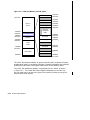
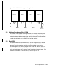

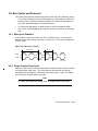
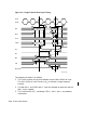

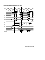


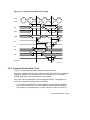
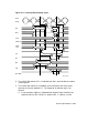
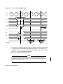
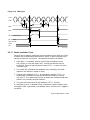
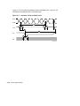
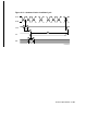


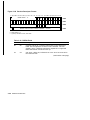


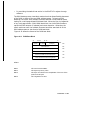


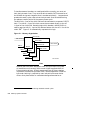


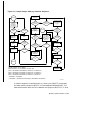
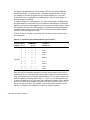


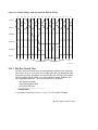


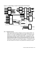
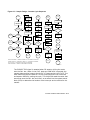


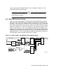
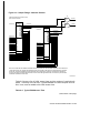
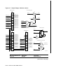


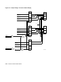


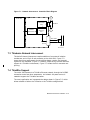
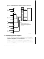


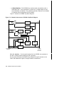
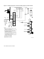


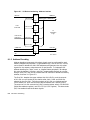


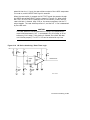
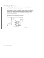
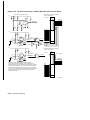


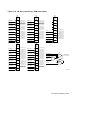


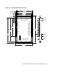


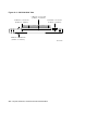
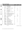


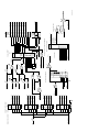


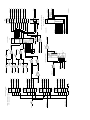


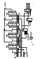


![PLAS A O ]-OR](http://vs1.manualzilla.com/store/data/005852706_1-5db0b7ed584537f0e62af161fb124638-150x150.png)