1
User Guide
PM1000 Polarimeter
Novoptel GmbH
EIM-E
Warburger Str. 100
33098 Paderborn
Germany
www.novoptel.com
Revision history
Version
Date
Remarks
Author
0.2.1
26.01.2015
Draft version
B. Koch
0.2.2
27.02.2015
Register and operation description updated
B. Koch
0.2.3
04.03.2015
Operation description updated
B. Koch
0.2.4
11.03.2015
Description of measurement data files
B. Koch
0.2.5
21.07.2015
Description of PDL measurement
B. Koch
Table of contents
Introduction ............................................................................................................................... 4 Rear panel ................................................................................................................................ 4 External monitor....................................................................................................................... 4 Fundamental PM1000 configuration..................................................................................... 5 Register description................................................................................................................. 5 Operation of the instrument via front control panel .......................................................... 10 Reset dark current ............................................................................................................. 10 Sphere / oscilloscope........................................................................................................ 10 Factory / User calibration ................................................................................................. 10 Connecting the instrument to a PC via USB ..................................................................... 11 Installing the USB driver ................................................................................................... 11 Connecting the instrument ............................................................................................... 11 Interfacing the instrument via SPI ....................................................................................... 12 Serial interface (SPI) commands .................................................................................... 12 Serial interface (SPI) timing ............................................................................................. 12 Operation of the instrument via graphical user interface................................................. 14 Installing the GUI ............................................................................................................... 14 Basic operation .................................................................................................................. 14 Memory configuration ....................................................................................................... 18 Triggering and gating ........................................................................................................ 19 Internal trigger configuration ............................................................................................ 20 User calibration set............................................................................................................ 21 Device Test......................................................................................................................... 21 Using Matlab to analyze stored data .............................................................................. 23 Operation of the instrument using Matlab®....................................................................... 26 Access the USB driver...................................................................................................... 26 USB Settings ...................................................................................................................... 26 Transfer protocol................................................................................................................ 26 Burst transfer...................................................................................................................... 27 Operation of the instrument using other programs........................................................... 28 Firmware upgrade ................................................................................................................. 28 Acronyms ................................................................................................................................ 28 Novoptel
3 of 28
PM1000_UG_0_2_5_n02.doc
Introduction
This user guide is valid and applicable not only for PM1000 but also for PM500.
The PM1000 polarimeter measures all 4 Stokes parameters at a rate of 100 MHz. The
samples can be averaged to increase accuracy at low optical input power. Three
normalization modes can be chosen. The calculated states of polarization (SOPs) are
displayed on a Poincaré sphere at a connected monitor. This allows the polarimeter to be
used without extra computer. It also enables realtime Poincaré sphere display at up to 50
MHz (at 100 MHz, only every second sample is displayed).
To explore the temporal evolution of the polarization, the user can switch the display to
oscilloscope view. In this mode, the Stokes parameters are recorded in the polarimeter’s
memory and then plotted over time. The memory size is 4.3 Gb, i.e. 67 M polarization states
can be recorded. The user can shift the oscilloscope plot and zoom into via the front control
buttons.
The recording process can be triggered either externally by a BNC input signal or internally
by defined SOP events. Pre- and post-trigger data is stored. The memory can be read out via
the SPI or USB interface. To configure the polarimeter, a graphical user interface (GUI) can
be started on a PC that is connected to the polarimeter by USB. The GUI can also load
screenshots of the connected monitor to the PC and display the Poincaré sphere.
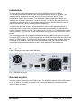
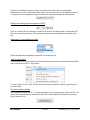
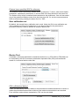
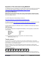
Rear panel
Figure 1 shows the rear panel of the PM1000.
BNC
AIR IN
POWER
SWITCH
AIR OUT
+5V IN
Fig. 1: PM1000 rear panel.
External monitor
A monitor can be connected to the HDMI output. The HDMI port outputs 1440 x 900 pixels at
60 Hz. A HDMI to DVI cable is included. It must be ensured that the connected monitor
supports this input mode! Novoptel
4 of 28
PM1000_UG_0_2_5_n02.doc
Fundamental PM1000 configuration
Optical frequency
The optical frequency value can be adjusted to match that of the analyzed optical input
signal.
Averaging time (ATE)
For accurate SOP measurement at lower optical input powers, internal averaging after the
100 MS/s AD conversion is recommended. The averaging time is denoted by the averaging
time exponent (ATE). 2ATE samples are averaged and an effective conversion time of
2ATE10 ns is achieved. ATE ranges from 0 (100 MS/s) to 20 (95.4 S/s).
Normalization mode
The PM1000 provides three choices for the normalization of Stokes parameters/ vectors:
Standard normalization: Stokes vectors are normalized to unit length. Regardless of
power and DOP, they appear at the surface of the Poincaré sphere.
Exact normalization: Stokes vectors are normalized only with respect to optical power.
For DOP < 1 (or DOP = 0) they appear inside (or in the center of) the Poincaré sphere.
Non-normalized: Stokes vectors are normalized only with respect to a user-defined power
value, 1 mW by default. This means that DOP and optical power determine the length of
the displayed Stokes vector up to a maximum length of 1.
Memory exponent (ME)
The memory exponent (ME) defines the size of the internal memory block that is being
written into. The smallest block is achieved with ME=10 (210 = 1024 samples). The largest
block is achieved with ME=26 (226 = 67,108,864 samples).
The memory recording time is derived from ME, ATE and the sampling time 10 ns. At highest
speed (ATE=0), the memory is filled within 0.67 seconds, since 226·20·10 ns = 0.67 s.
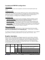
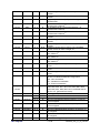
Register description
Basic functions of the PM1000 are configured using the front control buttons. Advanced
functions can be controlled through the USB or SPI port by reading and writing to internal
registers, which are described in the following table. Note that the register addresses have
an offset of 512. This allows a Novoptel PM1000 polarimeter and EPS1000 polarization
scrambler/transformer to be connected to a shared single SPI port. All undefined registers
are reserved and should not be written into.
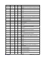
Register
address
512+0
512+1
Novoptel
Name
Bit(s)
Read/
Write
ALM
ATE
0
1
2
4
9..0
R/W
R/W
R/W
R/W
R/W
Function
Internal alarm code. The alarm can be cleared by
writing “0” to this register. This is successful only if
the alarm condition is no longer present.
Alarm condition present.
Optical input over range.
Optical input under range.
Critical board temperature.
Averaging time exponent (ATE), integer range 0 to
5 of 28
PM1000_UG_0_2_5_n02.doc
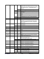
512+2
PC1
15..0
R
512+3
PC2
15..0
R
512+4
PC3
15..0
R
512+5
PC4
15..0
R
512+6
LPC2
15..0
R
512+7
LPC3
15..0
R
512+8
LPC4
15..0
R
512+9
PCFP
15..0
R
512+10
512+11
S0uWU
S0uWL
15..0
15..0
R
R
512+12
S1uWU
15..0
R
512+13
S1uWL
15..0
R
512+14
S2uWU
15..0
R
512+15
S2uWL
15..0
R
512+16
S3uWU
15..0
R
512+17
S3uWL
15..0
R
512+18
LS1uWU
15..0
R
512+19
LS1uWL
15..0
R
512+20
LS2uWU
15..0
R
512+21
LS2uWL
15..0
R
512+22
LS3uWU
15..0
R
512+23
LS3uWL
15..0
R
512+24
DOPSt
15..0
R
512+25
S1St
15..0
R
512+26
S2St
15..0
R
512+27
S3St
15..0
R
512+28
LS1St
15..0
R
Novoptel
20.
Photocurrent 1, 16 bit unsigned, averaged according
to ATE.
Photocurrent 2, 16 bit unsigned, averaged according
to ATE.
Photocurrent 3, 16 bit unsigned, averaged according
to ATE.
Photocurrent 4, 16 bit unsigned, averaged according
to ATE.
Latched copy of photocurrent 2, updated on any read
of PC1.
Latched copy of photocurrent 3, updated on any read
of PC1.
Latched copy of photocurrent 4, updated on any read
of PC1.
Floating point position of photocurrent 1 to 4,
updated on any read of PC1.
Input power in µW, integer part.
Input power in µW, fractional part. Updated at last
read of S0uWU.
S1 of Stokes vector normalized to 1 µW, integer part.
Offset=215.
S1 of Stokes vector normalized to 1 µW, fractional
part. Updated at last read of S1uWU.
S2 of Stokes vector normalized to 1 µW, integer part.
Offset=215.
S2 of Stokes vector normalized to 1 µW, fractional
part. Updated at last read of S2uWU.
S3 of Stokes vector normalized to 1 µW, integer part.
Offset=215
S3 of Stokes vector normalized to 1 µW, fractional
part. Updated at last read of S3uWU.
Latched copy of S1uWU, updated on any read of
S0uWU
Latched copy of S1uWL, updated on any read of
S0uWU
Latched copy of S2uWU, updated on any read of
S0uWU
Latched copy of S2uWL, updated on any read of
S0uWU
Latched copy of S3uWU, updated on any read of
S0uWU
Latched copy of S3uWL, updated on any read of
S0uWU
Degree of polarization (DOP), 16 bit unsigned, 15
fractional bits
S1 of Stokes vector “Standard Normalization”, 15
fractional bits. Offset=215.
S2 of Stokes vector “Standard Normalization”, 15
fractional bits. Offset=215.
S3 of Stokes vector “Standard Normalization”, 15
fractional bits. Offset=215.
Latched copy of S1St, updated on any read of
DOPSt
6 of 28
PM1000_UG_0_2_5_n02.doc
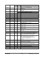
512+29
LS2St
15..0
R
512+30
LS3St
15..0
R
512+31
DOPEx
15..0
R
512+32
S1Ex
15..0
R
512+33
S2Ex
15..0
R
512+34
S3Ex
15..0
R
512+35
LS1Ex
15..0
R
512+36
LS2Ex
15..0
R
512+37
LS3Ex
15..0
R
512+38
EPow
15..0
R/W
512+39
S1Nn
15..0
R
512+40
S2Nn
15..0
R
512+41
S3Nn
15..0
R
512+42
LS2Nn
15..0
R
512+43
LS2Nn
15..0
R
512+44
LS3Nn
15..0
R
512+46
SlNrm
1..0
R/W
512+48
…
512+63
UCal
15..0
R/W
512+64
512+65
UCalSL
SelUCal
512+67
MinFreq
3..0
0
1
15..0
R/W
R/W
W
R
512+68
MaxFreq
15..0
R
512+69
512+70
CurFreq
MinCalFr
15..0
15..0
R/W
R
512+71
MaxCalFr
15..0
R
0
W
512+72
Novoptel
Latched copy of S2St, updated on any read of
DOPSt
Latched copy of S3St, updated on any read of
DOPSt
Degree of polarization (DOP), 16 bit unsigned, 15
fractional bits
S1 of Stokes vector “Exact Normalization”, 15
fractional bits. Offset=215.
S2 of Stokes vector “Exact Normalization”, 15
fractional bits. Offset=215.
S3 of Stokes vector “Exact Normalization”, 15
fractional bits. Offset=215.
Latched copy of S1Ex, updated on any read of
DOPEx
Latched copy of S2Ex, updated on any read of
DOPEx
Latched copy of S3Ex, updated on any read of
DOPEx
Reference power level in µW for non-normalized
Stokes vectors to reach a length of 1.
S1 of Stokes vector “Non-normalized”, 15 fractional
bits. Offset=215.
S2 of Stokes vector “Non-normalized”, 15 fractional
bits. Offset=215.
S3 of Stokes vector “Non-normalized”, 15 fractional
bits. Offset=215.
Latched copy of S2Nn , updated on any read of
EPow
Latched copy of S2Nn , updated on any read of
EPow
Latched copy of S3Nn , updated on any read of
EPow
Stokes parameters/vector normalization mode, see
section Fundamental PM1000 configuration.
“00”: Non-normalized
“01”: Standard normalization
“10”: Exact normalization
User calibration matrix M with elements M00, M01,
M02, M03; M10, M11, M12, M13; M20, M21, M22,
M23; M30, M31, M32, M33. Non-normalized Stokes
vector = M (photocurrent vector).
Floating point position of user calibration matrix.
“1” switches to user defined calibration matrix.
“1” writes user calibration matrix to flash RAM.
Minimum extrapolated optical frequency in GHz/10,
16 bit unsigned.
Maximum extrapolated optical frequency in GHz/10,
16 bit unsigned.
Current optical frequency in GHz/10, 16 bit unsigned.
Minimum calibrated optical frequency in GHz/10, 16
bit unsigned.
Maximum calibrated optical frequency in GHz/10, 16
bit unsigned.
SDRAM write trigger. Any write of “1” to this register
7 of 28
PM1000_UG_0_2_5_n02.doc
1
2
R
R
R/W
3
R
W
512+73
512+74
4
5
4..0
3..0
R
R
R/W
R/W
512+75
0
R/W
1
R
512+76
512+77
512+78
15..0
9..0
15..0
R
R
R
512+79
512+80
15..0
15..0
R/W
R
512+81
9..0
R
512+82
9..0
R/W
512+86
0
R/W
512+87
6..1
10..7
15..0
R/W
R/W
R/W
512+88
15..0
R/W
512+89
15..0
R/W
512+90
512+91
512+92
15..0
15..0
0
1
2
R
R/W
R/W
R/W
R/W
3
R/W
Novoptel
bit will trigger a recording of the sampled SOPs in the
SDRAM. Recording period is defined by averaging
ATE (register 512+1). 2ME samples will be recorded,
defined by the memory exponent ME (register
512+73).
SDRAM busy. ”1” if recording is in progress.
“1” if post-trigger data recording is in progress.
Continuous cyclic memory recording enabled (1) or
disabled(0)
“1” if a full memory block was recorded since the last
trigger
“1” enables automatic retrigger for next memory
block
“1” if SDRAM is busy due to oscilloscope display
“1” if SDRAM is busy due to Poincaré sphere display
SDRAM memory exponent ME (max. 26)
Negative exponent for 16 bit power vector recorded
to SDRAM. The recorded data represents power in
µW left-shifted bitwise by this value. The shifting
reduces quantization errors when recording at low
input powers.
“0” selects Power+Stokes to be recorded, “1” selects
DOP+Stokes
Power/DOP selection updated at last SDRAM trigger
Current write address of SDRAM, bits 15..0
Current write address of SDRAM, bits 25..16
The number of recorded Blocks after last SDRAM
trigger
Selects a memory block
The stop address in the selected memory block, bits
15..0
The stop address in the selected memory block, bits
25..16
Maximum number of memory blocks in automatic
retrigger mode. Default is 512.
Define reference for internal trigger signal:
“0”: External Stokes vector
“1”: Internal delayed Stokes vector
Number of clock cycles for Stokes vector delay
Exponent for clock division of Stokes vector delay
Stokes parameter 1 of external Stokes vector
reference. 15 fractional bits. Offset=215.
Stokes parameter 2 of external Stokes vector
reference. 15 fractional bits. Offset=215.
Stokes parameter 3 of external Stokes vector
reference. 15 fractional bits. Offset=215.
Current internal trigger signal
Trigger threshold for internal trigger signal
“1” enables internal triggering.
“1” enables internal gating.
Internal triggering/gating: “0”: Active high/rising edge.
“1”: Active low/falling edge
“1” enables external triggering.
8 of 28
PM1000_UG_0_2_5_n02.doc
4
5
R/W
R/W
512+93
0
R/W
512+95
3..0
R/W
512+96
0
512+97
512+98
512+99
512+100
512+101
512+102
512+104
512+105
512+106
512+107
15..0
9..0
15..0
15..0
15..0
15..0
15..0
15..0
9..0
15..0
R
W
R/W
R/W
R
R
R
R
W
R/W
R/W
R/W
512+128
512+129
15..0
15..0
R
R
512+130
15..0
R
512+131
15..0
R
512+132
15..0
R
512+133
512+134
512+144
…
512+159
512+186
15..0
15..0
15..0
R
R
R
1..0
R/W
512+187
512+188
0
15..0
R/W
R/W
512+189
15..0
W
512+204
512+205
512+206
512+207
11..0
9..0
15..0
0
R/W
R/W
R
R/W
Novoptel
“1” enable external gating.
External triggering/gating: “0”: Active high/rising
edge. “1”: Active low/falling edge
When set to “0”, this bit will become “1” after the next
trigger event.
Undersampling exponent for SDRAM readout, 4 bit
unsigned
Read: “1” if SDRAM to BlockRAM copy is in progress
SDRAM to BlockRAM copy trigger.
Bits 15..0 of SDRAM to BlockRAM read address
Bits 25..16 of SDRAM to BlockRAM read address
SDRAM output word 1, unsigned 16 bit
SDRAM output word 2. 15 fractional bits. Offset=215.
SDRAM output word 3. 15 fractional bits. Offset=215.
SDRAM output word 4. 15 fractional bits. Offset=215.
Code 39293 triggers SDRAM high speed transfer.
Bits 15..0 of SDRAM high speed read address
Bits 25..16 of SDRAM high speed read address
Number of addresses to be transferred in SDRAM
high speed mode.
Firmware version as 4 digit BCD
Device DNA word 3 (DNA bits 63...48) (same as
read via JTAG)
Device DNA word 2 (DNA bits 47...32) (same as
read via JTAG)
Device DNA word 1 (DNA bits 31...16) (same as
read via JTAG)
Device DNA word 0 (DNA bits 15...0) (same as read
via JTAG)
Module Serial Number
Maximum input power in µW
Module Type as 32 character string. Beginning at
512+144, each Register contains two bytes,
representing two ASCII-coded characters.
Selects display type at connected monitor:
“00” selects Poincaré sphere live view
“01” selects Poincaré sphere memory view
“10” selects Oscilloscope view
“11” tbd
“1” enables automatic Poincaré sphere refresh
Automatic Poincaré sphere refresh period in
milliseconds, 16 bit unsigned
Any write transaction to this register clears the
Poincaré sphere on the connected monitor.
HDMI frame buffer pixel row
HDMI frame buffer pixel column
HDMI frame buffer pixel data code
“0” freezes HDMI frame buffer
9 of 28
PM1000_UG_0_2_5_n02.doc
Operation of the instrument via front control panel
The polarimeter firmware provides a cyclic menu, the keywords of which are shown on the
OLED display. The menu structure is
Optical frequency
Averaging time (ATE)
Normalization mode
Sphere / Oscilloscope
Rotate H / Zoom
Rotate V / Shift
Memory exponent (ME)
Reset dark current
Factory / User calibration
The control buttons UP and DOWN let you to navigate through the menu. The control
buttons LEFT and RIGHT change a selected setting or value.
Reset dark current
Especially at low input powers, recalibration of the 4 photodetector’s dark currents can
improve measurement accuracy. Use the UP/DOWN buttons to navigate through the menu
until Reset dark current is displayed. Disable any optical input signal and press the RIGHT
button twice. The new dark current values are then stored in the correspondent registers.
Sphere / oscilloscope
This menu item lets you select between the following display modes:
Poincaré live
The current SOP is displayed as a point in or on the Poincaré sphere. The SOPs are plotted
in red if they lie on the front side of the sphere and blue if they lie on the back side. Points of
past SOPs are kept in infinite persistence. According to the selected ATE (averaging) value,
new points are plotted with a frequency of up to 50 MHz. Pushing the center button or
rotating the sphere clears the SOPs on the sphere.
Poincaré memory
SOPs stored in the memory are being displayed. This is useful if you want to explore the
evolution of a recorded SOP event in the Stokes space. If the sphere is rotated, memory data
is loaded anew.
Oscilloscope
The 4 Stokes parameters stored in the memory are being plotted as curves over time to
illustrate the temporal evolution of a recorded SOP event. Push the center button to trigger a
new measurement.
Factory / User calibration
By default, the PM1000 uses an internal factory calibration set which is valid for the specified
wavelength range. By the GUI, the user can also write/read user calibration data to/from the
polarimeter which is valid for only one specific wavelength. The user calibration can be
Novoptel
10 of 28
PM1000_UG_0_2_5_n02.doc
stored permanently in the polarimeter so that it can be accessed through the polarimeter
menu without a PC. Connecting the instrument to a PC via USB
The instrument communicates by a USB IC FT232H from FTDI (Future Technology Devices
International Limited, http://www.ftdichip.com).
The Novoptel PM1000 Graphical User Interface (= GUI) is compiled on a Microsoft Windows
7 64 Bit system.
Installing the USB driver
Execute the installation program of the provided USB driver (CDM v2.10.00 WHQL
Certified.exe). You will find more detailed information about the driver at
http://www.ftdichip.com/Support/Documents/InstallGuides.htm.
Connecting the instrument
After the driver is installed successfully, connect PC and instrument using the provided USB
cable. Wait until Windows has recognized the USB device and shown an acknowledgement
message. Power the instrument with the provided power supply and switch it on. Novoptel
11 of 28
PM1000_UG_0_2_5_n02.doc
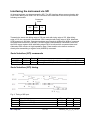
Interfacing the instrument via SPI
All internal registers can also accessed by SPI. The SPI interface allows communication with
much lower latency than USB. The SPI connector at the backside of the device provides the
following connection: Connector
notch
SDI
GND
CS
SDO
GND
SDCK
Transmission starts with falling edge of CS and ends with rising edge of CS. After falling
edge of CS, the command is transmitted. SDI is sampled with rising edge of SCK. Maximum
SCK frequency is 500 kHz. Command and data word length is 16 bit each. MSB of command
and data word is sent first, LSB last. If a valid register read (RDREG) command is received,
the SDO output register shifts with falling edge of SCK to transmit the requested data word.
Otherwise SDO remains in high impedance state. Data transfer to the device continues
directly after transmitting a register write (WRREG) command.
Serial interface (SPI) commands
Command
RDREG
WRREG
Code
0XXXh
1XXXh
Data
OUT
IN
Function
Read register XXXh (for definition see USB section)
Write register XXXh (for definition see USB section)
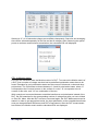
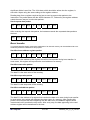
Serial interface (SPI) timing
Fig. 2: Timing of SPI port.
Symbol
TCSCK
TCKCS
TSDCKL
Description
CS low to SDCK high
SDCK low to CS high
SDCKL low time
Novoptel
Min
120
120
1
12 of 28
Max
–
–
–
Units
ns
ns
µs
PM1000_UG_0_2_5_n02.doc
TSDCKH
TSETUP
THOLD
TCKO
SDCKL high time
SDI egde to SDCK high (setup time)
SDCK to SDI edge (hold time)
SDCK edge to stable SDO
Novoptel
13 of 28
1
30
30
–
–
–
–
100
µs
ns
ns
ns
PM1000_UG_0_2_5_n02.doc
Operation of the instrument via graphical user interface
Installing the GUI
Any previous version of the graphical user interface has to be uninstalled first. For
installation, execute setup.exe in the folder PM_GUI_XXXX. Follow the instructions of the
installation dialogue.
If not found on the PC, Microsoft .NET Framework 4.5 will be installed during installation of
the GUI. In addition, the Visual Basic Power Packs will be required to be installed. They can
be downloaded using the following link:
http://go.microsoft.com/fwlink/?LinkID=145727&clcid=0x804
The software launches automatically after installation. If you want to launch the software later
manually, select Programs\Novoptel\PM_GUI from the Windows Start Menu.
Basic operation
Selecting one of the attached instruments
If you have attached only one Novoptel polarimeter, the GUI automatically selects this one. If
you have attached more than one instrument, select the desired one from the drop-down list
in the menu strip “Device”->”Connect”.
Subsequently, you can launch further instances of the GUI and connect them to further
instruments.
Setting the optical frequency
Type the optical frequency in THz with up to two positions after decimal point into the field
besides Frequency and press Enter or tune the frequency with the up and down buttons.
Novoptel
14 of 28
PM1000_UG_0_2_5_n02.doc
Outside the calibrated frequency range, the polarimeter matrix will be extrapolated.
Measurements in the extrapolated range will be less accurate than in the calibrated range. If
a frequency in the extrapolated range is selected, a warning message will be displayed.
Setting the averaging time exponent (ATE)
Type any valid ATE value between 0 and 20 into the box and press Enter or adjust the ATE
with the up and down buttons. The resulting conversion rate is displayed at the right of the
box.
Selection of a normalization mode
Select the desired normalization mode from the drop-down list.
Save a screenshot
A screenshot of the current picture that is displayed at the monitor connected to the PM1000
can be saved on the PC in .png format.
To do so, select Tools->Save Screenshot from the menu strip and select a target folder on
your hard disk.
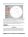
Poincaré sphere display
At a reduced sampling rate of 1 to 2 kHz depending on processing power of the host PC, the
actual SOP samples can be displayed in the GUI. A new window is opened after pressing
Show Sphere (Live).
Novoptel
15 of 28
PM1000_UG_0_2_5_n02.doc
The sphere window can be resized by moving the window corners with the mouse. Power,
degree-of-polarization (DOP) and the three Stokes parameters are displayed as color bars
and text.
The orientation of the Poincaré sphere can be changed by moving the mouse with left button
pressed. In the upper right corner, a pause/play symbol can be pressed to freeze/release the
display. The endless plotting of SOPs can be paused by clicking on the Pause sign which
appears when moving the mouse into the upper right corner.
The sphere window can also be used to display SOP samples that have previously been
stored in the PM1000 internal memory. This is done by pressing Show Sphere (Memory)
instead of Show Sphere (Live). After every window resize or sphere rotation, the memory will
be loaded again. The loading progress is displayed in the lower right corner.
Oscilloscope plot
The stored Stokes parameters can also be displayed in an oscilloscope plot over time by
pressing Show Oscilloscope.
Four traces are being plotted in the new window: The three Stokes parameters S1-S3 plus
either power or DOP, whichever has been selected for memory recording, see section
Memory configuration. In the plot, the DOP will be normalized to 2, which means that a DOP
of 1 will appear in the middle of the y-range. The power curve will be normalized to the
maximum value in the data set. The value is displayed in mW in the top right corner of the
plot.
Novoptel
16 of 28
PM1000_UG_0_2_5_n02.doc
The plot can be zoomed in/out and shifted right and left. To restrict loading time, only 2048
samples are being displayed. If the memory contains more data, it is undersampled
accordingly. For a full oscilloscope plot of large memory areas, up to 67 M SOPs, the
oscilloscope plot displayed on the monitor connected to the PM1000 can be used.
When more than one SOP event has been recorded, the different events can be selected for
plotting by up and down buttons:
The GUI oscilloscope plot allows to derive the SOP changing speed from the stored SOP
samples.
After selecting Speed from the drop-down list, the black curve in the plot will show the SOP
speed instead of Power or DOP. The SOP speed plot is normalized to its maximum, which is
displayed at the upper right of the plot. Since the SOP speed is calculated sample-to-sample,
it will contain a lot of noise when observing slow SOP changes with small ATE.
For deeper SOP analysis with other programs like Matlab, the data displayed in the
oscilloscope plot can be stored into a file on the computer by pressing Save data (screen
span). If the checkbox Full sampling depth is activated, the memory will not be undersampled
again and every stored sample will be copied to the computer.
Novoptel
17 of 28
PM1000_UG_0_2_5_n02.doc
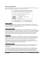
Memory configuration
The PM1000 internal memory allows to store up to 67 M SOP samples at a rate of up to 100
MS/s. It is configured in the Memory tab of the main tab control.
Memory exponent
The block size of the memory is defined by a memory exponent between 10 and 26, see
section Fundamental PM1000 configuration. The memory recording time, derived from block
size and averaging time, is displayed accordingly.
Power or DOP recording
The memory stores 4 Stokes parameters at once. For the parameter S0, the GUI allows to
select either optical power or degree-of-polarization (DOP) for recording. If power is selected,
the unit of S0 will be µW. To increase accuracy, the 16 bit integer value can be shifted bitwise
to add some fractional bits before recording. If the option auto is selected, the number of
fractional bits will be selected automatically according to the current input power level.
Data file types
The data can be saved in binary or text file format. The binary format uses less disk space
and works faster, whereas the text format allows an easier processing of data with external
programs. The data type can be chosen in the menu strip Tools->Select Data File Type.
Both file types start with an ASCII text header for additional data, e.g. sampling and
averaging time. Sample scripts for opening and plotting data in Matlab can be provided by
Novoptel. They are described in the end of this document.
Trigger-event recording
A measurement is started by pressing the button Activate. In normal recording mode, the
measurement stops when the memory block is filled completely or when the button is
pressed again.
The checkbox Trigger-Event Recording enables the continuous, cyclic recording mode. In
this mode, the measurement process is repeated without interruption until a trigger event
occurs. This trigger event can be launched from an internal or external signal, see next
section. After a trigger event, half of the block size is still recorded. In the block data loaded
Novoptel
18 of 28
PM1000_UG_0_2_5_n02.doc
from the memory starting at the stop address, the trigger event will be in the middle.
To stop the recording immediately, the button Activate can be pressed a second time.
If the checkbox Multiple Events is activated, the recording will continue in the next memory
block after the post-trigger data of the first event has been recorded. The number of events
to be recorded can be selected. The maximum number of events depends on the memory
block size defined by ME. At ME up to 17, the maximum is 512. At larger ME the maximum is
226-ME. This means that at an ME of 26 (whole memory as one block), only one event can be
recorded.
If multiple events have been recorded, the Tools->Save Data option from the menu strip will
store each event in a separate file. The Save data (screen span) option in the scope window
will only store the event that is currently displayed.
Auto-reactivated recording and storing
For automated measurements, the GUI allows to automatically store the measurement data
in a file and re-activate the measurement. The number of activations generated in this mode
can be defined between 1 and 1000. If multiple events are recorded during each activation,
multiple files will be stored after each recording.
If the checkbox Fill HDD is activated, the number of files created is only limited by disk
space. Even if there is disk space available, Windows sometimes blocks file creation in
directories that already contain many ten thousand files. If the checkbox Sub-Dirs is
activated, the GUI will create a new directory at the beginning of a measurement and every
time the current directory is blocked.
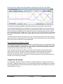
Triggering and gating
The Triggering / Gating tab of the GUI allows to enable triggering or gating of the memory
recording. Triggering means that the cyclic measurement process is stopped after recording
of post-trigger samples. Gating means that the recording process will be paused as long as
the gating signal is active.
Novoptel
19 of 28
PM1000_UG_0_2_5_n02.doc
The internal triggering / gating signal is the result of an internal Stokes vector multiplication,
see next section. The external triggering / gating signal is a LVCMOS33 (0 V / +3.3 V) signal
that is applied to the BNC connector at the rear panel of the instrument.
Internal trigger configuration
The internal trigger signal can be configured in the Internal Trigger tab of the GUI. This signal
is the length of a difference vector between the current and a reference Stokes vector,
normalized to a maximum of 1. It is therefore a function of the angle δ between the two
Stokes vectors: Trigger threshold = 0.5 · | Scur-Sref |= sin(δ/2). For small δ it holds trigger
threshold δ/2.
The trigger threshold can be adjusted between 0 (always trigger) and 1 (never trigger) in
steps of 0.01.
Delayed measured SOP for reference
The reference Stokes vector can be a copy of the permanently measured SOP that has been
delayed by a specified time. The delay time is specified by the number of clock cycles, tau,
and an exponent for clock division, clkexp. Based on an initial clock period of 10 ns, the
delay Td can be calculated by Td = 10 ns · tau · 2clkexp. By the angle δ and the time Td, a
certain SOP changing speed δ/Td is specified. The PM1000 will be triggered whenever the
optical input signal surpasses this speed. Please note that for correct operation, the delay
time should always be longer than the averaging time (set by ATE).
Novoptel
20 of 28
PM1000_UG_0_2_5_n02.doc
External (user-specified) SOP for reference
It is possible to define an arbitrary Stokes vector as reference. To do so, enter three Stokes
parameters, separated by semicolons, in the text field of the drop-down box and press Set.
The Stokes vector will be normalized and transmitted to the polarimeter. One can also select
one of the predefined Stokes vectors from the drop-down list. Or, set the current measured
SOP as reference by pressing the button Set Cur. SOP.
User calibration set
By default, the internal factory calibration set is used. Using the GUI a user calibration set
can be loaded to and from the polarimeter. It can also be stored in the polarimeter’s
permanent memory (Flash) to be able to access it without GUI.
Device Test
If available, a Novoptel polarization scrambler/transformer (e.g. EPS1000 or EPX1000) can
be controlled by the GUI to measure polarization dependent loss (PDL) and the Mueller
matrix of a connected device under test.
PDL by Extinction Method
If PDL is measured by Extinction Method, the polarization scrambler/transformer is driven to
obtain the polarization states where minimum and maximum transmissions are reached.
From minimum and maximum transmission, PDL can be calculated.
Novoptel
21 of 28
PM1000_UG_0_2_5_n02.doc
Starting at “0”, all 16 electrode voltages are modified subsequently. Step size and averaging
time can be selected separately for the first and last 8 voltages. After measuring the optical
power at maximum and minimum transmission, the calculated PDL will displayed.
PDL by Mueller matrix
PDL can also calculated from the Mueller matrix of a DUT. To measure the Mueller matrix of
a DUT, first a number of voltage sets that lead to predefined polarization states have to be
found. Examples for such polarization states are the corners of diamonds, cubes and other
polyhedrons. The GUI allows to choose between 6, 8 and 14 polarization states, where “6”
corresponds to the 6 normal vectors on the surface of a cube, “8” corresponds to the 8
corners of this cube, and “14” is a combination of the two.
With a patch cord connected between scrambler/transformer and polarimeter instead of the
DUT, the GUI searches for the corresponding number of voltage sets after you have clicked
on Run Ref. Meas. After the DUT has been connected again, the DUT Measurement can be
started. In order to get appropriate results, the input polarization to the scrambler/transformer
must not change between Reference and DUT measurement. After the DUT measurement
has finished, the Mueller matrix and the calculated PDL are displayed.
Novoptel
22 of 28
PM1000_UG_0_2_5_n02.doc
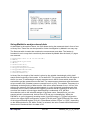
Using Matlab to analyze stored data
As described in the sections above, the GUI allows storing the measured data in form of text
or binary files. These files can be opened for further investigation by Matlab in an easy way.
The files start with a header that contains the measurement meta data. The header is
formatted in such a way that it can directly be evaluated by Matlab after the hash (“#”) signs
are removed:
#
#
#
#
#
#
#
#
#
#
Timestamp='2015.07.21 16:22:16:698';
ATE=9;
SamplePeriod_ns=5120;
ME=10;
Normalization=0;
CyclicRecording=1;
TriggerConfiguration=828;
TriggerThreshold=2621;
Data1Name='Power';
PowerLeftShift=5;
In binary files, the length of the header is given by the variable headerlength, which itself
stands at the beginning of the header. It is at least 256. This means that the first 256 bytes of
the file (or more, if headerlength is larger) represent text in ASCII format which should be
evaluated to get the measurement meta data. The measurement data starts after the header
at byte number 256 (if header bytes are counted from 0 to 255). The variable Timestamp is a
timestamp at the beginning of data transfer. With a time offset between 0 and ~100 ms, this
refers to the moment of the last recorded sample. In cyclic (triggered) recording mode, this
timestamp can be used to estimate the triggering moment with an uncertainty of about 100
ms when the duration of post-trigger data sampling is subtracted. ATE, ME and
Normalization refer to the selected settings of the same name. SamplePeriod_ns is the
sample period in nanoseconds, derived from ATE and any undersampling. When the
PM1000 is in cyclic (triggered) recording mode (CyclicRecording=1), TriggerConfiguration
refers to the trigger signal configuration register (512+86) and TriggerThreshold is the value
of the trigger threshold register (512+91). Data1Name is either “Power” or “DOP”, depending
on the data selection for S0. When “Power” is selected, the value PowerLeftShift determines
the amount of fractional bits in the data of S0.
Novoptel
23 of 28
PM1000_UG_0_2_5_n02.doc
In contrast to binary files, the byte length of the header in text files is not specified. Hence the
variable headerlength is missing. Instead, all lines of the header begin with a hash sign to
distinguish header from subsequent measurement data.
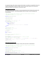
Read data from text files
The measurement data in text files are comma-separated values that also allow opening the
file in Excel for instance. The following Matlab function will open a text file and plot the
contained data:
% This is to plot the stokes parameters loaded from a Novoptel PM1000 polarimeter
% GUI version 1.0.1.8
% Copyright 2015 Benjamin Koch, Novoptel GmbH
function pm1000plot(filename)
% open the data file
FID=fopen(filename);
% get the meta data
C=textscan(FID, '#%s', 'Delimiter', '@');
% load information from meta data
if length(C{1})>0,
for ii = 1:length(C{1}),
try eval(C{1}{ii})
catch err
disp(sprintf('ERROR: Unknown command: %s', C{1}{ii}));
end
end
end
% get the stokes values
NN=textscan(FID,'%f,%f,%f,%f');
% close the data file
fclose(FID);
for ii=1:4,
N(ii,:)=NN{ii};
end;
% remove offset from stokes parameters 1..3
N(2:4,:)=N(2:4,:)-2^15;
% plot the data
x=(1:length(N(1,:))) * SamplePeriod_ns*10^-9; % X-Axis in seconds
%x=(1:length(N{1})); % X-Axis as samples
plot(x, N(1,:)/2^15, '.:k', x, N(2,:)/2^15, '.:r', x, N(3,:)/2^15, '.:b', x, N(4,:)/2^15,
'.:g');
legend(Data1Name, 'Stokes 1', 'Stokes 2', 'Stokes 3');
xlabel('Seconds');
Read data from binary files
The following Matlab function will open a binary file and plot the contained data:
% This is to plot the stokes parameters loaded from a Novoptel PM1000 polarimeter
% GUI version 1.0.1.8
% Copyright 2015 Benjamin Koch, Novoptel GmbH
function pm1000plotbinary(filename)
% open the data file
FID=fopen(filename);
% get the header length (mimimum 256 bytes)
C=fread(FID, 256, 'uint8');
headerstrings=strsplit(char(transpose(C)), char(13));
try eval(char(headerstrings(1)))
Novoptel
24 of 28
PM1000_UG_0_2_5_n02.doc
catch err
disp(sprintf('ERROR: Unknown command: %s', char(headerstrings(1))));
pause
end
% get the full header with meta data
fseek(FID, 0, 'bof');
C=fread(FID, headerlength, 'uint8');
headerstrings=strsplit(char(transpose(C)), char(13));
size_headerstrings=size(headerstrings);
nlines=size_headerstrings(2);
% load information from meta data
if nlines>2,
for ii=2:nlines-1
try eval(char(headerstrings(ii)))
catch err
disp(sprintf('ERROR: Unknown command: %s', char(headerstrings(ii))));
pause
end
end;
end;
% get the data after the header
fseek(FID, headerlength, 'bof');
C=fread(FID, 'uint16');
% get the stokes parameters
N=reshape(C, 4, floor(length(C)/4));
% remove offset from stokes parameters 1..3
N(2:4,:)=N(2:4,:)-2^15;
% close the data file
fclose(FID);
% plot the data
x=(1:length(N(1,:))) * SamplePeriod_ns*10^-9; % X-Axis in seconds
%x=(1:length(N(1,:))); % X-Axis in samples
plot(x, N(1,:)/2^15, '.:k', x, N(2,:)/2^15, '.:r', x, N(3,:)/2^15, '.:b', x, N(4,:)/2^15,
'.:g');
legend(Data1Name, 'Stokes 1', 'Stokes 2', 'Stokes 3');
xlabel('Seconds');
Novoptel
25 of 28
PM1000_UG_0_2_5_n02.doc
Operation of the instrument using Matlab®
The USB driver has to be installed on your system and the instrument needs to be connected
using a USB cable. Examples of Matlab communication scripts can be downloaded from
http://www.novoptel.de/Home/Downloads/Matlab_Support_Files.zip
Access the USB driver
Matlab needs a header file like ftd2xx.h from FTDI to access the driver. Novoptel provides
the header version matftd2xx.h, in which the data types are modified to become compatible
with current Matlab versions.
You will find help about communicating to a driver at
http://www.mathworks.com/help/techdoc/ref/loadlibrary.html
The different functions of the driver can be seen from the header file. Information about each
function is provided at http://www.ftdichip.com/Support/Knowledgebase/index.html
Example Matlab programs for USB data transfer are available from Novoptel upon request.
USB Settings
The following settings have to be applied within Matlab (or other programs) to enable USB
communication:
Baud Rate
Word Length
Stop Bits
Parity
230400 baud
8 Bits
1 Bit
0 Bit
To speed up sequential read and write operations, we recommend setting:
USB Latency Timer 2 ms
Transfer protocol
The instrument is controlled by reading from and writing to USB registers. The register
address line is 12 bits wide, while each register stores 16 bits. All communication is initiated
by the USB host, e.g. the Matlab program.
Writing to a register uses a 9 byte data packet. Each byte represents an ASCII-coded
character. The packet starts with the ASCII-character “W” and ends with the ASCII-code for
carriage return.
Send write data packet
„W“
A(2)
A(1)
A(0)
D(3)
D(2)
D(1)
D(0)
^CR
The 12 bit register address A is sent using 3 bytes, each containing the ASCII-character of
the hexadecimal numbers 0 to F which represents the 4 bit nibble. The character of the most
Novoptel
26 of 28
PM1000_UG_0_2_5_n02.doc
significant nibble is sent first. The 16 bit data, which should be written into the register, is
sent with 4 bytes using the same coding as the register address.
Reading data from a register requires the host to send a request data packet to the
instrument. The packet starts with the ASCII-character “R”, followed by the register address
coded the same way as in write data packets.
Send request data packet
„R“
A(2)
A(1)
A(0)
„0“
„0“
„0“
„0“
^CR
After receiving the request data packet, the instrument sends the requested data packet to
the host:
D(3)
D(2)
D(1)
D(0)
CR
Burst transfer
To increase transfer speed, consecutive addresses of an internal memory can be transferred at once.
Additional packets are defined for this purpose:
Send Set burst address register packet
„X“
„0“
„0“
„0“
D(3)
D(2)
D(1)
D(0)
^CR
The data D is the address of the register that will be incremented during burst transfer. In
most cases, this register will represent the read address of a memory.
Send Set start value packet
„X“
„0“
„0“
„1“
D(3)
D(2)
D(1)
D(0)
^CR
D(0)
^CR
D(0)
^CR
The data D is the start value of the counting.
Send Set stop value packet
„X“
„0“
„0“
„2“
D(3)
D(2)
D(1)
The data D is the stop value of the counting
Send Set read address packet
„X“
„0“
„0“
„3“
D(3)
D(2)
D(1)
The data D is the address of a register that contains the data to be sent during burst transfer.
In most cases, this register will represent the data output of a memory. After sending this
packet, burst transfer will start. Beginning with the start value, the address register will be
incremented until it reaches the stop value. After every step, the data appearing in the read
address register will be transferred to the host.
Novoptel
27 of 28
PM1000_UG_0_2_5_n02.doc
Operation of the instrument using other programs
The USB vendor http://www.ftdichip.com/Support/Knowledgebase/index.html provides
examples for USB access using other programs, for example LabVIEW®. A rudimental
example of a LabVIEW-VI (virtual instrument) is available from Novoptel upon request.
Firmware upgrade
Via the JTAG port the user can upgrade the firmware, if ever needed.
The schematic and timing of the JTAG port correspond to that detailed in Spartan-6 FPGA
Configuration User Guide UG380 (v2.6) June 20, 2014 from Xilinx (www.xilinx.com).
Acronyms
ATE
DOP
DUT
DVI
FPGA
GUI
HDMI
LSB
JTAG
ME
MSB
PC
PDL
SOP
SPI
USB
Novoptel
Averaging time exponent
Degree of polarization
Device under test
Digital visual interface
Field-programmable gate array
Graphical user interface
High definition multimedia interface
Least significant bit
Joint test action group
Memory exponent
Most significant bit
Personal computer
Polarization dependent loss
State of polarization
Serial peripheral interface
Universal serial bus
28 of 28
PM1000_UG_0_2_5_n02.doc