1
TMS320TCI648x Serial RapidIO (SRIO)
User's Guide
Literature Number: SPRUE13A
September 2006
2
SPRUE13A – September 2006
Submit Documentation Feedback
Contents
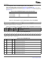
Preface.............................................................................................................................. 14
1
Overview .................................................................................................................. 16
2
1.1
General RapidIO System ...................................................................................... 16
1.2
RapidIO Feature Support in SRIO............................................................................ 19
1.3
Standards ........................................................................................................ 20
1.4
External Devices Requirements .............................................................................. 20
1.5
TI Devices Supported By This Document ................................................................... 20
SRIO Functional Description ....................................................................................... 21
2.1
3
4
5
Overview ......................................................................................................... 21
....................................................................................................... 25
2.3
Functional Operation ........................................................................................... 26
Logical/Transport Error Handling and Logging ............................................................. 83
Interrupt Conditions................................................................................................... 85
4.1
CPU Interrupts .................................................................................................. 85
4.2
General Description ............................................................................................ 85
4.3
Interrupt Condition Status and Clear Registers ............................................................. 86
4.4
Interrupt Condition Routing Registers........................................................................ 93
4.5
Interrupt Status Decode Registers ........................................................................... 97
4.6
Interrupt Generation ............................................................................................ 99
4.7
Interrupt Pacing ................................................................................................. 99
4.8
Interrupt Handling ............................................................................................. 100
SRIO Registers ........................................................................................................ 102
5.1
Introduction .................................................................................................... 102
5.2
Peripheral Identification Register (PID) .................................................................... 111
5.3
Peripheral Control Register (PCR) .......................................................................... 112
5.4
Peripheral Settings Control Register (PER_SET_CNTL) ................................................ 113
5.5
Peripheral Global Enable Register (GBL_EN) ............................................................ 116
5.6
Peripheral Global Enable Status Register (GBL_EN_STAT)............................................ 117
5.7
Block n Enable Register (BLKn_EN) ....................................................................... 119
5.8
Block n Enable Status Register (BLKn_EN_STAT) ...................................................... 120
5.9
RapidIO DEVICEID1 Register (DEVICEID_REG1)....................................................... 121
5.10 RapidIO DEVICEID2 Register (DEVICEID_REG2)....................................................... 122
5.11 Packet Forwarding Register n for 16-Bit Device IDs (PF_16B_CNTLn) ............................... 123
5.12 Packet Forwarding Register n for 8-Bit Device IDs (PF_8B_CNTLn) .................................. 124
5.13 SERDES Receive Channel Configuration Register n (SERDES_CFGRXn_CNTL) ................. 125
5.14 SERDES Transmit Channel Configuration Register n (SERDES_CFGTXn_CNTL) ................. 128
5.15 SERDES Macro Configuration Register n (SERDES_CFGn_CNTL) .................................. 130
5.16 DOORBELLn Interrupt Condition Status Register (DOORBELLn_ICSR) ............................. 132
5.17 DOORBELLn Interrupt Condition Clear Register (DOORBELLn_ICCR) .............................. 133
5.18 RX CPPI Interrupt Status Register (RX_CPPI_ICSR) ................................................... 134
5.19 RX CPPI Interrupt Clear Register (RX_CPPI_ICCR)..................................................... 135
5.20 TX CPPI Interrupt Status Register (TX_CPPI_ICSR) .................................................... 136
5.21 TX CPPI Interrupt Clear Register (TX_CPPI_ICCR) ..................................................... 137
5.22 LSU Interrupt Condition Status Register (LSU_ICSR) ................................................... 138
2.2
SRIO Pins
SPRUE13A – September 2006
Submit Documentation Feedback
Table of Contents
3
5.23
LSU Interrupt Condition Clear Register (LSU_ICCR) .................................................... 141
5.24
Error, Reset, and Special Event Interrupt Condition Status Register
(ERR_RST_EVNT_ICSR).................................................................................... 142
5.25
Error, Reset, and Special Event Interrupt Condition Clear Register
(ERR_RST_EVNT_ICCR) ................................................................................... 143
5.26
DOORBELLn Interrupt Condition Routing Registers (DOORBELLn_ICRR and
DOORBELLn_ICRR2) ........................................................................................ 144
5.27
RX CPPI Interrupt Condition Routing Registers (RX_CPPI_ICRR and RX_CPPI_ICRR2) ......... 145
5.28
TX CPPI Interrupt Condition Routing Registers (TX_CPPI_ICRR and TX_CPPI_ICRR2) .......... 146
5.29
LSU Interrupt Condition Routing Registers (LSU_ICRR0–LSU_ICRR3) .............................. 147
5.30
Error, Reset, and Special Event Interrupt Condition Routing Registers
(ERR_RST_EVNT_ICRR, ERR_RST_EVNT_ICRR2, and ERR_RST_EVNT_ICRR3) ............. 149
5.31
Interrupt Status Decode Register (INTDSTn_DECODE) ................................................ 150
5.32
INTDSTn Interrupt Rate Control Register (INTDSTn_RATE_CNTL)................................... 154
5.33
LSUn Control Register 0 (LSUn_REG0) ................................................................... 155
5.34
LSUn Control Register 1 (LSUn_REG1) ................................................................... 156
5.35
LSUn Control Register 2 (LSUn_REG2) ................................................................... 157
5.36
LSUn Control Register 3 (LSUn_REG3) ................................................................... 158
5.37
LSUn Control Register 4 (LSUn_REG4) ................................................................... 159
5.38
LSUn Control Register 5 (LSUn_REG5) ................................................................... 160
5.39
LSUn Control Register 6 (LSUn_REG6) ................................................................... 161
5.40
LSUn Congestion Control Flow Mask Register (LSUn_FLOW_MASKS).............................. 162
5.41
Queue n Transmit DMA Head Descriptor Pointer Register (QUEUEn_TXDMA_HDP) .............. 164
5.42
Queue n Transmit DMA Completion Pointer Register (QUEUEn_TXDMA_CP)...................... 165
5.43
Queue n Receive DMA Head Descriptor Pointer Register (QUEUEn_RXDMA_HDP) .............. 166
5.44
Queue n Receive DMA Completion Pointer Register (QUEUEn_RXDMA_CP) ...................... 167
5.45
Transmit Queue Teardown Register (TX_QUEUE_TEAR_DOWN) .................................... 168
5.46
Transmit CPPI Supported Flow Mask Registers (TX_CPPI_FLOW_MASKS[0–7]) .................. 169
5.47
Receive Queue Teardown Register (RX_QUEUE_TEAR_DOWN) .................................... 172
5.48
Receive CPPI Control Register (RX_CPPI_CNTL) ....................................................... 173
5.49
Transmit CPPI Weighted Round Robin Control Registers (TX_QUEUE_CNTL[0–3]) ............... 174
5.50
Mailbox to Queue Mapping Registers (RXU_MAP_Ln and RXU_MAP_Hn) .......................... 177
5.51
Flow Control Table Entry Register n (FLOW_CNTLn) ................................................... 181
5.52
Device Identity CAR (DEV_ID) .............................................................................. 182
5.53
Device Information CAR (DEV_INFO)
183
5.54
Assembly Identity CAR (ASBLY_ID)
184
5.55
5.56
5.57
5.58
5.59
5.60
5.61
5.62
5.63
5.64
5.65
5.66
5.67
5.68
4
Contents
.....................................................................
.......................................................................
Assembly Information CAR (ASBLY_INFO) ...............................................................
Processing Element Features CAR (PE_FEAT) ..........................................................
Source Operations CAR (SRC_OP) ........................................................................
Destination Operations CAR (DEST_OP) .................................................................
Processing Element Logical Layer Control CSR (PE_LL_CTL) ........................................
Local Configuration Space Base Address 0 CSR (LCL_CFG_HBAR) .................................
Local Configuration Space Base Address 1 CSR (LCL_CFG_BAR)...................................
Base Device ID CSR (BASE_ID) ...........................................................................
Host Base Device ID Lock CSR (HOST_BASE_ID_LOCK) .............................................
Component Tag CSR (COMP_TAG) .......................................................................
1x/4x LP Serial Port Maintenance Block Header Register (SP_MB_HEAD) ..........................
Port Link Time-Out Control CSR (SP_LT_CTL) ..........................................................
Port Response Time-Out Control CSR (SP_RT_CTL) ...................................................
Port General Control CSR (SP_GEN_CTL) ...............................................................
185
186
188
189
190
191
192
193
194
195
196
197
198
199
SPRUE13A – September 2006
Submit Documentation Feedback
5.69
Port Link Maintenance Request CSR n (SPn_LM_REQ) ................................................ 200
5.70
Port Link Maintenance Response CSR n (SPn_LM_RESP) ............................................ 201
5.71
Port Local AckID Status CSR n (SPn_ACKID_STAT) ................................................... 202
5.72
Port Error and Status CSR n (SPn_ERR_STAT) ......................................................... 203
5.73
Port Control CSR n (SPn_CTL) ............................................................................. 206
5.74
Error Reporting Block Header Register (ERR_RPT_BH) ................................................ 209
5.75
Logical/Transport Layer Error Detect CSR (ERR_DET) ................................................. 210
5.76
Logical/Transport Layer Error Enable CSR (ERR_EN) .................................................. 212
5.77
Logical/Transport Layer High Address Capture CSR (H_ADDR_CAPT) .............................. 214
5.78
Logical/Transport Layer Address Capture CSR (ADDR_CAPT) ........................................ 215
5.79
Logical/Transport Layer Device ID Capture CSR (ID_CAPT) ........................................... 216
5.80
Logical/Transport Layer Control Capture CSR (CTRL_CAPT)
5.81
5.82
5.83
5.84
5.85
5.86
5.87
5.88
5.89
5.90
5.91
5.92
5.93
5.94
5.95
5.96
5.97
5.98
5.99
.........................................
Port-Write Target Device ID CSR (PW_TGT_ID) .........................................................
Port Error Detect CSR n (SPn_ERR_DET) ................................................................
Port Error Rate Enable CSR n (SPn_RATE_EN) .........................................................
Port n Attributes Error Capture CSR 0 (SPn_ERR_ATTR_CAPT_DBG0) ............................
Port n Error Capture CSR 1 (SPn_ERR_CAPT_DBG1) .................................................
Port n Error Capture CSR 2 (SPn_ERR_CAPT_DBG2) .................................................
Port n Error Capture CSR 3 (SPn_ERR_CAPT_DBG3) .................................................
Port n Error Capture CSR 4 (SPn_ERR_CAPT_DBG4) .................................................
Port Error Rate CSR n (SPn_ERR_RATE) ................................................................
Port Error Rate Threshold CSR n (SPn_ERR_THRESH) ...............................................
Port IP Discovery Timer for 4x Mode Register (SP_IP_DISCOVERY_TIMER) ......................
Port IP Mode CSR (SP_IP_MODE) ........................................................................
Port IP Prescaler Register (IP_PRESCAL) ................................................................
Port-Write-In Capture CSRs (SP_IP_PW_IN_CAPT[0–3]) ..............................................
Port Reset Option CSR n (SPn_RST_OPT)...............................................................
Port Control Independent Register n (SPn_CTL_INDEP) ...............................................
Port Silence Timer n Register (SPn_SILENCE_TIMER) ................................................
Port Multicast-Event Control Symbol Request Register n (SPn_MULT_EVNT_CS).................
Port Control Symbol Transmit n Register (SPn_CS_TX) ................................................
217
218
219
221
223
224
225
226
227
228
229
230
231
233
234
235
236
238
239
240
Index ............................................................................................................................... 241
SPRUE13A – September 2006
Submit Documentation Feedback
Contents
5
List of Figures
1
2
3
4
5
6
7
8
9
10
11
12
13
14
15
16
17
18
19
20
21
22
23
24
25
26
27
28
29
30
31
32
33
34
35
36
37
38
39
40
41
42
43
44
45
46
47
48
49
6
RapidIO Architectural Hierarchy ..........................................................................................
RapidIO Interconnect Architecture .......................................................................................
Serial RapidIO Device to Device Interface Diagrams .................................................................
SRIO Peripheral Block Diagram ..........................................................................................
Operation Sequence .......................................................................................................
1x/4x RapidIO Packet Data Stream (Streaming-Write Class) ........................................................
Serial RapidIO Control Symbol Format..................................................................................
SRIO Component Block Diagram ........................................................................................
SERDES Macro Configuration Register 0 (SERDES_CFG0_CNTL) ...............................................
SERDES Receive Channel Configuration Register n (SERDES_CFGRXn_CNTL)...............................
SERDES Transmit Channel Configuration Register n (SERDES_CFGTXn_CNTL) ..............................
Load/Store Registers for RapidIO (Address Offset: LSU1 400h–418h, LSU2 420h–438h, LSU3
440h–458h, LSU4 460h-478h) ...........................................................................................
LSU Registers Timing .....................................................................................................
Example Burst NWRITE_R ...............................................................................................
Load/Store Module Data Flow Diagram .................................................................................
CPPI RX Scheme for RapidIO............................................................................................
Message Request Packet .................................................................................................
Mailbox to Queue Mapping Register Pair ...............................................................................
RX Buffer Descriptor Fields ...............................................................................................
RX CPPI Mode Explanation ..............................................................................................
CPPI Boundary Diagram ..................................................................................................
TX Buffer Descriptor Fields ...............................................................................................
Weighted Round Robin Programming Registers (Address Offset 7E0h–7ECh) ...................................
RX Buffer Descriptors......................................................................................................
TX Buffer Descriptors ......................................................................................................
Doorbell Operation .........................................................................................................
Flow Control Table Entry Registers (Address Offset 0900h–093Ch) ...............................................
Transmit Source Flow Control Masks ...................................................................................
Fields Within Each Flow Mask............................................................................................
Configuration Bus Example ...............................................................................................
DMA Example ..............................................................................................................
GBL_EN (Address 0030h) ................................................................................................
GBL_EN_STAT (Address 0034h) ........................................................................................
BLK0_EN (Address 0038h) ...............................................................................................
BLK0_EN_STAT (Address 003Ch) ......................................................................................
BLK1_EN (Address 0040h) ...............................................................................................
BLK1_EN_STAT (Address 0044h) .......................................................................................
BLK8_EN (Address 0078h) ...............................................................................................
BLK8_EN_STAT (Address 007Ch) ......................................................................................
Peripheral Control Register (PCR) - Address Offset 0004h ..........................................................
Bootload Operation ........................................................................................................
Packet Forwarding Register n for 16-Bit Device IDs (PF_16B_CNTLn) Offsets 0x0090, 0x0098, 0x00A0,
0x00A8 .......................................................................................................................
Packet Forwarding Register n for 8-Bit Device IDs (PF_8B_CNTLn) Offsets 0x0094, 0x009C, 0x00A4,
0x00AC ......................................................................................................................
Logical/Transport Layer Error Detect CSR (ERR_DET) ..............................................................
RapidIO DOORBELL Packet for Interrupt Use .........................................................................
Doorbell 0 Interrupt Condition Status and Clear Registers ...........................................................
Doorbell 1 Interrupt Condition Status and Clear Registers ...........................................................
Doorbell 2 Interrupt Condition Status and Clear Registers ...........................................................
Doorbell 3 Interrupt Condition Status and Clear Registers ...........................................................
List of Figures
17
18
19
22
23
24
24
27
28
31
33
36
38
39
40
44
45
46
47
49
51
52
56
62
63
64
66
67
67
69
69
71
71
72
73
73
73
73
73
74
80
81
82
83
85
87
87
88
88
SPRUE13A – September 2006
Submit Documentation Feedback
50
51
52
53
54
55
56
57
58
59
60
61
62
63
64
65
66
67
68
69
70
71
72
73
74
75
76
77
78
79
80
81
82
83
84
85
86
87
88
89
90
91
92
93
94
95
96
97
98
99
100
101
RX CPPI Interrupt Condition Status and Clear Registers ............................................................. 89
TX CPPI Interrupt Condition Status and Clear Registers ............................................................. 89
LSU Interrupt Condition Status and Clear Registers .................................................................. 90
Error, Reset, and Special Event Interrupt Condition Status and Clear Registers ................................. 91
Doorbell 0 Interrupt Condition Routing Registers ...................................................................... 94
RX CPPI Interrupt Condition Routing Registers........................................................................ 94
TX CPPI Interrupt Condition Routing Registers ........................................................................ 95
LSU Interrupt Condition Routing Registers ............................................................................. 96
Error, Reset, and Special Event Interrupt Condition Routing Registers ............................................ 97
Interrupt Status Decode Register (INTDSTn_DECODE) ............................................................. 98
Interrupt Sources Assigned to ISDR Bits ............................................................................... 98
Example Diagram of Interrupt Status Decode Register Mapping .................................................... 99
INTDSTn_RATE_CNTL Interrupt Rate Control Register ............................................................ 100
Peripheral ID Register (PID) - Address Offset 0000h ................................................................ 111
Peripheral Control Register (PCR) - Address Offset 0004h......................................................... 112
Peripheral Settings Control Register (PER_SET_CNTL) (Address Offset 0020h) ............................... 113
Peripheral Global Enable Register (GBL_EN) (Address Offset 0030h) ........................................... 116
Peripheral Global Enable Status Register (GBL_EN_STAT) - Address 0034h .................................. 117
Block n Enable Register (BLKn_EN) ................................................................................... 119
Block n Enable Status Register (BLKn_EN) .......................................................................... 120
RapidIO DEVICEID1 Register (DEVICEID_REG1) (Offset 0080h) ................................................ 121
RapidIO DEVICEID2 Register (DEVICEID_REG2) (Offset 0x0084) ............................................... 122
Packet Forwarding Register n for 16-Bit Device IDs (PF_16B_CNTLn) .......................................... 123
Packet Forwarding Register n for 8-Bit Device IDs (PF_8B_CNTLn) ............................................. 124
SERDES Receive Channel Configuration Register n (SERDES_CFGRXn_CNTL) ............................. 125
SERDES Transmit Channel Configuration Register n (SERDES_CFGTXn_CNTL) ............................. 128
SERDES Macro Configuration Register n (SERDES_CFGn_CNTL) .............................................. 130
Doorbell n Interrupt Condition Status Register (DOORBELLn_ICSR) ............................................. 132
Doorbell n Interrupt Condition Clear Register (DOORBELLn_ICCR) .............................................. 133
RX CPPI Interrupt Condition Status Register (RX_CPPI_ICSR) - Address Offset 0240h ...................... 134
RX CPPI Interrupt Condition Clear Register (RX_CPPI_ICCR) - Address Offset 0248h ....................... 135
TX CPPI Interrupt Condition Status Register (TX_CPPI_ICSR) - Address Offset 0250h ....................... 136
TX CPPI Interrupt Condition Clear Register (TX_CPPI_ICCR) - Address Offset 0258h ........................ 137
LSU Interrupt Condition Status Register (LSU_ICSR) - Address Offset 0260h .................................. 138
LSU Interrupt Condition Clear Register (LSU_ICCR) - Address Offset 0268h ................................... 141
Error, Reset, and Special Event Interrupt Condition Status Register (ERR_RST_EVNT_ICSR) - Address
Offset 0270h ............................................................................................................... 142
Error, Reset, and Special Event Interrupt Condition Clear Register (ERR_RST_EVNT_ICCR) - Address
Offset 0278h ............................................................................................................... 143
Doorbell n Interrupt Condition Routing Registers..................................................................... 144
RX CPPI Interrupt Condition Routing Registers ...................................................................... 145
TX CPPI Interrupt Condition Routing Registers ...................................................................... 146
LSU Interrupt Condition Routing Registers ............................................................................ 147
Error, Reset, and Special Event Interrupt Condition Routing Registers ........................................... 149
Interrupt Status Decode Register (INTDSTn_DECODE) ............................................................ 150
INTDSTn Interrupt Rate Control Register (INTDSTn_RATE_CNTL) .............................................. 154
LSUn Control Register 0 (LSUn_REG0) ............................................................................... 155
LSUn Control Register 1 (LSUn_REG1) ............................................................................... 156
LSUn Control Register 2 (LSUn_REG2) ............................................................................... 157
LSUn Control Register 3 (LSUn_REG3) ............................................................................... 158
LSUn Control Register 4 (LSUn_REG4) ............................................................................... 159
LSUn Control Register 5 (LSUn_REG5) ............................................................................... 160
LSUn Control Register 6 (LSUn_REG6) ............................................................................... 161
LSUn Congestion Control Flow Mask Register (LSUn_FLOW_MASKS) ......................................... 162
SPRUE13A – September 2006
Submit Documentation Feedback
List of Figures
7
102
103
104
105
106
107
108
109
110
111
112
113
114
115
116
117
118
119
120
121
122
123
124
125
126
127
128
129
130
131
132
133
134
135
136
137
138
139
140
141
142
143
144
145
146
147
148
149
150
151
152
153
154
8
LSUn FLOW_MASK Fields ..............................................................................................
Queue n Transmit DMA Head Descriptor Pointer Register (QUEUEn_TXDMA_HDP) .........................
Queue n Transmit DMA Completion Pointer Register (QUEUEn_TXDMA_CP) .................................
Queue n Receive DMA Head Descriptor Pointer Register (QUEUEn_RXDMA_HDP) ..........................
Queue n Receive DMA Completion Pointer Register (QUEUEn_RXDMA_CP) ..................................
Transmit Queue Teardown Register (TX_QUEUE_TEAR_DOWN) - Address Offset 0700h ...................
Transmit CPPI Supported Flow Mask Registers .....................................................................
TX Queue n FLOW_MASK Fields ......................................................................................
Receive Queue Teardown Register (RX_QUEUE_TEAR_DOWN) (Address Offset 0740h) ...................
Receive CPPI Control Register (RX_CPPI_CNTL) (Address Offset 0744h)......................................
Transmit CPPI Weighted Round Robin Control Registers ..........................................................
Mailbox to Queue Mapping Register Pair .............................................................................
Flow Control Table Entry Register n (FLOW_CNTLn) ...............................................................
Device Identity CAR (DEV_ID) - Address Offset 1000h .............................................................
Device Information CAR (DEV_INFO) - Address Offset 1004h ....................................................
Assembly Identity CAR (ASBLY_ID) - Address Offset 1008h ......................................................
Assembly Information CAR (ASBLY_INFO) - Address Offset 100Ch .............................................
Processing Element Features CAR (PE_FEAT) - Address Offset 1010h .........................................
Source Operations CAR (SRC_OP) - Address Offset 1018h .......................................................
Destination Operations CAR (DEST_OP) - Address Offset 101Ch ................................................
Processing Element Logical Layer Control CSR (PE_LL_CTL) - Address Offset 104Ch .......................
Local Configuration Space Base Address 0 CSR (LCL_CFG_HBAR) - Address Offset 1058h................
Local Configuration Space Base Address 1 CSR (LCL_CFG_BAR) - Address Offset 105Ch .................
Base Device ID CSR (BASE_ID) - Address Offset 1060h ..........................................................
Host Base Device ID Lock CSR (HOST_BASE_ID_LOCK) - Address Offset 1068h ............................
Component Tag CSR (COMP_TAG) - Address Offset 106Ch .....................................................
1x/4x LP_Serial Port Maintenance Block Header Register (SP_MB_HEAD) - Address Offset 1100h ........
Port Link Time-Out Control CSR (SP_LT_CTL) - Address Offset 1120h .........................................
Port Response Time-Out Control CSR (SP_RT_CTL) - Address Offset 1124h ..................................
Port General Control CSR (SP_GEN_CTL) - Address Offset 113Ch..............................................
Port Link Maintenance Request CSR n (SPn_LM_REQ) ...........................................................
Port Link Maintenance Response CSR n (SPn_LM_RESP) ........................................................
Port Local AckID Status CSR n (SPn_ACKID_STAT) ...............................................................
Port Error and Status CSR n (SPn_ERR_STAT) .....................................................................
Port Control CSR n (SPn_CTL) .........................................................................................
Error Reporting Block Header Register (ERR_RPT_BH) - Address Offset 2000h ...............................
Logical/Transport Layer Error Detect CSR (ERR_DET) - Address Offset 2008h ................................
Logical/Transport Layer Error Enable CSR (ERR_EN) - Address Offset 200Ch .................................
Logical/Transport Layer High Address Capture CSR (H_ADDR_CAPT) - Address Offset 2010h .............
Logical/Transport Layer Address Capture CSR (ADDR_CAPT) - Address Offset 2014h.......................
Logical/Transport Layer Device ID Capture CSR (ID_CAPT) - Address Offset 2018h ..........................
Logical/Transport Layer Control Capture CSR (CTRL_CAPT) - Address Offset 201Ch ........................
Port-Write Target Device ID CSR (PW_TGT_ID) - Address Offset 2028h ........................................
Port Error Detect CSR n (SPn_ERR_DET) ...........................................................................
Port Error Rate Enable CSR n (SPn_RATE_EN) ....................................................................
Port n Attributes Error Capture CSR 0 (SPn_ERR_ATTR_CAPT_DBG0) ........................................
Port n Error Capture CSR 1 (SPn_ERR_CAPT_DBG1).............................................................
Port n Error Capture CSR 2 (SPn_ERR_CAPT_DBG2).............................................................
Port n Error Capture CSR 3 (SPn_ERR_CAPT_DBG3).............................................................
Port n Error Capture CSR 4 (SPn_ERR_CAPT_DBG4).............................................................
Port Error Rate CSR n (SPn_ERR_RATE) ............................................................................
Port Error Rate Threshold CSR n (SPn_ERR_THRESH) ...........................................................
Port IP Discovery Timer for 4x Mode Register (SP_IP_DISCOVERY_TIMER) - Address Offset 12000h ....
List of Figures
162
164
165
166
167
168
170
170
172
173
174
179
181
182
183
184
185
186
188
189
190
191
192
193
194
195
196
197
198
199
200
201
202
203
206
209
210
212
214
215
216
217
218
219
221
223
224
225
226
227
228
229
230
SPRUE13A – September 2006
Submit Documentation Feedback
155
156
157
158
159
160
161
162
Port IP Mode CSR (SP_IP_MODE) - Address Offset 12004h ......................................................
Port IP Prescaler Register (IP_PRESCAL) - Address Offset 12008h .............................................
Port-Write-In Capture CSRs .............................................................................................
Port Reset Option CSR n (SPn_RST_OPT) ..........................................................................
Port Control Independent Register n (SPn_CTL_INDEP) ...........................................................
Port Silence Timer n Register (SPn_SILENCE_TIMER) ............................................................
Port Multicast-Event Control Symbol Request Register n (SPn_MULT_EVNT_CS) ............................
Port Control Symbol Transmit n Register (SPn_CS_TX) ............................................................
SPRUE13A – September 2006
Submit Documentation Feedback
List of Figures
231
233
234
235
236
238
239
240
9
List of Tables
1
2
3
4
5
6
7
8
9
10
11
12
13
14
15
16
17
18
19
20
21
22
23
24
25
26
27
28
29
30
31
32
33
34
35
36
37
38
39
40
41
42
43
44
45
46
47
48
49
10
TI Devices Supported By This Document ............................................................................... 20
Registers Checked for Multicast DeviceID .............................................................................. 21
Packet Types ............................................................................................................... 25
Pin Description.............................................................................................................. 26
SERDES Macro Configuration Register 0 (SERDES_CFG0_CNTL) Field Descriptions ......................... 29
Line Rate versus PLL Output Clock Frequency ........................................................................ 30
Effect of the RATE Bits .................................................................................................... 30
Frequency Range versus MPY Value ................................................................................... 30
SERDES Receive Channel Configuration Register n (SERDES_CFGRXn_CNTL) Field Descriptions ........ 31
EQ Bits....................................................................................................................... 33
SERDES Transmit Channel Configuration Register n (SERDES_CFGTXn_CNTL) Field Descriptions ........ 33
DE Bits of SERDES_CFGTXn_CNTL ................................................................................... 34
SWING Bits of SERDES_CFGTXn_CNTL .............................................................................. 35
LSU Control/Command Register Fields ................................................................................. 36
LSU Status Register Fields ............................................................................................... 37
RX DMA State Head Descriptor Pointer (HDP) (Address Offset 600h–63Ch) ..................................... 46
RX DMA State Completion Pointer (CP) (Address Offset 680h–6BCh) ............................................ 46
RX Buffer Descriptor Field Descriptions ................................................................................. 47
TX DMA State Head Descriptor Pointer (HDP) (Address Offset 500h–53Ch) ..................................... 51
TX DMA State Completion Pointer (CP) (Address Offset 58h–5BCh) .............................................. 52
TX Buffer Descriptor Field Definitions ................................................................................... 52
Weighted Round Robin Programming Registers (Address Offset 7E0h–7ECh) ................................... 56
Examples of DOORBELL_INFO Designations (See Figure 26 )..................................................... 64
Flow Control Table Entry Register n (FLOW_CNTLn) Field Descriptions .......................................... 67
Fields Within Each Flow Mask............................................................................................ 68
Reset Hierarchy ............................................................................................................ 70
Global Enable and Global Enable Status Field Descriptions ......................................................... 72
Block Enable and Block Enable Status Field Descriptions ........................................................... 73
Peripheral Control Register (PCR) Field Descriptions................................................................. 74
Port Mode Register Settings .............................................................................................. 77
Multicast DeviceID Operation ............................................................................................. 81
Packet Forwarding Register n for 16-Bit DeviceIDs (PF_16B_CNTLn) Field Descriptions ...................... 81
Packet Forwarding Register n for 8-Bit DeviceIDs (PF_8B_CNTLn) Field Descriptions ......................... 82
Logical/Transport Layer Error Detect CSR (ERR_DET) Field Descriptions ........................................ 83
Interrupt Condition Status and Clear Bits ............................................................................... 87
Interrupt Conditions Shown in LSU_ICSR and Cleared With LSU_ICCR .......................................... 90
Interrupt Conditions Shown in ERR_RST_EVNT_ICSR and Cleared With ERR_RST_EVNT_ICCR .......... 91
Interrupt Clearing Sequence for Special Event Interrupts ............................................................ 92
Interrupt Condition Routing Options ..................................................................................... 93
Serial RapidIO (SRIO) Registers ....................................................................................... 102
Peripheral ID Register (PID) Field Descriptions ...................................................................... 111
Peripheral Control Register (PCR) Field Descriptions ............................................................... 112
Peripheral Settings Control Register (PER_SET_CNTL) Field Descriptions ..................................... 113
Peripheral Global Enable Register (GBL_EN) Field Descriptions .................................................. 116
Peripheral Global Enable Status Register (GBL_EN_STAT) Field Descriptions ................................. 117
Block n Enable Registers and the Associated Blocks ............................................................... 119
Block n Enable Register (BLKn_EN) Field Descriptions............................................................. 119
Block n Enable Status Registers and the Associated Blocks ....................................................... 120
Block n Enable Status Register (BLKn_EN_STAT) Field Descriptions ............................................ 120
List of Tables
SPRUE13A – September 2006
Submit Documentation Feedback
50
51
52
53
54
55
56
57
58
59
60
61
62
63
64
65
66
67
68
69
70
71
72
73
74
75
76
77
78
79
80
81
82
83
84
85
86
87
88
89
90
91
92
93
94
95
96
97
98
RapidIO DEVICEID1 Register (DEVICEID_REG1) Field Descriptions ............................................
RapidIO DEVICEID2 Register (DEVICEID_REG2) Field Descriptions ............................................
PF_16B_CNTL Registers ................................................................................................
Packet Forwarding Register n for 16-Bit DeviceIDs (PF_16B_CNTLn) Field Descriptions .....................
PF_8B_CNTL Registers .................................................................................................
Packet Forwarding Register n for 8-Bit DeviceIDs (PF_8B_CNTLn) Field Descriptions ........................
SERDES_CFGRXn_CNTL Registers and the Associated Ports ...................................................
SERDES Receive Channel Configuration Register n (SERDES_CFGRXn_CNTL) Field Descriptions .......
EQ Bits .....................................................................................................................
SERDES_CFGTXn_CNTL Registers and the Associated Ports ...................................................
SERDES Transmit Channel Configuration Register n (SERDES_CFGTXn_CNTL) Field Descriptions ......
DE Bits of SERDES_CFGTXn_CNTL..................................................................................
SWING Bits of SERDES_CFGTXn_CNTL ............................................................................
SERDES_CFGn_CNTL Registers and the Associated Ports .......................................................
SERDES Macro Configuration Register n (SERDES_CFGn_CNTL) Field Descriptions ........................
DOORBELLn_ICSR Registers ..........................................................................................
DOORBELLn Interrupt Condition Status Register (DOORBELLn_ICSR) Field Descriptions ...................
DOORBELLn_ICCR Registers ..........................................................................................
DOORBELLn Interrupt Condition Clear Register (DOORBELLn_ICCR) Field Descriptions ....................
RX CPPI Interrupt Condition Status Register (RX_CPPI_ICSR) Field Descriptions .............................
RX CPPI Interrupt Condition Clear Register (RX_CPPI_ICCR) Field Descriptions ..............................
TX CPPI Interrupt Condition Status Register (TX_CPPI_ICSR) Field Descriptions .............................
TX CPPI Interrupt Condition Clear Register (TX_CPPI_ICCR) Field Descriptions ..............................
LSU Interrupt Condition Status Register (LSU_ICSR) Field Descriptions.........................................
LSU Interrupt Condition Clear Register (LSU_ICCR) Field Descriptions ..........................................
Error, Reset, and Special Event Interrupt Condition Status Register (ERR_RST_EVNT_ICSR) Field
Descriptions ...............................................................................................................
Error, Reset, and Special Event Interrupt Condition Clear Register (ERR_RST_EVNT_ICCR) Field
Descriptions ...............................................................................................................
DOORBELLn_ICRR Registers ..........................................................................................
DOORBELLn Interrupt Condition Routing Register Field Descriptions ............................................
RX CPPI Interrupt Condition Routing Register Field Descriptions .................................................
TX CPPI Interrupt Condition Routing Register Field Descriptions .................................................
LSU Interrupt Condition Routing Register Field Descriptions .......................................................
Error, Reset, and Special Event Interrupt Condition Routing Register Field Descriptions ......................
INTDSTn_DECODE Registers and the Associated Interrupt Destinations .......................................
Interrupt Status Decode Register (INTDSTn_DECODE) Field Descriptions ......................................
INTDSTn_RATE_CNTL Registers and the Associated Interrupt Destinations ...................................
INTDSTn Interrupt Rate Control Register (INTDSTn_RATE_CNTL) Field Descriptions ........................
LSUn_REG0 Registers and the Associated LSUs ...................................................................
LSUn Control Register 0 (LSUn_REG0) Field Descriptions ........................................................
LSUn_REG1 Registers and the Associated LSUs ...................................................................
LSUn Control Register 1 (LSUn_REG1) Field Descriptions ........................................................
LSUn_REG2 Registers and the Associated LSUs ...................................................................
LSUn Control Register 2 (LSUn_REG2) Field Descriptions ........................................................
LSUn_REG3 Registers and the Associated LSUs ...................................................................
LSUn Control Register 3 (LSUn_REG3) Field Descriptions ........................................................
LSUn_REG4 Registers and the Associated LSUs ...................................................................
LSUn Control Register 4 (LSUn_REG4) Field Descriptions ........................................................
LSUn_REG5 Registers and the Associated LSUs ...................................................................
LSUn Control Register 5 (LSUn_REG5) Field Descriptions ........................................................
SPRUE13A – September 2006
Submit Documentation Feedback
List of Tables
121
122
123
123
124
124
125
125
126
128
128
129
129
130
130
132
132
133
133
134
135
136
137
138
141
142
143
144
144
145
146
148
149
150
150
154
154
155
155
156
156
157
157
158
158
159
159
160
160
11
99
100
101
102
103
104
105
106
107
108
109
110
111
112
113
114
115
116
117
118
119
120
121
122
123
124
125
126
127
128
129
130
131
132
133
134
135
136
137
138
139
140
141
142
143
144
145
146
147
148
149
12
LSUn_REG6 Registers and the Associated LSUs ...................................................................
LSUn Control Register 6 (LSUn_REG6) Field Descriptions ........................................................
LSUn_FLOW_MASKS Registers and the Associated LSUs ........................................................
LSUn Congestion Control Flow Mask Register (LSUn_FLOW_MASKS) Field Descriptions ...................
LSUn FLOW_MASK Fields ..............................................................................................
QUEUEn_TXDMA_HDP Registers .....................................................................................
Queue n Transmit DMA Head Descriptor Pointer Register (QUEUEn_TXDMA_HDP) Field Descriptions ...
QUEUEn_TXDMA_CP Registers .......................................................................................
Queue Transmit DMA Completion Pointer Registers (QUEUEn_TXDMA_CP) Field Descriptions ............
QUEUEn_RXDMA_HDP Registers.....................................................................................
Queue n Receive DMA Head Descriptor Pointer Register (QUEUEn_RXDMA_HDP) Field Descriptions ...
QUEUEn_RXDMA_CP Registers ......................................................................................
Queue n Receive DMA Completion Pointer Register (QUEUEn_RXDMA_CP) Field Descriptions ...........
Transmit Queue Teardown Register (TX_QUEUE_TEAR_DOWN) Field Descriptions .........................
TX_CPPI_FLOW_MASKS Registers and the Associated TX Queues ............................................
TX Queue n FLOW_MASK Field Descriptions........................................................................
Receive Queue Teardown Register (RX_QUEUE_TEAR_DOWN) Field Descriptions .........................
Receive CPPI Control Register (RX_CPPI_CNTL) Field Descriptions ............................................
Transmit CPPI Weighted Round Robin Control Register Field Descriptions .....................................
Mailbox to Queue Mapping Registers and the Associated RX Mappers ..........................................
Mailbox-to-Queue Mapping Register Ln (RXU_MAP_Ln) Field Descriptions.....................................
Mailbox-to-Queue Mapping Register Hn (RXU_MAP_Hn) Field Descriptions ....................................
FLOW_CNTLn Registers ................................................................................................
Flow Control Table Entry Register n (FLOW_CNTLn) Field Descriptions ........................................
Device Identity CAR (DEV_ID) Field Descriptions ...................................................................
Device Information CAR (DEV_INFO) Field Descriptions ...........................................................
Assembly Identity CAR (ASBLY_ID) Field Descriptions .............................................................
Assembly Information CAR (ASBLY_INFO) Field Descriptions ....................................................
Processing Element Features CAR (PE_FEAT) Field Descriptions ...............................................
Source Operations CAR (SRC_OP) Field Descriptions .............................................................
Destination Operations CAR (DEST_OP) Field Descriptions .......................................................
Processing Element Logical Layer Control CSR (PE_LL_CTL) Field Descriptions ..............................
Local Configuration Space Base Address 0 CSR (LCL_CFG_HBAR) Field Descriptions ......................
Local Configuration Space Base Address 1 CSR (LCL_CFG_BAR) Field Descriptions ........................
Base Device ID CSR (BASE_ID) Field Descriptions .................................................................
Host Base Device ID Lock CSR (HOST_BASE_ID_LOCK) Field Descriptions ..................................
Component Tag CSR (COMP_TAG) Field Descriptions ............................................................
1x/4x LP_Serial Port Maintenance Block Header Register (SP_MB_HEAD) Field Descriptions ..............
Port Link Timeout Control CSR (SP_LT_CTL) Field Descriptions .................................................
Port Response Time-Out Control CSR (SP_RT_CTL) Field Descriptions ........................................
Port General Control CSR (SP_GEN_CTL) Field Descriptions ....................................................
SPn_LM_REQ Registers and the Associated Ports .................................................................
Port Link Maintenance Request CSR n (SPn_LM_REQ) Field Descriptions .....................................
SPn_LM_RESP Registers and the Associated Ports ................................................................
Port Link Maintenance Response CSR n (SPn_LM_RESP) Field Descriptions .................................
SPn_ACKID_STAT Registers and the Associated Ports ............................................................
Port Local AckID Status CSR n (SPn_ACKID_STAT) Field Descriptions .........................................
SPn_ERR_STAT Registers and the Associated Ports ..............................................................
Port Error and Status CSR n (SPn_ERR_STAT) Field Descriptions ..............................................
SPn_CTL Registers and the Associated Ports .......................................................................
Port Control CSR n (SPn_CTL) Field Descriptions ..................................................................
List of Tables
161
161
162
162
162
164
164
165
165
166
166
167
167
168
169
170
172
173
175
177
179
179
181
181
182
183
184
185
186
188
189
190
191
192
193
194
195
196
197
198
199
200
200
201
201
202
202
203
203
206
206
SPRUE13A – September 2006
Submit Documentation Feedback
150
151
152
153
154
155
156
157
158
159
160
161
162
163
164
165
166
167
168
169
170
171
172
173
174
175
176
177
178
179
180
181
182
183
184
185
186
187
188
189
Error Reporting Block Header Register (ERR_RPT_BH) Field Descriptions .....................................
Logical/Transport Layer Error Detect CSR (ERR_DET) Field Descriptions ......................................
Logical/Transport Layer Error Enable CSR (ERR_EN) Field Descriptions .......................................
Logical/Transport Layer High Address Capture CSR (H_ADDR_CAPT) Field Descriptions ...................
Logical/Transport Layer Address Capture CSR (ADDR_CAPT) Field Descriptions .............................
Logical/Transport Layer Device ID Capture CSR (ID_CAPT) Field Descriptions ................................
Logical/Transport Layer Control Capture CSR (CTRL_CAPT) Field Descriptions ...............................
Port-Write Target Device ID CSR (PW_TGT_ID) Field Descriptions ..............................................
SPn_ERR_DET Registers and the Associated Ports ................................................................
Port Error Detect CSR n (SPn_ERR_DET) Field Descriptions .....................................................
SPn_RATE_EN Registers and the Associated Ports ................................................................
Port Error Rate Enable CSR n (SPn_RATE_EN) Field Descriptions ..............................................
SPn_ERR_ATTR_CAPT_DBG0 Registers and the Associated Ports .............................................
Port n Attributes Error Capture CSR 0 (SPn_ERR_ATTR_CAPT_DBG0) Field Descriptions .................
SPn_ERR_CAPT_DBG1 Registers and the Associated Ports .....................................................
Port n Error Capture CSR 1 (SPn_ERR_CAPT_DBG1) Field Descriptions ......................................
SPn_ERR_CAPT_DBG2 Registers and the Associated Ports .....................................................
Port n Error Capture CSR 2 (SPn_ERR_CAPT_DBG2) Field Descriptions ......................................
SPn_ERR_CAPT_DBG3 Registers and the Associated Ports .....................................................
Port n Error Capture CSR 3 (SPn_ERR_CAPT_DBG3) Field Descriptions ......................................
SPn_ERR_CAPT_DBG4 Registers and the Associated Ports .....................................................
Port n Error Capture CSR 4 (SPn_ERR_CAPT_DBG4) Field Descriptions ......................................
SPn_ERR_RATE Registers and the Associated Ports ..............................................................
Port Error Rate CSR n (SPn_ERR_RATE) Field Descriptions .....................................................
SPn_ERR_THRESH Registers and the Associated Ports ..........................................................
Port Error Rate Threshold CSR n (SPn_ERR_THRESH) Field Descriptions .....................................
Port IP Discovery Timer for 4x Mode Register (SP_IP_DISCOVERY_TIMER) Field Descriptions ............
Port IP Mode CSR (SP_IP_MODE) Field Descriptions ..............................................................
Port IP Prescaler Register (IP_PRESCAL) Field Descriptions .....................................................
Port-Write-In Capture CSR Field Descriptions ........................................................................
SPn_RST_OPT Registers and the Associated Ports ................................................................
Port Reset Option CSR n (SPn_RST_OPT) Field Descriptions ....................................................
SPn_CTL_INDEP Registers and the Associated Ports ..............................................................
Port Control Independent Register n (SPn_CTL_INDEP) Field Descriptions ....................................
SPn_SILENCE_TIMER Registers and the Associated Ports .......................................................
Port Silence Timer n Register (SPn_SILENCE_TIMER) Field Descriptions ......................................
SPn_MULT_EVNT_CS Registers and the Associated Ports .......................................................
Port Multicast-Event Control Symbol Request Register n (SPn_MULT_EVNT_CS) Field Descriptions ......
SPn_CS_TX Registers and the Associated Ports ....................................................................
Port Control Symbol Transmit n Register (SPn_CS_TX) Field Descriptions .....................................
SPRUE13A – September 2006
Submit Documentation Feedback
List of Tables
209
210
212
214
215
216
217
218
219
219
221
221
223
223
224
224
225
225
226
226
227
227
228
228
229
229
230
231
233
234
235
235
236
236
238
238
239
239
240
240
13
Preface
SPRUE13A – September 2006
Read This First
About This Manual
This document describes the Serial RapidIO® (SRIO) peripheral on the TMS320TCI648x™ devices.
Notational Conventions
This document uses the following conventions.
• Hexadecimal numbers are shown with the suffix h. For example, the following number represents 40
hexadecimal (decimal 64): 40h.
• Registers in this document are shown in figures and described in tables.
– Each register figure shows a rectangle divided into fields that represent the fields of the register.
Each field is labeled with its bit name, its beginning and ending bit numbers above, and its
read/write properties below. A legend explains the notation used for the properties.
– Reserved bits in a register figure designate a bit that is used for future device expansion.
Related Documentation From Texas Instruments
The following documents describe the C6000™ devices and related support tools. Copies of these
documents are available on the Internet at www.ti.com. Tip: Enter the literature number in the search box
provided at www.ti.com.
Implementing Serial RapidIO (SRIO) PCB Layout on a TMS320TCI6482 Hardware Design (literature
number SPRAAB0) specifies a complete printed circuit board (PCB) solution for the TCI6482 as well as a
list of compatible SRIO devices showing two DSPs connected via a 4x SRIO link. TI has performed the
simulation and system characterization to ensure all SRIO interface timings in this solution are met;
therefore, no electrical data/timing information is supplied here for this interface.
TMS320C6000 CPU and Instruction Set Reference Guide (literature number SPRU189) gives an
introduction to the TMS320C62x™ and TMS320C67x™ DSPs, development tools, and third-party support.
TMS320C6000 Programmer's Guide (literature number SPRU198) describes ways to optimize C and
assembly code for the TMS320C6000™ DSPs and includes application program examples.
TMS320C6000 Code Composer Studio Tutorial (literature number SPRU301) introduces the Code
Composer Studio™ integrated development environment and software tools.
Code Composer Studio Application Programming Interface Reference Guide (literature number
SPRU321) describes the Code Composer Studio™ application programming interface (API), which allows
you to program custom plug-ins for Code Composer.
TMS320C64x+ Megamodule Reference Guide (literature number SPRU871) describes the
TMS320C64x+ digital signal processor (DSP) megamodule. Included is a discussion on the internal direct
memory access (IDMA) controller, the interrupt controller, the power-down controller, memory protection,
bandwidth management, and the memory and cache.
TMS320TCI648x Bootloader User's Guide(literature number SPRUEC7) describes the features of the
on-chip Bootloader provided with the TMS320TCI648x Digital Signal Processor (DSP). Included are
descriptions of the available boot modes and any interfacing requirements associated with them,
instructions on generating the boot table, and information on the different versions of the Bootloader.
14
Preface
SPRUE13A – September 2006
Submit Documentation Feedback
www.ti.com
Related Documentation From Texas Instruments
Trademarks
TMS320TCI648x, C6000, TMS320C62x, TMS320C67x, TMS320C6000, Code Composer Studio are
trademarks of Texas Instruments.
RapidIO is a registered trademark of RapidIO Trade Association.
InfiniBand is a trademark of the InfiniBand Trade Association.
SPRUE13A – September 2006
Submit Documentation Feedback
Read This First
15
User's Guide
SPRUE13A – September 2006
Serial RapidIO (SRIO)
1
Overview
The RapidIO peripheral used in the TMS320TCI648x is called a serial RapidIO (SRIO). This chapter
describes the general operation of a RapidIO system, how this module is connected to the outside world,
the definitions of terms used within this document, and the features supported and not supported for
SRIO.
1.1
General RapidIO System
RapidIO®is a non-proprietary high-bandwidth system level interconnect. It is a packet-switched
interconnect intended primarily as an intra-system interface for chip-to-chip and board-to-board
communications at Gigabyte-per-second performance levels. Uses for the architecture can be found in
connected microprocessors, memory, and memory mapped I/O devices that operate in networking
equipment, memory subsystems, and general purpose computing. Principle features of RapidIO include:
• Flexible system architecture allowing peer-to-peer communication
• Robust communication with error detection features
• Frequency and port width scalability
• Operation that is not software intensive
• High bandwidth interconnect with low overhead
• Low pin count
• Low power
• Low latency
1.1.1
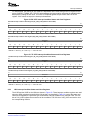
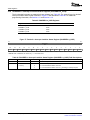
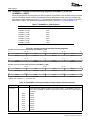
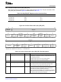
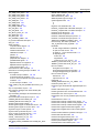
RapidIO Architectural Hierarchy
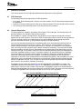
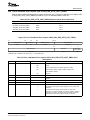
RapidIO is defined as a 3-layer architectural hierarchy.
• Logical layer: Specifies the protocols, including packet formats, which are needed by endpoints to
process transactions
• Transport layer: Defines addressing schemes to correctly route information packets within a system
• Physical layer: Contains the device level interface information such as the electrical characteristics,
error management data, and basic flow control data
In the RapidIO architecture, a single specification for the transport layer is compatible with differing
specifications for the logical and physical layers (see Figure 1).
16
Serial RapidIO (SRIO)
SPRUE13A – September 2006
Submit Documentation Feedback
www.ti.com
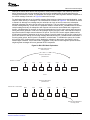
Overview
Figure 1. RapidIO Architectural Hierarchy
Logical specification
Information necessary for the end point
to process the transaction (i.e., transaction
type, size, physical address)
I/O
system
Transport specification
Information to transport packet from end
to end in the system (i.e., routing address)
Physical specification
Information necessary to move packet
between two physical devices (i.e., electrical
interface, flow control)
Globally
shared
memory
Message
passing
Common
transport
spec
8/16
LP-LVDS
1x/4x
LP serial
Interoperability
specification
SPRUE13A – September 2006
Submit Documentation Feedback
Future
logical
spec
Future
physical
spec
Compliance
checklist
Serial RapidIO (SRIO)
17
www.ti.com
Overview
1.1.2
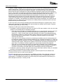
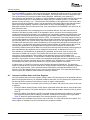
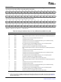
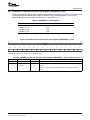
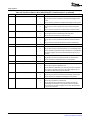
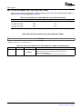
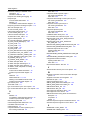
RapidIO Interconnect Architecture
The interconnect architecture is defined as a packet switched protocol independent of a physical layer
implementation. Figure 2 illustrates the interconnection system.
Figure 2. RapidIO Interconnect Architecture
Host Subsystem
I/O Control Subsystem
InfiniBand™ HCA
Memory
Memory
Control
Processor
Host
Processor
IO
Processor
ASIC/FPGA
Host
Processor
Memory
To System Area
Network
RapidIO to
InfiniBand
RapidIO
Switch
Memory
RapidIO
RapidIO
RapidIO
RapidIO
RapidIO
Switch
RapidIO
RapidIO
Switch
Backplane
RapidIO
RapidIO
Switch
RapidIO
DSP
Memory
DSP
DSP
Comm
Processor
Memory
DSP Farm
1.1.3
Comm
Processor
PCI
DSP
TDM,GMII, Utopia
(1)
RapidIO to
PCI Bridge
RapidIO
Communications Subsystem
Legacy
PCI Subsystem
InfiniBand™ is a trademark of the InfiniBand Trade Association.
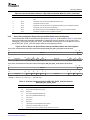
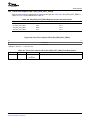
Physical Layer 1x/4x LP-Serial Specification
Currently, there are two physical layer specifications recognized by the RapidIO Trade Association: 8/16
LP-LVDS and 1x/4x LP-Serial. The 8/16 LP-LVDS specification is a point-to-point synchronous clock
sourcing DDR interface. The 1x/4x LP-Serial specification is a point-to-point, AC coupled, clock recovery
interface. The two physical layer specifications are not compatible.
SRIO complies with the 1x/4x LP-Serial specification. The serializer/deserializer (SERDES) technology in
SRIO also aligns with that specification.
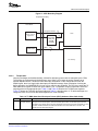
The RapidIO Physical Layer 1x/4x LP-Serial Specification currently covers three frequency points: 1.25,
2.5, and 3.125 Gbps. This defines the total bandwidth of each differential pair of I/O signals. An 8-bit/10-bit
encoding scheme ensures ample data transitions for the clock recovery circuits. Due to the 8-bit/10-bit
encoding overhead, the effective data bandwidth per differential pair is 1.0, 2.0, and 2.5 Gbps
respectively. Serial RapidIO only specifies these rates for both the 1x and 4x ports. A 1x port is defined as
1 TX and 1 RX differential pair. A 4x port is a combination of four of these pairs. This document describes
a 4x RapidIO port that can also be configured as four 1x ports, thus providing a scalable interface capable
of supporting a data bandwidth of 1 to 10 Gbps.
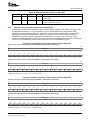
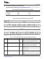
Figure 3 shows how to interface two 1x devices and two 4x devices. Each positive transmit data line (TDx)
on one device is connected to a positive receive data line (RDx) on the other device. Likewise, each
negative transmit data line (TDx) is connected to a negative receive data line (RDx).
18
Serial RapidIO (SRIO)
SPRUE13A – September 2006
Submit Documentation Feedback
www.ti.com
Overview
Figure 3. Serial RapidIO Device to Device Interface Diagrams
1x Device
1x Device
TD[0]
RD[0]
TD[0]
RD[0]
RD[0]
TD[0]
RD[0]
TD[0]
Serial RapidIO 1x Device to 1x Device Interface Diagram
4x Device
4x Device
TD[0-3]
RD[0-3]
TD[0-3]
RD[0-3]
RD[0-3]
TD[0-3]
RD[0-3]
TD[0-3]
Serial RapidIO 4x Device to 4x Device Interface Diagram
1.2
RapidIO Feature Support in SRIO
Features Supported in SRIO Peripheral:
• RapidIO Interconnect Specification V1.2 compliance, Errata 1.2
• Physical Layer 1x/4x LP-Serial Specification V1.2 compliance
• 4x Serial RapidIO with auto-negotiation to 1x port, optional operation for four 1x ports
• Integrated clock recovery with TI SERDES
• Hardware error handling including Cyclic Redundancy Code (CRC)
• Differential CML signaling supporting AC coupling
• Support for 1.25, 2.5, and 3.125 Gbps rates
• Power-down option for unused ports
• Read, write, write with response, streaming write, outgoing Atomic, and maintenance operations
• Generates interrupts to the CPU (Doorbell packets and internal scheduling)
• Support for 8-bit and 16-bit device ID
• Support for receiving 34-bit addresses
• Support for generating 34-bit, 50-bit, and 66-bit addresses
• Support for the following data sizes: byte, half-word, word, double-word
• Big endian data transfers
• Direct I/O transfers
• Message passing transfers
• Data payloads of up to 256 bytes
• Single messages consisting of up to 16 packets
• Elastic storage FIFOs for clock domain handoff
• Short run and long run compliance
• Support for Error Management Extensions
• Support for Congestion Control Extensions
• Support for one multi-cast ID
SPRUE13A – September 2006
Submit Documentation Feedback
Serial RapidIO (SRIO)
19
www.ti.com
Overview
Features Not Supported:
• Compliance with the Global Shared Memory specification (GSM)
• 8/16 LP-LVDS compatible
• Destination support of RapidIO Atomic Operations
• Simultaneous mixing of frequencies between 1x ports (all ports must be the same frequency)
• Target atomic operations (including increment, decrement, test-and-swap, set, and clear) for internal
L2 memory and registers
1.3
Standards
The SRIO peripheral is compliant to V1.2 of the RapidIO Interconnect Specification and V1.2 of the
RapidIO Physical Layer 1x/4x LP-Serial Specification. These and the various associated documents listed
herein can be found at the official RapidIO website: www.RapidIO.org.
1.4
External Devices Requirements
SRIO provides a seamless interface to all devices which are compliant to V1.2 of the RapidIO Physical
Layer 1x/4x LP-Serial Specification. This includes ASIC, microprocessor, DSP, and switch fabric devices
from multiple vendors. Compliance to the specification can be verified with bus-functional models available
through the RapidIO Trade Association, as well as test suites currently available for licensing.
1.5
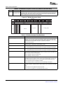
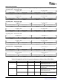
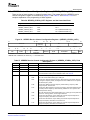
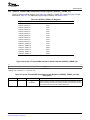
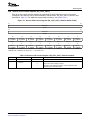
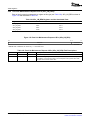
TI Devices Supported By This Document
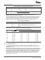
Table 1. TI Devices Supported By This Document
20
Device
Number of
DSP Cores (CPUs)
Number of
Ports
Number of
Lanes
Configurations
SRIO Module
Frequency
TMS320TCI6482
1
4
4
1x/4x, 1x/1x
DSP frequency ÷ 4
Serial RapidIO (SRIO)
SPRUE13A – September 2006
Submit Documentation Feedback
www.ti.com
SRIO Functional Description
2
SRIO Functional Description
2.1
Overview
2.1.1
Peripheral Data Flow
This peripheral is designed to be an externally driven slave module that is capable of acting as a master in
the DSP system. This means that an external device can push (burst write) data to the DSP as needed,
without having to generate an interrupt to the CPU or without relying on the DSP EDMA. This has several
benefits. It cuts down on the total number of interrupts, it reduces handshaking (latency) associated with
read-only peripherals, and it frees up the EDMA for other tasks.
SRIO specifies data packets with payloads up to 256 bytes. Many times, transactions will span across
multiple packets. RapidIO specifies a maximum of 16 transactions per message. Although a request is
generated for each packet transaction so that the DMA can transfer the data to L2 memory, an interrupt is
only generated after the final packet of the message. This interrupt notifies the CPU that data is available
in L2 Memory for processing.
As an endpoint device, the peripheral accepts packets based on the destination ID. Two options exist for
packet acceptance and are mode selectable. The first option is to only accept packets whose DestIDs
match the local deviceID in 0x0080. This provides a level of security. The second option is is system
multicast operation. When multicast is enabled in SP_IP_MODE (offset 12004h) bit 5, incoming packets
matching the deviceID in the registers shown in are accepted.
Table 2. Registers Checked for Multicast DeviceID
Registers Checked For Multicast DeviceID
Device
Name
Address Offset
TMS320TCI6482
Local DeviceID Register
0080h
Multicast DeviceID Register
0084h
Data flow through the peripheral can be explained using the high-level block diagram shown in Figure 4.
High-speed data enters from the device pins into the RX block of the SERDES macro. The RX block is a
differential receiver expecting a minimum of 175mV peak-to-peak differential input voltage (Vid). Level
shifting is performed in the RX block, such that the output is single ended CMOS. The serial data is then
fed to the SERDES clock recovery block. The sole purpose of this block is to extract a clock signal from
the data stream. To do this, a low-frequency reference clock is required. Typically, this clock comes from
an off-chip stable crystal oscillator and is a LVDS device input separate to the SERDES. This clock is
distributed to the SERDES PLL block which multiplies that frequency up to that of the data rate. Multiple
high-speed clock phases are created and routed to the clock recovery blocks. The clock recovery blocks
further interpolate between these clocks to provide maximum Unit Interval (UI) resolution on the recovered
clock. The clock recovery block samples the incoming data and monitors the relative positions of the data
edges. With this information, it can provide the data and a center-aligned clock to the S2P block. The S2P
block uses the newly recovered clock to de-multiplex the data into 10-bit words. At this point, the data
leaves the SERDES macro at 1/10th the pin data rate, accompanied by an aligned byte clock.
SPRUE13A – September 2006
Submit Documentation Feedback
Serial RapidIO (SRIO)
21
www.ti.com
SRIO Functional Description
System
clock
PLL
TX P2S
10b
Clk
TX P2S
10b
Clk
10b
Clk
TX P2S
10b
Clk
TX P2S
8b/10b 8b FIFO
coding
8b/10b 8b FIFO
coding
8b/10b 8b FIFO
coding
8b/10b 8b FIFO
coding
Clock domain 1
Control
Buffering address and data handoff
10b
8b FIFO
S2P Clk 8b/10b
decode
Capability
registers
Packet Generation
RX Clock
recovery
RX Clock
recovery
Lane de-skew
RX Clock
recovery
SERDES
10b
8b FIFO
S2P Clk 8b/10b
decode
10b
8b FIFO
S2P Clk 8b/10b
decode
10b
8b FIFO
S2P Clk 8b/10b
decode
RX Clock
recovery
Lane striping
CRC generation
1.25 to 3.125 Gbps
differential data
CRC error detection
Figure 4. SRIO Peripheral Block Diagram
DMA
bus
Command
and status
registers
Clock domain 2
Clock domain 3
Within the physical layer, the data next goes to the 8-bit/10-bit (8b/10b) decode block. 8b/10b encoding is
used by RapidIO to ensure adequate data transitions for the clock recovery circuits. Here the 20%
encoding overhead is removed as the 10-bit data is decoded to the raw 8-bit data. At this point, the
recovered byte clock is still being used.
The next step is clock synchronization and data alignment. These functions are handled by the FIFO and
lane de-skewing blocks. In the RapidIO Interconnect Specification, a "lane" is one serial differential pair.
The FIFO provides an elastic store mechanism used to hand off between the recovered clock domains
and a common system clock. After the FIFO, the four lanes are synchronized in frequency and phase,
whether 1X or 4X mode is being used. The FIFO is 8 words deep. The lane de-skew is only meaningful in
the 4X mode, where it aligns each channel’s word boundaries, such that the resulting 32-bit word is
correctly aligned.
The CRC error detection block keeps a running tally of the incoming data and computes the expected
CRC value for the 1X or 4X mode. The expected value is compared against the CRC value at the end of
the received packet.
After the packet reaches the logical layer, the packet fields are decoded and the payload is buffered.
Depending on the type of received packet, the packet routing is handled by functional blocks which control
the DMA access.
2.1.2
SRIO Packets
The SRIO data stream consists of data fields pertaining to the logical layer, the transport layer, and the
physical layer.
• The logical layer consists of the header (defining the type of access) and the payload (if present).
• The transport layer is partially dependent on the physical topology in the system, and consists of
source and destination IDs for the sending and receiving devices.
• The physical layer is dependent on the physical interface (i.e., serial versus parallel RapidIO) and
includes priority, acknowledgment, and error checking fields.
2.1.2.1
Operation Sequence
SRIO transactions are based on request and response packets. Packets are the communication element
between endpoint devices in the system. A master or initiator generates a request packet which is
transmitted to a target. The target then generates a response packet back to the initiator to complete the
transaction.
22
Serial RapidIO (SRIO)
SPRUE13A – September 2006
Submit Documentation Feedback
www.ti.com
SRIO Functional Description
SRIO endpoints are typically not connected directly to each other but instead have intervening connection
fabric devices. Control symbols are used to manage the flow of transactions in the SRIO physical
interconnect. Control symbols are used for packet acknowledgment, flow control information, and
maintenance functions. Figure 5 shows how a packet progresses through the system.
Figure 5. Operation Sequence
Initiator
Operation
Issued By
Master
Acknowledge
Symbol
Request
Packet Issued
Operation
Completed for
Master
Fabric
Response
Packet
Forwarded
Acknowledge
Symbol
Acknowledge
Symbol
Request Packet
Forwarded
Target
Response Packet
Issued
Acknowledge
Symbol
Target
Completes
Operation
2.1.2.2
Example Packet – Streaming Write
An example packet is shown as two data streams in Figure 6. The first is for payload sizes of 80 bytes or
less, while the second applies to payload sizes of 80 to 256 bytes. SRIO packets must have a length that
is an even integer of 32 bits. If the combination of physical, logical and transport layers has a length that is
an integer of 16 bits, a 16-bit pad of value 0000h is added to the end of the packet, after the CRC (not
shown). Bit fields that are defined as reserved are assigned to logic 0s when generated and ignored when
received. All request and response packet formats are described in the RapidIO Input/Output Logical
Specification and MIessage Passing Logical Specification.
SPRUE13A – September 2006
Submit Documentation Feedback
Serial RapidIO (SRIO)
23
www.ti.com
SRIO Functional Description
Figure 6. 1x/4x RapidIO Packet Data Stream (Streaming-Write Class)
n*64+80
PHY
10
acklD rsv
5
prio
3
2
tt ftype destID
2
4
8
sourcelD
4
address rsrv xamsbs
8
1
29
LOG
TRA
2
LOG
TRA
16
...
double-word 0 double-word 1
2
64
TRA
LOG
PHY
n*64+32
PHY = Physical layer
TRA = Transport layer
LOG = Logical layer
double-word n-2 double-word n-1 CRC
64
64
(n-4)*64
64
16
16
n*64+96
PHY
2
10
prio
a c k l D rsv
5
2
3
tt ftype destID
2
4
8
Note:
sourcelD address
8
29
4
TRA
16
rsrv xamsbs double-word 0 double-word 1
1
2
64
64
LOG
PHY
LOG
PHY
9 * 6 4 + 32
16
(n-9)*64
16
...
double-word 8
double-word 9
5*64
64
64
CRC
16
...
double-word 11
double-word 10
64
64
(n-13)*64
double-word n-2 double-word n-1 CRC
64
64
16
Figure 6 assumes that addresses are 32-bit and device IDs are 8-bit.
The device ID, being an 8-bit field, will address up to 256 nodes in the system. If 16-bit addresses were
used, the system could accommodate up to 64k nodes.
The data stream includes a Cyclic Redundancy Code (CRC) field to ensure the data was correctly
received. The CRC value protects the entire packet except the ackID and one bit of the reserved PHY
field. The peripheral checks the CRC automatically in hardware. If the CRC is correct, a Packet-Accepted
control symbol is sent by the receiving device. If the CRC is incorrect, a Packet-Not-Accepted control
symbol is sent so that transmission may be retried.
2.1.2.3
Control Symbols
Control symbols are physical layer message elements used to manage link maintenance, packet
delimiting, packet acknowledgment, error reporting, and error recovery. All transmitted data packets are
delimited by start-of-packet and end-of-packet delimiters. SRIO control symbols are 24 bits long and are
protected by their own CRC (see Figure 7). Control symbols provide two functions: stype0 symbols
convey the status of the port transmitting the symbol, and stype1 symbols are requests to the receiving
port or transmission delimiters. They have the following format, which is detailed in Section 3 of the
RapidIO Physical Layer 1x/4x LP-Serial Specification.
Figure 7. Serial RapidIO Control Symbol Format
Delimiter
SC or PD
8
1st Byte
stype0
3
2nd Byte
Parameter0
5
3rd Byte
parameter1
stype1
cmd
CRC
5
3
3
5
Control symbols are delimited by special characters at the beginning of the symbol. If the control symbol
contains a packet delimiter(start-of-packet, end-of-packet, etc.), the special character PD (K28.3) is used.
If the control symbol does not contain a packet delimiter, the special character SC (K28.0) is used. This
use of special characters provides an early warning of the contents of the control symbol. The CRC does
not protect the special characters, but an illegal or invalid character is recognized and flagged as
Packet-Not-Accepted. Since control symbols are known length, they do not need end delimiters.
24
Serial RapidIO (SRIO)
SPRUE13A – September 2006
Submit Documentation Feedback
www.ti.com
SRIO Functional Description
The type of received packet determines how the packet routing is handled. Reserved or undefined packet
types are destroyed before being processed by the logical layer functional blocks. This prevents erroneous
allocation of resources to them. Unsupported packet types are responded to with an error response
packet. Section 2.1.2.4 details the handling of such packets.
2.1.2.4
SRIO Packet Type
The type of SRIO packet is determined by the combination of Ftype and Ttype fields in the packet. Table 3
lists all supported combinations of Ftype/Ttype and the corresponding decoded actions on the packets.
Table 3. Packet Types
Ftype
Ttype
Ftype = 0
Ttype = don't care
Packet Type
Ftype = 2
Ttype = 0100b
NREAD
Ttype = 1100b
Atomic increment
Ttype = 1101b
Atomic decrement
Ttype = 1110b
Atomic set
Ttype = 1111b
Atomic clear
Ttype = others
Ftype = 5
Ttype = 0100b
NWRITE
Ttype = 0101b
NWRITE_R
Ttype = 1110b
Atomic test and swap
Ttype = others
Ftype = 6
Ttype = don't care
SWRITE
Ftype = 7
Ttype = don't care
Congestion control
Ftype = 8
Ttype = 0000b
Maintenance read
Ttype = 0001b
Maintenance write
Ttype = 0010b
Maintenance read response
Ttype = 0011b
Maintenance write response
Ttype = 0100b
Maintenance port-write
Ttype = others
Ftype = 10
Ttype = don't care
Doorbell
Ftype = 11
Ttype = don't care
Message
Ftype = 13
Ttype = 0000b
Response(+Doorbell Resp)
Ttype = 0001b
Message Response
Ttype = 1000b
Response w/payload
Ttype = other
Undefined Ftypes: 1,3,4,9,12,14,15
2.2
SRIO Pins
The SRIO device pins are high-speed differential signals based on Current-Mode Logic (CML) switching
levels. The transmit and receive buffers are self-contained within the clock recovery blocks. The reference
clock input is not incorporated into the SERDES macro. It uses a differential input buffer that is compatible
with the LVDS and LVPECL interfaces available from crystal oscillator manufacturers. Table 4 describes
the device pins for the SRIO peripheral.
SPRUE13A – September 2006
Submit Documentation Feedback
Serial RapidIO (SRIO)
25
www.ti.com
SRIO Functional Description
Table 4. Pin Description
Pin
Count
Signal
Direction
RIOTX3/ RIOTX3
2
Output
Transmit Data – Differential point-to-point unidirectional bus. Transmits
packet data to a receiving device’s RX pins. Most significant bits in 1
port 4X device. Used in 4 port 1X device.
RIOTX2/ RIOTX2
2
Output
Transmit Data – Differential point-to-point unidirectional bus. Transmits
packet data to a receiving device’s RX pins. Bit used in 4 port 1x
device and 1 port 4X device.
RIOTX1/ RIOTX1
2
Output
Transmit Data – Differential point-to-point unidirectional bus. Transmits
packet data to a receiving device’s RX pins. Bit used in 4 port 1x
device and 1 port 4X device.
RIOTX0/ RIOTX0
2
Output
Transmit Data – Differential point-to-point unidirectional bus. Transmits
packet data to a receiving device’s RX pins. Bit used in 1 port 1X
device, 4 port 1x device, and 1 port 4X device.
RIORX3/ RIORX3
2
Input
Receive Data – Differential point-to-point unidirectional bus. Receives
packet data for a transmitting device’s TX pins. Most significant bits in
1 port 4X device. Used in 4 port 1X device.
RIORX2/ RIORX2
2
Input
Receive Data – Differential point-to-point unidirectional bus. Receives
packet data for a transmitting device’s TX pins. Bit used in 4 port 1x
device and 1 port 4X device.
RIORX1/ RIORX1
2
Input
Receive Data – Differential point-to-point unidirectional bus. Receives
packet data for a transmitting device’s TX pins. Bit used in 4 port 1x
device and 1 port 4X device.
RIORX0/ RIORX0
2
Input
Receive Data – Differential point-to-point unidirectional bus. Receives
packet data for a transmitting device’s TX pins. Bit used in 1 port 1X
device, 4 port 1x device, and 1 port 4X device.
RIOCLK/ RIOCLK
2
Input
Reference Clock Input Buffer for peripheral clock recovery circuitry.
Pin Name
2.3
2.3.1
Description
Functional Operation
Component Block Diagram
Figure 8 shows a component block diagram of the SRIO peripheral. The load/store unit (LSU) controls the
transmission of direct I/O packets, and the memory access unit (MAU) controls the reception of direct I/O
packets. The LSU also controls the transmission of maintenance packets. Message packets are
transmitted by the TXU and received by the RXU. These four units use the internal DMA to communicate
with internal memory, and they use buffers and receive/transmit ports to communicate with external
devices. Serializer/deserializer (SERDES) macros support the ports by performing the parallel-to-serial
coding for transmission and serial-to-parallel decoding for reception.
26
Serial RapidIO (SRIO)
SPRUE13A – September 2006
Submit Documentation Feedback
www.ti.com
SRIO Functional Description
Figure 8. SRIO Component Block Diagram
DMA bus
Load/Store
units (LSUs)
TX direct I/O
TXU
Messaging
Maintenance
4.5 KB TX
shared
buffer
Memory
access unit
(MAU)
RX direct I/O
RXU
Messaging
4.5 KB RX
shared
buffer
Queue
handle
TX buffering
32 x 276B
8 buffers per 1X port - all priorities
32 buffers per 4X port - 8 per priority
Logical
layer
buffers
Transaction
mapping
UDI
Port 0
Port 1
Port 2
Port 3
8 x 276 TX
8 x 276 RX
8 x 276 TX
8 x 276 RX
8 x 276 TX
8 x 276 RX
8 x 276 TX
8 x 276 RX
SERDES 1
SERDES 2
SERDES 3
Physical
layer
buffers
4x mode
data path
SERDES 0
SERDES
differential
signals
SPRUE13A – September 2006
Submit Documentation Feedback
Serial RapidIO (SRIO)
27
www.ti.com
SRIO Functional Description
2.3.2
SERDES Macro and its Configurations
SRIO offers many benefits to customers by allowing a scalable non-proprietary interface. With the use of
TI’s SERDES macros, the peripheral is very adaptable and bandwidth scalable. The same peripheral can
be used for all three frequency nodes specified in V1.2 of the RapidIO Interconnect Specification (1.25,
2.5, and 3.125 Gbps). This allows you to design to only one protocol throughout the system and
selectively choose the bandwidth, thus eliminating the need for user’s proprietary protocols in many
instances, and providing a faster design turn and production ramp. Since this interface is serial, the
application space is not limited to a single board. It will propagate into backplane applications as well.
Integration of these macros on an ASIC or DSP allows you to reduce the number of discrete components
on the board and eliminates the need for bus driver chips.
Additionally, there are some valuable features built into TI SERDES. System optimization can be uniquely
managed to meet individual customer applications. For example, control registers within the SERDES
allow you to adjust the TX differential output voltage (Vod) on a per driver basis. This allows power
savings on short trace links (on the same board) by reducing the TX swing. Similarly, data edge rates can
be adjusted through the control registers to help reduce any EMI affects. Unused links can be individually
powered down without affecting the working links.
The SERDES macro is a self-contained macro which includes transmitter (TX), receiver (RX),
phase-locked-loop (PLL), clock recovery, serial-to-parallel (S2P), and parallel-to-serial (P2S) blocks. The
internal PLL multiplies a user-supplied reference clock. All loop filter components of the PLL are onchip.
Likewise, the differential TX and RX buffers contain on-chip termination resistors. The only off-chip
component requirement is for DC blocking capacitors.
2.3.2.1
Enabling the PLL
The Physical layer SERDES has a built-in PLL, which is used for the clock recovery circuitry. The PLL is
responsible for clock multiplication of a slow speed reference clock. This reference clock has no timing
relationship to the serial data and is asynchronous to any CPU system clock. The multiplied high-speed
clock is only routed within the SERDES block; it is not distributed to the remaining blocks of the peripheral,
nor is it a boundary signal to the core of the device. It is extremely important to have a good quality
reference clock, and to isolate it and the PLL from all noise sources. Since RapidIO requires 8-bit/10-bit
encoded data, the 8-bit mode of the SERDES PLL is not be used.
The SERDES macro is configured with the register SERDES_CFG0_CNTL, SERDES_CFGRXn_CNTL,
and SERDES_CFGTXn_CNTL, where n is the number of the macro. To enable the internal PLL, the
ENPLL bit of SERDES_CFG0_CNTL (see Figure 9 and Table 5) must be set. After setting this bit, it is
necessary to allow 1µs for the regulator to stabilize. Thereafter, the PLL will take no longer than 200
reference clock cycles to lock to the required frequency, provided RIOCLK and RIOCLK are stable.
Registers SERDES_CFG1_CNTL, SERDES_CFG2_CNTL, and SERDES_CFG3_CNTL are not used.
Figure 9. SERDES Macro Configuration Register 0 (SERDES_CFG0_CNTL)
31
16
Reserved
R-0000h
15
10 9
8 7
6 5
1
0
Reserved
LB
Reserved
MPY
ENPLL
R-00h
R/W-0
R-0
R/W-0
R/W-0
LEGEND: R/W = Read/Write; R = Read only; -n = Value after reset
28
Serial RapidIO (SRIO)
SPRUE13A – September 2006
Submit Documentation Feedback
www.ti.com
SRIO Functional Description
Table 5. SERDES Macro Configuration Register 0 (SERDES_CFG0_CNTL) Field Descriptions
Bit
31–10
9–8
Field
Value
Description
Reserved
0000h
Reserved
LB
7–6
Reserved
5–1
MPY
0
Loop bandwidth. Specify loop bandwidth settings. Jitter on the reference clock will
degrade both the transmit eye and receiver jitter tolerance thereby impairing system
performance. Performance of the integrated PLL can be optimized according to the
jitter characteristics of the reference clock via the LB field.
00b
Frequency dependent bandwidth. The PLL bandwidth is set to a twelfth of the
frequency of RIOCLK/RIOCLK. This setting is suitable for most systems that input the
reference clock via a low jitter input cell, and is required for standards compliance
01b
Reserved
10b
Low bandwidth. The PLL bandwidth is set to a twentieth of the frequency of
RIOCLK/RIOCLK, or 3MHz (whichever is larger). In systems where the reference
clock is directly input via a low jitter input cell, but is of lower quality, this setting may
offer better performance. It will reduce the amount of reference clock jitter transferred
through the PLL. However, it also increases the susceptibility to loop noise generated
within the PLL itself. It is difficult to predict whether the improvement in the former will
more than offset the degradation in the latter.
11b
High bandwidth. The PLL bandwidth is set to a eighth of the frequency of
RIOCLK/RIOCLK. This is the setting appropriate for systems where the reference
clock is cleaned through an ultra low jitter LC-based PLL. Standards compliance will
be achieved even if the reference clock input to the cleaner PLL is outside the
specification for the standard.
00h
Reserved
PLL multiply. Select PLL multiply factors between 4 and 60.
00000b
4x
00001b
5x
00010b
6x
00011b
Reserved
00100b
8x
00101b
10x
00110b
12x
00111b
12.5x
01000b
15x
01001b
20x
01010b
25x
01011b
Reserved
01100b
Reserved
01111b
Reserved
1xxxxb
Reserved
ENPLL
Enable PLL
0
PLL disabled
1
PLL enabled
Based on the MPY value, the line rate versus PLL output clock frequency can be calculated. This is
summarized in Table 6.
SPRUE13A – September 2006
Submit Documentation Feedback
Serial RapidIO (SRIO)
29
www.ti.com
SRIO Functional Description
Table 6. Line Rate versus PLL Output Clock Frequency
Rate
Line Rate
PLL Output Frequency
RATESCALE
Full
x Gbps
0.5x GHz
0.5
Half
x Gbps
x GHz
1
Quarter
x Gbps
2x GHz
2
RIOCLK and RIOCLKFREQ =
LINERATE × RATESCALE
MPY
The rate is defined by the RATE bits of the SERDES_CFGRXn_CNTL register and the
SERDES_CFGTXn_CNTL register, respectively.
The primary operating frequency of the SERDES macro is determined by the reference clock frequency
and PLL multiplication factor. However, to support lower frequency applications, each receiver and
transmitter can also be configured to operate at a half or quarter of this rate via the RATE bits of the
SERDES_CFGRXn_CNTL and SERDES_CFGTXn_CNTL registers as described in Table 7.
Table 7. Effect of the RATE Bits
RATE
Description
00b
Full rate. Two data samples taken per PLL output clock cycle.
01b
Half rate. One data sample taken per PLL output clock cycle.
10b
Quarter rate. One data sample taken every two PLL output clock cycles.
11b
Reserved.
Table 8 shows the frequency range versus the multiplication factor (MPY).
Table 8. Frequency Range versus MPY Value
RIOCLK and RIOCLK
2.3.2.2
Line Rate Range (Gbps)
MPY
Range (MHz)
Full
Half
Quarter
4x
250 - 425
2 - 3.4
1 - 1.7
0.5 - 0.85
5x
200 - 425
2 - 4.25
1 - 2.125
0.5 - 1.0625
6x
167 - 354.167
2 - 4.25
1 - 2.125
0.5 - 1.0625
8x
125 - 265.625
2 - 4.25
1 - 2.125
0.5 - 1.0625
10x
100 - 212.5
2 - 4.25
1 - 2.125
0.5 - 1.0625
12x
83.33 - 177.08
2 - 4.25
1 - 2.125
0.5 - 1.0625
12.5x
80 - 170
2 - 4.25
1 - 2.125
0.5 - 1.0625
15x
66.67 - 141.67
2 - 4.25
1 - 2.125
0.5 - 1.0625
20x
50 - 106.25
2 - 4.25
1 - 2.125
0.5 - 1.0625
25x
40 - 85
2 - 4.25
1 - 2.125
0.5 - 1.0625
Enabling the Receiver
To enable a receiver for deserialization, the ENRX bit of the associated SERDES_CFGRXn_CNTL
registers (100h–10Ch) must be set high. The fields of SERDES_CFGRXn_CNTL are shown in Figure 10
and described in Table 9.
When ENRX is low, all digital circuitry within the receiver will be disabled, and clocks will be gated off. All
current sources within the receiver will be fully powered down, with the exception of those associated with
the loss of signal detector and IEEE1149.6 boundary scan comparators. Loss of signal power down is
independently controlled via the LOS bits of SERDES_CFGRXn_CNTL. When enabled, the differential
signal amplitude of the received signal is monitored. Whenever loss of signal is detected, the clock
recovery algorithm is frozen to prevent the phase and frequency of the recovered clock from being
modified by low level signal noise.
30
Serial RapidIO (SRIO)
SPRUE13A – September 2006
Submit Documentation Feedback
www.ti.com
SRIO Functional Description
The clock recovery algorithms listed in the CDR bits operate to adjust the clocks used to sample the
received message so that the data samples are taken midway between data transitions. The second order
algorithm can be optionally disabled, and both can be configured to optimize their dynamics. Both
algorithms use the same basic technique for determining whether the sampling clock is ideally placed, and
if not whether it needs to be moved earlier or later. When two contiguous data samples are different, the
phase sample between the two is examined. Eight data samples and nine phase samples are taken with
each result counted as a vote to move the sample point either earlier or later. These eight data bits
constitute the voting window. The eight votes are then counted, and an action to adjust the position of the
sampling clock occurs if there is a majority of early or late votes. The first order algorithm makes a single
phase adjustment per majority vote. The second order algorithm acts repeatedly according to the net
difference between early and late majority votes, thereby adjusting for the rate of change of phase.
Setting the ALIGN field to 01 enables alignment to the K28 comma symbols included in the 8b:10b data
encoding scheme defined by the IEEE and employed by numerous transmission standards. For systems
which cannot use comma based symbol alignment, the single bit alignment jog capability provides a
means to control the symbol realignment features of the receiver directly from logic implemented in the
ASIC core. This logic can be designed to support whatever alignment detection protocol is required.
The EQ bits allow for enabling and configuring the adaptive equalizer incorporated in all of the receive
channels, which can compensate for channel insertion loss by attenuating the low frequency components
with respect to the high frequency components of the signal, thereby reducing inter-symbol interference.
Above the zero frequency, the gain increases at 6dB/octave until it reaches the high frequency gain. When
enabled, the receiver equalization logic analyzes data patterns and transition times to determine whether
the low frequency gain of the equalizer should be increased or decreased. For the fully adaptive setting
(EQ = 0001), if the low frequency gain reaches the minimum value, the zero frequency is then reduced.
Likewise, if it reaches the maximum value, the zero frequency is then increased. This decision logic is
implemented as a voting algorithm with a relatively long analysis interval. The slow time constant that
results reduces the probability of incorrect decisions but allows the equalizer to compensate for the
relatively stable response of the channel.
• No adaptive equalization. The equalizer provides a flat response at the maximum gain. This setting
may be appropriate if jitter at the receiver occurs predominantly as a result of crosstalk rather than
frequency dependent loss.
• Fully adaptive equalization. Both the low frequency gain and zero position of the equalizer are
determined algorithmically by analysing the data patterns and transition positions in the received data.
This setting should be used for most applications.
• Partially adaptive equalisation. The low frequency gain of the equalizer is determined algorithmically by
analysing the data patterns and transition positions in the received data. The zero position is fixed in
one of eight zero positions. For any given application, the optimal setting is a function of the loss
characteristics of the channel and the spectral density of the signal as well as the data rate, which
means it is not possible to identify the best setting by data rate alone, although generally speaking, the
lower the line rate, the lower the zero frequency that will be required.
Figure 10. SERDES Receive Channel Configuration Register n (SERDES_CFGRXn_CNTL)
31
26 25
15
24
23
22
19 18
16
Reserved
Reserved
(write 0s)
—
EQ
CDR
R-0
R/W-0
R-0
R/W-0
R/W-0
14 13
12
11
10
8
LOS
ALIGN
—
TERM
(write 001b)
R/W-0
R/W-0
R-0
R/W-0
7
6
5 4
INVPAIR
RATE
R/W-0
R/W-0
2
1
0
BUSWIDTH
—
(write 0)
ENRX
R/W-0
R/W-0
R/W-0
LEGEND: R/W = Read/Write; R = Read only; -n = Value after reset
Table 9. SERDES Receive Channel Configuration Register n (SERDES_CFGRXn_CNTL) Field
Descriptions
Bit
31–26
Field
Reserved
SPRUE13A – September 2006
Submit Documentation Feedback
Value
000000b
Description
These read-only bits return 0s when read.
Serial RapidIO (SRIO)
31
www.ti.com
SRIO Functional Description
Table 9. SERDES Receive Channel Configuration Register n (SERDES_CFGRXn_CNTL) Field
Descriptions (continued)
Bit
Reserved
23
Reserved
22–19
EQ
18–16
CDR
15–14
13–12
11
10–8
7
6–5
32
Field
25–24
Value
Always write 0s to these reserved bits.
0
This read-only bit returns 0 when read.
0000b–1111b
000b
First order. Phase offset tracking up to ±488 ppm.
001b
Second order. Highest precision frequency offset matching but poorest response
to changes in frequency offset, and longest lock time. Suitable for use in systems
with fixed frequency offset.
010b
Second order. Medium precision frequency offset matching, frequency offset
change response, and lock time.
011b
Second order. Best response to changes in frequency offset and fastest lock time,
but lowest precision frequency offset matching. Suitable for use in systems with
spread spectrum clocking.
100b
First order with fast lock. Phase offset tracking up to ±1953 ppm in the presence of
..10101010.. training pattern, and ±448 ppm otherwise.
101b
Second order with fast lock. As per setting 001, but with improved response to
changes in frequency offset when not close to lock.
110b
Second order with fast lock. As per setting 010, but with improved response to
changes in frequency offset when not close to lock.
111b
Second order with fast lock. As per setting 011, but with improved response to
changes in frequency offset when not close to lock.
Loss of signal. Enables loss of signal detection with 2 selectable thresholds.
00b
Disabled. Loss of signal detection disabled.
01b
High threshold. Loss of signal detection threshold in the range 85 to 195mVdfpp.
This setting is suitable for Infiniband.
10b
Low threshold. Loss of signal detection threshold in the range 65 to 175mVdfpp.
This setting is suitable for PCI-E and S-ATA.
11b
Reserved
ALIGN
TERM
Symbol alignment. Enables internal or external symbol alignment.
00b
Alignment disabled. No symbol alignment will be performed while this setting is
selected, or when switching to this selection from another.
01b
Comma alignment enabled. Symbol alignment will be performed whenever a
misaligned comma symbol is received.
10b
Alignment jog. The symbol alignment will be adjusted by one bit position when this
mode is selected (that is, the ALIGN value changes from 0xb to 1xb).
11b
Reserved
0
001b
INVPAIR
This read-only bit returns 0 when read.
Input termination. The only valid value for this field is 001b; all other values are
reserved. The value 001b sets the common point to 0.8 VDDT and supports AC
coupled systems using CML transmitters. The transmitter has no effect on the
receiver common mode, which is set to optimize the input sensitivity of the
receiver. Common mode termination is via a 50 pF capacitor to VSSA.
Invert polarity. Inverts polarity of RIORXn and RIORXn.
0
Normal polarity. RIORXn is considered to be positive data and RIORXn negative.
1
Inverted polarity. RIORXn is considered to be negative data and RIORXn positive.
RATE
Serial RapidIO (SRIO)
Equalizer. Enables and configures the adaptive equalizer to compensate for loss
in the transmission media. For the selectable values, see Table 10.
Clock/data recovery. Configures the clock/data recovery algorithm.
LOS
Reserved
Description
00b
Operating rate. Selects full, half, or quarter rate operation.
00b
Full rate. Two data samples taken per PLL output clock cycle.
01b
Half rate. One data sample taken per PLL output clock cycle.
10b
Quarter rate. One data sample taken every two PLL output clock cycles.
11b
Reserved
SPRUE13A – September 2006
Submit Documentation Feedback
www.ti.com
SRIO Functional Description
Table 9. SERDES Receive Channel Configuration Register n (SERDES_CFGRXn_CNTL) Field
Descriptions (continued)
Bit
Field
Value
Description
4–2
BUSWIDTH
000b
Bus width. Always write 000b to this field, to indicate a 10-bit-wide parallel bus to
the clock. All other values are reserved. See Section 2.3.2.1 for an explanation of
the bus.
1
Reserved
0
ENRX
0
Always write 0 to this reserved bit.
Enable receiver
0
Disable this receiver.
1
Enable this receiver.
Table 10. EQ Bits
CFGRX[22–19]
Low Freq Gain
0000b
Maximum
–
0001b
Adaptive
Adaptive
001xb
Reserved
01xxb
Reserved
1000b
2.3.2.3
Zero Freq (at e28 (min))
Adaptive
1084MHz
1001b
805MHz
1010b
573MHz
1011b
402MHz
1100b
304MHz
1101b
216MHz
1110b
156MHz
1111b
135MHz
Enabling the Transmitter
To enable a transmitter for serialization, the ENTX bit of the associated SERDES_CFGTXn_CNTL
registers (110h–10Ch) must be set high. When ENTX is low, all digital circuitry within the transmitter will
be disabled, and clocks will be gated off, with the exception of the transmit clock (TXBCLK[n]) output,
which will continue to operate normally. All current sources within the transmitter will be fully powered
down, with the exception of the current mode logic (CML) driver, which will remain powered up if boundary
scan is selected. Figure 11 shows the fields of SERDES_CFGTXn_CNTL and Table 11 describes them.
Figure 11. SERDES Transmit Channel Configuration Register n (SERDES_CFGTXn_CNTL)
31
17
15
12 11
9
16
Reserved
ENFTP
R-0
R/W-1
8
7
6
5 4
2
1
0
DE
SWING
CM
INVPAIR
RATE
BUSWIDTH
(write 0)
ENTX
R/W-0
R/W-0
R/W-0
R/W-0
R/W-0
R/W-0
R/W-0
R/W-0
LEGEND: R/W = Read/Write; R = Read only; -n = Value after reset
Table 11. SERDES Transmit Channel Configuration Register n (SERDES_CFGTXn_CNTL) Field
Descriptions
Bit
31–17
16
Field
Value
Description
Reserved
0
These read-only bits return 0s when read.
ENFTP
1
Enables fixed phase relationship of transmit input clock with respect to transmit output
clock. The only valid value for this field is 1b; all other values are reserved.
SPRUE13A – September 2006
Submit Documentation Feedback
Serial RapidIO (SRIO)
33
www.ti.com
SRIO Functional Description
Table 11. SERDES Transmit Channel Configuration Register n (SERDES_CFGTXn_CNTL) Field
Descriptions (continued)
Bit
Field
15–12
DE
11–9
SWING
8
7
6–5
4–2
Value
0000b–1111b
000b–111b
CM
Reserved
0
ENTX
Output swing. Selects one of 8 outputs amplitude settings between 125 and
1250mVdfpp. See Table 13.
0
Normal common mode. Common mode not adjusted.
1
Raised common mode. Common mode raised by 5% of difference between RIOTXn
and RIOTXn
Invert polarity. Inverts the polarity of RIOTXn and RIOTXn.
0
Normal polarity. RIOTXn is considered to be positive data and RIOTXn negative.
1
Inverted polarity. RIOTXn is considered to be negative data and RIOTXn positive.
RATE
1
De-emphasis. Selects one of 15 output de-emphasis settings from 4.76 to 71.42%.
De-emphasis provides a means to compensate for high frequency attenuation in the
attached media. It causes the output amplitude to be smaller for bits which are not
preceded by a transition than for bits which are. See Table 12.
Common mode. Adjusts the common mode to suit the termination at the attached
receiver. For output swing settings above 750mV, this reduced common mode can
cause distortion of the waveform. Under these conditions, this bit should be set high to
offset some of the common mode reduction.
INVPAIR
BUSWIDTH
Description
Operating rate. Selects full, half, or quarter rate operation.
00b
Full rate. Two data samples taken per PLL output clock cycle.
01b
Half rate. One data sample taken per PLL output clock cycle.
10b
Quarter rate. One data sample taken every two PLL output clock cycles.
11b
Reserved
000b
Bus width. Always write 000b to this field, to indicate a 10-bit-wide parallel bus to the
clock. All other values are reserved. See Section 2.3.2.1 for an explanation of the bus.
0
Always write 0 to this reserved bit.
Enable transmitter
0
Disable this transmitter.
1
Enable this transmitter.
Table 12. DE Bits of SERDES_CFGTXn_CNTL
Amplitude Reduction
34
Serial RapidIO (SRIO)
DE Bits
%
dB
0000b
0
0
0001b
4.76
–0.42
0010b
9.52
–0.87
0011b
14.28
–1.34
0100b
19.04
–1.83
0101b
23.8
–2.36
0110b
28.56
–2.92
0111b
33.32
–3.52
1000b
38.08
–4.16
1001b
42.85
–4.86
1010b
47.61
–5.61
1011b
52.38
–6.44
1100b
57.14
–7.35
1101b
61.9
–8.38
1110b
66.66
–9.54
1111b
71.42
–10.87
SPRUE13A – September 2006
Submit Documentation Feedback
www.ti.com
SRIO Functional Description
Table 13. SWING Bits of SERDES_CFGTXn_CNTL
2.3.2.4
SWING Bits
Amplitude (mVdfpp)
000b
125
001b
250
010b
500
011b
625
100b
750
101b
1000
110b
1125
111b
1250
SERDES Configuration Example
//full sample rate at 3.125 Gbps
//SERDES reference clock (RIOCLK) 125 MHz
//MPY = 12.5
125MHz = ((3.125 Gbps)(.5))/MPY
SRIO_REGS->SERDES_CFG0_CNTL = 0x0000000F;
SRIO_REGS->SERDES_CFG1_CNTL = 0x00000000;
SRIO_REGS->SERDES_CFG2_CNTL = 0x00000000;
SRIO_REGS->SERDES_CFG3_CNTL = 0x00000000;
// SRIO_REGS->SERDES_CFG1_CNTL not used
// SRIO_REGS->SERDES_CFG2_CNTL not used
// SRIO_REGS->SERDES_CFG3_CNTL not used
//four ports enabled
SRIO_REGS->SERDES_CFGRX0_CNTL
SRIO_REGS->SERDES_CFGRX1_CNTL
SRIO_REGS->SERDES_CFGRX2_CNTL
SRIO_REGS->SERDES_CFGRX3_CNTL
SRIO_REGS->SERDES_CFGTX0_CNTL
SRIO_REGS->SERDES_CFGTX1_CNTL
SRIO_REGS->SERDES_CFGTX2_CNTL
SRIO_REGS->SERDES_CFGTX3_CNTL
2.3.3
=
=
=
=
=
=
=
=
0x00081101
0x00081101
0x00081101
0x00081101
0x00010801
0x00010801
0x00010801
0x00010801
;
;
;
;
;
;
;
;
Direct I/O Operation
The direct I/O (Load/Store) module serves as the source of all outgoing direct I/O packets. With direct I/O,
the RapidIO packet contains the specific address where the data should be stored or read in the
destination device. Direct I/O requires that a RapidIO source device keep a local table of addresses for
memory within the destination device. Once these tables are established, the RapidIO source controller
uses this data to compute the destination address and insert it into the packet header. The RapidIO
destination peripheral extracts the destination address from the received packet header and transfers the
payload to memory via the DMA.
When a CPU wants to send data from memory to an external processing element (PE) or read data from
an external PE, it provides the RIO peripheral vital information about the transfer such as DSP memory
address, target device ID, target destination address, packet priority, etc. Essentially, a means must exist
to fill all the header fields of the RapidIO packet. The Load/Store module provides a mechanism to handle
this information exchange via a set of MMRs acting as transfer descriptors. These registers, shown in
Figure 12, are addressable by the CPU through the configuration bus. Upon completion of a write to
LSUn_REG5, a data transfer is initiated for either an NREAD, NWRITE, NWRITE_R, SWRITE, ATOMIC,
or MAINTENANCE RapidIO transaction. Some fields, such as the RapidIO srcTID/targetTID field, are
assigned by hardware and do not have a corresponding command register field.
SPRUE13A – September 2006
Submit Documentation Feedback
Serial RapidIO (SRIO)
35
www.ti.com
SRIO Functional Description
Figure 12. Load/Store Registers for RapidIO (Address Offset: LSU1 400h–418h, LSU2 420h–438h, LSU3
440h–458h, LSU4 460h-478h)
LSUn_REG0
RapidIO Address MSB
Control
0
31
LSUn_REG1
RapidIO Address LSB/Config_offset
Control
31
0
LSUn_REG2
DSP Address
Control
31
0
LSUn_REG3
RSV
LSUn_REG4
LSUn_REG5
Priority
30 29
xambs
28 27
ID Size
26 25
Drbll Info
DestID
24 23
8
Interrupt Req
RSV
7
Packet Type
Hop Count
RSV
31
8 7
Completion Code
5 4
Control
0
1
16 15
31
LSUn_REG6
0
12 11
OutPortID
31
Control
Byte_count
31
Command
0
Bsy
1
Status
0
The mapping of LSU register fields to RapidIO packet header fields is explained in Table 14 and Table 15.
Table 14 has the fields of the control and command registers (LSUn_REG0 through LSUn_REG5), and
Table 15 has the fields of the status register (LSUn_REG6).
Table 14. LSU Control/Command Register Fields
LSU Register Field
RapidIO Packet Header Field
RapidIO Address MSB
32-bit Extended Address Fields – Packet Types 2, 5, and 6
RapidIO Address
LSB/Config_offset
1.
2.
32-bit Address– Packet Types 2, 5, and 6 (Will be used in conjunction with BYTE_COUNT to
create 64-bit aligned RapidIO packet header address)
24-bit Config_offset Field – Maintenance Packets Type 8 (Will be used in conjunction with
BYTE_COUNT to create 64-bit aligned RapidIO packet header Config_offset). The 2 LSBs of
this field must be zero since the smallest configuration access is 4 bytes.
DSP Address
32-bit DSP byte address. Not available in RapidIO Header.
Byte_Count
Number of data bytes to Read/Write - up to 4K bytes. (Used in conjunction with RapidIO address
to create WRSIZE/RDSIZE and WDPTR in RapidIO packet header.)
000000000000b – 4K bytes
000000000001b – 1 byte
000000000010b – 2 bytes
...
111111111111b – 4095 bytes
(Maintenance requests are limited to 4 bytes)
ID Size
RapidIO tt field specifying 8- or 16-bit DeviceIDs.
00b – 8-bit deviceIDs
01b – 16-bit deviceIDs
10b - reserved
11b - reserved
36
Priority
RapidIO prio field specifying packet priority (0 = lowest, 3 = highest). Request packets should not
be sent at a priority level of 3 to avoid system deadlock. It is the responsibility of the software to
assign the appropriate outgoing priority.
Xamsbs
RapidIO xamsb field specifying the extended address MSBs.
Serial RapidIO (SRIO)
SPRUE13A – September 2006
Submit Documentation Feedback
www.ti.com
SRIO Functional Description
Table 14. LSU Control/Command Register Fields (continued)
LSU Register Field
RapidIO Packet Header Field
DestID
RapidIO destinationID field specifying the target device.
Packet Type
4 MSBs: 4-bit ftype field for all packets
4 LSBs: 4-bit trans field for packet types 2, 5, and 8
OutPortID
Not available in RapidIO header.
Indicates the output port number for the packet to be transmitted from. Specified by the CPU
along with NodeID.
Drbll Info
RapidIO doorbell info field for type 10 packets. (see Table 23)
Hop Count
RapidIO hop_count field specified for Type 8 Maintenance packets.
Interrupt Req
Not available in RapidIO header.
CPU controlled request bit used for interrupt generation. Typically used in conjunction with
non-posted commands to alert the CPU when the requested data/status is present.
0 - An interrupt is not requested upon completion of command
1- An interrupt is requested upon completion of command
Table 15. LSU Status Register Fields
LSU Register Field
Function
BSY
Indicates status of the command registers.
0 - Command registers are available (writable) for next set of transfer descriptors
1 - Command registers are busy with current transfer
Completion Code
Indicates the status of the pending command.
000b – Transaction complete, no errors (Posted/Non-posted)
001b – Transaction timeout occurred on Non-posted transaction
010b – Transaction complete, packet not sent due to flow control blockade (Xoff)
011b – Transaction complete, non-posted response packet (type 8 and 13) contained ERROR status, or
response payload length was in error
100b – Transaction complete, packet not sent due to unsupported transaction type or invalid programming
encoding for one or more LSU register fields
101b – DMA data transfer error
110b – Retry DOORBELL response received, or Atomic Test-and-swap was not allowed (semaphore in
use)
111b – Transaction complete, packet not sent due to unavailable outbound credit at given priority
(1)
(1)
Status available only when busy (BSY) signal = 0.
Four LSU register sets exist. This allows four outstanding requests for all transaction types that require a
response (i.e., non-posted). For multi-core devices, software manages the usage of the registers. A
shared configuration bus accesses all register sets. A single core device can utilize all four LSU blocks.
Figure 13 shows the timing diagram for accessing the LSU registers. The busy (BSY) signal is deasserted.
LSUn_REG1 is written on configuration bus clock cycle T0, LSUn_REG2 is written on cycle T1,
LSUn_REG3 is written on cycle T2, and LSUn_REG4 is written on cycle T3. The command register
LSUn_REG5 is written on cycle T4. The extended address field in LSUn_REG0 is assumed to be constant
in this example. Upon completion of the write to the command register (next clock cycle T5), the BSY
signal is asserted, at which point the preceding completion code is invalid and accesses to the LSU
registers are not allowed. Once the transaction completes (either as a successful transmission, or
unsuccessfully, such as flow control prevention or response timeout) and any required interrupt service
routine is completed, the BSY signal is deasserted and the completion code becomes valid and the
registers are accessible again.
SPRUE13A – September 2006
Submit Documentation Feedback
Serial RapidIO (SRIO)
37
www.ti.com
SRIO Functional Description
Figure 13. LSU Registers Timing
T0
T1
T3
T2
LSUn_REG1
T4
After Transaction Completes
Tn
T5
Valid
LSUn_REG2
Valid
LSUn_REG3
Valid
LSUn_REG4
Valid
LSUn_REG5
Valid
Rdy/BSY
Completion
Valid
Valid
The following code illustrates an LSU registers programming example.
SRIO_REGS->LSU1_REG0
SRIO_REGS->LSU1_REG1
SRIO_REGS->LSU1_REG2
SRIO_REGS->LSU1_REG3
SRIO_REGS->LSU1_REG4
=
=
=
=
=
SRIO_REGS->LSU1_REG5 =
CSL_FMK(
CSL_FMK(
CSL_FMK(
CSL_FMK(
CSL_FMK(
CSL_FMK(
CSL_FMK(
CSL_FMK(
CSL_FMK(
CSL_FMK(
CSL_FMK(
CSL_FMK(
CSL_FMK(
SRIO_LSU1_REG0_RAPIDIO_ADDRESS_MSB,0 );
SRIO_LSU1_REG1_ADDRESS_LSB_CONFIG_OFFSET,(int)&rcvBuff1[0] );
SRIO_LSU1_REG2_DSP_ADDRESS, (int)&xmtBuff1[0]);
SRIO_LSU1_REG3_BYTE_COUNT,byte_count );
SRIO_LSU1_REG4_OUTPORTID,0 ) |
SRIO_LSU1_REG4_PRIORITY,0 )
|
SRIO_LSU1_REG4_XAMSB,0 )
|
SRIO_LSU1_REG4_ID_SIZE,1 )
|
SRIO_LSU1_REG4_DESTID,0xBEEF )|
SRIO_LSU1_REG4_INTERRUPT_REQ,1 );
SRIO_LSU1_REG5_DRBLL_INFO,0x0000 )|
SRIO_LSU1_REG5_HOP_COUNT,0x00 )
|
SRIO_LSU1_REG5_PACKET_TYPE,type );
Figure 14 gives an example of the data flow and field mappings for a burst NWRITE_R transaction.
38
Serial RapidIO (SRIO)
SPRUE13A – September 2006
Submit Documentation Feedback
www.ti.com
SRIO Functional Description
Figure 14. Example Burst NWRITE_R
LSUn_REG2
DMA Read
DSP Address
Source Address
LSUn_REG4
Priority
OutPortID
31
30 29
ID Size
xambs
28 27
26 25
24
8
7
Destination Address
Interrupt Req
RSV
DestID
23
1
Count
0
LSUn_REG3
LSUn_REG5
31
Byte Count
Hop Count
Drbll
16 15
Packet
8 7
0
Count
translator
LSUn_REG0
LSUn_REG1
rdsize/
wsize
RapioIO Address/Config_offset
rdptr/
wptr
NodeID
Count*8
ackID
rsv
prio
tt
ftype
destID
sourceID
trans
wrsize
srcTID
ext addr
address
wr ptr
xamsbs
5
3
2
2
4
8
8
4
4
8
32
29
1
2
payload
CRC
16
TX Shared Buffer Pool
For WRITE commands, the payload is combined with the header information from the control/command
registers and buffered in the shared TX buffer resource pool. Finally, it is forwarded to the TX FIFO for
transmission. READ commands have no payload. In this case, only the control/command register fields
are buffered and used to create a RapidIO NREAD packet, which is forwarded to the TX FIFO.
Corresponding response packet payloads from READ transactions are buffered in the shared RX buffer
resource pool when forwarded from the receive ports. Both posted and non-posted operations rely on the
OutPortID command register field to specify the appropriate output port/FIFO.
The data is burst internally to the Load/Store module at the DMA clock rate.
2.3.3.1
Detailed Data Path Description
The Load/Store module is for generating all outgoing RapidIO direct I/O packets. Any read or write
transaction, other than the messaging protocol, uses this interface. In addition, outgoing DOORBELL
packets are generated through this interface.
The data path for this module uses DMA bus as the DMA interface. The configuration bus is used by the
CPU to access the control/command registers. The registers contain transfer descriptors that are needed
to initiate READ and WRITE packet generation. After the transfer descriptors are written, flow control
status is queried. The unit examines the DESTID and PRIORITY fields of LSUn_REG4 to determine if that
flow has been Xoffd. Additionally, the free buffer status of the TX FIFO is checked (based on the
OutPortID register field). Only after the flow control access is granted, and a TX FIFO buffer has been
allocated, can a DMA bus read command be issued for payload data to be moved into the shared TX
buffer. Data is moved from the shared TX buffer to the appropriate output TX FIFO in simple sequential
order based on completion of the DMA bus transaction. However, if fabric congestion occurs, priority can
affect the order in which the data leaves the TX FIFOs.
Here a reordering mechanism exists, which transmits the highest priority packets first if RETRY
acknowledges. Once in the FIFO, the data is guaranteed to be transmitted through the pins. Alternatively,
if an intended flow has been shut down, the peripheral signals the CPU with an interrupt to notify that the
packet was not sent and sets the completion code to 010b in the status register. The registers are held
until the interrupt service routine is complete before the BSY signal is released (BSY=0 in LSUn_REG6)
and the CPU can then rewrite or overwrite the transfer descriptors with new data. Figure 15 illustrates the
data path and buffering that is required to support the Load/Store module.
SPRUE13A – September 2006
Submit Documentation Feedback
Serial RapidIO (SRIO)
39
www.ti.com
SRIO Functional Description
Figure 15. Load/Store Module Data Flow Diagram
UDI
RapidIO transport
and physical layers
Peripheral boundary
Load/Store module
Write transfer
descriptors
Port x transmission
FIFO queues
Control
and
arbitrator
TX
FIFO
I/O
pins
RX
FIFO
Response
timer
LSU4
LSU3
LSU2
LSU1
MMR command
Shared
TX
buffer
Config bus
access
CPU
DMA
request
Shared
RX
buffer
L2 memory
DMA
response
= Shared resource for CPPI and MAU
2.3.3.2
Direct I/O TX Operation
WRITE Transactions:
The TX buffers are implemented in a single SRAM and shared between multiple cores. A state machine
arbitrates and assigns available buffers between the LSUs. When the DMA bus read request is
transmitted, the appropriate TX buffer address is specified within it. The data payload is written to that
buffer through the DMA bus response transaction. Depending on the architecture of the device,
interleaving of multi-segmented DMA bus responses from the DMA is possible. Upon receipt of a DMA
bus read response segment, the unit checks the completion status of the payload. Note that only one
payload can be completed in any single DMA bus cycle. The Load/Store module can only forward the
packet to the TX FIFO after the final payload byte from the DMA bus response has been written into the
shared TX buffer. Once the packet is forwarded to the TX FIFO, the shared TX buffer can be released and
made available for a new transaction.
The TX buffer space is dynamically shared among all outgoing sources, including the Load/Store module
and the TX CPPI, as well as the response packets from RX CPPI and the memory access unit (MAU).
Thus, the buffer space memory is partitioned to handle packets with and without payloads. A 4.5K-byte
buffer space is configured to support 16 packets with payloads up to 256 bytes, in addition to 16 packets
without payloads. The SRAM is configured as a 128-bit wide two port, which matches the UDI width of the
TX FIFOs.
Note:
40
The "UDI" ("User Defined Interface") is a reference to the interface between (a) the
SERDES and the FIFO queues and (b) the logical buffers, shared buffers, LSU and MAU
modules, response timer, and controllers (together known as the "User Application"). UDI
could also be known as the "logical/physical interface". No action is required to "define"
this interface.
Serial RapidIO (SRIO)
SPRUE13A – September 2006
Submit Documentation Feedback
www.ti.com
SRIO Functional Description
Data leaves the shared TX buffer sequentially in order of receipt, not based on the packet priority.
However, if fabric congestion occurs, priority can affect the order in which the data leaves the TX FIFOs. A
reordering mechanism exists here, which transmits the highest priority packets first if RETRY
acknowledges.
For posted WRITE operations, which do not require a RapidIO response packet, a core may submit
multiple outstanding requests. For instance, a single core may have many streaming write packets
buffered at any given time, given outgoing resources. In this application, the control/command registers
can be released (BSY = 0) to the CPU as soon as the header info is written into the shared TX buffer. If
the request has been flow controlled, the peripheral will set the completion code status register and
appropriate interrupt bit of the ICSR. The control/command registers can be released after the interrupt
service routine completes.
For non-posted WRITE operations, which do require a RapidIO response packet, there can be only one
outstanding request per core at any given time. The payload data and header information is written to the
shared TX buffer as described above; however, the command registers cannot be released (BSY = 1) until
the response packet is routed back to the module and the appropriate completion code is set in the status
register. One special case exists for outgoing test-and-swap packets (Ftype 5, Transaction 1110b). This is
the only WRITE class packet that expects a response with payload. This response payload is routed to the
LSU, where it is examined to verify whether the semaphore was accepted, and then the appropriate
completion code is set. The payload is not transferred out of the peripheral via the DMA bus.
So the general flow is as follows:
• LSU registers are written using the configuration bus
• Flow control is determined
• TX FIFO free buffer availability is determined
• DMA bus read request for data payload
• DMA bus response writes data to specified module buffer in the shared TX buffer space
• DMA bus read response is monitored for last byte of payload
• Header data in the LSU registers is written to the shared TX buffer space
• Payload and header are transferred to the TX FIFO
• The LSU registers are released if no RapidIO response is needed
• Transfer from the TX FIFO to external device based on priority
READ Transactions:
The flow for generating READ transactions is similar to non-posted WRITE with response transactions.
There are two main differences: READ packets contain no data payload, and READ responses have a
payload. So READ commands simply require a non-payload shared TX buffer. In addition, they require a
shared RX buffer. This buffer is not pre-allocated before transmitting the READ request packet, since
doing so could cause traffic congestion of other in-bound packets destined to other functional blocks.
Again, the control/command registers cannot be released (BSY = 1) until the response packet is routed
back to the module and appropriate completion code is set in the status register.
So the general flow would be:
• LSU registers are written using the configuration bus
• Flow control is determined
• TX FIFO free buffer availability is determined
• Header data in the LSU registers is written to the shared TX buffer
• Payload and header are transferred to the TX FIFO
• The LSU registers are released if no RapidIO response is needed
• Transfer from the TX FIFO to external device based on priority
For all transactions, the shared TX buffers are released as soon as the packet is forwarded to the TX
FIFOs. If an ERROR or RETRY response is received for a non-posted transaction, the CPU must either
reinitiate the process by writing to the LSU register, or initiate a new transaction altogether.
SPRUE13A – September 2006
Submit Documentation Feedback
Serial RapidIO (SRIO)
41
www.ti.com
SRIO Functional Description
Segmentation:
The LSU handles two types of segmentation of outbound requests. The first type is when the Byte_Count
of Read/Write requests exceeds 256 bytes (up to 4K bytes). The second type is when Read/Write request
RapidIO address is non-64-bit aligned. In both cases, the outgoing request is broken up into multiple
RapidIO request packets. For example, assume that the CPU wants to perform a 1K-byte store operation
to an external RapidIO device. After setting up the LSU registers, the CPU performs one write to the
LSUn_REG5 register. The peripheral hardware then segments the store operation into four RapidIO write
packets of 256 bytes each, and calculates the 64-bit-aligned RapidIO address, WRSIZE, and WDPTR as
required for each packet. This example requires four outbound handles to be assigned and four DMA
transmit requests. The LSU registers cannot be released until all posted request packets are passed to
the TX FIFOs. Alternatively, for non-posted operations, such as CPU loads, all packet responses must be
received before the LSU registers are released.
2.3.3.3
Direct I/O RX Operation
Response packets are always type 13 RapidIO packets. All response packets with transaction types not
equal to 0001b are routed to the LSU block sequentially in order of reception. These packets may have a
payload, depending on the type of corresponding request packet that was originally sent. Due to the
nature of RapidIO switch fabric systems, response packets can arrive in any order. The data payload, if
any, and header data is moved from the RX FIFO to the shared RX buffer. The targetTID field of the
packet is examined to determine which core and corresponding set of registers are waiting for the
response. Remember, there can be only one outstanding request per core. Any payload data is moved
from the shared RX buffer into memory through normal DMA bus operations.
Registers for all non-posted operations should only be held for a finite amount of time to avoid blocking
resources when a request or response packet is somehow lost in the switch fabric. This time correlates to
the 24-bit Port Response Time-out Control CSR value discussed in sections 5.10.1 and 6.1.2.4 of the
RapidIO Physical Layer 1x/4x LP-Serial Specification. If the time expires, control/command register
resources should be released, and an error is logged in the error-management RapidIO registers. The
RapidIO Interconnect Specification states that the maximum time interval (all 1s) is between 3 and 6
seconds. A logical layer timeout occurs if the response packet is not received before a countdown timer
(initialized to this CSR value) reaches zero.
Each outstanding packet response timer requires a 4-bit register. The register is loaded with the current
timecode when the transaction is sent. The timecode comes from a 4 bit counter associated with the 24 bit
down counter that continually counts down and is re-loaded with the value of SP_RT_CTL (Address offset
1124h) when it reaches 0. Each time the timecode changes, a 4-bit compare is done to the register. If the
register becomes equal to the timecode again, without a response being seen, then the transaction has
timed out. Essentially, instead of the 24-bit value representing the period of the response timer, the period
is now defined as P = (2^24 x 16)/F. This means the countdown timer frequency needs to be 44.7 –
89.5Mhz for a 6 – 3 second response timeout. Because the needed timer frequency is derived from the
DMA bus clock (which is device dependent), the hardware supports a programmable configuration register
field to properly scale the clock frequency. This configuration register field is described in the Peripheral
Setting Control register (Address offset 0020h).
If a response packet indicates ERROR status, the Load/Store module notifies the CPU by generating an
error interrupt for the pending non-posted transaction. If the response has completed successfully, and the
Interrupt Req bit is set in the control register, the module generates a CPU servicing interrupt to notify the
CPU that the response is available. The control/command registers can be released as soon as the
response packet is received by the logical layer. The hardware is not responsible for attempting a
retransmission of the non-posted transaction.
If a Doorbell response packet indicates Retry status, the Load/Store module notifies the CPU by
generating an interrupt. The control/command registers can be released as soon as the response packet
is received by the logical layer. The hardware is not responsible for attempting retransmission of the
Doorbell transaction.
42
Serial RapidIO (SRIO)
SPRUE13A – September 2006
Submit Documentation Feedback
www.ti.com
SRIO Functional Description
So the general flow is as follows:
• Previously, the control/command registers were written and the request packet was sent
• Response Packet Type13, Trans != 0001b arrives at module interface, and is handled sequentially (not
based on priority)
• The argetTID is examined to determine routing of a response to the appropriate core
• The status field of the response packet is checked for ERROR, RETRY or DONE
• If the field is DONE, it submits DMA bus request and transmits the payload (if any) to DSP address. If
the field is ERROR/RETRY, it sets an interrupt
• Command registers are released (BSY = 0)
• Optional Interrupt to CPU notifying packet reception
2.3.3.4
Reset and Power Down State
Upon reset, the Load/Store module clears the command register fields and wait for a write by the CPU.
The Load/Store module can be powered down if the direct I/O protocol is not being supported in the
application. For example, if the messaging protocol is being used for data transfers, powering down the
Load/Store module will save power. In this situation, the command registers should be powered down and
inaccessible. Clocks should be gated to these blocks while in the power down state.
2.3.4
Message Passing
The Communications Port Programming Interface (CPPI) module is the incoming and outgoing
message-passing protocol engine of the RapidIO peripheral. Messages contain application specific data
that is pushed to the receiving device comparable to a streaming write. Messages do not contain read
operations, but do have response packets.
With message passing, a destination address is not specified. Instead, a mailbox identifier is used within
the RapidIO packet. The mailbox is controlled and mapped to memory by the local (destination) device.
For RapidIO message passing, four mailbox locations are specified. Each mailbox can contain 4 separate
transactions (or letters), effectively providing 16 messages. Single packet messages provide 64 mailboxes
with 4 letters, effectively providing 256 messages. Mailboxes can be defined for different data types or
priorities. The advantage of message passing is that the source device does not require any knowledge of
the destination device’s memory map. The DSP contains buffer description tables for each mailbox. These
tables define a memory map and pointers for each mailbox. Messages are transferred to the appropriate
memory locations via the DMA.
The data path for this module uses the DMA bus as the DMA interface. The ftype header field of the
received RapidIO message packets are decoded by the logical layer of the peripheral. Only Type 11 and
Type 13 (transaction type 1) packets are routed to this module. Data is routed from the priority-based RX
FIFOs to the CPPI module’s data buffer within the shared buffer pool. The mbox (mailbox) header fields
are examined by the mailbox mapper block of the CPPI module. Based on the mailbox and message
length, the data is assigned memory addresses within memory. Data is transferred via DMA bus
commands to memory from the buffer space of the peripheral. The maximum buffer space should
accommodate 256 bytes of data, as that is the maximum payload size of a RapidIO packet. Each
message in memory will be represented by a buffer descriptor in the queue.
The following rules exist for all CPPI traffic:
• One buffer descriptor is provided per message (each buffer descriptor consists of 4 words or 16 bytes).
• Contiguous memory space is required for multi-segment read and write operations.
– There are fixed buffer sizes (configured to handle the application's maximum message size).
• An ERROR response is sent if the RX message is too big for the allotted buffer space.
– ERROR responses are sent for all subsequent segments of that message.
• An ERROR response is sent if the mailbox is not mapped, or if it is mapped to a non-existent queue.
• An ERROR response is sent if the mailbox is mapped but the queue is not initialized (the head
descriptor pointer is not written), or if the queue is disabled (due to a teardown).
• An ERROR response is sent if the RX buffer descriptor queue has no empty buffers (there is an
overflow) .
SPRUE13A – September 2006
Submit Documentation Feedback
Serial RapidIO (SRIO)
43
www.ti.com
SRIO Functional Description
•
•
•
•
•
•
•
2.3.4.1
Out-of-order responses are allowed.
A RETRY response is issued to the first received segment of a multi-segment message when the RX
queue is busy servicing another request.
– Subsequent RETRY responses may have to be sent for received pipeline segments or additional
pipelined messages to the same queue.
In-order message reception for dedicated flows is mode programmable.
A queue is needed for each supported simultaneous multi-segment RX message.
A minimum of 1.25K bytes of SRAM (64 buffer descriptors) is supported.
The transmit source must be able to retry any given segment of a message.
DestID is equal to port for TX operations, and the same DestID is not accessible from multiple ports.
RX Operation
As message packets are received by the RapidIO ports, the data is written into memory while maintaining
accurate state information that is needed for future processing. For instance, if a message spans multiple
packets, information is saved that allows re-assembly of those packets by the CPU. The CPPI module
provides a scheme for tracking single and multi-packet messages, linking messages in queues, and
generating interrupts. Figure 16 illustrates the scheme.
Figure 16. CPPI RX Scheme for RapidIO
Buffer descriptor
queues:
Descriptor per message
All priorities
Mailbox 1...64
from RapidIO packet
Header - Received on any
input port
Dedicated single-segment
message descriptor queue
A
Mailbox mapper
C
L2 memory
data buffer, up to 256B
n data packet
n+3 data packet
Q2
Q1
D
Q0
n+4 data packet
E
n+6 data packet
null
256B free buffer
n
n+1
n+2
n+3
A
B
B
C
n+4
D
n+5
B
n+1 data packet
n+6
E
n+2 data packet
Packet sequence
Queue assignable to any core
Packet
manager
Message
Q15
L2 memory
data buffer, up to 4K
Multi-segment message
descriptor queue
n+5 data packet
B
Multi-segment message
descriptor queue N
null
4KB free buffer
Messages addressed to any of the 64 mailbox locations can be received on any of the RapidIO ports
simultaneously. Packets are handled sequentially in order of receipt. The function of the mailbox mapper
block is to direct the inbound messages to the appropriate queue and finally to the correct core. The
queue mapping is programmable and must be configured after device reset. RapidIO originally supported
only 4 mailboxes with 4 letters/mailbox. Letters allow concurrent message traffic between sender and
receiver. However, for messages that consist of only single packets, the unused 4-bit packet field normally
indicating the message segment extends the available number of mailboxes. Figure 17 shows the packet
header fields for message requests.
44
Serial RapidIO (SRIO)
SPRUE13A – September 2006
Submit Documentation Feedback
www.ti.com
SRIO Functional Description
Figure 17. Message Request Packet
n*64+64
PHY
10
acklD
rsv
5
3
ftype = 1011
prio
tt
2
2
ftype destID sourcelD msglen
4
8
8
4
ssize
4
TRA
2
TRA
16
LOG
4
letter mbox msgseg/xmbox double-word 0 double-word 1
2
2
4
PHY
16
LOG
n*64+16
64
64
...
(n-4)*64
double-word n-2
double-word n-1
CRC
64
64
16
This enables the letter and mailbox fields to instead allow four concurrent single-segment messages to
sixty-four possible mailboxes (256 total locations) for a source and destination pair. The mailbox mapper
directs the inbound messages to the appropriate queue based on a pre-programmed routing table. It
bases the decision on the SOURCEID, MSGLEN (the size indicates whether the message is segmented),
MBOX, LETTER, and XMBOX fields of the RapidIO packet.
There are 32 programmable look-up table entries for mapping mailboxes to queues. Each entry consists
of two registers, RXU_MAP_Ln and RXU_MAP_Hn, which are shown in Figure 18. A detailed summary of
these register's field is in Section 5.50. In total, there are 64 registers, at address offsets 0800h–08FCh.
Each entry stores the queue number associated with the message’s intended mailbox/letter. If a
mailbox/letter is not supported or does not have a mapping table entry, the message is discarded and an
ERROR response sent. The mapping entries can explicitly call out a mailbox and letter combination, or
alternatively, the mask fields can be used to grant multiple mailbox/letter combinations access to a queue
using the same table entry. A masking value of 0 in the mailbox or letter mask fields indicates that the
corresponding bit in the mailbox or letter field will not be used to match for this queue mapping entry. For
example, a mailbox mask of all zeros would allow a mapping entry to be used for all incoming mailboxes.
The mapping table entry also provides a security feature to enable or disable access from specific external
devices to local mailboxes. The sourceID field indicates which external device has access to the mapping
entry and corresponding queue. A compare is performed between the sourceID of the incoming message
packet and each relevant mailbox/letter table mapping entry SOURCEID field. If they do not match, an
ERROR response is sent back to the sender, and the transaction is logged in the logical layer error
management capture registers, which sets an interrupt. A PROMISCUOUS bit allows this security feature
to be disabled. When the PROMISCUOUS bit is set, full access to the mapping entry from any sourceID is
allowed. Note that when the PROMISCUOUS bit is set, the mailbox/letter and corresponding mask bits
are still in effect. When the PROMISCUOUS bit is cleared, it equals a mask value of FFFFh, and only a
request with the matching sourceID is allowed access to the mailbox.
Each table entry also indicates if it used for single or multi-segment message mapping. Single segment
message mapping entries utilize all six bits of the mailbox and corresponding mask fields. Multi-segment
entries uses only the 2 LSBs. The number of simultaneous supported multi-segment messages is
determined by the number of dedicated RX queues as discussed further below. It is recommended to
dedicate a multi-segment mapping entry for each supported simultaneous letter. Essentially, letter masks
should be avoided for multi-segment mapping to reduce excessive retries. Note that it is possible to
configure the table entries such that incoming single segment and multi-segment messages are directed
to the same queue. To avoid this condition, properly program the mapping table entries.
SPRUE13A – September 2006
Submit Documentation Feedback
Serial RapidIO (SRIO)
45
www.ti.com
SRIO Functional Description
Figure 18. Mailbox to Queue Mapping Register Pair
Mailbox to Queue Mapping Register L n (RXU_MAP_L n )
31
30 29
24 23
22 21
16
LETTER_MASK
MAILBOX_MASK
LETTER
MAILBOX
R/W-11
R/W-111111
R/W-00
R/W-000000
15
0
SOURCEID
R/W-0000h
Mailbox to Queue Mapping Register H n (RXU_MAP_H n )
31
Reserved
R-0
10 9
8 7
6 5
2
1
0
Reserved
TT
Reserved
QUEUE_ID
PROMISCUOUS
SEGMENT
MAPPING
R-0
R/W-01
R-00
R/W-0000
R/W-0
R/W-0
LEGEND: R/W = Read/Write; R = Read only; -n = Value after reset
The packet manager maintains the RX DMA state of free and used data buffers within the memory space.
It directs the data to specific addresses within the memory and maintains and updates the buffer
descriptor queues. There is a single buffer descriptor per RapidIO message. For example, single segment
messages have one buffer descriptor, as do multi-segment messages with up to 4K-byte payloads.
There can be multiple RX buffer descriptor queues per core. It is suggested that one queue be dedicated
to single segment messages and additional queues be dedicated to multi-segment messages. Each
multi-segment message queue can support only one incoming message at a time. Depending on the
application, it may be necessary to support multiple simultaneous segmentation and reassembly (SAR)
operations per core. In this case, a buffer descriptor queue is allocated for each desired simultaneous
message. The peripheral supports a total of 16 assignable RX queues and their associated RX DMA state
registers. Each of the queues can be assigned to single or multi-segment messages.
Table 16 and Table 17 describe the RX DMA State Registers.
Table 16. RX DMA State Head Descriptor Pointer (HDP) (Address Offset 600h–63Ch)
Bit
Name
Description
31–0
RX Queue Head
Descriptor Pointer
RX Queue Head Descriptor Pointer: This field is the memory address for the first buffer descriptor
in the channel receive queue. This field is written by the DSP core to initiate queue receive
operations and is zeroed by the port when all free buffers have been used. An error condition
results if the DSP core writes this field when the current field value is nonzero. The address must
be 32-bit word aligned.
Table 17. RX DMA State Completion Pointer (CP) (Address Offset 680h–6BCh)
Bit
Name
Description
31–0
RX Queue
Completion Pointer
RX Queue Completion Pointer: This field is the memory address for the receive queue completion
pointer. This register is written by the DSP core with the buffer descriptor address for the last buffer
processed by the DSP core during interrupt processing. The port uses the value written to
determine if the interrupt should be deasserted.
If a multi-segment buffer descriptor queue is not currently free, and an RX port receives another
multi-segment message that is destined for that queue, the RX CPPI sends a RETRY RESPONSE packet
(type 13) to the sender, indicating that an internal buffering problem exists. If a multi-segment buffer
descriptor queue is busy and there is another incoming multi-segment message with the same
SOURCEID, MAILBOX, and LETTER, an ERROR response is sent. This usually indicates that a TX
programming error has occurred, where duplicate segments or segments outside the MSGLEN were sent.
Upon successful reception of any message segment, the RX CPPI is responsible for sending a DONE
response to the sender.
46
Serial RapidIO (SRIO)
SPRUE13A – September 2006
Submit Documentation Feedback
www.ti.com
SRIO Functional Description
If a RX message’s length is greater than that of the targeted buffer descriptor, an ERROR response is
sent back to the source device. In addition, the DSP is notified with the use of the CC field of the RX CPPI
buffer descriptor, described as follows. This situation can result from a DSP software error (misallocating a
buffer for the queue), or as a result of sender error (sending to a wrong mailbox).
An RX transaction timeout is used by all multi-segment queues, in order to not hang receive mailbox
resources in the event that a message segment is lost in the fabric. This response-to-request timer
controls the time-out period for sending a response packet and receiving the next request packet of a
given multi-segment message. It has the same value and is analogous to the request-to-response timer
discussed in the TX CPPI and LSU sections, which is defined by the 24-bit value in the port response
time-out CSR (See Section 2.3.3.3). The RapidIO Interconnect Specification states that the maximum time
interval (all 1s) is between 3 and 6 seconds. Each multi-segment receive timer requires a 4-bit register.
The register is loaded with the current timecode when the response is sent. Each time the timecode
changes, a 4-bit compare is done to the register. If the register becomes equal to the timecode again,
without the next message segment being seen, then the transaction has timed out. If this happens, the RX
buffer resources can be released.
The buffer descriptor points to the corresponding data buffer in memory and also points to the next buffer
descriptor in the queue. As segments of a received message arrive, the msgseg field of each segment is
monitored to detect the completion of the received message. Once a full message is received, the
OWNERSHIP bit is cleared in the packet’s buffer descriptor to give control to the host. At this point, a host
interrupt is issued. This interface works with programmable interrupt rate control. There is an ICSR bit for
each supported queue. On interrupt, the CPU processes the RX buffer queue, detecting received packets
by the status of the OWNERSHIP bit in each buffer descriptor. The host processes the RX queue until it
reaches a buffer descriptor with a set OWNERSHIP bit, or set EOQ bit. Once processing is complete, the
host updates the RX DMA State Completion Pointer, allowing the peripheral to reuse the buffer.
Figure 19 shows the RX buffer descriptor fields and Table 18 describes them. A RX buffer descriptor is a
contiguous block of four 32-bit data words aligned on a 32-bit boundary. Accesses to these registers are
restricted to 32-bit boundaries.
Figure 19. RX Buffer Descriptor Fields
Bit Fields
Word
Offset 31 30 29 28 27 26 25 24 23 22 21 20 19 18 17 16 15 14 13 12 11 10 9 8 7
next_descriptor_pointer
0
buffer_pointer
1
src_id
pri
tt
reserved
2
3
s
o
p
o
w
n
e e
o r
p s
h
i
p
e
o
q
t
e
a
r
d
o
w
n
reserved
cc
6
5
4
3
2
1
0
mailbox
message_length
Table 18. RX Buffer Descriptor Field Descriptions
Field
Description
next_descriptor_pointer
Next Descriptor Pointer: The 32-bit word aligned memory address of the next buffer
descriptor in the RX queue. This references the next buffer descriptor from the current
buffer descriptor. If the value of this pointer is zero, then the current buffer is the last
buffer in the queue. The DSP core sets the next_descriptor_pointer.
buffer_pointer
Buffer Pointer: The byte aligned memory address of the buffer associated with the
buffer descriptor. The DSP core sets the buffer_pointer.
sop = 1
Start of Message: Indicates that the descriptor buffer is the first buffer in the message.
• This bit will always be set, as this device only supports one buffer per message.
eop = 1
End of Message: Indicates that the descriptor buffer is the last buffer in the message.
• This bit will always be set, as this device only supports one buffer per message.
SPRUE13A – September 2006
Submit Documentation Feedback
Serial RapidIO (SRIO)
47
www.ti.com
SRIO Functional Description
Table 18. RX Buffer Descriptor Field Descriptions (continued)
Field
Description
ownership
Ownership: Indicates ownership of the message and is valid only on sop. This bit is set
by the DSP core and cleared by the port when the message has been transmitted. The
DSP core uses this bit to reclaim buffers.
0: The message is owned by the DSP core
1: The message is owned by the port
eoq
End Of Queue: Set by the port to indicate that the RX queue empty condition exists.
This bit is valid only on eop. The port determines the end of queue condition by a zero
next_descriptor_pointer.
0: The RX queue has more buffers available for reception.
1: The Descriptor buffer is the last buffer in the last message in the queue.
teardown_complete
Teardown Complete: Set by the port to indicate that the host commanded teardown
process is complete, and the channel buffers may be reclaimed by the host.
0: The port has not completed the teardown process.
1: The port has completed the commanded teardown process.
message_length
Message Length: Initially written by the DSP core to specify the maximum number of
double-words the buffer can receive. Updated by the peripheral (after receiving a
message) to indicate the actual number of double-words in the entire message.
Message payloads are limited to a maximum size of 512 double-words (4096 bytes).
000000000b: 512 double words
000000001b: 1 double word
000000010b: 2 double words
...
111111111b: 511 double words
src_id
Source Node ID: Unique node identifier of the source of the message. Written by the
DSP core.
tt
RapidIO tt field specifying 8- or 16-bit DeviceIDs. Written by the DSP core.
00b: 8-bit deviceIDs
01b: 16-bit deviceIDs
10: reserved
11: reserved
pri
Message Priority: Specifies the SRIO priority at which the message was sent. Written
by the DSP core.
cc
Completion Code: Written by the port.
000: Good completion. Message received.
001: Error, RX message length greater than supported buffer descriptor
message_length
010: Error, TimeOut on receiving one of the segments
011: DMA transfer error on one or more segments
100: Queue teardown completed, data invalid
101: 111 Reserved
mailbox
Destination Mailbox: Specifies the mailbox to which the message was sent. Written by
the DSP core.
000000b: Mailbox 0
000001b: Mailbox 1
...
000100b: Mailbox 4
...
111111b: Mailbox 63
For multi-segment messages, only the two LSBs of this mailbox are valid. Hardware
ignores the four MSBs if the incoming message has multiple segments.
48
Serial RapidIO (SRIO)
SPRUE13A – September 2006
Submit Documentation Feedback
www.ti.com
SRIO Functional Description
Although the switch fabric delivers the segments of multi-packet messages in the order they were sent,
buffer resources at the receiving endpoint may only become available after the initial segment(s) of a
message have had to be retried. The peripheral can accept out-of-order segments and track completion of
the overall message. Scenario A in Figure 20 shows this concept.
For applications that are set up for specific message flows between a single source and destination, it may
require in-order delivery of messages. This is described in scenario B of Figure 20. This scenario is similar
to scenario A, although one message may be retried due to a lack of receiver resources, subsequent
pipelined messages may arrive just as resources are freed up. This is a problem for systems requiring
in-order message delivery. In this case, the peripheral needs to record the Src_id/mailbox/letter of the first
retried message and retry all subsequent new requests until resources are available and a segment for
that Src_id/mailbox/letter is received. As long as all messages are from the same source and that source
sends (and retries) packets in order, then all messages will be received in order. Note that this solution is
less effective when multiple sources share an RX queue. The RX CPPI Control register (Address offset
0744h) sets this mode of operation on all receive queues. Once this mode is set and a retry is issued, the
queue will continue to wait for an incoming message that matches the Src_id/mailbox/letter combination. If
no such packet arrives, the RX queue is unusable in a locked state. To reenable the queue, the in-order
bit in the RX CPPI Control register must be disabled by software for that queue, after which it may be
enabled again if desired. The in-order mode of operation is only valid on multi-segment queues because
single-segment messages will never generate RETRY responses.
Figure 20. RX CPPI Mode Explanation
Data flow destined for the
same RX queue
RX queue status when
packet arrives
Scenario A - Default
Switch
Open
Open
Open
Open
Open
Full
C0
B2
B1
B0
A1
A0
Retry
Retry
Retry
Retry
Accept
Retry
Full
Full
Endpoint
Action
RX queue status when
packet arrives
Scenario B - In order mode
Open
Switch
Open
Open
Open
C0
B2
B1
B0
A1
A0
Retry
Retry
Retry
Retry
Retry
Retry
Endpoint
Action
Records SourceID/letter of
first retry packet
SPRUE13A – September 2006
Submit Documentation Feedback
Serial RapidIO (SRIO)
49
www.ti.com
SRIO Functional Description
In addition, multiple messages can be interleaved at the receive port due to ordering within a connected
switch’s output queue. This can occur when using a single or multiple priorities. The RX CPPI block can
handle simultaneous interleaved multi-segment messages. This implies that state information (write
pointers and sourceID) is maintained on each simultaneous message to properly store the segments in
memory. The number of simultaneous transactions supported directly impacts the number of states to be
stored, and the size of the buffer descriptor memory outside the peripheral. With this in mind, the
peripheral’s supported buffer descriptor SRAM is parameterizable. A minimum size of 1.25K bytes is
recommended, which will allow up to 64 buffer descriptors to be stored at any given time for one core.
These buffer descriptors can be configured to support any combination of single and multi-segment
messages. For example, if the application only handles single-segment messages, all 64 buffers can be
allotted to that queue. Note that a given RX queue can contain packets of all priorities which have been
directed from any of the receive ports.
A CPU may wish to stop receiving messages and reclaim buffers belonging to a specific queue. This is
called queue teardown. The CPU initiates a RX queue teardown by writing to the RX Queue Teardown
command register (Address Offset 0740h).
Teardown of an RX queue causes the following actions:
• If teardown is issued by software during the time when the RX state machine is idle, then the state
machine will immediately start the teardown procedure:
– If the queue to be torn down is in-message (waiting for one or more segments), then the queue will
be torn down and reported with the current buffer descriptor (teardown bit set, ownership bit
cleared, CC = 100b). All other fields of the buffer descriptor are invalid. The peripheral completes
the teardown procedure by clearing the HDP register, setting the CP register to FFFFFFFCh, and
issuing an interrupt for the given queue. The teardown command register bit is automatically
cleared by the peripheral.
– If the queue is not in-message, and active (next descriptor available), then the next descriptor will
be fetched and updated to report teardown (teardown bit set, ownership bit cleared, CC = 100b). All
other fields of the buffer descriptor are invalid. The peripheral completes the teardown procedure by
clearing the HDP register, setting the CP register to FFFFFFFCh, and issuing an interrupt for the
given queue. The teardown command register bit is automatically cleared by the peripheral.
– If the queue is not in-message, but inactive (next descriptor unavailable), then no additional buffer
descriptor will be written. The HDP register and the CP register remain unchanged. An interrupt is
not issued. The teardown command register bit is automatically cleared by the peripheral.
• If teardown is issued by software during the time when the RXU state machine is busy, the teardown
procedure will be postponed until the state machine is idle.
After the teardown process is complete and the interrupt is serviced by the CPU, the software must
re-initialize the RX queue to restart normal operation.
The buffer descriptor queues are maintained in local SRAM just outside of the peripheral, as shown in
Figure 21. This allows the quickest access time, while maintaining a level of configurability for device
implementation. The SRAM is accessible by the CPU through the configuration bus. Alternatively, the
buffer descriptors could use L2 memory as well.
50
Serial RapidIO (SRIO)
SPRUE13A – September 2006
Submit Documentation Feedback
www.ti.com
SRIO Functional Description
Figure 21. CPPI Boundary Diagram
Peripheral boundary
CPPI block
Config bus access
CPPI control
registers
Data buffer
32
CPU
32
DMA
Buffer
descriptor
dual-port
SRAM
(Nx20B)
32
128
L2 memory
2.3.4.2
TX Operation
Outgoing messages are handled similarly, with buffer descriptor queues that are assigned by the CPUs.
The queues are configured and initialized upon reset. When a CPU wants to send a message to an
external RapidIO device, it writes the buffer descriptor information via the configuration bus into the
SRAM. Again, there is a single buffer descriptor per RapidIO message. Upon completion of writing the
buffer descriptor, the OWNERSHIP bit is set to give control to the peripheral. The CPU then writes the TX
DMA State HDP register to initiate the queue transmit. For TX operation, PortID is specified to direct the
outgoing packet to the appropriate port. Table 19 and Table 20 describe the TX DMA state registers.
Figure 22 shows the TX buffer descriptor fields and Table 21 describes them. A TX buffer descriptor is a
contiguous block of four 32-bit data words aligned on a 32-bit boundary.
Table 19. TX DMA State Head Descriptor Pointer (HDP) (Address Offset 500h–53Ch)
Bit
Name
Description
31–0
TX Queue Head
Descriptor Pointer
TX Queue Head Descriptor Pointer: This field is the DSP core memory address for the first buffer
descriptor in the transmit queue. This field is written by the DSP core to initiate queue transmit
operations and is zeroed by the port when all packets in the queue have been transmitted. An error
condition results if the DSP core writes this field when the current field value is nonzero. The
address must be 32-bit word aligned.
SPRUE13A – September 2006
Submit Documentation Feedback
Serial RapidIO (SRIO)
51
www.ti.com
SRIO Functional Description
Table 20. TX DMA State Completion Pointer (CP) (Address Offset 58h–5BCh)
Bit
Name
Description
31–0
TX Queue
Completion Pointer
TX Queue Completion Pointer: This field is the DSP core memory address for the transmit queue
completion pointer. This register is written by the DSP core with the buffer descriptor address for
the last buffer processed by the DSP core during interrupt processing. The port uses the value
written to determine if the interrupt should be deasserted.
Figure 22. TX Buffer Descriptor Fields
Bit Fields
Word
Offset 31 30 29 28 27 26 25 24 23 22 21 20 19 18 17 16 15 14 13 12 11 10 9
next_descriptor_pointer
0
buffer_pointer
1
dest_id
pri
tt port_id
2
3
s
o
p
o
w
n
e e e
o r o
p s q
h
i
p
t
e
a
r
d
o
w
n
reserved
retry_count
8
7
6
ssize
cc
5
4
3
2
1
0
mailbox
message_length
Table 21. TX Buffer Descriptor Field Definitions
Field
Description
next_descriptor_pointer
Next Descriptor Pointer: The 32-bit word aligned memory address of the next buffer
descriptor in the TX queue. This is the mechanism used to reference the next buffer
descriptor from the current buffer descriptor. If the value of this pointer is zero then the
current buffer is the last buffer in the queue. The DSP core sets the
next_descriptor_pointer.
buffer_pointer
Buffer Pointer: The byte aligned memory address of the buffer associated with the
buffer descriptor. The DSP core sets the buffer_pointer.
sop = 1
Start of Message: Indicates that the descriptor buffer is the first buffer in the message.
• This bit will always be set as this device only supports one buffer per message.
eop = 1
End of Message: Indicates that the descriptor buffer is the last buffer in the message.
• This bit will always be set as this device only supports one buffer per message.
ownership
Ownership: Indicates ownership of the message and is valid only on sop. This bit is set
by the DSP core and cleared by the port when the message has been transmitted. The
DSP core uses this bit to reclaim buffers.
0: The message is owned by the DSP core
1: The message is owned by the port
eoq
End Of Queue: Set by the port to indicate that all messages in the queue have been
transmitted and the TX queue is empty. End of queue is determined by the port when
the next_descriptor_pointer is zero on an eop buffer. This bit is valid only on eop.
0: The TX queue has more messages to transfer.
1: The Descriptor buffer is the last buffer in the last message in the queue.
teardown_complete
Teardown Complete: Set by the port to indicate that the DSP core commanded
teardown process is complete, and the channel buffers may be reclaimed by the DSP
core.
0: The port has not completed the teardown process.
1: The port has completed the commanded teardown process.
52
Serial RapidIO (SRIO)
SPRUE13A – September 2006
Submit Documentation Feedback
www.ti.com
SRIO Functional Description
Table 21. TX Buffer Descriptor Field Definitions (continued)
Field
Description
retry_count
Message Retry Count: Set by the DSP core to indicate the total number of retries
allowed for this message, including all segments. Decremented by the port each time a
message is retried.
000000b: Infinite Retries
000001b: Retry Message 1 time
000002b: Retry Message 2 times
...
111111b: Retry Message 63 times
cc
Completion Code: Set by the port.
000: Good Completion. Message received a done response.
001: Transaction error. Message received an error response. *
010: Excessive Retries. Message received more than retry_count retry responses.
011: Transaction timeout. Transaction timer elapsed without any message response
being received.
100: DMA data transfer error
101: Descriptor Programming error
110: TX Queue Teardown Complete
111: Outbound Credit not available.
* An ERROR transfer completion code indicates an error in one or more segments of a
transmitted multi-segment message.
message_length
Message Length: Message Length – Written by the DSP core to specify the number of
double-words to transmit. Message payloads are limited to a maximum size of 512
double-words (4096 bytes).
000000000b: 512 double words
000000001b: 1 double word
000000010b: 2 double words
...
111111111b: 511 double words
dest_id
Destination Node Id: Unique Node identifier for the Destination of the message. Written
by the DSP core.
pri
Message Priority: Specifies the SRIO priority at which the message will be sent.
Messages should not be sent at a priority level of 3 because the message response is
required to promote the priority to avoid system deadlock. It is the responsibility of the
software to assign the appropriate outgoing priority.
tt
RapidIO tt field specifying 8- or 16-bit DeviceIDs. Written by the host.
00: 8-bit deviceIDs
01: 16-bit deviceIDs
10: reserved
11: reserved
port_id
SPRUE13A – September 2006
Submit Documentation Feedback
Port number for routing outgoing packet. Written by the DSP core.
Serial RapidIO (SRIO)
53
www.ti.com
SRIO Functional Description
Table 21. TX Buffer Descriptor Field Definitions (continued)
Field
Description
ssize
RIO standard message payload size. Indicates how the hardware should segment the
outgoing message by specifying the maximum number of double-words per packet. If
the message is a multi-segment message, this field remains the same for all outgoing
segments. All segments of the message, except for the last segment, have payloads
equal to this size. The last message segment may be equal or less than this size.
Maximum message size for a 16 segment message is shown below.
Message_length/16 must be less than or equal to Ssize, if not, the message is not sent
and CC 101b is set. Written by the DSP core.
0000b - 1000b: Reserved
1001b: 1 Double-word payload (Supports up to a 128-byte message)
1010b: 2 Double-word payload (Supports up to a 256-byte message)
1011b: 4 Double-word payload (Supports up to a 512-byte message)
1100b: 8 Double-word payload (Supports up to a 1024-byte message)
1101b: 16 Double-word payload (Supports up to a 2048-byte message)
1110b: 32 Double-word payload (Supports up to a 4096-byte message)
1111b: Reserved
mailbox
Destination Mailbox: Specifies the mailbox to which the message will be sent. Written
by the DSP core.
000000b: Mailbox 0
000001b: Mailbox 1
...
000100b: Mailbox 4
...
111111b: Mailbox 63
For multi-segment messages, only the 2 LSBs of this mailbox field are valid. Hardware
will ignore the 4 MSBs of this field if the outgoing message is multi-segment.
Once the port controls the buffer descriptor, the DEST_ID field can be queried to determine flow control. If
the transaction has been flow controlled, the DMA bus READ request is postponed so that the TX buffer
space is not wasted. Because buffer descriptors cannot be reordered in the link list, if the transaction at
the head of the buffer descriptor queue is flow controlled, head-of-line (HOL) blocking will occur on that
queue. When this occurs, all transactions located in that queue are stalled. To counter the effects and
reduce back-up of more TX packets, multiple queues are available. The peripheral supports a total of 16
assignable TX queues and their associated TX DMA state registers. The transmission order between
queues is based on a programmable weighted round-robin scheme at the message level. The
programmable control registers are shown in Figure 23. This scheme allows configurability of the queue
transmission order, as well as the weight of each queue within the round robin.
The TX state machine begins by processing the current TX_Queue_Map(n). It will attempt to process the
queue and number of buffer descriptors from that queue programmed in this mapping entry. Then it will
move to TX_Queue_Map(n+1), followed by TX_Queue_Map(n+2) and so forth. It is important to note that
this mapping order is fixed in a circular pattern. Each mapper can point to any queue and multiple
mappers can point to a single queue. If a mapper points to an inactive queue, the peripheral recognizes
this and moves to the next mapper. In order for an active queue to transmit packets, at least one mapper
must be pointing to that queue. The default settings dictate an equally weighted round-robin that starts on
queue0 and increments by one until reaching queue15.
The round-robin scheme does not provide precise control over the order of data sent out of the device.
The ordering of the messages provided by the entries in the Weighted Round Robin Programming
Registers is not an absolute guarantee of the actual transmission order or receive order of the messages.
For example, take a case where there are two active queues and the TX_Queue_Map registers are setup
to continuously send 2 messages from Queue 0, followed by 1 message from Queue 1. If the first
message from Queue 0 attempts to reuse a mailbox/letter combination already in use (Content
Addressable Memory (CAM) violation), or fails to gain outbound credit due to buffer congestion at a given
priority, then the state machine will re-evaluate the TX_Queue_Map to decide on the next step. Since the
54
Serial RapidIO (SRIO)
SPRUE13A – September 2006
Submit Documentation Feedback
www.ti.com
SRIO Functional Description
TX_Queue_Map has been programmed to send two messages from Queue 0 before moving to Queue 1,
it will re-attempt to send the same message from Queue 0 before moving on. Whether it is successful or
not, the next attempt will come from Queue 1. Within a given queue, the hardware will always try to send
the head buffer descriptor and can not move to the next buffer descriptor in the queue until a completion
code is written. The weighted round robin control advocates, that statistically over many transmissions, the
messages will be transmitted in accordance with the percentages programmed into the registers .
Network traffic can also affect the packet delivery order. The physical layer of the RapidIO peripheral can
re-order packets of different priorities when fabric congestion occurs.
If message ordering is needed, the following must be obeyed:
• Multi Segmented Messages
– If there are only two devices A sending to B where ordering has to be guaranteed:
• - Use one TX queue
• - Use the same priority
• - Map all messages to the same RX queue
– If there are multiple devices A and B both sending to C, and ordering has to be guaranteed for
both:
• - Use one TX queue in each sending device
• - Use the same priority within each TX queue
• - Map all A messages to the same RX queue and all B messages to another queue by disabling
the promiscuous mode and programming allowable sourceIDs.
• Single Segmented Messages
– There will never be a retry so even if there are multiple senders:
• - Use one TX queue in each sending device
• - Use the same priority within each TX queue
• - Map all messages to the same RX queue
SPRUE13A – September 2006
Submit Documentation Feedback
Serial RapidIO (SRIO)
55
www.ti.com
SRIO Functional Description
Figure 23. Weighted Round Robin Programming Registers (Address Offset 7E0h–7ECh)
TX_QUEUE_CNTL0 - Address Offset 7E0h
<-------------------------------- TX_Queue_Map3 ----------------------------->
<-------------------------------- TX_Queue_Map2 ----------------------------->
31
28 27
24 23
20 19
16
Number of Msgs
Queue Pointer
Number of Msgs
Queue Pointer
R/W-0h
R/W-3h
R/W-0
R/W-2h
<-------------------------------- TX_Queue_Map1 ----------------------------->
<-------------------------------- TX_Queue_Map0 ----------------------------->
15
12 11
8 7
4 3
0
Number of Msgs
Queue Pointer
Number of Msgs
Queue Pointer
R/W-0h
R/W-1h
R/W-0h
R/W-0h
TX_QUEUE_CNTL1 - Address Offset 7E4h
<-------------------------------- TX_Queue_Map7 ----------------------------->
<-------------------------------- TX_Queue_Map6 ----------------------------->
31
28 27
24 23
20 19
16
Number of Msgs
Queue Pointer
Number of Msgs
Queue Pointer
R/W-0
R/W-7h
R/W-0h
R/W-6h
<-------------------------------- TX_Queue_Map5 ----------------------------->
<-------------------------------- TX_Queue_Map4 ----------------------------->
15
12 11
8 7
4 3
0
Number of Msgs
Queue Pointer
Number of Msgs
Queue Pointer
R/W-0h
R/W-5h
R/W-0h
R/W-4h
TX_QUEUE_CNTL2 - Address Offset 7E8h
<-------------------------------- TX_Queue_Map11 -----------------------------> <-------------------------------- TX_Queue_Map10 ----------------------------->
31
28 27
24 23
20 19
16
Number of Msgs
Queue Pointer
Number of Msgs
Queue Pointer
R/W-0h
R/W-Bh
R/W-0h
R/W-Ah
<-------------------------------- TX_Queue_Map9 ----------------------------->
<-------------------------------- TX_Queue_Map8 ----------------------------->
15
12 11
8 7
4 3
0
Number of Msgs
Queue Pointer
Number of Msgs
Queue Pointer
R/W-0h
R/W-9h
R/W-0h
R/W-8h
TX_QUEUE_CNTL3 - Address Offset 7ECh
<-------------------------------- TX_Queue_Map15 -----------------------------> <-------------------------------- TX_Queue_Map14 ----------------------------->
31
28 27
24 23
20 19
16
Number of Msgs
Queue Pointer
Number of Msgs
Queue Pointer
R/W-0h
R/W-Fh
R/W-0h
R/W-Eh
<-------------------------------- TX_Queue_Map13 -----------------------------> <-------------------------------- TX_Queue_Map12 ----------------------------->
15
12 11
8 7
4 3
0
Number of Msgs
Queue Pointer
Number of Msgs
Queue Pointer
R/W-0h
R/W-Dh
R/W-0h
R/W-Ch
Table 22. Weighted Round Robin Programming Registers (Address Offset 7E0h–7ECh)
Field Pair
TX_Queue_Map0
TX_Queue_Map1
56
Serial RapidIO (SRIO)
Register[Bits]
Field
Value
Description
TX_QUEUE_CNTL0[3–0]
Queue Pointer
0h to Fh
Pointer to a queue. This pointer can be
programmed to point to any one of the 16
TX buffer descriptor queues.
TX_QUEUE_CNTL0[7–4]
Number of Msgs
0h to Fh
Number of contiguous messages
(descriptors) to process before moving to
TX_Queue_Map1.
TX_QUEUE_CNTL0[11–8]
Queue Pointer
0h to Fh
Pointer to a queue. This pointer can be
programmed to point to any one of the 16
TX buffer descriptor queues.
TX_QUEUE_CNTL0[15–12]
Number of Msgs
0h to Fh
Number of contiguous messages
(descriptors) to process before moving to
TX_Queue_Map2.
SPRUE13A – September 2006
Submit Documentation Feedback
www.ti.com
SRIO Functional Description
Table 22. Weighted Round Robin Programming Registers (Address Offset 7E0h–7ECh) (continued)
Field Pair
TX_Queue_Map2
TX_Queue_Map3
Register[Bits]
Pointer to a queue. This pointer can be
programmed to point to any one of the 16
TX buffer descriptor queues.
TX_QUEUE_CNTL0[23–20]
Number of Msgs
0h to Fh
Number of contiguous messages
(descriptors) to process before moving to
TX_Queue_Map3.
TX_QUEUE_CNTL0[27–24]
Queue Pointer
0h to Fh
Pointer to a queue. This pointer can be
programmed to point to any one of the 16
TX buffer descriptor queues.
TX_QUEUE_CNTL0[31–28]
Number of Msgs
0h to Fh
Number of contiguous messages
(descriptors) to process before moving to
TX_Queue_Map4.
TX_QUEUE_CNTL1[3–0]
Queue Pointer
0h to Fh
Pointer to a queue. This pointer can be
programmed to point to any one of the 16
TX buffer descriptor queues.
TX_QUEUE_CNTL1[7–4]
Number of Msgs
0h to Fh
Number of contiguous messages
(descriptors) to process before moving to
TX_Queue_Map5.
TX_QUEUE_CNTL1[11–8]
Queue Pointer
0h to Fh
Pointer to a queue. This pointer can be
programmed to point to any one of the 16
TX buffer descriptor queues.
TX_QUEUE_CNTL1[15–12]
Number of Msgs
0h to Fh
Number of contiguous messages
(descriptors) to process before moving to
TX_Queue_Map6.
TX_QUEUE_CNTL1[19–16]
Queue Pointer
0h to Fh
Pointer to a queue. This pointer can be
programmed to point to any one of the 16
TX buffer descriptor queues.
TX_QUEUE_CNTL1[23–20]
Number of Msgs
0h to Fh
Number of contiguous messages
(descriptors) to process before moving to
TX_Queue_Map7.
TX_QUEUE_CNTL1[27–24]
Queue Pointer
0h to Fh
Pointer to a queue. This pointer can be
programmed to point to any one of the 16
TX buffer descriptor queues.
TX_QUEUE_CNTL1[31–28]
Number of Msgs
0h to Fh
Number of contiguous messages
(descriptors) to process before moving to
TX_Queue_Map8.
TX_QUEUE_CNTL2[3–0]
Queue Pointer
0h to Fh
Pointer to a queue. This pointer can be
programmed to point to any one of the 16
TX buffer descriptor queues.
TX_QUEUE_CNTL2[7–4]
Number of Msgs
0h to Fh
Number of contiguous messages
(descriptors) to process before moving to
TX_Queue_Map9.
TX_QUEUE_CNTL2[11–8]
Queue Pointer
0h to Fh
Pointer to a queue. This pointer can be
programmed to point to any one of the 16
TX buffer descriptor queues.
TX_QUEUE_CNTL2[15–12]
Number of Msgs
0h to Fh
Number of contiguous messages
(descriptors) to process before moving to
TX_Queue_Map10.
TX_QUEUE_CNTL2[19–16]
Queue Pointer
0h to Fh
Pointer to a queue. This pointer can be
programmed to point to any one of the 16
TX buffer descriptor queues.
TX_QUEUE_CNTL2[23–20]
Number of Msgs
0h to Fh
Number of contiguous messages
(descriptors) to process before moving to
TX_Queue_Map11.
TX_Queue_Map8
TX_Queue_Map9
TX_Queue_Map10
Description
0h to Fh
TX_Queue_Map5
TX_Queue_Map7
Value
Queue Pointer
TX_Queue_Map4
TX_Queue_Map6
Field
TX_QUEUE_CNTL0[19–16]
SPRUE13A – September 2006
Submit Documentation Feedback
Serial RapidIO (SRIO)
57
www.ti.com
SRIO Functional Description
Table 22. Weighted Round Robin Programming Registers (Address Offset 7E0h–7ECh) (continued)
Field Pair
TX_Queue_Map11
TX_Queue_Map12
TX_Queue_Map13
TX_Queue_Map14
TX_Queue_Map15
Register[Bits]
Field
Value
Description
TX_QUEUE_CNTL2[27–24]
Queue Pointer
0h to Fh
Pointer to a queue. This pointer can be
programmed to point to any one of the 16
TX buffer descriptor queues.
TX_QUEUE_CNTL2[31–28]
Number of Msgs
0h to Fh
Number of contiguous messages
(descriptors) to process before moving to
TX_Queue_Map12.
TX_QUEUE_CNTL3[3–0]
Queue Pointer
0h to Fh
Pointer to a queue. This pointer can be
programmed to point to any one of the 16
TX buffer descriptor queues.
TX_QUEUE_CNTL3[7–4]
Number of Msgs
0h to Fh
Number of contiguous messages
(descriptors) to process before moving to
TX_Queue_Map13.
TX_QUEUE_CNTL3[11–8]
Queue Pointer
0h to Fh
Pointer to a queue. This pointer can be
programmed to point to any one of the 16
TX buffer descriptor queues.
TX_QUEUE_CNTL3[15–12]
Number of Msgs
0h to Fh
Number of contiguous messages
(descriptors) to process before moving to
TX_Queue_Map14.
TX_QUEUE_CNTL3[19–16]
Queue Pointer
0h to Fh
Pointer to a queue. This pointer can be
programmed to point to any one of the 16
TX buffer descriptor queues.
TX_QUEUE_CNTL3[23–20]
Number of Msgs
0h to Fh
Number of contiguous messages
(descriptors) to process before moving to
TX_Queue_Map15.
TX_QUEUE_CNTL3[27–24]
Queue Pointer
0h to Fh
Pointer to a queue. This pointer can be
programmed to point to any one of the 16
TX buffer descriptor queues.
TX_QUEUE_CNTL3[31–28]
Number of Msgs
0h to Fh
Number of contiguous messages
(descriptors) to process before moving to
TX_Queue_Map0.
The TX queues are treated differently than the RX queues. A TX queue can mix single and multi-segment
message buffer descriptors. The software manages the queue usage.
All outgoing message segments have responses that indicate the status of the transaction. Responses
may indicate DONE, ERROR or RETRY. A buffer descriptor may be released back to CPU control
(OWNERSHIP = 0), only after all segment responses are received, or alternatively if a response timeout
occurs. Timeouts and response evaluation have high priority in the state-machine since they are the only
means to release TX packet resources. The CC is set in the buffer descriptor to indicate the response
status to the CPU. If there is a RETRY response, the TX CPPI module will immediately retry the packet
before continuing to the next queue in the round-robin loop, as long as the RETRY_COUNT is not
exceeded. Once this limit is exceeded, the buffer can be released back to CPU control with the
appropriate CC set. Retry of a message segment does not imply retrying a whole message. Only
segments for which a RETRY response is received should be re-transmitted. This will involve calculating
the correct starting point within the TX data buffer based on the failed segment number and message
length. To achieve respectable performance, the peripheral must not wait for a message/segment
response before sending out the next packet.
Since RapidIO allows for out-of-order responses, the TX CPPI hardware must support this functionality. As
responses are received, the hardware updates the corresponding TX buffer descriptor to reflect the status.
However, if the response is out-of-order, the hardware does not update the CP or set the corresponding
interrupt. Only after all preceding outstanding message responses are received, will the CP and interrupt
be updated. This ensures that a contiguous block of buffer descriptors, starting at the oldest outstanding
descriptor, has been processed by the hardware and is ready for the CPU to reclaim the buffers.
58
Serial RapidIO (SRIO)
SPRUE13A – September 2006
Submit Documentation Feedback
www.ti.com
SRIO Functional Description
A transaction timeout is used by all outgoing message and direct I/O packets. It has the same value and is
analogous to the request-to-response timer discussed in the RX CPPI and LSU sections, which is defined
by the 24-bit value in the port response time-out CSR (See Section 2.3.3.3 ). The RapidIO Interconnect
Specification states that the maximum time interval (all 1s) is between 3 and 6 seconds. A logical layer
timeout occurs if the response packet is not received before a countdown timer (initialized to this CSR
value) reaches zero. Since transaction responses can be acknowledged out-of-order, a timer is needed for
each supported outstanding packet in the TX queue. Each outstanding packet response timer requires a
4-bit register. The register is loaded with the current timecode when the transaction is sent. Each time the
timecode changes, a 4-bit compare is done to the 16 outstanding packet registers. If the register becomes
equal to the timecode again, without a response being seen, then the transaction has timed out and the
buffer descriptor is written.
Essentially, instead of the 24-bit value representing the period of the response timer, the period is now
defined as P = (224 x 16)/F. This means the countdown timer frequency needs to be 44.7–89.5 MHz for a
6–3 second response timeout. Since the needed timer frequency is derived from the DMA bus clock
(which is device dependent), the hardware supports a programmable configuration register field to
properly scale the clock frequency. This configuration register field is described in the Peripheral Setting
Control register (Address offset 0020h).
The CPU initiates a TX queue teardown by writing to the TX Queue Teardown command register.
Teardown of a TX queue will cause the following actions:
• No new messages will be sent.
• All messages (single and multi-segment) already started will be completed.
– Failing to complete the message TX would leave an active receiver blocked waiting for the final
segments until the transaction eventually times-out.
– Note that normal TX State Machine operation is to not send any more segments once an error
response has been received on any segment. So if the receiver has also been torn-down (and is
receiving error responses) multi-segment transmit will complete as soon as all in-transit segments
have been responded to.
•
When all in-transit messages/segments have been responded to, teardown will be completed as
follows:
– If the queue is active, the teardown bit will be set in the next buffer descriptor in the queue. The
peripheral completes the teardown procedure by clearing the HDP register, setting the CP register
to FFFFFFFCh, and issuing an interrupt for the given queue. The teardown command register bit is
automatically cleared by the peripheral.
– If the queue is in-active (no additional buffer descriptors available), or becomes inactive after a
message in transmission is completed, no buffer descriptor fields are written. The HDP register and
the CP register remain unchanged. An interrupt is not issued. The teardown command register bit
is automatically cleared by the peripheral.
– Because of topology differences between flow's response, packets may arrive in a different order to
the order of requests.
After the teardown process is complete and the interrupt is serviced by the CPU, software must
re-initialize the TX queue to restart normal operation.
2.3.4.3
Reset and Power Down State
Upon reset, the CPPI module must be configured by the CPU. The CPU sets up the receive and transmit
queues in memory. Then the CPU updates the CPPI module with the appropriate RX/TX DMA state head
descriptor pointer, so the peripheral knows with which buffer descriptor address to start. Additionally, the
CPU must provide the CPPI module with initial buffer descriptor values for each data buffer.
The CPPI module can be powered down if the message passing protocol is not being supported in the
application. For example, if the direct I/O protocol is being used for data transfers, powering down the
CPPI module will save power. In this situation, the buffer descriptor queue SRAMs and mailbox mapper
logic should be powered down. Clocks should be gated to these blocks while in the power down state.
Section 2.3.10 describes this in detail.
SPRUE13A – September 2006
Submit Documentation Feedback
Serial RapidIO (SRIO)
59
www.ti.com
SRIO Functional Description
2.3.4.4
Message Passing Software Requirements
Software performs the following functions for messaging:
RX Operation
• Assigns Mailbox-to-queue mapping and allowable SourceIDs/mailbox- Queue Mapping
• Sets up associated buffer descriptor memory – CPPI RAM or L2 RAM
• Link-lists the buffer descriptors, next_descriptor_pointer
• Assigns single segment (256-byte payload) and multi-segment (4K-byte payload) buffers to queues
buffer_length
• Assigns buffer descriptor to data buffer, buffer_pointer
• Gives control of the buffer to the peripheral, ownership = 1
Configures and initiates RX queues
• Assigns Head Descriptor Pointer, HDP, for up to 16 queues: RX DMA State HDP
• Port begins to consume buffers beginning with HDP descriptor and sets ownership = 0 for each buffer
descriptor used. Writes Completion Pointer, CP, RX DMA State CP and moves to next buffer.
• Port hardware generates pending interrupt when CP is written. Physical interrupt generated when
Interrupt Pacing Count down timer = 0.
Processes interrupt
• Determines ICSR bit and process corresponding queue until ownership = 1 or eoq = 1
• Sets processed buffer descriptor ownership = 1
• Writes CP value of last buffer descriptor processed
• Port hardware clears ICSR bit only if the CP value written by CPU equals port written value in the RX
DMA State CP register
• Resets interrupt pacing value
TX Operation
Sets up associated buffer descriptor memory – CPPI RAM or L2 RAM
• Link-lists the buffer descriptors, next_descriptor_pointer
• Assigns buffer descriptor to data buffer, buffer_pointer
• CPU writes buffer descriptors and sets ownership = 1 for each used.
• Specifies RIO fields: Dest_id, Pri, tt, Mailbox
• Sets parameters: PortID, Message_length
• Port starts queue transmit on CPU write to HDP for up to 16 queues - TX DMA State HDP
• Port processes corresponding queues until ownership = 0 or next_descriptor_pointer = all 0s. Port sets
eoq = 1 and writes all 0s to the HDP.
• When each packet transmission is complete, the port sets ownership = 0 and issues an interrupt to the
CPU by writing the last processed buffer descriptor address to the CP, TX DMA State CP
Processes interrupt
• The CPU processes the buffer queue to reclaim buffers. If ownership = 0, the packet has been
transmitted and the buffer is reclaimed.
• CPU processes the queue until eoq = 1 or ownership = 1
• CPU determines all packets have been transmitted if ownership = 0, eoq = 1, and
next_descriptor_pointer = all 0s in last processed buffer descriptor
• CPU acknowledges the interrupt after re-claiming all available buffer descriptors.
• CPU acknowledges the interrupt by writing the CP value
• This value is compared against the port written value in the TX DMA State CP register, if equal, the
interrupt is deasserted.
60
Serial RapidIO (SRIO)
SPRUE13A – September 2006
Submit Documentation Feedback
www.ti.com
SRIO Functional Description
Initialization Example
SRIO_REGS->Queue0_RXDMA_HDP
SRIO_REGS->Queue1_RXDMA_HDP
SRIO_REGS->Queue2_RXDMA_HDP
SRIO_REGS->Queue3_RXDMA_HDP
SRIO_REGS->Queue4_RXDMA_HDP
SRIO_REGS->Queue5_RXDMA_HDP
SRIO_REGS->Queue6_RXDMA_HDP
SRIO_REGS->Queue7_RXDMA_HDP
SRIO_REGS->Queue8_RXDMA_HDP
SRIO_REGS->Queue9_RXDMA_HDP
SRIO_REGS->Queue10_RXDMA_HDP
SRIO_REGS->Queue11_RXDMA_HDP
SRIO_REGS->Queue12_RXDMA_HDP
SRIO_REGS->Queue13_RXDMA_HDP
SRIO_REGS->Queue14_RXDMA_HDP
SRIO_REGS->Queue15_RXDMA_HDP
=
=
=
=
=
=
=
=
=
=
=
=
=
=
=
=
0
0
0
0
0
0
0
0
0
0
0
0
0
0
0
0
;
;
;
;
;
;
;
;
;
;
;
;
;
;
;
;
Queue Mapping
SRIO_REGS->RXU_MAP01_L = CSL_FMK(
CSL_FMK(
CSL_FMK(
CSL_FMK(
CSL_FMK(
SRIO_RXU_MAP01_L_LETTER_MASK, 3)|
SRIO_RXU_MAP01_L_MAILBOX_MASK, 0x3F)
SRIO_RXU_MAP01_L_LETTER, 0)
SRIO_RXU_MAP01_L_MAILBOX, 1)
SRIO_RXU_MAP01_L_SOURCEID, 0xBEEF);
SRIO_REGS->RXU_MAP01_H = CSL_FMK(
CSL_FMK(
CSL_FMK(
CSL_FMK(
SRIO_RXU_MAP01_H_TT, 1)
|
SRIO_RXU_MAP01_H_QUEUE_ID, 0)
|
SRIO_RXU_MAP01_H_PROMISCUOUS, 1)|
SRIO_RXU_MAP01_H_SEGMENT_MAPPING, 1);
|
|
|
RX Buffer Descriptor
RX_DESCP0_0->RXDESC0 = CSL_FMK( SRIO_RXDESC0_N_POINTER,(int )RX_DESCP0_1 );
//link to RX_DESCP0_1
RX_DESCP0_0->RXDESC1 = CSL_FMK( SRIO_RXDESC1_B_POINTER,(int )&rcvBuff1[0] );
RX_DESCP0_0->RXDESC2 = CSL_FMK(
CSL_FMK(
CSL_FMK(
CSL_FMK(
SRIO_RXDESC2_SRC_ID, 0xBEEF)|
SRIO_RXDESC2_PRI, 1)
|
SRIO_RXDESC2_TT, 1)
|
SRIO_RXDESC2_MAILBOX, 0);
RX_DESCP0_0->RXDESC3 = CSL_FMK(
CSL_FMK(
CSL_FMK(
CSL_FMK(
CSL_FMK(
CSL_FMK(
CSL_FMK(
SRIO_RXDESC3_SOP,1 )
|
SRIO_RXDESC3_EOP,1 )
|
SRIO_RXDESC3_OWNERSHIP,1 )|
SRIO_RXDESC3_EOQ,1 )
|
SRIO_RXDESC3_TEARDOWN,0 ) |
SRIO_RXDESC3_CC,0 )
|
SRIO_RXDESC3_MESSAGE_LENGTH,MLEN_512DW);
RX_DESCP0_1->RXDESC0 = CSL_FMK( SRIO_RXDESC0_N_POINTER, 0);
//end of message
RX_DESCP0_1->RXDESC1 = CSL_FMK( SRIO_RXDESC1_B_POINTER,(int )&rcvBuff2[0] );
RX_DESCP0_1->RXDESC2 = CSL_FMK(
CSL_FMK(
CSL_FMK(
CSL_FMK(
SRIO_RXDESC2_SRC_ID, 0xBEEF)|
SRIO_RXDESC2_PRI, 1)
|
SRIO_RXDESC2_TT, 1)
|
SRIO_RXDESC2_MAILBOX, 1);
RX_DESCP0_1->RXDESC3 = CSL_FMK(
CSL_FMK(
CSL_FMK(
CSL_FMK(
CSL_FMK(
CSL_FMK(
CSL_FMK(
SRIO_RXDESC3_SOP,1 )
|
SRIO_RXDESC3_EOP,1 )
|
SRIO_RXDESC3_OWNERSHIP,1 )|
SRIO_RXDESC3_EOQ,1 )
|
SRIO_RXDESC3_TEARDOWN,0 ) |
SRIO_RXDESC3_CC,0 )
|
SRIO_RXDESC3_MESSAGE_LENGTH,MLEN_512DW );
SPRUE13A – September 2006
Submit Documentation Feedback
Serial RapidIO (SRIO)
61
www.ti.com
SRIO Functional Description
Figure 24. RX Buffer Descriptors
Descriptor
Buffer
Descriptor
Buffer
RX queue head descriptor
pointer
Port RX DMA
state
TX Buffer Descriptor
62
TX_DESCP0_0->TXDESC0 =
TX_DESCP0_1
CSL_FMK( SRIO_TXDESC0_N_POINTER,(int )TX_DESCP0_1 );
TX_DESCP0_0->TXDESC1 =
Pointer
CSL_FMK( SRIO_TXDESC1_B_POINTER,(int )&xmtBuff1[0] );
TX_DESCP0_0->TXDESC2 =
CSL_FMK(
CSL_FMK(
CSL_FMK(
CSL_FMK(
CSL_FMK(
CSL_FMK(
SRIO_TXDESC2_DESTID, 0xBEEF)
|
SRIO_TXDESC2_PRI, 1)
|
SRIO_TXDESC2_TT, 1)
|
SRIO_TXDESC2_PORTID, 3)
|
SRIO_TXDESC2_SSIZE, SSIZE_256B)|
SRIO_TXDESC2_MAILBOX, 0);
TX_DESCP0_0->TXDESC3 =
CSL_FMK(
CSL_FMK(
CSL_FMK(
CSL_FMK(
CSL_FMK(
CSL_FMK(
CSL_FMK(
SRIO_TXDESC3_SOP,1 )
|
SRIO_TXDESC3_EOP,1 )
|
SRIO_TXDESC3_OWNERSHIP,1 ) |
SRIO_TXDESC3_EOQ,1 )
|
SRIO_TXDESC3_TEARDOWN,0 )
|
SRIO_TXDESC3_RETRY_COUNT,0 )|
SRIO_TXDESC3_MESSAGE_LENGTH,MLEN_512DW );
TX_DESCP0_1->TXDESC0 =
CSL_FMK( SRIO_TXDESC0_N_POINTER, 0);
TX_DESCP0_1->TXDESC1 =
CSL_FMK( SRIO_TXDESC1_B_POINTER,(int )&xmtBuff2[0] );
TX_DESCP0_1->TXDESC2 =
CSL_FMK(
CSL_FMK(
CSL_FMK(
CSL_FMK(
CSL_FMK(
CSL_FMK(
SRIO_TXDESC2_DESTID, 0xBEEF)
|
SRIO_TXDESC2_PRI, 1)
|
SRIO_TXDESC2_TT, 1)
|
SRIO_TXDESC2_PORTID, 3)
|
SRIO_TXDESC2_SSIZE, SSIZE_256B)|
SRIO_TXDESC2_MAILBOX, 1);
TX_DESCP0_1->TXDESC3 =
CSL_FMK(
CSL_FMK(
CSL_FMK(
CSL_FMK(
CSL_FMK(
CSL_FMK(
CSL_FMK(
SRIO_TXDESC3_SOP,1 )
|
SRIO_TXDESC3_EOP,1 )
|
SRIO_TXDESC3_OWNERSHIP,1 ) |
SRIO_TXDESC3_EOQ,1 )
|
SRIO_TXDESC3_TEARDOWN,0 )
|
SRIO_TXDESC3_RETRY_COUNT,0 )|
SRIO_TXDESC3_MESSAGE_LENGTH,MLEN_512DW );
Serial RapidIO (SRIO)
//link to
//Buffer
//end of message
SPRUE13A – September 2006
Submit Documentation Feedback
www.ti.com
SRIO Functional Description
Figure 25. TX Buffer Descriptors
Descriptor
Buffer
Descriptor
Buffer
TX queue head descriptor
pointer
Port TX DMA
state
Start Message Passing
2.3.5
SRIO_REGS->Queue0_RXDMA_HDP
= (int )RX_DESCP0_0 ;
SRIO_REGS->Queue0_TXDMA_HDP
= (int )TX_DESCP0_0 ;
Maintenance
The type 8 MAINTENANCE packet format accesses the RapidIO capability registers (CARs), command
and status registers (CSRs), and data structures. Unlike other request formats, the type 8 packet format
serves as both the request and the response format for maintenance operations. Type 8 packets contain
no addresses and only contain data payloads for write requests and read responses. All configuration
register read accesses are word (4-byte) accesses. All configuration register write accesses are also word
(4-byte) accesses.
The wrsize field specifies the maximum size of the data payload for multiple double-word transactions.
The data payload may not exceed that size but may be smaller if desired. Both the maintenance read and
the maintenance write request generate the appropriate maintenance response.
The maintenance port-write operation is a write operation that does not have guaranteed delivery and
does not have an associated response. This maintenance operation is useful for sending messages such
as error indicators or status information from a device that does not contain an endpoint, such as a switch.
The data payload is typically placed in a queue in the targeted endpoint and an interrupt is typically
generated to a local processor. A port-write request to a queue that is full or busy servicing another
request may be discarded.
SRIO_REGS->LSU1_REG0
SRIO_REGS->LSU1_REG1
SRIO_REGS->LSU1_REG2
SRIO_REGS->LSU1_REG3
SRIO_REGS->LSU1_REG4
=
=
=
=
=
SRIO_REGS->LSU1_REG5 =
2.3.6
CSL_FMK(
CSL_FMK(
CSL_FMK(
CSL_FMK(
CSL_FMK(
CSL_FMK(
CSL_FMK(
CSL_FMK(
CSL_FMK(
CSL_FMK(
CSL_FMK(
CSL_FMK(
CSL_FMK(
SRIO_LSU1_REG0_RAPIDIO_ADDRESS_MSB,0 );
SRIO_LSU1_REG1_ADDRESS_LSB_CONFIG_OFFSET, (int )car_csr );
SRIO_LSU1_REG2_DSP_ADDRESS, (int )&xmtBuff[0]);
SRIO_LSU1_REG3_BYTE_COUNT,byte_count );
SRIO_LSU1_REG4_OUTPORTID,0 )
|
SRIO_LSU1_REG4_PRIORITY,0 )
|
SRIO_LSU1_REG4_XAMSB,0 )
|
//no extended address
SRIO_LSU1_REG4_ID_SIZE,1 )
|
SRIO_LSU1_REG4_DESTID,0xBEEF )
|
SRIO_LSU1_REG4_INTERRUPT_REQ,0 );
SRIO_LSU1_REG5_DRBLL_INFO,0x0000 )|
SRIO_LSU1_REG5_HOP_COUNT,0x03 )
|
SRIO_LSU1_REG5_PACKET_TYPE,type );
//type = REQ_MAINT_RD
Doorbell Operation
The doorbell operation is shown in Figure 26. It consists of the DOORBELL and RESPONSE transactions
(typically a DONE response), and it is used by a processing element to send a very short message to
another processing element through the interconnect fabric. The DOORBELL transaction contains the info
field to hold information and does not have a data payload. This field is software-defined and can be used
SPRUE13A – September 2006
Submit Documentation Feedback
Serial RapidIO (SRIO)
63
www.ti.com
SRIO Functional Description
for any desired purpose; see the RapidIO Interconnect Specification, Section 3.1.4, Type 10 Packet
Formats (Doorbell Class), for information about the info field. A processing element that receives a
doorbell transaction takes the packet and puts it in a doorbell message queue within the processing
element. This queue may be implemented in hardware or in local memory. This behavior is similar to that
of typical message passing mailbox hardware. The local processor is expected to read the queue to
determine the sending processing element and the info field, and determine what action to take.
The DOORBELL functionality is user-defined, but this packet type is commonly used to initiate DSP core
(CPU) interrupts. A DOORBELL packet is not associated with a particular data packet that was previously
transferred, so the info field of the packet must be configured to reflect the DOORBELL bit to be serviced
for the correct TID (Transfer Information Descriptor) information to be processed.
Figure 26. Doorbell Operation
PHY
10
acklD
rsv
prio
tt
5
3
2
2
TRA
2
1010 destID sourcelD
4
8
LOG
4
TRA
16
Reserved
srcTID
8
8
8
9
Reserved
2
Doorbell Reg #
LOG
32
info (msb)
8
1
rsv
PHY
16
info (lsb)
8
CRC
16
4
Doorbell bit
The DOORBELL packet’s 16-bit INFO field indicates which DOORBELL register interrupt bit to set. There
are four DOORBELL registers, each currently with 16 bits, allowing 64 interrupt sources or circular buffers
(see Table 23). Each bit can be assigned to any core as described below by the Interrupt Condition
Routing Registers. Additionally, each status bit is user-defined for the application. For instance, it may be
desirable to support multiple priorities with multiple TID circular buffers per core if control data uses a high
priority (for example, priority = 2), while data packets are sent on priority 0 or 1. This allows the control
packets to have preference in the switch fabric and arrive as quickly as possible. Since it may be required
to interrupt the CPU for both data and control packet processing separately, separate circular buffers are
used, and DOORBELL packets need to distinguish between them for interrupt servicing. If any reserved
bit in the DOORBELL info field is set, an error response is sent.
Table 23. Examples of DOORBELL_INFO Designations (See Figure 26 )
info Field Segments
64
Value Written To
DOORBELL_INFO
Field Of
LSUn_REG5
Associated
Doorbell Interrupt
Routing Bits
Mapped To This
Doorbell Interrupt
Status Bit
DOORBELL0_ICRR[3:0]
DOORBELL0_ICSR[0]
DOORBELL0_ICSR[9]
Reserved
Doorbell
Reg #
rsv
Doorbell
Bit
000000000b
00b
0b
0000b
0000h
000000000b
00b
0b
1001b
0009h
DOORBELL0_ICRR2[7:4]
000000000b
01b
0b
0111b
0027h
DOORBELL1_ICRR[31:28]
DOORBELL1_ICSR[7]
000000000b
01b
0b
1100b
002Ch
DOORBELL1_ICRR2[19:16]
DOORBELL1_ICSR[12]
000000000b
10b
0b
0101b
0045h
DOORBELL2_ICRR[23:20]
DOORBELL2_ICSR[5]
000000000b
10b
0b
1111b
004Fh
DOORBELL2_ICRR2[31:28]
DOORBELL2_ICSR[15]
000000000b
11b
0b
0110b
0066h
DOORBELL3_ICRR[27:24]
DOORBELL3_ICSR[6]
000000000b
11b
0b
1011b
006Bh
DOORBELL3_ICRR2[15:12]
DOORBELL3_ICSR[11]
Serial RapidIO (SRIO)
SPRUE13A – September 2006
Submit Documentation Feedback
www.ti.com
SRIO Functional Description
SRIO_REGS->LSU1_REG0
SRIO_REGS->LSU1_REG1
SRIO_REGS->LSU1_REG2
SRIO_REGS->LSU1_REG3
SRIO_REGS->LSU1_REG4
=
=
=
=
=
SRIO_REGS->LSU1_REG5 =
2.3.7
CSL_FMK(
CSL_FMK(
CSL_FMK(
CSL_FMK(
CSL_FMK(
CSL_FMK(
CSL_FMK(
CSL_FMK(
CSL_FMK(
CSL_FMK(
CSL_FMK(
CSL_FMK(
CSL_FMK(
SRIO_LSU1_REG0_RAPIDIO_ADDRESS_MSB,0 );
SRIO_LSU1_REG1_ADDRESS_LSB_CONFIG_OFFSET, 0);
SRIO_LSU1_REG2_DSP_ADDRESS, 0);
SRIO_LSU1_REG3_BYTE_COUNT, 0 );
SRIO_LSU1_REG4_OUTPORTID,1 ) |
SRIO_LSU1_REG4_PRIORITY,0 )
|
SRIO_LSU1_REG4_XAMSB,0 )
|
SRIO_LSU1_REG4_ID_SIZE,1 )
|
SRIO_LSU1_REG4_DESTID,0xBEEF )|
SRIO_LSU1_REG4_INTERRUPT_REQ,0 );
SRIO_LSU1_REG5_DRBLL_INFO,0x0000 )|
SRIO_LSU1_REG5_HOP_COUNT,0x03 )
|
SRIO_LSU1_REG5_PACKET_TYPE,type );//type = DOORBELL
Atomic Operations
The Atomic operation is a combination read and write operation. The destination reads the data at the
specified address, returns the read data to the requestor, performs the required operation to the data, and
then writes the modified data back to the specified address without allowing any intervening activity to that
address. Defined operations are increment, decrement, test-and-swap, set, and clear (see Table 3, Packet
Type). Of these, only test-and-swap requires the requesting processing element to supply data. Incoming
Atomic operations which target the device are not supported for internal L2 memory or registers. Atomic
request operations to external devices are supported and have a response packet.
Request Atomic operations (Ftype 2) never contain a data payload. These operations are like NREAD
(24h) transactions. The data payload size for the response to an Atomic transaction is 8 bytes. The
addressing scheme defined for the read portion of the Atomic transaction also controls the size of the
atomic operation in memory so that the bytes are contiguous and of size byte, half-word (2 bytes), or word
(4 bytes), and are aligned to that boundary and byte lane as with a regular read transaction. Double-word
(8-byte), 3-byte, 5-byte, 6-byte, and 7-byte Atomic transactions are not allowed.
Atomic test-and-swap operations (Ftype 5) to external devices are limited to a payload of one double-word
(8 bytes). These operations are like NWRITE with response (55h) transactions. The addressing scheme
defined for the write transactions also controls the size of the Atomic operation in memory so that the
bytes are contiguous and of size byte, half-word (2 bytes), or word (4 bytes), and are aligned to that
boundary and byte lane as with a regular write transaction. Double-word (8-byte), 3-byte, 5-byte, 6-byte,
and 7-byte Atomic test-and-swap transactions are not allowed. Upon receipt of the request, the targeted
device swaps the contents of the specified memory location and the payload if the contents of the memory
location are all 0s. The contents of the memory location are returned, and the appropriate completion code
is set in the LSU status register (LSUn_REG6). The completion codes are listed in Table 15.
2.3.8
Congestion Control
The RapidIO Logical Layer Flow Control Extensions Specification. This section describes the requirements
and implementation of congestion control within the peripheral.
The peripheral is notified of switch fabric congestion through type 7 RapidIO packets. The packets are
referred to as Congestion Control Packets (CCPs). The purpose of these packets is to turn off (Xoff), or
turn on (Xon) specific flows defined by DESTID and PRIORITY of outgoing packets. CCPs are sent at the
highest priority in an attempt to address fabric congestion as quickly as possible. CCPs do not have a
response packet and they do not have guaranteed delivery.
When the peripheral receives an Xoff CCP, the peripheral must block outgoing LSU and CPPI packets
that are destined for that flow. When the peripheral receives an Xon, the flow may be enabled. Since
CCPs may arrive from different switches within the fabric, it is possible to receive multiple Xoff CCPs for
the same flow. For this reason, the peripheral must maintain a table and count of Xoff CCPs for each flow.
For example, if two Xoff CCPs are received for a given flow, two Xon CCPs must be received before the
flow is enabled.
SPRUE13A – September 2006
Submit Documentation Feedback
Serial RapidIO (SRIO)
65
www.ti.com
SRIO Functional Description
Since CCPs do not have guaranteed delivery and can be dropped by the fabric, an implicit method of
enabling an Xoff’d flow must exist. A simple timeout method is used. Additionally, flow control checks can
be enabled or disabled through the Transmit Source Flow Control Masks. Received CCPs are not passed
through the DMA bus interface.
2.3.8.1
Detailed Description
To avoid large and complex table management, a basic scheme is implemented for congestion
management. The primary goal is to avoid large parallel searches of a centralized congested route table
for each outgoing packet request. The congested route table requirements and subsequent searches
would be overwhelming if each possible DESTID and PRIORITY combination had its own entry. To
implement a more basic scheme, the following assumptions have been made:
• A small number of flows constitute the majority of traffic, and these flows are most likely to cause
congestion
• HOL blocking is undesired, but allowable for TX CPPI queues
• Flow control will be based on DESTID only, regardless of PRIORITY
The congested route table is therefore more static in nature. Instead of dynamically updating a table with
each CCP’s flow information as it arrives, a small finite-entry table is set up and configured by software to
reflect the more critical flows it is using. Only these flows have a discrete table entry. A 16 entry table
reflects 15 critical flows, leaving the sixteenth entry for general other flows, which are categorized
together. Figure 27 and Table 24 summarize the DESTID table entries that are programmable by the CPU
through dedicated flow control registers. A 3-bit hardware counter is implemented for table entries 0
through 14, to maintain a count of Xoff CCPs for that flow. The other flows table entry counts Xoff CCPs
for all flows other than the discrete entries. The counter for this table entry has 5 bits. All outgoing flows
with non-zero Xoff counts are disabled. The counter value is decremented for each corresponding Xon
CCP that is received, but it is not decrement below zero. Additionally, a hardware timer exists for each
table entry to turn on flows that may have been abandoned by lost Xon CCPs. The timer value is of an
order of magnitude larger than the 32-bit Port Response Time-out CSR value. For this reason, each
transmission source adds 2 bits to its 4-bit response time-out counter. Descriptions of this type of time-out
counter are in Section 2.3.3.3 and Section 2.3.4.2. The additional 2 bits count three timecode revolutions
and provide an implicit Xon timer equal to 3x the Response time-out counter value.
Figure 27. Flow Control Table Entry Registers (Address Offset 0900h–093Ch)
31-18
FLOW_CNTL0
FLOW_CNTL1
FLOW_CNTL2
FLOW_CNTL15
17-16
15-0
Reserved
TT
FLOW_CNTL_ID
R-0x00000
R/W-01
R/W-0x0000
31-18
17-16
15-0
Reserved
TT
FLOW_CNTL_ID
R-0x00000
R/W-01
R/W-0x0000
31-18
17-16
15-0
Reserved
TT
FLOW_CNTL_ID
R-0x00000
R/W-01
R/W-0x0000
31-18
17-16
15-0
Reserved
TT
FLOW_CNTL_ID
R-0x00000
R/W-01
R/W-0x0000
LEGEND: R/W = Read/Write; R = Read only; -n = Value after reset
66
Serial RapidIO (SRIO)
SPRUE13A – September 2006
Submit Documentation Feedback
www.ti.com
SRIO Functional Description
Table 24. Flow Control Table Entry Register n (FLOW_CNTLn) Field Descriptions
Bit
Field
31–18
Reserved
17–16
TT
15–0
Value
Description
0
These read-only bits return 0s when read.
Transfer type for flow n
FLOW_CNTL_ID
00b
8-bit destination IDs
01b
16-bit destination IDs
1xb
Reserved
0000h–FFFFh
Destination ID for flow n. When 8-bit destination IDs are used (TT = 00b),
the 8 MSBs of this field are don't care bits.
Each transmit source, including any LSU and any TX CPPI queue, indicates which of the 16 flows it uses
with a 16-bit flow mask. Figure 28 illustrates the registers that contain the flow masks, and Figure 29
illustrates the general form of an individual flow mask. As can be seen from Table 25, bits 0 through 15 of
the flow mask correspond to flows 0 through 15, respectively.
The CPU must configure the flow masks upon reset. The default setting is all 1s, indicating that the
transmit source supports all flows. If the register is set to all 0s, the transmit source does not support any
flow, and consequently, that source is never flow-controlled. If any of the table entry counters that a
transmit source supports have a corresponding non-zero Xoff count, the transmit source is flow-controlled.
A simple 16-bit bus indicates the Xoff state of all 16 flows and is compared to the transmit source mask
register. Each source interprets this result and performs flow control accordingly. For example, an LSU
module that is flow-controlled can reload its registers and attempt to send a packet to another flow, while a
TX CPPI queue that is flow-controlled may create HOL blocking issues on that queue.
Figure 28. Transmit Source Flow Control Masks
RIO_LSUn_FLOW_MASKS
(Address Offsets: 0x041C,
0x043C, 0x045C, 0x047C)
RIO_TX_CPPI_FLOW_MASKS0
(Address Offsets: 0x0704)
RIO_TX_CPPI_FLOW_MASKS1
(Address Offsets: 0x0708)
RIO_TX_CPPI_FLOW_MASKS2
(Address Offsets: 0x070C)
RIO_TX_CPPI_FLOW_MASKS3
(Address Offsets: 0x0710)
31-16
15-0
Reserved
LSU n Flow Mask
R, 0x0000
R/W, 0xFFFF
31-16
15-0
TX Queue1
Flow Mask
TX Queue0
Flow Mask
R/W, 0xFFFF
R/W, 0xFFFF
31-16
15-0
TX Queue3
Flow Mask
TX Queue2
Flow Mask
R/W, 0xFFFF
R/W, 0xFFFF
31-16
15-0
TX Queue5
Flow Mask
TX Queue4
Flow Mask
R/W, 0xFFFF
R/W, 0xFFFF
31-16
15-0
TX Queue7
Flow Mask
TX Queue6
Flow Mask
R/W, 0xFFFF
R/W, 0xFFFF
RIO_TX_CPPI_FLOW_MASKS4
(Address Offsets: 0x0714)
RIO_TX_CPPI_FLOW_MASKS5
(Address Offsets: 0x0718)
RIO_TX_CPPI_FLOW_MASKS6
(Address Offsets: 0x071C)
RIO_TX_CPPI_FLOW_MASKS7
(Address Offsets: 0x0720)
31-16
15-0
TX Queue9
Flow Mask
TX Queue8
Flow Mask
R/W, 0xFFFF
R/W, 0xFFFF
31-16
15-0
TX Queue11
Flow Mask
TX Queue10
Flow Mask
R/W, 0xFFFF
R/W, 0xFFFF
31-16
15-0
TX Queue13
Flow Mask
TX Queue12
Flow Mask
R/W, 0xFFFF
R/W, 0xFFFF
31-16
15-0
TX Queue15
Flow Mask
TX Queue14
Flow Mask
R/W, 0xFFFF
R/W, 0xFFFF
LEGEND: R/W = Read/Write; R = Read only; -n = Value after reset
Figure 29. Fields Within Each Flow Mask
15
14
13
12
11
10
9
8
7
6
5
4
3
2
1
0
FL15
FL14
FL13
FL12
FL11
FL10
FL9
FL8
FL7
FL6
FL5
FL4
FL3
FL2
FL1
FL0
R/W-1
R/W-1
R/W-1
R/W-1
R/W-1
R/W-1
R/W-1
R/W-1
R/W-1
R/W-1
R/W-1
R/W-1
R/W-1
R/W-1
R/W-1
R/W-1
LEGEND: R/W = Read/Write; -n = Value after reset
SPRUE13A – September 2006
Submit Documentation Feedback
Serial RapidIO (SRIO)
67
www.ti.com
SRIO Functional Description
Table 25. Fields Within Each Flow Mask
Bit
Field
Value
15
FL15
0
TX source does not support Flow 15 from table entry
1
TX source supports Flow 15 from table entry
14
FL14
0
TX source does not support Flow 14 from table entry
1
TX source supports Flow 14 from table entry
0
TX source does not support Flow 13 from table entry
1
TX source supports Flow 13 from table entry
0
TX source does not support Flow 12 from table entry
1
TX source supports Flow 12 from table entry
0
TX source does not support Flow 11 from table entry
1
TX source supports Flow 11 from table entry
0
TX source does not support Flow 10 from table entry
1
TX source supports Flow 10 from table entry
0
TX source does not support Flow 9 from table entry
1
TX source supports Flow 9 from table entry
0
TX source does not support Flow 8 from table entry
1
TX source supports Flow 8 from table entry
0
TX source does not support Flow 7 from table entry
1
TX source supports Flow 7 from table entry
0
TX source does not support Flow 6 from table entry
1
TX source supports Flow 6 from table entry
0
TX source does not support Flow 5 from table entry
1
TX source supports Flow 5 from table entry
0
TX source does not support Flow 4 from table entry
1
TX source supports Flow 4 from table entry
0
TX source does not support Flow 3 from table entry
1
TX source supports Flow 3 from table entry
0
TX source does not support Flow 2 from table entry
1
TX source supports Flow 2 from table entry
0
TX source does not support Flow 1 from table entry
1
TX source supports Flow 1 from table entry
0
TX source does not support Flow 0 from table entry
1
TX source supports Flow 0 from table entry
13
FL13
12
FL12
11
FL11
10
FL10
9
FL9
8
FL8
7
FL7
6
FL6
5
FL5
4
FL4
3
FL3
2
FL2
1
0
2.3.9
FL1
FL0
Description
Endianness
RapidIO is based on Big Endian. This is discussed in detail in Section 2.4 of the RapidIO Interconnect
Specification. Essentially, Big Endian specifies the address ordering as the most significant bit/byte first.
For example, in the 29-bit address field of a RapidIO packet (shown in Figure 6) the left-most bit that is
transmitted first in the serial bit stream is the MSB of the address. Likewise, the data payload of the packet
is double-word aligned Big Endian, which means the MSB is transmitted first. Bit 0 of all the
RapidIO-defined MMR registers is the MSB.
All Endian-specific conversion is handled within the peripheral. For double-word aligned payloads, the
data should be written contiguously into memory beginning at the specified address. Any unaligned
payloads will be padded and properly aligned within the 8-byte boundary. In this case, WDPTR, RDSIZE,
and WRSIZE RapidIO header fields indicate the byte position of the data within the double-word
boundary. An example of an unaligned transfer is shown in Section 2.4 of the RapidIO Interconnect
Specification.
68
Serial RapidIO (SRIO)
SPRUE13A – September 2006
Submit Documentation Feedback
www.ti.com
SRIO Functional Description
2.3.9.1
Translation for MMR space
There are no Endian translation requirements for accessing the local MMR space. Regardless of the
device memory Endian configuration, all configuration bus accesses are performed on 32-bit values at a
fixed address position. The bit positions in the 32-bit word are defined by this specification. This means
that a memory image which will be copied to a MMR is identical between Little Endian and Big Endian
configurations. Configuration bus reads are performed in the same manner. Figure 30 illustrates the
concept. The desired operation is to locally update a serial RapidIO MMR (offset 1000h) with a value of
A0A1A2A3h, using the configuration bus.
Figure 30. Configuration Bus Example
Byte
lane 0
Byte
lane 3
31
0
DSP defined MMR A0 A1 A2 A3
offset 0x1000
L2 offset 0x0 A0 A1 A2 A3
DMA 32b
When accessing RapidIO defined MMR within an external device, RapidIO allows 4 bytes, 8 bytes, or any
multiple of a double-word access (up to 64 bytes) for type 8 (maintenance) packets. The peripheral only
supports 4-byte accesses as the target, but can generate all sizes of request packets. RapidIO is defined
as Big Endian only, and has double-word aligned Big Endian packet payloads.
2.3.9.2
Endian Conversion (TMS320TCI6482)
The DMA, however, supports byte wide accesses. The peripheral performs Endian conversion on the
payload if Little Endian is used on the device. This conversion is not only applicable for type 8 packets, but
is also relevant for all outgoing payloads of NWRITE, NWRITE_R, SWRITE, NREAD, and message
packets. This means that the memory image is different between Little Endian and Big Endian
configurations, as shown in Figure 31.
Figure 31. DMA Example
The desired operation is to send a Type 8 maintenance request to an external device.
The goal is to read 16B of RapidIO MMR from an external device, starting offset 0x0000.
This operation involves the LSU block and utilizes the DMA for transferring the response
packet payload.
RapidIO defined bit positions
0
31
MMR offset 0x0000 A0 A1 A2 A3
RapidIO
defined
MMR
offsets
MMR offset 0x0004 B0 B1 B2 B3
MMR offset 0x0008 C0 C1 C2 C3
MMR offset 0x000C D0 D1 D2 D3
Type 8
Response
Header fields
Big Endian
Byte
address 0
A0A1A2A3B0B1B2B3 C0C1C2C3D0D1D2D3
Double-word0
Double-word1
Little Endian
Byte
address 3
Byte
address 3
Byte
address 0
L2 offset 0x0 A0 A1 A2 A3
L2 offset 0x0 A3 A2 A1 A0
L2 offset 0x4 B0 B1 B2 B3
L2 offset 0x4 B3 B2 B1 B0
L2 offset 0x8 C0 C1 C2 C3
L2 offset 0x8 C3 C2 C1 C0
L2 offset 0xC D0 D1 D2 D3
L2 offset 0xC D3 D2 D1 D0
SPRUE13A – September 2006
Submit Documentation Feedback
Serial RapidIO (SRIO)
69
www.ti.com
SRIO Functional Description
2.3.10
Reset and Power Down
The RapidIO peripheral allows independent software controlled shutdown for the logical blocks listed in
Table 26. With the exception of BLK0_EN for the memory-mapped registers (MMRs), when the BLKn_EN
signals are deasserted, the clocks are gated to these blocks, effectively providing a shutdown function.
Table 26. Reset Hierarchy
Logical Block
Bus
Reset
GBL
_EN
DMA interface
√
√
MMRs:
Reset/powerdown control
registers
√
√
MMRs:
Non-reset/powerdown control
registers
√
√
Interrupt handling
unit (IHU)
√
√
Traffic flow logic
√
√
Congestion
control unit
(CCU)
√
√
LSU (Direct I/O
initiator)
√
√
MAU (Direct I/O
target)
√
√
TXU (message
passing initiator)
√
√
RXU (message
passing target)
√
√
Port 0 datapath
√
√
Port 1 datapath
√
√
Port 2 datapath
√
√
Port 3 datapath
√
√
BLK0
_EN
BLK1
_EN
BLK2
_EN
BLK3
_EN
BLK4
_EN
BLK5
_EN
BLK6
_EN
BLK7
_EN
BLK8
_EN
√
√
√
√
√
√
√
√
√
Reset of the SERDES macros is handled independently of the registers discussed in this section. The
SERDES can be configured to shutdown unused links or fully shutdown. SERDES TX and RX channels
may be enabled/disabled by writing to bit 0 of the SERDES_CFGTXn_CNTL and
SERDES_CFGRXn_CNTL registers. The PLL and remaining SERDES functional blocks can be controlled
by writing to the ENPLL signal in the SERDES_CFG0_CNTL register. This bit will drive the SERDES
signal input, which will gate the reference clock to these blocks internally. This reference clock is sourced
from a device pin specifically for the SERDES and is not derived from the CPU clock, thus it resets
asynchronously. ENPLL will disable all SERDES high-speed output clocks. Since these clocks are
distributed to all the links, ENPLL should only be used to completely shutdown the peripheral. It should be
noted that shutdown of SERDES links in between normal packet transmissions is not permissible for two
reasons. First, the serial RapidIO sends idle packets between data packets to maintain synchronization
and lane alignment. Without this mechanism, the RapidIO RX logic can be mis-aligned for both 1X and 4X
ports. Second, the lock time of the SERDES PLL would need to reoccur, which would slow down the
operation.
When the SERDES ENTX signal is held low, the corresponding transmitter is powered down. In this state,
both outputs, TXP and TXN, will be pulled high to VDDT.
70
Serial RapidIO (SRIO)
SPRUE13A – September 2006
Submit Documentation Feedback
www.ti.com
SRIO Functional Description
2.3.10.1
Reset and Power Down Summary
After reset, the state of the peripheral depends on the default register values.
Software can also perform a hard reset of each logical block within the peripheral via the GBL_EN and
BLKn_EN bits. The GBL_EN bit resets the peripheral, while the rest of the device is not reset. The
BLKn_EN bits shut down unused portions of the peripheral, which minimizes power by resetting the
appropriate logical block(s) and gating off the clock to the appropriate logical block(s). This should be
considered an abrupt reset that is independent of the state of the peripheral and that resets the peripheral
to its original state.
Upon reset of the peripheral, the device must reestablish communication with its link partner. Depending
on the system, this may include a discovery phase in which a host processor reads the peripheral’s
CAR/CSR registers to determine its capabilities. In its simplest form, it involves retraining the SERDES
and going through the initialization phase to synchronize on bit and word boundaries by using idle and
control symbols, as described in Section 5.5.2 of the Part VI of the RapidIO Interconnect Specification.
Until the peripheral and its partner are fully initialized and ready for normal operation, the peripheral will
not send any data packets or non-status control symbols.
• GBL_EN: Resets all MMRs, excluding Reset Ctl Values (0000h–01FCh). Resets all logical blocks
except MMR configuration bus i/f. While asserted, the slave configuration bus is operational.
• BLK_EN0: Resets all MMRs, excluding Reset Ctl Values (0000h–01FCh). Other logical blocks are
unaffected, including MMR configuration bus i/f.
• BLK_EN[n:1]: Single enable/reset per logical block. See Table 26.
2.3.10.2
Enable and Enable Status Registers
The enable and enable status registers are comprised of two global registers and nine pairs of
block-specific registers. The global registers are summarized by Figure 32, Figure 33, Table 26, and
Table 27. The GBL_EN register is implemented with a single enable bit. This bit is logically ORed with the
reset input to the module and is fanned out to all logical blocks within the peripheral.
Figure 32. GBL_EN (Address 0030h)
31
1
0
Reserved
EN
R-0
R/W-1
LEGEND: R/W = Read/Write; R = Read only; -n = Value after reset
Figure 33. GBL_EN_STAT (Address 0034h)
31
24
Reserved
R-0
23
16
Reserved
R-0
15
10
9
8
Reserved
BLK8_EN_
STAT
BLK7_EN_
STAT
R-0
R-1
R-1
7
6
5
4
3
2
1
0
BLK6_EN_
STAT
BLK5_EN_
STAT
BLK4_EN_
STAT
BLK3_EN_
STAT
BLK2_EN_
STAT
BLK1_EN_
STAT
BLK0_EN_
STAT
GBL_EN_
STAT
R-1
R-1
R-1
R-1
R-1
R-1
R-1
R-1
LEGEND: R = Read only; -n = Value after reset
SPRUE13A – September 2006
Submit Documentation Feedback
Serial RapidIO (SRIO)
71
www.ti.com
SRIO Functional Description
Table 27. Global Enable and Global Enable Status Field Descriptions
Register (Bit)
Field
GBL_EN(31–1)
Reserved
GBL_EN(0)
GBL_EN_STAT(31–10)
GBL_EN_STAT(9)
GBL_EN_STAT(8)
GBL_EN_STAT(7)
GBL_EN_STAT(6)
GBL_EN_STAT(5)
GBL_EN_STAT(4)
GBL_EN_STAT(3)
GBL_EN_STAT(2)
GBL_EN_STAT(1)
GBL_EN_STAT(0)
Value Description
0
These read-only bits return 0s when read.
EN
Global enable. This bit controls reset to all clock domains within the
peripheral.
Reserved
0
The peripheral is to be disabled (held in reset with clocks disabled).
1
The peripheral is to be enabled.
0
These read-only bits return 0s when read.
BLK8_EN_STAT
Block 8 enable status. Logical block 8 is SRIO port 3.
0
Logical block 8 is in reset with its clock off.
1
Logical block 8 is enabled with its clock running.
BLK7_EN_STAT
Block 7 enable status. Logical block 7 is SRIO port 2.
0
Logical block 7 is in reset with its clock off.
1
Logical block 7 is enabled with its clock running.
BLK6_EN_STAT
Block 6 enable status. Logical block 6 is SRIO port 1.
0
Logical block 6 is in reset with its clock off.
1
Logical block 6 is enabled with its clock running.
BLK5_EN_STAT
Block 5 enable status. Logical block 5 is SRIO port 0.
0
Logical block 5 is in reset with its clock off.
1
Logical block 5 is enabled with its clock running.
BLK4_EN_STAT
Block 4 enable status. Logical block 4 is the message receive unit (RXU).
0
Logical block 4 is in reset with its clock off.
1
Logical block 4 is enabled with its clock running.
BLK3_EN_STAT
Block 3 enable status. Logical block 3 is the message transmit unit (TXU).
0
Logical block 3 is in reset with its clock off.
1
Logical block 3 is enabled with clock running.
BLK2_EN_STAT
Block 2 enable status. Logical block 2 is the memory access unit (MAU).
0
Logical block 2 is in reset with its clock off.
1
Logical block 2 is enabled with its clock running.
BLK1_EN_STAT
Block 1 enable status. Logical block 1 is the Load/Store module, which is
comprised of the four Load/Store units (LSU1, LSU2, LSU3, and LSU4).
0
Logical block 1 is in reset with its clock off.
1
Logical block 1 is enabled with its clock running.
BLK0_EN_STAT
Block 0 enable status. Logical block 0 is the set of memory-mapped control
registers for the SRIO peripheral.
0
Logical block 0 is in reset with its clock off.
1
Logical block 0 is enabled with its clock running.
GBL_EN_STAT
Global enable status
0
The peripheral is in reset with all its clocks off.
1
The peripheral is enabled with all its clocks running.
The 18 block-specific registers are represented by Figure 34 through Figure 39. These register pairs have
bits with the same functions, which are described in Table 28.
Figure 34. BLK0_EN (Address 0038h)
31
1
0
Reserved
EN
R-0
R/W-1
LEGEND: R = Read, W = Write, -n = Value after reset
72
Serial RapidIO (SRIO)
SPRUE13A – September 2006
Submit Documentation Feedback
www.ti.com
SRIO Functional Description
Figure 35. BLK0_EN_STAT (Address 003Ch)
31
1
0
Reserved
EN_STAT
R-0
R-1
LEGEND: R = Read, W = Write, -n = Value after reset
Figure 36. BLK1_EN (Address 0040h)
31
1
0
Reserved
EN
R-0
R/W-1
LEGEND: R = Read, W = Write, -n = Value after reset
Figure 37. BLK1_EN_STAT (Address 0044h)
31
1
0
Reserved
EN_STAT
R-0
R-1
LEGEND: R = Read, W = Write, -n = Value after reset
•
•
•
Figure 38. BLK8_EN (Address 0078h)
31
1
0
Reserved
EN
R-0
R/W-1
LEGEND: R = Read, W = Write, -n = Value after reset
Figure 39. BLK8_EN_STAT (Address 007Ch)
31
1
0
Reserved
EN_STAT
R-0
R-1
LEGEND: R = Read, W = Write, -n = Value after reset
Table 28. Block Enable and Block Enable Status Field Descriptions
Register(Bit)
BLKn_EN(31–1)
BLKn_EN(0)
Field
Reserved
Valu Description
e
0
EN
BLKn_EN_STAT(31–1)
Reserved
BLKn_EN_STAT(0)
EN_STAT
SPRUE13A – September 2006
Submit Documentation Feedback
These read-only bits return 0s when read.
Block n enable
0
Logical block n is to be reset with its clock off.
1
Logical block n is to be enabled with its clock running.
0
These read-only bits return 0s when read.
Block n enable status
0
Logical block n is reset with its clock off.
1
Logical block n is enabled with its clock running.
Serial RapidIO (SRIO)
73
www.ti.com
SRIO Functional Description
2.3.10.3
Software Shutdown Details
Power consumption is minimized for all logical blocks that are in shutdown. In addition to simply asserting
the appropriate reset signal to each logical block within the peripheral, clocks are gated off to the
corresponding logical block as well. Clocks are allowed to run for 32 clock cycles, which is necessary to
fully reset each logical block. When the appropriate logical block is fully reset, the clock input to that
subblock is gated off. When software asserts GBL_EN/BLKn_EN to release the logical block from reset,
the clocks are un-gated and the GBL_EN_STAT/BLKn_EN_STAT bit(s) indicate a value of 1b.
Note:
The BLK_EN bits allow you to shut down and gate clocks to unused portions of the logic,
while other parts of the peripheral continue to operate. When shutting down an individual
block, if TXU and RXU queues are not torn down correctly, the DMA bus could hang. For
example, setting BLK3_EN = 0 (disabling the TXU) before a teardown of the queue could
cause any outstanding DMA request returned to the peripheral for the TXU to hang the
bus.
When using the GBL_EN to shutdown/reset the entire peripheral, it is important to first stop all
master-initiated commands on the DMA bus interface. For example, if the GBL_EN is asserted in the
middle of a DMA transfer from the peripheral, this could hang the bus. The procedure to follow is:
1. Stop all RapidIO source transactions, including LSU and TXU operations. The four LSU blocks should
indiciate a BSY status of 0b (offsets 0418h, 0438h, 0458h, 0478h). If an EDMA channel is used for
driving the LSU, it must be stopped to prevent new/additional transfers. This procedure is outside the
scope of this specification. Teardown of the TXU queues is accomplished by writing 0000FFFFh to
RIO_TX_QUEUE_TEAR_DOWN (offset 0700h). Hardware will then tear down the queues and clear
these bits automatically when the teardown is complete.
2. Stop all RapidIO message receive, RXU, operations. Teardown of the RXU queues is accomplished by
writing 0000FFFFh to RIO_RX_QUEUE_TEAR_DOWN (offset 0740h). Hardware will then tear down
the queues and clear these bits automatically when complete.
3. Once teardown is complete, clear the PEREN bit of the RIO_PCR (offset 0004h) to stop all new logical
layer transactions.
4. Wait 1 second to finish any current DMA transfer.
5. Deassert GBL_EN (offset 0030h).
2.3.11
Emulation
Expected behavior during emulation halt is controlled within the peripheral by the SOFT and FREE bits of
the peripheral control register (PCR). These bits are shown in Figure 40 and described in Table 29.
Figure 40. Peripheral Control Register (PCR) - Address Offset 0004h
31
16
Reserved
R-0
15
2
1
0
Reserved
3
PEREN
SOFT
FREE
R-0
R/W-0
R/W-0
R/W-1
LEGEND: R/W = Read/Write; R = Read only; -n = Value after reset
Table 29. Peripheral Control Register (PCR) Field Descriptions
Bit
31–3
2
74
Field
Reserved
Value
0
PEREN
Serial RapidIO (SRIO)
Description
These read-only bits return 0s when read.
Peripheral enable. Controls the flow of data in the logical layer of the peripheral. As an initiator, it
will prevent TX transaction generation; as a target, it will disable incoming requests. This should be
the last enable bit to toggle when bringing the device out of reset to begin normal operation.
0
Data flow control is disabled.
1
Data flow control is enabled.
SPRUE13A – September 2006
Submit Documentation Feedback
www.ti.com
SRIO Functional Description
Table 29. Peripheral Control Register (PCR) Field Descriptions (continued)
Bit
Field
1
SOFT
0
Value
Description
Soft stop. This bit and the FREE bit determine how the SRIO peripheral behaves during emulation
halts.
0
Hard stop. All status registers are frozen in default state. (This mode is not supported on the SRIO
peripheral.)
1
Soft stop
FREE
Free run
0
The SOFT bit takes effect.
1
Free run. Peripheral ignores the emulation suspend signal and functions normally.
Free Run Mode: (default mode) Peripheral does not respond to an emulation suspend assertion. The
peripheral functions normally, irrespective of the CPU emulation state.
Soft Stop Mode: The peripheral gracefully halts operations. The peripheral halts operation at a point that
makes sense both to the internal DMA/data access operation and to the pin interface as described below,
after finishing packet reception or transmission in progress:
• DMA bus DMA master: DMA bus requests in progress are allowed to complete (DMA bus has no
means to throttle command in progress from the master). DMA bus requests that correspond to the
same network packet are allowed to complete. No new DMA bus requests will be generated on the
next new packet.
• Configuration bus MMR interface: All memory-mapped register (MMR) configuration bus requests
are serviced as normal.
• Events/interrupts: New events/interrupts are not generated to the CPU for newly arriving packets.
Current transactions are allowed to finish and may cause an interrupt upon completion.
• Slave pin interface: The pin interface functions as normal. If buffering is available in the peripheral,
the peripheral services externally generated requests as long as possible. When the internal buffers
are consumed, the peripheral will retry incoming network packets in the physical layer.
• Master pin interface: No new master requests are generated. Master requests in progress are
allowed to complete, including all packets located in the physical layer transmit buffers.
Hard Stop Mode: The peripheral halts immediately. This mode is not supported in the peripheral.
2.3.12
TX Buffers, Credit, and Packet Reordering
Packets to be transmitted by the SRIO peripheral travel to logical layer buffers. The packets are then
moved from the logical layer buffers to physical layer buffers. From the physical layer buffers, the packets
are transmitted through a port to a connected device.
2.3.12.1
Multiple Ports With 1x Operation
With multiple ports in 1x mode, logical layer buffers are grouped per port and contain all priorities. Each
group is 8 buffers deep. A counter is maintained for each port to track available buffer credit across the
UDI. The count is initialized to 8 credits per port. The count is decremented each time a packet is sent
across the UDI for a port. Each port buffer group has a buffer release signal which indicates the release of
a packet from the logical layer buffer to the port's physical buffer, thus indicating the freeing up of space in
the port's logical buffer.
Thresholds are used to govern outbound credit when requested by the protocol units (MAU, RXU, TXU,
and the LSUs). These thresholds are programmable in the peripheral settings control register
(PER_SET_CNTL at address offset 0020h).
The physical layer buffer tries to process all packets in the order they were sent across the UDI. However,
it is also governed by a re-ordering algorithm to decide which packets may be sent to the physical layer
buffer depending on credit availability there.
SPRUE13A – September 2006
Submit Documentation Feedback
Serial RapidIO (SRIO)
75
www.ti.com
SRIO Functional Description
The physical layer buffers act like a FIFO unless there is a retry of a packet from the connected device, in
which case a re-ordering algorithm is used. The algorithm searches backward through the buffer group for
the first packet with the highest priority. If there are no higher priority packets in the queue, the current
packet is sent again. As an example of the re-ordering algorithm, suppose a physical layer buffer group
contains packets with the following priorities:
00123310
where the leftmost 0 represents the packet that was the first in, or the head of the queue. If this packet is
retried, the next packet to be sent is the earliest packet with priority 3 (the lefthand 3). If that packet is sent
successfully, the physical layer attempts to send the original retried packet again; otherwise, the physical
layer repeats the re-ordering algorithm.
2.3.12.2
Single Port With 1x or 4x Operation
In the case when only one portis used, logical layer buffers are grouped per priority. Each priority is 8
buffers deep. A counter is maintained for each priority to track available buffer credit across the UDI. The
count is initialized to 8 credits per port. The count is decremented each time a packet is sent across the
UDI for a port. Each port buffer group has a buffer release signal which indicates the release of a packet
from the logical layer buffer to the port's physical buffer, thus indicating the freeing up of space in the
port's logical buffer.
A priority arbiter empties the logical layer buffer with the highest priority available first. For example, it
empties all available priority 3 buffers before priority 2, 1, or 0.
The physical layer buffers act like a FIFO unless there is a retry of a packet from the connected device, in
which case a re-ordering algorithm is used.The algorithm searches backward through the buffer group for
the first packet with the highest priority. If there are no higher priority packets in the queue, the current
packet is sent again. As an example of the re-ordering algorithm, suppose a physical layer buffer group
contains packets with the following priorities:
00123310
where the leftmost 0 represents the packet that was the first in, or head of the queue. If this packet is
retried, the next packet to be sent is the earliest packet with priority 3 (the lefthand 3). If that packet is sent
successfully, the physical layer attempts to send the original retried packet again; otherwise, the physical
layer repeats the re-ordering algorithm.
2.3.12.3
Unavailable Outbound Credit
At any time, if one of the credit counters reaches 0, no more buffer credit is available. The following
describes how the protocol units deal with this case.
MAU or RXU.In the case of the MAU or the RXU, all outbound packets are response packets. As a result,
the MAU or RXU is free to promote a packet’s priority level until priority 3 is reached. If priority 3 cannot
warrant a credit, the MAU or RXU keeps retrying on priority 3 until credit is available. The assumption is
that if all priority levels become backed up, the physical layer re-ordering mechanism will be implemented
to send out the highest priority packets first.
LSUs. For single-packet transfers, if the transfer is unsuccessful after 256 times of credit request, a
completion code of 111b is indicated in the LSU status register (LSUn_REG6). After reading this status,
software must determine whether to try again, increase the priority, or try a different control flow.
For transfers (with up to 4K-byte payloads) requiring multiple packets, if the transfer is unsuccessful after
256 times of credit request for the first packet, a completion code of 111b is indicated in LSUn_REG6.
After the first packet is successfully completed, subsequent packets are given more retry attempts. The
LSU makes up to 64K attempts to gain outbound credit for the subsequent packets. If the LSU is
unsuccessful after the 64K attempts, a completion code of 111b is indicated in LSUn_REG6.
TXU. The TXU cannot change state to handle inbound responses while it is requesting outbound credit.
To avoid deadlock situations, the TXU tries for outbound credit in the following manner.
For single-segment messages, if the transfer is unsuccessful after 256 times of credit request, the TXU
moves to the next queue in the round-robin loop of TX buffer descriptor queues. The TXU tries to send the
unsent message again the next time the round-robin scheduler returns to the given queue.
76
Serial RapidIO (SRIO)
SPRUE13A – September 2006
Submit Documentation Feedback
www.ti.com
SRIO Functional Description
For multi-segment messages, if the transfer is unsuccessful after 256 times of credit request for the first
segment, the TXU moves to the next queue in the round-robin loop. The TXU tries to send the unsent
message again the next time around the loop. After the first segment is granted outbound credit and is
sent to the physical layer for transmission, all subsequent segments are given 64K attempts to gain
outbound credit. If the TXU is unsuccessful after the 64K attempts, a completion code of 111b is written to
the buffer descriptor, and the message is cancelled with no attempt to resend.
2.3.13
Initialization Example
2.3.13.1
Enabling the SRIO Peripheral
When the device is powered on, the SRIO peripheral is in a disabled state. Before any SRIO specific
initialization can take place, the peripheral needs to be enabled; otherwise, its registers cannot be written,
and the reads will all return a value of zero.
/* Glb enable srio */
SRIO_REGS->GBL_EN
= 0x00000001 ;
SRIO_REGS->BLK0_EN = 0x00000001 ;
SRIO_REGS->BLK5_EN = 0x00000001 ;
SRIO_REGS->BLK1_EN = 0x00000001 ;
SRIO_REGS->BLK2_EN = 0x00000001 ;
SRIO_REGS->BLK3_EN = 0x00000001 ;
SRIO_REGS->BLK4_EN = 0x00000001 ;
SRIO_REGS->BLK6_EN = 0x00000001 ;
SRIO_REGS->BLK7_EN = 0x00000001 ;
SRIO_REGS->BLK8_EN = 0x00000001 ;
2.3.13.2
//MMR_EN
//PORT0_EN
//LSU_EN
//MAU_EN
//TXU_EN
//RXU_EN
//PORT1_EN
//PORT2_EN
//PORT3_EN
PLL, Ports, Device ID and Data Rate Initializations
To change from 1 lane to 4 lanes there are 2 registers that need to be programmed. See Table 30.
Table 30. Port Mode Register Settings
Device
SP_IP_MODE (offset 0x12004)
Bits 31-30
PER_SET_CNTL (offset 0x0020)
Bit 8
Port Mode
TMS320TCI6482
0x00
0x00
1x/4p
TMS320TCI6482
0x01
0x01
1x/1x
For example, Enable PLL, 333MHz, 1x/4p (srio4p1x_mode = 1), x20, 125MHz ref. clock, 2.5 Gbps, half
rate:
if (srio4p1x_mode){
rdata = SRIO_REGS->PER_SET_CNTL;
wdata = 0x0000014F;
//4p1x
mask = 0x000001FF;
mdata = (wdata & mask) | (rdata & ~mask);
SRIO_REGS->PER_SET_CNTL = mdata ; // enable PLL
}
else{
wdata = 0x0000004F; // enable PLL, 1p4x
rdata = SRIO_REGS->PER_SET_CNTL;
mask = 0x000001FF;
mdata = (wdata & mask) | (rdata & ~mask);
SRIO_REGS->PER_SET_CNTL = mdata ; // enable PLL, 1p1x/4x
}
//INIT_MAC0
if (srio4p1x_mode){
SRIO_REGS->SP_IP_MODE = 0x4400003F; // Jadis mltc/rst/pw enable, clear
}
else{
SRIO_REGS->SP_IP_MODE = 0x0400003F; // Jadis mltc/rst/pw enable, clear
}
SPRUE13A – September 2006
Submit Documentation Feedback
Serial RapidIO (SRIO)
77
www.ti.com
SRIO Functional Description
SRIO_REGS->SERDES_CFG0_CNTL = 0x00000013;
SRIO_REGS->SERDES_CFG1_CNTL = 0x00000000;
SRIO_REGS->SERDES_CFG2_CNTL = 0x00000000;
SRIO_REGS->SERDES_CFG3_CNTL = 0x00000000;
SRIO_REGS->SERDES_CFGRX0_CNTL
SRIO_REGS->SERDES_CFGRX1_CNTL
SRIO_REGS->SERDES_CFGRX2_CNTL
SRIO_REGS->SERDES_CFGRX3_CNTL
SRIO_REGS->SERDES_CFGTX0_CNTL
SRIO_REGS->SERDES_CFGTX1_CNTL
SRIO_REGS->SERDES_CFGTX2_CNTL
SRIO_REGS->SERDES_CFGTX3_CNTL
2.3.13.3
=
=
=
=
=
=
=
=
0x00081121
0x00081121
0x00081121
0x00081121
0x00010821
0x00010821
0x00010821
0x00010821
;
;
;
;
;
;
;
;
//
//
//
//
//
//
//
//
enable
enable
enable
enable
enable
enable
enable
enable
rx,
rx,
rx,
rx,
tx,
tx,
tx,
tx,
half
half
half
half
half
half
half
half
rate
rate
rate
rate
rate
rate
rate
rate
Peripheral Initializations
Set Device ID Registers
rdata = SRIO_REGS->DEVICEID_REG1;
wdata = 0x00ABBEEF;
mask = 0x00FFFFFF;
mdata = (wdata & mask) | (rdata & ~mask);
SRIO_REGS->DEVICEID_REG1 = mdata ; // id-16b=BEEF, id-08b=AB
rdata = SRIO_REGS->DEVICEID_REG2;
wdata = 0x00ABBEEF;
mask = 0x00FFFFFF;
mdata = (wdata & mask) | (rdata & ~mask);
SRIO_REGS->DEVICEID_REG2 = mdata ; // id-16b=BEEF, id-08b=AB
rdata = SRIO_REGS->PER_SET_CNTL;
data = 0x00000000;
mask = 0x01000000;
mdata = (wdata & mask) | (rdata & ~mask);
SRIO_REGS->PER_SET_CNTL = mdata; // bootcmpl=0
SRIO_REGS->DEV_ID
= 0xBEEF0030 ;
//
SRIO_REGS->DEV_INFO
= 0x00000000 ;
//
SRIO_REGS->ASBLY_ID
= 0x00000030 ;
//
SRIO_REGS->ASBLY_INFO
= 0x00000000;
//
SRIO_REGS->PE_FEAT
= 0x20000019 ;
//
SRIO_REGS->SRC_OP
= 0x0000FDF4;
//
SRIO_REGS->DEST_OP
= 0x0000FC04;
//
SRIO_REGS->PE_LL_CTL
= 0x00000001;
//
SRIO_REGS->LCL_CFG_HBAR
= 0x00000000 ;
//
SRIO_REGS->LCL_CFG_BAR
= 0x00000000;
//
SRIO_REGS->BASE_ID
= 0x00ABBEEF;
//
SRIO_REGS->HOST_BASE_ID_LOCK = 0x0000BEEF;
//
SRIO_REGS->COMP_TAG
= 0x00000000;
//
SRIO_REGS->SP_IP_DISCOVERY_TIMER = 0x90000000;//
SRIO_REGS->IP_PRESCAL
SRIO_REGS->SP0_SILENCE_TIMER
SRIO_REGS->SP1_SILENCE_TIMER
SRIO_REGS->SP2_SILENCE_TIMER
SRIO_REGS->SP3_SILENCE_TIMER
=
=
=
=
=
0x00000021;
0x20000000;
0x20000000;
0x20000000;
0x20000000;
id=BEEF, ti=0x0030
0
ti=0x0030
0x0000, next ext=0x0100
proc, bu ext, 16-bit ID, 34-bit addr
all
all except atomic
34-bit addr
0
0
16b-id=BEEF, 08b-id=AB
id=BEEF, lock
not touched
0, short cycles for sim
// srv_clk prescalar=0x21 (333MHz)
rdata = SRIO_REGS->PER_SET_CNTL;
wdata = 0x01000000;
mask = 0x01000000;
mdata = (wdata & mask) | (rdata & ~mask);
SRIO_REGS->PER_SET_CNTL = mdata; // bootcmpl=1
RIO_REGS->SP_LT_CTL
78
Serial RapidIO (SRIO)
= 0xFFFFFF00;
// long
SPRUE13A – September 2006
Submit Documentation Feedback
www.ti.com
SRIO Functional Description
SRIO_REGS->SP_RT_CTL
SRIO_REGS->SP_GEN_CTL
SRIO_REGS->SP0_CTL
SRIO_REGS->SP1_CTL
SRIO_REGS->SP2_CTL
SRIO_REGS->SP3_CTL
=
=
=
=
=
=
0xFFFFFF00;
0x40000000;
0x00600000;
0x00600000;
0x00600000;
0x00600000;
//
//
//
//
//
//
long
agent,
enable
enable
enable
enable
SRIO_REGS->ERR_DET
SRIO_REGS->ERR_EN
SRIO_REGS->H_ADDR_CAPT
SRIO_REGS->ADDR_CAPT
SRIO_REGS->ID_CAPT
SRIO_REGS->CTRL_CAPT
=
=
=
=
=
=
0x00000000
0x00000000
0x00000000
0x00000000
0x00000000
0x00000000
;
;
;
;
;
;
//
//
//
//
//
//
clear
disable
clear
clear
clear
clear
SRIO_REGS->SP_IP_PW_IN_CAPT0
SRIO_REGS->SP_IP_PW_IN_CAPT1
SRIO_REGS->SP_IP_PW_IN_CAPT2
SRIO_REGS->SP_IP_PW_IN_CAPT3
=
=
=
=
0x00000000
0x00000000
0x00000000
0x00000000
;
;
;
;
//
//
//
//
clear
clear
clear
clear
master, undiscovered
i/o
i/o
i/o
i/o
//INIT_WAIT wait for lane initialization
Read register to check portx(1-4) OK bit
// polling SRIO_MAC's port_ok bit
rdata = SRIO_REGS->P0_ERR_STAT ;
while ((rdata & 0x00000002) != 0x00000002)
{
rdata = SRIO_REGS->P0_ERR_STAT ;
}
if (srio4p1x_mode){
rdata = SRIO_REGS->P1_ERR_STAT;
while ((rdata & 0x00000002) != 0x00000002)
{
rdata = SRIO_REGS->P1_ERR_STAT;
}
rdata = SRIO_REGS->P2_ERR_STAT;
while ((rdata & 0x00000002) != 0x00000002)
{
rdata = SRIO_REGS->P2_ERR_STAT;
}
rdata = SRIO_REGS->P3_ERR_STAT;
while ((rdata & 0x00000002) != 0x00000002)
{
rdata = SRIO_REGS->P3_ERR_STAT;
}
}
Assert the PEREN bit to enable logical layer data flow
SRIO_REGS->PCR = 0x00000004;
2.3.14
// peren
Bootload Capability
2.3.14.1
Configuration and Operation
Figure 41 illustrates the system components involved in bootload operation. It is assumed that an external
device will initiate the bootload data transfer and master the DMA interface. Upon reset, the following
sequence of events must occur:
1. DSP is placed in SRIO boot mode by HW mode pins.
2. Host takes DSP out of reset (POR or RST). The peripheral’s state machines and registers are reset.
3. Internal boot-strap ROM configures device registers, including SERDES, and DMA. DSP executes
internal ROM code to initialize SRIO.
• Choice of 4 pin selectable configurations
• Optionally, I2C boot can be used to configure SRIO
SPRUE13A – September 2006
Submit Documentation Feedback
Serial RapidIO (SRIO)
79
www.ti.com
SRIO Functional Description
4.
5.
6.
7.
8.
DSP executes idle instruction.
RapidIO ports send Idle control symbols to train PHYs.
Host enabled to explore system with RapidIO Maintenance packets.
Host identifies, enumerates and initializes the RapidIO device.
Host controller configures DSP peripherals through maintenance packets.
• SRIO Device IDs are set for DSPs (either by pin strapping or by host manipulation)
9. Boot Code sent from host controller to DSP L2 memory base address via NWRITE.
10. DSP CPU is awakened by an interrupt such as a RapidIO DOORBELL packet.
11. Boot Code is executed and normal operation follows.
Figure 41. Bootload Operation
Boot
Program
1x RapidIO
Host
Controller
2.3.14.2
DSP
ROM
Optional
I2C
EEPROM
Bootload Data Movement
The system host is responsible for writing the bootload data into the DSP’s L2 memory. As such, bootload
is only supported using the direct I/O model, and not the message passing model. Bootload data must be
sent in packets with explicit L2 memory addresses indicating proper destination within the DSP. As part of
the peripheral’s configuration, it should be set up to transfer the desired bootload program to the DSP's
memory through normal DMA bus commands.
2.3.14.3
Device Wakeup
Upon completion of the bootload data transfer, the system host issues a DOORBELL interrupt to the DSP.
The RapidIO peripheral processes this interrupt in a manner similar to that described in Section 4,
monitoring the DMA bus write-with-response commands to ensure that the data has been completely
transferred through the DMA. This interrupt wakes up the CPUs by pulling them out of their reset state.
The 16-bit data field of the DOORBELL packet should be configured to interrupt Core 0 by setting a
corresponding ICSR bit as described in Figure 46.
2.3.15
RX Multicast Support, Daisy Chain Operation and Packet Forwarding
2.3.15.1
RX Multicast Support
Multicast transactions are I/O packets that specify a destination address within the header. This address is
used directly for the internal DSP transfers and is not modified in any way. For this reason, multi-cast
support is limited to groups containing devices with the same memory map, or other devices that can
perform address translation. It is the responsibility of the system designer to pre-determine valid multi-cast
address ranges.
When a packet is received, the packet’s tt field and DestID are checked against the main DeviceID (offset
0x0080) and the MulticastID (see Table 31). If there is no match, the packet is destroyed and not
forwarded to the logical layer. If there is a match, it is forwarded to the logical layer. Since multicast
operations are defined to be operations that do not require responses, they are limited to NWRITE and
SWRITE operations and forwarded to the MAU.
As an endpoint device, the peripheral accepts packets based on the destination ID. Two options exist for
packet acceptance and are mode selectable. The first option is to only accept packets whose DestIDs
match the local deviceID in 0x0080. This provides a level of security. The second option is is system
multicast operation.
80
Serial RapidIO (SRIO)
SPRUE13A – September 2006
Submit Documentation Feedback
www.ti.com
SRIO Functional Description
Table 31. Multicast DeviceID Operation
2.3.15.2
Device
Local DeviceID
Register Offset
Multicast DeviceID
Register Offset
TMS320TCI6482
0080h
0084h
Endpoint Device Requirements
Accepts discrete multiple DestIDs from
incoming packet
Daisy Chain Operation and Packet Forwarding
Some applications may require daisy chaining of devices together versus using a switch fabric. Typically,
these applications are low cost implementations. Daisy chains have variable system latency depending on
device position within the chain. Daisy chain implementations also have reduced bandwidth capabilities,
since the link bandwidth doesn’t change, the bandwidth allocated to each device in the chain is limited
(sum of devices’ individual bandwidth needs can’t exceed link bandwidth).
To support daisy chain or ring topologies, the peripheral features a hardware packet forwarding function.
This feature eliminates the need for software to be involved in routing a packet to the next device in the
chain. The basic idea behind the hardware packet forwarding logic is to provide an input port to output
port path such that the packets never leave the peripheral (no DMA transfer). A simple check of an
in-coming packet’s DestID versus the device’s DeviceID and MulticastID is done to determine if the packet
should be forwarded. If the packet’s DestID matches DeviceID, the packet is accepted and processed by
the device. If the packet’s DestID matches the MulticastID, the packet is accepted by the device and
forwarded based on the rules outlined in Section 2.3.15.1. If the packet’s DestID doesn’t match either, the
packet is simply destroyed or forwarded, depending on the whether the hardware packet forwarding is
enabled.
Additionally, it is beneficial to be able to only forward a packet if the destination ID is one of the devices in
the chain/ring. Otherwise, a rogue packet may be forwarded endlessly using up valuable bandwidth. The
hardware packet forwarding uses a 4 entry mapping table shown in Table 32 and Table 33 . These
mapping entries allow programmable selection of output port based on the in-coming packets DestID
range. Since the packet forwarding is done at the logical layer and not the physical layer, CRCs will be
regenerated for each forwarded packet.
2.3.15.3
Enabling Multicast and Packet Forwarding
In order to enable multicast support, bit 5 of the SP_IP_MODE (offset 0x12004) must be set to 1.The
multicast mode is disabled by simply writing the same deviceID into the registers listed in Table 31.
Hardware packet forwarding can be disabled by assigning all the table entry Upper and Lower deviceID
boundaries equal to the local DeviceID value.
Figure 42. Packet Forwarding Register n for 16-Bit Device IDs (PF_16B_CNTLn) Offsets 0x0090,
0x0098, 0x00A0, 0x00A8
31
16 15
0
16BIT_DEVID_UP_BOUND
16BIT_DEVID_LOW_BOUND
R/W-FFFFh
R/W-FFFFh
LEGEND: R/W = Read/Write; -n = Value after reset
Table 32. Packet Forwarding Register n for 16-Bit DeviceIDs (PF_16B_CNTLn) Field Descriptions
Bit
Field
Value
Description
31–16
16BIT_DEVID_UP_BOUND
0000h–FFFFh
Upper 16-bit DeviceID boundary. DestID above this range
cannot use the table entry.
15–0
16BIT_DEVID_LOW_BOUND
0000h–FFFFh
Lower 16-bit DeviceID boundary. DestID lower than this
number cannot use the table entry.
SPRUE13A – September 2006
Submit Documentation Feedback
Serial RapidIO (SRIO)
81
www.ti.com
SRIO Functional Description
Figure 43. Packet Forwarding Register n for 8-Bit Device IDs (PF_8B_CNTLn) Offsets 0x0094,
0x009C, 0x00A4, 0x00AC
31
18 17
16
Reserved
OUT_BOUND_
PORT
R-0
R/W-3
15
8
8BIT_DEVID_UP_BOUND
R/W-FFh
7
0
8BIT_DEVID_LOW_BOUND
R/W-FFh
LEGEND: R/W = Read/Write; R = Read only; -n = Value after reset
Table 33. Packet Forwarding Register n for 8-Bit DeviceIDs (PF_8B_CNTLn) Field Descriptions
Bit
82
Field
31–18
Reserved
17–16
OUT_BOUND_PORT
15–8
7–0
Value
0
Description
Reserved
0–3
Output port number for packets whose DestID falls within the 8-bit or
16-bit range for this table entry.
8BIT_DEVID_UP_BOUND
00h–FFh
Upper 8-bit DeviceID boundary. DestID above this range cannot use
the table entry.
8BIT_DEVID_LOW_BOUND
00h–FFh
Lower 8-bit DeviceID boundary. DestID lower than this number cannot
use the table entry.
Serial RapidIO (SRIO)
SPRUE13A – September 2006
Submit Documentation Feedback
www.ti.com
Logical/Transport Error Handling and Logging
3
Logical/Transport Error Handling and Logging
Error management registers allow detection and logging of logical/transport layer errors. The detectable
errors are captured in the logical layer error detect CSR (see Figure 44). Table 34 names the functional
block(s) involved for each detectable error condition, and includes brief descriptions of the errors captured.
Figure 44. Logical/Transport Layer Error Detect CSR (ERR_DET)
31
30
29
28
27
26
25
24
IO_ERR_
RSPNS
MSG_ERR_
RSPNS
Reserved
ERR_MSG_
FORMAT
ILL_TRANS_
DECODE
Reserved
MSG_REQ_
TIMEOUT
PKT_RSPNS_
TIMEOUT
R/W-0
R/W-0
R-0
R/W-0
R/W-0
R-0
R/W-0
R/W-0
23
22
UNSOLICITED_
RSPNS
UNSUPPORTED_
TRANS
21
Reserved
R/W-0
R/W-0
R-0
8
Reserved
R-0
7
6
RX_CPPI_
SECURITY
RX_IO_DMA_
ACCESS
5
0
Reserved
R/W-0
R/W-0
R-0
LEGEND: R = Read; W = Write; -n = Value after reset
Table 34. Logical/Transport Layer Error Detect CSR (ERR_DET) Field Descriptions
Bit
Field
31
IO_ERR_RSPNS
30
Reserved
28
ERR_MSG_FORMAT
Description
IO error response (endpoint device only)
0
An LSU did not receive an ERROR response to an IO logical layer request.
1
An LSU received an ERROR response to an IO logical layer request. To clear
this bit, write 0 to it.
MSG_ERR_RSPNS
29
27
Value
Message error response (endpoint device only)
0
The TXU did not receive an ERROR response to a message logical layer
request.
1
The TXU received an ERROR response to a message logical layer request. To
clear this bit, write 0 to it.
0
This read-only bit returns 0 when read.
Error in message format (endpoint device only)
0
The RXU did not receive a message data payload with an invalid size or
segment.
1
The RXU received a message data payload with an invalid size or segment. To
clear this bit, write 0 to it.
ILL_TRANS_DECODE
Illegal transaction decode (switch or endpoint device)
For an LSU or the TXU:
0
The LSU/TXU did not receive illegal fields in the response packet for an
IO/message transaction.
1
The LSU/TXU received illegal fields in the response packet for an IO/message
transaction. To clear this bit, write 0 to it.
For the MAU or the RXU:
26
Reserved
SPRUE13A – September 2006
Submit Documentation Feedback
0
The MAU/RXU did not receive illegal fields in the request packet for an
IO/message transaction.
1
The MAU/RXU received illegal fields in the request packet for an IO/message
transaction. To clear this bit, write 0 to it.
0
This read-only bit returns 0 when read.
Serial RapidIO (SRIO)
83
www.ti.com
Logical/Transport Error Handling and Logging
Table 34. Logical/Transport Layer Error Detect CSR (ERR_DET) Field Descriptions (continued)
Bit
Field
25
MSG_REQ_TIMEOUT
24
23
22
21–8
7
6
5–0
84
Value
Message request timeout (endpoint device only)
0
A timeout has not been detected by RXU.
1
A timeout has been detected by the RXU. A required message request has not
been received by the RXU within the specified time-out interval. To clear this
bit, write 0 to it.
PKT_RSPNS_TIMEOUT
Packet response timeout (endpoint device only)
0
A timeout has not been detected by an LSU or the TXU.
1
A timeout has been detected by an LSU or the TXU. A required response has
not been received by the LSU/TXU within the specified timeout interval. To
clear this bit, write 0 to it.
UNSOLICITED_RSPNS
Unsolicited response (switch or endpoint device)
0
An unsolicited response packet has not been received by an LSU or the TXU.
1
An unsolicited response packet has been received by an LSU or the TXU. To
clear this bit, write 0 to it.
UNSUPPORTED_TRANS
Reserved
Unsupported transaction (switch or endpoint device)
0
The MAU has not received an unsupported transaction.
1
The MAU has received an unsupported transaction. That is, the MAU received
a transaction that is not supported in the destination operations CAR. To clear
this bit, write 0 to it.
0
These read-only bits return 0 when read.
RX_CPPI_SECURITY
RX CPPI security error
0
The RXU has not detected an access block.
1
The RXU has detected an access block. That is, access to one of the RX
queues was blocked. To clear this bit, write 0 to it.
RX_IO_DMA_ACCESS
Reserved
Serial RapidIO (SRIO)
Description
RX IO DMA access error
0
A DMA access to the MAU has not been blocked.
1
A DMA access to the MAU was blocked. To clear this bit, write 0 to it.
0
These read-only bits return 0 when read.
SPRUE13A – September 2006
Submit Documentation Feedback
www.ti.com
Interrupt Conditions
4
Interrupt Conditions
This section defines the CPU interrupt capabilities and requirements of the peripheral.
4.1
CPU Interrupts
The following interrupts are supported by the RIO peripheral.
• Error status: Event indicating that a run-time error was reached. The CPU should reset/resynchronize
the peripheral.
• Critical error: Event indicating that a critical error state was reached. The CPU should reset the system.
• CPU servicing: Event indicating that the CPU should service the peripheral.
4.2
General Description
The RIO peripheral is capable of generating various types of CPU interrupts. The interrupts serve two
general purposes: error indication and servicing requests.
Since RapidIO is a packet oriented interface, the peripheral must recognize and respond to inbound
signals from the serial interface. There are no GPIO or external pins used to indicate an interrupt request.
Thus, the interrupt requests are signaled either by an external RapidIO device through the packet
protocols discussed as follows, or are generated internally by the RIO peripheral.
CPU servicing interrupts lag behind the corresponding data, which was generally transferred from an
external processing element into local L2 memory. This transfer can use a messaging or direct I/O
protocol. When the single or multi-packet data transfer is complete, the external PE, or the peripheral
itself, must notify the local processor that the data is available for processing. To avoid erroneous data
being processed by the local CPU, the data transfer must complete through the DMA before the CPU
interrupt is serviced. This condition could occur since the data and interrupt queues are independent of
each other, and DMA transfers can stall. To avoid this condition, all data transfers from the peripheral
through the DMA use write-with-response DMA bus commands, allowing the peripheral to always be
aware that outstanding transfers have completed. Interrupts are generated only after all DMA bus
responses are received. Since all RapidIO packets are handled sequentially, and submitted on the same
DMA priority queue, the peripheral must keep track of the number of DMA requests submitted and the
number of responses received. Thus, a simple counter within the peripheral ensures that data packets
have arrived in memory before submitting an interrupt.
The sending device initiates the interrupt by using the RapidIO defined DOORBELL message. The
DOORBELL packet format is shown in Figure 45. The DOORBELL functionality is user-defined. This
packet type is commonly used to initiate CPU interrupts. A DOORBELL packet is not associated with a
particular data packet that was previously transferred, so the INFO field of the packet must be configured
to reflect the DOORBELL bit to be serviced for the correct TID info to be processed.
Figure 45. RapidIO DOORBELL Packet for Interrupt Use
PHY
10
acklD
rsv
prio
tt
5
3
2
2
TRA
2
1010 destID sourcelD
4
8
LOG
4
Reserved
srcTID
8
8
8
9
Reserved
SPRUE13A – September 2006
Submit Documentation Feedback
TRA
16
2
Doorbell Reg #
LOG
32
info (msb)
8
1
rsv
PHY
16
info (lsb)
8
CRC
16
4
Doorbell bit
Serial RapidIO (SRIO)
85
www.ti.com
Interrupt Conditions
The DOORBELL packet’s 16-bit INFO field indicates which DOORBELL register interrupt bit to set. There
are four DOORBELL registers, each currently with 16 bits, allowing 64 interrupt sources or circular buffers
(see Table 23 for assignment of the 16 bits of DOORBELL_INFO field). Each bit can be assigned to any
core as described by the Interrupt Condition Routing Registers. Additionally, each status bit is
user-defined for the application. For instance, it may be desirable to support multiple priorities with multiple
TID circular buffers per core if control data uses a high priority (for example, priority = 2), while data
packets are sent on priority 0 or 1. This allows the control packets to have preference in the switch fabric
and arrive as quickly as possible. Since it may be required to interrupt the CPU for both data and control
packet processing separately, separate circular buffers are used, and DOORBELL packets must
distinguish between them for interrupt servicing. If any reserved bit in the DOORBELL info field is set, an
error response is sent.
The interrupt approach to the messaging protocol is somewhat different. Since the source device is
unaware of the data's physical location in the destination device, and since each messaging packet
contains size and segment information, the peripheral can automatically generate the interrupt after it has
successfully received all packet segments comprising the complete message. This DMA interface uses
the Communications Port Programming Interface (CPPI). This interface is a link-listed approach versus a
circular buffer approach. Data buffer descriptors which contain information such as start of Packet (SOP),
end of packet (EOP), end of queue (EOQ), and packet length are built from the RapidIO header fields.
The data buffer descriptors also contain the address of the corresponding data buffer as assigned by the
receive device. The data buffer descriptors are then link-listed together as multiple packets are received.
Interrupts are generated by the peripheral after all segments of the messages are received and
successfully transferred through the DMA bus with the write-with-response commands. Interrupt pacing is
also implemented at the peripheral level to manage the interrupt rate, as described in Section 4.7.
Error handling on the RapidIO link is handled by the peripheral, and as such, does not require the
intervention of software for recovery. This includes CRC errors due to bit rate errors that may cause
erroneous or invalid operations. The exception to this statement is the use of the RapidIO error
management extended features. This specification monitors and tabulates the errors that occur on a per
port basis. If the number of errors exceeds a pre-determined configurable amount, the peripheral should
interrupt the CPU software and notify that an error condition exits. Alternatively, if a system host is used,
the peripheral may issue a port-write operation to notify the system software of a bad link.
A system reset, or Critical Error interrupt, can be initialized through the RapidIO link. This procedure
allows an external device to reset the local device, causing all state machine and configuration registers to
reset to their original values. This is executed with the Reset-Device command described in Part VI,
Section 3.4.5 of the RapidIO Physical Layer 1x/4x LP-Serial Specification. Four sequential Reset-Device
control symbols are needed to avoid inadvertent resetting of a device.
4.3
Interrupt Condition Status and Clear Registers
Interrupt condition status and clear registers configure which CPU interrupts are to be generated and how,
based on the peripheral activity. All peripheral conditions that result in a CPU interrupt are grouped so that
the interrupt can be accessed in the minimum number of register reads possible.
For each of the three types of interrupts (CPU servicing, error status, and critical error), there are two sets
of registers:
• Interrupt Condition Status Register (ICSR): Status register that reflects the state of each condition that
can trigger the interrupt. The general description of each interrupt condition status bit (ICSx) is given in
Table 35.
• Interrupt Condition Clear Register (ICCR): Command register that allows each condition to be cleared.
This is typically required prior to enabling a condition, so that spurious interrupts are not generated.
Table 35 shows the general description of an interrupt condition clear bit (ICCx).
These registers are accessible in the memory map of the CPU. The CPU controls the clear register. The
status register is readable by the CPU to determine the peripheral condition.
86
Serial RapidIO (SRIO)
SPRUE13A – September 2006
Submit Documentation Feedback
www.ti.com
Interrupt Conditions
Table 35. Interrupt Condition Status and Clear Bits
Field
Access
Reset Value
Value
ICSx
R
0
0
Condition not present
1
Condition present
0
No effect
1
Clear the condition status bit (ICSx)
ICCx
4.3.1
W
0
Function
Doorbell Interrupt Condition Status and Clear Registers
The interrupt condition status registers (ICSRs) and the interrupt condition clear registers (ICCRs) for the
four doorbells are shown in Figure 46 through Figure 49. These registers are used when the SRIO
peripheral receives doorbell packets. The 16 ICS bits of each interrupt condition status register (ICSR)
indicate the incoming doorbell information packet. For example, the bits ICS15, ICS8, and ICS0 of
DOORBELL0_ICSR correspond to Doorbell 0 information bits 15, 8, and 0. The 16 ICC bits of each
interrupt condition clear register (ICCR) are used to clear the corresponding bits in the ICSR. For example,
the ICC7 bit of DOORBELL2_ICCR is used to clear the ICS7 bit of DOORBELL2_ICSR.
Figure 46. Doorbell 0 Interrupt Condition Status and Clear Registers
Doorbell 0 Interrupt Condition Status Register (DOORBELL0_ICSR) (Address Offset 0200h)
31
16
Reserved
R-0
15
14
13
12
11
10
9
8
7
6
5
4
3
2
1
0
ICS15
ICS14
ICS13
ICS12
ICS11
ICS10
ICS9
ICS8
ICS7
ICS6
ICS5
ICS4
ICS3
ICS2
ICS1
ICS0
R-0
R-0
R-0
R-0
R-0
R-0
R-0
R-0
R-0
R-0
R-0
R-0
R-0
R-0
R-0
R-0
Doorbell 0 Interrupt Condition Clear Register (DOORBELL0_ICCR) (Address Offset 0208h)
31
16
Reserved
R-0
15
14
13
12
11
10
9
8
7
6
5
4
3
2
1
0
ICC15
ICC14
ICC13
ICC12
ICC11
ICC10
ICC9
ICC8
ICC7
ICC6
ICC5
ICC4
ICC3
ICC2
ICC1
ICC0
W-0
W-0
W-0
W-0
W-0
W-0
W-0
W-0
W-0
W-0
W-0
W-0
W-0
W-0
W-0
W-0
LEGEND: R = Read only; W = Write only; -n = Value after reset
Figure 47. Doorbell 1 Interrupt Condition Status and Clear Registers
Doorbell 1 Interrupt Condition Status Register (DOORBELL1_ICSR) (Address Offset 0210h)
31
16
Reserved
R-0
15
14
13
12
11
10
9
8
7
6
5
4
3
2
1
0
ICS15
ICS14
ICS13
ICS12
ICS11
ICS10
ICS9
ICS8
ICS7
ICS6
ICS5
ICS4
ICS3
ICS2
ICS1
ICS0
R-0
R-0
R-0
R-0
R-0
R-0
R-0
R-0
R-0
R-0
R-0
R-0
R-0
R-0
R-0
R-0
Doorbell 1 Interrupt Condition Clear Register (DOORBELL1_ICCR) (Address Offset 0218h)
31
16
Reserved
R-0
15
14
13
12
11
10
9
8
7
6
5
4
3
2
1
0
ICC15
ICC14
ICC13
ICC12
ICC11
ICC10
ICC9
ICC8
ICC7
ICC6
ICC5
ICC4
ICC3
ICC2
ICC1
ICC0
W-0
W-0
W-0
W-0
W-0
W-0
W-0
W-0
W-0
W-0
W-0
W-0
W-0
W-0
W-0
W-0
LEGEND: R = Read only; W = Write only; -n = Value after reset
SPRUE13A – September 2006
Submit Documentation Feedback
Serial RapidIO (SRIO)
87
www.ti.com
Interrupt Conditions
Figure 48. Doorbell 2 Interrupt Condition Status and Clear Registers
Doorbell 2 Interrupt Condition Status Register (DOORBELL2_ICSR) (Address Offset 0220h)
31
16
Reserved
R-0
15
14
13
12
11
10
9
8
7
6
5
4
3
2
1
0
ICS15
ICS14
ICS13
ICS12
ICS11
ICS10
ICS9
ICS8
ICS7
ICS6
ICS5
ICS4
ICS3
ICS2
ICS1
ICS0
R-0
R-0
R-0
R-0
R-0
R-0
R-0
R-0
R-0
R-0
R-0
R-0
R-0
R-0
R-0
R-0
Doorbell 2 Interrupt Condition Clear Register (DOORBELL2_ICCR) (Address Offset 0228h)
31
16
Reserved
R-0
15
14
13
12
11
10
9
8
7
6
5
4
3
2
1
0
ICC15
ICC14
ICC13
ICC12
ICC11
ICC10
ICC9
ICC8
ICC7
ICC6
ICC5
ICC4
ICC3
ICC2
ICC1
ICC0
W-0
W-0
W-0
W-0
W-0
W-0
W-0
W-0
W-0
W-0
W-0
W-0
W-0
W-0
W-0
W-0
LEGEND: R = Read only; W = Write only; -n = Value after reset
Figure 49. Doorbell 3 Interrupt Condition Status and Clear Registers
Doorbell 3 Interrupt Condition Status Register (DOORBELL3_ICSR) (Address Offset 0230h)
31
16
Reserved
R-0
15
14
13
12
11
10
9
8
7
6
5
4
3
2
1
0
ICS15
ICS14
ICS13
ICS12
ICS11
ICS10
ICS9
ICS8
ICS7
ICS6
ICS5
ICS4
ICS3
ICS2
ICS1
ICS0
R-0
R-0
R-0
R-0
R-0
R-0
R-0
R-0
R-0
R-0
R-0
R-0
R-0
R-0
R-0
R-0
Doorbell 3 Interrupt Condition Clear Register (DOORBELL3_ICCR) (Address Offset 0238h)
31
16
Reserved
R-0
15
14
13
12
11
10
9
8
7
6
5
4
3
2
1
0
ICC15
ICC14
ICC13
ICC12
ICC11
ICC10
ICC9
ICC8
ICC7
ICC6
ICC5
ICC4
ICC3
ICC2
ICC1
ICC0
W-0
W-0
W-0
W-0
W-0
W-0
W-0
W-0
W-0
W-0
W-0
W-0
W-0
W-0
W-0
W-0
LEGEND: R = Read only; W = Write only; -n = Value after reset
4.3.2
CPPI Interrupt Condition Status and Clear Registers
The ICSRs and the ICCRs for the RXU and the TXU are shown in Figure 50 and Figure 51. These
interrupt condition registers are used when the SRIO peripheral receives and transmits data message
packets. Each ICS bit corresponds to the interrupt for one of the buffer descriptor queues. For example,
the bits ICS15, ICS8, and ICS0 of RX_CPPI_ICSR correspond to RX buffer descriptor queues 15, 8, and
0. Similarly, the bits ICS15, ICS8, and ICS0 of TX_CPPI_ICSR support TX buffer descriptor queues 15, 8,
and 0. The 16 ICC bits of each interrupt condition clear register (ICCR) are used to clear the
corresponding bits in the ICSR.
For reception, the clearing of any ICSR bit depends on the CPU writing the value of the last buffer
descriptor processed to the completion pointer (CP) register for the queue (QUEUEn_RXDMA_CP). Port
hardware clears the ICSR bit only if the CP value written by the CPU equals the port written value in the
CP register.
88
Serial RapidIO (SRIO)
SPRUE13A – September 2006
Submit Documentation Feedback
www.ti.com
Interrupt Conditions
For transmission, the clearing of any ICSR bit is dependent on the CPU writing to the CP register for the
queue (QUEUEn_TXDMA_CP). The CPU acknowledges the interrupt after reclaiming all available buffer
descriptors by writing the CP value. This value is compared against the port written value in the CP
register. If the values are equal, the interrupt is deasserted.
Figure 50. RX CPPI Interrupt Condition Status and Clear Registers
RX CPPI Interrupt Condition Status Register (RX_CPPI_ICSR) (Address Offset 0240h)
31
16
Reserved
R-0
15
14
13
12
11
10
9
8
7
6
5
4
3
2
1
0
ICS15
ICS14
ICS13
ICS12
ICS11
ICS10
ICS9
ICS8
ICS7
ICS6
ICS5
ICS4
ICS3
ICS2
ICS1
ICS0
R-0
R-0
R-0
R-0
R-0
R-0
R-0
R-0
R-0
R-0
R-0
R-0
R-0
R-0
R-0
R-0
RX CPPI Interrupt Condition Clear Register (RX_CPPI_ICCR) (Address Offset 0248h)
31
16
Reserved
R-0
15
14
13
12
11
10
9
8
7
6
5
4
3
2
1
0
ICC15
ICC14
ICC13
ICC12
ICC11
ICC10
ICC9
ICC8
ICC7
ICC6
ICC5
ICC4
ICC3
ICC2
ICC1
ICC0
W-0
W-0
W-0
W-0
W-0
W-0
W-0
W-0
W-0
W-0
W-0
W-0
W-0
W-0
W-0
W-0
LEGEND: R = Read only; W = Write only; -n = Value after reset
Figure 51. TX CPPI Interrupt Condition Status and Clear Registers
TX CPPI Interrupt Condition Status Register (TX_CPPI_ICSR) (Address Offset 0250h)
31
16
Reserved
R-0
15
14
13
12
11
10
9
8
7
6
5
4
3
2
1
0
ICS15
ICS14
ICS13
ICS12
ICS11
ICS10
ICS9
ICS8
ICS7
ICS6
ICS5
ICS4
ICS3
ICS2
ICS1
ICS0
R-0
R-0
R-0
R-0
R-0
R-0
R-0
R-0
R-0
R-0
R-0
R-0
R-0
R-0
R-0
R-0
TX CPPI Interrupt Condition Clear Register (TX_CPPI_ICCR) (Address Offset 0258h)
31
16
Reserved
R-0
15
14
13
12
11
10
9
8
7
6
5
4
3
2
1
0
ICC15
ICC14
ICC13
ICC12
ICC11
ICC10
ICC9
ICC8
ICC7
ICC6
ICC5
ICC4
ICC3
ICC2
ICC1
ICC0
W-0
W-0
W-0
W-0
W-0
W-0
W-0
W-0
W-0
W-0
W-0
W-0
W-0
W-0
W-0
W-0
LEGEND: R = Read only; W = Write only; -n = Value after reset
4.3.3
LSU Interrupt Condition Status and Clear Registers
The ICSR and the ICCR for the LSUs are shown in Figure 52. These interrupt condition registers are used
when the SRIO peripheral transmits direct I/O packets. As described in Table 36, each of the status and
clear bits corresponds to a particular type of transaction interrupt condition for a particular LSU. The ICS
bits of LSU_ICSR indicate the occurrence of the conditions. The ICC bits of LSU_ICCR are used to clear
the corresponding ICS bits.
SPRUE13A – September 2006
Submit Documentation Feedback
Serial RapidIO (SRIO)
89
www.ti.com
Interrupt Conditions
Figure 52. LSU Interrupt Condition Status and Clear Registers
LSU Interrupt Condition Status Register (LSU_ICSR) (Address Offset 0260h)
31
30
29
28
27
26
25
24
23
22
21
20
19
18
17
16
ICS31
ICS30
ICS29
ICS28
ICS27
ICS26
ICS25
ICS24
ICS23
ICS22
ICS21
ICS20
ICS19
ICS18
ICS17
ICS16
R-0
R-0
R-0
R-0
R-0
R-0
R-0
R-0
R-0
R-0
R-0
R-0
R-0
R-0
R-0
R-0
15
14
13
12
11
10
9
8
7
6
5
4
3
2
1
0
ICS15
ICS14
ICS13
ICS12
ICS11
ICS10
ICS9
ICS8
ICS7
ICS6
ICS5
ICS4
ICS3
ICS2
ICS1
ICS0
R-0
R-0
R-0
R-0
R-0
R-0
R-0
R-0
R-0
R-0
R-0
R-0
R-0
R-0
R-0
R-0
LSU Interrupt Condition Clear Register (LSU_ICCR) (Address Offset 0268h)
31
30
29
28
27
26
25
24
23
22
21
20
19
18
17
16
ICC31
ICC30
ICC29
ICC28
ICC27
ICC26
ICC25
ICC24
ICC23
ICC22
ICC21
ICC20
ICC19
ICC18
ICC17
ICC16
W-0
W-0
W-0
W-0
W-0
W-0
W-0
W-0
W-0
W-0
W-0
W-0
W-0
W-0
W-0
W-0
15
14
13
12
11
10
9
8
7
6
5
4
3
2
1
0
ICC15
ICC14
ICC13
ICC12
ICC11
ICC10
ICC9
ICC8
ICC7
ICC6
ICC5
ICC4
ICC3
ICC2
ICC1
ICC0
W-0
W-0
W-0
W-0
W-0
W-0
W-0
W-0
W-0
W-0
W-0
W-0
W-0
W-0
W-0
W-0
LEGEND: R = Read only; W = Write only; -n = Value after reset
Table 36. Interrupt Conditions Shown in LSU_ICSR and Cleared With LSU_ICCR
Bit
Associated LSU
Interrupt Condition
31
LSU4
Packet not sent due to unavailable outbound credit at given priority
30
LSU4
Retry Doorbell response received or Atomic test-and-swap was not allowed (semaphore in
use)
29
LSU4
Transaction was not sent due to DMA data transfer error
28
LSU4
Transaction timeout occurred
27
LSU4
Transaction was not sent due to unsupported transaction type or invalid field encoding
26
LSU4
Transaction was not sent due to Xoff condition
25
LSU4
Non-posted transaction received ERROR response, or error in response payload
24
LSU4
Transaction complete, No errors (posted/non-posted) (1)
23
LSU3
Packet not sent due to unavailable outbound credit at given priority
22
LSU3
Retry Doorbell response received or Atomic test-and-swap was not allowed (semaphore in
use)
21
LSU3
Transaction was not sent due to DMA data transfer error
20
LSU3
Transaction timeout occurred
19
LSU3
Transaction was not sent due to unsupported transaction type or invalid field encoding
18
LSU3
Transaction was not sent due to Xoff condition
17
LSU3
Non-posted transaction received ERROR response, or error in response payload
16
LSU3
Transaction complete, No errors (posted/non-posted) (1)
15
LSU2
Packet not sent due to unavailable outbound credit at given priority
14
LSU2
Retry Doorbell response received or Atomic test-and-swap was not allowed (semaphore in
use)
13
LSU2
Transaction was not sent due to DMA data transfer error
12
LSU2
Transaction timeout occurred
11
LSU2
Transaction was not sent due to unsupported transaction type or invalid field encoding
10
LSU2
Transaction was not sent due to Xoff condition
9
LSU2
Non-posted transaction received ERROR response, or error in response payload
8
LSU2
Transaction complete, No errors (posted/non-posted) (1)
7
LSU1
Packet not sent due to unavailable outbound credit at given priority
(1)
90
Enable for this interrupt is ultimately controlled by the Interrupt Req register bit of LSUn_REG4. This allows enabling/disabling
on a per request basis. For optimum LSU performance, interrupt pacing should not be used on the LSU interrupts. Section 4.7
describes interrupt pacing.
Serial RapidIO (SRIO)
SPRUE13A – September 2006
Submit Documentation Feedback
www.ti.com
Interrupt Conditions
Table 36. Interrupt Conditions Shown in LSU_ICSR and Cleared With LSU_ICCR (continued)
4.3.4
Bit
Associated LSU
Interrupt Condition
6
LSU1
Retry Doorbell response received or Atomic test-and-swap was not allowed (semaphore in
use)
5
LSU1
Transaction was not sent due to DMA data transfer error
4
LSU1
Transaction timeout occurred
3
LSU1
Transaction was not sent due to unsupported transaction type or invalid field encoding
2
LSU1
Transaction was not sent due to Xoff condition
1
LSU1
Non-posted transaction received ERROR response, or error in response payload
0
LSU1
Transaction complete, No errors (posted/non-posted) (1)
Error, Reset, and Special Event Interrupt Condition Status and Clear Registers
The ICSR and the ICCR for the SRIO ports are shown in Figure 53. As described in Table 37, each of the
nonreserved status and clear bits corresponds to a particular interrupt condition in one or more of the
SRIO ports. The ICS bits of ERR_RST_EVNT_ICSR indicate the occurrence of the conditions. The ICC
bits of ERR_RST_EVNT_ICCR are used to clear the corresponding ICS bits.
Figure 53. Error, Reset, and Special Event Interrupt Condition Status and Clear Registers
Error, Reset, and Special Event Interrupt Condition Status Register (ERR_RST_EVNT_ICSR) (Address Offset 0270h)
31
17
15
12
16
Reserved
ICS16
R-0
R-0
11
10
9
8
2
1
0
Reserved
ICS11
ICS10
ICS9
ICS8
7
Reserved
3
ICS2
ICS1
ICS0
R-0
R-0
R-0
R-0
R-0
R-0
R-0
R-0
R-0
Error, Reset, and Special Event Interrupt Condition Clear Register (ERR_RST_EVNT_ICCR) (Address Offset 0278h)
31
17
15
12
16
Reserved
ICC16
R-0
W-0
11
10
9
8
2
1
0
Reserved
ICC11
ICC10
ICC9
ICC8
7
Reserved
3
ICC2
ICC1
ICC0
R-0
W-0
W-0
W-0
W-0
R-0
W-0
W-0
W-0
LEGEND: R = Read only; W = Write only; -n = Value after reset
Table 37. Interrupt Conditions Shown in ERR_RST_EVNT_ICSR and Cleared
With ERR_RST_EVNT_ICCR
Bit
31–17
16
15–12
Interrupt Condition
Reserved
Device reset interrupt from any port
Reserved
11
Port 3 error (TMS320TCI6482 Only)
10
Port 2 error (TMS320TCI6482 Only)
9
Port 1 error
8
Port 0 error
7–3
Reserved
2
Logical layer error management event capture
1
Port-write-in request received on any port
0
Multi-cast event control symbol interrupt received on any port
SPRUE13A – September 2006
Submit Documentation Feedback
Serial RapidIO (SRIO)
91
www.ti.com
Interrupt Conditions
The interrupt status bits found in the ERR_RST_EVNT (0x0270) can be cleared by writing to the ICCR
register (0x0278) in the same manner as other interrupts. However, in order for new event detection and
interrupt generation to occur for these special interrupts, additional register bits must be cleared. The
following table notes the additional interrupt source register bits that need to be cleared and the
appropriated sequence. These are all the bits that can cause the ERR_RST_EVNT status bits to be set
Table 38. Interrupt Clearing Sequence for Special Event Interrupts
Interrupt Function
1st Step
2 nd Step
Multicast Event Control Symbol
received on any port
Write 1 to clear:
Write 1 to clear:
Offset 0x0278
Offset 0x12004
ERR_RST_EVNT_ICCR[0]
SP_IP_MODE[4]
Write 1 to clear:
Write 1 to clear:
Offset 0x0278
Offset 0x12004
ERR_RST_EVNT_ICCR[1]
SP_IP_MODE[0]
Write 1 to clear:
Write 1 to clear any of the
following possible bits:
Write 1 to clear:
Offset 0x0278
Offset 0x2040
Offset 0x14004
ERR_RST_EVNT_ICCR[8]
SP0_ERR_STAT[2] – Fatal
error
SP0_CTL_INDEP[6]
Port Write In Request received
on any port
Port 0 Error
3rd Step
SP0_ERR_STAT[25] – Failed
Threshold
SP0_ERR_STAT[24] –
Degraded Threshold
Offset 0x14004
SP0_CTL_INDEP[20] – Illegal
Transaction
SP0_CTL_INDEP[16] – Max
Retry Error
Port 1 Error
Write 1 to clear:
Write 1 to clear any of the
following possible bits:
Write 1 to clear:
Offset 0x0278
Offset 0x2080
Offset 0x14104
ERR_RST_EVNT_ICCR[9]
SP1_ERR_STAT[2] – Fatal
error
SP1_CTL_INDEP[6]
SP1_ERR_STAT[25] – Failed
Threshold
SP1_ERR_STAT[24] –
Degraded Threshold
Offset 0x14104
SP1_CTL_INDEP[20] – Illegal
Transaction
SP1_CTL_INDEP[16] – Max
Retry Error
Port 2 Error
(TMS320TCI6482 Only)
Write 1 to clear:
Write 1 to clear any of the
following possible bits:
Write 1 to clear:
Offset 0x0278
Offset 0x20C0
Offset 0x14204
ERR_RST_EVNT_ICCR[10]
SP2_ERR_STAT[2] – Fatal
error
SP2_CTL_INDEP[6]
SP2_ERR_STAT[25] – Failed
Threshold
SP2_ERR_STAT[24] –
Degraded Threshold
Offset 0x14204
SP2_CTL_INDEP[20] – Illegal
Transaction
SP2_CTL_INDEP[16] – Max
Retry Error
92
Serial RapidIO (SRIO)
SPRUE13A – September 2006
Submit Documentation Feedback
www.ti.com
Interrupt Conditions
Table 38. Interrupt Clearing Sequence for Special Event Interrupts (continued)
Interrupt Function
1st Step
2 nd Step
3rd Step
Port 3 Error
(TMS320TCI6482 Only)
Write 1 to clear:
Write 1 to clear any of the
following possible bits:
Write 1 to clear:
Offset 0x0278
Offset 0x2100
Offset 0x14304
ERR_RST_EVNT_ICCR[11]
SP3_ERR_STAT[2] – Fatal
error
SP_CTL_INDEP[6]
SP3_ERR_STAT[25] – Failed
Threshold
SP3_ERR_STAT[24] –
Degraded Threshold
Offset 0x14304
SP3_CTL_INDEP[20] – Illegal
Transaction
SP3_CTL_INDEP[16] – Max
Retry Error
Device Reset
4.4
Write 1 to clear:
Write 1 to clear:
Offset 0x0278
Offset 0x12004
ERR_RST_EVNT_ICCR[16]
SP_IP_MODE[2]
Interrupt Condition Routing Registers
The interrupt conditions are programmable to select the interrupt output that will be driven. Using the
interrupt condition routing registers (ICRRs), software can independently route each interrupt request to
any of the interrupt destinations supported by the device. For example, a quad core device may support
four CPU servicing interrupt destinations, one per core (INTDST0 for Core0, INTDST1 for Core1,
INTDST2 for Core2, and INTDST3 for Core3). In addition, INTDST4 may be globally routed to all cores
and provide notification of a change in the one ICSR, while INTDST5 may be globally routed to all cores
and provide notification of a change in a different ICSR. The routing defaults for an interrupt condition
routing bit (ICRx) are given in Table 39.
Table 39. Interrupt Condition Routing Options
4.4.1
Field
Access
Reset Value
Value
Function
ICRx
R
0000b
0000b
Routed to INTDST0
0001b
Routed to INTDST1
0010b
Routed to INTDST2
0011b
Routed to INTDST3
0100b
Routed to INTDST4
0101b
Routed to INTDST5
0110b
Routed to INTDST6
0111b
Routed to INTDST7
1111b
No interrupt destination, interrupt source disabled
other
Reserved
Doorbell Interrupt Condition Routing Registers
Figure 54 shows the interrupt condition routing registers for Doorbell 0. The other doorbell ICRRs have the
same bit field map, with the following addresses:
• DOORBELL1_ICRR and DOORBELL1_ICCR2 (Address offsets 0290h and 0294h)
• DOORBELL2_ICRR and DOORBELL2_ICRR2 (Address offset 02A0h and 02A4h)
• DOORBELL3_ICRR and DOORBELL3_ICRR2 (Address offset 02B0h and 02B4h)
SPRUE13A – September 2006
Submit Documentation Feedback
Serial RapidIO (SRIO)
93
www.ti.com
Interrupt Conditions
When doorbell packets are received by the SRIO peripheral, these ICRRs route doorbell interrupt requests
to interrupt destinations. For example, if ICS6 = 1 in DOORBELL2_ICSR and ICR6 = 0010b in
DOORBELL2_ICRR, the interrupt request from Doorbell 2, bit 6 is sent to interrupt destination 2.
Figure 54. Doorbell 0 Interrupt Condition Routing Registers
Doorbell 0 Interrupt Condition Routing Register (DOORBELL0_ICRR) (Address Offset 0280h)
31
28 27
24 23
20 19
16
ICR7
ICR6
ICR5
ICR4
R/W-0000
R/W-0000
R/W-0000
R/W-0000
15
12 11
8 7
4 3
0
ICR3
ICR2
ICR1
ICR0
R/W-0000
R/W-0000
R/W-0000
R/W-0000
Doorbell 0 Interrupt Condition Routing Register 2 (DOORBELL0_ICRR2) (Address Offset 0284h)
31
28 27
24 23
20 19
16
ICR15
ICR14
ICR13
ICR12
R/W-0000
R/W-0000
R/W-0000
R/W-0000
15
12 11
8 7
4 3
0
ICR11
ICR10
ICR9
ICR8
R/W-0000
R/W-0000
R/W-0000
R/W-0000
LEGEND: R/W = Read/Write; -n = Value after reset
4.4.1.1
CPPI Interrupt Condition Routing Registers
Figure 55 shows the ICRRs for the RXU, and Figure 56 shows the ICRRs for the TXU. These registers
route queue interrupts to interrupt destinations. For example, if ICS6 = 1 in RX_CPPI_ICSR and ICR6 =
0010b in RX_CPPI_ICRR, the interrupt request from RX buffer descriptor queue 6 is sent to interrupt
destination 2. Similarly, if ICS6 = 1 in TX_CPPI_ICSR and ICR6 = 0011b in TX_CPPI_ICRR, the interrupt
request from TX buffer descriptor queue 6 is sent to interrupt destination 3.
Figure 55. RX CPPI Interrupt Condition Routing Registers
RX CPPI Interrupt Condition Routing Register (RX_CPPI_ICRR) (Address Offset 02C0h)
31
28 27
24 23
20 19
16
ICR7
ICR6
ICR5
ICR4
R/W-0000
R/W-0000
R/W-0000
R/W-0000
15
12 11
8 7
4 3
0
ICR3
ICR2
ICR1
ICR0
R/W-0000
R/W-0000
R/W-0000
R/W-0000
RX CPPI Interrupt Condition Routing Register 2 (RX_CPPI_ICRR2) (Address Offset 02C4h)
31
28 27
24 23
20 19
16
ICR15
ICR14
ICR13
ICR12
R/W-0000
R/W-0000
R/W-0000
R/W-0000
15
12 11
8 7
4 3
0
ICR11
ICR10
ICR9
ICR8
R/W-0000
R/W-0000
R/W-0000
R/W-0000
LEGEND: R/W = Read/Write; -n = Value after reset
94
Serial RapidIO (SRIO)
SPRUE13A – September 2006
Submit Documentation Feedback
www.ti.com
Interrupt Conditions
Figure 56. TX CPPI Interrupt Condition Routing Registers
TX CPPI Interrupt Condition Routing Register (TX_CPPI_ICRR) (Address Offset 02D0h)
31
28 27
24 23
20 19
16
ICR7
ICR6
ICR5
ICR4
R/W-0000
R/W-0000
R/W-0000
R/W-0000
15
12 11
8 7
4 3
0
ICR3
ICR2
ICR1
ICR0
R/W-0000
R/W-0000
R/W-0000
R/W-0000
TX CPPI Interrupt Condition Routing Register 2 (TX_CPPI_ICRR2) (Address Offset 02D4h)
31
28 27
24 23
20 19
16
ICR15
ICR14
ICR13
ICR12
R/W-0000
R/W-0000
R/W-0000
R/W-0000
15
12 11
8 7
4 3
0
ICR11
ICR10
ICR9
ICR8
R/W-0000
R/W-0000
R/W-0000
R/W-0000
LEGEND: R/W = Read/Write; -n = Value after reset
4.4.1.2
LSU Interrupt Condition Routing Registers
Figure 57 shows the ICRRs for the LSU interrupt requests. These registers route LSU interrupt requests to
interrupt destinations. For example, if ICS4 = 1 in LSU_ICSR and ICR4 = 0000b in LSU_ICRR0, LSU1
has generated a transaction-timeout interrupt request, and that request is routed to interrupt destination 0.
SPRUE13A – September 2006
Submit Documentation Feedback
Serial RapidIO (SRIO)
95
www.ti.com
Interrupt Conditions
Figure 57. LSU Interrupt Condition Routing Registers
LSU Interrupt Condition Routing Register 0 (LSU_ICRR0) (Address Offset 02E0h)
31
28 27
24 23
20 19
16
ICR7
ICR6
ICR5
ICR4
R/W-0000
R/W-0000
R/W-0000
R/W-0000
15
12 11
8 7
4 3
0
ICR3
ICR2
ICR1
ICR0
R/W-0000
R/W-0000
R/W-0000
R/W-0000
LSU Interrupt Condition Routing Register 1 (LSU_ICRR1) (Address Offset 02E4h)
31
28 27
24 23
20 19
16
ICR15
ICR14
ICR13
ICR12
R/W-0000
R/W-0000
R/W-0000
R/W-0000
15
12 11
8 7
4 3
0
ICR11
ICR10
ICR9
ICR8
R/W-0000
R/W-0000
R/W-0000
R/W-0000
LSU Interrupt Condition Routing Register 2 (LSU_ICRR2) (Address Offset 02E8h)
31
28 27
24 23
20 19
16
ICR23
ICR22
ICR21
ICR20
R/W-0000
R/W-0000
R/W-0000
R/W-0000
15
12 11
8 7
4 3
0
ICR19
ICR18
ICR17
ICR16
R/W-0000
R/W-0000
R/W-0000
R/W-0000
LSU Interrupt Condition Routing Register 3 (LSU_ICRR3) (Address Offset 02ECh)
31
28 27
24 23
20 19
16
ICR31
ICR30
ICR29
ICR28
R/W-0000
R/W-0000
R/W-0000
R/W-0000
15
12 11
8 7
4 3
0
ICR27
ICR26
ICR25
ICR24
R/W-0000
R/W-0000
R/W-0000
R/W-0000
LEGEND: R/W = Read/Write; -n = Value after reset
4.4.1.3
Error, Reset, and Special Event Interrupt Condition Routing Registers
The ICRRs shown in Figure 58 route port interrupt requests to interrupt destinations. For example, if
ICS8 = 1 in ERR_RST_EVNT_ICSR and ICR8 = 0001b in ERR_RST_EVNT_ICRR2, port 0 has generated
an error interrupt request, and that request is routed to interrupt destination 1.
96
Serial RapidIO (SRIO)
SPRUE13A – September 2006
Submit Documentation Feedback
www.ti.com
Interrupt Conditions
Figure 58. Error, Reset, and Special Event Interrupt Condition Routing Registers
Error, Reset, and Special Event ICRR (ERR_RST_EVNT_ICRR) (Address Offset 02F0h)
31
Reserved
R-0
12 11
8 7
4 3
0
Reserved
ICR2
ICR1
ICR0
R-0
R/W-0000
R/W-0000
R/W-0000
Error, Reset, & Special Event ICRR 2 (ERR_RST_EVNT_ICRR2) (Address Offset 02F4h)
31
16
Reserved
R-0
15
12 11
8 7
4 3
0
ICR11
ICR10
ICR9
ICR8
R/W-0000
R/W-0000
R/W-0000
R/W-0000
Error, Reset, and Special Event ICRR 3 (ERR_RST_EVNT_ICRR3) (Address Offset 02F8h)
31
Reserved
R-0
4 3
0
Reserved
ICR16
R-0
R/W-0000
LEGEND: R/W = Read/Write; R = Read only; -n = Value after reset
4.5
Interrupt Status Decode Registers
There are 8 blocks of the ICSRs to indicate the source of a pending interrupt.
0x0200:
0x0210:
0x0220:
0x0230:
0x0240:
0x0250:
0x0260:
0x0270:
Doorbell0 interrupts
Doorbell1 interrupts
Doorbell2 interrupts
Doorbell3 interrupts
RX CPPI interrupts
TX CPPI interrupts
LSU interrupts
Error, Reset, and Special Event interrupts
To reduce the number of reads (up to 5 reads) required to find the source bit, an Interrupt Status Decode
Register (ISDR) is implemented for each supported physical interrupt destination. The device supports up
to eight interrupt destinations, INTDST0–INTDST7. The names of the ISDRs and their address offsets are:
• INTDST0_DECODE (Address offset 0300h)
• INTDST1_DECODE (Address offset 0304h)
• INTDST2_DECODE (Address offset 0308h)
• INTDST3_DECODE (Address offset 030Ch)
• INTDST4_DECODE (Address offset 0310h)
• INTDST5_DECODE (Address offset 0314h)
• INTDST6_DECODE (Address offset 0318h)
• INTDST7_DECODE (Address offset 031Ch)
Aside from supporting different interrupt destinations, the ISDRs are the same in content and functionality.
The register fields are shown in Figure 59. Figure 60 shows which interrupt sources can be mapped to
SPRUE13A – September 2006
Submit Documentation Feedback
Serial RapidIO (SRIO)
97
www.ti.com
Interrupt Conditions
each bit in the ISDR. Bits within the LSU interrupt condition status register (ICSR) are logically grouped for
a given core and ORed together into a single bit (bit 31) of the decode register. Similarly, the bits within
the Error, Reset, and Special Event ICSR are ORed together into bit 30 of the decode register. The TX
CPPI and RX CPPI interrupt sources (one for each buffer descriptor queue) can be mapped to bits 31–16
as shown in Figure 60. The doorbell interrupt sources can be mapped to bits 15–0.
An interrupt source is mapped to ISDR bits only if the ICRR for that interrupt source routes it to the
corresponding interrupt destination. When multiple interrupt sources are mapped to the same bit, the bit
status is a logical OR of those interrupt sources. The mapping of interrupt source bits to decode bits is
fixed and is not programmable.
Figure 59. Interrupt Status Decode Register (INTDSTn_DECODE)
31
30
29
28
27
26
25
24
23
22
21
20
19
18
17
16
ISD31
ISD30
ISD29
ISD28
ISD27
ISD26
ISD25
ISD24
ISD23
ISD22
ISD21
ISD20
ISD19
ISD18
ISD17
ISD16
R-0
R-0
R-0
R-0
R-0
R-0
R-0
R-0
R-0
R-0
R-0
R-0
R-0
R-0
R-0
R-0
15
14
13
12
11
10
9
8
7
6
5
4
3
2
1
0
ISD15
ISD14
ISD13
ISD12
ISD11
ISD10
ISD9
ISD8
ISD7
ISD6
ISD5
ISD4
ISD3
ISD2
ISD1
ISD0
R-0
R-0
R-0
R-0
R-0
R-0
R-0
R-0
R-0
R-0
R-0
R-0
R-0
R-0
R-0
R-0
LEGEND: R = Read only; -n = Value after reset
Figure 60. Interrupt Sources Assigned to ISDR Bits
A
Please note that bits 0 through 15 of this ICSR correspond to bits 31 through 16 of the ISDR. For example, bit 15 of
the ICSR corresponds to bit 31 of the ISDR, and so on.
B
Please note that bits 15 through 0 of this ICSR correspond to bits 15 through 0 of the ISDR. For example, bit 15 of
the ICSR corresponds to bit 15 of the ISDR, and so on.
As an example of reading an ISDR, if bit 29 of the ISDR is set, this indicates that there is a pending
interrupt on either the TX CPPI queue 2 or RX CPPI queue 2. Figure 61 illustrates the decode routing for
this example.
98
Serial RapidIO (SRIO)
SPRUE13A – September 2006
Submit Documentation Feedback
www.ti.com
Interrupt Conditions
Figure 61. Example Diagram of Interrupt Status Decode Register Mapping
The following are suggestions for minimizing the number of register reads to identifying the interrupt
source:
• Dedicate each doorbell ICSR to one core. The CPU can then determine the interrupt source from a
single read of the decode register.
• Assign the RX and TX CPPI queues orthogonally to different cores. The CPU can then determine the
interrupt source from a single read of the decode registers. The only exceptions to this are bits 31 and
30, which are also logically ORed with LSU and port interrupt sources.
4.6
Interrupt Generation
Interrupts are triggered on a 0-to-1 logic-signal transition. Regardless of the interrupt sources, the physical
interrupts are set only when the total number of set ICSR bits transitions from none to one or more. The
peripheral is responsible for setting the correct bit within the ICSR. The ICRR register maps the pending
interrupt request to the appropriate physical interrupt line. The corresponding CPU is interrupted and
reads the ISDR and ICSR registers to determine the interrupt source and appropriate action. Interrupt
generation is governed by the interrupt pacing discussed Section 4.7.
4.7
Interrupt Pacing
The rate at which an interrupt can be generated is controllable for each physical interrupt destination. Rate
control is implemented with a programmable down-counter. The load value of the counter is written by the
CPU into the appropriate interrupt rate control register (see Figure 62). The counter reloads and
SPRUE13A – September 2006
Submit Documentation Feedback
Serial RapidIO (SRIO)
99
www.ti.com
Interrupt Conditions
immediately starts down-counting each time the CPU writes these registers. When the rate control counter
register is written, and the counter value reaches zero (note that the CPU may write zero immediately for
a zero count), the interrupt pulse generation logic is allowed to fire a single pulse if any bits in the
corresponding ICSR register bits are set (or become set after the zero count is reached). The counter
remains at zero. When the single pulse is generated, the logic will not generate another pulse, regardless
of interrupt status changes, until the rate control counter register is written again.
An interrupt rate control register (INTDSTn_RATE_CNTL) is implemented for each supported physical
interrupt destination. The device supports up to eight interrupt destinations, INTDST0–INTDST7. The
names of the registers and their address offsets are:
• INTDST0_RATE_CNTL (Address offset 0320h)
• INTDST1_RATE_CNTL (Address offset 0324h)
• INTDST2_RATE_CNTL (Address offset 0328h)
• INTDST3_RATE_CNTL (Address offset 032Ch)
• INTDST4_RATE_CNTL (Address offset 0330h)
• INTDST5_RATE_CNTL (Address offset 0334h)
• INTDST6_RATE_CNTL (Address offset 0338h)
• INTDST7_RATE_CNTL (Address offset 033Ch)
If interrupt pacing is not desired for a particular interrupt destination, the CPU must still write 00000000h
into the INTDSTn_RATE_CNTL register after clearing the corresponding ICSR bits to acknowledge the
physical interrupt. If an ICSR is not mapped to an interrupt destination, pending interrupt bits within the
ICSR maintain current status. When enabled, the interrupt logic re-evaluates all pending interrupts and
re-pulses the interrupt signal if any interrupt conditions are pending. The down-counter is based on the
DMA clock cycle.
Figure 62. INTDSTn_RATE_CNTL Interrupt Rate Control Register
31
0
32-bit Count Down Value
R/W-0
LEGEND: R/W = Read/Write; -n = Value after reset
4.8
Interrupt Handling
Interrupts are either signaled externally through RapidIO packets, or internally by state machines in the
peripheral. CPU servicing interrupts are signaled externally by the DOORBELL RapidIO packet in direct
I/O mode, or internally by the CPPI module in the message passing mode. Error Status interrupts are
signaled when error counting logic within the peripheral have reached their thresholds. In either case, it is
the peripheral that signals the interrupt and sets the corresponding status bits.
When the CPU is interrupted, it reads the ICSR registers to determine the source of the interrupt and
appropriate action to take. For example, if it is a DOORBELL interrupt, the CPU will read from an L2
address that is specified by its circular buffer read pointer that is managed by software. There may be
more than one circular buffer for each core. The correct circular buffer to read from and increment
depends on the bit set in the ICSR register. The CPU then clears the status bit.
For Error Status interrupts, the peripheral must indicate to all the CPUs that one of the link ports has
reached the error threshold. In this case, the peripheral sets the status bit indicating degraded or failed
limits have been reached, and an interrupt is generated to each core through the ICRR mapping. The
cores can then scan the ICSR registers to determine the port with the error problems. Further action can
then be taken as determined by the application.
100
Serial RapidIO (SRIO)
SPRUE13A – September 2006
Submit Documentation Feedback
www.ti.com
Interrupt Conditions
Interrupt Handler
temp1 = SRIO_REGS->TX_CPPI_ICSR;
if ((temp1 & 0x00000001) == 0x00000001)
{
SRIO_REGS->Queue0_TXDMA_CP = (int )TX_DESCP0_0;
}
temp2 = SRIO_REGS->RX_CPPI_ICSR;
if ((temp2 & 0x00000001) == 0x00000001)
{
SRIO_REGS->Queue0_RXDMA_CP = (int )RX_DESCP0_0;
}
SRIO_REGS->DOORBELL0_ICCR=0xFFFFFFFF;
SRIO_REGS->DOORBELL1_ICCR=0xFFFFFFFF;
SRIO_REGS->DOORBELL2_ICCR=0xFFFFFFFF;
SRIO_REGS->DOORBELL3_ICCR=0xFFFFFFFF;
SRIO_REGS->INTDST0_Rate_CNTL=1;
SPRUE13A – September 2006
Submit Documentation Feedback
Serial RapidIO (SRIO)
101
www.ti.com
SRIO Registers
5
SRIO Registers
5.1
Introduction
Table 40 lists the names and address offsets of the memory-mapped registers for the Serial RapidIO
(SRIO) peripheral. See the device-specific data manual for the exact memory addresses of these
registers.
Table 40. Serial RapidIO (SRIO) Registers
102
Offset
Acronym
Register Description
0000h
PID
Peripheral Identification Register
Section 5.2
Section
0004h
PCR
Peripheral Control Register
Section 5.3
0020h
PER_SET_CNTL
Peripheral Settings Control Register
Section 5.4
0030h
GBL_EN
Peripheral Global Enable Register
Section 5.5
0034h
GBL_EN_STAT
Peripheral Global Enable Status
Section 5.6
0038h
BLK0_EN
Block Enable 0
Section 5.7
003Ch
BLK0_EN_STAT
Block Enable Status 0
Section 5.8
0040h
BLK1_EN
Block Enable 1
Section 5.7
0044h
BLK1_EN_STAT
Block Enable Status 1
Section 5.8
0048h
BLK2_EN
Block Enable 2
Section 5.7
004Ch
BLK2_EN_STAT
Block Enable Status 2
Section 5.8
0050h
BLK3_EN
Block Enable 3
Section 5.7
0054h
BLK3_EN_STAT
Block Enable Status 3
Section 5.8
0058h
BLK4_EN
Block Enable 4
Section 5.7
005Ch
BLK4_EN_STAT
Block Enable Status 4
Section 5.8
0060h
BLK5_EN
Block Enable 5
Section 5.7
0064h
BLK5_EN_STAT
Block Enable Status 5
Section 5.8
0068h
BLK6_EN
Block Enable 6
Section 5.7
006Ch
BLK6_EN_STAT
Block Enable Status 6
Section 5.8
0070h
BLK7_EN
Block Enable 7
Section 5.7
0074h
BLK7_EN_STAT
Block Enable Status 7
Section 5.8
0078h
BLK8_EN
Block Enable 8
Section 5.7
007Ch
BLK8_EN_STAT
Block Enable Status 8
Section 5.8
0080h
DEVICEID_REG1
RapidIO DEVICEID1 Register
Section 5.9
0084h
DEVICEID_REG2
RapidIO DEVICEID2 Register
Section 5.10
0090h
PF_16B_CNTL0
Packet Forwarding Register 0 for 16-bit DeviceIDs
Section 5.11
0094h
PF_8B_CNTL0
Packet Forwarding Register 0 for 8-bit DeviceIDs
Section 5.12
0098h
PF_16B_CNTL1
Packet Forwarding Register 1 for 16-bit DeviceIDs
Section 5.11
009Ch
PF_8B_CNTL1
Packet Forwarding Register 1 for 8-bit DeviceIDs
Section 5.12
00A0h
PF_16B_CNTL2
Packet Forwarding Register 2 for 16-bit DeviceIDs
Section 5.11
00A4h
PF_8B_CNTL2
Packet Forwarding Register 2 for 8-bit DeviceIDs
Section 5.12
00A8h
PF_16B_CNTL3
Packet Forwarding Register 3 for 16-bit DeviceIDs
Section 5.11
00ACh
PF_8B_CNTL3
Packet Forwarding Register 3 for 8-bit DeviceIDs
Section 5.12
0100h
SERDES_CFGRX0_CNTL
SERDES Receive Channel Configuration Register 0
Section 5.13
0104h
SERDES_CFGRX1_CNTL
SERDES Receive Channel Configuration Register 1
Section 5.13
0108h
SERDES_CFGRX2_CNTL
SERDES Receive Channel Configuration Register 2
Section 5.13
010Ch
SERDES_CFGRX3_CNTL
SERDES Receive Channel Configuration Register 3
Section 5.13
0110h
SERDES_CFGTX0_CNTL
SERDES Transmit Channel Configuration Register 0
Section 5.14
0114h
SERDES_CFGTX1_CNTL
SERDES Transmit Channel Configuration Register 1
Section 5.14
0118h
SERDES_CFGTX2_CNTL
SERDES Transmit Channel Configuration Register 2
Section 5.14
Serial RapidIO (SRIO)
SPRUE13A – September 2006
Submit Documentation Feedback
www.ti.com
SRIO Registers
Table 40. Serial RapidIO (SRIO) Registers (continued)
Offset
Acronym
Register Description
011Ch
SERDES_CFGTX3_CNTL
SERDES Transmit Channel Configuration Register 3
Section 5.14
0120h
SERDES_CFG0_CNTL
SERDES Macro Configuration Register 0
Section 5.15
0124h
SERDES_CFG1_CNTL
SERDES Macro Configuration Register 1
Section 5.15
0128h
SERDES_CFG2_CNTL
SERDES Macro Configuration Register 2
Section 5.15
012Ch
SERDES_CFG3_CNTL
SERDES Macro Configuration Register 3
Section 5.15
0200h
DOORBELL0_ICSR
DOORBELL Interrupt Condition Status Register 0
Section 5.16
0208h
DOORBELL0_ICCR
DOORBELL Interrupt Condition Clear Register 0
Section 5.17
0210h
DOORBELL1_ICSR
DOORBELL Interrupt Condition Status Register 1
Section 5.16
0218h
DOORBELL1_ICCR
DOORBELL Interrupt Condition Clear Register 1
Section 5.17
0220h
DOORBELL2_ICSR
DOORBELL Interrupt Condition Status Register 2
Section 5.16
0228h
DOORBELL2_ICCR
DOORBELL Interrupt Condition Clear Register 2
Section 5.17
0230h
DOORBELL3_ICSR
DOORBELL Interrupt Condition Status Register 3
Section 5.16
0238h
DOORBELL3_ICCR
DOORBELL Interrupt Condition Clear Register 3
Section 5.17
0240h
RX_CPPI_ICSR
RX CPPI Interrupt Condition Status Register
Section 5.18
0248h
RX_CPPI_ICCR
RX CPPI Interrupt Condition Clear Register
Section 5.19
0250h
TX_CPPI_ICSR
TX CPPI Interrupt Condition Status Register
Section 5.20
0258h
TX_CPPI_ICCR
TX CPPI Interrupt Condition Clear Register
Section 5.21
0260h
LSU_ICSR
LSU Interrupt Condition Status Register
Section 5.22
0268h
LSU_ICCR
LSU Interrupt Condition Clear Register
Section 5.23
0270h
ERR_RST_EVNT_ICSR
Error, Reset, and Special Event Interrupt Condition Status
Register
Section 5.24
0278h
ERR_RST_EVNT_ICCR
Error, Reset, and Special Event Interrupt Condition Clear
Register
Section 5.25
0280h
DOORBELL0_ICRR
DOORBELL0 Interrupt Condition Routing Register
Section 5.26
0284h
DOORBELL0_ICRR2
DOORBELL 0 Interrupt Condition Routing Register 2
Section 5.26
0290h
DOORBELL1_ICRR
DOORBELL1 Interrupt Condition Routing Register
Section 5.26
0294h
DOORBELL1_ICRR2
DOORBELL 1 Interrupt Condition Routing Register 2
Section 5.26
02A0h
DOORBELL2_ICRR
DOORBELL2 Interrupt Condition Routing Register
Section 5.26
02A4h
DOORBELL2_ICRR2
DOORBELL 2 Interrupt Condition Routing Register 2
Section 5.26
02B0h
DOORBELL3_ICRR
DOORBELL3 Interrupt Condition Routing Register
Section 5.26
02B4h
DOORBELL3_ICRR2
DOORBELL 3 Interrupt Condition Routing Register 2
Section 5.26
02C0h
RX_CPPI _ICRR
Receive CPPI Interrupt Condition Routing Register
Section 5.27
02C4h
RX_CPPI _ICRR2
Receive CPPI Interrupt Condition Routing Register 2
Section 5.27
02D0h
TX_CPPI _ICRR
Transmit CPPI Interrupt Condition Routing Register
Section 5.28
02D4h
TX_CPPI _ICRR2
Transmit CPPI Interrupt Condition Routing Register 2
Section 5.28
02E0h
LSU_ICRR0
LSU Interrupt Condition Routing Register 0
Section 5.29
02E4h
LSU_ICRR1
LSU Interrupt Condition Routing Register 1
Section 5.29
02E8h
LSU_ICRR2
LSU Interrupt Condition Routing Register 2
Section 5.29
02ECh
LSU_ICRR3
LSU Interrupt Condition Routing Register 3
Section 5.29
02F0h
ERR_RST_EVNT_ICRR
Error, Reset, and Special Event Interrupt Condition Routing
Register
Section 5.30
02F4h
ERR_RST_EVNT_ICRR2
Error, Reset, and Special Event Interrupt Condition Routing
Register 2
Section 5.30
02F8h
ERR_RST_EVNT_ICRR3
Error, Reset, and Special Event Interrupt Condition Routing
Register 3
Section 5.30
0300h
INTDST0_DECODE
INTDST Interrupt Status Decode Register 0
Section 5.31
0304h
INTDST1_DECODE
INTDST Interrupt Status Decode Register 1
Section 5.31
0308h
INTDST2_DECODE
INTDST Interrupt Status Decode Register 2
Section 5.31
SPRUE13A – September 2006
Submit Documentation Feedback
Section
Serial RapidIO (SRIO)
103
www.ti.com
SRIO Registers
Table 40. Serial RapidIO (SRIO) Registers (continued)
104
Offset
Acronym
Register Description
030Ch
INTDST3_DECODE
INTDST Interrupt Status Decode Register 3
Section 5.31
Section
0310h
INTDST4_DECODE
INTDST Interrupt Status Decode Register 4
Section 5.31
0314h
INTDST5_DECODE
INTDST Interrupt Status Decode Register 5
Section 5.31
0318h
INTDST6_DECODE
INTDST Interrupt Status Decode Register 6
Section 5.31
031Ch
INTDST7_DECODE
INTDST Interrupt Status Decode Register 7
Section 5.31
0320h
INTDST0_RATE_CNTL
INTDST Interrupt Rate Control Register 0
Section 5.32
0324h
INTDST1_RATE_CNTL
INTDST Interrupt Rate Control Register 1
Section 5.32
0328h
INTDST2_RATE_CNTL
INTDST Interrupt Rate Control Register 2
Section 5.32
032Ch
INTDST3_RATE_CNTL
INTDST Interrupt Rate Control Register 3
Section 5.32
0330h
INTDST4_RATE_CNTL
INTDST Interrupt Rate Control Register 4
Section 5.32
0334h
INTDST5_RATE_CNTL
INTDST Interrupt Rate Control Register 5
Section 5.32
0338h
INTDST6_RATE_CNTL
INTDST Interrupt Rate Control Register 6
Section 5.32
033Ch
INTDST7_RATE_CNTL
INTDST Interrupt Rate Control Register 7
Section 5.32
0400h
LSU1_REG0
LSU1 Control Register 0
Section 5.33
0404h
LSU1_REG1
LSU1 Control Register 1
Section 5.34
0408h
LSU1_REG2
LSU1 Control Register 2
Section 5.35
040Ch
LSU1_REG3
LSU1 Control Register 3
Section 5.36
0410h
LSU1_REG4
LSU1 Control Register 4
Section 5.37
0414h
LSU1_REG5
LSU1 Control Register 5
Section 5.38
0418h
LSU1_REG6
LSU1 Control Register 6
Section 5.39
041Ch
LSU1_FLOW_MASKS
LSU1 Congestion Control Flow Mask Register
Section 5.40
0420h
LSU2_REG0
LSU2 Control Register 0
Section 5.33
0424h
LSU2_REG1
LSU2 Control Register 1
Section 5.34
0428h
LSU2_REG2
LSU2 Control Register 2
Section 5.35
042Ch
LSU2_REG3
LSU2 Control Register 3
Section 5.36
0430h
LSU2_REG4
LSU2 Control Register 4
Section 5.37
0434h
LSU2_REG5
LSU2 Control Register 5
Section 5.38
0438h
LSU2_REG6
LSU2 Control Register 6
Section 5.39
043Ch
LSU2_FLOW_MASKS1
LSU2 Congestion Control Flow Mask Register
Section 5.40
0440h
LSU3_REG0
LSU3 Control Register 0
Section 5.33
0444h
LSU3_REG1
LSU3 Control Register 1
Section 5.34
0448h
LSU3_REG2
LSU3 Control Register 2
Section 5.35
044Ch
LSU3_REG3
LSU3 Control Register 3
Section 5.36
0450h
LSU3_REG4
LSU3 Control Register 4
Section 5.37
0454h
LSU3_REG5
LSU3 Control Register 5
Section 5.38
0458h
LSU3_REG6
LSU3 Control Register 6
Section 5.39
045Ch
LSU3_FLOW_MASKS2
LSU3 Congestion Control Flow Mask Register
Section 5.40
0460h
LSU4_REG0
LSU4 Control Register 0
Section 5.33
0464h
LSU4_REG1
LSU4 Control Register 1
Section 5.34
0468h
LSU4_REG2
LSU4 Control Register 2
Section 5.35
046Ch
LSU4_REG3
LSU4 Control Register 3
Section 5.36
0470h
LSU4_REG4
LSU4 Control Register 4
Section 5.37
0474h
LSU4_REG5
LSU4 Control Register 5
Section 5.38≈
0478h
LSU4_REG6
LSU4 Control Register 6
Section 5.39
047Ch
LSU4_FLOW_MASKS3
LSU4 Congestion Control Flow Mask Register
Section 5.40
0500h
QUEUE0_TXDMA_HDP
Queue Transmit DMA Head Descriptor Pointer Register 0
Section 5.41
Serial RapidIO (SRIO)
SPRUE13A – September 2006
Submit Documentation Feedback
www.ti.com
SRIO Registers
Table 40. Serial RapidIO (SRIO) Registers (continued)
Offset
Acronym
Register Description
0504h
QUEUE1_TXDMA_HDP
Queue Transmit DMA Head Descriptor Pointer Register 1
Section 5.41
Section
0508h
QUEUE2_TXDMA_HDP
Queue Transmit DMA Head Descriptor Pointer Register 2
Section 5.41
050Ch
QUEUE3_TXDMA_HDP
Queue Transmit DMA Head Descriptor Pointer Register 3
Section 5.41
0510h
QUEUE4_TXDMA_HDP
Queue Transmit DMA Head Descriptor Pointer Register 4
Section 5.41
0514h
QUEUE5_TXDMA_HDP
Queue Transmit DMA Head Descriptor Pointer Register 5
Section 5.41
0518h
QUEUE6_TXDMA_HDP
Queue Transmit DMA Head Descriptor Pointer Register 6
Section 5.41
051Ch
QUEUE7_TXDMA_HDP
Queue Transmit DMA Head Descriptor Pointer Register 7
Section 5.41
0520h
QUEUE8_TXDMA_HDP
Queue Transmit DMA Head Descriptor Pointer Register 8
Section 5.41
0524h
QUEUE9_TXDMA_HDP
Queue Transmit DMA Head Descriptor Pointer Register 9
Section 5.41
0528h
QUEUE10_TXDMA_HDP
Queue Transmit DMA Head Descriptor Pointer Register 10
Section 5.41
052Ch
QUEUE11_TXDMA_HDP
Queue Transmit DMA Head Descriptor Pointer Register 11
Section 5.41
0530h
QUEUE12_TXDMA_HDP
Queue Transmit DMA Head Descriptor Pointer Register 12
Section 5.41
0534h
QUEUE13_TXDMA_HDP
Queue Transmit DMA Head Descriptor Pointer Register 13
Section 5.41
0538h
QUEUE14_TXDMA_HDP
Queue Transmit DMA Head Descriptor Pointer Register 14
Section 5.41
053Ch
QUEUE15_TXDMA_HDP
Queue Transmit DMA Head Descriptor Pointer Register 15
Section 5.41
0580h
QUEUE0_TXDMA_CP
Queue Transmit DMA Completion Pointer Register 0
Section 5.42
0584h
QUEUE1_TXDMA_CP
Queue Transmit DMA Completion Pointer Register 1
Section 5.42
0588h
QUEUE2_TXDMA_CP
Queue Transmit DMA Completion Pointer Register 2
Section 5.42
058Ch
QUEUE3_TXDMA_CP
Queue Transmit DMA Completion Pointer Register 3
Section 5.42
0590h
QUEUE4_TXDMA_CP
Queue Transmit DMA Completion Pointer Register 4
Section 5.42
0594h
QUEUE5_TXDMA_CP
Queue Transmit DMA Completion Pointer Register 5
Section 5.42
0598h
QUEUE6_TXDMA_CP
Queue Transmit DMA Completion Pointer Register 6
Section 5.42
059Ch
QUEUE7_TXDMA_CP
Queue Transmit DMA Completion Pointer Register 7
Section 5.42
05A0h
QUEUE8_TXDMA_CP
Queue Transmit DMA Completion Pointer Register 8
Section 5.42
05A4h
QUEUE9_TXDMA_CP
Queue Transmit DMA Completion Pointer Register 9
Section 5.42
05A8h
QUEUE10_TXDMA_CP
Queue Transmit DMA Completion Pointer Register 10
Section 5.42
05ACh
QUEUE11_TXDMA_CP
Queue Transmit DMA Completion Pointer Register 11
Section 5.42
05B0h
QUEUE12_TXDMA_CP
Queue Transmit DMA Completion Pointer Register 12
Section 5.42
05B4h
QUEUE13_TXDMA_CP
Queue Transmit DMA Completion Pointer Register 13
Section 5.42
05B8h
QUEUE14_TXDMA_CP
Queue Transmit DMA Completion Pointer Register 14
Section 5.42
05BCh
QUEUE15_TXDMA_CP
Queue Transmit DMA Completion Pointer Register 15
Section 5.42
0600h
QUEUE0_RXDMA_HDP
Queue Receive DMA Head Descriptor Pointer Register 0
Section 5.43
0604h
QUEUE1_RXDMA_HDP
Queue Receive DMA Head Descriptor Pointer Register 1
Section 5.43
0608h
QUEUE2_RXDMA_HDP
Queue Receive DMA Head Descriptor Pointer Register 2
Section 5.43
060Ch
QUEUE3_RXDMA_HDP
Queue Receive DMA Head Descriptor Pointer Register 3
Section 5.43
0610h
QUEUE4_RXDMA_HDP
Queue Receive DMA Head Descriptor Pointer Register 4
Section 5.43
0614h
QUEUE5_RXDMA_HDP
Queue Receive DMA Head Descriptor Pointer Register 5
Section 5.43
0618h
QUEUE6_RXDMA_HDP
Queue Receive DMA Head Descriptor Pointer Register 6
Section 5.43
061Ch
QUEUE7_RXDMA_HDP
Queue Receive DMA Head Descriptor Pointer Register 7
Section 5.43
0620h
QUEUE8_RXDMA_HDP
Queue Receive DMA Head Descriptor Pointer Register 8
Section 5.43
0624h
QUEUE9_RXDMA_HDP
Queue Receive DMA Head Descriptor Pointer Register 9
Section 5.43
0628h
QUEUE10_RXDMA_HDP
Queue Receive DMA Head Descriptor Pointer Register 10
Section 5.43
062Ch
QUEUE11_RXDMA_HDP
Queue Receive DMA Head Descriptor Pointer Register 11
Section 5.43
0630h
QUEUE12_RXDMA_HDP
Queue Receive DMA Head Descriptor Pointer Register 12
Section 5.43
0634h
QUEUE13_RXDMA_HDP
Queue Receive DMA Head Descriptor Pointer Register 13
Section 5.43
0638h
QUEUE14_RXDMA_HDP
Queue Receive DMA Head Descriptor Pointer Register 14
Section 5.43
SPRUE13A – September 2006
Submit Documentation Feedback
Serial RapidIO (SRIO)
105
www.ti.com
SRIO Registers
Table 40. Serial RapidIO (SRIO) Registers (continued)
106
Offset
Acronym
Register Description
063Ch
QUEUE15_RXDMA_HDP
Queue Receive DMA Head Descriptor Pointer Register 15
Section 5.43
Section
0680h
QUEUE0_RXDMA_CP
Queue Receive DMA Completion Pointer Register 0
Section 5.44
0684h
QUEUE1_RXDMA_CP
Queue Receive DMA Completion Pointer Register 1
Section 5.44
0688h
QUEUE2_RXDMA_CP
Queue Receive DMA Completion Pointer Register 2
Section 5.44
068Ch
QUEUE3_RXDMA_CP
Queue Receive DMA Completion Pointer Register 3
Section 5.44
0690h
QUEUE4_RXDMA_CP
Queue Receive DMA Completion Pointer Register 4
Section 5.44
0694h
QUEUE5_RXDMA_CP
Queue Receive DMA Completion Pointer Register 5
Section 5.44
0698h
QUEUE6_RXDMA_CP
Queue Receive DMA Completion Pointer Register 6
Section 5.44
069Ch
QUEUE7_RXDMA_CP
Queue Receive DMA Completion Pointer Register 7
Section 5.44
06A0h
QUEUE8_RXDMA_CP
Queue Receive DMA Completion Pointer Register 8
Section 5.44
06A4h
QUEUE9_RXDMA_CP
Queue Receive DMA Completion Pointer Register 9
Section 5.44
06A8h
QUEUE10_RXDMA_CP
Queue Receive DMA Completion Pointer Register 10
Section 5.44
06ACh
QUEUE11_RXDMA_CP
Queue Receive DMA Completion Pointer Register 11
Section 5.44
06B0h
QUEUE12_RXDMA_CP
Queue Receive DMA Completion Pointer Register 12
Section 5.44
06B4h
QUEUE13_RXDMA_CP
Queue Receive DMA Completion Pointer Register 13
Section 5.44
06B8h
QUEUE14_RXDMA_CP
Queue Receive DMA Completion Pointer Register 14
Section 5.44
06BCh
QUEUE15_RXDMA_CP
Queue Receive DMA Completion Pointer Register 15
Section 5.44
0700h
TX_QUEUE_TEAR_DOWN
Transmit Queue Teardown Register
Section 5.45
0704h
TX_CPPI_FLOW_MASKS0
Transmit CPPI Supported Flow Mask Register 0
Section 5.46
0708h
TX_CPPI_FLOW_MASKS1
Transmit CPPI Supported Flow Mask Register 1
Section 5.46
070Ch
TX_CPPI_FLOW_MASKS2
Transmit CPPI Supported Flow Mask Register 2
Section 5.46
0710h
TX_CPPI_FLOW_MASKS3
Transmit CPPI Supported Flow Mask Register 3
Section 5.46
0714h
TX_CPPI_FLOW_MASKS4
Transmit CPPI Supported Flow Mask Register 4
Section 5.46
0718h
TX_CPPI_FLOW_MASKS5
Transmit CPPI Supported Flow Mask Register 5
Section 5.46
071Ch
TX_CPPI_FLOW_MASKS6
Transmit CPPI Supported Flow Mask Register 6
Section 5.46
0720h
TX_CPPI_FLOW_MASKS7
Transmit CPPI Supported Flow Mask Register 7
Section 5.46
0740h
RX_QUEUE_TEAR_DOWN
Receive Queue Teardown Register
Section 5.47
0744h
RX_CPPI_CNTL
Receive CPPI Control Register
Section 5.48
07E0h
TX_QUEUE_CNTL0
Transmit CPPI Weighted Round Robin Control Register 0
Section 5.49
07E4h
TX_QUEUE_CNTL1
Transmit CPPI Weighted Round Robin Control Register 1
Section 5.49
07E8h
TX_QUEUE_CNTL2
Transmit CPPI Weighted Round Robin Control Register 2
Section 5.49
07ECh
TX_QUEUE_CNTL3
Transmit CPPI Weighted Round Robin Control Register 3
Section 5.49
0800h
RXU_MAP_L0
MailBox-to-Queue Mapping Register L0
Section 5.50
0804h
RXU_MAP_H0
MailBox-to-Queue Mapping Register H0
Section 5.50
0808h
RXU_MAP_L1
MailBox-to-Queue Mapping Register L1
Section 5.50
080Ch
RXU_MAP_H1
MailBox-to-Queue Mapping Register H1
Section 5.50
0810h
RXU_MAP_L2
MailBox-to-Queue Mapping Register L2
Section 5.50
0814h
RXU_MAP_H2
MailBox-to-Queue Mapping Register H2
Section 5.50
0818h
RXU_MAP_L3
MailBox-to-Queue Mapping Register L3
Section 5.50
081Ch
RXU_MAP_H3
MailBox-to-Queue Mapping Register H3
Section 5.50
0820h
RXU_MAP_L4
MailBox-to-Queue Mapping Register L4
Section 5.50
0824h
RXU_MAP_H4
MailBox-to-Queue Mapping Register H4
Section 5.50
0828h
RXU_MAP_L5
MailBox-to-Queue Mapping Register L5
Section 5.50
082Ch
RXU_MAP_H5
MailBox-to-Queue Mapping Register H5
Section 5.50
0830h
RXU_MAP_L6
MailBox-to-Queue Mapping Register L6
Section 5.50
0834h
RXU_MAP_H6
MailBox-to-Queue Mapping Register H6
Section 5.50
Serial RapidIO (SRIO)
SPRUE13A – September 2006
Submit Documentation Feedback
www.ti.com
SRIO Registers
Table 40. Serial RapidIO (SRIO) Registers (continued)
Offset
Acronym
Register Description
0838h
RXU_MAP_L7
MailBox-to-Queue Mapping Register L7
Section 5.50
Section
083Ch
RXU_MAP_H7
MailBox-to-Queue Mapping Register H7
Section 5.50
0840h
RXU_MAP_L8
MailBox-to-Queue Mapping Register L8
Section 5.50
0844h
RXU_MAP_H8
MailBox-to-Queue Mapping Register H8
Section 5.50
0848h
RXU_MAP_L9
MailBox-to-Queue Mapping Register L9
Section 5.50
084Ch
RXU_MAP_H9
MailBox-to-Queue Mapping Register H9
Section 5.50
0850h
RXU_MAP_L10
MailBox-to-Queue Mapping Register L10
Section 5.50
0854h
RXU_MAP_H10
MailBox-to-Queue Mapping Register H10
Section 5.50
0858h
RXU_MAP_L11
MailBox-to-Queue Mapping Register L11
Section 5.50
085Ch
RXU_MAP_H11
MailBox-to-Queue Mapping Register H11
Section 5.50
0860h
RXU_MAP_L12
MailBox-to-Queue Mapping Register L12
Section 5.50
0864h
RXU_MAP_H12
MailBox-to-Queue Mapping Register H12
Section 5.50
0868h
RXU_MAP_L13
MailBox-to-Queue Mapping Register L13
Section 5.50
086Ch
RXU_MAP_H13
MailBox-to-Queue Mapping Register H13
Section 5.50
0870h
RXU_MAP_L14
MailBox-to-Queue Mapping Register L14
Section 5.50
0874h
RXU_MAP_H14
MailBox-to-Queue Mapping Register H14
Section 5.50
0878h
RXU_MAP_L15
MailBox-to-Queue Mapping Register L15
Section 5.50
087Ch
RXU_MAP_H15
MailBox-to-Queue Mapping Register H15
Section 5.50
0880h
RXU_MAP_L16
MailBox-to-Queue Mapping Register L16
Section 5.50
0884h
RXU_MAP_H16
MailBox-to-Queue Mapping Register H16
Section 5.50
0888h
RXU_MAP_L17
MailBox-to-Queue Mapping Register L17
Section 5.50
088Ch
RXU_MAP_H17
MailBox-to-Queue Mapping Register H17
Section 5.50
0890h
RXU_MAP_L18
MailBox-to-Queue Mapping Register L18
Section 5.50
0894h
RXU_MAP_H18
MailBox-to-Queue Mapping Register H18
Section 5.50
0898h
RXU_MAP_L19
MailBox-to-Queue Mapping Register L19
Section 5.50
089Ch
RXU_MAP_H19
MailBox-to-Queue Mapping Register H19
Section 5.50
08A0h
RXU_MAP_L20
MailBox-to-Queue Mapping Register L20
Section 5.50
08A4h
RXU_MAP_H20
MailBox-to-Queue Mapping Register H20
Section 5.50
08A8h
RXU_MAP_L21
MailBox-to-Queue Mapping Register L21
Section 5.50
08ACh
RXU_MAP_H21
MailBox-to-Queue Mapping Register H21
Section 5.50
08B0h
RXU_MAP_L22
MailBox-to-Queue Mapping Register L22
Section 5.50
08B4h
RXU_MAP_H22
MailBox-to-Queue Mapping Register H22
Section 5.50
08B8h
RXU_MAP_L23
MailBox-to-Queue Mapping Register L23
Section 5.50
08BCh
RXU_MAP_H23
MailBox-to-Queue Mapping Register H23
Section 5.50
08C0h
RXU_MAP_L24
MailBox-to-Queue Mapping Register L24
Section 5.50
08C4h
RXU_MAP_H24
MailBox-to-Queue Mapping Register H24
Section 5.50
08C8h
RXU_MAP_L25
MailBox-to-Queue Mapping Register L25
Section 5.50
08CCh
RXU_MAP_H25
MailBox-to-Queue Mapping Register H25
Section 5.50
08D0h
RXU_MAP_L26
MailBox-to-Queue Mapping Register L26
Section 5.50
08D4h
RXU_MAP_H26
MailBox-to-Queue Mapping Register H26
Section 5.50
08D8h
RXU_MAP_L27
MailBox-to-Queue Mapping Register L27
Section 5.50
08DCh
RXU_MAP_H27
MailBox-to-Queue Mapping Register H27
Section 5.50
08E0h
RXU_MAP_L28
MailBox-to-Queue Mapping Register L28
Section 5.50
08E4h
RXU_MAP_H28
MailBox-to-Queue Mapping Register H28
Section 5.50
08E8h
RXU_MAP_L29
MailBox-to-Queue Mapping Register L29
Section 5.50
08ECh
RXU_MAP_H29
MailBox-to-Queue Mapping Register H29
Section 5.50
SPRUE13A – September 2006
Submit Documentation Feedback
Serial RapidIO (SRIO)
107
www.ti.com
SRIO Registers
Table 40. Serial RapidIO (SRIO) Registers (continued)
108
Offset
Acronym
Register Description
08F0h
RXU_MAP_L30
MailBox-to-Queue Mapping Register L30
Section 5.50
Section
08F4h
RXU_MAP_H30
MailBox-to-Queue Mapping Register H30
Section 5.50
08F8h
RXU_MAP_L31
MailBox-to-Queue Mapping Register L31
Section 5.50
08FCh
RXU_MAP_H31
MailBox-to-Queue Mapping Register H31
Section 5.50
0900h
FLOW_CNTL0
Flow Control Table Entry Register 0
Section 5.51
0904h
FLOW_CNTL1
Flow Control Table Entry Register 1
Section 5.51
0908h
FLOW_CNTL2
Flow Control Table Entry Register 2
Section 5.51
090Ch
FLOW_CNTL3
Flow Control Table Entry Register 3
Section 5.51
0910h
FLOW_CNTL4
Flow Control Table Entry Register 4
Section 5.51
0914h
FLOW_CNTL5
Flow Control Table Entry Register 5
Section 5.51
0918h
FLOW_CNTL6
Flow Control Table Entry Register 6
Section 5.51
091Ch
FLOW_CNTL7
Flow Control Table Entry Register 7
Section 5.51
0920h
FLOW_CNTL8
Flow Control Table Entry Register 8
Section 5.51
0924h
FLOW_CNTL9
Flow Control Table Entry Register 9
Section 5.51
0928h
FLOW_CNTL10
Flow Control Table Entry Register 10
Section 5.51
092Ch
FLOW_CNTL11
Flow Control Table Entry Register 11
Section 5.51
0930h
FLOW_CNTL12
Flow Control Table Entry Register 12
Section 5.51
0934h
FLOW_CNTL13
Flow Control Table Entry Register 13
Section 5.51
0938h
FLOW_CNTL14
Flow Control Table Entry Register 14
Section 5.51
093Ch
FLOW_CNTL15
Flow Control Table Entry Register 15
Section 5.51
1000h
DEV_ID
Device Identity CAR
Section 5.52
1004h
DEV_INFO
Device Information CAR
Section 5.53
1008h
ASBLY_ID
Assembly Identity CAR
Section 5.54
100Ch
ASBLY_INFO
Assembly Information CAR
Section 5.55
1010h
PE_FEAT
Processing Element Features CAR
Section 5.56
1018h
SRC_OP
Source Operations CAR
Section 5.57
101Ch
DEST_OP
Destination Operations CAR
Section 5.58
104Ch
PE_LL_CTL
Processing Element Logical Layer Control CSR
Section 5.59
1058h
LCL_CFG_HBAR
Local Configuration Space Base Address 0 CSR
Section 5.60
105Ch
LCL_CFG_BAR
Local Configuration Space Base Address 1 CSR
Section 5.61
1060h
BASE_ID
Base Device ID CSR
Section 5.62
1068h
HOST_BASE_ID_LOCK
Host Base Device ID Lock CSR
Section 5.63
106Ch
COMP_TAG
Component Tag CSR
Section 5.64
1100h
SP_MB_HEAD
1x/4x LP_Serial Port Maintenance Block Header
Section 5.65
1120h
SP_LT_CTL
Port Link Time-Out Control CSR
Section 5.66
1124h
SP_RT_CTL
Port Response Time-Out Control CSR
Section 5.67
113Ch
SP_GEN_CTL
Port General Control CSR
Section 5.68
1140h
SP0_LM_REQ
Port 0 Link Maintenance Request CSR
Section 5.69
1144h
SP0_LM_RESP
Port 0 Link Maintenance Response CSR
Section 5.70
1148h
SP0_ACKID_STAT
Port 0 Local AckID Status CSR
Section 5.71
1158h
SP0_ERR_STAT
Port 0 Error and Status CSR
Section 5.72
115Ch
SP0_CTL
Port 0 Control CSR
Section 5.73
1160h
SP1_LM_REQ
Port 1 Link Maintenance Request CSR
Section 5.69
1164h
SP1_LM_RESP
Port 1 Link Maintenance Response CSR
Section 5.70
1168h
SP1_ACKID_STAT
Port 1 Local AckID Status CSR
Section 5.71
1178h
SP1_ERR_STAT
Port 1 Error and Status CSR
Section 5.72
Serial RapidIO (SRIO)
SPRUE13A – September 2006
Submit Documentation Feedback
www.ti.com
SRIO Registers
Table 40. Serial RapidIO (SRIO) Registers (continued)
Offset
Acronym
Register Description
117Ch
SP1_CTL
Port 1 Control CSR
Section 5.73
Section
1180h
SP2_LM_REQ
Port 2 Link Maintenance Request CSR
Section 5.69
1184h
SP2_LM_RESP
Port 2 Link Maintenance Response CSR
Section 5.70
1188h
SP2_ACKID_STAT
Port 2 Local AckID Status CSR
Section 5.71
1198h
SP2_ERR_STAT
Port 2 Error and Status CSR
Section 5.72
119Ch
SP2_CTL
Port 2 Control CSR
Section 5.73
11A0h
SP3_LM_REQ
Port 3 Link Maintenance Request CSR
Section 5.69
11A4h
SP3_LM_RESP
Port 3 Link Maintenance Response CSR
Section 5.70
11A8h
SP3_ACKID_STAT
Port 3 Local AckID Status CSR
Section 5.71
11B8h
SP3_ERR_STAT
Port 3 Error and Status CSR
Section 5.72
11BCh
SP3_CTL
Port 3 Control CSR
Section 5.73
2000h
ERR_RPT_BH
Error Reporting Block Header
Section 5.74
2008h
ERR_DET
Logical/Transport Layer Error Detect CSR
Section 5.75
200Ch
ERR_EN
Logical/Transport Layer Error Enable CSR
Section 5.76
2010h
H_ADDR_CAPT
Logical/Transport Layer High Address Capture CSR
Section 5.77
2014h
ADDR_CAPT
Logical/Transport Layer Address Capture CSR
Section 5.78
2018h
ID_CAPT
Logical/Transport Layer Device ID Capture CSR
Section 5.79
201Ch
CTRL_CAPT
Logical/Transport Layer Control Capture CSR
Section 5.80
2028h
PW_TGT_ID
Port-Write Target Device ID CSR
Section 5.81
2040h
SP0_ERR_DET
Port 0 Error Detect CSR
Section 5.82
2044h
SP0_RATE_EN
Port 0 Error Enable CSR
Section 5.83
2048h
SP0_ERR_ATTR_CAPT_DBG0
Port 0 Attributes Error Capture CSR 0
Section 5.84
204Ch
SP0_ERR_CAPT_DBG1
Port 0 Packet/Control Symbol Error Capture CSR 1
Section 5.85
2050h
SP0_ERR_CAPT_DBG2
Port 0 Packet/Control Symbol Error Capture CSR 2
Section 5.86
2054h
SP0_ERR_CAPT_DBG3
Port 0 Packet/Control Symbol Error Capture CSR 3
Section 5.87
2058h
SP0_ERR_CAPT_DBG4
Port 0 Packet/Control Symbol Error Capture CSR 4
Section 5.88
2068h
SP0_ERR_RATE
Port 0 Error Rate CSR 0
Section 5.89
206Ch
SP0_ERR_THRESH
Port 0 Error Rate Threshold CSR
Section 5.90
2080h
SP1_ERR_DET
Port 1 Error Detect CSR
Section 5.82
2084h
SP1_RATE_EN
Port 1 Error Enable CSR
Section 5.83
2088h
SP1_ERR_ATTR_CAPT_DBG0
Port 1 Attributes Error Capture CSR 0
Section 5.84
208Ch
SP1_ERR_CAPT_DBG1
Port 1 Packet/Control Symbol Error Capture CSR 1
Section 5.85
2090h
SP1_ERR_CAPT_DBG2
Port 1 Packet/Control Symbol Error Capture CSR 2
Section 5.86
2094h
SP1_ERR_CAPT_DBG3
Port 1 Packet/Control Symbol Error Capture CSR 3
Section 5.87
2098h
SP1_ERR_CAPT_DBG4
Port 1 Packet/Control Symbol Error Capture CSR 4
Section 5.88
20A8h
SP1_ERR_RATE
Port 1 Error Rate CSR
Section 5.89
20ACh
SP1_ERR_THRESH
Port 1 Error Rate Threshold CSR
Section 5.90
20C0h
SP2_ERR_DET
Port 2 Error Detect CSR
Section 5.82
20C4h
SP2_RATE_EN
Port 2 Error Enable CSR
Section 5.83
20C8h
SP2_ERR_ATTR_CAPT_DBG0
Port 2 Attributes Error Capture CSR 0
Section 5.84
20CCh
SP2_ERR_CAPT_DBG1
Port 2 Packet/Control Symbol Error Capture CSR 1
Section 5.85
20D0h
SP2_ERR_CAPT_DBG2
Port 2 Packet/Control Symbol Error Capture CSR 2
Section 5.86
20D4h
SP2_ERR_CAPT_DBG3
Port 2 Packet/Control Symbol Error Capture CSR 3
Section 5.87
20D8h
SP2_ERR_CAPT_DBG4
Port 2 Packet/Control Symbol Error Capture CSR 4
Section 5.88
20E8h
SP2_ERR_RATE
Port 2 Error Rate CSR
Section 5.89
20ECh
SP2_ERR_THRESH
Port 2 Error Rate Threshold CSR
Section 5.90
SPRUE13A – September 2006
Submit Documentation Feedback
Serial RapidIO (SRIO)
109
www.ti.com
SRIO Registers
Table 40. Serial RapidIO (SRIO) Registers (continued)
110
Offset
Acronym
Register Description
2100h
SP3_ERR_DET
Port 3 Error Detect CSR
Section 5.82
Section
2104h
SP3_RATE_EN
Port 3 Error Enable CSR
Section 5.83
2108h
SP3_ERR_ATTR_CAPT_DBG0
Port 3 Attributes Error Capture CSR 0
Section 5.84
210Ch
SP3_ERR_CAPT_DBG1
Port 3 Packet/Control Symbol Error Capture CSR 1
Section 5.85
2110h
SP3_ERR_CAPT_DBG2
Port 3 Packet/Control Symbol Error Capture CSR 2
Section 5.86
2114h
SP3_ERR_CAPT_DBG3
Port 3 Packet/Control Symbol Error Capture CSR 3
Section 5.87
2118h
SP3_ERR_CAPT_DBG4
Port 3 Packet/Control Symbol Error Capture CSR 4
Section 5.88
2128h
SP3_ERR_RATE
Port 3 Error Rate CSR
Section 5.89
212Ch
SP3_ERR_THRESH
Port 3 Error Rate Threshold CSR
Section 5.90
12000h
SP_IP_DISCOVERY_TIMER
Port IP Discovery Timer in 4x mode
Section 5.91
12004h
SP_IP_MODE
Port IP Mode CSR
Section 5.92
12008h
IP_PRESCAL
Port IP Prescaler Register
Section 5.93
12010h
SP_IP_PW_IN_CAPT0
Port-Write-In Capture CSR Register 0
Section 5.94
12014h
SP_IP_PW_IN_CAPT1
Port-Write-In Capture CSR Register 1
Section 5.94
12018h
SP_IP_PW_IN_CAPT2
Port-Write-In Capture CSR Register 2
Section 5.94
1201Ch
SP_IP_PW_IN_CAPT3
Port-Write-In Capture CSR Register 3
Section 5.94
14000h
SP0_RST_OPT
Port 0 Reset Option CSR
Section 5.95
14004h
SP0_CTL_INDEP
Port 0 Control Independent Register
Section 5.96
14008h
SP0_SILENCE_TIMER
Port 0 Silence Timer Register
Section 5.97
1400Ch
SP0_MULT_EVNT_CS
Port 0 Multicast-Event Control Symbol Request Register
Section 5.98
14014h
SP0_CS_TX
Port 0 Control Symbol Transmit Register
Section 5.99
14100h
SP1_RST_OPT
Port 1 Reset Option CSR
Section 5.95
14104h
SP1_CTL_INDEP
Port 1 Control Independent Register
Section 5.96
14108h
SP1_SILENCE_TIMER
Port 1 Silence Timer Register
Section 5.97
1410Ch
SP1_MULT_EVNT_CS
Port 1 Multicast-Event Control Symbol Request Register
Section 5.98
14114h
SP1_CS_TX
Port 1 Control Symbol Transmit Register
Section 5.99
14200h
SP2_RST_OPT
Port 2 Reset Option CSR
Section 5.95
14204h
SP2_CTL_INDEP
Port 2 Control Independent Register
Section 5.96
14208h
SP2_SILENCE_TIMER
Port 2 Silence Timer Register
Section 5.97
1420Ch
SP2_MULT_EVNT_CS
Port 2 Multicast-Event Control Symbol Request Register
Section 5.98
14214h
SP2_CS_TX
Port 2 Control Symbol Transmit Register
Section 5.99
14300h
SP3_RST_OPT
Port 3 Reset Option CSR
Section 5.95
14304h
SP3_CTL_INDEP
Port 3 Control Independent Register
Section 5.96
14308h
SP3_SILENCE_TIMER
Port 3 Silence Timer Register
Section 5.97
1430Ch
SP3_MULT_EVNT_CS
Port 3 Multicast-Event Control Symbol Request Register
Section 5.98
14314h
SP3_CS_TX
Port 3 Control Symbol Transmit Register
Section 5.99
Serial RapidIO (SRIO)
SPRUE13A – September 2006
Submit Documentation Feedback
www.ti.com
SRIO Registers
5.2
Peripheral Identification Register (PID)
The peripheral identification register (PID) is a read-only register that contains the ID and ID revision
number for that peripheral. The PID stores version information used to identify the peripheral. Writes have
no effect to this register. The values are hard coded and will not change from their reset state.
The peripheral ID register (PID) is shown in Figure 63 and described in Table 41.
Figure 63. Peripheral ID Register (PID) - Address Offset 0000h
31
24 23
16
Reserved
TYPE
R-00h
R-01h
15
8 7
0
CLASS
REV
R-0Ah
R-01h
LEGEND: R/W = Read/Write; R = Read only; -n = Value after reset
Table 41. Peripheral ID Register (PID) Field Descriptions
Bit
Field
Value
Description
31–24
Reserved
Reserved
23–16
TYPE
Peripheral type: Identifies the type of the peripheral RIO
15–8
CLASS
Peripheral class: Identifies the class Switch Fabric
7–0
REV
Peripheral revision: Identifies the revision of the peripheral. This value should begin at 01h and be
incremented each time the design is revised .
SPRUE13A – September 2006
Submit Documentation Feedback
Serial RapidIO (SRIO)
111
www.ti.com
SRIO Registers
5.3
Peripheral Control Register (PCR)
The peripheral control register (PCR) contains a bit that enables or disables data flow in the logical layer
of the entire peripheral. In addition, the PCR has emulation control bits that control the peripheral behavior
during emulation halts. PCR is shown in Figure 64 and described in Table 42. For additional programming
information, see Section 2.3.11.
Figure 64. Peripheral Control Register (PCR) - Address Offset 0004h
31
16
Reserved
R-0
15
2
1
0
Reserved
3
PEREN
SOFT
FREE
R-0
R/W-0
R/W-0
R/W-1
LEGEND: R/W = Read/Write; R = Read only; -n = Value after reset
Table 42. Peripheral Control Register (PCR) Field Descriptions
Bit
31–3
2
1
0
112
Field
Reserved
Value
0
PEREN
These read-only bits return 0s when read.
Peripheral flow control enable. Controls the flow of data in the logical layer of the peripheral. As an
initiator, it will prevent TX transaction generation; as a target, it will disable incoming requests. This
should be the last enable bit to toggle when bringing the device out of reset to begin normal
operation.
0
Data flow control is disabled.
1
Data flow control is enabled.
SOFT
Soft stop. This bit and the FREE bit determine how the SRIO peripheral behaves during emulation
halts.
0
Hard stop. All status registers are frozen in default state. (This mode is not supported on the SRIO
peripheral.)
1
Soft stop
FREE
Serial RapidIO (SRIO)
Description
Free run
0
The SOFT bit takes effect.
1
Free run. Peripheral ignores the emulation suspend signal and functions normally.
SPRUE13A – September 2006
Submit Documentation Feedback
www.ti.com
SRIO Registers
5.4
Peripheral Settings Control Register (PER_SET_CNTL)
The peripheral settings control register (PER_SET_CNTL) is shown in Figure 65 and described in
Table 43. For additional programming information, see Section 2.3.12.
Figure 65. Peripheral Settings Control Register (PER_SET_CNTL) (Address Offset 0020h)
31
27
26
25
24
Reserved
SW_MEM_SLEEP_
OVERRIDE
LOOPBACK
BOOT_
COMPLETE
R-0
R/W-1
R/W-0
R/W-0
23
21 20
15
18 17
16
Reserved
TX_PRI2_WM
TX_PRI1_WM
R-0
R/W-01h
R/W-02h
14
12 11
9
8
TX_PRI1_WM
TX_PRI0_WM
CBA_TRANS_PRI
1X_MODE
R/W-02h
R/W-03h
R/W-0
R/W-0
7
3
2
1
0
PRESCALER_SELECT
4
ENPLL4
ENPLL3
ENPLL2
ENPLL1
R/W-0
R/W-0
R/W-0
R/W-0
R/W-0
LEGEND: R/W = Read/Write; R = Read only; -n = Value after reset
Table 43. Peripheral Settings Control Register (PER_SET_CNTL) Field Descriptions
Bit
31–27
26
25
24
Field
Reserved
Value
00000b
SW_MEM_SLEEP_OVERRIDE
Software memory sleep override
Memories are put in sleep mode while in shutdown
1
Memories are not put in sleep mode while in shutdown
Loopback mode
0
Normal operation
1
Loop back mode. Transmit data to receive on the same port. Packet
data is looped back in the digital domain before the SERDES macros.
BOOT_COMPLETE
Reserved
20–18
TX_PRI2_WM
These read-only bits return 0s when read.
0
LOOPBACK
23–21
Description
Controls ability to write any register during initialization. It also includes
read only registers during normal mode of operation that have
application defined reset value.
0
Write to read-only registers enabled
1
Write to read-only registers disabled. Usually the boot_complete is
asserted once after reset to define power on configuration.
000b
000b–111b
These read-only bits return 0s when read.
Transmit credit threshold. Sets the required number of logical layer TX
buffers needed to send priority 2 packets across the UDI. This is valid
for all ports in 1x mode only.
Required buffer count for transmit credit threshold 2 value
(TX_PRI2_WM):
•
•
•
•
•
•
•
•
SPRUE13A – September 2006
Submit Documentation Feedback
000→8,
001→8,
010→8,
011→8,
100→8,
101→8,
110→8,
111→8
7,
7,
7,
7,
7,
7,
7
6, 5,
6, 5,
6, 5,
6, 5,
6, 5
6
4, 3, 2, 1 (effectively lets all of this priority pass)
4, 3, 2
4, 3
4
Serial RapidIO (SRIO)
113
www.ti.com
SRIO Registers
Table 43. Peripheral Settings Control Register (PER_SET_CNTL) Field Descriptions (continued)
Bit
17–15
Field
TX_PRI1_WM
Value
000b–111b
Description
Transmit credit threshold. Sets the required number of logical layer TX
buffers needed to send priority 1 packets across the UDI. This is valid
for all ports in 1x mode only.
Required buffer count for transmit credit threshold 1 value
(TX_PRI1_WM):
•
•
•
•
•
•
•
•
14–12
TX_PRI0_WM
000b–111b
8
000b–111b
1X_MODE
7–4
114
CBA_TRANS_PRI
6, 5,
6, 5,
6, 5,
6, 5,
6, 5
6
4, 3, 2, 1 (effectively lets all of this priority pass)
4, 3, 2
4, 3
4
000→8,
001→8,
010→8,
011→8,
100→8,
101→8,
110→8,
111→8
7,
7,
7,
7,
7,
7,
7
6, 5,
6, 5,
6, 5,
6, 5,
6, 5
6
4, 3, 2, 1 (effectively lets all of this priority pass)
4, 3, 2
4, 3
4
DSP system transaction priority. 000b – Highest Priority … 111b –
Lowest Priority.
This register bit determines the UDI buffering setup (priority versus port).
For additional programming information, see Section 2.3.13.2.
0
UDI buffers are priority based
1
UDI buffers are port based. This mode must be selected when using
more than one 1x port
PRESCALER_SELECT
Serial RapidIO (SRIO)
7,
7,
7,
7,
7,
7,
7
Transmit credit threshold. Sets the required number of logical layer TX
buffers needed to send priority 0 packets across the UDI. This is valid
for all ports in 1x mode only.
Required buffer count for transmit credit threshold 0 value
(TX_PRI0_WM):
•
•
•
•
•
•
•
•
11–9
000→8,
001→8,
010→8,
011→8,
100→8,
101→8,
110→8,
111→8
Internal frequency prescaler, used to drive the request to response
timers. These 4 bits are the prescaler reload value allowing division of
the DMA clock by a range from 1 up to 16. Setting should reflect the
device DMA frequency in MHz.
0000b
Sets the internal clock frequency Min 44.7 and Max 89.5
0001b
Sets the internal clock frequency Min 89.5 and Max 179.0
0010b
Sets the internal clock frequency Min 134.2 and Max 268.4
0011b
Sets the internal clock frequency Min 180.0 and Max 360.0
0100b
Sets the internal clock frequency Min 223.7 and Max 447.4
0101b
Sets the internal clock frequency Min 268.4 and Max 536.8
0110b
Sets the internal clock frequency Min 313.2 and Max 626.4
0111b
Sets the internal clock frequency Min 357.9 and Max 715.8
1000b
sets the internal clock frequency Min 402.7 and Max 805.4
1001b
Sets the internal clock frequency Min 447.4 and Max 894.8
1010b
Sets the internal clock frequency Min 492.1 and Max 984.2
1011b
Sets the internal clock frequency Min 536.9 and Max 1073.8
1100b
Sets the internal clock frequency Min 581.6 and Max 1163.2
1101b
Sets the internal clock frequency Min 626.3 and Max 1252.6
1110b
Sets the internal clock frequency Min 671.1 and Max 1342.2
1111b
Sets the internal clock frequency Min 715.8 and Max 1431.6
SPRUE13A – September 2006
Submit Documentation Feedback
www.ti.com
SRIO Registers
Table 43. Peripheral Settings Control Register (PER_SET_CNTL) Field Descriptions (continued)
Bit
Field
Value
Description
3
ENPLL4
0
Not used. Should always be programmed as "0". See Section 2.3.2.1 to
enable SERDES PLL.
2
ENPLL3
0
Not used. Should always be programmed as "0". See Section 2.3.2.1 to
enable SERDES PLL.
1
ENPLL2
0
Not used. Should always be programmed as "0". See Section 2.3.2.1 to
enable SERDES PLL.
0
ENPLL1
0
Not used. Should always be programmed as "0". See Section 2.3.2.1 to
enable SERDES PLL.
SPRUE13A – September 2006
Submit Documentation Feedback
Serial RapidIO (SRIO)
115
www.ti.com
SRIO Registers
5.5
Peripheral Global Enable Register (GBL_EN)
GBL_EN is implemented with a single enable bit for the entire SRIO peripheral. This bit is logically ORed
with the reset input to the module and is fanned out to all logical blocks within the peripheral. GBL_EN is
shown in Figure 66 and described in Table 44. For additional programming information, see
Section 2.3.10.
Figure 66. Peripheral Global Enable Register (GBL_EN) (Address Offset 0030h)
31
1
0
Reserved
EN
R-0
R/W-0
LEGEND: R/W = Read/Write; R = Read only; -n = Value after reset
Table 44. Peripheral Global Enable Register (GBL_EN) Field Descriptions
Bit
31–1
0
116
Field
Reserved
Value
00000000h
EN
Serial RapidIO (SRIO)
Description
These read-only bits return 0s when read.
Global enable. This bit controls reset to all clock domains within the peripheral.
0
The peripheral is to be disabled (held in reset with clocks disabled).
1
The peripheral is to be enabled.
SPRUE13A – September 2006
Submit Documentation Feedback
www.ti.com
SRIO Registers
5.6
Peripheral Global Enable Status Register (GBL_EN_STAT)
The peripheral global enable status register (GBL_EN_STAT) is shown in Figure 67 and described in
Table 45. For additional programming information, see Section 2.3.10.
Figure 67. Peripheral Global Enable Status Register (GBL_EN_STAT) - Address 0034h
31
24
Reserved
R-0
23
16
Reserved
R-0
15
10
9
8
Reserved
BLK8_EN_
STAT
BLK7_EN_
STAT
R-0
R-1
R-1
7
6
5
4
3
2
1
0
BLK6_EN_
STAT
BLK5_EN_
STAT
BLK4_EN_
STAT
BLK3_EN_
STAT
BLK2_EN_
STAT
BLK1_EN_
STAT
BLK0_EN_
STAT
GBL_EN_
STAT
R-1
R-1
R-1
R-1
R-1
R-1
R-1
R-1
LEGEND: R = Read only; -n = Value after reset
Table 45. Peripheral Global Enable Status Register (GBL_EN_STAT) Field Descriptions
Bit
31–10
9
8
7
6
5
4
3
2
Field
Reserved
Value
0
BLK8_EN_STAT
These read-only bits return 0s when read.
Block 8 enable status. Logical block 8 is SRIO port 3.
0
Logical block 8 is in reset with its clock off.
1
Logical block 8 is enabled with its clock running.
BLK7_EN_STAT
Block 7 enable status. Logical block 7 is SRIO port 2.
0
Logical block 7 is in reset with its clock off.
1
Logical block 7 is enabled with its clock running.
BLK6_EN_STAT
Block 6 enable status. Logical block 6 is SRIO port 1.
0
Logical block 6 is in reset with its clock off.
1
Logical block 6 is enabled with its clock running.
BLK5_EN_STAT
Block 5 enable status. Logical block 5 is SRIO port 0.
0
Logical block 5 is in reset with its clock off.
1
Logical block 5 is enabled with its clock running.
BLK4_EN_STAT
Block 4 enable status. Logical block 4 is the message receive unit (RXU).
0
Logical block 4 is in reset with its clock off.
1
Logical block 4 is enabled with its clock running.
BLK3_EN_STAT
Block 3 enable status. Logical block 3 is the message transmit unit (TXU).
0
Logical block 3 is in reset with its clock off.
1
Logical block 3 is enabled with clock running.
BLK2_EN_STAT
Block 2 enable status. Logical block 2 is the memory access unit (MAU).
0
Logical block 2 is in reset with its clock off.
1
Logical block 2 is enabled with its clock running.
BLK1_EN_STAT
SPRUE13A – September 2006
Submit Documentation Feedback
Description
Block 1 enable status. Logical block 1 is the Load/Store module, which is
comprised of the four Load/Store units (LSU1, LSU2, LSU3, and LSU4).
0
Logical block 1 is in reset with its clock off.
1
Logical block 1 is enabled with its clock running.
Serial RapidIO (SRIO)
117
www.ti.com
SRIO Registers
Table 45. Peripheral Global Enable Status Register (GBL_EN_STAT) Field Descriptions (continued)
Bit
1
0
118
Field
Value
BLK0_EN_STAT
Block 0 enable status. Logical block 0 is the set of memory-mapped registers
(MMRs) for the SRIO peripheral.
0
Logical block 0 is in reset with its clock off.
1
Logical block 0 is enabled with its clock running.
GBL_EN_STAT
Serial RapidIO (SRIO)
Description
Global enable status
0
The peripheral is in reset with all its clocks off.
1
The peripheral is enabled with all its clocks running.
SPRUE13A – September 2006
Submit Documentation Feedback
www.ti.com
SRIO Registers
5.7
Block n Enable Register (BLKn_EN)
There are nine of these registers, one for each of nine logical blocks in the peripheral. The registers and
the blocks they support are listed in Table 46. The general form for a block n enable register (BLKn_EN) is
shown in Figure 68 and described in Table 47. For additional programming information, see
Section 2.3.10.
Table 46. Block n Enable Registers and the Associated Blocks
Register
Address Offset
Associated Block
BLK0_EN
0038h
Logical block 0: the set of memory-mapped control registers for the SRIO
peripheral
BLK1_EN
0040h
Logical block 1: the Load/Store module (the four LSUs and supporting logic)
BLK2_EN
0048h
Logical block 2: the memory access unit (MAU)
BLK3_EN
0050h
Logical block 3: the message transmit unit (TXU)
BLK4_EN
0058h
Logical block 4: the message receive unit (RXU).
BLK5_EN
0060h
Logical block 5: SRIO port 0
BLK6_EN
0068h
Logical block 6: SRIO port 1.
BLK7_EN
0070h
Logical block 7: SRIO port 2.
BLK8_EN
0078h
Logical block 8: SRIO port 3.
Figure 68. Block n Enable Register (BLKn_EN)
31
1
0
Reserved
EN
R-0
R/W-1
LEGEND: R/W = Read/Write; R = Read only; -n = Value after reset
Table 47. Block n Enable Register (BLKn_EN) Field Descriptions
Bit
31-1
0
Field
Value
Reserved
0
EN
SPRUE13A – September 2006
Submit Documentation Feedback
Description
Reserved
Block n enable
0
Logical block n is to be reset with its clock off.
1
Logical block n is to be enabled with its clock running.
Serial RapidIO (SRIO)
119
www.ti.com
SRIO Registers
5.8
Block n Enable Status Register (BLKn_EN_STAT)
There are nine of these registers, one for each of nine logical blocks in the peripheral. The registers and
the blocks they support are listed in Table 48. The general form for a block n enable status register
(BLKn_EN_STAT) is shown in Figure 69 and described in Table 49. For additional programming
information, see Section 2.3.10.
Table 48. Block n Enable Status Registers and the Associated Blocks
Register
Address Offset
Associated Block
BLK0_EN_STAT
003Ch
Logical block 0: the set of memory-mapped control registers for the SRIO
peripheral
BLK1_EN_STAT
0044h
Logical block 1: the Load/Store module (the four LSUs and supporting logic)
BLK2_EN_STAT
004Ch
Logical block 2: the memory access unit (MAU)
BLK3_EN_STAT
0054h
Logical block 3: the message transmit unit (TXU)
BLK4_EN_STAT
005Ch
Logical block 4: the message receive unit (RXU).
BLK5_EN_STAT
0064h
Logical block 5: SRIO port 0
BLK6_EN_STAT
006Ch
Logical block 6: SRIO port 1.
BLK7_EN_STAT
0074h
Logical block 7: SRIO port 2.
BLK8_EN_STAT
007Ch
Logical block 8: SRIO port 3.
Figure 69. Block n Enable Status Register (BLKn_EN)
31
1
0
Reserved
EN_STAT
R-0
R/W-1
LEGEND: R/W = Read/Write; R = Read only; -n = Value after reset
Table 49. Block n Enable Status Register (BLKn_EN_STAT) Field Descriptions
Bit
Field
31-1
Reserved
0
EN_STAT
120
Serial RapidIO (SRIO)
Value
0
Description
These read-only bits return 0s when read.
Block n enable status
0
Logical block n is reset with its clock off.
1
Logical block n is enabled with its clock running.
SPRUE13A – September 2006
Submit Documentation Feedback
www.ti.com
SRIO Registers
5.9
RapidIO DEVICEID1 Register (DEVICEID_REG1)
The RapidIO DEVICEID1 register (DEVICEID_REG1) is shown in Figure 70 and described in Table 50.
Figure 70. RapidIO DEVICEID1 Register (DEVICEID_REG1) (Offset 0080h)
31
24 23
16
Reserved
8BNODEID
R-00h
R/W-FFh
15
0
16BNODEID
R/W-FFFFh
LEGEND: R/W = Read/Write; R = Read only; -n = Value after reset
Table 50. RapidIO DEVICEID1 Register (DEVICEID_REG1) Field Descriptions
Bit
Field
Value
31–24
Reserved
23–16
8BNODEID
00h–FFh
This value is equal to the value of the RapidIO Base Device ID CSR. The CPU must
read the CSR value and set this register, so that outgoing packets contain the correct
SOURCEID value
15–0
16BNODEID
0000h–FFFFh
This value is equal to the value of the RapidIO Base Device ID CSR. The CPU must
read the CSR value and set this register, so that outgoing packets contain the correct
SOURCEID value
SPRUE13A – September 2006
Submit Documentation Feedback
0
Description
Reserved
Serial RapidIO (SRIO)
121
www.ti.com
SRIO Registers
5.10 RapidIO DEVICEID2 Register (DEVICEID_REG2)
The RapidIO DEVICEID2 register (DEVICEID_REG2 is shown in Figure 71 and described in Table 51. For
additional programming information, see Section 2.3.15.1 and Section 2.3.15.3.
Figure 71. RapidIO DEVICEID2 Register (DEVICEID_REG2) (Offset 0x0084)
31
24 23
16
Reserved
8BNODEID
R-00h
R/W-FFh
15
0
16BNODEID
R-FFFFh
LEGEND: R/W = Read/Write; R = Read only; -n = Value after reset
Table 51. RapidIO DEVICEID2 Register (DEVICEID_REG2) Field Descriptions
Bit
Field
Value
Reserved
23–16
8BNODEID
00h–FFh
This is a secondary supported DeviceID checked against an incoming packet's DestID
field. Typically used for Multi-cast support.
15–0
16BNODEID
0000h–FFFFh
This is a secondary supported DeviceID checked against an incoming packet's DestID
field. Typically used for Multi-cast support.
122
Serial RapidIO (SRIO)
0
Description
31–24
Reserved
SPRUE13A – September 2006
Submit Documentation Feedback
www.ti.com
SRIO Registers
5.11 Packet Forwarding Register n for 16-Bit Device IDs (PF_16B_CNTLn)
There are four of these registers (see Table 52). The general form of a packet forwarding register for
16-bit DeviceIDs is shown in Figure 72 and described in Table 53. For additional programming
information, see Section 2.3.15 and Section 2.3.15.3.
Table 52. PF_16B_CNTL Registers
Register
Address Offset
PF_16B_CNTL0
0090h
PF_16B_CNTL1
0098h
PF_16B_CNTL2
00A0h
PF_16B_CNTL3
00A8h
Figure 72. Packet Forwarding Register n for 16-Bit Device IDs (PF_16B_CNTLn)
31
16 15
0
16BIT_DEVID_UP_BOUND
16BIT_DEVID_LOW_BOUND
R/W-FFFFh
R/W-FFFFh
LEGEND: R/W = Read/Write; -n = Value after reset
Table 53. Packet Forwarding Register n for 16-Bit DeviceIDs (PF_16B_CNTLn) Field Descriptions
Bit
Field
Value
Description
31–16
16BIT_DEVID_UP_BOUND
0000h–FFFFh
Upper 16-bit DeviceID boundary. DestID above this range
cannot use the table entry.
15–0
16BIT_DEVID_LOW_BOUND
0000h–FFFFh
Lower 16-bit DeviceID boundary. DestID lower than this
number cannot use the table entry.
SPRUE13A – September 2006
Submit Documentation Feedback
Serial RapidIO (SRIO)
123
www.ti.com
SRIO Registers
5.12 Packet Forwarding Register n for 8-Bit Device IDs (PF_8B_CNTLn)
There are four of these registers (see Table 54). The general form of a packet forwarding register for
16-bit DeviceIDs is shown in Figure 73 and described in Table 55. For additiona programming information
see Section 2.3.15 and and Section 2.3.15.3.
Table 54. PF_8B_CNTL Registers
Register
Address Offset
PF_8B_CNTL0
0094h
PF_8B_CNTL1
009Ch
PF_8B_CNTL2
00A4h
PF_8B_CNTL3
00ACh
Figure 73. Packet Forwarding Register n for 8-Bit Device IDs (PF_8B_CNTLn)
31
18 17
16
Reserved
OUT_BOUND_
PORT
R-0
R/W-3
15
8
8BIT_DEVID_UP_BOUND
R/W-FFh
7
0
8BIT_DEVID_LOW_BOUND
R/W-FFh
LEGEND: R/W = Read/Write; R = Read only; -n = Value after reset
Table 55. Packet Forwarding Register n for 8-Bit DeviceIDs (PF_8B_CNTLn) Field Descriptions
Bit
Field
31–18
Reserved
17–16
OUT_BOUND_PORT
15–8
7–0
124
Value
0
Description
Reserved
0–3
Output port number for packets whose DestID falls within the 8-bit or
16-bit range for this table entry.
8BIT_DEVID_UP_BOUND
00h–FFh
Upper 8-bit DeviceID boundary. DestID above this range cannot use
the table entry.
8BIT_DEVID_LOW_BOUND
00h–FFh
Lower 8-bit DeviceID boundary. DestID lower than this number cannot
use the table entry.
Serial RapidIO (SRIO)
SPRUE13A – September 2006
Submit Documentation Feedback
www.ti.com
SRIO Registers
5.13 SERDES Receive Channel Configuration Register n (SERDES_CFGRXn_CNTL)
There are four of these registers, to support four ports (see ). The general form for a SERDES receive
channel configuration register is summarized by Figure 74 and Table 57. See Section 2.3.2.2 for a
complete explanation of the programming of these registers.
Table 56. SERDES_CFGRXn_CNTL Registers and the Associated Ports
Register
Address Offset
Associated Port
SERDES_CFGRX0_CNTL
0100h
Port 0
SERDES_CFGRX1_CNTL
0104h
Port 1
SERDES_CFGRX2_CNTL
0108h
Port 2 (TMS320TCI6482 Only)
SERDES_CFGRX3_CNTL
010Ch
Port 3 (TMS320TCI6482 Only)
Figure 74. SERDES Receive Channel Configuration Register n (SERDES_CFGRXn_CNTL)
31
26 25
15
24
23
22
19 18
16
Reserved
Reserved
(write 0s)
—
EQ
CDR
R-0
R/W-0
R-0
R/W-0
R/W-0
14 13
12
11
10
8
LOS
ALIGN
—
TERM
(write 001b)
R/W-0
R/W-0
R-0
R/W-0
7
6
5 4
INVPAIR
RATE
R/W-0
R/W-0
2
1
0
BUSWIDTH
—
(write 0)
ENRX
R/W-0
R/W-0
R/W-0
LEGEND: R/W = Read/Write; R = Read only; -n = Value after reset
Table 57. SERDES Receive Channel Configuration Register n (SERDES_CFGRXn_CNTL) Field
Descriptions
Bit
Field
Value
Description
31–26
Reserved
000000b
25–24
Reserved
00b
Always write 0s to these reserved bits.
23
Reserved
0
This read-only bit returns 0 when read.
22–19
EQ
18–16
CDR
SPRUE13A – September 2006
Submit Documentation Feedback
0000b–1111b
These read-only bits return 0s when read.
Equalizer. Enables and configures the adaptive equalizer to compensate for loss
in the transmission media. For the selectable values, see Table 58.
Clock/data recovery. Configures the clock/data recovery algorithm.
000b
First order. Phase offset tracking up to ±488 ppm.
001b
Second order. Highest precision frequency offset matching but poorest response
to changes in frequency offset, and longest lock time. Suitable for use in systems
with fixed frequency offset.
010b
Second order. Medium precision frequency offset matching, frequency offset
change response, and lock time.
011b
Second order. Best response to changes in frequency offset and fastest lock time,
but lowest precision frequency offset matching. Suitable for use in systems with
spread spectrum clocking.
100b
First order with fast lock. Phase offset tracking up to ±1953 ppm in the presence of
..10101010.. training pattern, and ±448 ppm otherwise.
101b
Second order with fast lock. As per setting 001, but with improved response to
changes in frequency offset when not close to lock.
110b
Second order with fast lock. As per setting 010, but with improved response to
changes in frequency offset when not close to lock.
111b
Second order with fast lock. As per setting 011, but with improved response to
changes in frequency offset when not close to lock.
Serial RapidIO (SRIO)
125
www.ti.com
SRIO Registers
Table 57. SERDES Receive Channel Configuration Register n (SERDES_CFGRXn_CNTL) Field
Descriptions (continued)
Bit
Field
15–14
LOS
13–12
11
10–8
7
6–5
4–2
Value
Description
Loss of signal. Enables loss of signal detection with 2 selectable thresholds.
00b
Disabled. Loss of signal detection disabled.
01b
High threshold. Loss of signal detection threshold in the range 85 to 195mVdfpp.
This setting is suitable for Infiniband.
10b
Low threshold. Loss of signal detection threshold in the range 65 to 175mVdfpp.
This setting is suitable for PCI-E and S-ATA.
11b
Reserved
ALIGN
Symbol alignment. Enables internal or external symbol alignment.
Reserved
00b
Alignment disabled. No symbol alignment will be performed while this setting is
selected, or when switching to this selection from another.
01b
Comma alignment enabled. Symbol alignment will be performed whenever a
misaligned comma symbol is received.
10b
Alignment jog. The symbol alignment will be adjusted by one bit position when this
mode is selected (that is, the ALIGN value changes from 0xb to 1xb).
11b
Reserved
0
TERM
001b
INVPAIR
This read-only bit returns 0 when read.
Input termination. The only valid value for this field is 001b. This value sets the
common point to 0.8 VDDT and supports AC coupled systems using CML
transmitters. The transmitter has no effect on the receiver common mode, which is
set to optimize the input sensitivity of the receiver. Common mode termination is
via a 50 pF capacitor to VSSA.
Invert polarity. Inverts polarity of RIORXn and RIORXn.
0
Normal polarity. RIORXn is considered to be positive data and RIORXn negative.
1
Inverted polarity. RIORXn is considered to be negative data and RIORXn positive.
RATE
Operating rate. Selects full, half, or quarter rate operation.
BUSWIDTH
1
Reserved
0
ENRX
00b
Full rate. Two data samples taken per PLL output clock cycle.
01b
Half rate. One data sample taken per PLL output clock cycle.
10b
Quarter rate. One data sample taken every two PLL output clock cycles.
11b
Reserved
000b
Bus width. Always write 000b to this field, to indicate a 10-bit-wide parallel bus to
the clock. All other values are reserved. See Section 2.3.2.1 for an explanation of
the bus.
0
Always write 0 to this reserved bit.
Enable receiver
0
Disable this receiver.
1
Enable this receiver.
Table 58. EQ Bits
126
CFGRX[22–19]
Low Freq Gain
0000b
Maximum
–
0001b
Adaptive
Adaptive
Serial RapidIO (SRIO)
Zero Freq (at e28 (min))
001xb
Reserved
01xxb
Reserved
SPRUE13A – September 2006
Submit Documentation Feedback
www.ti.com
SRIO Registers
Table 58. EQ Bits (continued)
CFGRX[22–19]
Low Freq Gain
Zero Freq (at e28 (min))
1000b
Adaptive
1084MHz
SPRUE13A – September 2006
Submit Documentation Feedback
1001b
805MHz
1010b
573MHz
1011b
402MHz
1100b
304MHz
1101b
216MHz
1110b
156MHz
1111b
135MHz
Serial RapidIO (SRIO)
127
www.ti.com
SRIO Registers
5.14 SERDES Transmit Channel Configuration Register n (SERDES_CFGTXn_CNTL)
There are four of these registers, to support four ports (see Table 59). The general form for a SERDES
transmit channel configuration register is summarized by Figure 75 and Table 60. See Section 2.3.2.3 for
a complete explanation of the programming for these registers.
Table 59. SERDES_CFGTXn_CNTL Registers and the Associated Ports
Register
Address Offset
Associated Port
SERDES_CFGTX0_CNTL
0110h
Port 0
SERDES_CFGTX1_CNTL
0114h
Port 1
SERDES_CFGTX2_CNTL
0118h
Port 2 (TMS320TCI6482 Only)
SERDES_CFGTX3_CNTL
011Ch
Port 3 (TMS320TCI6482 Only)
Figure 75. SERDES Transmit Channel Configuration Register n (SERDES_CFGTXn_CNTL)
31
17
15
12 11
9
16
Reserved
ENFTP
R-0
R/W-0
8
7
6
5 4
2
1
0
ENTX
R/W-0
DE
SWING
CM
INVPAIR
RATE
BUSWIDTH
—
(write 0)
R/W-0
R/W-0
R/W-0
R/W-0
R/W-0
R/W-0
R/W-0
LEGEND: R/W = Read/Write; R = Read only; -n = Value after reset
Table 60. SERDES Transmit Channel Configuration Register n (SERDES_CFGTXn_CNTL) Field
Descriptions
Bit
31–17
16
These read-only bits return 0s when read.
ENFTP
1
Enables fixed phase relationship of transmit input clock with respect to transmit
output clock. The only valid value for this field is 1b; all other values are reserved.
0000b–1111b
De-emphasis. Selects one of 15 output de-emphasis settings from 4.76 to 71.42%.
De-emphasis provides a means to compensate for high frequency attenuation in
the attached media. It causes the output amplitude to be smaller for bits which are
not preceded by a transition than for bits which are. See Table 61.
11–9
SWING
6–5
4–2
1
Description
0
DE
7
Value
Reserved
15–12
8
128
Field
000b–111b
CM
Common mode. Adjusts the common mode to suit the termination at the attached
receiver.
0
Normal common mode. Common mode not adjusted.
1
Raised common mode. Common mode raised by 5% of e54.
INVPAIR
Invert polarity. Inverts the polarity of RIOTXn and RIOTXn.
0
Normal polarity. RIOTXn is considered to be positive data and RIOTXn negative.
1
Inverted polarity. RIOTXn is considered to be negative data and RIOTXn positive.
RATE
BUSWIDTH
Reserved
Serial RapidIO (SRIO)
Output swing. Selects one of 8 output amplitude settings between 125 and
1250mVdfpp. See Table 62.
Operating rate. Selects full, half, or quarter rate operation.
00b
Full rate. Two data samples taken per PLL output clock cycle.
01b
Half rate. One data sample taken per PLL output clock cycle.
10b
Quarter rate. One data sample taken every two PLL output clock cycles.
11b
Reserved
000b
Bus width. Always write 000b to this field, to indicate a 10-bit-wide parallel bus to
the clock. All other values are reserved. See Section 2.3.2.1 for an explanation of
the bus.
0
Always write 0 to this reserved bit.
SPRUE13A – September 2006
Submit Documentation Feedback
www.ti.com
SRIO Registers
Table 60. SERDES Transmit Channel Configuration Register n (SERDES_CFGTXn_CNTL) Field
Descriptions (continued)
Bit
Field
0
ENTX
Value
Description
Enable transmitter
0
Disable this transmitter.
1
Enable this transmitter.
Table 61. DE Bits of SERDES_CFGTXn_CNTL
Amplitude Reduction
DE Bits
%
dB
0000b
0
0
0001b
4.76
–0.42
0010b
9.52
–0.87
0011b
14.28
–1.34
0100b
19.04
–1.83
0101b
23.8
–2.36
0110b
28.56
–2.92
0111b
33.32
–3.52
1000b
38.08
–4.16
1001b
42.85
–4.86
1010b
47.61
–5.61
1011b
52.38
–6.44
1100b
57.14
–7.35
1101b
61.9
–8.38
1110b
66.66
–9.54
1111b
71.42
–10.87
Table 62. SWING Bits of SERDES_CFGTXn_CNTL
SPRUE13A – September 2006
Submit Documentation Feedback
SWING Bits
Amplitude (mVdfpp)
000b
125
001b
250
010b
500
011b
625
100b
750
101b
1000
110b
1125
111b
1250
Serial RapidIO (SRIO)
129
www.ti.com
SRIO Registers
5.15 SERDES Macro Configuration Register n (SERDES_CFGn_CNTL)
There are four of these registers, to support four ports (see Table 63). The general form for a SERDES
transmit channel configuration register is summarized by Figure 76 and Table 64. See Section 2.3.2.1 for
a complete explanation of the programming of this register.
Table 63. SERDES_CFGn_CNTL Registers and the Associated Ports
Register
Address Offset
Associated Port
SERDES_CFG0_CNTL
0120h
Port 0, Port 1, Port 2, and Port 3
SERDES_CFG1_CNTL
0124h
Not Used. Program as
0x00000000
SERDES_CFG2_CNTL
0128h
Not Used. Program as
0x00000000
SERDES_CFG3_CNTL
012Ch
Not Used. Program as
0x00000000
Figure 76. SERDES Macro Configuration Register n (SERDES_CFGn_CNTL)
31
16
Reserved
R-0
15
10 9
8 7
6 5
1
0
Reserved
LB
Reserved
MPY
ENPLL
R-0
R/W-0
R-0
R/W-0
R/W-0
LEGEND: R/W = Read/Write; R = Read only; -n = Value after reset
Table 64. SERDES Macro Configuration Register n (SERDES_CFGn_CNTL) Field Descriptions
Bit
31–10
9–8
7–6
130
Field
Reserved
Value
0
LB
Reserved
Serial RapidIO (SRIO)
Description
Reserved
Loop bandwidth. Specify loop bandwidth settings. Jitter on the reference clock will
degrade both the transmit eye and receiver jitter tolerance thereby impairing system
performance. Performance of the integrated PLL can be optimized according to the
jitter characteristics of the reference clock via the LB field.
00b
Frequency dependent bandwidth. The PLL bandwidth is set to a twelfth of the
frequency of RIOCLK/RIOCLK. This setting is suitable for most systems that input the
reference clock via a low jitter input cell, and is required for standards compliance
01b
Reserved
10b
Low bandwidth. The PLL bandwidth is set to a twentieth of the frequency of
RIOCLK/RIOCLK, or 3MHz (whichever is larger). In systems where the reference
clock is directly input via a low jitter input cell, but is of lower quality, this setting may
offer better performance. It will reduce the amount of reference clock jitter transferred
through the PLL. However, it also increases the susceptibility to loop noise generated
within the PLL itself. It is difficult to predict whether the improvement in the former will
more than offset the degradation in the latter.
11b
High bandwidth. The PLL bandwidth is set to a eighth of the frequency of
RIOCLK/RIOCLK. This is the setting appropriate for systems where the reference
clock is cleaned through an ultra low jitter LC-based PLL. Standards compliance will
be achieved even if the reference clock input to the cleaner PLL is outside the
specification for the standard.
0
Reserved
SPRUE13A – September 2006
Submit Documentation Feedback
www.ti.com
SRIO Registers
Table 64. SERDES Macro Configuration Register n (SERDES_CFGn_CNTL) Field Descriptions
(continued)
Bit
Field
5–1
MPY
0
Value
PLL multiply. Select PLL multiply factors between 4 and 60.
00000b
4x
00001b
5x
00010b
6x
00011b
Reserved
00100b
8x
00101b
10x
00110b
12x
00111b
12.5x
01000b
15x
01001b
20x
01010b
25x
01011b
Reserved
01100b
Reserved
01111b
Reserved
1xxxxb
Reserved
ENPLL
SPRUE13A – September 2006
Submit Documentation Feedback
Description
Enable PLL
0
PLL disabled
1
PLL enabled
Serial RapidIO (SRIO)
131
www.ti.com
SRIO Registers
5.16 DOORBELLn Interrupt Condition Status Register (DOORBELLn_ICSR)
The four doorbell interrupts are mapped to these registers (see Table 65). The general form of a doorbell
interrupt condition status register is shown in Figure 77 and described in Table 66. For additional
programming information, see Section 4.3.1 and Section 2.3.6.
Table 65. DOORBELLn_ICSR Registers
Register
Address Offset
DOORBELL0_ICSR
0200h
DOORBELL1_ICSR
0210h
DOORBELL2_ICSR
0220h
DOORBELL3_ICSR
0230h
Figure 77. Doorbell n Interrupt Condition Status Register (DOORBELLn_ICSR)
31
16
Reserved
R-0
15
14
13
12
11
10
9
8
7
6
5
4
3
2
1
0
ICS15
ICS14
ICS13
ICS12
ICS11
ICS10
ICS9
ICS8
ICS7
ICS6
ICS5
ICS4
ICS3
ICS2
ICS1
ICS0
R/W-0
R/W-0
R/W-0
R/W-0
R/W-0
R/W-0
R/W-0
R/W-0
R/W-0
R/W-0
R/W-0
R/W-0
R/W-0
R/W-0
R/W-0
R/W-0
LEGEND: R/W = Read/Write; R = Read only; -n = Value after reset
Table 66. DOORBELLn Interrupt Condition Status Register (DOORBELLn_ICSR) Field Descriptions
Bit
132
Field
31–16
Reserved
15–0
ICSx
(x = 15 to 0)
Serial RapidIO (SRIO)
Value
0
Description
These read-only bits return 0s when read.
Doorbell n interrupt condition status bit
0
Bit x of the doorbell information value is 0.
1
Bit x of the doorbell information value is 1, generating an interrupt request.
SPRUE13A – September 2006
Submit Documentation Feedback
www.ti.com
SRIO Registers
5.17 DOORBELLn Interrupt Condition Clear Register (DOORBELLn_ICCR)
The four doorbells interrupts that are mapped are cleared by this register (see Table 67). The general form
of a doorbell interrupt condition clear register is shown in Figure 78 and described in Table 68. For
additional programming information, see Section 4.4.1 and Section 2.3.6.
Table 67. DOORBELLn_ICCR Registers
Register
Address Offset
DOORBELL0_ICCR
0208h
DOORBELL1_ICCR
0218h
DOORBELL2_ICCR
0228h
DOORBELL3_ICCR
0238h
Figure 78. Doorbell n Interrupt Condition Clear Register (DOORBELLn_ICCR)
31
16
Reserved
R-0
15
14
13
12
11
10
9
8
7
6
5
4
3
2
1
0
ICC15
ICC14
ICC13
ICC12
ICC11
ICC10
ICC9
ICC8
ICC7
ICC6
ICC5
ICC4
ICC3
ICC2
ICC1
ICC0
W-0
W-0
W-0
W-0
W-0
W-0
W-0
W-0
W-0
W-0
W-0
W-0
W-0
W-0
W-0
W-0
LEGEND: W = Write only; R = Read only; -n = Value after reset
Table 68. DOORBELLn Interrupt Condition Clear Register (DOORBELLn_ICCR) Field Descriptions
Bit
Field
31–16
Reserved
15–0
ICCx
(x = 15 to 0)
SPRUE13A – September 2006
Submit Documentation Feedback
Value
0
Description
These read-only bits return 0s when read.
Doorbell n interrupt condition clear bit
0
No effect
1
Clear bit x of the corresponding doorbell interrupt condition status register
(ICSR).
Serial RapidIO (SRIO)
133
www.ti.com
SRIO Registers
5.18 RX CPPI Interrupt Status Register (RX_CPPI_ICSR)
The bits in this register indicate any active interrupt requests from RX buffer descriptor queues. The RX
CPPI interrupt status register (RX_CPPI_ICSR) is shown in Figure 79 and described in Table 69. For
additional programming information, see Section 4.3.2.
Figure 79. RX CPPI Interrupt Condition Status Register (RX_CPPI_ICSR) - Address Offset 0240h
31
16
Reserved
R-0
15
14
13
12
11
10
9
8
7
6
5
4
3
2
1
0
ICS15
ICS14
ICS13
ICS12
ICS11
ICS10
ICS9
ICS8
ICS7
ICS6
ICS5
ICS4
ICS3
ICS2
ICS1
ICS0
R/W-0
R/W-0
R/W-0
R/W-0
R/W-0
R/W-0
R/W-0
R/W-0
R/W-0
R/W-0
R/W-0
R/W-0
R/W-0
R/W-0
R/W-0
R/W-0
LEGEND: R/W = Read/Write; R = Read only; -n = Value after reset
Table 69. RX CPPI Interrupt Condition Status Register (RX_CPPI_ICSR) Field Descriptions
Bit
Field
31–16
Reserved
15–0
ICSx
(x = 15 to 0)
134
Serial RapidIO (SRIO)
Value
0
Description
These read-only bits return 0 when read.
RX CPPI interrupt status
0
RX buffer descriptor queue x has not generated an interrupt request.
1
RX buffer descriptor queue x has generated an interrupt request.
SPRUE13A – September 2006
Submit Documentation Feedback
www.ti.com
SRIO Registers
5.19 RX CPPI Interrupt Clear Register (RX_CPPI_ICCR)
This register is used to clear bits in RX_CPPI_ICSR to acknowledge interrupts from the RX buffer
descriptor queues. The RX CPPI interrupt clear register (RX_CPPI_ICCR) is shown in Figure 80 and
described in Table 70. For additional programming information, see Section 4.3.2.
Figure 80. RX CPPI Interrupt Condition Clear Register (RX_CPPI_ICCR) - Address Offset 0248h
31
16
Reserved
R-0
15
14
13
12
11
10
9
8
7
6
5
4
3
2
1
0
ICC15
ICC14
ICC13
ICC12
ICC11
ICC10
ICC9
ICC8
ICC7
ICC6
ICC5
ICC4
ICC3
ICC2
ICC1
ICC0
W-0
W-0
W-0
W-0
W-0
W-0
W-0
W-0
W-0
W-0
W-0
W-0
W-0
W-0
W-0
W-0
LEGEND: R = Read only; W = Write only; -n = Value after reset
Table 70. RX CPPI Interrupt Condition Clear Register (RX_CPPI_ICCR) Field Descriptions
Bit
Field
31–16
Reserved
15–0
ICCx
(x = 15 to 0)
Value
SPRUE13A – September 2006
Submit Documentation Feedback
0
Description
These read-only bits return 0 when read.
RX CPPI interrupt clear
0
No effect
1
Clear bit x of RX_CPPI_ICSR.
Serial RapidIO (SRIO)
135
www.ti.com
SRIO Registers
5.20 TX CPPI Interrupt Status Register (TX_CPPI_ICSR)
The bits in this register indicate any active interrupt requests from TX buffer descriptor queues.
TX_CPPI_ICSR is shown in Figure 81 and described in Table 71.
Figure 81. TX CPPI Interrupt Condition Status Register (TX_CPPI_ICSR) - Address Offset 0250h
31
16
Reserved
R-0
15
14
13
12
11
10
9
8
7
6
5
4
3
2
1
0
ICS15
ICS14
ICS13
ICS12
ICS11
ICS10
ICS9
ICS8
ICS7
ICS6
ICS5
ICS4
ICS3
ICS2
ICS1
ICS0
R/W-0
R/W-0
R/W-0
R/W-0
R/W-0
R/W-0
R/W-0
R/W-0
R/W-0
R/W-0
R/W-0
R/W-0
R/W-0
R/W-0
R/W-0
R/W-0
LEGEND: R/W = Read/Write; R = Read only; -n = Value after reset
Table 71. TX CPPI Interrupt Condition Status Register (TX_CPPI_ICSR) Field Descriptions
Bit
Field
31–16
Reserved
15–0
ICSx
(x = 15 to 0)
136
Serial RapidIO (SRIO)
Value
0
Description
These read-only bits return 0 when read.
TX CPPI interrupt status
0
TX buffer descriptor queue x has not generated an interrupt request.
1
TX buffer descriptor queue x has generated an interrupt request.
SPRUE13A – September 2006
Submit Documentation Feedback
www.ti.com
SRIO Registers
5.21 TX CPPI Interrupt Clear Register (TX_CPPI_ICCR)
This register is used to clear bits in TX_CPPI_ICSR to acknowledge interrupts from the TX buffer
descriptor queues. TX_CPPI_ICCR is shown in Figure 82 and described in Table 72.
Figure 82. TX CPPI Interrupt Condition Clear Register (TX_CPPI_ICCR) - Address Offset 0258h
31
16
Reserved
R-0
15
14
13
12
11
10
9
8
7
6
5
4
3
2
1
0
ICC15
ICC14
ICC13
ICC12
ICC11
ICC10
ICC9
ICC8
ICC7
ICC6
ICC5
ICC4
ICC3
ICC2
ICC1
ICC0
W-0
W-0
W-0
W-0
W-0
W-0
W-0
W-0
W-0
W-0
W-0
W-0
W-0
W-0
W-0
W-0
LEGEND: R = Read only; W = Write only; -n = Value after reset
Table 72. TX CPPI Interrupt Condition Clear Register (TX_CPPI_ICCR) Field Descriptions
Bit
Field
31–16
Reserved
15–0
ICCx
(x = 15 to 0)
Value
SPRUE13A – September 2006
Submit Documentation Feedback
0
Description
These read-only bits return 0 when read.
TX CPPI interrupt clear
0
No effect
1
Clear bit x of TX_CPPI_ICSR.
Serial RapidIO (SRIO)
137
www.ti.com
SRIO Registers
5.22 LSU Interrupt Condition Status Register (LSU_ICSR)
Each of the status bits in this register indicates the occurrence of a particular type of transaction interrupt
condition for a particular LSU. LSU_ICSR is shown in Figure 83 and described in Table 73. For additional
programming information, see Section 4.3.3.
Figure 83. LSU Interrupt Condition Status Register (LSU_ICSR) - Address Offset 0260h
<--------------------------------- Bits for LSU4 --------------------------------->
<--------------------------------- Bits for LSU3 --------------------------------->
31
30
29
28
27
26
25
24
23
22
21
20
19
18
17
16
ICS31
ICS30
ICS29
ICS28
ICS27
ICS26
ICS25
ICS24
ICS23
ICS22
ICS21
ICS20
ICS19
ICS18
ICS17
ICS16
R-0
R-0
R-0
R-0
R-0
R-0
R-0
R-0
R-0
R-0
R-0
R-0
R-0
R-0
R-0
R-0
<--------------------------------- Bits for LSU2 --------------------------------->
<--------------------------------- Bits for LSU1 --------------------------------->
15
14
13
12
11
10
9
8
7
6
5
4
3
2
1
0
ICS15
ICS14
ICS13
ICS12
ICS11
ICS10
ICS9
ICS8
ICS7
ICS6
ICS5
ICS4
ICS3
ICS2
ICS1
ICS0
R-0
R-0
R-0
R-0
R-0
R-0
R-0
R-0
R-0
R-0
R-0
R-0
R-0
R-0
R-0
R-0
LEGEND: R = Read only; -n = Value after reset
Table 73. LSU Interrupt Condition Status Register (LSU_ICSR) Field Descriptions
Bit
Field
Value
31
ICS31
0
LSU4 interrupt condition not detected.
1
LSU4 interrupt condition detected. Packet not sent due to unavailable outbound credit at given
priority.
0
LSU4 interrupt condition not detected.
1
LSU4 interrupt condition detected. Retry Doorbell response received or Atomic test-and-swap was
not allowed (semaphore in use).
0
LSU4 interrupt condition not detected.
1
LSU4 interrupt condition detected. Transaction was not sent due to DMA data transfer error.
0
LSU4 interrupt condition not detected.
1
LSU4 interrupt condition detected. Transaction timeout occurred.
0
LSU4 interrupt condition not detected.
1
LSU4 interrupt condition detected. Transaction was not sent due to unsupported transaction type or
invalid field encoding.
0
LSU4 interrupt condition not detected.
1
LSU4 interrupt condition detected. Transaction was not sent due to Xoff condition.
0
LSU4 interrupt condition not detected.
1
LSU4 interrupt condition detected. Non-posted transaction received ERROR response, or error in
response payload.
0
LSU4 interrupt condition not detected.
1
LSU4 interrupt condition detected. Transaction complete, No errors (posted/non-posted). Enable for
this interrupt is ultimately controlled by the Interrupt Req bit of LSU4_REG4. This allows
enabling/disabling on a per request basis. For optimum LSU performance, interrupt pacing should
not be used on the LSU interrupts.
0
LSU3 interrupt condition not detected.
1
LSU3 interrupt condition detected. Packet not sent due to unavailable outbound credit at given
priority.
0
LSU3 interrupt condition not detected.
1
LSU3 interrupt condition detected. Retry Doorbell response received or Atomic test-and-swap was
not allowed (semaphore in use).
0
LSU3 interrupt condition not detected.
1
LSU3 interrupt condition detected. Transaction was not sent due to DMA data transfer error.
0
LSU3 interrupt condition not detected.
1
LSU3 interrupt condition detected. Transaction timeout occurred.
30
29
28
27
26
25
24
23
22
21
20
138
ICS30
ICS29
ICS28
ICS27
ICS26
ICS25
ICS24
ICS23
ICS22
ICS21
ICS20
Serial RapidIO (SRIO)
Description
SPRUE13A – September 2006
Submit Documentation Feedback
www.ti.com
SRIO Registers
Table 73. LSU Interrupt Condition Status Register (LSU_ICSR) Field Descriptions (continued)
Bit
Field
Value
19
ICS19
0
LSU3 interrupt condition not detected.
1
LSU3 interrupt condition detected. Transaction was not sent due to unsupported transaction type or
invalid field encoding.
0
LSU3 interrupt condition not detected.
1
LSU3 interrupt condition detected. Transaction was not sent due to Xoff condition.
0
LSU3 interrupt condition not detected.
1
LSU3 interrupt condition detected. Non-posted transaction received ERROR response, or error in
response payload.
0
LSU3 interrupt condition not detected.
1
LSU3 interrupt condition detected. Transaction complete, No errors (posted/non-posted). Enable for
this interrupt is ultimately controlled by the Interrupt Req bit of LSU3_REG4. This allows
enabling/disabling on a per request basis. For optimum LSU performance, interrupt pacing should
not be used on the LSU interrupts.
0
LSU2 interrupt condition not detected.
1
LSU2 interrupt condition detected. Packet not sent due to unavailable outbound credit at given
priority.
0
LSU2 interrupt condition not detected.
1
LSU2 interrupt condition detected. Retry Doorbell response received or Atomic test-and-swap was
not allowed (semaphore in use).
0
LSU2 interrupt condition not detected.
1
LSU2 interrupt condition detected. Transaction was not sent due to DMA data transfer error.
0
LSU2 interrupt condition not detected.
1
LSU2 interrupt condition detected. Transaction timeout occurred.
0
LSU2 interrupt condition not detected.
1
LSU2 interrupt condition detected. Transaction was not sent due to unsupported transaction type or
invalid field encoding.
0
LSU2 interrupt condition not detected.
1
LSU2 interrupt condition detected. Transaction was not sent due to Xoff condition.
0
LSU2 interrupt condition not detected.
1
LSU2 interrupt condition detected. Non-posted transaction received ERROR response, or error in
response payload.
0
LSU2 interrupt condition not detected.
1
LSU2 interrupt condition detected. Transaction complete, No errors (posted/non-posted). Enable for
this interrupt is ultimately controlled by the Interrupt Req bit of LSU2_REG4. This allows
enabling/disabling on a per request basis. For optimum LSU performance, interrupt pacing should
not be used on the LSU interrupts.
0
LSU1 interrupt condition not detected.
1
LSU1 interrupt condition detected. Packet not sent due to unavailable outbound credit at given
priority.
0
LSU1 interrupt condition not detected.
1
LSU1 interrupt condition detected. Retry Doorbell response received or Atomic test-and-swap was
not allowed (semaphore in use).
0
LSU1 interrupt condition not detected.
1
LSU1 interrupt condition detected. Transaction was not sent due to DMA data transfer error.
0
LSU1 interrupt condition not detected.
1
LSU1 interrupt condition detected. Transaction timeout occurred.
0
LSU1 interrupt condition not detected.
1
LSU1 interrupt condition detected. Transaction was not sent due to unsupported transaction type or
invalid field encoding.
0
LSU1 interrupt condition not detected.
1
LSU1 interrupt condition detected. Transaction was not sent due to Xoff condition.
18
17
16
15
14
ICS18
ICS17
ICS16
ICS15
ICS14
13
ICS13
12
ICS12
11
ICS11
10
ICS10
9
ICS9
8
7
6
5
ICS8
ICS7
ICS6
ICS5
4
ICS4
3
ICS3
2
ICS2
SPRUE13A – September 2006
Submit Documentation Feedback
Description
Serial RapidIO (SRIO)
139
www.ti.com
SRIO Registers
Table 73. LSU Interrupt Condition Status Register (LSU_ICSR) Field Descriptions (continued)
Bit
Field
Value
1
ICS1
0
LSU1 interrupt condition not detected.
1
LSU1 interrupt condition detected. Non-posted transaction received ERROR response, or error in
response payload.
0
LSU1 interrupt condition not detected.
1
LSU1 interrupt condition detected. Transaction complete, No errors (posted/non-posted). Enable for
this interrupt is ultimately controlled by the Interrupt Req bit of LSU1_REG4. This allows
enabling/disabling on a per request basis. For optimum LSU performance, interrupt pacing should
not be used on the LSU interrupts.
0
140
ICS0
Serial RapidIO (SRIO)
Description
SPRUE13A – September 2006
Submit Documentation Feedback
www.ti.com
SRIO Registers
5.23 LSU Interrupt Condition Clear Register (LSU_ICCR)
Setting a bit in this register clears the corresponding bit in LSU_ICSR, to acknowledge the interrupt.
LSU_ICCR is shown in Figure 84 and described in Table 74. For additional programming information, see
Section 4.3.3.
Figure 84. LSU Interrupt Condition Clear Register (LSU_ICCR) - Address Offset 0268h
<--------------------------------- Bits for LSU4 --------------------------------->
<--------------------------------- Bits for LSU3 --------------------------------->
31
30
29
28
27
26
25
24
23
22
21
20
19
18
17
16
ICC31
ICC30
ICC29
ICC28
ICC27
ICC26
ICC25
ICC24
ICC23
ICC22
ICC21
ICC20
ICC19
ICC18
ICC17
ICC16
W-0
W-0
W-0
W-0
W-0
W-0
W-0
W-0
W-0
W-0
W-0
W-0
W-0
W-0
W-0
W-0
<--------------------------------- Bits for LSU2 --------------------------------->
<--------------------------------- Bits for LSU1 --------------------------------->
15
14
13
12
11
10
9
8
7
6
5
4
3
2
1
0
ICC15
ICC14
ICC13
ICC12
ICC11
ICC10
ICC9
ICC8
ICC7
ICC6
ICC5
ICC4
ICC3
ICC2
ICC1
ICC0
W-0
W-0
W-0
W-0
W-0
W-0
W-0
W-0
W-0
W-0
W-0
W-0
W-0
W-0
W-0
W-0
LEGEND: W = Write only; -n = Value after reset
Table 74. LSU Interrupt Condition Clear Register (LSU_ICCR) Field Descriptions
Bit
31–0
Field
Value
ICCx
(x = 31 to 0)
SPRUE13A – September 2006
Submit Documentation Feedback
Description
0
No effect
1
Clear bit x of the LSU interrupt condition status register (LSU_ICSR).
Serial RapidIO (SRIO)
141
www.ti.com
SRIO Registers
5.24 Error, Reset, and Special Event Interrupt Condition Status Register
(ERR_RST_EVNT_ICSR)
Each of the nonreserved bits in this register indicate the status of a particular interrupt condition in one or
more of the SRIO ports. ERR_RST_EVNT_ICSR is shown in Figure 85 and described in Table 75. For
additional programming information, see Section 4.3.4.
Figure 85. Error, Reset, and Special Event Interrupt Condition Status Register
(ERR_RST_EVNT_ICSR) - Address Offset 0270h
31
17
15
12
16
Reserved
ICS16
R-0
R-0
11
10
9
8
2
1
0
Reserved
ICS11
ICS10
ICS9
ICS8
7
Reserved
3
ICS2
ICS1
ICS0
R-0
R-0
R-0
R-0
R-0
R-0
R-0
R-0
R-0
LEGEND: R = Read only; W = Write only; -n = Value after reset
Table 75. Error, Reset, and Special Event Interrupt Condition Status Register
(ERR_RST_EVNT_ICSR) Field Descriptions
Bit
31–17
Value
Description
Reserved
0
These reserved bits return 0s when read.
ICS16
0
Device reset interrupt not received from any port
1
Device reset interrupt received from any port
Reserved
0
These reserved bits return 0s when read.
11
ICS11
0
Error not detected on port 3
1
Error detected on port 3
10
ICS10
0
Error not detected on port 2
1
Error detected on port 2
0
Error not detected on port 1
1
Error detected on port 1
0
Error not detected on port 0
16
15–12
9
8
7–3
2
1
0
142
Field
ICS9
ICS8
1
Error detected on port 0
Reserved
0
These reserved bits return 0s when read.
ICS2
0
Logical layer error management event capture not detected
1
Logical layer error management event capture detected
0
Port-write-in request not received on any port
1
Port-write-in request received on any port
0
Multi-cast event control symbol interrupt not received on any port
1
Multi-cast event control symbol interrupt received on any port
ICS1
ICS0
Serial RapidIO (SRIO)
SPRUE13A – September 2006
Submit Documentation Feedback
www.ti.com
SRIO Registers
5.25 Error, Reset, and Special Event Interrupt Condition Clear Register
(ERR_RST_EVNT_ICCR)
Each bit in this register is used to clear the corresponding status bit in ERR_RST_EVNT_ICSR. The field
of ERR_RST_EVNT_ICCR are shown in Figure 86 and described in Table 76. For additional programming
information, see Section 4.3.4.
Figure 86. Error, Reset, and Special Event Interrupt Condition Clear Register
(ERR_RST_EVNT_ICCR) - Address Offset 0278h
31
17
15
12
16
Reserved
ICC16
R-0
W-0
11
10
9
8
2
1
0
Reserved
ICC11
ICC10
ICC9
ICC8
7
Reserved
3
ICC2
ICC1
ICC0
R-0
W-0
W-0
W-0
W-0
R-0
W-0
W-0
W-0
LEGEND: R = Read only; W = Write only; -n = Value after reset
Table 76. Error, Reset, and Special Event Interrupt Condition Clear Register
(ERR_RST_EVNT_ICCR) Field Descriptions
Bit
31–17
16
Field
Value
Description
Reserved
0
These read-only bits return 0s when read.
ICC16
0
No effect
1
Clear bit 16 of ERR_RST_EVNT_ICSR.
15–12
Reserved
0
These read-only bits return 0s when read.
11–8
ICCx
(x = 11 to 8)
0
No effect
1
Clear bit x of ERR_RST_EVNT_ICSR.
7–3
Reserved
0
These read-only bits return 0s when read.
2–0
ICCy
(y = 2 to 0)
0
No effect
1
Clear bit y of ERR_RST_EVNT_ICSR.
SPRUE13A – September 2006
Submit Documentation Feedback
Serial RapidIO (SRIO)
143
www.ti.com
SRIO Registers
5.26 DOORBELLn Interrupt Condition Routing Registers (DOORBELLn_ICRR and
DOORBELLn_ICRR2)
When doorbell packets are received by the SRIO peripheral, these ICRRs route doorbell interrupt requests
from the associated doorbell ICSR to user-selected interrupt destinations. Each of the four doorbells can
be mapped to these registers (see Table 77). The general field description in Table 78 applies to an ICRx
field of either register. For additional programming information, see Section 4.4.1 and Section 2.3.6.
Table 77. DOORBELLn_ICRR Registers
Register
Address Offset
DOORBELL0_ICRR
0280h
DOORBELL0_ICRR2
0284h
DOORBELL1_ICRR
0290h
DOORBELL1_ICRR2
0294h
DOORBELL2_ICRR
02A0h
DOORBELL2_ICRR2
02A4h
DOORBELL3_ICRR
02B0h
DOORBELL3_ICRR3
02B4h
Figure 87. Doorbell n Interrupt Condition Routing Registers
Doorbell n Interrupt Condition Routing Register (DOORBELLn_ICRR)
31
28 27
24 23
20 19
16
ICR7
ICR6
ICR5
ICR4
R/W-0h
R/W-0h
R/W-0h
R/W-0h
15
12 11
8 7
4 3
0
ICR3
ICR2
ICR1
ICR0
R/W-0000
R/W-0000
R/W-0000
R/W-0000
Doorbell n Interrupt Condition Routing Register 2 (DOORBELLn_ICRR2)
31
28 27
24 23
20 19
16
ICR15
ICR14
ICR13
ICR12
R/W-0000
R/W-0000
R/W-0000
R/W-0000
15
12 11
8 7
4 3
0
ICR11
ICR10
ICR9
ICR8
R/W-0000
R/W-0000
R/W-0000
R/W-0000
LEGEND: R/W = Read/Write; -n = Value after reset
Table 78. DOORBELLn Interrupt Condition Routing Register Field Descriptions
Field
Value
ICRx
(x = 0 to 15)
144
Description
Interrupt condition routing. Routes the interrupt request from doorbell n, bit x to one of eight
interrupt destinations (INTDST0–INTDST7). For example, if ICS6 = 1 in DOORBELL2_ICSR and
ICR6 = 0010b in DOORBELL2_ICRR, the interrupt request from doorbell 2, bit 6 is sent to interrupt
destination 2.
0000b
INTDST0
0001b
INTDST1
0010b
INTDST2
0011b
INTDST3
0100b
INTDST4
0101b
INTDST5
0110b
INTDST6
0111b
INTDST7
1xxxb
Reserved
Serial RapidIO (SRIO)
SPRUE13A – September 2006
Submit Documentation Feedback
www.ti.com
SRIO Registers
5.27 RX CPPI Interrupt Condition Routing Registers (RX_CPPI_ICRR and RX_CPPI_ICRR2)
Figure 88 and Table 79 summarize the ICRRs for the RXU. These registers route queue interrupts to
interrupt destinations. For example, if ICS6 = 1 in RX_CPPI_ICSR and ICR6 = 0010b in RX_CPPI_ICRR,
the interrupt request from RX buffer descriptor queue 6 is sent to interrupt destination 2. For additional
programming see Section 4.4.1.1.
Figure 88. RX CPPI Interrupt Condition Routing Registers
RX CPPI Interrupt Condition Routing Register (RX_CPPI_ICRR) (Address Offset 02C0h)
31
28 27
24 23
20 19
16
ICR7
ICR6
ICR5
ICR4
R/W-0000
R/W-0000
R/W-0000
R/W-0000
15
12 11
8 7
4 3
0
ICR3
ICR2
ICR1
ICR0
R/W-0000
R/W-0000
R/W-0000
R/W-0000
RX CPPI Interrupt Condition Routing Register 2 (RX_CPPI_ICRR2) (Address Offset 02C4h)
31
28 27
24 23
20 19
16
ICR15
ICR14
ICR13
ICR12
R/W-0000
R/W-0000
R/W-0000
R/W-0000
15
12 11
8 7
4 3
0
ICR11
ICR10
ICR9
ICR8
R/W-0000
R/W-0000
R/W-0000
R/W-0000
LEGEND: R/W = Read/Write; -n = Value after reset
Table 79. RX CPPI Interrupt Condition Routing Register Field Descriptions
Field
Value
ICRx
(x = 0 to 15)
Description
Interrupt condition routing. Routes the interrupt request from RX buffer descriptor queue x to one of
eight interrupt destinations (INTDST0–INTDST7).
0000b
INTDST0
0001b
INTDST1
0010b
INTDST2
0011b
INTDST3
0100b
INTDST4
0101b
INTDST5
0110b
INTDST6
0111b
INTDST7
1xxxb
Reserved
SPRUE13A – September 2006
Submit Documentation Feedback
Serial RapidIO (SRIO)
145
www.ti.com
SRIO Registers
5.28 TX CPPI Interrupt Condition Routing Registers (TX_CPPI_ICRR and TX_CPPI_ICRR2)
Figure 89 and Table 80 summarize the ICRRs for the TXU. These registers route queue interrupts to
interrupt destinations. For example, if ICS6 = 1 in TX_CPPI_ICSR and ICR6 = 0011b in TX_CPPI_ICRR,
the interrupt request from TX buffer descriptor queue 6 is sent to interrupt destination 3. For additional
programming see Section 4.4.1.1.
Figure 89. TX CPPI Interrupt Condition Routing Registers
TX CPPI Interrupt Condition Routing Register (TX_CPPI_ICRR) (Address Offset 02D0h)
31
28 27
24 23
20 19
16
ICR7
ICR6
ICR5
ICR4
R/W-0000
R/W-0000
R/W-0000
R/W-0000
15
12 11
8 7
4 3
0
ICR3
ICR2
ICR1
ICR0
R/W-0000
R/W-0000
R/W-0000
R/W-0000
TX CPPI Interrupt Condition Routing Register 2 (TX_CPPI_ICRR2) (Address Offset 02D4h)
31
28 27
24 23
20 19
16
ICR15
ICR14
ICR13
ICR12
R/W-0000
R/W-0000
R/W-0000
R/W-0000
15
12 11
8 7
4 3
0
ICR11
ICR10
ICR9
ICR8
R/W-0000
R/W-0000
R/W-0000
R/W-0000
LEGEND: R/W = Read/Write; -n = Value after reset
Table 80. TX CPPI Interrupt Condition Routing Register Field Descriptions
Field
Value
ICRx
(x = 0 to 15)
146
Description
Interrupt condition routing. Routes the interrupt request from TX buffer descriptor queue x to one of
eight interrupt destinations (INTDST0–INTDST7).
0000b
INTDST0
0001b
INTDST1
0010b
INTDST2
0011b
INTDST3
0100b
INTDST4
0101b
INTDST5
0110b
INTDST6
0111b
INTDST7
1xxxb
Reserved
Serial RapidIO (SRIO)
SPRUE13A – September 2006
Submit Documentation Feedback
www.ti.com
SRIO Registers
5.29 LSU Interrupt Condition Routing Registers (LSU_ICRR0–LSU_ICRR3)
Figure 90 shows the ICRRs for the LSU interrupt requests, and Table 81 shows the general description for
an ICRx field in any of the four registers. These registers route LSU interrupt requests from LSU_ICSR to
interrupt destinations. For example, if ICS4 = 1 in LSU_ICSR and ICR4 = 0000b in LSU_ICRR0, LSU1
has generated a transaction-timeout interrupt request, and that request is routed to interrupt destination 0.
For additional programming see Section 4.4.1.2.
Figure 90. LSU Interrupt Condition Routing Registers
LSU Interrupt Condition Routing Register 0 (LSU_ICRR0) (Address Offset 02E0h)
31
28 27
24 23
20 19
16
ICR7
ICR6
ICR5
ICR4
R/W-0000
R/W-0000
R/W-0000
R/W-0000
15
12 11
8 7
4 3
0
ICR3
ICR2
ICR1
ICR0
R/W-0000
R/W-0000
R/W-0000
R/W-0000
LSU Interrupt Condition Routing Register 1 (LSU_ICRR1) (Address Offset 02E4h)
31
28 27
24 23
20 19
16
ICR15
ICR14
ICR13
ICR12
R/W-0000
R/W-0000
R/W-0000
R/W-0000
15
12 11
8 7
4 3
0
ICR11
ICR10
ICR9
ICR8
R/W-0000
R/W-0000
R/W-0000
R/W-0000
LSU Interrupt Condition Routing Register 2 (LSU_ICRR2) (Address Offset 02E8h)
31
28 27
24 23
20 19
16
ICR23
ICR22
ICR21
ICR20
R/W-0000
R/W-0000
R/W-0000
R/W-0000
15
12 11
8 7
4 3
0
ICR19
ICR18
ICR17
ICR16
R/W-0000
R/W-0000
R/W-0000
R/W-0000
LSU Interrupt Condition Routing Register 3 (LSU_ICRR3) (Address Offset 02ECh)
31
28 27
24 23
20 19
16
ICR31
ICR30
ICR29
ICR28
R/W-0000
R/W-0000
R/W-0000
R/W-0000
15
12 11
8 7
4 3
0
ICR27
ICR26
ICR25
ICR24
R/W-0000
R/W-0000
R/W-0000
R/W-0000
LEGEND: R/W = Read/Write; -n = Value after reset
SPRUE13A – September 2006
Submit Documentation Feedback
Serial RapidIO (SRIO)
147
www.ti.com
SRIO Registers
Table 81. LSU Interrupt Condition Routing Register Field Descriptions
Field
Value
ICRx
(x = 0 to 31)
148
Description
Interrupt condition routing. Routes the associated LSU interrupt request to one of eight interrupt
destinations (INTDST0–INTDST7). Bits ICR0–ICR7 are for LSU1; bits ICR8–ICR15, for LSU2; bits
ICR16–ICR23, for LSU3; bits ICR24–ICR31, for LSU4.
0000b
INTDST0
0001b
INTDST1
0010b
INTDST2
0011b
INTDST3
0100b
INTDST4
0101b
INTDST5
0110b
INTDST6
0111b
INTDST7
1xxxb
Reserved
Serial RapidIO (SRIO)
SPRUE13A – September 2006
Submit Documentation Feedback
www.ti.com
SRIO Registers
5.30 Error, Reset, and Special Event Interrupt Condition Routing Registers
(ERR_RST_EVNT_ICRR, ERR_RST_EVNT_ICRR2, and ERR_RST_EVNT_ICRR3)
The ICRRs shown in Figure 91 route port interrupt requests from ERR_RST_EVNT_ICSR to interrupt
destinations. For example, if ICS8 = 1 in ERR_RST_EVNT_ICSR and ICR8 = 0001b in
ERR_RST_EVNT_ICRR2, port 0 has generated an error interrupt request, and that request is routed to
interrupt destination 1. Table 82 gives a general description for an ICRx field in any of the three registers.
For additional programming see Section 4.4.1.3.
Figure 91. Error, Reset, and Special Event Interrupt Condition Routing Registers
Error, Reset, and Special Event ICRR (ERR_RST_EVNT_ICRR) (Address Offset 02F0h)
31
Reserved
R-0
12 11
8 7
4 3
0
Reserved
ICR2
ICR1
ICR0
R-0
R/W-0000
R/W-0000
R/W-0000
Error, Reset, & Special Event ICRR 2 (ERR_RST_EVNT_ICRR2) (Address Offset 02F4h)
31
16
Reserved
R-0
15
12 11
8 7
4 3
0
ICR11
ICR10
ICR9
ICR8
R/W-0000
R/W-0000
R/W-0000
R/W-0000
Error, Reset, and Special Event ICRR 3 (ERR_RST_EVNT_ICRR3) (Address Offset 02F8h)
31
Reserved
R-0
4 3
0
Reserved
ICR16
R-0
R/W-0000
LEGEND: R/W = Read/Write; R = Read only; -n = Value after reset
Table 82. Error, Reset, and Special Event Interrupt Condition Routing Register Field Descriptions
Field
Value
ICRx
(x = 0 to 2, 8 to 11, and 16)
SPRUE13A – September 2006
Submit Documentation Feedback
Description
Interrupt condition routing. Routes the associated port interrupt request to one of eight
interrupt destinations (INTDST0–INTDST7).
0000b
INTDST0
0001b
INTDST1
0010b
INTDST2
0011b
INTDST3
0100b
INTDST4
0101b
INTDST5
0110b
INTDST6
0111b
INTDST7
1xxxb
Reserved
Serial RapidIO (SRIO)
149
www.ti.com
SRIO Registers
5.31 Interrupt Status Decode Register (INTDSTn_DECODE)
There are eight of these registers, one for each interrupt destination (see Table 83). This type of register is
shown in Figure 92 and described in Table 84. Interrupt sources are mapped to an interrupt decode
register only if the ICRRs routes the interrupt source to the corresponding physical interrupt. Each status
decode bit is a logical OR of multiple interrupt sources that are mapped to the same bit. For additional
programming see Section 4.5.
Table 83. INTDSTn_DECODE Registers and the Associated Interrupt
Destinations
Register
Address Offset
Associated Interrupt
Destination
INTDST0_DECODE
0300h
INTDST0
INTDST1_DECODE
0304h
INTDST1
INTDST2_DECODE
0308h
INTDST2
INTDST3_DECODE
030Ch
INTDST3
INTDST4_DECODE
0310h
INTDST4
INTDST5_DECODE
0314h
INTDST5
INTDST6_DECODE
0318h
INTDST6
INTDST7_DECODE
031Ch
INTDST7
Figure 92. Interrupt Status Decode Register (INTDSTn_DECODE)
31
30
29
28
27
26
25
24
23
22
21
20
19
18
17
16
ISD31
ISD30
ISD29
ISD28
ISD27
ISD26
ISD25
ISD24
ISD23
ISD22
ISD21
ISD20
ISD19
ISD18
ISD17
ISD16
R-0
R-0
R-0
R-0
R-0
R-0
R-0
R-0
R-0
R-0
R-0
R-0
R-0
R-0
R-0
R-0
15
14
13
12
11
10
9
8
7
6
5
4
3
2
1
0
ISD15
ISD14
ISD13
ISD12
ISD11
ISD10
ISD9
ISD8
ISD7
ISD6
ISD5
ISD4
ISD3
ISD2
ISD1
ISD0
R-0
R-0
R-0
R-0
R-0
R-0
R-0
R-0
R-0
R-0
R-0
R-0
R-0
R-0
R-0
R-0
LEGEND: R = Read, W = Write, -n = Value after reset
Table 84. Interrupt Status Decode Register (INTDSTn_DECODE) Field Descriptions
Bit
Field
Value
31
ISD31
0
Description
No interrupt request routed to this bit.
1
Interrupt request detected. Possible interrupt sources:
• An LSU (check LSU_ICSR)
• TX buffer descriptor queue 0 (bit 0 of TX_CPPI_ICSR)
• RX buffer descriptor queue 0 (bit 0 of RX_CPPI_ICSR)
30
ISD30
0
No interrupt request routed to this bit.
1
Interrupt request detected. Possible interrupt sources:
• A port (check ERR_RST_EVNT_ICSR)
• TX buffer descriptor queue 1 (bit 1 of TX_CPPI_ICSR)
• RX buffer descriptor queue 1 (bit 1 of RX_CPPI_ICSR)
29
ISD29
0
No interrupt request routed to this bit.
1
Interrupt request detected. Possible interrupt sources:
• TX buffer descriptor queue 2 (bit 2 of TX_CPPI_ICSR)
• RX buffer descriptor queue 2 (bit 2 of RX_CPPI_ICSR)
28
ISD28
0
No interrupt request routed to this bit.
1
Interrupt request detected. Possible interrupt sources:
• TX buffer descriptor queue 3 (bit 3 of TX_CPPI_ICSR)
• RX buffer descriptor queue 3 (bit 3 of RX_CPPI_ICSR)
150
Serial RapidIO (SRIO)
SPRUE13A – September 2006
Submit Documentation Feedback
www.ti.com
SRIO Registers
Table 84. Interrupt Status Decode Register (INTDSTn_DECODE) Field Descriptions (continued)
Bit
Field
Value
27
ISD27
0
Description
No interrupt request routed to this bit.
1
Interrupt request detected. Possible interrupt sources:
• TX buffer descriptor queue 4 (bit 4 of TX_CPPI_ICSR)
• RX buffer descriptor queue 4 (bit 4 of RX_CPPI_ICSR)
26
ISD26
0
No interrupt request routed to this bit.
1
Interrupt request detected. Possible interrupt sources:
• TX buffer descriptor queue 5 (bit 5 of TX_CPPI_ICSR)
• RX buffer descriptor queue 5 (bit 5 of RX_CPPI_ICSR)
25
ISD25
0
No interrupt request routed to this bit.
1
Interrupt request detected. Possible interrupt sources:
• TX buffer descriptor queue 6 (bit 6 of TX_CPPI_ICSR)
• RX buffer descriptor queue 6 (bit 6 of RX_CPPI_ICSR)
24
ISD24
0
No interrupt request routed to this bit.
1
Interrupt request detected. Possible interrupt sources:
• TX buffer descriptor queue 7 (bit 7 of TX_CPPI_ICSR)
• RX buffer descriptor queue 7 (bit 7 of RX_CPPI_ICSR)
23
ISD23
0
No interrupt request routed to this bit.
1
Interrupt request detected. Possible interrupt sources:
• TX buffer descriptor queue 8 (bit 8 of TX_CPPI_ICSR)
• RX buffer descriptor queue 8 (bit 8 of RX_CPPI_ICSR)
22
ISD22
0
No interrupt request routed to this bit.
1
Interrupt request detected. Possible interrupt sources:
• TX buffer descriptor queue 9 (bit 9 of TX_CPPI_ICSR)
• RX buffer descriptor queue 9 (bit 9 of RX_CPPI_ICSR)
21
ISD21
0
No interrupt request routed to this bit.
1
Interrupt request detected. Possible interrupt sources:
• TX buffer descriptor queue 10 (bit 10 of TX_CPPI_ICSR)
• RX buffer descriptor queue 10 (bit 10 of RX_CPPI_ICSR)
20
ISD20
0
No interrupt request routed to this bit.
1
Interrupt request detected. Possible interrupt sources:
• TX buffer descriptor queue 11 (bit 11 of TX_CPPI_ICSR)
• RX buffer descriptor queue 11 (bit 11 of RX_CPPI_ICSR)
19
ISD19
0
No interrupt request routed to this bit.
1
Interrupt request detected. Possible interrupt sources:
• TX buffer descriptor queue 12 (bit 12 of TX_CPPI_ICSR)
• RX buffer descriptor queue 12 (bit 12 of RX_CPPI_ICSR)
18
ISD18
0
No interrupt request routed to this bit.
1
Interrupt request detected. Possible interrupt sources:
• TX buffer descriptor queue 13 (bit 13 of TX_CPPI_ICSR)
• RX buffer descriptor queue 13 (bit 13 of RX_CPPI_ICSR)
17
ISD17
0
No interrupt request routed to this bit.
1
Interrupt request detected. Possible interrupt sources:
• TX buffer descriptor queue 14 (bit 14 of TX_CPPI_ICSR)
• RX buffer descriptor queue 14 (bit 14 of RX_CPPI_ICSR)
16
ISD16
0
No interrupt request routed to this bit.
1
Interrupt request detected. Possible interrupt sources:
• TX buffer descriptor queue 15 (bit 15 of TX_CPPI_ICSR)
• RX buffer descriptor queue 15 (bit 15 of RX_CPPI_ICSR)
SPRUE13A – September 2006
Submit Documentation Feedback
Serial RapidIO (SRIO)
151
www.ti.com
SRIO Registers
Table 84. Interrupt Status Decode Register (INTDSTn_DECODE) Field Descriptions (continued)
Bit
Field
Value
15
ISD15
0
Description
No interrupt request routed to this bit.
1
Interrupt request detected. Possible interrupt sources:
•
•
•
•
14
ISD14
ISD13
ISD12
ISD11
ISD10
ISD9
ISD8
Serial RapidIO (SRIO)
Doorbell 0,
Doorbell 1,
Doorbell 2,
Doorbell 3,
bit
bit
bit
bit
14
14
14
14
(bit
(bit
(bit
(bit
14
14
14
14
of
of
of
of
DOORBELL0_ICSR)
DOORBELL1_ICSR)
DOORBELL2_ICSR)
DOORBELL3_ICSR)
No interrupt request routed to this bit.
Interrupt request detected. Possible interrupt sources:
Doorbell 0,
Doorbell 1,
Doorbell 2,
Doorbell 3,
bit
bit
bit
bit
13
13
13
13
(bit
(bit
(bit
(bit
13
13
13
13
of
of
of
of
DOORBELL0_ICSR)
DOORBELL1_ICSR)
DOORBELL2_ICSR)
DOORBELL3_ICSR)
0
No interrupt request routed to this bit.
1
Interrupt request detected. Possible interrupt sources:
Doorbell 0,
Doorbell 1,
Doorbell 2,
Doorbell 3,
bit
bit
bit
bit
12
12
12
12
(bit
(bit
(bit
(bit
12
12
12
12
of
of
of
of
DOORBELL0_ICSR)
DOORBELL1_ICSR)
DOORBELL2_ICSR)
DOORBELL3_ICSR)
0
No interrupt request routed to this bit.
1
Interrupt request detected. Possible interrupt sources:
Doorbell 0,
Doorbell 1,
Doorbell 2,
Doorbell 3,
bit
bit
bit
bit
11
11
11
11
(bit
(bit
(bit
(bit
11
11
11
11
of
of
of
of
DOORBELL0_ICSR)
DOORBELL1_ICSR)
DOORBELL2_ICSR)
DOORBELL3_ICSR)
0
No interrupt request routed to this bit.
1
Interrupt request detected. Possible interrupt sources:
Doorbell 0,
Doorbell 1,
Doorbell 2,
Doorbell 3,
bit
bit
bit
bit
10
10
10
10
(bit
(bit
(bit
(bit
10
10
10
10
of
of
of
of
DOORBELL0_ICSR)
DOORBELL1_ICSR)
DOORBELL2_ICSR)
DOORBELL3_ICSR)
0
No interrupt request routed to this bit.
1
Interrupt request detected. Possible interrupt sources:
Doorbell 0,
Doorbell 1,
Doorbell 2,
Doorbell 3,
bit
bit
bit
bit
9
9
9
9
(bit
(bit
(bit
(bit
9
9
9
9
of
of
of
of
DOORBELL0_ICSR)
DOORBELL1_ICSR)
DOORBELL2_ICSR)
DOORBELL3_ICSR)
0
No interrupt request routed to this bit.
1
Interrupt request detected. Possible interrupt sources:
•
•
•
•
152
DOORBELL0_ICSR)
DOORBELL1_ICSR)
DOORBELL2_ICSR)
DOORBELL3_ICSR)
1
•
•
•
•
8
of
of
of
of
0
•
•
•
•
9
15
15
15
15
Interrupt request detected. Possible interrupt sources:
•
•
•
•
10
(bit
(bit
(bit
(bit
1
•
•
•
•
11
15
15
15
15
No interrupt request routed to this bit.
•
•
•
•
12
bit
bit
bit
bit
0
•
•
•
•
13
Doorbell 0,
Doorbell 1,
Doorbell 2,
Doorbell 3,
Doorbell 0,
Doorbell 1,
Doorbell 2,
Doorbell 3,
bit
bit
bit
bit
8
8
8
8
(bit
(bit
(bit
(bit
8
8
8
8
of
of
of
of
DOORBELL0_ICSR)
DOORBELL1_ICSR)
DOORBELL2_ICSR)
DOORBELL3_ICSR)
SPRUE13A – September 2006
Submit Documentation Feedback
www.ti.com
SRIO Registers
Table 84. Interrupt Status Decode Register (INTDSTn_DECODE) Field Descriptions (continued)
Bit
Field
Value
7
ISD7
0
Description
No interrupt request routed to this bit.
1
Interrupt request detected. Possible interrupt sources:
•
•
•
•
6
ISD6
ISD5
ISD4
ISD3
ISD2
ISD1
ISD0
Doorbell 0,
Doorbell 1,
Doorbell 2,
Doorbell 3,
bit
bit
bit
bit
6
6
6
6
(bit
(bit
(bit
(bit
6
6
6
6
of
of
of
of
DOORBELL0_ICSR)
DOORBELL1_ICSR)
DOORBELL2_ICSR)
DOORBELL3_ICSR)
No interrupt request routed to this bit.
Interrupt request detected. Possible interrupt sources:
Doorbell 0,
Doorbell 1,
Doorbell 2,
Doorbell 3,
bit
bit
bit
bit
5
5
5
5
(bit
(bit
(bit
(bit
5
5
5
5
of
of
of
of
DOORBELL0_ICSR)
DOORBELL1_ICSR)
DOORBELL2_ICSR)
DOORBELL3_ICSR)
0
No interrupt request routed to this bit.
1
Interrupt request detected. Possible interrupt sources:
Doorbell 0,
Doorbell 1,
Doorbell 2,
Doorbell 3,
bit
bit
bit
bit
4
4
4
4
(bit
(bit
(bit
(bit
4
4
4
4
of
of
of
of
DOORBELL0_ICSR)
DOORBELL1_ICSR)
DOORBELL2_ICSR)
DOORBELL3_ICSR)
0
No interrupt request routed to this bit.
1
Interrupt request detected. Possible interrupt sources:
Doorbell 0,
Doorbell 1,
Doorbell 2,
Doorbell 3,
bit
bit
bit
bit
3
3
3
3
(bit
(bit
(bit
(bit
3
3
3
3
of
of
of
of
DOORBELL0_ICSR)
DOORBELL1_ICSR)
DOORBELL2_ICSR)
DOORBELL3_ICSR)
0
No interrupt request routed to this bit.
1
Interrupt request detected. Possible interrupt sources:
Doorbell 0,
Doorbell 1,
Doorbell 2,
Doorbell 3,
bit
bit
bit
bit
2
2
2
2
(bit
(bit
(bit
(bit
2
2
2
2
of
of
of
of
DOORBELL0_ICSR)
DOORBELL1_ICSR)
DOORBELL2_ICSR)
DOORBELL3_ICSR)
0
No interrupt request routed to this bit.
1
Interrupt request detected. Possible interrupt sources:
Doorbell 0,
Doorbell 1,
Doorbell 2,
Doorbell 3,
bit
bit
bit
bit
1
1
1
1
(bit
(bit
(bit
(bit
1
1
1
1
of
of
of
of
DOORBELL0_ICSR)
DOORBELL1_ICSR)
DOORBELL2_ICSR)
DOORBELL3_ICSR)
0
No interrupt request routed to this bit.
1
Interrupt request detected. Possible interrupt sources:
•
•
•
•
SPRUE13A – September 2006
Submit Documentation Feedback
DOORBELL0_ICSR)
DOORBELL1_ICSR)
DOORBELL2_ICSR)
DOORBELL3_ICSR)
1
•
•
•
•
0
of
of
of
of
0
•
•
•
•
1
7
7
7
7
Interrupt request detected. Possible interrupt sources:
•
•
•
•
2
(bit
(bit
(bit
(bit
1
•
•
•
•
3
7
7
7
7
No interrupt request routed to this bit.
•
•
•
•
4
bit
bit
bit
bit
0
•
•
•
•
5
Doorbell 0,
Doorbell 1,
Doorbell 2,
Doorbell 3,
Doorbell 0,
Doorbell 1,
Doorbell 2,
Doorbell 3,
bit
bit
bit
bit
0
0
0
0
(bit
(bit
(bit
(bit
0
0
0
0
of
of
of
of
DOORBELL0_ICSR)
DOORBELL1_ICSR)
DOORBELL2_ICSR)
DOORBELL3_ICSR)
Serial RapidIO (SRIO)
153
www.ti.com
SRIO Registers
5.32 INTDSTn Interrupt Rate Control Register (INTDSTn_RATE_CNTL)
There are eight interrupt rate control registers, one for each interrupt destination (see Table 85). Figure 93
and Table 86 provide a general description for an interrupt rate control register. These registers are used
to set the rate at which an interrupt can be generated for each interrupt destination. A write to one of the
registers reloads a counter and immediately starts the counter decrementing. When the counter value
reaches 0 (after counting down or after a CPU write of 0), the interrupt logic generates a single interrupt
pulse if any bits in the corresponding ICSR are set (or become set after the zero count is reached). For
additional programming see Section 4.7.
Table 85. INTDSTn_RATE_CNTL Registers and the Associated Interrupt
Destinations
Register
Address Offset
Associated Interrupt
Destination
INTDST0_RATE_CNTL
0320h
INTDST0
INTDST1_RATE_CNTL
0324h
INTDST1
INTDST2_RATE_CNTL
0328h
INTDST2
INTDST3_RATE_CNTL
032Ch
INTDST3
INTDST4_RATE_CNTL
0330h
INTDST4
INTDST5_RATE_CNTL
0334h
INTDST5
INTDST6_RATE_CNTL
0338h
INTDST6
INTDST7_RATE_CNTL
033Ch
INTDST7
Figure 93. INTDSTn Interrupt Rate Control Register (INTDSTn_RATE_CNTL)
31
0
COUNT_DOWN_VALUE
R/W-00000000h
LEGEND: R/W = Read/Write; R = Read only; -n = Value after reset
Table 86. INTDSTn Interrupt Rate Control Register (INTDSTn_RATE_CNTL) Field Descriptions
Bit
31–0
154
Field
COUNT_DOWN_VALUE
Serial RapidIO (SRIO)
Value
00000000h
to
FFFFFFFFh
Description
The value written to this field is immediately transferred to the interrupt
rate counter, which starts counting down (or causes an interrupt if 0 is
written).
SPRUE13A – September 2006
Submit Documentation Feedback
www.ti.com
SRIO Registers
5.33 LSUn Control Register 0 (LSUn_REG0)
There are four of these registers, one for each LSU (see Table 87). The general description for an LSU
control register 0 is shown in Figure 94 and described in Table 88. For additional programming see
Section 2.3.3.
Table 87. LSUn_REG0 Registers and the Associated LSUs
Register
Address Offset
Associated LSU
LSU1_REG0
0400h
LSU1
LSU2_REG0
0420h
LSU2
LSU3_REG0
0440h
LSU3
LSU4_REG0
0460h
LSU4
Figure 94. LSUn Control Register 0 (LSUn_REG0)
31
0
ADDRESS_MSB
R/W-00h
LEGEND: R/W = Read/Write; -n = Value after reset
Table 88. LSUn Control Register 0 (LSUn_REG0) Field Descriptions
Bit
31–0
Field
ADDRESS_MSB
SPRUE13A – September 2006
Submit Documentation Feedback
Value
00000000h
to
FFFFFFFFh
Description
32-bit most significant bits of an extended address specified through LSUn.
Serial RapidIO (SRIO)
155
www.ti.com
SRIO Registers
5.34 LSUn Control Register 1 (LSUn_REG1)
There are four of these registers, one for each LSU (see ). This register's content is shown in Figure 95
and described in Table 90. For additional programming see Section 2.3.3.
Table 89. LSUn_REG1 Registers and the Associated LSUs
Register
Address Offset
Associated LSU
LSU1_REG1
0404h
LSU1
LSU2_REG1
0424h
LSU2
LSU3_REG1
0444h
LSU3
LSU4_REG1
0464h
LSU4
Figure 95. LSUn Control Register 1 (LSUn_REG1)
31
0
ADDRESS_LSB/CONFIG_OFFSET
R/W-00000000h
LEGEND: R/W = Read/Write; -n = Value after reset
Table 90. LSUn Control Register 1 (LSUn_REG1) Field Descriptions
Bit
31–0
Field
ADDRESS_LSB/CONFIG_OFFSET
Value
00000000h
to
FFFFFFFFh
Description
For packet types 2, 5, and 6:
The 32-bit destination address or the 32 least significant bits of
an extended destination address. This value is used in
conjunction with BYTE_COUNT to create a 64-bit aligned
RapidIO packet header address.
For packet type 8 (maintenance packet):
00000000h
to
00FFFFFFh
156
Serial RapidIO (SRIO)
The right-aligned 24-bit register configuration offset. This value is
used in conjunction with BYTE_COUNT to create a 64-bit aligned
RapidIO packet header Config_offset value. The 2 LSBs of this
field must be 0s because the smallest configuration access is 4
bytes.
SPRUE13A – September 2006
Submit Documentation Feedback
www.ti.com
SRIO Registers
5.35 LSUn Control Register 2 (LSUn_REG2)
There are four of these registers, one for each LSU (see Table 91). LSUn_REG2 is shown in Figure 96
and described in Table 92. For additional programming see Section 2.3.3.
Table 91. LSUn_REG2 Registers and the Associated LSUs
Register
Address Offset
Associated LSU
LSU1_REG2
0408h
LSU1
LSU2_REG2
0428h
LSU2
LSU3_REG2
0448h
LSU3
LSU4_REG2
0468h
LSU4
Figure 96. LSUn Control Register 2 (LSUn_REG2)
31
0
DSP_ADDRESS
R/W-00000000h
LEGEND: R/W = Read/Write; -n = Value after reset
Table 92. LSUn Control Register 2 (LSUn_REG2) Field Descriptions
Bit
31–0
Field
DSP_ADDRESS
SPRUE13A – September 2006
Submit Documentation Feedback
Value
00000000h
to
FFFFFFFFh
Description
32-bit DSP byte address for the source of the LSU transaction
Serial RapidIO (SRIO)
157
www.ti.com
SRIO Registers
5.36 LSUn Control Register 3 (LSUn_REG3)
There are four of these registers, one for each LSU (see Table 93). LSUn_REG3 is shown in Figure 97
and described in Table 94. For additional programming see Section 2.3.3.
Table 93. LSUn_REG3 Registers and the Associated LSUs
Register
Address Offset
Associated LSU
LSU1_REG3
040Ch
LSU1
LSU2_REG3
042Ch
LSU2
LSU3_REG3
044Ch
LSU3
LSU4_REG3
046Ch
LSU4
Figure 97. LSUn Control Register 3 (LSUn_REG3)
31
16
Reserved
R-0000h
15
12 11
0
Reserved
BYTE_COUNT
R-0h
R/W-000h
LEGEND: R/W = Read/Write; R = Read only; -n = Value after reset
Table 94. LSUn Control Register 3 (LSUn_REG3) Field Descriptions
Bit
158
Field
31–12
Reserved
11–0
BYTE_COUNT
Serial RapidIO (SRIO)
Value
00000h
000h–FFFh
Description
These read-only bits return 0s when read.
Number of data bytes to read or write, up to 4K bytes. This value is used in
conjunction with the specified RapidIO address to create the data size and word
pointer fields in the RapidIO packet header.
SPRUE13A – September 2006
Submit Documentation Feedback
www.ti.com
SRIO Registers
5.37 LSUn Control Register 4 (LSUn_REG4)
There are four of these registers, one for each LSU (see Table 95). LSUn_REG4 is shown in Figure 98
and described in Table 96. For additional programming see Section 2.3.3.
Table 95. LSUn_REG4 Registers and the Associated LSUs
Register
Address Offset
Associated LSU
LSU1_REG4
0410h
LSU1
LSU2_REG4
0430h
LSU2
LSU3_REG4
0450h
LSU3
LSU4_REG4
0470h
LSU4
Figure 98. LSUn Control Register 4 (LSUn_REG4)
31
30 29
28 27
26 25
24 23
OUTPORTID
PRIORITY
XAMSB
ID_SIZE
DESTID
R/W-00
R/W-00
R/W-00
R/W-00
R/W-0000h
8 7
1
0
DESTID
Reserved
INTERRUPT_
REQ
R/W-0000h
R-00h
R/W-0
LEGEND: R/W = Read/Write; R = Read only; -n = Value after reset
Table 96. LSUn Control Register 4 (LSUn_REG4) Field Descriptions
Bit
Field
Value
Description
31–30
OUTPORTID
00b–11b
Indicates the number of the output port (0, 1, 2, or 3) from which the packet is to
be transmitted. Specified by the CPU along with the node ID. The output port
value is not included in the RapidIO header.
29–28
PRIORITY
00b–11b
Supplies the prio field of the RapidIO packet header to indicate packet priority.
To avoid system deadlock, it is recommended that request packets not be sent
with priority level 3. It is the responsibility of the software to assign the
appropriate outgoing priority.
27–26
XAMSB
00b–11b
Supplies the xamsb field of the RapidIO packet header to specify the 2 MSBs of
the extended RapidIO address.
25–24
ID_SIZE
23–8
DESTID
7–1
Reserved
0
Supplies the tt field of the RapidIO packet header to specify whether 8-bit or
16-bit DeviceIDs are used.
00b
8 bit device IDs
01b
16 bit device IDs
1xb
Reserved
0000h
00h
INTERRUPT_REQ
SPRUE13A – September 2006
Submit Documentation Feedback
Supplies the destination ID field of the RapidIO packet header to specifying
target device.
These read-only bits return 0s when read.
Indicates whether the CPU requests an interrupt upon completion of the LSU
command. This is a CPU-controlled request bit and is typically used in
conjunction with non-posted commands to alert the CPU when the requested
data/status is present.
0
Interrupt not requested upon completion of command
1
Interrupt requested upon completion of command
Serial RapidIO (SRIO)
159
www.ti.com
SRIO Registers
5.38 LSUn Control Register 5 (LSUn_REG5)
There are four of these registers, one for each LSU (see Table 97). LSUn_REG5 is shown in Figure 99
and described in Table 98. For additional programming see Section 2.3.3.
Table 97. LSUn_REG5 Registers and the Associated LSUs
Register
Address Offset
Associated LSU
LSU1_REG5
0414h
LSU1
LSU2_REG5
0434h
LSU2
LSU3_REG5
0454h
LSU3
LSU4_REG5
0474h
LSU4
Figure 99. LSUn Control Register 5 (LSUn_REG5)
31
16
DRBLL_INFO
R/W-0000h
15
8 7
0
HOP_COUNT
PACKET_TYPE
R/W-00h
R/W-00h
LEGEND: R/W = Read/Write; -n = Value after reset
Table 98. LSUn Control Register 5 (LSUn_REG5) Field Descriptions
Bit
160
Field
Value
Description
31–16
DRBLL_INFO
0000h–FFFFh
15–8
HOP_COUNT
00h–FFh
RapidIO hop count field specified for type 8 (maintenance) packets
7–0
PACKET_TYPE
00h–FFh
The 4 MSBs specify the ftype field for all packet types, and the 4 LSBs
specify the trans field for packet types 2, 5, and 8. See Section 2.1.2.4
Serial RapidIO (SRIO)
RapidIO doorbell info field for type 10 packets. (see Table 23)
SPRUE13A – September 2006
Submit Documentation Feedback
www.ti.com
SRIO Registers
5.39 LSUn Control Register 6 (LSUn_REG6)
There are four of these registers, one for each LSU (see Table 99). LSUn_REG6 is shown in Figure 100
and described in Table 100. For additional programming see Section 2.3.3.
Table 99. LSUn_REG6 Registers and the Associated LSUs
Register
Address Offset
Associated LSU
LSU1_REG6
0418h
LSU1
LSU2_REG6
0438h
LSU2
LSU3_REG6
0458h
LSU3
LSU4_REG6
0478h
LSU4
Figure 100. LSUn Control Register 6 (LSUn_REG6)
31
16
Reserved
R-0000h
15
5 4
1
0
Reserved
COMPLETION_CODE
BSY
R-000h
R-0000
R-0
LEGEND: R = Read only; -n = Value after reset
Table 100. LSUn Control Register 6 (LSUn_REG6) Field Descriptions
Bit
Field
Value
Description
31–5
Reserved
0000h
These read-only bits return 0s when read.
4–1
COMPLETION_CODE
0
Indicates the status of the pending command.
0000b
Transaction complete, no errors (posted/non-posted)
0001b
Transaction timeout occurred on non-posted transaction
0010 b
Transaction complete, packet not sent due to flow control blockade (Xoff)
0011b
Transaction complete, non-posted response packet (type 8 and 13)
contained ERROR status, or response payload length was in error
0100b
Transaction complete, packet not sent due to unsupported transaction type or
invalid programming encoding for one or more LSU register fields
0101b
DMA data transfer error
0110b
"Retry" DOORBELL response received, or Atomic test-and-swap was not
allowed (semaphore in use)
0111b
Transaction complete, packet not sent due to unavailable outbound credit at
given priority
1xxxb
Reserved
BSY
SPRUE13A – September 2006
Submit Documentation Feedback
Indicates status of the writeable LSU registers
0
LSU registers available (writable) for next set of transfer descriptors
1
LSU registers busy with current transfer
Serial RapidIO (SRIO)
161
www.ti.com
SRIO Registers
5.40 LSUn Congestion Control Flow Mask Register (LSUn_FLOW_MASKS)
There are four of these registers, one for each LSU (see Table 101). The fields of an
LSUn_FLOW_MASKS register are summarized by Figure 101 and described in Table 102. The 16 bits
within each FLOW_MASK field are summarized by Figure 102 and Table 103. For additional programming
see Section 2.3.8.
Table 101. LSUn_FLOW_MASKS Registers and the Associated LSUs
Register
Address Offset
LSU
LSU1_FLOW_MASKS
041Ch
LSU1
LSU2_FLOW_MASKS
043Ch
LSU2
LSU3_FLOW_MASKS
045Ch
LSU3
LSU4_FLOW_MASKS
047Ch
LSU4
Figure 101. LSUn Congestion Control Flow Mask Register (LSUn_FLOW_MASKS)
31
16 15
0
Reserved
FLOW_MASK
R-00h
R/W-FFh
LEGEND: R/W = Read/Write; R = Read only; -n = Value after reset
Table 102. LSUn Congestion Control Flow Mask Register (LSUn_FLOW_MASKS) Field Descriptions
Bit
Field
Value
31–16
Reserved
15–0
FLOW_MASK
Description
00h
These read-only bits return 0s when read.
00h-FFh
Flow mask for LSUn
Figure 102. LSUn FLOW_MASK Fields
15
14
13
12
11
10
9
8
7
6
5
4
3
2
1
0
FL15
FL14
FL13
FL12
FL11
FL10
FL9
FL8
FL7
FL6
FL5
FL4
FL3
FL2
FL1
FL0
R/W-1
R/W-1
R/W-1
R/W-1
R/W-1
R/W-1
R/W-1
R/W-1
R/W-1
R/W-1
R/W-1
R/W-1
R/W-1
R/W-1
R/W-1
R/W-1
LEGEND: R = Read; W = Write; -n = Value after reset
Table 103. LSUn FLOW_MASK Fields
Bit
Field
Value
15
FL15
0
LSUn does not support Flow 15 from table entry
1
LSUn supports Flow 15 from table entry
0
LSUn does not support Flow 14 from table entry
1
LSUn supports Flow 14 from table entry
0
LSUn does not support Flow 13 from table entry
1
LSUn supports Flow 13 from table entry
0
LSUn does not support Flow 12 from table entry
1
LSUn supports Flow 12 from table entry
0
LSUn does not support Flow 11 from table entry
1
LSUn supports Flow 11 from table entry
0
LSUn does not support Flow 10 from table entry
1
LSUn supports Flow 10 from table entry
0
LSUn does not support Flow 9 from table entry
1
LSUn supports Flow 9 from table entry
14
FL14
13
FL13
12
11
10
9
162
FL12
FL11
FL10
FL9
Serial RapidIO (SRIO)
Description
SPRUE13A – September 2006
Submit Documentation Feedback
www.ti.com
SRIO Registers
Table 103. LSUn FLOW_MASK Fields (continued)
Bit
8
7
6
5
Field
FL7
FL6
FL5
4
FL4
3
FL3
2
1
0
Value
FL8
FL2
FL1
FL0
SPRUE13A – September 2006
Submit Documentation Feedback
Description
0
LSUn does not support Flow 8 from table entry
1
LSUn supports Flow 8 from table entry
0
LSUn does not support Flow 7 from table entry
1
LSUn supports Flow 7 from table entry
0
LSUn does not support Flow 6 from table entry
1
LSUn supports Flow 6 from table entry
0
LSUn does not support Flow 5 from table entry
1
LSUn supports Flow 5 from table entry
0
LSUn does not support Flow 4 from table entry
1
LSUn supports Flow 4 from table entry
0
LSUn does not support Flow 3 from table entry
1
LSUn supports Flow 3 from table entry
0
LSUn does not support Flow 2 from table entry
1
LSUn supports Flow 2 from table entry
0
LSUn does not support Flow 1 from table entry
1
LSUn supports Flow 1 from table entry
0
LSUn does not support Flow 0 from table entry
1
LSUn supports Flow 0 from table entry
Serial RapidIO (SRIO)
163
www.ti.com
SRIO Registers
5.41 Queue n Transmit DMA Head Descriptor Pointer Register (QUEUEn_TXDMA_HDP)
There are sixteen of these registers (see Table 104). QUEUEn_TXDMA_HDP is shown in Figure 103 and
described in Table 105. For additional programming information, see Section 2.3.4.2 .
Table 104. QUEUEn_TXDMA_HDP Registers
Register
Address Offset
QUEUE0_TXDMA_HDP
0500h
QUEUE1_TXDMA_HDP
0504h
QUEUE2_TXDMA_HDP
0508h
QUEUE3_TXDMA_HDP
050Ch
QUEUE4_TXDMA_HDP
0510h
QUEUE5_TXDMA_HDP
0514h
QUEUE6_TXDMA_HDP
0518h
QUEUE7_TXDMA_HDP
051Ch
QUEUE8_TXDMA_HDP
0520h
QUEUE9_TXDMA_HDP
0524h
QUEUE10_TXDMA_HDP
0528h
QUEUE11_TXDMA_HDP
052Ch
QUEUE12_TXDMA_HDP
0530h
QUEUE13_TXDMA_HDP
0534h
QUEUE14_TXDMA_HDP
0538h
QUEUE15_TXDMA_HDP
053Ch
Figure 103. Queue n Transmit DMA Head Descriptor Pointer Register (QUEUEn_TXDMA_HDP)
31
0
TX_HDP
R/W-00000000h
LEGEND: R/W = Read/Write; -n = Value after reset
Table 105. Queue n Transmit DMA Head Descriptor Pointer Register (QUEUEn_TXDMA_HDP) Field
Descriptions
Bit
31–0
164
Field
TX_HDP
Serial RapidIO (SRIO)
Value
00000000h
to
FFFFFFFCh
Description
This field is the memory address for the first buffer descriptor in the transmit
queue. This field is written by the DSP core to initiate queue transmit operations
and is zeroed by the port when all packets in the queue have been transmitted.
An error condition results if the DSP core writes this field when the current field
value is nonzero. The address must be 32-bit word aligned (the 2 LSBs must be
0s).
SPRUE13A – September 2006
Submit Documentation Feedback
www.ti.com
SRIO Registers
5.42 Queue n Transmit DMA Completion Pointer Register (QUEUEn_TXDMA_CP)
There are sixteen of these registers (see Table 106). QUEUEn_TXDMA_CP is shown in Figure 104 and
described in Table 107. For additional programming information, see Section 2.3.4.2 .
Table 106. QUEUEn_TXDMA_CP Registers
Register
Address Offset
QUEUE0_TXDMA_CP
0580h
QUEUE1_TXDMA_CP
0584h
QUEUE2_TXDMA_CP
0588h
QUEUE3_TXDMA_CP
058Ch
QUEUE4_TXDMA_CP
0590h
QUEUE5_TXDMA_CP
0594h
QUEUE6_TXDMA_CP
0598h
QUEUE7_TXDMA_CP
059Ch
QUEUE8_TXDMA_CP
05A0h
QUEUE9_TXDMA_CP
05A4h
QUEUE10_TXDMA_CP
05A8h
QUEUE11_TXDMA_CP
05ACh
QUEUE12_TXDMA_CP
05B0h
QUEUE13_TXDMA_CP
05B4h
QUEUE14_TXDMA_CP
05B8h
QUEUE15_TXDMA_CP
05BCh
Figure 104. Queue n Transmit DMA Completion Pointer Register (QUEUEn_TXDMA_CP)
31
0
TX_CP
R/W-00000000h
LEGEND: R/W = Read/Write; -n = Value after reset
Table 107. Queue Transmit DMA Completion Pointer Registers (QUEUEn_TXDMA_CP) Field
Descriptions
Bit
31–0
Field
TX_CP
SPRUE13A – September 2006
Submit Documentation Feedback
Value
00000000h
to
FFFFFFFFh
Description
This field is the memory address for the transmit queue completion pointer. This
register is written by the DSP core with the buffer descriptor address for the last
buffer processed by the host during interrupt processing. The port uses the value
written to determine if the interrupt should be deasserted.
Serial RapidIO (SRIO)
165
www.ti.com
SRIO Registers
5.43 Queue n Receive DMA Head Descriptor Pointer Register (QUEUEn_RXDMA_HDP)
There are sixteen of these registers (see Table 108). QUEUEn_RXDMA_HDP is shown in Figure 105 and
described in Table 109. For additional programming information, see Section 2.3.4.1 .
Table 108. QUEUEn_RXDMA_HDP Registers
Register
Address Offset
QUEUE0_RXDMA_HDP
0600h
QUEUE1_RXDMA_HDP
0604h
QUEUE2_RXDMA_HDP
0608h
QUEUE3_RXDMA_HDP
060Ch
QUEUE4_RXDMA_HDP
0610h
QUEUE5_RXDMA_HDP
0614h
QUEUE6_RXDMA_HDP
0618h
QUEUE7_RXDMA_HDP
061Ch
QUEUE8_RXDMA_HDP
0620h
QUEUE9_RXDMA_HDP
0624h
QUEUE10_RXDMA_HDP
0628h
QUEUE11_RXDMA_HDP
062Ch
QUEUE12_RXDMA_HDP
0630h
QUEUE13_RXDMA_HDP
0634h
QUEUE14_RXDMA_HDP
0638h
QUEUE15_RXDMA_HDP
063Ch
Figure 105. Queue n Receive DMA Head Descriptor Pointer Register (QUEUEn_RXDMA_HDP)
31
0
RX_HDP
R/W-00000000h
LEGEND: R/W = Read/Write; -n = Value after reset
Table 109. Queue n Receive DMA Head Descriptor Pointer Register (QUEUEn_RXDMA_HDP) Field
Descriptions
Bit
31–0
166
Field
RX_HDP
Serial RapidIO (SRIO)
Value
00000000h
to
FFFFFFFCh
Description
RX Queue Head Descriptor Pointer: This field is the memory address for the first
buffer descriptor in the channel receive queue. This field is written by the DSP
core to initiate queue receive operations and is zeroed by the port when all free
buffers have been used. An error condition results if the DSP core writes this
field when the current field value is nonzero. The address must be 32-bit word
aligned (the 2 LSBs must be 0s).
SPRUE13A – September 2006
Submit Documentation Feedback
www.ti.com
SRIO Registers
5.44 Queue n Receive DMA Completion Pointer Register (QUEUEn_RXDMA_CP)
There are sixteen of these registers (see Table 110). QUEUEn_RXDMA_CP is shown in Figure 106 and
described in Table 111. For additional programming information, see Section 2.3.4.1 .
Table 110. QUEUEn_RXDMA_CP Registers
Register
Address Offset
QUEUE0_RXDMA_CP
0680h
QUEUE1_RXDMA_CP
0684h
QUEUE2_RXDMA_CP
0688h
QUEUE3_RXDMA_CP
068Ch
QUEUE4_RXDMA_CP
0690h
QUEUE5_RXDMA_CP
0694h
QUEUE6_RXDMA_CP
0698h
QUEUE7_RXDMA_CP
069Ch
QUEUE8_RXDMA_CP
06A0h
QUEUE9_RXDMA_CP
06A4h
QUEUE10_RXDMA_CP
06A8h
QUEUE11_RXDMA_CP
06ACh
QUEUE12_RXDMA_CP
06B0h
QUEUE13_RXDMA_CP
06B4h
QUEUE14_RXDMA_CP
06B8h
QUEUE15_RXDMA_CP
06BCh
Figure 106. Queue n Receive DMA Completion Pointer Register (QUEUEn_RXDMA_CP)
31
0
RX_CP
R/W-00000000h
LEGEND: R/W = Read/Write; -n = Value after reset
Table 111. Queue n Receive DMA Completion Pointer Register (QUEUEn_RXDMA_CP) Field
Descriptions
Bit
31–0
Field
RX_CP
SPRUE13A – September 2006
Submit Documentation Feedback
Value
00000000h
to
FFFFFFFFh
Description
This field is the memory address for the receive queue completion pointer. This
register is written by the DSP core with the buffer descriptor address for the last
buffer processed by the DSP core during interrupt processing. The port uses the
value written to determine if the interrupt should be deasserted.
Serial RapidIO (SRIO)
167
www.ti.com
SRIO Registers
5.45 Transmit Queue Teardown Register (TX_QUEUE_TEAR_DOWN)
Each bit in this register corresponds to one of the 16 TX buffer descriptor queues. If a 1 is written to a bit,
the teardown process is initiated for the associated queue. TX_QUEUE_TEAR_DOWN is shown in
Figure 107 and described in Table 112.
Figure 107. Transmit Queue Teardown Register (TX_QUEUE_TEAR_DOWN) - Address Offset 0700h
31
16
Reserved
R-0000h
15
14
13
12
11
10
9
8
QUEUE15_
TEAR_DWN
QUEUE14_
TEAR_DWN
QUEUE13_
TEAR_DWN
QUEUE12_
TEAR_DWN
QUEUE11_
TEAR_DWN
QUEUE10_
TEAR_DWN
QUEUE9_
TEAR_DWN
QUEUE8_
TEAR_DWN
W-0
W-0
W-0
W-0
W-0
W-0
W-0
W-0
7
6
5
4
3
2
1
0
QUEUE7_
TEAR_DWN
QUEUE6_
TEAR_DWN
QUEUE5_
TEAR_DWN
QUEUE4_
TEAR_DWN
QUEUE3_
TEAR_DWN
QUEUE2_
TEAR_DWN
QUEUE1_
TEAR_DWN
QUEUE0_
TEAR_DWN
W-0
W-0
W-0
W-0
W-0
W-0
W-0
W-0
LEGEND: R = Read only; W = Write only; -n = Value after reset
Table 112. Transmit Queue Teardown Register (TX_QUEUE_TEAR_DOWN) Field Descriptions
Bit
Field
31–16
Reserved
15–0
QUEUEn_TEAR_DWN
(n = 15 to 0)
168
Serial RapidIO (SRIO)
Value
0
Description
These read-oinly bits return 0s when read.
Queue n tear down
0
No effect
1
Tear down Queue n.
SPRUE13A – September 2006
Submit Documentation Feedback
www.ti.com
SRIO Registers
5.46 Transmit CPPI Supported Flow Mask Registers (TX_CPPI_FLOW_MASKS[0–7])
Each of the eight TX CPPI flow mask registers holds the flow masks for two TX descriptor buffer queues
(see Table 113). Figure 108 shows the registers, and Figure 109 shows the general form of a flow mask.
Each bit of a flow mask selects or deselects a flow for the associated TX queue (see Table 114). For
additional programming information, see Section 2.3.8 .
Table 113. TX_CPPI_FLOW_MASKS Registers and the Associated TX Queues
Register
Address Offset
Associated TX Queues
TX_CPPI_FLOW_MASKS0
0704h
Queues 0 and 1
TX_CPPI_FLOW_MASKS1
0708h
Queues 2 and 3
TX_CPPI_FLOW_MASKS2
070Ch
Queues 4 and 5
TX_CPPI_FLOW_MASKS3
0710h
Queues 6 and 7
TX_CPPI_FLOW_MASKS4
0714h
Queues 8 and 9
TX_CPPI_FLOW_MASKS5
0718h
Queues 10 and 11
TX_CPPI_FLOW_MASKS6
071Ch
Queues 12 and 13
TX_CPPI_FLOW_MASKS7
0720h
Queues 14 and 15
SPRUE13A – September 2006
Submit Documentation Feedback
Serial RapidIO (SRIO)
169
www.ti.com
SRIO Registers
Figure 108. Transmit CPPI Supported Flow Mask Registers
Transmit CPPI Supported Flow Mask Register 0 (TX_CPPI_FLOW_MASKS0)
31
16
15
0
QUEUE1_FLOW_MASK
QUEUE0_FLOW_MASK
R/W-FFh
R/W-FFh
Transmit CPPI Supported Flow Mask Register 1 (TX_CPPI_FLOW_MASKS1)
31
16
15
0
QUEUE3_FLOW_MASK
QUEUE2_FLOW_MASK
R/W-FFh
R/W-FFh
Transmit CPPI Supported Flow Mask Register 2 (TX_CPPI_FLOW_MASKS2)
31
16
15
0
QUEUE5_FLOW_MASK
QUEUE4_FLOW_MASK
R/W-FFh
R/W-FFh
Transmit CPPI Supported Flow Mask Register 3 (TX_CPPI_FLOW_MASKS3)
31
16
15
0
QUEUE7_FLOW_MASK
QUEUE6_FLOW_MASK
R/W-FFh
R/W-FFh
Transmit CPPI Supported Flow Mask Register 4 (TX_CPPI_FLOW_MASKS4)
31
16
15
0
QUEUE9_FLOW_MASK
QUEUE8_FLOW_MASK
R/W-FFh
R/W-FFh
Transmit CPPI Supported Flow Mask Register 5 (TX_CPPI_FLOW_MASKS5)
31
16
15
0
QUEUE11_FLOW_MASK
QUEUE10_FLOW_MASK
R/W-FFh
R/W-FFh
Transmit CPPI Supported Flow Mask Register 6 (TX_CPPI_FLOW_MASKS6)
31
16
15
0
QUEUE13_FLOW_MASK
QUEUE12_FLOW_MASK
R/W-FFh
R/W-FFh
Transmit CPPI Supported Flow Mask Register 7 (TX_CPPI_FLOW_MASKS7)
31
16
15
0
QUEUE15_FLOW_MASK
QUEUE14_FLOW_MASK
R/W-FFh
R/W-FFh
LEGEND: R/W = Read/Write; -n = Value after reset
Figure 109. TX Queue n FLOW_MASK Fields
15
14
13
12
11
10
9
8
7
6
5
4
3
2
1
0
FL15
FL14
FL13
FL12
FL11
FL10
FL9
FL8
FL7
FL6
FL5
FL4
FL3
FL2
FL1
FL0
R/W-1
R/W-1
R/W-1
R/W-1
R/W-1
R/W-1
R/W-1
R/W-1
R/W-1
R/W-1
R/W-1
R/W-1
R/W-1
R/W-1
R/W-1
R/W-1
LEGEND: R/W = Read/Write; -n = Value after reset
Table 114. TX Queue n FLOW_MASK Field Descriptions
Bit
Field
Value
15
FL15
0
Queue n does not support Flow 15 from table entry
1
Queue n supports Flow 15 from table entry
14
FL14
0
Queue n does not support Flow 14 from table entry
1
Queue n supports Flow 14 from table entry
0
Queue n does not support Flow 13 from table entry
1
Queue n supports Flow 13 from table entry
13
170
FL13
Serial RapidIO (SRIO)
Description
SPRUE13A – September 2006
Submit Documentation Feedback
www.ti.com
SRIO Registers
Table 114. TX Queue n FLOW_MASK Field Descriptions (continued)
Bit
Field
Value
12
FL12
0
Queue n does not support Flow 12 from table entry
1
Queue n supports Flow 12 from table entry
0
Queue n does not support Flow 11 from table entry
1
Queue n supports Flow 11 from table entry
0
Queue n does not support Flow 10 from table entry
1
Queue n supports Flow 10 from table entry
0
Queue n does not support Flow 9 from table entry
1
Queue n supports Flow 9 from table entry
0
Queue n does not support Flow 8 from table entry
1
Queue n supports Flow 8 from table entry
0
Queue n does not support Flow 7 from table entry
1
Queue n supports Flow 7 from table entry
0
Queue n does not support Flow 6 from table entry
1
Queue n supports Flow 6 from table entry
0
Queue n does not support Flow 5 from table entry
1
Queue n supports Flow 5 from table entry
0
Queue n does not support Flow 4 from table entry
1
Queue n supports Flow 4 from table entry
0
Queue n does not support Flow 3 from table entry
1
Queue n supports Flow 3 from table entry
0
Queue n does not support Flow 2 from table entry
1
Queue n supports Flow 2 from table entry
0
Queue n does not support Flow 1 from table entry
1
Queue n supports Flow 1 from table entry
0
Queue n does not support Flow 0 from table entry
1
Queue n supports Flow 0 from table entry
11
10
9
FL11
FL10
FL9
8
FL8
7
FL7
6
5
4
FL6
FL5
FL4
3
FL3
2
FL2
1
0
FL1
FL0
SPRUE13A – September 2006
Submit Documentation Feedback
Description
Serial RapidIO (SRIO)
171
www.ti.com
SRIO Registers
5.47 Receive Queue Teardown Register (RX_QUEUE_TEAR_DOWN)
Each of this register's bits corresponds to one of the 16 RX buffer descriptor queues. If a 1 is written to a
bit, the teardown process is started for the associated queue. RX_QUEUE_TEAR_DOWN is shown in
Figure 110 and described in Table 115. For additional programming information, see Section 2.3.4.1 .
Figure 110. Receive Queue Teardown Register (RX_QUEUE_TEAR_DOWN) (Address Offset 0740h)
31
16
Reserved
R-0000h
15
14
13
12
11
10
9
8
QUEUE15_
TEAR_DWN
QUEUE14_
TEAR_DWN
QUEUE13_
TEAR_DWN
QUEUE12_
TEAR_DWN
QUEUE11_
TEAR_DWN
QUEUE10_
TEAR_DWN
QUEUE9_
TEAR_DWN
QUEUE8_
TEAR_DWN
W-0
W-0
W-0
W-0
W-0
W-0
W-0
W-0
7
6
5
4
3
2
1
0
QUEUE7_
TEAR_DWN
QUEUE6_
TEAR_DWN
QUEUE5_
TEAR_DWN
QUEUE4_
TEAR_DWN
QUEUE3_
TEAR_DWN
QUEUE2_
TEAR_DWN
QUEUE1_
TEAR_DWN
QUEUE0_
TEAR_DWN
W-0
W-0
W-0
W-0
W-0
W-0
W-0
W-0
LEGEND: R = Read only; W = Write; -n = Value after reset
Table 115. Receive Queue Teardown Register (RX_QUEUE_TEAR_DOWN) Field Descriptions
Bit
172
Field
Value
Description
31–16
Reserved
0000h
These read-only bits return 0s when read.
15–0
QUEUEn_TEAR_DWN
(n = 15 to 0)
Serial RapidIO (SRIO)
Queue n tear down
0
No effect
1
Tear down Queue n.
SPRUE13A – September 2006
Submit Documentation Feedback
www.ti.com
SRIO Registers
5.48 Receive CPPI Control Register (RX_CPPI_CNTL)
Each bit in this register indicates whether the associated RX buffer descriptor queue must receive
messages in the order the source device attempts to transmit them. RX_CPPI_CNTL is shown in and
described in Table 116. For additional programming information, see Section 2.3.4.1 .
Figure 111. Receive CPPI Control Register (RX_CPPI_CNTL) (Address Offset 0744h)
31
24
Reserved
R-00h
23
16
Reserved
R-00h
15
14
13
12
11
10
9
8
QUEUE15_
IN_ORDER
QUEUE14_
IN_ORDER
QUEUE13_
IN_ORDER
QUEUE12_
IN_ORDER
QUEUE11_
IN_ORDER
QUEUE10_
IN_ORDER
QUEUE9_
IN_ORDER
QUEUE8_
IN_ORDER
R/W-0
R/W-0
R/W-0
R/W-0
R/W-0
R/W-0
R/W-0
R/W-0
7
6
5
4
3
2
1
0
QUEUE7_
IN_ORDER
QUEUE6_
IN_ORDER
QUEUE5_
IN_ORDER
QUEUE4_
IN_ORDER
QUEUE3_
IN_ORDER
QUEUE2_
IN_ORDER
QUEUE1_
IN_ORDER
QUEUE0_
IN_ORDER
R/W-0
R/W-0
R/W-0
R/W-0
R/W-0
R/W-0
R/W-0
R/W-0
LEGEND: R/W = Read/Write; R = Read only; -n = Value after reset
Table 116. Receive CPPI Control Register (RX_CPPI_CNTL) Field Descriptions
Field
Value
Description
31–16
Bit
Reserved
0000h
Reserved
15–0
QUEUEn_IN_ORDER
(n = 15 to 0)
SPRUE13A – September 2006
Submit Documentation Feedback
Queuen in order
0
Allows out-of-order message reception
1
Requires in-order message reception. Used for applications with
dedicated source-destination flows.
Serial RapidIO (SRIO)
173
www.ti.com
SRIO Registers
5.49 Transmit CPPI Weighted Round Robin Control Registers (TX_QUEUE_CNTL[0–3])
The transmission order among TX buffer descriptor queues is based on the programmable weighted
round-robin scheme explained in Section 2.3.4.2. As part of this scheme, software must program the 16
mappers to determine the order in which the queues are serviced and how many messages are handled
in each queue during each time around the round-robin cycle. The mappers are programmed with the
registers shown in Figure 112. The register fields are described in Table 117. For additional programming
information, see Section 2.3.4.2 .
Figure 112. Transmit CPPI Weighted Round Robin Control Registers
TX_QUEUE_CNTL0 - Address Offset 07E0h
<-------------------------------- TX_Queue_Map3 ----------------------------->
<-------------------------------- TX_Queue_Map2 ----------------------------->
31
28 27
24 23
20 19
16
Number of Msgs
Queue Pointer
Number of Msgs
Queue Pointer
R/W-0h
R/W-3h
R/W-0
R/W-2h
<-------------------------------- TX_Queue_Map1 ----------------------------->
<-------------------------------- TX_Queue_Map0 ----------------------------->
15
12 11
8 7
4 3
0
Number of Msgs
Queue Pointer
Number of Msgs
Queue Pointer
R/W-0h
R/W-1h
R/W-0h
R/W-0h
TX_QUEUE_CNTL1 - Address Offset 07E4h
<-------------------------------- TX_Queue_Map7 ----------------------------->
<-------------------------------- TX_Queue_Map6 ----------------------------->
31
28 27
24 23
20 19
16
Number of Msgs
Queue Pointer
Number of Msgs
Queue Pointer
R/W-0
R/W-7h
R/W-0h
R/W-6h
<-------------------------------- TX_Queue_Map5 ----------------------------->
<-------------------------------- TX_Queue_Map4 ----------------------------->
15
12 11
8 7
4 3
0
Number of Msgs
Queue Pointer
Number of Msgs
Queue Pointer
R/W-0h
R/W-5h
R/W-0h
R/W-4h
TX_QUEUE_CNTL2 - Address Offset 07E8h
<-------------------------------- TX_Queue_Map11 -----------------------------> <-------------------------------- TX_Queue_Map10 ----------------------------->
31
28 27
24 23
20 19
16
Number of Msgs
Queue Pointer
Number of Msgs
Queue Pointer
R/W-0h
R/W-Bh
R/W-0h
R/W-Ah
<-------------------------------- TX_Queue_Map9 ----------------------------->
<-------------------------------- TX_Queue_Map8 ----------------------------->
15
12 11
8 7
4 3
0
Number of Msgs
Queue Pointer
Number of Msgs
Queue Pointer
R/W-0h
R/W-9h
R/W-0h
R/W-8h
TX_QUEUE_CNTL3 - Address Offset 07ECh
<-------------------------------- TX_Queue_Map15 -----------------------------> <-------------------------------- TX_Queue_Map14 ----------------------------->
31
28 27
24 23
20 19
16
Number of Msgs
Queue Pointer
Number of Msgs
Queue Pointer
R/W-0h
R/W-Fh
R/W-0h
R/W-Eh
<-------------------------------- TX_Queue_Map13 -----------------------------> <-------------------------------- TX_Queue_Map12 ----------------------------->
15
12 11
8 7
4 3
0
174
Number of Msgs
Queue Pointer
Number of Msgs
Queue Pointer
R/W-0h
R/W-Dh
R/W-0h
R/W-Ch
Serial RapidIO (SRIO)
SPRUE13A – September 2006
Submit Documentation Feedback
www.ti.com
SRIO Registers
Table 117. Transmit CPPI Weighted Round Robin Control Register Field Descriptions
Field Pair
Register[Bits]
TX_Queue_Map0
TX_Queue_Map3
0h to Fh
Pointer to a queue. This pointer can be
programmed to point to any one of the 16
TX buffer descriptor queues.
TX_QUEUE_CNTL0[7–4]
Number of Msgs
0h to Fh
Number of contiguous messages
(descriptors) to process before moving to
TX_Queue_Map1.
TX_QUEUE_CNTL0[11–8]
Queue Pointer
0h to Fh
Pointer to a queue. This pointer can be
programmed to point to any one of the 16
TX buffer descriptor queues.
TX_QUEUE_CNTL0[15–12]
Number of Msgs
0h to Fh
Number of contiguous messages
(descriptors) to process before moving to
TX_Queue_Map2.
TX_QUEUE_CNTL0[19–16]
Queue Pointer
0h to Fh
Pointer to a queue. This pointer can be
programmed to point to any one of the 16
TX buffer descriptor queues.
TX_QUEUE_CNTL0[23–20]
Number of Msgs
0h to Fh
Number of contiguous messages
(descriptors) to process before moving to
TX_Queue_Map3.
TX_QUEUE_CNTL0[27–24]
Queue Pointer
0h to Fh
Pointer to a queue. This pointer can be
programmed to point to any one of the 16
TX buffer descriptor queues.
TX_QUEUE_CNTL0[31–28]
Number of Msgs
0h to Fh
Number of contiguous messages
(descriptors) to process before moving to
TX_Queue_Map4.
TX_QUEUE_CNTL1[3–0]
Queue Pointer
0h to Fh
Pointer to a queue. This pointer can be
programmed to point to any one of the 16
TX buffer descriptor queues.
TX_QUEUE_CNTL1[7–4]
Number of Msgs
0h to Fh
Number of contiguous messages
(descriptors) to process before moving to
TX_Queue_Map5.
TX_QUEUE_CNTL1[11–8]
Queue Pointer
0h to Fh
Pointer to a queue. This pointer can be
programmed to point to any one of the 16
TX buffer descriptor queues.
TX_QUEUE_CNTL1[15–12]
Number of Msgs
0h to Fh
Number of contiguous messages
(descriptors) to process before moving to
TX_Queue_Map6.
TX_QUEUE_CNTL1[19–16]
Queue Pointer
0h to Fh
Pointer to a queue. This pointer can be
programmed to point to any one of the 16
TX buffer descriptor queues.
TX_QUEUE_CNTL1[23–20]
Number of Msgs
0h to Fh
Number of contiguous messages
(descriptors) to process before moving to
TX_Queue_Map7.
TX_QUEUE_CNTL1[27–24]
Queue Pointer
0h to Fh
Pointer to a queue. This pointer can be
programmed to point to any one of the 16
TX buffer descriptor queues.
TX_QUEUE_CNTL1[31–28]
Number of Msgs
0h to Fh
Number of contiguous messages
(descriptors) to process before moving to
TX_Queue_Map8.
TX_QUEUE_CNTL2[3–0]
Queue Pointer
0h to Fh
Pointer to a queue. This pointer can be
programmed to point to any one of the 16
TX buffer descriptor queues.
TX_QUEUE_CNTL2[7–4]
Number of Msgs
0h to Fh
Number of contiguous messages
(descriptors) to process before moving to
TX_Queue_Map9.
TX_Queue_Map5
TX_Queue_Map7
Description
Queue Pointer
TX_Queue_Map4
TX_Queue_Map6
Value
TX_QUEUE_CNTL0[3–0]
TX_Queue_Map1
TX_Queue_Map2
Field
TX_Queue_Map8
SPRUE13A – September 2006
Submit Documentation Feedback
Serial RapidIO (SRIO)
175
www.ti.com
SRIO Registers
Table 117. Transmit CPPI Weighted Round Robin Control Register Field Descriptions (continued)
Field Pair
TX_Queue_Map9
TX_Queue_Map10
TX_Queue_Map11
TX_Queue_Map12
TX_Queue_Map13
TX_Queue_Map14
TX_Queue_Map15
176
Serial RapidIO (SRIO)
Register[Bits]
Field
Value
Description
TX_QUEUE_CNTL2[11–8]
Queue Pointer
0h to Fh
Pointer to a queue. This pointer can be
programmed to point to any one of the 16
TX buffer descriptor queues.
TX_QUEUE_CNTL2[15–12]
Number of Msgs
0h to Fh
Number of contiguous messages
(descriptors) to process before moving to
TX_Queue_Map10.
TX_QUEUE_CNTL2[19–16]
Queue Pointer
0h to Fh
Pointer to a queue. This pointer can be
programmed to point to any one of the 16
TX buffer descriptor queues.
TX_QUEUE_CNTL2[23–20]
Number of Msgs
0h to Fh
Number of contiguous messages
(descriptors) to process before moving to
TX_Queue_Map11.
TX_QUEUE_CNTL2[27–24]
Queue Pointer
0h to Fh
Pointer to a queue. This pointer can be
programmed to point to any one of the 16
TX buffer descriptor queues.
TX_QUEUE_CNTL2[31–28]
Number of Msgs
0h to Fh
Number of contiguous messages
(descriptors) to process before moving to
TX_Queue_Map12.
TX_QUEUE_CNTL3[3–0]
Queue Pointer
0h to Fh
Pointer to a queue. This pointer can be
programmed to point to any one of the 16
TX buffer descriptor queues.
TX_QUEUE_CNTL3[7–4]
Number of Msgs
0h to Fh
Number of contiguous messages
(descriptors) to process before moving to
TX_Queue_Map13.
TX_QUEUE_CNTL3[11–8]
Queue Pointer
0h to Fh
Pointer to a queue. This pointer can be
programmed to point to any one of the 16
TX buffer descriptor queues.
TX_QUEUE_CNTL3[15–12]
Number of Msgs
0h to Fh
Number of contiguous messages
(descriptors) to process before moving to
TX_Queue_Map14.
TX_QUEUE_CNTL3[19–16]
Queue Pointer
0h to Fh
Pointer to a queue. This pointer can be
programmed to point to any one of the 16
TX buffer descriptor queues.
TX_QUEUE_CNTL3[23–20]
Number of Msgs
0h to Fh
Number of contiguous messages
(descriptors) to process before moving to
TX_Queue_Map15.
TX_QUEUE_CNTL3[27–24]
Queue Pointer
0h to Fh
Pointer to a queue. This pointer can be
programmed to point to any one of the 16
TX buffer descriptor queues.
TX_QUEUE_CNTL3[31–28]
Number of Msgs
0h to Fh
Number of contiguous messages
(descriptors) to process before moving to
TX_Queue_Map0.
SPRUE13A – September 2006
Submit Documentation Feedback
www.ti.com
SRIO Registers
5.50 Mailbox to Queue Mapping Registers (RXU_MAP_Ln and RXU_MAP_Hn)
Messages addressed to any of the 64 mailbox locations can be received on any of the RapidIO ports
simultaneously. Packets are handled sequentially in order of receipt. A block of 32 mappers directs the
inbound messages to the appropriate RX queues. After a device reset, software must configure each of
the mappers to map incoming messages with selected mailbox and letter numbers to the desired queue.
For a given mapper n, a pair of mailbox to queue mapping registers fully define the configuration for that
mapper: a low register (RXU_MAP_Ln) and a high register (RXU_MAP_Hn). Table 118 lists all of these
register pairs and the associated RX mappers. The general form of an RXU_MAP register pair is
summarized by Figure 113, Table 119, and Table 120. For additional programming information, see
Section 2.3.4.1 .
Table 118. Mailbox to Queue Mapping Registers and the Associated RX
Mappers
Register
Address Offset
Associated RX Mapper
RXU_MAP_L0
0800h
Mapper 0
RXU_MAP_H0
0804h
Mapper 0
RXU_MAP_L1
0808h
Mapper 1
RXU_MAP_H1
080Ch
Mapper 1
RXU_MAP_L2
0810h
Mapper 2
RXU_MAP_H2
0814h
Mapper 2
RXU_MAP_L3
0818h
Mapper 3
RXU_MAP_H3
081Ch
Mapper 3
RXU_MAP_L4
0820h
Mapper 4
RXU_MAP_H4
0824h
Mapper 4
RXU_MAP_L5
0828h
Mapper 5
RXU_MAP_H5
082Ch
Mapper 5
RXU_MAP_L6
0830h
Mapper 6
RXU_MAP_H6
0834h
Mapper 6
RXU_MAP_L7
0838h
Mapper 7
RXU_MAP_H7
083Ch
Mapper 7
RXU_MAP_L8
0840h
Mapper 8
RXU_MAP_H8
0844h
Mapper 8
RXU_MAP_L9
0848h
Mapper 9
RXU_MAP_H9
084Ch
Mapper 9
RXU_MAP_L10
0850h
Mapper 10
RXU_MAP_H10
0854h
Mapper 10
RXU_MAP_L11
0858h
Mapper 11
RXU_MAP_H11
085Ch
Mapper 11
RXU_MAP_L12
0860h
Mapper 12
RXU_MAP_H12
0864h
Mapper 12
RXU_MAP_L13
0868h
Mapper 13
RXU_MAP_H13
086Ch
Mapper 13
RXU_MAP_L14
0870h
Mapper 14
RXU_MAP_H14
0874h
Mapper 14
RXU_MAP_L15
0878h
Mapper 15
RXU_MAP_H15
087Ch
Mapper 15
RXU_MAP_L16
0880h
Mapper 16
RXU_MAP_H16
0884h
Mapper 16
RXU_MAP_L17
0888h
Mapper 17
RXU_MAP_H17
088Ch
Mapper 17
SPRUE13A – September 2006
Submit Documentation Feedback
Serial RapidIO (SRIO)
177
www.ti.com
SRIO Registers
Table 118. Mailbox to Queue Mapping Registers and the Associated RX
Mappers (continued)
178
Register
Address Offset
Associated RX Mapper
RXU_MAP_L18
0890h
Mapper 18
RXU_MAP_H18
0894h
Mapper 18
RXU_MAP_L19
0898h
Mapper 19
RXU_MAP_H19
089Ch
Mapper 19
RXU_MAP_L20
08A0h
Mapper 20
RXU_MAP_H20
08A4h
Mapper 20
RXU_MAP_L21
08A8h
Mapper 21
RXU_MAP_H21
08ACh
Mapper 21
RXU_MAP_L22
08B0h
Mapper 22
RXU_MAP_H22
08B4h
Mapper 22
RXU_MAP_L23
08B8h
Mapper 23
RXU_MAP_H23
08BCh
Mapper 23
RXU_MAP_L24
08C0h
Mapper 24
RXU_MAP_H24
08C4h
Mapper 24
RXU_MAP_L25
08C8h
Mapper 25
RXU_MAP_H25
08CCh
Mapper 25
RXU_MAP_L26
08D0h
Mapper 26
RXU_MAP_H26
08D4h
Mapper 26
RXU_MAP_L27
08D8h
Mapper 27
RXU_MAP_H27
08DCh
Mapper 27
RXU_MAP_L28
08E0h
Mapper 28
RXU_MAP_H28
08E4h
Mapper 28
RXU_MAP_L29
08E8h
Mapper 29
RXU_MAP_H29
08ECh
Mapper 29
RXU_MAP_L30
08F0h
Mapper 30
RXU_MAP_H30
08F4h
Mapper 30
RXU_MAP_L31
08F8h
Mapper 31
RXU_MAP_H31
08FCh
Mapper 31
Serial RapidIO (SRIO)
SPRUE13A – September 2006
Submit Documentation Feedback
www.ti.com
SRIO Registers
Figure 113. Mailbox to Queue Mapping Register Pair
Mailbox to Queue Mapping Register L n (RXU_MAP_L n )
31
30 29
24 23
22 21
16
LETTER_MASK
MAILBOX_MASK
LETTER
MAILBOX
R/W-11
R/W-111111
R/W-00
R/W-000000
15
0
SOURCEID
R/W-0000h
Mailbox to Queue Mapping Register H n (RXU_MAP_H n )
31
Reserved
R-0
10 9
8 7
6 5
2
1
0
Reserved
TT
Reserved
QUEUE_ID
PROMISCUOUS
SEGMENT_
MAPPING
R-0
R/W-01
R-00
R/W-0000
R/W-0
R/W-0
LEGEND: R/W = Read/Write; R = Read only; -n = Value after reset
Table 119. Mailbox-to-Queue Mapping Register Ln (RXU_MAP_Ln) Field Descriptions
Bit
Field
31–30
LETTER_MASK
29–24
MAILBOX_MASK
Value
Description
00b–11b
Letter mask. Each 0 in this field indicates a don't care bit in the letter
number. This allows mapper n to handle a set or range of letter numbers
rather than only one.
Mailbox mask. Each 0 in this field indicates a don't care bit in the mailbox
number. This allows mapper n to handle a set or range of mailbox numbers
rather than only one.
For a single-segment message:
000000b–111111b
6-bit mailbox mask value
For a multi-segment message:
xxxx00b–xxxx11b
23–22
LETTER
21–16
MAILBOX
00b–11b
3-bit mailbox mask value
Letter number. If LETTER_MASK = 11b, this is the only letter number
handled by mapper n. If LETTER_MASK is not 11b, mapper n handles the
set of letter numbers formed with the mask bit(s).
Mailbox number. If MAILBOX_MASK = 111111b, this is the only mailbox
number handled by mapper n. If MAILBOX_MASK is not all 1s, mapper n
handles the set of mailbox numbers formed with the mask bit(s).
For a single-segment message:
000000b–111111b
6-bit mailbox number (0 to 63)
For a multi-segment message:
xxxx00b–xxxx11b
15–0
SOURCEID
0000h–FFFFh
3-bit mailbox number (0 to 3)
Source identification number. The SOURCEID field is used to indicate which
external device has access to mapper n and its corresponding queue. A
comparison is performed between the sourceID of the incoming message
packet and the SOURCEID field. If the values do not match, an ERROR
response is sent to the sender, and the transaction is logged in the logical
layer error management capture registers.
Table 120. Mailbox-to-Queue Mapping Register Hn (RXU_MAP_Hn) Field Descriptions
Bit
31–10
9–8
Field
Reserved
Value
0
TT
SPRUE13A – September 2006
Submit Documentation Feedback
Description
These read-only bits return 0s when read.
Transport type
0
During the sourceID comparison, the incoming sourceID is compared
with the 8 LSBs of the SOURCEID field of RXU_MAP_Ln.
1
During the sourceID comparison, the incoming sourceID is compared
with all 16 bits of the SOURCEID field of RXU_MAP_Ln.
Serial RapidIO (SRIO)
179
www.ti.com
SRIO Registers
Table 120. Mailbox-to-Queue Mapping Register Hn (RXU_MAP_Hn) Field Descriptions (continued)
Bit
Field
7–6
Reserved
5–2
QUEUE_ID
1
0
180
Value
0
0–15
PROMISCUOUS
These read-only bits return 0s when read.
Queue identification number. This field selects which of the 16 RX buffer
queues is associated with mapper n.
Promiscuous access
0
Mapper n checks the incoming sourceID (access is restricted to one
sender). When determining which transactions to service, the mapper
checks the sourceID in addition to the mailbox and letter qualifications.
1
Mapper n ignores the incoming sourceID (access is available to any
sender). When determining which transactions to service, the mapper
checks only the mailbox and letter qualifications.
SEGMENT_MAPPING
Serial RapidIO (SRIO)
Description
Segment mapping
0
Single-segment messaging. Up to 64 mailboxes are available. All six
bits of the MAILBOX and MAILBOX_MASK fields of RXU_MAP_Ln are
valid.
1
Multi-segment messaging. Up to 4 mailboxes are available. Only the 2
LSBs of the MAILBOX and MAILBOX_MASK fields of RXU_MAP_Ln
are valid.
SPRUE13A – September 2006
Submit Documentation Feedback
www.ti.com
SRIO Registers
5.51 Flow Control Table Entry Register n (FLOW_CNTLn)
There are sixteen of these registers (see Table 121). FLOW_CNTLn is shown in Figure 114 and described
in Table 122. For additional programming information, see Section 2.3.8.
Table 121. FLOW_CNTLn Registers
Register
Address Offset
FLOW_CNTL0
0900h
FLOW_CNTL1
0904h
FLOW_CNTL2
0908h
FLOW_CNTL3
090Ch
FLOW_CNTL4
0910h
FLOW_CNTL5
0914h
FLOW_CNTL6
0918h
FLOW_CNTL7
091Ch
FLOW_CNTL8
0920h
FLOW_CNTL9
0924h
FLOW_CNTL10
0928h
FLOW_CNTL11
092Ch
FLOW_CNTL12
0930h
FLOW_CNTL13
0934h
FLOW_CNTL14
0938h
FLOW_CNTL15
093Ch
Figure 114. Flow Control Table Entry Register n (FLOW_CNTLn)
31
18 17
16
Reserved
TT
R-0
R/W-01
15
0
FLOW_CNTL_ID
R/W-0000h
LEGEND: R/W = Read/Write; R = Read only; -n = Value after reset
Table 122. Flow Control Table Entry Register n (FLOW_CNTLn) Field Descriptions
Bit
Field
31–18
Reserved
17–16
TT
15–0
FLOW_CNTL_ID
SPRUE13A – September 2006
Submit Documentation Feedback
Value
0
Description
These read-only bits return 0s when read.
Transfer type for flow n
00b
8-bit destination IDs
01b
16-bit destination IDs
1xb
Reserved
0000h–FFFFh
Destination ID for flow n. When 8-bit destination IDs are used (TT = 00b),
the 8 MSBs of this field are don't care bits.
Serial RapidIO (SRIO)
181
www.ti.com
SRIO Registers
5.52 Device Identity CAR (DEV_ID)
The device identity CAR (DEV_ID) is shown in Figure 115 and described in Table 123. Writes have no
effect to this register. The values are hard coded and will not change from their reset state.
Figure 115. Device Identity CAR (DEV_ID) - Address Offset 1000h
31
16 15
0
DEVICEIDENTITY
DEVICE_VENDORIDENTITY
R-0000h
R-0030h
LEGEND: R = Read only; -n = Value after reset
Table 123. Device Identity CAR (DEV_ID) Field Descriptions
Bit
182
Field
Value
Description
31–16
DEVICEIDENTITY
0000h
Identifies the type of device. Vendor specific.
15–0
DEVICE_VENDORIDENTITY
0030h
Device Vendor ID assigned by RapidIO Trade Association.
Serial RapidIO (SRIO)
SPRUE13A – September 2006
Submit Documentation Feedback
www.ti.com
SRIO Registers
5.53 Device Information CAR (DEV_INFO)
The device information CAR (DEV_INFO) is shown in Figure 116 and described in Table 124. Writes have
no effect to this register. The values are hard coded and will not change from their reset state.
Figure 116. Device Information CAR (DEV_INFO) - Address Offset 1004h
31
0
DEVICEREV
R-00000000h
LEGEND: R = Read only; -n = Value after reset
Table 124. Device Information CAR (DEV_INFO) Field Descriptions
Bit
31–0
Field
DEVICEREV
SPRUE13A – September 2006
Submit Documentation Feedback
Value
00000000h
Description
Vendor supply device revision
Serial RapidIO (SRIO)
183
www.ti.com
SRIO Registers
5.54 Assembly Identity CAR (ASBLY_ID)
The assembly identity CAR (ASBLY_ID) is shown in Figure 117 and described in Table 125. Writes have
no effect to this register. The values are hard coded and will not change from their reset state.
Figure 117. Assembly Identity CAR (ASBLY_ID) - Address Offset 1008h
31
16 15
0
ASSY_IDENTITY
ASSY_VENDORIDENTITY
R-0000h
R-0030h
LEGEND: R = Read only; -n = Value after reset
Table 125. Assembly Identity CAR (ASBLY_ID) Field Descriptions
Bit
184
Field
Value
Description
31–16
ASSY_IDENTITY
0000h
Assembly identifier. Vendor specific.
15–0
ASSY_VENDORIDENTITY
0030h
Assembly vendor identifier assigned by RapidIO Trade Association.
Serial RapidIO (SRIO)
SPRUE13A – September 2006
Submit Documentation Feedback
www.ti.com
SRIO Registers
5.55 Assembly Information CAR (ASBLY_INFO)
The assembly information CAR (ASBLY_INFO) is shown in Figure 118 and described in Table 126. This
register is used by SERDES vendor to designate endpoints among the various function blocks of
registers. Writes have no effect to this register. The values are hard coded and will not change from their
reset state.
Figure 118. Assembly Information CAR (ASBLY_INFO) - Address Offset 100Ch
31
16 15
0
ASSYREV
EXTENDEDFEATURESPTR
R-0000h
R-0100h
LEGEND: R = Read only; -n = Value after reset
Table 126. Assembly Information CAR (ASBLY_INFO) Field Descriptions
Field
Value
Description
31–16
Bit
ASSYREV
0000h
Assembly revision level.
15–0
EXTENDEDFEATURESPTR
0100h
Pointer to first entry in extended features list.
SPRUE13A – September 2006
Submit Documentation Feedback
Serial RapidIO (SRIO)
185
www.ti.com
SRIO Registers
5.56 Processing Element Features CAR (PE_FEAT)
The processing element features CAR (PE_FEAT) is shown in Figure 119 and described in Table 127.
Figure 119. Processing Element Features CAR (PE_FEAT) - Address Offset 1010h
31
30
29
28
BRIDGE
MEMORY
PROCESSOR
SWITCH
27
Reserved
24
R-0
R-0
R-1
R-0
R-0h
23
16
Reserved
R-00h
15
8
Reserved
R-00h
7
6
5
4
3
FLOW_
CONTROL_
SUPPORT
2
0
RETRANSMIT_
SUPPRESS
CRF_
SUPPORT
LARGE_
SUPPORT
EXTENDED_
FEATURES
EXTENDED_ADDRESSING_SUPPORT
R-0
R-0
R-0
R-0
R-1
R-001
LEGEND: R = Read only; -n = Value after reset
Table 127. Processing Element Features CAR (PE_FEAT) Field Descriptions
Bit
Field
31
BRIDGE
PE can bridge to another interface. Examples are PCI,
proprietary processor buses, DRAM, etc.
30
MEMORY
PE has physically addressable local address space and can be
accessed as an endpoint through non-maintenance (i.e.,
non-coherent read and write) operations. This local address
space may be limited to local configuration Registers, or could be
on-chip SRAM, etc.
29
PROCESSOR
PE physically contains a local processor or similar device that
executes code. A device that bridges to an interface that
connects to a processor does not count (see bit 31).
28
SWITCH
PE can bridge to another external RapidIO interface. An internal
port to a local endpoint does not count as a switch port. For
example, a device with two RapidIO ports and a local endpoint is
a two port switch, not a three port switch, regardless of the
internal architecture.
27–8
Reserved
7
6
5
4
3
186
Value
0
FLOW_CONTROL_SUPPORT
PE supports congestion flow control mechanism
PE does not support flow control
1
PE supports flow control
PE supports suppression of error recovery on packet CRC errors.
0
PE does not support suppression
1
PE supports suppression
CRF_SUPPORT
This bit indicates PE support for the Critical Request Flow (CRF)
Function.
0
PE does not support CRF Function
1
PE supports CRF Function
LARGE_SUPPORT
Serial RapidIO (SRIO)
These read-only bits return 0s when read.
0
RETRANSMIT_SUPPRESS
EXTENDED_FEATURES
Description
Support of common transport large systems.
0
PE does not support common transport large systems
1
PE supports common transport large systems
PE has extended features list; the extended features pointer is
valid.
SPRUE13A – September 2006
Submit Documentation Feedback
www.ti.com
SRIO Registers
Table 127. Processing Element Features CAR (PE_FEAT) Field Descriptions (continued)
Bit
Field
2–0
EXTENDED_ADDRESSING_SUPPORT
SPRUE13A – September 2006
Submit Documentation Feedback
Value
Description
Indicates the number address bits supported by the PE both as a
source and target of an operation. All PEs shall at minimum
support 34 bit addresses. Encodings other than below are
reserved.
001b
PE supports 34 bit addresses
011b
PE supports 50 and 34 bit addresses
101b
PE supports 66 and 34 bit addresses
111b
PE supports 66, 50 and 34 bit addresses
Other
Reserved
Serial RapidIO (SRIO)
187
www.ti.com
SRIO Registers
5.57 Source Operations CAR (SRC_OP)
The source operations CAR (SRC_OP) is shown in Figure 120 and described in Table 128.
Figure 120. Source Operations CAR (SRC_OP) - Address Offset 1018h
31
24
Reserved
R-0
23
18 17
16
Reserved
IMPLMNT_DEFINED_2
R-0
R-00
15
14
13
12
11
10
9
8
READ
WRITE
STREAM_
WRITE
WRITE_WITH_
RESP
DATA_MESS
DOORBELL
Reserved
ATOMIC_TEST_
AND_SWAP
R-0
R-0
R-0
R-0
R-0
R-0
R-0
R-0
7
6
5
4
3
2
ATOMIC_
INCRMNT
ATOMIC_
DCRMNT
ATOMIC_
SET
ATOMIC_
CLEAR
Reserved
PORT_
WRITE
1
0
IMPLMNT_DEFINED_1
R-0
R-0
R-0
R-0
R-0
R-1
R-00
LEGEND: R = Read only; -n = Value after reset
Table 128. Source Operations CAR (SRC_OP) Field Descriptions
Bit
Value
Reserved
17–16
IMPLMNT_DEFINED_2
Defined by the device implementation
15
READ
PE can support a read operation
14
WRITE
PE can support a write operation
13
STREAM_WRITE
PE can support a streaming-write operation
12
WRITE_WITH_RESP
PE can support a write-with-response operation
11
DATA_MESS
PE can support a data message operation
10
DOORBELL
9
Reserved
8
ATOMIC_TEST_
AND_SWAP
PE can support an atomic test-and-swap operation
7
ATOMIC_INCRMNT
PE can support an atomic increment operation
6
ATOMIC_DCRMNT
PE can support an atomic decrement operation
5
ATOMIC_SET
PE can support an atomic set operation
4
ATOMIC_CLEAR
3
Reserved
2
PORT_WRITE
PE can support a port-write generation
IMPLMNT_DEFINED_1
Defined by the device implementation
Serial RapidIO (SRIO)
0
Description
31–18
1–0
188
Field
These read-only bits return 0s when read.
PE can support a doorbell operation
0
This read-only bit returns 0 when read.
PE can support an atomic clear operation
0
This read-only bit returns 0 when read.
SPRUE13A – September 2006
Submit Documentation Feedback
www.ti.com
SRIO Registers
5.58 Destination Operations CAR (DEST_OP)
The destination operations CAR (DEST_OP) is shown in Figure 121 and described in Table 129.
Figure 121. Destination Operations CAR (DEST_OP) - Address Offset 101Ch
31
24
Reserved
R-0
23
18 17
16
Reserved
IMPLMNT_DEFINED_2
R-0
R-00
15
14
13
12
11
10
9
8
READ
WRITE
STREAM_WRITE
WRITE_WITH_
RESP
DATA_MESS
DOORBELL
Reserved
ATOMIC_TEST_
AND_SWAP
R-0
R-0
R-0
R-0
R-0
R-0
R-0
R-0
7
6
5
4
3
2
ATOMIC_
INCRMNT
ATOMIC_
DCRMNT
ATOMIC_
SET
ATOMIC_
CLEAR
Reserved
PORT_
WRITE
1
0
IMPLMNT_DEFINED_1
R-0
R-0
R-0
R-0
R-0
R-1
R-00
LEGEND: R = Read only; -n = Value after reset
Table 129. Destination Operations CAR (DEST_OP) Field Descriptions
Bit
Field
Value
31–18
Reserved
17–16
IMPLMNT_DEFINED_2
Defined by the device implementation
15
READ
PE can support a read operation
14
WRITE
PE can support a write operation
13
STREAM_WRITE
PE can support a streaming-write operation
12
WRITE_WITH_RESP
PE can support a write-with-response operation
11
DATA_MESS
PE can support a data message operation
10
DOORBELL
9
Reserved
8
ATOMIC_TEST_AND_SWAP
PE can support an atomic test-and-swap operation
7
ATOMIC_INCRMNT
PE can support an atomic increment operation
6
ATOMIC_DCRMNT
PE can support an atomic decrement operation
5
ATOMIC_SET
PE can support an atomic set operation
4
ATOMIC_CLEAR
3
Reserved
2
PORT_WRITE
PE can support a port-write generation
IMPLMNT_DEFINED_1
Defined by the device implementation
1–0
SPRUE13A – September 2006
Submit Documentation Feedback
0
Description
These read-only bits return 0s when read.
PE can support a doorbell operation
0
This read-only bit returns 0 when read.
PE can support an atomic clear operation
0
This read-only bit returns 0 when read.
Serial RapidIO (SRIO)
189
www.ti.com
SRIO Registers
5.59 Processing Element Logical Layer Control CSR (PE_LL_CTL)
The processing element logical layer control CSR (PE_LL_CTL) is shown in Figure 122 and described in
Table 130.
Figure 122. Processing Element Logical Layer Control CSR (PE_LL_CTL) - Address Offset 104Ch
31
16
Reserved
R-0
15
3 2
0
Reserved
EXTENDED_
ADDRESSING_
CONTROL
R-0
R/W-001
LEGEND: R/W = Read/Write; R = Read only; -n = Value after reset
Table 130. Processing Element Logical Layer Control CSR (PE_LL_CTL) Field Descriptions
Bit
190
Field
31–3
Reserved
2–0
EXTENDED_ADDRESSING_CONTROL
Serial RapidIO (SRIO)
Value
0
Description
These read-only bits return 0s when read.
Controls the number of address bits generated by the PE as a
source and processed by the PE as the target of an operation. All
other encodings reserved.
001b
PE supports 34 bit addresses
010b
PE supports 50 bit addresses
100b
PE supports 66 bit addresses
Other
Reserved
SPRUE13A – September 2006
Submit Documentation Feedback
www.ti.com
SRIO Registers
5.60 Local Configuration Space Base Address 0 CSR (LCL_CFG_HBAR)
The local configuration space base address 0 CSR (LCL_CFG_HBAR) is shown in Figure 123 and
described in Table 131.
Figure 123. Local Configuration Space Base Address 0 CSR (LCL_CFG_HBAR) - Address Offset
1058h
31
30
0
Reserved
LCSBA
R-0
R-00000000h
LEGEND: R = Read only; -n = Value after reset
Table 131. Local Configuration Space Base Address 0 CSR (LCL_CFG_HBAR) Field Descriptions
Bit
Field
31
Reserved
30–0
LCSBA
SPRUE13A – September 2006
Submit Documentation Feedback
Value
0
00000000h
to
FFFFFFFFh
Description
These read-only bits return 0s when read.
Bits 30 to 15 are reserved for 34-bit addresses, reserved for 50-bit addresses, and
bits 66 to 51 of a 66-bit address.
Bits 14 to 0 are reserved for 34-bit addresses, bits 50 to 36 of a 50-bit address, and
bits 50 to 36 of a 66-bit address.
Serial RapidIO (SRIO)
191
www.ti.com
SRIO Registers
5.61 Local Configuration Space Base Address 1 CSR (LCL_CFG_BAR)
The local configuration space base address 1 CSR (LCL_CFG_BAR) is shown in Figure 124 and
described in Table 132.
Figure 124. Local Configuration Space Base Address 1 CSR (LCL_CFG_BAR) - Address Offset
105Ch
31
0
LCSBA
R-00000000h
LEGEND: R = Read only; -n = Value after reset
Table 132. Local Configuration Space Base Address 1 CSR (LCL_CFG_BAR) Field Descriptions
Bit
31–0
192
Field
LCSBA
Serial RapidIO (SRIO)
Value
00000000h
to
FFFFFFFFh
Description
Bit 31 is reserved for 34-bit addresses, bit 35 of a 50-bit address, and bit 35 of a
66-bit address.
Bits 30 to 0 are bits 34 to 3 of a 34-bit address, bits 35 to 3 of a 50-bit address, and
bits 35 to 3 of a 66-bit address.
SPRUE13A – September 2006
Submit Documentation Feedback
www.ti.com
SRIO Registers
5.62 Base Device ID CSR (BASE_ID)
The base device ID CSR (BASE_ID) is shown in Figure 125 and described in Table 133.
Figure 125. Base Device ID CSR (BASE_ID) - Address Offset 1060h
31
24 23
16
Reserved
BASE_DEVICEID
R-00h
R/W-FFh
15
0
LARGE_BASE_DEVICEID
R/W-FFFFh
LEGEND: R/W = Read/Write; R = Read only; -n = Value after reset
Table 133. Base Device ID CSR (BASE_ID) Field Descriptions
Bit
Field
31–24
Reserved
23–16
BASE_DEVICEID
15–0
LARGE_BASE_DEVICEID
SPRUE13A – September 2006
Submit Documentation Feedback
Value
00h
00h–FFh
0000h–FFFFh
Description
These read-only bits return 0s when read.
This is the base ID of the device in small common transport system
(endpoints only).
This is the base ID of the device in a large common transport system
(Only valid for endpoints, and if bit 4 of the PE_FEAT Register is set).
Serial RapidIO (SRIO)
193
www.ti.com
SRIO Registers
5.63 Host Base Device ID Lock CSR (HOST_BASE_ID_LOCK)
See Section 2.4.2 of the RapidIO Common Transport Specification for a description of this register. It
provides a lock function that is write-once/reset-able. The host base device ID lock CSR
(HOST_BASE_ID_LOCK) is shown in Figure 126 and described in Table 134.
Figure 126. Host Base Device ID Lock CSR (HOST_BASE_ID_LOCK) - Address Offset 1068h
31
16 15
0
Reserved
HOST_BASE_DEVICEID
R-0000h
R/W-FFFFh
LEGEND: R/W = Read/Write; R = Read only; -n = Value after reset
Table 134. Host Base Device ID Lock CSR (HOST_BASE_ID_LOCK) Field Descriptions
Bit
194
Field
31–16
Reserved
15–0
HOST_BASE_DEVICEID
Serial RapidIO (SRIO)
Value
Description
0000h
These read-only bits return 0s when read.
0000h–FFFFh
This is the base ID for the Host PE that is initializing this PE.
SPRUE13A – September 2006
Submit Documentation Feedback
www.ti.com
SRIO Registers
5.64 Component Tag CSR (COMP_TAG)
The component Tag CSR (COMP_TAG) is shown in Figure 127 and described in Table 135.
Figure 127. Component Tag CSR (COMP_TAG) - Address Offset 106Ch
31
0
COMPONENT_TAG
R/W-00000000h
LEGEND: R/W = Read/Write; -n = Value after reset
Table 135. Component Tag CSR (COMP_TAG) Field Descriptions
Bit
31–0
Field
COMPONENT_TAG
SPRUE13A – September 2006
Submit Documentation Feedback
Value
00000000h
to
FFFFFFFFh
Description
Software defined component tag for the PE. Useful for devices without
device IDs.
Serial RapidIO (SRIO)
195
www.ti.com
SRIO Registers
5.65 1x/4x LP Serial Port Maintenance Block Header Register (SP_MB_HEAD)
The 1x/4x LP_Serial port maintenance block header register (SP_MB_HEAD) is shown in Figure 128 and
described in Table 136.
Figure 128. 1x/4x LP_Serial Port Maintenance Block Header Register (SP_MB_HEAD) - Address
Offset 1100h
31
16 15
0
EF_PTR
EF_ID
R-1000h
R-0001h
LEGEND: R = Read only; -n = Value after reset
Table 136. 1x/4x LP_Serial Port Maintenance Block Header Register (SP_MB_HEAD) Field
Descriptions
Bit
196
Field
Value
Description
31–16
EF_PTR
Hard wired pointer to the next block in the data structure.
15–0
EF_ID
Hard wired extended features ID.
Serial RapidIO (SRIO)
0001h
General endpoint device
0002h
General endpoint device with software assisted error recovery option
0003h
Switch
SPRUE13A – September 2006
Submit Documentation Feedback
www.ti.com
SRIO Registers
5.66 Port Link Time-Out Control CSR (SP_LT_CTL)
The port link time-out control CSR (SP_LT_CTL) is shown in Figure 129 and described in Table 137.
Figure 129. Port Link Time-Out Control CSR (SP_LT_CTL) - Address Offset 1120h
31
TIMEOUT_VALUE
R/W-FFFFFFh
8
7
0
TIMEOUT_VALUE
Reserved
R/W-FFFFFFh
R-00h
LEGEND: R/W = Read/Write; R = Read only; -n = Value after reset
Table 137. Port Link Timeout Control CSR (SP_LT_CTL) Field Descriptions
Bit
31–8
7–0
Field
Value
TIMEOUT_VALUE
Reserved
SPRUE13A – September 2006
Submit Documentation Feedback
Description
Timeout value for all ports on the device. This timeout is for link events
such as sending a packet to receiving the corresponding ACK. Max
value represents 3-6 seconds. Timeout duration = 205 ns * Timeout
Value; where Timeout value is the decimal representation of this register
value.
FFFFFFh
3.4 s
0FFFFFh
215 ms
00FFFFh
13.4 ms
000FFFh
839.5 µs
0000FFh
52.3 µs
00000Fh
3.1 µs
000001h
205 ns for simulation only
000000h
Timer disabled
00h
These read-only bits return 0s when read.
Serial RapidIO (SRIO)
197
www.ti.com
SRIO Registers
5.67 Port Response Time-Out Control CSR (SP_RT_CTL)
The port response time-out control CSR (SP_RT_CTL) is shown in Figure 130 and described in Table 138
For additional programming information, see Section 2.3.3.3 and Section 2.3.3.
Figure 130. Port Response Time-Out Control CSR (SP_RT_CTL) - Address Offset 1124h
31
TIMEOUT_VALUE
RW-FFFFFFh
8 7
0
TIMEOUT_VALUE
Reserved
RW-FFFFFFh
R-00h
LEGEND: R/W = Read/Write; R = Read only; -n = Value after reset
Table 138. Port Response Time-Out Control CSR (SP_RT_CTL) Field Descriptions
Bit
31–8
Field
TIMEOUT_VALUE
Value
000000h
to
FFFFFFh
Description
Timeout value for all ports on the device. This timeout is for sending a packet to
receiving the corresponding response packet. Max value represents 3 to 6
seconds. The timeout duration can be expressed as:
Timeout = 15 x ((Prescale Value + 1) x DMA Clock Period x Timeout Value)
where Prescale value is set in PER_SET_CNTL (offset 0020h) and the Timeout
value is the decimal representation of this register value. For example, given a
400-MHz DMA, a Prescale Value of 4, and a Timeout Value of FFFFFFh, the
Timeout duration would be:
Timeout = 15 x ((4 + 1) x 2.5 ns x 16777216) = 3.15 s
7–0
198
Reserved
Serial RapidIO (SRIO)
00h
These read-only bits return 0s when read.
SPRUE13A – September 2006
Submit Documentation Feedback
www.ti.com
SRIO Registers
5.68 Port General Control CSR (SP_GEN_CTL)
The port general control CSR (SP_GEN_CTL) is shown in Figure 131 and described in Table 139.
Figure 131. Port General Control CSR (SP_GEN_CTL) - Address Offset 113Ch
31
30
29
HOST
MASTER_
ENABLE
28
0
DISCOVERED
Reserved
R/W-0
R/W-0
R/W-0
R-0
LEGEND: R/W = Read/Write; R = Read only; -n = Value after reset
Table 139. Port General Control CSR (SP_GEN_CTL) Field Descriptions
Bit
Field
31
HOST
30
29
28–0
Value
A host device is a device that is responsible for system exploration, initialization,
and maintenance. Agent or slave devices are typically initialized by Host
devices.
0
Agent or Slave device
1
Host device
MASTER_ENABLE
The Master Enable bit controls whether or not a device is allowed to issue
requests into the system. If the Master Enable is not set, the device may only
respond to requests.
0
Processing element cannot issue requests
1
Processing element can issue requests
DISCOVERED
Reserved
SPRUE13A – September 2006
Submit Documentation Feedback
Description
This device has been located by the processing element responsible for system
configuration.
0
The device has not been previously discovered
1
The device has been discovered by another processing element
0
These read-only bits return 0s when read.
Serial RapidIO (SRIO)
199
www.ti.com
SRIO Registers
5.69 Port Link Maintenance Request CSR n (SPn_LM_REQ)
Each of the four ports is supported by a register of this type (see Table 140). SPn_LM_REQ is shown in
Figure 132 and described in Table 141.
Table 140. SPn_LM_REQ Registers and the Associated Ports
Register
Address Offset
Associated Port
SP0_LM_REQ
1140h
Port 0
SP1_LM_REQ
1160h
Port 1
SP2_LM_REQ
1180h
Port 2
SP3_LM_REQ
11A0h
Port 3
Figure 132. Port Link Maintenance Request CSR n (SPn_LM_REQ)
31
3 2
0
Reserved
COMMAND
R-0
R/W-000
LEGEND: R/W = Read/Write; R = Read only; -n = Value after reset
Table 141. Port Link Maintenance Request CSR n (SPn_LM_REQ) Field Descriptions
Bit
200
Field
31–3
Reserved
2–0
COMMAND
Serial RapidIO (SRIO)
Value
0
000b–111b
Description
These read-only bits return 0s when read.
A write to this register generates a link-request control symbol on the corresponding
port interface. Command to be sent in the link-request control symbol. When read,
this field returns the last written value.
SPRUE13A – September 2006
Submit Documentation Feedback
www.ti.com
SRIO Registers
5.70 Port Link Maintenance Response CSR n (SPn_LM_RESP)
Each of the four ports is supported by a register of this type (see Table 142). The port link maintenance
response CSR n (SPn_LM_RESP) is shown in Figure 133 and described in Table 143.
Table 142. SPn_LM_RESP Registers and the Associated Ports
Register
Address Offset
Associated Port
SP0_LM_RESP
1144h
Port 0
SP1_LM_RESP
1164h
Port 1
SP2_LM_RESP
1184h
Port 2
SP3_LM_RESP
11A4h
Port 3
Figure 133. Port Link Maintenance Response CSR n (SPn_LM_RESP)
31
30
16
RESPONSE_
VALID
Reserved
R-0
R-0
15
10 9
5 4
0
Reserved
ACKID_STATUS
LINK_STATUS
R-0
R-0
R-0
LEGEND: R = Read only; -n = Value after reset
Table 143. Port Link Maintenance Response CSR n (SPn_LM_RESP) Field Descriptions
Bit
Field
31
RESPONSE_VALID
30–10
Reserved
Value
Description
If the link-request causes a link-response, this bit indicates that the
link-response has been received and the status fields are valid. If the
link-request does not cause a link-response, this bit indicates that the
link-request has been transmitted. This bit automatically clears on read.
0
These read-only bits return 0s when read.
9–5
ACKID_STATUS
00000b–11111b
AckID status field from the link-response control symbol
4–0
LINK_STATUS
00000b–11111b
Link status field from the link-response control symbol
SPRUE13A – September 2006
Submit Documentation Feedback
Serial RapidIO (SRIO)
201
www.ti.com
SRIO Registers
5.71 Port Local AckID Status CSR n (SPn_ACKID_STAT)
Each of the four ports is supported by a register of this type (see Table 144). The port local ackID status
CSR n (SPn_ACKID_STAT) is shown in Figure 134 and described in Table 145.
Table 144. SPn_ACKID_STAT Registers and the Associated Ports
Register
Address Offset
Associated Port
SP0_ACKID_STAT
1148h
Port 0
SP1_ACKID_STAT
1168h
Port 1
SP2_ACKID_STAT
1188h
Port 2
SP3_ACKID_STAT
11A8h
Port 3
Figure 134. Port Local AckID Status CSR n (SPn_ACKID_STAT)
31
29 28
24 23
16
Reserved
INBOUND_ACKID
Reserved
R-0
R/W-0
R-0
15
13 12
8 7
3 4
0
Reserved
OUTSTANDING_ACKID
Reserved
OUTBOUND_ACKID
R-0
R/W-0
R-0
R/W-0
LEGEND: R/W = Read/Write; R = Read only; -n = Value after reset
Table 145. Port Local AckID Status CSR n (SPn_ACKID_STAT) Field Descriptions
Bit
202
Field
31–29
Reserved
28–24
INBOUND_ACKID
23–13
Reserved
12–8
OUTSTANDING_ACKID
7–5
Reserved
4–0
OUTBOUND_ACKID
Serial RapidIO (SRIO)
Value
0
00000b–11111b
0
00000b–11111b
0
00000b–11111b
Description
These read-only bits return 0s when read.
Input port next expected ackID value
These read-only bits return 0s when read.
Output port unacknowledged ackID status. Next expected acknowledge
control symbol ackID field that indicates the ackID value expected in the
next received acknowledge control symbol.
These read-only bits return 0s when read.
Output port next transmitted ackID value. Software writing this value can
force retransmission of outstanding unacknowledged packets in order to
manually implement error recovery.
SPRUE13A – September 2006
Submit Documentation Feedback
www.ti.com
SRIO Registers
5.72 Port Error and Status CSR n (SPn_ERR_STAT)
Each of the four ports is supported by a register of this type (see Table 146). The port error and status
CSR n (SPn_ERR_STAT) is shown in Figure 135 and described in Table 147.
Table 146. SPn_ERR_STAT Registers and the Associated Ports
Register
Address Offset
Associated Port
SP0_ERR_STAT
1158h
Port 0
SP1_ERR_STAT
1178h
Port 1
SP2_ERR_STAT
1198h
Port 2
SP3_ERR_STAT
11B8h
Port 3
Figure 135. Port Error and Status CSR n (SPn_ERR_STAT)
31
27
26
25
24
Reserved
OUTPUT_
PKT_
DROP
OUTPUT_
FLD_
ENC
OUTPUT_
DEGRD_
ENC
R-0
R/W-0
R/W-0
R/W-0
23
21
19
18
17
16
Reserved
OUTPUT_
RETRY_
ENC
20
OUTPUT_
RETRIED
OUTPUT_
RETRY_
STP
OUTPUT_
ERROR_
ENC
OUTPUT_
ERROR_
STP
R-0
R/W-0
R-0
R-0
R/W-0
R-0
15
11
10
9
8
Reserved
INPUT_
RETRY_
STP
INPUT_
ERROR_
ENC
INPUT_
ERROR_
STP
R-0
R-0
R/W-0
R-0
7
5
4
3
2
1
0
Reserved
PORT_
WRITE_
PND
Reserved
PORT_
ERROR
PORT_
OK
PORT_
UNINITIALIZED
R-0
R/W-0
R-0
R/W-0
R-0
R-1
LEGEND: R/W = Read/Write; R = Read only; -n = Value after reset
Table 147. Port Error and Status CSR n (SPn_ERR_STAT) Field Descriptions
Bit
31–27
26
25
24
Field
Reserved
Value
0
OUTPUT_PKT_DROP
These read-only bits return 0s when read.
Output packet drop (switch devices only)
0
The output port has not discarded a packet.
1
The output port has discarded a packet.
OUTPUT_FLD_ENC
Output failed condition encountered. Once set, the OUTPUT_FLD_ENC bit
remains set until software writes a 1 to it.
0
The output port has not encountered a failed condition.
1
The output port has encountered a failed condition. The failed port error
threshold has been reached in the Port n Error Rate Threshold Register.
OUTPUT_DEGRD_ENC
SPRUE13A – September 2006
Submit Documentation Feedback
Description
Output degraded condition encountered. Once set, the
OUTPUT_DEGRD_ENC bit remains set until software writes a 1 to it.
0
The output port has not encountered a degraded condition.
1
The output port has encountered a degraded condition. The degraded port
error threshold has been reached in the Port n Error Rate Threshold
Register.
Serial RapidIO (SRIO)
203
www.ti.com
SRIO Registers
Table 147. Port Error and Status CSR n (SPn_ERR_STAT) Field Descriptions (continued)
Bit
23–21
20
19
18
17
16
15–11
10
9
Value
0
OUTPUT_RETRY_ENC
The output port has not encountered a retry condition.
1
The output port has encountered a retry condition. This bit is set when bit 18
is set.
Output retried. OUTPUT_RETRIED is a read-only bit.
0
The output port has not received a packet-retry control symbol.
1
The output port has received a packet-retry control symbol and cannot make
forward progress. This bit is set when bit 18 is set and is cleared when a
packet-accepted or packet-not-accepted control symbol is received.
OUTPUT_RETRY_STP
Output retry-stopped state. OUTPUT_RETRY_STP is a read-only bit.
0
The output port has not received a packet-retry control symbol and/or is not
in the "output retry-stopped" state.
1
The output port has received a packet-retry control symbol and is in the
"output retry-stopped" state.
OUTPUT_ERROR_ENC
Output transmission error encountered. Once set, the
OUTPUT_ERROR_ENC bit remains set until software writes a 1 to it.
0
The output port has not encountered a transmission error.
1
The output port has encountered (and possibly recovered from) a
transmission error. This bit is set when bit 16 is set.
OUTPUT_ERROR_STP
Output error-stopped. OUTPUT_ERROR_STP is a read-only bit.
0
The output port is not in the "output error-stopped" state.
1
The output port is in the "output error-stopped" state.
0
These read-only bits return 0s when read.
INPUT_RETRY_STP
Reserved
Input retry-stopped state. INPUT_RETRY_STP is a read-only bit.
0
The input port is not in the "input retry-stopped" state.
1
The input port is in the "input retry-stopped" state.
Input port transmission error encountered. Once set, the
INPUT_ERROR_ENC bit remains set until software writes a 1 to it.
0
The input port has not encountered a transmission error.
1
The input port has encountered (and possibly recovered from) a transmission
error. This bit is set when bit 8 is set.
Input error-stopped state. INPUT_ERROR_STP is a read-only bit.
0
The input port is not in the "input error-stopped" state.
1
The input port is in the "input error-stopped" state.
0
These read-only bits return 0s when read.
PORT_WRITE_PND
3
Reserved
2
PORT_ERROR
Serial RapidIO (SRIO)
These read-only bits return 0s when read.
0
OUTPUT_RETRIED
Reserved
Description
Output retry condition encountered. Once set, the OUTPUT_RETRY_ENC bit
remains set until software writes a 1 to it.
INPUT_ERROR_STP
7–5
204
Reserved
INPUT_ERROR_ENC
8
4
Field
Port-write pending. This bit is only valid if the device is capable of issuing a
maintenance port-write transaction. Once set, the PORT_WRITE_PND bit
remains set until software writes a 1 to it.
0
The port has not encountered a condition which required it to initiate a
Maintenance Port-write operation.
1
The port has encountered a condition which required it to initiate a
Maintenance Port-write operation.
0
This read-only bit returns 0 when read.
Port unrecoverable error. Once set, the PORT_ERROR bit remains set until
software writes a 1 to it.
0
The input or output port has not encountered an error from which hardware
was unable to recover.
1
The input or output port has encountered an error from which hardware was
unable to recover.
SPRUE13A – September 2006
Submit Documentation Feedback
www.ti.com
SRIO Registers
Table 147. Port Error and Status CSR n (SPn_ERR_STAT) Field Descriptions (continued)
Bit
1
0
Field
Value
PORT_OK
Port OK. This bit is a read-only bit.
0
Port not-OK condition
1
Port OK condition. The input and output ports are initialized, and the port is
exchanging error-free control symbols with the attached device.
PORT_UNINITIALIZED
SPRUE13A – September 2006
Submit Documentation Feedback
Description
Port uninitialized. PORT_UNINITIALIZED is a read-only bit. This bit and the
PORT_OK bit are mutually exclusive.
0
Input and output ports are initialized.
1
Input and output ports are not initialized.
Serial RapidIO (SRIO)
205
www.ti.com
SRIO Registers
5.73 Port Control CSR n (SPn_CTL)
Each of the four ports is supported by a register of this type (see Table 148). The port control CSR n
(SPn_CTL) is shown in Figure 136 and described in Table 149. To change from 1 lane to 4 lanes there
are 2 registers that need to be programmed. The SP_IP_MODE (offset 0x12004) bits 31-30 are set to be
1x/4p or 4 ports (1x mode each). The PER_SET_CNTL (offset 0x0020) bit 8 is set up for port (1x/4p) or
priority based (1x mode each).
Table 148. SPn_CTL Registers and the Associated Ports
Register
Address Offset
Associated Port
SP0_CTL
115Ch
Port 0
SP1_CTL
117Ch
Port 1
SP2_CTL
119Ch
Port 2
SP3_CTL
11BCh
Port 3
Figure 136. Port Control CSR n (SPn_CTL)
31
30 29
27 26
24
PORT_WIDTH
INITIALIZED_PORT_WIDTH
PORT_WIDTH_OVERRIDE
R-01
R-000
R/W-000
23
22
21
20
19
18
16
PORT_
DISABLE
OUTPUT_
PORT_
ENABLE
INPUT_
PORT_
ENABLE
ERROR_
CHECK_
DISABLE
MULTICAST_
PARTICIPANT
Reserved
R/W-0
R/W-0
R/W-0
R/W-0
R-0
R-0
15
8
Reserved
R-0
7
4
3
2
1
0
Reserved
STOP_PORT_
FLD_ENC_
ENABLE
DROP_
PACKET_
ENABLE
PORT_
LOCKOUT
PORT_TYPE
R-0
R/W-0
R/W-0
R/W-0
R-1
LEGEND: R/W = Read/Write; R = Read only; -n = Value after reset
Table 149. Port Control CSR n (SPn_CTL) Field Descriptions
Bit
31–30
29–27
Field
Value
PORT_WIDTH
Port width. This read-only field indicates the hardware width of
the port.
00b
Single-lane port (valid for all ports)
01b
Four-lane port (valid for port 0 only)
1xb
Reserved
INITIALIZED_PORT_WIDTH
Initialized port width. This read-only field indicates the width of
the ports after initialization.
000b
Single-lane port, lane 0
001b
Single-lane port, lane 2 (See RapidIO Serial Spec 1.2, Chapter
4.4.10)
010b
Four-lane port
011b–111b
206
Serial RapidIO (SRIO)
Description
Reserved
SPRUE13A – September 2006
Submit Documentation Feedback
www.ti.com
SRIO Registers
Table 149. Port Control CSR n (SPn_CTL) Field Descriptions (continued)
Bit
26–24
Field
Value
PORT_WIDTH_OVERRIDE
Port width override. This read-only field is available as a software
means to override the hardware width.
000b
No override
001b
Reserved
010b
Force single lane, lane 0
011b
Force single lane, lane 2
100b–111b
23
22
21
20
19
18–4
3
2
1
Description
PORT_DISABLE
Reserved
Port disable
0
Port receivers/drivers are enabled.
1
Port receivers/drivers are disabled and are unable to
receive/transmit any packets or control symbols.
OUTPUT_PORT_ENABLE
Output port enable
0
The port is stopped and not enabled to issue any packets except
to route or respond to I/O logical maintenance packets,
depending upon the functionality of the processing element.
Control symbols are not affected and are sent normally.
1
The port is enabled to issue any packets.
INPUT_PORT_ENABLE
Input port receive enable
0
The port is stopped and only enabled to route or respond I/O
logical maintenance packets, depending upon the functionality of
the processing element. Other packets generate
packet-not-accepted control symbols to force an error condition
to be signaled by the sending device. Control symbols are not
affected and are received and handled normally.
1
Port is enabled to respond to any packet.
ERROR_CHECK_DISABLE
Error check disable
0
RapidIO transmission error checking and recovery are enabled.
1
RapiIO transmission error checking and recovery are disabled. If
an error condition occurs, device behavior is undefined.
MULTICAST_PARTICIPANT
0
Multicast-event participant enable. This read-only bit is 0 to
indicate that multicast-event control symbols cannot be accepted
by this port.
Reserved
0
These read-only bits return 0s when read.
STOP_PORT_FLD_ENC_ENABLE
Stop-on-fail enable
0
Even when the Output Failed-encountered bit is set, the port
continues to attempt to transmit packets to the connected device.
1
When the Output Failed-encountered bit is set, the port sets the
Port Error bit in the Port n Error and Status CSR and stops
attempting to send packets to the connected device. Packets are
discarded if the Drop Packet Enable bit is set.
DROP_PACKET_ENABLE
Drop packet enable
0
The output port continues to try to transmit packets that have
been rejected due to transmission errors.
1
The output port drops packets that are acknowledged with a
packet-not-accepted control symbol when the error failed
threshold is exceeded. If the port "heals", and the current error
rate falls below the failed threshold, the output no longer drops
packets. (switch devices only)
PORT_LOCKOUT
SPRUE13A – September 2006
Submit Documentation Feedback
Port lockout
0
The port is enabled to issue any packets.
1
The port is stopped and is not enabled to issue or receive any
packets. The input port can still follow the training procedure and
can still send and respond to link-requests. All received packets
return packet-not-accepted control symbols to force an error
condition to be signaled by the sending device.
Serial RapidIO (SRIO)
207
www.ti.com
SRIO Registers
Table 149. Port Control CSR n (SPn_CTL) Field Descriptions (continued)
Bit
0
208
Field
PORT_TYPE
Serial RapidIO (SRIO)
Value
1
Description
Port type. This read-only bit indicates that the port is a serial port
rather than a parallel port.
SPRUE13A – September 2006
Submit Documentation Feedback
www.ti.com
SRIO Registers
5.74 Error Reporting Block Header Register (ERR_RPT_BH)
The Error Reporting Block Header Register (ERR_RPT_BH) is shown in Figure 137 and described in
Table 150.
Figure 137. Error Reporting Block Header Register (ERR_RPT_BH) - Address Offset 2000h
31
16 15
0
EF_PTR
EF_ID
R-0000h
R-0007h
LEGEND: R = Read only; -n = Value after reset
Table 150. Error Reporting Block Header Register (ERR_RPT_BH) Field Descriptions
Field
Value
Description
31–16
Bit
EF_PTR
0000h
Hard-wired pointer to the next block in the data structure. NONE EXISTS
15–0
EF_ID
0007h
Hard-wired Extended Features ID
SPRUE13A – September 2006
Submit Documentation Feedback
Serial RapidIO (SRIO)
209
www.ti.com
SRIO Registers
5.75 Logical/Transport Layer Error Detect CSR (ERR_DET)
This register allows for the detection of logical/transport layer errors. The detectable errors are captured in
the fields shown in Figure 138 and described in Table 151. For additional programming information, see
Section 3 .
Figure 138. Logical/Transport Layer Error Detect CSR (ERR_DET) - Address Offset 2008h
31
30
29
28
27
26
25
24
IO_ERR_
RSPNS
MSG_ERR_
RSPNS
Reserved
ERR_MSG_
FORMAT
ILL_TRANS_
DECODE
Reserved
MSG_REQ_
TIMEOUT
PKT_RSPNS_
TIMEOUT
R/W-0
R/W-0
R-0
R/W-0
R/W-0
R-0
R/W-0
R/W-0
23
22
UNSOLICITED_
RSPNS
UNSUPPORTED_
TRANS
21
Reserved
R/W-0
R/W-0
R-0
8
Reserved
R-0
7
6
RX_CPPI_
SECURITY
RX_IO_DMA_
ACCESS
5
0
Reserved
R/W-0
R/W-0
R-0
LEGEND: R = Read; W = Write; -n = Value after reset
Table 151. Logical/Transport Layer Error Detect CSR (ERR_DET) Field Descriptions
Bit
Field
31
IO_ERR_RSPNS
30
Reserved
28
ERR_MSG_FORMAT
Description
I/O error response (endpoint device only)
0
An LSU did not receive an ERROR response to an I/O logical layer request.
1
An LSU received an ERROR response to an I/O logical layer request. To clear
this bit, write 0 to it.
MSG_ERR_RSPNS
29
27
Value
Message error response (endpoint device only)
0
The TXU did not receive an ERROR response to a message logical layer
request.
1
The TXU received an ERROR response to a message logical layer request. To
clear this bit, write 0 to it.
0
This read-only bit returns 0 when read.
Error in message format (endpoint device only)
0
The RXU did not receive a message data payload with an invalid size or
segment.
1
The RXU received a message data payload with an invalid size or segment. To
clear this bit, write 0 to it.
ILL_TRANS_DECODE
Illegal transaction decode (switch or endpoint device)
For an LSU or the TXU:
0
The LSU/TXU did not receive illegal fields in the response packet for an
IO/message transaction.
1
The LSU/TXU received illegal fields in the response packet for an IO/message
transaction. To clear this bit, write 0 to it.
For the MAU or the RXU:
26
210
Reserved
Serial RapidIO (SRIO)
0
The MAU/RXU did not receive illegal fields in the request packet for an
IO/message transaction.
1
The MAU/RXU received illegal fields in the request packet for an IO/message
transaction. To clear this bit, write 0 to it.
0
This read-only bit returns 0 when read.
SPRUE13A – September 2006
Submit Documentation Feedback
www.ti.com
SRIO Registers
Table 151. Logical/Transport Layer Error Detect CSR (ERR_DET) Field Descriptions (continued)
Bit
Field
25
MSG_REQ_TIMEOUT
24
23
22
21–8
7
6
5–0
Value
Message request timeout (endpoint device only)
0
A timeout has not been detected by RXU.
1
A timeout has been detected by the RXU. A required message request has not
been received by the RXU within the specified time-out interval. To clear this
bit, write 0 to it.
PKT_RSPNS_TIMEOUT
Packet response timeout (endpoint device only)
0
A timeout has not been detected by an LSU or the TXU.
1
A timeout has been detected by an LSU or the TXU. A required response has
not been received by the LSU/TXU within the specified timeout interval. To
clear this bit, write 0 to it.
UNSOLICITED_RSPNS
Unsolicited response (switch or endpoint device)
0
An unsolicited response packet has not been received by an LSU or the TXU.
1
An unsolicited response packet has been received by an LSU or the TXU. To
clear this bit, write 0 to it.
UNSUPPORTED_TRANS
Reserved
Unsupported transaction (switch or endpoint device)
0
The MAU has not received an unsupported transaction.
1
The MAU has received an unsupported transaction. That is, the MAU received
a transaction that is not supported in the destination operations CAR. To clear
this bit, write 0 to it.
0
These read-only bits return 0 when read.
RX_CPPI_SECURITY
RX CPPI security error
0
The RXU has not detected an access block.
1
The RXU has detected an access block. That is, access to one of the RX
queues was blocked. To clear this bit, write 0 to it.
RX_IO_DMA_ACCESS
Reserved
SPRUE13A – September 2006
Submit Documentation Feedback
Description
RX I/O DMA access error
0
A DMA access to the MAU has not been blocked.
1
A DMA access to the MAU was blocked. To clear this bit, write 0 to it.
0
These read-only bits return 0 when read.
Serial RapidIO (SRIO)
211
www.ti.com
SRIO Registers
5.76 Logical/Transport Layer Error Enable CSR (ERR_EN)
The logical/transport layer error enable CSR (ERR_EN) is shown in Figure 139 and described in
Table 152.
Figure 139. Logical/Transport Layer Error Enable CSR (ERR_EN) - Address Offset 200Ch
31
30
29
28
27
26
25
24
IO_ERR_
RESP_
ENABLE
MSG_ERR_
RESP_
ENABLE
Reserved
(write 0)
ERR_MSG_
FORMAT_
ENABLE
ILL_TRANS_
DECODE_
ENABLE
Reserved
(write 0)
MSG_REQ_
TIMEOUT_
ENABLE
PKT_RESP_
TIMEOUT_
ENABLE
R/W-0
R/W-0
R/W-0
R/W-0
R/W-0
R/W-0
R/W-0
R/W-0
23
22
UNSOLICITED_
RESP_ENABLE
UNSUPPORTED_
TRANS_ENABLE
21
Reserved
R/W-0
R/W-0
R-0
8
Reserved
R-0
7
6
RX_CPPI_
SECURITY_
ENABLE
RX_IO_
SECURITY_
ENABLE
5
Reserved
0
R/W-0
R/W-0
R-0
LEGEND: R/W = Read/Write; R = Read only; -n = Value after reset
Table 152. Logical/Transport Layer Error Enable CSR (ERR_EN) Field Descriptions
Bit
Field
31
IO_ERR_RESP_ENABLE
30
Reserved
28
ERR_MSG_FORMAT_ENABLE
212
0
Disable reporting of an IO error response.
1
Enable reporting of an IO error response (endpoint device only).
Save and lock original request transaction capture information in all
Logical/Transport Layer Capture CSRs.
Message error response reporting enable
0
Disable reporting of a message error response.
1
Enable reporting of a message error response (endpoint device
only). Save and lock transaction capture information in all
Logical/Transport Layer Capture CSRs.
0
Always write 0 to this reserved bit.
Message format error reporting enable
0
Disable reporting of a message format error.
1
Enable reporting of a message format error (endpoint device only).
Save and lock transaction capture information in Logical/Transport
Layer Device ID and Control Capture CSRs.
ILL_TRANS_DECODE_ENABLE
26
Reserved
25
MSG_REQ_TIMEOUT_ENABLE
Serial RapidIO (SRIO)
Description
IO error response reporting enable
MSG_ERR_RESP_ENABLE
29
27
Value
Illegal transaction decode error reporting enable
0
Disable reporting of an illegal transaction decode error.
1
Enable reporting of an illegal transaction decode error (switch or
endpoint device). Save and lock transaction capture information in
Logical/Transport Layer Device ID and Control Capture CSRs.
0
Always write 0 to this reserved bit.
Message request time-out error reporting enable
0
Disable reporting of a message request time-out error.
1
Enable reporting of a message request time-out error (endpoint
device only). Save and lock transaction capture information in
Logical/Transport Layer Device ID and Control Capture CSRs for the
last message-segment request packet received.
SPRUE13A – September 2006
Submit Documentation Feedback
www.ti.com
SRIO Registers
Table 152. Logical/Transport Layer Error Enable CSR (ERR_EN) Field Descriptions (continued)
Bit
Field
24
PKT_RESP_TIMEOUT_ENABLE
23
22
21–8
7
6
5–0
Value
Packet response time-out error reporting enable
0
Disable reporting of a packet response time-out error.
1
Enable reporting of a packet response time-out error (endpoint
device only). Save and lock original request address in
Logical/Transport Layer Address Capture CSRs. Save and lock
original request Destination ID in Logical/Transport Layer Device ID
Capture CSR.
UNSOLICITED_RESP_ENABLE
Unsolicited response error reporting enable
0
Disable reporting of an unsolicited response error.
1
Enable reporting of an unsolicited response error (switch or endpoint
device). Save and lock transaction capture information in
Logical/Transport Layer Device ID and Control Capture CSRs.
UNSUPPORTED_TRANS_ENABLE
Reserved
Unsupported transaction error reporting enable
0
Disable reporting of an unsupported transaction error.
1
Enable reporting of an unsupported transaction error (switch or
endpoint device). Save and lock transaction capture information in
Logical/Transport Layer Device ID and Control Capture CSRs.
0
These read-only bits return 0s when read.
RX_CPPI_SECURITY_ENABLE
RX CPPI security error reporting enable
0
Disable reporting of an attempt at unauthorized access to a RX
queue.
1
Enable reporting of attempt at unauthorized access to a RX queue.
Save and Lock capture information in appropriate Logical/Transport
Layer Capture CSRs.
RX_IO_SECURITY_ENABLE
Reserved
SPRUE13A – September 2006
Submit Documentation Feedback
Description
RX I/O secuirty error reporting enable
0
Disable reporting of attempt at unauthorized access to a memory
location.
1
Enable reporting of attempt at unauthorized access to a memory
location. Save and Lock capture information in appropriate
Logical/Transport Layer Capture CSRs.
0
These read-only bits return 0s when read.
Serial RapidIO (SRIO)
213
www.ti.com
SRIO Registers
5.77 Logical/Transport Layer High Address Capture CSR (H_ADDR_CAPT)
The logical/transport layer high address capture CSR (H_ADDR_CAPT) is shown in Figure 140 and
described in Table 153.
Figure 140. Logical/Transport Layer High Address Capture CSR (H_ADDR_CAPT) - Address Offset
2010h
31
0
ADDRESS_63_32
R-00000000h
LEGEND: R = Read only; -n = Value after reset
Table 153. Logical/Transport Layer High Address Capture CSR (H_ADDR_CAPT) Field Descriptions
Bit
31–0
214
Field
ADDRESS_63_32
Serial RapidIO (SRIO)
Value
00000000h
to
FFFFFFFFh
Description
Most significant 32 bits of the address associated with the error (only
valid for devices supporting 66-bit and 50-bit addresses)
SPRUE13A – September 2006
Submit Documentation Feedback
www.ti.com
SRIO Registers
5.78 Logical/Transport Layer Address Capture CSR (ADDR_CAPT)
The logical/transport layer address capture CSR (ADDR_CAPT) is shown in Figure 141 and described in
Table 154.
Figure 141. Logical/Transport Layer Address Capture CSR (ADDR_CAPT) - Address Offset 2014h
31
16
ADDRESS_31_3
R-0000h
15
3
2
1
0
ADDRESS_31_3
Reserved
XAMSBS
R-0000h
R-0
R-00
LEGEND: R/W = Read/Write; R = Read only; -n = Value after reset
Table 154. Logical/Transport Layer Address Capture CSR (ADDR_CAPT) Field Descriptions
Bit
31–3
Field
ADDRESS_31_3
Value
00000000h
to
1FFFFFFFh
2
Reserved
0
1–0
XAMSBS
00b–11b
SPRUE13A – September 2006
Submit Documentation Feedback
Description
Least significant 29 bits of the address associated with the error
This read-only bit returns 0 when read.
Extended address bits of the address associated with the error
Serial RapidIO (SRIO)
215
www.ti.com
SRIO Registers
5.79 Logical/Transport Layer Device ID Capture CSR (ID_CAPT)
The logical/transport layer device ID capture CSR (ID_CAPT) is shown in Figure 142 and described in
Table 155.
Figure 142. Logical/Transport Layer Device ID Capture CSR (ID_CAPT) - Address Offset 2018h
31
24 23
16
MSB_DESTID
DESTID
R-00h
R-00h
15
8 7
0
MSB_SOURCEID
SOURCEID
R-00h
R-00h
LEGEND: R = Read only; -n = Value after reset
Table 155. Logical/Transport Layer Device ID Capture CSR (ID_CAPT) Field Descriptions
Bit
216
Field
Value
Description
31–24
MSB_DESTID
00h–FFh
Most significant byte of the destinationID associated with the error (large
transport systems only)
23–16
DESTID
00h–FFh
The destinationID associated with the error
15–8
MSB_SOURCEID
00h–FFh
Most significant byte of the source ID associated with the error (large transport
systems only)
7–0
SOURCEID
00h–FFh
The sourceID associated with the error
Serial RapidIO (SRIO)
SPRUE13A – September 2006
Submit Documentation Feedback
www.ti.com
SRIO Registers
5.80 Logical/Transport Layer Control Capture CSR (CTRL_CAPT)
The logical/transport layer control capture CSR (CTRL_CAPT) is shown in Figure 143 and described in
Table 156.
Figure 143. Logical/Transport Layer Control Capture CSR (CTRL_CAPT) - Address Offset 201Ch
31
28 27
24 23
16
FTYPE
TTYPE
MSGINFO
R-0h
R-0h
R-00h
15
0
IMP_SPECIFIC
R-0000h
LEGEND: R = Read only; -n = Value after reset
Table 156. Logical/Transport Layer Control Capture CSR (CTRL_CAPT) Field Descriptions
Field
Value
Description
31–28
Bit
FTYPE
0h–Fh
Format type associated with the error
27–24
TTYPE
0h–Fh
Transaction type associated with the error
23–16
MSGINFO
15–0
IMP_SPECIFIC
SPRUE13A – September 2006
Submit Documentation Feedback
00h–FFh
0000h–FFFFh
Letter, mailbox, and message segment for the last message request received
for the mailbox that had an error (message errors only)
Implementation specific information associated with the error
Serial RapidIO (SRIO)
217
www.ti.com
SRIO Registers
5.81 Port-Write Target Device ID CSR (PW_TGT_ID)
The port-write target device ID CSR (PW_TGT_ID) is shown in Figure 144 and described in Table 157.
For additional programming information, see Section 2.3.5.
Figure 144. Port-Write Target Device ID CSR (PW_TGT_ID) - Address Offset 2028h
31
24 23
16
DEVICEID_MSB
DEVICEID
R/W-00h
R/W-00h
15
0
Reserved
R-0000h
LEGEND: R/W = Read/Write; R = Read only; -n = Value after reset
Table 157. Port-Write Target Device ID CSR (PW_TGT_ID) Field Descriptions
Bit
218
Field
Value
Description
31–24
DEVICEID_MSB
00h–FFh
Most significant byte of the port-write target device ID (large transport systems only)
23–16
DEVICEID
00h–FFh
Port-write target deviceID
15–0
Reserved
0000h
Serial RapidIO (SRIO)
These read-only bits return 0s when read.
SPRUE13A – September 2006
Submit Documentation Feedback
www.ti.com
SRIO Registers
5.82 Port Error Detect CSR n (SPn_ERR_DET)
Each of the four ports is supported by a register of this type (see Table 158). The port error detect CSR n
(SPn_ERR_DET) is shown in Figure 145 and described in Table 159.
Table 158. SPn_ERR_DET Registers and the Associated Ports
Register
Address Offset
Associated Port
SP0_ERR_DET
2040h
Port 0
SP1_ERR_DET
2080h
Port 1
SP2_ERR_DET
20C0h
Port 2
SP3_ERR_DET
2100h
Port 3
Figure 145. Port Error Detect CSR n (SPn_ERR_DET)
31
30
24
ERR_IMP_
SPECIFIC
Reserved
R/W-0
R-0
23
22
21
20
19
18
17
16
Reserved
CORRUPT_
CNTL_SYM
CNTL_SYM_
UNEXPECTED_
ACKID
RCVD_PKT_
NOT_ACCPT
PKT_
UNEXPECTED_
ACKID
RCVD_PKT_
WITH_BAD
_CRC
RCVD_PKT_
OVER_276B
Reserved
R-0
R/W-0
R/W-0
R/W-0
R/W-0
R/W-0
R/W-0
R-0
15
8
Reserved
R-0
7
6
5
4
3
2
1
0
Reserved
NON_
OUTSTANDING_
ACKID
PROTOCOL_
ERROR
Reserved
DELINEATION_
ERROR
UNSOLICITED_
ACK_CNTL_SYM
LINK_
TIMEOUT
R-0
R/W-0
R/W-0
R-0
R-00h
R/W-0
R/W-0
LEGEND: R/W = Read/Write; R = Read only; -n = Value after reset
Table 159. Port Error Detect CSR n (SPn_ERR_DET) Field Descriptions
Bit
Field
31
ERR_IMP_SPECIFIC
30–23
22
21
Reserved
Value
Implementation-specific error. This bit covers errors that are a result of
an illegal field in a maintenance packet, an illegal destination ID, and
an unsupported transaction.
0
An implementation specific error has not been detected.
1
An implementation specific error has been detected.
0
These read-only bits return 0s when read.
CORRUPT_CNTL_SYM
Bad CRC in control symbol
0
The port did not receive a control symbol with a bad CRC value.
1
The port received a control symbol with a bad CRC value.
CNTL_SYM_UNEXPECTED_ACKID
SPRUE13A – September 2006
Submit Documentation Feedback
Description
Unexpected ackID in control symbol
0
The port did not receive an acknowledge control symbol with an
unexpected ackID (packet-accepted or packet-retry).
1
The port received an acknowledge control symbol with an unexpected
ackID (packet-accepted or packet-retry). The capture registers do not
have valid information during this error detection.
Serial RapidIO (SRIO)
219
www.ti.com
SRIO Registers
Table 159. Port Error Detect CSR n (SPn_ERR_DET) Field Descriptions (continued)
Bit
Field
20
RCVD_PKT_NOT_ACCPT
19
1
The port received a packet-not-accepted acknowledge control symbol.
Unexpected ackID in packet
0
The port did not receive a packet with unexpected/out-of-sequence
ackID.
1
The port received a packet with unexpected/out-of-sequence ackID.
Bad CRC in packet
0
The port did not receive a packet with a bad CRC value.
1
The port received a packet with a bad CRC value.
Oversize packet
0
The port did not receive packet that exceeds the maximum allowed
size.
1
The port received packet that exceeds the maximum allowed size.
0
These read-only bits return 0s when read.
NON_OUTSTANDING_ACKID
Non-outstanding ackID
0
The port did not receive a link response with a non-outstanding ackID.
1
The port received a link response with an ackID that is not outstanding.
The capture registers do not have valid information during this error
detection.
PROTOCOL_ERROR
Reserved
2
DELINEATION_ERROR
0
220
Reserved
3
1
The port did not receive a packet-not-accepted acknowledge control
symbol.
RCVD_PKT_OVER_276B
16–6
4
Packet-not-accepted control symbol
RCVD_PKT_WITH_BAD_CRC
17
Protocol error
0
The port did not receive an unexpected packet or control symbol.
1
The port received an unexpected packet or control symbol.
0
This read-only bit returns 0 when read.
Delineation error
0
The port did not detect a delineation error.
1
The port detected a delineation error. The port received an unaligned
/SC/ or /PD/ or undefined code-group. The capture registers do not
have valid information during this error detection.
UNSOLICITED_ACK_CNTL_SYM
Unsolicited acknowledge control symbol
0
The port did not receive an unexpected acknowledge control symbol.
1
The port received an unexpected acknowledge control symbol.
LINK_TIMEOUT
Serial RapidIO (SRIO)
Description
0
PKT_UNEXPECTED_ACKID
18
5
Value
Link timeout
0
The port did not experience a link timeout.
1
The port experienced a link timeout. The port did not receive an
acknowledge or link-response control symbol within the specified
time-out interval. The capture registers do not have valid information
during this error detection.
SPRUE13A – September 2006
Submit Documentation Feedback
www.ti.com
SRIO Registers
5.83 Port Error Rate Enable CSR n (SPn_RATE_EN)
Each of the four ports is supported by a register of this type (see Table 160). The port error rate enable
CSR n (SPn_RATE_EN) is shown in Figure 146 and described in Table 161.
Table 160. SPn_RATE_EN Registers and the Associated Ports
Register
Address Offset
Associated Port
SP0_RATE_EN
2044h
Port 0
SP1_RATE_EN
2084h
Port 1
SP2_RATE_EN
20C4h
Port 2
SP3_RATE_EN
2104h
Port 3
Figure 146. Port Error Rate Enable CSR n (SPn_RATE_EN)
31
30
24
ERR_IMP_
SPECIFIC
Reserved
R/W-0
R-00h
23
22
21
20
19
18
17
16
Reserved
CORRUPT_
CNTL_SYM_
EN
CNTL_SYM_
UNEXPECTED_
ACKID_EN
RCVED_
PKT_NOT_
ACCPT_EN
PKT_
UNEXPECTED_
ACKID_EN
RCVED_PKT_
WITH_BAD_
CRC_EN
RCVED_
PKT_OVER_
276B_EN
Reserved
R-0
R/W-0
R/W-0
R/W-0
R/W-0
R/W-0
R/W-0
R-0
15
8
Reserved
R-0
7
6
5
4
3
Reserved
NON_
OUTSTANDING_
ACKID_EN
PROTOCOL_
ERROR_EN
R-0
R/W-0
R/W-0
2
1
0
Reserved
DELINEATION_
ERROR_EN
UNSOLICITED_
ACK_CNTL_
SYM_EN
LINK_
TIMEOUT_EN
R-0
R/W-0
R/W-0
R/W-0
LEGEND: R/W = Read/Write; R = Read only; -n = Value after reset
Table 161. Port Error Rate Enable CSR n (SPn_RATE_EN) Field Descriptions
Bit
Field
31
EN_IMP_SPECIFIC
30–23
22
21
20
Reserved
Value
Rate counting enable for implementation-specific errors
0
Disable error rate counting of implementation specific errors
1
Enable error rate counting of implementation specific errors.
0
These read-only bits return 0s when read.
CORRUPT_CNTL_SYM_ENABLE
Rate counting enable for corrupt control symbols
0
Disable error rate counting of a corrupt control symbol.
1
Enable error rate counting of a corrupt control symbol.
CNTL_SYM_UNEXPECTED_ACKID_EN
Rate counting enable for control symbols with unexpected ackIDs
0
Disable error rate counting of an acknowledge control symbol with
an unexpected ackID.
1
Enable error rate counting of an acknowledge control symbol with
an unexpected ackID.
RCVED_PKT_NOT_ACCPT_EN
SPRUE13A – September 2006
Submit Documentation Feedback
Description
Rate counting enable for packet-not-accepted control symbols
0
Disable error rate counting of received packet-not-accepted control
symbols.
1
Enable error rate counting of received packet-not-accepted control
symbols.
Serial RapidIO (SRIO)
221
www.ti.com
SRIO Registers
Table 161. Port Error Rate Enable CSR n (SPn_RATE_EN) Field Descriptions (continued)
Bit
Field
19
PKT_UNEXPECTED_ACKID_EN
18
4
Disable error rate counting of packets with
unexpected/out-of-sequence ackIDs
1
Enable error rate counting of packets with
unexpected/out-of-sequence ackIDs.
Rate counting enable for packets with bad CRC
0
Disable error rate counting of packets with a bad CRC values.
1
Enable error rate counting of packets with a bad CRC values.
Rate counting enable for oversize packets
0
Disable error rate counting of packets that exceed the maximum
allowed size.
1
Enable error rate counting of packets that exceed the maximum
allowed size.
0
These read-only bits return 0s when read.
NON_OUTSTANDING_ACKID_EN
Rate counting enable for non-outstanding ackIDs
0
Disable error rate counting of link-responses received with an
ackID that is not outstanding.
1
Enable error rate counting of link-responses received with an
ackID that is not outstanding.
PROTOCOL_ERROR_EN
Reserved
2
DELINEATION_ERROR_EN
0
222
Reserved
3
1
Rate counting enable for packets with unexpected ackIDs
RCVED_PKT_OVER_276B_EN
16–6
Rate counting enable for protocol errors
0
Disable error rate counting of protocol errors.
1
Enable error rate counting of protocol errors.
0
This read-only bit returns 0 when read.
Rate counting enable for delineation errors
0
Disable error rate counting of delineation errors.
1
Enable error rate counting of delineation errors.
UNSOLICITED_ACK_CNTL_SYM_EN
Rate counting enable for unsolicited acknowledge control symbols
0
Disable error rate counting of unsolicited acknowledge control
symbols.
1
Enable error rate counting of unsolicited acknowledge control
symbols.
LINK_TIMEOUT_EN
Serial RapidIO (SRIO)
Description
0
RCVED_PKT_WITH_BAD_CRC_EN
17
5
Value
Rate counting enable for link time-out errors
0
Disable error rate counting of link timeout errors.
1
Enable error rate counting of link timeout errors.
SPRUE13A – September 2006
Submit Documentation Feedback
www.ti.com
SRIO Registers
5.84 Port n Attributes Error Capture CSR 0 (SPn_ERR_ATTR_CAPT_DBG0)
Each of the four ports is supported by a register of this type (see ). The port n attributes error capture CSR
0 (SPn_ERR_ATTR_CAPT_DBG0) is shown in Figure 147 and described in Table 163.
Table 162. SPn_ERR_ATTR_CAPT_DBG0 Registers and the Associated Ports
Register
Address Offset
Associated Port
SP0_ERR_ATTR_CAPT_DBG0
2048h
Port 0
SP1_ERR_ATTR_CAPT_DBG0
2088h
Port 1
SP2_ERR_ATTR_CAPT_DBG0
20C8h
Port 2
SP3_ERR_ATTR_CAPT_DBG0
2108h
Port 3
Figure 147. Port n Attributes Error Capture CSR 0 (SPn_ERR_ATTR_CAPT_DBG0)
31
30
29
28
24 23
INFO_TYPE
Reserved
ERROR_TYPE
IMP_SPECIFIC
R-00
R-0
R-00000
R-00000h
4 3
1
0
IMP_SPECIFIC
Reserved
CAPTURE_
VALID_INFO
R-00000h
R-00
R/W-0
LEGEND: R/W = Read/Write; R = Read only; -n = Value after reset
Table 163. Port n Attributes Error Capture CSR 0 (SPn_ERR_ATTR_CAPT_DBG0) Field
Descriptions
Bit
31–30
29
Field
Value
INFO_TYPE
Reserved
Description
Type of information logged
00b
Packet
01b
Control symbol (only error capture register 0 is valid)
10b
Implementation specific (capture register contents are
implementation specific)
11b
Reserved
0
This read-only bit returns 0 when read.
28–24
ERROR_TYPE
00000b–11111b
Encoded value of captured error bit in the Port n Error Detect
Register
23–4
IMP_SPECIFIC
00000h–FFFFFh
Implementation Dependent Error Information
3–1
Reserved
0
0
CAPTURE_VALID_INFO
SPRUE13A – September 2006
Submit Documentation Feedback
These read-only bits return 0s when read.
Valid information captured
0
The packet/control symbol capture registers do not contain valid
information.
1
The packet/control symbol capture registers contain valid
information. For control symbols, only capture register 0 contains
meaningful information. A software write of 0 clears this bit and
subsequently unlocks all the capture registers of the port.
Serial RapidIO (SRIO)
223
www.ti.com
SRIO Registers
5.85 Port n Error Capture CSR 1 (SPn_ERR_CAPT_DBG1)
Each of the four ports is supported by a register of this type (see Table 164). SPn_ERR_CAPT_DBG1 is
shown in Figure 148 and described in Table 165.
Table 164. SPn_ERR_CAPT_DBG1 Registers and the Associated Ports
Register
Address Offset
Associated Port
SP0_ERR_CAPT_DBG1
204Ch
Port 0
SP1_ERR_CAPT_DBG1
208Ch
Port 1
SP2_ERR_CAPT_DBG1
20CCh
Port 2
SP3_ERR_CAPT_DBG1
210Ch
Port 3
Figure 148. Port n Error Capture CSR 1 (SPn_ERR_CAPT_DBG1)
31
0
CAPTURE0
R-00000000h
LEGEND: R = Read only; -n = Value after reset
Table 165. Port n Error Capture CSR 1 (SPn_ERR_CAPT_DBG1) Field Descriptions
Bit
31–0
224
Field
CAPTURE0
Serial RapidIO (SRIO)
Value
00000000h
to
FFFFFFFFh
Description
In the case of a control-symbol error:
Control character and control symbol that correspond to the error
In the case of a packet error:
Bytes 0 to 3 of the packet header that corresponds to the error
SPRUE13A – September 2006
Submit Documentation Feedback
www.ti.com
SRIO Registers
5.86 Port n Error Capture CSR 2 (SPn_ERR_CAPT_DBG2)
Each of the four ports is supported by a register of this type (see Table 166). SPn_ERR_CAPT_DBG2 is
shown in Figure 149 and described in Table 167.
Table 166. SPn_ERR_CAPT_DBG2 Registers and the Associated Ports
Register
Address Offset
Associated Port
SP0_ERR_CAPT_DBG2
2050h
Port 0
SP1_ERR_CAPT_DBG2
2090h
Port 1
SP2_ERR_CAPT_DBG2
20D0h
Port 2
SP3_ERR_CAPT_DBG2
2110h
Port 3
Figure 149. Port n Error Capture CSR 2 (SPn_ERR_CAPT_DBG2)
31
0
CAPTURE1
R-00000000h
LEGEND: R = Read only; -n = Value after reset
Table 167. Port n Error Capture CSR 2 (SPn_ERR_CAPT_DBG2) Field Descriptions
Bit
31–0
Field
CAPTURE1
SPRUE13A – September 2006
Submit Documentation Feedback
Value
00000000h
to
FFFFFFFFh
Description
Bytes 4 to 7 of the packet header that corresponds to the error
Serial RapidIO (SRIO)
225
www.ti.com
SRIO Registers
5.87 Port n Error Capture CSR 3 (SPn_ERR_CAPT_DBG3)
Each of the four ports is supported by a register of this type (see Table 168). SPn_ERR_CAPT_DBG3 is
shown in Figure 150 and described in Table 169.
Table 168. SPn_ERR_CAPT_DBG3 Registers and the Associated Ports
Register
Address Offset
Associated Port
SP0_ERR_CAPT_DBG3
2054h
Port 0
SP1_ERR_CAPT_DBG3
2094h
Port 1
SP2_ERR_CAPT_DBG3
20D4h
Port 2
SP3_ERR_CAPT_DBG3
2114h
Port 3
Figure 150. Port n Error Capture CSR 3 (SPn_ERR_CAPT_DBG3)
31
0
CAPTURE2
R-00000000h
LEGEND: R = Read only; -n = Value after reset
Table 169. Port n Error Capture CSR 3 (SPn_ERR_CAPT_DBG3) Field Descriptions
Bit
31–0
226
Field
CAPTURE2
Serial RapidIO (SRIO)
Value
00000000h
to
FFFFFFFFh
Description
Bytes 8 to 11 of the packet header that corresponds to the error
SPRUE13A – September 2006
Submit Documentation Feedback
www.ti.com
SRIO Registers
5.88 Port n Error Capture CSR 4 (SPn_ERR_CAPT_DBG4)
Each of the four ports is supported by a register of this type (see Table 170). The port n packet/control
symbol error capture CSR 4 (SPn_ERR_CAPT_DBG4) is shown in Figure 151 and described in
Table 171.
Table 170. SPn_ERR_CAPT_DBG4 Registers and the Associated Ports
Register
Address Offset
Associated Port
SP0_ERR_CAPT_DBG4
2058h
Port 0
SP1_ERR_CAPT_DBG4
2098h
Port 1
SP2_ERR_CAPT_DBG4
20D8h
Port 2
SP3_ERR_CAPT_DBG4
2118h
Port 3
Figure 151. Port n Error Capture CSR 4 (SPn_ERR_CAPT_DBG4)
31
0
CAPTURE3
R-00000000h
LEGEND: R = Read only; -n = Value after reset
Table 171. Port n Error Capture CSR 4 (SPn_ERR_CAPT_DBG4) Field Descriptions
Bit
31–0
Field
CAPTURE3
SPRUE13A – September 2006
Submit Documentation Feedback
Value
00000000h
to
FFFFFFFFh
Description
Bytes 12 to 15 of the packet header that corresponds to the error
Serial RapidIO (SRIO)
227
www.ti.com
SRIO Registers
5.89 Port Error Rate CSR n (SPn_ERR_RATE)
Each of the four ports is supported by a register of this type (see Table 172). SPn_ERR_RATE is shown
in Figure 152 and described in Table 173.
Table 172. SPn_ERR_RATE Registers and the Associated Ports
Register
Address Offset
Associated Port
SP0_ERR_RATE
2068h
Port 0
SP1_ERR_RATE
20A8h
Port 1
SP2_ERR_RATE
20E8h
Port 2
SP3_ERR_RATE
2128h
Port 3
Figure 152. Port Error Rate CSR n (SPn_ERR_RATE)
31
24 23
18 17
16
ERROR_RATE_BIAS
Reserved
ERROR_RATE_
RECOVERY
R/W-FFh
R-00h
R/W-00
15
8 7
0
PEAK_ERROR_RATE
ERROR_RATE_COUNTER
R/W-00h
R/W-00h
LEGEND: R/W = Read/Write; R = Read only; -n = Value after reset
Table 173. Port Error Rate CSR n (SPn_ERR_RATE) Field Descriptions
Bit
31–24
Field
Value
ERROR_RATE_BIAS
These bits provide the error rate bias value.
00h
Do not decrement the error rate counter
01h
Decrement every 1ms (nominal)
03h
Decrement every 10ms (nominal)
07h
Decrement every 100ms
0Fh
Decrement every 1s (nominal)
1Fh
Decrement every 10s (nominal)
3Fh
Decrement every 100s (nominal)
7Fh
Decrement every 1000s (nominal)
FFh
Decrement every 10000s (nominal)
Other
228
23–18
Reserved
17–16
ERROR_RATE_RECOVERY
Description
00h
Reserved
These read-only bits return 0s when read.
These bits limit the incrementing of the error rate counter above the
failed threshold trigger.
00b
Only count 2 errors above
01b
Only count 4 errors above
10b
Only count 16 errors above
11b
Do not limit incrementing the error rate count
15–8
PEAK_ERROR_RATE
00h–FFh
This field contains the peak value attained by the error rate counter.
7–0
ERROR_RATE_COUNTER
00h–FFh
These bits maintain a count of the number of transmission errors that
have occurred. If this value equals the value contained in the error rate
threshold trigger register, then an error will be reported.
Serial RapidIO (SRIO)
SPRUE13A – September 2006
Submit Documentation Feedback
www.ti.com
SRIO Registers
5.90 Port Error Rate Threshold CSR n (SPn_ERR_THRESH)
Each of the four ports is supported by a register of this type (see ). The port error rate threshold CSR n
(SPn_ERR_THRESH) is shown in Figure 153 and described in Table 175.
Table 174. SPn_ERR_THRESH Registers and the Associated Ports
Register
Address Offset
Associated Port
SP0_ERR_THRESH
206Ch
Port 0
SP1_ERR_THRESH
20ACh
Port 1
SP2_ERR_THRESH
20ECh
Port 2
SP3_ERR_THRESH
212Ch
Port 3
Figure 153. Port Error Rate Threshold CSR n (SPn_ERR_THRESH)
31
24 23
16
ERROR_RATE_FAILED_THRESH
ERROR_RATE_DEGRADED_THRESH
R/W-FFh
R/W-FFh
15
0
Reserved
R-0000h
LEGEND: R/W = Read/Write; R = Read only; -n = Value after reset
Table 175. Port Error Rate Threshold CSR n (SPn_ERR_THRESH) Field Descriptions
Bit
31–24
Field
Value
ERROR_RATE_FAILED_THRESH
These bits provide the threshold value for reporting an error
condition due to a possibly broken link.
00h
Disable the error rate register
01h
Set the error reporting threshold to 1
02h
Set the error reporting threshold to 2
...
FFh
23–16
ERROR_RATE_DEGRADED_THRESH
SPRUE13A – September 2006
Submit Documentation Feedback
Set the error reporting threshold to 255
00h
Disable the error rate Register
01h
Set the error reporting threshold to 1
02h
Set the error reporting threshold to 2
...
Reserved
...
These bits provide the threshold value for reporting an error
condition due to a degrading link.
FFh
15–0
Description
0000h
...
Set the error reporting threshold to 255
These read-only bits return 0s when read.
Serial RapidIO (SRIO)
229
www.ti.com
SRIO Registers
5.91 Port IP Discovery Timer for 4x Mode Register (SP_IP_DISCOVERY_TIMER)
The port IP discovery timer for 4x mode register (SP_IP_DISCOVERY_TIMER) is shown in Figure 154
and described in Table 176.
Figure 154. Port IP Discovery Timer for 4x Mode Register (SP_IP_DISCOVERY_TIMER) - Address
Offset 12000h
31
28 27
24 23
20 19
16
DISCOVERY_TIMER
Reserved
PW_TIMER
Reserved
R/W-9h
R-0h
R/W-8h
R-0h
15
0
Reserved
R-0000h
LEGEND: R/W = Read/Write; R = Read only; -n = Value after reset
Table 176. Port IP Discovery Timer for 4x Mode Register (SP_IP_DISCOVERY_TIMER) Field
Descriptions
Bit
31–28
Field
Value
DISCOVERY_TIMER
Discovery timer for 4x mode. The discovery timer allows time for the link partner
to enter its DISCOVERY state and if the link partner is supporting 4x mode, for
all 4 lanes to be aligned.
0000b
Reserved
0001b
0.84 ms
0010b
0.84 ms x 2 = 1.68 ms
...
1001b
...
27–24
Reserved
23–20
PW_TIMER
19–0
230
Reserved
Serial RapidIO (SRIO)
Description
...
0.84 ms x 9= 7.56 ms (default)
...
1111b
0.84 ms x 15= 12.6 ms
0000b
These read-only bits return 0s when read.
Port-write timer. The timer defines a period to repeat sending an error reporting
port-write request for software assistance. The timer is stopped by software
writing to the error detect registers.
0000b
Disabled. Port-write is sent once only.
0001b
107 ms–214 ms
0010b
214 ms–321 ms
0100b
428 ms–535 ms
1000b
856 ms–963 ms (default)
Other
Reserved
0000h
These read-only bits return 0s when read.
SPRUE13A – September 2006
Submit Documentation Feedback
www.ti.com
SRIO Registers
5.92 Port IP Mode CSR (SP_IP_MODE)
The port IP mode CSR (SP_IP_MODE) is shown in Figure 155 and described in Table 177. For additional
programming information, see Section 2.3.13.2 .
Figure 155. Port IP Mode CSR (SP_IP_MODE) - Address Offset 12004h
31
30
29
28
27
26
25
24
SP_MODE
IDLE_
ERR_
DIS
TX_
FIFO_
BYPASS
PW_
DIS
TGT_
ID_DIS
SELF_
RST
Reserved
R/W-0
R/W-0
R/W-0
R/W-0
R-0
R/W-0
R-0
15
16
6
5
4
3
2
1
0
Reserved
MLTC_
EN
MLTC_
IRQ
RST_
EN
RST_
CS
PW_
EN
PW_
IRQ
R-0
R/W-0
R/W-0
R/W-0
R/W-0
R/W-0
R/W-0
LEGEND: R/W = Read/Write; R = Read only; -n = Value after reset
Table 177. Port IP Mode CSR (SP_IP_MODE) Field Descriptions
Bit
31–30
29
28
27
26
25
Field
SRIO port IP mode of operation
RapidIO Physical Layer 1x/4x LP-Serial Specification
01b
4 ports (1x mode each)
10b
Reserved
11b
Reserved
Idle error checking disable
0
Error checking enabled (default), only |K|, |A| and |R| characters are available. If input receives
any other characters in idle sequence, it should enter the Input-Error-stopped state.
1
Error checking disabled, all not idle or invalid characters during idle sequence are ignored
TX_FIFO_BYPASS
Transmit FIFO bypass
0
The TX_FIFO is operational (default)
1
The TX_FIFO is bypassed. The txbclk and the sys_clk must be locked during operation, but the
phase variation up to 1 clock cycle is allowable. The 4 deep FIFO is used to accommodate the
phase difference.
PW_DIS
Port-write error reporting disable.
0
Enable Port-Write Error reporting (default)
1
Disable Port-Write Error reporting
TGT_ID_DIS
Destination ID Decode Disable- Definition of packet acceptance by the physical layer.
0
Packet accepted if DestID = Base ID. When DestID is not equal to Base ID, the packet is
ignored; i.e., it is accepted by RapidIO port but is not forwarded to logical layer.
1
Packet accepted with any DestID and forwarded to the logical layer.
SELF_RST
Reserved
5
MLTC_EN
Self reset interrupt enable, when 4 link-request reset control symbols are accepted.
0
Self reset interrupt disabled (default), interrupt signal is asserted
1
Self reset interrupt enabled, the reset signal is asserted by the reset controller. When the
SELF_RST is set to 1, the SERDES macro resets and all register values from address offset
1000h and higher are returned to default value. All initialized values are lost.
0
These read-only bits return 0s when read.
Multicast-Event Interrupt Enable. If enabled, the interrupt signal is High when the
Multicast-Event control symbol is received by any port.
0
Multicast interrupt disable
1
Multicast interrupt enable
MLTC_IRQ
SPRUE13A – September 2006
Submit Documentation Feedback
Description
00b
IDLE_ERR_DIS
24–6
4
Value
SP_MODE
Multicast-event interrupt status. Once set, the MLTC_IRQ bit remains set until software writes a
1 to it. The mltc_irq output signal is driven by this bit.
0
The multicast event control symbol has not been received by any of the ports.
1
The multicast-event control symbol has been received by one of the ports.
Serial RapidIO (SRIO)
231
www.ti.com
SRIO Registers
Table 177. Port IP Mode CSR (SP_IP_MODE) Field Descriptions (continued)
Bit
3
2
1
0
232
Field
Value
RST_EN
Reset Interrupt Enable. If enabled, the interrupt signal is High when the 4 reset control symbols
are received in a sequence
0
Reset interrupt disable
1
Reset interrupt enable
RST_CS
Reset received status bit. It is set when Once set, the RST_CS bit remains set until software
writes a 1 to it. The rst_irq output signal is driven by this bit.
0
Four reset control symbols have not been received in a sequence.
1
Four reset control symbols have been received in a sequence.
PW_EN
Port-Write-In Interrupt Enable. If enabled, the interrupt signal is High when the Port-Write-In
request is received
0
Port-Write-In interrupt disable
1
Port-Write-In interrupt enable
PW_IRQ
Serial RapidIO (SRIO)
Description
Port-Write-In request interrupt. Once set, the PW_IRQ bit remains set until software writes a 1
to it. The pw_irq output signal is driven by this bit.
0
The Port-Write-In request has not been received.
1
The Port-Write-In request has been received. The payload is captured.
SPRUE13A – September 2006
Submit Documentation Feedback
www.ti.com
SRIO Registers
5.93 Port IP Prescaler Register (IP_PRESCAL)
The port IP prescaler register (IP_PRESCAL) is shown in Figure 156 and described in Table 178. This
register defines a prescaler for different frequencies of the DMA clock. The purpose of this register is to
keep the timers of SP_LT_CTL (offset 01120h), SP0_ERR_RATE through SP3_ERR_RATE (offsets
02068h, 020A8h, 020E8, and 02128h), SP_IP_DISCOVERY_TIMER (offset 12000h), and
SP0_SILENCE_TIMER through SP3_SILENCE_TIMER (offsets 14008h, 14108h, 14208h, and 14308h)
within the same range for different frequencies of the DMA clock.
Figure 156. Port IP Prescaler Register (IP_PRESCAL) - Address Offset 12008h
31
16
Reserved
R-0000h
15
8 7
0
Reserved
PRESCALE
R-00h
RW-0Fh
LEGEND: R/W = Read/Write; R = Read only; -n = Value after reset
Table 178. Port IP Prescaler Register (IP_PRESCAL) Field Descriptions
Bit
Field
31–8
Reserved
7–0
PRESCALE
Value
000000h
Description
These read-only bits return 0s when read.
For different frequencies of the DMA clock, use the following formula to get the prescaler value in
decimal, where the DMA clock frequency is in MHz:
DMA clock frequency x 16
156.25 – 1
06h
...
09h
...
66.67 MHz
...
100 MHz
...
0Fh
156.25 MHz
10h
166.67 MHz
...
18h
...
250 MHz
...
21h
SPRUE13A – September 2006
Submit Documentation Feedback
333 MHz
Serial RapidIO (SRIO)
233
www.ti.com
SRIO Registers
5.94 Port-Write-In Capture CSRs (SP_IP_PW_IN_CAPT[0–3])
Four registers are used to capture the incoming 128-bit payload of a Port-Write. These four registers are
shown in Figure 157. As can be seen in Table 179, each of the registers captures one of the four 32-bit
words of the payload.
Figure 157. Port-Write-In Capture CSRs
Port-Write-In Capture CSR 0 (SP_IP_PW_IN_CAPT0) - Address Offset 12010h
31
0
PW_CAPT0
R-00000000h
Port-Write-In Capture CSR 1 (SP_IP_PW_IN_CAPT1) - Address Offset 12014h
31
0
PW_CAPT1
R-00000000h
Port-Write-In Capture CSR 0 (SP_IP_PW_IN_CAPT0) - Address Offset 12018h
31
0
PW_CAPT2
R-00000000h
Port-Write-In Capture CSR 0 (SP_IP_PW_IN_CAPT0) - Address Offset 1201Ch
31
0
PW_CAPT3
R-00000000h
LEGEND: R = Read only; -n = Value after reset
Table 179. Port-Write-In Capture CSR Field Descriptions
Field
Value
Description
PW_CAPT0
00000000h
to
FFFFFFFFh
Word 0 (bits 0 to 31) of the Port-Write payload.
PW_CAPT1
00000000h
to
FFFFFFFFh
Word 1 (bits 32 to 63) of the Port-Write payload.
PW_CAPT2
00000000h
to
FFFFFFFFh
Word 2 (bits 64 to 95) of the Port-Write payload.
PW_CAPT3
00000000h
to
FFFFFFFFh
Word 3 (bits 96 to 127) of the Port-Write payload.
234
Serial RapidIO (SRIO)
SPRUE13A – September 2006
Submit Documentation Feedback
www.ti.com
SRIO Registers
5.95 Port Reset Option CSR n (SPn_RST_OPT)
Each of the four ports is supported by a register of this type (see Table 180). SPn_RST_OPT is shown in
Figure 158 and described in Table 181.
Table 180. SPn_RST_OPT Registers and the Associated Ports
Register
Address Offset
Associated Port
SP0_RST_OPT
14000h
Port 0
SP1_RST_OPT
14100h
Port 1
SP2_RST_OPT
14200h
Port 2
SP3_RST_OPT
14300h
Port 3
Figure 158. Port Reset Option CSR n (SPn_RST_OPT)
31
16
Reserved
R-0000h
15
8 7
0
Reserved
PORT_ID
R-00h
R-imp
LEGEND: R = Read only; -n = Value after reset; -imp = Value after reset is implementation defined.
Table 181. Port Reset Option CSR n (SPn_RST_OPT) Field Descriptions
Bit
Field
31–8
Reserved
7–0
PORT_ID
Value
SPRUE13A – September 2006
Submit Documentation Feedback
0
Description
These read-only bits return 0s when read.
Port ID defines unique number for port in Switch. The Port ID is used for port-write request. The ID
coincides with ISF port of connection. Example: 00_0000_01 _ port 1 ( Impl.: IP0, port 1)
00_0001_11 _ port 7 ( Impl.: IP1, port 3).
Serial RapidIO (SRIO)
235
www.ti.com
SRIO Registers
5.96 Port Control Independent Register n (SPn_CTL_INDEP)
Each of the four ports is supported by a register of this type (see Table 182). The port control independent
register n (SPn_CTL_INDEP) is shown in Figure 159 and described in Table 183.
Table 182. SPn_CTL_INDEP Registers and the Associated Ports
Register
Address Offset
Associated Port
SP0_CTL_INDEP
14004h
Port 0
SP1_CTL_INDEP
14104h
Port 1
SP2_CTL_INDEP
14204h
Port 2
SP3_CTL_INDEP
14304h
Port 3
Figure 159. Port Control Independent Register n (SPn_CTL_INDEP)
31
30
29
Reserved
TX_FLW
SOFT_REC
28
Reserved
27
FORCE_REINIT
TRANS_MODE
R-0
R/W-0
R/W-0
R-0
W-0
R/W-01
23
22
21
20
DEBUG
SEND_DBG_
PKT
ILL_TRANS_
EN
ILL_TRANS_
ERR
R/W-0
R/W-0
R/W-0
R/W-0
26
19
25
18
24
17
16
Reserved
MAX_RETRY_
EN
MAX_RETRY_
ERR
R-0
R/W-0
R/W-0
15
8
MAX_RETRY_THR
R/W-00h
7
6
IRQ_EN
IRQ_ERR
5
Reserved
0
R/W-0
R/W-0
R-0
LEGEND: R/W = Read/Write; R = Read only; -n = Value after reset
Table 183. Port Control Independent Register n (SPn_CTL_INDEP) Field Descriptions
Bit
Field
31
Reserved
30
TX_FLW
29
28–27
236
Value
0
Reserved
FORCE_REINIT
25–24
TRANS_MODE
Serial RapidIO (SRIO)
This read-only bit returns 0 when read.
Transmit Link Flow Control enable
0
Disables transmit flow control (Enables receive link flow control)
1
Reserved
SOFT_REC
26
Description
Software controlled error recovery
0
Transmission of error recovery sequence is performed by the hardware
1
Transmission of error recovery sequence is performed by the software. By
default the transmission error recovery sequence is performed by the hardware.
If this bit is set, the hardware recovery is disabled and the hardware
transmission logic must wait until software has written the register Port n Local
ackID Status CSR.
0
These read-only bits return 0s when read.
Force reinitialization process. In 4x mode this bit affects all 4 lanes. This bit is
write only, and reads always return 0.
Describes the transfer mode for each port.
00b
Reserved (Cut-Through Mode)
01b
Store & Forward Mode
1xb
Reserved
SPRUE13A – September 2006
Submit Documentation Feedback
www.ti.com
SRIO Registers
Table 183. Port Control Independent Register n (SPn_CTL_INDEP) Field Descriptions (continued)
Bit
Field
23
DEBUG
Value
Description
Mode of operation.
0
Normal mode
1
Debug mode. The debug mode unlocks capture registers for write and enable
debug packet generator feature.
22
SEND_DBG_PKT
Send debug packet. Write 1 to force the sending of a debug packet. This bit is
set by software and cleared after debug packet is sent. Writes when the bit is set
are ignored. Debug mode only.
21
ILL_TRANS_EN
Illegal transfer error reporting enable. If enabled, the Port-Write and interrupt are
reported errors.
20
0
Disable illegal transfer error reporting.
1
Enable illegal transfer error reporting.
ILL_TRANS_ERR
Illegal Transfer Error. After being set, the ILL_TRANS_ERR bit remains set until
written with a 1, or until a value of all 0s is written to the register
SP0_ERR_DET.
0
No error condition detected
1
One of the following error conditions has been detected:
• The received transaction has a reserved value in the tt field.
• A reserved field of Maintenance transaction type is detected.
• The destination ID is not defined in look-up table.
This error is also reported in registers SP0_ERR_DET and ERR_DET.
19–18
17
16
15–8
Reserved
0
MAX_RETRY_EN
Maximum retry error reporting enable. If enabled, the Port-Write and interrupt are
reported as errors.
0b
Max retry error report disable
1b
Max retry error report enable
MAX_RETRY_ERR
Maximum retry error. This bit is ignored if max_retry_threshold is 0. Once set,
the MAX_RETRY_ERR bit remains set until written with a 1, or until a value of
all 0s is written to the register SP0_ERR_DET.
0
No error condition detected
1
max_retry_cnt is equal to max_retry_threshold. The Port-Write request and
interrupt are generated if enabled. This error is also reported in the register
SP0_ERR_DET.
MAX_RETRY_THR
Maximum Retry Threshold Trigger. These bits provide the threshold value for
reporting an error condition due to possibly broken partner behavior.
00h
Disable the max_retry_error reporting
01h
Set the max_retry_threshold to 1
02h
Set the max_retry_threshold to 2
...
FFh
7
6
5–0
IRQ_EN
SPRUE13A – September 2006
Submit Documentation Feedback
...
Set the max_retry_threshold to 255
Interrupt error reporting enable. If enabled, the interrupt signal is high when the
IRQ_ERR is set to 1.
0
Interrupt error report disable
1
Interrupt error report enable
IRQ_ERR
Reserved
These read-only bits return 0s when read.
Interrupt error status
0
An error has not occurred and/or there is not a Port-Write condition.
1
An error occurred and there is a Port-Write condition. IRQ_ERR remains at 1
until software writes a 1 to it.
0
These read-only bits return 0s when read.
Serial RapidIO (SRIO)
237
www.ti.com
SRIO Registers
5.97 Port Silence Timer n Register (SPn_SILENCE_TIMER)
Each of the four ports is supported by a register of this type (see Table 184). The port silence timer n
register (SPn_SILENCE_TIMER) is shown in Figure 160 and described in Table 185.
Table 184. SPn_SILENCE_TIMER Registers and the Associated Ports
Register
Address Offset
Associated Port
SP0_SILENCE_TIMER
14008h
Port 0
SP1_SILENCE_TIMER
14108h
Port 1
SP2_SILENCE_TIMER
14208h
Port 2
SP3_SILENCE_TIMER
14308h
Port 3
Figure 160. Port Silence Timer n Register (SPn_SILENCE_TIMER)
31
28 27
16
SILENCE_TIMER
Reserved
R/W-Bh
R-0
15
0
Reserved
R-0
LEGEND: R/W = Read/Write; R = Read only; -n = Value after reset
Table 185. Port Silence Timer n Register (SPn_SILENCE_TIMER) Field Descriptions
Bit
31–28
Field
Value
SILENCE_TIMER
Silence timer. Defines the time of the port in the SILENT state.
0000b
64 ns for debug
0001b
13.1 µs
0010b
13.1 µs x 2 = 26.2 µs
...
1011b
...
1111b
27–0
238
Reserved
Serial RapidIO (SRIO)
Description
0
...
13.1 µs x 11 = 144.1 µs default
...
13.1 µs x 15= 196.5 µs
These read-only bits return 0s when read.
SPRUE13A – September 2006
Submit Documentation Feedback
www.ti.com
SRIO Registers
5.98 Port Multicast-Event Control Symbol Request Register n (SPn_MULT_EVNT_CS)
Each of the four ports is supported by a register of this type (see Table 186). The port multicast-event
control symbol request register n (SPn_MULT_EVNT_CS) is shown in Figure 161 and described in
Table 187.
Table 186. SPn_MULT_EVNT_CS Registers and the Associated Ports
Register
Address Offset
Associated Port
SP0_MULT_EVNT_CS
1400Ch
Port 0
SP1_MULT_EVNT_CS
1410Ch
Port 1
SP2_MULT_EVNT_CS
1420Ch
Port 2
SP3_MULT_EVNT_CS
1430Ch
Port 3
Figure 161. Port Multicast-Event Control Symbol Request Register n (SPn_MULT_EVNT_CS)
31
0
MULT_EVNT_CS
W-0
LEGEND: R/W = Read/Write; R = Read only; -n = Value after reset
Table 187. Port Multicast-Event Control Symbol Request Register n (SPn_MULT_EVNT_CS) Field
Descriptions
Bit
31–0
Field
MULT_EVNT_CS
SPRUE13A – September 2006
Submit Documentation Feedback
Value
Description
Write to send Control Symbol, data is ignored. Reads return 000000h.
Serial RapidIO (SRIO)
239
www.ti.com
SRIO Registers
5.99 Port Control Symbol Transmit n Register (SPn_CS_TX)
Each of the four ports is supported by a register of this type (see Table 188). The port control symbol
transmit n register (SPn_CS_TX) is shown in Figure 162 and described in Table 189.
Table 188. SPn_CS_TX Registers and the Associated Ports
Register
Address Offset
Associated Port
SP0_CS_TX
14014h
Port 0
SP1_CS_TX
14114h
Port 1
SP2_CS_TX
14214h
Port 2
SP3_CS_TX
14314h
Port 3
Figure 162. Port Control Symbol Transmit n Register (SPn_CS_TX)
31
29 28
24 23
19 18
16
STYPE_0
PAR_0
PAR_1
STYPE_1
R/W-0
R/W-0
R/W-0
R/W-0
15
13
12
11
0
CMD
CS_EMB
Reserved
R/W-0
R/W-0
R-0
LEGEND: R/W = Read/Write; R = Read only; -n = Value after reset
Table 189. Port Control Symbol Transmit n Register (SPn_CS_TX) Field Descriptions
Bit
240
Field
Value
Description
31–29
STYPE_0
Encoding for control symbol that makes use of parameters PAR_0 and PAR_1.
28–24
PAR_0
Used in conjunction with stype0 encoding.
23–19
PAR_1
Used in conjunction with stype0 encoding.
18–16
STYPE_1
Encoding for control symbol that makes use of parameter CMD.
15–13
CMD
Used in conjunction with stype1 encoding to define the link maintenance commands.
12
CS_EMB
When set, forces the outbound flow to insert control symbol into packet. Used in
debug mode.
11–0
Reserved
Serial RapidIO (SRIO)
0
These read-only bits return 0s when read.
SPRUE13A – September 2006
Submit Documentation Feedback
Index
SPRUE13A – September 2006
Index
1x/4x LP serial port maintenance block header register
196
1x/4x mode selection field for ports 231
1X_MODE field of PER_SET_SNTL 113
2 MSBs of address for LSUn 159
4x/1x mode selection field for ports 231
4x mode
data path in SRIO component block diagram 26
discovery timer period field 230
8-bit/10-bit coding and decoding 21
8BIT_DEVID_LOW_BOUND field of PF_8B_CNTL 124
8BIT_DEVID_UP_BOUND field of PF_8B_CNTL 124
8-bit device IDs
lower boundary for packet forwarding 124
node ID field to compare to incoming destination ID
122
node ID field to supply outgoing source ID 121
upper boundary for packet forwarding 124
8-bit node ID field
to compare to incoming destination ID 122
to supply outgoing source ID 121
8BNODEID field of DEVICEID_REG1 121
8BNODEID field of DEVICEID_REG2 122
16BIT_DEVID_LOW_BOUND field of PF_16B_CNTLn
123
16BIT_DEVID_UP_BOUND field of PF_16B_CNTLn
123
16-bit device IDs
lower boundary for packet forwarding 123
node ID field to compare to incoming destination ID
122
node ID field to supply outgoing source ID 121
upper boundary for packet forwarding 123
16-bit node ID field
to compare to incoming destination ID 122
to supply outgoing source ID 121
16BNODEID field of DEVICEID_REG1 121
16BNODEID field of DEVICEID_REG2 122
A
ACKID_STATUS field of SPn_LM_RESP 201
acknowledge control symbol overdue at port n
rate counting enable field 222
status field 220
acknowledge control symbols in SRIO operation
sequence 22
acknowledge IDs
ackID status field for link response 201
SPRUE13A – September 2006
Submit Documentation Feedback
next expected ackID field 202
output port next transmitted ackID field 202
output port unacknowledged ackID status field 202
unexpected ackID in control symbol at port n
rate counting enable field 221
status field 219
unexpected ackID in packet at port n
rate counting enable field 222
status field 220
adaptive equalizer control field 125
ADDR_CAPT 215
ADDRESS_31_3 field of ADDR_CAPT 215
ADDRESS_63_32 field of H_ADDR_CAPT 214
ADDRESS_LSB/CONFIG_OFFSET field of LSUn_REG1
156
ADDRESS_MSB field of LSUn_REG0 155
address associated with logical/transport error
LSBs 215
MSBs 214
address capture CSRs for logical/transport errors 214,
215
address LSBs for LSUn destination 156
address MSBs for LSUn destination 155
ALIGN field of SERDES_CFGRXn_CNTL 125
amplitude reduction (de-emphasis) field 128
ASBLY_ID 184
ASBLY_INFO 185
assembly identity CAR 184
assembly information CAR 185
ASSY_IDENTITY field of ASBLY_ID 184
ASSY_VENDORIDENTITY field of ASBLY_ID 184
ASSYREV field of ASBLY_INFO 185
ATOMIC_CLEAR field of DEST_OP 189
ATOMIC_CLEAR field of SRC_OP 188
ATOMIC_DCRMNT field of DEST_OP 189
ATOMIC_DCRMNT field of SRC_OP 188
ATOMIC_INCRMNT field of DEST_OP 189
ATOMIC_INCRMNT field of SRC_OP 188
ATOMIC_SET field of DEST_OP 189
ATOMIC_SET field of SRC_OP 188
ATOMIC_TEST_AND_SWAP field of DEST_OP 189
ATOMIC_TEST_AND_SWAP field of SRC_OP 188
Atomic operations
overview 65
packet Ftypes and Ttypes 25
Atomic operations support for destination device 189
Atomic operations support for source device 188
Index
241
SRIO Registers
BYTE_COUNT field of LSUn_REG3 158
B
bad CRC in control symbol at port n
rate counting enable field 221
status field 219
bad CRC in packet at port n
rate counting enable field 222
status field 220
bandwidth per differential pair based on 1x/4x LP-Serial
specification 18
BASE_DEVICEID field of BASE_ID 193
BASE_ID 193
base address registers for local configuration space
191, 192
base device ID CSR 193
base device ID for host PE 194
Big Endian versus Little Endian 68
binary notational convention 14
BLK0_EN_STAT field of GBL_EN_STAT 117
BLK1_EN_STAT field of GBL_EN_STAT 117
BLK2_EN_STAT field of GBL_EN_STAT 117
BLK3_EN_STAT field of GBL_EN_STAT 117
BLK4_EN_STAT field of GBL_EN_STAT 117
BLK5_EN_STAT field of GBL_EN_STAT 117
BLK6_EN_STAT field of GBL_EN_STAT 117
BLK7_EN_STAT field of GBL_EN_STAT 117
BLK8_EN_STAT field of GBL_EN_STAT 117
BLKn_EN 119
BLKn_EN_STAT 120
block 0 enable status bit 118
block 1 enable status bit 117
block 2 enable status bit 117
block 3 enable status bit 117
block 4 enable status bit 117
block 5 enable status bit 117
block 6 enable status bit 117
block 7 enable status bit 117
block 8 enable status bit 117
block diagram of SRIO components 26
block diagram of SRIO peripheral 21
block enable registers 119
block enable status registers 120
BOOT_COMPLETE field of PER_SET_CNTL 113
bootloading
access to read-only registers 113
configuration and operation 79
data movement 80
device wakeup afterwards 80
BRIDGE field of PE_FEAT 186
bridge present field 186
BSY field of LSUn_REG6 161
buffer_pointer field of RX buffer descriptor 47
buffer_pointer field of TX buffer descriptor 52
BUSWIDTH field of SERDES_CFGRXn_CNTL 125
BUSWIDTH field of SERDES_CFGTXn_CNTL 128
busy (BSY) signal of an LSU 39
busy status field for LSUn 161
242
Index
C
CAPTURE0 field of SPn_ERR_CAPT_DBG1 224
CAPTURE1 field of SPn_ERR_CAPT_DBG2 225
CAPTURE2 field of SPn_ERR_CAPT_DBG3 226
CAPTURE3 field of SPn_ERR_CAPT_DBG4 227
CAPTURE_VALID_INFO field of
SPn_ERR_ATTR_CAPT_DBG0 223
CBA_TRANS_PRI field of PER_SET_CNTL 113
cc field of RX buffer descriptor 47
cc field of TX buffer descriptor 52
CDR field of SERDES_CFGRXn_CNTL 125
CLASS field of PID 111
clearing interrupt conditions 86
clear registers
for CPPI interrupt conditions 135, 137
for doorbell interrupt conditions 133
for error, reset, and special event (port) interrupt
conditions 143
for LSU interrupt conditions 141
clock/data recovery field 125
clock domains 21
clock prescaler field 233
clock recovery 21
CMD field of SPn_CS_TX 240
CM field of SERDES_CFGTXn_CNTL 128
CNTL_SYM_UNEXPECTED_ACKID_EN field of
SPn_RATE_EN 221
CNTL_SYM_UNEXPECTED_ACKID field of
SPn_ERR_DET 219
command control symbol field for port n 240
COMMAND field of SPn_LM_REQ 200
command status (completion code) field for LSUn 161
common mode field 128
common transport large system support field 186
Communications Port Programming Interface. See CPPI
43
COMP_TAG 195
COMPLETION_CODE field of LSUn_REG6 161
completion pointer for RX queue n 167
completion pointer for TX queue n 165
COMPONENT_TAG field of COMP_TAG 195
configuration offset field for LSUn 156
configuring SERDES macros 28
congestion control 65
basic scheme 66
congestion control packet (CCP) Ftype and Ttype 25
congestion control packet (CCP) purpose 65
count of Xoff congestion control packets 66
flow control destination IDs 66
flow masks 67
time-out timer 66
control capture CSR for logical/transport errors 217
control information field for port n error capture 224
control symbols
acknowledge or link-response control symbol overdue
SPRUE13A – September 2006
Submit Documentation Feedback
SRIO Registers
at port n
rate counting enable field 222
status field 220
bad CRC in control symbol at port n
rate counting enable field 221
status field 219
detect 4 reset control symbols at port 232
detect multicast-event control symbol at port 231
enable interrupt if 4 reset control symbols received at
port 232
enable interrupt if multicast-event control symbol
received at port 231
force insertion of control symbol in outbound packet
240
initiate self reset interrupt if 4 link-request control
symbols accepted 231
introduction 24
link maintenance command field for port n 240
link maintenance request control symbol generation
register 200
packet-not-accepted control symbol at port n
rate counting enable field 221
status field 220
parameter0 field for port n 240
parameter1 field for port n 240
port multicast-event control symbol request field 239
stype0 field for port n 240
stype1 field for port n 240
transmit request field for port n 240
unexpected ackID in control symbol at port n
rate counting enable field 221
status field 219
unexpected acknowledge control symbol at port n
rate counting enable field 222
status field 220
unexpected control symbol at port n
rate counting enable field 222
status field 220
CORRUPT_CNTL_SYM_EN field of SPn_RATE_EN
221
CORRUPT_CNTL_SYM field of SPn_ERR_DET 219
corrupt control symbol at port n
rate counting enable field 221
status field 219
corrupt packet at port n
rate counting enable field 222
status field 220
count down value for interrupt rate control 154
CPPI 43
boundary diagram 50
rules for data traffic 43
RX operation 44
TX operation 51
CPU
in Load/Store module data flow diagram 39
interrupts 85
SPRUE13A – September 2006
Submit Documentation Feedback
requesting interrupt with INTERRUPT_REQ field 159
CRC errors
bad CRC in control symbol at port n
rate counting enable field 221
status field 219
bad CRC in packet at port n
rate counting enable field 222
status field 220
recovery suppression support field 186
CRC in control symbol 24
CRC in packet 23
credit for outbound packets 75
CRF_SUPPORT field of PE_FEAT 186
critical error interrupt to the CPU 85
critical request flow support field 186
CS_EMB field of SPn_CS_TX 240
CTRL_CAPT 217
cut-through mode option for port n 236
D
DATA_MESS field of DEST_OP 189
DATA_MESS field of SRC_OP 188
data flow diagram for Load/Store module 39
data flow overview for SRIO peripheral 21
data message support for destination device 189
data message support for source device 188
data rate select field for SERDES receiver 126
DEBUG field of SPn_CTL_INDEP 236
debug mode selection for port n 237
debug packet field for port n 237
decode registers for interrupt conditions 150
decoding interrupt condition source 97
decrement rate for port error rate counter 228
de-emphasis field 128
DE field of SERDES_CFGTXn_CNTL 128
delimiting of control symbols 24
delineation error at port n
rate counting enable field 222
status field 220
dest_id field of TX buffer descriptor 52
DEST_OP 189
DESTID field for LSUn 159
DESTID field of ID_CAPT 216
DESTID field of LSUn_REG4 159
destination IDs
destination ID associated with logical/transport error
216
device ID for port-write target 218
disable base ID match requirement field for ports 231
for control flows
description 181
introduction 66
for LSU transmission 159
size select field for flow control 181
destination operations CAR 189
DEV_ID 182
Index
243
SRIO Registers
DEV_INFO 183
DEVICE_VENDORIDENTITY field of DEV_ID 182
DEVICEID_MSB field of PW_TGT_ID 218
DEVICEID_REG1 121
DEVICEID_REG2 122
device ID capture CSR for logical/transport errors 216
device identity CAR 182
DEVICEIDENTITY field of DEV_ID 182
DEVICEID field of PW_TGT_ID 218
device IDs
base device ID for host PE 194
base device ID for large common transport system
193
base device ID for small common transport system
193
device ID for port-write target 218
disable base ID match requirement field for ports 231
flow control destination ID size field 181
lower boundary for packet forwarding
8-bit IDs 124
16-bit IDs 123
node ID field to compare to incoming destination ID
122
node ID field to supply outgoing source ID 121
size selection field for LSUn 159
upper boundary for packet forwarding
8-bit IDs 124
16-bit IDs 123
device information CAR 183
device revision field 183
device type field 182
device wakeup after bootloading 80
differential signals/pins 25
direct I/O
data path description 39
introduction 35
RX operation 42
TX operation 40
disable error checking for port n 207
disable port n 207
DISCOVERED field of SP_GEN_CTL 199
DISCOVERY_TIMER field of
SP_IP_DISCOVERY_TIMER 230
DMA bus
considerations regarding CPU interrupts 85
in data path description for LSUs 39
in direct I/O RX operation 42
in Load/Store module data flow diagram 39
in message passing 43
in SRIO component block diagram 26
DMA clock frequency as variable in clock prescaling
233
DMA error status bit for MAU 211
doorbell information field for LSUn 160
doorbell interrupt condition clear registers 133
doorbell interrupt condition routing registers 144
244
Index
doorbell interrupt condition status registers 132
DOORBELLn_ICCR 133
DOORBELLn_ICRR 144
DOORBELLn_ICRR2 144
DOORBELLn_ICSR 132
doorbell operation 63
doorbell packets
Ftype and Ttype 25
packet header 64
priority 64
used to cause CPU interrupts 85
doorbell-retry response during direct I/O reception 42
doorbell support for destination device 189
doorbell support for source device 188
DRBLL_INFO field of LSUn_REG5 160
drop packet enable for port n 207
DSP address field for LSUn 157
E
EF_ID field of ERR_RPT_BH 209
EF_ID field of SP_MB_HEAD 196
EF_PTR field of ERR_RPT_BH 209
EF_PTR field of SP_MB_HEAD 196
emulation 74
EN_STAT field of BLKn_EN_STAT 120
enable and enable status registers 71
enable bit(s)
for access to read-only registers during boot loading
113
for adaptive equalizer 125
for entire SRIO peripheral 116
for fixed-phase transmit clocking 128
for flow control 112
for logical blocks 119
for port idle error checking 231
for port illegal-transfer error reporting 237
for port multicast-event interrupt 231
for port n 207
for port reset interrupt 232
for port self-reset interrupt 231
for port-write error reporting 231
for port-write-in interrupt 232
for SERDES PLLs 115, 131
for SERDES receivers 126
for SERDES transmitters 129
enable input only for port n 207
enable multicast-event participation for port n 207
enable output only for port n 207
enable status bit(s)
for entire SRIO peripheral 117
for logical blocks 0 through 8 117, 120
endianness 68
EN field of BLKn_EN 119
EN field of GBL_EN 116
ENFTP field of SERDES_CFGTXn_CNTL 128
ENPLL1 field of PER_SET_CNTL 113
SPRUE13A – September 2006
Submit Documentation Feedback
SRIO Registers
ENPLL2 field of PER_SET_CNTL 113
ENPLL3 field of PER_SET_CNTL 113
ENPLL4 field of PER_SET_CNTL 113
ENPLL field of SERDES_CFGn_CNTL 130
ENRX field of SERDES_CFGRXn_CNTL 125
ENTX field of SERDES_CFGTXn_CNTL 128
eop field of RX buffer descriptor 47
eop field of TX buffer descriptor 52
eoq field of RX buffer descriptor 47
eoq field of TX buffer descriptor 52
EQ field of SERDES_CFGRXn_CNTL 125
equalizer control field 125
ERR_DET 210
ERR_EN 212
ERR_MSG_FORMAT_ENABLE field of ERR_EN 212
ERR_MSG_FORMAT field of ERR_DET 210
ERR_RPT_BH 209
ERR_RST_EVNT_ICCR 143
ERR_RST_EVNT_ICRR 149
ERR_RST_EVNT_ICRR2 149
ERR_RST_EVNT_ICRR3 149
ERR_RST_EVNT_ICSR 142
ERROR_CHECK_DISABLE field of SPn_CTL 206
ERROR_RATE_BIAS field of SPn_ERR_RATE 228
ERROR_RATE_COUNTER field of SPn_ERR_RATE
228
ERROR_RATE_DEGRADED_THRESH field of
SPn_ERR_THRESH 229
ERROR_RATE_FAILED_THRESH field of
SPn_ERR_THRESH 229
ERROR_RATE_RECOVERY field of SPn_ERR_RATE
228
ERROR_TYPE field of SPn_ERR_ATTR_CAPT_DBG0
223
error checking for ports
general error checking disable field 207
idle error checking disable field 231
error handling and logging for logical/transport errors 83
error rate counter for port n
count value 228
decrement rate 228
peak count value 228
threshold 228
error rate counting enable register for port n 221
error rate thresholds for port n
broken link case 229
degraded link case 229
error recovery software option for port n 236
error reporting block header register 209
error reporting thresholds for port n
broken link case 229
degraded link case 229
error, reset, and special event interrupt condition clear
register 143
error, reset, and special event interrupt condition routing
registers 149
error, reset, and special event interrupt condition status
SPRUE13A – September 2006
Submit Documentation Feedback
register 142
ERROR response
during direct I/O reception 42
during message passing 43
error status interrupt to the CPU 85
error type field for port n error capture 223
EXTENDED_ADDRESSING_CONTROL field of
PE_LL_CTL 190
EXTENDED_ADDRESSING_SUPPORT field of
PE_FEAT 186
EXTENDED_FEATURES field of PE_FEAT 186
extended address 2 MSBs field for LSUn 159
extended address LSB field for LSUn 156
extended address MSB field for LSUn 155
extended features ID field 196
EXTENDEDFEATURESPTR field of ASBLY_INFO 185
extended feature support field 186
external device requirements 20
F
features not supported in SRIO peripheral 20
features supported in SRIO peripheral 19
FIFOs
in data path description for LSUs 39
in direct I/O RX operation 42
in direct I/O TX operation 40
in Load/Store module data flow diagram 39
in message passing 43
in SRIO peripheral block diagram 21
TX FIFO bypass field for ports 231
finding interrupt source with help from interrupt status
decode registers 97
fixed transmit clock phase enable bit 128
FLOW_CNTL_ID field of FLOW_CNTLn 181
FLOW_CNTLn 181
FLOW_CONTROL_SUPPORT field of PE_FEAT 186
FLOW_MASK field of LSUn_FLOW_MASKS 162
flow control 65
flow control enable bit
for data flow in logical layer of peripheral 112
for port n transmit flow control 236
flow control table entry register 181
flow masks
for CPPI (message) transmission 169
for LSU transmission 162
introduction 67
force insertion of control symbol in outbound packet 240
force reinitialization process for port n 236
format type associated with logical/transport error 217
FREE field of PCR 112
free run bit 112
free run emulation mode 75
frequency points of 1x/4x LP-Serial specification 18
frequency prescaler select field 114
frequency range versus MPY value 30
FTYPE field of CTRL_CAPT 217
Ftypes of SRIO packets 25
Index
245
SRIO Registers
G
GBL_EN 116
GBL_EN_STAT 117
global enable bit 116
global enable status bit 118
global enabling/disabling of all logical blocks 71
H
H_ADDR_CAPT 214
head descriptor pointer field for RX queue n 166
head descriptor pointer field for TX queue n 164
header fields
doorbell operation 64
message request packet 44
hexadecimal notational convention 14
HOP_COUNT field of LSUn_REG5 160
host base device ID lock CSR 194
host device mode field 199
I
ID_CAPT 216
ID_SIZE field of LSUn_REG4 159
idle error checking disable field for ports 231
ILL_TRANS_EN field of SPn_CTL_INDEP 236
ILL_TRANS_ERR field of SPn_CTL_INDEP 236
illegal transaction at LSU, TXU, MAU, or RXU
reporting enable field 212
status field 210
illegal transfer error at port n
reporting enable field 237
status field 237
INBOUND_ACKID field of SPn_ACKID_STAT 202
INFO_TYPE field of SPn_ERR_ATTR_CAPT_DBG0
223
initialization example for message passing 61
initialization example for the SRIO peripheral 77
INITIALIZED_PORT_WIDTH field of SPn_CTL 206
initialized status bit for ports 205
initialized width field for port n 206
in-order reception of message packets 49
in-order requirement bits for RX queues 173
INPUT_ERROR_ENC field of SPn_ERR_STAT 203
INPUT_ERROR_STP field of SPn_ERR_STAT 203
INPUT_PORT_ENABLE field of SPnCTL 206
INPUT_RETRY_STP field of SPn_ERR_STAT 203
input enable field for port n 207
input error-stopped status bit for ports 204
input retry-stopped status bit for ports 204
input termination field for SERDES receiver 126
input transmission error status bit for ports 204
INTDSTn_DECODE 150
INTDSTn_RATE_CNTL 154
interconnect architecture for RapidIO 18
interfacing two 1x or 4x devices 18
INTERRUPT_REQ field of LSUn_REG4 159
interrupt approach to messaging protocol 86
246
Index
interrupt condition clearing 86
interrupt condition clear registers
for CPPI interrupt conditions 135, 137
for doorbell interrupt conditions 133
for error, reset, and special event (port) interrupt
conditions 143
for LSU interrupt conditions 141
interrupt condition routing 93
interrupt conditions 85
interrupt condition status checking 86
interrupt condition status registers
for CPPI interrupt conditions 134, 136
for doorbell interrupt conditions 132
for error, reset, and special event (port) interrupt
conditions 142
interrupt destinations
controlling interrupt pacing with interrupt rate control
registers 99
narrowing down interrupt sources with help from
interrupt status decode registers 97
selecting with interrupt condition routing registers 93
interrupt error at port n
reporting enable field 237
status field 237
interrupt generation 99
interrupt handling 100
interrupt pacing (rate control) 99
interrupt rate control registers 154
interrupt request field for LSUn 159
interrupt status decode registers
description 150
introduction 97
mapping example 98
invert polarity bit for SERDES receiver 126
invert polarity bit for SERDES transmitter 128
INVPAIR field of SERDES_CFGRXn_CNTL 125
INVPAIR field of SERDES_CFGTXn_CNTL 128
I/O error response at LSU
reporting enable field 212
status field 210
IP_PRESCAL 233
IRQ_EN field of SPn_CTL_INDEP 236
IRQ_ERR field of SPn_CTL_INDEP 236
L
L2 memory in Load/Store module data flow diagram 39
lane select field for port n 206
large common transport system base device ID 193
large common transport system support field 186
LB field of SERDES_CFGn_CNTL 130
LCL_CFG_BAR 192
LCL_CFG_HBAR 191
LETTER_MASK field of RXU_MAP_Ln 178
LETTER field of RXU_MAP_Ln 178
letter number associated with logical/transport error 217
letter number masking 45
letters and mailboxes 43
SPRUE13A – September 2006
Submit Documentation Feedback
SRIO Registers
limiting which devices can access a mailbox 45
line rate versus PLL output clock frequency 29
LINK_STATUS field of SPn_LM_RESP 201
LINK_TIMEOUT_EN field of SPn_RATE_EN 221
LINK_TIMEOUT field of SPn_ERR_DET 219
link maintenance command field for port n 240
link-request control symbol generation register 200
link responses
acknowledge or link-response control symbol overdue
at port n
rate counting enable field 222
status field 220
link-response valid field 201
link status received 201
non-outstanding ackID at port n
rate counting enable field 222
status field 220
link timeout at port n
rate counting enable field 222
status field 220
Little Endian versus Big Endian 68
Load/Store module
data flow diagram 39
data path description 39
enable bit 119
enable status bits 117, 120
power down state 43
Load/Store units. See LSUs 40
local configuration space base address CSRs 191, 192
lockout field for port n 207
logical blocks of the SRIO peripheral 71
logical layer
content in SRIO data stream 22
definition 16
logical layer buffers
in packet transmission discussion 75
in SRIO component block diagram 26
logical/transport error handling and logging 83
logical/transport layer address capture CSR 215
logical/transport layer control capture CSR 217
logical/transport layer device ID capture CSR 216
logical/transport layer error detect CSR 210
logical/transport layer error enable CSR 212
logical/transport layer high address capture CSR 214
LOG. See logical layer 23
loopback mode 113
loop bandwidth field for SERDES PLL 130
LOS field of SERDES_CFGRXn_CNTL 125
loss of signal detection in SERDES receiver 126
LSBs of address associated with logical/transport error
215
LSBs of destination ID associated with logical/transport
error 216
LSBs of source ID associated with logical/transport error
216
LSU_ICCR 141
LSU_ICRR0 to LSU_ICRR3 147
SPRUE13A – September 2006
Submit Documentation Feedback
LSU_ICSR 138
LSU congestion control flow mask register 162
LSU control register 0 155
LSU control register 1 156
LSU control register 2 157
LSU control register 3 158
LSU control register 4 159
LSU control register 5 160
LSU control register 6 161
LSU interrupt condition clear register 141
LSU interrupt condition routing registers 147
LSU interrupt condition status register 138
LSUn_FLOW_MASKS 162
LSUn_REG0 155
LSUn_REG1 156
LSUn_REG2 157
LSUn_REG3 158
LSUn_REG4 159
LSUn_REG5 160
LSUn_REG6 161
LSUs
data path description 39
enable bit 119
enable status bits 117, 120
handling of unavailable outbound credit 76
in Load/Store module data flow diagram 39
in SRIO component block diagram 26
register introduction 35
register-load timing diagram 37
register programming example 38
RX operation 42
TX operation 40
M
MAILBOX_MASK field of RXU_MAP_Ln 178
mailboxes and letters 43
mailbox field of RX buffer descriptor 47
MAILBOX field of RXU_MAP_Ln 178
mailbox field of TX buffer descriptor 52
mailbox number associated with logical/transport error
217
mailbox number masking 45
mailbox to queue mapping during message reception
introduction 44
register descriptions 177
maintenance packets
Ftypes and Ttypes 25
introduction 63
masking mailbox and letter numbers 45
master device mode field 199
MAU
enable bit 119
enable status bits 117, 120
handling of unavailable outbound credit 76
in SRIO component block diagram 26
MAX_RETRY_EN field of SPn_CTL_INDEP 236
Index
247
SRIO Registers
MAX_RETRY_ERR field of SPn_CTL_INDEP 236
MAX_RETRY_THR field of SPn_CTL_INDEP 236
maximum packet size exceeded at port n
rate counting enable field 222
status field 220
maximum retry error at port n
reporting enable field 237
reporting threshold field 237
status field 237
memory access unit. See MAU 26
MEMORY field of PE_FEAT 186
memory-mapped registers enable bit 119
memory-mapped registers enable status bits 118, 120
memory present field 186
message_length field of RX buffer descriptor 47
message_length field of TX buffer descriptor 52
message error response at TXU
reporting enable field 212
status field 210
message format error at RXU
reporting enable field 212
status field 210
message packet Ftype and Ttype 25
message passing 43
CPPI reset and power down state 59
ERROR response 43
initialization example 61
interrupting the CPU after reception 86
order of received packets 49
order of response packets during TX operation 58
order of transmitted packets 54
responses to CPPI transmissions 58
RETRY response 43
RX buffer descriptor fields 47
RX buffer descriptor link-list figure 61
RX descriptor pointers 46
RX operation 44
software requirements 60
teardown of RX buffer descriptor queues 50
time-out condition during RX operation 47
time-out condition during TX operation 59
TX buffer descriptor fields 52
TX buffer descriptor link-list figure 62
TX descriptor pointers 51
TX operation 51
weighted round-robin transmission scheme 54
message request packet header fields 44
message request timeout at RXU
reporting enable field 212
status field 211
message segment associated with logical/transport error
217
message support for destination device 189
message support for source device 188
MLTC_EN field of SP_IP_MODE 231
MLTC_IRQ field of SP_IP_MODE 231
248
Index
MMRs enable bit 119
MMRs enable status bits 118, 120
mode selection field for ports 231
MPY field of SERDES_CFGn_CNTL 130
MPY value versus frequency range 30
MSB_DESTID field of ID_CAPT 216
MSB_SOURCEID field of ID_CAPT 216
MSBs of address associated with logical/transport error
214
MSBs of destination ID associated with logical/transport
error 216
MSBs of source ID associated with logical/transport error
216
MSG_ERR_RESP_ENABLE field of ERR_EN 212
MSG_ERR_RSPNS field of ERR_DET 210
MSG_REQ_TIMEOUT_ENABLE field of ERR_EN 212
MSG_REQ_TIMEOUT field of ERR_DET 210
MSGINFO field of CTRL_CAPT 217
MULT_EVNT_CS field of SPn_MULT_EVNT_CS 239
MULTICAST_PARTICIPANT field of SPn_CTL 206
multicast-event control symbol request field for port n
239
multicast-event interrupt enable field for ports 231
multicast-event interrupt status field for ports 231
multicast-event participant enable field for port n 207
multiple ports with 1x operation 75
multiply field for SERDES PLL 131
N
next_descriptor_pointer field of RX buffer descriptor 47
next_descriptor_pointer field of TX buffer descriptor 52
next expected acknowledge ID field 202
next transmitted acknowledge ID field 202
node ID field
to compare to incoming destination ID 122
to supply outgoing source ID 121
NON_OUTSTANDING_ACKID_EN field of
SPn_RATE_EN 221
NON_OUTSTANDING_ACKID field of SPn_ERR_DET
219
non-posted WRITE operations during direct I/O
transmission 41
normal mode selection for port n 237
notational conventions 14
NREAD packet Ftype and Ttype 25
number of data bytes field for LSUn 158
Number of Msgs fields of TX_QUEUE_CNTLn 174
NWRITE_R packet Ftype and Ttype 25
NWRITE packet Ftype and Ttype 25
O
OK status bit for ports 205
operating rate field
for SERDES receiver 126
for SERDES transmitter 128
operation sequence for SRIO packets 22
OUT_BOUND_ PORT field of PF_8B_CNTL 124
SPRUE13A – September 2006
Submit Documentation Feedback
SRIO Registers
OUTBOUND_ACKID field of SPn_ACKID_STAT 202
outbound credit 75
outbound port number for packet forwarding 124
out-of-order reception of message packets 49
out-of-order responses during message-passing TX
operation 58
OUTPORTID field of LSUn_REG4 159
OUTPUT_DEGRD_ENC field of SPn_ERR_STAT 203
OUTPUT_ERROR_ENC field of SPn_ERR_STAT 203
OUTPUT_ERROR_STP field of SPn_ERR_STAT 203
OUTPUT_FLD_ENC field of SPn_ERR_STAT 203
OUTPUT_PKT_DROP field of SPn_ERR_STAT 203
OUTPUT_PORT_ENABLE field of SPn_CTL 206
OUTPUT_RETRIED field of SPn_ERR_STAT 203
OUTPUT_RETRY_ENC field of SPn_ERR_STAT 203
OUTPUT_RETRY_STP field of SPn_ERR_STAT 203
output amplitude field 128
output degraded status bit for ports 203
output enable field for port n 207
output error-stopped status bit for ports 204
output failed status bit for ports 203
output packet drop status bit for ports 203
output port number field for LSUn 159
output retry control symbol status bit for ports 204
output retry status bit for ports 204
output retry-stopped status bit for ports 204
output swing field 128
output transmission error status bit for ports 204
OUTSTANDING_ACKID field of SPn_ACKID_STAT 202
override memory sleep bit 113
oversize packet at port n
rate counting enable field 222
status field 220
ownership field of RX buffer descriptor 47
ownership field of TX buffer descriptor 52
P
PACKET_TYPE field of LSUn_REG5 160
packet drop status bit for ports 203
packet forwarding registers
8-bit device IDs 124
16-bit device IDs 123
packet header capture fields for port n error capture
bytes 0 to 3 224
bytes 4 to 7 225
bytes 8 to 11 226
bytes 12 to 15 227
packet header fields
direct I/O operation 38
doorbell operation 64
message request packet 44
packet-not-accepted control symbol at port n
rate counting enable field 221
status field 220
packet priority field for LSUn 159
packet reordering during transmission 75
SPRUE13A – September 2006
Submit Documentation Feedback
packet response timeout at LSU or TXU
reporting enable field 213
status field 211
packets
bad CRC in packet at port n
rate counting enable field 222
status field 220
force insertion of control symbol in outbound packet
240
Ftype and Ttype 25
maintenance packets 63
operation sequence 22
oversize packet at port n
rate counting enable field 222
status field 220
send debug packet field for port n 237
streaming-write example 23
unexpected ackID in packet at port n
rate counting enable field 222
status field 220
unexpected packet at port n
rate counting enable field 222
status field 220
PAR_0 field of SPn_CS_TX 240
PAR_1 field of SPn_CS_TX 240
parameter0 control symbol field for port n 240
parameter1 control symbol field for port n 240
payload capture fields for port-write-in 234
PCR 112
PE_FEAT 186
PE_LL_CTL 190
peak value of error rate counter for port n 228
PER_SET_CNTL 113
PEREN field of PCR 112
peripheral class field 111
peripheral control register 112
peripheral data flow 21
peripheral flow control enable bit 112
peripheral global enable register 116
peripheral global enable status register 117
peripheral identification register 111
peripheral revision field 111
peripheral settings control register 113
peripheral type field 111
PF_8B_CNTL 124
PF_16B_CNTLn 123
PHY. See physical layer 23
physical layer
content in SRIO data stream 22
control symbols 24
definition 16
in Load/Store module data flow diagram 39
specifications 18
Physical Layer 1x/4x LP-Serial specification 18
physical layer buffers
in packet transmission discussion 75
Index
249
SRIO Registers
in SRIO component block diagram 26
PID register 111
pins/differential signals 25
PKT_RESP_TIMEOUT_ENABLE field of ERR_EN 212
PKT_RSPNS_TIMEOUT field of ERR_DET 210
PKT_UNEXPECTED_ACKID_EN field of SPn_RATE_EN
221
PKT_UNEXPECTED_ACKID field of SPn_ERR_DET
219
PLL block for SERDES 21, 28
PLL enable bit 131
PLL multiply field for SERDES macro 131
PLL output clock frequency versus line rate 29
pointer to the next block in the data structure 196
polarity inversion bit
for RIORX and RIORX (reception) 126
for RIOTX and RIOTX (transmission) 128
port 0 enable status bit 117
port 1 enable status bits 117
port 2 enable status bits 117
port 3 enable status bits 117
PORT_DISABLE field of SPn_CTL 206
PORT_ERROR field of SPn_ERR_STAT 203
PORT_ID field of SPn_RST_OPT 235
port_id field of TX buffer descriptor 52
PORT_LOCKOUT field of SPn_CTL 206
PORT_OK field of SPn_ERR_STAT 203
PORT_TYPE field of SPn_CTL 206
PORT_UNINITIALIZED field of SPn_ERR_STAT 203
PORT_WIDTH_OVERRIDE field of SPn_CTL 206
PORT_WIDTH field of SPn_CTL 206
PORT_WRITE_PND field of SPn_ERR_STAT 203
PORT_WRITE field of DEST_OP 189
PORT_WRITE field of SRC_OP 188
port attributes error capture CSR 0 223
port control CSR 206
port control independent register 236
port control symbol transmit registers 240
port error and status CSR 203
port error capture CSR 1 224
port error capture CSR 2 225
port error capture CSR 3 226
port error capture CSR 4 227
port error detect CSR 219
port error rate CSR 228
port error rate enable CSR 221
port error rate threshold CSR 229
port general control CSR 199
port ID field for port-write request at port n 235
port IP discovery timer for 4x mode register 230
port IP mode CSR 231
port IP prescaler register 233
port link maintenance request CSR 200
port link maintenance response CSR 201
port link time-out control CSR 197
port local ackID status CSR 202
250
Index
port multicast-event control symbol request registers
239
port n error capture
control information field 224
packet header bytes 0 to 3 field 224
packet header bytes 4 to 7 field 225
packet header bytes 8 to 11 field 226
packet header bytes 12 to 15 field 227
type of error field 223
type of information field 223
valid information field 223
port reset option CSR 235
port response time-out control CSR 198
ports
enable bits 119
enable status bits 120
in SRIO component block diagram 26
port silence timer registers 238
port-write error reporting disable field 231
port-write generation support for destination device 189
port-write generation support for source device 188
port-write-in capture CSR 234
port-write-in capture payload 234
port-write-in interrupt enable field 232
port-write-in interrupt status field 232
port-write maintenance operation 63
port-write pending status field 204
port-write repeat period field 230
port-write request port ID 235
port-write target device ID CSR 218
posted WRITE operations during direct I/O transmission
41
power down state
CPPI module 59
Load/Store module 43
PRESCALE field of IP_PRESCAL 233
PRESCALER_SELECT field of PER_SET_CNTL 113
pri field of RX buffer descriptor 47
pri field of TX buffer descriptor 52
priority arbiter for single-port transmission 76
PRIORITY field of LSUn_REG4 159
priority of doorbell packets 64
priority transmit credit thresholds 113
processing element features CAR 186
processing element logical layer control CSR 190
PROCESSOR field of PE_FEAT 186
processor present field 186
PROMISCUOUS field of RXU_MAP_Hn
description 178
introduction 45
PROTOCOL_ERROR_EN field of SPn_RATE_EN 221
PROTOCOL_ERROR field of SPn_ERR_DET 219
PW_CAPT0 field of SP_IP_PW_IN_CAPT0 234
PW_CAPT1 field of SP_IP_PW_IN_CAPT1 234
PW_CAPT2 field of SP_IP_PW_IN_CAPT2 234
PW_CAPT3 field of SP_IP_PW_IN_CAPT3 234
SPRUE13A – September 2006
Submit Documentation Feedback
SRIO Registers
PW_DIS field of SP_IP_MODE 231
PW_EN field of SP_IP_MODE 231
PW_IRQ field of SP_IP_MODE 231
PW_TGT_ID 218
PW_TIMER field of SP_IP_DISCOVERY_TIMER 230
Q
QUEUE_ID field of RXU_MAP_Hn 178
QUEUEn_FLOW_MASK fields of
TX_CPPI_FLOW_MASKS[0–7] 169
QUEUEn_IN_ORDER fields of RX_CPPI_CNTL 173
QUEUEn_RXDMA_CP 167
QUEUEn_RXDMA_HDP 166
QUEUEn_TEAR_DWN fields of
RX_QUEUE_TEAR_DOWN 172
QUEUEn_TEAR_DWN fields of
TX_QUEUE_TEAR_DOWN 168
QUEUEn_TXDMA_CP 165
QUEUEn_TXDMA_HDP 164
queue n receive DMA completion pointer register 167
queue n receive DMA head descriptor pointer register
166
queue n transmit DMA completion pointer register 165
queue n transmit DMA head descriptor pointer register
164
Queue Pointer fields of TX_QUEUE_CNTLn 174
queue teardown bits for message reception 172
queue teardown bits for message transmission 168
queue transmission order 54
R
RapidIO
architectural hierarchy 16
external device requirements 20
features 16
features supported in SRIO peripheral 19
interconnect architecture 18
standards 20
RapidIO DEVICEID1 register 121
RapidIO DEVICEID2 register 122
RATE fields
effect on data rate 30
RATE field of SERDES_CFGRXn_CNTL 125
RATE field of SERDES_CFGTXn_CNTL 128
rate select field for SERDES receiver 126
rate select field for SERDES transmitter 128
RCVD_PKT_NOT_ACCPT field of SPn_ERR_DET 219
RCVD_PKT_OVER_276B field of SPn_ERR_DET 219
RCVD_PKT_WITH_BAD_CRC field of SPn_ERR_DET
219
RCVED_PKT_NOT_ACCPT_EN field of SPn_RATE_EN
221
RCVED_PKT_OVER_276B_EN field of SPn_RATE_EN
221
RCVED_PKT_WITH_BAD_CRC_EN field of
SPn_RATE_EN 221
READ field of DEST_OP 189
READ field of SRC_OP 188
SPRUE13A – September 2006
Submit Documentation Feedback
read support for destination device 189
read support for source device 188
READ transactions during direct I/O transmission 41
receive CPPI control register 173
receive CPPI interrupt condition clear register 135
receive CPPI interrupt condition routing registers 145
receive CPPI interrupt condition status register 134
receive queue teardown register 172
receiver enabling for SERDES macro
introduction 30
receiver enable bit 126
receive/transmit lockout field for port n 207
register configuration offset field for LSUn 156
register introduction 102
reinitialization process field for port n 236
related documentation 14
reordering of outbound packets 75
reporting thresholds for port n errors
broken link case 229
degraded link case 229
request packets
Ftypes and Ttypes 25
in SRIO operation sequence 22
requirements for external devices 20
reset and power down 70
CPPI module 59
enable and enable status registers 71
Load/Store module 43
software shutdown details 74
reset interrupt enable field for ports 232
reset interrupt status field for ports 232
reset option CSR for port n 235
RESPONSE_VALID field of SPn_LM_RESP 201
response packets
Ftypes and Ttypes 25
in SRIO operation sequence 22
responses to CPPI (message) transmissions 58
response time-out error at LSU or TXU
reporting enable field 213
status field 211
response timer
in direct I/O reception 42
in Load/Store module data flow diagram 39
in message reception 47
in message transmission 59
RETRANSMIT_SUPPRESS field of PE_FEAT 186
retry_count field of TX buffer descriptor 52
RETRY response in message passing 43
REV field of PID 111
RIOCLK and RIOCLK signals 25
RIORXn and RIORXn signals 25
RIOTXn and RIOTXn signals 25
round-robin access to TX buffer descriptor queues 54
routing interrupt conditions to interrupt destinations 93
routing registers
for CPPI interrupt conditions 145, 146
Index
251
SRIO Registers
for doorbell interrupt conditions 144
for error, reset, and special event (port) interrupt
conditions 149
for LSU interrupt conditions 147
RST_CS field of SP_IP_MODE 231
RST_EN field of SP_IP_MODE 231
rules for CPPI data traffic 43
RX_CP field of QUEUEn_RXDMA_CP 167
RX_CPPI_CNTL 173
RX_CPPI_ICCR 135
RX_CPPI_ICRR 145
RX_CPPI_ICRR2 145
RX_CPPI_ICSR 134
RX_CPPI_SECURITY_ENABLE field of ERR_EN 212
RX_CPPI_SECURITY field of ERR_DET 210
RX_HDP field of QUEUEn_RXDMA_HDP 166
RX_IO_DMA_ACCESS field of ERR_DET 210
RX_IO_SECURITY_ENABLE field of ERR_EN 212
RX_QUEUE_TEAR_DOWN 172
RX buffer descriptor fields 47
RX buffer descriptor link-list figure 61
RX buffer descriptor queue teardown 50
RX CPPI security error
reporting enable field 213
status bit 211
RX I/O DMA access error
reporting enable field 213
status field 211
RX shared buffer
in direct I/O RX operation 42
in direct I/O TX READ transaction 41
in SRIO component block diagram 26
RXU
enable bit 119
enable status bits 117, 120
handling of unavailable outbound credit 76
in SRIO component block diagram 26
RXU_MAP registers
description 177
introduction 45
S
security error reporting enable bit for MAU 213
security error reporting enable bit for RXU 213
security error status bit for MAU 211
security error status bit for RXU 211
SEGMENT_MAPPING field of RXU_MAP_Hn 178
segmentation of outbound direct I/O requests 42
SELF_RST field of SP_IP_MODE 231
self reset interrupt enable field for ports 231
SEND_DBG_PKT field of SPn_CTL_INDEP 236
send debug packet field for port n 237
SERDES_CFGn_CNTL 130
SERDES_CFGRXn_CNTL 125
SERDES_CFGTXn_CNTL 128
SERDES macro configuration register 130
252
Index
SERDES macros
configuration example 35
description 28
enable bits 115
in SRIO component block diagram 26
in SRIO peripheral block diagram 21
PLL enabling 28
receiver enabling 30
transmitter enabling 33
SERDES receive channel configuration registers 125
SERDES transmit channel configuration registers 128
serialization/deserialization (SERDES) 21
serial port IP prescaler register 233
Serial RapidIO peripheral. See SRIO peripheral 19
shared buffers
in direct I/O RX operation 42
in direct I/O TX READ transaction 41
in direct I/O TX WRITE transaction 40
in Load/Store module data flow diagram 39
in message passing 43
in SRIO component block diagram 26
SILENCE_TIMER field of SPn_SILENCE_TIMER 238
silent state period for port n 238
single-/multi-segment selection field for message
reception 180
single port with 1x or 4x operation 76
small common transport system base device ID 193
SOFT_REC field of SPn_CTL_INDEP 236
SOFT field of PCR 112
soft stop bit 112
soft stop emulation mode 75
software memory sleep override bit 113
software requirements for message passing 60
software shutdown details 74
sop field of RX buffer descriptor 47
sop field of TX buffer descriptor 52
source address field for LSUn 157
source ID associated with logical/transport error 216
source ID check or ignore field for message reception
180
SOURCEID field of ID_CAPT 216
SOURCEID field of RXU_MAP_Ln 178
source operations CAR 188
SP_GEN_CTL 199
SP_IP_DISCOVERY_TIMER 230
SP_IP_IPW_IN_CAPTn 234
SP_IP_MODE 231
SP_LT_CTL 197
SP_MB_HEAD 196
SP_MODE field of SP_IP_MODE 231
SP_RT_CTL 198
SPn_ACKID_STAT 202
SPn_CS_TX 240
SPn_CTL 206
SPn_CTL_INDEP 236
SPn_ERR_ATTR_CAPT_DBG0 223
SPRUE13A – September 2006
Submit Documentation Feedback
SRIO Registers
SPn_ERR_CAPT_DBG1 224
SPn_ERR_CAPT_DBG2 225
SPn_ERR_CAPT_DBG3 226
SPn_ERR_CAPT_DBG4 227
SPn_ERR_DET 219
SPn_ERR_RATE 228
SPn_ERR_STAT 203
SPn_ERR_THRESH 229
SPn_LM_REQ 200
SPn_LM_RESP 201
SPn_MULT_EVNT_CS 239
SPn_RATE_EN 221
SPn_RST_OPT 235
SPn_SILENCE_TIMER 238
src_id field of RX buffer descriptor 47
SRC_OP 188
SRIO peripheral
component block diagram 26
data flow overview 21
emulation halt behavior 74
initialization example 77
packets 22
packet types 25
peripheral block diagram 21
pins/differential signals 25
RapidIO features not supported 20
RapidIO features supported 19
reset and power down 70
ssize field of TX buffer descriptor 52
status bits for recording interrupt conditions 86
status registers
for CPPI interrupt conditions 134, 136
for doorbell interrupt conditions 132
for error, reset, and special event (port) interrupt
conditions 142
for LSU interrupt conditions 138
STOP_PORT_FLD_ENC_ENABLE field of SPn_CTL
206
stop on output failure at port n 207
stop receiving messages and reclaim buffers (RX
teardown) 50
stop transmitting messages and clear buffers (TX
teardown) 59
store-and-forward mode option for port n 236
STREAM_WRITE field of DEST_OP 189
STREAM_WRITE field of SRC_OP 188
streaming-write packet example 23
streaming-write support for destination device 189
streaming-write support for source device 188
stype0 and stype1 control symbols 24
stype0 control symbol field for port n 240
stype1 control symbol field for port n 240
STYPE_0 field of SPn_CS_TX 240
STYPE_1 field of SPn_CS_TX 240
suppression support field 186
SW_MEM_SLEEP_OVERRIDE field of PER_SET_CNTL
113
SPRUE13A – September 2006
Submit Documentation Feedback
SWING field of SERDES_CFGTXn_CNTL 128
switch capability field 186
SWITCH field of PE_FEAT 186
SWRITE packet Ftype and Ttype 25
symbol alignment field 126
T
target IDs. See destination IDs 218
teardown_complete field of RX buffer descriptor 47
teardown_complete field of TX buffer descriptor 52
teardown bits for RX queues 172
teardown bits for TX queues 168
teardown of RX buffer descriptor queues 50
teardown of TX buffer descriptor queues 59
TERM field of SERDES_CFGRXn_CNTL 125
test and swap. See Atomic operations 25
TGT_ID_DIS field of SP_IP_MODE 231
thresholds
for loss of signal detection (LOS field) 126
for port error rate counter 228
for priority 0, 1, and 2 transmit credit 113
for reporting errors
broken link 229
degraded link 229
maximum retry error at port n 237
TIMEOUT_VALUE field of SP_LT_CTL 197
TIMEOUT_VALUE field of SP_RT_CTL 198
time-out condition
during direct I/O reception 42
during message-passing RX operation 47
during message-passing TX operation 59
time-out values for ports
link time-out 197
response time-out 198
trademarks 14
TRANS_MODE field of SPn_CTL_INDEP 236
transaction priority field 114
transaction type associated with logical/transport error
217
transfer mode field for port n 236
transfer type field for flow control destination IDs 181
transmission error count for port n 228
transmission error recovery software option for port n
236
transmission flow control 65
transmit CPPI interrupt condition clear register 137
transmit CPPI interrupt condition routing registers 146
transmit CPPI interrupt condition status register 136
transmit CPPI supported flow mask registers 169
transmit CPPI weighted round robin control registers
174
transmit credit threshold for priorities 0 through 2 113
transmit data rate select field 128
transmit FIFO bypass field for ports 231
transmit flow control enable field for port n 236
transmit queue teardown register 168
transmit/receive lockout field for port n 207
Index
253
SRIO Registers
transmitter enabling for SERDES macro
introduction 33
transmitter enable bit 129
transport error handling and logging 83
transport layer
content in SRIO data stream 22
definition 16
in Load/Store module data flow diagram 39
transport type field for message reception 179
TRA. See transport layer 23
TT field of FLOW_CNTLn 181
tt field of RX buffer descriptor 47
TT field of RXU_MAP_Hn 178
tt field of TX buffer descriptor 52
TTYPE field of CTRL_CAPT 217
Ttypes of SRIO packets 25
TX_CP field of QUEUEn_TXDMA_CP 165
TX_CPPI_FLOW_MASKS[0–7] 169
TX_CPPI_ICCR 137
TX_CPPI_ICRR 146
TX_CPPI_ICRR2 146
TX_CPPI_ICSR 136
TX_FIFO_BYPASS field of SP_IP_MODE 231
TX_FLW field of SPn_CTL_INDEP 236
TX_HDP field of QUEUEn_TXDMA_HDP 164
TX_PRIn_WM fields of PER_SET_CNTL 113
TX_QUEUE_CNTL[0–3] 174
TX_QUEUE_TEAR_DOWN 168
TX buffer descriptor fields 52
TX buffer descriptor link-list figure 62
TX buffer descriptor queue teardown 59
TX buffers, credit, and packet re-ordering 75
TX shared buffer
in direct I/O TX WRITE transaction 40
in SRIO component block diagram 26
TXU
enable bit 119
enable status bits 117, 120
handling of unavailable outbound credit 76
in SRIO component block diagram 26
type field for port n 208
TYPE field of PID 111
type of error field for port n error capture 223
type of information field for port n error capture 223
U
UDI
definition 40
in Load/Store module data flow diagram 39
in SRIO component block diagram 26
UDI buffering setup field 114
unacknowledged ackID status field 202
unavailable outbound credit 76
undefined Ftypes 25
unexpected ackID in control symbol at port n
rate counting enable field 221
254
Index
status field 219
unexpected ackID in packet at port n
rate counting enable field 222
status field 220
unexpected acknowledge control symbol at port n
rate counting enable field 222
status field 220
unexpected control symbol at port n
rate counting enable field 222
status field 220
unexpected packet at port n
rate counting enable field 222
status field 220
uninitialized status bit for ports 205
unrecoverable error status bit for ports 204
UNSOLICITED_ACK_CNTL_SYM_EN field of
SPn_RATE_EN 221
UNSOLICITED_ACK_CNTL_SYM field of
SPn_ERR_DET 219
UNSOLICITED_RESP_ENABLE field of ERR_EN 212
UNSOLICITED_RSPNS field of ERR_DET 210
unsolicited response at LSU or TXU
reporting enable field 213
status field 211
UNSUPPORTED_TRANS_ENABLE field of ERR_EN
212
UNSUPPORTED_TRANS field of ERR_DET 210
unsupported transaction at MAU
reporting enable field 213
status field 211
User Defined Interface. See UDI 40
V
valid information field for port n error capture 223
W
weighted round-robin access to TX buffer descriptor
queues 54
weighted round robin control registers 174
width field for port n 206
width override field for port n 207
WRITE_WITH_RESP field of DEST_OP 189
WRITE_WITH_RESP field of SRC_OP 188
WRITE field of DEST_OP 189
WRITE field of SRC_OP 188
write support for destination device 189
write support for source device 188
WRITE transactions during direct I/O transmission
description 40
non-posted 41
posted 41
write-with-response support for destination device 189
write-with-response support for source device 188
X
XAMSB field of LSUn_REG4 159
XAMSBS field of ADDR_CAPT 215
SPRUE13A – September 2006
Submit Documentation Feedback
SRIO Registers
Xoff 65
SPRUE13A – September 2006
Submit Documentation Feedback
Xon 65
Index
255
IMPORTANT NOTICE
Texas Instruments Incorporated and its subsidiaries (TI) reserve the right to make corrections, modifications,
enhancements, improvements, and other changes to its products and services at any time and to discontinue
any product or service without notice. Customers should obtain the latest relevant information before placing
orders and should verify that such information is current and complete. All products are sold subject to TI’s terms
and conditions of sale supplied at the time of order acknowledgment.
TI warrants performance of its hardware products to the specifications applicable at the time of sale in
accordance with TI’s standard warranty. Testing and other quality control techniques are used to the extent TI
deems necessary to support this warranty. Except where mandated by government requirements, testing of all
parameters of each product is not necessarily performed.
TI assumes no liability for applications assistance or customer product design. Customers are responsible for
their products and applications using TI components. To minimize the risks associated with customer products
and applications, customers should provide adequate design and operating safeguards.
TI does not warrant or represent that any license, either express or implied, is granted under any TI patent right,
copyright, mask work right, or other TI intellectual property right relating to any combination, machine, or process
in which TI products or services are used. Information published by TI regarding third-party products or services
does not constitute a license from TI to use such products or services or a warranty or endorsement thereof.
Use of such information may require a license from a third party under the patents or other intellectual property
of the third party, or a license from TI under the patents or other intellectual property of TI.
Reproduction of information in TI data books or data sheets is permissible only if reproduction is without
alteration and is accompanied by all associated warranties, conditions, limitations, and notices. Reproduction
of this information with alteration is an unfair and deceptive business practice. TI is not responsible or liable for
such altered documentation.
Resale of TI products or services with statements different from or beyond the parameters stated by TI for that
product or service voids all express and any implied warranties for the associated TI product or service and
is an unfair and deceptive business practice. TI is not responsible or liable for any such statements.
Following are URLs where you can obtain information on other Texas Instruments products and application
solutions:
Products
Applications
Amplifiers
amplifier.ti.com
Audio
www.ti.com/audio
Data Converters
dataconverter.ti.com
Automotive
www.ti.com/automotive
DSP
dsp.ti.com
Broadband
www.ti.com/broadband
Interface
interface.ti.com
Digital Control
www.ti.com/digitalcontrol
Logic
logic.ti.com
Military
www.ti.com/military
Power Mgmt
power.ti.com
Optical Networking
www.ti.com/opticalnetwork
Microcontrollers
microcontroller.ti.com
Security
www.ti.com/security
Low Power Wireless www.ti.com/lpw
Mailing Address:
Telephony
www.ti.com/telephony
Video & Imaging
www.ti.com/video
Wireless
www.ti.com/wireless
Texas Instruments
Post Office Box 655303 Dallas, Texas 75265
Copyright 2006, Texas Instruments Incorporated