1
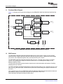
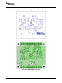
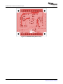
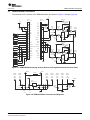
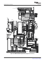
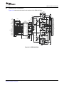
DEM-DSD1796/PCM1795/PCM1796/PCM1798 DSD1796/PCM1795/PCM1796/PCM1798 Evaluation Module User's Guide Literature Number: SLEU057A September 2004 – Revised May 2009 2 SLEU057A – September 2004 – Revised May 2009 Submit Documentation Feedback Contents Preface ............................................................................................................................... 5 1 1.1 1.2 1.3 1.4 1.5 1.6 1.7 1.8 1.9 2 2.1 2.2 2.3 2.4 2.5 ................................................................................................................ 7 Functional Block Diagram .................................................................................................. 8 EVM Features ................................................................................................................ 8 System Requirements ....................................................................................................... 9 Electrostatic Discharge Warning ........................................................................................... 9 Function Control for DAI Interface Format ............................................................................... 9 Reset Operation.............................................................................................................. 9 SW006 Operation Control for DAC ...................................................................................... 10 Jumper Connection ........................................................................................................ 10 Demonstration Software ................................................................................................... 10 Description ............................................................. 11 DEM-DAI/ASDAC Printed Circuit Board Layout ........................................................................ 12 DEM-AS/CDAC Printed Circuit Board Layout .......................................................................... 15 DEM-DAI/ASDAC Schematics............................................................................................ 17 DEM-AS/CDAC Schematics .............................................................................................. 19 Component Lists ........................................................................................................... 20 2.5.1 DEM-AS/CDAC_96/98 Parts List................................................................................ 20 2.5.2 DEM-DAI/ASDAC_96/98 Parts List ............................................................................. 20 Schematics, PCB Layout, and Bill of Materials Revision History ................................................................................................................. 22 Important Notices ............................................................................................................... 23 SLEU057A – September 2004 – Revised May 2009 Submit Documentation Feedback Contents 3 www.ti.com List of Figures 1-1 2-1 2-2 2-3 2-4 2-5 2-6 2-7 2-8 2-9 2-10 DEM-DSD1796/PCM1795/PCM1796/PCM1798 Block Diagram ...................................................... 8 DEM-DAI/ASDAC Silkscreen ............................................................................................. 12 DEM-DAI/ASDAC (Top View) ............................................................................................ 13 DEM-DAI/ASDAC (Bottom View)......................................................................................... 14 DEM-AS/CDAC Silkscreen ................................................................................................ 15 DEM-AS/CDAC (Top View) ............................................................................................... 15 DEM-AS/CDAC (Bottom View) ........................................................................................... 16 DEM-DAI/ASDAC Analog Section (Sockets for Daughterboard and Low-Pass Filter)............................ 17 DEM-DAI/ASDAC Connector and Regulator ........................................................................... 17 DEM-DAI/ASDAC Digital Section (Digital Audio Interface) ........................................................... 18 DEM-AS/CDAC ............................................................................................................. 19 List of Tables 1-1 1-2 2-1 2-2 4 Digital Audio Receiver Configuration ...................................................................................... 9 SW006 Options ............................................................................................................. 10 Bill of Materials ............................................................................................................. 20 Bill of Materials ............................................................................................................. 20 List of Figures SLEU057A – September 2004 – Revised May 2009 Submit Documentation Feedback Preface SLEU057A – September 2004 – Revised May 2009 Read This First About This Manual This document provides the information needed to set up and operate the DEM-DSD1796/PCM1795/PCM1796/PCM1798 EVM evaluation module, a test platform for the 24-bit, 192-kHz, sampling stereo DSD1796, PCM1795, PCM1796, and PCM1798 audio digital-to-analog converters (DACs). For a more detailed description of these devices, refer to the specific device product data sheet available from the Texas Instruments web site at http://www.ti.com. How to Use This Manual Throughout this document, the abbreviation EVM and the term evaluation module are synonymous with the DEM-DSD1796/PCM1795/PCM1796/PCM1798 EVM. Unless specifically noted, the information presented in this manual applies to the DSD1796, PCM1795, PCM1796, and PCM1798 audio stereo DACs. Chapter 1 describes the hardware setup guide for the EVM, including the necessary information required to configure the EVM switches and jumpers for product evaluation. This chapter also explains how to use the software provided with the DEM-DSD1796/PCM1795/PCM1796/PCM1798 EVM for controlling the DAC. Chapter 2 includes the EVM electrical schematics, printed circuit board (PCB) layouts, and the bills of material for both the DEM-DSD1796/PCM1795/PCM1796/PCM1798, the DEM-AS/CDAC, and the DEM-DAI/ASDAC. Information About Cautions and Warnings This document contains caution statements. CAUTION This is an example of a caution statement. A caution statement describes a situation that could potentially damage your software or equipment. The information in a caution or a warning is provided for your protection. Please read each caution and warning carefully. If You Need Assistance If you have questions regarding either the use of this evaluation module or the information contained in the accompanying documentation, please contact the Texas Instruments Product Information Center at (972) 644–5580 or visit the TI web site at www.ti.com. FCC Warning This equipment is intended for use in a laboratory test environment only. It generates, uses, and can radiate radio frequency energy and has not been tested for compliance with the limits of computing devices pursuant to subpart J of part 15 of FCC rules, which are designed to provide reasonable protection against radio frequency interference. Operation of this equipment in other environments may cause interference with radio communications, in which case the user at his own expense is required to take whatever measures may be required to correct this interference. Microsoft, Windows are registered trademarks of Microsoft Corporation. I2S is a trademark of NXP Semiconductors. TOSLINK is a trademark of Toshiba Corporation. All other trademarks are the property of their respective owners. SLEU057A – September 2004 – Revised May 2009 Submit Documentation Feedback Read This First 5 Trademarks www.ti.com Trademarks All trademarks are the property of their respective owners. 6 Read This First SLEU057A – September 2004 – Revised May 2009 Submit Documentation Feedback Chapter 1 SLEU057A – September 2004 – Revised May 2009 Description The DEM-DSD1796/PCM1795/PCM1796/PCM1798 is an evaluation fixture for the DSD1796/PCM1795/ PCM1796/PCM1798 series of 24-bit, 192-kHz sampling stereo DACs. This EVM provides all necessary connectors and circuitry for interfacing to audio test systems and commercial audio equipment. Topic 1.1 1.2 1.3 1.4 1.5 1.6 1.7 1.8 1.9 .................................................................................................. Page Functional Block Diagram ............................................................ 8 EVM Features ............................................................................. 8 System Requirements ................................................................. 9 Electrostatic Discharge Warning .................................................. 9 Function Control for DAI Interface Format ..................................... 9 Reset Operation.......................................................................... 9 SW006 Operation Control for DAC .............................................. 10 Jumper Connection ................................................................... 10 Demonstration Software ............................................................ 10 SLEU057A – September 2004 – Revised May 2009 Submit Documentation Feedback Description 7 Functional Block Diagram 1.1 www.ti.com Functional Block Diagram Figure 1-1 illustrates the functional block diagram of the DEM-DSD1796/PCM1795/PCM1796/PCM1798 EVM. I/V 5534a CN003 Serial Connector S/PDIF IN OPT Coax DAI CS8414 BAL Amp 5534a LchOUT (4.5 VRMS) BAL Amp 5534a RchOUT (4.5 VRMS) I/V 5534a DSDS1796 PCM1795 PCM1796 PCM1798 I/V 5534a SW001-003 Mode Control I/V 5534a DEM-AS/CDAC Daughter Card 3.3-V Regulator +VCC (5 V) ±AVCC (±15 V) Figure 1-1. DEM-DSD1796/PCM1795/PCM1796/PCM1798 Block Diagram 1.2 EVM Features The DEM-DSD1796/PCM1795/PCM1796/PCM1798 series of stereo DACs consist of a DAI (S/PDIF) section that uses a DSD1796/PCM1795/PCM1796/PCM1798 DAC section, a differential current/voltage (I/V) section, and a balanced amplifier with a post-low-pass filter (LPF) section. The DEM-DSD1796/PCM1795/PCM1796/PCM1798 requires a 5-V digital power supply for its digital circuits, a 5-V analog power supply for the device itself, and a ±15-V analog power supply for the balanced amplifier circuits. The DAI section has both coaxial and optical inputs that are switch-selectable and capable of handling sampling rates up to 96 kHz. The DSD1796/PCM1795/PCM1796/PCM1798 accepts PCM audio data input at a sampling rate up to 192 kHz, or a 64-fS DSD signal input, as determined by functional control settings and jumper connections on the board. This evaluation fixture uses the DEM-DSD1796/PCM1795/PCM1796/PCM1798 demonstration board and demonstration software for functional evaluation and operational control of the DSD1796/PCM1795/PCM1796/PCM1798 DAC device. 8 Description SLEU057A – September 2004 – Revised May 2009 Submit Documentation Feedback System Requirements www.ti.com 1.3 System Requirements The DEM-DSD1796/PCM1795/PCM1796/PCM1798 EVM has the following requirements: • ±15-V analog power supply at AVCC+, AVCC–, and GND • 5-V DAC power supply at VCC and GND • S/PDIF input (sampling rate fS is up to 96 kHz) connected at the coaxial or optical connector • RCA analog output connected at CN103 (Lch) and CN104 (Rch); analog full-scale output level is 4.5 VRMS. • PC connected to printer connector CN003 for demonstration software operation (if necessary) • Appropriate test module: – DEM-PCM1795: for PCM1795 – DEM-PCM1796: for PCM1796 – DEM-DSD1796: for DSD1796 – DEM-PCM1798: for PCM1798 1.4 Electrostatic Discharge Warning Many of the components on the DEM-DSD1796/PCM1795/PCM1796/PCM1798 EVM are susceptible to damage by electrostatic discharge (ESD). Customers are advised to observe proper ESD handling precautions when unpacking and handling the EVM, including the use of a grounded wrist strap at an approved ESD workstation. CAUTION Failure to observe ESD handling procedures may result in damage to EVM components. 1.5 Function Control for DAI Interface Format SW001, SW002, and SW003 are switches for controlling the audio interface format of the DAI receiver CS8414. The default audio interface format of the DSD1796/PCM1795/PCM1796/PCM1798 is I2S™ format. Table 1-1 lists the digital audio receiver configuration parameters. Table 1-1. Digital Audio Receiver Configuration SW002 SW003 Receiver Output Data Format L L L 16- to 24-bit left–justified L H L 16- to 24-bit l2S SW001 1.6 H L H 16-bit right-justified (or standard) L H H 18-bit right-justified (or standard) Reset Operation Pressing the SW004 pushbutton initiates a reset operation of the CS8414. SLEU057A – September 2004 – Revised May 2009 Submit Documentation Feedback Description 9 SW006 Operation Control for DAC 1.7 www.ti.com SW006 Operation Control for DAC Switch SW006 is the register set and reset control for the PCM1796 and DSD1796. The RESET section of the switch must be set to H except to perform a reset operation. Table 1-2 shows the options for SW006. Table 1-2. SW006 Options 1.8 SW006 RESET Function H Normal operation (default) L Reset operation Jumper Connection JP001 selects the normal or inverted BCK signal for 24-bit left-justified or other formats (I2S); the default position is I2S. 1.9 Demonstration Software Demonstration software is provided to control the PCM1796/DSD1796 internal register using a PC that is running the Microsoft® Windows® operating system. This software uses a printer cable to connect the PC to the DEM-PCM/DSD1796 connector CN003. The demonstration software includes a total of five files in the DEM1796 directory of the supplied CD. These files are: • DEM1796.exe • DEM1796.ini • Vbrjp200.dll • Ver.dll • Inpout.dll To load the software, first copy these files to a convenient directory (folder), such as: C:\DEM1796 Then, change the printer-port address in the DEM1796.ini initialization file to: &H378, &H278, or &H3BCO Most PCs use &H378 as the default printer-port address. 10 Description SLEU057A – September 2004 – Revised May 2009 Submit Documentation Feedback Chapter 2 SLEU057A – September 2004 – Revised May 2009 Schematics, PCB Layout, and Bill of Materials This chapter provides the DEM-DAI/ASDAC and the DEM-AS/CDAC printed circuit boards and schematics. The bill of materials (BOM) is included for component and manufacturer reference. Note: Board layouts are not to scale. These are intended to show how the board is laid out; they are not intended to be used for manufacturing DEM-DAI1753/54/55 EVM PCBs. Topic 2.1 2.2 2.3 2.4 2.5 .................................................................................................. DEM-DAI/ASDAC Printed Circuit Board Layout ............................. DEM-AS/CDAC Printed Circuit Board Layout ................................ DEM-DAI/ASDAC Schematics ..................................................... DEM-AS/CDAC Schematics ........................................................ Component Lists....................................................................... SLEU057A – September 2004 – Revised May 2009 Submit Documentation Feedback Page 12 15 17 19 20 Schematics, PCB Layout, and Bill of Materials 11 DEM-DAI/ASDAC Printed Circuit Board Layout 2.1 www.ti.com DEM-DAI/ASDAC Printed Circuit Board Layout Figure 2-1 through Figure 2-3 illustrate the printed circuit board (PCB) layout for the DEM-DAI/ASDAC. Figure 2-1. DEM-DAI/ASDAC Silkscreen 12 Schematics, PCB Layout, and Bill of Materials SLEU057A – September 2004 – Revised May 2009 Submit Documentation Feedback DEM-DAI/ASDAC Printed Circuit Board Layout www.ti.com Figure 2-2. DEM-DAI/ASDAC (Top View) SLEU057A – September 2004 – Revised May 2009 Submit Documentation Feedback Schematics, PCB Layout, and Bill of Materials 13 DEM-DAI/ASDAC Printed Circuit Board Layout www.ti.com Figure 2-3. DEM-DAI/ASDAC (Bottom View) 14 Schematics, PCB Layout, and Bill of Materials SLEU057A – September 2004 – Revised May 2009 Submit Documentation Feedback DEM-AS/CDAC Printed Circuit Board Layout www.ti.com 2.2 DEM-AS/CDAC Printed Circuit Board Layout Figure 2-4 through Figure 2-6 illustrate the PCB layout for the DEM-AS/CDAC. Figure 2-4. DEM-AS/CDAC Silkscreen Figure 2-5. DEM-AS/CDAC (Top View) SLEU057A – September 2004 – Revised May 2009 Submit Documentation Feedback Schematics, PCB Layout, and Bill of Materials 15 DEM-AS/CDAC Printed Circuit Board Layout www.ti.com Figure 2-6. DEM-AS/CDAC (Bottom View) 16 Schematics, PCB Layout, and Bill of Materials SLEU057A – September 2004 – Revised May 2009 Submit Documentation Feedback DEM-DAI/ASDAC Schematics www.ti.com 2.3 DEM-DAI/ASDAC Schematics The schematic for the sections of the DEM-DAI/ASDAC are shown in Figure 2-7 through Figure 2-9. VCC1 (NC) C101 10uF /16V RST MDO MUTE VCC VDD GND VDD GND GND (NC) GND (NC) RESET (NC) MDO (NC) MDI VOUTL MC MC VOUTL+ ML ML GND AGND AGND GND SCLK C105 8200pF VCC MDI CLKO R109 200 CN102 XB 3 7 20 CN101 XB 3 7 20 VDD D_SCLK VOUTR CLKO/D_BCK VOUTR+ P_SCLK C102 10uF /16V AVCC BCK P_BCK AVCC+ LRCK P_LRCK (NC) DATA P_DATA GND DSD_L GND U101 NJM5534 C103 0.027uF R103 220 R107 180 R111 200 AVCC+ C109 10uF /16V 7 2 6 3 R113 100 4 C107 8200pF CN103 RCA pj C111 10uF /16V AVCC AVCC AVCC+ R110 200 C106 8200pF (NC) DSD_R R105 180 R101 220 R106 180 R102 220 U102 NJM5534 C104 0.027uF R104 220 D SCLK R108 180 R112 200 D BCK AVCC+ 2 C110 10uF /16V 7 6 3 C108 8200pF CN104 RCA pj R114 100 4 C112 10uF /16V AVCC DSD R DSD L Figure 2-7. DEM-DAI/ASDAC Analog Section (Sockets for Daughterboard and Low-Pass Filter) VCC2 CN057 Banana Jack (Black) CN056 Banana Jack (Red) CN058 VCC1 CN055 Banana Jack (Black) VDD CN054 Banana Jack (Red) CN053 Banana Jack (Blue) CN052 Banana Jack (Gray) CN051 Banana Jack (Orange) AVCC+ U051 REG1117 3.3 2 OUT IN 3 GND 1 C055 0.1uF C058 0.1uF C057 100uF /16V C051 0.1uF C052 100uF /16V C053 100uF /16V C054 100uF /16V AVCC C056 10uF /16V Figure 2-8. DEM-DAI/ASDAC Connector and Regulator SLEU057A – September 2004 – Revised May 2009 Submit Documentation Feedback Schematics, PCB Layout, and Bill of Materials 17 DEM-DAI/ASDAC Schematics www.ti.com VDD 1 18 CN003 57LE 40360 7700(D3) 19 36 C014 0.1 uF U006 74VHC244 SW006 DSS104 1 1 VCC 2 19 2 [MDO] 3 18 3 [MDI] 4 17 5 16 6 15 7 14 8 13 4 [MC] [ML] RA001 47k x5 VCC2 CN002 FFC 2BMEP1 U002 2 3 C005 10uF C006 /16V 0.1uF 4 5 6 U001 TORX173 7 3 (TORX179P) 8 C002 0.01uF 9 10 C003 10uF /16V 11 C001 0.01uF 12 13 14 28 VERF C Cd/F1 Ce/F2 Cc/F0 SDATA CS8414 (L001) C004 0.1uF CN001 RCA pj Cb/E2 Ca/E1 ERF M1 M0 C0/E0 VD+ VA+ AGND DGND RXP FILT RXN MCK 26 2 25 3 12 C007 4 11 23 C008 10uF 22 0.1uF /16V 5 10 21 7 24 SCK M3 CS12/FCK SEL U CBL 6 EXT 17 0.1 uF 17 5 16 6 15 7 14 8 13 [DATA] 9 12 [e-DATA] (FIL001) (C016) 3 IN OUT 2 0.1uF VCC 4 [LRCK] 10 GND [e-DATA] [e-LRCK] 14 13 3 12 4 11 5 10 6 9 GND 8 CN006 XB 3 7 20 C017 10uF /16V [SCLK] [BCK] [LRCK] SW001 FT1D 2M SW002 SW003 FT1D 2M FT1D 2M [SCLK] JP001 FFC-4BMEP1 [DATA] [BCK] [BCK(INV)] [LRCK] [DATA] 11 GND U005 74VHC244 1 C012 10uF /16V [BCK] 20 18 [e-LRCK] SW004 FP1F 2M 8 VCC 2 19 [BCK] R004 470 0.1 uF 74VHC14 1 15 3 [e-BCK] 13 9 GND C010 U003 R002 470 16 2 [SCLK] D001 1SS133 14 18 C009 0.068uF 1 [e-SCLK] ML 19 M2 C013 VCC 7 [e-BCK] MC 20 FSYNC FT2D 2M 0.1 uF 74HCT32 1 SW005 R001 75 C011 U004 27 DAI select INT(CS8414) [e-SCLK] MDI R003 47k 1 2 456 MDO 11 GND CN007 XB-3-7-20 1 RST 12 9 10 C018 10uF /16V 20 [RST ] JP002 AGND FFC 2BMEP1 SCLK BCK LRCK (C015) 100uF/16V DATA DSD-L 24 (CN004) FFC 48BMEP1 1 DSD-R D-BCK D-SCLK 48 25 Figure 2-9. DEM-DAI/ASDAC Digital Section (Digital Audio Interface) 18 Schematics, PCB Layout, and Bill of Materials SLEU057A – September 2004 – Revised May 2009 Submit Documentation Feedback DEM-AS/CDAC Schematics www.ti.com 2.4 DEM-AS/CDAC Schematics Figure 2-10 shows the schematic for the sections of the DEM-AS/CDAC. C011 R005 Vcc1 2 GND GND RESET MDO MDI MC ML AGND D_SCLK CLKO/D_BCK P_SCLK DSD_R P_BCK P_LRCK P_DATA DSD_L (R001) C009 0.1uF U001 DSD1796 1 2 3 4 5 C002 6 0.1uF 7 8 9 10 C001 11 10uF/16V 12 13 14 VCC2L DSDR AGND3L DBCK IOUTL IOUTL+ PDATA/DFD/PDI AGND2 PBCK VCC1 SCKI VCOML DGND VCOMR VDD IREF MS AGND1 MDI IOUTR MC MDO RST (R003) (R004) IOUTR+ AGND3R VCC2R C004 0.1uF 28 27 26 25 24 C007 23 0.1uF 22 21 R002 20 10k 19 18 17 16 15 C003 10uF /16V U003 NJM5534 3 5 C016 22pF 4 R009 820 C018 10uF/16V C019 2700pF 8 820 C021 U004 NJM5534 C016 Jumper 3 5 C020 22pF C023 (R008) R010 2 U005 NJM5534 3 5 C024 22pF VCC VCC GND GND (NC) (NC) (NC) (NC) VOUTL VOUTL+ GND GND VOUTR VOUTR+ (NC) AVCC AVCC+ (NC) 10uF 7 /16V 6 8 4 2 (R007) C013 10uF/16V C017 10uF 7 /16V 6 2 C006 10uF /16V C005 10uF /16V 6 3 8 4 5 C010 C012 C014 Jumper 22pF 10uF/16V C015 2700pF R006 DSDL PLRCK/WDCK C008 10uF /16V Vcc1 820 7 U002 NJM5534 (NC) MUTE VDD VDD 2700pF GND GND C022 10uF/16V 2700pF 820 C025 10uF 7 /16V 6 8 4 C026 10uF/16V Figure 2-10. DEM-AS/CDAC SLEU057A – September 2004 – Revised May 2009 Submit Documentation Feedback Schematics, PCB Layout, and Bill of Materials 19 Component Lists 2.5 www.ti.com Component Lists 2.5.1 DEM-AS/CDAC_96/98 Parts List Table 2-1 lists the bill of materials for the DEM-AS/CDAC_96/98. Table 2-1. Bill of Materials Qty RefDes 11 C001, C003, C008, C013, C014, C017, C018, C021, C022, C025, C026 2 C002, C007 2 C004, C009 2 0 Item Value Mfr Part No 10 µF/16 V ROA–16V100M ELNA Film capacitor 0.1 µF AMFF0050J104 Nissei Chip film capacitor 0.1 µF ECHU1C104JB Matsushita C005, C006 AL ELE capacitor 10 µF/16 V ROA-16V100M ELNA C010, C027 Film capacitor 0.1 µF AMFF0050J104 Nissei 4 C011, C015, C019, C023 Film capacitor 2700 pF APSF0100J272 Nissei 4 C012, C016, C020, C024 Ceramic capacitor 22 pF RPE131CH220J50 Murata 1 R001 Resistor 47 kΩ SN14C2C–47kΩF KOA 1 R002 Resistor 10 kΩ SN14C2C–10kΩF KOA 2 R003, R007 Resistor 4.7 kΩ SN14C2C–4.7kΩF KOA Not mounted 6 R004, R005, R006, R008, R009, R010 Resistor 820Ω SN14C2C–820ΩF KOA R004, R008 not mounted 1 U001 DAC 28-pin, SSOP DSD1796 TIJ 8-pin, SOP NJM5534M JRC AL ELE capacitor Manufacturer Remarks Jumper connection Not mounted PCM1796 PCM1798 4 U002, U003, U004, U005 Op amp 2.5.2 DEM-DAI/ASDAC_96/98 Parts List Table 2-2 lists the bill of materials for the DEM-DAI/ASDAC_96/98. Table 2-2. Bill of Materials 20 Qty RefDes 2 C001, C002 Item Value Mfr Part No 0.01 µF AMFF0050J103 Nissei 7 C003, C005, C007, C109, C110, C111, C112 AL ELE capacitor 10 µF/16 V ROA-16V100M ELNA 6 C004, C006, C008, C016, C051, C058 Film capacitor 0.1 µF AMFF0050J104 Nissei 1 C009 5 C010, C011, C013, C014, C055 Film capacitor 0.068 µF AMFF0050J683 Nissei Ceramic capacitor 0.1 µF RPE132F104Z50 Murata 1 C012 AL ELE capacitor 10 µF/16 V SME16VB10M ELNA 5 C015, C052, C053, C054, C057 AL ELE capacitor 100 µF/16 V ROA-16V101M ELNA 1 C056 Tantalum capacitor 10 µF/16 V DN1C100M1S NEC 2 C101, C102, C017, C018 AL ELE capacitor 10 µF/16 V R3A-16V100M ELNA Nissei Film capacitor 2 C103, C104 Film capacitor 0.027 µF APSF0100J273 4 C105, C106, C107, C108 Film capacitor 8200 pF APSF0100J822 1 L001 Inductor Schematics, PCB Layout, and Bill of Materials Manufacturer Remarks C016 not mounted C015 not mounted C017, C108 not mounted Not mounted SLEU057A – September 2004 – Revised May 2009 Submit Documentation Feedback Component Lists www.ti.com Table 2-2. Bill of Materials (continued) Qty RefDes 1 FIL001 Filter Item Value Mfr Part No Manufacturer 1 CN003 L-type connector 57LE40360-7700(D3) Yamaichi 1 CN004 48-pin connector FFC-48BMEP1 Yamaichi 3 CN002, CN058, JP002 2-pin connector FFC-2BMEP1 Yamaichi 1 CN104 RCA connector (red) LPR6520-0802 SMK 1 CN103 RCA connector (white) LPR6520-0803 SMK 1 CN001 RCA connector (yellow) LPR6520-0804 SMK 1 CN051 Banana jack (yellow) T-45(Yellow) Honda 1 CN052 Banana jack (green) T-45(Green) Honda 1 CN053 Banana jack (blue) T-45(Blue) Honda 2 CN054, CN056 Banana jack (red) T-45(Red) Honda 2 CN055, CN057 Banana jack (black) T-45(Black) Honda 4 CN101, CN102, CN006, CN007 Connector 20-pin XB-3-7-20 MAC8 1SS133 ROHM 1 D001 Diode 1 JP001 4-pin connector 1 R001 Resistor 75 Ω SN14C2C-75ΩF KOA 1 R003 Resistor 47 kΩ SN14C2C-47kΩF KOA 2 R002, R004 Resistor 470 Ω SN14C2C-470ΩF KOA 4 R101–R104 Resistor 220 Ω SN14C2C-220ΩF KOA 4 R105–R108 Resistor 180 Ω SN14C2C-180ΩF KOA 4 R109–R112 Resistor 200 Ω SN14C2C-200ΩF KOA 2 R113, R114 Resistor 100 Ω SN14C2C-100ΩF KOA 1 RA001 Resitor array 47 kΩ × 5 M6-1-473J BI 1 U001 TOSLINK™ connector TORX179P Toshiba 1 U002 Digital audio I/F receiver IC CS8414-CS Cirrus Logic 1 U003 Logic IC TC74VHC14F TI 1 U004 Logic IC TC74HCT32AF TI 2 U005, U006 Logic IC TC74VHC244F TI 1 U051 2 U101, U102 3 SW001, SW002, SW003 1 SW004 1 SW005 1 SW006 4 — 3 JP101–JP103 FFC-4BMEP1 REG1117-3.3 TI/BB IC socket, DIP 8-pin 100-008-000 3M FT1D-2M Fujisoku Push switch FP1F-2M Fujisoku DIP switch ()ײ FT2D-2M Fujisoku DIP switch ()״ DSS104 Fujisoku Spacer AR-325B Nakao SLEU057A – September 2004 – Revised May 2009 Submit Documentation Feedback CN006, CN007 not mounted Yamaichi Regulator IC DIP switch Remarks Not mounted Schematics, PCB Layout, and Bill of Materials 21 Revision History www.ti.com Revision History Changes from Original (September, 2004) to A Revision .............................................................................................. Page • • Updated document format to current standards....................................................................................... 5 Added PCM1795 to devices relevant to this user guide ............................................................................. 5 NOTE: Page numbers for previous revisions may differ from page numbers in the current version. 22 Revision History SLEU057A – September 2004 – Revised May 2009 Submit Documentation Feedback EVALUATION BOARD/KIT IMPORTANT NOTICE Texas Instruments (TI) provides the enclosed product(s) under the following conditions: This evaluation board/kit is intended for use for ENGINEERING DEVELOPMENT, DEMONSTRATION, OR EVALUATION PURPOSES ONLY and is not considered by TI to be a finished end-product fit for general consumer use. Persons handling the product(s) must have electronics training and observe good engineering practice standards. As such, the goods being provided are not intended to be complete in terms of required design-, marketing-, and/or manufacturing-related protective considerations, including product safety and environmental measures typically found in end products that incorporate such semiconductor components or circuit boards. This evaluation board/kit does not fall within the scope of the European Union directives regarding electromagnetic compatibility, restricted substances (RoHS), recycling (WEEE), FCC, CE or UL, and therefore may not meet the technical requirements of these directives or other related directives. Should this evaluation board/kit not meet the specifications indicated in the User’s Guide, the board/kit may be returned within 30 days from the date of delivery for a full refund. THE FOREGOING WARRANTY IS THE EXCLUSIVE WARRANTY MADE BY SELLER TO BUYER AND IS IN LIEU OF ALL OTHER WARRANTIES, EXPRESSED, IMPLIED, OR STATUTORY, INCLUDING ANY WARRANTY OF MERCHANTABILITY OR FITNESS FOR ANY PARTICULAR PURPOSE. The user assumes all responsibility and liability for proper and safe handling of the goods. Further, the user indemnifies TI from all claims arising from the handling or use of the goods. Due to the open construction of the product, it is the user’s responsibility to take any and all appropriate precautions with regard to electrostatic discharge. EXCEPT TO THE EXTENT OF THE INDEMNITY SET FORTH ABOVE, NEITHER PARTY SHALL BE LIABLE TO THE OTHER FOR ANY INDIRECT, SPECIAL, INCIDENTAL, OR CONSEQUENTIAL DAMAGES. TI currently deals with a variety of customers for products, and therefore our arrangement with the user is not exclusive. TI assumes no liability for applications assistance, customer product design, software performance, or infringement of patents or services described herein. Please read the User’s Guide and, specifically, the Warnings and Restrictions notice in the User’s Guide prior to handling the product. This notice contains important safety information about temperatures and voltages. For additional information on TI’s environmental and/or safety programs, please contact the TI application engineer or visit www.ti.com/esh. No license is granted under any patent right or other intellectual property right of TI covering or relating to any machine, process, or combination in which such TI products or services might be or are used. FCC Warning This evaluation board/kit is intended for use for ENGINEERING DEVELOPMENT, DEMONSTRATION, OR EVALUATION PURPOSES ONLY and is not considered by TI to be a finished end-product fit for general consumer use. It generates, uses, and can radiate radio frequency energy and has not been tested for compliance with the limits of computing devices pursuant to part 15 of FCC rules, which are designed to provide reasonable protection against radio frequency interference. Operation of this equipment in other environments may cause interference with radio communications, in which case the user at his own expense will be required to take whatever measures may be required to correct this interference. EVM WARNINGS AND RESTRICTIONS It is important to operate this EVM within the input voltage range of ±15 V and the output voltage range of ±15 V. Exceeding the specified input range may cause unexpected operation and/or irreversible damage to the EVM. If there are questions concerning the input range, please contact a TI field representative prior to connecting the input power. Applying loads outside of the specified output range may result in unintended operation and/or possible permanent damage to the EVM. Please consult the EVM User's Guide prior to connecting any load to the EVM output. If there is uncertainty as to the load specification, please contact a TI field representative. During normal operation, some circuit components may have case temperatures greater than +55°C. The EVM is designed to operate properly with certain components above +55°C as long as the input and output ranges are maintained. These components include but are not limited to linear regulators, switching transistors, pass transistors, and current sense resistors. These types of devices can be identified using the EVM schematic located in the EVM User's Guide. When placing measurement probes near these devices during operation, please be aware that these devices may be very warm to the touch. Mailing Address: Texas Instruments, Post Office Box 655303, Dallas, Texas 75265 Copyright © 2009, Texas Instruments Incorporated IMPORTANT NOTICE Texas Instruments Incorporated and its subsidiaries (TI) reserve the right to make corrections, modifications, enhancements, improvements, and other changes to its products and services at any time and to discontinue any product or service without notice. Customers should obtain the latest relevant information before placing orders and should verify that such information is current and complete. All products are sold subject to TI’s terms and conditions of sale supplied at the time of order acknowledgment. TI warrants performance of its hardware products to the specifications applicable at the time of sale in accordance with TI’s standard warranty. Testing and other quality control techniques are used to the extent TI deems necessary to support this warranty. Except where mandated by government requirements, testing of all parameters of each product is not necessarily performed. TI assumes no liability for applications assistance or customer product design. Customers are responsible for their products and applications using TI components. To minimize the risks associated with customer products and applications, customers should provide adequate design and operating safeguards. TI does not warrant or represent that any license, either express or implied, is granted under any TI patent right, copyright, mask work right, or other TI intellectual property right relating to any combination, machine, or process in which TI products or services are used. Information published by TI regarding third-party products or services does not constitute a license from TI to use such products or services or a warranty or endorsement thereof. Use of such information may require a license from a third party under the patents or other intellectual property of the third party, or a license from TI under the patents or other intellectual property of TI. Reproduction of TI information in TI data books or data sheets is permissible only if reproduction is without alteration and is accompanied by all associated warranties, conditions, limitations, and notices. Reproduction of this information with alteration is an unfair and deceptive business practice. TI is not responsible or liable for such altered documentation. Information of third parties may be subject to additional restrictions. Resale of TI products or services with statements different from or beyond the parameters stated by TI for that product or service voids all express and any implied warranties for the associated TI product or service and is an unfair and deceptive business practice. TI is not responsible or liable for any such statements. TI products are not authorized for use in safety-critical applications (such as life support) where a failure of the TI product would reasonably be expected to cause severe personal injury or death, unless officers of the parties have executed an agreement specifically governing such use. Buyers represent that they have all necessary expertise in the safety and regulatory ramifications of their applications, and acknowledge and agree that they are solely responsible for all legal, regulatory and safety-related requirements concerning their products and any use of TI products in such safety-critical applications, notwithstanding any applications-related information or support that may be provided by TI. Further, Buyers must fully indemnify TI and its representatives against any damages arising out of the use of TI products in such safety-critical applications. TI products are neither designed nor intended for use in military/aerospace applications or environments unless the TI products are specifically designated by TI as military-grade or "enhanced plastic." Only products designated by TI as military-grade meet military specifications. Buyers acknowledge and agree that any such use of TI products which TI has not designated as military-grade is solely at the Buyer's risk, and that they are solely responsible for compliance with all legal and regulatory requirements in connection with such use. TI products are neither designed nor intended for use in automotive applications or environments unless the specific TI products are designated by TI as compliant with ISO/TS 16949 requirements. Buyers acknowledge and agree that, if they use any non-designated products in automotive applications, TI will not be responsible for any failure to meet such requirements. Following are URLs where you can obtain information on other Texas Instruments products and application solutions: Products Amplifiers Data Converters DLP® Products DSP Clocks and Timers Interface Logic Power Mgmt Microcontrollers RFID RF/IF and ZigBee® Solutions amplifier.ti.com dataconverter.ti.com www.dlp.com dsp.ti.com www.ti.com/clocks interface.ti.com logic.ti.com power.ti.com microcontroller.ti.com www.ti-rfid.com www.ti.com/lprf Applications Audio Automotive Broadband Digital Control Medical Military Optical Networking Security Telephony Video & Imaging Wireless www.ti.com/audio www.ti.com/automotive www.ti.com/broadband www.ti.com/digitalcontrol www.ti.com/medical www.ti.com/military www.ti.com/opticalnetwork www.ti.com/security www.ti.com/telephony www.ti.com/video www.ti.com/wireless Mailing Address: Texas Instruments, Post Office Box 655303, Dallas, Texas 75265 Copyright © 2009, Texas Instruments Incorporated