1
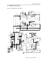
DEMĆDAI3010 User’s Guide April 2003 DAV Digital Audio/Speaker SLEU036 IMPORTANT NOTICE Texas Instruments Incorporated and its subsidiaries (TI) reserve the right to make corrections, modifications, enhancements, improvements, and other changes to its products and services at any time and to discontinue any product or service without notice. Customers should obtain the latest relevant information before placing orders and should verify that such information is current and complete. All products are sold subject to TI’s terms and conditions of sale supplied at the time of order acknowledgment. TI warrants performance of its hardware products to the specifications applicable at the time of sale in accordance with TI’s standard warranty. Testing and other quality control techniques are used to the extent TI deems necessary to support this warranty. Except where mandated by government requirements, testing of all parameters of each product is not necessarily performed. TI assumes no liability for applications assistance or customer product design. Customers are responsible for their products and applications using TI components. To minimize the risks associated with customer products and applications, customers should provide adequate design and operating safeguards. TI does not warrant or represent that any license, either express or implied, is granted under any TI patent right, copyright, mask work right, or other TI intellectual property right relating to any combination, machine, or process in which TI products or services are used. Information published by TI regarding third–party products or services does not constitute a license from TI to use such products or services or a warranty or endorsement thereof. Use of such information may require a license from a third party under the patents or other intellectual property of the third party, or a license from TI under the patents or other intellectual property of TI. Reproduction of information in TI data books or data sheets is permissible only if reproduction is without alteration and is accompanied by all associated warranties, conditions, limitations, and notices. Reproduction of this information with alteration is an unfair and deceptive business practice. TI is not responsible or liable for such altered documentation. Resale of TI products or services with statements different from or beyond the parameters stated by TI for that product or service voids all express and any implied warranties for the associated TI product or service and is an unfair and deceptive business practice. TI is not responsible or liable for any such statements. Mailing Address: Texas Instruments Post Office Box 655303 Dallas, Texas 75265 Copyright 2003, Texas Instruments Incorporated EVM IMPORTANT NOTICE Texas Instruments (TI) provides the enclosed product(s) under the following conditions: This evaluation kit being sold by TI is intended for use for ENGINEERING DEVELOPMENT OR EVALUATION PURPOSES ONLY and is not considered by TI to be fit for commercial use. As such, the goods being provided may not be complete in terms of required design-, marketing-, and/or manufacturing-related protective considerations, including product safety measures typically found in the end product incorporating the goods. As a prototype, this product does not fall within the scope of the European Union directive on electromagnetic compatibility and therefore may not meet the technical requirements of the directive. Should this evaluation kit not meet the specifications indicated in the EVM User’s Guide, the kit may be returned within 30 days from the date of delivery for a full refund. THE FOREGOING WARRANTY IS THE EXCLUSIVE WARRANTY MADE BY SELLER TO BUYER AND IS IN LIEU OF ALL OTHER WARRANTIES, EXPRESSED, IMPLIED, OR STATUTORY, INCLUDING ANY WARRANTY OF MERCHANTABILITY OR FITNESS FOR ANY PARTICULAR PURPOSE. The user assumes all responsibility and liability for proper and safe handling of the goods. Further, the user indemnifies TI from all claims arising from the handling or use of the goods. Please be aware that the products received may not be regulatory compliant or agency certified (FCC, UL, CE, etc.). Due to the open construction of the product, it is the user’s responsibility to take any and all appropriate precautions with regard to electrostatic discharge. EXCEPT TO THE EXTENT OF THE INDEMNITY SET FORTH ABOVE, NEITHER PARTY SHALL BE LIABLE TO THE OTHER FOR ANY INDIRECT, SPECIAL, INCIDENTAL, OR CONSEQUENTIAL DAMAGES. TI currently deals with a variety of customers for products, and therefore our arrangement with the user is not exclusive. TI assumes no liability for applications assistance, customer product design, software performance, or infringement of patents or services described herein. Please read the EVM User’s Guide and, specifically, the EVM Warnings and Restrictions notice in the EVM User’s Guide prior to handling the product. This notice contains important safety information about temperatures and voltages. For further safety concerns, please contact the TI application engineer. Persons handling the product must have electronics training and observe good laboratory practice standards. No license is granted under any patent right or other intellectual property right of TI covering or relating to any machine, process, or combination in which such TI products or services might be or are used. Mailing Address: Texas Instruments Post Office Box 655303 Dallas, Texas 75265 Copyright 2003, Texas Instruments Incorporated EVM WARNINGS AND RESTRICTIONS It is important to operate this EVM within the input voltage range of ±15 V and the output voltage range of ±15 V. Exceeding the specified input range may cause unexpected operation and/or irreversible damage to the EVM. If there are questions concerning the input range, please contact a TI field representative prior to connecting the input power. Applying loads outside of the specified output range may result in unintended operation and/or possible permanent damage to the EVM. Please consult the EVM User’s Guide prior to connecting any load to the EVM output. If there is uncertainty as to the load specification, please contact a TI field representative. During normal operation, some circuit components may have case temperatures greater than 55°C. The EVM is designed to operate properly with certain components above 55°C as long as the input and output ranges are maintained. These components include but are not limited to linear regulators, switching transistors, pass transistors, and current sense resistors. These types of devices can be identified using the EVM schematic located in the EVM User’s Guide. When placing measurement probes near these devices during operation, please be aware that these devices may be very warm to the touch. Mailing Address: Texas Instruments Post Office Box 655303 Dallas, Texas 75265 Copyright 2003, Texas Instruments Incorporated Contents Contents 1 Description . . . . . . . . . . . . . . . . . . . . . . . . . . . . . . . . . . . . . . . . . . . . . . . . . . . . . . . . . . . . . . . . . . . . . 1.1 Block Diagram . . . . . . . . . . . . . . . . . . . . . . . . . . . . . . . . . . . . . . . . . . . . . . . . . . . . . . . . . . . . . 1.2 Use of the DEM-DAI3010 . . . . . . . . . . . . . . . . . . . . . . . . . . . . . . . . . . . . . . . . . . . . . . . . . . . . 1.2.1 Initial Settings of the DEM-DAI3010 (at shipping) . . . . . . . . . . . . . . . . . . . . . . . . 1.2.2 How to Connect Power Supplies to the DEM-DAI3010 . . . . . . . . . . . . . . . . . . . 1.3 Settings and Connections for Basic Operation . . . . . . . . . . . . . . . . . . . . . . . . . . . . . . . . . . 1.4 Setting Functions . . . . . . . . . . . . . . . . . . . . . . . . . . . . . . . . . . . . . . . . . . . . . . . . . . . . . . . . . . . 1.4.1 Function Setting Switches and Header Pins . . . . . . . . . . . . . . . . . . . . . . . . . . . . . 1.4.2 Detailed Explanation of Function Setting Switches and Header Pins . . . . . . . . 1-1 1-2 1-3 1-3 1-3 1-4 1-5 1-5 1-6 2 Printed-Circuit Board and Schematic . . . . . . . . . . . . . . . . . . . . . . . . . . . . . . . . . . . . . . . . . . . . . 2-1 2.1 DEM-DAI3010 Printed-Circuit Board . . . . . . . . . . . . . . . . . . . . . . . . . . . . . . . . . . . . . . . . . . 2-2 2.2 DEM-DAI3010 Schematics . . . . . . . . . . . . . . . . . . . . . . . . . . . . . . . . . . . . . . . . . . . . . . . . . . . 2-5 Figures 1–1 2–1 2–2 2–3 2–4 2–5 2–6 DEM-DAI3010 Block DIagram . . . . . . . . . . . . . . . . . . . . . . . . . . . . . . . . . . . . . . . . . . . . . . . . . . DEM-DAI3010 Silkscreen . . . . . . . . . . . . . . . . . . . . . . . . . . . . . . . . . . . . . . . . . . . . . . . . . . . . . . DEM-DAI3010—Top View . . . . . . . . . . . . . . . . . . . . . . . . . . . . . . . . . . . . . . . . . . . . . . . . . . . . . . DEM-DAI3010—Bottom View . . . . . . . . . . . . . . . . . . . . . . . . . . . . . . . . . . . . . . . . . . . . . . . . . . . DEM-DAI3010 Analog Section . . . . . . . . . . . . . . . . . . . . . . . . . . . . . . . . . . . . . . . . . . . . . . . . . . DEM-DAI3010 Regulator, Connector and Ext.-I/F . . . . . . . . . . . . . . . . . . . . . . . . . . . . . . . . . . DEM-DAI3010 Digital Section (Digital Audio Interface) . . . . . . . . . . . . . . . . . . . . . . . . . . . . . 1-2 2-2 2-3 2-4 2-5 2-6 2-7 Tables 1–1 1–2 1–3 Initial Settings of the DEM-DAI3010 at Shipping . . . . . . . . . . . . . . . . . . . . . . . . . . . . . . . . . . . 1-3 Power Supply Terminals and Supply Voltage (Depending on CN057 Setting) . . . . . . . . . . 1-3 Switches and Header Pins of the DEM-DAI3010 . . . . . . . . . . . . . . . . . . . . . . . . . . . . . . . . . . 1-5 v Contents vi Chapter 1 Description The DEM-DAI3010 is an evaluation board for the PCM3010 (24-bit, 96-kHz ADC and 192-kHz DAC, stereo codec). This board includes not only the PCM3010 but also analog I/O terminals, analog filter circuits, and an S/PDIF digital I/O circuit that is useful for codec evaluation. S/PDIF I/O circuits consist of a 24-bit/96-kHz digital audio interface receiver (DIR1703) and a digital audio interface transmitter (DIT4096), and include optical (TOSLINK) and coaxial S/PDIF digital I/O connectors. Removing shorting plugs from the pins of a header breaks the connection between the S/PDIF I/O circuits and the PCM3010for easier PCM3010 device evaluation. Topic Page 1.1 Block Diagram . . . . . . . . . . . . . . . . . . . . . . . . . . . . . . . . . . . . . . . . . . . . . . . . 1-2 1.2 Use of the DEM-DAI3010 . . . . . . . . . . . . . . . . . . . . . . . . . . . . . . . . . . . . . . . 1-3 1.3 Settings and Connections for Basic Operation . . . . . . . . . . . . . . . . . . 1-4 1.4 Setting Functions . . . . . . . . . . . . . . . . . . . . . . . . . . . . . . . . . . . . . . . . . . . . . 1-5 1-1 Block Diagram 1.1 Block Diagram Figure 1–1. DEM-DAI3010 Block DIagram System Clock Data Format Clock Mode X’tal Frequency System Clock SW003 SW004 JP001 DAC Output S/PDIF Input OPT. IN L-ch Output JP107 SW001 LPF PCM3010 DIR1703 R-ch Output (Slave Only) LPF COAX. IN ADC Input 24.576 MHz L-ch 1Vrms JP105 L-ch 2Vrms S/PDIF Output OPT. OUT LPF SW051 DIT4096 COAX. OUT R-ch 1Vrms JP106 74HCT244 R-ch 2Vrms LPF SW005 SW006 SW101 System Clock Data Format Channel Status System Clock Data Format Power Down ±15 V LPF Circuits 5V PCM3010 VCC and DIR1703, DIT4096, TOSLINK CN057 3.3 V 3.3 V 1-2 PCM3010 VDD Use of the DEM-DAI3010 1.2 Use of the DEM-DAI3010 The DEM-DAI3010 is shipped with standard settings preset. Therefore, connecting power supplies (15-V, –15-V and 5-V) is the only requirement to prepare the board for use, unless nonstandard settings are desired. 1.2.1 Initial Settings of the DEM-DAI3010 (at shipping) Table 1–1. Initial Settings of the DEM-DAI3010 at Shipping Item Initial Setting (at shipping) Power supply voltage 15 V, –15 V, and 5 V (close CN57) Power supply terminals CN51–CN55 (open CN56) Connection of PCM3010 and S/PDIF I/O DIR1703 and DIT4096 connected with JP107 DIR1703 system clock (SCK) 256 fS DIR1703 output audio data format I2S DIR1703 crystal clock frequency 24.576 MHz (load capacitance: 18 pF) DIT4096 system clock (SCLK) 256 fS DIT4096 input audio data format I2S PCM3010 system clock Automatic selection (no setting required) PCM3010 I/O audio data format I2S PCM3010 power-down function Disabled PCM3010 de-emphasis function (DAC) Disabled PCM3010 DAC cutoff frequency 54 kHz (JP101–JP104 are closed) PCM3010 ADC input terminal selection CN101, CN102: 2-V rms input (with LPF) 1.2.2 How to Connect Power Supplies to the DEM-DAI3010 The DEM-DAI3010 requires 5-V, 15-V, and –15-V power supplies. Power is supplied to this board by five binding posts (one each for VCC = +5 V, +AVCC = +15 V, –AVCC = –15 V, and two for ground) from stabilized dc power supplies. VDD (3.3 V) for the PCM3010 is normally generated by an onboard voltage-regulator IC from VCC (5 V), but it is possible to supply 3.3 V directly. To do so, open CN057, then supply 3.3 V to CN056 and 5 V to CN054. If 3.3 V is supplied externally, 5 V must still be provided to CN054 in order to supply the analog section of the PCM3010. To avoid latch-up of the PCM3010, ensure that VCC and VDD are powered up simultaneously. Table 1–2. Power Supply Terminals and Supply Voltage (Depending on CN057 Setting) Power Terminal CN057 Closed (Default) CN057 Open CN051 (orange) 15 V 15 V CN052 (green) 0 V (ground) 0 V (ground) CN053 (blue) –15 V –15 V CN054 (red) 5V 5V CN055 (black) 0 V (ground) 0 V (ground) CN056 (2-pin connector) Open (no connection) 3.3 V Description 1-3 Settings and Connections for Basic Operation 1.3 Settings and Connections for Basic Operation The PCM3010 is an LSI codec containing an ADC and a DAC. Connections and settings depend on the evaluation object (ADC or DAC), and the setup should be checked carefully. Following are example settings for three typical evaluation situations. Note that when using S/PDIF I/O, the optical and coaxial input corresponds to fS = 96 kHz. When the DAC section of PCM3010 is evaluated with S/PDIF input signal (the PCM3010 operates as a slave of the DIR1703 PLL clock) - Close all pins of JP107 with shorting plugs. - Input an S/PDIF signal into the optical (U053) or coaxial (CN059) connector. - CN105 (L-ch) and CN106 (R-ch) are the analog signal outputs. - Choose an S/PDIF input terminal (optical/coaxial) with the S/PDIF input switch (SW051). - Set the clock-mode switch (SW004) to PLL or Auto. - The cutoff frequency of the LPF can be changed by JP101, JP102, JP103, and JP104. All these jumpers are shorted at the time of shipment, which sets the cutoff frequency to 20 kHz. When the ADC section of PCM3010 is evaluated with S/PDIF output signal (the PCM3010 operates as a slave of the DIR1703 crystal clock) - Short all pins of JP107 with shorting plugs. - Connect an analog signal to CN101/CN102 using an LPF, or to CN103/ CN104 using only a coupling capacitor without an LPF. - Select the analog input terminal by changing by the settings of JP105 and JP106. (Setup at the time of shipment is for CN101 and CN102.) - A Toslink (U052) and a pin jack (CN058) are the S/PDIF digital output terminals. Select the digital output connector by setting the S/PDIF output switch (SW051). Simultaneous use of optical and coaxial outputs is impossible. - Set the clock mode switch (SW004) to X’tal. The X’tal mode of DIR1703 is used as a master clock for the ADC and DIT. - Set up the channel status data using SW006. - Because system clock frequency is 256 fS, the ADC section operates at fS = 96 kHz. To operate the ADC section at a different fS, the crystal (X001) connected to DIR1703 must be changed. The system clock setup can be changed if required. The load capacitance used with the crystal is dependent on the crystal properties. Therefore, when the crystal is changed, the capacitance of C006 and C007 must be selected to match the crystal specification. When S/PDIF I/O is not used (the PCM3010 is evaluated alone) - Remove all shorting plugs attached to JP107. 1-4 Setting Functions - Data and a clock are supplied to the PCM3010 side of JP107. - Set up FMT0 and FMT1 of SW101 according to the data format to be used. - Set up DEMP0 and DEMP1 of SW101 for the desired de-emphasis of the DAC section and PWDN for the power-down setting. 1.4 Setting Functions All functions of the devices (PCM3010, DIR1703, DIT4096) on the DEM-DAI3010 are controlled by DIP switches or header pins on this PCB. Therefore, the DEM-DAI3010 does not require a microcontroller or software to transmit data to internal function-setting registers. For specific information on any device, see the data sheet for that device. 1.4.1 Function Setting Switches and Header Pins Table 1–3. Switches and Header Pins of the DEM-DAI3010 SW/JP No. Item Shape SW001 S/PDIF input selection (optical/coax) Toggle switch SW002 Reset of DIR1703 and DIT4096 Pushbutton switch SW003 Format and system clock setting of DIR1703 4-pole DIP switch SW004 Output clock selection of DIR1703 (X’tal/Auto/PLL) Toggle switch SW005 Format and system clock setting of DIT4096 4-pole DIP switch SW006 Channel status data setting of DIT4096 10-pole DIP switch SW051 S/PDIF output selection (optical/coax) Toggle switch SW101 Setting of PCM3010 (format, de-emphasis, power down) 5-pole DIP switch JP001 Crystal frequency and system clock setting of DIR1703 2×5 header JP107 Connection of S/PDIF I/O circuit and PCM3010 2×7 header JP101 Cutoff frequency setting of DAC output filter (L-ch) 2×2 header JP102 Cutoff frequency setting of DAC output filter (R-ch) 2×2 header JP103 Cutoff frequency setting of DAC output filter (L-ch) 2×1 header JP104 Cutoff frequency setting of DAC output filter (R-ch) 2×1 header JP105 Selection of L-ch ADC input terminal (CN101/CN103) 2×2 header JP106 Selection of R-ch ADC input terminal (CN102/CN104) 2×2 header CN057 The way of power supply of PCM3010 VDD (3.3 V) 2×1 header Note: The relation between the DIP switch setting (ON/OFF) and the setting of the IC input port is printed on the PCB. The DIP switch H position does not always set the IC input port level HIGH. Toggle switch settings are printed on the PCB. Description 1-5 Setting Functions 1.4.2 Detailed Explanation of Function Setting Switches and Header Pins SW001: Switch to select S/PDIF input connector (optical/coaxial). Selection of the S/PDIF signal that is routed to the DIR1703 DIN port. SW002: Reset switch for the DIR1703 and DIT4096. Pushing this switch resets the DIR1703 and DIT4096 to the initial state. A reset circuit operates at the time of power-supply connection, resetting the DIR1703 and DIT4096 automatically. Therefore, it is not usually necessary to operate this switch. SW003: Switch for setting the DIR1703 system clock and output data format SCF1 SCF0 System Clock L L 128 fS L H 256 fS (initial stting) H L 384 fS H H 512 fS FMT1 FMT0 Output Data Format L L 16-bit right-justified, MSB-first L H 24-bit right-justified, MSB-first H L 24-bit left-justified, MSB-first H H 24-bit, I2S (initial setting) SW004: Switch for setting the DIR1703 output clock source Position Output Clock (SCK, BCK, LRCK) X’tal Crystal clock PLL PLL clock Auto PLL (PLL locked) / crystal (PLL unlocked) Note: When using the DIR1703 as a master clock for the ADC, this switch must be set to X’tal. When inputting S/PDIF data demodulated by the DIR1703 into the DAC, set this switch to Auto or PLL. SW005: 1-6 Switch for setting the DIT4096 system clock and input data format Note that the OFF state of this switch sets a HIGH level. CLK1 CLK0 System Clock L L Not used L H 256 fS (initial setting) H L 384 fS H H 512 fS Setting Functions FMT1 FMT0 Input Data Format L L 24-bit, left-justified, MSB-first L H 24-bit, I2S (initial setting) H L 24-bit, right-justified, MSB-first H H 16-bit, right-justified, MSB-first SW006: Switch for setting channel-status data of the DIT4096. Note that the OFF state of this switch sets a HIGH level. Channel status data can set up if needed. Moreover, it is also possible to connect a microcontroller to CN002 and to write in channel-status data with the microcontroller. See the DIT4096 data sheet (TI literature number SBOS225) for details about the contents of a setting. SW051: Switch to select the S/PDIF output connector (optical/coaxial). An S/PDIF output connector is chosen from optical (U052) and coaxial (CN058). The optical and coaxial output terminals cannot be used simultaneously. SW101: Switch for setting the functions of the PCM3010. All the functions of PCM3010 are set up with this switch. Functions that can be set are the audio serial data I/O format, the DAC section de-emphasis, and power-down control. FMT1 FMT0 DAC Input Data Format ADC Output Data Format L L 24-bit, right-justified, MSB-first 24-bit, left-justified, MSB-first L H 16-bit, right-justified, MSB-first 24-bit, left-justified, MSB-first H L 24-bit, left-justified, MSB-first 24-bit, left-justified, MSB-first H H 24-bit, I2S (initial setting) 24-bit, I2S (initial setting) DEMP1 DEMP0 DAC De-Emphasis L L De-emphasis ON, 44.1-kHz L H De-emphasis OFF (initial setting) H L De-emphasis ON, 48-kHz H H De-emphasis ON, 32-kHz PDOWN Power-Down Control L Power-down mode H Nomal operation (initial setting) JP001: Setup of the crystal frequency and system clock for the DIR1703. When the system clock and the frequency of the crystal for the DIR1703 are changed, a shorting plug is inserted in only one position of JP001 according to the following tables. In order to avoid the loss of a shorting plug which is not being used, the plug is put in the header pin position labeled as OPEN. Because 24.576 MHz is used for a quartz crystal and the system clock is set as the 256 fS output in initial setting at the time of shipment, the shorting plug is attached in the CSBIT position. Description 1-7 Setting Functions JP001 setting table: DIR1703 system clock and crystal frequency fS in X’tal Mode 128 fS 256 fS 384 fS 512 fS BRSEL Jumper Position 32 kHz 4.096 MHz 8.192 MHz 12.288 MHz 16.384 MHz BFRAME 44.1 kHz 5.6448 MHz 11.2896 MHz 16.9344 MHz 22.5792 MHz EMFLG 48 kHz 6.144 MHz 12.288 MHz 18.432 MHz 24.576 MHz OPEN (no jumper) 88.2 kHz 11.2896 MHz 22.5792 MHz 33.8688 MHz 45.1584 MHz URBIT 96 kHz 12.288 MHz 24.576 MHz 36.864 MHz 49.152 MHz CSBIT Sample of a of JP001 setting Target: system clock: 256 fS and fS = 48 kHz in the X’tal mode In the preceding table, the frequency listed where the 256-fS column intersects the 48-kHz row is 12.288 MHz. JP101–JP104: Cutoff frequency setting of DAC output post-LPF The cutoff frequency of the LPF inserted in the DAC output is chosen by these jumpers. The initial setting (all pins shorted) is 54 kHz at the time of shipment. The cutoff frequency with all JP101–JP104 jumper pins open is 108 kHz. JP105–JP106: Selection of ADC input connectors (CN101 and CN102 or CN103 and CN104) There are two pairs of ADC input connectors. One pair is coupled to the PCM3010 through capacitors (C121, C122). The other pair is connected through a 103-kHz cutoff LPF and a –6 dB amplifier. The input connectors are chosen by JP105 and JP106. When the jumpers are on Direct-IN, then the left- and right-channel inputs on CN103 and CN104, respectively, bypass the LPF. When the jumpers are on –6 db/LPF, then the left- and right-channel inputs on CN101 and CN102, respectively, go through the LPF to the PCM3010. ADC Full-Scale Input Connector No. Details L-ch 2 V rms CN101 L-ch ADC input with LPF R-ch 2 V rms CN102 R-ch ADC input with LPF L-ch 1 V rms CN103 L-ch ADC input without LPF R-ch 1 V rms CN104 R-ch ADC input without LPF JP107: Connection of PCM3010 and S/PDIF I/O circuits This is the header pin which connects the clock input and data I/O of the PCM3010 with an S/PDIF I/O circuit. All pin positions have shorting plugs installed at the time of shipment. For evaluating the PCM3010 with other DSPs, DIRs, and DITs, JP107 jumpers are removed. Connection to the alternative devices is made through the row of JP107 pins that is wired to the PCM3010. 1-8 Setting Functions CN057: VCC supply selection for the PCM3010 This jumper determines whether VCC for the PCM3010 is supplied from a 3.3-V regulator on this board (U051), or via an external power supply terminal (CN056). In the initial setting, VCC is supplied from the onboard regulator. When VCC for the PCM3010 is to be provided by an external power supply, the jumper is removed from CN057 and 3.3 V is supplied to CN056. If 3.3 V is supplied externally, 5 V must still be provided to CN054 in order to supply the analog section of the PCM3010. To avoid latch-up of the PCM3010, ensure that VCC and VDD are switched on simultaneously at start-up. Description 1-9 1-10 Chapter 2 Printed-Circuit Board and Schematic This chapter presents the DEM-DAI3010 printed-circuit board and schematics. Topic Page 2.1 DEM-DAI3010 Printed-Circuit Board . . . . . . . . . . . . . . . . . . . . . . . . . . . . 2-2 2.2 DEM-DAI3010 Schematics . . . . . . . . . . . . . . . . . . . . . . . . . . . . . . . . . . . . . 2-5 Printed-Circuit Board and Schematic 2-1 DEM-DAI3010 Printed-Circuit Board 2.1 DEM-DAI3010 Printed-Circuit Board Figure 2–1. DEM-DAI3010 Silkscreen 2-2 DEM-DAI3010 Printed-Circuit Board Figure 2–2. DEM-DAI3010—Top View Printed-Circuit Board and Schematic 2-3 DEM-DAI3010 Printed-Circuit Board Figure 2–3. DEM-DAI3010—Bottom View 2-4 DEM-DAI3010 Schematics 2.2 DEM-DAI3010 Schematics Figure 2–4. DEM-DAI3010 Analog Section R113 C119 1.2k 100pF C117 330pF R117 4.7k C121 CN101 R109 2.4k RCA pj 2 10uF /16V R111 3.3k AVCC+ JP105 1 6 8 FFC–4BMEP1 7 5 U102 4 10uF/16V OPA2134PA 2/2 C 115 1800pF 3 C123 R115 4.7k C113 10uF /16V C125 U102 10uF/16V OPA2134PA 1/2 CN103 RCA AVCC– R114 pj 1.2k C120 100pF C118 330pF R118 4.7k CN102 R110 2.4k R112 3.3k AVCC+ C122 RCA pj 2 10uF JP106 /16V FFC–4BMEP1 1 6 8 7 5 U103 10uF/16V OPA2134PA 2/2 C116 1800pF 3 C124 R116 4.7k 4 U103 C114 10uF /16V C126 OPA2134PA 10uF/16V 1/2 CN104 RCA AVCC– pj VCC C138 U104 PCM3010 C128 /16V C127 0.1uF 1 2 3 C130 10uF/16V 4 C129 0.1uF 5 C132 6 10uF/16V C131 0.1uF 7 8 9 10 11 12 R120 R121 0 0 VINL VCOM VINR VOUTL VREF1 VREF2 VCC1 PCM3010 10uF C137 0.1uF VOUTR VCC2 AGND2 AGND1 DEMP0 FMT0 DEMP1 FMT1 PDWN TEST SCKI LRCK VDD BCK DGND DIN DOUT 10uF R105 15k /16V C101 24 10uF 23 /16V C109 C135 22 21 120pF C136 20 10uF/16V R101 8.2k R103 1k 0.1uF 19 JP103 JP101 2/2 C107 120pF 18 1 17 VDD 16 15 R107 100 2 JP101 1/2 3 C105 1200pF C103 1200pF 4 CN105 RCA U101 OPA2134A 1/2 14 AVCC+ 13 C133 C134 0.1uF 10uF /16V C111 JP101/102: FFC–4BMEP1 10uF JP103/104: FFC–2BMEP1 /16V C102 C112 R106 15k 10uF 10uF /16V /16V R119 220 JP107 FFC–12BMEP1 C110 5 4 GND 3 TX–DATA 2 SCLK BCK LRCK RX–DATA SW101 DSS105 pj 1 JP102 2/2 FMT0 R102 8.2k FMT1 DEMP0 DEMP1 PDWN C104 1200pF AVCC– 120pF R104 1k C108 120pF 6 JP102 1/2 JP104 R108 100 8 CN106 RCA pj 7 C106 1200pF 5 U101 OPA2134A 2/2 Printed-Circuit Board and Schematic 2-5 DEM-DAI3010 Schematics Figure 2–5. DEM-DAI3010 Regulator, Connector and Ext.-I/F CN056 B2P–VH CN055 banana jack V DD 2 1 (Black) U051 REG1117–3.3 CN057 CN054 CN053 CN052 banana jack banana jack banana jack CN051 banana jack (Red) (Orange) (Blue) (Green) A V CC + V CC FFC–2BMEP1 2 OUT IN 3 GND C053 100uF /16V C052 10ouF /16V C051 0.1uF C055 0.1uF 1 C056 10uF/16V C054 100uF /16V A V CC – CN060 57LE–40360–7700(D3) 1 19 2 3 4 21 20 22 5 6 23 7 24 8 25 26 9 10 27 11 28 29 12 30 13 31 14 15 32 16 33 17 34 35 C062 SW053 DSS104 U052 TOTX179P 3 1 2 4 5 CN05 8 RCA pj U054 74LVC244 RA051 47k x 5 0.1uF Vcc 20 2 19 2 [MDO] 3 18 3 [MDI] 4 17 5 16 6 15 7 14 8 13 [MC] C058 10uF /16V [ML] 9 10 R052 36 [RESET] 1 4 C057 0.1uF 1 18 374 RESET MDO MDI MC ML 12 GND 11 6 4 2 SW051 FT1D–2M R051 90.9 Optical 5 3 1 SW052 REC-out FT1D–2M REC–out TR001 DA–02 DIT/REC–out select DIT –out C061 0.1uF U053 TORX179P 1 2 3 4 5 CN059 RCA C 05 9 0.1uF pj R053 75 2-6 Coaxial OPT/COAX–out select C060 10uF /16V DIT–out OPT-in COAX-in DEM-DAI3010 Schematics Figure 2–6. DEM-DAI3010 Digital Section (Digital Audio Interface) DSS108 47k x 5 RA003 2 FMT0 47k x 9 3 CLK1 CLK0 MODE MDAT MONO M/S C018 1 6 2 7 3 8 4 RA002 0.1uF 6 C015 10 uF /16V 7 47k x 3 20 8 Vcc 9 2 19 3 18 4 17 5 16 12 6 15 13 7 14 14 [TX–DATA] 8 13 9 12 [LRCK] C014 10 0.1uF 11 CSS MODE COPY/C U L V CLK1 CLK0 MCLK BLS BLSM EMPH VDD AUDIO DGND MONO FMT0 MDAT FMT1 VDD SCLK TX+ SYNC TX– SDATA DGND M/S U004 10 DSS109 9 5 1 [BCK] SW006 FFC –9AMEP1 5 [SCLK] CN002 4 DIT4096 SW005 RA001 1 FMT1 RST 28 8 27 7 26 6 25 5 24 4 23 3 22 2 21 1 20 C016 19 0.1uF CSS COPY/C U V L AUDIO EMPH BLSM BLS C017 18 10 uF /16V 17 16 15 DIT4096 11 GND U005 CN001 74HCT244 FFC–10AMEP1 [ADFLG] [BRATE0] [BRATE1] ADFLG BRATE0 BRATE1 UNLOCK/PE BFRAME EMFLG URBIT CSBIT CKTRNS SW003 DSS104 SW004 FT1E–2M Clock mode select 4 3 47k 2 470 1 2 D001 3 1SS133 C009 C008 V CC SW002 FP1F–2M X’tal 1 0.1 uF 10uF 4 5 /16V 6 C019 C005 10uF 10uF R005 /16V /16V 1M 7 8 X001 9 24.576MHz 10 (PX–1 x2pcs.) C006 C007 11 18p F 18p F 12 13 REC–out DIT–out 14 ADFLG CKSEL BRATE0 UNLOCK BRATE1 FMT1 SCKO[SCLK] FMT0 VDD DGND XTO VCC DIR1703 R004 R003 AGND FILT XTI RST CKTRNS DIN LRCKO[LRCK] BRSEL BCKO[BCK] BFRAME DOUT[RX-DATA] EMFLG SCF0 SCF1 URBIT CSBIT GND 28 PLL 27 Auto C010 26 C011 10uF 25 [BRSEL] 10uF /16V 24 23 R006 22 1.2k [CSBIT] [URBIT] [EMFLG] [BFRAME] JP001 FFC10– C012 BMEP1 21 20 0.068uF C013 8200pF 19 V CC 18 17 16 C020 U003 REG1117–3.3 2 OU T 15 IN 10uF 3 /16V GND 1 C0 04 0.1uF OPT–in 0.1u F COAX in CN003 U002 C001 1 Vcc 14 R001 2 13 47k 3 12 R002 4 11 2.2k 5 10 6 9 XB–3–7–20 7 GND U001 74HCU04 DIR1703 C002 C003 0.1uF 10uF/16V CN004 XB–3–7–20 [TX–DATA ] [SCLK ] 8 SW001 FT1D–2M [BCK ] [LRCK ] [RX–DATA] Printed-Circuit Board and Schematic RESET MDO MDI MC ML GND TX–DATA SCLK BCK LRCK RX–DATA 2-7 2-8