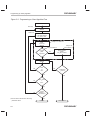
1
TMS320F20x/F24x DSP Embedded Flash Memory Technical Reference This document contains preliminary data current as of publication date and is subject to change without notice. Literature Number: SPRU282 September 1998 Printed on Recycled Paper IMPORTANT NOTICE Texas Instruments and its subsidiaries (TI) reserve the right to make changes to their products or to discontinue any product or service without notice, and advise customers to obtain the latest version of relevant information to verify, before placing orders, that information being relied on is current and complete. All products are sold subject to the terms and conditions of sale supplied at the time of order acknowledgement, including those pertaining to warranty, patent infringement, and limitation of liability. TI warrants performance of its semiconductor products to the specifications applicable at the time of sale in accordance with TI’s standard warranty. Testing and other quality control techniques are utilized to the extent TI deems necessary to support this warranty. Specific testing of all parameters of each device is not necessarily performed, except those mandated by government requirements. CERTAIN APPLICATIONS USING SEMICONDUCTOR PRODUCTS MAY INVOLVE POTENTIAL RISKS OF DEATH, PERSONAL INJURY, OR SEVERE PROPERTY OR ENVIRONMENTAL DAMAGE (“CRITICAL APPLICATIONS”). TI SEMICONDUCTOR PRODUCTS ARE NOT DESIGNED, AUTHORIZED, OR WARRANTED TO BE SUITABLE FOR USE IN LIFE-SUPPORT DEVICES OR SYSTEMS OR OTHER CRITICAL APPLICATIONS. INCLUSION OF TI PRODUCTS IN SUCH APPLICATIONS IS UNDERSTOOD TO BE FULLY AT THE CUSTOMER’S RISK. In order to minimize risks associated with the customer’s applications, adequate design and operating safeguards must be provided by the customer to minimize inherent or procedural hazards. TI assumes no liability for applications assistance or customer product design. TI does not warrant or represent that any license, either express or implied, is granted under any patent right, copyright, mask work right, or other intellectual property right of TI covering or relating to any combination, machine, or process in which such semiconductor products or services might be or are used. TI’s publication of information regarding any third party’s products or services does not constitute TI’s approval, warranty or endorsement thereof. Copyright 1998, Texas Instruments Incorporated PRELIMINARY Preface Read This First About This Manual This reference guide describes the operation of the embedded flash EEPROM module on the TMS320F20x/F24x digital signal processor (DSP) devices and provides sample code that you can use in developing your own software. The performance specifications of the embedded flash memory have been evaluated using the algorithms and techniques described in this guide. TI does not recommend deviation from these algorithms and techniques, since doing so could affect device performance. The book does not describe the use of any specific flash programming tool nor does it describe the external interface to the DSP. For information about any aspect of the TMS320F20x/F24x devices other than the embedded flash EEPROM module, see Related Documentation from Texas Instruments on page v. How to Use This Manual There are several stand-alone flash programming tools for TMS320F20x/ F24x generation of DSPs. Using one of these stand-alone tools with the TMS320F20x/F24x requires only a basic understanding of the flash operations. More information about these flash programming tools is available on the TI web page, http://www.ti.com. This guide is intended to provide a complete understanding of the flash operations. This level of understanding is necessary for making modifications to existing flash programming tools or for developing alternative programming schemes. If you are looking for information about: PRELIMINARY Turn to these locations: Algorithms Chapter 3, Algorithm Implementations and Software Considerations Erasing the flash array Section 1.1, Basic Concepts of Flash Memory Technology Section 2.1, Modifying the Contents of the TMS320F20x/F24x Flash Array Section 2.6, Erase Operation Section 3.3, Erase Algorithm iii PRELIMINARY If you are looking for information about: Turn to these locations: Over-erasure (depletion) and recovery Section 1.1, Basic Concepts of Flash Memory Technology Section 2.7, Recovering From Over-Erasure (Flash-Write Operation) Section 3.4, Flash-Write Algorithm Programming the flash array Section 1.1, Basic Concepts of Flash Memory Technology Section 2.1, Modifying the Contents of the TMS320F20x/F24x Flash Array Section 2.5, Program Operation Section 3.2, Programming Algorithm Sample code Appendix A, Assembly Source Listings and Program Examples Notational Conventions This document uses the following conventions. - The flash EEPROM is referred to as flash memory or the flash module. The term flash array refers to the actual memory array within the flash module. The flash module includes the flash memory array and the associated control circuitry. - The DSP generation and devices are abbreviated as follows: J TMS320F20x/24x generation: ’F20x/24x J TMS320F20x devices: ’F20x J TMS320F24x devices: ’F24x - Program listings and code examples are shown in a special type- face. Here is a sample program listing: 0011 0012 0013 0014 iv 0005 0005 0005 0006 0001 0003 0006 .field .field .field .even 1, 2 3, 4 6, 3 PRELIMINARY PRELIMINARY Related Documentation From Texas Instruments Related Documentation From Texas Instruments The following books describe the ’F20x/24x and related support tools. To obtain a copy of any of these TI documents, call the Texas Instruments Literature Response Center at (800) 477–8924. When ordering, please identify the book by its title and literature number. TMS320C24x DSP Controllers Reference Set, Volume 1: CPU, System, and Instruction Set (literature number SPRU160) describes the TMS320C24x 16-bit, fixed-point, digital signal processor controller. Covered are its architecture, internal register structure, data and program addressing, and instruction set. Also includes instruction set comparisons and design considerations for using the XDS510 emulator. TMS320C24x DSP Controllers Reference Set Volume 2: Peripheral Library and Specific Devices (literature number SPRU161) describes the peripherals available on the TMS320C24x digital signal processor controllers and their operation. Also described are specific device configurations of the ’C24x family. TMS320C240, TMS320F240 DSP Controllers (literature number SPRS042) data sheet contains the electrical and timing specifications for these devices, as well as signal descriptions and pinouts for all of the available packages. TMS320C2x/C2xx/C5x Optimizing C Compiler User’s Guide (literature number SPRU024) describes the ’C2x/C2xx/C5x C compiler. This C compiler accepts ANSI standard C source code and produces TMS320 assembly language source code for the ’C2x, ’C2xx, and ’C5x generations of devices. TMS320F206 Digital Signal Processor (literature number SPRS050) data sheet contains the electrical and timing specifications for the ’F206 device, as well as signal descriptions and the pinout. TMS320F241, TMS320C241, TMS320C242 DSP Controllers (literature number SPRS063) data sheet contains the electrical and timing specifications for the ’F241, ’C241, and ’C242 devices, as well as signal descriptions and pinouts. TMS320F243 DSP Controller (literature number SPRS064) data sheet contains the electrical and timing specifications for the ’F243 device, as well as signal descriptions and the pinout. TMS320C2xx User’s Guide (literature number SPRU127) discusses the hardware aspects of the ’C2xx 16-bit, fixed-point digital signal processors. It describes the architecture, the instruction set, and the on-chip peripherals. PRELIMINARY Read This First v Related Documentation From Texas Instruments PRELIMINARY TMS320C2xx C Source Debugger User’s Guide (literature number SPRU151) tells you how to invoke the ’C2xx emulator and simulator versions of the C source debugger interface. This book discusses various aspects of the debugger interface, including window management, command entry, code execution, data management, and breakpoints. It also includes a tutorial that introduces basic debugger functionality. vi PRELIMINARY PRELIMINARY If You Need Assistance . . . If You Need Assistance . . . - World-Wide Web Sites TI Online Semiconductor Product Information Center (PIC) DSP Solutions 320 Hotline On-linet - http://www.ti.com http://www.ti.com/sc/docs/pic/home.htm http://www.ti.com/dsps http://www.ti.com/sc/docs/dsps/support.htm North America, South America, Central America Product Information Center (PIC) (972) 644-5580 TI Literature Response Center U.S.A. (800) 477-8924 Software Registration/Upgrades (214) 638-0333 Fax: (214) 638-7742 U.S.A. Factory Repair/Hardware Upgrades (281) 274-2285 U.S. Technical Training Organization (972) 644-5580 DSP Hotline (281) 274-2320 Fax: (281) 274-2324 DSP Modem BBS (281) 274-2323 DSP Internet BBS via anonymous ftp to ftp://ftp.ti.com/pub/tms320bbs - Europe, Middle East, Africa European Product Information Center (EPIC) Hotlines: Multi-Language Support +33 1 30 70 11 69 Email: [email protected] Deutsch +49 8161 80 33 11 or +33 1 30 70 11 68 English +33 1 30 70 11 65 Francais +33 1 30 70 11 64 Italiano +33 1 30 70 11 67 EPIC Modem BBS +33 1 30 70 11 99 European Factory Repair +33 4 93 22 25 40 Europe Customer Training Helpline - Email: [email protected] Fax: +33 1 30 70 10 32 Fax: +49 81 61 80 40 10 Asia-Pacific Literature Response Center +852 2 956 7288 Fax: +852 2 956 2200 Hong Kong DSP Hotline +852 2 956 7268 Fax: +852 2 956 1002 Korea DSP Hotline +82 2 551 2804 Fax: +82 2 551 2828 Korea DSP Modem BBS +82 2 551 2914 Singapore DSP Hotline Fax: +65 390 7179 Taiwan DSP Hotline +886 2 377 1450 Fax: +886 2 377 2718 Taiwan DSP Modem BBS +886 2 376 2592 Taiwan DSP Internet BBS via anonymous ftp to ftp://dsp.ee.tit.edu.tw/pub/TI/ - Japan Product Information Center +0120-81-0026 (in Japan) +03-3457-0972 or (INTL) 813-3457-0972 DSP Hotline +03-3769-8735 or (INTL) 813-3769-8735 DSP BBS via Nifty-Serve Type “Go TIASP” - Fax: +0120-81-0036 (in Japan) Fax: +03-3457-1259 or (INTL) 813-3457-1259 Fax: +03-3457-7071 or (INTL) 813-3457-7071 Documentation When making suggestions or reporting errors in documentation, please include the following information that is on the title page: the full title of the book, the publication date, and the literature number. Mail: Texas Instruments Incorporated Email: [email protected] Technical Documentation Services, MS 702 P.O. Box 1443 Houston, Texas 77251-1443 Note: When calling a Literature Response Center to order documentation, please specify the literature number of the book. PRELIMINARY Read This First vii PRELIMINARY viii PRELIMINARY Contents Contents 1 Introduction . . . . . . . . . . . . . . . . . . . . . . . . . . . . . . . . . . . . . . . . . . . . . . . . . . . . . . . . . . . . . . . . . . . . . 1Ć1 Discusses basic flash memory technology; summarizes the features and benefits of the TMS320F20x/F24x flash module 1.1 1.2 1.3 2 Flash Operations and Control Registers . . . . . . . . . . . . . . . . . . . . . . . . . . . . . . . . . . . . . . . . . . 2Ć1 Describes the operations that modify the content of the flash module; explains the role of the control registers 2.1 2.2 2.3 2.4 2.5 2.6 2.7 2.8 2.9 3 Operations that Modify the Contents of the ’F20x/F24x Flash Array . . . . . . . . . . . . . . . 2Ć2 Accessing the Flash Module . . . . . . . . . . . . . . . . . . . . . . . . . . . . . . . . . . . . . . . . . . . . . . . . . 2Ć5 2.2.1 TMS320F206 Flash Access-Control Register . . . . . . . . . . . . . . . . . . . . . . . . . . . 2Ć6 2.2.2 TMS320F24x Flash Access-Control Register . . . . . . . . . . . . . . . . . . . . . . . . . . . . 2Ć7 Flash Module Control Registers . . . . . . . . . . . . . . . . . . . . . . . . . . . . . . . . . . . . . . . . . . . . . . 2Ć8 2.3.1 Segment Control Register (SEG_CTR) . . . . . . . . . . . . . . . . . . . . . . . . . . . . . . . . . 2Ć8 2.3.2 Flash Test Register (TST) . . . . . . . . . . . . . . . . . . . . . . . . . . . . . . . . . . . . . . . . . . . 2Ć10 2.3.3 Write Address Register (WADRS) . . . . . . . . . . . . . . . . . . . . . . . . . . . . . . . . . . . . 2Ć10 2.3.4 Write Data Register (WDATA) . . . . . . . . . . . . . . . . . . . . . . . . . . . . . . . . . . . . . . . . 2Ć11 Read Modes . . . . . . . . . . . . . . . . . . . . . . . . . . . . . . . . . . . . . . . . . . . . . . . . . . . . . . . . . . . . . . 2Ć12 Program Operation . . . . . . . . . . . . . . . . . . . . . . . . . . . . . . . . . . . . . . . . . . . . . . . . . . . . . . . . 2Ć13 Erase Operation . . . . . . . . . . . . . . . . . . . . . . . . . . . . . . . . . . . . . . . . . . . . . . . . . . . . . . . . . . . 2Ć14 Recovering From Over-Erasure (Flash-Write Operation) . . . . . . . . . . . . . . . . . . . . . . . . 2Ć15 Reading From the Flash Array . . . . . . . . . . . . . . . . . . . . . . . . . . . . . . . . . . . . . . . . . . . . . . . 2Ć16 Protecting the Array . . . . . . . . . . . . . . . . . . . . . . . . . . . . . . . . . . . . . . . . . . . . . . . . . . . . . . . . 2Ć16 Algorithm Implementations and Software Considerations . . . . . . . . . . . . . . . . . . . . . . . . . . 3Ć1 Describes the algorithms used for the programming, erase, and flash-write operations; discusses considerations necessary for developing your software 3.1 3.2 3.3 3.4 A Basic Concepts of Flash Memory Technology . . . . . . . . . . . . . . . . . . . . . . . . . . . . . . . . . . 1Ć2 TMS320F20x/F24x Flash Module . . . . . . . . . . . . . . . . . . . . . . . . . . . . . . . . . . . . . . . . . . . . . 1Ć3 Benefits of Embedded Flash Memory in a DSP System . . . . . . . . . . . . . . . . . . . . . . . . . . 1Ć5 How the Algorithms Fit Into the Program-Erase-Reprogram Flow . . . . . . . . . . . . . . . . . 3Ć2 Programming (or Clear) Algorithm . . . . . . . . . . . . . . . . . . . . . . . . . . . . . . . . . . . . . . . . . . . . 3Ć4 Erase Algorithm . . . . . . . . . . . . . . . . . . . . . . . . . . . . . . . . . . . . . . . . . . . . . . . . . . . . . . . . . . . 3Ć10 Flash-Write Algorithm . . . . . . . . . . . . . . . . . . . . . . . . . . . . . . . . . . . . . . . . . . . . . . . . . . . . . . 3Ć14 Assembly Source Listings and Program Examples . . . . . . . . . . . . . . . . . . . . . . . . . . . . . . . . . AĆ1 A.1 Assembly Source for Algorithms . . . . . . . . . . . . . . . . . . . . . . . . . . . . . . . . . . . . . . . . . . . . . . AĆ2 ix Contents A.2 A.3 A.4 A.5 A.6 x A.1.1 Header File for Constants and Variables, SVAR20.H . . . . . . . . . . . . . . . . . . . . . AĆ2 A.1.2 Clear Algorithm, SCLR20.ASM . . . . . . . . . . . . . . . . . . . . . . . . . . . . . . . . . . . . . . . . AĆ5 A.1.3 Erase Algorithm, SERA20.ASM . . . . . . . . . . . . . . . . . . . . . . . . . . . . . . . . . . . . . . AĆ10 A.1.4 Flash-Write Algorithm, SFLW20.ASM . . . . . . . . . . . . . . . . . . . . . . . . . . . . . . . . . AĆ15 A.1.5 Programming Algorithm, SPGM20.ASM . . . . . . . . . . . . . . . . . . . . . . . . . . . . . . . AĆ19 A.1.6 Subroutines Used By All Four Algorithms, SUTILS20.ASM . . . . . . . . . . . . . . . AĆ25 C-Callable Interface to Flash Algorithms . . . . . . . . . . . . . . . . . . . . . . . . . . . . . . . . . . . . . . AĆ27 Sample Assembly Code to Erase and Reprogram the TMS320F206 . . . . . . . . . . . . . . AĆ32 A.3.1 Assembly Code for TMS320F206 . . . . . . . . . . . . . . . . . . . . . . . . . . . . . . . . . . . . . AĆ32 A.3.2 Linker Command File for TMS320F206 Sample Assembly Code . . . . . . . . . . AĆ35 Sample C Code to Erase and Reprogram the TMS320F206 . . . . . . . . . . . . . . . . . . . . . AĆ37 A.4.1 C Code That Calls the Interface to Flash Algorithms for TMS320F206 . . . . . AĆ37 A.4.2 Linker Command File for TMS320F206 Sample C Code . . . . . . . . . . . . . . . . . AĆ38 Sample Assembly Code to Erase and Reprogram the TMS320F240 . . . . . . . . . . . . . . AĆ40 A.5.1 Assembly Code for TMS320F240 . . . . . . . . . . . . . . . . . . . . . . . . . . . . . . . . . . . . . AĆ40 A.5.2 Linker Command File for TMS320F240 Sample Assembly Code . . . . . . . . . . AĆ45 Using the Algorithms With C Code to Erase and Reprogram the ’F240 . . . . . . . . . . . . AĆ47 A.6.1 C Code That Calls the Interface to Flash Algorithms for TMS320F240 . . . . . AĆ47 A.6.2 Linker Command File for TMS320F240 Sample C Code . . . . . . . . . . . . . . . . . AĆ48 A.6.3 C Function for Disabling TMS320F240 Watchdog Timer . . . . . . . . . . . . . . . . . AĆ50 A.6.4 C Functions for Initializing the TMS320F240 . . . . . . . . . . . . . . . . . . . . . . . . . . . AĆ51 Figures Figures 1–1 2–1 2–2 2–3 3–1 3–2 3–3 3–4 3–5 3–6 3–7 TMS320F20x/F24x Program Space Memory Maps . . . . . . . . . . . . . . . . . . . . . . . . . . . . . . . . 1Ć4 Flash Memory Logic Levels During Programming and Erasing . . . . . . . . . . . . . . . . . . . . . . 2Ć4 Memory Maps in Register and Array Access Modes . . . . . . . . . . . . . . . . . . . . . . . . . . . . . . . 2Ć6 Segment Control Register (SEG_CTR) . . . . . . . . . . . . . . . . . . . . . . . . . . . . . . . . . . . . . . . . . . 2Ć8 Algorithms in the Overall Flow . . . . . . . . . . . . . . . . . . . . . . . . . . . . . . . . . . . . . . . . . . . . . . . . . . 3Ć3 The Programming Algorithm in the Overall Flow . . . . . . . . . . . . . . . . . . . . . . . . . . . . . . . . . . . 3Ć4 Programming or Clear Algorithm Flow . . . . . . . . . . . . . . . . . . . . . . . . . . . . . . . . . . . . . . . . . . . 3-6 Erase Algorithm in the Overall Flow . . . . . . . . . . . . . . . . . . . . . . . . . . . . . . . . . . . . . . . . . . . . 3Ć10 Erase Algorithm Flow . . . . . . . . . . . . . . . . . . . . . . . . . . . . . . . . . . . . . . . . . . . . . . . . . . . . . . . . . 3Ć13 Flash-Write Algorithm in the Overall Flow . . . . . . . . . . . . . . . . . . . . . . . . . . . . . . . . . . . . . . . 3Ć14 Flash-Write Algorithm Flow . . . . . . . . . . . . . . . . . . . . . . . . . . . . . . . . . . . . . . . . . . . . . . . . . . . . 3Ć16 Contents xi Tables Tables 1–1 2–1 2–2 2–3 2–4 3–1 3–2 3–3 xii TMS320 Devices With On-Chip Flash EEPROM . . . . . . . . . . . . . . . . . . . . . . . . . . . . . . . . . . 1Ć3 Operations that Modify the Contents of the Flash Array . . . . . . . . . . . . . . . . . . . . . . . . . . . . 2Ć4 Flash Module Control Registers . . . . . . . . . . . . . . . . . . . . . . . . . . . . . . . . . . . . . . . . . . . . . . . . . 2Ć8 Segment Control Register Field Descriptions . . . . . . . . . . . . . . . . . . . . . . . . . . . . . . . . . . . . . 2Ć9 Flash Array Segments Summary . . . . . . . . . . . . . . . . . . . . . . . . . . . . . . . . . . . . . . . . . . . . . . . 2Ć10 Steps for Verifying Programmed Bits and Applying One Program or Clear Pulse . . . . . . 3Ć8 Steps for Applying One Erase Pulse . . . . . . . . . . . . . . . . . . . . . . . . . . . . . . . . . . . . . . . . . . . . 3Ć11 Steps for Applying One Flash-Write Pulse . . . . . . . . . . . . . . . . . . . . . . . . . . . . . . . . . . . . . . . 3Ć15 PRELIMINARY Chapter 1 Introduction The TMS320F20x/F24x digital signal processors (DSPs) contain on-chip flash EEPROM (electrically-erasable programmable read-only memory). The embedded flash memory provides an attractive alternative to masked program ROM. Like ROM, flash memory is nonvolatile, but it has an advantage over ROM: in-system reprogrammability. This chapter discusses basic flash memory technology, introduces the flash memory module of the ’F20x/F24x DSP, and lists the benefits of flash memory embedded in a DSP chip. Topic PRELIMINARY Page 1.1 Basic Concepts of Flash Memory Technology . . . . . . . . . . . . . . . . . . . 1-2 1.2 TMS320F20x/F24x Flash Module . . . . . . . . . . . . . . . . . . . . . . . . . . . . . . . 1-3 1.3 Benefits of Embedded Flash Memory in a DSP System . . . . . . . . . . . 1-5 1-1 Basic Concepts of Flash Memory Technology PRELIMINARY 1.1 Basic Concepts of Flash Memory Technology The term flash in this EEPROM technology refers to the speed of some of the operations performed on the memory (these operations will be described in greater detail later in this document). An entire block of bits is affected simultaneously in a block or flash operation, rather than being affected one bit at a time. In contrast, writing data to the flash memory cannot be a block operation, since normally a selection of ones and zeroes are written (all bits are not the same value). Writing selected bits to create a desired pattern is known as programming the flash memory, and a written bit is called a programmed bit. Several different types of program and erase operations are performed on the flash memory in order to properly produce the desired pattern of ones and zeroes in the memory. It should be noted that, under some conditions, flash memory may become overerased, resulting in a condition known as depletion. The ’F20x/F24x algorithms avoid overerasure by using an approach that erases in small increments until complete erasure is achieved. The ’F20x/F24x flash EEPROM includes a special operation, flash-write, that is used only to recover from over-erasure. Because of the implementation of the flash memory, when over-erasure occurs, any particular bit in depletion mode is difficult to identify. For this reason, the ’F20x/F24x simply writes an entire block of bits simultaneously; hence, the name flash-write. The program and erase operations in flash memory must provide sufficient charge margin on 1s and 0s to ensure data retention, so the ’F20x/F24x flash module includes a hardware mechanism that provides margin for erasing or programming. This mechanism implements voltage reference levels which ensure this logic level margin when modifying the contents of the flash memory. 1-2 PRELIMINARY PRELIMINARY TMS320F20x/F24x Flash Module 1.2 TMS320F20x/F24x Flash Module The ’F20x/F24x flash EEPROM is implemented with one or two independent flash memory modules of 8K or 16K words. Each flash module is composed of a flash memory array, four control registers, and circuitry that produces analog voltages for programming and erasing. The flash array size of the TMS320F206 and TMS320F240 is 16K × 16 bits, while the TMS320F241 and TMS320F243 incorporate an 8K × 16-bit flash array (see Table 1–1). Unlike most discrete flash memories, the ’F20x/F24x flash module does not require a dedicated state machine, because the algorithms for programming and erasing the flash are executed in software by the DSP core. The use of these sophisticated, adaptive programming algorithms results in reduced chip size and greater programming flexibility. In addition, the application code can manage the use of the flash memory without the requirement of external programming equipment. Table 1–1. TMS320 Devices With On-Chip Flash EEPROM Device Array Size Total Flash Memory TMS320F206 16K 32K† TMS320F240 16K 16K TMS320F241 8K 8K TMS320F243 8K 8K † Each array can be independently erased. PRELIMINARY Introduction 1-3 PRELIMINARY TMS320F20x/F24x Flash Module Simplified memory maps for the program space of the TMS320F20x/F24x devices are shown in Figure 1–1 to illustrate the location of the flash modules. Figure 1–1. TMS320F20x/F24x Program Space Memory Maps TMS320F240 MP/MC = 0 Flash0 Flash0 3FFFh 4000h 3FFFh 4000h Flash1 7FFFh 8000h FFFFh 1-4 0000h 0000h 0000h FFFFh TMS320F241 1FFFh Flash0 TMS320F243 MP/MC = 0 0000h 1FFFh Flash0 no external memory available TMS320F206 MP/MC = 0 FFFFh PRELIMINARY PRELIMINARY Benefits of Embedded Flash Memory in a DSP System 1.3 Benefits of Embedded Flash Memory in a DSP System The circuitry density of flash memory is about half that of conventional EEPROM memory, making it possible to approach DRAM densities with flash memory. This increased density allows flash memory to be integrated with a CPU and other peripherals in a single ’F20x/F24x DSP chip. Embedded flash memory expands the capabilities of the ’F20x/F24x DSPs in the areas of prototyping, integrated solutions, and field upgradeable designs. Embedded flash memory facilitates system development and early field testing. Throughout the development process, the system software can be updated and reprogrammed into the flash memory for testing at various stages. Since flash is a non-volatile memory type, the resulting standalone prototype can be tested in the appropriate environment without the need for battery backup. In addition to its nonvolatile nature, embedded flash memory has the advantage of in-system programming. Unlike some discrete flash or EEPROM chips, embedded flash memory can be programmed without removing the device from the system board. In fact, the embedded flash memory of ’F20x/F24x DSPs can be programmed using hardware emulators which are already an integral part of the DSP development process; no external programming equipment is required. The embedded flash memory of ’F20x/F24x DSPs also makes these devices ideal for highly integrated, low-cost systems. The initial investment involved with making a ROM memory is not justifiable for certain low-cost applications. Accordingly, when on-chip ROM is not an option, DSP system designers usually resort to using expensive static RAM (SRAM), to store system software and data. The SRAM provides the fast access times required by the DSP, but has the disadvantage of being a volatile memory type. To address the issue of memory volatility, designers often use a low-cost EPROM or flash device to load the SRAM after system power-up. This approach is very expensive, and the increased chip count is often prohibitive. The ’F20x/F24x DSPs, with their on-chip flash memory modules, provide a single chip solution with nonvolatile memory that supports full speed DSP access rates. Another benefit of embedded flash memory in a DSP system is remote reprogrammability. Field upgradeability is an extremely useful feature for embedded systems. For example, many modem manufacturers offer algorithm upgrades remotely, without requiring the modem to be removed from the host computer system. The same type of feature is also being offered for many handheld consumer products. Adding this capability to a product requires the addition of EEPROM or flash devices, which increase chip count and system cost. Since no external equipment is required to program the embedded flash memory of the ’F20x/F24x DSPs, these devices enable field upgradeability without impacting system cost. PRELIMINARY Introduction 1-5 PRELIMINARY 1-6 PRELIMINARY PRELIMINARY Chapter 2 Flash Operations and Control Registers The operations that modify the contents of the ’F20x/F24x flash array are performed in software through the use of dedicated programming algorithms. This chapter introduces the operations performed by these algorithms and explains the role of the control registers in this process. The actual algorithms are discussed in Chapter 3. Topic PRELIMINARY Page 2.1 Operations that Modify the Contents of the ’F20x/F24x Flash Array . . . . . . . . . . . . . . . . . . . . . . . . . . . . . . . . . . . . . . . . . . . . . . . . . . . 2-2 2.2 Accessing the Flash Module . . . . . . . . . . . . . . . . . . . . . . . . . . . . . . . . . . . 2-5 2.3 Flash Module Control Registers . . . . . . . . . . . . . . . . . . . . . . . . . . . . . . . . 2-8 2.4 Read Modes . . . . . . . . . . . . . . . . . . . . . . . . . . . . . . . . . . . . . . . . . . . . . . . . . 2-12 2.5 Program Operation . . . . . . . . . . . . . . . . . . . . . . . . . . . . . . . . . . . . . . . . . . . 2-13 2.6 Erase Operation . . . . . . . . . . . . . . . . . . . . . . . . . . . . . . . . . . . . . . . . . . . . . 2-14 2.7 Recovering From Over-Erasure (Flash-Write Operation) . . . . . . . . . 2-15 2.8 Reading From the Flash Array . . . . . . . . . . . . . . . . . . . . . . . . . . . . . . . . 2-16 2.9 Protecting the Array . . . . . . . . . . . . . . . . . . . . . . . . . . . . . . . . . . . . . . . . . . 2-16 2-1 Operations that Modify the Contents of the ’F20x/F24x Flash Array PRELIMINARY 2.1 Operations that Modify the Contents of the ’F20x/F24x Flash Array Operations that modify the contents of the flash array are generically referred to as either “programming,” which drives one or more bits toward the logic zero state, or “erasing,” which drives all bits towards the logic one state. It should be noted that since these operations are performed incrementally, a single “programming” or “erasing” operation does not ALWAYS result in a valid logic one or zero. The result of each of these types of operations depends on the initial state of the bit(s) prior to the operation. This is described in more detail below. Within these two basic types of operations (which are related to the fact that there are only two valid logic levels in the F20x/F24x device) are four distinctly different types of functions which are actually performed. In the category of “programming” operations, there are three actual types of functions that are performed: Clear – which is used to write ALL array bits to a zero state, Program – which is used to write SELECTED array bits to zero, and Flash-Write – which is used to recover ALL array bits from depletion In the category of “erase” operations, there is only one type of operation: Erase – which is used to write ALL array bits to a one state. Clear, Program, Flash-Write, and Erase are the only four functions that are used to modify the flash array. Assuming that the intent of a modification of the contents of the flash array is to program the array with a selection of ones and zeroes, the following sequence of operations must be performed for proper operation of the flash memory: 1) The array is first CLEARED to all zeroes. 2) The array is then ERASED to all ones. 3) The array is then checked for depletion and recovered using FLASHWRITE if necessary (note that if Flash-Write is used to recover from depletion, this sequence must be started over again with the Clear and Erase functions). 4) Once the array is properly cleared and erased, and verified not to be in depletion, the array is then PROGRAMMED with the desired selection of zero bits. 2-2 PRELIMINARY PRELIMINARY Operations that Modify the Contents of the ’F20x/F24x Flash Array This procedure is discussed in complete detail in Chapter 3. During these operations that are used to modify the contents of the flash array, three special read modes, and a corresponding set of reference voltage levels, are used when reading back data values to verify programming and erase operations. These read modes and reference levels are: VER0 – which is used to verify the logic zero level including margin, VER1 – which is used to verify the logic one level including margin, and Inverse Erase – which is used to verify depletion recovery. These concepts are illustrated graphically in Figure 2–1 and summarized in Table 2–1. Note that ONLY the Erase and the Flash-Write functions are truly “flash” in the sense that these functions actually affect all bits in the array simultaneously. In contrast, bit programming levels in the Program and Clear functions can be controlled individually on a bit-by-bit basis. Therefore, when using the Erase or Flash-Write functions, the whole array is modified, and then the whole array is read, word by word, to verify whether all words have reached the same value (if not, further iterations of the Erase or Flash-Write functions continue). In these cases, as mentioned previously, all the bits in the array are modified simultaneously, but some bits may react more quickly, potentially resulting in variation in actual levels on different bits. Therefore, when performing an Erase, it is possible that some bits may reach depletion even before other bits reach the logic one reference level (VER1). The reason that it is critical to clear the array to a consistent zero level before erasing the array is to give maximum immunity to depletion when erasing. Note, however, that even when following this sequence, some flash arrays may experience depletion, and may require recovery using the Flash-Write function. In contrast to the true “flash” operations Erase and Flash-Write, after each incremental Program or Clear operation, each bit is tested against the VER0 reference level to determine the exact point at which it has reached the proper value, following which, no further incremental adjustment of the level is made on that bit. Therefore, when the Program or Clear operation is complete, all bits are at the same zero level, which greatly increases proper data retention and depletion immunity for the device. Again, note that the programming and erase operations are discussed in complete detail in Chapter 3. PRELIMINARY Flash Operations and Control Registers 2-3 PRELIMINARY Operations that Modify the Contents of the ’F20x/F24x Flash Array Figure 2–1. Flash Memory Logic Levels During Programming and Erasing Depletion Mode Inverse Erase Reference Level Logic 1 Program operations VER1 Reference Level Clear Program 1 Margin Flash Write (Towards logic zero level) Erase (Towards logic one level) Erase operation 0 Margin VER0 Reference level Logic 0 Table 2–1. Operations that Modify the Contents of the Flash Array Change in Bit Level Towards Logic 1 Function Erase (all bits) 2-4 Reference Level VER1 Towards Logic 0 Function Reference Level Program (selected bits) VER0 Clear (all bits) VER0 Flash-Write (all bits) Inverse Erase PRELIMINARY PRELIMINARY Accessing the Flash Module 2.2 Accessing the Flash Module In addition to the flash memory array, each flash module has four registers that control operations on the flash array. These registers are: Segment control register (SEG_CTR) Test register (TST) Write address register (WADRS) Write data register (WDATA) The flash module operates in one of two modes: one in which the flash memory is accessed directly by the CPU, and one in which the memory array cannot be accessed directly, but the four control registers are accessible. This mode is used for programming. Each flash module has a flash access-control register that selects between these two access modes. The register is a single-bit, I/O-mapped register. The two access modes are summarized as follows: Array-access mode. You can access the flash array in the memory space decoded for the flash module. The flash module remains in this mode most of the time, because it allows the DSP core to read from the memory array. Register-access mode. You can access the four control registers in the memory space decoded for the flash module. This mode is used for programming. When the flash module is in register-access mode, the registers are repeated every four address locations within the flash module’s address range. The flash array is not directly accessible as memory in register-access mode, and the control registers are not directly accessible in array-access mode. Figure 2–2 shows memory maps of the flash array in register and array access modes. PRELIMINARY Flash Operations and Control Registers 2-5 PRELIMINARY Accessing the Flash Module Figure 2–2. Memory Maps in Register and Array Access Modes Flash access control register (single bit) MODE = 1: Array-access mode MODE = 0: Register access mode 0100 ... 010 0100 ... 011 SEG_CTR register TST register WADRS register WDATA register 4 registers duplicated Flash memory array 4 registers duplicated 1110 ...110 0110 ...111 2.2.1 4 registers duplicated TMS320F206 Flash Access-Control Register Because each flash module has an access-control register associated with it, the ’F206 has two access-control registers. These registers are standard I/Omapped registers that can be read with an IN instruction and must be modified with an OUT instruction. F_ACCESS0 is mapped in I/O space at 0FFE0h. F_ACCESS1 is mapped in I/O space at 0FFE1h. The MODE bit (bit 0) of the access-control register selects the access mode: MODE = 0 Register-access mode MODE = 1 Array-access mode Bits 15–1 of each access-control register are always read as 0 and are unaffected by writes. 2-6 PRELIMINARY PRELIMINARY Accessing the Flash Module Although the function is the same, the access control registers of the ’F206 device are mapped at different addresses from that of the ’F24x devices, and their values are modified in a different way. 2.2.2 TMS320F24x Flash Access-Control Register The access-control register of the ’F24x devices is a special type of I/Omapped register that cannot be read. The register is mapped at I/O address 0FF0Fh, and it functions as indicated below. Note: For both the IN and OUT instructions, the data operand (dummy) is not used, and can be any valid memory location. An OUT instruction using the register address as an I/O port places the flash module in register-access mode. For example: OUT dummy, 0FF0Fh ;Selects register-access mode An IN instruction using the register address as an I/O port places the flash module in array-access mode. The data operand (dummy) is not used, and can be any valid memory location. For example: IN PRELIMINARY dummy, 0FF0Fh ;Selects array-access mode Flash Operations and Control Registers 2-7 PRELIMINARY Flash Module Control Registers 2.3 Flash Module Control Registers Table 2–2 lists the control registers and their relative addresses within the four locations that repeat throughout the module’s address range. Table 2–2. Flash Module Control Registers Described in ... Relative Address Register Name Description Section Page 0 SEG_CTR Segment control register. The eight MSBs enable specific segments for programming. Setting a bit to 1 enables the segment. The eight LSBs control the program, erase, and verify operations of the module. 2.3.1 2-5 1 TST Test register. Reserved for test; not accessible to the user. 2.3.2 2-8 2 WADRS Write address register. Holds the address for a write operation. 2.3.3 2-8 3 WDATA Write data register. Holds the data for a write operation. 2.3.4 2-8 2.3.1 Segment Control Register (SEG_CTR) SEG_CTR is a 16-bit register that initiates and monitors the programming and erasing of the flash array. This register contains the bits that initiate the active operations (the WRITE/ERASE field and EXE bit), those used for verification (VER0 and VER1), and those used for protection (KEY0, KEY1, and SEG7–SEG0). All bits of SEG_CTR register are cleared to 0 upon reset. SEG_CTR is shown in Figure 2–3 and the fields are described in Table 2–3. Figure 2–3. Segment Control Register (SEG_CTR) 15 14 13 12 11 10 9 8 7 6 5 4 3 2 1 0 SEG7 SEG6 SEG5 SEG4 SEG3 SEG2 SEG1 SEG0 Res KEY1 KEY0 VER0 VER1 WRITE/ ERASE EXE RW–0 RW–0 RW–0 RW–0 RW–0 RW–0 RW–0 RW–0 X RW–0 RW–0 RW–0 RW–0 RW–0 RW–0 Legend: R = read W = write –0 = value after reset X = don’t care 2-8 PRELIMINARY PRELIMINARY Flash Module Control Registers Table 2–3. Segment Control Register Field Descriptions Bits Name Description 15–8 SEG7–SEG0 Segment enable bits. Each of these bits protects the specified segment against programming or enables programming for the specified segment in the array. Any number of segments (from 0 to 7 in any combination) can be enabled at any one time. See Table 2–4 for segment address ranges. EXE must be cleared to modify the SEGx bits. SEGx = 1 enables programming of the corresponding segment. SEGx = 0 protects the segment from programming. 7 Reserved This bit is not affected by writes, and reads of this bit are undefined. 6–5 KEY1, KEY0 Execute key bits. A binary value of 10 must be written to these bits in the same DSP core access in which the EXE bit is set for the selected operation (erase, program, or flash-write) to start. KEY1 and KEY0 must be cleared in the same write access that clears EXE. These bits are used as additional protection against inadvertent programming or erasure of the array. These bits are read as 0s. 4–3 VER0, VER1 Verify bits. These bits select special read modes used to verify proper erasure or programming. Possible values: 00: 01: 10: 11: 2–1 WRITE/ERASE Normal read mode Verify 1s (VER1) read mode to verify margin of 1s for proper erasure Verify 0s (VER0) read mode to verify margin of 0s for proper programming Inverse-read mode; tests for bits erased into depletion Write/erase enable field. These bits select the program, erase, or flash-write operation. However, modification of the array data does not actually start until the EXE bit is set. Reset clears these bits to zero. Possible values: 00: 01: 10: 11: 0 Note: EXE Read operation is enabled. These bit values are required to read the array. Erase operation is enabled Write operation is enabled Flash-write operation is enabled Execute bit. In conjunction with WRITE/ERASE, KEY1, and KEY0, this bit controls the program, erase, and flash-write operations. Setting EXE starts and stops programming and erasing of the flash array. The KEY1 and KEY0 bits must be written in the same write access that sets EXE, and EXE must be cleared in the same write access that clears KEY1 and KEY0. EXE must be cleared to modify the SEGx bits. The segment enable bits are not intended for protection during the erase or flash-write operations. During these operations, all segments must be enabled. PRELIMINARY Flash Operations and Control Registers 2-9 PRELIMINARY Flash Module Control Registers Table 2–4. Flash Array Segments Summary ’F206/F240 Flash Module† SEG7–SEG0 Bits ’F241/F243 F241/F243 Flash Module Array Segment Enabled 0000–07FFh 4000–47FFh 0000–03FFh 0 0 0800–0FFFh 4800–4FFFh 0400–07FFh 1 0 0 1000–17FFh 5000–57FFh 0800–0BFFh 2 0 0 0 1800–1FFFh 5800–5FFFh 0C00–0FFFh 3 0 0 0 0 2000–27FFh 6000–67FFh 1000–13FFh 4 0 0 0 0 0 2800–2FFFh 6800–6FFFh 1400–17FFh 5 0 0 0 0 0 0 3000–37FFh 7000–77FFh 1800–1BFFh 6 0 0 0 0 0 0 3800–3FFFh 7800–7FFFh 1C00–1FFFh 7 15 14 13 12 11 10 9 8 0 0 0 0 0 0 0 1 0 0 0 0 0 0 1 0 0 0 0 0 1 0 0 0 0 1 0 0 0 1 0 0 1 0 1 1 0 Flash0 Flash1 † The TMS320F206 has two flash modules. The TMS320F240 device uses the address ranges shown for Flash0. Although segmentation is not supported during erase (i.e., the entire array must be erased simultaneously), the segment enable bits can be used to protect portions of the array against unintentional programming. This is useful for applications in which different portions of the array are programmed at different times. For example, an application might program the flash module with a large table in 2K × 16 blocks. Some time after the first block is programmed, the next block is programmed. The segment enable bits can be used to prevent corruption of the first block while the second block is being programmed. 2.3.2 Flash Test Register (TST) The flash test register (TST) is a 5-bit register used during manufacturing test of the flash array. This register is not accessible to the DSP core. 2.3.3 Write Address Register (WADRS) The write address register (WADRS) is a 16-bit register that holds the latched write address for a programming operation. In array-access mode, this register is loaded with the value on the address bus when you are writing a data value to the flash module. It can be loaded directly in register-access mode by writing to it. 2-10 PRELIMINARY PRELIMINARY 2.3.4 Flash Module Control Registers Write Data Register (WDATA) The write data register (WDATA) is a 16-bit register that contains the latched write data for a programming operation. In array-access mode, this register can be loaded by writing a data value to the flash module. It can be loaded directly in register-access mode by writing to it. The WDATA register must be loaded with the value FFFFh before an erase operation starts. PRELIMINARY Flash Operations and Control Registers 2-11 PRELIMINARY Read Modes 2.4 Read Modes The ’F20x/F24x flash module uses four read modes and corresponding sets of reference levels: Standard Verify 0s (VER0) Verify 1s (VER1) Inverse-erase Read mode selection is accomplished through the verify bits (bits 3 and 4) in SEG_CTR during execution of the algorithms. In the standard read mode of the ’F20x/F24x flash module, the supply voltage (VDD) is internally applied to the cell to select it for reading. The VER0, VER1, and inverse-erase read modes differ from the standard read mode in the internal voltage level applied to the flash cell. Because the program and erase operations must provide sufficient margin on 1s and 0s to ensure data retention, the verify 0s (VER0) and verify 1s (VER1), are provided on the flash module to check for sufficient margin. The VER0 and VER1 read modes provide a method for adjusting the level on the cells during programming or erasing, beyond the point required for reading a 0 or a 1, creating the required logic level margin. In VER0 mode, a voltage closer to an ideal logic zero level than necessary to read a logic zero is internally applied to the cell to select it for reading. This is the worst-case condition for reading a programmed cell, and if a cell can be read as 0 in VER0 mode, then it can also be read as 0 in standard read mode. Similarly, in the VER1 read mode, a voltage closer to an ideal logic one level than necessary to read a logic one is internally applied to the cell to select it for reading. This is the worst-case condition for reading an erased cell, and if a cell can be read as 1 in the VER1 mode, then it can be read as 1 in standard read mode. The inverse-erase read mode detects flash bits that are in depletion mode. This read mode applies a voltage to all array cells so that all cells are deselected. The entire array can be tested for bits in depletion mode by reading the first row (32 words) of the array in inverse-erase read mode. If there are no bits in depletion mode, all 32 words are read as 0000h. 2-12 PRELIMINARY PRELIMINARY Program Operation 2.5 Program Operation The program operation of the ’F20x/F24x flash module loads the applicationspecific data (a pattern of 0s) into the flash array. The basis of the operation is applying a program pulse to a single word of flash memory. The term program pulse refers to the time during the program operation between the setting and the clearing of the EXE bit ( bit 0 of SEG_CTR). During the program pulse, charge is added to the addressed bits via the programming mechanism. Several program pulses may be required to fully program the bits of a word, and the application of program pulses is controlled by the programming algorithm. The flash location to be programmed is specified by the address in the WADRS register, and the data pattern to be programmed is loaded into the WDATA register. Only the bits that contain a 0 are programmed; any bit positions containing a 1 remain unchanged. (See sections 2.3.3 and 2.3.4 for information about how to load the WADRS and WDATA registers.) To assure that the 0 bits are programmed with enough margin, the reads associated with programming are performed using the VER0 read mode. After a program pulse has been applied, the byte is read back in VER0 mode to assure that programmed bits can be read as 0 over the entire operating range of the device. The flash module supports programming of up to eight bits of data. Therefore, although the flash bits are addressed on 16-bit word boundaries, only eight bits can be programmed at a time. The algorithm must limit the programming to eight bits by masking the word to be programmed before writing it to the WDATA register. For example, to mask off the upper byte while programming the lower byte, the data value is logically 0Red with 0FF00h in software. When a program pulse is applied, only the selected bits are programmed. PRELIMINARY Flash Operations and Control Registers 2-13 PRELIMINARY Erase Operation 2.6 Erase Operation The erase operation of the ’F20x/F24x flash module prepares the flash array for programming and enables reprogrammability of the flash array. Before the array can be erased, all bits must be programmed to 0s. This procedure of programming all array locations in preparation for the erase is called clearing the array. During the erase, all bits in the array are changed from 0s to 1s. After the erase is finished, a depletion mode test is made to determine whether any bits have been over-erased. If over-erased bits are detected, they must be recovered with the flash-write algorithm, and the clear and erase algorithms must be repeated. An erase pulse is the time during the erase operation between the setting and the clearing of the EXE bit ( bit 0 of SEG_CTR). During the erase pulse, the level on all array bits is modified via the erase mechanism. Erasing the flash array is a block operation. During the erase pulse, all array bits are affected simultaneously. (See Figure 2–1, Flash Memory Logic Levels During Programming and Erasing, on page 2-4 for an illustration of this mechanism.) Multiple erase pulses may be required to fully erase all bits in the array, and the application of erase pulses is controlled by the erase algorithm. The erase operation uses the VER1 read mode to determine when erasure is complete. After erasure is complete, the inverse-erase read mode is used to determine if any bits are over-erased. For more information about these read modes, see section 2.4, Read Modes, on page 2-12. 2-14 PRELIMINARY PRELIMINARY Recovering From Over-Erasure (Flash-Write Operation) 2.7 Recovering From Over-Erasure (Flash-Write Operation) Generally, not all bits in the flash array have the same amount of charge removed with each erase pulse. By the time all bits have reached the VER1 read margin (and erase is complete), some of the bits in the array may be overerased. They are said to be in depletion mode. If even one single flash cell is over-erased into depletion mode, it is always read as logic 1 and can corrupt the reading of other bits. This condition must be detected and corrected, because it also inhibits reprogramming of the flash array. The ’F20x/F24x flash array employs the flash-write operation to recover bits that are erased into depletion mode. The flash-write operation is similar to the erase operation in that it affects all bits in the array simultaneously. This enables recovery of multiple bits from depletion mode, but requires the flashwrite operation to be followed by the clear and erase operations to restore the erase margin on all bits. A flash-write pulse is the time during the flash-write operation between the setting and the clearing of the EXE bit (bit 0 of SEG_CTR). During the flash-write pulse, all array bits are affected simultaneously. (See Figure 2–1, Flash Memory Logic Levels During Programming and Erasing, on page 2-4 for an illustration of this mechanism.) Multiple flash-write pulses may be required to fully recover all bits in the array, and the application of flash-write pulses is controlled by the flash-write algorithm. The flash-write operation uses the inverse-erase read mode and inverseerase reference level to detect bits that are in depletion mode. For more information about the inverse-erase read mode, see section 2.4, Read Modes, on page 2-12. PRELIMINARY Flash Operations and Control Registers 2-15 PRELIMINARY Reading From the Flash Array 2.8 Reading From the Flash Array Once the array is programmed, it is read in the same manner as other memory devices on the DSP memory interface. The flash module operates with zero wait states. When you are reading the flash module, the flash segment control register (SEG_CTR) bits should be 0 and the flash array must be in the arrayaccess mode. 2.9 Protecting the Array After the flash memory array is programmed, it is desirable to protect the array against corruption. The flash module of the ’F20x/F24x DSPs includes several protection mechanisms to prevent unintentional modification of the array. Flash programming is facilitated via the supply voltage connected to the VCCP pin. If this pin is grounded, the program operation will not modify the flash array. Note, that grounding the VCCP pin does not prevent the erase operation; other protection mechanisms for the erase operation are discussed below. The control registers provide the following mechanisms for protecting the flash array from unintentional modification. Segment enable bits EXE, KEY0, and KEY1 bits WDATA register An array segment is prevented from being programmed when the corresponding segment enable bit in the SEG_CTR is cleared to zero. Additionally, all segment enable bits are cleared by reset, making unintentional programming less likely. Even if the segment enable bits are set to one, the program, erase, and flash-write operations are not initiated unless the appropriate values are set in the EXE, KEY0, and KEY1 bits of the SEG_CTR. At the start of an operation, the KEY1 and KEY0 bits must be written in the same write access that sets EXE. When the program pulse, erase pulse, or flash-write pulse is finished, EXE must be cleared in the same write that clears KEY1 and KEY0. The data and address latches are locked whenever the EXE bit is set, and all attempts to read from or write to the array are ignored (read data is indeterminate). Once the EXE bit is set, all register bits are latched and protected. You must clear EXE to modify the SEGx bits. This protects the array from inadvertent change. Unprotected segments cannot be masked in the same register load with the deactivation of EXE. Additional security is provided by a function of the WDATA register to prevent unintentional erasure. The WDATA register must be loaded with FFFFh before the erase operation is initiated. If the register is not loaded with this value, the array will not be modified. 2-16 PRELIMINARY PRELIMINARY Chapter 3 Algorithm Implementations and Software Considerations This chapter discusses the implementations of the algorithms for performing the operations described in the previous chapter. It also discusses items you must consider when incorporating the algorithms into your ’F20x/F24x DSP application code. Topic PRELIMINARY Page 3.1 How the Algorithms Fit Into the Program-Erase-Reprogram Flow . . . . . . . . . . . . . . . . . . . . . . . . . . . . . . . . . . . . . . . . . . . . . . . . . . . . . . . . . 3-2 3.2 Programming (or Clear) Algorithm . . . . . . . . . . . . . . . . . . . . . . . . . . . . . . 3-4 3.3 Erase Algorithm . . . . . . . . . . . . . . . . . . . . . . . . . . . . . . . . . . . . . . . . . . . . . 3-10 3.4 Flash-Write Algorithm . . . . . . . . . . . . . . . . . . . . . . . . . . . . . . . . . . . . . . . . 3-14 3-1 How the Algorithms Fit Into the Program-Erase-Reprogram Flow PRELIMINARY 3.1 How the Algorithms Fit Into the Program-Erase-Reprogram Flow The algorithms discussed in this chapter can be used to reprogram the ’F20x/F24x flash module multiple times. The clear algorithm, erase algorithm, and flash-write algorithm are used to prepare the flash memory for programming, while the programming algorithm is used to write a desired pattern of 0s to the array (program the array). The programming algorithm and the clear algorithm are both implementations of the program operation. The difference between the two is the data that is written: the programming algorithm programs the user data, while the clear algorithm uses all 0s. All of the algorithms can be viewed as portions of a single flow diagram, as shown in Figure 3–1. Note that in the algorithm flowcharts, the variable X represents the number of attempts at depletion recovery using the flash-write algorithm. It has been shown that if flash-write is not successful in depletion recovery after ten attempts, depletion recovery is not possible, and a device failure has occurred. Therefore, if ten flash-write attempts at depletion recovery are not successful, the algorithm returns a device failure error message. 3-2 PRELIMINARY PRELIMINARY How the Algorithms Fit Into the Program-Erase-Reprogram Flow Figure 3–1. Algorithms in the Overall Flow Initialization flow Start X=1 Clear algorithm Clear the array Yes Flash-write algorithm Erase the array Erase algorithm Recover using flash-write X = X+1 No Reprogram? Yes Bits in depletion? Done/Stop Yes X < 10 ? No No Fail Program the array Programming algorithm PRELIMINARY Algorithm Implementations and Software Considerations 3-3 PRELIMINARY Programming (or Clear) Algorithm 3.2 Programming (or Clear) Algorithm The programming algorithm sequentially writes any number of addresses with a specified bit pattern.This algorithm is used to program application code or data into the flash array. With a slight modification, the same algorithm performs the clear portion of the initialization flow (i.e., programs all bits to zero). In this role, the algorithm is called the clear algorithm. For the clear algorithm, the values programmed are always 0000h, while the values for application code can be any combination of 1s and 0s. Figure 3–2 highlights the programming and clear algorithms’ place in the overall flow. Figure 3–2. The Programming Algorithm in the Overall Flow Initialization flow Start X=1 Clear algorithm Clear the array Yes Flash-write algorithm Erase the array Erase algorithm Recover using flash-write X = X+1 No Reprogram? Yes Bits in depletion? Yes X < 10 ? No No Fail Done/Stop Program the array Programming algorithm 3-4 PRELIMINARY PRELIMINARY Programming (or Clear) Algorithm The main feature of the program/clear algorithm is the concept of programming an entire row of bits in a group. The ’F20x/F24x flash array is organized in rows of 32 words. That is, addresses 0000h through 001Fh are physically located on the same row of the flash memory array. The array is designed so that there is a dependence between the charge levels on adjacent (even–odd) addresses during programming. Programming the bits of an odd address reduces the charge margin of the programmed bits (the 0s) in the preceding adjacent (even) address within the row. Similarly, programming the bits of an even address reduces the charge margin of the programmed bits in the next adjacent (odd) address within the row. Because of this dependence, if each address is programmed individually, the charge levels among programmed bits is not uniform. The programming algorithm improves the uniformity of charge levels on programmed bits by programming all of the words of a row in a group. For example, the contents of address 0000h is compared with the data to be programmed and one program pulse is applied if necessary. The same procedure is performed on addresses 0001h through 001Fh. The procedure repeats starting at address 0000h until no more program pulses are required for any address in the row. The number of iterations of this loop equals the maximum number of program pulses required to program the bits in the row. The flow for the programming algorithm is shown in Figure 3–3, and the assembly code is given in Appendix A. An important consideration for programming the flash array is the CPU frequency range for the application. Because of the actual implementation of the flash memory circuitry, a 0 bit is most easily read at high frequency; programmed bits have less margin when read at lower frequency. So, if the application requires a variable CPU clock rate, programming should be performed at the lowest frequency in the range. (A similar condition exists for the erase operation, which requires execution of the erase algorithm at the highest frequency in the range. See section 3.3, page 3-10.) Only the read portion of the program operation must be performed at the lower frequency, because the read is used to determine margin. The read operation can be extended by sequentially executing multiple reads on the same location. Because the same address is selected the entire time and internal control signals are maintained between reads, the final read is equivalent to a slow read. For example, if the DSP core is executing the programming algorithm at a CLKOUT rate of 20 MHz (50 ns), sequentially reading a location three times is equivalent to reading it once at 6.67 MHz (150 ns). This is important, because it facilitates execution of the program and erase algorithms at the same CLKOUT rate. PRELIMINARY Algorithm Implementations and Software Considerations 3-5 PRELIMINARY Programming (or Clear) Algorithm Figure 3–3. Programming or Clear Algorithm Flow Start New row Save row start address Same row Current address = row start address; row_done = true Verify contents of current address Steps 2–5 in Table 3–1 Steps 7–25 in Table 3–1 Step 6 in Table 3–1 Program pulse required? Apply program pulse; row_done = false Yes No Increment address No End of row? Yes No No Pulsecount =max†? Yes Row_done = true? Yes No † See the device data sheet for the timing parameter values. 3-6 Current address > end address? Yes Continue Device failure PRELIMINARY PRELIMINARY Programming (or Clear) Algorithm Another important consideration is the total amount of time required to do the programming. The number of programming pulses required to completely program a flash memory cell increases as ambient temperature increases and/or supply voltage decreases. More programming pulses are required when the minimum supply voltage is used than when the nominal or maximum supply voltage is used. The number of program pulses required also increases throughout the life of the device, as more program-erase cycles are carried out. The device data sheet specifies the maximum number of program pulses under all operating conditions; use this number when you calculate the maximum amount of time required for programming. The algorithm incorporates the steps for applying a program pulse (outlined in Table 3–1) along with some other techniques to ensure margin. In general, not all flash bits require the same number of program pulses to reach the programmed margin level. For this reason, the programming algorithm applies a series of short program pulses until the memory location is programmed. However, to understand how the series of program pulses works, you must first understand how the algorithm applies a single program pulse. Table 3–1 outlines the steps involved in verifying programmed bits and applying a single pulse to each of the upper and lower bytes of a single location. This process corresponds to the steps enclosed in the dashed box in the flowchart in Figure 3–3. Table 3–1. Steps for Verifying Programmed Bits and Applying One Program or Clear Pulse Step Action Description 1 Power up the VCCP pin. Set the VCCP pin to VDD. If the VCCP pin for the flash module to be programmed is not set to VDD, then the array will not be programmed. 2 Activate VER0 mode. Set the VER0 bit in SEG_CTR (load SEG_CTR with 0010h). 3 Delay for VER0 reference The CPU executes a delay loop for the td(VERIFY-SETUP†) time period. voltage stabilization. 4 Read flash array contents for The CPU reads the addressed location. The flash module must be in verification. array-access mode (see section 2.2, Accessing the Flash Module, page 2-5). 5 Deactivate VER0 mode. 6 Compare contents of flash If the verification passes (i.e., if the data read in step 4 is equal to the delocation (16 bits) with de- sired data value), then no further program pulses are required. The flash word has been programmed with the desired data value. The program sired data. or clear function is completed and this algorithm is exited. Clear the VER0 bit in SEG_CTR (load SEG_CTR with 0000h). If the verification fails (i.e., if the data read in step 4 is not equal to the desired data value), then proceed to step 7. PRELIMINARY Algorithm Implementations and Software Considerations 3-7 PRELIMINARY Programming (or Clear) Algorithm Table 3–1. Steps for Verifying Programmed Bits and Applying One Program or Clear Pulse (Continued) Step Action Description 7 Mask the data to program Mask any bits in the lower byte that do not require programming (are allower byte. ready read as zero), and mask off upper byte. Recall that the algorithm should mask one byte while programming the other because a maximum of eight bits can be programmed simultaneously. 8 Load WADRS and WDATA If the flash module is in array access mode, write the data to be proregisters. grammed to its address. If the flash module is in register access mode, load the individual registers directly. 10 Activate the WRITE/ERASE Set the WRITE/ERASE field in SEG_CTR to 10 and set the correspondfield and enable segments. ing segment enable bits (SEG0–SEG7) for the segments where the programmed word resides. † See the device data sheet for the timing parameter values. 11 Wait for internally generated The CPU executes a delay loop for the td(PGM–MODE†) time period. supply voltage stabilization time. 12 Initiate the program pulse. Load the EXE, KEY1, and KEY0 bits with 1, 1, and 0, respectively. All three bits must be loaded in the same write cycle. The segment enable bits and the WRITE/ERASE field must also be maintained. 13 Delay for program pulse The CPU executes a delay loop for the td(PGM†) time period. time. 14 Terminate pulse. 15 Delay for array stabilization The CPU executes a delay loop for the td(BUSY†) time period. time. 16–25 the program Clear the WRITE/ERASE field and EXE bit in SEG_CTR (e.g., load SEG_CTR with 0000h). Program upper byte if nec- Repeat steps 7–15 for the upper byte. Mask the lower byte to 1s when essary. programming the upper byte. † See the device data sheet for the timing parameter values. 3-8 PRELIMINARY PRELIMINARY Programming (or Clear) Algorithm Before each program pulse is applied, a read of the byte is performed to determine which bits have reached the programmed level. Any bits that have reached the programmed level are masked (set to 1 in the WDATA register). This method of programming provides uniform charge levels among programmed bits, whereas using a single, long program pulse could result in some bits having much more charge than others. The uniformity of charge levels among bits has the primary effect of reducing programming time and the secondary effect of reducing the time for a subsequent erase operation. To assure that the bits are programmed with enough margin, the reads associated with programming use the VER0 read mode. PRELIMINARY Algorithm Implementations and Software Considerations 3-9 PRELIMINARY Erase Algorithm 3.3 Erase Algorithm The erase algorithm follows the clear algorithm in executing the entire initialization flow. Figure 3–4 highlights the erase algorithm’s place in the overall flow. Figure 3–4. Erase Algorithm in the Overall Flow Initialization flow Start X=1 Clear algorithm Clear the array Yes Flash-write algorithm Erase the array Erase algorithm Recover using flash-write X = X+1 No Reprogram? Yes Bits in depletion? Yes Done/Stop X < 10 ? No No Fail Program the array Programming algorithm The erase algorithm consists of multiple iterations of a loop with one erase pulse applied in each iteration. Table 3–2 outlines the steps involved in applying a single erase pulse. 3-10 PRELIMINARY PRELIMINARY Erase Algorithm Table 3–2. Steps for Applying One Erase Pulse Step Action Description 1 Power up the VCCP pin. Set VCCP pin to VDD. If the VCCP pin for the flash module to be erased is not set to VDD, then the array will not be erased properly. 2 Load WDATA register with This load overrides the erase protection mechanism. FFFFh. 3 Activate the erase mode and Set the WRITE/ERASE field to 01 and set SEG0–SEG7 bits in the enable segments. SEG_CTR register. The flash module must be in register-access mode (see section 2.2). 4 Wait for internally generated The CPU executes a delay loop for the td(ERASE-MODE†) time period. supply voltage stabilization time. 5 Initiate the erase pulse. Load the EXE, KEY1, and KEY0 bits with 1, 1, and 0, respectively. All three bits must be loaded in the same write cycle. The segment enable bits and the WRITE/ERASE field must also be maintained. 6 Delay for erase pulse time. The CPU executes a delay loop for the td(ERASE†) time period. 7 Terminate the erase pulse. Clear the EXE bit and WRITE/ERASE field in the SEG_CTR register (load SEG_CTR with 0000h to clear all bits). 8 Delay for mode deselect CPU executes a delay loop for the td(BUSY†) time period. time. † See the device data sheet for the timing parameter values. At the beginning of each iteration, a read operation is performed on all the bits in the array to determine if an erase pulse is required. Erasure is complete when all array locations are read as FFFFh. To assure that the flash array is erased with enough margin, the reads associated with the erase use the VER1 read mode. Additional margin can be gained during the erase operation if the reads are performed using address complementing. When the array is read with address complementing, the following sequence is used for each address read: 1) All of the bits of the address to be read are complemented. 2) The contents of the resulting address are read. 3) The value read at the complemented address is discarded. PRELIMINARY Algorithm Implementations and Software Considerations 3-11 PRELIMINARY Erase Algorithm 4) The actual address is restored. 5) The contents of the restored address are read. The advantage of this approach is that it forces the worst-case switching condition on the flash addressing logic during the reads, thus improving the margin of the erase. Address complementing on the ’F20x/F24x can be accomplished easily by using the XOR instruction to complement the bits of the address. An important consideration for erasing the flash array is the CPU frequency range for the application. Because of the actual implementation of the flash memory circuitry, a logic 1 is most easily read at low frequency; erased bits have less margin when read at higher frequency. Accordingly, if the application requires a variable CPU clock rate, the erase should be performed at the highest frequency in the range. (A similar condition exists for the programming operation, which requires execution of the programming algorithm at the lowest frequency in the range. See section 3.2, page 3-4.) Another important consideration is the total amount of time required to erase the array. The number of erase pulses required to completely erase a flash memory cell increases as ambient temperature increases or decreases relative to the nominal temperature and as supply voltage decreases. More erase pulses are required when the ambient temperature is toward the extremes of the operating range. Also, more erase pulses are required when the minimum supply voltage is used than when the nominal or maximum supply voltage is used. The number of erase pulses required also increases throughout the life of the device, as more program-erase cycles are carried out. The device data sheet specifies the maximum number of erase pulses under all operating conditions; use this number when you calculate the maximum amount of time required for the erase algorithm. The complete erase algorithm including depletion check is shown in the flowchart in Figure 3–5. 3-12 PRELIMINARY PRELIMINARY Erase Algorithm Figure 3–5. Erase Algorithm Flow Start (all words=0000h) Set VER1 bit in SEG_CTR Wait for td(BUSY-VERIFY) Verify erase Read all locations using address complementing Clear all bits in SEG_CTR Á Á All words = FFFFh ? Yes Set VER0 and VER1 bits in SEG_CTR No Apply one erase pulse to flash array (see Table 3–2) Wait for td(BUSY-INVERSE) Read first 32 words No Erase pulse count ≥ Max† ? No Yes † See the device data sheet for the timing parameter values. PRELIMINARY Device failure Depletion recovery Á Á Depletion check All 32 words = 0000h? Á Á Yes Program array Algorithm Implementations and Software Considerations 3-13 PRELIMINARY Flash-Write Algorithm 3.4 Flash-Write Algorithm The flash-write operation recovers bits in depletion mode, which can be caused by over-erasure. The flash-write algorithm’s place in the overall flow is highlighted in Figure 3–6. Figure 3–6. Flash-Write Algorithm in the Overall Flow Initialization flow Start X=1 Clear algorithm Clear the array Yes Flash-write algorithm Erase the array Erase algorithm Recover using flash-write X = X+1 No Reprogram? Yes Bits in depletion? Yes Done/Stop X < 10 ? No No Fail Program the array Programming algorithm A flash-write pulse is the time during the flash-write operation between the setting and the clearing of the EXE bit (bit 0 of SEG_CTR). Charge is added to the bits of the flash memory array via the flash-write mechanism. The flashwrite algorithm may require multiple flash-write pulses. The steps required to apply one flash-write pulse are outlined in Table 3–3. 3-14 PRELIMINARY PRELIMINARY Flash-Write Algorithm Table 3–3. Steps for Applying One Flash-Write Pulse Steps Action Description 1 Power up the VCCP pin. Set the VCCP pin to VDD. If the VCCP pin for the flash module to be recovered is not set to VDD, then the flash-write operation will not be effective. 2 Activate the flash-write Set the WRITE/ERASE field to 10 and set SEG0–SEG7 in the mode and enable all seg- SEG_CTR register. The flash module must be in register access ments. mode (see section 2.2). 3 Wait for the internally gener- The CPU executes a delay loop for the td(FLW-MODE†) time period. ated supply voltage stabilization time. 4 Initiate the flash-write pulse. Load the EXE, KEY1, and KEY0 bits with 1, 1, and 0, respectively. All three bits must be loaded in the same write cycle. The segment enable bits and WRITE/ERASE field must also be maintained. 5 Delay for the flash-write The CPU executes a delay loop for the td(FLW†) time period. pulse time. 6 Terminate pulse. 7 Delay for mode deselect CPU executes a delay loop for the td(BUSY†) time period. time. the flash-write Clear all bits in the SEG_CTR register (load SEG_CTR with 0000h). † See the device data sheet for the timing parameter values. The flash-write algorithm consists of multiple iterations of a loop with one flashwrite pulse applied in each iteration. At the beginning of each iteration, a depletion test is performed to determine if a flash-write pulse is required. Figure 3–7 shows the flow of the flash-write algorithm. The flash-write operation uses the inverse-erase read mode to detect bits that are in depletion mode. For more information about the inverse-erase read mode, see section 2.4, Read Modes, on page 2-12. PRELIMINARY Algorithm Implementations and Software Considerations 3-15 PRELIMINARY Flash-Write Algorithm Figure 3–7. Flash-Write Algorithm Flow Start Set VER0 and VER1 bits in SEG_CTR Wait for td(RD-VERIFY) Depletion check Read first 32 words All 32 words = 0000h? Yes No Apply one flash-write pulse to flash array (see Table 3–3) No Flash-write pulse count ≥ Max† ? Yes † See the device data sheet for the timing parameter values. 3-16 Device failure Go to clear PRELIMINARY PRELIMINARY Flash-Write Algorithm The CPU frequency range for the application is an important consideration for the depletion test, as well as for the program and erase operations. Because of the actual implementation of the flash memory circuitry, a bit in depletion mode is most easily detected at low frequency. Accordingly, if the application requires a variable CPU clock rate, the depletion test should be performed at the lowest frequency in the range. Only the read portion of the depletion test must be performed at the lower frequency, because it is the read that is used to detect depletion. The effective duration of the read operation can be extended by sequentially executing multiple reads on the same location. Because the same address is selected the entire time and internal control signals are maintained between reads, the final read is equivalent to a slow read. For example, if the DSP core is executing the programming algorithm at a CLKOUT rate of 20 MHz (50 ns), sequentially reading a location three times is equivalent to reading it once at 6.67 MHz (150 ns). The erase and flash-write algorithm implementations given in Appendix A use three reads to check for depletion. PRELIMINARY Algorithm Implementations and Software Considerations 3-17 PRELIMINARY 3-18 PRELIMINARY PRELIMINARY Appendix AppendixAA Assembly Source Listings and Program Examples The flash array is erased and programmed by code running on the DSP core. This code can originate from off-chip memory or can be loaded into on-chip RAM. The available flash programming tools for the ’F20x/F24x allow you to program the on-chip flash module without having knowledge or visibility of the algorithms. One scheme uses the scan emulation feature of the ’F20x/F24x to load the algorithms onto the DSP and control execution, and another scheme relies on boot loader code preprogrammed into the flash memory at the factory. You can find more information about these stand-alone flash programming tools on the Texas Instruments web page at http://www.ti.com. This appendix explains how to use the algorithm source files to program the flash module. You need this information to create new flash programming tools or to add such features as remote reprogrammability to a design. Topic PRELIMINARY Page A.1 Assembly Source for Algorithms . . . . . . . . . . . . . . . . . . . . . . . . . . . . . . . A-2 A.2 C-Callable Interface to Flash Algorithms . . . . . . . . . . . . . . . . . . . . . . . A-27 A.3 Sample Assembly Code to Erase and Reprogram the TMS320F206 . . . . . . . . . . . . . . . . . . . . . . . . . . . . . . . . . . . . . . . . . . . . . A-32 A.4 Sample C Code to Erase and Reprogram the TMS320F206 . . . . . . A-37 A.5 Sample Assembly Code to Erase and Reprogram the TMS320F240 . . . . . . . . . . . . . . . . . . . . . . . . . . . . . . . . . . . . . . . . . . . . . A-40 A.6 Using the Algorithms with C Code to Erase and Reprogram the TMS320F240 . . . . . . . . . . . . . . . . . . . . . . . . . . . . . . . . . . . . . . . . . . . . . . . . . A-47 A-1 Assembly Source for Algorithms PRELIMINARY A.1 Assembly Source for Algorithms The algorithm source files implement the flows given in Chapter 3. Each algorithm is written as an assembly language subroutine, beginning with a label at an entry point and ending with a return instruction. The algorithms share a set of 16 relocatable variables for which pointers are defined in the header file, SVAR20.H. The variables are defined at the beginning of B1 RAM, and an uninitialized section should be declared at link time to reserve this space. Also, the data page pointer (DP) should be initialized to point to this space before a call is made to any of the algorithms. In addition to these variables, each algorithm references parameters that should be declared globally in the calling code. These parameters are listed in the introduction to each of the algorithm source files below. The source files given are: SVAR20.H: header file that defines variables and constants SCLR20.ASM: clear algorithm SERA20.ASM: erase algorithm SFLW20.ASM: flash-write algorithm SPGM20.ASM: programming algorithm SUTILS20.ASM: subroutines common to all four algorithms The same algorithm files can be used for the TMS320F206 and the TMS320F240/1/3 devices. A conditional assembly variable is provided in the header file, SVAR20.H, for assembling the algorithms for the correct device. For more details on this conditional assembly variable, see A.1.1. A.1.1 Header File for Constants and Variables, SVAR20.H This header file is included in each of the algorithm files using the .include directive. All of the constants used for flash programming are defined in this file. Also, the conditional assembly constant, F24x, is defined here to allow reuse of the algorithms for multiple device types. This constant should be modified to select the correct device when the algorithms are assembled. The SVAR20.H header file can also be included in the calling code, to allow visibility to the variable names. A-2 PRELIMINARY PRELIMINARY Assembly Source for Algorithms ************************************************************** ** Variable declaration file ** * ** * TMS320F2XX Flash Utilities. ** * Revision: 2.0, 9/10/97 ** * Revision: 2.1, 1/31/98 ** * ** * Filename: svar20.asm ** * ** *Note: ** *DLOOP is a delay loop variable used in flash algorithms. ** *This is a function of CLKOUT1. If the F206 device runs at ** *any CLKOUT1 speed other than 20 MHz, DLOOP value should be ** *redefined per the equation explained below. Use of ** *current DLOOP for flash programming at speeds other than ** *20 MHz is not recommended. ** ************************************************************** .mmregs BASE .set 0300h ;Base address for variables ;can be changed to relocate ;variable space in RAM. BASE_0 .set BASE+0 ;Scratch pad registers. BASE_1 .set BASE+1 ; BASE_2 .set BASE+2 ; BASE_3 .set BASE+3 ; BASE_4 .set BASE+4 ; BASE_5 .set BASE+5 ; BASE_6 .set BASE+6 ; SPAD1 .set BASE+7 ; SPAD2 .set BASE+8 ; FL_ADRS .set BASE+10 ;Flash load address. FL_DATA .set BASE+11 ;Flash load data. ERROR .set BASE+15 ;Error flag register. *Variables for ERASE and CLEAR RPG_CNT .set BASE+12 ;Program pulse count. FL_ST .set BASE+13 ;Flash start addr/Seg Cntrl Reg. FL_END .set BASE+14 ;Flash end address. * PRELIMINARY Assembly Source Listings and Program Examples A-3 Assembly Source for Algorithms PRELIMINARY *CONSTANTS * ********************************************************* *Conditional assembly variable for F24X vs F206. * *If F24X = 1, then assemble for F24X; otherwise, * *assemble for F206. * ********************************************************* F24X .set 0 ;Assemble for F206 ;F24X .set 1 ;Assemble for F24X *********************************************** * Delay variables for CLEAR,ERASE and PROGRAM * *********************************************** D5 .set 0 ;5 us delay D10 .set 1 ;10 us delay D100 .set 19 ;100 us delay D5K .set 999 ;5 ms delay D7K .set 1399 ;7 ms delay ************************************************************* *DLOOP constant proportional to CLKOUT1 * *Calculate DLOOP in decimal using the following equation: * * DLOOP=FLOOR{(5us/tCLKOUT1)–6}; * *Examples * *a. @ 15 MHz, DLOOP= 69; * *b. @ 9.8304 MHz, DLOOP= 43; * *c. @ 16.384 MHz, DLOOP= 75; * ************************************************************** ;DLOOP .set 14 ;5–us delay loop @ 4.032 MIPs ;DLOOP .set 19 ;5–us delay loop @ 5 MIPs ;DLOOP .set 44 ;5–us delay loop @ 10 MIPs ;DLOOP .set 75 ;5–us delay loop @ 16.384 MIPs ;DLOOP .set 94 ;5–us delay loop @ 20 MIPs ************************* * On–chip I/O registers * ************************* F_ACCESS0 .set 0FFE0h ;F206 ACCESS CNTRL REGISTER 0. F_ACCESS1 .set 0FFE1h ;F206 ACCESS CNTRL REGISTER 1. PMST .set 0FFE4h ;Defines SARAM in PM/DM and MP/MC bit. F24X_ACCS .set 0FF0Fh ;F240 ACCESS CNTRL REGISTER. ;––––––––––––––––––––––––––––––––––––––––––– ;Register Declarations for F240 Peripherals | ;––––––––––––––––––––––––––––––––––––––––––– ;Watch–Dog(WD)/Real Time Int(RTI)/Phase–Locked Loop (PLL) ;Registers ;~~~~~~~~~~~~~~~~~~~~~~~~~~~~~~~~~~~~~~~~~~~~~~~~~~~~~~~~~~~~~ RTI_CNTR .set 07021h ;RTI Counter reg WD_CNTR .set 07023h ;WD Counter reg WD_KEY .set 07025h ;WD Key reg RTI_CNTL .set 07027h ;RTI Control reg WD_CNTL .set 07029h ;WD Control reg PLL_CNTL1 .set 0702Bh ;PLL control reg 1 PLL_CNTL2 .set 0702Dh ;PLL control reg 2 A-4 PRELIMINARY PRELIMINARY Assembly Source for Algorithms A.1.2 Clear Algorithm, SCLR20.ASM This code is an implementation of the clear (programming) algorithm described in section 3.2 on page 3-4. Recall that the clear algorithm is identical to the programming algorithm with the data forced to 0000h for all flash addresses. Memory section: fl_clr Entry point: GCLR Parameters to be declared and initialized by the calling code are: PROTECT defines the values of bits 8–15 of SEG_CTR during the clear algorithm. SEG_ST defines the start address of the flash array to be cleared. SEG_END defines the end address of the flash array to be cleared. Return value: ERROR (@BASE+15); 0 = Pass, 1 = Fail ************************************************************** ** CLEAR Subroutine ** * ** * TMS320F2XX Flash Utilities. ** * Revision: 2.0, 9/10/97 ** * Revision: 2.1, 1/31/98 ** * ** * Filename: sclr20.asm ** * ** * Called by: c2xx_bcx.asm or flash application programs. ** * ** * !!CAUTION – INITIALIZE DP BEFORE CALLING THIS ROUTINE!! ** * ** * Function: Clears one or more contiguous segments of ** * array 0/1 as specified by the following ** * variables. ** * SEG_ST Segment start address ** * SEG_END Segment end address ** * PROTECT Sector protect enable ** * * * The algorithm used is ”row-horizontal”, which means that * * an entire flash row (32 words) is programmed in parallel.* * This method provides better uniformity of programming * * levels between adjacent bits than if each address were * * programmed independently. The algorithm also uses a * * 3-read check for VER0 margin (i.e.,the flash location is * * read three times and the first two values are discarded.)* * This provides low–frequency read–back margin on * PRELIMINARY Assembly Source Listings and Program Examples A-5 Assembly Source for Algorithms PRELIMINARY * programmed bits. For example, if the flash is programmed * * using a CLKOUT period of 50 ns, the flash can be read back * reliably over the CLKOUT period range of 50 ns to 150 ns * * (6.67 MHz–20 MHz). The programming pulse-duration is * * 100 us, and a maximum of 150 pulses is applied per row. * * * * The following resources are used for temporary storage: * * AR0 Used for comparisons * * AR1 Used for pgm pulse count * * AR2 Used for row banz loop. * * AR6 Parameter passed to Delay * * FL_ADRS Used for flash address * * FL_DATA Used for flash data. * * FL_ST Used for flash start address * * BASE_0 Used for row–done flag * * BASE_1 Used for row start address * * SPAD1 Flash commands * * SPAD2 Flash commands * * ** ************************************************************** .include ”svar20.h” * MAX_PGM .set 150 ;Only allow 150 pulses per row. VER0 .set 010h ;VER0 command. WR_CMND .set 4 ;Write command. WR_EXE .set 045h ;Write EXEBIN command. STOP .set 0 ;Reset command. .def GCLR .ref PROTECT,SEG_ST,SEG_END .ref DELAY,REGS,ARRAY .sect ”fl_clr” ************************************************************* * GCLR: This routine performs a clear operation on the * * flash array defined by the FL_ST variable. The segments * * to be cleared are defined by the SEG_ST, SEG_END, and * * PROTECT variables. * * The following resources are used for temp storage: * * AR0 Used for comparisons * * AR1 Used for pgm pulse count * * AR2 Used for row banz loop * * FL_ADRS Used for flash address * * FL_DATA Used for flash data * * BASE_0 Used for row–done flag * * BASE_1 Used for row start address * * BASE_2 Used for byte mask. * ************************************************************* GCLR: SETC INTM ;Disable all ints. CLRC SXM ;Disable sign extension. SPLK #0,ERROR ;Reset error flag LACL SEG_ST ;Get segment start address. SACL FL_ADRS ;Save as current address. AND #04000h ;Get array start address. A-6 PRELIMINARY PRELIMINARY Assembly Source for Algorithms SACL LACL FL_ST ;Save array start address. FL_ADRS ;Get segment start address. NEWROW ;********Begin a new row.* SACL BASE_1 ;Save row start address. LAR AR1,#0 ;Init pulse count to zero. SAMEROW ;********Same row, next pulse.* SPLK #1,BASE_0 ;Set row done flag = 1(True). LACL BASE_1 ;Get row start address. SACL FL_ADRS ;Save as current address. LAR AR2,#31 ;Init row index. ********Repeat the following code 32 times until end of row.* LOBYTE ;********First, do low byte.* SPLK #0FFh,BASE_2 ;Get lo–byte mask. CALL PRG_BYTE ;Check/Program lo–byte SPLK #0FF00h,BASE_2 ;Get hi–byte mask. CALL PRG_BYTE ;Check/Program hi–byte. NEXTWORD ;********Next word in row. LACL FL_ADRS ;Load address for next word. ADD #1 ;Increment address. SACL FL_ADRS ;Save as current address. MAR *,AR2 ;Point to row index. BANZ LOBYTE ;Do next word,and dec AR2. ********Reached end of row. Check if row done.* BIT BASE_0,15 ;Get row_done flag. BCND ROW_DONE,TC ;If 1, then row is done. MAR *,AR1 ;Else, row is not done, so MAR *+ ;inc row pulse count. LAR AR0,#MAX_PGM ;Check if passed allowable max. CMPR 2 ;If AR1>MAX_PGM, then BCND EXIT,TC ;fail, don’t continue. B SAMEROW ;else, go to beginning ;of same row. ********If row done, then check if Array done.* ROW_DONE ;Check if end of array. SUB SEG_END ;Subtract segment end address. BCND DONE,GEQ ;If >0, then done. ********Else, go to next row.* LACL FL_ADRS ;Get current address. B NEWROW ;Start new row. ********If here, then done. DONE CALL ARRAY ;Access flash in array mode. RET ********If here, then unit failed to program.* EXIT SPLK #1,ERROR ;Update error flag. B DONE ;Get outa here. .page ************************************************************* * THIS SECTION PROGRAMS THE VALUE STORED IN FL_DATA INTO * * THE FLASH ADDRESS DEFINED BY FL_ADRS. * * * * The following resources are used for temporary storage: * * AR6 Parameter passed to Delay. * * SPAD1 Flash program and STOP commands. * PRELIMINARY Assembly Source Listings and Program Examples A-7 Assembly Source for Algorithms PRELIMINARY * SPAD2 Flash program + EXE command. * ************************************************************* EXE_PGM ;* CALL ARRAY ;ACCESS ARRAY * *LOAD WADRS AND WDATA ** LACL FL_ADRS ;ACC => PROGRAM ADRS * TBLW FL_DATA ;LOAD WADRS AND WDATA * CALL REGS ;ACCESS FLASH REGS * *SET UP WRITE COMMAND WORDS ** LACL PROTECT ;GET SEGMENT PROTECT MASK ** OR #WR_CMND ;OR IN WRITE COMMAND ** SACL SPAD1 ;SPAD1 = WRITE COMMAND ** OR #WR_EXE ;OR IN EXEBIN COMMAND ** SACL SPAD2 ;SPAD2 = WRITE EXE COMMAND ** * * LACL FL_ST ;ACC => 0 (FLASH0) * * ACTIVATE WRITE BIT ** TBLW SPAD1 ;EXECUTE COMMAND ** LAR AR6,#D10 ;SET DELAY ** CALL DELAY,*,AR6 ;WAIT ** * SET EXEBIN BIT ** TBLW SPAD2 ;EXECUTE COMMAND ** LAR AR6,#D100 ;SET DELAY ** CALL DELAY,*,AR6 ;WAIT ** * STOP WRITE OPERATION * SPLK #0,SPAD1 ;SHUTDOWN WRITE OPERATION * TBLW SPAD1 ;EXECUTE COMMAND * LAR AR6,#D10 ;SET DELAY * CALL DELAY,*,AR6 ;WAIT * * * RET ;RETURN TO CALLING SEQUENCE* ************************************************************ .page ************************************************************ * ACTIVATE VER0 ON FLASH READS * * LOADS FLASH WORD AT ADDR FL_ADRS TO FL_DATA. * * Uses SPAD1 for temporary storage of flash commands. * ************************************************************ SET_RD_VER0 ;* CALL REGS ;ACCESS FLASH REGISTERS * LACL FL_ST ;ACC => FLASH * SPLK #VER0,SPAD1 ;ACTIVATE VER0 * TBLW SPAD1 ;EXECUTE COMMAND* LAR AR6,#D10 ;SET DELAY * CALL DELAY,*,AR6 ;WAIT * CALL ARRAY ;ACCESS FLASH ARRAY * LACL FL_ADRS ;POINT TO ADRS * TBLR FL_DATA ;GET FLASH WORD 1x read * TBLR FL_DATA ;2x read * TBLR FL_DATA ;3x read * CALL REGS ;ACCESS FLASH REGISTERS * LACL FL_ST ;ACC => FLASH * SPLK #STOP,SPAD1 ;DEACTIVATE VER0 * A-8 PRELIMINARY PRELIMINARY Assembly Source for Algorithms TBLW SPAD1 ;EXECUTE COMMAND * LAR AR6,#D10 ;SET DELAY * CALL DELAY,*,AR6 ;WAIT * CALL ARRAY ;ACCESS FLASH ARRAY * RET ;RETURN TO CALLING SEQUENCE* ************************************************************* ************************************************* * PRG_BYTE: Programs hi or lo byte depending on * * byte mask (BASE_2). * ************************************************* PRG_BYTE: CALL SET_RD_VER0 ;Read word at VER0 level. LACL BASE_2 ;Get lo/hi byte mask. AND FL_DATA ;Xor with read–back value. BCND PB_DONE,EQ ;If zero, then done. XOR #0FFFFh ;else, mask off good bits. SACL FL_DATA ;New data. CALL EXE_PGM ;PGM Pulse. SPLK #0,BASE_0 ;Set row done flag = 0(False). PB_DONE RET ************************************************ .end PRELIMINARY Assembly Source Listings and Program Examples A-9 Assembly Source for Algorithms PRELIMINARY A.1.3 Erase Algorithm, SERA20.ASM This code is an implementation of the erase algorithm described in section 3.3 on page 3-10. Memory section: fl_ers Entry point: GERS Parameters to be declared and initialized by the calling code are: PROTECT defines the values of bits 8–15 of SEG_CTR during the erase algorithm. SEG_ST defines the start address of the flash array to be erased. SEG_END defines the end address of the flash array to be erased. Return value: ERROR (@BASE+15); 0 = Pass, 1 = Fail ************************************************************** * ERASE subroutine ** * ** * TMS320F2XX Flash Utilities. ** * Revision: 2.0, 9/10/97 ** * Revision: 2.1, 1/31/98 ** * ** * Filename: sera20.asm ** * ** * Called by: c2xx_bex.asm or flash application programs. ** * ** * !!CAUTION – INITIALIZE DP BEFORE CALLING THIS ROUTINE!! ** * ** * Function: Erases one or more contiguous segments of ** * flash array 0/1 as specified by the ** * following variables. ** * SEG_ST Segment start address ** * SEG_END Segment end address ** * PROTECT Sector protect enable ** * ** * The algorithm used is XOR–VER1, which means that in ** * addition to the VER1 read mode, an XOR readback is used ** * to gain more margin. During the read portion of the ** * erase, two reads are performed for each address; for the ** * first read, all address bits are complemented using a ** * logical XOR with the array end address. The data read ** * during the first read is discarded, and the second read ** * is performed on the actual address. This scheme ** * simulates the worst–case branching condition for code ** * executing from the flash array. ** A-10 PRELIMINARY PRELIMINARY Assembly Source for Algorithms * The erase pulse duration is 7ms, and a maximum of ** * 1000 pulses is applied to the array. ** * ** * The following resources are used for temporary storage: ** * AR0 Used for comparisons ** * AR1 Used for erase pulse count ** * AR2 Used for main banz loop ** * AR6 Parameter passed to DELAY ** * BASE_0 Parameter passed to Set_mode ** * BASE_1 Used for flash address. ** * BASE_2 Used for flash data ** * BASE_3 Used for flash checksum ** * BASE_4 Used for segment size ** * BASE_5 Flash Erase command ** * BASE_6 Flash Erase+EXE command ** ************************************************************* .include ”svar20.h” ;defines variables for flash0 ;or for flash1 array * MAX_ER .set 1000 ;Allow only 1000 erase pulses. VER1 .set 8 ;VER1 command. ER_CMND .set 2 ;ERASE COMMAND WORD ER_EXE .set 043h ;ERASE EXEBIN COMMAND WORD INV_ER .set 018h ;INVERSE ERASE COMMAND WORD FL_WR .set 6 ;FLASH WRITE COMMAND WORD FLWR_EX .set 047h ;FLASH WRITE EXEBIN COMMAND WORD STOP .set 0 ;RESET REGISTER COMMAND WORD .def GERS .ref PROTECT,SEG_ST,SEG_END .ref DELAY,REGS,ARRAY .sect ”fl_ers” ************************************************************* * GERS: This routine performs an erase to * * xorver1 level. The Seg to erase is defined by * * the vars SEG_ST and SEG_END. The following * * resources are used for temporary storage: * * AR0 Used for comparisons * * AR1 Used for erase pulse count * * AR2 Used for main banz loop * * BASE_0 Parameter passed to Set_mode * * BASE_1 Used for flash address. * * BASE_2 Used for flash data * * BASE_3 Used for flash checksum * * BASE_4 Used for segment size * ************************************************************* GERS: ************************************************************* * Code initialization section * * Initialize test loop counters: * * AR1 is the number of ERASE pulses. * ************************************************************* SETC INTM ;Disable all maskable ints. SETC SXM ;Enable sign extension. PRELIMINARY Assembly Source Listings and Program Examples A-11 Assembly Source for Algorithms PRELIMINARY CLRC OVM ;Disable overflow mode. LACL SEG_ST ;Get segment start address. AND #04000h ;Get array start address. SACL FL_ST ;Save array start address. OR #03FFFh ;Get array end address. SACL FL_END ;Save array end address. SPLK #0,ERROR ;Reset error flag LAR AR1,#0 ;Set erase count to 0. SPLK #STOP, BASE_0 ;Stop command. CALL SET_MODE ;Disable any flash cmds. XOR_ERASE ** Compute checksum for flash, using address complementing.** LACC SEG_END SUB SEG_ST SAC BASE_4 ;Segment length–1. LAR AR2,BASE_4 ;load n–1 to loop n times. ADD #1 SACL BASE_4 ;Segment length. SPLK #VER1,BASE_0 ;VER1 command. CALL SET_MODE ;Set VER1 mode. MAR *,AR2 BLDD #SEG_ST,BASE_1 ;Segment start address. SPLK #0,BASE_3 ;Clear checksum. RD1_LOOP ;For I = SEG_ST to SEG_END. LACC BASE_1 ;ACC => CURRENT ADDR. XOR FL_END ;XOR addr with flash end addr. TBLR BASE_2 ;Dummy Read. LACC BASE_1 ;Get actual addr again. TBLR BASE_2 ;True Read. ADD #1 ;Increment flash addr. SACL BASE_1 ;Store for next read. LACC BASE_3 ;Get old check sum. ADD BASE_2 ;ACC=>ACC+FL_DATA. SACL BASE_3 ;Save new check sum. BANZ RD1_LOOP,*– ADD BASE_4 ;Should make ACC = 0 for ;erased array. BCND XOR_ERFIN,EQ ;If BASE_3 = 0, finished. ***** If not erased, apply an erase pulse. CALL ERASE_A ;Else, pulse it again. MAR *,AR1 ;ARP–>AR1 (Erase pulse count) MAR *+ ;Increment Erase count. LAR AR0,#MAX_ER CMPR2 ;If AR1>MAX_ER then BCND EXIT,TC ;fail, don’t continue erasing. B XOR_ERASE ;Else, check again. ***** If here, then erase passed; now check for depletion. XOR_ERFIN SPLK #STOP, BASE_0 ;Stop command. CALL SET_MODE ;Disable any flash cmds. CALL INV_ERASE ;Check for depletion. DONE RET ;Return to calling code. A-12 PRELIMINARY PRELIMINARY Assembly Source for Algorithms ***** If here, then an error has occurred. EXIT SPLK #1,ERROR ;Update error flag SPLK #STOP,BASE_0 ;Stop command. CALL SET_MODE ;Disable any flash cmds. B DONE ;Get outa here. ************************************************************ .page ************************************************** * SET_MODE: This routine sets the flash in the * * mode specified by the contents of BASE_0. This * * can be used for VER0,VER1,INVERASE, or STOP. * * AR6: Parameter passed to DELAY. * ************************************************** SET_MODE CALL REGS ;ACCESS FLASH REGS LACL FL_ST ;ACC => SEG_CTR. TBLW BASE_0 ;Activate MODE. LAR AR6,#D10 ;SET DELAY CALL DELAY,*,AR6 ;WAIT * CALL ARRAY ;ACCESS FLASH ARRAY * RET ************************************************ * INV_ERASE: This routine is used to check for * * depletion in the flash array. * * AR2 Used for main banz loop * * BASE_0 Parameter passed to Set_mode * * BASE_1 Used for flash address * * BASE_2 Used for flash data * ************************************************ INV_ERASE SPLK #INV_ER,BASE_0 CALL SET_MODE ;Set inverse–erase mode. BLDD #FL_ST,BASE_1 ;Array start address. LAR AR2,#31 ;Loop count. MAR *,AR2 NEXT_IVERS LACL BASE_1 ;Get address. TBLR BASE_2 ;Dummy read. TBLR BASE_2 ;Read data. ADD #1 ;Increment address. SACL BASE_1 ;Save address. ZAC ADD BASE_2 ;Add data. BCND EXIT,NEQ ;If ACC<>0, then fail. *Else continue, until until done with row. BANZ NEXT_IVERS ;Loop 32 times. SPLK #STOP,BASE_0 ;Stop command. CALL SET_MODE ;Disable any flash cmds. RET ;If here then test passed. .page ************************************************************* * ERASE_A: This subroutine applies one erase pulse to the * * flash array. * PRELIMINARY Assembly Source Listings and Program Examples A-13 Assembly Source for Algorithms PRELIMINARY * * * The following resources are used for temporary storage: * * BASE_0 Flash STOP command, and FFFF for WDATA. * * BASE_5 Flash erase command. * * BASE_6 Flash erase + EXE command. * ************************************************************* ERASE_A * SET UP FLASH ERASE COMMANDS FOR PROTECT MASK. ** LACL PROTECT ;GET SEGMENT PROTECT MASK ** OR #ER_CMND ;OR IN ERASE COMMAND ** SACL BASE_5 ;BASE_5 = ERASE COMMAND ** OR #ER_EXE ;OR IN EXEBIN COMMAND ** SACL BASE_6 ;BASE_6 = ERASE EXE COMMAND ** * ** * MUST LOAD WDATA WITH FFFF. ** SPLK #0FFFFh,BASE_0 ;WDATA VALUE FOR ERASE ** LACC FL_ST ;ACC => FLASH ** TBLW BASE_0 ;SET WDATA = FFFF ** * ** * THIS SECTION ACTIVATES THE WRITE COMMAND. ** SPLK #STOP,BASE_0 ;Stop command. ** CALL SET_MODE ;Disable any flash cmds. ** CALL REGS ;ACCESS FLASH REGS ** LACC FL_ST ;ACC => FLASH ** TBLW BASE_5 ;ACTIVATE ERASE ** LAR AR6,#D10 ;SET DELAY ** CALL DELAY,*,AR6 ;WAIT ** * ** * THIS SECTION ACTIVATES THE EXEBIN COMMAND. ** TBLW BASE_6 ;START ERASURE ** LAR AR6,#D7K ;SET DELAY to 7 ms ** CALL DELAY,*,AR6 ;WAIT ** SPLK #STOP,BASE_0 ;STOP COMMAND ** CALL SET_MODE ;STOP ERASE ** RET ;RETURN TO CALLING CODE ** ************************************************************** .end A-14 PRELIMINARY PRELIMINARY Assembly Source for Algorithms A.1.4 Flash-Write Algorithm, SFLW20.ASM This code is an implementation of the flash-write algorithm described in section 3.4 on page 3-14. Memory section: fl_wrt Entry point: FLWS Parameters to be declared and initialized by the calling code are: PROTECT defines the values of bits 8–15 of SEG_CTR during the flashwrite algorithm. SEG_ST defines the start address of the flash array to be recovered. SEG_END defines the end address of the flash array to be recovered. Return value: ERROR (@BASE+15) 0=Pass, 1=Fail ************************************************************** ** FLASH–WRITE subroutine ** * ** * TMS320F2XX Flash Utilities. ** * Revision: 2.0, 9/10/97 ** * Revision: 2.1, 1/31/98 ** * ** * Filename: sflw20.asm ** * ** * Called by : c2xx_bfx.asm or flash application programs. ** * ** * !!CAUTION – INITIALIZE DP BEFORE CALLING THIS ROUTINE!! ** * ** * Function: Performs flash writes on flash array 0/1 as ** * specified by the following vars: ** * SEG_ST Array segment start address ** * PROTECT Sector protect enable ** * * * The flash–write pulse duration used is 14 ms, and a * * maximum of 10000 pulses is applied until the device * * passes the depletion test. * * * * The following resources are used for temp storage: * * AR0 Used for comparison * * AR1 Flash–Write Pulse Count * * AR2 Used for main BANZ loop * * AR6 Parameter passed to DELAY * * BASE_0 Parameter passed to SET_MODE * * BASE_1 Used for flash address * * BASE_2 Used for flash data * PRELIMINARY Assembly Source Listings and Program Examples A-15 Assembly Source for Algorithms PRELIMINARY * BASE_3 Used for EXE + flw cmd * ************************************************************** .include ”svar20.h” ;defines variables for flash0 ;or for flash1 array * MAX_FLW .set 10000 ;Allow only 10000 flw pulses. INV_ER .set 018h ;INVERSE ERASE COMMAND WORD FLWR .set 6 ;FLASH WRITE COMMAND WORD FLWR_EX .set 047h ;FLASH WRITE EXEBIN COMMAND WORD STOP .set 0 ;RESET REGISTER COMMAND WORD .def FLWS .ref PROTECT,SEG_ST,SEG_END .ref DELAY,REGS,ARRAY .sect ”fl_wrt” ****************************************************** * FLWS: This routine is used to check for bits * * in depletion mode. If any are found, flash– * * write is used to recover. * * AR1 Flash–write pulse count. * * AR2 Used for main banz loop. * * BASE_0 Parameter passed to Set_mode. * * BASE_1 Used for flash address. * * BASE_2 Used for flash data. * ****************************************************** FLWS: ****************************************************** * Code initialization section * * Initialize test loop counters: * * AR1 is the number of flash–write pulses. * ****************************************************** SETC INTM ;Disable maskable ints. LACL SEG_ST ;Get segment start address. AND #04000h ;Get array start address. SACL FL_ST ;Save array start address. SPLK #0,ERROR ;Reset error flag. LAR AR1,#0 ;Set FLW count to 0. SPLK #STOP,BASE_0 ;Flash STOP command. CALL SET_MODE ;Disable any flash commands. INV_ERASE SPLK #INV_ER,BASE_0 CALL SET_MODE ;Set inverse–erase mode. BLDD #FL_ST,BASE_1 ;Array start address. LAR AR2,#31 ;Loop count. MAR *,AR2 NEXT_IVERS LACL BASE_1 ;Get address. TBLR BASE_2 ;Dummy read. TBLR BASE_2 ;Dummy read. TBLR BASE_2 ;Read data. ADD #1 ;Increment address. SACL BASE_1 ;Save address. ZAC ADD BASE_2 ;Add data. A-16 PRELIMINARY PRELIMINARY Assembly Source for Algorithms BCND FL_WRITE, NEQ ;If ACC<>0, then flwrite. *Else, continue until until done with row. BANZ NEXT_IVERS ;Loop 32 times. SPLK #STOP,BASE_0 ;Flash STOP command. CALL SET_MODE ;Disable flash commands. ;If here then test passed. DONE RET ;Return to calling code. * If here, then an error has occurred. EXIT SPLK #1,ERROR ;Update error flag SPLK #STOP,BASE_0 ;Flash STOP command. CALL SET_MODE ;Disable flash commands. CALL ARRAY ;ACCESS FLASH ARRAY B DONE ;Get outa here. .page *************************************************** * FL_WRITE: This routine performs a fl_write on * * the flash until a maximum is reached. The * * array is defined by the variable FL_ST * * and the segment(s) is defined by the PROTECT * * mask. The following resources are used for * * temporary storage: * * AR0 Used for comparison * * AR1 Used for pulse count (Global) * * AR6 Parameter passed to DELAY * * BASE_0 Parameter passed to SET_MODE * * BASE_2 Used for flw cmd * * BASE_3 Used for EXE + flw cmd * *************************************************** FL_WRITE SPLK #STOP,BASE_0 ;Flash STOP command. CALL SET_MODE ;Disable flash commands. LACL PROTECT ;Get sector_prot mask. OR #FLWR ;Or in fl_write cmd. SACL BASE_2 ;BASE_2 = fl_write cmd. OR #FLWR_EX ;Or in EXE + fl_write cmd. SACL BASE_3 ;BASE_3 = EXE + fl_write cmd. *Set the flash–write command. CALL REGS ;Access flash regs. LACC FL_ST ;ACC => SEG_CTL. TBLW BASE_2 ;Initiate fl_write. LAR AR6,#D10 ;Set delay. CALL DELAY,*,AR6 ;Wait,10US flw stabilization time. *Set the EXE bit (start flash–write pulse). TBLW BASE_3 ;Start flw pulse. LAR AR6,#D7K ;Set delay to 7 ms. CALL DELAY,*,AR6 ;WAIT,7 ms. LAR AR6,#D7K ;Set delay to 7 ms. CALL DELAY,*,AR6 ;WAIT 7 ms. *A 14–mS flash write pulse has been applied. SPLK #STOP,BASE_0 ;Flash STOP command. CALL SET_MODE ;Disable flash commands. MAR *,AR1 MAR *+ ;Increment flw count. PRELIMINARY Assembly Source Listings and Program Examples A-17 Assembly Source for Algorithms PRELIMINARY LAR AR0,#MAX_FLW CMPR 2 ;If AR1>MAX_FLW then BCND EXIT,TC ;Fail, don’t continue recovery. B INV_ERASE ;Else, perform iverase again. ************************************************** * SET_MODE: This routine sets the flash in the * * mode specified by the contents of BASE_0. This * * can be used for VER0,VER1,INVERASE,or STOP. * ************************************************** SET_MODE CALL REGS ;ACCESS FLASH REGS LACL FL_ST ;ACC => SEG_CTR. TBLW BASE_0 ;Activate MODE. LAR AR6,#D10 ;SET DELAY CALL DELAY,*,AR6 ;WAIT CALL ARRAY ;ACCESS FLASH ARRAY RET ************************************************* .end A-18 PRELIMINARY PRELIMINARY Assembly Source for Algorithms A.1.5 Programming Algorithm, SPGM20.ASM This code is an implementation of the program algorithm described in section 3.2 on page 3-4. Memory section: fl_prg Entry point: GPGMJ Parameters to be declared and initialized by the calling code are: PRG_bufaddr defines the destination start address. PRG_length defines the source buffer length. PRG_paddr defines the source buffer start address (data space). PROTECT defines the values of bits 8–15 of SEG_CTR during the programming algorithm. Return value: ERROR (@BASE+15); 0 = Pass, 1 = Fail ************************************************************** ** PROGRAM Subroutine ** * ** * TMS320F2XX Flash Utilities. ** * Revision: 2.0, 9/10/97 ** * Revision: 2.0b, 12/5/97 ** * Revision: 2.1, 1/31/98 ** * ** * Filename: spgm20.asm ** * ** * Called by: c2xx_bpx.asm or flash application programs. ** * ** * !!CAUTION – INITIALIZE DP BEFORE CALLING THIS ROUTINE!! ** * ** * Function: This routine programs all or part of the ** * flash as specified by the variables: ** * PRG_paddr Destination start address * * PRG_length Source buffer length * * PRG_bufaddr Source buffer start address * * * * The algorithm used is ”row–horizontal”, which means that * * an entire flash row (32 words) is programmed in parallel.* * This method provides better uniformity of programming * * levels between adjacent bits than if each address were * * programmed independently. The algorithm also uses a * * 3–read check for VER0 margin (i.e., the flash location is* * read three times and the first two values are discarded.)* * This provides low–freq read–back margin on programmed * PRELIMINARY Assembly Source Listings and Program Examples A-19 Assembly Source for Algorithms PRELIMINARY * bits. For example, if the flash is programmed using a * * CLKOUT period of 50 ns, the flash can be reliably read * * back over the CLKOUT period range of 50 ns to 150 ns * * (6.67MHz–20 MHz). The programming pulse duration is * * 100 us, and a maximum of 150 pulses is applied per row. * * * * The following variables are used for temp storage: * * AR0 Used for comparisons * * AR1 Used for pgm pulse count * * AR2 Used for row banz loop * * AR3 Used for buffer addr index * * AR4 Used for flash address. * * AR6 Parameter passed to Delay * * SPAD1 Flash program and STOP commands * * SPAD2 Flash program + EXE command * * FL_ADRS Used for flash address * * FL_DATA Used for flash data * * BASE_0 Used for row–done flag * * BASE_1 Used for row start address * * BASE_2 Used for row length–1 * * BASE_3 Used for buffer/row start addr * * BASE_4 Used for destination end addr * * BASE_5 Used for byte mask * ************************************************************* .include ”svar20.h” * MAX_PGM .set 150 ;Allow only 150 pulses per row. VER0 .set 010h ;VER0 command. WR_CMND .set 4 ;Write command. WR_EXE .set 045h ;Write EXEBIN command. STOP .set 0 ;Reset command. .def GPGMJ .ref PRG_bufaddr,PRG_length,PRG_paddr .ref PROTECT,DELAY,REGS,ARRAY .sect ”fl_prg” ********************************************************* * GPGMJ: This routine programs all or part of * * the flash as specified by the variables: * * PRG_paddr Destination start address * * PRG_length Source buffer length * * PRG_bufaddr Buffer start address * * * * The following variables are used for temp * * storage: * * AR0 Used for comparisons * * AR1 Used for pgm pulse count * * AR2 Used for row banz loop * * AR3 Used for buffer addr index * * FL_ADRS Used for flash address * * FL_DATA Used for flash data * * BASE_0 Used for row–done flag * * BASE_1 Used for row start address * * BASE_2 Used for row length–1 * A-20 PRELIMINARY PRELIMINARY Assembly Source for Algorithms * BASE_3 Used for buffer/row start addr * * BASE_4 Used for destination end addr * * BASE_5 Used for byte mask * ****************************************************** GPGMJ: SPLK #0,IMR ;MASK ALL INTERRUPTS SETC INTM ;GLOBALLY MASK ALL INTERRUPTS SPLK #0,ERROR ;Initialize error flag (no error). LACL PRG_paddr ;Get destination start address. SACL FL_ADRS ;Save as current address. ADD PRG_length ;Determine destination end addr. SUB #1 ; SACL BASE_4 ;Save destination end addr. LACL PRG_paddr ;Get destination start addr. LAR AR3,PRG_bufaddr ;Get buffer start address. ********Begin a new row.* NEWROW SACL BASE_1 ;Save row start address. SAR AR3,BASE_3 ;Save buffer/row start address. LAR AR1,#0 ;Init pulse count to zero. SPLK #31,BASE_2 ;Init row length–1 to 31. AND #001Fh ;Is start addr on row boundary? CC ADJ_ROW,NEQ ;If not then adjust row length. LACL BASE_1 ;Get row start address. OR #001Fh ;Get row end address. SUB BASE_4 ;Is end address on row boundary? CC ADJ_ROW,GT ;If not then adjust row length. ********Same row, next pulse.* SAMEROW SPLK #1,BASE_0 ;Set row done flag = 1(True). LACL BASE_1 ;Get row start address. SACL FL_ADRS ;Save as current address. LAR AR3,BASE_3 ;Get buffer/row start addr. LAR AR2,BASE_2 ;Init row index. ** Repeat the following code 32 times or until end of row.* LOBYTE ;********First, do low byte.* CALL SET_MODULE,AR4 ;Determine which flash module. SPLK #0FFh,BASE_5 ;Set lo–byte mask. CALL PRG_BYTE ;Check/Program lo–byte. SPLK #0FF00h,BASE_5 ;Set hi–byte mask. CALL PRG_BYTE ;Check/Program hi–byte. NEXTWORD ;********Next word in row. LACL FL_ADRS ;Load address for next word. ADD #1 ;Increment address. SACL FL_ADRS ;Save as current address. MAR *,AR3 ;ARP –> buffer addr index. MAR *+,AR2 ;Inc, and ARP –> row index. BANZ LOBYTE ;Do next word,and dec AR2. ** Reached end of row. Check if row done. * BIT BASE_0,15 ;Get row_done flag. BCND ROW_DONE,TC ;If 1 then row is done. MAR *,AR1 ;Else, row is not done, so MAR *+ ;inc row pulse count. LAR AR0,#MAX_PGM ;Check if passed allowable max. CMPR 2 ;If AR1>MAX_PGM then PRELIMINARY Assembly Source Listings and Program Examples A-21 PRELIMINARY Assembly Source for Algorithms BCND B ;fail, don’t continue. ;else, go to beginning ;of same row. ** If row done, then check if Array done. * ROW_DONE LACL FL_ADRS ;Check if end of array. SUB BASE_4 ;Subtract end addr. BCND DONE, GT ;If >0 then done. ** Else, go to next row. * LACL FL_ADRS B NEWROW ;Start new row. ** If here, then done. DONE CALL ARRAY ;Access flash in array mode. RET ;Return to calling program. ** If here, then unit failed to program. * EXIT SPLK #1,ERROR ;Update error flag (error). B DONE ;Get outa here. ************************************************ .page ************************************************ * ADJ_ROW: This routine is used to adjust the * * row length, if the start or end address of * * code being programmed does not fall on a row * * boundary. The row length is passed in the * * BASE_2 variable, and the adjustment value to * * be subtracted is passed in the accumulator. * *********************************************** ADJ_ROW NEG ;Take twos complement. ADD BASE_2 ;Add row length. SACL BASE_2 ;Save new row length. RET ************************************************* * SET_MODULE: This routine is used to point to * * the appropriate flash array control register * * This is only important for ’F2XX devices with * * multiple flash modules like the 320F206. The * * variable FL_ST is returned with the correct * * register address. * * The following resources are used * * temporarily: * * AR0 Used for comparisons * * AR4 Used for flash address * *************************************************** SET_MODULE LAR AR4,FL_ADRS ;AR4 = current address. SPLK #0,FL_ST ;FL_ST = FLASH0 CTRL REGS LAR AR0,#4000H ;AR0 = compare value. CMPR 1 ;If AR4 < AR0 then ;FL_ADRS < 4000H; SET TC BCND FL0,TC ;Address is in FL0. * ;Else address is in FL1. A-22 EXIT,TC SAMEROW PRELIMINARY PRELIMINARY Assembly Source for Algorithms SPLK #04000h,FL_ST ;FL_ST = FLASH1 CTRL REGS FL0 RET ************************************************************* .page ************************************************************* * THIS SECTION PROGRAMS THE VALUE STORED IN FL_DATA INTO * * THE FLASH ADDRESS DEFINED BY FL_ADRS. * * * * The following resources are used for temporary storage: * * AR6 Parameter passed to Delay * * SPAD1 Flash program and STOP commands * * SPAD2 Flash program + EXE command. * ************************************************************** EXE_PGM ; * * * CALL ARRAY ;ACCESS ARRAY * * LOAD WADRS AND WDATA ** LACL FL_ADRS ;ACC => PROGRAM ADRS * TBLW FL_DATA ;LOAD WADRS AND WDATA * CALL REGS ;ACCESS FLASH REGS * * SET UP WRITE COMMAND WORDS ** LACL PROTECT ;GET SEGMENT PROTECT MASK ** OR #WR_CMND ;OR IN WRITE COMMAND ** SACL SPAD1 ;SPAD1 = WRITE COMMAND ** OR #WR_EXE ;OR IN EXEBIN COMMAND ** SACL SPAD2 ;SPAD2 = WRITE EXE COMMAND ** LACL FL_ST ;ACC => (FLASH) * * * * ACTIVATE WRITE BIT ** TBLW SPAD1 ;EXECUTE COMMAND ** LAR AR6,#D10 ;SET DELAY ** CALL DELAY,*,AR6 ;WAIT ** * SET EXEBIN BIT ** TBLW SPAD2 ;EXECUTE COMMAND ** LAR AR6,#D100 ;SET DELAY ** CALL DELAY,*,AR6 ;WAIT ** * STOP WRITE OPERATION * SPLK #0,SPAD1 ;SHUT DOWN WRITE OPERATION * TBLW SPAD1 ;EXECUTE COMMAND * TBLW SPAD1 ;EXECUTE COMMAND * LAR AR6,#D10 ;SET DELAY * CALL DELAY,*,AR6 ;WAIT * * * RET ;RETURN TO CALLING SEQUENCE * ************************************************************* .page ************************************************************* * ACTIVATE VER0 ON FLASH READS * * LOADS FLASH WORD AT ADDR FL_ADRS TO FL_DATA. * * Uses SPAD1 for temporary storage of flash commands. * ************************************************************* SET_RD_VER0 ; * CALL REGS ;ACCESS FLASH REGISTERS * PRELIMINARY Assembly Source Listings and Program Examples A-23 Assembly Source for Algorithms PRELIMINARY LACL FL_ST ;ACC => FLASH * SPLK #VER0,SPAD1 ;ACTIVATE VER0 * TBLW SPAD1 ;EXECUTE COMMAND * LAR AR6,#D10 ;SET DELAY * CALL DELAY,*,AR6 ;WAIT * CALL ARRAY ;ACCESS FLASH ARRAY * LACL FL_ADRS ;POINT TO ADRS * TBLR FL_DATA ;GET FLASH WORD 1x read * TBLR FL_DATA ; 2x read * TBLR FL_DATA ; 3x read * CALL REGS ;ACCESS FLASH REGISTERS * LACL FL_ST ;ACC => FLASH * SPLK #STOP,SPAD1 ;DEACTIVATE VER0 * TBLW SPAD1 ;EXECUTE COMMAND * LAR AR6,#D10 ;SET DELAY * CALL DELAY,*,AR6 ;WAIT * CALL ARRAY ;ACCESS FLASH ARRAY * RET ;RETURN TO CALLING SEQUENCE * ************************************************************* .page ************************************************* * PRG_BYTE: Programs hi or lo byte depending on* * byte mask (BASE_5). * ************************************************* PRG_BYTE: CALL SET_RD_VER0 ;Read word at VER0 level. MAR *,AR3 ;ARP –> buffer addr index. LACL * ;Get word to program. XOR FL_DATA ;Xor with read–back value. AND BASE_5 ;Mask off hi/lo byte. BCND PB_END,EQ ;If zero then done. XOR #0FFFFh ;else, mask off good bits. SACL FL_DATA ;New data. CALL EXE_PGM ;PGM Pulse. SPLK #0,BASE_0 ;Set row done flag = 0(False). PB_END RET ************************************************************** .end A-24 PRELIMINARY PRELIMINARY Assembly Source for Algorithms A.1.6 Subroutines Used By All Four Algorithms, SUTILS20.ASM This assembly file includes two subroutines that change the flash module access mode and one subroutine that performs software delays. More details on the individual functions are given in the comments. ************************************************************** ** Delay And Access Mode Subroutines ** * ** * TMS320F2XX Flash Utilities. ** * Revision: 2.0, 9/10/97 ** * Revision: 2.1, 1/31/98 ** * ** * Filename: sutils20.asm ** * ** * Called by: These utilities are used by CLEAR,ERASE, ** * PROGRAM algorithms written for F2xx ** * devices. ** * Function: DELAY Delay loop specified by AR6. ** * REGS Clears MODE bit of F_ACCESS0/1 to ** * access flash module control registers. ** * ARRAY Sets MODE bit of F_ACCESS0/1 to access ** * the flash array. ** ************************************************************** .include ”svar20.h” .def DELAY,REGS,ARRAY .sect ”DLY” ************************************* *Delays as follows: * * LAR AR6,#N 2 Cycles * * CALL DELAY 4 Cycles * * RPT #DLOOP 2*(N+1) Cycles * * NOP DLOOP*(N+1) Cycles * * BANZ DLY_LP 4*N+2 Cycles * * RET 4 Cycles * * –––––––––––––––––––––––– * * = DLOOP(N+1)+6*N+14 Cycles * * Set N and DLOOP appropriately to * * get desired delay. * ************************************** DELAY ;AR6 = OUTER LOOP COUNT DLY_LP RPT #DLOOP ;APPROX 5US DELAY NOP BANZ DLY_LP,*– ;LOOP UNTIL DONE RET ;RETURN TO CALLING SEQUENCE .page ************************************************** * REGS Clears MODE bit of F_ACCESS0/1 to ** * access flash module control registers. ** ******************************************************* .sect ”REG” REGS PRELIMINARY Assembly Source Listings and Program Examples A-25 PRELIMINARY Assembly Source for Algorithms SPLK #0000h,SPAD2 ***********The next instruction is for F240 only************* .if F24X = 1 ;Assemble for F24X only. OUT SPAD2,F24X_ACCS ;Enable F240 flash reg mode. ;SPAD1 is dummy value. .endif ************************************************************* .if F24X = 0 ;Assemble for F206 only. LACC FL_ST SUB #4000h BCND reg1,geq ;if address>= 4000h,set ;set reg mode for flash1 array OUT SPAD2,F_ACCESS0 ;Change mode of flash0. RET reg1 OUT SPAD2,F_ACCESS1 ;Change mode of flash1. .endif RET ;RETURN TO CALLING SEQUENCE .page **************************************************** * ARRAY Sets MODE bit of F_ACCESS0/1 to access ** * the flash array. ** **************************************************** .sect ”ARY” ARRAY SPLK #0001h,SPAD2 ***********The next instruction is for F240 only************* .if F24X = 1 ;Assemble for F240 only. IN SPAD1,F24X_ACCS ;Enable F240 flash array mode. ;SPAD1 is dummy value. .endif ************************************************************* .if F24X = 0 ;Assemble for F206 only. LACC FL_ST SUB #4000h BCND ary1,geq ;if address>= 4000h,set ;set reg mode for flash1 array OUT SPAD2,F_ACCESS0 ;Change mode of flash0. RET ary1 OUT SPAD2,F_ACCESS1 ;Change mode of flash1. .endif RET ;RETURN TO CALLING SEQUENCE .end A-26 PRELIMINARY PRELIMINARY C-Callable Interface to Flash Algorithms A.2 C-Callable Interface to Flash Algorithms The two functions erase() and program() are intended for in-application programming of the ’F20x/F24x flash module. These functions were written to be C callable, but they can also be called from assembly as long as the C stack calling convention is used. ***************************************************** * This file contains two C–callable functions: * * program(), and erase() * * These functions are used for programming and * * erasing the on–chip flash EEPROM of the ’F2XX * * product family. * ***************************************************** * The functions provide a C–callable, interface to * * the standard ’F2XX flash algorithms. They can * * also be used from assembly code, as long as the * * C stack calling convention is used. Since the * * standard flash algorithms are actually used to * * perform the various flash operations, they must * * must be combined with this code at link time. * * * * The erase function includes all the operations * * (clear+erase+flw) required to prepare the flash * * for programming. In addition to providing the * * C–callable interface, this function is very * * useful since it provides a single call to erase * * the flash memory. * * Since programming the device requires a single * * algorithm, the only purpose for the program() * * function is to provide a C–callable interface. * * The program() function transfers a specified * * block of data memory into a specified, erased * * flash array. * * * * The parameters for each function are described * * in detail below. Note these functions cannot * * reside in the same flash module that they are * * meant to modify. * * * * 10/29/97 Ruben D. Perez * * DSP Applications Team * * Texas Instruments, Inc. * * 03/20/98 Updated for inclusion in flash * * technical reference. * *************************************************** .title ”C–callable Interface to ’F2XX Flash Algorithms**” ;**C–callable functions defined in this file. .global _erase, _program PRELIMINARY Assembly Source Listings and Program Examples A-27 C-Callable Interface to Flash Algorithms PRELIMINARY ;**Variables included from flash algorithms. .include ”svar20.h” ;Variable declarations .ref GCLR ;References clear algo. .ref GPGMJ ;References program algo. .ref GERS ;References erase algo. .ref FLWS ;References flash–write algo. ;**Parameters used by flash algorithms. .def PRG_bufaddr, PRG_paddr .def PRG_length, PARMS .def SEG_ST,SEG_END,PROTECT ************************************************************* VARS: .usect ”PRG_data”,16 ;This is an uninitialized data * ;section required by the standard * ;flash algos for temporary * ;variables. Pointers to this * ;space are hardcoded in SVAR20.H, * ;and variables are init’d at * ;run time. * ************************************************************* PARMS: .usect ”PRG_parm”,10 ;This is an uninitialized data * ;section used for temporary * ;variables and for passing * ;parameters to the flash * ;algorithms. * ************************************************************* PROTECT .set PARMS ;Segment enable bits. * ************************************************************* ***** Parameters needed for Programming algorithm. ******** ************************************************************* PRG_bufaddr .set PARMS+1 ;Addr of buffer for pgm data * PRG_paddr .set PARMS+2 ;First flash addr to program * PRG_length .set PARMS+3 ;Length of block to program * ************************************************************* ** Parameters needed for CLEAR, ERASE, and FLW algorithms. * ************************************************************* SEG_ST .set PARMS+4 ;Segment start address. * SEG_END .set PARMS+5 ;Segment end address. * ************************************************************* **** Other misc variables. **** ************************************************************* ERS_COUNT .set PARMS+6 ;Used for erase fail count. * SV_AR1 .set PARMS+7 ;Used to save AR1. * ************************************************************** .sect ”PRG_text” ********************************************************** * function erase(PROTECT,SEG_ST,SEG_END) * * Status is returned in the accumulator. * * 0 = Fail,1 = Pass * ********************************************************** * This function performs the clear and erase operation * * on the ’F2XX flash. If the erase operation fails, the * * flash–write operation is used to try to recover from * * depletion. If the array recovers, the entire process * * (clr+ers+flw) is repeated a maximum of 10 times. The * * return value indicates the status. If this function * A-28 PRELIMINARY PRELIMINARY C-Callable Interface to Flash Algorithms * passes, the flash is ready to be reprogrammed. The * * operations are performed on the segments of the flash * * module described by the parameter list: * * 1)PROTECT–defines which flash segments to protect.* * 2)SEG_ST –start address of segment to be erased. * * 3)SEG_END–end address of segment to be erased. * * To erase flash0 use erase(0xff00,0x0000,0x3fff). * * To erase flash1 use erase(0xff00,0x4000,0x7fff). * ********************************************************* * CAUTION: Erasing individual segments is not allowed. * * The PROTECT parameter should always be set to * * enable all segments, and SEG_ST and SEG_END * * should be set to the end and start address of * * the array to be erased. * ********************************************************* _erase: ERS_PARAMS .set 3 AR_STACK .set ar1 AR_PROTECT .set ar2 AR_SEG_ST .set ar3 AR_SEG_END .set ar4 ;Begin C Preprocessing POPD *+ ;pop return address, push on software stack sar ar0,*+ ;save FP sar ar6,* ;save ar6 sbrk #3 ;get arguments and place them properly – take them from ;the software stack and place them into their correct ;positions lar AR_PROTECT,*– lar AR_SEG_ST,*– lar AR_SEG_END,*– adrk #ERS_PARAMS+4 ;ar1 = next empty point on stack (SP) ;End C Preprocessing LDP #PARMS SAR AR1,SV_AR1 ;Save AR1. SPLK #0,ERS_COUNT ;Set erase fail count to 0. SPLK #0,ERROR ;Set algo error flag to 0 (no errors). **********Put parameters where they belong.********** SAR AR_PROTECT,PROTECT SAR AR_SEG_ST,SEG_ST SAR AR_SEG_END,SEG_END ***********Next Setup to clear flash ************ ers_loop: CALL GCLR ;Clear flash. LACL ERROR ;Check for CLEAR/ERASE error BCND ers_error,neq ;If error, then hard fail. ***********Next Setup to erase flash ************ CALL GERS ;Erase flash. LACL ERROR ;Check for CLEAR/ERASE error BCND depletion,neq ;If error, try Flash–write. LACL #1 ;Else, no errors erasing. B ers_done ;Restore registers and return. depletion: LACL ERS_COUNT ;Get erase fail count. PRELIMINARY Assembly Source Listings and Program Examples A-29 C-Callable Interface to Flash Algorithms PRELIMINARY ADD #1 ;Increment fail count. SACL ERS_COUNT ;Save new count. SUB #10 ;CHECK for max of 10. BCND ers_error,GT ;If ers_cout>10 then hard fail. CALL FLWS ;Else, try to recover from depletion. LACL ERROR ;Check for FLASH–WRITE error. BCND ers_error,neq ;If couldn’t recover, then hard fail. B ers_loop ;Else, try erase again. ers_error: LACL #0 ;Error while erasing. ers_done: LAR AR1,SV_AR1 ;Restore AR1. CLRC OVM ;Disable overflow. ******************************************** ;Begin C Post Processing mar *,ar1 sbrk #1 lar ar6,*– ;save FP lar ar0,*– ;save ar6 pshd * ;pop return address, push on s/w stack ;End C Post Processing ret *****************END of _erase**************************** ********************************************************** * function program(PROTECT,PRG_bufaddr,PRG_paddr, * * PRG_length) * * Status will be returned in the accumulator. * * 0 = Fail, 1 = Pass * ********************************************************* * This function performs the program operation on the * * ’F2XX flash. The values to be programmed will be read * * from a buffer in data memory. The function can program* * one to n words of flash in a single call; restricted * * only by the data buffer size. If the function passes, * * the flash was programmed correctly. The function is * * controlled by the following parameter list: * * 1)PROTECT –flash segments to protect. * * 2)PRG_bufaddr –Start address of program buffer in * * data memory. * * 3)PRG_paddr –Start address of flash locations to * * be programmed. * * 4)PRG_length –Number of words to be programmed. * * * * To program 20 words of flash1 starting at address * * 0x4020, from a buffer at 0x0800@data use this: * * program(0xff00,0x0800,0x4020,20). * ********************************************************* _program: PRG_PARAMS .set 4 AR_STACK .set ar1 ;**Parameters to be popped from s/w stack. AR_PROTECT .set ar2 AR_bufaddr .set ar3 AR_paddr .set ar4 AR_length .set ar5 A-30 PRELIMINARY PRELIMINARY C-Callable Interface to Flash Algorithms ;Begin C Preprocessing POPD *+ ; pop return address, push on s/w stack sar ar0,*+ ; save FP sar ar6,* ; save ar6 sbrk #3 ; Local variables (and parameters) are set up as follows: ; ;get arguments and place them properly – take them from ;the software stack and place them into their correct ;positions lar AR_PROTECT,*– lar AR_bufaddr,*– lar AR_paddr,*– lar AR_length,*– adrk #PRG_PARAMS+4 ; ar1 = next empty point on stack (SP) ; End C Preprocessing LDP #PARMS SAR AR1,SV_AR1 ;Save AR1. SPLK #0,ERROR ;Set algo error flag to 0 ;(no errors). **********Put parameters where they belong.********** SAR AR_PROTECT,PROTECT SAR AR_bufaddr,PRG_bufaddr SAR AR_paddr,PRG_paddr SAR AR_length,PRG_length ***********Next, program flash ************ CALL GPGMJ ;Program flash from buffer. LACL ERROR ;Check for program error. BCND prg_error,neq ;If error then clear ACC. LACL #1 ;Else, No errors programming. B prg_done prg_error: LACL #0 ;Error while programming. prg_done: LAR AR1,SV_AR1 ;Restore AR1. CLRC OVM ;Disable overflow. ******************************************** ;Begin C Post Processing mar *,ar1 sbrk #1 lar ar6,*– ;save FP lar ar0,*– ;save ar6 pshd * ;pop return address, push on s/w stack ;End C Post Processing ret *****************END of _program************************ PRELIMINARY Assembly Source Listings and Program Examples A-31 Sample Assembly Code to Erase and Reprogram the TMS320F206 PRELIMINARY A.3 Sample Assembly Code to Erase and Reprogram the TMS320F206 The algorithm files can be used from assembly in a straightforward manner. In general, the algorithms can reside anywhere in program space. However, the algorithms cannot be executed from the flash module that is being modified, and the algorithms must execute with zero wait states. The assembly code and linker command file in this section provide a working example for the ’F206. In this example, the algorithms reside in SARAM, and flash1 is erased and reprogrammed. A.3.1 Assembly Code for TMS320F206 ******************************************************* * Filename: ASMEXAMP.ASM * * Description: * * This file contains an example of how to erase * * and program the TMS320F206 flash from assembly * * code using the standard flash algorithm modules. * * The example erases one of the ’F206 flash * * modules, then programs the first three words. * * Since the standard flash algorithms are actually * * used to perform the various flash operations, * * they must must be combined with this code at * * link time. * * * * 03/20/98 Updated for inclusion in flash * * technical reference. * ******************************************************* .title ”**Example of Using ’F2XX Flash Algorithms**” ;**Variables included from flash algorithms. .include ”svar20.h” ;Variable declarations .ref GCLR ;References clear algo. .ref GPGMJ ;References program algo. .ref GERS ;References erase algo. .ref FLWS ;References Flash–write algo. ;**Parameters used by flash algorithms. .def PRG_bufaddr, PRG_paddr .def PRG_length, PARMS .def SEG_ST,SEG_END,PROTECT ********************************************************** VARS: .usect ”PRG_data”,16 ;This is an uninitialized * ;data section required by * ;the standard flash algos * ;for temporary variables. * ;Pointers to this space * ;are hardcoded in SVAR20.H, * ;and variables are * ;init’d at run time. * ********************************************************** PARMS: .usect ”PRG_parm”,10 ;This is an uninitialized * A-32 PRELIMINARY PRELIMINARY Sample Assembly Code to Erase and Reprogram the TMS320F206 ;data section used for * ;temporary variables, and * ;for passing parameters * ;to the flash algorithms. * ********************************************************* PROTECT .set PARMS ;Segment enable bits. * ********************************************************** ***Parameters needed for Programming algorithm. *** ********************************************************** PRG_bufaddr .set PARMS+1 ;Address of buffer for * ;program data. * PRG_paddr .set PARMS+2 ;First flash address to * ;program. * PRG_length .set PARMS+3 ;Length of block to program. * ********************************************************** * Parameters needed for CLEAR, ERASE, and FLW algorithms. * ********************************************************** SEG_ST .set PARMS+4 ;Segment start address. * SEG_END .set PARMS+5 ;Segment end address. * ********************************************************** **** Other misc variables. **** ********************************************************** ERS_COUNT .set PARMS+6 ;Used for erase fail count. * ********************************************************** .text ********************************************************* ** First, erase flash1 by invoking the clear and erase * ** algorithms. * ** Note: three parameters must be initialized before * ** calling the algorithms. * ********************************************************* LDP #PARMS SPLK #0,ERS_COUNT ;Set erase fail count to 0. **********Put parameters where they belong.********** SPLK #0ff00h,PROTECT SPLK #04000h,SEG_ST SPLK #07FFFh,SEG_END ***********First clear flash ************ ers_loop: CALL GCLR ;Clear flash. LACL ERROR ;Check for CLEAR error BCND ers_error,neq ;If error, then hard fail. ***********Next erase flash ************ CALL GERS ;Erase flash. LACL ERROR ;Check for CLEAR error BCND depletion,neq ;If error, then try ;flash–write. B ers_done ;Else, no errors erasing. depletion: LACL ERS_COUNT ;Get erase fail count. ADD #1 ;Increment fail count. SACL ERS_COUNT ;Save new count. PRELIMINARY Assembly Source Listings and Program Examples A-33 Sample Assembly Code to Erase and Reprogram the TMS320F206 PRELIMINARY SUB #10 BCND ers_error,GT CALL LACL BCND B ;CHECK for max of 10. ;If ers_cout>10 then hard ;fail. FLWS ;Else, try to recover from ;depletion. ERROR ;Check for FLASH–WRITE error. ers_error,neq ;If couldn’t recover, then ;hard fail. ers_loop ;Else, try erase again. ers_error: ******************************************************** ** If here, then an unrecoverable error has occurred ** ** during erase. In an actual application, the system** ** takes some action to indicate that service is ** ** required. ** ******************************************************** B ers_error ;Error while erasing. ers_done: ******************************************************** ** If here, then flash is erased and ready to be ** ** reprogrammed. This is a good place in the example ** ** to set a breakpoint so that erasure can be ** ** verified (i.e., all flash bits should be 1). ** ******************************************************** ********************************************************** ** At this point, an actual application fills a buffer ** ** with the data to be programmed. To simulate this in ** ** the example, three SARAM locations are initialized. ** ********************************************************** LAR AR1, #0c00h ;Using last 3K of SARAM as ;buffer. MAR *,AR1 SPLK #0AAAAh,*+ ;Use dummy data for buffer. SPLK #05555h,*+ SPLK #0AAAAh,* ********************************************************** ** Now that the data to be programmed is ready, the ** ** programming algorithm is invoked. Note that four ** ** parameters must be initialized before calling the ** ** algorithm. ** ********************************************************** LDP #PARMS **********Put parameters where they belong.********** splk #0ff00h,PROTECT splk #0c00h,PRG_bufaddr splk #04000h,PRG_paddr splk #3,PRG_length ***********Next program flash ************ CALL GPGMJ ;Program flash from buffer. LACL ERROR ;Check for program error. BCND prg_error,neq ;If error then clear ACC. B prg_done ;Else, No errors programming. A-34 PRELIMINARY PRELIMINARY Sample Assembly Code to Erase and Reprogram the TMS320F206 prg_error: ******************************************************** ** If here, then an error has occurred during ** ** programming. In an actual application, the system ** ** takes some action to indicate that service is ** ** required. ** ******************************************************** B prg_error ;Error while programming. prg_done: ********************************************************** ********* ** If here, then flash has been successfully programmed. ** ********************************************************** B prg_done ;Done programming. A.3.2 Linker Command File for TMS320F206 Sample Assembly Code /********************************************************************************/ /* Filename: ASMEXAMP.CMD */ /* Description: Linker command file for ’F206 example of on–chip */ /* flash programming from assembly. This command file links the example to addr */ /* 0x8000 of the on–chip SARAM so that the debugger can be used to set */ /* breakpoints. Another benefit of linking the example to SARAM is that the */ /* code can be modified to operate on either flash module0, or module1, or */ /* both. */ /* Notes: */ /* 1. This example expects the ’F206 SARAM to be mapped in both data space */ /* and program space (DON=PON=1). */ /* 2. The object modules for the standard flash algos are expected to be in */ /* a subdirectory (ALGOS) of the path of this file. */ /********************************************************************************/ /* Rev1.0 3/98 RDP */ /********************************************************************************/ /*****************************Command Line Options*******************************/ –e .text –o asmexamp.out –m asmexamp.map /**************************Input Files*******************************************/ asmexamp.obj /*User assembly code that calls flash algos. */ algos\spgm20.obj /*Standard Programming algorithm. */ algos\sclr20.obj /*Standard Clear algorithm. */ algos\sera20.obj /*Standard Erase algorithm. */ algos\sflw20.obj /*Standard Flash–write algorithm. */ algos\sutils20.obj /*Subroutines used by standard algos. */ /*****************************Memory Map*****************************************/ MEMORY { PAGE 0: /* PM – Program memory */ FLASH0: origin = 0x0000, length = 0x3fff FLASH1: origin = 0x4000, length = 0x3fff PSARAM: origin = 0x8000, length = 0x400 /*Use 1K of SARAM for PROGRAM B0: origin = 0xff00, length = 0x1ff PRELIMINARY Assembly Source Listings and Program Examples */ A-35 Sample Assembly Code to Erase and Reprogram the TMS320F206 PAGE 1: PRELIMINARY /* DM – Data memory */ BLK_B2: origin = 0x60,length = 0x20 DSARAM: origin = 0xc00, length = 0xC00 EX1_DM: origin = 0x4000, length = 0x4000 B1: origin = 0x300, length = 0x1ff /*BLOCK B2 /*Use 3K of SARAM for data DON=1 /*External data RAM /*B1 Ram (Used for algo vars ) */ */ */ */ } /*************************Section Allocation************************************/ SECTIONS { .text : {} > PSARAM PAGE 0 /* asmexamp.asm */ /*All fl_prg fl_clr fl_ers fl_wrt DLY REG ARY PRG_data these sections are for flash programming.*/ : {} > PSARAM PAGE 0 /**Programming Algorithm*****/ : {} > PSARAM PAGE 0 /******Clear Algorithm*******/ : {} > PSARAM PAGE 0 /******Erase Algorithm*******/ : {} > PSARAM PAGE 0 /****Flash–write Algorithm***/ : {} > PSARAM PAGE 0 /******Delay Subroutine******/ : {} > PSARAM PAGE 0 /*******Regs Subroutine******/ : {} > PSARAM PAGE 0 /******Array Subroutine******/ : {} > B1 PAGE 1 /*Reserved in asmexamp.asm **/ /*for flash algo variables.**/ PRG_parm : {} > B1 PAGE 1 /*Reserved in asmexamp.asm **/ /*for param passing to algos*/ /*End of sections for flash programming. */ } A-36 PRELIMINARY PRELIMINARY Sample C Code to Erase and Reprogram the TMS320F206 A.4 Sample C Code to Erase and Reprogram the TMS320F206 Because the algorithm implementations do not follow the C-calling convention of the ’C2000 C environment, they cannot be used directly from C. The assembly code of section A.2, C-Callable Interface to Flash Algorithms, is provided as a C-callable interface to the programming algorithms. The following C source file and linker command file provide a working example for the ’F206. In this example, the algorithms reside in the on-chip SARAM, and either flash0 or flash1 can be reprogrammed. The code can be relocated anywhere in program space, with the exceptions described in section A.3, Using the Algorithms With Assembly Code. A.4.1 C Code That Calls the Interface to Flash Algorithms for TMS320F206 /***************************************************/ /* Filename: sample.c */ /* Description: This is an example of how to */ /* program the ’F2XX flash from C code. */ /* The C–callable interface for the standard */ /* flash algorithms is used. This interface is */ /* defined in the file <flash.asm>, as two */ /* C–callable functions: erase(), and program() */ /* At link time, this example must be combined */ /* with the code in <flash.asm> as well as with */ /* the object modules for the standard algos. */ /***************************************************/ /* This example is set up for the TMS320F206, */ /* and uses the SARAM as a buffer for programming */ /* data. The code first erases module1, */ /* then programs the first three locations. */ /***************************************************/ /* Rev1.0 10/97 RDP */ /***************************************************/ extern int erase(); /* Declare external func for flash erase. */ extern int program(); /* Declare external func for flash programming. main() { int *a; if (erase(0xff00,0x4000,0x7fff)) { /*Flash is erased, now let’s program it.*/ /* Init program buffer. */ a=(int *)0xC00; /*Use last 3K of SARAM for data buffer*/ a[0]=0x7A80; a[1]=0x0FDF; a[2]=0x7A80; */ /*Program the flash from the buffer*/ if (program(0xff00,0xc00,0x4000,0x3)) { /*Flash programmed ok.*/ while(1){} /*Spin here forever*/ } else PRELIMINARY Assembly Source Listings and Program Examples A-37 Sample C Code to Erase and Reprogram the TMS320F206 PRELIMINARY { /*Flash fails programming, EXIT*/ while(1){} /*Spin here forever*/ } } else { /*Flash fails erase, EXIT*/ while(1){} /*Spin here forever*/ } } A.4.2 Linker Command File for TMS320F206 Sample C Code /*************************************************************************/ /* Filename: F206_SA.CMD */ /* Description: Linker command file for ’F206 example of on–chip flash */ /* programming from C code. This command file links the */ /* example to addr 0x8000 of the on–chip SARAM so that */ /* the debugger can be used to set breakpoints. Another */ /* benefit of linking the example to SARAM is that the */ /* C code can be modified to operate on either flash */ /* module0, or module1, or both. */ /* Notes: */ /* 1. This example expects the ’F206 SARAM to be */ /* mapped in both data space and program space */ /* (DON=PON=1). */ /* 2. The object modules for the standard flash algos */ /* are expected to be in a subdirectory (ALGOS) of */ /* the path of this file. */ /**********************************************************************/ /* Rev1.0 10/97 RDP */ /**********************************************************************/ /************************Command Line Options**************************/ –cr /*Use Ram init model. */ –heap 0x0 /*No heap needed for this example. */ –stack 0x96 /*150–word stack is enough for this example. */ –x /*Force rereading of libraries. */ –l c:\dsptools\rts2xx.lib –o sample_S.out –m sample_S.map /*****************************Input Files******************************/ sample.obj /*User C code with calls to erase() and program() */ flash.obj /*C–callable interface to standard algorithms. */ algos\spgm20.obj /*Standard Programming algorithms. */ algos\sclr20.obj /*Standard Clear algorithm. */ algos\sera20.obj /*Standard Erase algorithm. */ algos\sflw20.obj /*Standard Flash–write algorithm. */ algos\sutils20.obj /*Subroutines used by standard algorithms. */ /*****************************Memory Map*******************************/ MEMORY { PAGE 0: /* PM – Program memory */ A-38 PRELIMINARY PRELIMINARY FLASH0: FLASH1: PSARAM: B0: Sample C Code to Erase and Reprogram the TMS320F206 origin origin origin origin = = = = 0x0000, 0x4000, 0x8000, 0xff00, PAGE 1: /* DM – Data memory length length length length = = = = 0x3fff 0x3fff 0x400 /*Use 1K of SARAM for PROGRAM*/ 0x1ff */ BLK_B2: DSARAM: origin = origin = 0x60, 0xc00, length = length = EX1_DM: B1: origin = origin = 0x4000, 0x300, length = length = 0x20 /*BLOCK B2 */ 0xC00 /*Use 3K of SARAM for data */ /*DON=1*/ 0x4000 /*External data RAM */ 0x1ff /*B1 RAM (Used for algo vars )*/ } /*************************Section Allocation***************************/ SECTIONS { .text : {} > PSARAM PAGE 0 /* sample.c */ /*All these sections are for flash programming.*/ PRG_text : {} > PSARAM PAGE 0 /**erase() and program()*****/ /*****from flash.asm file****/ fl_prg : {} > PSARAM PAGE 0 /**Programming Algorithm*****/ fl_clr : {} > PSARAM PAGE 0 /******Clear Algorithm*******/ fl_ers : {} > PSARAM PAGE 0 /******Erase Algorithm*******/ fl_wrt : {} > PSARAM PAGE 0 /****Flash–write Algorithm***/ DLY : {} > PSARAM PAGE 0 /******Delay Subroutine******/ REG : {} > PSARAM PAGE 0 /*******Regs Subroutine******/ ARY : {} > PSARAM PAGE 0 /******Array Subroutine******/ PRG_data : {} > B1 PAGE 1 /*Reserved in flash.asm for**/ /***flash algo variables.****/ PRG_parm : {} > B1 PAGE 1 /*Reserved in flash.asm for**/ /*parameter passing to algos*/ /*End of sections for flash programming. */ .bss .cinit .const .data .stack : : : : : {} {} {} {} {} > > > > > B1 B1 B1 B1 B1 PAGE PAGE PAGE PAGE PAGE 1 1 1 1 1 /*C stack. */ } PRELIMINARY Assembly Source Listings and Program Examples A-39 Sample Assembly Code to Erase and Reprogram the TMS320F240 PRELIMINARY A.5 Sample Assembly Code to Erase and Reprogram the TMS320F240 The algorithm files can be used from assembly in a straightforward manner. In general, the algorithms can reside anywhere in program space. However, the algorithms cannot be executed from the flash module that is being modified, and the algorithms must execute with zero wait states. The assembly code and linker command file in this section provide a working example for the ’F240. Note: This is not an actual application example since a boot mechanism is required to load the external SRAM on powerup. This example uses the ’C2xx Csource Debugger to download the code to the external SRAM. In addition, no reset or interrupt vectors are initialized. The system requirements are F240 EVM or target board with external program space SRAM located at 0x8000 and a minumum of 1K words. A.5.1 Assembly Code for TMS320F240 ************************************************************* * Filename: ASMEXA24.ASM * * Description: * * This file contains an example of how to erase * * and program the TMS320F240 flash from assembly * * code using the standard flash algorithm modules. * * The example erases the ’F240 flash * * modules, then programs the first three words. * * Since the standard flash algorithms are actually * * used to perform the various flash operations, * * they must must be combined with this code at * * link time. * * * * 03/25/98 Updated for inclusion in flash * * technical reference. * ************************************************************* .title ”**Example of Using ’F2XX Flash Algorithms**” A-40 PRELIMINARY PRELIMINARY Sample Assembly Code to Erase and Reprogram the TMS320F240 ;**Variables included from flash algorithms. .include ”svar20.h” ;Variable declarations .ref GCLR ;References clear algo. .ref GPGMJ ;References program algo. .ref GERS ;References erase algo. .ref FLWS ;References flash–write algo. ;**Parameters used by flash algorithms. .def PRG_bufaddr, PRG_paddr .def PRG_length, PARMS .def SEG_ST,SEG_END,PROTECT ;**F240 Register definitions RTICR .set 07027h ;RTI Control Register WDCR .set 07029h ;WD Control Register CKCR0 .set 0702Bh ;Clock Control Register 0 CKCR1 .set 0702Dh ;Clock Control Register 1 SYSSR .set 0701Ah ;System Module Status Register DP_PF1 .set 224 ;page 1 of peripheral file ;(7000h/80h) ************************************************************* VARS: .usect ”PRG_data”,16 ;This is an uninitialized data * ;section required by the standard * ;flash algos for temporary * ;variables. Pointers to this * ;space are hardcoded in SVAR20.H, * ;and variables are init’d at * ;run time. * ************************************************************* PARMS: .usect ”PRG_parm”,10 ;This is an uninitialized data * ;section that is used for * ;temporary variables and for * ;passing parameters to the flash * ;algorithms. * ************************************************************* PROTECT .set PARMS ;Segment enable bits. * ************************************************************** ***** Parameters needed for Programming algorithm. *** ************************************************************* PRG_bufaddr .set PARMS+1 ;Addr of buffer for pgm data. * PRG_paddr .set PARMS+2 ;1st flash addr to program. * PRG_length .set PARMS+3 ;Length of block to program. * ************************************************************* *** Parameters needed for CLEAR, ERASE, and FLW algorithms. ** ************************************************************* SEG_ST .set PARMS+4 ;Segment start address. * SEG_END .set PARMS+5 ;Segment end address. * ************************************************************* **** Other misc variables. **** ************************************************************* ERS_COUNT .set PARMS+6 ;Used for erase fail count. * ************************************************************* .text ************************************************************* ** First, initialize the key F240 registers for use with * ** the EVM. * ************************************************************* PRELIMINARY Assembly Source Listings and Program Examples A-41 Sample Assembly Code to Erase and Reprogram the TMS320F240 PRELIMINARY F240INIT: ;Set Data Page pointer to page 1 of the ;peripheral frame LDP #DP_PF1 ;Page DP_PF1 includes WET through * ;EINT frames ;initialize WDT registers SPLK #06Fh, WDCR ;clear WDFLAG, Disable WDT ;(if Vpp=5V), set WDT ;for 1 second overflow (max) SPLK #07h, RTICR ;clear RTI Flag, ;set RTI for 1 second overflow ;(max) ;EVM 10–MHz oscillator settings. ;(XTAL2 open, OSCBYP_=GND) SPLK #00B1h,CKCR1 ;CLKIN(OSC)=10MHz, ;Mult by 2, Div by 1. SPLK #00C3h,CKCR0 ;CLKMD=PLL Enable,SYSCLK=CPUCLK/2 ;Clear reset flag bits in SYSSR ;(PORRST, PLLRST, ILLRST, SWRST, WDRST) LACL SYSSR ;ACCL <= SYSSR AND #00FFh ;Clear upper 8 bits of SYSSR SACL SYSSR ;Load new value into SYSSR ********************************************************** ** First, erase flash1 by invoking the clear and erase ** ** algorithms. ** ** Note: Three parameters must be initialized before ** ** calling the algorithms. ** ********************************************************** LDP #PARMS SPLK #0,ERS_COUNT ;Set erase fail count to 0. **********Put parameters where they belong.********** SPLK #0ff00h,PROTECT SPLK #00000h,SEG_ST SPLK #03FFFh,SEG_END ***********First, clear flash ************ ers_loop: CALL GCLR ;Clear flash. LACL ERROR ;Check for CLEAR/ERASE error clrerr: BCND ers_error,neq ;If error, then hard fail. ***********Next erase flash ************ CALL GERS ;Erase flash. LACL ERROR ;Check for CLEAR/ERASE error BCND depletion,neq ;If error, then try Flash–write. B ers_done ;Else, no errors erasing. A-42 PRELIMINARY PRELIMINARY Sample Assembly Code to Erase and Reprogram the TMS320F240 depletion: LACL ADD SACL SUB BCND CALL ERS_COUNT #1 ERS_COUNT #10 ers_error,GT FLWS LACL BCND ERROR ers_error,neq B ers_loop ;Get erase fail count. ;Increment fail count. ;Save new count. ;CHECK for max of 10. ;If ers_cout>10 then hard fail. ;Else, try to recover from ;depletion. ;Check for FLASH–WRITE error. ;If couldn’t recover, then hard ;fail. ;Else, Try erase again. ers_error: ************************************************************** ** If here, then an unrecoverable error occurred during ** ** erase. ** ** In an actual application, the system takes some action ** ** to indicate that service is required. ** ************************************************************** B ers_error ;Error while erasing. ers_done: ********************************************************** ** If here, then flash is erased and ready to be ** ** reprogrammed. ** ** This is a good place in the example to set a ** ** breakpoint so that erasure can be verified (i.e., ** ** all flash bits should be 1). ** ********************************************************** ************************************************************** ** At this point, an actual application fills a buffer with ** ** the data to be programmed. To simulate this in the ** ** example, three DARAM locations are initialized. ** ************************************************************** LAR AR1, #0380h ;Using last 128 words of B1 DARAM ;as buffer. MAR *,AR1 SPLK #0AAAAh,*+ ;Use dummy data for buffer. SPLK #05555h,*+ SPLK #0AAAAh,* PRELIMINARY Assembly Source Listings and Program Examples A-43 Sample Assembly Code to Erase and Reprogram the TMS320F240 PRELIMINARY ************************************************************** ** Now that the data to be programmed is ready, the ** ** programming algorithm is invoked. Note: Four parameters ** ** must be initialized before calling the algorithm. ** ************************************************************** LDP #PARMS **********Put parameters where they belong.********** splk #0ff00h,PROTECT splk #0380h,PRG_bufaddr splk #00000h,PRG_paddr splk #3,PRG_length ***********Next, program flash************ CALL GPGMJ ;Program flash from buffer. LACL ERROR ;Check for program error. BCND prg_error,neq ;If error then clear ACC. B prg_done ;Else, No errors programming. prg_error: ********************************************************** ** If here, then an error occurred during programming. ** ** In an actual application, the system takes some ** ** action to indicate that service is required. ** ********************************************************** B prg_error ;Error while programming. prg_done: ********************************************************** ** If here, then flash has been successfully programmed. * ********************************************************** B prg_done ;Done programming. A-44 PRELIMINARY PRELIMINARY Sample Assembly Code to Erase and Reprogram the TMS320F240 A.5.2 Linker Command File for TMS320F240 Sample Assembly Code /************************************************************/ /* Filename: ASMEXA24.CMD */ /* Description: Linker command file for ’F240 example of */ /* on–chip flash programming from assembly. This command */ /* file links the example to addr 0x8000 of the off–chip */ /* pgm RAM, so that the debugger can be used to set */ /* breakpoints. */ /* Notes: */ /* 1. The object modules for the standard flash */ /* algos are expected to be in a subdirectory */ /* (ALGOS) of the path of this file. */ /************************************************************/ /* Rev1.0 3/98 JGC */ /************************************************************/ /*******************Command Line Options*********************/ –e .text –o asmexa24.out –m asmexa24.map /************************Input Files*************************/ asmexa24.obj /*User assembly code that calls flash algos. algos\spgm20.obj /*Standard Programming algorithm. algos\sclr20.obj /*Standard Clear algorithm. algos\sera20.obj /*Standard Erase algorithm. algos\sflw20.obj /*Standard Flash–write algorithm. algos\sutils20.obj /*Subroutines used by standard algorithms. */ */ */ */ */ */ /************************Memory Map**************************/ MEMORY { PAGE 0: /* PM – Program memory */ FLASH0: EXTRAM: B0PGM: origin = 0x0000, length = 0x4000 origin = 0x8000, length = 0x400 /*Use 1K of Ext. RAM for PROGRAM*/ origin = 0xfe00, length = 0x100 PAGE 1: BLK_B2: EX1_DM: B0: B1: /* DM – Data memory */ origin origin origin origin = = = = 0x60, length = 0x20 0x8000, length = 0x4000 0x200, length = 0x100 0x300, length = 0x100 /* /* /* /* BLOCK B2*/ External data RAM */ B0 Ram (Used for temp data )*/ B1 Ram (Used for algo vars )*/ } /*************************Section Allocation***************************/ SECTIONS { .text :{} > EXTRAM PAGE 0 /* asmexa24.asm */ PRELIMINARY Assembly Source Listings and Program Examples A-45 Sample Assembly Code to Erase and Reprogram the TMS320F240 PRELIMINARY /*All these fl_prg : fl_clr : fl_ers : fl_wrt : DLY : REG : ARY : PRG_data : sections are for flash programming.*/ {} > EXTRAM PAGE 0 /**Programming Algorithm*****/ {} > EXTRAM PAGE 0 /******Clear Algorithm*******/ {} > EXTRAM PAGE 0 /******Erase Algorithm*******/ {} > EXTRAM PAGE 0 /****Flash–write Algorithm***/ {} > EXTRAM PAGE 0 /******Delay Subroutine******/ {} > EXTRAM PAGE 0 /*******Regs Subroutine******/ {} > EXTRAM PAGE 0 /******Array Subroutine******/ {} > B1 PAGE 1 /*Reserved in asmexamp.asm **/ /*for flash algo variables.**/ PRG_parm : {} > B1 PAGE 1 /*Reserved in asmexamp.asm **/ /*for param passing to algos*/ /*End of sections for flash programming. */ } A-46 PRELIMINARY PRELIMINARY Using the Algorithms With C Code to Erase and Reprogram the ’F240 A.6 Using the Algorithms With C Code to Erase and Reprogram the ’F240 Because the algorithm implementations do not follow the C-calling convention of the ’C2000 C environment, they cannot be used directly from C. The assembly code of section A.2, C-Callable Interface to Flash Algorithms, is provided as a C-callable interface to the programming algorithms. The C source file and linker command file provide a working example for the ’F240. In this example, the algorithms reside in external SRAM. The code can be relocated anywhere in program space, with the exceptions described in section A.3, Using the Algorithms With Assembly Code. Note: This is not an actual application example since a boot mechanism is required to load the external SRAM on powerup. This example uses the ’C2xx Csource Debugger to download the code to the external SRAM. In addition, no reset or interrupt vectors are initialized. The system requirements are F240 EVM or target board with external program space SRAM located at 0x8000 and a minimum of 1K words. A.6.1 C Code That Calls the Interface to Flash Algorithms for TMS320F240 /***********************************************/ /* Filname: sample24.c */ /* Description: This is an example of how to */ /* program the ’F2XX flash from C code. */ /* The C–callable interface for the standard */ /* flash algorithms is used. This interface is */ /* defined in the file <flash.asm>, as two */ /* C–callable functions: erase(), and program() */ /* At link time, this example must be combined */ /* with the code in <flash.asm> as well as with */ /* the object modules for the standard algos. */ /***************************************************/ /* This example is setup for the TMS320F240, */ /* and uses the B1 DARAM as a buffer for program– */ /* –ming data. The code first claers, erases, */ /* then programs the first three locations. */ /***************************************************/ /* Rev1.0 03/98 JGC */ /***************************************************/ PRELIMINARY Assembly Source Listings and Program Examples A-47 Using the Algorithms With C Code to Erase and Reprogram the ’F240 PRELIMINARY extern int erase(); /* Declare external func for flash erase. */ extern int program(); /* Declare external func for flash programming */ extern c240init(); /* Declare external func for C240 register init’l’n */ extern wdtoff(); /* Declare external func for wdt disable */ main() { int *a; asm(” CLRC CNF ”); /* map B0 to data space */ c240init(); /* initialize key ’240 registers */ wdtoff(); /* disable WD timer (works when VCCP=5v) */ if (erase(0xff00,0x0000,0x3fff)) { /*Flash is erased, now let’s program it.*/ /* Init program buffer. */ a=(int *)0x200; /*Use last 128 words of B1 DARAM for data buffer*/ a[0]=0x7A80; a[1]=0x0FDF; a[2]=0x7A80; /*Program the flash from the buffer*/ if (program(0xff00,0x200,0x0000,0x3)) { /*Flash programmed ok.*/ while(1){} /*Spin here forever*/ } else { /*Flash fails programming, EXIT*/ while(1){} /*Spin here forever*/ } } else { /*Flash fails erase, EXIT*/ while(1){} /*Spin here forever*/ } } A.6.2 Linker Command File for TMS320F240 Sample C Code /**********************************************************************/ /* Filename: F240_EXT.CMD /* Description: Linker command file for ’F240 example of on–chip flash /* programming from C–code. This command file links the /* example to addr 0x8000 of the offchip SRAM, so that /* the debugger can be used to set breakpoints. /* Notes: /* 1. The object modules for the standard flash algos /* are expected to be in a subdirectory (ALGOS) of /* the path of this file. /**********************************************************************/ /* Rev1.0 03/98 JGC /**********************************************************************/ A-48 */ */ */ */ */ */ */ */ */ */ PRELIMINARY PRELIMINARY Using the Algorithms With C Code to Erase and Reprogram the ’F240 /************************Command Line Options**************************/ –cr /*Use Ram init model. */ –heap 0x0 /*No heap needed for this example. */ –stack 0x96 /*150 word stack is enough for this example. */ –x /*Force re–reading of libraries. */ –l c:\dsptools\fix\rts2xx.lib –o sample24.out –m sample24.map /*****************************Input Files******************************/ sample24.obj /*User C–code with calls to erase() and program() */ c240init.obj /*C–callabe asm function to init ’240 regs */ wdtoff.obj /*C–callable asm function to disable the wdt */ flash.obj /*C–callable interface to standard algorithms. */ algos\spgm20.obj /*Standard Programming algorithms. */ algos\sclr20.obj /*Standard Clear algorithm. */ algos\sera20.obj /*Standard Erase algorithm. */ algos\sflw20.obj /*Standard Flash–write algorithm. */ algos\sutils20.obj /*Subroutines used by standard algorithms. */ /*****************************Memory Map*******************************/ MEMORY { PAGE 0: /* PM – Program memory */ FLASH0: origin = 0x0000, length = 0x4000 EXTRAM: origin = 0x8000, length = 0x400 B0: origin = 0xfe00, length = 0x100 PAGE 1: /* DM – Data memory */ BLK_B2: DSRAM: B0DAT: B1: /*Use 1K of EXT SRAM for PROGRAM*/ origin = 0x60, length = 0x20 /*BLOCK B2 */ origin = 0x8000, length = 0x4000 /*External data RAM */ origin = 0x200, length = 0x100 /*B0 RAM */ /*(Used for pgm data buffer)*/ origin = 0x300, length = 0x100 /* B1 RAM (Used for algo vars )*/ } /*************************Section Allocation***************************/ SECTIONS { .text :{} > EXTRAM PAGE 0 /* sample.c */ /*All these sections are for flash programming.*/ PRG_text : {} > EXTRAM PAGE 0 /**erase() and program()*****/ /*****from flash.asm file****/ fl_prg : {} > EXTRAM PAGE 0 /**Programming Algorithm*****/ fl_clr : {} > EXTRAM PAGE 0 /******Clear Algorithm*******/ fl_ers : {} > EXTRAM PAGE 0 /******Erase Algorithm*******/ fl_wrt : {} > EXTRAM PAGE 0 /****Flash–write Algorithm***/ DLY : {} > EXTRAM PAGE 0 /******Delay Subroutine******/ REG : {} > EXTRAM PAGE 0 /*******Regs Subroutine******/ ARY : {} > EXTRAM PAGE 0 /******Array Subroutine******/ PRG_data : {} > B1 PAGE 1 /*Reserved in flash.asm for**/ /***flash algo variables.****/ PRG_parm : {} > B1 PAGE 1 /*Reserved in flash.asm for**/ /*parameter passing to algos*/ /*End of sections for flash programming. */ PRELIMINARY Assembly Source Listings and Program Examples A-49 PRELIMINARY Using the Algorithms With C Code to Erase and Reprogram the ’F240 .bss .cinit .const :{} > B1 PAGE 1 :{} > B1 PAGE 1 : load = EXTRAM PAGE 0, run = DSRAM PAGE 1 { /* GET RUN ADDRESS */ __const_run = .; /* MARK LOAD ADDRESS */ *(.c_mark) /* ALLOCATE .const */ *(.const) /* COMPUTE LENGTH */ __const_length = .– __const_run; } .data :{} > B1 PAGE 1 .stack :{} > B1 PAGE 1 /*C stack. */ } A.6.3 C Function for Disabling TMS320F240 Watchdog Timer *********************************************************************** * Watchdog Timer Disable function * * Arguments passed from Caller: None * * Local Variables: None * *********************************************************************** SYSSR .set 0701Ah ; System Module Status Register WDCR .set 07029h ; WDT Control reg DP_PF1 .set 224 ; 7000h/80h = 100h or 224 .globl _wdtoff .text .def _wdtoff _wdtoff: ; presume ARP = AR1 (SP) ***************************************************************************** * On entry, presume ARP = AR1 (SP) * * * * Step 1. Pop the return address off the h/w stack and push to s/w stack * ***************************************************************************** POPD *+ ; pop return address, push on software stack ; ARP=AR1, SP=SP+1 ***************************************************************************** * Step 2. Push the frame pointer onto s/w stack * ***************************************************************************** SAR AR0,*+ ; push AR0 (FP) onto SP ; ARP=AR1, SP=SP+2 ***************************************************************************** * Step 3. Allocate the local frame * ***************************************************************************** SAR AR1,* ; *SP = FP LAR AR0,#1 ; FP = size of local frame, 1 LAR AR0,*0+ ; FP = SP, SP += size ==> allocate frame ***************************************************************************** * Step 5. Begin code that will disable the WDT * ***************************************************************************** LDP #DP_PF1 ; Page DP_PF1 includes WET through EINT frames LACL WDCR ; ACC = WDTCR, watchdog timer control register A-50 PRELIMINARY PRELIMINARY Using the Algorithms With C Code to Erase and Reprogram the ’F240 OR #06fh ; set WDDIS bit and WDCHK2:0 bits, WDCLK to max. SACL WDCR ; write ACC out to WDTCR ***************************************************************************** * Step 9. Deallocate the local frame * ***************************************************************************** SBRK 1+1 ; deallocate frame, point to saved FP *************************************************************************** * Step 10. restore the frame pointer * ***************************************************************************** LAR AR0,*– ; pop FP *************************************************************************** * Step 11. copy the return address from the s/w stack and push onto h/w * * stack * *************************************************************************** PSHD * ; push return address on h/w stack RET ; return .en A.6.4 C Functions for Initializing the TMS320F240 *********************************************************************** * TMS320x240 Initialization Function * * Arguments passed from Caller: None * * Local Variables: None * *********************************************************************** SYSSR .set 0701Ah SYSCR .set 07018h WDTCR .set 07029h ;WD Control reg CKCR0 .set 0702ah ;PLL Clock Control Register 0 CKCR1 .set 0702ch ;PLL Clock Control Register 1 DP_PF1 .set 224 .globl _c240init .text .def _c240init _c240init: ; presume ARP = AR1 (SP)** *************************************************************************** * On entry, presume ARP = AR1 (SP) * * * * Step 1. pop the return address off the h/w stack and push to s/w stack * ***************************************************************************** POPD *+ ; pop return address, push on software stack ; ARP=AR1, SP=SP+1 ***************************************************************************** * Step 2. push the frame pointer onto s/w stack * ***************************************************************************** SAR AR0,*+ ; push AR0 (FP) onto SP ; ARP=AR1, SP=SP+2 ***************************************************************************** * Step 3. Allocate the local frame * ***************************************************************************** SAR AR1,* ; *SP = FP LAR AR0,#1 ; FP = size of local frame, 1 LAR AR0,*0+ ; FP = SP, SP += size ==> allocate frame ***************************************************************************** PRELIMINARY Assembly Source Listings and Program Examples A-51 Using the Algorithms With C Code to Erase and Reprogram the ’F240 PRELIMINARY * Step 5. begin code that will initialize the ’240 registers * ***************************************************************************** CLRC SXM ; Clear Sign Extension Mode CLRC OVM ; Reset Overflow Mode * Set Data Page pointer to page 1 of the peripheral frame LDP #DP_PF1 ; Page DP_PF1 includes WET through EINT frames * Clear system status register reset bits (PORRST, ILLADR, SWRST, & WDRST) LACL #020h ; load mask pattern to clear rst flags SACL SYSSR ; write ACC to SYSSR * Set Watchdog timer period to 1 second LACL #02Fh ; set WDCHK2 & 0 bits, WDCLK divider to max (1s) SACL WDTCR ; write ACC out to WDTCR * Configure PLL for 4–MHz xtal, 10–MHz SYSCLK, and 20–MHz CPUCLK * SPLK #00E4h,CKCR1 ;CLKIN(XTAL)=4 MHz,CPUCLK=20 MHz * SPLK #00C3h,CKCR0 ;CLKMD=PLL Enable,SYSCLK=CPUCLK/2 * Configure PLL for 10–MHz osc, 10–MHz SYSCLK, and 20–MHz CPUCLK SPLK #00B1h,CKCR1 ;CLKIN(OSC)=10 MHz,CPUCLK=20 MHz SPLK #00C3h,CKCR0 ;CLKMD=PLL Enable,SYSCLK=CPUCLK/2 * Set VCCAON bit and CLKSRC1:0; leave other bits at their reset values. SPLK #40C8h,SYSCR ; SYSCR <= 40C8h *************************************************************************** * Step 9. Deallocate the local frame * *************************************************************************** SBRK 1+1 ; deallocate frame, point to saved FP *************************************************************************** * Step 10. restore the frame pointer * *************************************************************************** LAR AR0,*– ; pop FP *************************************************************************** * Step 11. copy the return address from the s/w stack and push onto h/w * * stack * *************************************************************************** PSHD * ; push return address on h/w stack RET ; return .en A-52 PRELIMINARY PRELIMINARY Index Index A access modes code for changing A-25 array access 2-5, 2-10, 2-11, 2-16, 3-8 register access 2-5, 2-10, 2-11, 3-11 access–control register 2-5 to 2-7 modifying in TMS320F206 2-6 modifying in TMS320F24x 2-7 reading in TMS320F206 2-6 accessing the flash module 2-5 address complementing 3-11 algorithms erase 3-10 to 3-13 flash–write 3-14 to 3-18 in the overall flow 3-2 limiting number of bits to be programmed 2-13 programming 3-4 to 3-9 applying a single erase pulse 3-11 applying a single flash–write pulse 3-15 applying a single program pulse 3-8 array protection 2-16 array segment locations 2-10 array size 1-3 array–access mode 2-5, 2-10, 2-11, 2-16, 3-8 See also register–access mode assembly source listings algorithms, variables, and common subroutines A-2 to A-26 sample code for TMS320F206 A-32 to A-35 sample code for TMS320F240 A-40 to A-44 assistance from TI vii B basic concepts of flash memory 1-2 benefits of flash EEPROM 1-1, 1-5 PRELIMINARY block erase (flash erase) boot loader code A-1 1-2 C C source listings code that calls the interface to the algorithms A-37, A-47 disabling TMS320F240 watchdog timer A-50 initializing the TMS320F240 A-51 interface to flash algorithms A-27 C–callable interface to flash algorithms A-27 charge levels for progamming and erasing 2-4 charge margin. See margin clear algorithm code (SCLR2x.ASM) A-5 clearing the array (clear operation) 2-14, 2-15 code origin for programming and erasing A-1 composition of flash module 1-3 control registers accessing 2-5 described 2-5 to 2-12 D data page pointer initialization A-2 data retention 1-2, 2-12 delay, in software (code listing) A-25 depletion mode described 2-15 inverse–erase read mode 2-12 test and detection 2-12, 2-14, 3-15 devices with embedded flash EEPROM 1-3 E embedded versus discrete flash memory 1-5 embedded flash memory described 1-1 Index-1 PRELIMINARY Index erase algorithm assembly code (SERA2x.ASM) described 3-10 to 3-13 flow diagram 3-13 in overall flow 3-10 erase() function (C code listing) A-27 erase operation described 2-14 following flash–write operation 2-15 frequency range 3-12 logic levels 2-4 role of WDATA 2-11 VER1 read mode 2-12 verification of erased bits 2-12 worst–case voltage for reading erased cell erase protection erase pulse 3-11 example for TMS320F206 assembly code A-32, A-40 C code that calls flash.asm A-37, A-47 linker command file A-35, A-38, A-45, A-48 execute bit (EXE) described 2-9 in mechanism for array protection 2-16 location in SEG_CTR register 2-8 relation to erase pulse 2-14 relation to flash–write pulse 2-15, 3-14 relation to program pulse 2-13 role in single erase pulse 3-11 role in single flash–write pulse 3-15 role in single program pulse 3-9 execute key bits (KEY1, KEY0) described 2-9 in mechanism for array protection 2-16 location in SEG_CTR register 2-8 role in single erase pulse 3-11 role in single flash–write pulse 3-15 role in single program pulse 3-9 3-5, 3-17 flash module 1-3 1-3 flash operation (block operation) Index-2 G A-2 H header file for constants and variables (SVAR2x.H) A-2 I IN instruction 2-7 inverse–erase read mode 2-12, 2-15, 3-15 K KEY1, KEY0 bits described 2-9 in mechanism for array protection 2-16 location in SEG_CTR register 2-8 role in single erase pulse 3-11 role in single flash–write pulse 3-15 role in single program pulse 3-9 L F flash memory size 2-12 A-15 global parameters in the calling code 2-14 extending a read flash–write algorithm assembly code (SFLW2x.ASM) described 3-14 flow diagram 3-16 in overall flow 3-14 flash–write operation described 1-2, 2-15 similarity to erase 2-15 flash–write pulse 2-15, 3-14 frequency range erasing 3-12 flash–write 3-17 programming 3-5 A-10 1-2 limited number of bits programmed at one time 2-13 linker command files for TMS320F206 sample assembly code for TMS320F206 sample C code A-38 for TMS320F240 sample assembly code for TMS320F240 sample C code A-48 A-35 A-45 PRELIMINARY PRELIMINARY Index M margin determining 3-5, 3-11 ensuring data retention 1-2 improving 3-12 in programming 2-13 restoring after flash–write operation 2-15 special read modes for ensuring 2-12 masking data in program operation 3-8 memory maps 1-4 MODE bit 2-6 See also flash access–control register mode selection for access 2-6 modifying the array contents 2-2, 2-16 module–control register 2-8 multiple reads at same location 3-5, 3-17 N notational conventions R read mode, standard 2-12 read modes 2-12 reading from the array 2-16 recovery from over–erasure 2-15 register–access mode 2-5, 2-10, 2-11 See also array–access mode related documentation v reprogrammability 1-1, 2-14, 2-15, A-1 reserving space for code A-2 retention of data. See data retention iv O OUT instruction 2-7 over–erasure 2-14, 2-15, 3-14 P program operation described 2-13 frequency range 3-5 latching the write address 2-10 latching the write data 2-11 logic levels 2-4 masking off upper or lower bits 2-13 specifying write address 2-13 VER0 read mode 2-13 verification of programmed bits 2-12 worst–case voltage for reading programmed cell 2-12 program pulse applying a series 3-8 defined 2-13 program() function (code listing) A-27 programming algorithm assembly code (SPGM2x.ASM) A-19 PRELIMINARY described 3-4 to 3-9 flow diagram 3-6 in overall flow 3-4 versus clear algorithm 3-2 programming the flash memory. See program operation protection from unintentional erasure 2-16, 3-11 S SCLR2x.ASM file A-5 segment control register (SEG_CTR) 2-8 described 2-8 in erase operation 2-14 in flash–write operation 2-15 in mechanism for array protection 2-16 in mode selection 2-6 in program operation 2-13 relation to flash–write pulse 3-14 role in single erase pulse 3-11 role in single flash–write pulse 3-15 role in single program pulse 3-8 segment enable bits (SEG0–SEG7) described 2-9 in mechanism for array protection 2-16 location in SEG_CTR register 2-8 role in single erase pulse 3-11 role in single flash–write pulse 3-15 role in single program pulse 3-8 segment locations in array 2-10 SERA2x.ASM file (erase algorithm code) A-10 SFLW2x.ASM file (flash–write algorithm code A-15 space for code A-2 SPGM2x.ASM file (program algorithm code) A-19 Index-3 PRELIMINARY Index subroutines used by all algorithms (SUTILS2x.ASM) A-25 SUTILS2x.ASM file (code for subroutines) A-25 SVAR2x.H file (header file for constants and variables) A-2 W T test register (TST) 2-6, 2-8, 2-10 U uniformity of charge 3-5, 3-9 unintentional erasure, protection 2-16 using the algorithms with assembly code A-32, A-40 using the algorithms with C code A-37, A-47 V variable CPU clock rate 3-5, 3-12, 3-17 variable declaration file. See header file for constants and variables (SVAR2x.H) VCCP pin 2-16, 3-8, 3-11, 3-15 VER0 read mode 2-12, 2-13, 3-8, 3-9 VER1 read mode 2-12, 2-15, 3-11 Index-4 verify bits (VER1, VER0) described 2-9 location in SEG_CTR register 2-8 voltage level for standard read 2-12 web page iii worst–case voltage for reading erased cell 2-12 worst–case voltage for reading programmed cell 2-12 write address register (WADRS) 2-10 described 2-8 in mode selection 2-6 in program operation 2-13 role in single program pulse 3-8 write data register (WDATA) 2-11 described 2-8 in mechanism for array protection 2-16 in mode selection 2-6 in program operation 2-13 role in single erase pulse 3-11 role in single program pulse 3-8, 3-9 WRITE/ERASE field described 2-9, 3-8 location in SEG_CTR register 2-8 role in single erase pulse 3-11 role in single flash–write pulse 3-15 PRELIMINARY