1
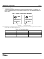
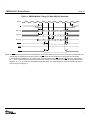
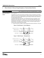
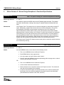
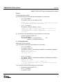
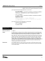
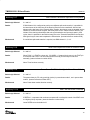
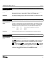
TMS320C6201 Digital Signal Processor Silicon Errata SPRZ153 November 2000 Copyright 2000, Texas Instruments Incorporated TMS320C6201 Silicon Errata SPRZ153 Contents 1 Introduction . . . . . . . . . . . . . . . . . . . . . . . . . . . . . . . . . . . . . . . . . . . . . . . . . . . . . . . . . . . . . . . . . . . . . . . . . . . . . . . . . . . . . . . . 1.1 Quality and Reliability Conditions . . . . . . . . . . . . . . . . . . . . . . . . . . . . . . . . . . . . . . . . . . . . . . . . . . . . . . . . . . . . . . . . . . TMX Definition . . . . . . . . . . . . . . . . . . . . . . . . . . . . . . . . . . . . . . . . . . . . . . . . . . . . . . . . . . . . . . . . . . . . . . . . . . . . . . . . . . TMP Definition . . . . . . . . . . . . . . . . . . . . . . . . . . . . . . . . . . . . . . . . . . . . . . . . . . . . . . . . . . . . . . . . . . . . . . . . . . . . . . . . . . TMS Definition . . . . . . . . . . . . . . . . . . . . . . . . . . . . . . . . . . . . . . . . . . . . . . . . . . . . . . . . . . . . . . . . . . . . . . . . . . . . . . . . . . 1.2 Revision Identification . . . . . . . . . . . . . . . . . . . . . . . . . . . . . . . . . . . . . . . . . . . . . . . . . . . . . . . . . . . . . . . . . . . . . . . . . . . . 4 4 4 4 4 5 2 Changes to the TMS320C6201 Data Sheet (literature number SPRS051) . . . . . . . . . . . . . . . . . . . . . . . . . . . . . . . . . 6 3 Silicon Revision 3.1 Known Design Exceptions to Functional Specifications . . . . . . . . . . . . . . . . . . . . . . . . . . . . 8 Advisory 3.1.1 Issues When Pausing at a Block Boundary . . . . . . . . . . . . . . . . . . . . . . . . . . . . . . . . . . . . . . . . . . . . . . . 8 Advisory 3.1.2 DMA: Transfer Incomplete When Pausing a Synchronized Transfer in Mid-frame . . . . . . . . . . . . . . 8 Advisory 3.1.3 DMA Multiframe Split-mode Transfers Source Address Indexing Not Functional . . . . . . . . . . . . . . . 9 Advisory 3.1.4 DMA: Stopped Transfer Reprogrammed Does Not Wait for Sync . . . . . . . . . . . . . . . . . . . . . . . . . . . . 9 Advisory 3.1.5 DMA Freezes if Postincrement/Decrement Across Port Boundary . . . . . . . . . . . . . . . . . . . . . . . . . . . 9 Advisory 3.1.6 DMA Paused During Emulation Halt . . . . . . . . . . . . . . . . . . . . . . . . . . . . . . . . . . . . . . . . . . . . . . . . . . . . 10 Advisory 3.1.7 DMA: RSYNC = 10000b (DSPINT) Does Not Wait for Sync . . . . . . . . . . . . . . . . . . . . . . . . . . . . . . . . 10 Advisory 3.1.8 EMIF: Invalid SDRAM Access to Last 1K Byte of CE3 . . . . . . . . . . . . . . . . . . . . . . . . . . . . . . . . . . . . . 10 Advisory 3.1.9 Cache During Emulation With Extremely Slow External Memory . . . . . . . . . . . . . . . . . . . . . . . . . . . . 11 4 Silicon Revision 3.0 Known Design Exceptions to Functional Specifications . . . . . . . . . . . . . . . . . . . . . . . . . . . 12 Advisory 3.0.8 EMIF: Inverted SDCLK and SSCLK at Speeds Above 175 MHz . . . . . . . . . . . . . . . . . . . . . . . . . . . . 12 Advisory 3.0.9 CPU: L2-unit Long Instructions Corrupted During Interrupt . . . . . . . . . . . . . . . . . . . . . . . . . . . . . . . . . 14 5 Silicon Revision 2.1 Known Design Exceptions to Functional Specifications . . . . . . . . . . . . . . . . . . . . . . . . . . . Advisory 2.1.1 EMIF: CE Space Crossing on Continuous Request Not Allowed . . . . . . . . . . . . . . . . . . . . . . . . . . . . Advisory 2.1.2 EMIF: SDRAM Invalid Access . . . . . . . . . . . . . . . . . . . . . . . . . . . . . . . . . . . . . . . . . . . . . . . . . . . . . . . . . . Advisory 2.1.4 DMA: RSYNC Cleared Late for Frame-synchronized Transfer . . . . . . . . . . . . . . . . . . . . . . . . . . . . . . Advisory 2.1.5 McBSP: DXR to XSR Copy Not Generated . . . . . . . . . . . . . . . . . . . . . . . . . . . . . . . . . . . . . . . . . . . . . . Advisory 2.1.6 DMA Split-mode End-of-frame Indexing . . . . . . . . . . . . . . . . . . . . . . . . . . . . . . . . . . . . . . . . . . . . . . . . . Advisory 2.1.7 DMA Channel 0 Multiframe Split-Mode Incompletion . . . . . . . . . . . . . . . . . . . . . . . . . . . . . . . . . . . . . . Advisory 2.1.8 Timer Clock Output Not Driven for External Clock . . . . . . . . . . . . . . . . . . . . . . . . . . . . . . . . . . . . . . . . Advisory 2.1.9 Power-Down Pin PD Not Set High for Power-Down 2 Mode . . . . . . . . . . . . . . . . . . . . . . . . . . . . . . . . Advisory 2.1.10 EMIF: RBTR8 Bit Not Functional . . . . . . . . . . . . . . . . . . . . . . . . . . . . . . . . . . . . . . . . . . . . . . . . . . . . . . . Advisory 2.1.11 McBSP: Incorrect mLaw Companding Value . . . . . . . . . . . . . . . . . . . . . . . . . . . . . . . . . . . . . . . . . . . . . Advisory 2.1.12 False Cache Hit – Extremely Rare . . . . . . . . . . . . . . . . . . . . . . . . . . . . . . . . . . . . . . . . . . . . . . . . . . . . . . Advisory 2.1.13 EMIF: HOLD Feature Improvement on Revision 3 . . . . . . . . . . . . . . . . . . . . . . . . . . . . . . . . . . . . . . . . Advisory 2.1.14 EMIF: HOLD Request Causes Problems With SDRAM Refresh . . . . . . . . . . . . . . . . . . . . . . . . . . . . Advisory 2.1.15 DMA Priority Ignored by PBUS . . . . . . . . . . . . . . . . . . . . . . . . . . . . . . . . . . . . . . . . . . . . . . . . . . . . . . . . . Advisory 2.1.16 DMA Split-mode Receive Transfer Incomplete After Pause . . . . . . . . . . . . . . . . . . . . . . . . . . . . . . . . Advisory 2.1.17 DMA Multiframe Transfer Data Lost During Stop . . . . . . . . . . . . . . . . . . . . . . . . . . . . . . . . . . . . . . . . . Advisory 2.1.18 Bootload: HPI Feature Improvement on Revision 3 . . . . . . . . . . . . . . . . . . . . . . . . . . . . . . . . . . . . . . . 15 15 15 16 16 18 19 19 19 19 20 20 20 21 21 22 22 22 2 TMS320C6201 Silicon Errata SPRZ153 Advisory 2.1.19 PMEMC: Branch from External to Internal . . . . . . . . . . . . . . . . . . . . . . . . . . . . . . . . . . . . . . . . . . . . . . . 23 Advisory 2.1.21 DMA: DMA Data Block Corrupted After Start Zero Transfer Count . . . . . . . . . . . . . . . . . . . . . . . . . . 23 6 7 Silicon Revision 2.0 Known Design Exceptions to Functional Specifications . . . . . . . . . . . . . . . . . . . . . . . . . . . Advisory 2.0.1 Program Fetch: Cache Modes Not Functional . . . . . . . . . . . . . . . . . . . . . . . . . . . . . . . . . . . . . . . . . . . . Advisory 2.0.2 Bootload: Boot from 16-Bit and 32-Bit Asynchronous ROMs Not Functional . . . . . . . . . . . . . . . . . . Advisory 2.0.3 DMA Channel 0 Split Mode Combined With autoinitialization Performs Improper Reinitialization . . . . . . . . . . . . . . . . . . . . . . . . . . . . . . . . . . . . . . . . . . . . . . . . . . . . . . . . . . . . . . . . . . . . . . . Advisory 2.0.4 DMA/Program Fetch: Cannot DMA into Program Memory From External . . . . . . . . . . . . . . . . . . . . Advisory 2.0.5 Data Access: Parallel Accesses to EMIF or Internal Peripheral Bus Location Sequenced Wrong . . . . . . . . . . . . . . . . . . . . . . . . . . . . . . . . . . . . . . . . . . . . . . . . . . . . . . . . . . . . . . . . . . . Advisory 2.0.7 EMIF: Reserved Fields Have Incorrect Values . . . . . . . . . . . . . . . . . . . . . . . . . . . . . . . . . . . . . . . . . . . . Advisory 2.0.8 EMIF: SDRAM Refresh/DCAB Not Performed Prior to HOLD Request Being Granted . . . . . . . . . Advisory 2.0.9 McBSP New Block Interrupt Does Not Occur for Start of Block 0 . . . . . . . . . . . . . . . . . . . . . . . . . . . Advisory 2.0.11 DMA/Internal Data Memory: First Load Data Corrupted When DMA in High Priority . . . . . . . . . . . Advisory 2.0.12 McBSP: FRST Improved in 2.1 over 2.0 . . . . . . . . . . . . . . . . . . . . . . . . . . . . . . . . . . . . . . . . . . . . . . . . . Advisory 2.0.13 McBSP: XEMPTY Stays Low When DXR Written Late . . . . . . . . . . . . . . . . . . . . . . . . . . . . . . . . . . . . Advisory 2.0.14 EMIF: Multiple SDRAM CE Spaces: Invalid Access After Refresh . . . . . . . . . . . . . . . . . . . . . . . . . . . Advisory 2.0.18 DMA/Internal Data Memory: Conflict Data Corruption . . . . . . . . . . . . . . . . . . . . . . . . . . . . . . . . . . . . . Advisory 2.0.19 EMIF: Data Setup Times . . . . . . . . . . . . . . . . . . . . . . . . . . . . . . . . . . . . . . . . . . . . . . . . . . . . . . . . . . . . . . Advisory 2.0.24 EMIF Extremely Rare Cases Cause an Improper Refresh Cycle to Occur . . . . . . . . . . . . . . . . . . . . 24 24 24 24 24 25 25 25 26 26 26 27 27 27 28 28 Documentation Support . . . . . . . . . . . . . . . . . . . . . . . . . . . . . . . . . . . . . . . . . . . . . . . . . . . . . . . . . . . . . . . . . . . . . . . . . . . . 28 3 TMS320C6201 Silicon Errata 1 SPRZ153 Introduction This document describes the silicon updates to the functional specifications for the TMS320C6201 silicon releases 3.1, 3.0, 2.1, and 2.0. 1.1 Quality and Reliability Conditions TMX Definition Texas Instruments (TI) does not warranty either (1) electrical performance to specification, or (2) product reliability for products classified as “TMX.” By definition, the product has not completed data sheet verification or reliability performance qualification according to TI Quality Systems Specifications. The mere fact that a “TMX” device was tested over a particular temperature and voltage ranges should not, in any way, be construed as a warranty of performance. TMP Definition TI does not warranty product reliability for products classified as “TMP.” By definition, the product has not completed reliability performance qualification according to TI Quality Systems Specifications; however, products are tested to a published electrical and mechanical specification. TMS Definition Fully-qualified production device. 4 TMS320C6201 Silicon Errata 1.2 SPRZ153 Revision Identification The device revision can be determined by the lot trace code marked on the top of the package. The location for the lot trace codes for the GJL package is shown in Figure 1 and the revision numbers are listed in Table 1. Figure 1. Example, Lot Trace Code for TMS320C6201 DSP DSP TMS320C6201GJL TMS320C6201GJL Cxx–YMLLLLS C31–YMLLLLS Lot trace code Lot trace code with revision 3.1 NOTE: Qualified devices are marked with the letters “TMS” at the beginning of the device name, while nonqualified devices are marked with the letters “TMX” at the beginning of the device name. Table 1. Lot Trace Number Names Lot Trace Code Silicon Revision 20 2.0 21 2.1 30 3.0 31 3.1 Comments 5 TMS320C6201 Silicon Errata 2 SPRZ153 Changes to the TMS320C6201 Data Sheet (literature number SPRS051) Table 2. Timing Requirements for Interrupt Response Cycles C6201B NO NO. 4 td(CKO2L-IACKV) Delay time, CLKOUT2 low to IACK valid 5 td(CKO2L-INUMV) Delay time, CLKOUT2 low to INUMx valid 6 td(CKO2L-INUMIV) Delay time, CLKOUT2 low to INUMx invalid UNIT MIN MAX –4 6 ns 6 ns –4 ns Table 3. JTAG Test-Port Timing C6201, C6201B NO. MIN UNIT MAX 1 Tc(TCK) Cycle time, TCK 50 ns 4 Th(TCKH-TDIV) Hold time, TDI/TMS/TRST valid after TCK high 9 ns Figure 2. SBSRAM Read Timing (1/2 Rate SSCLK) (See Note) SSCLK 1 2 CE 3 BE_ [3:0] 4 BE1 BE2 BE3 BE4 A2 A3 A4 5 EA [21:2] 6 A1 8 7 ED [31:0] Q1 9 Q2 Q3 Q4 10 SSADS 11 12 SSOE SSWE NOTE: The CEx output setup and hold times are specified to be accurate relative to the clock cycle to which they are referenced, since these timings are specified as minimums. However, the CE output setup and hold time may be greater than that shown in the data sheet in multiples of P ns. In other words, for output setup time, the CEx transition from high to low may happen P, 2P, …, or nP ns before the time specified by the data sheet. Similarly, for output hold time, the CEx low-to-high transition may happen P, 2P, …, or nP ns after the time specified by the data sheet. This is indicated by the period of uncertainty for specs 1 and 2 in Figure 2, and Figure 3. 6 TMS320C6201 Silicon Errata SPRZ153 Figure 3. SBSRAM Write Timing (1/2 Rate SSCLK) (See Note) SSCLK 1 2 CE 3 BE_ [3:0] 4 BE1 BE2 BE3 BE4 EA [21:2] A1 A2 A3 A4 ED [31:0] Q1 5 6 13 Q2 14 Q3 Q4 9 10 15 16 SSADS SSOE SSWE NOTE: The CEx output setup and hold times are specified to be accurate relative to the clock cycle to which they are referenced, since these timings are specified as minimums. However, the CE output setup and hold time may be greater than that shown in the data sheet in multiples of P ns. In other words, for output setup time, the CEx transition from high to low may happen P, 2P, …, or nP ns before the time specified by the data sheet. Similarly, for output hold time, the CEx low-to-high transition may happen P, 2P, …, or nP ns after the time specified by the data sheet. This is indicated by the period of uncertainty for specs 1 and 2 in Figure 2, and Figure 3. 7 TMS320C6201 Silicon Errata 3 SPRZ153 Silicon Revision 3.1 Known Design Exceptions to Functional Specifications Advisory 3.1.1 Issues When Pausing at a Block Boundary Revision(s) Affected: 3.1, 3.0, 2.1, and 2.0 Details: The following problems exist when a DMA channel is paused at a block boundary: Workaround: Advisory 3.1.2 • DMA does not flush internal FIFO when a channel is paused across block boundary. As a result, data from old and new blocks of that channel are in FIFO simultaneously. This prevents other channels from using the FIFO for high performance until that channel is restarted. Data is not lost when that channel is started again. (Internal reference number C601299) • For DMA transfers with autoinitialization, if a channel is paused just as the last transfer in a block completes (just as the transfer counter reaches zero), none of the register reloads take place (count, source address, and destination address). When the same channel is restarted, the channel will not transfer anything due to the zero transfer count. This problem only occurs at block boundaries. (Internal reference number C601258) Do not pause across block boundary if the internal FIFO is to be used by other channels for high performance. For DMA transfers with autoinitialization, if a channel is paused with a zero transfer count, manually reload all registers before restarting the channel. DMA: Transfer Incomplete When Pausing a Synchronized Transfer in Mid-frame Revision(s) Affected: 3.1, 3.0, 2.1, and 2.0 Details: If a frame-synchronized transfer is paused in mid-frame and then restarted again, a DMA channel does not continue the transfer. Instead, the channel waits for synchronization. If the channel is manually synchronized, it will properly complete the frame, but will immediately begin the transfer of the next frame. This behavior occurs for both a software pause (setting START = 10b) and for an emulation halt (with EMOD = 1). (Internal reference number C601257) Workaround: If pausing the DMA channel in software, do the following to restart: 1. Set the RSYNC bit in the Secondary Control Register. 2. Read the Transfer Count Register and then write back to Transfer Count Register. This enables the present frame to transfer but will wait for the next sync event to trigger the next frame transfer. 3. Set START to 01b or 11b. If pausing the DMA channel with an emulation halt, do the following to restart: 1. Double-click on the Transfer Count Register and hit enter (rewrite current transfer count). 2. Set the RSYNC STAT bit in the Secondary Control Register (change 0xXXXX4XXX to 0xXXXX1XXX). 3. Run. NOTE: The sequence of 1 and 2 is critical for an emulator halt (EMOD = 1), but not for the software pause. 8 TMS320C6201 Silicon Errata Advisory 3.1.3 SPRZ153 DMA Multiframe Split-mode Transfers Source Address Indexing Not Functional Revision(s) Affected: 3.1, 3.0, 2.1, and 2.0 Details: If a DMA channel is configured to do a multiframe split-mode transfer with SRC_DIR = Index (11b), the source address is always modified using the Element Index, even during the last element transfer of a frame. The transfer of the last element in a frame should index the source address using the Frame Index instead of the Element Index. DST_DIR = 11b functions properly. (Internal reference number C601256) Workaround: For multiframe transfers, use two DMA channels instead of using the split mode. Source Index works properly for non-split-mode transfers. Advisory 3.1.4 DMA: Stopped Transfer Reprogrammed Does Not Wait for Sync Revision(s) Affected: 3.1, 3.0, 2.1, and 2.0 Details: If any non-synchronized transfer (e.g., auto-init transfer) is stopped, and then the same channel is programmed to do a write-synchronized transfer (e.g., split-mode transfer), the write transfer does not wait for the sync event. (Internal reference number C601261) Workaround: Perform a nonsynchronized dummy transfer of one element to/from the same location before starting the synchronized transfer. Advisory 3.1.5 DMA Freezes if Postincrement/Decrement Across Port Boundary Revision(s) Affected: 3.1, 3.0, 2.1, and 2.0 Details: For any DMA transfers with source/destination address postincrement/decrement, if the last element to be transferred is aligned on a port boundary, then the DMA may freeze before transferring this element. A port boundary is the address boundary between external memory and program memory, between external memory and the peripheral address space, or between program memory and the peripheral address space. The following conditions cause DMA to freeze: Workaround: • For non-sync and frame-sync transfers: if a channel is paused after the second-to-last element is read, the DMA will freeze when the channel is then restarted with a request to the address at a port boundary. • For split-mode transfers or read/write-sync transfers: the DMA will freeze while transferring the element aligned on the port boundary. A continuous burst transfer with post-increment/decrement source/destination address does not exhibit this problem. (Internal reference number C601300) Do not transfer to boundary addresses if the DMA source/destination address is post-incremented/ decremented. 9 TMS320C6201 Silicon Errata SPRZ153 Advisory 3.1.6 DMA Paused During Emulation Halt Revision(s) Affected: 3.1, 3.0, 2.1, and 2.0 Details: When running an autoinitialized transfer, the DMA write state machine is halted during an emulation halt regardless of the value of EMOD in the DMA Channel Primary Control Register. The read state machine functions properly in this case. The problem exists only at block boundaries. If EMOD = 1, this problem is irrelevant since the DMA channel is expected to pause during an emulation halt. (Internal reference number C601301) Workaround: There is no workaround for EMOD = 0. Expect DMA transfers to pause when the emulator stops the processor. Advisory 3.1.7 DMA: RSYNC = 10000b (DSPINT) Does Not Wait for Sync Revision(s) Affected: 3.1, 3.0, 2.1, and 2.0 Details: If RSYNC in the DMA Channel Primary Control Register is set to host-port host-to-DSP interrupt (DSPINT – 10000b), the DMA channel would do the read transfer without waiting for the sync event. There is not a problem if WSYNC is set to DSPINT. (Internal reference number C601302) Workaround: Do not use synchronized DMA reads to DSPINT. If a DMA read is desired during a host-port host-to-DSP interrupt, set RSYNC in the Primary Control Register to one of the EXT_INT events instead (EXT_INT4 – EXT_INT7) and have the host trigger an interrupt on that pin rather than by writing to HPIC. Advisory 3.1.8 EMIF: Invalid SDRAM Access to Last 1K Byte of CE3 Revision(s) Affected: 3.1, 3.0, 2.1, and 2.0 Details: If 16M bytes of SDRAM (two 64M bits in a 1M X 16x4 organization) is used in CE3, you can have invalid accesses to the last 1K byte of CE3 (0x03FFFC00). This occurs when the following is true: Workaround: • After a DCAB (deactivate all pages) to all SDRAM CE spaces (forced by Refresh or MRS command) • The first access to CE3 is to the last page of CE3 (0x03FFFC00). • Then a page activate will not be issued to CE3. Since the SDRAM in CE3 is in a deactivated state at that point, invalid accesses will occur. (Internal reference number C630280) Best Case: Avoid designing a board with a 64M-bit (1M X 16x4) SDRAM mapped into CE3. 10 TMS320C6201 Silicon Errata SPRZ153 Alternative: If a 64M-bit SDRAM is located in CE3, avoid using the last 1K byte in the CE3 memory map (0x03FFFC00). Advisory 3.1.9 Cache During Emulation With Extremely Slow External Memory Revision(s) Affected: 3.1, 3.0, 2.1, and 2.0 Details: If a program requests fetch packet “A” followed immediately by fetch packet “B”, and all of the following four conditions are true: 1. A and B are separated by a multiple of 64K in memory (i.e., they will occupy the same cache frame) 2. B is currently located in cache 3. You are using the emulator to single-step through the branch from A to B 4. The code is running off of an extremely slow external memory that transfers one 32-bit word every 8000 or more CPU clock cycles (CPU running at 200 MHz) Then A will be registered as a “miss” and B will be registered as a “hit”. B will not be reloaded into cache, and A will be executed twice. This condition is extremely rare because B has to be in cache memory, and must be the next fetch packet requested after A (which is not in cache memory). In addition, this problem only occurs if you single-step through the branch from A to B using the emulator, and if the code is located in an extremely slow external memory. (Internal reference number C630283) Workaround: • Do not single-step through the branch from A to B if the above conditions are true. • Do not use an extremely slow external memory (transfers one 32-bit word every 8000 or more CPU clock cycles) if conditions 1, 2, and 3 are true. 11 TMS320C6201 Silicon Errata 4 SPRZ153 Silicon Revision 3.0 Known Design Exceptions to Functional Specifications Advisory 3.0.8 EMIF: Inverted SDCLK and SSCLK at Speeds Above 175 MHz Revision(s) Affected: 3.0, 2.1, and 2.0 Details: A speedpath in the device causes SDCLK and SSCLK to start up 180 degrees out-of-phase (effectively inverted) from the desired waveform. Normally, EMIF outputs are delayed 1/2 CPU clock from the rising edge of SDCLK/SSCLK to give it adequate hold time while maintaining more than adequate setup times. The desired relationship is described in the TMS320C6201B data sheet (SPRS051) and is illustrated in Figure 4 and Figure 6. However, in the case where SDCLK/SSCLK becomes inverted (Figure 5 and Figure 7), control signals only have 1/2 CPU clock of setup to the next SDCLK/SSCLK rising rather than 3/2 CPU clock of setup. This has two negative effects to interface timing to external synchronous RAMs. 1. On writes, setup time to RAMs for control signals and write data is reduced by 1 CPU cycle. Figure 4. Write Example – Desired Behavior CLKOUT1 (CPU Clock) SS/SDCLK Internal SS/SDCLK External tosu toh Output Signals Figure 5. Write Example – Failing Behavior CLKOUT1 (CPU Clock) SS/SDCLK Internal SS/SDCLK External toh tosu Output Signals 12 TMS320C6201 Silicon Errata SPRZ153 EMIF: Inverted SDCLK and SSCLK at Speeds Above 175 MHz (Continued) 2. On SBSRAM/SDRAM reads, data will be sampled on the falling edge before the rising edge that would be expected. In this case, the input setup time for data at the C62xt is reduced by 1 CPU cycle. Note that this case can be compounded with Case 1. The control signals could be latched one SSCLK/SDCLK cycle (2 CPU cycles) late by the memories. Thus, the setup could be reduced by up to 3 CPU cycles and be more than an entire SSCLK/SDCLK late. Figure 6. Read Example – Desired Behavior CLKOUT1 (CPU Clock) SS/SDCLK Internal SS/SDCLK External tisu tacc Read Data Figure 7. Read Example – Failing Behavior CLKOUT1 (CPU Clock) SS/SDCLK Internal SS/SDCLK External tisu tacc Read Data CLKOUT2 is also affected by this speedpath bug and is 180 degrees out-of-phase. It behaves in the same way as SDCLK. (Internal reference number C601307) Workaround: • For prototypes, raising the core supply to 1.9 – 2.1 V corrects this problem. This is not recommended in boards shipped to customers, since the manufacturing process is not designed to be reliable outside the normal operating range. This option allows the user to verify current board designs at all valid frequency ranges. • Reduce the operating frequency of the TMS320C6201B until SSCLK/SDCLK has the desired relationship. Typically, this occurs at 175 MHz across the range of recommended operating conditions. • Since SSCLK and SDCLK are inverted externally relative to each other by design, these signals can be swapped on external memory interfaces to correct the problem (SSCLK to SDRAM and SDCLK to SBSRAM). This will cause invalid operation at frequencies below 175 MHz and will not work with future silicon revisions. • If CLKOUT2 is used as an SDRAM clock, follow all the workarounds for SDCLK. C62x is a trademark of Texas Instruments Incorporated. 13 TMS320C6201 Silicon Errata SPRZ153 EMIF: Inverted SDCLK and SSCLK at Speeds Above 175 MHz (Continued) Alternate Workaround: Resolution The following alternate workarounds can help for certain board and layout configurations. • Using faster (125 MHz or PC100) SDRAMs and/or SBSRAMs will reduce the chances of data corruption and/or increase the frequency at which reliable memory operation can be observed. Operation is not specified to be reliable across operating conditions and different samples of memory and C6201B devices due to lot-to-lot variation on both the memory and the C6201B. • SDCLK/SSCLK can be delayed externally. This can be accomplished either via inverter(s), precision delay device, or longer board route on the clock line. The idea is to force the external clock to resemble the desired clock waveform as closely as possible, providing more setup for both reads and writes. • You may start the device at a frequency where the skew does not occur and raise the operating frequency to the desired rate. This must be done at each processor reset. This solution works since the speedpath exists in the reset (non-run time) operation of the SDCLK/SSCLK circuit. Whatever operations starts at reset is observable until the next reset. • Revision 3.1 of silicon will correct this problem. Advisory 3.0.9 CPU: L2-unit Long Instructions Corrupted During Interrupt Revision(s) Affected: 3.0, 2.1, and 2.0 Details: If an interrupt occurs causing a B-side L-unit (.L2 unit) instruction that writes a long value to be annulled, the top 8 bits of the result will be written rather than being annulled. This bug only applies to the B-side L-unit (.L2 unit). The A-side L-unit (.L1 unit) functions correctly. (Internal reference number C620774) This bug will not affect: Workaround: Resolution • Customers programming in C with no long data types. • Customers not using code with long instructions on the .L2-unit. • Customers only using long instructions on the .L2-unit inside loops 5 or less than 5 cycles long. (Interrupts are disabled in the five delay slots of a branch.) • Disable interrupts using the appropriate compiler switches or register modifications in the affected C code. • Disable interrupts seven execute packets before any long instructions on the .L2-unit that are not in the delay slots of a branch. • Use the .L1-unit for long instructions if interrupts are anticipated. • Revision 3.1 of silicon will correct this problem. 14 TMS320C6201 Silicon Errata 5 SPRZ153 Silicon Revision 2.1 Known Design Exceptions to Functional Specifications Advisory 2.1.1 EMIF: CE Space Crossing on Continuous Request Not Allowed Revision(s) Affected: 2.1 and 2.0 Details: Any continuous request of the EMIF cannot cross CE address space boundaries. This condition can result in bad data read, or writing to the wrong CE. (Internal Reference Numbers 2600 and 3421) Workaround: CPU Program Fetch: The simplest fix is for all external program to reside within a single CE space. Alternatively, program fetch flow should not occur across CE spaces. This can be accomplished by branching on-chip between executing from one CE to another CE. DMA: All DMA block transfers without read or write synchronization should have all EMIF addresses within a frame to belong to one CE space. In other words, all read (src) addresses should belong to one CE space and should not cross CE boundaries. The same applies to write (dst) addresses within a frame. Note that the source can be in the same CE space or different CE space as the destination. DMA transfers with read and/or write synchronization together with CE boundaries crossed between frames are not affected by this bug. CPU Data Access: External CPU data accesses cannot perform continuous requests and thus are not affected by this bug. Advisory 2.1.2 EMIF: SDRAM Invalid Access Revision(s) Affected: 2.1 and 2.0 Details: An invalid SDRAM access occurs when all of the following are true: • • • • Two or more SDRAM devices in different CE spaces • • • Two or more SDRAM devices in different CE spaces • If request to second CE space occurs before refresh occurs, then an invalid access takes place, since the controller neglects the fact that this space was deactivated. (Internal Reference Numbers 4139, 0335, and 0871) Each SDRAM device has a page activate One active page is in bank 0 and the other in bank 1 Each CE space with SDRAM is accessed (alternating) without a page miss or refresh occurring (no Deactivate command). OR A trickle refresh deactivates both devices Before refresh occurs, a request to access one CE space comes in. The refresh will wait until the first requester has completed. 15 TMS320C6201 Silicon Errata SPRZ153 EMIF: SDRAM Invalid Access (Continued) Workaround: Avoid use of multiple CE spaces of SDRAM within a single refresh period. Advisory 2.1.4 Revision(s) Affected: DMA: RSYNC Cleared Late for Frame-synchronized Transfer 2.1 and 2.0 In a frame-synchronized transfer, RSYNC is only cleared after the beginning of last write transfer. It should occur after the start of the first read transfer in the synchronized frame. (Internal reference number 0267) Workaround: Wait until end-of-frame (perhaps using DMAC pins for external status) to issue next frame synchronization. Advisory 2.1.5 McBSP: DXR to XSR Copy Not Generated Revision(s) Affected: 2.1 and 2.0 Details: If any element size other than 32 bits is written to the DXR of either serial port, then the register is not copied to the XSR. (Internal reference number 0511) Workaround: The following workaround is applicable only for non-split mode DMA transfers. 1. For little-endian mode: Always write 32 bits to the DXR. When using the DMA, it is possible to perform word transfers, but increment or decrement the address by one or two bytes using one of the global index registers. If the serial port is transferring out 16-bit words, which are stored on consecutive half-word boundaries in memory (either internal or external), the DMA would need to be set up such that it performs word writes to DXR (ESIZE = 00b). The global index register used would need an element index of 0x0002 (2 bytes). If an 8-bit data transfer is desired, then element index would need to be 0x0001. Please note that this workaround assumes that the receive justification, RJUST in the McBSP’s SPCR is set for right justification (zero-fill or sign-extended). If left justification is chosen for receive data, the DMA receive src address pointing to DRR should be changed to DRR+3 (which is 0x018C0003 for McBSP0 and 0x01900003 for McBSP1) for byte-size elements and DRR+2 for half-word elements. This ensures packing data on byte or half-word boundaries for receive data. 16 TMS320C6201 Silicon Errata SPRZ153 McBSP: DXR to XSR Copy Not Generated (Continued) Example: Configure the DMA as follows: (a) For half-word/byte-size accesses with right justification on receive data: – ch_A: /* for transmit */ src_address = mem_out; dst_address = DXR; Element_size = WORDAddress_inc_mode = indexIndex_reg_value = 2 /* change this to 1 for byte writes */ – ch_B : /* for receive */ src_address = DRR; dst_address = mem_in; Element_size = HALF /* change this to BYTE for 8-b element size */Address_inc_mode = inc_by_ element_size /* inc_by_index whose value is as specified for ch_A above will also work */ (b) For half-word / byte-size accesses with left justification on receive data: – Same as 1(a) above EXCEPT for: ch_B : /* for receive */ src_address = DRR+3; /* for byte accesses */ = DRR+2; /* for half-word accesses */ OR 2. For big-endian mode: Always write 32 bits to the DXR. (a) For half-word accesses with right justification on receive data: – ch_A: /* for transmit */ src_address = mem_out; dst_address = DXR+2; /* 0x018C0006 for McBSP0 or 0x01900006 for McBSP1 */ Element_size = WORD Address_inc_mode = index Index_reg_value = 2 – ch_B : /* for receive */ src_address = DRR+2 /* 0x018C0002 for McBSP0 or 0x01900002 for McBSP1 */ dst_address = mem_in; Element_size = HALF; Address_inc_mode = = inc_by_ element_size /* inc_by_index whose value is as specified for ch_A above will also work */ (b) For half-word writes with left justification on receive data: – Same as 2(a) above EXCEPT for: ch_B : /* for receive */ src_address = DRR; 17 TMS320C6201 Silicon Errata SPRZ153 McBSP: DXR to XSR Copy Not Generated (Continued) (c) For byte-size writes with right justification on receive data: – ch_A: /* for transmit */ dst_address = DXR+3; /* 0x018C0007 for McBSP0 or 0x01900007 for McBSP1 */ Element_size = WORDAddress_inc_mode = indexIndex_reg_value = 1 – ch_B : /* for receive */ src_address = DRR+3 /* 0x018C0003 for McBSP0 or 0x01900003 for McBSP1 */ dst_address = mem_in; Element_size = BYTE; Address_inc_mode = = inc_by_ element_size /* inc_by_index whose value is as specified for ch_A above will also work */ (d) For byte-size writes with left justification on receive data: – Advisory 2.1.6 Same as 2(c) above EXCEPT for: ch_B : /* for receive */ src_address = DRR; DMA Split-mode End-of-frame Indexing Revision(s) Affected: 2.1 and 2.0 Details: If a DMA channel is configured to do a multiframe split-mode transfer, both the Receive and Transmit transfers will generate an end-of-frame condition. This will cause the FRAME COND bit to be set multiple times per frame in the Secondary Control Register of the channel. Also, if DST_DIR = Index (11b), the end-of-frame condition by both the Receive and Transmit Transfers will cause a destination address to be incremented using Frame Index, rather than Element Index. The problem is that both the last element in a frame for the Receive Read Transfer (split source to destination) and the last element in a frame for the Transmit Write Transfer (source to split destination) will cause the destination address to be indexed using the frame index. This should only occur for the last element in a frame for the Receive Read Transfer. (Internal reference number 0559) Workaround: If the FRAME COND bit is used to generate an interrupt to the CPU and/or the frame index and the element index on the destination address are not the same for a split-mode transfer, use two DMA channels. 18 TMS320C6201 Silicon Errata SPRZ153 Advisory 2.1.7 DMA Channel 0 Multiframe Split-Mode Incompletion Revision(s) Affected: 2.1 and 2.0 Details: If DMA Channel 0 is configured to perform a multiframe split-mode transfer, it is possible for the last element of the last frame of the Receive Read to not be transferred. After the last element of the last frame of the Transmit Write Transfer, the element count is reloaded into the Channel 0 Transfer Counter Register, which may allow for the Transmit Read Transfer to be initiated. If the read synchronization and write synchronization are far enough apart in CPU cycles, then it is possible for the DMA to hang (due to the Transmit Read) before the Receive Write gets its sync event and completes the transmission. (Internal reference number 0558) Workaround: If a multiframe split-mode transfer is required, use DMA channel 1, 2, or 3. Advisory 2.1.8 Timer Clock Output Not Driven for External Clock Revision(s) Affected: 2.1 and 2.0 Details: When FUNC = 1 (TOUT is a timer pin), if CLKSRC = 0 (external clock source), the TOUT pin is not driven with TSTAT. The timer still functions correctly, but the output is not seen externally. (Internal reference number 0568) Workaround: None. Timer functions correctly. Advisory 2.1.9 Power-Down Pin PD Not Set High for Power-Down 2 Mode Revision(s) Affected: 2.1 and 2.0 Details: The power-down pin, PD, only goes high (active) in power-down mode 3, not in power-down mode 2. (Internal reference number 0537) Workaround: None. Power-down modes function correctly. Advisory 2.1.10 EMIF: RBTR8 Bit Not Functional Revision(s) Affected: 2.1 and 2.0 Details: If RBTR8=1, a requester with continuous requests will not relinquish control of the EMIF even to a higher-priority requester. (Internal reference number 0432) Workaround: Leave RBTR8 set to the default of 0. 19 TMS320C6201 Silicon Errata SPRZ153 McBSP: Incorrect mLaw Companding Value Advisory 2.1.11 Revision(s) Affected: 2.1 and 2.0 Details: The C6201 McBSP m-Law/A-Law companding hardware produces an incorrectly expanded m-Law value. McBSP receives m-Law value 0111 1111, representing a mid-scale analog value. Expanded 16-bit data is 1000 0000 0000 0000, representing a most negative value. Expected value is 0000 0000 0000 0000. McBSP expands µ-Law 1111 1111 (also mid-scale value) correctly. m-Law works correctly for all encoded values, except for 0x7f. (Internal Reference Number 0651) Advisory 2.1.12 False Cache Hit – Extremely Rare Revision(s) Affected: 2.1 and 2.0 Details: If a program requests fetch packet “A” followed immediately by fetch packet “B”, and the following are true: • A and B are separated by a multiple of 64K in memory (i.e., they will occupy the same cache frame) • B is currently located in cache Then, A will be registered as a “miss” and B will be registered as a “hit”. B will not be reloaded into cache, and A will be executed twice. This condition is extremely rare because B has to be in cache memory, and must be the next fetch packet requested after A (which is not in cache memory). (Internal Reference Number 4372) Workaround: The program should be relinked to force A and B to not be a multiple of 64K apart. Advisory 2.1.13 EMIF: HOLD Feature Improvement on Revision 3 Revision(s) Affected: 2.1 and 2.0 Details: This is documented as a difference between the TMX320C6201 revision 2.x (and earlier) and revision 3.0 (and later). The HOLD feature of the C6201 currently will not respond to a HOLD request if the NOHOLD bit is set at the time of the HOLD request, but is then cleared while the HOLD request is pending. In other words, for a HOLD request to be recognized, a high-to-low transition must occur on the HOLD input while the NOHOLD bit is not set. Future revisions of the device will operate as described below. If NOHOLD is set and a HOLD request comes in, the C62xt will ignore the HOLD request. If while the HOLD request is still asserted the NOHOLD bit is then deasserted, the HOLD will be acknowledged as expected. (Internal reference number 0101) Workaround: To recognize a pending HOLD request when the state of the NOHOLD bit is changed from 1 to 0, a pulse must be generated on the input HOLD line. This can be done by logically OR-ing a normally low general-purpose output (DMAC can be used) with the HOLD request signal from the requester, and creating a high pulse on the general-purpose output pin. 20 TMS320C6201 Silicon Errata Advisory 2.1.14 SPRZ153 EMIF: HOLD Request Causes Problems With SDRAM Refresh Revision(s) Affected: 2.1 and 2.0 Details: If the HOLD interface is used in a system with SDRAM, there are some situations that are likely to occur. If the NOHOLD bit is not set and an external requester attempts to gain control of the bus via the HOLD signal of the EMIF at the exact same time when the EMIF is issuing a SDRAM Refresh command, the HOLD request is never recognized. Even if the NOHOLD bit is set in the EMIF Global Control Register, SDRAM refreshes are still disabled as long as the HOLD request is pending. A single refresh after receiving the HOLD request is issued, but no additional refreshes are issued until the HOLD request is removed. The C62xt still owns the bus since the NOHOLD bit is set. In addition, if an SDRAM burst is started just prior to a HOLD request, it is possible that the request will not be recognized until a refresh occurs. This will potentially allow for the HOLD request to be ignored for several microseconds. (Internal reference number 0757 and 0777) Workaround: Do not allow a requester to activate the HOLD line without acknowledging it for longer than the SDRAM refresh period. A workaround can be accomplished by keeping the NOHOLD bit set and software-polling the HOLD bit of the EMIF Global Control Register. Software-polling of the HOLD bit in the EMIF Global Control Register will indicate when a HOLD request has been received (this can be done in the SD_INT service routine or Timer interrupt service routine). Upon detecting a HOLD request, SDRAM refreshes are disabled, NOHOLD bit is cleared, and a pulse is generated on the input HOLD signal (can use DMACx as a general-purpose output pin in combination with the requesters HOLD signal). Then, NOHOLD can be set and SDRAM refreshes enabled in anticipation of the next HOLD request. Advisory 2.1.15 DMA Priority Ignored by PBUS Revision(s) Affected: 2.1 and 2.0 Details: The CPU always has priority over the DMA when accessing peripherals. The DMA PRI bit is ignored and treated as “0”. (Internal reference number 0540) Workaround: Leave sufficient gaps in CPU accesses to the PBUS to allow the DMA time to gain adequate access. 21 TMS320C6201 Silicon Errata Advisory 2.1.16 SPRZ153 DMA Split-mode Receive Transfer Incomplete After Pause Revision(s) Affected: 2.1 and 2.0 Details: If the DMA is performing a split-mode transfer and the channel is paused after all Transmit Reads in a frame are completed but before the Receive Reads are completed, then the Receive Transfer will not complete after the channel is restarted. (Internal reference number 0606) Workaround: Do not pause a split-mode transfer at the end of a frame unless the frame has completed. Advisory 2.1.17 DMA Multiframe Transfer Data Lost During Stop Revision(s) Affected: 2.1 and 2.0 Details: If the DMA is stopped while performing an unsynchronized, multiframe transfer, all of the read data may not be written. The data will be written when the channel is restarted. This case will only occur when the frame size (element count) is 10 or less and data elements from multiple frames are in the FIFO when it is stopped. (Internal reference number 0789) Workaround: Keep frame size > 10, synchronize the frame (FS = 1), or do not stop the transfer. Advisory 2.1.18 Bootload: HPI Feature Improvement on Revision 3 Revision(s) Affected: 2.1 and 2.0 Details: This is documented as a difference between the TMX320C6201 revision 2.x (and earlier) and revision 3.0 (and later). Currently, during HPI boot, all accesses to program memory are treated as writes by the PMEMC. This means that the host may not read the internal program memory space, as doing so will overwrite the memory space, usually with all zeros. The PMEMC will be changed to differentiate between reads and writes to program memory during boot. (Internal reference number 0604) 22 TMS320C6201 Silicon Errata Advisory 2.1.19 SPRZ153 PMEMC: Branch from External to Internal Revision(s) Affected: 2.1 and 2.0 Details: The program flow is corrupted after branching from external memory to internal program memory when the following are true: • CPU is executing from external memory • A CPU stall occurs that holds the CPU until all pending program fetches complete. CPU stalls may be caused by: – – – – • External data access Multicycle NOPs Prolonged data memory bank conflict with DMA Multiple accesses to on-chip peripherals (not likely to cause this problem) A branch to internal program memory is taken before a new fetch packet is requested (i.e. during the same fetch packet that is executed when the CPU stalls. The CPU will branch correctly to the internal memory location and correctly execute the code located there. When the branch is executed to return to external memory, the CPU will not complete the branch properly and the program will crash. (Internal reference number 0958) Workaround: There are several workaround options, depending on the situation that causes the failure. One or more of the following should be used to circumvent the problem: • If the problem arises during an interrupt, move IST to external memory (same CE as code). • If the problem occurs after a branch, delay the branch instruction with single-cycle NOPs or extend the delay slots to span multiple fetch packets (i.e., follow the branch instruction with parallel NOPs). • If an external data access is causing the CPU stall, place data in internal data memory. • If a multicycle NOP is causing the stall, change to multiple single-cycle NOPs. • If the stall is due to the CPU being starved, change the DMA priority to be lower than that of the CPU. Advisory 2.1.21 DMA: DMA Data Block Corrupted After Start Zero Transfer Count Revision(s) Affected: 2.1 and 2.0 Details: If DMA is stopped after it has been started with a zero transfer count, then reprogrammed and started again, the first element of the block will be corrupted. (Internal reference number 0242) Workaround: Make sure the transfer count is not near zero when starting the DMA. 23 TMS320C6201 Silicon Errata 6 SPRZ153 Silicon Revision 2.0 Known Design Exceptions to Functional Specifications Advisory 2.0.1 Program Fetch: Cache Modes Not Functional Revision(s) Affected: 2.0 Workaround: Use internal program memory in mapped mode. Advisory 2.0.2 Bootload: Boot from 16-Bit and 32-Bit Asynchronous ROMs Not Functional Revision(s) Affected: 2.0 Details: 16-bit-wide ROM mode and 32-bit-wide asynchronous mode work in run time without bugs. The problem is only in boot. (Internal Reference Number 3088) Workaround: Place all code in the lowest byte of the boot ROM. Advisory 2.0.3 DMA Channel 0 Split Mode Combined With autoinitialization Performs Improper Reinitialization Revision(s) Affected: 2.0 Details: The source address (transmit read address) is reset too early when both split mode and autoinitialization are enabled. The bug exists on DMA channel 0 only. (Internal Reference Number 3481) Workaround: Substitute one of the other channels for channel 0 when this configuration is desired. Advisory 2.0.4 DMA/Program Fetch: Cannot DMA into Program Memory From External Revision(s) Affected: 2.0 Details: Performing a DMA transfer into program memory while running from off-chip can cause invalid program data to read by the CPU. (Internal Reference Number 2978) Workaround: DMA into program memory only when running from internal program memory. 24 TMS320C6201 Silicon Errata Advisory 2.0.5 SPRZ153 Data Access: Parallel Accesses to EMIF or Internal Peripheral Bus Location Sequenced Wrong Revision(s) Affected: 2.0 Details: Parallel read and write accesses to the same EMIF or internal peripheral bus location are sequenced incorrectly when: • A load and store are in the same execute packet and either – The addresses both point to off-chip memory through the EMIF, and the load has a destination register in side A (therefore, the store would have a source register in side B). Or – The addresses both point to the peripheral bus, and the load has a destination register in side B (therefore, the store would have a source register in side A). When these conditions occur, the store occurs first rather than the load. In general, this will only cause an error if both the load and store addresses are the same. This bug does not occur if both accesses are to internal data memory. (Internal Reference Number 3087) Workaround: Avoid loading and storing the same address on the same cycle. Advisory 2.0.7 EMIF: Reserved Fields Have Incorrect Values Revision(s) Affected: 2.0 Details: Fields in Bits 15:14 of the EMIF CE Space Control registers are writable. They should be read only and have a 0 value. Bits 5:4 of the EMIF SDRAM Control register are 11b rather than 0. (Internal Reference Number s 3248 and 3283) Workaround: Mask these values if 0s are expected and to only write 0s to reserved fields. Advisory 2.0.8 EMIF: SDRAM Refresh/DCAB Not Performed Prior to HOLD Request Being Granted Revision(s) Affected: 2.0 Details: SDRAM is left in the current state when an external HOLD is granted. SDRAM refresh/DCAB is necessary if an interface to a shared memory external SDRAM controller is desired. (Internal Reference Number 3249) Workaround: Make sure the external controller performs a refresh/DCAB before performing SDRAM accesses. 25 TMS320C6201 Silicon Errata SPRZ153 Advisory 2.0.9 McBSP New Block Interrupt Does Not Occur for Start of Block 0 Revision(s) Affected: 2.0 Details: When end-of-block interrupt is selected ((R/X)INTM=01b), McBSP new block interrupt does not occur at end of frame (i.e., before block 0). (Internal reference number 4357) Workaround: This interrupt is used when on-the-fly channel selection/enabling is being performed. A static channel selection/enabling avoids this. Advisory 2.0.11 DMA/Internal Data Memory: First Load Data Corrupted When DMA in High Priority Revision(s) Affected: 2.0 Details: In the case of a single load from A side or B side followed by two loads in parallel from both sides, and in concert with a DMA high-priority access to the same bank as the parallel load, the DMEMC provides corrupt data for that first load. (Internal Reference Number 3858) Example: Workaround: LDW .D1 *A3, A4; A4 gets corrupt data due to the bug LDW .D2 *B3, B4 || LDW .D1 *A6, A7 Avoid high-priority DMA transfers to/from internal data memory during these conditions. Advisory 2.0.12 McBSP: FRST Improved in 2.1 over 2.0 Revision(s) Affected: 2.0 Details: The following enhancements were made in 2.1. When FRST transitions to a 1, the first frame sync is generated after 8 CLKG clocks. The 2.0 implementation was such that the first frame sync was generated after FPER+1 number of CLKG clocks. FRST = 1 is valid only when GRST = 1. In other words the user has to set FRST = 1 only after GRST = 1. If not, write to FRST = 1 is ignored or rather a zero is forced on FRST by the logic. During normal operation, when FRST = 1 and GRST = 1, and now the user puts the sample rate generator in reset (GRST=0) without first clearing the FRST bit to zero, then the logic will force a zero to the FRST bit before shutting down the sample-rate generator. 26 TMS320C6201 Silicon Errata SPRZ153 Advisory 2.0.13 McBSP: XEMPTY Stays Low When DXR Written Late Revision(s) Affected: 2.0 Details: XEMPTY goes low and stays low when DXR was written on either the last bit or next-to-last bit of the previous word being transferred to DX. (Internal Reference Number 3383) Advisory 2.0.14 EMIF: Multiple SDRAM CE Spaces: Invalid Access After Refresh Revision(s) Affected: 2.0 Details: This bug exists only in those systems that have SDRAMs in more than one CE space. When there are two SDRAM accesses performed to two CE spaces, followed by a refresh, the pages in all CE spaces with SDRAM are deactivated. The first CE space to be accessed after the refresh is activated correctly. The bug is that if the second CE space is accessed on the same page as before the refresh, it will not be activated before the read or write is attempted. (Internal Reference Number 3952) Workaround: Avoid use of multiple CE spaces of SDRAM within a single refresh period. Advisory 2.0.18 DMA/Internal Data Memory: Conflict Data Corruption Revision(s) Affected: 2.0 Details: This bug occurs when the CPU has high priority and is accessing a bank with word access (load or store) followed by similar (load or store) half-word access, and the DMA is also accessing the same bank simultaneously with word accesses: Example: LDW .D1 *A3, A4 LDW .D2 *A3, A5 ; A DMA to the bank containing never completes | ; but the DMA continues as if it did The data transfer done by the DMA is corrupted in half-words (or rather not updated) when the DMA transfer is complete. (Internal Reference Number 4195) Workaround: When DMAing to/from internal memory with DMA in low priority, use half-word or byte element size transfers. Alternatively, avoid the above code sequence during DMA transfers. 27 TMS320C6201 Silicon Errata SPRZ153 Advisory 2.0.19 EMIF: Data Setup Times Revision(s) Affected: 2.0 Details: The data setup time for the external memory interface is listed in the February 21, 1998 Advanced Information TMSX320C6201 Data Sheet as 2 ns, 3 ns, and 2 ns for full-rate SBSRAM, half-rate SBSRAM, and SDRAM, respectively. In revision 2.0 of silicon, these values are to 4.8, 6.0, and 6.4 ns respectively, from worst-case simulation data (low voltage, high temperature, worst-case process conditions.) Workaround: In room temperature operation, we have not seen these setup times affect operation except in the case of SDRAM where it may be limited to 80–95 MHz. Advisory 2.0.24 EMIF Extremely Rare Cases Cause an Improper Refresh Cycle to Occur Revision(s) Affected: 2.0 Details: If a trickle refresh is waiting for the EMIF, and the refresh timer counts down and makes the refresh urgent just as the EMIF grants the request, then CE is held low for only 1/2 SDCLK cycle during the deactivate command before the refresh. This will result in an invalid deactivate command. Since the SDRAM did not deactivate the open page, the next activate command following the refresh will not be executed by the SDRAM. This will cause any subsequent accesses to go to the non-deactivated page. This will cause corrupt data read and writes if the page to be opened after the refresh was not the same page that was open before the refresh. (Internal Reference Number 3453) Workaround: Increase the refresh period. 7 Documentation Support For device-specific data sheets and related documentation, visit the TI web site at: http://www.ti.com. To access documentation on the web site: 1. Go to http://www.ti.com 2. Open the “Products” dialog box and choose “Digital Signal Processors” 3. Scroll to the “TMS320C6000tHighest Performance DSP Platform” and click on “TMS320C62x DSP Generation”. 4. Click on a device name and then click on the documentation type you prefer. TMS320C6000 and C62x are trademarks of Texas Instruments. 28 IMPORTANT NOTICE Texas Instruments Incorporated and its subsidiaries (TI) reserve the right to make corrections, modifications, enhancements, improvements, and other changes to its products and services at any time and to discontinue any product or service without notice. Customers should obtain the latest relevant information before placing orders and should verify that such information is current and complete. All products are sold subject to TI’s terms and conditions of sale supplied at the time of order acknowledgment. TI warrants performance of its hardware products to the specifications applicable at the time of sale in accordance with TI’s standard warranty. Testing and other quality control techniques are used to the extent TI deems necessary to support this warranty. Except where mandated by government requirements, testing of all parameters of each product is not necessarily performed. TI assumes no liability for applications assistance or customer product design. Customers are responsible for their products and applications using TI components. To minimize the risks associated with customer products and applications, customers should provide adequate design and operating safeguards. TI does not warrant or represent that any license, either express or implied, is granted under any TI patent right, copyright, mask work right, or other TI intellectual property right relating to any combination, machine, or process in which TI products or services are used. Information published by TI regarding third–party products or services does not constitute a license from TI to use such products or services or a warranty or endorsement thereof. Use of such information may require a license from a third party under the patents or other intellectual property of the third party, or a license from TI under the patents or other intellectual property of TI. Reproduction of information in TI data books or data sheets is permissible only if reproduction is without alteration and is accompanied by all associated warranties, conditions, limitations, and notices. Reproduction of this information with alteration is an unfair and deceptive business practice. TI is not responsible or liable for such altered documentation. Resale of TI products or services with statements different from or beyond the parameters stated by TI for that product or service voids all express and any implied warranties for the associated TI product or service and is an unfair and deceptive business practice. TI is not responsible or liable for any such statements. Mailing Address: Texas Instruments Post Office Box 655303 Dallas, Texas 75265 Copyright 2001, Texas Instruments Incorporated