1
SMT387
User Manual
User Manual; Version 1.0.2, 4/8/04; © Sundance Digital Signal Processing, Inc. 2004
Version 1.0.3
Page 2 of 42
SMT387 User Manual
Revision History
Date
Comments
Engineer
Version
3/26/04
First released version
PTM
1.0.0
3/29/04
Minor cleanups
PTM
1.0.1
4/8/04
Edits from feedback
PTM
1.0.2
6/23/04
Update of jumper details, LED info added
PTM
1.0.3
Version 1.0.3
Page 3 of 42
SMT387 User Manual
Table of Contents
Revision History ....................................................................................................... 2
Table of Contents ..................................................................................................... 3
Table of Figures........................................................................................................ 6
Table of Tables ......................................................................................................... 6
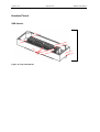
Physical Properties .................................................................................................. 7
Introduction............................................................................................................... 8
Related Documents ................................................................................................ 8
Block Diagram .......................................................................................................... 8
Mechanical Interface: TIM Standard ....................................................................... 9
SMT387 Support ....................................................................................................... 9
SMT387 Installation .................................................................................................. 9
SMT387 Alone ........................................................................................................ 9
SMT387 + DSP TIM.............................................................................................. 10
TMS320C6415 ......................................................................................................... 11
Boot Mode............................................................................................................. 11
EMIF Control Registers......................................................................................... 11
SDRAM ................................................................................................................. 12
FLASH .................................................................................................................. 12
PCI ........................................................................................................................ 13
Virtex FPGA .......................................................................................................... 14
FPGA ....................................................................................................................... 15
Configuration......................................................................................................... 15
JTAG/Boundary Scan........................................................................................ 15
Configuring with MultiLINX ................................................................................ 16
Memory ................................................................................................................. 17
Pipelined ZBTRAM ............................................................................................ 17
Comports .............................................................................................................. 17
SHB ...................................................................................................................... 18
SHB Connector ................................................................................................. 18
SHB Cable Assembly ........................................................................................ 19
SHB Inter Modules solutions ............................................................................. 19
Version 1.0.3
Page 4 of 42
SMT387 User Manual
Half Word Interface (16-bit SHB Interface) ........................................................ 19
Constraint File Signal Names ............................................................................ 20
RSL ....................................................................................................................... 21
RSL Connector.................................................................................................. 21
RSL Cable Assembly......................................................................................... 21
RSL Interface .................................................................................................... 21
Global bus............................................................................................................. 22
Constraints File Signals Names ........................................................................ 22
Clocks ................................................................................................................... 23
PCI ........................................................................................................................ 23
FPGA_PCI_CMD .............................................................................................. 24
FPGA_PCI_ADDR ............................................................................................ 24
FPGA_PCI_DOUT ............................................................................................ 24
FPGA_PCI_DIN ................................................................................................ 24
Miscellaneous I/O ................................................................................................. 24
Power Supplies ..................................................................................................... 25
DC/DC converter ............................................................................................... 26
Linear Voltage regulator .................................................................................... 26
Power Consumption.............................................................................................. 27
Serial ATA ............................................................................................................... 28
Software .................................................................................................................. 29
Configuration......................................................................................................... 29
Prerequisites ......................................................................................................... 30
The Kit................................................................................................................... 30
Building the Example ............................................................................................ 30
Running the Example............................................................................................ 31
User Interface ....................................................................................................... 31
Playback ............................................................................................................... 31
Playback to file...................................................................................................... 31
SDBs ................................................................................................................. 32
Discs.................................................................................................................. 33
Information ........................................................................................................ 33
Status ................................................................................................................ 33
Version 1.0.3
Page 5 of 42
SMT387 User Manual
Further details ....................................................................................................... 33
Verification Procedures ......................................................................................... 34
Review Procedures ................................................................................................ 34
Validation Procedures............................................................................................ 34
FPGA Constraint File General Information........................................................... 34
Ordering Information.............................................................................................. 34
Basic ..................................................................................................................... 34
Custom.................................................................................................................. 35
FPGA................................................................................................................. 35
Memories........................................................................................................... 35
SHBs ................................................................................................................. 35
Comports........................................................................................................... 35
Global Bus......................................................................................................... 35
External Clock ................................................................................................... 35
PCB Layout Details ................................................................................................ 36
Components placement ........................................................................................ 36
Headers Pinout ....................................................................................................... 38
SHB Header.......................................................................................................... 38
SHB Pinout (LVTTL only).(J2) ........................................................................... 39
JTAG/Multilinx headers ......................................................................................... 40
JTAG Boundary scan/User defined jumpers pinout (JP1/JP2) .......................... 40
Safety....................................................................................................................... 42
EMC ......................................................................................................................... 42
Version 1.0.3
Page 6 of 42
SMT387 User Manual
Table of Figures
Figure 1: SMT387 Block Diagram............................................................................... 8
Figure 2: Flash logical sections ................................................................................ 13
Figure 3: JTAG Chain on the SMT387 ..................................................................... 16
Figure 4: SHB Connector.......................................................................................... 18
Figure 5: RSL Connector .......................................................................................... 21
Figure 6: Global Bus constraints file signal names. .................................................. 22
Figure 7: FPGA PCI Command Sequences ............................................................. 23
Figure 8: SATA daughter module ............................................................................. 28
Figure 9: SMT387 with SATA daughter module installed ......................................... 28
Figure 10: SMT387 Components placement-Top view............................................. 36
Figure 11: SMT387 Components placement-Bottom view ....................................... 37
Figure 12: Top View QSH 30.................................................................................... 38
Figure 13: Top View of JTAG/Multilinx headers........................................................ 40
Table of Tables
Table 1: FPGA Choices ............................................................................................ 15
Table 2: ZBTRAM sizes............................................................................................ 17
Table 3: RSL Speed vs. FPGA Speed Grade........................................................... 22
Table 4: FPGA PCI Register Offsets ........................................................................ 23
Table 5: LED Identification........................................................................................ 25
Table 6: Powering the devices.................................................................................. 25
Table 7: Power Consumption ................................................................................... 27
Table 8: SHB interfaces table. .................................................................................. 39
Table 9: Connector JTAG/Jumper Header ............................................................... 41
Version 1.0.3
Page 7 of 42
SMT387 User Manual
Physical Properties
Dimensions
See Physical specifications of TI TIM specification &
user’s guide
Weight
68.4g (with daughter module)
Supply Voltages
See See Figure 10: SMT387 Components placementTop view.
Power Supplies
Supply Current
See See Figure 10: SMT387 Components placementTop view.
Power Supplies
Version 1.0.3
Page 8 of 42
SMT387 User Manual
Introduction
Related Documents
[1] Sundance High-speed Bus (SHB) specifications – Sundance.
http://sundance.com/docs/SHB%20Technical%20Specification.pdf
[2] RocketIO Serial Links (RSL) specifications – Sundance.
http://sundance.com/docs/RSL%20%20Technical%20Specification%20Rev01%20Iss03.pdf
[3] TIM specifications.
http://sundance.com/docs/TIM_Spec_v1_12.pdf
[4] External Interface User Manual- Sundance.
http://sundance.com/docs/Firmware.pdf
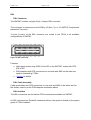
Block Diagram
SDRAM
SDRAM
(optional)
(128MB
max)
S
H
B
60
pins
107
pins
XC2VP
FPGA
R
S
L
16
pins
156
pins
32
64 EMIFA
320C6415
EMIFB
DSP
SRAM
PCI32
33MHz
53
pins
51
pins
(18Mb)
6 x ComPort,
Global Bus
TIMConnectors
Connectors
TIM
Connectors
TIM
Figure 1: SMT387 Block Diagram
SATA
XCVR
1.5Gb/s LVDS
1.5Gb/s LVDS
Flash
(8MB)
S-ATA Conn
S-ATA Conn
Version 1.0.3
Page 9 of 42
SMT387 User Manual
Mechanical Interface: TIM Standard
This module conforms to the TIM standard (Texas Instrument Module, See TI TIM
specification & user’s guide.) for single width modules.
It sits on a carrier board.
The carrier board provides power, Ground, communication links (Comport links)
between all the modules fitted and a pathway to the host, for a non stand-alone
system.
The SMT387 requires an additional 3.3V power supply (as present on all Sundance
TIM carrier boards), which must be provided by the two diagonally opposite mounting
holes.
SMT387 Support
The SMT387 is supported by the SMT6087 software package available from
SUNDANCE. Please register on the SUNDANCE Support Forum if not yet registered.
Then enter your company’s forum and you can request the SMT6087 from there.
SMT387 Installation
Do NOT connect any external TTL (5v) signals to the SMT387 I/Os as the FPGA
is NOT 5v compliant. This implies that the Comports and global bus lines of
the carrier board MUST be LVTTL and that any device driving signals on the
SHB connectors must drive at LVTTL (3.3v).
Two types of configuration are described here, nevertheless, you shouldn’t be
restricted and should consult Sundance if your system architecture differs.
SMT387 Alone
You can fit the SMT387 on its own, on the first TIM site of one of Sundance’s 3.3v
compatible carrier boards plugged in a host computer (PC, PCI, VME carrier etc…),
like SMT310Q, SMT328, SMT300 etc…)
Please, follow these steps to install the SMT387 module on a Host system:
1. Remove the carrier board from the host system.
2. Place the SMT387 module on the first TIM site. This TIM site communicates
with the host. (See your carrier board User Manual.) This allows you to use
Global Bus and Comport 3 to communicate with the host.
3. Make sure that the board is firmly seated, and then provide the 3.3V to the
board by screwing the SMT387 on the two main mounting holes with the bolts
and screws provided with the board.
4. Connect the SHB links if required by your application.
Version 1.0.3
Page 10 of 42
SMT387 User Manual
5. Replace the carrier board in the host system or power on for a stand-alone
carrier.
SMT387 + DSP TIM
You can fit the SMT387 coupled with a DSP module on any of Sundance carrier
boards: Stand alones or plugged in a Host.
Please, follow these steps to install the SMT387 module and the DSP TIM on a
carrier:
1. Remove the carrier board from the host system or turn the power off for a standalone carrier.
2. Place the SMT387 module onto one of the TIM sites on the carrier board.
•
Preferably, fit the DSP TIM on the first TIM site. This TIM site
communicates with the host. (See your carrier board User Manual.).
This allows the processor board to handle the interactions with the
Host.
•
Fit the Comport communication links between the DSP TIM and the
SMT387 respecting the rules on polarity at reset. (See your carrier
board User Manual.)
3. Make sure that the board is firmly seated, and then provide the 3.3V to the board
by screwing the SMT387 on the two main mounting holes with the bolts and
screws provided with the board.
4. Connect the SHB links if required by your application.
5. Replace the carrier board in the host system or power on for a stand-alone
carrier.
Version 1.0.3
Page 11 of 42
SMT387 User Manual
TMS320C6415{xe "TMS320C6201"}
The processor will run with zero wait states from internal SRAM.
An on-board crystal oscillator provides the clock used for the C60 which then
multiplies this by 12 internally.
Boot Mode{xe "Boot Mode"}
The SMT387 is configured to boot from Flash only after a reset.
Flash boot:
1. The processor copies a bootstrap { XE "bootstrap program" }program from the
first part of the flash memory into internal program RAM starting at address 0.
2. Execution starts at address 0.
The standard bootstrap supplied with the SMT387 then performs the following
operations:
1. All relevant C60 internal registers are set to default values;
2. The FPGA is configured { XE "FPGA:configuration" }from data held in flash
memory and sets up the communication ports, the global bus and the
Sundance High-speed Buses. This step must have been completed before
data can be sent to the Comports from external sources such as the host or
other TIMs;
3. A C4x-style boot loader is executed. This will continually examine the six
communication ports until data appears on one of them. The bootstrap will
then load a program in boot format from that port; the loader will not read data
arriving on other ports.
4. Finally, control is passed to the loaded program.
The delay between the release of the board reset and the FPGA configuration is
around 4s for a SMT387 (600MHz clock).
A typical time to wait after releasing the board reset should be in excess of this delay,
but no damage will result if any of the I/Os are used before they are fully configured.
In fact, the comm. Ports will just produce a not ready signal when data transfer is
attempted during this time, and then continue normally after the FPGA is configured.
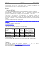
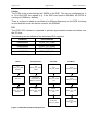
EMIF Control Registers{xe "EMIF Control Registers"}
The C6415 has two external memory interfaces (EMIFs). One of these is 64 bits
wide, the other 16 bits.
Version 1.0.3
Page 12 of 42
SMT387 User Manual
The C60 contains several registers that control the external memory interfaces
(EMIFs). {xe "memory space (CE0 to CE3)"}A full description of these registers can
be found in the C60 Peripherals Reference Guide.
The standard bootstrap will initialise these registers to use the following resources:
Resource
Memory
space
Address range
(EMIFA)
Internal
(1MB)
program
memory 0x00000000 - 0x000FFFFF
CE0
SDRAM (2x 8MB chips)
0x80000000 - 0x807FFFFF
CE3
Virtex
0xB0000000 - 0xBFFFFFFF
Resource
Address range
CE1
1st / 3rd section of flash (2MB
each)
0x64000000 – 0x641FFFFF
CE2
2nd / 4th section of flash (2MB
each)
0x68000000 – 0x681FFFFF
Memory
space
(EMIFB)
SDRAM{xe "RAM"}
Memory space CE0 is used to access 16MB of SDRAM over EMIFA. The SDRAM
operates at one quarter (or one sixth) of the core clock speed (with a max frequency
of 133MHz). Depending upon the application, the best performance may be obtained
whilst running the DSP at a lower clock speed. Eg. At 600MHz, the external EMIF will
only run at 100MHz (core clock / 6, as we are constrained by the TI imposed limit of
133MHz). But if the core were running at 533MHz, then the EMIF would be at the
max possible speed of 133MHz (533/4). This speed adjustment is not a user option,
but must be adjusted during manufacture.
The EMIFA CE0 memory space control register should be programmed with the
value 0x00000030.
Note that the DSP only has 20 address pins on the EMIFA, but since address bits are
multiplexed for SDRAM a maximum addressable space of 128MB is possible.
FLASH{xe "Flash"}
An 8MB Flash ROM{ XE "Flash:protection algorithm" } device is connected to the
C60 EMIFB.
The ROM holds boot code for the C60, configuration data for the FPGA, and optional
user-defined code.
Version 1.0.3
Page 13 of 42
SMT387 User Manual
The EMIFB CE1 and CE2 space control registers should be programmed with the
value 0xFFFFFF03.
As the C60 only provides 20 address lines on its EMIFB, both CE1 & CE2 are used
to access this device. This in itself allows the direct access of 4MB. A paging
mechanism is used to select which half of the 8MB device is visible in this 4MB
window.
As the EMIFB CE1 & 2 memory spaces alias throughout the available range, the
flash device can be accessed using the address range 0x67E00000-0x681FFFFF.
This gives a 4MB continuous space.
The flash can be divided into the four logical sections shown in the following figure
(paging bit is bit 21).
0x67C00000
Page0
(2 MBytes)
CE0
Section 1
0x67E00000
Page1
(2 MBytes)
Section 2
0x68000000
Page0
(2 MBytes)
CE1
Section 3
0x68200000
Page1
(2 MBytes)
Section 4
0x68400000
Figure 2: Flash logical sections
To change the state of the page bit, you need to write to the following address as
shown (the data written are irrelevant):
Address
Flash page selected
0x6C000000
Page 0 (1st and 3rd
sections enabled)
0x6C000001
Page 1 (2nd and 4th
sections enabled)
The EMIFB CE0 space control register should be programmed with the value
0xFFF0C003.
PCI
The integrated 33MHz PCI32 bus interface of the 6415/6416 DSP is used to access
the Serial ATA host controller. For more information on the DSP PCI interface see:
TMS320C6000 DSP Peripheral Component Interconnect Reference Guide
(SPRU581).
Version 1.0.3
Page 14 of 42
SMT387 User Manual
One limitation of the DSP PCI interface is that it is incapable of byte-oriented reads or
writes. This limitation has been circumvented by implementation of this feature in the
FPGA. Refer to the description of the PCI interface in the FPGA section below.
Note: Due to a defect in the DSP PCI interface, the DSP should only be operated “at
an 18.0 or 14.8 CPU-to-PCI clock frequency ratio only (e.g., 600-MHz or 490-MHz
CPU for 33-MHz PCI).” Refer to TMS320C6414, TMS320C6415, and TMS320C6416
Digital Signal Processors Silicon Errata (SPRZ011) for more information.
Virtex FPGA
The SMT387 incorporates a Xilinx Virtex XC2VP20 FPGA (XC2VP7 or XC2VP30 are
also possible). This device controls the majority of the I/O functionality on the
module, including the Comports, SHBs, global bus, timers and interrupts.
This device requires configuring after power-up (the Virtex technology is an SRAM
based logic array). This configuration is performed by the DSP as part of the boot
process.
Two control register bits are needed for this purpose, one to put the FPGA into a
‘waiting for configuration’ state, and another to actually transfer the configuration
data.
The PROG pin (causes the FPGA to enter the non-configured state) is accessed at
address 0x6C02000X. Writing to address 0x6C020000 will assert this pin, and
address 0x6C0200001 will de-assert this pin.
The configuration data clock is accessed at address 0x6C080001. Each bit of the
FPGA’s configuration bit-stream must be serially clocked through this address.
Note: This configuration process is part of the standard boot code, and does not
need to be implemented in any user application.
Version 1.0.3
Page 15 of 42
SMT387 User Manual
FPGA
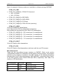
The module can be fitted with a XC2VP7, XC2VP20, or XC2VP30.
Only flip-chip FF896 package will fit on this board.
The choice of FPGA will be price/performance driven. The following table shows the
main FPGA characteristics.
The choice of the FPGA also determines which board architecture you will get
(amount of logic available, speed, number and type of I/Os, on-board Memory size
and type). For a complete list of the different board architectures, please consult:
Ordering Information
This Xilinx Virtex II Pro, is responsible for the provision of one SHB, 6 Comports, a
PCI interface, 8 RSLs, the global bus and the ZBT memory (In FULL configuration,
see Ordering Information).
CLB(1 CLB = 4 slices =
Max 128 bits)
Device
RocketIO
Transciever
Blocks
PowerPC
Processor
Blocks
XC2VP7
8
XC2VP20
XC2VP30
SelectRAM Blocks
Slices
Maximum
distributed
RAM Kbits
Multiplier
blocks
11,088
4,928
154
2
20,880
9,280
2
30,816
13,696
Logic
Cells
1
8
8
18-Kbit
Block
Max RAM
(Kbits)
DCMs
44
44
792
4
290
88
88
1,584
8
428
136
136
2,448
8
Table 1: FPGA Choices
Configuration
The FPGA can be configured 2 different ways:
•
Using SMT6001 to update the FPGA loaded from flash by the DSP (See
http://www.sundance.com/docs/SMT6001%20User%20Manual.pdf)
•
Using the on-board JTAG header and Xilinx JTAG programming tools.
JTAG/Boundary Scan
The JTAG Programmer software is a standard feature of the Alliance Series ™ and
Foundation Series ™ software packages. JTAG Programmer is a part of Web Pack,
which can be downloaded from the following site:
Xilinx JTAG programmer
The JTAG chain is composed of the CPLD and the FPGA.
The CPLD is pre-programmed by Sundance.
Do NOT try to reprogram the CPLD without SUNDANCE approval
Version 1.0.3
Page 16 of 42
SMT387 User Manual
Figure 3: JTAG Chain on the SMT387
When accessing the board using JTAG, the CPLD can be bypassed and you can
configure the FPGA only.
Xilinx describe how to connect both download cables at: Parallel cables
Xilinx describe how to configure their devices using these cables at: Configuration
Mode General Information.
For complementary and more detailed information please go to: Xilinx 5 software
Manuals and Help.
See board header pinout in Table 9: Connector JTAG/Jumper Header
Configuring with MultiLINX
The Mutilinx cable can be used to configure the FPGA via JTAG.
See board header pinout in Table 9: Connector JTAG/Jumper Header.
The MultiLINX cable set is a peripheral hardware product from Xilinx.
For additional information on the MultiLINX cable set, go to the following site:
Xilinx MultiLINX cable
Using MultiLINX /Parallel cable III or IV
The JTAG header is provided to enable device programming via suitable software.
Typically, this will be Xilinx iMPACT.
Xilinx iMPACT supports both the Xilinx MultiLINX™ and Parallel Cable III download
cables for communication between the PC and FPGA(s). The MultiLINX cable
supports both USB (Windows 98 and Windows 2000) and RS-232 serial
Version 1.0.3
Page 17 of 42
SMT387 User Manual
communication from the PC. The Parallel Cable III supports only parallel port
communication from the PC to the Boundary Scan chain.
Memory
Pipelined ZBTRAM
Up to 4MB of pipeline ZBT memory is provided with direct access by the FPGA.
The ZBTRAM is designed to sustain 100% bus bandwidth by eliminating the
turnaround cycle when there is transition from Read to Write, or vice versa.
This device is well suited for SDR applications that experience frequent bus
turnarounds, need to operate on small data chunks (especially one-word chunks),
and need to operate at higher frequencies than permitted by the flow-through
version.
For more complete information, please read:
General Information on how to choose your memory type according to your
application
For the parts datasheet, please read:
ZBTRAM datasheets
Chips parts and densities are shown in the table below.
ZBTRAM
number
part
Size in
bits
Size in
Bytes
Actual
Memory
size
Amount of
memory
per board
K7N801801M
8Mb
1MB
512kx18
1MB
K7N161801A
16Mb
2MB
1Mx18
2MB
K7N321801M
32Mb
4MB
2Mx18
4MB
Table 2: ZBTRAM sizes
The total available ZBT RAM on the board is therefore 1 MB, 2 MB, or 4 MB.
Comports
The SMT387 provides 6 Comports, numbered 0, 1, 2,
These are described in http://sundance.com/docs/Firmware.pdf
The Comport drives at 3.3v signal levels.
3,
4,
and
5.
Version 1.0.3
Page 18 of 42
SMT387 User Manual
SHB
SHB Connector
The SMT387 includes a single 60-pin connector to provide SHB communication to
the outside world.
The connector is referenced on the PCB by J2 (See Figure 10: SMT387 Components
placement-Top view).
All 60 pins of the SHB connector are routed to the FPGA in all available
configurations of SMT387.
Pin2
Pin 1
ral
Integ
5m
0.
m
Blad
am
d Be
e an
Desig
nd p
Grou
lane
n
t Pi
men
n
g
i
Al
n
Figure 4: SHB Connector
Features:
High-speed socket strip: QSH-030-01-L-D-A-K on the SMT387, mates with
QTH-030-01-L-D-A-K
QTH are used for cable assembly or PCB connecting 2 TIMs.
Centreline: 0.5mm (0.0197”)
QSH Connector
An adapter is available for Agilent probes for the 16760A Logic Analyser.
The 2 probes supported are the E5378A 100-pin Single-ended Probe and the
E5386A Half Channel Adapter with E5378A.
Version 1.0.3
Page 19 of 42
SMT387 User Manual
SHB Cable Assembly
The cable is custom made by Precision Interconnect and a cable assembly solution
builder can be found at: http://www.precisionint.com/tdibrsb/content/howtouse.asp
SHB Inter Modules solutions
High-speed data transfer can be achieved between TIM modules thanks to the use of
a 60-way flat ribbon micro-coax cable or via PCB connections.
InterModule PCBs can be found at: Inter Module Connections
As a result, NO DIFFERENTIAL lines are required to transfer data on long distances
and at speeds in excess of 100MHz, which allows the full use of the SHB connector
60 pins.
Half Word Interface (16-bit SHB Interface)
The SHB connectors provide to the FPGA connections to the external world.
You can implement your own interface to transfer data over using these connectors,
but if you want to communicate with other Sundance TIM modules, you can
implement a Half Word (Hw) interface sitting on 25 pins of an SHB connector.
Then, the SHBs are parallel communication links for synchronous transmission.
An SHB interface is derived from the SDB interface which is a 16-bit wide
synchronous communication interface.(SUNDANCE SDB specification)
The differences are:
The SHB interface can be made Byte (8 bits), Half Word (16 bits) or
Word (32 bits) wide.
The transfer rate can be increased thanks to better quality interconnect.
As an example, let us consider the Half Word (Hw) SHB interface.
You can implement 2 x 16-bit SHB interfaces per SHB connector, and have some
spare signals for User defined functions. (no differential lines are needed thanks to
our SHB cable assembly described in SHB Cable Assembly).
The SMT387 provides one SHB interface on one connectors and can support data
rates of 400MB/s at 100MHz
You must refer to the latest SUNDANCE SDB specification for technical information
on how it works.
Version 1.0.3
Page 20 of 42
SMT387 User Manual
Constraint File Signal Names
According to the SUNDANCE SHB specification, 5 Byte-interfaces (from 0 to 4) can
be implemented on the 60 pins of a SHB connector. Each Byte interface has its own
CLK, WEN, REQ and ACK.
The signal names going from the FPGA to the SHB connector use the configuration
of 2 SDB interfaces.
So, when in Half Word configuration:
•
16-bit data D(0 to 15)
•
CLK0 is borrowed from Byte configuration 0, WEN1, REQ1 and ACK1 are
borrowed from Byte configuration 1 to make configuration SDBA control
signals and
•
CLK3 is borrowed from Byte configuration 3, WEN4, REQ4 ACK4 are
borrowed from Byte configuration 4 to make configuration SDBB control
signals.
The SHB connector is J2. (See Figure 10: SMT387 Components placement-Top view)
Please refer to SHB Header.
Version 1.0.3
Page 21 of 42
SMT387 User Manual
RSL
RSL Connector
The SMT387 includes a single 28-pin (14-pair) RSL connector.
The connector is referenced on the PCB by J3 (See Figure 10: SMT387 Components
placement-Top view).
16 pins (8 pairs) of the RSL connector are routed to the FPGA in all available
configurations of SMT387.
Figure 5: RSL Connector
Features:
High-speed socket strip: QSE-014-xx-DP on the SMT387, mates with QTE014-xx-DP
PCB adapters with QTE connectors on one side and QSE on the other are
used for connecting 2 TIMs.
Samtec for details
RSL Cable Assembly
Cable assemblies with QTE connectors on one side and QSE on the other are like
the flexible versions of the PCB adapters mentioned above.
RSL Interface
The RSL connectors are the fastest FPGA connections available on SMT387.
As RSL are based on RocketIO transciever blocks, the speed is limited by the speed
grade of FPGA installed:
Version 1.0.3
Page 22 of 42
Speed grade
RSL speed (Gbps)
SMT387 User Manual
-7
-6
-5
3.125
3.125
2.0
Table 3: RSL Speed vs. FPGA Speed Grade
Based on the above, the 4 bi-directional links of SMT387 can provide a combined
bandwidth of up to 12.5Gbps.
The RSL connector is J3. (See Figure 10: SMT387 Components placement-Top view)
Refer to the latest SUNDANCE RSL specification for technical information on how it
works.
Global bus
The global bus is compatible with the TIM standard.
The Global Bus Interface is a memory Interface that follows Texas Instruments’
TMS320C4x External Bus operation standard. Additional information on the standard
is available in the TMS320C4x User’s Guide chapter 9:
External Bus operation.
When Writing, the FPGA sends data across the global bus to the external device.
When Reading, the external device writes data across the global bus to the FPGA.
Constraints File Signals Names
GBUS RW1N
Global Bus
signal
Active level:
N = Active low
STATn(3:0) are also global
Bus signals
Figure 6: Global Bus constraints file signal names.
Version 1.0.3
Page 23 of 42
SMT387 User Manual
Clocks
The FPGA clock is provided by the EMIFA of the DSP. This can be configured as ¼
or 1/6 of the DSP core speed (e.g. if the DSP core speed is 600MHz, the FPGA is
running at 100MHz by default).
There is a place to install an oscillator of a different frequency on the PCB, but keep
in mind that this clock will also be used for the SDRAM.
PCI
The FPGA PCI interface is required to perform byte-oriented reads and writes over
the PCI bus.
The following are the offsets of the associated PCI registers:
Address
PCI Function
0xB0060000
FPGA_PCI_CMD
0xB0068000
FPGA_PCI_ADDR
0xB0070000
FPGA_PCI_DOUT
0xB0078000
FPGA_PCI_DIN
Table 4: FPGA PCI Register Offsets
Reset
Configuration
I/O Read
I/O Write
Set
FPGA_PCI_CMD
Reset bit
Set
FPGA_PCI_CMD
IDSEL
Write
FPGA_PCI_ADDR
Write
FPGA_PCI_ADDR
Wait 1ms
Perform PCI
configuration via
DSP PCI interface
Set
FPGA_PCI_CMD
= 0x2
Write
FPGA_PCI_DATA
Clear
FPGA_PCI_CMD
Reset bit
Clear
FPGA_PCI_CMD
IDSEL
Poll for
FPGA_PCI_CMD
Idle
Set
FPGA_PCI_CMD
= 0x3
Read from
FPGA_PCI_DATA
Poll for
FPGA_PCI_CMD
Idle
Figure 7: FPGA PCI Command Sequences
Version 1.0.3
Page 24 of 42
SMT387 User Manual
Note: An example of these procedures is available in software package SMT6087.
FPGA_PCI_CMD
FPGA_PCI_CMD[3:0] = FPGA PCI Command
0x2 = I/O Read
0x3 = I/O Write
FPGA_PCI_CMD[12] = DSP IDSEL
FPGA_PCI_CMD[13] = SATA IDSEL
FPGA_PCI_CMD[15] = PCI Reset
FPGA_PCI_CMD[16] = FPGA PCI Idle (read-only)
FPGA_PCI_ADDR
32-bit PCI Address for Reads/Writes
Low 2 bits must be "00" for configuration transactions
Byte enables are decoded from low 2 bits for I/O transactions
FPGA_PCI_ADDR[1:0] = "00" means byte 0 is read/effected
FPGA_PCI_ADDR[1:0] = "01" means byte 1 is read/effected
FPGA_PCI_ADDR[1:0] = "10" means byte 2 is read/effected
FPGA_PCI_ADDR[1:0] = "11" means byte 3 is read/effected
FPGA_PCI_DOUT
32-bit PCI Data for Write transactions
FPGA_PCI_DIN
32-bit PCI Data for Read transactions (valid only until the next PCI access)
Miscellaneous I/O
There are two user-defined jumper locations on SMT387. Refer to the section
JTAG/Multilinx headers for information on the location of these jumpers. The software
interface to the jumpers is located in the LED register of the standard Sundance
firmware. Bits 2 and 3 reflect the status of JMP0 and JMP1, respectively. Bits 0 and 1
of the LED register control FPGA LED0 and LED1, respectively. See Table 5 for
details on LED identification.
LED Designator
LED Color
Meaning
D1
Green
IDE0 Disk Activity
D2
Green
IDE1 Disk Activity
D3
Red
FPGA DONE
Version 1.0.3
Page 25 of 42
SMT387 User Manual
D4
Red
DSP GP0
D5
Red
DSP GP1
D6
Red
FPGA LED0
D7
Red
FPGA LED1 / PCI SATA
IDSEL*
*FPGA LED1 is used for PCI SATA IDSEL on SMT387V1 PCBs.
Table 5: LED Identification
See Figure 10: SMT387 Components placement-Top view.
Power Supplies
The PCI specifications state that the maximum power allowed for any PCI board is 25
Watts, and represents the total power drawn from all power rails provided at the
connector (+5V, +3.3v, +VI/O,+12V,-12V, +3.3Vaux). The expansion board (in our
case the TIM carrier board and the TIM modules) may optionally draw all this power
from either the +5V or +3.3V rail.
Nevertheless, it is anticipated that many systems will not provide a full 25 Watts per
connector for each power rail, because most boards will typically draw much less
than this amount.
For this reason it is recommended that you analyse the total FPGA device power
drawn by using Xilinx XPOWER before implementing your design in the FPGA.
This will tell you if you need to use the external power connector provided on our
carrier boards. (Like the SMT310Q carrier board)
TI 6415 DSP
FPGA
XC2VP
SiI3512
ZBT
RSL
Vccint/Vdd
1.2v
1.5v
1.8v
3.3v
N/A
Vcco/Vddq
3.3v
3.3v
3.3v
3.3v
N/A
Vpci
N/A
3.0v
N/A
N/A
N/A
Vccaux
N/A
2.5v
N/A
N/A
2.5v
Table 6: Powering the devices.
DC/DC
converter
PC 3.3v
Voltage
regulator
Version 1.0.3
Page 26 of 42
SMT387 User Manual
This module must have 5V supplied through the TIM connectors. In addition, a 3.3V
supply is required and should be supplied through the TIM mounting holes. This is
compatible with the SMT310Q, SMT327 and future Sundance TIM carrier boards.
Contained on the module are linear regulators for the DSP core, 3512 core, FPGA
VCCAUX, and FPGA PCI. A DC/DC converter supplies the core voltage for the
FPGA.
DC/DC converter
An International Rectifier IP1001 Power Block is used to supply the 1.5V core voltage
to the FPGA. The current limit is configured for 20A.
Linear Voltage regulator
The DSP core, 3512 core, FPGA VCCAUX, and FPGA PCI voltages are supplied
through linear voltage regulators drawn from 3.3V.
Version 1.0.3
Page 27 of 42
SMT387 User Manual
Power Consumption
Measurements were made on an SMT387 at idle with the standard FPGA
configuration loaded. Requirements will vary depending on software activity, FPGA
configuration, environment, and other factors.
Supply (V)
Current (A)
Power (W)
3.3
0.84
2.77
5.0
0.07
0.35
Total
-
3.12
Table 7: Power Consumption
Note: Figures do not include power required for the carrier board itself.
FPGA: Depending on the implemented design, the power consumption can reach 30
Watts or more. Please consider connecting an external power supply to the carrier
board for demanding designs.
Version 1.0.3
Page 28 of 42
SMT387 User Manual
Serial ATA
The Silicon Image 3512 host controller allows for 2x Serial ATA 1.0 compliant
interfaces. This device is under the control of the DSP and FPGA and requires
special application software (such as SMT 6087). Details of the functionality of the
host controller can be found in SiI3512 PCI to Serial ATA Controller Datasheet,
which can be obtained from Silicon Image with an NDA.
Connection to Serial ATA devices requires that the daughter module be installed on
the SMT387. Placement of connectors on the daughter module conforms to the
Serial ATA Specification 1.0.
Figure 8: SATA daughter module
Figure 9: SMT387 with SATA daughter module installed
Version 1.0.3
Page 29 of 42
SMT387 User Manual
Software
The software developed to support the SMT387 Data Logger will transfer data
between one or two SDBs and one or two discs in two modes:
1. Record: Read in continuous mode from the SDBs and write to the discs,
stopping under user control or when the discs are full.
2. Playback: Read from the saved data on disc and write to the SDBs.
This document assumes the reader is familiar with Diamond, PCI, Visual C++, and
Sundance TIMs.
Configuration
The following diagram shows the hardware configuration1.
Host PC
IDE0
3
Root
SMT387
0
1
1
IDE1
SATA
0
Node
4
1
Sundance Digital Bus (SDB)
SMT376
Comport
The Host PC runs a Visual C++ program, Logger.exe, to provide a user interface
(UI). The two DSPs, Root and Node, run a Diamond application, Logger.app.
1
Connectors for IDE0 and IDE1 are labelled as JA1 and JA2 on the SATA daughter module,
respectively.
Version 1.0.3
Page 30 of 42
SMT387 User Manual
Prerequisites
1. To run the example you will need:
•
The Sundance board support package (SMT6025).
•
The Diamond Windows Server. This is made available as part of the
installation of Diamond. This part of the product can also be installed
using a kit contained in newer versions of Diamond. The kit can be
included in distributions of the Logger under simple licence conditions.
2. To modify and rebuild the DSP application you will need:
•
Diamond
•
The Texas Instruments C6000 tools (compiler and linker)
3. To modify and rebuild the user interface you will need:
•
Microsoft Visual C++
The Kit
The distribution kit contains a number of files in several directories. Copy the
complete contents of the kit into a working directory, which this document will assume
is called Logger.
Building the Example
The Logger directory contains a makefile that will build the complete application
(see Prerequisites). The directory Logger\DSP contains a makefile that will build only
the DSP portion (Logger.app). Note that the Microsoft VC++ compiler may object to
the existing intermediate files (and complain about precompiled headers). This can
be cured by selecting the VC++ option Build/Clean and then rebuilding the
application.
The DSP configuration is specified in the file Logger\DSP\Logger.cfg. The Root
processor is currently identified as an SMT361 because the SMT387 has not been
included in the standard Diamond release. The type of the Node processor is not
particularly significant, as any Sundance TIM with one or two SDBs may be used.
The application in the kit has been built assuming an SMT376; you will need to
modify Logger\DSP\Logger.cfg and reconfigure the application if a different type of
TIM is to be used.
Version 1.0.3
Page 31 of 42
SMT387 User Manual
Running the Example
The example is executed by running Logger.exe. This resets the DSPs, loads them
with Logger.app, and starts them running. It assumes that Logger.app is in the
same directory that contains Logger.exe. Note that it takes a few seconds to reset
the SMT387.
User Interface
Once the DSPs have been successfully started running, the following window will
appear:
The top five buttons are:
Playback
Start transferring data from the discs to the SDBs. The
transfer will stop once all the written data have been
moved.
Playback to file Ask for an output file name and start transferring data from
the discs to that file. The transfer will stop once all the
written data have been moved.
Record
Delete any existing data on the discs and start transferring
new data from the SDBs to the discs. The transfer will
stop once all the available space on the discs has been
Version 1.0.3
Page 32 of 42
SMT387 User Manual
used. The first few blocks of data read from the SDBs will
be discarded to ensure a continuous data stream.
Stop
Stop Playback or Record. When a Record operation is
stopped, information will be written to the discs to note the
amount of data recorded.
Exit
This has the same effect as Stop, but also terminates the
example.
SDBs
You can select how many SDBs to use by clicking either 1 SDB or 2 SDBs.
Version 1.0.3
Page 33 of 42
SMT387 User Manual
Discs
You can select the discs to use by clicking IDE 0 and IDE 1. The discs will be used
as follows:
IDE 0
Use only the disc connected as IDE 0.
IDE 1
Use only the disc connected as IDE 1.
IDE 0 & IDE 1
Start using the disc connected as IDE 0. Once that is full
(for Record) or has been read to the end (Playback), the
selected operation will continue using IDE 1.
The setting will be changed automatically if the DSP reports it can only find one disc.
Information
The window at the bottom right of the display is used to show various status and
error messages.
Status
The user interface displays information about each disc in the system.
Capacity
The size of the disc report by the controller.
Recorded
The amount of information that has been written to the discs.
Playback
Record: the percentage of the disc that has been written.
Playback: the percentage of the recorded data that have been
read.
Rate
The current rate at which data are being transferred.
Further details
Please consult the documentation included with the SMT6087 package for details on
the internals of this software.
Version 1.0.3
Page 34 of 42
SMT387 User Manual
Verification Procedures
The specification (design requirements) will be tested using the following:
1) Power module test.
2) FPGA configuration using DSP and/or JTAG connector.
3) Comport transfers between a SMT376 and the SMT387.
4) SDRAM memory tests.
5) SHB connector Pins Test using SHB tester PCBs.
6) Global Bus transfers between SMT387 and SMT310Q onboard SRAM.(Not
yet implemented)
7) External clock I/O tested with scope.
8) Serial ATA disk transfers
Review Procedures
Reviews will be carried out as indicated in design quality document QCF14 and in
accordance with Sundance’s ISO9000 procedures.
Validation Procedures
The validation procedure is happening during the verification procedure.
Test that all the memories are accessible by the FPGA as well as all the
communication links.
FPGA Constraint File General Information
Since only the FF896 package type is supported on SMT387, one constraints file is
provided. Some pins will not be supported on VP7.
Ordering Information
Currently, the SMT387 is available in 2 configurations: Basic and Custom.
Basic
In the basic configuration a Virtex II Pro 20 is used and allows interfacing to ALL the
memories and ALL I/Os available on the SMT387. Basic configuration includes 16MB
of SDRAM and no ZBT SRAM.
Version 1.0.3
Page 35 of 42
SMT387 User Manual
Custom
The ordering code for custom configuration is as follows:
SMT387–VP20-5-x-Zy
Board Type
Virtex II part
Virtex II speed grade
On-board SDRAM in MB
On-board ZBTRAM in MB
FPGA
Part options: VP7, VP20, VP30
Speed grades: 5, 6, 7
Note: With VP7 part installed SATA connectivity is not possible and no ZBT
memory can be used.
Memories
SDRAM: 16MB, 32MB, 64MB, 128MB
ZBTRAM: 1MB, 2MB, 4MB
SHBs
One SHB connectors is available in all configurations to allow the
implementation of up to 2x16-bit SDB interfaces.
Comports
6 Comports are available in all configurations
Global Bus
1 Global Bus
External Clock
1 External clock I/O.
Version 1.0.3
Page 36 of 42
PCB Layout Details
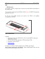
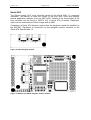
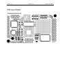
Components placement
Figure 10: SMT387 Components placement-Top view
SMT387 User Manual
Version 1.0.3
Page 37 of 42
Figure 11: SMT387 Components placement-Bottom view
U1: Xilinx FPGA Power Supply
U2: SiI3512
U3 & U12: SDRAM
U4: Xilinx FPGA
U5: Xilinx CPLD
U6: TI 6415 DSP
U7: ZBTRAM
U14: Flash
Y1: PCI Clock (33MHz)
Y2: EMIFA External Clock (optional)
Y3: DSP Core Clock / 12 (50MHz)
SMT387 User Manual
Version 1.0.3
Page 38 of 42
SMT387 User Manual
Headers Pinout
SHB Header
Pin2
Pin 1
e
plan
und
l Gro
a
r
g
Inte
m
5m
0.
Figure 12: Top View QSH 30
am
d Be
e an
Blad
n
Desig
n
t Pi
men
n
g
i
Al
Version 1.0.3
Page 39 of 42
SMT387 User Manual
SHB Pinout (LVTTL only).(J2)
QSH Pin number
QSH Pin number
Hw
SHBxCLK0
1
2
SHBxD0(0)
SHBxD0(1)
3
4
SHBxD0(2)
SHBxD0(3)
5
6
SHBxD0(4)
SHBxD0(5)
7
8
SHBxD0(6)
SHBxD0(7)
9
10
SHBxD0(8)
SHBxD0(9)
11
12
SHBxD0(10)
SHBxD0(11)
13
14
SHBxD0(13)
15
16
SHBxD0(14)
SHBxD0(15)
17
18
SHBxUSER0(16)
SHBxUSER0(17)
19
20
SHBxUSER0(18)
SHBxUSER0(19)
21
22
SHBxWEN1
SHBxREQ1
23
24
SHBxACK1
SHBxUSER1(23)
25
26
SHBxUSER1(24)
SHBxUSER1(25)
27
28
SHBxUSER1(26)
SHBxUSER1(27)
29
30
SHBxUSER1(28)
SHBxUSER1(29)
31
32
SHBxUSER1(30)
SHBxUSER1(31)
33
34
SHBxUSER1(32)
SHBxUSER1(33)
35
36
SHBxUSER1(34)
SHBxCLK3
37
38
SHBxD1(0)
SHBxD1(1)
39
40
SHBxD1(2)
SHBxD1(3)
41
42
SHBxD1(4)
SHBxD1(5)
43
44
SHBxD1(6)
SHBxD1(7)
45
46
SHBxD1(8)
SHBxD1(9)
47
48
SHBxD1(10)
SHBxD1(11)
49
50
SHBxD1(13)
51
52
SHBxD1(14)
SHBxD1(15)
53
54
SHBxUSER2(52)
SHBxUSER2(53)
55
56
SHBxUSER2(54)
SHBxUSER2(55)
57
58
SHBxWEN4
SHBxREQ4
59
60
SHBxACK4
Table 8: SHB interfaces table.
16-bit interface
Hw0
Hw
Hw1
Hw1
Hw0
In the constraints file provided for the SMT387 FPGA, the SHB signals have been
named to match 2 16-bit SDB interfaces (or Hw SHB interface) pinout according to
the SUNDANCE SHB specification Half Word configuration.
SHBxD0(12)
SHBxD1(12)
Version 1.0.3
Page 40 of 42
SMT387 User Manual
JTAG/Multilinx headers
The JTAG/Multilinx headers have the following pinout:
TIM Connector
S
H
B
ZBT
SRAM
XC2VP
FF896
SDRAM
2.5
V
IP1001
1.5V
320C6415
DSP
R
S
L
9
7
5
3
1
10
8
6
4
2
HDR
S
A
T
A
S-ATA
XCVR
XC9536
VQ44
TIM Connector
Figure 13: Top View of JTAG/Multilinx headers
JTAG Boundary scan/User defined jumpers pinout (JP1/JP2)
Name
Pin Function
Connections
JMP1
1
To FPGA pin
AD16
User defined function
Pulled-up to 3.3V with 4.7k when unconnected
JMP0
2
User defined function
Pulled-up to 3.3V with 4.7k when unconnected
GND
3
Ground
Designed to pull down pin 1 by using a 0.1” jumper.
GND
4
Ground
Designed to pull down pin 2 by using a 0.1” jumper.
VCC
5
Power.
To FPGA pin
AE16
Board
ground
Board
ground
To target
VCC
Version 1.0.3
Page 41 of 42
Supplies VCC (3.3V, 10 mA, typically) to the cable.
SMT387 User Manual
system VCC
TCK
6
Test Clock.
Connect to
This clock drives the test logic for all devices on system TCK
boundary-scan chain.
pin.
GND
7
Ground.
Supplies ground reference to the cable.
To target
system
ground
TMS
8
Test Mode Select.
Connect to
This signal is decoded by the TAP controller to control system TMS
pin.
test operations.
TDO
9
Read Data.
Connect to
Read back data from the target system is read at this system TDO
pin.
pin.
TDI
10
Test Data In.
Connect to
This signal is used to transmit serial test instructions system TDI
pin.
and data.
Table 9: Connector JTAG/Jumper Header
Version 1.0.3
Page 42 of 42
SMT387 User Manual
Safety
This module presents no hazard to the user.
EMC
This module is designed to operate from within an enclosed host system, which is
build to provide EMC shielding. Operation within the EU EMC guidelines is not
guaranteed unless it is installed within an adequate host system.
This module is protected from damage by fast voltage transients originating from
outside the host system which may be introduced through the output cables.
Short-circuiting any output to ground does not cause the host PC system to lock up
or reboot.