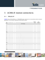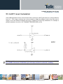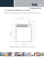
1
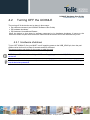
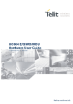
UC864 Hardware User Guide 1vv0300766a Rev.1 31/01/08 UC864-E Hardware User Guide 1vv0300766a Rev.1 - 31/01/08 This document is relating to the following products: UC864-E 3990250694 Reproduction forbidden without Telit Communications S.p.A. written authorization - All Rights Reserved page 2 of 51 UC864-E Hardware User Guide 1vv0300766a Rev.1 - 31/01/08 Contents 1 Overview ........................................................................................................................... 6 2 Mechanical Dimensions................................................................................................... 7 3 UC864-E module connections ......................................................................................... 8 3.1 PIN-OUT ................................................................................................................................... 8 UC864-E Antenna connector ..........................................................................................................11 3.1.1 4 Hardware Commands .................................................................................................... 12 4.1 Turning ON the UC864-E ...................................................................................................... 12 4.2 Turning OFF the UC864-E .................................................................................................... 14 Hardware shutdown ........................................................................................................................14 Hardware Unconditional Restart .....................................................................................................15 4.2.1 4.2.2 5 Power Supply .................................................................................................................17 5.1 Power Supply Requirements ............................................................................................... 17 5.2 General Design Rules .......................................................................................................... 19 5.2.1 Electrical Design Guidelines ...........................................................................................................19 5.2.1.1 + 5V input Source Power Supply Design Guidelines .................................................................19 5.2.1.2 + 12V input Source Power Supply Design Guidelines ...............................................................20 5.2.1.3 Battery Source Power Supply Design Guidelines ......................................................................22 5.2.1.4 Battery Charge control Circuitry Design Guidelines ...................................................................22 5.2.2 Thermal Design Guidelines ............................................................................................................24 5.2.3 Power Supply PCB layout Guidelines ............................................................................................25 6 7 Antenna ........................................................................................................................... 26 6.1 Antenna Requirements ........................................................................................................ 26 6.2 Antenna - Installation Guidelines ........................................................................................ 27 Logic level specifications .............................................................................................. 28 7.1 8 Reset signal .......................................................................................................................... 29 Serial Ports ..................................................................................................................... 30 8.1 MODEM SERIAL PORT ......................................................................................................... 30 8.2 RS232 level translation ........................................................................................................ 32 5V UART level translation ............................................................................................................... 35 9 USB Port ......................................................................................................................... 37 9.1 Communication ports combinations .................................................................................. 37 10 Audio Section Overview ................................................................................................ 38 10.1 Generality .............................................................................................................................. 38 10.2 Definitions ............................................................................................................................. 38 Reproduction forbidden without Telit Communications S.p.A. written authorization - All Rights Reserved page 3 of 51 UC864-E Hardware User Guide 1vv0300766a Rev.1 - 31/01/08 10.3 Selection ................................................................................................................................ 38 10.4 Electrical Characteristics ..................................................................................................... 39 10.4.1 Input lines (microphone) .................................................................................................................39 10.4.2 Output lines (speaker) ....................................................................................................................40 11 General Purpose I/O ....................................................................................................... 41 11.1 Logic level specifications .................................................................................................... 42 11.2 Using a GPIO Pad as INPUT ................................................................................................ 43 11.3 Using a GPIO Pad as OUTPUT ............................................................................................ 43 11.4 Using the Alarm Output GPIO6 ........................................................................................... 43 11.5 Using the Buzzer Output GPIO7 .......................................................................................... 44 11.6 Indication of network service availability ........................................................................... 45 11.7 RTC Bypass out .................................................................................................................... 46 11.8 VAUX1 power output ............................................................................................................ 46 11.9 Mounting UC864-E on your board....................................................................................... 47 11.9.1 Debug of the UC864-E in production ..............................................................................................48 12 Conformity Assessment Issues .................................................................................... 49 13 SAFETY RECOMMANDATIONS..................................................................................... 50 14 Document Change Log .................................................................................................. 51 Reproduction forbidden without Telit Communications S.p.A. written authorization - All Rights Reserved page 4 of 51 UC864-E Hardware User Guide 1vv0300766a Rev.1 - 31/01/08 DISCLAIMER The information contained in this document is the proprietary information of Telit Communications S.p.A. and its affiliates (“TELIT”). The contents are confidential and any disclosure to persons other than the officers, employees, agents or subcontractors of the owner or licensee of this document, without the prior written consent of Telit, is strictly prohibited. Telit makes every effort to ensure the quality of the information it makes available. Notwithstanding the foregoing, Telit does not make any warranty as to the information contained herein, and does not accept any liability for any injury, loss or damage of any kind incurred by use of or reliance upon the information. Telit disclaims any and all responsibility for the application of the devices characterized in this document, and notes that the application of the device must comply with the safety standards of the applicable country, and where applicable, with the relevant wiring rules. Telit reserves the right to make modifications, additions and deletions to this document due to typographical errors, inaccurate information, or improvements to programs and/or equipment at any time and without notice. Such changes will, nevertheless be incorporated into new editions of this application note. All rights reserved. © 2007 – 2008 Telit Communications S.p.A. Reproduction forbidden without Telit Communications S.p.A. written authorization - All Rights Reserved page 5 of 51 UC864-E Hardware User Guide 1vv0300766a Rev.1 - 31/01/08 1 Overview The aim of this document is the description of some hardware solutions useful for developing a product with the Telit UC864-E module. In this document all the basic functions of a mobile phone will be taken into account; for each one of them a proper hardware solution will be suggested and eventually the wrong solutions and common errors to be avoided will be evidenced. Obviously this document cannot embrace the whole hardware solutions and products that may be designed. The wrong solutions to be avoided shall be considered as mandatory, while the suggested hardware configurations shall not be considered mandatory, instead the information given shall be used as a guide and a starting point for properly developing your product with the Telit UC864-E module. For further hardware details that may not be explained in this document refer to the Telit UC864-E Product Description document where all the hardware information is reported. NOTICE (EN) The integration of the GSM/GPRS/EGPRS/WCDMA/HSDPA UC864-E cellular module within user application shall be done according to the design rules described in this manual. (IT) L’integrazione del modulo cellulare GSM/GPRS/EGPRS/WCDMA/HSDPA UC864-E all’interno dell’applicazione dell’utente dovrà rispettare le indicazioni progettuali descritte in questo manuale. (DE) Die integration des UC864-E GSM/GPRS/EGPRS/WCDMA/HSDPA Mobilfunk-Moduls in ein Gerät muß gemäß der in diesem Dokument beschriebenen Kunstruktionsregeln erfolgen (SL) Integracija GSM/GPRS/EGPRS/WCDMA/HSDPA UC864-E modula v uporabniški aplikaciji bo morala upoštevati projektna navodila, opisana v tem piročniku. (SP) La utilización del modulo GSM/GPRS/EGPRS/WCDMA/HSDPA UC864-E debe ser conforme a los usos para los cuales ha sido deseñado descritos en este manual del usuario. (FR) L’intégration du module cellulaire GSM/GPRS/EGPRS/WCDMA/HSDPA UC864-E dans l’application de l’utilisateur sera faite selon les règles de conception décrites dans ce manuel. UC864-E The information presented in this document is believed to be accurate and reliable. However, no responsibility is assumed by Telit Communications S.p.A. for its use, nor any infringement of patents or other rights of third parties which may result from its use. No license is granted by implication or otherwise under any patent rights of Telit Communications S.p.A. other than for circuitry embodied in Telit products. This document is subject to change without notice. Reproduction forbidden without Telit Communications S.p.A. written authorization - All Rights Reserved page 6 of 51 UC864-E Hardware User Guide 1vv0300766a Rev.1 - 31/01/08 2 Mechanical Dimensions The Telit UC864-E module overall dimensions are: • • • Length: Width: Thickness: 36.2 mm 30 mm 4.8mm Reproduction forbidden without Telit Communications S.p.A. written authorization - All Rights Reserved page 7 of 51 UC864-E Hardware User Guide 1vv0300766a Rev.1 - 31/01/08 3 UC864-E module connections 3.1 PIN-OUT UC864-E uses an 80-pin Molex p.n. 53949-0878 male connector for the connections with the external applications. This connector matches the 54150-0878 models. Pin Signal I/O Function Internal Pull up Type UC864-E Power Supply 1 VBATT - Main power supply Power 2 VBATT - Main power supply Power 3 VBATT - Main power supply Power 4 VBATT - Main power supply Power 5 GND - Ground Power 6 GND - Ground Power 7 GND - Ground Power Audio I 100KΩ 8 AXE 9 EAR_HF+ AO Hands-free ear output, phase + Hands-free switching CMOS 2.6V Audio 10 EAR_HF- AO Hands-free ear output, phase - Audio 11 EAR_MT+ AO Handset earphone signal output, phase + Audio 12 EAR_MT- AO Handset earphone signal output, phase - Audio 13 MIC_HF+ AI Hands-free microphone input; phase + Audio 14 MIC_HF- AI Hands-free microphone input; phase - Audio 15 MIC_MT+ AI Handset microphone signal input; phase+ Audio 16 MIC_MT- AI Handset microphone signal input; phase- Audio 1 SIMVCC - External SIM signal – Power supply for the SIM 1.8 / 3V 19 SIMRST O External SIM signal – Reset 1.8 / 3V 20 SIMIO I/O External SIM signal - Data I/O 21 SIMIN I External SIM signal - Presence (active low) 22 SIMCLK O External SIM signal – Clock SIM Card Interface 18 1.8 / 3V 47KΩ 1.8 / 3V 1.8 / 3V Trace 1 On this line a maximum of 10nF bypass capacitor is allowed Reproduction forbidden without Telit Communications S.p.A. written authorization - All Rights Reserved page 8 of 51 UC864-E Hardware User Guide 1vv0300766a Rev.1 - 31/01/08 Pin Signal I/O Function Internal Pull up Type UC864-E 23 RX_TRACE I RX Data for debug monitor CMOS 2.6V 24 TX_TRACE O TX Data for debug monitor CMOS 2.6V Prog. / Data + Hw Flow Control 25 C103/TXD I Serial data input (TXD) from DTE CMOS 2.6V 26 C104/RXD O Serial data output to DTE CMOS 2.6V 27 C107/DSR O Output for Data set ready signal (DSR) to DTE CMOS 2.6V 28 C106/CTS O Output for Clear to send signal (CTS) to DTE CMOS 2.6V 29 C108/DTR I Input for Data terminal ready signal (DTR) from DTE CMOS 2.6V 30 C125/RING O Output for Ring indicator signal (RI) to DTE CMOS 2.6V 31 C105/RTS I Input for Request to send signal (RTS) from DTE CMOS 2.6V 32 C109/DCD O Output for Data carrier detect signal (DCD) to DTE CMOS 2.6V Analog input used to sense whether a peripheral device is connected, and determine the peripheral type, a host or a peripheral Miscellaneous Functions 35 USB_ID AI Analog 36 PCM_CLOCK I/O PCM clock out 37 ADC_IN1 AI Analog/Digital converter input A/D 38 ADC_IN2 AI Analog/Digital converter input A/D 39 ADC_IN3 AI Analog/Digital converter input A/D 40 DAC_OUT AO Digital/Analog converter output 45 STAT_LED O Status indicator led 46 GND - Ground 48 USB_VBUS 49 PWRMON 50 VAUX1 51 CHARGE AI 52 CHARGE AI Charger input CMOS 2.6V DAC and ADC D/A(PDM) Miscellaneous Functions 53 ON/OFF* 54 RESET# 55 VRTC CMOS 1.8V Ground Power supply for the internal USB transceiver. This pin is AI configured as an analog input or an analog output depending /AO upon the type of peripheral device connected. 4.4V ~5.25V O Power ON Monitor CMOS 2.6V - Power output for external accessories 2.85V Charger input Power Power I Input command for switching power ON or OFF (toggle command). I Reset input AO VRTC Backup capacitor Pull up to VBATT Power Telit GPIOs 56 TGPIO_19 I/O Telit GPIO19 Configurable GPIO CMOS 2.6V 57 TGPIO_11 I/O Telit GPIO11 Configurable GPIO CMOS 2.6V 58 TGPIO_20 I/O Telit GPIO20 Configurable GPIO CMOS 2.6V 59 TGPIO_04 I/O Telit GPIO4 Configurable GPIO CMOS 2.6V 60 TGPIO_14 I/O Telit GPIO14 Configurable GPIO CMOS 2.6V Reproduction forbidden without Telit Communications S.p.A. written authorization - All Rights Reserved page 9 of 51 UC864-E Hardware User Guide 1vv0300766a Rev.1 - 31/01/08 Pin Signal I/O Function Internal Pull up Type UC864-E 61 TGPIO_15 I/O Telit GPIO15 Configurable GPIO CMOS 2.6V 62 TGPIO_12 I/O Telit GPIO12 Configurable GPIO CMOS 2.6V 63 TGPIO_10/ PCM_TX I/O Telit GPIO10 Configurable GPIO / PCM Data Output CMOS 2.6V 64 TGPIO_22 I/O Telit GPIO22 Configurable GPIO CMOS 1.8V 65 TGPIO_18/ PCM_RX I/O Telit GPIO18 Configurable GPIO / PCM Data input CMOS 2.6V 66 TGPIO_03 I/O Telit GPIO3 Configurable GPIO CMOS 2.6V 67 TGPIO_08 I/O Telit GPIO8 Configurable GPIO CMOS 2.6V 68 TGPIO_06 / ALARM I/O Telit GPIO6 Configurable GPIO / ALARM CMOS 2.6V 70 TGPIO_01 I/O Telit GPIO1 Configurable GPIO CMOS 2.6V 71 TGPIO_17/ PCM_SYNC I/O Telit GPIO17 Configurable GPIO / PCM Sync CMOS 2.6V 72 TGPIO_21 I/O Telit GPIO21 Configurable GPIO CMOS 2.6V 73 TGPIO_07/ BUZZER I/O Telit GPIO7 Configurable GPIO / Buzzer CMOS 2.6V 74 TGPIO_02 I/O Telit GPIO02 I/O pin CMOS 2.6V 75 TGPIO_16 I/O Telit GPIO16 Configurable GPIO CMOS 2.6V 76 TGPIO_09 I/O Telit GPIO9 Configurable GPIO CMOS 2.6V 77 TGPIO_13 I/O Telit GPIO13 Configurable CMOS 2.6V 78 TGPIO_05/ RFTXMON I/O Telit GPIO05 Configurable GPIO / Transmitter ON monitor CMOS 2.6V USB Interface 79 USB_D+ I/O USB differential Data (+) 2.8V~3.6V 80 USB_D- I/O USB differential Data (-) 2.8V~3.6V RESERVED 17 - 41 - 42 - 43 - 44 - 47 - 69 - 33 - 34 - NOTE: RESERVED pins must not be connected RTS should be connected to the GND (on the module side) if flow control is not used Reproduction forbidden without Telit Communications S.p.A. written authorization - All Rights Reserved page 10 of 51 UC864-E Hardware User Guide 1vv0300766a Rev.1 - 31/01/08 NOTE: If not used, almost all pins should be left disconnected. The only exceptions are the following pins: Pin Signal Function 1 VBATT Main power supply 2 VBATT Main power supply 3 VBATT Main power supply 4 VBATT Main power supply 5 GND Ground 6 GND Ground 7 GND Ground 46 GND Ground 25 C103/TXD Serial data input (TXD) from DTE 26 C104/RXD Serial data output to DTE 31 C105/RTS Input for Request to send signal (RTS) from DTE 53 ON/OFF* Input command for switching power ON or OFF (toggle command). 54 RESET# Reset input 35 USB_ID 48 USB_VBUS 79 USB_D+ USB differential Data (+) 80 USB_D- USB differential Data (-) Analog input used to sense whether a peripheral device is connected, and determine the peripheral type, a host or a peripheral Power supply for the internal USB transceiver. This pin is configured as an analog input or an analog output depending upon the type of peripheral device connected. 3.1.1 UC864-E Antenna connector The UC864-E module is equipped with a RF connector from Murata, GSC type P/N MM9329-2700B. The counterpart suitable is Murata MXTK92 Type or MXTK88 Type. Reproduction forbidden without Telit Communications S.p.A. written authorization - All Rights Reserved page 11 of 51 UC864-E Hardware User Guide 1vv0300766a Rev.1 - 31/01/08 4 Hardware Commands 4.1 Turning ON the UC864-E To turn on UC864-E, the pad ON# must be tied low for at least 1 second and then released. The maximum current that can be drained from the ON# pad is 0,1 mA. A simple circuit to do it is: ON# R1 Q1 Power ON impulse R2 GND NOTE: UC864-E turns fully on also by supplying power to the USB_VBUS pin (provided there's a battery on the VBATT pads). Care must be taken to avoid supplying power to the USB_VBUS pin before the module turns on. To check if the UC864-E has powered on, the hardware line PWRMON should be monitored. When PWRMON goes high, the module has powered on. NOTE: don't use any pull up resistor on the ON# line, it is internally pulled up. Using pull up resistor may bring to latch up problems on the UC864-E power regulator and improper power on/off of the module. The line ON# must be connected only in open collector configuration. NOTE: In this document all the lines that are inverted, hence have active low signals are labeled with a name that ends with a "#" or with a bar over the name. NOTE: UC864-E turns fully on also by supplying power to the Charge pad (provided there's a battery on the VBATT pads). Reproduction forbidden without Telit Communications S.p.A. written authorization - All Rights Reserved page 12 of 51 UC864-E Hardware User Guide 1vv0300766a Rev.1 - 31/01/08 For example: 1- Let's assume you need to drive the ON# pad with a totem pole output of a 1.8/5 V microcontroller (uP_OUT1): 10k 2- Let's assume you need to drive the ON# pad directly with an ON/OFF button: 1.8 / 5V 1s Reproduction forbidden without Telit Communications S.p.A. written authorization - All Rights Reserved page 13 of 51 UC864-E Hardware User Guide 1vv0300766a Rev.1 - 31/01/08 4.2 Turning OFF the UC864-E The turning off of the device can be done in three ways: • By software command (see UC864-E Software User Guide) • By hardware shutdown • By Hardware Unconditional Restart When the device is shut down by software command or by hardware shutdown, it issues to the network a detach request that informs the network that the device will not be reachable any more. 4.2.1 Hardware shutdown To turn OFF UC864-E, first, you MUST cut off supplying power to the USB_VBUS pin, then the pad ON# must be tied low for at least 2 seconds and then released. The same circuitry and timing for the power on shall be used. The device shuts down after the release of the ON# pad. NOTE: To turn OFF UC864-E, first of all, you MUST cut off supplying power to the USB_VBUS, or the module does not turn off TIP: To check if the device has powered off, the hardware line PWRMON should be monitored. When PWRMON goes low, the device has powered off. Reproduction forbidden without Telit Communications S.p.A. written authorization - All Rights Reserved page 14 of 51 UC864-E Hardware User Guide 1vv0300766a Rev.1 - 31/01/08 4.2.2 Hardware Unconditional Restart To unconditionally restart UC864-E, the pad RESET# must be tied low for at least 200 milliseconds and then released. The maximum current that can be drained from the ON# pad is 0,15 mA. A simple circuit to do it is: RESET# Unconditional Restart impulse GND NOTE: Do not use any pull up resistor on the RESET# line or any totem pole digital output. Using pull up resistor may bring to latch up problems on the UC864-E power regulator and improper functioning of the module. The line RESET# must be connected only in open collector configuration. TIP: The unconditional hardware Restart should be always implemented on the boards and software should use it as an emergency exit procedure. Reproduction forbidden without Telit Communications S.p.A. written authorization - All Rights Reserved page 15 of 51 UC864-E Hardware User Guide 1vv0300766a Rev.1 - 31/01/08 10k For example: 1- Let's assume you need to drive the RESET# pad with a totem pole output of a +1.8/5 V micro controller (uP_OUT2): +1.8 / 5V * This signal is internally pulled up so the pin can be left floating if not used. NOTE: If UC864-E is connected as USB slave (considering also the presence of VBATT supply), when powered off it automatically switch on again. Reproduction forbidden without Telit Communications S.p.A. written authorization - All Rights Reserved page 16 of 51 UC864-E Hardware User Guide 1vv0300766a Rev.1 - 31/01/08 5 Power Supply The power supply circuitry and board layout are a very important part in the full product design and they strongly reflect on the product overall performances, hence read carefully the requirements and the guidelines that will follow for a proper design. 5.1 Power Supply Requirements POWER SUPPLY Nominal Supply Voltage 3.8V Max Supply Voltage 4.2 Supply Voltage Range 3.51 – 4.2 The UC864-E power consumptions are: UC864-E (GSM900) Mode Average (mA) IDLE mode AT+CFUN=1 21,7 AT+CFUN=4 21,3 AT+CFUN=0 or AT+CFUN=5 3,3 GSM TX and RX mode Min power level 139.1 Max power level 340.8 GPRS (class 10) TX and RX mode Max power level 728.2 WCDMA Max power level 619,7 Mode description Stand by mode; no call in progress Normal mode: full functionality of the module (MF=9) Disabled TX and RX; module is not registered on the network Power saving: CFUN=0 module registered on the network and can receive voice call or an SMS; but it is not possible to send AT commands; module wakes up with an unsolicited code (call or SMS) or rising RTS line. CFUN=5 full functionality with power saving; module registered on the network can receive incoming calls and SMS – (MF=2) GSM Sending data mode GPRS Sending data mode (3 slot TX) WCDMA Call in progress In GSM/GPRS mode, RF transmission is not continuous and it is packed into bursts at a base frequency of about 216 Hz, and the relative current peaks can be as high as about 2A. Therefore the power supply has to be designed in order to withstand with these current peaks without big voltage drops; this means that both the electrical design and the board layout must be designed for this current flow. Reproduction forbidden without Telit Communications S.p.A. written authorization - All Rights Reserved page 17 of 51 UC864-E Hardware User Guide 1vv0300766a Rev.1 - 31/01/08 If the layout of the PCB is not well designed a strong noise floor is generated on the ground and the supply; this will reflect on all the audio paths producing an audible annoying noise at 216 Hz; if the voltage drop during the peak current absorption is too much, then the device may even shutdown as a consequence of the supply voltage drop. TIP: The electrical design for the Power supply should be made ensuring it will be capable of a peak current output of at least 2 A. Reproduction forbidden without Telit Communications S.p.A. written authorization - All Rights Reserved page 18 of 51 UC864-E Hardware User Guide 1vv0300766a Rev.1 - 31/01/08 5.2 General Design Rules The principal guidelines for the Power Supply Design embrace three different design steps: • The electrical design • The thermal design • The PCB layout. 5.2.1 Electrical Design Guidelines The electrical design of the power supply depends strongly from the power source where this power is drained. We will distinguish them into three categories: • +5V input (typically PC internal regulator output) • +12V input (typically automotive) • Battery 5.2.1.1 + 5V input Source Power Supply Design Guidelines • • • • • The desired output for the power supply is 3.8V, hence there's not a big difference between the input source and the desired output and a linear regulator can be used. A switching power supply will not be suited because of the low drop out requirements. When using a linear regulator, a proper heat sink shall be provided in order to dissipate the power generated. A Bypass low ESR capacitor of adequate capacity must be provided in order to cut the current absorption peaks close to UC864-E, a 100μF tantalum capacitor is usually suited. Make sure the low ESR capacitor on the power supply output (usually a tantalum one) is rated at least 10V. A protection diode should be inserted close to the power input, in order to save the electrical circuit from power polarity inversion. Reproduction forbidden without Telit Communications S.p.A. written authorization - All Rights Reserved page 19 of 51 UC864-E Hardware User Guide 1vv0300766a Rev.1 - 31/01/08 An example of linear regulator with 5V input is: 5.2.1.2 + 12V input Source Power Supply Design Guidelines • • • • • • • The desired output for the power supply is 3.8V; hence due to the big difference between the input source and the desired output, a linear regulator is not suited and shall not be used. A switching power supply will be preferable because of its better efficiency especially with the 2A peak current load represented by UC864-E. When using a switching regulator, a 500kHz or more switching frequency regulator is preferable because of its smaller inductor size and its faster transient response. This allows the regulator to respond quickly to the current peaks absorption. For car Pb battery the input voltage can rise up to 15.8V and this should be kept in mind when choosing components: all components in the power supply must withstand this voltage. The same consideration has to be applied to the voltage peaks that in a Car Application could rise to 100V. A Bypass low ESR capacitor of adequate capacity must be provided in order to cut the current absorption peaks, a 100μF tantalum capacitor is usually suited. Make sure the low ESR capacitor on the power supply output (usually a tantalum one) is rated at least 10V. A spike protection diode should be inserted close to the power input for Car applications, in order to clean the supply from spikes. A protection diode should be inserted close to the power input, in order to save UC864-E from power polarity inversion. This can be the same diode as for spike protection. Reproduction forbidden without Telit Communications S.p.A. written authorization - All Rights Reserved page 20 of 51 UC864-E Hardware User Guide 1vv0300766a Rev.1 - 31/01/08 An example of switching regulator with 12V input is in the below schematic (it is split in 2 parts): Reproduction forbidden without Telit Communications S.p.A. written authorization - All Rights Reserved page 21 of 51 UC864-E Hardware User Guide 1vv0300766a Rev.1 - 31/01/08 5.2.1.3 Battery Source Power Supply Design Guidelines • • The desired nominal output for the power supply is 3.8V and the maximum voltage allowed is 4.2V, hence a single 3.7V Li-Ion cell battery type is suited for supplying the power to the Telit UC864-E module. The three cells Ni/Cd or Ni/MH 3.6 V Nom. battery types or 4V PB types MUST NOT BE DIRECTLY USED since their maximum voltage can rise over the absolute maximum voltage for UC864-E and damage it. NOTE: DON'T USE any Ni-Cd, Ni-MH, and Pb battery types directly connected with UC864-E. Their use can lead to overvoltage on UC864-E and damage it. USE ONLY Li-Ion battery types. • • • • A Bypass low ESR capacitor of adequate capacity must be provided in order to cut the current absorption peaks, a 100μF tantalum capacitor is usually suited. Make sure the low ESR capacitor (usually a tantalum one) is rated at least 10V. A protection diode should be inserted close to the power input, in order to save UC864-E from power polarity inversion. Otherwise the battery connector should be done in a way to avoid polarity inversions when connecting the battery. The battery capacity must be at least 500mAh in order to withstand the current peaks of 2A; the suggested capacity is from 500mAh to 1000mAh. 5.2.1.4 Battery Charge control Circuitry Design Guidelines The charging process for Li-Ion Batteries can be divided into 4 phases: • Qualification and trickle charging • Fast charge 1 - constant current • Final charge - constant voltage • Maintenance charge The qualification process consists in a battery voltage measure, indicating roughly its charge status. If the battery is deeply discharged, that means its voltage is lower than the trickle charging threshold, then the charge must start slowly possibly with a current limited pre-charging process keeping the current very low respect to the fast charge value: the trickle charging. During the trickle charging the voltage across the battery terminals rises; when it reaches the fast charge threshold level the charging process goes into fast charge phase. During the fast charge phase the process proceeds with a current limited charging; this current limit depends the complete charge required time and from the battery pack capacity. During this phase the voltage across the battery terminals still raises but at a lower rate. Once the battery voltage reaches its maximum voltage then the process goes into its third state: Final charging. The voltage measure to change the process status into final charge is very important. It must be ensured that the maximum battery voltage is never exceeded, otherwise the battery may be damaged and even explode. Moreover regarding the constant voltage final chargers, the constant voltage phase (final charge) must not start before the battery voltage has reached its maximum value; otherwise the battery capacity will be highly reduced. The final charge is done using constant voltage. Reproduction forbidden without Telit Communications S.p.A. written authorization - All Rights Reserved page 22 of 51 UC864-E Hardware User Guide 1vv0300766a Rev.1 - 31/01/08 The constant voltage charge proceeds with a fixed voltage regulator (very accurately set to the maximum battery voltage) and hence the current will decrease while the battery is becoming charged. When the charging current falls below a certain fraction of the fast charge current value, then the battery is considered fully charged, the final charge stops and eventually starts the maintenance. The last phase is not properly a charging phase, since the battery at this point is fully charged and the process may stop after the final charge. The maintenance charge provides an additional charging process to compensate for the typical Li-Ion battery charge leak. It is done by issuing pulses with a fixed time length, again few hundreds of ms, and a duty-cycle around 5% or less. This last phase is not implemented in the UC864-E internal charging algorithm, so that the battery once charged is left discharging down to a certain threshold so that it is cycled from full charge to slight discharge even if the battery charger is always inserted. This guarantees that anyway the remaining charge in the battery is a good percentage and that the battery is not damaged by keeping it always fully charged (Li-Ion rechargeable battery usually deteriorates when kept fully charged). Last but not least, in some applications it is highly desired that the charging process restarts when the battery is discharged and its voltage drops below a certain threshold, UC864-E internal charger does it. As you can see, the charging process is not a trivial task to be done; moreover all these operations should start only if battery temperature is inside a charging range, usually +5°C ÷ +45°C. In order to satisfy this last requirement, the UC864-E measures the temperature of its internal components even if it is not exactly the same as the battery temperature; but in common application the two temperatures should not differ too much and the charging temperature range should be guaranteed. NOTE: All voltage thresholds are provided, inside UC864-E, in order to maximize Li-Ion battery performances and do not need to be changed. NOTE: In this application the battery charger input current must be limited to less than 400mA. This can be done by using a current limited wall adapter as the power source. NOTE: When starting the charger from Module powered off the startup will be in CFUN4; to activate the normal mode the command AT+CFUN=1 has to be provided. Reproduction forbidden without Telit Communications S.p.A. written authorization - All Rights Reserved page 23 of 51 UC864-E Hardware User Guide 1vv0300766a Rev.1 - 31/01/08 5.2.2 Thermal Design Guidelines The thermal design for the power supply heat sink should be done with the following specifications: • Average current consumption during WCDMA transmission @PWR level max: 620mA • Average current consumption during class12 GPRS transmission @PWR level max: 930mA NOTE: The average consumption during transmissions depends on the power level at which the device is requested to transmit by the network. The average current consumption hence varies significantly. Considering the very low current during idle, especially if Power Saving function is enabled, it is possible to consider from the thermal point of view that the device absorbs current significantly only during calls. If we assume that the device stays into transmission for short periods of time (let's say few minutes) and then remains for a quite long time in idle (let's say one hour), then the power supply has always the time to cool down between the calls and the heat sink could be smaller than the calculated one for 930mA maximum RMS current, or even could be the simple chip package (no heat sink). Moreover in the average network conditions the device is requested to transmit at a lower power level than the maximum and hence the current consumption will be less than the 930mA, being usually around 150mA. For these reasons the thermal design is rarely a concern and the simple ground plane where the power supply chip is placed can be enough to ensure a good thermal condition and avoid overheating. For the heat generated by the UC864-E, you can consider it to be during transmission 1W max during CSD/VOICE calls and 2W max during class12 GPRS upload. This generated heat will be mostly conducted to the ground plane under the UC864-E; you must ensure that your application can dissipate it. In the WCDMA mode, since UC864-E emits RF signals continuously during WCDMA transmission, you should pay special attention on how to dissipate the heat generated. The current consumption will be up to about 620mA continuously at the maximum TX output power (24dBm). Thus, you should arrange the PCB area as large as possible under UC864-E, which you will mount. You can mount UC864-E on the large ground area of your application board and make many ground vias for heat sink. The peak current consumption in the GSM mode is higher than that in WCDMA. However, considering the heat sink is more important with WCDMA. As mentioned before, GSM signal is bursty. Thus, the temperature drift is more insensible than WCDMA. Consequently, if you prescribe the heat dissipation in the WCDMA mode, you don’t need to think more about the GSM mode Reproduction forbidden without Telit Communications S.p.A. written authorization - All Rights Reserved page 24 of 51 UC864-E Hardware User Guide 1vv0300766a Rev.1 - 31/01/08 5.2.3 Power Supply PCB layout Guidelines As seen on the electrical design guidelines the power supply shall have a low ESR capacitor on the output to cut the current peaks and a protection diode on the input to protect the supply from spikes and polarity inversion. The placement of these components is crucial for the correct working of the circuitry. A misplaced component can be useless or can even decrease the power supply performances. • • • • • • • • The Bypass low ESR capacitor must be placed close to the Telit UC864-E power input pads or in the case of a switching power supply it can be placed close to the inductor to cut the ripple provided the PCB trace from the capacitor to UC864-E is wide enough to ensure a drop-less connection even during the 2A current peaks. The protection diode must be placed close to the input connector where the power source is drained. The PCB traces from the input connector to the power regulator IC must be wide enough to ensure no voltage drops occur when the 2A current peaks are absorbed. Note that this is not made in order to save power loss but especially to avoid the voltage drops on the power line at the current peaks frequency of 216 Hz that will reflect on all the components connected to that supply, introducing the noise floor at the burst base frequency. For this reason while a voltage drop of 300400 mV may be acceptable from the power loss point of view, the same voltage drop may not be acceptable from the noise point of view. If your application doesn't have audio interface but only uses the data feature of the Telit UC864-E, then this noise is not so disturbing and power supply layout design can be more forgiving. The PCB traces to UC864-E and the Bypass capacitor must be big enough to ensure no significant voltage drops occur when the 2A current peaks are absorbed. This is for the same reason as previous point. Try to keep this trace as short as possible. The PCB traces connecting the Switching output to the inductor and the switching diode must be kept as short as possible by placing the inductor and the diode very close to the power switching IC (only for switching power supply). This is done in order to reduce the radiated field (noise) at the switching frequency (100÷500 usually). The use of a good common ground plane is suggested. The placement of the power supply on the board should be done in such a way to guarantee that the high current return paths in the ground plane are not overlapped to any noise sensitive circuitry as the microphone amplifier/buffer or earphone amplifier. The power supply input cables should be kept separate from noise sensitive lines such as microphone/earphone cables. Reproduction forbidden without Telit Communications S.p.A. written authorization - All Rights Reserved page 25 of 51 UC864-E Hardware User Guide 1vv0300766a Rev.1 - 31/01/08 6 Antenna The antenna connection and board layout design are the most important part in the full product design and they strongly reflect on the product overall performances, hence read carefully and follow the requirements and the guidelines for a proper design. 6.1 Antenna Requirements As suggested on the Product Description the antenna for a Telit UC864-E device shall fulfill the following requirements: ANTENNA REQUIREMENTS Depending by frequency band(s) provided by the network operator, the customer shall use the most suitable antenna for that/those band(s) 70 MHz in GSM850, 80 MHz in GSM900, 170 Bandwidth MHz in DCS & 140 MHz PCS 250 MHz in WCDMA2100 band Gain < 3dBi Gain 50 ohm Impedance > 33dBm(2 W) peak power in GSM Input power > 24dBm Average power in WCDMA2100 VSWR absolute max <= 10:1 <= 2:1 VSWR recommended Frequency range Furthermore if the device is developed for the US market and/or Canada market, it shall comply with the FCC and/or IC approval requirements: This device is to be used only for mobile and fixed applications. The antenna(s) used for this transmitter must be installed to provide a separation distance of at least 20 cm from all persons and must not be co-located or operating in conjunction with any other antenna or transmitter. End-Users must be provided with transmitter operation conditions for satisfying RF exposure compliance. OEM integrators must ensure that the end user has no manual instructions to remove or install the UC864-E module. Antennas used for this OEM module must not exceed 3dBi gain for mobile and fixed operating configurations. Reproduction forbidden without Telit Communications S.p.A. written authorization - All Rights Reserved page 26 of 51 UC864-E Hardware User Guide 1vv0300766a Rev.1 - 31/01/08 6.2 • • • • Antenna - Installation Guidelines Install the antenna in a place covered by the GSM/WCDMA signal. The Antenna must be installed to provide a separation distance of at least 20 cm from all persons and must not be co-located or operating in conjunction with any other antenna or transmitter; Antenna shall not be installed inside metal cases Antenna shall be installed also according Antenna manufacturer instructions. Reproduction forbidden without Telit Communications S.p.A. written authorization - All Rights Reserved page 27 of 51 UC864-E Hardware User Guide 1vv0300766a Rev.1 - 31/01/08 7 Logic level specifications Where not specifically stated, all the interface circuits work at 2.6V CMOS logic levels. The following table shows the logic level specifications used in the Telit UC864-E interface circuits: For 2.6V CMOS signals: Absolute Maximum Ratings -Not Functional Parameter Input level on any digital pin when on Input voltage on analog pins when on UC864-E Min Max -0.3V +3.0V -0.3V +3.0 V Operating Range - Interface levels Level UC864-E Input high level Min 2.0V Max 2.9 V Input low level -0.3V 0.6V Output high level 2.2V 2.6V Output low level 0V 0.35V For 1.8V signals: Operating Range - Interface levels (1.8V CMOS) Level UC864-E Min Max Input high level 1.5V 2.1V Input low level -0.3V 0.5V Output high level 1.4V 1.8V Output low level 0V 0.35V Reproduction forbidden without Telit Communications S.p.A. written authorization - All Rights Reserved page 28 of 51 UC864-E Hardware User Guide 1vv0300766a Rev.1 - 31/01/08 7.1 Reset signal Signal Function I/O PIN Number RESET Phone reset I 54 RESET is used to reset the UC864-E module. Whenever this signal is pulled low, UC864-E is reset. When the device is reset it stops any operation. After the release of the reset UC864-E is unconditionally shut down, without doing any detach operation from the network where it is registered. This behavior is not a proper shut down because any device is requested to issue a detach request on turn off. For this reason the Reset signal must not be used to normally shutting down the device, but only as an emergency exit in the rare case the device remains stuck waiting for some network response. The RESET is internally controlled on start-up to achieve always a proper power-on reset sequence, so there's no need to control this pin on start-up. It may only be used to reset a device already on that is not responding to any command. NOTE: do not use this signal to turn off the UC864-E. Use the ON/OFF signal to perform this function or the AT#SHDN command. Reset Signal Operating levels: Signal Min Max RESET Input high 2.0V* 2.2V RESET Input low 0V 0.2V * This signal is internally pulled up so the pin can be left floating if not used. If unused, this signal may be left unconnected. If used, then it must always be connected with an open collector transistor, to permit to the internal circuitry the power on reset and under voltage lockout functions. Reproduction forbidden without Telit Communications S.p.A. written authorization - All Rights Reserved page 29 of 51 UC864-E Hardware User Guide 1vv0300766a Rev.1 - 31/01/08 8 Serial Ports The serial port on the Telit UC864-E is the interface between the module and OEM hardware. 2 serial ports are available on the module: • MODEM SERIAL PORT • MODEM SERIAL PORT 2 (DEBUG) 8.1 MODEM SERIAL PORT Several configurations can be designed for the serial port on the OEM hardware, but the most common are: • RS232 PC com port • microcontroller UART @ 2.6V - 3V (Universal Asynchronous Receive Transmit) • microcontroller UART @ 5V or other voltages different from 2.8V Depending from the type of serial port on the OEM hardware a level translator circuit may be needed to make the system work. The only configuration that doesn't need a level translation is the 2.6V UART. The serial port on UC864-E is a +2.6V UART with all the 7 RS232 signals. It differs from the PCRS232 in the signal polarity (RS232 is reversed) and levels. The levels for UC864-E UART are the CMOS levels: Absolute Maximum Ratings - Not Functional Parameter Input level on any digital pin when on Input voltage on analog pins when on UC864-E Min Max -0.3V +3.0V -0.3V +3.0 V Operating Range - Interface levels Level UC864-E Input high level Min 2.0V Max 2.9 V Input low level -0.3V 0.6V Output high level 2.2V 2.6V Output low level 0V 0.35V Reproduction forbidden without Telit Communications S.p.A. written authorization - All Rights Reserved page 30 of 51 UC864-E Hardware User Guide 1vv0300766a Rev.1 - 31/01/08 The signals of the UC864-E serial port are: RS232 Pin Number 1 2 3 4 5 6 7 8 9 Signal DCD dcd_uart RXD tx_uart TXD rx_uart DTR dtr_uart GND DSR dsr_uart RTS rts_uart CTS cts_uart RI ri_uart UC864-E Pad Number 32 Name Usage Data Carrier Detect 26 Transmit line *see Note Output from the UC864-E that indicates the carrier presence Output transmit line of UC864-E UART 25 Receive line *see Note Input receive of the UC864-E UART 29 Data Terminal Ready 5,6,7 27 Ground Data Set Ready 31 Request to Send 28 Clear to Send 30 Ring Indicator Input to the UC864-E that controls the DTE READY condition Ground Output from the UC864-E that indicates the module is ready Input to the UC864-E that controls the Hardware flow control Output from the UC864-E that controls the Hardware flow control Output from the UC864-E that indicates the incoming call condition NOTE: According to V.24, RX/TX signal names are referred to the application side, therefore on the UC864-E side these signal are on the opposite direction: TXD on the application side will be connected to the receive line (here named TXD/ rx_uart ) of the UC864-E serial port and vice versa for RX. TIP: For a minimum implementation, only the TXD and RXD lines can be connected, the other lines can be left open provided a software flow control is implemented. Reproduction forbidden without Telit Communications S.p.A. written authorization - All Rights Reserved page 31 of 51 UC864-E Hardware User Guide 1vv0300766a Rev.1 - 31/01/08 8.2 RS232 level translation In order to interface the Telit UC864-E with a PC com port or a RS232 (EIA/TIA-232) application a level translator is required. This level translator must Invert the electrical signal in both directions Translate the level from 0/2.6V to +15/-15V Actually, the RS232 UART 16450, 16550, 16650 & 16750 chipsets accept signals with lower levels on the RS232 side (EIA/TIA-562), allowing for a lower voltage-multiplying ratio on the level translator. Note that the negative signal voltage must be less than 0V and hence some sort of level translation is always required. The simplest way to translate the levels and invert the signal is by using a single chip level translator. There are a multitude of them, differing in the number of driver and receiver and in the levels (be sure to get a true RS232 level translator not a RS485 or other standards). By convention the driver is the level translator from the 0-2.6V UART level to the RS232 level, while the receiver is the translator from RS232 level to 0-2.6V UART. In order to translate the whole set of control lines of the UART you will need: • • 5 drivers 3 receivers NOTE: The digital input lines working at 2.6V CMOS have an absolute maximum input voltage of 3.0V; therefore the level translator IC shall not be powered by the +3.8V supply of the module. Instead it shall be powered from a +2.6V / +2.9 (dedicated) power supply. This is because in this way the level translator IC outputs on the module side (i.e. UC864-E inputs) will work at +3.8V interface levels, stressing the module inputs at its maximum input voltage. NOTE: In order to be able to do in circuit reprogramming of the UC864-E firmware, the serial port on the Telit UC864-E shall be available for translation into RS232 and either it's controlling device shall be placed into tristate, disconnected or as a gateway for the serial data when module reprogramming occurs. Only RXD, TXD, GND and the On/off module turn on pad are required to the reprogramming of the module, the other lines are unused. All applicator shall include in their design such a way of reprogramming UC864-E. Reproduction forbidden without Telit Communications S.p.A. written authorization - All Rights Reserved page 32 of 51 UC864-E Hardware User Guide 1vv0300766a Rev.1 - 31/01/08 An example of level translation circuitry of this kind is: The example is done with a SIPEX SP3282EB RS232 Transceiver that could accept supply voltages lower than 3V DC. NOTE: In this case Vin has to be set with a value compatible with the logic levels of the module (Max 2.9V DC). In this configuration the SP3282EB will adhere to EIA/TIA-562 voltage levels instead of RS232 (-5 +5V) Reproduction forbidden without Telit Communications S.p.A. written authorization - All Rights Reserved page 33 of 51 UC864-E Hardware User Guide 1vv0300766a Rev.1 - 31/01/08 Second solution could be done using a MAXIM transceiver (MAX218) In this case the compliance with RS232 (+-5V) is possible. Another level adapting method could be done using a standard RS232 Transceiver (MAX3237EAI) adding some resistors to adapt the levels on the UC864 Input lines. NOTE: In this case has to be taken in account the length of the lines on the application to avoid problems in case of High-speed rates on RS232. The RS232 serial port lines are usually connected to a DB9 connector with the following layout: Reproduction forbidden without Telit Communications S.p.A. written authorization - All Rights Reserved page 34 of 51 UC864-E Hardware User Guide 1vv0300766a Rev.1 - 31/01/08 5V UART level translation If the OEM application uses a microcontroller with a serial port (UART) that works at a voltage different from 2.6 – 2.9V, then a circuitry has to be provided to adapt the different levels of the two sets of signals. As for the RS232 translation there are a multitude of single chip translators. For example a possible translator circuit for a 5V TRANSMITTER/RECEIVER can be: TO TELIT MODULE TIP: This logic IC for the level translator and 2.6V pull-ups (not the 5V one) can be powered directly from PWRMON line of UC864-E. Note that the TC7SZ07AE has open drain output; therefore the resistor R2 is mandatory. Reproduction forbidden without Telit Communications S.p.A. written authorization - All Rights Reserved page 35 of 51 UC864-E Hardware User Guide 1vv0300766a Rev.1 - 31/01/08 NOTE: The UART input line TXD (rx_uart) of UC864-E is NOT internally pulled up with a resistor, so there may be the need to place an external 47KΩ pull-up resistor, either the DTR (dtr_uart) and RTS (rts_uart) input lines are not pulled up internally, so an external pull-up resistor of 47KΩ may be required. A power source of the internal interface voltage corresponding to the 2.6V CMOS high level is available at the PWRMON pin on the connector, whose absolute maximum output current is 1mA. A maximum of 9 resistors of 47 KΩ pull-up can be connected to the PWRMON pin, provided no other devices are connected to it and the pulled-up lines are UC864-E input lines connected to open collector outputs in order to avoid latch-up problems on UC864-E. Care must be taken to avoid latch-up on UC864-E and the use of this output line to power electronic devices shall be avoided, especially for devices that generate spikes and noise such as switching level translators, micro controllers, failure in any of these condition can severely compromise the UC864-E functionality. NOTE: The input lines working at 2.6VCMOS can be pulled-up with 47KΩ resistors that can be connected directly to the PWRMON line provided they are connected as in this example. NO OTHER devices than those suggested should be powered with the PWRMON line; otherwise the module functionality may be compromised. It is important to consider that the added circuit must have consumption lower than 1mA. In case of reprogramming of the module has to be considered the use of the RESET line to start correctly the activity. The preferable configuration is having an external supply for the buffer. Reproduction forbidden without Telit Communications S.p.A. written authorization - All Rights Reserved page 36 of 51 UC864-E Hardware User Guide 1vv0300766a Rev.1 - 31/01/08 9 USB Port UC864-E includes an integrated universal serial bus (USB) transceiver, compliant with USB 2.0 specification, for interfacing UC864-E to a computer as a USB peripheral or connecting the UC864-E to other peripherals. It supports the USB low-speed (1.5 Mbits/s) and full-speed (12 Mb/s) modes. In HSDPA (High Speed download Packet Access) mode, the downlink data speed rates up to 7.2Mbps. Hence you need to interface UC864-E to your applications in full-speed (12Mbits/s) mode. You can use USB for the following purposes: communication with external peripheral devices, debug monitor USB Pin No. 1 Signal USB_VBUS UC864-E Pad No. 48 2 USB_D- 80 3 USB D+ 79 4 USB_ID 35 Usage Power supply for the internal USB transceiver. This pin is configured as an analog input or an analog output depending upon the type of peripheral device connected. Minus (-) line of the differential, bi-directional USB signal to/from the peripheral device Plus (+) line of the differential, bi-directional USB signal to/from the peripheral device Analog input used to sense whether a peripheral device is connected, and determine the peripheral type, a host or a slave NOTE: the UC864-E is turned fully on also by connecting the module’s USB port as slave (considering also the presence of VBATT supply). 9.1 Communication ports combinations The following port combinations are available on the UC864-E module: • • UART (AT command) +USB (DATA/TRACE) USB (AT command) + USB (DATA/TRACE) Reproduction forbidden without Telit Communications S.p.A. written authorization - All Rights Reserved page 37 of 51 UC864-E Hardware User Guide 1vv0300766a Rev.1 - 31/01/08 10 Audio Section Overview 10.1 Generality The UC864-E Audio Section provides two audio paths both in transmit and in receive sections, active only one at time. Two buffering amplifiers could be used in Differential or Single Ended configuration. To select the well-suited section, refer to paragraph 10.3 Selection mode. For applications and suggestion refer to the Telit modules Audio Application Note (80000NT10007a) 10.2 Definitions The Baseband chip was developed for the cellular phones, which needed a couple of amplifiers to be used with internal audio transducers and another couple to be used with external ones , both in transmit and in receive sections . Two different definitions were introduced to distinguish the schematic signals and the Software identifiers, with the following meaning: • • HS or MT Æ internal audio transducers (from HandSet or MicroTelephone ) HF Æ external audio transducers (from HandsFree ) We have not changed the HS and HF acronyms with UC864-E, keeping them both in the Software and on the schematics. But we want you to remember that if you don’t have any load driving constraint (like a speaker with an impedance coil lower than 16Ω) this distinction is not relevant, because the two sections: • have fully equivalent electrical performances (like the two microphone amplifiers) • activate the same functionalities (like the Echo Canceller module) • offer slightly different performances (like the two speaker buffering stages) Being the performances of the two blocks like the same in this case, the choice could be done as example in order to overcome the PCB design difficulties, respecting the electrical characteristics. 10.3 Selection The activation of the requested audio section is made Hardware by AXE line or Software by AT#CAP command, turning on: • an output stage to drive a low resistive load earpiece and an input stage to drive the local microphone when AUDIO-1 mode (HS/MT) ; • an output stage to drive a high resistive load headset and an input stage to drive the headset microphone when AUDIO-2 mode (HF) . Reproduction forbidden without Telit Communications S.p.A. written authorization - All Rights Reserved page 38 of 51 UC864-E Hardware User Guide 1vv0300766a Rev.1 - 31/01/08 10.4 Electrical Characteristics 10.4.1 Input lines (microphone) The two transmit blocks are fully equivalent, connected in Differential mode Line coupling Line type Coupling capacitor Differential input resistance Differential input voltage AC (*) Balanced ≥ 100nF 20kΩ ≤ 1,03Vpp @ HSMicG=0dB Table 1. “Mic_MT” 1st differential microphone path Line coupling Line type Coupling capacitor Differential input resistance Differential input voltage AC (*) Balanced ≥ 100nF 20kΩ ≤ 1,03Vpp @ HFMicG=0dB Table 2. “Mic_HF” 2nd differential microphone path Due to the fact that particular OEM applications need a single line connection, a Single Ended configuration could be implemented, but halving the useful microphone signal. In both cases the OEM circuitries shall be carefully designed to reduce the common mode noise typically generated on the ground plane. WARNING In the previous tables, the line coupling definition AC (*) means that: the signals from microphone must be connected to the input lines of the UC864-E through CAPACITORS, not less than 100nF Not respecting this constraint, the input stage will be damaged! Reproduction forbidden without Telit Communications S.p.A. written authorization - All Rights Reserved page 39 of 51 UC864-E Hardware User Guide 1vv0300766a Rev.1 - 31/01/08 10.4.2 Output lines (speaker) During designing, remember that while no difference could be if the amplifiers drive an external amplifier, there are slightly different electrical performances when the load is driven directly from the internal audio amplifiers, due to differential output voltage. Line coupling Line type Output load resistance Max. Load capacitance Differential output impedance Signal bandwidth Differential output voltage @ 0dBm0 Number of volume steps Volume level step DC Differential 32 Ω 500pF(max) 1 Ω (max) @ 1.02KHz 150 - 4000 Hz @ -3 dB 1.06 Vrms (typical) 10 -2dB Table 3. “Ear_MT” Buffers Line coupling Line type Output load resistance Max. load capacitance Differential output resistance Signal bandwidth Differential output voltage @ 0dBm0 Number of volume steps Volume level step DC Differential 32 Ω 500pF(max) 1 Ω (max) @ 1.02KHz 150 - 4000 Hz @ -3 dB 833mVrms (typical) 10 (SW) -2dB Table 4. “Ear_HF” Buffers We suggest to drive the load differentially from both receive drivers, thus the output swing is doubled and the need for the output coupling capacitor is eliminated. However for particular OEM application needs also a Single Ended circuitry can be implemented, but reducing by four the output power. The OEM circuitry shall be designed to reduce the common mode noise typically generated on the ground plane and to get the maximum power output from the device (low traces resistance). Audio amplifiers could be design in two configurations: balanced (or differential) and unbalanced (or single-ended). The differential output power amplifier configuration is also called BTL (bridge-tied load). In the following a discussion about the use of the two input and output amplifier configurations will be dealt with. Also calculation and circuit examples will be exhaustively performed. Reproduction forbidden without Telit Communications S.p.A. written authorization - All Rights Reserved page 40 of 51 UC864-E Hardware User Guide 1vv0300766a Rev.1 - 31/01/08 11 General Purpose I/O The general-purpose I/O pads can be configured to act in three different ways: • Input • Output • Alternate function (internally controlled) Input pads can only be read and report the digital value (high or low) present on the pad at the read time; output pads can only be written or queried and set the value of the pad output; an alternate function pad is internally controlled by the UC864-E firmware and acts depending on the function implemented. The following GPIO are available on the UC864-E module: Pin Signal I/O Function Type Input / output current ON_OFF state 70 TGPIO_01 I/O GPIO01 Configurable GPIO CMOS 2.6V 1uA / 1mA pull up 74 TGPIO_02 I/O GPIO02 Configurable GPIO CMOS 2.6V 1uA / 1mA pull up 66 TGPIO_03 I/O GPIO03 Configurable GPIO CMOS 2.6V 1uA / 1mA pull down 59 TGPIO_04 I/O GPIO04 Configurable GPIO CMOS 2.6V 1uA / 1mA pull down 78 TGPIO_05 I/O GPIO05 Configurable GPIO CMOS 2.6V 1uA / 1mA pull down 68 TGPIO_06 I/O GPIO06 Configurable GPIO CMOS 2.6V 1uA / 1mA pull up 73 TGPIO_07 I/O GPIO07 Configurable GPIO CMOS 2.6V 1uA / 1mA pull down 67 TGPIO_08 I/O GPIO08 Configurable GPIO CMOS 2.6V 1uA / 1mA pull down 76 TGPIO_09 I/O GPIO09 Configurable GPIO CMOS 2.6V 1uA / 1mA pull up 63 TGPIO_10 I/O GPIO10 Configurable GPIO CMOS 2.6V 1uA / 1mA pull down 57 TGPIO_11 I/O GPIO11 Configurable GPIO CMOS 2.6V 1uA / 1mA pull down 62 TGPIO_12 I/O GPIO12 Configurable GPIO CMOS 2.6V 1uA / 1mA pull up 77 TGPIO_13 I/O GPIO13 Configurable GPIO CMOS 2.6V 1uA / 1mA pull down 60 TGPIO_14 I/O GPIO14 Configurable GPIO CMOS 2.6V 1uA / 1mA pull up 61 TGPIO_15 I/O GPIO15 Configurable GPIO CMOS 2.6V 1uA / 1mA pull up 75 TGPIO_16 I/O GPIO16 Configurable GPIO CMOS 2.6V 1uA / 1mA pull up 71 TGPIO_17 I/O GPIO17 Configurable GPIO CMOS 2.6V 1uA / 1mA pull down 65 TGPIO_18 I/O GPIO18 Configurable GPIO CMOS 2.6V 1uA / 1mA pull down 56 TGPIO_19 I/O GPIO19 Configurable GPIO CMOS 2.6V 1uA / 1mA 58 TGPIO_20 I/O GPIO20 Configurable GPIO CMOS 2.6V 1uA / 1mA 72 TGPIO_21 I/O GPIO21 Configurable GPIO CMOS 2.6V 1uA / 1mA pull up 64 TGPIO_22 I/O GPIO22 Configurable GPIO CMOS 1.8V (not 2.6V !!) 1uA / 1mA pull up Reproduction forbidden without Telit Communications S.p.A. written authorization - All Rights Reserved Note Alternate function (RFTXMON) Alternate function (ALARM) Alternate function (BUZZER) page 41 of 51 UC864-E Hardware User Guide 1vv0300766a Rev.1 - 31/01/08 Not all GPIO pads support all these three modes: • GPIO5 supports all three modes and can be input, output, RFTX monitor output (Alternate function) • GPIO6 supports all three modes and can be input, output, alarm output (Alternate function) • GPIO7 supports all three modes and can be input, output, buzzer output (Alternate function) 11.1 Logic level specifications Where not specifically stated, all the interface circuits work at 2.6V CMOS logic levels. The following table shows the logic level specifications used in the UC864-E interface circuits: Absolute Maximum Ratings -Not Functional Parameter Input level on any digital pin when on Input voltage on analog pins when on UC864-E Min Max -0.3V +3.0V -0.3V +3.0 V For 2.6V CMOS signals; Operating Range - Interface levels Level UC864-E Input high level Min 2.0V Max 2.9 V Input low level -0.3V 0.6V Output high level 2.2V 2.6V Output low level 0V 0.35V For 1.8V signals: Operating Range - Interface levels (1.8V CMOS) Level UC864-E Min Max Input high level 1.5V 2.1V Input low level -0.3V 0.5V Output high level 1.4V 1.8V Output low level 0V 0.35V Reproduction forbidden without Telit Communications S.p.A. written authorization - All Rights Reserved page 42 of 51 UC864-E Hardware User Guide 1vv0300766a Rev.1 - 31/01/08 11.2 Using a GPIO Pad as INPUT The GPIO pads, when used as inputs, can be connected to a digital output of another device and report its status, provided this device has interface levels compatible with the 2.6V CMOS levels of the GPIO. NOTE: If the digital output of the device to be connected with the GPIO input pad has interface levels different from the 2.6V CMOS, it can be buffered with an open collector transistor, provided a 47KΩ pull-up resistor is connected as seen in the paragraph 0 11.3 Using a GPIO Pad as OUTPUT The GPIO pads, when used as outputs, can drive 2.6V CMOS digital devices or compatible hardware. When set as outputs, the pads have a push-pull output and therefore the pull-up resistor may be omitted. 11.4 Using the Alarm Output GPIO6 The GPIO6 pad, when configured as Alarm Output, is controlled by the UC864-E module and will rise when the alarm starts and fall after the issue of a dedicated AT command. This output can be used to power up the UC864-E controlling microcontroller or application at the alarm time, giving you the possibility to program a timely system wake-up to achieve some periodic actions and completely turn off either the application and the UC864-E during sleep periods, dramatically reducing the sleep consumption to few μA. In battery-powered devices this feature will greatly improve the autonomy of the device. NOTE: During RESET the line is set to HIGH logic level. Reproduction forbidden without Telit Communications S.p.A. written authorization - All Rights Reserved page 43 of 51 UC864-E Hardware User Guide 1vv0300766a Rev.1 - 31/01/08 11.5 Using the Buzzer Output GPIO7 The GPIO7 pad, when configured as Buzzer Output, is controlled by the UC864-E module and will drive with appropriate square waves a Buzzer driver. This permits to your application to easily implement Buzzer feature with ringing tones or melody played at the call incoming, tone playing on SMS incoming or simply playing a tone or melody when needed by your application. A sample interface scheme is included below to give you an idea of how to interface a Buzzer to the GPIO7: NOTE: To correctly drive a buzzer a driver must be provided, its characteristics depend on the Buzzer and for them refer to your buzzer vendor. Reproduction forbidden without Telit Communications S.p.A. written authorization - All Rights Reserved page 44 of 51 UC864-E Hardware User Guide 1vv0300766a Rev.1 - 31/01/08 11.6 Indication of network service availability The STAT_LED pin status shows information on the network service availability and Call status. In the UC864-E modules, the STAT_LED usually needs an external transistor to drive an external LED. Therefore, the status indicated in the following table is reversed with respect to the pin status. LED status Device Status Permanently off Device off Fast blinking (Period 1s, Ton 0,5s) Slow blinking (Period 3s, Ton 0,3s) Permanently on Net search / Not registered / turning off Registered full service a call is active Reproduction forbidden without Telit Communications S.p.A. written authorization - All Rights Reserved page 45 of 51 UC864-E Hardware User Guide 1vv0300766a Rev.1 - 31/01/08 11.7 RTC Bypass out The VRTC pin brings out the Real Time Clock supply, which is separate from the rest of the digital part, allowing having only RTC going on when all the other parts of the device are off. To this power output a backup capacitor can be added in order to increase the RTC autonomy during power off of the battery. Parameter Symbol min. Input Voltage VRTC Input current, Xtal ON IRTC Limit Values typ. max. 1.50 3.0 3.25 1.1 Unit V uA NOTE: NO Devices must be powered from this pin. 11.8 VAUX1 power output A regulated power supply output is provided in order to supply small devices from the module. This output is active when the module is ON and goes OFF when the module is shut down. The operating range characteristics of the supply are: Operating Range – VAUX1 power supply Output voltage Min Typical Max 2.75V 2.85V 2.95V Output current 100mA Output bypass capacitor 2.2μF NOTE: During RESET and POWER ON the VAUX line is OFF Reproduction forbidden without Telit Communications S.p.A. written authorization - All Rights Reserved page 46 of 51 UC864-E Hardware User Guide 1vv0300766a Rev.1 - 31/01/08 11.9 Mounting UC864-E on your board The position of the Molex board-to-board connector and the pin 1 are shown in the following picture. NOTE: metal tabs present on UC864-E should be connected to GND Reproduction forbidden without Telit Communications S.p.A. written authorization - All Rights Reserved page 47 of 51 UC864-E Hardware User Guide 1vv0300766a Rev.1 - 31/01/08 11.9.1 Debug of the UC864-E in production To test and debug the mounting of the UC864-E, we strongly recommend to foreseen test pads on the host PCB, in order to check the connection between the UC864-E itself and the application and to test the performance of the module connecting it with an external computer. Depending by the customer application, these pads include, but are not limited to the following signals: • • • • • • • • • • • • • TXD RXD ON/OFF RESET GND VBATT TX_TRACE RX_TRACE PWRMON USB D+ USB DUSB V_BUS USB_ID Reproduction forbidden without Telit Communications S.p.A. written authorization - All Rights Reserved page 48 of 51 UC864-E Hardware User Guide 1vv0300766a Rev.1 - 31/01/08 12 Conformity Assessment Issues The UC864-E module is assessed to be conforming to the R&TTE Directive as stand-alone products, so if the module is installed in conformance with Dai Telecom installation instructions require no further evaluation under Article 3.2 of the R&TTE Directive and do not require further involvement of a R&TTE Directive Notified Body for the final product. In all other cases, or if the manufacturer of the final product is in doubt then the equipment integrating the radio module must be assessed against Article 3.2 of the R&TTE Directive. In all cases assessment of the final product must be made against the Essential requirements of the R&TTE Directive Articles 3.1(a) and (b), safety and EMC respectively, and any relevant Article 3.3 requirements. The UC864-E module is conforming to the following European Union Directives: • R&TTE Directive 1999/5/EC (Radio Equipment & Telecommunications Terminal Equipments) • Low Voltage Directive 73/23/EEC and product safety • Directive 89/336/EEC for conformity for EMC In order to satisfy the essential requisite of the R&TTE 99/5/EC directive, the UC864-E module is compliant with the following standards: • Radio Spectrum, Standard: EN 301 511 and 3GPP 51.010-1 • EMC (Electromagnetic Compatibility). Standards: EN 301 489-1 and EN 301 489-7 • LVD (Low Voltage Directive) Standards: EN 60 950 In this document and the Hardware User Guide, Software User Guide all the information you may need for developing a product meeting the R&TTE Directive is included. The UC864-E module is conforming to the following US Directives: • Use of RF Spectrum. Standards: FCC 47 Part 24 (GSM 1900) • EMC (Electromagnetic Compatibility). Standards: FCC47 Part 15 To meet the FCC's RF exposure rules and regulations: - The system antenna(s) used for this transmitter must be installed to provide a separation distance of at least 20 cm from all the persons and must not be co-located or operating in conjunction with any other antenna or transmitter. - The system antenna(s) used for this module must not exceed 3 dBi for mobile and fixed or mobile operating configurations. - Users and installers must be provided with antenna installation instructions and transmitter operating conditions for satisfying RF exposure compliance. Manufacturers of mobile, fixed or portable devices incorporating this module are advised to clarify any regulatory questions and to have their complete product tested and approved for FCC compliance. Reproduction forbidden without Telit Communications S.p.A. written authorization - All Rights Reserved page 49 of 51 UC864-E Hardware User Guide 1vv0300766a Rev.1 - 31/01/08 13 SAFETY RECOMMANDATIONS READ CAREFULLY Be sure the use of this product is allowed in the country and in the environment required. The use of this product may be dangerous and has to be avoided in the following areas: Where it can interfere with other electronic devices in environments such as hospitals, airports, aircrafts, etc. Where there is risk of explosion such as gasoline stations, oil refineries, etc. It is responsibility of the user to enforce the country regulation and the specific environment regulation. Do not disassemble the product; any mark of tampering will compromise the warranty validity. We recommend following the instructions of the hardware user guides for a correct wiring of the product. The product has to be supplied with a stabilized voltage source and the wiring has to be conforming to the security and fire prevention regulations. The product has to be handled with care, avoiding any contact with the pins because electrostatic discharges may damage the product itself. Same cautions have to be taken for the SIM, checking carefully the instruction for its use. Do not insert or remove the SIM when the product is in power saving mode. The system integrator is responsible of the functioning of the final product; therefore, care has to be taken to the external components of the module, as well as of any project or installation issue, because the risk of disturbing the GSM network or external devices or having impact on the security. Should there be any doubt, please refer to the technical documentation and the regulations in force. Every module has to be equipped with a proper antenna with specific characteristics. The antenna has to be installed with care in order to avoid any interference with other electronic devices and has to guarantee a minimum distance from the body (20 cm). In case of this requirement cannot be satisfied, the system integrator has to assess the final product against the SAR regulation. The European Community provides some Directives for the electronic equipments introduced on the market. All the relevant information’s are available on the European Community website: http://europa.eu.int/comm/enterprise/rtte/dir99-5.htm The text of the Directive 99/05 regarding telecommunication equipments is available, while the applicable Directives (Low Voltage and EMC) are available at: http://europa.eu.int/comm/enterprise/electr_equipment/index_en.htm Reproduction forbidden without Telit Communications S.p.A. written authorization - All Rights Reserved page 50 of 51 UC864-E Hardware User Guide 1vv0300766a Rev.1 - 31/01/08 14 Document Change Log Changes Revision Date Rev.0 Rev.1 23/10/2007 Initial release 31/01/2008 3.1 – Pin 33 and 34 now Reserved 11.8 – VAUX is OFF during RESET and Power On period Added table with power consumptions and Supply voltage range Reproduction forbidden without Telit Communications S.p.A. written authorization - All Rights Reserved page 51 of 51