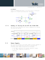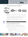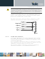
1
CC864-DUAL Hardware User Guide 1vv0300791 Rev 6 – 2012-02-13 CC864-DUAL Hardware User Guide 1vv0300791 Rev 6 – 2012-02-13 Disclaimer The information contained in this document is the proprietary information of Telit Communications S.p.A. and its affiliates (“TELIT”). The contents are confidential and any disclosure to persons other than the officers, employees, agents or subcontractors of the owner or licensee of this document, without the prior written consent of Telit, is strictly prohibited. Telit makes every effort to ensure the quality of the information it makes available. Notwithstanding the foregoing, Telit does not make any warranty as to the information contained herein, and does not accept any liability for any injury, loss or damage of any kind incurred by use of or reliance upon the information. Telit disclaims any and all responsibility for of the devices characterized in this document, the application of the device must comply with standards of the applicable country, and where with the relevant wiring rules. the application and notes that the safety applicable, Telit reserves the right to make modifications, additions and deletions to this document due to typographical errors, inaccurate information, or improvements to programs and/or equipment at any time and without notice. Such changes will, nevertheless be incorporated into new editions of this document. All rights reserved. © 2010 Telit Communications S.p.A. Reproduction forbidden without Telit Communications S.p.A’s. written authorization - All Rights Reserved. Page 2 of 68 CC864-DUAL Hardware User Guide 1vv0300791 Rev 6 – 2012-02-13 Contents 1. Introduction ................................................. 6 1.1. Scope ..................................................... 6 1.2. Audience .................................................. 6 1.3. Contact Information, Support .............................. 6 1.4. Product Overview .......................................... 7 1.4.1. 1.4.2. 1.4.3. 1.4.4. 1.5. General Specifications ...................................... Receiver Specifications ..................................... Transmitter Specifications .................................. gpsOne Receiver Specifications .............................. 7 7 7 8 Safety Recommendations .................................... 9 1.5.1. 1.5.2. 1.5.3. 1.5.4. 1.5.5. Local regulations ........................................... 9 Wiring and Installation ..................................... 9 Electrostatic Discharge ..................................... 9 Antennas .................................................... 9 Disassembly ................................................ 10 1.6. Document Organization .................................... 10 1.7. Text Conventions ......................................... 10 1.8. Related Documents ........................................ 11 1.9. Document History ......................................... 11 2. Mechanical Specifications ................................... 12 2.1. Module Dimensions ........................................ 12 2.2. Interface Connector ...................................... 13 2.3. Mounting ................................................. 15 3. Hardware Interface Description .............................. 16 3.1. Overview ................................................. 16 3.2. Turning On and Off the Module ............................ 17 3.2.1. Turning On the CC864-DUAL .................................. 3.2.2. Initialization and Activation state ........................ 3.2.3. Turning Off the CC864-DUAL ................................. 3.2.3.1. Hardware Shutdown ....................................... 3.2.3.2. Software Shutdown ....................................... 3.2.4. Hardware Reset ............................................. 3.2.5. Summary of Turning ON and OFF the CC864-DUAL ............... Reproduction forbidden without Telit Communications S.p.A’s. written authorization - All Rights Reserved. Page 3 of 68 17 17 19 19 20 20 21 CC864-DUAL Hardware User Guide 1vv0300791 Rev 6 – 2012-02-13 3.3. Power Supply ............................................. 21 3.3.1. +5V Input Source Power Supply Design Guidelines ............ 3.3.2. +12V Input Source Power Supply Design Guidelines ........... 3.3.3. Battery Source Power Supply Design Guidelines .............. 3.3.4. Battery Charge Control Circuitry Design Guideline .......... 3.3.4.1. Trickle Charging ........................................ 3.3.4.2. Constant Current Charging ............................... 3.3.4.3. Constant Voltage Charging ............................... 3.3.4.4. Pulse Charging .......................................... 3.3.5. Thermal Design Guidelines .................................. 3.3.6. Power Supply PCB Layout Guidelines ......................... 3.4. Antenna Requirements ..................................... 32 3.4.1. 3.4.2. 3.5. 24 25 26 27 28 29 29 29 30 31 FCC’s RF Exposure Rules and Regulations .................... 33 Antenna Installation Guideline ............................. 33 GPS path Architecture and antenna ........................ 34 3.5.1. GPS Antenna Requirements (Path 1) .......................... 34 3.5.2. Combined Cellular/GPS Antenna Requirements (Path 2) ........ 35 3.5.3. Linear and Patch GPS Antennas (Path 1) ..................... 35 3.5.4. Active GPS Antenna LNA and Front End Design Considerations (Path 1) 35 3.6. GPS Antenna – Installation Guidelines .................... 36 3.7. Logic Level Specification ................................ 36 3.8. Serial Interfaces ........................................ 37 3.8.1. UART - Serial Interface .................................... 3.8.1.1. RS232C Interface and Level Translation .................. 3.8.1.2. 5V UART Level Translation ............................... 3.8.2. USB Interface .............................................. 3.8.2.1. USB Transceiver Specifications .......................... 3.8.2.2. Diagnostic Monitor Port ................................. 3.9. 37 38 40 42 42 43 Analog Audio Interface ................................... 44 3.9.1. 3.9.2. 3.9.3. 3.9.4. 3.9.5. 3.9.6. Input lines (microphone) ................................... Output lines (Speaker) ..................................... General Design Rules ....................................... Handset Interface .......................................... Headset Interface .......................................... Car Kit Speakerphone Interface ............................. 45 46 47 48 49 50 3.10. PCM Digital Audio Interface ............................ 52 3.11. ADC/DAC Interface ...................................... 52 3.11.1. ADC Converter ............................................ 53 Reproduction forbidden without Telit Communications S.p.A’s. written authorization - All Rights Reserved. Page 4 of 68 CC864-DUAL Hardware User Guide 1vv0300791 Rev 6 – 2012-02-13 3.11.1.1. Description ............................................ 3.11.1.2. Using ADC Converter .................................... 3.11.2. DAC Converter ............................................ 3.11.2.1. Description ............................................ 3.11.2.2. Enabling the DAC ....................................... 3.11.2.3. Low Pass Filter Example ................................ 3.12. General Purpose I/O .................................... 55 3.12.1. 3.12.2. 3.12.3. 3.12.4. 3.12.5. 3.12.6. 3.12.7. 3.13. Using a GPIO pin as Input ................................ Using a GPIO pin as Output ............................... Using the RF Transmission Control, GPIO4 ................. Using the RFTXMON Output, GPIO5 .......................... Using the Alarm Output, GPIO6 ............................ Using the Buzzer Output, GPIO7 ........................... TGPIO_08 ................................................. 56 56 56 56 57 57 58 Miscellaneous Interface Signals ........................ 58 3.13.1. 3.13.2. 3.13.3. 3.13.4. 3.13.5. 4. 53 53 53 53 54 54 VAUX1 .................................................... VRTC ..................................................... STAT_LED – Network Status LED ............................ PWRMON ................................................... AXE ...................................................... 58 58 59 59 60 Development and Testing ..................................... 61 4.1. Debug of the Module in the Final Application ............. 61 4.2. Development Kit .......................................... 61 5. Acronyms and Abbreviations .................................. 63 6. Appendix: Pin Allocation .................................... 64 Reproduction forbidden without Telit Communications S.p.A’s. written authorization - All Rights Reserved. Page 5 of 68 CC864-DUAL Hardware User Guide 1vv0300791 Rev 6 – 2012-02-13 1. Introduction 1.1. Scope This document describes hardware solutions for developing a product containing the Telit CC864-DUAL module, by: • Describing the basic functions of the module • Suggesting a proper hardware solution for each function • Describing common errors to be avoided This document is not intended to provide an overall description of all hardware solutions and all products that may be designed. The solutions suggested serve as a guide or starting point for developing a product with the Telit CC864-DUAL module. However, avoiding the most common errors described in this document should be regarded as UA mandatory. 1.2. Audience This manual is intended for hardware developers who design products that integrate the CC864-DUAL module. 1.3. Contact Information, Support For general information, technical supports, to report documentation errors or to order manuals, contact Telit’s Technical Support Center (TTSC) at: [email protected], [email protected], [email protected], [email protected], or use http://www.telit.com/en/products/technical-supportcenter/contact.php For detailed information about where to buy Telit modules or for recommendations on accessories and components visit: http://www.telit.com. To register for product news and announcements or for product questions contact Telit's Technical Support Center (TTSC). Our aim is to make this guide as helpful as possible. Keep us informed of your comments and suggestions for improvements. Telit appreciates feedback from the users of our documentation. Reproduction forbidden without Telit Communications S.p.A’s. written authorization - All Rights Reserved. Page 6 of 68 CC864-DUAL Hardware User Guide 1vv0300791 Rev 6 – 2012-02-13 1.4. Product Overview The CC864-DUAL is a CDMA-1XRTT wireless module designed to have the same form, fit and function as its GSM/GPRS counterpart product, the GC864-QUAD. As a result, integrators and developers are able to design applications once and take advantage of the global coverage and service flexibility allowed by the combination of the most prevalent cellular technologies worldwide. With its ultra-compact design and extended operating temperature range, the Telit CC864-DUAL module is the perfect platform for m2m applications, mobile data and computing devices. It also incorporates gpsOne capability for applications in mobile environments such as telematics, personal and asset tracking. 1.4.1. General Specifications Parameter External access CDMA protocol Data Rate GPS Vocoder Operating temperature 1.4.2. Receiver Specifications Parameters Frequency range Sensitivity Input dynamic range 1.4.3. Description Code division multiple access CDMA2000 1x Rel A and Rel B 153.6 Kb/s (full-duplex) Standalone GPS/ SGPS/ AGPS EVRC, 13kQCELP, 4GV -30° ~ +80° Descriptions Cellular: 869~894 MHz PCS: 1930~1990 MHz Better than -108 dBm -25dBm ~ -108 dBm Transmitter Specifications Parameters Frequency range Power class Nominal power Descriptions Cellular: 824~849 MHz PCS: 1850~1910 MHz Cellular: Class III PCS: Class II 0.27 W (24.31 dBm) Reproduction forbidden without Telit Communications S.p.A’s. written authorization - All Rights Reserved. Page 7 of 68 CC864-DUAL Hardware User Guide 1vv0300791 Rev 6 – 2012-02-13 1.4.4. gpsOne Receiver Specifications CC864-DUAL Qualcomm chipset QSC6055 is a Gen 7 device. Parameters Frequency range Acquisition Sensitivity - MSA Asynchronous A-GPS (dBm) Acquisition Sensitivity - MSA Synchronous A-GPS (dBm) Acquisition Sensitivity - MSA Synchronous A-GPS (dBm) w/ Sensitivity Assistance (dBm) Cold Start Sensitivity (dBm) Tracking Sensitivity Standalone or MSB (dBm) Accuracy in Open Sky Standalone TTFF (Super Hot /Warm / Cold) Total number of SV available Range Notes L1,1575.42 MHz -158 -159 -160 *QCT GPS RF Conducted Sensitivity is defined at the measurement level: the lowest GPS signal level (S,in dBm) at the antenna port for which the device can still detect an "in view" satellite 50% of the time. *Acquisition / Tracking Sensitivity performance figures assume open sky w/antenna and 2.5dB Noise Figure. -145 -160 <2m CEP-50 Open sky, 1Hz tracking 1s/29s/35s ~30 SVs Support of Predicted Orbits Yes Predicted Orbit CEP-50 Accuracy 5m 1-2 days age Reproduction forbidden without Telit Communications S.p.A’s. written authorization - All Rights Reserved. Page 8 of 68 CC864-DUAL Hardware User Guide 1vv0300791 Rev 6 – 2012-02-13 1.5. Safety Recommendations 1.5.1. Local regulations Verify that the use of this product is permitted in the country intended and in the required product environment. The use of this product may be dangerous and thus must be avoided where: • Interfacing with other electronic devices in environments such as hospitals, airports, etc. is a concern. • A risk of explosion exists, such as in the proximity of gasoline, oil refineries, etc. The integrator is responsible for enforcing local and specific environmental regulations on the product. For further details refer to Chapter 1.7 for related documents. 1.5.2. Wiring and Installation Always follow the instructions in this guide when wiring the product. The module must be supplied with a stable voltage source, and the wiring must conform to security and fire prevention regulations. The installation of external components must be well designed in order to ensure the proper functioning of the module. 1.5.3. Electrostatic Discharge Avoid any contact with the pins because electrostatic discharge can damage the product. 1.5.4. Antennas Every module must be equipped with a compatible antenna. The antenna must be installed in a manner which avoids interference with other electronic devices. Reusing the Telit FCC ID for the end product may be possible if the antenna is greater than 20cm from the human body when in use and there are no co-located transmitters. Otherwise additional FCC testing such as SAR is required. The system integrator must assess the final product against the applicable FCC regulations. Reproduction forbidden without Telit Communications S.p.A’s. written authorization - All Rights Reserved. Page 9 of 68 CC864-DUAL Hardware User Guide 1vv0300791 Rev 6 – 2012-02-13 1.5.5. Disassembly Do not disassemble the product. Any evidence of tampering will void the warranty. 1.6. Document Organization This manual contains the following chapters: “Chapter 1: Introduction” provides the scope for this manual, target audience, contact and support information, and text conventions. “Chapter 2: Mechanical Specifications” contains information on the dimensions of the module, the interface connector and the RF connector, and instructions for designing the module into external applications. “Chapter 3: Hardware Interface Description” describes the hardware interfaces of the product and provides guidelines for using the module in various applications. “Chapter 4: Development and Testing” provides information on operating the module with the Telit Evaluation Kit (EVK). “Chapter 5: Acronyms and Abbreviations” provides definitions for all acronyms and abbreviations used in this guide. “Appendix: Pin Allocation” specifies the allocation of the pins on the module connector. 1.7. Text Conventions Danger – This information MUST be followed or catastrophic equipment failure or bodily injury may occur. Caution or Warning – Alerts the user to important points about integrating the module. If these points are not followed, the module and end user equipment may fail or malfunction. Tip or Information – Provides advice and suggestions that may be useful when integrating the module. All dates are in ISO 8601 format, i.e. YYYY-MM-DD. Reproduction forbidden without Telit Communications S.p.A’s. written authorization - All Rights Reserved. Page 10 of 68 CC864-DUAL Hardware User Guide 1vv0300791 Rev 6 – 2012-02-13 1.8. Related Documents The following documents are related to this user guide: 1.9. • CC864-DUAL Product Description – 80332ST10045A • CC864-DUAL AT-Command Reference Guide – 80332ST10044A • CC864-DUAL Software User Guide – 1vv0300792 Document History Revision Date R0 2008-12-03 R1 2009-07-16 R2 2010-04-19 R3 R4 2010-09-13 2010-09-20 R5 2011-01-31 R6 2012-02-13 Changes First draft version for release. Removed some unnecessary notes and removed Pin 80 from “Reserved”. Removed the channels listed from the specifications, because the module was on channels not listed. Add a power supply table in section 3.3. Corrected information regarding flow control on pages 33 & 61 (R1). DAC bit accuracy corrected, 8-bit not 7-bit. R-UIM information removed, not supported on CC864DUAL. Formatting updates. Additions in the UART, AXE, and RESET sections. Additions to USB section and mechanical specifications. Updated Power Consumption Table Updated Antenna Requirements Table Updated Chapter 3.2, Turning On and Off the Module Updated Thermal Design Guidelines Updated External Active Antenna Spec. Table Updated Input Lines (Microphone) Added Output Lines (Speaker) Updated 3.3.2 Switching regulator schematic Updated 3.4 Antenna Requirements Updated 3.8.1.3 5V UART Translation Removed I2C Bus Interface Updated 3.12 General Purpose I/O Updated 6 Pin Allocation Added FCC/IC compliance Information Reproduction forbidden without Telit Communications S.p.A’s. written authorization - All Rights Reserved. Page 11 of 68 CC864-DUAL Hardware User Guide 1vv0300791 Rev 6 – 2012-02-13 2. Mechanical Specifications 2.1. Module Dimensions The table below outlines the overall dimensions of the CC864DUAL: Length: 36.2 ±0.3 mm Width: 30.0 ±0.2 mm* Thickness: 4.8 ±0.1 mm 9g Weight: *Excluding solder pads Reproduction forbidden without Telit Communications S.p.A’s. written authorization - All Rights Reserved. Page 12 of 68 CC864-DUAL Hardware User Guide 1vv0300791 Rev 6 – 2012-02-13 2.2. Interface Connector The CC864-DUAL is equipped with a Molex 80-pin board-to-board connector, P/N 0539490878 (male). The mating part is Molex P/N 0541500878 (female). The CC864-DUAL is equipped with a Murata GSC type 50 Ohm RF connector, P/N MM9329-2700. The suitable counterpart is Murata MXTK92 type or MXTK88 type connector. Reproduction forbidden without Telit Communications S.p.A’s. written authorization - All Rights Reserved. Page 13 of 68 CC864-DUAL Hardware User Guide 1vv0300791 Rev 6 – 2012-02-13 The same connector type and part number is used for both the CDMA RF port and the GPS RF port. NOTE: The CDMA RF antenna connector is located on the same side as the MOLEX 80 pin connector. The GPS RF antenna connector is located on the side with no system connector. Reproduction forbidden without Telit Communications S.p.A’s. written authorization - All Rights Reserved. Page 14 of 68 CC864-DUAL Hardware User Guide 1vv0300791 Rev 6 – 2012-02-13 2.3. Mounting The figure below shows the position of the Molex board-toboard connector and pin 1. Tip: It is highly recommended to maintain a 1.5mm clearance between all wireless modems and any components, including solder tabs. Reproduction forbidden without Telit Communications S.p.A’s. written authorization - All Rights Reserved. Page 15 of 68 CC864-DUAL Hardware User Guide 1vv0300791 Rev 6 – 2012-02-13 3. Hardware Interface Description 3.1. Overview The CC864-DUAL has the following main interface functional blocks: • UART1 (used for AT commands) • USB (can be used for AT commands, Data sessions, GPS NMEA Data, Diagnostics, and updating firmware). • GPIOs • Audio (includes Analog I/O audio codecs and PCM interface) • Miscellaneous pins GPS Switch To GPS Dedicated Antenna LNA GPS filter QSC 6055 CDMA Tx UART1 RX Filter US-PCS Duplexer USB RUIM Triplexer To Antenna Cellular LNA TX Filter RX Filter RF Interface PAM GPIOs CODEC JTAG 80 Pin Modem Interface Connector US PCS LNA Cellular Duplexer Misc IIC PAM ROM TX Filter CDMA Rx GPS Reproduction forbidden without Telit Communications S.p.A’s. written authorization - All Rights Reserved. Page 16 of 68 RAM CC864-DUAL Hardware User Guide 1vv0300791 Rev 6 – 2012-02-13 3.2. Turning On and Off the Module 3.2.1. Turning On the CC864-DUAL To turn on CC864-DUAL, the pad ON# must be tied low for at least 1 second and then released. The maximum current that can be drained from the ON# pad is 0.1mA. The following figure shows a sample circuit to accomplish this operation: 3.2.2. Initialization and Activation state The CC864-DUAL is not activated immediately after power up because the boot sequence of CC864-DUAL needs to complete. It takes about 10 seconds to initialize the module internally. For this reason, the CC864-DUAL should not be accessed during the initialization state as below. To get the desirable stability, CC864-DUAL needs at least 10 seconds after the PWRMON goes HIGH. Reproduction forbidden without Telit Communications S.p.A’s. written authorization - All Rights Reserved. Page 17 of 68 CC864-DUAL Hardware User Guide 1vv0300791 Rev 6 – 2012-02-13 During the Initialization state, no AT-commands are available. DTE must wait for the Activation state to communicate with CC864-DUAL. NOTE: To check if the CC864-DUAL has powered on, the hardware line PWRMON must be monitored. When PWRMON goes high, the module has powered on. NOTE: Do not use any pull up resistor on the ON# line (it is internally pulled up). Using a pull up resistor may cause latch up problems on the CC864-DUAL power regulator and improper power on/off of the module. The line ON# must be connected only in open collector configuration. NOTE: In this document all the lines are inverted. Active low signals are labeled with a name ending with "#" or with a bar over the name. NOTE: CC864-DUAL may be turned on also by supplying power to the Charge pad (provided there is a battery on the VBATT pads). An example: 1- Assume the ON# pad needs to be driven with a totem pole output of a +1.8/5 V microcontroller (uP_OUT1): Reproduction forbidden without Telit Communications S.p.A’s. written authorization - All Rights Reserved. Page 18 of 68 CC864-DUAL Hardware User Guide 1vv0300791 Rev 6 – 2012-02-13 3.2.3. Turning Off the CC864-DUAL The module may be turned off with either a software command or a hardware shutdown circuit. When the device is shut down, it notifies the network that it is powering down and is therefore no longer reachable. Warning: Never disconnect power before the power off procedure is completed. This may cause severe damage and render the module inoperable. 3.2.3.1. Hardware Shutdown To turn the CC864-DUAL off, the ON/OFF Pin must be tied low for 2 second and then released. The same circuitry and timing used for powering on the module must be used for powering off the module. The device shuts down after the ON_OFF pin is released. When the hold time of ON/OFF# is above 2 seconds, CC864-DUAL goes into the finalization state and finally will shut down PWRMON at the end of this state. The period of the finalization state can differ according to the situation in which the CC864-DUAL is so it cannot be fixed definitely. Normally it will be above 10 seconds later from releasing ON/OFF# and DTE should monitor the status of PWRMON to see the actual power off. TIP: To check if the device has powered off, hardware line PWRMON must be monitored. When PWRMON goes low, the device has powered off. Reproduction forbidden without Telit Communications S.p.A’s. written authorization - All Rights Reserved. Page 19 of 68 CC864-DUAL Hardware User Guide 1vv0300791 Rev 6 – 2012-02-13 3.2.3.2. Software Shutdown The “Software User Guide” contains procedures for shutting down the module using AT-commands. 3.2.4. Hardware Reset To perform a hardware reset and to reboot the module, the RESET pin must be tied low for at least 200 milliseconds and then released. The following figure shows a sample circuit to accomplish this operation: TIP: A hardware reset circuit should always be implemented on the host board and used as an emergency reset procedure only. NOTE: If unused, the RESET pin may be left unconnected. Otherwise, it must always be connected to an open collector transistor to permit the internal circuitry to control the signal during the power on reset and under voltage lockout functions. Reset Signal Operating Levels: Signal RESET Input High RESET Input Low MIN 2.0V* 0V MAX 2.6V .2V *This signal is internally pulled up so the pin can be left floating if not used. Reproduction forbidden without Telit Communications S.p.A’s. written authorization - All Rights Reserved. Page 20 of 68 CC864-DUAL Hardware User Guide 1vv0300791 Rev 6 – 2012-02-13 An Example: Assume the RESET# pad needs to be driven with a totem pole output of a +1.8/5 V microcontroller (uP_OUT2): 3.2.5. Summary of Turning ON and OFF the CC864-DUAL The chart below describes the overall sequences for turning the module ON and OFF. 3.3. Power Supply The electrical design of the power supply strongly depends on the power source from which the power is drained. The following three common categories are discussed: • +5V input (typically PC internal regulator output) • +12V input (typically automotive) • Battery Reproduction forbidden without Telit Communications S.p.A’s. written authorization - All Rights Reserved. Page 21 of 68 CC864-DUAL Hardware User Guide 1vv0300791 Rev 6 – 2012-02-13 Power Supply Nominal Supply Voltage 3.8 V Max Supply Voltage 4.2V Normal Operating Voltage Range 3.4 V – 4.20 V TIP: In order to be compatible with the sibling wireless modems in the Telit Unified Form Factor, the power supply should be designed for 2A current peaks as this will allow the use of a GSM/GPRS modem with the same design. CC864-DUAL Mode Average(mA) SWITCHED OFF Typically** 10uA Maximum** 40uA IDLE mode with GPS OFF AT+CFUN=1 46* AT+CFUN=4 0.4* AT+CFUN=0 or AT+CFUN=5 4.5* CDMA TX and RX mode with GPS OFF Voice & Data < 700 Mode Description Module supplied but switched off Standby mode; no call in progress; GPS OFF Normal mode; full functionality of the module Disabled TX and RX; modules is not registered on the network Power saving; CFUN=0 module registered on the network and can receive voice call or an SMS; but it is not possible to send AT commands; module wakes up with an unsolicited code (call or SMS) or rising RTS line. CFUN=5 full functionality with power saving; Module registered on the network can receive incoming call sand SMS Voice & Data channel(Max power) * Worst/best case depends on network configuration and is not under module control. ** Total supply current from the main battery with the device off and the 32.768 MHz crystal oscillator on. This specification applies only for case operating temperatures from -30oC to +60oC Reproduction forbidden without Telit Communications S.p.A’s. written authorization - All Rights Reserved. Page 22 of 68 CC864-DUAL Hardware User Guide 1vv0300791 Rev 6 – 2012-02-13 CC864-DUAL Mode Average(mA) Mode Description IDLE mode with GPS ON full power Standby mode; no call in progress; GPS mode* ON Normal mode; full functionality of the AT+CFUN=1 135* module AT+CFUN=4 94* AT+CFUN=0 or AT+CFUN=5 98* CDMA TX and RX mode with GPS ON Voice & Data < 800 Disabled TX and RX; modules is not registered on the network Power saving; CFUN=0 module registered on the network and can receive voice call or an SMS; but it is not possible to send AT commands; module wakes up with an unsolicited code (call or SMS) or rising RTS line. CFUN=5 full functionality with power saving; Module registered on the network can receive incoming call sand SMS GPS ON in Cellular Measurements channel * Except external active GPS antenna Reproduction forbidden without Telit Communications S.p.A’s. written authorization - All Rights Reserved. Page 23 of 68 CC864-DUAL Hardware User Guide 1vv0300791 Rev 6 – 2012-02-13 3.3.1. +5V Input Source Power Supply Design Guidelines The desired output for the power supply is 3.8V, hence there’s not a big difference between the input source and the desired output so a linear regulator can be used. When using a linear regulator, a proper heat sink may be required. A bypass low ESR capacitor must be provided to cut the current absorption peaks close to the CC864-DUAL; a 100µF tantalum (or equivalent) capacitor is suited for this purpose. Verify that the low ESR capacitor on the power supply output (usually a tantalum) is rated to at least 10V. A protection diode should be inserted close to the power input to protect the module from power polarity inversion. A typical example of a linear regulator with 5V input is below: Reproduction forbidden without Telit Communications S.p.A’s. written authorization - All Rights Reserved. Page 24 of 68 CC864-DUAL Hardware User Guide 1vv0300791 Rev 6 – 2012-02-13 3.3.2. +12V Input Source Power Supply Design Guidelines The desired output for the power supply is 3.8V. Due to the large difference between the input voltage and the desired output, a linear regulator should not be used. A switching power supply is preferred because of its better efficiency with the 1A peak current load drawn by the CC864DUAL. When using a switching regulator, a 500 KHz or more switching frequency regulator is preferable because of its smaller inductor size and faster transient response. This allows the regulator to respond quickly to current peaks. In any case the frequency and switching design selection is application specific because the switching frequency could also generate EMC interference, which must be taken into account. A bypass low ESR capacitor of adequate capacity must be provided in order to cut the current absorption peaks; a 100µF tantalum (or equivalent) capacitor is suitable for this purpose. The low ESR capacitor on the power supply output (usually a tantalum) must be rated to at least 10V. A protection diode (which can be the same diode as in spike protection below) must be inserted close to the power input in order to save the CC864-DUAL from power polarity inversion. Power supplies for “automotive use” are complicated so many factors must be considered, such as: over voltage, reverse polarity, cranking, load dump booster batteries, forced charging, etc. A spike protection diode must be inserted close to the power input to clean the supply from spikes. A specific automotive grade regulator is recommended as well. For a car PB battery the input voltage can rise up to 16V, therefore all components in the power supply must withstand this voltage. An example of switching regulator with 12V input is in the below schematic (it is split in 2 parts): Reproduction forbidden without Telit Communications S.p.A’s. written authorization - All Rights Reserved. Page 25 of 68 CC864-DUAL Hardware User Guide 1vv0300791 Rev 6 – 2012-02-13 Switching regulator 3.3.3. Battery Source Power Supply Design Guidelines The desired nominal output for the power supply is 3.8V with a maximum allowed voltage of 4.2V. Therefore, a single 3.7V lithium-ion cell battery is ideal to supply the power to the module. The suggested battery capacity is from 500mAh to 1000mAh. Warning: DO NOT USE any Ni-Cd, Ni-MH or Pb battery types directly connected to the modem! Their use can lead to overvoltage and damage to the module. USE ONLY Li-Ion battery types. A bypass low (usually 100uF tantalum) ESR capacitor rated to at least 10V with adequate capacity must be provided to cut the current absorption peaks. A protection diode must be inserted close to the power input to protect the module from voltage polarity inversion. Reproduction forbidden without Telit Communications S.p.A’s. written authorization - All Rights Reserved. Page 26 of 68 CC864-DUAL Hardware User Guide 1vv0300791 Rev 6 – 2012-02-13 3.3.4. Battery Charge Control Circuitry Design Guideline The CC864-DUAL provides support circuitry for charging a lithium-ion battery utilizing four firmware-controlled charging modes: • Trickle • Constant current • Constant voltage • Pulsed Battery voltage, external supply voltage, and total detected current measurements are available to the module firmware through the analog multiplexer, which allows the firmware to monitor charging parameters and control the charging process, which progresses as follows: • Charging begins with trickle charging, which limits the current and avoids pulling the VDD down. • Once a minimum battery voltage is established using trickle charging, constant current charging is enabled by the firmware in order to charge the battery quickly (this mode is sometimes called fast charging). • When the Li-ion battery approaches its target voltage (through constant current charging), the charge is completed using either constant voltage or pulse charging. Note: This process is completely transparent to the application and is controlled by the module firmware. The description below is for completeness and battery selection purposes only. Further description of all charging modes is provided in the sections below. The following figure illustrates the main battery charging sequence. Reproduction forbidden without Telit Communications S.p.A’s. written authorization - All Rights Reserved. Page 27 of 68 CC864-DUAL Hardware User Guide 1vv0300791 Rev 6 – 2012-02-13 3.3.4.1. Trickle Charging The module firmware and power management circuitry provides trickle charging of the main battery when powered from VDD. This mode is used by the module to raise a severely depleted battery’s voltage to a level sufficient to begin fast charging. Attempting fast charging with a high-current supply on a deeply discharged battery would cause the battery to draw excessive current, pull the VDD voltage down, and possibly cause a module malfunction or shutdown due to an under-voltage lockout condition. Trickle charging is used by the module firmware until the main battery reaches a predefined threshold, which is usually about 3.0V for Li-ion batteries. The threshold varies with battery type and application, so there is no predefined value implemented in the detection circuits. The firmware stops the trickle charging based on battery voltage measurements and battery type. Reproduction forbidden without Telit Communications S.p.A’s. written authorization - All Rights Reserved. Page 28 of 68 CC864-DUAL Hardware User Guide 1vv0300791 Rev 6 – 2012-02-13 3.3.4.2. Constant Current Charging The module firmware supports constant current charging of the main battery. During constant current charging the battery is charged with a constant current of 600mA. As the battery voltage rises and approaches its desired value of 4.2V the charging current begins to decrease, indicating the end of constant current charging and the beginning of residual charging. The firmware monitors the voltage and takes the appropriate action to terminate constant current charging mode. Charging continues with residual charging (either constant voltage or pulsed). Note: In this application the charging firmware limits the charging current to 600mA. 3.3.4.3. Constant Voltage Charging Once constant current charging of the lithium-ion battery is finished, the charging continues using either constant voltage or pulsed techniques. Constant voltage charging is similar to the constant current mode: The battery voltage is constant while the charging current decreases exponentially for the remaining charging process. The end of the constant voltage charging is typically detected by allowing voltage operation for a pre-determined duration beyond crossing the VBATDET threshold in the internal charger IC (lasting for one and a half to two hours). The firmware limits the predetermined duration to 120 minutes because charging for too long can damage the battery. 3.3.4.4. Pulse Charging The CC864-DUAL uses pulse charging for final charging. Pulse charging is implemented by switching the pass transistor on the internal charger IC on and off. The module and external electronics must draw minimal current so the battery’s open circuit voltage can be measured accurately during the off interval. Compared to constant voltage charging, pulse charging: • Provides better voltage accuracy • Reaches full charge more quickly Reproduction forbidden without Telit Communications S.p.A’s. written authorization - All Rights Reserved. Page 29 of 68 CC864-DUAL Hardware User Guide 1vv0300791 Rev 6 – 2012-02-13 • Dissipates less transistor power when switching from constant current charging Pulse charging is enabled through firmware control and uses the same hardware as constant current or constant voltage charging, but repeatedly opens and closes the pass transistor to deliver current pulses to the battery. One purpose of pulsed operation is to check and recheck the battery’s open circuit voltage, confirming a full charge before terminating the process. 3.3.5. Thermal Design Guidelines The thermal design for the application and its power supply should take the following parameters into account: Average current consumption during transmission at Max level (< 25dBm) < 700mA NOTE: The average current consumption during transmissions depends on the power level at which the device is requested to transmit by the network. Hence, the average current consumption varies significantly. Considering the very low current during idle and sleep time, especially when the power saving function is enabled, from a thermal point of view it is accurate for estimation purposes to consider that the device only draws significant current during calls. An Example: If the device transmits for a few minutes and then remains idle for an hour, the power supply always has time to cool down between the calls. The heat sink can therefore be smaller than the calculated 700mA maximum RMS current or there can be no heat sink (simple chip package). In average network conditions, the device transmit power is lower than the maximum, and thus the current consumption is less than 500mA. For these reasons, the thermal design is rarely a concern and using the ground plane where the power supply chip is placed as the heat sink can be enough to ensure good thermal conditions and avoid overheating. The generated heat is primarily conducted to the ground plane under the module and the ambient air by convection, so ensure that the application can dissipate the heat as required. Reproduction forbidden without Telit Communications S.p.A’s. written authorization - All Rights Reserved. Page 30 of 68 CC864-DUAL Hardware User Guide 1vv0300791 Rev 6 – 2012-02-13 3.3.6. Power Supply PCB Layout Guidelines Telit recommends that the power supply for the CC864-DUAL be designed to meet the higher demands of GSM/UMTS modules. The power supply will be slightly over-dimensioned for a CDMA modem, but will allow for an easy transition to another technology if need be (GSM/UMTS 2A vs. CDMA 1A peak current consumption). The power supply implementation must have a low ESR capacitor on the output to smooth the current peaks and should include a protection diode on the power supply input to protect from spikes and polarity inversion. The placement of these components is crucial for the correct operation of the circuitry and application. A misplaced component can be ineffective or even decrease the power supply performance. Therefore, the following guidelines are offered: • The Bypass low ESR capacitor must be placed close to the module power input pads. If the power supply is of the switching variety it can be placed close to the inductor to cut the ripple provided the PCB trace from the capacitor to the module is wide enough to ensure no voltage drops during the transmission current peaks. • The protection diode must be placed close to the input connector where the power source is drained. • The PCB traces from the input connector to the power regulator IC must be wide enough to ensure no voltage drops occur during the transmission current peaks. Note: (GSM/UMTS specific consideration): This recommendation is not made to save power but instead to avoid the voltage drops on the power line at the current peaks frequency of 216 Hz that will reflect on all the components connected to that supply, introducing a noise floor at the burst base frequency. For this reason, while a voltage drop of 300-400 mV may be acceptable for power loss, it may not be acceptable for noise considerations. If the application does not have an audio interface but only uses GSM/UMTS data, then this noise may not be so disturbing and power supply layout design can be more forgiving. • For the reasons outlined above, the PCB traces to the module and the bypass capacitor must be wide enough to ensure no significant voltage drops occur during the GSM Reproduction forbidden without Telit Communications S.p.A’s. written authorization - All Rights Reserved. Page 31 of 68 CC864-DUAL Hardware User Guide 1vv0300791 Rev 6 – 2012-02-13 2A/CDMA 1A current peaks. This trace should be as short as possible. 3.4. • The PCB traces connecting the switching output to the inductor and the switching diode must be kept as short as possible by placing the inductor and the diode very close to the power switching IC (only for switching power supply). This will reduce the radiated field (noise) at the switching frequency (usually 100-500 kHz). • The use of a good common ground plane is suggested. • The placement of the power supply on the board should guarantee that the high current return paths in the ground plane are not overlapped with any noise sensitive circuitry such as the microphone amplifier/buffer or earphone amplifier. Antenna Requirements This radio transmitter (5131A-CC864DUAL) has been approved by Industry Canada to operate with the antenna types listed below with the maximum permissible gain and required antenna impedance for each antenna type indicated. Antenna types not included in this list, having a gain greater than the maximum gain indicated for that type, are strictly prohibited for use with this device. The table below outlines antenna requirements for the CC864DUAL: Frequency range Gain Impedance Input power VSWR recommended Radiation pattern Polarization Antenna Requirements CDMA PCS Tx:824MHz~849MHz Tx:1850MHz~1910MHz Rx:869MHz~894MHz Rx:1930MHz~1990MHz < 5.12dBi < 6.12dBi 50 Ohm > 24dBm max power in CDMA and PCS ≤ 2:1 Omni-directional Vertical Reproduction forbidden without Telit Communications S.p.A’s. written authorization - All Rights Reserved. Page 32 of 68 CC864-DUAL Hardware User Guide 1vv0300791 Rev 6 – 2012-02-13 Note: If the application is developed for the US and/or Canadian market, it must comply with FCC and/or IC approval requirements: This device is to be used only for mobile and fixed application. The antenna(s) used for this transmitter must be installed to provide a separation distance of at least 20 cm from all persons and must not be co-located or operating in conjunction with any other antenna or transmitter. End-Users must be provided with transmitter operation conditions for satisfying RF exposure compliance. OEM integrators must ensure that the end user has no manual instructions to remove or install the CC864-DUAL module. Antennas used for this OEM module must not exceed 5.12dBi gain in CDMA and 6.12dBi gain in PCS for mobile and fixed operating configurations. 3.4.1. FCC’s RF Exposure Rules and Regulations To meet the FCC's RF exposure rules and regulations: • The system antenna(s) used for this transmitter must be installed to provide a separation distance of at least 20 cm from all the persons and must not be co-located or operating in conjunction with any other antenna or transmitter. • The system antenna(s) used for this module must not exceed 5.12dBi (800MHz) and 6.12dBi (1900MHz) for mobile and fixed or mobile operating configurations. • Users and installers must be provided with antenna installation instructions and transmitter operating conditions for satisfying RF exposure compliance. Manufacturers of mobile, fixed or portable devices incorporating this module are advised to clarify any regulatory questions and to have their complete product tested and approved for FCC compliance. 3.4.2. Antenna Installation Guideline To avoid subjecting the application to FCC SAR requirements, if possible the antenna should be at least 20 cm from all persons during operation. In general, the antenna should not be co-located or operating in conjunction with any other antenna or transmitter. The antenna must be installed according to the antenna manufacturer instructions. Warning: The antenna must not be installed inside metal cases. Reproduction forbidden without Telit Communications S.p.A’s. written authorization - All Rights Reserved. Page 33 of 68 CC864-DUAL Hardware User Guide 1vv0300791 Rev 6 – 2012-02-13 3.5. GPS path Architecture and antenna The CC864-DUAL has two different GPS paths: Path 1 is the dedicated GPS path; this path can support an external active GPS antenna and external GPS antenna monitoring functions. Path 2 is a combined path. In this configuration, the triplexer is furnished by the module so no external triplexer is necessary. A combined CDMA/GPS antenna is sufficient. Please note that this configuration cannot support an active GPS antenna or any antenna monitoring functions. The desired GPS RF path is chosen by an AT-command. Please refer to the AT-command manual for information on this command. Note: An AT-command is used to switch GPS ports: AT$GPSPATH. 3.5.1. GPS Antenna Requirements (Path 1) The CC864-DUAL includes an internal LNA. The internal LNA provides 13dB and ensures sufficient performance in most cases. If the application calls for additional gain, an external active antenna may be utilized. The module provides an active GPS antenna supply circuit with the following characteristics: • A total gain of 12 ~ 16dB from the GPS antenna plus any external LNA is recommended. • Supply voltage is derived from VBATT (can vary from 3.4 to 4.2V DC). • Supply enable is controlled internally by the module. Reproduction forbidden without Telit Communications S.p.A’s. written authorization - All Rights Reserved. Page 34 of 68 CC864-DUAL Hardware User Guide 1vv0300791 Rev 6 – 2012-02-13 3.5.2. • Current measurement circuit provided (AT-command controlled). • Voltage measurement circuit provided (AT-command controlled). • Integrated HW protection for Antenna Short Circuit (>40mA current draw). Combined Cellular/GPS Antenna Requirements (Path 2) The CC864-DUAL can support the use of a combined Cellular/GPS antenna without the need for an additional external diplexer. The CC864-DUAL contains the required di-/tri-plexers and RF path. However, the combined Cellular/GPS path adds about 1 dB of loss for GPS and consequently affects performance. This configuration cannot support an active GPS antenna. 3.5.3. Linear and Patch GPS Antennas (Path 1) Linear or patch antennas result in 3 dB of loss relative to a circularly polarized (CP) antenna. Spherical gain response opposed to a hemispherical gain response will aggravate the multipath behavior and create poor position accuracy, leading to 50m accuracy or less in some situations. Poor LHCP relative to RHCP response can have multiple gain nulls and average gain is far lower than for a good path (9dB). 3.5.4. Active GPS Antenna LNA and Front End Design Considerations (Path 1) The antenna LNA gain should be between 12dB and 16dB assuming a patch antenna with > 3dBi of gain is utilized. Excessive LNA gain (>17dB) can introduce jamming spurs, degrade 3IP, and saturate the receiver, primarily due to the fact that the CC864-DUAL already has an internal GPS LNA (13dB gain). The active antenna must operate with a supply voltage between 3.4 to 4.2V DC. No other circuitry is required. The external active antenna for CC864-DUAL must fulfill the following requirements: Reproduction forbidden without Telit Communications S.p.A’s. written authorization - All Rights Reserved. Page 35 of 68 CC864-DUAL Hardware User Guide 1vv0300791 Rev 6 – 2012-02-13 Parameter Frequency range Bandwidth Gain Impedance Amplification Supply voltage Current consumption 3.6. Value 1575.42MHz (GPS L1) +- 1.023MHz 1.5dBi < Gain < 4.5dBi 50 ohm <14dB Must accept from 3 to 5 V DC 20mA Typical (40mA max) GPS Antenna – Installation Guidelines Installation of the GPS antenna should follow the guidelines below: The antenna should not be co-located or operating in conjunction with any other antenna or transmitter. The antenna shall not be installed inside metal cases. The antenna shall be installed according to manufacturer instructions. 3.7. Logic Level Specification Where not specifically stated, the interface circuits work at 2.6V CMOS logic levels. The following tables show the logic level specifications for the CC864-DUAL interface circuits: Operating Range – Interface levels (2.6V CMOS): Parameter VIH (input high level) VIL (input low level) VOH (output high level) VOL (output low level) Min 1.69 V -0.3 V 2.15 V 0.0 V Max 2.9 V 0.91 V 2.6 V 0.45 V Operating Range – Interface levels (1.8V CMOS): Parameter VIH (input high level) VIL (input low level) VOH (output high level) VOL (output low level) Min 1.2V -0.3V 1.35V 0.0V Max 2.1V 0.63V 1.8V 0.45V Reproduction forbidden without Telit Communications S.p.A’s. written authorization - All Rights Reserved. Page 36 of 68 CC864-DUAL Hardware User Guide 1vv0300791 Rev 6 – 2012-02-13 3.8. Serial Interfaces Serial ports on the CC864-DUAL function as the interface between the module and User Application. There are two main types of serial ports on the module: UART and USB. The CC864-DUAL has one main UART that can be used for control and data transfer. In addition, the module has a USB port that can function as the main control interface for the host application. NOTE: To access the module and to allow in-circuit reprogramming of the module’s firmware, the USB port must be made available. This is generally a requirement for wireless carrier approval testing as well. The application controlling the device may be placed into tri-state, disconnected, or act as a gateway for the serial data when reprogramming occurs. All application designs should include a means to reprogram the module! 3.8.1. UART - Serial Interface The CC864-DUAL UART functions as the controlling interface between the module and the host hardware. Depending on the host hardware serial port implementation, a level translator circuit may be required. The only configuration that does not require level translation is interfacing to a 2.8V UART. There is one UART port on the CC864-DUAL. It differs from the standard PC RS232C in signal polarity (where RS232 is reversed) and levels. The UART can be used as the module’s serial data port for test and debug using AT commands, and can support additional interface functions such as an external keypad or ringer. The following table lists the signals of the CC864-DUAL UART and the corresponding RS-232 signals: RS232 Pin No 1 Signal C109/DCD Pin No 32 Name Usage Data Carrier Detect Output from the CC864DUAL that indicates the carrier presence Reproduction forbidden without Telit Communications S.p.A’s. written authorization - All Rights Reserved. Page 37 of 68 CC864-DUAL Hardware User Guide 1vv0300791 Rev 6 – 2012-02-13 RS232 Pin No 2 Signal Pin No Name Usage Output transmit line of CC864-DUAL UART Input receive of the CC864-DUAL UART Input to the CC864DUAL controlling the DTE READY condition Ground Output from the CC864DUAL indicating the module is ready Input to the CC864DUAL controlling the hardware flow Output from the CC864DUAL controlling the hardware flow Output from the CC864DUAL indicating the incoming call condition C104/RXD 26 Transmit line 3 C103/TXD 25 Receive line 4 C108/DTR 29 Data Terminal Ready 5 6 GND C107/DSR 5,6,7 27 Ground Data Set Ready 7 C105/RTS 31 Request to Send 8 C106/CTS 28 Clear to Send 9 C125/RIN G 30 Ring Indicator NOTE: According to V.24, the RXD and TXD signals are referred to from the perspective of the application. Therefore, these signals are referred to in the opposite direction for the module: TXD on the application side will be connected to the receive line (here named TXD/Receive line) of the module’s serial port and vice versa for RXD. TIP: For a minimum implementation, only the TXD and RXD lines need to be connected, leaving the other lines open, provided software flow control is implemented. 3.8.1.1. RS232C Interface and Level Translation In order for the module to interface with a PC com port or a RS232 (EIA/TIA-232) application, a level translator is required. This level translator must: • Invert the electrical signal in both directions • Translate the level from 0/2.8V to +15/-15V The RS232 UART 16450, 16550, 16650 and 16750 chipsets accept signals with lower levels on the RS232 side (EIA/TIA-562), Reproduction forbidden without Telit Communications S.p.A’s. written authorization - All Rights Reserved. Page 38 of 68 CC864-DUAL Hardware User Guide 1vv0300791 Rev 6 – 2012-02-13 allowing for a lower voltage-multiplying ratio on the level translator. Note that the negative signal voltage must be less than 0 V so that some form of level translation is always required. The simplest way to translate the levels and invert the signal is by using a single chip level translator. There are several available, differing in the number of drivers and receivers and levels. NOTE: Always use a true RS232 level translator and not a translator for RS485 or any other standard. By convention, the driver is the level translator from the 03V UART level to the RS232 level, while the receiver is the translator from RS232 level to 0-3V UART. In order to translate the whole set of control lines of the UART, five drivers and three receivers are required. The figure below shows an example of level translation circuitry: SP3238EEA 100n C1+ C1C2+ VCC V+ V- C2- GND 100n 100n DCD/_UART1 DSR/_UART1 RXD_UART1 CTS/_UART1 RI_UART1 T1_IN T2_IN T3_IN T4_IN T5_IN RTS/_UART1 TXD_UART1 DTR_UART1 R1_OUT R2_OUT R3_OUT +3V 100n 100n T1_OUT T2_OUT T3_OUT T4_OUT T5_OUT DCD_RS232 DSR_RS232 RXD_RS232 CTS_RS232 RI_RS232 R1_IN R2_IN R3_IN RTS_RS232 TXD_RS232 DTR_RS232 NOTE: In this case VIn has to be set with a value compatible with the logic levels of the module. In this configuration the SP3282EB will adhere to EIA/TIA-562 voltage levels instead of RS232 (-5 +5V) Reproduction forbidden without Telit Communications S.p.A’s. written authorization - All Rights Reserved. Page 39 of 68 CC864-DUAL Hardware User Guide 1vv0300791 Rev 6 – 2012-02-13 NOTE: The digital input lines working at 2.6V CMOS have an absolute maximum input voltage of 2.9V; therefore the level translator IC shall not be powered by the +3.8V supply of the module. Instead, it must be powered from a +2.6V (preferably dedicated) power supply. If supplied from the main 3.8V, the level translator IC outputs on the module side (i.e. the CC864-DUAL inputs) will work at +3.8V interface levels, stressing the module inputs beyond their maximum input voltage range. The RS232 serial port lines are usually connected to a DB9 connector with the layout shown in the following figure: 3.8.1.2. 5V UART Level Translation If the host application uses a microcontroller with a serial port (UART) that works at a voltage different from 2.6~2.9V, circuitry must be provided to translate the different levels of the two signal sets. As for the RS232 translation, there is a selection of single chip translators, but since the translation requires very few components a discrete design can also be used. The following example illustrates a potential inexpensive translator circuit for a 5V transmitter/receiver: Reproduction forbidden without Telit Communications S.p.A’s. written authorization - All Rights Reserved. Page 40 of 68 CC864-DUAL Hardware User Guide 1vv0300791 Rev 6 – 2012-02-13 The following example illustrates a potential inexpensive translator circuit for a 5V receiver: 22k 22k 22k 22k A power source of the internal interface voltage corresponding to the 2.6V CMOS high level is available at the VAUX1 pin on the connector with an absolute maximum output current of 1mA. A maximum of 9 resistors of 4.7 KΩ pull-up can be connected to the VAUX1 pin provided no other devices are connected to it. The pulled-up lines are module’s input lines connected to open collector outputs in order to avoid latch-up problems on the module. Care must be taken to avoid latch-up on the module and the use of this output line to power electronic devices shall be avoided. This is especially true for devices that generate spikes and noise such as switching level translators and micro controllers. Reproduction forbidden without Telit Communications S.p.A’s. written authorization - All Rights Reserved. Page 41 of 68 CC864-DUAL Hardware User Guide 1vv0300791 Rev 6 – 2012-02-13 3.8.2. USB Interface The CC864-DUAL includes a Universal Serial Bus (USB) transceiver, which operates at USB low-speed (1.5Mbits/sec) and USB full-speed (12Mbits/sec). The transceiver is compliant with the USB 2.0 specification and can be used for diagnostics, control and data transfers. The table below describes the USB interface signals Note: USB connection points are required for software upgrades and other services. USB Pin No. 1 Signal Name USB_VBUS Pin No. 48 2 USB_D- 80 3 USB D+ 79 4 USB_ID 35 3.8.2.1. Usage Power supply for the internal USB transceiver. This pin is configured as an analog input or an analog output depending upon the type of peripheral device connected. Minus (-) line of the differential, bidirectional USB signal to/from the peripheral device. Plus (+) line of the differential, bidirectional USB signal to/from the peripheral device. Analog input to sense whether a peripheral device is connected as well as detects the USB peripheral type, Host or Slave. Left floating, grounded, or resistor to ground by the peripheral. USB Transceiver Specifications The USB transceiver specifications are in the table below. Parameter Comments VBUS Supply Voltage Supply Current Input Levels for Low-/Full-speed Input sensitivity |D+ - D-|, Vin = 0.8 (differential) to 2.5 V Common-mode range Includes VDI (diff) Receiver threshold Single-ended Receiver hysteresis Single-ended Output Levels for Low speed and Full speed Logic low RL = 1.5 k to 3.6 V RL = 15 k to GND, IO Logic high = 1 mA Output signal crossover Min Typ Max Units 4.4 5.0 5.6 25 V mA 0.2 – – V 0.8 – 2.5 V 0.8 – – 200 2.0 – V mV – – 0.3 V 2.8 – 3.6 1.30 – 2.00 Reproduction forbidden without Telit Communications S.p.A’s. written authorization - All Rights Reserved. Page 42 of 68 V CC864-DUAL Hardware User Guide 1vv0300791 Rev 6 – 2012-02-13 Parameter Comments Min Typ Max Units 300 – – kΩ 6 – 18 Ω 28 33 44 Ω 1.42 5 1.500 1.575 kΩ 14.3 15.0 24.8 kΩ – – 20 pF 4 4 90 – – – 20 20 111 ns ns % 28 33 44 Ω 75 75 80 – – – 300 300 125 ns ns % 108 140 182 kΩ – V – V voltage Terminations High-Z state output impedance 0 V < VDD < 3.6 V; measured at D+ and D- pins to GND Active high or active low Transceiver output impedance Series output D+, Dresistance Internal pull-up VTRM to D+, VTRM to resistor DInternal pull-down D+ to GND, D- to GND resistor Transceiver input D+ and D- pins to capacitance GND Driver characteristics – full speed Transition time Rise time (tR) CL = 50 to 125 pF Fall time (tF) CL = 50 to 125 pF Rise/fall time matching Series output D+, Dresistance Driver characteristics –low speed Transition time Rise time (tR) CL = 50 to 600 pF Fall time (tF) CL = 50 to 600 pF Rise/fall time matching ID detection ID pin pull-up resistance A-device detection tdelay < 1 µs, Vhys threshold = 50 mV B-device detection tdelay < 1 µs, Vhys threshold = 50 mV 3.8.2.2. – – 0.15· VTRM 0.85· VTRM Diagnostic Monitor Port The CC864-DUAL has a diagnostic monitor port only on the USB’s “Diagnostic Interface”. TIP: Make this port available on test pads or internal headers in order to facilitate capturing test and debug data from the module. Firmware updates can only be done on this “Diagnostics Interface”. Reproduction forbidden without Telit Communications S.p.A’s. written authorization - All Rights Reserved. Page 43 of 68 CC864-DUAL Hardware User Guide 1vv0300791 Rev 6 – 2012-02-13 3.9. Analog Audio Interface NOTE: There are variants of the CC864-DUAL available, including data only and voice support. Please verify the module is voice enabled before attempting to use the Audio Functions. The CC864-DUAL contains two distinct bi-directional analog audio blocks: • MT lines for handset function • HF lines for hands-free function or earphone function Only one of the blocks can be active at a time as selected by the AXE input pin or by an AT-command. There are three types of analog audio interface configurations: • Handset (low power, typically a handset) • Hands-free (low power, typically an earphone) • Car kit speakerphone (high power, typically a speaker) “MT” and “HF” are legacy industry notations, with the following meanings: Term HS / MT HF Definition Internal audio transducers (Handset or Micro Telephone) External audio transducers (Hands-Free) Telit has retained the HS and HF acronyms, keeping them both in the software and on any schematics. However, apart from any load driving constraint (like a speaker with impedance lower than 16 Ohms) this distinction is not relevant, because the two sections both: • Have fully equivalent electrical performance (e.g., two microphone amplifiers) • Activate the same functionalities (e.g., echo canceller module) • Offer slightly different performances (e.g., two speaker buffering stages, for example) Reproduction forbidden without Telit Communications S.p.A’s. written authorization - All Rights Reserved. Page 44 of 68 CC864-DUAL Hardware User Guide 1vv0300791 Rev 6 – 2012-02-13 As the performances of the two blocks are comparable, the choice to use either could be made to overcome PCB design difficulties. 3.9.1. Input lines (microphone) The two receive blocks are fully equivalent connected in Differential mode: “Mic_MT” 1st differential microphone path: Line coupling Line type Coupling capacitor Differential input resistance Differential input voltage Gain steps Gain increment AC Balanced ≥ 100nF 20kOhm ≤ 1,03Vpp @ G=0dB 7 6dB per step HSMic “Mic_HF” 2nd differential microphone path: Line coupling Line type Coupling capacitor Differential input resistance Differential input voltage Gain steps Gain increment AC (*) Balanced ≥ 100nF 20kOhm ≤ 1,03Vpp @ G=0dB 7 6dB per step HFMic Because particular applications may need a single line connection, a Single Ended configuration could be implemented, but halving the useful microphone signal. In both cases the application circuitry must be carefully designed to reduce the common mode noise typically generated on the ground plane. Warning: The line coupling definition “AC” means that the signals from the microphone must be connected to the input lines of the module through CAPACITORS not less than 100nF. By not respecting this constraint, the input stage may be damaged. Reproduction forbidden without Telit Communications S.p.A’s. written authorization - All Rights Reserved. Page 45 of 68 CC864-DUAL Hardware User Guide 1vv0300791 Rev 6 – 2012-02-13 3.9.2. Output lines (Speaker) The load should be driven differentially from both output drivers, thus the output swing will double and the need for the output coupling capacitor avoided. If a particular OEM application needs a Single Ended Output configuration the output power will be reduced four times. The OEM circuitry shall be designed to reduce the common mode noise typically generated on the ground plane and to get the maximum power output from the device (low resistance tracks). (*) WARNING: Using single ended configuration, the unused output line must be left open. Not respecting this constraint will damage the output stage. “Ear_MT” Differential Line-out Drivers Line coupling : Line type : Output load resistance : Signal bandwidth : Differential output voltage (MAX) : DC Differential 32 Ω 150 ~ 4000 Hz @ -3 dB 734 mVrms Gain steps Gain increment 7 3dB per step “Ear_HF” Fully Differential Power Buffers line coupling : line type : output load resistance : signal bandwidth : Differential output voltage (MAX) : DC Differential 32 Ω 150 ~ 4000 Hz @ -3 dB 640 mVrms Gain steps Gain increment 7 3dB per step Reproduction forbidden without Telit Communications S.p.A’s. written authorization - All Rights Reserved. Page 46 of 68 CC864-DUAL Hardware User Guide 1vv0300791 Rev 6 – 2012-02-13 3.9.3. General Design Rules There are several possible configurations for the audio paths, but the two main types are balanced and unbalanced microphone configurations. The entire microphone path should be balanced even if this requires having two wires connecting the microphone instead of the required one in the unbalanced case. NOTE: The balanced circuitry is preferred because of its good common mode noise rejection. TIP: Keep the analog microphone traces on the PCB and any wires as short as possible. The microphone traces on the PCB should not cross or run parallel to noisy traces (especially power traces). TIP: If your application requires an unbalanced microphone, keep the traces on the PCB balanced as close as possible to the microphone or wire connector. TIP: Put a ground trace connected to the ground plane by several vias all around the microphone lines in order to simulate a shielded trace on the PCB. The module provides two audio paths in the receive section. Only one of the paths can be active at a time, selectable by the AXE input signal or with an AT- command. The table below lists the audio connections that can be used for the CC864-DUAL module. Pin number 16 15 14 13 10 Pin name Pin type Functional description MIC_MTMIC_MT+ MIC_HFMIC_HF+ EAR_HF- AI AI AI AI AO 9 EAR_HF+ AO 12 EAR_MT+ AO 11 EAR_MT- AO Microphone #1 input (-) Microphone #1 input (+) Microphone #2 input (-) Microphone #2 input (+) Headphone output #1 (right side) Headphone output #2 (left side) Earphone amplifier output (+) Earphone amplifier output (-) Reproduction forbidden without Telit Communications S.p.A’s. written authorization - All Rights Reserved. Page 47 of 68 CC864-DUAL Hardware User Guide 1vv0300791 Rev 6 – 2012-02-13 3.9.4. Handset Interface The earpiece output pins are connected directly to the handset earpiece, each with its own bypass capacitor. The capacitor value is selected to optimize performance in each design, but a value of 100pF or less is suggested. The output power for the differential EAR1 output is typically 50mW for a full-scale +3dBm sine wave into a 32 Ohm speaker. Each microphone pin requires a 2.2K bias resistor. The positive microphone terminal is connected to the bias power (1.8V) through one of the 2.2K resistors. The 1.8V output provides up to 1mA bias current for the microphone. In addition, each connection includes a bypass capacitor (27pF is used in the example below), and a 100pF capacitor is connected across the differential pair near the earpiece. The following figure shows a typical “handset”-interface: 1uF Reproduction forbidden without Telit Communications S.p.A’s. written authorization - All Rights Reserved. Page 48 of 68 CC864-DUAL Hardware User Guide 1vv0300791 Rev 6 – 2012-02-13 3.9.5. Headset Interface This configuration uses a standard mono single-ended microphone interface. The positive input contains the signal and is AC-coupled directly to the microphone, while the negative input is ACcoupled to ground. A 100pF capacitor is connected across the two AC-coupling capacitors on the microphone side. A 27pF capacitor bypasses the microphone output. The positive microphone terminal is connected to the bias voltage (1.8V) through a 2.2 Ohm bias resistor. The 1.8V output provides up to 1 mA bias current for the microphone. The bias power is bypassed by a 0.1uF capacitor. The figure below shows the basic “headset”-configuration: 1uF - + The module also supports a differential “headset” interface as shown in the figure below: Reproduction forbidden without Telit Communications S.p.A’s. written authorization - All Rights Reserved. Page 49 of 68 CC864-DUAL Hardware User Guide 1vv0300791 Rev 6 – 2012-02-13 1uF 3.9.6. Car Kit Speakerphone Interface For the “car kit speaker phone” configuration, the power output requirement is usually at least 4W; therefore an amplifier is required to boost the CC864-DUAL audio output. The design of the amplifier should comply with the following guidelines: • The input to the amplifier must be taken from the “EAR_HF” audio path of the module. • The amplifier must have a mute control to be used while not in conversation to eliminate background noise and to save power. • The power to the amplifier must be decoupled as much as possible from the CC864-DUAL power supply by either keeping separate wires or by placing bypass capacitors of adequate value close to the amplifier power input pins. • The biasing voltage of the amplifier must be stabilized with low ESR (e.g., tantalum) capacitor of adequate value. The figure below shows an example of car kit amplifier schematic: Reproduction forbidden without Telit Communications S.p.A’s. written authorization - All Rights Reserved. Page 50 of 68 CC864-DUAL Hardware User Guide 1vv0300791 Rev 6 – 2012-02-13 Reproduction forbidden without Telit Communications S.p.A’s. written authorization - All Rights Reserved. Page 51 of 68 CC864-DUAL Hardware User Guide 1vv0300791 Rev 6 – 2012-02-13 3.10. PCM Digital Audio Interface The CC864-DUAL can support a PCM interface for digital audio. The PCM interface supports clock rates from 128 kHz to 2.048 MHz and enables communication with an external CODEC or host application. Linear, µ-law, and A-law CODECs are all supported by the PCM interface. The PCM interface can be configured and controlled by ATcommands. The PCM interface is only available on voice enabled product versions. Pin Number 36 63 3.11. Name I/O Description Level PCM_CLOCK TGPIO_10/PCM_TX I/O I/O CMOS 2.6V CMOS 2.6V 65 TGPIO_18/PCM_RX I/O 71 TGPIO_17/PCM_SYNC I/O PCM_CLOCK TGPIO10 Configurable GPIO/PCM_TX TGPIO18 Configurable GPIO/PCM_RX TGPIO17 Configurable GPIO/PCM_SYNC CMOS 2.6V CMOS 2.6V ADC/DAC Interface The CC864-DUAL provides three ADC converters and one DAC converter. Pin No 37 Name ADC_IN1 38 ADC_IN2 39 ADC_IN3 40 DAC_OUT Description Analog/Digital input Analog/Digital input*) Analog/Digital input*) Digital/Analog output converter converter converter converter *Note: ADC_IN2 and ADC_IN3 cannot be used on product variants that have active GPS antenna support. Reproduction forbidden without Telit Communications S.p.A’s. written authorization - All Rights Reserved. Page 52 of 68 CC864-DUAL Hardware User Guide 1vv0300791 Rev 6 – 2012-02-13 3.11.1. ADC Converter 3.11.1.1. Description The CC864-DUAL provides three on-board ADC converters. The actual ADC is a Sample and Hold Successive Approximation ADC shared resource that is multiplexed between many peripherals. Parameter Input Voltage Range Resolution & Accuracy Conversion time Min 0V Max 2.5 V 8 bit 15.4uS Analog measurement output or sensor output (e.g. battery voltage, temperature) can be connected to the ADC pin with proper signal conditioning and can be read via AT-command. Note: In a product variant (including the default configuration) where the CC864-DUAL has external active GPS antenna support, only one of ADC2 or ADC3 can be used even when the active antenna is turned off. V_ANT_GPS and I_ANT_GPS monitoring lines are internally connected to these ADCs, and even when switched off, the configuration will allow sufficient current leakage between channels 2 and 3 to cause measurement errors. The conversion time is 15.4uS. An Rin of 5K maximum with Cin 12pF leads to a maximum of 233K external resistance to allow proper conversion. 3.11.1.2. Using ADC Converter The AT-command, AT#ADC=1,2, is available to use the ADC function. The read value is expressed in mV Refer to SW User Guide or AT Commands Reference Guide for the full description of this function. 3.11.2. DAC Converter 3.11.2.1. Description The CC864-DUAL provides a digital to analog converter (DAC). The DAC is a PDM output (Pulse Density Modulated DAC). Reproduction forbidden without Telit Communications S.p.A’s. written authorization - All Rights Reserved. Page 53 of 68 CC864-DUAL Hardware User Guide 1vv0300791 Rev 6 – 2012-02-13 Parameter Output Voltage Range Resolution PDM Clock rate Min 0V Max 2.6 V 8 bit 4.8Mhz The resolution is 8 bits so, as an example, if the maximum voltage is 2.6V, the integrated voltage could be calculated with the following formula: Integrated output voltage = (2.6 × value)/255 3.11.2.2. Enabling the DAC An AT-command is available to control the DAC function: AT#DAC[=<enable>[,<value>]] <value> - scale factor of the integrated output voltage (0…255 - 8 bit precision) and must be present if <enable>=1. Refer to the SW User Guide or AT Commands Reference Guide for the full description of this function. 3.11.2.3. Low Pass Filter Example The DAC pin drives the PDM (Pulse Density Modulation) signal. It is a square wave output. The application needs an additional RC filter to convert the PDM output to an analog signal. The figure below shows an example of a Low Pass filter. Final tuning is needed to find the exact values of resistors and capacitors for the target application. Reproduction forbidden without Telit Communications S.p.A’s. written authorization - All Rights Reserved. Page 54 of 68 CC864-DUAL Hardware User Guide 1vv0300791 Rev 6 – 2012-02-13 3.12. General Purpose I/O The general purpose I/O Pins can be configured to act in three different ways: Pin 70 74 66 59 78 68 73 67 76 63 57 62 77 60 61 75 Signal • Input: Input pins can only be read. They report the digital value (high or low) present on the pin at the read time. • Output: Output pins can be written or queried. • Alternate function (internally controlled): An alternate function pin is internally controlled by the CC864-DUAL firmware and acts depending on the currently selected function. I/O Function Type Input / Default output State current ON_OFF state TGPIO_01 I/O Configurable GPIO TGPIO_02 I/O Configurable GPIO TGPIO_03 I/O Configurable GPIO TGPIO_04 I/O Configurable GPIO CMOS 2.6V CMOS 2.6V CMOS 2.6V CMOS 2.6V Input Low Input Low Input Low Input Low TGPIO_05 I/O Configurable GPIO TGPIO_06 I/O Configurable GPIO TGPIO_07 I/O Configurable GPIO TGPIO_08 I/O Configurable GPIO TGPIO_09 I/O Configurable GPIO TGPIO_10 I/O Configurable GPIO TGPIO_11 I/O Configurable GPIO TGPIO_12 I/O Configurable GPIO TGPIO_13 I/O Configurable GPIO TGPIO_14 I/O Configurable GPIO TGPIO_15 I/O Configurable GPIO TGPIO_16 I/O Configurable GPIO CMOS 2.6V CMOS 2.6V CMOS 2.6V CMOS 2.6V CMOS 2.6V CMOS 2.6V CMOS 2.6V CMOS 2.6V CMOS 2.6V CMOS 2.6V CMOS 2.6V CMOS 2.6V Input Low Input State during Reset Alternate Function RF Transmission control RFTXMON ALARM Input Low Input Low Input Low Input Low Input Low Input Low Input Low Input Low Input Low Input Low BUZZER PCM_TX Reproduction forbidden without Telit Communications S.p.A’s. written authorization - All Rights Reserved. Page 55 of 68 CC864-DUAL Hardware User Guide 1vv0300791 Rev 6 – 2012-02-13 Pin 71 65 56 58 72 64 Signal I/O Function TGPIO_17 I/O Configurable GPIO TGPIO_18 I/O Configurable GPIO TGPIO_19 I/O Configurable GPIO TGPIO_20 I/O Configurable GPIO TGPIO_21 I/O Configurable GPIO TGPIO_22 I/O Configurable GPIO Type Input / Default output State current CMOS 2.6V CMOS 2.6V CMOS 2.6V CMOS 2.6V CMOS 2.6V CMOS 1.8V ON_OFF state State during Reset Alternate Function Input Low PCM_SYNC Input Low PCM_RX Input Low Input Low Input High Input Low Warning: TGPIO_22 has 1.8V CMOS level tolerance to be compatible with the Telit Unified Form Factor. 3.12.1. Using a GPIO pin as Input The GPIO pins, when used as input, can be connected to the digital output of another device to report its status, provided this device has interface levels compatible with the 2.6V CMOS levels of the GPIO. 3.12.2. Using a GPIO pin as Output The GPIO pins, when used as outputs, can drive 2.6V CMOS digital devices or compatible hardware. When set as outputs, the pins have a push-pull output and therefore the pull-up resistor can be omitted. 3.12.3. Using the RF Transmission Control, GPIO4 The GPIO4 pin, when configured as RF Transmission Control Input, permits to disable the Transmitter when the GPIO is set to Low by the application. In the design it is necessary to add a pull up resistor (4.7K to VAUX1). 3.12.4. Using the RFTXMON Output, GPIO5 The GPIO5 pin, when configured as RFTXMON Output, is controlled by the CC864 Family module and will rise when the transmitter is active and fall after the transmitter activity is completed. For example, if a call is started, the line will be HIGH during all conversations and it will be again LOW after hanged up. Reproduction forbidden without Telit Communications S.p.A’s. written authorization - All Rights Reserved. Page 56 of 68 CC864-DUAL Hardware User Guide 1vv0300791 Rev 6 – 2012-02-13 The line rises up 300ms before first TX burst and will become again LOW from 500ms to 1sec after last TX burst. 3.12.5. Using the Alarm Output, GPIO6 The GPIO6 pin, when configured as Alarm Output, is controlled by the CC864-DUAL. It goes high when the alarm starts, and low again after receiving an alarm control AT-command. This output may be used to power up the module itself or the external application at the alarm time, providing the option to program a timely system wake-up to perform periodic actions while completely turning off either the application or the module during sleep periods, considerably reducing power consumption. Refer to SW User Guide or AT Commands Reference Guide for the full description of this function. NOTE: During RESET this pin is at a HIGH logic level. 3.12.6. Using the Buzzer Output, GPIO7 The GPIO7 pin, when configured as Buzzer Output, is controlled by the module. It drives a buzzer with square waves, and permits the application to easily implement the buzzer feature with tones (incoming call, SMS, etc.), or simply playing a tone or melody when required by the application. The following figure shows an example of the TGPIO_07/BUZZER configuration: Reproduction forbidden without Telit Communications S.p.A’s. written authorization - All Rights Reserved. Page 57 of 68 CC864-DUAL Hardware User Guide 1vv0300791 Rev 6 – 2012-02-13 Note: The driver configuration depends on the characteristics of the buzzer. Please consult the buzzer documentation for a correct configuration. 3.12.7. TGPIO_08 The GPIO9 pin, when configured for power saving, the host provides this signal to the module thereby setting the module into power saving mode. This signal is active low. When the module enters power saving mode, every active item, including the UART, is turned off so that current consumption is considerably reduced. 3.13. Miscellaneous Interface Signals 3.13.1. VAUX1 A regulated power supply output is provided to supply small devices. This output is active when the module is on, and turns off when the module is shut down. The operating range characteristics of the supply are listed in the table below: Parameters Output voltage Output current Output bypass capacitor Min 2.62V Typical 2.65V Max 2.68V 150mA 1uF 3.13.2. VRTC The VRTC pin brings out the real time clock supply, which is separated from the rest of the module’s internal power supply, allowing the RTC to operate when all the other module functionality is turned off. A coin cell or backup capacitor can be added However, a backup capacitor does not support The coin cell or backup capacitor is charged is on, and supplies power to the RTC circuit is turned off. to this pin. the RTC feature. when the module when the module WARNING: NO devices must be powered from this pin. Reproduction forbidden without Telit Communications S.p.A’s. written authorization - All Rights Reserved. Page 58 of 68 CC864-DUAL Hardware User Guide 1vv0300791 Rev 6 – 2012-02-13 3.13.3. STAT_LED – Network Status LED This pin is an open collector output signal with an internal pull-up resistor. The STAT_LED pin shows information on the network service availability and call status. The STAT_LED pin usually needs an external transistor to drive an external LED. Therefore, the status indicated in the following table is reversed with respect to the pin status: LED status Permanently off Fast blinking(Period 1s, Ton 0.5s) Slow blinking(Period 3s, Ton 0.3s) Permanently on Device Status Device off Net search/Not registered/Turning off Registered full service A call is active 3.13.4. PWRMON The PWRMON pin is connected internally to a power source of the internal interface voltage corresponding to the 2.6V CMOS high level. If the reset procedure and boot sequence is finished successfully, PWRMON is changed to high state. Reproduction forbidden without Telit Communications S.p.A’s. written authorization - All Rights Reserved. Page 59 of 68 CC864-DUAL Hardware User Guide 1vv0300791 Rev 6 – 2012-02-13 3.13.5. AXE The AXE pin can be used for audio path switching. The handset path or hands-free path can be selected with this signal. State Low High Audio Path Hands free mode (Tx: MIC_HF+/-, Rx: EAR_HF+/- or EAR_HF+) Handset mode (Tx: MIC_MT+/-, Rx: EAR_MT+/-) If this pin is set to a low state, the module uses the handset audio path. If set to a high state, the module changes the audio path to hands free mode from handset mode. Reproduction forbidden without Telit Communications S.p.A’s. written authorization - All Rights Reserved. Page 60 of 68 CC864-DUAL Hardware User Guide 1vv0300791 Rev 6 – 2012-02-13 4. Development and Testing 4.1. Debug of the Module in the Final Application To test, debug and reprogram a module in the final application, Telit strongly recommends having the interfaces listed below externally accessible or available via test pads on the host PCB. This allows testing of the connection between the module and the application and to test the performance of the module using an external computer or test set. Depending on the customer application, these pads include, but are not limited to, the following signals: • TXD • RXD • ON/OFF • RESET • GND • VBATT • PWRMON • USB D+ • USB D- • USB V_BUS • USB_ID TIP: If the application uses USB as the main interface to the module, this is sufficient to capture any debug and trace data (no other UARTS needed) provided the application can export the data stream from the USB Diagnostic Interface port. 4.2. Development Kit To assist with the development of Telit CC864-DUAL based applications, the EVK2 Evaluation Kit is available which Reproduction forbidden without Telit Communications S.p.A’s. written authorization - All Rights Reserved. Page 61 of 68 CC864-DUAL Hardware User Guide 1vv0300791 Rev 6 – 2012-02-13 provides the following: RS232 serial port level translator, direct UART connection, USB connection, Handset, Headset and Hands-free (car kit) audio and antenna. The EVK2 provides a fully functional reference solution for a data/phone application. The RS232 and USB interfaces provided allow the EVK2 to connect to a PC or other DTE. An application utilizing the Telit CC864-DUAL must adhere to design guidelines for all interfaces to and from the module (e.g. power supply, audio paths, level translators). Otherwise, degraded performance could be experienced or, in the worst case, an operational failure of the module. To assist with designs, the EVK2 presents a series of different solutions which cover the most common design requirements on the market. These can be easily integrated into the OEM design as building blocks or can be taken as starting points to develop a specific solution. Reproduction forbidden without Telit Communications S.p.A’s. written authorization - All Rights Reserved. Page 62 of 68 CC864-DUAL Hardware User Guide 1vv0300791 Rev 6 – 2012-02-13 5. Acronyms and Abbreviations Term ADC CDMA DAC EVRC GPIO GPS HF I2C JDR JTAG MT PCM PDM RTC R-UIM S-GPS TGPIO UART USB VAUX ZIF Definition Analog-to-Digital Converter Code Division Multiple Access Digital-to-Analog Converter Enhanced Variable Rate CODEC General Purpose Input / Output Global Positioning System Hands-free Inter-Integrated Circuit Jammer Detector Joint Test Action Group(ANSI/ICEEE Std. 1149.1-1990) Micro Telephone or Handset (MT or HS) Pulse Coded Modulation Pulse Density Modulation (in a DAC) Real Time Clock Removable User Identity Module Simultaneous-GPS Telit General Purpose Input / Output Universal Asynchronous Receiver Transmitter Universal Serial Bus Voltage Auxiliary Zero Intermediate Frequency Reproduction forbidden without Telit Communications S.p.A’s. written authorization - All Rights Reserved. Page 63 of 68 CC864-DUAL Hardware User Guide 1vv0300791 Rev 6 – 2012-02-13 6. Appendix: Pin Allocation The table below lists the complete pin allocation on the system connector of the CC864-DUAL. Pin Signal I/O 1 2 3 4 5 6 7 VBATT VBATT VBATT VBATT GND GND GND - 8 AXE I 9 10 11 EAR_HF+ EAR_HFEAR_MT+ 12 EAR_MT- 13 MIC_HF+ 14 MIC_HF- 15 MIC_MT+ 16 MIC_MT- 18 19 20 21 22 VREG_RUIM UIM_RST UIM_DATA UIM_IN UIM_CLK 23 RX_TRACE 24 TX_TRACE 25 C103/TXD Function Power Supply Main power supply Main power supply Main power supply Main power supply Ground Ground Ground Audio Hands free switching Hands free ear output, phase+ Hands free ear output, phaseHandset earphone signal output, phase+ AO Handset earphone signal output, phaseAI Hands free microphone input ; phase+, nominal level 3mVrms AI Hands free microphone input ; phase-, nominal level 3mVrms AI Handset microphone signal input ; phase+, nominal level 50mVrms AI Handset microphone signal input ; phase-, nominal level 50mVrms R-UIM Card Interface (Future) Power supply for the UIM O Reset I/O Data I/O I Presence(active low) O Clock Diagnostic Monitor I RX Data for debug monitor Internal Pull up Power Power Power Power Power Power Power 100K AO AO AO O TX Data for debug monitor Program / Data + Hw Flow Control I Serial data input (TXD) from DTE Type CMOS 2.6V Audio Audio Audio Audio Audio Audio Audio Audio 47K 2.8V 2.8V 2.8V 2.8V 2.8V CMOS 2.6V CMOS 2.6V CMOS 2.6V Reproduction forbidden without Telit Communications S.p.A’s. written authorization - All Rights Reserved. Page 64 of 68 CC864-DUAL Hardware User Guide 1vv0300791 Rev 6 – 2012-02-13 I/O Internal Pull up Pin Signal Function 26 C104/RXD O Serial data output to DTE 27 C107/DSR O 28 C106/CTS O 29 C108/DTR I 30 C125/RING O 31 C105/RTS I 32 C109/DCD O 35 USB_ID I Output for Data set ready signal (DSR) to DTE Output for Clear to send signal (CTS) to DTE Input for Data terminal ready signal (DTR) from DTE Output for Ring indicator signal (RI) to DTE Input for Request to send signal (RTS) from DTE Output for Data carrier detect signal (DCD) to DTE USB USB_ID input 48 USB_VBUS 79 USB_D+ AI/ AO I/O 80 USB_D- I/O 37 38 39 40 ADC_IN1 ADC_IN2 ADC_IN3 DAC_OUT AI AI AI AO USB Data(USB Internal Transceiver In/Output) USB Data(USB Internal Transceiver In/Output) DAC and ADC Analog/Digital converter Analog/Digital converter Analog/Digital converter Digital/Analog converter USB_VBUS power supply Type CMOS 2.6V CMOS 2.6V CMOS 2.6V CMOS 2.6V CMOS 2.6V CMOS 2.6V CMOS 2.6V 47K CMOS 2.6V 5V 2.8V~3.6 V 2.8V~3.6 V input input input output 36 PCM_CLOCK I/O PCM Telit GPIO Configurable GPIO 63 TGPIO_10/PCM_TX I/O Telit GPIO10 Configurable GPIO 65 TGPIO_18/PCM_RX I/O Telit GPIO18 Configurable GPIO 71 TGPIO_17/PCM_SYN C I/O Telit GPIO17 Configurable GPIO Miscellaneous Functions Status indicator led 45 STAT_LED O 46 49 GND PWRMON O Ground Power ON Monitor 50 VAUX1 - 51 CHARGE AI Power output for external accessories (AT command driven) Charger input Li-Ion A/D A/D A/D D/A (PDM) CMOS 2.6V CMOS 2.6V CMOS 2.6V CMOS 2.6V CMOS 1.8V Ground CMOS 2.6V 2.65V/ 150mA Power Reproduction forbidden without Telit Communications S.p.A’s. written authorization - All Rights Reserved. Page 65 of 68 CC864-DUAL Hardware User Guide 1vv0300791 Rev 6 – 2012-02-13 Pin Signal I/O Function 52 53 CHARGE ON/OFF* AI I 54 55 RESET* VRTC I Charger input Li-Ion Input command for switching power ON or OFF (toggle command). The pulse to be sent to the CC864-DUAL must be equal or greater than 1 second. Reset input Internal Pull up 47kΩ Type Power Pull up to VBTT Power 56 TGPIO_19 I/O Telit GPIO Telit GPIO19 Configurable GPIO 57 TGPIO_11 I/O Telit GPIO11 Configurable GPIO 58 TGPIO_20 I/O Telit GPIO20 Configurable GPIO 59 I/O 60 TGPIO_04/CONVERS ATION TGPIO_14 I/O Telit GPIO4 Configurable GPIO/ Conversation Telit GPIO14 Configurable GPIO 61 TGPIO_15 I/O Telit GPIO15 Configurable GPIO 62 TGPIO_12 I/O Telit GPIO12 Configurable GPIO 64 TGPIO_22 I/O Telit GPIO22 Configurable GPIO 66 TGPIO_03 I/O Telit GPIO03 Configurable GPIO 67 TGPIO_08 I/O Telit GPIO08 Configurable GPIO 68 TGPIO_06/ALARM I/O 70 TGPIO_01 I/O Telit GPIO06 Configurable GPIO/ Power wakeup Telit GPIO01 Configurable GPIO 72 TGPIO_21 I/O Telit GPIO21 Configurable GPIO 73 TGPIO_07/BUZZER I/O Telit GPIO07 Configurable GPIO/ Buzzer 74 TGPIO_02 I/O Telit GPIO02 Configurable GPIO 75 TGPIO_16 I/O Telit GPIO16 Configurable GPIO 76 TGPIO_09 I/O Telit GPIO09 Configurable GPIO 77 TGPIO_13 I/O Telit GPIO13 Configurable GPIO 78 TGPIO_05/RFTXMON I/O Telit GPIO05 Configurable GPIO/ CMOS 2.6V CMOS 2.6V CMOS 2.6V CMOS 2.6V CMOS 2.6V CMOS 2.6V CMOS 2.6V CMOS 1.8V CMOS 2.6V CMOS 2.6V CMOS 2.6V CMOS 2.6V CMOS 2.6V CMOS 2.6V (PWM) CMOS 2.6V CMOS 2.6V CMOS 2.6V CMOS 2.6V CMOS Reproduction forbidden without Telit Communications S.p.A’s. written authorization - All Rights Reserved. Page 66 of 68 CC864-DUAL Hardware User Guide 1vv0300791 Rev 6 – 2012-02-13 Pin Signal I/O Function Transmitter ON monitor Reserved Internal Pull up Type 2.6V 17 33 34 41 42 43 44 47 69 Warning: All reserved pins must be left open and unconnected; they may not be used for any routing purposes on the application PCB (NC/NR pins). They are reserved for internal Telit use or future expansion. NOTE: RTS must be connected to the GND (on the module side) if hardware flow control is not used. Reproduction forbidden without Telit Communications S.p.A’s. written authorization - All Rights Reserved. Page 67 of 68 CC864-DUAL Hardware User Guide 1vv0300791 Rev 6 – 2012-02-13 U.S.A. U.S.FEDERAL COMMUNICATIONS COMMISSION RADIO FREQUENCY INTERFERENCE STATEMENT INFORMATION TO THE USER NOTE: This equipment has been tested and found to comply with the limits for a Class B digital device pursuant to Part 15 of the FCC Rules. These limits are designed to provide reasonable protection against harmful interference in a residential installation. This equipment generates, uses, and can radiate radio frequency energy and, if not installed and used in accordance with the instructions, may cause harmful interference to radio communications. However, there is no guarantee that interference will not occur in a particular Installation. If this equipment does cause harmful interference to radio or television reception, which can be determined by turning the equipment off and on, the user is encouraged to try to correct the interference by one or more of the following measures: *- Reorient or relocate the receiving antenna. Increase the separation between the equipment and receiver. *- Connect the equipment into an outlet of a circuit different from that to which the receiver is connected. *- Consult the dealer or an experienced radio/TV technician for assistance. Changes or modification not expressly approved by the party responsible for Compliance could void the user’s authority to operate the equipment. Connecting of peripherals requires the use of grounded shielded signal cables. FCC Compliance Information This device complies with Part 15 of FCC Rules. Operation is subject to the following two conditions: (1) This device may not cause harmful interference, and (2) This device must accept any interference received. Including interference that may cause undesired operation. Industry Canada Compliance Information * This Class B digital apparatus complies with Canadian ICES-003. * This device complies with RSS-102 RF Exposure Compliance. Reproduction forbidden without Telit Communications S.p.A’s. written authorization - All Rights Reserved. Page 68 of 68