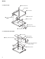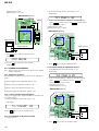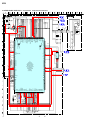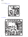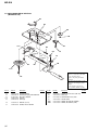
1
MZ-E10
SERVICE MANUAL
US Model
Canadian Model
AEP Model
UK Model
E Model
Tourist Model
Ver 1.0 2002.11
US and foreign patents licensed from Dolby
Laboratories Licensing Corporation
Model Name Using Similar Mechanism
NEW
MD Mechanism Type
MT-MZE10-184
Optical Pick-up Mechanism Type
ABX-1ES
SPECIFICATIONS
Audio playing system
MiniDisc digital audio system
Laser diode properties
Material: GaAlAs
Wavelength: λ = 790 nm
Emission duration: continuous
Laser output: less than 44.6 µW*
* This output is the value measured at a distance of 200 mm from the
objective lens surface on the optical pick-up block with 7 mm aperture.
Revolutions
Approx. 300 rpm to 2,700 rpm
Error correction
ACIRC (Advanced Cross Interleave Reed Solomon Code)
Sampling frequency
44.1 kHz
Coding
ATRAC (Adaptive TRansform Acoustic Coding)
ATRAC3: LP2/LP4
Modulation system
EFM (Eight to Fourteen Modulation)
Number of channels
2 stereo channels
1 monaural channel
Frequency response
20 to 20,000 Hz ± 3 dB
Outputs
Headphones/earphones: dedicated headphone/ remote control jack,
output level 5 mW + 5 mW(US model) load impedance 16 ohms,
5 mW + 5 mW (Other models)
load impedance 16 ohms
Power requirements
Lithium-ion rechargeable battery (Built-in: LIP- 3WMB, 3.7 V,
340 mAh, Li-ion)
External power jack (for the battery charging stand): Power rating 6 V
DC
Battery life1)
(Unit: Approx. hours) (JEITA2))
Batteries
Lithium-ion
built-in
rechargeable
battery3)
SP Stereo
(normal)
23
LP2
Stereo
33
LP4
Stereo
40
1)
Measured with the power save function on (see
“ Preserving battery power” ).
2)
Measured in accordance with the JEITA (Japan Electronics and
Information Technology Industries Association) standard (using a Sony
MDW-series Mini-disc).
3)
With a fully charged battery.
Note
The battery life may be shorter than that specified, depending on the
operating conditions,the temperature of the location.
Dimensions
Approx. 81.9 x 72.2 x 9.9 mm (w/h/d) ( 3 1/4 x 2 7/8 x 13/32 in.)
(not including projecting parts and controls)
Mass
Approx. 55 g (1.6 oz) (including the built-in rechargeable battery)
Supplied accessories
Headphones/earphones with a remote control (1)
Battery charging stand (1)
AC power adaptor (for the supplied battery charging stand) (1)
Headphone adaptor (1)
Carrying pouch (1)
Design and specifications are subject to change without notice.
PORTABLE MINIDISC PLAYER
9-874-219-01
Sony Corporation
2002K0200-1
© 2002.11
Personal Audio Company
Published by Sony Engineering Corporation
MZ-E10
CAUTION
Danger of explosion if battery is incorrectly replaced.
Replace only with the same or equivalent type recommended by
the manufacturer.
Discard used batteries according to the manufacturer’s instructions.
ADVARSEL!
Lithiumbatteri-Eksplosionsfare ved fejlagtig håndtering.
Udskiftning må kun ske med batteri
af samme fabrikat og type.
Levér det brugte batteri tilbage til leverandøren.
ADVARSEL
Eksplosjonsfare ved feilaktig skifte av batteri.
Benytt samme batteritype eller en tilsvarende type
anbefalt av apparatfabrikanten.
Brukte batterier kasseres i henhold til fabrikantens
instruksjoner.
VARNING
Explosionsfara vid felaktigt batteribyte.
Använd samma batterityp eller en likvärdig typ som
rekommenderas av apparattillverkaren.
Kassera använt batteri enligt gällande föreskrifter.
VAROITUS
Paristo voi räjähtää, jos se on virheellisesti asennettu.
Vaihda paristo ainoastaan laitevalmistajan suosittelemaan
tyyppiin. Hävitä käytetty paristo valmistajan ohjeiden
mukaisesti.
CAUTION
Use of controls or adjustments or performance of procedures
other than those specified herein may result in hazardous
radiation exposure.
Flexible Circuit Board Repairing
• Keep the temperature of the soldering iron around 270°C during
repairing.
• Do not touch the soldering iron on the same conductor of the
circuit board (within 3 times).
• Be careful not to apply force on the conductor when soldering or
unsoldering.
TABLE OF CONTENTS
Specifications ........................................................................... 1
1. SERVICING NOTE ...................................................... 3
2. GENERAL
Playing an MD ................................................................... 4
3. DISASSEMBLY
3-1. Panel assy (S), Upper .................................................
3-2. Mechanism Deck (MT-MZE10-184) ..........................
3-3. Bracket assy ...............................................................
3-4. Power Board, Main Board ..........................................
3-5. Control Board .............................................................
3-6. Optical Pick-up assy(ABX-1ES) ................................
5
5
6
6
7
7
4. TEST MODE .................................................................. 8
5. ELECTRICAL ADJUSTMENTS ............................ 11
6. DIAGRAMS
6-1. Block Diagram ..........................................................
6-2. Printed Wiring Boards – Main Section (1/2) – .........
6-3. Printed Wiring Boards – Main Section (2/2) – .........
6-4. Schematic Diagram – Main Section (1/3) – .............
6-5. Schematic Diagram – Main Section (2/3) – .............
6-6. Schematic Diagram – Main Section (3/3) – .............
6-7. IC Pin Function Descrintion .....................................
6-8. IC Block Diagrams ...................................................
19
20
21
22
23
24
26
30
7. EXPLODED VIEWS
7-1. Main Section ............................................................. 33
7-2. Mechanism Deck Section (MT-MZE10-184) ........... 34
8. ELECTRICAL PARTS LIST ................................... 35
r
UNLEADED SOLDER
Boards requiring use of unleaded solder are printed with the
lead-free mark (LF) indicating the solder contains no lead.
(Caution: Some printed circuit boards may not come printed
with the lead free mark due to their particular size.)
: LEAD FREE MARK
Notes on chip component replacement
• Never reuse a disconnected chip component.
• Notice that the minus side of a tantalum capacitor may be damaged by heat.
SAFETY-RELATED COMPONENT WARNING!!
COMPONENTS IDENTIFIED BY MARK ! OR DOTTED LINE WITH
MARK !ON THE SCHEMATIC DIAGRAMS AND IN THE PARTS
LIST ARE CRITICAL TO SAFE OPERATION.
REPLACE THESE COMPONENTS WITH SONY PARTS WHOSE
PART NUMBERS APPEAR AS SHOWN IN THIS MANUAL OR IN
SUPPLEMENTS PUBLISHED BY SONY.
ATTENTION AU COMPOSANT AYANT RAPPORT
À LA SÉCURITÉ!
LES COMPOSANTS IDENTIFÉS PAR UNE MARQUE 0 SUR
LES DIAGRAMMES SCHÉMATIQUES ET LA LISTE DES
PIÈCES SONT CRITIQUES POUR LA SÉCURITÉ DE
FONCTIONNEMENT. NE REMPLACER CES COMPOSANTS
QUE PAR DES PIÈSES SONY DONT LES NUMÉROS SONT
DONNÉS DANS CE MANUEL OU DANS LES SUPPÉMENTS
PUBLIÉS PAR SONY.
2
Unleaded solder has the following characteristics.
• Unleaded solder melts at a temperature about 40°C higher
than ordinary solder.
Ordinary soldering irons can be used but the iron tip has to
be applied to the solder joint for a slightly longer time.
Soldering irons using a temperature regulator should be set
to about 350°C.
Caution: The printed pattern (copper foil) may peel away if
the heated tip is applied for too long, so be careful!
• Strong viscosity
Unleaded solder is more viscous (sticky, less prone to
flow) than ordinary solder so use caution not to let solder
bridges occur such as on IC pins, etc.
• Usable with ordinary solder
It is best to use only unleaded solder but unleaded solder
may also be added to ordinary solder.
* Replacement of SN761058ZQL (IC501) and LC896442-VH416-E (IC601) used in this set requires a special tool.
MZ-E10
SECTION 1
SERVICING NOTE
When repairing this device with the power on, if you remove the main board, this device stops working.
In this case, you work without the device stopping by fastening the hook of the Open/Close detection switch (S803).
Open/Close detection switch (S803)
3
MZ-E10
SECTION 2
GENERAL
The Player
1 2
C
D
9
This section is extracted from
instruction manual.
Playing an MD
E
1 Insert an MD.
6
1 Slide OPEN to open the lid.
2 Insert an MD.
8
7
1
2
3
4
5
3
i (Headphones/earphones) jack
GROUP button
“3-color info-LED”
HOLD (Locking the control) switch
5-way control key ( .• > N*
• x•VOL +, –)
OPEN switch
BUILT-IN BATTERY switch (at the
bottom)
Terminals for charging stand (at the
bottom)
Hand strap hole
Use the hole to attach your strap
6
7
8
9
3 Close the lid.
2
1
Insert an MD with the label side facing up, pushing the
MD to the direction of the arrow in the illustration.
2 Play an MD.
“3-color info-LED”
Bottom side of
the player
VOL–
* N has a tactile dot .
VOL+
The display window of the remote
control
1 2
3
4 5
x
6
VOL +
Jog lever (.• u/ENT•>)
7
8
9
. x >N
VOL –
5-way control key
1
2
3
4
5
6
Disc indication
Track number display
Character information display
Group play indication
Play mode indication
Virtual Surround/6-band equalizer
indications
7 Battery level indication
8 Bookmark indication
9 Alarm indication
1 Press the jog lever ( u) on the remote control. (Press towards > N on
the player.)
A short beep sounds in the headphones/earphones. The LED lights up.
2 Turn the control towards VOL + or – on the remote control to adjust the
volume. (Press towards VOL + or – on the player. )
The volume indicator appears in the display, allowing you to check the
volume level.
To stop play, press x.
A long beep sounds in the headphones/earphones.
Playback starts from the point you last stopped playing. To start playback from the
beginning of the disc, press and hold the jog lever (u) for 2 seconds or more on the
remote control (Press and hold towards > N for 2 seconds or more on the player).
The battery charging stand
1
2
1 DC IN (6V jack) (at the bottom)
2 Terminals for charging
The headphones/earphones with a
remote control
A
B
C
D
5
F
1 Headphones/earphone s
2 Stereo mini plug
3 Control VOL +, –
Turn to adjust the volume .
4
5
6
7
8
9
q;
qa
qs
4
x (stop) button
Jog lever (.• u/ENT• >)
(Group) +, – button
Clip
HOLD switch
Display window
DISPLAY button
P MODE /
(play mode/repeat) button
SOUND button
7
8
9
q;
qa
qs
To
Pause
Do this (Beeps in the headphones/earphones)
Press the jog lever (u) on the remote control (continuous short
beeps).
Press the jog lever (u) again to resume play.
Cue to the current track
or the previous track
Slide the jog lever towards . on the remote control
(three short beeps). (Press towards . on the player. )
Cue to the next track
Slide the jog lever towards > on the remote control (two short
beeps). (Press towards > on the player.)
Go backwards or
forward while playing
Slide and hold the jog lever towards . or > on the remote
control. (Press and hold towards . or > on the player. )
Searching for a specific
position while viewing
a elapsed time
(Time search)
While the player is paused, slide and hold the jog lever towards
. or > on the remote control.
Searching for a specific
track while viewing
track numbers or
track names
(Index search)
While the player is stopped, slide and hold the jog lever towards
. or > on the remote control.
Cue to the beginning of
every 10th track
(only during playback of
the disc with no group
settings 1))
Press
Remove the MD
Press x, and then slide OPEN 2).
1)
2)
+ or – button.
For more details, see “Using the group function.”
Once you open the lid, the point to start play will change to the beginning of the first track (except
when the disc information has been stored in the personal disc memory).
About the “3-color info-LED”
The LED indicates the current operating mode, charging status, and battery condition. For
details about the charging status, see “Getting started.” For details about the battery condition,
see “When to recharge the built-in battery” on the back page.
LED color
Operating status
Red
Playing a disc with no group settings
Green
Playing a disc with group settings
Orange
Cueing to the another group (Group Skip)
MZ-E10
SECTION 3
DISASSEMBLY
r
The equipment can be removed using the following procedure.
Bracket ASSY
Set
Panel ASSY (S), upper
POWER board, MAIN board
Mechsnism deck
(MT-MZE10-184)
CONTROL board
Optical pick-up ASSY
(ABX-1ES)
Note : Follow the disassembly procedure in the numerical order given.
3-1. PANEL ASSY (S), UPPER
7 Panel ASSY (S), upper
4
1 Two screws (M1.4)
2 Claw
Holder ASSY
3 Claw
6
5 Bracket ASSY
3-2. MECHANISM DECK (MT-MZE10-184)
1 Screw, step
6 Mechanism deck
(MT-MZE10-184)
4 OP flexible board
(CN501)
5 Motor flexible board
(CN551)
3
2 Two claws
5
MZ-E10
3-3. BRACKET ASSY
7 Two screws (M1.4)
Sheet (blind)
6 Screw (M1.4)
0 Bracket ASSY
9 Switch flexible board
(CN801)
8
2 Plate, retainer
1 Screw (M1.4)
4 Lid (DC), battery case
3
5 Konb (power)
3-4. POWER BOARD, MAIN BOARD
1 Case, battery
2 Retainer, battery
3 Battery, lithium ion storage
4 POWER board
5 Power relay flexible board
(CN952, CN953)
6
6
7 MAIN board ASSY
MZ-E10
3-5. CONTROL BOARD
Bracket ASSY
7 CONTROL board
6 Button (control)
4 Cover (control)
5 Switch flexible board
(CN801)
3 Knob (open)
2 Remove three claws
1 Screw (M1.4)
3-6. OPTICAL PICK-UP ASSY (ABX-1ES)
3 Screw, tapping
6 Optical pick-up ASSY
(ABX-1ES)
4 Spring, thrust detent
1 Washer (0.8-2.5)
2 Gear (SA)
5
Mechanism deck
(MT-MZE10-184)
7
MZ-E10
SECTION 4
TEST MODE
4-1. GENERAL
Remote control LCD
• When entered in the TEST MODE, this set provides the Overall
Adjustment mode which allows CD and MO discs to be automatically adjusted. In the Overall Adjustment mode, the system
discriminates between CD and MO discs, performs adjustments
in sequence automatically, and displays the faulty location if
any fault is found. In the Manual mode, selected adjustments
can be performed automatically.
• The attached remote control is used to operate the TEST MODE.
Unless otherwise specified in the text, the key means that on the
remote control.
u
F 1SHUFPGM SOUND
V-SUR
000
8
All on
All off
001 V1.000
4-2. SETTING THE TEST MODE
Microprocessor
version
display
4-2-1. How to set the TEST MODE
To set the TEST MODE, two methods are available.
1 Solder bridge and short TAP602 (TEST) on the main board.
Then turn on the power.
• Press and hold down
key is being pressed.
MAIN BOARD (SIDE A)
7
FB601
18
Q951
1
19
24
C954
C957
TAP602
(TEST)
R961
D951
R956
R959
1
C958
R964
R958 R957
R965
CN951
R604
956
1
2
C612 C617
IC951
5
C928
C960
R627
E
C607
C608 R607
6
C606
R623
R620
8 R621
8 R622
13
C953
12
R
4-2-3. How to release the TEST MODE
When method 1 was used:
Turn off the power and open the solder bridge on TAP602 on the
main board.
Note: The solder should be removed clean. The remaining solder
may make a short with the chassis and other part.
When method 2 was used:
Turn off the power.
Note: If electrical adjustment (see page 11) has not been finished
completely, always start in the test mode.
4-3. TEST MODE STRUCTURE
Test Mode
(Display Check Mode)
VOL + key
Manual Mode
TAP602
SHORT: TEST MODE
OPEN: NORMAL MODE
x
key
Servo Adjustment
Audio Adjustment
2 In the normal mode, operate the keys on the set and those on the
remote control as specified below:
Power Supply Voltage Adjustment
Turn on HOLD switch on the set. Holding down x (STOP)
key on the set, press the keys on the remote control in the
following sequence:
> t> t . t . t > t .
t > t . t
to hold the current display while the
Charge Adjustment
key
VOL
Overall Adjustment Mode
t
x
4-2-2. Operations when the TEST MODE is set
When the TEST MODE is entered, the system switches to the display check mode within the TEST MODE. From this mode, the
other Test modes can be accessed.
When the TEST MODE is set, the LCD repeats a cycle of the following displays:
key
CD/MO Adjustment
Power Supply Voltage Adjustment
NV Initialize
(Clear the Non-Volatile memory
+ key or DISPLAY key
(Press and hold down about for more than2 sec)
Key Check Mode
Terminate key checking or open
the top panel.
8
MZ-E10
4-4. MANUAL MODE
4. During each test mode, the display is changed from one to
another each time DISPLAY key is pressed.
4-4-1. Outline of the function
The Manual mode is designed to perform adjustments and
operational checks on the set’s operation according to each
individual function.
The Manual mode is used to clear the memory before
performing automatic adjustments in the Overall Adjustment mode.
1. Set the TEST MODE and press VOL + key to set the Manual
mode.
Remote control LCD display
VOL + key : 100th place of mode number
increase
VOL key : 100th place of mode number
decrease
VOL + key : 10th place of mode number
increase
key : 10th place of mode number
VOL
decrease
> key
x
address
adjusted value
• Jitter Value & Adjusted Value Display
LCD display
011 O F F J 3 F
mode number
jitter value
adjusted value
• Block Error Value & Adjusted Value Display
LCD display
011 0 0 0 B 3 F
mode number
key
Change Middle
Item
adjusted value
• Address & Adjusted Value Display
LCD display
mode number
2. During each test, press and hold down > key or .
key for a while to move the optical pickup on the sled outer or
inner perimeter.
3. Each test item is assigned with a three-digit item number. The
100th place is a major item, 10th place is a middle item, and unit
place is a minor item.
Note: Changes in adjustment item settings are written into the
non-volatile memory.
x
mode number
011 A A A S 3 F
000 Manual
> key
011 L r e f p w 3 F
Item title
4-4-2. How to set the Manual mode
Change Major
Item
• Item title Display
LCD display
block error value
adjusted value
• ADIP Error Value & Adjusted Value Display
LCD display
011 0 0 0 A 3 F
key
Change Minor
Item
> key : Unit place of mode number
increase
. key : Unit place of mode number
decrease
Change Adjustment
Value
VOL + key : Up
key : Down
VOL
mode number
adjusted value
• Focus drive voltage value & Adjusted value
LCD display
011 0 0 0 F 3 F
mode number
Write Adjustment
Value
key : When adjusted value is changed :
Adjusted value is written.
When adjusted value is not changed :
That item is adjusted automatically.
ADIP error value
adjusted value
Focus drive voltage value
Note: In the Power mode, the item title display is only displayed.
5. To terminate the Manual mode and return to the TEST MODE,
press x key.
4-5. OVERALL ADJUSTMENT MODE
4-5-1. Outline of the function
This mode is designed to adjust the servo system automatically by
going through all the adjustment items.
Usually, this mode is used to perform automatic adjustments when
servicing the set.
For further information, refer to section 5. ELECTRICAL ADJUSTMENTS. (See page 11)
9
MZ-E10
4-6. KEY CHECK MODE
4-6-1. Outline of the function
This mode is used to check to make sure that each of the keys
(including the slide switch) on the set operates normally.
4-6-2. Setting the Key Check mode
1. Set the TEST MODE. Press and hold down DISPLAY key
(for more than 2 sec) to set the Key Check mode.
LCD display
000
XX
2. When each key on the set and on remote control is pressed, its
name is displayed on the LCD. (The operated position is displayed for 4 sec after the slide switch is operated. If any other
key is pressed during this display, the LCD switches to its name
display)
Example: When > key on the set is pressed:
LCD display
000 FF XX
Example: When > key on the remote control is pressed:
LCD display
000 rFF XX
XX: AD value of the remote control key (hexadecimal 00 to FF)
3. When all the keys on the set and on the remote control are considered as OK, the following displays are shown.
(The key pressed to enter the Key Check mode has been checked
even if it is not pressed in this mode)
Example: When the keys on the set are considered as OK:
LCD display
SET OK XX
Example: When the keys on the remote control are considered
as OK:
LCD display
RMC OK XX
4. When all the key have been checked or when the top panel is
opened during this checking, the system terminates the Key
Check mode and return to the TEST MODE.
Note: Slide switch can checked as OK by ON t OFF t ON
(or reverse) operation.
10
MZ-E10
SECTION 5
ELECTRICAL ADJUSTMENTS
5-1. GENERAL
In this set, CD and MO discs can be automatically adjusted by setting the Overall Adjustment mode within the TEST MODE,
Before performing these automatic adjustments, it is necessary to
clear the memory, adjust the power charge and temperature in the
Manual mode.
5-3-2. Changing Adjustment values
Adjustment settings are cleared when NV initialize is performed.
So right after performing NV initialize you must rewrite the correct
data according to the microcomputer version.
• Adjustment value change method 1
• Adjustment value change method 2
(Perform after the 7 charging adjustment)
5-2. NOTES FOR ADJUSTMENT
5-2-1. Jigs
• CD disc TDYS-1 (part code: 4-963-646-01)
• MO disc PTDM-1 (part code: J-2501-054-A) (recorded)
• Digital voltmeter
• Thermometer
5-2-2. Adjustment sequence
The adjustments should be always performed in the following
sequence:
1 NV Initialize
(Clear the Non-Volatile memory)
Overall adjustment mode
2 Power supply voltage adjustment
5-3-3 Adjustment value change method 1
(when using Version 1.000)
1. In test mode press the VOL + key and then switch to Manual
mode.
2. Set 861 as the item number.
LCD display
861 VarB1k 00
3. Press the
key.
4. Press the > key and set 862 as the item number.
LCD display
862 VarWrt 00
3 Charge adjustments
Manual mode
4 Temperature adjustment
5. Press the
key, and set in Adjustment change mode.
862 88C6
5 Overall CD adjustments
FF
Overall adjustment mode
This section (address) flashes.
6 Overall MO adjustments
Manual mode
7 RESUME clear
5-2-3. Power
In overall adjustment, the power is supplied from the internal battery (Li-Ion) and the charging stand simultaneously.
Turn S901 (BUILT-IN BATTERY) to ON.
Note: Be sure to place the set horizontally on the overall
adjustment.
5-3. NV Initialize
(Clear the Non-volatile memory)
6. Press the x key.
LCD display
862 88C6
FF
This section (data) flashes.
7. Press the VOL + and VOL – keys and set the value in the
flashing data section while referring to the adjustment data change
list.
LCD display
5-3-1. How to NV Initialize
1. Set the Test mode.
862 88C6
3F
2. Press the VOL – kye and set the Overall adjustment.
3. Press
key on the remote control.
LCD display
000 Res OK?
4. Press
key on the remote control again.
LCD display
000 Res ***
8. Press the
Data value.
key. and the address section starts flashing.
9. Press the VOL + key and set the next adjustment address.
LCD display
862 88C7
FF
This section (address) flashes.
10.Press the x key.
LCD display
After initialize is completed.
862 88C7
FF
000 Reset
5. Press x key. to terminate the Manual mode and return to the
Overall adjustment mode.
Note: The power, charging and temperature adjustment settings are
not cleared during NV initialize.
This section (data) flashes.
11.Repeat the adjustments in items 6 - 9 and set up through address
88D3 while referring to the Adjustment Data Change List.
11
MZ-E10
12.Press the
LCD display
key. (Address section starts flashing.)
862 88D3
FC
24.Press the
LCD display
key to return to Manual mode.
862 VarWrt 01
This section (address) flashes.
13.Press the
LCD display
key to return to Manual mode.
862 VarWrt 00
14.Press the
key and write in the correction data.
15. Press the > key and 862 as the item number.
LCD display
862 VarWrt 01
Data value.
16.Press the
LCD display
key, and set in Adjustment change mode.
862 88C6 FF
This section (address) flashes.
17. Press the x key . (FF section (data) flashes)
18.Press the VOL + and VOL – key and set the value in the
flashing data section while referring to the adjustment data change
list.
LCD display
Data value.
25.Press the
key and write in the correction data.
26.Turn off the power.
Note: Always turn off the power after changing the adjustment settings.
Adjustment Data Change List
If adjustment data is VarWrt is 00 If adjustment data is VarWrt is 01
Version 1.000
Version 1.000
Address
Adjustment Data
Address
Adjustment Data
88C6
3F
88C6
07
88C7
03
88C7
8D
88C8
D6
88C8
FF
88C9
22
88C9
FF
88CA
C4
88CA
FF
88CB
37
88CB
FF
88CC
C2
88CC
FF
88CD
04
88CD
FF
88CE
E8
88CE
FF
88CF
42
88CF
FF
88D0
6E
88D0
FF
88D1
FC
88D1
FF
88D2
71
88D2
FF
88D3
FC
88D3
FF
5-4. POWER SUPPLY VOLTAGE ADJUSTMENTS
862 88C6 07
Data value.
19.Press the
key, and the address section starts flashing.
20.Press the VOL + key and set the next adjustment address.
LCD display
862 88C7 FF
This section (address) flashes.
21. Press the x key . (FF section (data) flashes)
LCD display
22.Press the VOL + and VOL – key and set the value in the
flashing data section while referring to the adjustment data change
list.
LCD display
5-4-1. Adjustment sequence
The adjustments should be always performed in the following sequence:
1 LEG1 adjustment (item No.:741)
r
2 VC1 adjustment (item No.:742)
r
3 VC2 adjustment (item No.:743)
r
4 Class-D power supply adjustment (item No.:744)
5-4-2. REG1 adjustment method
1. Supply power (DC 6.0 volts) from the charging terminal CN951.
2. Set the Test mode.
3. Set the overall adjustment mode and press P.MODE/F
key, item No. will change to 741.
LCD display
741 Reg1
XX
4. Connect a digital voltmeter to TP908 (REG1) on the main
862 88C7 8D
Data value.
23.Press the
12
key, and the address section starts flashing.
board and adjust VOL + (voltage up) key and VOL –
(voltage down)key on the remote control.
MZ-E10
Adjustment value:1.05V
Standard value:1.04 to 1.055V
3. Press
key to write the adjustment value, item No. will
change to 743.
MAIN BOARD (SIDE A)
5-4-4. VC2 adjustment method
1. Set the overall adjustment mode and set the item No. to 743.
C
C
37
C202
LCD display
743 Vc2 XX
TP908
(REG 1)
R921
C910 R908
2. Connect a digital voltmeter to TP907(VC2) on the main board
C926
912 R911
C916
L904
C922
C908
1-686-492-
and adjust VOL + key (Voltage down) and VOL – key
(Voltage up) on the remote control.
Adjustment value:1.15V
Standard value:1.15 to 1.18V
MAIN BOARD (SIDE A)
digital voltmeter
TP907
(VC2)
TP908
(REG1)
R921
R908
C910
C926
C916
12 R911
5. Press
key to write the adjustment value, item No.will
change to 742.
C922
C908
L904
1-686-492-
digital voltmeter
5-4-3. VC1 adjustment method
1. Set the overall adjustment mode and set the item No. to 742.
LCD display
TP907(VC2)
742 Vc1 XX
2. Connect a digital voltmeter to TP902 (VC1) on the main board
and adjust VOL + key (Voltage up) and VOL – key
(Voltage down) on the remote control.
Adjustment value:2.15V
Standard value:2.14 to 2.155V
MAIN BOARD (SIDE A)
3. Press
key to write the adjustment value, item No. will
change to 744.
5-4-5. Class-D power supply adjustment method
1. Set the overall adjustment mode and set the item No. to 744.
LCD display
744 Cls D XX
2. Connect a digital voltmeter to TP909 (Class-D) on the main
R921
R908
C910
TP902(VC1)
C916
12 R911
C922
C908
C926
board and adjust VOL + key (Voltage up) and VOL – key
(Voltage down) on the remote control.
L904
1-686-492-
digital voltmeter
TP902
(VC1)
13
MZ-E10
2. Set the manual mode, item No. will change to 754.
Adjustment value:1.75V
Standard value:1.75 to 1.80V
LCD display
MAIN BOARD (SIDE A)
754 ChgV L XX
TP909
HOLD
(CLASS-D)
3. Connect a digital voltmeter to TP962 on the main board and
t
C104
IC301
digital voltmeter
1
7
MAIN BOARD (SIDE A)
D
12
D
7
13
6
C953
8
IC951
D
E
18
19
TP909(CLASS-D)
24
digital voltmeter
C954
R965
C957
TP962
D95
CN951
000 ADJ OK
TP962
56
R959
R961
1
C958
R964
3. Press
key to write the adjustment value,
LCD display.
Q
1
R957
14
C204 R317 R318
R819 R818
C301
adjust VOL + (voltage up) key and VOL – (voltage down)
key on the remote control.
Adjustment value:3.40V
Standard value:3.395 to 3.405V
R958
C302
4. Press the x key and return to the test mode.
LCD display.
4. Press
5-5. CHARGE ADJUSTMENTS
5-5-4. Charge voltage (H) adjustment method
1. Set the Manual mode and set the item No. to 755.
2. Connect a digital voltmeter to TP962 on the main board and
adjust VOL + key (Voltage down) and VOL – key
(Voltage up) on the remote control.
Adjustment value:4.20V
Standard value:4.2 to 4.21V
MAIN BOARD (SIDE A)
7
13
6
IC951
LCD display
18
751 ChgIOf
19
XX
24
digital voltmeter
C954
R965
1
5-5-3. Vc PWM Duty (L) adjustment method
1. Set the Test mode.
CN951
3. Press
14
R959
R961
R964
C958
key to write the adjustment value.
Q
1
C957
4. Press
C953
12
5-5-2. Current amplifier offset adjustment
1. The power supply of 3V is supplied to TP951 on the main board.
2. Set the Test mode.
3. Set the manualmode, item No.will change to 751.
R957
1 Current amplifier offset adjustment (item No.:751)
r
2 Change voltage (L) adjustment (item No.:754)
r
3 Change voltage (H) adjustment (item No.:755)
r
4 Current Amplifier (L) adjustment (item No.:752)
755 ChgV H XX
R958
5-5-1. Adjustment sequence
The adjustments should be always performed in the following sequence:
LCD display
TP962
TP962
D95
56
Note: Always remove the internal battery (Li-Ion) before making
charging adjustments.
key to write the adjustment value.
key to write the adjustment value.
MZ-E10
5-5-5.Current Amplifier (L) adjustment method
1. Connect TP953 to TP959 on the main board.
2. Set the test mode.
3. Set the Manual mode and set the item No. to 752.
LCD display
4. Adjust with the remote control VOL + and VOL – keys so
that the temperature value is at room temperature.
Reset value:
19h = 25 C
Adjustment range: 80h to 7Fh = -128 C to +127 C
5. Press the
key and write in the adjustment value.
752 ChgI L XX
5-7. OVERALL ADJUSTMENT MODE
4. Press
key to write the adjustment value.
5-7-1. Overall adjustment mode structure
5-5-6. Adjustment value change method 2
(when using Version 1.000)
1. Set in Manual mode and then set item number 026.
LCD display
TEST MODE
(Display Check Mode)
026 NvWrt CC
Overall Adjustment
Title Display(ASSY**)
2. Press the
LCD display
key.
VOL — key
. key
026 8200
**
> key
This section (address) flashes.
**
4. Press the x key.
LCD display
026 828A
key two times
MO overall
Adjustment
x
key
x
key
x
key
NV Initialize
P.MODE/F key Power Supply
Adjustment
**
This section (data) flashes.
00
6. Press the
key.
7. Press the
LCD display
key to return to Manual mode.
026 NvWrt CC
8. Press the
key
Note: The overall adjustments should be always performed in the
sequence of CD t MO adjustments.
5. Press the VOL + and VOL – keys and set 00 in the flashing
data section.
LCD display
026 828A
x
> key
3. Press the
key (100th place) and the VOL + key (10th
place) and set 828A in the flashing address section.
LCD display
026 828A
CD overall
Adjustment
key and write in the adjustment setting.
5-6. TEMPERATURE ADJUSTMENT
[Temperature adjustment method]
1. Set in Test mode.
2. Set in Manual mode and set the item number 014.
LCD display
014 AdjTmp XX
5-7-2. Total Adjust mode title display
Switching to Total Adjust Mode sets the following All Adjust mode
title display on the LCD.
LCD display
000 Assy
**
: Disk mark (outer) lights up when power adjustment is complete.
Disk mark (inner) not used
** : Left side is MO alignment information
F* : MO total alignment is complete
1* : Manual alignment (not part of total adjustment)
0* : Not adjusted
Right side is CD alignment information
F* : CD total alignment is complete
1* : Manual alignment (not part of total adjustment)
0* : Not adjusted
5-7-3. Overall CD and MO adjustment method
1. Set the TEST MODE and press VOL – key to set the Overall
Adjustment mode.
LCD display
Item No.
3. Measure the temperature.
Adjustment setting
000 Assy11
15
MZ-E10
2. Insert CD disc in the set, and press . key to set the Overall
CD Adjustment mode.
Automatic adjustments are made.
3. Press the
key.
LCD display
043 Res ***
LCD display
XXX CD RUN
XXX: Item No. for which an adjustment is being executed.
3. If NG in the overall CD adjustments, return to Reset NV and
perform from the overall CD adjustment again.
LCD display
000 XXX NG YY
XXX: NG item No.
YY: adjusted valive.
4. If OK through the overall CD adjustments, then perform overall
MO adjustments.
LCD display
After reset is completed
LCD display
043 Res C1r
5-7-5.Resume clear method
When the battery exchange was done.
1. Setting the testmode.
2. Set the Manual mode and set the item No.043(RESUME Clear).
LCD display
043 Resume 00
3. Press the VOL + key two times, and set the adjustment value
to 02.
043 Res
000 CD OK
5. Insert MO disc in the set, and press > key to set the Overall
MO Adjustment mode. Automatic adjustments are made.
4. Press the
key.
LCD display
043 Res ***
LCD display
XXX MO RUN
XXX: Item No. for which an adjustment is being executed.
After reset is completed
LCD display
043 Res C1r
6. If NG in the overall MO adjustments, return to NV initiale and
perform from the overall CD adjustments again.
LCD display
000 XXX NG YY
XXX: NG item No.
YY: adjusted valive.
7. If OK through the overall MO adjustments, press x key to
return to the test mode.
LCD display
000 MO OK
5-7-4.Resume clear method
When the battery exchange isn't being done.
1. Setting the testmode.
2. Set the Manual mode and set the item No.043(RESUME Clear).
LCD display
043 Resume 00
16
02
5-7-6. Overall CD and MO adjustment items
1. Overall CD adjustment items
Item No.
Contents
312
ALFA offsetadjustment
313
IJ offset adjustment
314
FE offset adjustment
320
Focus servo ON
324
TE offset adjustment
321
TE gain adjustment
328
TWPP gain adjustment
824
twpp-gain[H]+4 t twpp-gain[L]
324
TE offset adjustment
330
Tracking servo ON
336
ABCD gain adjustment
337
KF gain adjustment
338
RF gain adjustment
344
CD focus gain adjustment
345
CD tracking gain adjustment
521
CD two-axis sensitivity adjustment (inside)
522
CD two-axis sensitivity adjustment (outside)
MZ-E10
2. Overall MO adjustment items
Item No.
Contents
5. Press the VOL + key and set the adjustment setting to 01.
LCD display
112
ALFA offset adjustment
113
IJ offset adjustment
114
FE offset adjustment
118
AW DW OFFSET
224
TE offset adjustment
221
TE gain adjustment
224
TE offset adjustment
236
ABCD gain adjustment
237
KF gain adjustment
238
RF gain adjustment
244
Focus gain adjustment
245
Tracking gain adjustment
120
Focus servo ON
8. Press the VOL + and VOL – keys and set the adjustment
data while referring to the patch data list.
122
TE offset adjustment (TON)
9. Press the
121
TE gain adjustment
122
TE offset adjustment (TON)
123
TE offset adjustment (TEIN)
10. Press the VOL + keys and set the address value in the next
address for adjustment.
LCD display
124
TE offset adjustment (TWPP)
130
Tracking servo ON
131
TE offset adjustment (TWPP/RF)
136
ABCD gain adjustment
137
KF gain adjustment
144
FCS gain adjustment
145
Tracking gain adjustment
139
BPF fo adjustment
134
TWPP gain adjustment
131
TE offset adjustment (TWPP/RF)
132
TE offset adjustment (TWPP/DSP)
138
RF gain adjustment
35
GOD offset correction.
023 Patch 01
6. Press the
LCD display
key.
022 PatClr CC
Data.
This section (address) flashes.
7. Press the x key.
(The data section flashes.)
key and the address section flashes.
023 8922
00
This section (address) flashes.
11. Press the x key.
LCD display
023 8922
5-8. REWEITING PATCH DATA AFTER REPLACING
THE NONVOLATILE MEMORY
Rewrite the program correction data after replacing the nonvolatile
memory.
5-8-1 Method for rewriting the corrected data
(when using Version 1.000)
1. Set in Test mode.
2. Set in Manual mode and enter the item number 022.
LCD display
00
This section (data) flashes.
12. While referring to the patch data table repeat the data correction
write procedure from steps 8 through 11 until the address 899E
is set.
13. Press the
key.
(The address value flashes.)
14. Press the
LCD display
key to quit the patch data write mode.
023 Patch 01
15. Press the
LCD display
LCD display
key.
023 Patch CC
022 PatClr CC
After finished writing data.
Data.
3. Press the
key to reset the patch data.
(Writing is complete if the setting changes to DD.)
LCD display
LCD display
023 Patch DD
16. Turn off the power.
022 PatClr DD
4. Press the > key and enter the item number 023.
LCD display
023 Patch 00
17
MZ-E10
Varsion 1.000
Address
18
Data
Address
Data
8921
02
8962
DE
8922
F7
8963
03
8923
F4
8964
E5
8924
02
8965
81
8925
06
8966
C3
8926
A9
8967
94
8928
03
8968
05
8929
2A
8969
F8
892A
FD
896A
76
892B
01
896B
2E
892C
12
896C
08
892D
06
896D
76
892E
B3
896E
FD
8931
02
8971
D0
8932
15
8972
E0
8933
95
8973
B4
8934
02
8974
02
8935
0A
8975
02
8936
66
8976
D3
8938
02
8977
22
8939
D1
8978
C3
893A
B3
8979
22
893B
02
897A
6C
05
893C
06
897B
893D
BD
897C
0A
8941
81
897D
30
8942
B2
897E
1A
8943
81
8981
02
8944
C3
8982
74
8945
81
8983
FF
8946
E2
8984
F8
8947
E4
8985
D0
8948
90
8986
E0
8949
87
8987
D0
894A
75
8988
E0
894B
F0
8989
D0
894C
E5
898A
E0
894D
81
898B
74
894E
C3
898C
F8
8951
94
898D
C0
8952
04
898E
E0
8953
F8
8991
74
8954
76
8992
B3
8955
19
8993
C0
8956
08
8994
E0
8957
76
8995
74
8958
E9
8996
02
8959
22
8997
C0
895A
C0
8998
E0
895B
E0
8999
E8
895C
12
899A
02
895D
20
899B
06
895E
7D
899C
CF
8961
8C
899E
01
MZ-E10
SECTION 6
DIAGRAMS
6-1. BLOCK DIAGRAMS
IC301
HEADPHONE AMP
(D CLASS AMP)
IC501
Iy
RF AMP,FOCUS/TRACKING ERROR AMP
12
Jx
VREF
7 VREF10
Iy
7
6
56
1
54
55
50
51
52
49
Ix
Jx
8
Jy
9
A
5
B
4
C
3
2 D
Jy
Jx Jy Jx
A
Ix Iy Ix
B
Iy
Ix
Jx
Jy
A
B
C
D
EFMO
37 NC
RFI
40
RF OUT
9
PEAK
48
BOTM
47
EFM
COMP
Ix
RF AMP,
FOCUS
ERROR,
TRACKING
ERROR
PEAK
/BOTM
a bc d
F
16
D-C
15
C
13
D
MON
12
PD
PD-NI
ADIP IN
PD-NI
APC
VCC-2
LASER
DRIVER
Q501
LD
LD-K
S0
S0
S1
VCC
S1
VCC
14
S MON
CLK
POWER
SUPPLY
18
14 RF TEMP MON
26
122 VC
24 AMICE CLK PWM
IC551
20
TRACKING
COIL
17
18
FOCUS
COIL
TRK+
FOCUS/TRACKING COIL DRIVE,
SPINDLE/SLED MOTOR DRIVE
TRK-
FCS+
45
18
17
19
OUT2R
SLDW
M902
SLED
MOTOR
SLDV
M
SLDU
SLDN
20
21
VS1
VG1
D803
HOLD SW 88
SET KEY 16
S803
(OPEN/CLOSE)
OUT1R
VOL-
TAP603
IC601
S802
GROUP
M901
SPINDLE
MOTOR
M
CLVU
CLVN
40
38
39
20
VI2DET
CHG_CTL
SW
SVO
PRE
DRIVER
LOGIC
S1 8
S2 9
S3
10
SLCOM
VG1
SPVS
16 I_CTL1
NV XCS
SI02 CLK
SI02 DO
SI02 DI
80 SLPWMF
81 SLPWMR
82 SLD0
CHG MON
CHG PWM
CHG AMP SEL
CHG AD SEL
XCHGI LIMIT
CHG VI MON
6
5
7
8
17
39
38
32
29
13
1
2
3
4
CHG MON
CHG CTL
CHG AMP SEL
CHG AD SEL
XCHGI LIMIT
CHG VI MON
68 4M
7
6
5
VG
UNREG MON 10
UOUT
SPCOM
LOGIC
SPBR
47
SPPWM
42
SPFG
37
76 SPPWMR
75 SPPWMF
66 FF
S104 DO 3
PWR STRB 37
S104 CLK 196
PWR CLK PWM 23
PWR SLEEP 36
PWR EFCLR 35
19
S104 DO
PWR STRB
S104 CLK
176K
PWR SLEEP
PWR EFCLR
L
23
18
Q951
17
6 V IN2
D951
7
LITHIUM-ION
RECHAGEABLE
BATTERY
Li-ion
1PC, 3.7v
8
IN29
OUT2
10
BAT_SEL
11
EEPROM
4
NC
3
S901 BUILT-IN
BATTERY
Q903
VB
55 MUTE ON
XRST2
27
LVB
7
Q952
VSTB
9
XWK3
3
VCO1
11
VCOUT
37
VCIN
38
Q901
L901
IC952
VB DETECT
Q953
DIFFERENTIAL
RMC KEY1
SI04 DO
PWR STRB
SI04 CLK
176K
PWR SLEEP
PWR FFCLR
19
VBAT
IC801
OUT
1
VCC-1
H
A/D
3
4 I_SEL
5 AD_SEL
CHG AD SEL
XCS
SK
DI
DO
2
IN
S/S
VG1
PRE
DRIVER
GND
VO
CHG MON
CHG AMP SEL
WOUT
VOUT
RF1
FOR
STAND
CHARGER
14 WK DET
SLVS
84 SLD2
83 SLD1
85 SLD3
VG
VG 12
VI
24
IN1-
S/S
SWO
VOL-
IC951
2
73 FOPWMF
74 FOPWMR
SLPWM
19
SLFG
24
ISEL1
12
> N
CHAGER CONTROL
71 TRPWMF
72 TRPWMR
IN1F
13
IN1R
14
VCC
CLVV
REW/PB
XRESET 192
CLK
41
.
S801
CHG VI MON
CHG CTL
S/S
LOGIC
S801
VOL+
CHARGE
CONTROL
IN2F
3
IN2R 4
SUO
35
STOP
FF/PB
VCC-1
VCC-2
CLVW
VOL+
OPEN CLS SW 15
OUT1F
PRE
DRIVER
RMC-VDD
S804
HOLD N
ON
OFF
D802
(G)
107 XOUT
23
22
OPR LED G PWM 41
(O)
LED
DRIVER
Q802
XCHG I LIMIT
VG1
26
OPR LED O CTL 30
X601
16.9344MHz
S/S
LOGIC
RMC-DTCK
VCC-1
D801
51 XDISC DET
FCS16
4
OUT2F
PRE
DRIVER
J301
i
D-GND
RMC-KEY
1
3
106 XIN
48
S/S
44
Q301,302
BOOSTER
R-CH
2,4
Q304
REGULATOR
(R)
DIGITAL SIGNAL PROCESSOR,
DIGITAL SERVO SIGNAL PROCESSOR,
EFM/ACIRC ENCODER/DECODER,
SHOCK PROOF MEMORY CONTROLLER,
16M BIT D-RAM, SYSTEM CONTROL
ATRAC ENCODER/DECODER
D/A CONVERTER
L501
VG1
IC302
L-CH
A-GND
REC KEY 2
47 XRF RESET
160 SBUS DATA
21 SBUS CLK
VCC-2
43 VS2
6,5
Q102,202
MUTE
BEEP DRIVER
4 EN1
11 EN2
3
VG
Q904
7
VDD0 •
8
8,7
139 ADIPW0
50 XSLPMIR OP
46 PDS1
UNREG
9
1
D VO PWM 40
RMC KEY1 12
RMC DTCK 19
104 LDREF
11 RFVCMON
13
1
10
OPTICAL PICK-UP BLOCK
(ABX-1ES)
OUT2
6
1 MCK
D EN1 45
D EN2 52
19
RESET
35
SBUS
33
SCK
32
S-MONITOR
PD-O
15
11
IN2
OPR LED R PWM 42
14
16
OUT1
14
AVCC
SERIAL
I/F
LD-A
12
F16M 57
125 ABCD
123 FE
124 TE
VC 8
AFDG
23
ADIP
DVDD
D RPWM+ 112
Q303
IN1
VCC-1
127 PEAK
126 BOTTOM
41
FE
42
TE
43
NPPO
44
TPP/WPP
3
136 EFMIN
ABCD
A-C
D LPWM+ 110
10
16
13
14
5
4
2
62
58
59
60
63
64
1
VCI
VC1G
L1
L1
XWK1
XWK2
XWK4
SEQSEL
DATA
STRB
SCK
CLK
SLEEP
FFCLR
ON
r
1,2
5,6
RESET
HVB
8
VB
VB
26
REGO1
43
L2
SERIES PASS
44
REGULATOR
VC2
42
36
LVB
DRIVER
VC
SWITCH
CONTROL
VG
VG
SETUP
DRIVER
UNREG
VDD
L903
Q902
VC2G 32
L2
SETUP
DRIVER
L2
VB VC
OFF
VG
34
35
VG
23
D902
CONTROL
SETUP
DC/DC
CONVERTER
LG
24
L903
D904
IC901
C1L 22
VGH
DC/DC CONVERTER
• Signal path.
F : Analog
J : Digital
MZ-E10
: Uses unleaded solder.
6-2. PRINTED WIRING BOARDS – MAIN SECTION (1/2) –
3
2
1
z
4
See page 25 for Notes.
5
6
8
7
9
10
A
1
3
CN801
z
C804
CONTROL BOARD (SIDE A)
HOLD
C302
CONTROL BOARD (SIDE B)
S804
HOLD B
ON
C104
t
C301
t
TP909
(CLASS-D)
R813
14
R816
8
7
1
R815
R812
IC301
11
(11)
1-686-491-
L101
> B
E
VOL –
C
C310
IC952
C312
C525
2 4
R953
FOR
STAND CHARGER
TAP602
TEST MODE
D951
C606
C928
C960
C955
C956
1
2
5
CN952
C626
R618
R617
R601
C604 C603
R967 R603
G
IC801
5
R915
D
R905 C925
R906 C904
16
17
C903
C909
L902
C917
*
D
D903
L901
IC601
D902
C902
C601 D
L903
C951
G Q902
20
S
20
C520
C555
Q901
C557
D
C901
R903
C923
C907 C911
1
64
IC901
C906
R916 C912
R554 C556
FB101
8
1
TP908 TP907
(REG1) (VC2)
24
Q102
7
R306
5
Q303
4
Q202
13
25
12
IC551
36
1
37
C202
CN551
8
1
FB803
FB801
R501
C803 R802 R803
C512
R507
R506
C515
C552
8
D904
FB201
R102
C553
Q903
G
S
D
R917
R615 C622
1
D
48
C102
R921
R908
C910
C926
R912 R911
32
33
48
C916
CN951
TP951 TP953
C801 R955
4
R961
C958
1
R959
R964
G
S
R801
R901
R902
C920
C957
R958 R957
C954
R956
R965
24
C554
R602
C924
TP959 19
C621
D101
D201
R204
R104
C905
1
R614
R918 R909 C913 R919 C915
Q951
R610
C616
R609
C614
C929
18
C612 C617
IC951
R627
E
C607
C608 R607
6
R623
R620
C628 R621
C605
R628
R622
R817
13
R611
C613
R608
C609
C611
R606 R605
FB601
C620 C610
R613 C619
C618
7
J301
i
C851 C303
Q304
D301
X601
C953
12
1
BCE
MAIN BOARD (SIDE A)
R302
E
Q904
C311
5
6
7
8
1
R303
C305
R305
D851
C309
M
C306
C852
R307
M902
SLED
MOTOR
Q952
3
R951
R313
M
1
2
3
4
R914
R552 R551
M901
SPINDLE
MOTOR
C921
C509
E
R553
11
(11)
C519
R518
R202
R516
C304
E IC302
C307
5
ECB
R561 R563
R301
4
R804
R562
C511
BCE
R564
1-686-490-
E
FB802
L552
4
5
Q953 BCE BCE
F
C507
C508
R505
C510 L501
L551
E
H
C505
Q501
C551
C558
POWER BOARD (SIDE B)
11
(11)
1-686-490-
1
2
C502
E
R311 C805
S803
(OPEN/CLOSE)
Q302
ECB
LITHIUM–ION
RECHARGEABLE
BATTERY
LIP–3WMB
1PC,3.7V 340mAh
Li–ion
C518
OPTICAL
PICK-UP
BLOCK
ABX–1ES
C536 R502
CN954
ON t OFF
S901
BUILT–IN BATTERY
C501
C503
5 CN953
*
IC501
R904 R504
1
D
R310
R509
POWER BOARD (SIDE A)
5
C308
1 3
Q301 E
R315
C959 R952
R309
R312
R511
C535
C534
C533
C532
C527 C523 R510
C513 R513
C526 C506
CN501
R514
S802
GROUP
C201
L201
1
GROUP
D801
49
C952
C922
C908
Ref. No.
Location
D101
D201
D301
D801
D802
D803
D851
D902
D903
D904
D951
E-9
E-9
F-9
B-9
B-9
B-9
E-9
G-6
G-6
G-7
G-3
IC301
IC302
IC501
IC551
IC601
IC801
IC901
IC951
IC952
B-9
D-9
D-8
G-9
G-4
G-5
G-7
F-2
C-8
Q102
Q202
Q301
Q302
Q303
Q304
Q501
Q802
Q901
Q902
Q903
Q904
Q951
Q952
Q953
F-9
F-9
C-9
D-9
F-9
E-8
D-8
C-9
G-7
H-5
G-6
E-8
G-3
E-7
E-7
Q802
VOL +
>
D802
E
11
(11)
1-686-491-
S801
OFF
D803
R304
R814
R811
B
C204 R317 R318
R819 R818
1
CN802
C101
3
Semiconductor
Location
L904
TP902
(VC1)
1-686-492-
11
(11)
MZ-E10
6-3. PRINTED WIRING BOARDS – MAIN SECTION (2/2) –
1
2
3
: Uses unleaded solder.
4
z
See page 25 for Notes.
5
6
7
8
9
MAIN BOARD (SIDE B)
A
B
C
D
E
F
G
H
1-686-492-
21
21
11
(11)
MZ-E10
6-4. SCHEMATIzC DIAGRAM – MAIN SECTION (1/3) –
z
See page 25 for Notes.
z
See page 26 for IC Pin Function Description.
VSTB
SIO4 DO
XD MUTE
R620 10k
R602 47k
S803
(OPEN/CLOSE)
MRASB
MAD0
MAD1
MAD2
SIO4 CLK
MAD3
VSS
VDD
XRESET
TEST3
TEST2
TEST1
TEST0
DEDATA
VCC2
DECLK
DEFECT
PCK
ADR17
VSS
ADR16
ADR15
ADR14
ADR13
ADR12
ADR11
MAD4
VCC2
VSS
MAD5
VDD
ADR10
ADR9
MAD6
ADR8
MAD7
ADR7
ADR6
MAD8
MAD9
MOEB
MCASB
ADR5
ADR4
ADR3
ADR2
ADR1
ADR0
FCEB
FOEB
C613
0.047
C611
1000p
R611 2.2k
C616 0.1
R610 4.7k
R816
10k
XRESET
VCC
XBUSY
RST
GND
R801
1M
IC801
AK6417AL-L
EEPROM
DGND
VCC
AGND
VDD
C619 0.1
C618 470p
22
C801
0.1
OPR GND
R615 10k
R613 470
R814
4.7k
TAP603
SIO4 CLK
XCS
SK
DI
DO
SIO4 DO
XD MUTE
MWEB
R608
4.7k
C608
0.047
C612
0.1
R813
4.7k
C805
0.01
C622 0.047
C610
0.1
R607
2.2k
X601
16.9344MHz
R811
2.2k
R812
2.2k
NV XCS
SIO2 CLK
SIO2 DO
SIO2 DI
C601 0.1
C626 0.022
C609
0.1
S801
VOL+
OPEN CLS SW
R605
1M
R606
0
CN802
3P
GND
XWK1
SET KEY
VOL-
ADIPWO
ON
CN801
3P
S802
GROUP
R614 4.7k
C621 0.1
OFF
HFL
EFMIN
TAP602
C620 4700p
S804
HOLD
C617 0.1
SLPWMF
SLPWMR
SLD0
SLD1
SLD2
SLD3
R609 10k
C607
0.1
BUS
XWK1
SET KEY
* IC601
LC896442-VH4-16-E
DIGITAL SIGNAL PROCESSOR,
DIGITAL SERVO SIGNAL PROCESSOR,
EFM/ACIRC ENCODER/DECODER,
SHOCK PROOF MEMORY CONTROLLER,
ATRAC ENCODER/DECODER,
D/A CONVERTER,16M BIT D-RAM
SYSTEM CONTROL
CSP(Chip Size Package)
C614 0.1
TRPWMF
TRPWMR
FOPWMF
FOPWMR
SPPWMF
SPPWMR
SMON
FE
TE
ABCD
BOTTOM
PEAK
4M
D LPWM+
D RPWM+
FG
C606
0.1
C804
470p
XSLP MTR OP
MSON4
(LOCAL CHK 3)
XRF RESET
C605
0.1
LDREF
R627
0 FB601
D CLK
XDISC DET
D EN2
SMON0
SMON1
SMON2
SMON3
F16M
MD7
MD6
MD5
MD4
VCC2
MD3VCC2
MECNT0(OPEN:MASK/L:FLASH)
MECNT1
FG
MD2
4M
MD1
MD0
TRPWMF
TRPWMR
FOPWMF
FOPWMR
SPPWMF
SPPWMR
VSS
VCC2
VDD
SLPWMF
SLPWMR
SLD0
SLD1
SLD2
SLD3
(LOCAL CHK 3)
VSS
HOLD SW
MD15
MD14
XADJUST
XPATCH
MD13
TYPE3
MD12
TYPE2
VSS
MD11
MD10
MD9
R618
470k
R622
10k
MD8
T1YPE
TYPE0
LDREF
VSS
XIN
XOUT
VDD
DPVSS
D LPWM+
D LPWMD RPWM+
D RPWMD CPWM
DVPP
VVDD
VPDD
VVSS
AVSS1
AVDD1
AUX
VC
FE
TE
ABCD
BOTTOM
PEAK
AVDD1
VCVSS
ISET
FR
VCVDD
PDO
JITTREC
HFL
EFMIN
SLCISET
SLCO
ADIPWO
VCC2
VSS
DATA0
DATA1
DATA2
DATA3
DATA4
DATA5
DATA6
DATA7
FWEB
D EN2
UNREG
R617
220k
PD S1
D EN1
VSS
VDD
OPR LED R PWM
OPR LED G PWM
D VO PWM
CHG PWM
CHG AMP SEL
PWR STRB
PWR SLEEP
PWR FFCLR
VSS
VCC2
CHG AD SEL
(LOCAL CHK1)
OPR LED O CTL
CHG I LIMIT
DRV SLED1 INT
DRV FG INT
DSP WRQB
DSP INTB
AMICE CLK PWM
PWR CLK PWM
SBUS DATA
SBUS CLK
(RMC SPCK)
RMC DTCK
AVDD
CHG MON
SET KEY
OPEN CLS SW
RF TEMP MON
CHG VI MON
RMC KEY1
RF VCMON
UNREG MON
AVSS
SIO2 DI
SIO2 DO
NV XCS
SIO2 CLK
(SIO4 DI)
C603 0.1
R628 22k
R603 2.2k
C628 0.047
Q802
XP4214-TXE
LED DRIVE
R601
220k
R621
100k
R623
10k
D803
R818 TLGE1008A
2.2
SIO2 DI
SIO2 DO
NV XCS
SIO2 CLK
CHG MON
SET KEY
OPEN CLS SW
SMON
CHG VI MON
RMC KEY1
RF VCMON
RMC DTCK
CHG I LIMIT
AMICE CLK PWM
176K
SBUS DATA
SBUS CLK
C604
0.1
CHG AD SEL
D VO PWM
CHG PWM
CHG AMP SEL
PWR STRB
PWR SLEEP
PWR FFCLR
D802
R819 TLOE1008A
470
R817
220
XRF RESET
PD S1
D EN1
D801-803
GROUP
XSLP MTR OP
D801
TLRE1008A
22
R815
10k
MZ-E10
R501
10k
L501
10µH
A
B
C
D
XSLP MTR OP
C536
0.047
R502
1k
R504
1
C508
2200p
R505
100k
R516
2.2k
Q501
2SA1577-T106-QR
LASER DRIVER
1
C511
10
4V
TE
HFL
R510 C523 R511
10k 0.01 10k
C512
4700p
C513
4700p
C525
0.01
XRF RESET
R518 0
R506 0
SBUS DATA
SBUS CLK
R507
0
R509
0
C520
1
C519
1
C518
0.047
C509
0.1
UNREG
5
MON
C510
10
6.3V
JY
JX
IY
IX
* IC501
SN761058ZQL
RF AMP,TRACKING/FOCUS
ERROR AMP
CSP(Chip Size Package)
FE
ABCD
BUS
PD S1
C506 4700p
C507 0.1
R513
0
FE
ABCD
RFI
ASSY
CIG
EFMO
DGND
RESET
VGIN
SBUS
SCK
CPOUT
CP
DVCC
VG1
VREF
RF VCMON
EFMIN
MON
VREF
10
C526
0.1
AMICE CLK PWM
L552
22µH
C503
2200p
C515
0.022
C505
0.1
ADIPWO
R563 R561
22
22
15
C501 10p
C502 10p
TRK+
FCSFCS+
TRK-
IX
PS
EQ
AGND
OFC C1
OFC C2
VREF10
VC
RFO
VREF09
AVCC2
PD NI
PD I
PD O
SMON
20
R514
0
IY
JY
JX
AVCC
C
B
A
D
PEAK
BOTM
TON C
OFTRX
NPPO
TE
L551
47µH
TP511
C527
0.1
D
A
AGND
SMON
ADIP IN
AGND
AGND
WPP LPF
ADFG
CDN
CCSL2
CLK
CPGND
CN
R562 R564
10
47
LDREF
CN501
20P
C
B
A
D
PEAK
BOTTOM
See page 25 for Notes.
IY
JY
JX
z
IX
6-5. SCHEMATIzC DIAGRAM – MAIN SECTION (2/3) –
C532 C533 C534 C535
22p 22p 22p 22p
FOPWMR
FOPWMF
Q951
FZT968TA
SWITCH
C955
10
OPR GND
IN2-
VI2
AD SEL
I SEL
VO
R956
0.022
CHG AD SEL
C958
1
IC952
XC61CN3002NR
VB DETECT
VBAT
CHG AMP SEL
CHG VI MON
SPPWMR
XSLP MTR OP
VI
Q953
2SC4738F
DIFFERENTIAL
OUT2
IC951
SC901582EPR2
CHARE CONTROL
IN1
C956
0.1
VG
R953
47k
BAT SEL
PWT
WDT
R961
2.2
NC
WK DET
I CTL2
CHG CTL
PWR WAKE
VIN
C954
4700p
R967
2.2k
R554 C557
4.7M 2.2
I CTL1
RF1
CHG PWM
R553
47k
CN951
2P
VCC
FOR STAND CHARGER
S901
BUILT-IN BATTERY
ON
OFF
AGND
DGND
TP959
+B
+B
R964
100
+B
+B
PWR CTL
GND
GND
GND
GND
CN954
5P
XWK1
C959
0.1
GND
C960
0.1
A/D
TRPWMR
TRPWMF
PGND
C551
0.1
R959
1
LITHIUM-ION
RECHARGEABLE
BATTERY
LIP-3WMB
1PC,3.7V 340mAh
Li-ion
C953
0.1
GND VOUT
SLD0
SLPWMR
SLPWMF
4M
R952
47k
CHG I LIMIT
C957
0.1
SLD3
CHG MON
C558
1000p
D951
FT1J3
R957
100
CAP C LIM
C555 0.22
C556 2200p
IC551
CXA8125ER-TBM-E
TRACKING/FOCUS
COIL DRIVE,
SPINDLE/SLED
MOTOR DRIVE
TRK+
TRK-
M901
SPINDLE
MOTOR
8 SLDN
SLDU
SLDV
SLDW
CLVW
CLVV
CLVU
CLVN
1
C553 0.47
C554 470p
R552 10k
SEL1
SEL2
S3
S2
S1
CLK
VCC
VG1
IN2R
IN2F
SPMAX
SPPD
SPFG
UOUT
SPCOM
VOUT
WOUT
SPPWM
VS2
OUT2F
OUT2R
PGND2
SPBR
S/S
M902
SLED
MOTOR
SLGND
SLVS
SLPD
SLVCO
SLMAX
GND
VG2
SPVCO
SPFIL
SPCIN
SPVS
SPGND
FG
CLVU
CLVN
CLVV
CLVW
SPPWMF
CN551
8P
C552
0.1
Q952
UN9113J
SWITCH
VI2DET
R551
100k
SLFG
SUO
SLCOM
SVO
SWO
SLPWM
VS1
OUT1L
OUT1R
PGND1
IN1R
IN1F
R958
10k
XRESET
FCS+
FCS-
SLD1
SLDU
SLDN
SLDV
SLDW
SLD2
RF VDD
CN953
5P
C928
0.1
CN952
5P
23
23
R965
220
R955
1M
Q903
HAT1043M-EL
SWITCH
C951
C929
47
0.1
10V
C952
22
10V
MZ-E10
See page 25 for Notes.
Q304
UN9113J-(TX).SO
INVERTER
XD MUTE
RMC DTCK
RMC KEY1
MUTE ON
D EN2
D LPWM+
OPR GND
FB801
7
FB803
R803 100
R804 100
FB101
0
R307
47k
IC301
NJU8713V-TE2
HEADPHONE AMP
(D CLASS AMP)
R315
47
D CLK
D RPWM+
D EN1
R317 1M
C201
0.22
L201
100µH
C204
0.1
MCK
VSS
IN1
EN1
VSSO
OUT1
VDDO
BEEP
VDD
IN2
EN2
VSSO
OUT2
VDDO
C302
47
6.3V
C311
0.47
C301
0.1
R104
2.2k
R318 1M
D201
MAZS027008SO
Q303
NTHD5904T1
MUTE
R204
2.2k
R102
4.7k
L101
100µH
Q102
2SC5585TL
MUTE
C102
220
2.5V
RVDD
RDTCK
RKEY
RGND
L-CH
A-GND
R-CH
J301
1
C852
0.1
D851
MAZZ068H01S0
FB802
Q202
2SC5585TL
MUTE
C309
0.1
C924
1
R904
220k
R310
0
C310
220
4V
D301
MAZS027008SO
C303
0.1
D101
MAZS027008SO
C851
0.1
C803
470p
R202
4.7k
C101
0.22
C104
0.1
C202
220
2.5V
FB201
0
R313
1k
C908 47 6.3V
C902 22 6.3V
C901 0.1
C312
10p
R802
1M
Q904
XP4313-(TX).SO
SWITCH
VCC
AGND
VG1
C903
22
6.3V
D904
MA116
R914
0
OPEN CLS SW
PWR FFCLR
z
XWK1
RMC KEY1
6-6. SCHEMATIzC DIAGRAM – MAIN SECTION (3/3) –
VSTB
R302
22k
R303
10k
R304
2.2k
IC302
LMV301MGX/NOPB
REG
IN+ VCC
GND
IN- OUT
R301
10k
C304
0.047
R306
100
C307
1
R311
1k
C909
4.7
16V
C306
0.47
R312
22k
R917
220k
R915 D903
MA116
0
C925
0.1
C921
1
R905
1k
C904
470p
Q302
UMT1N
R309
10
C907
0.01
D902
MA729-TX
L902
220µH
Q301,302
BOOSTER
R906
1M
C905
0.01
C906
1000p
XRESET
C911 0.01
C912 0.01
C910
0.1
R919
1M
C915
470p
C913
0.047
R909
1k
R901
470k
Q901
XP152A12COMR
SWITCH
R903 10k
D VO PWM
C305
4.7
10V
Q301
UMX1N
L901
150µH
R908
10k
R902
220k
R916
470k
TAP901
RF1
INM1
DTC1
CRST1
XRST1
C1L
VG
LG
PGND3
VB
XRST2
CRST2
DTC2
INM2
RF2
VC2G
VC1G
PGND1
L1
L1
VO1
VCO1
VC1
VSTB
HVB
LVB
VRMC
XWK1
XWK2
XWK3
XWK4
FFCLR
R305
10k
C308
22
4V
SLEEP
CLK
SEQSEL
WDT
SCK
STRB
DATA
HPI2
HPI1
MUTEON
GND
VHP1
HP1
PGND
HP2
VHP2
IC901
SC901580EPR2
DC-DC
CONVERTER
PWR SLEEP
176K
SIO4 CLK
PWR STRB
SIO4 DO
C923
1
MUTE ON
PGND2
L2
L2
VO2
VCO2
VCIN
REGO3
REGI3
REGO2
VC2
REGC1
REGI1
REGC1
REGC2
REGC3
VREF
DGND
Q902
MMBF0202PLT1
SWITCH
BUS
L903
150µH
R918
220k
UNREG
R912
10k
L904
10µH
RF VDD
C926
22
6.3V
R921
0
VDD
C916
1
C917
22
6.3V
C922
22
4V
R911
100k
C920
0.1
R951
0
(CHASSIS)
24
24
MZ-E10
r WAVEFORMS
Note on Printed Wiring Boards
• X : parts extracted from the component side.
z
: Through hole.
•
•
: Pattern from the side which enables seeing.
(The other layers' patterns are not indicated.)
Caution:
Pattern face side:
Parts on the pattern face side seen from the
(Side B)
pattern face are indicated.
Parts face side:
Parts on the parts face side seen from the
(Side A)
parts face are indicated.
• Main boards is six-layer pritnted board.
However, the patterns of layer 2 to 5 have not been included in this diagrams.
• Replacement of IC501 and IC601 used in this set requires
a special tool.
• Lead Layouts
1
1.3 Vp-p
16.9344 MHz
IC601 (R606)
107
XOUT
2
surface
3.6 Vp-p
11.3 µsec
IC901 qdqf L1
Lead layout of
conventional IC
CSP (chip size package)
3
3.6 Vp-p
11.3 µsec
IC901 efeg L2
Note on Schematic Diagram
• All capacitors are in µF unless otherwise noted. pF: µµF
50 WV or less are not indicated except for electrolytics
and tantalums.
• All resistors are in Ω and 1/4 W or less unless otherwise
specified.
Note:
The components identified by mark 0 or dotted
line with mark 0 are critical for safety.
Replace only with part
number specified.
Note:
Les composants identifiés par
une marque 0 sont critiques
pour la sécurité.
Ne les remplacer que par une
piéce portant le numéro
spécifié.
: B+ Line.
•
• Power voltage is dc 3.7V and fed with regulated dc power supply
from connector (CN952).
• Voltages and waveforms are dc with respect to ground under nosignal conditions.
no mark : PLAY
• Voltages are taken with a VOM (Input impedance 10 MΩ).
Voltage variations may be noted due to normal production tolerances.
• Waveforms are taken with a oscilloscope.
Voltage variations may be noted due to normal production tolerances.
• Circled numbers refer to waveforms.
• Signal path.
F : Analog
J : Digital
* Replacement of IC501 and IC601 used in this set requires a special tool.
• The voltage and waveform of CSP (chip size package) cannot be
measured, because its lead layout is different form that of conventional IC.
25
MZ-E10
6-7. IC PIN FUNCTION DESCRINTION
• IC601 LC-896442-VH4-16-E (DIGITAL SIGNAL PROCESSOR, DIGITAL SERVO SIGNAL PROCESSOR, EFM/ACIRC
ENCODER/DECODER, SHOCK PROOF MEMORY CONTROLLER, 16M BIT D-RAM, SYSTEM CONTROL)
(MAIN BOARD)
Pin No.
26
Pin Name
I/O
Description
1
MWEB
–
Not used (open)
2
XD_MUTE
O
Mute signal output to Headphone
3
SIO4 DO
O
Serial data output to DC-DC convertor (SC901580EPR2)
4
(SIO4 DI)
I
Not used (Connected to ground)
5
SIO2 CLK
O
Serial clock output to EEPROM
6
NV XCS
O
Chip select signal output to EEPROM
7
SIO2 DO
O
Serial data output to EEPROM
8
SIO2 DI
I
Serial data input from EEPROM
9
AVSS
–
Ground
10
UNREG MON
I
UNREG voltage monitor input
11
RF VCMON
I
Reference voltage (VC) input from RF AMP (SN761058ZQL)
12
RMC KEY1
I
Remoto control key signal input
13
CHG_VI_MON
I
AC adapter voltage input
14
RF_TMP_MON
I
signal monitor input
15
OPEN CLS SW
I
Cassette lid open/close signal input
16
SET KEY
I
Key signal input
17
CHG MON
I
Battery charge ∆V detect and charge current monitor input
18
AVDD
–
Power supply
19
RMC DTCK
I/O
20
(RMC SPCK)
–
Not used (open)
Serial clock output to RF AMP (SN761058ZQL)
Serial data input/output
21
SBUS CLK
O
22
SBUS DATA
I/O
23
PWR_CLK_PWM
O
Clock output to DC-DC converter (SC901580EPR2)
24
AMICE CLK PWM
O
PWM signal output to RF AMP (SN761058ZQL)
25
DSP INTB
–
Not used (open)
26
DSP WRQB
–
Not used (open)
27
DRV FG INT
–
Not used (open)
28
DRV SLEDI INT
–
Not used (open)
29
XCHG I LIMIT
O
Limit charge current control signal
30
OPR_LED_O_CTL
O
LED (orange) control signal output
31
(LOCAL CHK1)
–
Not used (open)
32
CHG AD SEL
O
Monitor control of charge A/D signal
33
VCC2
–
Power supply
34
VSS
–
Ground
35
PWR FFCLR
O
Latch and clear signal output to DC/DC converter (SC91580EPR2)
36
PWR SLEEP
O
Sleep signal output to DC/DC converter (SC91580EPR2)
37
PWR STRB
O
Strobe signal output to DC/DC converter (SC91580EPR2)
38
CHG AMP SEL
O
Select signal output of charge control
39
CHG PWM
O
Charge control PWM signal output
40
D_VO_PWM
O
Power supply control PWM signal output of Headphone AMP (NJU8713V-TE2)
41
OPR LED G PWM
O
LED (green) control signal output
42
OPR LED R PWM
O
LED (red) control signal output
43
VDD
–
Power supply
44
VSS
–
Ground
45
D_EN1
O
Drive control signal output to Headphone AMP (NJU-8713V-TE2)
46
PD S1
O
PD-IC mode select signal output to optical pick-up
47
XRF_RESET
O
Reset signal output to RF AMP (SN761058ZQL)
48
(LOCAL CHK2)
–
Not used (open)
49
SMON4
–
Not used (open)
Serial data input/output to RF AMP (SN761058ZQL)
MZ-E10
Pin No.
Pin Name
I/O
50
XSLP MTR OP
51
XDISC DET
I
Not used (connected to ground)
52
D_EN2
O
Drive control signal output to Headphone AMP (NJU-8713V-TE2)
SMON 0 to 3
–
Not used (open)
F16M
O
Clock (16.9344MHz) output to Headphone AMP (NJU-8713V-TE2)
53 to 56
57
58 to 61
O
Description
Start/stop signal output to motor drive (CXA8125ER-TBM-E)
MD 7 to 4
–
Not used (open)
VCC2
–
Power supply
63
MD3
–
Not used (open)
64
MECNT0
I
Not used (open)
65
MECNT1
–
Not used (open)
66
FG
I
Spindle FG signal input from motor drive (CXA8125ER-TBM-E)
62
67
MD2
–
Not used (open)
68
4M
O
Clock output to motor drive (CXA8125ER-TBM-E)
69
MD1
–
Not used (open)
70
MD0
–
Not used (open)
71
TRPWMF
O
Tracking PWM signal output to motor drive (CXA8125ER-TBM-E)
72
TRPWMR
O
Tracking PWM signal output to motor drive (CXA8125ER-TBM-E)
73
FOPWMF
O
Focus PWM signal output to motor drive (CXA8125ER-TBM-E)
74
FOPWMR
O
Focus PWM signal output to motor drive (CXA8125ER-TBM-E)
75
SPPWMF
O
Spindle PWM signal output to motor drive (CXA8125ER-TBM-E)
76
SPPWMR
O
Spindle PWM signal output to motor drive (CXA8125ER-TBM-E)
77
VSS
–
Ground
78
VCC2
–
Power supply
79
VDD
–
Power supply
80
SLPWMF
O
Sled PWM signal output to motor drive (CXA8125ER-TBM-E)
81
SLPWMR
O
Sled PWM signal output to motor drive (CXA8125ER-TBM-E)
82
SLD0
O
Sled stepping control signal output to motor drive (CXA8125ER-TBM-E)
83
SLD1
I
Sled FG signal input from motor drive (CXA8125ER-TBM-E)
84
SLD2
O
Sled control signal output to motor drive (CXA8125ER-TBM-E)
85
SLD3
O
Stepping /DC change signal output to motor drive (CXA8125ER-TBM-E)
86
(LOCAL CHK3)
–
Not used (open)
87
VSS
–
Ground
88
HOLD SW
I
HOLD switch signal input
89
MD15
–
Not used
90
MD14
–
Not used
91
XADJUST
I
Test mode set input
92
XPATCH
I
Not used (connected to ground)
93
MD13
–
Not used (open)
94
TYPE3
I
Not used (connected to ground)
95
MD12
–
Not used (open)
96
TYPE2
I
Not used (connected to ground)
97
VSS
–
Ground
MD11 to 8
–
Not used (open)
102
TYPE1
I
Not used (connected to ground)
103
TYPE0
I
Not used (open)
104
LDREF
O
Laser control signal output to RF AMP (SN761058ZQL)
105
VSS
–
Ground
106
XIN
I
System clock input (16.9344MHz)
107
XOUT
O
System clock output (16.9344MHz)
108
VDD
–
Power supply
109
DPVSS
–
Ground
98 to 101
27
MZ-E10
Pin No.
Description
I/O
110
D LPWM+
O
L-CH audio signal output
111
D PWM–
O
Not used (open)
112
D RPWM+
O
R-CH audio signal output
113
D RPWM–
O
Not used (open)
114
D CPWM
O
Not used (open)
115
DPVDD
–
Power supply
116
VVDD
–
Power supply
117
VPDO
O
Not used
118
VVSS
–
Ground
119
AVSS1
–
Ground
120
AVDD1
–
Power supply
121
AUX
I
Not used
122
VC
I
VC monitor input to RF AMP (SN761058ZQL)
123
FE
I
FE signal input to RF AMP (SN761058ZQL)
124
TE
I
TE signal input to RF AMP (SN761058ZQL)
125
ABCD
I
ABCD signal input to RF AMP (SN761068)
126
BOTTOM
I
RF/ABCD bottom hold signal to RF AMP (SN761058ZQL)
127
PEAK
I
RF/ABCD peak hold signal to RF AMP (SN761058ZQL)
128
AVDD
–
Power supply
129
VC VSS
–
Ground
130
ISET
I
Bias resistor connect terminal of charge pump
131
FR
I
Bias resistor connect terminal of oscillator
132
VC VDD
–
Power supply
133
PDO
O
Charge pump (VCEC) output
134
JITTERC
O
Capacitor connect terminal of jitter measurement
135
HFL
I
Track detect signal input from RF AMP (SN761058ZQL)
136
EFMIN
I
EFM signal input from RF AMP (SN761058ZQL)
137
SLCISET
O
Bias resistor connect terminal of slice level amplifier
138
SLCO
O
Slice level of EFM signal output
139
ADIPWO
I
ADIP signal input from RF AMP (SN761058ZQL)
140
VCC2
–
Power supply
141
VSS
–
Ground
142 to 149
I/O
Not used
FWEB
–
Not used
151
FOEB
–
Not used
152
FCEB
–
Not used
150
153 to 158
28
Pin Name
DATA0 to 7
ADR 0 to 5
–
Not used
159
MCASB
–
Not used
160
MOEB
–
Not used
161
MAD9
–
Not used
162
MAD8
–
Not used
163
ADR6
–
Not used
164
ADR7
–
Not used
165
MAD7
–
Not used
166
MDR8
–
Not used
167
MAD6
–
Not used
168
ADR9
–
Not used
169
ADR10
–
Not used
170
VDD
–
Power supply
171
MAD5
–
Not used
172
VSS
–
Ground
MZ-E10
Pin No.
Pin Name
I/O
Description
173
VCC2
–
Power supply
174
MAD4
–
Not used
175 to 180
ADR11 to 16
–
Not used
VSS
–
Ground
182
ADR17
–
Not used
183
PCK
–
Not used (open)
184
DEFECT
–
Not used (open)
185
DECLK
–
Not used (open)
186
VCC2
–
Ground
187
DEDATA
–
Not used (open)
181
188 to 191
TEST0 to 3
I
Not used (open)
192
XRESET
I
System reset signal input
193
VDD
–
Power supply
194
VSS
–
Ground
195
MAD3
–
Not used
196
SIO4 CLK
O
System clock output to DC/DC converter (SC901580EPR2)
197
MAD2
–
Not used (open)
198
MAD1
–
Not used (open)
199
MAD0
–
Not used (open)
200
MRASB
–
Not used (open)
29
MZ-E10
6-8. IC BLOCK DIAGRAMS
VI
IN1
WDT
PWT
CHG_CTL
GND
IC951 SC901582EPR2
24
23
22
21
20
19
SW6
OSC
VI
NSW4
VREF
TIME
DIVIDER
CAP_C_LIM 1
18 RF1
VI2DET 2
N1
19 GND
NSW3
SW5
A/D 3
NSW1
I_SEL 4
LOGIC
SIGNAL
RECEIVER
17 I_CTL1
LOGIC
SIGNAL
RECEIVER
16 I_CTL2
N2
AD_SEL 5
15 WK_DET
VO
VI2
SW4
VREF
N3
VI2 6
14 PWR_WAKE
DELAY
VI
VREF
VCR
BATT
SEL
VOLTAGE
REFERENCE
VG
11
12
VG
IN2-
VO
10
BAT_SEL
9
OUT2
8
VBAT
7
SEQSEL
WDT
SCK
STRB
DATA
HPI2
HPI1
MUTEON
GND
VHP1
HP1
PGND4
HP2
VHP2
63
62
61
60
59
58
57
56
55
54
53
52
51
50
49
(VCC)
CLK
64
(VCC)
SLEEP
IC901 SC901580EPR2
(HP AMP)
VC
AMP1
CONTROL
FFCLR1 1
BANDGAP
REFERENCE
AM2
XWK4 2
48 VREF
XWK3 3
REF2
REF3
XWK2 4
REF DAC
47 REGC3
REF1
46 REGC2
45 REGC1
REF4
REF5
XWK1 5
VC2
REF1
FFCLR
LVB 7
43 REGO1
VG
LVB
DRIVER
HVB 8
44 REGI1
SERIES PASS
REGULATOR1
REF3
REF2
VC2
VRMC 6
VG
VC2
42 VC2
SERIES PASS
REGULATOR2
REF4
41 REGO2
VG
VSTB 9
40 REGI3
XRST1
VC
VF1
XRST1
VC1 10
SERIES PASS
REGULATOR3
VF2
REF5
POWER
AWITCH 1
VCO1 11
38 CVIN
XRST1
POWER
AWITCH 2
XRST2
VO1 12
L1 13
L1 14
SEQSEL
XRST1
37 VCO2
XRST2
XRST2
36 VO2
XRST1
PWM
VC
START-UP
VC
VB
SET-UP
PRE DRIVER
SET-UP
PRE DRIVER
XRST1
PWM
PGND11 15
REF2
34 L2
33 PGND2
VG
VMODE
VG
VB
VC
VG
35 L2
REF2
SET-UP
DC/DC
CONVERTOR
VC1G 16
VB
VG
VF2
17
18
19
20
21
22
23
24
25
26
27
28
29
30
31
32
RF1
INM1
DTC1
CRST1
XRST1
CIL
VG
LG
PGND3
VB
XRST2
CRST2
DTC2
INM2
RF2
VC2G
VF2
30
39 REGO3
XRST2
MZ-E10
OUTPUT
CONTROL
IC301 NJU8713V-TE2
NCK 1
VSS 2
14 BEEP
13 VDD
IN1 3
12 IN2
EN1 4
11 EN2
VSS 0 5
10 VSS 0
OUT 1 6
9 OUT 2
VDD 0 7 VDD
VDD 8 VDD 0
BPZ OUTPUT
S/S
SP BR
PGND2
OUT2R
OUTF2
VS2
SPPWM
WOUT
VOUT
SPCOM
UOUT
SPFG
IC551 CXA8125ER-TBM-E
48
47
46
45
44
43
42
41
40
39
38
37
LOGIC
PRE DRIVE
DRIVER
35 SPVS
34 SPCIN
PHASE
COMP.
33 SPIL
WAVE
MIX
REG.
VG
SINK
PRI DRIVER
VG
32 SPVCO
PHASE
COMP.
1/N
CLK 7
WAVE
MIX
S3 10
SEL
LOGIC
S2 9
DRIVER
LOGIC
S1 8
31 VG2
30 GND
SENSORLESS
LOGIC
SLED
PRE
DRIVE
VCC 6
SLED
PRE
DRIVE
1/N
IN2F 3
VG1 5
SEL
SPMAX 2
IN2R 4
36 SPGND
VCO
SPPD 1
29 SLMAX
28 SLVCO
27 SLPD
SEL2 11
26 SLVS
SEL1 12
25 SLGND
PRE DRIVE
13
14
15
16
17
18
19
20
21
22
23
24
IN1F
IN1R
PGND1
OUT1R
OUT1F
VS1
SLPWM
SWO
SVO
SLCOM
SUO
SLFG
LOGIC
31
MZ-E10
IY
JY
JX
AVCC
C
B
A
D
PEAK
BOTM
TON-C
OFTRK
PPON
TE
IC501 SN761058ZQL
56
55
54
53
52
35
50
49
48
47
46
45
44
43
AVCC
PEAK/
BOTM
OFTRK
T-ON
IX 1
42 FE
ABCD
PS 2
41 ABCD
EFM
COMP.
EQ 3
FE
A GND 4
OFC-C1 5
39 ASSY
38 CIG
RF
TPP/WPP
TE
OFC-C2 6
37 EFMO
VREF10 7
36 DGND
VC 8
35 RESET
VREF09 10
33 SBUS
APC
PD-I 13
14-O 14
32 SCK
31 CPOUT
A+B+C+D
I+J
NPP
TON
CSL
AW+DW
TONE PEAK
TON BOTM
ADIP
TE
TWP-P
PK/BTM
AW
CSLO
VREF
A-C
D-C
OFTTH
PD-NI
ADIP-BPF
PD-NI 12
AVCC2
TEMP
AVCC2
SERIAL
I/F
34 VGIN
AVCC
RFO 9
AVCC2 11
POWER
SUPPLY
30 CP
29 DVCC
SIGNAL MONITOR
15
16
17
18
19
20
21
22
23
24
25
26
27
28
D-C
A-C
AGND
SMPN
ADIP-IN
AGND
AGND
WPP-LPF
ADFG
CON
CCSL2
CLK
CPGND
NC
ADIP
32
40 RFI
MZ-E10
SECTION 7
EXPLODED VIEWS
NOTE :
• -XX, -X mean standardized parts, so they
may have some difference from the original
one.
• Color indication of Appearance Parts
Example :
KNOB, BALANCE (WHITE) ••• (RED)
↑
↑
Parts color Cabinet's color
• Items marked “ * ”are not stocked since they
are seldom required for routine service. Some
delay should be anticipated when ordering
these items.
7-1. MAIN SECTION
• The mechanical parts with no reference
number in the exploded views are not
supplied.
• Hardware (# mark) list and accessories are
given in the last of this parts list.
• Abbreviation
CND : Canadian
HK
: Hong Kong
JEW : Tourist
KR
: Korean
The components identified by
mark 0 or dotted line with mark
0 are critical for safety.
Replace only with part number
specified.
Les composants identifiés par une
marque 0 sont critiques pour la
sécurité.
Ne les remplacer que par une
piéce portant le numéro spécifié.
16
5
13
17
18
15
33 19
12
14
5
20
5
21
30
11
10
29
32
31
22
5
28
9
5
27
23
8
7
5
3
2
4
6
25
24
5
Ref. No.
Part No.
Description
1
2
* 3
4
5
3-248-142-01
3-246-315-01
A-3178-965-A
1-686-493-11
3-234-449-07
PLATE, RETAINER
SHEET (CONTROL)
CONTROL BOARD, COMPLETE
PWB, SWITCH FLEXIBLE
SCREW (M1.4)
Remark
6
7
8
9
10
3-246-314-01
3-246-313-01
3-246-312-01
X-3382-635-1
3-246-203-01
KNOB (OPEN)
COVER (CONTROL)
BUTTON (CONTROL)
BRACKET ASSY
SCREW, STEP
11
12
13
14
15
X-3382-636-1
3-246-318-01
X-3382-787-1
3-246-319-01
1-756-318-21
HOLDER ASSY
BRACKET (STOP)
PANEL ASSY (S), UPPER
BRACKET (R)
BATTERY, LITHIUM ION STORAGE (US, CND)
15
1-756-318-31 BATTERY, LITHIUM ION STORAGE
(AEP, UK, HK, JEW, KR)
3-246-322-01 CASE, BATTERY
16
26
1
Ref. No.
17
* 18
19
* 20
Part No.
Description
Remark
3-246-323-01 RETAINER, BATTERY
A-3178-966-A POWER BOARD, COMPLETE
1-686-494-11 PWB, POWER RELAY FLEXIBLE
21
22
23
24
A-3178-957-A
3-246-305-01
3-250-833-01
3-246-306-01
3-250-169-01
MAIN BOARD ASSY
SHEET (INSULATING)
SHEET (BLIND)
ESCUTCHEON
LID (DC), BATTERY CASE
25
26
26
27
28
3-246-325-01
3-246-304-21
3-246-304-31
3-246-310-01
3-246-308-01
KNOB (POWER)
PANEL (LOWER) (JEW,KR)
PANEL (LOWER) (AEP,UK,HK,US,CND)
COVER (L)
KNOB (HOLD)
29
30
31
32
33
3-249-753-01
3-246-307-01
3-246-309-01
3-246-311-01
3-250-176-01
SHEET (LED)
BUTTON (GROUP)
WINDOW (LED)
STRAP HOLE
SHEET (POWER PC BOARD)
33
MZ-E10
7-2. MECHANISM DECK SECTION
(MT-MZE10-184)
53
54
55
56
57
M902
59
not
supplied
52
51
52
not
supplied
61
58
60
M901
The components identified by
mark 0 or dotted line with mark
0 are critical for safety.
Replace only with part number
specified.
51
Les composants identifiés par une
marque 0 sont critiques pour la
sécurité.
Ne les remplacer que par une
piéce portant le numéro spécifié.
Ref. No.
Part No.
Description
51
52
53
* 54
55
3-225-278-02
3-225-996-17
X-3382-398-1
3-244-870-01
3-244-882-01
SCREW, TAPPING
SCREW (M1.4)(EG),PRECISION PAN
BASE ASSY, MOTOR
CHASSIS
GEAR (SA)
56
57
34
3-338-645-31 WASHER (0.8-2.5)
3-244-880-01 SPRING, THRUST DETENT
Remark
Ref. No.
Part No.
0 58
59
60
X-3383-261-1 OPTICAL PICK-UP ASSY (ABX-1ES)
3-244-883-01 GEAR (SB)
A-3174-607-A SCREW BLOCK ASSY, LEAD
61
M901
M902
Description
3-244-879-01 SPRING, RACK
8-835-782-01 MOTOR, DC SSM18D (SPINDLE)
8-835-783-01 MOTOR, DC SSM21B (SLED)
Remark
MZ-E10
SECTION 8
ELECTRICAL PARTS LIST
NOTE :
• Due to standardization, replacements in the
parts list may be different from the parts
specified in the diagrams or the components
used on the set.
• -XX, -X mean standardized parts, so they
may have some difference from the original
one.
• RESISTORS
All resistors are in ohms
METAL : Metal-film resistor
METAL OXIDE :Metal oxide-film resistor
F : nonflammable
• Items marked “ * ”are not stocked since
they are seldom required for routine service.
Some delay should be anticipated when
ordering these items.
Ref. No.
Part No.
*
A-3178-957-A MAIN BOARD ASSY
• SEMICONDUCTORS
In each case, u : µ , for example :
uA.... : µ A.... , uPA.... : µ PA....
uPB.... : µ PB.... , uPC.... : µ PC....
uPD.... : µ PD....
• CAPACITORS
uF : µ F
• COILS
uH : µ H
The components identified by mark 0
or dotted line with mark 0 are critical
for safety.
Replace only with part number specified.
Les composants identifiés par une
marque 0 sont critiques pour la sécurité.
Ne les remplacer que par une piéce
portant le numéro spécifié.
• Abbreviation
CND : Canadian
HK
: Hong Kong
JEW : Tourist
KR
: Korean
Description
Remark
**************
MAIN
When indicating parts by reference number, please include the board.
Ref. No.
Part No.
Description
Remark
C527
C532
C533
1-125-777-11 CERAMIC CHIP
1-164-858-11 CERAMIC CHIP
1-164-858-11 CERAMIC CHIP
0.1uF
22PF
22PF
10%
5%
5%
10V
50V
50V
C534
C535
C536
C551
C552
1-164-858-11
1-164-858-11
1-119-923-81
1-107-820-11
1-107-820-11
CERAMIC CHIP
CERAMIC CHIP
CERAMIC CHIP
CERAMIC CHIP
CERAMIC CHIP
22PF
22PF
0.047uF
0.1uF
0.1uF
5%
5%
10%
50V
50V
10V
16V
16V
C553
C554
C555
C556
C557
1-125-891-11
1-164-935-11
1-127-715-91
1-164-939-11
1-125-838-11
CERAMIC CHIP
CERAMIC CHIP
CERAMIC CHIP
CERAMIC CHIP
CERAMIC CHIP
0.47uF
470PF
0.22uF
0.0022uF
2.2uF
10%
10%
10%
10%
10%
10V
50V
16V
50V
6.3V
C558
C601
C603
C604
C605
1-164-937-11
1-107-820-11
1-107-820-11
1-125-777-11
1-107-820-11
CERAMIC CHIP
CERAMIC CHIP
CERAMIC CHIP
CERAMIC CHIP
CERAMIC CHIP
0.001uF
0.1uF
0.1uF
0.1uF
0.1uF
10%
50V
16V
16V
10V
16V
C606
C607
C608
C609
C610
1-125-777-11
1-107-820-11
1-119-923-81
1-107-820-11
1-107-820-11
CERAMIC CHIP
CERAMIC CHIP
CERAMIC CHIP
CERAMIC CHIP
CERAMIC CHIP
0.1uF
0.1uF
0.047uF
0.1uF
0.1uF
10%
C611
C612
C613
C614
C616
1-164-937-11
1-107-820-11
1-119-923-81
1-125-777-11
1-125-777-11
CERAMIC CHIP
CERAMIC CHIP
CERAMIC CHIP
CERAMIC CHIP
CERAMIC CHIP
0.001uF
0.1uF
0.047uF
0.1uF
0.1uF
C617
C618
C619
C620
C621
1-107-820-11
1-164-935-11
1-125-777-11
1-164-941-11
1-125-777-11
CERAMIC CHIP
CERAMIC CHIP
CERAMIC CHIP
CERAMIC CHIP
CERAMIC CHIP
0.1uF
470PF
0.1uF
0.0047uF
0.1uF
C622
C626
C628
C801
C803
1-119-923-81
1-107-819-11
1-119-923-81
1-107-820-11
1-164-935-11
CERAMIC CHIP
CERAMIC CHIP
CERAMIC CHIP
CERAMIC CHIP
CERAMIC CHIP
0.047uF
0.022uF
0.047uF
0.1uF
470PF
10%
10%
10%
C804
C805
C851
C852
C901
1-164-935-11
1-164-943-11
1-107-820-11
1-107-820-11
1-125-777-11
CERAMIC CHIP
CERAMIC CHIP
CERAMIC CHIP
CERAMIC CHIP
CERAMIC CHIP
470PF
0.01uF
0.1uF
0.1uF
0.1uF
10%
10%
1-686-494-11 POWER RELAY FLEXIBLE BOARD
< CAPACITOR >
C101
C102
C104
C201
C202
1-127-715-91
1-135-868-91
1-107-820-11
1-127-715-91
1-135-868-91
CERAMIC CHIP
TANTAL. CHIP
CERAMIC CHIP
CERAMIC CHIP
TANTAL. CHIP
0.22uF
220uF
0.1uF
0.22uF
220uF
10%
20%
C204
C301
C302
C303
C304
1-107-820-11
1-107-820-11
1-137-858-11
1-107-820-11
1-119-923-81
CERAMIC CHIP
CERAMIC CHIP
TANTAL. CHIP
CERAMIC CHIP
CERAMIC CHIP
0.1uF
0.1uF
47uF
0.1uF
0.047uF
10%
16V
16V
6.3V
16V
10V
C305
C306
C307
C308
C309
1-137-701-11
1-125-891-11
1-125-837-91
1-127-895-91
1-107-826-11
TANTAL. CHIP
CERAMIC CHIP
CERAMIC CHIP
TANTAL. CHIP
CERAMIC CHIP
4.7uF
0.47uF
1uF
22uF
0.1uF
20%
10%
10%
20%
10%
10V
10V
6.3V
4V
16V
C310
C311
C312
C501
C502
1-137-859-11
1-125-891-11
1-164-850-11
1-164-850-11
1-164-850-11
TANTAL. CHIP
CERAMIC CHIP
CERAMIC CHIP
CERAMIC CHIP
CERAMIC CHIP
220uF
0.47uF
10PF
10PF
10PF
20%
10%
0.50PF
0.50PF
0.50PF
4V
10V
50V
50V
50V
C503
C505
C506
C507
C508
1-164-939-11
1-125-777-11
1-164-941-11
1-125-777-11
1-164-939-11
CERAMIC CHIP
CERAMIC CHIP
CERAMIC CHIP
CERAMIC CHIP
CERAMIC CHIP
0.0022uF
0.1uF
0.0047uF
0.1uF
0.0022uF
10%
10%
10%
10%
10%
50V
10V
16V
10V
50V
C509
C510
C511
C512
C513
1-125-777-11
1-117-919-11
1-137-762-91
1-164-941-11
1-164-941-11
CERAMIC CHIP
TANTAL. CHIP
TANTALUM
CERAMIC CHIP
CERAMIC CHIP
0.1uF
10uF
10uF
0.0047uF
0.0047uF
10%
20%
20%
10%
10%
10V
6.3V
4V
16V
16V
C515
C518
C519
C520
C523
1-107-819-11
1-119-923-81
1-125-837-91
1-125-837-91
1-164-943-11
CERAMIC CHIP
CERAMIC CHIP
CERAMIC CHIP
CERAMIC CHIP
CERAMIC CHIP
0.022uF
0.047uF
1uF
1uF
0.01uF
10%
10%
10%
10%
10%
16V
10V
6.3V
6.3V
16V
C525
C526
1-164-943-11 CERAMIC CHIP
1-125-777-11 CERAMIC CHIP
0.01uF
0.1uF
10%
10%
16V
10V
10%
20%
20%
16V
2.5V
16V
16V
2.5V
10%
10%
10%
10V
16V
10V
16V
16V
10%
10%
10%
50V
16V
10V
10V
10V
10%
10%
10%
10%
16V
50V
10V
16V
10V
10%
10%
10V
16V
10V
16V
50V
50V
16V
16V
16V
10V
35
MZ-E10
MAIN
Ref. No.
Part No.
Description
C902
C903
C904
C905
C906
1-135-837-91
1-135-837-91
1-164-935-11
1-164-943-11
1-164-937-11
TANTAL. CHIP
TANTAL. CHIP
CERAMIC CHIP
CERAMIC CHIP
CERAMIC CHIP
22uF
22uF
470PF
0.01uF
0.001uF
20%
20%
10%
10%
10%
Remark
6.3V
6.3V
50V
16V
50V
C907
C908
C909
C910
C911
1-164-943-11
1-137-858-11
1-100-396-91
1-125-777-11
1-164-943-11
CERAMIC CHIP
TANTAL. CHIP
TANTAL. CHIP
CERAMIC CHIP
CERAMIC CHIP
0.01uF
47uF
4.7uF
0.1uF
0.01uF
10%
20%
20%
10%
10%
16V
6.3V
16V
10V
16V
C912
C913
C915
C916
C917
1-164-943-11
1-119-923-81
1-164-935-11
1-100-352-91
1-135-837-91
CERAMIC CHIP
CERAMIC CHIP
CERAMIC CHIP
CHIP CERAMIC
TANTAL. CHIP
0.01uF
0.047uF
470PF
1uF
22uF
10%
10%
10%
16V
10V
50V
16V
6.3V
C920
C921
C922
C923
C924
1-125-777-11
1-100-352-91
1-165-799-11
1-125-837-91
1-127-573-11
CERAMIC CHIP
CHIP CERAMIC
TANTAL. CHIP
CERAMIC CHIP
CERAMIC CHIP
0.1uF
1uF
22uF
1uF
1uF
10%
C925
C926
C928
C929
C951
1-125-777-11
1-135-837-91
1-107-820-11
1-107-820-11
1-137-934-91
CERAMIC CHIP
TANTAL. CHIP
CERAMIC CHIP
CERAMIC CHIP
TANTAL. CHIP
0.1uF
22uF
0.1uF
0.1uF
47uF
20%
10V
6.3V
16V
16V
10V
C952
C953
C954
C955
C956
1-165-897-11
1-107-820-11
1-164-941-11
1-127-692-11
1-107-820-11
TANTAL. CHIP
CERAMIC CHIP
CERAMIC CHIP
CERAMIC CHIP
CERAMIC CHIP
22uF
20%
0.1uF
0.0047uF 10%
10uF
10%
0.1uF
10V
16V
16V
16V
16V
C957
C958
C959
C960
1-125-777-11
1-100-352-91
1-125-777-11
1-125-777-11
CERAMIC CHIP
CHIP CERAMIC
CERAMIC CHIP
CERAMIC CHIP
0.1uF
1uF
0.1uF
0.1uF
10V
16V
10V
10V
20%
Ref. No.
FB803
20%
10%
10%
10%
20%
10%
10%
10%
< CONNECTOR >
CN801
CN951
CN952
1-816-846-21 CONNECTOR, FPC (ZIF)
1-816-868-21 CONNECTOR (POWER JACK)
1-816-922-21 CONNECTOR, FPC (ZIF)
< DIODE >
D101
D201
D301
D801
D802
8-719-056-58
8-719-056-58
8-719-056-58
6-500-444-01
6-500-445-01
DIODE
DIODE
DIODE
DIODE
DIODE
MAZS027008SO
MAZS027008SO
MAZS027008SO
TLRE1008A(T04) (GROUP)
TLOE1008A(T04) (GROUP)
D803
D851
D902
D903
D904
6-500-446-01
8-719-077-43
8-719-420-51
8-719-071-45
8-719-071-45
DIODE
DIODE
DIODE
DIODE
DIODE
TLGE1008A(T04) (GROUP)
MAZZ068H01S0
MA729
MA116-(TX).SO
MA116-(TX).SO
D951
6-500-369-01 DIODE FT1J3TP
36
1-216-864-11
1-216-864-11
1-414-227-11
1-414-228-11
1-414-228-11
METAL CHIP
METAL CHIP
FERRITE
FERRITE
FERRITE
0
0
0uH
0uH
0uH
5%
5%
Remark
0uH
IC301
IC302
@ IC501
IC551
@ IC601
6-703-631-01
6-703-652-01
6-702-869-01
8-835-792-01
6-802-226-01
IC
IC
IC
IC
IC
NJU8713V-TE2
LMV301MGX/NOPB
SN761058ZQL
CXA8125ER-TBM-E
LC896442-VH4-16-E
IC801
IC901
IC951
IC952
8-759-680-85
6-702-865-01
6-702-867-01
8-759-824-57
IC
IC
IC
IC
AK6417AL-L
SC901580EPR2
SC901582EPR2
XC61CN3002NR
< JACK >
1-816-845-21 JACK 7P (i)
< COIL >
L101
L201
L501
L551
L552
1-412-032-11
1-412-032-11
1-469-570-21
1-469-846-11
1-400-353-21
INDUCTOR CHIP
INDUCTOR CHIP
INDUCTOR
INDUCTOR
INDUCTOR
100uH
100uH
10uH
47uH
22uH
L901
L902
L903
L904
1-424-929-21
1-412-033-11
1-424-929-21
1-414-398-11
INDUCTOR
INDUCTOR CHIP
INDUCTOR
INDUCTOR
150uH
220uH
150uH
10uH
< TRANSISTOR >
Q102
Q202
Q301
Q302
Q303
8-729-050-32
8-729-050-32
6-550-376-01
8-729-055-85
6-550-527-01
TRANSISTOR
TRANSISTOR
TRANSISTOR
TRANSISTOR
TRANSISTOR
2SC5585TL
2SC5585TL
UMX1N-TN
UMT1N-TN
NTHD5904T1
Q304
Q501
Q802
Q901
Q902
8-729-037-61
8-729-922-10
8-729-427-49
6-550-561-01
6-550-561-01
TRANSISTOR
TRANSISTOR
TRANSISTOR
TRANSISTOR
TRANSISTOR
UN9113J-(TX).SO
2SA1577-QR
XP4214-TXE
MMBF0202PLT1
MMBF0202PLT1
Q903
Q904
Q951
Q952
Q953
8-729-048-92
8-729-048-77
6-550-326-01
8-729-037-61
8-729-042-27
TRANSISTOR
TRANSISTOR
TRANSISTOR
TRANSISTOR
TRANSISTOR
HAT1043M-EL
XP4313-(TX).SO
FZT968TA
UN9113J-(TX).SO
2SD2216J-QR(TX).SO
< RESISTOR >
< FERRITE BEAD >
FB101
FB201
FB601
FB801
FB802
Description
1-469-082-21 FERRITE
< IC >
J301
10V
16V
4V
6.3V
16V
Part No.
1/10W
1/10W
R102
R104
R202
R204
R301
1-218-961-11
1-218-957-11
1-218-961-11
1-218-957-11
1-218-965-11
RES-CHIP
RES-CHIP
RES-CHIP
RES-CHIP
RES-CHIP
4.7K
2.2K
4.7K
2.2K
10K
5%
5%
5%
5%
5%
1/16W
1/16W
1/16W
1/16W
1/16W
R302
R303
R304
R305
R306
1-218-969-11
1-218-965-11
1-218-957-11
1-218-965-11
1-218-941-81
RES-CHIP
RES-CHIP
RES-CHIP
RES-CHIP
RES-CHIP
22K
10K
2.2K
10K
100
5%
5%
5%
5%
5%
1/16W
1/16W
1/16W
1/16W
1/16W
R307
R309
1-218-973-11 RES-CHIP
1-208-635-11 RES-CHIP
47K
10
5%
0.5%
1/16W
1/16W
@ Replacement of IC501 and IC601 used in this set requires a
special tool.
MZ-E10
MAIN
Ref. No.
Part No.
Description
Remark
R310
R311
R312
1-218-990-11 SHORT CHIP
1-218-953-11 RES-CHIP
1-218-969-11 RES-CHIP
0
1K
22K
5%
5%
1/16W
1/16W
R313
R315
R317
R318
R501
1-218-953-11
1-218-937-11
1-218-989-11
1-218-989-11
1-208-707-11
RES-CHIP
RES-CHIP
RES-CHIP
RES-CHIP
METAL CHIP
1K
47
1M
1M
10K
5%
5%
5%
5%
0.5%
1/16W
1/16W
1/16W
1/16W
1/16W
R502
R504
R505
R506
R507
1-208-683-11
1-242-967-81
1-218-977-11
1-218-990-11
1-218-990-11
METAL CHIP
RES-CHIP
RES-CHIP
SHORT CHIP
SHORT CHIP
1K
1
100K
0
0
0.5%
5%
5%
1/16W
1/16W
1/16W
R509
R510
R511
R513
R514
1-218-990-11
1-218-965-11
1-218-965-11
1-218-990-11
1-218-990-11
SHORT CHIP
RES-CHIP
RES-CHIP
SHORT CHIP
SHORT CHIP
0
10K
10K
0
0
5%
5%
1/16W
1/16W
R516
R518
R551
R552
R553
1-208-691-11
1-218-990-11
1-218-977-11
1-218-965-11
1-218-973-11
METAL CHIP
SHORT CHIP
RES-CHIP
RES-CHIP
RES-CHIP
2.2K
0
100K
10K
47K
0.5%
1/16W
5%
5%
5%
1/16W
1/16W
1/16W
R554
R561
R562
R563
R564
1-243-975-81
1-216-801-11
1-216-797-11
1-216-801-11
1-216-805-11
METAL CHIP
METAL CHIP
METAL CHIP
METAL CHIP
METAL CHIP
4.7M
22
10
22
47
5%
5%
5%
5%
5%
1/16W
1/10W
1/10W
1/10W
1/10W
R601
R602
R603
R605
R606
1-208-943-11
1-218-973-11
1-218-957-11
1-218-989-11
1-218-990-11
METAL CHIP
RES-CHIP
RES-CHIP
RES-CHIP
SHORT CHIP
220K
47K
2.2K
1M
0
0.5%
5%
5%
5%
1/16W
1/16W
1/16W
1/16W
R607
R608
R609
R610
R611
1-208-691-11
1-218-961-11
1-218-965-11
1-218-961-11
1-218-957-11
METAL CHIP
RES-CHIP
RES-CHIP
RES-CHIP
RES-CHIP
2.2K
4.7K
10K
4.7K
2.2K
0.5%
5%
5%
5%
5%
1/16W
1/16W
1/16W
1/16W
1/16W
R613
R614
R615
R617
R618
1-218-949-11
1-218-961-11
1-218-965-11
1-208-943-11
1-218-985-11
RES-CHIP
RES-CHIP
RES-CHIP
METAL CHIP
METAL CHIP
470
4.7K
10K
220K
470K
5%
5%
5%
0.5%
0.5%
1/16W
1/16W
1/16W
1/16W
1/16W
R620
R621
R622
R623
R627
1-218-965-11
1-218-977-11
1-218-965-11
1-218-965-11
1-218-990-11
RES-CHIP
RES-CHIP
RES-CHIP
RES-CHIP
SHORT CHIP
10K
100K
10K
10K
0
5%
5%
5%
5%
1/16W
1/16W
1/16W
1/16W
R628
R801
R802
R803
R804
1-218-969-11
1-218-989-11
1-218-989-11
1-218-941-81
1-218-941-81
RES-CHIP
RES-CHIP
RES-CHIP
RES-CHIP
RES-CHIP
22K
1M
1M
100
100
5%
5%
5%
5%
5%
1/16W
1/16W
1/16W
1/16W
1/16W
R817
R818
R819
R901
R902
1-218-945-11
1-244-161-81
1-218-949-11
1-218-985-11
1-218-981-11
RES-CHIP
RES-CHIP
RES-CHIP
RES-CHIP
RES-CHIP
220
2.2
470
470K
220K
5%
5%
5%
5%
5%
1/16W
1/16W
1/16W
1/16W
1/16W
Ref. No.
POWER
CONTROL
Part No.
Description
R903
R904
R905
R906
R908
1-208-707-11
1-218-981-11
1-218-953-11
1-218-989-11
1-218-965-11
METAL CHIP
RES-CHIP
RES-CHIP
RES-CHIP
RES-CHIP
10K
220K
1K
1M
10K
0.5%
5%
5%
5%
5%
Remark
1/16W
1/16W
1/16W
1/16W
1/16W
R909
R911
R912
R914
R915
1-218-953-11
1-218-977-11
1-218-965-11
1-218-990-11
1-218-990-11
RES-CHIP
RES-CHIP
RES-CHIP
SHORT CHIP
SHORT CHIP
1K
100K
10K
0
0
5%
5%
5%
1/16W
1/16W
1/16W
R916
R917
R918
R919
R921
1-218-985-11
1-218-981-11
1-218-981-11
1-218-989-11
1-218-990-11
RES-CHIP
RES-CHIP
RES-CHIP
RES-CHIP
SHORT CHIP
470K
220K
220K
1M
0
5%
5%
5%
5%
1/16W
1/16W
1/16W
1/16W
R951
R952
R953
R955
R956
1-218-990-11
1-218-973-11
1-218-973-11
1-218-989-11
1-245-454-21
SHORT CHIP
0
RES-CHIP
47K
RES-CHIP
47K
RES-CHIP
1M
METAL FILM (SMD)
5%
1/16W
5%
1/16W
5%
1/16W
0.022(1608)
R957
R958
R959
R961
R964
1-218-941-81
1-218-965-11
1-245-456-21
1-245-457-21
1-218-941-11
RES-CHIP
100
RES-CHIP
10K
METAL FILM (SMD)
METAL FILM (SMD)
METAL CHIP
100
5%
1/16W
5%
1/16W
1.0(1608)
2.2(1608)
0.5% 1/16W
R965
R967
1-218-945-11 METAL CHIP
1-218-957-11 RES-CHIP
220
2.2K
0.5%
5%
1/16W
1/16W
< SWITCH >
S802
S803
S804
1-786-424-21 SWITCH, TACTILE (GROUP)
1-786-443-21 SWITCH, DETECTION (OPEN/CLOSE)
1-786-425-21 SWITCH, SLIDE (HOLD N )
< VIBRATOR >
X601
1-795-561-21 VIBRATOR, CERAMIC (16.9344MHz)
*****************************************************
*
A-3178-966-A POWER BOARD, COMPLETE
*********************
< CONNECTOR >
CN953
CN954
1-816-937-21 CONNECTOR, FPC (ZIF)
1-816-922-21 CONNECTOR, FPC (ZIF)
< SWITCH >
S901
1-786-425-21 SWITCH, SLIDE (BUILT-IN BATTERY)
******************************************************
*
A-3178-965-A CONTROL BOARD, COMPLETE
**********************
< CONNECTOR >
CN802
1-816-846-21 CONNECTOR, FPC (ZIF)
< RESISTOR >
R811
R812
R813
1-218-957-11 RES-CHIP
1-218-957-11 RES-CHIP
1-218-961-11 RES-CHIP
2.2K
2.2K
4.7K
5%
5%
5%
1/16W
1/16W
1/16W
37
MZ-E10
CONTROL
Ref. No.
Part No.
Description
Remark
R814
R815
1-218-961-11 RES-CHIP
1-218-965-11 RES-CHIP
4.7K
10K
5%
5%
1/16W
1/16W
R816
1-218-965-11 RES-CHIP
10K
5%
1/16W
< SWITCH >
S801
1-786-401-21 SWITCH, TACTILE
(., > N, x, VOL–, VOL+)
******************************************************
MISCELLANEOUS
*************
4
16
20
0 58
M901
M902
1-686-493-11
1-756-318-11
1-686-494-11
X-3383-261-1
8-835-782-01
PWB, SWITCH FLEXIBLE
BATTERY, LITHIUM ION STORAGE
PWB, POWER RELAY FLEXIBLE
OPTICAL PICK-UP ASSY (ABX-1ES)
MOTOR, DC SSM18D (SPINDLE)
8-835-783-01 MOTOR, DC SSM21B (SLED)
******************************************************
ACCESSORIES
************
0
0
0
0
1-477-536-11
1-477-537-11
1-477-538-11
1-477-539-11
1-477-585-11
ADAPTOR, AC (JEW,KR)
ADAPTOR, AC (UK,HK)
ADAPTOR, AC (AEP)
ADAPTOR, AC (US,CND)
REMOTE CONTROL UNIT (RM-MC33ELU)
0
1-569-007-11
1-756-303-11
1-816-921-11
3-220-749-01
3-247-809-01
ADAPTOR, CONVERSION 2P (JEW,KR)
STAND, CHARGE
ADAPTOR, HEADPHONE PC-WM10
CASE, CARRYING
MANUAL, INSTRUCTION (JAPANESE)(JEW,KR)
3-247-809-11 MANUAL, INSTRUCTION (ENGLISH)
3-247-809-21 MANUAL, INSTRUCTION (FRENCH)
(AEP,JEW,KR)
3-247-809-41 MANUAL, INSTRUCTION (SPANISH)
(AEP,JEW,KR)
3-247-809-51 MANUAL, INSTRUCTION (DUTCH) (AEP)
3-247-809-61 MANUAL, INSTRUCTION (SWEDISH) (AEP)
3-247-809-71
3-247-809-81
3-247-809-91
3-247-810-11
MANUAL, INSTRUCTION (ITALIAN) (AEP)
MANUAL, INSTRUCTION (PORTUGUESE)(AEP)
MANUAL, INSTRUCTION (FINNISH) (AEP)
MANUAL, INSTRUCTION
(TRADITIONAL CHINESE) (UK,HK,JEW,KR)
3-247-810-21 MANUAL, INSTRUCTION (KOREAN) (JEW,KR)
8-953-218-91 RECEIVER MDR-E838SP
3-252-648-01 CLIP (REMOTE CONTROL)
The components identified by mark 0
or dotted line with mark 0 are critical
for safety.
Replace only with part number specified.
Les composants identifiés par une
marque 0 sont critiques pour la sécurité.
Ne les remplacer que par une piéce
portant le numéro spécifié.
38
MZ-E10
MEMO
39
MZ-E10
REVISION HISTORY
Clicking the version allows you to jump to the revised page.
Also, clicking the version at the upper right on the revised page allows you to jump to the next revised
page.
Ver.
Date
1.0
2002.11
Description of Revision
New