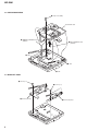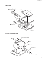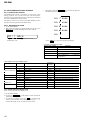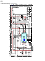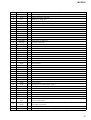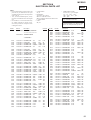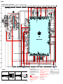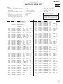
1
MZ-E501
SERVICE MANUAL
AEP Model
Hong Kong Model
Ver 1.2 2001. 12
With SUPPLEMENT-1
US and foreign patents licensed from Dolby
Laboratories Licensing Corporation
Model Name Using Similar Mechanism
MZ-E500
MD Mechanism Type
MT-MZE500-174
Optical Pick-up Mechanism Type
LCX-4E
SPECIFICATIONS
Audio playing system
Outputs
MiniDisc digital audio system
Headphones/earphones: stereo mini-jack, maximum output level 5 mW +
5 mW, load impedance 16 ohms
Laser diode properties
Material: GaAlAs
Wavelength: λ = 790 nm
Emission duration: continuous
Laser output: less than 44.6 µW*
* This output is the value measured at a distance of 200 mm from the
objective lens surface on the optical pick-up block with 7 mm aperture.
Power requirements
Revolutions
Nickel Cadmium rechargeable battery
One NC-6WM (supplied): 1.2V, 600 mAh
One LR6 (size AA) battery (not supplied)
External power jack: Power rating 3V DC
AC power adaptor for the battery charging stand (supplied): AC230~240V,
50Hz
Approx. 300 rpm to 2,700 rpm
Battery operation time
Error correction
See “When to replace or recharge the battery”
ACIRC (Advanced Cross Interleave Reed Solomon Code)
Dimensions
Sampling frequency
44.1 kHz
Approx. 74.5 × 80.5 × 17.9 mm (w/h/d) (3 × 3 1/4 × 23/32 in.)
(not including projecting parts and controls)
Coding
Mass
ATRAC (Adaptive TRansform Acoustic Coding)
ATRAC3: LP2
ATRAC3: LP4
Approx. 80 g (2.8 oz) (the player only)
Modulation system
EFM (Eight to Fourteen Modulation)
Number of channels
2 stereo channels
1 monaural channel
Frequency response
20 to 20,000 Hz ± 3 dB
Wow and Flutter
Supplied accessories
Headphones/earphones with a remote control (1)
Battery charging stand (assembly needed)(1)
AC power adaptor*
Rechargeable battery (1)
Rechargeable battery carrying case (1)
Dry battery case (1)
Carrying pouch (1)
AC plug adaptor (1) (world model only)
US and foreign patents licensed from Dolby Laboratories.
Below measurable limits
Design and specifications are subject to change without notice.
PORTABLE MINIDISC PLAYER
9-873-162-03
Sony Corporation
2001L1600-1
© 2001.12
Personal Audio Company
Published by Sony Engineering Corporation
MZ-E501
TABLE OF CONTENTS
1. SERVICING NOTE ···················································· 3
2. GENERAL ·································································· 4
3. DISASSEMBLY
3-1.
3-2.
3-3.
3-4.
3-5.
Case Assy, Holder Assy ·················································· 5
Mechanism Deck ···························································· 6
Bracket Assy ··································································· 6
Main Board ····································································· 7
Optical Pick-up Assy (LCX-4E) ····································· 7
4. TEST MODE ······························································ 8
5. ELECTRICAL ADJUSTMENTS ··························· 12
6. DIAGRAMS
6-1. Block Diagram ······························································ 17
6-2. Printed Wiring Board – Main Section (Side A) – ········· 18
6-3. Printed Wiring Board – Main Section (Side B) – ········· 19
6-4. Schematic Diagram – Main Section (1/3) – ·················· 20
6-5. Schematic Diagram – Main Section (2/3) – ·················· 21
6-6. Schematic Diagram – Main Section (3/3) – ·················· 22
6-7. IC Block Diagrams ······················································· 23
6-8. IC Pin Function Description ········································· 25
7. EXPLODED VIEWS
7-1. Main Section ································································· 31
7-2. Mechanism Deck Section ············································· 32
8. ELECTRICAL PARTS LIST ·································· 33
CAUTION
Use of controls or adjustments or performance of
procedures other than those specified herein may result in
hazardous radiation exposure.
Flexible Circuit Board Repairing
• Keep the temperature of the soldering iron around 270°C during
repairing.
• Do not touch the soldering iron on the same conductor of the
circuit board (within 3 times).
• Be careful not to apply force on the conductor when soldering or
unsoldering.
Notes on chip component replacement
• Never reuse a disconnected chip component.
• Notice that the minus side of a tantalum capacitor may be damaged by heat.
Unleaded solder
Boards requiring use of unleaded solder are printed with the leadfree mark (LF) indicating the solder contains no lead.
(Caution: Some printed circuit boards may not come printed with
the lead free mark due to their particular size.)
: LEAD FREE MARK
Unleaded solder has the following characteristics.
• Unleaded solder melts at a temperature about 40°C higher than
ordinary solder.
Ordinary soldering irons can be used but the iron tip has to be
applied to the solder joint for a slightly longer time.
Soldering irons using a temperature regulator should be set to
about 350°C.
Caution: The printed pattern (copper foil) may peel away if the
heated tip is applied for too long, so be careful!
• Strong viscosity
Unleaded solder is more viscous (sticky, less prone to flow) than
ordinary solder so use caution not to let solder bridges occur such
as on IC pins, etc.
• Usable with ordinary solder
It is best to use only unleaded solder but unleaded solder may
also be added to ordinary solder.
SAFETY-RELATED COMPONENT WARNING!!
COMPONENTS IDENTIFIED BY MARK ! OR DOTTED LINE WITH
MARK !ON THE SCHEMATIC DIAGRAMS AND IN THE PARTS
LIST ARE CRITICAL TO SAFE OPERATION.
REPLACE THESE COMPONENTS WITH SONY PARTS WHOSE
PART NUMBERS APPEAR AS SHOWN IN THIS MANUAL OR IN
SUPPLEMENTS PUBLISHED BY SONY.
2
MZ-E501
SECTION 1
SERVICING NOTES
NOTES ON HANDLING THE OPTICAL PICK-UP
BLOCK OR BASE UNIT
The laser diode in the optical pick-up block may suffer electrostatic
break-down because of the potential difference generated by the
charged electrostatic load, etc. on clothing and the human body.
During repair, pay attention to electrostatic break-down and also
use the procedure in the printed matter which is included in the
repair parts.
The flexible board is easily damaged and should be handled with
care.
When repairing this device with the power on, if you remove the
main board, this device stops working.
In this case, you work without the device stopping by fastening the
hook of the Open/Close detection switch (S809).
Open/Close detection switch (S809)
NOTES ON LASER DIODE EMISSION CHECK
Never look into the laser diode emission from right above when
checking it for adjustment. It is feared that you will lose your sight.
NOTES ON HANDLING THE OPTICAL PICK-UP BLOCK
(LCX-4E)
The laser diode in the optical pick-up block may suffer electrostatic
break-down easily. When handling it, perform soldering bridge to
the laser-tap on the flexible board. Also perform measures against
electrostatic break-down sufficiently before the operation. The
flexible board is easily damaged and should be handled with care.
* Replacement of CXD2671-205GA (IC601) used in this set
requires a special tool.
laser-tap
OPTICAL PICK-UP FLEXIBLE BOARD
3
MZ-E501
SECTION 2
GENERAL
This section is extracted from
instruction manual.
LOCATION AND FUNCTION OF CONTROLS
VOL+
.
GROUP
VOL+/–
x
VOL–
1N>
X
.
3 Color Info-LED
>N
PLAYMODE
DISPLAY
x
RPT/ENT
SOUND
HOLD
./N>
VOL +/–
GROUP
x
3 Color Info-LED
HOLD
4
MZ-E501
SECTION 3
DISASSEMBLY
r
Disassemble the unit in the order as shown below.
Set
Case assy, Holder assy
Mechanism deck
Bracket assy
MAIN board
Optical pick-up assy (LCX-4E)
Note : Follow the disassembly procedure in the numerical order given.
3-1. CASE ASSY, HOLDER ASSY
case assy
1 screws (1.4), MI
1 screws (1.4), MI
3 Move it away
from the projection
2
hold assy
3 Move it away
from the projection
case (rear)
5
MZ-E501
3-2. MECHANISM DECK
1 step screw (MD)
mechanism deck
6 MOTER FLEXIBLE board
(CN551)
5 OP FLEXIBLE board
(CN501)
4
2 claw
3 claw
3 claw
3-3. BRACKET ASSY
3 screw (1.7)
1 screw (1.7)
4 bracket (L) assy
6
2 bracket (R) assy
MZ-E501
3-4. MAIN BOARD
1 screw (1.7)
5 Remove the soldering
7 battery case assy
6 MAIN board
5 Remove the soldering
2 claw
4 ornamental strip
3 battery case lid
case (rear)
3-5. OPTICAL PICK-UP ASSY (LCX-4E)
optical pick-up assy (LCX-4E)
1 washer
2 gear (SA)
5
3 screw (MI 1.4)
4 thrust detent spring
7
MZ-E501
SECTION 4
TEST MODE
4-1. GENERAL
Remote control LCD
• When entered in the TEST MODE, this set provides the Overall
Adjustment mode which allows CD and MO discs to be automatically adjusted. In the Overall Adjustment mode, the system
discriminates between CD and MO discs, performs adjustments
in sequence automatically, and displays the faulty location if any
fault is found. In the Manual mode, selected adjustments can be
performed automatically.
• The attached remote control is used to operate the TEST MODE.
Unless otherwise specified in the text, the key means that on the
remote control.
All on
All off
012 V1.110
4-2. SETTING THE TEST MODE
4-2-1. How to set the TEST MODE
To set the TEST MODE, two methods are available.
1 Solder bridge and short TAP601 (TEST) on the main board.
Then turn on the power. Press the x button or close the upper
panel.
Microprocessor
version
display
• Press and hold down X to hold the current display while the key
is being pressed.
MAIN BOARD (SIDE B)
4-2-3. How to release the TEST MODE
When method 1 was used:
Turn off the power and open the solder bridge on TAP601 on the
main board.
Note : The solder should be removed clean. The remaining solder
may make a short with the chassis and other part.
When method 2 was used:
Turn off the power.
Note : If electrical adjustment (see page 12) has not been finished
completely, always start in the test mode. (The set cannot
start in normal mode)
4-3. TEST MODE STRUCTURE
TAP601
OPEN : Normal mode
SHORT : Test mode
2 In the normal mode, operate the keys on the set and those on the
remote control rapidly as specified below:
Turn on HOLD switch on the set. Holding down x (STOP)
key on the set, press the keys on the remote control in the
following sequence:
>N t >N t . t . t >N
t . t >N t . t X t X
Test Mode
(Display Check Mode)
VOL+ key
Manual Mode
x
VOL+ key
Servo Mode
Audio Mode
Note : When you press an incorrect switch by mistake, remove your
hands from the switches and perform all the operations once
again from the very beginning.
4-2-2. Operations when the TEST MODE is set
When the TEST MODE is entered, the system switches to the
display check mode within the TEST MODE. From this mode, the
other Test modes can be accessed.
When the TEST MODE is set, the LCD repeats a cycle of the
following displays:
key
Power Mode
VOL– key
OP Alignment Mode
.
or VOL– key
Overall Adjustment Mode
x
key
DISPLAY key
x
key
>B
x
Self-diagnostic Display Mode
key
key
Sound Skip Check Result Display Mode
DISPLAY key
(Press and hold down about 3 sec)
Key Check Mode
Terminate key checking or open
the top panel.
8
MZ-E501
4-4. MANUAL MODE
4. During each test mode, the display is changed from one to
another each time DISPLAY key is pressed.
4-4-1. Outline of the function
The Manual mode is designed to perform adjustments and
operational checks on the set’s operation according to each
individual function.
Usually, no adjustments are made in this mode.
However, the Manual mode is used to clear the memory before
performing automatic adjustments in the Overall Adjustment mode.
4-4-2. How to set the Manual mode
1. Set the TEST MODE and press VOL+ key to set the Manual mode.
Remote control LCD display
• Address & Adjusted Value Display
LCD display
011 C 6 8 S 5 E
adress
mode number
• Jitter Value & Adjusted Value Display
LCD display
000 Manual
011 O F E J 5 E
2. During each test, press and hold down > N key or .
key for a while to move the optical pickup on the sled outer or
inner perimeter.
3. Each test item is assigned with a three-digit item number. The
100th place is a major item, 10th place is a middle item, and unit
place is a minor item.
jitter value
mode number
VOL+ key : 100th place of mode number
increase
VOL– key : 100th place of mode number
decrease
block error value
Change Major
Item
> N key
x
key
VOL+ key : 10th place of mode number
increase
VOL– key : 10th place of mode number
decrease
Change Middle
Item
> N key
x
key
Change Minor
Item
adjusted value
> N key : Unit place of mode number
increase
. key : Unit place of mode number
decrease
Change Adjustment
Value
VOL+ key : Up
VOL– key : Down
Write Adjustment
Value
X key : When adjusted value is changed :
Adjusted value is written.
When adjusted value is not changed :
That item is adjusted automatically.
adjusted value
• Block Error Value & Adjusted Value Display
LCD display
011 0 6 3 B 5 E
adjusted value
mode number
• ADIP Error Value & Adjusted Value Display
LCD display
011 0 7 2 A 5 E
ADIP error value
adjusted value
mode number
• Focus Drive Voltage Value &
Adjusted Value Display
011 0 0 0 F 5 E
forcus drive
voltage value
mode number
adjusted value
• Item Title Display
LCD display
011 LrefPw 5 E
item title
adjusted value
mode number
Note: In the Power mode, the item title display is only displayed.
5. To terminate the Manual mode and return to the TEST MODE,
press x key.
4-5. OVERALL ADJUSTMENT MODE
4-5-1. Outline of the function
This mode is designed to adjust the servo system automatically by
going through all the adjustment items.
The power adjustment manual setting is performed in this mode also.
Usually, this mode is used to perform automatic adjustments when
servicing the set.
For further information, refer to section 5. ELECTRICAL
ADJUSTMENTS. (See page 12)
9
MZ-E501
4-6. SELF-DIAGNOSTIC DISPLAY MODE
4-6-1. Outline of the function
3. Hereinafter, each time > N key is pressed, the reference
information display changes as follows:
The Self-diagnostic system is used in this set. If an error occurs
during playback, this system detects the fault through the
microprocessor’s mechanism and power control blocks and stores
the cause in EEPROM in a history format.
This history, which can be viewed in the TEST MODE, provides
the means of locating the fault in troubleshooting.
4-6-2. Self-diagnostic mode
####
0XX N
####
0XX N1 # # # #
1. Set the TEST MODE.
2. With all the LCD display segments blinking on the set, press
DISPLAY key and the Self-diagnostic mode is entered.
0XX N2 # # # #
0XX
001 1 Adrs
History code
0XX 1
R
– – – –
Simplified contents
Error display code
• Press . key to go back to the previous display.
• Contents of the history codes
History code number
Contents
1
The first error that occurred.
N
The last error that occurred.
N-1
The first error from the last one.
N-2
The second error from the last one.
Total recording time ( – – – – is displayed
R
for MZ-E501)
• Description of the error display codes
Contents of fault Display code
No error
Servo system error
TOC error
Power system error
Offset error
00
01
02
03
04
11
12
22
31
32
33
34
Meaning of code
No error
Access target address illegally specified
HIGH TEMP
FOCUS ERROR
SPINDLE ERROR
TOC ERROR
READ DATA ERROR
LOWBATT
OFFSET ERROR
FE_ABCD_OFFSET_ERR
TE_OFFSET_ERR
X1_TE_OFFSET_ERR
4-6-3. Clearing the error display code
After servicing, reset the error display code.
1. Set the TEST MODE.
2. Pressing the DISPLAY key on the remote control activates the
self-diagnosis display mode.
3. To reset the error display code, press X key (2 times)on the
remote control when the code is displayed. (except “R - - - -” )
(All the data on the 1st, N, N-1 and N-2 will be reset)
10
Simplified
contents
––––
Adrs
Temp
Fcus
Spdl
TOC
Data
LBat
Ofst
ABCD
TE
X1TE
Description
No error
An attempt to access an abnormal address.
HIGH TEMP
Focus off-center.
Abnormal rotation of disc
Faulty TOC contents
Data could not be read at SYNC
Instantaneous interruption detected.
Offset error
FE ABCD Offset error
TE Offset error
X1 TE Offset error
MZ-E501
4-7. Sound Skip Check Result Display Mode
This set can display and check the error count occurring during
play.
• Setting method of Sound Skip Check Result Display Mode
1. Setting the test mode.
2. Pressing the > N key activates the sound skip check result
display mode where the LCD displays as shown below.
LCD display
000 P**R##
Total of record system
error count
Total of play system error count
3. When > N key is pressed, the total of error count is
displayed on the LCD, and each time the > N key is pressed,
the error count descents one by one as shown below. Also, when
. key is pressed, the error count ascends one by one.
000 P**R00
4-8. KEY CHECK MODE
4-8-1. Outline of the function
This mode is used to check to make sure that each of the keys
(including the slide switch) on the set operates normally.(The 1 kHz
signal is outputted from the L and R channels of head phones)
4-8-2. Setting the Key Check mode
1. Set the TEST MODE. Press and hold down DISPLAY key (for
more than 3 sec) to set the Key Check mode.
LCD display
000
0F
2. When each key on the set and on remote control is pressed, its
name is displayed on the LCD. (The operated position is
displayed for 4 sec after the slide switch is operated. If any other
key is pressed during this display, the LCD switches to its name
display)
Example: When > N key on the set is pressed:
LCD display
000 EIB **
000 Stat**
000 Adrs**
000 FF
0F
Example: When > N key on the remote control is pressed:
LCD display
000 rPLAY
XX
XX: AD value of the remote control key (hexadecimal 00 to FF)
000 BEmp**
000 ######
P**R00 : Total of play system error and record system error count
** : Sound skip check items counter (hexadecimal)
##### : 6-digit address (hexadecimal) where a sound skipped last
3. When all the keys on the set and on the remote control are
considered as OK, the following displays are shown for 2 sec.
(The key pressed to enter the Key Check mode has been checked
even if it is not pressed in this mode)
Example: When the keys on the set are considered as OK:
LCD display
888 SET OK OF
Error code
Cause of error
Playback EIB
Stat
Adrs
BEmp
Description of error
Sound error correction error
Decorder status error
Cannot access the address
Buffer becomes empty
4. Press the x key to terminate the sound skip check result display
mode and to return to the test mode. (Display check mode)
Example: When the keys on the remote control are considered
as OK:
LCD display
888 RMC OK OX
4. When all the key have been checked or when the top panel is
opened during this checking, the system terminates the Key
Check mode and return to the TEST MODE.
11
MZ-E501
SECTION 5
ELECTRICAL ADJUSTMENTS
5-1. GENERAL
5-4. MANUAL POWER ADJUSTMENTS
In this set, CD and MO discs can be automatically adjusted by setting
the Overall Adjustment mode within the TEST MODE,
Before performing these automatic adjustments, it is necessary to
clear the memory and adjust the power in the Manual mode.
5-4-1. Adjustment sequence
The adjustments should be always performed in the following
sequence:
5-2. NOTES FOR ADJUSTMENT
5-2-1. Jigs
• CD disc TDYS-1 (part code: 4-963-646-01)
• MO disc PTDM-1 (part code: J-2501-054-A)
or commercially available MO disc (recorded)
• Digital voltmeter
5-2-2. Adjustment sequence
The adjustments should be always performed in the following
sequence:
1 Reset NV (Clear the memory)
2 Manual power adjustments
5-4-2. Vc PWM Duty (L) adjustment method
1. Confirm that the power voltage is at 1.5 V DC.
2. Set the TEST MODE.
3. To set the overall adjustment mode, press VOL– key.
LCD display
Manual mode
3 Electrical offset adjustments
(Do not enter the disc)
000 Assy 00
4. Press PLAY MODE key, and item No. will change to 762.
LCD display
4 Overall CD adjustments
Overall adjustment mode
5 Overall MO adjustments
Manual mode
6 RESUME clear
1 Vc PWM Duty (L) adjustment (item No.:762)
r
2 Vc PWM Duty (H) adjustment (item No.:763)
r
3 VLL PWM Duty adjustment (item No.:764)
5-2-3. Power
The power is supplied with 1.5 V DC from the battery case.
5-3. RESET NV
762 VclPWM XX
5. Connect a digital voltmeter to TP901 (VC) on the main board
and adjust VOL+ key (voltage up) and VOL– key (voltage
down) on the remote control.
Adjustment value:2.36V
Standard value:2.35 to 2.365V
MAIN BOARD (SIDE B)
5-3-1. How to reset NV
1. Set the TEST MODE.
2. Set the Manual mode and set the item No. 021, Reset NV.
LCD display
021 Res NV CC
3. Press X key on the remote control.
digital voltmeter
LCD display
021 Res OK?
TP901 (VC)
4. Press X key on the remote control again.
LCD display
021 Res ***
After reset is completed.
021 Reset!
5. Press x key to terminate the Manual mode and return to the
TEST MODE.
12
6. Press X key to write the adjustment value. Item No.will change
to 763.
MZ-E501
5-4-3. Vc PWM Duty (H) adjustment method
1. Set the Manual mode and set the item No. to 763.
3. Press X key to write the adjustment value.
The adjustment completion display appears as follows.
LCD display
LCD display
763 VchPWM XX
2. Connect a digital voltmeter to TP901(VC) on the main board
and adjust VOL+ key and VOL– key on the remote control.
Adjustment value:2.75V
Standard value:2.74 to 2.755V
MAIN BOARD (SIDE B)
000 ADJ OK
5-4-5.Electrical offset adjustment method
Note: Doing adjustment by the state that a disc does not enter.
1. Confirm the power voltage is 1.5V.
2. Set to the test mode.
3. Press the VOL– key activates the overall adjustment mode.
LCD display
000 Assy11
4. Press the DISPLAY key.
LCD display
030 Ofst**
5. If result of electrical offset adjustment is OK,the following display
appears.
LCD display
digital voltmeter
TP901 (VC)
030 OfstOK
3. Press X key to write the adjustment value.(Item No. will change
to 764)
5-4-4. VLL PWM Duty adjustment method
1. Set the Manual mode and set the item No. to 764.
5-5. OVERALL ADJUSTMENT MODE
5-5-1. Overall adjustment mode structure
TEST MODE
(Display Check Mode)
VOL – key
LCD display
764 Vl PWM XX
2. Connect a digital voltmeter to TP904 (VL) on the main board
and adjust VOL+ key and VOL– key on the remote control.
Adjustment value:2.23V
Standard value:2.22 to 2.235V
MAIN BOARD (SIDE B)
Overall Adjustment
Title Display(ASSY**)
. key
CD overall
Adjustment
x
key
> N key
> N key
MO overall
Adjustment
x
key
Note: The overall adjustments should be always performed in the
sequence of CD t MO adjustments.
5-5-2. Overall CD and MO adjustment method
1. Set the TEST MODE and press VOL– key to set the Overall
Adjustment mode.
LCD display
000 Assy11
2. Insert CD disc in the set, and press . key to set the Overall
CD Adjustment mode.
Automatic adjustments are made.
LCD display
digital voltmeter
XXX CD RUN
TP904 (VL)
XXX: Item No. for which an adjustment is being executed.
13
MZ-E501
3. If NG in the overall CD adjustments, return to Reset NV and
perform from the electrical offset adjustment again.
Item No.
Contents
030
GRV setting • Sarvo OFF • Head UP
035
Laser ON/OFF electrical offset difference
measurement
Completed
LCD display
000 XXX NG
XXX: NG item No.
4. If OK through the overall CD adjustments, then perform overall
MO adjustments.
LCD display
XXX CD OK
5. Insert MO disc in the set, and press > N key to set the
Overall MO Adjustment mode. Automatic adjustments are made.
LCD display
XXX MO RUN
XXX: Item No. for which an adjustment is being executed.
6. If NG in the overall MO adjustments, return to Reset NV and
perform the adjustment again.
LCD display
000 XXX NG
XXX: NG item No.
7. If OK through the overall MO adjustments, press x key to
return to the TEST MODE and terminate the Overall Adjustment
mode.
LCD display
000 MO OK
5-5-3.Resume clear method
1. Setting the test mode.
2. Set the Manual mode and set the item No.043(RESUME Clear).
LCD display
043 Resume CC
3. Press the X key.
LCD display
043 Res ***
After reset is completed
LCD display
043 Res Clr
14
5-5-4. Overall CD and MO adjustment items
1. Overall offset adjustment
2. Overall CD adjustment items
Item No.
Contents
761
VC,VR power voltage High/Low selection
300
HPIT setting • Sarvo OFF
561
SLED move to inside
562
SLED move to outside
High reflection CD electrical offset adjustment
312
Laser ON • Focus UP • VC correction ALFA offset
adjustment
313
IJ offset adjustment
314
FE offset adjustment
HPIT adjustment
320
Focus servo ON
324
TE offset adjustment 1
321
TE gain adjustment
328
TWPP gain adjustment
324
TE offset adjustment 1
332
TE offset adjustment 2
330
Tracking servo ON
336
ABCD gain adjustment
337
KF gain correction
338
RF gain adjustment
344
FCS gain adjustment
345
TRK gain adjustment
521
Two-axis sensitivity adjustment (inside)
522
Two-axis sensitivity adjustment (outside)
341
Focus bias adjustment
300
HPIT setting • servo OFF
Completed
3. Overall MO adjustment items
Item No.
Contents
761
VC,VR power voltage High/Low selection
100
R_GV setting
Low reflect MO offset adjustment
112
Laser ON • Focus UP • VC correction ALFA offset
adjustment
113
IJ offset adjustment
114
FE offset adjustment
118
Wpp denominator adjustment
LPIT adjustmet
200
LPIT setting • servo OFF
561
SLED move to inside
220
Focus servo ON
224
TE offset adjustment 1
221
TE gain adjustment
224
TE offset adjustment 1
232
TE offset adjustment 2
MZ-E501
Item No.
230
236
237
238
244
245
100
562
120
122
121
122
123
124
130
131
136
137
139
144
145
134
131
132
149
138
100
Contents
Tracking servo ON
ABCD gain adjustment
KF gain adjustment
RF gain adjustment
FCS gain adjustment
TRK gain adjustment
READ GRV adjustment 1
R GRV setting • servo OFF
SLED move to outside
Focus servo OFF
TON offset adjustment
TE gain adjustment
TON offset adjustment
TEIN offset adjustment
TWPP offset adjustment
Tracking servo ON
TWPP offset adjustment
ABCD gain adjustment
KF gain adjustment
ADIP BPF fo adjustment
FCS gain adjustment
TRK gain adjustment
TWPP gain adjustment
TWPP offset adjustment 1
TWPP offset adjustment 2
TWPP OP offset adjustment
RF gain adjustment
R GRV setting • Servo OFF
15
MZ-E501
SECTION 6
DIAGRAMS
Note on Printed Wiring Boards: MAIN SECTION
• X : parts extracted from the component side.
•
: Pattern from the side which enables seeing.
(The other layers' patterns are not indicated.)
Caution:
Pattern face side:
Parts on the pattern face side seen from the
(Side B)
pattern face are indicated.
Parts face side:
Parts on the parts face side seen from the
(Side A)
parts face are indicated.
• Main boards is four-layer pritnted board.
However, the patterns of layer 2 and 3 have not been
included in this diagrams.
r WAVEFORMS
1 IC501 1 TE
Approx.
12 mVp-p
2
IC501 ed (RF OUT)
* Replacement of IC601 used in this set requires a special
tool.
• Lead Layouts
Approx.
1.2 Vp-p
surface
3 IC501 rs (FE)
Lead layout of
conventional IC
Approx.
10 mVp-p
CSP (chip size package)
4
X601 (OSCO)
Note on Schematic Diagram: MAIN SECTION
• All capacitors are in µF unless otherwise noted. pF: µµF
50 WV or less are not indicated except for electrolytics
and tantalums.
• All resistors are in Ω and 1/4 W or less unless otherwise
specified.
f
: internal component.
•
Note: The components identified by mark 0 or dotted
line with mark 0 are critical for safety.
Replace only with part number specified.
•
: B+ Line.
• Power voltage is dc 1.5V and fed with regulated dc power
supply from battery terminal.
• Voltages and waveforms are dc with respect to ground
under no-signal conditions.
no mark : PLAY
• Voltages are taken with a VOM (Input impedance 10 MΩ).
Voltage variations may be noted due to normal production tolerances.
• Waveforms are taken with a oscilloscope.
Voltage variations may be noted due to normal production tolerances.
• Circled numbers refer to waveforms.
• Signal path.
F : Audio (Analog)
J : Audio (Digital)
* Replacement of IC601 used in this set requires a special
tool.
• The voltage and waveform of CSP (chip size package)
cannot be measured, because its lead layout is different
from that of conventional IC.
16
22.1 ns
2.7 V
MZ-E501
6-1. BLOCK DIAGRAM
MAIN BOARD
Iy
Ix
6
HEADPHONE AMP
IC301
4 VREF
Iy
8
9
10
11
12
14
5
6
9
Ix
10
Jx
14
Jy
15
A
16
B
17
C
7
8 D
Jy
Jx Jy Jx
A
Ix Iy Ix
B
Iy
Ix
Jx
Jy
A
B
C
D
A-C
13
D-C
7
C
18
D
MON
18
PD-I
RF OUT
RF AMP,
FOCUS
ERROR,
TRACKING
ERROR
PEAK
29
BOTM
28
PEAK
/BOTM
ABCD
41
42
47 FE
1
ADIP IN 44
56 TE
FE
TE
TPP/WPP
PD-NI
OFTRK 26
XRST
25
SBUS
23
SCK
24
221 XRF RST
160 SSB DATA
161 SSB CLK
PD
SERIAL
I/F
5
LD
LD-K
S0
S1
S0
S1
LASER
AUTO POWER
CONTROL
Q501
20
S-MONITOR
PD-O
S MON
43
VIF
BEEP OUT A
RCH
RGND
KEY
24
23
BEEP OUT B
BEEP
VREF IN 13
DATA
RMC
VDD
REFERENCE
VOLTAGE
SWITCHING
Q301
VDD
RMC VDD
REC KEY 18
SET KEY2 14
TSB MST VDD 141
D801
(INFO)
Q801
LED SWITCH
13
OPR LED R PWM 167
OPR LED G PWM 163
11
19
HOLD SW 227
XAVLS 224
194 PD S0
195 PDS1
ON
OFF
S808
HOLD
EEPROM
AVCC
DI
DO
SK
XCS
20
42
41
39
TRACKING
COIL
1
33
32
TRK-
38
100 SLD1MON
37
101 SLD2MON
FOCUS
COIL
3
81 TFDR
88 TRDR
24
25
HI-BRIDGE
CONTROL
35
10
7
DIFVDD0 76
DIFVDD1 103
TSB SLV VDD 143
MIFVDD0 154
MIFVDD1 176
MIFVDD2 196
TSB SLV CHK 210
MIFVDD3 241
3 XTEST
PRE
DRIVER
HI-BRIDGE
CONTROL
OSCO 25
19
18
X601
45.1584MHz
RMC KEY 20
82 FFDR
80 FRDR
VB MON 10
UNREG
CN551
5
14
15
12
7
SLED2+ 6
SLED2- 8
29
31
1
PRE
DRIVER
PRE
DRIVER
HI-BRIDGE
CONTROL
HI-BRIDGE
CONTROL
54
51
53
CLVU
CLVV
CLVW
48
2
45
46
49
44
3
4
26
27
1
52
M901
(SPINDLE)
16
17
20
PRE
DRIVER
3 PHASE
CONTROL
98 SLDV
96 SRDR
97 SFDR
99 SLDW
102 SLCW
XCS NV
SI0
93 SPCU
SCK0
56
94 SPCV
S00
55
95 SPCW
2
3
4
5
6
FS4
VLON
SLEEP
FFCLR
XRST
AVDD
86
234
235
236
8
21
23
119
139
151
231
MCU VDD0 6
DSP VDD0 59
DSP VDD1 73
MCU VDD1 84
DSP VDD2 91
DSP VDD3 113
MCU VDD2 153
MCU VDD3 222
90 SPD W
89 SPD V
87 SPD U
88 SPDL PWM
220 XRST MTR DRV
UNREG
17
17
5 XWK4
2 XWK1
7
4
6
3
VRMC
XWK3
VSTB
XWK2
22
56
1
55
54
46
36
34
AVDD
AVD1
AVD2
VDI00
VDI01
VDI02
S805
VOL
+
IC901
26 INM1
27 RF1
23 RF2
VC PWM 165
VL PWM 164
SLED1-
S806
GROUP
44 VD
8
SLED1+
S809
(OPEN/CLOSE
DETECT)
S804
VOL
--
S803
.
S802
>N
S801
x
POWER SUPPLY
OSCI 24
TAP601
(TEST)
FCS+
FCS-
VIF
DIGITAL SIGNAL PROCESSOR,
DIGITAL SERVO SIGNAL PROCESSOR,
EFM/ACIRC ENCODER/DECODER,
SHOCK PROOF MEMORY CONTROLLER,
16M BIT D-RAM, SYSTEM CONTROL
DVDD
PRE
DRIVER
BIAS
4
XCS NV
SCK0
S00
SI0
IC601
40
TRK+
HALF LOCK SW 19
219
181
180
179
IC551
MINIDISC
OPTICAL PICK-UP BLOCK
(LCX-4E)
2
SET KEY 1 13
WK DET 17
IC801
FOCUS/TRACKING COIL DRIVE,
SPINDLE/SLED MOTOR DRIVE
MINIDISC
MECHANISM BLOCK
M902
(SLED)
4
OUT B
IN B
1 +B
20 VCC
15
18 STB
17 MUTE
XHP STB 240
MUTE 218
9 S MON
VL
AVCC
UNREG
RMC DTCK 142
22 DVDD
40 AVCC
12
19
VC 31
LCH
J301
i
21
AOUT R 30
BEEP 183
78 APCREF
49 VC
12 VREF MON
217 OFTRK
APC
2
RCH
74 ADFG
ADIP 21
VIF
LD-A
44 PEAK
45 BOTM
46 ABCD
22
AOUT L 29
37 RFI
33
4
3
2
1
F
IC501
VREF
RCH
Jx
a bc d
RF AMP,FOCUS/TRACKING ERROR AMP
CN501
INM2
CLK
VLON
SLEEP
FFCLR
XRST
VC
VC
45 VC2
VL
VLO 10
VCO 35
VIF 42
VC
VIF
AVDD
VA 41
VG 19
VG
D903
LG 18
L906
VL 9
VL 11
D902
L2 16
L2 12
L902
UNREG
VB 50
L1 32
L1 28
L901
D901
RECHAGEABLE
BATTERY
NC-6WM
1PC, 1.2V 600mAh
VC OUT 33
DVDD
• Signal path
J : Audio (Digital)
F : Audio (Analog)
• RCH is omitted due to same as LCH
DRY BATTERY
SIZE "AA"
(IEC DESIGNATION LR6)
1PC, 1.5V
MZ-E501
6-2. PRINTED WIRING BOARD – MAIN SECTION (SIDE A) –
1
3
2
4
5
6
7
8
9
10
MAIN BOARD (SIDE A)
A
• Semiconductor
Location
Ref. No.
E
IC 301
S801
x
B
*
IC 601
CSP (Chip Size Package)
S806
GROUP
C
D
S803
.
S808
HOLD
E
OFF
ON
S804
VOL–
DRY BATTERY
SIZE "AA"
(IEC DESIGNATION LR6)
1PC, 1.5V
IC 901
(INFO)
S802
>N
S805
VOL+
F
E
11
(11)
IC 501
1-681-868-
G
18
18
11
(11)
Location
D101
D201
D801
D855
D902
D903
C-9
C-10
E-7
D-10
F-9
F-10
IC301
IC501
IC601
IC901
B-9
F-4
B-4
E-9
Q301
Q501
A-8
F-3
MZ-E501
6-3. PRINTED WIRING BOARD – MAIN SECTION (SIDE B) –
1
3
2
MAIN BOARD (SIDE B)
A
4
5
6
7
8
9
10
TO
OPTICAL
PICK-UP
BLOCK
(LCX-4E)
TO MOTOR FLEXIBLE BOARD
(M901 : SPINDLE MOTOR)
(M902 : SLED MOTOR)
• Semiconductor
Location
Ref. No.
IC 801
B
C609
R
COM
J301
C
L
TAP601
(TEST)
RGND
TP904
(VL)
R-KEY
R-DATA
D
TP901
(VC)
RVDD
E
S809
(OPEN/CLOSE
DETECT SWITCH)
IC 551
F
1-681-868-
G
RECHARGEABLE BATTERY
NC-6WM
1PC, 1.2V 600mAh
19
19
11
(11)
Location
D901
E-2
IC551
IC801
F-5
B-9
Q801
C-3
MZ-E501
6-4. SCHEMATIC DIAGRAM – MAIN SECTION (1/3) – • See page 16 for Waveforms. • See page 25, 26 for IC Pin Function Description.
OPR_LED_G_H
OPR_LED_G_L
OPR_LED_R_H
OPR_LED_R_L
TAP602
20
20
MZ-E501
6-5. SCHEMATIC DIAGRAM – MAIN SECTION (2/3) –
• See page 23, 24 for IC Block Diagrams.
IC B/D
IC B/D
C956
0.1
21
21
MZ-E501
6-6. SCHEMATIC DIAGRAM – MAIN SECTION (3/3) – • See page 23 for IC Block Diagrams.
(INFO)
IC B/D
22
22
MZ-E501
6-7. IC BLOCK DIAGRAMS
STB
MUTE
BST SW
BEEP IN
GND
VREF IN
IC301 TA2131FL (EL)
18
17
16
15
14
13
PW
SW
MT
SW
BST
SW
BEEP
12 VREF
V REF
11 LPF1
TC MT 19
VCC 20
ADD
INR 21
10 BST NF1
BST1
INL 22
9 LPF2
PW
A
BEEP
23
OUTB
PW
B
BST2
8 BST NF2
7 BST OUT
BEEP
24
OUTA
OUTL
PWR
GND
4
5
6
AGC IN
3
DET
2
OUTR
1
+B
BST
AGC
CPBIM
CPAO
CPB0
VM3
RO3
PGND3
FO3
VM34
40
39
38
37
36
35
34
33
32
FO4
CPBIP
41
RO4
CPAIM
42
PGND4
CPAIP
IC551 SC111257FCR2
31
30
29
28 VM4
VC VG
VC VG
VC VG
PRE DRIVER
PGNDW 43
PRE DRIVER
VC
WO 44
PRE DRIVER
VMVW 45
VO 46
PGNDUV 47
VC
H-BRIDGE
CONTROL
27 R14
26 F14
H-BRIDGE
CONTROL
25 R13
UO 48
24 F13
VMU 49
VG
23 VG
GND2 50
VC
22 VC
CPW1 51
21 GND1
CPV1 52
20 PWM24
19 F11
CPU1 53
18 R11
VC
COM 54
VC
H-BRIDGE
CONTROL
H-BRIDGE
CONTROL
VC VG
CPWO 55
VC
3 PHASE
CONTROL
VC VG
PRE DRIVER
PRE DRIVER
BIAS
1
2
3
4
5
6
7
8
9
10
11
12
13
14
W1
V1
U1
PWM
OE
VM1
RO1
PGND1
FO1
VM12
RO2
PGND2
FO2
15 VM2
CPUO
CPVO 56
17 F12
16 R12
23
MZ-E501
VAFB
VDFB
VIFFB
GND
VC
VCO
VC
VCOUT
L1
NC
PGND1
PGND1
42 41
40
39
38
37
36
35
34
33
32
31
30
29
VIF
VA
IC901 XPC18A32FCR2
NC 43
VG
SERIAL PASS
REGULATOR VA
VD 44
STEP-UP
PRE DRIVEER
POWER
SWITCH 1
28 L1
VG
VG
STEP-UP
PRE DRIVEER
27 RF1
SERIAL PASS
REGULATOR VD
VC2 45
SERIAL PASS
REGULATOR VIF
26 INM1
XRST (INT)
XRST 46
25 DTC1
VC
VC
VC
24 DTC2
PWM
CRST 47
VC
RSTREF 48
23 RF2
VC
BANDGAP
REFERENCE
VREF 49
22 INM2
VG
VC
VB 50
21 PWM1
VG
GND 51
VC
20 PWM2
VSTB VC
VB
VB VC VG
VG
19 VG
CLKSEL 52
VAIFON 53
VB
FFCLR 54
START-UP
CONTROL
STEP-UP
DC/DC
CONVERTOR
18 LG
SLEEP 55
17 PGND2
CLK 56
VSTB
VG
STEP-UP
PRE DRIVEER
PWER
SWITCH 2
16 L2
VC VB
24
1
2
3
4
5
6
7
8
9
10
11
12
13
14
VLON
XWK1
XWK2
XWK3
XWK4
VSTV
VRMC
GND
VL
VLO
VL
L2
PGND2
PGND2
15 NC
MZ-E501
6-8. IC PIN FUNCTION DESCRIPTION
• IC501 SN761057DBT (RF AMP, FOCUS/TRACKING ERROR AMP)
Pin No.
Pin Name
I/O
1
TE
O
Tracking error signal output to the system controller (IC601)
Description
2
REXT
I
Connect terminal to the external resistor for ADIP amp control
3
WPPLPF
I
Connect terminal to the external capacitor for TPP/WPP low-pass filter
4
VREF
O
Reference voltage output terminal (+1.1V)
5
C
I
Signal (C) input from the optical pickup detector
6
D
I
Signal (D) input from the optical pickup detector
7
D-C
I
Signal (D) input from the optical pickup detector (AC input)
8
IY
I
I-V converted RF signal (IY) input from the optical pickup detector
9
IX
I
I-V converted RF signal (IX) input from the optical pickup detector
10
JX
I
I-V converted RF signal (JX) input from the optical pickup detector
11
JY
I
I-V converted RF signal (JY) input from the optical pickup detector
12
A
I
Signal (A) input from the optical pickup detector
13
A-C
I
Signal (A) input from the optical pickup detector (AC input)
14
B
I
Signal (B) input from the optical pickup detector
15
TON-C
I
Connect terminal to the external capacitor for TON hold
16
CIG
I
Connect terminal to the external capacitor for the low-pass filter of NPP divider
denominator (Not used in this set)
17
CDN
I
Connect terminal to the external capacitor for the low-pass filter of CSL divider
denominator (Not used in this set)
18
PD-I
I
Light amount monitor input terminal (invert input)
19
PD-NI
I
Light amount monitor input terminal (non-invert input)
20
PD-O
O
Light amount monitor output terminal
21
ADIP
O
ADIP duplex FM signal (66.15kHz ± 3kHz) output to the system controller (IC601)
22
DVDD
I
23
SBUS
I/O
SSB serial data input/output with the system controller (IC601)
24
SCK
I
SSB serial clock signal input from the system controller (IC601)
Power supply terminal (+1.9V) (digital system)
25
XRST
I
Reset signal input from the system controller (IC601)
26
OFTRK
I
Off track signal input from the system controller (IC601)
“L”: reset
27
DGND
I
Ground terminal (digital system)
28
BOTM
O
Bottom hold signal output of the light amount signal (RF/ABCD) to the system controller
(IC 601)
29
PEAK
O
Peak hold signal output of the light amount signal (RF/ABCD) to the system controller
(IC 601)
30
VREF
I
Connect terminal to the external capacitor for the internal reference voltage
31
VC
O
Middle point voltage (+1.2V) generation output terminal
32
CCSL2
I
Connect terminal to the external capacitor for TPP/WPP low-pass filter (not used in this set)
33
RF OUT
O
Playback EFM RF signal output to the system controller (IC601)
34
AGND
I
Ground terminal (analog system)
35~37
EQ, LP, PS
I
Connect terminal to the external capacitor for the RF equalizer
38
AVCC
I
Power supply terminal (analog system) (+2.2V)
39, 40
OFC2, OFC-1
I
Connect terminal to the external capacitor for RF AC coupling
41
ABCD
O
Light amount signal (ABCD) output to the system controller (IC601)
42
FE
O
Focus error signal output to the system controller (IC601)
43
S-MON
O
Servo signal monitor output to the system controller (IC601)
44
ADIP-IN
I
ADIP duplex FM signal (66.15kHz ± 3kHz) input terminal, 3 times speed
25
MZ-E501
• IC601 CXD2671-205GA (SYSTEM CONTROL)
Pin No.
Pin Name
I/O
1
26
Description
OPR_LED_G_H
O
High intensity green LED control (open)
2
OPR_LED_G_L
O
Low intensity green LED control (open)
3
XTEST
I
Input terminal for the test mode detection
4
OPR_LED_R_H
O
High intensity red LED control (open)
5
OPR_LED_R_L
O
Low intensity red LED control (open)
6
MCUVDD0
—
Power supply (for microcomputer block)
7
MIFVSS3
—
Ground (for microcomputer I/F)
8
XRST
I
System reset terminal
9
S MON
I
Servo signal monitor
10
VB MON
I
Voltage monitor of UNREG power supply
11
CHG MON
I
Not used (connected to ground)
12
VREF MON
I
Clear reference voltage monitor
13
14
SET KEY 1
I
SET KEY 2
I
Set key detection 1
Not used (connected to RMC VDD)
15
VL MON
I
VL voltage monitor
16
HIDC MON
I
Not used (connected to ground)
17
WK DET
I
Set KEY WAKE detection
18
REC KEY
I
Not used (connected to RMC VDD)
19
HALF LOCK SW
I
Signal input for OPEN SW detection
20
RMC KEY
I
Remote control key detection
21
AVDD
—
Power supply (for the analog circuit block)
22
AVSS
—
Ground (for the analog circuit block)
23
VDIOSC
—
Power supply (for OSC cell)
24
OSCI
I
Input to the X’tal oscillator circuit
25
OSCO
O
Output from the X’tal oscillator circuit
26
VSIOSC
—
Ground (for OSC cell)
27
DAVDD
—
Built-in DAC VCC
28
VREFL
—
Built-in DAC VREF (L-ch)
29
AOUTL
O
Built-in DAC (L-ch) output
30
AOUTR
O
Built-in DAC (R-ch) output
31
VREFR
I
32
DAVSS
—
Ground (for the built-in DAC)
33
ASYO
O
Playback EFM duplex signal output
Playback EFM comparison slice level input
Built-in DAC VREF (R-ch)
34
ASYI
I
35
AVD1
—
36
BIAS
I
Bias input for the playback EFM comparison
Playback EFM RF signal input
AVDD
37
RFI
I
38
AVS1
—
AVSS
39
PCO
O
Phase comparison output for the playback EFM system master PLL
40
Phase comparison output for the analog PLL
PDO
O
41
FILI
I
Filter input for the playback EFM system master PLL
42
FILO
O
Filter output for the playback EFM system master PLL
43
CLTV
I
Internal VCO control voltage input for the playback EFM system master PLL
44
PEAK
I
Peak hold signal input of the light amount signal
45
BOTM
I
Bottom hold signal input of the light amount signal
46
ABCD
I
Light amount signal input
MZ-E501
Pin No.
Pin Name
I/O
47
FE
I
Focus error signal input
Description
48
AUX1
I
Support signal input (A/D input)
49
VC
I
Middle point voltage input
50
ADIO
O
Not used (open)
51
ADRT
I
A/D converter the upper limit voltage input
52
AVD2
—
AVDD
53
AVS2
—
AVSS
54
ADRB
I
A/D converter the lower limit voltage input
55
SE
I
Sled error signal input
56
TE
I
Tracking error signal input
57
DCHG
—
Connecting analog power supply of the low impedance
58
APC
I
59
DSPVDD0
—
Power supply (for DSP block)
60
DSPVSS0
—
Ground (for DSP block)
61
Error signal input for the laser digital APC
XTSL
I
X’tal oscillation frequency selection
62
DIN1
I
Not used (connected to ground)
63
DOUT
O
Not used (open)
64
Not used (open)
PWMLP
O
65
PWMLN
O
Not used (open)
66
PWMRP
O
Not used (open)
67
Not used (open)
DADT/PWMRN
O
68
ADDT
I
Not used (connected to ground)
69
LRCK
O
Not used (open)
70
XBCK
O
Not used (open)
71
FS256
O
Not used (open)
72
MVCI
I
Not used (connected to ground)
73
Power supply (for DSP block)
DSPVDD1
—
74
ADFG
I
ADIP duplex FM signal (20.05±1KHz) input
75
F0CNT
O
Not used (open)
76
DIFVDD0
—
Power supply (for DSP I/F)
77
DIFVSS0
—
Ground (for DSP I/F)
78
APCREF
O
Output to the reference PWM for the laser APC
79
LDDR
O
Not used (open)
80
TRDR
O
Tracking servo drive PWM signal output (–)
81
TFDR
O
Tracking servo drive PWM signal output (+)
82
FFDR
O
Focus servo drive PWM signal output (–)
83
Focus servo drive PWM signal output (+)
FRDR
O
84
MCUVDD1
—
85
FGIN
I
Not used (open)
86
FS4
O
176.4kHz clock signal output
87
SPRD/SPDU/
RTG0
O
Spindle servo drive output (PWM– or inertia)/Brushless spindle motor 3-phase drive logic
output (U)/RTG output 0
88
SPFD/SPVS/
PWM3
O
Spindle servo drive output (PWM+ or PWM absolute value)/Brushless spindle motor absolute
value PWM output/PWM3
89
SPDV/RTG1
O
Brushless spindle motor 3-phase drive logic output (V)/RTG output 1
90
SPDW/RTG2
O
Brushless spindle motor 3-phase drive logic output (W)/RTG output 2
Power supply (for the microcomputer block)
27
MZ-E501
Pin No.
Pin Name
I/O
91
DSPVDD2
—
Description
Power supply (for DSP block)
92
DSPVSS1
—
Ground (for DSP block)
93
SPCU
I
Brushless spindle motor drive comparison signal input (U)
94
SPCV
I
Brushless spindle motor drive comparison signal input (V)
95
SPCW
I
Brushless spindle motor drive comparison signal input (W)
96
SRDR/SL1F
O
Sled servo drive PWM signal output (–)
97
SFDR/SLVF
O
Sled servo drive PWM signal output (+)
98
SLDV
O
Brushless sled motor 3-phase logic output (V)/2-phase drive logic output (1–)
99
SLDW
O
Brushless sled motor 3-phase drive logic output (W)/2-phase drive logic output (2+)
100
SLCU
I
Brushless sled motor 3-phase drive comparate input (U)/2-phase drive comparate input (1)
101
SLCV
I
Brushless sled motor 3-phase drive comparate input (V)/2-phase drive comparate input (2)
102
SLCW
I
Brushless sled motor 3-phase drive comparate input (W)/2-phase comparate output (2–)
103
DIFVDD1
—
Power supply (for DSP I/F)
104
DIFVSS1
—
Ground (for DSP I/F)
105
EFMO
O
Not used (open)
106
MNT0
O
DSP monitor output (0)
107
MNT1
O
DSP monitor output (1)
108
MNT2
O
DSP monitor output (2)
109
MNT3
O
DSP monitor output (3)
110
SENSE
O
Not used (open)
111
TX
O
Not used (open)
112
RECP
O
Not used (open)
Power supply (for DSP block)
113
DSPVDD3
—
114 to
117
NC
—
Not used (open)
118
DRAMVSS0
—
Ground (for the external D-RAM)
119
DRAMVDD0
—
Power supply (for the external D-RAM)
120 to
138
NC
—
Not used (open)
139
DRAMVDD1
—
Power supply (for the external D-RAM)
140
DRAMVSS1
—
Ground (for the external D-RAM)
141
TSB MST VDD
—
Power supply (for TSB master communication)
142
RMC DTCK
I/O
TSB master data input/output
143
TSB SLV VDD
—
I/F power supply (for TSB slave communication)
28
144
TSB SLVI
I
TSB slave signal input
145
TSB SLVO
O
Not used (open)
146
TDI
I
Data input terminal for JTAG
147
TMS
I
Test mode control input terminal for JTAG
148
TCK
I
Clock input terminal for JTAG
149
XTRST
I
Reset input terminal for JTAG
150
TDO
O
Data output terminal for JTAG
151
JTAGVDD
—
Power supply terminal for JTAG
152
JTAGVSS
—
Ground terminal for JTAG
153
MCUVDD2
—
Power supply (for the microcomputer block)
154
MIFVDD0
—
Power supply (for the microcomputer I/F block)
155
MIFVSS0
—
Ground (for the microcomputer I/F block)
MZ-E501
Ver 1.2 2001.12
Pin No.
Pin Name
I/O
Description
156, 157
TEST1, TEST0
I
Terminal 1, 0 for the main test
158
EVA
I
EVA/FLASH chip discrimination terminal
159
OPR LED
O
Operation LED control (Not used in this set)
160
SSB DATA
I/O
Input/output of SSB serial data
161
SSB CLK
—
SSB serial clock
162
MCUVSS0
—
Ground (for the microcomputer block)
163
OPR_LED_R_PWM
O
Operation LED (R) control PWM
164
VL PWM
—
PWM for the laser power supply voltage control
165
VC PWM
—
PWM for the system power supply voltage control
166
SPDL_AUX_PWM
O
Spindle auxiliary control PWM
167
OPR_LED_G_PWM
O
Operation LED (G) control PWM
168
NC
O
Not used (open)
169
CLK SEL
O
Not used (open)
170
OPEN CLOSE
SW
I
Not used (open)
171
GND SW
O
Not used (open)
172
SET CODE0
O
Set code 0
173
SET CODE1
O
Set code 1
174
SET CODE2
O
Set code 2
175
SET CODE3
O
Set code 3
176
MIFVDD1
—
Power supply (for the microcomputer I/F block)
177
MIFVSS1
—
Ground (for the microcomputer I/F block)
178
AOUT SEL
O
HP/LINE changeover signal output Not used (open)
179
SI0
I
Serial data input (CH0)
180
SO0
O
Serial data output (CH0)
181
SCK0
O
Serial clock signal output (CH0)
182
XGUM ON
I
Not used (open)
183
BEEP
O
Beep sound output
184
NC
—
Not used (open)
185
VD. SEL
O
Not used (open)
186
XMUTE
O
Not used (open)
187
LCD_RST_AUX
O
Not used (open)
188-189
NC
O
Not used (open)
190
X PATCH
I
191
OPT DET
I
Not used (connected to ground)
Not used (open)
192
XJACK DET
I
Not used (open)
193
XMIC DET
I
Not used (open)
194, 195
PD S0, PD S1
O
PD IC mode changeover 0, 1
196
MIFVDD2
—
Power supply (for the microcomputer I/F block)
197 to
199
MODE1 to 3
O
Not used (open)
200, 201
HD CON 1, 2
O
Not used (open)
202
NC
O
Not used (open)
203
XCS ADA
O
Not used (open)
204
XPD ADA
O
Not used (open)
205
XCS LCD
O
Not used (open)
29
MZ-E501
Pin No.
Pin Name
I/O
206
LCD STB
O
Not used (open)
Description
207
LCD RST
O
Not used (open)
208
REC LED
O
Not used (open)
209
LD ON
O
Not used (open)
210
TSB SLV CHK
I
TSB slave check
211
K-TAI_MON
I
Not used (open)
212
K-TAI_SW
I
Not used (open)
213
MCUVSS1
—
214
CAV CLV SW
O
Not used (open)
215
XOPT CTL
O
Not used (open)
216
CS RTC
O
Not used (open)
217
OFTRK
I
Off track signal input
218
MUTE
O
Analog mute
219
XCS NV
O
NV RAM chip select
220
XRST MTR
DRV
O
NADESHIKO2 reset
Ground (for the microcomputer block)
“H”: muting ON
221
XRF RST
O
TIARA reset
222
MCUVDD3
—
Power supply (for the microcomputer block)
223
224
SPDL MON
XAVLS
I
I
225, 226
SOUND 1, 2
I
Not used (open)
227
XHOLD SW
I
HOLD switch detection
228
SYNC REC
I
Not used (open)
229
TSB_SSB_CTL
O
TSB/SSB switching
230
PROTECT
Not used (open)
231
FLASHVDD
I
—
232
FLASHVSS
—
233
SLD MON
I
Sled monitor
234
VLON
O
Laser power supply control
235
SLEEP
O
SLEEP request
236
FFCLR
O
Input latch output for the start signal
237
CHG GAIN
O
Not used (open)
Power supply for FLASH
Ground terminal for FLASH
238
CHG
O
Not used (open)
239
TUN REG ON
O
Not used (open)
240
XHP STBY
O
HP Amp power supply control
241
MIFVDD3
—
Power supply (for the microcomputer I/F block)
242
MIFVSS2
—
Ground (for the microcomputer I/F block)
243
TEST2
O
Not used (open)
NC
—
Not used (open)
244
30
Spindle monitor
AVLS SW detection
MZ-E501
SECTION 7
EXPLODED VIEWS
NOTE:
• -XX, -X mean standardized parts, so they may
have some differences from the original one.
• Items marked “*” are not stocked since they
are seldom required for routine service. Some
delay should be anticipated when ordering these
items.
• The mechanical parts with no reference number
in the exploded views are not supplied.
•
•
Ver 1.2 2001.12
Hardware (# mark) list and accessories and
packing materials are given in the last of this
parts list.
Color Indication of Appearance Parts Example:
KNOB, BALANCE (WHITE) . . . (RED)
↑
↑
Parts of Color Cabinet’s Color
The components identified by mark 0 or
dotted line with mark 0 are critical for safety.
Replace only with part number specified.
7-1. MAIN SECTION
8
6
not
supplied
MT-MZE500-174
9
not
supplied
6
11
10
10
10
22
21
18
7
1
2
17
5
12
13
6
20
10
19
14
3
not
supplied
4
16
15
Ref. No.
Part No.
Description
Ref. No.
Part No.
Description
1
1
1
1
2
3-232-193-01
3-232-193-11
3-232-193-21
3-232-193-31
X-3380-732-1
LID, BATTERY CASE (SILVER)
LID, BATTERY CASE (PINK)
LID, BATTERY CASE (BLUE)
LID, BATTERY CASE (YELLOW)
TERMINAL ASSY, BATTERY
Remarks
9
10
11
12
∗ 13
3-049-051-01
3-318-382-02
X-3380-734-1
X-3380-735-1
A-3021-503-A
SCREW (MD), STEP
SCREW (1.7), TAPPING
BRACKET (L) ASSY
BRACKET (R) ASSY
MAIN BOARD, COMPLETE
3
4
5
5
5
3-232-180-01
3-224-025-01
3-232-179-01
3-232-179-11
3-232-179-21
BUTTON (OPEN)
TERMINAL BOARD (MINUS)
STRIP, ORNAMENTAL (SILVER)
STRIP, ORNAMENTAL (PINK)
STRIP, ORNAMENTAL (BLUE)
14
15
16
16
16
X-3380-733-1
4-989-078-01
X-3380-896-1
X-3380-897-1
X-3380-898-1
CASE ASSY, BATTERY
SPRING (OPEN), TENSION
CASE ASSY (SILVER)
CASE ASSY (PINK)
CASE ASSY (BLUE)
5
6
7
8
8
3-232-179-31
4-218-233-09
X-3380-870-1
X-3380-740-1
X-3380-741-1
STRIP, ORNAMENTAL (YELLOW)
SCREW (1.4), MI
HOLDER ASSY (S)
LID ASSY, UPPER (SILVER)
LID ASSY, UPPER (PINK)
16
17
18
19
20
X-3380-899-1
3-232-194-01
3-232-178-01
4-225-074-01
3-241-062-01
CASE ASSY (YELLOW)
PLATE, ELECTROSTATIC
BUTTON (B), CONTROL
TERMINAL BOARD
SHEET (BATT CASE)
8
8
X-3380-742-1 LID ASSY, UPPER (BLUE)
X-3380-743-1 LID ASSY, UPPER (YELLOW)
21
22
3-234-918-01 SHEET (FITTING R)
3-234-920-01 SHEET (JACK)
Remarks
31
MZ-E501
7-2. MECHANISM SECTION
65
55
54
53
56
57
M902
M901
61
59
60
58
62
64
63
51
52
Ref. No.
Part No.
Description
51
52
53
54
55
1-680-453-11
3-222-392-01
3-222-394-01
3-224-779-01
4-222-216-01
MOTOR FLEXIBLE BOARD
SCREW (M1.4), TAPPING
CHASSIS
SPRING, THRUST DETENT
GEAR (SA)
56
57
58
59
60
3-338-645-51
4-218-233-01
4-218-233-13
4-222-208-01
3-043-237-02
WASHER
SCREW (1.4), MI
SCREW (1.4), MI
GEAR (SB)
BEARING (N)
Remarks
Ref. No.
Part No.
Description
61
0 62
63
64
65
4-222-203-01
X-3379-869-1
3-222-391-01
3-225-278-11
X-3379-529-1
SCREW, LEAD
OPTICAL PICK-UP ASSY (LCX-4E)
SPRING (M), RACK
SCREW, TAPPING
BASE ASSY, MOTOR
M901
M902
Remarks
8-835-706-01 MOTOR, DC SSM18A/C-NP (SPINDLE)
1-763-399-11 MOTOR, DC (SLED)(WITH PULLY)
The components identified by mark 0 or dotted
line with mark 0 are critical for safety.
Replace only with part number specified.
32
MZ-E501
SECTION 8
ELECTRICAL PARTS LIST
NOTE:
• Due to standardization, replacements in the
parts list may be different from the parts
specified in the diagrams or the components
used on the set.
• -XX, -X mean standardized parts, so they
may have some difference from the original
one.
• Items marked “*” are not stocked since they
are seldom required for routine service.
Some delay should be anticipated when
ordering these items.
•
•
•
Ref. No.
Part No.
∗
A-3021-503-A MAIN BOARD, COMPLETE
∗∗∗∗∗∗∗∗∗∗∗∗∗∗∗∗∗∗∗∗∗
CAPACITORS:
uF: µF
RESISTORS
All resistors are in ohms.
METAL: metal-film resistor
METAL OXIDE: Metal Oxide-film resistor
F: nonflammable
COILS
uH: µH
Description
Remarks
4-225-074-03 TERMINAL BOARD
Ref. No.
MAIN
•
SEMICONDUCTORS
In each case, u: µ, for example:
uA...: µA... , uPA... , µPA... ,
uPB... , µPB... , uPC... , µPC... ,
uPD..., µPD...
When indicating parts by reference number,
please include the board name.
The components identified by mark 0 or
dotted line with mark 0 are critical for safety.
Replace only with part number specified.
Part No.
Description
C604
C605
C606
C607
C608
1-107-820-11
1-115-156-11
1-119-750-11
1-115-156-11
1-107-820-11
CERAMIC CHIP
CERAMIC CHIP
TANTAL. CHIP
CERAMIC CHIP
CERAMIC CHIP
0.1uF
1uF
22uF
1uF
0.1uF
Remarks
16V
10V
20.00% 6.3V
10V
16V
C609
C610
C611
C612
C613
1-107-820-11
1-135-259-11
1-164-943-11
1-125-891-11
1-164-935-11
CERAMIC CHIP
TANTAL. CHIP
CERAMIC CHIP
CERAMIC CHIP
CERAMIC CHIP
0.1uF
10uF
0.01uF
0.47uF
470PF
20.00%
10.00%
10.00%
10.00%
C615
C616
C617
C618
C698
1-125-777-11
1-107-820-11
1-107-820-11
1-109-982-11
1-107-820-11
CERAMIC CHIP
CERAMIC CHIP
CERAMIC CHIP
CERAMIC CHIP
CERAMIC CHIP
0.1uF
0.1uF
0.1uF
1uF
0.1uF
10.00% 10V
16V
16V
10.00% 10V
16V
C699
C802
C803
C804
C806
1-107-820-11
1-107-820-11
1-164-935-11
1-164-943-11
1-119-923-11
CERAMIC CHIP
CERAMIC CHIP
CERAMIC CHIP
CERAMIC CHIP
CERAMIC CHIP
0.1uF
0.1uF
470PF
0.01uF
0.047uF
16V
16V
10.00% 16V
10.00% 16V
10.00% 10V
C807
C808
C810
C851
C853
1-119-923-11
1-107-820-11
1-164-943-11
1-107-820-11
1-164-942-11
CERAMIC CHIP
CERAMIC CHIP
CERAMIC CHIP
CERAMIC CHIP
CERAMIC CHIP
0.047uF 10.00% 10V
0.1uF
16V
0.01uF
10.00% 16V
0.1uF
16V
0.0068uF 10.00% 16V
C854
C901
C903
C905
C907
1-107-820-11
1-137-739-11
1-104-752-11
1-125-777-11
1-109-982-11
CERAMIC CHIP
TANTALUM
TANTAL. CHIP
CERAMIC CHIP
CERAMIC CHIP
0.1uF
22uF
33uF
0.1uF
1uF
20%
20.00%
10.00%
10.00%
16V
6.3V
6.3V
10V
10V
C908
C909
C910
C911
C913
1-125-777-11
1-164-943-11
1-164-937-11
1-135-201-11
1-104-752-11
CERAMIC CHIP
CERAMIC CHIP
CERAMIC CHIP
TANTALUM CHIP
TANTAL. CHIP
0.1uF
0.01uF
0.001uF
10uF
33uF
10.00%
10.00%
10.00%
20%
20.00%
10V
16V
16V
4V
6.3V
C915
C917
C918
C919
C920
1-125-777-11
1-125-777-11
1-125-777-11
1-135-201-11
1-119-750-11
CERAMIC CHIP
CERAMIC CHIP
CERAMIC CHIP
TANTALUM CHIP
TANTAL. CHIP
0.1uF
0.1uF
0.1uF
10uF
22UF
10.00%
10.00%
10.00%
20%
20.00%
10V
10V
10V
4V
6.3V
C921
C952
C953
C954
C955
1-125-777-11
1-128-964-11
1-107-820-11
1-107-820-11
1-107-820-11
CERAMIC CHIP
TANTAL. CHIP
CERAMIC CHIP
CERAMIC CHIP
CERAMIC CHIP
0.1uF
100uF
0.1uF
0.1uF
0.1uF
10.00% 10V
20%
6.3V
16V
16V
16V
< CAPACITOR >
C101
C102
C103
C104
C201
1-125-837-11
1-126-210-11
1-115-467-11
1-164-942-11
1-125-837-11
CERAMIC CHIP
ELECT CHIP
CERAMIC CHIP
CERAMIC CHIP
CERAMIC CHIP
1uF
220uF
0.22uF
0.0068uF
1uF
10%
20%
10.00%
10.00%
10%
6.3V
4V
10V
16V
6.3V
C202
C203
C204
C301
C302
1-126-210-11
1-115-467-11
1-164-942-11
1-135-201-11
1-107-820-11
ELECT CHIP
CERAMIC CHIP
CERAMIC CHIP
TANTALUM CHIP
CERAMIC CHIP
220uF
0.22uF
0.0068uF
10uF
0.1uF
20%
10.00%
10.00%
20%
4V
10V
16V
4V
16V
C303
C304
C305
C306
C501
1-125-837-11
1-135-181-11
1-125-838-11
1-104-847-11
1-164-931-11
CERAMIC CHIP
TANTALUM CHIP
CERAMIC CHIP
TANTAL. CHIP
CERAMIC CHIP
1uF
4.7uF
2.2uF
22uF
100PF
10%
20%
10%
20.00%
10.00%
6.3V
6.3V
6.3V
4V
16V
C502
C503
C504
C505
C508
1-127-772-11
1-164-940-11
1-164-940-11
1-164-943-11
1-164-938-11
CERAMIC CHIP
CERAMIC CHIP
CERAMIC CHIP
CERAMIC CHIP
CERAMIC CHIP
33000PF
0.0033uF
0.0033uF
0.01uF
0.0015uF
10%
10.00%
10.00%
10.00%
10.00%
10V
16V
16V
16V
16V
C509
C510
C511
C513
C515
1-164-940-11
1-164-850-11
1-164-850-11
1-164-850-11
1-107-820-11
CERAMIC CHIP
CERAMIC CHIP
CERAMIC CHIP
CERAMIC CHIP
CERAMIC CHIP
0.0033uF
10PF
10PF
10PF
0.1uF
10.00%
0.50PF
0.50PF
0.50PF
16V
16V
16V
16V
16V
C516
C519
C524
C526
C527
1-125-777-11
1-164-940-11
1-135-259-11
1-127-772-11
1-127-772-11
CERAMIC CHIP
CERAMIC CHIP
TANTAL. CHIP
CERAMIC CHIP
CERAMIC CHIP
0.1uF
0.0033uF
10uF
33000PF
33000PF
10.00%
10.00%
20.00%
10%
10%
10V
16V
6.3V
10V
10V
C529
C530
C551
C552
C557
1-135-259-11
1-164-939-11
1-125-837-11
1-125-837-11
1-127-772-11
TANTAL. CHIP
CERAMIC CHIP
CERAMIC CHIP
CERAMIC CHIP
CERAMIC CHIP
10uF
0.0022uF
1uF
1uF
33000PF
20.00%
10.00%
10%
10%
10%
6.3V
16V
6.3V
6.3V
10V
C558
C559
C561
C601
C603
1-127-772-11
1-127-772-11
1-107-820-11
1-107-820-11
1-107-820-11
CERAMIC CHIP
CERAMIC CHIP
CERAMIC CHIP
CERAMIC CHIP
CERAMIC CHIP
33000PF
33000PF
0.1uF
0.1uF
0.1uF
10%
10%
10V
10V
16V
16V
16V
16V
6.3V
16V
10V
16V
33
MZ-E501
MAIN
Ref. No.
C956
C963
Part No.
Description
1-107-820-11 CERAMIC CHIP
1-107-820-11 CERAMIC CHIP
Remarks
0.1uF
0.1uF
16V
16V
< CONNECTOR >
∗ CN501
∗ CN551
1-778-168-11 CONNECTOR, FFC/FPC (ZIF) 20P
1-793-124-11 CONNECTOR, FPC (ZIP) 8P
< DIODE >
D101
D201
D801
D855
D901
8-719-064-91
8-719-064-91
8-719-085-54
8-719-066-17
8-719-081-33
DIODE 02DZ2.4-Z(TPH3)
DIODE 02DZ2.4-Z(TPH3)
LED KPTB-1612SURKSGC (INFO)
DIODE FTZ6.8E-T148
DIODE MA2YD1500LS0
D902
D903
8-719-081-33 DIODE MA2YD1500LS0
8-719-049-09 DIODE 1SS367-T3SONY
< FERRITE BEAD >
FB801
FB802
1-414-228-11 FERRITE
1-414-228-11 FERRITE
0uH
0uH
< IC >
IC301
IC501
IC551
@ IC601
IC801
IC901
8-759-598-15
8-759-689-67
8-759-698-62
8-752-413-13
8-759-566-18
IC
IC
IC
IC
IC
TA2131FL(EL)
SN761057DBT
SC111257FCR2
CXD2671-205GA
AK6480BH-E2
8-759-698-61 IC XPC18A32FCR2
Ref. No.
Part No.
Description
R515
R516
R517
R519
R521
1-208-895-11
1-208-895-11
1-208-895-11
1-218-977-11
1-242-967-11
METAL CHIP
METAL CHIP
METAL CHIP
RES-CHIP
RES-CHIP
2.2K
2.2K
2.2K
100K
1
Remarks
R552
R553
R554
R555
1-216-296-11
1-216-296-11
1-216-296-11
1-216-296-11
SHORT
SHORT
SHORT
SHORT
0
0
0
0
R601
R602
R603
R605
R606
1-218-929-11
1-218-935-11
1-218-943-11
1-218-965-11
1-218-977-11
RES-CHIP
RES-CHIP
RES-CHIP
RES-CHIP
RES-CHIP
R607
R609
R612
R613
R614
1-218-977-11
1-218-981-11
1-218-959-11
1-218-945-11
1-218-953-11
R615
R802
R804
R806
R807
0.5%
0.5%
0.5%
5%
5%
1/16W
1/16W
1/16W
1/16W
1/16W
10
33
150
10K
100K
5%
5%
5%
5%
5%
1/16W
1/16W
1/16W
1/16W
1/16W
RES-CHIP
RES-CHIP
RES-CHIP
RES-CHIP
RES-CHIP
100K
220K
3.3K
220
1K
5%
5%
5%
5%
5%
1/16W
1/16W
1/16W
1/16W
1/16W
1-202-974-11
1-218-990-11
1-218-973-11
1-218-977-11
1-218-959-11
RES-CHIP
SHORT
RES-CHIP
RES-CHIP
RES-CHIP
3.3M
0
47K
100K
3.3K
5%
1/16W
5%
5%
5%
1/16W
1/16W
1/16W
R808
R811
R812
R813
R814
1-218-959-11
1-218-963-11
1-218-965-11
1-218-967-11
1-218-971-11
RES-CHIP
RES-CHIP
RES-CHIP
RES-CHIP
RES-CHIP
3.3K
6.8K
10K
15K
33K
5%
5%
5%
5%
5%
1/16W
1/16W
1/16W
1/16W
1/16W
R815
R817
R818
R819
R820
1-218-975-11
1-218-941-11
1-218-941-11
1-218-989-11
1-218-935-11
RES-CHIP
RES-CHIP
RES-CHIP
RES-CHIP
RES-CHIP
68K
100
100
1M
33
5%
5%
5%
5%
5%
1/16W
1/16W
1/16W
1/16W
1/16W
R822
R827
R828
R829
R830
1-218-947-11
1-218-989-11
1-218-967-11
1-218-985-11
1-218-975-11
RES-CHIP
RES-CHIP
RES-CHIP
RES-CHIP
RES-CHIP
330
1M
15K
470K
68K
5%
5%
5%
5%
5%
1/16W
1/16W
1/16W
1/16W
1/16W
R831
R833
R901
R903
R909
1-218-985-11
1-218-990-11
1-218-969-11
1-218-957-11
1-218-965-11
RES-CHIP
SHORT
RES-CHIP
RES-CHIP
RES-CHIP
470K
0
22K
2.2K
10K
5%
1/16W
5%
5%
5%
1/16W
1/16W
1/16W
R910
R920
R921
R946
1-218-965-11
1-208-911-11
1-218-979-11
1-208-919-11
RES-CHIP
METAL CHIP
RES-CHIP
METAL CHIP
10K
10K
150K
22K
5%
0.5%
5%
0.5%
1/16W
1/16W
1/16W
1/16W
R948
R950
1-208-939-11 METAL CHIP
1-218-953-11 RES-CHIP
150K
1K
0.5%
5%
1/16W
1/16W
< JACK >
J301
1-793-288-71 JACK (i)
< COIL >
L503
L901
L902
L904
L906
1-469-570-11
1-419-258-11
1-419-646-11
1-414-398-31
1-419-258-11
INDUCTOR
INDUCTOR
INDUCTOR
INDUCTOR
INDUCTOR
10uH
68uH
47uH
10uH
68uH
< TRANSISTOR >
Q301
Q501
Q801
8-729-042-27 TRANSISTOR
8-729-922-10 TRANSISTOR
8-729-429-44 TRANSISTOR
2SC4738F-Y/GR(TPL3)
2SA1577-T106-QR
XP1501-TXE
< RESISTOR >
R104
R105
R204
R205
R301
1-218-929-11
1-218-977-11
1-218-929-11
1-218-977-11
1-218-935-11
RES-CHIP
RES-CHIP
RES-CHIP
RES-CHIP
RES-CHIP
10
100K
10
100K
33
5%
5%
5%
5%
5%
1/16W
1/16W
1/16W
1/16W
1/16W
R302
R303
R501
R503
R505
1-218-963-11
1-218-981-11
1-218-971-11
1-218-953-11
1-208-895-11
RES-CHIP
RES-CHIP
RES-CHIP
RES-CHIP
METAL CHIP
6.8K
220K
33K
1K
2.2K
5%
5%
5%
5%
0.5%
1/16W
1/16W
1/16W
1/16W
1/16W
< COMPOSITION CIRCUIT BLOCK >
RB301
RB302
RB551
RB552
RB553
1-233-970-11
1-233-966-11
1-233-959-11
1-233-973-11
1-233-967-11
RES, NETWORK (CHIP TYPE) 33K
RES, NETWORK (CHIP TYPE) 6.8K
RES, NETWORK (CHIP TYPE) 470
RES, NETWORK (CHIP TYPE) 100K
RES, NETWORK (CHIP TYPE) 10K
@Replacement of IC601 used in this set
requires a special tool.
34
MZ-E501
Ver 1.1 2001.11
MAIN
Ref. No.
Part No.
Description
Remarks
Ref. No.
Part No.
Description
< SWITCH >
S801
S802
S803
S804
S805
1-786-033-11
1-786-033-11
1-786-033-11
1-786-033-11
1-786-033-11
SWITCH, TACTILE (x)
SWITCH, TACTILE (>N)
SWITCH, TACTILE (.)
SWITCH, TACTILE (VOL-)
SWITCH, TACTILE (VOL+)
S806
S808
S809
1-786-033-11 SWITCH, TACTILE (GROUP)
1-762-078-11 SWITCH, SLIDE (HOLD)
1-762-498-11 SWITCH, PUSH (1 KEY)(OPEN/CLOSE DETECT)
< VIBRATOR >
0
0
0
0
1-251-895-11
1-476-211-21
1-476-277-11
1-476-763-11
1-476-763-14
BATTERY CASE
REMOTE CONTROL UNIT (RM-MC10L)
ADAPTOR, AC (AC-MZR55) (Hong Kong)
CHARGE UNIT (Hong Kong)
CHARGE UNIT (AEP,French)
1-476-857-11
1-528-299-61
3-008-521-01
3-220-749-01
3-231-629-11
ADAPTOR, AC (AC-ES305) (AEP,French)
BATTERY, NI-CD (NC-6WM)
CASE, BATTERY CHARGE
CASE, CARRYING
MANUAL, INSTRUCTION
(ENGLISH,CHINESE) (Hong Kong)
X601
1-795-002-11 VIBRATOR, CERAMIC 45.1584MHz
∗∗∗∗∗∗∗∗∗∗∗∗∗∗∗∗∗∗∗∗∗∗∗∗∗∗∗∗∗∗∗∗∗∗∗∗∗∗∗∗∗∗∗∗∗∗∗∗∗∗∗∗∗∗∗∗∗∗∗∗
MISCELLANEOUS
∗∗∗∗∗∗∗∗∗∗∗∗∗∗
51
0 62
M901
M902
1-680-453-11
X-3379-869-1
8-835-706-01
1-763-399-11
MOTOR FLEXIBLE BOARD
OPTICAL PICK-UP ASSY (LCX-4E)
MOTOR, DC SSM18A/C-NP (SPINDLE)
MOTOR, DC (SLED)(WITH PULLY)
Remarks
ACCESSORIES
∗∗∗∗∗∗∗∗∗∗∗∗
3-231-629-21 MANUAL, INSTRUCTION
(ENGLISH,FRENCH) (AEP,French)
3-231-629-31 MANUAL, INSTRUCTION
(GERMAN,ITALIAN) (AEP)
3-231-629-41 MANUAL, INSTRUCTION
(SPANISH,PORTUGUESE) (AEP)
3-231-629-51 MANUAL, INSTRUCTION
(DUTCH,SWEDISH) (AEP)
3-231-629-61 MANUAL, INSTRUCTION
(FINNISH,RUSSIAN) (AEP)
3-232-198-01
3-232-198-11
3-232-198-21
3-232-198-31
8-953-304-90
ATTACHMENT (STAND)(SILVER)
ATTACHMENT (STAND)(PINK)
ATTACHMENT (STAND)(BLUE)
ATTACHMENT (STAND)(YELLOW)
RECEIVER MDR-E805SP SET
The components identified by mark 0 or dotted
line with mark 0 are critical for safety.
Replace only with part number specified.
35
MZ-E501
MEMO
36
MZ-E501
AEP Model
Hong Kong Model
SERVICE MANUAL
Ver 1.2 2001. 12
SUPPLEMENT-1
Subject : 1. Schematic diagram and printed wiring
board are changed.
(ECN-DAB01214)
MZ-E501
How to distinguish the sets
Parts code of printed wiring board are changed.
Before change
Part No.
Description
1-681-868-11 MAIN BORD
After change
Part No.
Description
1-681-868-12 MAIN BORD
Location of parts code on changed printed wiring board.
MAIN BOARD (SIDE B)
Before change: 1-681-868-11
After change: 1-681-868-12
2
MZ-E501
SECTION 2
DIAGRAMS
2-1. BLOCK DIAGRAM
MAIN BOARD
Iy
Ix
6
HEADPHONE AMP
IC301
4 VREF
Iy
8
9
10
11
12
14
5
6
9
Ix
10
Jx
14
Jy
15
A
16
B
17
C
7
8 D
Jy
Jx Jy Jx
A
Ix Iy Ix
B
Iy
Ix
Jx
Jy
A
B
C
D
A-C
13
D-C
7
C
18
D
MON
18
PD-I
RF OUT
RF AMP,
FOCUS
ERROR,
TRACKING
ERROR
PEAK
PEAK
/BOTM
BOTM
ABCD
42
47 FE
1
ADIP IN 44
56 TE
TPP/WPP
PD-NI
OFTRK 26
XRST
25
SBUS
23
SCK
24
221 XRF RST
160 SSB DATA
161 SSB CLK
S0
S1
S0
S1
20
S-MONITOR
PD-O
S MON
43
21
AOUT R 30
UNREG
VIF
BEEP OUT A
BEEP OUT B
R-CH
RGND
KEY
24
23
BEEP
VREF IN 13
DATA
RMC
VDD
REFERENCE
VOLTAGE
SWITCHING
Q301
VDD
RMC VDD
REC KEY 18
SET KEY2 14
TSB MST VDD 141
D801
(INFO)
Q801
LED SWITCH
13
OPR LED R PWM 167
OPR LED G PWM 163
11
19
HOLD SW 227
XAVLS 224
194 PD S0
195 PDS1
OFF
ON
S808
HOLD
EEPROM
AVCC
DI
DO
SK
XCS
20
42
41
40
39
TRACKING
COIL
1
TRK+
33
32
TRK-
FOCUS
COIL
100 SLD1MON
37
101 SLD2MON
3
DIGITAL SIGNAL PROCESSOR,
DIGITAL SERVO SIGNAL PROCESSOR,
EFM/ACIRC ENCODER/DECODER,
SHOCK PROOF MEMORY CONTROLLER,
16M BIT D-RAM, SYSTEM CONTROL
IC601
81 TFDR
88 TRDR
24
25
HI-BRIDGE
CONTROL
DIFVDD0 76
DIFVDD1 103
TSB SLV VDD 143
MIFVDD0 154
MIFVDD1 176
MIFVDD2 196
TSB SLV CHK 210
MIFVDD3 241
PRE
DRIVER
HI-BRIDGE
CONTROL
OSCO 25
TAP601
(TEST)
19
18
X601
45.1584MHz
VB MON 10
26 INM1
27 RF1
23 RF2
CN551
5
14
15
12
7
SLED2+ 6
SLED2- 8
29
31
1
PRE
DRIVER
PRE
DRIVER
HI-BRIDGE
CONTROL
HI-BRIDGE
CONTROL
54
51
56
55
53
CLVU
CLVV
CLVW
48
2
45
46
49
44
3
4
26
27
1
52
M901
(SPINDLE)
16
17
20
PRE
DRIVER
3 PHASE
CONTROL
2
3
4
5
6
98 SLDV
96 SRDR
97 SFDR
FS4
VLON
SLEEP
FFCLR
XRST
AVDD
99 SLDW
102 SLCW
XCS NV
SI0
93 SPCU
SCK0
22
56
1
55
54
46
36
34
86
234
235
236
8
21
AVDD
AVD1
AVD2
VDI00
VDI01
VDI02
94 SPCV
S00
95 SPCW
23
119
139
151
231
MCU VDD0 6
DSP VDD0 59
DSP VDD1 73
MCU VDD1 84
DSP VDD2 91
DSP VDD3 113
MCU VDD2 153
MCU VDD3 222
90 SPD W
89 SPD V
87 SPD U
88 SPDL PWM
220 XRST MTR DRV
UNREG
3
3
S805
VOL
+
S804
VOL
--
S803
.
S802
>N
S801
x
VL
VLO 10
VCO 35
VIF 42
VC
VIF
AVDD
VA 41
VG 19
UNREG
VC PWM 165
VL PWM 164
SLED1-
5 XWK4
2 XWK1
7 VRMC
3 XWK2
8
SLED1+
IC901
44 VD
RMC KEY 20
82 FFDR
80 FRDR
S806
GROUP
POWER SUPPLY
OSCI 24
3 XTEST
FCS+
10
7
S809
(OPEN/CLOSE
DETECT)
VIF
DVDD
PRE
DRIVER
35
FCS-
XCS NV
SCK0
S00
SI0
38
BIAS
4
HALF LOCK SW 19
219
181
180
179
IC551
MINIDISC
OPTICAL PICK-UP BLOCK
(LCX-4E)
2
SET KEY 1 13
WK DET 17
IC801
FOCUS/TRACKING COIL DRIVE,
SPINDLE/SLED MOTOR DRIVE
MINIDISC
MECHANISM BLOCK
M902
(SLED)
4
OUT B
IN B
1 +B
20 VCC
15
18 STB
17 MUTE
XHP STB 240
MUTE 218
9 S MON
VL
AVCC
L-CH
J301
i
RMC DTCK 142
5
LD-K
19
VC 31
2
R-CH
BEEP 183
78 APCREF
49 VC
12 VREF MON
217 OFTRK
APC
22
AOUT L 29
74 ADFG
ADIP 21
SERIAL
I/F
LD
44 PEAK
45 BOTM
46 ABCD
22 DVDD
40 AVCC
LASER
AUTO POWER
CONTROL
Q501
29
28
TE
PD
12
37 RFI
41
FE
VIF
LD-A
33
4
3
2
1
F
IC501
VREF
R-CH
Jx
a bc d
RF AMP,FOCUS/TRACKING ERROR AMP
CN501
INM2
CLK
VLON
SLEEP
FFCLR
XRST
VC
VC
45 VC2
VG
D903
LG 18
L906
VL 9
VL 11
D902
L2 16
L2 12
L902
UNREG
L1 32
L1 28
L901
D901
VOLTAGE
DETECTOR
VC OUT 33
VB 50
DVDD
XWK3
VSTB
4
6
B+
SWITCH
Q901
RECHAGEABLE
BATTERY
NC-6WM
1PC, 1.2V 600mAh
IC903
SWITCH
Q902,903
1 OUT IN 3
¥ Signal path
J : Audio (Digital)
F : Audio (Analog)
¥ R-CH is omitted due to same as L-CH
DRY BATTERY
SIZE "AA"
(IEC DESIGNATION LR6)
1PC, 1.5V
MZ-E501
2-2. PRINTED WIRING BOARD – MAIN SECTION (SIDE A) –
1
2
3
4
5
6
7
8
9
10
11
12
13
14
MAIN BOARD (SIDE A)
E
• Semiconductor
IC 301
Location
1
18
S801
5 6
15 13
10 12
B
7
A
Ref. No.
24
19
*
C
C301
IC 601
CSP (Chip Size Package)
S806
GROUP
D
E
S803
Location
D101
D201
D801
D855
D902
D903
C-13
C-13
G-10
E-13
H-13
G-14
IC301
IC501
IC601
IC901
B-12
H-5
C-6
G-12
Q301
Q501
Q901
Q902
Q903
B-11
H-3
G-11
F-11
F-11
S808
HOLD
ON
S804
VOL-
F
OFF
DRY BATTERY
SIZE "AA"
(IEC DESIGNATION LR6)
1PC, 1.5V
IC 901
G
(INFO)
S802
S805
VOL+
E
IC 501
H
1-681-868-
12
(12)
I
Note on Printed Wiring Boards
• X : parts extracted from the component side.
•
: Pattern from the side which enables seeing.
(The other layers' patterns are not indicated.)
Caution:
Pattern face side:
Parts on the pattern face side seen from the
(Side B)
pattern face are indicated.
Parts face side:
Parts on the parts face side seen from the
(Side A)
parts face are indicated.
• Main boards is four-layer pritnted board.
However, the patterns of layer 2 and 3 have not been
included in this diagrams.
4
4
* Replacement of IC601 used in this set requires a special tool.
surface
• Lead Layouts
Lead layout of
conventional IC
CSP (chip size package)
MZ-E501
2-3. PRINTED WIRING BOARD – MAIN SECTION (SIDE B) –
1
2
A
3
4
5
6
7
9
10
11
12
13
14
TO
OPTICAL
PICK-UP
BLOCK
(LCX-4E)
TO MOTOR FLEXIBLE BOARD
(M901 : SPINDLE MOTOR)
(M902 : SLED MOTOR)
MAIN BOARD (SIDE B)
8
B
• Semiconductor
Location
Ref. No.
IC 801
R
J301
COM
C
Location
D901
F-3
IC551
IC801
IC903
H-6
C-12
H-5
Q801
D-4
L
D
RGND
5
3
4
1
R-KEY
E
R-DATA
RVDD
F
G
S809
(OPEN/CLOSE
DETECT SWITCH)
IC 551
H
IC 903
1-681-868-
I
12
(12)
RECHARGEABLE BATTERY
NC-6WM
1PC, 1.2V 600mAh
Note on Printed Wiring Boards
• X : parts extracted from the component side.
•
: Pattern from the side which enables seeing.
(The other layers' patterns are not indicated.)
Caution:
Pattern face side:
Parts on the pattern face side seen from the
(Side B)
pattern face are indicated.
Parts face side:
Parts on the parts face side seen from the
(Side A)
parts face are indicated.
5
5
• Main boards is four-layer pritnted board.
However, the patterns of layer 2 and 3 have not been
included in this diagrams.
MZ-E501
2-4. SCHEMATIC DIAGRAM – MAIN SECTION (1/3) – • See page 11, 12 for IC Pin Function Description.
Note on Schematic Diagram
r WAVEFORMS
1 IC501 1 TE
2
Approx.
12 mVp-p
IC501 ed (RF OUT)
Approx.
1.2 Vp-p
3 IC501 rs (FE)
4
Approx.
10 mVp-p
• All capacitors are in µF unless otherwise noted.
pF: µµF 50 WV or less are not indicated except
for electrolytics and tantalums.
• All resistors are in Ω and 1/4 W or less unless
otherwise specified.
f
•
: internal component.
•
: B+ Line.
• Power voltage is dc 1.5V and fed with regulated
dc power supply from battery terminal.
• Voltages and waveforms are dc with respect to
ground under no-signal conditions.
no mark : PLAY
X601 (OSCO)
22.1 ns
2.7 V
6
6
• Voltages are taken with a VOM (Input impedance 10 MΩ).
Voltage variations may be noted due to normal
production tolerances.
• Waveforms are taken with a oscilloscope.
Voltage variations may be noted due to normal
production tolerances.
• Circled numbers refer to waveforms.
• Signal path.
F : Audio (Analog)
J : Audio (Digital)
* Replacement of IC601 used in this set requires
a special tool.
• The voltage and waveform of CSP (chip size
package) cannot be measured, because its lead
layout is different from that of conventional IC.
MZ-E501
2-5. SCHEMATIC DIAGRAM – MAIN SECTION (2/3) –
• See page 9, 10 for IC Block Diagrams.
IC B/D
IC B/D
Note on Schematic Diagram
• All capacitors are in µF unless otherwise noted. pF: µµF
50 WV or less are not indicated except for electrolytics
and tantalums.
• All resistors are in Ω and 1/4 W or less unless otherwise
specified.
•
: B+ Line.
• Power voltage is dc 1.5V and fed with regulated dc power
supply from battery terminal.
• Voltages and waveforms are dc with respect to ground
under no-signal conditions.
no mark : PLAY
• Voltages are taken with a VOM (Input impedance 10 MΩ).
Voltage variations may be noted due to normal production tolerances.
7
7
MZ-E501
2-6. SCHEMATIC DIAGRAM – MAIN SECTION (3/3) –
• See page 9 for IC Block Diagrams.
IC B/D
Note on Schematic Diagram
• All capacitors are in µF unless otherwise noted. pF: µµF
50 WV or less are not indicated except for electrolytics
and tantalums.
• All resistors are in Ω and 1/4 W or less unless otherwise
specified.
• C : panel designation.
•
: B+ Line.
• Power voltage is dc 1.5V and fed with regulated dc power
supply from battery terminal.
• Voltages and waveforms are dc with respect to ground
under no-signal conditions.
no mark : PLAY
• Voltages are taken with a VOM (Input impedance 10 MΩ).
Voltage variations may be noted due to normal production tolerances.
• Signal path.
F : Audio (Analog)
J : Audio (Digital)
8
8
MZ-E501
6-7. IC BLOCK DIAGRAMS
STB
MUTE
BST SW
BEEP IN
GND
VREF IN
IC301 TA2131FL (EL)
18
17
16
15
14
13
PW
SW
MT
SW
BST
SW
BEEP
12 VREF
V REF
11 LPF1
TC MT 19
VCC 20
ADD
INR 21
10 BST NF1
BST1
INL 22
9 LPF2
PW
A
BEEP
23
OUTB
PW
B
BST2
8 BST NF2
7 BST OUT
BEEP
24
OUTA
OUTL
PWR
GND
4
5
6
AGC IN
3
DET
2
OUTR
1
+B
BST
AGC
CPBIM
CPAO
CPB0
VM3
RO3
PGND3
FO3
VM34
40
39
38
37
36
35
34
33
32
FO4
CPBIP
41
RO4
CPAIM
42
PGND4
CPAIP
IC551 SC111257FCR2
31
30
29
28 VM4
VC VG
VC VG
VC VG
PRE DRIVER
PGNDW 43
PRE DRIVER
VC
WO 44
PRE DRIVER
VMVW 45
VO 46
PGNDUV 47
VC
H-BRIDGE
CONTROL
27 R14
26 F14
H-BRIDGE
CONTROL
25 R13
UO 48
24 F13
VMU 49
VG
23 VG
GND2 50
VC
22 VC
CPW1 51
21 GND1
CPV1 52
20 PWM24
19 F11
CPU1 53
18 R11
VC
COM 54
VC
H-BRIDGE
CONTROL
H-BRIDGE
CONTROL
VC VG
CPWO 55
VC
3 PHASE
CONTROL
VC VG
PRE DRIVER
PRE DRIVER
BIAS
1
2
3
4
5
6
7
8
9
10
11
12
13
14
W1
V1
U1
PWM
OE
VM1
RO1
PGND1
FO1
VM12
RO2
PGND2
FO2
15 VM2
CPUO
CPVO 56
17 F12
16 R12
9
MZ-E501
VAFB
VDFB
VIFFB
GND
VC
VCO
VC
VCOUT
L1
NC
PGND1
PGND1
42 41
40
39
38
37
36
35
34
33
32
31
30
29
VIF
VA
IC901 XPC18A32FCR2
NC 43
VG
SERIAL PASS
REGULATOR VA
VD 44
STEP-UP
PRE DRIVEER
POWER
SWITCH 1
28 L1
VG
VG
STEP-UP
PRE DRIVEER
27 RF1
SERIAL PASS
REGULATOR VD
VC2 45
SERIAL PASS
REGULATOR VIF
26 INM1
XRST (INT)
XRST 46
25 DTC1
VC
VC
VC
24 DTC2
PWM
CRST 47
VC
RSTREF 48
23 RF2
VC
BANDGAP
REFERENCE
VREF 49
22 INM2
VG
VC
VB 50
21 PWM1
VG
GND 51
VC
20 PWM2
VSTB VC
VB
VB VC VG
VG
19 VG
CLKSEL 52
VAIFON 53
VB
FFCLR 54
START-UP
CONTROL
STEP-UP
DC/DC
CONVERTOR
18 LG
SLEEP 55
17 PGND2
CLK 56
VSTB
VG
STEP-UP
PRE DRIVEER
PWER
SWITCH 2
16 L2
VC VB
10
1
2
3
4
5
6
7
8
9
10
11
12
13
14
VLON
XWK1
XWK2
XWK3
XWK4
VSTV
VRMC
GND
VL
VLO
VL
L2
PGND2
PGND2
15 NC
MZ-E501
6-8. IC PIN FUNCTION DESCRIPTION
• IC501 SN761057DBT (RF AMP, FOCUS/TRACKING ERROR AMP)
Pin No.
Pin Name
I/O
1
TE
O
Tracking error signal output to the system controller (IC601)
Description
2
REXT
I
Connect terminal to the external resistor for ADIP amp control
3
WPPLPF
I
Connect terminal to the external capacitor for TPP/WPP low-pass filter
4
VREF
O
Reference voltage output terminal (+1.1V)
5
C
I
Signal (C) input from the optical pick-up detector
6
D
I
Signal (D) input from the optical pick-up detector
7
D-C
I
Signal (D) input from the optical pick-up detector (AC input)
8
IY
I
I-V converted RF signal (IY) input from the optical pick-up detector
9
IX
I
I-V converted RF signal (IX) input from the optical pick-up detector
10
JX
I
I-V converted RF signal (JX) input from the optical pick-up detector
11
JY
I
I-V converted RF signal (JY) input from the optical pick-up detector
12
A
I
Signal (A) input from the optical pick-up detector
13
A-C
I
Signal (A) input from the optical pick-up detector (AC input)
14
B
I
Signal (B) input from the optical pick-up detector
15
TON-C
I
Connect terminal to the external capacitor for TON hold
16
CIG
I
Connect terminal to the external capacitor for the low-pass filter of NPP divider
denominator (Not used in this set)
17
CDN
I
Connect terminal to the external capacitor for the low-pass filter of CSL divider
denominator (Not used in this set)
18
PD-I
I
Light amount monitor input terminal (invert input)
19
PD-NI
I
Light amount monitor input terminal (non-invert input)
20
PD-O
O
Light amount monitor output terminal
21
ADIP
O
ADIP duplex FM signal (66.15kHz ± 3kHz) output to the system controller (IC601)
22
DVDD
—
Power supply terminal (+1.9V) (digital system)
23
SBUS
I/O
SSB serial data input/output with the system controller (IC601)
24
SCK
I
SSB serial clock signal input from the system controller (IC601)
25
XRST
I
Reset signal input from the system controller (IC601)
26
OFTRK
I
Off track signal input from the system controller (IC601)
“L”: reset
27
DGND
I
Ground terminal (digital system)
28
BOTM
O
Bottom hold signal output of the light amount signal (RF/ABCD) to the system controller
(IC 601)
29
PEAK
O
Peak hold signal output of the light amount signal (RF/ABCD) to the system controller
(IC 601)
30
VREF
I
Connect terminal to the external capacitor for the internal reference voltage
31
VC
—
Middle point voltage (+1.2V) generation output terminal
32
CCSL2
I
Connect terminal to the external capacitor for TPP/WPP low-pass filter (not used in this set)
33
RF OUT
O
Playback EFM RF signal output to the system controller (IC601)
34
AGND
I
Ground terminal (analog system)
35~37
EQ, LP, PS
I
Connect terminal to the external capacitor for the RF equalizer
38
AVCC
—
39, 40
OFC2, OFC-1
I
41
ABCD
O
Light amount signal (ABCD) output to the system controller (IC601)
42
FE
O
Focus error signal output to the system controller (IC601)
43
S-MON
O
Servo signal monitor output to the system controller (IC601)
44
ADIP-IN
I
ADIP duplex FM signal (66.15kHz ± 3kHz) input terminal, 3 times speed
Power supply terminal (analog system) (+2.2V)
Connect terminal to the external capacitor for RF AC coupling
11
MZ-E501
• IC601 CXD2671-207GA (SYSTEM CONTROL)
Pin No.
Pin Name
I/O
1
12
Description
OPR_LED_G_H
O
High intensity green LED control (open)
2
OPR_LED_G_L
O
Low intensity green LED control (open)
3
XTEST
I
Input terminal for the test mode detection
4
OPR_LED_R_H
O
High intensity red LED control (open)
5
OPR_LED_R_L
O
Low intensity red LED control (open)
6
MCUVDD0
—
Power supply (for microcomputer block)
7
MIFVSS3
—
Ground (for microcomputer I/F)
8
XRST
I
System reset terminal
9
S MON
I
Servo signal monitor
10
VB MON
I
Voltage monitor of UNREG power supply
11
CHG MON
I
Not used (connected to ground)
12
VREF MON
I
Clear reference voltage monitor
13
14
SET KEY 1
I
SET KEY 2
I
Set key detection 1
Not used (connected to RMC VDD)
15
VL MON
I
VL voltage monitor
16
HIDC MON
I
Not used (connected to ground)
17
WK DET
I
Set KEY WAKE detection
18
REC KEY
I
Not used (connected to RMC VDD)
19
HALF LOCK SW
I
Signal input for OPEN SW detection
20
RMC KEY
I
Remote control key detection
21
AVDD
—
Power supply (for the analog circuit block)
22
AVSS
—
Ground (for the analog circuit block)
23
VDIOSC
—
Power supply (for OSC cell)
24
OSCI
I
Input to the X’tal oscillator circuit
25
OSCO
O
Output from the X’tal oscillator circuit
26
VSIOSC
—
Ground (for OSC cell)
27
DAVDD
—
Built-in DAC VCC
28
VREFL
—
Built-in DAC VREF (L-ch)
29
AOUTL
O
Built-in DAC (L-ch) output
30
AOUTR
O
Built-in DAC (R-ch) output
31
VREFR
I
32
DAVSS
—
Ground (for the built-in DAC)
33
ASYO
O
Playback EFM duplex signal output
Playback EFM comparison slice level input
Built-in DAC VREF (R-ch)
34
ASYI
I
35
AVD1
—
36
BIAS
I
Bias input for the playback EFM comparison
Playback EFM RF signal input
AVDD
37
RFI
I
38
AVS1
—
AVSS
39
PCO
O
Phase comparison output for the playback EFM system master PLL
40
Phase comparison output for the analog PLL
PDO
O
41
FILI
I
Filter input for the playback EFM system master PLL
42
FILO
O
Filter output for the playback EFM system master PLL
43
CLTV
I
Internal VCO control voltage input for the playback EFM system master PLL
44
PEAK
I
Peak hold signal input of the light amount signal
45
BOTM
I
Bottom hold signal input of the light amount signal
46
ABCD
I
Light amount signal input
MZ-E501
Pin No.
Pin Name
I/O
47
FE
I
Focus error signal input
Description
48
AUX1
I
Support signal input (A/D input)
49
VC
I
Middle point voltage input
50
ADIO
O
Not used (open)
51
ADRT
I
A/D converter the upper limit voltage input
52
AVD2
—
AVDD
53
AVS2
—
AVSS
54
ADRB
I
A/D converter the lower limit voltage input
55
SE
I
Sled error signal input
56
TE
I
Tracking error signal input
57
DCHG
—
Connecting analog power supply of the low impedance
58
APC
I
59
DSPVDD0
—
Power supply (for DSP block)
60
DSPVSS0
—
Ground (for DSP block)
61
Error signal input for the laser digital APC
XTSL
I
X’tal oscillation frequency selection
62
DIN1
I
Not used (connected to ground)
63
DOUT
O
Not used (open)
64
Not used (open)
PWMLP
O
65
PWMLN
O
Not used (open)
66
PWMRP
O
Not used (open)
67
Not used (open)
DADT/PWMRN
O
68
ADDT
I
Not used (connected to ground)
69
LRCK
O
Not used (open)
70
XBCK
O
Not used (open)
71
FS256
O
Not used (open)
72
MVCI
I
Not used (connected to ground)
73
Power supply (for DSP block)
DSPVDD1
—
74
ADFG
I
ADIP duplex FM signal (20.05±1KHz) input
75
F0CNT
O
Not used (open)
76
DIFVDD0
—
Power supply (for DSP I/F)
77
DIFVSS0
—
Ground (for DSP I/F)
78
APCREF
O
Output to the reference PWM for the laser APC
79
LDDR
O
Not used (open)
80
TRDR
O
Tracking servo drive PWM signal output (–)
81
TFDR
O
Tracking servo drive PWM signal output (+)
82
FFDR
O
Focus servo drive PWM signal output (–)
83
Focus servo drive PWM signal output (+)
FRDR
O
84
MCUVDD1
—
85
FGIN
I
Not used (open)
86
FS4
O
176.4kHz clock signal output
87
SPRD/SPDU/
RTG0
O
Spindle servo drive output (PWM– or inertia)/Brushless spindle motor 3-phase drive logic
output (U)/RTG output 0
88
SPFD/SPVS/
PWM3
O
Spindle servo drive output (PWM+ or PWM absolute value)/Brushless spindle motor absolute
value PWM output/PWM3
89
SPDV/RTG1
O
Brushless spindle motor 3-phase drive logic output (V)/RTG output 1
90
SPDW/RTG2
O
Brushless spindle motor 3-phase drive logic output (W)/RTG output 2
Power supply (for the microcomputer block)
13
MZ-E501
Pin No.
Pin Name
I/O
91
DSPVDD2
—
Description
Power supply (for DSP block)
92
DSPVSS1
—
Ground (for DSP block)
93
SPCU
I
Brushless spindle motor drive comparison signal input (U)
94
SPCV
I
Brushless spindle motor drive comparison signal input (V)
95
SPCW
I
Brushless spindle motor drive comparison signal input (W)
96
SRDR/SL1F
O
Sled servo drive PWM signal output (–)
97
SFDR/SLVF
O
Sled servo drive PWM signal output (+)
98
SLDV
O
Brushless sled motor 3-phase logic output (V)/2-phase drive logic output (1–)
99
SLDW
O
Brushless sled motor 3-phase drive logic output (W)/2-phase drive logic output (2+)
100
SLCU
I
Brushless sled motor 3-phase drive comparate input (U)/2-phase drive comparate input (1)
101
SLCV
I
Brushless sled motor 3-phase drive comparate input (V)/2-phase drive comparate input (2)
102
SLCW
—
Brushless sled motor 3-phase drive comparate input (W)/2-phase comparate output (2–)
103
DIFVDD1
—
Power supply (for DSP I/F)
104
DIFVSS1
—
Ground (for DSP I/F)
105
EFMO
O
Not used (open)
106
MNT0
O
DSP monitor output (0)
107
MNT1
O
DSP monitor output (1)
108
MNT2
O
DSP monitor output (2)
109
MNT3
O
DSP monitor output (3)
110
SENSE
O
Not used (open)
111
TX
O
Not used (open)
112
RECP
O
Not used (open)
Power supply (for DSP block)
113
DSPVDD3
—
114 to
117
NC
—
Not used (open)
118
DRAMVSS0
—
Ground (for the external D-RAM)
119
DRAMVDD0
—
Power supply (for the external D-RAM)
120 to
138
NC
—
Not used (open)
139
DRAMVDD1
—
Power supply (for the external D-RAM)
140
DRAMVSS1
—
Ground (for the external D-RAM)
141
TSB MST VDD
—
Power supply (for TSB master communication)
142
RMC DTCK
I/O
TSB master data input/output
143
TSB SLV VDD
—
I/F power supply (for TSB slave communication)
14
144
TSB SLVI
I
TSB slave signal input
145
TSB SLVO
O
Not used (open)
146
TDI
I
Data input terminal for JTAG
147
TMS
I
Test mode control input terminal for JTAG
148
TCK
I
Clock input terminal for JTAG
149
XTRST
I
Reset input terminal for JTAG
150
TDO
O
Data output terminal for JTAG
151
JTAGVDD
—
Power supply terminal for JTAG
152
JTAGVSS
—
Ground terminal for JTAG
153
MCUVDD2
—
Power supply (for the microcomputer block)
154
MIFVDD0
—
Power supply (for the microcomputer I/F block)
155
MIFVSS0
—
Ground (for the microcomputer I/F block)
MZ-E501
Pin No.
Pin Name
I/O
Description
156, 157
TEST1, TEST0
I
Terminal 1, 0 for the main test
158
EVA
I
EVA/FLASH chip discrimination terminal
159
OPR LED
O
Operation LED control (Not used in this set)
160
SSB DATA
I/O
Input/output of SSB serial data
161
SSB CLK
—
SSB serial clock
162
MCUVSS0
—
Ground (for the microcomputer block)
163
OPR_LED_R_PWM
O
Operation LED (R) control PWM
164
VL PWM
—
PWM for the laser power supply voltage control
165
VC PWM
—
PWM for the system power supply voltage control
166
SPDL_AUX_PWM
O
Spindle auxiliary control PWM
167
OPR_LED_G_PWM
O
Operation LED (G) control PWM
168
NC
O
Not used (open)
169
CLK SEL
O
Not used (open)
170
OPEN CLOSE
SW
I
Not used (open)
171
GND SW
O
Not used (open)
172
SET CODE0
O
Set code 0
173
SET CODE1
O
Set code 1
174
SET CODE2
O
Set code 2
175
SET CODE3
O
Set code 3
176
MIFVDD1
—
Power supply (for the microcomputer I/F block)
177
MIFVSS1
—
Ground (for the microcomputer I/F block)
178
AOUT SEL
O
HP/LINE changeover signal output Not used (open)
179
SI0
I
Serial data input (CH0)
180
SO0
O
Serial data output (CH0)
181
SCK0
O
Serial clock signal output (CH0)
182
XGUM ON
I
Not used (open)
183
BEEP
O
Beep sound output
184
NC
—
Not used (open)
185
VD. SEL
O
Not used (open)
186
XMUTE
O
Not used (open)
187
LCD_RST_AUX
O
Not used (open)
188,189
NC
O
Not used (open)
190
X PATCH
I
191
OPT DET
I
Not used (connected to ground)
Not used (open)
192
XJACK DET
I
Not used (open)
193
XMIC DET
I
Not used (open)
194, 195
PD S0, PD S1
O
PD IC mode changeover 0, 1
196
MIFVDD2
—
Power supply (for the microcomputer I/F block)
197 to
199
MODE1 to 3
O
Not used (open)
200, 201
HD CON 1, 2
O
Not used (open)
202
NC
O
Not used (open)
203
XCS ADA
O
Not used (open)
204
XPD ADA
O
Not used (open)
205
XCS LCD
O
Not used (open)
15
MZ-E501
Pin No.
Pin Name
I/O
206
LCD STB
O
Not used (open)
Description
207
LCD RST
O
Not used (open)
208
REC LED
O
Not used (open)
209
LD ON
O
Not used (open)
210
TSB SLV CHK
I
TSB slave check
211
K-TAI_MON
I
Not used (open)
212
K-TAI_SW
I
Not used (open)
213
MCUVSS1
—
214
CAV CLV SW
O
Not used (open)
215
XOPT CTL
O
Not used (open)
216
CS RTC
O
Not used (open)
217
OFTRK
I
Off track signal input
218
MUTE
O
Analog mute
219
XCS NV
O
NV RAM chip select
220
XRST MTR
DRV
O
NADESHIKO2 reset
Ground (for the microcomputer block)
“H”: muting ON
221
XRF RST
O
TIARA reset
222
MCUVDD3
—
Power supply (for the microcomputer block)
223
224
SPDL MON
XAVLS
I
I
225, 226
SOUND 1, 2
I
Not used (open)
227
XHOLD SW
I
HOLD switch detection
228
SYNC REC
I
Not used (open)
229
TSB_SSB_CTL
O
TSB/SSB switching
230
PROTECT
Not used (open)
231
FLASHVDD
I
—
232
FLASHVSS
—
233
SLD MON
I
Sled monitor
234
VLON
O
Laser power supply control
235
SLEEP
O
SLEEP request
236
FFCLR
O
Input latch output for the start signal
237
CHG GAIN
O
Not used (open)
Power supply for FLASH
Ground terminal for FLASH
238
CHG
O
Not used (open)
239
TUN REG ON
O
Not used (open)
240
XHP STBY
O
HP Amp power supply control
241
MIFVDD3
—
Power supply (for the microcomputer I/F block)
242
MIFVSS2
—
Ground (for the microcomputer I/F block)
243
TEST2
O
Not used (open)
NC
—
Not used (open)
244
16
Spindle monitor
AVLS SW detection
MZ-E501
SECTION 2
ELECTRICAL PARTS LIST
NOTE:
• Due to standardization, replacements in the
parts list may be different from the parts
specified in the diagrams or the components
used on the set.
• -XX, -X mean standardized parts, so they
may have some difference from the original
one.
• Items marked “*” are not stocked since they
are seldom required for routine service.
Some delay should be anticipated when
ordering these items.
•
•
•
Ref. No.
Part No.
*
A-3021-503-A MAIN BOARD, COMPLETE
*********************
CAPACITORS:
uF: µF
RESISTORS
All resistors are in ohms.
METAL: metal-film resistor
METAL OXIDE: Metal Oxide-film resistor
F: nonflammable
COILS
uH: µH
Description
Remarks
4-225-074-03 TERMINAL BOARD
Ref. No.
MAIN
•
SEMICONDUCTORS
In each case, u: µ, for example:
uA...: µA... , uPA... , µPA... ,
uPB... , µPB... , uPC... , µPC... ,
uPD..., µPD...
When indicating parts by reference number,
please include the board name.
The components identified by mark 0 or
dotted line with mark 0 are critical for safety.
Replace only with part number specified.
Part No.
Description
C604
C605
C606
C607
C608
1-107-820-11
1-115-156-11
1-119-750-11
1-115-156-11
1-107-820-11
CERAMIC CHIP
CERAMIC CHIP
TANTAL. CHIP
CERAMIC CHIP
CERAMIC CHIP
0.1uF
1uF
22uF
1uF
0.1uF
Remarks
16V
10V
20.00% 6.3V
10V
16V
C609
C610
C611
C612
C613
1-107-820-11
1-135-259-11
1-164-943-11
1-125-891-11
1-164-935-11
CERAMIC CHIP
TANTAL. CHIP
CERAMIC CHIP
CERAMIC CHIP
CERAMIC CHIP
0.1uF
10uF
0.01uF
0.47uF
470PF
20.00%
10.00%
10.00%
10.00%
C615
C616
C617
C618
C698
1-125-777-11
1-107-820-11
1-107-820-11
1-109-982-11
1-107-820-11
CERAMIC CHIP
CERAMIC CHIP
CERAMIC CHIP
CERAMIC CHIP
CERAMIC CHIP
0.1uF
0.1uF
0.1uF
1uF
0.1uF
10.00% 10V
16V
16V
10.00% 10V
16V
C699
C802
C803
C804
C806
1-107-820-11
1-107-820-11
1-164-935-11
1-164-943-11
1-119-923-11
CERAMIC CHIP
CERAMIC CHIP
CERAMIC CHIP
CERAMIC CHIP
CERAMIC CHIP
0.1uF
0.1uF
470PF
0.01uF
0.047uF
16V
16V
10.00% 50V
10.00% 16V
10.00% 10V
C807
C808
C810
C851
C853
1-119-923-11
1-107-820-11
1-164-943-11
1-107-820-11
1-164-942-11
CERAMIC CHIP
CERAMIC CHIP
CERAMIC CHIP
CERAMIC CHIP
CERAMIC CHIP
0.047uF 10.00% 10V
0.1uF
16V
0.01uF
10.00% 16V
0.1uF
16V
0.0068uF 10.00% 16V
C854
C901
C903
C905
C907
1-107-820-11
1-137-739-11
1-104-752-11
1-125-777-11
1-109-982-11
CERAMIC CHIP
TANTALUM
TANTAL. CHIP
CERAMIC CHIP
CERAMIC CHIP
0.1uF
22uF
33uF
0.1uF
1uF
20%
20.00%
10.00%
10.00%
16V
6.3V
6.3V
10V
10V
C908
C909
C910
C911
C913
1-125-777-11
1-164-943-11
1-164-937-11
1-135-201-11
1-104-752-11
CERAMIC CHIP
CERAMIC CHIP
CERAMIC CHIP
TANTALUM CHIP
TANTAL. CHIP
0.1uF
0.01uF
0.001uF
10uF
33uF
10.00%
10.00%
10.00%
20%
20.00%
10V
16V
50V
4V
6.3V
C914
C915
C916
C917
C918
1-125-777-11
1-125-777-11
1-125-777-11
1-125-777-11
1-125-777-11
CERAMIC CHIP
CERAMIC CHIP
CERAMIC CHIP
CERAMIC CHIP
CERAMIC CHIP
0.1uF
0.1uF
0.1uF
0.1uF
0.1uF
10.00%
10.00%
10.00%
10.00%
10.00%
10V
10V
10V
10V
10V
C919
C920
C921
C952
C953
1-135-201-11
1-119-750-11
1-125-777-11
1-128-964-11
1-107-820-11
TANTALUM CHIP
TANTAL. CHIP
CERAMIC CHIP
TANTAL. CHIP
CERAMIC CHIP
10uF
22UF
0.1uF
100uF
0.1uF
20%
20.00%
10.00%
20%
4V
6.3V
10V
6.3V
16V
< CAPACITOR >
C101
C102
C103
C104
C201
1-125-837-11
1-126-246-11
1-115-467-11
1-164-942-11
1-125-837-11
CERAMIC CHIP
ELECT CHIP
CERAMIC CHIP
CERAMIC CHIP
CERAMIC CHIP
1uF
220uF
0.22uF
0.0068uF
1uF
10%
20%
10.00%
10.00%
10%
6.3V
4V
10V
16V
6.3V
C202
C203
C204
C301
C302
1-126-246-11
1-115-467-11
1-164-942-11
1-135-201-11
1-107-820-11
ELECT CHIP
CERAMIC CHIP
CERAMIC CHIP
TANTALUM CHIP
CERAMIC CHIP
220uF
0.22uF
0.0068uF
10uF
0.1uF
20%
10.00%
10.00%
20%
4V
10V
16V
4V
16V
C303
C304
C305
C306
C501
1-125-837-11
1-135-210-11
1-125-838-11
1-104-847-11
1-164-931-11
CERAMIC CHIP
TANTALUM CHIP
CERAMIC CHIP
TANTAL. CHIP
CERAMIC CHIP
1uF
4.7uF
2.2uF
22uF
100PF
10%
20%
10%
20.00%
10.00%
6.3V
10V
6.3V
4V
50V
C502
C503
C504
C505
C508
1-127-772-11
1-164-940-11
1-164-940-11
1-164-943-11
1-164-938-11
CERAMIC CHIP
CERAMIC CHIP
CERAMIC CHIP
CERAMIC CHIP
CERAMIC CHIP
33000PF
0.0033uF
0.0033uF
0.01uF
0.0015uF
10%
10.00%
10.00%
10.00%
10.00%
10V
16V
16V
16V
50V
C509
C510
C511
C513
C515
1-164-940-11
1-164-850-11
1-164-850-11
1-164-850-11
1-107-820-11
CERAMIC CHIP
CERAMIC CHIP
CERAMIC CHIP
CERAMIC CHIP
CERAMIC CHIP
0.0033uF
10PF
10PF
10PF
0.1uF
10.00%
0.50PF
0.50PF
0.50PF
16V
50V
50V
50V
16V
C516
C519
C524
C526
C527
1-125-777-11
1-164-940-11
1-135-259-11
1-127-772-11
1-127-772-11
CERAMIC CHIP
CERAMIC CHIP
TANTAL. CHIP
CERAMIC CHIP
CERAMIC CHIP
0.1uF
0.0033uF
10uF
33000PF
33000PF
10.00%
10.00%
20.00%
10%
10%
10V
16V
6.3V
10V
10V
C529
C530
C551
C552
C557
1-135-259-11
1-164-939-11
1-125-837-11
1-125-837-11
1-127-772-11
TANTAL. CHIP
CERAMIC CHIP
CERAMIC CHIP
CERAMIC CHIP
CERAMIC CHIP
10uF
0.0022uF
1uF
1uF
33000PF
20.00%
10.00%
10%
10%
10%
6.3V
50V
6.3V
6.3V
10V
C558
C559
C561
C601
C603
1-127-772-11
1-127-772-11
1-107-820-11
1-107-820-11
1-107-820-11
CERAMIC CHIP
CERAMIC CHIP
CERAMIC CHIP
CERAMIC CHIP
CERAMIC CHIP
33000PF
33000PF
0.1uF
0.1uF
0.1uF
10%
10%
10V
10V
16V
16V
16V
16V
6.3V
16V
10V
50V
17
MZ-E501
MAIN
Ref. No.
C954
C955
C956
C963
Part No.
Description
1-107-820-11
1-107-820-11
1-107-820-11
1-107-820-11
CERAMIC CHIP
CERAMIC CHIP
CERAMIC CHIP
CERAMIC CHIP
Remarks
Part No.
Description
R302
R303
R501
R503
R505
1-218-963-11
1-218-981-11
1-218-971-11
1-218-953-11
1-208-691-11
RES-CHIP
RES-CHIP
RES-CHIP
RES-CHIP
METAL CHIP
6.8K
220K
33K
1K
2.2K
5%
5%
5%
5%
0.5%
1/16W
1/16W
1/16W
1/16W
1/16W
< DIODE >
R515
R516
R517
R519
R521
1-208-691-11
1-208-691-11
1-208-691-11
1-218-977-11
1-242-967-11
METAL CHIP
METAL CHIP
METAL CHIP
RES-CHIP
RES-CHIP
2.2K
2.2K
2.2K
100K
1
0.5%
0.5%
0.5%
5%
5%
1/16W
1/16W
1/16W
1/16W
1/16W
DIODE
DIODE
DIODE
DIODE
DIODE
R601
R602
R603
R605
R606
1-208-635-11
1-218-935-11
1-218-943-11
1-218-965-11
1-218-977-11
RES-CHIP
RES-CHIP
RES-CHIP
RES-CHIP
RES-CHIP
10
33
150
10K
100K
5%
5%
5%
5%
5%
1/16W
1/16W
1/16W
1/16W
1/16W
R607
R609
R612
R613
R614
1-218-977-11
1-218-981-11
1-218-959-11
1-218-945-11
1-218-953-11
RES-CHIP
RES-CHIP
RES-CHIP
RES-CHIP
RES-CHIP
100K
220K
3.3K
220
1K
5%
5%
5%
5%
5%
1/16W
1/16W
1/16W
1/16W
1/16W
R615
R802
R804
R806
R807
1-202-974-11
1-218-990-11
1-218-973-11
1-218-977-11
1-218-959-11
RES-CHIP
SHORT
RES-CHIP
RES-CHIP
RES-CHIP
3.3M
0
47K
100K
3.3K
5%
1/16W
5%
5%
5%
1/16W
1/16W
1/16W
R808
R811
R812
R813
R814
1-218-959-11
1-218-963-11
1-218-965-11
1-218-967-11
1-218-971-11
RES-CHIP
RES-CHIP
RES-CHIP
RES-CHIP
RES-CHIP
3.3K
6.8K
10K
15K
33K
5%
5%
5%
5%
5%
1/16W
1/16W
1/16W
1/16W
1/16W
R815
R817
R818
R819
R820
1-218-975-11
1-218-941-11
1-218-941-11
1-218-989-11
1-218-935-11
RES-CHIP
RES-CHIP
RES-CHIP
RES-CHIP
RES-CHIP
68K
100
100
1M
33
5%
5%
5%
5%
5%
1/16W
1/16W
1/16W
1/16W
1/16W
R822
R827
R828
R829
R830
1-218-947-11
1-218-989-11
1-218-967-11
1-218-985-11
1-218-975-11
RES-CHIP
RES-CHIP
RES-CHIP
RES-CHIP
RES-CHIP
330
1M
15K
470K
68K
5%
5%
5%
5%
5%
1/16W
1/16W
1/16W
1/16W
1/16W
R831
R833
R901
R903
R906
1-218-985-11
1-218-990-11
1-218-969-11
1-218-957-11
1-218-989-11
RES-CHIP
SHORT
RES-CHIP
RES-CHIP
RES-CHIP
470K
0
22K
2.2K
1M
5%
1/16W
5%
5%
5%
1/16W
1/16W
1/16W
R907
R909
R910
R911
R913
1-218-979-11
1-218-965-11
1-218-965-11
1-218-973-11
1-218-989-11
RES-CHIP
RES-CHIP
RES-CHIP
RES-CHIP
RES-CHIP
150K
10K
10K
47K
1M
5%
5%
5%
5%
5%
1/16W
1/16W
1/16W
1/16W
1/16W
R914
R915
R916
R920
R946
1-218-977-11
1-218-977-11
1-218-989-11
1-208-707-11
1-208-715-11
RES-CHIP
RES-CHIP
RES-CHIP
METAL CHIP
METAL CHIP
100K
100K
1M
10K
22K
5%
5%
5%
0.5%
0.5%
1/16W
1/16W
1/16W
1/16W
1/16W
R948
R950
1-208-939-11 METAL CHIP
1-218-953-11 RES-CHIP
150K
1K
0.5%
5%
1/16W
1/16W
0.1uF
0.1uF
0.1uF
0.1uF
16V
16V
16V
16V
Ref. No.
Remarks
< CONNECTOR >
* CN501
* CN551
1-778-168-11 CONNECTOR, FFC/FPC (ZIF) 20P
1-793-124-21 CONNECTOR, FPC (ZIP) 8P
D101
D201
D801
D855
D855
8-719-056-72
8-719-056-72
8-719-085-54
8-719-066-17
8-719-068-83
02DZ2.4-Z(TPH3)
02DZ2.4-Z(TPH3)
KPTB-1612LSURKSGC (INFO)
FTZ6.8E-T148
MAZL068D0LS0-TX/L
D901
D902
D903
8-719-081-33 DIODE MA2YD1500LS0
8-719-081-33 DIODE MA2YD1500LS0
8-719-049-09 DIODE 1SS367-T3SONY
< FERRITE BEAD >
FB801
FB802
1-414-228-11 FERRITE
1-414-228-11 FERRITE
0uH
0uH
< IC >
IC301
IC501
IC551
@ IC601
IC801
IC901
IC903
8-759-598-15
8-759-689-67
8-759-698-62
8-752-413-15
8-759-566-18
IC
IC
IC
IC
IC
TA2131FL(EL)
SN761057DBT
SC111257FCR2
CXD2671-207GA
AK6480BH-E2
8-759-698-61 IC XPC18A32FCR2
8-759-186-89 IC XC61AN0802MR
< JACK >
J301
1-793-288-81 JACK (i)
< COIL >
L503
L901
L902
L904
L906
1-469-570-11
1-419-258-11
1-419-646-11
1-414-398-11
1-419-258-11
INDUCTOR
INDUCTOR
INDUCTOR
INDUCTOR
INDUCTOR
10uH
68uH
47uH
10uH
68uH
< TRANSISTOR >
Q301
Q501
Q801
Q901
Q902
8-729-037-52
8-729-922-10
8-729-429-44
6-550-075-01
8-729-037-92
TRANSISTOR
TRANSISTOR
TRANSISTOR
TRANSISTOR
TRANSISTOR
Q903
8-729-037-92 TRANSISTOR
2SC4738F-Y/GR(TPL3)
2SA1577-T106-QR
XP1501-TXE
UMZ8NTR
2SD2216J-R(TX).SO
2SD2216J-R(TX).SO
< RESISTOR >
R104
R105
R204
R205
R301
1-208-635-11
1-218-977-11
1-208-635-11
1-218-977-11
1-218-935-11
RES-CHIP
RES-CHIP
RES-CHIP
RES-CHIP
RES-CHIP
10
100K
10
100K
33
5%
5%
5%
5%
5%
1/16W
1/16W
1/16W
1/16W
1/16W
@Replacement of IC601 used in this set
requires a special tool.
18
MZ-E501
MAIN
Ref. No.
Part No.
Description
Remarks
Ref. No.
Part No.
Description
Remarks
< COMPOSITION CIRCUIT BLOCK >
RB301
RB302
RB551
RB552
RB553
1-233-970-11
1-233-966-11
1-233-959-11
1-233-973-11
1-233-967-11
RES, NETWORK (CHIP TYPE) 33K
RES, NETWORK (CHIP TYPE) 6.8K
RES, NETWORK (CHIP TYPE) 470
RES, NETWORK (CHIP TYPE) 100K
RES, NETWORK (CHIP TYPE) 10K
< SWITCH >
S801
S802
S803
S804
S805
1-786-033-21
1-786-033-21
1-786-033-21
1-786-033-21
1-786-033-21
SWITCH, TACTILE (x)
SWITCH, TACTILE (>N)
SWITCH, TACTILE (.)
SWITCH, TACTILE (VOL−)
SWITCH, TACTILE (VOL+)
S806
S808
S809
1-786-033-21 SWITCH, TACTILE (GROUP)
1-762-078-11 SWITCH, SLIDE (HOLD)
1-762-498-21 SWITCH, PUSH (1 KEY) (OPEN/CLOSE DETECT)
< VIBRATOR >
X601
1-795-002-11 VIBRATOR, CERAMIC 45.1584MHz
**************************************************************
19
MZ-E501
REVISION HISTORY
Clicking the version allows you to jump to the revised page.
Also, clicking the version at the upper right on the revised page allows you to jump to the next revised
page.
Ver.
Date
1.2
2001.12
Description of Revision
Supplement-1:Change of board (1-681-868-11→1-681-868-12)
Correction of IC pin function description and exploded views
(ECN-DAB01214)
1.1
2001.11
AEP, French model addition
1.0
2001.07
New
(ENG-01021)