1
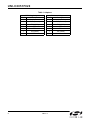
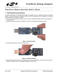
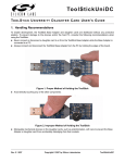
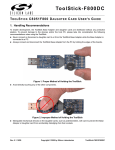
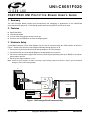
U NI - C8 0 5 1 F020 C8051F020 UNI P ROTOTYPE B OARD U SER ’ S G UIDE 1. Summary The UNI Prototype Board provides easy development and debugging of applications on the C8051F020 microcontroller through use of a JTAG debug header and direct through-hole access to each pin. 2. Features C8051F020 MCU JTAG debug header 0.1-inch center through-hole access to each pin Access to VDD and DGND for an external voltage supplier 3. Hardware Setup A USB Debug Adapter or EC2 Serial Adapter may be used to connect through the JTAG interface as shown in Figure 1. Power to the device must be supplied externally through pin VDD on J6. 1. Connect the 10-pin ribbon cable from the debug adapter to the JTAG interface. 2. Connect the other end of the debug adapter to the appropriate port on the PC. 3. Connect an external power supply to the device by connecting the grounding cable to pin DGND on J6 and the power cable to pin VDD. 4. Set the power supply voltage to +3.3 V. Note: Ensure the power supply is off when connecting or disconnecting cables to the device in order to prevent accidental damage to device and/or debug adapter. PC Power Silicon Laboratories USB DEBUG ADAPTER Run Stop Variable Power Supply (1 Amp Max) USB Debug Adapter J1 DEBUG UNI PROTO BD J6 DGND VDD U1 C8051 F020 3.3V SILICON LABS Figure 1. UNI Prototype Board Hardware Setup Rev. 0.1 11/08 Copyright © 2008 by Silicon Laboratories UNI-C8051020 UNI-C8051F020 Table 1. Adapters USB Debug Adapter 2 Pin # Description EC2 Serial Adapter Pin # Description 1,8 Not Connected 1 3.0 to 3.6 VDC Input 2,3,9 GND (Ground) 2,3,9 GND (Ground) 4 TCK (C2D) 4 TCK (C2D) 5 TMS 5 TMS 6 TDO 6 TDO 7 TDI (C2CK) 7 TDI (C2CK) 10 USB Power 8,10 Not Connected Rev. 0.1 UNI-C8051F020 NOTES: Rev. 0.1 3 UNI-C8051F020 CONTACT INFORMATION Silicon Laboratories Inc. 400 West Cesar Chavez Austin, TX 78701 Tel: 1+(512) 416-8500 Fax: 1+(512) 416-9669 Toll Free: 1+(877) 444-3032 Email: [email protected] Internet: www.silabs.com The information in this document is believed to be accurate in all respects at the time of publication but is subject to change without notice. Silicon Laboratories assumes no responsibility for errors and omissions, and disclaims responsibility for any consequences resulting from the use of information included herein. Additionally, Silicon Laboratories assumes no responsibility for the functioning of undescribed features or parameters. Silicon Laboratories reserves the right to make changes without further notice. Silicon Laboratories makes no warranty, representation or guarantee regarding the suitability of its products for any particular purpose, nor does Silicon Laboratories assume any liability arising out of the application or use of any product or circuit, and specifically disclaims any and all liability, including without limitation consequential or incidental damages. Silicon Laboratories products are not designed, intended, or authorized for use in applications intended to support or sustain life, or for any other application in which the failure of the Silicon Laboratories product could create a situation where personal injury or death may occur. Should Buyer purchase or use Silicon Laboratories products for any such unintended or unauthorized application, Buyer shall indemnify and hold Silicon Laboratories harmless against all claims and damages. Silicon Laboratories and Silicon Labs are trademarks of Silicon Laboratories Inc. Other products or brandnames mentioned herein are trademarks or registered trademarks of their respective holders. 4 Rev. 0.1