1
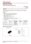
HD74LV1GWU04A
Dual Unbuffer Inverter
REJ03D0074-0200
Rev.2.00
May 19, 2006
Description
The HD74LV1GW04A has dual inverter in a 6 pin package. Low voltage and high-speed operation is suitable for the
battery powered products (e.g., notebook computers), and the low power consumption extends the battery life.
Features
• The basic gate function is lined up as Renesas uni logic series.
• Supplied on emboss taping for high-speed automatic mounting.
• Electrical characteristics equivalent to the HD74LV04A
Supply voltage range : 1.65 to 5.5 V
Operating temperature range : –40 to +85°C
• All inputs VIH (Max.) = 5.5 V (@VCC = 0 V to 5.5 V)
All outputs VO (Max.) = 5.5 V (@VCC = 0 V)
• Output current ±6 mA (@VCC = 3.0 V to 3.6 V), ±12 mA (@VCC = 4.5 V to 5.5 V)
• All the logical input has hysteresis voltage for the slow transition.
• Ordering Information
Part Name
Package Type
HD74LV1GWU04ACME CMPAK-6 pin
Package Code
(Previous Code)
PTSP0006JA-A
(CMPAK-6V)
Package
Abbreviation
Taping Abbreviation
(Quantity)
CM
E (3,000 pcs / Reel)
Outline and Article Indication
• HD74LV1GWU04A
Index band
Marking
W 6
CMPAK–6
= Control code
Function Table
Input A
H
L
H : High level
L : Low level
Rev.2.00, May 19, 2006 page 1 of 5
Output Y
L
H
HD74LV1GWU04A
Pin Arrangement
1A
1
6
1Y
GND
2
5
VCC
2A
3
4
2Y
(Top view)
Absolute Maximum Ratings
Item
Symbol
Ratings
Unit
VCC
VI
VO
IIK
IOK
IO
–0.5 to 7.0
–0.5 to 7.0
–0.5 to VCC + 0.5
–20
±50
±25
V
V
V
mA
mA
mA
ICC or IGND
±50
mA
PT
200
mW
Tstg
–65 to 150
°C
Supply voltage range
Input voltage range *1
Output voltage range *1, 2
Input clamp current
Output clamp current
Continuous output current
Continuous current through
VCC or GND
Maximum power dissipation
*3
at Ta = 25°C (in still air)
Storage temperature
Notes:
Test Conditions
Output : H or L
VI < 0
VO < 0 or VO > VCC
VO = 0 to VCC
The absolute maximum ratings are values, which must not individually be exceeded, and furthermore no two
of which may be realized at the same time.
1. The input and output voltage ratings may be exceeded if the input and output clamp-current ratings are
observed.
2. This value is limited to 5.5 V maximum.
3. The maximum package power dissipation was calculated using a junction temperature of 150°C.
Recommended Operating Conditions
Item
Supply voltage range
Input voltage range
Output voltage range
Symbol
VCC
VI
VO
IOL
Output current
IOH
Operating free-air temperature
Ta
Min
1.65
0
0
—
—
—
—
—
—
—
Max
5.5
5.5
VCC
1
2
6
12
–1
–2
–6
—
–40
–12
85
Note: Unused or floating inputs must be held high or low.
Rev.2.00, May 19, 2006 page 2 of 5
Unit
V
V
V
mA
°C
Conditions
VCC = 1.65 to 1.95 V
VCC = 2.3 to 2.7 V
VCC = 3.0 to 3.6 V
VCC = 4.5 to 5.5 V
VCC = 1.65 to 1.95 V
VCC = 2.3 to 2.7 V
VCC = 3.0 to 3.6 V
VCC = 4.5 to 5.5 V
HD74LV1GWU04A
Electrical Characteristic
• Ta = –40 to 85°C
Item
Symbol
VIH
Input voltage
VIL
VOH
Output voltage
VOL
Input current
IIN
VCC (V) *
1.65 to 1.95
2.3 to 2.7
3.0 to 3.6
4.5 to 5.5
1.65 to 1.95
2.3 to 2.7
3.0 to 3.6
4.5 to 5.5
Min to Max
1.65
2.3
3.0
Min
VCC×0.85
VCC×0.8
VCC×0.8
VCC×0.8
—
—
—
—
VCC–0.1
1.4
2.0
2.48
Typ
—
—
—
—
—
—
—
—
—
—
—
—
Max
—
—
—
—
VCC×0.15
VCC×0.2
VCC×0.2
VCC×0.2
—
—
—
—
Unit
Test condition
4.5
Min to Max
1.65
3.8
—
—
—
—
—
—
0.1
0.3
2.3
3.0
—
—
—
—
0.4
0.44
IOL = 2 mA
IOL = 6 mA
4.5
0 to 5.5
—
—
—
—
0.55
±1
IOL = 12 mA
VIN = 5.5 V or GND
V
V
µA
IOH = –50 µA
IOH = –1 mA
IOH = –2 mA
IOH = –6 mA
IOH = –12 mA
IOL = 50 µA
IOL = 1 mA
Quiescent
VIN = VCC or GND,
ICC
5.5
—
—
10
µA
supply current
IO = 0
Input capacitance
CIN
3.3
—
4.0
—
pF
VIN = VCC or GND
Note: For conditions shown as Min or Max, use the appropriate values under recommended operating conditions.
Rev.2.00, May 19, 2006 page 3 of 5
HD74LV1GWU04A
Switching Characteristics
• VCC = 1.8 ± 0.15 V
Item
Symbol
Propagation
delay time
tPLH
tPHL
Ta = 25°C
Min
Typ
Max
—
8.0
15.0
—
15.2
24.0
Ta = –40 to 85°C
Ta = 25°C
Typ
Max
6.0
10.9
9.5
13.4
Ta = –40 to 85°C
Ta = 25°C
Ta = –40 to 85°C
Min
1.0
1.0
Max
18.0
27.0
Test
Conditions
Unit
CL = 15 pF
CL = 50 pF
ns
FROM
(Input)
TO
(Output)
A
Y
FROM
(Input)
TO
(Output)
A
Y
FROM
(Input)
TO
(Output)
A
Y
FROM
(Input)
TO
(Output)
A
Y
• VCC = 2.5 ± 0.2 V
Item
Symbol
Propagation
delay time
tPLH
tPHL
Min
—
—
Min
1.0
1.0
Max
14.0
16.0
Test
Conditions
Unit
CL = 15 pF
CL = 50 pF
ns
• VCC = 3.3 ± 0.3 V
Item
Symbol
Propagation
delay time
tPLH
tPHL
Min
—
—
Typ
5.0
7.5
Max
8.9
11.4
Min
1.0
1.0
Max
10.5
13.0
Test
Conditions
Unit
CL = 15 pF
CL = 50 pF
ns
• VCC = 5.0 ± 0.5 V
Item
Symbol
Propagation
delay time
Min
Ta = 25°C
Typ
Max
—
—
tPLH
tPHL
3.5
5.0
5.5
7.0
Ta = –40 to 85°C
Min
Max
1.0
1.0
6.5
8.0
Test
Conditions
Unit
CL = 15 pF
CL = 50 pF
ns
Operating Characteristics
• CL = 50 Pf
Item
Power dissipation
capacitance
Symbol VCC (V)
CPD
3.3
5.0
Min
Ta = 25°C
Typ
Max
—
—
4.0
5.0
—
—
Unit
Test Conditions
pF
f = 10 MHz
Test Circuit
VCC
Pulse
generator
Output
Input
50 Ω
Note: CL includes probe and jig capacitance.
Rev.2.00, May 19, 2006 page 4 of 5
CL
HD74LV1GWU04A
• Waveforms
tr
tf
90%
50%
Input
VCC
90%
50%
10%
10%
GND
VOH
50%
Output
50%
VOL
t PLH
t PHL
Notes: 1. Input waveform : PRR ≤ 1 MHz, Zo = 50 Ω, tr ≤ 3 ns, tf ≤ 3 ns.
2. The output are measured one at a time with one transition per measurement.
Package Dimensions
JEITA Package Code
SC-88
Package Name
CMPAK-6
RENESAS Code
PTSP0006JA-A
D
Previous Code
CMPAK-6 / CMPAK-6V
MASS[Typ.]
0.006g
A
e
Q
c
E
HE
LP
L
A
A
x M
L1
S
A
A3
b
Reference
Symbol
e
A2
y S
A
A1
S
e1
b
l1
c
b2
A-A Section
Rev.2.00, May 19, 2006 page 5 of 5
Pattern of terminal position areas
A
A1
A2
A3
b
c
D
E
e
HE
L
L1
LP
x
y
b2
e1
l1
Q
Dimension in Millimeters
Min
0.8
0
0.8
0.15
0.1
1.8
1.15
2.0
0.3
0.1
0.2
Nom
0.9
0.25
0.2
0.15
2.0
1.25
0.65
2.1
Max
1.1
0.1
1.0
0.25
0.25
2.2
1.35
2.2
0.7
0.5
0.6
0.05
0.05
0.35
1.5
0.9
0.25
Sales Strategic Planning Div.
Nippon Bldg., 2-6-2, Ohte-machi, Chiyoda-ku, Tokyo 100-0004, Japan
Keep safety first in your circuit designs!
1. Renesas Technology Corp. puts the maximum effort into making semiconductor products better and more reliable, but there is always the possibility that trouble
may occur with them. Trouble with semiconductors may lead to personal injury, fire or property damage.
Remember to give due consideration to safety when making your circuit designs, with appropriate measures such as (i) placement of substitutive, auxiliary
circuits, (ii) use of nonflammable material or (iii) prevention against any malfunction or mishap.
Notes regarding these materials
1. These materials are intended as a reference to assist our customers in the selection of the Renesas Technology Corp. product best suited to the customer's
application; they do not convey any license under any intellectual property rights, or any other rights, belonging to Renesas Technology Corp. or a third party.
2. Renesas Technology Corp. assumes no responsibility for any damage, or infringement of any third-party's rights, originating in the use of any product data,
diagrams, charts, programs, algorithms, or circuit application examples contained in these materials.
3. All information contained in these materials, including product data, diagrams, charts, programs and algorithms represents information on products at the time of
publication of these materials, and are subject to change by Renesas Technology Corp. without notice due to product improvements or other reasons. It is
therefore recommended that customers contact Renesas Technology Corp. or an authorized Renesas Technology Corp. product distributor for the latest product
information before purchasing a product listed herein.
The information described here may contain technical inaccuracies or typographical errors.
Renesas Technology Corp. assumes no responsibility for any damage, liability, or other loss rising from these inaccuracies or errors.
Please also pay attention to information published by Renesas Technology Corp. by various means, including the Renesas Technology Corp. Semiconductor
home page (http://www.renesas.com).
4. When using any or all of the information contained in these materials, including product data, diagrams, charts, programs, and algorithms, please be sure to
evaluate all information as a total system before making a final decision on the applicability of the information and products. Renesas Technology Corp. assumes
no responsibility for any damage, liability or other loss resulting from the information contained herein.
5. Renesas Technology Corp. semiconductors are not designed or manufactured for use in a device or system that is used under circumstances in which human life
is potentially at stake. Please contact Renesas Technology Corp. or an authorized Renesas Technology Corp. product distributor when considering the use of a
product contained herein for any specific purposes, such as apparatus or systems for transportation, vehicular, medical, aerospace, nuclear, or undersea repeater
use.
6. The prior written approval of Renesas Technology Corp. is necessary to reprint or reproduce in whole or in part these materials.
7. If these products or technologies are subject to the Japanese export control restrictions, they must be exported under a license from the Japanese government and
cannot be imported into a country other than the approved destination.
Any diversion or reexport contrary to the export control laws and regulations of Japan and/or the country of destination is prohibited.
8. Please contact Renesas Technology Corp. for further details on these materials or the products contained therein.
http://www.renesas.com
RENESAS SALES OFFICES
Refer to "http://www.renesas.com/en/network" for the latest and detailed information.
Renesas Technology America, Inc.
450 Holger Way, San Jose, CA 95134-1368, U.S.A
Tel: <1> (408) 382-7500, Fax: <1> (408) 382-7501
Renesas Technology Europe Limited
Dukes Meadow, Millboard Road, Bourne End, Buckinghamshire, SL8 5FH, U.K.
Tel: <44> (1628) 585-100, Fax: <44> (1628) 585-900
Renesas Technology (Shanghai) Co., Ltd.
Unit 204, 205, AZIACenter, No.1233 Lujiazui Ring Rd, Pudong District, Shanghai, China 200120
Tel: <86> (21) 5877-1818, Fax: <86> (21) 6887-7898
Renesas Technology Hong Kong Ltd.
7th Floor, North Tower, World Finance Centre, Harbour City, 1 Canton Road, Tsimshatsui, Kowloon, Hong Kong
Tel: <852> 2265-6688, Fax: <852> 2730-6071
Renesas Technology Taiwan Co., Ltd.
10th Floor, No.99, Fushing North Road, Taipei, Taiwan
Tel: <886> (2) 2715-2888, Fax: <886> (2) 2713-2999
Renesas Technology Singapore Pte. Ltd.
1 Harbour Front Avenue, #06-10, Keppel Bay Tower, Singapore 098632
Tel: <65> 6213-0200, Fax: <65> 6278-8001
Renesas Technology Korea Co., Ltd.
Kukje Center Bldg. 18th Fl., 191, 2-ka, Hangang-ro, Yongsan-ku, Seoul 140-702, Korea
Tel: <82> (2) 796-3115, Fax: <82> (2) 796-2145
Renesas Technology Malaysia Sdn. Bhd
Unit 906, Block B, Menara Amcorp, Amcorp Trade Centre, No.18, Jalan Persiaran Barat, 46050 Petaling Jaya, Selangor Darul Ehsan, Malaysia
Tel: <603> 7955-9390, Fax: <603> 7955-9510
© 2006. Renesas Technology Corp., All rights reserved. Printed in Japan.
Colophon .6.0