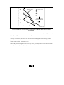
1
Surface Mount Package User’s Manual ADE-810-007C Rev. 4.0 3/15/02 Hitachi Ltd. Cautions 1. Hitachi neither warrants nor grants licenses of any rights of Hitachi’s or any third party’s patent, copyright, trademark, or other intellectual property rights for information contained in this document. Hitachi bears no responsibility for problems that may arise with third party’s rights, including intellectual property rights, in connection with use of the information contained in this document. 2. Products and product specifications may be subject to change without notice. Confirm that you have received the latest product standards or specifications before final design, purchase or use. 3. Hitachi makes every attempt to ensure that its products are of high quality and reliability. However, contact Hitachi’s sales office before using the product in an application that demands especially high quality and reliability or where its failure or malfunction may directly threaten human life or cause risk of bodily injury, such as aerospace, aeronautics, nuclear power, combustion control, transportation, traffic, safety equipment or medical equipment for life support. 4. Design your application so that the product is used within the ranges guaranteed by Hitachi particularly for maximum rating, operating supply voltage range, heat radiation characteristics, installation conditions and other characteristics. Hitachi bears no responsibility for failure or damage when used beyond the guaranteed ranges. Even within the guaranteed ranges, consider normally foreseeable failure rates or failure modes in semiconductor devices and employ systemic measures such as fail-safes, so that the equipment incorporating Hitachi product does not cause bodily injury, fire or other consequential damage due to operation of the Hitachi product. 5. This product is not designed to be radiation resistant. 6. No one is permitted to reproduce or duplicate, in any form, the whole or part of this document without written approval from Hitachi. 7. Contact Hitachi’s sales office for any questions regarding this document or Hitachi semiconductor products. Contents Section 1 Types of Package Mounting Configurations ............................................. 1 Section 2 Surface Mount Package Assembly Process Flow .................................... 3 3 2.1 Basic Assembly Process Flow for Surface Mount Packages ............................................. Section 3 Overview of the Individual Steps in the Assembly Process ................. 3.1 3.2 3.3 3.4 3.5 3.6 3.7 3.8 Designing the Printed Wiring Board and the Mounting Pad.............................................. 3.1.1 Printed Wiring Board Material.............................................................................. 3.1.2 Mounting Pads ...................................................................................................... Solder Application.............................................................................................................. 3.2.1 Solder Paste ........................................................................................................... 3.2.2 Applying the Solder Paste ..................................................................................... 3.2.3 Amount of Printed Solder Paste............................................................................ Temporary Adhesive .......................................................................................................... 3.3.1 Adhesive Strength ................................................................................................. 3.3.2 Curing Conditions ................................................................................................. 3.3.3 Amount of Adhesive Applied (Height) ................................................................. Mounting (Placement)........................................................................................................ 3.4.1 Mounting Process.................................................................................................. 3.4.2 Selecting the Mounter ........................................................................................... 3.4.3 Mounting Accuracy............................................................................................... 3.4.4 Shapes of the Package Packing ............................................................................. Soldering ............................................................................................................................ 3.5.1 Soldering Methods ................................................................................................ 3.5.2 Overview of Various Soldering Methods.............................................................. 3.5.3 Setting the Soldering Temperature Profile............................................................ 3.5.4 Soldering Methods for Various Surface Mount Packages .................................... 3.5.5 Soldering Conditions............................................................................................. Cleaning.............................................................................................................................. 3.6.1 Selecting the Cleaning Solution ............................................................................ 3.6.2 Cleaning Methods ................................................................................................. 3.6.3 Cleaning Conditions.............................................................................................. 3.6.4 Determining the Cleanliness ................................................................................. 3.6.5 Other Notes and Cautions ..................................................................................... Inspection ........................................................................................................................... 3.7.1 Inspection Equipment............................................................................................ 3.7.2 Subject of Inspections ........................................................................................... Storage................................................................................................................................ 3.8.1 Moisture-proof Packing ........................................................................................ 5 5 5 10 20 20 25 31 33 34 35 36 37 37 39 40 40 44 44 46 52 55 56 63 63 64 65 65 65 66 66 68 72 72 i 3.9 3.8.2 Storage Before the Moisture-proof Bag is Opened ............................................... 3.8.3 Storage and Handling After the Moisture-proof Bag is Opened........................... 3.8.4 Storage and Handling Without Moisture-proof Packing ...................................... 3.8.5 Baking Process ...................................................................................................... Notes and Cautions During the Mounting Process ............................................................ 3.9.1 Damage from Static Electricity ............................................................................. 3.9.2 Notes and Cautions Before Performing the Reflow Soldering ............................. 3.9.3 Discerning the Package Crack .............................................................................. 3.9.4 Importance to Measures to Deal with Mechanical Stress ..................................... 73 73 74 74 76 76 79 83 85 Section 4 Examples of BGA Assembly Evaluations.................................................. 87 4.1 4.2 4.3 4.4 4.5 4.6 4.7 4.8 ii Assembly Process Flow...................................................................................................... Mounting Pad Design ......................................................................................................... Applying the Solder Paste .................................................................................................. 4.3.1 Solder Paste ........................................................................................................... 4.3.2 Solder Printing Stencil .......................................................................................... 4.3.3 Allowable Mounting Misalignment ...................................................................... Reflow Soldering Conditions ............................................................................................. Inspecting the Solder Joints After Mounting on the Printed Wiring Board ....................... Removing Method.............................................................................................................. Cleaning.............................................................................................................................. Storage................................................................................................................................ 87 88 89 89 89 89 90 91 92 93 94 Section 1 Types of Package Mounting Configurations Package mounting configurations may include surface mounting and mixed mounting. The forms of the various mounting approaches are as shown in Figure 1.1. Because only surface mount devices can be used in double-sided surface mounting, the double-sided surface mounting method provides the highest mounting density. Insertion devices and surface mount devices are both used in mixed mounting. A flow soldering process is used for the insertion devices. Application of solder paste Solder paste Application of solder paste Solder paste Printed wiring board Surface mount package mounting Printed wiring board Surface mount package mounting Soldering (reflow) Reflow (a) Single-sided surface mounting (reflow) Insertion of insertion- type package Soldering (flow soldering) Solder (b) Single-sided mixed mounting: Surface mount + insertion mount (reflow) + (flow soldering) Application of solder paste Solder paste Application of solder paste Printed wiring board Printed wiring board Surface mount package mounting Surface mount package mounting Soldering (reflow) Reflow The board is turned over The board is turned over Solder paste Solder paste Application of solder paste Application of temporary adhesive Surface mount package mounting Surface mount package mounting Adhesive Ultraviolet rays Soldering (reflow) Adhesive cure (c) Double-sided surface mounting: Surface mount + surface mount (reflow) + (reflow) The board is turned over Insertion of insertion- type package Soldering (flow soldering) Solder (d) Double-sided mixed mounting: Surface mount + surface mount/insertion mount (reflow) + (batch flow soldering) Figure 1.1 Types of Surface Mount Package Mounting Configurations 1 2 Section 2 Surface Mount Package Assembly Process Flow 2.1 Basic Assembly Process Flow for Surface Mount Packages Figure 2.1 shows the basic assembly process flow for surface mount packages. First a solder paste is applied to the mounting pads on the printed wiring board and the devices are placed thereon, and then soldered. References Printed wiring board 3.1 P.5 to 3.2.1 P.20 to 3.2.2 3.2.3 P.25 to 3.4 P.37 to 3.3 P.33 to 3.5 P.44 Cleaning 3.6 P.65 Inspection 3.7 P.68 Solder paste Application of solder paste LSI packages Mounting Application of temporary adhesive Soldering Heating Camera LED HITACHI Figure 2.1 Basic Assembly Process Flow for Surface Mount Packages 3 When simultaneous reflow for double-sided surface mounting or flow soldering is performed, a temporary adhesive is used to affix the devices to the printed wiring board before the soldering is performed. A cleaning process is performed to remove the residual flux, etc., after the soldering process is performed, after which an inspection is performed. A baking process is performed before the soldering when a moisture-removal treatment is required when a plastic package is used. See the references in Figure 2.1 for details about the various steps in the assembly process. 4 Section 3 Overview of the Individual Steps in the Assembly Process 3.1 Designing the Printed Wiring Board and the Mounting Pad In surface mount assembly, the materials from which the printed wiring board is manufactured and the design of the mounting pads have an effect on the manufacturability and on the solder joint reliability. The section below will discuss the selection of the materials from which to manufacture the printed wiring boards and the design standards for mounting pads. 3.1.1 Printed Wiring Board Material Although there are many different types of printed wiring boards, these printed wiring boards basically fall into one of two broad categories: boards made from organic materials and boards made from inorganic materials. (See Figure 3.1.) Printed wiring boards made from organic materials are the most commonly used today, and copper-clad laminate boards are the most common. Table 3.1 describes the types of copper-clad laminate boards, and their primary characteristics and applications. Because the various board materials can be categorized by the specific applications, the materials should be selected after taking required electrical characteristics, thermal dissipation characteristics, thermal durability, mechanical characteristics, reliability, and so forth into account. Table 3.2 shows the types of printed wiring boards used most commonly in the consumer and industrial uses. 5 Figure 3.1 Types of Printed Wiring Board Materials 6 Materials for Printed Wiring Boards Ceramic base Printed Wiring Board Metal base Printed Wiring Board High heat resistant Thermoplastics Printed Wiring Board Flexible Copperclad Laminate Composite materials base Copper-clad Laminate Glass Fabric/Glass Mat base Polyester-resin Copper-clad Laminate (FR6) Glass Fabric/Paper base Epoxy-resin Copper-clad Laminate (CEM1) Glass Fabric/Glass Mat base Epoxy-resin Copper-clad Laminate (CEM3) Alumina base Printed Wiring Board Aluminium nitride base Printed Wiring Board Silicon nitride base Printed Wiring Board Silicon carbide base Printed Wiring Board Metal core Metal base Enamel Polysulfone-resin Polyetherimide-resin Polyetherketon-resin Polyester-resin Flexible Copper-clad Laminate Polyimid-resin Flexible Copper-clad Laminate Glass Fabric base Epoxy-resin Flexible Copper-clad Laminate Rigid-Flexible Multilayer Polyester-resin Copper-clad Laminated Epoxy-resin Copper-clad Laminate Glass fabric base Epoxy-resin Copper-clad Laminate (FR4, G10) Glass fabric base High heat resistant Epoxy-resin Copper-clad Laminate (FR5, G11) Glass Fabric base Polyimid-resin Copper-clad Laminate (GPY) Glass Fabric base Fluorocarbon polymer Copper-clad Laminate Materials for Multilayer Printed Wiring Board [Prepreg/Thin Copper-clad Laminate] (FR4, FR5, GPY) Paper base Phenolic-resin Copper-clad Laminate (FR1, FR2, XXXpc, Xpc) Paper base Epoxy-resin Copper-clad Laminate (FR3) Paper base Polyester-resin Copper-clad Laminate (Source: "Mr. Masamitsu Aoki, Toshiba Chemicals, "Issues in Selecting PWB," Surface Mount Technology, December, 1995, pg. 6 - 13. Inorganic Materials Organic Materials Glass Fabric base Copperclad Laminate Paper base Copper-clad Laminate Film Adhesive Copper layer Flexibility, low price Flexibility, high thermal durability Consumer electronics (calculators) Industrial electronics (office automation equipment), Consumer electronics (cameras, CD players) Satellite communications, computers, space/military demand, instruments. Low dielectric constant, high insulation Copper layer Fluorine Epoxy-type adhesive material Computers, semiconductor test equipment High insulation, strong, high reliability Glass fabric + resin Polyimide Industrial electronics (office automation equipment, etc.), Thin consumer electronics (calculators, etc.) Consumer electronics (TVs, bicycles, toys, etc.) Consumer electronics (8 mm video, video camera, CD players, etc.) Industrial electronics (office automation equipment, factory automation equipment, etc.) Industrial electronics (office automation equipment, etc.) Consumer electronics (toys, etc.) Consumer electronics (VTR, TV, Audio/visual, etc.) Consumer electronics (office automation equipment, tuners, etc.) Consumer electronics (audio/visual, etc.) Applications High insulation, strong, high dimensional stability. Strong Through-hole plating is possible. High insulation Good in punch processes Excellent insulation Good in punch processes Good in punch processes Good tracking resistance Superior manufacturability Good in punch processes Good in punch processes Through-hole plating is possible. Characteristics Copper layer Glass fabric + resin or glass mat Glass fabric + resin Copper layer Glass fabric + resin Copper layer Copper layer Glass fabric + resin Paper + resin Glass fabric + resin Copper layer Paper + Resin Copper layer with adhesive Structure Epoxy Polyester Epoxy Epoxy Polyester Epoxy Phenol Resin (Source: "Mr. Masamitsu Aoki, Toshiba Chemicals, "Issues in Selecting PWB," Surface Mount Technology, December, 1995, pg. 6 - 13. Polyester Polyimide Glass fabric Glass fabric Glass mat Glass paper Glass fabric Paper Paper Base Material GPY FR-5, FR-4 G-11, G-10 FR-6 CEM-3 CEM-1 FR-3 FR-2, XXXpc FR-1, Xpc NEMA (ANSI) Grade There is also the 2-layer FPC. May also be constructed with multiple layers Sometimes uses a copper layer with adhesive. Also found in multilayer boards (there are some thickness constraints). Notes Table 3.1 Types of Copper-clad Laminate Board’ and Their Primary Characteristics and Applications 7 Table 3.2 Characteristics of the Various Types of Resin Laminate Boards Material Characteristics Material Structure Glass Coefficient Transition of Thermal Tensile Tempe- Expansion Thermal Strength rature (XY) Conductivity (XY) Units (°C) (PPM/°C) (W/M°C) (PSI × 10 –6 ) (—) Glass Epoxy (FR-4) 125 14-18 0.16 2.5 High Tg Glass Epoxy (New FR-5) 194 8-9 — — Glass Polyimide 250 12-16 0.35 Aramid-based Epoxy 125 6-8 Aramid-based Polyimide 250 Dielectric Constant (1 MHz) Coefficient Volume Surface of Water Resistivity Resistance Absorption (Ω/cm) (Ω) (%) 4.8 10 12 10 13 0.10 5.1 10 15 10 14 0.11 4.8 4.8 10 14 10 13 0.35 0.12 4.4 3.9 10 16 10 16 0.85 5-8 TBD 4.0 3.6 10 12 10 12 1.50 20 0.26 0.2 2.3 10 10 10 11 1.10 — 5 to 7 21.0 44.0 8.0 10 14 TBD TBD — Magnetic-coated Copper Laminate Alloy 6 to 7 TBD TBD TBD TBD TBD TBD Printed Wiring Board Glass-Teflon Laminate 75 Inorganic Materials Alumina-Beryllia (ceramic) Note: TBD: Variable, to be determined. When it comes to the reliability of solder joints, it is necessary to take into consideration the matching of the coefficient of thermal expansion with that of the package when selecting the materials. In the electronic circuits, LSI packages are soldered on the boards that have different coefficients of thermal expansion. (Figure 3.2 shows the coefficient of thermal expansion of various materials.) As is shown in Figure 3.3, changes in temperatures cause repetitive relative thermal displacements, which may cause the solder joints to crack and break. The thermal displacements ∆ is calculated as shown below, and is dependent on the difference in the coefficients in thermal expansion between the board and the package (∆α), the difference in temperature (∆T), and the package size . ∆ = ∆α × ∆T × ( /2) In the thin packages such as typified by TSOP (packages that are compatible with the recent demands for smaller and thinner devices), the percentage of the package body volume occupied by the silicon dies is increasing and the coefficient of thermal expansion of the overall package has become relatively small. In applications requiring high levels of reliability, the application of boards with low coefficients of thermal expansion (such as the new FR-5 in Table 3.2) are recommended because they are able to reduce the global mismatch of the coefficients of thermal expansion between the package and the board. 8 Coefficient of Thermal Expansion x 10–6/°C Device 100 High temperature solder 9/1, 95/5 50 Board Paper phenol (Y): In the Y direction Eutectic solder Paper phenol (X): In the X direction Resin (epoxy) Copper, silver 20 Glass epoxy (Y) Gold Glass epoxy (X) Glass 10 Alumina Kovar, alloy 42 5 SiC Si 3 1 Figure 3.2 Types of Electronic Materials for Surface Mount Assembly and Their Coefficients of Thermal Expansion Lead Resin Board Thermal displacement ∆ Lead ∆ = ∆α·∆ T·( /2) γ max Solder Shear strain γ Board QFP/SOP Figure 3.3 Structure of Minute Solder Joint and Thermal Shear Displacement (The dotted line represents the deformation by changes in temperature.) 9 3.1.2 Mounting Pads The geometry of the mounting pad is critical because of its influence on the soldering yield and the solder joint reliability. Examples of mounting pad design for various surface mount packages are given below. (Figures 3.4 to 3.15.) ; ;; ; ; ;; The optimum value for mounting pads depends on the board material, the solder paste material, the soldering method, and the precision of the equipment used. The actual design of the mounting pads must be suited to the circumstances. QFP (Including TQFP and LQFP) MID E or D e β2 β2 β1 α α e e β1 M IE = E + 2 α 2 = L + β1 + β2 MIE M ID = D + 2α H E (or HD) + 2 β2 2 b2 e L α : Ease of cleaning β1 : Solder joint strength β2 : Solder mask pattern accuracy and ease of solder inspection ( β2 =0.2 mm) 2 ≥ L + β1 + β2 b ≤ b2 ≤ e – r ( 2 : Mounting pad length) ( b 2: Mounting pad width) γ : Eliminating solder bridge L: Length of flat part of terminal, b: Terminal width Units: mm e α β1 β2 γ 1.0, 0.8, 0.65 0.2 or more 0.5 0.2 0.3 0.5 0.1 or more 0.2 to 0.3 0.2 0.25 0.4 0.2 0.3 0.2 0.2 0.3 0.2 0.3 0.2 0.15 (Reference values based on the former EIAJ standard ED-7404A.) Figure 3.4 Example of Mounting Pad Design for QFP (Including TQFP and LQFP) 10 ; ; ;;;; ;;; SOJ e1 e1 b2 2 1 e Units: mm 1.2 2.0 0.75 1 e 2 b2 (Reference values based on the former EIAJ standard ED-7406.) Figure 3.5 Example of Mounting Pad Design for SOJ QFJ (PLCC) e e1 E b e1 D or e1 E b2 e 1 2 e1 D Units: mm 1 2 b2 1.2 2.0 0.75 (Reference values based on the former EIAJ standard ED-7407.) Figure 3.6 Example of Mounting Pad Design for QFJ (PLCC) 11 QFN (LCC) e E e MD1 α e b2 MD2 D β b2 ME1 ME2 L b MD1 ≤ D – 2 × MD2 ≥ D + 2 × ME1 ≤ E – 2 × ME2 ≥ E + 2 × b ≤ b 2 ≤ e – L α L α β Units: mm α β (Reference values based on the former EIAJ standard ED-7412.) Figure 3.7 Example of Mounting Pad Design for QFN (LCC) 12 0.2 0.3 ; ; ; ;; ; ; SOP L b2 L 2 e1 e1 e b e e e β1 α e e e e Units: mm e β2 L e e1 α β 1 β 2 γ b2 2 Type 1 Type 2 Type 3 Type 4 Type 5 Type 6 225 mil (5.72) 300 mil (7.62) 375 mil (9.53) 450 mil (11.43) 525 mil (13.34) 600 mil (15.24) 0.2 or more 0.2 to 0.5 0.2 0.3 0.76 L + β1 + β2 (Reference values based on the former EIAJ standard ED-7402-1.) Figure 3.8 Example of Mounting Pad Design for SOP 13 ; ;; ; TSOP (I) MD D L L e e b2 e b 2 Units: mm β1 β2 L α α β 1 β 2 γ b2 2 0.1 to 0.2 0.2 to 0.3 0.2 0.25 ( e = 0.5) 0.25 ≥ L + β1 + β2 (Reference values based on the former EIAJ standard ED-7402-3.) Figure 3.9 Example of Mounting Pad Design for TSOP (I) 14 ;;; ; ;; ; ; TSOP (II) E ME e e b2 e b 2 β1 α β 1 β 2 γ β2 L 2 α b2 Units: mm 0.1 0.2 0.2 0.3 ≥ L + β1 + β2 b 2 to e – γ (Reference values based on the former EIAJ standard ED-7402-4A.) Figure 3.10 Example of Mounting Pad Design for TSOP (II) SOI e e1 2 Units: mm b2 2 e1 e 0.50 2.00 9.53 0.80 b2 Figure 3.11 Example of Mounting Pad Design for SOI 15 ;;;;;;;; ;;; ; ; ; ;; ;;;;;;;;;; ;;;;; Discrete Packages SMPAK 0.4 0.5 0.5 0.5 MFPAK 0.3 0.4 1.2 0.7 0.7 0.9 0.4 0.4 SMFPAK-6 0.7 1.4 0.45 0.45 0.5 0.4 CMPAK 0.65 CMPAK-4(T) 0.65 0.6 0.5 CMPAK-5(T) 0.65 0.3 0.6 0.6 2.6 0.8 0.65 CMPAK-6 1.9 0.8 0.6 0.6 0.8 0.8 1.9 0.8 0.8 0.5 0.8 0.65 0.65 0.65 CMFPAK-6 0.3 0.4 1.9 1.9 0.5 0.3 0.65 0.65 0.65 0.65 Figure 3.12 Example of Mounting Pad Design for Discrete Packages (1) Note: ‘(T)’ in CMPAK-4(T), CMPAK-5(T) indicates transistor packages. However, ‘(T)’ is omitted in each product’s document. The CMPAK mounting pads are suitable for both transistors and diodes. 16 ; ; ; ;; ;;;;;; ; ; ; ;; ; MPAK-4 MPAK 1.8 0.95 1.0 0.95 1.0 1.0 2.6 2.6 1.2 1.9 0.8 0.8 MPAK-5 MPAK-6 0.95 0.6 1.0 1.0 0.6 0.95 2.6 0.95 2.6 0.95 ;;; ; 1.9 TSOP-6 UPAK 2.0 2.6 45° 1.0 1.0 1.5 1.0 1.5 0.7 1.0 3.0 0.5 1.0 1.5 1.0 Figure 3.13 Example of Mounting Pad Design for Discrete Packages (2) Note: The MPAK and MPAK-5 mounting pads are suitable for both transistors and diodes. 17 ;;;;;;; ; ; ; ; ; ;;;;;;; LDPAK(S) DPAK(S) 11.2 5.5 10.5 13.7 8.8 1.0 1.0 1.5 2.5 6.0 4.0 8.8 2.5 2.5 2.0 2.0 2.0 2.0 2.54 2.54 2.3 LFPAK 2.3 LLD 1.6 4.57 2.2 1.2 7.04 5.04 1.2 1.5 SRP 1.52 0.76 1.5 2.0 1.5 1.27 4.57 0.8 URP 0.8 1.5 0.8 Figure 3.14 Example of Mounting Pad Design for Discrete Packages (3) 18 ; ;;;;;;;;;;; ;;;;;;; ; ; UFP SFP MOP 2.6 0.8 φ0.5 1.4 1.0 CMPAK-5(D) 1.9 1.3 0.65 0.65 0.4 0.7 0.8 0.6 1.0 1.9 CMPAK-4(D) 0.8 1.27 0.6 1.1 0.6 1.3 VSON-5 0.5 1.35 0.5 0.45 0.3 1.0 Figure 3.15 Example of Mounting Pad Design for Discrete Packages (4) Note: ‘(D)’ in CMPAK-4(D), CMPAK-5(D) indicates diode packages. However, ‘(D)’ is omitted in each product’s document. 19 3.2 Solder Application As the lead pitch for surface mount packages has become narrower, the application process of solder paste has come to have a great influence on the stability of soldering qualities (yield and reliability). By optimizing the following elements of the application process of solder paste, it is possible to stabilize the quality of the soldering. • Solder paste materials • Printing mask for the solder paste application • Application equipment of solder paste (printer or dispenser) 3.2.1 Solder Paste (1) Structure of the Material Solder paste consists of solder powder, flux, etc. (a) Solder Powder As lead pitches have become narrower, solder powder has undergone a sequential miniaturization from irregular shape to spherical shape, to fine spherical shape. At present, the spherical shape solder is used the most in surface mounting applications. Figure 3.16 shows a comparison of solder powder shapes. Figure 3.17 shows the relationship between the size of the solder powder grains and the paste-printing mask opening dimensions. Generally, excellent printing results can be obtained when the powder grain diameter is less than about 1/7 of the printing mask opening width, and less than about 1/5 of the thickness of the printing mask. Generally the printing mask opening dimension, when used with a 0.5 mm lead pitch QFP, is approximately 0.25 mm, and the solder powder average grain diameter is about 0.03 mm (30 µm). 20 Shape of Solder Powder Diameter of Solder Powder Grain Lead Pitch Compatibility 53 to 75 µm 25 to 38 µm 15 to 25 µm 0.65 mm and above 0.5 to 0.4 mm 0.3 mm Figure 3.16 Shape of Solder Powder Average solder powder grain diameter (µm) (Materials provided by Senju Metal Industry Co., Ltd.) 150 100 50 25 0 W 0.15 mm 0.25 mm 0.35 mm (Printing mask opening width) Corresponding lead pitch 0.3 mm 0.5 mm 0.65 mm 0.76 mm 1.27 mm Figure 3.17 Relationship Between the Printing Mask Opening Width and the Average Solder Powder Grain Diameter Table 3.3 shows the types of solder alloys that are used for the primary solder pastes. 21 Table 3.3 Types of Solder Alloys Used in Major Solder Pastes Type Alloy Composition Eutectic solder 63Sn-37Pb The melting temperature is low (183°C), General and thus there is little thermal impact on the electronic components. Silver bearing solder 62Sn-36Pb-2Ag • Solder joint strength is stronger and has superior life expectancy. • Prevents the silver scavenging phenomenon.* Lead-free Sn-Ag solder Characteristics Sn-3.0Ag-0.5Cu, • etc. • • Notes: * 22 Application Ag electrodes, Ag patterns. High soldering temperature General High solder bulk strength Lead-free mounting Higher creep strength than Sn-Pb eutectic solder When applying solder to metal surfaces that include Ag (such as Ag conductors and Ag pads), this is a phenomenon where the Ag from the material being soldered diffuses into the solder. (Materials provided by Senju Metal Industry Co., Ltd.) (b) Flux The flux used in the solder paste performs functions such as preventing reoxidization, cleaning the surface, providing adhesion, etc. The compositional structure of the flux is as shown in Table 3.4. Generally halogen is included in activator. After the solder is applied, then when there is residual activator (i.e. where this activator contains halogen, etc.) on the devices or the board, then there will be an impact of reliability. Consequently, regulations should be put in place and enforced regarding cleaning the boards. Evaluate the cleanliness of the boards after considering the cleaning conditions when selecting the flux. Table 3.5 shows the recommended values based on the MIL standards for the cleanliness of the board after devices are mounted. Table 3.4 Structural Components of the Flux and Flux Functions Structure Function Composition Resin To prevent reoxidization. Natural or Modified rosin. To reduce surface tension. (WW rosin, Polymerized rosin, Hydrogenated rosin, Disproportionated rosin) To provide adhesion. Activating Component To provide a surface cleaning effect. Amine hydrohalide salts. (Etylamine hydrobromide, Aniline hydrocloride, etc.) Organic acids (stearic acid, sebacic acid, etc.) Supplementary Components To supplement the functions. Slump prevention material, adhesive material, etc. Thixotropic Agent To prevent separation. Hardened caster oil, etc. Solvent To regulate the viscosity. Butyl carbitol To provide adhesion. Terpineol Materials provided by: Senju Metal Industry Co., Ltd. 23 Table 3.5 Cleanliness of the Boards after the Devices Have Been Mounted (Converted values from the MIL-P-28809A specified values) Cleanliness of the printed wiring board after cleaning. Item Standard Amount of residual Cl. 1 µ g/cm 2, or less The resistivity of the extracted solvent (after extraction). 2 × 10 6 Ω · cm, or more Notes: 1. Board Area: Both sides of the printed wiring board plus the surface area of the devices mounted thereon. 2. Extraction Solvent: Isopropyl alcohol (75% by volume) plus H 2O (25% by volume). (Before Extraction) (The extracted solvent resistance is 6 × 10 6 Ω·cm or more.) 3. Extraction Method: Rinse both sides of the printed wiring board with 10 ml/2.54 × 2.54 cm2 for at least 1 minute. 4. Extracted Solvent Resistance Measurement: With a conductivity gage. (Check MIL-P-28809A for details on the MIL standards.) (2) Performance Required by the Solder Paste Requirements for performance of the solder paste are as listed below: (a) Paste can be printed in the appropriate thickness and pattern using a screen printing method. Or it is possible to supply a specific amount of paste using a dispenser. (It may also be dip coated.) (b) When there is a preheat process, the printed pattern will spread as much as required after printing. (c) There is excellent solderability on the chip electrodes and on the circuit paths. (d) There is high reliability for the flux residual after reflow. (e) Cleaning properties for the residual flux are excellent. (f) There are no remaining solder balls after reflow or after cleaning. (g) There are no changes in viscosity over time and that a specific set of use requirements are maintained. (h) Solder paste remains adhesive even after printing and it is able to adhere the device. (Materials supplied by: Senju Metal Industry Co., Ltd.) The board mounting pad dimensions and operability, product reliability, and so forth should be thoroughly researched before selecting the solder paste. 24 3.2.2 Applying the Solder Paste Generally, the solder paste is applied through either a screen printing method or a dispensing method. The application method of solder paste will differ depending on the form of the solder powder in the solder paste. Summaries of both methods are presented below. (1) Screen Printing Method The screen printing method is a method where a printing mask loaded with solder paste is aligned on top of the printed wiring board, a squeegee is used on top of the printing mask to push the solder paste through the mask, supplying the solder paste to the pads through the openings in the mask. There are mesh screens and metal stencils for the printing masks. The characteristics of each are shown in Figure 3.18. The various factors that influence the print quality are listed in Table 3.6. (i) When a mesh screen is used. Squeegee ;; Solder paste Screen gap Printed wiring board (ii) When a metal stencil is used: Printing in direct contact with the printed wiring board. Squeegee Solder paste Printed wiring board Figure 3.18 Screen Printing 25 Table 3.6 Factors That Influence the Quality of Screen Printing Factor Screen (a) Density of the mesh. (b) Thickness of the emulsion or the thickness of the metal. (c) Amount of tension. (d) Unbalanced tension. Paste. (a) Viscosity. Categories of Impact, With Details Clarity of pattern (resolution) Pattern film thickness Pattern film thickness Pattern misalignment, non-uniformity of the film thickness. Pattern film thickness Blotting, blurring, contamination Squeegee. (a) Squeegee hardness. Pattern dimensional precision, film thickness Pattern dimensional precision, film thickness (b) Shape of the squeegee (three types, flat, rectangular, or sword-like). (c) Angle of the squeegee (when a flat squeegee Pattern dimensional precision, film thickness is used). Operating Conditions. (a) Screen gap. (b) Squeegee pressure. (c) Squeegee speed. (d) Ambient temperature and humidity. Pattern dimensional precision, film thickness Blotting, blurring, contamination Clarity, dimensional precision, and film thickness of pattern Pattern film thickness Changes in the viscosity of the paste, evaporation of the solvent Changes in the board dimensions Changes in the screen tension and the dimensions Mechanical Precision of the Printer. Non-uniformity of the pattern film thickness (a) Stability of the squeegee speed (speed variation) (b) Stability of the screen frame (screen slipping) Pattern printing misalignment (c) Uneven screen gap. Pattern printing misalignment, non-uniformity of film thickness. Pattern printing misalignment, non-uniformity of (d) Parallelism of the squeegee (vis-à-vis the film thickness. table) (e) Parallelism of the operation of the squeegee Pattern printing misalignment, non-uniformity of film thickness. (f) Mechanical strength (the force vis-à-vis the Pattern printing misalignment, non-uniformity of film thickness. squeegee). 26 Comparing metal stencils to mesh screens, the metal stencils are most appropriate in terms of printing precision, and durability, and in soldering for fine lead pitch, the metal stencils are most appropriate. The following conditions are required by the metal stencils. (i) Dimensional accuracy (the dimensions of the openings and the stencil thickness) (ii) Ease of the solder paste removal (iii) Positional accuracy This accuracy is more important the finer the pitch of the pads. (i) Improving the Dimensional Accuracy The accuracy of the opening dimensions and of the stencil thickness is greatly influenced by the metal stencil manufacturing process; thus the metal stencil manufacturing process must be selected based on the level of accuracy requirements. Stencils that are manufactured using the electro-forming method (an additive method) are marked by the shortcomings that they are expensive and that they have poor durability; however, their removal characteristics are excellent (in that the solder paste does not catch on the side surfaces of the openings when the stencil is removed), which leads to the strength that this approach can improve the solder paste printing process. Because of this, metal stencils that have been manufactured using the additive method are now used (in addition to the conventional etching method) for fine pitch printing with pitches of 0.5 mm or less. Figure 3.19 (supplied by Sonocom, Ltd.) shows the openings of the metal stencils manufactured through both the conventional etching process and the additive process. Figure 3.20 combines the various elements and shows the effects of improvements to the number of boards that can be printed continuously. (Source: Data from Hitachi Techno Engineering, Ltd.) Additive stencil Etched stencil Figure 3.19 Cross-sectional View of the Metal Stencils (Source: Sonocom, Ltd.) 27 Number of boards printed continuously (relative value) 5 Additive stencil Spherical solder paste 4 Etched stencil 3 Irregular solder paste Additive stencil and spherical solder paste 2 1 0.65 0.5 0.4 0.3 Lead pitch (mm) Figure 3.20 Results of Experiments on the Number of Boards That Can Be Printed Continuously (Source: Hitachi Techno Engineering, Ltd. Data) (ii) Improving the Solder Paste Removal Properties The solder paste removal properties are influenced by the cross-sectional smoothness of the stencil openings. Consequently, the stencils that are manufactured through the electro-forming method (an additive method) have come to be used because of the excellent smoothness of the side surfaces of the openings. (See Figure 3.21) When solder paste with higher levels of viscosity is used, providing a taper on the side walls of the openings is said to improve the printing characteristics. 28 A 0.3 mm-pitch pattern printed using a stencil manufactured by an additive method. A 0.3 mm-pitch pattern printed using a stencil manufactured by an etching method. Figure 3.21 Print Patterns Using Different Types of Stencils (Source: Hitachi Techno Engineering, Ltd. Catalog) Select the printing stencil type to be used based on the lead pitch of the ICs to be mounted, the costs, and so forth in an overall evaluation before making the selection. (iii) Improving the Positional Accuracy It is important to increase the stiffness of the stencil so that there will be no misalignment during printing if there are going to be improvements in the positioning accuracy. Furthermore, image recognition is required in order to perform high accuracy alignment between the board and the stencil. Solder paste application equipment possessing the automatic pattern recognition and positioning methods, such as shown in Figure 3.22, is recommended if it is required to perform high yield soldering, especially in high pin-count or fine-pitch applications. 29 Screen Screen Screen marks (recognized after test print) Printing Unit Printing Unit Screen marks Camera Camera Recognition Unit Recognition Unit Printing marks Board for printing (standby unit) Test print board (a) Normal Method (b) Method Used When Performing Solder Printing Figure 3.22 Reference Mark Recognition Method (2) Dispensing Method The dispensing method is a method that uses air pressure to dispense a specific volume of solder paste from a nozzle. The amount of paste dispensed is adjusted by the paste viscosity, the nozzle diameter, the air pressure, and the dispensing time. Figure 3.23 presents a schematic diagram of the dispensing method. Air pressure Nozzle Regulator Solder paste ; Printed wiring board Mounting pad Figure 3.23 Dispensing Method 30 ; ; ;; 3.2.3 Amount of Printed Solder Paste The solder paste to be printed is calculated using the method described below. (Figure 3.24.) (a) When a Mesh Screen Is Used: The amount of paste printed = (screen thickness × proportion of open area + emulsion thickness) × pattern area. Screen thickness Emulsion thickness Solder paste (b) When a Metal Stencil Is Used: The amount of paste printed = stencil thickness × pattern area. Metal stencil Solder paste Figure 3.24 Amount of Printed Solder Paste 31 The shape of the printed solder paste is sometimes ruined when it is spread after printing or during the preheat process. This is normally called "slump" for solder paste. When this "slump" is increased, it can lead to the formation of solder balls, and can extremely lead to the bridge and/or misaligned devices. (Figure 3.25 (A)). It is said that by making the surface area of the paste that is printed somewhat smaller than the mounting pads, it is possible to avoid the formation of solder balls (Figure 3.25 (B)). Mounting pad Slump Solder paste Solder balls (A) Printed wiring board Print Preheat Reflow The solder applied is slighted smaller than the size of the mounting pad. (B) Figure 3.25 Solder Paste Slump (Materials provided by Senju Metal Industry Co., Ltd.) 32 3.3 Temporary Adhesive When the flow soldering method (i.e., the solder dipping method) is used, the devices must be affixed temporarily before soldering. The temporary affixing of the devices is usually performed using an adhesive. The temporary adhesives used can be categorized by how they are cured, either using thermosetting type or UV curable type. Issues such as the following must be taken into account when selecting the temporary adhesive: Ease of Applying the Adhesive: Will a dispenser be used or will screen printing be used? Is high speed dispensing a possibility? Adhesive Strength: How much adhesive strength (in terms of kg) is required? In particular, will the adhesive be able to stand up to the flow soldering conditions? Curing Conditions: What is the maximum temperature and the maximum time to which the IC device and the board can be exposed for curing? Reliability: What impact will there be on reliability of the products as a whole when it comes to the characteristics of the adhesive after curing (for example, its electrical isolation characteristics, its dielectric constant, its coefficient of thermal expansion, etc.)? 33 3.3.1 Adhesive Strength Figure 3.26 shows the temporary adhesive strength of typical adhesives in the market place. Regardless of the adhesive material used we were able to obtain an adequate adhesive strength. However, the adhesives with the greater adhesive strengths were the thermosetting types. Average adhesive strength (kg/mm2) 1.5 Cured at 150 °C for 60 seconds 1.0 0.5 0 Adhesive strength criteria: 0.3 kg/mm2 UF1300 NF5000 PD860002 Adhesive A Fuji Heleus Chemicals Somar UV curable type D124F JU-11T Amicon Koki Thermosetting type Figure 3.26 Adhesive Strengths of the Temporary Adhesives (Examples Using SOP) 34 3.3.2 Curing Conditions In adhesive A, which was shown in Figure 3.26, an adequate adhesive strength is obtained after cured at a sufficiently high temperature. As is shown in Figure 3.27, generally the adhesive which is applied to the bottom surface of the package body is cooler than the surface of the board. Be sure to obtain adequate adhesive strength by controlling the curing conditions at the adhesive. Temperature on the surface of the board 150°C Temperature 135°C Temperature at the adhesive Time Figure 3.27 Example of the Temperature Profile When Curing the Temporary Adhesive 35 3.3.3 Amount of Adhesive Applied (Height) The dependence of the adhesive strength on the area adhesion is substantial, and it is necessary to investigate the coating spread of the adhesive so that the optimal strength can be obtained (Figure 3.28). Moreover, the stand-off heights are different depending on the packages. The amount of adhesive applied, and especially the height of the application must be optimized for each package (Figure 3.29). 20 Adhesive strength (kg/mm2) (For a 32-pin SOP) 15 10 5 0 10 20 30 40 Adhesive area after curing (mm2) Figure 3.28 Relationship Between the Adhesive Area and the Adhesive Strength (Using Adhesive: NF5000) SOP The adhesive layer is not thick enough for an SOJ, and thus “does not reach.” SOJ ;; ; Temporary adhesive Figure 3.29 Optimization of the Application Height of the Temporary Adhesive (Schematic) 36 3.4 Mounting (Placement) 3.4.1 Mounting Process While the actual mounting process may vary in terms of the equipment used, or in terms of the devices that are mounted, the mounting capability, etc., when it comes to the mounting process itself, the processes used can be categorized as the individual device mounting method, the in-line mounting method, and the batch mounting method depending on whether individual devices are mounted one at a time or whether multiple devices are mounted simultaneously. Supplementary equipment for each model type must be provided so that the mounter that will be used for surface mount packages will be able to perform high precision mounting operations, and in most cases robots are used in an individual device mounting system. The various methods for mounting are as shown in Figure 3.30. 37 X-Y Table Vacuum nozzle Printed wiring board Feeder Devices (a) Individual Mounting Method Vacuum nozzle Feeder Printed wiring board Devices (b) In-line Mounting Method Devices Vacuum nozzle Printed wiring board Magazine (c) Batch Mounting Method Figure 3.30 Device Mounting Methods 38 3.4.2 Selecting the Mounter As lead pitches become finer, there are ever increasing demands for greater accuracy in the mounting process. Issues such as the following require careful consideration when selecting the mounter: • • • • • Mounting accuracy Mounting speed Positioning method Repeatability accuracy Set-up time High precision equipment is especially important when performing fine-pitch mounting for multipin QFP, etc. with a lead pitch of 0.5 mm or less. The key points in selecting the mounter for fine pitch placement are to emphasize the precision of the mounting, and the following issues require special attention: • The equipment must be able to recognize the printed wiring board. • The equipment must have a positional accuracy within ±0.1 mm (and there must be visual recognition for all devices). • The equipment must be able to provide control in the vertical direction (i.e., the direction of the Z axis) so that that the force with which the leads are inserted can be controlled. • The equipment must be able to detect bent leads and must have an auto reject function (i.e., a function that inspects the package and only places packages with the proper external appearance.) On the IC package side, as well, it is critical that the packages are shipped in "hard trays" to prevent bent leads and floating leads, thus making it possible to provide high precision mounting capabilities. For the lead coplanarity, which is an especially critical attribute, 0.1 mm is guaranteed for most packages. 39 3.4.3 Mounting Accuracy Figure 3.31 shows the fundamental concepts of mounting accuracy. W Lead X: Allowable misalignment Mounting pad b Allowable protrusion Mounting accuracy= (Total placement accuracy)2 — (Board accuracy)2 — (QFP lead accuracy)2 Total placement accuracy = the amount of allowable misalignment (X). (Example) Example for a 0.4 mm pitch QFP where the allowable protrusions are 1/3 of lead width (W): Total placement accuracy = allowable misalignment (X) = W × 1/3 + (b-W) × 1/2 = 0.17 mm/3 + (0.22 mm - 0.17 mm) / 2 = 0.0817 mm. When we assume that the board pattern accuracy: 0.01 mm, QFP lead accuracy: 0.03 mm, Mounting accuracy = (0.0817)2 — (0.01)2 — (0.03)2 = ±0.075 mm Figure 3.31 QFP Mounting Accuracy 3.4.4 Shapes of the Package Packing (1) Specifications and Characteristics of the Package Packing At Hitachi, Ltd. products are shipped in one of three forms: "magazines," "trays," and "embossed taping." See Chapter 4 of the "Hitachi Semiconductor Package Data Book," published by Hitachi, Ltd. regarding the form in which the packages are shipped, and regarding the external dimensions of the various packing types. Figure 3.32 shows the general packing specifications used at Hitachi. Table 3.7 lists the features and characteristics of the packing characteristics at Hitachi. 40 Outside Cardboard Packing Box Carton tape (blue) PP band Inside Box Corrugated cardboard Label Cardboard Magazine Tape Corrugated cardboard Label Magazine, Tray or Tape Tape IC device Stopper Magazine Reel Tray Figure 3.32 LSI Package Packing Specifications 41 Table 3.7 Features and Characteristics of Hitachi's Packing Specifications Characteristic Magazine Standardized at 495 mm or 500 mm long, the magazines are used for various types of packages. Tray The external tray dimensions are standardized at 315.8 mm (L) × 135.8 mm (W) × 7.6 mm (T). However, the trend toward the use of JEDEC trays continues. Tape The specifications for the tape conform to the JIS C0806, EIA481, and IEC286-3. (2) Environmental Compatibility Hitachi is aggressively pursuing the following measures to reduce waste and to increase the effectiveness of resource utilization: (i) Recycling of Packing Materials • To decrease waste and utilize limited resources, Hitachi plans to recover and reuse trays promotes marking to indicate the materials used in packing-trays, magazines, reels, etc. seeks easily recycled alternatives to conventional packing materials (ii) Reducing the Amount of Packing Material and Switching to Different Packing Materials As shown in Table 3.8, Hitachi is reducing the amount of cushioning material used for devices shipped in trays and certain devices shipped in magazines and changing the packing materials for devices shipped in tapes. 42 Table 3.8 Reducing Cushioning Material and Changing Packing Materials Before change After change Air bubbles (for packing) Outside packing box (Example of reduced use of cushioning material for devices shipped in trays) Inside box Inside box (Example of reduced use of cushioning material for devices shipped in magazines) Individual packing (Example of change in packing materials for devices shipped in tapes) Inside box (carton paper) Inside box Size of outside box adjusted to match inside box Inside box (cardboard) Bubble wrap or Styrofoam Embossed carrier tapes made of polyvinyl chloride Polystyrene (no polyvinyl chloride) 43 3.5 Soldering 3.5.1 Soldering Methods Soldering methods can be divided into partial heating methods where only the parts to be soldered are heated and full heating methods where the entire packages are heated. While the influence of temperature on the package is relatively small because of the minimal increase in temperature of the package itself in the partial heating method, the range of application of this method is limited because of its unsuitability for high-volume production. On the other hand, even though the superior performance in mass production of the full heating method has caused this method to be employed used, the temperature increase of the package as a whole is considerable and thus ample care is required regarding the thermal shock to the packages. Table 3.9 shows the primary soldering methods used for surface mount packages. 44 Table 3.9 Soldering Methods Used for Surface Mount Packages Summary of Soldering Method Partial Heating Methods Temperature Thermal Productivity Uniformity Shock Illustration Soldering iron Solderability Cost Soldering iron Pulse current Pulse heater Heater Hot air Hot air Laser Laser Xenon lamp Parabolic mirror Light beam Printed wiring board Full Heating Methods Infrared heater Infrared reflow Cooling coil Vapor phase reflow VPS* method Saturated vapor Inert liquid Heater Air reflow Heater N2 reflow Heater Hot air N2 (Nitrogen) Flow soldering Flow solder (Solder bath for surface mounting) Note: The circle mark indicates a comparative advantage over the other methods. VPS: Vapor Phase reflow Soldering 45 Although full heating methods are seen as advantageous for mass production, for devices that are particularly sensitive to the heat associated with soldering, we recommend using a partial heating method (e.g., soldering iron heating) following reflow soldering of other devices. In high density mounting, methods such as the VPS method and the air reflow method, which tend not to raise the temperature of the package as a whole but which are able to heat the solder joints directly, are useful in terms of the thermal conduction methods. Infrared reflow Air reflow Radiant heat Convection heat Conducted heat Conducted heat Conducted heat Conducted heat Printed wiring board Figure 3.33 Comparison of Thermal Conduction Methods (Schematic) 3.5.2 Overview of Various Soldering Methods 1. Partial Heating Methods (i) Soldering Iron Heating This is a method where the package is affixed to the board using flux or an adhesive and a soldering iron is used to perform the soldering process (i.e., melting the solder). In order to avoid reliability degradation from overheating, the temperature of the soldering iron should be 350°C or less, and the soldering iron should not be in contact with any given pin for more than 3 seconds. The temperature of the lead itself should be 260°C or less. (ii) Pulse Heating This is a method where a heat collet is placed on the leads after the package has been placed on the pad, and the collet is heated through a pulse current to perform the soldering by melting the solder. (a) While the reflow heating characteristics are determined by the collet temperature, because there is gap between the collet temperature and the actual temperature at the 46 solder joints, it is likely that the actual temperature at the solder joints will be lower than the temperature setting for the collet. (b) When there is a large amount of variability within the temperature distribution within the heat collet, or when the heat collet is lacking adequate thermal capacity, the soldering temperature will differ depending on the actual soldering process performed. For these reasons, it is necessary to carefully consider the following when setting the reflow conditions: (a) Setting the reflow temperature conditions in terms of the actual solder joint temperature. (b) Setting the reflow temperature at a target of approximate 50°C higher than the solder melting point. (iii) Hot Air Heating This is a process where the reflow heating makes use of a jet of hot gas from a nozzle, where this gas (air, nitrogen, etc.) is heated using a heater. Because the thermal conduction and thermal capacity of the gaseous medium used in this method are low, an extremely large volume of heated air must be supplied, and it is difficult to insure uniformity and stability in the processing conditions. Heater Air or nitrogen Quartz glass tube LSI Hot air Solder paste Printed wiring board Mounting pad Figure 3.34 Schematic Diagram of the Hot Air Heating Method 47 (iv)Laser Heating This is a method where the soldering is performed by melting the solder through irradiating the solder joint with a laser beam. Generally YAG lasers are used most often in this process because of the thermal transfer to the metal surface at the solder joint and because of the level of energy absorption at the printed wiring board. Camera Cross line Relay lens Mirrors for beam axis adjustment Dichroic mirror ; Illumination Beam expander Focusing lens Material to be soldered Laser beam Figure 3.35 Example of the Optical System for a YAG Laser (v) Light Beam Heating This is a method where light from a source such as a xenon lamp is concentrated using a parabolic mirror, and the soldering is performed by splitting the beam and shining it on the solder joints. There is also equipment that splits the beam into four parts, making it possible to perform the soldering of the packages with the leads emerged into four sides. 2. Full Heating Methods (i) Infrared Reflow Method This is a method where the solder is melted and the soldering process is thus performed based on radiant heat (i.e., heat that is radiated from infrared light sources such as lamps, panel heaters, sheath heaters, etc.). This method is used very often because of its superior performance in mass production situations. Figure 3.36 shows a schematic of infrared reflow equipment. For the reasons listed below, it is likely that there will be a temperature gap even within a given package: 48 (a) There will be locations that are illuminated directly by the infrared radiation (the top surfaces of the devices, etc.), along with places that are not illuminated (such as the bottom surfaces of the devices). (b) The level of absorption of infrared radiation will vary depending on the material being used (e.g., the resin, lead materials, solder paste, etc.). As a result, when this method is used, the surface temperature of the package body will be higher than the temperature of the leads when the reflow temperature profile is set for the lead parts which are to be soldered, which in some cases may cause thermal stresses and cracks in the package. There are especially large thermal stresses on the ICs when the near infrared rays are used (wherein resin is quite transparent), and thus at present the far infrared rays are usually used. In either case, the surface temperature of the package body must be checked when the temperature profile is set. Section 3.9.2 should also be referenced for the information regarding the prevention of package cracking. Exhaust Heaters Heaters or lamps Preheating Main heating Cooling Device load Device unload Conveyor Figure 3.36 Infrared Reflow Equipment (ii) Air Reflow Method In the air reflow method, the solder is melted through a hot gas (convection heating) that is circulated within the furnace chamber after either air or inert gas has been heated using a heater. One of two methods can be used: either the heating can be performed using hot air alone or the heating can be performed using a combination of hot air and infrared radiation. Figure 3.37 shows a schematic of the air reflow equipment. 49 The strengths of this method have to do with the fact that the heating is performed primarily by thermal transmission from the hot air flow, and thus it is possible to have less variability in temperature in the devices and in the printed wiring board than is found using the infrared reflow method, with thermal uniformities similar to those of the VPS method. When compared to the VPS method, the air reflow method has a relative cost advantage because there is no need for any solvent, and thus this method is expected to be increasingly popular in the future. However, when inert gases are not used, then the ambient gases will be likely to cause oxidation, which could lead to problems such as solder balls. Thus care is required when selecting the gas. Exhaust Hot air flow fan Fan Heater Preheat chamber Cooler Preheat chamber Reflow chamber Hot air Figure 3.37 Air Reflow Equipment (iii) N2 Reflow Method While in principle this method is the same as the air reflow method, in this method N2 (nitrogen) is circulated instead of air when the reflow soldering is performed. When the oxygen density is 1000 PPM or less in the circulating chamber when the solder is melted, then there are generally effects such as greater control of solder balls and greater control of solder bridges (when there is fine-pitch placement) than is possible when performing the reflow in a normal atmosphere environment. (iv) Vapor Phase Reflow Method (VPS Method) This is a method where a solvent is heated to create a vapor layer, the entire printed wiring board is passed through this solvent vapor layer and the reflow soldering is performed by the latent heat of vaporization. Figure 3.38 shows a schematic of the vapor phase reflow equipment. The features of this method include the following. 50 (a) There is no danger of overheating vis-à-vis the set temperature because the reflow temperature does not exceed the boiling point of the solvent (where solvents at the boiling point of 215°C are commonly used). (b) The heating is performed uniformly so that there is little influence of the shape of the devices or of the printed wiring boards. (c) Because the reflow process is performed in an inert atmosphere, there is no oxidation of the solder and thus the solder wettability is excellent. (d) There is a decreased tendency for the flux to become burnt on, making cleaning relatively easy. Exhaust system recovery unit Chiller unit Cooling chamber Preheat Reflow chamber chamber Filtering unit In-line equipment structure (Source: Hitachi Techno Engineering, Ltd. catalog) Figure 3.38 Vapor Phase Reflow Equipment (v) Flow Soldering Method In this method, the devices are temporarily fixed to the printed wiring board using an adhesive, the board is inverted so that the devices are on the bottom surface of the board and the bottom surface of the board is then passed through molten solder (flow solder). Figure 3.39 shows a schematic of the flow soldering process by which soldering is performed using the SOP. The flow soldering method usually uses temperatures relatively higher than reflow methods when performing the soldering, and thus large thermal shocks are likely, limiting the range of products to which this process can be applied. Note that this process is not suited to all products: please contact your service representative regarding whether or not the flow soldering process can be applied to your products. We also recommend that you review Section 3.3 regarding the use of temporary adhesives. 51 Adhesive Adhesive application Mounting pads SOP placement SOP Adhesive cure Solder dip Direction of movement Flow solder (Solder bath for surface mounting) Figure 3.39 Schematic of Flow Soldering Method (Using a SOP as an example) 3.5.3 Setting the Soldering Temperature Profile Peak temperature Temperature Time Temperature ramping Preheating temperature Time Temperature ramping Preheating Main heating (Reflow) Cooling • Key Approaches to Setting the Temperature Profile Key considerations in setting the temperature profile for the soldering process include the following: Setting temperature conditions that allow effective soldering Setting temperature conditions that do not cause thermal damage to the devices 52 • Key Points in Assigning Actual Temperature Profile Settings The key parameters to be set in defining the temperature profile include the following: Peak temperature Solder melting time Preheating temperature and time Temperature ramping 1. Setting the Peak Temperature The optimal parameters for the peak temperature should be set after taking the following into consideration: (a) The surface temperature of the devices to be mounted must be less than the thermal durability temperature of those devices. (b) The solder joint temperature must be higher than the solder paste melting point. Example 1: 63Sn-37Pb eutectic solder paste Generally the temperature is 30°C above the solder paste melting point. Solder paste melting point: 183°C Solder joint temperature: 210 to 260°C at leads 210 to 260°C at balls of BGA* Note: * When BGA is used, it is necessary to melt the balls as well in order that the shape of the solder joints after reflow soldering should be a uniform “barrel” shape. If the composition of the BGA balls is Sn-Ag, the solder joint temperature should be between 220°C and 260°C. Example 2: Sn-Ag solder paste Solder paste melting point: Solder joint temperature: Approximately 217°C 230 to 260°C at leads 230 to 260°C at balls of BGA Depending on the size of the device, there may be differences between the solder joint temperature and the temperature of the surface of the package body. While there is a tendency that there is few differences between the lead temperature and the surface temperature of the package in the small TQFP 1414 size, the lead temperature tends to be higher than the surface temperature of the package in the larger QFP 2828 size. 2. Solder Melting Time When the solder melting time is too short, the solder does not adequately melt and spread onto the mounting pads and the leads. Conversely, if the solder melting time is too long, there can be a "silver scavenging" phenomenon in the Ag and Ag-Pd electrodes, reducing the strength of the solder joint. These factors must be taken into consideration when setting the solder melting time. 53 3. Preheating The role of preheating is becoming more important as the mounting density increases. The primary roles played by the preheating process include the following: (a) Preventing or minimizing board warping (b) Evaporating the solvent in the solder paste (c) Preventing the wicking and the Manhattan phenomena While the preheating process does not affect thermal damage to the devices themselves, the process is required for effective soldering. When the preheating process is too long, the surface of solder paste and the printed wiring board oxidizes, which may lead to the formation of solder balls and poor wetting. On the other hand, if the preheating process is too short, the amount of warp in the printed wiring board may increase, there may be temperature gaps between the board, the IC leads, and the surface of the packages, and there may be a greater tendency for the wicking and the Manhattan phenomena. Taking these factors into consideration, we recommend that preheating conditions be set such that the entire printed wiring board is heated to a uniform temperature. 4. Thermal Ramping There is the danger of thermal damage to the devices when the temperature ramping (i.e., the rate at which the temperature is increased or decreased) is too large in the process; however, there should be no problems with the 1 to 5°C/second temperature ramp recommended by Hitachi. On the other hand, increasing the thermal ramp with which the printed wiring boards are cooled (i.e., by increasing the speed of cooling) can improve the luster of the solder surface of the solder joints. However, it must be noted when setting the thermal ramping parameters that if the cooling ramp is too fast, there will be an increased tendency for the printed wiring board to warp. 54 3.5.4 Soldering Methods for Various Surface Mount Packages Table 3.10 shows the appropriate soldering methods to be used for the various types of surface mount packages. Select the soldering method based on factors such as manufacturing capability, thermal damage to devices, etc. Table 3.10 Soldering Methods for Various Surface Mount Packages Soldering Methods HTSSOP*4 HQFP*4 HLQFP*4 HTQFP*4 QFN SOP P-VQFN MFPAK SSOP TSSOP BGA HSOP VSSOP SMPAK LFBGA P-VSON CMFPAK QFP HBGA HSOI SMFPAK LQFP HFBGA TSOP-6 G-QFP QFJ HQFP TQFP 3 LDPAK(S) LFPAK RP8P*4 SFP HLQFP HTQFP TSOP SIP* SOJ G-QFJ TFBGA × Partial Soldering Heating iron/Laser Methods Pulse heater × × × × × Other Discrete Packages Not Listed to the Left × × × Hot air Full Infrared reflow/ Heating Air reflow Methods Vapor phase reflow Flow soldering*5 *1 *1, 2 *2 × × × × × × : Soldering is possible using this method on the conditions recommended by Hitachi, Ltd. X: Soldering cannot be performed using this method. (Please avoid using this method.) Notes: *1 Varies depending on the product. Contact your sales representative for more details. *2 For some products, the maximum solder bath temperature is 235°C and the maximum time passing through the solder bath is 5 seconds. *3 Only the SP-23TD may be surface mounted. *4 Heat spreader exposed type and die pad exposed type. *5 With fine pitch packages, there is the potential for solder bridges, etc. Use this method only after the soldering conditions have been confirmed. 55 3.5.5 Soldering Conditions Control of both the soldering temperature and the humidity during package storage are important in order to prevent the deterioration in surface mount package reliability due to thermal shock during soldering. A variety of soldering conditions are described below. If there are any points of disagreement, the soldering conditions listed in the delivery specifications for the individual products should take priority over the conditions listed below. (1) Soldering Conditions Using Partial Heating Methods (Table 3.11) The conditions listed below are recommended when using Sn-Pb eutectic or Sn-Ag solder paste to mount packages with leads (QFP, etc.) that are suitable for soldering using partial heating methods. Table 3.11 Soldering Conditions Using Partial Heating Methods Methods Conditions Soldering iron Maximum lead temperature: 260°C for 3 seconds. However, the temperature of the soldering iron itself should not exceed 350°C. Pulse heater Hot air Laser 5 to 10 seconds 230°C to 260°C Lead Package Solder Mounting pad Location at which to measure the temperature of the solder joint is marked with the diagonal lines. ; Solder joint temperature Light beam Time 56 (2) Soldering Conditions Using Full Heating Methods We recommend limiting heating to three times within the storage durations indicated in section 3.8.3. (a) Reflow Soldering Conditions (Tables 3.12 to 3.15) (i) IC Packages • Packages with Leads (QFP, etc.) Table 3.12 Soldering Conditions for IC Packages with Leads Using Reflow Soldering Methods Lead plating Solder paste Sn-Pb eutectic Sn-Ag Peak temperature: 260°C* 230°C or greater for 50 seconds or less 50 seconds or less 260°C Max.* 230°C 140 to 160°C 1 to 4°C/second Approx. 60 seconds 1 to 5°C/second Sn-Pb eutectic Sn-Ag Peak temperature: 260°C* 230°C or greater for 50 seconds or less 50 seconds or less Package surface temperature Package surface temperature Package surface temperature (upper limit) Temperature profile Sn–Bi, Sn–Cu Sn-Pb, palladium 260°C Max.* 230°C 150 to 180°C 90 ±30 seconds 1 to 4°C/second 1 to 5°C/second Time Time Note: * The maximum temperature for large and thick QFPs or QFJs is 250°C. Refer to the delivery specifications of the individual product for details. 57 • BGA Table 3.13 Soldering Conditions for BGA Using Reflow Soldering Methods Sn-Pb eutectic Ball composition Solder paste Sn-Pb eutectic Sn-Ag Sn-Ag Sn-Pb eutectic Sn-Ag Peak temperature: 260°C 230°C or greater for 50 seconds or less Package surface temperature Package surface temperature (upper limit) Temperature profile 50 seconds or less 260°C Max. 230°C 150 to 180°C 90 ±30 seconds 1 to 4°C/second 1 to 5°C/second Time (ii) Transistor Packages Table 3.14 Soldering Conditions for Transistor Packages Using Reflow Soldering Methods Lead plating Sn–Bi, Sn–Cu Sn-Pb, palladium Solder paste Sn-Pb eutectic Sn-Ag Peak temperature: 260°C* 230°C or greater for 50 seconds or less Package surface temperature (upper limit) Sn-Pb eutectic Peak temperature: 260°C* 230°C or greater for 50 seconds or less 50 seconds or less 230°C 140 to 160°C 1 to 4°C/second Approx. 60 seconds 1 to 5°C/second Package surface temperature Temperature profile Package surface temperature 50 seconds or less 260°C Max.* 260°C Max.* 230°C 150 to 180°C 90 ±30 seconds 1 to 4°C/second 1 to 5°C/second Time Note: * 58 Sn-Ag For UPAK, DPAK, and LDPAK products, please refer to the delivery specifications. Time (iii) Diode Packages Table 3.15 Soldering Conditions for Diode Packages Using Reflow Soldering Methods Lead plating Sn–Bi, Sn–Cu Sn–Pb Solder paste Sn-Pb eutectic Package surface temperature (upper limit) Peak temperature: 260°C 230°C or greater for 50 seconds or less Sn-Pb eutectic Sn-Ag Peak temperature: 260°C 230°C or greater for 50 seconds or less 50 seconds or less 260°C Max. Package surface temperature Package surface temperature Temperature profile Sn-Ag 230°C 140 to 160°C 1 to 4°C/second Approx. 60 seconds 1 to 5°C/second 50 seconds or less 260°C Max. 230°C 150 to 180°C 90 ±30 seconds 1 to 4°C/second 1 to 5°C/second Time Time (b) Flow Soldering Conditions (Table 3.16) The conditions for the flow soldering method are shown in the table below. Table 3.16 Soldering Conditions Using Flow Soldering Method Item Conditions Preheating Temperature 80 to 150°C Time Solder dip Condition Setting — At the surface of the printed wiring board 1 to 3 minutes Temperature 230 to 250°C* 1 Time Upper Limit 2 to 4 seconds 260°C* 1 7 seconds* Solder bath temperature 1, 2 Time during which the package passes through the solder bath. Notes: *1 For some products of thin packages (TQFP, TSOP), the solder bath temperature should not exceed 235°C and the time passing through the solder bath should not exceed 5 seconds. Refer to the delivery specifications of the individual product for details. *2 For surface mounted transistor products, the time passing through the solder bath should not exceed 5 seconds. Refer to the delivery specifications of the individual product for details. 59 • SOP-28 pins Solder bath: 245°C Dip time: 4 seconds (The temperature is measured at the surface of the printed wiring board.) 4 seconds 235°C Temperature Preheat approximately 60 seconds. 120°C Board surface temperature Enters the solder Exits the solder Time Figure 3.40 Example Temperature Profile for Flow Soldering Method Note that the applicability of this process depends on the individual products; contact your service representative directly to check the applicability of this process to your products. When the flow soldering method is used, there are even greater temperature differences within the IC itself depending on the thermal capacity of the packages than there are using reflow methods such as IR reflow. This is because the heat that reaches the IC comes from direct thermal transmission from contact with the molten solder. One method that is commonly used in experimenting with the thermal durability to flow soldering method is that of immersing the IC which is not mounted on a board into the solder bath. However, although this method is both convenient and easy to perform, because all surfaces of the package directly contact the molten solder, the temperature within the IC will be higher than it would were the IC mounted on a board used as it is in actual practice, and thus the stresses exerted on the package will be larger. Consequently, we would suggest that when thermal durability testing is performed relative to the flow soldering method, it should be performed using ICs that are actually mounted on boards in order to insure testing conditions more closely resembling the actual conditions of use. 60 Figure 3.41 shows a comparison of the temperature profiles for tests using the ICs which are not mounted on boards vs. tests where the ICs are mounted on boards. Even when the solder temperatures and dip times are held constant, whether or not the package cracks is dependent on the temperatures within the package (i.e., the temperature at the die itself or at the die pad, etc.) and we can see from the figure that there is relatively little chance of cracking when the ICs are mounted on boards. 300 Mounted on board Board 10s SOP-32 pins surface temperature: 247°C Package surface temperature: 241°C • Solder bath temperature: 260°C • Dip time: 10 seconds 250 Not mounted on board 10s Package surface temperature: 247 °C Die surface temperature: 224°C Temperature (°C) 200 Die surface temperature: 189°C 150 100 50 0 0 60 120 180 240 300 0 60 120 Time (seconds) Figure 3.41 Comparative Example of Solder Dip Temperature Profiles (For ICs mounted on boards vs. ICs not mounted on boards) 61 Furthermore, when the IC has been in the solder dip for 5 seconds or less, a small change in the solder dip time will result in a large difference in peak temperature within the IC. (See Figure 3.42.) The thermal stresses on the ICs can be minimized by shortening the duration of the solder dip as much as possible. 300 10 seconds 9 seconds 8 seconds 7 seconds 6 seconds 5 seconds Internal Temperature (°C) 250 200 4 seconds 3 seconds 2 seconds 150 1 second 100 50 (SOP-28 pins) Solder bath temperature: 260 ± 2°C 0 Time Figure 3.42 Examples of the Relationship Between the Temperature Within the IC and the Duration of the Solder Dip (Example taken for a IC not mounted on board) 62 3.6 Cleaning When there is residual flux that includes corrosive materials on the printed wiring board after the reflow soldering process is performed, this flux may have an influence on the reliability of the devices and of the wiring board interconnects. Because of this, a cleaning or rinsing is performed to remove the residual flux, or solder paste must be selected that includes a flux that is compatible to a "no-clean" process (i.e. a flux that leaves little residual material). The following must be taken into account when determining whether to use a cleaning process or to use a "no-clean" process,: • • • • • Product reliability level Environment in which the product will be used Appearance level Characteristics of the flux to be used Whether or not there is the need for an in-circuit test. 3.6.1 Selecting the Cleaning Solution The type of cleaning solution will vary greatly depending on whether the flux to be used is a rosinbased, or whether the flux to be used is water soluble. The cleaning solution must be selected to match the characteristics of the flux residue. (1) When a Rosin-based Flux is Used (a) Terpene-based solvent: A fluid that has components extracted from orange peels. (b) Petroleum-based solvent: A compound fluid made from a petroleum-based solvent and a surface activator. (c) Alcohol-based solvent: Ethanol, methanol, etc. (d) Alkaline thinner. (2) When a Water-soluble Flux is Used (a) Water (including hot water) (b) Water with an alkali neutralizer. (3) Cleaning Solutions and Fluxes Compatible With the Anti-chlorofluorocarbon Regulations We have investigated the impact on semiconductor packages of the use of typical cleaning solutions and fluxes that are compatible with anti-chlorofluorocarbon regulations. The typical materials are given in Table 3.17, below. None of these materials have an impact on the semiconductor packages. 63 Table 3.17 Cleaning Solutions and Fluxes Compatible With Anti-chlorofluorocarbon Regulations Cleaning Solutions Compatible With Rosin-based Fluxes Water Soluble Fluxes EC-7 Lonco: 3355-11 Pain-α ST-100S Tamura Chemicals: TF-33B Clean-Through 750H Koki: JSW-3F Techno-care FPW, FPV Filler Metals Japan: FW175 (35) FW178 The table above lists the common cleaning solutions. Select the cleaning solution after considering the impact on the environment and the safety issues, etc. 3.6.2 Cleaning Methods Cleaning methods include ultrasonic cleaning, immersion cleaning, spray cleaning, and vapor cleaning. The respective benefits of these methods are listed below. Table 3.18 Various Cleaning Methods Ultrasonic Cleaning This is a method where the cleaning is performed by subjecting the product to ultrasonic vibrations when it is in the solution. While this method can make the cleaning solution to enter fine spaces, caution is required, because it may damage the connections in the product. Immersion Cleaning This is a method where the product is submerged in the cleaning fluid, requiring the cleaning fluid to be very clean. Spray Cleaning This is a method where a high-pressure solvent spray is sprayed against the product. Spraying at an angle may increase the effectiveness of cleaning when there is little clearance between the devices and the printed wiring board. Vapor Cleaning This is a method where the cleaning is performed by solvent vapors. This method is often used as a final cleaning method because it is possible to clean using a solvent that contains no impurities. The selection of the cleaning solution, the cleaning method, the cleaning equipment, and so forth depends on the structure of the printed wiring board and on the configuration of devices on the board. Select an appropriate cleaning method based on an evaluation that takes all of these factors into account. 64 3.6.3 Cleaning Conditions The following conditions are presented as an example of ultrasonic cleaning. However, care is required in selecting the applied frequency, power (especially the peak power), and time. Also, be sure devices do not resonate. (a) Frequency: 28 kHz to 29 kHz (selected so that the device does not resonate.) (b) Ultrasonic output: 15W/liter (once) (c) Time: 30 seconds or less (d) Other: The oscillator shall not contact the device or the printed wiring board directly. This is especially true for ceramic packages such as QFN (LCC) and QFP (Ceramic), because they are cavity packages and the ultrasonic cleaning will cause the connection wires to resonate, thus breaking the wires. 3.6.4 Determining the Cleanliness Determine the cleanliness based on Table 3.5 of Section 3.2.1, discussed above, "Cleanliness of the Boards after the Devices Have Been Mounted." 3.6.5 Other Notes and Cautions (1) Be aware that exposure to excessive cleaning may cause the markings on the package to fade for disappear; check the process under actual use conditions. (2) Cleaning Using Organic Solvents (a) Because of flammability concerns, fire-prevention equipment must be used when terpenebased solvents, alcohol, or petroleum-based solvents are used. (b) When the cleaning is done by rinsing with water, it is necessary to give adequate consideration to processing the effluent. (3) Rinsing with Water Care must be taken to follow all regulations pertaining to waste water processing. 65 3.7 Inspection 3.7.1 Inspection Equipment As the soldering connection pitch becomes finer and the solder joints are miniaturized, the amount of solder per joint and the area of joint both become smaller, and thus the inspections in each process through the completion of soldering are ever more important. While in the past visual inspections have been the primary means by which these inspections have been performed, recently a variety of automated inspection equipment has been developed and has appeared on the market. At present the inspection equipment is primarily soldering appearance inspection equipment and solder paste post-printing appearance inspection equipment. (1) Soldering Appearance Inspection Equipment While in the past the primary objective of inspections and tests was to determine whether or not the soldering appearance is acceptable, recently the equipment is also able to inspect the device mounting status at the same time. 66 Table 3.19 Schematic Representations of Inspection Equipment Defects Device Mounting Status ;;; Soldering Appearance Insufficient Open Solder Lead Misaligned Lead Bridge Missing Device Incorrect Misaligned Mounting Device Orientation Method/Principle Multi-angular TV camera illumination Light cut-off X to LED LED Light source Image sensor ∆ to X to ∆ Imaging lens Laser scanning X-ray X to ∆ Spot laser Photoreceiver µ-Focus X-ray source ∆ X Image Can be inspected Cannot be inspected Can be inspected with conditions or the detection rate is low. ; : X: ∆: In fine pitch lead packages, the coplanarity, which has an especially large impact on quality, has been standardized at 0.1 mm. Efforts are being made to improve technologies in the pursuit of quality improvements of the lead coplanarity. (2) Inspection Equipment for Appearance of Solder Paste After Printing The objective of these systems is to prevent in advance the occurrence of soldering defects (such as inadequate solder, bridging, etc.) by inspecting the shape of the fine-pitch lead solder paste patterns (i.e. the volume, shifted patterns, the height of the paste, bridging, slump, unevenness, etc.) after the minute patterns are printed. At present, one of two systems is used, either the multi-angular illumination method or the laser scanning method. 67 3.7.2 Subject of Inspections The inspections of the solder joints inspect the defects shown in Table 3.20. Both the causes and the countermeasures for the various defects are listed in this table. This material should be used as a reference when improving the various processes. Table 3.20 Reflow Soldering Defects: Troubleshooting Guide Type of Defect Description Causes Countermeasures Inadequate reflow This is a situation where • there is still remaining Some solder powder solder powder and either • is still remaining the solder paste has not Mounting been subjected to reflow • pad at all or, even though most of the solder paste Printed wiring board has been melted in the reflow process, there are still those places where soldering has not been performed and solder powder is found on the surface of the solder that has been melted. • Inadequate heating (temperature, time) Solder paste degradation (aging) • Excessive preheating (temperature and time • between beginning heating and melting the solder. Re-evaluate the heating equipment and method. Store the solder paste in a refrigerator. Do not use hardened portions of solder paste, such as surface areas. There is no solder found • on the locations where There is no solder Mounting there was supposed to be • pad soldered. Solder paste will not • print. • Poor printability of solder paste. The printing conditions are not suited to the solder paste properties. Select solder paste with good printability. Re-evaluate the printing parameters (including the printing mask thickness and the printing mask size). • The solder paste printing are smaller when compared to the • pad. The pad, lead, or paste have poor solderability. • The amount of solder paste used in the • printing is inadequate. Increase the printing area. Switch to the pads, leads, or solder paste with better solderability. Plate the pads and leads with solder. Print a thicker solder layer. Not solder • Inadequate spread The solder does not spread to adequately The spread is cover the mounting pad not adequate or the lead. Die • • • 68 Table 3.20 Reflow Soldering Defects: Troubleshooting Guide (cont) Type of Defect Description Bridge The gaps between • adjacent pads were filled with solder when the reflow process was performed. Pad Leads Causes Connection • Solder balls are found • around the pads or around the devices. Solder balls Pad Lead There has been too much solder paste printed and thus a connection is made to the adjacent pads already by the time of the preheat process. Countermeasures • Reduce the amount of solder (both the printed area and the thickness. • Change the printing method. The solder paste is printed bridging several pads. • The solder paste has melted in places aside from the pad. The • reason for this might be: Shift during printing the solder paste, or • blotting during printing. Solder balls Align the printing position. Print a somewhat smaller pattern on the pads. Switch to a solder paste that is less likely to slump. Slump of solder paste during the heating. Capillary effect of solder paste between the device and the board. Pad Lead Solder balls Solder balls are found • on the surface of the solder which has been subjected to a reflow • process. • Inadequate heating (temperature, time) • Solder paste degradation • (aging) Solder paste degradation • due to excessive preheating. Re-evaluate the heating equipment and method. Store the solder paste in a refrigerator. Switch to a solder paste that does not degrade as much over time. 69 Table 3.20 Reflow Soldering Defects: Troubleshooting Guide (cont) Type of Defect Description Causes Uneven amount of The amount of solder • on the mounting pads solder is not uniform. There is a different amount of solder on the different pads. Position slip LSI Device is soldered in a misaligned position. Countermeasures • There is a lack of uniformity in the solder paste during printing, and the amount of solder • paste printed is thus non-uniform. • The solder paste has poor printability. • The printing parameters are not set correctly. • The devices have been • placed with an offset. • The devices have shifted in their position due to • vibrations during transport. • Lead Inadequate adhesive strength in the solder paste. • Inadequate force applied to the devices during placement. • Shifted due to the flux during reflow. Too much flux in the solder paste. 70 Switch to a solder paste with better printability. Re-examine the printing parameters. Place the devices so that they are not shifted. Minimize the vibration during transport. Switch to a solder paste with greater adhesive strength. Reduce the amount of flux included. Table 3.20 Reflow Soldering Defects: Troubleshooting Guide (cont) Type of Defect Description Open lead The solder paste is • reflowed cleanly and, at first, appears to have • made a good connection; however, the solder is not attached to the lead. • A small shift in the position of the device. • Print so that there is no shift. The flux in the solder paste has caused the device to float. • Reduce the amount of flux included. • Use LSIs with minimal bend in the leads. • • The amount of solder paste printed is not uniform. Re-examine the printing parameters. • Increase the thickness of the printing layer. Lead Solder LSI ;; ;; ;; Cleaning defect Pad Despite the fact that the board has been cleaned, there is flux residue or white Lead powder residue. Residue Wicking Resin Lead Solder Pad Printed wiring board Causes The lead is bent in QFPs, SOPs, etc. Countermeasures • There is uneven heating • and thus there is a nonuniformity in the time over which the solder is molten. • The flux residue is resistant to cleaning. • The cleaning solution is not appropriate. • • The cleaning method is not appropriate. • The cleaning solution did • not saturate the residue. • There is a long time delay between the reflow process and the cleaning process. There is no solder • between the lead and the pad because the molten solder has been sucked up SOJ, QFJ (PLCC) lead. • Re-examine the heating conditions. Use a solder paste that has good cleaning properties. Re-examine the cleaning solution and cleaning method. Perform the cleaning as soon as possible after the reflow process. In the VPS method, this • occurs when the heating is done too rapidly. Insure adequate preheating in the VPS method. • Perform the soldering in a far infrared reflow furnace. 71 3.8 Storage 3.8.1 Moisture-proof Packing When the plastic packages are stored in a high moisture location, the resin absorbs the moisture. When soldering is performed while the resin contains this absorbed moisture, the high temperature will vaporize the water content and cause reflow cracks. Those devices that are sensitive to moisture should be provided with moisture-proof packing to prevent the absorption of moisture before soldering. (See Figure 3.43) Stopper Magazine LSI *This card is not applied to some devices. Magazine Band Moisture-proof bag (aluminium laminated) Moistureproof packing Humidity indicator card* Silica gel Label There is also the following specification, which is based on the JEDEC standard. Inside box Handle packages according to the instructions written on the surface of the moisture-proof bags. Figure 3.43 Moisture-proof Packing (Example taken for Magazines) 72 3.8.2 Storage Before the Moisture-proof Bag is Opened Before the moisture-proof bag is opened, it should be stored at the target of between 5 and 35°C at 85% RH or less. If the storage duration exceeds 24 months, the devices should be checked for solderability, corrosion on the leads, etc., before use. 3.8.3 Storage and Handling After the Moisture-proof Bag is Opened Table 3.21 Standard Storage Conditions After the Moisture-proof Bag is Opened Item Condition Temperature 5 to 30°C Humidity 60% RH or less Time* 168 hours or less Notes * This refers to the total time between opening the moisture-proof bag and completing the final reflow soldering process. • When there is a thermal-resistant ranking or storage conditions specified on the label affixed to the moisture-proof bag, or if there are stipulations in the delivery specifications, etc., these stipulations take priority over the conditions listed above in Table 3.21. • Contact your service representative if the devices are to be stored under any conditions in violation of the storage conditions listed above in Table 3.21 (e.g., in a different environment or for a longer period of time). • The use of a readily available low-moisture storage chamber (at less than 30% RH) is recommended if the devices are to be stored for a long period of time after the moisture-proof bag is opened. Please insure that the requirements in Table 3.21 are fulfilled when the packages are removed from the low-moisture storage chamber, just as they are when the packages are removed from the moisture-proof bag. When the devices are removed from the moisture-proof bag for the delivery check, etc., be sure that the devices are re-put into the moisture-proof bag as soon as possible (at the target of within 60 minutes). • When multiple soldering processes (for up to three multiple soldering processes) are performed, be sure that the time until the completion of the final process falls within the storage times given in Table 3.21. 73 3.8.4 Storage and Handling Without Moisture-proof Packing Due to considerations of solderability, corrosion on the leads, etc., the following conditions should be taken as guidelines for storage and handling of devices not in moisture-proof bags. Temperature: 5 to 30°C Humidity: 45 to 75% RH Storage Period: 1 year When there are stipulations in delivery specifications, etc., these stipulations take priority over the conditions listed above. 3.8.5 Baking Process When the following conditions apply, baking process (moisture removal process) should be performed based on the conditions listed in Table 3.22. • Products provided with a humidity indicator card. When the 30% spot on the card turns pink when the moisture-proof bag is opened. When there is a difference in color between the indicator card and the silica gel, then make the decision based on the color of the indicator card. • Products not provided with a humidity indicator card. When the silica gels turn pink when the moisture-proof bag is opened. • When the storage conditions exceed the stipulation in Table 3.21 after the moisture-proof bag is opened. See Figure 3.44 regarding the specifications of the humidity indicator card. Table 3.22 Recommended Baking Conditions Baking Temperature Baking Time Repetitive Baking General products 125°C ± 5°C 16 to 24 hours Total of 96 hours or less Thin packages with a mounting height of 1.20 mm or less 125°C ± 5°C 4 to 24 hours Special products As per the delivery specifications Total of 96 hours or less Be sure to use heatproof trays, etc., when performing the baking process. Heatproof trays are marked “HEAT PROOF” or carry an indication of their maximum temperature rating. Confirm these markings before performing the baking process. 74 76.0±1.0mm Characteristics of the Humidity Indicator Card RELATIVE HUMIDITY PERCENTAGE 20% 30% Read at Lavender Spot 40% 50.0±1.0mm HUMIDITY INDICATOR · While the color of the spot becomes blue when it is dry, as it becomes moist the color shifts from blue to lavender, and then shifts further to pink. · When the card is removed from the moisture -proof bag, the presence of a lavender spot indicates that the relative humidity within the bag equals the quantitative value on the spot. (The color sample within the printed frame is lavender.) Printed Color within the Frame: Lavender Figure 3.44 Humidity Indicator Card Specifications 75 3.9 Notes and Cautions During the Mounting Process 3.9.1 Damage from Static Electricity Because semiconductors are generally susceptible to damage by electrostatic discharge (ESD), extreme caution is required when handling the semiconductors and mounting them on the printed wiring boards. The cautions and procedures are as described below. (1) Operating Environment When the relative humidity is low, there is an increased risk of electrostatic charging. While it is necessary to store the surface mount packages in a dry ambient in order to prevent them from absorbing water, when these packaged are handled and mounted on printed wiring boards, etc., a relative humidity between 45 and 75% is ideal from the perspective of the accumulation of electrostatic charge. (2) Preventing the Accumulation of Electrostatic Charge During Operations (a) Avoid the use of insulative materials in the assembly process because these materials tend to accumulate electrostatic charge. It is especially important to be careful with semiconductors and completed boards—even if these semiconductors and boards are not contacted or touched directly, when these objects are in the presence of a charged object, they will be charged by a phenomenon of static induction. Examples of countermeasures to prevent electrostatic discharge include the wearing of ESD protective smocks, the use of conductive carrier boxes, and the use of air ionizers. (b) In order to avoid electrostatic charge, all measurement instruments, conveyer belts, workbenches, floor mats, tools, soldering irons, etc. must be grounded. The workbenches and the floors should be covered with ESD protective mats (with resistance of 109 to 1011Ω. (See Figure 3.45) (c) The workers should be grounded using wrist straps. However, in order to prevent the risk of electrical shock, the grounding for the human beings must be placed in series with a resistor of at least 1MΩ as shown in Figure 3.46. (d) Use only soldering irons that are designed for use with semiconductors (e.g., low-voltage soldering irons functioning at voltages between 12 V and 24 V). Ground the soldering iron tip as shown in Figure 3.47. 76 Resistance (2) (1) (5) (4) (6) (3) (1) (2) (3) (4) (5) (6) ESD protective mat (for grounding). Ground the human workers (using wrist straps). ESD protective floor mat (for grounding). Humidifier ESD protective smock ESD protected footwear Figure 3.45 Examples of Countermeasures to Prevent Static Electricity in Operations Metal or other conductive material Coated wire R = 1 MΩ or more Figure 3.46 Grounding for the Human Body AC 100 V 12 V to 24 V Soldering iron tip 1 MΩ Figure 3.47 Example of Grounding for the Soldering Iron 77 (3) Countermeasures to Prevent Electrostatic Discharge from the Semiconductors When there is static electrical charge on a package or on the semiconductor die, the electrostatic charge by itself does not damage the semiconductor, rather it is the terminal coming into contact with a metal object when the semiconductor is charged that causes a discharge which damages the semiconductor. In this type of situation, grounding the metal will have no effect. The countermeasures to be used are as follows: (a) Avoid contact semiconductor with or rubbing semiconductor against insulative materials that will tend to cause triboelectric charging. (b) Avoid handling operations of the semiconductors on metal plates, but rather work on ESD protective mats. (c) When there is the chance that the semiconductor is charged static electricity, be careful to avoid bringing the semiconductors into direct contact with metal objects. (4) Notes and Cautions for Mounting Operations (a) It is necessary to use a ESD protective mat, etc. even when mounting the semiconductors on the printed wiring board, and to insure that the mat is grounded in advance. Special care is required when there is an accumulated charge in the capacitor after operation tests have been performed on the printed wiring board. (b) The printed wiring board will be charged by contact, rubbing, conduction, etc. To prevent electrostatic discharge by contact during transportation using a carrier box, etc., it is necessary to use an anti-static bag or to innovate ways to isolate the printed wiring boards. (c) For chip components for which taping has been performed, and for ICs (MPAK, SOP, etc.) the electrostatic charge resulting from peeling the cover tape from the carrier tape is larger, the faster the peeling is performed. Rubbing and rapid peeling should be avoided as much as possible. The recommended peeling rate is 10 mm/second or less. 78 3.9.2 Notes and Cautions Before Performing the Reflow Soldering Because, when compared with conventional insertion packages, surface mount packages that contain large dies are structurally weaker, and because in the reflow processes that are generally used the entire package is heated, the handling before the reflow process and the reflow conditions should be set in advance after referencing the characteristics shown below: (1) Mechanisms By Which the Packages Crack During Reflow and the Moisture Absorption Characteristics Packages that absorb moisture exhibit the cracking phenomenon during reflow as shown in Figure 3.48. In other words, the moisture that is absorbed during storage diffuses throughout the interior of the package and thus becomes moisture content throughout the resin. When a package in this state passes through the reflow furnace, which heats the entire package, the adhesive strength at the interface between the resin and the frame is reduced by the high temperature, while at the same time differences in the coefficient of thermal expansion produce a sheer force. Because of this, minute interfacial peeling appears at the interface between the resin and the frame, and the water content within the resin near the frame vaporizes due to the heat and is expelled to the interface, accelerating the peeling at this interface. In this region the internal pressure increases, and the resin warps, eventually resulting in cracks. Using the Fick diffusion model we can calculate the diffusion of the moisture within the resin as follows: δ C(x, t) δt = D(t) δ2 C(x, t) δ2X2 x: The distance from the back surface of the package in the direction of the center of the package. t: Storage time D: Diffusion coefficient Furthermore, Q (t) = ∫ C (x, t) dx indicates the total moisture content in the package. Consequently, due to the storage time and environment of the package, there will be situations where the amount of moisture in the package has the opposite effect on the cracking. (See Figure 3.49). Because of this, it is important to control the moisture content by focusing on the amount of moisture in the vicinity of the frame. 79 The diffusion coefficient D, shown above, is a function of temperature, and thus the amount of moisture in the vicinity of the frame is also a function of temperature. When there has been no cracking in the reflow soldering after a given heating test, then we can obtain the graph shown in Figure 3.50 for the allowable storage time.* Figure 3.51 shows the relationship between the adhesive strength between the resin and the frame at various temperatures, the maximum stress that is generated when the package is heated given various moisture absorption conditions, and the bending strength of the resin. In this example, cracks were formed when the moisture absorption ratio exceeded 0.2% by weight in a VPS process (Vapor Phase Soldering process at 215°C). The correctness of this model is supported by the fact that crack appears when, in practice, the absorption ratio within a package is 0.25% by weight. Note: This graph shows that the length of the allowable storage period changes depending on the storage temperature and the storage humidity. When the storage temperature or storage humidity is lower, the storage time can be increased. ;;; ;;; ;;; ;;;; ;; ;;; ;;; ;;; ;;; ;;; Die Moisture absorption Resin ; ; ;; Storage ∂ c ∂ 2 c • =D ∂t ∂ χ2 c: Moisture density within the package D: Coefficient of diffusion of water • 1 mol H 2 O → 22.4 /latm • pV = nRT Reflow soldering Vaporization of internal moisture content • σ(T) > fad (T) Interfacial peeling Expansion Cracks h a Frame fad: Adhesive strength of the resin σ : Generated stress 4 • Wmax = α a 3 P Eh α : Shape coefficient E : Young's Modulus of the resin P : Internal pressure a : Dimension of the die pad in the short direction h : Thickness of resin under the die pad • σmax > F (T) a2 σmax = β 2 P h F (T): Resin strength Shape coefficient β: σmax P Wmax Figure 3.48 Mechanism By Which Package Cracks Occur 80 Crack Moisture absorption ratio (percentage by weight) 0.5 No cracks occur Cracks occur 0.4 Calculated values 0.3 Moisture absorption 85°C, 85% RH 0.2 0.1 0 Moisture desorption baked at 80°C 20 40 60 80 100 Storage time (h) Figure 3.49 Cracks and Moisture Absorption Ratio During Moisture Absorption and Moisture Desorption 81 Allowable storage time after the moisture-proof bag has been opened (h) 500 15°C 400 20°C 300 25°C 200 30°C 100 0 40 60 80 100 Relative humidity during storage(% RH) Figure 3.50 Example of the Allowable Storage Times After the Moisture-proof Bag Has Been Opened 82 10Z Fs 8Z 8Z VPS IR (σ MLX) SAT 6Z 6Z MoistureZ absorption ratioZ (85°C, 85% RH) 4Z 4Z Fad σ 2 0.3 wt% 2 0.2 wt% Generated stress σ MAX (kgf/mm2) Adhesive strength Fad × Bending strength Fs (kgf/mm2) 10Z 0.1 wt% 0 100 150 200 250 0 Temperature (°C) Figure 3.51 Dependence on Temperature of the Adhesive Strength, Mechanical Strength of the Resin, and the Generated Stress 3.9.3 Discerning the Package Crack When the cracks are extreme and the cracks extend to the surface of the package, it is possible to discern the cracks through an visual inspection. The cracks that do not extend to the surface, however, can be evaluated through the use of an ultrasonic scanning instrument. Figure 3.52 shows an overview of this ultrasonic scanning method. An ultrasonic beam (either 25 MHz or 50 MHz) is transmitted from a probe into the package which is immersed in water, and the ultrasonic waves that are reflected from the package are picked up by the probe. The ultrasonic waves received by the probe are converted into electronic signals, and are canceled against the ultrasonic wave signals that are reflected from the surface of the package, etc., so that only internal signals are subjected to image processing. Using this process it is possible to make the comparison shown in Figure 3.53 where an example of a package wherein internal cracks are detected is compared to an example devoid of cracks. These internal cracks result when the reflow conditions are relatively harsh. The use of this instrument makes it possible to find the optimal reflow conditions and thus develop a high reliability system. 83 Probe XYZ scanner Water tank Scan Ultrasonic beam Water Reflected wave Package Figure 3.52 Detecting Internal Cracks Using Ultrasonic Scanning Instrument Internal crack (a) Product with no cracks Peeling (b) Product with cracks Figure 3.53 Results of an Inspection Using Ultrasonic Scanning Instrument 84 3.9.4 Importance to Measures to Deal with Mechanical Stress • Broken Leads Due to Package Resonance In cases where circuit boards with devices using QFP packages or the like mounted on them are stored in a location where there is a significant amount of vibration, such as the engine compartment of an automobile, there is a danger that mechanical stress due to package resonance could cause the leads the break. To prevent this, it is important to verify at the design stage for the chassis and circuit boards that the packages do not resonate. In addition, the leads can be reinforced by applying a coating, or an adhesive or under-fill can be used to secure the package to the circuit board. These can be effective ways to prevent package resonance. Note, however, that careful preliminary evaluation is required before using coatings, adhesives, or under-fills. • Separated BGA Solder Connections Due to Shock from Dropping Since area array package types such as BGA and CSP have no leads, mechanical stress affecting a populated circuit board is applied directly to the solder connections. For this reason solder connections becoming separated due to shock from dropping is a concern. For example, circuit boards can be dropped accidentally after devices are mounted when the boards are divided into smaller sections, during in-circuit testing, or during the assembly process. Also, mobile equipment containing such devices can be dropped in the marketplace. For these reasons it is important to carefully study ways to maintain circuit boards that will prevent them from being exposed to mechanical stress during the assembly process. In addition, when designing chassis and circuit boards attention needs to be paid to verifying ways to eliminate mechanical stress caused by being dropped in the marketplace. Another effective method of reinforcing soldered connections and ameliorating the effects of mechanical stress is to secure the package body to the circuit board using adhesive or underfill. Note, however, that careful preliminary evaluation is required before using adhesives or underfills. 85 86 Section 4 Examples of BGA Assembly Evaluations The BGA (Ball Grid Array) assembly method is as described below. 4.1 Assembly Process Flow Use a reflow process similar to the process used for conventional packages such as QFPs and SOJs to perform the soldering. The flow of the assembly process is shown in Figure 4.1. Printed wiring board Solder paste Metal stencil Solder paste Solder printing Printed wiring board BGA Mounting Reflow soldering Heating Cleaning Inspection Figure 4.1 BGA Assembly Process Flow 87 4.2 Mounting Pad Design Mounting pad designs include the over-resist type where the mounting pad is covered with solder resist, and the normal type where the solder resist is not placed on the pad. Select the type based on considerations of the wiring design on the printed wiring board. Over-resist type Normal type Mounting pad (copper land) Solder resist The standard alignment accuracy of solder resists is about ±0.1 mm. An example of a mounting pad design designed based on this specification is shown in Table 4.1. The pad copper land dimension should be designed taking into consideration the solder resist alignment accuracy. Whichever pad type is used, the opening diameter of the solder resist should be the same as the pad dimension on the BGA side. This produces a ball shape with good vertical balance following reflow soldering, which helps to moderate the concentration of thermal stress during the heat cycle. Table 4.1 Mounting Pad Design Examples Solder ball pitch 0.5 0.65 0.8 1.0 1.27 Solder ball size (diameter) 0.3 0.4 0.5 0.6 0.76 Over-resist type Solder resist opening diameter 0.25 0.35 0.45 0.50 0.62 Copper land diameter 0.35 0.45 0.55 0.60 0.72 Solder resist opening diameter 0.28 0.35 0.45 0.50 0.62 Copper land diameter 0.18 0.25 0.35 0.40 0.52 Normal type Unit: mm Note: Above values calculated based on a solder resist positioning accuracy of ±0.05 mm (50 µm). 88 4.3 Applying the Solder Paste The printing method is the best way to apply the solder paste. Print the paste at the same time for other devices on the printed wiring board. 4.3.1 Solder Paste In addition to the tin-lead eutectic solder pastes commonly used, lead-free compounds have started to be used as well. Sufficient research should be performed before selecting the composition to be used. 4.3.2 Solder Printing Stencil Table 4.2 shows an example of solder printing stencil designs. The solder printing stencil opening diameter should have the same dimensions as the solder resist opening diameter. Table 4.2 Solder Printing Stencil Design Examples Solder ball pitch 0.5 0.65 0.8 1.0 1.27 Solder ball size (diameter) 0.3 0.4 0.5 0.6 0.76 0.35 0.45 0.50 0.62 0.28 0.35 0.45 0.50 0.62 0.15 0.15 0.15 0.15 0.15 Solder printing stencil Over-resist type 0.25 opening diameter mounting pad structure Normal type mounting pad structure Solder printing stencil thickness Unit: mm 4.3.3 Allowable Mounting Misalignment In BGA, there is a great latitude for self alignment, and adequate mounting can be performed using a 0.5 mm-pitch QFP-compatible mounter. If the center of the BGA bump is on the edge part of the mounting pad, then the soldering occurs at the proper location due to the self alignment effect. 89 4.4 Reflow Soldering Conditions Use a common reflow method such as the air reflow, far infrared reflow, N2 reflow, etc., for soldering. Perform the soldering by melting the solder balls that are on the rear surface of the BGA package body. Considering the thermal durability of the product, it is necessary to control the surface temperature of the BGA package. Refer to section 3.5.5, Soldering Conditions, for specific temperature conditions. If there are soldering temperature stipulations in the delivery specifications, perform the soldering based on the soldering conditions in the delivery specifications. Set the preheating conditions after giving consideration to issues such as driving out the flux from the solder paste, the warping of the printed wiring board, etc. In common cases, the settings are the same as for QFP. 90 4.5 Inspecting the Solder Joints After Mounting on the Printed Wiring Board The BGA cannot be inspected visually after mounting on the printed wiring board; however, BGA solder defect rates of several PPM have been reported by various firms, and defect rates in the order of about 1/10 to 1/50 have been achieved for 0.5 mm-pitch QFP. X-ray transparency inspection is difficult in mass production situations. Because of this, process conditions should be set in advance through research before mass production begins. 91 4.6 Removing Method As is shown in Figure 4.2, blowing hot air on the package makes it possible to remove the package. Note, however, that some research will be required in advance when setting the conditions for BGA removal, because the adjacent devices and the ones on the back surface of the printed wiring board are also heated when the BGA is removed. Hot air Figure 4.2 BGA Removing Method 92 4.7 Cleaning Select the cleaning solution and the cleaning conditions after taking into consideration regulations such as environmental regulations, when it is necessary to perform a cleaning process after soldering. No damage is done to the BGA even when the cleaning is performed with the solutions compatible with the anti-chlorofluorocarbon regulations that are used most commonly. Investigations are also required in advance to set the parameters for long-term cleaning and repetitive brush cleaning operations, etc., to insure that the markings on the packages are not erased. 93 4.8 Storage Refer to section 3.8, Storage, for information on storing packages prior to soldering. 94 Surface Moount Package User’s Manual Publication Date: 1st Edition, September 1987 4th Edition, March 2002 Published by: Business Planning Division Semiconductor & Integrated Circuits Hitachi, Ltd. Edited by: Technical Documentation Group Hitachi Kodaira Semiconductor Co., Ltd. Copyright © Hitachi, Ltd., 1987. All rights reserved. Printed in Japan.