1
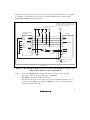
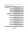
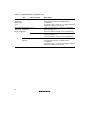
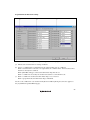
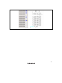
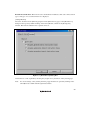
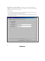
REJ10J1709-0100
SuperH™ Family E10A-USB Emulator
Additional Document for User’s Manual
Supplementary Information on Using the SH7362
Renesas Microcomputer Development Environment System
SuperH™ Family
E10A-USB for SH7362 HS7362KCU01HE
Rev.1.00
Revision Date: Aug. 20, 2007
Notes regarding these materials
1. This document is provided for reference purposes only so that Renesas customers may select the appropriate
Renesas products for their use. Renesas neither makes warranties or representations with respect to the
accuracy or completeness of the information contained in this document nor grants any license to any
intellectual property rights or any other rights of Renesas or any third party with respect to the information in
this document.
2. Renesas shall have no liability for damages or infringement of any intellectual property or other rights arising
out of the use of any information in this document, including, but not limited to, product data, diagrams, charts,
programs, algorithms, and application circuit examples.
3. You should not use the products or the technology described in this document for the purpose of military
applications such as the development of weapons of mass destruction or for the purpose of any other military
use. When exporting the products or technology described herein, you should follow the applicable export
control laws and regulations, and procedures required by such laws and regulations.
4. All information included in this document such as product data, diagrams, charts, programs, algorithms, and
application circuit examples, is current as of the date this document is issued. Such information, however, is
subject to change without any prior notice. Before purchasing or using any Renesas products listed in this
document, please confirm the latest product information with a Renesas sales office. Also, please pay regular
and careful attention to additional and different information to be disclosed by Renesas such as that disclosed
through our website. (http://www.renesas.com )
5. Renesas has used reasonable care in compiling the information included in this document, but Renesas
assumes no liability whatsoever for any damages incurred as a result of errors or omissions in the information
included in this document.
6. When using or otherwise relying on the information in this document, you should evaluate the information in
light of the total system before deciding about the applicability of such information to the intended application.
Renesas makes no representations, warranties or guaranties regarding the suitability of its products for any
particular application and specifically disclaims any liability arising out of the application and use of the
information in this document or Renesas products.
7. With the exception of products specified by Renesas as suitable for automobile applications, Renesas
products are not designed, manufactured or tested for applications or otherwise in systems the failure or
malfunction of which may cause a direct threat to human life or create a risk of human injury or which require
especially high quality and reliability such as safety systems, or equipment or systems for transportation and
traffic, healthcare, combustion control, aerospace and aeronautics, nuclear power, or undersea communication
transmission. If you are considering the use of our products for such purposes, please contact a Renesas
sales office beforehand. Renesas shall have no liability for damages arising out of the uses set forth above.
8. Notwithstanding the preceding paragraph, you should not use Renesas products for the purposes listed below:
(1) artificial life support devices or systems
(2) surgical implantations
(3) healthcare intervention (e.g., excision, administration of medication, etc.)
(4) any other purposes that pose a direct threat to human life
Renesas shall have no liability for damages arising out of the uses set forth in the above and purchasers who
elect to use Renesas products in any of the foregoing applications shall indemnify and hold harmless Renesas
Technology Corp., its affiliated companies and their officers, directors, and employees against any and all
damages arising out of such applications.
9. You should use the products described herein within the range specified by Renesas, especially with respect
to the maximum rating, operating supply voltage range, movement power voltage range, heat radiation
characteristics, installation and other product characteristics. Renesas shall have no liability for malfunctions or
damages arising out of the use of Renesas products beyond such specified ranges.
10. Although Renesas endeavors to improve the quality and reliability of its products, IC products have specific
characteristics such as the occurrence of failure at a certain rate and malfunctions under certain use
conditions. Please be sure to implement safety measures to guard against the possibility of physical injury, and
injury or damage caused by fire in the event of the failure of a Renesas product, such as safety design for
hardware and software including but not limited to redundancy, fire control and malfunction prevention,
appropriate treatment for aging degradation or any other applicable measures. Among others, since the
evaluation of microcomputer software alone is very difficult, please evaluate the safety of the final products or
system manufactured by you.
11. In case Renesas products listed in this document are detached from the products to which the Renesas
products are attached or affixed, the risk of accident such as swallowing by infants and small children is very
high. You should implement safety measures so that Renesas products may not be easily detached from your
products. Renesas shall have no liability for damages arising out of such detachment.
12. This document may not be reproduced or duplicated, in any form, in whole or in part, without prior written
approval from Renesas.
13. Please contact a Renesas sales office if you have any questions regarding the information contained in this
document, Renesas semiconductor products, or if you have any other inquiries.
Contents
Section 1 Connecting the Emulator with the User System ................................1
1.1
1.2
1.3
1.4
1.5
Components of the Emulator ............................................................................................ 1
Connecting the Emulator with the User System ............................................................... 2
Installing the H-UDI Port Connector on the User System ................................................ 3
Pin Assignments of the H-UDI Port Connector ................................................................ 4
Recommended Circuit between the H-UDI Port Connector and the MPU....................... 8
1.5.1 Recommended Circuit (36-Pin Type) .................................................................. 8
1.5.2 Recommended Circuit (14-Pin Type) .................................................................. 10
1.5.3 Recommended Circuit (38-Pin Type) .................................................................. 12
Section 2 Software Specifications when Using the SH7362 .............................15
2.1
2.2
Differences between the SH7362 and the Emulator ......................................................... 15
Specific Functions for the Emulator when Using the SH7362.......................................... 20
2.2.1 Event Condition Functions .................................................................................. 20
2.2.2 Trace Functions.................................................................................................... 28
2.2.3 Notes on Using the JTAG (H-UDI) Clock (TCK) and AUD Clock (AUDCK)... 38
2.2.4 Notes on Setting the [Breakpoint] Dialog Box .................................................... 38
2.2.5 Notes on Setting the [Event Condition] Dialog Box and
the BREAKCONDITION_SET Command ........................................................ 40
2.2.6 Note on Setting the UBC_MODE Command ...................................................... 40
2.2.7 Note on Setting the PPC_MODE Command ....................................................... 40
2.2.8 Performance Measurement Function ................................................................... 41
i
ii
Section 1 Connecting the Emulator with the User System
1.1
Components of the Emulator
The E10A-USB emulator supports the SH7362. Table 1.1 lists the components of the emulator.
Table 1.1 Components of the Emulator
Classification Component
Hardware
Appearance
Quantity
Emulator box
1
User system interface
cable
User system interface
cable
1
USB cable
1
1
Remarks
HS0005KCU01H:
Depth: 65.0 mm, Width: 97.0 mm,
Height: 20.0 mm, Mass: 72.9 g
or
HS0005KCU02H:
Depth: 65.0 mm, Width: 97.0 mm,
Height: 20.0 mm, Mass: 73.7 g
14-pin type:
Length: 20 cm, Mass: 33.1 g
36-pin type:
Length: 20 cm, Mass: 49.2 g
(only for HS0005KCU02H)
Length: 150 cm, Mass: 50.6 g
Software
E10A-USB emulator setup
1
HS0005KCU01SR,
program,
TM
SuperH Family E10AHS0005KCU01HJ,
USB Emulator User’s
HS0005KCU01HE,
Manual,
Supplementary
HS7362KCU01HJ,
Information on Using the
HS7362KCU01HE,
SH7362*, and
HS0005TM01HJ, and
Test program manual for
HS0005KCU01H and
HS0005TM01HE
(provided on a CD-R)
HS0005KCU02H
Note: Additional document for the MPUs supported by the emulator is included. Check the target
MPU and refer to its additional document.
1
1.2
Connecting the Emulator with the User System
To connect the E10A-USB emulator (hereinafter referred to as the emulator), the H-UDI port
connector must be installed on the user system to connect the user system interface cable. When
designing the user system, refer to an example of recommended connection between the connector
and the MPU shown in this manual. In addition, read the E10A-USB emulator user's manual and
hardware manual for the related device.
Table 1.2 shows the type number of the emulator, the corresponding connector type, and the use of
AUD function.
Table 1.2 Type Number, AUD Function, and Connector Type
Type Number
Connector
AUD Function
HS0005KCU02H
36-pin connector
Available
HS0005KCU01H, HS0005KCU02H
14-pin connector
Not available
HS0005KCU02H
38-pin connector
Available
The H-UDI port connector has the 36-pin, 14-pin, and 38-pin types as described below. Use them
according to the purpose of the usage.
1. 36-pin type (with AUD function)
The AUD trace function is supported. A large amount of trace information can be acquired in
realtime. The window trace function is also supported for acquiring memory access in the
specified range (memory access address or memory access data) by tracing.
2. 14-pin type (without AUD function)
The AUD trace function cannot be used because only the H-UDI function is supported. Since
the 14-pin type connector is smaller than the 36-pin type (1/2.5), the size of the area where the
connector is installed on the user system can be reduced.
3. 38-pin type (with AUD function)
The AUD trace function is supported. As well as the 36-pin type, a large amount of trace
information can be acquired in realtime. Since the 38-pin type connector is smaller than the
36-pin type (1/2.5), the size of the area where the connector is installed on the user system can
be reduced. To use the 38-pin type connector, however, an optional cable (HS0005ECK01H)
is required.
2
1.3
Installing the H-UDI Port Connector on the User System
Table 1.3 shows the recommended H-UDI port connectors for the emulator.
Table 1.3 Recommended H-UDI Port Connectors
Connector
Type Number
Manufacturer
Specifications
36-pin connector
DX10M-36S
Hirose Electric Co., Ltd.
Screw type
DX10M-36SE,
DX10G1M-36SE
Lock-pin type
14-pin connector
2514-6002
Minnesota Mining &
Manufacturing Ltd.
14-pin straight type
38-pin connector
2-5767004-2
Tyco Electronics AMP K.K.
38-pin Mictor type
Note: When designing the 36-pin connector layout on the user board, do not connect any
components under the H-UDI connector. When designing the 14-pin connector layout on
the user board, do not place any components within 3 mm of the H-UDI port connector.
When designing the 38-pin connector layout on the user board, reduce cross-talk noise etc.
by keeping other signal lines out of the region where the H-UDI port connector is situated.
As shown in figure 1.1, an upper limit (5 mm) applies to the heights of components
mounted around the user system connector.
3
E10A-USB optional 38-pin
user system interface cable
50 mm
1
38
2
20 mm
37
5 mm
2-5767004-2
: Area to be kept free of other components
Target system
H-UDI port connector (top view)
Figure 1.1 Restriction on Component Mounting
1.4
Pin Assignments of the H-UDI Port Connector
Figures 1.2 through 1.4 show the pin assignments of the 36-pin, 14-pin, and 38-pin H-UDI port
connectors, respectively.
Note: Note that the pin number assignments of the H-UDI port connector shown on the
following pages differ from those of the connector manufacturer.
4
Pin
No.
Signal
Input/
Output *1
1
AUDCK
Output
M15
2
GND
3
AUDATA0
Output
L14
4
GND
5
AUDATA1
6
GND
7
AUDATA2
8
GND
9
AUDATA3
Output
Output
SH7362
Pin No.
Note
L15
M13
Pin
No.
Signal
Input/
Output*1
19
TMS
Input
K13
20
GND
21
/TRST *2
Input
L13
22
(GND) *4
23
TDI
Input
K14
24
GND
25
TDO
Output
K15
26
GND
27
/ASEBRK / *2
BRKACK
Input/
output
N13
28
GND
29
UVCC
Output
M14
10
GND
11
/AUDSYNC *2 Output
M16
12
GND
30
GND
13
N.C.
31
/RESETP *2
/RESETA
14
GND
32
GND
15
N.C.
33
GND *3
16
GND
34
GND
17
TCK
18
GND
Input
J17
35
N.C.
36
GND
SH7362
Pin No.
Note
Output
Output
Output
D15
D12
User reset
*5
Output
Notes: 1. Input to or output from the user system.
2. The symbol (/) means that the signal is active-low.
3. The emulator monitors the GND signal of the user system and detects whether or
not the user system is connected.
4. When the user system interface cable is connected to this pin and the MPMD pin is
set to 0, do not connect to GND but to the MPMD pin directly.
5. Connect /RESETP and /RESETA to the user system if required, as shown in figure 1.5.
H-UDI port connector (top view)
Edge of the board
(connected to the connector)
φ 0.7+0.1
0
36
1
3
9.0
1.905
1.1
4.5
2
φ 2.8+0.1
0
4
(Pin 1 mark)
35
1.27
4.09
M2.6 x 0.45
H-UDI port connector (front view)
4.8
H-UDI port connector (top view)
3.9
37.61
43.51
: Pattern inhibited area
0.3
9.0
21.59
Unit: mm
Figure 1.2 Pin Assignments of the H-UDI Port Connector (36 Pins)
5
SH7362
Pin No.
Signal
Input/
Output*1
1
TCK
Input
J17
2
/TRST
Input
L13
Output
K15
Input/
N13
Pin No.
3
*2
TDO
4
/ASEBRK
5
6
7
*2
Note
/BRKACK
output
TMS
Input
K13
TDI
Input
K14
/RESETP
Output
D15
User reset
Output
D12
*5
*2
/RESETA
8
N.C.
9
(GND)
11
UVCC
10, 12,
GND
*4
Output
and 13
14
GND
*3
Output
Notes: 1. Input to or output from the user system.
2. The symbol (/) means that the signal is active-low.
3. The emulator monitors the GND signal of the user
system and detects whether or not the user system
is connected.
4. When the user system interface cable is connected to
this pin and the MPMD pin is set to 0, do not connect to
GND but to the MPMD pin directly.
5. Connect /RESETP and /RESETA to the user system
if required, as shown in figure 1.6.
Pin 1 mark
H-UDI port connector (top view)
25.0
23.0
6 x 2.54 = 15.24
(2.54)
H-UDI port connector
(top view)
Pin 8
Pin 1
Pin 14
Pin 7
0.45
Pin 1 mark
Unit: mm
Figure 1.3 Pin Assignments of the H-UDI Port Connector (14 Pins)
6
Pin
No. Signal
1
N.C.
2
N.C.
SH7362
Pin No.
Input/
Output*1
Note
*4
3
MPMD (GND)
4
N.C.
5
/UCON (GND) *3
6
AUDCK
7
N.C.
8
/ASEBRK/
BRKACK *2
Input/
Output
N13
9
/RESETP *2
/RESETA
Output
D15
D12
Output
10
N.C.
11
TDO
Output
12
UVCC_AUD
Output
13
M15
User reset
Pin
No.
Signal
20
N.C.
21
/TRST *2
22
N.C.
23
N.C.
24
AUDATA3
25
N.C.
26
AUDATA2
27
N.C.
28
AUDATA1
29
N.C.
Input/
Output*1
SH7362
Pin No.
Input
L13
Output
M14
Output
M13
Output
L15
30
AUDATA0
Output
L14
31
N.C.
N.C.
32
/AUDSYNC *2 Output
M16
14
UVCC
Output
33
N.C.
15
TCK
Input
34
N.C.
35
N.C.
16
N.C.
17
TMS
18
N.C.
19
TDI
K15
J17
Input
K13
Input
K14
36
N.C.
37
N.C.
38
N.C.
Note
Notes: 1. Input to or output from the user system.
2. The symbol (#) means that the signal is active-low.
3. The emulator monitors the GND signal of the user system and detects whether or not the user system is connected.
4. When the user system interface cable is connected to this pin and the MPMD pin is set to 0, do not connect to
GND but to the MPMD pin directly.
5. The GND bus lead at the center of the H-UDI port connector must be grounded.
6. Connect /RESETP and /RESETA to the user system if required, as shown in figure 1.7.
37
1
6.91
38
2
Unit: mm
25.4
H-UDI port connector (top view)
Figure 1.4 Pin Assignments of the H-UDI Port Connector (38 Pins)
7
1.5
Recommended Circuit between the H-UDI Port Connector and the
MPU
1.5.1
Recommended Circuit (36-Pin Type)
Figure 1.5 shows a recommended circuit for connection between the H-UDI and AUD port
connectors (36 pins) and the MPU when the emulator is in use.
Notes: 1. Do not connect anything to the N.C. pins of the H-UDI port connector.
8
2.
The MPMD pin must be 0 when the emulator is connected and 1 when the emulator is
not connected, respectively.
(1) When the emulator is used: MPMD = 0
(2) When the emulator is not used: MPMD = 1
Figure 1.5 shows an example of circuits that allow the MPMD pin to be GND (0)
whenever the emulator is connected by using the user system interface cable.
3.
When a network resistance is used for pull-up, it may be affected by a noise. Separate
TCK from other resistances.
4.
The /TRST pin must be at the low level for a certain period when the power is
supplied whether the H-UDI is used or not. Reduce the power supplied to the /TRST
pin by pulling the pin down by a resistance of 1 kilo-ohm and setting PUL15 = 0 in
the PULCR register after a reset.
5.
The pattern between the H-UDI port connector and the MPU must be as short as
possible. Do not connect the signal lines to other components on the board.
6.
Since the H-UDI and the AUD of the MPU operate with the VccQ, supply only the
VccQ to the UVCC pin. Make the emulator’s switch settings so that the user power
will be supplied (SW2 = 1 and SW3 = 1).
7.
The resistance values shown in figure 1.5 are for reference.
8.
For the pin processing in cases where the emulator is not used, refer to the hardware
manual of the related MPU.
9.
For the AUDCK pin, guard the pattern between the H-UDI port connector and the
MPU at GND level.
When the circuit is connected as shown in figure 1.5, the switches of the emulator are set as SW2
TM
= 1 and SW3 = 1. For details, refer to section 3.8, Setting the DIP Switches, in the SuperH
Family E10A-USB Emulator User’s Manual.
VccQ_SR = 2.85-V/1.8-V I/O power supply
VccQ_MFI = 2.85-V/1.8-V I/O power supply
VccQ = 2.85-V I/O power supply
All pulled-up at 4.7 kΩ or more
VccQ_SR VccQ_SRVccQ_SRVccQ_SR VccQ_SR
VccQ_SR
H-UDI port connector
(36-pin type)
2
4
6
8
10
12
14
16
18
20
22
24
26
28
30
32
34
36
GND
AUDCK
GND
AUDATA0
GND
AUDATA1
GND
AUDATA2
GND
AUDATA3
GND
AUDSYNC
GND
N.C.
GND
GND
GND
(GND)
GND
GND
GND
GND
GND
GND
GND
SH7362
1
5
AUDATA2
AUDATA3
11
AUDSYNC
13
15
17
TMS
19
TDO
AUDATA1
9
N.C.
TDI
AUDATA0
7
TCK
TRST
AUDCK
3
TCK
TMS
21
TRST
23
TDI
25
ASEBRK 27
/ BRKACK
29
UVCC
31
RESET
33
GND
35
N.C.
TDO
ASEBRK
/BRKACK
RESETP *1
1 kΩ
*2
Level-shift
circuit
*3
RESETA
MPMD
Power-on reset signal
Reset signal
User system
Figure 1.5 Recommended Circuit for Connection between the H-UDI Port Connector and
MPU when the Emulator is in Use (36-Pin Type)
Notes: 1. Do not use /RESETP in the emulator after the user system has been activated.
When reset signals are used for debugging, use /RESETA.
2. Fix /RESETA as high level when it is not used.
9
3. When the voltage level of VccQ_SR (power supply for H-UDI and AUD) is 2.85 V
and that of VccQ_MFI (power supply for /RESETA) is 1.8 V, a level-shift circuit is
required as shown in the figure.
1.5.2
Recommended Circuit (14-Pin Type)
Figure 1.6 shows a recommended circuit for connection between the H-UDI port connector (14
pins) and the MPU when the emulator is in use.
Notes: 1. Do not connect anything to the N.C. pins of the H-UDI port connector.
10
2.
The MPMD pin must be 0 when the emulator is connected and 1 when the emulator is
not connected, respectively.
(1) When the emulator is used: MPMD = 0
(2) When the emulator is not used: MPMD = 1
Figure 1.6 shows an example of circuits that allow the MPMD pin to be GND (0)
whenever the emulator is connected by using the user system interface cable.
3.
When a network resistance is used for pull-up, it may be affected by a noise. Separate
TCK from other resistances.
4.
The /TRST pin must be at the low level for a certain period when the power is
supplied whether the H-UDI is used or not. Reduce the power supplied to the /TRST
pin by pulling the pin down by a resistance of 1 kilo-ohm and setting PUL15 = 0 in
the PULCR register after a reset.
5.
The pattern between the H-UDI port connector and the MPU must be as short as
possible. Do not connect the signal lines to other components on the board.
6.
Since the H-UDI of the MPU operates with the VccQ, supply only the VccQ to the
UVCC pin. Make the emulator’s switch settings so that the user power will be
supplied (SW2 = 1 and SW3 = 1).
7.
The resistance values shown in figure 1.6 are for reference.
8.
For the pin processing in cases where the emulator is not used, refer to the hardware
manual of the related MPU.
When the circuit is connected as shown in figure 1.6, the switches of the emulator are set as SW2
TM
= 1 and SW3 = 1. For details, refer to section 3.8, Setting the DIP Switches, in the SuperH
Family E10A-USB Emulator User’s Manual.
VccQ_SR = 2.85-V/1.8-V I/O power supply
VccQ_MFI = 2.85-V/1.8-V I/O power supply
VccQ = 2.85-V I/O power supply
All pulled-up at 4.7 kΩ or more
VccQ_SR VccQ_SR VccQ_SR VccQ_SR VccQ_SR
VccQ_SR
H-UDI port connector
(14-pin type)
TCK
9
(GND)
10 GND
12
13
14
TRST
TDO
SH7362
1
GND
GND
RESET
N.C.
UVCC
TRST
3
ASEBRK
4
/ BRKACK
5
TMS
6
TDI
GND
TCK
2
TDO
ASEBRK/BRKACK
TMS
TDI
7
RESETP *1
8
11
*2
1 kΩ
Level-shift
circuit
*3
RESETA
MPMD
Power-on reset signal
Reset signal
User system
Figure 1.6 Recommended Circuit for Connection between the H-UDI Port Connector and
MPU when the Emulator is in Use (14-Pin Type)
Notes: 1. Do not use /RESETP in the emulator after the user system has been activated.
When reset signals are used for debugging, use /RESETA.
2. Fix /RESETA as high level when it is not used.
3. When the voltage level of VccQ_SR (power supply for H-UDI and AUD) is 2.85 V
and that of VccQ_MFI (power supply for /RESETA) is 1.8 V, a level-shift circuit is
required as shown in the figure.
11
1.5.3
Recommended Circuit (38-Pin Type)
Figure 1.7 shows a recommended circuit for connection between the H-UDI and AUD port
connectors (38 pins) and the MPU when the emulator is in use.
Notes: 1. Do not connect anything to the N.C. pins of the H-UDI port connector.
2.
The MPMD pin must be 0 when the emulator is connected and 1 when the emulator is
not connected, respectively.
(1) When the emulator is used: MPMD = 0
(2) When the emulator is not used: MPMD = 1
Figure 1.7 shows an example of circuits that allow the MPMD pin to be GND (0)
whenever the emulator is connected by using the user system interface cable.
When the MPMD pin is changed by switches, etc., ground pin 3. Do not connect this
pin to the MPMD pin.
3.
When a network resistance is used for pull-up, it may be affected by a noise. Separate
TCK from other resistances.
4.
The pattern between the H-UDI port connector and the MPU must be as short as
possible. Do not connect the signal lines to other components on the board.
5.
The AUD signals (AUDCK, AUDATA3 to AUDATA0, and AUDSYNC) operate in
high speed. Isometric connection is needed if possible. Do not separate connection nor
connect other signal lines adjacently.
6.
Supply only the VCCQ voltage (I/O power supply) to the UVCC and UVCC_AUD
pins because the H-UDI and AUD of the MPU operate at the VCCQ voltage,
respectively. Make the emulator’s switch settings so that the user power will be
supplied (SW2 = 1 and SW3 = 1).
7.
The resistance value shown in figure 1.7 is for reference.
8.
For the AUDCK pin, guard the pattern between the H-UDI port connector and the
MPU at GND level.
9.
When the power is supplied, the TRST# pin must be low during a specified period
regardless of whether or not the H-UDI is used.
10. The GND bus lead at the center of the H-UDI port connector must be grounded.
11. For the pin processing in cases where the emulator is not used, refer to the hardware
manual of the related MPU.
12
When the circuit is connected as shown in figure 1.7, the switches of the emulator are set as SW2
TM
= 1 and SW3 = 1. For details, refer to section 3.8, Setting the DIP Switches, in the SuperH
Family E10A-USB Emulator User’s Manual.
VccQ_SR = 2.85-V/1.8-V I/O power supply
VccQ_MFI = 2.85-V/1.8-V I/O power supply
VccQ = 2.85-V I/O power supply
All pulled-up at 4.7 kΩ or more
VccQ_SR
VccQ_SR VccQ_SR VccQ_SR
H-UDI port connector
(38-pin type)
AUDCK
AUDSYNC
AUDATA0
SH7362
6
28
AUDATA2
26
AUDATA3
24
TMS
TRST
TDI
TDO
ASEBRK
/ BRKACK
RESET
AUDSYNC
30
AUDATA1
TCK
AUDCK
32
AUDATA0
AUDATA1
AUDATA2
AUDATA3
15
TCK
17
TMS
21
TRST
19
TDI
11
TDO
8
ASEBRK
/BRKACK
9
*2
MPMD(GND)
UVCC
UVCC_AUD
UCON (GND)
GND
N.C.
3
14
Level-shift
circuit
*3
1 kΩ
RESETP *1
RESETA
MPMD
Power-on reset signal
Reset signal
12
5
GND bus leads
1, 2, 4, 7,
10, 13, 16, 18,
20, 22, 23, 25, 27, 29,
31, 33, 34, 35, 36, 37, 38
User system
Figure 1.7 Recommended Circuit for Connection between the H-UDI Port Connector and
MPU when the Emulator is in Use (38-Pin Type)
13
Notes: 1. Do not use /RESETP in the emulator after the user system has been activated.
When reset signals are used for debugging, use /RESETA.
2. Fix /RESETA as high level when it is not used.
3. When the voltage level of VccQ_SR (power supply for H-UDI and AUD) is 2.85 V
and that of VccQ_MFI (power supply for /RESETA) is 1.8 V, a level-shift circuit is
required as shown in the figure.
14
Section 2 Software Specifications when Using the SH7362
2.1
Differences between the SH7362 and the Emulator
1. When the emulator system is initiated, it initializes the general registers and part of the control
registers as shown in table 2.1. The initial values of the actual SH7362 registers are undefined.
When the emulator is initiated from the workspace, a value to be entered is saved in a session.
Table 2.1 Register Initial Values at Emulator Link Up
Register
Emulator at Link Up
R0 to R14
H'00000000
R15 (SP)
H'A0000000
R0_BANK to R7_BANK
H'00000000
PC
H'A0000000
SR
H'700000F0
GBR
H'00000000
VBR
H'00000000
MACH
H'00000000
MACL
H'00000000
PR
H'00000000
SPC
H'00000000
SSR
H'000000F0
RS
H'00000000
RE
H'00000000
MOD
H'00000000
A0G, A1G
H'00000000
A0, A1
H'00000000
X0, X1
H'00000000
Y0, Y1
H'00000000
M0, M1
H'00000000
DSR
H'00000000
2. The emulator uses the H-UDI; do not access the H-UDI.
15
3. Low-Power States (Sleep, Software Standby, Module Standby, U Standby, and R Standby)
For low-power consumption, the SH7362 has sleep, software standby, module standby, U
standby, and R standby states.
The sleep, software standby, U Standby, and R Standby states are switched using the SLEEP
instruction. When the emulator is used, the sleep and software standby states can be cleared
with either the normal clearing function or with the [STOP] button, and a break will occur.
The power for some areas is turned off in U standby or R standby state and turned on in using
the emulator.
Note: The memory must not be accessed or modified in low-power state using the SLEEP
instruction.
4. Reset Signal (/RESETA)
The SH7362 reset signal is only valid during emulation started with clicking the GO or STEPtype button.
If the reset signal is enabled on the user system in command input wait state, it is not sent to
the SH7362.
Note: Do not break the user program when the /RESETA signal is being low or the bus-release
request or wait control signal is being active. A TIMEOUT error will occur. If the busrelease request or wait control signal is fixed to active during break, a TIMEOUT error
will occur at memory access.
5. Direct Memory Access Controller (DMAC)
The DMAC operates even when the emulator is used. When a data transfer request is
generated, the DMAC executes DMA transfer.
6. Memory Access during User Program Execution
When a memory is accessed from the memory window, etc. during user program execution,
the user program is resumed after it has stopped in the emulator to access the memory.
Therefore, realtime emulation cannot be performed.
The stopping time of the user program is as follows:
Environment:
®
Host computer: 800 MHz (Pentium III)
JTAG clock: 10 MHz (TCK clock)
When a one-byte memory is read from the command-line window, the stopping time will be
about 42 ms.
16
7. Memory Access during User Program Break
The emulator can download the program for the flash memory area (for details, refer to section
TM
6.22, Download Function to the Flash Memory Area, in the SuperH Family E10A-USB
Emulator User’s Manual). Other memory write operations are enabled for the RAM area.
Therefore, an operation such as memory write or BREAKPOINT should be set only for the
RAM area.
8. Cache Operation during User Program Break
When cache is enabled, the emulator accesses the memory by the following methods:
• At memory write: Writes through the cache, then issues a single write to outside. The LRU
is not updated.
• At memory read: Reads memory from the cache. The LRU is not updated.
Therefore, when memory read or write is performed during user program break, the cache state
does not change.
• At breakpoint set: Disables the instruction cache.
9. Port G
The AUD pin is multiplexed as shown in table 2.2.
Table 2.2 Multiplexed Functions
Port
Function 1
Function 2
G
PTG5 input/output (port)/IRQ7*
AUDSYNC (AUD)
G
PTG4 input/output (port)
/SCIF_RXD/THPRTC4*
AUDSYNC (AUD)
G
PTG3 input/output (port)
/SCIF_TXD/THPRTC3*
AUDATA3 (AUD)
G
PTG2 input/output (port)
/SIM_CLK/THPRTC2*
AUDATA2 (AUD)
G
PTG1 input/output (port)
/SIM_D/THPRTC1*
AUDATA1 (AUD)
G
PTG0 input/output (port)
/SIM_RST/THPRTC0*
AUDATA0 (AUD)
Note: Function 1 can be used when the AUD pins of the device are not connected to the emulator.
10. UBC
When [User] is specified in the [UBC mode] list box in the [Configuration] dialog box, the
UBC can be used in the user program.
Do not use the UBC in the user program as it is used by the emulator when [EML] is specified
in the [UBC mode] list box in the [Configuration] dialog box.
17
11. MFI
When the MFI boot mode is used, be sure to activate the emulator by setting the MFIINT
signal as a trigger for the MFI transfer from the base-band side.
12. Memory Access during Break
In the enabled MMU, when a memory is accessed and a TLB error occurs during break, it can
be selected whether the TLB exception is controlled or the program jumps to the user
exception handler in [TLB Mode] in the [Configuration] dialog box. When [TLB miss
exception is enable] is selected, a “Communication Timeout error” will occur if the TLB
exception handler does not operate correctly. When [TLB miss exception is disable] is selected,
the program does not jump to the TLB exception handler even if a TLB exception occurs.
Therefore, if the TLB exception handler does not operate correctly, a “Communication
Timeout error” will not occur but the memory contents may not be correctly displayed.
13. Loading Sessions
Information in [JTAG clock] of the [Configuration] dialog box cannot be recovered by loading
sessions. Thus the TCK value will be 1.25 MHz.
14. [IO] Window
• Display and modification
Do not change values of the User Break Controller because it is used by the emulator.
For each RCLK watchdog timer register, there are two registers to be separately used for
write and read operations.
Table 2.3 RCLK Watchdog Timer Register
Register Name
Usage
Register
RWTCSR(W)
Write
RCLK watchdog timer control/status register
RWTCNT(W)
Write
RCLK watchdog timer counter
RWTCSR(R)
Read
RCLK watchdog timer control/status register
RWTCNT(R)
Read
RCLK watchdog timer counter
18
The RCLK watchdog timer operates only when the user program is executed. Do not
change the value of the frequency change register in the [IO] window or [Memory] window.
The internal I/O registers can be accessed from the [IO] window. However, note the
following when accessing the SDMR register of the bus-state controller. Before accessing
the SDMR register, specify addresses to be accessed in the I/O-register definition file
(SH7362.IO) and then activate the High-performance Embedded Workshop. After the I/Oregister definition file is created, the MPU’s specifications may be changed. If each I/O
register in the I/O-register definition file differs from addresses described in the hardware
manual, change the I/O-register definition file according to the description in the hardware
manual. The I/O-register definition file can be customized depending on its format. Note
that, however, the E10A emulator does not support the bit-field function.
• Verify
In the [IO] window, the verify function of the input value is disabled.
15. Illegal Instructions
If illegal instructions are executed by STEP-type commands, the emulator cannot go to the
next program counter.
16. [Reset CPU] and [Reset Go] in the [Debug] Menu
When [Reset Mode] of the [Configuration] dialog box is set as [Auto], an H-UDI reset is
issued by executing [Reset CPU] or [Reset Go]. For the H-UDI reset, the clock pulse
generator and RCLK watchdog timer are not initialized.
When [User] is selected and [Reset CPU] or [Reset Go] is executed, a reset signal input from
the user system is waited; do not input /RESETP.
19
2.2
Specific Functions for the Emulator when Using the SH7362
2.2.1
Event Condition Functions
The emulator is used to set 12 event conditions (Ch1 to Ch12) and the software trace. Table 2.4
lists the conditions of Event Condition.
Table 2.4 Types of Event Conditions
Event Condition Type
Description
Address bus condition (Address)
Breaks when the SH7362 address bus value or the program
counter value matches the specified value.
Data bus condition (Data)
Breaks when the SH7362 data bus value matches the
specified value. Byte, word, or longword can be specified as
the access data size.
Bus state condition
(Bus State)
There are two bus state condition settings:
Bus state condition: Breaks or acquires a trace when the
data bus or the X-Bus or Y-Bus address bus of the SH7362
is matched.
Read/Write condition: Breaks or acquires a trace when the
specified read/write condition is matched.
Window address condition
Breaks or acquires a trace when the data in the specified
memory range is accessed.
System bus
Breaks or acquires a trace when the address or data on the
system bus is matched.
LDTLB instruction event condition
Breaks when the SH7362 executes the LDTLB instruction.
Count
Breaks when the conditions set are satisfied the specified
number of times.
Branch trace condition
(Branch trace)
Breaks or acquires a trace when a branch occurs with the
condition specified by the SH7362. (By default, trace
acquisition is enabled).
Software trace
Selects whether or not the software trace is acquired.
Action
Selects the operation when a condition, such as setting a
break, trace, or performance start or end, is matched.
Table 2.5 lists the combinations of conditions that can be set under Ch1 to Ch12 and the software
trace.
20
Table 2.5 Dialog Boxes for Setting Event Conditions
Function
Address
Data
Bus
Bus
ASID
Bus
Window
State
Address
Branch
Condition Condition
LDTLB
Count
Condition
Dialog
Condition Condition Condition (Bus
(Window System Instruction Condition (Branch
Software
Box
(Address) (Data)
address) Bus
Trace)
Trace
X
X
[Event
O
X
(ASID)
O
Status)
O
X
Break
X
X
(Count)
X
Action
O
Condition
(B and
1] dialog
P)
box
[Event
O
O
O
O
X
X
X
O
X
X
O
Condition
(B and
2] dialog
P)
box
[Event
O
X
O
X
X
X
X
X
X
X
O
Condition
(B and
3] dialog
P)
box
[Event
O
X
O
X
X
X
X
X
X
X
O
Condition
(B and
4] dialog
P)
box
[Event
X
X
O
O
O
X
X
X
X
X
O
Condition
(B, T,
5] dialog
and P)
box
[Event
X
X
O
O
O
X
X
X
X
X
O
Condition
(B, T,
6] dialog
and P)
box
[Event
X
X
X
X
X
X
O
X
X
X
Condition
Break
fixed
7] dialog
box
[Event
O
X
X
X
X
O
X
X
X
X
O
Condition
(B, T,
8] dialog
and P)
box
21
Table 2.5 Dialog Boxes for Setting Event Conditions (cont)
Function
Address
Data
Bus
Bus
ASID
Bus
Window
State
Address
Branch
Condition Condition
LDTLB
Count
Condition
Dialog
Condition Condition Condition (Bus
(Window System Instruction Condition (Branch
Software
Box
(Address) (Data)
address) Bus
Trace)
Trace
X
X
[Event
O
(ASID)
X
Status)
X
X
X
Break
O
X
(Count)
X
Action
O
Condition
(B, T,
9] dialog
and P)
box
[Event
O
X
O
O
X
X
X
X
X
X
O
Condition
(B and
10] dialog
P)
box
[Event
O
O
O
O
X
X
X
O
X
X
O
Condition
(B and
11] dialog
P)
box
[Event
X
X
X
X
X
X
X
X
O
X
O
Condition
(B, T,
12] dialog
and P)
box
[Software
X
X
X
X
X
X
trace]
box
1.
O: Can be set in the dialog box.
X: Cannot be set in the dialog box.
2.
For the Action item,
B: Setting a break is enabled.
T: Setting a trace is enabled.
P: Setting a performance start or end condition is enabled.
22
X
X
O
Trace
fixed
dialog
Notes:
X
Sequential Setting: In the emulator, sequential setting of an Event Condition is enabled.
Table 2.6 Sequential Event Conditions
Type
Event Condition
Description
[CPU
2 Channel Ch2 -> 1
Sequential Sequential
Event] Page
Halts a program when a condition is satisfied in the
order of Event Condition 2, 1.
An event condition must be set for Ch2 and Ch1.
Ch4 -> 3
Halts a program when a condition is satisfied in the
order of Event Condition 4, 3.
An event condition must be set for Ch4 and Ch3.
Ch6 -> 5
Halts a program when a condition is satisfied in the
order of Event Condition 6, 5.
An event condition must be set for Ch6 and Ch5.
Ch11 -> 10
Halts a program when a condition is satisfied in the
order of Event Condition 11, 10.
An event condition must be set for Ch11 and Ch10.
Many
Ch3 -> 2 -> 1
Channel
Sequential
Ch4 -> 3-> 2 -> 1
Halts a program when a condition is satisfied in the
order of Event Condition 3, 2, 1.
An event condition must be set for Ch3, Ch2, and
Ch1.
Halts a program when a condition is satisfied in the
order of Event Condition 4, 3, 2, 1.
An event condition must be set for Ch4, Ch3, Ch2,
and Ch1.
Ch5 -> 4 -> 3-> 2 -> 1 Halts a program when a condition is satisfied in the
order of Event Condition 5, 4, 3, 2, 1.
An event condition must be set for Ch5, Ch4, Ch3,
Ch2, and Ch1.
Ch6 -> 5 -> 4 -> 3-> 2 Halts a program when a condition is satisfied in the
-> 1
order of Event Condition 6, 5, 4, 3, 2, 1.
An event condition must be set for Ch6, Ch5, Ch4,
Ch3, Ch2, and Ch1.
Ch10 -> 6 -> 5 -> 4 -> Halts a program when a condition is satisfied in the
3-> 2 -> 1
order of Event Condition 10, 6, 5, 4, 3, 2, 1.
An event condition must be set for Ch10, Ch6,
Ch5, Ch4, Ch3, Ch2, and Ch1.
Ch11 -> 10 -> 6 -> 5 -> Halts a program when a condition is satisfied in the
4 -> 3-> 2 -> 1
order of Event Condition 11, 10, 6, 5, 4, 3, 2, 1.
An event condition must be set for Ch11, Ch10,
Ch6, Ch5, Ch4, Ch3, Ch2, and Ch1.
23
Table 2.6 Sequential Event Conditions (cont)
Type
Event Condition
Description
[CPU
CPU Extend
Sequential
Event] Page
(cont)
Expands the [CPU Sequential Extend] page.
The sequential setting is enabled with any
combination.
For details, refer to section 2.2.1, Sequential Break
Extension Setting, in this manual.
[SystemBus SystemBus Ch9 -> 8
Sequential Sequential
Event] Page Event
Halts a program when a condition is satisfied for
Event Condition 9, 8.
An event condition must be set for Ch9 and Ch8.
Ch8 -> 9
Halts a program when a condition is satisfied for
Event Condition 8, 9.
An event condition must be set for Ch8 and Ch9.
SystemBus
Extend
24
Expands the [SystemBus Sequential Extend] page.
The sequential setting is enabled with any
combination.
For details, refer to section 2.2.1, Sequential Break
Extension Setting, in this manual.
Sequential Break Extension Setting:
Figure 2.1 [CPU Sequential Extend] Page
(a) Indicates the channel name for setting conditions.
(b) Selects a condition that is satisfied before the channel which sets up conditions.
When a channel name is selected, it is required that the condition of the channel selected here
must have already been satisfied.
When [CPU Match flag] is selected, the CPU match flag must be set.
When a condition is selected by the channel selected here, no break will occur.
(c) When a condition is satisfied, the CPU match flag is set or cleared.
When a program breaks, the CPU match flag is initialized.
Set the event condition for each channel in the [Event Condition] dialog box; this also applies to
the [SystemBus Sequential Extend] page.
25
Usage Example of Sequential Break Extension Setting: A tutorial program provided for the
product is used as an example. For the tutorial program, refer to section 6, Tutorial, in the
TM
SuperH Family E10A-USB Emulator User’s Manual.
The conditions of Event Condition are set as follows:
1. Ch1
Breaks address H’00001068 when the condition [Prefetch address break after executing] is
satisfied.
2. Ch2
Breaks address H’00001058 when the condition [Prefetch address break after executing] is
satisfied.
3. Ch4
Breaks address H’0000107a when the condition [Prefetch address break after executing] is
satisfied.
4. Ch10
Breaks address H’00001086 when the condition [Prefetch address break after executing] is
satisfied.
Note: Do not set other channels.
5. Set the [CPU Sequential Extend] page as shown in figure 2.1.
Then, set the program counter and stack pointer (PC = H’00000800, R15 = H’00010000) in the
[Registers] window and click the [Go] button. If this does not execute normally, issue a reset and
execute the above procedures.
The program is executed up to the condition of Ch10 and halted. Here, the condition is satisfied in
the order of Ch2 -> 1 -> 4 -> 10.
26
Figure 2.2 [Source] Window at Execution Halted (Sequential Break)
27
2.2.2
Trace Functions
The emulator supports the trace functions listed in table 2.7.
Table 2.7 Trace Functions
Function
Internal Trace
AUD Trace
Memory Output
Trace
Branch trace
Supported (eight branches)
Supported
Supported
Range memory access trace
Supported (eight events)
Supported
Supported
Software trace
Supported (eight events)
Supported
Supported
Table 2.8 shows the type numbers that the AUD function can be used.
Table 2.8 Type Number and AUD Function
Type Number
AUD Function
HS0005KCU01H
Not supported
HS0005KCU02H
Supported
28
Branch Trace Functions: The branch source and destination addresses, their source lines, branch
types, and types of accessed bus masters are displayed.
[Setting Method]
Select the check box in the [Branch] group box in the [Branch trace] page of the [Branch trace]
dialog box that opens by double-clicking on the Ch12 (Branch) column of the [Eventpoint]
window. The branch condition to be acquired can be set.
Figure 2.3 [Branch trace] Dialog Box
A branch trace can be acquired by selecting the [Acquire trace] check box of the [Action] page.
Note: To cancel settings, select [Delete] from the popup menu that is opened by clicking on the
Ch12 (Branch) column with the right-mouse button.
29
Range Memory Access Trace Functions: The memory access within the specified range is
acquired by a trace. The read cycle, write cycle, or read/write cycle can be selected as the bus type,
ASID value, or bus cycle for trace acquisition.
[Setting Method]
(i) To open the [Event condition 5] or [Event condition 6] dialog box, double-click on the Ch5
(OA) or Ch6 (OA) column of the [Eventpoint] window.
(ii) Remove the check mark of the [Don’t care] check box in the [Window address] page and enter
the memory range to be set.
Figure 2.4 [Window address] Page
30
(iii)
Open the [ASID] page, remove the check mark of the [Don’t care] check box, and enter the
ASID value to be set.
When the ASID value is not set as a condition, do not remove the check mark of the [Don’t
care] check box.
(iv)
Open the [Bus state] page and specify the bus type and bus cycle that are to be set.
Figure 2.5 [Bus State] Page
(v)
Selecting the [Acquire trace] check box in the [Action] page enables acquiring memory
access within the range.
Note: To cancel settings, select the popup menu that is opened by clicking on the Ch5 (OA) or
Ch6 (OA) column with the right-mouse button.
31
Software Trace Function:
Note: This function can be supported with SHC/C++ compiler (manufactured by Renesas
Technology Corp.; including OEM and bundle products) V6.0 or later.
However, SHC/C++ compiler (including OEM and bundle products) V8.0 or later is
needed when instructions other than those compatible with SH4 are output.
When a specific instruction is executed, the PC value at execution and the contents of one general
register are acquired by trace. Describe the Trace(x) function (x is a variable name) to be
TM
compiled and linked beforehand. For details, refer to the SuperH RISC engine C/C++ Compiler,
Assembler, Optimizing Linkage Editor User’s Manual.
When the load module is downloaded on the emulator and is executed while a software trace
function is valid, the PC value that has executed the Trace(x) function, the general register value
for x, and the source lines are displayed.
To activate the software trace function, select the [Acquire Software trace] radio button in the
[Software trace] dialog box that is opened by double-clicking on the software Trace column of the
[Eventpoint] window.
Note: To cancel settings, select the [Don’t care] radio button in the [Software trace] dialog box
or select [Delete] from the popup menu that is opened by clicking on the software Trace
column with the right-mouse button.
Internal Trace Function: This function is activated by selecting the [Internal trace] radio button
in the [Trace type] group box of the [Trace mode] page. Set the trace condition to be used.
Notes: 1. If an interrupt is generated at the program execution start or end, including a step
operation, the emulator address may be acquired. In such a case, the following
message will be displayed. Ignore this address because it is not a user program address.
*** EML ***
2. If a completion-type exception occurs during exception branch acquisition, the next
address to the address in which an exception occurs is acquired.
3. Trace information cannot be acquired for the following branch instructions:
• The BF and BT instructions whose displacement value is 0
• Branch to H'A0000000 by reset
32
AUD Trace Function: This function is operational when the AUD pin of the device is connected
to the emulator. It is activated by selecting the [AUD trace] radio button in the [Trace type] group
box of the [Trace mode] page. Set the trace condition to be used.
[Restrictions]
• Set bits 2 and 1 in register HIZCRB and bit 15 in register HIZCRC as 0 before activating the
AUD trace function.
• When a reset signal is input during execution of the user program, no trace information can be
acquired until a break occurs. If you wish to continue execution of the user program after a
break, set bits 2 and 1 in register HIZCRB and bit 15 in register HIZCRC as 0.
• Do not execute [Reset Go] while using the AUD trace function. Use [Reset CPU] instead and
set bits 2 and 1 in register HIZCRB and bit 15 in register HIZCRC as 0 before restarting the
execution.
Table 2.9 shows the AUD trace acquisition mode that can be set in each trace function.
Table 2.9 AUD Trace Acquisition Mode
Type
Mode
Description
Continuous
trace occurs
Realtime trace
When the next branch occurs while the trace information is
being output, all the information may not be output. The user
program can be executed in realtime, but some trace
information will be lost.
Non realtime trace
When the next branch occurs while the trace information is
being output, the CPU stops operations until the information
is output. The user program is not executed in realtime.
Trace continue
This function overwrites the oldest trace information to store
the latest trace information.
Trace stop
After the trace buffer becomes full, the trace information is no
longer acquired. The user program is continuously executed.
Trace buffer
full
33
To set the AUD trace acquisition mode, click the [Trace] window with the right mouse button and
select [Setting] from the pop-up menu to display the [Acquisition] dialog box. The AUD trace
acquisition mode can be set in the [Trace Mode 1] or [Trace Mode 2] group box in the [Trace
Mode] page of the [Acquisition] dialog box.
Figure 2.6 [Trace Mode] Page
34
Notes on AUD Trace:
1. When the trace display is performed during user program execution, the mnemonics, operands,
or source is not displayed.
2. The AUD branch trace function outputs the differences between newly output branch source
addresses and previously output branch source addresses. The window trace function outputs
the differences between newly output addresses and previously output addresses. If the
previously output address is the same as the upper 16 bits, the lower 16 bits are output. If it
matches the upper 24 bits, the lower 8 bits are output. If it matches the upper 28 bits, the lower
4 bits are output.
The emulator regenerates the 32-bit address from these differences and displays it in the
[Trace] window. If the emulator cannot display the 32-bit address, it displays the difference
from the previously displayed 32-bit address.
3. If the 32-bit address cannot be displayed, the source line is not displayed.
4. In the emulator, when multiple loops are performed to reduce the number of AUD trace
displays, only the IP counts up.
5. In the emulator, the maximum number of trace displays is 65534 lines (32767 branches).
However, the maximum number of trace displays differs according to the AUD trace
information to be output. Therefore, the above pointers cannot be always acquired.
6. The AUD trace acquisition is not available when [User] is selected in the [UBC mode] list box
of the [Configuration] dialog box. In this case, close the [Trace] window.
7. Do not use the AUD full-trace mode for the VIO function.
8. If a completion-type exception occurs during exception branch acquisition, the next address to
the address in which an exception occurs is acquired.
35
Memory Output Trace Function: This function is activated by selecting the [Use Memory
trace] radio button in the [Trace type] group box of the [Trace mode] page.
In this function, write the trace data in the specified user memory range.
Specify the start address to output a trace for the [Start] edit box in the [User memory area] group
box, and the end address for the [End Address] edit box. Set the trace condition to be used.
Table 2.10 shows the memory-output trace acquisition mode that can be set in each trace function.
Table 2.10 Memory-Output Trace Acquisition Mode
Type
Mode
Description
Continuous
trace occurs
Realtime trace
When the next branch occurs while the trace information is
being output, all the information may not be output. The user
program can be executed in realtime, but some trace
information will be lost.
Non realtime trace
When the next branch occurs while the trace information is
being output, the CPU stops operations until the information
is output. The user program is not executed in realtime.
Trace continue
This function overwrites the oldest trace information to store
the latest trace information.
Trace stop
After the trace buffer becomes full, the trace information is no
longer acquired. The user program is continuously executed.
Trace buffer
full
36
To set the memory-output trace acquisition mode, click the [Trace] window with the right mouse
button and select [Setting] from the pop-up menu to display the [Acquisition] dialog box. The
AUD trace acquisition mode can be set in the [Trace Mode 1] or [Trace Mode 2] group box in the
[Trace Mode] page of the [Acquisition] dialog box.
Figure 2.7 [Trace Mode] Page
37
Notes: 1. The memory range for which trace is output is the address on the system bus and not
supported for the MMU or cache.
2. In the memory range for output, do not specify the ranges that the user program has
been downloaded or the user program accesses.
3. Do not select an internal RAM area as the memory range for output.
4. The range for trace output must be 1 MB or less.
2.2.3
Notes on Using the JTAG (H-UDI) Clock (TCK) and AUD Clock (AUDCK)
1. Set the JTAG clock (TCK) frequency to lower than the frequency of the SH7362 peripheral
module clock (CKP).
2. Set the AUD clock (AUDCK) frequency to 50 MHz or lower. If the frequency is higher than
50 MHz, the emulator will not operate normally.
3. The set value of the JTAG clock (TCK) is initialized by executing [Reset CPU] or [Reset Go].
Thus the TCK value will be 1.25 MHz. When the [Search the best JTAG clock] option has
been selected at initiation of the emulator, the TCK value is initialized to a value that was
automatically acquired.
2.2.4
Notes on Setting the [Breakpoint] Dialog Box
1. When an odd address is set, the next lowest even address is used.
2. A BREAKPOINT is accomplished by replacing instructions of the specified address.
Accordingly, it can be set only to the RAM areas in CS0 to CS6 and the internal RAM areas.
A BREAKPOINT cannot be set to the following addresses:
• ROM areas in CS0 to CS6
• Areas other than CS0 to CS6 except for the internal RAM
• A slot instruction of a delayed branch instruction
• An area that can be only read by MMU
3. During step operation, BREAKPOINTs are disabled.
4. When execution resumes from the address where a BREAKPOINT is specified, single-step
operation is performed at the address before execution resumes. Therefore, realtime operation
cannot be performed.
5. When a BREAKPOINT is set to the slot instruction of a delayed branch instruction, the PC
value becomes an illegal value. Accordingly, do not set a BREAKPOINT to the slot
instruction of a delayed branch instruction.
6. Note on DSP repeat loop:
A BREAKPOINT is equal to a branch instruction. In some DSP repeat loops, branch
38
instructions cannot be set. For these cases, do not set BREAKPOINTs. Refer to the hardware
manual for details.
7. When the [Normal] option is selected in the [Memory area] group box in the [General] page of
the [Configuration] dialog box, a BREAKPOINT is set to a physical address or a virtual
address according to the SH7362 MMU status during command input when the VPMAP_SET
command setting is disabled. The ASID value of the SH7362 PTEH register during command
input is used. When VPMAP_SET command setting is enabled, a BREAKPOINT is set to a
physical address into which address translation is made according to the VP_MAP table.
However, for addresses out of the range of the VP_MAP table, the address to which a
BREAKPOINT is set depends on the SH7362 MMU status during command input. Even
when the VP_MAP table is modified after BREAKPOINT setting, the address translated when
the BREAKPOINT is set valid.
8. When the [Physical] option is selected in the [Memory area] group box in the [General] page
of the [Configuration] dialog box, a BREAKPOINT is set to a physical address. A
BREAKPOINT is set after disabling the SH7362 MMU upon program execution. After setting,
the MMU is returned to the original state. When a break occurs at the corresponding virtual
address, the cause of termination displayed in the status bar and the [Output] window is
ILLEGAL INSTRUCTION, not BREAKPOINT.
9. When the [Virtual] option is selected in the [Memory area] group box in the [General] page of
the [Configuration] dialog box, a BREAKPOINT is set to a virtual address. A BREAKPOINT
is set after enabling the SH7362 MMU upon program execution. After setting, the MMU is
returned to the original state. When an ASID value is specified, the BREAKPOINT is set to
the virtual address corresponding to the ASID value. The emulator sets the BREAKPOINT
after rewriting the ASID value to the specified value, and returns the ASID value to its original
value after setting. When no ASID value is specified, the BREAKPOINT is set to a virtual
address corresponding to the ASID value at command input.
10. An address (physical address) to which a BREAKPOINT is set is determined when the
BREAKPOINT is set. Accordingly, even if the VP_MAP table is modified after
BREAKPOINT setting, the BREAKPOINT address remains unchanged. When a
BREAKPOINT is satisfied with the modified address in the VP_MAP table, the cause of
termination displayed in the status bar and the [Output] window is ILLEGAL INSTRUCTION,
not BREAKPOINT.
11. If an address of a BREAKPOINT cannot be correctly set in the ROM or flash memory area, a
mark z will be displayed in the [BP] area of the address on the [Source] or [Disassembly]
window by refreshing the [Memory] window, etc. after Go execution. However, no break will
occur at this address. When the program halts with the event condition, the mark z disappears.
39
2.2.5
Notes on Setting the [Event Condition] Dialog Box and the BREAKCONDITION_
SET Command
1. When [Go to cursor], [Step In], [Step Over], or [Step Out] is selected, the settings of Event
Condition 3 are disabled.
2. When an Event Condition is satisfied, emulation may stop after two or more instructions have
been executed.
3. If a PC break address condition is set to the slot instruction after a delayed branch instruction,
user program execution cannot be terminated before the slot instruction execution; execution
stops before the branch destination instruction.
2.2.6
Note on Setting the UBC_MODE Command
In the [Configuration] dialog box, if [User] is set while the [UBC mode] list box has been set,
Ch10 (IA_OA_R) and Ch11 (OA_OA_CT_R) of Event Condition cannot be used.
2.2.7
Note on Setting the PPC_MODE Command
In the [Configuration] dialog box, if [User] is set while the [PPC mode] list box has been set, Ch1
and Ch2 of the performance analysis function and options 1 and 2 of the profile function cannot be
used.
40
2.2.8
Performance Measurement Function
The emulator supports the performance measurement function.
1. Setting the performance measurement conditions
To set the performance measurement conditions, use the [Performance Analysis] dialog box
and the PERFORMANCE_SET command. When a channel line on the [Performance
Analysis] window is clicked with the right mouse button, the popup menu is displayed and the
[Performance Analysis] dialog box is displayed by selecting [Setting].
Figure 2.8 [Performance Analysis] Dialog Box
41
Note: For the command line syntax, refer to the online help.
(a) Specifying the measurement start/end conditions
Set the performance measurement conditions in the [Action] page after conditions have been
set in the [Event Condition] dialog box that is opened by double-clicking Ch1 to Ch6 and Ch8
to Ch12 on the [Event Condition] sheet of the [Eventpoint] window.
Notes: 1. When no measurement start/end conditions are specified, measurement is started by
executing a program and ended when an event condition is satisfied.
42
2.
When only the measurement start or end condition is specified, performance cannot be
measured. Be sure to specify both of the measurement start and end conditions.
3.
When the measurement start/end conditions are specified, step operation cannot be
performed. In addition, when execution is restarted from the address where step
operation has been stopped by the break conditions of BREAKPOINT or Event
Condition, step functions are used and operation is disabled. Restart execution after
the settings of the break conditions of BREAKPOINT or Event Condition have been
canceled.
4.
It is not possible to specify the break conditions and the measurement start/end
conditions at the same time with one channel. If the measurement start/end conditions
are specified, the settings of the break conditions will be disabled.
Table 2.11 Conditions Specified in the [Action] Page
Item
PA1
PA2
PA3
PA4
Description
pa1_start_point
Specifies the conditions of Event Condition that has been set as
the measurement start condition of performance channel 1.
pa1_end_point
Specifies the conditions of Event Condition that has been set as
the measurement end condition of performance channel 1.
pa2_start_point
Specifies the conditions of Event Condition that has been set as
the measurement start condition of performance channel 2.
pa2_end_point
Specifies the conditions of Event Condition that has been set as
the measurement end condition of performance channel 2.
pa3_start_point
Specifies the conditions of Event Condition that has been set as
the measurement start condition of performance channel 3.
pa3_end_point
Specifies the conditions of Event Condition that has been set as
the measurement end condition of performance channel 3.
pa4_start_point
Specifies the conditions of Event Condition that has been set as
the measurement start condition of performance channel 4.
pa4_end_point
Specifies the conditions of Event Condition that has been set as
the measurement end condition of performance channel 4.
43
Figure 2.9 [Action] Page
Note: PA1 or PA2 cannot be set for Ch8 and Ch9.
44
(b) Measurement tolerance
• The measured value includes tolerance.
• Tolerance will be generated before or after a break.
For details, see table 2.14.
(c) Measurement items
Items are measured in the [Performance Analysis] dialog box for each channel from Ch1 to
Ch4. A maximum of four conditions can be specified at the same time. Table 2.12 shows the
measurement items. (Options in table 2.12 are parameters for <mode> of the
PERFORMANCE_SET command. They are displayed in CONDITION of the [Performance
Analysis] window.)
45
Table 2.12 Measurement Items
Classification
Type
Measurement Item
Option
Note
None
Not measured.
Elapsed cycles
AC
Except for power-on period;
counted by the CPU clock.
Cycles executed in
privileged mode
PM
The number of privilegedmode cycles among the
number of elapsed cycles.
Cycles for asserting
the SR.BL bit
BL
The number of cycles when
the SR.BL bit = 1 among the
number of elapsed cycles.
Number of effective
instructions issued
I
The number of execution
instructions = number of valid
instructions issued + number
of cases of simultaneous
execution of two instructions.
Disabled
CPU
performance
Cycle
Instruction
The number of valid
instructions means the
number of completed
instructions.
46
Number of 2
instruction executed
simultaneously
2I
The number of times that two
instructions are executed
simultaneously among the
valid instructions issued.
Branch
Number of
unconditional branch
BT
The number of unconditional
branches other than branches
occurring after an exception.
However, RTE is counted.
Exception,
interruption
Number of
exceptions accepted
EA
Interrupts are included.
Number of interrupts
accepted
INT
NMI is included.
Number of UBC
channel hit
UBC
Performs OR to count the
number of channel-hits in the
CPU.
Table 2.12 Measurement Items (cont)
Classification
Type
Measurement Item
Option
Note
CPU
performance
(cont)
Stalled
cycle
Cycles stalled in fulltrace mode (with
multi-counts)
SFM
All items are counted
independently.
Cycles stalled in fulltrace mode (without
multi-counts)
SF
This item is not counted if the
stall cycle is generated
simultaneously with a stall
cycle that has occurred due
to instruction execution.
Number of UTLB miss
for instruction fetch
UMI
The number of TLB-miss
exceptions generated by an
instruction fetch (number of
EXPEVT sets).
Number of UTLB miss
for operand fetch
UMO
The number of TLB-miss
exceptions generated by an
operand access (number of
EXPEVT sets).
Number of ITLB miss
IM
The number of ITLB misses
for valid accesses (does not
include UTLB hits or misses).
Number of memory
accesses for
instruction fetch
MIF
The number of memory
accesses by an instruction
fetch.
TLB
performance
Instruction bus
performance
TLB
Instruction
Accesses canceled by an
instruction-fetch bus are not
counted.
Instruction fetches, which
have been fetched in
anticipation of a branch but
not actually executed, are
counted.
Accesses by the PREFI
instruction are included.
Number of instruction
cache access
IC
The number of accesses for
an instruction cache during
memory access of the
opcode.
47
Table 2.12 Measurement Items (cont)
Classification
Type
Measurement Item
Option
Note
Instruction bus
performance
(cont)
Instruction
(cont)
Number of
instruction cache
miss
ICM
The number of cache misses
by an instruction cache
access (the number of
accesses to the outside of the
CPU core due to a cache
miss).
Number of internalRAM access for
instruction fetch
(XY-RAM or O-L
memory)
XL
The number of accesses for
the XY memory in the
SH7362 during memory
accesses of the opcode.
Number of I-L
memory access for
instruction fetch
ILIF
The number of accesses for
the I-L memory in the SH7362
during memory accesses of
the opcode.
Number of U
memory access for
instruction fetch
ULF
The number of accesses for
the U memory in the SH7362
during memory accesses of
the opcode.
Number of memory
access for operand
fetch (READ)
MR
The number of memory
accesses by an operand read
(equal to loading on the
operand bus).
Operand bus
performance
Access
count
Accesses by the PREF
instruction or canceled
accesses are not included.
Number of memory
access for operand
fetch (WRITE)
MW
The number of memory
accesses by an operand write
(equal to storing memory on
the operand bus).
Canceled accesses are not
included.
48
Number of operand
cache access
(READ)
CR
The number of operandcache reads during memory
access (read) of an operand.
Number of operand
cache access
(WRITE)
CW
The number of operandcache reads during memory
access (write) of an operand.
Table 2.12 Measurement Items (cont)
Classification
Type
Measurement Item
Option
Note
Operand bus
performance
(cont)
Access
count (cont)
Number of internalRAM access for
operand fetch
(READ) (XY-RAM or
O-L memory)
XLR
The number of accesses to XY
memory in the SH7362 during
memory access (read) of an
operand.
(Accesses via the XY bus and
the operand bus are included.
When MOVX and MOVY are
executed simultaneously, it
increments one count
regardless of the read or write.)
Number of internalRAM access for
operand fetch
(WRITE) (XY-RAM
or O-L memory)
XLW
The number of accesses to XY
memory in the SH7362 during
memory access (write) of an
operand.
(Accesses via the XY bus and
the operand bus are included.
When MOVX and MOVY are
executed simultaneously, it
increments one count
regardless of the read or write.)
Number of I-L
memory access for
operand fetch
(READ/WRITE)
ILRW
The number of accesses to I-L
memory in the SH7362 during
memory access (read/write) of
an operand.
Number of U-RAM
access (READ)
UR
The number of U-memory
accesses during memory
access (read) of an operand.
(Accesses via the cache are
not included.)
Number of U-RAM
access (WRITE)
UW
The number of U-memory
accesses during memory
access (write) of an operand.
(Accesses via the cache are
not included.)
49
Table 2.12 Measurement Items (cont)
Classification
Type
Measurement Item
Option
Note
Operand bus
performance
(cont)
Access
miss count
Number of operand
cache miss (READ)
CMR
The number of cache misses
by an operand cache access
(read) (number of accesses to
the outside of the CPU core
due to a cache miss).
Cache misses are not counted
by the PREF instruction.
Number of operand
cache miss (WRITE)
CMW
The number of cache misses
by an operand cache access
(write) (number of accesses to
the outside of the CPU core
due to a cache miss).
Write-through accesses are not
counted.
Cache misses are not counted
by the PREF instruction.
Waited
cycle
50
Number of U-RAM
read-buffer miss
UBM
Waited cycles for
operand fetch
(READ)
WOR
The number of wait cycles by a
memory access (read) of an
operand.
Waited cycles for
operand fetch
(WRITE)
WOW
The number of wait cycles by a
memory access (write) of an
operand.
Waited cycles for
operand cache miss
(READ)
WCMR
The number of wait cycles by
an operand cache miss (read)
(however, the number of wait
cycles of cache FIII is included
due to contention).
Waited cycles for
operand cache miss
(WRITE)
WCMW
The number of wait cycles by
an operand cache miss (write).
Waited cycles for I-L
access (READ)
WILR
The number of wait cycles by IL memory access (READ) of
an operand.
Waited cycles for I-L
access (WRITE)
WILW
The number of wait cycles by IL memory access (WRITE) of
an operand.
Table 2.12 Measurement Items (cont)
Classification
Type
Measurement Item
Option
Note
System bus
performance
(only available
for Ch3 and
Ch4)
System bus
Number of requests
RQ
The number of valid bus cycles
(cells) is counted by the
system bus clock.
Number of
responses
RS
The number of valid bus cycles
(cells) is counted by the
system bus clock.
Waited cycles for
request
WRQ
The cycles for an issued
request (req), that no
acceptance signal (gnt) is
issued to, are counted by the
system bus clock.
Even if the waits are issued
simultaneously for multiple
requests, they are counted as
1.
Waited cycles for
response
WRS
The cycles for an issued
response (r_req), that no
acceptance signal (r_gnt) is
issued to, are counted by the
system bus clock.
Even if the waits are issued
simultaneously for multiple
requests, they are counted as
1.
51
Table 2.13 shows the measurement items and methods that are mainly used.
Table 2.13 Main Measurement Items
Main Measurement Item
Measurement Method
Elapsed time
Number of elapsed cycles x CPU clock cycles
Number of execution instructions
Number of valid instructions issued + number of cases of
simultaneous execution of two instructions
Number of interrupts accepted
Number of exceptions accepted
Number of instruction fetches (for
both cache and non-cache)
Number of memory accesses in an opcode
Instruction-cache hit ratio
(Number of instruction-cache accesses– instruction-cache
miss counts)/instruction-cache access counts
Number of operand accesses (for
both cache and non-cache)
Number of memory accesses in an operand (read) + number
of memory accesses in an operand (write)
Operand-cache hit ratio (read)
(Number of operand-cache accesses (read) – number of
operand-cache misses (read))/number of operand-cache
accesses (read)
Operand-cache hit ratio (write)
(Number of operand-cache accesses (write) – number of
operand-cache misses (write))/ number of operand-cache
accesses (write)
Operand-cache hit ratio
(Number of operand-cache accesses (read) + number of
operand-cache accesses (write) – number of operand-cache
misses (read) – number of operand-cache misses
(write))/(number of operand-cache accesses (read) + number
of operand-cache accesses (write))
System bus: occupied rate of
request bus
(The equivalent CPU clock value of the number of
requests)/number of elapsed cycles
System bus: occupied rate of
response bus
(The equivalent CPU clock value of the number of
responses)/number of elapsed cycles
52
Each measurement condition is also counted when conditions in table 2.14 are generated.
Table 2.14 Performance Measurement Conditions to be Counted
Measurement Condition
Notes
No caching due to the
settings of TLB cacheable
bit
Counted for accessing the cacheable area.
Cache-on counting
Accessing the non-cacheable area is counted less than the actual
number of cycles and counts. Accessing the cacheable, X/Y-RAM,
and U-RAM areas is counted more than the actual number of cycles
and counts.
Branch count
The counter value is incremented by 2. This means that two cycles
are valid for one branch.
Notes: 1. In the non-realtime trace mode of the AUD trace and memory output trace, normal
counting cannot be performed because the generation state of the stall or the execution
cycle is changed.
2. Since the clock source of the counter is the CPU clock, counting also stops when the
clock halts in the sleep mode.
(d) Extension setting of the performance-result storing counter
The 32-bit counter stores the result of performance, and two counters can be used as a 64-bit
counter.
To set a 64-bit counter, check the [Enable] check box in the [Extend counter] group box of the
[Performance Analysis] dialog box for Ch1 and Ch3.
2. Displaying the result of performance
The result of performance is displayed in the [Performance Analysis] window or the
PERFORMANCE_ANALYSIS command in hexadecimal (32 bits).
However, when the extension counter is enabled, it is displayed in hexadecimal (64 bits).
Note: If a performance counter overflows as a result of measurement, “********” will be
displayed.
3. Initializing the measured result
To initialize the measured result, select [Initialize] from the popup menu in the [Performance
Analysis] window or specify INIT with the PERFORMANCE_ANALYSIS command.
53
54
SuperH™ Family E10A-USB Emulator
Additional Document for User's Manual
Supplementary Information on Using the SH7362
Publication Date: Rev.1.00, August 20, 2007
Published by:
Sales Strategic Planning Div.
Renesas Technology Corp.
Edited by:
Customer Support Department
Global Strategic Communication Div.
Renesas Solutions Corp.
© 2007. Renesas Technology Corp., All rights reserved. Printed in Japan.
Sales Strategic Planning Div.
Nippon Bldg., 2-6-2, Ohte-machi, Chiyoda-ku, Tokyo 100-0004, Japan
RENESAS SALES OFFICES
http://www.renesas.com
Refer to "http://www.renesas.com/en/network" for the latest and detailed information.
Renesas Technology America, Inc.
450 Holger Way, San Jose, CA 95134-1368, U.S.A
Tel: <1> (408) 382-7500, Fax: <1> (408) 382-7501
Renesas Technology Europe Limited
Dukes Meadow, Millboard Road, Bourne End, Buckinghamshire, SL8 5FH, U.K.
Tel: <44> (1628) 585-100, Fax: <44> (1628) 585-900
Renesas Technology (Shanghai) Co., Ltd.
Unit 204, 205, AZIACenter, No.1233 Lujiazui Ring Rd, Pudong District, Shanghai, China 200120
Tel: <86> (21) 5877-1818, Fax: <86> (21) 6887-7898
Renesas Technology Hong Kong Ltd.
7th Floor, North Tower, World Finance Centre, Harbour City, 1 Canton Road, Tsimshatsui, Kowloon, Hong Kong
Tel: <852> 2265-6688, Fax: <852> 2730-6071
Renesas Technology Taiwan Co., Ltd.
10th Floor, No.99, Fushing North Road, Taipei, Taiwan
Tel: <886> (2) 2715-2888, Fax: <886> (2) 2713-2999
Renesas Technology Singapore Pte. Ltd.
1 Harbour Front Avenue, #06-10, Keppel Bay Tower, Singapore 098632
Tel: <65> 6213-0200, Fax: <65> 6278-8001
Renesas Technology Korea Co., Ltd.
Kukje Center Bldg. 18th Fl., 191, 2-ka, Hangang-ro, Yongsan-ku, Seoul 140-702, Korea
Tel: <82> (2) 796-3115, Fax: <82> (2) 796-2145
Renesas Technology Malaysia Sdn. Bhd
Unit 906, Block B, Menara Amcorp, Amcorp Trade Centre, No.18, Jalan Persiaran Barat, 46050 Petaling Jaya, Selangor Darul Ehsan, Malaysia
Tel: <603> 7955-9390, Fax: <603> 7955-9510
Colophon 6.0
SuperH™ Family E10A-USB Emulator
Additional Document for User’s Manual
Supplementary Information
on Using the SH7362