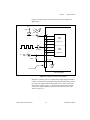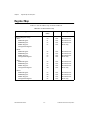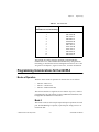
1
PCI-DIO-96 User Manual
A 96-Bit Parallel Digital I/O Interface
for PCI Bus Computers
January 1997 Edition
Part Number 320938B-01
© Copyright 1996, 1997 National Instruments Corporation. All Rights Reserved.
Internet Support
[email protected]
E-mail: [email protected]
FTP Site: ftp.natinst.com
Web Address: http://www.natinst.com
Bulletin Board Support
BBS United States: (512) 794-5422
BBS United Kingdom: 01635 551422
BBS France: 01 48 65 15 59
Fax-on-Demand Support
(512) 418-1111
Telephone Support (U.S.)
Tel: (512) 795-8248
Fax: (512) 794-5678
International Offices
Australia 03 9879 5166, Austria 0662 45 79 90 0, Belgium 02 757 00 20,
Canada (Ontario) 905 785 0085, Canada (Québec) 514 694 8521, Denmark 45 76 26 00,
Finland 09 527 2321, France 01 48 14 24 24, Germany 089 741 31 30, Hong Kong 2645 3186,
Israel 03 5734815, Italy 02 413091, Japan 03 5472 2970, Korea 02 596 7456,
Mexico 5 520 2635, Netherlands 0348 433466, Norway 32 84 84 00, Singapore 2265886,
Spain 91 640 0085, Sweden 08 730 49 70, Switzerland 056 200 51 51, Taiwan 02 377 1200,
U.K. 01635 523545
National Instruments Corporate Headquarters
6504 Bridge Point Parkway
Austin, TX 78730-5039
Tel: (512) 794-0100
Important Information
Warranty
The PCI-DIO-96 is warranted against defects in materials and workmanship for a period of one year from the date of
shipment, as evidenced by receipts or other documentation. National Instruments will, at its option, repair or replace
equipment that proves to be defective during the warranty period. This warranty includes parts and labor.
The media on which you receive National Instruments software are warranted not to fail to execute programming
instructions, due to defects in materials and workmanship, for a period of 90 days from date of shipment, as evidenced
by receipts or other documentation. National Instruments will, at its option, repair or replace software media that do
not execute programming instructions if National Instruments receives notice of such defects during the warranty
period. National Instruments does not warrant that the operation of the software shall be uninterrupted or error free.
A Return Material Authorization (RMA) number must be obtained from the factory and clearly marked on the outside
of the package before any equipment will be accepted for warranty work. National Instruments will pay the shipping
costs of returning to the owner parts which are covered by warranty.
National Instruments believes that the information in this manual is accurate. The document has been carefully
reviewed for technical accuracy. In the event that technical or typographical errors exist, National Instruments reserves
the right to make changes to subsequent editions of this document without prior notice to holders of this edition. The
reader should consult National Instruments if errors are suspected. In no event shall National Instruments be liable for
any damages arising out of or related to this document or the information contained in it.
EXCEPT AS SPECIFIED HEREIN, NATIONAL INSTRUMENTS MAKES NO WARRANTIES, EXPRESS OR IMPLIED, AND
SPECIFICALLY DISCLAIMS ANY WARRANTY OF MERCHANTABILITY OR FITNESS FOR A PARTICULAR PURPOSE.
CUSTOMER’S RIGHT TO RECOVER DAMAGES CAUSED BY FAULT OR NEGLIGENCE ON THE PART OF NATIONAL
INSTRUMENTS SHALL BE LIMITED TO THE AMOUNT THERETOFORE PAID BY THE CUSTOMER. NATIONAL INSTRUMENTS
WILL NOT BE LIABLE FOR DAMAGES RESULTING FROM LOSS OF DATA, PROFITS, USE OF PRODUCTS, OR INCIDENTAL OR
CONSEQUENTIAL DAMAGES, EVEN IF ADVISED OF THE POSSIBILITY THEREOF. This limitation of the liability of National
Instruments will apply regardless of the form of action, whether in contract or tort, including negligence. Any action
against National Instruments must be brought within one year after the cause of action accrues. National Instruments
shall not be liable for any delay in performance due to causes beyond its reasonable control. The warranty provided
herein does not cover damages, defects, malfunctions, or service failures caused by owner’s failure to follow the
National Instruments installation, operation, or maintenance instructions; owner’s modification of the product;
owner’s abuse, misuse, or negligent acts; and power failure or surges, fire, flood, accident, actions of third parties, or
other events outside reasonable control.
Copyright
Under the copyright laws, this publication may not be reproduced or transmitted in any form, electronic or mechanical,
including photocopying, recording, storing in an information retrieval system, or translating, in whole or in part,
without the prior written consent of National Instruments Corporation.
Trademarks
LabVIEW®, NI-DAQ®, ComponentWorks™, CVI™, MITE™, and SCXI™ are trademarks of National Instruments
Corporation.
Product and company names listed are trademarks or trade names of their respective companies.
WARNING REGARDING MEDICAL AND CLINICAL USE OF NATIONAL INSTRUMENTS PRODUCTS
National Instruments products are not designed with components and testing intended to ensure a level of reliability
suitable for use in treatment and diagnosis of humans. Applications of National Instruments products involving
medical or clinical treatment can create a potential for accidental injury caused by product failure, or by errors on the
part of the user or application designer. Any use or application of National Instruments products for or involving
medical or clinical treatment must be performed by properly trained and qualified medical personnel, and all traditional
medical safeguards, equipment, and procedures that are appropriate in the particular situation to prevent serious injury
or death should always continue to be used when National Instruments products are being used. National Instruments
products are NOT intended to be a substitute for any form of established process, procedure, or equipment used to
monitor or safeguard human health and safety in medical or clinical treatment.
Table
of
Contents
About This Manual
Organization of This Manual ........................................................................................ix
Conventions Used in This Manual................................................................................x
National Instruments Documentation ...........................................................................xi
Related Documentation.................................................................................................xii
Customer Communication ............................................................................................xii
Chapter 1
Introduction
About the PCI-DIO-96..................................................................................................1-1
What You Need to Get Started .....................................................................................1-2
Software Programming Choices ...................................................................................1-2
National Instruments Application Software ...................................................1-2
NI-DAQ Driver Software ...............................................................................1-3
Register-Level Programming .........................................................................1-4
Optional Equipment ......................................................................................................1-5
Custom Cabling ............................................................................................................1-5
Unpacking .....................................................................................................................1-6
Chapter 2
Installation and Configuration
Software Installation .....................................................................................................2-1
Hardware Installation....................................................................................................2-1
Board Configuration .....................................................................................................2-2
Chapter 3
Signal Connections
I/O Connector................................................................................................................3-1
I/O Connector Pin Descriptions......................................................................3-1
Port C Pin Assignments ...................................................................3-5
Digital I/O Signal Connections ......................................................................3-6
Power Connections.........................................................................................3-8
Timing Specifications.....................................................................................3-8
© National Instruments Corporation
v
PCI-DIO-96 User Manual
Table of Contents
Mode 1 Input Timing....................................................................... 3-10
Mode 1 Output Timing .................................................................... 3-11
Mode 2 Bidirectional Timing .......................................................... 3-12
Chapter 4
Theory of Operation
Functional Overview .................................................................................................... 4-1
PCI Interface Circuitry................................................................................... 4-2
82C55A Programmable Peripheral Interface ................................................. 4-3
82C53 Programmable Interval Timer ............................................................ 4-3
Interrupt Control Circuitry ............................................................................. 4-3
Chapter 5
Register Map and Description
Introduction .................................................................................................................. 5-1
Register Map ................................................................................................................ 5-2
Register Descriptions.................................................................................................... 5-3
Register Description Format .......................................................................... 5-3
Register Description for the 82C55A............................................................. 5-3
Register Description for the 82C53 ............................................................... 5-5
Register Description for the Interrupt Control Registers ............................... 5-6
Interrupt Control Register 1............................................................. 5-7
Interrupt Control Register 2............................................................. 5-9
Interrupt Clear Register ................................................................... 5-10
Chapter 6
Programming
PCl Local Bus............................................................................................................... 6-1
Programming Examples .............................................................................................. 6-1
PCI Initialization for the PC........................................................................... 6-3
PCI Initialization for the Macintosh............................................................... 6-4
Programming Options...................................................................... 6-4
Using NI-DAQ and the Driver Toolkit ............................. 6-4
Performing Simple Accesses............................................. 6-5
Developing Your Own Interrupt Method.......................... 6-5
Port Identification ............................................................................ 6-6
Programming Considerations for the 82C55A ............................................................. 6-7
Modes of Operation ....................................................................................... 6-7
Mode 0 ............................................................................................. 6-7
Mode 1 ............................................................................................. 6-8
Mode 2 ............................................................................................. 6-8
PCI-DIO-96 User Manual
vi
© National Instruments Corporation
Table of Contents
Single Bit Set/Reset Feature ............................................................6-8
Mode 0–Basic I/O...........................................................................................6-8
Mode 0 Basic I/O Programming Example .......................................6-10
Mode 1–Strobed Input....................................................................................6-10
Port C Status-Word Bit Definitions for Input (Ports A and B) ........6-12
Mode 1 Strobed Input Programming Example ................................6-13
Mode 1–Strobed Output .................................................................................6-13
Port C Status-Word Bit Definitions for Output (Ports A and B) .....6-15
Mode 1 Strobed Output Programming Example..............................6-16
Mode 2–Bidirectional Bus..............................................................................6-16
Port C Status-Word Bit Definitions for Bidirectional Data Path
(Port A Only).................................................................................6-18
Mode 2 Bidirectional Bus Programming Example ..........................6-19
Interrupt Handling.........................................................................................................6-20
Interrupt Programming Examples for the 82C55A ........................................6-20
Mode 1 Strobed Input Programming Example ................................6-21
Mode 1 Strobed Output Programming Example..............................6-21
Mode 2 Bidirectional Bus Programming Example ..........................6-21
Programming Considerations for the 82C53 ................................................................6-22
General Information .......................................................................................6-22
Interrupt Programming Example....................................................................6-22
Appendix A
Specifications
Appendix B
MSM82C55A Data Sheet
Appendix C
MSM82C53 Data Sheet
Appendix D
Customer Communication
Glossary
Index
© National Instruments Corporation
vii
PCI-DIO-96 User Manual
Table of Contents
Figures
Figure 1-1.
The Relationship between the Programming Environment,
NI-DAQ, and Your Hardware ............................................................... 1-4
Figure 3-1.
Figure 3-3.
Figure 3-4.
Figure 3-5.
Figure 3-6.
PCI-DIO-96 Cable-Assembly Connector Pinout for Pins 1 through
50 with the R1005050 Ribbon Cable .................................................... 3-2
PCI-DIO-96 Cable-Assembly Connector Pinout for Pins 51 through
100 with the R1005050 Ribbon Cable .................................................. 3-3
Digital I/O Connections Block Diagram ............................................... 3-7
Timing Specifications for Mode 1 Input Transfer................................. 3-10
Timing Specifications for Mode 1 Output Transfer .............................. 3-11
Timing Specifications for Mode 2 Bidirectional Transfer .................... 3-12
Figure 4-1.
Figure 4-2.
PCI-DIO-96 Block Diagram.................................................................. 4-2
PCI-DIO-96 Interrupt Control Circuitry Block Diagram...................... 4-4
Figure 5-1.
Figure 5-2.
Control Word Formats for the 82C55A................................................. 5-4
Control Word Format for the 82C53 ..................................................... 5-6
Figure 6-1.
Figure 6-2.
Figure 6-3.
Control Word to Configure Port A for Mode 1 Input ........................... 6-10
Control Word to Configure Port B for Mode 1 Input............................ 6-11
Port C Pin Assignments on I/O Connector when Port C Configured
for Mode 1 Input.................................................................................... 6-13
Control Word to Configure Port A for Mode 1 Output......................... 6-14
Control Word to Configure Port B for Mode 1 Output ......................... 6-14
Port C Pin Assignments on I/O Connector when Port C Configured
for Mode 1 Output ................................................................................. 6-16
Control Word to Configure Port A as Mode 2 Bidirectional
Data Bus ................................................................................................ 6-17
Port C Pin Assignments on I/O Connector when Port C is
Configured for Mode 2.......................................................................... 6-19
Figure 3-2.
Figure 6-4.
Figure 6-5.
Figure 6-6.
Figure 6-7.
Figure 6-8.
Tables
Table 3-1.
Table 3-2.
Table 3-3.
Signal Descriptions for PCI-DIO-96 I/O Connector Pins ..................... 3-4
Port C Signal Assignments.................................................................... 3-5
Signal Names Used in Timing Diagrams .............................................. 3-8
Table 5-1.
Table 5-2.
PCI-DIO-96 Address Map..................................................................... 5-2
Port C Set/Reset Control Words............................................................ 5-5
Table 6-1.
Table 6-2.
Port Identification.................................................................................. 6-7
Mode 0 I/O Configurations ................................................................... 6-9
PCI-DIO-96 User Manual
viii
© National Instruments Corporation
About
This
Manual
This manual describes the electrical and mechanical aspects of the
PCI-DIO-96 and contains information concerning its installation,
operation, and programming. The PCI-DIO-96 is a member of the
National Instruments PCI Series of expansion boards for PCI bus
computers. These boards are designed for high-performance data
acquisition and control for applications in laboratory testing,
production testing, and industrial process monitoring and control.
Organization of This Manual
The PCI-DIO-96 User Manual is organized as follows:
•
Chapter 1, Introduction, describes the PCI-DIO-96; lists what you
need to get started, software programming choices, and optional
equipment; describes custom cabling options; and explains how to
unpack the PCI-DIO-96.
•
Chapter 2, Installation and Configuration, describes how to install
and configure your PCI-DIO-96 board.
•
Chapter 3, Signal Connections, describes how to make input and
output signal connections to your PCI-DIO-96 via the board I/O
connector.
•
Chapter 4, Theory of Operation, contains a functional overview of
the PCI-DIO-96 and explains the operation of each functional unit
comprising the PCI-DIO-96.
•
Chapter 5, Register Map and Description, describes in detail the
address and function of each PCI-DIO-96 register.
•
Chapter 6, Programming, contains instructions on how to operate
the PCI-DIO-96 circuitry, and examples of the programming steps
necessary to execute an operation.
•
Appendix A, Specifications, lists the specifications of the
PCI-DIO-96.
© National Instruments Corporation
ix
PCI-DIO-96 User Manual
About This Manual
•
Appendix B, MSM82C55A Data Sheet, contains a manufacturer
data sheet for the MSM82C55A CMOS programmable peripheral
interface (OKI Semiconductor). This device is used on the
PCI-DIO-96.
•
Appendix C, MSM82C53 Data Sheet, contains a manufacturer data
sheet for the MSM82C53 CMOS programmable interval timer
(OKI Semiconductor). This timer is used on the PCI-DIO-96.
•
Appendix D, Customer Communication, contains forms you can
use to request help from National Instruments or to comment on our
products.
•
The Glossary contains an alphabetical list and description of terms
used in this manual, including abbreviations, acronyms, metric
prefixes, mnemonics, symbols, and terms.
•
The Index contains an alphabetical list of key terms and topics used
in this manual, including the page where each one can be found.
Conventions Used in This Manual
The following conventions are used in this manual:
bold
Bold text denotes menu items, function panel items, and dialog box
buttons or options.
bold italic
Bold italic text denotes a note, caution, or warning.
italic
Italic text denotes emphasis, a cross reference, or an introduction to a
key concept.
Macintosh
Macintosh refers to all Macintosh computers with PCI bus, unless
otherwise noted.
monospace
Text in this font denotes text or characters that are to be literally input
from the keyboard, sections of code, programming examples, and
syntax examples. This font is also used for the proper names of disk
drives, paths, directories, programs, subprograms, subroutines, device
names, functions, variables, parameters, file names, and extensions, and
for statements and comments taken from program code.
NI-DAQ
NI-DAQ is used in this manual to refer to NI-DAQ software for PC or
Macintosh computers unless otherwise noted.
PC
PC refers to all IBM PC compatible computers with PCI bus.
PPI x
PPI x, where the x is replaced by A, B, C, or D, refers to one of the four
programmable peripheral interface (PPI) chips on the PCI-DIO-96.
PCI-DIO-96 User Manual
x
© National Instruments Corporation
About This Manual
SCXI
SCXI stands for Signal Conditioning eXtensions for Instrumentation
and is a National Instruments product line designed to perform
front-end signal conditioning for National Instruments plug-in DAQ
boards.
<>
Angle brackets containing numbers separated by an ellipses represent a
range of values associated with a bit, signal, or port (for example,
ACH<0..7> stands for ACH0 through ACH7).
Abbreviations, acronyms, metric prefixes, mnemonics, symbols, and
terms are listed in the Glossary.
National Instruments Documentation
The PCI-DIO-96 User Manual is one piece of the documentation set for
your data acquisition system. You could have any of several types of
manuals, depending on the hardware and software in your system. Use
the manuals you have as follows:
•
Getting Started with SCXI—If you are using SCXI, this is the first
manual you should read. It gives an overview of the SCXI system
and contains the most commonly needed information for the
modules, chassis, and software.
•
Your SCXI hardware user manuals—If you are using SCXI, read
these manuals next for detailed information about signal
connections and module configuration. They also explain in greater
detail how the module works and contain application hints.
•
Your DAQ hardware user manuals—These manuals have detailed
information about the DAQ hardware that plugs into or is
connected to your computer. Use these manuals for hardware
installation and configuration instructions, specification
information about your DAQ hardware, and application hints.
•
Software documentation—Examples of software documentation
you may have are the LabVIEW, LabWindows/CVI, or
ComponentWorks documentation sets and the NI-DAQ
documentation. After you set up your hardware system, use either
the application software or the NI-DAQ documentation to help you
write your application. If you have a large and complicated system,
it is worthwhile to look through the software documentation before
you configure your hardware.
© National Instruments Corporation
xi
PCI-DIO-96 User Manual
About This Manual
•
Accessory installation guides or manuals—If you are using
accessory products, read the terminal block and cable assembly
installation guides or accessory board user manuals. They explain
how to physically connect the relevant pieces of the system.
Consult these guides when you are making your connections.
•
SCXI Chassis User Manual—If you are using SCXI, read these
manuals for maintenance information on the chassis and
installation instructions.
Related Documentation
The following National Instruments document contains information
that you may find helpful as you read this manual:
•
Application Note 025, Field Wiring and Noise Considerations for
Analog Signals
The following documents also contain information that you may find
helpful as you read this manual:
•
Your computer’s technical reference manual
•
PCI Local Bus Specification, Revision 2.0
Customer Communication
National Instruments wants to receive your comments on our products
and manuals. We are interested in the applications you develop with our
products, and we want to help if you have problems with them. To make
it easy for you to contact us, this manual contains comment and
configuration forms for you to complete. These forms are in
Appendix D, Customer Communication, at the end of this manual.
PCI-DIO-96 User Manual
xii
© National Instruments Corporation
Chapter
1
Introduction
This chapter describes the PCI-DIO-96; lists what you need to get
started, software programming choices, optional equipment; describes
custom cabling options; and explains how to unpack the PCI-DIO-96.
About the PCI-DIO-96
Thank you for purchasing a National Instruments PCI-DIO-96 board.
The PCI-DIO-96 is a 96-bit, parallel, digital I/O interface for PCI bus
computers. Four 82C55A programmable peripheral interface (PPI)
chips control the 96 bits of TTL-compatible digital I/O. The four OKI
Semiconductor 82C55A PPI chips can operate in unidirectional mode,
bidirectional mode, or handshaking mode and can generate interrupt
requests to your computer. You can program the 82C55A for almost any
8-bit or 16-bit digital I/O application. The OKI Semiconductor 82C53
counter/timer chip has two usable counters that can generate timed
interrupt requests to your computer. The digital I/O lines are all
accessible through a 100-pin female connector.
The PCI-DIO-96 is a completely switchless and jumperless DAQ board.
All resource allocation is completed automatically at startup, so you
will not need to set interrupt levels or base addresses for the
PCI-DIO-96.
You can use the PCI-DIO-96 in a wide range of digital I/O applications.
For example, you can connect the PCI-DIO-96 to any of the following:
panel meters, instruments and test equipment with BCD readouts and/or
controls, or optically isolated, solid-state relays and I/O module
mounting racks.
With the PCI-DIO-96, you can use your computer as a digital I/O
system controller for laboratory testing, production testing, and
industrial process monitoring and control.
Detailed PCI-DIO-96 specifications are in Appendix A, Specifications.
© National Instruments Corporation
1-1
PCI-DIO-96 User Manual
Chapter 1
Introduction
What You Need to Get Started
To set up and use your PCI-DIO-96 board, you will need the following:
❑ PCI-DIO-96 board
❑ PCI-DIO-96 User Manual
❑ One of the following software packages and documentation:
ComponentWorks
LabVIEW for Macintosh
LabVIEW for Windows
LabWindows/CVI for Windows
NI-DAQ for Macintosh
NI-DAQ for PC Compatibles
❑ Your computer
Software Programming Choices
There are several options to choose from when programming your
National Instruments DAQ hardware. You can use LabVIEW,
LabWindows/CVI, ComponentWorks, or other application
development environments with the NI-DAQ instrument driver, or you
can register-level program.
National Instruments Application Software
ComponentWorks contains tools for data acquisition and instrument
control built on NI-DAQ driver software. ComponentWorks provides a
higher-level programming interface for building virtual instruments
through standard OLE controls and DLLs. With ComponentWorks, you
can use all of the configuration tools, resource management utilities,
and interactive control utilities included with NI-DAQ.
LabVIEW features interactive graphics, a state-of-the-art user
interface, and a powerful graphical programming language. The
LabVIEW Data Acquisition VI Library, a series of VIs for using
LabVIEW with National Instruments DAQ hardware, is included with
LabVIEW. The LabVIEW Data Acquisition VI Library is functionally
equivalent to the NI-DAQ software.
PCI-DIO-96 User Manual
1-2
© National Instruments Corporation
Chapter 1
Introduction
LabWindows/CVI features interactive graphics, a state-of-the-art user
interface, and uses the ANSI standard C programming language. The
LabWindows/CVI Data Acquisition Library, a series of functions for
using LabWindows/CVI with National Instruments DAQ hardware, is
included with the NI-DAQ software kit. The LabWindows/CVI Data
Acquisition Library is functionally equivalent to the NI-DAQ software.
Using ComponentWorks, LabVIEW, or LabWindows/CVI software
will greatly reduce the development time for your data acquisition and
control application.
NI-DAQ Driver Software
The NI-DAQ driver software is included at no charge with all National
Instruments DAQ hardware. NI-DAQ is not included with SCXI or
accessory products, except the SCXI-1200. NI-DAQ has an extensive
library of functions that you can call from your application
programming environment. These functions include routines for analog
input (A/D conversion), buffered data acquisition (high-speed A/D
conversion), analog output (D/A conversion), waveform generation
(timed D/A conversion), digital I/O, counter/timer operations, SCXI,
RTSI, self-calibration, messaging, and acquiring data to memory.
NI-DAQ has both high-level DAQ I/O functions for maximum ease of
use and low-level DAQ I/O functions for maximum flexibility and
performance. Examples of high-level functions are streaming data to
disk or acquiring a certain number of data points. An example of a
low-level function is writing directly to registers on the DAQ device.
NI-DAQ does not sacrifice the performance of National Instruments
DAQ devices because it lets multiple devices operate at their peak
performance.
NI-DAQ also internally addresses many of the complex issues between
the computer and the DAQ hardware such as programming interrupts
and DMA controllers. NI-DAQ maintains a consistent software
interface among its different versions so that you can change platforms
with minimal modifications to your code. Whether you are using
conventional programming languages, ComponentWorks, LabVIEW,
or LabWindows/CVI, your application uses the NI-DAQ driver
software, as illustrated in Figure 1-1.
© National Instruments Corporation
1-3
PCI-DIO-96 User Manual
Chapter 1
Introduction
Conventional
Programming Environment
ComponentWorks,
LabVIEW, or
LabWindows/CVI
NI-DAQ
Driver Software
DAQ or
SCXI Hardware
Personal
Computer or
Workstation
Figure 1-1. The Relationship between the Programming Environment,
NI-DAQ, and Your Hardware
Register-Level Programming
The final option for programming any National Instruments DAQ
hardware is to write register-level software. Writing register-level
programming software can be very time-consuming and inefficient, and
is not recommended for most users.
Even if you are an experienced register-level programmer, consider
using NI-DAQ or other National Instruments application software to
program your National Instruments DAQ hardware. Using NI-DAQ,
ComponentWorks, LabVIEW, or LabWindows/CVI software is easier
than, and as flexible as, register-level programming, and can save
weeks of development time.
PCI-DIO-96 User Manual
1-4
© National Instruments Corporation
Chapter 1
Introduction
Optional Equipment
National Instruments offers a variety of products to use with your
PCI-DIO-96 board, including cables, connector blocks, and other
accessories, as follows:
•
Cables and cable assemblies
•
Connector blocks, 50-pin screw terminals
•
SCXI modules and accessories for isolating, amplifying, exciting,
and multiplexing signals for relays and analog output. With SCXI
you can condition and acquire up to 3,072 channels.
•
Low channel count signal conditioning modules, boards, and
accessories, including conditioning for strain gauges and RTDs,
simultaneous sample and hold, and relays
For more information about optional equipment available from
National Instruments, refer to your National Instruments catalog or call
the office nearest you.
Custom Cabling
National Instruments offers cables and accessories for you to prototype
your application or to use if you frequently change board
interconnections.
If you want to develop your own cable, the mating connector for the
PCI-DIO-96 is a 100-position, right-angle receptacle without board
locks. Recommended manufacturer part numbers for this mating
connector are as follows:
•
AMP Corporation (part number 749076-9)
•
Honda Corporation (part number PCS-XE100LFD-HS)
© National Instruments Corporation
1-5
PCI-DIO-96 User Manual
Chapter 1
Introduction
Unpacking
Your PCI-DIO-96 board is shipped in an antistatic package to prevent
electrostatic damage to the board. Electrostatic discharge can damage
several components on the board. To avoid such damage in handling the
board, take the following precautions.
PCI-DIO-96 User Manual
•
Ground yourself via a grounding strap or by holding a grounded
object.
•
Touch the antistatic package to a metal part of your computer
chassis before removing the board from the package.
•
Remove the board from the package and inspect the board for loose
components or any other sign of damage. Notify National
Instruments if the board appears damaged in any way. Do not
install a damaged board into your computer.
•
Never touch the exposed pins of connectors.
1-6
© National Instruments Corporation
Chapter
Installation and
Configuration
2
This chapter describes how to install and configure your PCI-DIO-96
board.
Software Installation
If you are using NI-DAQ, ComponentWorks, LabWindows/CVI, or
LabVIEW, refer to the installation instructions in your documentation
to install and configure your software.
If you are a register-level programmer, refer to Chapter 5, Register Map
and Description, and Chapter 6, Programming, of this manual.
Hardware Installation
The PCI-DIO-96 can be installed in any unused PCI expansion slot in
your computer.
The following are general installation instructions. Consult your
computer user manual or technical reference manual for specific
instructions and warnings.
1.
Turn off your computer.
2.
Remove the top cover or access port to the I/O channel.
3.
Remove the expansion slot cover on the back panel of the
computer.
4.
Insert the PCI-DIO-96 in an unused 5 V PCI slot. The fit may be
tight, but do not force the board into place.
5.
Screw the PCI-DIO-96 mounting bracket to the back panel rail of
the computer, or use the slot side tabs, if available, to secure the
PCI-DIO-96 in place.
6.
Replace the computer cover.
The PCI-DIO-96 board is installed. You are now ready to configure
your hardware.
© National Instruments Corporation
2-1
PCI-DIO-96 User Manual
Chapter 2
Installation and Configuration
Board Configuration
The PCI-DIO-96 is completely software configurable. The PCI-DIO-96
is fully compliant with the PCI Local Bus Specification, Revision 2.0.
Therefore, all board resources are automatically allocated by the PCI
system, including the base address and interrupt level. The base address
for the PCI-DIO-96 is mapped into PCI memory space. You do not need
to perform any configuration steps after the system powers up.
PCI-DIO-96 User Manual
2-2
© National Instruments Corporation
Chapter
3
Signal Connections
This chapter describes how to make input and output signal connections
to your PCI-DIO-96 via the board I/O connector.
I/O Connector
The I/O connector for the PCI-DIO-96 has 100 pins that you can
connect to 50-pin accessories with the R1005050 cable.
!
Warning: Connections that exceed any of the maximum ratings of input or output
signals on the PCI-DIO-96 can damage the PCI-DIO-96 board and your
computer. The description of each signal in this chapter includes
information about maximum input ratings. National Instruments is NOT
liable for any damages resulting from signal connections that exceed these
maximum ratings.
I/O Connector Pin Descriptions
Figures 3-1 and 3-2 show the pin assignments for the PCI-DIO-96
digital I/O connector using the R1005050 ribbon cable.
See Table 3-1 for descriptions of each pin on the I/O connector.
© National Instruments Corporation
3-1
PCI-DIO-96 User Manual
Chapter 3
Signal Connections
APC7
1
2
BPC7
APC6
3
4
BPC6
APC5
5
6
BPC5
APC4
7
8
BPC4
APC3
9
10
BPC3
APC2
11 12
BPC2
APC1
13 14
BPC1
APC0
15 16
BPC0
APB7
17 18
BPB7
APB6
19 20
BPB6
APB5
21 22
BPB5
APB4
23 24
BPB4
APB3
25 26
BPB3
APB2
27 28
BPB2
APB1
29 30
BPB1
APB0
31 32
BPB0
APA7
33 34
BPA7
APA6
35 36
BPA6
APA5
37 38
BPA5
APA4
39 40
BPA4
APA3
41 42
BPA3
APA2
43 44
BPA2
APA1
45 46
BPA1
APA0
47 48
BPA0
+5 V
49 50
GND
Figure 3-1. PCI-DIO-96 Cable-Assembly Connector Pinout for Pins 1 through 50
with the R1005050 Ribbon Cable
PCI-DIO-96 User Manual
3-2
© National Instruments Corporation
Chapter 3
CPC7
51 52
DPC7
CPC6
53 54
DPC6
CPC5
55 56
DPC5
CPC4
57 58
DPC4
CPC3
59 60
DPC3
CPC2
61 62
DPC2
CPC1
63 64
DPC1
CPC0
65 66
DPC0
CPB7
67 68
DPB7
CPB6
69 70
DPB6
CPB5
71 72
DPB5
CPB4
73 74
DPB4
CPB3
75 76
DPB3
CPB2
77 78
DPB2
CPB1
79 80
DPB1
CPB0
81 82
DPB0
CPA7
83 84
DPA7
CPA6
85 86
DPA6
CPA5
87 88
DPA5
CPA4
89 90
DPA4
CPA3
91 92
DPA3
CPA2
93 94
DPA2
CPA1
95 96
DPA1
CPA0
97 98
DPA0
+5 V
99 100
GND
Signal Connections
Figure 3-2. PCI-DIO-96 Cable-Assembly Connector Pinout for Pins 51 through 100
with the R1005050 Ribbon Cable
© National Instruments Corporation
3-3
PCI-DIO-96 User Manual
Chapter 3
Signal Connections
Table 3-1 lists the signal descriptions for the PCI-DIO-96 I/O connector
pins.
Table 3-1. Signal Descriptions for PCI-DIO-96 I/O Connector Pins
Pin
Signal Name
Description
1, 3, 5, 7, 9, 11,
13, 15
APC<7..0>
Bidirectional data lines for port C of PPI A—APC7 is the
MSB, APC0 the LSB.
2, 4, 6, 8, 10, 12,
14, 16
BPC<7..0>
Bidirectional data lines for port C of PPI B—BPC7 is the
MSB, BPC0 the LSB.
17, 19, 21, 23,
25, 27, 29, 31
APB<7..0>
Bidirectional data lines for port B of PPI A—APB7 is the
MSB, APB0 the LSB.
18, 20, 22, 24,
26, 28, 30, 32
BPB<7..0>
Bidirectional data lines for port B of PPI B—BPB7 is the
MSB, BPB0 the LSB.
33, 35, 37, 39,
41, 43, 45, 47
APA<7..0>
Bidirectional data lines for port A of PPI A—APA7 is the
MSB, APA0 the LSB.
34, 36, 38, 40,
42, 44, 46, 48
BPA<7..0>
Bidirectional data lines for port A of PPI B—BPA7 is the
MSB, BPA0 the LSB.
49, 99
+5 V supply
+5 Volts—These pins are fused for up to 1 A total of +4.65
to +5.25 V.
50, 100
GND
Ground—These pins are connected to the computer ground
signal.
51, 53, 55, 57,
59, 61, 63, 65
CPC<7..0>
Bidirectional data lines for port C of PPI C—CPC7 is the
MSB, CPC0 the LSB.
52, 54, 56, 58,
60, 62, 64, 66
DPC<7..0>
Bidirectional data lines for port C of PPI D—DPC7 is the
MSB, DPC0 the LSB.
67, 69, 71, 73,
75, 77, 79, 81
CPB<7..0>
Bidirectional data lines for port B of PPI C—CPB7 is the
MSB, CPB0 the LSB.
68, 70, 72, 74,
76, 78, 80, 82
DPB<7..0>
Bidirectional data lines for port B of PPI D—DPB7 is the
MSB, DPB0 the LSB.
PCI-DIO-96 User Manual
3-4
© National Instruments Corporation
Chapter 3
Signal Connections
Table 3-1. Signal Descriptions for PCI-DIO-96 I/O Connector Pins (Continued)
Pin
Signal Name
Description
83, 85, 87, 89,
91, 93, 95, 97
CPA<7..0>
Bidirectional data lines for port A of PPI C—CPA7 is the
MSB, CPA0 the LSB.
84, 86, 88, 90,
92, 94, 96, 98
DPA<7..0>
Bidirectional data lines for port A of PPI D—DPA7 is the
MSB, DPA0 the LSB.
Port C Pin Assignments
The signals assigned to port C depend on how the 82C55A is
configured. In mode 0, or no handshaking configuration, port C is
configured as two 4-bit I/O ports. In modes 1 and 2, or handshaking
configuration, port C is used for status and handshaking signals with
zero, two, or three lines available for general-purpose I/O. Table 3-2
summarizes the port C signal assignments for each configuration.
Consult Chapter 6, Programming, for register-level programming
information.
Note:
Table 3-2 shows both the port C signal assignments and the terminology
correlation between different documentation sources. The 82C55A
terminology refers to the different 82C55A configurations as modes
whereas NI-DAQ, ComponentWorks, LabWindows/CVI, and LabVIEW
documentation refers to them as handshaking and no handshaking. These
signal assignments are the same for all four 82C55A PPIs. Refer to Port
Identification in Chapter 6, Programming, for more information.
Table 3-2. Port C Signal Assignments
Configuration Terminology
82C55A/
PCI-DIO-96
User Manual
National
Instruments
Software
Signal Assignments
APC7,
BPC7,
CPC7,
or
DPC7
APC6,
BPC6,
CPC6,
or
DPC6
APC5,
BPC5,
CPC5,
or
DPC5
APC4,
BPC4,
CPC4,
or
DPC4
APC3,
BPC3,
CPC3,
or
DPC3
APC2,
BPC2,
CPC2,
or
DPC2
APC1,
BPC1,
CPC1,
or
DPC1
APC0,
BPC0,
CPC0,
or
DPC0
Mode 0
(Basic I/O)
No
Handshaking
I/O
I/O
I/O
I/O
I/O
I/O
I/O
I/O
Mode 1
(Strobed Input)
Handshaking
I/O
I/O
IBFA
STBA*
INTRA
STBB*
IBFBB
INTRB
© National Instruments Corporation
3-5
PCI-DIO-96 User Manual
Chapter 3
Signal Connections
Table 3-2. Port C Signal Assignments (Continued)
Configuration Terminology
82C55A/
PCI-DIO-96
User Manual
Signal Assignments
National
Instruments
Software
APC7,
BPC7,
CPC7,
or
DPC7
APC6,
BPC6,
CPC6,
or
DPC6
APC5,
BPC5,
CPC5,
or
DPC5
APC4,
BPC4,
CPC4,
or
DPC4
APC3,
BPC3,
CPC3,
or
DPC3
APC2,
BPC2,
CPC2,
or
DPC2
APC1,
BPC1,
CPC1,
or
DPC1
APC0,
BPC0,
CPC0,
or
DPC0
Mode 1
(Strobed
Output)
Handshaking
OBFA*
ACKA*
I/O
I/O
INTRA
ACKB*
OBFB*
INTRB
Mode 2
(Bidirectional
Bus)
Handshaking
OBFA*
ACKA*
IBFA
STBA*
INTRA
I/O
I/O
I/O
*Indicates that the signal is active low.
Subscripts A and B denote port A or port B handshaking signals.
Digital I/O Signal Connections
Pins 1 through 48 and pins 51 through 98 of the I/O connector are
digital I/O signal pins. The following specifications and ratings apply
to the digital I/O lines.
•
Absolute maximum voltage rating
•
Digital input specifications (referenced to GND):
– Input logic high
2.2 V minimum
5.3 V maximum
voltage
•
PCI-DIO-96 User Manual
-0.5 to +5.5 V with
respect to GND
–
Input logic low
voltage
-0.3 V minimum
0.8 V maximum
–
Maximum input
current
(0 < Vin < 5 V)
-1 µA minimum
1 µA maximum
Digital output specifications (referenced to GND):
– Output logic high 3.7 V minimum
—
voltage at
Iout = -2.5 mA
– Output logic low
—
0.4 V maximum at
voltage
Iout = 2.5 mA
3-6
© National Instruments Corporation
Chapter 3
Signal Connections
Figure 3-3 depicts signal connections for three typical digital I/O
applications.
+5 V
LED
41
PPI A
Port A
43
45
APA<3..0>
47
67
69
PPI C
Port B
TTL Signal
71
CPB<7..4>
73
+5 V
Switch
50, 100
GND
I/O Connector
PCI-DIO-96 Board
Figure 3-3. Digital I/O Connections Block Diagram
In Figure 3-3, PPI A, port A, is configured for digital output, and PPI C,
port B, is configured for digital input. Digital input applications include
receiving TTL signals and sensing external device states such as the
state of the switch in Figure 3-3. Digital output applications include
sending TTL signals and driving external devices such as the LED
shown in Figure 3-3.
© National Instruments Corporation
3-7
PCI-DIO-96 User Manual
Chapter 3
Signal Connections
Power Connections
Pins 49 and 99 of the I/O connector supply +5 V from the computer’s
power supply via a self-resetting fuse. The fuse will reset automatically
within a few seconds after the overcurrent condition is removed. These
pins are referenced to GND and can be used to power external digital
circuitry. For more information on these output pins, see Appendix A,
Specifications.
•
Power rating
1 A at +4.65 to +5.25 V
Warning: Under no circumstances should you connect these +5 V power pins directly
to ground or to any other voltage source on the PCI-DIO-96 or any other
device. Doing so can damage the PCI-DIO-96 and the computer. National
Instruments is NOT liable for damage resulting from such a connection.
!
Timing Specifications
This section lists the timing specifications for handshaking with the
PCI-DIO-96. The handshaking lines STB* and IBF synchronize input
transfers. The handshaking lines OBF* and ACK* synchronize output
transfers.
Table 3-3 describes the connector pins on the PCI-DIO-96 I/O
connector by pin number and gives the signal name and description of
each signal connector pin.
Table 3-3. Signal Names Used in Timing Diagrams
Name
Type
Description
STB*
Input
Strobe Input—A low signal on this handshaking line loads data
into the input latch.
IBF
Output
Input Buffer Full—A high signal on this handshaking line
indicates that data has been loaded into the input latch. This is
an input acknowledge signal.
ACK*
Input
Acknowledge Input—A low signal on this handshaking line
indicates that the data written to the port has been accepted.
This signal is a response from the external device indicating
that it has received the data from the PCI-DIO-96.
OBF*
Output
Output Buffer Full—A low signal on this handshaking line
indicates that data has been written to the port.
PCI-DIO-96 User Manual
3-8
© National Instruments Corporation
Chapter 3
Signal Connections
Table 3-3. Signal Names Used in Timing Diagrams (Continued)
Name
Type
Description
INTR
Output
Interrupt Request—This signal becomes high when the
82C55A requests service during a data transfer. The
appropriate interrupt enable bits must be set to generate this
signal.
RD*
Internal
Read—This signal is the read signal generated from the control
lines of the computer I/O expansion bus.
WR*
Internal
Write —This signal is the write signal generated from the
control lines of the computer I/O expansion bus.
DATA
Bidirectional
Data Lines at the Specified Port—This signal indicates the
availability of data on the data lines at a port that is in the output
mode. If the port is in the input mode, this signal indicates when
the data on the data lines should be valid.
© National Instruments Corporation
3-9
PCI-DIO-96 User Manual
Chapter 3
Signal Connections
Mode 1 Input Timing
The timing specifications for an input transfer in mode 1 are as follows:
T1
T2
T4
STB *
T7
IBF
T6
INTR
RD *
T3
T5
DATA
Name
Description
Minimum
Maximum
T1
STB* Pulse Width
100
—
T2
STB* = 0 to IBF = 1
—
150
T3
Data before STB* = 1
20
—
T4
STB* = 1 to INTR = 1
—
150
T5
Data after STB* = 1
50
—
T6
RD* = 0 to INTR = 0
—
200
—
150
T7
RD* = 1 to IBF = 0
All timing values are in nanoseconds.
Figure 3-4. Timing Specifications for Mode 1 Input Transfer
PCI-DIO-96 User Manual
3-10
© National Instruments Corporation
Chapter 3
Signal Connections
Mode 1 Output Timing
The timing specifications for an output transfer in mode 1 are as
follows:
T3
WR*
T4
OBF*
T1
T6
INTR
T5
ACK*
DATA
T2
Name
Description
Minimum
Maximum
T1
WR* = 0 to INTR = 0
—
250
T2
WR* = 1 to Output
—
200
T3
WR* = 1 to OBF* = 0
—
150
T4
ACK* = 0 to OBF* = 1
—
150
T5
ACK* Pulse Width
100
—
—
150
T6
ACK* = 1 to INTR = 1
All timing values are in nanoseconds.
Figure 3-5. Timing Specifications for Mode 1 Output Transfer
© National Instruments Corporation
3-11
PCI-DIO-96 User Manual
Chapter 3
Signal Connections
Mode 2 Bidirectional Timing
The timing specifications for bidirectional transfers in mode 2 are as
follows:
T1
WR *
T6
OBF *
INTR
T7
ACK *
T3
STB *
T10
T4
IBF
RD *
T2
T5
T8
T9
DATA
Name
Description
Minimum
Maximum
T1
WR* = 1 to OBF* = 0
—
150
T2
Data before STB* = 1
20
—
T3
STB* Pulse Width
100
—
T4
STB* = 0 to IBF = 1
—
150
T5
Data after STB* = 1
50
—
T6
ACK* = 0 to OBF* = 1
—
150
T7
ACK* Pulse Width
100
—
T8
ACK* = 0 to Output
—
150
T9
ACK* = 1 to Output Float
20
250
—
150
T10
RD* = 1 to IBF = 0
All timing values are in nanoseconds.
Figure 3-6. Timing Specifications for Mode 2 Bidirectional Transfer
PCI-DIO-96 User Manual
3-12
© National Instruments Corporation
Chapter
4
Theory of Operation
This chapter contains a functional overview of the PCI-DIO-96 and
explains the operation of each functional unit comprising the
PCI-DIO-96.
Functional Overview
The block diagram in Figure 4-1 illustrates the key functional
components of the PCI-DIO-96 board.
© National Instruments Corporation
4-1
PCI-DIO-96 User Manual
Chapter 4
Theory of Operation
Data/Address
37
82C55A
PPI A
Interface Control
Port A
8
Port B
8
Port C
8
Port A
8
Port B
8
Port C
8
Port A
8
Port B
8
Port C
8
Port A
8
Port B
8
Port C
8
Error Reporting
MITE
PCI
Interface
Circuitry
2
Arbitration
Data
Bus
82C55A
PPI B
2
System
PCI
2
82C55A
PPI C
Interrupt
1
Interrupt
Interrupt
Control
Circuitry
82C55A
PPI D
Interrupt
Bus
I/O Connector
6
82C53
Timer
+5 VDC
1 A Fuse
Figure 4-1. PCI-DIO-96 Block Diagram
PCI Interface Circuitry
The PCI-DIO-96 uses the MITE ASIC to communicate with the PCI
bus. The MITE ASIC was designed by National Instruments
specifically for data acquisition. The PCI-DIO-96 is fully compliant
with Local Bus Specification 2.0.
The base memory address and interrupt level for the board are stored
inside the MITE at power on. You do not need to set any switches or
jumpers.
PCI-DIO-96 User Manual
4-2
© National Instruments Corporation
Chapter 4
Theory of Operation
82C55A Programmable Peripheral Interface
The four 82C55A PPI chips are the heart of the PCI-DIO-96. Each of
these chips has 24 programmable I/O pins that represent three 8-bit
ports: PA, PB, and PC. Each port can be programmed as an input or
output port. The 82C55A has three modes of operation: simple I/O
(mode 0), strobed I/O (mode 1), and bidirectional I/O (mode 2). In
modes 1 and 2, the three ports are divided into two groups: group A and
group B. Each group has eight data bits and four control and status bits
from port C (PC). Modes 1 and 2 use handshaking signals from the
computer to synchronize data transfers. Refer to Chapter 6,
Programming, or to Appendix B, MSM82C55A Data Sheet, for more
detailed information.
82C53 Programmable Interval Timer
The 82C53 programmable interval timer generates timed interrupt
requests to your computer. The 82C53 has three 16-bit counters, which
can each be used in one of six different modes. The PCI-DIO-96 uses
two of the counters to generate interrupt requests; the third counter is
not used and is not accessible. Refer to Chapter 5, Register Map and
Description, or to Appendix C, MSM82C53 Data Sheet, for more
detailed information.
Interrupt Control Circuitry
Two software-controlled registers determine which devices, if any,
generate interrupts. Each of the four 82C55A devices has two interrupt
lines, PC3 and PC0, connected to the interrupt circuitry. The 82C53
device has two of its three counter outputs connected to the interrupt
circuitry. Any of these 10 signals can interrupt the computer if the
interrupt circuitry is enabled and the corresponding enable bit is set. See
Chapter 5, Register Map and Description, for more information.
Normally, the handshaking circuitry controls PC3 and/or PC0 of the
82C55A devices; however, you can configure either of these two lines
for input and then use them as external interrupts. An interrupt occurs
on the signal line low-to-high transition.
Refer to Chapter 5, Register Map and Description, Chapter 6,
Programming, Appendix B, MSM82C55A Data Sheet, or Appendix C,
MSM82C53 Data Sheet, for more detailed information concerning
interrupts.
© National Instruments Corporation
4-3
PCI-DIO-96 User Manual
Chapter 4
Theory of Operation
The block diagram in Figure 4-2 illustrates the PCI-DIO-96 interrupt
control circuitry.
82C53
Counter/Timer
CLK0
2 MHz
+5 V
OUT0
GATE0
CLK1
+5 V
OUT1
PCI
Interrupt
GATE1
CLK2
OUT2
GATE2
PC3
82C55A
PPI A
PC0
Interrupt
Control
Circuitry
PC3
82C55A
PPI B
PC0
PC3
82C55A
PPI C
PC0
PC3
82C55A
PPI D
PC0
PCI-DIO-96
Interrupt Control Registers
Figure 4-2. PCI-DIO-96 Interrupt Control Circuitry Block Diagram
PCI-DIO-96 User Manual
4-4
© National Instruments Corporation
Chapter
Register Map and
Description
5
This chapter describes in detail the address and function of each
PCI-DIO-96 register.
Note:
If you plan to use a programming software package such as
ComponentWorks, LabVIEW, LabWindows/CVI, or NI-DAQ with your
PCI-DIO-96 board, you need not read this chapter.
Introduction
The three 8-bit ports of the 82C55A are divided into two groups of 12
signals: group A and group B. One 8-bit control word selects the mode
of operation for each group. The group A control bits configure port A
(A<7..0>) and the upper 4 bits (nibble) of port C (C<7..4>). The
group B control bits configure port B (B<7..0>) and the lower nibble of
port C (C<3..0>). These configuration bits are defined in the section
Register Description for the 82C55A later in this chapter. Because there
are four 82C55A PPI devices on the board, they are referenced as
PPI A, PPI B, PPI C, and PPI D when differentiation is required.
The three 16-bit counters of the 82C53 are accessed through individual
data ports and controlled by one 8-bit control word. The control word
selects how the counter data ports are accessed and what mode the
counter uses. The configuration bits are defined in the section Register
Description for the 82C53 later in this chapter.
In addition to the 82C55A and 82C53 devices, there are two registers
that select which onboard signals are capable of generating interrupts.
There are two interrupt signals from each of the four 82C55A devices
and two interrupt signals from the 82C53 device. Individual enable bits
select which of these 10 signals can generate interrupts. Also, a master
enable signal determines whether the board can actually send a request
to the computer. The configuration bits for these registers are defined
in the section Register Description for the Interrupt Control Registers
later in this chapter.
© National Instruments Corporation
5-1
PCI-DIO-96 User Manual
Chapter 5
Register Map and Description
Register Map
Table 5-1 lists the address map for the PCI-DIO-96.
Table 5-1. PCI-DIO-96 Address Map
Register Name
Offset Address
(Hex)
Size
00
01
02
03
8-bit
8-bit
8-bit
8-bit
Read-and-write
Read-and-write
Read-and-write
Write-only
PPI B
PORTA Register
PORTB Register
PORTC Register
Configuration Register
04
05
06
07
8-bit
8-bit
8-bit
8-bit
Read-and-write
Read-and-write
Read-and-write
Write-only
PPI C
PORTA Register
PORTB Register
PORTC Register
Configuration Register
08
09
0A
0B
8-bit
8-bit
8-bit
8-bit
Read-and-write
Read-and-write
Read-and-write
Write-only
PPI D
PORTA Register
PORTB Register
PORTC Register
Configuration Register
0C
0D
0E
0F
8-bit
8-bit
8-bit
8-bit
Read-and-write
Read-and-write
Read-and-write
Write-only
82C55A Register Group
PPI A
PORTA Register
PORTB Register
PORTC Register
Configuration Register
PCI-DIO-96 User Manual
5-2
Type
© National Instruments Corporation
Chapter 5
Register Map and Description
Table 5-1. PCI-DIO-96 Address Map (Continued)
Register Name
Offset Address
(Hex)
Size
Type
82C53 Register Group
PORTA Register
PORTB Register
PORTC Register
Configuration Register
10
11
12
13
8-bit
8-bit
8-bit
8-bit
Read-and-write
Read-and-write
Read-and-write
Write-only
Interrupt Control Register Group
Register 1
Register 2
Interrupt Clear Register
14
15
16
8-bit
8-bit
8-bit
Write-only
Write-only
Write-only
Register Descriptions
The register descriptions for the devices used on the PCI-DIO-96 are
given on the pages that follow. The register description bits labeled with
an X indicate don’t care bits. Always write a 0 to these bits.
Register Description Format
The remainder of this section discusses each of the PCI-DIO-96
registers in the order shown in Table 5-1. Each register group is
introduced, followed by a detailed bit description of each register.
Individual register descriptions give the address (in hexadecimal), type,
data size, and bit map of the register, followed by a description of each
bit.
The register bit map shows a diagram of the register with the MSB
(bit 7) shown on the left, and the LSB (bit 0) shown on the right. A
rectangle with the bit name inside represents each bit.
The bit map for the Interrupt Clear Register states not applicable, no
bits used. The data is ignored when you write to this register; therefore,
any bit pattern will suffice.
Register Description for the 82C55A
Figure 5-1 shows the two control word formats used to completely
program the 82C55A. The control word flag (bit 7) determines which
control word format is being programmed. When the control word flag
© National Instruments Corporation
5-3
PCI-DIO-96 User Manual
Chapter 5
Register Map and Description
is 1, bits 6 through 0 select the I/O characteristics of the 82C55A ports.
These bits also select the mode in which the ports are operating; that is,
mode 0, mode 1, or mode 2. When the control word flag is 0, bits 3
through 0 select the bit set/reset format of port C.
Group A
D7
D6
D5
Group B
D4
D3
D2
D1
D0
Port C
(low nibble)
1 = Input
0 = Output
Control Word Flag
1 = Mode Set
Mode Selection
00 = Mode 0
01 = Mode 1
1X = Mode 2
Port B
1 = Input
0 = Output
Port A
1 = Input
0 = Output
Mode Selection
0 = Mode 0
1 = Mode 1
Port C
(high nibble)
1 = Input
0 = Output
a. Control Word Flag, Mode Set (bit 7 = 1)
D7
D6
D5
D4
D3
D2
D1
D0
Control Word Flag
0 = Bit Set/Reset
Bit Set/Reset
1 = Set
0 = Reset
Unused
Bit Select
(000)
(001)
(010)
:
:
(111)
b. Control Word Flag, Bit Set/Reset (bit 7 = 0)
Figure 5-1. Control Word Formats for the 82C55A
PCI-DIO-96 User Manual
5-4
© National Instruments Corporation
Chapter 5
Register Map and Description
Table 5-2 shows the control words for setting or resetting each bit in
port C. Notice that bit 7 of the control word is cleared when
programming the set/reset option for the bits of port C.
Table 5-2. Port C Set/Reset Control Words
Bit Number
Bit Set
Control Word
Bit Reset
Control Word
Bit Set or Reset
in Port C
0
0xxx0001
0xxx0000
xxxxxxxb
1
0xxx0011
0xxx0010
xxxxxxbx
2
0xxx0101
0xxx0100
xxxxxbxx
3
0xxx0111
0xxx0110
xxxxbxxx
4
0xxx1001
0xxx1000
xxxbxxxx
5
0xxx1011
0xxx1010
xxbxxxxx
6
0xxx1101
0xxx1100
xbxxxxxx
7
0xxx1111
0xxx1110
bxxxxxxx
Register Description for the 82C53
Figure 5-2 shows the control word format used to completely program
the 82C53. Bits 7 and 6 of the control word select the counter to be
programmed. Bits 5 and 4 select the mode by which the count data is
written to and read from the selected counter. Bits 3, 2, and 1 select the
mode for the selected counter. Bit 0 selects whether the counter counts
in binary or BCD format.
© National Instruments Corporation
5-5
PCI-DIO-96 User Manual
Chapter 5
Register Map and Description
D7
D6
D5
D4
D3
D2
D1
D0
Counter Select
00 = Counter 0
01 = Counter 1
10 = Counter 2
11 = Illegal
BCD
1 = Count in BCD
0 = Count in Binary
Access Mode
00 = Latch counter value
01 = Access LSB only
10 = Access MSB only
11 = Access LSB, then MSB
Mode Select
000 = Mode 0
001 = Mode 1
010 = Mode 2
011 = Mode 3
100 = Mode 4
101 = Mode 5
110 = Mode 2
111 = Mode 3
Figure 5-2. Control Word Format for the 82C53
Register Description for the Interrupt Control Registers
There are two interrupt control registers on the PCI-DIO-96. One of
these registers has individual enable bits for the two interrupt lines from
each of the 82C55A devices. The other register has a master interrupt
enable bit and two bits for the timed interrupt circuitry. Of the latter two
bits, one bit enables counter interrupts, while the other selects counter 0
or counter 1. The bit maps and signal definitions are listed in this
chapter.
PCI-DIO-96 User Manual
5-6
© National Instruments Corporation
Chapter 5
Register Map and Description
Interrupt Control Register 1
Address:
Base address + 14 (hex)
Type:
Write-only
Word Size:
8-bit
Bit Map:
7
6
5
4
3
2
1
0
DIRQ1
DIRQ0
CIRQ1
CIRQ0
BIRQ1
BIRQ0
AIRQ1
AIRQ0
Bit
Name
Description
7
DIRQ1
PPI D Port B Interrupt Enable Bit—If this bit and the
INTEN bit in Interrupt Control Register 2 are both
set, PPI D sends an interrupt, INTRB, to the
computer. If this bit is cleared, PPI D does not send
the interrupt INTRB to the computer, regardless of
the setting of INTEN.
6
DIRQ0
PPI D Port A Interrupt Enable Bit—If this bit and
the INTEN bit in Interrupt Control Register 2 are
both set, PPI D sends an interrupt, INTRA, to the
computer. If this bit is cleared, PPI D does not send
the interrupt INTRA to the computer, regardless of
the setting of INTEN.
5
CIRQ1
PPI C Port B Interrupt Enable Bit—If this bit and the
INTEN bit in Interrupt Control Register 2 are both
set, PPI C sends an interrupt, INTRB, to the
computer. If this bit is cleared, PPI C does not send
the interrupt INTRB to the computer, regardless of
the setting of INTEN.
4
CIRQ0
PPI C Port A Interrupt Enable Bit—If this bit and the
INTEN bit in Interrupt Control Register 2 are both
set, PPI C sends an interrupt, INTRA, to the
computer. If this bit is cleared, PPI C does not send
the interrupt INTRA to the computer, regardless of
the setting of INTEN.
© National Instruments Corporation
5-7
PCI-DIO-96 User Manual
Chapter 5
Register Map and Description
Bit
Name
Description (Continued)
3
BIRQ1
PPI B Port B Interrupt Enable Bit—If this bit and the
INTEN bit in Interrupt Control Register 2 are both
set, PPI B sends an interrupt, INTRB, to the
computer. If this bit is cleared, PPI B does not send
the interrupt INTRB to the computer, regardless of
the setting of INTEN.
2
BIRQ0
PPI B Port A Interrupt Enable Bit—If this bit and the
INTEN bit in Interrupt Control Register 2 are both
set, PPI B sends an interrupt, INTRA, to the
computer. If this bit is cleared, PPI B does not send
the interrupt INTRA to the computer, regardless of
the setting of INTEN.
1
AIRQ1
PPI A Port B Interrupt Enable Bit—If this bit and the
INTEN bit in Interrupt Control Register 2 are both
set, PPI A sends an interrupt, INTRB, to the
computer. If this bit is cleared, PPI A does not send
the interrupt INTRB to the computer, regardless of
the setting of INTEN.
0
AIRQ0
PPI A Port A Interrupt Enable Bit—If this bit and
the INTEN bit in Interrupt Control Register 2 are
both set, PPI A sends an interrupt, INTRA, to the
computer. If this bit is cleared, PPI A does not send
the interrupt INTRA to the computer, regardless of
the setting of INTEN.
PCI-DIO-96 User Manual
5-8
© National Instruments Corporation
Chapter 5
Register Map and Description
Interrupt Control Register 2
Address:
Base address + 15 (hex)
Type:
Write-only
Word Size:
8-bit
Bit Map:
7
6
5
4
3
2
1
0
X
X
X
X
X
INTEN
CTRIRQ
CTR1
Bit
Name
Description
7–3
X
Don’t care bit.
2
INTEN
Interrupt Enable Bit—If this bit is set, the
PCI-DIO-96 can interrupt the computer. If this bit is
cleared, the PCI-DIO-96 cannot generate interrupts
to the computer, regardless of the status of the bits in
Interrupt Control Register 2.
1
CTRIRQ
Counter Interrupt Enable Bit—If this bit is set, the
82C53 counter outputs can interrupt the computer. If
this bit is cleared, the counter outputs have no effect.
0
CTR1
Counter Select Bit—If this bit is set, the output from
counter 1 of the 82C53 is connected to the interrupt
request circuitry. In this mode, counter 0 of the
82C53 acts as a frequency scaler for counter 1,
which generates the interrupt. If CTR1 is cleared, the
output from counter 0 of the 82C53 is connected to
the interrupt request circuitry. In this mode,
counter 0 generates the interrupt. For more
information, see the section Interrupt Programming
Example for the 82C53 in Chapter 6, Programming.
© National Instruments Corporation
5-9
PCI-DIO-96 User Manual
Chapter 5
Register Map and Description
Interrupt Clear Register
The interrupt clear register has no bits associated with it. Use this register to reset the
state of the interrupt request signal once the interrupt routine has been entered. To clear
the interrupt, perform an 8-bit write to this register address; the data is irrelevant.
Address:
Base address + 16 (hex)
Type:
Write-only
Word Size:
8-bit
Bit Map:
7
6
5
4
3
2
1
0
X
X
X
X
X
X
X
X
Bit
Name
Description
7–0
X
Don’t care bit.
PCI-DIO-96 User Manual
5-10
© National Instruments Corporation
Chapter
6
Programming
This chapter contains instructions on how to operate the PCI-DIO-96
circuitry, and examples of the programming steps necessary to execute
an operation. If you are not using NI-DAQ, you must first initialize your
board. The initialization steps are unique for PC and Macintosh users,
so refer to the section pertaining to your platform.
Programming the PCI-DIO-96 involves writing to and reading from
registers on the board. You will find a listing of these registers in
Chapter 5, Register Map and Description, of this manual.
PCl Local Bus
The PCI-DIO-96 is fully compatible with the PCI Local Bus
Specification, Version 2.1, from the PCI Special Interest Group (SIG).
The PCI Local Bus is a high performance, 32-bit bus with multiplexed
address and data lines. The PCI system arbitrates and assigns resources
through software, freeing you from manually setting switches and
jumpers. Bus-related resources must be configured before you attempt
to execute a register-level program. This entails assigning a base
address and interrupt channel to the PCI-DIO-96.
You can use PCI local bus boards on both PC-compatible and
Macintosh computers. However, due to the differences in those
systems, configuration will be different and performed through
different versions of NI-DAQ.
Programming Examples
The programming examples in this section demonstrate the
programming steps needed to perform several different operations. The
instructions are language independent; that is, they tell you to read or
write a given register or to detect if a given bit is set or cleared, without
presenting the actual code. The information given is not intended to be
used without proper modification in a practical solution.
© National Instruments Corporation
6-1
PCI-DIO-96 User Manual
Chapter 6
Programming
Before you can implement any of the examples into a real application,
you must know the base memory address for your board. To generate
and process any interrupts, you must write and install an applicable
interrupt service routine.
Note:
In this chapter all numbers preceded by 0x are hexadecimal
Common terms that you will see used in the programming examples are
listed below:
PCI-DIO-96 User Manual
Port A
Address of PPI A Port A Register
(Base Address + 0x00)
Port B
Address of PPI A Port B Register
(Base Address + 0x01)
Port C
Address of PPI A Port C Register
(Base Address + 0x02)
8255Cnfg
Address of PPI A Configuration
Register
(Base Address + 0x03)
Ctr0
Address of 82C53 Counter 0 Register
(Base Address + 0x10)
Ctr1
Address of 82C53 Counter 1 Register
(Base Address + 0x11)
CntrCnfg
Address of 82C53 Configuration
Register (Base Address + 0x13)
IREG1
Address of Interrupt Control Register 1
(Base Address + 0x14)
IREG2
Address of Interrupt Control Register 2
(Base Address + 0x15)
Write (address, data)
Generic function call for a memory
space Write of data to address
Read (address)
Generic function call for a memory
space Read from address
CWrite (offset, data)
PCI configuration space write of data to
PCI configuration space offset
6-2
© National Instruments Corporation
Chapter 6
Programming
PCI Initialization for the PC
To program at the register level without NI-DAQ, you must know the
PCI-DIO-96 base memory address and install an interrupt handler to
generate interrupts. Writing an interrupt handler is solely left to you
and is not discussed in this manual. The PCI-DIO-96 uses the MITE
Application Specific Integrated Circuit (ASIC) chip as the PCI bus
interface. National Instruments designed this ASIC specifically for
data acquisition. In order for the board to operate properly this chip
must be configured. Ordinarily, NI-DAQ performs this function, but if
you are not using NI-DAQ, then you must configure the MITE ASIC
chip. The following sections explain how to accomplish this. The
references made about PCI BIOS1 calls are left to you to implement.
In order to configure the MITE chip you must first write an algorithm
that finds and stores all configuration information about the
PCI-DIO-96. You can do this by using PCI BIOS calls to search PCI
configuration space for the National Instruments vendor ID (0x1093)
and PCI-DIO-96 device ID (0x0160). If a board is found, the algorithm
stores all the board’s configuration information into a data structure.
Base Address Register 0 (BAR0) corresponds to the base address of the
MITE, while Base Address Register 1 (BAR1) is the base address of the
board registers. The size of each of these windows is 4 KB. Both
addresses will most likely be mapped above 1 MB in the memory map.
This means that in order to communicate with the board you must know
how to perform memory cycles to extended memory. Information is
provided to re-map the board under 1 MB in the memory map, which
makes communicating with the board simpler. PCI BIOS read and write
calls are used to accomplish this. Use the pseudocode in this section to
re-map the board below 1 MB. If you choose not to re-map the board,
you must still perform Steps 4 and 5. All values in this example are
32 bits.
1.
Write the address to which you want to re-map the MITE to PCI
configuration space offset 0x10 (BAR0).
2.
Write the value 0x0000aeae to offset 0x340 from the new MITE
address.
3.
Write the address to which you want to re-map the board to PCI
configuration space offset 0x14 (BAR1).
1. You can obtain more information on PCI BIOS calls from the PCI SIG on the World Wide
Web.
© National Instruments Corporation
6-3
PCI-DIO-96 User Manual
Chapter 6
Programming
4.
Create the window data value by masking the new board address:
window data value = ((0xffffff00 and new board address) or
(0x00000080))
If you are not remapping the board, then the new board address is
the value in BAR1.
5.
Write the window data value to offset 0xc0 from the new MITE
address.
If you are not remapping the board, then the new MITE address is
the value in BAR0.
The following pseudocode re-maps the MITE to memory address
0xd0000 and the board to memory address 0xd1000.
CWrite(0x10, 0x000d0000)
Write(0xd0340,0x0000aeae)
CWrite(0x14,0x000d1000)
Write(0xd00c0,0x000d1080)
The new base address for the PCI-DIO-96 would now be 0xd1000, for
this example. It is important that the memory range to which you
re-map the board is not being used by another device or system
resource. You can exclude this memory from use with a memory
manager.
PCI Initialization for the Macintosh
Programming Options
To program at the register level, you must know the PCI-DIO-96 base
memory address and you must install an interrupt handler to generate
interrupts. Both of these operations are difficult tasks. To make this
process easier, National Instruments provides a driver toolkit and
additional NI-DAQ functions to perform these operations.
You have three options to program the PCI-DIO-96. The following
sections describe these options.
Using NI-DAQ and the Driver Toolkit
Included on the NI-DAQ installation media is a toolkit for creating
plug-in drivers for most of the devices which NI-DAQ controls. Using
this toolkit, you can write a plug-in driver for your PCI board, but
continue to use NI-DAQ for any other boards that are installed in your
PCI-DIO-96 User Manual
6-4
© National Instruments Corporation
Chapter 6
Programming
system. When you develop a driver using the toolkit, your driver
plug-in has access to all the information and support functions it needs
to control the device and respond to interrupts. When you use the
toolkit, your application is divided into two parts—a driver and an
interface to the driver. You use the driver to control the hardware and
the interface to control the driver. You can install the driver toolkit by
launching the NI-DAQ installer, choosing the alternate installations
option (see the installer for help), and dragging the toolkit icon to your
disk. Documentation for the toolkit is included in the toolkit.
Performing Simple Accesses
To perform simple input and output using your PCI board without using
the drivers included in NI-DAQ or writing your own drivers, you can
use the Get_DAQ_Device_Info call to do simple accesses with the
board. If you want to use interrupts, you must work directly with the
Macintosh Operating System (OS), and you could inadvertently corrupt
portions of NI-DAQ. Therefore, National Instruments recommends this
option only if you are not generating interrupts. If you need or want to
use interrupts, either use the driver toolkit mentioned earlier or develop
your own method.
Developing Your Own Interrupt Method
National Instruments does not support developing your own interrupt
method. To do this, consult the following documents:
•
Designing PCI Cards and Drivers for Power Macintosh Computers
•
Inside Macintosh: Devices
•
Inside Macintosh: Memory
•
Inside Macintosh: Operating System Utilities
•
Inside Macintosh: Processes
•
Inside Macintosh: Power PC System Software
Because NI-DAQ has not configured your board, you will need to
perform the following code sequence to activate the board. Using the
documents listed above, you must retrieve the deviceNode parameter
from the Name Registry.
#include<pci.h>
void
*configureCard(RegEntryIDPtr deviceNode);
void
*configureCard
(
RegEntryIDPtrdeviceNode
© National Instruments Corporation
6-5
PCI-DIO-96 User Manual
Chapter 6
Programming
)
{
unsigned short pciCommandRegister;
unsigned long cardBaseAddress,
miteBaseAddress;
// configure the i/o space of the board such
// that it is memory mapped.
ExpMgrConfigReadWord(deviceNode,
((LogicalAddress) 0x00000004L),
&pciCommandRegister);
ExpMgrConfigWriteWord(deviceNode,
((LogicalAddress) 0x00000004L),
(pciCommandRegister | 0x0002));
// get the base addresses for the board.
ExpMgrConfigReadLong(deviceNode,
((LogicalAddress) 0x00000010L),
&miteBaseAddress);
ExpMgrConfigReadLong(deviceNode,
((LogicalAddress) 0x00000014L),
&cardBaseAddress);
// activate the standard i/o window.
*((unsigned long *) (miteBaseAddress +
0x000000c0L)) =
EndianSwap32Bit(((cardBaseAddress &
0xffffff00L) | 0x00000080L));
// return the base address of the board.
return ((void *) cardBaseAddress);
}
Port Identification
This manual refers to each port as A, B, and C and each PPI (82C55A)
as A, B, C, and D. NI-DAQ and LabVIEW documentation use numbers
to identify each port and PPI. For example, this manual uses PPI A
port A to refer to port A of the 82C55A identified as PPI A. NI-DAQ,
LabWindows/CVI, LabVIEW, or other application software
documentation, however, refer to this port as 0. Table 6-1 shows the
correlation between the different port names.
PCI-DIO-96 User Manual
6-6
© National Instruments Corporation
Chapter 6
Programming
Table 6-1. Port Identification
ComponentWorks, LabVIEW,
LabWindows/CVI, and NI-DAQ
PCI-DIO-96 User Manual
0
1
2
3
4
5
6
7
8
9
10
11
PPI A Port A
PPI A Port B
PPI A Port C
PPI B Port A
PPI B Port B
PPI B Port C
PPI C Port A
PPI C Port B
PPI C Port C
PPI D Port A
PPI D Port B
PPI D Port C
This manual also differs from the NI-DAQ, ComponentWorks,
LabWindows/CVI, and LabVIEW documentation by using different
terminology to describe the 82C55A configurations. Refer to Port C Pin
Assignments in Chapter 3, Signal Connections, for more information.
Programming Considerations for the 82C55A
Modes of Operation
The three basic modes of operation for the 82C55A are as follows:
•
Mode 0—Basic I/O
•
Mode 1—Strobed I/O
•
Mode 2—Bidirectional bus
The 82C55A also has a single bit set/reset feature for port C, which is
programmed by the 8-bit control word. For additional information, refer
to Appendix B, MSM82C55A Data Sheet.
Mode 0
This mode can be used for simple input and output operations for each
port. No handshaking is required; a specified port simply writes to or
reads from data.
© National Instruments Corporation
6-7
PCI-DIO-96 User Manual
Chapter 6
Programming
Mode 0 has the following features:
•
Two 8-bit ports (A and B) and two 4-bit ports (upper and lower
nibbles of port C).
•
Any port can be input or output.
•
Outputs are latched, but inputs are not latched.
Mode 1
This mode transfers data that is synchronized by handshaking signals.
Ports A and B use the eight lines of port C to generate or receive the
handshake signals. This mode divides the ports into two groups
(group A and group B) and includes the following features:
•
Each group contains one 8-bit data port (port A or port B) and one
4-bit control/data port (upper or lower nibble of port C).
•
The 8-bit data ports can be either input or output; both are latched.
•
The 4-bit ports are used for control and status of the 8-bit data ports.
•
Interrupt generation and enable/disable functions are available.
Mode 2
This mode can be used for communication over a bidirectional 8-bit
bus. Handshaking signals are used in a manner similar to mode 1.
Mode 2 is available for use in group A only (port A and the upper
nibble of port C). Other features of this mode include the following:
•
One 8-bit bidirectional port (port A) and a 5-bit control/status port
(port C).
•
Latched inputs and outputs.
•
Interrupt generation and enable/disable functions.
Single Bit Set/Reset Feature
Any of the eight bits of port C can be set or reset with one control word.
This feature generates control signals for port A and port B when these
ports are operating in mode 1 or mode 2.
Mode 0–Basic I/O
You can use mode 0 for simple I/O functions (no handshaking) for each
of the three ports and assign each port as an input or an output port.
Table 6-2 shows the 16 possible I/O configurations. Notice that bit 7 of
the control word is set when programming the mode of operation for
each port.
PCI-DIO-96 User Manual
6-8
© National Instruments Corporation
Chapter 6
Programming
Table 6-2. Mode 0 I/O Configurations
Group A
Group B
Number
Control Word
Bit 76543210
Port A
Port C1
Port B
Port C2
0
10000000
Output
Output
Output
Output
1
10000001
Output
Output
Output
Input
2
10000010
Output
Output
Input
Output
3
10000011
Output
Output
Input
Input
4
10001000
Output
Input
Output
Output
5
10001001
Output
Input
Output
Input
6
10001010
Output
Input
Input
Output
7
10001011
Output
Input
Input
Input
8
10010000
Input
Output
Output
Output
9
10010001
Input
Output
Output
Input
10
10010010
Input
Output
Input
Output
11
10010011
Input
Output
Input
Input
12
10011000
Input
Input
Output
Output
13
10011001
Input
Input
Output
Input
14
10011010
Input
Input
Input
Output
15
10011011
Input
Input
Input
Input
1
2
Upper nibble of port C
Lower nibble of port C
© National Instruments Corporation
6-9
PCI-DIO-96 User Manual
Chapter 6
Programming
Mode 0 Basic I/O Programming Example
The following example shows how to configure PPI A for mode 0 input
and output.
Write (8255Cnfg,0x80)
Set mode 0—ports A, B, and C
are outputs
Write data to port A
Write data to port B
Write data to port C
Write (PortA, Data)
Write (PortB, Data)
Write (PortC, Data)
Write (8255Cnfg,0x90)
Set mode 0—port A is Input;
ports B and C are outputs
Write data to port B
Read data from port A
Write (PortB, Data)
Read (PortA)
Mode 1–Strobed Input
Note:
For mode 1 examples, you must configure the don’t care bits appropriately
in the control word if you want to use the other ports in combination with
the example.
In mode 1, the digital I/O bits are divided into two groups: group A and
group B. Each of these groups contains one 8-bit port and one 4-bit
control/data port. The 8-bit port can be either an input or an output port,
and the 4-bit port is used for control and status information for the 8-bit
port. The transfer of data is synchronized by handshaking signals in the
4-bit port.
The control word written to the Configuration Register to configure
port A for input in mode 1 is shown in Figure 6-1. You can use bits PC6
and PC7 of port C as extra input or output lines.
D7
D6
D5
D4
D3
D2
D1
D0
1
0
1
1
1/0
X
X
X
Port C bits PC6 and PC7
1 = Input
0 = Output
Figure 6-1. Control Word to Configure Port A for Mode 1 Input
PCI-DIO-96 User Manual
6-10
© National Instruments Corporation
Chapter 6
Programming
Figure 6-2 shows the control word written to the Configuration Register
to configure port B for input in mode 1. Notice that port B does not have
extra input or output lines from port C.
D7
D6
D5
D4
D3
D2
D1
D0
1
X
X
X
X
1
1
X
Figure 6-2. Control Word to Configure Port B for Mode 1 Input
During a mode 1 data read transfer, read port C to obtain the status of
the handshaking lines and interrupt signals. See the Port C Status-Word
Bit Definitions for Input (Ports A and B), Port C Status-Word Bit
Definitions for Output (Ports A and B), and Port C Status-Word Bit
Definitions for Bidirectional Data Path (Port A Only) sections later in
this manual for detailed definitions.
© National Instruments Corporation
6-11
PCI-DIO-96 User Manual
Chapter 6
Programming
Port C Status-Word Bit Definitions for Input
(Ports A and B)
Address:
Base address + 03 (hex) for PPI A
Base address + 07 (hex) for PPI B
Base address + 0B (hex) for PPI C
Base address + 0F (hex) for PPI D
Type:
Read and write
Word Size:
8-bit
Bit Map:
7
6
5
4
3
2
1
0
I/O
I/O
IBFA
INTEA
INTRA
INTEB
IBFB
INTRB
Bit
Name
Description
7–6
I/O
Input/Output—These bits can be used for
general-purpose I/O when port A is in mode 1 input.
If these bits are configured for output, the port C bit
set/reset function must be used to manipulate them.
5
IBFA
Input Buffer Acknowledgment for Port A—A high
setting indicates that data has been loaded into the
input latch for port A.
4
INTEA
Interrupt Enable Bit for Port A—Setting this bit
enables interrupts from port A of the 82C55A.
Control this bit by setting/resetting PC4.
3
INTRA
Interrupt Request Status for Port A—When INTEA
and IBFA are high, this bit is high, indicating that an
interrupt request is pending for port A.
2
INTEB
Interrupt Enable Bit for Port B—Setting this bit
enables interrupts from port B of the 82C55A.
Control this bit by setting/resetting PC2.
1
IBFB
Input Buffer Acknowledgment for Port B—A high
setting indicates that data has been loaded into the
input latch for port B.
0
INTRB
Interrupt Request Status for Port B—When INTEB
and IBFB are high, this bit is high, indicating that an
interrupt request is pending for port B.
PCI-DIO-96 User Manual
6-12
© National Instruments Corporation
Chapter 6
Programming
At the digital I/O connector, port C has the pin assignments shown in
Figure 6-3 when in mode 1 input. Notice that the status of STBA* and
the status of STBB* are not included in the port C status word.
Group A
Group B
PC7
PC6
PC5
PC4
PC3
PC2
PC1
PC0
I/O
I/O
IBFA
STBA*
INTRA
STBB*
IBFB
INTRB
Figure 6-3. Port C Pin Assignments on I/O Connector when Port C Configured
for Mode 1 Input
Mode 1 Strobed Input Programming Example
The following example shows how to configure PPI A for mode 1
input.
Write (8255Cnfg, 0xB0)
Set mode 1—port A is an input.
Loop until IBFA (PC5) is set, indicating that data is
available in port A to be read
Read (PortA)
Now, read the data from port A
Mode 1–Strobed Output
Note:
For mode 1 examples, you must configure the don’t care bits appropriately
in the control word if you want to use the other ports in combination with
the example.
The control word written to the Configuration Register to configure
port A for output in mode 1 is shown in Figure 6-4. You can use bits
PC4 and PC5 of port C as extra input or output lines.
© National Instruments Corporation
6-13
PCI-DIO-96 User Manual
Chapter 6
Programming
D7
D6
D5
D4
D3
D2
D1
D0
1
0
1
0
1/0
X
X
X
Port C bits PC4 and PC5
1 = Input
0 = Output
Figure 6-4. Control Word to Configure Port A for Mode 1 Output
The control word written to the Configuration Register to configure
port B for output in mode 1 is shown in Figure 6-5. Notice that port B
does not have extra input or output lines from port C.
D7
D6
D5
D4
D3
D2
D1
D0
1
X
X
X
X
1
0
X
Figure 6-5. Control Word to Configure Port B for Mode 1 Output
During a mode 1 data write transfer, you can obtain the status of the
handshaking lines and interrupt signals by reading port C. Notice that
the bit definitions are different for a write and a read transfer.
PCI-DIO-96 User Manual
6-14
© National Instruments Corporation
Chapter 6
Programming
Port C Status-Word Bit Definitions for Output (Ports A and B)
Address:
Base address + 03 (hex) for PPI A
Base address + 07 (hex) for PPI B
Base address + 0B (hex) for PPI C
Base address + 0F (hex) for PPI D
Type:
Read and write
Word Size:
8-bit
Bit Map:
7
6
5
4
3
2
1
0
OBFA*
INTEA
I/O
I/O
INTRA
INTEB
OBFB*
INTRB
Bit
Name
Description
7
OBFA*
Output Buffer for Port A—A low setting indicates
that the CPU has written data to port A.
6
INTEA
Interrupt Enable Bit for Port A—Setting this bit
enables interrupts from port A of the 82C55A.
Control this bit by setting/resetting PC6.
5–4
I/O
Input/Output—These bits can be used for
general-purpose I/O when port A is in mode 1
output. If these bits are configured for output, you
must use the port C bit set/reset function to
manipulate them.
3
INTRA
Interrupt Request Status for Port A—When INTEA
and OBFA* are high, this bit is high, indicating that
an interrupt request is pending for port A.
2
INTEB
Interrupt Enable Bit for Port B—Setting this bit
enables interrupts from port B of the 82C55A.
Control this bit by setting/resetting PC2.
1
OBFB*
Output Buffer for Port B—A low setting indicates
that the CPU has written data to port B.
0
INTRB
Interrupt Request Status for Port B—When INTEB
and OBFB* are high, this bit is high, indicating that
an interrupt request is pending for port B.
© National Instruments Corporation
6-15
PCI-DIO-96 User Manual
Chapter 6
Programming
At the digital I/O connector, port C has the pin assignments shown in
Figure 6-6 when in mode 1 output. Notice that the status of ACKA* and
ACKB* are not included when port C is read.
Group A
Group B
PC7
PC6
PC5
PC4
PC3
PC2
PC1
PC0
OBFA*
ACKA*
I/O
I/O
INTRA
ACKB*
OBFB*
INTRB
Figure 6-6. Port C Pin Assignments on I/O Connector when Port C Configured for
Mode 1 Output
Mode 1 Strobed Output Programming Example
The following example shows how to configure PPI A for mode 1
output.
Write (8255Cnfg, 0xA0)
Set mode 1-port A is an output
Loop until OBFA (PC7) is set, indicating that the
data last written to port A
has been read
Write (PortA, Data)
Write data to port A
Mode 2–Bidirectional Bus
Note:
For mode 2 examples, you must configure the don’t care bits appropriately
in the control word if you want to use the other ports in combination with
the example.
Mode 2 has an 8-bit bus that can transfer both input and output data
without changing the configuration. The data transfers are synchronized
with handshaking lines in port C. This mode uses only port A; however,
port B can be used in either mode 0 or mode 1 while port A is
configured for mode 2.
The control word written to the Configuration Register to configure
port A as a bidirectional data bus in mode 2 is shown in Figure 6-7. If
port B is configured for mode 0, you can use PC2, PC1, and PC0 of
port C as extra input or output lines.
PCI-DIO-96 User Manual
6-16
© National Instruments Corporation
Chapter 6
D7
D6
D5
D4
D3
D2
D1
D0
1
1
X
X
X
1/0
1/0
1/0
Programming
Port C
PC <2..0>
1 = Input
0 = Output
Port B
1 = Input
0 = Output
Group B Mode
0 = Mode 0
1 = Mode 1
Figure 6-7. Control Word to Configure Port A as Mode 2 Bidirectional Data Bus
During a mode 2 data transfer, you can obtain the status of the
handshaking lines and interrupt signals by reading port C. The port C
status-word bit definitions for a mode 2 transfer are shown as follows.
© National Instruments Corporation
6-17
PCI-DIO-96 User Manual
Chapter 6
Programming
Port C Status-Word Bit Definitions for Bidirectional Data Path
(Port A Only)
Address:
Base address + 03 (hex) for PPI A
Base address + 07 (hex) for PPI B
Base address + 0B (hex) for PPI C
Base address + 0F (hex) for PPI D
Type:
Read and write
Word Size:
8-bit
Bit Map:
7
6
5
4
3
2
1
0
OBFA*
INTE1
IBFA
INTE2
INTRA
I/O
I/O
I/O
Bit
Name
Description
7
OBFA*
Output Buffer for Port A—A low setting indicates
that the CPU has written data to port A.
6
INTE1
Interrupt Enable Bit for Port A Output Interrupts—
Setting this bit enables output interrupts from port A
of the 82C55A. Control this bit by setting/resetting
PC6.
5
IBFA
Input Buffer Acknowledgment for Port A—A high
setting indicates that data has been loaded into the
input latch of port A.
4
INTE2
Interrupt Enable Bit for Port A Input Interrupts—
Setting this bit enables input interrupts from port A
of the 82C55A. Control this bit by setting/resetting
PC4.
3
INTRA
Interrupt Request Status for Port A—If INTE1 and
IBFA are high, this bit is high, indicating that an
interrupt request is pending for port A input
transfers. If INTE2 and OBFA* are high, this bit is
high, indicating that an interrupt request is pending
for port A output transfers.
PCI-DIO-96 User Manual
6-18
© National Instruments Corporation
Chapter 6
Programming
Bit
Name
Description (Continued)
2-0
I/O
Input/Output—Use these bits for general-purpose
I/O lines if group B is configured for mode 0. If
group B is configured for mode 1, refer to the bit
explanations shown in the preceding mode 1
sections.
Figure 6-8 shows the port C pin assignments on the digital I/O
connector when port C is configured for mode 2. Notice that the status
of STBA* and the status of ACKA* are not included in the port C status
word.
Group A
Group B
PC7
PC6
PC5
PC4
PC3
PC2
PC1
PC0
OBFA*
ACKA*
IBFA
STBA*
INTRA
#
#
#
# The three port C lines associated with group B function based on the
mode selected for group B; that is, if group B is configured for mode 0,
PC<2..0> function as general-purpose I/O, but if group B is configured
for mode 1 input or output, PC<2..0> function as handshaking lines as
shown in the preceding mode 1 sections.
Figure 6-8. Port C Pin Assignments on I/O Connector when Port C is
Configured for Mode 2
Mode 2 Bidirectional Bus Programming Example
The following example shows how to configure PPI A for mode 2 input
and output.
Write (8255Cnfg, 0xC0)
Set mode 2 — port A
is bidirectional
Loop until OBFA (PC7) is set, indicating that the
data last written to port A
has been read
Write (PortA, Data)
Write data to port A
Loop until IBFA (PC5) is set, indicating that data is
available in port A to be read
Read (PortA)
Now, read the data from port A
© National Instruments Corporation
6-19
PCI-DIO-96 User Manual
Chapter 6
Programming
Interrupt Handling
You must set the INTEN bit of Interrupt Control Register 2 to enable
interrupts from the PCI-DIO-96. Clear this bit first to disable unwanted
interrupts. After all sources of interrupts have been disabled or placed
in an inactive state, you can set INTEN. You must set INTEN before
you generate an interrupt for proper operation.
To interrupt the computer using one of the 82C55A devices, program
the selected 82C55A for the I/O mode desired. In mode 1, set either the
INTEA or the INTEB bit to enable interrupts from port A or port B,
respectively. In mode 2, set either INTE1 or INTE2 for interrupts on
output or input transfers, respectively. The INTE1 and INTE2 interrupt
outputs are cascaded into a single interrupt output for port A. After you
enable interrupts from the 82C55A, set the appropriate enable bit for the
selected 82C55A; for example, if you select both mode 2 interrupts for
PPI C, set CIRQ0 to interrupt the computer.
To interrupt the computer using one of the 82C53 counter outputs,
program the counters as described in the Interrupt Programming
Example section later in this chapter.
You can use external signals to interrupt the PCI-DIO-96 when port A
or port B is in mode 0 and the low nibble of port C is configured for
input. If port A is in mode 0, use PC3 to generate an interrupt; if port B
is in mode 0, use PC0 to generate an interrupt. After you have
configured the selected 82C55A, you must set the corresponding
interrupt enable bit in Interrupt Control Register 1. If you are using
PC3, set xIRQ0; if you are using PC0, set xIRQ1, where x is the letter
corresponding to the PPI you want to generate interrupts (A–D). When
the external signal becomes logic high, an interrupt request occurs. To
disable the external interrupt, the interrupt service routine that you have
written should acknowledge the interrupt and write the interrupt clear
register.
Interrupt Programming Examples for the 82C55A
The following examples show the process required to enable interrupts
for several different operating modes. You must write and install the
interrupt service routine in order to process the interrupt and gain any
useful knowledge from it. You should clear all interrupt sources and
interrupt enable bits first to disable unwanted interrupts.
PCI-DIO-96 User Manual
6-20
© National Instruments Corporation
Chapter 6
Programming
Mode 1 Strobed Input Programming Example
The following example shows how to set up interrupts for mode 1 input
for port A.
Write (8255Cnfg, 0xB0)
Write (8255Cnfg, 0x09)
Write (IREG2, 0x04)
Write (IREG1, 0x01)
Set mode 1-port A is an input
Set PC4 to enable interrupts
from the 82C55A
Set INTEN bit
Set AIRQ0 to enable PPI A,
port A interrupts
Mode 1 Strobed Output Programming Example
The following example shows how to set up interrupts for mode 1
output for port A.
Write(8255Cnfg, 0xA0)
Write(8255Cnfg, 0x0D)
Write(IREG2, 0x04)
Write(IREG1, 0x01)
Set mode 1-port A is an output
Set PC6 to enable interrupts
from 82C55A
Set INTEN bit
Set AIRQ0 to enable PPI A,
port A interrupts
Mode 2 Bidirectional Bus Programming Example
The following example shows how to set up interrupts for mode 2
output transfers.
Write (8255Cnfg, 0xC0)
Write (8255Cnfg, 0x0D)
Write (IREG2, 0x04)
Write (IREG1, 0x01)
Set mode 2 — port A is
bidirectional
Set PC6 to enable interrupt
from 82C55A
Set INTEN bit
Set AIRQ0 to enable PPI A,
port A interrupts
The following example shows how to set up interrupts for mode 2 input
transfers.
Write (8255Cnfg, 0xC0)
Write (8255Cnfg, 0x09)
Write (IREG2, 0x04)
Write (IREG1, 0x01)
© National Instruments Corporation
6-21
Set mode 2 - port A is
bidirectional
Set PC4 to enable interrupt
from 82C55A
Set INTEN bit
Set AIRQ0 to enable PPI A,
port A interrupts
PCI-DIO-96 User Manual
Chapter 6
Programming
Programming Considerations for the 82C53
A general overview of the 82C53 and how it is configured on the
PCI-DIO-96 follows.
General Information
The 82C53 contains three counter/timers, each of which can operate in
one of six different modes. However, only counter 0 and counter 1 are
configured for operation; counter 2 is not connected, nor is it available
on the external I/O connector. In addition, counter 0 and counter 1 are
wired to the interrupt circuitry in such a way that only four of the modes
are available for use.
The source for counter 0 is a 2 MHz clock. If you use counter 0 to
interrupt the computer, configure the counter for rate generation, or
mode 2. If you use counter 1 to interrupt the computer, counter 0 is a
frequency scale that feeds the source input for counter 1. In this case,
configure both counters for rate generation, or mode 2.
To determine the time between pulses generated by counter 0, multiply
the load value by 500 ns (1/(2 MHz)). To determine the time between
pulses generated by counter 1, multiply the load value by the time
between pulses of counter 0. A sample configuration procedure is
presented in the next section.
Interrupt Programming Example
The following example shows how to set up counter 0 to generate
interrupts:
Write(IREG1, 0x00)
Write(IREG2, 0x00)
Write(CntrCnfg, 0x34)
Write(IREG2, 0x06)
Write(Ctr0, Data0)
Write(Ctr0, Data1)
PCI-DIO-96 User Manual
6-22
Disable all 82C55A interrupts
Disable counter interrupts
Set counter 0 to mode 2
Enable interrupts and select
the output from counter 0
Send the least significant byte
of the counter data to counter 0
Send the most significant byte
of the counter data to counter 0
© National Instruments Corporation
Chapter 6
Programming
The counter begins counting as soon as the most significant byte is
written. When you are ready to exit your program, disable the counter
and interrupts as shown below.
Write(Cnfg, 0x30)
Write(IREG2, 0x00)
interrupts
Note:
Turn off counter 0
Disable all PCI-DIO-96
In order for any of the interrupts to be processed, you must write and install
an interrupt service routine. Failure to do so could cause the system to fail
upon the interrupt generation.
© National Instruments Corporation
6-23
PCI-DIO-96 User Manual
Appendix
A
Specifications
This appendix lists the specifications for the PCI-DIO-96. These
specifications are typical at 25° C unless otherwise noted.
Digital I/O
Number of channels ............................... 96 I/O
Compatibility ......................................... TTL
Reference voltage................................... +5 V
Power on state ........................................ Inputs (High-Z), pulled up
through 100 kΩ
Digital logic levels
Level
© National Instruments Corporation
Min
Max
Input low voltage
-0.3 V
0.8 V
Input high voltage
2.2 V
5.3 V
Output low voltage
(Iout = 2.5 mA)
—
Output high voltage
(Iout = -40 µA)
(Iout = -2.5 mA)
4.2 V
3.7 V
A-1
0.4 V
—
—
PCI-DIO-96 User Manual
Appendix A
Specifications
Transfer rate1 (1 word = 8 bits), absolute max
Language
Macintosh
PC
Ca
900 kHz
845 kHz
LabVIEWb
2.8 kHz
3.8 kHz
a
C routine is used to write/read data to/from a port
VI is used to write/read data to/from a port
b LabVIEW
Handshaking ....................................3 wire, two port
Data transfers...................................Interrupts, programmed I/O
Bus Interface
Type ........................................................Slave
Power Requirement
Power consumption ................................400 mA at +5 VDC (±5%)
Power available at I/O connector............+4.65 to +5.25 V fused at 1 A
Physical
Dimensions .............................................13.7 x 10.7 cm (5.4 x 4.2 in.)
I/O connector ..........................................100-pin female, 0.050 series
D-type
Environment
Operating temperature ............................0° to 70° C
Storage temperature ................................-55° to 150° C
Relative humidity....................................5% to 90% noncondensing
1
Transfer rate depends on the computer and software. These tests were made using either a
Power Macintosh 8500, 120 MHz computer, or a Pentium, 133 MHz computer.
PCI-DIO-96 User Manual
A-2
© National Instruments Corporation
Appendix
MSM82C55A Data Sheet*
B
This appendix contains a manufacturer data sheet for the MSM82C55A
CMOS programmable peripheral interface (OKI Semiconductor). This
interface is used on the PCI-DIO-96.
*
Copyright© OKI Semiconductor. 1993. Reprinted with permission of copyright owner.
All rights reserved.
OKI Semiconductor. Microprocessor Data Book 1993.
© National Instruments Corporation
B-1
PCI-DIO-96 User Manual
Appendix
MSM82C53 Data Sheet*
C
This appendix contains a manufacturer data sheet for the MSM82C53
CMOS programmable interval timer (OKI Semiconductor). This timer
is used on the PCI-DIO-96.
*
Copyright© OKI Semiconductor. 1993. Reprinted with permission of copyright owner.
All rights reserved.
OKI Semiconductor. Microprocessor Data Book 1993.
© National Instruments Corporation
C-1
PCI-DIO-96 User Manual
Appendix
Customer Communication
D
For your convenience, this appendix contains forms to help you gather the information necessary
to help us solve your technical problems and a form you can use to comment on the product
documentation. When you contact us, we need the information on the Technical Support Form
and the configuration form, if your manual contains one, about your system configuration to
answer your questions as quickly as possible.
National Instruments has technical assistance through electronic, fax, and telephone systems to
quickly provide the information you need. Our electronic services include a bulletin board
service, an FTP site, a Fax-on-Demand system, and e-mail support. If you have a hardware or
software problem, first try the electronic support systems. If the information available on these
systems does not answer your questions, we offer fax and telephone support through our technical
support centers, which are staffed by applications engineers.
Electronic Services
Bulletin Board Support
National Instruments has BBS and FTP sites dedicated for 24-hour support with a collection of
files and documents to answer most common customer questions. From these sites, you can also
download the latest instrument drivers, updates, and example programs. For recorded instructions
on how to use the bulletin board and FTP services and for BBS automated information, call
(512) 795-6990. You can access these services at:
United States: (512) 794-5422
Up to 14,400 baud, 8 data bits, 1 stop bit, no parity
United Kingdom: 01635 551422
Up to 9,600 baud, 8 data bits, 1 stop bit, no parity
France: 01 48 65 15 59
Up to 9,600 baud, 8 data bits, 1 stop bit, no parity
FTP Support
To access our FTP site, log on to our Internet host, ftp.natinst.com, as anonymous and use
your Internet address, such as [email protected], as your password. The support files
and documents are located in the /support directories.
© National Instruments Corporation
D-1
PCI-DIO-96 User Manual
Fax-on-Demand Support
Fax-on-Demand is a 24-hour information retrieval system containing a library of documents on a
wide range of technical information. You can access Fax-on-Demand from a touch-tone
telephone at (512) 418-1111.
E-Mail Support (currently U.S. only)
You can submit technical support questions to the applications engineering team through e-mail
at the Internet address listed below. Remember to include your name, address, and phone number
so we can contact you with solutions and suggestions.
[email protected]
Fax and Telephone Support
National Instruments has branch offices all over the world. Use the list below to find the technical
support number for your country. If there is no National Instruments office in your country,
contact the source from which you purchased your software to obtain support.
Telephone
Australia
Austria
Belgium
Canada (Ontario)
Canada (Quebec)
Denmark
Finland
France
Germany
Hong Kong
Israel
Italy
Japan
Korea
Mexico
Netherlands
Norway
Singapore
Spain
Sweden
Switzerland
Taiwan
U.K.
03 9879 5166
0662 45 79 90 0
02 757 00 20
905 785 0085
514 694 8521
45 76 26 00
09 527 2321
01 48 14 24 24
089 741 31 30
2645 3186
03 5734815
02 413091
03 5472 2970
02 596 7456
5 520 2635
0348 433466
32 84 84 00
2265886
91 640 0085
08 730 49 70
056 200 51 51
02 377 1200
01635 523545
Fax
03 9879 6277
0662 45 79 90 19
02 757 03 11
905 785 0086
514 694 4399
45 76 26 02
09 502 2930
01 48 14 24 14
089 714 60 35
2686 8505
03 5734816
02 41309215
03 5472 2977
02 596 7455
5 520 3282
0348 430673
32 84 86 00
2265887
91 640 0533
08 730 43 70
056 200 51 55
02 737 4644
01635 523154
Technical Support Form
Photocopy this form and update it each time you make changes to your software or hardware, and
use the completed copy of this form as a reference for your current configuration. Completing
this form accurately before contacting National Instruments for technical support helps our
applications engineers answer your questions more efficiently.
If you are using any National Instruments hardware or software products related to this problem,
include the configuration forms from their user manuals. Include additional pages if necessary.
Name __________________________________________________________________________
Company _______________________________________________________________________
Address ________________________________________________________________________
_______________________________________________________________________________
Fax (___ )___________________ Phone (___ ) ________________________________________
Computer brand ________________ Model ________________ Processor___________________
Operating system (include version number) ____________________________________________
Clock speed ______MHz RAM _____MB
Mouse ___yes ___no
Display adapter __________________________
Other adapters installed _______________________________________
Hard disk capacity _____MB
Brand _____________________________________________
Instruments used _________________________________________________________________
_______________________________________________________________________________
National Instruments hardware product model __________ Revision _______________________
Configuration ___________________________________________________________________
National Instruments software product ___________________________ Version ____________
Configuration ___________________________________________________________________
The problem is: __________________________________________________________________
_______________________________________________________________________________
_______________________________________________________________________________
_______________________________________________________________________________
_______________________________________________________________________________
List any error messages: ___________________________________________________________
_______________________________________________________________________________
_______________________________________________________________________________
The following steps reproduce the problem:____________________________________________
_______________________________________________________________________________
_______________________________________________________________________________
_______________________________________________________________________________
_______________________________________________________________________________
_______________________________________________________________________________
PCI-DIO-96 Hardware and Software
Configuration Form
Record the settings and revisions of your hardware and software on the line to the right of each
item. Complete a new copy of this form each time you revise your software or hardware
configuration, and use this form as a reference for your current configuration. Completing this
form accurately before contacting National Instruments for technical support helps our
applications engineers answer your questions more efficiently.
National Instruments Products
PCI-DIO-96 board _____________________________________________________________
PCI-DIO-96 board serial number _________________________________________________
Base memory address of PCI-DIO-96 board ________________________________________
Interrupt level of PCI-DIO-96 board ______________________________________________
Programming choice (NI-DAQ, LabVIEW, LabWindows/CVI, or other) __________________
Software version ______________________________________________________________
Other Products
Computer make and model ______________________________________________________
Microprocessor _______________________________________________________________
Clock frequency or speed _______________________________________________________
Type of video board installed ____________________________________________________
Operating system (DOS, Windows, or MacOS) ______________________________________
Operating system version _______________________________________________________
Operating system mode _________________________________________________________
Programming language _________________________________________________________
Programming language version __________________________________________________
Other boards in system _________________________________________________________
Base memory address of other boards _____________________________________________
Interrupt level of other boards ___________________________________________________
Documentation Comment Form
National Instruments encourages you to comment on the documentation supplied with our
products. This information helps us provide quality products to meet your needs.
Title:
PCI-DIO-96 User Manual
Edition Date:
January 1997
Part Number:
320938B-01
Please comment on the completeness, clarity, and organization of the manual.
_______________________________________________________________________________
_______________________________________________________________________________
_______________________________________________________________________________
_______________________________________________________________________________
_______________________________________________________________________________
_______________________________________________________________________________
_______________________________________________________________________________
If you find errors in the manual, please record the page numbers and describe the errors.
_______________________________________________________________________________
_______________________________________________________________________________
_______________________________________________________________________________
_______________________________________________________________________________
_______________________________________________________________________________
_______________________________________________________________________________
_______________________________________________________________________________
Thank you for your help.
Name _________________________________________________________________________
Title __________________________________________________________________________
Company _______________________________________________________________________
Address ________________________________________________________________________
_______________________________________________________________________________
Phone (___ )__________________________ Fax (___ ) _________________________________
Mail to: Technical Publications
National Instruments Corporation
6504 Bridge Point Parkway
Austin, TX 78730-5039
Fax to:
Technical Publications
National Instruments Corporation
(512) 794-5678
Glossary
Prefix
Meaning
Value
p-
pico-
10-12
n-
nano-
10-9
µ-
micro-
10-6
m-
milli-
10-3
k-
kilo-
103
M-
mega-
106
G-
giga-
109
Numbers/Symbols
˚
degrees
>
greater than
≥
greater than or equal to
<
less than
-
negative of, or minus
Ω
ohms
/
per
%
percent
© National Instruments Corporation
G-1
PCI-DIO-96 User Manual
Glossary
±
plus or minus
+
positive of, or plus
+5 V
+5 Volts signal
A
A
amperes
ACK*
acknowledge input signal
AIRQ0
PPI A port A interrupt enable bit
AIRQ1
PPI A port B interrupt enable bit
ANSI
American National Standards Institute
APA
PPI A port A
APB
PPI A port B
APC
PPI A port C
ASIC
Application Specific Integrated Circuit
AWG
American Wire Gauge
B
BIRQ0
PPI B port A interrupt enable bit
BIRQ1
PPI B port B interrupt enable bit
BPA
PPI B port A
BPB
PPI B port B
BPC
PPI B port C
PCI-DIO-96 User Manual
G-2
© National Instruments Corporation
Glossary
C
C
Celsius
CIRQ0
PPI C port A interrupt enable bit
CIRQ1
PPI C port B interrupt enable bit
cm
centimeters
CPA
PPI C port A
CPB
PPI C port B
CPC
PPI C port C
CTR1
counter select bit
CTRIRQ
counter interrupt enable bit
D
DAQ
a system that uses the personal computer to collect, measure, and
generate electrical signals
DI
digital input
DIO
digital input/output
DIRQ0
PPI D port A interrupt enable bit
DIRQ1
PPI D port B interrupt enable bit
DMA
direct memory access—a method by which data can be transferred
to/from computer memory from/to a device or memory on the bus while
the processor does something else. DMA is the fastest method of
transferring data to/from computer memory.
DO
digital output
DPA
PPI D port A
DPB
PPI D port B
DPC
PPI D port C
© National Instruments Corporation
G-3
PCI-DIO-96 User Manual
Glossary
F
ft
feet
G
GND
ground signal
H
hex
hexadecimal
I
IBF
input buffer full signal
in.
inches
INTE1
port A output interrupt enable bit
INTE2
port A input interrupt enable bit
INTEA
port A interrupt enable bit
INTEB
port B interrupt enable bit
INTEN
interrupt enable bit
INTRA
port A interrupt request status
INTRB
port B interrupt request status
I/O
input/output
L
LED
light-emitting diode
LSB
least significant bit
PCI-DIO-96 User Manual
G-4
© National Instruments Corporation
Glossary
M
m
meters
max
maximum
MB
megabytes of memory
min.
minutes
min
minimum
MSB
most significant bit
O
OBF*
output buffer full signal
P
PA, PB, PC <0..7>
port A, B, or C 0 through 7 lines
PCI
Peripheral Component Interconnect—a high-performance expansion
bus architecture originally developed by Intel to replace ISA and EISA.
It is achieving widespread acceptance as a standard for PCs and
work-stations; it offers a theoretical maximum transfer rate of 132
Mbytes/s.
port
a digital port, consisting of four or eight lines of digital input and/or
output
PPI
programmable peripheral interface
R
RD*
read signal
© National Instruments Corporation
G-5
PCI-DIO-96 User Manual
Glossary
S
S
samples
s
seconds
SCXI
Signal Conditioning eXtensions for Instrumentation—the National
Instruments product line for conditioning low-level signals within an
external chassis near sensors so only high-level signals are sent to DAQ
boards in the noisy PC environment
signal conditioning
the manipulation of signals to prepare them for digitizing
STB
strobe input signal
T
TTL
transistor-transistor logic
typ
typical
V
V
volts
VDC
volts direct current
VI
virtual instrument—a combination of hardware and/or software
elements, typically used with a PC, that has the functionality of a classic
standalone instrument
Vin
input voltage
W
W
watts
WRT*
write signal
PCI-DIO-96 User Manual
G-6
© National Instruments Corporation
Index
Numbers
Port C status-word bit definitions,
6-12 to 6-13
programming example, 6-13
Mode 1 strobed output, 6-13 to 6-16
control word configuration
Port A (figure), 6-14
Port B (figure), 6-14
Port C pin assignments (figure), 6-16
Port C status-word bit definitions,
6-15 to 6-16
programming example, 6-16
Mode 2 bidirectional bus, 6-16 to 6-19
control word configuration of Port A
(figure), 6-17
Port C pin assignments (figure), 6-19
Port C status-word bit definitions,
6-18 to 6-19
programming example, 6-19
modes of operation, 6-7 to 6-8
Mode 0, 6-7 to 6-8
Mode 1, 6-8
Mode 2, 6-8
single bit set/reset feature, 6-8
82C55A Register Group
address map (table), 5-2
control word formats (figure), 5-4
description, 5-3 to 5-5
Port C set/reset control words (table), 5-5
+5 V supply pin
connecting directly to ground or other
voltage source (warning), 3-8
description (table), 3-4
82C53 Programmable Interval Timer
data sheet, C-1 to C-12
theory of operation, 4-3
82C53 programming considerations, 6-22 to
6-23
general information, 6-22
interrupt programming example, 6-22 to
6-23
82C53 Register Group
address map (table), 5-3
control word format (figure), 5-6
Interrupt Clear Register, 5-10
Interrupt Control Register 1, 5-7 to 5-8
Interrupt Control Register 2, 5-9
82C55A Programmable peripheral Interface
data sheet, B-1 to B-17
theory of operation, 4-3
82C55A programming considerations, 6-7 to
6-19
Mode 0 basic I/O, 6-8 to 6-10
configurations (table), 6-9
programming example, 6-10
Mode 1 strobed input, 6-10 to 6-13
control word configuration
Port A (figure), 6-10
Port B (figure), 6-11
Port C pin assignments (figure), 6-13
© National Instruments Corporation
A
ACK* signal
description (table), 3-8
Mode 1 output timing (figure), 3-10
I -1
PCI-DIO-96 User Manual
Index
control words
82C53 Register Group control word
format (figure), 5-6
82C55A Register Group
control word formats (figure), 5-4
Port C set/reset control words (table),
5-5
Mode 1 strobed input
Port A configuration (figure), 6-10
Port B configuration (figure), 6-11
Mode 1 strobed output
Port A configuration (figure), 6-14
Port B configuration (figure), 6-14
Mode 2 bidirectional bus (figure), 6-17
CPA<7..0> signal (table), 3-5
CPB<7..0> signal (table), 3-4
CPC<7..0> signal (table), 3-4
CTR1 bit, 5-9
CTRIRQ bit, 5-9
custom cabling, 1-5
customer communication, xii, D-1 to D-2
Mode 2 bidirectional timing (figure), 3-12
AIRQ0 bit, 5-8
AIRQ1 bit, 5-8
APA<7..0> signal (table), 3-4
APB<7..0> signal (table), 3-4
APC<7..0> signal (table), 3-4
ASIC (MITE Application specific Integrated
Circuit) chip, 6-3
B
BIRQ0 bit, 5-8
BIRQ1 bit, 5-8
bit descriptions. See also Port C status-word
bit definitions.
AIRQ0, 5-8
AIRQ1, 5-8
BIRQ0, 5-8
BIRQ1, 5-8
CIRQ0, 5-7
CIRQ1, 5-7
CTR1, 5-9
CTRIRQ, 5-9
DIRQ0, 5-7
DIRQ1, 5-7
INTEN, 5-9
board configuration, 2-2
BPA<7..0> signal (table), 3-4
BPB<7..0> signal (table), 3-4
BPC<7..0> signal (table), 3-4
bulletin board support, D-1
bus interface specifications, A-2
D
DATA signal
description (table), 3-9
Mode 1 input timing (figure), 3-10
Mode 1 output timing (figure), 3-11
Mode 2 bidirectional timing (figure), 3-12
digital I/O signal connections, 3-6 to 3-7
block diagram, 3-7
specifications and ratings, 3-6
digital I/O specifications, A-1 to A-2
DIRQ0 bit, 5-7
DIRQ1 bit, 5-7
documentation
conventions used in manual, x-xi
National Instruments documentation,
xi-xii
organization of manual, ix-x
related documentation, xii
C
cabling, custom, 1-5
CIRQ0 bit, 5-7
CIRQ1 bit, 5-7
ComponentWorks software, 1-2
configuration, 2-2
PCI-DIO-96 User Manual
I -2
© National Instruments Corporation
Index
INTE2 bit, 6-18
INTEA bit
Mode 1 strobed input, 6-12
Mode 1 strobed output, 6-15
INTEB bit
Mode 1 strobed input, 6-12
Mode 1 strobed output, 6-15
INTEN bit, 5-9
interrupt control circuitry
block diagram, 4-4
theory of operation, 4-3
Interrupt Control Register Group
address map (table), 5-3
Interrupt Clear Register, 5-10
Interrupt Control Register 1, 5-7 to 5-8
Interrupt Control Register 2, 5-9
interrupt generation
developing your own driver, 6-5 to 6-6
simple access with
Get_DAQ_device_Info, 6-5
using NI-DAQ software, 6-4 to 6-5
interrupt handling, 6-20 to 6-21
82C53 programming example, 6-22 to
6-23
82C55A programming examples, 6-20 to
6-21
INTR signal
description (table), 3-9
Mode 1 input timing (figure), 3-10
Mode 1 output timing (figure), 3-11
Mode 2 bidirectional timing (figure), 3-12
INTRA bit
Mode 1 strobed input, 6-12
Mode 1 strobed output, 6-15
Mode 2 bidirectional bus, 6-18
INTRB bit
Mode 1 strobed input, 6-12
Mode 1 strobed output, 6-15
I/O bit
Mode 1 strobed input, 6-12
DPA<7..0> signal (table), 3-5
DPB<7..0> signal (table), 3-4
DPC<7..0> signal (table), 3-4
E
electronic support services, D-1 to D-2
e-mail support, D-2
environment specifications, A-2
equipment, optional, 1-5
F
fax and telephone support, D-2
FaxBack support, D-2
FTP support, D-1
fuse, automatic reset, 3-8
G
Get_DAQ_device_Info call for simple
accesses, 6-5
GND signal (table), 3-4
H
hardware installation, 2-1
I
IBF signal
description (table), 3-8
Mode 1 input timing (figure), 3-10
Mode 2 bidirectional timing (figure), 3-12
IBFA bit
Mode 1 strobed input, 6-12
Mode 2 bidirectional bus, 6-18
IBFB bit, 6-12
installation
hardware, 2-1
software, 2-1
unpacking the PCI-DIO-96, 1-6
INTE1 bit, 6-18
© National Instruments Corporation
I -3
PCI-DIO-96 User Manual
Index
Port C pin assignments on I/O
connector (figure), 6-13
Port C status-word bit definitions for
input, 6-12 to 6-13
programming example, 6-13
timing (figure), 3-10
Mode 1 output
interrupt programming example, 6-21
overview and features, 6-8
strobed output programming
considerations, 6-13 to 6-16
control word to configure Port A
(figure), 6-14
control word to configure Port B
(figure), 6-14
Port C pin assignments on I/O
connector (figure), 6-16
Port C status-word bit definitions for
output, 6-15 to 6-16
programming example, 6-16
timing (figure), 3-11
Mode 2 bidirectional bus
interrupt programming example, 6-21
programming considerations, 6-16 to
6-19
control word to configure Port A
(figure), 6-17
Port C pin assignments on I/O
connector, 6-19
Port C status-word bit definitions,
6-18 to 6-19
programming example, 6-19
timing (figure), 3-12
Mode 1 strobed output, 6-15
Mode 2 bidirectional bus, 6-19
I/O connector
cable assembly connector pinouts (figure)
pins 1 through 50, 3-2
pins 51 through 100, 3-3
digital I/O connector pin assignments
(figure), 3-2 to 3-3
exceeding maximum ratings (warning),
3-1
Port C pin assignments
Mode 1 input (figure), 6-13
Mode 1 output (figure), 6-16
Mode 2 bidirectional bus (figure),
6-19
signal connection descriptions (table), 3-4
to 3-5
L
LabVIEW application software, 1-2
LabWindows/CVI applications software, 1-3
M
manual. See documentation.
MITE Application specific Integrated Circuit
(ASIC) chip, 6-3
Mode 0 basic I/O
port configurations (table), 6-9
programming considerations, 6-7 to 6-8
programming example, 6-10
Mode 1 input
interrupt programming example, 6-21
overview and features, 6-8
strobed input programming
considerations, 6-10 to 6-13
control word to configure Port A
(figure), 6-10
control word to configure Port B
(figure), 6-11
PCI-DIO-96 User Manual
N
NI-DAQ driver software, 1-3 to 1-4
interrupt generation
developing your own driver, 6-5
simple access using
Get_DAQ_device_Info, 6-5
I -4
© National Instruments Corporation
Index
LabVIEW application software, 1-2
LabWindows/CVI application
software, 1-3
NI-DAQ driver software, 1-3 to 1-4
register-level programming, 1-4
unpacking, 1-6
physical specifications, A-2
Port C pin assignments
correlation between mode and
handshaking terminology (table), 3-5 to
3-6
I/O connector
Mode 1 input (figure), 6-13
Mode 1 output (figure), 6-16
Mode 2 bidirectional bus, 6-19
mode configuration, 3-5 to 3-6
overview, 3-5
Port C set/reset control words (table), 5-5
Port C status-word bit definitions
Mode 1 strobed input, 6-12 to 6-13
IBFA, 6-12
IBFB, 6-12
INTEA, 6-12
INTEB, 6-12
INTRA, 6-12
INTRB, 6-12
I/O, 6-12
Mode 1 strobed output, 6-15 to 6-16
INTEA, 6-15
INTEB, 6-15
INTRA, 6-15
INTRB, 6-15
I/O, 6-15
OBFA*, 6-15
OBFB*, 6-15
Mode 2 bidirectional bus, 6-18 to 6-19
IBFA, 6-18
INT1, 6-18
INTE2, 6-18
INTRA, 6-18
overview, 1-3 to 1-4
relationship to programming environment
(figure), 1-4
toolkit for writing PCI driver, 6-4 to 6-5
O
OBF* signal
description (table), 3-8
Mode 1 output timing (figure), 3-11
Mode 2 bidirectional timing (figure), 3-12
OBFA* bit
Mode 1 strobed output, 6-15
Mode 2 bidirectional bus, 6-18
OBFB* bit, 6-15
operation of PCI-DIO-96. See theory of
operation.
optional equipment, 1-5
P
PCI initialization for Macintosh, 6-4 to 6-5
developing your own interrupt method,
6-5 to 6-6
performing simple accesses, 6-5
port identification, 6-6 to 6-7
programming options, 6-4 to 6-6
using NI-DAQ and driver toolkit, 6-4 to
6-5
PCI initialization for PC, 6-3 to 6-4
PCI interface circuitry, 4-2
PCI local bus specifications, 6-1
PCI-DIO-96
block diagram, 4-2
configuration, 2-2
custom cabling, 1-5
optional equipment, 1-5
overview, 1-1
requirements for getting started, 1-2
software programming choices, 1-2 to 1-3
ComponentWorks, 1-2
© National Instruments Corporation
I -5
PCI-DIO-96 User Manual
Index
Port C status-word bit definitions for
input, 6-12 to 6-13
programming example, 6-13
Mode 1 strobed output, 6-13 to 6-16
control word to configure Port A
(figure), 6-14
control word to configure Port B
(figure), 6-14
Port C pin assignments on I/O
connector (figure), 6-16
Port C status-word bit definitions for
output, 6-15 to 6-16
programming example, 6-16
Mode 2 bidirectional bus, 6-16 to 6-19
control word to configure Port A
(figure), 6-17
Port C pin assignments on I/O
connector, 6-19
Port C status-word bit definitions,
6-18 to 6-19
programming example, 6-19
PCI initialization for Macintosh, 6-4 to
6-5
developing your own interrupt
method, 6-5 to 6-6
performing simple accesses, 6-5
port identification, 6-6 to 6-7
programming options, 6-4 to 6-6
using NI-DAQ and driver toolkit, 6-4
to 6-5
PCI initialization for PC, 6-3 to 6-4
software programming choices, 1-2 to 1-4
I/O, 6-19
OBFA*, 6-18
port identification, 6-6 to 6-7
power connections, 3-8
power requirement specifications, A-2
programming, 6-1 to 6-23
82C53 programming considerations, 6-22
to 6-23
82C55A considerations, 6-7 to 6-8
Mode 0 basic I/O, 6-8 to 6-10
Mode 1 strobed input, 6-10 to 6-13
Mode 1 strobed output, 6-13 to 6-16
Mode 2 bidirectional bus, 6-16 to
6-19
modes of operation, 6-7 to 6-8
Mode 0, 6-7 to 6-8
Mode 1, 6-8
Mode 2, 6-8
single bit set/reset feature, 6-8
common terms used in examples, 6-2
interrupt generation
developing your own driver, 6-5 to
6-6
simple access with
Get_DAQ_device_Info, 6-5
using NI-DAQ software, 6-4 to 6-5
interrupt handling, 6-20 to 6-21
82C53 programming example, 6-22
to 6-23
82C55A programming examples,
6-20 to 6-21
Mode 0 basic I/O, 6-8 to 6-10
configurations (table), 6-9
programming example, 6-10
Mode 1 strobed input, 6-10 to 6-13
control word to configure Port A
(figure), 6-10
control word to configure Port B
(figure), 6-11
Port C pin assignments on I/O
connector (figure), 6-13
PCI-DIO-96 User Manual
R
RD* signal
description (table), 3-9
Mode 1 input timing (figure), 3-10
Mode 2 bidirectional timing (figure), 3-12
register-level programming. See also
programming.
I -6
© National Instruments Corporation
Index
Mode 1 input timing, 3-10
Mode 1 output timing, 3-11
Mode 2 bidirectional timing, 3-12
signal names used in timing diagrams
(table), 3-8 to 3-9
simple accesses using Get_DAQ_device_Info,
6-5
single bit set/reset feature, 6-8
software installation, 2-1
software programming choices, 1-2 to 1-4
ComponentWorks, 1-2
LabVIEW application software, 1-2
LabWindows/CVI, 1-3
NI-DAQ driver software, 1-3 to 1-4
register-level programming, 1-4
specifications
bus interface, A-2
digital I/O, A-1 to A-2
environment, A-2
physical, A-2
power requirement, A-2
STB* signal
description (table), 3-8
Mode 1 input timing (figure), 3-10
Mode 2 bidirectional timing (figure), 3-12
using other software instead, 1-4
registers
82C53 Register Group
address map (table), 5-3
control word format (figure), 5-6
Interrupt Clear Register, 5-10
Interrupt Control Register 1, 5-7 to
5-8
Interrupt Control Register 2, 5-9
82C55A Register Group
address map (table), 5-2
control word formats (figure), 5-4
description, 5-3 to 5-5
Port C set/reset control words (table),
5-5
address map (table), 5-2 to 5-3
correlation between mode and
handshaking terminology (table), 3-5 to
3-6
overview, 5-1
reset feature, 6-8
S
signal connections
digital I/O signal connections, 3-6 to 3-7
block diagram, 3-7
I/O connector
cable assembly connector pinouts
(figure)
pins 1 through 50, 3-2
pins 51 through 100, 3-3
digital I/O connector pin assignments
(figure), 3-2 to 3-3
exceeding maximum ratings
(warning), 3-1
signal connection descriptions
(table), 3-4 to 3-5
Port C pin assignments, 3-5 to 3-6
power connections, 3-8
timing specifications, 3-8 to 3-12
© National Instruments Corporation
T
technical support, D-1 to D-2
theory of operation
82C53 Programmable Interval Timer, 4-3
82C55A Programmable peripheral
Interface, 4-3
interrupt control circuitry, 4-3
block diagram, 4-4
PCI interface circuitry, 4-2
PCI-DIO-96 block diagram, 4-2
timing specifications, 3-8 to 3-12
Mode 1 input timing, 3-10
Mode 1 output timing, 3-11
Mode 2 bidirectional timing, 3-12
I -7
PCI-DIO-96 User Manual
Index
signal names used in timing diagrams
(table), 3-8 to 3-9
U
unpacking the PCI-DIO-96, 1-6
W
WR* signal
description (table), 3-9
Mode 1 output timing (figure), 3-11
Mode 2 bidirectional timing (figure), 3-12
PCI-DIO-96 User Manual
I -8
© National Instruments Corporation