1
Welcome to
LG LCD TV
LE-15A10 Europe
LL-15A10
Canada
CIS
China
Middle-East
Taiwan
Philippines
Asia
Africa
LT-15A10
America
Austria
1
Contents
1. LCD Technology
1) What is TFT LCD ?
2) Structure of TFT LCD
3) TFT-LCD Operating Mechanism
4) Operating Theory
5) Structure LCD Module
6) Structure of Back light
7) Function of Back light
8) Key Parts ; Color Filter, Polarizer
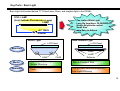
2. LCD Market Trend
(1) Comparison with other Display devices
(2) World Display Market Trend
(3) LCD TV Market trend
(4) Guidance of handling LCD product
(5) Abbreviations
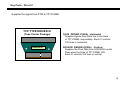
3. LCD TV Structure
(1) General Specifications
(2) Presentation for SVC Engineer
2
1. LCD Technology
1) What is TFT LCD ?
2) Structure of TFT LCD
3) TFT-LCD Operating Mechanism
4) Operating Theory
5) Structure LCD Module
6) Structure of Back light
7) Function of Back light
8) Key Parts ; Color Filter, Polarizer
3
What is TFT(Thin Film Transistor)?
TRANSISTOR
TFT
(MOS-FET)
DRAIN
DRAIN
Vth
Vth
GATE
GATE
SOURCE
SOURCE
TPE
When supply over certain voltage(Vth) to
the GATE, it delivers information from
Drain to Source
SWITCHING Characteristics
Compound Transistor with thin film in every Pixel
on ITO.
Independent on neighboring Pixel
TFT Panel
TFT Cross section
TFT Element
SOURCE
Semi-Conductor
GATE
DRAIN
Insulator
Glass Panel
Transparent Pixel Electrode
4
Structure of TFT- LCD
300 ㎛
(Approx....)
C/F Glass
)
TFT LCD
Panel
One Pixel
Common Electrode
)
TFT Glass
Pixel Electrode
Data Line
Gate Line
④ Liquid Crystal
Control the amount
of light by the
Applying Voltage
Glass
① Source
Transport the
Data Signal
+
+
+
+
-
-
-
-
-
③ Pixel
Applying
Voltage
to the
Liquid Crystal
Polarizer
Glass
+
Liquid
Crystal
② Gate
On/Off the
TFT
Back Light
-
-
-
-
-
White (TFT Off)
-
Black (TFT On)
5
TFT- LCD Operating mechanism
The structure of TFT-LCD is that Liquid Crystal is being filled between C/F Glass & TFT Glass. One Pixel consists of 3
sub-Pixels(R,G,B) and according to the number of the pixels, Display Resolution (SVGA,XGA,etc) is determined.
The TFT Matrix consists of Data Line(Carrying display data signal),Gate Line(Carrying signal for turn On/Off the
TFT).Each TFT, on each sub-pixel, controls the amount of Applying Voltage between C/F glass electrode & TFT glass
electrode for the Liquid Crystal.
The Applying Voltage changes the Direction of Liquid Crystal which changes direction of the Light. Transmittance rate
of the Polarized Light, polarized by Polarizer, is controlled by Applying Voltage. As a conclusion, Displayed Light is now
under-control of Display Data Signal.
Light(CCFL lamp)
Polarizer is a filter
which polarize the
light to one direction.
Polarizer
< Light transmittance >
< Blocking >
Polarized light
Electrode
Liquid
Crystal
VLC
= on
VLC
∼ = off
∼
Liquid
Crystal
Electrode
< VLC = 0 >
< VLC = 3.3V >
6
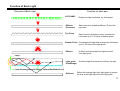
Operating Theory
(Braun Tube : Light Emitting Component)
(TFT-LCD : Non-Light Emitting Component)
COLOR FILTER
GLASS
Anode
Grid 4
Grid 1
Polarizer
Glass Panel
Polarizer
Flourescent
HEATER
Grid 3
Liquid
Crystal
Green
Beam
Luminous
Source
Light(White)
Grid 2
Electronic Gun Deflection
Section
Vacuum
TFT+Electrode
Electrode
7
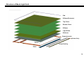
Structure of LCD Module
LCM = Case top + LCD panel
B/L Assy + Plate
Case Top
①
LCD Panel ②
③
Diffusers & Prisms
Back light
Assy
Light Guide
Reflector
Lamp
Housing Lamp
D-IC(on TCP)
PCB
Support Main
④
Bottom Plate
Bottom Cover
8
Structure of LCD Module
Driving
Circuit
Bright
Data Driver IC
Printed PCB Board
Common
Electrode
R
Dark Gray
G
Gate Driver IC
B
Inverter
Dn-1
Pixel Array & Wiring
Dn
Dn+1
LC
Pixel Electrode
Polarizer
CF Panel
LC Panel
LC
Power Supply
for Video Signal
Lamp
TFT Panel
Polarizer
Lamp
Prism
Diffuser
Light Guide
Lamp
Inverter
B/L Unit
Reflector
9
Structure of Back Light Unit
Pad
Diffuser(Protector)
Top Prism
Bottom Prism
Diffuser
Light Guide
Reflector
Supporter main
Lamp Ass’y
Screw
Lamp Housing
Plate
10
Function of Back Light
Function on each part
Structure of Back Light
LCD PANEL
Diffuser
(Protector)
Top Prism
Display the light controlled by data signal
Same structure as bellow diffuser, Protect the
top prism
Same function as bottom prism, Increase the
luminance up to 1.33 times of bottom prism
Bottom Prism Concentrate the light and increase the luminance
up to 1.55 times of the light guide
Diffuser
Uniform and concentrate the light received
from light guide
Light guide
(Flat/Wedge)
Guide the light from lamp and uniform the light
Lamp
Lamp Housing(Lamp Reflector) Pattern(Dot/Shibo/V-cut)
Reflector
Reflect the leakage light from light guide to reduce
the loss of the light injected to the light guide
11
Key Parts : Color Filter
To realize color of the Display, array Red,Green & Blue color paint beneath Upper Glass Panel regularly in
accord with Pixel electrode of lower Glass Panel.
! Kinds of Pixel Array
② Stripe Array
① Delta Array
③ Mosaic Array
! The Function of Color Filter
Divide the white light from luminous source into Red, Green & Blue
White Light
Pixel
Common Electrode
Glass
R
G
B
12
Key Parts : Polarizer
A kind of filter, which polarize light one direction.
Light
Polarizer
<Blocking>
<Passing>
13
Key Parts : Back Light
Back Light Unit,located behind TFT-Panel lower Glass, and supplies light to the PANEL.
CCFL LAMP
(Cold Cathode Fluorescence Lamp)
LAMP
Can realize White Light
Long life time(Appr. 25,000HRS)
Simple Brightness control
Small Size
Easy to Adhere
AC 1000V
Inverter
Direct Type
Side Guided Type
LCD Panel
LCD Panel
Structure
LAMP
Merits
Demerits
High Light Efficiency
Simple Structure
Thick
CASE
Guide
LAMP
Reflector
Slim & Compact Size
Complicated Structure,Expensive
Low Light Efficiency
14
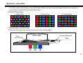
Key Parts : Drive IC
Supplies the signal from PCB to TFT-PANEL
TCP TYPE DRIVER IC
(Tape Carrier Package)
DRIVER IC
GATE DRIVER IC(8EA) : Horizontal
Supplies signals from Data line to the Gate
of TFT-PANEL sequentially. Each IC controls
128 lines in horizontal.
SOURCE DRIVER IC(5EA) : Vertical
Supplies the Pixel Data from SOURCE to each
Pixel when the Gate of TFT PANEL ON.
Each IC controls 154 lines in vertical.
15
2. LCD Market Trends
(1) Comparison with other Display devices
(2) World Display Market Trend
(3) LCD TV Market Trend
(4) Guidance of handling LCD products
(5) Abbreviations
16
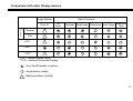
Comparison with other Display devices
Large Screen
Over 40”
C
P
T
Basic Functions
Full
Color
Contrast
Brightness
Resolution View Angle
Response
Time
Normal
Flat
LCD
PDP*
VFD**
*PDP : Plasma Display Panel
**VFD : Vacuum Flourescent Display
: Very Good(Possible to realize)
: Good(Hard to realize)
: Bad(Impossible to realize)
17
World Display Market Trend
60”
Projector
50”
P
D
P
40”
30”
LCD
CRT
Market 1
20”
Market 3
LCD
10”
LCD
Market 2
Small AV System
NTPC***
Monitor
Large AV System
NTPC : NoteBook PC
18
World Market
LG LCD TV Market Trend
World Market LCD TV
K
Volume
7000
6000
5000
4000
3000
2000
1000
0
7000
4000
2000
250
2000
500
2001
1000
2002
2003
2004
2005
Years
Source : IDC JAPAN
19
Guidance of handling Color TFT LCD Module
Color TFT LCD Module is very sensitive both electrically and physically.Users, therefore,
are requested to follow the “Guidance of handling color TFT LCD Module” on the followings.
1
Be careful not to make scratch
on the polarizer.
- Surface of polarizer is soft and can be
physically damaged easily.
- Please do not touch, push or rub polarizer
surface with materials over HB hardness.
2
Keep clean the surface.
- Please wear rubber glove when touch the
surface of LCD screen.
- Please use soft and anti-static material
with n-Hexane as cleaner.
3
Keep out of water.
- Water on/in the LCD may cause electrical
short or corrosion.
- Please wipe out or dry water carefully.
4
Prevent swift Temperature
& Humidity change.
- Swift temperature and/or humidity change
can make dew or ice which cause
nonconformance such as malfunction.
5
High temperature & high humidity
reduce the life-time.
- LCD is not proper to be used at high temperature and high humidity.
- Please keep specified temperature and
humidity condition.
6
Keep out of Corrosive Gas.
- Corrosive gas effect the polarizer and the circuit
chemically and cause defects accordingly.
7
Electrostatic discharge can make damage
- There are electro-static sensitive components such as
CMOS in LCD Module.
- Please earth human body when handle the LCD.In addition,
please do not touch the interface connector pin with bare
hand. Do not operate for a long time under
8
the same pattern.
- Operating LCD for a long time under the same pattern
can cause image persistence and can damage it.
- Please follow following guidance.
1. Turn the power off when do not use.
2. Change the pattern periodically.
20
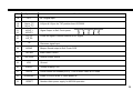
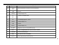
Abbreviations
Abbreviations on LCD Module and TV
No
1
2
3
4
5
6
7
8
9
10
11
12
13
14
15
16
Terms
ACF
B/L
CCFL
CF
CR
FPD
LC
LCD
LCM
LD
MNT
POL
Pixel
TAB
TCP
TFT
Full Description
Anisotropic Conductive Film
Back Light
Cold Cathode Fluorescent Lamp
Color Filter
Contrast Ratio ( White / Black )
Flat Panel Display
Liquid Crystal
Liquid Crystal Display
Liquid Crystal Module
Line Defect
Monitor
Polarizer
Picture Element
Tape Automatic Bonding
Tape Carrier Package
Thin Film Transistor
21
LG LCD TV
1) General Specification
- Key Value
- Specifications
- Monitor Features
- Unique Features
2) Presentation for SVC Engineer
- Specifications
- Exploded View
- Interconnection Guide
- Block Diagram
- IIC Adjustment
- MICOM Pinning & Descriptions
- Video Processing
- Audio Processing
22
General Specifications
Key Value
LE/LL/LT-15A10
KEY VALUE
-. Great Design
. Modern Style
. Slim
. Free space
-. Dual Functionality . Computer Monitor
Up to XGA 1024X768 85Hz
. Independent TV Receiver
-. High-Tech
. LCD
. HD Compatible
. Component Input(Optional)-ME
. SCART Jack(Optional)-EU
Without Stand
Stand type Wall mounting
23
General Specifications
PC Input
Monitor Features
1. Connect the signal cable from the monitor out socket of
the personal computer to the input socket of the set.
2. Connect the audio cable from the PC to the Audio socket
of the set.
3. Press the TV/AV/PC button to select PC Mode
4. Switch on the PC Mode, and the PC Screen automatically
appears on the set. The set can be operated as the PC monitor.
Note :
1. Check the PC Mode before exchanging the new monitor(LG),
the PC Mode should be within a mode in the table listed .
If over XGA mode, after change the PC mode to one mode of
table listed ( If possible, use the 1024 X 768 @60Hz
video mode to obtain the best image quality for you.
and then exchange the monitor ).
2. When the PC screen appears on the set, some message may
be appear on the screen, and the message is different depend
on Window system version( Win98,2000 )--Next Page
3. If you have an Apple Macintosh, connect the VGA adaptor
block from the 3 row 15 pin to 2 row 15 pin with the signal
cable and connect the VGA adaptor block to the Macintosh.
The cable are not supplied, such as the signal cable, audio
cable, VGA adaptor block for Macintosh PC.
Mode
Resolution
Horizontal Freq.(KHz)
Vertical Freq.)Hz)
VGA
640 X 480
640 X 480
565 X 496
640 X 480
640 X 480
720 X 400
31.5kHz
35kHz
37.9kHz
37.5kHz
43.3kHz
31.5kHz
60Hz
67Hz
72Hz
75Hz
85Hz
70Hz
SVGA
800 X 600
800 X 600
800 X 600
800 X 600
800 X 600
832 X 624
35.2kHz
37.9kHz
48.1kHz
46.9kHz
53.7kHz
49.7kHz
56Hz
60Hz
72Hz
75Hz
85Hz
75Hz
XGA
1024 X 768
1024 X 768
1024 X 768
1024 X 768
48.4kHz
56.5kHz
60.2kHz
68.7kHz
60Hz
70Hz
75Hz
85Hz
24
General Specifications
Unique Feature
Soft Touch Control
Soft Touch control system, LG’s advanced technology, leads customers to the emotional satisfaction.
Its main characteristics are Anti-static function when touching besides softness & luxurious looking.
Conductive Rubber
Cabinet
Conductive Film
Insulation PCB
Conductive plate
25
Specifications
Presentation for SVC Engineer
SYSTEM
PAL/SECAM-B/G, SECAM-L/L’
LL-15A10
PAL/SECAM-B/G,D/K, PAL-I
LE-15A10
PAL/SECAM-B,D,I, NTSC,4.43AV LT-15A10
POWER
100-240V , 50/60Hz
AC/DC Adapter 12V
Power consumption : 30 W
Stand by : 3W Below
TUNING
FVS, 100Program(200 Optional)
Auto/Manual programming
ACMS+ With VPS & TXT
Quick View
VIDEO
PSM
-Dynamic, Standard, Mild, Game
Digital comb filter
Progressive scan
SOUND
RF Stereo ( A2, NICAM)
DASP(4mode)
AVL, Balance(stereo)
Graphic equalizer
Sound output : 1W + 1W (rms)
OSD
EXTERNAL
CONNECTIONS
USER
CONVENIENT
FEATURES
MONITOR
LT-15A10
(TTS Turbo
search Sys.)
LCD
Panel
FLOF/LIST/TOP*
XGA 1024 X 768 85Hz
Type
Size
Pixel Format
Display Type
Pixel Pitch
Color Depth
Active Video Area
Surface
Back Light
Color Active Matrix TFT
15.1” ( 38.35cm)
1024 X 768 Pixel
R / G / B Stripe
0.3 X 0.3mm
16Mil. Color, 8 bits
307 X 230mm
Anti Glare, Hard Coating
2CCFL
Viewing Angle
Left / Right : 75˚
Upward
: 60 ˚
Downward : 55 ˚
250Cd/m²
300
Luminance
Contrast Ratio
Input Signal Volt.
PC Input
Sync
LL/LE-15A10
( EU Model )
TOP
- Optional
Soft Touch control
Auto A/V
Child Lock
Easy picture control(PSM)
Auto sleep
Any key power on
Optical
Halftone OSD
Menu ( Window type OSD)
Multilanguage *
Program List & Edit Mode
Rear part
.Scart in
.Video in
.S-VHS in
.DVD in ( LT-15A10)
.Headphone out
.XGA-IN ( D-SUB Jack)
TELETEXT
Input Signal type
Signal Polarity
Dot Spec Dark Dot
LT-15A10
Dot Spec Bright Dot
Low = 0 ~ 0.8V
High= 2.1 ~ 5.5V
Separator Signal
Positive & Negative
1 Dot : Below 4
2 Dot : Below 1
Sub Total : below 5
1 Dot : Below 2
2 Dot : None
Sub Total : below 2
Contrast ratio
≥5
Neighboring
Neighboring
*The Life Time is defined as the time at which brightness of lamp is 50% compare to that of initial value
at the typical lamp current on condition of continuos operating at 25+/- 2 C.
26
MAIN PCB
INVERTER
Connector between
Main PCB and LCM
CONTROL PCB
SPEAKER (R)
27
Interconnection Guide
Presentation for SVC Engineer
CN2
I
n
v
e
r
t
e
r
CN1
LCD Module
CN3
P502
P801
Main PCB
P601
To SPK
P401
P602
P001B
Control PCB
28
Adjustment in SVC mode
Presentation for SVC Engineer
“SVC” key, or
“OK” +”OK”
SVC mode
ADJUSTMENT mode
“YELLOW” key
◈ OPTION Part
RD
GD
BD
RO
GO
BO
S-B
PC CP
80
80
80
32
32
32
23
3
200PR
TEXT
I II SA
TOP
SCART
A2 ST
SYS
Average ADJ. Data List
☞
50 N AV1
RD
GD
BD
RO
GO
BO
Drive Red
Drive Green
Drive Blue
Red
Green
Blue
80
80
80
32
32
32
0
1
1
1
1
1
2
50 N AV1
102
Opt 1
ACMS
VOL
BBACK
LANG
0
0
0
0
50 N AV1
8
FP
NP
SP
S1VOL
S2VOL
21
89
38
105
105
☞
50 N AV1
50
N
AV1
: Vertical Frequency
(50=PAL, 60-NTSC)
: Mode (N=normal, W=wide)
: TV/AV1/AV2
☞ OPTION-1
200PR
TEXT
I II SA
TOP
PR MEMORY
TEXT Option
DUAL Mode Save
TXT MODE
SCART
A2 ST
SCART Option
A2 Stereo
SYS
SYSTEM Select
0 : BG/I/DK
1 : BG/L
2 : BG/I/DK/M
3 : RESERVED
☞ OPTION-2
ACMS
VOL
BBACK
LANG
STATION Memory
VOL Curve Select
BLUE BACK Option
OSD Language
Opt 2
Initial Data List (PAL)
FP
NP
SP
S1VOL
S2VOL
FM Prescaler
NICAM Prescaler
SECAM Prescaler
S1 VOL
S2 VOL
21
89
38
105
105
☞ OPTION-3
TSS
PANEL
IIC T
INVT
MD SA
MONO
CH+AU
T-LAN
0
0
0
0
0
1
0
14(0-16)
50 N AV1
4
TSS
PANEL
IIC T
INVT
MD SA
Turbo Search System
PANEL Option
AGC Option
Inverter Option
Last Mode Save
MONO
MONO Option
CH+AU
CHINA,AU Option
T-LAN
TXT Language(0-16)
Opt 3
☞ OPTION-4
OSD
T-LAN
OSD Language
TEXT Language
29
OPTION - 1
OPTION CODE
200PR
TEXT
I II SA
0
1
OPTION - 2
FUCTION
REMARK
OPTION CODE
100 PROGRAM
200 PROGRAM
Only China without TXT
ACMS
A2 ST
SYS
Channel Name Memory
Except AUSTRALIA
1
TEXT
0
Slow VOLUME Change
Normal Curve
0
DUAL I
1
Steep VOLUME Change
Rushed Curve
1
MODE SAVE
0
W/O BLUE BACK
0
No TOP TEXT
1
With BLUE BACK
1
TOP TEXT
0
ENG Only
0
W/O SCART
1
EU-5EA
1
WITH SCART
2
EU ETC
0
NO A2 STEREO
3
FARSI
4
ARAB URDU
VOL
BBACK
LANG
1
A2 STEREO
0
11
BG/I/DK
LE Model(EU)
5
E+CHINA
BG/L
LL Model(FRANCE)
6
RESERVED
2
BG/I/DK/M
LT Model(Middle East)
7
RESERVED
3
RESERVED
OPTION CODE
PANEL
IIC T
INVT
MD SA
MONO
CH+AU
T-LAN
Only AUSTRALIA
1
TELETXT
OPTION - 3
TSS
REMARK
FUCTION
No Channel Name Memory
Without TEXT
0
TOP
SCART
0
REMARK
FUCTION
0
W/O Turbo Search System
1
WITH Turbo Search
0
WEST EU
9
TURK GRE3
1
EAST EU1
10
ARAB FRA
2
TURKEY EU
11
ARAB ENG
3
EAST EU2
12
ARAB HEB1
0
PANEL
1
PANEL
0
MICOM AFT
1
TUNER AGC
4
CYRILLIC1
13
ARAB HEB2
0
INVERTER
5
CYRILLIC2
14
FARSI ENG
1
INVERTER
0
Last Mode Save
RF, AV Mode
6
CYRILLIC3
15
FARSI FRA
All Modes
7
TURK GRE1
16
FARSI ALL
8
TURK GRE2
1
Last Mode Save
0
No Forcible MONO Mode
1
Forcible MONO Mode
Only TUNISIA
0
Option OFF
Except China & Australia
1
Option ON
China & Australia
2
TXT Language Select
0~16
30
Presentation for SVC Engineer
3.3V
5V
SCL1
SDA1
V
V
Addr.(16bits)
Video Decoder
VPC3230D
Y/C
Trans
EPROM for OSD
SC786102A
Data(8bits)
Y/U/V = 8:4:4
R/G/B
(8bits)
Hs/Vs/Hsc/Avo/Intlc
Y/Pb/Pr
9V
32V
(Tuner) (Tuner)
Vout
8V
(MSP3440)
9V
(Audio AMP)
9V
R/G/B
R,G,B,Ys
for TXT
A/D
Converter
AD9884
H/Vs
for OSD position
Sync
Detecter
H/Vs
H/Vs(H/V counter)
Tuner & IF
TAUC-S120D
TAFC-M130D
TAFC-Z140D
SCL1
MICOM+TXT
SDA1
SDA555
AM
SCL1
SDA1
EPROM
24C16
MX88L284
SCL1
SDA1
CLK
HS
VS
D_EN
SCL1
SCL1
SDA1
SDA1
SIF
5V
(Micom)
Video Scaler
Y/U/V
(8bits)
To LCD Panel
To Inverter
DC/DC
Power
IC
SI786
BLOCK DIAGRAM
L
Audio
Processor
MSP3410D
Audio AMP
LA4282
R
H,V
And Gate
7408F
SCL2
SDA2
Pb
Power
12V/3A
ANT.
Pr
Y
Component Input
(or SCART JACK)
D-SUB
PC/D-TV
Input
E/P
Y/C
R
L
V
Video Input
31
MICOM Pinning & Descriptions
Presentation for SVC Engineer
SCL0
1
52
MX-CS
SDA0
2
51
MX-DA
SCL1
3
50
A-MUTE
SDA1
4
49
MX-CK
FS
5
48
KIN4
SW1
6
47
RGB SW
SW2
7
46
S-DET
AV-ID
8
45
INV_BRT
VDD2.5
9
44
VDD3.3
VSS
10
43
VSS
VDD3.3
11
42
VDD2.5
CVBS
12
41
FB
VDDA2.5
13
40
B
VSS
14
39
G
KIN1
15
38
R
KIN2
16
37
VDDA2.5
KIN3
17
36
VSS
AFT
18
35
XIN
Hsync_TV
19
34
XOUT
Vsync_TV
20
33
RESET
KOUT1
21
32
3230RESET
KOUT2
22
31
AD-PD
VS_PC
23
30
VDD3.3
IR
24
29
VSS
B/SND
25
28
INV-PWR
HS_PC
26
27
M-PWR
IIC Control
To Tuner
Soft Touch Key Input
For TXT position
Soft Touch Key Output
SDA555X
MX IC control
6 MHz
32
Function
No
Symbol
1
2
SCL0
SDA0
.IIC Control with EEPROM
3
4
SCL1
SDA1
.IIC control with other Devices(TUNER,VPC3230,MSP3410,etc)
5
FS
6
7
SW1
SW2
8
AV-ID
9
VDD2.5
10
VSS
11
VDD3.3
.Voltage Supply(3.3V)
12
CVBS
.Composite video signal input for TXT process
13
VDDA2.5
.Voltage Supply for Analog circuit
.Factory Service mode(Data control during production)
.TUNER System control signal
BG/I/DK
NTSC-M
B/G
SECAM-L
SECAM-L’
SW1
H
L
L
H
H
SW2
L
H
L
L
H
.AV identification signal input from pin8 of SCART
.Voltage Supply(2.5V)
.Ground
14
VSS
.Ground
15
16
17
KIN1
KIN2
KIN3
.Signal Input from Soft touch panel
33
Function
No
Symbol
18
AFT
19
20
Hsync_TV
Vsync_TV
21
22
KOUT1
KOUT2
.Signal Output to Soft Touch panel
23
26
VS_PC
HS_PC
.Check the signal 100msec interval for PC signal
24
IR
25
B/SND
.Beeper Sound output to Soft Touch PCB
27
M-PWR
.Main Power Control
28
INV-PWR
.AFT signal input
.H-Sync & V-Sync for TXT position from VPC3230
.Remocon signal input
.Inverter Power control
29
VSS
.Ground
30
VDD3.3
.Voltage Supply(3.3V)
31
AD-PD
.Power control for AD9884(IC201). Turn off when Video & RF mode.
32
3230RESET
33
RESET
.Reset VPC3230 & MX IC when power on
.Monitors Main power supply for MICOM operation
34
Function
No
Symbol
34
35
XOUT
XIN
.Main crystal(6MHz) connection for MICOM operation
36
VSS
.Ground
37
VDDA2.5
.Voltage Supply(2.5V)
38
39
40
R
G
B
.Teletext R,G,B signal output
41
FB
.Fast Blanking signal for Teletext
42
VDD2.5
43
VSS
44
VDD3.3
.Voltage Supply(3.3V)
45
INV_BRT
.Brightness control to Inverter(PWN control)
46
S-DET
.SCART FB signal input from 16 pin for Auto AV function
47
RGB SW
.Control RGB switching IC
48
KIN4
.Key Input from Soft Touch panel
49
MX-CK
.Clock output terminal to MX IC(IC501)
.Voltage Supply(2.5V)
.Ground
35
No
Symbol
Function
50
A-MUTE
.Sound Mute control when Channel up/down, Mode change & Power on/off.
51
52
MX-DA
MX-CS
.Data communication terminal with MX IC(Data & CS)
36
C7
C6
C5
C4
VSUPC
GNDC
C3
C2
C1
C0
GNDSY
VSUPSY
INTLC
AVO
FSY/HC
MSY/HS
VS
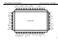
Video Processing - VPC3230D
FPDAT
VSTBY
CLK5
NC
XTAL1
XTAL2
ASGF
Presentation for SVC Engineer
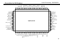
64 63 62 61 60 59 58 57 56 55 54 53 52 51 50 49 48 47 46 45 44 43 42 41
GNDF
VRT
I2CSEL
ISGND
VSUPF
VOUT
CIN
VIN1
VIN2
VIN3
65
66
40
39
67
68
38
37
69
36
70
71
35
34
72
73
33
32
VPC3230D
76
77
29
28
FB1IN
78
79
27
26
AISGND
80
25
Y1
Y2
Y3
VSUPY
GNDY
Y4
Y5
Y6
Y7
GNDLLC
VSUPLLC
LLC1
LLC2
VSUPPA
GNDPA
FFOE
CLK20
FFRE
FFWE
FFRSTW
9 10 11 12 13 14 15 16 17 18 19 20 21 22 23 24
YCOEQ
FFIE
7 8
VGAV
6
TEST
5
SDA
RESQ
4
GNDCAP
SCL
3
GNDD
2
VSUPD
1
G2/Y2IN
R2/CR2IN
GNDAI
VREF
R1/CR1IN
B2/CB2IN
VSUPAI
B1/CB1IN
G1/Y1IN
VIN4
VSUPCAP
31
30
ASGF
NC
74
75
Y0
37
Presentation for SVC Engineer
Video Processing - VPC3230D
1. Features
Video Decoding
- 4 Composite inputs, 1 S-VHS input
- Composite video & sync output
- integrated high-quality A/D converters
- Adaptive 2H comb filter Y/C separator
- 1H NTSC comb filter
- Multi-standard color decoder(1 Crystal)
- Multi-standard sync decoder
- Black line detector
Video Decoding
- Horizontal scaling(0.25 to 4)
- Panorama vision
- Black level expander
- Dynamic peaking
- Soft limiter(gamma correction)
- Color transient improvement
RGB Processing
- Programmable RGB matrix
- Digital color bus interface
- Additional analog RGB/Fast blank input
- Half contrast switch
- Picture frame generator
Deflection
- Scan velocity modulation output
- High performance H/V deflection
- Separate ADC for tube measurements
- EHT compensation
Miscellaneous
- One 20.25MHz crystal, few external components
- Embedded RISC controller(80 MIPS)
- I2C Bus interface
- Single 5V power supply
- Submicrom COMS technology
- 64 pin PSDIP package
38
Block Diagram
CIN1
VIN1
Adaptive
Comb
Filter
Analog
Front End
Color
Decoder
VIN2
NTSC,
PAL,
SECAL
VIN3
VIN4
AGC,
2*ADC
FB
RGB/
YCbCr
Y/G
ANALOG
Component
Front-End
Saturation
Tint
MIXER
2D Scaler
PIP
Panorama
Mode
Contrast
Brightness
Peaking
Output
Formatter
U/B
ITU-R 656
ITU-R 601
YCOE
Memory
Control
FIFO
CNTL
Y
LL Clock
FB
Cr
Matrix
Contrast
Saturation
Brightness
Tint
SYNC
+
Clock
Generation
Cb
FB
Y OUT
CrCb OUT
I2C BUS
V/R
4 x ADC
Processing
Cr
Cb
NTSC
PAL
VOUT
RGB/
YCbCr
Y
H Sync
Vsync
CNTL
AVI0
Clock
Gen.
20.25MHz
39
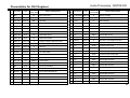
Presentation for SVC Engineer
Pin
Pin Name
No.
Type
Connection
(if not used)
Short Description
Video Processing - VPC3230D
Pin
Pin Name
No.
Type
Connection
(if not used)
Short Description
1
B1/CB1IN
IN
VREF
Blue1/Cb1 Analog Component Input
25
GND PA SUPPLYD
X
Ground, Pad Decoupling Circuitry
2
G1/Y1IN
IN
VREF
Green1/Y1 Analog Component Input
26
V SUPPA SUPPLYD
X
Supply Voltage, Pad Decoupling Circuitry
3
R1/CR1IN
IN
VREF
Red1/Cr1 Analog Component Input
27
LLC2
OUT
LV
Double Clock Output
4
B2/CB2IN
IN
VREF
Blue2/Cb2 Analog Component Input
28
LLC1
IN/OUT
LV
Clock Output
5
G2/Y2IN
IN
VREF
Green2/Y2 Analog Component Input
29
V SUPLLCSUPPLYD
X
Supply Voltage, LLC Circuitry
6
R2/CR2IN
IN
VREF
Red2/Cr2 Analog Component Input
30
GND LLC SUPPLYD
X
Ground, LLC Circuitry
7
ASGF
Analog Shield GND F
31
Y7
OUT
GND
Picture Bus Luma (MSB)
8
NC
No connected
32
Y6
OUT
GND
Picture Bus Luma
9
V SUPCAPSUPPLYD
X
Supply Voltage, Digital Decoupling
Circuitry
33
Y5
OUT
GND
Picture Bus Luma
10
V SUPD SUPPLYD
X
Supply Voltage, Digital Circuitry
34
Y4
OUT
GND
Picture Bus Luma
11
GND D
SUPPLYD
X
Ground, Digital Circuitry
35
GND Y
SUPPLYD
X
Ground, Luma Output Circuitry
12
GND CAP SUPPLYD
X
Ground, Digital Decoupling Circuitry
36
V SUPY
SUPPLYD
X
Supply Voltage, Luma Output Circuitry
13
SCL
IN/OUT
X
I 2 C Bus Clock
37
Y3
OUT
GND
Y Picture Bus Luma
14
SDA
IN/OUT
X
I 2 C Bus Data
38
Y2
OUT
GND
Y Picture Bus Luma
15
RESQ
IN
X
Reset Input, Active Low
39
Y1
OUT
GND
Y Picture Bus Luma
16
TEST
IN
GND D
Test Pin, connect to GND D
40
Y0
OUT
GND
Y Picture Bus Luma(LSB)
17
VGAV
IN
GND D
VGAV Input
41
C7
OUT
GND
Picture Bus Chroma (MSB)
18
YCOEQ
IN
V SUPD
Y/C Output Enable Input, Active Low
42
C6
OUT
GND
Picture Bus Chroma
19
FFIE
OUT
LV
FIFO Input Enable
43
C5
OUT
GND
Picture Bus Chroma
20
FFWE
OUT
LV
FIFO Write Enable
44
C4
OUT
GND
Picture Bus Chroma
21
FFRSTW
OUT
LV
FIFO Reset Write/Read
45
V SUPC SUPPLYD
X
Supply Voltage, Chroma Output Circuitry
22
FFRE
OUT
LV
FIFO Read Enable
46
GND C
SUPPLYD
X
Ground, Chroma Output Circuitry
23
FFOE
OUT
LV
FIFO Output Enable
47
C3
OUT
GND
Picture Bus Chroma
24
CLK20
IN/OUT
LV
Main Clock Output 20.25 MHz
48
C2
OUT
GND
Picture Bus Chroma
X
-
LV or GND
40
Presentation for SVC Engineer
Video Processing - VPC3230D
Pin
Pin Name
No.
Type
Connection
(if not used)
Type
Connection
(if not used)
49
C1
OUT
GND
Picture Bus Chroma
71
CIN
IN
LV*
50
C0
OUT
GND
Picture Bus Chroma(LSB)
72
VIN1
IN
VRT*
Video 1 Analog Input
51
GND SY SUPPLYD
X
Ground, Sync Pad Circuitry
73
VIN2
IN
VRT
Video 2 Analog Input
52
V SUPSY SUPPLYD
X
Supply Voltage, Sync Pad Circuitry
74
VIN3
IN
VRT
Video 3 Analog Input
53
INTLC
OUT
LV
Interlace Output
75
VIN4
IN
VRT
Video 4 Analog Input
54
AVO
OUT
LV
Active Video Output
76
V SUPAI SUPPLYA
X
55
FSY/HC
OUT
LV
Front Sync/ Horizontal Clamp Pulse
56
MSY/HS
IN/OUT
LV
Main Sync/Horizontal Sync Pulse
77
GND AI
SUPPLYA
X
57
VS
OUT
LV
Vertical Sync Pulse
78
VREF
OUT
X
58
FPDAT
IN/OUT
LV
Front-End/ Back-End Data
79
FB1IN
IN
VREF
59
V STBY
SUPPLYA
X
Standby Supply Voltage
80
AISGND SUPPLYA
60
CLK5
OUT
LV
CCU 5 MHz Clock Output
61
NC
62
XTAL1
IN
X
Analog Crystal Input
63
XTAL2
OUT
X
Analog Crystal Output
64
ASGF
X
Analog Shield GND F
65
GND F
SUPPLYA
X
Ground, Analog Front-End
66
VRT
OUT
X
Reference Voltage Top, Analog
67
I2CSEL
IN
X
I 2 C Bus Address Select
68
ISGND
SUPPLYA
X
Signal Ground for Analog Input,
connect to GND F
69
V SUPF
SUPPLYA
X
Supply Voltage, Analog Front-End
70
VOUT
OUT
LV
Analog Video Output
-
Short Description
Pin
Pin Name
No.
X
Short Description
Chroma / Analog Video 5 Input
Supply Voltage, Analog Component
Inputs Front-End
Ground, Analog Component Inputs
Front-End
Reference Voltage Top, Analog
Component Inputs Front-End
Fast Blank Input
Signal Ground for Analog Component
Inputs, connect to GND AI
LV or GNDd No connected
41
NC
NC
AHVSS
AHVSS
NC
SC4_IN_L
SC4_IN_R
ASG4
SC3_IN_L
SC3_IN_R
ASG2
SC2_IN_L
SC2_IN_R
ASG1
SC1_IN_L
SC1_IN_R
VREFTOP
NC
MONO_IN
AVSS
AVSS
NC
NC
AGNDC
Audio Processing - MSP3440G
Presentation for SVC Engineer
64 63 62 61 60 59 58 57 56 55 54 53 52 51 50 49 48 47 46 45 44 43 42 41
AVSUP
AVSUP
65
66
40
39
CAPL_M
AHVSUP
ANA_IN1+
67
68
38
37
CAPL_A
SC1_OUT_L
69
70
36
35
SC1_OUT_R
71
72
34
33
SC2_OUT_L
ANA_INANA_IN2+
TESTEN
XTAL_IN
XTAL_OUT
TP
MSP3410D
AUD_CL_OUT
NC
74
32
31
75
30
NC
D_CTR_I/O_1
76
77
29
D_CTR_I/O_0
78
79
28
27
ADR_WS
SC2_OUT_R
ASG3
NC
DACM_SUB
NC
DACM_L
26
DACM_R
VREF2
25
DACA_L
DACA_R
ADR_DA
NC
I2S_DA_IN1
NC
I2S_DA_OUT
RESETQ
I2S_WS
NC
I2S_CL
NC
I2C_DA
NC
9 10 11 12 13 14 15 16 17 18 19 20 21 22 23 24
I2S_DA_IN2
8
DVSS
7
DVSS
6
DVSS
5
DVSUP
4
DVSUP
3
DVSUP
2
ADR_CL
1
I2C_CL
80
NC
ADR_SEL
STANDBYQ
73
VREF1
42
Audio Processing - MSP3410D
Presentation for SVC Engineer
Pin
Pin Name
No.
Type
1
NC
2
I2C_CL
IN/OUT
3
I2C_DA
4
Connection
(if not used)
LV
Short Description
Pin
Pin Name
No.
Type
Connection
(if not used)
Short Description
Not connected
26
V SUPPA SUPPLYD
X
Supply Voltage
OBL
I2Cclock
27
LLC2
OUT
LV
Double Clock Output
IN/OUT
OBL
I2C data
28
LLC1
IN/OUT
LV
Clock Output
I2S_CL
IN/OUT
LV
I2S clock
29
V SUPLLCSUPPLYD
X
Supply Voltage, LLC Circuitry
5
I2S_WS
IN/OUT
LV
I2S word strobe
30
GND LLC SUPPLYD
X
Ground, LLC Circuitry
6
I2S_DA_OUTOUT
LV
I2S data output
31
Y7
OUT
GND
Picture Bus Luma (MSB)
7
I2S_DA_IN1 IN
LV
I2S1 data input
32
Y6
OUT
GND
Picture Bus Luma
8
ADR_DA
OUT
LV
ADR data output
33
Y5
OUT
GND
Picture Bus Luma
9
ADR_WS
OUT
LV
ADR word strobe
34
Y4
OUT
GND
Picture Bus Luma
10
ADR_CL SUPPLYD
X
Supply Voltage, Digital Circuitry
35
GND Y
SUPPLYD
X
Ground, Luma Output Circuitry
11
DVSUP
SUPPLYD
X
Ground, Digital Circuitry
36
V SUPY
SUPPLYD
X
Supply Voltage, Luma Output Circuitry
12
DVSUP
SUPPLYD
X
Ground
37
Y3
OUT
GND
Y Picture Bus Luma
13
DVSUP
IN/OUT
X
I 2 C Bus Clock
38
Y2
OUT
GND
Y Picture Bus Luma
14
DVSS
IN/OUT
X
I 2 C Bus Data
39
Y1
OUT
GND
Y Picture Bus Luma
15
DVSS
IN
X
Reset Input, Active Low
40
Y0
OUT
GND
Y Picture Bus Luma(LSB)
16
DVSS
IN
GND D
Test Pin, connect to GND D
41
C7
OUT
GND
Picture Bus Chroma (MSB)
17
I2S_DA_IN2 IN
GND D
VGAV Input
42
C6
OUT
GND
Picture Bus Chroma
18
NC
IN
V SUPD
Y/C Output Enable Input, Active Low
43
C5
OUT
GND
Picture Bus Chroma
19
NC
OUT
LV
FIFO Input Enable
44
C4
OUT
GND
Picture Bus Chroma
20
NC
OUT
LV
FIFO Write Enable
45
V SUPC SUPPLYD
X
Supply Voltage, Chroma Output Circuitry
21
RESET_Q
OUT
LV
FIFO Reset Write/Read
46
GND C
SUPPLYD
X
Ground, Chroma Output Circuitry
22
NC
OUT
LV
FIFO Read Enable
47
C3
OUT
GND
Picture Bus Chroma
23
NC
OUT
LV
FIFO Output Enable
48
C2
OUT
GND
Picture Bus Chroma
24
DACA_R
IN/OUT
LV
Main Clock Output 20.25 MHz
49
C1
OUT
GND
Picture Bus Chroma
25
DACA_R SUPPLYD
X
Ground
50
C0
OUT
GND
Picture Bus Chroma(LSB)
43
Audio Processing - MSP3440G
Presentation for SVC Engineer
Pin
Pin Name
No.
Type
Connection
(if not used)
Short Description
Pin
Pin Name
No.
Type
Connection
(if not used)
51
GND SY SUPPLYD
X
Ground, Sync Pad Circuitry
72
XTAL_OUT OUT
52
V SUPSY SUPPLYD
X
Supply Voltage, Sync Pad Circuitry
73
TP
LV
Test pin
53
INTLC
OUT
LV
Interlace Output
74
AUD_CL_OUT
OUT
LV
Audio clock output(18.432MHz)
54
AVO
OUT
LV
Active Video Output
75
NC
LV
Not connected
55
FSY/HC
OUT
LV
Front Sync/ Horizontal Clamp Pulse
56
MSY/HS
IN/OUT
LV
Main Sync/Horizontal Sync Pulse
76
NC
LV
Not connected
57
SC1_in_R
IN
LV
SCART 1input,right
77
D_CTR_I/O_1
IN/OUT
LV
D_CTR_I/O_1
58
VREFTOP
Reference voltage IF A/D converter
78
D_CTR_I/O_0
IN/OUT
LV
D_CTR_I/O_0
59
NC
79
ADR_SEL
IN
OBL
I2C Bus address select
60
MONO_IN
61
AVSS
OBL
Analog ground
80
STANDBYQ
IN
OBL
Stand-by(low active)
62
AVSS
OBL
Analog ground
63
NC
LV
Not connected
64
NC
LV
Not connected
65
AVSUP
OBL
Analog power supply 5V
66
AVSUP
OBL
Analog power supply 5V
67
ANA_IN+
IN
LV
68
ANA_IN-
IN
AVSS via
56pF/LV
IF common{can be left vacant,only
if IF input1 is also not in use}
69
ANA_IN2+
IN
AVSS via
56pF/LV
IF input{can be left vacant,only if
IF input1 is also not in use}
70
TESTEN
IN
OBL
Test pin
71
XTAL_IN
IN
OBL
Crystal oscillator
OBL
IN
LV
Not connected
LV
Mono input
OBL
Short Description
Crystal oscillator
IF input 1
44
LCD Monitor Controller - MX88L284
Presentation for SVC Engineer
Features
• Converts NTSC/PAL and PC video signal into flat
panel display device timing and resolution
• Provide full frame buffer, reduce frame buffer and
frame buffer less optional architecture.
• Built-in memory and output clock generator
• Support Auto-tracking and Auto-position capabilities
• Support Auto-gain capability for input image
• On-chip brightness and contrast adjustments
• On-chip gamma correction for panel compensation
Memory
Input
• PC video up to 1024X768@85Hz, and 1280X1024
@60Hz operation mode
• Support YCrCb422,RGB888 mode
(Interlace & Progressive)
• Support TTL clock input
Output
• Single and dual bit RGB data output
• Built-in YCrCb to RGB color space converter
• Built-in programmable Brightness and Contrast control
• Support Horizontal and Vertical position adjustment
RGB24/YUV
PIXIN
(RGB or
YCrCb)
Scale Down
with
SmartScaling-2
Technology
MIU
Scale up
with
SmartScaling-2
Technology
DRAM
Controller
Brightness
Contrast
control
OSD
Generator
VOP
Autotracking
Autoposition
Autogain
Mode Detection
De-Interlaced
Color
Conversion
BIU
CPU I/F
VCG X 2
Gamma
Correction
Odd/Even
Mux
Dithering
OSD MUX
Blending
PIXOUT-A
(RGB)
PIXOUT-B
(RGB)
VIP
(RGB24)
External OSD
45