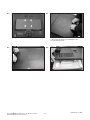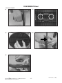
1
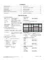
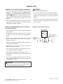
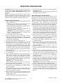
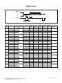
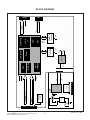
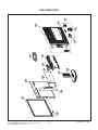
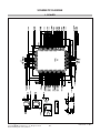
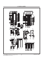
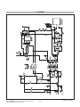
Internal Use Only
Website:http://biz.LGservice.com
COLOR MONITOR
SERVICE MANUAL
CHASSIS NO. : LM57B
MODEL:
L1733TR (L1733TR-SFQ.A**MQP)
L1933TR (L1933TR-SFQ.A**MQP,A**RQP)
(
) **Same model for Service
CAUTION
BEFORE SERVICING THE UNIT,
READ THE SAFETY PRECAUTIONS IN THIS MANUAL.
*To apply the MSTAR Chip.
CONTENTS
SPECIFICATIONS ................................................... 2
PRECAUTIONS ....................................................... 3
TIMING CHART ....................................................... 7
DISASSEMBLY ....................................................... 8
BLOCK DIAGRAM...................................................12
DISCRIPTION OF BLOCK DIAGRAM .................. 14
ADJUSTMENT ...................................................... 16
SERVICE OSD ........................................................17
TROUBLESHOOTING GUIDE .............................. 18
WIRING DIAGRAM ............................................... 24
EXPLODED VIEW...................................................25
REPLACEMENT PARTS LIST ...............................27
SCHEMATIC DIAGRAM ......................................... 31
SPECIFICATIONS
1. LCD CHARACTERISTICS
Type
: TFT Color LCD Module
Active Display Area : 17 inch - L1733T
: 19 inch - L1933T
Pixel Pitch
: 0.264 (H) x 0.264 (V) - L1733T
: 0.294 (H) x 0.294 (V) - L1933T
Color Depth
: 8bits, 16.2M colors
Size
: 358.5 (H) x 296.5 (V) x 17.0(D) - L1733T
: 396 (H) x 324 (V) x 17.5(D) - L1933T
Electrical Interface
: LVDS
Surface Treatment
: Hard-coating(3H), Anti-Glare
Operating Mode
: Normally White, Transmissive mode
Backlight Unit
: 4-CCFL
4. Max. Resolution
D-sub Analog
Digital
5. POWER SUPPLY
5-1. Power : AC 100~240V, 50/60Hz , 0.6A
5-2. Power Consumption
MODE
POWER ON (NORMAL)
2. OPTICAL CHARACTERISTICS
2-1. Viewing Angle by Contrast Ratio ≥ 10
Left : -60° min., -70°(Typ) Right : +60° min., +70°(Typ)
Top :+60° min., +75°(Typ) Bottom : -50° min., -65°(Typ)
2-2. Luminance
: 230(min), 300(Typ) (Full White pattern, 0.70V) -6500K
: 150(min) (Full White pattern, 0.70V) -9300K
75%(min)
2-3. Contrast Ratio
: 1400:1 (DFC)
3. SIGNAL (Refer to the Timing Chart)
3-1. Sync Signal
• Type
: Separate Sync, Digital, SOG
3-2. Video Input Signal
1) Type
2) Voltage Level
a) Color 0, 0
b) Color 7, 0
c) Color 15, 0
3) Input Impedance
: R, G, B Analog
: 0~0.71 V
: 0 Vp-p
: 0.467Vp-p
: 0.714Vp-p
: 75Ω
3-3. Operating Frequency
Horizontal
: 30 ~ 83kHz
Vertical
: 56 ~ 75Hz
H/V SYNC VIDEO POWER CONSUMPTION LED COLOR
ON/ON ACTIVE
less than 33 W -L1733T
BLUE
less than 37 W -L1933T
or GREEN
STAND-BY
OFF/ON
OFF
less than 1 W
AMBER
SUSPEND
ON/OFF
OFF
less than 1 W
AMBER
DPMS OFF
OFF/OFF OFF
less than 1 W
AMBER
less than 1 W
OFF
POWER S/W Off
-
-
6. ENVIRONMENT
6-1. Operating Temperature : 10°C~35°C (50°F~95°F)
(Ambient)
6-2. Relative Humidity
: 10%~80% (Non-condensing)
6-3. MTBF
: 50,000 HRS with 90% Confidence
Lamp Life
: 50,000 Hours(Min)
7. DIMENSIONS (with TILT/SWIVEL)
L1733T
Width
: 364.5 mm (14.35'')
Depth
: 180 mm (7.09'')
Height
: 378.2 mm (14.89'')
L1933T
Width
Depth
Height
: 402 mm (15.83'')
: 180 mm (7.09'')
: 407.5 mm (16.04'')
8. WEIGHT (with TILT/SWIVEL)
L1733T
Net. Weight
: 3.5 kg (7.72 lbs)
Gross Weight
: 4.6 kg (10.14 lbs)
L1933T
Net. Weight
Gross Weight
Copyright
2007 LG Electronics. Inc. All right reserved.
Only for training and service purposes
: 1280 x 1024@75Hz
: 1280 x 1024@60Hz
-2-
: 4.4 kg (9.70 lbs)
: 5.6 kg (12.35 lbs)
LGE Internal Use Only
PRECAUTION
WARNING FOR THE SAFETY-RELATED COMPONENT.
WARNING
• There are some special components used in LCD
monitor that are important for safety. These parts are
marked on the schematic diagram and the
replacement parts list. It is essential that these critical
parts should be replaced with the manufacturer’s
specified parts to prevent electric shock, fire or other
hazard.
• Do not modify original design without obtaining written
permission from manufacturer or you will void the
original parts and labor guarantee.
BE CAREFUL ELECTRIC SHOCK !
• If you want to replace with the new backlight (CCFL) or
inverter circuit, must disconnect the AC adapter
because high voltage appears at inverter circuit about
650Vrms.
• Handle with care wires or connectors of the inverter
circuit. If the wires are pressed cause short and may
burn or take fire.
Leakage Current Hot Check Circuit
TAKE CARE DURING HANDLING THE LCD MODULE
WITH BACKLIGHT UNIT.
AC Volt-meter
• Must mount the module using mounting holes arranged
in four corners.
• Do not press on the panel, edge of the frame strongly
or electric shock as this will result in damage to the
screen.
• Do not scratch or press on the panel with any sharp
objects, such as pencil or pen as this may result in
damage to the panel.
• Protect the module from the ESD as it may damage the
electronic circuit (C-MOS).
Good Earth Ground
such as WATER PIPE,
CONDUIT etc.
To Instrument’s
exposed
METALLIC PARTS
1.5 Kohm/10W
• Make certain that treatment person’s body are
grounded through wrist band.
• Do not leave the module in high temperature and in
areas of high humidity for a long time.
• The module not be exposed to the direct sunlight.
• Avoid contact with water as it may a short circuit within
the module.
• If the surface of panel become dirty, please wipe it off
with a softmaterial. (Cleaning with a dirty or rough cloth
may damage the panel.)
CAUTION
Please use only a plastic screwdriver to protect yourself
from shock hazard during service operation.
Copyright
2007 LG Electronics. Inc. All right reserved.
Only for training and service purposes
-3-
LGE Internal Use Only
SERVICING PRECAUTIONS
CAUTION: Before servicing receivers covered by this
service manual and its supplements and addenda, read
and follow the SAFETY PRECAUTIONS on page 3 of this
publication.
NOTE: If unforeseen circumstances create conflict
between the following servicing precautions and any of the
safety precautions on page 3 of this publication, always
follow the safety precautions. Remember: Safety First.
General Servicing Precautions
1. Always unplug the receiver AC power cord from the AC
power source before;
a. Removing or reinstalling any component, circuit
board module or any other receiver assembly.
b. Disconnecting or reconnecting any receiver electrical
plug or other electrical connection.
c. Connecting a test substitute in parallel with an
electrolytic capacitor in the receiver.
CAUTION: A wrong part substitution or incorrect
polarity installation of electrolytic capacitors may
result in an explosion hazard.
d. Discharging the picture tube anode.
2. Test high voltage only by measuring it with an
appropriate high voltage meter or other voltage
measuring device (DVM, FETVOM, etc) equipped with
a suitable high voltage probe.
Do not test high voltage by "drawing an arc".
3. Discharge the picture tube anode only by (a) first
connecting one end of an insulated clip lead to the
degaussing or kine aquadag grounding system shield
at the point where the picture tube socket ground lead
is connected, and then (b) touch the other end of the
insulated clip lead to the picture tube anode button,
using an insulating handle to avoid personal contact
with high voltage.
4. Do not spray chemicals on or near this receiver or any
of its assemblies.
5. Unless specified otherwise in this service manual,
clean electrical contacts only by applying the following
mixture to the contacts with a pipe cleaner, cottontipped stick or comparable non-abrasive applicator;
10% (by volume) Acetone and 90% (by volume)
isopropyl alcohol (90%-99% strength)
CAUTION: This is a flammable mixture.
Unless specified otherwise in this service manual,
lubrication of contacts in not required.
6. Do not defeat any plug/socket B+ voltage interlocks
with which receivers covered by this service manual
might be equipped.
7. Do not apply AC power to this instrument and/or any of
its electrical assemblies unless all solid-state device
heat sinks are correctly installed.
8. Always connect the test receiver ground lead to the
receiver chassis ground before connecting the test
receiver positive lead.
Always remove the test receiver ground lead last.
Copyright
2007 LG Electronics. Inc. All right reserved.
Only for training and service purposes
9. Use with this receiver only the test fixtures specified in
this service manual.
CAUTION: Do not connect the test fixture ground strap
to any heat sink in this receiver.
Electrostatically Sensitive (ES) Devices
Some semiconductor (solid-state) devices can be
damaged easily by static electricity. Such components
commonly are called Electrostatically Sensitive (ES)
Devices. Examples of typical ES devices are integrated
circuits and some field-effect transistors and
semiconductor "chip" components. The following
techniques should be used to help reduce the incidence of
component damage caused by static by static electricity.
1. Immediately before handling any semiconductor
component or semiconductor-equipped assembly, drain
off any electrostatic charge on your body by touching a
known earth ground. Alternatively, obtain and wear a
commercially available discharging wrist strap device,
which should be removed to prevent potential shock
reasons prior to applying power to the unit under test.
2. After removing an electrical assembly equipped with
ES devices, place the assembly on a conductive
surface such as aluminum foil, to prevent electrostatic
charge buildup or exposure of the assembly.
3. Use only a grounded-tip soldering iron to solder or
unsolder ES devices.
4. Use only an anti-static type solder removal device.
Some solder removal devices not classified as "antistatic" can generate electrical charges sufficient to
damage ES devices.
5. Do not use freon-propelled chemicals. These can
generate electrical charges sufficient to damage ES
devices.
6. Do not remove a replacement ES device from its
protective package until immediately before you are
ready to install it. (Most replacement ES devices are
packaged with leads electrically shorted together by
conductive foam, aluminum foil or comparable
conductive material).
7. Immediately before removing the protective material
from the leads of a replacement ES device, touch the
protective material to the chassis or circuit assembly
into which the device will be installed.
CAUTION: Be sure no power is applied to the chassis
or circuit, and observe all other safety precautions.
8. Minimize bodily motions when handling unpackaged
replacement ES devices. (Otherwise harmless motion
such as the brushing together of your clothes fabric or
the lifting of your foot from a carpeted floor can
generate static electricity sufficient to damage an ES
device.)
-4-
LGE Internal Use Only
General Soldering Guidelines
1. Use a grounded-tip, low-wattage soldering iron and
appropriate tip size and shape that will maintain tip
temperature within the range or 500 F to 600 F.
2. Use an appropriate gauge of RMA resin-core solder
composed of 60 parts tin/40 parts lead.
3. Keep the soldering iron tip clean and well tinned.
4. Thoroughly clean the surfaces to be soldered. Use a
mall wire-bristle (0.5 inch, or 1.25cm) brush with a
metal handle.
Do not use freon-propelled spray-on cleaners.
5. Use the following unsoldering technique
a. Allow the soldering iron tip to reach normal
temperature.
(500 F to 600 F)
b. Heat the component lead until the solder melts.
c. Quickly draw the melted solder with an anti-static,
suction-type solder removal device or with solder
braid.
CAUTION: Work quickly to avoid overheating the
circuitboard printed foil.
6. Use the following soldering technique.
a. Allow the soldering iron tip to reach a normal
temperature (500 F to 600 F)
b. First, hold the soldering iron tip and solder the strand
against the component lead until the solder melts.
c. Quickly move the soldering iron tip to the junction of
the component lead and the printed circuit foil, and
hold it there only until the solder flows onto and
around both the component lead and the foil.
CAUTION: Work quickly to avoid overheating the
circuit board printed foil.
d. Closely inspect the solder area and remove any
excess or splashed solder with a small wire-bristle
brush.
IC Remove/Replacement
Some chassis circuit boards have slotted holes (oblong)
through which the IC leads are inserted and then bent flat
against the circuit foil. When holes are the slotted type,
the following technique should be used to remove and
replace the IC. When working with boards using the
familiar round hole, use the standard technique as
outlined in paragraphs 5 and 6 above.
Removal
1. Desolder and straighten each IC lead in one operation
by gently prying up on the lead with the soldering iron
tip as the solder melts.
2. Draw away the melted solder with an anti-static
suction-type solder removal device (or with solder
braid) before removing the IC.
Copyright
2007 LG Electronics. Inc. All right reserved.
Only for training and service purposes
Replacement
1. Carefully insert the replacement IC in the circuit board.
2. Carefully bend each IC lead against the circuit foil pad
and solder it.
3. Clean the soldered areas with a small wire-bristle
brush. (It is not necessary to reapply acrylic coating to
the areas).
"Small-Signal" Discrete Transistor
Removal/Replacement
1. Remove the defective transistor by clipping its leads as
close as possible to the component body.
2. Bend into a "U" shape the end of each of three leads
remaining on the circuit board.
3. Bend into a "U" shape the replacement transistor leads.
4. Connect the replacement transistor leads to the
corresponding leads extending from the circuit board
and crimp the "U" with long nose pliers to insure metal
to metal contact then solder each connection.
Power Output, Transistor Device
Removal/Replacement
1. Heat and remove all solder from around the transistor
leads.
2. Remove the heat sink mounting screw (if so equipped).
3. Carefully remove the transistor from the heat sink of the
circuit board.
4. Insert new transistor in the circuit board.
5. Solder each transistor lead, and clip off excess lead.
6. Replace heat sink.
Diode Removal/Replacement
1. Remove defective diode by clipping its leads as close
as possible to diode body.
2. Bend the two remaining leads perpendicular y to the
circuit board.
3. Observing diode polarity, wrap each lead of the new
diode around the corresponding lead on the circuit
board.
4. Securely crimp each connection and solder it.
5. Inspect (on the circuit board copper side) the solder
joints of the two "original" leads. If they are not shiny,
reheat them and if necessary, apply additional solder.
Fuse and Conventional Resistor
Removal/Replacement
1. Clip each fuse or resistor lead at top of the circuit board
hollow stake.
2. Securely crimp the leads of replacement component
around notch at stake top.
3. Solder the connections.
CAUTION: Maintain original spacing between the
replaced component and adjacent components and the
circuit board to prevent excessive component
temperatures.
-5-
LGE Internal Use Only
Circuit Board Foil Repair
Excessive heat applied to the copper foil of any printed
circuit board will weaken the adhesive that bonds the foil
to the circuit board causing the foil to separate from or
"lift-off" the board. The following guidelines and
procedures should be followed whenever this condition is
encountered.
At IC Connections
To repair a defective copper pattern at IC connections use
the following procedure to install a jumper wire on the
copper pattern side of the circuit board. (Use this
technique only on IC connections).
1. Carefully remove the damaged copper pattern with a
sharp knife. (Remove only as much copper as
absolutely necessary).
2. carefully scratch away the solder resist and acrylic
coating (if used) from the end of the remaining copper
pattern.
3. Bend a small "U" in one end of a small gauge jumper
wire and carefully crimp it around the IC pin. Solder the
IC connection.
4. Route the jumper wire along the path of the out-away
copper pattern and let it overlap the previously scraped
end of the good copper pattern. Solder the overlapped
area and clip off any excess jumper wire.
Copyright
2007 LG Electronics. Inc. All right reserved.
Only for training and service purposes
At Other Connections
Use the following technique to repair the defective copper
pattern at connections other than IC Pins. This technique
involves the installation of a jumper wire on the
component side of the circuit board.
1. Remove the defective copper pattern with a sharp
knife.
Remove at least 1/4 inch of copper, to ensure that a
hazardous condition will not exist if the jumper wire
opens.
2. Trace along the copper pattern from both sides of the
pattern break and locate the nearest component that is
directly connected to the affected copper pattern.
3. Connect insulated 20-gauge jumper wire from the lead
of the nearest component on one side of the pattern
break to the lead of the nearest component on the
other side.
Carefully crimp and solder the connections.
CAUTION: Be sure the insulated jumper wire is
dressed so the it does not touch components or sharp
edges.
-6-
LGE Internal Use Only
TIMING CHART
VIDEO
A
E
D
B
SYNC
C
Sync
Video
Duration
Active
(D)
Time ( A )
640
16
MODE
H/V
Sync
Polarity
Dot
Clock
Frequency
1
H(Pixels)
+
25.175
31.469
Total
Period
(E)
800
V(Lines)
-
70.09
449
350
2
H(Pixels)
-
28.321
31.468
900
720
V(Lines)
+
70.08
449
400
3
4
5
6
7
H(Pixels)
-
V(Lines)
-
H(Pixels)
-
V(Lines)
-
H(Pixels)
+
V(Lines)
+
H(Pixels)
+
V(Lines)
+
H(Pixels)
+/-
V(Lines)
+/-
8
H(Pixels)
-
V(Lines)
-
9
H(Pixels)
-
V(Lines)
-
10
H(Pixels)
+/-
V(Lines)
+/-
11
H(Pixels)
+/-
V(Lines)
+/-
12
H(Pixels)
+
V(Lines)
+
13
H(Pixels)
+
V(Lines)
+
25.175
31.5
40.0
Front
Porch
(C)
96
Blanking
Time
(B)
48
37
2
60
18
108
54
12
2
35
31.469
800
640
16
96
48
59.94
525
480
10
2
33
37.5
840
640
16
64
120
75
500
480
1
3
16
37.879
1056
800
40
128
88
60.317
628
600
1
4
23
46.875
1056
800
16
80
160
75.0
625
600
1
3
21
49.725
1152
832
32
64
224
74.55
667
624
1
3
39
65.0
48.363
1344
1024
24
136
160
60.0
806
768
3
6
29
78.75
60.123
1312
1024
16
96
176
49.5
57.283
100.0
75.029
800
768
1
3
28
68.681
1456
1152
32
128
144
75.062
915
870
3
3
39
92.978
61.805
1504
1152
18
134
200
65.96
937
900
2
4
31
108.0
63.981
1688
1280
48
112
248
60.02
1066
1024
1
3
38
135.0
79.976
1688
1280
16
144
248
75.035
1066
1024
1
3
38
Copyright
2007 LG Electronics. Inc. All right reserved.
Only for training and service purposes
-7-
Resolution
640 x 350
720 X 400
640 x 480
640 x 480
800 x 600
800 x 600
832 x 624
1024 x 768
1024 x 768
1152 x 870
1152 x 900
1280 x 1024
1280 x 1024
LGE Internal Use Only
DISASSEMBLY-Set
#1
#2
Soft pad on the table.
#3
Monitor on the pad.
# 4-1
Hold the head & stand base and then
Pull up the stand part.
Twist Stand until "Click".
# 4-2
#5
Separate head & stand
Copyright
2007 LG Electronics. Inc. All right reserved.
Only for training and service purposes
-8-
LGE Internal Use Only
#6
#7
1. Pull the front cover upward.
2. Then, let the all latches are separated.(#3-1~3-2)
3. Put the front face down.
Remove the screws.
#8
#9
Disassemble back cover.
Copyright
2007 LG Electronics. Inc. All right reserved.
Only for training and service purposes
-9-
LGE Internal Use Only
DISASSEMBLY-Stand
* In case of Latch 4.
# 1-1
# 1-2
Push the four latches on the bottom to the
outside and Separate Stand Body & Base.
(Reference the #1-2)
#2
#3
After finished repair, necessarily push 4ea
Latches to inside for restoration.
Copyright
2007 LG Electronics. Inc. All right reserved.
Only for training and service purposes
- 10 -
LGE Internal Use Only
DISASSEMBLY-Stand
* In case of Latch 2.
#1
#2
Hold the stand body.
#3
Confirm two latch of right and left.
#4
Push the latch to the inside.
Push the base to the opposite direction.
#5
Confirm the condition of separation.
Copyright
2007 LG Electronics. Inc. All right reserved.
Only for training and service purposes
- 11 -
LGE Internal Use Only
Copyright
2007 LG Electronics. Inc. All right reserved.
Only for training and service purposes
D-Sub
DVI-D
Filter
EEPROM
(EDID)
Digital
- 12 -
Inverter (4 lamps)
12V
LIPS
Analog (R/G/B)
12V
5V
1.8V
3.3V
5V
MCU
Intel8032
TMDS Rx
ADC
TSUMx6AL
12V
Regulator
1.8V
3.3V
3.3V
Flash ROM
Scaler
Line Buffer
3.3V
EEPROM
(System)
SDA
/SCL
SSC
OSD
LVDS
Tx
MStarACE
Vcc
5V
LVDS
Module
KEY
5V
BLOCK DIAGRAM
LGE Internal Use Only
Main Board
(Scaler &
DC DC
converter)
Module Vcc
Copyright
2007 LG Electronics. Inc. All right reserved.
Only for training and service purposes
- 13 L
N
Line Filter
Start
Power
Control
IC
Drive
Aux
Dimming (Lamp Current Control)
Inverter On/OFF (3.3V)
12V
5V
POWER
Feedback
SMPS
5V
12V
Inverter
Control
IC
Drive Block
N-ch
P-ch
13V
INVERTER
Lamp
Current
Feedback
Inverter
Trans
Over
Voltage
Protection
Low
LAMP
High
BLOCK DIAGRAM-POWER
LGE Internal Use Only
DESCRIPTION OF BLOCK DIAGRAM
1. Video Controller Part.
This part amplifies the level of video signal for the digital conversion and converts from the analog video signal to the
digital video signal using a pixel clock.
The pixel clock for each mode is generated by the PLL.
The range of the pixel clock is from 25MHz to 135MHz.
This part consists of the Scaler, ADC convertor, TMDS receiver and LVDS transmitter.
The Scaler gets the video signal converted analog to digital, interpolates input to 1280 X 1024 resolution signal and
outputs 8-bit R, G, B signal to transmitter.
2. Power Part.
This part consists of the one 3.3V, and one 1.8V regulators to convert power which is provided 5V in Power board.
12V is provided for inverter, 5V is provided for LCD panel.
Also, 5V is converted 3.3V and 1.8V by regulator. Converted power is provided for IC in the main board.
The inverter converts from DC12V to AC 700Vrms and operates back-light lamps of module.
3. MICOM Part.
This part is include video controller part. And this part consists of EEPROM IC which stores control data, Reset IC and
the Micom.
The Micom distinguishes polarity and frequency of the H/V sync are supplied from signal cable.
The controlled data of each modes is stored in EEPROM.
Copyright
2007 LG Electronics. Inc. All right reserved.
Only for training and service purposes
- 14 -
LGE Internal Use Only
LIPS Board Block Diagram
12V
50 ~ 60Hz
LINE
100 ~ 240V
EMI
COMPONENTS
INPUT RECTIFIER
AND FILTER
HVDC
SWITCHING
TRANSFORMER
100KHz
OUTPUT RECTIFIER
AND FILTER
5V
GND
PWM CONTROL
CIRCUIT
PHOTO-COUPLER
ISOLATION
PRIMARY
12V
SIGNAL
COLLENTION
SECONDARY
INVERTER CIRCUIT
High Voltage
Operation description_LIPS
1. EMI components.
This part contains of EMI components to comply with global marketing EMI standards like FCC,VCCI CISPR, the
circuit included a line-filter, across line capacitor and of course the primary protection fuse.
2. Input rectifier and filter.
This part function is for transfer the input AC voltage to a DC voltage through a bridge rectifier and a bulk capacitor.
3. Energy Transfer.
This part function is for transfer the primary energy to secondary through a power transformer.
4. Output rectifier and filter.
This part function is to make a pulse width modulation control and to provide the driver signal to power switch, to
adjust the duty cycle during different AC input and output loading condition to achieve the dc output stabilized, and
also the over power protection is also monitor by this part.
5. Photo-Coupler isolation.
This part function is to feed back the DC output changing status through a photo transistor to primary controller to
achieve the stabilized DC output voltage.
6. Signal collection.
This part function is to collect the any change from the DC output and feed back to the primary through photo
transistor.
Copyright
2007 LG Electronics. Inc. All right reserved.
Only for training and service purposes
- 15 -
LGE Internal Use Only
ADJUSTMENT
Windows EDID V1.0 User Manual
2. EDID Read & Write
1) Run WinEDID.exe
Operating System: MS Windows 98, 2000, XP
Port Setup: Windows 98 => Don’t need setup
Windows 2000, XP => Need to Port Setup.
This program is available to LCD Monitor only.
1. Port Setup
a) Copy “UserPort.sys” file to
“c:\WINNT\system32\drivers” folder
b) Run Userport.exe
2) Edit Week of Manufacture, Year of Manufacture,
Serial Number
a) Input User Info Data
b) Click “Update” button
c) Click “ Write” button
c) Remove all default number
d) Add 300-3FF
e) Click Start button.
f) Click Exit button.
Copyright
2007 LG Electronics. Inc. All right reserved.
Only for training and service purposes
- 16 -
LGE Internal Use Only
SERVICE OSD
1) Turn off the power switch at the front side of the display.
2) Wait for about 5 seconds and press MENU, POWER switch with 1 second interval.
3) The SVC OSD menu contains additional menus that the User OSD menu as described below.
a) Auto Color : W/B balance and Automatically sets the gain and offset value.
b) NVRAM INIT : EEPROM initialize.(24C08)
c) CLEAR ETI : To initialize using time.
d) AGING : Select Aging mode(on/off).
e) R/G/B-9300K : Allows you to set the R/G/B-9300K value manually.
f) R/G/B-6500K : Allows you to set the R/G/B-6500K value manually.
g) R/G/B-Offset : Allows you to set the R/G/B-Offset value manually.(Analog Only)
h) R/G/B-Gain : Allows you to set the R/G/B-Gain value manually.(Analog Only)
i) MODULE : To select applied module.
A
9
IBM
Compatible PC
Video Signal
Generator
15
10
5
11
6
1
6
1
5
C
d
PARALLEL PORT
tu
No
RS
23
2C
se
13
PA
RA
LL
EL
14
ON
F
Power inlet (required)
5V
220
WE
R
PO
VG
S
A
Power Select Switch
(110V/220V)
Power LED
MO
NI
TO
R
V-S
YN
CS
T
Control Line
5V
C
1
25
OFF
ON
4.7K
4.7K
5V
E
4.7K
OFF
74LS06
74LS06
B
E ST Switch
B
F V-Sync On/Off Switch
(Switch must be ON.)
Figure 1. Cable Connection
Copyright
2007 LG Electronics. Inc. All right reserved.
Only for training and service purposes
- 17 -
LGE Internal Use Only
TROUBLESHOOTING GUIDE
1. NO POWER
NO POWER
(POWER INDICATOR OFF)
Check J403 Voltage
Pin5, Pin6 (5V)?
NO
Check Power Board,
And Find Out a Short Point
as Opening
Each Power Line
YES
Check
U301 Pin2 Voltage
(3.3V) ?
NO
Check 3.3V Line
(Open Check)
No Problem
YES
Check Key Control
Connector Routine
Is U201
Pin75 (3.3V)
Voltage ?
NO
Check 3.3V Line
YES
1
Check U201 Pin 96
Pulse
NO
Check X-TAL
YES
Check U201
Waveforms
1
U201-#96
Copyright
2007 LG Electronics. Inc. All right reserved.
Only for training and service purposes
- 18 -
LGE Internal Use Only
2. NO RASTER (OSD IS NOT DISPLAYED) – LIPS
NO RASTER
(OSD IS NOT DISPLAYED)
J403
PIN5, PIN6
5V?
NO
CHECK POWER BOARD,
AND FIND OUT A SHORT
POINT AS OPENING EACH
POWER LINE
YES
J403 PIN9
5V?
NO
CHECK MICOM INV
ON/OFF PORT.
YES
J403 PIN10
5V?
NO
1. CONFIRM BRIGHTNESS
OSD CONTRL STATE.
2. CHECK MICOM DIM-ADJ
PORT
YES
CHECK
PULSE AS
CONTACTING SCOPE
PROBE TO CAUTION LABEL.
(CONTACT PROBE TO
CAUTION LABEL.
CAN YOU SEE PULSE
AT YOUR
SCOPE?
NO
LIPS
YES
REPLACE CCFL LAMP
IN THE LCD MODULE
Copyright
2007 LG Electronics. Inc. All right reserved.
Only for training and service purposes
- 19 -
LGE Internal Use Only
3. NO RASTER (OSD IS NOT DISPLAYED) – MSTAR
NO RASTER
(OSD IS NOT DISPLAYED)
U201
PIN 16, 75
3.3V?
NO
CHECK U301
YES
U201
PIN96, 97
OSCILLATE AS
14.31MHZ?
1
1. CHECK C210, C211
SOLDERING CONDITION
2. CHECK X201
3. TROUBLE IN U201
NO
YES
2
U201
PIN27 IS 48KHz H-SYNC?
PIN28 IS 60Hz V-SYNC?
IS PULSE APPEARED
AT SIGNAL PINS?
AT MODE 12?
CHECK CONNECTION
LINE FROM D-SUB TO
U201
NO
YES
TROUBLE IN CABLE
OR LCD MODULE
Waveforms
1
U201-#96, 97
2
2
U201-#27 H-SYNC
Copyright
2007 LG Electronics. Inc. All right reserved.
Only for training and service purposes
- 20 -
U201-#28 V-SYNC
LGE Internal Use Only
4. TROUBLE IN DPM
TROUBLE IN DPM
NO
CHECK
R442, R443
3
CHECK PC
PC IS NOT GOING
INTO DPM OFF MODE
YES
CHECK
U201 PIN 27,28
SYNC PULSE ?
NO
CHECK H/V SYNC LINE
YES
TROUBLE IN U201
Waveforms
3
R442 H-Sync
3
R443 V-Sync
Copyright
2007 LG Electronics. Inc. All right reserved.
Only for training and service purposes
- 21 -
LGE Internal Use Only
5. POWER
NO POWER
(POWER INDICATOR OFF)
CHECK
Fuse F101 OK?
NO
Trouble in Fuse (F101)
YES
CHECK
C101 Voltage
(AC110V->160Vdc
(AC220V->304Vdc
NO
Check BD101
YES
CHECK
U101 Pin6 Waveform
(Square wave
Come out?)
NO
Check U101 Pin7 : 9~10V
Check D102
YES
Check Q101 Drain
Waveform
NO
Trouble in Q101
YES
Check D201, D202
Voltage
NO
Trouble in D201, D202
YES
CHECK 5V, 12V Line
Copyright
2007 LG Electronics. Inc. All right reserved.
Only for training and service purposes
- 22 -
LGE Internal Use Only
6. Raster
NO Raster
(Lamp Off)
CHECK
P201 Pin9
3.3V?
NO
Check Scaler Output
(Main Board)
YES
Check U301 Pin3
5V?
NO
Check Q301, Q302
YES
Check U301 Pin2 OVP,
Less than 1.8V
NO
Check the waveform of U301
Pin11, 12, 19, 20
NO
Check the waveform of U301
Pin11, 12, 19, 20
YES
Check U301 Pin10 CMP,
Less than 2.75V
If waveform is no problem
Check U303, U304
Drain waveform
NO
Check Q303~Q308
Or Trouble in U303, U304
YES
CHECK T301, T302
Copyright
2007 LG Electronics. Inc. All right reserved.
Only for training and service purposes
- 23 -
LGE Internal Use Only
WIRING DIAGRAM
30P
6631900109A
11P
6631T20023J
6P
6631900011H
3P
6631T20010E-L1733TR
6631900125A-L1933TR
Copyright
2007 LG Electronics. Inc. All right reserved.
Only for training and service purposes
- 24 -
LGE Internal Use Only
120
060
010
070
080
020
090
050
100
040
110
190
130
140
170
180
030
150
160
EXPLODED VIEW
Copyright
2007 LG Electronics. Inc. All right reserved.
Only for training and service purposes
- 25 -
LGE Internal Use Only
EXPLODED VIEW PARTS LIST
* Note: Safety mark
Ref. No.
010
020
Part No.
Description
ABJ32220472
Cabinet Assembly, L1753 . 17" SILVER best buy for L1733TR
ABJ32229471
Cabinet Assembly, L1953 . 19" SILVER L1933TR FOR BEST BUY
EAJ32188801
LCD,Module-TFT, LM170E03-TLB3 DRIVER 17.0INCH 1280X1024 300CD COLOR 72% 5/4 800 VS 1 5MS, 160/160, 4LAMP, 2CH-LVDS LG PHILIPS LCD .
EAJ32189001
LCD,Module-TFT, LM190E08-TLB2 DRIVER 19.0INCH 1280X1024 300CD COLOR 72% 5/4 800:1 P7 FACTORY 5MS, 160/160, 2CH-LVDS, 4LAMP LG PHILIPS LCD .
or EAJ35908201
LCD,Module-TFT, LM190E08-TLB6 DRIVER 17.0INCH 1280X1024 300CD COLOR 72% 4/3 800:1 P7, Lusem/Lusem D-IC, 5ms LG PHILIPS LCD
or EAJ32188901
LCD,Module-TFT, LM190E08-TLB5 DRIVER 19INCH 1280X1024 300CD COLOR 72% 5/4 800 : 1 P4 FACTORY 5MS, 2CH-LVDS, 160/160, 4LAMP LG PHILIPS LCD .
6304FHS014B
LCD,Module-TFT, HSD190ME13-D10(700VS1) DRIVER 19INCH 1280X1024 300CD COLOR 72% 4/3 700:1 - HANNSTAR DISPLAY CORPORATION
3809900177B
Cover Assembly, L1752T NON BACK COVER ASSY MODULE-LPL+DUAL-L1733TR
3809900178B
Cover Assembly, L1952T NON BACK COVER ASSY MODULE-LPL+DUAL-L1933TR
3809900178H
Cover Assembly, L1952T NON BACK COVER ASSY MODULE-HSD-DUAL-L1933TR
040
AAN32608906
Base Assembly, ASSY Lx53 LM57B Lx53 PATTERN TEXTURE(3043900041L)
050
35509K0245D
Cover, MOLD ABS L1752 ABS L1752 NEW BODY-L1733TR
35509K0246D
Cover, MOLD ABS L1952 ABS L1952 NEW BODY-L1933TR
060
3520900038A
Indicator, LED&PRE AMP LX52 PMMA NON LED LENS
070
49509K0266A
Plate, SHIELD LX52 LAMP-L1733TR
49509K0267F
Plate, PRESS SPTE-C 0.3 LAMP SPTE SHIELD for 19' LPL 5ms module-L1933TR
080
EBR36881501
PCB Assembly,Sub, CONTROL T.T LM57A ND L1953TR/HR... KXXXXPN L1953TR/HR...
090
6709900027A
SMPS,AC/DC, AIVP 100VTO240V 40W 50TO60HZ UL/CSA/VDE/SEV/SEMKO/FIMKO/IMQ/OVE/BSI WORLD WIDE LIEN CHANG
030
or 68719PT298A
100
PCB Assembly,Power, POWER T.T LM57A L1752S KNRDQPT -
EBU30504102
Main Total Assembly, L1752HQ-BFQ BRAND LM57B-L1733TR
EBU30504105
Main Total Assembly, L1752HQ-BFQ BRAND LM57B-L1933TR
110
35509K0247A
Cover, MOLD ABS AF-320T L1752TX ABS .
120
49509S0034B
Plate, SHIELD LX52 REAR SHIELD-DUAL
130
49509K0262A
Plate, SUPPORT L1752 BRACKET-L1733TR
49509K0263A
Plate, SUPPORT L1952S BRACKET-L1933TR
140
4940900022B
Knob, MAIN 5KEY LX52 TACK KNOB ADD SOURCE PRINTING
150
49519K0137A
Plate Assembly, ASSY STAND HINGE ASSY FOR LX52S/T
160
35509K0243A
Cover, LX52 HINGE L
170
35509K0242A
Cover, LX52 HINGE R
180
35509K0244A
Cover, LX52 HINGE COVER BODY
190
64109UP002A
Power Cord, DTII-3P-11+DTII-3P-04 HONGCHANG UL/CSA 1870MM PLUG BLACK
or 6410TUW008A
Power Cord, UL_CSA,LP-31 & SVT 18X3C, LS-13_1.87M_BLK LP-31 LS-13 1.87M - 125V 10A SVT 3XAWG18 BLACK UL CSA N
Copyright
2007 LG Electronics. Inc. All right reserved.
Only for training and service purposes
- 26 -
LGE Internal Use Only
REPLACEMENT PARTS LIST
CAUTION: BEFORE REPLACING ANY OF THESE COMPONENTS,
READ CAREFULLY THE SAFETY PRECAUTIONS IN THIS MANUAL.
MAIN BOARD AND POWER BOARD PARTS ARE DIFFERENT.
* NOTE : S SAFETY Mark
AL ALTERNATIVE PARTS
*S *AL LOC. NO.
PART NO.
DATE: 2007. 02. 06.
DESCRIPTION / SPECIFICATION
*S *AL LOC. NO.
MAIN BOARD
CAPACITORS
C501
C502
C503
C504
C505
C506
C507
C508
C509
C510
C511
C512
C513
C514
C515
C516
C517
C518
C519
C520
C521
C522
C523
C524
C525
C526
C527
C528
C529
C530
C531
C532
C533
C534
C535
C536
C537
C538
C701
C702
C703
C704
C705
C706
C707
C708
C709
C710
C711
C712
C713
C714
0CK104CF56A
0CK473CH56A
0CK473CH56A
0CK473CH56A
0CK473CH56A
0CC102CK41A
0CK473CH56A
0CK473CH56A
0CC270CK41A
0CC270CK41A
0CK103CK51A
0CK103CK51A
0CK104CF56A
0CK224CF56A
0CE106CF638
0CK104CF56A
0CK104CF56A
0CK104CF56A
0CK104CF56A
0CK104CF56A
0CK104CF56A
0CK104CF56A
0CK104CF56A
0CK104CF56A
0CK104CF56A
0CK104CF56A
0CK104CF56A
0CK104CF56A
0CK104CF56A
0CK104CF56A
0CK104CF56A
0CK104CF56A
0CK104CF56A
0CK104CF56A
0CK104CF56A
0CK104CF56A
0CK104CF56A
0CK104CF56A
0CC101CK41A
0CC101CK41A
0CC680CK41A
0CK104CK56A
0CC680CK41A
0CK104CF56A
0CK104CF56A
0CK104CF56A
0CK104CF56A
0CK104CF56A
0CK104CF56A
0CK104CF56A
0CK104CF56A
0CC680CK41A
C715
C716
C717
C718
C719
C720
C723
C724
C725
C901
C902
C903
C904
C905
C906
C907
C908
C909
C910
C911
C912
C913
C914
0603B104K160CT 100nF 10% 16V
C1608X7R1E473KT 47nF 10% 25V
C1608X7R1E473KT 47nF 10% 25V
C1608X7R1E473KT 47nF 10% 25V
C1608X7R1E473KT 47nF 10% 25V
C1608C0G1H102JT 1nF 5% 50V C
C1608X7R1E473KT 47nF 10% 25V
C1608X7R1E473KT 47nF 10% 25V
C1608C0G1H270JT 27pF 5% 50V
C1608C0G1H270JT 27pF 5% 50V
0603B103K500CT 10nF 10% 50V
0603B103K500CT 10nF 10% 50V
0603B104K160CT 100nF 10% 16V
0603B224K160CT 220nF 10% 16V
SHL5.0TP16VB10M 10uF 20% 16V
0603B104K160CT 100nF 10% 16V
0603B104K160CT 100nF 10% 16V
0603B104K160CT 100nF 10% 16V
0603B104K160CT 100nF 10% 16V
0603B104K160CT 100nF 10% 16V
0603B104K160CT 100nF 10% 16V
0603B104K160CT 100nF 10% 16V
0603B104K160CT 100nF 10% 16V
0603B104K160CT 100nF 10% 16V
0603B104K160CT 100nF 10% 16V
0603B104K160CT 100nF 10% 16V
0603B104K160CT 100nF 10% 16V
0603B104K160CT 100nF 10% 16V
0603B104K160CT 100nF 10% 16V
0603B104K160CT 100nF 10% 16V
0603B104K160CT 100nF 10% 16V
0603B104K160CT 100nF 10% 16V
0603B104K160CT 100nF 10% 16V
0603B104K160CT 100nF 10% 16V
0603B104K160CT 100nF 10% 16V
0603B104K160CT 100nF 10% 16V
0603B104K160CT 100nF 10% 16V
0603B104K160CT 100nF 10% 16V
C1608C0G1H101JT 100pF 5% 50V
C1608C0G1H101JT 100pF 5% 50V
C1608C0G1H680JT 68pF 5% 50V
0603B104K500CT 100nF 10% 50V
C1608C0G1H680JT 68pF 5% 50V
0603B104K160CT 100nF 10% 16V
0603B104K160CT 100nF 10% 16V
0603B104K160CT 100nF 10% 16V
0603B104K160CT 100nF 10% 16V
0603B104K160CT 100nF 10% 16V
0603B104K160CT 100nF 10% 16V
0603B104K160CT 100nF 10% 16V
0603B104K160CT 100nF 10% 16V
C1608C0G1H680JT 68pF 5% 50V
Copyright
2007 LG Electronics. Inc. All right reserved.
Only for training and service purposes
PART NO.
DATE: 2007. 02. 06.
DESCRIPTION / SPECIFICATION
0CC680CK41A
0CK104CF56A
0CK104CF56A
0CK104CF56A
0CK104CF56A
0CK104CF56A
0CK104CF56A
0CK105CD56A
0CC101CK41A
0CE107EF610
0CK103CK51A
0CC102CK41A
0CK105CD56A
0CE107EF610
0CE107EF610
0CE107EF610
0CK104CK56A
0CK104CK56A
0CK104CK56A
0CK102CK56A
0CK102CK56A
0CK102CK56A
0CE227EF610
C1608C0G1H680JT 68pF 5% 50V
0603B104K160CT 100nF 10% 16V
0603B104K160CT 100nF 10% 16V
0603B104K160CT 100nF 10% 16V
0603B104K160CT 100nF 10% 16V
0603B104K160CT 100nF 10% 16V
0603B104K160CT 100nF 10% 16V
C1608X7R1A105KT 1uF 10% 10V
C1608C0G1H101JT 100pF 5% 50V
KMG16VB100M 100uF 20% 16V 12
0603B103K500CT 10nF 10% 50V
C1608C0G1H102JT 1nF 5% 50V C
C1608X7R1A105KT 1uF 10% 10V
KMG16VB100M 100uF 20% 16V 12
KMG16VB100M 100uF 20% 16V 12
KMG16VB100M 100uF 20% 16V 12
0603B104K500CT 100nF 10% 50V
0603B104K500CT 100nF 10% 50V
0603B104K500CT 100nF 10% 50V
0603B102K500CT 1nF 10% 50V X
0603B102K500CT 1nF 10% 50V X
0603B102K500CT 1nF 10% 50V X
KMG16VB220M 220uF 20% 16V 21
0DS226009AA
0DS226009AA
0DS226009AA
0DS226009AA
0DS226009AA
0DS226009AA
0DS226009AA
0DS226009AA
0DS226009AA
0DS226009AA
0DS226009AA
0DSON00138A
0DD184009AA
0DSON00138A
0DD184009AA
0DZ560009GB
0DZ560009GB
0DZ560009GB
0DZ560009GB
0DZ560009GB
0DZ560009GB
0DZ560009GB
0DZ560009GB
KDS226 1.2V 85V 300MA 2A 4NS
KDS226 1.2V 85V 300MA 2A 4NS
KDS226 1.2V 85V 300MA 2A 4NS
KDS226 1.2V 85V 300MA 2A 4NS
KDS226 1.2V 85V 300MA 2A 4NS
KDS226 1.2V 85V 300MA 2A 4NS
KDS226 1.2V 85V 300MA 2A 4NS
KDS226 1.2V 85V 300MA 2A 4NS
KDS226 1.2V 85V 300MA 2A 4NS
KDS226 1.2V 85V 300MA 2A 4NS
KDS226 1.2V 85V 300MA 2A 4NS
MMBD301LT1G 600MV 30V - - 1.
KDS184 KDS184 TP KEC - 85V MMBD301LT1G 600MV 30V - - 1.
KDS184 KDS184 TP KEC - 85V BZT52C5V6S-(F) 5.6V 5.2TO6V
BZT52C5V6S-(F) 5.6V 5.2TO6V
BZT52C5V6S-(F) 5.6V 5.2TO6V
BZT52C5V6S-(F) 5.6V 5.2TO6V
BZT52C5V6S-(F) 5.6V 5.2TO6V
BZT52C5V6S-(F) 5.6V 5.2TO6V
BZT52C5V6S-(F) 5.6V 5.2TO6V
BZT52C5V6S-(F) 5.6V 5.2TO6V
0IPRP00784A
EAN30510505
FE251MOH-LF(TSUMO56WHJ-LF) 3
L1952HQ-SFQ ARDRQP TSUMO G
DIODEs
D701
D702
D703
D704
D705
D706
D707
D708
D709
D710
D711
D712
D713
D714
D715
ZD701
ZD702
ZD703
ZD704
ZD705
ZD708
ZD709
ZD710
ICs
U501
U502
- 27 -
LGE Internal Use Only
PART NO.
DATE: 2007. 02. 06.
DESCRIPTION / SPECIFICATION
0ISG240860B
0IMMR00203A
0IMMR00014A
0IMMR00014A
0IPMGFA003G
0IPMGSG016A
0IPMG78403A
M24C08-WMN6TP 8KBIT 1KX8BIT-L1733TR
FM24C08 8KBIT 1KX8BIT 2.7VTO-L1933TR
M24C02-RMN6TP 2KBIT 256X8BIT
M24C02-RMN6TP 2KBIT 256X8BIT
FAN1117AS33X 4.8TO10.3V 3.3V
LD1086D2T18TR 3.4TO30V 1.8V-L1733TR
AZ1086S-1.8TRE1 3.2TO10V 1.8-L1933TR
0LCML00003B
0LCML00003B
0LCML00003B
MLB-201209-0120P-N2 120OHM 2
MLB-201209-0120P-N2 120OHM 2
MLB-201209-0120P-N2 120OHM 2
*S *AL LOC. NO.
U503
U503
U701
U702
U901
U902
U902
*S *AL LOC. NO.
FILTERs
L901
L902
L903
TRANSISTOR
Q501
Q501
Q701
Q701
Q702
Q702
0TR390409AE
0TRKE80046A
0TR390609FA
0TR390609DC
0TR390609FA
0TR390609DC
KST3904 NPN 6V 60V 40V 200MA-L1733TR
2N3904S NPN 6V 60V 40V 200MA-L1933TR
KST3906-MTF PNP -5V -40V -40-L1733TR
2N3906S-RTK PNP -5V -40V -40-L1933TR
KST3906-MTF PNP -5V -40V -40-L1733TR
2N3906S-RTK PNP -5V -40V -40-L1933TR
RESISTORs
R501
R502
R503
R504
R505
R506
R507
R508
R509
R510
R511
R512
R513
R516
R517
R518
R519
R522
R523
R524
R525
R526
R527
R530
R701
R702
R703
R704
R705
R706
R707
R708
R709
R710
R711
R712
R713
0RJ1000D677
0RJ0562D677
0RJ1000D677
0RJ0562D677
0RJ4700D677
0RJ1000D677
0RJ0562D677
0RJ4701D677
0RJ4701D677
0RJ4701D677
0RJ4701D677
0RJ4700D677
0RJ4700D677
0RJ3900D677
0RJ1002D677
0RJ0000D677
0RJ1502D677
0RJ4701D677
0RJ1000D677
0RJ1002D677
0RJ4701D677
0RJ0332D677
0RJ0332D677
0RJ1002D677
0RJ4701D677
0RJ4701D677
0RJ0332D677
0RJ0102D677
0RJ0102D677
0RJ0102D677
0RJ0102D677
0RJ0102D677
0RJ0102D677
0RJ0332D677
0RJ0000D677
0RJ0102D677
0RJ0102D677
MCR03EZPJ101 100OHM 5% 1/10W
MCR03EZPJ560 56OHM 5% 1/10W
MCR03EZPJ101 100OHM 5% 1/10W
MCR03EZPJ560 56OHM 5% 1/10W
MCR03EZPJ471 470OHM 5% 1/10W
MCR03EZPJ101 100OHM 5% 1/10W
MCR03EZPJ560 56OHM 5% 1/10W
MCR03EZPJ472 4.7KOHM 5% 1/10
MCR03EZPJ472 4.7KOHM 5% 1/10
MCR03EZPJ472 4.7KOHM 5% 1/10
MCR03EZPJ472 4.7KOHM 5% 1/10
MCR03EZPJ471 470OHM 5% 1/10W
MCR03EZPJ471 470OHM 5% 1/10W
MCR03EZPJ391 390OHM 5% 1/10W
MCR03EZPJ103 10KOHM 5% 1/10W
MCR03EZPJ000 0OHM 5% 1/10W 1
MCR03EZPJ153 15KOHM 5% 1/10W
MCR03EZPJ472 4.7KOHM 5% 1/10
MCR03EZPJ101 100OHM 5% 1/10W
MCR03EZPJ103 10KOHM 5% 1/10W
MCR03EZPJ472 4.7KOHM 5% 1/10
MCR03EZPJ330 33OHM 5% 1/10W
MCR03EZPJ330 33OHM 5% 1/10W
MCR03EZPJ103 10KOHM 5% 1/10W
MCR03EZPJ472 4.7KOHM 5% 1/10
MCR03EZPJ472 4.7KOHM 5% 1/10
MCR03EZPJ330 33OHM 5% 1/10W
MCR03EZPJ100 10OHM 5% 1/10W
MCR03EZPJ100 10OHM 5% 1/10W
MCR03EZPJ100 10OHM 5% 1/10W
MCR03EZPJ100 10OHM 5% 1/10W
MCR03EZPJ100 10OHM 5% 1/10W
MCR03EZPJ100 10OHM 5% 1/10W
MCR03EZPJ330 33OHM 5% 1/10W
MCR03EZPJ000 0OHM 5% 1/10W 1
MCR03EZPJ100 10OHM 5% 1/10W
MCR03EZPJ100 10OHM 5% 1/10W
Copyright
2007 LG Electronics. Inc. All right reserved.
Only for training and service purposes
R714
R715
R716
R717
R718
R719
R720
R721
R722
R723
R724
R725
R726
R727
R728
R729
R730
R731
R732
R733
R735
R736
R737
R738
R739
R903
R904
R905
R907
R909
R910
PART NO.
DATE: 2007. 02. 06.
DESCRIPTION / SPECIFICATION
0RJ1001D677
0RJ0000D677
0RJ0332D677
0RJ0752D677
0RJ0682D677
0RJ0682D677
0RJ0332D677
0RJ0752D677
0RJ0752D677
0RJ0000D677
0RJ4701D677
0RJ4701D677
0RJ4701D677
0RJ4701D677
0RJ4701D677
0RJ4701D677
0RJ2200D677
0RJ2200D677
0RJ1000D677
0RJ1000D677
0RJ2001D677
0RJ4701D677
0RJ4701D677
0RJ4701D677
0RJ4701D677
0RJ5600D677
0RJ2202D677
0RJ2702D677
0RX0331K668
0RJ0000D677
0RJ0000D677
MCR03EZPJ102 1KOHM 5% 1/10W
MCR03EZPJ000 0OHM 5% 1/10W 1
MCR03EZPJ330 33OHM 5% 1/10W
MCR03EZPJ750 75OHM 5% 1/10W
MCR03EZPJ680 68OHM 5% 1/10W
MCR03EZPJ680 68OHM 5% 1/10W
MCR03EZPJ330 33OHM 5% 1/10W
MCR03EZPJ750 75OHM 5% 1/10W
MCR03EZPJ750 75OHM 5% 1/10W
MCR03EZPJ000 0OHM 5% 1/10W 1
MCR03EZPJ472 4.7KOHM 5% 1/10
MCR03EZPJ472 4.7KOHM 5% 1/10
MCR03EZPJ472 4.7KOHM 5% 1/10
MCR03EZPJ472 4.7KOHM 5% 1/10
MCR03EZPJ472 4.7KOHM 5% 1/10
MCR03EZPJ472 4.7KOHM 5% 1/10
MCR03EZPJ221 220OHM 5% 1/10W
MCR03EZPJ221 220OHM 5% 1/10W
MCR03EZPJ101 100OHM 5% 1/10W
MCR03EZPJ101 100OHM 5% 1/10W
MCR03EZPJ202 2KOHM 5% 1/10W
MCR03EZPJ472 4.7KOHM 5% 1/10
MCR03EZPJ472 4.7KOHM 5% 1/10
MCR03EZPJ472 4.7KOHM 5% 1/10
MCR03EZPJ472 4.7KOHM 5% 1/10
MCR03EZPJ561 560OHM 5% 1/10W
MCR03EZPJ223 22KOHM 5% 1/10W
MCR03EZPJ273 27KOHM 5% 1/10W
RSD02F4J3R30 3.3OHM 5% 2W 12
MCR03EZPJ000 0OHM 5% 1/10W 1
MCR03EZPJ000 0OHM 5% 1/10W 1
6630TGA005B
6630G100316
6602T20008E
6602T20008K
6630V90219A
0TFVI80067A
6212AA2004F
QH11121-DN0-D DVI 24P 1.90MM
DZ11AA1-HVG-PF D-SUB 15P 2.2
SMW200-06P 6P 2.00MM 1R STRA
SMW200-11P 11P 2.00MM 1R STR
SMW200-28C 28P 2.0MM 2R STRA
SI3865BDV(E3) N-CHANNEL MOSF
HC-49/U 14.31818MHZ 30PPM(TX
OTHERs
J901
J902
J904
J905
J906
Q901
X501
CONTROL BOARD
R1
R2
R3
R4
R5
SW1
SW2
SW3
SW4
SW5
ZD1
ZD2
ZD3
J1
J2
J3
LED1
- 28 -
0RD7501Q609
0RD7501Q609
0RD1801Q609
0RD1201Q609
0RD1201Q609
140-058E
140-058E
140-058E
140-058E
140-058E
0DZ560009AG
0DZ560009AG
0DZ560009AG
6602T20009E
6602T20009B
6602T20009B
EAV30486601
RDM94T1J7K50 7.5KOHM 5% 1/4W
RDM94T1J7K50 7.5KOHM 5% 1/4W
RDM94T1J1K80 1.8KOHM 5% 1/4W
RDM94T1J1K20 1.2KOHM 5% 1/4W
RDM94T1J1K20 1.2KOHM 5% 1/4W
THVV502GBC 1C1P 12VDC 0.05A
THVV502GBC 1C1P 12VDC 0.05A
THVV502GBC 1C1P 12VDC 0.05A
THVV502GBC 1C1P 12VDC 0.05A
THVV502GBC 1C1P 12VDC 0.05A
GDZJ5.6B 5.6V 5.45TO5.73V 60
GDZJ5.6B 5.6V 5.45TO5.73V 60
GDZJ5.6B 5.6V 5.45TO5.73V 60
SMAW200-06P 6P 2.00MM 1R ANG
SMAW200-03P 3P 2.00MM 1R ANG
SMAW200-03P 3P 2.00MM 1R ANG
BL-BY0BK201G-AB-LC4.5 ROUND
LGE Internal Use Only
*S *AL LOC. NO.
PART NO.
DATE: 2007. 02. 06.
DESCRIPTION / SPECIFICATION
*S *AL LOC. NO.
POWER BOARD
CAPACITORS
C101
C103
C104
C105
C106
C107
C201
C202
C203
C204
C205
C206
C207
C208
C210
C301
C303
C304
C305
C306
C307
C308
C309
C310
C313
C314
C315
C317
C320
C402
C403
C404
C405
C406
C407
C409
C410
C411
C412
C413
C414
C415
C417
C418
C419
CX101
CY101
CY102
CY104
0CZZ9ST017A
0CZZ9ST014A
0CH5271K416
0CZZ9ST013A
0CK222DK4DA
0CK1040K945
0CKZTTA002E
0CZZ9ST021A
0CZZ9ST020A
0CZZ9ST018A
0CZZ9ST018A
0CZZ9ST021A
0CZZ9ST019A
0CKZTTA002B
0CH3104K566
0CZZTCT006D
0CZZTCT006D
0CZZTCT006D
0CZZTCT006D
0CK224DH56A
0CH3104K566
0CK105DH56A
0CK224DH56A
0CK105DH56A
0CH2393K516
0CK152DK51A
0CH3103K516
0CH5221K416
0CZZTCT006D
0CK22201510
0CZZ9ST028A
0CH2153K516
0CK22201510
0CZZ9ST028A
0CH2153K516
0CK22201510
0CZZ9ST028A
0CH2153K516
0CK22201510
0CZZ9ST028A
0CH2153K516
0CH2222K516
0CH2222K516
0CH2222K516
0CH2222K516
0CZZ9ST025A
0CZZ9ST024A
0CZZ9ST024A
0CZZ9ST023A
AL EL CAPACITOR 100UF 450V 2
AL EL CAPACITOR 33UF 50V 20%
270PF 2012 50V 5% NP0 R/TP
AL EL CAPACITOR 0.47UF 50V 2
2200PF 2012 50V 5% COG R/TP
"0.1UF D 50V 80%,-20% F(Y5V)"
EKR3A102K09FK5 SAMWHA 1KV 10
AL EL CAPACITOR 1000UF 25V 2
AL EL CAPACITOR 680UF 25V 20
AL EL CAPACITOR 1000UF 16V 2
AL EL CAPACITOR 1000UF 16V 2
AL EL CAPACITOR 1000UF 25V 2
AL EL CAPACITOR 470UF 25V 20
330PF 1KV K R TP5.0 TAPING .
0.1UF 50V 10% X7R 2012 R/TP
C3216X7R1E225M TDK 25V 2.2UF
C3216X7R1E225M TDK 25V 2.2UF
C3216X7R1E225M TDK 25V 2.2UF
C3216X7R1E225M TDK 25V 2.2UF
0.22UF 2012 25V 10% R/TP X7R
0.1UF 50V 10% X7R 2012 R/TP
1UF 2012 25V 10% X7R R/TP
0.22UF 2012 25V 10% R/TP X7R
1UF 2012 25V 10% X7R R/TP
39000PF 50V 10% B(Y5P) 2012
1500PF 2012 50V 10% B(Y5P) R
10000PF 50V 10% B(Y5P) 2012
220PF 50V 5% NP0 2012 R/TP
C3216X7R1E225M TDK 25V 2.2UF
2200PF D 1KV 10% B(Y5P) R
CERAMIC DISK 10PF 6KV 5% TR
15000PF 50V 10% B(Y5P) 2012
2200PF D 1KV 10% B(Y5P) R
CERAMIC DISK 10PF 6KV 5% TR
15000PF 50V 10% B(Y5P) 2012
2200PF D 1KV 10% B(Y5P) R
CERAMIC DISK 10PF 6KV 5% TR
15000PF 50V 10% B(Y5P) 2012
2200PF D 1KV 10% B(Y5P) R
CERAMIC DISK 10PF 6KV 5% TR
15000PF 50V 10% B(Y5P) 2012
2200PF 50V 10% B(Y5P) 2012 R
2200PF 50V 10% B(Y5P) 2012 R
2200PF 50V 10% B(Y5P) 2012 R
2200PF 50V 10% B(Y5P) 2012 R
FILM CAPACITOR 0.47UF 275V 1
"Y CAPACITOR 100PF 250V 10%,-"
"Y CAPACITOR 100PF 250V 10%,-"
"Y CAPACITOR 4700PF 250V 20%,"
0DRTW00121A
0DRDI00234A
0DRDI00244A
0DSGF00019A
0DRNH00140A
0DRNH00130A
0DSGD00048A
0DSDI00038A
D2SB60-1121 TIWAN SEMI ST GB
PR1007 DIODES TAPING52 DO41
1N4007/L DIODES TAPING52 DO4
1N4148 GULF TP DO35 100V 0.1
FCH10U15 NIHON INTER BULK TO
FCH10U10 NIHON INTER BULK TO
MM4148 GRANDE REEL TAPING LL
"BAV99-(F),LF DIODES R/TP SOT"
D402
D403
D404
D405
D406
D407
D408
ZD101
ZD301
Copyright
2007 LG Electronics. Inc. All right reserved.
Only for training and service purposes
0DSDI00038A
0DSDI00038A
0DSDI00038A
0DSDI00038A
0DSDI00038A
0DSDI00038A
0DSDI00038A
0DZ330009CC
0DZGD00128A
DATE: 2007. 02. 06.
DESCRIPTION / SPECIFICATION
"BAV99-(F),LF DIODES R/TP SOT"
"BAV99-(F),LF DIODES R/TP SOT"
"BAV99-(F),LF DIODES R/TP SOT"
"BAV99-(F),LF DIODES R/TP SOT"
"BAV99-(F),LF DIODES R/TP SOT"
"BAV99-(F),LF DIODES R/TP SOT"
"BAV99-(F),LF DIODES R/TP SOT"
MTZJ3.3B TP ROHM-K DO34 - 3.
ZMM5231B GRANDE REEL TAPING
TRANSISTORs & ICs
Q101
Q301
Q302
Q303
Q304
Q305
Q306
Q307
Q308
U101
U201
U301
U303
U304
PC201
0TF760000AD
0TR144009AI
0TR144009AH
0TRKE80046A
0TR390609DC
0TFDI80001A
0TFDI80001A
0TR390609DC
0TRKE80046A
0IPMG78425A
0IPMG78424A
0IPMG78426A
0TFAN00001A
0TFAN00001A
0IPMG78432A
SSS7N60B FAIRCHILD ST TO220F
DTA144EK CHIP TP ROHM - DTC144EK CHIP TP ROHM - 2N3904S KEC R/TP SOT23 60V 2
2N3906S-RTK KEC REEL TAPING
2N7002 DIODES R/TP SOT23 60V
2N7002 DIODES R/TP SOT23 60V
2N3906S-RTK KEC REEL TAPING
2N3904S KEC R/TP SOT23 60V 2
FAN7601 FAIRCHILD DIP-8P BUL
"AZ431-A BCD 3P,TO-92 TAPING"
OZL68GN O2MICRO 20P SOP BULK
AP4511GD ADVANCED POWER ELEC
AP4511GD ADVANCED POWER ELEC
"LTV-817M-V(C) LITEON 4P, WID"
RESISTORs
R101
R102
R103
R104
R105
R106
R107
R108
R109
R110
R111
R112
R115
R116
R117
R118
R202
R204
R205
R206
R207
R208
R209
R211
R301
R303
R304
R309
R310
R311
R313
R315
DIODEs
BD101
D101
D102
D103
D201
D202
D306
D401
PART NO.
- 29 -
0RJ4703G676
0RJ6801E472
0RH1004D622
0RH1001D622
0RD0912Q609
0RH2201D622
0RD8203A609
0RD4702A609
0RX0560J609
0RX1003K607
0RD0471Q609
0RJ1302E472
0RJ4703G676
0RJ4703G676
0RH2403D622
0RH2403D622
0RX0242K665
0RN3002F409
0RN2201F409
0RJ1601E472
0RH1001D622
0RH6800D622
0RH1001D622
0RJ1001G476
0RD1001Q609
0RH0222D622
0RD1002Q609
0RN1502F409
0RH1004D622
0RH1502D422
0RJ6202E472
0RH2001D622
470K OHM 1/4 W 5% 3216 R/TP
6800 OHM 1/8 W 1% 2012 R/TP
1M OHM 1 / 10 W 2012 5.00% D
1K OHM 1 / 10 W 2012 5.00% D
91 OHM 1/4 W (3.4) 5% TA52
2.2K OHM 1 / 10 W 2012 5.00%
820K OHM 1/2 W(7.0) 5.00% TA
47K OHM 1/2 W(7.0) 5.00% TA5
0.56OHM 1 W 5% TA52
100KOHM 2 W 5% TA62
4.70 1/4W(3 5% TA52
13K OHM 1/8 W 1% 2012 R/TP
470K OHM 1/4 W 5% 3216 R/TP
470K OHM 1/4 W 5% 3216 R/TP
240K OHM 1 / 10 W 2012 5.00%
240K OHM 1 / 10 W 2012 5.00%
24 OHM 2 W 5% SF
30K OHM 1/6 W 1.00% TA52
2.2K OHM 1/6 W 1.00% TA52
1.6K OHM 1/8 W 1% 2012 R/TP
1K OHM 1 / 10 W 2012 5.00% D
680 OHM 1 / 10 W 2012 5.00%
1K OHM 1 / 10 W 2012 5.00% D
1K OHM 1/4 W 1% 3216 R/TP
1K OHM 1/4 W(3.4) 5.00% TA52
22 OHM 1 / 10 W 2012 5.00% D
10K OHM 1/4 W(3.4) 5.00% TA5
15K OHM 1/6 W 1.00% TA52
1M OHM 1 / 10 W 2012 5.00% D
"15K , 1/10W 1% TP"
62K OHM 1/8 W 1% 2012 R/TP
2K OHM 1 / 10 W 2012 5.00% D
LGE Internal Use Only
*S *AL LOC. NO.
R316
R317
R318
R319
R320
R321
R401
R402
R403
R404
R406
R407
R408
R409
TH101
PART NO.
0RH2001D622
0RJ3303E472
0RJ1503E472
0RH1303D622
0RH1502D422
0RH1002D422
0RJ1001G476
0RJ1001G476
0RJ1001G476
0RJ1001G476
0RJ3600E472
0RJ3600E472
0RJ3600E472
0RJ3600E472
6322A00035A
DATE: 2007. 02. 06.
DESCRIPTION / SPECIFICATION
2K OHM 1 / 10 W 2012 5.00% D
330000 OHM 1/8 W 1% 2012 R/T
150K OHM 1/8 W 1% 2012 R/TP
130K OHM 1 / 10 W 2012 5.00%
"15K , 1/10W 1% TP"
10K OHM 1/10 W 1% 2012 R/TP
1K OHM 1/4 W 1% 3216 R/TP
1K OHM 1/4 W 1% 3216 R/TP
1K OHM 1/4 W 1% 3216 R/TP
1K OHM 1/4 W 1% 3216 R/TP
360 OHM 1/8 W 1% 2012 R/TP
360 OHM 1/8 W 1% 2012 R/TP
360 OHM 1/8 W 1% 2012 R/TP
360 OHM 1/8 W 1% 2012 R/TP
10D2-07 SEMITEC 10OHM 15% L1
TRANSFORMER
T101
T301
T302
61709MC011A
61709MC010A
61709MC010A
EER3016 430UH LX52 LIPS SMPS
EFD-2124 95UH INVERTER TRANS
EFD-2124 95UH INVERTER TRANS
6620K00020A
0FZZTTH001E
6210TCE003G
4920900021A
4920900021A
4920900022A
4920900032A
61409B0009A
6200J000154
6602T20008K
6630V90218A
6630V90218A
6630V90218A
6630V90218A
971-0016
971-0016
HUAJIE AC UL/CSA 3PPIN BLACK
TIME LAG HBC 2153.15MXE(LEAD
BRS3550B BO SUNG 3550MM RADI
EXTRUSION 10*20 16 LX52
EXTRUSION 10*20 16 LX52
PLATE 7*60 16 LX52
PLATE 20.5 *10.5 *12.0
HL-1520S JEONGSAN 7.0UH 25%
13.0*710*23680 SAMWAH BULK L
SMW200-11 YEONHO 11P 2.0MM L
"35001WR YEONHO 2P 3.5MM DIP,"
"35001WR YEONHO 2P 3.5MM DIP,"
"35001WR YEONHO 2P 3.5MM DIP,"
"35001WR YEONHO 2P 3.5MM DIP,"
TIN HDC 0.60H NON NON
TIN HDC 0.60H NON NON
OTHERs
SC101
F101
FB101
HS1
HS2
HS3
HS4
L202
LF101
P201
P401
P402
P403
P404
J30
J31
Copyright
2007 LG Electronics. Inc. All right reserved.
Only for training and service purposes
- 30 -
LGE Internal Use Only
SCHEMATIC DIAGRAM
1. SCALER
Copyright
2007 LG Electronics. Inc. All right reserved.
Only for training and service purposes
- 31 -
LGE Internal Use Only
2. POWER & WAFER
Copyright
2007 LG Electronics. Inc. All right reserved.
Only for training and service purposes
- 32 -
LGE Internal Use Only
3. INVERTER
Copyright
2007 LG Electronics. Inc. All right reserved.
Only for training and service purposes
- 33 -
LGE Internal Use Only
4. POWER
Copyright
2007 LG Electronics. Inc. All right reserved.
Only for training and service purposes
- 34 -
LGE Internal Use Only
P/NO : MFL43002807
Feb. 2007
Printed in Korea