1
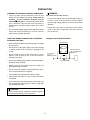
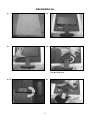
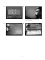
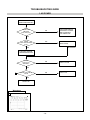
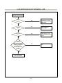
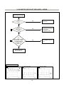
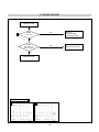
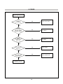
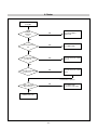
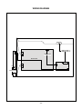
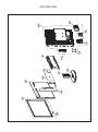
Website:http://biz.LGservice.com
COLOR MONITOR
SERVICE MANUAL
CHASSIS NO. : LM57A
MODEL:
L1753S (L1753S-*FS.A***QP)
L1953S (L1953S-*FS.A***QP)
(
) **Same model for Service
CAUTION
BEFORE SERVICING THE UNIT,
READ THE SAFETY PRECAUTIONS IN THIS MANUAL.
*To apply the MSTAR Chip.
CONTENTS
SPECIFICATIONS ................................................... 2
PRECAUTIONS ....................................................... 3
TIMING CHART ....................................................... 7
DISASSEMBLY ........................................................ 8
BLOCK DIAGRAM...................................................12
DISCRIPTION OF BLOCK DIAGRAM .................. 13
ADJUSTMENT ...................................................... 16
SERVICE OSD ........................................................17
TROUBLESHOOTING GUIDE .............................. 18
WIRING DIAGRAM ............................................... 24
EXPLODED VIEW...................................................25
REPLACEMENT PARTS LIST ...............................27
SCHEMATIC DIAGRAM ......................................... 31
SPECIFICATIONS
1. LCD CHARACTERISTICS
Type
: TFT Color LCD Module
Active Display Area : 17 inch - L1753S
: 19 inch - L1953S
Pixel Pitch
: 0.264 (H) x 0.264 (V) - L1753S
: 0.294 (H) x 0.294 (V) - L1953S
Color Depth
: 8bits, 16.2M colors
Size
: 358.5 (H) x 296.5 (V) x 17.0(D) - L1753S
: 396 (H) x 324 (V) x 17.5(D) - L1953S
Electrical Interface
: LVDS
Surface Treatment
: Hard-coating(3H), Anti-Glare
Operating Mode
: Normally White, Transmissive mode
Backlight Unit
: 4-CCFL
4. Max. Resolution
D-sub Analog
5. POWER SUPPLY
5-1. Power : AC 100~240V, 50/60Hz , 0.6A
5-2. Power Consumption
MODE
POWER ON (NORMAL)
2. OPTICAL CHARACTERISTICS
2-1. Viewing Angle by Contrast Ratio ≥ 10
: 230(min), 300(Typ) (Full White pattern, 0.70V) -6500K
: 150(min) (Full White pattern, 0.70V) -9300K
75%(min)
2-3. Contrast Ratio
: 2000:1 (DFC)
3. SIGNAL (Refer to the Timing Chart)
3-1. Sync Signal
• Type
: Separate Sync, SOG
3-2. Video Input Signal
1) Type
2) Voltage Level
a) Color 0, 0
b) Color 7, 0
c) Color 15, 0
3) Input Impedance
: R, G, B Analog
: 0~0.71 V
: 0 Vp-p
: 0.467Vp-p
: 0.714Vp-p
: 75Ω
3-3. Operating Frequency
Horizontal
: 30 ~ 83kHz
Vertical
: 56 ~ 75Hz
H/V SYNC VIDEO POWER CONSUMPTION LED COLOR
ON/ON ACTIVE
less than 35 W -L1753S
BLUE
less than 39 W -L1953S
or GREEN
STAND-BY
OFF/ON
OFF
less than 1 W
AMBER
SUSPEND
ON/OFF
OFF
less than 1 W
AMBER
DPMS OFF
OFF/OFF OFF
less than 1 W
AMBER
less than 1 W
OFF
POWER S/W Off
Left : -60° min., -70°(Typ) Right : +60° min., +70°(Typ)
Top :+60° min., +75°(Typ) Bottom : -50° min., -65°(Typ)
2-2. Luminance
: 1280 x 1024@75Hz
-
-
6. ENVIRONMENT
6-1. Operating Temperature : 10°C~35°C (50°F~95°F)
(Ambient)
6-2. Relative Humidity
: 10%~80% (Non-condensing)
6-3. MTBF
: 50,000 HRS with 90% Confidence
Lamp Life
: 50,000 Hours(Min)
7. DIMENSIONS (with TILT/SWIVEL)
L1753S
Width
: 364.5 mm (14.35'')
Depth
: 180 mm (7.09'')
Height
: 378.2 mm (14.89'')
L1953S
Width
Depth
Height
: 402 mm (15.83'')
: 180 mm (7.09'')
: 407.5 mm (16.04'')
8. WEIGHT (with TILT/SWIVEL)
L1753S
Net. Weight
: 3.3 kg (7.28 lbs)
Gross Weight
: 4.4 kg (9.70 lbs)
L1953S
Net. Weight
Gross Weight
-2-
: 4.2 kg (9.26 lbs)
: 5.4 kg (11.91 lbs)
PRECAUTION
WARNING FOR THE SAFETY-RELATED COMPONENT.
WARNING
• There are some special components used in LCD
monitor that are important for safety. These parts are
marked on the schematic diagram and the
replacement parts list. It is essential that these critical
parts should be replaced with the manufacturer’s
specified parts to prevent electric shock, fire or other
hazard.
• Do not modify original design without obtaining written
permission from manufacturer or you will void the
original parts and labor guarantee.
BE CAREFUL ELECTRIC SHOCK !
• If you want to replace with the new backlight (CCFL) or
inverter circuit, must disconnect the AC adapter
because high voltage appears at inverter circuit about
650Vrms.
• Handle with care wires or connectors of the inverter
circuit. If the wires are pressed cause short and may
burn or take fire.
Leakage Current Hot Check Circuit
TAKE CARE DURING HANDLING THE LCD MODULE
WITH BACKLIGHT UNIT.
AC Volt-meter
• Must mount the module using mounting holes arranged
in four corners.
• Do not press on the panel, edge of the frame strongly
or electric shock as this will result in damage to the
screen.
• Do not scratch or press on the panel with any sharp
objects, such as pencil or pen as this may result in
damage to the panel.
• Protect the module from the ESD as it may damage the
electronic circuit (C-MOS).
• Make certain that treatment person’s body are
grounded through wrist band.
• Do not leave the module in high temperature and in
areas of high humidity for a long time.
• The module not be exposed to the direct sunlight.
• Avoid contact with water as it may a short circuit within
the module.
• If the surface of panel become dirty, please wipe it off
with a softmaterial. (Cleaning with a dirty or rough cloth
may damage the panel.)
CAUTION
Please use only a plastic screwdriver to protect yourself
from shock hazard during service operation.
-3-
Good Earth Ground
such as WATER PIPE,
CONDUIT etc.
To Instrument’s
exposed
METALLIC PARTS
1.5 Kohm/10W
SERVICING PRECAUTIONS
CAUTION: Before servicing receivers covered by this
service manual and its supplements and addenda, read
and follow the SAFETY PRECAUTIONS on page 3 of this
publication.
NOTE: If unforeseen circumstances create conflict
between the following servicing precautions and any of the
safety precautions on page 3 of this publication, always
follow the safety precautions. Remember: Safety First.
General Servicing Precautions
1. Always unplug the receiver AC power cord from the AC
power source before;
a. Removing or reinstalling any component, circuit
board module or any other receiver assembly.
b. Disconnecting or reconnecting any receiver electrical
plug or other electrical connection.
c. Connecting a test substitute in parallel with an
electrolytic capacitor in the receiver.
CAUTION: A wrong part substitution or incorrect
polarity installation of electrolytic capacitors may
result in an explosion hazard.
d. Discharging the picture tube anode.
2. Test high voltage only by measuring it with an
appropriate high voltage meter or other voltage
measuring device (DVM, FETVOM, etc) equipped with
a suitable high voltage probe.
Do not test high voltage by "drawing an arc".
3. Discharge the picture tube anode only by (a) first
connecting one end of an insulated clip lead to the
degaussing or kine aquadag grounding system shield
at the point where the picture tube socket ground lead
is connected, and then (b) touch the other end of the
insulated clip lead to the picture tube anode button,
using an insulating handle to avoid personal contact
with high voltage.
4. Do not spray chemicals on or near this receiver or any
of its assemblies.
5. Unless specified otherwise in this service manual,
clean electrical contacts only by applying the following
mixture to the contacts with a pipe cleaner, cottontipped stick or comparable non-abrasive applicator;
10% (by volume) Acetone and 90% (by volume)
isopropyl alcohol (90%-99% strength)
CAUTION: This is a flammable mixture.
Unless specified otherwise in this service manual,
lubrication of contacts in not required.
6. Do not defeat any plug/socket B+ voltage interlocks
with which receivers covered by this service manual
might be equipped.
7. Do not apply AC power to this instrument and/or any of
its electrical assemblies unless all solid-state device
heat sinks are correctly installed.
8. Always connect the test receiver ground lead to the
receiver chassis ground before connecting the test
receiver positive lead.
Always remove the test receiver ground lead last.
9. Use with this receiver only the test fixtures specified in
this service manual.
CAUTION: Do not connect the test fixture ground strap
to any heat sink in this receiver.
Electrostatically Sensitive (ES) Devices
Some semiconductor (solid-state) devices can be
damaged easily by static electricity. Such components
commonly are called Electrostatically Sensitive (ES)
Devices. Examples of typical ES devices are integrated
circuits and some field-effect transistors and
semiconductor "chip" components. The following
techniques should be used to help reduce the incidence of
component damage caused by static by static electricity.
1. Immediately before handling any semiconductor
component or semiconductor-equipped assembly, drain
off any electrostatic charge on your body by touching a
known earth ground. Alternatively, obtain and wear a
commercially available discharging wrist strap device,
which should be removed to prevent potential shock
reasons prior to applying power to the unit under test.
2. After removing an electrical assembly equipped with
ES devices, place the assembly on a conductive
surface such as aluminum foil, to prevent electrostatic
charge buildup or exposure of the assembly.
3. Use only a grounded-tip soldering iron to solder or
unsolder ES devices.
4. Use only an anti-static type solder removal device.
Some solder removal devices not classified as "antistatic" can generate electrical charges sufficient to
damage ES devices.
5. Do not use freon-propelled chemicals. These can
generate electrical charges sufficient to damage ES
devices.
6. Do not remove a replacement ES device from its
protective package until immediately before you are
ready to install it. (Most replacement ES devices are
packaged with leads electrically shorted together by
conductive foam, aluminum foil or comparable
conductive material).
7. Immediately before removing the protective material
from the leads of a replacement ES device, touch the
protective material to the chassis or circuit assembly
into which the device will be installed.
CAUTION: Be sure no power is applied to the chassis
or circuit, and observe all other safety precautions.
8. Minimize bodily motions when handling unpackaged
replacement ES devices. (Otherwise harmless motion
such as the brushing together of your clothes fabric or
the lifting of your foot from a carpeted floor can
generate static electricity sufficient to damage an ES
device.)
-4-
General Soldering Guidelines
1. Use a grounded-tip, low-wattage soldering iron and
appropriate tip size and shape that will maintain tip
temperature within the range or 500 F to 600 F.
2. Use an appropriate gauge of RMA resin-core solder
composed of 60 parts tin/40 parts lead.
3. Keep the soldering iron tip clean and well tinned.
4. Thoroughly clean the surfaces to be soldered. Use a
mall wire-bristle (0.5 inch, or 1.25cm) brush with a
metal handle.
Do not use freon-propelled spray-on cleaners.
5. Use the following unsoldering technique
a. Allow the soldering iron tip to reach normal
temperature.
(500 F to 600 F)
b. Heat the component lead until the solder melts.
c. Quickly draw the melted solder with an anti-static,
suction-type solder removal device or with solder
braid.
CAUTION: Work quickly to avoid overheating the
circuitboard printed foil.
6. Use the following soldering technique.
a. Allow the soldering iron tip to reach a normal
temperature (500 F to 600 F)
b. First, hold the soldering iron tip and solder the strand
against the component lead until the solder melts.
c. Quickly move the soldering iron tip to the junction of
the component lead and the printed circuit foil, and
hold it there only until the solder flows onto and
around both the component lead and the foil.
CAUTION: Work quickly to avoid overheating the
circuit board printed foil.
d. Closely inspect the solder area and remove any
excess or splashed solder with a small wire-bristle
brush.
IC Remove/Replacement
Some chassis circuit boards have slotted holes (oblong)
through which the IC leads are inserted and then bent flat
against the circuit foil. When holes are the slotted type,
the following technique should be used to remove and
replace the IC. When working with boards using the
familiar round hole, use the standard technique as
outlined in paragraphs 5 and 6 above.
Removal
1. Desolder and straighten each IC lead in one operation
by gently prying up on the lead with the soldering iron
tip as the solder melts.
2. Draw away the melted solder with an anti-static
suction-type solder removal device (or with solder
braid) before removing the IC.
Replacement
1. Carefully insert the replacement IC in the circuit board.
2. Carefully bend each IC lead against the circuit foil pad
and solder it.
3. Clean the soldered areas with a small wire-bristle
brush. (It is not necessary to reapply acrylic coating to
the areas).
"Small-Signal" Discrete Transistor
Removal/Replacement
1. Remove the defective transistor by clipping its leads as
close as possible to the component body.
2. Bend into a "U" shape the end of each of three leads
remaining on the circuit board.
3. Bend into a "U" shape the replacement transistor leads.
4. Connect the replacement transistor leads to the
corresponding leads extending from the circuit board
and crimp the "U" with long nose pliers to insure metal
to metal contact then solder each connection.
Power Output, Transistor Device
Removal/Replacement
1. Heat and remove all solder from around the transistor
leads.
2. Remove the heat sink mounting screw (if so equipped).
3. Carefully remove the transistor from the heat sink of the
circuit board.
4. Insert new transistor in the circuit board.
5. Solder each transistor lead, and clip off excess lead.
6. Replace heat sink.
Diode Removal/Replacement
1. Remove defective diode by clipping its leads as close
as possible to diode body.
2. Bend the two remaining leads perpendicular y to the
circuit board.
3. Observing diode polarity, wrap each lead of the new
diode around the corresponding lead on the circuit
board.
4. Securely crimp each connection and solder it.
5. Inspect (on the circuit board copper side) the solder
joints of the two "original" leads. If they are not shiny,
reheat them and if necessary, apply additional solder.
Fuse and Conventional Resistor
Removal/Replacement
1. Clip each fuse or resistor lead at top of the circuit board
hollow stake.
2. Securely crimp the leads of replacement component
around notch at stake top.
3. Solder the connections.
CAUTION: Maintain original spacing between the
replaced component and adjacent components and the
circuit board to prevent excessive component
temperatures.
-5-
Circuit Board Foil Repair
Excessive heat applied to the copper foil of any printed
circuit board will weaken the adhesive that bonds the foil
to the circuit board causing the foil to separate from or
"lift-off" the board. The following guidelines and
procedures should be followed whenever this condition is
encountered.
At IC Connections
To repair a defective copper pattern at IC connections use
the following procedure to install a jumper wire on the
copper pattern side of the circuit board. (Use this
technique only on IC connections).
1. Carefully remove the damaged copper pattern with a
sharp knife. (Remove only as much copper as
absolutely necessary).
2. carefully scratch away the solder resist and acrylic
coating (if used) from the end of the remaining copper
pattern.
3. Bend a small "U" in one end of a small gauge jumper
wire and carefully crimp it around the IC pin. Solder the
IC connection.
4. Route the jumper wire along the path of the out-away
copper pattern and let it overlap the previously scraped
end of the good copper pattern. Solder the overlapped
area and clip off any excess jumper wire.
At Other Connections
Use the following technique to repair the defective copper
pattern at connections other than IC Pins. This technique
involves the installation of a jumper wire on the
component side of the circuit board.
1. Remove the defective copper pattern with a sharp
knife.
Remove at least 1/4 inch of copper, to ensure that a
hazardous condition will not exist if the jumper wire
opens.
2. Trace along the copper pattern from both sides of the
pattern break and locate the nearest component that is
directly connected to the affected copper pattern.
3. Connect insulated 20-gauge jumper wire from the lead
of the nearest component on one side of the pattern
break to the lead of the nearest component on the
other side.
Carefully crimp and solder the connections.
CAUTION: Be sure the insulated jumper wire is
dressed so the it does not touch components or sharp
edges.
-6-
TIMING CHART
VIDEO
A
E
D
B
SYNC
C
Sync
Video
Duration
Active
(D)
Time ( A )
640
16
MODE
H/V
Sync
Polarity
Dot
Clock
Frequency
1
H(Pixels)
+
25.175
31.469
Total
Period
(E)
800
V(Lines)
-
70.09
449
350
2
H(Pixels)
-
28.321
31.468
900
720
V(Lines)
+
70.08
449
400
H(Pixels)
-
V(Lines)
-
3
4
5
6
7
H(Pixels)
-
V(Lines)
-
H(Pixels)
+
V(Lines)
+
H(Pixels)
+
V(Lines)
+
H(Pixels)
+/-
V(Lines)
+/-
8
H(Pixels)
-
V(Lines)
-
9
H(Pixels)
-
V(Lines)
-
10
H(Pixels)
+/-
V(Lines)
+/-
11
H(Pixels)
+/-
V(Lines)
+/-
12
H(Pixels)
+
V(Lines)
+
13
H(Pixels)
+
V(Lines)
+
25.175
31.5
Front
Porch
(C)
96
Blanking
Time
(B)
48
37
2
60
18
108
54
12
2
35
31.469
800
640
16
96
48
59.94
525
480
10
2
33
37.5
840
640
16
64
120
75
500
480
1
3
16
37.879
1056
800
40
128
88
60.317
628
600
1
4
23
46.875
1056
800
16
80
160
75.0
625
600
1
3
21
49.725
1152
832
32
64
224
74.55
667
624
1
3
39
65.0
48.363
1344
1024
24
136
160
60.0
806
768
3
6
29
78.75
60.123
1312
1024
16
96
176
40.0
49.5
57.283
100.0
75.029
800
768
1
3
28
68.681
1456
1152
32
128
144
75.062
915
870
3
3
39
92.978
61.805
1504
1152
18
134
200
65.96
937
900
2
4
31
108.0
63.981
1688
1280
48
112
248
60.02
1066
1024
1
3
38
135.0
79.976
1688
1280
16
144
248
75.035
1066
1024
1
3
38
-7-
Resolution
640 x 350
720 X 400
640 x 480
640 x 480
800 x 600
800 x 600
832 x 624
1024 x 768
1024 x 768
1152 x 870
1152 x 900
1280 x 1024
1280 x 1024
DISASSEMBLY-Set
#1
#2
Soft pad on the table.
#3
Monitor on the pad.
# 4-1
Hold the head & stand base and then
Pull up the stand part.
Twist Stand until "Click".
# 4-2
#5
Separate head & stand
-8-
#6
#7
1. Pull the front cover upward.
2. Then, let the all latches are separated.(#3-1~3-2)
3. Put the front face down.
Remove the screws.
#8
#9
Disassemble back cover.
-9-
DISASSEMBLY-Stand
* In case of Latch 4.
# 1-1
# 1-2
Push the four latches on the bottom to the
outside and Separate Stand Body & Base.
(Reference the #1-2)
#2
#3
After finished repair, necessarily push 4ea
Latches to inside for restoration.
- 10 -
DISASSEMBLY-Stand
* In case of Latch 2.
#1
#2
Hold the stand body.
#3
Confirm two latch of right and left.
#4
Push the latch to the inside.
Push the base to the opposite direction.
#5
Confirm the condition of separation.
- 11 -
Adapter
1.8V
3.3V
- 10 IIn
nvveerrtteerr
P ow e r
To Key Control
Digital(R/G/B)
DVI-D
Analog(R/G/B)
D-Sub
M
MC
CU
U
O
OS
SD
D
S
Scca
alleerr
12V
5V
FFlla
assh
hm
meem
mo
orryy
T
DS
TM
MD
S
P
PLLLL
A
AD
C
DC
R
Reeg
gu
ullaattoorr
UP stream
5V
LVDS
1.8V
(only ODC version)
3.3V
EEPROM
24C08
1EA
LLV
S
DS
VD
i
T
r
a
m
s
n
Transmitttteerr
NT68625/68665/68670
BLOCK DIAGRAM
Main Board
(Scaler &
DC DC
converter)
Module Vcc
- 11 L
N
Line Filter
Start
Power
Control
IC
Drive
Aux
Dimming (Lamp Current Control)
Inverter On/OFF (3.3V)
12V
5V
POWER
Feedback
SMPS
5V
12V
Inverter
Control
IC
Drive Block
N-ch
P-ch
13V
INVERTER
Lamp
Current
Feedback
Inverter
Trans
Over
Voltage
Protection
Low
LAMP
High
BLOCK DIAGRAM-POWER
DESCRIPTION OF BLOCK DIAGRAM
1. Video Controller Part.
This part amplifies the level of video signal for the digital conversion and converts from the analog video signal to the
digital video signal using a pixel clock.
The pixel clock for each mode is generated by the PLL.
The range of the pixel clock is from 25MHz to 135MHz.
This part consists of the Scaler, ADC convertor, TMDS receiver and LVDS transmitter.
The Scaler gets the video signal converted analog to digital, interpolates input to 1280 X 1024 resolution signal and
outputs 8-bit R, G, B signal to transmitter.
2. Power Part.
This part consists of the one 3.3V, and one 1.8V regulators to convert power which is provided 5V in Power board.
12V is provided for inverter, 5V is provided for LCD panel.
Also, 5V is converted 3.3V and 1.8V by regulator. Converted power is provided for IC in the main board.
The inverter converts from DC12V to AC 700Vrms and operates back-light lamps of module.
3. MICOM Part.
This part is include video controller part. And this part consists of EEPROM IC which stores control data, Reset IC and
the Micom.
The Micom distinguishes polarity and frequency of the H/V sync are supplied from signal cable.
The controlled data of each modes is stored in EEPROM.
- 12 -
LIPS Board Block Diagram
12V
50 ~ 60Hz
LINE
100 ~ 240V
EMI
COMPONENTS
INPUT RECTIFIER
AND FILTER
HVDC
SWITCHING
TRANSFORMER
100KHz
OUTPUT RECTIFIER
AND FILTER
5V
GND
PWM CONTROL
CIRCUIT
PHOTO-COUPLER
ISOLATION
PRIMARY
12V
SIGNAL
COLLENTION
SECONDARY
INVERTER CIRCUIT
High Voltage
Operation description_LIPS
1. EMI components.
This part contains of EMI components to comply with global marketing EMI standards like FCC,VCCI CISPR, the
circuit included a line-filter, across line capacitor and of course the primary protection fuse.
2. Input rectifier and filter.
This part function is for transfer the input AC voltage to a DC voltage through a bridge rectifier and a bulk capacitor.
3. Energy Transfer.
This part function is for transfer the primary energy to secondary through a power transformer.
4. Output rectifier and filter.
This part function is to make a pulse width modulation control and to provide the driver signal to power switch, to
adjust the duty cycle during different AC input and output loading condition to achieve the dc output stabilized, and
also the over power protection is also monitor by this part.
5. Photo-Coupler isolation.
This part function is to feed back the DC output changing status through a photo transistor to primary controller to
achieve the stabilized DC output voltage.
6. Signal collection.
This part function is to collect the any change from the DC output and feed back to the primary through photo
transistor.
- 13 -
ADJUSTMENT
Windows EDID V1.0 User Manual
2. EDID Read & Write
1) Run WinEDID.exe
Operating System: MS Windows 98, 2000, XP
Port Setup: Windows 98 => Don’t need setup
Windows 2000, XP => Need to Port Setup.
This program is available to LCD Monitor only.
1. Port Setup
a) Copy “UserPort.sys” file to
“c:\WINNT\system32\drivers” folder
b) Run Userport.exe
2) Edit Week of Manufacture, Year of Manufacture,
Serial Number
a) Input User Info Data
b) Click “Update” button
c) Click “ Write” button
c) Remove all default number
d) Add 300-3FF
e) Click Start button.
f) Click Exit button.
- 14 -
SERVICE OSD
1) Turn off the power switch at the front side of the display.
2) Wait for about 5 seconds and press MENU, POWER switch with 1 second interval.
3) The SVC OSD menu contains additional menus that the User OSD menu as described below.
a) Auto Color : W/B balance and Automatically sets the gain and offset value.
b) NVRAM INIT : EEPROM initialize.(24C08)
c) CLEAR ETI : To initialize using time.
d) AGING : Select Aging mode(on/off).
e) R/G/B-9300K : Allows you to set the R/G/B-9300K value manually.
f) R/G/B-6500K : Allows you to set the R/G/B-6500K value manually.
g) R/G/B-Offset : Allows you to set the R/G/B-Offset value manually.(Analog Only)
h) R/G/B-Gain : Allows you to set the R/G/B-Gain value manually.(Analog Only)
i) MODULE : To select applied module.
A
9
IBM
Compatible PC
Video Signal
Generator
15
10
5
11
6
1
6
1
5
C
d
PARALLEL PORT
tu
No
RS
23
2C
se
13
PA
RA
LL
EL
14
ON
F
Power inlet (required)
5V
WE
R
220
A
PO
VG
S
MO
NI
TO
R
V-S
YN
CS
T
Control Line
5V
C
1
25
OFF
Power Select Switch
(110V/220V)
Power LED
ON
E
4.7K
OFF
74LS06
B
E ST Switch
B
F V-Sync On/Off Switch
(Switch must be ON.)
Figure 1. Cable Connection
- 17 -
4.7K
4.7K
5V
74LS06
TROUBLESHOOTING GUIDE
1. NO POWER
NO POWER
(POWER INDICATOR OFF)
CHECK J703
VOLTAGE
PIN5, PIN6 (5V)?
NO
CHECK POWER BOARD,
AND FIND OUT A SHORT
POINT AS OPENING
EACH POWER LINE
YES
CHECK
U601 PIN2 VOLTAGE
(3.3V) ?
NO
CHECK 3.3V LINE
(OPEN CHECK)
NO PROBLEM
YES
CHECK KEY CONTROL
CONNECTOR ROUTINE
IS U201
PIN75 (3.3V)
VOLTAGE ?
NO
CHECK 3.3V LINE
YES
1
CHECK U201 PIN 96
PULSE
NO
YES
CHECK U201
Waveforms
1
U201-#96
- 16 -
CHECK X-TAL
2. NO RASTER (OSD IS NOT DISPLAYED) – LIPS
NO RASTER
(OSD IS NOT DISPLAYED)
J703
PIN5, PIN6
5V?
NO
CHECK POWER BOARD,
AND FIND OUT A SHORT
POINT AS OPENING EACH
POWER LINE
YES
J703 PIN9
5V?
NO
CHECK MICOM INV
ON/OFF PORT.
YES
J703 PIN10
5V?
NO
1. CONFIRM BRIGHTNESS
OSD CONTRL STATE.
2. CHECK MICOM DIM-ADJ
PORT
YES
CHECK
PULSE AS
CONTACTING SCOPE
PROBE TO CAUTION LABEL.
(CONTACT PROBE TO
CAUTION LABEL.
CAN YOU SEE PULSE
AT YOUR
SCOPE?
NO
YES
REPLACE CCFL LAMP
IN THE LCD MODULE
- 17 -
LIPS
3. NO RASTER (OSD IS NOT DISPLAYED) – MSTAR
NO RASTER
(OSD IS NOT DISPLAYED)
U201
PIN 16, 75
3.3V?
NO
CHECK U601
YES
U201
PIN96, 97
OSCILLATE AS
14.31MHZ?
1
1. CHECK C509, C510
SOLDERING CONDITION
2. CHECK X501
3. TROUBLE IN U201
NO
YES
2
U201
PIN27 IS 48KHz H-SYNC?
PIN28 IS 60Hz V-SYNC?
IS PULSE APPEARED
AT SIGNAL PINS?
AT MODE 12?
CHECK CONNECTION
LINE FROM D-SUB TO
U201
NO
YES
TROUBLE IN CABLE
OR LCD MODULE
Waveforms
1
U201-#96, 97
2
2
U201-#27 H-SYNC
- 18 -
U201-#28 V-SYNC
4. TROUBLE IN DPM
TROUBLE IN DPM
NO
CHECK
R730, R731
3
CHECK PC
PC IS NOT GOING
INTO DPM OFF MODE
YES
CHECK
U201 PIN 27,28
SYNC PULSE ?
NO
YES
TROUBLE IN U201
Waveforms
3
R442 H-Sync
3
R443 V-Sync
- 19 -
CHECK H/V SYNC LINE
5. POWER
NO POWER
(POWER INDICATOR OFF)
CHECK
Fuse F101 OK?
NO
Trouble in Fuse (F101)
YES
CHECK
C101 Voltage
(AC110V->160Vdc
(AC220V->304Vdc
NO
Check BD101
YES
CHECK
U101 Pin6 Waveform
(Square wave
Come out?)
NO
Check U101 Pin7 : 9~10V
Check D102
YES
Check Q101 Drain
Waveform
NO
Trouble in Q101
YES
Check D201, D202
D203,Voltage
NO
YES
CHECK 5V, 12V Line
- 20 -
Trouble in D201, D202
6. Raster
NO Raster
(Lamp Off)
CHECK
P201 Pin9
3.3V?
NO
Check Scaler Output
(Main Board)
YES
Check U301 Pin2
5V?
NO
Check Q301, Q302
YES
Check U301 Pin6 VSEN,
Less than 3V
NO
Check the waveform of U301
Pin1, 15
NO
Check the waveform of U301
Pin2, 3
YES
Check U301 Pin12 SSTCMT,
Less than 1V
If waveform is no problem
Check U303, U304
Drain waveform
NO
YES
CHECK T301, T302
- 21 -
Check D302~D308
Or Trouble in U303, U304
WIRING DIAGRAM
30P
11P
6631T20023J
6P
6631900011H
3P
6631T20010E
- 22 -
EAD37414501 17"
EAD37413101 19"
060
010
070
080
020
090
050
040
100
140
110
150
160
170
030
130
EXPLORE VIEW
EXPLODED VIEW PARTS LIST
L1753S
* Note:Safety mark
Ref. No.
Description
Part No.
ABJ32220401
Cabinet Assembly,L1753 . 17" SILVER ANALOG WORLD WIDE -SILVER
ABJ32220402
) TEXTURE FOR 30919C0018B -BLACK
Cabinet Assembly,L1753 . 17" NEW PATTERN
ABJ32220444
Cabinet Assembly,L1753 . 17" NEW PATTERN TEXTURE FOR 30919C0029V -WHITE
EAJ34858001
LCD,Module-TFT,HT170E01-300 ZBD DRIVER 17.0INCH 1280X1024 300CD COLOR 72% 5/4 800:1 4MASK, 5ms, 160/160 BOE HYDIS TECHNOLOGY
EAJ32176801
LCD, Module-TFT,M170EG01-VD ZBD DRIVER 17.0INCH 1280X1024 300CD COLOR 72% 5/4 800:1 5MS, 160/160, 2CH-LVDS, 4LAMP AU OPTRONICS CORP
EAJ36378001
LCD,Module-TFT,LM170E03-TLL1 DRIVER 17.0INCH 1280X1024 300CD COLOR 72% 4/3 800:1 P5, 5ms, 160/160, TLI T-con, Lusem/Toshba(Source/Gate), Diffuser*2+Prism*1,lamp wire 135mm LG PHILIPS LCD
EAJ36379501
LCD,Module-TFT,LM170E03-TLL2 DRIVER 17.0INCH 1280X1024 300CD COLOR 72% 4/3 800:1 P6, 5ms, 160/160, TLI T-con, Lusem/Toshiba(Source/Gate), Diffuser x2+Prism x1, lamp(L1753T- FS.AWFOQ*N)
EAJ36380701
LCD,Module-TFT,LM170E03-TLL3 DRIVER 17.0INCH 1280X1024 300CD COLOR 72% 4/3 800:1 P5, 5ms, 160/160, TLI T-con, Magna/Toshiba(Source/Gate), Diffuser x2+Prism x1, lamp wire 135mm LG PHILIPS LCD
EAJ36720102
LCD,Module-TFT,CLAA170EA07P Non-ZBD DRIVER 17INCH 1280X1024 300CD COLOR 72% 4/3 700:1 5ms, 16.7M color depth, 160/160, lamp wire length 150mm CHUNGHWA PICTURE TUBES,
* LTD.
EAJ36720101
LCD,Module-TFT,LM190E08-TLL2 DRIVER 19.0INCH 1280X1024 300CD COLOR 72% 4/3 800:1 P7, 5ms, 160/160, TLI T-con, Lusem/Toshiba(Source/Gate), lamp Heesung, Diffuser x2+P
ACQ33170001
Cover Assembly,L1753S Baikal CI model 17" Back Cover Assy Auo-VD+Analog NT Local
ACQ33170003
Cover Assembly,L1753S Baikal CI model 17" Back Cover Assy LPL-TLL+Analog NT Local
ACQ33170005
Cover Assembly,L1753S Baikal CI model 17" Back Cover Assy BOE 5MS-Analog NT Local
ACQ33170008
Cover Assembly,L1753S Baikal CI model 17" L1753S Baikal CI model Back Cover Assy AUO 5ms+Analog SVC label
ACQ33170010
Cover Assembly,L1753S Baikal CI model 17" L1753S Baikal CI model B/C ASSY LPL-TLL+Analog+SVC LABLE ND Local
ACQ33170013
Cover Assembly,L1753S Baikal CI model 17" L1753S Baikal CI model Back Cover Assy BOE 5ms +SVC
* lable ND local
ACQ33170015
Cover Assembly,L1753S Baikal CI model 17" L1753S Baikal CI model Back Cover Assy CPT 5ms +SVC lable ND local
ACQ33170017
Cover Assembly,L1753S Baikal CI model 17" L1753S Baikal CI model Back Cover Assy CPT 5ms ND local
ACQ33170019
Cover Assembly,L1753S Baikal CI model 17" L1753S Baikal Back Cover Assy LPL Plus White for Japan
AAN32608903
Base Assembly,ASSY Lx53 LM57B Lx53 PATTERN TEXTURE -WHITE
AAN32608901
Base Assembly,ASSY Lx53 LM57B Lx53 PATTERN TEXTURE-W/W
AAN32608906
Base Assembly,ASSY Lx53 LM57B Lx53 PATTERN TEXTURE-US
050
35509K0246D
Cover,MOLD ABS L1952 ABS L1952 NEW BODY
060
3520900038A
Indicator,LED&PRE AMP LX52 PMMA NON LED LENS
070
MGJ37924303
Plate,PRESS SPTE 0.3 LAMP SPTE SHIELD L1753 FOR LPL/AUO CI MODULE ND LOCCAL
080
EBR37002601
PCB Assembly,CONTROL A.I LM72A BAIKAL II 17-INCH BLUE RD 53 SERIAL
090
EBR36269401
PCB Assembly,Power,POWER T.T LM-57C BAIKAL II - -
100
EBR36999808
Main Total Assembly,MAIN M.I LM72B BAIKAL II MSTAR ANALOG RD BAIKAL II MSTAR ANALOG
110
MGJ37924107
Plate,PRESS SBHG 0.8 REAR SECC SHIELD LX53 FOR LPL/AUO CI MODULE Analog ND local
130
MCK37398801
Cover,MOLD ABS LX53 CI ABS Lx53 CI hinge cover.ND-local
140
4940900022A
Knob,MAIN 5KEY LX52 TACK KNOB
150
FAB30006311
Screw,1FTF0403321 TH + P 4MM 20MM MSWR3 FNM2
160
MCK37400101
Cover,MOLD POM Lx53 CI POM Lx53 CI hinge body,ND-local
170
MCK37399101
Cover,MOLD ABS Lx53 CI ABS Lx53 CI hinge support,ND-LOCAL
010
020
030
040
- 26 -
EXPLODED VIEW PARTS LIST
L1953S
* Note:Safety mark
Ref. No.
010
020
Description
Part No.
ABJ32229401
Cabinet Assembly,L1953 . 19" NEW PATTERN TEXTURE FOR 30919C0019A -SILVER
ABJ32229402
) TEXTURE FOR 30919C0019B -BLACK
Cabinet Assembly,L1953 . 19" NEW PATTERN
ABJ32229443
Cabinet Assembly,L1953 . 19" NEW PATTERN TEXTURE FOR 30919C0030U -WHITE
EAJ36380901
LCD,Module-TFT,LM190E08-TLL2 DRIVER 19.0INCH 1280X1024 300CD COLOR 72% 4/3 800:1 P7, 5ms, 160/160, TLI T-con, Lusem/Toshiba(Source/Gate), lamp Heesung, Diffuser x2+Prism x1, lamp wire 160mm, depth 15.5T LG PHILIPS LCD
or EAJ36380801
LCD, Module-TFT,LM190E08-TLL1 DRIVER 19.0INCH 1280X1024 300CD COLOR 72% 4/3 800:1 P4, 5ms, 160/160, TLI T-con, Lusem/Toshiba(Source/Gate), lamp:Heesung, Diffuser x2+LC213x1, lamp wire 160mm, depth 15.5T LG PHILIPS LCD
or EAJ36381001
LCD,Module-TFT,LM190E08-TLL3 DRIVER 19.0INCH 1280X1024 300CD COLOR 72% 4/3 800:1 P4, 5ms, 160/160, TLI T-con, Magna/Toshiba(Source/Gate), lamp Heesung, Diffuser x2+LC213 x1, lamp wire 160mm, depth 15.5T LG PHILIPS LCD
6304FHS014C
or 6304FHS014B
EAJ32176101
or EAJ32176102
LCD,Module-TFT,HSD190ME13-D10 DRIVER 19INCH 1280X1024 300CD COLOR 72% 4/3 700:1 - HANNSTAR DISPLAY CORPORATION
LCD,Module-TFT,HSD190ME13-D10(700VS1) DRIVER 19INCH 1280X1024 300CD COLOR 72% 4/3 700:1 - HANNSTAR DISPLAY CORPORATION
LCD,Module-TFT,M190EG02-V4 ZBD DRIVER 19.0INCH 1280X1024 300CD COLOR 72% 5/4 800 VS 1 5MS, 160/160, 2CH-LVDS, 4LAMP AU OPTRONICS CORP
LCD,Module-TFT,M190EG02-V4 NON-ZBD DRIVER 19.0INCH 1280X1024 300CD COLOR 72% 5/4 800 VS 1 5MS, 160/160, 2CH-LVDS, 4LAMP, NON-ZBD AU OPTRONICS CORP
ACQ33173101
Cover Assembly,L1953S Baikal CI model 19" Back Cover Assy Auo-V4-Analog NT
ACQ33173103
Cover Assembly,L1953S Baikal CI model 19" Back Cover Assy LPL-TLL Analog NT
ACQ33173107
Cover Assembly,L1953S Baikal CI model 19" L1953S Baikal CI Back Cover Assy HSD ND LOCAL
ACQ33173109
Cover Assembly,L1953S Baikal CI model 19" L1953S Baikal CI Back Cover Assy AUO VD+SVC LABEL ND LOCAL
ACQ33173111
Cover Assembly,L1953S Baikal CI model 19" L1953S Baikal CI Back Cover Assy LPL CI MODULE+ SVC LABLE ND LOCAL
ACQ33173113
Cover Assembly,L1953S Baikal CI model 19" L1953S Baikal CI Back Cover Assy HSD +SVC LABLE ND
* LOCAL
ACQ33173115
Cover Assembly,L1953S Baikal CI model 19" L1953S baikal Back Cover Assy LPL plus module White for Japan
AAN32608903
Base Assembly,ASSY Lx53 LM57B Lx53 PATTERN TEXTURE -WHITE
AAN32608901
Base Assembly,ASSY Lx53 LM57B Lx53 PATTERN TEXTURE-W/W
AAN32608906
Base Assembly,ASSY Lx53 LM57B Lx53 PATTERN TEXTURE-US
050
35509K0246D
Cover,MOLD ABS L1952 ABS L1952 NEW BODY
060
3520900038A
Indicator,LED&PRE AMP LX52 PMMA NON LED LENS
070
MGJ37924303
Plate,PRESS SPTE 0.3 LAMP SPTE SHIELD L1753 FOR LPL/AUO CI MODULE ND LOCCAL
080
EBR37002601
PCB Assembly,CONTROL A.I LM72A BAIKAL II 17-INCH BLUE RD 53 SERIAL
090
EBR36269401
PCB Assembly,Power,POWER T.T LM-57C BAIKAL II - -
100
EBR36999808
Main Total Assembly,MAIN M.I LM72B BAIKAL II MSTAR ANALOG RD BAIKAL II MSTAR ANALOG
110
MGJ37924107
Plate,PRESS SBHG 0.8 REAR SECC SHIELD LX53 FOR LPL/AUO CI MODULE Analog ND local
130
MCK37398801
Cover,MOLD ABS LX53 CI ABS Lx53 CI hinge cover.ND-local
140
4940900022A
Knob,MAIN 5KEY LX52 TACK KNOB
150
FAB30006311
Screw,1FTF0403321 TH + P 4MM 20MM MSWR3 FNM2
160
MCK37400101
Cover,MOLD POM Lx53 CI POM Lx53 CI hinge body,ND-local
170
MCK37399101
Cover,MOLD ABS Lx53 CI ABS Lx53 CI hinge support,ND-LOCAL
030
040
- 26 -
SCHEMATIC DIAGRAM
1. SCALER
- 33 -
2. POWER & WAFER
- 33 -
3. INVERTER
- 32 -
4. POWER
- 33 -
4
2
3
1
P/NO : MFL30290843
May. 2007
Printed in China