1
Service Manual
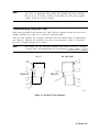
HP 8560A Spectrum Analyzer
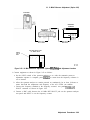
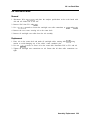
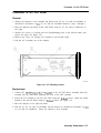
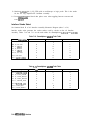
SERIAL NUMBERS
Prefix 3207A and Above
Eiia
HEWLETT
PACKARD
HP Part No. 08560-90081
Printed in USA August 1992
@Copyright Hewlett-Packard Company 1990, 1992
All Rights Reserved. Reproduction, adaptation, or translation without prior written
permission is prohibited, except as allowed under the copyright laws.
1212 Valley House Drive, Rohnert Park, CA 94928-4999, USA
Certification
Hewlett-Packard Company certifies that this product met its published specifications at the
time of shipment from the factory. Hewlett-Packard further certifies that its calibration
measurements are traceable to the United States National Institute of Standards and
Technology, to the extent allowed by the Institute’s calibration facility, and to the calibration
facilities of other International Standards Organization members.
Warranty
This Hewlett-Packard instrument product is warranted against defects in material and
workmanship for a period of one year from date of shipment. During the warranty period,
Hewlett-Packard Company will, at its option, either repair or replace products which prove to
be defective.
For warranty service or repair, this product must be returned to a service facility designated
by HP. Buyer shall prepay shipping charges to HP and HP shall pay shipping charges to
return the product to Buyer. However, Buyer shall pay all shipping charges, duties, and taxes
for products returned to HP from another country.
HP warrants that its software and firmware designated by HP for use with an instrument
will execute its programming instructions when properly installed on that instrument. HP
does not warrant that the operation of the instrument, or software, or firmware will be
uninterrupted or error-free.
Limitation of Warranty
The foregoing warranty shall not apply to defects resulting from improper or inadequate
maintenance by Buyer, Buyer-supplied software or interfacing, unauthorized modification or
misuse, operation outside of the environmental specifications for the product, or improper
site preparation or maintenance.
NO OTHER WARRANTY IS EXPRESSED OR IMPLIED. HP SPECIFICALLY
DISCLAIMS THE IMPLIED WARRANTIES OF MERCHANTABILITY AND FITNESS
FOR A PARTICULAR PURPOSE.
Exclusive Remedies
THE REMEDIES PROVIDED HEREIN ARE BUYER’S SOLE AND EXCLUSIVE
REMEDIES. HP SHALL NOT BE LIABLE FOR ANY DIRECT, INDIRECT, SPECIAL,
INCIDENTAL, OR CONSEQUENTIAL DAMAGES, WHETHER BASED ON
CONTRACT, TORT, OR ANY OTHER LEGAL THEORY.
Assistance
Product maintenance agreements and other customer assistance agreements are available for
Hewlett-Packard products.
For any assistance, contact your nearest Hewlett-Packard Sales and Service Ofice.
...
III
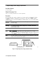
Safety Symbols
The following safety symbols are used throughout this manual. Familiarize yourself with each
of the symbols and its meaning before operating this instrument.
Caution
The caution sign denotes a hazard. It calls attention to a procedure which,
if not correctly performed or adhered to, could result in damage to or
destruction of the instrument. Do not proceed beyond a caution sign until the
indicated conditions are fully understood and met.
Warning
The warning sign denotes a hazard. It calls attention to a procedure which,
if not correctly performed or adhered to, could result in injury or loss of life.
Do not proceed beyond a warning sign until the indicated conditions are fully
understood and met.
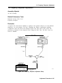
General Safety Considerations
Warning
Before this instrument is switched on, make sure it has been properly grounded
through the protective conductor of the ac power cable to a socket outlet
provided with protective earth contact.
Any interruption of the protective (grounding) conductor, inside or outside
the instrument, or disconnection of the protective earth terminal can result in
personal injury.
Warning
There are many points in the instrument which can, if contacted, cause personal.
injury. Be extremely careful.
Any adjustments or service procedures that require operation of the instrument
with protective covers removed should be performed only by trained service
personnel.
Caution
Before this instrument is switched on, make sure its primary power circuitry
has been adapted to the voltage of the ac power source.
Failure to set the ac power input to the correct voltage could cause damage to
the instrument when the ac power cable is plugged in.
iv
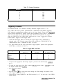
HP 8560A Spectrum Analyzer Documentation Outline
For ordering information, contact a Hewlett-Packard Sales and Service Office.
Manuals Shipped with Your Instrument
HP 8560A Installation and Verification Manual
n
Tells you how to install the spectrum analyzer.
n
Tells you what your analyzer’s specifications are.
HP 856OA/8561 B/8563A 0 perating and Programming Manual
w Tells you how to make measurements with your spectrum analyzer.
w Tells you how to program your spectrum analyzer.
HP 8560A Quick Reference Guide
8 Is an abbreviated version of the HP 856OA/8561B/8563A
iWanua1
n
Operating and Programming
Provides you with a listing of all remote programming commands.
Options
Option 915: HP 8560A Service Manual and HP 8560A/6lB/63A Spectrum Analyzer
Component Level Information
w The service manual provides information to service your analyzer to the assembly-level (not
always immediately available for new products).
n
The component-level information binder provides component-level information for
component-level repair of the analyzer or analyzer family (not always immediately available
for new products).
Option 910: Extra Manual Set
w Doubles all documentation shipped with a standard instrument.
Option 916: HP 8560A Quick Reference Guide
1 Adds an extra HP 8560A Quick Reference Guide to the document package.
V
Contents
1. General Information
Manual Organization . . . . . . . . .
Manual Text Conventions . . . . . . .
Serial Numbers Covered by This Manual .
Instrument Variations . . . . . . . . .
HP 85629B Test and Adjustment Module
Service Kit . . . . . . . . . . . . . .
Recommended Test Equipment . . . . .
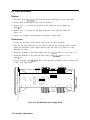
Electrostatic Discharge . . . . . . . .
Reducing Potential for ESD Damage .
Static-Safe Accessories . . . . . . . .
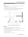
Returning Instruments for Service . . . .
Service Tag . . . . . . . . . . . .
Original Packaging . . . . . . . . .
Other Packaging . . . . . . . . . .
Sales and Service Offices . . . . . . . .
.
.
.
.
.
.
.
.
.
.
.
.
.
.
.
l-l
l-2
l-2
l-3
l-6
l-6
1-6
l-7
l-7
1-8
1-8
l-8
l-8
1-8
1-11
2. Adjustment Procedures
Introduction . . . . . . . . . . . . . . . . . . . . . . . . . . . . .
Safety Considerations . . . . . . . . . . . . . . . . . . . . . . . .
Which Adjustments Should Be Performed? . . . . . . . . . . . . . . .
Test Equipment . . . . . . . . . . . . . . . . . . . . . . . . . . .
Adjustable and Factory-Selected Components . . . . . . . . . . . . . .
Adjustment Tools . . . . . . . . . . . . . . . . . . . . . . . . . .
Instrument Service Position . . . . . . . . . . . . . . . . . . . . .
Using the TAM . . . . . . . . . . . . . . . . . . . . . . . . . . . .
Test Equipment . . . . . . . . . . . . . . . . . . . . . . . . . . .
Adjustment Indicator . . . . . . . . . . . . . . . . . . . . . . . .
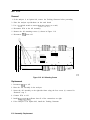
1. High-Voltage Power Supply Adjustment . . . . . . . . . . . . . .
. . . . . . . . . . . . . . . . . . . . . .
2. Display Adjustment
3. IF Bandpass Adjustment . . . . . . . . . . . . . . . . . . . . .
4. IF Amplitude Adjustments . . . . . . . . . . . . . . . . . . .
. . . . . . . . . . . . . . . . .
5. DC Log Amplifier Adjustments
6. Sampling Oscillator Adjustment . . . . . . . . . . . . . . . . .
. . . . . . . . . . . . . . . . . . . . . . .
7. YTO Adjustment
8. First LO Distribution Amplifier Adjustment . . . . . . . . . . . .
9. Tracking Generator Power Level Adjustments . . . . . . . . . . .
10. Frequency Response Adjustment . . . . . . . . . . . . . . . .
11. Calibrator Amplitude Adjustment . . . . . . . . . . . . . . . .
12. 10 MHz Reference Adjustment (Non-Option 003 only) . . . . . . .
13. Demodulator Adjustment . . . . . . . . . . . . . . . . . . . .
14. External Mixer Bias Adjustment . . . . . . . . . . . . . . . .
2-l
2-2
2-2
2-2
2-2
2-3
2-3
2-9
2-9
2-9
2-12
2-14
2-20
2-25
2-29
2-33
2-37
2-40
2-42
2-45
2-48
2-50
2-52
2-55
.
.
.
.
.
.
.
.
.
.
.
.
.
.
.
.
.
.
.
.
.
.
.
.
.
.
.
.
.
.
.
.
.
.
.
.
.
.
.
.
.
.
.
.
.
.
.
.
.
.
.
.
.
.
.
.
.
.
.
.
.
.
.
.
.
.
.
.
.
.
.
.
.
.
.
.
.
.
.
.
.
.
.
.
.
.
.
.
.
.
.
.
.
.
.
.
.
.
.
.
.
.
.
.
.
.
.
.
.
.
.
.
.
.
.
.
.
.
.
.
.
.
.
.
.
.
.
.
.
.
.
.
.
.
.
.
.
.
.
.
.
.
.
.
.
.
.
.
.
.
.
.
.
.
.
.
.
.
.
.
.
.
.
.
.
.
.
.
.
.
.
.
.
.
.
.
.
.
.
.
.
.
.
.
.
.
.
.
.
.
.
.
.
.
.
.
.
.
.
.
.
.
.
.
.
.
.
.
.
.
.
.
.
.
.
.
.
.
.
.
.
.
.
.
.
Contents-l
15.
16.
17.
18.
19.
20.
External Mixer Amplitude Adjustment
Second IF Gain Adjustment . . . .
Signal ID Oscillator Adjustment . . .
600 MHz Amplitude Adjustment
. .
10 MHz Reference Adjustment (Option
Tracking Oscillator Adjustment (Option
. . .
. . .
. . .
. . .
003)
002)
.
.
.
.
.
.
.
.
.
.
.
.
.
.
.
.
.
.
.
.
.
.
.
.
.
.
.
.
.
.
.
.
.
.
.
.
.
.
.
.
.
.
.
.
.
.
.
.
.
.
.
.
.
.
.
.
.
.
.
.
.
.
.
.
.
.
2-57
2-60
2-63
2-66
2-68
2-71
3. Assembly Replacement
Access to Internal Assemblies . . . . . . . . . .
Cable Color Code . . . . . . . . . . . . . . .
Procedure 1. Analyzer Cover . . . . . . . . .
Procedure 2. Al Front Frame/Al8 CRT . . . .
Procedure 3. AlAl Keyboard/Front Panel Keys
Procedure 4. AlA RPG . . . . . . . . . .
Procedure 5. A2, A3, A4, and A5 Assemblies .
Procedure 6. A6 Power Supply Assembly . . .
Procedure 7. A6Al High Voltage Assembly . .
Procedure 8. A7 through Al3 Assemblies . . .
A7 1st LO Distribution Amplifier . . . . . . .
A8 Low Band Mixer . . . . . . . . . . . . .
A9 Input Attenuator . . . . . . . . . . . .
A10 Tracking Generator (Option 002) . . . . .
AllYTO . . . . . . . . . . . . . . . . .
Al3 Second Converter . . . . . . . . . . . .
Procedure 9. Al4 and Al5 Assemblies . . . .
Procedure 10. Al7 CRT Driver . . . . . . . .
Procedure 11. Bl Fan . . . . . . . . . . . .
Procedure 12. BTl Battery . . . . . . . . .
Procedure 13. Rear Frame/Rear Dress Panel . .
Procedure 14. W3 Line Switch Cable . . . . .
Procedure 15. EEROM (A2U501)
. . . . . .
Procedure 16. A21 OCXO (Option 003) . . . .
.
.
.
.
.
.
.
.
.
.
.
.
.
.
.
.
.
.
.
.
.
.
.
.
.
.
.
.
.
.
.
.
.
.
.
.
.
.
.
.
.
.
.
.
.
.
.
.
.
.
.
.
.
.
.
.
.
.
.
.
.
.
.
.
.
.
.
.
.
.
.
.
.
.
.
.
.
.
.
.
.
.
.
.
.
.
.
.
.
.
.
.
.
.
.
.
.
.
.
.
.
.
.
.
.
.
.
.
.
.
.
.
.
.
.
.
.
.
.
.
.
.
.
.
.
.
.
.
.
.
.
.
.
.
.
.
.
.
.
.
.
.
.
.
.
.
.
.
.
.
.
.
.
.
.
.
.
.
.
.
.
.
.
.
.
.
.
.
.
.
.
.
.
.
.
.
.
.
.
.
.
.
.
.
.
.
.
.
.
.
.
.
.
.
.
.
.
.
.
.
.
.
.
.
.
.
.
.
.
.
.
.
.
.
.
.
.
.
.
.
.
.
.
.
.
.
.
.
.
.
.
.
.
.
.
.
.
.
.
.
.
.
.
.
.
.
.
.
.
.
.
.
.
.
.
.
.
.
.
.
.
.
.
.
.
.
.
.
.
.
.
.
.
.
.
.
.
.
.
.
.
.
.
.
.
.
.
.
3-2
3-2
3-3
3-4
3-11
3-12
3-13
3-19
3-22
3-25
3-28
3-29
3-30
3-31
3-32
3-33
3-34
3-37
3-38
3-39
3-40
3-44
3-50
3-51
4. Replaceable Parts
Ordering Information . . . . . .
Direct Mail-Order System . . .
Direct Phone-Order System . .
Parts List Format . . . . . . . .
Firmware-Dependent Part Numbers
.
.
.
.
.
.
.
.
.
.
.
.
.
.
.
.
.
.
.
.
.
.
.
.
.
.
.
.
.
.
.
.
.
.
.
.
.
.
.
.
.
.
.
.
.
.
.
.
.
.
.
.
.
.
.
.
.
.
.
.
4-l
4-l
4-2
4-2
4-2
5. Major Assembly and Cable Locations
Introduction . . . . . . . . . . . . . . . . . . . . . . . . . . . . .
5-l
Contents-2
.
.
.
.
.
.
.
.
.
.
.
.
.
.
.
.
.
.
.
.
.
.
.
.
.
.
.
.
.
.
.
.
.
.
.
6. General Troubleshooting
Introduction . . . . . . . . . . . . . . . . . . .
Assembly Level Text . . . . . . . . . . . . . .
Block Diagrams . . . . . . . . . . . . . . . . .
Assembly Test Points . . . . . . . . . . . . . .
Pad.. . . . . . . . . . . . . . . . . . . .
Test Jack . . . . . . . . . . . . . . . . . .
Ribbon Cables . . . . . . . . . . . . . . . . .
WR PROT/WR ENA Softkey Menus . . . . . . .
Troubleshooting to a Functional Section . . . . . . .
Using the TAM . . . . . . . . . . . . . . . . . .
Diagnostic Functions . . . . . . . . . . . . . .
TAM Requirements . . . . . . . . . . . . . . .
Test Connectors . . . . . . . . . . . . . . . .
Revision Connectors . . . . . . . . . . . . . .
Inconsistent Results . . . . . . . . . . . . . . .
Erroneous Results . . . . . . . . . . . . . . . .
Blank Display . . . . . . . . . . . . . . . . .
Automatic Fault Isolation . . . . . . . . . . . .
Display/Power Supply . . . . . . . . . . . . .
Controller Check . . . . . . . . . . . . . . .
ADC/Interface Check . . . . . . . . . . . . .
IF/LOG Check . . . . . . . . . . . . . . . .
LO Control Check . . . . . . . . . . . . . .
RF Check . . . . . . . . . . . . . . . . . .
Manual Probe Troubleshooting . . . . . . . . . .
Cal Osc. Troubleshooting Mode . . . . . . . . .
Error Messages . . . . . . . . . . . . . . . . . .
Viewing Multiple Messages . . . . . . . . . . . .
Error Message Elimination . . . . . . . . . . . .
System Analyzer Programming Errors (100 to 150) .
ADC Errors (200 to 299) . . . . . . . . . . . . .
LO and RF Hardware/Firmware Failures (300 to 399)
YTO Loop Errors (300 to 301) . . . . . . . . .
Roller PLL Errors (302 to 316) . . . . . . . . .
YTO Loop Errors (317 to 318) . . . . . . . . .
Roller Oscillator Errors (321 to 329) . . . . . . .
YTO Loop Errors (331) . . . . . . . . . . . .
600 MHz Reference Loop (333) . . . . . . . . .
YTO Leveling Loop (334) . . . . . . . . . . .
Sampling Oscillator (335) . . . . . . . . . . .
Automatic IF Errors (400 to 599) . . . . . . . . .
System Errors (600 to 651) . . . . . . . . . . . .
Digital and Checksum Errors (700 to 799) . . . . .
EEROM Checksum Errors (700 to 704) . . . . .
Program ROM Check-sum Errors (705 to 710) . .
RAM Check Errors (711 to 719) . . . . . . . .
Microprocessor Error (717) . . . . . . . . . . .
Battery Problem (718) . . . . . . . . . . . . . .
Model Number Error (719) . . . . . . . . . . . .
System Errors (750 to 757) . . . . . . . . . . . .
.
.
.
.
.
.
.
.
.
.
.
.
.
.
.
.
.
.
.
.
.
.
.
.
.
.
.
.
.
.
.
.
.
.
.
.
.
.
.
.
.
.
.
.
.
.
.
.
.
.
.
.
.
.
.
.
.
.
.
.
.
.
.
.
.
.
.
.
.
.
.
.
.
.
.
.
.
.
.
.
.
.
.
.
.
.
.
.
.
.
.
.
.
.
.
.
.
.
.
.
.
.
.
.
.
.
.
.
.
.
.
.
.
.
.
.
.
.
.
.
.
.
.
.
.
.
.
.
.
.
.
.
.
.
.
.
.
.
.
.
.
.
.
.
.
.
.
.
.
.
.
.
.
.
.
.
.
.
.
.
.
.
.
.
.
.
.
.
.
.
.
.
.
.
.
.
.
.
.
.
.
.
.
.
.
.
.
.
.
.
.
.
.
.
.
.
.
.
.
.
.
.
.
.
.
.
.
.
.
.
.
.
.
.
.
.
.
.
.
.
.
.
.
.
.
.
.
.
.
.
.
.
.
.
.
.
.
.
.
.
.
.
.
.
.
.
.
.
.
.
.
.
.
.
.
.
.
.
.
.
.
.
.
.
.
.
.
.
.
.
.
.
.
.
.
.
.
.
.
.
.
.
.
.
.
.
.
.
.
.
.
.
.
.
.
.
.
.
.
.
.
.
.
.
.
.
.
.
.
.
.
.
.
.
.
.
.
.
.
.
.
.
.
.
.
.
.
.
.
.
.
.
.
.
.
.
.
.
.
.
.
.
.
.
.
.
.
.
.
.
.
.
.
.
.
.
.
.
.
.
.
.
.
.
.
.
.
.
.
.
.
.
.
.
.
.
.
.
.
.
.
.
.
.
.
.
.
.
.
.
.
.
.
.
.
.
.
.
.
.
.
.
.
.
.
.
.
.
.
.
.
.
.
.
.
.
.
.
.
.
.
.
.
.
.
.
.
.
.
.
.
.
.
.
.
.
.
.
.
.
.
.
.
.
.
.
.
.
.
.
.
.
.
.
.
.
.
.
.
.
.
.
.
.
.
.
.
.
.
.
.
.
.
.
.
.
.
.
.
.
.
.
.
.
.
.
.
.
.
.
.
.
.
.
.
.
.
.
.
.
6-1
6-l
6-l
6-2
6-2
6-2
6-2
6-6
6-8
6-10
6-10
6-11
6-11
6-11
6-12
6-12
6-12
6-12
6-12
6-12
6-13
6-13
6-13
6-13
6-13
6-14
6-15
6-15
6-16
6-16
6-17
6-18
6-18
6-18
6-20
6-20
6-21
6-21
6-22
6-22
6-22
6-31
6-31
6-31
6-32
6-33
6-33
6-33
6-34
6-34
Contents-3
Option Module Errors (800 to 899) . . . . . . . . .
User-Generated Errors (902 to 904) . . . . . . . . .
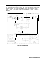
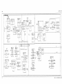
Block Diagram Description . . . . . . . . . . . . . .
RF Section . . . . . . . . . . . . . . . . . . . .
A7 LODA . . . . . . . . . . . . . . . . . . .
A8 Low Band Mixer . . . . . . . . . . . . . . .
A9 Input Attenuator . . . . . . . . . . . . . .
All YTO . . . . . . . . . . . . . . . . . . .
Al3 Second Converter . . . . . . . . . . . . . .
A15Al Second IF Distribution Amplifier (P/O A15) .
Third Converter (P/O A15) . . . . . . . . . . .
Flatness Compensation Amplifiers (P/O A15) . . .
Synthesizer Section . . . . . . . . . . . . . . . .
Sweeping the First LO . . . . . . . . . . . . . .
Reference PLL (P/O A15) . . . . . . . . . . . .
YTO PLL (A7, All, P/O A14, P/O A15) . . . . .
Offset Lock Loop (P/O A15) . . . . . . . . . . .
Roller Oscillator PLL (P/O A14) . . . . . . . . .
IF Section . . . . . . . . . . . . . . . . . . . .
A4 LOG Amplifier/Cal Oscillator assembly . . . . .
A5 IF Assembly . . . . . . . . . . . . . . . .
ADC/Interface Section . . . . . . . . . . . . . .
ADC . . . . . . . . . . . . . . . . . . . . .
Log Expand/Video Functions (P/O A3) . . . . . .
Triggering . . . . . . . . . . . . . . . . . . .
Controller Section . . . . . . . . . . . . . . . . .
EEROM . . . . . . . . . . . . . . . . . . . .
Firmware . . . . . . . . . . . . . . . . . . .
Display ASM . . . . . . . . . . . . . . . . . .
Display/Power Supply Section . . . . . . . . . . .
A6 Power Supply . . . . . . . . . . . . . . . .
Al7 CRT Display Driver . . . . . . . . . . . . .
7. ADC/Interface Section
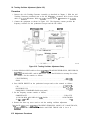
Troubleshooting Using the TAM .
Automatic Fault Isolation . . .
Keyboard/RPG Problems . . . .
Keyboard Interface . . . . . .
RPG Interface . . . . . . . .
Triggering Problems . . . . . . .
Flatness Control (RF Gain DACs)
A3 Assembly’s Video Circuits . .
Log Offset/Log Expand . . . .
Video MUX . . . . . . . . .
Video Filter . . . . . . . . .
Video Filter Buffer Amplifier . .
Positive/Negative Peak Detectors
Peak Detector Reset . . . . . .
Rosenfell Detector . . . . . .
ADCMUX . . . . . . . . . .
Variable Gain Amplifier (VGA) .
Contents-4
.
.
.
.
.
.
.
.
.
.
.
.
.
.
.
.
.
.
.
.
.
.
.
.
.
.
.
.
.
.
.
.
.
.
.
.
.
.
.
.
.
.
.
.
.
.
.
.
.
.
.
.
.
.
.
.
.
.
.
.
.
.
.
.
.
.
.
.
.
.
.
.
.
.
.
.
.
.
.
.
.
.
.
.
.
.
.
.
.
.
.
.
.
.
.
.
.
.
.
.
.
.
.
.
.
.
.
.
.
.
.
.
.
.
.
.
.
.
.
.
.
.
.
.
.
.
.
.
.
.
.
.
.
.
.
.
.
.
.
.
.
.
.
.
.
.
.
.
.
.
.
.
.
.
.
.
.
.
.
.
.
.
.
.
.
.
.
.
.
.
.
.
.
.
.
.
.
.
.
.
.
.
.
.
.
.
.
.
.
.
.
.
.
.
.
.
.
.
.
.
.
.
.
.
.
.
.
.
.
.
.
.
.
.
.
.
.
.
.
.
.
.
.
.
.
.
.
.
.
.
.
.
.
.
.
.
.
.
.
.
.
.
.
.
.
.
.
.
.
.
.
.
.
.
.
.
.
.
.
.
.
.
.
.
.
.
.
.
.
.
.
.
.
.
.
.
.
.
.
.
.
.
.
.
.
.
.
.
.
.
.
.
.
.
.
.
.
.
.
.
.
.
.
.
.
.
.
.
.
.
.
.
.
.
.
.
.
.
.
.
.
.
.
.
.
.
.
.
.
.
.
.
.
.
.
.
.
.
.
.
.
.
.
.
.
.
.
.
.
.
.
.
.
.
.
.
.
.
.
.
.
.
.
.
.
.
.
.
.
.
.
.
.
.
.
.
.
.
.
.
.
.
.
.
.
.
.
.
.
.
.
.
.
.
.
.
.
.
.
.
.
.
.
.
.
.
.
.
.
.
.
.
.
.
.
.
.
.
.
.
.
.
.
.
.
.
.
.
.
.
.
.
.
.
.
.
.
.
.
.
.
.
.
.
.
.
.
.
.
.
.
.
.
.
.
.
.
.
6-34
6-34
6-35
6-36
6-36
6-36
6-36
6-36
6-37
6-37
6-37
6-37
6-37
6-37
6-38
6-38
6-38
6-39
6-39
6-40
6-40
6-41
6-42
6-42
6-42
6-42
6-43
6-43
6-43
6-43
6-43
6-43
.
.
.
.
.
.
.
.
.
.
.
.
.
.
.
.
.
.
.
.
.
.
.
.
.
.
.
.
.
.
.
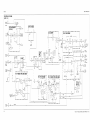
.
.
.
.
.
.
.
.
.
.
.
.
.
.
.
.
.
.
.
.
.
.
.
.
.
.
.
.
.
.
.
.
.
.
.
.
.
.
.
.
.
.
.
.
.
.
.
.
.
.
.
.
.
.
.
.
.
.
.
.
.
.
.
.
.
.
.
.
.
.
.
.
.
.
.
.
.
.
.
.
.
.
.
.
.
.
.
.
.
.
.
.
.
.
.
.
.
.
.
.
.
.
.
.
.
.
.
.
.
.
.
.
.
.
.
.
.
.
.
.
.
.
7-4
7-4
7-7
7-7
7-8
7-9
7-11
7-12
7- 14
7-15
7-15
7-16
7-17
7-18
7-18
7-19
7-21
Track and Hold . . . . . .
A3 Assembly’s ADC Circuits .
ADC Control Signals . . .
ADC Start/Stop Control . .
ADC ASM . . . . . . . .
ADC . . . . . . . . . .
Ramp Counter . . . . . .
A3 Assembly’s Control Circuits
Analog Bus Drivers . . . .
Analog Bus Timing . . . .
Interface Strobe Select . . .
.
.
.
.
.
.
.
.
.
.
.
.
.
.
.
.
.
.
.
.
.
.
.
.
.
.
.
.
.
.
.
.
.
.
.
.
.
.
.
.
.
.
.
.
.
.
.
.
.
.
.
.
.
.
.
.
.
.
.
.
.
.
.
.
.
.
.
.
.
.
.
.
.
.
.
.
.
.
.
.
.
.
.
.
.
.
.
.
.
.
.
.
.
.
.
.
.
.
.
.
.
.
.
.
.
.
.
.
.
.
.
.
.
.
.
.
.
.
.
.
.
.
.
.
.
.
.
.
.
.
.
.
.
.
.
.
.
.
.
.
.
.
.
.
.
.
.
.
.
.
.
.
.
.
.
.
.
.
.
.
.
.
.
.
.
.
.
.
.
.
.
.
.
.
.
.
.
.
.
.
.
.
.
.
.
.
.
.
.
.
.
.
.
.
.
.
.
.
.
.
.
.
.
.
.
.
.
.
.
.
.
.
.
.
.
.
.
.
.
.
.
.
.
.
.
.
.
.
.
.
.
7-21
7-22
7-22
7-23
7-24
7-24
7-25
7-26
7-26
7-27
7-28
8. IF Section
Troubleshooting Using the TAM . . . . . . . . . . . . . . . . . . . .
Troubleshooting A4 Log Amplifier with the TAM . . . . . . . . . . . .
Troubleshooting A5 with the TAM . . . . . . . . . . . . . . . . . .
Troubleshooting A4 Cal Oscillator with the TAM . . . . . . . . . . . .
Automatic IF Adjustment . . . . . . . . . . . . . . . . . . . . . . .
Parameters Adjusted . . . . . . . . . . . . . . . . . . . . . . . .
Requirements . . . . . . . . . . . . . . . . . . . . . . . . . . . .
Performance Test Failures . . . . . . . . . . . . . . . . . . . . . . .
IF Gain Uncertainty Performance Test . . . . . . . . . . . . . . . . .
Scale Fidelity Performance Test . . . . . . . . . . . . . . . . . . . .
Resolution Bandwidths Performance Tests . . . . . . . . . . . . . . .
A4 Assembly’s Log Amplifier Circuits . . . . . . . . . . . . . . . . . .
Log Amplifier . . . . . . . . . . . . . . . . . . . . . . . . . . .
Linear Amplifiers . . . . . . . . . . . . . . . . . . . . . . . . . .
Video Offset . . . . . . . . . . . . . . . . . . . . . . . . . . . .
Video Output . . . . . . . . . . . . . . . . . . . . . . . . . . .
Frequency Counter Prescaler/Conditioner . . . . . . . . . . . . . . .
AM/FM Demodulator . . . . . . . . . . . . . . . . . . . . . . . . .
4.8 kHz IF Filters . . . . . . . . . . . . . . . . . . . . . . . . . .
4.8 kHz and 10.7 MHz IF Filters . . . . . . . . . . . . . . . . . . .
10.6952 MHz VCXO . . . . . . . . . . . . . . . . . . . . . . . . .
Input Switch . . . . . . . . . . . . . . . . . . . . . . . . . . . .
LO Switch . . . . . . . . . . . . . . . . . . . . . . . . . . . . .
Synchronous Detector . . . . . . . . . . . . . . . . . . . . . . . .
Limiter . . . . . . . . . . . . . . . . . . . . . . . . . . . . .
Isolation Amplifier . . . . . . . . . . . . . . . . . . . . . . . .
Detector/Mixer . . . . . . . . . . . . . . . . . . . . . . . . . .
Log Offset/Gain Compensation . . . . . . . . . . . . . . . . . . . .
Log Offset Compensation . . . . . . . . . . . . . . . . . . . . .
Log Gain Compensation . . . . . . . . . . . . . . . . . . . . . .
Video Mux . . . . . . . . . . . . . . . . . . . . . . . . . . . . .
A5 IF Section . . . . . . . . . . . . . . . . . . . . . . . . . . . .
IF Signature . . . . . . . . . . . . . . . . . . . . . . . . . . . .
Common IF Signature Problems . . . . . . . . . . . . . . . . . . .
1 MHz Resolution Bandwidth Problems . . . . . . . . . . . . . . . .
30 kHz Resolution Bandwidth Problems . . . . . . . . . . . . . . . .
3 kHz and 10 kHz Resolution Bandwidth Problems . . . . . . . . . . .
Step Gains . . . . . . . . . . . . . . . . . . . . . . . . . . . . .
8-3
8-4
8-4
8-8
8-9
8-10
8-11
8-12
8-12
8-13
8-13
8-14
8-14
8-15
8-16
8-16
8-17
8-17
8-17
8-18
8-19
8-19
8-19
8-20
8-20
8-20
8-20
8-21
8-21
8-21
8-21
8-22
8-23
8-28
8-30
8-32
8-32
8-33
Contents-5
A4 Assembly’s Cal Oscillator Circuit . . . . . . . . . . .
Cal Oscillator Unlock at Beginning of IF Adjust . . . . .
Inadequate CAL OSC AMPTD Range . . . . . . . . . .
300 Hz to 3 kHz Resolution Bandwidth Out of Specification
Low-Pass Filter . . . . . . . . . . . . . . . . . . . .
Sweep Generator . . . . . . . . . . . . . . . . . . .
AM/FM Demodulation, Audio Amplifier, and Speaker . . .
9. Controller Section
Troubleshooting Using the TAM . . .
Blank Display . . . . . . . . . .
Digital Signature Analysis (DSA) . . .
Display Problems . . . . . . . . . .
Line Generators . . . . . . . . .
Blanking . . . . . . . . . . . . .
Display Jumbled or Trace Off Screen
Intensity . . . . . . . . . . . . .
Bad Characters or Graticule . . . .
Long Lines Dimmer Than Short Lines
Analog Zero-Span Problems . . . . .
Frequency-Count Marker Problems . .
Frequency Counter . . . . . . . . .
State- and Trace-Storage Problems . .
Keyboard Problems . . . . . . . . .
.
.
.
.
.
.
.
.
.
.
.
.
.
.
.
.
.
.
.
.
.
.
.
.
.
.
.
.
.
.
.
.
.
.
.
.
.
.
.
.
.
.
.
.
.
.
.
.
.
.
.
.
.
.
.
.
.
.
.
.
.
.
.
.
.
.
.
.
.
.
.
.
.
.
.
.
.
.
.
.
.
.
.
.
.
.
.
.
.
.
.
.
.
.
.
.
.
.
.
.
.
.
.
.
.
10. Synthesizer Section
Confirming a Faulty Synthesizer Section . . . . . . .
Troubleshooting Test Setup . . . . . . . . . . . .
Troubleshooting Using the TAM . . . . . . . . . .
General PLL Troubleshooting . . . . . . . . . . .
PLL Locked at Wrong Frequency . . . . . . . . .
Unlocked PLL . . . . . . . . . . . . . . . . .
Frequency Span Accuracy Problems . . . . . . . . .
Determining the First LO Span . . . . . . . . . .
Confirming Span Problems . . . . . . . . . . . .
YTO Main Coil Span Problems (LO Spans >20 MHz)
YTO FM Coil Span Problems (LO Spans 1.01 MHz to
Roller Oscillator Span Problems (LO Spans 51 MHz)
First LO Span Problems (All Spans) . . . . . . .
Unlocked YTO PLL . . . . . . . . . . . . . . . .
Operation . . . . . . . . . . . . . . . . . . .
Troubleshooting an Unlocked YTO PLL . . . . . .
Unlocked Roller Oscillator PLL . . . . . . . . . . .
Operation . . . . . . . . . . . . . . . . . . .
Confirming an Unlocked Condition . . . . . . . .
Offset Oscillator PLL . . . . . . . . . . . . . .
Transfer Oscillator PLL . . . . . . . . . . . . .
Main Oscillator PLL . . . . . . . . . . . . . .
Unlocked Offset Lock Loop (Sampling Oscillator) . . .
Operation . . . . . . . . . . . . . . . . . . .
Troubleshooting . . . . . . . . . . . . . . . .
Contents-6
.
.
.
.
.
.
.
.
.
.
.
.
.
.
.
.
.
.
.
.
.
.
.
.
.
.
.
.
.
.
.
.
.
.
.
.
.
.
.
.
.
.
8-34
8-35
8-35
8 8-40
8-40
8-40
.
.
.
.
.
.
.
.
.
.
.
.
.
.
.
.
.
.
.
.
.
.
.
.
.
.
.
.
.
.
.
.
:
.
.
.
.
.
.
.
.
.
.
.
.
. . .
. . .
. . .
. . .
. . .
. . .
. . .
. . .
. . .
. . .
. . .
. . .
. . .
. . .
. . .
.
.
.
.
.
.
.
.
.
.
.
.
.
.
.
9-l
9-2
9-4
9-4
9-4
9-5
9-7
9-10
9-10
9-11
9-12
9-13
9-14
9-15
9-16
. . . . .
. . . . .
. . . . .
. . . . .
. . . . .
. . . . .
. . . . .
. . . . .
. . . . .
. . . . .
20 MHz)
. . . . .
. . . . .
. . . . .
. . . . .
. . . . .
. . . . .
. . . . .
. . . . .
. . . . .
. . . . .
. . . . .
. . . . .
. . . . .
. . . . .
.
.
.
.
.
.
.
.
.
.
.
.
.
.
.
.
.
.
.
.
.
.
.
.
.
.
.
.
.
.
.
.
.
.
.
.
.
.
.
.
.
.
.
.
.
.
.
.
.
.
.
.
.
.
.
.
.
.
.
.
.
.
.
.
.
.
.
.
.
.
.
.
.
.
.
10-2
10-7
10-8
10-13
10-13
10-13
10-15
10-15
lo-16
lo-16
10-17
lo-18
10-21
lo-23
lo-23
lo-25
lo-32
lo-32
lo-32
10-33
10-35
10-37
10-39
10-39
10-39
.
.
.
.
.
.
.
.
.
.
.
.
.
.
.
.
.
.
.
.
.
.
.
.
.
.
.
.
.
.
.
.
.
.
.
.
.
.
.
.
.
.
.
.
.
.
.
.
.
.
.
.
.
.
.
.
.
.
.
.
.
.
.
.
.
.
.
.
.
.
.
.
.
.
.
.
.
.
.
.
.
.
.
.
.
.
.
.
.
.
.
.
.
.
.
.
.
.
.
.
.
.
3
6
Unlocked Reference PLL . . .
Operation . . . . . . . .
Troubleshooting . . . . .
Third LO Driver Amplifier .
Sampler and Sampler IF . . .
Sweep Generator Circuit . . .
A21 OCXO (Option 003 only)
.
.
.
.
.
.
.
.
.
.
.
.
.
.
.
.
.
.
.
.
.
.
.
.
.
.
.
.
.
.
.
.
.
.
.
.
.
.
.
.
.
.
.
.
.
.
.
.
.
.
.
.
.
.
.
.
.
.
.
.
.
.
.
.
.
.
.
.
.
.
.
.
.
.
.
.
.
.
.
.
.
.
.
.
.
.
.
.
.
.
.
.
.
.
.
.
.
.
.
.
.
.
.
.
.
.
.
.
.
.
.
.
.
.
.
.
.
.
.
.
.
.
.
.
.
.
.
.
.
.
.
.
.
.
.
.
.
.
.
.
.
.
.
.
.
.
.
lo-42
lo-42
lo-42
10-44
10-45
10-47
lo-52
11. RF Section
Troubleshooting Using the TAM . . . . . . . .
Low Band Problems (50 Hz to 2.9 GHz) . . . . .
Low Band Problems . . . . . . . . . . . . . .
A7 LODA (LO Distribution Amplifier) . . . . .
A9 Input Attenuator . . . . . . . . . . . . .
Al3 Second Converter . . . . . . . . . . . . .
Al4 Frequency Control Assembly . . . . . . . .
A7 LODA Drive . . . . . . . . . . . . . .
Al5 RF Assembly . . . . . . . . . . . . . . .
Confirming a Faulty Third Converter . . . . .
Confirming Third Converter Output . . . . . .
Third Converter . . . . . . . . . . . . . .
Flatness Compensation Control . . . . . . . .
Control Latches . . . . . . . . . . . . . . .
SIG ID Oscillator . . . . . . . . . . . . . .
10 MHz Reference . . . . . . . . . . . . . .
A10 Tracking Generator (Option 002) . . . . . .
Block Diagram Description . . . . . . . . . .
Tracking Oscillator . . . . . . . . . . . .
Upconverter . . . . . . . . . . . . . . .
Pentupler . . . . . . . . . . . . . . . .
Modulator . . . . . . . . . . . . . . . .
Coupler . . . . . . . . . . . . . . . . .
Output Mixer . . . . . . . . . . . . . .
Output Amplifier . . . . . . . . . . . . .
Bias Board . . . . . . . . . . . . . . . .
Output Goes Unleveled (ERR 900 or ERR 901) .
Excessive Residual FM . . . . . . . . . . .
Flatness Out-of-Tolerance . . . . . . . . . .
Vernier Accuracy Out-of-Tolerance . . . . . .
Harmonic/Spurious Outputs Too High . . . . .
Power Sweep Not Functioning Properly . . . .
No Power Output . . . . . . . . . . . . . .
.
.
.
.
.
.
.
.
.
.
.
.
.
.
.
.
.
.
.
.
.
.
.
.
.
.
.
.
.
.
.
.
.
.
.
.
.
.
.
.
.
.
.
.
.
.
.
.
.
.
.
.
.
.
.
.
.
.
.
.
.
.
.
.
.
.
.
.
.
.
.
.
.
.
.
.
.
.
.
.
.
.
.
.
.
.
.
.
.
.
.
.
.
.
.
.
.
.
.
.
.
.
.
.
.
.
.
.
.
.
.
.
.
.
.
.
.
.
.
.
.
.
.
.
.
.
.
.
.
.
.
.
.
.
.
.
.
.
.
.
.
.
.
.
.
.
.
.
.
.
.
.
.
.
.
.
.
.
.
.
.
.
.
.
.
.
.
.
.
.
.
.
.
.
.
.
.
.
.
.
.
.
.
.
.
.
.
.
.
.
.
.
.
.
.
.
.
.
.
.
.
.
.
.
.
.
.
.
.
.
.
.
.
.
.
.
.
.
.
.
.
.
.
.
.
.
.
.
.
.
.
.
.
.
.
.
.
.
.
.
.
.
.
.
.
.
.
.
.
.
.
.
.
.
.
.
.
.
.
.
.
.
.
.
.
.
.
.
.
.
.
.
.
.
.
.
.
.
.
.
.
.
.
.
.
.
.
.
.
.
.
.
.
.
.
.
.
.
.
.
.
.
.
.
.
.
.
.
.
.
.
.
.
.
.
.
.
.
.
.
.
.
.
.
.
.
.
.
.
.
.
.
.
.
.
.
.
.
.
.
.
.
.
.
.
.
.
.
.
.
.
.
.
.
.
.
.
.
.
.
.
.
.
.
.
.
.
.
.
.
.
.
.
.
.
.
.
.
.
.
.
.
.
.
.
.
.
.
.
.
.
.
.
.
.
.
11-2
11-4
11-5
11-6
11-7
11-8
11-9
11-9
11-10
11-10
11-11
11-11
11-13
11-13
11-13
11-14
11-18
11-18
11-18
11-18
11-18
11-18
11-18
11-18
11-19
11-19
11-19
11-20
11-21
11-21
1 l-22
11-23
11-23
Contents-7
12. Display/Power Supply Section
Troubleshooting Using the TAM . . . . . . . .
Blank Display . . . . . . . . . . . . . . .
Blank Display . . . . . . . . . . . . . . . .
Display Distortion . . . . . . . . . . . . . .
Focus Problems . . . . . . . . . . . . . . . .
Intensity Problems . . . . . . . . . . . . . .
A6 Power Supply Assembly . . . . . . . . . .
Dead Power Supply . . . . . . . . . . . . .
Line Fuse Blowing . . . . . . . . . . . . .
Supply Restarting Every 1.5 Seconds (Kick Start)
Low Voltage Supplies . . . . . . . . . . . .
High Voltage Supplies . . . . . . . . . . . .
CRT Supply Dropping Out . . . . . . . . . .
Blanking Signal . . . . . . . . . . . . . . .
Buck Regulator Control . . . . . . . . . . .
DC-DC Converter Control . . . . . . . . . .
Power Up . . . . . . . . . . . . . . . . .
A. Component-Level Information Packets
Index
Contents-8
.
.
.
.
.
.
.
.
.
.
.
.
.
.
.
.
.
.
.
.
.
.
.
.
.
.
.
.
.
.
.
.
.
.
.
.
.
.
.
.
.
.
.
.
.
.
.
.
.
.
.
.
.
.
.
.
.
.
.
.
.
.
.
.
.
.
.
.
.
.
.
.
.
.
.
.
.
.
.
.
.
.
.
.
.
.
.
.
.
.
.
.
.
.
.
.
.
.
.
.
.
.
.
.
.
.
.
.
.
.
.
.
.
.
.
.
.
.
.
.
.
.
.
.
.
.
.
.
.
.
.
.
.
.
.
.
.
.
.
.
.
.
.
.
.
.
.
.
.
.
.
.
.
.
.
.
.
.
.
.
.
.
.
.
.
.
.
.
.
.
.
.
.
.
.
.
.
.
.
.
.
.
.
.
.
.
.
.
.
.
.
.
.
.
.
.
.
.
.
.
.
.
.
.
12-4
12-5
12-6
12-7
12-8
12-9
12-11
12-11
12-13
12-13
12-13
12-14
12-15
12-15
12-16
12-16
12-17
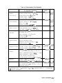
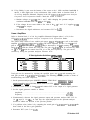
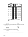
Figures
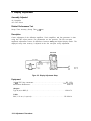
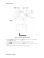
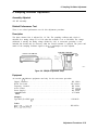
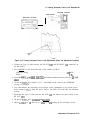
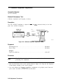
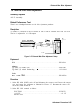
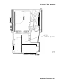
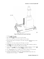
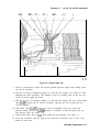
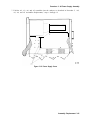
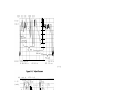
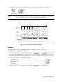
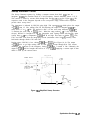
Serial Number Label Example . . . . . . . . . . . . . . . . . . . .
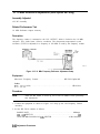
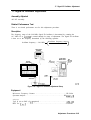
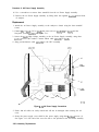
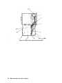
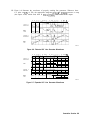
Example of a Static-Safe Workstation . . . . . . . . . . . . . . . . .
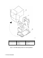
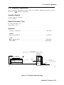
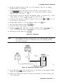
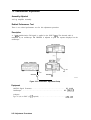
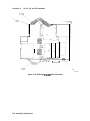
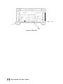
HP 8560A Shipping Container and Cushioning Materials . . . . . . . . .
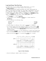
High-Voltage Power Supply Adjustment Setup . . . . . . . . . . . . .
Display Adjustment Setup . . . . . . . . . . . . . . . . . . . . . .
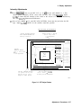
CRT Adjust Pattern . . . . . . . . . . . . . . . . . . . . . . . .
A2 Display Adjustment Locations . . . . . . . . . . . . . . . . . . .
IF Bandpass Adjustment Setup . . . . . . . . . . . . . . . . . . . .
IF Amplitude Adjustment Setup . . . . . . . . . . . . . . . . . . .
. . . . . . . . . . . . . . . . .
IF Amplitude Adjustment Locations
Sampler Adjustment Setup . . . . . . . . . . . . . . . . . . . . . .
Coarse-Tune Adjustment Setup . . . . . . . . . . . . . . . . . . . .
YTO Adjustment Setup . . . . . . . . . . . . . . . . . . . . . . .
First LO Distribution Amplifier Adjustment Setup . . . . . . . . . . .
Tracking Generator Power Level Adjustments Setup and Adjustment
Locations . . . . . . . . . . . . . . . . . . . . . . . . . . . .
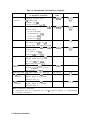
2-13. Frequency Response Adjustment Setup . . . . . . . . . . . . . . . .
2-14. Calibrator Amplitude Adjustment Setup . . . . . . . . . . . . . . . .
2-15. 10 MHz Frequency Reference Adjustment Setup . . . . . . . . . . . .
. . . . . . . . . . . . . . . . . . .
2-16. Demodulator Adjustment Setup
2-17. External Mixer Bias Adjustment Setup . . . . . . . . . . . . . . . .
2-18. External Mixer Amplitude Adjustment Setup . . . . . . . . . . . . . .
2-19. Location of A15Al . . . . . . . . . . . . . . . . . . . . . . . . .
2-20. Signal ID Oscillator Adjustment Setup . . . . . . . . . . . . . . . . .
2-21. 600 MHz Amplitude Adjustment Setup . . . . . . . . . . . . . . . .
2-22. 10 MHz Reference Adjustment (Option 003)/Setup and Adjustment Location
2-23. Tracking Oscillator Adjustment Setup . . . . . . . . . . . . . . . . .
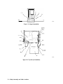
3- 1. Hinged Assemblies . . . . . . . . . . . . . . . . . . . . . . . . .
3-2. Discharging the Post-Accelerator Cable . . . . . . . . . . . . . . . .
3-3. A9, A18, and Line-Switch Assembly Mounting Screws . . . . . . . . . .
3-4. Front-Frame Mounting Screws . . . . . . . . . . . . . . . . . . . .
3-5. Installing the CRT and Front-Frame Assemblies . . . . . . . . . . . .
3-6. Placing the CRT into the Front Frame . . . . . . . . . . . . . . . . .
3-7. A2, A3, A4, and A5 Assembly Removal . . . . . . . . . . . . . . . .
3-8. Assembly Cables (1 of 2) . . . . . . . . . . . . . . . . . . . . . . .
3-8. Assembly Cables (2 of 2) . . . . . . . . . . . . . . . . . . . . . . .
3-9. Coaxial Cable Clip . . . . . . . . . . . . . . . . . . . . . . . . .
3-10. HP-IB and AlAl Wl Cable Placement . . . . . . . . . . . . . . . .
3-11. A6 Power Supply Connections . . . . . . . . . . . . . . . . . . . .
3-12. Power Supply Cover . . . . . . . . . . . . . . . . . . . . . . . . .
3-13. Al7 CRT Driver Mounting Screws . . . . . . . . . . . . . . . . . .
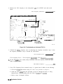
3-14. Assembly Locations . . . . . . . . . . . . . . . . . . . . . . . . .
l-1.
l-2.
1-3.
2-1.
2-2.
2-3.
2-4.
2-5.
2-6.
2-7.
2-8.
2-9.
2-10.
2-11.
2-12.
l-2
1-7
l-10
2-12
2-14
2-17
2-18
2-20
2-25
2-26
2-33
2-35
2-37
2-40
2-43
2-45
2-48
2-50
2-52
2-55
2-57
2-61
2-63
2-66
2-69
2-72
3-3
3-5
3-6
3-7
3-8
3-9
3-14
3-15
3-16
3-17
3-18
3-20
3-21
3-23
3-26
Contents-9
3-15. RF Section Bias Connections . . . . . . . . .
3-16. A9 Mounting Screws at Right Frame . . . . .
3-17. A10 Tracking Generator Mounting Screws . . .
3-18. All Mounting Screws . . . . . . . . . . . .
3-19. Al4 and Al5 Assembly Removal . . . . . . .
3-20. Al4 and Al5 Assembly Cables . . . . . . . .
3-21. Al7 Mounting Screws . . . . . . . . . . . .
3-22. Main Deck Screws . . . . . . . . . . . . .
3-23. A6 Power-Supply Cover . . . . . . . . . . .
3-24. W3 Dress and Connection to A6 Power Supply .
3-25. Line Switch Mounting Screw and Cable Dress .
3-26. W3 Cable Connector . . . . . . . . . . . .
3-27. Side Frame Mounting Screws . . . . . . . . .
3-28. A21 OCXO Mounting Screws . . . . . . . . .
4-l. Parts Identification, Assembly Mounting . . . .
4-2. Parts Identification, Cover Assembly . . . . .
4-3. Parts Identification, Main Chassis . . . . . . .
4-4. Parts Identification, RF Section . . . . . . . .
4-5. Parts Identification, Front Frame . . . . . . .
4-6. Parts Identification, Rear Frame . . . . . . .
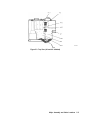
5- 1. Hinged Assemblies . . . . . . . . . . . . .
5-2. Top View (A2 Unfolded) . . . . . . . . . . .
5-3. Top View (A2 and A3 Unfolded) . . . . . . .
5-4. Top View (A2, A3, A4, and A5 Unfolded) . . .
5-5. Bottom View (Al5 Unfolded) . . . . . . . . .
. . . .
5-6. Bottom View (Al5 and Al4 Unfolded)
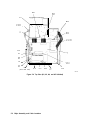
5-7. Front End . . . . . . . . . . . . . . . . .
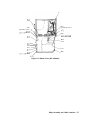
5-8. Rear View . . . . . . . . . . . . . . . . .
6-l. Assembly Test Points . . . . . . . . . . . .
6-2. Ribbon Cable Connections (1 of 2) . . . . . .
6-3. WR ENA Softkey Menu . . . . . . . . . . .
6-4. Functional Sections . . . . . . . . . . . . .
6-5. Phase Lock Loops . . . . . . . . . . . . . .
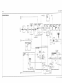
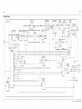
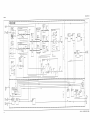
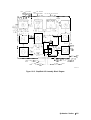
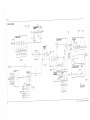
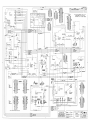
6-6. Simplified Block Diagram . . . . . . . . . .
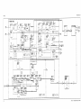
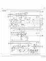
6-7. HP 8560A Overall Block Diagram (Sheet 1 of 3)
6-7. HP 8560A Overall Block Diagram (Sheet 2 of 3)
6-7. HP 8560A Overall Block Diagram (Sheet 3 of 3)
7-l. A3 Test Connectors . . . . . . . . . . . . .
7-2. A3 Interface Assembly Block Diagram . . . . .
8-1. A4 and A5 Test Connectors . . . . . . . . .
8-2. IF Section Troubleshooting with TAM . . . . .
8-3. IF Adjust Signature . . . . . . . . . . . . .
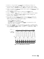
8-4. Detailed IF Adjust Signature (1) . . . . . . .
8-5. Detailed IF Adjust Signature (2) . . . . . . .
8-6. Detailed IF Adjust Signature (3) . . . . . . .
8-7. Detailed IF Adjust Signature (4) . . . . . . .
8-8. Detailed IF Adjust Signature (5) . . . . . . .
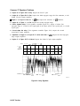
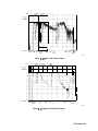
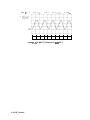
8-9. Noisy Signature . . . . . . . . . . . . . . .
8-10. Noise with Correct Shape . . . . . . . . . .
8-11. Region B Amplitude Variation . . . . . . . .
8-12. Region B Amplitude Offset . . . . . . . . . .
Contents-10
.
.
.
.
.
.
.
.
.
.
.
.
.
.
.
.
.
.
.
.
.
.
.
.
.
.
.
.
.
.
.
.
.
.
.
.
.
.
.
.
.
.
.
.
.
.
.
.
.
.
.
.
.
.
.
.
.
.
.
.
.
.
.
.
.
.
.
.
.
.
.
.
.
.
.
.
.
.
.
.
.
.
.
.
.
.
.
.
.
.
.
.
.
.
.
.
.
.
.
.
.
.
.
.
.
.
.
.
.
.
.
.
.
.
.
.
.
.
.
.
.
.
.
.
.
.
.
.
.
.
.
.
.
.
.
.
.
.
.
.
.
.
.
.
.
.
.
.
.
.
.
.
.
.
.
.
.
.
.
.
.
.
.
.
.
.
.
.
.
.
.
.
.
.
.
.
.
.
.
.
.
.
.
.
.
.
.
.
.
.
.
.
.
.
.
.
.
.
.
.
.
.
.
.
.
.
.
.
.
.
.
.
.
.
.
.
.
.
.
.
.
.
.
.
.
.
.
.
.
.
.
.
.
.
.
.
.
.
.
.
.
.
.
.
.
.
.
.
.
.
.
.
.
.
.
.
.
.
.
.
.
.
.
.
.
.
.
.
.
.
.
.
.
.
.
.
.
.
.
.
.
.
.
.
.
.
.
.
.
.
.
.
.
.
.
.
.
.
.
.
.
.
.
.
.
.
.
.
.
.
.
.
.
.
.
.
.
.
.
.
.
.
.
.
.
.
.
.
.
.
.
.
.
.
.
.
.
.
.
.
.
.
.
.
.
.
.
.
.
.
.
.
.
.
.
.
.
.
.
.
.
.
.
.
.
.
.
.
.
.
.
.
.
.
.
.
.
.
.
.
.
.
.
.
.
.
.
.
.
.
.
.
.
.
.
.
.
.
.
.
.
.
.
.
.
.
.
.
.
.
.
.
.
.
.
.
.
.
.
.
.
.
.
.
.
.
.
.
.
.
.
.
.
.
.
.
.
.
.
.
.
.
.
.
.
.
.
.
.
.
.
.
.
.
.
.
.
.
.
.
.
.
.
.
.
.
.
.
.
.
.
.
.
.
.
.
.
.
.
.
.
.
.
.
.
.
.
.
.
.
.
.
.
.
.
.
.
.
.
.
.
.
.
.
.
.
.
.
.
.
.
.
.
.
.
.
.
.
.
.
.
.
.
.
.
.
.
.
.
.
.
.
.
.
.
.
.
.
.
.
.
.
.
.
.
.
.
.
.
.
.
.
.
.
.
.
.
.
.
.
.
.
.
.
.
.
.
.
.
.
.
.
.
.
.
.
.
.
.
.
.
.
.
.
.
.
.
.
.
.
.
.
.
.
.
.
.
.
.
.
.
.
.
.
.
.
.
.
.
.
.
.
3-27
3-30
3-31
3-32
3-34
3-36
3-37
3-41
3-43
3-45
3-46
3-47
3-49
3-51
4-21
4-33
4-35
4-37
4-39
4-41
5-4
5-4
5-5
5-6
5-7
5-8
5-9
5-10
6-3
6-4
6-7
6-35
6-39
6-45
6-47
6-49
6-51
7-4
7-29
8-3
8-7
8-25
8-25
8-26
8-26
8-27
8-27
8-28
8-29
8-29
8-30
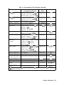
. . . . . . . . . . . . . . .
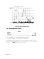
8-13. Faulty Crystal Short
.
.
.
.
. . . . . . . . . . . . . .
8-14. Faulty LC Pole
8-15. Faulty Crystal Symmetry . . . . . . . . . . . . .
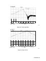
8-16. Output Waveform, 10 kHz Resolution Bandwidth . . .
8-17. Output Waveform, 3 kHz Resolution Bandwidth . . .
8-18. Output Waveform, 1 kHz Resolution Bandwidth . . .
8-19. Output Waveform, 300 Hz Resolution Bandwidth . . .
8-20. Failed Crystal Set Symptoms . . . . . . . . . . . .
8-21. A4 Log Amplifier Block Diagram . . . . . . . . . .
8-22. A5 IF Assembly Block Diagram . . . . . . . . . . .
8-23. Cal Oscillator Block Diagram . . . . . . . . . . . .
9-l. A2 Test Connectors . . . . . . . . . . . . . . . .
9-2. Line Generator Output Waveforms . . . . . . . . .
9-3. Blanking Waveforms . . . . . . . . . . . . . . .
9-4. Expanded Blanking Waveforms . . . . . . . . . . .
9-5. Switch Driver Waveform LCHAR . . . . . . . . . .
9-6. Distorted X/Y Line Generator Waveforms . . . . . .
9-7. Expanded X/Y Line Generator Waveforms . . . . . .
9-8. Normal X/Y Line Generator Waveforms . . . . . . .
9-9. Delta X Waveform . . . . . . . . . . . . . . . .
9-10. Delta Y Waveform . . . . . . . . . . . . . . . .
9- 11. DEFl Synchronization . . . . . . . . . . . . . . .
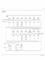
9-12. A2 Controller Block Diagram . . . . . . . . . . . .
10-l. YTO Loop Test Setup . . . . . . . . . . . . . . .
10-2. Sampler and Sampling Oscillator Test Setup . . . . .
10-3. Al4 and Al5 Test Connectors . . . . . . . . . . .
10-4. PLL Locked at Wrong Frequency . . . . . . . . . .
10-5. Unlocked PLL . . . . . . . . . . . . . . . . . .
10-6. Input to YTO FM Coil Driver . . . . . . . . . . .
10-7. Input to Main/FM/VCO Sweep Switch . . . . . . .
10-8. Troubleshooting an Unlocked YTO PLL . . . . . . .
10-9. Simplified Sweep Generator . . . . . . . . . . . .
10-10. Simplified Sweep Generator during Retrace . . . . . .
10-11. Simplified Synthesizer Section . . . . . . . . . . .
10-12. Simplified Al4 Assembly Block Diagram . . . . . . .
10-13. Simplified Al5 Assembly Block Diagram . . . . . . .
10-14. Frequency Control Block Diagram . . . . . . . . . .
10-15. RF Assembly Block Diagram . . . . . . . . . . . .
11-l. Al4 and Al5 Test Connectors . . . . . . . . . . .
11-2. A7 LODA Drive . . . . . . . . . . . . . . . . .
11-3. 10 MHz Reference at A15J302 . . . . . . . . . . .
11-4. 10 MHz TTL-Reference at U303 Pin 5 . . . . . . . .
11-5. HP 8560A RF Section Troubleshooting Block Diagram
12-l. Simplified Section Block Diagram . . . . . . . . . .
12-2. Al7 Test Connector . . . . . . . . . . . . . . . .
12-3. Probe Power Socket . . . . . . . . . . . . . . . .
12-4. Buck Regulator Waveform . . . . . . . . . . . . .
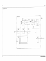
12-5. A6 Power Supply Block Diagram . . . . . . . . . .
12-6. Al7 CRT Driver Block Diagram . . . . . . . . . .
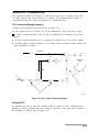
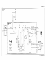
A-l. Interconnect Diagram . . . . . . . . . . . . . . .
. . . . . . . . .
. . . . . . . . .
. . . . . . . . .
. . . . . . . . .
. . . . . . . . .
. . . . . . . . .
. . . . . . . . .
. . . . . . . . .
. . . . . . . . .
. . . . . . . . .
. . . . . . . . .
. . . . . . . . .
. . . . . . . . .
. . . . . . . . .
. . . . . . . . .
. . . . . . . . .
. . . . . . . . .
. . . . . . . . .
. . . . . . . . .
. . . . . . . . .
. . . . . . . . .
. . . . . . . . .
. . . . . . . . .
. . . . . . . . .
. . . . . . . . .
. . . . . . . . .
. . . . . . . . .
. . . . . . . . .
. . . . . . . . .
. . . . . . . . .
. . . . . . . . .
. . . . . . . . .
. . . . . . . . .
. . . . . . . . .
. . . . . . . . .
. . . . . . . . .
. . . . . . . . .
. . . . . . . . .
. . . . . . . . .
. . . . . . . . .
. . . . . . . . .
. . . . . . . . .
. . . . . . . . .
. . . . . . . . .
. . . . . . . . .
. . . . . . . . .
. . . . . . . . .
. . . . . . . . .
. . . . . . . . .
. . . . . . . . .
8-31
8-31
8-33
8-37
8-38
8-38
8-39
8-39
8-43
8-45
8-47
9-3
9-5
9-6
9-7
9-8
9-9
9-9
9-10
9-11
9-12
9-13
9-17
10-5
10-6
10-8
10-13
10-14
lo-18
10-19
lo-26
10-47
lo-48
10-49
10-50
10-51
10-53
10-54
11-2
11-10
11-15
11-16
11-25
12-2
12-5
12-7
12-12
12-19
12-21
A-7
Contents-l 1
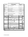
Tables
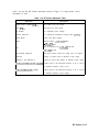
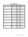
l-l. Service Kit Contents . . . . . . . . . . . . . . . . . . . .
l-2. Static-Safe Accessories . . . . . . . . . . . . . . . . . . . .
l-3. Hewlett-Packard Sales and Service Offices . . . . . . . . . . .
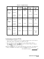
1-4. Recommended Test Equipment . . . . . . . . . . . . . . . .
2-l. Related Adjustments (1 of 2) . . . . . . . . . . . . . . . . .
2-l. Related Adjustments (2 of 2) . . . . . . . . . . . . . . . . .
2-2. Adjustable Components (1 of 3) . . . . . . . . . . . . . . .
2-2. Adjustable Components (2 of 3) . . . . . . . . . . . . . . .
2-2. Adjustable Components (3 of 3) . . .’ . . . . . . . . . . . .
2-3. Factory Selected Components . . . . . . . . . . . . . . . . .
2-4. TAM Adjustments . . . . . . . . . . . . . . . . . . . . .
2-5. Required Test Equipment for TAM . . . . . . . . . . . . . .
2-6. Factory-Selected LC Filter Capacitors . . . . . . . . . . . . .
2-7. LC Factory-Selected Capacitor Selection . . . . . . . . . . . .
2-8. Factory-Selected XTAL Filter Capacitors . . . . . . . . . . .
2-9. XTAL Factory-Selected Capacitor Selection . . . . . . . . . .
2-10. Capacitor Part Numbers . . . . . . . . . . . . . . . . . . .
2-11. Sampling Adjustments . . . . . . . . . . . . . . . . . . . .
2-12. Conversion Loss Data . . . . . . . . . . . . . . . . . . . .
2-13. A15U802 Values . . . . . . . . . . . . . . . . . . . . . .
2-14. Tracking Oscillator Range Centering . . . . . . . . . . . . .
3-l. Required Tools . . . . . . . . . . . . . . . . . . . . . . .
4-2. Reference Designations, Abbreviations and Multipliers (1 of 4) . .
4-2. Reference Designations, Abbreviations, and Multipliers (2 of 4) . .
4-2. Reference Designations, Abbreviations, and Multipliers (3 of 4) . .
4-2. Reference Designations, Abbreviations, and Multipliers (4 of 4) . .
4-3. Manufacturers Code List (1 of 3) . . . . . . . . . . . . . . .
4-4. Replaceable Parts . . . . . . . . . . . . . . . . . . . . . .
6-l. Location of Assembly Troubleshooting Text . . . . . . . . . .
7-l. W2 Control Cable Connections (1 of 2) . . . . . . . . . . . . .
7-2. Automatic Fault Isolation References . . . . . . . . . . . . .
7-3. TAM Tests Versus A3 Test Connectors . . . . . . . . . . . .
7-4. Keyboard Matrix . . . . . . . . . . . . . . . . . . . . . .
7-5. Counter Frequencies . . . . . . . . . . . . . . . . . . . . .
7-6. Trigger MUX Truth Table . . . . . . . . . . . . . . . . . .
7-7. A3U102 Latch Outputs . . . . . . . . . . . . . . . . . . .
7-8. HMUX-SELO/l Versus Detector Mode . . . . . . . . . . . .
7-9. Logic Levels at A3U108 . . . . . . . . . . . . . . . . . . .
7-10. Demultiplexer A3U410 Truth Table . . . . . . . . . . . . . .
7-11. Demultiplexer A3U500 Truth Table . . . . . . . . . . . . . .
8-l. Automatic Fault Isolation References . . . . . . . . . . . . .
8-2. TAM Tests Versus Test Connectors (1 of 2) . . . . . . . . . .
8-3. Sweep Width Settings . . . . . . . . . . . . . . . . . . . .
Contents-12
.
.
.
.
.
.
.
.
.
.
.
.
.
.
.
.
.
.
.
.
.
.
.
.
.
.
.
.
.
.
.
.
.
.
.
.
.
.
.
.
.
.
.
.
.
.
.
.
.
.
.
.
.
.
.
.
.
.
.
.
.
.
.
.
.
.
.
.
.
.
.
.
.
.
.
.
.
.
.
.
.
.
.
.
.
.
.
.
.
.
.
.
.
.
.
.
.
.
.
.
.
.
.
.
.
.
.
.
.
.
.
.
.
.
.
.
.
.
.
.
.
.
.
.
.
.
.
.
.
.
.
.
.
.
.
.
.
.
.
.
.
.
.
.
.
.
.
.
.
.
.
.
.
.
.
.
.
.
.
.
.
.
.
.
.
.
.
.
.
.
.
.
l-6
l-8
1-12
1-13
2-4
2-5
2-6
2-7
2-8
2-8
2-10
2-10
2-22
2-22
2-23
2-23
2-24
2-36
2-59
2-62
2-73
3-2
4-3
4-4
4-5
4-6
4-7
4-10
6-9
7-2
7-5
7-6
7-7
7-9
7-9
7-16
7-18
7-20
7-28
7-28
8-4
8-5
8-9
8-4. Available Reference Level Range . . . . . . . . . . . . . . . . . . .
8-5. Signal Level for Reference Level Display . . . . . . . . . . . . . . . .
9-l. TAM Tests Versus Test Connectors . . . . . . . . . . . . . . . . . .
9-2. Gate Times . . . . . . . . . . . . . . . . . . . . . . . . . . . .
10-l. Center Frequency Tuning Values . . . . . . . . . . . . . . . . . . .
10-2. Sampling Oscillator Test Frequencies . . . . . . . . . . . . . . . . .
10-3. YTO Frequency in TEST Position . . . . . . . . . . . . . . . . . .
10-4. Automatic Fault Isolation References (1 of 2) . . . . . . . . . . . . . .
10-4. Automatic Fault Isolation References (2 of 2) . . . . . . . . . . . . . .
10-5. TAM Tests versus Test Connectors (1 of 2) . . . . . . . . . . . . . . .
10-5. TAM Tests versus Test Connectors (2 of 2) . . . . . . . . . . . . . . .
10-6. Sweep Signal Destination versus Span . . . . . . . . . . . . . . . . .
10-7. Harmonic Mixing Number versus Center Frequency . . . . . . . . . . .
10-8. Settings of Sweep Switches . . . . . . . . . . . . . . . . . . . . . .
10-9. Settings of Sweep Switches . . . . . . . . . . . . . . . . . . . . . .
10-10. Settings for Switches and Comparators . . . . . . . . . . . . . . . .
lo- 11. Amplifier Polarities . . . . . . . . . . . . . . . . . . . . . . . . .
10-12. YTO Frequency Errors with A14J23 on Pins 2 and 3 . . . . . . . . . .
10-13. Voltages in FM Coil and Main Loop Drivers . . . . . . . . . . . . . .
10-14. Main Coil Coarse and Fine DACs Voltages . . . . . . . . . . . . . . .
10-15. Sampling Oscillator PLL Divide Ratios . . . . . . . . . . . . . . . .
11-1. Automatic Fault Isolation References . . . . . . . . . . . . . . . . .
11-2. TAM Tests versus Test Connectors . . . . . . . . . . . . . . . . . .
11-3. Attenuator Pin Values . . . . . . . . . . . . . . . . . . . . . . . .
11-4. RF Section Mnemonic Table . . . . . . . . . . . . . . . . . . . . .
12-1. Wl Power-Cable Connections (1 of 2) . . . . . . . . . . . . . . . . .
12-1. Wl Power-Cable Connections (2 of 2) . . . . . . . . . . . . . . . . .
12-2. Automatic Fault Isolation References . . . . . . . . . . . . . . . . .
12-3. TAM Tests versus Test Connectors . . . . , . . . . . . . . . . . . .
A-l. HP 8560A Spectrum Analyzer Documented Assemblies . . . . . . . . .
A-2. A4 and Al6 Assemblies Shipped with HP 8560As Serial Prefixed below 3207A
A-3. Al5 RF Assemblies Shipped with HP 8560As Serial Prefixed below 3029A .
8-12
8-12
9-2
9- 14
10-3
10-7
10-8
10-9
10-10
10-11
10-12
10-15
10-15
10-17
10-19
10-22
lo-25
lo-28
10-30
10-31
10-40
11-3
11-4
11-7
11-17
12-3
12-4
12-4
12-5
A-2
A-4
A-5
Contents-13
General Information
This HP 8560A Spectrum Analyzer Service Manual contains information required to adjust
and service the HP 8560A Spectrum Analyzer to the assembly level.
For component-level information, refer to the HP 856OA/61B/63A
Spectrum Analyzer
Component Level Information.
Manual Organization
Chapter 1, General Information, contains information about service kit contents,
recommended test equipment, returning an instrument for service, and sales and service
offices.
Chapter 2, Adjustment Procedures, contains the necessary adjustment procedures to adjust
the instrument properly after repair.
Chapter 3, Assembly Replacement, contains instructions for removal and replacement of all
major assemblies.
Chapter 4, Replaceable Parts, contains the information necessary to order parts or assemblies
for the instrument.
Chapter 5, Major Assembly and Cable Locations, contains figures identifying all major
assemblies and cables.
Chapter 6, General Troubleshooting, contains instrument-level troubleshooting information,
block diagrams, and troubleshooting information covering the instrument’s six functional
areas.
Chapters 7 through 12 contain troubleshooting information covering the instrument’s six
functional areas.
Appendix contains the component-level documented assemblies matrix and the HP 8560A
Interconnect Diagram.
General Information 1-l
Manual Text Conventions
The following text conventions are used throughout this manual:
m
Softkeys
Display
Text
Boxed text in this typeface represents a mechanical key physically located on the
instrument.
Shaded text indicates a softkey. Softkey labels appear on the display and can be
activated by pressing corresponding keys surrounding the display. The labels
displayed are determined by the mechanical front-panel key depressed and the
instrument’s firmware.
Text printed in this typeface indicates text appearing on the screen.
Serial N.umbers Covered by This Manual
This service manual applies directly to HP 8560A spectrum analyzers with serial numbers
prefixed 3207A and above. For HP 8560A spectrum analyzers with serial numbers prefixed
below 3207A, order HP Part Number 08560-90038.
Hewlett-Packard makes frequent improvements to its products to enhance their performance,
usability, or reliability. HP service personnel have access to complete records of design changes
to each type of equipment, based on the equipment’s serial number. Whenever you contact
HP about your analyzer, have the complete serial number available to ensure obtaining the
most complete and accurate information possible.
The serial number label is attached to the rear of the analyzer. The serial number has two
parts: the prefix (the first four numbers and a letter), and the suffix (the last five numbers).
See Figure l-l.
The first four numbers of the prefix are a code identifying the date of the last major design
change incorporated in your analyzer. The letter identifies the country in which the unit
was manufactured. The five-digit suffix is a sequential number and is different for each
unit. Whenever you list the serial number or refer to it in obtaining information about your
analyzer, be sure to use the complete number, including the full prefix and the suffix.
Figure l-l. Serial Number Label Example
l-2 General Information
Instrument Variations
The following text lists the unique assemblies contained in the HP 8560A Options 001, 002,
003, and all combinations.
HP 8560A Option 001 (Rear-Panel 2nd IF Output)
Al5 RF Assembly
unique part number
w19
added
Rear-panel JlO
added
HP 8560A Option 002 (Tracking Generator)
A10 Tracking Generator
added
Al5 RF Assembly
unique part number
Front dress-panel
unique part number
w14
added
W16
added
W36
deleted
W42
deleted
w43
added
W46
added
w47
added
W48
added
Rear-panel J 11
added
Front-panel 53
deleted
Front-panel J6
added
HP 8560A Option 012 (001 + 002)
Al5 RF Assembly
unique part number
w19
added
Rear-panel JlO
added
A10 Tracking Generator
added
Front dress-panel
unique part number
w14
added
W16
added
W36
deleted
W42
deleted
w43
added
General Information 1-3
W46
added
w47
added
W48
added
Rear-panel J 11
added
Front-panel 53
deleted
Front-panel J6
added
HP 8560A Option 003 (Precision Frequency Reference)
Al5 RF Assembly
unique part number
A21 OCXO
added
w49
added
w50
added
HP 8560A Option 013 (001 + 003)
Al5 RF Assembly
unique part number
w19
added
Rear-panel JlO
added
A21 OCXO
added
w49
added
w50
added
HP 8560A Option 023 (002 + 003)
Al5 RF Assembly
unique part number
A10 Tracking Generator
added
Front dress-panel
unique part number
w14
added
W16
added
W36
deleted
W42
deleted
w43
added
W46
added
w47
added
W48
added
Rear-panel Jll
added
Front-panel 53
deleted
1-4 General Information
Front-panel J6
added
A21 OCXO
added
w49
added
w50
added
HP 8560A Option 123 (001 + 002 + 003)
Al5 RF Assembly
unique part number
w19
added
Rear-panel JlO
added
A10 Tracking Generator
added
Front dress-panel
unique part number
w14
added
W16
added
W36
deleted
W42
deleted
w43
added
W46
added
w47
added
W48
added
Rear-panel Jll
added
Front-panel J3
deleted
Front-panel J6
added
A21 OCXO
added
w49
added
w50
added
General Information l-5
HP 85629B Test and Adjustment Module
When attached to the spectrum analyzer’s rear panel, the HP 85629B Test and Adjustment
Module (TAM) p rovides diagnostic functions for the HP 8560A. Because the TAM connects
directly to the analyzer’s internal data and address bus, it controls the analyzer’s hardware
directly. It would be impossible to control the hardware to the same extent either from the
analyzer’s front panel or over the HP-IB.
The TAM measures voltages at key points in the circuitry and flags a failure whenever the
voltage falls outside the limits. The TAM locates the failure to a small functional area which
can be examined manually.
Service Kit
The HP 8560A Service Kit (HP part number 08562-60021) contains service tools required to
repair the instrument. Refer to Table l-l for a list of items in the service kit.
Table l-l. Service Kit Contents
Quantity
HP Part Number
Cable Puller
PC Board Prop
Line Filter Assembly
1
1
1
Line Switch Cable
Extender Cable
BNC to SMB (snap-on) Cable
1
1
2
5021-6773
5021-7459
5061-9032
5062-0728
5062-0737
85680-60093
Connector Extractor Tool Kit
1
8710-1791
Description
Recommended Test Equipment
Equipment required for operation verification, performance tests, adjustments,
troubleshooting, and the Test and Adjustment Module is listed in Table l-4. Other equipment
may be substituted if it meets or exceeds the critical specifications listed in the table. Refer to
the HP 856OA Installation and Verification Manual for the performance tests.
1-6 General Information
Electrostatic Discharge
Electrostatic discharge (ESD) can damage or destroy electronic components. Therefore,
all work performed on assemblies consisting of electronic components should be done at a
static-free workstation. Figure l-2 is an example of a static-safe work station using two kinds
of ESD protection:
w Conductive table mat and wrist-strap combination.
n
Conductive floor mat and heel-strap combination.
These methods may be used together or separately.
B u i lding
Ground
1 MegOhm
Resistor
I
/TV
hhirist
StroD\
*
5111125
Figure 1-2. Example of a Static-Safe Workstation
Reducing Potential for ESD Damage
The suggestions that follow may help reduce ESD damage that occurs during nstrument
testing and servicing.
w Before connecting any coaxial cable to an analyzer connector for the first time each day,
momentarily ground the center and outer connectors of the cable.
n
Personnel should be grounded with a resistor-isolated wrist strap before touching the center
in of any connector and before removing any assembly from the unit.
n
Be sure all instruments are properly earth-grounded to prevent build-up of static discharge.
General Information l-7
Static-Safe Accessories
Table 1-2. Static-Safe Accessories
HP Part
Number
Description
9300-0797
Set includes: 3M static control mat 0.6 m x 1.2 m (2 ft x 4 ft) and 4.6 cm (15 ft)
ground wire. (The wrist-strap and wrist-strap cord are not included. They must
be ordered separately.)
9300-0980
Wrist-strap cord 1.5 m (5 ft)
9300-1383
Wrist-strap, color black, stainless steel, without cord, has four adjustable links
and a 7 mm post-type connection.
9300-l169
ESD heel-strap (reusable 6 to 12 months).
Returning Instruments for Service
Service Tag
If you are returning the instrument to Hewlett-Packard for servicing, fill in and attach a blue
service tag. Service tags are supplied in the back of this chapter.
Please be as specific as possible about the nature of the problem. If you have recorded any
error messages that appeared on the screen, or have completed a performance test record, or
have any other specific data on the performance of the analyzer, please send a copy of this
information with the unit.
Original Packaging
Before shipping, pack the unit in the original factory packaging materials if they are available.
If the original materials are unavailable, identical packaging materials may be acquired
through’any Hewlett-Packard Sales and Service Office. Descriptions of the packaging materials
are listed in Figure l-3.
Other Packaging
Caution
Analyzer damage can result from using packaging materials other than those
specified. Never use styrene pellets in any shape as packaging materials. They
do not adequately cushion the equipment or prevent it from shifting in the
carton. They cause equipment damage by generating static electricity and by
lodging in the analyzer fan.
Repackage the analyzer in the original packaging materials or with commercially available
materials described in steps 4 and 5, below.
1. Attach a completed service tag to the instrument.
1-8 General Information
2. Install the front-panel cover on the instrument.
3. Wrap the instrument in antistatic plastic to reduce the possibility of damage caused by
electrostatic discharge.
4. Use the original materials or a strong shipping container that is double-walled, corrugated
cardboard carton with 159 kg (350 lb) bursting strength. The carton must be both large
enough and strong enough to accommodate the analyzer and allows at least 3 to 4 inches
on all sides of the analyzer for packing material.
5. Surround the equipment with at least 3 to 4 inches of packing material, or enough to
prevent the equipment from moving in the carton. If packing foam is unavailable, the best
alternative is SD-240 Air Cap TM from Sealed Air Corporation (Commerce, CA 90001).
Air Cap looks like a plastic sheet covered with l-1/4 inch air-filled bubbles. Use the
pink-colored Air Cap to reduce static electricity. Wrap the equipment several times in this
material to both protect the equipment and prevent it from moving in the carton.
6. Seal the shipping container securely with strong nylon adhesive tape.
7. Mark the shipping container “FRAGILE, HANDLE WITH CARE” to assure careful
handling.
8. Retain copies of all shipping papers.
General Information l-9
SK1126
Item
Description
HP Part Number
1
2
9211-5636
08590-80013
Outer Carton
Pads (2)
3
08590-80014
Bottom Tray
Figure 1-3. HP 8560A Shipping Container and Cushioning Materials
l-1 0 General Information
Sales and Service Offices
Hewlett-Packard has sales and service offices around the world providing complete support for
Hewlett-Packard products. To obtain servicing information, or to order replacement parts,
contact the nearest Hewlett-Packard Sales and Service Office listed in Table l-3.
In any correspondence, be sure to include the pertinent information about model numbers,
serial numbers, and assembly part numbers.
Note
Within the USA, a toll-free phone number is available for ordering
replacement parts. Refer to the “Ordering Information” section in Chapter 4,
“Replaceable Parts,” for the phone number and more information.
General Information l-l 1
Table 1-3. Hewlett-Packard Sales and Service Offices
US FIELD OPERATIONS EUROPEAN OPERATIONS
INTERCON OPERATIONS
HEADQUARTERS
HEADQUARTERS
HEADQUARTERS
Hewlett-Packard Company Hewlett-Packard S.A.
Hewlett-Packard Company
19320 Pruneridge Avenue
150, Route du Nant-d’Avri1
3495 Deer Creek Rd.
Cupertino, CA 95014, USA 1217 Meyrin 2/Geneva
Palo Alto, California 94304-1316
Switzerland
(800) 752-0900
(415) 857-5027
(41 22) 780.8111
California
Australia
Hewlett-Packard Co.
France
Hewlett-Packard Australia Ltd.
1421 South Manhattan Ave. Hewlett-Packard France
31-41 Joseph Street
Fullerton, CA 92631
1 Avenue Du Canada
Blackburn, Victoria 3130
(714) 999-6700
Zone D’Activite De Courtaboeuf (61 3) 895-2895
F-91947 Les Ulis Cedex
Canada
Hewlett-Packard Co.
France
Hewlett-Packard (Canada) Ltd.
301 E. Evelyn
(33 1) 69 82 60 60
Mountain View, CA 94041
17500 South Service Road
Trans-Canada Highway
(415) 694-2000
Germany
Kirkland, Quebec H9J 2X8
Hewlett-Packard GmbH
Berner Strasse 117
Canada
Colorado
(514) 697-4232
6000 Frankfurt 56
Hewlett-Packard Co.
West Germany
24 Inverness Place, East
(49 69) 500006-O
Englewood, CO 80112
Japan
(303) 649-5000
Yokogawa-Hewlett-Packard Ltd.
Great Britain
1-27-15 Yabe, Sagamihara
Hewlett-Packard Ltd.
Georgia
Eskdale Road, Winnersh Triangle Kanagawa 229, Japan
Hewlett-Packard Co.
Wokingham, Berkshire RGll 5DZ (81 427) 59-1311
2000 South Park Place
England
Atlanta, GA 30339
(44 734) 696622
(404) 955-1500
China
China Hewlett-Packard, Co.
IlklOiS
38 Bei San Huan Xl Road
Hewlett-Packard Co.
Shuang Yu Shu
5201 Tollview Drive
Hai Dian District
Rolling Meadows, IL 60008
Beijing, China
(708) 255-9800
(86 1) 256-6888
New Jersey
Singapore
Hewlett-Packard Co.
Hewlett-Packard Singapore
120 W. Century Road
Pte. Ltd.
Paramus, NJ 07653
1150 Depot Road
(201) 599-5000
Singapore 0410
(65) 273 7388
Texas
Hewlett-Packard Co.
Taiwan
930 E. Campbell Rd.
Hewlett-Packard Taiwan
Richardson, TX 75081
8th Floor, H-P Building
(214) 231-6101
337 Fu Hsing North Road
Taipei, Taiwan
(886 2) 712-0404
1-12 General Information
Table 1-4. Recommended Test Equipment
Instrument
Synthesized
Critical Specifications
for Equipment Substitution
Sweeper
Frequency Range: 10 MHz to 7 GHz
Frequency Accuracy (CW): 1 x 10eg/day
(two required)
Leveling Modes: Internal & External
Recommended
Model
Use
HP 8340A*
PAT,
M,V
HP 3335A*
PAT,
Modulation Modes: AM & Pulse
Power Level Range: -80 to +16 dBm
Synthesizer/
Level Generator
Frequency Range: 200 Hz to 80 MHz
Frequency Accuracy: 1 x 10e7/month
M,V
Flatness: f0.15 dB
Attenuator Accuracy: <&0.09 dB
Synthesized
Signal Generator
Frequency Range: 5 MHz to 2.5 GHz
Residual SSB Phase Noise at 10 kHz offset
HP 8663A
p,v
HP 8116A
P
HP 8640B
A
HP 5343A*
Option 001
P,A,M,V
(320 MHz <fc <640 MHz): <-131 dBc/Hz
Pulse/Function
Generator
Frequency Range: 10 kHz to 50 MHz
Pulse Width: 200 ns;
Output Amplitude: 5 V peak-to-peak
Functions: Pulse & Triangle
TTL Sync Output
AM/FM
Signal Generator
Frequency Range: 1 MHz to 200 MHz
Frequency Modulation Mode
Modulation Oscillator Frequency: 1 kHz
FM Peak Deviation: 5 kHz
Microwave
Frequency Range: 9 MHz to 6.9 GHz
Frequency Counter Time base Accuracy (Aging): <5 x lo-“/day of
External Frequency Reference Input
Universal
Counter
Modes: TI AFB, Frequency Count
HP
5334A/B
P
Time Interval Measurement Range: 20 ms to 75 s
Frequency Measurement Range: 17 kHz to 11 MHz
Frequency Resolution: 1 MHz at 10 MHz
External Frequency Reference Input
Time base accuracy (Aging): <3 x 10m7/month
Oscilloscope
Bandwidth (3 dB): dc to 100 MHz
HP
1980A/B* A , T
Minimum Vertical Deflection Factor: <2 mV/div
Spectrum Analyzer
Frequency Range: 4 kHz to 7 GHz
HP 8566A/B
PAT
Typical Residual FM: <l Hz Pk-to-Pk in 100 ms
(Fundamental Mixing)
* Part of Microwave Workstation
P = Performance Tests; A = Adjustments; M = Test & Adjustment Module; T = Troubleshooting;
V = Operation Verification
General Information
l- 13
Table 1-4. Recommended Test Equipment (continued)
Instrument
Critical Specifications
for Equipment Substitution
Measuring
Compatible w/Power Sensors
Receiver
dB Relative Mode
Resolution: 0.01 dB
Reference Accuracy: <&1.2%
Power Sensor
Frequency Range: 50 MHz to 6.9 GHz
Maximum SWR:
1.15 (50 to 100 MHz)
Recommended
Model
Use
HP 8902A*
PAT,
M,V
HP 8485A*
PAT,
M,V
HP 8484A
P,A
HP 8482A*
PAT,
M,V
HP 11975
P
Digital Voltmeter Range: -15 V dc to +120 V dc
Accuracy: <fl mV on 10 V Range
Input Impedance: 21 Ma
HP 3456A*
A
DVM Test Leads 236 inches, alligator clips, probe tips
HP 34118A
A,T
1.10 (100 MHz to 2 GHz)
1.15 (2.0 to 6.5 GHz)
1.20 (12.4 to 18 GHz)
Power Sensor
Frequency Range: 250 MHz to 350 MHz
Power Range: 100 nW to 10 PW
Maximum SWR: 1.15 (250 to 350 MHz)
Power Sensor
Frequency Range: 100 kHz to 2.9 GHz
Maximum SWR:
1.1 (1 MHz to 2.0 GHz)
1.30 (2.0 GHz to 2.9 GHz)
4mplifier
Frequency Range: 2.0 to 2.9 GHz
Minimum Output Power (Leveled)
2.0 to 8.0 GHz: $16 dBm
Output SWR (Leveled): <1.7
10 dB Step
Attenuator
Attenuation Range: 30 dB
Frequency Range: dc to 80 MHz
Connectors: BNC (f)
HP 355D
p,v
1 dB Fixed
Attenuator
Attenuation Range: 12 dB
Frequency Range: dc to 80 MHz
Connectors: BNC (f)
HP 355C
P,V,A
’ Part of Microwave Workstation
P = Performance Tests; A = Adjustments; M = Test & Adjustment Module; T = Troubleshooting
V = Operation Verification
1-14 General Information
Table 1-4. Recommended Test Equipment (continued)
Instrument
Critical Specifications
for Equipment Substitution
Recommended
Model
Use
20 dB Fixed
Attenuator
Frequency Range: dc to 6.5 GHz
Attenuation Accuracy: <fl dB
Maximum SWR: 1.2 (dc to 6.5 GHz)
HP 8491B
Option 020
p,v
10 dB Fixed
Frequency Range: dc to 6.5 GHz
HP 8491B
p,v
Attenuation Accuracy: <f0.6 dB
Option 010
Attenuator
Maximum SWR: 1.2 (dc to 6.5 GHz)
Signature Multimeter
Clock Frequency >lO MHz
Reference Attenuator
Supplied with HP 8484A
Termination
Low-Pass Filter
HP 5005A/B
T
HP 11708A
P,A
Frequency Range: dc to 22 GHz
Impedance: 5OQ
Maximum SWR: <1.22
Connector: APC 3.5
HP 909D
P,M,V
Cutoff Frequency: 50 MHz
Rejection at 80 MHz: >50 dB
0955-0306
P,M,V
12 MHz Low-Pass-Filter Cutoff Frequency: 12 MHz
g-element Tchebychev, 0.1 dB ripple
Rejection at 18 MHz: >45 dB
0955-0518
P
Frequency Range: 5 MHz to 50 MHz
Coupling: 6.0 dB (nominal)
HP 8721A
P
HP 11667B
P,A,M,V
08562-60021
Directional
Bridge
Directivity: 30 dB minimum
Power Splitter
VSWR: <1.45
Frequency Range: 1 kHz to 22 GHz
Insertion Loss: 6 dB (nominal)
Output Tracking: <0.25 dB
Equivalent Output SWR: <1.22
Product Support Kit
No Substitute
Adapter
Type N (f) to BNC (m)
1250-1477
A,T
A
Adapter
Type N (m) to BNC (f)
1250-1476
p,v
Adapter
Type N (f) to BNC (f)
1250- 1474
Adapter
Type N (f) to APC 3.5 (m)
1250-1750
p,v
A
Adapter
Type N (m) to APC 3.5 (m)
1250-1743
P,A,M,V
Type N (m) to APC 3.5 (f)
1250-1744
(three required)
(two required)
Adapter
P,A,V
P = Performance Tests; A = Adjustments; M = Test & Adjustment Module; T = Troubleshooting;
V = Operation Verification
General Information 1-15
Table 1-4. Recommended Test Equipment (continued)
ment Substitution
Type N (m) to SMA (f)
Length: 291 cm (36 in.)
Cable, 5052 Coaxial Connectors: BNC (m)
(five required)
Cable, HP-IB
(12 required)
HP 10503A
P,A,V
HP 10833B
PAM
8120-4921
P,A,M,V
Tek JlG-TV
A
HP 9816A,
HP 9836A/C,
V
Length: 2 122 cm (48 in.)
Required w/Performance Test Software
Required w/HP 85629B Test & Adjustment Module
Length: 2 m (6.6 ft.)
Cable
(three required)
Frequency Range: 10 kHz to 6.9 GHz
Maximum SWR: <1.4 at 6.9 GHz
Maximum Insertion Loss: 2 dB
Connectors: APC 3.5 (m), both ends
Length: 2 91 cm (36 in.)
Photometer/
Radiometer
Controller
Power Supply
No Substitute
Required to run Operation Verification Software
No substitute.
Output Voltage: 224 V dc
Output Voltage Accuracy: <f0.2 V
or HP 310
HP 6114A
A
A
8710-1010
N/A
P = Performance Tests; A = Adjustments; M = Test & Adjustment Module; T = Troubleshooting
V = Operation Verification
Tuning Tool
1-16 General Information
2
Adjustment Procedures
Introduction
This chapter contains information on automated and manual adjustment procedures for the
HP 8560A spectrum analyzer. Perform the automated procedures using the HP 85629B
Tests and Adjustment Module (TAM). Never perform adjustments as routine maintenance.
Adjustments should be performed after a repair or performance test failure.
Introduction . . . . . . . . . . . . . . . . . . . . . . . . . . . . . . . . . . . . . . . . . . . . . . . . . . . . . . . . . . . . . . . . . . . . . . . . . ..2- 1
Safety Considerations . . . . . . . . . . . . . . . . . . . . . . . . . . . . . . . . . . . . . . . . . . . . . . . . . . . . . . . . . . . . . . ..2- 2
Which Adjustments Should Be Performed? . . . . . . . . . . . . . . . . . . . . . . . . . . . . . . . . . . . . . . . . . . .2-2
Test Equipment . . . . . . . . . . . . . . . . . . . . . . . . . . . . . . . . . . . . . . . . . . . . . . . . . . . . . . . . . . . . . . . . . . . . ..2- 2
Adjustable and Factory-Selected Components . . . . . . . . . . . . . . . . . . . . . . . . . . . . . . . . . . . . . . . . .2-2
Adjustment Tools . . . . . . . . . . . . . . . . . . . . . . . . . . . . . . . . . . . . . . . . . . . . . . . . . . . . . . . . . . . . . . . . . . ..2- 3
Instrument Service Position . . . . . . . . . . . . . . . . . . . . . . . . . . . . . . . . . . . . . . . . . . . . . . . . . . . . . . . . ..2- 3
Using the TAM . . . . . . . . . . . . . . . . . . . . . . . . . . . . . . . . . . . . . . . . . . . . . . . . . . . . . . . . . . . . . . . . . . . . . . . .2-9
Test Equipment . . . . . . . . . . . . . . . . . . . . . . . . . . . . . . . . . . . . . . . . . . . . . . . . . . . . . . . . . . . . . . . . . . . . ..2- 9
Adjustment Indicator . . . . . . . . . . . . . . . . . . . . . . . . . . . . . . . . . . . . . . . . . . . . . . . . . . . . . . . . . . . . . . ..2- 9
1. High-Voltage Power Supply Adjustment . . . . . . . . . . . . . . . . . . . . . . . . . . . . . . . . . . . . . . . . . .2-12
2. Display Adjustment . . . . . . . . . . . . . . . . . . . . . . . . . . . . . . . . . . . . . . . . . . . . . . . . . . . . . . . . . . ..2-14
3. IF Bandpass Adjustment . . . . . . . . . . . . . . . . . . . . . . . . . . . . . . . . . . . . . . . . . . . . . . . . . . . . . . . 2-20
4. IF Amplitude Adjustments . . . . . . . . . . . . . . . . . . . . . . . . . . . . . . . . . . . . . . . . . . . . . . . . . . . . . 2-25
5. DC Log Amplifier Adjustments . . . . . . . . . . . . . . . . . . . . . . . . . . . . . . . . . . . . . . . . . . . . . . . . .2-29
6. Sampling Oscillator Adjustment . . . . . . . . . . . . . . . . . . . . . . . . . . . . . . . . . . . . . . . . . . . . . . . . 2-33
7. YTO Adjustment . . . . . . . . . . . . . . . . . . . . . . . . . . . . . . . . . . . . . . . . . . . . . . . . . . . . . . . . . . . . . ..2-3 7
8. First LO Distribution Amplifier Adjustment . . . . . . . . . . . . . . . . . . . . . . . . . . . . . . . . . . . . .2-40
9. Tracking Generator Power Level Adjustments . . . . . . . . . . . . . . . . . . . . . . . . . . . . . . . . . . .2-42
10. Frequency Response Adjustment . . . . . . . . . . . . . . . . . . . . . . . . . . . . . . . . . . . . . . . . . . . . . . .2-45
11. Calibrator Amplitude Adjustment . . . . . . . . . . . . . . . . . . . . . . . . . . . . . . . . . . . . . . . . . . . . . 2-48
12. 10 MHz Reference Adjustment (Non-Option 003 only) . . . . . . . . . . . . . . . . . . . . . . . . . .2-50
13. Demodulator Adjustment . . . . . . . . . . . . . . . . . . . . . . . . . . . . . . . . . . . . . . . . . . . . . . . . . . . . ..2-5 2
14. External Mixer Bias Adjustment . . . . . . . . . . . . . . . . . . . . . . . . . . . . . . . . . . . . . . . . . . . . . . .2-55
15. External Mixer Amplitude Adjustment . . . . . . . . . . . . . . . . . . . . . . . . . . . . . . . . . . . . . . . . .2-57
16. Second IF Gain Adjustment . . . . . . . . . . . . . . . . . . . . . . . . . . . . . . . . . . . . . . . . . . . . . . . . . ..2-6 0
17. Signal ID Oscillator Adjustment . . . . . . . . . . . . . . . . . . . . . . . . . . . . . . . . . . . . . . . . . . . . . . . 2-63
18. 600 MHz Amplitude Adjustment . . . . . . . . . . . . . . . . . . . . . . . . . . . . . . . . . . . . . . . . . . . . . . .2-66
19. 10 MHz Reference Adjustment (Option 003) . . . . . . . . . . . . . . . . . . . . . . . . . . . . . . . . . . .2-68
20. Tracking Oscillator Adjustment . . . . . . . . . . . . . . . . . . . . . . . . . . . . . . . . . . . . . . . . . . . . . . . .2-71
Note
Before performing any adjustments, allow the instrument to warm up for 5
minutes.
Adjustment Procedures 2-l
Safety Considerations
Although this instrument has been designed in accordance with international safety standards,
this manual contains information, cautions, and warnings which must be followed to ensure
safe operation and to prevent damage to the instrument. Service and adjustments should be
performed only by qualified service personnel.
Warning
Adjustments in this section are performed with power supplied to the instrument
and protective covers removed. There are voltages at many points in the
instrument which can, if contacted, cause personal injury. Be extremely careful.
Adjustments should be performed only by trained service personnel.
Warning
Power is still applied to this instrument with the m switch in the off position.
Before removing or installing any assembly or printed circuit board, remove the
line-power cord.
Warning
Capacitors inside the instrument may still be charged, even if the instrument has
been disconnected from its source of supply.
Warning
Use a nonmetallic adjustment tool whenever possible.
Which Adjustments Should Be Performed?
Table 2-1 lists the manual adjustments that should be performed when an assembly is repaired
or changed. It is important to perform the adjustments in the order indicated to ensure that
the instrument meets its specifications.
Test Equipment
The equipment required for the manual adjustment procedures is listed in Table 1-4,
“Recommended Test Equipment .” Any equipment that satisfies the critical specifications
given in the table may be substituted for the preferred test equipment.
Adjustable and Factory-Selected Components
Table 2-2 lists the adjustable components by reference designation and name. For each
component, the table provides a description and lists the adjustment number.
Refer to Table 2-3 for a complete list of factory-selected components used in the instrument
along with their functions. Factory-selected components are identified with an asterisk on the
schematic diagrams.
2-2 Adjustment Procedures
Adjustment Tools
For adjustments requiring a nonmetallic tuning tool, use fiber tuning tool, HP part number
8170-0033. For adjustments to the IF Bandpass, use tuning tool, HP part number 8710-1010.
Never try to force an adjustment control. This is especially critical when tuning variable
capacitors or slug-tuned inductors.
Required service accessories, with part numbers, are listed in “Service Kit” in Chapter 1.
Instrument Service Position
Refer to Chapter 3 for information on removing the analyzer cover assembly and accessing all
internal assemblies.
Adjustment Procedures 2-3
Table 2-1. Related Adjustments (1 of 2)
Assembly Changed
or Repaired
Perform the Following Related Adjustments in the Order Listed
kdjustment
Number
AlAl Keyboard
No related adjustment
AlA RPG
No related adjustment
A2 Controller
Display Adjustment
2
If the old EEROM cannot be used in a new A2
or if an EEROM must be replaced, the following
adjustments must be performed:
External Mixer Amplitude Adjustment
15
Frequency Response Adjustment
A3 Interface
A4 Log Amp/Cal Osc
A5 IF
A6 Power Supply
A6Al HV Module
A7 1ST LO
Distribution Amplifier
10
Display Adjustment (Fast Zero Span)
2
Frequency Response Adjustment
10
Display Adjustment (Fast Zero Span)
2
Demodulator Adjustment
IF Amplitude Adjustment
DC Log Amplifier Adjustment
13
4
5
IF Bandpass Adjustment
3
IF Amplitude Adjustment
4
High Voltage Power Supply Adjustment
1
Display Adjustment
2
High Voltage Power Supply Adjustment
1
Display Adjustment
2
First LO Distribution Amplifier Adjustment
8
Frequency Response Adjustment (or perform the Frequency
10
Response performance test in the
HP 8560A Installation and Verification Manual.
The adjustment must be performed if the performance test fails.)
A8 Low Band Mixer
Frequency Response Adjustment
10
A9 Input Attenuator
Frequency Response Adjustment (or perform the Frequency
10
Response performance test in the
HP 856OA Installation and Verification Manual.
The adjustment must be performed if the performance test fails.)
A10 Tracking Generator Tracking Generator Power Level Adjustment
All YTO
9
Frequency Response Adjustment
10
YTO Adjustment
7
Frequency Response Adjustment (or perform the Frequency
10
Response performance test in the
HP 8560A Installation and Verification Manual.
The adjustment must be performed if the performance test fails.)
2-4 Adjustment Procedures
Table 2-1. Related Adjustments (2 of 2)
Assembly Changed
or Repaired
Perform the Following Related Adjustments in the Order Listed Adjustmeni
Number
Al3 2nd Converter
Frequency Response Adjustment
10
Al4 Frequency Control
Display Adjustment (Fast Zero Span)
2
YTO Adjustment
7
First LO Distribution Amplifier Adjustment
Frequency Response Adjustment
8
10
10 MHz Reference Adjustment (TCXO)
12
Calibrator Amplitude Adjustment
11
14
6
Al5 RF
External Mixer Bias Adjustment
Sampling Oscillator Adjustment
Signal ID Oscillator Adjustment
External Mixer Amplitude Adjustment
Frequency Response Adjustment
600 MHz Amplitude Adjustment
17
15
10
18
Al5Al 2nd IF Amplifiel
Second IF Gain Adjustment
16
Al5A2 Sampler
Sampling Oscillator Adjustment
6
Al7 CRT Driver
Display Adjustment
2
418Vl CRT
Display Adjustment
2
A19 HP-IB
No related adjustment
A21 OCXO
10 MHz Reference Adjustment (OCXO)
19
Adjustment Procedures 2-5
Table 2-2. Adjustable Components (1 of 3)
Reference
Designator
Adjustment
Name
Adjustment
Number
Description
A2R206
DGTL X GAIN
2
Adjusts the horizontal gain in the X line generator.
A2R209
SWEEP OFFSET
2
Adjusts the beginning of the trace to the leftmost
vertical graticule line in fast-analog, zero-span mode.
A2R215
DGTL Y GAIN
2
Adjusts the vertical gain in the Y line generator.
A2R218
VIDEO OFFSET
2
Adjusts the vertical position in fast-analog, zero-span
to match the digital zero-span input.
A2R262
STOP BLANK
2
Adjusts the blanking at the end of a vector on
the display.
A2R263
START BLANK
2
Adjusts the blanking at the start of a vector on
the display.
A2R268
VIDEO GAIN
2
Adjusts the vertical gain in fast-analog, zero-span
to match with the digital zero-span input.
A2R271
SWEEP GAIN
2
Adjusts the end of the trace to the rightmost
vertical-graticule line in fast-analog,
zero-span mode.
A4C707
FM DEMOD
13
Adjusts the FM demodulation for a peak response.
A4R445
LIMITER PHASE
5
Adjusts Limiter Phase for peak response
A4R531
LOG AMP TOS
5
Minimizes Log error near Top of Screen
A4R544
LIN FIDELITY BOW
5
Minimizes Linearity Fidelity error.
A4R826
CAL OSC AMPTD
4
Sets calibration oscillator output power
(nominally -35 dBm). This power is injected into
the IF during the AUTO IF ADJUST routines.
A5L300
LC CTR 1
3
Adjusts center frequency of first stage of LC
bandwidth filter to 10.7 MHz.
A5L301
LC CTR 2
3
Adjusts center frequency of second stage of LC
bandwidth filter to 10.7 MHz.
A5L700
LC CTR 3
3
Adjusts center frequency of third stage of LC
bandwidth filter to 10.7 MHz.
A5L702
LC CTR 4
3
Adjusts center frequency of fourth stage of LC
bandwidth filter to 10.7 MHz.
A5R343
15 DB ATT
4
Adjusts the attenuation of the Reference 15 dB
attenuator for 15 db between minimum and
maximum attenuation.
A5T200
XTAL CTR 1
3
Adjusts center frequency of first stage of crystal
3
Adjusts center frequency of second stage of crystal
bandwidth filter to 10.7 MHZ.
A5T202
XTAL CTR 2
bandwidth filter to 10.7 MHZ.
2-6 Adjustment Procedures
Table 2-2. Adjustable Components (2 of 3)
Reference
Designatol
Adjustment
Name
Adjustmend
Number
A5T500
XTAL CTR 3
3
A5T502
XTAL CTR 4
3
A6R410
HV ADJ
1
Description
Adjusts center frequency
bandwidth filter to 10.7
Adjusts center frequency
bandwidth filter to 10.7
of third stage of crystal
MHz.
of fourth stage of crystal
MHz.
Adjusts the voltage between A6TP405 and A6TP401
to the voltage marked on the A6Al High Voltage
Module.
AlOR
-10 dB ADJ
9
AlOR
3 dB ADJ
9
AlOC3
TRK OSC CTR
20
A14R42
5.01 GHz
7
Offsets power level range of A10 Tracking
Generator.
Adjusts gain of power level range of A10
Tracking Generator.
Centers range of A10 Tracking Generator’s
tracking oscillator.
Adjusts the main coil tune driver current at a
YTO frequency of 6.01 GHz (near the upper YTO
frequency limit).
A14R76
FM SPAN
7
Adjusts the FM span accuracy by affecting the
sensitivity of the FM coil driver.
A14R93
3.2 GHz
7
Adjusts the main coil fixed driver current at a
YTO frequency of 3.2 GHz (near the lower
YTO frequency limit).
A14R621
;O AMPTD
8
Adjusts the amplitude of the first LO by changing
the reference voltage for the leveling loop.
414R628
>ATE BIAS
8
Adjusts the gate bias for the A7 LO Distribution
Amplifier.
415ClOO
;MPL MATCH 1
6
Transforms the sampler input impedance to 50 ohms
3ver the 280 to 298 MHz range.
A15C210
VCO RANGE
6
Adjusts the VCO tank capacitance so that 21 V
on the VCO tune line equals 298 MHz VCO frequency.
A15C629
298 MHz ADJ
17
Fine adjusts the 298 MHz SIG ID Oscillator
frequency to optimize its performance.
A15R237
SMPL PWR ADJ
6
Adjusts the signal power level to the Sampler.
A15U302
10 MHz ADJ
12
Adjusts frequency of the temperature
compensated crystal oscillator (TCXO) to 10 MHz.
A15R453
PHASE DET
6
Adjusts bias at pin 3 of phase detector A15U408 to 1.80 V.
A15R726
BIAS
500 MHz
4MPLITUDE
18
Adjusts input power to ECL divide-by-two chip.
Adjustment Procedures 2-7
Table 2-2. Adjustable Components (3 of 3)
Reference
Designator
Adjustment
Name
Adjustment
Number
Description
A15R561 C A L A M P T D
11
Adjusts amplitude of the 300 MHz calibrator signal
to -10.0 dBm.
A15R926 E X T B I A S Z E R O
14
Adjusts zero bias point of external mixer bias.
A17R4
Z GAIN
2
Adjusts maximum intensity.
A17Rll
CUTOFF
2
Adjusts intensity to turn off blanked lines.
A17R21
Z FOCUS
2
Adjusts focus for lines of different brightness.
A17R26
X FOCUS
2
Adjusts focus at the left and right corners of the display
A17R34
COARSE FOCUS
2
Adjusts focus at the center of the display.
A17R55
X GAIN
2
Adjusts the horizontal-deflection amplifier gain.
A17R57
X POSN
2
Adjusts the CRT horizontal position.
Al7R75
Y GAIN
2
Adjusts the vertical-deflection amplifier gain.
A17R77
Y POSN
2
Adjusts the CRT vertical position.
A17R90
TRACE ALIGN
2
Adjusts the display axis rotation.
A17R92
DDD
2
Adjusts focus of the center of the display.
417R93
ASTIG
2
Adjusts for the spot roundness on the CRT display.
Table 2-3. Factory Selected Components
Basis of Selection
Reference Adjustment
Designator
Number
A5C204
3
Selected to optimize center frequency of LC tank that loads the crystal.
A5C216
3
Selected to optimize center frequency of LC tank that loads the crystal.
A5C326
3
Selected to optimize LC pole center frequency.
A5C327
3
Selected to, optimize LC pole center frequency.
A5C505
3
Selected to optimize center frequency of LC tank that loads the crystal.
A5C516
3
Selected to optimize center frequency of LC tank that loads the crystal.
A5C717
3
Selected to optimize LC pole center frequency.
A5C718
3
Selected to optimize LC pole center frequency.
A15U802
16
Selected to set the gain of the second IF to 12 dB.
2-6 Adjustment Procedures
Using the TAM
The HP 85629B TAM can be used to perform approximately half of the HP 8560A
adjustment procedures. Table 2-4 lists the TAM adjustments and their corresponding manual
adjustments.
The TAM adjustments do not include procedures for choosing factory-selected components. If
an adjustment cannot be made and a factory-selected component must be changed, refer to
the corresponding manual adjustment.
To select an adjustment, press (m) to display the TAM Main Menu, then press ADJUST.
Position the pointer next to the desired adjustment using either the knob or step keys. Press
EXECUTE, then follow the on-screen instructions displayed.
Test Equipment
During the TAM adjustments, instructions for setting test equipment controls are displayed,
with the exclusion of the test listed below. Test equipment for this adjustment is controlled
automatically.
Test 8. Low Band Flatness
Table 2-5 lists the test equipment needed to perform each TAM adjustment. Required models
must be used. Substitutions may be made for recommended models. Substitute sources
must operate over the frequency ranges indicated. Recommended substitutes are listed in
the Configuration Menu. If you must substitute the source with a user-defined model, the
adjustments run faster using a synthesized source rather than an unsynthesized source.
Note
When connecting signals from the HP 8340A/B (or any microwave source)
to the adjustment setup, use a high-frequency test cable with minimum
attenuation to 22 GHz. HP part number 8120-4921 is recommended for its
ruggedness, repeatability, and low insertion loss.
Adjustment Indicator
To aid in making adjustments, the TAM displays an “Analog Voltmeter Display Box” along
the left-hand side of the display. A horizontal line moves inside the box to represent the
needle of an analog voltmeter. A digital readout appears below the box. Tick marks are often
displayed on the inside edges of the box indicating the desired needle position. (The tick
marks and needle are intensified when the needle is within this acceptable region.) During
some adjustments, an arrow appears along the right edge of the box. This arrow always
indicates the highest position the needle has reached. The arrow is useful when a component
must be adjusted for a peak response; if the peak is overshot, the arrow indicates where the
peak was. The component can be readjusted until the needle is at the same position as the
arrow.
Adjustment Procedures 2-9
Table 2-4. TAM Adjustments
1.
2.
3.
4.
5.
TAM Adjustment
Corresponding Manual Adjustment
Adjustment
Number
IF Bandpass, LC Poles
IF Bandpass, Crystal Poles
IF Amplitude
Limiter Phase
Linear Fidelity
IF Bandpass Adjustment
IF Bandpass Adjustment
IF Amplitude Adjustment
DC Log Amplifier Adjustments, A4 Limiter Phase
DC Log Amplifier Adjustments, A4 Linear Fidelity
3
3
4
5
5
6. Log Fidelity
7. Sampling Oscillator
DC Log Amplifier Adjustments, A4 Log Fidelity
Sampling Oscillator Adjustment
8. YTO
YTO Adjustment
9. LO Distribution Amp
First LO Distribution Amplifier Adjustment
10. Low Band Flatness
Frequency Response Adjustment
11. Calibrator Amplitude
Calibrator Amplitude Adjustment
12. 10 MHz Reference Oscillator 10 MHz Reference Adjustment - TCXO
5
6
7
8
10
11
19
(Option 003)
13. External Mixer Bias *
External Mixer Bias Adjustment
14. External Mixer Amplitude * External Mixer Amplitude Adjustment
14
15
* Adjustment excluded if the HP 8560A is an Option 002.
Table 2-5. Required Test Equipment for TAM
Adjustment
1. IF Bandoass. LC Poles
Equipment Used
Required Recommended
Model
Model
None
2. IF Bandpass, Crystal Poles None
3. IF Amplitude
Synthesizer/Level Generator HP 3335A
Test Cable (SMB to BNC)
85680-60093
Manual Probe Cable
4. Limiter Phase
Synthesizer/Level Generator HP 3335A
Test Cable BNC
5. Linear Fidelity
Synthesizer/Level Generator HP 3335A
Test Cable BNC
2-10 Adjustment Procedures
HP 10503A
HP 10503A
Table 2-5. Required Test Equipment for TAM (continued)
Adjustment
6. Log Fidelity
Equipment Used
Synthesizer/Level
Generator
Required
Model
HP 3335A
HP 10503A
Test Cable BNC
7. Sampling Oscillator
Manual Probe Cable
8. YTO
Frequency Counter (3 to 6.8 GHz)
HP 5342A, HP 5343A
HP 8902A, HP 436A,
9. LO Distribution Amplifier Power Meter
HP 438A
HP 8485A
Power Sensor
(3 to 6.8 GHz, 10 to 20 dBm)
10. Low Band Flatness
Recommended
Model
Source (10 MHz to 2.9 GHz)
HP 8340A/B
Power Meter
HP 8902A, HP 436A,
HP438A
HP 8482A, HP 8481A
Power Sensor
(10 MHz to 2.9 GHz)
11. Calibrator Amplitude
Power Splitter
(10 MHz to 2.9 GHz)
HP 11667B
Power Meter
HP 8902A, HP 436A,
HP 438A
Power Sensor
12. 10 MHz Reference
Oscillator
Frequency Counter
(9 to 11 MHz)
13. External Mixer Bias
Manual Probe Cable
14. External Mixer Amplitude Power Meter
Power Sensor
(310.7 MHz, -25 to -35 dBm)
Source (310.7 MHz, -30 dBm)
HP 8482A,
HP 8481A
HP 5342A, HP 5343A
HP 8902A, HP 436A,
HP 438A
HP 8484A
HP 8340A/B
Adjustment Procedures 2-11
1. High-Voltage Power Supply Adjustment
Assembly Adjusted
A6 Power Supply
Related Performance Test
There is no related performance test for this adjustment.
Description
The high-voltage power supply is adjusted to the voltage marked on the A6Al HV Module.
The A6Al HV Module is characterized in the factory to ensure that the display filament
voltage is set to 6.0 V rms when the +llO Vdc ( nominal) supply is set to the voltage marked
on the HV Module.
Warning
To minimize shock hazard, use a nonmetallic adjustment tool when adjusting the
A6 Power Supply.
Warning
The following procedure probes voltages that, if contacted, could cause
personal injury or death.
Note
Adjustment of the high-voltage power supply should not be a routine
maintenance procedure. Any adjustments should be done only if the A6 Power
Supply, A6Al HV Module, or Al8 CRT (display) is repaired or replaced.
Note
You must perform the display adjustments after this adjustment if either the
display or HV Module has been replaced.
DIGITAL VOLTMETER
SK11
Figure 2-1. High-Voltage Power Supply Adjustment Setup
2-12 Adjustment Procedures
1. High-Voltage Power Supply Adjustment
Equipment
Digital Multimeter . . . . . . . . . . . . . . . . . . . . . . . . . . . . . . . . . . . . . . . . . . . . . . HP 3456A
DVM Test Leads . . . . . . . . . . . . . . . . . . . . . . . . . . . . . . . . . . . . . . . . . . . . . . . HP 34118A
Procedure
Warning
After disconnecting the ac power cord, allow capacitors in the high-voltage
supply to discharge for at least 30 seconds before removing the protective
cover from the A6 Power Supply.
1. Set the HP 8560A (LINE) switch off, disconnect the power cord, and remove the analyzer
cover. Fold down the A2 Controller, A3 Interface, A4 Log Amplifier, and A5 IF assemblies.
Remove the A6 Power Supply cover.
2. Position the HP 8560A as shown in Figure 2-l. Connect the positive DVM lead to
A6TP405 and the negative DVM lead to A6TP401.
3. Set the HP 3456A controls as follows:
FUNCTION . . . . . . . . . . . . . . . . . . . . . . . . . . . . . . . . . . . . . . . . . . . . . . . . DCVOLTS
RANGE . . . . . . . . . . . . . . . . . . . . . . . . . . . . . . . . . . . . . . . . . . . . . . . . . . . 1OOOVOLTS
4. Reconnect the power cord to the HP 8560A and set the @ switch on.
5. Record the voltage marked on the A6Al HV Module.
Voltage marked on A6Al HV Module =
Vdc
6. Adjust A6R410 HV ADJ for a voltage equal to the voltage recorded in step 5.
7. Set the HP 8560A (LINE) switch off and disconnect the power cord. Wait at least 30 seconds
for the high-voltage power supply capacitors to discharge.
8. Disconnect the DVM test leads from A6TP401 and A6TP405. Reinstall the power supply
cover.
Adjustment Procedures
2- 13
2. Display Adjustment
Assembly Adjusted
A2 Controller
Al7 CRT Driver
Related Performance Test
Sweep Time Accuracy (Sweep Times <30 ms)
Description
Coarse adjustment of the deflection amplifiers, Z-axis amplifiers, and line generators is done
using the CRT adjust pattern. Fine adjustments use the graticule. The fast zero-span
amplitude adjustments correct for differences between analog and digital display modes. The
displayed sweep time accuracy is adjusted in the fast zero-span sweep adjustments.
SPECTRUM
ANALYZER
BNC CABLE
SK12
Figure 2-2. Display Adjustment Setup
Equipment
10 dB VHF Step Attenuator . . . . . . . . . . . . . . . . . . . . . . . . . . . . . . . . . . . . . . . HP 355D
Photometer/Radiometer . . . . . . . . . . . . . . . . . . . . . . . . . . . . . . . . . . . . . . . TEK JlG-TV
Adapters
Type N (m) to BNC (f) . . . . . . . . . . . . . . . . . . . . . . . . . . . . . . . . . . . . . . . . . . . 1250-1476
Cables
BNC, 122 cm (2 required) . . . . . . . . . . . . . . . . . . . . . . . . . . . . . . . . . . . . . . . HP 10503A
2-14 Adjustment Procedures
2. Display Adjustment
Procedure
1. Set the analyzer’s @ switch off. Remove the analyzer’s cover and fold out the A2
Controller and A3 Interface assemblies as illustrated in Figure 2-2. Connect the CAL
OUTPUT to the INPUT. Adjustment locations are shown on the CRT neck for Al7
adjustments and in Figure 2-4 for the A2 adjustments.
Preliminary Adjustments
2. Set A17R55 X GAIN, A17R75 Y GAIN, A17R92 DDD, A17R93 ASTIG, A2R206 DGTL
X GAIN, A2R215 DGTL Y GAIN, A2R262 STOP BLANK, and A2R263 START
BLANK to midrange. Also set the rear-panel X POSN, Y POSN, and TRACE ALIGN to
midrange.
3. Set A17R21 Z FOCUS, A17R26 X FOCUS, and A17Rll CUTOFF fully counterclockwise.
4. Set A17R4 Z GAIN fully clockwise.
5. Turn the analyzer on and allow it to warm up for at least 3 minutes. Adjust A17Rll
CUTOFF until the display is visible and A17R34 COARSE FOCUS for best possible
focus.
Cutoff Adjustment
6. Press (=I,[-), INTENSITY,255[jK$, STORE INTENSITY, MORE I of 2,
FOCUS ,127[=], STORE FOCUS ,then GRAT OFF. Adjust A17Rll CUTOFF until the
line between the bottom of trace A and the annunciators at the bottom of the display just
disappears.
Deflection Adjustments
7. Press CRAT ON, MORE 2 of 2, INTENSITY,80('), STORE INTENSITY,a,
MORE 1 of 2 , and CRT ADJ PATTERN . Fold up the A3 Interface assembly.
8. Refer to Figure 2-3 for locating the lines used for adjusting DGTL X GAIN and DGTL Y
GAIN. Each of these lines is actually two lines adjusted for coincidence. The two lines will
form an “X” if they are not adjusted properly.
9. Adjust A2R206 DGTL X GAIN until the two vertical lines near the left edge of the
display appear to be one single line.
10. Adjust A2R215 DGTL Y GAIN until the two horizontal lines near the top edge of the
display appear to be one single line.
11. Adjust A2R262 STOP BLANK and A2R263 START BLANK for the sharpest corners of
the outer box in the test pattern. The intensity of the corners should be the same as the
middle of the lines between the corners.
12. Adjust the rear-panel TRACE ALIGN until the leftmost line of the test pattern is parallel
with the CRT bezel. See Figure 2-3.
13. Adjust the rear-panel X POSN and A17R55 X GAIN until the leftmost ‘Q” characters
and the softkey labels appear just inside the left and right edges of the CRT bezel.
Adjustment Procedures 2-15
2. Display Adjustment
14. Adjust the rear-panel Y POSN and A17R75 Y GAIN until the softkey labels align with
their appropriate softkeys.
15. Press [m). If necessary, readjust STOP BLANK and START BLANK for the
best-looking intersection of the graticule lines. This will be most noticeable along the
center vertical and horizontal graticule lines.
2-16 Adjustment Procedures
2. Display Adjustment
Intensity Adjustments
16. Press (-1 then set the REF LVL to -70 dB and the LOG dB/DIV to 1. This
should almost completely fill the screen with the noise floor. Press (SWP). Adjust
A17R4 Z GAIN until the intensity at the center of the screen is 15 NITS, as indicated by
the TEK JlG-TV Photometer/Radiometer.
17. Press (CAL), MORE 1 of 2, and CRT ADJ PATTERN. Locate the dot just below the HP
logo. Adjust A17R93 ASTIG for the smallest round dot possible.
DEFLECTION ADJUSTMENTS
Adjust START BLANK
Adjust DGTL Y GAIN
and STOP BLANK for
sharp corners
u n t i l o n l y o n e
line a p p e a r s
/
jRECALLl
SOFTKEY
1
SOFTKEY
2
hp
.
SOFTKEY
3
856X
SOFTKEY
4
SOFTKEY
5
Adjust
DGTL X GAIN
unti I o n l y o n e
line appears
-
\
EX I T
\
Adjus
t o p l
p a r a
edge
t TRACE ALIGN
a c e t h i s l i n e
l l e l t o l e f t
of CRT bezel
A d j u s t M I N INTEN
u n t i I d o t s In t h e s e
a r e a s j u s t d i s a p p e a r
SK13
Figure 2-3. CRT Adjust Pattern
Adjustment Procedures 2-17
2. Display Adjustment
AZR215
A2R263
DGTLY GAIN START BLANK
AZR206
DGTLY GAIN
AZR262
STOP BLANK
A2R268
VIDEO GAIN
/
SK14
Figure 2-4. A2 Display Adjustment Locations
18. Adjust A17R34 COURSE FOCUS and A17R92 DDD for the best focus of the characters
at the center of the screen.
19. Adjust A17R21 Z FOCUS for the best focus of the test pattern’s outside box.
20. Adjust A17R26 X FOCUS for best focus of the “@” characters at the corners of the test
pattern.
21. Repeat steps 17 through 20 to obtain the best overall focus quality.
2-18 Adjustment Procedures
2. Display Adjustment
Fast Zero Span Adjustments
22. Set A2R209 SWEEP OFFSET, A2R218 VIDEO OFFSET, A2R268 VIDEO GAIN and
A2R271 SWEEP GAIN to midrange. Adjustment locations are shown in Figure 2-4 for
these A2 adjustments.
23. Set the HP 355D Attenuator to provide 30 dB attenuation.
24. Press (-1 on the analyzer, and connect the equipment as shown in Figure 2-2. Set
the HP 8560A controls as follows:
C E N T E R F R E Q . . . . . . . . . . . . . . . . . . . . . . . . . . . . . . . . . . . . . . . . . . . ...300 MHz
SPAN . . . . . . . . . . . . . . . . . . . . . . . . . . . . . . . . . . . . . . . . . . . . . . . . . . . . . . . . . . . 0 Hz
REF LVL . . . . . . . . . . . . . . . . . . . . . . . . . . . . . . . . . . . . . . . . . . . . . . . . . . . . -4OdBm
RES BW . . . . . . . . . . . . . . . . . . . . . . . . . . . . . . . . . . . . . . . . . . . . . . . . . . . . . . . 1kHz
VIDEO BW . . . . . . . . . . . . . . . . . . . . . . . . . . . . . . . . . . . . . . . . . . . . . . . . . . . 300Hz
Sweep time . . . . . . . . . . . . . . . . . . . . . . . . . . . . . . . . . . . . . . . . . . . . . . . . . . . . . 50 ms
25. Press (MKR), (MKR->), MARKER-> REF LVL . If the marker is not at the top graticule, press
MARKER-B REF LVL again.
26. Press (SAVE), SAVE STATE, and STATE 0.
27. Set sweeptime to 10 ms.
28. Press (SAVE), SAVE STATE, and STATE 1 .
29. Adjust A2R209 SWEEP OFFSET to place the beginning of the trace at the leftmost
vertical graticule line.
30. Adjust A2R271 SWEEP GAIN to place the end of the trace at the tenth vertical graticule
line (one division from the right edge of the graticule).
31. Press [AMPLITUDE) and press the (up) key seven times.
32. Press (SAVE], SAVE STATE , and STATE 2.
33. Set the sweep time to 50 ms. Press ISAVE), SAVE STATE, and STATE 3 .
34. Press (m), RECALL STATE, and STATE 1 .
35. Switch between STATE1 and STATE2. Adjusting A2R268 and A2R218 so that in STATE1
the trace is lined up with the top graticule and in STATE2 the trace is lined up with the
eighth graticule (from the top line). Repeat until they align to within &0.2 divisions.
36. Adjust A2R209 and A2R271 until the start of sweep is aligned to the leftmost vertical
graticule line and the stop sweep is aligned with the right most vertical graticule line.
37. Press STATE2 and STATE3. The two traces should be aligned within +/-.l divisions.
38. Press STATE0 and STATE1 . The two traces should be aligned within +/-.l divisions.
Adjustment Procedures 2-19
3. IF Bandpass Adjustment
Assembly Adjusted
A5 IF Assembly
Related Performance Test
Resolution Bandwidth Accuracy and Selectivity
Description
The center frequency of each IF bandpass filter pole is adjusted by DAC-controlled varactor
diodes and an inductor (for the LC poles) or a transformer (for the crystal poles). The
inductors and transformers are for coarse tuning and the varactors are for fine tuning by the
microprocessor. The inductors and transformers are adjusted such that the varactor diodes
are biased near the middle of their capacitance range. The varactor diode bias is measured
with the DVM.
Note
This procedure is not a routine adjustment. It should be performed only
if repairs to the A5 IF assembly are made. If the entire A5 IF assembly is
replaced, the assembly arrives pre-adjusted from the factory and requires no
further adjustment.
SPECTRUM
ANALYZER
BOARD
A:
A2
Figure 2-5. IF Bandpass Adjustment Setup
Equipment
HP 3456A
Digital Voltmeter . . . . . . . . . . . . . . . . . . . . . . . . . . . . . . . . . . . . . . . . . . . . . . . .
HP 34118A
DVM Test Leads . . . . . . . . . . . . . . . . . . . . . . . . . . . . . . . . . . . . . . . . . . . . . . .
Special Tuning Tool . . . . . . . . . . . . . . . . . . . . . . . . . . . . . . . . . . . . . . . . . . . . . . 8710-1010
2-20 Adjustment Procedures
SK15
3. IF Bandpass Adjustment
Procedure
1. Set the HP 8560A m switch off and disconnect the power cord. Remove the analyzer
cover and fold down the A2 Controller, A3 Interface, A4 Log Amp, and A5 IF assemblies.
Reconnect the power cord and set the (LINE) switch on. Allow the analyzer to warm up for
at least 30 minutes.
2. Connect the negative DVM lead to pin 6 of A5J6. See Figure 2-5. Set the HP 3456A
controls as follows:
FUNCTION . . . . . . . . . . . . . . . . . . . . . . . . . . . . . . . . . . . . . . . . . . . . . . . DC VOLTS
RANGE . . . . . . . . . . . . . . . . . . . . . . . . . . . . . . . . . . . . . . . . . . . . . . . . . . . . . . . . ..lOV
3. On the HP 8560A press (PRESET) (SPAN) 2 INIHz) LCAL) and IF ADJ OFF.
LC Bandpass Adjustments
4. On the HP 8560A, press ADJ CURR IF STATE. Wait for the IF ADJUST STATUS message
to disappear before continuing with the next step.
5. Read the voltage on A5TP5 (this is an empty-hole type of test point). If the voltage is
less than +6.06 Vdc, turn A5L300 LC CTR 1 clockwise. If the voltage is greater than
t6.26 Vdc, turn LC CTR 1 counterclockwise.
6. Repeat steps 4 and 5 until the voltage reads t6.16 Vdc flO0 mV.
Note
If the range for the LC CTR adjustment is insufficient, replace the
appropriate factory-selected capacitor as listed in Table 2-6. To determine
the correct replacement value, center the LC CTR adjustment and press
ADJ CURR IF STATE. After the IF ADJUST STATUS message disappears, read
the DVM display. Choose a capacitor value from Table 2-7, based on the
DVM reading and the presently loaded capacitor value. Table 2-10 lists a few
capacitor part numbers.
Caution
Set the HP 8560A m switch off before removing or replacing any shield.
7. Move the positive DVM lead to A5TP6.
8. Adjust A5L301 LC CTR 2 by repeating steps 4 through 6.
9. Move the positive DVM test lead to A5TPl (this is a resistor-lead type of test point).
10. Adjust A5L700 LC CTR 3 by repeating steps 4 through 6.
11. Move the positive DVM test lead to A5TP2 (this is a resistor-lead type of test point).
12. Adjust A5L702 LC CTR 4 using the procedure in steps 4 through 6.
Adjustment Procedures 2-21
3. IF Bandpass Adjustment
Table 2-6. Factory-Selected LC Filter Capacitors
1CC CTR Adjustment Fixed Factory Select Capacitor
A5L300
A5L301
A5L700
A5L702
LC
LC
LC
LC
CTR
CTR
CTR
CTR
1
2
3
4
A5C326
A5C327
A5C717
A5C718
Table 2-7. LC Factory-Selected Capacitor Selection
Currentl! Y Loaded CaDacitor Value (pF)
DVM Reading (V)
0 to 1.5
1.5 to 2.5
2.5 to 3.5
3.5 to 4.5
4.5 to 5.5
5.5 to 6.5
6.5 to
7.5 to
8.5 to
9.5 to
7.5
8.5
9.5
10
* Indicates a
Replace
6.8 with:
*
Replace
8.2 with:
*
Replace
10 with:
*
*
Replace
Replace
12 with: I
15 with:
*
*
*
*
*
18
Replace
18 with:
*
*
*
*
*
18
18
15
15
18
12
15
10
15
18
12
8.2
10
15
18
no change no change no change no change no change no change
no change no change no change no change no change no change
*
12
6.8
8.2
10
15
*
*
8.2
12
6.8
15
*
*
12
10
6.8
8.2
condition that should not exist; suspect broken hardware.
XTAL Bandpass Adjustments
13. On the HP 856OA, press @ii) 1 m and ICAL).
14. Move the positive DVM test lead to A5TP7.
15. On the HP 8560A, press ADJ CURR IF STATE. Wait for the IF ADJUST STATUS message
to disappear before continuing to the next step.
16. Read the voltage displayed on the DVM. If the voltage is less than t6.06 Vdc, turn
A5T200 XTAL CTR 1 clockwise. If the voltage is greater than t6.26 Vdc, turn XTAL
CTR 1 counterclockwise.
17. Repeat steps 15 and 16 until the voltage reads t6.16 Vdc flO0 mV.
2-22 Adjustment Procedures
3. IF Bandpass Adjustment
Note
If the range for the XTAL CTR adjustment is insufficient, replace the
appropriate factory-selected capacitor as listed in Table 2-8. To determine
the correct replacement value, center the XTAL CTR adjustment, and press
ADJ CURR IF STATE. After the IF ADJUST STATUS message disappears,read
the DVM display. Choose a capacitor value from Table 2-9, based on the
DVM reading and the presently loaded capacitor value. Table 2-10 lists a few
capacitor part numbers.
Caution
Set the HP 8560A luNE) switch off before removing or replacing any shield.
18. Move the positive DVM test lead to A5TP8.
19. Adjust A5T202 XTAL CTR 2 using the procedure in steps 15 through 17.
20. Move the positive DVM test lead to A5TP3.
21. Adjust A5T500 XTAL CTR 3 using the procedure in steps 15 through 17.
22. Move the positive DVM test lead to A5TP4.
23. Adjust A5T502 XTAL CTR 4 using the procedure in steps 15 through 17.
Table 2-8. Factory-Selected XTAL Filter Capacitors
XTAL CTR Adjustment Fixed Factory Select Capacitor
A5T200
A5T202
A5T500
A5T502
XTAL
XTAL
XTAL
XTAL
CTR
CTR
CTR
CTR
1
A5C204
2
3
4
A5C216
A5C505
A5C516
Table 2-9. XTAL Factory-Selected Capacitor Selection
Currently Loaded Capacitor Value (pF)
DVM Reading (V)
0 to 1.5
1.5 to 2.5
2.5 to 3.5
3.5 to 4.5
4.5 to 5.5
5.5 to 6.5
6.5 to 7.5
7.5 to 8.5
8.5 to 9.5
9.5 to 10
Replace
15 with:
*
Replace
18 with:
*
Replace
20 with:
*
Replace
22 with:
*
Replace
24 with:
*
Replace
27 with:
*
27
22
18
18
*
27
22
20
*
27
24
22
*
*
27
24
*
*
27
27
*
*
*
*
no change no
no change no
*
*
*
change no change no change no change no change
change no change no change no change no change
18
22
24
15
18
18
20
24
15
15
*
15
18
20
24
* Indicates a condition that should not exist; suspect broken hardware.
Adjustment Procedures 2-23
3. IF Bandpass Adjustment
Table 2-10. Capacitor Part Numbers
Capacitor Value (pF) HP Part Number
6.8
8.2
10
12
15
18
20
22
24
27
2-24 Adjustment Procedures
0160-4793
0160-4792
0160-4791
0160-4790
0160-4789
0160-4788
0160-5699
0160-4787
0160-5903
0160-4786
4. IF Amplitude Adjustments
4. IF Amplitude Adjustments
The IF Amplitude Adjustments consist of the Cal Oscillator Amplitude adjustment and the
Reference 15 dB Attenuator adjustment.
Assembly Adjusted
A4 Log Amp/Cal Oscillator
A5 IF Assembly
Related Performance Tests
IF Gain Uncertainty Test
Scale Fidelity Test
Equipment
Frequency Synthesizer . . . . . . . . . . . . . . . . . . . . . . . . . . . . . . . . . . . . . . . . . . . HP 3335A
Adapters
Type N (m) to BNC (f) . . . . . . . . . . . . . . . . . . . . . . . . . . . . . . . . . . . . . . . . . . . 1250-1476
Cables
BNC,122cm (48in) . . . . . . . . . . . . . . . . . . . . . . . . . . . . . . . . . . . . . . . . . . . HP 10503A
Test Cable . . . . . . . . . . . . . . . . . . . . . . . . . . . . . . . . . . . . . . . . . . . . . . . . . ...85680-60093
/
I
I
I
FREQUENCY
TEST CABLE
_--------------------,
SPECTRUM
ANALYZER
I
I
Figure 2-6. IF Amplitude Adjustment Setup
Adjustment Procedures 2-25
4. IF Amplitude Adjustments
A5
IF
A4 LOG AMP
J9
J7
R826
R445
J2
38
JIO
(REVISION
CONNECTOR)
J5
Jl
Jll
J
4
’
J4
R544
/
J3
R531'
SK190
Figure 2-7. IF Amplitude Adjustment Locations
A4 Log Amp/Cal Oscillator Amplitude Adjustment
This adjustment sets the output amplitude of the A4 Log Amp/Cal Oscillator and the
absolute amplitude of the reference 15 dB attenuator.
The output of the A4 Log Amp/Cal Oscillator is adjusted so that a -55 dBm signal
applied to the 10.7 MHz IF input on the A5 IF assembly (A5J3) causes a displayed signal
of -60 dBm. The effect of this adjustment is visible only after the ADJ CURR IF STATE
sequence is complete. ADJ CURR IF STATE causes the IF gain adjustment to use the “new”
output amplitude from the A4 Log Amp/Cal Oscillator. When the adjustment sequence
is complete, the result of the adjustment should cause the -35 dBm signal at A5J5 to be
displayed at -60 dBm.
This procedure also sets the attenuator of the reference 15 dB attenuator so that a source
amplitude change of 50 dB combined with a spectrum analyzer reference level change of 50 dB
displays an amplitude difference of 50 dB.
Note
The 15 dB Reference Attenuator adjustment is preset at the factory and need
not be done if the entire A5 IF assembly is replaced.
2-26 Adjustment Procedures
4. IF Amplitude Adjustments
Procedure
1. Set the HP 8560A m switch to off. Remove the analyzer cover and place the analyzer
in the service position as illustrated in Figure 2-6. See Figure 2-7 for adjustment location.
2. Disconnect W29, violet coax cable, from A5J3. Connect the test cable between A5J3 and
the 50 R output of the HP 3335A. Set the HP 8560A (LINE) switch on.
3. Set the HP 8560A controls as follows:
C E N T E R F R E Q . . . . . . . . . . . . . . . . . . . . . . . . . . . . . . . . . . . . . . . . . . . ..10.7MHz
SPAN . . . . . . . . . . . . . . . . . . . . . . . . . . . . . . . . . . . . . . . . . . . . . . . . . . . . . . . . 200kHz
REF LVL . . . . . . . . . . . . . . . . . . . . . . . . . . . . . . . . . . . . . . . . . . . . . . . . . . . . -6OdBm
ATTEN . . . . . . . . . . . . . . . . . . . . . . . . . . . . . . . . . . . . . . . . . . . . . . . . . . . . . . . . . OdB
dB/DIV . . . . . . . . . . . . . . . . . . . . . . . . . . . . . . . . . . . . . . . . . . . . . . . . . . . ..ldB/DIV
RES BW . . . . . . . . . . . . . . . . . . . . . . . . . . . . . . . . . . . . . . . . . . . . . . . . . . . . . 300kHz
VIDEO BW . . . . . . . . . . . . . . . . . . . . . . . . . . . . . . . . . . . . . . . . . . . . . . . . . . . 100Hz
4. On the HP 8560A, press INIKR) LCAL) and IF ADJ OFF.
5. Set the HP 3335A controls as follows:
FREQUENCY . . . . . . . . . . . . . . . . . . . . . . . . . . . . . . . . . . . . . . . . . . . . . . . 10.7MHz
AMPLITUDE . . . . . . . . . . . . . . . . . . . . . . . . . . . . . . . . . . . . . . . . . . . . . . . . -55dBm
6. Note the marker value. Ideally it should read -60 dBm +/-.l dB.
7. If the marker reads below -60.1 dBm, rotate A4R826 CAL OSC AMPTD one-third turn
clockwise for every 0.1 dB below -60 dBm. See Figure 2-7 for the location of A4R826.
8. If the marker reads above -59.9 dBm, rotate A4R826 CAL OSC AMPTD one-third turn
counter clockwise for every 0.1 dB above -60 dBm. A change in the displayed amplitude
will not be seen at this point.
Note
If A4R826 has inadequate range, refer to “Inadequate CAL OSC AMPTD
Range” in Chapter 9.
9. Press AD3 CURR IF STATE . After allowing the analyzer time to complete the
adjustments, the displayed amplitude and marker reading should change.
10. Repeat steps 7 and 8 until the marker reads -60 dBm +/-.l dB.
11. Disconnect the test cable from A5J3 and reconnect W29 to A5J3.
Adjustment Procedures 2-27
4. IF Amplitude Adjustments
A5 Reference Attenuator Adjustment
12. Set the HP 3335A (AMPLITUDE) to -60 dBm.
13. Connect a BNC cable between the 50 R output of the HP 3335A and the HP 8560A
INPUT 500.
14. On the HP 856OA, press (CAL) and REF LEVEL ADJUST. Use the front-panel knob or step
keys to place the peak of the displayed signal 3 dB to 5 dB below the reference level.
15.
On the HP 8560A press
level to -10 dBm.
[ PEAK
SEARCH]
and MARKER DELTA. Set the analyzer reference
16. Change the HP 3335A (AMPLITUDE) to -10 dBm.
17. On the HP 8560A press ICAL).
18. Note the AMKR amplitude. Ideally, it should read 50.00 dB +/-.l dB.
19. If the AMKR amplitude is less than 49.9 dB, rotate A5R343 (15 dB ATTEN) one-half
turn counterclockwise for each 0.1 dB below 50.00 dB. If the AMKR amplitude is greater
than 50.1 dB, rotate A5R343 one-half turn clockwise for each 0.1 dB above 50.00 dB. Do
not adjust A5R343 more than five turns before continuing with the next step.
20. On the HP 8560A press ADJ CXJRR IF STATE. Note the AMKR amplitude reading.
21. Set the HP 8560A reference level to -60 dBm and press INIKR) and MARKERS OFF .
22. Repeat steps 12 through 21 until the AMKR amplitude reading is 50.00 dB +/-.l dB.
A5 Adjustment Verification
23. On the HP 856OA, disconnect W29 from A5J3. Connect the test cable between A5J3 and
the 50 R output of the HP 3335A.
24. Set the HP 8560A reference level to -10 dBm.
25. Set the HP 3335A [n) to -5 dBm.
26. On the HP 8560A press LMKR) and MARKER NORMAL.
27. The MARKER amplitude should read -10 dBm +/-.13 dB. If the reading is outside of
this range, repeat steps 4 through 21.
28. On the HP 8560A, reconnect W29 to A5J3. Press (PRESET) and set the controls as follows:
C E N T E R F R E Q . . . . . . . . . . . . . . . . . . . . . . . . . . . . . . . . . . . . . . . . . . . . ..300MHz
SPAN . . . . . . . . . . . . . . . . . . . . . . . . . . . . . . . . . . . . . . . . . . . . . . . . . . . . . . . . . . . 0 Hz
REF LVL . . . . . . . . . . . . . . . . . . . . . . . . . . . . . . . . . . . . . . . . . . . . . . . . . . . . -1OdBm
RES BW . . . . . . . . . . . . . . . . . . . . . . . . . . . . . . . . . . . . . . . . . . . . . . . . . . . . . 300kHz
29. Connect a BNC cable between the HP 8560A CAL OUTPUT and INPUT 500.
30. On the HP 8560A, press [E) (CAL) and REF LVL ADJ .
31. Use the knob or step keys to adjust the REF LEVEL CAL setting until the MKR reads
-10.00 dBm +/-.l dB.
32. On the HP 8560A, press STORE REF LVL .
2-28 Adjustment Procedures
5. DC Log Amplifier Adjustments
5. DC Log Amplifier Adjustments
There are three DC Log adjustments; Limiter Phase, Linear Fidelity, and Log Fidelity.
These adjustment need only be done under the following conditions:
Limiter Phase
Only if a repair is made to blocks F, G, H, I, or J.
Linear Fidelity
Only if a repair is made to blocks C, D, F, G, H, I, J, K, 0, IF Gain
Accuracy, RBW switching, or Log Fidelity.
Log Fidelity
Only if a repair is made to blocks D, F, H, K, IF Gain Accuracy, RBW
switching, or Log Fidelity.
If multiple adjustments are required they should be done in the following order:
1. Limiter Phase
2. Linear Fidelity
3. Log Fidelity
All adjustments should be made with all of the shields on and only after allowing at least a
20-minute warm up.
Assembly Adjusted
A4 Log Amplifier
Related Performance Tests
IF Gain Uncertainty Test
Scale Fidelity Test
Equipment
Frequency Synthesizer . . . . . . . . . . . . . . . . . . . . . . . . . . . . . . . . . . . . . . . . . . . HP 3335A
Adapters
Type N (m) to BNC (f) . . . . . . . . . . . . . . . . . . . . . . . . . . . . . . . . . . . . . . . . . . . 1250-1476
Cables
BNC,122 cm(48in) . . . . . . . . . . . . . . . . . . . . . . . . . . . . . . . . . . . . . . . . . . . HP 10503A
Test Cable . . . . . . . . . . . . . . . . . . . . . . . . . . . . . . . . . . . . . . . . . . . . . . . . . ...85680-60093
A4 Limiter Phase Adjustment
This adjustment consists of adjusting A4R445 for maximum on screen amplitude under the
following conditions.
Adjustment Procedures 2-29
5. DC Log Amplifier Adjustments
Procedure
1. Set the HP 8560A m switch to off. Remove the analyzer cover and place the analyzer in
the service position as illustrated in Figure 2-6. See Figure 2-7 for adjustment location.
2. Connect the HP 3335 50 0 output to the HP 8560A 50 0 input. Set the HP 8560A (LINE)
switch on.
3. Set the HP 8560A controls as follows
C E N T E R F R E Q . . . . . . . . . . . . . . . . . . . . . . . . . . . . . . . . . . . . . . . . . . . . . ...15 MHz
SPAN . . . . . . . . . . . . . . . . . . . . . . . . . . . . . . . . . . . . . . . . . . . . . . . . . . . . . . . . . . . . . . ..O
REF LVL . . . . . . . . . . . . . . . . . . . . . . . . . . . . . . . . . . . . . . . . . . . . . . . . . . . . . -1OdBm
dB/DIV . . . . . . . . . . . . . . . . . . . . . . . . . . . . . . . . . . . . . . . . . . . . . . . . . . . . ..ldB/DIV
RES BW . . . . . . . . . . . . . . . . . . . . . . . . . . . . . . . . . . . . . . . . . . . . . . . . . . . . . . 300kHz
IF Adjust . . . . . . . . . . . . . . . . . . . . . . . . . . . . . . . . . . . . . . . . . . . . . . . . . . . . . . . . . . . off
4. Set up an HP 3335A as follows:
FREQUENCY . . . . . . . . . . . . . . . . . . . . . . . . . . . . . . . . . . . . . . . . . . . . . . . ...15 MHz
AMPLITUDE . . . . . . . . . . . . . . . . . . . . . . . . . . . . . . . . . . . . . . . . . . . . . . . . . -18dBm
5. Press ICAL), ADJ CURR IF STATE , wait for the analyzer to complete adjustments then press
m.
6. Adjust A4R445 for maximum on-screen amplitude. Refer to Figure 2-7 for the location of
A4R445.
A4 Linear Fidelity Adjustment
This adjustment consists of adjusting A4R544 until the delta marker reads -40 dB under the
following conditions.
Procedure
1. Set the HP 8560A (LINE) switch to off. Remove the analyzer cover and place the analyzer
in the service position as illustrated in Figure 2-6. See Figure 2-7 for adjustment location.
2. Connect the HP 3335 50 R output to the HP 8560A 50 R input. Set the HP 8560A m
switch on.
3. Press(PRESET)(AMPLITUDE),
LINEAR, MORE 1 of 3, AMPD UNITS,dBm,(CAL),
IF ADJ OFF.
4. Set the HP 8560A controls as follows:
C E N T E R F R E Q . . . . . . . . . . . . . . . . . . . . . . . . . . . . . . . . . . . . . . . . . . . . ...15 MHz
SPAN . . . . . . . . . . . . . . . . . . . . . . . . . . . . . . . . . . . . . . . . . . . . . . . . . . . . . . . ...5 MHz
RES BW . . . . . . . . . . . . . . . . . . . . . . . . . . . . . . . . . . . . . . . . . . . . . . . . . . . . . 300kHz
REF LVL . . . . . . . . . . . . . . . . . . . . . . . . . . . . . . . . . . . . . . . . . . . . . . . . . . . . -1OdBm
5. Set up an HP 3335A as follows:
FREQUENCY . . . . . . . . . . . . . . . . . . . . . . . . . . . . . . . . . . . . . . . . . . . . . . ...15 MHz
AMPLITUDE . . . . . . . . . . . . . . . . . . . . . . . . . . . . . . . . . . . . . . . . . . . . . . . . -18dBm
6. Press [PEAK
SEARCH),
MARKER DELTA .
2-30 Adjustment Procedures
5. DC Log Amplifier Adjustments
7. Reduce the input power by 40 dB, to -58 dBm ( use an attenuator or a source with a
good relative amplitude accuracy).
8. If the signal is lower on the screen than expected (delta marker reads a change of greater
than 40 dB, such as -4ldB) then adjust A4R544 ( see Figure 2-7) for an even lower level
and press LCAL), ADJ CURR IF STATE . Allow sufficient time for the analyzer to complete
the adjustment.
9. If the signal is higher on the screen than expected (delta marker reads a change of less
than 40 dB, such as reads -39 dB) then adjust A4R544 for an even higher level signal and
press LCAL), ADJ CURR IF STATE . Allow sufficient time for the analyzer to complete the
adjustment.
10. Repeat the adjustment and adjust current state until the delta marker reads -40 dB
f2 dB.
Adjustment Procedures 2-31
5. DC Log Amplifier Adjustments
A4 LOG Fidelity Adjustment
This adjustment consists of adjusting A4R531 until the error is adjusted to zero.
Procedure
1. Set the HP 8560A (LINE) switch to off. Remove the analyzer cover and place the analyzer
in the service position as illustrated in Figure 2-6. See Figure 2-7 for adjustment location.
2. Connect the HP 3335 50 R output to the HP 8560A 50 R input. Set the HP 8560A (LINE)
switch on.
3. Press [m), ICAL), IF ADJ OFF, ADJ CURR IF STATE
4. Set the HP 8560A controls as follows:
C E N T E R F R E Q . . . . . . . . . . . . . . . . . . . . . . . . . . . . . . . . . . . . . . . . . . . . . ..15MHz
SPAN . . . . . . . . . . . . . . . . . . . . . . . . . . . . . . . . . . . . . . . . . . . . . . . . . . . . . . . . . . . . . . .O
RES BW . . . . . . . . . . . . . . . . . . . . . . . . . . . . . . . . . . . . . . . . . . . . . . . . . . . . . 300 kHz
REF LVL . . . . . . . . . . . . . . . . . . . . . . . . . . . . . . . . . . . . . . . . . . . . . . . . . . . . -1OdBm
5. Set up an HP 3335A as follows:
FREQUENCY . . . . . . . . . . . . . . . . . . . . . . . . . . . . . . . . . . . . . . . . . . . . . . . ..15MHz
AMPLITUDE . . . . . . . . . . . . . . . . . . . . . . . . . . . . . . . . . . . . . . . . . . . . . . . . -1OdBm
6. Press (MKR), MARKER DELTA and decrease the source power to -26 dBm.
7. Calcuate the error. The error = Delta Marker reading + 16 ( in dB).
8. Set the source power to -10 dBm.
9. Adjust A4R531 ( see Figure 2-7) to read two times the error, press LCAL),
ADJ CURR IF STATE.
10. Repeat to check. Readjust as necessary to get error adjusted to zero.
2-32 Adjustment Procedures
6. Sampling Oscillator Adjustment
6. Sampling Oscillator Adjustment
Assembly Adjusted
Al5 RF Assembly
Related Performance Test
There is no related performance test for this adjustment procedure.
Description
The phase detector bias is adjusted for 1.8 Vdc. The sampling oscillator tank circuit is
adjusted for a tuning voltage of 0.9 Vdc when the oscillator is set to 288 MHz. The voltage
monitored is actually the tuning voltage divided by 4.05. A coarse-tune procedure is also
included, but should only be necessary when the coaxial resonator is replaced. The power and
match of the sampling oscillator signal to the A15A2 Sampler are also adjusted.
SPECTRUM ANALYZER
DIGITAL VOLTMETER
w PC
BOARD
PROP
SK17
Figure 2-8. Sampler Adjustment Setup
Equipment
An asterisk (*) indicates equipment used only for the coarse-tune procedure.
HP 3456A
Digital Voltmeter . . . . . . . . . . . . . . . . . . . . . . . . . . . . . . . . . . . . . . . . . . . . . . . .
HP 34118A
DVM Test Leads . . . . . . . . . . . . . . . . . . . . . . . . . . . . . . . . . . . . . . . . . . . . . . .
HP 5343A
Frequency Counter* . . . . . . . . . . . . . . . . . . . . . . . . . . . . . . . . . . . . . . . . . . . . .
HP 1121A
Active Probe* . . . . . . . . . . . . . . . . . . . . . . . . . . . . . . . . . . . . . . . . . . . . . . . . . .
HP 6114A
Power Supply* . . . . . . . . . . . . . . . . . . . . . . . . . . . . . . . . . . . . . . . . . . . . . . . . . .
1 MR Resistor* . . . . . . . . . . . . . . . . . . . . . . . . . . . . . . . . . . . . . . . . . . . . . . . . . . 0757-0080
Adapters
Type BNC (f) to BNC (f)’ . . . . . . . . . . . . . . . . . . . . . . . . . . . . . . . . . . . . . . . . 1250-0059
Cables
BNC,122cm(48in)*
. . . . . . . . . . . . . . . . . . . . . . . . . . . . . . . . . . . . . . . . . . HP 10503A
Adjustment Procedures 2-33
6. Sampling Oscillator Adjustment
Procedure
1. Set the HP 8560A m switch to off and disconnect the line power cord. Remove the
analyzer cover and fold down the Al5 RF and Al4 Frequency Control assemblies. Prop
up the Al4 Frequency Control assembly. Reconnect the line power cord and set the (LINE)
switch on. Connect the equipment as illustrated in Figure 2-8.
2. Press (PRESET] on the HP 8560A and set the controls as follows:
CENTER FREQ . . . . . . . . . . . . . . . . . . . . . . . . . . . . . . . . . . . . . . . . . . . . . .661 MHz
CF STEP . . . . . . . . . . . . . . . . . . . . . . . . . . . . . . . . . . . . . . . . . . . . . . . . . . . ...30 MHz
SPAN . . . . . . . . . . . . . . . . . . . . . . . . . . . . . . . . . . . . . . . . . . . . . . . . . . . . . . . . . . . 0 Hz
3. Set the HP 3456A controls as follows:
FUNCTION . . . . . . . . . . . . . . . . . . . . . . . . . . . . . . . . . . . . . . . . . . . . . . . DCVOLTS
RANGE . . . . . . . . . . . . . . . . . . . . . . . . . . . . . . . . . . . . . . . . . . . . . . ..lOV.MANUAL
Phase Detector Bias Adjustment
4. Connect the negative DVM lead to A15J200 pin 6, and the positive lead to A15J200 pin
5. Adjust A15R453 PHASE DET BIAS for a DVM reading of +1.8 f0.02 Vdc.
Sampling Oscillator Fine-Tune Adjustment
6. Connect the positive DVM lead to A15J200 pin 13. Leave the negative DVM lead
connected to A15J200 pin 6.
7. Adjust A15C210 VCO RANGE for a DVM reading of t5.18 &to.05 Vdc.
Note
If A15C210 cannot be adjusted for 5.18 Vdc, perform the coarse-tune
adjustment located at the end of this procedure.
Power and Sampler Match Adjustments
8. Connect the negative DVM test lead to A15J400 pin 6, and the positive DVM test lead to
A15J400 pin 1.
9. Press (-1 and set the HP 8560A center frequency to 511 MHz. This sets the
sampling oscillator to 288 MHz.
10. Adjust A15ClOO SMPL MATCH 1 to peak the voltage displayed on the DVM.
Note
If a peak cannot
Adjust A15R237
10. If necessary,
displayed voltage
be obtained, the sampling oscillator power might be too low.
SMPL PWR ADJ clockwise one-eighth turn and repeat step
continue increasing the oscillator power, but do not allow the
to exceed +3 Vdc when peaked.
11. Adjust A15R237 SMPL PWR ADJ to set the displayed voltage to to.9 f0.2 Vdc.
2-34 Adjustment Procedures
6. Sampling Oscillator Adjustment
12. Record the displayed voltage in Table 2-11 as the displayed voltage for the sampling
oscillator frequency of 288 MHz.
13. Press (m) on the HP 8560A. Use the step keys to set the analyzer center
frequency to the frequencies listed in Table 2-11. At each listed frequency, record the
displayed voltage in the table.
’
14. If the difference between the maximum and minimum voltages is less than 0.50 V, and all
voltage readings are between to.5 and t2.5 Vdc, proceed to step 19.
15. Locate the center frequency at which the voltage is lowest. Use the II] and II] keys to set
the HP 8560A to this frequency.
16. Readjust SMPL MATCH 1 to set the displayed voltage to 0.8 $0.1 Vdc.
17. Move the positive DVM test lead to A15J400 pin 3.
18. Set the HP 8560A center frequency to 511 MHz.
19. Readjust A15R237 SMPL PWR ADJ if necessary, until the voltage at A15J400 pin 3 is
-0.5 to -2.5 Vdc and the voltage at A15J400 pin 1 is -0.5 to i-2.5 Vdc.
20. Disconnect the DVM probes from A15J400.
Coarse-Tune Adjustment
Note
This adjustment should be necessary only if the coaxial resonator 2200 has
been replaced or if there was insufficient range in the Sampling Oscillator
Fine-Tune Adjustment.
FREQUENCY
COUNTER
POWER
SUPPLY
A14
SPECTRUM
ANALYZER
SK18
Figure 2-9. Coarse-Tune Adjustment Setup
21. Set the HP 8560A m switch off and remove the top shield over the sampling oscillator.
Connect the equipment as shown in Figure 2-9.
22. Remove any existing shorts from the exposed center-conductor of coaxial resonator 2200
to the ground plane.
Adjustment Procedures 2-35
6. Sampling Oscillator Adjustment
23. Set the HP 6114A Power Supply for a 21 Vdc output 50.2 V. Connect the positive supply
lead to X201 pin 1 and the negative supply lead to X201 pin 4.
24. Connect the active probe to TP201.
25. Set the HP 8560A [LINE] switch on and set the controls as follows:
C E N T E R F R E Q . . . . . . . . . . . . . . . . . . . . . . . . . . . . . . . . . . . . . . . . . . . . ..661MHz
SPAN . . . . . . . . . . . . . . . . . . . . . . . . . . . . . . . . . . . . . . . . . . . . . . . . . . . . . . . . . . . 0 Hz
26. Set the HP 5343A Frequency Counter as follows:
SAMPLE RATE . . . . . . . . . . . . . . . . . . . . . . . . . . . . . . . . . . . . . . . Counterclockwise
50R--MO SWITCH . . . . . . . . . . . . . . . . . . . . . . . . . . . . . . . . . . . . . . . . . . . . . . . . 500
10 Hz-500 MHz/500 MHz-26.5 GHz SWITCH . . . . . . . . . . . 10 Hz-500 MHz
RESOLUTION . . . . . . . . . . . . . . . . . . . . . . . . . . . . . . . . . . . . . . . . . . . . . . . . 100 kHz
27. Starting at the end of 2200 nearest X201, short the center conductor to a hole in the
ground plane with the lead of a 1 MR resistor (HP part number 0757-0059) until the
frequency counter reads 298 MHz f4 MHz.
28. Once the proper tap has been found, solder the resistor lead to the ground plane and the
center conductor of 2200. Cut away the rest of the resistor.
29. Remove the power supply leads and the active probe.
30. Set the HP 8560A (LINE) switch off and reinstall the top shield. Set the m switch on.
31. Repeat the procedure beginning at step 2 for the remaining center frequencies listed in
Table 2-11.
Table 2-l 1. Sampling Adjustments
511
288
541
290
571
292
601
294
631
296
661
298
2-36 Adjustment Procedures
7. YTO Adjustment
7. YTO Adjustment
Assembly Adjusted
Al4 Frequency Control Assembly
Related Performance Tests
Frequency Span Accuracy
Frequency Readout Accuracy and Frequency Count Marker Accuracy
Description
The YTO main coil adjustments are made with the phase-lock loops disabled. The YTO
endpoints are adjusted to bring these points within the capture range of the main loop. The
YTO FM coil is adjusted to place the 300 MHz CAL OUTPUT signal at the center vertical
graticule in a 20 MHz span.
FREQUENCY
COUNTER
SPECTRUM
ANALYZER
Al4 FREQ CONTRO
SK19
Al5 RF
Figure 2-10. YTO Adjustment Setup
Equipment
Microwave Frequency Counter . . . . . . . . . . . . . . . . . . . . . . . . . . . HP 5343A Option 001
Adapters
Type N (m) to BNC (f) . . . . . . . . . . . . . . . . . . . . . . . . . . . . . . . . . . . . . . . . . . . .1250-1476
Type N (f) to APC 3.5 (f) (Option 026 only). . . . . . . . . . . . . . . . . . . . . . . . . .1250-1745
APC 3.5 (f) to APC 3.5 (f) . . . . . . . . . . . . . . . . . . . . . . . . . . . . . . . . . . . . . . . . .5061-5311
Cables
BNC,122cm(48in) . . . . . . . . . . . . . . . . . . . . . . . . . . . . . . . . . . . . . . . . . . . . HP 10503A
SMA,61cm(24in) . . . . . . . . . . . . . . . . . . . . . . . . . . . . . . . . . . . . . . . . . . . . ...8120-1578
Adjustment Procedures 2-37
7. YTO Adjustment
Procedure
Note
This adjustment cannot be performed if the analyzer preselected external
mixer mode is selected.
YTO Main Coil Adjustments
1. Set the HP 8560A m switch off. Remove the analyzer cover and fold down the Al5 RF
and Al4 Frequency Control assemblies.
2. Disconnect the 50R termination from the 1ST LO OUTPUT. Connect the equipment as
shown in Figure 2-10. Set the LuNE) switch on.
3. Move the jumper on A14523 from the NORM position (pins 1 and 2 jumpered) to the
TEST position (pins 2 and 3 jumpered).
4. On the HP 8560A, press the following keys:
(CONFIG)
EXT MXR UMPR
(AUX-) ( EXTERNAL
MIXER )
LOCK HARMONIC 6 IHz)
w ZERO SPAN
(FREQUENCY) CENTER FREQ 18.8893 (GHz) (WSWP), then press
ISAVE) SAVE LOCK OFF SAVE STATE STATE 0. Press[m)35.7493(GHz
(SAVE) SAVE STATE STATE 1 , then press (m) RECALL STATE STATE 0.
5. On the HP 5343A, press (SHIFT) 7 and set the controls as follows:
SAMPLE RATE . . . . . . . . . . . . . . . . . . . . . . . . . . . . . . . . . . Fully Counterclockwise
10 Hz-500 MHz/506 MHz-26.5 GHz SWITCH . . . . . . . . 500 MHz-26.5 GHz
6. Adjust A14R93 3.2 GHz for the appropriate frequency counter reading of 3.200 GHz
fl MHz.
7. On the HP 8560A, press STATE 1.
8. Adjust A14R42 6.01 GHz for a frequency counter reading of 6.010 GHz fl MHz.
9. On the HP 8560A, press STATE 0.
10. Repeat steps 6 through 9 until both of these interacting adjustments meet their
tolerances.
11. Place the jumper on A14523 in the NORM position (pins 1 and 2 jumpered).
12. Disconnect the SMA cable from the 1ST LO OUTPUT jack and reconnect the 500
termination on the 1ST LO OUTPUT.
2-38 Adjustment Procedures
7. YTO Adjustment
YTO FM Coil Adjustments
13. On the HP 856OA, press (PRESET) and set the controls as follows:
CENTER FREQ . . . :. . . . . . . . . . . . . . . . . . . . . . . . . . . . . . . . . . . . . . . . . .300 MHz
SPAN . . . . . . . . . . . . . . . . . . . . . . . . . . . . . . . . . . . . . . . . . . . . . . . . . . . . . . ...20 MHz
14. Adjust A14R76 FM SPAN until the 300 MHz CAL OUTPUT SIGNAL is aligned with the
center vertical graticule line.
Adjustment Procedures 2-39
8. First LO Distribution Amplifier Adjustment
Assembly Adjusted
Al4 Frequency Control Assembly
Related Performance Test
First LO OUTPUT Amplitude
Description
The gate bias for the A7 LO Distribution Amplifier is adjusted to the value specified on A7.
LO AMPTD is adjusted so that the LO SENSE voltage is 6 mV more negative than the value
specified on the A7 LODA label.
MEASURING RECEIVER
SPECTRUM
ANALYZER
DVM T E S T L E A D S
DIGITAL VOLTMETER
SKI10
Figure 2-11. First LO Distribution Amplifier Adjustment Setup
Equipment
Measuring Receiver . . . . . . . . . . . . . . . . . . . . . . . . . . . . . . . . . . . . . . . . . . . . . .
DVM . . . . . . . . . . . . . . . . . . . . . . . . . . . . . . . . . . . . . . . . . . . . . . . . . . . . . . . . . .
Power Sensor . . . . . . . . . . . . . . . . . . . . . . . . . . . . . . . . . . . . . . . . . . . . . . . . . . .
DVMTest Leads . . . . . . . . . . . . . . . . . . . . . . . . . . . . . . . . . . . . . . . . . . . . . . . .
HP 8902A
HP 3456A
HP 8485A
HP 34118A
Adapters
Type N (f) to APC (m) . . . . . . . . . . . . . . . . . . . . . . . . . . . . . . . . . . . . . . . . . . . 1250-1750
Procedure
1. Set the HP 8560A (LINE) switch off and disconnect the line cord. Remove the cover and
fold down the Al5 RF and Al4 Frequency Control assemblies. Reconnect the line cord.
2. Remove the 500 termination from the 1ST LO OUTPUT.
3. Connect the positive lead of the DVM probe to pin 15 of A14J18. Connect the DVM
ground lead to pin 6 of A14J18. See Figure 2-11.
2-40 Adjustment Procedures
8. First LO Distribution Amplifier Adjustment
4. Set the HP 3456A controls as follows:
FUNCTION . . . . . . . . . . . . . . . . . . . . . . . . . . . . . . . . . . . . . . . . . . . . . . . DCVOLTS
RANGE . . . . . . . . . . . . . . . . . . . . . . . . . . . . . . . . . . . . . . . . . . . . . . . . . . . . . . . . . 1OV
RESOLUTION . . . . . . . . . . . . . . . . . . . . . . . . . . . . . . . . . . . . . . . . . . . . . . . . . ..lmV
5. Turn the HP 8560A m switch on.
6. Adjust A14R628 GATE BIAS for a DVM reading within 5% of the GATE BIAS voltage
printed on the A7 LO Distribution Amplifier label.
7. Zero and calibrate the HP 8902A/HP 8485A in LOG mode (power levels read in dBm).
Enter the power sensor 1 GHz Cal Factor into the HP 8902A.
8. Connect the power sensor to the 1ST LO OUTPUT on the HP 8560A.
9. On the HP 8560A, press (PRESET) (SPAN) ZERO SPAN (w) 1.0893 (GHz).
10. Connect the positive DVM lead to A14J18 pin 13.
11. Note the LO SENSE voltage printed on the A7 LODA label. Adjust A14R621 LO
AMPTD until the DVM reads 6 mV more negative than the LO SENSE voltage printed
on the A7 LODA label. For example, if the LO SENSE voltage is -170 mV, adjust
A14R621 until the DVM reads -176 mV.
12. Check that the HP 8902A power level reads greater than +15.2 dBm.
13. Disconnect the power sensor from the 1ST LO OUTPUT and reconnect the 5052
termination.
14. Disconnect the DVM leads from A14J18.
Adjustment Procedures 2-41
9. Tracking Generator Power Level Adjustments
Assembly Adjusted
A10 Tracking Generator Assembly
Related Performance Test
Absolute Amplitude and Vernier Accuracy
Description
The A10 Tracking Generator has two adjustments for setting the output power. AlOR
-10 dB ADJ sets the power level when the TRK GEN RF POWER is set to -10 dBm and
AlOR 0 dB ADJ sets the power level when the TRK GEN RF POWER is set to 0 dBm.
The -10 dB ADJ acts as an offset adjustment while 0 dB ADJ acts as a gain adjustment.
These adjustments are set in the factory for a 10 dB difference in output power between
the -10 dBm and 0 dBm TRK GEN RF POWER settings. When installing a replacement
tracking generator, it should only be necessary to adjust -10 dB ADJ (the offset adjustment)
to account for variations in cable loss from the tracking generator to the RF OUT 50 R
connector. This adjustment is done at a 0 dBm TRK GEN RF POWER setting. This ensures
that the absolute power level with a 0 dBm TRK GEN RF POWER setting is 0 dBm with
little effect, if any, on the vernier accuracy.
In some cases, the power level at the -10 dBm TRK GEN RF POWER setting might be out
of tolerance. In such cases, the -10 dB ADJ is set at a TRK GEN RF POWER of -10 dBm
and the 0 dB ADJ is set at a TRK GEN RF POWER of 0 dBm. These two adjustments must
be iterated until the power level at the two settings are within the given tolerance.
Equipment
Measuring Receiver . . . . . . . . . . . . . . . . . . . . . . . . . . . . . . . . . . . . . . . . . . . . . . HP 8902A
Power Sensor . . . . . . . . . . . . . . . . . . . . . . . . . . . . . . . . . . . . . . . . . . . . . . . . . . . HP 8482A
Cable
Type N, 62 cm (24 in.) . . . . . . . . . . . . . . . . . . . . . . . . . . . . . . . . . . . . . . . . . HP 11500B/C
Procedure
1. Set the HP 8560A LINE switch off. Remove the analyzer’s cover and place the analyzer in
the service position as illustrated in Figure 2-12.
2-42 Adjustment Procedures
9. Tracking Generator Power Level Adjustments
SPECTRUM ANALYZER
POWER SENSOR
MEASURING RECEIVER
mj
- 1 0 db A D J
\
SJll
0 db ADJ
Figure 2-12. Tracking Generator Power Level Adjustments Setup and Adjustment Locations
2. Connect the Type N cable between the RF OUT 500 and RF INPUT 50R connectors on
the HP 8560A.
3. Press (PRESET) on the HP 8560A and set the controls as follows:
CENTER FREQ . . . . . . . . . . . . . . . . . . . . . . . . . . . . . . . . . . . . . . . . . . . . . .300 MHz
SPAN . . . . . . . . . . . . . . . . . . . . . . . . . . . . . . . . . . . . . . . . . . . . . . . . . . . . . . . . . . . OHz
4. On the HP 8560A,press (K),(AUXCTRTI), TRACKING GENRATOR, SRC PWR ON ,@,and
m.
5. On the HP 8560A, press MORE 1 OF 3 , TRACKING PEAK. Wait for the “PEAKING”
message to disappear.
6. Zero and calibrate the measuring receiver/power sensor combination in log mode (power
levels readout in dBm). Enter the power sensor’s 300 MHz Cal Factor into the measuring
receiver.
7. Disconnect the Type N cable from the RF OUT 50R and connect the power sensor to the
RF OUT 5Ofl.
8. On the HP 8560A, press @, m, and (mSWP).
9. Adjust AlOR -10 dB ADJ for a 0 dBm +/-.05dB reading on the measuring receiver.
Adjustment Procedures 2-43
9. Tracking Generator Power Level Adjustments
10. Set the TRK GEN RF POWER to -10 dBm. Note the power displayed on the measuring
receiver.
Power at -10 dBm Setting
dBm
11. Proceed with steps 12 through 14 only if the power level noted in the previous step was
outside the range of -10 dBm +/-.23 dB.
12. With the TRK GEN RF POWER set to -10 dBm, adjust AlOR -10 dB ADJ for a
-10 dBm +/-.l dB reading on the measuring receiver. Refer to Figure 2-12 for adjustment
location.
13. Set the TRK GEN RF POWER to 0 dBm. Adjust AlOR 0 dB ADJ for a 0 dBm
f0.2 dB reading on the measuring receiver. Refer to Figure 2-12 for adjustment location.
14. Repeat steps 12 and 13 until the output power level is within the tolerances indicated at
both the -10 dBm and 0 dBm TRK GEN RF POWER settings. Adjust -10 dB ADJ
only with the TRK GEN RF POWER set to -10 dBm and adjust 0 dB ADJ only with
the TRK GEN RF POWER set to 0 dBm.
2-44 Adjustment Procedures
10. Frequency Response Adjustment
10. Frequency Response Adjustment
Assembly Adjusted
Al5 RF Assembly
Related Performance Tests
Displayed Average Noise Level
Frequency Response
Description
A signal of the same known amplitude is applied to the spectrum analyzer at several different
frequencies. At each frequency, the DAC controlling the flatness compensation amplifiers
is adjusted to place the peak of the displayed signal at the same place on the screen. The
preselector is centered at each frequency before setting the DAC value. The DAC values are
stored in EEROM.
REF
SJ12
Figure 2-13. Frequency Response Adjustment Setup
Adjustment Procedures 2-45
10. Frequency Response Adjustment
Equipment
Synthesized Sweeper . . . . . . . . . . . . . . . . . . . . . . . . . . . . . . . . . . . . . . . . . . . HP 8340A/B
Measuring Receiver . . . . . . . . . . . . . . . . . . . . . . . . . . . . . . . . . . . . . . . . . . . . . .
HP 8902A
Power Sensor . . . . . . . . . . . . . . . . . . . . . . . . . . . . . . . . . . . . . . . . . . . . . . . . . . .
HP 8482A
Power Splitter . . . . . . . . . . . . . . . . . . . . . . . . . . . . . . . . . . . . . . . . . . . . . . . . . . HP 11667A
Adapters
Type N (m) to Type N (m) . . . . . . . . . . . . . . . . . . . . . . . . . . . . . . . . . . . . . . . . 1250-1475
Type N (f) to APC 3.5 (m) . . . . . . . . . . . . . . . . . . . . . . . . . . . . . . . . . . . . . . . . 1250-1750
Type APC 3.5 (f) to APC 3.5 (f) . . . . . . . . . . . . . . . . . . . . . . . . . . . . . . . . . . . 5061-5311
Cables
BNC,122cm (48in)............................................ HP 10503A
APC 3.5,91cm(36in) . . . . . . . . . . . . . . . . . . . . . . . . . . . . . . . . . . . . . . . . ...8120-4921
Procedure
1. Connect the equipment as shown in Figure 2-13. Do not connect the HP 8482A Power
Sensor to the HP 11667B Power Splitter.
2. Zero and calibrate the HP 8902A/HP 8482A combination in log mode (power levels read
out in dBm) and connect the power sensor through an adapter to the power splitter.
3. Place the WR PROT/WR ENA jumper on the A2 Controller assembly in the WR ENA
position.
4. Press [PRESET) on the HP 8560A and set the controls as follows:
C E N T E R F R E Q . . . . . . . . . . . . . . . . . . . . . . . . . . . . . . . . . . . . . . . . . . . . . ..lO MHz
SPAN . . . . . . . . . . . . . . . . . . . . . . . . . . . . . . . . . . . . . . . . . . . . . . . . . . . . . . . . . . . OHz
RES BW . . . . . . . . . . . . . . . . . . . . . . . . . . . . . . . . . . . . . . . . . . . . . . . . . . . . . 300kHz
dB/DIV . . . . . . . . . . . . . . . . . . . . . . . . . . . . . . . . . . . . . . . . . . . . . . . . . . . . . . . . . 2dB
5. Press
@NSTR
PRESET )
on the HP 8340A/B and set the controls as follows:
CW . . . . . . . . . . . . . . . . . . . . . . . . . . . . . . . . . . . . . . . . . . . . . . . . . . . . . . . . . ..lO MHz
POWERLEVEL . . . . . . . . . . . . . . . . . . . . . . . . . . . . . . . . . . . . . . . . . . . . . . -4 dBm
6. On the HP 8560A, press IhnKR) ICAL) MORE 1 OF 2 SERVICE CAL DATA, then FLATNESS.
The current value of the RF Gain DAC should be displayed in the active function area.
7. Enter the appropriate Power Sensor Calibration factor into the HP 8902A.
8. Set the HP 8340A/B [cw) output to the frequency indicated in the active function area of
the HP 8560A display. Adjust the HP 8340A/B POWER LEVEL for a -10 dBm reading
on the HP 8902A.
9. On the HP 8560A, adjust the RF Gain DAC value using the front-panel knob or keypad
until the marker reads -10 dBm +/-.10 dB.
10. On the HP 8560A, press II) to proceed to the next frequency.
11. Repeat steps 7 through 10 for all low band frequencies.
12. Press PREV MENU STORE DATA ,then YES on the HP 856OA.
2-46 Adjustment Procedures
10. Frequency Response Adjustment
13. Place the WR PROT/WR ENA jumper on the A2 Controller assembly in the WR PROT
position.
Adjustment Procedures 2-47
11. Calibrator Amplitude Adjustment
Assembly Adjusted
Al5 RF Assembly
Related Performance Test
Calibrator Amplitude and Frequency Accuracy
Description
The CAL OUTPUT amplitude is adjusted for - 10.00 dBm measured directly at the front
panel CAL OUTPUT connector.
MEASUR I NG
RECEIVER
SPECTRUM ANALYZER
Y
PC
BOARD
PROP
SK113
Figure 2-14. Calibrator Amplitude Adjustment Setup
Equipment
Measuring Receiver . . . . . . . . . . . . . . . . . . . . . . . . . . . . . . . . . . . . . . . . . . . . . . HP 8902A
Power Sensor . . . . . . . . . . . . . . . . . . . . . . . . . . . . . . . . . . . . . . . . . . . . . . . . . . . HP 8482A
Adapters
Type N (f) to BNC (m) . . . . . . . . . . . . . . . . . . . . . . . . . . . . . . . . . . . . . . . . . . . 1250-1477
Procedure
Note
The HP 8560A should be allowed to warm up for at least 30 minutes before
performing this adjustment.
1. Place the HP 8560A in the service position shown in Figure 2-14. Prop the Al4 Frequency
Control Board assembly in the service position.
2. Zero and calibrate the HP 8902A/HP 8482A combination in log display mode. Enter the
power sensor 300 MHz Cal Factor into the HP 8902A.
2-48 Adjustment Procedures
11. Calibrator Amplitude Adjustment
3. Connect the HP 8482A through an adapter directly to the HP 8560A CAL OUTPUT
connector.
4. Adjust A15R561 CAL AMPTD for a -10.00 dBm reading on the HP 8902A display.
Adjustment Procedures 2-49
12. 10 MHz Reference Adjustment (Non-Option 003 only)
Assembly Adjusted
Al5 RF Assembly
Related Performance Test
10 MHz Reference Output Accuracy
Description
The frequency counter is connected to the CAL OUTPUT, which is locked to the 10 MHz
reference. This yields better effective resolution. The temperature-compensated crystal
oscillator (TCXO) is adjusted for a frequency of 300 MHz as read by the frequency counter.
FREQUENCY COUNTER
PC
BOARD
PROP
SK114
Figure 2-15. 10 MHz Frequency Reference Adjustment Setup
Equipment
Microwave Frequency Counter . . . . . . . . . . . . . . . . . . . . . . . . . . HP 5343A Option 001
Cables
BNC,122cm (48in)
. . . . . . . . . . . . . . . . . . . . . . . . . . . . . . . . . . . . . . . . . . . . HP 10503A
Procedure
Note
Allow the HP 8560A to warm up for at least 30 minutes before performing
this adjustment.
1. Connect the equipment as shown in Figure 2-15. Prop up the Al4 Frequency Control
Assembly.
2. Set the HP 5343A controls as follows:
SAMPLE RATE . . . . . . . . . . . . . . . . . . . . . . . . . . . . . . . . . . . . . . . . . . . . . . . Midrange
5052-1Mfl SWITCH . . . . . . . . . . . . . . . . . . . . . . . . . . . . . . . . . . . . . . . . . . . . . . . . 500
10 Hz-500 MHz/500 MHz-26.5 GHz SWITCH . . . . . . . . . . . . . . . . 10 Hz-500 MHz
2-50’ Adjustment Procedures
12. 10 MHz Reference Adjustment (Non-Option 003 only)
3. Press CjCTRL), REAR PANEL , and ensure that the 10 MHz reference is set to
10 MHz INT.
Note
When the 10 MHz reference is set to IO MHz EXT , the TCXO is not operating
and warmed up. If the reference is set to 10 MHz EXT , set the reference to
10 MHz INT and allow 30 minutes for the TCXO to warm up.
4. Remove dust cap from A15U302, TCXO. The dust cap is toward the rear of the HP 8560A.
5. Adjust 10 MHz ADJ on A15U302 for a frequency counter reading of 300.000000 MHz
f30 Hz.
6. Replace the dustcap on A15U302.
Adjustment Procedures 2-51
13. Demodulator Adjustment
Assembly Adjusted
A4 Log Amplifier Assembly
Related Performance Test
There is no related performance test for this adjustment procedure.
Description
A 5 kHz peak-deviation FM signal is applied to the INPUT 5Ofl. The detected audio is
monitored by an oscilloscope. FM DEMOD is adjusted to peak the response displayed on the
oscilloscope.
OSCILLOSCOPE
wj
SIGNAL GENERATOR
ADAPTER
I
OUTPUT
ADAPTER
SK115
Figure 2-16. Demodulator Adjustment Setup
Equipment
AM/FM Signal Generator . . . . . . . . . . . . . . . . . . . . . . . . . . . . . . . . . . . . . . . . . HP 8640B
Oscilloscope . . . . . . . . . . . . . . . . . . . . . . . . . . . . . . . . . . . . . . . . . . . . . . . . . . . HP 1980A/B
Adapters
Type N (m) to BNC (f) (2 required) . . . . . . . . . . . . . . . . . . . . . . . . . . . . . . . . .1250-1476
2-52 Adjustment Procedures
13. Demodulator Adjustment
Cables
BNC,122cm(48in) . . . . . . . . . . . . . . . . . . . . . . . . . . . . . . . . . . . . . . . . . . . . HP 10503A
1:l Oscilloscope Probe . . . . . . . . . . . . . . . . . . . . . . . . . . . . . . . . . . . . . . . . . . HP 10084A
Procedure
1. Set the HP 8560A luNE) switch off. Place the analyzer in the service position as
illustrated in Figure 2-16.
2. Connect the 1:l probe from the oscilloscope Channel 1 input to A4R718 (the end closest
to A4J4). Set the HP 8560A m switch on. Connect the HP 8640B RF OUTPUT to
the HP 8560A INPUT 50R.
3. Set the HP 8640B controls as follows:
RANGE MHz . . . . . . . . . . . . . . . . . . . . . . . . . . . . . . . . . . . . . . . . . . . . . . . . . . . 61-128
FREQUENCY . . . . . . . . . . . . . . . . . . . . . . . . . . . . . . . . . . . . . . . . . . . . lOO.OOOMHz
OUTPUT LEVEL . . . . . . . . . . . . . . . . . . . . . . . . . . . . . . . . . . . . . . . . . . . . -10 dBm
RF . . . . . . . . . . . . . . . . . . . . . . . . . . . . . . . . . . . . . . . . . . . . . . . . . . . . . . . . . . . . . . . ON
AM . . . . . . . . . . . . . . . . . . . . . . . . . . . . . . . . . . . . . . . . . . . . . . . . . . . . . . . . . . . . . OFF
FM . . . . . . . . . . . . . . . . . . . . . . . . . . . . . . . . . . . . . . . . . . . . . . . . . . . . . . . . . . . . ..INT
MODULATION FREQUENCY . . . . . . . . . . . . . . . . . . . . . . . . . . . . . . . . . 1000 Hz
PEAK DEVIATION . . . . . . . . . . . . . . . . . . . . . . . . . . . . . . . . . . . . . . . . . . . . . . 5 kHz
SCALEFM . . . . . . . . . . . . . . . . . . . . . . . . . . . . . . . . . . . . . . . . . . . . . . . . . ..(k/MHz)
4. Adjust the HP 8640B FM Deviation vernier for a full-scale reading on the meter. Set the
FM to off.
5. Set the HP 1980A/B controls as follows:
CH 1 . . . . . . . . . . . . . . . . . . . . . . . . . . . . . . . . . . . . . . . . . . . . . . . . . . . . . . . . . . . . . ON
CH 2 . . . . . . . . . . . . . . . . . . . . . . . . . . . . . . . . . . . . . . . . . . . . . . . . . . . . . . . . . . . . OFF
CH lVOLTS/DIV . . . . . . . . . . . . . . . . . . . . . . . . . . . . . . . . . . . . . . . . . . . . . ..50mV
TIMEBASE . . . . . . . . . . . . . . . . . . . . . . . . . . . . . . . . . . . . . . . . . . . . . . . . . . . . ..MAIN
CHACOUPLING . . . . . . . . . . . . . . . . . . . . . . . . . . . . . . . . . . . . . . . . . . . . . . . . . . AC
SECS/DIV . . . . . . . . . . . . . . . . . . . . . . . . . . . . . . . . . . . . . . . . . . . . . . . . 1.00 ms/DIV
TRIGGER . . . . . . . . . . . . . . . . . . . . . . . . . . . . . . . . . . . . . . . . . . . . . . . . . . . . . . . ..INT
HF REJ............................................................ ON
TRIGGER COUPLING.............................................. AC
6. On the HP 8560A, press (m) and set the controls as follows:
CENTER FREQ . . . . . . . . . . . . . . . . . . . . . . . . . . . . . . . . . . . . . . . . . . . . . .lOO MHz
SPAN . . . . . . . . . . . . . . . . . . . . . . . . . . . . . . . . . . . . . . . . . . . . . . . . . . . . . . . ...5 MHz
REF LVL . . . . . . . . . . . . . . . . . . . . . . . . . . . . . . . . . . . . . . . . . . . . . . . . . . . . -10 dBm
RES BW . . . . . . . . . . . . . . . . . . . . . . . . . . . . . . . . . . . . . . . . . . . . . . . . . . . . . 100kHz
7. On the HP 8560A, press (PEAK
SEARCH)
MARKER b CF. Press w ZERO SPAN, then
(SCTRL) AM/FM DEMOD FM DEMOD ON ITRIG) and SINGLE.
8. Set the FM to INT on the HP 8640B.
9. A 1 kHz sine wave should be observed on the oscilloscope.
10. Adjust A4C707 FM DEMOD for a maximum peak-to-peak response on the oscilloscope.
See Figure 2-7 for adjustment location.
Adjustment Procedures 2-53
13. Demodulator Adjustment
Note
It is possible to do this procedure without an oscilloscope by adjusting
A4C707 FM DEMOD for the loudest audio tone from the internal speaker.
This adjustment method may give broader and less accurate results than when
using the oscilloscope to peak the response.
11. Set the.HP 8560A LuNE) switch to off. Disconnect the probe from A4R718.
2-54 Adjustment Procedures
14. External Mixer Bias Adjustment
14. External Mixer Bias Adjustment
Assembly Adjusted
Al5 RF Assembly
Related Performance Test
There is no related performance test for this adjustment procedure.
Description
A voltmeter is connected to the HP 8560A IF INPUT with the external mixer bias set to off.
The bias is adjusted for a 0 Vdc output.
Al4
F R E Q U E N C Y /
^^ - - ^
DIGITAL VOLTMETER
SPECTRUM
ANALYZER
kRD
PROP
ADAPTER
SK1 1 6
Al5 RF
Figure 2-17. External Mixer Bias Adjustment Setup
Equipment
DVM . . . . . . . . . . . . . . . . . . . . . . . . . . . . . . . . . . . . . . . . . . . . . . . . . . . . . . . . . . HP 3456A
Adapters
Type BNC (f) to SMA (m) . . . . . . . . . . . . . . . . . . . . . . . . . . . . . . . . . . . . . . . . 1250-1200
Type BNC (f) to dual banana plug . . _ . . . . . . . . . . . . . . . . . . . . . . . . . . . . . . 1251-2816
Cables
BNC,122 cm(48in) . . . . . . . . . . . . . . . . . . . . . . . . . . . . . . . . . . . . . . . . . . . . HP 10503A
Procedure
1. Set the HP 8560A (LINE) switch off and disconnect the ac power cord. Remove the analyzer
cover and connect the equipment as illustrated in Figure 2-17. Reconnect the power cord
and set the (LINE) switch on.
2. Set the HP 3456A controls as follows:
FUNCTION . . . . . . . . . . . . . . . . . . . . . . . . . . . . . . . . . . . . . . . . . . . . . . . . DCVOLTS
RANGE...........................................................O.lV
RESOLUTION . . . . . . . . . . . . . . . . . . . . . . . . . . . . . . . . . . . . . . . . . . . . . . . . ..lOOmV
Adjustment Procedures 2-55
14. External Mixer Bias Adjustment
3. On the HP 8560A press [m) EXTERNAL MIXER BIAS, then BIAS OFF.
4. Adjust A15R926 EXT BIAS ZERO for a DVM reading of 0.000 Vdc 512.5 mV.
2-56 Adjustment Procedures
15. External Mixer Amplitude Adjustment
15. External Mixer Amplitude Adjustment
Assembly Adjusted
Al5 RF Assembly
Related Performance Test
IF Input Amplitude Accuracy
Description
The slope of the flatness compensation amplifiers is determined. The user-loaded conversion
losses for K-band are recorded and reset to 30 dB. A 310.7 MHz signal is applied to the power
sensor and the power level of the source is adjusted for a -30 dBm reading. The signal is then
applied to the IF INPUT. The flatness compensation amplifiers are then adjusted (via DACs)
to place the displayed signal at the reference level. Only the determination of the Flatness
Compensation Amplifier slope is performed if the HP 8560A has Option 002.
SYNTHESIZED
SWEEPER
FREQUENCY
STANDARD
EXT
BNC
CABLE
SPECTRUM
POWER
SENSOR
IN OUT
;K117
Figure 2-18. External Mixer Amplitude Adjustment Setup
Equipment
Synthesized Sweeper . . . . . . . . . . . . . . . . . . . . . . . . . . . . . . . . . . . . . . . . . . . . HP 8340A/B
HP 8902A
Measuring Receiver . . . . . . . . . . . . . . . . . . . . . . . . . . . . . . . . . . . . . . . . . . . . . . .
HP 8484A
Power Sensor . . . . . . . . . . . . . . . . . . . . . . . . . . . . . . . . . . . . . . . . . . . . . . . . . . . .
50 MHz Reference Attenuator . . . . . . . . . . . . . . . . . . . . . . . . . . . . . . . . . . . . . HP 11708A
(supplied with HP 8484A)
Adjustment Procedures 2-57
15. External Mixer Amplitude Adjustment
Adapters
Type N (f) to SMA (f) . . . . . . . . . . . . . . . . . . . . . . . . . . . . . . . . . . . . . . . . . . . . .1250-1772
Type N (m) to BNC (f) . . . . . . . . . . . . . . . . . . . . . . . . . . . . . . . . . . . . . . . . . . . .1250-1476
Type APC 3.5 (f) to APC 3.5 (f) . . . . . . . . . . . . . . . . . . . . . . . . . . . . . . . . . . . .5061-5311
Cables
BNC,122cm (48in) . . . . . . . . . . . . . . . . . . . . . . . . . . . . . . . . . . . . . . . . . . . . .
SMA,61cm (24in) . . . . . . . . . . . . . . . . . . . . . . . . . . . . . . . . . . . . . . . . . . . . .
HP 10503A
..8120-1578
Procedure
1. Set the HP 8560A (LINE] switch off and disconnect the power cord. Remove the analyzer
cover and reconnect the power cord.
2. Set up the equipment as illustrated in Figure 2-18. Do not connect the SMA cable to the
HP 8560A.
3. Move the WR PROT/WR ENA jumper on the A2 Controller assembly to the WR ENA
position. Set the HP 8560A luNE) switch on.
4. On the HP 8560A, press
(AUX) EXTERNAL MIXER AMPTD CORRECT , then
CNV LOSS VS FREQ .
5. On the HP 8560A, press LCAL), MORE 1 OF 2, SERVICE CAL DATA, 3RD IF AMP, and
CAL 3RD AMP GAIN. Wait until the message ADJUSTMENT-DONE appears in the active
function block.
Note
Perform the following steps only if the HP 8560A does not have Option 002.
6. Press @ or @ to display the conversion loss value for each frequency listed in Table 2-12.
Record any conversion loss reading not equal to 30 dB in Table 2-12 at the appropriate
frequency.
7. If all conversion loss values equal 30 dB, skip to step 8, otherwise continue to step a.
a. Refer to Table 2-12 and press II] or II] to select a frequency at which the conversion
loss value does not equal 30 dB.
b. Use the analyzer front-panel keys to set the conversion loss value to 30 dB.
c. Repeat steps a and b for all frequencies having a conversion loss value other than
30 dB.
8. Press
[INSTR PRESET)
on the HP 8340A/B and set the controls as follows:
CW . . . . . . . . . . . . . . . . . . . . . . . . . . . . . . . . . . . . . . . . . . . . . . . . . . . . . . . . 310.7 MHz
POWERLEVEL . . . . . . . . . . . . . . . . . . . . . . . . . . . . . . . . . . . . . . . . . . . . . -30 dBm
2-58 Adjustment Procedures
16. Second IF Gain Adjustment
Assembly Adjusted
Al5 RF Assembly
Related Performance Test
IF Input Amplitude Accuracy
Description
The gain of the Second IF (between A15J801 INT Second IF and the third mixer) is set to
12 dB.
Note
This adjustment is necessary after replacing either A15Al Second IF Amplifier
or A15U802 Second IF pad.
Equipment
No test equipment or test setup is required for this adjustment procedure.
Procedure
1. Set the HP 8560A m switch off, disconnect the power cord, and remove the analyzer
cover. Fold down the Al5 RF and Al4 Frequency Control assemblies. Prop up the Al4
Frequency Control assembly.
2. Remove the shield covering the third converter and A15Al Second IF Amplifier. See
Figure 2- 19.
3. Read the gain printed on the A15Al Second IF Amplifier label. Select a value for A15U802
from Table 2-13 based upon the gain of the Second IF Amplifier.
4. Reinstall the shield on the Al5 assembly.
5. Perform the External Mixer Amplitude Adjustment.
Note
If the second IF input switch is repaired, there might be insufficient range in
the External Mixer Amplitude Adjustment. If this is the case, select a new
value for A15U802. Greater attenuation values of U802 will lower the signal
amplitude, and lower attenuation values will increase the signal amplitude.
2-60 Adjustment Procedures
16. Second IF Gain Adjustment
c
c
c
A15Al
(BENEA
T H
5~
I
E L D
)
/
1:
SK118
Figure 2-19. Location of AlSAl
Adjustment Procedures 2-61
16. Second IF Gain Adjustment
Table 2-13. A15U802 Values
Second IF Amplifier
Gain Range (dB)
U802 Value
(dB)
Second IFA Pad
Part Number
13.1 to 14.2
1
0955-0308
14.3 to 15.2
2
0955-0309
15.3 to 16.2
3
0955-0310
16.3 to 17.2
4
0955-0311
17.3 to 18.2
5
0955-0312
18.3 to 19.2
6
0955-0313
19.3 to 20.2
7
0955-0314
2-62 Adjustment Procedures
17. Signal ID Oscillator Adjustment
17. Signal ID Oscillator Adjustment
Assembly Adjusted
Al5 RF Assembly
Related Performance Test
There is no related performance test for this adjustment procedure.
Description
The frequency range of the 298 MHz Signal ID Oscillator is determined by counting the
10.7 MHz IF as A15C629 is rotated through its range of adjustment. The Signal ID Oscillator
is then set to the frequency determined by the following equation:
Oscillator frequency = 298 MHz -
Oscillator frequency range
4
>
FREQUENCY
COUNTER
Al4
FREOUENCY
SIGNAL
ANALYZER
SPECTRUM
ANALYZER
PC
,’ BOARD
PROP
I
ADAPTER
Y
TEE
+
1
Al5 RF
\
\ A15J601
SK1 19
TEST CABLE
Figure 2-20. Signal ID Oscillator Adjustment Setup
Equipment
Microwave Frequency Counter . . . . . . . . . . . . . . . . . . . . . . . . . . . . . . . . . . . . . HP 5343A
Spectrum Analyzer . . . . . . . . . . . . . . . . . . . . . . . . . . . . . . . . . . . . . . . . . . . . . HP 8566A/B
Adapters
Type N (m) to BNC (f) (2 required) . . . . . . . . . . . . . . . . . . . . . . . . . . . . . . . . .1250-1476
BNC Tee (f,m,f) . . . . . . . . . . . . . . . . . . . . . . . . . . . . . . . . . . . . . . . . . . . . . . ...1250-0781
Adjustment Procedures 2-63
17. Signal ID Oscillator Adjustment
Cables
BNC, 122 cm (48 in) (2 required) . . . . . . . . . . . . . . . . . . . . . . . . . . . . . . . . . . HP 10503A
Test Cable, BNC (m) to SMB (f) . . . . . . . . . . . . . . . . . . . . . . . . . . . . . . . . .85680-60093
Procedure
1. Set the HP 8560A LuNE) switch off, disconnect the power cord, and remove the analyzer
cover. Fold down the Al5 RF and Al4 Frequency Control assemblies. Prop up the A14
Frequency Control assembly.
2. Connect the HP 8560A CAL OUTPUT to the INPUT 500 using an adapter. Disconnect
the W29 cable from A15J601 (10.7 MHz IF out) and connect the SMB end of the test
cable to A15J601. Connect the rest of the equipment as shown in Figure 2-20.
3. Reconnect the power cord and set the luNE) switch on. After the power-on sequence is
complete, set the HP 8560A controls as follows:
C E N T E R F R E Q . . . . . . . . . . . . . . . . . . . . . . . . . . . . . . . . . . . . . . . . . . . . ..300MHz
SPAN . . . . . . . . . . . . . . . . . . . . . . . . . . . . . . . . . . . . . . . . . . . . . . . . . . . . . . . . . . . 0 Hz
4. Press (mCTRL) INTERNAL MIXER SIG ID ON SGL SWP.
5. Press
(INSTR PRESET)
on the HP 8566A/B and set the controls as follows:
CENTER FREQUENCY . . . . . . . . . . . . . . . . . . . . . . . . . . . . . . . . . , . . . . 10.7 MHz
FREQUENCY SPAN . . . . . . . . . . . . . . . . . . . . . . . . . . . . . . . . . . . . . . . . . . . 200 kHz
6. Set the HP 5343A controls as follows:
SAMPLE RATE . . . . . . . . . . . . . . . . . . . . . . . . . . . . . . . . . . Fully Counterclockwise
50R-1MR SWITCH . . . . . . . . . . . . . . . . . . . . . . . . . . . . . . . . . . . . . . . . . . . . . 500
10 Hz-500 MHz/500 MHz-26.5 GHz SWITCH . . . . . . . . . . . .10 Hz-500 MHz
7. If no signal is displayed on the HP 8566A/B, adjust A15C629 SIG ID until a signal is
displayed.
Note
If the 298 MHz SIG ID oscillator is severely mistuned, it might be necessary to
widen the span on the HP 8566A/B to see the shifted sweep.
8. Rotate A15C629 SIG ID slightly while observing the HP 8566A/B display. If the
displayed signal frequency does not change, press SGL SWP on the HP 8560A.
2-64 Adjustment Procedures
17. Signal ID Oscillator Adjustment
9. While observing the HP 8566A/B display, adjust A15C629 SIG ID for the highest
obtainable frequency with less than 3 dB decrease in amplitude from maximum. Read this
frequency from the frequency counter and record as Fs dB HIGH.
Hz
F3 dB HIGH =
10. Observe the HP 8566A/B display as you adjust A15C629 SIG ID for the lowest obtainable
frequency with less than 3 dB decrease in amplitude from maximum. Record the
frequency counter reading as Fs dB LOW.
F3 dB
LOW
=
MHz
11. Calculate the difference between Fs dB HIGH and Fs dB LOW, then divide results by four.
Enter the result as FOFFSET.
FOFFSET
=
kHz
12. Add FOFFSET to Fs dB LOW recorded in step 10 and record the result as FSIGID.
F SIGID
=
MHz
13. Adjust A15C629 for a frequency counter reading equaling FSIGID. The final adjusted
frequency must equal 10.7 MHz f50 kHz.
Adjustment Procedures 2-65
18. 600 MHz Amplitude Adjustment
Assembly Adjusted
Al5 RF Assembly
Related Performance Test
There is no related performance test for this adjustment procedure.
Description
The HP 8566 Spectrum Analyzer is used to monitor the CAL OUTPUT signal of the
HP 8560A. Potentiometer R726 is then adjusted to minimize the displayed noise floor and
thus ensure proper input power to the ECL divide-by-two chip.
Equipment
Spectrum Analyzer . . . . . . . . . . . . . . . . . . . . . . . . . . . . . . . . . . . . . . . . . . . . . . . . HP 8566
Adapters
Type N (m) to BNC (f) . . . . . . . . . . . . . . . . . . . . . . . . . . . . . . . . . . . . . . . . . . . 1250-1476
Cables
BNC,122 cm . . . . . . . . . . . . . . . . . . . . . . . . . . . . . . . . . . . . . . . . . . . . . . . . . . HP 10503A
Procedure
1. Set the HP 8560A (LINE) switch off, disconnect the power cord, and remove the analyzer’s
cover. Fold down the Al5 RF and Al4 Frequency Control assemblies. Prop up the Al4
Frequency Control Assembly.
2. Connect the equipment as shown in Figure 2-21.
SPECTRUM
FREOIJENCY
CONTROL ,~
S I GNAL
ANALYZER
I
PC
BOARD
PROP
Al5 Ri
SJl3
Figure 2-21. 600 MHz Amplitude Adjustment Setup
3. Reconnect the power cord and set the (LINE) switch on.
2-66 Adjustment Procedures
18. 600 MHz Amplitude Adjustment
4. Press
(INSTR PRESET)
on the HP 8566 and set the controls as follows:
START FREQ . . . . . . . . . . . . . . . . . . . . . . . . . . . . . . . . . . . . . . . . . . . . . . . . . .10 MHz
STOP FREQ . . . . . . . . . . . . . . . . . . . . . . . . . . . . . . . . . . . . . . . . . . . . . . . . ..3lOMHz
RES BW . . . . . . . . . . . . . . . . . . . . . . . . . . . . . . . . . . . . . . . . . . . . . . . . . . . . . ...3 MHz
VIDEO BW . . . . . . . . . . . . . . . . . . . . . . . . . . . . . . . . . . . . . . . . . . . . . . . . . . . ..lMHz
REFERENCE LEVEL . . . . . . . . . . . . . . . . . . . . . . . . . . . . . . . . . . . . . . . . . -10 dBm
ATTEN . . . . . . . . . . . . . . . . . . . . . . . . . . . . . . . . . . . . . . . . . . . . . . . . . . . . . . . . . . OdB
5. While observing the HP 8566 display, adjust A15R726 600 MHz AMPLITUDE to minimize
the noise floor.
Adjustment Procedures 2-67
19. 10 MHz Reference Adjustment (Option 003)
Assembly Adjusted
A21 OCXO Assembly
Note
Replacement oscillators are factory adjusted after a complete warmup and
after the specified aging rate has been achieved. Thus, readjustment should
typically not be necessary after oscillator replacement and is generally not
recommended.
Related Performance Test
10 MHz Reference Accuracy (Option 003)
Description
The frequency of the internal 10 MHz frequency reference is compared to a known frequency
standard and adjusted for minimum frequency error. This procedure does not adjust the
short-term stability or long-term stability of the A21 10 MHz Ovenized Crystal Oscillator
(OCXO). Stability is determined by the characteristics of the particular oscillator and the
environmental and warmup conditions to which it has been recently exposed. The spectrum
analyzer must be on continuously for at least 24 hours immediately prior to oscillator
adjustment to allow both the temperature and frequency of the oscillator to stabilize.
Equipment
Frequency Counter . . . . . . . . . . . . . . . . . . . . . . . . . . . . . . . . . . . . . . . . . . . . HP 5334A/B
Frequency Standard . . . . . . . . . . . . . . . . . . . . . . . . . . . . . . . . . HP 5061B Cesium Beam
Standard (or any 10 MHz
frequency standard with
aging rate <f 1 X 10-r’ per day)
Cable
BNC, 122 cm (2 required) . . . . . . . . . . . . . . . . . . . . . . . . . . . . . . . . . . . . . . . . HP 10503A
Procedure
Note
The spectrum analyzer must be on continuously for at least 24 hours
immediately prior to oscillator adjustment to allow both the temperature and
frequency of the oscillator to stabilize. Failure to allow sufficient stabilization
time could result in oscillator misadjustment.
2-68 Adjustment Procedures
19. 10 MHz Reference Adjustment (Option 003)
SPECTRUM
ANALYZER
FREQUENCY
STANDARD
ELECTRONIC
\
.
/’
@ OOOb
*
10 MHz
OUTPUT
/
\
BNC CABLE
FREO
ADJ
BNC CABLE
BOTTOM-SIDE VIEW
OF MAIN DECK
SK120
Figure 2-22. 10 MHz Reference Adjustment (Option 003)/Setup and Adjustment Location
1. Connect equipment as shown in Figure 2-22 as follows:
a. Set the (LINE) switch of the spectrum analyzer to on. After the automatic power-on
adjustment sequence is complete, press (PRESET) to ensure that the frequency reference is
set to internal.
b. Allow the spectrum analyzer to remain powered on continuously for at least 24 hours to
ensure that both the temperature and frequency of the A21 OCXO can stabilize.
c. Connect the frequency standard to the frequency counter’s rear panel TIMEBASE
IN/OUT connector as shown in Figure 2-22.
d. Connect a BNC cable between the 10 MHz REF IN/OUT jack on the spectrum analyzer
rear panel and INPUT A on the frequency counter.
Adjustment Procedures 2-69
19. 10 MHz Reference Adjustment (Option 003)
2. Set the frequency counter controls as follows:
FUNCTION/DATA . . . . . . . . . . . . . . . . . . . . . . . . . . . . . . . . . . . . . . . . . . . . . . . . . . . . . . . . . . .FREQ A
INPUT . . . . . . . . . . . . . . . . . . . . . . . . . . . . . . . . . . . . . . . . . . . . . . . . . . . . . . . . . . . . . . . . . . . . . . . . . . . . . .A:
X10 ATTN . . . . . . . . . . . . . . . . . . . . . . . . . . . . . . . . . . . . . . . . . . . . . . . . . . . . . . . . . . . . . . . . . . . . . . OFF
AC . . . . . . . . . . . . . . . . . . . . . . . . . . . . . . . . . . . . . . . . . . . . . . . . . . . . . . . . . . . . . . . . OFF (DC coupled)
5002 . . . . . . . . . . . . . . . . . . . . . . . . . . . . . . . . . . . . . . . . . . . . . . . . . . .OFF (1 MR input impedance)
AUTO TRIG . . . . . . . . . . . . . . . . . . . . . . . . . . . . . . . . . . . . . . . . . . . . . . . . . . . . . . . . . . . . . . . . . . . . . . .ON
100 kHz FILTER A . . . . . . . . . . . . . . . . . . . . . . . . . . . . . . . . . . . . . . . . . . . . . . . . . . . . . . . . . . . . . . . OFF
INT/EXT switch (rear panel) . . . . . . . . . . . . . . . . . . . . . . . . . . . . . . . . . . . . . . . . . . . . . . . . . . . . . EXT
3. On the HP 5334A/B Frequency Counter, select a 1 second gate time by pressing
rsp ayed frequency by -10.0 MHz by pressing
IGATE (iJ 1[GATE). Offset th e d’
MATH [SELECT/ENTER) [CHX/EEX) Ilo) ICHS/EEX) @ (SELECT/ENTER) (SELECT/ENTER). The
frequency counter should now display the difference between the frequency of the INPUT A
signal and 10.0 MHz with a displayed resolution of 0.010 Hz (10 mHz).
4. Locate the FREQ ADJ control on the HP 8560A. This control is accessible through the
center deck of the spectrum analyzer. See Figure 2-22.
5. Remove the dust cap screw.
6. Use a nonconductive adjustment tool to adjust the FREQ ADJ control on the A21 OCXO
for a frequency counter indication of 0.00 Hz.
7. On the HP 5334A/B Frequency Counter, select a 10 second gate time by pressing
(GATE] Ilo] (GATE]. The frequency counter should now display the difference
between the frequency of the INPUT A signal and 10.0 MHz with a resolution of 0.001 Hz
(1 mHz).
8. Wait at least 2 gate periods for the frequency counter to stabilize, and then adjust the
FREQ ADJ control on the A21 OCXO for a stable frequency counter indication of 0.000
fO.O1O Hz.
9. Replace the dust cap screw on the A21 OCXO.
2-70 Adjustment Procedures
20. Tracking Oscillator Adjustment (Option 002)
20. Tracking Oscillator Adjustment (Option 002)
Note
This is not a routine adjustment. This adjustment should only be performed if
the Tracking Adjustment Range performance test has failed.
Assembly Adjusted
A10 Tracking Generator Assembly
Related Performance Test
Tracking Adjustment Range
Description
The centering of the tracking oscillator range is adjusted in the factory to ensure that
the tracking adjustment functions properly. Over a period of 5 years, however, the center
frequency of the tracking oscillator range may drift outside of acceptable limits. These limits
are tested in the Tracking Adjustment Range performance test. This adjustment should only
be performed if the Tracking Adjustment Range performance test has failed.
This adjustment recenters the tracking oscillator range. The A10 Tracking Generator is
partially removed from the spectrum analyzer to perform this adjustment. A synthesized
sweeper is used as the first local oscillator signal. A frequency counter is used to measure the
output frequency.
Equipment
Synthesized Sweeper . . . . . . . . . . . . . . . . . . . . . . . . . . . . . . . . . . . . . . . . . . . HP 8340A/B
Microwave Frequency Counter . . . . . . . . . . . . . . . . . . . . . . . . . . . . . . . . . . . . HP 5343A
50RTermination . . . . . . . . . . . . . . . . . . . . . . . . . . . . . . . . . . . . . . . . . . . . . . . ..1810-0118
Alignment Tool, Non-Metallic . . . . . . . . . . . . . . . . . . . . . . . . . . . . . . . . . . . . . . 8710-0033
Cables
SMA, 91 cm (36 in.) . . . . . . . . . . . . . . . . . . . . . . . . . . . . . . . . . . . . . . . . . . . . . 5061-5458
BNC, 122 cm (48 in.) (3 required) . . . . . . . . . . . . . . . . . . . . . . . . . . . . . . . HP 10503A
Adapters
APC 3.5 (f) to APC 3.5 (f) . . . . . . . . . . . . . . . . . . . . . . . . . . . . . . . . . . . . . . . . 5061-5311
SMA (m) to BNC (f) . . . . . . . . . . . . . . . . . . . . . . . . . . . . . . . . . . . . . . . . . . . . . 1250-1200
BNC Tee . . . . . . . . . . . . . . . . . . . . . . . . . . . . . . . . . . . . . . . . . . . . . . . . . . . . . . ..1250-0781
Adjustment Procedures 2-71
20. Tracking Oscillator Adjustment (Option 002)
Procedure
1. Remove the A10 Tracking Generator Assembly as described in Chapter 3. With the A10
Tracking Generator positioned next to the the HP 8560A, reconnect W14 (lo-wire ribbon
cable) to AlOJl. Reconnect W48 to AlOJ8. Connect the 50 R termination to AlOJ3.
2. Connect the equipment as shown in Figure 2-23. The frequency counter provides the
frequency reference for the synthesized sweeper and the HP 8560A.
SPECTRUM ANALYZER
BNC TEE
SJ14
Figure 2-23. Tracking Oscillator Adjustment Setup
3. Set the HP 8560A LINE switch on. Press (mCTRL), TRACKING GENRATOR , SRC PWR ON,
(AUX-), REAR PANEL, and 10 MHz EXT . Allow the HP 8560A to warmup for at least
five minutes. Set the controls as follows:
C E N T E R F R E Q . . . . . . . . . . . . . . . . . . . . . . . . . . . . . . . . . . . . . . . . . . . . ..300MHz
SPAN . . . . . . . . . . . . . . . . . . . . . . . . . . . . . . . . . . . . . . . . . . . . . . . . . . . . . . . . . . . 0 Hz
4. Press INSTR PRESET on the synthesized sweeper and set the controls as follows:
CW . . . . . . . . . . . . . . . . . . . . . . . . . . . . . . . . . . . . . . . . . . . . . . . . . . . . . . . 4.2107GHz
P O W E R L E V E L . . . . . . . . . . . . . . . . . . . . . . . . . . . . . . . . . . . . . . . . . . . . . +12dBm
FREQUENCY STANDARD Switch (rear panel) . . . . . . . . . . . . . . . . . . . . . . EXT
5. Set the frequency counter controls as follows:
SAMPLE RATE . . . . . . . . . . . . . . . . . . . . . . . . . . . . . . . . . . . . . . . . . . . . Fully CCW
10 Hz-500 MHz / 500 MHz-26.5 GHz Switch . . . . . . . . . . . . . . . . 10 Hz-500 MHz
50 R - 1MR Switch . . . . . . . . . . . . . . . . . . . . . . . . . . . . . . . . . . . . . . . . . . . . . . . 50 fl
6. Remove the dust cap screw used to seal the tracking oscillator adjustment.
7. On the HP 856OA, press (m), TRACKING GEMRATOR , MORE 1 OF 3, MAN TRK ADJ ,
a, a. Rotate the knob counterclockwise until FINE TRACK ADJ is set to 0.
2-72 Adjustment Procedures
20. Tracking Oscillator Adjustment (Option 002)
8. Record the frequency counter reading in Table 2-14 as Fl.
9. On the HP 8560A, press MAN TRK ADJ , (255), (Hz. Rotate the knob clockwise until the
FINE TRACK ADJ is set to 255.
10. Record the frequency counter reading in Table 2-14 as F2.
11. Calculate Fcenter as shown below and record in Table 2-14.
F center= (Fl + F2) / 2
12. Set COARSE TRACK ADJ to 25. This sets the tracking oscillator near the center of its
frequency range (the relationship between the COARSE TRACK ADJ dac number and
the output frequency is nonlinear). Adjust COARSE TRACK ADJ and FINE TRACK
ADJ until the frequency counter reads Fcenter flO0 Hz.
13. Record the values of COARSE TRACK ADJ and FINE TRACK ADJ in Table 2-14.
14. Adjust AlOC3 TRK OSC CTR until the frequency counter reads 300 MHz f500 Hz.
15. Repeat steps 7 through 14 at least once more until no further adjustment of AlOC3 TRK
OSC CTR is necessary.
16. Set the HP 8560A LINE switch off. Replace the dust cap screw on AlO. Disconnect all
cables from AlO.
17. Reinstall A10 in the HP 8560A.
Table 2-14. Tracking Oscillator Range Centering
TRACK ADJ
Adjustment Procedures 2-73
3
Assembly Replacement
This chapter describes the removal and replacement of all major assemblies. The following
replacement procedures are provided:
Page
Access to InternalAssemblies...........................................................3- 2
Cable Color Code......................................................................3- 2
Procedure 1. Analyzer Cover...........................................................3- 3
Procedure 2. Al Front Frame/Al8 CRT . . . . . . . . . . . . . . . . . . . . . . . . . . . . . . . . . . . . . . . . . . . . . . . .3-4
Procedure 3. AlAl Keyboard/Front Panel Keys . . . . . . . . . . . . . . . . . . . . . . . . . . . . . . . . . . . . . . .3-11
Procedure 4. AlA RPG . . . . . . . . . . . . . . . . . . . . . . . . . . . . . . . . . . . . . . . . . . . . . . . . . . . . . . . . . . . . . .3-12
Procedure 5. A2, A3, A4, and A5 Assemblies . . . . . . . . . . . . . . . . . . . . . . . . . . . . . . . . . . . . . . . . . .3-13
Procedure 6. A6 Power Supply Assembly . . . . . . . . . . . . . . . . . . . . . . . . . . . . . . . . . . . . . . . . . . . . . .3-19
Procedure 7. A6Al High Voltage Assembly . . . . . . . . . . . . . . . . . . . . . . . . . . . . . . . . . . . . . . . . . . . .3-22
Procedure 8. A7 through Al3 Assemblies . . . . . . . . . . . . . . . . . . . . . . . . . . . . . . . . . . . . . . . . . . . . . .3-25
A7 1st LO Distribution Amplifier . . . . . . . . . . . . . . . . . . . . . . . . . . . . . . . . . . . . . . . . . . . . . . . . . . . .3-28
A8 Dual Band Mixer.................................................................3-2 9
A9 Input Attenuator.................................................................3-3 0
A10 Tracking Generator.............................................................3-31
All YTO . . . . . . . . . . . . . . . . . . . . . . . . . . . . . . . . . . . . . . . . . . . . . . . . . . . . . . . . . . . . . . . . . . . . . . . . . . . .3-32
Al3 Second Converter...............................................................3-33
Procedure 9. Al4 and Al5 Assemblies . . . . . . . . . . . . . . . . . . . . . . . . . . . . . . . . . . . . . . . . . . . . . . . 3-34
Procedure 10. Al7 CRT Driver . . . . . . . . . . . . . . . . . . . . . . . . . . . . . . . . . . . . . . . . . . . . . . . . . . . . . . 3-37
Procedure 11. Bl Fan.. . . . . . . . . . . . . . . . . . . . . . . . . . . . . . . . . . . . . . . . . . . . . . . . . . . . . . . . . . . . ..3-3 8
Procedure 12. BTl Battery..........................................................3-3 9
Procedure 13. Rear Frame/Rear Dress Panel . . . . . . . . . . . . . . . . . . . . . . . . . . . . . . . . . . . . . . . . .3-40
Procedure 14. W3 Line Switch Cable . . . . . . . . . . . . . . . . . . . . . . . . . . . . . . . . . . . . . . . . . . . . . . . . 3-44
Procedure 15. EEROM (A2U501). . . . . . . . . . . . . . . . . . . . . . . . . . . . . . . . . . . . . . . . . . . . . . . . . . . .3-50
Procedure 16. A21 OCXO (Option 003) . . . . . . . . . . . . . . . . . . . . . . . . . . . . . . . . . . . . . . . . . . . . . .3-51
Tools required to perform the procedures are listed in Table 3-l.
The words right and left are used throughout the replacement procedures to indicate the side
of the analyzer as viewed from the front panel.
Numbers in parentheses are used throughout the replacement procedures to indicate numerical
callouts on the figures.
Caution
The spectrum analyzer contains static-sensitive components. Read the section
entitled “Electrostatic Discharge” in Chapter 1.
Assembly Replacement 3-1
Access to Internal Assemblies
Servicing the HP 8560A requires the removal of the spectrum analyzer’s cover assembly and
the folding down of six board assemblies. Four of these assemblies lay flat along the top of the
analyzer and two lay flat along the bottom of the analyzer. All six assemblies are attached to
the analyzer’s right side frame using hinges and fold out of the analyzer allowing access to all
major assemblies. See Figure 3-l.
n
To remove the analyzer’s cover assembly, refer to Procedure 1.
n
To access the A2, A3, A4, and A5 assemblies, refer to Procedure 5.
n
To access the Al4 and Al5 assemblies, refer to Procedure 9.
Cable Color Code
Coaxial cables and wires will be identified in the procedures by reference designation, or name,
followed by a color code. The code is identical to the resistor color code. The first number
indicates the base color with second and third numbers indicating any colored stripes. For
example, W23, coax 93, indicates a white cable with an orange stripe.
Table 3-1. Required Tools
Description
HP Part Number
5/16-inch open-end wrench
8720-0015
3 mm hex (Allen) wrench
4 mm hex (Allen) wrench
No. 6 hex (Allen) wrench
8710-1164
7 mm nut driver
3/8-inch nut driver
8710-1217
8720-0005
7/16-inch nut driver
8720-0006
g/16-inch nut driver (drilled out, end covered
8720-0008
8710-1366
5020-0289
with heatshrink tubing)
Small No.1 pozidrive screwdriver
Large No.2 pozidrive screwdriver
T-6 TORX screwdriver
T-8 TORX screwdriver
T-10 TORX screwdriver
Long-nose pliers
Wire cutters
3-2 Assembly Replacement
8710-0899
8710-0900
8710-1618
8710-1614
8710-1623
8710-0030
8710-0012
Procedure 1. Analyzer Cover
Procedure 1. Analyzer Cover
Removal/Replacement
1. Disconnect the line-power cord, and place the analyzer on its front panel.
2. Loosen (but do not remove) the four rear-bumper screws, using a 4 mm hex wrench. Pull
the cover assembly off towards the rear of the instrument.
Caution
When replacing the analyzer’s cover, use caution to avoid damaging any
cables.
3. When installing the cover assembly, be sure to locate the cover’s air vent holes on the
bottom side of the analyzer. Attach with the four screws loosened in step 2, and tighten
the four screws gradually to ensure that the cover is seated in the front-frame gasket
groove.
4. Torque each screw to 40 to 50 inch-pounds to ensure proper EM1 gasket compression.
SK122
Figure 3-1. Hinged Assemblies
Assembly Replacement 3-3
Procedure 2. Al Front Frame/A18 CRT
Removal
Warning
The voltage potential at A6AlW3 is +9 kV. Disconnect at the CRT with caution!
Failure to properly discharge A6AlW3 may result in severe electrical shoclc to
personnel and damage to the instrument.
1. Remove the analyzer’s cover assembly as described in Procedure 1, “Analyzer Cover.”
2. Fold out the A2, A3, A4, and A5 assemblies as described in Procedure 5, “A2, A3, A4,
and A5 Assemblies Removal,” steps 2 through 6.
3. Disconnect AlAlWl from A3J602.
4. Place the analyzer top-side-up on the work bench.
5. Connect the analyzer’s line-power cord to provide proper grounding while discharging the
A6AlW3 post-accelerator cable. Make sure that the analyzer’s line-power switch is in the
off position.
6. Connect a high-voltage probe (lOOO:l), such as the HP 34111A to a voltmeter with a
10 megohm input.
7. Connect the clip lead of the probe (ground) to the chassis of the spectrum analyzer.
8. Slip the tip of the high-voltage probe under the A6AlW3 post-accelarator cable’s rubber
shround to obtain a reading on the voltmeter. See Figure 3-2.
9. Keep the high-voltage probe on the post-accelerator connector until the voltage has
dropped to a voltmeter reading of less than 5 mV (less than 5 V at the connector). This
normally takes about 30 seconds.
10. Disconnect the line-power cord from the spectrum analyzer.
11. Using a small screwdriver with the shank in contact with the CRT shield assembly, slip
the tip of the screwdriver under the A6AlW3 post-accelerator cable’s rubber shroud and
short the cable to ground on the CRT shield assembly. See Figure 3-2.
12. Pry out the black grommet protecting post-accelerator cable A6AlW3 from the CRT
shield assembly.
13. Carefully unsnap the A6AlW3 post-accelerator cable from the CRT and discharge it by
shorting the cable to chassis ground on the CRT shield assembly.
14. Place the analyzer on its right side frame with the front-frame assembly hanging over the
front edge of the work bench.
15. Fold out the Al4 and Al5 assemblies as described in Procedure 9, “Al4 and Al5
Assemblies Removal,” steps 3 and 4.
3-4 Assembly Replacement
Procedure 2. Al Front Frame/Al8 CRT
Warning
The voltage potential at A6AlW3 is +9 kV. Failure to discharge A6AlW3
correctly may result in severe electrical shock to personnel and damage to the
instrument.
A6AlW3
HIGH-VOLTAGE
PROBE
’\
GROMMET
A6A-1 W3
SK123
Figure 3-2. Discharging the Post-Accelerator Cable
Assembly Replacement 3-5
Procedure 2. Al Front Frame/Al8 CRT
1/
,W42
(STANDARD)
4 PLACES
\
\
I
w47
(OPT 002)
W46
(OPT 002)
5J15
Figure 3-3. A9, A18, and Line-Switch Assembly Mounting Screws
16. Remove screw (2) securing the A9 Input Attenuator Assembly to the center support on
the front frame. See Figure 3-3.
17. Use a 5/16-inch open-end wrench to disconnect W41 from the front-panel INPUT 50R
connector. Loosen the opposite end of W41.
18. For Option 002 analyzers: use a 5/16-inch open-end wrench to disconnect W47 from the
front-panel RF OUT 50R connector.
19. Disconnect W42 from A7J3 and the front-panel 1ST LO OUTPUT connector. For Option
002 analyzers: disconnect W46 from the front-panel 1ST LO OUTPUT connector.
20. Disconnect W36, coax 86, from the front-panel IF INPUT connector.
21. Remove the VOLUME knob and potentiometer from the front panel. If necessary, drill
out the nut driver used to remove the VOLUME potentiometer and cover the tip with
heatshrink tubing or tape to avoid scratching the enameled front panel.
3-6 Assembly Replacement
Procedure 2. Al Front Frame/Al8 CRT
22. Use a 9/16-inch nut driver to remove the dress nut holding the front-panel CAL OUTPUT
connector to the front panel. If necessary, drill out the nut driver to fit over the BNC
connectors and cover the tip with heatshrink tubing or tape to avoid scratching the
enameled front panel.
23. Remove screw (3) securing the line-switch assembly to the front frame. See Figure 3-3.
24. Gently remove the line-switch assembly, using caution to avoid damaging AlWl and
power indicator LED AlWlDSl.
25. Remove AlWl and AlWlDSl from the line-power switch assembly.
26. Remove the three screws (1) securing the front-frame assembly to the analyzer’s right side
frame. See Figure 3-4.
1 3 PLACES
q
Figure 3-4. Front-Frame Mounting Screws
27. Remove the three screws securing the front-frame assembly to the analyzer’s left side
frame.
28. Remove the four screws (1) (F’g
1 ure 3-3) securing the CRT clamps to the deck.
29. Pull the cable tie (1) to free W9. See Figure 3-5. Gently pry W9, the CRT cable, from
the end of the CRT assembly.
30. Support the Al8 CRT assembly while gently pulling the front frame and CRT ou of the
analyzer one or two inches.
31. Disconnect A18W1, the trace align wires, from A17J5. Remove the front-frame and CRT
assemblies.
32. Gently pull the CRT assembly off of the front-frame assembly.
Assembly Replacement 3-7
Procedure 2. Al Front Frame/Al8 CRT
A18Wl
F
SK126
Figure 3-5. Installing the CRT and Front-Frame Assemblies
Replacement
Note
Use care when handling the glass CRT EM1 shield. The glass may be cleaned
using thin-film cleaner (HP part number 8500-2163) and a lint-free cloth.
When installing the glass shield, face the side of the glass with the silver
coated edge towards the inside of the analyzer.
1. Place the analyzer on its right-side frame with the front end extending slightly over the
front of the work bench.
2. Gently place the A18 CRT assembly into the Al Front-Frame assembly as llustrated in
Figure 3-6.
3. Place the front-frame and CRT assemblies into the analyzer, using caution to avoid
pinching any cables.
4. Dress the AlBWl trace-align wires between the CRT assembly mounts and the A6 Power
Supply top shield.
3-8 Assembly Replacement
Procedure 2. Al Front Frame/Al8 CRT
AIAIWI
SK127
Figure 3-6. Placing the CRT into the Front Frame
5. Connect A18Wl to A17J5.
6. Snap CRT cable W9 onto the end of the CRT assembly.
7. Fully seat the front frame and CRT assemblies into the analyzer.
8. Secure the front frame to the analyzer’s side frames, using three flathead screws per side.
See Figure 3-4.
9. Retighten the four screws securing the CRT clamps to the deck.
10. Place W9 between the CRT assembly and the A6 Power Supply assembly top shield so
that the W9 wires are below the surface of the top shield.
11. Connect W42 to A7J3 and the front-panel 1ST LO OUTPUT connector. For Option 002
analyzers: connect W46 to the front-panel 1ST LO OUTPUT connector.
12. Use a 9/16-inch nut driver to reconnect CAL OUTPUT connector to the front panel.
13. Connect the VOLUME potentiometer and knob to the front panel.
14. For Option 002 analyzers: use a 5/16-inch open-end wrench to connect W47 to the
front-panel RF OUT connector.
Assembly Replacement 3-9
Procedure 2. Al Front Frame/Al8 CRT
15. Connect W36, coax 86, to the front-panel IF INPUT connector.
16. Use a 5/16-inch wrench to connect W41 from the A9 Input Attenuator to the front-panel
INPUT 5OQ connector. Make sure that W40, W36, and AlWl are routed between W41
and the attenuator bracket. Secure the A9 Input Attenuator bracket to the center support
on the front frame using one panhead screw. See Figure 3-3 (2).
17. Place led AlWlDSl into the line-power switch assembly.
18. Attach the line switch assembly into the front-frame using one panhead screw. Be sure to
connect the line-power switch ground lug with the screw. The screw is captive.
19. Fold up the Al4 and Al5 assemblies as described in Procedure 9, “A14 and Al5
Assemblies Replacement,” steps 3 through 5.
20. Place the analyzer top-side-up on the work bench and connect AlAlWl to A3J602.
21. Snap post-accelerator cable A6AlW3 to the A18 CRT assembly.
22. Snap the black grommet protecting the A6AlW3 into the CRT shield.
23. Fold up assemblies A2, A3, A4, and A5 as described in Procedure 5, “A2, A3, A4, and A5
Assemblies Replacement,” steps 6 through 12.
24. Replace the analyzer’s cover assembly.
25. Connect the line-power cord and switch the analyzer’s power on. If the display does
not operate properly, turn off analyzer power, disconnect the line cord, and recheck the
analyzer.
3- 10 Assembly Replacement
Procedure 3. AlAl Keyboard/Front Panel Keys
Procedure 3. AlAl Keyboard/Front Panel Keys
Removal
1. Remove the front frame from the analyzer as described in Procedure 2, “Al Front
Frame/A18 CRT.”
2. Place the front frame face-down on the bench and remove the front-frame center support.
3. Disconnect AlWl from AlAlJ3 and the RPG cable from AlAlJ2.
4. Remove the nine screws holding the AlAl Keyboard assembly to the front frame and
remove the assembly.
5. Remove the rubber keypad.
Note
The front-panel softkey actuators are part of the CRT bezel assembly and
are not replaceable. Should the softkeys become damaged, replace the bezel
assembly.
Replacement
1. Install the rubber keypad, ensuring that the screw holes are visible through the pad.
2. Place the AlAl Keyboard assembly over the rubber keypad. Secure with nine panhead
screws.
3. Connect the RPG cable to AlAlJ2, and AlWl to AlAlJ3.
4. Secure the center support to the front frame using two panhead screws. The arrow
stamped on the center support should point to the top of the frame.
5. Install the front-frame assembly as described in Procedure 2, “Al Front Frame/Al8 CRT.”
Assembly Replacement 3-11
Procedure 4. AlA RPG
Removal
1. Remove the A9 Input Attenuator as described in Procedure 8, “A7 through Al3
Assemblies.”
2. Disconnect the RPG cable from the AlAl Keyboard assembly.
3. Remove the front-panel RPG knob using a number 6 hex (Allen) wrench. Use a 7/16-inch
nut driver to remove the nut holding the RPG shaft to the front panel.
4. Remove the RPG.
Replacement
1. Place the RPG into the front frame with the cable facing the bottom of the analyzer. Place
a lock washer and nut on the RPG shaft to hold it in the frame.
2. Use a 7/16-inch nut driver to secure the RPG assembly to the front frame.
3. Connect the RPG cable to AlAlJ2.
4. Attach the RPG knob using a number 6 hex (Allen) wrench.
5. Replace the A9 Input Attenuator as described in Procedure 8, “A7 through Al3
Assemblies.”
3-12 Assembly Replacement
Procedure 5.
Procedure 5.
A2, A3, A4, and AS Assemblies
A2, A3, A4, and A5 Assemblies
Removal
1. Remove the analyzer’s cover.
2. Place the analyzer on its right side frame.
3. Remove the eight screws holding the A2, A3, A4, and A5 assemblies to the top of the
analyzer. These screws are labeled (a), (3), and (4) in Figure 3-7. They are also labeled on
the back of the A2 board assembly.
4. Remove ribbon cable W4 from A2J6. See Figure 3-7.
Caution
Do not fold the board assemblies out of the analyzer one at a time. Always
fold the A2 and A3 assemblies as a unit and the A4 and A5 assemblies as
a unit. Folding out one assembly at a time binds the hinges attaching the
assemblies and may damage an assembly and hinge.
5. The board assemblies are attached to the analyzer’s right side frame with two hinges. Fold
both the A2 and A3 assemblies out of the analyzer as a unit.
6. Fold both the A4 and A5 assemblies out of the analyzer as a unit.
7. Remove the cables from the assembly being removed, as illustrated in Figure 3-9.
8. Remove the two screws that attach the assembly being removed to its two mounting hinges.
Caution
Do not torque shield pozidrive screws to more than 5 inch-pounds. Applying
excessive torque will cause the screws to stretch.
Assembly Replacement 3-13
Procedure 5.
A2, A3, A4, and A5 Assemblies
SK129
Figure 3-7. A2, A3, A4, and A5 Assembly Removal
Replacement
1. Place the analyzer top-side-up on the work bench.
2. Attach the assembly being installed to the two chassis hinges with two panhead screws.
3. Leave the assembly in the folded-out position and attach ribbon cables Wl and W2.
4. Attach all coaxial cables to the assembly, as illustrated in Figure 3-9.
5. Locate the cable clip on the inside of the right-side frame. Make sure that the coaxial
cables are routed properly on the clip as illustrated in Figure 3-9.
6. Lay the A2, A3, A4, and A5 assemblies flat against each other in the folded-out position.
Make sure that no cables become pinched between any two assemblies.
3-14 Assembly Replacement
Procedure 5.
A2, A3, A4, and A5 Assemblies
w20
BLUE
W24
GREEN
w54
RED
COMPONENT
SIDE
WHITE
w20
BLUE
COMPONENT
BLACK
A19Wl
w53
BROWN
-A2
WI
W27
ORANGE
A4
W54
RED
w53
BROWN
W52
WHITE
VI2
w51
GRAY/YELLOW
SK130
Figure 3-8. Assembly Cables (1 of 2)
Assembly Replacement 3-15
Procedure 5.
A2, A3, A4, and A5 Assemblies
W52
WH I TE
w29
VIOLET
W27
ORANGE
Figure 3-8. Assembly Cables (2 of 2)
3-18 Assembly Replacement
SK131
A2, A3, A4, and A5 Assemblies
Procedure 5.
w29
COAX 7
W52
COAX 9
W27
COAX 3
W23
COAX 9 3
W25
COAX 4
w22
COAX 0
W6
SK132
Figure 3-9. Coaxial Cable Clip
7. Check to ensure that no cables will become pinched under the hinges when folding up the
A4 and A5 assemblies.
8. Fold the A4 and A5 assemblies together as a unit into the analyzer. Use caution to avoid
damaging any cable assemblies. The standoffs on the A5 assembly must fit into the cups
on the A6 power supply top shield.
9. Fold the A2 and A3 assemblies together as a unit into the analyzer. Be sure to fold HP-IB
cable A19Wl between the A3 and A4 assemblies, using the two sets of hook and loop
(velcro) fasteners.
10. Fold ribbon cable AlAlWl between A3 and A4 assemblies. Take care to dress the
protective tubing as close to A3J602 connector as possible, so that the tubing does not
fold with the cable. See Figure 3-10.
11. Attach ribbon cable W4 to A2J6 while folding up the assemblies. See Figure 3-7.
12. Secure the assemblies using the eight screws removed in “Removal” step 3. Place a flat
washer on each screw.
Assembly Replacement 3-17
Procedure 5.
A2, A3, A4, and A5 Assemblies
AlAlWl
A 3 J602
P
J
P
A19Wl
SK133
Figure 3-10. HP-IB and AlAl Wl Cable Placement
3-18 Assembly Replacement
Procedure 6. A6 Power Supply Assembly
Procedure 6. A6 Power Supply Assembly
Removal
Warning
The A6 Power Supply and A6A1 High Voltage assemblies contain lethal voltages
with lethal currents in all areas. Use extreme care when servicing these
assemblies. Always disconnect the power cord from the instrument before
beginning this replacement procedure. Failure to follow this precaution will
represent a shock hazard which may result in personal injury.
1. Disconnect the power cord from the analyzer.
2. Remove the analyzer’s cover assembly. Refer to Procedure 1, “Analyzer Cover.”
3. Fold out the A2, A3, A4, and A5 assemblies as described in Procedure 5, “A2, A3, A4,
and A5 Assemblies Removal,” steps 2 through 6.
4. Place the analyzer top-side-up on the work bench with A2, A3, A4, and A5 folded out to
the right.
Warning
The voltage potential at A6AlW3 is +9 kV. Disconnect at the CRT with caution!
Failure to properly discharge A6AlW3 may result in severe electrical shock to
personnel and damage to the instrument.
5. Connect the analyzer’s line-power cord to provide proper grounding while discharging the
A6AlW3 post-accelerator cable. Make sure that the analyzer’s line-power switch is in the
off position.
6. Connect a high-voltage probe (lOOO:l), such as the HP 34111A to a voltmeter with a
10 megohm input.
7. Connect the clip lead of the probe (ground) to the chassis of the spectrum analyzer.
8. Slip the tip of the high-voltage probe under the A6AlW3 post-accelarator cable’s rubber
shround to obtain a reading on the voltmeter. See Figure 3-2.
9. Keep the high-voltage probe on the post-accelerator connector until the voltage has
dropped to a voltmeter reading of less than 5 mV (1ess than 5 V at the connector). This
normally takes about 30 seconds.
10. Disconnect the line-power cord from the spectrum analyzer.
11. Using a small screwdriver with the shank in contact with the CRT shield assembly, slip
the tip of the screwdriver under the A6AlW3 post-accelerator cable’s rubber shroud and
short the cable to ground on the CRT shield assembly. See Figure 3-2.
12. Remove the three screws securing the power supply shield to the power supply and remove
the shield.
13. Remove the three screws and washers securing the A6Al High Voltage assembly to the A6
Power Supply assembly.
14. Disconnect ribbon cable A6AlWl from A6J5 and lift the A6Al assembly out of the way.
See Figure 3- 11.
15. Disconnect all cables from the A6 Power Supply assembly. See Figure 3-11.
Assembly Replacement 3-19
Procedure 6. A6 Power Supply Assembly
16. Use a screwdriver to remove three standoffs from the A6 Power Supply assembly.
17. Remove the A6 Power Supply assembly by lifting from the regulator heatsink toward front
of analyzer.
Replacement
1. Attach the A6 Power Supply assembly to the analyzer’s chassis using the three standoff
screws.
2. Connect Wl to A6J1, W3 to A6J2, fan power wires to A6J3, W8 to A6J4, and the
line-power jack to A6JlOl. See Figure 3-11.
3. Secure the A6Al High Voltage assembly to the A6 Power Supply assembly, using three
panhead screws and washers. Connect ribbon cable A6AlWl to A6J5.
4. Snap post-accelerator cable A6AlW3 to the CRT assembly.
A6Al
AGAIWI
FAN
POWER
L I NE
POWER
SK134
WI
Figure 3-11. A6 Power Supply Connections
5. Ensure that all cables are safely routed and will not be damaged when securing the A6
cover.
6. Secure the power supply cover shield to the power supply using three flathead screws (1).
See Figure 3-12. One end of the cover fits into a slot provided in the rear frame assembly.
3-20 Assembly Replacement
Procedure 6. A6 Power Supply Assembly
7. Fold the A2, A3, A4, and A5 assemblies into the analyzer as described in Procedure 5, “A2,
A3, A4, and A5 Assemblies Replacement,” steps 6 through 12.
SK135
Figure 3-12. Power Supply Cover
Assembly Replacement 3-21
Procedure 7. A6Al High Voltage Assembly
Removal
Warning
The A6 Power Supply and A6Al High Voltage assemblies contain lethal voltages
with lethal currents in all areas. Use extreme care when servicing these
assemblies. Always disconnect the power cord from the instrument before
beginning this replacement procedure. Failure to follow this precaution can
represent a shock hazard which may result in personal injury.
1. Disconnect the power cord from the analyzer.
2. Remove the analyzer’s cover assembly as described in Procedure 1.
3. Fold out the A2, A3, A4, and A5 assemblies as described in Procedure 5, “A2, A3, A4,
and A5 Assemblies.”
4. Place the analyzer top-side-up on the work bench.
Warning
The voltage potential at A6AlW3 is +9 kV. Disconnect at the CRT with caution!
Failure to properly discharge A6AlW3 may result in severe electrical shock to
personnel and damage to the instrument.
5. Connect the analyzer’s line-power cord to provide proper grounding while discharging the
A6AlW3 post-accelerator cable. Make sure that the analyzer’s line-power switch is in the
off position.
6. Connect a high-voltage probe (lOOO:l), such as the HP 34111A to a voltmeter with a
10 megohm input.
7. Connect the clip lead of the probe (ground) to the chassis of the spectrum analyzer.
8. Slip the tip of the high-voltage probe under the A6AlW3 post-accelarator cable’s rubber
shround to obtain a reading on the voltmeter. See Figure 3-2.
9. Keep the high-voltage probe on the post-accelerator connector until the voltage has
dropped to a voltmeter reading of less than 5 mV (less than 5 V at the connector). This
normally takes about 30 seconds.
10. Disconnect the line-power cord from the spectrum analyzer.
11. Using a small screwdriver with the shank in contact with the CRT shield assembly, slip
the tip of the screwdriver under the A6AlW3 post-accelerator cable’s rubber shroud and
short the cable to ground on the CRT shield assembly. See Figure 3-2.
12. Pry out the black grommet protecting post-accelerator cable A6AlW3 from the CRT
shield assembly.
13. Carefully unsnap the A6AlW3 post-accelerator cable from the CRT and discharge it by
shorting the cable to chassis ground on the CRT shield assembly.
14. Remove the three screws securing the power supply shield to the power supply and remove
the shield.
15. Remove the three screws and washers securing the A6Al High Voltage assembly to the A6
Power Supply assembly.
3-22 Assembly Replacement
Procedure 7. A6Al High Voltage Assembly
16. Disconnect ribbon cable A6AlWl from A6J5. See Figure 3-11.
17. Remove the two screws (1) securing two board-mounting posts to the left side frame and
remove the posts. See Figure 3-13.
18. Remove the two left side-frame screws (2) securing the Al7 assembly.
19. Lift up the Al7 CRT driver assembly and disconnect A6AlW2 from A17J6. Do not
remove any other cables from the Al 7 assembly.
20. Disconnect the tie wraps from the A6Al assembly cables and remove the A6Al High
Voltage assembly from the analyzer.
SK136
Figure 3-13. Al7 CRT Driver Mounting Screws
Replacement
1. Secure the A6Al High Voltage assembly to the A6 Power Supply using three panhead
screws and washers. Connect ribbon cable A6AlWl to A6J5.
2. Snap post-accelerator cable A6AlW3 to the CRT assembly.
3. Place the black grommet protecting the post-accelerator cable into the CRT shield.
4. Ensure that all cables are safely routed and will not be damaged when securing the A6
cover.
5. Secure the power supply cover shield to the power supply using three flathead screws (1).
See Figure 3-12. One end of the cover fits into a slot provided in the rear frame assembly.
6. Connect A6AlW2 to A17J6.
7. Place the Al7 CRT Driver assembly into the center-deck mounting slot nearest the CRT.
Use caution when routing cables to avoid damage.
8. Secure the Al7 assembly with the two flathead screws removed in “Removal” step 17. See
Figure 3-13 (2).
9. Connect the two mounting posts to the left-side frame using the two screws removed in
“Removal” step 16. See Figure 3-13 (1).
Assembly Replacement 3-23
Procedure 7. A6Al High Voltage Assembly
10. Fold the A2, A3, A4, and A5 assemblies into the analyzer and secure the analyzer cover
assembly as described in Procedure 5, “A2, A3, A4, and A5 Assemblies.”
3-24 Assembly Replacement
Procedure 8. A7 through Al3 Assemblies
Procedure 8. A7 through Al3 Assemblies
A separate replacement procedure is supplied for each assembly listed below. Before beginning
a procedure, do the following:
w Fold out the Al4 and Al5 assemblies as described in Procedure 9, “Al4 and Al5
Assemblies.”
n
If the All YTO or A10 Tracking Generator (Option 002) assembly is being removed, also
fold down the A2, A3, A4, and A5 assemblies as described in Procedure 5, “A2, A3, A4, and
A5 Assemblies.”
A7 First LO Distribution Amplifier
A8 Low Band Mixer
A9 Input Attenuator
A10 Tracking Generator (Option 002)
All YTO
Al3 Second Converter
Figure 3-14 illustrates the location of the assemblies and Figure 3-15 provides the colors and
locations of the assembly bias wires.
Assembly Replacement 3-25
Procedure 8. A7 through Al3 Assemblies
w44
w39
W3
A7
W38
w42
(STA
N D A R D
)
/
FL1
l
A8
/
W56
,
WI2
w45
w47
(OPTION
002)
- w 3 4
\
\
?I\
FL2
w33
W46
(oPTIor\I
002)
w43
(OPT 10~
002 )
w57
A l 3
w35
WI0
WI6
A10
(OPTI
002)
Figure 3-14. Assembly Locations
3-26 Assembly Replacement
------- w41
A9
\
w14
(OPTION
002)
Al
O N
SJ16
Procedure 8. A7 through Al3 Assemblies
GATE BIA
WHITE/VIOLET
(97)
GND
BLACK
(0)
\
SJ17
Figure 3-15. RF Section Bias Connections
Assembly Replacement 3-27
A7 1st LO Distribution Amplifier
Removal
1. Remove the two screws securing the assembly to the analyzer’s center deck.
2. Use a 5/16-inch wrench to disconnect W38 and W39 at A7Jl and J2.
3. Disconnect W42 (W43 on Option 002) at the front-panel 1ST LO OUTPUT connector.
Loosen W42 (W43 on Option 002) at A7J3.
4. Remove the gate bias wire, color code 97, and W12 from the A7 assembly.
5. Remove the assembly and disconnect W34.
Replacement
1. Use a 5/16-inch wrench to attach W34 to A7J4 and W42 (W43 on Option 002) to A7J3.
2. Connect gate bias wire, color code 97, to the A7 gate bias connection next to A7J2.
3. Connect cable W12 to the A7 assembly.
4. Place gate bias wire, color code 97, beneath W38 and connect W38 to A7Jl. Connect W42
(W43 on Option 002) to the front-panel 1ST LO OUTPUT connector. Connect W39 to
A7J2.
5. Use two panhead screws to secure A7 to the center deck. Be sure to attach the ground lug
on the screw next to A7J4.
6. Tighten all RF cable connections.
3-28 Assembly Replacement
A8 Low Band Mixer
A8 Low Band Mixer
Removal
1. Disconnect W34 at A15A2J1, and place the analyzer upside-down on the work bench with
Al4 and Al5 folded out to the left.
2. Remove W45 from FL1 and A8Jl
3. Use a 5/16-inch wrench to loosen the semirigid coax cable connections at A8J2 and A8J3.
4. Remove the two screws securing A8 to the center deck.
5. Remove all semirigid coax cables from the A8 assembly.
Replacement
1. Place A8 on the center deck and attach all semirigid cables, starting with A8J3, using
caution to avoid damaging any of the cables’ center conductor pins.
2. Use two panhead screws to secure A8 to the center deck. Reconnect W45 to FL1 and A8.
3. Tighten all semirigid coax connections on A8. Ensure that all other cable connections are
tight.
Assembly Replacement 3-29
A9 Input Attenuator
Removal
1. Disconnect W34 at A15A2J1, and place the analyzer upside-down on the work bench.
2. Remove W41 and disconnect W44 from the attenuator.
3. Remove screw (1) securing the attenuator to the front-frame center support. See
Figure 3- 15.
4. Remove screw (1) securing the A9 Input Attenuator to the right side frame. See
Figure 3-16.
5. Remove the attenuator and disconnect the attenuator ribbon cable.
Replacement
1. Connect the attenuator-control ribbon cable to the A9 Input Attenuator.
2. Place the A9 Input Attenuator into the analyzer with the A9 mounting brackets resting
against the front-frame center support and the right side frame. Use caution to avoid
damaging any cables.
3. Attach the attenuator to the center support with one panhead screw (1). See Figure 3-15.
4. Attach the attenuator to the right side frame, using one flathead screw (1). See
Figure 3- 16.
5. Connect semirigid cables W4l and W44 to the attenuator assembly. Connect opposite end
of W41 to the front frame.
I
0
0
ii
Figure 3-18. A9 Mounting Screws at Right Frame
3-30 Assembly Replacement
A10 Tracking Generator (Option 002)
A10 Tracking Generator (Option 002)
Removal
1. Use a 5/16 inch wrench to remove the Tracking Generator’s RF OUT, LO OUT, and LO
IN semi-rigid cables.
2. Disconnect W14 and W16 from the Tracking Generator.
3. Remove the three screws (1) securing the Tracking Generator to the center deck. These
screws are located on the top side of the center deck as illustrated in Figure 3-17.
4. Remove the Tracking Generator and disconnect W48, coax 80.
CL
Q
(3 PLACES)
Figure 3-17. A10 Tracking Generator Mounting Screws
Replacement
1. Connect W48, coax 80, to the Tracking Generator’s INPUT connector.
2. Orient the Tracking Generator so that its LO IN, LO OUT, and RF OUT connectors are
closest to the Al3 Second Converter.
3. Loosely connect the LO IN, LO OUT, and RF OUT semi-rigid cables.
4. Secure the Tracking Generator to the analyzer’s center deck using the three screws removed
in step 3 of the removal procedure.
5. Tighten the semi-rigid cables.
6. Connect W14 and W16 to the Tracking Generator.
Assembly Replacement 3-31
All YTO
Removal
1. If the analyzer is an Option 002, remove the Tracking Generator before proceeding.
2. Place the analyzer top-side-down on the work bench.
3. Use a 5/16 inch wrench to remove W56/FL2/W57 (as a unit).
4. Disconnect W38 at the All Assembly.
5. Remove the All mounting screws (1) shown in Figure 3-18.
6. Disconnect WlO from All.
SJ19
Figure 3-18. A11 Mounting Screws
Replacement
1. Reconnect WlO to All.
2. Place the All Assembly in the analyzer.
3. Secure the All Assembly to the right-side frame using the four screws (1) removed in
“Removal” step 5.
4. Connect W38 to All.
5. Install W56/FL2/W57. Ensure that all of the connections are tight.
6. If the analyzer is an Option 002, install the Tracking Generator.
3-32 Assembly Replacement
Al3 Second Converter
Al3 Second Converter
Caution
Turn off the analyzer’s power when replacing the Al3 Second Converter
Assembly. Failure to turn off the power may result in damage to the assembly.
Removal
1. Disconnect W34 at A15A2Jl and place the analyzer upside-down on the work bench.
2. Disconnect ribbon cable W13 from the Al3 assembly.
3. Disconnect W33, coax 81, and W35, coax 92, from the Al3 assembly.
4. Disconnect W57 from A13Jl.
5. Remove the four screws securing Al3 to the main deck and remove the assembly.
Replacement
1. Secure Al3 to the analyzer’s main deck, using four panhead screws.
2. Connect W57 to A13Jl. Ensure that the connections on both ends of FL2 are tight.
3. Connect W35, coax 92, to A13J2 310.7 MHz OUT jack.
4. Connect W33, coax 81, to A13J4 600 MHz IN jack.
5. Connect ribbon cable W13 to the Al3 assembly.
Assembly Replacement 3-33
Procedure 9. Al4 and Al5 Assemblies
R e m o v a l
1. Remove the analyzer’s cover as described in Procedure 1, “Analyzer Cover.”
2. Place the analyzer on its right side frame.
3. Remove the eight screws and washers holding the Al4 and Al5 assemblies to the bottom of
the analyzer. These screws are labeled 1 and 2 in Figure 3-19.
A
/./
P
1
1
/
r
SK143
Figure 3-19. Al4 and Al5 Assembly Removal
Caution
Washers are not captive. Loose washers in instrument may cause internal
damage.
3-34 Assembly Replacement
Procedure 9. Al4 and Al5 Assemblies
Caution
DO NOT fold the board assemblies out of the analyzer one at a time. Always
fold the Al4 and Al5 assemblies as a unit. Folding out one assembly at a time
binds the hinges attaching the assemblies and may damage an assembly and
hinge.
4. The board assemblies are attached to the analyzer’s right side frame with two hinges. Fold
both the Al4 and Al5 assemblies out of the analyzer as a unit.
5. Remove all cables from the assembly being removed.
6. Remove the two screws that attach the assembly being removed to its two mounting hinges.
Caution
DO NOT torque shield screws to more than 5 inch-pounds. Applying
excessive torque will cause the screws to stretch.
Replacement
1. Attach the removed assembly to the two chassis hinges with two panhead screws.
2. Attach all cables to the assembly as illustrated in Figure 3-20.
3. Lay the Al4 and Al5 assemblies flat against each other in the folded out position. Make
sure that no cables become pinched between the two assemblies. Ensure that all coaxial
cables are clear of hinges and standoffs before continuing onto the next step.
4. Fold both board assemblies into the analyzer as a unit. Use caution to avoid damaging any
cable assemblies.
5. Secure the assemblies using the eight screws and washers removed in “Removal” step 3.
Place a washer (2) on the appropriate screws. See Figure 3-19.
6. Secure the analyzer’s cover assembly as described in Procedure 1, “Analyzer Cover.”
Assembly Replacement 3-35
Procedure 9. Al4 and A15 Assemblies
AIAI
WI8
W32
Ali
w2
w49
(OPTION 0 0 3 )
w50
(OPTION 0 0 3 )
w40
I
w37
\
WI 1
WI4
(OPTION 0 0 2 )
Y\
W37
WI
WI9
(OPTION 0 0 1 )
w35
W36
(DELETED I N
OPTION 002)
w29
A34
A l 5
w51
W48 3
(OPT 10~ 0 0 2 )
/
SJllO
Figure 3-20. Al4 and Al5 Assembly Cables
3-36 Assembly Replacement
Procedure 10. Al7 CRT Driver
Procedure 10. Al7 CRT Driver
Removal
1. Remove the analyzer’s cover assembly and fold out the A2, A3, A4, and A5 assemblies as
described in Procedure 5, “A2, A3, A4, and A5 Assemblies Removal,” steps 3 through 6.
2. Place the analyzer top-side-up on the work bench with A2, A3, A4, and A5 folded out to
the right.
3. Remove two screws (1) securing the two board-mounting posts to the left-side frame, and
remove the posts. See Figure 3-21.
4. Remove two screws (2) securing Al7 assembly to the left-side frame.
5. Pull the Al7 Assembly out of the analyzer.
SK145
Figure 3-21. Al7 Mounting Screws
Replacement
1. Connect W7, W8, W9, A6AlW2, and A18Wl to the Al7 CRT Driver Assembly. Place the
assembly into the center-deck mounting slot next to the CRT assembly.
2. Secure the Al7 assembly to the left side frame using two flathead screws. Attach the board
mounts to the left side frame using two flathead screws. See Figure 3-21.
3. Place the analyzer on its right side frame.
4. Fold the A2, A3, A4, and A5 assemblies into the analyzer as described in Procedure 5, “A2,
A3, A4, and A5 Assemblies.” Secure the analyzer’s cover assembly.
Assembly Replacement 3-37
Procedure 11. Bl Fan
Removal/Replacement
Warning
Always disconnect the power cord from the instrument before beginning this
replacement procedure. Failure to follow this precaution can present a shock
hazard which may result in personal injury.
1. Remove the four screws securing the fan assembly to the rear frame.
2. Remove the fan and disconnect the fan wire from the A6 Power Supply assembly.
3. To reinstall the fan, connect the fan wire to A6J3 and place the wire into the channel
provided on the left side of the rear-frame opening. Secure the fan to the rear frame using
four panhead screws.
Note
The fan must be installed so that the air passes through the instrument and
exits out the front of the instrument.
3-38 Assembly Replacement
Procedure 12. BTl Battery
Procedure 12. BTl Battery
Warning
Battery BTl contains lithium polycarbon monofluoride. Do not incinerate or
puncture this battery. Dispose of discharged battery in a safe manner.
Caution
To avoid loss of the calibration constants stored on the A2 Controller
assembly, connect the analyzer to the main power source and turn on before
removing the battery.
The battery used in this instrument is designed to last several years. An output voltage of
+3.0 V is maintained for most of its useful life. Once this voltage drops to +2.6 V, its life and
use are limited and the output voltage will deteriorate quickly. When the instrument is turned
off, stored states and traces will only be retained for a short time and may be lost. Refer to
“State- and Trace-Storage Problems” in chapter 9,“Controller Section”, in this manual. The
battery should be replaced if its voltage is +2.6 V or less.
Removal/Replacement
1. Locate the battery assembly cover on the analyzer’s rear panel. Use a screwdriver to
remove the two flathead screws securing the cover to the analyzer.
2. Remove the old battery and replace it with the new one, ensuring proper polarity.
3. Measure the voltage across the new battery. Nominal new battery voltage is approximately
t3.0 V. If this is not the case, check the battery cable and A2 Controller assembly.
4. Secure the battery assembly into the analyzer.
Assembly Replacement 3-39
Procedure 13. Rear Frame/Rear Dress Panel
Removal
Warning
The A8 Power Supply and A6Al High Voltage assemblies contain lethal voltages
with lethal currents in all areas. Use extreme care when servicing these
assemblies. Always disconnect the power cord from the instrument before
beginning this replacement procedure. Failure to follow this precaution can
represent a shock hazard which may result in personal injury.
1. Disconnect the line-power cord from the analyzer.
2. Remove the analyzer’s cover, and place the analyzer on its right side frame.
3. Fold out the A2, A3, A4, and A5 assemblies as described in Procedure 5, “A2, A3, A4,
and A5 Assemblies Removal,” steps 3 through 5.
4. Disconnect the HP-IB cable at A2J5.
5. Place the analyzer top-side-up on the work bench with A2 through A5 folded out to the
right.
Warning
The voltage potential at A6AlW3 is +9 kV. Disconnect at the CRT with caution!
Failure to properly discharge A6AlW3 may result in severe electrical shock to
personnel and damage to the instrument.
6. Connect the analyzer’s line-power cord to provide proper grounding while discharging the
A6AlW3 post-accelerator cable. Make sure that the analyzer’s line-power switch is in the
off position.
7. Connect a high-voltage probe (lOOO:l), such as the HP 34111A to a voltmeter with a
10 megohm input.
8. Connect the clip lead of the probe (ground) to the chassis of the spectrum analyzer.
9. Slip the tip of the high-voltage probe under the A6AlW3 post-accelarator cable’s rubber
shround to obtain a reading on the voltmeter. See Figure 3-2.
10. Keep the high-voltage probe on the post-accelerator connector until the voltage has
dropped to a voltmeter reading of less than 5 mV (1ess than 5 V at the connector). This
normally takes about 30 seconds.
11. Disconnect the line-power cord from the spectrum analyzer.
12. Using a small screwdriver with the shank in contact with the CRT shield assembly, slip
the tip of the screwdriver under the A6AlW3 post-accelerator cable’s rubber shroud and
short the cable to ground on the CRT shield assembly. See Figure 3-2.
13. Remove the three screws securing the power-supply shield to the power supply, and
remove the shield.
14. Disconnect the fan and line-power cables from A6J3 and A6JlOl on the A6 Power Supply
assembly.
3-40 Assembly Replacement
Procedure 13. Rear Frame/Rear Dress Panel
15. Remove the two flathead screws securing the rear-panel battery assembly, and remove
the assembly. Remove the battery and unsolder the two wires attached to the battery
assembly.
16. Use a 9/16-inch nut driver to remove the dress nuts holding the BNC connectors to the
rear frame. If necessary, drill out the nut driver to fit over the BNC connectors, and cover
it with heatshrink tubing or tape to avoid scratching the dress panel.
17. For Option 001 analyzers: Use a 5/16-inch wrench to disconnect W19, coax 83, from
rear-panel connector J 10.
18. For Option 002 analyzers: Use a 5/16-inch wrench to disconnect Jll from the rear panel.
19. Disconnect the two cable ties holding ribbon cable W7 to the A19 HP-IB assembly.
20. Remove four screws (1) securing the rear frame to the main deck. See Figure 3-22.
21. Remove the six screws securing the rear frame to the left and right side frames.
22. Use a 3/8-inch nut driver to remove the nut securing the earphone jack. Carefully
remove the jack using caution to avoid losing the lock washer located on the inside of the
rear-frame assembly. Replace the washer and nut onto the jack for safekeeping.
23. Remove the rear-frame assembly.
24. To remove the rear dress panel, remove the two spring clips located on the inside of the
rear frame near the display adjustment holes.
SK147
Figure 3-22. Main Deck Screws
Replacement
1. If the rear dress panel is removed, secure it to the rear frame using two spring clips. Take
care to seat the panel tight against the frame.
2. Place the analyzer on its front panel allowing easy access to the rear-frame area.
3. Place the rear frame on the analyzer and use a 3/8-inch nut driver to secure the earphone
jack. A lock washer should be used on the inside of the rear frame and a flat washer on
the outside.
Assembly Replacement 3-41
Procedure 13. Rear Frame/Rear Dress Panel
4. Place the coax cable’s BNC connectors into the appropriate rear-frame holes as described
below. Use a 9/16-inch nut driver to attach the dress nuts holding the BNC connectors to
the rear frame.
Rear Panel Jack
54
J5
J6
58
J9
5. For Option 001 analyzers:
RF Cable
W24, coax 5
W23, coax 93
W25, coax 4
W18, coax 97
W31, coax 8
Use a 5/16-inch wrench to connect W,l9, coax 83, to rear-panel
connector JlO.
6. For Option
002 analyzers: Use a 5/16-inch wrench to connect Jll to the rear panel.
7. Secure the rear frame to the analyzer’s main deck, using four panhead screws (1). See
Figure 3-22.
8. Secure the rear frame to the analyzer side frames using three flathead screws per side. Use
caution to avoid damaging any coaxial cables.
9. Place the analyzer top-side-up on the work bench.
10. Pull the red and black battery wires through the rear-frame’s battery-assembly hole.
Solder the red wire to the battery-assembly’s positive lug and the black wire to the
negative lug. Replace the battery.
11. Secure the battery assembly to the rear frame, using two flathead screws.
12. Reconnect the two cable ties on the A19 HP-IB assembly to hold ribbon cable W7 to the
A19 assembly.
13. Connect the fan and line-power cables to A6J3 and A6JlOl on the A6 Power Supply.
14. Snap the A6AlW3 post-accelerator cable to the CRT assembly.
15. Snap the black grommet protecting A6AlW3 into the CRT shield.
16. Ensure that all cables are safely routed and will not be damaged when securing the A6
cover.
17. Secure the power-supply cover shield to the power supply, using three flathead screws (1).
One end of the cover fits into a slot provided in the rear-frame assembly.
18. Connect the HP-IB cable to A2J5.
19. Fold the A2, A3, A4, and A5 assemblies into the analyzer as described in Procedure 5.
3-42 Assembly Replacement
\
Procedure 14. W3 Line Switch Cable
Removal
Warning
Due to possible contact with high voltages, disconnect the analyzer’s
line-power cord before performing this procedure.
1. Remove the analyzer’s cover assembly as described in Procedure 1, “Analyzer Cover.”
2. Fold out the A2, A3, A4, and A5 assemblies as described in Procedure 5, “A2, A3, A4,
and A5 Assemblies Removal,” steps 3 through 5.
3. Disconnect AlAlWl from A3J602.
4. Place the analyzer top-side-up on the work bench with A2 through A5 folded out to the
right.
Warning
The voltage potential at A6AlW3 is +9 kV. Disconnect at the CRT with caution!
Failure to properly discharge A6AlW3 may result in severe electrical shoclc to
personnel and damage to the instrument.
5. Connect the analyzer’s line-power cord to provide proper grounding while discharging the
A6AlW3 post-accelerator cable. Make sure that the analyzer’s line-power switch is in the
off position.
6. Connect a high-voltage probe (lOOO:l), such as the HP 34111A to a voltmeter with a
10 megohm input.
7. Connect the clip lead of the probe (ground) to the chassis of the spectrum analyzer.
8. Slip the tip of the high-voltage probe under the A6AlW3 post-accelarator cable’s rubber
shround to obtain a reading on the voltmeter. See Figure 3-2.
9. Keep the high-voltage probe on the post-accelerator connector until the voltage has
dropped to a voltmeter reading of less than 5 mV (1ess than 5 V at the connector). This
normally takes about 30 seconds.
10. Disconnect the line-power cord from the spectrum analyzer.
11. Using a small screwdriver with the shank in contact with the CRT shield assembly, slip
the tip of the screwdriver under the A6AlW3 post-accelerator cable’s rubber shroud and
short the cable to ground on the CRT shield assembly. See Figure 3-2.
12. Remove the three screws securing the power supply shield to the power supply, and
remove the shield.
13. Pull the cable tie (l), Figure 3-24, to free W9 and the post-accelerator cables.
14. Disconnect W3 from A6J2.
15. Pull W3 up from between the power supply and the CRT assembly.
16. Undress W3.
17. Place the analyzer on its right side frame.
3-44 Assembly Replacement
Procedure 14. W3 Line Switch Cable
18. Fold out the Al4 and Al5 assemblies as described in Procedure 9, “Al4 and Al5
Assemblies Removal,” steps 3 and 4.
19. Remove the screw (1) securing W3, the line switch assembly, to the front frame. The
screw is captive. See Figure 3-25.
A6Al
w9
w3
0
0
-
0
0
0
0
0
0
0
0
.
.
.
11
.
.
.
I-
SK 149
Figure 3-24. W3 Dress and Connection to A6 Power Supply
20. Remove AlWl and AlWlDSl from the line-switch assembly. Let each hang freely.
Note
If contact removal tool, HP part number 8710-1791, is available, complete
assembly removal by performing “Removal” steps 21 and 22. If not, skip to
“Removal” step 23.
Assembly Replacement 3-45
Procedure 14. W3 Line Switch Cable
21. From the top side of the analyzer, use contact removal tool, HP part number 8710-1791,
to remove the four wires from the W3 connector. See Figure 3-26. With wire cutters, clip
the tie wrap holding the cable to the contact housing.
22. Completely remove the cable from the instrument.
23. Remove the Al Front-Frame assembly and Al8 CRT assembly as described in
Procedure 2, “Al Front Frame/Al8 CRT Removal,” steps 16 through 29.
24. Remove the left side frame from the analyzer using the hardware listed below. (The side
frame will still be attached by the speaker wires. Do not let it hang freely.)
Screw
Quantity
(1) SCREW-MACH M4 X 0.7 8 mm-LG FLAT HD . . . . . . . . . . . . . . . . . . . . . . .3
(2) SCREW-MACH M3 X 0.5 35 mm-LG FLAT HD . . . . . . . . . . . . . . . . . . . . . .2
(3)SCREW-MACHM3X0.56mm-LGFLATHD
.......................6
25. Remove the line-switch cable assembly.
DRESS CABLE BETWEEN
STANDOFF AND SIDE FRAME
Figure 3-25. Line Switch Mounting Screw and Cable Dress
3-46 Assembly Replacement
Procedure 14. W3 Line Switch Cable
CONNECTOR \
L POSITION OF
TIE WRAP KNUCKLE
WIRE (98)
WIRE (928)
WIRE (8)
WIRE (918)
\ PLIJNGER P U S H E S C O N T A C T O U T
CONNECTOR BODY
‘\
CONTACT REMOVAL TOOL
WIRE
SK151
Figure 3-26. W3 Cable Connector
Assembly Replacement 3-47
Procedure 14. W3 Line Switch Cable
Replacement (Using Contact Removal Tool, HP part number 8710-1791)
1. Ensure that the action of the switch is working properly. With a pair of wire cutters, clip
the tie wrap holding the cable to the contact housing of the replacement W3 assembly.
2. Using the contact removal tool, remove the four wires from the replacement cable
assembly’s connector.
3. From the bottom side of the analyzer, insert the contact end of W3 through the slotted
opening in the main deck. W3 should come through to the top side of the analyzer
between the Al8 CRT assembly and the post-accelerator cable.
4. Place LED AlWlDSl into the line-switch assembly.
5. Attach the line-switch assembly into the front frame, using the captive panhead screw. Be
sure to connect the line-switch grounding lug with the screw.
6. Dress W3 between the main deck standoff and the side frame. See Figure 3-24.
7. On the top side of the analyzer, redress W3.
8. Insert the four contacts into the W3 connector.
9. Attach the cable to the connector housing using the supplied tie wrap.
10. Connect W3 to A6J2. Dress W3 into the slotted opening in the deck.
11. Connect AlAlWl to A3J602.
12. Secure the power-supply cover shield to the power supply, using three flathead screws.
One end of the cover fits into a slot provided in the rear-frame assembly.
13. Redress W3 and the other cable assemblies down between the CRT assembly and the
power supply cover such that the W9 wires are below the surface of the power-supply
cover.
14. Fold up the A2, A3, A4, and A5 assemblies into the analyzer as described in Procedure 5,
“A2, A3, A4, and A5 Assemblies Replacement,” steps 5 through 10.
15. Fold up Al4 and Al5 assemblies as described in Procedure 9, “Al4 and Al5 Assemblies
Replacement,” steps 9 through 11.
Replacement (Without Contact Removal Tool)
1. Lay the replacement line-switch cable assembly between the side frame and main deck.
Ensure that the action of the switch is working properly.
2. Attach the left side frame to the deck and rear frame. See Figure 3-27.
Screw
Quantity
(1) SCREW-MACH M4 X 0.7 8 mm-LG FLAT HD . . . . . . . . . . . . . . . . . . . . . . .3
......................2
(2)SCREW-MACHM3X0.535mm-LGFLATHD
.
.
. . . . . . . . . . . . . . . . . . . . .6
(3) SCREW-MACH M3 X 0.5 6 mm-LG FLAT HD
3. Dress W3 between the main deck standoff and the side frame. See Figure 3-24.
4. Attach the Al Front Frame assembly and the A18 CRT assembly as described in
Procedure 2, “Al Front Frame/Al8 CRT Replacement,” steps 1 through 15.
5. Place LED AlWlDSl into the line-switch assembly.
3-48 Assembly Replacement
Procedure 14. W3 Line Switch Cable
6. Attach the line-switch assembly into the front frame using the captive panhead screw. Be
sure to connect the line-switch grounding lug with the screw.
SK152
Figure 3-27. Side Frame Mounting Screws
7. On the top side of the analyzer, redress W3.
8. Connect W3 to A6J2. Dress W3 into the slotted opening in the deck.
9. Connect AlAlWl to A3J602.
10. Secure the power-supply cover shield to the power supply using three flathead screws. One
end of the cover fits into a slot provided in the rear-frame assembly.
11. Place W3 and the other cable assemblies between the CRT assembly and the power
supply cover so the W9 wires are below the surface of the power-supply cover.
12. Fold up the A2, A3, A4, and A5 assemblies into the analyzer as described in Procedure 5,
“A2, A3, A4, and A5 Assemblies Replacement,” steps 5 through 10.
13. Fold up Al4 and Al5 assemblies as described in Procedure 9, “Al4 and Al5 Assemblies
Replacement,” steps 3 through 5.
14. Replace the analyzer’s cover assembly.
15. Connect the line-power cord and switch the analyzer’s power on. If the analyzer does not
operate properly, turn off the analyzer power, disconnect the line cord, and recheck the
analyzer.
Assembly Replacement 3-49
Procedure 15. EEROM (A2U501)
Removal/Replacement
Caution
The EEROM is replaced with the power on. Use a nonmetallic tool to remove
the defective EEROM and install the new EEROM.
1. Turn the HP 8560A (LINE) switch off. Remove the analyzer’s cover assembly and fold out
the A2, A3, A4, and A5 assemblies as described in Procedure 5, "A2, A3, A4, and A5
Assemblies Removal,” steps 3 through 5.
2. Turn the HP 8560A @ switch on.
3. Set the WR PROT/WR ENA jumper on the A2 Controller Assembly to the WR ENA
position.
4. Press ICAL), MORE 1 OF 2, SERVICE CAL DATA, COPY EEROM. The analyzer will store
the contents of the EEROM into the program RAM.
5. Using a nonmetallic tool, carefully remove the defective EEROM.
6. Carefully install a new EEROM.
7. Press COPY TO EEHOM . The analyzer will store the contents of the program RAM into the
new EEROM.
8. Turn the HP 8561B’s (LINE) switch off, then on, cycling the analyzer power. Allow the
power-on sequence to finish.
9. If error message 701, 702, or 703 is displayed, press cm), MORE, and RECALL ERRORS .
Use the STEP keys to view any other errors.
10. If error message 701 or 703 is displayed, perform Adjustment 9,“Frequency Response
Adjustment” in Chapter 2. (If a TAM is available, perform the module’s “Low Band
Flatness” tests. Press (MODULE), ADJUST to enter the adjust menu of the TAM.)
11. If error message 704 is displayed, press (SAVEI, SAVE PRSEL PK , and [PRESET).
12. If there are no errors after cycling the analyzer power, the EEROM is working properly,
but the frequency-response correction data might be invalid. Check the analyzer’s
frequency response.
13. Place the WR PROT/WR ENA jumper in the WR PROT position.
14. Fold the A2 and A3 assemblies into the analyzer as described in Procedure 5, “A2, A3,
A4, and A5 Assemblies.” Secure the analyzer’s cover assembly.
3-50 Assembly Replacement
Procedure 16. A21 OCXO (Option 003)
Procedure 16. A21 OCXO (Option 003)
Removal
1. Remove the rear-frame assembly as described in Procedure 13, “Rear Frame/Rear Dress
Panel Removal,” steps 1 through 22.
2. Place the analyzer on its right-side frame.
3. Fold out the Al4 and Al5 assemblies as described in Procedure 9, “Al4 and Al5
Assemblies Removal,” steps 3 and 4.
4. Remove the three screws (1) securing the OCXO to the main deck. See Figure 3-28.
5. Disconnect W49, coax 82, and W50 from the OCXO and remove the OCXO from the
analyzer.
Figure 3-28. A21 OCXO Mounting Screws
Replacement
1. Connect W49, coax 82, and W50 to the OCXO and position the OCXO in the analyzer.
2. Secure the OCXO to the analyzer’s main deck using three screws (1). See Figure 3-28.
3. Fold the Al4 and Al5 assemblies into the analyzer as described in Procedure 9.
4. Perform the rear-frame assembly replacement procedure described in Procedure 13.
Assembly Replacement 3-51
Replaceable Parts
This chapter contains information on ordering all replaceable parts and assemblies. Locate the
instrument parts in the following figures and tables:
Page
Table 4-l. Firmware-Dependent Part Numbers . . . . . . . . . . . . . . . . . . . . . . . . . . . . . . . . . . . . 4-3
Table 4-4. Replaceable Parts . . . . . . . . . . . . . . . . . . . . . . . . . . . . . . . . . . . . . . . . . . . . . . . . . . 4-11
Figure
Figure
Figure
Figure
Figure
Figure
4-1.
4-2.
4-3.
4-4.
4-5.
4-6.
Parts
Parts
Parts
Parts
Parts
Parts
Identification,
Identification,
Identification,
Identification,
Identification,
Identification,
Assembly Mounting . . . . . . . . . . . . . . . . . . . . . . . . . . . . . .
Cover Assembly . . . . . . . . . . . . . . . . . . . . . . . . . . . . . . . . . . . . .
Main Chassis . . . . . . . . . . . . . . . . . . . . . . . . . . . . . . . . . . . . . . . .
RF Section . . . . . . . . . . . . . . . . . . . . . . . . . . . . . . . . . . . . . . . . . .
Front Frame . . . . . . . . . . . . . . . . . . . . . . . . . . . . . . . . . . . . . . . . . .
Rear Frame . . . . . . . . . . . . . . . . . . . . . . . . . . . . . . . . . . . . . . . . .
4-21
.4-23
.4-25
.4-27
.4-29
.4-33
Ordering Information
To order a part or assembly, quote the Hewlett-Packard part number (with check digit),
indicate the quantity required, and address the order to the nearest Hewlett-Packard office.
The check digit will ensure accurate and timely processing of your order.
To order a part that is not listed in the replaceable parts table, include the instrument model
number, the description and function of the part, and the number of parts required. Address
the order to the nearest Hewlett-Packard office.
Direct Mail-Order System
Within the USA, Hewlett-Packard can supply parts through a direct mail-order system.
Advantages of using the system are as follows:
n
Direct ordering and shipment from the HP Support Materials Organization in Roseville,
California.
n
No maximum or minimum on any mail order. (There is a minimum order amount for parts
ordered through a local HP office when the orders require billing and invoicing.)
n
n
Prepaid transportation. (There is a small handling charge for each order.)
No invoices.
To provide these advantages, a check or money order must accompany each order. Mail-order
forms and specific ordering information is available through your local Hewlett-Packard Sales
and Service office.
Replaceable Parts 4-l
Direct Phone-Order System
Within the USA, a phone order system is available for regular and hotline replacement parts
service. A toll-free phone number is available, and Mastercard and Visa are accepted.
Regular Orders: The toll-free phone number, (800) 227-8164, is available 6 am to 5 pm,
Pacific standard time, Monday through Friday. Regular orders have a four-day delivery time.
Hotline Orders: Hotline service for ordering emergency parts is available 24 hours a day, 365
days a year. There is an additional hotline charge to cover the cost of freight and special
handling.
The toll-free phone number, (800) 227-8164, is available 6 am to 5 pm, Pacific standard time,
Monday through Friday and (916) 785-BHOT for after-hours, weekends, and holidays. Hotline
orders are normally delivered the following business day.
Parts List Format
The following information is listed for each part:
1. The Hewlett-Packard part number.
2. The part number check digit (CD).
3. The total quantity (Qty) in the assembly. This quantity is given only once, at the first
appearance of the part in the list.
4. The description of the part.
5. A five-digit code indicating a typical manufacturer of the part.
6. The manufacturer part number.
Firmware-Dependent Part Numbers
Refer to Firmware Note: HP 856X Series, HP 85620A, and HP 85629B.
4-2 Replaceable Parts
Table 4-2. Reference Designations, Abbreviations and Multipliers (1 of 4)
REFERENCE DESIGNATIONS
A
AT
Assembly
Attenuator, Isolator,
Limiter, Termination
F
FL
HY
B
BT
Fan, Motor
Battery
J
C
CP
Capacitor
Coupler
Diode, Diode
Thyristor, Step
CR
Recovery Diode,
K
L
M
MP
Varactor
RT
S
T
Thermistor
Switch
Circulator
Electrical Connector TB
(Stationary Portion), TC
Transformer
Terminal Board
Thermocouple
Jack
Relay
Coil, Inductor
Meter
Miscellaneous
Test Point
Integrated Circuit,
Microcircuit
Electron Tube
Breakdown Diode
TP
U
V
VR
Mechanical Part
(Zener),
Electrical Connector
(Movable Portion), W
Voltage Regulator
Cable, Wire, Jumper
X
Plug
Silicon Controlled Y
Rectifier (SCR),
Socket
Crystal Unit
(Piezoelectric,
Signaling Device
Transistor,
Quartz)
(Visible)
Triode Thyristor Z
Tuned Cavity,
Miscellaneous Electrical Part R
Resistor
Tuned Circuit
DC
DL
Directional Coupler
Delay Line
DS
Annunciator, Lamp,
Light Emitting
Diode (LED),
E
Fuse
Filter
P
Q
ABBREVIATIONS
A
A
BSC
BTN
Across Flats, Acrylic,
Air (Dry Method),
Basic
Button
CONT Contact,
C
Capacitance,
Capacitor,
Center Tapped,
Continuous,
Control,
Controller
Standards Institute
(formerly
Cermet , Cold,
CONV Converter
USASI-ASA)
Compression
CPRSN Compression
ASSY Assembly
AWG American Wire Gage
CCP
CD
B
BCD
Conductivity,
Conductor
C
Ampere
ADJ
Adjust, Adjustment
ANSI American National
CNDCT Conducting,
Conductive,
Binary Coded
Decimal
BD
Board, Bundle
BE-CU Beryllium Copper
Type of Connector
BNC
Bearing, Boring
BRG
Brass
3RS
Carbon Composition CUP-PT Cup Point
Clockwise,
Plastic
C W
Continuous
Wave
Cadmium, Card,
Cord
Ceramic
CER
CHAM Chamfer
D
CHAR Character,
Characteristic,
Charcoal
D
CMOS Complementary
Metal Oxide
Semiconductor
DA
Deep, Depletion,
Depth, Diameter,
Direct Current
Darlington
Replaceable Parts 4-3
Table 4-2. Reference Designations, Abbreviations, and Multipliers (2 of 4)
ABBREVIATIONS
DAP-GL
DBL
Diallyl Phthalate
Glass
Double
DCDR
Decoder
FT
Current Gain
Bandwidth Product
(Transition
JFET
K
Frequency), Feet,
DEG
Degree
Foot
D-HOLE D-Shaped Hole
FXD Fixed
DIA
Diameter
DIP
Dual In-Line Package
G
DIP-SLDR Dip Solder
D-MODE Depletion Mode
GEN General, Generator
DO
Package Type
GND Ground
Designation
GP
General Purpose,
DP
Deep, Depth, DiaGroup
metric Pitch, Dip
Double Pole Three
DP3T
II
Throw
DPDT
Double Pole Double H
Henry, High
Throw
HDW Hardware
Dowel1
HEX Hexadecimal,
DWL
Hexagon,
Junction Field
Effect Transistor
K
Kelvin, Key,
Kilo, Potassium
KNRLD Knurled
KVDC Kilovolts
Direct Current
L
LED
LG
LIN
LK
LKG
LUM
Light Emitting
Diode
Length, Long
Linear, Linearity
Link, Lock
Leakage, Locking
Luminous
E
E-R
EXT
Hexagonal
HLCL Helical
Hewlett-Packard
HP
E-Ring
Company, High Pass
Extended, Extension,
M
External, Extinguish
Collector Current,
Integrated Circuit
Identification,
Inside Diameter
Male, Maximum,
Mega, Mil, Milli,
Mode
Milliampere
MA
MACH Machined
MAX
Maximum
Molded Carbon
MC
Forward Current,
Intermediate
MET
I
F
IC
F
FC
Fahrenheit, Farad,
Female, Film
(Resistor), Fixed,
Flange, Frequency
Carbon Film/
Composition, Edge
of Cutoff Frequency,
Face
FDTHRU Feedthrough
Female
FEM
FIL-HD
Fillister Head
Flash, Flat, Fluid
FL
FLAT-PT Flat Point
Front
FR
Frequency
FREQ
4-4 Replaceable Parts
ID
IF
M
Frequency
Inch
IN
1NCL I n c l u d i n g
Integral, Intensity,
[NT
Internal
J
I-FET Junction Field
Effect Transistor
MHZ
MINTR
MIT
MLD
MM
Composition
Metal, Metallized
Megahertz
Miniature
Miter
Mold, Molded
Magnetized Material,
Millimeter
Momentary
Mounting
MOM
MTG
MTLC Metallic
Milliwatt
MW
Table 4-2. Reference Designations, Abbreviations, and Multipliers (3 of 4)
r
ABBREVIATIONS
N
N
PLSTC Plastic
PNL
Panel
Nano, None
PNP
N-CHAN N-Channel
NH
Nanohenry
NM
NO
NOM
NPN
YS
NUM
VYL
Positive Negative
Positive (Transistor
POLYE Polyester
Connector)
POT
POZI
Number
PREC Precision
Nominal
PRP
Purple, Purpose
PSTN Piston
Negative Positive
Negative (Transistor: PT
Nanosecond,
Non-Shorting, Nose
PW
Numeric
Potentiometer
Pozidriv Recess
SMC
Pulse Time
Pulse Width
SPCG
SPDT
SPST
SST
Single
Pole
’
Single Pole
Single Throw
Square
Stainless Steel
STL
Steel
SUBMIN Subminiature
SZ
Size
R
R
P
REF
RES
Picoampere, Power
Amplifier
3F
2GD
IND
Range, Red,
Resistance, Resistor:
T
Right, Ring
Reference
Resistance, Resistor
Radio Frequency
Rigid
Round
TA
2R
2VT
Rear
Rivet, Riveted
Optical, Option,
Optional
Lead (Metal),
Pushbutton
Printed Circuit
Printed Circuit
Board
Spacing
Double Throw
SQ
Figure of Merit
Subminiature,
C-Type (Threaded
Connector)
Part, Point,
Nylon (Polyamide)
PAN-HD Pan Head
Parallel, Parity
PAR
;AWR Surface Acoustic
Wave Resonator
;EG
;GL
11
Package
;LT
;L
Segment
Single
Silicon,
Square Inch
Slide, Slow
Slot, Slotted
T
Teeth,
Temperature,
Thickness, Time,
Timed, Tooth,
Typical
Ambient
Temperature,
Tantalum
TC
Temperature
I’HD
IHK
r0
Coefficient
Thread, Threaded
Thick
Package Type
s
P-CHAN P-Channel
Pad, Power
PD
Dissipation
Picofarad, Power
PF
Factor
PKG
Subminiature,
Nonmetallic
Normally Open,
Q
PCB
SMB
Nanometer,
Over- All
3A
Outside Diameter
3D
3P AMP Operational
Amplifier
PB
Connector)
B Type (Slip-on
&
PA
Subminiature,
A Type (Threadec
POLYC Polycarbonate
0
1PT
SMA
I’PG
IR-HD
IRMR
I’RN
I’RSN
Designation
Tapping
Truss Head
Trimmer
Turn, Turns
Torsion
Replaceable Parts 4-5
Table 4-2. Reference Designations, Abbreviations, and Multipliers (4 of 4)
ABBREVIATIONS
U
UCD
UF
UH
UL
VAR
Variable
VDC Volts-Direct Current
Microcandela
Microfarad
Microhenry
Microliter,
Underwriters’
Laboratories, Inc.
UNHDND Unhardened
Y
Y I G Yttrium-lronGarnet
W
Watt, Wattage,
White, Wide, Width
W/SW With Switch
z
W
W W
ZNR Zener
Wire Wound
V
X
V
Variable, Violet,
Volt, Voltage
VAC
X
By (Used with
Vacuum, Volts-
Dimensions),
Alternating Current
Reactance
Abbreviation
Prefix
T
G
M
k
da
d
tera
C
4-6 Replaceable Parts
giga
mega
kilo
deka
deci
centi
MULTI ‘LIERS
Multiple Abbreviation
lo=
109
lo6
lo3
10
10-l
1o-2
m
P
n
P
f
a
Prefix
Multiple
milli
micro
nano
pica
femto
atto
10-s
lo-;6
10-9
10-12
10-15
1 0 - 18
Table 4-3. Manufacturers Code List (1 of 3)
Mfr.
Code
CO633 RIFA AB
Manufacturer Name
Address
D8439 ROEDERSTEIN/RESISTA GMBH
STOCKHOLM
SALZBURG
STUTTGART
RIETHEIM
LANDSHUT
SW
AU
GM
GM
GM
K7253 STC/STANTEL
DEVON
EG
K8479
SO545
SO562
00000
DO471
HOLSWORTHY EG
MTN VIEW
CA
TOKYO
JP
Cl433 AB ELEKTRONICK GMBH
D8350 GROSS A
D8351 MARQUARDT GMBH
00779
00853
01121
01295
01686
01766
01961
32113
02114
02768
HOLSWORTHY ELECTRONICS LTD
NEC ELECTRONICS INC
TOSHIBA CORP
ANY SATISFACTORY SUPPLIER
DOW-KEY CO INC
ADDRESSOGRAPH FARRINGTON
AMP INC
SANGAMO WESTON INC
ALLEN-BRADLEY CO INC
TEXAS INSTRUMENTS INC
RCL ELECTRONICS INC
INTL CRYSTAL MFG CO INC
PULSE ENGINEERING INC
COILCRAFT INC
FERROXCUBE CORP
ITW FASTEX
04222
AVX CORP
04713
05791
05972
06001
MOTOROLA INC
LYN-TRON INC
LOCTITE CORP
MEPCO/ELECTRA INC
DO494
BROOMFIELD
TREVOSE
HARRISBURG
NORCROSS
EL PASO
DALLAS
NORTHBROOK
OKLAHOMA CITY
SAN DIEGO
CARY
SAUGERTIES
DES PLAINES
GREAT NECK
ROSELLE
BURBANK
NEWINGTON
MORRISTOWN
WY
PA
PA US
GA US
TX US
TX US
IL us
OK
CA
IL
NY US
IL
NY US
IL us
CA
CT
NJ US
16132 COMPUTER TERMINAL CORP
06156 BAUM W A CO INC
06341 PRODUCTS/TECHNIQUES INC
SAN ANTONIO TX
NY
COPIAGUE
LOS ANGELES CA
06383 PANDUIT CORP
06394 HOOVER UNIVERSAL INC BALL & RLR DIV
06424 SPERRY U-WAVE ELEK DIV SPERRY RAND
06560 JEFFERS ELECTRONICS INC
06665 PRECISION MONOLITHICS INC
07047 MILTON ROSS CO
07263 FAIRCHILD SEMICONDUCTOR CORP
07933 RAYTHEON CO SEMICONDUCTOR DIV HQ
09023 CORNELL-DUBILIER/SANGAMO
TINLEY PARK
SALINE
CLEARWATER
NOGALES
SANTA CLARA
SOUTHHAMPTON
CUPERTINO
MOUNTAIN VIEW
WAYNE
IL us
MI
FL
AZ US
CA US
PA
CA US
CA
NJ
09795 DIXON INDUSTRIES CORPORATION
09922 BURNDY CORP
11236 CTS CORP
11502 IRC INC
BRISTOL
NORWALK
ELKHART
BOONE
RI
CT
IN
NC US
Replaceable Parts 4-7
Table 4-3. Manufacturers Code List (2 of 3)
Mfr.
Code
Manufacturer Name
Address
15542
15801
15818
16179
MINI-CIRCUITS LAB
FENWAL ELECTRONICS INC
TELEDYNE SEMICONDUCTOR
M/A-COM INC
BROOKLYN
SADDLE BROOK
MOUNTAIN VIEW
BURLINGTON
NY US
NJ
CA
16299
16428
17856
18324
18612
18873
19701
CORNING ELECTRONICS
COOPER INDUSTRIES INC
SILICONIX INC
SIGNETICS CORP
VISHAY INTERTECHNOLOGY INC
DUPONT E I DE NEMOURS & CO
MEPCO/CENTRALAB INC
RALEIGH
HOUSTON
SANTA CLARA
SUNNYVALE
MALVERN
WILMINGTON
WEST PALM BEACH
NC US
TX
CA US
CA US
PA
DE US
FL US
2M62i
24022
24226
24355
25403
27014
28480
29005
30043
jL585
10161
12159
32293
32997
33096
33399
34335
34371
34649
34899
4G819
50157
32063
52763
55719
55210
55285
55322
55680
ROHM CORP
TELEDYNE INC
GOWANDA ELECTRONICS CORP
ANALOG DEVICE INC
NV PHILIPS ELCOMA
NATIONAL SEMICONDUCTOR CORP
HP DIV 01 SAN JOSE COMPONENTS
STORM PRODUCTS CO
SOLID STATE DEVICES INC
RCA CORP
4AVID ENGINEERING INC
WEST-CAP ARIZONA
INTERSIL INC
BOURNS INC
COLORADO CRYSTAL CORP
TELE-TECH CORP
ADVANCED MICRO DEVICES INC
HARRIS CORP
INTEL CORP
FAIR RITE PRODUCTS CORP
3VERLAND PRODUCTS CORP
MIDWEST COMPONENTS
EXAR INTEGRATED SYSTEMS INC
STETTNER & CO
SNAP-ON TOOLS CORP
2ETTIG ENGRG & MFG CO INC
BERGWUIST CO
SAMTEC
VICHICON (AMERICA) CORP
IRVINE
LOS ANGELES
GOWANDA
NORWOOD
EINDHOVEN
SANTA CLARA
SAN JOSE
LOS ANGELES
LA MIRADA
NEW YORK
LACONIA
SAN FERNANDO
CUPERTINO
RIVERSIDE
LOVELAND
BOZEMAN
SUNNYVALE
MELBOURNE
SANTA CLARA
WALLKILL
PHOENIX
MUSKEGON
SUNNYVALE
LAUF
KENOSHA
SPRING MILLS
MINNEAPOLIS
NEW ALBANY
SCHAUMBERG
CA US
CA US
NY US
MA US
NE
CA US
CA
CA
CA
NY US
NH US
CA US
CA US
CA US
c o
MT US
CA US
FL US
CA US
NY
AZ
MI
CA
GM
WI us
PA
MN
IN
IL us
56289
?PRAGUE ELECTRIC CO
LEXINGTON
MA US
4-8 Replaceable Parts
MA US
Table 4-3. Manufacturers Code List (3 of 3)
Mfr.
Manufacturer Name
Code
6E259 AMETEK INC
70276 ALLEN MFG CO
71744 GENERAL INSTRUMENT CORP
71984 DOW CORNING CORP
72228 CONTINENTAL SCREW CO DIV OF AMCA
73138 BECKMAN INDUSTRIAL CORP
76381 3M CO
78553 EATON CORP
83701 ELECTRONIC DEVICES INC
84411 AMERICAN SHIZUKI CORP
9MOll INTL RECTIFIER CORP
9N171 UNITRODE CORP
91506 AUGAT INC
91637 DALE ELECTRONICS INC
92194 ALPHA WIRE CORP
92895 AMERICAN OIL & SUPPLY CO
96900 HARDMAN INC
98978 INTL ELECTRONIC RESEARCH CORP
98291 SEALECTRO CORP
99800 AMER PRCN IND INC DELEVAN DIV
01561 CHASSIS TRAK DIV GENERAL DEVICES CO
10183 GRAHAM MAGNETICS INC
11591 STUART RADIATOR CO
16179 M/A-COM INC
16428 COOPER INDUSTRIES INC
24022 TELEDYNE INC
24931 SPECIALTY CONNECTOR CO
Address
PAOLI
PA US
HARTFORD
CT
CLIFTON
NJ
MIDLAND
MI
BEDFORD
MA
FULLERTON
CA US
ST PAUL
MN US
CLEVELAND OH
NY
YONKERS
CONOGA PARK CA US
LOS ANGELES
CA US
LEXINGTON
MA US
MANSFIELD
MA
COLUMBUS
NE US
ELIZABETH
NJ
NEWARK
NJ
BELLEVILLE
NJ
BURBANK
CA
TRUMBULL
CT US
AURORA
NY
INDIANAPOLIS IN
FT WORTH
TX US
SAN FRANCISCO CA
BURLINGTON
MA US
HOUSTON
TX US
LOS ANGELES
CA US
FRANKLIN
IN US
Replaceable Parts 4-9
Table 4-4. Replaceable Parts
Reference
Designation
HP Part
Number
<:
-I:
Gi
-
Description
Mfr
Code
Mfi Part
Number
ACCESSORIES SUPPLIED
1810-0118
1
1
TERMINATION-COAXIAL SMA; 0.5W; 500
16179 2003-6113-O2
1250-0780
HP 10502P
8120-2682
5
9
2
1
1
1
ADAPTER-COAX F-BNC M-N
50R COAX CABLE WITH BNC MALE
CABLE ASSY-COAX 50R 30 PF/FT
24931 29JP104-2
28480 HP 10502A
28480 5120-2682
8710-1755
9
3
WRENCH-HEX KEY
55719 AWML4
OPTION 908
5062-0800
5
1
RACK KIT WITH FLANGES
(Includes Parts Listed Below)
5001-8739
7
2
PANEL-DRESS
5001-8740
5001-8742
5021-5807
5021-5808
5021-5836
0510-1148
3515-0886
3515-0887
3515-0889
3515-1241
1515-1331
5061-9679
1515-1114
3710-1755
5958-6573
0
2
6
7
1
2
3
4
6
6
5
2
2
3
0
2
2
2
2
5
10
16
8
12
8
22
2
6
PANEL-SUB
28480 jOOl-8740
SUPPORT-REAR
28480 5001-8742
FRAME-FRONT
28480 jO21-5807
FRAME-REAR
28480 5021-5808
CORNER-STRUT
28480 iO21-5836
RETAINER-PUSH-ON KB-TO-SHFT EXT
11591 ;69
SCREW-MACH M3 x 0.5 GMM-LG PAN-HD
28480 1515-0886
SCREW-MACH M3.5 x 0.6 GMM-LG PAN-HD
28480 1515-0887
SCREW-MACH M3.5 x 0.6 GMM-LG
28480 1515-0889
SCREW-MACH M5 x 0.8 12 MM-LG PAN-HD
28480 1515-1241
SCREW-METRIC SPECIALTY M4 x 0.7 THD; 7MM 28480 1515-1331
MOUNT FLANGE
28480 iO61-9679
SCREW-MACH M4 x 0.7 lOMM-LG PAN-HD
28480 1515-1114
WRENCH-HEX KEY
55719 1WML4
ASSEMBLY INSTRUCTIONS
28480 5958-6573
2
28480 jOOl-8739
OPTION 909
5062-1900
8
1
RACK KIT WITH FLANGES AND HANDLES
(Includes Parts Listed Below)
5001-8739
5001-8740
5001-8742
5021-5807
3021-5808
5021-5836
3510-1148
3515-0886
3515-0887
7
0
2
6
7
1
2
3
4- -
PANEL-DRESS
PANEL-SUB
SUPPORT-REAR
FRAME-FRONT
FRAME-REAR
CORNER-STRUT
RETAINER-PUSH-ON KB-TO-SHFT EXT
SCREW-MACH M3 x 0.5 GMM-LG PAN-HD
SCREW-MACH M3.5 x 0.6 GMM-LG PAN-HD
4-10 Replaceable Parts
28480
28480
28480
28480
28480
28480
11591
28480
28480
5001-8739
jOOl-8740
5001-8742
jO21-5807
jO21-5808
5021-5836
;69
1515-0886
1515-0887
Table 4-4. Replaceable Parts (continued)
Reference
Designation
HP Part
Number
0515-0889
c
0515-1241
0515-1331
5061-9501
5061-9685
0515-1106
8710-1755
5958-6573
6
5
9
0
2
9
0
D
s
sty
-
Description
Mfr
Code
SCREW-MACH M3.5 x 0.6 GMM-LG
Mfi Part
Number
28480 0515-0889
SCREW-MACH M5 x 0.8 12MM-LG PAN-HD
28480 0515-1241
SCREW-METRIC SPECIALTY M4 x 0.7 THD; 7MM 28480 0515-1331
FRONT HANDLE ASS’Y
28480 5061-9501
MOUNT FLANGE
28480 5061-9685
SCREW-MACH M4 x 0.7 16MM-LG PAN-HD
28480 0515-1106
WRENCH-HEX KEY
55719 AWML4
ASSEMBLY INSTRUCTIONS
28480 5958-6573
RACK SLIDE KIT
1494-0060
1
SLIDE-CHAS 25-IN-LG 21.84-IN-TRVL
01561 C858-2
(Includes Parts Listed Below. Slides Cannot be)
Ordered Separately.)
0515-0949
0515-1013
0515-0909
0535-0080
4
9
4
8
SCREW-MACH M5 x 0.8 14MM-LG PAN-HD
SCREW-MACH M4 x 0.7 12MM-LG
SCREW-MACH M4 x 0.7 12MM-LG PAN-HD
NUT-CHANNEL M4 x 0.7 3.5MM-THK lO.SMM-WD
28480
28480
28480
28480
3515-0949
3515-1013
3515-0909
3535-0080
MAJOR ASSEMBLIES
Al
38560-60052
38560-60053
1
1
FRONT FRAME ASSEMBLY
FRONT FRAME ASSEMBLY (OPT 002)
28480 38560-60052
28480 38560-60053
(The Al assembly includes the front
frame, front faceplate, front-panel
keys, and other hardware. Refer to
Figure 4-5 for individual part numbers.)
-
Replaceable Parts 4-l 1
Table 4-4. Replaceable Parts (continued)
Reference
HP Part C
Designation
Number D
AlAl
See Tbl A-l
AlA
0960-0745
6
QtY
Description
Mfi
Code
MG Part
Number
1 BD AY-KEYBOARD
28480 See Tbl A-l
1
28480 0960-0745
RPG ASSEMBLY (Includes Cable)
A2
See Tbl A-l
1 CONTROLLER ASSEMBLY *
28480 See Tbl A-l
A3
See Tbl A-l
1 INTERFACE ASSEMBLY
28480 See Tbl A-l
A4
See Tbl A-l
1
28480 See Tbl A-l
A5
See Tbl A-l
1 IF FILTER ASSEMBLY
28480 See Tbl A-l
A6
See Tbl A-l
1
POWER SUPPLY ASSEMBLY *
(DOES NOT INCLUDE A6Al)
28480 See Tbl A-l
28480 5062-7089
LOG AMPLIFIER ASSEMBLY *
A6Al
5062-7089
6
1
HIGH VOLTAGE ASSEMBLY
A7
5086-7744
5086-6744
0
8
1
FIRST LO DISTRIBUTION AMPLIFIER 28480 5086-7744
REBUILT A7, EXCHANGE REQUIRED 28480 5086-6744
A8
5086-7748
4
1
LOW BAND MIXER
5086-6748
2
A9
5086-7822
5086-6822
5
3
A10
(Opt. 002)
5086-7799
5086-6799
All
5086-7781
5086-6781
Al2
REBUILT LOW BAND MIXER
28480 5086-7748
28480 5086-6748
1
PORT ATTEN 22 GHz
REBUILT A9, EXCHANGE REQUIRED
28480 5086-7822
28480 5086-6822
5
3
1
28480 5086-7799
TRACKING GENERATOR
REBUILT AlO, EXCHANGE REQUIRED 28480 5086-6799
5
3
1
28480 5086-7781
PORTABLE LVLD YTO
REBUILT All, EXCHANGE REQUIRED 28480 5086-6781
NOT ASSIGNED
’ These board assemblies are part of the rebuilt board exchange program. To order
a rebuilt board, use the same number as that of the new board with the exception
of the 7th digit which should be a 9. Example: New board number is 08562-60094.
Therefore, the rebuilt board number will be 08562-69094.
4-12 Replaceable Parts
Table 4-4. Replaceable Parts (continued)
Reference
Designation
HP Part
Number
Al3
5086-7812
Al4
See Tbl A-l
G
T
1
Description
Mti
Code
Mfr Part
Number
SECOND CONVERTER
28480 5086-7812
FREQUENCY CONTROL ASSEMBLY
28480 See Tbl A-l
(Includes A14A101, 102, and 103)
Al5
See Tbl A-l
1
RF ASSEMBLY
28480 See Tbl A-l
(Opt. 001)
See Tbl A-l
1
RF ASSEMBLY
28480 See Tbl A-l
(Opt. 002)
See Tbl A-l
1
RF ASSEMBLY
28480 See Tbl A-l
(Opt. 003)
See Tbl A-l
1
RF ASSEMBLY
28480 See Tbl A-l
(Opt. 012)
See Tbl A-l
1
RF ASSEMBLY
28480 See Tbl A-l
(Opt. 013)
See Tbl A-l
1
RF ASSEMBLY
28480 See Tbl A-l
(Opt. 023)
See Tbl A-l
1
RF ASSEMBLY
28480 See Tbl A-l
(Opt. 123)
See Tbl A-l
1
RF ASSEMBLY
28480 See Tbl A-l
A15Al
5086-7751
1
SECOND IF AMP
28480 5086-7751
A15A2
5086-7750
1
SAMPLER
28480 5086-7750
Al6
See Tbl A-l
1
CAL OSCILLATOR ASSEMBLY
28480 See Tbl A-l
Al7
See Tbl A-l
1
CRT DRIVER ASSEMBLY
28480 See Tbl A-l
CRT ASSEMBLY
A18
(Order by Individual Parts)
A18MPl
5062-7097
1
CRT WIRING ASSEM. (Includes Shield
28480 5062-7097
A18L1, and A18Wl)
A18MP2
5041-3987
1
SPACER, CRT
28480 5041-3987
A18Vl
2090-0225
1
TUBE, CRT 6.7 IN
28480 2090-0225
A18Wl
CABLE ASSEMBLY, TWO WIRE, TRACE
ALIGN (P/O A18MP1, A17J5 to A18Ll)
See Tbl A-l
1
HP-IB ASSEMBLY
28480 see Tbl A-l
A19Wl
5061-9031
1
SABLE ASSEMBLY, RIBBON, HP-IB
IA2J5 to Rear Panel J2)
28480
iO61-9031
A20
5062-7755
1
BATTERY ASSY (Includes W6, BTl)
28480
jO62-7755
28480
1813-0644
A19
121 (Opt. 003) 1813-0644
1
XX0 10.0 MHz
-
Replaceable Parts 4-13
Table 4-4. Replaceable Parts (continued)
Bl
HP Part
Number
5061-9036
iG
r
BTl
1420-0341
1
Reference
Designation
Description
FAN ASSEMBLY (Includes Wire)
Mfr Part
Number
28480 5083-9036
BATTERY 3.0 V 1.2 A-HR LITHIUM
08709 BR 213 A 55P
Mfr
Code
POLYCARBON MONOFLORIDE;
BUTTON TERMINATIONS
THIONYL FUSE 5A 250V NTD FE IEC
(230 VAC Operation)
Fl
2110-0709
3
1
Fl
21 lo-0756 0
1
FUSE 5A 125V NTD UL
(115 VAC Operation)
28480 2110-0756
FL1
0955-0420
3
1
LOW PASS FILTER
28480 0955-042
FL2
0135-0307
6
1
LOW PASS FILTER, A8J2 TO A13Jl
(SERIAL PREFIX 3029A and BELOW)
28480 9135-0307
FL2
0955-0519
1
1
LOW PASS FILTER, 4.4 GHz
(SERIAL PREFIX 3031A and ABOVE)
28480 0955-0519
FL3
LSl
5061-9032
9160-0282
1
9
1
1
LINE FILTER ASSEMBLY
LOUDSPEAKER 2.5 IN SQ (Part of W5:
28480 5061-9032
28480 9160-0282
16428 GDA-5
CHASSIS MECHANICAL PARTS
(See Figures 4-l through 4-6 for a
complete listing of mechanical
chassis parts.)
ASSEMBLY SHIELDS
13 Assembly 5021-6723
7
1
PEAK DETECTOR (TOP)
28480 5021-6723
5021-6724
8
1
PEAK DETECTOR (BOTTOM)
28480 5021-6723
0515-2080
0515-1486
0905-0375
2190-0583
2
8
9 10
2 12
9- 12
SCREW M2.5 14L
SCREW M2.5 9.5L
j-RING .070ID
WSHR LK M2.5ID
28480
28480
28480
28480
4-14 Replaceable Parts
0515-2080
0515-1486
0905-0375
2190-0583
Table 4-4. Replaceable Parts (continued)
Reference
Designation
HP Part
Number
Description
-
MfiCode
Mfr Part
Number
ASSEMBLY SHIELDS (continued:
A4 Assembly
5021-991:
5021-991:
5021-9914
5021-991:
0515-1486
0515-208C
2190-0582
0905-0375
I
7
s
a
1
8
9
2
1
AMP 1 (BOTTOM)
2848C
5021-991:
1
AMP 1 (TOP)
2848C
5021-991:
1
AMP 2 (TOP)
2848C
5021-9911
1
AMP 2 (BOTTOM)
2848C 5021-991:
SCREW SMM 2.5 10 PNTROX
SCREW M2.5 14L
WSHR LK M2.5ID
O-RING .070ID
2848C
2848C
2848C
28480
4
24
24
24
0515-148C
0515-208(
2190-058:
0905-037:
5021-672s 3
1
IF 1 (TOP)
28480 5021-672:
5021-6730
6
1
IF 1 (BOTTOM)
28480 5021-673C
5021-6731
7
1
IF 2 (TOP)
28480 5021-6731
5021-6732
8
1
IF 2 (BOTTOM)
28480 5021-6732
0515-2081
0905-0375
2190-0583
3
2
9
16
16
16
SCREW 5MM 2.5 16 PNPDS
D-RING .070ID
WSHR LK M2.5ID
28480 0515-2081
28480 0905-0375
28480 2190-0583
114 Assembly 5021-6733
9
1
RLR OSC (TOP)
28480 5021-6733
5021-6734
0
1
RLR OSC (BOTTOM)
28480 5021-6734
3515-0951
3905-0375
2190-0583
3
2
3
13
13
13
SCREW 5MM 2.5 16 PNPDS
I-RING .070ID
WSHR LK M2.5ID
28480 0515-0951
28480 0905-0375
28480 2190-0583
L15 Assembly 5021-6735
1
1
REF (TOP)
28480 5021-6735
5021-6736
2
1
REF (BOTTOM)
28480 5021-6736
5021-6737
3
1
SYNTHZR (TOP)
28480 3021-6737
5021-6738
i
1
SYNTHZR (BOTTOM)
28480 5021-6738
5021-6739
3
1
jIGPATH (TOP)
28480 3515-6739
3021-6740
3
1
jIGPATH (BOTTOM)
28480 3905-6740
iOO2-0631
1515-2081
1515-2081
1905-0375
!190-0583
1
1
2
31
33
31
-
BRACE, RF BD
28480
28480
28480
28480
28480
A5 Assembly
3
3
2
3
SCREW
SCREW 5MM 2.5 16 PNPDS
)-RING .070ID
vliSHR LK M2.5 ID
jOO2-0631
1515-2081
1515-2081
1905-0375
2190-0583
Replaceable Parts 4-15
Table 4-4. Replaceable Parts (continued)
Reference
Designation
HP Part
Number
c KG
D
Description
-
Mfi
Mfr Part
Code
Number
Wl
5061-9024
1
1
CABLE ASSEMBLIES
POWER CABLE, RIBBON
w2
5061-9025
2
1
CONTROL CABLE, RIBBON
28480 5061-9025
w3
5062-0’728
6
1
CABLE ASSEMBLY LINE SWITCH
28480 5062-0728
w4
5061-9033
2
1
CABLE ASSEMBLY, RIBBON, OPTION
MODULE (A2J6 to Rear Panel J3)
28480 5061-9033
W5
5062-4838
7
1
CABLE ASSEMBLY, HEADPHONE
28480 5062-4838
W6
5062-7755
3
1
CABLE ASSEMBLY, BATTERY (A2J9 to Rear
28480 5062-7755
28480 5061-9024
Panel Battery Holder)
w7
5061-9034
1
3
CABLE ASSEMBLY, RIBBON, DISPLAY
28480 5061-9034
(A2J3 to A17Jl)
W8
5061-9030
1
9
CABLE ASSEMBLY, DISPLAY POWER
28480 5061-9030
(A6J4 to A17J2)
w9
5062-6482
1
1
CABLE ASSEMBLY, CRT, YOKE
28480 5062-6482
(A17J3 and 57 to A18Vl)
WlO
5062-0742
1
4
CABLE ASSEMBLY, RIBBON, All YTO DRIVE 28480 5062-0742
(A14J3 to AllJl)
Wll
5062-0741
1
3
CABLE ASSEMBLY, RIBBON, A9 ATTEN.
28480 5062-0741
DRIVE (A14J6 to A9)
w12
5062-0740
1
2
CABLE ASSEMBLY, A7 LODA ‘DRIVE
28480 5062-0740
(A14J10, to A7) Part of Cable AssemblyMicrocircuit, 08562-60045)
w13
5062-0743
1
5
CABLE ASSEMBLY, RIBBON, Al3 2ND CONV
28480 5062-0743
DRIVE (A14J12 to A13) (Part of Cable
Assembly-Microcircuit,
w14
08560-60002
1
7
CABLE ASSEMBLY, RIBBON, A10 CONTROL
SIGNAL (A14J13 to AlO)
(Opt. 002)
w15
08562-60045)
- NOT ASSIGNED
4-16 Replaceable Parts
28480 08560-60002
Table 4-4. Replaceable Parts (continued)
Reference
Designation
HP Part
Number
W16
(Opt. 002)
08560-60001
W18
5062-0721
Gi
r
8
1
Description
Mfi
Code
Mfr Part
Number
CABLE ASSEMBLY, A10 ALC
EXT (Rear Panel Jll to AlO)
2848(
08560-6000.
CABLE ASSEMBLY, COAX 97, LO SWEEP
28480
5062-0721
28480
5062-0723
CABLE ASSEMBLY, COAX 6,0 SPAN VIDEO 28480
5062-0717
0.5 V/GHz (A14J7 to Rear Panel JS)
iv19 (Opt. 001; 5062-0723
1
1
CABLE ASSEMBLY, COAX 83,
2ND IF OUT (A15J803 to Rear Panel JlO)
w20
5062-0717
3
1
(A3J103 to A2J4)
w22
5062-0709
3
CABLE ASSEMBLY, COAX 0, 10 MHz FREQ.
28480
5062-0709
CABLE ASSEMBLY, COAX 93, EXT TRIG IN 28480
5062-0719
COUNT (A15J302 to A2J8)
W23
5062-0719
5
1
(Rear Panel 55 to A3J600)
W24
5062-0720
3
1
CABLE ASSEMBLY, COAX, 5 VIDEO OUT
28480
5062-0720
28480
3062-0718
28480
5062-0714
28480
3062-0711
28480
5062-0722
28480
5062-0705
(A3J102 to Rear Panel 54)
W25
5062-0718
4
1
CABLE ASSEMBLY, COAX 4, BLANKING
OUT (A3J601 to Rear Panel J6)
W27
5062-0714
3
1
CABLE ASSEMBLY, FILTER 10.7 MHz
(A5J5 to A4J3)
w29
5062-0711
7
1
CABLE ASSEMBLY, COAX 7, 10.7 IF
(A15J601 to A5J3)
w31
5062-0722
I
1
CABLE ASSEMBLY, COAX 8, REF IN/OUT
(A15J301 to Rear Panel 59)
W32
5062-0705
iI
1
CABLE ASSEMBLY, COAX 87, SAMPLER IF
(A15JlOl to A14JlOl)
w33
5062-0706
I
1
CABLE ASSEMBLY, COAX 81,2ND LO
DRIVE (A15J701 to A13J4)
28480
iO62-0706
w34
8120-5446
1
1
CABLE ASSEMBLY, COAX 0,lST LO SAMP.
28480
3120-5446
- (A7J4 to Al5A2Jl)
Replaceable Parts 4-17
Table 4-4. Replaceable Parts (continued)
w35
5062-0710
c iG
D
s r
W36
5062-0725
3
Reference
Designation
HP Part
Number
1
Description
Mfr
Code
Mfr Part
CABLE ASSEMBLY, COAX 92, INT 2ND IF
(A13J2 to A15J801)
28480
5062-0710
CABLE ASSEMBLY, COAX 86, EXT 2ND IF
28480
5062-0725
28480
5062-0707
Number
(Front Panel 53 to Al5J802)
w37
5062-0707
1
1
CABLE ASSEMBLY, COAX 85,lO MHz REF 1
(A15J303 to A14J301)
W38
08560-2000;
6
1
CABLE ASSEMBLY, SEMI-RIGID, LO IN
28480 08560-20005
(AllJ2 to A7Jl)
w39
08560-20006
7
1
CABLE ASSEMBLY, SEMI-RIGID, 1ST MIXER
28480 08560-20006
OUT (A7J2 to A8J3)
w40
5062-0724
2
1
CABLE ASSEMBLY, COAX 89, CAL OUT
28480 5062-0724
(A15J501 to Front Panel J5)
w41
5021-8635
4
1
CABLE ASSEMBLY, SEMI-RIGID, RF INPUT
28480 5021-8635
(Front panel J 1 to A9Jl)
W42
5021-6705
5
1
CABLE ASSEMBLY, SEMI-RIGID, 1ST LO OUT 28480 5021-6705
(A7J3 to Front Panel 54)
.
w43
08560-20001
2
1
28480 08560-20001
(A10 to A7J3)
(Opt. 002)
w44
CABLE ASSEMBLY, SEMI-RIGID, A10 LO IN
08560-20004
5
1
CABLE ASSEMBLY, SEMI-RIGID
28480 08560-20004
(A9 to FLlJl)
w45
5021-6706
6
1
CABLE ASSEMBLY, SEMI-RIGID
28480 5021-6706
(FLlJ2 to A8Jl)
W46
38560-20002
3
1
(Al0 to Front Panel 54)
(Opt. 002)
w47
38560-20003
4
1
CABLE ASSEMBLY, SEMI-RIGID, A10
RF OUT (A10 to Front Panel J6)
28480 08560-20003
38560-60003
3
1
CABLE ASSEMBLY, COAX 80,
A10 600 MHz (A155702 to AlO)
28480 08560-60003
3
1
ZABLE ASSEMBLY, COAX 82, A21 OCXO
28480 5062-4892
(Opt. 002)
W48
(Opt. 002)
CABLE ASSEMBLY, SEMI-RIGID, A10 LO OUT 28480 08560-20002
v49 (Opt. 003) 5062-4892
:A21 to A155305)
v50 (Opt. 003) 5062-4891
2
-
4-18 Replaceable Parts
1
ZABLE ASSEMBLY, OCXO DRIVE
:A21 to A15J306)
28480 5062-4891
Table 4-4. Replaceable Parts (continued)
Reference
Designation
HP Part
Number
C QtY
Description
D
MG
Mfr Part
Code
Number
w51
5062-6478 5
1
CABLE ASSEMBLY, COAX 84, 10 MHz REF2
(A15J304 to A4J7)
W52
5062-6477 4
1
CABLE ASSEMBLY, COAX 9, 10.7 MHz CAL SIG 28480 5062-6477
(A5J4 to A4J8)
w53
5062-6476 3
1
CABLE ASSEMBLY, COAX 1, FREQ COUNTER
(A2J7 to A4J5)
28480 5062-6476
w54
5062-6475 3
1
CABLE ASSEMBLY, COAX 2, VIDEO
(A3JlOl to A4J4)
28480 5062-6475
w55
5062-6471
8
1
CABLE ASSEMBLY, AUDIO
(A4J6 to LSI Jl and Rear Panel 53)
28480 5062-6471
W56
5022-0049 0
1
CABLE ASSEMBLY, SEMI-RIGID
(A8J2 to FL2, Serial Prefix 3031A and Above)
28480 5022-0049
w57
5022-0050
3
1
CABLE ASSEMBLY, SEMI-RIGID
(FL2 to A13J1, S erial Prefix 3031A and Above)
28480 5022-0050
28480 5062-6478
Replaceable Parts 4-19
4-20 Replaceable Parts
BOTTOM VIEW
kern
Description
Mfi
Code
SCREW-MACH M3 x 0.5 30MM-LG PAN-HD
SCREW-MACH M3 x 0.5 GOMM-LG PAN-HD
SCREW-MACH M3 x 0.5 lOOMM-LG PAN-HD
WASHER-FL MTLC NO. 4 .125-IN-ID
SCREW-MACH M3 x 0.5 GMM-LG PAN-HD
28480
28480
28480
28480
28480
Figure 4-1. Parts Identification, Assembly Mounting
Replaceable Parts 4-2 1
4-22 Replaceable Parts
Parts List, Cover Assembly (See Figure 4-2)
Item
1
2
3
4
5
6
7
8
9
10
11
12
13
14
15
16
17
18
19
20
HP Part
Number
5041-8911
5041-8912
0515-1114
1460-2164
5021-6343
5021-6344
5021-8667
5001-8728
0515-1367
0515-1133
5001-8800
5041-7238
5041-3989
5041-8913
0515-1114
5041-8907
0900-0024
2190-0587
0515-1218
08562-80028
C
D
1
2
2
0
7
8
2
4
0
5
3
3
3
3
2
5
8
3
7
-1
Qty
Description
Mfi
Code
1
~2
~4
2
2
2
2
2
6
2
1
1
1
2
2
2
4
4
4
1
i
BAIL HANDLE
TRIM CAP
SCREW MACH M4 X 0.7 lOMM-LG PAN-HD
SPRING-CPRSN ,845 IN-OD 1.25-lN-OA-LG
RING GEAR
SOCKET GEAR
HANDLE PLATE
BACKUP PLATE
SCREW MACH M4 X 0.7 BMM-LG SODEG-FLH-HD
SCREW-MACH M5 X 0.8 16MM-LG
COVER
MOISTURE DEFLECTOR-LF
MOISTURE DEFLECTOR-RT
SIDE TRIM
SCREW-MACH M4 X 0.7 lOMM-LG PAN-HD
REAR FOOT
O-RING .145-lN-XSECT-DIA SIL
WASHER-LK HLCL 5.0 MM 5.1-MM-ID
SCREW-SKT-HD-CAP M5 X 0.8 40MM-LG
INSULATOR 292 X 355 MM .51 THK
Mfr Part
Number
28480 5041-8911
28480 5041-8912
28480 0515-1114
28480 1460-2108
28480 5021-6343
28480 5021-6344
28480 5021-8667
28480 5001-8728
28480 0515-1397
28480 0515-1133
28480 5001-8800
28480 5041-7238
28480 5041-3989
28480 5041-8913
28480 0515-1114
28480 5041-8907
51633 A5568-007
28480 2190-0587
28480 0515-1218
28480 08562-80028
Replaceable Parts 4-23
4-24 Replaceable Parts
Parts List, Main Chassis (See Figure 4-3)
c
0515-1079
5180-9023
0515-1826
3050-0891
5063-0249
3
iG
-7
2
3
0
3
7
3
7
1
8
3
3
1
3
4
1
1
7
2
22
0515-1590
5041-7246
0515-1079
5041-8961
5021-5486
5001-5870
3050-0891
0515-1079
5001-8705
5001-5872
0515-1367
0515-1461
5021-7464
0515-1367
0515-1461
0515-1461
0515-1461
Item
1
2
3
4
5
6
7
8
9
10
11
12
13
14
15
16
17
18
19
HP Part
Number
D
1
2
7
3
3
4
7
3
1
1
7
4
9
2
5
1
7
4
9
2
9
2
9
2
23
5021-5484 5
5
24
5062-0750 4
2
25
5062-0751
5
2
26
5041-7250 9
1
27
0515-1010
0515-1461
5181-5040
5062-7095
7
2
2
2
7
1
1
20
21
28
29
A18MPl
4
Mfr
Code
Description
SCREW-MACH M3 X 0.5 8MM-LG PAN-HD SEM
SMM 3.0 35 PCPDS
SCREW-MACH M3 X 0.5 35MM-LG PAN-HD SEM
WASHER-FL MTLC NO.4 .125-IN-IO
COVER, A6 POWER SUPPLY (Includes label)
SCREW-MACH M3 X 0.5 45MM-LG
BOARD MOUNT
SCREW-MACH M3 X 0.5 8MM-LG PAN-HD SEM
COVER, Al7
CRT MOUNT
CRT MOUNT STRAP
WASHER-FL MTLC NO.4 .125-IN-ID
SCREW-MACH M3 X 0.5 8MM-LG PAN-HD SEM
MAIN DECK
FRONT END DECK
SCREW-MACH M4 X 0.7 8MM-LG SODEG-FLH-HD
SCREW MACH M3 X 0.5 GMM-LG SOOEG-FLH-HD
SIDE FRAME
SCREW-MACH M4 X 0.7 8MM-LG SOOEG-FLH-HD
SCREW MACH M3 X 0.5 GMM-LG SODEG-FLH-HD
SCREW MACH M3 X 0.5 GMM-LG SODEG-FLH-HD
SCREW MACH M3 X 0.5 GMM-LG SODEG-FLH-HD
MOUNTING POST
HINGE, 2 BOARD
HINGE, 4 BOARD
CABLE CLAMP
SCREW-MACH M3 X 0.5 35MM-LG
SCREW-MACH M3 X 0.5 GMM-LG SODEG-FLH-HD
LABEL, ASSEMBLY LOCATIONS
CRT WIRING ASSY (INCLUDES A18L1, A18Wl)
1 SPACER, CRT
A18MP2 5041-3987 1
1 TUBE, CRT
A18Vl 2090-0225 4
A18Wl
- - P/O A18MPl
Mfr Part
Number
28480 0515-1079
28480 5180-9023
28480 0515-1826
28480 3050-0891
28480 5063-0249
28480 0515-1590
28480 5041-7246
28480 0515-1079
28480 5041-8961
28480 5021-5486
28480 5001-5870
28480 3050-0891
28480 0515-1079
28480 5001-8705
28480 5001-5872
28480 0515-1367
28480 0515-1461
28480 5021-7464
28480 0515-1367
28480 0515-1461
28480 0515-1461
28480 0515-1461
28480 5021-5484
28480 5062-0750
28480 5062-0751
28480 5041-7250
28480 0515-1010
28480 0515-1461
28480 5181-5040
28480 5062-7095
28480 5041-3987
28480 2090-0225
Replaceable Parts 4-25
4-26 Replaceable Parts
Parts List, RF Section (See Figure 4-4)
Item
1
2
3
4
5
6
7
8
9
10
11 (Opt. 002)
12
13
14
15
16
17
18
19
20
21
22
:Option 003)
iG
T
HP Part
Number
0515-0886
0515-0886
0515-0886
5021-6749
2
2
1
0515-0886
5001-8705
0515-0890
5001-8755
0515-0890
2360-0507
3
7
9
7
9
8
2
1
2
1
2
3
2360-0183
0515-0866
0515-1146
5001-8731
6
9
0
9
4
1
2
1
18560-00002
0515-0886
0515-1461
1
2
1
0515-1461
0515-0890
4
3
Mfr
Description
SCREW-MACH M3 X 0.5 GMM-LG PAN-HD
SCREW-MACH M3 X 0.5 GMM-LG PAN-HD
SCREW-MACH M3 X 0.5 GMM-LG PAN-HD
FILTER CLAMP
NOT ASSIGNED
SCREW-MACH M3 X 0.5 GMM-LG PAN-HD
MAIN DECK
SCREW-MACH M3 X 0.5 6MM-LG SODEG-FLH-HD
FRONTENDDECK
SCREW-MACH M3 X 0.5 GMM-LG SODEG-FLH-HD
SCREW-MACH 6-32 1.625-INLG 82DEG
SCREW-MACH 6-32 .375-IN-LG 82DEG
SCREW-MACH M3 X 0.5 8MM-LG PAN-HD
SCREW-MACH M3 X 0.5 GMM-LG PAN-HD
ATTENUATOR BRACKET
NOT ASSIGNED
NOT ASSIGNED
ATTENUATOR BRACKET
SCREW-MACH M3 X 0.5 GMM-LG PAN-HD
SCREW-MACH M3 X 0.5 GMM-LG SEM FLHD
NOT ASSIGNED
SCREW-MACH M3 X 0.5 GMM-LG SEM FLHD
SCREW-MACH M3 X 0.5 GMM-LG SODEG-FLH-HD
Code
Mfr Part
Number
2848C
2848C
2848C
28480
0515-0886
0515-0886
0515-0886
5021-6749
28480
28480
28480
28480
28480
28480
0515-0886
5001-8705
0515-0890
5001-8755
0515-0890
2360-0507
28480
28480
28480
28480
2360-0183
0515-0866
0515-1146
5001-8731
28480
28480
28480
18560-00002
0515-0886
0515-1461
28480
28480
0515-1461
0515-0890
- [NOT SHOWN IN FIGURE 4-4)
Replaceable Parts 4-27
4-28 Replaceable Parts
[ten
-
HP Part
Number
1
2
3
4
0515-1622
5041-8906
1000-0897
0370-3069
at:
4
1
1
1
Parts List, Front Frame (See Figure 4-5)
Description
SCREW-SKT-HD-CAP M4 X 0.7 8MM-LG
CRT BEZEL
RF1 CRT FACEPLATE
KNOB BASE l-1/8 JGK .252-IN-IO
MG
Code
Mfr Part
2848C
2848C
2848C
2848C
0515-1622
5041-8906
1000-0897
0370-3069
Number
(INCLUDES ITEM 5)
3030-0022
2950-0043
2
2
SCREW-SET 6-32 .125-IN-LG SMALL CUP-PT
NUT-HEX-DBL-CHAM 3/8-32-THD .094-IN-THK
ooooc
ooooc
BY DESCRIPTION
BY DESCRIPTION
2190-0016
2
WASHER-LK INTL T 3/8 IN .377-IN-ID
28480
2190-0016
9
10
38560-00001
18560-OOOOt
5060-0467
0590-1251
1
1
1
1
FRONT PANEL-DRESS
FRONT PANEL-DRESS, OPT 002
PROBE POWER JACK
NUT-SPCLY 15/32-32-THD .l-IN-THK .562-WD
28480
28480
28480
00000 BY
11
12
13
1250-1666
0515-2145
5062-4806
2
12
1
ADAPTOR COAX STR F-SMA F-SMA
SCREW-MACH M3 X 0.5 8MM-LG PAN-HD TX
BUMPER KIT (Includes 4 bumpers)
28480
28480
28480
1250-1666
0515-2145
5062-4806
14
15
16
17
18
0905-1018
5021-5483
0515-0366
5021-8689
8160-0520
4
2
13
1
1
O-RING .126TD
CATCHLATCH
SCREW-MACH M2.5 X 0.45 GMM-LG PAN-HD TX
FRONT FRAME
RF1 ROUND STRIP STL MSH/SIL RBR CU/SN
28480
28480
28480
28480
28480
0905-1018
5021-5483
0515-0366
5021-8689
8160-0520
19
20
0535-0082
2190-0016
2
1
NVTM W LKWR M4
WASHER-LK INTL T 3/8 IN .377-IN-ID
28480
28480
21
2950-0043
1
NUT-HEX-DBL-CHAM 3/8-32-THD .094-IN-THK
00000
0535-0082
2190-0016
BY DESCRIPTION
22
23
24
1250-2191
0515-2145
5041-8985
1
2
1
RF INPUT ASSEMBLY
SCREW-MACH M3 X 0.5 8MM-LG PAN-HD TX
RUBBER KEYPAD (INCLUDES KEYCAPS)
25
26
27
28
29
30
31
1990-1131
5041-1682
0900-0010
0515-1552
5021-5482
0515-1143
0515-1934
1
1
1
1
1
2
9
LED-LAMP LUM-INT=560UCD IF=20MA-MAX
KEYCAP “LINE”
X-RING .lOl-IN-ID .07-IN-XSECT-DIA NTRL
SCREW-MACHINE ASSEMBLY M3 X 0.5 12MM-LG
<UPPORT CENTER
SCREW-MACH M4 X 0.7 16MM-LG PAN-HD TX
<CREW-MACH M2.5 X 0.45 GMM-LG PAN-HD TX
‘P/O AlWl)
28480
28480
28480
!M627
28480
51633
JO421
28480
28480
28480
LD-1OlMG
5041-1682
AS568-005
M3.OX0.5X12
5021-5482
0515-1143
0515-1934
32
33
34
35
2100-4232
3050-0014
2190-0067
2950-0072
1
2
1
1
t-VC 20K 20% LOG
VlrASHER-FL .250ID12
WASHER-LK INTL .256-IN-ID
VUT-HEX l/4-32 THD
28480
28480
28480
28480
2100-4232
3050-0014
2190-0067
2950-0072
36
-
0370-3079
1
-
(NOB RND ,125 JG
28480
0370-3079
08560-00009
08560-00008
5060-0467
DESCRIPTIC )N
1250-2191
0515-2145
5041-8985
Replaceable Parts 4-29
4-30 Replaceable Parts
Parts List, Rear Frame (See Figure 4-6)
Iten
Qty
Description
Mfk
Code
Mfr Part
Number
0515-0890 9
5062-7755 3
2
1
SCREWMACH M3 X 0.5 GMM-LG SODEG-FLH-HD
BATTERY HOLDER (INCLUDES WIRES)
28480
28480
0515-0890
5062-7755
2
5
0
4
1
4
28480
28480
28480
0515-1669
3160-0309
0380-0012
4
6960-0023 9
1250-1753 4
1
2
SCREW-MACH M4 X 0.7 40MM-LG PAN-HD
FAN GRILLE
SPACER-RND .875-IN-ID
NOT ASSIGNED
PLUG-HOLE TR-HD FOR 0.5-D-HOLE STL
PLUG-HOLE DOME-HD FOR 0.312-D-HOLE STL
05093
04213
28480
SS-48152
D-2730-LC2
1250-1753
10
11
12
0515-0890
0515-0898
0590-1251
0515-0890
4 SCREW-MACH M3 X 0.5 GMM-LG SODEG-FLH-HD 28480
0515-0898
28480
1 SCREW-MACH M3 X 0.5 GMM-LG PAN-HD
5 NUT-SPCLY 15/32-32-THD .l-IN-THK .562-WD
00000 BY DESCRIPTION
13
1252-0995
1
CONNECTOR-TEL P-CKT .141-SHK-DIA
(INCLUDES NUT AND JACK)
28480
14
15
16
17
18
19
20
21
22
Bl
5001-8719 3
0515-1461 2
8160-0662 8
5021-5479 8
5021-6391 5
2200-0104 3
0515-1148 2
0515-0898 7
0535-0023 2
5061-9036 5
1
4
1
1
2
2
2
1
2
REAR PANEL-DRESS
SCREW-MACH M3 X 0.5 GMM-LG PAN-HD
RF1 ROUND STRIP STL SPIRA .150
REAR FRAME
SCREW-CONN HPIB
SCREW-MACH 4-40 .25-IN-LG 82 DEG
RETAINER-PUSH ON KB-TO-SHFT EXT
SCREW-MACH M3 X 0.5 GMM-LG PAN-HD
NUT-HEX DBL-CHAM M4 X 0.7 3.2MM-THK
1
FAN ASSEMBLY (INCLUDES WIRES)
BTl
1420-0341 5
1
BATTERY 3.OV 1.2 A-HR LITHIUM
POLYCARBON MONOFLUORIDE;
BUTTON TERMINATIONS
5001-8719
28480
0515-1461
28480
8160-0662
28480
5021-5479
28480
5021-6391
28480
00000 BY DESCRIPTION
0510-1148
28480
0515-0898
28480
00000 BY DESCRIPTION
5061-9036
28480
BR 2/3A SSP
08709
HP Part
Number
C
D
0515-1669
3160-0309
0380-0012
6960-0002
I
1
ADAPTOR-COAX STR F-SMA
(INCLUDES WASHER AND NUT)
1252-0995
Replaceable Parts 4-31
4-32 Replaceable Parts
5
Major Assembly and Cable Locations
Introduction
This chapter identifies the module’s assemblies and cables and contains the following figures:
Page
Figure
Figure
Figure
Figure
Figure
Figure
Figure
Figure
5-l.
5-2.
5-3.
5-4.
5-5.
5-6.
5-7.
5-8.
Hinged Assemblies . . . . . . . . . . . . . . . . . . . . . . . . . . . . . . . . . . . . . . . . . . . 5-4
Top View (A2 Unfolded) . . . . . . . . . . . . . . . . . . . . . . . . . . . . . . . . . . . . . . 5-4
Top View (A2 and A3 Unfolded) . . . . . . . . . . . . . . . . . . . . . . . . . . . . . . . 5-5
Top View (A2, A3, A4, and A5 Unfolded) . . . . . . . . . . . . . . . . . . . . . . . 5-6
Bottom View (Al5 Unfolded) . . . . . . . . . . . . . . . . . . . . . . . . . . . . . . . . . 5-7
Bottom View (Al5 and Al4 Unfolded) . . . . . . . . . . . . . . . . . . . . . . . . . 5-8
Front End . . . . . . . . . . . . . . . . . . . . . . . . . . . . . . . . . . . . . . . . . . . . . . . . . . 5-9
Rear View . . . . . . . . . . . . . . . . . . . . . . . . . . . . . . . . . . . . . . . . . . . . . . . . . 5-10
Use the list below to determine the figure(s) illustrating the desired assembly or cable.
Assemblies
.......................................................
..Figur e
5-6
Al Front Frame . . . . . . . . . . . . . . . . . . . . . . . . . . . . . . . . . . . . . . . . . . . . . . . . . . . . . . . .
AlAl Keyboard . . . . . . . . . . . . . . . . . . . . . . . . . . . . . . . . . . . . . . . . . . . . . . . . . . . . . . ..5- 6
5-1, 5-2
A2 Controller . . . . . . . . . . . . . . . . . . . . . . . . . . . . . . . . . . . . . . . . . . . . . . . . . . . . . .
..5-1.52
A3 Interface . . . . . . . . . . . . . . . . . . . . . . . . . . . . . . . . . . . . . . . . . . . . . . . . . . . . .
A4 Log Amplifier/Cal Oscillator . . . . . . . . . . . . . . . . . . . . . . . . . . . . . . . . . . . . . 5-1, 5-3
5-1,5-4
A5 IF Filter . . . . . . . . . . . . . . . . . . . . . . . . . . . . . . . . . . . . . . . . . . . . . . . . . . . . . . .
A6 Power Supply . . . . . . . . . . . . . . . . . . . . . . . . . . . . . . . . . . . . . . . . . . . . . . . . . . . . . . . 5-4
A6Al High Voltage Module . . . . . . . . . . . . . . . . . . . . . . . . . . . . . . . . . . . . . . . . . . . . . . 5-4
A7 LO Distribution Amplifier . . . . . . . . . . . . . . . . . . . . . . . . . . . . . . . . . . . . . . . . . . . . 5-7
A8 Low Band Mixer . . . . . . . . . . . . . . . . . . . . . . . . . . . . . . . . . . . . . . . . . . . . . . . . . . . . 5-7
A9 RF Attenuator . . . . . . . . . . . . . . . . . . . . . . . . . . . . . . . . . . . . . . . . . . . . . . . . . . . . ..5- 7
A10 Tracking Generator . . . . . . . . . . . . . . . . . . . . . . . . . . . . . . . . . . . . . . . . . . . . . . . ..5- 7
..5- 7
AllYTO . . . . . . . . . . . . . . . . . . . . . . . . . . . . . . . . . . . . . . . . . . . . . . . . . . . . . . . . . . .
Al2 (Not Assigned)
Al3 Second Converter . . . . . . . . . . . . . . . . . . . . . . . . . . . . . . . . . . . . . . . . . . . . . . . . ..5- 7
Al4 Frequency Control . . . . . . . . . . . . . . . . . . . . . . . . . . . . . . . . . . . . . . . . . . . . . 5-1, 5-6
5-1,5-5,5-6
Al5 RF . . . . . . . . . . . . . . . . . . . . . . . . . . . . . . . . . . . . . . . . . . . . . . . . . . . . . . .
Al7 CRT Driver . . . . . . . . . . . . . . . . . . . . . . . . . . . . . . . . . . . . . . . . . . . . . . . . . . . . . ..5- 4
Al8 CRT Assembly . . . . . . . . . . . . . . . . . . . . . . . . . . . . . . . . . . . . . . . . . . . . . . . . . . . . 5-4
Major Assembly and Cable Locations 5-l
Assemblies
.......................................................
..Figure
A19 HP-IB . . . . . . . . . . . . . . . . . . . . . . . . . . . . . . . . . . . . . . . . . . . . . . . . . . . . . . . . . . ..5-4
A20 Battery Assy . . . . . . . . . . . . . . . . . . . . . . . . . . . . . . . . . . . . . . . . . . . . . . . . . . . . ..5-8
A21OCXO (Option003) . . . . . . . . . . . . . . . . . . . . . . . . . . . . . . . . . . . . . . . . . . . . . . ..5-4
Bl Fan . . . . . . . . . . . . . . . . . . . . . . . . . . . . . . . . . . . . . . . . . . . . . . . . . . . . . . . . . . . . . ..5-8
BTl Battery . . . . . . . . . . . . . . . . . . . . . . . . . . . . . . . . . . . . . . . . . . . . . . . . . . . . . . . . . ..5-8
FL1 Low Pass Filter . . . . . . . . . . . . . . . . . . . . . . . . . . . . . . . . . . . . . . . . . . . . . . . . . . . .5-7
FL2 Low Pass Filter . . . . . . . . . . . . . . . . . . . . . . . . . . . . . . . . . . . . . . . . . . . . . . . . . . . . 5-7
FL3 Line Filter . . . . . . . . . . . . . . . . . . . . . . . . . . . . . . . . . . . . . . . . . . . . . . . . . . . . . . . .5-8
LSl Speaker . . . . . . . . . . . . . . . . . . . . . . . . . . . . . . . . . . . . . . . . . . . . . . . . . . . . . . . . . ..5-4
Cables . . . . . . . . . . . . . . . . . . . . . . . . . . . . . . . . . . . . . . . . . . . . . . . . . . . . . . . . . . .
..Figure
AlAlWl Keyboard Cable . . . . . . . . . . . . . . . . . . . . . . . . . . . . . . . . . . . . . . . . . . . 5-2, 5-4
A3Wl Interface Cable . . . . . . . . . . . . . . . . . . . . . . . . . . . . . . . . . . . . . . . . . . . . . . . . . . 5-2
A19Wl HP-IB Cable . . . . . . . . . . . . . . . . . . . . . . . . . . . . . . . . . . . . . . . . . . . . . . . 5-2, 5-4
Wl Power Cable . . . . . . . . . . . . . . . . . . . . . . . . . . . . . . . . . . . . . . . . . . . 5-2, 5-3, 5-4, 5-5
W2 Control Cable . . . . . . . . . . . . . . . . . . . . . . . . . . . . . . . . . . . . . . . . . . 5-2, 5-3, 5-4, 5-5
W3 Line Switch Cable . . . . . . . . . . . . . . . . . . . . . . . . . . . . . . . . . . . . . . . . . . . . . . 5-4, 5-7
W4 Option Module Cable . . . . . . . . . . . . . . . . . . . . . . . . . . . . . . . . . . . . . . . . . . . . . . .5-4
W5 (NOT ASSIGNED)
W6 Battery Cable . . . . . . . . . . . . . . . . . . . . . . . . . . . . . . . . . . . . . . . . . . . . . . . . . . . . ..5-2
W7 Display/Cal Osc Cable . . . . . . . . . . . . . . . . . . . . . . . . . . . . . . . . . . . . . . . . . . . . . . 5-2
W8 Display Power Cable . . . . . . . . . . . . . . . . . . . . . . . . . . . . . . . . . . . . . . . . . . . . . . . .5-4
W9 CRTYoke Cable . . . . . . . . . . . . . . . . . . . . . . . . . . . . . . . . . . . . . . . . . . . . . . . . . ..5-4
WlO YTO Drive Cable . . . . . . . . . . . . . . . . . . . . . . . . . . . . . . . . . . . . . . . . . . . . . . 5-6, 5-7
Wll Attenuator Drive Cable . . . . . . . . . . . . . . . . . . . . . . . . . . . . . . . . . . . . . . . . . . . .5-6
W12 A7 LODA Drive Cable . . . . . . . . . . . . . . . . . . . . . . . . . . . . . . . . . . . . . . . . . 5-6, 5-7.
W13 Al3 Second Conv. Drive Cable . . . . . . . . . . . . . . . . . . . . . . . . . . . . . . . . . . . . . .5-6
W14 A10 Control Signal Cable (Opt. 002) . . . . . . . . . . . . . . . . . . . . . . . . . . . . 5-6, 5-7
W15 (Not Assigned)
W16 A10 ALC EXT Cable (Opt. 002) . . . . . . . . . . . . . . . . . . . . . . . . . . . . . . . . 5-6, 5-7
W17 (NOT ASSIGNED)
W18 LO Sweep (Coax 97) . . . . . . . . . . . . . . . . . . . . . . . . . . . . . . . . . . . . . . . . . . . . . . .5-6
W19 Second IF Out (Coax 83) (Option 001) . . . . . . . . . . . . . . . . . . . . . . . . . . . . . . . 5-5
W20 Zero-Span Video (Coax 6) . . . . . . . . . . . . . . . . . . . . . . . . . . . . . . . . . . . . . . . . . .5-2
W21 (NOT ASSIGNED)
W22 10 MHz Freq. Count (Coax 0) . . . . . . . . . . . . . . . . . . . . . . . . . . . . . . . . . . 5-2, 5-5
W23 Ext. Trigger In (Coax 93) . . . . . . . . . . . . . . . . . . . . . . . . . . . . . . . . . . . . . . . . . .5-2
W24Video O u t ( C o a x 5 ) . . . . . . . . . . . . . . . . . . . . . . . . . . . . . . . . . . . . . . . . . . . . . . ..5-2
W25 Blanking Out (Coax 4) . . . . . . . . . . . . . . . . . . . . . . . . . . . . . . . . . . . . . . . . . . . . . 5-2
W26 (NOT ASSIGNED)
W27 Filter 10.7 MHz . . . . . . . . . . . . . . . . . . . . . . . . . . . . . . . . . . . . . . . . . . . . . . . 5-3, 5-4
W28 (NOT ASSIGNED)
W29 10.7 IF (Coax 7) . . . . . . . . . . . . . . . . . . . . . . . . . . . . . . . . . . . . . . . . . . . . . . 5-4, 5-5
W30 (NOT ASSIGNED)
W31 Ref. In/Out (Coax 8 > ..............................................5-5
W32 Sampler IF (Coax 87 > . . . . . . . . . . . . . . . . . . . . . . . . . . . . . . . . . . . . . . . . . . 5-5, 5-6
W33 Second LO Drive (Coax 81) . . . . . . . . . . . . . . . . . . . . . . . . . . . . . . . . . . . . . 5-5, 5-7
5-2
Major Assembly and Cable Locations
Cables . . . . . . . . . . . . . . . . . . . . . . . . . . . . . . . . . . . . . . . . . . . . . . . . . . . . . . . . . . .
..Figure
W34 First LO Samp. (Coax 0) . . . . . . . . . . . . . . . . . . . . . . . . . . . . . . . . . . . 5-5, 5-6, 5-7
W35 Int Second IF (Coax 92) . . . . . . . . . . . . . . . . . . . . . . . . . . . . . . . . . . . . . . . . 5-5, 5-7
W36 Ext Second IF (Coax 86) (Deleted in Opt. 002) . . . . . . . . . . . . . . . . . . . . . . . 5-5
W37 10 MHz Ref 1 (Coax 85) . . . . . . . . . . . . . . . . . . . . . . . . . . . . . . . . . . . . . . . . 5-5, 5-6
W38 First LO . . . . . . . . . . . . . . . . . . . . . . . . . . . . . . . . . . . . . . . . . . . . . . . . . . . . . . . ..5-7
W39 Low Band Mixer . . . . . . . . . . . . . . . . . . . . . . . . . . . . . . . . . . . . . . . . . . . . . . . . . . 5-7
W40 Cal. Out (Coax 89) . . . . . . . . . . . . . . . . . . . . . . . . . . . . . . . . . . . . . . . . . . . . . . . . 5-5
W41RF Input . . . . . . . . . . . . . . . . . . . . . . . . . . . . . . . . . . . . . . . . . . . . . . . . . . . . . . . ..5-7
W42 First LO Out (Standard) . . . . . . . . . . . . . . . . . . . . . . . . . . . . . . . . . . . . . . . . . . . 5-7
W43 A10 LO IN (Opt. 002) . . . . . . . . . . . . . . . . . . . . . . . . . . . . . . . . . . . . . . . . . . . . . 5-7
W44 Semirigid . . . . . . . . . . . . . . . . . . . . . . . . . . . . . . . . . . . . . . . . . . . . . . . . . . . . . . . ..5-7
W45 Semirigid . . . . . . . . . . . . . . . . . . . . . . . . . . . . . . . . . . . . . . . . . . . . . . . . . . . . . . . ..5-7
W46 A10 LO OUT (Opt. 002) . . . . . . . . . . . . . . . . . . . . . . . . . . . . . . . . . . . . . . . . . . . 5-7
W47 A10 RF OUT (Opt. 002) . . . . . . . . . . . . . . . . . . . . . . . . . . . . . . . . . . . . . . . . . . . 5-7
W48 A10 600 MHz (Coax 80) (Opt. 002) . . . . . . . . . . . . . . . . . . . . . . . . . . . . . . . . . 5-5
W49 A21 OCXO (Coax 82) (Option 003) . . . . . . . . . . . . . . . . . . . . . . . . . . . . . . . . . . 5-5
W50 A21 OCXO Drive (Option 003) . . . . . . . . . . . . . . . . . . . . . . . . . . . . . . . . . . . . . . 5-5
W51 10 MHz IN (Coax 84) . . . . . . . . . . . . . . . . . . . . . . . . . . . . . . . . . . . . . . . . . . 5-3, 5-5
W52 CAL Oscillator Out (Coax 9) . . . . . . . . . . . . . . . . . . . . . . . . . . . . . . . . . . . . . . . 5-4
W53 Frequency Counter (Coax 1) . . . . . . . . . . . . . . . . . . . . . . . . . . . . . . . . . . . . 5-2, 5-3
W54 Video (Coax 2) . . . . . . . . . . . . . . . . . . . . . . . . . . . . . . . . . . . . . . . . . . . . . . . . 5-2, 5-3
W55 Audio Out . . . . . . . . . . . . . . . . . . . . . . . . . . . . . . . . . . . . . . . . . . . . . . . . . . . . 5-3, 5-4
W56 Semirigid . . . . . . . . . . . . . . . . . . . . . . . . . . . . . . . . . . . . . . . . . . . . . . . . . . . . . . . ..5-7
W57 Semirigid . . . . . . . . . . . . . . . . . . . . . . . . . . . . . . . . . . . . . . . . . . . . . . . . . . . . . . . ..5-7
Major Assembly and Cable Locations 5-3
/
A3
nnnu noon
0000 0000
noon n o o n
A l 5
SK155
Figure 5-l. Hinged Assemblies
w20
W24
A3
AIAIWI
W25
W2
W23
A3Wl
w20
COMPONENT
A19Wl
W6
Wl
/
\
*w53
A2
SK156
Figure 5-2. Top View (A2 Unfolded)
5-4
Major Assembly and Cable Locations
w54
A4
\
w55
SK157
W27
Figure 5-3. Top View (A2 and A3 Unfolded)
Major Assembly and Cable Locations 5-5
W27
Wl
A5
W52
A19Wl
\
\
/
w29
AlAlWl
A19
w3
W8
w4
w9
.
A6Al
/
I
/
A21
(OPTION 003)
A l 6
\
A l 7
\
w55
\
LSI
\
A18
SK158
Figure 5-4. Top View (A2, A3, A4, and A5 Unfolded)
5-6
Major Assembly and Cable Locations
W2
(OPTION
WI9
(OPTION
w49
003)
W50
(OPTION 0 0 3 )
001)
W36
(DELETED IN
OPTION 002)
w40
W29
w34
W22 \
w 3 1 w 3 7 -
A l 5
WI7 /
W32
W48 A
(OPTION 0 0 2 )
/
w3-3
Figure 5-5. Bottom View (Al5 Unfolded)
Major Assembly and Cable Locations 5-7
AIAI
WI8
W32
/
A14
I
wj7
\
WI 1
‘WI4
( ‘ O P T 10~
Figure 5-6. Bottom View (Al5 and Al4 Unfolded)
5-8
Major Assembly and Cable Locations
002)
w44
w3
w39
A7
W42
(STANDARD)
W38
/
FL1
/
W56
,
w45
- w 3 4
w47
(
OPT
WI2
/
ION
002)
FL2
\
3\
w33
W46
(
OPT
ION
002)
w43
(OPTION
002)
w57
A l 3
w35
WI0
A10
(OPTI
002)
WI6
.
w
4
1
A3
\
WI4
(OPT 10~
002 )
Al 1
O N
SJlll
Figure 5-7. Front End
Major Assembly and Cable Locations 5-9
BTl/A20
Bl
Figure 5-8. Rear View
5-10
Major Assembly and Cable Locations
6
General Troubleshooting
Introduction
This chapter provides information needed to troubleshoot the instrument to one of the six
major functional sections. Chapters 7 through 12 cover troubleshooting for each of these
sections. Before troubleshooting, read the rest of this introduction. To begin troubleshooting,
refer to “Troubleshooting to a Functional Section” in this chapter.
Topic
Page
Troubleshooting to a Functional Section . . . . . . . . . . . . . . . . . . . . . . . . . . . . . . . . . . . 6-8
UsingtheTAM . . . . . . . . . . . . . . . . . . . . . . . . . . . . . . . . . . . . . . . . . . . . . . . . . . . . ...6-10
Error Messages . . . . . . . . . . . . . . . . . . . . . . . . . . . . . . . . . . . . . . . . . . . . . . . . . . . . ...6-15
Block Diagram Description . . . . . . . . . . . . . . . . . . . . . . . . . . . . . . . . . . . . . . . . . . . . .6-35
Note
When a part or assembly is replaced, adjustment of the affected circuitry is
usually required. Refer to Chapter 2, “Adjustment Procedures.”
Warning
Troubleshooting and repair of this instrument without the cover exposes high
voltage points that may, if contacted, cause personal injury. Maintenance and
repair of this instrument should, therefore, be performed only by a skilled
person who knows the hazards involved. Where maintenance can be performed
without power applied, the power should be removed. When any repair is
completed, be sure that all safety features are intact and functioning and that all
necessary parts are connected to their grounds.
Assembly Level Text
To locate troubleshooting information for an individual assembly, refer to Table 6-1.
Block Diagrams
Instrument-level block diagrams are located at the end of this chapter. Power levels and
voltages shown on block diagrams are provided as a troubleshooting aid only. They should not
be used for making instrument adjustments.
General Troubleshooting 8-1
Assembly Test Points
The analyzer’s board assemblies contain four types of test points: post, pad, extended
component lead, and test jack. Figure 6-l illustrates each type of test point as seen on both
block diagrams and circuit boards. The name of the test point will be etched into the circuit
board next to the test point (for example, TP2). In some instances, the test point will be
identified on the board by its number only.
Pad
Each pad test point uses a square pad and a round pad etched into the board assembly. The
square pad is the point being measured. The round pad supplies a grounding point for the
test probe.
Test Jack
The test jack is a collection of test points located on a 16-pin jack. There are over 26 test
jacks used throughout the analyzer. The HP 85629B Test and Adjustment Module uses the
analyzer’s test jacks during diagnostic and adjustment procedures. The pins on the test jack
may be manually probed, provided caution is used to prevent accidental shorting between
adjacent pins.
Figure 6-l illustrates the pin configuration for the test jack. Line names are the same for
all test jacks. The following mnemonics are used: MS “measured signal,” TA “test and
adjustment Module address line,” and OS “output signal.” Test jack test points are identified
on block diagrams by both the jack/pin number and line name.
Ribbon Cables
Ribbon cables are used extensively in the analyzer. The following five cables use different pin
numbering methods on the jacks (signal names remain the same but the pin numbers vary):
Wl, Power Cable
W2, Control Cable
W4, Option Cable
A3W 1, Interface Cable
A19W1, HPIB Cable
Figure 6-2 illustrates the pin configurations of these five cables. Cables Wl and W2 use two
pin numbering methods on their many jacks. These methods are identified in the interconnect
and block diagrams by the letters “A” and “B” next to the jack designator (for example,
Jl(A)). Board assembly jacks connected to Wl will always be labeled Jl. Board assembly
jacks connected to W2 will always be labeled J2.
8-2 General Troubleshooting
TEST POINTS ON BLOCK DIAGRAM
TP3
TEST JACK
PIN NAME
Q
TPI
TP2
@AMPLIFIER
TEST JACK
J4-MS8 /--- P I N N U M B E R
(J4-15j
TEST POINTS ON CIRCUIT BOARD ASSEMBLY
TPI ( P O S T ) ,
J4 (TEST
JACK) \
r:
;_;::> TP2 cpAD;;PONENT LEAD)
SK163
Figure 8-1. Assembly Test Points
General Troubleshooting 6-3
.
WI
POWER CABLE
CONNECTIONS
46
l
44
‘.42
.
40
38
D GND l
D GND .
36
l
34
A GND
D G N D 032 3
. 30
+5v
l
28
+15v .
26
-15v l
24
P W R U P 022 2
020 1
A G N D . 18
- 1 5 v l 16
-15v
A GND
*SCAN RAMP
NC
A GND
45
43
41
39
37
35
33
1
29
27
25
23
1
9
17
POWER FOR
CONTROLLER
AND INTERFACE
ONLY
l
l
.
.
.
.
.
.
.
15 .
4’
A GND
0
GNC
+5v
+5v
+15v
-15v
+2av
f15V
+15v
A GND
-12.6V
NC
A GND
NC
NC
A GND
NC
(PROBE
D G N D 013
D GND 0 1 5
A GND l
l7
D G N D 019
+5v l 21
+5V
. 2 3
+lSV . 2 5
- 1 5 v 0 27
PWR UP . 2 9
+28v l 3 1
A GND . 3 3
-15v
POWER)
-15v
A GND
*SCAN RAMP
NC
A GND
NC
NC
16
D GND
A GND
D GND
. +5v
l
15.
20 l
2 2
24 l
2 6 .
2 8 .
30 l
32 l
3 4 .
+5v
+15v
-15V
+2av
+15V
c15v
A GND
-12.6V
NC
A GND
NC
NC
A GND
NC
(PROBE
POWER
*NOTE: Scan Ramp for the Controller or Interface boards only
W2
CONTROL
CABLE
CONNECT I
49 01 R/T DAC 2
NC . 45 47 . A GN,,
VIDEO TRIGI. 46
45 . S
I CAN RAMP
44
43. +lOV R E F
A GND .
Y T O E R R O R . 42 41. A G N D
F C E R R O R . 40 39 . L F C E N A B L E
38 37 . L O 3 E R R
A GND l
. 36 35 . A G N D
RF GAIN
. 34 33 . O F L E R R
R / T QAC 3
. 3 2 31
. D GND
RESERVED
. 3 0 29
. R,‘T PULSE
HSCAN
D GND . 28 27 . NC
. 26
LLOG-VIDSTB
25 . C A L O S C T U N E
. 23L 24F C. S T B
LIFSTB
. 22 21
.
D GND
LAFSTB
. 20 19 l A 6
ONS
A7
D GND
A 5 . 18 17 .
A4 l
16
15* A 3
A 2 014
13 .
Al
.
12
11.
A0
D
GND
D 7 010
9.
D6
05
08
7*
D GNC
D4 l
6 5 .
D3
D 2 .4
3.
Dl
.
2
1.
DO
D GND
B
L
SK164
Figure 6-2. Ribbon Cable Connections (1 of 2)
6-4 General Troubleshooting
)
/
REAR PANEL J3
A2J6
OAl5 . 1 5
OAl4 0I 1 7
.
1 6
L O P T IDENT
1 8 . IO A 1 3
O D 6 . ,D 9
. OD5
D GND i
8.7. O D 4
003 . 6
5 . D GND
ODZ l
4
3. ODl
D GND .
2
1
l ODO
A2J2
A3J401
D GND . 11
D GND I 0 13
D GND 1. 15
12 . L K E Y R P G I R G
1 4 . I +10” R E F
1 6 .I N C
A3Wl
I NTERFACE
CABLE
CONNECTIONS
AZJ5
REAR
P A N E L J2
A19Jl
A19Wl
HPIB C A B L E
CONNECTIONS
SK165
Figure 6-2. Ribbon Cable Connections (2 of 2)
General Troubleshooting 6-5
WR PROT/WR ENA Softkey Menus
The jumper on jack A2J12 is shipped from the factory in the WR PROT (write protect)
position (jumper on pins 2 and 3). W hen the jumper is set to the WR ENA (write enable)
position (jumper on pins 1 and 2), an alternate softkey menu is displayed under (CAL).
Figure 6-3 illustrates those areas of the (CAL) menu that are unique to the WR ENA mode of
operation.
6-6 General Troubleshooting
L
E
LO
/
%
IF
PATTERN
IF ADJ
ON OFF
ADJ CURR
IF STATE
FREQ
DIAGNOSE
FULL
IF ADJ
REF LVL
ADJ
MORE
1 OF 2
t
i
Ei
J
7
SERVICE
CAL DATA
MORE
2 OF 2
Lu
J
FLATNESS
STORE
DATA
Figure 6-3. WR ENA Softkey Menu
General Troubleshooting 6-7
Troubleshooting to a Functional Section
1. Refer to Table 6-l for the location of troubleshooting information.
2. If the HP 85629B Test and Adjustment Module (TAM) is available, refer to “Using the
TAM” in this chapter.
3. If error messages are displayed, refer to “Error Messages” in this chapter. You will find
both error descriptions and troubleshooting information.
4. If a signal cannot be seen, and no errors messages are displayed, the fault is probably in the
RF Section. Refer to Chapter 11, “RF Section.”
5. Blank displays result from problems caused by either the Controller or Display/PowerSupply Sections. Because error messages 700 to 755 caused by the Controller Section
cannot be seen on a blank display, use the following BASIC program to read these errors
over HP-IB. If the program returns an error code of 0, there are no errors.
10 DIM Err$[128]
20 OUTPUT 718;"ERR?;"
30 ENTER718; Err$
40 PRINTErr$
50 END
a. If there is no response over HP-IB, set an oscilloscope to the following settings:
Sweep Time . . . . . . . . . . . . . . . . . . . . . . . . . . . . . . . . . . . . . . . . . . . . . . . ..2ms/div
Amplitude Scale . . . . . . . . . . . . . . . . . . . . . . . . . . . . . . . . . . . . . . . . . . . . . . . 1 V/div
b. The signals at A2J202 pin 3 and pin 14 should measure about 4 Vp-p. If the levels are
incorrect, refer to Chapter 9 and troubleshoot the A2 Controller Assembly.
c. Set the oscilloscope to the following settings:
Sweep Time . . . . . . . . . . . . . . . . . . . . . . . . . . . . . . . . . . . . . . . . . . . . . . . ..lms/div
Amplitude Scale . . . . . . . . . . . . . . . . . . . . . . . . . . . . . . . . . . . . . . . . . . . . . .2 V/div
d. The signal at A2J202 pin 15 should consist of TTL pulses. If the signal is at a constant
level (high or low), troubleshoot the A2 Controller assembly.
6. Display problems such as intensity or distortion are caused by either the Controller or
Display/Power-Supply Sections. Refer to Chapter 9.
6-8 General Troubleshooting
Table 6-1. Location of Assembly Troubleshooting Texi
Instrument
Assembly
Location of Troubleshooting Text
AlAl Keyboard
Chapter 7. ADC/Interface Section
AlA RPG
Chapter 7. ADC/Interface Section
A2 Controller
Chapter 9. Controller Section
A3 Interface
Chapter 7. ADC/Interface Section
Chapter 8. IF Section
A4 Log Amplifier/Cal
Oscillator
Chapter 8. IF Section
A5 IF
Chapter 8. IF Section
A6 Power Supply
Chapter 12. Display/Power Supply Section
A6Al HV Module
Chapter 12. Display/Power Supply Section
A7 1ST LO Dist. Ampl.
Chapter 10. Synthesizer Section
A8 Low Band Mixer
Chapter 11. RF Section
A9 Input Attenuator
Chapter 11. RF Section
A10 Tracking Generator
Chapter 11. RF Section
All YTO
Chapter 10. Synthesizer Section
413 2nd Converter
Chapter 11. RF Section
414 Frequency Control
Chapter 10. Synthesizer Section
Chapter 11. RF Section
Al5 RF Assembly
Chapter 10. Synthesizer Section
Chapter 11. RF Section
Al7 CRT Driver
Chapter 12. Display/Power Supply Section
A18 CRT
Chapter 12. Display/Power Supply Section
A19 HP-IB
Chapter 9. Controller Section
FL1,2
Chapter 11. RF Section
General Troubleshooting 6-9
Using the TAM
When attached to the spectrum analyzer’s rear panel, the HP 85629B Test and Adjustment
Module (TAM) p rovides diagnostic functions for supporting the HP 8560A. Because the TAM
is connected directly to the analyzer’s internal data and address bus, it controls the analyzer’s
hardware directly through firmware control. It would be impossible to control the hardware to
the same extent either from the analyzer’s front panel or over the HP-IB.
n
Revision C (date code 890704), or later, of the HP 85629B TAM firmware supports the
HP 8560A Spectrum Analyzer.
The TAM measures voltages at key points in the circuitry and flags a failure whenever the
voltage falls outside the limits. The TAM locates the failure to a small functional area which
can be examined manually. Remember the following when using the TAM:
n
Be sure the spectrum analyzer’s power is turned off when installing or removing the TAM.
l
Use the HELP softkey (found in all menus) for useful information.
n
Pressing (MODULE) will return you to the TAM’s main menu.
n
The TAM acts as the active controller on the HP-IB bus. No other active controller should
be connected to the bus.
Diagnostic Functions
The TAM provides the four diagnostic functions listed below. (Additional menu selections
support the TAM itself.) Refer to the indicated page for a description of each function.
Diagnostic
Page
1. Automatic Fault Isolation . . . . . . . . . . . . . . . . . . . . . . . . . . . . . . . . . . . . . . . . . . . . 6-12
2. Manual Probe Troubleshooting (requires cover removal) . . . . . . . . . . . . . . . . . . 6-13
3. Cal Oscillator Troubleshooting Mode (requires cover removal) . . . . . . . . . . . . . 6-14
6-10 General Troubleshooting
Note
The HP 85629B Test and Adjustment Modules with firmware revision A
or B will not properly execute Automatic Fault Isolation on the HP 8560A
Spectrum Analyzer.
Note
HP 8560A Spectrum Analyzers with serial prefix 3207A and above have the
TAM firmware residing in the spectrum analyzer. The TAM will use this
firmware regardless of the firmware revision in the HP 85629B.
TAM Requirements
For the TAM to function properly, certain parts of the analyzer must be operating properly.
These include the CPU, parts of the program ROM and program RAM, the keyboard and
keyboard interface, and the display.
Even though the TAM communicates to the operator via the display, some display problems
can be troubleshot using the TAM. This is possible by using the Print Page softkey. Even if
the display is dead, Print Page is still active. Refer to Chapter 12 for instructions on using
the TAM when the display is not functioning.
Test Connectors
The TAM uses a built-in dc voltmeter and DAC to measure voltages on any one of 26 “test
connectors” located throughout the HP 8560A.
Note
HP 85629B Test and Adjustment modules with firmware revisions A or B
cannot make valid measurements on test connector A14J16 on standard
HP 8560A Spectrum Analyzers, nor test connector A14J17 on HP 8560A
Option 002 Spectrum Analyzers.
Revision Connectors
One test connector on each assembly is reserved as a “revision connector.” The TAM uses the
revision connector to identify the assembly’s design revision. A “revision voltage” (placed onto
one MSL pin) indicates design changes.
The TAM must be plugged into the revision connector first to determine which tests to use for
the assembly. If the revision connector has not been probed, a message will appear instructing
you to connect the probe to the revision connector and press TEST. You can then probe the
rest of the assembly’s connectors.
Note
If the revision of the PC board is newer than the TAM, a message will be
displayed stating that the revision code for this board is not known by this
module. The choices presented are to use the test for the latest known
revision board, measure only voltages, or exit. In general, most points will not
change from one board revision to another, so using the most current tests
is still very useful. However, any failure should be verified using the manual
troubleshooting procedures before doing a repair.
General Troubleshooting 6-11
Inconsistent Results
Many of the signals measured by the TAM are digitally controlled. If inconsistent results are
obtained, or if failures appear in unrelated areas, the digital control may be at fault. Refer to
the manual troubleshooting procedures for those assemblies to isolate those failures.
Erroneous Results
If the TAM manual probe troubleshooting seems to be giving erroneous results, its
performance can be checked by placing the probe on the TAM test connector (A2Jll) located
on the A2 Controller Assembly and executing the manual probe diagnostics. If either of the
tests fail, the TAM is malfunctioning and should be serviced.
Blank Display
It is possible to use the TAM’s Manual Probe Troubleshooting without a display if an HP-IB
printer is available. Refer to Chapter 12 for more information.
Automatic Fault Isolation
Automatic Fault Isolation (AFI) is designed to isolate most faults to one or two assemblies.
AFI can be run with the analyzer’s cover in place and requires only the CAL OUTPUT signal
as a stimulus. The entire procedure takes less than 2 minutes to complete if no failures are
found.
AFI performs checks of five functional areas in a pre-defined sequence. The sequence
minimizes the chance of making false assumptions. The TAM checks the analyzer “from the
inside out .” For example, the ADC is checked before the IF is checked. This ensures that if no
signal is detected through the IF, the fault is in the IF Section and not a faulty ADC. (The
ADC measures the video signal from the IF Section.)
The sequence of checks is as follows:
1.
2.
3.
4.
5.
Controller Check
ADC/Interface Check
IF/LOG Check
LO Control Check
RF Low Band Check
Display/Power Supply
AFI cannot check the Display/Power-Supply Section because this section powers the TAM
and provides the display of AFI results.
Controller Check
The TAM performs a check-sum of all ROMs, RAMS, and the EEROM. The CPU is also
checked, since parts of the CPU could be nonfunctional while the TAM still operates. These
checks are very similar to those done by the analyzer at power-on.
6-12 General Troubleshooting
ADC/lnterface Check
The keyboard interface and strobe-select circuitry must be functioning correctly, since these
are required to operate the TAM. The TAM checks the ADC by attempting to measure three
signals from three different locations. This ensures that an open or short in one cable will not
hide the fact that the ADC is operating satisfactorily.
The analog bus (W2 Control Cable) is checked by sending data out on the data lines and
reading the data back. If this check fails, disconnect one board at a time and rerun AFI
to determine if an assembly causes the problem. If the fault remains with all assemblies
disconnected from W2, troubleshoot W2 or the A3 Interface Assembly.
IF/LOG Check
The TAM uses the Cal Oscillator on the A4 assembly as the stimulus for checking the IF
Section. If the signal is undetected, the TAM repeats the test with a signal originating from
the RF Section. Presence of this signal through the IF indicates a faulty Cal Oscillator.
LO Control Check
The LO Control Check verifies test that all phase-lock loops (PLLs) in the Synthesizer
Section lock. (Some oscillators are checked to ensure that they will lock outside their normal
operating frequency range.) The TAM also performs an operational check on several DACs in
the Synthesizer Section.
RF Check
The TAM tests the operation of A8 Low Band Mixer, A9 Input Attenuator, Second IF
Distribution, and most of the Al3 Second converter.
AFI also checks the Flatness Compensation Amplifiers (part of the Al5 RF Assembly),
ensuring that their gain can be adjusted over a certain range.
If no signal is detected through the RF Section, AFI will substitute the 298 MHz SIG ID
oscillator for the 3rd LO while simultaneously decreasing the 1st LO frequency by 2 MHz.
If a signal can now be detected, troubleshoot the 3rd LO Driver Amplifier on the Al5 RF
Assembly.
Manual Probe Troubleshooting
Manual Probe Troubleshooting probes the instrument’s test connectors to perform the
following types of measurements:
n
Amplifier and oscillator dc current draw by monitoring the voltage across a resistor of
known value.
n
Oscillator tune voltages ensuring proper operation of phase/frequency detectors and loop
integrators.
n
Static bias voltages.
If probing a connector for a check yields a “FAIL” indication, select the desired check using
either the knob or step keys and press More Info. A description of the function checked
(with measured and expected voltages/currents) is displayed with a list of additional areas
to check. These areas can sometimes be checked by looking at another TAM connector, but
usually require manual troubleshooting techniques to isolate the problem further.If an HP-IB
General Troubleshooting 6-13
printer is connected, press Print Page to provide a hard copy of the currently displayed
screen (the softkey labels will not be printed).
Each test connector has fifteen pins (one pin is missing to act as a key). The pins contain
eight measured signal lines (measured signal lines denoted as MS1 through MSS), one input
signal line (OSl), one ground, and five pins encoding a five-bit connector address.
The TAM needs to probe each assembly’s Revision Connector once; subsequent readings
are not necessary. It is possible, for example, to probe the A5 IF Assembly, then the A4
Log Amplifier Assembly, and then return to A5 without having to re-probe A5’s Revision
Connector. However, the Revision Connector must be re-probed if the spectrum analyzer is
returned to normal operation and then back to TAM control. (This is also true if the analyzer
is turned off.)
Cal Osc. Troubleshooting Mode
The Cal Osc. Troubleshooting Mode enables front-panel control of the Cal Oscillator on the
A4 assembly. The Cal Oscillator can be fixed-tuned to three different frequencies. The Cal
Oscillator may also be set to one of five sweep widths, centered at 10.7 MHz.
Fixed-tuned settings:
11.5 MHz
10.7 MHz
9.9 MHz
Sweep-width settings:
20 kHz
10 kHz
4 kHz
2 kHz
.7 kHz
The Cal Osc. Troubleshooting Mode sends the Cal Oscillator output (-35 dBm) to the A5 IF
Assembly. On the A5 IF Assembly all crystal filter poles are shorted, all LC poles enabled,
and the 15 dB attenuator disabled. Signals from the RF Section are attenuated as much as
possible.
6-14 General Troubleshooting
Error Messages
The spectrum analyzer displays error messages in the lower right-hand corner of the display.
A number, or error code, is associated with each error message. These error messages alert the
user to errors in spectrum analyzer function or use.
Multiple error messages may exist simultaneously. Refer to “Viewing Multiple Messages”
below.
The following information can be found in this section:
Page
Viewing Multiple Messages . . . . . . . . . . . . . . . . . . . . . . . . . . . . . . . . . . . . . . . . . . . . . 6-15
Error Message Elimination . . . . . . . . . . . . . . . . . . . . . . . . . . . . . . . . . . . . . . . . . . . . .6-16
System Analyzer Programming Errors (100 to 150) . . . . . . . . . . . . . . . . . . . . . . . .6-16
ADC Errors (200 to 251) . . . . . . . . . . . . . . . . . . . . . . . . . . . . . . . . . . . . . . . . . . . . . . .6-17
LO or RF Failures (300 to 399)
YTO Loop Errors (300 to 301) . . . . . . . . . . . . . . . . . . . . . . . . . . . . . . . . . . . . . . . . 6-18
Roller PLL Errors (302 to 316) . . . . . . . . . . . . . . . . . . . . . . . . . . . . . . . . . . . . . . . .6-18
YTO Loop Errors (317 to 318) . . . . . . . . . . . . . . . . . . . . . . . . . . . . . . . . . . . . . . . .6-20
Roller Oscillator Errors (321 to 329) . . . . . . . . . . . . . . . . . . . . . . . . . . . . . . . . . . . .6-20
YTO Loop Errors(331) . . . . . . . . . . . . . . . . . . . . . . . . . . . . . . . . . . . . . . . . . . . . . ..6-2 1
600 MHz Reference Loop (333) . . . . . . . . . . . . . . . . . . . . . . . . . . . . . . . . . . . . . . . . 6-21
YTO Leveling Loop (334) . . . . . . . . . . . . . . . . . . . . . . . . . . . . . . . . . . . . . . . . . . . . .6-22
Sampling Oscillator (335) . . . . . . . . . . . . . . . . . . . . . . . . . . . . . . . . . . . . . . . . . . . . .6-22
Automatic IF Errors (400 to 599) . . . . . . . . . . . . . . . . . . . . . . . . . . . . . . . . . . . . . . .6-22
System Errors (600 to 651) . . . . . . . . . . . . . . . . . . . . . . . . . . . . . . . . . . . . . . . . . . . . .6-31
Digital Errors (700 to 799)
EEROM Checksum Errors (700 to 704) . . . . . . . . . . . . . . . . . . . . . . . . . . . . . . . . . 6-31
Program ROM Checksum Errors (705 to 708) . . . . . . . . . . . . . . . . . . . . . . . . . . . . 6-32
RAM Check Errors (713 to 714) . . . . . . . . . . . . . . . . . . . . . . . . . . . . . . . . . . . . . . . 6-33
Microprocessor Error (717) . . . . . . . . . . . . . . . . . . . . . . . . . . . . . . . . . . . . . . . . . . . .6-33
Battery Problem (718) . . . . . . . . . . . . . . . . . . . . . . . . . . . . . . . . . . . . . . . . . . . . . . . .6-33
Model Number Error (719) . . . . . . . . . . . . . . . . . . . . . . . . . . . . . . . . . . . . . . . . . . . . 6-34
System Errors (750 to 757) . . . . . . . . . . . . . . . . . . . . . . . . . . . . . . . . . . . . . . . . . . . . 6-34
Optional Module Errors (800 to 899) . . . . . . . . . . . . . . . . . . . . . . . . . . . . . . . . . . . .6-34
User Generated Errors (902 to 999) . . . . . . . . . . . . . . . . . . . . . . . . . . . . . . . . . . . . . .6-34
Viewing Multiple Messages
Although multiple errors may exist, the spectrum analyzer displays only one error message at
a time. To view any additional messages, do the following:
1. Press (RECALL) and MORE 1 OF 2 .
2. Press RECALL ERRORS . An error message is displayed in the active function block.
3. Use the up and down step keys to scroll through any other error messages which might
exist, making note of each error code.
General Troubleshooting 6-15
Error Message Elimination
When an error message is displayed, always perform the following procedure.
1. Press ISAVE] and SAVE STATE.
2. Store the current state in a convenient STATE register. (It may be necessary to set
SAVELOCK to OFF.)
3. Press ICAL) and REALIGN LO % IF . Wait for the sequence to finish.
4. Press (RECALL) and RECALL STATE.
5. Recall the previously stored STATE.
6. If an error message is still displayed, refer to the list of error messages below for an
explanation of the error messages.
System Analyzer Programming Errors (100 to 150)
Refer to the HP 856OA/856lB/8563A Spectrum Analyzer Operating and Programming Manual
for information on programming the analyzer.
100 NO PWRON
Power-on state is invalid; default state is loaded. Press (SAVE),
PWR ON STATE to clear error message.
101 NO STATE
State to be RECALLed not valid or not SAVEd.
106 ABORTED!
Current operation is aborted; HP-IB parser reset.
107 HELLO ??
No HP-IB listener is present.
108 TIME OUT
Analyzer timed out when acting as controller.
109 CtrlFail
Analyzer unable to take control of the bus.
110. NOT CTRL
Analyzer is not system controller.
111 # ARGMTS
Command does not have enough arguments.
112 ??CMD??
Unrecognized command.
113 FREQ NO!
Command cannot have frequency units.
114 TIME NO!
Command cannot have time units.
115 AMPL NO!
Command cannot have amplitude units.
116 ?UNITS??
Unrecognizable units.
117 NOP NUM
Command cannot have numeric units.
118 NOP EP
Enable parameter cannot be used.
119 NOP UPDN
UP/DN are not valid arguments for this command.
120 NOP ONOF
ON/OFF are not valid arguments for this command.
121 NOP ARG
AUTO/MAN are not valid arguments for this command.
122 NOP TRC
Trace registers are not valid for this command.
123 NOP ABLK
A-block format not valid here.
6-16 General Troubleshooting
'
124 NOP IBLK
I-block format not valid here.
125 NOP STRNG
Strings are not valid for this command.
126 NO ?
This command cannot be queried.
127 BAD DTMD
Not a valid peak detector mode.
128 PK WHAT?
Not a valid peak search parameter.
129 PRE TERM
Premature A-block termination.
130 BAD TDF
Arguments are only for TDF command.
131 ?? AM/FM
AM/FM are not valid arguments for this command.
132 !FAV/RMP
FAV/RAMP are not valid arguments for this command.
133 !INT/EXT
INT/EXT are not valid arguments for this command.
134 ??? ZERO
ZERO is not a valid argument for this command.
135 ??? CURR
CURR is not a valid argument for this command.
136 ??? FULL
FULL is not a valid argument for this command.
137 ??? LAST
LAST is not a valid argument for this command.
138 !GRT/DSP
GRT/DSP are not valid arguments for this command.
139 PLOTONLY
Argument can only be used with PLOT command.
‘ 140 ?? PWRON”
PWRON is not a valid argument for this command.
141 BAD ARG
Argument can only be used with FDIAG command.
142 BAD ARG
Query expected for FDIAG command.
143 NO PRESL
No preselector hardware to use command with.
144 COUPL??
Invalid COUPLING argument, expected AC or DC.
ADC Errors (200 to 299)
These errors are directly related to the ADC/Interface Section.
Suspect a faulty A2 Controller or A3 Interface assembly.
200 SYSTEM
ADC Driver/ADC Hardware/firmware interaction; check for other
errors.
201 SYSTEM
ADC Controller/ADC Hardware/firmware interaction; check for other
errors.
250 OUTOF RG
ADC input is outside of ADC range.
251 NO IRQ
Microprocessor not receiving interrupt from ADC.
General Troubleshooting 6-17
LO and RF Hardware/Firmware Failures (300 to 399)
YTO Loop Errors (300 to 301)
These errors often require troubleshooting the Al4 Frequency Control
assembly (Synthesizer Section) or the ADC circuits.
300 YTO UNLK
YTO (1st LO) Loo p is unlocked. The ADC measures YTO-ERR
voltage under phase-lock condition.
301 YTO UNLK
YTO Loop is unlocked. Same as ERR 300 except ERR 301 is set if
the voltage is outside certain limits.
Roller PLL Errors (302 to 316)
These errors indicate a faulty roller oscillator on the Al4 Frequency
Control assembly. Refer to Chapter 10. The A3 Interface ADC
circuits may also be faulty. If error codes 333 and 499 are present,
suspect the 10 MHz Reference, the A21 OCXO, or on the Al5
assembly (Option 103).
302 OFF UNLK
Offset roller oscillator PLL is unlocked. May indicate loss of 10 MHz
reference. The 10 MHz reference should measure greater than -7 dBm
at A15J303. The ADC measures OFFSENSE at the beginning of each
sweep and, if the voltage is outside certain limits, the offset oscillator
pretuned DAC is adjusted to bring OFFSENSE within the proper
range. ERR 302 is set if this cannot be accomplished.
303 XFR UNLK
Transfer roller oscillator PLL is unlocked. May indicate loss of
10 MHz reference. The 10 MHz reference should measure greater
than -7 dBm at A155303. The ADC measures XFRSENSE at
the beginning of each sweep and, if the voltage is outside certain
limits, the transfer oscillator pretuned DAC is adjusted to bring
XFRSENSE within the proper range. ERR 303 is set if this cannot be
accomplished.
304 ROL UNLK
Main roller oscillator PLL is unlocked. May indicate loss of 10 MHz
reference. The 10 MHz reference should measure greater than -7 dBm
at A15J303. The ADC measures MAINSENSE at the beginning of
each sweep and, if the voltage is outside certain limits, the main roller
pretune DAC is adjusted to bring OFFSENSE within the proper
range. ERR 304 is set if this cannot be accomplished.
305 FREQ ACC
Unable to adjust MAINSENSE close to 0 volts using the coarse adjust
DAC. The coarse adjust and fine adjust DAC are used together to set
MAINSENSE to 0 volts with the loop opened. ERR 305 is set if the
coarse adjust DAC cannot bring MAINSENSE close enough to 0 volts
for the fine adjust DAC to bring MAINSENSE to exactly 0 volts.
306 FREQ ACC
Unable to adjust MAINSENSE to 0 volts using the fine adjust DAC.
The coarse adjust and fine adjust DAC are used together to set
MAINSENSE to 0 volts with the loop opened. ERR 306 is set if the
fine adjust DAC cannot bring MAINSENSE to 0 volts.
6-18 General Troubleshooting
307 FREQ ACC
Transfer oscillator pretuned DAC out of range. The transfer oscillator
pretune procedure attempts to find pretuned DAC values by
programming the PLL to 25 different frequencies and incrementing
the transfer oscillator pretune DAC until XFRSENSE changes
polarity. ERR 307 is set if the DAC is set to 255 (maximum) before
XFRSENSE changes polarity.
308 FREQ ACC
Offset oscillator pretune DAC not within prescribed limits at low
frequency. The offset oscillator pretune DAC is set to provide a
frequency less than 189 MHz while the PLL is programmed for 189
MHz. ERR 308 is set if XFRSENSE is greater than i-5 V (it should
be at the negative rail).
309 FREQ ACC
Offset oscillator pretune DAC not within prescribed limits at high
frequency. The offset oscillator pretune DAC is set to provide a
frequency less than 294 MHz while the PLL is programmed for 204
MHz. ERR 309 is set if XFRSENSE is greater than +5 V (it should
be at the negative rail).
310 FREq ACC
Main roller pretune DAC set to 255. The main roller pretune DAC is
set to 5, causing MAINSENSE to go to the positive rail. The DAC
is incremented until MAINSENSE changes polarity. ERR 310 is set
if the DAC is set to 255 before MAINSENSE changes to a negative
polarity.
311 FREQ ACC
Main roller pretune DAC set to 255. The main roller pretune DAC is
set to 5, causing MAINSENSE to go to the positive rail. The DAC
is incremented until MAINSENSE changes polarity. ERR 311 is set
if the DAC is set to 255 before MAINSENSE changes to a negative
polarity.
312 FREQ ACC
Unable to adjust MAINSENSE to 0 volts using the fine adjust DAC.
The coarse adjust and fine adjust DAC are used together to set
MAINSENSE to 0 volts with the loop opened. ERR 312 is set if the
fine adjust DAC cannot bring MAINSENSE to 0 volts.
313 FREQ ACC
Error in LO synthesis algorithm. ERR 313 is set if a combination of
Sampler oscillator and roller oscillator frequencies could not be found
to correspond to the required YTO start frequency. Contact the
factory.
314 FREQ ACC
Indicates problems in the span calibration. Troubleshoot any unlocks
before attempting to troubleshoot span calibration problems, because
the loops must all lock in order to perform the calibration. If LO
spans greater than 1 MHz are correct, check A14U114B , A14U115A,
A14U116, or A14QlOl. This error message appears when the main
roller oscillator sweep sensitivity is 0. A sweep ramp is injected into
the locked main roller loop which should generate a negative-going
ramp on MAINSENSE. ERR 314 is set if the slope of this ramp is 0.
This is an indication of an unlocked main roller loop or lack of a sweep
ramp.
General Troubleshooting 6-19
315 FREQ ACC
Indicates problems in the span calibration. Troubleshoot any unlocks
before attempting to troubleshoot span calibration problems, because
the loops must all lock in order to perform the calibration. If LO
spans greater than 1 MHz are correct, check A14U114B , A14U115A,
A14U116, or A14QlOl. This error message appears when the roller
Span Attenuator DAC is out of range. This DAC value is recalculated
each time there are changes to the span or start frequency. ERR 315
is set if this value is less than 10 or greater than 245.
316 FREQ ACC
Sensitivity of main roller pretune DAC is 0. Once the main roller is
locked, the MAINSENSE voltage is measured and the pretune DAC
value is incremented by two. ERR 316 is set if the difference between
the new MAINSENSE voltage and the previous MAINSENSE voltage
is 0.
YTO Loop Errors (317 to 318)
These messages indicate that the YTO Main Coil Coarse DAC (ERR
317) or fine DAC (ERR 318) is at its limit. If error codes 300 or 301
are not present, a hardware problem exists in the YTO loop but the
loop can still acquire lock. Refer to Chapter 10 to troubleshoot the
YTO PLL. The ADC circuit on the A3 Interface assembly may also
cause this error.
317 FREQ ACC
Main coil coarse DAC at limit. The main coil coarse DAC is set to
bring YTO ERR close enough to 0 volts for the main coil fine DAC to
bring YTO ERR to exactly 0 volts. ERR 317 is set if the main coil
coarse DAC is set to one of its limits before bringing YTO ERR close
enough to 0 volts.
318 FREQ ACC
Main
YTO
YTO
is set
coil fine DAC at limit. The main coil fine DAC is set to bring
ERR to 0 volts after the main coil coarse DAC has brought
ERR close to 0 volts. ERR 318 is set if the main coil fine DAC
to one of its limits before bringing YTO ERR to 0 volts.
Roller Oscillator Errors (321 to 329)
These errors indicate a faulty roller oscillator on the Al4 Frequency
Control assembly. Refer to Chapter 10. The A3 Interface ADC
circuits may also be faulty. If error codes 333 and 499 are also present,
suspect the 10 MHz Reference, the A21 OCXO, or the Al5 assembly
(Option 103).
321 FREQ ACC
Main roller tuning sensitivity is not greater than 0. The MAINSENSE
voltage is noted in a locked condition and the main roller is
programmed to a frequency 400 kHz higher. ERR 321 is set if the new
MAINSENSE voltage is not greater than the previous MAINSENSE
voltage.
322 FREQ ACC
Main roller pretune DAC value set greater than 255. During the LO
adjust sequence, the main roller is locked and then programmed to a
frequency 1.6 MHz higher. A new pretune DAC value is calculated
based upon the main roller tuning sensitivity. ERR 322 is set if this
calculated value is greater than 255.
8-20 General Troubleshooting
324 FREQ ACC
Unable to adjust MAINSENSE c1 ose to 0 volts using the coarse adjust
DAC. The coarse adjust and fine adjust DAC are used together to set
MAINSENSE to 0 volts with the loop opened. ERR 324 is set if the
coarse adjust DAC cannot bring MAINSENSE close enough to 0 volts
for the fine adjust DACs to bring MAINSENSE to exactly 0 volts.
325 FREQ ACC
Unable to adjust MAINSENSE to 0 volts using the fine adjust DAC.
The coarse adjust and fine adjust DAC are used together to set
MAINSENSE to 0 volts with the loop opened. ERR 325 is set if the
fine adjust DAC cannot bring MAINSENSE to 0 volts.
326 FREQ ACC
Fine adjust DAC near end of range. The fine adjust DAC is set to
bring MAINSENSE to 0 volts. ERR 326 is set if the fine adjust DAC
value is set to less than 5 or greater than 250.
327 OFF UNLK
Offset roller oscillator PLL is unlocked. May indicate loss of 10 MHz
reference. The 10 MHz reference should measure greater than -7 dBm
at A155303. The ADC measures OFFSENSE at the beginning of each
sweep and, if the voltage is outside certain limits, the offset oscillator
pretune DAC is adjusted to bring OFFSENSE within the proper
range. ERR 327 is set if this cannot be accomplished.
328 FREQ ACC
Roller fine adjust DAC sensitivity less than or equal to 0. During the
LO adjust routine, the fine adjust DAC is set to two different values
and the MAINSENSE voltage is measured at each setting. ERR 328
is set if the difference between these voltages is 0 or negative. This is
typically the result of the main roller loop’s being unlocked.
329 FREQ ACC
Roller coarse adjust DAC sensitivity less than or equal to 0. During
the LO adjust routine, the coarse adjust DAC is set to two different
values and the MAINSENSE voltage is measured at each setting. ERR
329 is set if the difference between these voltages is 0 or negative. This
is typically the result of the main roller loop’s being unlocked.
YTO Loop Errors (331)
This error rarely occurs but is usually indicative of a digital hardware
failure.
331 FREQ ACC
Invalid YTO frequency. Firmware attempted to set the YTO to a
frequency outside the range of the YTO (2.95 to 6.8107 GHz). Suspect
a digital hardware problem, such as a bad RAM on the A2 Controller
assembly. Contact the factory.
600 MHz Reference Loop (333)
This error requires troubleshooting the Al4 Frequency Control
assembly (Synthesizer Section) or the ADC circuits.
333 600 UNLK
The 600 MHz Reference Oscillator PLL is unlocked. If error codes
302, 303, 304, 327 or 499 are also present, suspect the 10 MHz
Reference, the A21 OCXO, or the TCXO on Option 103, or the Al5
RF assembly. ERR 333 is set if L03ERR is outside of its prescribed
limits.
General Troubleshooting 6-21
YTO Leveling Loop (334)
This error often requires troubleshooting the Al4 Frequency Control
assembly or A7 LODA (Synthesizer Section) or the ADC circuits.
334 LO AMPL
1ST LO Distribution Amplifier is unleveled. This error is usually
accompanied by error codes 300 or 301. ERR 301 YTO UNLK is
cleared once ERR 334 has been cleared. Check the output of the
All YTO with the jumper on A14J23 in the TEST position. The
YTO power output should be between +9 and +13 dBm. If the
YTO is working properly, refer to “A7 LODA Drive” in Chapter
10. The LODA AGC voltage is monitored by the ADC. ERR 334 is
set if LODA AGC is outside of its prescribed limits. Refer to “A7
LODA Drive” in Chapter 11. Error 334 may also be displayed if the
front-panel LO OUTPUT is not terminated into 50 ohms.
Sampling Oscillator (335)
This error indicates an unlocked Sampling oscillator (also known as
the offset Lock Loop).
335 SMP UNLK
Sampling oscillator PLL is unlocked. ERR 335 is set if OFL_ERR is
outside its prescribed limits.
Automatic IF Errors (400 to 599)
These error codes are generated when the automatic IF adjustment
routine detects a fault. This routine first adjusts amplitude
parameters, then resolution bandwidths in this sequence: 300 kHz, 1
MHz, 100 kHz, 30 kHz, 10 kHz, 3 kHz, 1 kHz, 300 Hz, 100 Hz, 30 Hz,
10 Hz, and 2 MHz. The routine restarts from the beginning if a fault is
detected. Parameters adjusted after the routine begins but before the
fault is detected are correct; parameters adjusted later in the sequence
are suspect. Refer to “Automatic IF Adjustment” in Chapter 8.
The IF Section relies on the ADC and video circuitry to perform its
continuous IF adjustments. IF-related errors occur if the ADC, video
circuitry, or A4 assembly linear path is faulty.
400 AMPL 100
Unable to adjust amplitude of 100 Hz Resolution Bandwidth.
401 AMPL 300
Unable to adjust amplitude of 300 Hz Resolution Bandwidth.
402 AMPL 1K
Unable to adjust amplitude of 1 kHz Resolution Bandwidth.
403 AMPL 3K
Unable to adjust amplitude of 3 kHz Resolution Bandwidth.
404 AMPL IOK
Unable to adjust amplitude of 10 kHz Resolution Bandwidth.
Errors 405 to 416:When these 10K resolution bandwidth (RBW) error
messages appear, use the following steps to check for errors 581 or 582.
1. Set the spectrum analyzer (LINE) switch OFF.
2. Set the spectrum analyzer m switch ON and observe the lower
right-hand corner of the display for 10 seconds.
6-22 General Troubleshooting
3. If ERR 581 or ERR 582 appears, the fault is most likely caused by
the Cal Oscillator. Refer to errors 581 and 582.
4. If ERR 581 or ERR 582 does not appear, troubleshoot the A5 IF
assembly.
Multiple IF Errors During IF adjust: If a FULL IF ADJ sequence
(pressing ICAL) and FULL IF ADJ ) results in IF errors while displaying
IF ADJUST STATUS: AMPLITUDE, A4 Cal Oscillator might not be
providing the correct output signal. Perform the following steps:
1. Disconnect W30 (white) from A5J4.
2. Connect W30 to the input of a second spectrum analyzer and set
its controls as follows:
Center Frequency. . . . . . . . . . . . . . . . . . . . . . . . . . 10.7 MHz
Reference Level . . . . . . . . . . . . . . . . . . . . . . . . . . . -30 dBm
3. Observe the spectrum analyzer display while pressing FULL IF ADJ
on the spectrum analyzer. If a -35 dBm signal does not appear,
troubleshoot the A4 Cal Oscillator.
4. If a -35 dBm signal does appear, troubleshoot the A5 IF assembly.
405 RBW 10K
Unable to adjust 10 kHz Resolution Bandwidth in first XTAL pole.
406 RBW 1OK
Unable to adjust 10 kHz Resolution Bandwidth in second XTAL pole.
407 RBW 10K
Unable to adjust 10 kHz Resolution Bandwidth in third XTAL pole.
408 RBW 10K
Unable to adjust 10 kHz Resolution Bandwidth in Fourth XTAL pole.
409 RBW 10K
Unable to adjust 10 kHz Resolution Bandwidth in first XTAL pole.
410 RBW 1OK
Unable to adjust 10 kHz Resolution Bandwidth in second XTAL pole.
411 RBW 10K
Unable to adjust 10 kHz Resolution Bandwidth in third XTAL pole.
412 RBW 10K
Unable to adjust 10 kHz Resolution Bandwidth in Fourth XTAL pole.
413 RBW 10K
Unable to adjust 10 kHz Resolution Bandwidth in first XTAL pole.
414 RBW 10K
Unable to adjust 10 kHz Resolution Bandwidth in second XTAL pole.
415 RBW 1OK
Unable to adjust 10 kHz Resolution Bandwidth in third XTAL pole.
416 RBW 10K
Unable to adjust 10 kHz Resolution Bandwidth in Fourth XTAL pole.
417 RBW 3K
Unable to adjust 3 kHz Resolution Bandwidth in first XTAL pole.
418 RBW 3K
Unable to adjust 3 kHz Resolution Bandwidth in second XTAL pole.
419 RBW 3K
Unable to adjust 3 kHz Resolution Bandwidth in third XTAL pole.
420 RBW 3K
Unable to adjust 3 kHz Resolution Bandwidth in Fourth XTAL pole.
421 RBW 10K
Unable to adjust 10 kHz Resolution Bandwidth in first XTAL pole.
422 RBW 1OK
Unable to adjust 10 kHz Resolution Bandwidth in second XTAL pole.
423 RBW 1OK
Unable to adjust 10 kHz Resolution Bandwidth in third XTAL pole.
424 RBW 10K
Unable to adjust 10 kHz Resolution Bandwidth in Fourth XTAL pole.
General Troubleshooting 6-23
425 RBW 3K
Unable to adjust 3 kHz Resolution Bandwidth in first XTAL pole.
426 RBW 3K
Unable to adjust 3 kHz Resolution Bandwidth in second XTAL pole.
427 RBW 3K
Unable to adjust 3 kHz Resolution Bandwidth in third XTAL pole.
428 RBW 3K
Unable to adjust 3 kHz Resolution Bandwidth in Fourth XTAL pole.
429 RBW 100
Unable to adjust 100 Hz Resolution Bandwidth. ADC Handshake.
430 RBW 300
Unable to adjust 300 Hz Resolution Bandwidth. ADC Handshake.
431 RBW 1K
Unable to adjust 1 kHz Resolution Bandwidth. ADC Handshake.
432 RBW 3K
Unable to adjust 3 kHz Resolution Bandwidth. ADC Handshake.
433 RBW 10K
Unable to adjust 10 kHz Resolution Bandwidth. ADC Handshake.
434 RBW 300
300 Hz Resolution Bandwidth amplitude low in first XTAL pole.
435 RBW 300
300 Hz Resolution Bandwidth amplitude low in second XTAL pole.
436 RBW 300
300 Hz Resolution Bandwidth amplitude low in third XTAL pole.
437 RBW 300
300 Hz Resolution Bandwidth amplitude low in Fourth XTAL pole.
438 RBW 1K
1 kHz Resolution Bandwidth amplitude low in first XTAL pole.
439 RBW 1K
1 kHz Resolution Bandwidth amplitude low in second XTAL pole.
440 RBW 1K
1 kHz Resolution Bandwidth amplitude low in third XTAL pole.
441 RBW 1K
1 kHz Resolution Bandwidth amplitude low in Fourth XTAL pole.
442 RBW 3K
3 kHz Resolution Bandwidth amplitude low in first XTAL pole.
443 RBW 3K
3 kHz Resolution Bandwidth amplitude low in second XTAL pole.
444 RBW 3K
3 kHz Resolution Bandwidth amplitude low in third XTAL pole.
445 RBW 3K
3 kHz Resolution Bandwidth amplitude low in Fourth XTAL pole.
446 RBW 1OK
10 kHz Resolution Bandwidth amplitude low in first XTAL pole.
447 RBW 10K
10 kHz Resolution Bandwidth amplitude low in second XTAL pole.
448 RBW 1OK
10 kHz Resolution Bandwidth amplitude low in third XTAL pole.
449 RBW 10K
10 kHz Resolution Bandwidth amplitude low in Fourth XTAL pole.
450 IF SYSTM
IF hardware failure. Check other error messages.
451 IF SYSTM
IF hardware failure. Check other error messages.
452 IF SYSTM
IF hardware failure. Check other error messages.
454 AMPL
Unable to adjust step gain amplifiers. Lin to Log utility. Check other
errors.
455 AMPL
Unable to adjust fine attenuator. Lin to Log conversion AMPLl.
456 AMPL
Unable to adjust fine attenuator. Lin to Log conversion AMPL2.
457 AMPL
Unable to adjust fine attenuator. Lin to log conversion AMPL3.
458 AMPL
Unable to adjust first step gain stage. Lin to log conversion AMPL4.
459 AMPL
Unable to adjust first step gain stage. Lin to log conversion AMPL5.
6-24 General Troubleshooting
460 AMPL
Unable to adjust first step gain stage. Lin to log conversion AMPLG.
461 AMPL
Unable to adjust second step gain stage. Lin to log conversion
AMPL7.
462 AMPL
Unable to adjust second step Gain stage. Lin to log conversion
AMPL8.
463 AMPL
Unable to adjust third step Gain stage. Lin to log conversion AMPLS.
464 AMPL
Unable to adjust third step Gain stage. Lin to log conversion
AMPLlO.
465 AMPL
Unable to adjust third step Gain stage. Lin to log conversion
AMPLll.
466 LIN AMPL
Unable to adjust linear amplifier scale. Lin to log conversion AMPL12.
467 AMPL
Unable to adjust step gain amplifiers. Lin to log conversion AMPL13.
468 AMPL
Unable to adjust third step Gain stage. Lin to log conversion
AMPL14.
469 AMPL
Unable to adjust step gain amplifiers. Lin to log conversion AMPL15.
470 AMPL
Unable to adjust third step Gain stage. Lin to log conversion
AMPL16.
471 RBW 30K
Unable to adjust 30 kHz Resolution Bandwidth in first LC pole.
472 RBW IOOK
Unable to adjust 100 kHz Resolution Bandwidth in first LC pole.
473 RBW 300K
Unable to adjust 300 kHz Resolution Bandwidth in first LC pole.
474 RBW IM
Unable to adjust 1 MHz Resolution Bandwidth in first LC pole.
475 RBW 30K
Unable to adjust 30 kHz Resolution Bandwidth in second LC pole.
476 RBW IOOK
Unable to adjust 100 kHz Resolution Bandwidth in second LC pole.
477 RBW 300K
Unable to adjust 300 kHz Resolution Bandwidth in second LC pole.
478 RBW 1M
Unable to adjust 1 MHz Resolution Bandwidth in second LC pole.
483 RBW IOK
Unable to adjust 10 kHz Resolution Bandwidth. XTALl
484 RBW 3K
Unable to adjust 3 kHz Resolution Bandwidth. XTAL2
485 RBW IK
Unable to adjust 1 kHz Resolution Bandwidth. XTALS
486 RBW 300
Unable to adjust 300 Hz Resolution Bandwidth. XTAL4
487 RBW 100
Unable to adjust 100 Hz Resolution Bandwidth. XTAL5
488 RBW 10
Unable to adjust 100 Hz Resolution Bandwidth.
489 RBW 100
Unable to adjust 100 Hz Resolution Bandwidth.
490 RBW 100
Unable to adjust 100 Hz Resolution Bandwidth.
491 RBW 100
Unable to adjust 100 Hz Resolution Bandwidth. XTAL SWP GAIN
492 RBW 300
Unable to adjust 300 Hz Resolution Bandwidth. XTAL SWP GAIN
493 RBW IK
Unable to adjust 1 kHz Resolution Bandwidth. XTAL SWP GAIN
494 RBW 3K
Unable to adjust 3 kHz Resolution Bandwidth. XTAL SWP GAIN
General Troubleshooting 6-25
495 RBW IOK
Unable to adjust 10 kHz Resolution Bandwidth. XTAL SWP GAIN
496 RBW 100
Unable to adjust 100 Hz Resolution Bandwidth. Inadequate Q,
497 RBW 100
Unable to adjust 100 Hz Resolution Bandwidth. Alignment problem.
498 RBW 100
Unable to adjust 100 Hz Resolution Bandwidth. Gain.
499 CAL UNLK
Cal Oscillator is unlocked. Verify the unlocked conditions as follows:
1. Place A4 in its service position and disconnect W51 (gray-yellow)
from A4J7.
2. Connect W51 to the input of another spectrum analyzer. This is
the 10 MHz reference for the Cal Oscillator.
3. If a 10 MHz signal (approximately 0 dBm) is not present, suspect
the Al5 RF assembly, the A21 OCXO, or the Al5 assembly TCXO
(Option 103). If the 10 MHz reference is present, continue with
step 4.
4. Reconnect W17 to A4J7 and monitor the tune voltage at A4J9 pin
3 with an oscilloscope.
5. Press (PRESET) on the spectrum analyzer under test.
6. If the voltage is either +15 V dc or -15 V dc, the Cal Oscillator
is probably at fault. Normally, the voltage should be near +15 V
during a sweep, and between -9 V and +9 V during retrace.
An intermittent error 499 indicates the Cal Osc phase-locked-loop
probably can lock at 10.7 MHz, but cannot lock at the 9.9 and 11.5
MHz extremes. This may prevent the Cal Oscillator from adjusting
the 1 MHz or 30 kHz through 300 kHz bandwidths. This symptom
implies a failure in the oscillator, function block X. (See the A4 Log
Amp/ Cal Oscillator schematic sheet 4 of 4.) The oscillator is unable
to tune the required frequency range with the -9 V to i-9 V control
voltage. Troubleshoot A4CR802 (most probable cause),
L801, C808, C809, and U807.
500 AMPL 30K
Unable to adjust amplitude of 30 kHz Resolution Bandwidth.
501 AMPL . l M
Unable to adjust amplitude of 100 kHz Resolution Bandwidth.
502 AMPL .3M
Unable to adjust amplitude of 300 kHz Resolution Bandwidth.
503 AMPL 1M
Unable to adjust amplitude of 1 MHz Resolution Bandwidth.
504 AMPL 30K
Unable to adjust amplitude of 30 kHz Resolution Bandwidth.
505 AMPL .lM
Unable to adjust amplitude of 100 kHz Resolution Bandwidth.
506 AMPL .3M
Unable to adjust amplitude of 300 kHz Resolution Bandwidth.
5 0 7 AMPL IM
Unable to adjust amplitude of 1 MHz Resolution Bandwidth.
508 AMPL 30K
Unable to adjust amplitude of 30 kHz Resolution Bandwidth.
Insufficient gain during LC BW Cal.
509 AMPL .lM
Unable to adjust amplitude of 100 kHz Resolution Bandwidth.
Insufficient gain during LC BW Cal.
6-26 General Troubleshooting
510 AMPL .3M
Unable to adjust amplitude of 300 kHz Resolution Bandwidth.
Insufficient gain during LC BW Cal.
511 AMPL IM
Unable to adjust amplitude of 1 MHz Resolution Bandwidth.
Insufficient gain during LC BW Cal.
512 RBW 100
Unable to adjust 100 Hz Resolution Bandwidth. Insufficient gain
during crystal BW Cal.
513 RBW 300
Unable to adjust 300 Hz Resolution Bandwidth. Insufficient gain
during crystal BW Cal.
514 RBW IK
Unable to adjust 1 kHz Resolution Bandwidth. Insufficient gain
during crystal BW Cal.
515 RBW 3K
Unable to adjust 3 kHz Resolution Bandwidth. Insufficient gain
during crystal BW Cal.
516 RBW IOK
Unable to adjust 10 kHz Resolution Bandwidth. Insufficient gain
during crystal BW Cal.
517 RBW 100
Unable to adjust 100 Hz Resolution Bandwidth. Crystal Sweep
problem.
518 RBW 300
Unable to adjust 300 Hz Resolution Bandwidth. Crystal Sweep
problem.
519 RBW IK
Unable to adjust 1 kHz Resolution Bandwidth. Crystal Sweep
problem.
520 RBW 3K
Unable to adjust 3 kHz Resolution Bandwidth. Crystal Sweep
problem.
521 RBW IOK
Unable to adjust 10 kHz Resolution Bandwidth. Crystal Sweep
problem.
522 RBW IOK
Unable to adjust symmetry of 10 kHz Resolution Bandwidth in first
XTAL pole.
523 RBW IOK
Unable to adjust symmetry of 10 kHz Resolution Bandwidth in second
XTAL pole.
524 RBW IOK
Unable to adjust symmetry of 10 kHz Resolution Bandwidth in third
XTAL pole.
525 RBW IOK
Unable to adjust symmetry of 10 kHz Resolution Bandwidth in Fourth
XTAL pole.
526 RBW <300
ADC timeout during IF ADJUST of <300 Hz Resolution Bandwidth.
527 RBW <300
Step gain correction failed for <300 Hz Resolution Bandwidth. Check
narrow BW SGO attenuator.
528 RBW <300
Calibration of dc level at ADC failed for <300 Hz Resolution
Bandwidth.
529 RBW <300
Invalid demodulated data for <300 Hz Resolution Bandwidth flatness
and IF down-converter. Demod data for calibration may be bad.
530 RBW (300
Adjustment of VCXO down-converter failed. Narrow BW VCXO
calibration failed.
General Troubleshooting 6-27
531 RBW (300
Flatness correction data for Resolution Bandwidths <300 Hz not
acceptable.
532 RBW <300
Absolute gain data for Resolution Bandwidths ~300 Hz not
acceptable.
533 RBW <300
ADC timeout using <300 Hz Resolution Bandwidth.
534 RBW (300
Unable to do frequency count of CAL OSC using IF down-converter.
535 RBW <300
Unable to obtain adequate FM demod range to measure 500 Hz IF
filter.
536 RBW <300
Unable to auto-range chirp signal while setting VCXO or doing
flatness calibration for <300 Hz Resolution Bandwidth.
537 RBW <300
Unable to auto-range CW CAL OSC signal to count VCXO signal.
538 RBW <300
Shape of 500 Hz IF filter appears too noisy to adjust VCXO
down-converter.
539 RBW <300
Unable to auto-range the CW CAL OSC signal to pretune VCXO.
540 RBW <300
Unable to find CW CAL OSC signal during VCXO pretune at
power-up.
550 LOG AMPL
CAL Oscillator ID. Indicates incompatible hardware. Cal Osc not
expected
551 LOG AMPL
LOG Board ID. Indicates incompatible hardware. Log board not
expected.
552 LOG AMPL
Unable to adjust amplitude of log scale.
553 LOG AMPL
Unable to adjust amplitude of log scale. Divide by 0-D in CalLogGain
problem.
554 LOG AMPL
Unable to adjust amplitude of log scale. Divide by 0-M in CalLogGain
problem.
555 LOG AMPL
Unable to adjust amplitude of log scale. No TOS-G in CalLogGain.
556 LOG AMPL
Unable to adjust amplitude of log scale. No TOS-0 in CalLogGain.
557 LOG AMPL
Unable to adjust amplitude of log scale. Insufficient IF gain in
CalLogGian.
558 LOG AMPL
Unable to adjust amplitude of log scale. Negative M, 0 in
CalLogGain.
559 LOG AMPL
Unable to adjust amplitude of log scale. Low MDAC value.
560 LOG AMPL
Unable to adjust amplitude of log scale. High MDAC value.
561 LOG AMPL
Unable to adjust amplitude of log scale. Possible problem in Second
Step Gain/P1 offset in CalLogGain.
562 LOG AMPL
Unable to adjust amplitude of log scale. Possible problem in Second
Step Gain/P2 offset in CalLogGain.
563 LOG AMPL
Unable to adjust amplitude of log scale. Possible problem in Third
Step Gain range in CalLogGain.
6-28 General Troubleshooting
564 LOG AMPL
Unable to adjust amplitude of log scale. No compression in
CalLogPower .
565 LOG AMPL
Unable to adjust amplitude of log scale. Gain compression error in
CalLogPower.
566 LOG AMPL
Unable to adjust amplitude of log scale. Unable to set LOG CAL LVL
in CalLogPower
567 LOG AMPL
Unable to adjust amplitude of log scale. No TOS LX in
CalLogExpand. Possible problem in Log offset/Log Expand stage.
568 LOG AMPL
Unable to adjust amplitude of log scale. No LVL LX in CalLog Power.
Possible problem in Log offset/Log Expand stage.
569 LOG AMPL
Unable to adjust amplitude of log scale. Low MDACX value in
CalLogExpand. Possible problem in Log offset/Log Expand stage.
570 LOG AMPL
Unable to adjust amplitude of log scale. High MDACX value in
CalLogExpand. Possible problem in Log offset/Log Expand stage.
571 AMPL
Unable to adjust step gain amplifiers. No TOS-D in CalDetectors.
572 AMPL IM
Unable to adjust amplitude of 1 MHz Resolution Bandwidth. No
TOS-W in CalWidebandLog.
573 LOG AMPL
Unable to adjust amplitude of log scale. Video offset error +O. Check
video offset circuitry.
574 LOG AMPL
Unable to adjust amplitude of log scale. Video offset error t.1. Check
video offset circuitry.
575 LOG AMPL
Unable to adjust amplitude of log scale. Video offset error +2. Check
video offset circuitry.
576 LOG AMPL
Unable to adjust amplitude of log scale. Video offset error +3. Check
video offset circuitry.
577 LOG AMPL
Unable to adjust amplitude of log scale. Video offset error +4. Check
video offset circuitry.
578 LOG AMPL
Lim Calibration error from DC Logger Cal
579 LOG AMPL
Attenuator CAL level error from DC Logger Cal.
580 LOG AMPL
FID CAL level error from DC Logger Cal
581 AMPL
Unable to adjust 100 kHz and 510 kHz Resolution Bandwidths.
ADC/CALOSC handshake CAL in Sweep Xtal problem. Refer to
Error 582.
General Troubleshooting 6-29
582 AMPL
Unable to adjust 100 kHz and 210 kHz Resolution Bandwidths. Bad
CALOSC Calibration in Sweep Rate. Test the 100 kHz Resolution
Bandwidth filter 3 dB bandwidth as follows:
1. Connect the CAL OUTPUT signal (A4J8) to the INPUT 50R.
2. Press (PRESET) and set the controls as follows:
CENTER FREQ . . . . . . . . . . . . . . . . . . . . . . . . . . .300 MHz
SPAN . . . . . . . . . . . . . . . . . . . . . . . . . . . . . . . . . . . . 500kHz
Resolution Bandwidth . . . . . . . . . . . . . . . . . . . . . . 100 kHz
LOG dB/DIV . . . . . . . . . . . . . . . . . . . . . . . . . . . . . . . . 1 dB
REF LEVEL . . . . adjust to place signal peak at top of the screen
3. Press (PEAK SEARCH) and MARKER DELTA and turn the knob
clockwise to position the marker until the delta MKR reads -3 dB
+ / - . l dB.
4. Press MARKER DELTA and move the marker to the other side of the
peak until the delta MKR reads 0 dB +/-.l dB.
5. If the delta MKR frequency is between 90 kHz and 110 kHz,
the 100 kHz Resolution Bandwidth is working properly. If the
frequency is outside these limits, read the following information on
the A4 Cal Oscillator sweep generator.
If the 100 kHz Resolution Bandwidth works properly, the A4 Cal
Oscillator sweep generator is failing to sweep its oscillator frequency at
the correct rate. The error is detected in sweeping on the skirts of the
100 kHz Resolution Bandwidth.
A properly operating sweep generator generates a series of
negative-going parabolas. These parabolas generate the sweeps used to
adjust resolution bandwidths of 10 kHz and below. Check the sweep
generator with the following steps. Refer also to “300 Hz to 3 kHz
Resolution Bandwidth Out of Specification” in the A4 Cal Oscillator
troubleshooting text in Chapter 8.
1. Remove the shields.
2. Connect an oscilloscope probe to A4U804C pin 8.
3. On the spectrum analyzer, press (CAL) and FULL IF ADJ .
4. Approximately 8 seconds after starting the FULL IF ADJ , check
for negative-going parabolas (similar to half-sine waves) 5 ms wide
and approximately -4 V at their peak. Refer to Chapter 8, “IF
Section,” for more information on the A4 Log Amp/Cal Oscillator
Assembly.
583 RBW 30K
Unable to adjust 30 kHz Resolution Bandwidth. SYSBW and LCBW
disagreement in LCCAL.
584 RBW IOOK
Unable to adjust 100 kHz Resolution Bandwidth. SYSBW and LCBW
disagreement in LCCAL.
6-30 General Troubleshooting
585 RBW 300K
Unable to adjust 300 kHz Resolution Bandwidth. SYSBW and LCBW
disagreement in LCCAL.
586 RBW IM
Unable to adjust 1 MHz Resolution Bandwidth. SYSBW and LCBW
disagreement in LCCAL.
587 RBW 30K
Unable to adjust 30 kHz Resolution Bandwidth. SYSBW and LCBW
disagreement in LCCAL.
588 RBW IOOK
Unable to adjust 100 kHz Resolution Bandwidth. SYSBW and LCBW
disagreement in LCCAL.
589 RBW 300K
Unable to adjust 300 kHz Resolution Bandwidth. SYSBW and LCBW
disagreement in LCCAL.
590 RBW IM
Unable to adjust 1 MHz Resolution Bandwidth. SYSBW and LCBW
disagreement in LCCAL.
591 LOG AMPL
Unable to adjust amplitude of log scale. No power sweep in find
compression point.
592 LOG AMPL
Unable to adjust amplitude of log scale. No compression BOW in find
compression point.
593 LOG TUNE
LIMIT Cal tune error from DC Logger Calibration.
594 LOG OFST
Attenuator Calibration Offset error from DC Logger Calibration.
595 LOG ATTN
Attenuator Calibration Absolute error from DC Logger Calibration.
596 LOG FID
Fidelity error from DC Logger Calibration.
597 LOG OFST
Fidelity Offset error from DC Logger Calibration.
598 LOG OFST
Fidelity Offset unstable from DC Logger calibration.
599 LOG GAIN
Fidelity Gain error from DC Logger calibration.
System Errors (600 to 651)
ADC timeout errors occur if the A2 Controller assembly frequency
counter is faulty. Refer to Chapter 7, “ADC/Interface Section.”
600 SYSTEM
Hardware/firmware interaction; check other errors.
601 SYSTEM
Hardware/firmware interaction; check other errors.
650 OUTOF RG
ADC input is outside of the ADC range.
651 NO IRQ
Microprocessor is not receiving interrupt from ADC.
Digital and Checksum Errors (700 to 799)
EEROM Checksum Errors (700 to 704)
Faults on the A2 Controller assembly can cause these errors. Refer
to Chapter 9, “Controller Section.” Although some of these errors
might result in a blanked display, it is possible to read these errors
over HP-IB. Refer to “Troubleshooting to a Functional Section” in this
chapter.
General Troubleshooting 6-3 1
The EEROM on A2 is used to store data for frequency response
correction, elapsed time, focus, and intensity levels. Error codes from
700 to 703 indicate that some part of the data in EEROM is invalid.
An EEROM error could result from either a defective EEROM or an
improper sequence of storing data in EEROM. Check the EEROM
with the following steps:
1. Place the WR PROT/WR ENA jumper on the A2 Controller
assembly in the WR ENA position.
2. On the spectrum analyzer, press ICAL) MORE 1 OF 2,
SERVICE CAL DATA, FLATNESS ,and FLATNESS DATA. Enter a
value of 130. Press PREV MENU, STORE DATA , YES, and [m).
3. Press INTEN, enter an intensity value of 90, and press
STORE INTEN.
4. Press MORE 1 OF 2 FOCUS, enter a focus value of 128, and press
STORE FOCUS. Turn the (LINE) switch off, then on, cycling the
power.
5. If errors are still present, the EEROM A2U501 is defective. Refer
to the EEROM replacement procedure in Chapter 3.
700 EEROM
Check-sum error of EEROM A2U501.
701 AMPL CAL
Check-sum error of frequency response correction data.
702 ELAP TIM
Check-sum error of elapsed time data.
703 AMPL CAL
Check-sum error of frequency response correction data. Default values
being used.
704 PRESELCT
Check-sum error of customer preselector peak data. External
preselector data recalled in internal mode, or internal preselector
data recalled in external mode. To clear the error, press (RECALL],
MORE 1 OF 2, FACTORY PRSEL PK ,(SAVE),and SAVE PRSEL PK.
Program ROM Check-sum Errors (705 to 710)
The instrument power-on diagnostics perform a check-sum on each
programmed ROM (A2 Controller assembly). If an invalid check-sum
is found for a particular ROM, an error code is generated. If a
defective programmed ROM is found, replace it with another ROM
with the same HP part number. Refer to Chapter 4, “Replaceable
Parts.”
Although some of these errors might result in a blanked display, it is
possible to read these errors over HP-IB. Refer to “Troubleshooting to
a Functional Section” in this chapter.
705 ROM U306
Check-sum error of program ROM A2U306.
706 ROM U307
Check-sum error of program ROM A2U307.
707 ROM U308
Check-sum error of program ROM A2U308.
6-32 General Troubleshooting
708 ROM U309
Check-sum error of program ROM A2U309.
709 ROM U310
Check-sum error of program ROM A2U310.
710 ROM U311
Check-sum error of program ROM A2U311.
RAM Check Errors (711 to 719)
The instrument power-on diagnostics check the program RAM. This
includes the two RAMS used for STATE storage. If any STATE
information is found to be invalid, all data in that RAM is destroyed.
A separate error code is generated for each defective program RAM.
All RAM is battery-backed. See State and Trace storage in Chapter 9.
711 RAM U303
Check-sum error of system RAM A2U303.
712 RAM U302
Check-sum error of system RAM A2U302.
713 RAM U301
Check-sum error of system RAM A2U301.
714 RAM U300
Check-sum error of system RAM A2U300.
Microprocessor Error (717)
717 BAD UP!!
Microprocessor not fully operational. Refer to Chapter 9, “Controller
Section.”
Battery Problem (718)
If STATE or TRACE data is found to be corrupt, the processor tests
the display RAMS and the program RAMS containing the STATE
information. If the RAMS are working properly, this error message
is generated. To check the BTl Battery and the battery backup
circuitry, refer to “STATE and TRACE Storage Problems” in Chapter
9.
718 BATTERY?
Nonvolatile RAM not working; check battery BTl.
This error can also be generated if the battery has been disconnected
then reconnected. If this is the cause, cycling power clears the error.
General Troubleshooting 6-33
Model Number Error (719)
If this error occurs, return the instrument to a service center for
repair.
719 MODEL #?
Could not read ID string from EEROM A2U501.
System Errors (750 to 757)
These errors often require troubleshooting the A2 Controller and A3
Interface assemblies.
750 SYSTEM
Hardware/firmware interaction; check other errors.
751 SYSTEM
Hardware/firmware interaction; check other errors.
752 SYSTEM
Hardware/firmware interaction; check other errors.
753 SYSTEM
Hardware/firmware interaction; check other errors.
754 SYSTEM
Hardware/firmware interaction; check other errors.
755 SYSTEM
Hardware/firmware interaction; check other errors.
757 SYSTEM
BCD overflow.
Option Module Errors (800 to 899)
These error codes are reserved for option modules, such as the HP
85629 Test and Adjustment Module and the HP 85620A Mass Memory
Module. Refer to the option module manual for a listing of error
messages.
User-Generated Errors (902 to 904)
These error codes indicate user-generated errors.
900 TG UNLVL
Tracking generator output is unleveled.
901 TGFrqLmt
Tracking generator output unleveled because START FREQ is set
below tracking generator frequency limit (300 kHz).
902 BAD NORM
State of stored trace does not match the current state of the analyzer.
903 A > DLMT
Unnormalized trace A is off-screen with trace math or normalization
on.
904 B > DLMT
Calibration trace (trace B) is off-screen with trace math or
normalization on.
905 EXT REF
Unable to lock Cal Oscillator when set to external frequency reference.
Check that the external 10 MHz reference is within tolerance.
906 OVENCOL
The OCXO oven is cold.
907 DO IF CAL
Still performing IF Cals, or in need of IF Cals which were not yet done
due to an OVENCOLD condition.
6-34 General Troubleshooting
Block Diagram Description
The spectrum analyzer is comprised of the six main sections listed below. See Figure 6-4. The
following descriptions apply to the Simplified Block Diagram and Overall Block Diagram
located at the end of this chapter. Assembly level block diagrams are located in Chapters 7
through 12.
; RF SECTION
IF SECTION
Figure 6-4. Functional Sections
General Troubleshooting 6-35
RF Section
The RF Section includes the following assemblies:
A7 LODA (LO Distribution Amplifier)
A8 Low Band Mixer
A9 Input Attenuator
A10 Tracking Generator (Option 002)
All YTO (YIG-Tuned Oscillator)
Al3 Second Converter
Al4 Frequency Control Assembly (also in Synthesizer Section)
Al5 RF Assembly (also in Synthesizer Section)
FLl, 2 Low-Pass Filters
The RF Section converts all input signals to a fixed IF of 10.7 MHz. The RF Section’s
microcircuits are controlled by signals from the Al4 Frequency Control and Al5 RF
assemblies.
The HP 8560A Spectrum Analyzer uses triple conversion to produce the 10.7 MHz IF and
a fourth conversion used only in 100 Hz, 30 Hz, and 10 Hz resolution bandwidths. A8 Low
Band Mixer up-converts the RF input to a first IF of 3.9107 GHz. Al3 Second Converter
down-converts the 3.9107 GHz IF to an IF of 310.7 MHz. A third conversion on the Al5 RF
assembly down-converts the second IF to the 10.7 MHz third IF. A fourth conversion on the
A4 Log Amplifier assembly down-converts the third IF to the 4.8 kHz fourth IF used only in
100 Hz, 30 Hz, and 10 Hz resolution bandwidths.
A7 LODA
The A7 LODA (LO Distribution Amplifier) levels the output of the All YTO and distributes
the power to the front-panel 1ST LO OUTPUT, A8 Low Band Mixer, Option 002 Tracking
Generator, and A15A2 Sampler. The leveling circuitry is on the Al4 Frequency Control
Assembly.
A8 Low Band Mixer
A8 Low Band Mixer is dc-coupled and contains a limiter.
A9 Input Attenuator
The attenuator is a 500 precision, coaxial step attenuator. Attenuation in 10 dB steps from
0 dB to 70 dB is accomplished by switching the signal path through one or more of the three
resistive pads. The attenuator automatically sets to 70 dB and DC block when the analyzer
turns off, providing ESD protection. (Note that the input attenuator is not field-repairable.)
All YTO
All is a YTO (YIG-Tuned Oscillator). YIG (yttrium-iron-garnet) is a ferro-magnetic material
which is polished into a small sphere and precisely oriented in a magnetic field. Changes in
this magnetic field alter the frequency generated by the YTO. Current control of the magnetic
field surrounding the YIG sphere tunes the oscillator to the desired frequency.
6-36 General Troubleshooting
Al3 Second Converter
The Al3 Second Converter down-converts the 3.9107 GHz 1st IF to a 310.7 MHz 2nd IF. The
converter generates a 3.6 GHz second LO by multiplying a 600 MHz reference. Bandpass
filters remove unwanted harmonics of the 600 MHz driving signal. First IF and 2nd LO
signals are filtered by cavity filters.
A15Al Second IF Distribution Amplifier (P/O A15)
The A15Al SIFA (Second IF Distribution Amplifier) amplifies and filters the second IF.
(Option 001 instruments provide the pre-filtered signal at the rear-panel’s 2ND IF OUTPUT.)
Factory select attenuator A15U802 ensures that the gain provided by the SIFA is 12 dB
f2 dB.
The external mixing input from the front-panel’s IF INPUT connector is also directed through
the SIFA. A dc bias is placed onto the IF INPUT line for biasing external mixers.
Third Converter (P/O A15)
The third converter down-converts the 310.7 MHz IF to 10.7 MHz. A PIN-diode switch selects
the LO signal used. For normal operation, a 300 MHz LO signal is used. The signal is derived
from the 600 MHz Reference PLL. During signal identification (SIG ID ON), the 298 MHz
SIG ID Oscillator is fed to the double balanced mixer on alternate sweeps.
Flatness Compensation Amplifiers (P/O A15)
The flatness compensation amplifiers amplify the output of the double-balanced mixer. The
amplifier’s variable gain (8 to 32 dB) compensates for flatness variations within a band. Band
conversion loss is compensated by step gain amplifiers in the IF Section.
Control for the amplifiers originates from two DACs on the A3 Interface assembly. (DAC
values are interpolated approximately every 17 MHz based on data obtained during the
Frequency Response Adjustment.) A15’s flatness-compensation control circuitry converts the
RF GAIN voltage, from A3, into two currents: RF GAIN1 and RF GAIN2. These currents
drive PIN diodes in the flatness compensation amplifiers.
Synthesizer Section
The first LO is phase-locked to the instrument’s internal 10 MHz standard by four PLLs. See
Figure 6-5.
The Reference PLL supplies reference frequencies for the instrument. The three remaining
PLLs tune and phase-lock the LO through its frequency range. To tune the LO to a particular
frequency, the instrument’s microprocessor must set the programmable feedback dividers (N)
and reference dividers (R) contained in each PLL.
Sweeping the First LO
The analyzer uses a method called Lock and Roll to sweep the first LO (All YTO). This
applies to all frequency spans and involves phase-locking the analyzer at the start frequency
during the retrace of the sweep. The sweep ramp, generated on the Al4 Frequency Control
assembly, is applied to either All YTO’s main coil, All YTO’s FM coil, Roller Oscillator
PLL’s Main Oscillator, or Roller Oscillator PLL’s Offset Oscillator. The frequency/span
relationships are as follows:
General Troubleshooting 6-37
All YTO Spanwidth
20.1 MHz to 3.8107 GHz
1.01 MHz to 20.0 MHz
100 kHz to 1 MHz
100 Hz to 100 kHz
Sweep Applied To
All YTO’s main coil
All YTO’s FM coil
Roller Oscillator PLL’s Main Oscillator
Roller Oscillator PLL’s Offset Oscillator
When the sweep ramp is applied to one of the PLLs, the analyzer must prevent this loop from
trying to compensate for changes in the output frequency. To accomplish this, the analyzer
breaks the PLL by switching the output of the PLL’s phase detector to ground.
Reference PLL (P/O A15)
The 600 MHz Reference PLL provides 600 MHz for the second LO, 300 MHz for the
third LO, and the Sampling Oscillator reference. The PLL is locked to a 10 MHz TCXO
(temperature-compensated crystal oscillator) or the optional OCXO (A21 Option 003). (The
PLL can also be locked to an external frequency reference.) The 10 MHz reference also
supplies the reference for the Roller Oscillators, the frequency counter on the A2 Controller
assembly, and the Cal Oscillator on the A4 Log Amplifier/Cal Oscillator assembly.
YTO PLL (A7, All, P/O A14, P/O A15)
The YTO PLL produces the instrument’s first LO (3.0 to 6.81 GHz). The oscillator’s output
is sampled by the Sampling Oscillator, and the resulting frequency is phase-locked to the
output of the Roller Oscillator PLL.
The A15A2 Sampler mixes the LO signal from the A7 LODA with a harmonic of the
Sampling Oscillator. The mixing product, the Sampler IF, is between 63 and 105.5 MHz
(same frequency range as the Roller Oscillator PLL).
Offset Lock Loop (P/O A15)
The 280 MHz to 298 MHz Sampling Oscillator is used to sample the YTO. By changing the
Offset Lock Loopls programmable dividers, the YTO frequency can be changed.
6-38 General Troubleshooting
,- Y T O PLL7
/ R O L L E R O S C I L L A T O R P L L \
1ST L O O U T P U T
3.0 - 6.81 GHz
I
YTO
I
I
I
AL
t
/ O F F S E T L O C K LOOP?
10 M H z T C X O
SK168
Figure 6-5. Phase Lock Loops
Roller Oscillator PLL (P/O A14)
This PLL’s output serves as the reference frequency for the YTO PLL. A one-to-one
relationship in frequency tracking exists between the Roller Oscillator PLL and the YTO.
(A change of 1 MHz in the Roller Oscillator PLL will produce a 1 MHz change in the YTO
frequency.)
The Roller Oscillator PLL actually contains three PLLs that collectively produce an output
of 63 MHz to 105.5 MHz. The three PLLs are the Main Roller PLL, Offset Roller PLL, and
Transfer Roller PLL.
The Offset Roller PLL tunes from 189 MHz to 204 MHz. Because the output of the PLL is
divided by 100, a one-hundred-to-one relationship exists between frequency changes in the
Offset Roller PLL and the YTO. The Offset Roller PLL can be synthesized in 2.5 kHz steps,
yielding an effective frequency resolution on the YTO of 25 Hz.
The Transfer Roller PLL tunes from 61 MHz to 103.5 MHz in 50 kHz steps.
IF Section
The IF Section processes the 10.7 MHz output of the RF Section and sends the detected video
to the ADC/Interface Section. The following major assemblies are included in this section:
A3 Interface assembly
A4 Log Amplifier/Cal Oscillator assembly
A5 IF assembly
General Troubleshooting 6-39
The HP 8560A uses trace-data manipulation to generate the 5 dB/DIV scale from the
10 dB/DIV scale. The A3 Interface Assembly amplifies and offsets the 10 dB/DIV video to
generate the 2 dB/DIV scale. The 1 dB/DIV scale is generated from the 2 dB/DIV scale
through trace data manipulation.
The first 50 dB of IF gain (log and linear mode) is achieved using the A5 assembly’s linear
step-gain amplifiers. The A4 assembly’s video-offset circuit provides the remaining 60 dB of
log mode IF gain. The A4 assembly’s linear amplifiers provide 40 dB of linear mode gain. IF
gain steps of less than 10 dB (regardless of the reference level) are accomplished on the A5
assembly.
A4 LOG Amplifier/Cal Oscillator assembly
The A4 Log Amplifier has separate log and linear amplifier paths. After amplification, the
signal path consists of a Linear Detector, Video Log Amp, Buffer Amplifier, Video Offset,
and Video Buffer Amplifier. Other auxiliary functions include the Frequency Counter
Prescaler/Conditioner, the AM/FM Demodulator, and down-conversion to 4.8 kHz for digital
resolution bandwidths of 10, 30, and 100 Hz. The A4 Cal Oscillator supplies the stimulus
signal for Automatic IF adjustments. Normally, the oscillator operates only during retrace
(for a few milliseconds) to adjust part of the IF. (All IF parameters will be re-adjusted
approximately every five minutes.) With continuous IF adjust ON, a group of IF parameters
are adjusted during each retrace period (non-disruptive). If continuous IF adjust is OFF, the
most recent IF calibration data will be used.
The IF parameters adjusted include step gains, log amplifier gain and offset, bandwidth
centering, 3 dB bandwidth, bandwidth amplitude, crystal-filter symmetry, and oscillator
frequency used in 10 Hz, 30 Hz, and 100 Hz resolution bandwidths.
The Cal Oscillator’s output has three forms (all -35 dBm):
n
n
n
10.7 MHz
9.9 to 11.5 MHz in 100 kHz steps
Frequency sweeps from 20 kHz to 2 kHz centered at 10.7 MHz (lasting 5 to 60 ms
respectively)
The purpose of these signals is:
Adjust gains, log amps, and video slopes and offsets
1 Adjust 3 dB bandwidth and center frequencies of LC resolution BW filters (30 kHz through
1 MHz).
n Adjust 3 dB bandwidth, symmetry, and gain of the crystal resolution BW filters (300 Hz
through 10 kHz).
n
Adjust gain and gain-vs-frequency for digital resolution bandwidths (10 Hz through
100 Hz).
n
The Low-Pass Filter is illustrated in Function Block AB. The Low-Pass Filter filters the
square wave output of the variable gain amplifier so that harmonics do not subtly degrade the
performance of the IF ADJUST process.
A5 IF Assembly
The A5 IF Assembly has four crystal filter poles, four LC filter poles, and step gain amplifiers.
The crystal filters provide resolution bandwidths of 300 Hz to 10 kHz. The LC filters provide
resolution bandwidths of 30 kHz to 2 MHz. All filter stages are in series. PIN diode switches
bypass unwanted stages.
6-40 General Troubleshooting
An Automatic IF Adjustment, in analyzer firmware, sets center frequency and 3 dB
bandwidth of all filter poles through varactor and PIN diodes. The firmware also controls
crystal-pole symmetry and the step gain amplification.
ADC/Interface Section
The ADC/Interface Section is the link between the Controller Section and the rest of the
spectrum analyzer. It controls the RF, Synthesizer,and IF sections through address and
data lines on the W2 Control Cable (Analog Bus). Analog signals from these sections are
monitored by the ADC/Interface Section’s ADC (Analog to Digital Converter) circuit.
The ADC/Interface section includes the A3 Interface Assembly, AlAl Keyboard, and AlA
RPG (front-panel knob). The A3 assembly includes log expand, video filter, peak detector,
track-and-hold, real-time DACs, RF gain DACs, +lO V reference, and ADC circuitry. The
assembly’s digital section includes ADC ASM, sweep trigger, keyboard interface, RPG
interface, and analog bus interface circuitry.
General Troubleshooting 6-41
ADC
The HP 8560A uses a successive-approximation type of ADC. The ADC Algorithmic State
Machine (ADC ASM) controls the interface between the Start/Stop Control and the ADC
itself, switching between positive and negative peak detectors when the NORMAL detector
mode is selected, and switching the Ramp Counter into the ADC for comparison to the analog
sweep ramp.
Log Expand/Video Functions (P/O A3)
The A3 Interface assembly performs log expand and offset functions. The Log Expand/Log
Offset Amplifier provides a 2 dB/Div log scale. The 5 dB/Div scale is derived by multiplying
the digitized 10 dB/Div trace data by two in the CPU. The 1 dB/Div scale is similarly
derived by multiplying the 2 dB/Div trace data by two.
The analyzer uses two types of video filters. An RC low-pass circuit provides 300 Hz to 3
MHz video bandwidths. Video bandwidths of 1 Hz to 100 Hz are filtered digitally by the
CPU. When a digital filter is selected, a D appears along the left edge of the CRT, indicating
that something other than the normal detector mode is being used. Digitally filtered
bandwidths use a sample detector.
After filtering, the video is sent to the Positive and Negative Peak Detectors. These detectors
are designed for optimum pulse response. The Positive Peak Detector resets at the end of
each horizontal “bucket” (there are 601 such buckets across the screen). The Negative Peak
Detector resets at the end of every other bucket. When reset, the output of the peak detector
equals its input.
Triggering
The HP 8560A has five trigger modes: free run, single, external, video, and line. The Free
Run and Single trigger signal comes from the 1 MHz ADC clock. The line trigger signal comes
from the A6 Power Supply. Video triggering originates from A3’s video filter buffer circuit.
External triggering requires a TTL logic high level received from a rear-panel BNC connector.
A DAC in the trigger circuit sets the video trigger level. The trigger circuit is responsible for
setting HSCAN high.
,Controller Section
The Controller Section includes the A2 Controller Assembly and A19 HP-IB Assembly. The
A2 assembly controls the A4 Cal Oscillator and Al7 CRT driver through W7. The battery on
the rear panel provides battery-backup for STATE and TRACE storage.
The A2 contains the CPU, RAM, ROM, the Display ASM and Line Generators, CRT
blanking, focus, intensity control, HP-IB Interface, Frequency Counter, Display RAM, Option
Module interface, and EEROM. The A19 HP-IB is a mechanical interface between the
standard HP-IB connector and the ribbon cable connector on the A2 Controller Assembly.
All four RAM IC’s are battery-backed. The battery-backed RAM stores trace information
(two Display Memory RAMS) and analyzer state information (two program RAMS). A total
of eight traces and ten states may be stored. Typical battery life is five years with the lithium
battery. Trace and state information may be retained for up to 30 minutes with a dead
battery and power turned off. This is due to the RAM’s very low data retention current.
6-42 General Troubleshooting
EEROM
The EEROM stores important amplitude-related correction data. This includes data for
mixer-bias DACs, and RF Gain DACs (flatness correction). The analyzer serial number,
model number, and installed options are also stored in EEROM.
Firmware
The analyzer firmware reads the model number and installed options from the EEROM to
determine how to respond to certain keystrokes.
Display ASM
Much of the miscellaneous digital control is performed by A2UlOO. UlOO functions as the
display ASM (Algorithmic State Machine) and character ROM. It also converts the 16-bit
CPU data bus to an 8-bit data bus for the rest of the analyzer.
Display/Power Supply Section
A6 Power Supply
The A6 Power Supply is a switching supply operating at 40 kHz for the low voltages and
30 kHz for the CRT supplies (cathode, filament, +llO Vdc, and post accelerator). A6Al High
Voltage Module contains the high-voltage transformer and post-accelerator multiplier. Power
is distributed through W8 to Al7 and through Wl to the rest of the assemblies. A6AlW2
supplies CRT cathode and filament voltages to the Al7 assembly.
The speed of the analyzer’s fan is variable. A thermistor on A6 senses the temperature
and adjusts the fan speed accordingly. This allows the analyzer to run quietly in most
room-temperature environments and faster (louder) only when necessary.
Al7 CRT Display Driver
The Line Generators on the A2 assembly drive the Al7 CRT Driver. The Al7 assembly
contains X and Y Deflection Amplifiers, focus and intensity grid amplifiers, and miscellaneous
CRT bias circuitry. The high voltage is supplied by A6Al High Voltage Module.
In fast-analog zero-span mode (sweep times 530 ms), the O-SPAN VIDEO signal from A3 and
the sweep ramp from Al4 goes to the Al7 CRT Driver. The graticule and annotation is still
digitally drawn.
General Troubleshooting 6-43
6-44 General Troubleshooting
ADC/lnterface Section
The ADC/Interface Section includes the AlAl Keyboard, AlA RPG (rotary pulse
generator), and A3 Interface assemblies. Table 7-l lists signal versus pin numbers for control
cable W2.
Troubleshooting Using the TAM . . . . . . . . . . . . . . . . . . . . . . . . . . . . . . . . . . . . . . . . . . . . . . . . . . . . . . .7-4
Automatic Fault Isolation . . . . . . . . . . . . . . . . . . . . . . . . . . . . . . . . . . . . . . . . . . . . . . . . . . . . . . . . . . . ..7- 4
Keyboard/RPG Problems . . . . . . . . . . . . . . . . . . . . . . . . . . . . . . . . . . . . . . . . . . . . . . . . . . . . . . . . . . . . ..7- 7
Keyboard Interface . . . . . . . . . . . . . . . . . . . . . . . . . . . . . . . . . . . . . . . . . . . . . . . . . . . . . . . . . . . . . . . . . ..7- 7
RPG Interface . . . . . . . . . . . . . . . . . . . . . . . . . . . . . . . . . . . . . . . . . . . . . . . . . . . . . . . . . . . . . . . . . . . . . ..7- 8
Triggering Problems . . . . . . . . . . . . . . . . . . . . . . . . . . . . . . . . . . . . . . . . . . . . . . . . . . . . . . . . . . . . . . . . . ..7- 9
Flatness Control (RF Gain DACs) . . . . . . . . . . . . . . . . . . . . . . . . . . . . . . . . . . . . . . . . . . . . . . . . . . . .7-11
A3 Assembly’s Video Circuits . . . . . . . . . . . . . . . . . . . . . . . . . . . . . . . . . . . . . . . . . . . . . . . . . . . . . . . ..7-12
Log Offset/Log Expand . . . . . . . . . . . . . . . . . . . . . . . . . . . . . . . . . . . . . . . . . . . . . . . . . . . . . . . . . . . . . 7-14
Video MUX . . . . . . . . . . . . . . . . . . . . . . . . . . . . . . . . . . . . . . . . . . . . . . . . . . . . . . . . . . . . . . . . . . . . . . . ..7-15
Video Filter . . . . . . . . . . . . . . . . . . . . . . . . . . . . . . . . . . . . . . . . . . . . . . . . . . . . . . . . . . . . . . . . . . . . . . . ..7-15
Video Filter Buffer Amplifier . . . . . . . . . . . . . . . . . . . . . . . . . . . . . . . . . . . . . . . . . . . . . . . . . . . . . . ..7-16
Positive/Negative Peak Detectors . . . . . . . . . . . . . . . . . . . . . . . . . . . . . . . . . . . . . . . . . . . . . . . . . . . 7-17
Peak Detector Reset . . . . . . . . . . . . . . . . . . . . . . . . . . . . . . . . . . . . . . . . . . . . . . . . . . . . . . . . . . . . . . ..7-18
Rosenfell Detector . . . . . . . . . . . . . . . . . . . . . . . . . . . . . . . . . . . . . . . . . . . . . . . . . . . . . . . . . . . . . . . . . . 7-18
ADC MUX . . . . . . . . . . . . . . . . . . . . . . . . . . . . . . . . . . . . . . . . . . . . . . . . . . . . . . . . . . . . . . . . . . . . . . . . . 7-19
Variable Gain Amplifier (VGA) . . . . . . . . . . . . . . . . . . . . . . . . . . . . . . . . . . . . . . . . . . . . . . . . . . . . . 7-21
Track and Hold . . . . . . . . . . . . . . . . . . . . . . . . . . . . . . . . . . . . . . . . . . . . . . . . . . . . . . . . . . . . . . . . . . . . . 7-21
A3 Assembly’s ADC Circuits . . . . . . . . . . . . . . . . . . . . . . . . . . . . . . . . . . . . . . . . . . . . . . . . . . . . . . . ..7-22
ADC Control Signals . . . . . . . . . . . . . . . . . . . . . . . . . . . . . . . . . . . . . . . . . . . . . . . . . . . . . . . . . . . . . . ..7-22
ADC Start/Stop Control . . . . . . . . . . . . . . . . . . . . . . . . . . . . . . . . . . . . . . . . . . . . . . . . . . . . . . . . . . . .7-23
ADC ASM . . . . . . . . . . . . . . . . . . . . . . . . . . . . . . . . . . . . . . . . . . . . . . . . . . . . . . . . . . . . . . . . . . . . . . . . . .7-24
ADC . . . . . . . . . . . . . . . . . . . . . . . . . . . . . . . . . . . . . . . . . . . . . . . . . . . . . . . . . . . . . . . . . . . . . . . . . . . . . . . .7-24
Ramp Counter . . . . . . . . . . . . . . . . . . . . . . . . . . . . . . . . . . . . . . . . . . . . . . . . . . . . . . . . . . . . . . . . . . . . ..7-25
A3 Assembly’s Control Circuits . . . . . . . . . . . . . . . . . . . . . . . . . . . . . . . . . . . . . . . . . . . . . . . . . . . . . ..7-26
Analog Bus Drivers . . . . . . . . . . . . . . . . . . . . . . . . . . . . . . . . . . . . . . . . . . . . . . . . . . . . . . . . . . . . . . . ..7-26
Analog Bus Timing . . . . . . . . . . . . . . . . . . . . . . . . . . . . . . . . . . . . . . . . . . . . . . . . . . . . . . . . . . . . . . . ..7-27
Interface Strobe Select . . . . . . . . . . . . . . . . . . . . . . . . . . . . . . . . . . . . . . . . . . . . . . . . . . . . . . . . . . . . ..7-28
ADC/lnterface Section 7-1
Table 7-1. W2 Control Cable Connections (1 of 2)
Signal
A3J2 (pins) A4J2 (pins) A5J2 (pins) A14J2 (pins) A15J2 (pins,
DO
D GND
Dl
D2
D3
D4
D GND
1*
2*
3*
4*
5*
6*
7*
1
2
3
4
5
6
7
D5
D6
D7
A0
D GND
Al
A2
8*
9*
10*
11*
12*
13*
14*
8
9
10
11
12
A3
A4
15*
16*
15
D GND
17*
18*
19*
20*
21*
22*
23*
24*
17
A5
A6
A7
D D GND
LRF_STB
LFC-STB
LIF-STB
CAL OSC TUNE
LLOG-STB
VCMON
D GND
RT PULSE
HSCAN
D GND
tESERVED
OFL ERR
R/T DAC3
25
26*
28*
29*
30*
31*
35*
36*
4 GND
LVFC-ENABLE
FC ERR
38”
39*
40
41*
42
1
2
3
4
5
6
7
8
9
10
11
12
13
14
15
16
17
35
34
33
32
31
30
20
21
27
23
-
23
27
28
28
20
30
31
31
21
22
25*
26
28
31
33*
35
16
38
-
13
41
10
43*
43
tlOV REF
’ Indicates signal source connectors.
7-2 ADC/lnterface Section
39
38
37
36
1
2
3
4
5
6
7
8
9
10
11
12
13
14
15
16
17
18
33
34*
A GND
&F GAIN
LO3 ERR
i GND
<TO ERR
21
50
49
48
47
46
45
44
43
42
41
40
35
37
38
39
40*
41
42*
35
36
37*
38
41
43
Table 7-1. W2 Control Cable Connections (2 of 2)
Signal
A5J2 (pins)
114J2 (pins)
44
7
44
45*
47
4
47
-
43J2 (pins) A4J2 (pins)
A GND
SCAN RAMP
VIDEO TRIGGER
A GND
NC
R/T DAC2
44*
45
46*
47*
R/T DACl
50*
49*
* Indicates signal source connectors
50
i
I
ADC/lnterface Section 7-3
Troubleshooting Using the TAM
When using Automatic Fault Isolation, the TAM indicates suspected circuits that need to be
manually checked. Use Table 7-2 to locate the manual procedure.
Table 7-3 lists assembly test connectors associated with each Manual Probe Troubleshooting
test. Figure 7-l illustrates the location of A3’s test connectors.
A3
INTERFACE
J400
(REVISION
CONNECTOR)
SK169
J105
Figure 7-1. A3 Test Connectors
Automatic Fault Isolation
Analog data bus errors that occur during Automatic Fault Isolation result from either a
shorted W2 control cable or faulty A3 assembly. Perform the following steps to determine the
cause of the error.
1. Disconnect W2 from A3J2 and repeat the Automatic Fault Isolation procedure.
2. If the analog data bus error is still present, troubleshoot the A3 Interface assembly. If the
error disappears, look for a short on W2 or another assembly connecting to it.
3. To isolate a short on W2, reconnect W2 to A3J2 and disconnect W2 from all other
assemblies.
4. Repeat the Automatic Fault Isolation routine.
5. If the analog data bus error is still present, W2 is shorted. If the error disappears,
reconnect the other assemblies one at a time and repeat the procedure. Once the faulty
assembly is reconnected to W2, the error should reappear.
7-4 ADC/lnterface Section
Table 7-2. Automatic Fault Isolation References
Suspected Circuit Indicated
by Automatic Fault Isolation
Manual Procedure to Perform
3heck ADC ASM
\DC ASM
Check ADC MUX
1DC MUX
2heck ADC Start/Stop Control
‘LDC Start/Stop Control
Check Analog Bus Drivers
iutomatic
pault Isolation (in this chapter)
inalog Bus Drivers
Check Analog Bus Timing
lutomatic
‘ault Isolation (in this chapter)
inalog Bus Timing
2heck Interface Strobe Select
nterface Strobe Select
Check Keyboard Interface
<eyboard/RPG
Check Negative Peak Detector
‘ositive/Negative Peak Detectors
Check Peak Detector Reset
‘eak Detector Reset
Check Positive Peak Detector
‘ositive/Negative Peak Detectors
Check Ramp Counter
tamp Counter
Check RF Gain DACs
3and Flatness Control (RF Gain DACs)
Check Rosenfell Detector
tosenfell Detector
2heck RPG Interface
(eyboard/RPG Problems
Check Track and Hold
Irack and Hold
v’heck Trigger
Triggering Problems
Check Variable Gain Amplifier (VGA)
Variable Gain Amplifier (VGA)
Check Video Filter
Video Filter
Check Video Filter Buffer Amplifier
Video Filter Buffer Amplifier
Check Video MUX
Video MUX
Problems
‘steps 3 through 10)
(steps 3 through 10)
ADCpterface Section 7-5
Table 7-3. TAM Tests Versus A3 Test Connectors
Connector
A3J105
A3J400
7-6 ADC/lnterface Section
Manual Probe
Troubleshooting Test
Measured Signal Lines
Video Input to Interface
Video to Rear Panel
Video MUX
LOG Offset/LOG Expand
MS1
MS2
MS3
MSl, MS3
Video Filter Buffer Amp.
Video Peak Detectors
ADC MUX
Variable Gain Amplifier
Track and Hold
MS3, MS5, OS1
MS5, MS6
MS6
MS6, MS7
MS7, MS8
Revision
Trigger
ADC Start/Stop Control
MS2
MS8
MS7
Video Trigger DAC
Real Time DAC #l
RF Gain DACs
MS1
MS3
MS6
Keyboard/RPG Problems
Keyboard Interface
See function block G of A3 Interface Assembly Schematic Diagram (sheet 3 of 6).
A pressed key results in a low on a keyboard sense line (LKSNSO through LKSNS7). This sets
the output of NAND gate U607 high, generating KBD/RPG-IRQ. The CPU determines the
key pressed by setting only one keyboard scan line (LKSCNO through LKSCN5) low through
U602 and reading the keyboard sense lines.
1. If none of the keys or RPG responds, check ribbon cable, AlAlWl. (This cable connects
the AlAl Keyboard to the A3 Interface assembly.) The keys are arranged in a row/column
matrix, as shown in Table 7-4.
2.
If an entire row or column of keys does not respond, and the RPG does respond, there
might be an open or shorted wire in AlAlWl.
Table 7-4. Keyboard Matrix
LKSNS2 LKSNS3 LKSNS4
GHz
MHz
TRIG
RECALL
DISP
9
6
BW
TRACE
8
5
LKSCNO
LKSCNl
MODULE
LKSCNZ
PEAK
LKSNS5 t LKSNSG 1 LKSNS7
/
k~z ,,“z,,
/,,:,,,
I
SEARCH
I
7
4
1
0
SK1
SK2
SK3
SK4
SK5
SK6
MEAS/USER
CAL
SGL
COPY
COUPLE
LKSCN4
SWEEP
LKSCNS
AUX
CTRL 1
SWP
FRE-
1
I
MKR-+
AUTO
FREQ
COUNT
LKSCNS
0
2
HOLD
MKR
S P A N AMPLI-
QUENCY
TUDE
3. Check that all inputs to NAND gate A3U607 (LKSNS lines) are high when no key is
pressed. If any input is low, continue with the following:
a. Disconnect AlAlWl from A3J602 and again check all inputs to U607.
b. If any input is low with AlAlWl disconnected, suspect A3U604, A3U607, or A3U602.
c. Reconnect AlAlWl to A3J602.
4. Monitor A3U607 pin 8 with a logic probe. A TTL high should be present when any key is
held down. Monitor this point while pressing each key in succession.
5. Check that the LKSCN lines (outputs of A3J602 pins 1 through 6) read a TTL low with no
key pressed. (Any TTL high indicates a faulty A3 Interface assembly.)
6. Check that a pulse is present at each LKSCN output of U602 when a key is pressed.
7. Check that only one input to U607 (LKSNS lines) goes low when a key is pressed.
8. Check that U602 pin 9 (LKBD-RESET) pulses low when a key is pressed.
9. If LKBD-RESET is incorrect and a pulse is not present at each of the LKSCN outputs of
U602 when a key is pressed, check for LWRCLK and LSCAN-KBD.
ADCpnterface Section 7-7
RPG Interface
See function block J of A3 Interface Assembly Schematic Diagram (sheet 3 of 6).
U608B latches the RPG direction from the two RPG outputs, RPG-01 and RPG-02.
Counterclockwise RPG rotation produces low-going pulses which result in a high output on
U608B. Clockwise RPG rotation results in a low output from U608B. U612A provides the
edge to trigger one-shot U423B, which generates a 90 ms pulse. This pulse gates U610A for
counting of RPG pulses by U606. Gates U610D and U614D prevent retriggering of U423B
until its 90 ms pulse has timed out.
1. Monitor A3U401 pin 2 with
RPG is rotated.
a
logic probe or oscilloscope. Pulses should be present as the
2. Monitor A3U608 pin 12 as the RPG is rotated. Pulses should be present.
3. If pulses are missing at both points, check for power and ground signals to AlAlWl and
AlA2Wl. If both power and ground are there, the AlA RPG is probably defective.
4. If pulses are missing at only one point, check for an open or short on AlAlWl and
AlA2Wl. If these cables are working properly, AlA RPG is probably defective.
5. Set the m switch off and disconnect AlAlWl from A3J602. Jumper A3U608 pin
12 (RPG-01) to U608 pin 14 (f5 Vdc). Jumper U401 pin 2 (RPG-02) to U511 pin 11
(HDPKD-CLK). This p rovides a 7.8 kHz square wave to the RPG-02 input of the RPG
Interface.
6. Set the m switch on.
7. Check A3U608 pin 9 for narrow, low-going pulses approximately every 90 ms.
8. Check A3U608 pin 13 (LRPG-RESET) for narrow, low-going pulses approximately every
90 ms.
9. Check A3U612 pin 5 for narrow, low-going pulses approximately every 90 ms.
10. Check U608 pin 5 (HRPG-IRQ) for narrow, high-going pulses approximately every 90 ms.
11. If HRPG-IRQ is correct but LRPG-RESET is incorrect, check U505 pin 13
(LKBD/RPG-IRQ) for narrow, low-going pulses approximately every 90 ms.
12. If HRPG-IRQ and LKBD/RPG-IRQ are correct but LRPG-RESET is incorrect, suspect
a failure on the A2 Controller Assembly.
13. Check U610 pin 3 for a 7.8 kHz square wave. Check U606 pin 2 (HRPG-RESET) for
narrow, high-going pulses approximately every 90 ms. Refer to Table 7-5 and check the
frequencies at divide-by-16 counter A3U606.
14. If all the checks above are correct but the analyzer does not respond to the RPG, suspect
a problem in either the AlA RPG or the AlAl Keyboard.
15. Set the [LINE] switch off.
16. Reconnect AlAlWl to A3J602 and remove all jumpers.
7-8 ADC/lnterface Section
Table 7-5. Counter Frequencies
A3U606 pin #
Nominal Frequency (Hz)
3
4
5
6
11
10
3900
1950
975
488
244
122
Triggering Problems
See function block H of A3 Interface Assembly Schematic Diagram (sheet 3 of 6).
The 1 MHz ADC clock provides synchronization in FREE RUN and SINGLE triggering.
LINE triggering synchronization originates on the A6 Power Supply. Trigger MUX A3U613A
selects between FREE RUN, VIDEO, LINE, and EXTERNAL trigger sources. The trigger
signal sets the output of the HSCAN latch high. HBADC-CLKO provides the trigger
signal for FREE RUN. The VIDEO TRIG signal must be at least 25 mV (0.25 divisions)
peak-to-peak to trigger in video trigger mode.
1. Check that the trigger MUX is receiving the proper trigger source information by
selecting each of the following trigger modes and checking the TRIG-SOURCE0 and
TRIG-SOURCE1 lines as indicated in Table 7-6 below.
2. If a trigger mode does not work, check that a trigger signal is present at the appropriate
MUX input, as indicated in Table 7-6.
Table 7-6. Trigger MUX Truth Table
Trigger Mode
FREE RUN
VIDEO
LINE
EXTERNAL
TRIG-SOURCE0
U613 pin 14
TRIG-SOURCE1
U613 pin 2
MUX Input
Pin Number U613
L
H
H
L
L
L
H
H
6
5
3
4
3. Check that the appropriate MUX input signal is present at the MUX output (A3U613
pin 7).
4. To check the video trigger level DAC, connect a DVM’s positive lead to A3J400 pin 1 and
the negative DVM lead to A3TP4.
5. Press ITRIG) and VIDEO.
6. Press the STEP @ key several times while noting the DVM reading and position of the
video trigger level on the screen.
7. Check that the voltage displayed on the DVM increases by 1 V for each step of the VIDEO
TRIG LEVEL.
ADC/lnterface Section 7-9
8. If the voltage changes incorrectly, proceed as follows:
a. Check the -10 Vdc reference (A3U409 pin 4).
b. While using the front-panel knob to adjust the video trigger level, check for the presence
of pulses on A3U409 pin 15 (LDAC2).
c. While using the front-panel knob to adjust the video trigger level, check for the presence
of pulses on A3U409 pin 16 (LWRCLK).
d. Check that pulses are present on U409 pin 6 (IAO).
9. If the LWRCLK and LDAC2 signals are not correct, refer to “Interface Strobe Select” in
this chapter.
7-10 ADC/lnterface Section
Flatness Control (RF Gain DACs)
See function block M of A3 Interface Assembly Schematic Diagram (sheet 4 of 6).
RF Gain DACs control the Al5 assembly’s flatness compensation amplifiers. The RF Gain
DACs are arranged so that the output of one DAC is the voltage reference for the other DAC.
This results in an RF GAIN voltage which is exponentially proportional to the DAC settings.
Each DAC is set to the same value. The Al5 RF assembly converts the RF GAIN signal to
a current for driving the PIN diode attenuators in the Flatness Compensation Amplifiers.
The exponentially-varying voltage compensates for the nonlinear resistance-versus-current
characteristic of the PIN diodes.
1. Place the WR PROT/WR ENA jumper on the A2 Controller assembly in the WR ENA
position.
2. Press ICAL), MORE 1 OF 2 , SERVICE CAL DATA, FLATNESS, FLATNESS DATA. Press
NEXT BAND until “FLATNESS BAND # 0” is displayed.
3. Press the @ key until “DATA @ 300 MHz” is displayed. Note the number directly below
“DATA @ 300 MHz”; this is the RF Gain DAC value.
4. Connect a positive DVM lead to A3J400 pin 13 and the negative DVM lead to A3TP4.
5. Check that the DVM reading increases from near 0 Vdc to between +3.5 and +5.0 Vdc as
the RF Gain DAC setting is increased from 0 to 255.
6. If the DVM readings are incorrect, press [m),(E), SINGLE,a, MORE 1 OF 2,
SERVICE CAL DATA, FLATNESS ,and FLATNESS DATA. Press NEXT BAND until
“FLATNESS BAND # 0” is displayed. Press the @ key until “DATA @ 300 MHz” is
displayed. Proceed as follows:
a. Check the +lO V reference.
b. Check for pulses at A3U417 pin 16 (LWRCLK).
c. While rotating the front-panel knob, check for pulses at A3U417 pin 15 (LDACl).
d. While rotating the front-panel knob, check for pulses at U417 pin 6 (IAO).
7. The LWRCLK and LDACl are incorrect, refer to the Interface Strobe Select block in this
chapter.
8. Place the WR PROT/ WR ENA jumper on the A2 Controller assembly in the WR PROT
position.
ADC/lnterface Section 7-11
A3 Assembly’s Video Circuits
Voltages from A3JlOl to A3’s Variable Gain Amplifier correspond (approximately) to
on-screen signal levels. (One volt corresponds to the top of the screen and zero volts
corresponds to the bottom of the screen.) This is true for both log and linear settings except
when the analyzer is in 1 dB/div or 2 dB/div. In these cases the log expand amplifier is
selected, and 1 V corresponds to top-screen and 0.8 or 0.9 V corresponds to bottom-screen.
The analyzer can be set to zero span at the peak of a signal to generate a constant dc voltage
in the video circuits during sweeps.
1. Disconnect W26 from A3JlOl and W20 from A2J4.
2. Connect W26 to A2J4.
3. Set the HP 8560A to the following settings:
SPAN . . . . . . . . . . . . . . . . . . . . . . . . . . . . . . . . . . . . . . . . . . . . . . . . . . . . . . . . . . . OHz
SWEEP TIME . . . . . . . . . . . . . . . . . . . . . . . . . . . . . . . . . . . . . . . . . . . . . . . . . . 20 ms
RES BW . . . . . . . . . . . . . . . . . . . . . . . . . . . . . . . . . . . . . . . . . . . . . . . . . . . . . ..lMHz
LOG/div . . . . . . . . . . . . . . . . . . . . . . . . . . . . . . . . . . . . . . . . . . . . . . . . . . ..lOdB/div
4. If a trace is displayed, troubleshoot the A3 assembly. If a trace is absent, connect an
oscilloscope to the rear-panel BLANKING OUTPUT.
5. The presence of a TTL signal (TTL low during 20 ms sweep) indicates a good A3
Interface Assembly. Troubleshoot the IF Section.
6. If the BLANKING OUTPUT is always at a TTL high or low, troubleshoot the A3’s
trigger circuits.
7. Reconnect W26 to A3JlOl and W20 to A2J4.
8. Remove the A3 assembly’s shield.
9. If the video filters appear to be faulty, refer to “Video Filter” in this chapter.
10. If there appears to be a peak detector problem, refer to “Positive/Negative Peak
Detectors” in this chapter.
11. Connect the HP 8560A’s CAL OUTPUT to the INPUT 50R and set the controls as
follows:
C E N T E R F R E Q . . . . . . . . . . . . . . . . . . . . . . . . ......................300 MHz
0 Hz
SPAN . . . . . . . . . . . . . . . . . . . . . . . . . . . . . . . . . . . . . . . . . . . . . . . . . . . . . . .
REFLVL . . . . . . . . . . . . . . . . . . . . . . . . . . . . . . . . . . . . . . . . . . . . . . . . . . ..‘llbdBm
12. If the analyzer works correctly in 5 dB/div and 10 dB/div but not in 1 dB/div or
2 dB/div, refer to “Log Offset/Log Expand” in this chapter. Continue with step 13 if the
problem involves on-screen amplitude errors which appear to originate in the video chain.
13. Monitor A3TP9 with an oscilloscope. If the voltage is not approximately i-1 Vdc,
troubleshoot the A4 Log Amplifier. (Refer to the IF troubleshooting procedure.)
14. To confirm proper video input to the video circuit, change the reference level in 10 dB
steps from -10 dBm to +30 dBm. At each 10 dB step, the input voltage should change
100 mV. The input level should be +0.6 Vdc for a +30 dBm reference level.
7-12 ADC/lnterface Section
Note
The on-screen amplitude level will probably not change as expected, since the
video circuitry is assumed to be faulty.
15. Monitor A3TP14 while stepping the reference level from -10 dBm to +30 dBm. If the
voltage does not step approximately 100 mV per 10 dB step, refer to “Video MUX” in
this chapter.
16. If the Video MUX is working properly, monitor A3TP15 with the oscilloscope and step
the reference level from -10 dBm to f30 dBm. If the voltage does not change 100 mV
per 10 dB step, refer to “Video Filter” in this chapter.
17. If the voltage at A3TP15 is correct, move the oscilloscope probe to A3TP17 and step the
reference level between -10 dBm and +30 dBm. If the voltage does not change 100 mV
per 10 dB step, refer to “Video Filter Buffer Amplifier” in this chapter.
18. If the voltage at A3TP17 is correct, move the oscilloscope probe to A3TP6. Set the
following controls to keep the ADC MUX set to the MOD-VIDEO input during the
sweep.
SWEEP TIME . . . . . . . . . . . . . . . . . . . . . . . . . . . . . . . . . . . . . . . . . . . . . . . . . . ..~OS
DETECTORMODE . . . . . . . . . . . . . . . . . . . . . . . . . . . . . . . . . . . . . . . . . . SAMPLE
19. Step the reference level from -10 dBm to +30 dBm while monitoring the voltage change
on the oscilloscope. If the voltage does not change 100 mV per 10 dB step, refer to “ADC
MUX” in this chapter.
20. If the voltage at A3TP6 is correct, move the oscilloscope probe to A3TP8 and step the
reference level between -10 dBm and +30 dBm. If the voltage at A3TP8 is not the same
as that at A3TP6, replace A3UllO.
21. If the voltage at A3TP8 and A3TP6 are equal, move the oscilloscope probe to A3TP7.
ADC/lnterface Section 7-13
22. Change the reference level from -10 dBm to 0 dBm. The voltage change on A3TP7
should be between 670 mV and 730 mV. If the voltage change is outside of these limits,
refer to “Variable Gain Amplifier (VGA)” in this chapter. The gain of the VGA should be
7 &lO%.
Log Offset/Log Expand
See function block X of A3 Interface Assembly Schematic Diagram (sheet 5 of 6).
The log scales are modified using a combination of amplification and digital trace
manipulation. The video input to the A3 assembly is either 10 dB/div or linear. To obtain
the 5 dB/div scale, the CPU manipulates the trace data from the 10 dB/div scale. To obtain
the 2 dB/div scale, the video signal is amplified and offset so that top-screen in 10 dB/div
corresponds to top-screen in 2 dB/d iv. To obtain the 1 dB/div scale, the CPU manipulates
trace data from the 2 dB/div scale.
In 2 dB/div, Log Offset/Log Expand amplifies the top 20 dB of the display. This is done by
offsetting the video signal by -0.8 V and providing a gain of 5 to the top 0.2 V of the video
signal. The -0.8 V offset is accomplished by sinking 2 mA through R114 by current source
U105/&101.
1. On the HP 8560A press (PRESET), l-j-, and ZERO SPAN.
2. Disconnect W26 (coax 2) from A3JlOl and connect the output of a function generator to
A3JlOl.
3. Set the function generator to the following settings:
Output . . . . . . . . . ..~..........................................Sine wave
Amplitude . . . . . . . . . . . . . . . . . . . . . . . . . . . . . . . . . . . . . . . . . . . . . . . . 1V pk-to-pk
DC Offset . . . . . . . . . . . . . . . . . . . . . . . . . . . . . . . . . . . . . . . . . . . . . . . . . . . t500 mV
Frequency . . . . . . . . . . . . . . . . . . . . . . . . . . . . . . . . . . . . . . . . . . . . . . . . . . . . . . 50 Hz
4. Set the HP 8560A sweep time to 50 ms.
5. Adjust the function generator amplitude and offset until the sine wave fills the entire
graticule area.
6. Measure and note the function generator’s peak-to-peak voltage using an oscilloscope.
v(10 dB/div) =
V
7. Set the HP 8560A’s dB/div to 2 dB.
8. Readjust the function generator amplitude and offset until the sine wave again fills the
entire graticule area.
9. Measure the function generator’s peak-to-peak voltage and dc offset.
v(2 dB/div) =
V
10. The ratio of voltage recorded in step 6 to the voltage recorded in step 9 should be 5 f3%.
If the ratio is not 5, troubleshoot the A3 Interface assembly.
11. Reconnect W26 to A3JlOl.
7-14 ADC/lnterface Section
Video MUX
See function block U of A3 Interface Assembly Schematic Diagram (sheet 5 of 6).
The AUX VIDEO port and the 0 SPAN CAL function are not used. Both Q220 and Q219
should be off at all times.
1. Press (PRESET) and set the HP 8560A controls as follows.
C E N T E R F R E Q . . . . . . . . . . . . . . . . . . . . . . . . . . . . . . . . . . . . . . . . . . . . ...300 MHz
SPAN . . . . . . . . . . . . . . . . . . . . . . . . . . . . . . . . . . . . . . . . . . . . . . . . . . . . . . . . . . . . OHz
2. Press [SWEEP) and SINGLE.
3. Check for a TTL high on A3U104 pin 2 and a TTL low on U104 pins 7, 10, and 15. Set
the analyzer to 2 dB/div and check for a TTL high on A3U104 pin 10 and a TTL low on
A3U104 pins 2, 7, and 15.
4. If the logic levels on A3U104 are incorrect, check the LLOG_STB signal as follows:
a. Monitor A3U104 pin 9 with an oscilloscope or logic probe. Check that a pulse is present
when switching between 10 dB/div and 2 dB/div.
b. Check the inputs to A3U104 (pins 4 and 12) while switching between 10 dB/div and
2 dB/div.
c. If the logic signals are incorrect, refer to “Analog Bus Timing” and “Analog Bus
Drivers.”
5. Check comparators A3U109A/C/D for proper outputs. The outputs should be high when
the noninverting input is greater than the threshold voltage of +2.4 Vdc.
6. If A3U104 and A3U109 are working properly, set the REF LEVEL to 0 dBm.
7. Monitor the voltage at A3TP14 while switching the analyzer between 10 dB/div and
2 dB/div. The voltage should switch between 0.9 and 0.5 Vdc.
8. If the voltage at A3TP14 is incorrect, suspect either A3Q220 or A3Q221.
9. The Video MUX will appear faulty if A3CR109 is shorted or leaky. Diode A3CR109
clamps the voltage at A3TP14 to -0.4 V when in log expand with less than 0.8 V at JlOl.
To confirm this failure, lift diode A3CR109’s cathode and perform steps 1 through 7 again.
Video Filter
See function block V of A3 Interface Assembly Schematic Diagram (sheet 5 of 6).
The HP 8560A uses digital filtering for 1 Hz to 100 Hz video bandwidths. An RC low-pass
filter is used for 300 Hz to 3 MHz video bandwidths. Various series resistances and shunt
capacitances switch into the video filter to change its cutoff frequency.
1. Press [PRESET) and set the HP 8560A controls to the following settings:
C E N T E R F R E Q . . . . . . . . . . . . . . . . . . . . . . . . . . . . . . . . . . . . . . . . . . . . ...225 MHz
SPAN . . . . . . . . . . . . . . . . . . . . . . . . . . . . . . . . . . . . . . . . . . . . . . . . . . . . . . ...550 MHz
SWEEP TIME . . . . . . . . . . . . . . . . . . . . . . . . . . . . . . . . . . . . . . . . Uncoupled (MAN)
2. Press (SWEEP) and SINGLE.
3. Step the Video BW from 3 MHz to 10 kHz. At each step, the peak-to-peak deviation of the
noise should decrease.
ADC/lnterface Section 7-15
4. Step the Video BW down to .1 Hz. At each step, the amplitude of the LO feedthrough
should decrease.
5. Refer to Table 7-7 and check for correct latch settings for the selected video bandwidth
setting.
6. If latch A3U102’s output is not correct, trigger an oscilloscope on LLOGSTB (UlO2 pin 9)
and monitor U102 pin 1 and other latch inputs while changing the video bandwidth.
7. If the inputs are incorrect, troubleshoot the analog bus. Correct inputs with bad outputs
indicate a faulty U102.
8. Check that the outputs of A3UlllA, ASUlllB, and A3U107A/B/C/D are correct for
their inputs. The outputs should be high with noninverting inputs higher than the +1.4 V
threshold voltage. If a voltage drop is noticed across these components, suspect A3CR109
or A3Q317B. Since no dc current flows through any of the series resistances or FETS
(drain to source), no voltage drops should occur.
Table 7-7. A3U102 Latch Outputs
Video BW
Pin2
Pin 5
Pin 7
Pin 10
Pin 12
Pin 15
300 Hz
1kHz
3 kHz
10kHz
30kHz
100 kHz
300 kHz
1MHz
3 MHz
H
L
L
L
H
L
L
L
L
L
L
H
L
L
L
H
L
L
L
L
L
L
H
H
H
H
L
L
L
L
L
L
L
L
L
H
L
L
L
H
L
L
L
H
L
L
H
L
L
L
H
L
L
L
Video Filter Buffer Amplifier
See function block W of A3 Interface Assembly Schematic Diagram (sheet 5 of 6).
The video filter buffer amplifier provides outputs for video trigger, positive and negative
peak detectors, and the analog zero-span (sweeps <30 ms). The zero-span video
output is terminated in 500 ohms on the A2 Controller assembly. The amplifier is a
high-input-impedance buffer amplifier with a gain of one when properly terminated.
Current source U307C provides twice the current of Q316. Resistor R145 and current source
U307D shift the dc level. Resistor R260 terminates the peak detector inputs in 500 ohms. The
unterminated gain is 1.1. Diode CR114 prevents latchup during positive overdrive conditions
while CR113 protects Q318 during overdrive. Diode CR117 is a 12.7 V zener that limits the
peak detector’s output to t1.5 V. Typically, limiting occurs at +l.l V.
7-16 ADC/lnterface Section
Positive/Negative Peak Detectors
See function blocks Y and Z of A3 Interface Assembly Schematic Diagram (sheet 5 of 6).
The following information pertains to the positive peak detector and is applicable to
troubleshooting the negative peak detector.
The positive peak detector consists of an input amplifier (A3U204 and A3Q210) followed
by detector diodes (A3CR203 and A3CR204) and hold capacitor A3C217. Output amplifier
A3Q206, Q211, and Q212 buffers the hold capacitor. Both the input and output amplifiers
have a gain of one. Each amplifier has local feedback. On the output amplifier the emitter of
Q212 connects to Q206’s gate. On the input amplifier the feedback goes through Q209 and
Q208 back to the base of U204D. Global feedback occurs from the output amplifier through
R223 back to the input amplifier U204D. The peak detector resets through Q207.
1. Press [PRESET) and set the HP 8560A controls as follows:
C E N T E R F R E Q . . . . . . . . . . . . . . . . . . . . . . . . . . . . . . . . . . . . . . . . . . . ...300 MHz
SPAN . . . . . . . . . . . . . . . . . . . . . . . . . . . . . . . . . . . . . . . . . . . . . . . . . . . . . . ..500MHz
RES BW . . . . . . . . . . . . . . . . . . . . . . . . . . . . . . . . . . . . . . . . . . . . . . . . . . . . . . . . Auto
VIDEO BW . . . . . . . . . . . . . . . . . . . . . . . . . . . . . . . . . . . . . . . . . . . . . . . . . . . . . Auto
LOG dB/DIV . . . . . . . . . . . . . . . . . . . . . . . . . . . . . . . . . . . . . . . . . . . . . . . .10 dB/div
2. If the HP 8560A does not meet the conditions in steps a through e below, the positive and
negative peak detectors are probably faulty. Continue with step 3 to check the detectors.
a. The peak-to-peak deviation of the noise in NORMAL detector mode should be
approximately two divisions. Note the amplitude levels of the top and bottom of the
displayed noise.
b. Select POS PEAK detector mode.
c. Confirm that the noise is about one-third division peak-to-peak. The noise should also
be no higher than the top of the noise level in NORMAL detector mode.
d. Select NEG PEAK detector mode. The noise should be about one-third of a division
peak-to-peak. The noise should also be no lower than the bottom of the noise in
NORMAL mode.
e. Select SAMPLE detector mode. Check that the noise appears between the top and
bottom of the noise in NORMAL mode.
3. On the HP 8560A, connect the front-panel CAL OUTPUT to the INPUT 50R and set the
controls to the following settings:
C E N T E R F R E Q . . . . . . . . . . . . . . . . . . . . . . . . . . . . . . . . . . . . . . . . . . . ...300 MHz
SPAN . . . . . . . . . . . . . . . . . . . . . . . . . . . . . . . . . . . . . . . . . . . . . . . . . . . . . . . . . . . OHz
SWEEP TIME . . . . . . . . . . . . . . . . . . . . . . . . . . . . . . . . . . . . . . . . . . . . . . . . . . ...5 s
DETECTORMODE . . . . . . . . . . . . . . . . . . . . . . . . . . . . . . . . . . . . . . . . POS PEAK
4. Monitor A3TP17 and ASTP16 simultaneously with an oscilloscope.
5. Change the reference level from -10 dBm to +30 dBm and verify a voltage change at
both A3TP17 and A3TP16 of 1 V to 0.6 V in 100 mV steps.
6. Check the entire range of the detector by substituting a dc source at JlOl and varying its
output from 0 V to 1 V.
7. If the peak detector appears latched up, check LPOS-RST for a negative TTL level reset
pulses. The reset pulses should occur every 130 ps and should be approximately 250 ns
wide.
ADC/lnterface Section 7-17
8. If the reset pulses are absent, troubleshoot the Peak Detector Reset circuitry.
9. If the reset pulses are present, check the gate of Q207. The pulses should be positive-going
from -12.7 V to -1.35 V.
10. The peak detector can be made into a unity gain amplifier by shorting the cathode of
CR203 to the anode of CR204. If the peak detector functions normally as a unity gain
amplifier, suspect Q208 or CR203 or CR204.
Peak Detector Reset
See function block R of A3 Interface Assembly Schematic Diagram (sheet 4 of 6).
1. Press (PRESET] on the HP 8560A and set the controls as follows:
C E N T E R F R E Q . . . . . . . . . . . . . . . . . . . . . . . . . . . . . . . . . . . . . . . . . . . . ...300MHz
SPAN . . . . . . . . . . . . . . . . . . . . . . . . . . . . . . . . . . . . . . . . . . . . . . . . . . . . . . . . . . . . 0 Hz
SWEEP TIME . . . . . . . . . . . . . . . . . . . . . . . . . . . . . . . . . . . . . . . . . . . . . . . . . . . . . . 5s
DETECTOR MODE . . . . . . . . . . . . . . . . . . . . . . . . . . . . . . . . . . . . . . . . . POS PEAK
2. Check that HHOLD (A3U526 pin 11) has 18 ps wide pulses every 128 pus.
3. Check that HODD (U408 pin 5) is a square wave with a period of 16.7 ms
(2 x sweep time/600).
4. Check LPOS-RST (U422 pin 4) for 200 ns low-going pulses every 128 pus.
5. Check LNEG_RST (A3U422 pin 12) for 200 ns low-going pulses every 128 ps.
6. Set the detector mode to NORMAL and check that LNEG_RST (A3U422 pin 12) has two
pulses spaced 40 pus apart and then a single pulse approximately 88 ps from the second
pulse.
7. Check HMUXSELO (A3U408 pin 3) and HMUXSELl (A3U408 pin 9) according to
Table 7-8.
Table 7-8. HMUX-SELO/l Versus Detector Mode
NORMAL
HMUX-SELl
HMUX-SELO
Detector Mode
40
ps pulse every 128 ps
40
ps pulse every 128 ps
SAMPLE
H
H
POS PEAK
H
L
NEG PEAK
L
H
Rosenfell Detector
See function block S of A3 Interface Assembly Schematic Diagram (sheet 4 of 6).
If both HPOS-HLDNG and HNEG-HLDNG are high during the same bucket,
HROSENFELL will also be set high. This indicates that the video signal probably consists of
noise, since it rose and fell during the same period. The HROSENFELL signal is valid only
when the NORMAL ( rosenfell) detector mode is selected.
7-18 ADC/lnterface Section
1. Press (%?i) on the HP 8560A and set the controls as follows:
C E N T E R F R E Q . . . . . . . . . . . . . . . . . . . . . . . . . . . . . . . . . . . . . . . . . . . . ...300 MHz
SPAN . . . . . . . . . . . . . . . . . . . . . . . . . . . . . . . . . . . . . . . . . . . . . . . . . . . . . . . . . . . . OHz
SWEEP TIME . . . . . . . . . . . . . . . . . . . . . . . . . . . . . . . . . . . . . . . . . . . . . . . . . . . . . . 5s
DETECTOR MODE . . . ........................................ NORMAL
2. Check LPOS-RST and LNEG-RST as described in “Peak Detector Reset.”
3. Check A3U423 pin 4 for two low-going 3.3 ~LS pulses 40 ps apart occurring every 130 ps.
4. Check that HROSENFELL (A3U610 pin 6) has two pulses spaced approximately 20 ms
apart and then a third pulse 60 ms from the second pulse at 50 ms sweep time. Each pulse
should be approximately 10 ms wide and low-going.
5. Monitor HROSENFELL with an oscilloscope while reducing the video bandwidth from
1 MHz to 1 kHz.
6. As the video bandwidth is decreased to 1 kHz, the HROSENFELL line should increasingly
show a low logic level. With a video bandwidth of 1 kHz, a nearly flat line should be
displayed on the CRT.
7. Set the sweep time to 5 ms.
8. Check that HPOS_HLDNG (A3U416 pin 4) is mostly high with a 1 MHz video bandwidth
and mostly low with a 1 kHz video bandwidth.
9. Check that HNEG_HLDNG (U416 pin 9) is mostly high with a 1 MHz video bandwidth
and mostly low with a 1 kHz video bandwidth.
ADC MUX
See function block AA of A3 Interface Assembly Schematic Diagram (sheet 6 of 6).
The ADC MUX switches various inputs into the video path for conversion by the ADC. The
SCAN RAMP input is used during non-zero-span sweeps. The YTO ERR, FCMUX, CAL
OSC TUNE, and OFL ERR inputs are used only during diagnostic and auto adjust routines
and during retrace.
1. Set the HP 8560A to the following settings:
C E N T E R F R E Q . . . . . . . . . . . . . . . . . . . . . . . . . . . . . . . . . . . . . . . . . . . ...300 MHz
SPAN . . . . . . . . . . . . . . . . . . . . . . . . . . . . . . . . . . . . . . . . . . . . . . . . . . . . . . . . . . . OHz
REF LEVEL . . . . . . . . . . . . . . . . . . . . . . . . . . . . . . . . . . . . . . . . . . . . . . . . . -1OdBm
SWEEP TIME . . . . . . . . . . . . . . . . . . . . . . . . . . . . . . . . . . . . . . . . . . . . . . . . . . ..~OS
DETECTOR MODE . . . . . . . . . . . . . . . . . . . . . . . . . . . . . . . . . . . . . . . . . . SAMPLE
2. Refer to Table 7-9 and check for correct logic levels at A3U108 pins 1, 15, and 16. Check
for proper output signals at TP6. If the select lines are not changing, suspect the ADC
ASM or the VGA/ADC MUX Control. If the select lines are changing, but the proper
video inputs are not being switched to the output, replace U108.
3. Check for the presence of the YTO ERR signal at A3J2 pin 42 with an oscilloscope probe.
4. If ERR 300 YTO UNLK or 301 YTO UNLK occurs and the voltage is zero during a
sweep and positive during retrace (YTO is being locked), the fault is on the A3 assembly.
If a constant dc voltage is present, refer to the Synthesizer Section troubleshooting
procedure.
ADC/lnterface Section 7-19
Table 7-9. Logic Levels at A3U108
iDetector Mode
U108 pin 1
U108 pin 15
U108 pin 16
SAMPLE
H
L
H
POS PEAK
H
L
L
NEG PEAK
L
H
H
5. Set the HP 8560A to the following settings:
SPAN . . . . . . . . . . . . . . . . . . . . . . . . . . . . . . . . . . . . . . . . . . . . . . . . . . . . . . . . ..lMHz
SWEEP TIME . . . . . . . . . . . . . . . . . . . . . . . . . . . . . . . . . . . . . . . . . . . . . . . . . . 50ms
6. Check for the presence of the SCAN RAMP signal by connecting an oscilloscope probe to
A3J2 pin 45 ( component side of A3J2). Connect the negative-probe lead to A3TP4.
7. A 0 to 10 V ramp should be present in both LINE and FREE RUN trigger modes. If the
waveform is present only in LINE trigger, ADC control signal HBADC-CLKO may be
faulty. Refer to “ADC Control Signals” in this chapter.
8. If the scan ramp is present, but is not being switched to the output of U108, replace
U108. If the scan ramp is absent in either mode, do the following:
a. Connect the oscilloscope probe to A3J400 pin 15 (HSCAN).
b. A TTL signal (high during 50 ms sweep time and low during retrace) should
be present, indicating A3 is working properly. Refer to the Synthesizer Section
troubleshooting procedure. A faulty TTL signal indicates a bad A3 Interface assembly.
9. Set the HP 8560A to the following settings:
SWEEP TIME . . . . . . . . . . . . . . . . . . . . . . . . . . . . . . . . . . . . . . . . . . . . . . . . . 100ms
SPAN . . . . . . . . . . . . . . . . . . . . . . . . . . . . . . . . . . . . . . . . . . . . . . . . . . . . . . ..lOOMHz
IF Adjust . . . . . . . . . . . . . . . . . . . . . . . . . . . . . . . . . . . . . . . . . . . . . . . . . . . . . . . . . ON
10. Check for the presence of the CAL OSC TUNE signal by monitoring A3J401 pin 25 with
an oscilloscope. If ERR 499 CAL UNLK is displayed and a signal greater than 10 V
peak-to-peak during part of the retrace period, is present, the fault is on the A3 assembly.
11. If a constant dc voltage is present during the sweep and all of the retrace period, refer to
the IF Section troubleshooting procedure.
7-20 ADC/lnterface Section
Variable Gain Amplifier (VGA)
See function block AB of A3 Interface Assembly Schematic Diagram (sheet 6 of 6).
The VGA provides adjustable gain in the video path. Its nominal gain of 7 can be adjusted
510%. U112 removes dc offset to keep U113 in its monotonic range. (Both U112 and U113
are set to the same value.) The DAC settings cannot be changed from the front panel.
Track and Hold
See function block AC of A3 Interface Assembly Schematic Diagram (sheet 6 of 6).
1. Press [PRESET) on the HP 8560A and set the controls as follows:
C E N T E R F R E Q . . . . . . . . . . . . . . . . . . . . . . . . . . . . . . . . . . . . . . . . . . . . ...300 MHz
SPAN . . . . . . . . . . . . . . . . . . . . . . . . . . . . . . . . . . . . . . . . . . . . . . . . . . . . . . . . . . . . OHz
DETECTOR MODE . . . . . . . . . . . . . . . . . . . . . . . . . . . . . . . . . . . . . . . . . . . . . Sample
REF LVL . . . . . . . . . . . . . . . . . . . . . . . . . . . . . . . . . . . . . . . . . . . . . . . . . . . . . -70 dBm
LOG dB/DIV . . . . . . . . . . . . . . . . . . . . . . . . . . . . . . . . . . . . . . . . . . . . . . . . ..2dB/div
SWEEP TIME . . . . . . . . . . . . . . . . . . . . . . . . . . . . . . . . . . . . . . . . . . . . . . . . . . . 50ms
2. Disconnect any signal from the analyzer input. A full scale display of sampled noise should
be present.
3. Trigger an oscilloscope on the positive going edge of HHOLD (A3U506 pin 16).
4. The waveform at A3TPlO should be random noise with an average level of approximately
4 V. The noise should have a flat spot in its response while HHOLD is high, indicating
proper operation of U114.
ADC/lnterface Section 7-21
A3 Assembly’s ADC Circuits
The ADC consists of a 12-bit DAC, 12-bit successive approximation register (SAR), data
multiplexers, and data latches. The ADC ASM (algorithmic state machine) controls the
ADC. Eight inputs are controlled by the ADC MUX. These include a positive peak detector,
negative peak detector, sampled video, scan ramp, YTO error voltage, FC MUX voltages, Cal
Oscillator tune voltage, and offset lock error voltage. A MUX on the Al4 Frequency Control
Assembly selects which voltage is sent to the ADC MUX on the FC MUX signal line.
During NORMAL detector mode sweeps, when noise is detected by the rosenfell detector, the
ADC ASM automatically switches between POS PEAK and NEG PEAK.
ADC Control Signals
See function blocks B and F of A3 Interface Assembly Schematic Diagram (sheet 2 of 6).
The ADC requires two signals from the A2 Controller Assembly: HBADC-CLKO and
HBBKT-PULSE. HBBKT-PULSE is used only in zero span. Use the following steps to verify
the signals.
1. Disconnect W22 from A2J8.
2. If a 10 MHz TTL signal is absent on W22, refer to the 10 MHz Reference (on the Al5 RF
Assembly) troubleshooting procedure in Chapter 11.
3. Set the HP 8560A’s ISPAN) to zero.
4. Reconnect W22.
5. With an oscilloscope probe, monitor A3J401 pin 20.
6. If TTL pulses are absent, the A2 Controller Assembly is faulty. Refer to Chapter 9. The
presence of TTL pulses indicates a faulty A3 assembly.
7. Monitor A3J401 pin 23 (HBADC-CLKO). If a 1 MHz TTL clock signal is present,
HBADC-CLKO is working properly.
8. If HBKT-PULSE or HBADC-CLKO is missing, disconnect A3Wl from A2J2.
9. Monitor A2U5 pin 3 for HBKT-PULSE and A2U5 pin 7 for HBADC-CLKO.
10. If HBADC-CLKO is absent, troubleshoot the A2 Controller assembly.
11. HBKT-PULSE is absent, refer to the information on troubleshooting the frequency
counter in Chapter 9.
12. Reconnect A3Wl to A2J2.
7-22 ADCpterface Section
ADC Start/Stop Control
See function block B of A3 Interface Assembly Schematic Diagram (sheet 2 of 6).
The ADC Start/Stop Control determines the start time of all ADC conversions. Multiplexer
A3U509 chooses the source of the start signal. Both HSTART-SRC and HBUCKET tell the
ASM to start a conversion.
1. Press (ml on the HP 8560A and set the following controls:
SPAN . . . . . . . . . . . . . . . . . . . . . . . . . . . . . . . . . . . . . . . . . . . . . . . . . . . . . . . . . . . OHz
SWEEP TIME . . . . . . . . . . . . . . . . . . . . . . . . . . . . . . . . . . . . . . . . . . . . . . . . . . . . 60s
DETECTOR MODE . . . . . . . . . . . . . . . . . . . . . . . . . . . . . . . . . . . . . . . . . . SAMPLE
2. Check for a TTL high at A3U509 pin 2 and a TTL low at A3U509 pin 14.
3. Set the detector mode to NORMAL.
4. Check that A3U509 pins 2 and 14 are both TTL low.
5. Set the HP 8560A to the following settings:
SPAN . . . . . . . . . . . . . . . . . . . . . . . . . . . . . . . . . . . . . . . . . . . . . . . . . . . . . . . . ..lMHz
DETECTOR MODE . . . . . . . . . . . . . . . . . . . . . . . . . . . . . . . . . . . . . . . . . . SAMPLE
6. Check that A3U509 pins 2 and 14 are both TTL high.
7. Press [CAL] and REALIGN LO & IF. During the realignment, A3U509 pin 2 should be
TTL low and pin 14 should be TTL high. If correct, the Start/Stop Control circuitry is
being selected properly by the processor and U508 in the ADC Register block is working
properly.
8. Press (PRESET) on the HP 8560A and set the controls as follows:
SPAN . . . . . . . . . . . . . . . . . . . . . . . . . . . . . . . . . . . . . . . . . . . . . . . . . . . . . . . . . . . OHz
DETECTOR MODE . . . . . . . . . . . . . . . . . . . . . . . . . . . . . . . . . . . . . . . . . . SAMPLE
SWEEP TIME . . . . . . . . . . . . . . . . . . . . . . . . . . . . . . . . . . . . . . . . . . . . . . . . . 400ms
9. Check that A3U509 pin 7 has positive 15 ps pulses with a 667 pus period (sweep
time/600). Check that A3U509 pin 9 has negative 15 ~LS pulses with a 667 ps period
(sweep time/600). The pulses should be present during the sweep but absent during
retrace.
10. Set the detector mode to NORMAL.
11. Check that A3U509 pin 9 has pulses every 130 11s and U509 pin 7 has pulses every 333 ps
(although pulse widths may be changing).
ADC/lnterface Section 7-23
See function block F of A3 Interface Assembly Schematic Diagram (sheet 2 of 6).
1. Press (=I) on the HP 8560A and set the controls as follows:
SPAN . . . . . . . . . . . . . . . . . . . . . . . . . . . . . . . . . . . . . . . . . . . . . . . . . . . . . . . . . . . . 0 Hz
SWEEP TIME . . . . . . . . . . . . . . . . . . . . . . . . . . . . . . . . . . . . . . . . . . . . . . . . . . . ..~OS
DETECTOR MODE . . . . . . . . . . . . . . . . . . . . . . . . . . . . . . . . . . . . . . . . . . . SAMPLE
2. Check that HSTART_SRC (U504 pin 4) goes TTL high, causing HHOLD (U506 pin 16) to
go high 15 /.JS later.
3. Check that HSTART_ADC (U506 pin 15) goes TTL high 19 ps after HSTART_SRC goes
high.
4. HHOLD should stay TTL high for approximately 18 ps, and HSTART_ADC should stay
high for approximately 31 ps.
5. Check that LCMPLT (U504 pin 15) goes TTL low 12 ps after HSTART_ADC goes high
(12 bits at 1 ps per bit). LCMPLT indicates that the successive approximation register
(SAR) has completed the ADC conversion.
6. Check that LDONE (U506 pin 19) goes TTL low approximately 2 ps after LCMPLT goes
low.
ADC
See function block A of A3 Interface Assembly Schematic Diagram (sheet 2 of 6).
The successive approximation register (SAR) consists of A3U513. Upon the occurrence of
HSTART_ADC, the SAR successively toggles bits from high to low starting with the most
significant bit. The digital result is then converted to an analog current in DAC U518 and
compared with the SAMPLED VIDEO. If the DAC current is too high, the output of U512
will be high, telling the SAR that the “guess” was high and that the bit just toggled should be
set low. It then moves on to the next most significant bit until all 12 bits have been “guessed”
at. Each “guess” takes 1 ps (one cycle of HBADC-CLKO), or 12 ps to complete a conversion.
When the conversion is completed, the SAR sets LCMPLT low. The bits are written to the
data bus by buffers U514 and U516.
1. Set the HP 8560A controls as follows:
C E N T E R F R E Q . . . . . . . . . . . . . . . . . . . . . . . . . . . . . . . . . . . . . . . . . . . . ...300MHz
SPAN . . . . . . . . . . . . . . . . . . . . . . . . . . . . . . . . . . . . . . . . . . . . . . . . . . . . . . . . . . . . 0 Hz
SWEEP TIME . . . . . . . . . . . . . . . . . . . . . . . . . . . . . . . . . . . . . . . . . . . . . . . . . . . . . 60s
DETECTOR MODE . . . . . . . . . . . . . . . . . . . . . . . . . . . . . . . . . . . . . . . . . . . SAMPLE
2. Trigger an oscilloscope on HSTART_ADC (U506 pin 15) and monitor the outputs Ql
through Qll of the SAR. With the exception of Qll, each bit should start high and be
switched low. It will either stay low or return to a high state 1 ps later, depending on the
comparison at U512.
3. If the Q outputs do not exhibit this bit pattern, and the ADC ASM checks are working
properly, replace U513. If the output of comparator U512 does not toggle back and forth
during a conversion, replace either U512 or CR502.
7-24 ADC/lnterface Section
Note
Since U512 pin 2 is at a virtual ground (currents are being summed at this
node), voltage levels at this point are difficult to interpret.
Ramp Counter
See function block D of A3 Interface Assembly Schematic Diagram (sheet 2 of 6).
The ramp counter is used for non-zero-span sweeps and for zero-span sweep times greater
than 30 ms. The analog sweep ramp is compared to the digital ramp counter. When the
analog sweep ramp exceeds the DAC output generated for that ramp counter setting,
HRAMP-COMP toggles high, indicating the end of a bucket. The ramp counter counts
horizontal buckets. There are 600 buckets per sweep, so the ramp (bucket) counter counts
from 0 to 600. The ramp counter is incremented by HRST-PK-ENA.
1. Press [w) on the HP 8560A and set the controls as follows:
SPAN . . . . . . . . . . . . . . . . . . . . . . . . . . . . . . . . . . . . . . . . . . . . . . . . . . . . . . . . . ..lMHz
DETECTOR MODE . . . . . . . . . . . . . . . . . . . . . . . . . . . . . . . . . . . . . . . . . . . SAMPLE
2. For sweep times between 100 ms and 60 s, HODD (A3U525 pin 3) is a square wave with a
period defined by (2 x sweep time/600). For example, for a 6 s sweep time, HODD has a
period of 20 ms. The ramp (bucket) counter will be odd every other bucket.
ADC/lnterface Section 7-25
A3 Assembly’s Control Circuits
A digital control problem will cause the following three steps to fail.
1. On the HP 8560A, press (-1, ATTEN MAN, 0, a, and (dB.
2. A click should be heard after pressing dB in step 1, unless ATTEN was previously set to
70 dB.
3. Press 0, @, and @. Another click should be heard. If no clicks were heard, but the
ATTEN value displayed on the CRT changed, the digital control signals are not operating
properly.
Analog Bus Drivers
See function block N of A3 Interface Assembly Schematic Diagram (sheet 4 of 6).
1. Press cm) on the HP 8560A, and set the controls as follows:
SPAN . . . . . . . . . . . . . . . . . . . . . . . . . . . . . . . . . . . . . . . . . . . . . . . . . . . . . . . . . . . 0 Hz
TRIGGER . . . . . . . . . . . . . . . . . . . . . . . . . . . . . . . . . . . . . . . . . . . . . . . . . . . . . . Single
2. Monitor A3U401 pin 3 (LRF_STB) with an oscilloscope or logic probe. This is the strobe
for the Al5 RF assembly.
3. Press (mCTRL) INTERNAL MIXER and check that pulses occur when toggling between
SIG ID ON and SIG ID OFF.
4. Monitor U401 pin 5 (LFC_STB) with an oscilloscope or logic probe. This is the strobe for
the Al4 Frequency Control assembly.
5. Press (AMPLITUDE) and check that pulses occur when toggling between ATTEN settings of
10 and 20 dB.
6. Monitor U401 pin 7 (LIF_STB) with an oscilloscope or logic probe. This is the strobe for
the A5 IF assembly.
7. Press (AMPLITUDE) and check that pulses occur when toggling between REF LVL settings of
-10 dBm and -20 dBm.
8. Monitor U401 pin 9 (LLOG_STB) with an oscilloscope or logic probe. This is the strobe
for the A4 Log Amplifier/Cal Oscillator assembly.
9. Press (-1 and check that pulses occur when toggling between LINEAR and
LOG dB/DIV .
10. To check the Address and Data Lines, place a jumper from A3TPl and A3TP2 to
A3U406 pin 20 (+5 V).
11. Check that address lines A0 through A7 and data lines DO through D7 are all TTL high.
12. If any address or data line is low, set the LINE switch off and disconnect the W2 control
cable from A3J2. Set the LINE switch on. Ignore any error messages.
13. Check that address lines A0 through A7 and data lines DO through D7 are all high. If
all address and data lines are high, suspect a fault either in W2 or one of the other four
assemblies which connect to W2.
7-26 ADC/lnterface Section
14. If any address or data line is low, check the appropriate input of either U405 (data lines)
or U406 (address lines).
15. If a data line input is stuck low, check the data bus buffer. If an address line input is
stuck low, check A3Wl and the A2 Controller assembly.
16. If the appropriate input is high or toggling between high and low, suspect a failure in
either U405 (data lines) or U406 (address lines).
17. Remove jumpers.
Analog Bus Timing
See function block P of A3 Interface Assembly Schematic Diagram (sheet 4 of 6).
Analog bus timing (ABT) generates the strobes for the A4, A5, A14, and Al5 assemblies.
The Al4 Frequency Control assembly also requires a qualifier for its strobe, LVFC-ENABLE.
A3U400 and A3U414 provide a 2 ps delay between the time HANA-BUS goes high and the
enable line to demultiplexer A3U407 goes low.
1. Press (PRESET) on the HP 8560A and set the controls as follows:
C E N T E R F R E Q . . . . . . . . . . . . . . . . . . . . . . . . . . . . . . . . . . . . . . . . . . . ...300 MHz
SPAN . . . . . . . . . . . . . . . . . . . . . . . . . . . . . . . . . . . . . . . . . . . . . . . . . . . . . . ..lOO MHz
2. Check that A3U407 pin 1 goes low approximately 2 ps after HANA-BUS (A3U400 pin 3)
goes high.
3. If HANA-BUS is absent, check for pulses on ABT A3U505 pin 2 and IA10 (A3U505 pin
5).
4. If A3U407 pin 1 is not delayed 2 11s from HANA_BUS, check for the presence of the
1 MHz HBADC-CLKO.
5. If A3U407 pin 1 is not delayed 2 ps from HANA_BUS and HBADC_CLKO is correct,
suspect a fault in either A3U414 or A3U400.
6. Press c-1 and set the controls as follows:
SPAN . . . . . . . . . . . . . . . . . . . . . . . . . . . . . . . . . . . . . . . . . . . . . . . . . . . . . . . . . . . OHz
TRIGGER . . . . . . . . . . . . . . . . . . . . . . . . . . . . . . . . . . . . . . . . . . . . . . . . . . ..SINGLE
7. Monitor A3U401 pin 3 (LR-STB) with an oscilloscope or logic probe. This is the strobe
for the Al5 RF assembly.
8. Press (mCTRL) INTERNAL MIXER and check that pulses occur when toggling between
SIG ID ON and SIG ID OFF.
9. Monitor A3U401 pin 5 (LFSTB) with an oscilloscope or logic probe. This is the strobe
for the Al4 Frequency Control assembly.
10. Press (-1 and check that pulses occur when toggling between ATTEN settings of
10 and 20 dB.
11. Monitor A3U401 pin 7 (LI_STB) with an oscilloscope or logic probe. This is the strobe
for the A5 IF assembly.
12. Press [AMPLITUDE) and check that pulses occur when toggling between REF LVL settings of
-10 dBm and -20 dBm.
ADC/lnterface Section 7-27
13. Monitor A3U401 pin 9 (LV_STB) with an oscilloscope or logic probe. This is the strobe
for the A4 Log Amplifier/Cal Oscillator assembly.
14. Press [w) and check that pulses occur when toggling between LINEAR and
LOG DB/DIV .
Interface Strobe Select
See function block K of A3 Interface Assembly Schematic Diagram (sheet 3 of 6).
Interface strobe select generates the various strobes used by circuits on the A3 Interface
Assembly. Tables 7-10 and 7-11 are the truth tables for demultiplexers A3U410 and A3U500.
Table 7-10. Demultiplexer A3U410 Truth Table
Selected Outmt he
Pin 15, LSCAN_KBD
Pin 14, not used
Pin 13, LDACl
Pin 12, LDAC2
Pin
Pin
Pin
Pin
11, LDACS
10, not used
9, not used
7, LADC-REGl
IA1
IA2
IA3
L
H
L
H
L
L
H
H
L
L
H
H
L
L
L
L
H
H
H
H
L
H
L
H
Table 7-11. Demultiplexer A3U500 Truth Table
Selected Output Line
IA0
IA1
IA2
Pin 15, LSENSE-KBD
Pin 14, LINT_PRIOR
L
H
L
H
L
H
L
H
L
L
H
H
L
L
H
L
L
L
L
H
H
H
H
H
Pin
Pin
Pin
Pin
Pin
13, LADC_DATA1
12, LDAC_DATA0
11, HCNTR_LDO
10, HCNTR-LDl
9, LRPG_RD
Pin 7, LADC_REGO
7-28 ADC/lnterface Section
8
IF Section
The IF Section contains the A4 Log Amplifier/Cal Oscillator and A5 IF assemblies.
Troubleshooting Using the TAM . . . . . . . . . . . . . . . . . . . . . . . . . . . . . . . . . . . . . . . . . . . . . . . . . . . . . . .8-3
Troubleshooting A4 Log Amplifier with the TAM . . . . . . . . . . . . . ;. . . . . . . . . . . . . . . . . . . . . . .8-4
Troubleshooting A5 with the TAM . . . . . . . . . . . . . . . . . . . . . . . . . . . . . . . . . . . . . . . . . . . . . . . . . . .8-4
Troubleshooting A4 Cal Oscillator with the TAM . . . . . . . . . . . . . . . . . . . . . . . . . . . . . . . . . . . . .8-8
Automatic IF Adjustment . . . . . . . . . . . . . . . . . . . . . . . . . . . . . . . . . . . . . . . . . . . . . . . . . . . . . . . . . . . ..8- 9
Parameters Adjusted . . . . . . . . . . . . . . . . . . . . . . . . . . . . . . . . . . . . . . . . . . . . . . . . . . . . . . . . . . . . . . ..8-10
Requirements . . . . . . . . . . . . . . . . . . . . . . . . . . . . . . . . . . . . . . . . . . . . . . . . . . . . . . . . . . . . . . . . . . . . . ..8-11
Performance Test Failures . . . . . . . . . . . . . . . . . . . . . . . . . . . . . . . . . . . . . . . . . . . . . . . . . . . . . . . . . . ..8-12
IF Gain Uncertainty Performance Test . . . . . . . . . . . . . . . . . . . . . . . . . . . . . . . . . . . . . . . . . . . . . . 8-12
Scale Fidelity Performance Test . . . . . . . . . . . . . . . . . . . . . . . . . . . . . . . . . . . . . . . . . . . . . . . . . . . . .8-13
Resolution Bandwidths Performance Tests . . . . . . . . . . . . . . . . . . . . . . . . . . . . . . . . . . . . . . . . . . .8-13
A4 Log Amplifier Assembly . . . . . . . . . . . . . . . . . . . . . . . . . . . . . . . . . . . . . . . . . . . . . . . . . . . . . . . . . . .8-14
Log Amplifier . . . . . . . . . . . . . . . . . . . . . . . . . . . . . . . . . . . . . . . . . . . . . . . . . . . . . . . . . . . . . . . . . . . . . ..8-14
Linear Amplifiers . . . . . . . . . . . . . . . . . . . . . . . . . . . . . . . . . . . . . . . . . . . . . . . . . . . . . . . . . . . . . . . . . ..8-15
Video Offset . . . . . . . . . . . . . . . . . . . . . . . . . . . . . . . . . . . . . . . . . . . . . . . . . . . . . . . . . . . . . . . . . . . . . . ..8-16
Video Output . . . . . . . . . . . . . . . . . . . . . . . . . . . . . . . . . . . . . . . . . . . . . . . . . . . . . . . . . . . . . . . . . . . . . ..8-16
Frequency Counter Prescaler/Conditioner . . . . . . . . . . . . . . . . . . . . . . . . . . . . . . . . . . . . . . . . . . . 8-17
AM/FM Demodulator . . . . . . . . . . . . . . . . . . . . . . . . . . . . . . . . . . . . . . . . . . . . . . . . . . . . . . . . . . . . ..8-17
4.8 kHz IF Filters . . . . . . . . . . . . . . . . . . . . . . . . . . . . . . . . . . . . . . . . . . . . . . . . . . . . . . . . . . . . . . . . . ..8-17
4.8 kHz and 10.7 MHz IF Filters . . . . . . . . . . . . . . . . . . . . . . . . . . . . . . . . . . . . . . . . . . . . . . . . . . . . 8-18
10.6952 MHz VCXO . . . . . . . . . . . . . . . . . . . . . . . . . . . . . . . . . . . . . . . . . . . . . . . . . . . . . . . . . . . . . . . . 8-19
Input Switch . . . . . . . . . . . . . . . . . . . . . . . . . . . . . . . . . . . . . . . . . . . . . . . . . . . . . . . . . . . . . . . . . . . . . . . .8-19
LO Switch . . . . . . . . . . . . . . . . . . . . . . . . . . . . . . . . . . . . . . . . . . . . . . . . . . . . . . . . . . . . . . . . . . . . . . . . . .8-19
Synchronous Detector . . . . . . . . . . . . . . . . . . . . . . . . . . . . . . . . . . . . . . . . . . . . . . . . . . . . . . . . . . . . . ..8-2 0
Limiter . . . . . . . . . . . . . . . . . . . . . . . . . . . . . . . . . . . . . . . . . . . . . . . . . . . . . . . . . . . . . . . . . . . . . . . . . . ..8-2 0
Isolation Amplifier . . . . . . . . . . . . . . . . . . . . . . . . . . . . . . . . . . . . . . . . . . . . . . . . . . . . . . . . . . . . . . . ..8-2 0
Detector/Mixer . . . . . . . . . . . . . . . . . . . . . . . . . . . . . . . . . . . . . . . . . . . . . . . . . . . . . . . . . . . . . . . . . . ..8-2 0
Log Offset/Gain Compensation . . . . . . . . . . . . . . . . . . . . . . . . . . . . . . . . . . . . . . . . . . . . . . . . . . . . . .8-21
Log Offset Compensation . . . . . . . . . . . . . . . . . . . . . . . . . . . . . . . . . . . . . . . . . . . . . . . . . . . . . . . . . .8-21
Log Gain Compensation . . . . . . . . . . . . . . . . . . . . . . . . . . . . . . . . . . . . . . . . . . . . . . . . . . . . . . . . . ..8-2 1
Video Mux . . . . . . . . . . . . . . . . . . . . . . . . . . . . . . . . . . . . . . . . . . . . . . . . . . . . . . . . . . . . . . . . . . . . . . . . ..8-2 1
A5 IF Section . . . . . . . . . . . . . . . . . . . . . . . . . . . . . . . . . . . . . . . . . . . . . . . . . . . . . . . . . . . . . . . . . . . . . . ..8-2 2
IF Signature . . . . . . . . . . . . . . . . . . . . . . . . . . . . . . . . . . . . . . . . . . . . . . . . . . . . . . . . . . . . . . . . . . . . . . ..8-2 3
Common IF Signature Problems . . . . . . . . . . . . . . . . . . . . . . . . . . . . . . . . . . . . . . . . . . . . . . . . . . . . .8-28
1 MHz Resolution Bandwidth Problems . . . . . . . . . . . . . . . . . . . . . . . . . . . . . . . . . . . . . . . . . . . . .8-30
30 kHz Resolution Bandwidth Problems . . . . . . . . . . . . . . . . . . . . . . . . . . . . . . . . . . . . . . . . . . . . .8-32
3 kHz and 10 kHz Resolution Bandwidth Problems . . . . . . . . . . . . . . . . . . . . . . . . . . . . . . . . . .8-32
Step Gains . . . . . . . . . . . . . . . . . . . . . . . . . . . . . . . . . . . . . . . . . . . . . . . . . . . . . . . . . . . . . . . . . . . . . . . . ..8-3 3
A4 Cal Oscillator Assembly . . . . . . . . . . . . . . . . . . . . . . . . . . . . . . . . . . . . . . . . . . . . . . . . . . . . . . . . . . .8-34
Cal Oscillator Unlock at Beginning of IF Adjust . . . . . . . . . . . . . . . . . . . . . . . . . . . . . . . . . . . . .8-35
Inadequate CAL OSC AMPTD Range . . . . . . . . . . . . . . . . . . . . . . . . . . . . . . . . . . . . . . . . . . . . . . .8-35
IF Section 8-l
300 Hz to 3 kHz Resolution Bandwidth Out of Specification . . . . . . . . . . . . . . . . . . . . . . . . . 8-36
Low-Pass Filter . . . . . . . . . . . . . . . . . . . . . . . . . . . . . . . . . . . . . . . . . . . . . . . . . . . . . . . . . . . . . . . . . . . .. 8-40
Sweep Generator . . . . . . . . . . . . . . . . . . . . . . . . . . . . . . . . . . . . . . . . . . . . . . . . . . . . . . . . . . . . . . . . . . . .8-40
AM/FM Demodulation, Audio Amplifier, and Speaker . . . . . . . . . . . . . . . . . . . . . . . . . . . . . . .8-40
8-2 IF Section
Note
Because the Cal Oscillator circuitry on the A4 assembly is such an integral
part of the IF adjustment, always check this assembly first, before checking
the rest of the IF Section. A faulty Cal Oscillator can cause many apparent
“faults” in the rest of the IF Section.
Troubleshooting Using the TAM
When using Automatic Fault Isolation, the TAM indicates suspected circuits that need to be
manually checked. Use Table 8-l to locate the manual procedure.
Table 8-2 lists assembly test connectors associated with each Manual Probe Troubleshooting
test. Figure 8-l illustrates the location of A4 and A5 test connectors. Figure 8-2 illustrates
the levels and paths through the IF Section.
Note
HP 85629B Test and Adjustment Modules with firmware revisions A through
F cannot make valid measurements on test connectors A4J9, A4J10, or A4Jll.
A4 LOG AMP
A5 IF
/Jg
39
37
J5
JIO
J8
J5
(REVISION
CONNECTOR
(REVISION
CONNECTOR
37
Jll
34
J6
J4
J3
J3
/
SK170
Figure 8-1. A4 and A5 Test Connectors
IF Section 8-3
Table 8-1. Automatic Fault Isolation References
Suspected Circuit Indicated
by Automatic Fault Isolation
Manual Procedure to Perform
Check Cal Oscillator on A4 Assembly
Troubleshooting A4 Cal Osc with the TAM
Check Input Switch on A5 IF Assembly
Troubleshooting A5 with the TAM
Check Linear Amplifiers on A4 Assembly
Linear Amplifiers
Check Log Expand on A3 Interface Assembly Refer to “Log Expand” in this chapter
Check Step Gains on A5 IF Assembly
Step Gains
Check Video Offsets on A4 Assembly
Video Offset (steps 1 through 4)
Check VIDEO OUT on A4 Assembly
Video Output
Troubleshooting A4 Log Amplifier with the TAM
Manual probe troubleshooting tests several dc bias points and signal path voltages. A dc
bias is measured in the limiter and a fault here indicates a broken limiter stage. Signal path
voltages are measured at the input, after the video amplifier in the linear path, after the offset
and gain compensation circuits in the log path, and after the video offset.
The Cal Oscillator is used as an input to the log amp for the purpose of measuring gains.
Faults in the signal path voltages indicate broken circuitry in prior stages. This technique
locates dead stages, but might not report slightly degraded ones. Both +15 V and -15 V are
measured. The revision code is on Jll.
Troubleshooting A5 with the TAM
Manual Probe Troubleshooting calculates stage bias-currents which test the operation of the
IF chain. (This technique locates dead stages, but might not report slightly degraded ones.)
DACs that are monitored are listed below:
IFDACl
. . . . . . . . . . . . . . . . . . . . . . . . . . . . . . . . . . . . . . . . . . . . . . . . . . . . . . . . . . . . . . . ..A5U812
IFDAC2
. . . . . . . . . . . . . . . . . . . . . . . . . . . . . . . . . . . . . . . . . . . . . . . . . . . . . . . . . . . . . . . ..A5U813
IFDAC3
. . . . . . . . . . . . . . . . . . . . . . . . . . . . . . . . . . . . . . . . . . . . . . . . . . . . . . . . . . . . . . . ..A5U809
IFDAC4
. . . . . . . . . . . . . . . . . . . . . . . . . . . . . . . . . . . . . . . . . . . . . . . . . . . . . . . . . . . . . . . ..A5U807
IFDAC5
. . . . . . . . . . . . . . . . . . . . . . . . . . . . . . . . . . . . . . . . . . . . . . . . . . . . . . . . . . . . . . . ..A5U810
IFDACG
. . . . . . . . . . . . . . . . . . . . . . . . . . . . . . . . . . . . . . . . . . . . . . . . . . . . . . . . . . . . . . . ..A5U806
8-4 IF Section
Table 8-2. TAM Tests Versus Test Connectors (1 of 2)
Zonnector
A3J105
Manual Probe Troubleshooting Test
Video Input to Interface
Video to Rear Panel
Video MUX
Log Offset/Log Expand
Video Filter Buffer Amplifier
Video Peak Detectors
ADC MUX
Variable Gain Amplifier
Track and Hold
A3J400
Measured Signal Liner
MS1
MS2
MS3
MSl,MS3
MS3, MS5, OS1
MS5, MS6
MS6
MS6, MS7
MS7, MS8
Video Trigger DAC
Revision
Real Time DAC #l
RF Gain DACs
ADC Start/Stop Control
MS1
MS2
MS3
MS6
MS7
Trigger
MS8
A4J9
Cal
Cal
Cal
Cal
A4510
Detected log input voltage
Limiter bias at end of (+)bias chain
MS1
MS2
Positive 15 V Supply
MS5
No connection
Linear video tapped out of log amplifier
Buffered log video (before compensation)
MS1
MS2
MS3
Log video after temperature and offset compensation
Revision code
No connection
-15 V
Video out after video offset
MS4
A4Jll
A5J6
Osc
Osc
Osc
Osc
Sweep Gen Hardware
Tune Line Test
ALC Test
Sweep Gen Output
MSl, MS2
MS3
MS4
MS6
MS5
MS6
MS7
MS8
1st Step Gain Stage 2
1st XTAL Pole Stage
2nd XTAL Pole Stage
MSl,
MSl,
MS2,
MS3,
1st LC Pole Stage 1
1st LC Pole Stage 2
MS4, MS5, MS6
MS5, MS6, MS7
1st Step Gain Stage 1
MS2,
MS2,
MS3,
MS4,
MS8
MS3
MS4
MS5
IF Section 8-5
Table 8-2. TAM Tests Versus Test Connectors (2 of 2)
Connector
A5J7
A5J8
A5J9
Manual Probe Troubleshooting Tes
Ref 15 dB Attenuator Stage
2nd Step Gain Stage
2nd/3rd Step Gain Stage
MSl, MS2, MS3
MS2, MS3, MS4
MS3, MS4, MS5
3rd Step Gain Stage
Fine Atten/Srd XTL Pole
MS4, MS5, MS6
MS5, MS6, MS7
3rd XTAL Pole Stage
MS6, MS7, MS8
Revision
4th XTAL Pole Stage
Post Amplifier Stage 1
MS8
MSl, MS2, MS3
MS2, MS3, MS4
Post Amplifier Stage 3
3rd LC Pole Stage
4th LC Pole Stage
MS3, MS4, MS5
MS5, MS6, MS7
MS6, MS7
IFDAC Channels ‘A’
IFDAC Channels ‘B’
IFDAC Channels ‘C’
IFDAC Channels ‘D’
Latched IF Control Lines
Negative 15 V Supply
5 Volt Supply
10 Volt Reference
8-6 IF Section
Measured Signal Liner
MS1
MS4
MS3
MS2
MS5
MS6
MS7
MS8
~5 OdBm
10.7 MHz
F ADJ OFF
.-mm----10
7
MHz
/
I
CAL OSC
i
L ---------I
+lV D C
IF ADJ OFF
W54
DISCONNECTED
i
J3
]+I-
LOG
p-
I
P
[_:
I
I
I
I
I
w54
I 34 ,‘-,
I
I
A i2
LAM/FM
- DEMOD
(RED)
*
WITH COUNTER ON
BURSTS OF 5.35 MHz
A P P R O X 1 0 mSEC
5 “P-P
I
i
LINEAR
J
u
I
I
I J 5
w53
(-‘,
I
l& ( B R O W N )
Jb
w55
!
I
I,b------------------A4 LOG AMP/CAL OSC ASSEMBLY ;
J6
f-t
!+A! ( W H I T E / )
BLUE)
I
w27
A
SK171
(ORANGE)
Figure 8-2. IF Section Troubleshooting with TAM
Both the digital control and DACs are multiplexed onto test point “channels” through
resistive networks. One DAC from each of the quad-DAC packages feeds into a network.
The TAM varies each DAC individually to isolate which ones failed. Similarly, 10
digitally-controlled lines feed into a network and are monitored by the TAM. The channels
used to monitor the DACs are listed below:
Channel A . . . . . . . . . . . . . . . . . . . . . . . . . . . . . . . . . . . . . . . . . . . . . . . . . . . . . . A5J9 pin 1 (MSl)
ChannelB . . . . . . . . . . . . . . . . . . . . . . . . . . . . . . . . . . . . . . . . . . . . . . . . . . . . . ..A5Jgpin 3(MS3)
Channel C . . . . . . . . . . . . . . . . . . . . . . . . . . . . . . . . . . . . . . . . . . . . . . . . . . . . . . A5J9 pin 4 (MS4)
Channel D . . . . . . . . . . . . . . . . . . . . . . . . . . . . . . . . . . . . . . . . . . . . . . . . . . . . . . A5J9 pin 2 (MS2)
1. On the spectrum analyzer, enter the TAM Cal Osc Troubleshooting Mode by selecting
diagnose then Cal Osc Troubleshooting Mode.
2. On the spectrum analyzer, disconnect W27 ( coax 3) from A5J5 and monitor the output of
A5J5 with a second spectrum analyzer.
IF Section 8-7
3. Set the other spectrum analyzer controls as follows:
SPAN . . . . . . . . . . . . . . . . . . . . . . . . . . . . . . . . . . . . . . . . . . . . . . . . . . . . . . . . . ...5 MHz
REFERENCE LEVEL . . . . . . . . . . . . . . . . , . . . . . . . . . . . . . . . . . . . . . . . . +lO dBm
CENTERFREQUENCY . . . . . . . . . . . . . . . . . . . . . . . . . . . . . . . . . . . . . . . 10.7MHz
4. On the spectrum analyzer, set the Cal Oscillator to 10.7 MHz by selecting
Fixed Tuned to 10.7 MHz .
5. A +lO dBm signal from A5J5 should be displayed. If the signal is missing, disconnect
W52 (coax 9) from A5J4. This is the cal oscillator signal input from the A4 Cal Oscillator
assembly.
6. Connect the end of cable W52 to the input of the second spectrum analyzer. The signal
coming from cable W52 should be -35 dBm at 10.7 MHz.
7. If the cal oscillator signal from cable W52 is correct, the A5 IF assembly is probably at
fault.
Troubleshooting A4 Cal Oscillator with the TAM
1. Enter the TAM Cal Osc Troubleshooting Mode.
2. On the spectrum analyzer, disconnect cable W52 (coax 9) from A5J4 and connect this end
of cable W52 to the input of a second spectrum analyzer.
3. Set the controls of the second spectrum analyzer connected to cable W52 to the following:
SPAN . . . . . . . . . . . . . . . . . . . . . . . . . . . . . . . . . . . . . . . . . . . . . . . . . . . . . . . . ...5 MHz
REFERENCE LEVEL . . . . . . . . . . . . . . . . . . . . . . . . . . . . . . . . . . . . . . . . . -30 dBm
CENTER FREQUENCY . . . . . . . . . . . . . . . . . . . . . . . . . . . . . . . . . . . . . . .10.7MHz
4. Select each of the fixed-tuned frequencies. Verify at each frequency that the signal
amplitude measures -35 dBm. If the frequency is incorrect, do the following:
a. Verify that the reference divider output (A4U811 pin 9) is 100 kHz. If it is not, verify
that the 10 MHz reference is present at A4U811 pin 1.
b. Verify that the frequency found on the output of the divider (A4U808 pin 15) matches
the output of the reference divider. Matching frequencies indicate the oscillator loop is
locked. If the loop is not locked, troubleshoot the divider, oscillator, or phase detector.
c. Verify that the frequency found at the divider input (A4U808 pin 3) matches the CW
frequency chosen in step a. Matching frequencies indicate a properly working oscillator.
If the frequency is different, troubleshoot the divider.
d. Repeat step c for all the CW frequencies provided by the test.
5. Select each of the sweep widths (these sweeps are centered about 10.7 MHz).
6. Reduce the span of the other spectrum analyzer to check that the A4 Cal Oscillator is
actually sweeping. If the oscillator is not sweeping, perform the following steps:
a. The output of the sweep generator circuit (A4U804 pin 8 of function block Z) should be
a series of negative-going parabolas (frequency and amplitude vary
depending on the sweep width chosen). Table 8-3 lists the RANGE, MA0, and MA1
values for the sweep widths. If a failure is indicated in the IF/LOG CHECK, press
More Info to provide more detailed information about the detected failure. If an
HP-IB printer is available, connect it to the analyzer HP-IB connector, then press
Print Page for a hard copy output.
8-8 IF Section
Table 8-3. Sweep Width Settings
Sweep Width Sweep Time RES BW RANGE MA1 MAO
Adjusted
20 kHz
10 kHz
4 kHz
2 kHz
5 ms
10 ms
30 ms
60 ms
10 kHz
3 kHz
1 kHz
300 Hz
$5
+5
+5
+5
0V
0V
V
0
V
+5v
V
V +5 V 0 V
V +5 V +5 V
Automatic IF Adjustment
The spectrum analyzer performs an automatic adjustment of the IF Section whenever needed.
The Cal Oscillator on the A4 assembly provides a stimulus signal which is routed through the
IF during the retrace period.
The A3 Interface assembly measures the response using its analog-to-digital converter (ADC).
The spectrum analyzer turns the Cal Oscillator off during a sweep.
When IF ADJ is on, the analyzer readjusts part of the IF circuitry during each retrace period
to readjust the IF completely every 5 minutes.
Automatic IF adjustment is performed upon the following conditions:
w Power on: (unless STOP ALIGN is pressed). The IF parameter variables are initialized to
values loaded in program ROM and all possible IF adjustments are made. If STOP ALIGN is
pressed, the adjustment is halted.
n
If REALIGN LO & IF is selected: All possible IF adjustments (and LO adjustments) are
made with the most recent IF parameter variables used as the starting point.
w If FULL IF ADJ is selected: All possible IF adjustments are made with the most recent IF
parameter variables used as the starting point. (FULL IF ADJ is located in the ICAL) menu.)
w If ADJ CURR IF STATE is selected: All amplitude data and some resolution bandwidths
are adjusted. The bandwidths adjusted are a function of the currently selected resolution
bandwidth setting.
n
Between sweeps: IF ADJ must be set to on. When IF ADJ is off, an A is displayed along
the left side of the graticule.
If a FULL IF ADJ sequence cannot proceed beyond the amplitude portion, check the output
of the A4 Cal Oscillator as follows:
1. Disconnect cable W52 (coax 9) from A5J4. Connect cable W52 to the input of a second
spectrum analyzer.
2. Set the second spectrum analyzer center frequency to 10.7 MHz and the reference level to
- 3 0 dBm.
3. On the spectrum analyzer under test, press FULL IF ADJ and observe the display of the
second spectrum analyzer
4. If a -35 dBm signal does not appear, the A4 Cal Oscillator is probably at fault.
IF Section 8-9
Parameters Adjusted
The following IF parameters are adjusted in the sequence listed:
1. Amplitude
A. Video Offsets: analog (using A4 Log Amplifier video offset DAC) and digital (applying
stored constant to all readings)
1. Linear Scale Offset
2. Log Scale Offset
a. Wideband and Narrowband modes.
b. 0 to 60 dB range in 10 dB steps.
c. 10 dB/DIV and 2 dB/DIV (log expand) modes.
B. Step Gains (A5 IF Assembly)
1. First Step Gain for 16 different DAC settings.
2. Second Step Gain for 16 different DAC settings.
3. Third Step Gain for 0, 15, and 30 dB attenuation relative to maximum gain.
4. Fine Attenuator for 32 evenly-spaced DAC settings.
C. Log Amplifier Slopes and Fidelity
1. Wideband (RES BW 300 kHz through 2 MHz) and Narrowband modes (RES BW
300 Hz through 100 kHz)
2. 10 dB/DIV and 2 dB/DIV (log expand) modes
D. Linear Scale Gains - On A4 Log Amplifier Assembly
E. Peak Detector Offsets (both Positive and Negative Peak Detectors with respect to
normal sample path used by Auto IF Adjust)
2. LC Bandwidths
A.
B.
C.
D.
E.
F.
300 kHz resolution bandwidth center frequency, bandwidth, and gain.
1 MHz resolution bandwidth center frequency, bandwidth, and gain.
2 MHz resolution bandwidth gain.
100 kHz resolution bandwidth center frequency, bandwidth, and gain.
30 kHz resolution bandwidth center frequency, bandwidth, and gain.
Gain of all resolution bandwidth relative to the 300 kHz RES BW.
3. Crystal Bandwidths
A. The A4 Cal Oscillator sweep rate is measured against the 100 kHz resolution bandwidth
filter skirt. This result is used in compensating the sweeps used for adjusting the crystal
bandwidths.
8-10 IF Section
B. 10 kHz resolution bandwidth
1. Center frequency of LC tank that loads the crystal
2. Symmetry adjustment to cancel crystal case capacitance.
3. Bandwidth
C. 3 kHz resolution bandwidth: center frequency of LC tank and bandwidth of resolution
bandwidth
D. 1 kHz resolution bandwidth: bandwidth
E. 300 Hz resolution bandwidth: bandwidth
F. Gain of all resolution bandwidth relative to the 300 kHz RES BW.
4. Digital Bandwidths (10 Hz through 100 Hz)
A. VCXO (final LO) t uned to align digital bandwidths with crystal bandwidth center
frequency.
B. Overall gain.
C. Gain variation with input frequency.
Requirements
For the Automatic IF Adjustment routine to work, the spectrum analyzer must provide the
following basic functions:
Power supplies
Control signals
n ADC
n 10 MHz Frequency Reference to the A4 Log Amp/Cal Oscillator
a Al5 RF Assembly isolation from the RF signal during IF adjustment.
n
n
Al5 RF Assembly isolation is a function of the REDIR signal in the Al5 Flatness
Compensation Control block.
The references against which the Automatic IF Adjustment routine aligns are:
n
n
n
n
10 MHz reference (A15)
Linear Scale Fidelity, especially the 10 dB gain stage in A4 Linear Amplifier block.
15 dB Reference Attenuator (A5)
A4 Log Amp/Cal Oscillator output power
IF Section 8-11
Performance Test Failures
Failures in IF-Section-related performance tests may be investigated using the following
information.
IF Gain Uncertainty Performance Test
Failure of this performance test indicates a possible problem with the spectrum analyzer IF
gain circuits. Assuming no major IF problems causing IF adjustment errors, IF gain problems
in the first 50 dB of IF gain (REF LVLs of 0 dBm to -50 dBm with 10 dB ATTEN) are a
result of faults on the A5 IF Assembly. IF gain problems in the next 60 dB of IF gain (REF
LVLs of -60 dBm to -110 dBm, 10 dB ATTEN) result from faults on the A4 Log Amplifier
assembly.
Table 8-4 lists the reference level range available in each band with 0 dB input attenuation.
Table 8-5 lists the input required at A5J3 for displaying a signal at top screen with 10 dB
input attenuation and a 0 dBm reference level.
Table 8-4. Available Reference Level Range
,:I
Band Frequency Range (GHz) Ref. Level Range (dBm)
Table 8-5. Signal Level for Reference Level Display
Baud Frequency Range (GHz) Input at A5J3 (dBm)
(0 dB Input Atten.)
0
0 to 2.9
-5
Isolate IF gain problems on A4 Log Amplifier assembly with the following steps:
1. On the spectrum analyzer press (PRESET),(SPAN),
ZERO SPAN ,( frequenc yw),
IGHz),1
(AMPLITUDE),soc--dB;;;).
2. Press (CAL), IF ADJ OFF.
3. Disconnect cable W27 (coax 3) from A5J5 and connect cable W27 to the output of a signal
generator.
8-12 IF Section
4. Set the signal generator controls as follows:
Amplitude . . . . . . . . . . . . . . . . . . . . . . . . . . . . . . . . . . . . . . . . . . . . . . . . . . . . +lO dBm
Frequency . . . . . . . . . . . . . . . . . . . . . . . . . . . . . . . . . . . . . . . . . . . . . . . . . . . . 10.7MHz
5. Simultaneously decrease the signal generator output and the spectrum analyzer REF
LVL in 10 dB steps. The signal displayed by the spectrum analyzer should remain at the
reference level for each step. If the signal deviates from the reference level, troubleshoot the
video offset circuitry on the A4 assembly.
6. Repeat steps 1 through 4 with the spectrum analyzer set to linear.
Scale Fidelity Performance Test
Failure of this performance test indicates a possible problem with the A4 assembly.
n
If the Linear, 5 dB/DIV, or 10 dB/DIV scales are out of specification, the fault is most
likely on the A4 Log Amplifier assembly.
n
If only the 1 dB/DIV or 2 dB/DIV scales are out of specification, the fault is most likely on
the A3 Interface assembly.
Resolution Bandwidths Performance Tests
Most resolution bandwidth problems are a result of A5 IF assembly failures. The resolution
bandwidths are adjusted in the following sequence using 300 kHz as the reference: 1 MHz,
100 kHz, 30 kHz, 10 kHz, 3 kHz, 1 kHz, 300 Hz, 100 Hz, 30 Hz, 10 Hz, and 2 MHz.
If the IF adjustment routine encountered an error, the previously adjusted resolution
bandwidths should be working properly and default DAC values are used for the remaining
resolution bandwidth settings.
If the IF bandpass adjustments and the automatic IF adjustments fail to bring the resolution
bandwidths within specification, troubleshoot the A5 IF assembly.
IF Section 8-13
A4 Assembly’s Log Amplifier Circuits
The Log Amplifier on the A4 assembly performs several functions. It provides log and linear
paths converting the 10.7 MHz’IF signal to video. In addition it also provides offset circuitry,
AM/FM demodulator circuitry, a frequency counter output, and down conversion of the
10.7 MHz IF to 4.8 KHz for use by the digital IF.
The log amp results are realized by using a wide dynamic range linear detector followed by a
video log amp. The detector is used for both linear and log paths and contains a mixer that
doubles as the down converter mixer for the digital IF.
Caution
For troubleshooting, it is recommended that you use an active probe, such
as an HP 85024A, and another spectrum analyzer. If an HP 1120A Active
Probe is being used with a spectrum analyzer having dc coupled inputs, such
as the HP 8566A/B, HP 8569A/B and the HP 8562A/B, either set the active
probe for an ac-coupled output or use a dc-blocking capacitor between the
active probe and the spectrum analyzer input. Failure to do this can result in
damage to the analyzer or the probe.
Log Amplifier
Refer to function blocks K, L, and AE of A4 Log Amplifier Schematic Diagram in the
HP 856OA/61B/63A Spectrum Analyzer Component Level Information binder. The log
amplifier receives the detected video signal from the Detector/Mixer and outputs a voltage
proportional to the log of the input voltage. The linear output is tapped off at the emitter of
U501D. U507 provides input offset adjustment capability and adjusts the offset of the opamp
formed by U501A, B, C, and D. Q 502 is a buffer. Q501 switches in additional offset for
digital RBWs. The logarithmic characteristic of the base-emitter junction of U502B is used in
the feedback path to produce the logging affect. U502D is used to adjust for non-linearities in
the linear mode. R531 is used to adjust Log Fidelity at the top of the screen.
Use the following steps to verify proper operation of the log amplifier chain:
1. Set the digital multimeter to read dc Volts and connect the negative lead to the chassis of
the spectrum analyzer.
2. Remove W27 from A4J3 and inject a 10.7 MHz signal of +lO dBm into A4J3.
3. Set the analyzer to log mode, with a RBW=300kHz and single sweep.
4. Using the DMM, check the voltage at U503 pin 6.
5. Verify that this level is about -700 mV.
6. Adjust the reference level of the HP 8566A/B to place the signal at the reference level.
7. Reduce the input signal level in 10 dB steps while noting the voltage displayed on the
DMM. The voltage should increase (become less negative) at a rate of 30 mV for each
10 dB decrease in input power. Troubleshoot the A4 assembly if the signal does not
decrease properly.
8. Set the spectrum analyzer resolution bandwidth to 100 kHz to place the wide/narrow
filter in narrow mode.
9. Repeat steps 2 through 7.
8-14 IF Section
10. If log fidelity is poor near the bottom of the screen or the 1 MHz resolution bandwidth is
narrow, a fault might exist in the wide/narrow filter switch. Refer to function block G
of A4 Log Amplifier Schematic Diagram in the HP 856UA/6lB/63A Spectrum Analyzer
Component Level Information binder. Check this switch as follows:
a. Monitor voltages on A4U302 pins 1 and 7 while changing the spectrum analyzer
resolution bandwidth from 100 kHz to 300 kHz.
b. If the voltages do not come within a few volts of the +15 V and -15 V supplies, U103
and U302 are suspect.
c. Disconnect the digital multimeter and reconnect W27 to A4J3.
Linear Amplifiers
Refer to function block C of A4 Log Amplifier Schematic Diagram (sheet 2 of 4) in the
HP 856OA/61B/63A Spectrum Analyzer Component Level Information binder.
The Linear Amps consist of two variable gain stages, U2OlC and U201E as well as the buffer
amplifier A4U201B, A4U201D, and A4Q201. The linear amplifiers provide 0 to 40 dB of IF
gain in 10 dB steps. The gain of A4U201C can be increased by 20 dB by turning on A4CR201
and A4CR210 with the control line LIN_20B. The gain of A4U201E can be increased by either
10 dB or 20 dB with the control lines LIN_10 or LIN_20A respectively. The gain can be
selected by setting the spectrum analyzers reference level.
IF Gain Application Guidelines (ATTEN=lO dB)
Power into A4J3 Reference Level Gain of A4U201C Gain of A4U201E Total Gain
+6 dBm
- 4 dBm
- 14dBm
-24 dBm
-34 dBm
-50
-60
-70
-80
-90
dBm
dBm
dBm
dBm
dBm
0 dB
0 dB
0 dB
20 dB
20 dB
0 dB
10 dB
20 dB
10 dB
20 dB
OdB
10 dB
20 dB
30 dB
40 dB
Total gain can be measured by injecting the specified power into A4J3 and measuring the
total gain provided by A4U201C and A4U201E. The following procedure provides a means of
troubleshooting the linear amplifiers.
1. On the spectrum analyzer press (PRESET), (SPAN), ZERO SPAN , (w), 1 IGHz),
(-1, 50 (--dBm], LINEAR, MORE, AMPTD UNITS , m, and (-1.
2. Disconnect W27 (coax 3) from A5J5 and connect W27 to the output of a signal generator.
3. Set the signal generator controls as follows:
Amplitude . . . . . . . . . . . . . . . . . . . . . . . . . . . . . . . . . . . . . . . . . . . . . . . . . . . . . +6dBm
Frequency . . . . . . . . . . . . . . . . . . . . . . . . . . . . . . . . . . . . . . . . . . . . . . . . . . . . 10.7MHz
4. Simultaneously decrease the signal generator output and spectrum analyzer REF LVL in
10 dB steps to -90 dBm. At each step, the signal displayed on the spectrum analyzer
should be within one division of the previous position.
5. If a problem exists, isolate it by comparing the actual gain of A4U201C and A4U201E with
those listed in the above gain guidelines.
6. Reconnect W27 (coax 3) to A5J5.
IF Section 8-15
Video Offset
Refer to function block P of A4 Log Amplifier Schematic Diagram (sheet 3 of 4) in the
HP 856OA/6lB/63A Spectrum Analyzer Component Level Information binder.
The circuit provides a programmable video offset, with a step size of 5 mV, from -300 mV to
+900 mV.
1. On the spectrum analyzer, press (m), (SPAN), ZERO SPAN, (-1, 1 IGHz),
[AMPLITUDE), 50 (--dBm). Turn the IF auto cal off.
2. Disconnect W27 (coax 3) from A4J3 and connect a signal generator to A4J3.
3. Set the signal generator controls as follows:
Amplitude . . . . . , :. . . . . . . . . . . . . . . . . . . . . . . . . . . . . . . . . . . . . . . . . . . . . +lO dBm
Frequency . . . . . . . . . . . . . . . . . . . . . . . . . . . . . . . . . . . . . . . . . . . . . . . . . . . . 10.7MHz
4. Simultaneously decrease the signal generator output and spectrum analyzer reference level
in 10 dB steps. At each step, the signal displayed on the spectrum analyzer should be close
to the reference level.
5. Reconnect W27 (coax 3) to A4J3 and cycle the analyzer power. Press STOP REALIGN when
it appears.
6. Press [e’) and SINGLE on the spectrum analyzer.
7. The offset DAC, A4U102 pin 2, should now be at its default value of approximately
+2.45 V. The voltage at U601 pin 3 should be approximately 0 V for a DAC output of
2.45 V.
8. If this default offset voltage is incorrect, DAC U102 is the most probable cause.
Video Output
1. On the spectrum analyzer, press (PRESET), (FREQUENCY), 300 (K], (SPAN), 100 (Hz),
(m), 10 (--dBm), and (SGLSWP).
2. Connect the CAL OUTPUT to the INPUT 50R.
3. Disconnect W54 (coax 2) from A4J4. Connect a test cable from A4J4 to the input of an
oscilloscope.
4. Set the oscilloscope controls as follows:
Amplitude scale . . . . . . . . . . . . . . . . . . . . . . . . . . . . . . . . . . . . . . . . . . . . . ..0 to+lV
Coupling . . . . . . . . . . . . . . . . . . . . . . . . . . . . . . . . . . . . . . . . . . . . . . . . . . . . . . . . . . ..dc
Sweep time . . . . . . . . . . . . . . . . . . . . . . . . . . . . . . . . . . . . . . . . . . . . . . . . . . .5 ms/DIV
5. The oscilloscope should display a 4.8 kHz sine wave.
6. Disconnect the cable from the CAL OUTPUT and connect to the INPUT 5Os1.
7. Broadband noise should be displayed on the oscilloscope from approximately +200 mV to
+400 mV.
8. As the REF LVL is decreased in 10 dB steps from -10 dBm to -70 dBm, the noise
displayed on the oscilloscope should increase in 100 mV increments. If this response is not
observed, refer to “Step Gains” and “Video Offset” in this chapter.
8-16 IF Section
9. Reconnect cables W54 to A4J6 and W52 to A4J8.
Frequency Counter Prescaler/Conditioner
Refer to function block Q of A4 Log Amplifier Schematic Diagram (sheet 4 of 4) in the
HP 856OA/61B/63A Spectrum Analyzer Component Level Information binder.
The Frequency Counter Prescaler/Conditioner divides the frequency by two, and then
attenuates it. The circuit consists of frequency divider (U703A) and an output attenuator.
The frequency divider turns on only when the instrument is counting.
AM/FM Demodulator
Refer to function block R of A4 Log Amplifier Schematic Diagram (sheet 4 of 4) in the
HP 856OA/61B/63A Spectrum Analyzer Component Level Information binder.
The demodulator circuitry on the A4 Log Amplifier produces a low-level audio signal. This
audio signal is then amplified by the A4 Audio Amplifier. The FM demodulator demodulates
narrowband FM (5 kHz deviation) signals.The detector demodulates AM signals.
1. If demodulation problems occur when the spectrum analyzer is in the frequency domain,
perform the Frequency Span Accuracy performance test and, if necessary, the YTO
Adjustments procedure.
2. If an FM signal cannot be demodulated, perform the Demodulator Adjustment procedure.
If the output of A4C707 cannot be adjusted for 50 mVp-p as described in the Demodulator
Adjustment procedure, troubleshoot the A4 FM Demodulator or Audio MUX circuits.
4.8 kHz IF Filters
Refer to function block N of A4 Log Amplifier Schematic Diagram (sheet 3 of 4) in the
HP 856OA/61B/63A Spectrum Analyzer Component Level Information binder.
Problems with the 4.8 kHz filters can result in spurious signals appearing 2.88 kHz to
3.52 kHz above the frequency of the desired response. Also, error message 536 may occur
when problems exist with the 4.8 kHz IF filters.
Measure the passband of the 4.8 kHz IF Filters as described in the following procedure.
1. On the spectrum analyzer, press LCAL), IF ADJ OFF , w), 600 (Hz.
2. Disconnect W27 from A4J3 and inject a 10.7 MHz signal of -20 dBm into A4J3.
3. Fine-tune the frequency of the signal generator to center the signal on the screen. Set the
signal generator to sweep one 2 kHz span about this center frequency. Set the spectrum
analyzer to single sweep.
4. Set the HP 8566A/B to 4.8 kHz center frequency and 2 kHz span.
5. Connect the VIDEO OUTPUT (rear panel) of the spectrum analyzer through a 20 dB
attenuator and dc block to the input of the HP 8566A/B. Set the sweep time of the
HP 8566A/B to 10 seconds.
IF Section 8-17
Caution
If a dc block is not used, damage to the HP 8566A/B results. The
HP 8566A/B and many other spectrum analyzers have dc-coupled inputs and
cannot tolerate dc voltages on their inputs.
6. Set the HP 8566A/B to single trigger and press TRACE A [CLEAR-WRITE]. Trigger a sweep
of the HP 8566A/B and the signal generator simultaneously. The HP 8566A/B shows the
passband of the 4.8 kHz IF filters. The 3 dB bandwidth of the filters should be 1.2 kHz.
The passband of the filters should be flat within 2 dB over 800 Hz.
7. If continuing to the next procedure, “4.8 kHz and 10.7 MHz IF Filters,” press TRACE A
(VIEW) on the HP 8566A/B.
8. Reconnect W27 (coax 3) to A4J3.
4.8 kHz and 10.7 MHz IF Filters
1. Connect a 10.7 MHz signal from a signal generator to the input of the A5 IF assembly and
decrease the signal generator level to -50 dBm.
2. Fine tune the frequency of the signal generator to center the signal on the screen. Set the
signal generator to sweep one 2 kHz span about this center frequency. Set the spectrum
analyzer to single sweep.
3. Set the HP 8566A/B to 4.8 kHz center frequency and 2 kHz span.
4. Connect the VIDEO OUTPUT ( rear panel) of the spectrum analyzer through a 20 dB
attenuator and dc block to the input of the HP 8566A/B. Set the sweep time of the
HP 8566A/B to 10 seconds.
Caution
Damage to the HP 8566A/B results if a dc block is not used. The HP
8566A/B and many other’spectrum analyzers have dc-coupled inputs and
cannot tolerate dc voltages on their inputs.
5. Set the HP 8566A/B to single trigger and press TRACE B (CLEAR-WRITE). Trigger a sweep
of the HP 8566A/B and the signal generator simultaneously. The HP 8566A/B should
show a 3 dB bandwidth of approximately 320 Hz.
6. To view the bandwidth of the 10.7 MHz IF filters alone, proceed as follows:
a. If the peak of the active trace (trace B) is not at the same amplitude as the stored trace
(trace A), adjust the HP 8566A/B reference level as necessary and repeat step 5.
b. Press TRACE B m on the HP 8566.
C.
On the HP 8566, press [A--B)A). The bandwidth of the 10.7 MHz filters is displayed
upside down and may have “wings” toward the sides. These “wings” should be ignored.
d. Press (A=), DISPLAY LINE [a’). Adjust the display line such that it is at the
peak of trace B (the dimmer trace). Press (B--DL)B]. The signal disappears from the
screen; it is actually below the bottom of the screen.
e. On the HP 8566A/B, press [FREQUENCY SPAN), 0 IHz), (j-1, 1 (dB), (-1,
50 m. Disconnect the signal from the RF INPUT. Press TRACE A CLEAR WRITE ,
(SINGLE).
8-18
IF Section
f. Press (A--B)A), (FREQUENCY SPAN), 2 @). The response should now be displayed
right-side up. Ignore any “wings” to the left and right of the passband.
g. The amplitude at 4.5 kHz and 5.1 kHz relative to 4.8 kHz should be 0 to -2.5 dB..
10.6952 MHz VCXO
Refer to function block E of A4 Log Amplifier Schematic Diagram (sheet 2 of 4) in the
HP 856OA/61B/63A Spectrum Analyzer Component Level Information binder.
The purpose of the 10.6952 MHz voltage-controlled crystal oscillator (VCXO) is to provide an
LO for down-converting the peak of the 10.7 MHz IF filter’s passband to 4.8 kHz. Since the
peak of the passband of the 10.7 MHz IF filters is 10.7 MHz f10 Hz, the frequency of the
VCXO is between 10.69519 MHz and 10.69521 MHz. This frequency can best be measured at
the collector of A4Q202.
The center frequency of the 300 Hz resolution-bandwidth filters and the 10 Hz to 100 Hz
filters should differ no more than 10 Hz. If the center frequency is different by more than this,
or if no signal is present in the 10 Hz to 100 Hz resolution-bandwidth settings, troubleshoot
the 10.6952 MHz VCXO.
Error message 539 may occur if the VCXO is not oscillating. If problems exist with the
VCXO control voltage, error messages 536 or 530 may occur.
Between sweeps the VCXO, at times, is turned off. To prevent the oscillator from turning off,
press (PRESET), (FREQUENCY), 0.3 (GHz), (SPAN), 1 (kHz), [GiYG).
Input Switch
Refer to function block D of A4 Log Amplifier Schematic Diagram (sheet 2 of 4) in the
HP 856OA/61B/63A Spectrum Analyzer Component Level Information binder.
The input switch switches between Log and Linear modes. in addition it contains a 20 dB
attenuator which is used only and always in digital resolution bandwidth settings. CR207,
CR208, and CR209 form the input switch. CR205 and CR206 switch in R234 when in linear
mode to maintain a constant impedance at J3. CR210, CR211, CR212, and CR221 switch the
20 dB attenuator in and out.
LO Switch
Refer to function block F of A4 Log Amplifier Schematic Diagram (sheet 2 of 4) in the
HP 856OA/61B/63A Spectrum Analyzer Component Level Information binder.
The LO switch switches the limiter input between the 10.7 MHz path or the 10.6952 MHz
VCXO path.
IF Section 8-19
Synchronous Detector
A wide dynamic range linear detector is realized by the Limiter (block G), the Isolation
Amplifier (block H), the LO Amplifier (block I), and the Detector/Mixer (block J). The
combination of these circuits form what is commonly known as a synchronous detector.
The input signal is split between two paths. One path flows through the Isolation Amplifier
and the other path flows through the Limiter and LO Amplifier The path flowing through
the limiter generates the LO for the Detector/Mixer block. The path through the Isolation
Amplifier drives the RF port.
To troubleshoot this group of circuits set the RBW to 300 kHz. Inject 10.7 MHz at +6 dbm
into J3. Probe the gate of A4Q404 or A4Q405 with a scope. Look for a 0 to -3 V square
wave. Decrease the input power from +6 dBm to -84 dBm in 10 dB steps. The square wave
signal should remain unchanged. It is normal for the phase of the signal to jitter at the lowest
signal levels.
The signals at the gates of A4Q404 and A4Q405 should be 180 degrees out of phase from
each other. If they are not 180 degrees out of phase or one of the signals are not present,
troubleshoot the LO Amplifier or the FET’s in the mixer. If the signal is not a symmetrical
square wave, troubleshoot the LO amplifier. If the signal drops out prematurely or is not
present at all, troubleshoot the limiter or LO amplifier.
Repeat the procedure for an RBW 2 100 kHz. If the log amplifier works in the 300 kHz RBW
but not in the narrower RBWs, troubleshoot the log narrow filter in the limiter or isolation
amplifier. A4CR302 and A4CR303 are varactor diodes in the limiter filter and are used to
tune the filter.
Limiter
Refer to function block G of A4 Log Amplifier Schematic Diagram (sheet 2 of 4) in the
HP 856OA/61B/63A Spectrum Analyzer Component Level Information binder.
The Limiter consists of 7 identical 20 dB gain stages. A “log narrow filter” is switched in for
RBWs 5100 kHz. This filter is switched in using the control lines NARROW between the 4th
and 5th stages. During normal operation, the limiter serves to amplify even the smallest 10.7
MHz signals up to a level sufficient to drive the LO Amplifier and subsequent Detector/Mixer.
This signal serves as the LO for the mixer circuitry.
Isolation Amplifier
Refer to function block H of A4 Log Amplifier Schematic Diagram (sheet 3 of 4) in the
HP 856OA/61B/63A Spectrum Analyzer Component Level Information binder.
The isolation amplifier prevents LO port to RF port feedthrough in the mixer
back to the input of the limiter and causing loop oscillations. In addition, the
amplifier matches the phase of the non-limited signal path to the phase of the
path. The isolation amplifier should have a gain of about 4 dB and also has a
filter” that is switched with the control line NARROWB.
from feeding
isolation
limited signal
“log narrow
Detector/Mixer
Refer to function block J of A4 Log Amplifier Schematic Diagram (sheet 3 of 4) in the
HP 856OA/61B/63A Spectrum Analyzer Component Level Information binder.
8-20 IF Section
Sum and difference frequencies are produced in the Detector/Mixer. The difference frequency
produces video (dc to approximately 3 MHz), since the two signals are at the same frequency.
During digital resolution bandwidths the two signals are separated by 4.8 kHz.
Log Offset/Gain Compensation
Refer to function blocks L and M of A4 Log Amplifier Schematic Diagram (sheet 3 of 4) in the
HP 856OA/61B/63A Spectrum Analyzer Component Level Information binder.
Log Offset Compensation
The gain of A4U503 is set to unity, with A4R539 and A4R540 combining for a gain of 0.5. So
the gain from A4U503 pin 3 to A4U508 pin 3 should be 0.5.
Log Gain Compensation
The gain of A4U508 is nominally 6.8, measuring from pin 3 to pin 8.
To check the log offset/gain compensation circuits inject a i-10 dBm signal into J3 with the
analyzer set to log mode. Measure A4U503 pin 3, vin (1) and A4U508 pin 3, vout (1) and
record the results. Decrease the input level to -40 dBm and make the same measurements
recording vin (2) and vout (2).
The gain is then:
(vout( l)-vout(2))
(vin( 1)-vin(2))
This gives an offset independent gain measurement.
Video MUX
The video mux switches the video output between linear, log and 4.8 kHz IF (for digital
RBWs). The demod video is an unused feature. The easiest way to trouble shoot this circuit
is to look for blown FETs. Bad FETs are characterized by having significant gate current.
Only one of the signal lines LIN-VIDEO, IF-VIDEO or LOG-VIDEO should be high
(t15 V) at any given time. The others should be low (-15 V). Also look for a voltage drop of
several volts across the gate resistors R601, R605, R609, or R613 when in either the off or on
state. This indicates gate current and thus a bad FET.
IF Section 8-21
A5 IF Section
The input switch connects the IF to either the A4 Cal Oscillator or the 10.7 MHz IF output
from the Al5 RF assembly. The Automatic IF Adjustment uses the A4 Cal Oscillator at
instrument turn-on and between sweeps to align the IF filters and step-gain amplifiers. During
sweeps the input switch selects the 10.7, MHz IF output from A15.
The LC filters are variable-bandwidth filters that provide resolution bandwidths from 30 kHz
to 2 MHz. The Automatic IF Adjustment sets the bandwidths and center frequencies of each
filter stage.
The crystal filters are variable-bandwidth filters that provide resolution bandwidths from
300 Hz to 10 kHz. The Automatic IF Adjustment sets the filter bandwidths and symmetry.
The step-gain amplifiers consist of the first step-gain stage, second step-gain stage, and third
step-gain stage. These amplifiers provide gain when the analyzer reference level is changed.
The amplifiers also provide gain range to compensate for variations in the IF filter gains,
which change with bandwidth and environmental conditions, and band conversion loss in the
front end. Fixed-gain amplifiers shift the signal levels to lower the noise of the IF chain.
The assembly has two variable attenuators. The fine attenuator provides the 0.1 dB reference
level steps. The reference 15 dB attenuator provides a reference for automatic adjustment of
the step-gain amplifiers and the A4 Log Amplifier assembly. The reference 15 dB attenuator
also provides gain for changes in analyzer reference level.
Various buffer amplifiers provide a high-input impedance to prevent loading of the previous
filter pole and a low-output impedance to drive the next filter pole.
Digital control signals from the W2 Control Cable, the “analog bus,” drive the control
circuitry. At the beginning of each sweep the analog bus sets each control line for instrument
operation. At the end of each sweep the analog bus sets each control line for the next portion
of the Automatic IF Adjustment routine. IF adjustments continuously remove the effects of
component drift as the analyzer temperature changes.
The assembly contains a reference limiting amplifier. This amplifier provides a known amount
of limiting for the Automatic IF Adjustment routines. (Limiting occurs only during the
Automatic IF Adjustment routines.) The LC34-Short switches are open during sweeps. The
current in the reference limiter is increased during sweeps to prevent limiting.
Caution
For troubleshooting, it is recommended that you use an active probe, such as
an HP 85024A, and another spectrum analyzer. If an HP 1120A Active Probe
is being used with a spectrum analyzer having dc-coupled inputs, such as the
HP 8566A/B, HP 8569A/B and the HP 8562A/B, either set the active probe
for an ac-coupled output or use a dc-blocking capacitor between the active
probe and the spectrum analyzer input.
Caution
Do not short control voltages to ground. These voltages are not short-circuit
protected. DACs damaged by shorting these voltages might not fail until
several weeks after the shorting takes place.
8-22 IF Section
Caution
Do not short power-supply voltages to ground. The analyzer power-supply
current limiting cannot protect the resistors in series with the power supply.
Note
Some transistors have collectors connected to the case. Electrical connection
of the case to the collector might not be reliable, making collector voltage
measurements on the transistor case unreliable.
IF Signature
1. Disconnect W27 (coax 3) from A5J5.
2. Connect the source connection of a 3 dB power splitter to A5J5. (Minicircuits Model: ZSC
J-2-l) Connect one output of the power splitter to the input of an HP 8566A/B Spectrum
Analyzer. Connect the other output of the power splitter to cable W27 (coax 3).
Note
If a 3 dB power splitter is not available, an SMB tee and an active probe with
a 1O:l divider may be substituted. Connect the active probe between the tee
and the other spectrum analyzer. The absolute power levels are approximately
17 dB lower than those stated below, due to the elimination of the 3 dB power
splitter and the 20 dB loss through the 1O:l divider.
IF Section 8-23
3. Set the HP 8566A/B controls as follows:
REFERENCE LEVEL . . . . . . . . . . . . . . . . . . . . . . . . . . . . . . . . . . . . . . . . . j-10 dBm
CENTERFREQUENCY . . . . . . . . . . . . . . . . . . . . . . . . . . . . . . . . . . . . . . . 10.7MHz
SPAN . . . . . . . . . . . . . . . . . . . . . . . . . . . . . . . . . . . . . . . . . . . . . . . . . . . . . . . . . . . .
OHz
RESOLUTION BANDWIDTH . . . . . . . . . . . . . . . . . . . . . . . . . . . . . . . . . . . 300 kHz
VIDEO BANDWIDTH . . . . . . . . . . . . . . . . . . . . . . . . . . . . . . . . . . . . . . . . . . 300kHz
SWEEP TIME . . . . . . . . . . . . . . . . . . . . . . . . . . . . . . . . . . . . . . . . . . . . . . . . . . . ..4.5 s
TRIGGER . . . . . . . . . . . . . . . . . . . . . . . . . . . . . . . . . . . . . . . . . . . . . . . . . . . . . . .
Single
4. On the HP 8566A/B press (SHIFT), (trace A blank) to set detector to SAMPLE mode.
5. On the spectrum analyzer, press [m) and set the controls as follows:
CENTER FREQ . . . . . . . . . . . . . . . . . . . . . . . . . . . . . . . . . . . . . . . . . . . . . ..300MH z
SPAN . . . . . . . . . . . . . . . . . . . . . . . . . . . . . . . . . . . . . . . . . . . . . . . . . . . . . . . . . . . .2 MHz
6. On the spectrum analyzer, press (TRIG), SINGLE, (CAL).
7. Simultaneously press (e) on the HP 8566A/B and ADJ CURR IF STATE on the
spectrum analyzer. The IF signature is displayed on the HP 8566A/B display.
8. Compare the IF signature to the signature of a properly operating spectrum analyzer
illustrated in Figure 8-3. If the signatures do not closely resemble each other, a more
detailed view of the signature may show the failed hardware.
a. Set the HP 8566A/B controls as follows:
Sweep Time . . . . . . . . . . . . . . . . . . . . . . . . . . . . . . . . . . . . . . . . . . . . . . . . . . . ..O.~S
dB/DIV . . . . . . . . . . . . . . . . . . . . . . . . . . . . . . . . . . . . . . . . . . . . . . . . . . . . . . . 5 dB
b. Simultaneously press I=) on the HP 8566A/B and AD3 CURR IF STATE on the
spectrum analyzer. Figure 8-4 through Figure 8-8 illustrate detailed IF signatures of a
properly operating HP 8560A.
9. Reconnect W27 (coax 3) to A5J5.
8-24 IF Section
REF
5
1 0 . 0
dBm
ATTEN 2
0
I
I
dB
dB/
SAMPLE
I
I
CENTER 10.700 000 MHz
R E S B W 3 0 0 kHz
I
V B W 3 0 0 kHz
I
I
I
SPAN 0 Hz
S W P 5 0 0 msec
SK174
Figure 8-5. Detailed IF Adjust Signature (2)
REF
1 0 . 0
/
1 0
ATTEN 2
dBm
0
dB
1
I
dB/
SAMPLE
CENTER 10.700 000 MHz
R E S B W 3 0 0 kHz
V B W 3 0 0 kHz
SPAN 0 H
S W P 1 . 4 set
SK175
Figure 8-8. Detailed IF Adjust Signature (3)
8-26 IF Section
REF
1 0
1 0 . 0
dBm
ATTEN 2
0
dB
dB,’
SAMPLE
CENTER
1 0 . 7 0 0 0 0 0 MHz
R E S B W 3 0 0 kHz
VBW
1
kHz
SWP
SPAN 0 Hz
1 . 4 0 set
SK176
Figure 8-7. Detailed IF Adjust Signature (4)
REF
1 0
.I0
dBm
ATTEN 2
0
dB
dB/
SAMPLE
CENTER
r
1 0 . 7 0 0 0 0 0 MHz
R E S B W 3 0 0 kHr
VBW
1
kHz
SWP
SPAN 0 H z
2 . 0 0 set
SK177
Figure 8-8. Detailed IF Adjust Signature (5)
IF Section 8-27
Common IF Signature Problems
n
n
Region A of Figure 8-4 is noisy: Suspect the first LC pole.
Region B of Figure 8-4 is flat: Suspect the third step-gain stage, the fine attenuator, or the
fourth LC-pole output amplifier.
H Region C of Figure 8-4 has no 15 dB step: Suspect the reference 15 dB attenuator.
n
Region D of Figure 8-4 is flat: Suspect the second step-gain stage.
n
Entire signature noisy: If the signature resembles Figure 8-9, suspect a broken first
step-gain stage or a break in the signal path in the input switch, first crystal pole, or second
crystal pole.
n
Correct shape but noisy: If the signature resembles Figure 8-10, suspect the second
crystal-pole output amplifier.
n
Amplitude of Region B of Figure 8-11 varies more than 12 dB: Suspect the third step-gain
stage output amplifier.
n
Region B of Figure 8-12 is kinked: Suspect the fourth LC-pole output amplifier.
REF
5
1 0 . 0
dBm
ATTEN 2
0
I
I
I
dB,’
dB
I
I
I
SAMPLE
CENTER
1 0 7 0 0
RES BW 3 0 0
kHz
VBW 3 0 0
kHz
SWP
SPAN 0 Hz
5 0 0 set
SK178
Figure 8-9. Noisy Signature
8-28 IF Section
REF
5
1 0 . 0
dBm
ATTEN 2
0
dB/
SAMPLE
CENTER 10.700 000 MHz
R E S B W 3 0 0 kHz
I
t
-
S P A N 1Q Hz
S W P 5 0 0 set
V B W 3 0 0 kHz
SK179
Figure 8-10. Noise with Correct Shape
RE F
5
1 0 . 0
dBm
ATTEN 2
0
dl?
dB/
SAMPLE
CENTER
1 0 . 7 0 0 0 0 0 MHz
R E S BW 3 0 0 kHz
VBW 3 0 0
kHz
SWP
SPAN 0 Hz
5 0 0 set
SK180
Figure 8-11. Region B Amplitude Variation
IF Section 8-29
RE F/
5
I”.;
dBmi
ATTEN
20
dB
dB,’
SAMPLE
CENTER
1
I
1 0 . 7 0 0 0 0 0 MHz
R E S B W 3 0 0 kHz
I
I
I
V B W 3 0 0 kHz
SPAN 0 Hz
S W P 5 0 0 set
SK181
Figure 8-12. Region B Amplitude Offset
1 MHz Resolution Bandwidth Problems
Check the crystal shorting switches as follows:
1. On the spectrum analyzer, press [PRESET) and set the controls as follows:
RES BW . . . . . . . . . . . . . . . . . . . . . . . . . . . . . . . . . . . . . . . . . . . . . . . . . . . . . . . . l M H z
SPAN . . . . . . . . . . . . . . . . . . . . . . . . . . . . . . . . . . . . . . . . . . . . . . . . . . . . . . . . .
500kHz
FREQUENCY . . . . . . . . . . . . . . . . . . . . . . . . . . . . . . . . . . . . . . . . . . . . . . . ..300MH z
2. On the spectrum analyzer, connect the 300 MHz CAL OUTPUT to the INPUT 50ohm.
3. If the trace flatness is not within 2.5 dB, a failure probably exists.
4. A trace similar to Figure 8-13 indicates a crystal short failure.
5. Set the spectrum analyzer (SPAN) to 3 MHz. A trace that slopes across the screen (see
Figure 8-14) indicates a failed LC pole. To isolate the broken pole refer to the shape factor
information in “30 kHz Resolution Bandwidth Problems.”
8-30 IF Section
*ATTEN
l0dB
RL OdBm
lOdB/
1
I
C E N T E R 300.0000MHz
*RBW 1.0MHz
/
I
I
I
1
1
I
S P A N 5 0 0 0kHz
V B W
1.0MHz
SWP 50ms
SK182
Figure 8-13. Faulty Crystal Short
*ATTEN 1 0 d B
R L
0dBm
10dB,’
A
C E N T E R 300.0000MHz
cRBW 1.0MHz
V B W 1 0MHz
S P A N 3 000MHz
SWP 50ms
SK183
Figure 8-14. Faulty LC Pole
IF Section 8-31
30 kHz Resolution Bandwidth Problems
Shape factor too high: Shape factor is the ratio of the 60 dB bandwidth to the 3 dB
bandwidth. Shape factor should be less than 15:l. If one of the LC poles malfunctions, the
shape factor may be the only indication of the failure. Isolate the non-functioning pole with
the IF signature. Region E of Figure 8-8 illustrates the four LC- pole adjustments. Take
several signatures to examine the LC-pole adjustments. If one of the four sections of Region E
is consistently longer than the others, the corresponding LC pole is faulty.
IF gain compression: FET transistors Q301, Q303, Q700, and Q701 can deteriorate with age.
Measuring less than 0 volts on the FET source indicates a bad FET.
Bandwidth too wide: Check for contamination on the printed-circuit board. Clean the board
as required.
3 kHz and 10 kHz Resolution Bandwidth Problems
Asymmetric Filter Response: Check the crystal symmetry control with the following steps.
1. Press (PRESET).
2. Set the spectrum analyzer controls as follows:
RES BW . . . . . . . . . . . . . . . . . . . . . . . . . . . . . . . . . . . . . . . . . . . . . . . . . . . . . . . . 3kHz
SPAN . . . . . . . . . . . . . . . . . . . . . . . . . . . . . . . . . . . . . . . . . . . . . . . . . . . . . . . . . 100 kHz
FREQUENCY . . . . . . . . . . . . . . . . . . . . . . . . . . . . . . . . . . . . . . . . . . . . . . . . . 100kHz
3. On the spectrum analyzer, connect the 300 MHz CAL OUTPUT to the INPUT 500.
4. A trace similar to Figure 8-15 indicates a failed crystal-symmetry circuit.
Narrow 10 kHz resolution bandwidth: Check for printed-circuit board contamination. Clean
the board as required.
IF Gain Compression in 10 kHz resolution bandwidth: FET transistors Q202, Q203, Q501,
and Q503 can deteriorate with age. Measuring less than 0 volts on the FET source indicates a
bad FET.
8-32 IF Section
ATTEN 1 0 d B
RL OdBm
10dB,’
BIRoKEN
C E N T E R 300.0000MHz
*RBW 3.0kHz
JSYMME~~TRY
V B W 3.0kHr
1
S P A N 1 0 0 0kHz
SWP 70ms
SK184
Figure 8-15. Faulty Crystal Symmetry
Step Gains
Refer to function blocks B, H, and I of A5 IF Filter Schematic Diagram (sheets 1 of 3 and
2 of 3) in the HP 856OA/61B/63A Spectrum Analyzer Component Level Information binder.
I. On the spectrum analyzer, press (-1, (SPAN), ZERO SPAN , (w), 1 IGHz).
2. Press (CAL), IF ADJ OFF.
3. Disconnect W29 (coax 7) from A5J3 and W27 (coax 3) from A5J5.
4. Inject a -5 dBm, 10.7 MHz signal into A5J3.
5. Monitor the output of A5J5 with another spectrum analyzer.
6. Simultaneously decrease the signal generator output and spectrum analyzer reference level
in 10 dB steps.
7. At each step, the signal displayed on the other spectrum analyzer should be close to
+lO dBm. (More subtle IF gain problems might require smaller signal generator and
reference level steps.)
8. Reconnect W29 to A5J3 and W27 (coax 3) to A5J5.
IF Section 8-33
A4 Assembly’s Cal Oscillator Circuit
The Cal Oscillator on the A4 assembly supplies the stimulus signal for Automatic IF
adjustments. Normally, the oscillator operates only during retrace (for a few milliseconds) to
adjust part of the IF. (All IF parameters are to be readjusted about every 5 minutes.) With
continuous IF adjust on, a group of IF parameters are adjusted during each retrace period
(non-disruptive). If continuous IF adjust is off, the most recent IF calibration data is used.
The IF parameters adjusted include step gains, log amplifier gain and offset, bandwidth
centering, 3 dB bandwidth, bandwidth amplitude, and crystal-filter symmetry.
The A4 Cal Oscillator provides three output frequencies (all -35 dBm):
n
10.7 MHz
n
9.9 to 11.5 MHz in 100 kHz steps
n
Frequency sweeps from 20 kHz to 2 kHz centered at 10.7 MHz (lasting 5 to 60 ms
respectively)
The signals perform the following functions:
n
Adjust gains, log amps, and video slopes and offsets.
n
Adjust 3 dB bandwidth and center frequencies of LC resolution bandwidth filters (30 kHz
through 1 MHz).
n
Adjust 3 dB bandwidth, symmetry, and gain of the crystal resolution bandwidth filters
(300 Hz through 10 kHz).
The cal oscillator uses a phase-locked loop (PLL). T he oscillator (function block X) is locked
to the instrument 10 MHz reference. The reference divider (function block U) divides the
reference and delivers a 100 kHz logic signal to the phase detector (function block V). The
divide-by-N circuitry (function block Y) divides the oscillator output of 9.9 MHz to 11.5 MHz
(by 99 to 115) resulting in a 100 kHz output to the phase detector. When the cal-oscillator
PLL is locked, narrow positive and negative of equal width pulses occur at the phase detector
output. Since the phase detector drives a low-input impedance at the loop integrator, observe
the positive pulses at A4CR808 anode and negative pulses at A4CR809 cathode.
The loop integrator acts as a low-pass filter that filters the pulses and inverts the result. If the
anode of A4CR808 is more positive (with respect to ground) than the cathode of A4CR809 is
negative, the loop integrator output should saturate to approximately -13 V. Conversely, if
the anode of A4CR808 is less positive than the cathode of A4CR809 is negative, the integrator
should saturate to a positive voltage.
Note
If error messages 581 AMPL or 582 AMPL appears, refer to error message 582
AMPL in Chapter 6 and perform the procedure provided.
1. The oscillator output frequency should exceed 11.5 MHz if the CAL OSC TUNE line,
A4U804 pin 14, exceeds +9 V. The oscillator frequency should be less than 9.9 MHz if
CAL OSC TUNE is below -9 V. The oscillator only operates when CALOSC-OFF is low
(0 v>.
2. If the Cal Oscillator remains locked (no error code 499 displayed) but does not have the
correct output level, troubleshoot the output leveling circuitry (function blocks AA, AB,
and AC) or output attenuator (function block AD).
8-34 IF Section
Cal Oscillator Unlock at Beginning of IF Adjust
1. Turn the spectrum analyzer luNE) switch off and then on. The words IF ADJUST STATUS
appear on the display 10 seconds after the instrument is turned on (assuming the rest of
the instrument is working correctly). Immediately observe the lower right corner of the
display for error messages. If the message ERR 499 CAL UNLK appears (before errors ERR
561, 562 and 565), the cal oscillator is unable to phase-lock. Expect to see the ERR 499
message for only about 1 second.
2. If the spectrum analyzer registers an unlocked cal oscillator, continue with step 3 to verify
the presence of externally supplied signals.
3. Check A4U811 pin 9 for a 100 kHz TTL-level square wave verifying operation of A4U811,
A4Q802, and the 10 MHz input signal from A4J7.
4. Check the $15 VF, i-5 VF and -15 V power supplies, and +lO V reference on the A4
assembly.
5. Check that A4U807 pin 5 (CALOSC-OFF) becomes TTL low (0 V) at the start of a FULL
IF ADJ (press (CAL) and FULL IF ADJ ). The phase modulation output at A4U804 pin 8
should also remain at 0 volts. If these checks are correct, troubleshoot blocks V, W, X, and
Y. See Figure 8-23, Cal Oscillator Block Diagram.
Inadequate CAL OSC AMPTD Range
Refer to function block AC of A4 Calibration Oscillator Schematic Diagram in the
HP 856OA/61B/63A Spectrum Analyzer Component Level Information binder.
1. If A4R826, CAL OSC AMPTD, has inadequate range to perform the IF Amplitude
Adjustment, press LCAL).
2. Rotate A4R826 fully clockwise and disconnect W52 (coax 9) from A5J4.
3. Connect A5J4 to the input of a second spectrum analyzer.
4. Set the other spectrum analyzer controls as follows:
Center Frequency . . . . . . . . . . . . . . . . . . . . . . . . . . . . . . . . . . . . . . . . . . . . . . 10.7MHz
Reference Level . . . . . . . . . . . . . . . . . . . . . . . . . . . . . . . . . . . . . . . . . . . . . . . . -30 dBm
5. Observe the spectrum analyzer display while pressing FULL IF ADJ . The signal level
should be above -34.55 dBm. If the signal level is incorrect, continue with step 7.
6. Rotate A4R826 fully counterclockwise. The signal should be below -36.25 dBm. If the
signal level is correct at both settings, troubleshoot the A5 IF assembly. If the signal level
is incorrect, continue with step 7.
7. Troubleshoot the ALC loop on this assembly using the following steps:
a. Connect a positive DVM probe to A4J9 pin 4.
b. On the spectrum analyzer press ICAL).
C. Press FULL IF ADJ . Observe the DVM reading between the displayed messages IF
ADJUST STATUS: 300 kHz RBW and IF ADJUST STATUS: 3 kHz RBW. Duringthistime
period, the voltage should be within a 2 to 10 Vdc range.
d. Observe the DVM reading while IF ADJUST STATUS: AMPLITUDE is displayed. The
reading should be within the 2 to 10 Vdc range.
IF Section 8-35
e. If the DVM reading is outside the range in step c but inside the range in step d, suspect
one of the filter-reactive components.
8. If the ALC loop is working correctly (A4J9 pin 4 within the test tolerances given), then
either the output attenuator is defective, or A4U810 pin 6 (in ALC loop integrator) is
outside of its +3 to +6 Vdc range.
9. Reconnect W52 (coax 9) to A5J4.
300 Hz to 3 kHz Resolution Bandwidth Out of Specification
1. If the 3 dB bandwidth of one of these filters is incorrect, suspect a failure of one of the five
available sweeps from A4 Cal Oscillators sweep generator (function block .Z). These sweeps
are generated by changing the switch settings of A4U803 which routes signals through
A4U802 and A4U804.
2. Disconnect W52 (coax 9) from A4J8.
3. Connect the source connection of a 3 dB power splitter (Minicircuits Model: ZSC J-2-l)
to A4J8. Connect one output of the power splitter to the input of an HP 8566A/B
Spectrum Analyzer. Connect the other output of the power splitter to cable W52 (coax
9).
Note
If a 3 dB power splitter is not available, an SMB tee and an active probe
may be substituted. Connect the active probe between the tee and the other
spectrum analyzer. The absolute power levels are approximately 3 dB higher
than those stated below, due to the elimination of the 3 dB power splitter.
4. Press
[INSTR
PRESET)
on the HP 8566A/B and set the controls as follows:
CENTER FREQUENCY . . . . . . . . . . . . . . . . . . . . . . . . . . . . . . . . . . . . . . 10.8 MHz
SPAN . . . . . . . . . . . . . . . . . . . . . . . . . . . . . . . . . . . . . . . . . . . . . . . . . . . . . . . . . . . 0 Hz
REFERENCE LEVEL . . . . . . . . . . . . . . . . . . . . . . . . . . . . . . . . . . . . . . . . -43 dBm
RESOLUTION BANDWIDTH . . . . . . . . . . . . . . . . . . . . . . . . . . . . . . . . . . 100 kHz
VIDEO BW . . . . . . . . . . . . . . . . . . . . . . . . . . . . . . . . . . . . . . . . . . . . . . . . . . . 10kHz
SWEEP TIME . . . . . . . . . . . . . . . . . . . . . . . . . . . . . . . . . . . . . . . . . . . . . . . . . . 50ms
SCALE . . . . . . . . . . . . . . . . . . . . . . . . . . . . . . . . . . . . . . . . . . . . . . . . . . . . . . ldB/DIV
SWEEP . . . . . . . . . . . . . . . . . . . . . . . . . . . . . . . . . . . . . . . . . . . . . . . . . . . . ..SINGLE
5. On the spectrum analyzer, press (PRESET), (CAL).
6. Press FULL IF ADJ . When the display reads ADJUSTING IF: 10 kHz RBW, press (m) on
the HP 8566A/B.
7. The HP 8566A/B screen illustrates frequency versus time of the A4 Cal Oscillator’s
output sweeps. See Figure 8-16. The slope of the HP 8566A/B 100 kHz resolution
bandwidth is used to detect frequency changes. Sweeps that vary (greater than 30%) from
the normal levels, trigger error code 581 or 582.
8. Press FULL IF ADJ . When the display reads ADJUSTING IF: 3 kHz, press (E) on the
HP 8566A/B.
9. Figure 8-17 illustrates normal operation. Severe failures (slope error greater than 30%)
and subtle 3 kHz resolution bandwidth errors (less than 30%) indicate a problem with
A4U802, A4U803, A4U804, or A4U106.
8-36 IF Section
R E F
- 4 3 . 0
dBm
ATTEN 1
0
1
I
dB
1 dB,’
I
L
CENTER
1 0 . 8 0 0 0 0 0 MHz
R E S B W 1 0 0 kHz
VBW
I
10
I
/
SWP
kHz
I
I
SPAN 0
Hz
5 0 . 0 msec
SK186
Figure 8-17. Output Waveform, 3 kHz Resolution Bandwidth
FR?EF
E F - - 44 33 .. 0
dBm
dBm
ATTEN 1
0
dB
1 dB/
\
CENTER
1 0 . 7 1 0 0 0 0 MHz
R E S B W 1 0 kHz
\
\
VBW
1
kHz
\
\
SWP
SPAN 0
Hz
2 0 0 msec
SK187
Figure 8-18. Output Waveform, 1 kHz Resolution Bandwidth
8-38 IF Section
R E F
1
- 4 3 . 0
ATTEN 1
dBm
0
dB
dB/
I I
I
\
I
L
I
I
i \,
I \
\ -& \ L- \ ‘- \, - ‘\ L \ - \ ~A&
\
I
I
CENTER
L
I
I
1 0 . 7 1 0 0 0 0 MHz
RES B W 1 0 kHz
I
I
VBW
1
I
I
I
kHz
SWP
I
I
SPAN 0
Hz
2 0 0 msec
SK188
Figure 8-19. Output Waveform, 300 Hz Resolution Bandwidth
REF
1
- 4 3 . 0
dBm
ATTEN
10
dB
dB/
I
CENTER
I
I
1 0 . 7 1 0 0 0 0 MHz
R E S B W 1 0 kHz
/I
VBW
II
1
kHz
I
I
SWP
I
SPAN 0
Hz
2 0 0 msec
SK189
Figure 8-20. Failed Crystal Set Symptoms
IF Section 8-39
Low-Pass Filter
Refer to function block AB of A4 Cal Oscillator Schematic Diagram in the
HP 856OA/61B/63A Spectrum Analyzer Component Level Information binder.
1. Connect a DVM positive probe to A4J9 pin 4.
2. On the spectrum analyzer, press ICAL).
3. Press FULL IF ADJUST. Observe the DVM reading between the displayed messages
IF ADJUST STATUS: 300 kHz RBW and IF ADJUST STATUS: 3 kHz RBW. During this time
period, the voltage should be within a 2 to 10 Vdc range.
4. Observe the DVM reading while IF ADJUST STATUS: AMPLITUDE is displayed. The reading
should be within the 2 to 10 Vdc range.
5. If the DVM reading is outside the range in step 3 but inside the range in step 4, suspect
one of the filter reactive components.
Sweep Generator
Refer to function block Z of A4 Cal Oscillator Schematic Diagram in the HP 856OA/61B/63A
Spectrum Analyzer Component Level Information binder.
A properly operating sweep generator generates a series of negative-going parabolas. Before
the sweep, switches A4U802C and A4U802D turn on, shorting A4C801 and A4C802 (the
output is at 0 volts). These switches open to start the sweep. The output of A4U804A, pin 1,
is 0.35 V to 10 V, depending on the sweep width selected by A4U802A and A4U803A. This
voltage appears across A4R801. Capacitor A4C801 integrates the current through A4R801.
The output of A4U804B is a straight, negative-going ramp. Capacitor A4C802 and resistor
A4R802 integrate the output of A4U804A which starts a negative ramp (A4U804C) at the
beginning of the sweep. The ramp from A4U804B is added to the current in A4R802 via
A4U803B. Integrating this ramp results in the parabolic output waveform.
AM/FM Demodulation, Audio Amplifier, and Speaker
Refer to function blocks R, S, and T of A4 Cal Oscillator Schematic (sheet 4 of 4) Diagram in
the HP 856OA/61 B/63A Spectrum Analyzer Component Level Information binder.
If the audio circuits are not functioning use the following procedure to isolate the problem.
1. Set an AM signal generator controls as follows:
Frequency . . . . . . . . . . . . . . . . . . . . . . . . . . . . . . . . . . . . . . . . . . . . . . . . . . . ..lOOMHz
Amplitude . . . . . . . . . . . . . . . . . . . . . . . . . . . . . . . . . . . . . . . . . . . . . . . . . . . . . -6 dBm
Modulation Type . . . . . . . . . . . . . . . . . . . . . . . . . . . . . . . . . . . . . . . . . . . . . . . 80% AM
Modulation Frequency . . . . . . . . . . . . . . . . . . . . . . . . . . . . . . . . . . . . . . . . . . . . 400 Hz
2. Set the spectrum analyzer controls as follows:
CENTER FREQ . . . . . . . . . . . . . . . . . . . . . . . . . . . . . . . . . . . . . . . . . . . . . . . 100 MHz
SPAN . . . . . . . . . . . . . . . . . . . . . . . . . . . . . . . . . . . . . . . . . . . . . . . . . . . . . . . . . . . . OHz
SWEEP TIME . . . . . . . . . . . . . . . . . . . . .._............................ 50ms
REF LVL . . . . . . . . . . . . . . . . . . . . . . . . . . . . . . . . . . . . . . . . . . . . . . . . . . . . . . .0 dBm
RES BW . . . . . . . . . . . . . . . . . . . . . . . . . . . . . . . . . . . . . . . . . . . . . . . . . . . . . . . 10 kHz
SCALE . . . . . . . . . . . . . . . . . . . . . . . . . . . . . . . . . . . . . . . . . . . . . . . . . . . . . . ..LINEAR
8-40 IF Section
3. Adjust the spectrum analyzer reference level and center frequency to display the 400 Hz
modulation frequency eight divisions peak-to-peak.
4. On the spectrum analyzer press (mCTRL), AM/FM DEMOD , AM DEMOD ON, and set the
sweep time to 5 seconds.
5. Vary the volume and listen for the variation in speaker output level. Clipping is normal on
the highest settings.
6. If the audio is not working correctly monitor the signal at A4U704 pin 3 with an
oscilloscope. The signal should be 190 mV rms *25% (with +5 V of dc bias). If the signal
measures outside these limits, the fault is prior to the audio amplifier (block T)
7. If the signal is correct, troubleshoot the audio amplifier and speaker.
IF Section 8-41
8-42 IF Section
9
Controller Section
The Controller Section includes the A2 Controller Assembly, A19 HP-IB Assembly, and
BTl Battery. The presence of a display (graticule and annotation) verifies that most of A2
Controller Assembly is operating properly.
Troubleshooting Using the TAM . . . . . . . . . . . . . . . . . . . . . . . . . . . . . . . . . . . . . . . . . . . . . . . . . . . . . . .9-l
Blank Display . . . . . . . . . . . . . . . . . . . . . . . . . . . . . . . . . . . . . . . . . . . . . . . . . . . . . . . . . . . . . . . . . . . . . . . . .9-2
Digital Signature Analysis (DSA) . . . . . . . . . . . . . . . . . . . . . . . . . . . . . . . . . . . . . . . . . . . . . . . . . . . . . .9-4
Display Problems . . . . . . . . . . . . . . . . . . . . . . . . . . . . . . . . . . . . . . . . . . . . . . . . . . . . . . . . . . . . . . . . . . . . .. 9-4
Line Generators . . . . . . . . . . . . . . . . . . . . . . . . . . . . . . . . . . . . . . . . . . . . . . . . . . . . . . . . . . . . . . . . . . . . .. 9-4
Blanking . . . . . . . . . . . . . . . . . . . . . . . . . . . . . . . . . . . . . . . . . . . . . . . . . . . . . . . . . . . . . . . . . . . . . . . . . . . .. 9-5
Display Jumbled or Trace Off Screen . . . . . . . . . . . . . . . . . . . . . . . . . . . . . . . . . . . . . . . . . . . . . . . .. 9-7
Intensity . . . . . . . . . . . . . . . . . . . . . . . . . . . . . . . . . . . . . . . . . . . . . . . . . . . . . . . . . . . . . . . . . . . . . . . . . . .. 9-10
Bad Characters or Graticule . . . . . . . . . . . . . . . . . . . . . . . . . . . . . . . . . . . . . . . . . . . . . . . . . . . . . . . .. 9-10
Long Lines Dimmer Than Short Lines . . . . . . . . . . . . . . . . . . . . . . . . . . . . . . . . . . . . . . . . . . . . . . . 9-11
Analog Zero-Span Problems . . . . . . . . . . . . . . . . . . . . . . . . . . . . . . . . . . . . . . . . . . . . . . . . . . . . . . . . .. 9-12
Frequency-Count Marker Problems . . . . . . . . . . . . . . . . . . . . . . . . . . . . . . . . . . . . . . . . . . . . . . . . . . . 9-13
Frequency Counter . . . . . . . . . . . . . . . . . . . . . . . . . . . . . . . . . . . . . . . . . . . . . . . . . . . . . . . . . . . . . . . . . .. 9-14
State- and Trace-Storage Problems . . . . . . . . . . . . . . . . . . . . . . . . . . . . . . . . . . . . . . . . . . . . . . . . . . .. 9-15
Keyboard Problems . . . . . . . . . . . . . . . . . . . . . . . . . . . . . . . . . . . . . . . . . . . . . . . . . . . . . . . . . . . . . . . . .. 9-16
Note
When measuring voltages or waveforms, make ground connections to A2TP3.
The metal board-standoffs are not grounded and should not be used when
taking measurements.
Troubleshooting Using the TAM
Table 9-l lists assembly test connectors associated with each Manual Probe Troubleshooting
test. Figure 9-l illustrates the location of A2’s test connectors.
Controller Section 9-1
Table 9-1. TAM Tests Versus Test Connectors
Connector Manual Probe Troubleshooting Test
A2Jll
ADC/MUX Test
DAC Test
A2J201
10 Volt Reference Test
Switch Drive Test
Buffered X & Y DAC Outputs
X Line Gen Test
Y Line Gen Test
Intensity Offset Output
A2J202 Revision
X, Y, & Z Output Offset
Measured Signal Lines
MSl, MS3 through MS6, MS8
MS2, MS7, OS1
MS4
MS8
MS2, MS7
MS6
MS1
MS3
MS1
MS3, MS4, MS7
X Output Amplifier
Y Output Amplifier
Blanking Test
Focus DAC Test
MS3
MS7
MS8
MS2
Blank Display
.
Use the following procedure if the instrument’s display is blank. This procedure substitutes an
HP-IB printer for the display.
1. Connect the printer to the HP 8560A and set the printer’s address to the value required
by the TAM. This is usually 1.
2. All of the power-supply indicator LEDs along the edge of the A2 Controller assembly
should be lit.
3. The rear-panel CRT +llO VDC ON indicator might not be lit, even if +llO V is present.
4. Connect the TAM’s probe cable to A2Jll.
5. Press (-1, SOFT KEY 83 , [DOWN), SOFT KEY #I . (The top soft key is #l.)
6. The yellow LED next to A2Jll should blink approximately ten times. If the LED fails to
blink correctly, troubleshoot the digital section of the A2 Controller assembly.
7. Move the probe cable to A2J202. Press SOFT KEY #I and wait five seconds.
8. Press SOFT KEY #4 . The results should be sent to the printer.
9. Move the probe cable to A2J201, press SOFT KEY Xl and wait five seconds.
9-2 Controller Section
A2
CONTROLLER
(T AM
TEST
CONNECTOR)
SPi7
Figure 9-1. A2 Test Connectors
10. Press SOFT KEY #4. The results will be sent to the printer.
11. If a failure is indicated in any of these tests, the fault lies on the A2 Controller assembly.
To obtain more information:
a. Press the down arrow key one less time than the test number. (For example, press it
twice for the third test on the list.)
b. Press SOFT KEY t3 , then SOFT KEY 64, and when the printout is complete,
SOFT KEY #6.
12. If no failures were indicated in testing the A2 Controller, move the probe cable to A17J4.
13. Press SOFT KEY #I and wait five seconds.
14. Press SOFT KEY #4 . The results will be sent to the printer.
15. If no failure is indicated in the printout, refer to “High Voltage Supplies” in Chapter 12.
Controller Section 9-3
Digital Signature Analysis (DSA)
Digital Signature Analysis (DSA) places microprocessor, A2U1, in a simplified known
state. This simplified state consists of placing a one-word instruction, MOVE QUICK,
(0111 XX10XXXXXXXO) on the data bus. The microprocessor cycles through its address
range continually reading the instruction. Perform the following DSA procedure to test the
operation of microprocessor, A2Ul:
1. Set the HP 8560A’s LINE switch off.
2. Move the DSA jumper (located in the middle of the A2 assembly) from connecting E6 and
E7 to connecting E5 and E6.
3. Remove jumper A2El. A2El is a 16 pin dual-in-line package located in the middle of the
A2 Assembly. Set the HP 8560A’s LINE switch on.
4. Use an oscilloscope to confirm that address lines, address strobe, and chip selects are
toggling at proper levels.
5. Use an oscilloscope to check the address line sequencing. The signal on each line (starting
with Al and ending with A23) should be one-half the frequency of the previous line.
6. If step 4 reveals problems, microprocessor A2Ul is probably faulty.
7. Set the HP 8560A’s LINE switch off. Replace jumper A2El. Move the DSA jumper from
connecting E5 and E6 to connecting E6 and E7.
Display Problems
Line Generators
See function blocks D and I of A2 Controller Schematic Diagram (sheet 1 of 4) in the
Component-Level Information binder.
The line generators convert the digital display information to an analog output suitable to
drive the Al7 CRT Driver assembly. These circuits change the digital words into vectors,
or lines, which move the beam of the CRT. The vectors are each 6 ~LS long (width of the
INTEGRATE pulse) followed by a 1 ~-LS SAMPLE pulse. When characters of text are being
drawn, the vectors are 3 ps long.
1. On the HP 8560A press (PRESET).
2. On the HP 8560A, press ICAL) MORE CRT ADJ PATTERN. If the display is blank, press the
third soft key.
3. Set an oscilloscope to the following settings:
Amplitude scale . . . . . . . . . . . . . . . . . . . . . . . . . . . . . . . . . . . . . . . . . . . . . . . . .3 V/div
Sweep time . . . . . . . . . . . . . . . . . . . . . . . . . . . . . . . . . . . . . . . . . . . . . . . . . . . . 1 ms/div
Triggering . . . . . . . . . . . . . . . . . . . . . . . . . . . . . . . . . . . . . . . . . . . . . . . . . . . ..External
4. Externally trigger the oscilloscope off the signal at A2U207 pin 8 (LBRIGHT).
9-4 Controller Section
5. Compare the signals at the following test points with those illustrated in Figure 9-2.
X POS:
Y POS:
Z OUT:
BLANKING:
Note
A2J202 pin 14
A2J202 pin 3
A2J201 pin 3
A2J202 pin 15
Waveforms displayed on an analog scope may show considerably more spikes.
This is normal and is due to the wider displayed bandwidth.
6. Troubleshoot the circuits associated with any bad waveforms.
3 . 0 0
x
POS
Y
POS
z
POS
V/di v
0 . 0 0 v
1 . 0 0
ms/dlv
0 . 0 0 0
s
t
B L A N K I biG
t
SK191
Figure 9-2. Line Generator Output Waveforms
Blanking
See function block J of A2 Controller Schematic Diagram (sheet 1 of 4) in the
Component-Level Information binder.
1. Using an oscilloscope, check for blanking pulses at A2J202 pin 15. A2U206 pin 6 should be
at a TTL high. Blanking pulses turn the CRT beam off during the sample time of the line
generators and when moving the CRT beam to a new position for drawing the next vector.
2. Set an oscilloscope to the following settings:
Amplitude Scale . . . . . . . . . . . . . . . . . . . . . . . . . . . . . . . . . . . . . . . . . . . . . . . . .4 V/div
Amplitude Offset . . . . . . . . . . . . . . . . . . . . , . . . . . . . . . . . . . . . . . . . . . . . . . . . +2.5 V
Sweep Time . . . . . . . . . . . . . . . . . . . . . . . . . , . . . . . . . . . . . . . . . . . . . . . . . . . 20 ps/div
Triggering . . . . . . . . . . . . . . . . . . . . . . . . . . . . . . . . . . . . . . . . . . . . . . . . . . . ..External
3. Externally trigger the oscilloscope off the signal at A2U207 pin 8 (LBRIGHT).
Controller Section 9-5
4. Compare the blanking-circuit input signals at the following test points with those
illustrated in Figure 9-3.
BLANKING:
BLANK:
VECTOR:
J202
U214
U214
U213
pin
pin
pin
pin
15
12
11
13
5. The waveforms in Figure 9-3 must match the timing of the vectors being drawn. To do
this, U215B is used to adjust the leading edge, and U215A is used to adjust the trailing
edge. The first six horizontal divisions show the line drawing mode where the VECTOR
pulses are 6 ps apart. The remaining divisions shows character mode (VECTOR pulses
3 ps apart). The BLANK pulses are synchronized to the VECTOR pulses by U214B. The
fourth trace shows the double pulses which delay the leading and trailing edges of the
blanking pulses.
6. Set the oscilloscope to the following settings to expand the first and fourth traces. This
displays how the rising edges of U213-13 determine the transitions of the blanking pulses.
See Figure 9-4.
Amplitude Scale . . . . . . . . . . . . . . . . . . . . . . . . . . . . . . . . . . . . . . . . . . . . . . . . . ..4V/div
Amplitude Offset . . . . . . . . . . . . . . . . . . . . . . . . . . . . . . . . . . . . . . . . . . . . . . . . . . . $2.5 V
Sweep Time . . . . . . . . . . . . . . . . . . . . . . . . . . . . . . . . . . . . . . . . . . . . . . . . . . . . . . 2psfdiv
Delay from Trigger . . . . . . . . . . . . . . . . . . . . . . . . , . . . . . . . . . . . . . . . . . . . . . . . . . . 96 ~LS
Triggering . . . . . . . . . . . . . . . . . . . . . . . . . . . . . . . . . . . . . . . . . . . . . . . . . . . . . . . . External
4 . 0 0
V/div
2
50
V
2 0 . 0
us/div
0 . 0 0 0
s
BLANK I NG
BLANK
U213-13
SK192
Figure 9-3. Blanking Waveforms
9-6 Controller Section
4 . 0 0
u213-13
1
V/div
nr
2 . 5 0 V
I L
2 . 0
us/div
9 6 . 0 0
u s
u
BLANK I NG
//I
II
SK193
Figure 9-4. Expanded Blanking Waveforms
Display Jumbled or Trace Off Screen
See function blocks D and I of A2 Controller Schematic Diagram (sheet 1 of 4) in the
Component-Level Information binder.
The two line generators are identical circuits, so the following steps apply to both; references
will be to the X generator with Y references in parentheses.
1. The voltage at A2U202B pin 7 should measure 10.0 V.
2. Perform steps 1 through 5 of “Line Generators” in this chapter. If the X POS and Y POS
waveforms look different from those illustrated in Figure 9-2, check the waveforms at the
low-pass filter’s input (function block E).
3. The waveform at the low-pass filter should look like X POS in Figure 9-2 but have an
amplitude from 0 V to +5 V.
4. If the waveform in step 3 is incorrect, set an oscilloscope to the following settings:
Amplitude Scale . . . . . . . . . . . . . . . . . . . . . . . . . . . . . . . . . . . . . . . . . . . . . . . 10 V/div
Sweep Time . . . . . . . . . . . . . . . . . . . . . . . . . . . . . . . . . . . . . . . . . . . . . . . . . . 20ps/div
Triggering . . . . . . . . . . . . . . . . . . . . . . . . . . . . . . . . . . . . . . . . . . . . . . . . . . ..External
5. Trigger the oscilloscope on the signal at U207 pin 8 (LBRIGHT).
6. Compare the line-generator input signals at the following test points with those illustrated
in Figure 9-5. INTEGRATE and SAMPLE waveforms are replicas of VECTOR except for
polarity and amplitude. LCHAR is low when characters are drawn.
INTEGRATE: Q202’s collector
Q201’s collector
SAMPLE:
LCHAR:
U207 pin 9
U213 Pin 9
VECTOR:
Controller Section 9-7
1 0 . 0 V/div
0
0 0 v
2 0 0
us/div
0.000 s
I NTEGRATE
SAMPLE
LCHAR
VECTOR
I
I
SK194
Figure 9-5. Switch Driver Waveform LCHAR
7. All of the DAC inputs should change state two or more times within a 5 ms window. If
one or more DAC bits are not working correctly, this will effect the entire display, but
especially in the diagonal lines that go from lower left to upper right. When these lines
are drawn, both the X and Y DACs are stepped one count at a time. A “stuck” bit will
distort the diagonal in a repetitive manner. The quicker the repetition, the less significant
the “stuck” bit. Horizontal distortions apply to the X LINE GENERATOR DAC, while
vertical distortions apply to the Y LINE GENERATOR DAC. The DACS have current
outputs so they are not readily observable with an oscilloscope. Continue with step 8 to
observe the DAC outputs.
8. To break the effect of feedback in the line generators and to observe the output of the
DACs, short J201 pin 1 to TP3 to observe U203 pin 1 and TPl. Continue with step 9.
9. Set an oscilloscope to the following settings:
Amplitude Scale . . . . . . . . . . . . . . . . . . . . . . . . . . . . . . . . . . . . . . . . . . . . . . . .5 V/div
Sweep Time . . . . . . . . . . . . . . . . . . . . . . . . . . . . . . . . . . . . . . . . . . . . . . . . . .l ms/div
Coupling . . . . . . . . . . . . . . . . . . . . . . . . . . . . . . . . . . . . . . . . . . . . . . . . . . . . . . . . ..AC
Triggering . . . . . . . . . . . . . . . . . . . . . . . . . . . . . . . . . . . . . . . . . . . . . . . . . . . . External
10. Trigger the oscilloscope on the signal at U207 pin 8 (LBRIGHT).
11. The following waveforms should look like Figure 9-6 on the oscilloscope. The top two
traces are for the X Line Generator and the bottom two traces for the Y Line Generator.
X Line
U201
TP2
Y Line
U203
TPl
Generator
pin 1
Generator
pin 1
12. Figure 9-7 illustrates the waveforms in step 11 expanded to show relative timing. the
second and fourth traces are delayed by 5 ms from the first and third. The oscilloscope
settings are changed as follows:
Sweep Time . . . . . . . . . . . . . . . . . . . . . . . . . . . . . . . . . . . . . . . . . . . . . . . . . . 20 ps/div
9-6 Controller Section
13. Figure 9-8 illustrates the waveforms of properly working line generators. Whenever there
is a pulse on TPl or TP2, the appropriate integrator (U201B or U203B) generates a ramp
(the output vector) which feeds back to U201A (U203A) and shows on its output.
5 . 0
V/div
0 . 0 0 v
1 . 0 0
ms/div
0
000
s
U201A-1
TP2
U203A-1
TPI
SK195
Figure 9-6. Distorted X/Y Line Generator Waveforms
5 . 0
V/div
0 . 0 0 v
2 0
0
us/div
0 . 0 0 0
s
U201A-1
TP2
U203A- 1
TPl
SK196
Figure 9-7. Expanded X/Y Line Generator Waveforms
Controller Section 9-9
a 0 0
v/dIv
0 . 0 0
v
1 0 . 0
us/div
0 . 0 0 0
s
U201A-1
TP2
U203A- 1
TPI
SK197
Figure 9-8. Normal X/Y Line Generator Waveforms
Intensity
1. The length of the vector being drawn can effect intensity (U210A, U21OC, and U2lOD).
Refer to “Long Lines Dimmer Than Short Lines” in this chapter.
2. Short A2U207 pin 2 to pin 7. If the display does not brighten, troubleshoot LBRIGHT
switch, U207B. This switch intensifies trace A and active softkeys.
3. Short A2U207 pin 2 to pin 3. If the display does not darken, troubleshoot DEFl switch,
U207A. This switch is used in analog zero-span.
4. Change the intensity (under [DISPLAY)). If the intensity does not change, troubleshoot the
intensity DAC, A2U212A. (A2U212A is controlled from the front panel.) The amplitude of
the waveform at U211A pin 1 should increase or decrease with intensity changes.
5. Clamp U211B limits the voltage to about 4.2 V. Short A2J201-1 to ground and set the
intensity DAC to a number greater than 80. A major portion of the waveform should be
limited to 4.2 V.
6. Troubleshoot the maximum brightness clamp, A2U211C.
Bad Characters or Graticule
If the displayed characters are bad but the graticule is correct (or if the symptoms are
reversed), troubleshoot the X- and Y- generator switches A2U207D and A2U207C. Check that
the switch driver signal LCHAR is working properly. Refer to “Display Jumbled or Trace Off
Screen” in this chapter.
9-10 Controller Section
Long Lines Dimmer Than Short Lines
See function block M of A2 Controller Schematic Diagram (sheet 1 of 4) in the
HP 856OA/61B/63A
Spectrum Analyzer Component Level Information.
The Z Output function block contains the absolute value circuits which determine the
intensity of vectors drawn on the display. The vector length is approximated by the sum of
the X length and Y length. The voltage corresponding to the X length, AX, is converted
to current by R274. If the voltage is negative, it is amplified by 2 in A2U210C, converted
to current by A2R246, and added to the current from A2R274. This effectively turns both
negative and positive voltages into positive currents, hence absolute value.
1. Short A2J201 pin 13 to ground (A2TP3).
2. Connect channel A of an oscilloscope to A2J201 pin 2. Connect channel B to
A2U210D-14.
3. Set an oscilloscope to the following settings:
Amplitude scale . . . . . . . . . . . . . . . . . . . . . . . . . . . . . . . . . . . . . . . . . . . . . . . 10 V/div
Sweep time . . . . . . . . . . . . . . . . . . . . . . . . . . . . . . . . . . . . . . . . . . . . . . . . . . . 1 ms/div
Triggering . . . . . . . . . . . . . . . . . . . . . . . . . . . . . . . . . . . . . . . . . . . . . . . . . . ..External
4. Externally trigger the oscilloscope off the signal at A2U207 pin 8 (LBRIGHT).
5. The waveforms should look like those illustrated in Figure 9-9. If the waveform at J201
pin 2 is bad, troubleshoot the X Line Generator (function block D of the A2 Controller
Schematic, sheet 1 of 4 in the HP 856OA/61B/63A Spectrum Analyzer Component Level
Information binder.)
6. If the waveform at U210D pin 14 is bad, troubleshoot the Z Output circuit (function block
M of A2 Controller Schematic, sheet 1 of 4 in the Component-Level Information binder).
7. Remove the short from J201 pin 13 to ground. Short A2J201 pin 1 to ground.
1 0 . 0
V/div
0 . 0 0 v
1 . 0 0 ms/div
0 . 0 0 0
s
J201-2
U210D-14
SK198
Figure 9-9. Delta X Waveform
8. Move the oscilloscope’s channel A probe to 5201 pin 14.
Controller Section 9-11
9. The waveforms should look like those illustrated in Figure 9-10. If the waveform at J201
pin 14 is bad, troubleshoot the Y Line Generator (function block I of A2 Controller
Schematic, sheet 1 of 4 in the Component-Level Information binder).
10. If the waveform at U210D pin 14 is bad, troubleshoot the Z Output circuit (function block
M of A2 Controller Schematic, sheet 1 of 4).
11. Remove the jumpers.
1 0 . 0
V,‘dlv
0 . 0 0 v
1 . 0 0
ms/div
0 . 0 0 0
s
J201-14
U210D-14
SK199
Figure 9-10. Delta Y Waveform
Analog Zero-Span Problems
l. On the HP 8560A press (PRESET), (m), ZERO SPAN , (SWEEP), 0, [ms, (CAL), MORE, and
CRT ADJ PATTERN.
2. Set an oscilloscope to the following settings:
Amplitude scale . . . . . . . . . . . . . . . . . . . . . . . . . . . . . . . . . . . . . . . . . . . . . . . . 10 V/div
Sweep time . . . . . . . . . . . . . . . . . . . . . . . . . . . . . . . . . . . . . . . . . . . . . . . . . . . . 1 ms/div
Triggering . . . . . . . . . . . . . . . . . . . . . . . . . . . . . . . . . . . . . . . . . . . . . . . . . . . ..External
3. Externally trigger the oscilloscope off the signal at A2U207 pin 8 (LBRIGHT).
4. The display should be similar to Figure 9-11 except that the untriggered trace should
show at the left edge of the screen. In these settings, DEFl causes switching between the
line generators and the analog inputs (sweep and video). DEFl remains high when the
CRT adjust pattern is on. Refer to function block M of the A2 Controller Schematic,
sheet 1 of 4 in the HP 856OA/61B/63A Spectrum Analyzer Component Level Information
binder.
5. The sweep input from 51-41 should go from 0 V to +lO V; the Video In signal should go
from about 0 V to 1 V from the bottom to the top of the screen. Apply a dc voltage to
A2J4, Video In, to test the circuit.
9-12 Controller Section
6. In Figure 9-11, there is no synchronization between DEFl and the video patterns X POS
and Y POS when DEFl is TTL high. The Y POS level when DEFl is low is the Video In
level.
5 . 0 0
V/div
0 . 0 0 v
5 . 0
ms/div
0 . 0 0 0 s
DEF 1
x
POS
Y
POS
SK1 100
Figure 9-11. DEFI Synchronization
Frequency-Count Marker Problems
The FREQ COUNT function works by dividing the 10.7 MHz IF signal by two (prescaling)
and counting the divided-down signal using the frequency counter on the A2 Controller
assembly (block Z of the A2 Schematic Diagram). The prescaler is on the A4 Log
Amplifier/Cal Oscillator assembly (block Q of the A4 Schematic Diagram). Perform the
following steps to determine whether the problem is on the A4 Log Amplifier/Cal Oscillator or
A2 Controller assembly:
1. Disconnect W53 from A2J7.
2. Connect the output of a synthesized source, such as an HP 3335A, to A2J7.
3. Set the synthesized source to the following settings:
Amplitude . . . . . . . . . . . . . . . . . . . . . . . . . . . . . . . . . . . . . . . . . . . . . . . . . . . . +lO dBm
Frequency . . . . . . . . . . . . . . . . . . . . . . . . . . . . . . . . . . . . . . . . . . . . . . . . . . . . 5.35MHz
4. Set the HP 8560A to the following settings:
C E N T E R F R E Q . . . . . . . . . . . . . . . . . . . . . . . . . . . . . . . . . . . . . . . . . . . . ...300 MHz
SPAN . . . . . . . . . . . . . . . . . . . . . . . . . . . . . . . . . . . . . . . . . . . . . . . . . . . . . . . . . ..lMHz
5. On the HP 8560A press (FREQ COUNT). The frequency counter actually reads one half
the frequency of the 10.7 MHz IF. If the CNT frequency display reads all asterisks, the
frequency counter is probably at fault.
6. If a valid frequency is displayed, troubleshoot the prescaler on the A4 Log Amplifier/Cal
Oscillator assembly.
7. Reconnect W53 to A2J7.
Controller Section 9- 13
Frequency Counter
See function block 2 of A2 Controller Schematic Diagram (sheet 4 of 4) in the
Component-Level Information binder.
The frequency counter counts the frequency of the last IF and provides accurate timing signals
for digital zero-spans. The circuit also provides timing signals to the A3 Interface assembly’s
ADC (Analog to Digital Converter). The nominal input frequency is 5.35 MHz (10.7 MHz
divided by 2). The circuit’s frequency reference is the 10 MHz reference from the Al5 RF
assembly.
In the frequency count mode, U702 prescales the 10 MHz reference by 5 to generate, a 2 MHz
timebase. This timebase feeds through MUX U704 to programmable-timer U7OO’s CLK2
input. Programmable-timer U7OO’s output (OUT2) is the gating signal (HBKT-PULSE)
for performing the frequency count. The gating time interval is a function of the counter
resolution which may be set between 10 Hz and 1 MHz. Table 9-2 lists the Gate Time for
each setting of COUNTER RES. The gate time is the period during which U511 pin 3 is high.
The FREQ COUNT input, A2J7, is gated in U511B by HBKT-PULSE. The gated signal
clocks divide-by-16 counters U703A and U703B. These counters are cascaded to form a
divide-by-256 counter. The MSB of this counter, CD7, clocks the CLKO input of U700. The
frequency of CD7 is a function of COUNTER RES as shown in Table 9-2. If Timer U700
overflows, OUT0 will be set and U701B clocked, generating CNTOVFLIRQ, which will
interrupt the CPU.
If IRQAK2 is high, HBKT_PULSE will clock U701A, generating FREQCNTLIRQ. Upon
receiving the FREQCNTLIRQ interrupt, the CPU latches the CD0 to CD7 onto the BID
bus by setting LCDRD (1ow counter data read) low and reading the counter data from the
BID bus. The CPU will also read the data from the timer, U700, by setting L8254CS and
LCNTLRD low, placing-the timer data on the BID bus. The CPU resets U701A by setting
IRQAK2 low via the BID bus and latch U506.
Table 9-2. Gate Times
Counter Res
A2TP16
Gate Time*
(U511 pin 3 high state)
A2TP15
2 MHz 4.18 kHz
10 Hz
200 ms
418 Hz
20
ms
2 MHz
100 Hz
2 MHz 41.8 Hz
2 ms
1 kHz
2 MHz 41.8 Hz
2 ms
10 kHz
2 ms
2 MHz 41.8 Hz
100 kHz
1 2 MHz 1 41.8 Hz
1
2 ms
1 MHz
* TP15 = (FREQ COUNT input x Gate Time)/256
9-14 Controller Section
1. Disconnect W22 from A2J8.
2. If a 10 MHz, TTL-level signal is not present at the end of W22 continue with step 3. If a
10 MHz signal is present at W22, proceed as follows:
a. Reconnect W22 to A2J8.
b. Set the HP 8560A to the following settings:
SPAN . . . . . . . . . . . . . . . . . . . . . . . . . . . . . . . . . . . . . . . . . . . . . . . . . . . ..Zero Span
SWEEP TIME . . . . . . . . . . . . . . . . . . . . . . . . . . . . . . . . . . . . . . . . . . . . . . . . 20ms
c. Monitor the signal at A2J2 pin 21. This is an output of the frequency counter,
HBUCKET PULSE.
d. If HBUCKET PULSE is stuck high, troubleshoot the frequency counter.
3. Check for a 10 MHz signal at A15J302. If the signal is not present at A15J302, the Al5 RF
assembly is probably defective.
State- and Trace-Storage Problems
STATE storage is in the two Program RAMS and TRACE storage is in the two Display
RAMS. With low battery voltage, it is normal for STATES and TRACES to be retained if the
power is off for less than one minute. If the power is left off for more than thirty minutes with
low battery voltage, the stored STATES and TRACES will be lost. The following steps test
battery backup:
1. Measure the voltage on W6 at A2JlO. If the voltage is less than 2.6 V, check the BTl
battery.
2. If the battery voltage is correct, reconnect W6 to A2J10, set the analyzer’s power off and
wait five minutes.
3. Measure the voltage at A2UlOl pin 28 and A2U102 pin 28.
4. If the voltage is less than 2.0 V dc, the RAM power battery-backup circuitry on the A2
Controller assembly is probably at fault.
Controller Section 9- 15
Keyboard Problems
If the analyzer does not respond to keys being pressed or the knob being rotated, the fault
could be either on the A3 Interface assembly or the A2 Controller assembly. To isolate the A2
Controller assembly, use the following procedure. This procedure tests the analyzer response
over HP-IB and the keyboard/RPG interrupt request signal.
1. Enter and run the following BASIC program.
10 OUTPUT718; "IP; SP 1MHz;"
20 WAIT 2 ! Wait 2 seconds
30 OUTPUT 718;"AT 70 DB;"
40 WAIT 2 ! Wait 2 seconds
50 OUTPUT718;"AT 30DB;"
60 WAIT 2 ! Wait 2 seconds
70 OUTPUT718;"AT IODB;"
80 END
2. When the program runs, three or four clicks should be heard. This is the A9 Input
Attenuator changing attenuation value.
3. If the display shows the analyzer to be in RMT and the ATTEN value displayed on the
CRT changed according to the program, the A2 Controller assembly is working properly.
Refer to Chapter 7, “ADC/Interface.”
4. If there was no response over HP-IB, the A2 Controller is probably defective. Be sure to
also check the A19 HP-IB assembly and A19Wl.
5. If there was an improper response (for example, the displayed ATTEN value changed but
no clicks were heard), the A2 Controller is probably working properly.
6. Monitor A2U2 pin 2 with a logic probe for pulses while pressing a key and rotating the
knob (RPG). This is the interrupt request signal for the keyboard and RPG.
7. If the interrupt request signal is always low, troubleshoot the A2 Controller assembly.
8. If the interrupt request signal is always high, the fault is on either the A3 Interface or
AlAl Keyboard assembly.
9-16 Controller Section
10
Synthesizer Section
The Synthesizer Section includes the A7 First LO Distribution Amplifier, All YTO, and parts
of the Al4 Frequency Control and Al5 RF assemblies. Simplified and detailed block diagrams
for each assembly are located at the end of this chapter.
Page
Confirming a Faulty Synthesizer Section . . . . . . . . . . . . . . . . . . . . . . . . . . . . . . . . . . 10-2
Troubleshooting Test Setup . . . . . . . . . . . . . . . . . . . . . . . . . . . . . . . . . . . . . . . . . . . . . 10-7
Troubleshooting Using the TAM . . . . . . . . . . . . . . . . . . . . . . . . . . . . . . . . . . . . . . . . 10-8
General PLL Troubleshooting . . . . . . . . . . . . . . . . . . . . . . . . . . . . . . . . . . . . . . . . . . lo-13
PLL Locked at Wrong Frequency . . . . . . . . . . . . . . . . . . . . . . . . . . . . . . . . . . . . . lo-14
Unlocked PLL . . . . . . . . . . . . . . . . . . . . . . . . . . . . . . . . . . . . . . . . . . . . . . . . . . . . .. l0-13
Frequency Span Accuracy Problems . . . . . . . . . . . . . . . . . . . . . . . . . . . . . . . . . . . . lo-15
Determining the First LO Span . . . . . . . . . . . . . . . . . . . . . . . . . . . . . . . . . . . . . . . lo-15
Confirming Span Problems . . . . . . . . . . . . . . . . . . . . . . . . . . . . . . . . . . . . . . . . . . . lo- 16
YTO Main Coil Span Problems (LO Spans >20 MHz) . . . . . . . . . . . . . . . . . . . lo-16
YTO FM Coil Span Problems (LO Spans 1.01 MHz to 20 MHz) . . . . . . . . . . . lo-17
Roller Oscillator Span Problems (LO Spans 51 MHz) . . . . . . . . . . . . . . . . . . . lo-18
First LO Span Problems (All Spans) . . . . . . . . . . . . . . . . . . . . . . . . . . . . . . . . . . lo-21
UnlockedYTO PLL . . . . . . . . . . . . . . . . . . . . . . . . . . . . . . . . . . . . . . . . . . . . . . . . . . lo-23
Operation . . . . . . . . . . . . . . . . . . . . . . . . . . . . . . . . . . . . . . . . . . . . . . . . . . . . . . . . . .l0-23
Troubleshooting an Unlocked YTO PLL . . . . . . . . . . . . . . . . . . . . . . . . . . . . . . . lo-25
Unlocked Roller Oscillator PLL . . . . . . . . . . . . . . . . . . . . . . . . . . . . . . . . . . . . . . . . lo-32
Operation . . . . . . . . . . . . . . . . . . . . . . . . . . . . . . . . . . . . . . . . . . . . . . . . . . . . . . . . .. l0-32
Confirming an Unlocked Condition . . . . . . . . . . . . . . . . . . . . . . . . . . . . . . . . . . . . lo-32
Offset Oscillator PLL . . . . . . . . . . . . . . . . . . . . . . . . . . . . . . . . . . . . . . . . . . . . . . . . lo-33
Transfer Oscillator PLL . . . . . . . . . . . . . . . . . . . . . . . . . . . . . . . . . . . . . . . . . . . . . . lo-35
Main Oscillator PLL . . . . . . . . . . . . . . . . . . . . . . . . . . . . . . . . . . . . . . . . . . . . . . . . lo-37
Unlocked Offset PLL (Sampling Oscillator) . . . . . . . . . . . . . . . . . . . . . . . . . . . . . . lo-39
Operation . . . . . . . . . . . . . . . . . . . . . . . . . . . . . . . . . . . . . . . . . . . . . . . . . . . . . . . . .. l0-39
Troubleshooting . . . . . . . . . . . . . . . . . . . . . . . . . . . . . . . . . . . . . . . . . . . . . . . . . . . . lo-39
Unlocked Reference PLL . . . . . . . . . . . . . . . . . . . . . . . . . . . . . . . . . . . . . . . . . . . . . . lo-42
Operation . . . . . . . . . . . . . . . . . . . . . . . . . . . . . . . . . . . . . . . . . . . . . . . . . . . . . . . . .. l0-42
Troubleshooting . . . . . . . . . . . . . . . . . . . . . . . . . . . . . . . . . . . . . . . . . . . . . . . . . . . . lo-42
Third LO Driver Amplifier . . . . . . . . . . . . . . . . . . . . . . . . . . . . . . . . . . . . . . . . . . . lo-44
Sampler and Sampler IF . . . . . . . . . . . . . . . . . . . . . . . . . . . . . . . . . . . . . . . . . . . . . . lo-45
Sweep Generator Circuit . . . . . . . . . . . . . . . . . . . . . . . . . . . . . . . . . . . . . . . . . . . . . . lo-47
A21 OCXO (Option 003 only) . . . . . . . . . . . . . . . . . . . . . . . . . . . . . . . . . . . . . . . . . lo-52
Caution
All of the assemblies are extremely sensitive to Electrostatic Discharge (ESD).
For further information regarding electrostatic cautions, refer to “Electrostatic
Discharge Information” in Chapter 1.
Synthesizer Section 10-l
Caution
Using an active probe, such as an HP 85024A, with a spectrum analyzer is
recommended for troubleshooting the RF circuitry. If an HP 1120A Active
Probe is being used with a spectrum analyzer, such as the HP 8566A/B,
HP 8569A/B and the HP 8562A/B, having dc coupled inputs, either set
the active probe for an ac coupled output or use a dc blocking capacitor
(HP 11240B) b e t ween the active probe and the spectrum-analyzer input.
Confirming a Faulty Synthesizer Section
The All YTO (the HP 8560A’s first LO) is a Yig-Tuned Oscillator which tunes from 2.95
to 6.8107 GHz. The A7 1ST LO Distribution Amplifier (LODA) levels All’s output and
distributes the signal to the A8 Low Band Mixer, A15A2 Sampler, and the front panel’s 1ST
LO OUTPUT. The Synthesizer Section includes the following PLLs (Phase Locked Loops):
A7, All, Al4 and Al5 RF assembly
YTO PLL
Offset PLL (Sampling Oscillator PLL) Al5 RF assembly
Al4 Frequency Control assembly
Roller Oscillator PLL
Reference PLL
Al5 RF assembly
In addition, the Al4 assembly’s Roller Oscillator PLL is actually comprised of the following
three PLLs:
Main Oscillator PLL
Transfer Oscillator PLL
Offset Oscillator PLL (This is not the same as A15’s Offset PLL)
The Main Oscillator PLL is sometimes swept backwards (higher frequency to lower
frequency). This is necessary because of the way in which the Sampler IF signal is produced.
Note
The Frequency Control board is mostly digitally controlled. If multiple failures
appear in unrelated areas of the circuitry, the control may be at fault. Refer
to the troubleshooting procedures in this chapter for further help on isolating
those failures.
Note
The TAM is unable to test the signal path on the RF board. It tests the
circuitry by digitally controlling the hardware and monitoring the control lines
to make sure they are responding properly. Use the TAM’s Automatic Fault
Isolation routine or verify the RF levels manually to ensure proper operation.
1. Connect a DVM’s positive lead to A15J502 pin 3 and the negative lead to A15J502 pin 6.
This measures the reference oscillator tune voltage which is an input to the A3 Interface
assembly’s ADC MUX.
10-2 Synthesizer Section
2. Set the HP 8560A to the following settings:
SPAN . . . . . . . . . . . . . . . . . . . . . . . . . . . . . . . . . . . . . . . . . . . . . . . . . . . . . . . . . . . OHz
C E N T E R F R E Q . . . . . . . . . . . . . . . . . . . . . . . . . . . . . . . . . . . . . . . . . . . .389.5MHz
CF STEP . . . . . . . . . . . . . . . . . . . . . . . . . . . . . . . . . . . . . . . . . . . . . . . . . . . . . 7.5 MHz
3. Use the step keys to tune the CENTER FREQ to the values listed in Table 10-l.
4. As the sampling oscillator frequency is increased, the DVM reading should also increase.
The voltage remains at approximately +5.5 Vdc. If the tune voltage is correct, but the
ADC measures the voltage and determines it to be out of specification, troubleshoot the
A3 assembly’s ADC MUX.
Table 10-l. Center Frequency Tuning Values
HP 8560A
sampling
Zenter Frequency (MHz) Oscillator’s Frequency (MHz)
389.5
427.0
449.5
464.5
479.5
502.0
509.5
539.5
569.5
577.0
599.5
614.5
629.5
652.0
659.5
280.0
282.5
284.0
285.0
286.0
287.5
288.0
290.0
292.0
292.5
294.0
295.0
296.0
297.5
298.0
5. Disconnect W37 from A14J301.
6. Connect a test cable from W37 to the input of another spectrum analyzer. Tune the other
spectrum analyzer to the following settings:
Center Frequency . . . . . . . . . . . . . . . . . . . . . . . . . . . . . . . . . . . . . . . . . . . . . . . 10 MHz
Span . . . . . . . . . . . . . . . . . . . . . . . . . . . . . . . . . . . . . . . . . . . . . . . . . . . . . . . . . ..2MHz
7. The amplitude of the 10 MHz reference signal should measure >-1 dBm. If the signal
does not measure >-1 dBm, troubleshoot A15’s 10 MHz Distribution and A21 OCXO
(if Option 003 is present).
8. Reconnect W37 from A14J301.
9. Connect the CAL OUTPUT to INPUT 50R.
Synthesizer Section 10-3
10. Set the HP 8560A to the following settings:
CENTER FREQ . . . . . . . . . . . . . . . . . . . . . . . . . . . . . . . . . . . . . . . . . . . . . .300 MHz
SPAN . . . . . . . . . . . . . . . . . . . . . . . . . . . . . . . . . . . . . . . . . . . . . . . . . . . . . . ..lOOMHz
11. If the 1st LO is present, a signal should be displayed at about -10 dBm (approximately
f20 MHz from the center frequency). If no signal is displayed and ERR 334 LO AMPL is
not present, troubleshoot the A7 LODA. If no signal is displayed and ERR 334 LO AMPL
is present, check the All YTO as follows:
Set jumper A14J23 to the TEST position.
Set the HP 8560A to the following settings:
C E N T E R F R E Q . . . . . . . . . . . . . . . . . . . . . . . . . . . . . . . . . . . . . . . . . . . . . . 50 Hz
CF STEP . . . . . . . . . . . . . . . . . . . . . . . . . . . . . . . . . . . . . . . . . . . . . . . . . ..300MHz
SPAN . . . . . . . . . . . . . . . . . . . . . . . . . . . . . . . . . . . . . . . . . . . . . . . . . . . . . . . . . 0 Hz
Connect a power meter directly to the output of the All YTO.
Press the HP 8560A’s step-up key and measure the YTO output power at each step.
Check that All YTO’s output power is between f9 and +13 dBm.
Set jumper A14J23 to the NORM position and reconnect the All YTO.
12. On the HP 8560A press (-1, ICAL), MORE, FREQ DIAGNOSE, and MAIN ROLLER. Note
the Main-Roller Oscillator’s frequency.
Main-Roller Oscillator’s Frequency =
13. Disconnect W32 from A14J501 and connect the output of a signal source to A14J501.
Connect a DVM’s positive lead to A14J17 pin 1 and negative lead to A14J17 pin 6. See
Figure lo-1.
14. Set the signal source to the following settings:
Power . . . . . . . . . . . . . . . . . . . . . . . . . . . . . . . . . . . . . . . . . . . . . . . . . . . . . . . . ..0 dBm
Frequency . . . . . . . . . . . . . . . . . . . . . . . . . . . . . . . . . Frequency recorded in step 12
15. Tune the source 1 MHz below the Main Roller frequency. The voltage measured on the
DVM should be approximately 8.2 Vdc.
16. Tune the source 1 MHz above the Main Roller frequency. The voltage measured on the
DVM should be approximately -8.2 Vdc.
17. If the DVM reading does not change, the Al4 Frequency Control assembly is defective.
Reconnect W32 to A14J501.
10-4 Synthesizer Section
M Hz
SYNTHESIZED
SWEEPER
ADAPTER
Q
S P E C T R U M A N ,A L Y Z E R
A D A P T E R jj
DIGITAL
‘y.ln1111
VOLTMETER
A14>501
A14J17
P I N 1
A14‘ FREO
CONTROL
SK1 101
Figure 10-l. YTO Loop Test Setup
18. Disconnect W34 from A15A2Jl and disconnect W32 from A15JlOl.
19. Connect a frequency counter to A15JlOl. Connect a high-frequency test cable from an
HP 8340A/B Synthesized Sweeper to A15A2Jl. See Figure 10-2.
20. Connect a BNC cable from the HP 8560A’s 10 MHz REF IN/OUT to the HP 8340A/B’s
FREQUENCY STANDARD EXT input.
21. Set the HP 8340A/B to the following settings:
FREQUENCY STANDARD . . . . . . . . . . . . . . . . . . . . . . . . . . . . . . . . . . . . . . . EXT
P O W E R L E V E L . . . . . . . . . . . . . . . . . . . . . . . . . . . . . . . . . . . . . . . . . . . . . .-5 dBm
FREQ STEP . . . . . . . . . . . . . . . . . . . . . . . . . . . . . . . . . . . . . . . . . . . . . . . . . . 7.5 MHz
22. Set the HP 8560A to the following settings:
SPAN . . . . . . . . . . . . . . . . . . . . . . . . . . . . . . . . . . . . . . . . . . . . . . . . . . . . . . . . . . . OHz
CFSTEP . . . . . . . . . . . . . . . . . . . . . . . . . . . . . . . . . . . . . . . . . . . . . . . . . . . . . 7.5 MHz
23. Set the HP 8560A and HP 8340A/B frequencies to the combinations listed in Table 10-2.
(Use the frequency step-keys on both instruments.)
Synthesizer Section 10-5
BNC CABLE
FREQUENCY COUNTER
S&Wⅈ I 2 ED
I
FREOUENCY
STANDARD
EXT
TEST CABLE
SMA C A B L E
A I 5’J 1 0 1
AdA Jl
SK1102
Figure 10-2. Sampler and Sampling Oscillator Test Setup
24. At each combination, the frequency counter should measure a sampler IF of 100.2 MHz
&500 Hz. (The Offset PLL’s sampling oscillator tunes to the frequencies listed in the
table.) If the frequency counter does not read a sampler IF of 100.2 MHz, suspect the Al5
RF Assembly.
25. Reconnect W34 to A15A2Jl and W32 to A15JlOl.
26. If YTO unlocks only with certain center frequency and span combinations, terminate the
1ST LO OUTPUT in 50 ohms.
27. Set the HP 8560A’s CENTER FREQ and m to generate the unlock conditions.
28. Set the HP 8560A’s trigger to SINGLE.
29. Move jumper A14J23 to the TEST position.
30. Disconnect W34 from A15A2Jl and measure the power of the signal at the end of W34.
31. If the power is less than -6.5 dBm, suspect W34, A7 LODA, or All YTO.
32. Move jumper A14J23 to the NORM position.
10-6 Synthesizer Section
Table 10-2. Sampling Oscillator Test Frequencies
HP 8560A
HP 8340A
Frequency of Offset PLL’s
Zenter Frequency (MHz) CW Frequency (MHz) Sampling Oscillator (MHz)
389.5
464.5
4300.2
4337.7
4360.2
4375.2
479.5
4390.2
502.0
4412.7
4420.2
4450.2
4480.2
4487.7
4510.2
4525.2
4540.2
4562.7
4570.2
427.0
449.5
509.5
539.5
569.5
577.0
599.5
614.5
629.5
652.0
659.5
280.0
282.5
284.0
285.0
286.0
287.5
288.0
290.0
292.0
292.5
294.0
295.0
296.0
297.5
298.0
Troubleshooting Test Setup
Some Synthesizer Section problems require placing the YTO PLL in an unlocked condition.
This is done by moving jumper A14J23 to the TEST position. This grounds the YTO LOOP
ERROR signal, disabling the CPU’s ability to detect an unlocked YTO. The FM Coil Driver’s
output is set to its mid-range level causing the YTO to be controlled only by the Main Coil
Tune DAC.
Synthesizer Section troubleshooting is best done with the HP 8560A’s SPAN set to 0 Hz (even
though it is still possible to sweep the Main and FM coils of the YTO).
With the YTO in its unlocked conditions and the SPAN set to 0 Hz, the nominal YTO
frequency is not necessarily the value listed as LO FREQ in the Frequency Diagnose menu.
The YTO has an initial pretune accuracy of 520 MHz, but this pretune accuracy shifts
f10 MHz as a function of the Sampler IF frequency. This enables the YTO loop to acquire
lock when the Sampler IF is near its extremes. As a result, the nominal YTO frequency also
shifts f10 MHz depending on the Sampler IF frequency.
The Roller Oscillator frequency is the same as the desired sampler IF. Table 10-3 outlines
the changes in YTO pretune accuracy and nominal YTO frequency as a function of Roller
Oscillator frequency.
n
To display the Roller Oscillator’s frequency press (CAL), MORE, FREQ DIAGNOSE ,
MAIN ROLLER. If the Sampler IF is negative (YTO frequency is lower than the desired
Sampling Oscillator harmonic), the Main Roller frequency will be displayed as a negative
number.
Synthesizer Section 10-7
n
To display the nominal YTO’s frequency, press (CAL), MORE, FREQ DIAGNOSE, LO FREQ .
Table 10-3. YTO Frequency in TEST Position
Roller Oscillator Frequency YTO Pretune Accuracy Nominal YTO Frequency
-104 to -93 MHz
+30/-10 MHz
LO Frequency +lO MHz
-93 to -73 MHz
f20 MHz
LO Frequency
-73
+lO/-30 MHz
LO frequency -10 MHz
to -65 MHz
65
to 73 MHz
+30/-10 MHz
LO Frequency +lO MHz
73
to 93 MHz
f20
LO Frequency
93 to 104 MHz
MHz
+lO/-30 MHz
LO Frequency -10 MHz
Troubleshooting Using the TAM
When using Automatic Fault Isolation, the TAM indicates suspected circuits that need to be
manually checked. Use Table 10-4 to locate the manual procedure.
Table 10-5 lists assembly test connectors associated with each Manual Probe Troubleshooting
test. Figure 10-3 illustrates the location of Al4 and Al5 test connectors.
Al4
Al5
FREQUENCY
CONTROL
3501
RF
J901
(REVISION
J5O2 C O N N E C T O R )
J304
37
J23
J17
JZOO
J 16
J302
(REVISION
CONNECTOR)
Ji8
Jj9
3602
JlCil
A15d2Jl
J400
SK1103
Figure 10-3. Al4 and Al5 Test Connectors
10-8 Synthesizer Section
J$Ol
J801
Table 10-4. Automatic Fault isolation References (1 of 2)
Suspected Circuit Indicated
by Automatic Fault Isolation
Manual Procedure to Perform
Check the YTO Loop
Check 1st LO
Confirming a Faulty Synthesizer Section
(steps 9-11)
Check 1st LO Pretune Frequency and Amplitude Unlocked YTO PLL (steps 10-13)
Check 3rd LO Drive
Third LO Driver amplifier (steps l-6)
Check 10 MHz Reference to Phase Frequency
Unlocked Reference PLL (steps 8-13)
Detector
Check for 10 MHz Signal at Other Input to
Unlocked Reference PLL (steps 12 and 13)
Phase/Frequency Detector
Check A3 ADC MUX function block
Confirming a Faulty Synthesizer Section (steps l-4j
Check Al4 Frequency Control Assembly
Confirming a Faulty Synthesizer Section
(steps 12-l 7)
Check A14J301 10 MHz REF Input
Confirming a Faulty Synthesizer Section
(steps 5-8)
2heck Al5 RF Assembly
Confirming a Faulty Synthesizer Section
(steps 18-25)
Check Current Source U307
First LO Span Problems (All Spans) (steps l4-21)
Check FM Loop Sense
Unlocked YTO PLL (steps 28-34)
Check YTF Gain and OFFset DACs
YTF Driver Circuit (steps 10-23)
Check Level at Amplifier Input
Third LO Driver Amplifier (steps l-6)
Check Levels into Mixer U400
Unlocked Offset PLL (steps 3-13)
Check Loop References
Unlocked Offset PLL (steps 1 and 2)
Check Main Coil Tune DAC
Unlocked YTO PLL (steps 45-49)
Check Main Coil Coarse and Fine DACs
Unlocked YTO PLL (steps 41-44)
Check Main Roller Mixer
Main Oscillator PLL (steps 10-15)
Check Main Roller Oscillator and Output Buffer
Main Oscillator PLL (steps l-4)
Amp
Check Main Roller PLL
Main Oscillator PLL (steps 16-22)
Check Main Roller Pretune DAC
Main Oscillator PLL (steps 5-9)
Clheck Main Roller Sweep/Hold Switches
First LO Span Problems 21 MHz (step 9)
Check Offset Oscillator and Buffer Amp
Offset Oscillator PLL (steps 1-3)
Synthesizer Section 10-9
Table 10-4. Automatic Fault Isolation References (2 of 2)
Suspected Circuit Indicated
by Automatic Fault Isolation
Manual Procedure to Perform
Check Offset Oscillator PLL
Offset Oscillator PLL (steps 14-18)
Check Offset Oscillator PLL Pre-Scaler
Offset Oscillator PLL (steps 9-13)
Check Offset Oscillator Pretune Circuitry
Offset Oscillator PLL (steps 4-8)
Check Offset Span Accuracy
First LO Span Problems 51 MHz (step 8)
Check Offset Oscillator Sweep/Hold
Offset Oscillator PLL (steps 20-23)
Check Phase/Frequency Detector
Unlocked Reference PLL (steps 17-25’1
Check Path to Phase/Frequency Detector
Unlocked Offset PLL (steps 3-7, 14-19)
Check Roller Oscillator
Unlocked YTO PLL (steps 14-18)
Check Sampler Drive Output of A7 LODA
Unlocked YTO PLL (steps 19-22)
Check Sampler IF
Unlocked YTO PLL (steps 23-27)
Check Sampler/Sampler IF Operation
Sampler and Sampler IF (steps l-15)
Check Span Attenuator
First LO Span Problems (All Spans) (steps 6-13)
Check Sweep Generator
Sweep Generator Circuit
Check Sweep + Tune Multiplier
YTF Driver Circuit (steps 4-9)
Check the 600 MHz Reference Loop Amplifier
Unlocked Reference PLL (steps 23-26)
Check the YTO Loop
Unlocked YTO PLL
Check Transfer Oscillator
Transfer Oscillator PLL (steps 1 and 2)
Check Transfer Oscillator PLL
Transfer Oscillator PLL (steps 15-16)
Check Transfer Oscillator Pre-Scaler
Transfer Oscillator PLL (steps 11-14)
Check Transfer Oscillator Pretune DAC
Transfer Oscillator PLL (steps 11-14)
Check YTF Gain and Offset DACs
Transfer Oscillator PLL (steps l-10)
Check YTO FM Coil Driver
First LO Span Problems (1 MHz to 20 MHz)
(Step 6)
Check YTO FM Coil Driver and Main
Loop Error
Voltage Driver
Unlocked YTO PLL (steps 35-40)
lo-10 Synthesizer Section
Table 10-5. TAM Tests versus Test Connectors (1 of 2)
Connector Manual Probe Troubleshooting Test Measured Signal Line,
A14J 15
Sweep Generator
Span Attenuator DAC
Span Attenuator Switches
Sweep + Tune Mult Input Amp
Sweep + Tune Mult Input Switches
VCO Sweep Driver
A14J 16
Al4J17
FAV Generator
FAV Gen 0.5 V/GHz Output
MS4
MS5
YTF Offset DAC
YTF Gain and Offset Input
YTF Gain DAC
YTF Drive
Band Switch Driver
MS6
MS2
MS1
MS3
MS8
Main
Main
Main
YTO
MS3
MS2
MS5
MS1
MS4
MS8
MS7
MS6
Coil Course DAC
Coil Fine DAC
Coil DACs Output
Loop Phase Detector
Main Loop Error Volt DVR
Option Drive
Option Drive Switch
Option Drive DAC
A14J18 f10 V Reference
LODA Drive
A14J19
MS8
MS7
MS7
MSl, OS1
MSl, MS3
MS6, OS1
Main Coil Tune DAC
Sweep Generator DAC
Sweep Generator Switches
Second Conv PIN Switch
Second Conv Mixer Bias
Second Conv Drain Bias
Second Conv Doubler Bias
Second Conv Driver Bias
First Mixer Drive Switch
First Mixer Drive DAC
A145302 Revision
XFER Osc Bias
XFER Pretune DAC
Offset Osc Bias
Offset Pretune DAC
Offset Amp Bias
MSl, MS2
MS5, MS6, MS7, MSE
MS3
MS4
MS4
MS8
MS1
MS3
MS4
MS5
MS7
MS6
MS7
MS1
MS6
MS2
MS8
MS5
Synthesizer Section
lo- 11
Table 10-5. TAM Tests versus Test Connectors (2 of 2)
Connector Manual Probe Troubleshooting Test Measured Signal Lines
A14J303 XFER Amp Bias
Main Amp Bias
Out Amp Bias
Main Osc Bias
Main Pretune DAC
Course Adj DAC
Fine Adj DAC
Span Multiplier DAC
MS3
MS4
MS1
MS2
MS7
MS8
MS6
MS5
A15J200 Positive 15 Volt Supply
Sampler Drive Buffer Bias
Sampling Oscillator Bias
MS1
MS2
MS3
Offset Lock Drive Buffer
OFL Error Voltage
Phase Detector Bias Adjust
MS4
MS6
MS8
A15J400 Positive 15 Volt Supply
Offset Lock RF Buffer
IF AMP/Limiter Bias
-
MS2
MS4
MS6
Offset Lock Loop Buffer D
Offset Lock Loop Buffer C
Sampler Bias Test
MS7
MS8
MS3
A15J502 Positive 15 Volt Supply
Third LO Tune Voltage
Offset Lock Loop Buffer
600 MHz Oscillator Bias
Calibrator AGC Amp Bias
Calibrator Amp1 Adj
3rd LO Driver Amp
MS2
A15J602 Positive 15 Volt Supply
Flatness Compensation 3
Flatness Compensation 2
Flatness Compensation 1
SIG ID Collector Bias
RF Gain Control Test
A15J901 R e v i s i o n
External Mixer Switch
Signal ID Switch
Ten Volt Reference
External Mixer Bias
RF Gain Test
lo-12 Synthesizer Section
MS3
MS4
MS5
MS6
MS7
MSl, MS8
MS8
MS2
MS5
MS6
MS7
MSl, MS3
MS4, MS3
MSl, MS8
MS5, MS6
MS4
MS7
MS2
General PLL Troubleshooting
The Synthesizer Section relies heavily on Phase-Lock Loops (PLL). Typically, faulty PLL’s
are either locked at the wrong frequency or unlocked. The information below applies to
troubleshooting these two classes of problems on a generalized PLL.
PLL Locked at Wrong Frequency
Numbers in the following text identify items in Figure 10-4.
n
Any frequency errors at reference (1) will be multiplied by N/M on the PLL’s output.
w A sampler reference-frequency error (2) will be multiplied by its harmonic on the PLL’s
output.
n
n
A mixer reference-frequency error (3) produces the identical error on the PLL’s output.
If divider input or output frequencies (4) are wrong, check for incorrect divide numbers and
data controlling the dividers.
PRETUNE
ALTERNATE
PATH
UP
DOWN
REFERENCE
I NPUT
SK1 104
-Figure 10-4. PLL Locked at Wrong Frequency
Unlocked PLL
An unlocked PLL can be caused by problems inside or outside the PLL. Troubleshoot this
problem by working backward from the oscillator as described in the steps below. Numbers in
the following text identify items in Figure 10-5.
Synthesizer Section lo-13
1. The loop integrator’s output voltage (1) should be attempting to tune the oscillator to the
correct frequency.
a. The voltage at (1) should increase as the frequency increases on the following PLLs:
YTO PLL
Reference PLL
Sampler PLL
A14J17 pin 1 (YTO LOOP ERROR)
A15J502 pin 3 (LO3 ERR)
A15J200 pin 13 (OFL ERR)
b. The voltage at (1) should increase as the frequency decreases on the following PLLs:
Main Roller PLL
Offset Roller PLL
Transfer Roller PLL
A14U115B pin 7 (MAINSENSE)
A14UlllA pin 1 (OFFSENSE)
A14U126A pin 1 (XFRSENSE)
OUTPUl
SK1 105
Figure 10-5. Unlocked PLL
2. If the integrator’s output voltage changes in the manner described in step 1, the problem
is external to the PLL. For example, the pretune DAC could be faulty. If the integrator’s
output voltage appears incorrect, confirm that the pulses out of the phase detector (2) are
attempting to tune the oscillator in the correct direction.
3. If the phase detector’s output is bad, check the inputs to the detector (3). One input
should be higher in frequency than the other; this should match the phase detector
outputs.
4. Confirm proper power levels for the signals at the input to the “N” dividers (4), the
reference input (5)) and the loop’s feedback path (6).
lo-14 Synthesizer Section
Frequency Span Accuracy Problems
The HP 8560A employs lock-and-roll tuning to sweep the 1st LO. The 1st LO is locked to the
start frequency immediately after the previous sweep has been completed. The 1st LO is then
unlocked, and, when a trigger signal is detected, the 1st LO sweeps (rolls).
When there is a considerable delay between the end of one sweep and the beginning of the
next, the actual 1st LO start frequency may differ from the locked start frequency. This start
frequency drift will be most noticeable in a 1.01 MHz LO span (the narrowest FM coil span).
This drift is not noticeable in either Free Run or Line Trigger modes.
The sweep signal is applied to different oscillators in the synthesizer section depending on the
desired first-LO’s span (due to harmonic mixing, this is not necessarily the same as the span
setting of the analyzer). Refer to Table 10-6 for a listing of sweep-signal destinations versus
First LO spans.
Sweeping the Roller Oscillator’s Offset Oscillator PLL results in sweeping the YTO’s FM
coil. There is a one-to-one relationship between the roller-oscillator’s frequency span and the
first-LO’s span.
Table 10-6. Sweep Signal Destination versus Span
First LO Span
>20 MHz
Sweep Signal Destination
All YTO’s Main Coil
1.01 MHz to 20 MHz All YTO’s FM Coil
1.01 kHz to 1 MHz
Main Roller Oscillator
5100 kHz
Offset Roller Oscillator
Determining the First LO Span
The first-LO’s span depends on the spectrum analyzer’s harmonic-mixing number. Use the
following steps to determine the first-LO’s span:
1. Read the span setting displayed on the HP 8560A.
2. Determine the harmonic-mixing number from the information in Table 10-7.
Table 10-7. Harmonic Mixing Number versus Center Frequency
Center Frequency
Harmonic Mixing Number
1 kHz to 2.9 GHz
1
18 GHz to 325 GHz
6 through 52
depending upon
lock harmonic
selected
Synthesizer Section
lo- 15
3. Use the following equation to determine the first-LO span used.
First LO Span =
Display’s Span Setting
Current Band’s Harmonic Mixing Number
4. Refer to Table 10-6 to determine the circuit associated with the span.
Confirming Span Problems
1. If all first-LO spans or only first-LO spans of 1.01 MHz or above are affected, perform the
YTO Adjustment procedure in Chapter 2.
a.
On the HP 8560A press (CAL), REALIGN LO & IF, and retest all spans.
b. If the YTO Adjustment has sufficient range and only LO spans of 1.01 MHz or above
are faulty, test YTO linearity by performing step c.
c. Test the span in question at different center frequencies in the same band. If the span
accuracy changes significantly (2% or more), suspect the All YTO.
2. If only first-LO spans of 1 MHz or less are faulty, suspect A14’s Roller Oscillator PLL.
3. If there are several spans in the main coil, FM coil, and roller span ranges affected, suspect
A14’s span attenuator.
YTO Main Coil Span Problems (LO Spans >20 MHz)
For YTO Main Coil spans, the YTO is locked at the beginning of the sweep and the sweep
ramp is summed into the Main Coil Tune Driver.
1. Perform the YTO Adjustment procedure in Chapter 2. If the YTO Adjustments cannot be
performed, continue with step 2.
2. Set the HP 8560A to the following settings:
START FREQ . . . . . . . . . . . . . . . . . . . . . . . . . . . . . . . . . . . . . . . . . . . . . . . . ..lO MHz
STOP FREQ . . . . . . . . . . . . . . . . . . . . . . . . . . . . . . . . . . . . . . . . . . . . . . . . . . 2.9 GHz
3. Verify that a -1.2 V to -4.8 V ramp (approximately) is present at A14U331 pin 2.
4. If this ramp is not present, troubleshoot the Main/FM/VCO Sweep Switch. See function
block G of Al4 Frequency Control Schematic (sheet 2 of 5).
5. Measure the output of the Main Coil Tune DAC at A14J18 pin 3. At the frequency
settings of step 2, this should be -2.49 V. If the voltage is not -2.49 V, troubleshoot the
Main Coil Tune DAC. See function block C of Al4 Frequency Control Schematic (sheet 2
of 5).
lo-16 Synthesizer Section
YTO FM Coil Span Problems (LO Spans 1.01 MHz to 20 MHz)
In YTO FM Coil spans, the YTO loop is locked and then opened while the sweep ramp is
summed into the FM coil. FM spans are adjusted by changing the sensitivity of the FM coil
driver.
1. Perform the YTO Adjustment procedure in Chapter 2. If the YTO adjustments cannot be
performed, continue with this procedure.
2. Set the HP 8560A to the following settings:
C E N T E R F R E Q . . . . . . . . . . . . . . . . . . . . . . . . . . . . . . . . . . . . . . . . . . . . .. 300 MHz
SPAN . . . . . . . . . . . . . . . . . . . . . . . . . . . . . . . . . . . . . . . . . . . . . . . . . . . . . . . ..20 MHz
SWEEPTIME . . . . . . . . . . . . . . . . . . . . . . . . . . . . . . . . . . . . . . . . . . . . . . . . . . .
50ms
3. Check for the presence of a 0 V to -10 V sweep ramp at A14J15 pin 14 (input to the
Main/FM/VCO/Sweep Switch). Refer to function block G of Al4 Frequency Control
Schematic (sheet 2 of 5).
4. Check for the presence of a 0 V to +5 V sweep ramp at A14U405 pin 6 (YTO FM Coil
Driver). Refer to function block N of Al4 Frequency Control Schematic (sheet 2 of 5).
5. Check the state of the Main/FM/VCO S weep Switches as indicated in Table 10-8.
6. The rest of the procedure troubleshoots the YTO FM Coil Driver. Refer to function block
N of Al4 Frequency Control Schematic (sheet 2 of 5).
Table 10-8. Settings of Sweep Switches
I
Switch
Switch State
I
U318A
U318C
U318D
U324A
U324B
U324C
Open
Open
Closed
Closed
Closed
Open
Switch Control Line
Control Line State
(Pin #)
PTL)
1
High
High
Low
High
High
Low
9
16
1
8
9
7. Set the HP 8560A to the following settings:
C E N T E R F R E Q . . . . . . . . . . . . . . . . . . . . . . . . . . . . . . . . . . . . . . . . . . . . .. 300 MHz
OHz
SPAN . . . . . . . . . . . . . . . . . . . . . . . . . . . . . . . . . . . . . . . . . . . . . . . . . . . . . . . . . . .
TRIG . . . . . . . . . . . . . . . . . . . . . . . . . . . . . . . . . . . . . . . . . . . . . . . . . . . . . . .. SINGLE
8.
On the HP 8560A press ISAVE), SAVE STATE, STATE 0.
9. Remove jumper A14J23 and connect a dc voltage source to A14J23 pin 2.
10. Connect a microwave frequency-counter or spectrum analyzer to the HP 8560A’s 1ST LO
OUTPUT.
11. Set the dc-voltage source’s output for 0 Vdc and note the 1st LO frequency.
12. Set the dc-voltage source’s output for +lO Vdc. The 1st LO frequency should increase
approximately +15.6 MHz.
Synthesizer Section lo-17
13. The voltage at A14U332 pin 2 should be approximately 19% of the voltage at A14523
pin 2.
14. If the 1st LO frequency did not change in step 12, set the HP 8560A’s (LINE) switch OFF
and disconnect WlO from A14J3.
15. Place a jumper between A14J3 pins 9 and 10 and set the (LINE) switch ON.
16.
On the HP 8560A press (m), STATE, STATE 0.
17. Repeat steps 6 through 13.
18. If the voltage at U332 pin 2 is correct with A14J3 pins 9 and 10 shorted, but was
incorrect with WlO connected, the YTO FM Coil is probably open; replace the All YTO.
19. Replace jumper A14J23.
Roller Oscillator Span Problems (LO Spans 51 MHz)
The following procedure troubleshoots problems with the Roller Oscillator PLL’s Main
Oscillator (101 kHz to 1 MHz) and Offset Oscillator (5 100 kHz).
1. Set the HP 8560A to the following settings:
C E N T E R F R E Q . . . . . . . . . . . . . . . . . . . . . . . . . . . . . . . . . . . . . . . . . . . ...300 MHz
SPAN . . . . . . . . . . . . . . . . . . . . . . . . . . . . . . . . . . . . . . . . . . . . . . . . . . . . . . . . ..lMHz
RES BW . . . . . . . . . . . . . . . . . . . . . . . . . . . . . . . . . . . . . . . . . . . . . . . . . . . . . . 10kHz
VIDEO BW . . . . . . . . . . . . . . . . . . . . . . . . . . . . . . . . . . . . . . . . . . . . . . . . . . . 10kHz
SWEEPTIME . . . . . . . . . . . . . . . . . . . . . . . . . . . . . . . . . . . . . . . . . . . . . . . . . . . 50ms
2. Set an oscilloscope to the settings listed below and monitor A14J17 pin 1. The waveform
should look similar to Figure 10-6.
Amplitude Scale . . . . . . . . . . . . . . . . . . . . . . . . . . . . . . . . . . . . . . . . . . . . 250 mV/div
Sweep Time . . . . . . . . . . . . . . . . . . . . . . . . . . . . . . . . . . . . . . . . . . . . . . . . ..50ms/div
Graph
C
1
1
1:
2 5 0 mV/div
0.00 v
5 0 . 0 0 ms/div
0
000
s
X Selected
Cursor x
4 8 4 mV
0 . 0 0 s
Cursor 0
4 8 4 mv
0 . 0 0
s
Cursor o-x
0 00 v
0
00
s
SK1106
Figure 10-8. Input to YTO FM Coil Driver
lo-18 Synthesizer Section
3. If A14J17 pin 1 does not appear to be correct, verify that the sweep ramp is reaching the
Main/FM/VCO Sweep Switch as follows:
Change the oscilloscope’s amplitude scale to 1.25 V/d’iv and monitor the A14J15 pin 14.
The waveform should be a 0 V to -10 V sweep of 50 ms duration. See Figure 10-7.
Check for a 0 V to -10 V ramp at A14J15 pin 13. Refer to function block H of Al4
Frequency Control Schematic (sheet 2 of 5).
Check that state of the Main/FM/VCO S weep Switches as indicated in Table 10-9.
Note
Switches U324A and U318C can change the polarity of A14U404B. This
allows the Roller Oscillator to sweep backwards when the YTO is locked to
a lower sideband of a Sampling Oscillator’s comb tooth. The YTO always
sweeps forward (lower frequency to higher frequency), but the Roller Oscillator
sometimes sweeps backwards (higher frequency to lower frequency). The FREQ
DIAGNOSE menu will indicate a negative Main Roller frequency in this instance.
S o u r c e C Chon 1 1
Leve I
C Adjust 1
1:l
1
P r o b e C
C- S l o p e
-2.500 v
1
1
Auto Scale C Enabled
0000 1
On Event
Coup1 i n g
Cdc 1 Cl Mnl
X Selected
+”
Cursor 0
Cursor O-X
I
0.00 v
0.00 s
\
-10”
SK1107
Figure 10-7. Input to Main/FM/VCO Sweep Switch
Table 10-9. Settings of Sweep Switches
Switch
Switch State
Switch Control Line
Control Line State
(Pin #I
P-L)
U318A
Open
1
U318C
Open
9
High
High
U318D
U324A
U324B
U324C
Open
Closed
Closed
Closed
16
1
8
9
High
High
High
High
Synthesizer Section
1 O-1 9
4. Set the HP 8560A to the following settings to open U324A and close U418C. This inverts
the waveform at A14J15 pin 13.
START FREQ . . . . . . . . . . . . . . . . . . . . . . . . . . . . . . . . . . . . . . . . . . . . . . 678.8 MHz
SPAN . . . . . . . . . . . . . . . . . . . . . . . . . . . . . . . . . . . . . . . . . . . . . . . . . . . . . . . . ..lMHz
5. The waveform at A14J15 pin 13 should be a ramp from 0 V to -10 V.
6. Set the HP 8560A to the following settings:
C E N T E R F R E Q . . . . . . . . . . . . . . . . . . . . . . . . . . . . . . . . . . . . . . . . . . . ...300 MHz
SPAN . . . . . . . . . . . . . . . . . . . . . . . . . . . . . . . . . . . . . . . . . . . . . . . . . . . . . . . . ..lMHz
7. Monitor the output of A14J304 ROLLER TST with another spectrum analyzer and check
that the Roller Oscillator is sweeping from 94.2 to 95.2 MHz.
8. If spans 5100 kHz are faulty, troubleshoot the Offset Oscillator circuits as follows:
Note
In LO spans 5100 kHz, the Roller Oscillator PLL’s Offset Oscillator is swept.
The Main Roller Oscillator remains locked to the Offset Oscillator’s frequency
divided by 100. (In a 100 kHz span, the Offset Oscillator rolls 10 MHz while
the Main Roller Oscillator rolls 100 kHz. The YTO is locked to the Main
Roller Oscillator and also rolls 100 kHz.)
If the sweep ramp is correct at A14J15 pin 13, but the Roller Oscillator is not sweeping
properly in spans 5100 kHz, troubleshoot the Offset Oscillator Sweep/Hold circuit.
Refer to function block AD of Al4 Frequency Control Schematic (sheet 5 of 5).
If the Offset Oscillator Sweep/Hold circuit is operating properly, Replace the A14AlOl
Offset Oscillator. Refer to Function Block AE of Al4 Frequency Control Schematic
(sheet 5 of 5).
9. If all LO spans 51 MHz are faulty, troubleshoot the Main Roller Sweep/Hold switches.
Refer to function block AM of Al4 Frequency Control Schematic (sheet 5 of 5).
Note
The switching network, UllGA/C/D, and QlOl, determines the Main Roller
Oscillator’s voltage source. When the oscillator is locked, U116A is closed to
apply the PLL error voltage to the oscillator. When the oscillator is swept,
U116A opens and U116C closes applying the span ramp to the oscillator.
U116D also closes providing the same impedance to ground as during the lock
mode.
10. If the spans are still faulty, refer to “Unlocked Roller Oscillator PLL” in this chapter.
lo-20 Synthesizer Section
First LO Span Problems (All Spans)
1. Set the HP 8560A to the following settings:
C E N T E R F R E Q . . . . . . . . . . . . . . . . . . . . . . . . . . . . . . . . . . . . . . . . . . . ...300 MHz
SPAN . . . . . . . . . . . . . . . . . . . . . . . . . . . . . . . . . . . . . . . . . . . . . . . . . . . . . . . . ..lMHz
RES BW . . . . . . . . . . . . . . . . . . . . . . . . . . . . . . . . . . . . . . . . . . . . . . . . . . . . . ..lMHz
VIDEO BW . . . . . . . . . . . . . . . . . . . . . . . . . . . . . . . . . . . . . . . . . . . . . . . . . . ..lMHz
SWEEPTIME . . . . . . . . . . . . . . . . . . . . . . . . . . . . . . . . . . . . . . . . . . . . . . . . . . . 50ms
2. Check that there is 0 V to +lO V ramp of 50 ms duration at A14Jl5 pin 15.
3. If a scan ramp is not present, refer to “Sweep Generator” in this chapter.
4. If there is a 0 to -10 V ramp at A14J15 pin 14, the fault is probably in the
Main/FM/VCO Sweep Switch. See function block G of Al4 Frequency Control Schematic
(sheet 2 of 5).
5. Check that there is a 0 V to +lO V ramp at U325 pin 1. The analyzer’s ADC obtains
information about the sweep from this node.
6. Continue with step 7 to check the Span Attenuator. See Function Block M of Al4
Frequency Control Schematic (sheet 2 of 5).
7. With the analyzer set to the settings in step 1, monitor A14U323 pin 6 with an
oscilloscope. A 0 V to -10 V ramp should be present.
8. Change the HP 8560A’s span to 500 kHz and check for a 0 V to -5 V ramp at U323 pin
6.
9. Change the HP 8560A’s span to 200 kHz and check for a 0 V to -2 V ramp at U323 pin
6.
10. Set the HP 8560A to the following settings:
START FREQ . . . . . . . . . . . . . . . . . . . . . . . . . . . . . . . . . . . . . . . . . . . . . . . ..l0 MHz
STOP FREQ . . . . . . . . . . . . . . . . . . . . . . . . . . . . . . . . . . . . . . . . . . . . . . . . . 2.9 GHz
SWEEPTIME . . . . . . . . . . . . . . . . . . . . . . . . . . . . . . . . . . . . . . . . . . . . . . . . . . . 80ms
11. Monitor A14J15 pin 14 for a 0 V to -9 V ramp. Switches U317A, U317B, and U317D
should be open and U317C should be closed.
12. Change the HP 8560A’s SPAN to 365 MHz and check for a 0 mv to -900 mV ramp at
A14J15 pin 14. Switch U317C should be open and U317B closed.
13. Change the HP 8560A’s SPAN to 36.5 MHz and check for a 0 mV to -90 mV ramp at
A14J15 pin 14. Switch U317B should be open and U317A closed.
14. Check the Sweep Generator’s Current Source with the following steps (function block K of
Al4 Frequency Control Schematic).
15. Set the HP 8560A to the following settings:
C E N T E R F R E Q . . . . . . . . . . . . . . . . . . . . . . . . . . . . . . . . . . . . . . . . . . . ...300 MHz
SPAN . . . . . . . . . . . . . . . . . . . . . . . . . . . . . . . . . . . . . . . . . . . . . . . . . . . . . . . . ..lMHz
SWEEPTIME . . . . . . . . . . . . . . . . . . . . . . . . . . . . . . . . . . . . . . . . . . . . . . . . . . . 50ms
16. Use a DVM to monitor the voltage at A14J18 pin 4. The voltage should measure
approximately -8.45 Vdc.
Synthesizer Section lo-21
17. Set the HP 8560A’s sweep time to 100 ms. The voltage at 518 pin 4 should measure
approximately -4.21 Vdc.
18. Set the HP 8560A’s sweep time to 200 ms. The voltage at 518 pin 4 should measure
approximately -2.1 Vdc.
19. The analog switches and comparators should be set as listed in Table 10-10.
20. Check that U312D opens when the sweep time is set to 2 seconds.
21. Check that U312B and U312C close when the sweep time is set to 20 seconds.
Table 10-10. Settings for Switches and Comparators
Switch
U312B
Switch
U312C
Switch
U312D
Comparator
U319A Pin 1
Comparator
U319B Pin 7
200 ms
Open
Open
Closed
High
High
2s
Open
Open
Open
High
High
20 s
Closed
Closed
Open
High
High
Sweep Time
lo-22 Synthesizer Section
Unlocked YTO PLL
Operation
The All YTO is locked to two other oscillators, the Roller PLL’s Main Oscillator and the
Offset PLL’s Sampling Oscillator. For LO spans of 1.01 MHz and above, either the FM or
Main Coil of the YTO is swept directly. For LO spans of 1 MHz and below, the Roller PLL’s
Main Oscillator is swept. The Sampling Oscillator remains fixed-tuned during all sweeps.
The output of All YTO feeds through the A7 LO Distribution Amplifier (LODA) to the
A15A2 Sampler. The Offset PLL’s Sampling Oscillator, which drives the sampler, oscillates
between 280 and 298 MHz. The sampler generates harmonics of the Sampling Oscillator and
one of these harmonics mixes with the YTO frequency to generate the Sampler IF frequency.
As a result, the frequency of the Sampler IF is determined by the following equation:
FIF = FYTO -
(Nz&)
Where:
FIF is the Sampler IF
FYTO is the YTO’s frequency
N is the desired Sampling Oscillator harmonic
FSAMP is the Sampling Oscillator frequency
Notice that FIF can be positive or negative depending upon whether the Sampling
Oscillator harmonic used is below or above the YTO frequency. Of course, the actual
Sampler IF is always positive, but the sign is carried along as a “bookkeeping” function
which determines which way to sweep the Roller Oscillator (up or down) and what polarity
the YTO error voltage should have (positive or negative) to maintain lock.
To check if a negative Sampler IF is selected, press [CAL), MORE, FREQ DIAGNOSE ,
MAIN ROLLER. If the Main Roller Oscillator frequency is positive, the Sampler IF is also
positive. A negative Main Roller frequency indicates that the Sampler IF is negative.
Notice that the polarity of the YTO loop error voltage (YTO LOOP ERROR) out of
the YTO Loop phase/frequency detector changes as a function of the polarity of the
Sampler IF. That is, for positive Sampler IF’s, an increasing YTO frequency results in
an increasing YTO LOOP ERROR signal. For negative Sampler IF’s, a decreasing YTO
frequency results in a decreasing YTO LOOP ERROR signal. This implies that to maintain
lock in both cases, the sense of YTO LOOP ERROR must be reversed such that, with
a negative Sampler IF, an increasing YTO LOOP ERROR results in an increasing YTO
frequency. This is accomplished with error-sign amplifier, A14U328D. This amplifier can
be firmware-controlled to operate as either an inverting or non-inverting amplifier. Digital
control line ERRSGN (from A14U313 pin 12) controls the polarity of this amplifier. When
ERRSGN is high, the amplifier has a positive polarity.
In Roller Spans (LO Spans <l MHz) the YTO remains locked to the sweeping Roller
Oscillator PLL. Thus, the Sampler IF must always equal the Main Roller Oscillator
frequency (conditions for lock). Since the YTO must always sweep up in frequency, for
Synthesizer Section lo-23
negative Sampler IF’s, the Main Roller Oscillator must sweep from a higher frequency
to a lower frequency. This is necessary since an increasing YTO frequency decreases the
Sampler IF for negative Sampler IF’s. The opposite is true for positive Sampler IF’s,
so in these cases, the Main. Roller Oscillator sweeps more conventionally from a lower
frequency to a higher frequency. This implies that the sense of the span ramp sweeping
the Roller Oscillator PLL must change between negative and positive Sampler IF’s. This
is accomplished by controlling the polarity of the VCO Sweep Driver. The polarity is
controlled by VCOSGN from A14U425 pin 12. When VCOSGN is high, the VCO Sweep
Driver has positive polarity.
The Main and Offset Roller Oscillators have opposite sense with respect to the VCO
span ramp (VCO RAMP). A positive-going ramp moves the Main Roller Oscillator lower
in frequency (Main Roller spans) while a positive-going ramp moves the Offset Roller
Oscillator higher in frequency (Offset Roller spans). Thus the polarity of the VCO Sweep
Driver depends on whether a Main Roller or Offset Roller LO span is selected.
Table lo-11 summarizes the amplifier polarities for the various combinations of Sampler IF
polarities and LO spans.
The YTO Main Coil Filter is used to improve residual FM in FM spans. See function block
E of Al4 Frequency Control Schematic (sheet 2 of 5) in the Component-Level Information
binder. Transistors Q304 and Q305 switch the filter (capacitor C36 and resistor R48)
into the circuit. Transistor Q303 and U333 keep C36 charged during main spans so the
frequency does not jump when C36 is switch in.
lo-24 Synthesizer Section
Table 10-l 1. Amplifier Polarities
YTO Error
Sign Amplifier
oller’s Offset
Positive
Oscillator
Swept
Sampler IF
VCO Sweep
Driver
Amplifier
ERRSGN
VCOSGN
(A14U313 p i n (A14U425 p i n
12)
12)
Positive
Negative
TTL
High
TTL
Low
Negative
Sampler IF
Negative
Negative
TTL Low
TTL High
Roller’s Main
Positive
Positive
Positive
TTL High
TTL
High
Oscillator
Swept
Sampler IF
Negative
Sampler IF
Negative
Negative
TTL Low
TTL Low
Positive
Sampler IF
Positive
Does not apply
TTL High
Does not apply
Negative
Negative
Does not apply
TTL Low
Does not
apply
FM/Main
YTO
Coils Swept
Sampler IF
Troubleshooting an Unlocked YTO PLL
1. If the YTO PLL is unlocked, error code 301 should be displayed. Place the HP 8560A in
ZERO SPAN. Figure 10-8 illustrates the simplified YTO PLL.
2. Move the jumper on A14523 to connect pins 2 and 3 (TEST position). Refer to
Figure 10-3 for the location of A14523. Error code 301 should no longer be displayed.
(The YTO PLL’s feedback path is now open.)
3. On the HP 8560A, press (CAL), MORE, FREQ DIAGNOSE, and LO FREQ . The displayed LO
FREQ is the desired YTO frequency. Record the YTO’s calculated frequency below:
YTO Frequency (calculated) =
MHz
Synthesizer Section lo-25
4. Measure the YTO frequency at the front-panel’s 1ST LO OUTPUT jack and record
below:
YTO Frequency (measured) =
----------------------I
MHz
’ Al4 FREQUENCY CONTROL ASSEMBLY /
!
MAIN COIL TUNING I
FM COIL
TUNING
I
-T
I
--- I
J304
ROLLER TEST
A P P R O X - 3 0 dBm
63 TO 105 5 MHz
MAIN ROLLER FREO
I SAMPLER
I
I
-
-
-
-s---
---
-15 T O OdBm
63 TO 105 5 MHz
W H E N LOCKED,SAME
AS MAIN ROLLER FREQ
SK1 108
Figure 10-8. Troubleshooting an Unlocked YTO PLL
5. Calculate the YTO’s frequency error by subtracting the frequency recorded in step 3 from
the frequency recorded in step 4. Record the result below:
YTO Frequency Error =
YTO Frequency Error = YTO Frequency (MEASURED) -YTO
MHz
FreqUenCy(CALCuLATED)
6. On the HP 8560A, press MORE, FREQ DIAGNOSE, and MAIN ROLLER. Record the Main
Roller frequency below:
Main Roller Frequency = MHz
7. If the YTO Frequency Error recorded in step 5 is greater than 30 MHz, do the following:
a. Check the YTO Adjustments using the TAM or the procedure in Chapter 2.
b. Check the YTO DACs using the procedure in steps 41 through 49 below, or using
Manual Probe Troubleshooting with the TAM on A14J17 and A14J18.
c. Refer to steps 10 through 34 below.
lo-26 Synthesizer Section
8. If the YTO Frequency Error recorded in step 5 is less than 10 MHz, do the following:
a. Measure the frequency at A14J304. The frequency should be equal to the frequency
recorded in step 6. If not, refer to “Unlocked Roller Oscillator PLL” in this chapter.
b. Measure the input and output levels of the A15A2 Sampler. If the sampler appears
defective, check the LO drive to the sampler as described in “Sampler and Sampler
IF.”
c. Refer to steps 35 through 49 below.
9. If the YTO Frequency Error recorded in step 5 is between 10 and 30 MHz, do the
following:
a. Find the Main Roller Frequency in Table lo-12 that matches the frequency recorded in
step 6. Locate the corresponding acceptable YTO Frequency Error range in the table.
Note
Table lo-12 shows how close in frequency the YTO must be in order to
phase-lock when the loop is closed. The range is a function of where the
main roller oscillator is tuned. The Main Roller Frequency column (showing
polarity) indicates whether the YTO frequency is above (-t) or below (-) the
sampler’s harmonic.
b. If the YTO Frequency Error recorded in step 5 is outside the range listed in Table
10-12, perform the following steps.
i. Check the YTO Adjustments using the TAM.
ii. Check the YTO DACs using the procedure in steps 41 through 49 below or using
Manual Probe Troubleshooting with the TAM on A14J17 and A14J18.
iii. Refer to steps 10 through 34 below.
c. If the YTO Frequency Error recorded in step 5 is within the range listed in
Table 10-12.
i. Measure the frequency at A145304. The frequency should be equal to the frequency
recorded in step 6. If not, refer to “Unlocked Roller Oscillator PLL” in this
chapter.
ii. Measure the input and output levels of the A15A2 Sampler. If the sampler appears
defective, check the LO drive to the sampler as described in “Sampler and Sampler
IF” in this chapter.
iii. Refer to steps 35 through 49 below.
Synthesizer Section lo-27
Table 10-12. YTO Frequency Errors with A14J23 on Pins 2 and 3
(
I
- 1 0 4 to -93 MHz
- 9 3 to -73 MHz
- 7 3 to -65 MHz
+65 to +73 MHz
+73 to +93 MHz
+93to $104 MHz
YTO Frequency Error
(with 523 on pins 2 and 3)
-10
-20
-30
-10
-20
-30
to
to
to
to
to
to
Gain of U328B
+30 MHz
+20 MHz
+10 MHz
+30 MHz
+20 MHz
+lO MHz
-1
-1
-1
+1
$1
+1
10. The 1st LO’s pretuned frequency must be sufficiently accurate for the YTO loop to
acquire lock. The 1st LO’s amplitude must be sufficient to drive the A15A2 Sampler.
Perform the YTO Adjustment procedure, particularly the YTO Main Coil adjustments.
(If available, use a synthesized microwave spectrum analyzer instead of the microwave
frequency counter specified in the adjustment procedure.)
11. If the YTO’s main coil cannot be adjusted, proceed to step 33 to troubleshoot the Main
Coil Coarse and Fine DACs and Main Coil Tune DAC.
12. The front-panel’s 1ST LO OUTPUT should measure between t14.5 and t18.5 dBm in
amplitude. (>+12.5 dBm if Option 002 is present.)
13. If the 1ST LO OUTPUT amplitude is out of the specified range, perform the First LO
Distribution Amplifier Adjustment procedure. Refer to Chapter 2.
14. Set the HP 8560A to the following settings:
C E N T E R F R E Q . . . . . . . . . . . . . . . . . . . . . . . . . . . . . . . . . . . . . . . . . . . ...300 MHz
SPAN . . . . . . . . . . . . . . . . . . . . . . . . . . . . . . . . . . . . . . . . . . . . . . . . . . . . . . . . . . . 0 Hz
15. Monitor the Roller Oscillator PLL’s output at A14J304 (ROLLER TST) with a
synthesized spectrum analyzer such as an HP 8568A/B or HP 8566A/B. Refer to function
block AQ of Al4 Frequency Control Schematic (sheet 5 of 5).
16. The signal at A14J304 (ROLLER TST) should measure approximately -30 dBm at
94.7 MHz.
17. If a problem exists only at particular CENTER FREQ and SPAN settings, determine
the desired Roller Oscillator frequency by pressing [CAL), MORE, FREQ DIAGNOSE,
MAIN ROLLER and setting the HP 8560A to SINGLE trigger mode.
18. If the Roller Oscillator frequency is not correct, refer to “Unlocked Roller Oscillator PLL”
in this chapter.
19. Set jumper A14J23 to the TEST position and set the HP 8560A to the following settings:
CENTER FREQ . . . . . . . . . . . . . . . , . . . . . . . . . . . . . . . . . . . . . . . . . . . . . . 2.9 GHz
SPAN . . . . . . . . . . . . . . . . . . . . . . . . . . . . . . . . . . . . . . . . . . . . . . . . . . . . . . . . . . . 0 Hz
20. Disconnect cable W34 from A15A2Jl.
21. Use a power meter to measure A7 LODA’s sampler-drive output at the end of W34. The
power should measure greater than -9 dBm.
lo-28 Synthesizer Section
22. Place jumper A14J23 in the NORMAL position and reconnect W34 to A15A2Jl.
23. Set the HP 8560A to the following settings:
CENTER FREQ . . . . . . . . . . . . . . . . . . . . . . . . . . . . . . . . . . . . . . . . . . . . . .300 MHz
SPAN . . . . . . . . . . . . . . . . . . . . . . . . . . . . . . . . . . . . . . . . . . . . . . . . . . . . . . . . . . . OHz
24. Place jumper A14J23 in the TEST position.
25. Disconnect W32 from A15JlOl. Monitor the Sampler IF output (A15J101, SAMPLER
IF) with a synthesized spectrum analyzer such as an HP 8568A/B or HP 8566A/B.
26. The Sampler IF should measure between 74 MHz and 114 MHz at -15 dBm to +2 dBm.
If the signal frequency or amplitude is incorrect, refer to “Unlocked Offset PLL” in this
chapter.
27. Set jumper A14J23 in the NORMAL position. Reconnect W32 to A15JlOl.
Note
The All YTO has an initial pretune accuracy of f20 MHz. However,
when the Roller Oscillator frequency is <73 MHz, this is changed to
-l-30/--10 MHz. If the Roller Oscillator is >93 MHz, the accuracy is changed
to +lO/-30 MHz. This is done by changing the Main Coil Coarse DAC to
keep the Sampler IF within the acquisition range of the YTO Loop. When
dealing with the Sampler IF and an unlocked YTO, the same frequency
differences apply to the Sampler IF.
28. Set the HP 8560A to the following settings:
CENTER FREQ . . . . . . . . . . . . . . . . . . . . . . . . . . . . . . . . . . . . . . . . . . . . . .300 MHz
SPAN . . . . . . . . . . . . . . . . . . . . . . . . . . . . . . . . . . . . . . . . . . . . . . . . . . . . . . . . . . . OHz
29. Connect an RF signal-generator’s output to A14J501. Set the signal generator to the
following settings:
Frequency . . . . . . . . . . . . . . . . . . . . . . . . . . . . . . . . . . . . . . . . . . . . . . . . . . ...84 MHz
Amplitude . . . . . . . . . . . . . . . . . . . . . . . . . . . . . . . . . . . . . . . . . . . . . . . . . . . . ..OdBm
30. Monitor A14J17 pin 1 with a DVM or oscilloscope.
31. As the signal generator’s frequency is increased to 104 MHz, the voltage at A14J17 pin 1
should change from f8.2 to -8.2 Vdc fl V.
32. Set the signal generator to the following settings and repeat step 23.
Frequency . . . . . . . . . . . . . . . . . . . . . . . . . . . . . . . . . . . . . . . . . . . . . . . . . . ...84 MHz
Amplitude . . . . . . . . . . . . . . . . . . . . . . . . . . . . . . . . . . . . . . . . . . . . . . . . . . . -15 dBm
Synthesizer Section
1 O-29
33.
If the voltage monitored in step 23 is correct with a 0 dBm output but not with -15 dBm
output, suspect A14U201 or A14U202. If the voltage does not change, check the YTO
PLL Loop’s divide-by-two circuits as follows:
Set the signal generator for an 80 MHz output.
Measure A14U203 pin 2 with an active probe and a spectrum analyzer. The signal
should be approximately 0 dBm (ECL levels) and 47.35 MHz (94.7 MHz Main Roller
Frequency divided by two).
The signal at A14U205 pin 2 should measure 40 MHz at approximately 0 dBm.
Note
A14U205 is turned off during YTO FM coil sweeps (LO spans between 1.01
and 20 MHz).
34. Place jumper A14J23 in the NORMAL position and connect W32 to A14J501.
35. Steps 27 through 31 verify that the YTO-loop error voltage is reaching the FM coil. Refer
to function blocks N and 0 of Al4 Frequency Control Schematic (sheet 2 of 5) in the
Component-Level Information binder. To troubleshoot the YTO FM Coil Driver, refer to
step 6 of “First LO Span Problems (1 MHz to 20 MHz).”
36. Remove jumper A14J23 and connect a dc power supply to A14J23 pin 2. Set the dc
power supply to t7.5 Vdc.
37. Verify the nominal test-point voltages listed in Table 10-13.
38. Change the input voltage to -7.5 volts and re-verify that the voltages listed in
Table lo-13 are the same except for a change in polarity.
39. The Main-Loop Error-Voltage Driver has a gain of either 1.5 or 15; the analyzer’s
firmware controls the gain during the locking process. The error voltage is read by the
ADC on the A3 Interface assembly. U324D calibrates out any offsets from true ground.
A14U326A inverts the sense of the YTO loop to lock the YTO on lower sampler-sidebands
(YTO frequency < (sampler frequency xsampler harmonic)). The Main Roller frequency
indicated in the FREQ DIAGNOSE menu will be negative in this situation. Changing the
CENTER FREQ to 678.8 MHz with a SPAN of 0 Hz will change the switch setting of U326A
and invert the voltages listed in Table 10-13.
Table 10-13. Voltages in FM Coil and Main Loop Drivers
Measurement Points
A14U405 pin 6
A14U322 pin 2
A14J17 pin 4
40. Place jumper A14J23 in the TEST position.
lo-30 Synthesizer Section
Voltages
+2.8
Vdc
0 Vdc
>+12 Vdc
41. The Main Coil Coarse and Fine DACs correct any initial pretune errors in the YTO main
coil. The DACs adjust the FM-coil current to zero before any sweep begins. Refer to
function block I of Al4 Frequency Control Schematic (sheet 2 of 5).
42. Set the HP 8560A to the settings listed below. These set both DACs to 128 (the DAC
setting range is 0 to 255).
C E N T E R F R E Q . . . . . . . . . . . . . . . . . . . . . . . . . . . . . . . . . . . . . . . . . . . ...300 MHz
SPAN . . . . . . . . . . . . . . . . . . . . . . . . . . . . . . . . . . . . . . . . . . . . . . . . . . . . . . . . . . . OHz
TRIG . . . . . . . . . . . . . . . . . . . . . . . . . . . . . . . . . . . . . . . . . . . . . . . . . . . . . . . . ..CONT
43. Verify the voltages listed in Table 10-14.
Table 10-14. Main Coil Coarse and Fine DACs Voltages
Measurement Points
Voltages
A14J17 pin 2
A14J17 pin 3
A14J17 pin 5
-7.0 Vdc
-7.0 Vdc
+8.1 Vdc
44. Place jumper A14J23 in the NORMAL position.
Note
The All YTO has an initial pretune accuracy of f20 MHz. However, when
the Roller Oscillator frequency is <73 MHz this is changed to +30/-10 MHz.
If the Roller Oscillator frequency is >93 MHz, the accuracy is changed to
+lO/-30 MHz. This is done by changing the Main Coil Coarse DAC to keep
the Sampler IF within the acquisition range of the YTO Loop. When dealing
with the Sampler IF and an unlocked YTO, the same frequency differences
apply to the Sampler IF.
45. Set the HP 8560A to the following settings:
C E N T E R F R E Q . . . . . . . . . . . . . . . . . . . . . . . . . . . . . . . . . . . . . . . . . . . ...300MHz
SPAN . . . . . . . . . . . . . . . . . . . . . :. . . . . . . . . . . . . . . . . . . . . . . . . . . . . . . . . . . . . 0 Hz
46. Place jumper A14J23 in the TEST position.
47. Measure the output of the Main Coil Tune DAC (A14J18 pin 3) with a DVM.
Refer to function block C of Al4 Frequency Control Schematic (sheet 2 of 5) in the
Component-Level Information binder.
48. If the HP 8560A’s center frequency is 300 MHz, the voltage at A14J18 pin 3 should
measure -3.35 V 60.25 V. The voltage may also be determined from the following
equation:
V = -(lst LO Frequency-2.95 GHz)x2.654V/GHz
49. The voltage at A14U330 pin 2 should measure 3.4 V f0.2 Vdc. This represents a current
setting the YTO to approximately 2.95 GHz.
Synthesizer Section
10-3 1
Unlocked Roller Oscillator PLL
Operation
The Roller Oscillator is used in the HP 8560A as a reference for the 1st LO phase-lock loop.
It provides the 25 Hz start-frequency resolution for the 1st LO, and is the means by which the
1st LO is swept in LO spans of 1 MHz or less (Roller spans). It is composed of the following
three separate phase-lock loops:
Offset Oscillator PLL
Transfer Oscillator PLL
Main Oscillator PLL
These three PLLs operate together to produce an output frequency in the range of 65 MHz to
104 MHz selectable in 25 Hz increments. The output frequency can be swept (increasing or
decreasing) over a selectable 2.5 kHz to 1 MHz range.
To determine the Roller frequency for any given center frequency, press (CAL), MORE ,
FREQ DIAGNOSE, and MAIN ROLLER. The MAIN ROLLER frequency displayed is the
frequency that will be measured at A14J304 ROLLER TST with the HP 8560A in zero span.
Note
Because the three Roller loops are all interdependent, an error message
displayed on screen might not be the primary cause of the failure. Be sure to
query the error message buffer for all encountered errors by pressing [m),
MORE, RECALL ERRORS and using the knob or step keys to scroll through all
encountered errors. The frequency displayed for the Offset Roller using the
above procedure is the Offset Roller frequency/loo.
During the LO ADJUST sequence performed at power-on, pretune-DAC-values for Roller
Oscillator frequencies, spaced 2 MHz apart, are determined and stored. Pretune-DAC-values
for frequencies locked during instrument operation are interpolated from these calibration
values. Tuning sensitivities for the Main and Offset Rollers are determined and used to adjust
the Roller Span Attenuator DAC U114B to improve span accuracy.
Confirming an Unlocked Condition
1. Set the HP 8560A to the following settings:
CENTER FREQ . . . . . . . . . . . . . . . . . . . . . . . . . . . . . . . . . . . . . . . . . . . . . . .300 MHz
SPAN . . . . . . . . . . . . . . . . . . . . . . . . . . . . . . . . . . . . . . . . . . . . . . . . . . . . . . . . . . . . 0 Hz
2. Connect A14J304 ROLLER TST to the input of a synthesized spectrum analyzer and view
the Roller Oscillator output at 94.7 MHz.
Note
If a synthesized spectrum analyzer is not available, connect A14J304 to the
input of a 20 dB gain amplifier, such as an HP 84473. Connect the output of
the amplifier to the input of a frequency counter.
lo-32 Synthesizer Section
3. If the Roller Oscillator measures a stable 94.7 MHz, the Roller Oscillator PLLs are
probably locked.
4. If the Roller Oscillator is off-frequency or unstable and no error message is displayed, check
Roller MUX U305, Roller MUX Amplifier U328, and MUX Gain Control Switch U328B.
Refer to function block AG of Al4 Frequency Control Schematic (sheet 5 of 5).
Note
Although J304 is the output of the Main Roller Oscillator, an unstable signal
here does not necessarily mean the Main Roller Oscillator is unlocked; the
Main Roller Oscillator will track the frequency movements of the other two
Roller PLLs.
Offset Oscillator PLL
The Offset Oscillator PLL provides a synthesized frequency in the range of 189 MHz to
204 MHz in 2.5 kHz steps. This frequency is divided by 100 to provide a 1.89 MHz to 2.04
MHz signal with 25 Hz resolution to the Main Oscillator PLL. It is swept in LO spans 5100
kHz.
1. Confirm an output from the Offset Oscillator at the points listed below. Refer to function
block AE of Al4 Frequency Control Schematic (sheet 5 of 5) in the Component-Level
Information binder.
A14TP302 (A14AlOl)
U102 pin 2
189 MHz to 204 MHz
189 MHz to 204 MHz (>-3 dBm)
2. Measure the Offset Amp and Offset Ox Bias voltages at the following test points:
A14J302 pin 5 (Offset Amp Bias)
A14J302 pin 2 (Offset Osc Bias)
between $2 and $4 Vdc
between +7 and +8 Vdc
3. The oscillator’s power level, measured with an active probe at TP302, should measure
- 1 5 dBm.
4. Set the HP 8560A to the following settings:
C E N T E R F R E Q . . . . . . . . . . . . . . . . . . . . . . . . . . . . . . . . . . . . . . . . . . . ...300 MHz
SPAN . . . . . . . . . . . . . . . . . . . . . . . . . . . . . . . . . . . . . . . . . . . . . . . . . . . . . . . . . . . 0 Hz
5. Measure the unlocked Offset Oscillator’s frequency at A14TP302. If the frequency is not
200 MHz f10 MHz, short U416 pin 14 to ground. Refer to function block AD of Al4
Frequency Control Schematic (sheet 5 of 5) in the Component-Level Information binder.
6. The Offset Oscillator’s frequency should measure 200 MHz fl MHz. If the frequency is
not in this range, measure the pretune voltage at J302 pin 15.
7. If the pretune voltage is not -5.25 +/-1.75 Vdc, troubleshootU126B, U119B, and the
offset pretune DAC address decoder U302. Refer to function block AF of Al4 Frequency
Control Schematic (sheet 5 of 5) and function block B of Al4 Frequency Control
Schematic (sheet 2 of 5) in the Component-Level Information binder.
8. Remove the short from U416.
Synthesizer Section lo-33
Note
If the Transfer Roller Oscillator is locked, the address decoder is not at fault.
Address decoder U302 decodes a single address for both the Offset Oscillator
Pretune DAC and the Transfer Oscillator Pretune DAC.
9. If the pretune voltage is within the range listed in step 7, the Offset Oscillator is probably
at fault.
10. Measure the Offset Oscillator’s frequency at A14TP302. If the frequency is not 200 MHz
f10 MHz, connect a frequency counter to UlOl pin 3 (using a x10 oscilloscope probe).
Place the counter in the high-input impedance function.
11. Set the HP 8560A to the following settings:
C E N T E R F R E Q . . . . . . . . . . . . . . . . . . . . . . . . . . . . . . . . . . . . . . . . . . . ...300MHz
SPAN . . . . . . . . . . . . . . . . . . . . . . . . . . . . . . . . . . . . . . . . . . . . . . . . . . . . . . . . . . . 0 Hz
12. Check that UlOl pin 1 is high. This indicates that prescaler UlOl is in the divide by 128
mode. Refer to function block AC of Al4 Frequency Control Schematic (sheet 5 of 5).
13. The signal’s frequency at UlOl pin 3 should be the Offset Oscillator’s frequency divided
by 128. The frequency would be 1.562500 MHz if the Offset Oscillator was locked at
200 MHz.
14. The amplitude of the signal at UllO pin 3 should measure greater than 0.1 Vp-p.
Note
Integrated circuit UllO contains the reference and VCO dividers, phase
detector and modulus (pre-scaler) control circuitry.
15. Set the HP 8560A to the following settings:
C E N T E R F R E Q . . . . . . . . . . . . . . . . . . . . . . . . . . . . . . . . . . . . . . . . . . . ...300MHz
SPAN . . . . . . . . . . . . . . . . . . . . . . . . . . . . . . . . . . . . . . . . . . . . . . . . . . . . . . . . . . . 0 Hz
16. Check that there are narrow (<l psec) pulses 400 psec apart at UllO pin 18 (reference
divider output) and UllO pin 15 (VCO divider output). Refer to function block AC of
Al4 Frequency Control Schematic (sheet 5 of 5).
17. Short A14AlOl pin 14 of the Offset Oscillator to A14AlOl pin 20. This sets the Offset
Oscillator’s TUNE+ line at +lO V, setting the Offset Oscillator to its maximum
frequency.
18. The error voltage measured at Ulll pin 1 should be greater than f9 Vdc.
19. Short A14AlOl pin 14 of the Offset Oscillator to ground. The error voltage at Ulll pin 1
should measure less than -9 Vdc.
Note
Under some unlocked conditions, the Offset Oscillator loop may appear to
become unstable. (The error voltage will oscillate wildly.) This is normal
behavior brought on by the conduction of zener diodes VR308 and VR309
which short out R336 to improve the lock time.
20. Remove the shorts from A14AlOl.
lo-34 Synthesizer Section
21. Set the HP 8560A to the following settings:
C E N T E R F R E Q . . . . . . . . . . . . . . . . . . . . . . . . . . . . . . . . . . . . . . . . . . . ...300 MHz
SPAN . . . . . . . . . . . . . . . . . . . . . . . . . . . . . . . . . . . . . . . . . . . . . . . . . . . . . . . . . . . OHz
22. Check that the voltage at U112 pin 5 is the same as that on U112 pin 3.
23. Set the HP 8560A to a SPAN of 100 kHz.
Note
A14U112 is a sample-and-hold IC that stores the phase-lock error voltage
during offset sweeps (5100 kHz). Refer to Function Block AD of Al4
Frequency Control Schematic (sheet 5 of 5). When the loop is locked, U112 is
in the hold mode and U112 pin 8 should be low.
24. Trigger a dual-trace oscilloscope from U112 pin 8 (OFFHOLD), and observe the
sample-and-hold action on U112 pins 3 and 5.
25. If ERRS 302 or 327 are displayed and the Offset Oscillator loop is locked, troubleshoot
Roller MUX U305, MUX Amp U328, and MUX Gain Control Switch U326B. Refer to
function block AG in Al4 Frequency Control Schematic (sheet 5 of 5).
26. If U305, U328, and U326B are working properly, suspect a malfunction of the A3 Interface
assembly or the W2 Control Cable.
Transfer Oscillator PLL
The Transfer Oscillator PLL provides a synthesized signal from 65 MHz to 110 MHz in
50 kHz steps. This signal mixes with the Main Roller PLL’s output, producing the roller IF at
approximately 2 MHz. The roller IF is compared to the Offset Oscillator’s divided output to
phase-lock the main-roller oscillator.
1. Use an active probe (or sniff loop) connected to a spectrum analyzer to test for an output
from the A14A102 Transfer Oscillator. The amplitude at TP301 should be approximately
-4 dBm. Refer to function block AI of Al4 Frequency Control Schematic (sheet 5 of 5).
2. The voltage at A14J302 pin 1, XFER OSC BIAS, should measure +7.5 Vdc fl V.
3. If the Transfer Oscillator’s output contains noise sidebands, phase noise, or jitter,
troubleshoot switches Q102 and Q103 in function block AK and Q104 in function block
AN.
4. Set the HP 8560A to the following settings:
C E N T E R F R E Q . . . . . . . . . . . . . . . . . . . . . . . . . . . . . . . . . . . . . . . . . . . ...300 MHz
SPAN . . . . . . . . . . . . . . . . . . . . . . . . . . . . . . . . . . . . . . . . . . . . . . . . . . . . . . . . . . . OHz
5. If the Transfer Oscillator’s frequency at TP301 is 96.7 MHz f2 MHz, the oscillator is
unlocked. Refer to function block AI of Al4 Frequency Control Schematic (sheet 5 of 5)
in the Component-Level Information binder.
6. If the Transfer Oscillator frequency is not within the range in step 5, short A14A102
pin 12.
7. If the Transfer Oscillator frequency is not 96.7 MHz fl MHz, check that the Transfer
Oscillator pretune voltage at J302 pin 13 is t13.6 Vdc +/-1.8 V.
Synthesizer Section lo-35
8. If the pretune voltage is not within the range in step 5, check U119A, U122A, Q102, Q103
and the Transfer Oscillator Pretune DAC address decoder, U302. Refer to function block
AK of Al4 Frequency Control Schematic (sheet 5 of 5).
9. If the Offset Roller is locked, then the address decoder is correct; U302 decodes a single
address for both the Offset Oscillator Pretune DAC and the Transfer Oscillator Pretune
DAC.
10. If the pretune voltage is within the range in step 5, the A14A102 Transfer Oscillator is
probably defective.
11. Remove the short from A14A102.
12. If the Transfer Oscillator’s frequency, measured at A14TP301, is 96.7 MHz f2 MHz, set
the HP 8560A to the following settings:
C E N T E R F R E Q . . . . . . . . . . . . . . . . . . . . . . . . . . . . . . . . . . . . . . . . . . . . .87.3MHz
SPAN . . . . . . . . . . . . . . . . . . . . . . . . . . . . . . . . . . . , . . . . . . . . . . . . . . . . . . . . . . . 0 Hz
13. Use a frequency counter/X10 oscilloscope probe combination to measure the frequency at
U127 pin 3. (Place the counter in the high-input impedance mode.)
14. The measured frequency should equal the Transfer Oscillator frequency divided by 32.
15. Confirm that U127 pin 1 is high. The signal amplitude at U127 pin 3 is 21 Vp-p.
16. Set the HP 8560A to the following settings:
C E N T E R F R E Q . . . . . . . . . . . . . . . . . . . . . . . . . . . . . . . . . . . . . . . . . . . ...300MHz
SPAN . . . . . . . . . . . . . . . . . . . . . . . . . . . . . . . . . . . . . . . . . . . . . . . . . . . . . . . . . . . 0 Hz
Note
Integrated circuit U124 contains the reference dividers, VCO dividers, phase
detector, and modulus (pre-scaler) control circuitry. Refer to function
block AH of Al4 Frequency Control Schematic (sheet 5 of 5) in the
Component-Level Information binder.
17. Check for narrow (<l ps) pulses 20 ~LS apart at U124 pin 18 (reference divider output)
and pin 15 (VCO divider output).
18. Short U126 pin 3 to ground. The voltage at U126 pin 1 should be <-9.5 Vdc.
19. Short U126 pin 2 to ground. The voltage at U126 pin 1 should be t9.5 Vdc.
20. If ERR 303 is displayed and the Transfer Oscillator loop is locked, troubleshoot Roller
MUX U305, MUX Amp U328, and MUX Gain Control Switch U326B. Refer to function
block AG in Al4 Frequency Control Schematic (sheet 5 of 5).
21. If U305, U328, and U326B are working properly, suspect a malfunctioning A3 Interface
Assembly or W2 Control Cable.
lo-36 Synthesizer Section
Main Oscillator PLL
The Main Oscillator PLL provides an output signal in the range of 63 MHz to 106 MHz. This
signal is the reference to the YTO PLL. The Sampler IF signal from the Al5 RF assembly is
compared to this signal in the YTO Loop providing an error voltage to phase-lock the YTO.
The Main Oscillator PLL’s sample-and-hold function is performed digitally using two DACs,
U113A Coarse Adjust and U113B Fine Adjust. When the Main Roller Oscillator is locked
after retrace and before the start of a Main Roller span, these DACs are adjusted to zero.
When the PLL error voltage is zero it provides no frequency correction and can thus be
disconnected (via switch U116A) without affecting the Main Roller frequency. The span ramp
is then applied to sweep the Main Roller over the desired range.
Assuming the DACs and their address decoder are working properly, suspect a bad calibration
performed in the power-on sequence, an unstable Main Roller loop or Oscillator, or an
intermittent failure in the Main Roller PLL circuitry.
Note
Before proceeding with the following steps, confirm that the Roller Oscillator
PLL’s Transfer Oscillator PLL and Offset Oscillator PLL loops are locked.
1. Measure the signal power at A145304. The signal should measure greater than -33 dBm.
2. Measure the signal at A14TP305. The signal’s nominal power should measure -16 dBm.
3. If the output of A14TP305 is not correct, confirm that the voltage at J303 pin 1, Out
Amp Bias, is between +3 Vdc and +6 Vdc. Refer to function block A0 of Al4 Frequency
Control Schematic (sheet 5 of 5) in the Component-Level Information binder.
4. Confirm that the voltage at J303 pin 2, Main Osc Bias, is +8 Vdc fl V.
5. Set the HP 8560A to the following settings:
C E N T E R F R E Q . . . . . . . . . . . . . . . . . . . . . . . . . . . . . . . . . . . . . . . . . . . ...300 MHz
SPAN . . . . . . . . . . . . . . . . . . . . . . . . . . . . . . . . . . . . . . . . . . . . . . . . . . . . . . . . . . . OHz
6. Confirm that the voltage at A14A103 pin 14, TUNE+, is t12.6 Vdc +/-1.4 V. Refer to
function blocks A0 and AN of Al4 Frequency Control Schematic (sheet 5 of 5).
7. If TUNE+ is within range, short A14A103 pin 12 to ground.
8. Measure the frequency at C345 (lead closest to mixer U117) with a frequency counter and
a x 10 oscilloscope probe.
9. If the frequency is not within 94.7 MHz *l MHz, the Main Roller Oscillator, A14A103, is
probably defective.
10. Set the HP 8560A to the following settings:
CENTER FREQ . . . . . . . . . . . . . . . . . . . . . . . . . . . . . . . . . . . . . . . . . . . . . .300 MHz
SPAN . . . . . . . . . . . . . . . . . . . . . . . . . . . . . . . . . . . . . . . . . . . . . . . . . . . . . . . . . . . OHz
11. Measure the PLL’s IF amplitude at U109 pin 1 with an oscilloscope and a x10
oscilloscope probe. A 50 mV signal at approximately 2 MHz should be observed.
12. If the PLL’s IF is not correct, check for Transfer Oscillator drive at U117 pin 1 (-13 dBm
nominal drive).
Synthesizer Section lo-37
13. If the Transfer Oscillator drive signal is not present, check the XFER AMP BIAS at J303
pin 3. The voltage should measure +2 Vdc to +4 Vdc.
14. Check that the voltage at U424B pin 7 is nominally -14 Vdc. Diodes CR302 and CR303
form a PIN diode switch that turns off the Transfer Oscillator drive to the mixer in Main
Roller Spans (100 kHz <LO Span 51 MHz). Refer to function block AI of Al4 Frequency
Control Schematic (sheet 5 of 5).
15. Check that
not near 0
to function
block B of
control signal XFEROSCSW is near 0 V (U424B pin 5). If XFEROSCSW is
V, check the Roller Interface Latch U401 and its address decoder U303. Refer
block AG of Al4 Frequency Control Schematic (sheet 5 of 5) and function
Al4 Frequency Control Schematic (sheet 2 of 5).
16. If the signal amplitude at U109 pin 1 (refer to step 11) is within range and near 2 MHz
in frequency, measure the signal with an oscilloscope at U109 pin 7. The voltage should
nominally be 100 mVp-p.
17. The waveform at U106 pin 7 should be a square wave with a lower limit between 0 V and
to.5 V and an upper limit between +3 V and +5 V. Refer to function block AL of Al4
Frequency Control Schematic (sheet 5 of 5).
18. The signal at U105 pin 1 should have a similar waveform as U106 pin 7, but may be
different in amplitude from the Offset Oscillator Dividers U103 and U104.
19. The Offset Oscillator Divider, function block AJ, is probably at fault if the signal at U105
pin 1 is not present and the Offset Roller is locked.
20. If the input signals to the Main Roller Phase Detector U105 (measured in steps 17 and
18) are in range, check for narrow (<O.l ps) pulses 0.5 ps apart on U105 pins 2 and 13.
21. Short U115B pin 5 to ground and check that U115B pin 7 is nominally -9.1 Vdc.
22. Short U115B pin 6 to ground and check that U115B pin 7 is nominally +9.1 Vdc.
23. If ERR 304 is displayed and the Main Oscillator PLL is locked, troubleshoot Roller MUX
U305, MUX Amp U328, and MUX Gain Control Switch U326B. Refer to function block
AG in Al4 Frequency Control Schematic (sheet 5 of 5).
24. If U305, U328, and U326B are working properly, suspect a malfunction of the A3 Interface
Assembly or the W2 Control Cable.
25. Remove the jumpers.
lo-36 Synthesizer Section
Unlocked Offset Lock Loop (Sampling Oscillator)
Operation
The Offset Lock Loop drives the A15A2 Sampler. The Offset Lock Loop’s sampling oscillator
tunes to one of fifteen discrete frequencies between 280 MHz and 298 MHz. Refer to Al5
Schematic (sheet 3 of 3). M ixer A15U400 mixes the oscillator’s output with 300 MHz
from the Reference PLL, producing a 2 MHz to 20 MHz IF signal. The 2 MHz to 20 MHz
signal is divided down to 2 MHz or 2.5 MHz and compared in the phase/frequency detector
with the divided-down 10 MHz from the Reference PLL. The phase/frequency detector
drives a voltage-to-current (V/I) d’10 d e switch which drives the loop integrator. Loop
bandwidth switches vary the loop bandwidth to minimize noise sidebands. The sampling
oscillator must produce low noise because the A15A2 Sampler multiplies noise by a factor of
approximately 24.
Table lo-15 lists the divide ratios and control-line settings for each of the 15 discrete
frequencies to which the Offset Lock Loop may be set.
Troubleshooting
1. Use an active probe and spectrum analyzer to confirm the presence of the following
references to the Offset Lock Loop’s input.
A15TP404
A15TP408
300 MHz at +5 dBm
10 MHz TTL-level
2. If either of these signals is not correct, refer to “Unlocked Reference PLL” in this chapter.
3. Force the PLL to unlock by shorting A15X201 pin 1 to A15X201 pin 5 with a short length
of wire.
4. Connect a dc power supply to A15J200 pin 16.
5. Monitor A15TP201 with an active probe/spectrum analyzer combination. Vary the dc
supply until the frequency of the sampling oscillator is 280 MHz.
6. The voltage required to tune the oscillator should measure between +2 Vdc and +8 Vdc.
If the voltage is out of this range, perform the Sampling Oscillator Adjustment in
Chapter 2.
7. Vary the voltage to tune the sampling oscillator to 280 MHz.
8. Use an active probe/spectrum analyzer combination to measure the 300 MHz LO signal at
the following test point:
A15TP402
+7 dBm
9. If the signal is not measured near the indicated power, troubleshoot the Offset Lock Loop
Buffer (function block AM of Al5 RF Schematic sheet 3 of 3).
Synthesizer Section lo-39
Table 10-15. Sampling Oscillator PLL Divide Ratios
!klplitlg Center Divide TP 406,
Oscillator
Freq.
(MHz)
Freq.* R a t i o s T P 4071
(MHz)
I
280.0
282.5
284.0
285.0
286.0
287.5
288.0
290.0
292.0
292.5
294.0
295.0
296.0
297.5
298.0
502.0
509.5
539.5
569.5
577.0
599.5
614.5
629.5
652.0
659.5
M Control
Lines
(MHz)
1 Bl 1 B2 I B3 I B4 I B5
INI M 1
389.5
427.0
449.5
464.5
479.5
N Control
Lines
8
7
8
6
7
4
4
5
4
5
4
2.5
2.5
2.0
2.5
2.0
3
5
5
5
4
2.5
2.0
2.0
2.0
2.5
3
2
2
1
1
5
4
5
4
5
2.0
2.5
2.0
2.5
2.0
5
6
5
4
high high
low high
high high
high low
low high
low low
high low
low low
high high
low high
low high
high low
high low
low low
low 1 low
high
high
high
high
high
high
high
low
high
low
low
low
high
low
high
high
high
high
low
low
high
low
low
low
high
low
high
high
high
low
low
low
low
low
low
low
high
low
high
low
high
low
high
low
high
c To set the Sampling Oscillator to a desired frequency, set span
to 0 Hz and CENTER FREQ to the value listed in the table.
tThe signals at TP406 and TP407 are TTL levels.
10. Measure the 280 MHz loop-feedback signal at the following test point:
A15TP400
0 dBm
11. If the feedback signal is not near the indicated power, measure the signal at the following
test points on the feedback path. Refer to function blocks AD, AG, and AH of Al5 RF
Schematic (sheet 3 of 3).
A15TP200
A15TP201
A15TP202
+7 dBm
+17 dBm
+8 dBm
12. Measure the 20 MHz loop-IF signal at the following test point:
A15TP401
- 6 dBm
13. If the IF signal is not near the indicated power, troubleshoot the loop mixer (function
block AI).
lo-40 Synthesizer Section
14. Measure the loop-IF signal at the input to the IF Amp./Limiter (function block AK):
U401
pin 2
20 MHz (approximately -6 dBm)
15. Confirm the presence of a 20 MHz square-wave signal at TP405. The square wave should
go from +0.6 V to +2.2 V.
16. Set HP 8560A to the following settings:
CENTER FREQ . . . . . . . . . . . . . . . . . . . . . . . . . . . . . . . . . . . . . . . . . . . . 369.3 MHz
SPAN . . . . . . . . . . . . . . . . . . . . . . . . . . . . . . . . . . . . . . . . . . . . . . . . . . . . . . . . . . . OHz
17. Use an oscilloscope to confirm the presence of a 2.5 MHz TTL-level signal at TP406.
18. Confirm the presence of a 2.5 MHz TTL-level signal at TP407.
19. Force the loop’s phase/frequency detector to a lock condition by unsoldering one end
of R436. Resistor R436 is located at the base of Q402 in function block AK of Al5 RF
Schematic (sheet 3 of 3). This opens the path between the Sampling Oscillator and the
phase/frequency detector.
20. If the dc power supply is connected to A15J200 pin 16, disconnect the power supply.
21. Connect A15TP406 to A15TP407. This forces both phase/frequency detector inputs to
the same 2.5 MHz signal.
22. Observe the phase/frequency detector outputs, U406 pins 5 and 8, with an oscilloscope.
Narrow TTL pulses should be present. Pin 5 is normally low, pulsing high, and pin 8 is
normally high, pulsing low.
23. Check the cathode of CR401 with an oscilloscope. With the oscilloscope’s input
ac-coupled, a sawtooth waveform approximately 5 mVp-p should be present.
24. Short C441 with a wire jumper. This changes loop integrator into a voltage follower.
Refer to function block AB of Al5 RF Schematic (sheet 3 of 3).
25. The voltage at A15J200 pin 15 should measure +1.8 Vdc. Adjust A15R453 PHASE DET
BIAS if necessary for +1.8 Vdc.
26. If the voltage at U408 pin 2 is not +1.8 Vdc, suspect U408.
27. Check the voltages at the following points:
A15U408 pin 6
A15J200 pin 16
+2 Vdc (approximately)
+2 Vdc (approximately)
28. Remove the jumpers.
Synthesizer Section lo-41
Unlocked Reference PLL
Operation
The Reference PLL’s 600 MHz output is generated by a 600 MHz SAWR (Surface Acoustical
Wave Resonator) VCO. The SAWR provides a high Q feedback path in the oscillator ensuring
good phase noise. If the oscillator is off-frequency, the phase-lock circuitry is probably
at fault. If there is no signal present at A15J701, or if the level is less than -3 dBm, the
oscillator has failed. Transistor Q703 provides active bias for oscillator transistor Q701.
Transistor Q704 provides active bias for 600 MHz buffer amplifier Q702. Refer to function
blocks Q and R of Al5 RF Schematic (sheet 2 of 3).
Troubleshooting
1. If Q701 and Q703 are functioning, check the bias on varactors CR701 and CR702. The
varactors should be reverse-biased between 0 V and 18 V, depending on tune voltage.
2. If the active devices are functioning properly, check the SAWR by placing a loo-ohm
resistor across U701 pins 1 and 2. This bypasses the SAWR, but provides the equivalent
loss of a correctly functioning SAWR.
3. If the oscillator begins to oscillate, the SAWR is probably defective.
4. On the HP 8560A, press (j), REAR PANEL, and 10 MHz INT .
5. Measuring tune line voltage (LO3 ERR) indicates if the Reference PLL is locked. Measure
the voltage at A15J502 pin 3. Connect the ground lead to A15J502 pin 6.
6. If voltage is not between 0 V and 5.75 V the loop is unlocked and ERR 333 600 UNLK
should be displayed on the CRT.
7. If the 600 MHz oscillator is working, the reason for the unlocked condition is either a
problem in the 10 MHz Reference or a fault in the signal path around the loop.
8. On the HP 8560A, press [mCTRL), REAR PANEL, and 10 MHz INT .
9. Check the 10 MHz reference frequency-accuracy by connecting a frequency counter to
A15J301 and verify that the reference frequency is 10 MHz f40 Hz after a 5 minute
warm-up period.
10. If a 10 MHz TTL level signal is not present, refer to the “10 MHz Reference” in
Chapter 11.
11. Measure the signal on U504 pin 3 with an oscilloscope. Refer to function block 0 of Al5
RF Schematic (sheet 2 of 3).
12. Measure the signal at U504 pin 11 with an oscilloscope. Refer to function block 0 of Al5
RF Schematic (sheet 2 of 3).
13. If TTL-level signals (approximately 10 MHz) are not present, check signals backwards
through the loop to find a fault in the signal path.
14. Use an oscilloscope to check for 10 MHz ECL level at U503 pin 3. Refer to function block
X of Al5 RF Schematic (sheet 2 of 3).
lo-42 Synthesizer Section
15. Measure the signals at the following test points with an active probe/spectrum analyzer
combination such as an HP 85024A/HP 8566A/B. The signal level at TP701 should be
sufficient to drive an ECL input.
TP506
U502 pin 15
50 MHz, >+3 dBm
TP503
300 MHz, approximately +8 dBm
300 MHz (ECL level), approximately +3 dBm
600 MHz
TP502
TP701
300 MHz,>+3 dBm
16. If an approximately 10 MHz TTL signal is present at U504 pin 11, and the RF portion of
the phase-lock loop is functioning, the fault probably lies in the Phase/Frequency Detector
or the 600 MHz Reference Loop Amplifier.
17. Monitor U504 pins 5 and 9 with an oscilloscope. These are the two outputs of the
Phase/Frequency Detector. Refer to function block 0 of Al5 RF Schematic (sheet 2 of 3).
18. A locked loop will exhibit stable, narrow (approximately 20 ps wide), and positive-going
TTL pulses occurring at a 10 MHz rate at U504 pins 5 and 9.
19. If the loop is unlocked, but signals are present on both inputs of the Phase/Frequency
Detector, the outputs pulses will be superimposed on each other.
20. If the loop is unlocked, and there is no signal at one of the Phase/Frequency Detector
inputs, one phase detector output will be at TTL low and the other will be at TTL high.
For example, if there is no input signal at U504 pin 3, U504 pin 5 will be TTL low and
U504 pin 9 will be TTL high. If there is no input signal at U504 pin 11, U504 pin 9 will
be TTL low and U504 pin 5 will be TTL high.
21. To remove the 10 MHz reference input to the Phase/Frequency Detector, press (AUXCTRL),
REAR PANEL, and 10 MHz EXT with no signal applied to the rear-panel 10 MHz REF
IN/OUT connector.
22. To remove the divided-down 600 MHz signal from the Phase/Frequency Detector, remove
C519 from X501. Refer to Function Block W of Al5 RF Schematic (sheet 2 of 3).
23. Remove 10 MHz reference input to the Phase/Frequency Detector by pressing f$??iKCTRL),
REAR PANEL, and 10 MHz EXT. No signal should be connected to the rear-panel 10 MHz
REF IN/OUT connector.
Note
The outputs of Phase/Frequency Detector are low-pass filtered to reduce the
10 MHz component of the signal. The filtered signals are then integrated by
U506 and the result is fed to the tune line of the 600 MHz oscillator.
24. Check that the voltage on A15J502 pin 3 is approximately -6 Vdc. Refer to function
block P of Al5 RF Schematic (sheet 2 of 3).
25. Press (mCTRL), REAR PANEL, and 10 MHz INT and remove the divided-down 600 MHz
input to the phase/frequency detector by removing C519 from X501.
26. Check that the voltage on A15J502 pin 3 is approximately 7 Volts.
27. Replace C519 in X501.
28. If the loop is locked, the voltage on A15J502 pin 3 should be between 0 V and +5.75 Vdc.
Synthesizer Section lo-43
29. If the front-panel CAL OUTPUT amplitude is out of specification and cannot be brought
within specification by adjusting A15R561, CAL AMPTD, check the Calibrator AGC
Amplifier with the following steps. Refer to function block W of Al5 RF Schematic (sheet
3 of 4).
Note
The 300 MHz CAL OUTPUT signal comes from the divided down 600 MHz
which is passed through a leveling loop. The 300 MHz signal passes through
a low-pass filter for reducing higher harmonics. These harmonics can fool the
detector. The 300 MHz signal passes through a variable attenuator controlled
by PIN diode CR503 which is controlled by the feedback loop. Diode CR504
is the detector diode (the same type as CR505). Diode CR504 provides
temperature compensation between the reference voltage and the detected RF
voltage.
a. Measure the level of 300 MHz at Al5 TP505 with an active probe/spectrum analyzer
combination. If the signal is less than +2 dBm, be sure to perform the beginning steps
of this procedure.
b. If the signal at this point is correct, place a short across the PIN diode CR503.
c. If the signal level at the CAL OUTPUT is still less than -10 dBm with CR503 shorted
out, troubleshoot the RF forward path through amplifier Q505.
d. If the CAL OUTPUT signal level is greater than -10 dBm, troubleshoot the PIN
diode attenuator, the detector, or the feedback path.
30. Measure the detector voltage at A15J502 pin 14. The voltage should measure
approximately +0.3 Vdc when the CAL OUTPUT signal is at -10 dBm. This voltage
should change with adjustment of A15R561, CAL AMPTD.
31. Check that the voltage at U507A Pin 3 is +1.7 Vdc. If this voltage is not correct, there
may be a problem with the +lO V reference.
32. Measure voltage at U507B pin 5 while adjusting R561. This is the temperaturecompensated adjustable voltage reference to which the detected voltage is compared. It
should vary between +1.3 V and -0.6 V.
33. Adjust R561 to its limits and verify that the output U507B pin 7 measures approximately
+9 Vdc at one limit and -12 Vdc at the other limit.
Third LO Driver Amplifier
The Third LO Driver Amplifier (Q503) amplifies the 300 MHz from the 600 MHz phase-lock
loop to a sufficient level to drive the LO port of the Double Balanced Mixer. During the SIG
ID operation, diodes CR501 and CR502 turn off the 3rd LO Driver Amplifier in order to
minimize the amount of 300 MHz going to the double-balanced mixer.
1. Press (AUXS), INTERNAL MIXER ,and SIG ID OFF.
2. Use an active-probe/spectrum-analyzer combination to confirm the power level of the 300
MHz signal at the following test points:
A15TP602
A15TP504
lo-44 Synthesizer Section
>+7 dBm
>+15 dBm
3. If the signal at A15TP602 is low, but the signal at A15TP504 is correct, press [s),
INTERNAL MIXER,and SIG ID OFF.
4. Check that PIN diode switches CR603 and CR605 are reverse biased by approximately
+10 Vdc. Refer to function block F of Al5 RF Schematic (sheet 1 of 3).
5. Measure 300 MHz signal at A15TP503 using an active probe/spectrum analyzer
combination. If the signal is not approximately +lO dBm, refer to “Unlocked Reference
PLL” in this chapter.
6. If the level at the TP503 is correct, but signal at TP504 is too low, the fault is probably in
the amplifier.
Sampler and Sampler IF
The A15A2 Sampler creates and mixes harmonics of the sampling oscillator with the first LO.
The resulting sampler IF (63 MHz to 105 MHz) is used to phase-lock the YTO. The Sampler
IF filters unwanted products from A15A2’s output and amplifies the IF to a level sufficient to
drive the YTO loop. When the IF is between 78 and 87 MHz, PIN diodes switch a 120 MHz
notch filter in the sampler IF section.
1. Set HP 8560A to the following settings:
C E N T E R F R E Q . . . . . . . . . . . . . . . . . . . . . . . . . . . . . . . . . . . . . . . . . . . ...300 MHz
SPAN . . . . . . . . . . . . . . . . . . . . . . . . . . . . . . . . . . . . . . . . . . . . . . . . . . . . . . . . . . . OHz
2. Disconnect W32 from A15JlOl.
3. Connect the input of a power splitter to A15JlOl. Connect W32 to one of the splitter
outputs. Connect the other splitter output to the input of another spectrum analyzer.
4. If a 94.7 MHz signal, greater than -15 dBm, is not displayed on the other spectrum
analyzer, set a microwave source to the following settings:
Frequency . . . . . . . . . . . . . . . . . . . . . . . . . . . . . . . . . . . . . . . . . . . . . . . . . 4.2107GHz
Amplitude . . . . . . . . . . . . . . . . . . . . . . . . . . . . . . . . . . . . . . . . . . . . . . . . . . . . -5 dBm
5. Connect the microwave source to A15A2Jl. A 94.7 MHz signal at approximately 0 dBm
should be displayed on the other spectrum analyzer.
6. Use an active probe/spectrum analyzer combination to measure the signal at the following
test points:
A15TPlOl
A15TP201
94.7 MHz, -25 dBm
294 MHz, +17 dBm
Synthesizer Section lo-45
7. If a correct signal is seen at A15TP201 but the signal at A15TPlOl is wrong, proceed as
follows:
.
Use an oscilloscope to measure the signals at the following test points:
A15J400 pin 1
A15J400 pin 3
t1.8 Vdc to t2.4 Vdc (LO.5 Vp-p variation)
-1.8 Vdc to -2.4 Vdc (SO.5 Vp-p variation)
If these levels are wrong, perform the “Power and Sampler Match Adjustments” in the
Sampler Oscillator Adjustment procedure. Refer to Chapter 2.
If adjusting the Sampler Match does not bring the signal at Al5TPlOl within
specification when the signal at A15TP201 is correct, the A15A2 Sampler is defective.
8. If the signal at A15TPlOl is correct, but the signal at A15JlOl is wrong, the fault lies in
the Sampler IF circuitry. Continue with the following steps.
9. Set the HP 8560A to the following settings:
C E N T E R F R E Q . . . . . . . . . . . . . . . . . . . . . . . . . . . . . . . . . . . . . . . . . . . ...300MHz
SPAN . . . . . . . . . . . . . . . . . . . . . . . . . . . . . . . . . . . . . . . . . . . . . . . . . . . . . . . . . . . OHz
10. Set a microwave source to the following settings:
Frequency . . . . . . . . . . . . . . . . . . . . . . . . . . . . . . . . . . . . . . . . . . . . . . . . . 4.2107GHz
Amplitude . . . . . . . . . . . . . . . . . . . . . . . . . . . . . . . . . . . . . . . . . . . . . . . . . . . . -5 dBm
11. Connect the microwave source to A15A2Jl.
12. Measure the signal at U103 pin 1 using an active probe/spectrum analyzer combination.
13. If a 94.7 MHz signal, approximately -14 dBm, is present, but the signal at A15JlOl is
low, suspect U103.
14. When U104 pin 3 is at TTL low, U104 pin 6 should near -15 Vdc and PIN diodes
CRlOl, CR102, and CR103 should be reverse-biased.
15. Set HP 8560A to the following settings:
C E N T E R F R E Q . . . . . . . . . . . . . . . . . . . . . . . . . . . . . . . . . . . . . . . . . . . . .89.3MHz
SPAN . . . . . . . . . . . . . . . . . . . . . . . . . . , . . . . . . . . . . . . . . . . . . . . . . . . . . . . . . . . 0 Hz
16. Check that U104 pin 3 is at a TTL high and U104 pin 6 is greater than +7 V. PIN diodes
CRlOl, CR102, and CR103 should all be turned on with about 7 mA of forward current.
17. Disconnect the power splitter and reconnect W32 to A15JlOl.
lo-46 Synthesizer Section
Sweep Generator Circuit
The Sweep Generator operates by feeding a constant current from DAC U307 into an
integrator, U320B. See function block K of Al4 Frequency Control Schematic (sheet 2 of 5).
This current is scaled by resistors R20 through R24 and U312B/C/D. See Figure 10-9. The
capacitors used in the integrator depend on the sweep-time range; smaller-value capacitors
provide faster sweep times.
The integration is initiated by HSCAN going high. This opens U312A which places the output
of U320A near -15 Vdc, turning CR6 off and allowing the output of integrator U320B to
ramp from 0 V to +lO Vdc. The analyzer’s ADC ( via the scan ramp attenuator U320B pin
7) monitors the scan ramp at U325A pin 1. When the ramp reaches +lO V (for single-band
sweeps), HSCAN is brought low and the integration ends. During normal non-fast-zero spans
(sweep times >30 ms), comparators U319A and B are high. This turns on diodes CRl, CR2,
CR3, and CR4. Note that the integrating current (maximum value 236 PA) actually flows
backwards through diodes CR3 and CR4.
During retrace, HSCAN is low, closing U306B and U312A. See Figure 10-10. The output
of U320A tries to go high, turning CR6 on and sourcing current through R26. This current
discharges the capacitors in the integrator, forcing U320B pin 7 toward 0 Vdc. Ultimately, the
output of U320B will be brought and held to 0 V by U320A supplying a current equal to that
which is sunk by the current source.
CURRENT SOURCE
+1ov
U308, R20-R24
U312B/C/D
750R
R26
+15VF
1
R65
526K
iOOK
U 3 1 12A
IK
SK1 1 0 9
Figure 10-9. Simplified Sweep Generator
Synthesizer Section lo-47
C14.Cl5.Cl6
CURRENT SOURCE
’ I
SWEEP
U308, RZO-R24
U312B/C/D
CR6
0
75oR
R29
R65
526K
IK
U31 12A
U312D
SK1110
Figure 10-10. Simplified Sweep Generator during Retrace
IO-48 Synthesizer Section
ROLLER
PLL’S
l
I
I
1
w34
BLACK
i
------I
I
I - - - e - h
J304
ROLLER TEST
A P P R O X -30 dBm
6 3 T O 1 0 5 . 5 MHz
M A I N R O L L E R FREO
t
6 0 0 MHz
A P P R O X 0 dBm
I
w32
GRAY/VIOLEl
1
A15AZJl
TO Al3
SECOND
CONVERTER
---------m
SAMPLER IF
;A15 R F A S S E M B L Y
10 MHz
A P P R O X OdBm
II
t
u
/
- 1 5 T O 0 dBm
63 TO 105.5 MHz
WHEN LOCKED, SAME
A S M A I N R O L L E R FREO
I
I
OFFSET
10 M H z
TCXO
PLL
I
I
I
4
-I
1301
w37
GRAY/GREEN
+(DE:FdTED
I OPT 003)
I
I-
-
-
-
-
II
,
---- A --- J
Q
-
J305
w49
(OPT 003)
iA21-
oc;tOl
‘ ( O P T 003);
I
I
I
I
I
h
e
- - - -J
SK1111
Figure 10-l 1. Simplified Synthesizer Section
Synthesizer Section lo-49
A l 5
J501 S A M P L E R
-
-
-
-
-
-
-
-
-
-
-
-
-
-
-
-
-
-
-
-
-
-
-
- 1 5
-
-
T O
-
OdBm
-
-
-
-
-
-
-
-
-
-
-
-
-
I
/P/O A l 4 F R E Q U E N C Y C O N T R O L 1
1
a
I
YTO LOOP
I
I
YTO LOOP
ERROR TO
FM COIL
w DRIVER
1 56 MHz/V
I
I
I
I
I
I
I
I
I
I
I
I
I
I
I
-
I
I
TUNE DAC
I
VCO RAMP FROM
I
VCO SWEEP DRIVER
I
I
I
MAIN ROLLER
SWEEP/HOLD
I
I
J304
ROLLER
TEST
'-25 d&r
I
I
I
I
I
I
1
I
I
I
MAIN PLL
XFER OSC
MAIN MIXER
I
TP301
dBn
I
I
I
-4
I
I
I
I
I
TP304
TTL
I
I
I
I
I
I
I
I
I
I
I
I
I
I
A14J301
10 MHz
I
REFl F R O M ;
Al5 0 dBm I
I
I
---I
---------------------------------t
SK1112
Figure 10-12. Simplified Al4 Assembly Block Diagram
lo-50 Synthesizer Section
W 3 4 1ST L O S A M P
J501 C A L O U T P U T
TO FRONT PANEL
TO SIG ID OSCILLATOR
FRoM A7 LoDA i
> -9 dBm 1
.v--m---m---$-losm--tf_15dBm_
-----__-
+/0
~15
RF
i
I
I
TTL
LEVELS
3RD L O D R I V E R
II
O S C I LLATt)R
MIXER
I
TP400
0 dBm
, TTL
I
I
+3a
I
OFFSET PLL
TTL
LEVEL
I
I
I
I
I
I
I
I
I
10 MHz TCXO
1 0 M H z DIST
TTL
-----------m-m
J701
600 MHz
2ND LO
DRIVE
0 dBm
0 MHz F R O M
A 2 1 0c x o
(OPTION 003)
+ 1
--
---
J303 1 0 M H z REFl T O
A l 4 0 dBm
3304 1 0 M H z REFZ
T O
4-L
A 4 0 dBm
-----__-
i
3301 1 0 MHz R E F I N / O U T
0 dBm I N , ’ - 2 T O +lO dBm OU7
J302 T O M H z FREQ C O N T
TO A2 TTL LEVEL
SK1113
Figure 10-13. Simplified Al5 Assembly Block Diagram
Synthesizer Section
1 O-5 1
A21 OCXO (Option 003 only)
Spectrum analyzers with Option 003, Precision Frequency Reference, use an oven-controlled
crystal oscillator (OCXO) instead of the standard temperature compensated crystal oscillator
(TCXO), 1oca t ed on the Al5 RF assembly. Jacks J305 and J306 on the Al5 RF assembly are
located where the TCXO would normally be installed.
The oven in the OCXO is powered only when the spectrum analyzer is powered on; there is no
standby mode of operation. The OCXO’s oscillator operates only when the internal frequency
reference is selected. Control line HEXT (High = EXTernal frequency reference) is inverted
by A15U303B (Refer to the Al5 RF Assembly Schematic Diagram, Block M, sheet 2 of 4)
to generate LEXT. LEXT is sent to the OCXO via A15J306 pin 4. When LEXT is low, the
oscillator in the OCXO will be turned off.
Replacement OCXOs are factory adjusted after a complete warmup and after the specified
aging rate has been achieved. Thus, readjustment should typically not be necessary after
OCXO replacement, and is generally not recommended.
If adjustment is necessary, the spectrum analyzer must be ON continuously for a minimum
of 24 hours immediately prior to oscillator adjustment to allow both the temperature and
frequency of the oscillator to stabilize. Failure to allow sufficient stabilization time could
result in oscillator misadjustment.
Check operation of the A21 OCXO as follows:
1. Disconnect W49 (Coax 82) from A155305. Connect the output of W49 to the input of
another spectrum analyzer.
2. Check that the fundamental frequency is 10 MHz and that the power level is 0 dBm
f3 dB. Also check that the harmonics are at least -25 dBc. Excessive harmonics can
generate spurious responses on the roller oscillators on the Al4 Frequency Control
assembly.
3. If the OCXO has no output, check A15J306 pin 1 for +15 Vdc. Check A15J306 pin 4 for a
TTL-high level.
4. If A15J306 pin 4 is at a TTL-low level, press [mCTRL) and REAR PANEL. Press
10 MHz EXT INT until INT is underlined. A15J306 pin 4 should read a TTL-high level.
Press 10 MHz EXT INT until EXT is underlined. A15J306 pin 4 should read a TTL-low
level.
lo-52 Synthesizer Section
11
RF Section
The RF Section converts the input signal to a 10.7 MHz IF (Intermediate Frequency). See
Figure 11-5 for a detailed section block diagram.
Note
The block diagrams for the Al4 and Al5 assemblies are located in Chapter 10,
Synthesizer Section.
Page
11-2
.
.
.
.
.
.
.
.
.
.
.
.
.
.
.
.
.
.
.
.
.
.
.
.
.
.
.
.
.
.
.
.
.
.
.
.
.
.
.
.
Troubleshooting Using the TAM
11-4
.
.
.
.
.
.
.
.
.
.
.
.
.
.
.
.
.
.
.
.
.
.
.
.
.
.
.
.
.
.
.
.
.
.
Low Band Problems (50 Hz to 2.9 GHz)
Low Band Problems . . . . . . . . . . . . . . . . . . . . . . . . . . . . . . . . . . . . . . . . . . . . . . . . . . . 11-5
A7 LODA (LO Distribution Amplifier) . . . . . . . . . . . . . . . . . . . . . . . . . . . . . . . . . . . 11-6
A9 Input Attenuator . . . . . . . . . . . . . . . . . . . . . . . . . . . . . . . . . . . . . . . . . . . . . . . . . . . 11-7
Al3 Second Converter . . . . . . . . . . . . . . . . . . . . . . . . . . . . . . . . . . . . . . . . . . . . . . . . . 11-8
Al4 Frequency Control Assembly . . . . . . . . . . . . . . . . . . . . . . . . . . . . . . . . . . . . . . . 11-9
A7 LODA Drive . . . . . . . . . . . . . . . . . . . . . . . . . . . . . . . . . . . . . . . . . . . . . . . . . . . ..ll- 9
Al5 RF Assembly . . . . . . . . . . . . . . . . . . . . . . . . . . . . . . . . . . . . . . . . . . . . . . . . . . . . 11-10
Confirming a Faulty Third Converter . . . . . . . . . . . . . . . . . . . . . . . . . . . . . . . . . . 11-10
Confirming Third Converter Output . . . . . . . . . . . . . . . . . . . . . . . . . . . . . . . . . . . 11-11
Third Converter . . . . . . . . . . . . . . . . . . . . . . . . . . . . . . . . . . . . . . . . . . . . . . . . . . . . 1 l- 11
Flatness Compensation Control . . . . . . . . . . . . . . . . . . . . . . . . . . . . . . . . . . . . . . . 11-13
11-13
Control Latches . . . . . . . . . . . . . . . . . . . . . . . . . . . . . . . . . . . . . . . . . . . . . . . . . . . . .
SIG ID Oscillator . . . . . . . . . . . . . . . . . . . . . . . . . . . . . . . . . . . . . . . . . . . . . . . . . . . 11-13
10 MHz Reference . . . . . . . . . . . . . . . . . . . . . . . . . . . . . . . . . . . . . . . . . . . . . . . . . ..ll-14
A10 Tracking Generator (Option 002) . . . . . . . . . . . . . . . . . . . . . . . . . . . . . . . . . . . 11-18
Block Diagram Description . . . . . . . . . . . . . . . . . . . . . . . . . . . . . . . . . . . . . . . . . . . 11-18
Output Goes Unleveled (ERR 900 or ERR 901) . . . . . . . . . . . . . . . . . . . . . . . . . 11-19
Excessive Residual FM . . . . . . . . . . . . . . . . . . . . . . . . . . . . . . . . . . . . . . . . . . . . . . 11-20
Flatness Out-of-Tolerance . . . . . . . . . . . . . . . . . . . . . . . . . . . . . . . . . . . . . . . . . . . . 11-21
Vernier Accuracy Out-of-Tolerance . . . . . . . . . . . . . . . . . . . . . . . . . . . . . . . . . . . . 11-21
Harmonic/Spurious Outputs Too High . . . . . . . . . . . . . . . . . . . . . . . . . . . . . . . . . 11-22
Power Sweep Not Functioning Properly . . . . . . . . . . . . . . . . . . . . . . . . . . . . . . . . 11-23
11-23
No Power Output . . . . . . . . . . . . . . . . . . . . . . . . . . . . . . . . . . . . . . . . . . . . . . . . . . .
Caution
All of the RF assemblies are extremely sensitive to Electrostatic Discharge
(ESD). Fo r f urther information regarding electrostatic cautions, refer to
“Electrostatic Discharge Information” in Chapter 1.
RF Section 11-1
Caution
Use of an active probe, such as an HP 85024A, with another spectrum
analyzer is recommended for troubleshooting the RF circuitry. If an HP
1120A Active Probe is being used with a spectrum analyzer, such as the HP
8566A/B, HP 8569A/B and the HP 8562A/B, having dc coupled inputs, either
set the active probe for an ac coupled output or use a dc blocking capacitor
(HP 11240B) between the active probe and the spectrum analyzer input.
Troubleshooting Using the TAM
When using Automatic Fault Isolation, the TAM indicates suspected circuits that need to be
manually checked. Use Table 11-2 to locate the manual procedure.
Table 11-l lists assembly test connectors associated with each Manual Probe Troubleshooting
test. Figure 11-l illustrates the location of A15’s test connectors.
Al4
FREQUENCY
CONTROL
J5Ol
Al5
RF
J502
J304
3901
(REVISION
CONNECTOR)
J7
J23
J17
J15
JZOO ’
J16
J302
( R EVISION
CONNECTOR)
J18
.J19
J602
/
Jlo’l
A15AZJl
SK1114
Figure 11-l. Al4 and Al5 Test Connectors
11-2 RF Section
J400
3601
J801
Table 11-l. Automatic Fault Isolation References
Manual Procedure to Perform
Suspected Circuit Indicated
by Automatic Fault Isolation
Check 2nd IF Amplifier
Third Converter
Check 2nd IF Distribution
Third Converter
Check 10.7 MHz IF Out of Double Balanced Mixer Third Converter
Check 300 MHz CAL OUTPUT
Calibrator Amplitude Adjustment in Chapter 2
Check A7 1st LO Distribution Amplifier
A7 LODA (LO Distribution Amplifier)
Check A9 Input Attenuator
A9 Input Attenuator
Check Al3 Second Converter
A13 Second Converter
Check A13J2 INT 2nd IF
Al3 Second Converter (steps 1 to 6)
Check Al5 Control Latches
Control Latches
Check A15J601 10.7 MHz
Third Converter Output
Check External 10 MHz Reference Operation
10 MHz Reference (steps 5 to 11)
Check Gain of Flatness Compensation Amplifier
Third Converter
Check INT 10 MHz Reference Operation
10 MHz Reference (steps 1 to 4)
Check LO Feedthrough
Low Band Problems (1 kHz to 2.9 GHz) (steps 1 to 3,
Check LO Power
Low Band Problems (steps 4 to 9)
Check PIN Switch
PIN Switch
Check PIN Switches in SIG ID Oscillator
SIG ID Oscillator
Check Second Converter Control
Al3 Second Converter
Check SIG ID Oscillator
Signal ID Oscillator Adjustment in Chapter 2
Check SIG ID Oscillator Operation
SIG ID Oscillator
Check Third Converter
Low Band Problems (step 10)
RF Section 11-3
Table 11-2. TAM Tests versus Test Connectors
Connector
Manual Probe Troubleshooting Tes
leasured Signal Lines
A14J17
A14J18
Main Coil Course DAC
LODA Drive
MS3
IIS5, MS6, MS7, MS8
A14J19
Second Conv PIN Switch
Second Conv Mixer Bias
Second Conv Drain Bias
Second Conv Doubler Bias
Second Conv Driver Bias
First Mixer Drive Switch
First Mixer Drive DAC
MS8
MS1
MS3
MS4
MS5
MS7
MS6
A14J302
Revision
MS7
A15J400
IF AMP/Limiter Bias
MS6
A15J502
Third LO Tune Voltage
3rd LO Driver Amp
MS3
MSl, MS8
A15J602
SIG ID Collector Bias
RF Gain Control Test
MS7
MSl, MS3
A15J901
Revision
External Mixer Switch
MS3
MSl, MS8
Signal ID Switch
External Mixer Bias
RF Gain Test
MS5, MS6
MS7
MS2
.
Low Band Problems (50 Hz to 2.9 GHz)
1. Disconnect all inputs from the front-panel INPUT 500 connector.
2. Set the HP 8560A to the following settings:
C E N T E R F R E Q . . . . . . . . . . . . . . . . . . . . . . . . . . . . . . . . . . . . . . . . . . . . . . . . . . 0 Hz
SPAN . . . . . . . . . . . . . . . . . . . . . . . . . . . . . . . . . . . . . . . . . . . . . . . . . . . . . . . . . . .1 MHz
I N P U T ATTEN . . . . . . . . . . . . . . . . . . . . . . . . . . . . . . . . . . . . . . . . . . . . . . . . . . . OdB
3. The LO feedthrough’s amplitude observed on the display should be between -6 and
- 3 0 dBm.
Note
The marker will not PEAK SEARCH on the LO Feedthrough when in a
non-zero span. To measure the LO Feedthrough amplitude with the markers,
set the SPAN to 0 Hz and CENTER FREQ to 0 Hz. Press (MKR) ON.
4. If the LO feedthrough’s amplitude is within limits, but signals are low, the RF path
following the A8 Low Band Mixer is operating properly.
5. If the LO feedthrough’s amplitude is higher than -5 dBm (signal will be “clipped” at top
of screen) and signals are low in amplitude, suspect a defective A8 Low Band Mixer.
11-4 RF Section
6. Check Al3 Second Converter mixer diode bias at A14J19 pin 1. The bias voltage should be
between -150 and -900 mVdc.
7. Troubleshoot the signal path. Refer to the power levels listed on Figure 11-3, RF Section
Troubleshooting.
Low Band Problems
1. On the HP 8560A press (-1 and REALIGN LO & IF . If any error messages are
displayed, refer to “Error Messages” in Chapter 6.
2. Perform External Mixer Amplitude Adjustment in Chapter 2. If this adjustment cannot
be completed, perform the steps located in “Third Converter” in this chapter.
3. Perform the First LO Output Amplitude performance test (Refer to the HP 8560A
Installation and Verification manual or use TAM functional test).
4. If the performance test fails, perform the First LO Distribution Amplifier adjustment
located in Chapter 2. If the adjustment fails, set the HP 8560A to the following settings:
C E N T E R F R E Q . . . . . . . . . . . . . . . . . . . . . . . . . . . . . . . . . . . . . . . . . . . ...300MHz
SPAN . . . . . . . . . . . . . . . . . . . . . . . . . . . . . . . . . . . . . . . . . . . . . . . . . . . . . . . . . . . OHz
5. Place the jumper on A14J23 in the TEST position. Remove W38 from the input of the
A7 LODA.
6. Use a power meter or another spectrum analyzer to measure the output of All YTO. The
power should be between +9 dBm and +13 dBm.
7. Reconnect W38 to the LODA. Place the jumper on A14J23 in the NORM position.
output) is present and the All YTO power output is correct,
8. If ERR 334 ( unLevelled
1
the A7 LODA drive circuit may be defective. Refer to “A7 LODA (LO Distribution
Amplifier)” in this chapter.
9. Troubleshoot the signal path. Refer to the power levels listed on Figure 11-5, RF Section
Troubleshooting.
10. Check Third Converter as follows:
a. On the HP 8560A, press (PRESET) and set the controls as follows:
CENTER FREQ . . . . . . . . . . . . . . . . . . . . . . . . . . . . . . . . . . . . . . . . . ...300 MHz
SPAN . . . . . . . . . . . . . . . . . . . . . . . . . . . . . . . . . . . . . . . . . . . . . . . . . . . . . . . . OHz
b. Inject a -28 dBm, 310.7 MHz signal into A15J801.
c. If a flat line is displayed within 2 dB of the reference level, but the External Mixer
Amplitude Adjustment fails, troubleshoot the Al5 RF Assembly.
RF Section 11-5
A7 LODA (LO Distribution Amplifier)
Note
YTO unlock errors may occur if the power delivered to the A15A2 Sampler is
less than -9.5 dBm. Frequency response will be degraded in both internal and
external mixing modes if the output power is low or unlevelled.
Caution
Connecting or disconnecting the A7 LODA’s bias with the HP 8560A IuNE]
switch on will destroy the A7 LODA. Always set the HP 8560A (LINE switch
off before removing or reinstalling W12 to either the A7 LODA or A14JlO.
Note
Error 334 may be displayed if the LO OUTPUT connector on the front panel
is not properly terminated into a 50R termination.
1. Set the HP 8560A’s (LINE) switch to off. Disconnect W12 from A14JlO.
2. Connect a jumper between A14JlO pin 5 and A14J19 pin 6. Connect a jumper between
A14J18 pin 13 and A14J18 pin 1.
3. Connect a DVM’s positive lead to A14J18 pin 14 and the negative lead to A14J18 pin 6.
4. Set the HP HP 8560A’s m switch to on.
5. The voltage measured on the DVM should be more negative than -9.4 Vdc.
6. Move the jumper from A14J18 pin 1 to A14J18 pin 2. The voltage measured on the DVM
should be more positive than t12.3 Vdc.
7. If the voltages do not meet the limits listed in steps 4 and 5, troubleshoot the Al4
Frequency Control assembly.
8. Connect the positive DVM lead to A14JlO pin 1.
9. The measured voltage should be approximately +5 Vdc. If the voltage is not +5 Vdc,
troubleshoot the Al4 Frequency Control Assembly.
10. Connect the DVM’s positive lead to A14J18 pin 1. The voltage should measure within 5%
of the GATE BIAS voltage listed on A7 LODA’s label.
11. If this voltage is not within this range, rotate A14R628 GATE BIAS through its range
while monitoring the DVM.
12. If the voltage varies between 0 Vdc and -2 Vdc, adjust A14R628 GATE BIAS for a DVM
reading within 5% of the GATE BIAS voltage listed on A7 LODA’s label. If the voltage
does not vary between 0 Vdc and -2 Vdc, troubleshoot the Al4 Frequency Control
assembly.
13. Disconnect the jumper from A14J19 to A14JlO. Set the luNE] switch off. Reconnect W12
to A14JlO. Set the (LINE) switch on.
14. If the DVM reading changes significantly, the A7 LODA is probably defective.
11-6 RF Section
A9 Input Attenuator
1. Perform the Input Attenuator Accuracy test in Chapter 3 of the Installation and
Verification Manual.
2. If there is a step-to-step error of approximately 10 dB or more, continue with step 3.
3. On the HP 8560A press [n), and ATTEN AUTO MAN until HAN is underlined.
4. Step the RF ATTEN from 0 dB to 70 dB. A “click” should be heard at each step. The
absence of a click indicates faulty attenuator drive circuitry.
5. Monitor the pins of A14U420 with a logic probe or DVM while setting ATTEN to the
values listed in Table 11-3.
Note
The logic levels listed in Table 11-3 show the default AC usage (Pin 5 low, Pin
6 high). DC usage (Pin 5 high, Pin 6 low) is not shown.
6. If one or more logic levels listed in Table 11-3 is incorrect, disconnect Wll from A14J6 and
repeat step 4 checking only pins 3, 5, 11, and 13 of A14U420. Pins 4, 6, 10, and 12 should
all read low TTL levels.
7. If one or more logic levels listed in Table 11-3 is incorrect with Wll disconnected,
troubleshoot the Al4 Frequency Control assembly.
8. If all logic levels are correct, the A9 Input Attenuator is probably defective.
Table 1 l-3. Attenuator Pin Values
A14U420 Pin Number
ATTEN Setting
(dB)
3
4
5
20 dB 20 dB DC
-
6
10
11
12
A C 4 0 d B 40dB 10 dB
13
10 dB
0
high
low
low high low
high
low
high
10
high
low
low high low
high high
low
20
low
high
low high low
high
low
high
30
low
high
low high low
high high
low
40
high
low
low high high
low
low
high
50
high
low
low high high
low
high
low
60
low
high
low high high
low
low
high
70
low
high
low high high
-
low
high
low
RF Section 11-7
Al3 Second Converter
Caution
The Al3 assembly is extremely sensitive to Electrostatic Discharge (ESD). For
further information regarding electrostatic cautions, refer to “Electrostatic
Discharge Information” in Chapter 1.
1. Connect the HP 8560A CAL OUTPUT to INPUT 50ohm.
2. Set the HP 8560A to the following settings:
C E N T E R F R E Q . . . . . . . . . . . . . . . . . . . . . . . . . . . . . . . . . . . . . . . . . . . ...300 MHz
SPAN . . . . . . . . . . . . . . . . . . . . . . . . . . . . . . . . . . . . . . . . . . . . . . . . . . . . . . . . . . . 0 Hz
ATTEN . . . . . . . . . . . . . . . . . . . . . . . . . . . . . . . . . . . . . . . . . . . . . . . . . . . . . . . . . OdB
3. Disconnect W35 from A13J2.
4. Connect a test cable from A13J2 to the input of another spectrum analyzer.
5. Tune the other spectrum analyzer to 310.7 MHz. The signal displayed on the other
spectrum analyzer should be approximately -28 dBm.
6. Remove the test cable from A13J2 and reconnect W35 to A13J2.
7. Disconnect W33 from A13J4 and connect W33 through a test cable to the input of
another spectrum analyzer.
8. Tune the other spectrum analyzer to a center frequency of 600 MHz.
9. If a 600 MHz signal is not present, or its amplitude is less than -5 dBm, the fault is
probably on the Al5 RF Assembly.
10. Reconnect W33 to A13J4.
11. Connect a DVM’s positive lead to A14J19 pin 15 and the negative lead to A14J19 pin 6.
12. If the DVM does not measure between +14.0 Vdc and i-15.0 Vdc perform the following:
a. Set the HP 8560A’s (LINE) switch off and disconnect W13 from A14J12.
b. Set the HP 8560A’s (LINE] switch on and set the analyzer to the following settings:
CENTER FREQ . . . . . . . . . . . . . . . . . . . . . . . . . . . . . . . . . . . . . . . . . ...300MHz
.
SPAN . . . . . . . . . . . . . . . . . . . . . . . . . . . . . . . . . . . . . . . . . . . . . . . . . . . . . . . . . . . ..l0 MHz
c. The voltage should measure +15 Vdc +/-0.2 V. If th e voltage measures outside this
limit, the Al4 Frequency Control Assembly is probably defective.
d. Set the HP 8560A’s IUNE) switch off, reconnect W13 to A14J12, and set the (LINEI
switch on. Set the HP 8560A to the following settings:
CENTER FREQ . . . . . . . . . . . . . . . . . . . . . . . . . . . . . . . . . . . . . . . . . . . .300 MHz
SPAN . . . . . . . . . . . . . . . . . . . . . . . . . . . . . . . . . . . . . . . . . . . . . . . . . . . . . . . . OHz
13. Move the DVM’s positive lead to A14J19 pin 1. The voltage should measure between
-150 m Vdc and -900 mVdc. If the voltage measures outside this limit, measure the
voltages on A14J19 pin 2 and pin3.
14. The voltage on A14J19 pin 2 should be 150 mV to 200 mV more positive than on A14J19
pin 3. If the voltage difference is not within this limit, the Al3 Second Converter is
probably defective.
15. Reconnect W13 to A14J12.
11-8 RF Section
Al4 Frequency Control Assembly
Note
The block diagrams for the Al4 and Al5 assemblies are located in Chapter 10,
Synthesizer Section.
A7 LODA Drive
See function block Z of Al4 Frequency Control Schematic Diagram (sheet 3 of 5) in the
Component-Level Information binder.
1. Set the HP 8560A to the following settings:
CENTER FREQ . . . . . . . . . . . . . . . . . . . . . . . . . . . . . . . . . . . . . . . . . . . . . . .300 MHz
SPAN . . . . . . . . . . . . . . . . . . . . . . . . . . . . . . . . . . . . . . . . . . . . . . . . . . . . . . . . ...2 MHz
TRIGGER . . . . . . . . . . . . . . . . . . . . . . . . . . . . . . . . . . . . . . . . . . . . . . . . . . . ..SINGLE
2. Measure the signal power at the output of A7 (see item (1) of Figure 11-2).
3. If the output power is low, A14U424A’s output voltage, item (a), (A14J18 pin 14) should
be above 0 V. If the output power is high, the voltage should be more negative than
-10 V. If the voltages do not measure as indicated, check that the voltages at A14J18 pins
5 and 13, item (4), are consistent with the operational amplifier’s output.
Note
If a TAM is available, use Manual Probe Troubleshooting to make
measurements on A14J18 pins 5, 13, and 14. These voltages are referred to as
. AMP CNTL, LO SENSE, and PIN ATTEN respectively.
4. If the voltages measure as indicated in step 3, measure the All YTO output. (See item (3)
of Figure 11-2.)
5. If all measurements are within limits, refer to “A7 LODA (LO Distribution Amplifier)” in
this chapter.
RF Section 1 l-9
F
--m--m--m--------
1
r;;7 1ST L O D I S T R I B U T I O N ,
All
YTO
J4
’
J3
I
1JZ1SAMPLER 1ST MIXER OUT OUT -9 13 TO TO -2 16dhdBM
1ST L O O U T 1 4 . 5 T O 1 8 . 5 dBm
I
I
t
-
- J
SCHEMAT I C
3OF5
,m”v”m”-------
A S V I N C R E A S E S __I
A7 OUTPUT INCREASES
REF VOLTAGE
L
SK1115
Figure 11-2. A7 LODA Drive
Al5 RF Assembly
Note
The block diagrams for the Al4 and Al5 assemblies are located in Chapter 10,
Synthesizer Section.
Confirming a Faulty Third Converter
1. Perform the IF Input Amplitude Accuracy performance test in the HP 8560A Installation
and Verification Manual if Option 002 is not present. This exercises most of the third
converter.
2. If the performance test fails or Option 002 is present, perform the External Mixer
Amplitude adjustment in Chapter 2 of this manual.
3. If adjustment cannot be made, disconnect W35 from A15J801.
4. On the HP 8560A press (PRESET) and set the controls to the following settings:
C E N T E R F R E Q . . . . . . . . . . . . . . . . . . . . . . . . . . . . . . . . . . . . . . . . . . . . ...300MHz
SPAN . . . . . . . . . . . . . . . . . . . . . . . . . . . . . . . . . . . . . . . . . . . . . . . . . . . . . . . . . . . . 0 Hz
5. Connect a signal generator to A15J801.
6. Set the signal generator to the following settings:
Frequency . . . . . . . . . . . . . . . . . . . . . . . . . . . . . . . . . . . . . . . . . . . . . ..310.7MHz CW
Power . . . . . . . . . . . . . . . . . . . . . . . . . . . . . . . . . . . . . . . . . . . . . . . . . . . . . . . . -28 dBm
11-10 RF Section
7. If a flat line is displayed within 2 dB of the reference level and the performance test passed,
troubleshoot microcircuits A7, A8, A9, and A13.
8. If a flat line is displayed within 2 dB of the reference level and the performance test failed,
troubleshoot the Al5 RF Assembly.
Confirming Third Converter Output
1. Connect the HP 8560A’s CAL OUTPUT to INPUT 50 a.
2. Set the HP 8560A to the following settings:
C E N T E R F R E Q . . . . . . . . . . . . . . . . . . . . . . . . . . . . . . . . . . . . . . . . . . . . ...300MHz
SPAN . . . . . . . . . . . . . . . . . . . . . . . . . . . . . . . . . . . . . . . . . . . . . . . . . . . . . . . . . . . . OHz
ATTEN . . . . . . . . . . . . . . . . . . . . . . . . . . . . . . . . . . . . . . . . . . . . . . . . . . . . . . . . . . OdB
3. Press (SGL).
4. Disconnect W29 from A15J601.
5. Connect a test cable from A15J601 to the input of another spectrum analyzer.
6. Tune the other spectrum analyzer to 10.7 MHz. The signal displayed on the other
spectrum analyzer should be approximately -5 dBm.
7. Remove the test cable from A15J601 and reconnect W29 to A15J601.
Third Converter
See Function Blocks A, B, C, D, and E of Al5 RF Schematic Diagram (Sheet 2 of 4) in the
component-level information binder.
The 3rd Converter consists of the 2nd IF Distribution, A15Al 2nd IF Amplifier, Double
Balanced Mixer, 10.7 MHz Bandpass Filter, and Flatness Compensation Amplifiers. The 2nd
IF Distribution switches between two possible 2nd IF inputs: the internally generated 2nd IF,
or the external mixing IF INPUT ( non-option 002 analyzers only). A variable dc bias can be
applied to the IF INPUT for external mixers which require such bias. The selected input is
fed to the A15Al 2nd IF Amplifier. This is a microcircuit consisting of two stages of gain and
two stages of SAW filters for image frequency rejection.
The 2nd IF Amplifier’s factory-selected attenuator is chosen to achieve a gain from A15J801
or A15J802 to A15TP601 of 12 dB f2 dB.
The Flatness Compensation Amplifier consists of three fixed-gain stages and two stages of
variable attenuation. This provides an overall adjustable gain of 8 dB to 32 dB. This gain
is adjusted during an analyzer sweep to compensate for front-end conversion-loss versus
frequency. Perform the following steps to test the amplifier’s gain:
The 10.7 MHz Bandpass ,Filter provides a broadband termination to the mixer while filtering
out unwanted mixer products.
1. On the HP 8560A,press (mCTRL) INTERNAL MIXER.
2. In the 2nd IF Distribution (Function Block A), diode CR802 should be forward biased
and diode CR801 should be reverse biased.
RF Section
1 l-1 1
3. Connect a signal source to A15J801 and set the source to the following settings:
Frequency . . . . . . . . . . . . . . . . . . . . . . . . . . . . . . . . . . . . . . . . . . . . . . . . . . 310.7MHz
Amplitude . . . . . . . . . . . . . . . . . . . . . . . . . . . . . . . . . . . . . . . . . . . . . . . . . . . -30 dBm
4. Use an active probe with another spectrum analyzer to measure the signal at A15TP601.
The signal should measure -18 dBm f2 dB confirming the operation of the 2nd IF
Amplifier.
5. Use an active probe with another spectrum analyzer to measure the 300 MHz into the
mixer’s LO port (A15TP602). The signal should measure at least -l-7 dBm.
6. Measure the power of the mixer’s 10.7 MHz IF output (A15TP603). The signal level
should be approximately -24 dBm.
7. Move the A2 Controller Assembly’s WR PROT/WR ENA jumper to the WR ENA
position.
8. While measuring the signal at TP603, adjust the signal source until the level of the 10.7
MHz IF is -40 dBm.
9. Set the HP 8560A to SINGLE mode.
10. On the HP 8560A press (CAL), MORE 1 OF 2, SERVICE CAL DATA and FLATNESS.
Increase the gain of the Flatness Compensation Amplifiers to maximum by entering #255
using the data keys. This sets the attenuators in the Flatness Compensation Amplifiers to
their minimum values.
11. Connect the other spectrum analyzer to A15J601 and measure the 10.7 MHz IF signal
level. The signal should measure approximately -10 dBm. If the signal level is incorrect,
continue with step 13.
12. Enter #0
less than
minimum
with step
into the HP 8560A Flatness Data. The signal level at A15J601 should measure
-32 dBm. This sets the gain of Flatness Compensation Amplifiers to a
(attenuators to maximum attenuation). If the signal level is incorrect, continue
12.
13. Check that the gain stages are properly biased and functioning.
14. Check the attenuator stages and Flatness Compensation Control circuitry.
For maximum gain (Flatness Data equals 255), RF GAIN (A15J901 pin 2) should be
at i-4 Vdc and the current through each attenuator section as measured across R606 or
R614 should be about 7 mA.
For minimum gain (Flatness Data equals 0), RF GAIN (A15J901 pin 2) should be at 0
Vdc and the current through each attenuator section should be close to 0 mA.
Caution
As long as the flatness data just entered is not stored, the previously-stored
flatness data will be present after the power is cycled.
15. Move the A2 Controller Assembly’s WR PROT/WR ENA jumper to the WR PROT
position.
16. Reconnect the cable to A15J801.
11-12 RF Section
Flatness Compensation Control
See Function Block G of Al5 RF Schematic Diagram (Sheet 2 of 4) in the component- level
information binder.
The Flatness Compensation Control consists of a buffer amp (U9OlB) and two identical
voltage-to-current converters (U901A and U9OlC). The thermistor RT901 in the buffer amp
provides temperature compensation for the PIN diodes in the attenuator stages. The gain of
the Flatness Compensation Amplifiers is driven to a minimum by the REDIR line going low
during Automatic IF Adjustment.
Control Latches
See Function Block H of Al5 RF Schematic Diagram (Sheet 2 of 4) in the component- level
information binder.
The control latches control the PIN Switch Drivers illustrated in Function Block I.
1. Connect a DVM’s positive lead to A15J901 pin 15 (HXMX). Connect the negative lead to
A15J901 pin 6. The measured signal controls the switching between internal and external
IF signals.
2. On the HP 8560A press (AUX-) and EXTERNAL MIXER. The voltage on the DVM
should measure approximately +5 Vdc (TTL high).
3. On the HP 8560A press [m) and INTERNAL MIXER. The voltage on the DVM
should measure approximately 0 Vdc (TTL low).
4. Connect the DVM’s positive lead to A15J901 pin 13 (LSID). The signal measured turns
on the SIG ID oscillator.
5. On the HP 8560A press SIG ID ON, ITRIG), and SINGLE.
6. Subsequent pushes of the SINGLE softkey should cause the signal measured on the DVM
to toggle between TTL high and low levels.
7. Connect an oscilloscope probe to A15U902 pin 7 (REDIR) and the probe ground lead to
A15J901 pin 6. The signal measured controls the flatness compensation circuit.
8. On the HP 8560A press cm) and set the (SPAN) to 1 MHz.
9. Set the oscilloscope for the following settings:
Amplitude Scale . . . . . . . . . . . . . . . . . . . . . . . . . . . . . . . . . . . . . . . . . . . . . . . .2 V/div
Sweep Time . . . . . . . . . . . . . . . . . . . . . . . . . . . . . . . . . . . . . . . . . . . . . . . . . .20 ms/div
10. The waveform should be at a TTL high during part of the retrace period and a TTL low
during the sweep (about 50 ms).
SIG ID Oscillator
See Function Block F of Al5 RF Schematic Diagram (Sheet 2 of 4) in the component- level
information binder.
The SIG ID Oscillator provides a shifted third LO (approximately 298 MHz) to distinguish
true signals from false signals (such as image or multiple responses). When the HP 8560A is
set to SIG ID ON, the SIG ID Oscillator turns on during alternate sweeps.
RF Section 11-13
1. Set the HP 8560A to the following settings:
TRIGGER . . . . . . . . . . . . . . . . . . . . . . . . . . . . . . . . . . . . . . . . . . . . . . . . . . . ..SINGLE
SIG ID . . . . . . . . . . . . . . . . . . . . . . . . . . . . . . . . . . . . . . . . . . . . . . . . . . . . . . . . . . . . ON
2. Use an active probe with another spectrum analyzer to measure the signal level at
A15TP602.
3. On the HP 8560A press SINGLE. With each press of SINGLE, the analyzer alternates
between the following two states:
State 1:
A15J901 pin 13 (LSID)
SIG ID Oscillator
Signal at A15TP602
TTL low
ON
298 MHz f50 kHz (at least +l dBm)
State 2:
A15J901 pin 13 (LSID)
SIG ID Oscillator
3rd LO Driver Amplifier
TTL high
OFF
Provides LO for Double Balanced Mixer
4. With the SIG ID Oscillator on, measure the frequency at A15TP602 with a frequency
counter and an active probe. If the frequency is not 298 MHz f50 kHz, refer to the SIG ID
Oscillator Adjustment procedure.
5. On the
CR605
reverse
Driver
HP 8560A press SINGLE until A15J901 pin 13 is at TTL low. Diodes CR603 and
should be forward biased and CR604 should be reverse biased (approximately 6 Vdc
bias). Diodes CR501 and CR502 should be forward-biased, disabling the 3rd LO
Amplifier.
6. The voltage at the R622/R623 node should measure approximately -5 Vdc, biasing Q604
on.
7. If oscillator bias voltages are correct, place a 100 R resistor across SAWR U602 pins 1 and
2. If the SAWR has failed, this will provide the equivalent loss of a correctly functioning
SAWR, and the circuit will begin to oscillate.
10 MHz Reference
The HP 8560A 10 MHz reference consists of 10 MHz TCXO (Option 003: A21 OCXO)
with associated TTL level generator and distribution amplifier. The TCXO and TTL level
generator (or OCXO) are turned off when using an external 10 MHz reference. Also, with the
analyzer set to EXTernal frequency reference, line receiver U304B is disabled and U304A is
on. In INTernal frequency reference, U304A is disabled and U304B is turned on.
1. Set the HP 8560A’s 10 MHz reference to internal by pressing (mCTRL), REAR PANEL,
and IO MHz INT.
2. Use a spectrum analyzer to confirm the presence of a 10 MHz signal at the following test
points:
A15J303 . . . . . . . . . . . . . . . . . . . . . . . . . . . . . . . . . . . . . . . . . . . . . . . . . . ..>-l0 dBm
A15J304 . . . . . . . . . . . . . . . . . . . . . . . . . . . . . . . . . . . . . . . . . . . . . . . . . . ..>-l0 dBm
A15J301 . . . . . . . . . . . . . . . . . . . . . . . . . . . . . . . . . . . . . . . . . . . . . . . . . . . ..~-a dBm
11-14 RF Section
3. Check for a 3 Vp-p waveform at A15J302 using an oscilloscope (see Figure 11-3).
4. Check that the signal at A15J301 is 10 MHz 640 Hz (with TCXO reference) using a
frequency counter. If necessary, perform the appropriate 10 MHz reference adjustment.
5. If there is no problem with INTernal 10 MHz reference operation, check EXTernal 10 MHz
reference operation as follows:
6. Set the HP 8560A’s 10 MHz reference to external by pressing 10 MHz EXT .
7. Connect a 10 MHz, -2 dBm, signal to the rear-panel 10 MHz REF IN/OUT connector.
8. Check the signals at A15J301, A155302, A15J303, and A15J304 according to the
procedure in steps 2 through 4.
9. If the signals are correct in EXTernal operation, but not in INTernal operation, the
problem lies in the TCXO, its voltage reference, the TTL level generator, or the A21
OCXO, if Option 003. Check these sections as follows:
On the HP 8560A, press 10 MHz INT .
Check U305 pin 3 for approximately +12 Vdc.
Check for a 10 MHz sine wave, 21 Vp-p, at U302 pin 2 (non-option 003) or J305
(Option 003) using an oscilloscope.
10. If the signal at U303 pin 5 is correct (see Figure ll-4), but there is a problem with the
signals at A15J301, A15J302, A155303, or A15J304, suspect U303, U304, or U306 in the
10 MHz Distribution Amplifier.
Graph I
1 :
1 1
1
0 0
V/div
0
00
v
5 0
0
ns/div
0
000
s
[Char- 1 1
u301
P I N9
Figure 11-3. 10 MHz Reference at A15J302
RF Section 1 l-15
Graph
1:
C
[Ghan
1
1
1
0 0
V/div
1.00 v
5 0 . 0
ns/div
1 1
A15J302
Figure 11-4. 10 MHz TTL Reference at U303 Pin 5
II-16 RF Section
0 . 0 0 0
s
Table 11-4 lists the RF Section mnemonics shown in Figure 11-5 and provides a brief
description of each.
Table 11-4. RF Section Mnemonic Table
Mnemonic
Description
MAIN COIL+, MAIN COIL-
YTO Main Coil Tune Signal
FM+, FM-
YTO FM Coil Tune Signal
LO SENSE
LO Amplitude Sense Voltage
LEVEL ADJUST
LO Amplitude Adjustment Voltage (PIN ATTEN)
GATE BIAS
LODA Gate Bias Voltage
XMX
External Mixer; +lZV=EXT MIX
- 12V=INT MIX
SID
SIG ID Oscillator ON +12V=SIG ID OFF
-8V=SIG ID ON
PIN DIODE SWITCH
PIN Diode Switch Control For 2ND Conv. IF Output
RFGAIN
Voltage to Control Gain of Flatness Comp. Amps.
RFGAIN 1 and RFGAIN 2
Currents to Drive PIN Diodes in Flatness Comp. Amps.
LlOdBA, L20dBB, LZOdBC, L20dBD Control Lines to Set Attenuator Sections A, B, C, and D
to Attenuate Position (Active Low)
lOdBA, 20dBB, 20dBC, 20dBD
Control Lines to Set Attenuator Sections A, B, C, and D
to Attenuate Position (Active High)
RF Section 1 I-17
A10 Tracking Generator (Option 002)
Block Diagram Description
The A10 Tracking Generator consists of several smaller circuits. The A10 is not
component-level repairable; a rebuilt exchange assembly is available.
The block diagram of the tracking generator is unique in that it only recreates one of the
spectrum analyzer’s intermediate frequencies. This minimizes isolation problems associated
with a built-in tracking generator. Each of the blocks comprising the A10 Tracking Generator
is described below.
Tracking Oscillator
The tracking oscillator enables the fine adjustment of the tracking generator output frequency
to compensate for the frequency inaccuracies of the spectrum analyzer’s 10.7 MHz IF. The
tracking oscillator determines the residual FM and frequency drift of the tracking generator.
The 182.14 MHz output frequency is obtained by doubling the output of a crystal oscillator
operating at 91.07 MHz.
Upconverter
The upconverter mixes the tracking oscillator output with the buffered 600 MHz reference
from the Al5 RF Assembly. The upconverter also contains a filter to pass only the 782.14
MHz upper sideband.
Pentupler
The pentupler multiplies the 782.14 MHz signal by five to generate 3.9107 GHz, the spectrum
analyzer’s 1st IF. A dual cavity band-pass filter centered at 3.9107 GHz eliminates all
unwanted multiples of 782.14 MHz.
Modulator
The output of the Pentupler is passed through a Modulator to adjust the power level into the
Output Mixer. The modulator is controlled by an ALC circuit on the Bias Board which is fed
by a detector in the Output Amplifier. If the detected output power is too high, the ALC will
drive the Modulator to decrease the input level into the Output Mixer, resulting in a decrease
in output power.
Coupler
The 1st LO signal from the A7 LODA is coupled off and buffered to drive the Output Mixer.
The main line of the coupler is fed to the 1ST LO OUTPUT on the front panel. The loss
through the coupler main line is less than 2.5 dB.
Output Mixer
The 3.9107 GHz signal from the Modulator is fed into the RF port of the Output Mixer. The
LO port of the output mixer is driven by the buffered 1st LO signal from the Coupler. The
output of the mixer is then amplified.
II-18 RF Section
Output Amplifier
The output amplifier low-pass filters the signal emerging from the Output Mixer and then
amplifies it into a usable range. The amplifier also contains a detector for leveling the output.
Bias Board
The bias board contains the ALC circuitry for the tracking generator and distributes dc power
from the Al4 Frequency Control Assembly to the rest of the tracking generator. The ALC
inputs come from the Al4 Frequency Control Assembly (for controlling the power level), the
EXT ALC INPUT on the rear panel, and the detector in the Output Amplifier. The ALC
loop drives the Modulator.
The following troubleshooting information is aimed at isolating tracking-generator-related
faults to either the A10 Tracking Generator Assembly, or one of the other supporting
assemblies, such as A14, A15, or A7. The A10 Tracking Generator is not field-repairable; a
rebuilt-exchange assembly is available.
Output Goes Unleveled (ERR 900 or ERR 901)
The ADC on the A3 Interface Assembly is used to monitor the control line ALC MON (ALC
Monitor) from AlO. If ALC MON is greater than +1.091 Vdc or less than -0.545 Vdc, ERR
900 TG UNLVL will be displayed, indicating that the output of the tracking generator (or
“TG”) is unleveled. The TG can typically be set for +2.8 dBm output power and remain
leveled. In any case, the output should remain leveled for output power settings of less than
the maximum leveled output power. Refer to Table l-l in the Installation and Verification
Manual for more information on this specification.
It is normal for the TG to be unleveled at frequencies below 300 kHz. If the TG output
is unleveled and the start frequency of the TG is below 300 kHz, ERR 901 TGFrqLmt
(TG Frequency Limit) and ERR 900 TG UNLVL may be displayed (refer to General
Troubleshooting for information on checking for multiple error messages). If the start
frequency is changed to be greater than 300 kHz and the output is still unleveled, ERR 900
TG UNLVL will be displayed (see above).
The ALC MON line is monitored only at the end of a sweep. For this reason, it is possible
that the output could be unleveled during a portion of a sweep, and, if the output returns to a
leveled condition by the end of the sweep, ERR 900 TG UNLVL will not be displayed.
If ERR 900 TG UNLVL is displayed, proceed as follows:
1. Check at which frequencies the output is unleveled. Set the analyzer to zero span and
step the center frequency in 50 MHz increments. Note at which frequencies the output is
unleveled.
2. Check at which power levels the output is unleveled. Connect the RF OUT 5Ofl to the
INPUT 5052. With the analyzer in zero span, set the Center Frequency to 300 MHz or
one of the frequencies noted in step 1, with the analyzer in zero span. Press [AUXCTRL),
TRACKING GENRATOR, SRC PWR ON, MORE I OF 3, TRACKING PEAK. Wait for the
“PEAKING” message to disappear. Step the TRK GEN RF POWER setting in 1 dB
increments and note at which power levels the output is unleveled. It is acceptable for the
output to be unleveled only at power levels greater than the specified maximum leveled
output power level.
RF Section 11-19
3. Check maximum power available from the TG. Connect the RF OUT 50R to the INPUT
50R. Press (??%??I, IAMPLITUDE), 0, @, (z), LOG dB/DIV ,a, (dB), (mj,
TRACKING GENRATOR , SRC PWR ON , MORE 1 OF 3 , ALC EXT. No connection should be
made to the ALC EXT INPUT connector on the rear panel. The available power should
always be greater than +l dBm. If the output is unleveled only at specific frequencies, a
power hole will usually be visible at those frequencies.
4. Perform the 1ST LO OUTPUT Amplitude performance test. If the test fails, note the
Center Frequency setting at which the power level was out-of-tolerance. Repeat the test
with the power sensor connected to A7J3 (a right-angle SMA adapter will be necessary)
and note the Center Frequency of any out-of-tolerance power levels. The power level should
be +16.5 dBm f2 dB.
If the power level is correct at W43 but out-of-tolerance at the 1ST LO OUTPUT (front
panel) and the Center Frequency setting of the out-of-tolerance power levels is close to the
frequencies at which the output is unleveled, suspect either A10 or W46.
If the power level at W43 is also out-of-tolerance, suspect either the A7 LODA or the All
YTO. Refer to Synthesizer Section Troubleshooting.
5. If the output is unleveled only at certain power level settings or certain frequencies,
monitor A17J16 pin 1 with a DVM. Connect the negative DVM lead to A17J16 pin 6.
Vary the TRK GEN RF POWER or Center Frequency settings, as appropriate, and plot
the voltage variation versus power level or frequency. A discontinuity in the plot near the
frequency or power level at which the output is unleveled indicates a problem on the Al4
Frequency Control Assembly.
Excessive Residual FM
Either the tracking oscillator or the ALC circuitry could be responsible for excessive residual
FM. The residual FM should be measured on another spectrum analyzer, such as an HP
8566A/B or HP 8568A/B, using slope detection with the HP 8560A set to zero span.
Proceed as follows to troubleshoot residual FM problems:
1. Perform the Residual FM performance test for the spectrum analyzer in the Installation
and Verification Manual. If this test passes, the 1st LO input and 600 MHz drive signals
should be correct. If the test fails, troubleshoot the Synthesizer Section.
2. Monitor A14J17 pin 15 (TUNE +) with an oscilloscope. Connect the oscilloscope probe
ground lead to A14J17 pin 6. The voltage at this point should be greater than 500 mV. If
the voltage is less than 500 mV, perform the Tracking Oscillator Range performance test in
the Installation and Verification Manual. If this test fails, perform the Tracking Oscillator
Range Adjustment. If the noise on this tune line is greater than 10 mV, troubleshoot the
BITG Drive circuitry on A14.
3. Monitor the output of the tracking generator with another spectrum analyzer. Check
for high-amplitude spurious responses from 100 kHz to at least 3 GHz. If the spurious
responses are too high in amplitude, the (broadband) ALC detector may cause the ALC
loop to oscillate, generating FM sidebands.. If any spurious responses are excessively high,
refer to Harmonic/Spurious Outputs Too High below.
4. If no spurious responses are present or are sufficiently low enough in amplitude to not cause
a problem, suspect the tracking oscillator in AlO.
11-20 RF Section
Flatness Out-of-Tolerance
The output level flatness of the tracking generator is specified at a 0 dBm output power
setting. In general, most flatness problems will be a result of a failure in the A10 Tracking
Generator microcircuit. However the POWER LVL signal from the Al4 Frequency Control
Assembly and the 1ST LO IN signal from the A7 LODA can also contribute to flatness
problems.
1. Check the function of the POWER LVL signal from the Al4 Frequency Control Assembly.
Set the TRK GEN RF POWER to a level at which the flatness is out-of-tolerance.
Monitor A17J16 pin 1 with a DVM and step the Center Frequency in 100 MHz increments
from 100 MHz to 2.9 GHz and plot the voltage variation versus frequency. A discontinuity
in the plot near the frequency at which the flatness is out-of-tolerance indicates a problem
on the Al4 Frequency Control Assembly.
2. Check the flatness of the 1ST LO IN signal. Perform the 1ST LO OUTPUT Amplitude
performance test. If the test passes, the fault is most likely in the A10 Tracking
Generator. If the test fails, note the Center Frequency setting at which the power level
was out-of-tolerance and compare against the frequency(ies) at which the flatness was
out-of-tolerance. Repeat the test with the power sensor connected to the end of W43
nearest AlO, noting the Center Frequency of any out-of-tolerance power levels. The power
level should be +16.5 dBm f2 dB.
If the power level is correct at W43 but out-of-tolerance at the 1ST LO OUTPUT and the
Center Frequency setting of the out-of-tolerance power levels is close to the frequencies at
which the output is unleveled, suspect AlO.
If the power level at W43 is also out-of-tolerance, suspect either the A7 LODA or the All
YTO. Refer to Synthesizer Section Troubleshooting.
3. Check all coax cables, especially semi-rigid cables. A fault in one of these cables can cause
a very high-Q power hole.
Vernier Accuracy Out-of-Tolerance
Vernier accuracy is a function of the POWER LVL drive signal from the Al4 Frequency
Control Assembly and the ALC circuitry on AlO. The vernier accuracy is specified at
300 MHz. Since vernier accuracy is tested using a broadband power sensor, abnormally high
spurious responses could cause the measured vernier accuracy to fail when in fact the accuracy
of the 300 MHz signal alone is within specification.
1. Check the POWER LVL drive signal from A14. Monitor A17J16 pin 1 with a DVM.
Change the TRK GEN RF POWER in 1 dB steps and note the voltage at each power
level setting. The voltage should change by the same amount for each 1 dB step. If the
voltage does not change by the same amount for each 1 dB step, the fault lies on the Al4
Frequency Control Assembly.
2. Check for abnormally high spurious outputs. Connect the RF OUT 5OQ to the input of
another spectrum analyzer (the “test analyzer”). Set the test analyzer to sweep from
300 kHz to 2.9 GHz, with a sweeptime of 100 msec or less. Set the HP 8560A to sweep
from 300 kHz to 2.9 GHz with a 50 second sweeptime. Press (SGLSWP) on the HP 8560A
and observe any responses on the test analyzer, ignoring the desired output signal. If any
spurious responses are greater than -20 dBc, the vernier accuracy measurement may fail.
Refer to Harmonic/Spurious Outputs Too High.
RF Section 11-21
3. Check for excessive LO feedthrough. Use the LO Feedthrough performance test in the
Installation and Verification Manual, but check over a Center Frequency range of 300 kHz
to 100 MHz. The LO Feedthrough will be 3.9107 GHz greater than the Center Frequency
setting.
Harmonic/Spurious Outputs Too High
Harmonic and spurious outputs may be generated by A10 itself or may be present on the
either the 600 MHz drive or 1st LO drive signal. There is a direct relationship between
spurious signals on the 1st LO and spurious signals on the TG output. There is a five-to-one
relationship between spurious signals on the 600 MHz drive and the spurious signals on the
TG output. For example, if the 600 MHz signal moves 1 MHz, the TG output signal will
move 5 MHz. This is due to the multiplication in the pentupler.
1. If the Harmonic Spurious Responses performance test failed, connect another spectrum
analyzer, such as an HP 8566A/B, to the HP 8560A 1ST LO OUTPUT connector. Set the
HP 8560A to each frequency as indicated in the performance test, with the Span set to
0 Hz. At each frequency setting,press [m],(K), MORE 1 OF 2, FREQ DIAGNOSE,
LO FREQ . The frequency displayed will be the fundamental frequency of the 1ST LO
OUTPUT. Use the HP 8566A/B to measure the level of the second and third harmonics of
the 1st LO signal.
Note
The 1st LO typically has a higher harmonic content than the tracking
generator output. For the purposes of this check, it is the variation in
harmonic content versus frequency which is important.
If the variation of the harmonic level of the 1st LO versus frequency tracks the harmonic
level variation of the tracking generator output, repeat this step while measuring the 1st
LO signal at the end of W43 nearest AlO. If there is little variation in the 1st LO harmonic
level between the 1ST LO OUTPUT connector and W43, and the relative variation in
harmonic level tracks with the TG output harmonic level, suspect either the A7 LODA or
A11 YTO.
If the harmonic level variation of the 1st LO versus frequency does not track the harmonic
level variation of the TG output, suspect AlO.
2. If sidebands are present at the same frequency offset at every output frequency, check
the spectral purity of the 1st LO and the 600 MHz drive signals using another spectrum
analyzer. When checking the 1st LO, the HP 8560A must be set to zero span. Press ICAL),
MORE I OF 2, FREQ DIAGNOSE, LO FREQ to determine the 1st LO frequency. A 1 MHz
sideband on the 1st LO will appear as a 1 MHz sideband on the output signal.
To verify that the 600 MHz drive or 1st LO signal is responsible for the sidebands,
substitute a clean signal for the 600 MHz drive or 1st LO signal. If the sidebands on the
output disappear when using the clean signal, the substituted signal was responsible for the
sidebands.
Note
The 600 MHz drive signal should be -8 dBm+/-3.5 dB. The 1st LO signal
should be +16 dBm f2 dB.
11-22 RF Section
Power Sweep Not Functioning Properly
Power sweep is accomplished by stepping Real Time Dac #l (R/T DACl) which adds an
offset to the POWER LVL signal. Refer to Function Block S of Al4 Frequency Control
Assembly schematic. R/T DACl is an 8-bit dac and can provide power sweeps of up to
12.8 dB. This is equivalent to 0.05 dB per dac step. Since R/T DACl has only 256 discrete
settings but 601 points per sweep are digitized, up to three adjacent points per sweep may
correspond to the same power level setting.
1. If the power sweep appears to be non-monotonic, the fault probably lies on the A3
Interface Assembly (Real Time DACs). To check the operation of R/T DACl, monitor
A3J400 pin 3 with an oscilloscope. Trigger the oscilloscope off the negative-going edge of
the BLANKING output of the HP 8560A. Set the POWER SWEEP RANGE to 12.8 dB
and TRK GEN RF POWER to -10 dBm. Set the HP 8560A SWEEPTIME to 50 ms. A 0
to +lO V ramp should be observed on the oscilloscope. The amplitude of the ramp should
decrease approximately 780 mV for each 1 dB decrease in POWER SWEEP RANGE.
Note
Although POWER SWEEP RANGE may be set to a 12.8 dB sweep width,
the POWER SWEEP function is only warranted to have a 10 dB sweep width.
2. Perform the Vernier Accuracy Performance Test. If this test fails, refer to Vernier Accuracy
Out-of-Tolerance, above.
No Power Output
The A10 requires power supplies, a 1st LO signal, and a 600 MHz drive signal in order to
provide power output.
1. Check power supplies on A14J13 and AlOJl. Refer to the Al4 Frequency Control
Assembly schematic.
2. Verify that the voltage at A14J17 pin 14 is greater than +14 Vdc. If the voltage is not
greater than +14 Vdc, troubleshoot A14.
3. Check that ALC-EXT, measured at A17J13 pin 10, is at a TTL low when the TG is set to
ALC INT and at a TTL high when the TG is set to ALC EXT.
4. Check that the 600 MHz drive signal is -8 dBm+/-3.5 dB. If the signal is outside of this
range, troubleshoot the Al5 RF Board Assembly.
5. Check that the 1st LO input signal is +16 dBm f2 dB. Perform the 1ST LO OUTPUT
Amplitude test, measuring instead at the end of W43 nearest AlO.
6. Check the tracking adjustment controls. Monitor A14J16 pin 13 with a DVM. On the
HP 8560A, use the STEP keys and numeric keypad to set the COARSE TRACK ADJ
value from 0 to 255. The voltage measured should increase from 0 V to +lOV.
Monitor A14J17 pin 13 with the DVM. Use the RPG knob to set the FINE TRACK ADJ
value from 0 to 255. The voltage measured should increase from 0 V to +lOV.
Monitor A14J17 pin 15 with the DVM. The voltage at this point should change as both the
FINE TRACK ADJ and COARSE TRACK ADJ values are changed, however the voltage
change per step of the FINE TRACK ADJ will be much less (about one-sixtieth) than the
voltage change per step of the COARSE TRACK ADJ.
RF Section 11-23
7. If all of the checks above are correct, the tracking oscillator might not be functioning.
Setup the HP 8560A as indicated in the Tracking Oscillator Range Adjustment procedure,
using a spectrum analyzer, such as an HP 8566A/B, in place of the frequency counter. Try
to adjust AlOC3 until a signal is displayed on the HP 8566A/B. If adjusting AlOC3 does
not start the tracking oscillator functioning, the A10 Tracking Generator is suspect.
11-24 RF Section
12
Display/Power Supply Section
The Display/Power Supply Section contains the A6 Power Supply, A6Al HV Module, Al7
CRT Driver, and Al8 CRT. Figure 12-1 illustrates the section block diagram. Table 12-1 lists
signal versus pin numbers for Power Cable Wl.
Page
Troubleshooting Using the TAM . . . . . . . . . . . . . . . . . . . . . . . . . . . . . . . . . . . . . . . . . 12-4
Blank Display . . . . . . . . . . . . . . . . . . . . . . . . . . . . . . . . . . . . . . . . . . . . . . . . . . . . .. 12-5
Blank Display . . . . . . . . . . . . . . . . . . . . . . . . . . . . . . . . . . . . . . . . . . . . . . . . . . . . . . .. 12-6
Display Distortion . . . . . . . . . . . . . . . . . . . . . . . . . . . . . . . . . . . . . . . . . . . . . . . . . . . .. 12-7
Focus Problems . . . . . . . . . . . . . . . . . . . . . . . . . . . . . . . . . . . . . . . . . . . . . . . . . . . . . .. 12-8
Intensity Problems . . . . . . . . . . . . . . . . . . . . . . . . . . . . . . . . . . . . . . . . . . . . . . . . . . . . 12-9
A6 Power Supply Assembly . . . . . . . . . . . . . . . . . . . . . . . . . . . . . . . . . . . . . . . . . . . . 12-11
Dead Power Supply . . . . . . . . . . . . . . . . . . . . . . . . . . . . . . . . . . . . . . . . . . . . . . . . . 12-11
Line Fuse Blowing . . . . . . . . . . . . . . . . . . . . . . . . . . . . . . . . . . . . . . . . . . . . . . . . .. 12-13
Supply Restarting Every 1.5 Seconds (Kick Start) . . . . . . . . . . . . . . . . . . . . . . 12-13
Low Voltage Supplies . . . . . . . . . . . . . . . . . . . . . . . . . . . . . . . . . . . . . . . . . . . . . . . 12-13
High Voltage Supplies . . . . . . . . . . . . . . . . . . . . . . . . . . . . . . . . . . . . . . . . . . . . . . . 12-14
CRT Supply Dropping Out . . . . . . . . . . . . . . . . . . . . . . . . . . . . . . . . . . . . . . . . . . 12-15
Blanking Signal.....................................................12-15
Buck Regulator Control . . . . . . . . . . . . . . . . . . . . . . . . . . . . . . . . . . . . . . . . . . . . . 12-16
DC-DC Converter Control . . . . . . . . . . . . . . . . . . . . . . . . . . . . . . . . . . . . . . . . . . . 12-16
Power Up . . . . . . . . . . . . . . . . . . . . . . . . . . . . . . . . . . . . . . . . . . . . . . . . . . . . . . . .. 12-17
Warning
The A8 Power Supply and A6Al High Voltage Assemblies contain lethal
voltages with lethal currents in all areas. Use extreme care when servicing
these assemblies. Always disconnect the power cord from the instrument
before servicing these assemblies. Failure to follow this precaution can
represent a shock hazard which may result in personal injury.
Warning
The voltage potential at A6AlW3 is +9 kV. If the cable must be disconnected,
always disconnect it at the CRT with caution! Failure to properly discharge
A6AlW3 may result in severe electrical shock to personnel and damage to the
instrument. See Chapter 3, Procedure 2.
Warning
Always use an isolation transformer when troubleshooting either the A6 Power
Supply or the A6Al HV Module. When using an isolation transformer, connect a
jumper between AGTPlOl and A6TP301. This connects the circuit common to
earth ground. Remove this jumper when the isolation transformer is not used.
Display/Power Supply Section 12-l
FRONT PANEL LED
+5v
~
7
FL4
A6
I‘OWER SUPPLi’
4SSEMBLY
LINE
^,.,, _r
>WI ILH
110/220
VOLTAGE
SELECTOR
ON REAR PANEL)
- 1 2
F A N
6
+28
Wl
-15
+15
+5
JWARNING(
+19v
WHEN
CRT SUPPLY
TROUBLESHOOTING
THE POWER SUPPLY
- 1 5 v __)
+15v __)
it 1ov 4
USE AN
ISOLATION
H V SHUTDOWNt(+5V = H V O N )
TRANSFORMER
AND CONNECT
AGTPlOi T
O
A6TP301
HIGH VOLTAGE
MODULE
i
AbAlW3
‘I I
POWER SUPPLY
I N D ICATOR LEDS
42
IONTROLLER
. . . . . . . . . . . . . . .
GENERATORS
Al8Vl C R T
SK1 120
Figure 12-l. Simplified Section Block Diagram
12-2 Display/Power Supply Section
Table 12-1. Wl Power-Cable Connections (1 of 2)
Signal
NC
NC
A GND
NC
NC
A GND
NC
NC
A GND
SCAN RAMF
NC
A GND
-12.6 V
-15V
A GND
-15 V
f15 V
A GND
+15 V
f28 V
+28 V
PWR UP
-15 V
-15 V
+15 V
+15 V
+5 V
+5 V
+5 V
+5 V
D GND
D GND
A GND
GND
D GND
D GND
D GND
D GND
A2J1
A3J1
A4J1
A5J1
A6Jl
A14J1
A15J1
(pins
(pins
(pins
(pins
(pins
(pins
(pins
3
3
48
3*
3
3
6
6
45
6*
6
6
9
10
9
42
9*
9
10*
9
12
13
14
15
16
17
18
19
20
21
12
39
12
12
14
15
16
.17
18
19
37
36
35
34
33
32
14
15
16
17
18
19
20
21
14
15
16
17
18
19
20
21
23
24
2j
26
27
28
29
30
31
32
33
34
35
36
37
38
23
24
25
26
27
28
29
30
31
32
33
34
35
36
37
38
28
27
26
25
24
23
22
21
20
19
18
17
16
15
14
13
12*
13*
14”
15*
16*
17*
18*
19*
20*
21*
22*
23*
24*
25*
26*
27*
28*
29*
30*
31*
32*
33*
34*
35*
36*
37*
38*
23
24
25
26
27
28
29
30
23
24
25
26
27
28
29
30
31
32
33
34
35
36
37
38
41
38
29
20
19
18
17
16
15
14
13
33
34
35
36
37
38
’ Indicates signal source connectors
Display/Power Supply Section 12-3
Table 12-1. Wl Power-Cable Connections (2 of 2)
Signal
A2Jl
A3Jl
A4Jl
A5Jl
46Jl-
414J1
415Jl
:pins)
:pins)
:pins)
:pins)
:pins)
(Pins)
(Pins)
39
39*
$5 V
+5 V
12
11
10
9
+5 V
8
+5 V
7
44
44*
+28 V
6
45
45*
46
46*
47
47*
48
48*
49
49*
50
50*
$5 v
$5 V
LINE TRIGGER
+15 V
+15 V
-15 V
-15 V
40
40*
41
41*
42
42*
43
43*
* Indicates signal source connectors.
Troubleshooting Using the TAM
When using Automatic Fault Isolation, the TAM indicates suspected circuits that need to be
manually checked. Use Table 12-1 to locate the manual procedure.
Table 12-2 lists assembly test connectors associated with each Manual Probe Troubleshooting
test. Figure 12-2 illustrates the location of A17’s test connectors.
Table 12-2. Automatic Fault Isolation References
Suspected Circuit Indicated
by Automatic Fault Isolation
Manual Procedure to Perform
Check A2 Controller
Blanking Signal
Check All Power Supply Outputs
Dead Power Supply (steps 1-5)
Check Buck Regulator
Dead Power Supply (steps 22-23)
Check Buck Regulator Control Circuitry
Dead Power Supply (steps 11-21)
Check High-Voltage Supplies
High Voltage Supplies
Check Input Rectifier
Dead Power Supply (steps 6-7)
Check Intensity Adjustments
Intensity Problems (steps l-
Check Kick Start/Bias Circuitry
Dead Power Supply (steps 8- 10)
Check Low-Voltage Supplies
Low Voltage Supplies
12-4 Display/Power Supply Section
4)
Al7
CRT DRIVER
I
D
&E”lSlON
CONNECTOR)
SK1121
Figure 12-2. Al7 Test Connector
Table 12-3. TAM Tests versus Test Connectors
Manual Probe Troubleshooting Test Measured Signal Lines
Revision
X-Deflection Amplifier
Constant Current Source
Focus Amplifier Bias
Intensity Amplifier Bias
Intensity Input
Intensity Offset
MS5
MS2, MS3
MS1
MS4
MS6
MS7
MS7
Blanking Control
MS8
Blank Display
Use the following procedure if the instrument’s display is blank. This procedure substitutes an
HP-IB printer for the display.
1. Connect the printer to the HP 8560A and set the printer’s address to the value required
by the TAM. This is usually 1.
2. All of the power-supply indicator LEDs along the edge of the A2 Controller Assembly
should be lit.
3. The rear-panel CRT +llO VDC ON indicator should also be lit.
4. Connect the TAM’s probe cable to A2Jll.
5. Press (m), SOFT KEY #3, a), SOFT KEY #l . (The top soft key is #l.)
6. The yellow LED next to A2Jll should blink approximately ten times. If the LED fails to
blink correctly, troubleshoot the digital section of the A2 Controller Assembly.
7. Move the probe cable to A25202. Press SOFT KEY #1 and wait five seconds.
8. Press SOFT KEY #4 . The results should be sent to the printer.
Display/Power Supply Section 12-5
9. Move the probe cable to A2J201, press SOFT KEY #l and wait five seconds.
16. Press SOFT KEY #4 . The results will be sent to the printer.
11. If a failure is indicated in any of these tests, the fault lies on the A2 Controller assembly.
to obtain more information:
a. Press the down arrow key one less time than the test number. (For example, press it
twice for the third test on the list.)
b. Press SOFT KEY 83 , then SOFT KEY #4, and when the printout is complete,
SOFT KEY #6.
12. If no failures were indicated in testing the A2 Controller, move the probe cable to A17J4.
13. Press SOFT KEY #I and wait five seconds.
14. Press SOFT KEY 84. The results will be sent to the printer.
15. If no failure is indicated in the printout, check the high-voltage supplies as described
“High Voltage Supplies” in this chapter.
Blank Display
1. If the LED above the front-panel LINE switch is lit, most of the A6 Power Supply is
functioning properly.
2. Carefully check the voltages on the front-panel PROBE POWER jack. Be careful to avoid
shorting the pins together. See Figure 12-3.
3. Check that the fan is operating. If the PROBE POWER voltages are correct, and the fan
is turning, the A6 Power Supply is probably working properly.
4. If the rear-panel’s CRT +llO VDC ON LED is lit, the high-voltage supplies should also
be operating. (The high-voltage supplies will be turned off if the HV SHUT-DOWN line
is low.) The A6 Power Supply feeds +5 V to the A2 Controller through WI. The A2
assembly distributes this +5 V to the Al7 CRT Driver through W7. Al7 sends +5 V back
to A6 as the HV SHUT_DOWN signal over W8. As a result, A2, A17, Wl, W7, and W8
must all be in place for the high-voltage supplies to operate.
12-6 Display/Power Supply Section
r--------_-------_
I
I
I
FRONT VIEW
I
, +15v
I
I
SK1122
Figure 12-3. Probe Power Socket
5. If all of the power supply indicators along the outside edge of,the A2 Controller assembly
are lit, the A6 Power Supply is probably working properly.
6. Press FREQUENCY, 0, (GHz).
7. Allow the analyzer to warm-up for at least one minute.
8. While observing the display, set the m switch off. If a green dot moves across the
display, the CRT is probably working properly; troubleshoot either the A2 Controller or the
Al7 CRT Driver.
9. If a green dot does not move across the display, the A2 Controller, A6Al HV Module, Al7
CRT Driver, or A18Vl CRT might be at fault.
Display Distortion
The HP 8560A uses a vector display. The graticule lines, traces, and characters are composed
of a series of straight lines (“vectors”) placed end-to-end. If the vectors do not begin and
end at the proper points, the display appears distorted, but in focus. Symptoms range
from characters appearing elongated and graticule lines not meeting squarely, to an entirely
unreadable display.
1. Use the CRT ADJ PATTERN to check for distortion. Press (CAL), MORE, and
CRT ADJ PATTERN. If vector distortion (described above) occurs, perform the Display
Adjustment in Chapter 2 to test the function of the A2 assembly.
2. If there is distortion along with slight focus degradation, but the graticule lines meet (not
necessarily squarely), the Al7 CRT Driver, CRT, DDD/TRACE ALIGN adjustments, or
cable connections might be at fault.
Display/Power Supply Section 12-7
3. Perform the Display Adjustment in Chapter 2. Isolate the problem to either the X or Y
axis by noting the behavior of the adjustments. If the line generator or fast zero-span
portion of the adjustment fails, troubleshoot the A2 assembly.
4. If the adjustments do not remedy the problem, set the HP 8560A’s (LINE) switch off and
place the Al7 CRT Driver in the service position.
5. Distortion confined to one axis (vertical or horizontal only), indicates a faulty Al7
assembly’s X or Y Deflection Amplifier. Use the alternate good deflection amplifier for
obtaining typical voltages. (There is enough symmetry in a typical display that the
voltages should be similar between these circuits.)
6. Monitor the waveforms at A17TPll and A17TP14 (or TP12 and TP13). The 50 to
100 Vp-p ac component of the waveforms at the X and X’ (or Y and Y’) outputs should
be mirror images of each other. The dc average should be 55 V.
7. The appropriate POSN adjustment (A17R57 or A17R77) should change the dc component
of both X and X’ (or Y and Y’) outputs in opposite directions.
8. The appropriate GAIN adjustment (A17R55 or A17R75) should change the ac component
in both outputs by the same amount.
9. If the display is a single dot, check the base of A17Q18 for -10.3 V +/-0.3.V. Verify the
signals at TPll, TP14, TP12, and TP13.
10. If signals are correct and cables to CRT are good, suspect the CRT.
Focus Problems
Focus problems may be due to a defective A18Vl CRT, improper adjustments, improper
connections, or absence of high voltage. The A2 Controller’s focus-control circuitry has a very
minor effect on the overall focus.
Although A17’s Grid Level Shifter (function block D) is the leading cause of Al7 focus.
problems, function blocks C, E, F, and H generally have less effect on focus, but may cause
poor focus that is a function of screen position, length of line, or intensity.
1. Connect a DVM’s positive lead to A25202, pin 2. Connect the negative lead to A2J202
pin 6.
2. Use the knob to change the focus value from 0 to 255.
3. If the DVM reads near 0 Vdc with the focus set to 0, and near -10 Vdc with the focus set
to 255, A2’s focus control circuitry is working properly.
4. Perform the Display Adjustment in Chapter 2. Note that A17R34 COURSE FOCUS has
the greatest effect on focus. Adjustment A17R93 ASTIG and A17R92 DDD have a lesser
effect, and A17R21 Z FOCUS, A17R26 X FOCUS and front-panel adjustment (press
[DISPLAY), MORE, FOCUS , and turn knob) have very little effect on focus.
5. If the focus of some areas of the screen are worse than normal, continue with step 11. If
no part of the screen can be brought to sharp focus, continue with step 6. (CRTs have
some normal focus variation across their face.)
12-8 Display/Power Supply Section
.
6. Turn off the analyzer and place Al7 in the service position. Connect the ground lead of
a high-voltage probe (HP 34111A) to the chassis, and use it with a DVM to measure
A17J7( 10).
7. The nominal A17J7(10) voltage is -1600 Vdc, but the CRT will function with this voltage
within 200 V of -1600 Vdc.
8. Adjusting A17R34 COURSE FOCUS should vary the A17J7(10) voltage by 150 V. If
these voltages are correct, suspect the CRT.
9. Check the A6Al High Voltage Module cathode supply output at A17TP16 using a high
voltage probe. If the cathode voltage is -2450 V +/-250 V, check the Focus Grid Level
Shifter.
10. If the cathode voltage is not correct, check the A6Al High Voltage Module and its
connections.
11. Connect an oscilloscope probe to A17TP9. This signal corrects the focus for the X
position of the CRT beam, and for intensity level. It also provides the front-panel focus
adjusting voltage.
12. Press [m), MORE, and FOCUS. While turning the front-panel knob, verify the dc level
of the signal at TP9 adjusts about 30 Vp-p.
13. Verify that the front panel INTEN adjustment plus A17R21 Z FOCUS changes the
peak-to-peak voltage at TP9 by 25 V.
14. Set front panel INTEN to minimum and Z FOCUS fully counterclockwise and A17R26 X
FOCUS to fully counterclockwise. Verify that the peak-to-peak voltage at TP9 is about
40 Vp-p (due to X-Dynamic Focus circuit).
15. If circuit operation seems correct, A18Vl CRT is probably at fault.
Intensity Problems
Intensity problems, or absence of display, can be due to the Al7 assembly’s Intensity
Amplifier (function block A), Intensity Grid Level Shifter (function block B), CRT (A18Vl),
interconnections, or lack of proper supplies or inputs to A17.
1. On the HP 8560A press (m), MORE 1 of 2 , INTEN .
2. Rotate the front-panel knob (RPG), and check that the intensity changes from dim, but
readable, to bright.
3. If the INTEN function does not function properly, troubleshoot the A2 Controller
assembly.
4. Perform the preliminary and Z-axis portions of the Display Adjustment in Chapter 2.
Verify that A17RlO CUTOFF functions properly. If A17Rll CUTOFF does not function
properly, place the Al7 CRT Driver in the service position.
5. Verify that blanking pulses are present at A17TP2 using an oscilloscope. The pulses
should be normal TTL levels, approximately 1 ps wide and 4 or 7 ~LS apart. If the
blanking pulses are not correct, check the BLANKING output of the A2 Controller
Assembly and cable W7.
Display/Power Supply Section 12-9
6. If blanking pulses are present, check A17TPlO with the oscilloscope. The TPlO signal
should vary with the front-panel INTEN adjustment, and be approximately 55 Vp-p
maximum. The signal will be composed of both blanking pulses and varying intensity
levels for the lines being drawn.
a. If a proper signal is not present at A17TP10, check A17Q1, Q2, CRl, and CR2.
b. If the blanking pulses do not reach 40 Vp-p with maximum intensity, turn off the
HP 8560A and check A17CRlO with an ohmmeter.
c. If the TPlO signal does not vary with the front-panel INTEN adjustment, check the
signals at A17TP4 and A17TPl. Both signals should vary with front panel INTEN
adjustment. The TP4 signal should be up to 4 Vp-p, and TPl signal should be up to
approximately 12 Vp-p.
Warning
The Al7 CRT Driver contains lethal voltages with lethal currents. Use extreme
care when servicing this assembly. Always disconnect the power cord from the
instrument before servicing this assembly. Failure to follow this precaution can
present a shock hazard which may result in personal injury.
Note
The following measurements should be made with a high-voltage probe, such
as the HP 34111A. When using the high-voltage probe, connect the ground
lead securely to the HP 8560A chassis.
7. Carefully measure the grid voltage at A17J7 pin 6, and the cathode voltage at A17J7 pin
4. The display will work with a cathode voltage of -2450 V f250 V, provided the grid
voltage (A17J7 pin 6) is 30 to 100 V more negative than the cathode. A17Rl1, CUTOFF,
should be able to adjust the voltage difference over a 60 V range to account for tube
variations, and achieve proper intensity.
8. If the grid and cathode voltages are correct, turn off the HP 8560A and check A17CRlO
with an ohmmeter. If A17CRlO is good, suspect the A18Vl CRT.
9. If the grid and cathode voltages are too low, turn off the power and disconnect W8 from
the base of A18Vl CRT, and recheck the grid and cathode voltages.
10. If the grid and cathode voltages are still too low, refer to “CRT Supply” in this chapter
and the High-Voltage Power Supply Adjustment procedure.
11. If voltages are correct when the tube is disconnected, the CRT is probably defective.
Caution
12- 10
The pins on the A18Vl CRT bend easily. Be careful not to bend pins when
connecting W8 to A18VI.
Display/Power Supply Section
A6 Power Supply Assembly
The HP 8560A uses a switching power supply operating at 40 kHz to supply the low voltages
for most of the analyzer hardware and a 30 kHz switching supply (CRT Supply) to provide
the high voltages for the CRT display. The CRT Supply will be treated as a separate supply
since the remainder of A6 must be operating for the CRT Supply to operate.
Kick starting occurs when there is a fault either on the power supply or on one of the other
assemblies. The power supply will try to start by generating a 200 ms pulse (“kick”) every
1.5 seconds. A kick-starting power supply often appears to be dead, but the fan will make one
or two revolutions and stop every 1.5 seconds.
Warning
The A6 Power Supply and A6Al High Voltage Assemblies contain lethal
voltages with lethal currents in all areas. Use extreme care when servicing
these assemblies. Always disconnect the power cord from the instrument
before servicing these assemblies. Failure to follow this precaution can present
a shock hazard which may result in personal injury.
Warning
The voltage potential at A6AlW3 is +9 kV. Disconnect at the CRT with caution!
Failure to properly discharge A6AlW3 may result in severe electrical shock to
personnel and damage to the instrument. See Chapter 3, Procedure 2.
Warning
Always use an isolation transformer when troubleshooting either the A6 Power
Supply or the A6Al HV Module. When using an isolation transformer, connect a
jumper between AGTPlOl and A6TP301. This connects the circuit common to
earth ground. Remove this jumper when the isolation transformer is not used.
Dead Power Supply
1. Connect the negative lead of a DVM to A6TP301.
2. Check TP308 for j-5 V.
3. Check TP302 for +15 V.
4. Check TP303 for -15 V.
5. Check TP304 for f28 V.
6. Check TP305 for -12.6 V.
7. Measure the voltage at TP108 to verify the output of the Input Rectifier. The voltage
should be between +215 Vdc and +350 Vdc.
8. If it is not within this range, check the Input Rectifier, Input Filter, and the rear-panel
line voltage selector switch.
9. Measure the voltage at TP206 to verify the output of the Kick- Start/Bias-Circuitry. The
voltage should be approximately +14 Vdc.
10. If there is no voltage at TP206, check TP210 for pulses 200 ms wide with an amplitude of
14.7 V. If there are no pulses present, the kick-start circuitry is probably defective. If the
pulses are low in amplitude (about 1 V), Q201 is probably shorted.
Display/Power Supply Section 12-11
11. If there are pulses at TP206, or there are pulses at TP210, but not at TP206, the Buck
Regulator Control circuitry is probably faulty.
12. Disconnect the power cord from the HP 8560A.
13. Connect the positive output of a current-limited dc power supply to the cathode of
A6CR201 and the ground to A6TP201.
14. Set the current limit to about 500 mA and the voltage to 12 Vdc.
15. Connect a jumper from the power supply’s +12 V output to the end of A6R202 physically
nearest A6U211.
16. Connect a jumper from AGTPlOl to A6TP301. This independently powers the Buck
Regulator Control circuitry.
17. Connect a jumper from +12 Vdc to the end of C207 nearest C209.
18. If the current draw exceeds approximately 50 mA, suspect a short in the Buck Regulator
Control circuitry or a shorted CR201.
19. Check TP204 for an 80 kHz sawtooth (4 Vp-p).
20. Check TP203 and TP207 for 40 kHz square (12 Vp-p). If the waveforms at either TP203
or TP207 are bad, one of the FETs in the DC-DC Converter is probably defective.
21. Check TP105 and TP106 for a 12 Vp-p sawtooth waveform that is Aattened at the
bottom. If the waveform is a squarewave, the FET to which the test point is connected
has failed or shorted.
22. Check TP202 for 80 kHz pulses (12 Vp-p).
23. Short TP401 to TP102. Check TP103 for a waveform similar to that in Figure 12-4.
24. If the waveform at TP202 is correct but the waveform at TP103 is bad, suspect either
QlO2 or CR106.
Figure 12-4. Buck Regulator Waveform
12-12 Display/Power Supply Section
Line Fuse Blowing
1. If the line fuse blows with the (LINE) switch off, suspect either the Input Filter or the power
switch cable assembly.
2. If the line fuse blows when the HP 8560A is turned on, disconnect the power cord and lift
the drain of A6QlO2 from TP108. If the line fuse still blows, suspect U102.
3. If the fuse is working properly, check A6TP108 for a voltage of between +215 V and
+350 v.
4. If the voltage at TP108 is correct, disconnect the power cord; remove and check A6QlO2.
5. If QlO2 is shorted, Q103, Q104, CR106, and CR108 are also probably shorted. If Q102 is
working properly, measure the resistance between TP102 and TPlOl (positive ohmmeter
lead to TPlO2).
6. If the resistance is less than 1 kR, suspect either Q103 or Q104 in the DC-DC Converter.
Supply Restarting Every 1.5 Seconds (Kick Start)
See function blocks G and L of A6 Power Supply Schematic Diagram in the Component- Level
Information binder.
If there is a short on the power supply or on one of the other assemblies, the power supply will
attempt to “kick start.” (Every 1.5 seconds the supply will attempt to start, but will be shut
down by a fault condition.) The Kick Start and Bias circuits provide power for the control
circuitry during power-up. The Kick Start circuitry is an RC oscillator which emits a 200 ms
pulse every 1.5 seconds. These pulses switch current from the Input Rectifier through Q201 to
charge C201. When the power supply is up, a winding on T103 provides power to the control
circuitry. This voltage is high enough to keep Q201 turned off.
1. Monitor the waveforms at TP206 and TP208 simultaneously on an oscilloscope.
2. If the signal at TP208 goes high before the signal at TP206 goes low, an overcurrent
condition has been detected. Suspect a short in the secondary (Output Rectifier, Voltage
Regulators, or another assembly).
Low Voltage Supplies
1. Connect the DVM’s negative lead to A6TP301.
2. Check A6TP302 for +15 Vdc.
3. Check A6TP303 for -15 Vdc.
4. Check A6TP304 for f28 Vdc.
5. Check A6TP305 for -12.6 Vdc.
6. Check A6TP308 for +5 Vdc.
7. If the voltages measured above are correct but the power supply LEDs on the A2
Controller Assembly are not lit, check Wl.
8. If the voltages are low, disconnect Wl from A6Jl and measure the test point voltages
again. Unless a dummy load is connected to the A6 Power Supply, the voltages should
return to their nominal voltages but be unregulated.
Display/Power Supply Section 12-13
9. If the voltages do not return to near their nominal range, the A6 Power Supply is
probably at fault.
10. If the +5 V supply is low, suspect the feedback circuit. Measure the voltage of the +5 V
reference (U305 pin 5) and the f7.5 V references (U306B pin 7 and U306D pin 14).
11. Check output of U306A pin 1. If the feedback circuit is working properly, the output of
U306A should be near +13 Vdc.
12. Check output of U302; its output should be high if the feedback circuit is working
properly.
High Voltage Supplies
1. Set the luNE) switch off, disconnect the power cord, and remove the power supply shield.
2. Connect a DVM’s negative lead to A6TP401 and positive lead to A6TP405.
3. Set the (LINE) switch on.
4. If the voltage displayed on the DVM is approximately i-110 Vdc and the rear-panel CRT
+llO VDC ON indicator is lit, A6Al HV Module is probably at fault.
Note
Ideally, the DVM should read the voltage written on the label of the A6Al
HV Module. If necessary, perform the High Voltage Power Supply adjustment
in Chapter 2.
5. If the DVM does not read approximately -l-110 Vdc, measure the voltage on A6U401 pin
10. This is the HV-SHUT-DOWN signal and should be near +5 Vdc.
6. If HV-SHUT-DOWN is low, suspect a bad connection along W8 between the A6 Power
Supply and the 17 CRT Driver.
7. If HV-SHUT-DOWN is correct, connect an oscilloscope to A6TP402. Connect the scope
probe’s negative lead to TP401. Set the oscilloscope to the following settings:
Sweep time . . . . . . . . . . . . . . . . . . . . . . . . . . . . . . . . . . . . . . . . . . . . . . . . . . 10 ps/div
Vertical Scale . . . . . . . . . . . . . . . . . . . . . . . . . . . . . . . . . . . . . . . . . . . . . . . . . 10 V/div
8. A nearly-sinusoidal waveform, greater than 30 Vp-p, with an approximately i-18 Vdc
offset, should be observed.
9. If the waveform is a dc voltage near 0 Vdc with narrow, positive- and negative-going
pulses, the A6Al HV Module is faulty. If the waveform is a dc voltage near +18 Vdc with
narrow, positive- and negative-going pulses, connect the probe to TP403.
10. If the waveform at TP403 is a sawtooth waveform with a 1.8 V amplitude, the A6Al HV
Module is faulty.
11. If the TP403 waveform has pulses similar to those on TP402, the A6 Power Supply is
probably faulty.
12-14 Display/Power Supply Section
CRT Supply Dropping Out
See function block K of A6 Power Supply Schematic Diagram in the Component-Level
Information binder.
The CRT Supply is a separate switching supply which provides the +llO Vdc for the
Al7 CRT Driver from a winding on the A6Al HV Module. The CRT Supply operates at
approximately 30 kHz. The exact frequency is determined by the inductance of the primary
winding of A6AlTl and A6C407. The supply will only operate if the HV-SHUT-DOWN line
is high.
If the power supply keeps dropping out, there is probably a short on the Al7 CRT Driver
assembly.
1. Disconnect W8 from A6J4.
2. Connect an IC clip to U401 and connect a jumper between U401 pin 10 and TP308
(+5 Vdc).
3. Connect a voltmeter to TP405 and set the (LINE) switch on.
4. Check TP405 for a voltage of approximately +llO Vdc. It will probably measure higher
since there is no load on the supply.
5. If the voltage at TP405 is correct, suspect a short on A17. If the voltage at TP405 is not
correct, check pin U401 pin 8 for a sawtooth signal. The sawtooth should be flat-topped
and about 5 Vp-p at a frequency of about 30 kHz.
6. If the sawtooth is not flat-topped, suspect U402A and its associated circuitry.
7. If the sawtooth is correct, check the base of Q401 for 30 kHz pulses.
8. If the duty cycle is high, but there is no +llO Vdc, suspect the bridge rectifier, CR401
through CR404.
Blanking Signal
1. Connect an oscilloscope probe to A25202 pin 3. Connect the oscilloscope ground lead to
TP3. Set the oscilloscope to the following settings:
Sweep Time . . . . . . . . . . . . . . . . . . . . . . . . . . . . . . . . . . . . . . . . . . . . . . . . . . . . 2ms/div
1 V/div
Vertical Scale . . . . . . . . . . . . . . . . . . . . . . . . . . . . . . . . . . . . . . . . . . . . . . . . . .
2. If a 4 Vp-p signal is not observed, the A2 Controller Assembly is faulty.
3. Repeat steps 1 and 2 with the oscilloscope probe on A25202 pin 14.
4. Set the oscilloscope to the following settings:
Sweep Time . . . . . . . . . . . . . . . . . . . . . . . . . . . . . . . . . . . . . . . . . . . . . . . . . . . . lps/div
Vertical Scale . . . . . . . . . . . . . . . . . . . . . . . . . . . . . . . . . . . . . . . . . . . . . . . . . . 2 V/div
5. Connect the positive probe lead to A2J202 pin 15. This is the blanking output.
6. TTL-level pulses should be observed. If the signal is either always high or always low, the
display will be blanked; suspect the A2 Controller Assembly.
7. If the signals on A2J202 pins 3, 14, and 15 are correct, troubleshoot the Al7 CRT Driver.
Display/Power Supply Section 12-15
Buck Regulator Control
See function block H of A6 Power Supply Schematic Diagram in the Component-Level
Information binder.
The Buck Regulator Control pulse-width modulates the Buck Regulator and provides a
synchronized signal to the DC-DC Converter Control circuitry. The Buck Regulator Control
has two feedback paths. The first is the output of the Buck Regulator, which provides coarse
regulation. The second is the Feedback Circuit which samples and compares the +5 Vdc
output of the Output Rectifier.
U202B and associated circuitry sense the output of the Input Rectifier and will turn off U203
if the voltage at TP108 goes below approximately i-170 Vdc. Also, it will not allow U203 to
start up until this voltage exceeds +215 Vdc. A low on the output of U202B will also clear
the overcurrent latch in the DC-DC Converter Control circuitry.
Thermal shutdown occurs when RT201, mounted on the main heatsink, reaches a temperature
of 100 C. When this occurs, the voltage at U203 pin 13 exceeds 0.6 V and inhibits pulses to
the Buck Regulator.
R203, R204, U211, and associated circuitry provide feedforward for U203. This makes the
loop gain independent of input line voltage and cancels 120 Hz ripple by more than 10 dB.
U202C and its associated circuitry permit the power supply to start up at low line voltages
at low temperatures. At low line voltages U202C will draw charge away from C206 through
R205. This allows the Buck Regulator to turn on and draw current through the thermistors in
the Input Rectifier. This warms up the thermistors, thereby decreasing their resistance and
increasing the voltage at TP108. When the voltage is sufficiently high at TP108, the output of
U202C will open and C206 will be allowed to charge normally.
U202A converts the sawtooth at TP204 to a squarewave to drive the DC-DC Converter
Control circuitry. The frequency of the sawtooth is determined by the resistance at pin 7 of
U203 and the capacitance at pin 8 of U203.
DC-DC Converter Control
See function block I of A6 Power Supply Schematic Diagram in the Component-Level
Information binder.
The DC-DC Converter Control circuitry divides the 80 kHz squarewave from U202A
and generates two complementary 40 kHz squarewaves to drive the FETs in the DC-DC
Converter. Also, U202D and its associated circuitry monitor the voltage across sense resistor
R116 in the DC-DC Converter. When the current through the FETs in the DC-DC Converter
exceeds 1.8 A, the voltage across R116 will cause the output of U202D to go high. This sets a
latch in U204 which turns off U203.
12-16 Display/Power Supply Section
Power Up
See function block M of A6 Power Supply Schematic Diagram in the Component-Level
Information binder.
The Power Up circuitry generates the PWR UP signal, which tells the microprocessor that
the supplies are up and stable. PWR UP will go high when the +5 Vdc supply exceeds
+4.99 Vdc. PWR UP will go low when this voltage drops below t4.895 Vdc. Once PWR UP
is set low, it will stay low for at least 50 ms before going high, even if the +5 Vdc supply
exceeds i-4.99 Vdc before 50 ms have elapsed.
.
Display/Power Supply Section 12-17
12-18 Display/Power Supply Section
Component-Level Information Packets
Component-Level information is available for selected instrument assemblies. The information
for each repairable assembly is provided in the form of Component-Level Information Packets
(CLIPS). Each CLIP contains a parts list, component-location diagram, and schematic
diagram. Each CLIP has an HP part number which is changed whenever the HP part number
for its related instrument assembly is changed.
Table A-l lists board assembly part numbers and corresponding component-level information
packet (CLIP) part numbers. Table A-2 lists documented A4 Log Amplifier and Al6 CAL
OSC Board Assemblies shipped with HP 8560A Spectrum Analyzers serial prefixed below
3207A. Table A-3 lists documented RF board assemblies shipped with HP 8560A Spectrum
Analyzers serial prefixed below 3029A.
Updated or replacement CLIPS may be ordered through your local Hewlett-Packard Sales or
Service office using the CLIP part numbers provided in the following tables.
A complete set of the latest version of CLIPS can be ordered using HP Part Number
5958-7187.
CLIPS are packaged in protective plastic envelopes. To use and store your CLIPS effectively,
the following accessories are available.
Note
2-l/2 inch CLIP binder (for 25 to 30 packets)
HP part number 9282-1134
2 inch CLIP binder (for 15 to 25 packets)
HP part number 9282-1133
l-1/2 inch CLIP binder (for fewer than 15 packets)
HP part number 9282-1132
Replacement plastic CLIP envelopes
HP part number 9222-1536
CLIPS may not be available for recently introduced assemblies.
Component-Level Information Packets A-l
Table A-l. HP 8560A Spectrum Analyzer Documented Assemblies
Board Assembly
41Al Keyboard
A2 Controller Assembly
A3 Interface Assembly
A4 Log Amplifier/CAL OSC
A5 IF Filter
A6 Power Supply
A14 Frequency Control
Instrument
Serial Prefix
Assembly
Part Number
CLIP Part Number*
2913A through 3147A
3204A and above
08562-60031
08562-60140
08562-90110
2913A through 2925A
2948A through 2949A
3003A through 3124A
3128A through 3204A
3207A and above
08560-60013
08563-60002
08563-60005
08563-60014
08563-600241
08563-90010
08563-90011
08563-90012
08563-90035
08563-90050*
3040A through 3109A
3115A
3121A through 3204A
3207A and above
08560-60015
08560-60003
08560-60008
08560-60009
08560-60013
08562-60144
08560-90021
08560-90042
08560-90068
08560-90069
08560-90070
O&3560-90072*
3207A and above
08560-60022t
08560-90071*
2913A through 2949A
2950A through 3204A
3207A and above
08560-60011
08560-60029
08560-60061
08560-90025
08560-90026
08560-90077*
2913A and above
08562-60094t
08562-90111*
2913A through 3003A
3006A through 3017A
08560-60012
08560-60036
08560-60043
08560-60064t
08560-90028
2913A through 3009A
3014A through 3029A
3020A through 3217A
3218A and above
08562-90188*
08560-90029
08560-90043
08560-90079*
’ Denotes the current version of board assembly.
Denotes rebuilt board assemblies available. Rebuilt board assembly part numbers have 9 as
he second digit of the suffix. For example, 08562-69157 is the rebuilt part number for board
ssembly 08562-60157.
A-2 Component-Level Information Packets
Table A-l.
HP 8580A Spectrum Analyzer Documented Assemblies (continued)
Board Assembly
Instrument
Serial Prefix
Assembly
Part Number
CLIP Part Number’
Al4 Frequency Control (Opt. 005)
3133A through 3217A
08560-60058
08560-90073
3218A and above
08560-60065t
08560-90080*
3029A through 3115A
3120A through 3133A
08562-60118
08562-60146
08562-90112
08562-90185
3137A through 3216A
3217A and above
08562-60157
08562-601691
08562-90184
3029A through 3115A
3120A through 3133A
08562-60117
08562-60145
08562-90113
08562-90185
3137A through 3216A
3217A and above
08562-60152
08562-60169t
08562-90184
2913A through 3040A
08562-60039
08562-90114
3049A through 3137A
3146A through 3218A
3221A and above
08562-60112
08562-60165
08562-60166
08562-90117
08562-90187
2913A and above
08562-60042
08562-90115*
Al5 RF Board
(Std, Opt. 001, 002, 012)
Al5 RF Board
(Opt. 003, 013, 123, 023)
Al7 CRT Driver
A19 HP-IB
08562-90194*
08562-90194*
08562-90193*
kDenotes the current version of board assembly.
.Denotes rebuilt board assemblies available. Rebuilt board assembly part numbers
iave 9 as the second digit of the suffix. For example, 08562-69157 is the rebuilt part number
for board assembly 08562-60157.
Component-Level Information Packets A-3
Table A-2.
A4 and A18 Assemblies Shipped with HP 8560As
Serial Prefixed below 3207A
Board Assembly
A4 Log Amplifier
Al6 CAL OSC
Instrument
Serial Prefix
Assembly
Part Number
CLIP Part Number
2913A through 2948A
08560-60010
08560-90022
2929A
2950A through 3204A
08560-60033
08560-60035
08560-90023
08560-90024
2913A through 3204A
08560-60014
08560-90027
A-4 Component-Level Information Packets
Table A-3.
Al5 RF Assemblies Shipped with HP 8560As
Serial Prefixed below 3029A
RF Board Option
Instrument
Serial Prefix
Assembly
Part Number
CLIP Part Number
2913A through 3009A
08562-60103
08562-90104
3017A through 3027A
08562-60122
08562-90107
2913A through 3009A
08562-60104
08562-60126
08562-90105
08562-90109
3017A through 3027A
08560-60024
08560-60037
08560-90030
08560-90031
2913A through 3009A
08560-60025
3017A through 3027A
08560-60038
08560-90032
08560-90033
Al5 R F Board, Option 003
2913A through 3009A
3017A through 3027A
08562-60101
08562-60121
08562-90102
08562-90106
Al5 R F Board, Option 013
2913A through 3009A
3017A through 3027A
08562-60102
08562-60125
08562-90103
08562-90108
A15 RF Board, Option 023
2913A through 3009A
3017A through 3027A
08560-60026
08560-60039
08560-90034
08560-90035
Al5 RF Board, Option 123
2913A through 3009A
3017A through 3027A
08560-60027
08560-60040
08560-90036
08562-90037
Al5 RF Board, Standard
Al5 RF Board, Option 001
3017A through 3027A
Al5 RF Board, Option 002
Al5 RF Board, Option 012
2913A through 3009A
Component-Level Information Packets A-5
A-6
Component-Level Information Packets