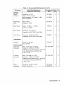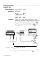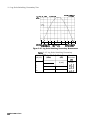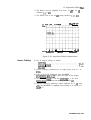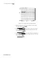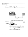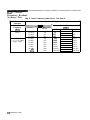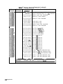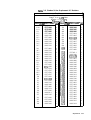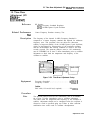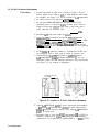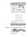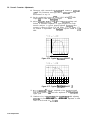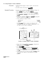
1
Performance Tests and
Adjustments Manual
HP 8568B Spectrum Analyzer
HEWLETT
PACKARD
HP Part No. 08568-90118
Printed in USA September 1993
@Copyright Hewlett-Packard Company 1993
All Rights Reserved. Reproduction, adaptation, or translation without
prior written permission is prohibited, except as allowed under the
copyright laws.
1212 Valley House Drive, Rohnert Park, CA 94928-4999, USA
Certification
Warranty
Hewlett-Packard Company certifies that this product met its
published specifications at the time of shipment from the factory.
Hewlett-Packard further certifies that its calibration measurements
are traceable to the United States National Institute of Standards and
Technology, to the extent allowed by the Institute’s calibration facility,
and to the calibration facilities of other International Standards
Organization members.
This Hewlett-Packard instrument product is warranted against defects
in material and workmanship for a period of one year from date of
shipment. During the warranty period, Hewlett-Packard Company
will, at its option, either repair or replace products which prove to be
defective.
For warranty service or repair, this product must be returned to a
service facility designated by Hewlett-Packard. Buyer shall prepay
shipping charges to Hewlett-Packard and Hewlett-Packard shall pay
shipping charges to return the product to Buyer. However, Buyer shall
pay all shipping charges, duties, and taxes for products returned to
Hewlett-Packard from another country.
Hewlett-Packard warrants that its software and firmware designated
by Hewlett-Packard for use with an instrument will execute
its programming instructions when properly installed on that
instrument. Hewlett-Packard does not warrant that the operation
of the instrument, or software, or firmware will be uninterrupted or
error-free.
L IMITATION
OF
W ARRANTY
The foregoing warranty shall not apply to defects resulting from
improper or inadequate maintenance by Buyer, Buyer-supplied
software or interfacing, unauthorized modification or misuse,
operation outside of the environmental specifications for the
product, or improper site preparation or maintenance.
NO OTHER WARRANTY IS EXPRESSED OR IMPLIED.
HEWLETT-PACKARD SPECIFICALLY DISCLAIMS THE IMPLIED
WARRANTIES OF MERCHANTABILITY AND FITNESS FOR A
PARTICULAR PURPOSE.
E XCLUSIVE
R EMEDIES
THE REMEDIES PROVIDED HEREIN ARE BUYER’S SOLE AND
EXCLUSIVE REMEDIES. HEWLETT-PACKARD SHALL NOT BE
LIABLE FOR ANY DIRECT, INDIRECT, SPECIAL, INCIDENTAL, OR
CONSEQUENTIAL DAMAGES, WHETHER BASED ON CONTRACT,
TORT, OR ANY OTHER LEGAL THEORY.
...
III
Assistance
Product maintenance agreements and other customer assistance
agreements are available for Hewlett-Rwkard products.
Fbr any assistance, contact your nearest Hewlett-Packard Sales and
Service OJke.
Safety Symbols
The following safety symbols are used throughout this manual.
Familiarize yourself with each of the symbols and its meaning before
operating this instrument.
Caution
The caution sign denotes a hazard. It calls attention to a procedure
which, if not correctly performed or adhered to, could result in
damage to or destruction of the instrument. Do not proceed beyond a
caution sign until the indicated conditions are fully understood and
met.
Warning
The warning sign denotes a hazard. It calls attention to a
procedure which, if not correctly performed or adhered to, could
result in injury or loss of life. Do not proceed beyond a warning
sign until the indicated conditions are fully understood and met.
General Safety
Considerations
Warning
Before this instrument is switched on, make sure it has been
properly grounded through the protective conductor of the ac
power cable to a socket outlet provided with protective earth
contact.
Any interruption of the protective (grounding) conductor, inside
or outside the instrument, or disconnection of the protective
earth terminal can result in personal injury.
Warning
There are many points in the instrument which can, if contacted,
cause personal injury. Be extremely careful.
Any adjustments or service procedures that require operation
of the instrument with protective covers removed should be
performed only by trained service personnel.
Caution
Before this instrument is switched on, make sure its primary power
circuitry has been adapted to the voltage of the ac power source.
Failure to set the ac power input to the correct voltage could cause
damage to the instrument when the ac power cable is plugged in.
V
HP 8568B
Spectrum Analyzer
Documentation
Outline
HP 8568B Installation
and Verification
Manual
HP 8568B Operating
and Programming
Manual
Included with the HP Model 8568B Spectrum Analyzer are three
manuals: the Installation and Verification Manual, the Operating and
Programming Manual, and the Performance Tests and Adjustments
Manual.
General information, installation, specifications, characteristics, and
operation verification.
Manual and remote operation, including complete syntax and
command description. Accompanying this manual is the separate,
pocket-sized Quick Reference Guide.
HP 8568B
Performance Tests and
Adjustments Manual
Electrical performance tests and adjustment procedures.
HP 85680B RF Section
Troubleshooting and
Repair Manual
RF Section service information.
HP 85662A IF-Display
Section
Troubleshooting and
Repair Manual
IF-Display Section service information.
vi
Contents
1. General Information
Introduction . . . . . .
Instruments Covered by
Operation Verification .
Option 462 Instruments
Option 857 Instruments
. .
this
. .
. .
. .
. . . .
Manual
. . . .
. . . .
. . . .
.
.
.
.
.
.
.
.
.
.
.
.
.
.
.
.
.
.
.
.
.
.
.
.
.
.
.
.
.
.
.
.
.
.
.
.
.
.
.
.
.
.
.
.
.
2. Performance Tests
Introduction . . . . . . . . . . . . . . . . . . . . .
Verification of Specifications . . . . . . . . . . . . .
Calibration Cycle . . . . . . . . . . . . . . . . . .
Equipment Required . . . . . . . . . . . . . . . .
Test Record . . . . . . . . . . . . . . . . . . . .
1. Center Frequency Readout Accuracy Test . . . .
2. Frequency Span Accuracy Test . . . . . . . . .
3. Sweep Time Accuracy Test (220 ms) . . . . . .
4. Resolution Bandwidth Accuracy Test . . . . . .
5. Resolution Bandwidth Selectivity Test . . . . . .
6. Resolution Bandwidth Switching Uncertainty Test
7. Input Attenuator Switching Uncertainty Test . .
8. Frequency Response Test . . . . . . . . . . . .
9. RF Gain Uncertainty Test . . . . . . . . . . . .
10. IF Gain Uncertainty Test . . . . . . . . . . .
11. Log Scale Switching Uncertainty Test . . . . .
12. Amplitude Fidelity Test . . . . . . . . . . . .
13. Average Noise Level Test . . . . . . . . . . .
14. Residual Responses Test . . . . . . . . . . . .
15. Spurious Responses Test . . . . . . . . . . . .
16. Residual FM Test . . . . . . . . . . . . . . .
17. Line-Related Sidebands Tests . . . . . . . . .
18. Calibrator Amplitude Accuracy Test . . . . . .
19. Fast Sweep Time Accuracy Test (~20 ms) . . . .
20. 1st LO Output Amplitude Test . . . . . . . . .
21. Frequency Reference Error Test . . . . . . . .
‘Ihble 2-19. Performance Test Record . . . . . . . . . .
Test 1. Center Frequency Readout Accuracy Test . . .
Test 2. Frequency Span Accuracy Test . . . . . . . .
Test 3. Sweep Time Accuracy . . . . . . . . . . . .
Test 4. Resolution Bandwidth Accuracy . . . . . . .
Test 5. Resolution Bandwidth Selectivity . . . . . . .
Test 6. Resolution Bandwidth Switching Uncertainty
Test . . . . . . . . . . . . . . . . . . . . . .
Test 7. Input Attenuator Switching Uncertainty Test .
Test 8. Frequency Response Test . . . . . . . . . .
Test 9. RF Gain Uncertainty Test . . . . . . . . . .
Test 10. IF Gain Uncertainty Test . . . . . . . . . .
l-l
l-l
l-2
1-2
l-2
2-l
2-l
2-l
2-2
2-2
2-3
2-6
2-9
2-13
2-15
2-18
2-20
2-22
2-31
2-33
2-39
2-41
2-45
2-47
2-49
2-56
2-60
2-62
2-63
2-66
2-67
2-69
2-70
2-71
2-72
2-73
2-74
2-75
2-76
2-77
2-78
2-79
Contents-l
Test
Test
Test
Test
Test
Test
Test
Test
Test
Test
Test
3.
Contents-2
11. Log Scale Switching Uncertainty Test . .
12. Amplitude Fidelity Test . . . . . . . . .
13. Average Noise Level Test . . . . . . . .
14. Residual Responses Test . . . . . . . . .
15. Spurious Responses Test . . . . . . . .
16. Residual FM Test . . . . . . . . . . . .
17. Line-Related Sidebands Test . . . . . . .
18. Calibrator Amplitude Accuracy Test . . .
19. Fast Sweep Time Accuracy Test (~20 ms)
20. 1st LO Output Amplitude Test . . . . . .
21. Frequency Reference Error Test . . . . .
.
.
.
.
.
.
.
.
.
.
.
.
.
.
.
.
.
.
.
.
.
.
Adjustments
Introduction . . . . . . . . . . . . . . . . . . . . .
Safety Considerations . . . . . . . . . . . . . . . . .
Equipment Required . . . . . . . . . . . . . . . . .
Adjustment Tools . . . . . . . . . . . . . . . . . . .
Factory-Selected Components . . . . . . . . . . . . .
Related Adjustments . . . . . . . . . . . . . . . . .
Location of Test Points and Adjustments . . . . . . . .
1. Low-Voltage Power Supply Adjustments . . . . . .
2. High-Voltage Adjustment (SN 3001A and Below) . .
2. High-Voltage Adjustment (SN 3004A and Above) . .
3. Preliminary Display Adjustments (SN 3001A and
Below) . . . . . . . . . . . . . . . . . . . . .
3. Preliminary Display Adjustments (SN 3004A and
Above) . . . . . . . . . . . . . . . . . . . . .
4. Final Display Adjustments (SN 3001A and Below) .
4. Final Display Adjustments (SN 3004A and Above) .
5. Log Amplifier Adjustments . . . . . . . . . . . .
6. Video Processor Adjustments . . . . . . . . . . .
7. 3 MHz Bandwidth Filter Adjustments . . . . . . .
8. 21.4 MHz Bandwidth Filter Adjustments . . . . .
9. 3 dB Bandwidth Adjustments . . . . . . . . . .
10. Step Gain and 18.4 MHz Local Oscillator
Adjustments . . . . . . . . . . . . . . . . . .
11. Down/Up Converter Adjustments . . . . . . . .
12. Time Base Adjustment (SN 2840A and Below, also
32 17AO5568 and Above) . . . . . . . . . . . . .
12. Time Base Adjustment (SN 2848A to 3217A05567)
13. 20 MHz Reference Adjustments . . . . . . . . .
14. 249 MHz Phase Lock Oscillator Adjustments . . .
15. 275 MHz Phase Lock Oscillator Adjustment . . . .
16. Second IF Amplifier and Third Converter
Adjustment . . . . . . . . . . . . . . . . . . .
17. Pilot Second IF Amplifier Adjustments . . . . . .
18. Frequency Control Adjustments . . . . . . . . .
19. Second Converter Adjustments . . . . . . . . .
20. 50 MHz Voltage-Tuned Oscillator Adjustments . .
2 1. Slope Compensation Adjustments . . . . . . . .
22. Comb Generator Adjustments . . . . . . . . . .
23. Analog-To-Digital Converter Adjustments . . . . .
24. Track and Hold Adjustments . . . . . . . . . . .
25. Digital Storage Display Adjustments . . . . . . .
Low-Noise DC Supply . . . . . . . . . . . . . . . .
2-82
2-83
2-84
2-85
2-86
2-87
2-88
2-89
2-90
2-91
2-92
3-l
3-2
3-2
3-2
3-3
3-4
3-4
3-25
3-29
3-39
3-45
3-52
3-59
3-61
3-65
3-69
3-72
3-77
3-84
3-87
3-92
3-95
3-99
3-103
3-107
3-110
3-112
3-116
3-119
3-123
3-130
3-133
3-136
3-139
3-142
3-145
3-150
Crystal Filter Bypass Network Configuration . . . . . 3-151
4. Option 462
Introduction . . . . . . . . . . . . . . . . . . . . .
4. 6 dB Resolution Bandwidth Accuracy Test . . . . .
4. Impulse and Resolution Bandwidth Accuracy Test .
5. 6 dB Resolution Bandwidth Selectivity Test . . . .
5. Impulse and Resolution Bandwidth Selectivity Test .
6. Impulse and Resolution Bandwidth Switching
Uncertainty Test . . . . . . . . . . . . . . . .
Test 4. 6 dB Resolution Bandwidth Accuracy Test (p/o
Table 2-19, Performance Test Record) . . . . . . .
Test 4. Impulse and Resolution Bandwidth Accuracy
Test (p/o Table 2-19, Performance Test Record) . .
Test 5. 6 dB Resolution Bandwidth Selectivity (p/o
‘Ihble 2-19, Performance Test Record) . . . . . . .
Test 5. Impulse and Resolution Bandwidth Selectivity
(p/o Table 2-19, Performance Test Record) . . . . .
Test 6. Impulse and Resolution Bandwidth Switching
Uncertainty (p/o ‘Iable 2-19, Performace Test
Record) . . . . . . . . . . . . . . . . . . . . .
9. 6 dB Resolution Bandwidth Adjustments . . . . .
9. Impulse Bandwidth Adjustments . . . . . . . . .
5. Option 857
Introduction . . . . . . . . . . . . . . . . . . .
12. Option 857 Amplitude Fidelity Test . . . . .
Performance Test Record . . . . . . . . . . . . .
Test 12. Option 857 Amplitude Fidelity Test . . .
6.
4-l
4-2
4-4
4-10
4-13
4-16
4-18
4-19
4-21
4-22
4-23
4-24
4-27
.
.
.
.
5-l
5-2
5-7
5-8
Major Assembly and Component Locations
IF-Display Section Figure Index . . . . . . . . . . . .
RF Section Figure Index . . . . . . . . . . . . . . .
6-l
6-2
.
.
.
.
Contents-3
Figures
l-l. Service Accessories, HP Part Number 08568-60001 . .
2-l. Center Frequency Accuracy Test Setup . . . . . . . .
2-2. Center Frequency Readout Error Measurement . . . .
2-3. Frequency Span Accuracy Test Setup . . . . . . . .
2-4. Sweep Time Accuracy Test Setup . . . . . . . . . .
2-5. Penlift Output Signal . . . . . . . . . . . . . . . .
2-6. Resolution Bandwidth Measurement . . . . . . . . .
2-7. 60 dB Bandwidth Measurement . . . . . . . . . . .
2-8. Bandwidth Switching Uncertainty Measurement . . .
2-9. Attenuator Switching Uncertainty Test Setup . . . . .
2-10. Attenuator Switching Uncertainty Measurement . . .
2-l 1. Frequency Response Test Setup (20 MHz to 1.5 GHz) .
2-12. Frequency Response Measurement (20 MHz to 1.5 GHz)
2-13. Frequency Response Test Setup (100 kHz to 20 MHz) .
2-14. Frequency Response Measurement (100 kHz to 20 MHz)
2-15. Frequency Response Test Setup (100 Hz to 100 kHz) .
2-16. RF Gain Uncertainty Measurement . . . . . . . . .
2-17. IF Gain Uncertainty Test Setup . . . . . . . . . . .
2-18. IF Gain Uncertainty Measurement . . . . . . . . . .
2-19. IF Gain Uncertainty Measurement (2 dB) . . . . . . .
2-20. Log Scale Switching Uncertainty Measurement . . . .
2-21. Amplitude Fidelity Test Setup . . . . . . . . . . . .
2-22. Amplitude Fidelity Measurement . . . . . . . . . .
2-23. Average Noise Level Measurement . . . . . . . . . .
2-24. Residual Responses Measurement . . . . . . . . . .
2-25. Harmonic Distortion Test Setup . . . . . . . . . . .
2-26. Intermodulation Distortion Test Setup . . . . . . . .
2-27. Intermodulation Distortion Products . . . . . . . . .
2-28. Bandwidth Filter Slope Measurement . . . . . . . .
2-29. Slope Detected Residual FM . . . . . . . . . . . . .
2-30. Peak-to-Peak Amplitude Measurement . . . . . . . .
2-31. Line Related Sidebands Measurement . . . . . . . .
2-32. Calibrator Amplitude Accuracy Test Setup . . . . . .
2-33. Fast Sweep Time Accuracy (~20 ms Test Setup) . . . .
2-34. Fast Sweep Time Measurement (~20 ms) . . . . . . .
2-35. 1st LO Output Amplitude Test Setup . . . . . . . . .
2-36. Frequency Reference Test Setup . . . . . . . . . . .
3-l. Low-Voltage Power Supply Adjustments Setup . . . .
3-2. IF-Display Section Low-Voltage Adjustments (SN 3001A
and Below) . . . . . . . . . . . . . . . . . . .
3-3. IF-Display Section Low-Voltage Adjustments (SN 3004A
and Above) . . . . . . . . . . . . . . . . . . .
3-4. Location of RF Section Low-Voltage Adjustments . . .
3-5. High Voltage Adjustment Setup . . . . . . . . . . .
3-6. Location of High Voltage Adjustments . . . . . . . .
3-7. Location of Label and Test Point . . . . . . . . . . .
Contents-4
l-8
2-3
2-4
2-6
2-9
2-11
2-14
2-16
2-19
2-20
2-21
2-22
2-24
2-25
2-26
2-27
2-32
2-33
2-35
2-36
2-40
2-41
2-43
2-46
2-48
2-50
2-52
2-53
2-57
2-58
2-58
2-61
2-62
2-63
2-64
2-66
2-68
3-25
3-26
3-26
3-27
3-30
3-31
3-32
3-8.
3-9.
3-10.
3-11.
3-12.
3-13.
3-14.
3-15.
3-16.
3-17.
3-18.
3-19.
3-20.
3-21.
3-22.
3-23.
3-24.
3-25.
3-26.
3-27.
3-28.
3-29.
3-30.
3-31.
3-32.
3-33.
3-34.
3-35.
3-36.
3-37.
3-38.
3-39.
3-40.
3-41.
3-42.
3-43.
3-44.
3-45.
3-46.
3-47.
3-48.
3-49.
3-50.
3-51.
3-52.
3-53.
3-54.
3-55.
Location of AlA Components . . . . . . . . . . .
CRT Cut-Off Voltage
Waveform at AlA3TP5’ : : : : : : : : : : : : : : :
Discharging the CRT Post-Accelerator Cable . . . . .
High Voltage Adjustment Setup . . . . . . . . . . .
Location of High Voltage Adjustments . . . . . . . .
Location of AlA Label and Test Point . . . . . . . .
Discharging the CRT Post-Accelerator Cable . . . . .
Preliminary Display Adjustments Setup . . . . . . .
Location of AlA2, AlA4, AlA5, and A3A2 . . . . .
AlA2, AlA4, and AlA Adjustment Locations . . . .
X+ and X- Waveforms . . . . . . . . . . . . . . .
Composite X Deflection Waveform . . . . . . . . . .
Rise and Fall Times and Overshoot Adjustment
Waveform . . . . . . . . . . . . . . . . . . .
5OV,-, Signal . . . . . . . . . . . . . . . . . . . .
Preliminary Display Adjustments Setup . . . . . . .
Location of AlA and A3A2
. . . . . . . . . . . .
AlA Adjustment Locations . . . . . . . . . . . . .
X+ and X- Waveforms . . . . . . . . . . . . . . .
Composite X Deflection Waveform . . . . . . . . . .
Rise and Fall Times and Overshoot Adjustment
Waveform . . . . . . . . . . . . . . . . . . .
5OV,-, Signal . . . . . . . . . . . . . . . . . . . .
Location of Final Display Adjustments on AlA2, AlA4,
and AlA5. . . . . . . . . . . . . . . . . . . .
Final Display Adjustments Setup . . . . . . . . . . .
Location of Final Display Adjustments on AlA . . .
Log Amplifier Adjustments Setup . . . . . . . . . .
Location of Log Amplifier Adjustments . . . . . . . .
Video Processor Adjustments Setup . . . . . . . . .
Location of Video Processor Adjustments . . . . . . .
3 MHz Bandwidth Filter Adjustments Setup . . . . .
Location of Center, Symmetry, and 10 Hz Amplitude
Adjustments . . . . . . . . . . . . . . . . . .
Location of 3 MHz Peak Adjustments . . . . . . . . .
21.4 MHz Bandwidth Filter Adjustments Setup . . . .
Location of A4A4 21.4 MHz LC Filter Adjustments . .
Location of A4A4 21.4 MHz Crystal Filter Adjustments
Location of A4AS 21.4 MHz LC Filter and Attenuation
Adjustments . . . . . . . . . . . . . . . . . .
Location of A4A8 21.4 MHz Crystal Filter Adjustments
Location of 3 dB Bandwidth Adjustments . . . . . .
Step Gain and 18.4 MHz Local Oscillator Adjustments
Setup . . . . . . . . . . . . . . . . . . . . . .
Location of IF Gain Adjustment . . . . . . . . . . .
Location of 10 dB Gain Step Adjustments . . . . . .
Location of .l dB Gain Step, 18.4 MHz LO, and + 1OV
Adjustments . . . . . . . . . . . . . . . . . .
Down/Up Converter Adjustments Setup . . . . . . .
Location of Down/Up Converter Adjustments . . . . .
Time Base Adjustment Setup . . . . . . . . . . . .
Location of A27Al Adjustment . . . . . . . . . . .
Time Base Adjustment Setup . . . . . . . . . . . .
Location of A27A2 Adjustment . . . . . . . . . . .
3-34
3-35
3-36
3-38
3-40
3-41
3-42
3-44
3-46
3-47
3-47
3-48
3-49
3-49
3-51
3-53
3-54
3-54
3-55
3-56
3-56
3-58
3-60
3-61
3-62
3-65
3-66
3-69
3-70
3-72
3-73
3-75
3-77
3-78
3-79
3-80
3-81
3-85
3-87
3-88
3-89
3-91
3-92
3-93
3-95
3-98
3-99
3-102
Contents-5
3-56.
3-57.
3-58.
3-59.
3-60.
3-61.
3-62.
3-63.
3-64.
3-65.
3-66.
3-67.
3-68.
3-69.
3-70.
3-71.
3-72.
3-73.
3-74.
3-75.
3-76.
3-77.
3-78.
3-79.
3-80.
3-81.
3-82.
3-83.
3-84.
3-85.
3-86.
3-87.
3-88.
3-89.
3-90.
3-91.
3-92.
3-93.
3-94.
4-l.
4-2.
4-3.
4-4.
4-5.
4-6.
4-7.
4-8.
5.1.
6-l.
6-2.
6-3.
6-4.
6-5.
6-6.
Contents-6
20 MHz Reference Adjustments Setup . . . . . . . .
Location of 20 MHz Reference Adjustments . . . . .
Typical Signal at A16TP3 . . . . . . . . . . . . . .
249 MHz Phase Lock Oscillator Adjustments Setup . .
Location of 249 MHz Phase Lock Oscillator Adjustments
275 MHz Phase Lock Oscillator Adjustment Setup . . .
Location of 275 MHz PLO Adjustment . . . . . . . .
Second IF Amplifier Adjustments Setup . . . . . . .
Location of 301.4 MHz BPF and 280 MHz AMPTD
Adjustments . . . . . . . . . . . . . . . . . .
301.4 MHz Bandpass Filter Adjustment Waveform . .
Minimum Image Response at 258.4 MHz . . . . . . .
Pilot Second IF Amplifier Adjustments Setup . . . . .
Location of 269 MHz Bandpass Filter Adjustments . .
269 MHz Bandpass Filter Adjustments Waveforms . .
Frequency Control Adjustments Setup . . . . . . . .
Location of Frequency Control Adjustments . . . . .
Second Converter Adjustments Setup . . . . . . . .
Location of Second Converter Adjustments . . . . . .
Typical PILOT 2ND IF Bandpass (SHIFT t) . . . . . .
Typical PILOT 2ND IF Bandpass (SHIFT 1) . . . . . .
Typical Bandpass (SHIFT t) . . . . . . . . . . . . .
Typical Bandpass (SHIFT 1) . . . . . . . . . . . . .
50 MHz Voltage-Tuned Oscillator Adjustments Setup .
Location of 50 MHz VT0 Adjustments . . . . . . . .
Slope Compensation Adjustment Setup . . . . . . . .
Location of A22R66 TILT Adjustment . . . . . . . .
Slope Compensation Adjustment Waveforms . . . . .
Location of Comb Generator Adjustments . . . . . .
Comb Teeth Display . . . . . . . . . . . . . . . . .
Analog-To-Digital Converter Adjustments Setup . . . .
Location of Analog-To-Digital Converter Adjustments .
Track and Hold Adjustments Setup . . . . . . . . .
Location of Track and Hold Adjustments . . . . . . .
Digital Storage Display Adjustments Setup . . . . . .
Location of Digital Storage Display Adjustments . . .
Sample and Hold Balance Adjustment Waveforms . . .
Waveform Before Adjustment . . . . . . . . . . . .
Low-Noise DC Supply . . . . . . . . . . . . . . . .
Crystal Filter Bypass Network Configurations . . . . .
Resolution Bandwidth Measurement . . . . . . . . .
Impulse Bandwidth Test Setup . . . . . . . . . . . .
6 dB Resolution Bandwidth Measurement . . . . . .
60 dB Bandwidth Measurement . . . . . . . . . . .
60 dB Bandwidth Measurement . . . . . . . . . . .
Bandwidth Switching Uncertainty Measurement . . .
Location of Bandwidth Adjustments . . . . . . . . .
Location of Bandwidth Adjustments . . . . . . . . .
Option 857 Amplitude Fidelity Test Setup . . . . . .
RF Section, Top View . . . . . . . . . . . . . . . .
RF Section, Front View . . . . . . . . . . . . . . .
RF Section, Bottom View . . . . . . . . . . . . . .
IF Section, Top View (SN 3001A and Below) . . . . .
IF Section, Top View (SN 3004A and Above) . . . . .
IF Section, Front View . . . . . . . . . . . . . . .
3-103
3-104
3-106
3-107
3-108
3-110
3-111
3-112
3-114
3-l 14
3-115
3-116
3-118
3-118
3-119
3-120
3-123
3-124
3-127
3-127
3-128
3-128
3-130
3-131
3-133
3-135
3-135
3-136
3-137
3-139
3-140
3-142
3-143
3-145
3-146
3-147
3-147
3-150
3-151
4-3
4-4
4-8
4-11
4-14
4-17
4-25
4-28
5-2
6-4
6-5
6-6
6-7
6-8
6-9
6-7. IF Section, Bottom View . . . . . . . . . . . . . .
6-10
Contents-7
lhbles
2-l.
2-2.
2-3.
2-4.
2-5.
2-6.
2-7.
Performance Test Cross-Reference . . . . . . . . . .
Center Frequency Readout Error Test Record . . . . .
Wide Span Error . . . . . . . . . . . . . . . . . .
Span Error . . . . . . . . . . . . . . . . . . . . .
Sweep Time Accuracy, Sweep Times 220 ms . . . . .
Sweep Time Accuracy, Sweep Times ~20 s . . . . . .
Sweep Time Accuracy, Sweep Times 220 ms (Alternate
Procedure) . . . . . . . . . . . . . . . . . . .
2-8. Bandwidth Accuracy . . . . . . . . . . . . . . . .
2-9. Resolution Bandwidth Selectivity . . . . . . . . . .
2-10. Bandwidth Switching Uncertainty . . . . . . . . . .
2-11. Input Attenuator Switching Uncertainty . . . . . . .
2-12. IF Gain Uncertainty, 10 dB Steps . . . . . . . . . .
2-13. IF Gain Uncertainty, 2 dB Steps . . . . . . . . . . .
2-14. IF Gain Uncertainty, 0.1 dB Steps . . . . . . . . . .
2-15. Log Scale Switching Uncertainty . . . . . . . . . . .
2-16. Log Amplitude Fidelity . . . . . . . . . . . . . . .
2- 17. Linear Amplitude Fidelity . . . . . . . . . . . . . .
2-18. Fast Sweep Time Accuracy (~20 ms) . . . . . . . . .
3-1. Adjustment Cross Reference . . . . . . . . . . . . .
3-2. Adjustable Components . . . . . . . . . . . . . . .
3-3. Factory-Selected Components . . . . . . . . . . . .
3-4. Standard Value Replacement Capacitors . . . . . . .
3-5. Standard Value Replacement 0.125 Resistors . . . . .
3-6. Standard Value Replacement 0.5 Resistors . . . . . .
3.5. Initial Adjustment Positions . . . . . . . . . . . . .
3-6. Initial Adjustment Positions . . . . . . . . . . . . .
3-7. Parts for Low-Noise DC Supply . . . . . . . . . . .
3-8. Crystal Filter Bypass Network Configuration for A4A4
and A4A8 (21.4 MHz) . . . . . . . . . . . . . .
3-9. Crystal Filter Bypass Network Configuration for A4A7
(3 MHz) . . . . . . . . . . . . . . . . . . . . .
4-l. 6 dB Resolution Bandwidth Accuracy . . . . . . . .
4-2. Impulse Bandwidth Accuracy . . . . . . . . . . . .
4-3. 6 dB Resolution Bandwidth Accuracy . . . . . . . .
4-4. 6 dB Resolution Bandwidth Selectivity . . . . . . . .
4-5. Impulse and Resolution Bandwidth Selectivity . . . .
4-6. Bandwidth Switching Uncertainty . . . . . . . . . .
5-l. Log Amplitude Fidelity (10 Hz RBW; Option 857) . . .
5-2. Log Amplitude Fidelity (10 kHz RBW; Option 857) . .
5-3. Linear Amplitude Fidelity . . . . . . _ . . . . . . .
Contents-E
2-2
2-5
2-7
2-8
2-11
2-12
2-12
2-14
2-17
2-19
2-21
2-35
2-36
2-38
2-40
2-42
2-44
2-65
3-3
3-5
3-13
3-20
3-21
3-23
3-59
3-62
3-150
3-151
3-151
4-3
4-8
4-9
4-12
4-15
4-17
5-4
5-5
5-6
1
General Information
Introduction
This HP 8568B Tests and Adjustments Manual contains two sections:
Performance Tests and Adjustments Procedures. The Performance
Tests provided should be performed for the following reasons:
w If the test equipment for the Operation Verification Program is not
available.
n
If the instrument does not pass all of the Operation Verification
tests.
w For complete verification of specifications not covered by the
Operation Verification program.
The adjustment procedures should be performed for the following
reasons:
w If the results of a performance test are not within the specifications.
w After the replacement of a part or component that affects electrical
performance.
Warning
The adjustment procedures require access to the interior of the
instrument and therefore should only be performed by qualified
service personnel. There are voltages at many points in the
instrument which can, if contacted, cause personal injury. Be
extremely careful. Adjustments should be performed only by
trained service personnel.
Power is still applied to this instrument with the LINE switch in
STANDBY. There is no OFF position on the LINE switch. Before
removing or installing any assembly or printed circuit board,
remove the power cord from the rear of both instruments and
wait for the MAINS indicators (red LEDs) to go completely out.
Capacitors inside the instrument may still be charged even if the
instrument has been disconnected from its source of power.
Use a non-metallic tuning tool whenever possible.
Instruments Covered
by this Manual
This manual contains procedures for testing and adjusting HP 8568B
Spectrum Analyzers, including those with Option 001 (75 Ohm RF
INPUT), Option 400 (400 Hz operation), Option 462, and Option 857
installed. The procedures in this manual can also be used to adjust HP
8568A Spectrum Analyzers that have been converted into HP 8568B
Spectrum Analyzers through the installation of an HP 8568AB Retrofit
Kit (formerly HP 8568A+ OlK Retrofit Kit).
G e n e r a l I n f o r m a t i o n l-1
Operation Verification
A high confidence level in the instrument’s operation can be achieved
by running only the Operation Verification Program, since it tests
most of the instrument’s specifications. It is recommended that the
Operation Verification Program be used for incoming inspection and
after repairs, since it requires much less time and test equipment.
A description of the program can be found in the Installation and
Verification manual.
Option 462
Instruments
Option 462 instruments require that the performance tests and
adjustment procedures listed below be performed instead of their
standard versions included in chapters two and three. Information on
Option 462 versions are located in Chapter 4, Option 462.
6 dB Bandwidths:
Test 4, 6 dB Resolution Bandwidth Accuracy Test
Test 5, 6 dB Resolution Selectivity Test
Adjustment 9, 6 dB Bandwidth Adjustments
Impulse Bandwidths:
Test 4, Impulse and Resolution Bandwidth Accuracy Test
Test 5, Impulse and Resolution Selectivity Test
Test 6, Impulse and Resolution Bandwidth Switching Uncertainty
Test
Adjustment 9, Impulse Bandwidth Adjustments
Option 857
Instruments
Option 857 instruments require that the performance test procedure
listed below be performed instead of the standard version included in
Chapter 2. Information on Option 857 is located in Chapter 5, Option
857.
Test 12, Option 857 Amplitude Fidelity Test
l-2 G e n e r a l I n f o r m a t i o n
‘Ihble l-l. Recommended Test Equipment (1 of 5)
Instrument
Critical Specifications for
Equipment Substitution
SIGNAL
SOURCES
Synthesized Frequency: 10 MHz to 1500 MHz
Sweeper
Output Power: + 10 dBm maximum (leveled)
Aging Rate: ~1 x 10mg/day
Spurious Signals: 135 dBc (~7 GHz)
125 dBc (<20 GHz)
Amplitude Modulation: dc to 100 kHz
Leveling: Internal, External Power Meter
Zecommended
Model
HP 8340A
Perf. 4dj.
Test
X
X
Signal
Generator
Frequency: 20 MHz to 450 MHz
SSB Phase Noise: >130 dB below carrier at
20 kHz away
Stability: ~10 ppm/lO min.
(HP 8340A may be substituted)
HP 8640B
Frequency
Synthesizer
Frequency: 200 Hz to 80 MHz
Stability: f 1 x lo-‘/day
Amplitude Range: + 13 to -86 dBm with 0.01 dB
resolution
Attenuator Accuracy: < f0.07 dB (+ 13 to -47 dBm)
HP 3335A
Pulse
Generator
Pulse Width: 10 nsec to 250 nsec
Rise and Fall Times: ~6 nsec
Output Level: + 2.5V
Output: Sine Wave and Triangle Wave, 2Vp-p
Range: 100 Hz to 500 kHz (Sweep Function Available)
HP 8116A
HP 3312A
X
X
Output: 1, 2, 5, or 10 MHz
Accuracy: <fl x 10-l’
Aging Rate: ~1 x lo-lo/day
HP 5061B
X
X
Function
Generator
Frequency
Standard
X
X
X
General Information 1-3
‘Ihble l-l. Recommended Test Equipment (2 of 5)
Instrument
ANALYZERS
Spectrum
Analyzer
Critical Specifications for
Equipment Substitution
Recommended Perf. Adj.
Model
Test
Frequency: 100 Hz to 2.5 GHz
2 to 22 GHz
Preselected
HP 8566A/B
X
Spectrum
Analyzer
RF Spectrum Analyzer
Frequency: 9 kHz to 1.8 GHz
8590B
X
AC Probe
High Frequency Probe
HP 85024A
X
Scalar
Network
Analyzer
Detector
(2 required)
10 MHz-l10 GHz
HP 8757E
X
Compatible with HP 8757E
HP 11664A
X
Frequency
Counter
Frequency: 10 MHz to 18 GHz
Sensitivity: -30 dBm
HP-IB Compatible
(HP 5343A may be substituted)
HP 5340A
X
Electronic
Counter
Range: >lO MHz
Resolution: 2 x lo-’ gate time
Ext. Time Base: 1, 2, 5, or 10 MHz
Frequency: dc to 100 MHz
Time Interval A + B: 100 nsec to 200 set
Sensitivity: 50 mV rms
Range: 30 mV to 5V p-p
HP 5345A
X
HP 5316B
X
COUNTERS
j = Universal
Counter
OSCILLOSCOPE
Digitizing OSCOPE, 4 Channel
Oscilloscope
Frequency: 100 MHz
Sensitivity: .005V/Division
Probe
l-4 G e n e r a l I n f o r m a t i o n
10: 1 Divider, compatible with oscilloscope
HP 54501A
HP 10432A
‘Ihble l-l. Recommended Test Equipment (4 of 5)
Instrument
Critical Specifications for
Equipment Substitution
Recommended
Model
Perf.
Test
1dj.
ATTENUATORS
(Cont’d)
20 dB
Attenuator
?requency: 200 Hz to 18 GHz
rype N Connectors
HP 8491B,
Option 020
TERMINATIONS
Termination
Impedance: 500; BNC
HP 11593A
?latness: ho.25 dB
Cut-off Frequency:2400 MHz and ~500 MHz
Xejection: >40 dB at 1750 MHz
Telonic
TLS450-7EE
FIWERS
Low-Pass
Filter
X
Low-Pass
Filter
ht.-off Frequency: 300 MHz
HP 0955-0455
X
Low-Pass
Filter
Cut-off Frequency: 50 MHz
HP 0955-0306
X
HP 11667A
X
HP 8721A
X
MISCELLANEOUS
DEVICES
Frequency: 1 MHz to 1500 MHz
Power
backing: ~0.2 dB
Splitter
Directional
Bridge
X
SPECIAL
DEVICES
Display
Adjustment
PC Board
Required for preliminary display adjustments HP85662-60088
X
Low-Noise
DC Supply
Zefer to Figure 70
(Optional)
X
Crystal Filter
Bypass Network
(4 required)
Xefer to Figure 71
X
l-6 G e n e r a l I n f o r m a t i o n
‘Ihble l-l. Recommended Test Equipment (5 of 5)
Instrument
Critical Specifications for
Equipment Substitution
Recommended Perf. Adj a
Model
Test
CABLES
Cable Assembly Frequency Range: 200 Hz to 22 GHz HP 8120-4921
APC 3.5 Male Connectors
Length: 91 cm (36 inches)
SWR: cl.4 at 22 GHz
Cable
BNC, 122 cm (48 in.) (3 required)
Test Cable *
Test Cable
Test Cable
ADAPTERS
Adapter
Adapter
Adapter
Adapter
Adapter
Adapter
Adapter
Adapter
Adapter
Adapter
BNC (m) to SMB Snap-On (f)
SMA (m) to SMA (m)
SMA (m) to SMA (m)
Type N (f) to BNC (m)
Type N (m) to BNC (m)
Tee, SMB Male Connectors
Type N (m) to N (m)
Type N (m) to BNC (f)(2 required)
BNC Tee (m) (f) (f)
Type N (m) to SMA (f)
Type N (f) to BNC (f)(2 required)
APC-3.5 (f) to APC-3.5 (f)
APC-3.5 (f) TO N (f)(2 required)
10503A
HP 85680-60093
HP 85680-20094
HP5061-5458 X
HP1250-0077
HP1250-0082
HP 1250-0670
HP1250-0778
HP1250-0780
HP1250-0781
HP1250-1250
HP1250-1474
HP1250-1749
HP 1250-1745
X
X
x
x
X
X
X
X
X
X
X
X
X
X
X
X
BOARD
EXTENDERS
Extender *
12 required)
PC Board: 36 contacts;
2 rows of 18
HP 08505-60042
X
Extender *
13 required)
PC Board: 30 contacts;
2 rows of 15
HP 08505-60041
X
Extender *
PC Board: 20 contacts;
2 rows of 10
HP 85680-60028
X
Extender *
12 required)
PC Board: 12 contacts;
2 rows of 6
HP08505-60109
X
HP 03950-4001
,X
PC Board extracting tool
PC Board
Extractor
* Part of Service Accessories
G e n e r a l I n f o r m a t i o n l-7
Description
HP Part Number
Extender Board: 20 contacts; 2 rows of 10
85680-60028
Cable: 4-foot long; BNC to SMB snap-on
85680-60093
PC Board: Display Adjustment Test
85662-60088
Extender Board: 30 contacts; 2 rows of 15
08505-60041
Extender Board: 12 contacts; 2 rows of 6
08505-60109
Extender Board: 50 contacts; 2 rows of 25
85680-60034
Extender Board: 36 contacts; 2 rows of 18
08505-60042
Figure l-l. Service Accessories, HP Part Number 08568-60001
l-8 G e n e r a l I n f o r m a t i o n
2
Performance Tksts
Introduction
Verification of
Specifications
The procedures in this section test the instrument’s electrical
performance using the Specifications in the Installation and
Verification Manual as the performance standards. None of the
tests require access to the interior of the instrument. The manual
Performance Tests provided in this section should be performed only
if semi-automatic test equipment (for Operation Verification) is not
available or the Performance Test is not in the Operation Verification
Program. (Refer to the Installation and Verification Manual for
information on Operation Verification.)
When a complete verification of specifications is required, proceed as
follows:
1. Run the Operation Verification Program.
2. The Operation Verification Program verifies compliance with
specifications of all tests it performs. The tests not performed by
the Operation Verification Program must be done manually and are
as follows:
n
Center Frequency Readout Accuracy
n
Spurious Responses
H Fast Sweep Time Accuracy
n
n
1st LO Output Amplitude Responses
Frequency Reference Error
If the results of a performance test are marginally within
specification, go to the Adjustments section of this manual and
perform the related adjustment procedures. When an adjustment is
directly related to a performance test, the adjustment procedure is
referenced under RELATED ADJUSTMENT in the performance test.
Calibration Cycle
This instrument requires periodic verification of performance. The
instrument should have a complete verification of specifications at
least every six months.
P e r f o r m a n c e T e s t s 2-l
Equipment Required
Test Record
Note
Equipment required for the manual performance tests and
adjustments is listed in ‘Ihble 2-1, Recommended Test Equipment,
at the beginning of this manual. Any equipment that satisfies the
critical specifications given in the list may be substituted for the
recommended model.
The Operation Verification Program provides a detailed test record
when a printer is used with the controller. If manual performance
tests are done, results of the performance tests may be tabulated in
the HP 8568B Performance Test Record at the end of this section. The
HP 8568B Performance Test Record lists all of the tested specifications
and the acceptable ranges for the measurement values obtained
during the tests.
Allow l/2-hour warm-up time for the HP 8568B before beginning the
Performance Tests.
able 2-1. Performance Test Cross-Reference
Function or Characteristic Tested Test
No.
Performance Test
Center Frequency Readout
1
Center Frequency Readout Accuracy Test
Frequency Spans
2
Frequency Span Accuracy Test
Sweep Time Accuracy (220 ms)
3
Sweep Time Accuracy Test
3-dB Bandwidths
4
Resolution Bandwidth Accuracy Test
Bandwidth Shape
5
Resolution Bandwidth Selectivity Test
Bandwidth Amplitudes
6
Resolution Bandwidth Switching Uncertainty Test
Input Attenuator Accuracay
7
Input Attenuator Switching Uncertainty
Frequency Response
8
RF Gains
9
RF Gain Uncertainty Test
IF Gains
10
IF Gain Uncertainty Test
Log Scales Accuracy
11
Log Scale Switching Uncertainty Test
Log and Linear Amplifier Fidelity
12
Amplitude Fidelity Test
Noise Floor
13
Average Noise Level Test
Residual Responses
14
Residual Responses Test
Spurious Responses
15
Spurious Responses Test
Residual FM
16
Residual FM Test
Line-Related Sidebands
17
Line-Related Sidebands Test
CAL OUTPUT Level
18
Calibrator Amplitude Accuracy Test
Fast Sweep Times
19
Fast Sweep Time Accuracy Test
1ST LO OUTPUT Amplitude
20
1ST LO OUTPUT Amplitude Test
Frequency Reference
21
Frequency Reference Error Test
2-2 Performance Tests
Frequency Response Test
1. Center Frequency Readout Accuracy Test
1. Center
Frequency Readout
Accuracy ‘I&t
Related Adjustments
Frequency Control Adjustments
Time Base Adjustment
Step Gain and 18.4 MHz Local Oscillator Adjustments
50 MHz Voltage-Tuned Oscillator Adjustments
Specification
(uncorrected)
f2% of frequency span + frequency reference error x tune frequency
+30% of resolution bandwidth setting + 10 Hz) in AUTO resolution
bandwidth after adjusting FREQ ZERO at stabilized temperature.
Description
A synthesized signal source that is phase-locked to a known frequency
standard is used to input a signal to the analyzer. The frequency
readout of the analyzer is compared to the actual input frequency
for several different frequency settings over the analyzer’s range.
The signal source is phase-locked to a standard known to be as
accurate as the analyzer’s internal frequency reference to minimize
the “frequency reference error x center frequency” term of the
specification.
FAEQUENCY
STANDARD
SPECTRUH ANALYZER
SYNTHESIZED
SHEEPER
SIONAL
INPUT 2
ADAPTER
CABLE ASSENBLY
Figure 2-1. Center Frequency Accuracy Test Setup
P e r f o r m a n c e T e s t s 2-3
1. Center Frequency Readout Accuracy Test
Equipment
Synthesized Sweeper . . . . . . . . .
HP8340A
Frequency Standard . 10 MHz standard, accy within + 1 part in lOlo,
e.g. HP 5061A
Adapter, Type N (m) to SMA (f) . . .
HP1250-1250
61 cm (24 in.) Cable Assembly, SMA Male Connectors HP 5061-1086
Procedure 1. Connect CAL OUTPUT to SIGNAL INPUT 2.
2 . Press [INSTR PRESET), @ on the analyzer.
3 . Adjust FREQ ZERO for a maximum amplitude trace.
4 . Press (1tds-r~ PRESET).
5 . Set the synthesized sweeper for a 100.000 MHz signal at a level of
approximately 0 dBm.
6 . Connect equipment as shown in Figure 2-l.
7 . Set analyzer ~CENTER
FREQUENCY ) and [ FREQUENCY SPAN ) and
synthesized sweeper frequency according to Table 2-2. At each
setting, press [PEAK SEARCH).~~) to center the signal. Adjust
CREFERENCE LEVEL) as necessary to place signal peak at a convenient
level.
8. Record the CENTER readout frequency in the table for each
setting. The limits for this frequency are given in the table. See
Figure 2-2.
Figure 2-2. Center Frequency Readout Error Measurement
2-4 Performance Tests
1. Center Frequency Readout Accuracy Test
Note
Spectrum analyzer center frequency readout can fall outside of
specified limits if 10 MHz frequency reference has not been calibrated
within the past year. To eliminate “frequency reference error x
tune frequency” term, substitute spectrum analyzer 10 MHz FREQ
REFERENCE rear panel output for frequency standard and repeat
test.
‘Ihble 2-2. Center Frequency Readout Error Test Record
Spectrum Analyzer
I
[FREQUENCYSPAN)I(CENTER
FREQumcy~
(MHz)
\
100 MHz
100 MHz
100 MHz
10 MHz
10 MHz
10 MHz
10 MHz
1 MHz
100 kHz
10 kHz
100
500
1000
100
500
1000
1500
1000
1000
1000
Center Readout
(MHZ)
Measured
\
I
Min
98
498
998
99.8
499.8
999.8
1499.8
999.98
999.998
999.9998
I
Max
102
502
1002
100.2
500.2
1000.2
1500.2
1000.02
1000.002
1000.0002
Performance Tests 2-5
2. Frequency Span
Accuracy lkst
Related Adjustments
Frequency Control Adjustments
50 MHz Voltage-Tuned Oscillator Adjustments
Specification
Uncertainty
Span
>l MHz f(2% of the actual frequency
separation between two points +0.5%
of span setting)
51 MHz 445% of the actual frequency
separation between two points +0.5%
of span setting)
Description
Frequency Span accuracy is determined by measuring a frequency at
5% of sweep and then at 95% of sweep. These frequencies correspond
to half a division from each edge of the CRT.
The spans chosen are based on the architecture of the HP 8568B RF
hardware:
Span
Assembly Being Swept
200 Hz
VT0 Oscillator (low divide)
100 kHz
VT0 Oscillator (low divide)
100.1 kHz
VT0 Oscillator (high divide)
1 MHz
VT0 Oscillator (high divide)
1.01 MHz
FM Coil of Yig Oscillator
20 MHz
FM Coil of Yig Oscillator
20.1 MHz
Main Coil of Yig Oscillator
1.5 GHz
Main Coil of Yig Oscillator
SYNTHESIZED WEEPER
Figure 2-3. Frequency Span Accuracy Test Setup
2-6 P e r f o r m a n c e T e s t s
2. Frequency Span Accuracy Test
Equipment
Procedure
Synthesized Sweeper ..................................................................... 83640A
AdapterTypeN(m) to SMA(f).................................................1250-1250
Cable;SMAconnectors.....................................................................5061-5458
Cable; BNC122cm(48in)............................................................HP10503A
1. Connect equipment as shown in Figure 2-3.
2. Press
3.
Press
QNsTR
PRESET] on analyzer.
[CENTER
FREQ UENCY ]
100 MHz,
[ FREQUENCY SPAN_) 200
Hz.
4. Connect synthesized sweeper tot spectrum analyzer RF input 2.
5. On synthesized sweeper, select external REFERENCE and key in
(jj’ 0 dBm.
6. Press Icw] and key in 99.999 910 MHz.
7. Press MARKER [PEAK SEARCH) on spectrum analyzer and record
marker reading under FREQ C of Table 2-3.
8. Set synthesized sweeper frequency to 100.000 090 MHz.
9. Press MARKER [PEAK
FREQ D of Table 2-3.
SEARCH ]
and record marker reading under
10. Repeat the span measurement procedure of steps 6 through 9 for
each frequency span listed in Table 2-3.
11. Determine the frequency difference between the two measured
points. Enter this value under the A DUT column in ‘fable 2-3.
12. The frequency span error is the difference between A DUT and A
SYNTH. (See table 2-3 for values). Calculate the span error and
record it in Table 2-4.
13. Compare the table 2-4 spec to the span error value calculated in
step 12.
lhble 2-3. Wide Span Error
Spectrun Analyzer
Frequent y
Center
&an
Frequent y
200Hz
IOOkHz
100.1 kHz
1MHz
1.01 MHz
20MHz
20.1 MHz
1.5 GHz
100 MHz
100MHz
100 MHz
100 MHz
100 MHz
100 MHz
100 MHz
900 MHz
1
Synthesized SweeDer
Freq. A
Cf-.45 span c
99.999 910 MHz
99.955 000 MHz
99.954955 MHz
99.550 000 MHz
99.550550MHz
91.000 000 MHz
90.955 000 MHz
225 MHz
Freq. B
cf + .45 span
100.000090
100.045 000
100.045 045
100.450000
100.450500
109.000000
109.045.000
1575
A Synth
(B-4
MHz
180 Hz
MHz
90.000 Hz
MHz 90.090kHz
MHz 900.000kHz
MHz 909.000kHz
MHz 18.000 MHz
MHz 18.090 MHz
MHz
1350 MHz
II
II
I
I
I
I
I
I
II
Performance Tests 2-7
2. Frequency Span Accuracy Test
r-
Freq Span
‘Ihble 2-4. Span Error
-I-
1 1 . 5 GHz
Note
SDan Error
ADUT-ASyn
from ‘Ihble 2-3
-I
Spec.
Min
Max
- 1 0 Hz
10 Hz
-5000 Hz
5000 Hz
-5,005 Hz
5,005 Hz
-50,000 Hz
50,000 Hz
-23,230 Hz
23,230 Hz
-460,000 Hz
460,000 Hz
-462,300 Hz
462,300 Hz
-34,500.OOO Hz ] 34,500O.OOO Hz
The specification in Table 2-4 was derived using the following formula:
For spans > 1 MHz, the spec is: >*[(.02)(A synth freq) + (.005)(span)]
For spans 2 1 MHz, the spec is: >&[(.05)(A synth freq) + (.005)(span)]
2-8 Performance Tests
3. Sweep Time Accuracy Test (220 ms)
3. Sweep Time
Accuracy Test (220
ms)
Related Adjustment
Specification
Description
Frequency Control Adjustments
*lo% for sweep times 5100 seconds
&20% for sweep times >lOO seconds
Preferred Procedure
This test is for sweep times 220 ms. For faster sweep times, refer to
Fast Sweep Time Accuracy Test (Test 19).
A universal counter is connected to the PENLIFT RECORDER
OUTPUT (on the rear panel) of the spectrum analyzer. The counter is
used in time interval mode to determine the “pen down” (sweep time)
interval of the PENLIFT RECORDER OUTPUT. The penlift output
voltage level corresponds directly to the sweeping of the analyzer
(pen down = OV) and not-sweeping of the analyzer (pen up = 15V). A
DVM is used to set the appropriate trigger level for the counter.
Alternate Procedure
Perform this procedure if the equipment for the preferred procedure
is unavailable.
Sweep time accuracy for sweep times 220 ms can also be measured
using the HP 8568B’s internal frequency counter for a time interval
measurement.
SPECTRUM ANALYZER
UNIVERSAL
COUNTER
DIGITAL VOLTMETER
\
Figure 2-4. Sweep Time Accuracy Test Setup
Performance Tests 2-9
3. Sweep Time Accuracy Test (220 ms)
Equipment
Universal Counter . . . . . . . . . . . . . . . . . . . . . . . . . . . . . . . . . . . . . . . . . . HP 5316A
Digital Voltmeter . . . . . . . . . . . . . . . . . . . . . . . . . . . . . . . . . . . . . . . . . . . HP 3456A
Procedure
Sweep Times 220 ms
1. Connect equipment as shown in Figure 2-4.
2. Press
[INSTR
PRESET )
on the spectrum analyzer.
3. Key in the following settings:
(CENTER
. . . . . . . . . . . . . . . . . . . . . . . . . . . . . . . . . . . . . 500 MHZ
. . . . . . . . . . . . . . . . . . . . . . . . . . . . . . . . . . . . . . . . . . . 0 kHz
FREQUENCY)
[FREQUENCY
SPAN]
4. Set up the universal counter as follows:
a. Set all front panel keys in “out” position.
b. Set POWER switch to ON.
c. Set GATE TIME vernier control to 9 o’clock.
d. Set SEPXOM A switch to COM A position.
e. Depress T.I. A + B switch (making sure the blue shift key is
out).
f. Set Channel A trigger level to trigger on negative slope.
g. Set Channel B trigger level to trigger on positive slope.
h. Set both Channel A and Channel B ac/dc switches to de.
i. Connect the digital voltmeter to Channel A TRIGGER LEVEL
OUT. (Be sure to ground the DVM properly.)
j. Adjust Channel A trigger level to set a DVM voltage reading of
0.3 v.
k. Repeat steps i and j for Channel B.
5. Set analyzer @WEEP TIME) to 20 ms. Allow the universal counter
enough time to settle at this sweep time.
2-10 P e r f o r m a n c e T e s t s
3. Sweep Time Accuracy Test (220 ms)
NOTE:PULSE WIDTH APPROXIMATE
+15v
t-SWEEP RETRACE
-r-l
ov- -
-
-
JI
r l
t-ACTIVE SNEEP +
START+TI”E
INTERVAL
MEASUREMENT
1 L ---
STOPhE
INTERVAL
MEASUREMENT
Figure 2-5. Penlift Output Signal
6. Note the measured sweep time on the universal counter and
record this value in Table 2-5. The measured sweep time should
be a value between the minimum and maximum values given in
Table 2-5.
7. Repeat steps 5 and 6 for each sweep time setting in Table 2-5.
‘Ihble 2-5.
Sweep Time Accuracy, Sweep Times 220 ms
[SWEEP
TIME)
20 ms
50 ms
100 ms
500 ms
1s
Min
18 ms
45 ms
90 ms
450 ms
900 ms
Marker A Time
Measured
8. Press MARKER (NORMAL].
9. Use @J to place the marker at the second vertical graticule.
10. Press @FiHIFT),[Xi!FF~.
11. Set analyzer [SWEEP TIME ) to 20 s. Allow the universal counter
enough time to settle at this sweep time.
12. Note the measured sweep time on the universal counter and
record this value in Table 2-6. The measured sweep time should
be a value between the minimum and maximum values given in
Table 2-6.
13. Repeat steps 11 and 12 for 200 s sweep time.
P e r f o r m a n c e T e s t s 2-11
3. Sweep Time Accuracy Test (220 ms)
‘Ihble 2-6.
Sweep Time Accuracy, Sweep Times 220 s
[SWEEP
TIME)
20 s
200 s
Sweep Times 220 ms
(Alternate Procedure)
14. Sweep times 220 ms are tested without external test equipment
by the following procedure.
15. Press
Start-Up Time
Measurement
Marker A Time
Min
Measured
Max
4.4 s
3.6 s
32 s
48 s
~NSTR PRESET).
16. Set @WEEP TIME] according to Table 2-7. Press MARKER (j-1.
Rotate the DATA knob to place the marker on the left edge of the
CRT display. Key in CSHIFT) [my.
17. Press [SHIFT) [REsy three times. The Active Function Block
reads SWEEP GEN followed by a measured sweep time. This is
the start-up time. Record it in ‘Ihble 2-7. The start-up time must
be subtracted from the SWEEP GEN time measured in step 19.
(Adding the start-up time to the [SWEEP TIME ] setting effectively
subtracts it from the SWEEP GEN time.)
18. Press MARKER (OFF).
Sweep Time
Measurement
19. Press @?i] (REST three times and note the SWEEP GEN
reading. The limits for the SWEEP GEN reading are listed in
Table 2-7. (For example, assume the start-up time measured in
step 17 was 700 ,US for a [SWEEP TIME) of 20 ms. The limits for the
SWEEP GEN readings would be 19.3 to 22.7 ms.)
20. Repeat steps 16 to 19 for each sweep time shown in Table 2-7.
lhble 2-7.
Sweep Time Accuracy, Sweep Times 220 ms
(Alternate Procedure)
SWEEP
20 ms
50 ms
100 ms
500 ms
1s
10 s
50 s
100 s
150 s
2-12 Performance Tests
-rIME_)
Sweep Gen Readout
Measured
ms
ms
110
ms
550
Min
18.0
45.0
90.0
450 ms
900 ms
9.00 ms
45.0 ms
90.0 ms
20.0 s
Max
22.0 ms
55.0 ms
ms
ms
1.10 ms
11.0 ms
55.0 ms
10.0 ms
80.0 ms
4. Resolution Bandwidth Accuracy Test
4. Resolution
Bandwidth
Accuracy Test
Related Adjustment
Specification
(For instruments with Option 462, refer to Chapter 4.)
3-dB Bandwidth Adjustments
&20%, 3 MHz
+lO%, 3 kHz to 1 MHz
&20% 10 Hz to 1 kHz
30 kHz and 100 kHz bandwidth accuracy figures apply only with
190% Relative Humidity, < 40°C.
Description
Equipment
Procedure
The 3 dB bandwidth for each resolution bandwidth setting is
measured with the MARKER function to determine bandwidth
accuracy. The CAL OUTPUT is used for a stable signal source.
None Required
1. Press
[INSTR PRESET).
2. Connect CAL OUTPUT to SIGNAL INPUT 2.
3. Key in spectrum analyzer setting as follows:
(CENTER FREQUENCY) . . . . . . . . . . . . . . . . . . . . . . . . . . . . . . . . . . . . . . . . 20 MHZ
FREQUENCY SPAN) . . . . . . . . . . . . . . . . . . . . . . . . . . . . . . . . . . . . . . . . . . . .5 MHz
[m) . . . . . . . . . . . . . . . . . . . . . . . . . . . . . . . . . . . . . . . . . . . . . . . . . . . . . 3 MHz
[ R E F E R E N C E L E V E L ) . . . . . . . . . . . . . . . . . . . . . . . . . . . . . . . . . . . . . . . . -10 dBm
4. Press SCALE LIN pushbutton. Press csHIFT],[my (resolution
bandwidth).
5. Adjust [REFERENCE LEVEL] to position peak of signal trace at
reference level (top) graticule line. Press SWEEP [SINGLE).
6. Press MARKER [ml and place marker at peak of signal trace
with DATA knob. Press MARKER In] and position movable marker
3 dB down from the stationary marker on the positive-going edge
of the signal trace (the MARKER A amplitude readout should be
-3.00 dB ho.05 dB). It may be necessary to press SWEEP ICONT)
and adjust [CENTER FREQUENCY) to center trace on screen.
7. Press MARKER (ZJ and position movable marker 3 dB down
from the signal peak on the negative going edge of the trace (the
MARKER A amplitude readout should be .OO dB f0.05 dB). The 3
dB bandwidth is given by the MARKER A frequency readout (see
Figure 2-6). Record this value in Table 2-8.
P e r f o r m a n c e T e s t s 2-13
4. Resolution Bandwidth Accuracy Test
Figure 2-6. Resolution Bandwidth Measurement
8. Vary spectrum analyzer settings according to ‘fable
the 3 dB bandwidth for each resolution bandwidth
procedure of steps 6 and 7 and record the value in
measured bandwidth should fall between the limits
table.
[REW)
3 MHz
1 MHz
300 kHz
100 kHz
30 kHz
10 kHz
3 kHz
1 kHz
300 Hz
100 Hz
30 Hz
10 Hz
2-14 Performance Tests
T1
2-8. Measure
setting by the
‘Ihble 2-8. The
shown in the
‘Ihble 2-8. Bandwidth Accuracy
‘FREQUENCY SPAN] MARKER
A Readout of 3 dl 3 Bandwidth
Min
5 MHz
2 MHz
500 kHz
200 kHz
50 kHz
20 kHz
5 kHz
2 kHz
500 Hz
200 Hz
Measured
Max
2.400 MHz
3.600 MHz
900 kHz
270.0 kHz
90.0 kHz
27.00 kHz
9.00 kHz
2.700 kHz
800 Hz
240 Hz
80 Hz
24 Hz
100 Hz
8 Hz
100 Hz
1.100 MHz
330.0 kHz
110.0 kHz
33.00 kHz
11.00 kHz
3.300 kHz
1.200 kHz
360 Hz
120 Hz
36 Hz
12 Hz
5. Resolution Bandwidth Selectivity Test
6. Read the 60 dB bandwidth for the 3 MHz resolution bandwidth
setting from the MARKER A frequency readout (see Figure 2-7)
and record the value in Table 2-9.
7. Vary spectrum analyzer settings according to Table 2-9. Measure
the 60 dB bandwidth for each resolution bandwidth setting by the
procedure of steps 4 through 6 and record the value in ‘fable 2-9.
8. Record the 3 dB bandwidths from Table 2-8 in Table 2-9.
9. Calculate the bandwidth selectivity for each setting by dividing
the 60 dB bandwidth by the 3 dB bandwidth. The bandwidth
ratios should be less than the maximum values shown in
‘fable 2-9.
10. The 60 dB bandwidth for the 10 Hz resolution bandwidth setting
should be less than 100 Hz.
Figure 2-7. 60 dB Bandwidth Measurement
2-16 Performance Tests
5. Resolution Bandwidth Selectivity Test
‘lhble 2-9. Resolution Bandwidth Selectivity
Spectrum Analyzer
RES] ( F R E Q U E N C Y
SPAN)
@iiFSE]
Maximum
Measured Measured Bandwidth
Selectivity
Selectivity
Ratio
3
dB
6OdB
Bandwidth Bandwidth (60 dB BW +
3dBBW)
3 MHz
20 MHz
100 Hz
15:l
1 MHz
15 MHz
300 Hz
15:l
300 kHz
5 MHz
AUTO
15:l
100 kHz
2 MHz
AUTO
15:l
30 kHz 500 kHz
AUTO
13:l
10 kHz 200 kHz
AUTO
13:l
3 kHz
50 kHz
AUTO
13:l
1 kHz
10 kHz
AUTO
11:l
300 Hz
5 kHz
AUTO
11:l
100 Hz
2 kHz
AUTO
11:l
30 Hz
500 Hz
AUTO
11:l
10 Hz 100 HZ
AUTO
60 dB points separated by cl00 Hz
Performance Tests 2-17
6. Resolution
Bandwidth
Switching
Uncertainty Test
Related Adjustments
(For instruments with Option 462, refer to Chapter 4.)
3 MHz Bandwidth Filter Adjustments
21.4 MHz Bandwidth Filter Adjustments Down/Up Converter
Adjustments
Specification
(uncorrected; referenced to 1 MHz bandwidth; 20 - 30°C after 1 hour
warm-up) k2.0 dB, 10 Hz bandwidth
f0.8 dB, 30 Hz bandwidth *0.5 dB, 100 Hz to 1 MHz bandwidth
fl.O dB, 3 MHz bandwidth 30 kHz and 100 kHz bandwidth switching
uncertainty figures only applicable 190% Relative Humidity
Description
Equipment
Procedure
The CAL OUTPUT signal is applied to the input of the spectrum
analyzer. The deviation in peak amplitude of the signal trace is then
measured as each resolution bandwidth filter is switched in.
None Required
1. Press
(INSTR PRESET).
2 . Connect CAL OUTPUT to SIGNAL INPUT 2.
3 . Key in the following control settings:
( CENTER FREQUENCY)
.................. ...................... 2 0 MHz
5 MHz
8 dBm
[ F R E Q U E N C Y SPAN] .................. . . . . . . . . . . . . . . . . . . . . . . .
REFERENCE LEVEL].................. . . . . . . . . . . . . . . . . . . . . . . &sTE,
.................. . . . . . . . . . . . . . . . . . . . . . . .
1 MHz
4 . Press LOG (ENTER dB/bIvj and key in 1 dB. Press MARKER
[PEAK SEARCH) a.
5 . Press m,@J
6 . Key in settings according to Table 2-10. Press MARKER
SEARCH ] at each setting, then read the amplitude deviation
from the MARKER A readout at the upper right of the display (see
Figure 2-8). The allowable deviation for each resolution bandwidth
setting is shown in the table.
[ PEAK
2-18 Performance Tests
6. Resolution Bandwidth Switching Uncertainty Test
Figure 2-8. Bandwidth Switching Uncertainty Measurement
‘Ihble 2-10. Bandwidth Switching Uncertainty
Deviation
(MKR A
Readout, dB)
0 (ref)
Allowable
Deviation
(dB)
0 (ref)
1 MHz
5 MHz
3 MHz
5 MHz
IlIl.00
300 kHz
5 MHz
Zto.50
100 kHz
500 kHz
Ito.
30 kHz
500 kHz
Ito.
10 kHz
50 kHz
f0.50
3 kHz
50 kHz
f0.50
1 kHz
10 kHz
Ito.
300 Hz
1 kHz
dZo.50
100 Hz
1 kHz
Ito.
30 Hz
200 Hz
f0.80
10 Hz
100 Hz
f2.00
Performance Tests
2-l 9
7. Input Attenuator Switching Uncertainty Test
6. Press MARKER
CPEAK SEARCH),(KJ
7. Set
[~~J’JREFERENCE LEVEL], and frequency synthesizer
amplitude according to Table 2-l 1. At each setting, press MARKER
( PEAK SEARCH ) and record the deviation from the 10 dB setting from
the MARKER A amplitude readout (see Figure 2-10). The deviation
should not exceed *l.O dB at any setting.
~Sl”‘ir’ -40.
CENTER
i
28.0000
RES BY
dBm
l
MHz
30 kHz
ATTi”
20
VBW
,dB IB
,
100
Hz
,
,
,
HKR
SPAN
SVP 500
A 0 Hz
i
100. 0 ktiz
n3mP.z
Figure 2-10. Attenuator Switching Uncertainty Measure]nent
‘Ihble 2-l 1. Input Attenuator Switching Uncertainty
Lz) [ R E F E R E N C E
LEVEL)
Wm)
Deviation Corrected Allowable
Frequency
Synthesizer (MARKER A Deviation Deviation
Amplitude Amplitude
(9
WV
Wm)
(W
10
-50
-52
20
-40
-42
fl dB
30
-30
-32
fl dB
40
-20
-22
fl dB
50
-10
-12
fl dB
60
0
-2
fl dB
70
+lO
8
fl dB
0 (ref)
0 (ref)
Performance Tests 2-21
8. Frequency
Response Test
Related Adjustment
Specification
Slope Compensation Adjustment
SIGNAL INPUT 1
~tl.5 dB, 100 Hz to 1.5 GHz
*I dB, 100 Hz to 500 MHz
SIGNAL INPUT 2
fl dB, 100 kHz to 1.5 GHz
Description
Frequency response at both analyzer inputs is tested by slowly
sweeping a flat signal source over the frequency range and observing
the peak-to-peak variation in trace amplitude. The test is divided into
three parts. First, the response is tested from 20 MHz to 1.5 GHz
with a power-meter-leveled synthesized sweeper. Next, a frequency
synthesizer is used to check the response from 100 kHz to 20 MHz.
Finally, SIGNAL INPUT 1 is tested from 100 Hz to 100 kHz with a
function generator.
SPECTRUM ANALYZER
SYNTHESIZED SWEEPER
POWER METER
RECORDER
OUTPUT
I GNAL
NPUT
.\
I
ADA,PT,ERS
I
I
I
I
\I
POWER SENSOR
O P T I O N 0 0 1 . A D D 5 0 OHMS/75 O H M P A D A N D A D A P T E R
gb12b
Figure 2-11. Frequency Response Test Setup (20 MHz to 1.5 GHz)
2-22 Performance Tests
8. Frequency Response Test
Note
Equipment
Equipment listed is for three test setups, Figure 2-11, Figure 2-13, and
Figure 2-15.
Synthesized Sweeper . . . . . . . . . . . . . . . . . . . . . . . . . . . . . . . . . . . . . . . HP 8340A
Power Meter . . . . . . . . . . . . . . . . . . . . . . . . . . . . . . . . . . . . . . . . . . . . . . . ..HP436 A
Power Sensor . . . . . . . . . . . . . . . . . . . . . . . . . . . . . . . . . . . . . . . . . . . . . . . HP 8482A
Frequency Synthesizer . . . . . . . . . . . . . . . . . . . . . . . . . . . . . . . . . . . . . HP 3335A
Function Generator . . . . . . . . . . . . . . . . . . . . . . . . . . . . . . . . . . . . . . . . HP 3312A
Power Splitter . . . . . . . . . . . . . . . . . . . . . . . . . . . . . . . . . . . . . . . . . . . . . HP 11667A
Adapter, Type N (m) to BNC (f) . . . . . . . . . . . . . . . . . . . . . . . . HP 1250-0780
Adapter, Type N (m) to BNC (m) . . . . . . . . . . . . . . . . . . . . . . . HP 1250-0082
Adapter, Type N (m) to Type N (m) . . . . . . . . . . . . . . . . . . . . HP 1250-0778
Adapter, Type N (m) to SMA (f) . . . . . . . . . . . . . . . . . . . . . . . . HP 1250-1250
Adapter, APC-3.5 (f) to APC-3.5 (f) . . . . . . . . . . . . . . . . . . . . HP 1250-1749
Cable, SMA Connectors . . . . . . . . . . . . . . . . . . . . . . . . . . . . . . . . HP 5061-5458
Additional Equipment for Option 001:
5OfY700 Minimum Loss Pad . . . . . . . . . . . . . . . . . . . . . . . . . . . . . . . HP 11852A
Adapter, Type N (f) to BNC (m) (7561) . . . . . . . . . . . . . . . . . . HP 1250-1534
Procedure
20 MHz to 1.5 GHz
1. Press
~NSTR
PRESET )
on spectrum analyzer and synthesized
sweeper.
2. Set controls as follows:
Power Meter
MODE .
.
RANGE HOLD .
CAL FACTOR % .
.
.
.
.
dBm
OFF
100
.
.
.
Synthesized Sweeper
START FREQ . . . . . . . . . . . . . . . . . . . . . . . . . . . . . . . . . . . . . . . . . . . 20 MHz
STOP FREQ ............................................ 1.5 GHz
SWEEP . . . . . . . . . . . . . . . . . . . . . . . . . . . . . . . . . . . . . . . . . . . . . . . . . [-)
SWEEP TIME . . . . . . . . . . . . . . . . . . . . . . . . . . . . . . . . . . . . . . . . . . . . . 120 s
POWER LEVEL . . . . . . . . . . . . . . . . . . . . . . . . . . . . . . . . . . . . . . 0.00 dBm
3. Connect equipment as shown in Figure 2-l 1. The RECORDER
OUTPUT on rear panel of power meter is connected to LEVELING
EXT INPUT of the synthesized sweeper. One output arm of the
power splitter is connected directly to SIGNAL INPUT 2 of the
spectrum analyzer via the N-to-N adapter. The power sensor
connects directly to the other splitter output.
4. Depress RANGE HOLD button on power meter.
5. Select METER leveling on synthesized sweeper.
6. Key in the following spectrum analyzer settings:
[CENTER FREQUENCY) . . . . . . . . . . . . . . . . . . . . . . . . . . . . . . . . . . . . . .
.20
MHZ
MHz
km) ............................................................................................ .3 MHz
FREQUENCY SPAN]
10
P e r f o r m a n c e T e s t s 2.23
8. Frequency Response Test
7. Adjust POWER LEVEL on synthesized sweeper (using data knob)
to place peak of 20 MHz signal near reference level (top) graticule
line.
8. Press [ENTER dB/mv], 1 dB on spectrum analyzer. Adjust POWER
LEVEL on synthesized sweeper to position peak of signal 2
divisions below the reference level line.
9 . Key in the following spectrum analyzer settings:
START FREQ) . . . . . . . . . . . . . . . . . . . . . . . . . . . . . . . . . . . . . . . . . . . . . . 20.MHz
km) . . . . . . . . . ..__.................................. 1.5GHz
10. Press TRACE A [MAX) on the analyzer.
11. Press SWEEP SINGLE on the synthesized sweeper.
rp
I
REF
.0
ATTEN
darn
10 dB
I
dB/
I
DL
-.B
dBm
START
,
20
I
nnz
RES BW
3
Mnt
VBW
1
MHZ
STOP 1500
SWP 20 mssc
MHZ
Figure 2-12. Frequency Response Measurement (20 MHz to 1.5 GHz)
12. Press DISPLAY LINE [ENTER) on the spectrum analyzer. Use the
Display Line to measure the maximum and minimum points on the
trace. Record measurements below.
SIGNAL INPUT 2
(20 MHz to 1.5 GHz)
Maximum
dBm
Minimum
dBm
13. To check SIGNAL INPUT 1, use the type N male to BNC male
adapter to connect the power splitter directly to SIGNAL INPUT
1.
Option 001: Use HP 11852A Minimum Loss Pad and adapters
between splitter and spectrum analyzer input.
14. Press [INSTR PRESET) on spectrum analyzer, then activate SIGNAL
INPUT 1 with the pushbutton.
2-24 Performance Tests
8. Frequency Response Test
Option 001: Set
[REFERENCE
LEVEL]
TO -6.0 dBm.
15. Repeat steps 6 through 11. Press DISPLAY LINE [ENTER) on the
spectrum analyzer. Use the Display Line to measure the maximum
and minimum points on the trace. Record measurements below.
SIGNAL INPUT 1
(20 MHz to 1.5 GHz)
Maximum
dBm
Minimum
dBm
16. Press MARKER (-1 on spectrum analyzer. Set marker to 500
MHz. Press DISPLAY LINE (ENTER] on the spectrum analyzer. Use
the Display Line to measure the maximum and minimum points
between 20 MHz and 500 MHz. Record measurements below.
SIGNAL INPUT 1
(20 MHz to 500 GHz)
100 kHz to 20 MHz
Maximum
dBm
Minimum
dBm
17. Set the frequency synthesizer controls as follows:
FREQUENCY . . . . . . . . . . . . . . . . . . . . . . . . . . . . . . . . . . . . . . . . . . . . . 20 MHz
SWEEP WIDTH . . . . . . . . . . . . . . . . . . . . . . . . . . . . . . . . . . . . . . . . . 19.9 MHz
AMPLITUDE . . . . . . . . . . . . . . . . . . . . . . . . . . . . . . . . . . . . . . . . . . . . . - 2 dBm
(Option 001: + 4 dBm)
18. Connect equipment as shown in Figure 2-13. The output of the
frequency synthesizer should be connected to SIGNAL INPUT 1.
Option 001: Use HP 11852 Minimum Loss Pad and adapters.
SPECTRUM ANALYZER
FREQUENCY SYNTHESIZER
#IONAL
8IHIAL
INPUT i
IaPuT P
I
I
l-f
ADAPTER
OPTIOW 001: MO 80 oHMa/ 78 ON88 PM AW AIDAPTUII
Figure 2-13. Frequency Response Test Setup (100 kHz to 20 MHz)
19. Press ~NSTR PRESET) on the spectrum analyzer. Activate SIGNAL
INPUT 1 with the pushbutton.
20. Key in the following spectrum analyzer settings:
Performance Tests 2-25
8. Frequency Response Test
25. After completion of sweep, press DISPLAY LINE (j?KiK] on the
spectrum analyzer. Use the Display Line to measure the maximum
and minimum points on the trace. Record the measurements
below.
SIGNAL INPUT 1
(100 kHz to 20 MHz)
Maximum
dBm
Minimum
dBm
26. Measure and record signal level at start of trace (100 kHz).
SIGNAL INPUT 1
(100 kHz)
dBm
27. Connect output of frequency synthesizer to SIGNAL INPUT 2.
Activate this input with the pushbutton.
Option 001. Do not use HP 11852A Minimum Loss Pad. Set
frequency synthesizer output amplitude to -2 dBm.
28. Press TRACE A CCLEAR-WRITE) and DISPLAY LINE (OFF) on
spectrum analyzer.
29. Set frequency synthesizer FREQUENCY to 20 MHz. Set spectrum
analyzer (CENTER FREQUENCY_) to 20 MHz, and (FREQUENCY SPAN) to
1 MHz.
30. Repeat steps 22 through 24.
31. After completion of sweep, press DISPLAY LINE [ENTER] on the
spectrum analyzer. Use the Display Line to measure the maximum
and minimum points on the trace. Record the measurements
below.
SIGNAL INPUT 2
(100 kHz to 20 MHz)
Maximum
dBm
Minimum
dBm
Figure 2-15.
Frequency Response Test Setup (100 Hz to 100
k=)
P e r f o r m a n c e T e s t s 2-27
8. Frequency Response Test
100Hzto 100 kHz
32. Press (INSTR
INPUT 1.
PRESET)
on the spectrum analyzer. Activate SIGNAL
33. Key in the following spectrum analyzer settings:
1 kHz
100 kHz
START FREQ) . . . . .._.............................. ...........
;&TEq . . . . . . . . . . . . . . . . . . . . . . . . . . . . . . . . . . . . . . . . . . . . . . . . .
34. Connect equipment as shown in Figure 2-15 with function
generator to SIGNAL INPUT 1.
35. Set the function generator controls as follows:
LINE . . . . . . . . . . . . . . . . . . .. . . . . . .. . . . . . . . . . . . . . . . . . . . ON
RANGE Hz . . . . . . . . . . . . . . . . . . . . . . . . . . . . . . . . . . . . . . . . . . 10 K
FUNCTION . . . . . . . . . . . . . . . . . . . . . . . . . . . . . . . . . . . . . . . . . . . . . OFFSET . . . . . . . . . . . . . . . . . . . . . . . . . . . . . . . . . . . . . CAL (button in)
AMPLITUDE . . . . . . . . . . . . . . . . . . . . . . . . . . . . . . . . . . . . . . . . . . . 1 V
AMPLITUDE VERNIER . . . . . . . . . . . . . . . . . . . . . . . . . . . . . . midrange
SYM . . . . . . . . . . . . . . . . . . . . . . . . . . . . . . . . . . . . . . . . . . . . . . . . . CAL
TRIGGER PHASE . . . . . . . . . . . . . . . . . . . . . . . . . . . . . . . . FREE RUN
MODULATION . . . . . . . . . . . . . . . . . . . . . . . . . . . . . . . . . . . . . . . all out
MODULATION RANGE Hz . . . . . . . . . . . . . . . . . . . . . . . . . . . . . . . . I
MODULATION RANGE Hz VERNIER .......fully CCW
MODULATION SYM . . . . . . . . . . . . . . . . . . . . . . . . . . . . . . . . . . . . CAL
Percent Modulation . . . . . . . . . . . . . . . . . . . . . . . . . . . . . . . . . . . .. ..fully CW
36. Adjust function generator FREQUENCY to place signal between
the last two graticule lines (right side) on the signal analyzer
display.
37. Adjust AMPLITUDE VERNIER on the function generator until
the peak of the signal is at the reference graticule line on the
spectrum analyzer display.
38. Press LOG CENTER dB/DIv_) 1 dB on the spectrum analyzer. Press
DISPLAY LINE [ENTER] and set the Display Line to the level
recorded for 100 kHz in step 25.
39. Adjust function generator AMPLITUDE VERNIER to place peak of
signal at the Display Line.
40. Adjust FREQUENCY on the function generator to position the
signal trace at the right edge of the spectrum analyzer display
(last graticule line).
41. Press MODULATION SWP on the function generator and allow the
function generator to make at least two complete sweeps. Press
TRACE A [MAX HOLD). Allow the function generator to make one
complete sweep. After completion of the sweep, press TRACE A
m).
2.28 P e r f o r m a n c e T e s t s
8. Frequency Response Test
42. Press DISPLAY LINE [ENTER] on the spectrum analyzer. Use the
Display Line to measure the maximum and minimum points on
the trace. (Disregard LO Feedthrough at 1 kHz.) Record the
measurements below.
SIGNAL INPUT 1
(1 kHz to 100 kHz)
Maximum
dBm
Minimum
dBm
43. Set Display Line to peak of trace at 1 kHz.
44. Key in the following spectrum analyzer settings:
TRACE A
( CLEAR - WRITE )
. . . . . . . . . . . . . . . . . . . . .l kHz
1 kHz
iO0 Hz
45. Set function generator controls as follows:
RANGE Hz . . . . . . . . . . . . . . . . . . . . . . . . . . . . . . . . . . . . . 100 (button)
FREQUENCY . . . . . . . . . . . . . . . . . . . . . . . . . . . . . . . . . . . . . . . . . . . 10
MODULATION . . . . . . . . . . . . . . . . . . . . . . . . . . . . . . . . . . . . . . . . . . . ..all out
46. Adjust function generator FREQUENCY as necessary to place
signal near center graticule line and adjust AMPLITUDE VERNIER
to place peak of signal at Display Line.
47. Key in the following spectrum analyzer settings:
FREQUENCY SPAN) . . . . . . . . . . . . . . . . . . . . . . . . . . . . . . . . . . . . . 100 Hz
&TT!, . . . . . . . . . . . . . . . . . . . . . . . . . . . . . . . . . . . . . . . . . . . . . . 30 Hz
to 100 Hz. Step spectrum analyzer
from 1 kHz to 100 Hz with a, while setting
function generator FREQUENCY to match spectrum analyzer
center frequency at each step. Record level-at each setting.
48. Set (CF STEP SIZE]
( C E N T E R FFIEQUENCY]
SIGNAL INPUT 1
1000 Hz
dBm
900 Hz
dBm
800 Hz
dBm
700 Hz
dBm
600 Hz
dBm
500 Hz
dBm
400 Hz
dBm
300 Hz
dBm
200 Hz
dBm
100 Hz
dBm
Performance Tests 2-29
8. Frequency Response Test
49. For each input, subtract the lowest minimum level (greatest
negative) from the highest maximum (least negative)
measurement recorded in steps indicated. The result should not
exceed 2 dB.
SIGNAL INPUT 1
100 Hz to 500 MHz (from steps 16, 25, 42, or 48)
Spec: ~2 dB
Overall Maximum
-Overall Minimum
Overall Deviation
dBm
dBm
dBm
SIGNAL INPUT 2
100 kHz to 1.5 GHz (from steps 12 or 31)
Spec: ~2 dB
Overall Maximum
-Overall Minimum
Overall Deviation
dBm
dBm
dBm
50. Subtract the lowest minimum level (greatest negative) from the
highest maximum (least negative) measurement recorded in steps
indicated. The result should not exceed 3 dB.
SIGNAL INPUT 1
100 Hz to 1.5 GHz (from steps 15, 16, 25, 42, or 48)
Spec: ~3 dB
Overall Maximum
-Overall Minimum
Overall Deviation
2.30 P e r f o r m a n c e T e s t s
dBm
dBm
dBm
9. RF Gain Uncertainty Test
h
/I
1 I I\ -I
Figure 2-16. RF Gain Uncertainty Measurement
2-32 Performance Tests
10. IF Gain Uncertainty Test
10. IF Gain
Uncertainty Test
Related Adjustments
Step Gain and 18.4 MHz Local Oscillator Adjustments
21.4 MHz Bandwidth Filter Adjustments
Specification
Assuming the internal calibration signal is used to calibrate the
reference level at -10 dBm and the input attenuator is fixed at 10 dB,
any changes in reference level from the -10 dB setting will contribute
to IF gain uncertainty as shown:
Uncertainty (uncorrected; 20 - 30°C)
Range
0 dBm to -55.9 dBm
Res BW 230 Hz, f0.6 dB; Res BW = 10 Hz, h1.6 dB
-56.0 dBm to -129.9 dBm Res BW 230 Hz, f1.0 dB; Res BW = 10 Hz, f2.0 dB
Description
The IF gain steps are tested over the entire range from 0 dBm to
-129.9 dBm using an RF substitution method. The 10 dB, 2 dB, and
0.1 dB steps are compared against a calibrated signal source provided
by an HP 3335A Frequency Synthesizer.
SPECTRUM ANALYZER
SIGNAL GENERATOR
RF OUTPUT
SIGNAL INPU
ADAPTER
ADAPTER
STEP ATTENUATOR
HP355CbHE9
-
-
-
-
STEP ATTENUATOR
HP355C-HZ5
Figure 2-17. IF Gain Uncertainty Test Setup
Performance Tests 2-33
10. IF Gain Uncertainty Test
Equipment
Frequency Synthesizer . . . . . . . . . . . . . . . . . . . . . . . . . . . . . . . . . . . . . HP 3335A
Adapter, Type N (m) to BNC (f) . . . . . . . . . . . . . . . . . . . . . . . . HP 1250-0780
Procedure 1. Press (
INSTR pfwm-).
2. Connect CAL OUTPUT to SIGNAL INPUT.
3. Press Cm] 8. Adjust AMPTD CAL for a MARKER amplitude of
-10.00 dBm 50.02 dB.
4. Press
10 dB Gain Steps
(1~~733
PRESET ).
5. Set the frequency synthesizer for an output frequency of 20.0010
MHz and an output power level of -2.0 dBm. Set the amplitude
increment for 10 dB steps.
6. Connect the equipment as shown in Figure 2-17.
7. Key in analyzer settings as follows:
CCENTER
FREQUENCY)
CFREQUENCY
SPAN)
8 Press MARKER
( CENTER
. . . . . . . . . . . . . . . . . . . . . . . . . . . . . . . 20.001 MHZ
. . . . . . . . . . . . . . . . . . . . . . . . . . . . . . . . 2 kHz
....
or adjust
center signal trace on display.
(PEAK SEARCH).~~)
FREQUENCY )
to
9 Set analyzer as follows:
[V’DEO- . . . . . . . . . . . . . . . . . . . . . . . . . . . . . . . . . . . . . . . 100 Hz
(j-1 . . . . . . . . . . . . . . . . . . . . . . . . . . . . . . . . . . . . . . . . . . . . 1 kHz
LOG
CENTER
dB/DIv] . . . . . . . . . . . . . . . . . . . . . . . . . . 1 dB
10. Press MARKER
[PEAK
SEARCH ),
11. Press (SHIFT),(m]I to permit extended reference level settings.
12. Set the analyzer (REFERENCE LEVEL],(VIDEO], and frequency
synthesizer amplitude according to Table 2-12 settings. (Use the
frequency synthesizer @J for 10 dB steps.) At each setting, note
the MKR A amplitude displayed in the upper right corner of the
analyzer display (deviation from the 0 dB reference setting) and
record it in the table. See Figure 2-18.
Note
After measurement at the (REFERENCE LEVEL) = -70 dBm setting, press
as indicated in ‘lhble 2-12.
[SHIFT),(ENTER dB/DIvP
2-34 Performance Tests
10. IF Gain Uncertainty Test
‘Ihble 2-12. IF Gain Uncertainty, 10 dB Steps
[REFERENCE
LEVEL)
Pm)
Frequency
Synthesizer
Amplitude
Pm)
v
0
-2
100
-10
-12
100
-20
-22
100
-30
-32
100
-40
-42
100
-50
-52
100
-60
-62
10
-70
-72
10
-80
-32
100
-90
-42
100
-100
-52
10
-110
-62
10
-120
-72
10
Deviation
(Marker A
Amplitude
WV
0 (ref.)
Figure 2-18. IF Gain Uncertainty Measurement
Performance Tests 2-35
10. IF Gain Uncertainty Test
2 dB Gain Steps
13. Press
14. Set
QNSTR pREsETj,(jRECALL)
[ REFERENCE LEVEL]
7.
to -1.9 dBm.
15. Press MARKER (OFF). Set CVlDEo] to 100 Hz.
16. Set the frequency synthesizer for an output power level of -3.9
dBm. Set the amplitude increment for 2 dB steps.
17. Press MARKER
[PEAK SEARCH),@
18. Set the analyzer CREFERENCE LEVEL) and the frequency synthesizer
amplitude according to ‘Iable 2-13. At each setting, note the MKR
A amplitude and record it in the table.
‘lhble 2-13. IF Gain Uncertainty, 2 dB Steps
LREFERENCE
LEVEL )
CdBm)
Deviation
Frequency
Synthesizer (MARKER A
‘Amplitude
Amplitude
Wm)
W-9
-1.9
-3.9
-3.9
-5.9
-5.9
-7.9
-7.9
-9.9
-9.9
-11.9
0 (ref)
YKRAE
rp
1
REF
-1.0
dBm
AtfEN
10
dB
Hz
0.02 dB
m/
CENTER
22.001
RES
81
03 Nbb
1
hbix
VBU
100
Hz
SPAM 2 . 0 0 kl4z
SUP SW “.O
Figure 2-19. IF Gain Uncertainty Measurement (2 dB)
2-36 Performance Tests
10. IF Gain Uncertainty Test
0.1 dB Gain Steps
19. Set
[REFERENCE LEVEL)
to 0 dB.
20. Set the frequency synthesizer for an output power level of -2.00
dBm. Set the amplitude increment for 0.1 dB steps.
21. Press MARKER
[PEAK SEARCH),@.
22. Set the analyzer and the frequency synthesizer amplitude
according to lkble 2-14. At each setting, note the MKR A
amplitude and record it in the table.
23. Find the largest positive deviation and the largest negative
deviation for reference level settings from 0 dBm to -70 dBm in
Table 2-12. Also, find the largest positive and negative deviations
for the last five settings in the table.
A
Reference Level Range:
B
-80 to -120 dBm
0 to -70 dBm
Largest Positive Deviation:
dB
dB
Largest Negative Deviation:
dB
dB
24. Find the largest positive and negative deviations in ‘lkble 2-13 and
Yhble 2-14:
D
‘able 2-14
C
‘Ihble 2-13
Largest Positive Deviation:
dB
dB
Largest Negative Deviation:
dB
dB
Performance Tests 2-37
10. IF Gain Uncertainty Test
‘Ihble 2-14. IF Gain Uncertainty, 0.1 dB Steps
[REFERENCE
LEVEL)
Pm)
Frequency
Synthesizer
Amplitude
(am)
0.0
-2.00
-0.1
-2.10
-0.2
-2.20
-0.3
-2.30
-0.4
-2.40
-0.5
-2.50
-0.6
-2.60
-0.7
-2.70
-0.8
-2.80
-0.9
-2.90
-1.0
-3.00
-1.1
-3.10
-1.2
-3.20
-1.3
-3.30
-1.4
-3.40
-1.5
-3.50
-1.6
-3.60
-1.7
-3.70
-1.8
-3.80
-1.9
-3.90
Deviation
(MKR A
Amplitude
PI
0 (ref)
25. The sum of the positive deviations recorded in A, C, and D should
not exceed 0.6 dB.
26. The sum of the negative deviations recorded in A, C, and D
should not be less than -0.6 dB.
27. The sum of the positive deviations recorded in A, B, C, and D
should not exceed 1.0 dB.
28. The sum of the negative deviations recorded in A, B, C, and D
should not exceed - 1 .O dB.
2.38 Performance Tests
11. Log Scale Switching Uncertainty Test
REP
b
-9.8
dml
ATTEN
10
HKA
de
dB
100.001
-a.a2
B MHZ
*em
2 dB/
/
CENTER
100.000
RES BW
I
MHZ
30 kHz
kliz
VBW
1 0 0 kHz
\
SWP
SPAN 100 kHZ
20.0 nl*ec
Figure 2-20. Log Scale Switching Uncertainty Measurement
able 2-15. Log Scale Switching Uncertainty
SCALE
(dB/DIV)
2-40 P e r f o r m a n c e T e s t s
Allowable
Deviation
WV
1
0 (ref)
2
f0.5
5
f0.5
10
f0.5
12. Amplitude Fidelity Test
12. Amplitude
Fidelity Test
Related Adjustment
Specification
(For instruments with Option 857, refer to Chapter 5.)
Log Amplifier Adjustments
Log:
Incremental
ho.1 dB/dB over 0 to 80 dB display
Cumulative
3 MHz to 30 Hz Resolution Bandwidth
<kl.O dB max over 0 to 80 dB display (20 - 30°C).
5% 1.5 dB max over 0 to 90 dB display
Linear:
f3% of Reference Level for top 9-l/2 divisions of display
Description
Amplitude fidelity in log and linear modes is tested by decreasing the
signal level to the spectrum analyzer in 10 dB steps with a calibrated
signal source and measuring the displayed amplitude change with the
analyzer’s MARKER A function.
SIGNAL
ANALYZER
SYNTHESIZER LEVEL
GENERA OR
f
ADAPTER
?
Figure 2-21. Amplitude Fidelity Test Setup
P e r f o r m a n c e T e s t s 2-41
12. Amplitude Fidelity Test
Equipment
Procedure
Frequency Synthesizer . . . . . . . . . . . . . . . . . . . . . . . . . . . . . . . . . . HP 3335A
Adapter, Type N (m) to BNC (f) . . . . . . . . . . . . . . . . . . . . . HP 1250-0780
Log Fidelity
1. Set the frequency synthesizer for an output frequency of 20.000
MHz and an output power level of + 10 dBm. Set the amplitude
increment for 10 dB steps.
2. Connect equipment as shown in Figure 2-21.
3. Press
~NSTR
PRESET)
on the analyzer. Key in analyzer settings as
follows:
[ C E N T E R F R E Q U E N C Y ) . . . . . . . . . . . . . . . . . . . . . . . . . . . . . . . . . . . . . . .20 MHZ
FREQUENCY S P A N ] . . . . . . . . . . . . . . . . . . . . . . . . . . . . . . . . . . . . . . . . . .50 kHz
CREFERENCE LEVEL) . . . . . . . . . . . . . . . . . . . . . . . . . . . . . . . . . . . . . . . + 10 dBm
4. Press MARKER SPEAK SEARCHJ@~K~GTJ~MKR
center the signal on the display.
+
REF
LVL)
to
5. Key in the following analyzer settings:
FREQUENCY SPAN) . . . . . . . . . . . . . . . . . . . . . . . . . . . . . . . . . . . . . . . . O Hz
[&Xi, . . . . . . . . . . . . . . . . . . . . . . . . . . . . . . . . . . . . . . . . . . . . 1 Hz
6. Press MARKER A. Step the frequency synthesizer output
amplitude from + 10 dBm to -80 dBm in 10 dB steps, noting
the MARKER A amplitude (a negative value) at each step and
recording it in column 2 of ‘fable 2-16. Allow several sweeps after
each step for the video filtered trace to reach its final amplitude
(see Figure 2-22).
7. Subtract the value in column 1 from the value in column 2 for
each setting to find the fidelity error.
‘Ihble 2-16. Log Amplitude Fidelity
Frequency
1
2
Fidelity Error
Cumulative Cumulative
Synthesizer Calibrated MARKER A Amplitude (Column 2- Column 1)
Error
Error
Amplitude Amplitude
(dB)
WV
0 to 80 dB 0 to 90 dB
Step
(mm)
(9
(dW
+lO
0 (ref)
0
-10
-10
-20
-20
-30
-30
-40
-40
-50
-50
-60
-60
-70
-70
-80
-80
-90
2-42 Performance Tests
0 (ref)
0 (ref)
<*l.O dB
~f1.5 dB
12. Amplitude Fidelity Test
8. The fidelity error for amplitude steps from -10 dB to -80 dB
should be <& 1.0 dB.
9. The fidelity error at the -90 dB setting should be s&l.5 dB.
4J
REF
9.7 d&n
YKR
ATTEN 20 dB
A
10 d0/
CENTER
L
1
20.000 iB0 MHz
RES BW I kHZ
I
I
VBW
1
1
HT.
I
I
I
SWP
I
SPAN 0
300 n..c
1
nz
Figure 2-22. Amplitude Fidelity Measurement
Linear Fidelity
10. Key in analyzer settings as follows:
(jEGi-- ................................................. 300 Hz
FREQUENCY SPAN) . . . . . . . . . . . . . . . . . . . . . . . . . . . . . . . . . . . . . . . . . . .I MHz
[M, . . . . . . . . . . . . . . . . . . . . . . . . . . . . . . . . . . . . . . . . . . . . . . . . . . . . 1 MHz
11. Set the frequency synthesizer for an output power level of + 10
dBm.
12. Press SCALE LIN pushbutton. Press MARKER
CPEAK SEARCHJ[MKR) to center the signal on the display.
13. Set (FREQUENCY SPAN) to 0 Hz and [VlDEo] to 1 Hz. Press
@‘iYiF),[XF6-~ (resolution bandwidth), MARKER a.
14. Decrease frequency synthesizer output amplitude by 10 dB steps,
noting the MARKER A amplitude and recording it in column 2 of
‘Ikble 2-17.
Performance Tests 2-43
12. Amplitude Fidelity Test
‘Ihble 2-17. Linear Amplitude Fidelity
1
Frequency MARKER A
Allowable Range
Synthesizer Amplitude (f3 % of Reference Level)
Amplitude
(W
(dB)
MW
I
I
I
2-44 Performance Tests
1
I
I
Min
I
Max
I
0
-10.87
-9.21
-10
-23.10
-17.72
13. Average Noise Level Test
13. Average Noise
Level Tkst
Specification
c-135 dBm for frequencies >I MHz, c-112 dBm for frequencies
<l MHz but >500 Hz with 10 Hz resolution bandwidth, 0 dB input
attenuation, 1 Hz video filter.
Option 001: c-129 dBm for frequencies >l MHz, c-106 dBm for
frequencies 51 MHz but >500 Hz with 10 Hz resolution bandwidth, 0
dB input attenuation, 1 Hz video filter (SIGNAL INPUT 1 only).
Description
Equipment
Procedure
The average noise level is checked by observing the displayed noise
level at several frequencies with no input signal applied.
50 Ohm Termination . . . . . . . . . . . . . . . . . . . . . . . . . . . . . . . . .HP 11593A
1. Press
(~NsTR PRESET].
2. Connect CAL OUTPUT to SIGNAL INPUT 2.
3. Press m @. Adjust AMPTD CAL for a MARKER amplitude
of -10.00 dBm 50.02 dB.
4. Press
~NSTR PRESET].
5. Disconnect CAL OUTPUT from analyzer. Terminate SIGNAL
INPUT 2 with a 509 coaxial termination.
6. Key in spectrum analyzer settings as follows:
CATTEN) . . . . . . . . . . . . . . . . . . . . . . . . . . . . . . . . . . . . . . . . . . . . . . 0 dB
(CENTER FREQUENCY] . . . . . . . . . . . . . . . . . . . . . . . . . . . . . . . . . . 501 HZ
FREQUENCY
SPAN) . . . . . . . . . . . . . . . . . . . . . . . . . . . . . . . . . .O Hz
;W, . . . . . . . . . . . . . . . . . . . . . . . . . . . . . . . . . . . . . . . . . . . . 10 Hz
REFERENCE
LEVEL) . . . . . . . . . . . . . . . . . . . . . . . . . . . . . . . . . -80 dBm
i-1 . . . . ..__............__.............................. 1Hz
@WEEP TIME] . . . . . . . . . . . . . . . . . . . . . . . . . . . . . . . . . . . ..20
. seconds
7. Press SWEEP (SINGLE] and wait for completion of the sweep.
8. Press DISPLAY LINE [ENTER). Using DATA knob, place display
line at the apparent average amplitude of the noise trace (see
Figure 2-23).
Performance Tests 2-45
13. Average Noise Level Test
Figure 2-23. Average Noise Level Measurement
9. Read the average noise level from the DISPLAY LINE readout.
The value should be c-112 dBm.
dBm
10. Change [CENTER FREQUENCY) to 1.001 MHz. Follow the procedure
to steps 7 through 9 to determine the average noise level. The
value should be c-135 dBm.
dBm
11. Change (-CENTER FREQUENCY) to 1501 Mhz. Follow the procedure of
steps 7 through 9 to determine the average noise level. The value
should be <- 135 dBm.
dBm
2-46 Performance Tests
14. Residual Responses Test
14. Residual
Responses Test
Specification
c-105 dBm for frequencies >500 Hz with 0 dB input attenuation (no
signal present at input) Option 100:
c-99 dBm for frequencies >500 Hz with 0 dB input attenuation
(SIGNAL INPUT 1 only).
Option 400:
c-95 dBm for frequencies >500 Hz with 0 dB input attenuation.
c-105 dBm for frequencies >2.5 kHz with 0 dB input attenuation.
Description
Equipment
Procedure
The spectrum analyzer is checked for residual responses across its
frequency range with no signal applied to the input and 0 dB input
attenuation.
50 Ohm Termination . . . . . . . . . . . . . . . . . . . . . . . . . . . . . . . . HP 11593A
1. Press
(INSTR
PRES ET].
2. Connect CAL OUTPUT to SIGNAL INPUT 2.
3. Press IRECALL) @J Adjust AMPTD CAL for a MARKER amplitude
of -10.00 dbm f0.02 dB.
4. Press
QNSTR
PRES ET).
5. Disconnect CAL OUTPUT from analyzer. Terminate SIGNAL
INPUT 2 with a 50 ohm coaxial termination.
6. Key in control settings as follows:
(FREQUENCY)
. . . . . . . . . . . . . . . . . . . . . . . . . . . . . . . . . . . . . . ...50 MHz
CREFERENCE LEVEL] . . . . . . . . . . . . . . . . . . . . . . . . . . . . . . . . . . . -60 dBm
(CENTER FREQUENCY) .
.25 MHz
CF
STEP SIZE) . . . . . . . . . . . . . . . . . . . . . . . . . . . . . . . . . . .45 MHz
km, . . . . . . . . . . . . . . . . . . . . . . . . . . . . . . . . . . . . . . . . . . 1 kHz
(@EGG-) . . . . . . . . . . . . . . . . . . . . . . . . . . . . . . . . . . . . ..3
kHz
(ATTEN) . . . . . . . . . . . . . . . . . . . . . . . . . . . . . . . . . . . . . . . . . . . . . 0 dB
7. Press DISPLAY LINE CENTER_) and key in -105 dBm.
8. Reduce [RESBW) or [VlDEOBW), if necessary, for a margin of at
least 4 dB between the noise trace and the display line (refer to
Figure 2-24). Do not reduce either bandwidth to less than 300 Hz.
Note
This test will require approximately 30 minutes to complete using
the settings given in step 6. If the resolution bandwidth or video
bandwidth are further reduced, a full band check of residual
responses will take up to 15 hours to complete
Performance Tests 2-47
14. Residual Responses Test
Figure 2-24. Residual Responses Measurement
9. Press SWEEP [SINGLE_) and wait for completion of sweep. Look for
any residual responses at or above the display line. If a residual
is suspected, press SWEEP CRINGLE) again and see if the response
persists. A residual will persist on repeated sweeps, but a noise
peak will not. Any residual responses must be c-105 dBm.
Option 400:
Any residual 500 Hz to 2.5 kHz must be c-95 dBm; any residuals
>2.5 kHz must be c-105 dBm
10. If a response appears marginal, do the following to determine
whether or not it exceeds the specification.
a. Press ISAVE_) 0.
b. Press MARKER [NORMAL) and place the marker on the peak of
the response in question.
c. Press MARKER Ijj), then activate SWEEP m.
d. Reduce [FREQUENCY SPAN] to 1 MHz or less. The amplitude of
the response should be c-105 dBm (below the display line).
e. Press (RECALL] (iJ to resume the search for residuals.
11. Step [CENTER FREQUENCY) to 1510 MHz with @) checking for
residual responses at each step by the procedure of steps 9 and
10. There should be no residual responses at or above the display
line below 1500 MHz.
Maximum Residual Response
dBm
MHz
2-46 Performance Tests
15. Spurious Responses Test
15. Spurious
Responses Test
Related Adjustment
Specification
Second Converter Adjustments
For total signal power of c-40 dBm at the input mixer of the
analyzer, all image and out-of-band mixing responses, harmonic and
intermodulation distortion products are >75 dB below the total signal
power for input signals 10 Mhz to 1500 MHz; >70 dB below the total
signal power for input signals 100 Hz to 10 MHz.
Second Harmonic Distortion
For a signal -30 dBm at the mixer and 210 MHz, second harmonic
distortion is >70 dB down; 60 dB down for signals ~10 MHz.
Third Order Intermodulation Distortion
For two signals each -30 dB at the mixer, third-order intermodulation
products are:
Description
Harmonic distortion (second and third) is tested using a signal source
and a low-pass filter. The LPF insures that the harmonics measured
are generated by the spectrum analyzer and not by the signal source.
Spurious responses due to image frequencies, out-of-band mixing, and
intermodulation distortion are measured by applying signals from two
separate sources to the spectrum analyzer input.
P e r f o r m a n c e T e s t s 2-49
15. Spurious Responses Test
SPECTRUM ANALYZER
SYNTHESIZED SMEEPEA
10 DB
ATTENUATOR
300 MHZ LPF
J
Figure 2-25. Harmonic Distortion Test Setup
Note
Equipment
Procedure
Equipment listed is for two test setups, Figure 2-25 and Figure 2-26.
Synthesized Sweeper . . . . . . . . . . . . . . . . . . . . . . . .
Frequency Synthesizer . . . . . . . . . . . . . . . . . . . . . .
10 dB Attenuator (2 required) ..............
Lowpass Filter (300 MHz) . . . . . . . . . . . . . . . . . . .
Adapter, Type N (m) to BNC (f) (2 required)
Adapter, Type N (m) to SMA (f) . . . . . . . . . . . . .
Adapter, Type N (f) to BNC (m) . . . . . . . . . . . . .
Adapter, Type N (f) to BNC (f) . . . . . . . . . . . . . .
Directional Bridge . . . . . . . . . . . . . . . . . . . . . . . . . . .
Lowpass Filter (50 MHz) (2 required) .......
........... HP 8340A
H P 3335A
: : ii< 84&A Opt 010
. . . . . . . HP 0955-0455
. . . . . . . . HP 1250-0780
. . . . . . . HP 1250-1250
. . . . . . . HP 1250-0077
. . . . . . . HP 1250-1474
. . . . . . . . . . . HP 8721A
. . . . . . . HP 0955-0306
Harmonic Distortion
1. Connect equipment as shown in Figure 2-25.
2. On the spectrum analyzer, press [INSTR
the spectrum analyzer as follows:
PRESET).
CENTER FREQUENCY . . . . . . . . . . . . . . . . .
FREQUENCY SPAN . . . . . . . . . . . . . . . . . . . .
REFERENCE LEVEL . . . . . . . . . . . . . . . . . . .
3. On the synthesized sweeper, key in
( P O W E R L E V E L ) -10 dBm.
~NSTR
Set the controls of
.............. 280 MHz
. . . . . . . . . . . . . . . . 10 kHz
. . . . . . . . . . . . . - 20 dBm
PRESET ],
Icw)
280 MHz,
4. On the spectrum analyzer, key in DISPLAY LINE CENTER] -90
dBm, MARKER [PEAK SEARCH] to position a marker on the peak of
the displayed 280 MHz signal.
5. On the synthesized sweeper, press ~POWER LEVEL] and use the
ENTRY knob to adjust the amplitude of the displayed 280 MHz
2-50 P e r f o r m a n c e T e s t s
15. Spurious Responses Test
signal for a marker indication of -20.00 dBm (-30.0 dBm at the
input mixer with 10 dBm of input attenuation).
6 On the spectrum analyzer, key in MARKER @,
CCENTER FREQUENCY) 560 MHz, MARKER CPEAK SEARCH) to position
a second marker on the peak of the second harmonic distortion
product of the 280 MHz input signal. The response should be
below the display line (>70 dB below the input signal level).
Second Harmonic
dBm
7. On the synthesized sweeper, key in ~POWER LEVEL) ato decrease
the amplitude of the 280 MHz signal by 10 dB.
8. On the spectrum analyzer, key in MARKER loFF),
CCENTER FREQUENCY ) 280 MHz, [ REFERENCE LEVEL ) -30 dBm,
DISPLAY LINE [ENTER] -105 dBm, MARKER CPEAK SEARCH) to
position a marker on the peak of the displayed 280 MHz signal.
9. On the synthesized sweeper, press [POWER LEVEL] and use the
ENTRY knob to adjust the amplitude of the displayed 280 MHz
signal for a marker indication of -30.00 dBm (-40.0 dBm at the
input mixer with 10 dBm of input attenuation).
10. On the spectrum analyzer, key in MARKER a],
[ CENTER FREQUENCY ) 840 MHz, MARKER [ PEAK SEARCH ) to position
a second marker on the peak of the third harmonic distortion
product of the 280 MHz input signal. The response should be
below the display line (>75 dB below the input signal level).
Third Harmonic
dBm
Performance Tests 2-51
15. Spurious Responses Test
Intermodulation
Distortion
SPECTRUM
ANALYZER
ATTENUATOR
ATTENUATOR
DIRECTIONAL
50 MHz LON
PASS FILTER
Figure 2-26. Intermodulation Distortion Test Setup
11. Connect equipment as shown in Figure 2-26.
12. Set the controls of the spectrum analyzer as follows:
CENTER FREQUENCY . . . . . . . . . . . . . . . . . . . . . . . . . . . 29.5 MHz
FREQUENCY SPAN . . . . . . . . . . . . . . . . . . . . . . . . . . . . . . . . 5 MHz
REFERENCE LEVEL . . . . . . . . . . . . . . . . . . . . . . . . . . . . . . . -20 dBm
DISPLAY LINE . . . . . . . . . . . . . . . . . . . . . . . . . . . . . . . . . . . . . . . . OFF
13. On the synthesized sweeper, key in [cw 30 MHz, [POWER LEVEL],
-4 dBm and use the ENTRY knob to position the peak of the
displayed 30 MHz signal at the top CRT graticule line.
14. On the frequency synthesizer, key in [FREQUENCY) 29 MHz,
(AMPLITUDE) -4 dBm. Readjust the signal amplitude as necessary
to position the peak of the displayed 29 MHz signal at the top CRT
graticule line.
15. Set the controls of the spectrum analyzer as follows:
CENTER FREQUENCY . . . . . . . . . . . . . . . . . . . . . . . . . . . . . . 29 MHz
FREQUENCY SPAN . . . . . . . . . . . . . . . . . . . . . . . . . . . . . . . . . 500 Hz
16. On the spectrum analyzer, key in DISPLAY LINE (ENTER) -100
dBm, MARKER [PEAK SEARCH) to position a marker on the peak of
the displayed 29 MHz signal.
17. On the frequency synthesizer, adjust the signal amplitude for a
marker indication of -20.00 dBm.
18. On the spectrum analyzer, key in [CENTER FREQUENCY) 30 MHz,
MARKER [PEAK SEARCH) to position a marker on the peak of the
displayed 30 MHz signal.
19. On the synthesized sweeper, adjust the signal power level for a
marker indication of -20.00 dBm.
2-52 Performance Tests
15. Spurious Responses Test
Note
If unable to locate intermodulation distortion products, temporarily
increase output power level of frequency synthesizer and synthesized
sweeper by + 10 dB. Return the output power level of both
signal sources to the previous settings before making distortion
measurements.
20. On the spectrum analyzer, key in MARKER [n),
[ CENTER FREQUENCY ) 31 MHz, MARKER [ PEAK SEARCH ) to position
a marker at the peak of the 31 MHz third-order intermodulation
product. The response should be below the display line (GO dB
below the input signals).
TO1 Distortion (1 MHz separation @ 30 MHz)
dBm
21. On the spectrum analyzer, key in [CENTER FREQUENCY) 28 MHz,
MARKER [PEAK SEARCH] to position a marker at the peak of the 28
MHz third-order intermodulation product. The response should be
below the display line (>80 dB below the input signals).
TO1 Distortion (1 MHz separation @ 30 MHz)
dBm
fz
fl
- 0
SECOND
HARMONICS
FROM SIGNAL
-10
z
E
i.i
z
3
Q
2
-20
GENERAToRS \
-30
-40
211
-50
2f2
-60
-70
-
f2
-
fl
SECOND
ORDER
L
SECOND
ORDER
THIRD
ORDER
Figure 2-27. Intermodulation Distortion Products
22. On the frequency synthesizer, key in
[FREQUENCY)
29.99 MHz.
23. On the spectrum analyzer, key in MARKER IOFF),
CCENTER FREQUENCY) 29.99 MHz, DISPLAY LINE [ENTER] -90 dBm,
MARKER (PEAK SEARCH).
Performance Tests 2-53
15. Spurious Responses Test
24. On the frequency synthesizer, readjust the signal amplitude as
necessary to position the peak of the displayed 29.99 MHz signal
at the top CRT graticule line.
25. On the spectrum analyzer, key in MARKER @,
(CENTER FR EQUENCY ) 30.01 MHz, MARKER ( PEAK SEARCH ) to
position a second marker at the peak of the 30.01 MHz third-order
intermodulation product. The response should be below the
display line (>70 dB below the input signals).
TO1 Distortion (10 kHz separation @ 30 MHz)
dBm
26. On the spectrum analyzer, key in [CENTER FREQUENCY) 29.98 MHz,
MARKER [PEAK SEARCH) to position a second marker at the peak
of the 29.98 MHz third-order intermodulation product. The
response should be below the display line (>70 dB below the
input signals).
TO1 Distortion (10 kHz separation @ 30 MHz)
dBm
27. On the synthesized sweeper, press (POWER LEVEL] and decrease
the amplitude of the 30 MHz signal by 13.0 dB from the current
setting.
28. On the frequency synthesizer, key in [FREQUENCY] 29 MHz,
(AMPLITUDE] and then decrease the amplitude of the 29 MHz signal
by 13.0 dB from the current setting.
29. Set the controls of the spectrum analyzer as follows:
CENTER FREQUENCY . . . . . . . . . . . . . . . . . . . . . . . . . . . . . 29 MHz
FREQUENCY SPAN . . . . . . . . . . . . . . . . . . . . . . . . . ,500 Hz
REFERENCE LEVEL . . . . . . . . . . . . . . . . . . . . . . . . . . . . . . -33 dBm
MARKER . . . . . . . . . . . . . . . . . . . . . . . . . . . . . . . . . . . . . . . . . . . OFF
30. On the spectrum analyzer, key in DISPLAY LINE [ml -105
dBm, MARKER CPEAK SEARCH) to position a marker on the peak of
the displayed 29 MHz signal.
31. On the frequency synthesizer, adjust the signal amplitude for a
marker indication of -33.0 dBm.
32. On the spectrum analyzer, key in CCENTER FREQUENCY) 30 MHz,
MARKER [PEAK SEARCH) to position a marker on the peak of the
displayed 30 MHz signal.
33. On the synthesized sweeper, adjust the signal power level for a
marker indication of -33.0 dBm (total signal power of -40 dBm
at the input mixer with 10 dB of input attenuation).
34. On the spectrum analyzer, key in MARKER a,
[CENTER FREQUENCY) 1 MHZ, MARKER [PEAK SEARCH] to position
a second marker at the peak of the 1 MHz second-order
intermodulation distortion product. The response should be below
the display line (>75 dB below the total input power).
SO1 Distortion (1 MHz separation @ 30 MHz)
dBm
2-54 Performance Tests
15. Spurious Responses Test
35. On the spectrum analyzer, key in [CENTER FREQUENCY] 59 MHz,
MARKER [PEAK SEARCH) to position a second marker at the peak
of the 59 MHz second-order intermodulation distortion product.
The response should be below the display line (>75 dB below the
total input power).
SO1 Distortion (1 MHz separation @ 30 MHz)
dBm
Performance Tests 2-55
16. Residual FM
Test
Specification
Description
Equipment
Procedure
<3 Hz peak-to-peak in 110 s; frequency span ~100 kHz, resolution
bandwidth 530 Hz, video bandwidth 530 Hz.
The spectrum analyzer CAL OUTPUT is used to supply a stable 20
MHz signal to the analyzer. The analyzer is tuned in zero span to a
point on the 30 Hz bandwidth response for which the slope of the
response is known from direct measurement. The residual FM is then
slope detected over a 10 second interval, yielding a trace whose
peak-to-peak excursion is proportional to the residual FM.
None Required
1. Press
(~N~TR PRESET).
2. Connect CAL OUTPUT to SIGNAL INPUT 2.
3. Press (RECALL) 8 and adjust AMPTD CAL for a MARKER amplitude
of -10.00 dBm ho.02 dB.
4. Press CRECALL) 9 and adjust FREQ ZERO for a maximum amplitude
trace.
5. Set PREFERENCE LEVEL) to -10 dBm. Adjust FREQ ZERO
counterclockwise until trace is at the center graticule line.
6. Set ~FREQUENCY SPAN) to 100 Hz. Press SWEEP CSINGLE) and wait
for completion of the sweep.
7. Press MARKER Cm), and place marker 1 division above the
center graticule line on the negative-going side of the trace. Press
MARKER In] and set the movable marker 1 division below the
center graticule line. See Figure 2-28.
2-56 Performance Tests
16. Residual FM Test
hr RF -I... L
1u
Figure 2-28. Bandwidth Filter Slope Measurement
8. Compute the detection slope of the 30 Hz filter between the
markers by dividing the MARKER A amplitude by the MARKER A
frequency:
filter slope = MARKER A amplitude/MARKER Afrequency =
dB/Hz
9. Press SWEEP [CONT),(mj IOFF).
10. Change FREQUENCY SPAN] to 0 Hz. Readjust FREQ ZERO, if
necessary, to position the trace at the center graticule line. The
amplitude variations of the trace (see Figure 2-29) represent the
analyzer residual FM.
P e r f o r m a n c e T e s t s 2-57
16. Residual FM Test
Figure 2-29. Slope Detected Residual FM
11. Press SWEEP CRINGLE) and wait for completion of the sweep.
12. Press MARKER [PEAK SEARCH_). Press DISPLAY LINE (m’ and
position the display line at the lowest point on the trace.
Figure 2-30. Peak-to-Peak Amplitude Measurement
2-58 Performance Tests
16. Residual FM Test
13. Press MARKER Ia] and position movable marker at the lowest
point on the trace (see Figure 2-30). Read the MARKER A
amplitude from the display and record its absolute value.
MARKER A amplitude = p-p amplitude =
dB
14. Divide the peak-to-peak amplitude by the slope computed in step
8 to obtain the residual FM:
p-p amplitude/filter slope = residual FM
dB/
dB/Hz =
Hz
= residual FM
The residual FM should be less than 3 Hz.
15. Press
~NSTR PRESET].
16. Press Cm] 9 and adjust FREQ ZERO for a maximum amplitude
trace.
Performance Tests 2-59
17. Line-Related
Sidebands Tests
Specification
Description
Equipment
Procedure
95 dB below the peak of a CW signal. Option $00: >75 dB below
the peak of a CW signal.
The spectrally pure calibrator signal of the spectrum analyzer is
applied to the analyzer input and the line related sidebands near the
signal are measured.
None required
1. Press ~NSTR PRESET) on the analyzer. Connect CAL OUTPUT to
SIGNAL INPUT 2.
2. Press C-j 8 and adjust AMPTD CAL for a MARKER amplitude
of -10.00 dBm f0.02 dB.
3. Press
(~NSTR PRESET).
4. Key in the following analyzer settings:
.20 MHZ
. . . . . . . . . . . . . . . . . . . . . . . . . . . . . . . . . . . . -10 dBm
S P A N ] . . . . . . . . . . . . . . . . . . . . 600 Hz
[CENTER FREQUENCY)
[REFERENCE LEVEL] .
CFREQUENCY
5. Wait for completion of sweep, then press MARKER
[ P E A K SEARCH),(jj).
6. Press (SHIFT) (-1 G, SWEEP @‘i7ZZ], 10 (j-/Iv to initiate
video averaging of 10 sweeps. Wait for completion of sweeps.
7. Press MARKER (PEAK SEARCH],(~) and position movable marker at
the peak of each line related sideband (120 Hz, 180 Hz, and 240 Hz
for 60 Hz line frequency; 100 Hz, 150 Hz, and 200 Hz for 50 Hz
line frequency, etc.). The MARKER A amplitude for each sideband
should be c-85 dB (see Figure 2-31).
2-60 P e r f o r m a n c e T e s t s
120 Hz (100 Hz)
dB
180 Hz (150 Hz)
dB
240 Hz (200 Hz)
dB
17. Line-Related Sidebands Tests
Figure 2-31. Line Related Sidebands Measurement
O p t i o n 4 0 0 1. Press
~NSTR
PRESET].
Connect CAL OUTPUT to SIGNAL INPUT 2.
2. Press (ml 8 and adjust AMPTD CAL for a MARKER amplitude
of -10. 00 dBm l tO.02 dB.
3. Press
ONSTR PRESET).
4. Key in the following analyzer settings:
[CENTER FREQUENCY] . . . . . . . . . . . . . . . . . . . . . . . . . . . . . . . . . . . . .
PREFERENCE L E V E L ] . . . . . . . . . . . . . . . . . . . . . . . . . . . . . . . . . . . . . . .
(FREQU ENCY S PAN ] . . . . . . . . . . . . . . . . . . . . . . . . . . . . . . . . . . . . . . .
20 MHz
- 1 0 dBm
3 kHz
5. Wait for completion of the sweep, then press MARKER
[ P E A K SEARCH],(-).
6. Press (SHIFT) [VlDEo] G, SWEEP (-1, 10 cm/Iv to initiate
video averaging of 10 sweeps. Wait for completion of sweeps.
7. Press MARKER SPEAK SEARCH],@ and position movable marker at
the peak of each line related sideband (400 Hz, 800 Hz, and 1200
Hz). The MARKER A amplitude for each sideband should be c-75
dB.
400 Hz
dB
800 Hz
dB
1200 Hz
dB
Performance Tests 2-61
18. Calibrator
Amplitude
Accuracy Test
Related Adjustment
Specification
Description
20 MHz Reference Adjustments
-10 dBm f0.3 dB
The output level of the calibrator signal is measured with a power
meter.
SPECTRUW ANILYZER
Figure 2-32. Calibrator Amplitude Accuracy Test Setup
Equipment
Procedure
Power Meter . . . . . . . . . . . . . . . . . . . . . . . . . . . . . . . . . . . . . . . . . . . . . . . . . HP 436A
Power Sensor . . . . . . . . . . . . . . . . . . . . . . . . . . . . . . . . . . . . . . . . . . . . . . . HP 8482A
Adapter, Type N (f) to BNC (m) . . . . . . . . . . . . . . . . . . . . . . . . HP 1250-0077
1. Connect equipment as shown in Figure 2-32.
2. Measure output level of the CAL OUTPUT signal. The value should
be -10.0 dBm ho.3 dB.
dBm
2-62 Performance Tests
19. Fast Sweep Time Accuracy Test (~20 ms)
19. Fast Sweep
Time Accuracy
Test (430 ms)
Related Adjustment
Specification
Description
None
&lo% for sweep times 5100 seconds
The triangular wave output of a function generator is used to
modulate a 500 MHz signal which is applied to the spectrum analyzer
SIGNAL INPUT. The signal is demodulated in the zero span mode to
display the triangular waveform. Sweep time accuracy for sweep
times ~20 ms is tested by checking the spacing of the signal peaks on
the displayed waveform.
SPECTRUM ANALYZER
SYNTHESIZED SWEEPER
Figure 2-33. Fast Sweep Time Accuracy (~20 ms Test Setup)
Equipment
Procedure
Function Generator . . . . . . . . . . . . . . . . . . . . . . . . . . . . . . . . . . . . . . . . HP 3312A
Universal Counter . . . . . . . . . . . . . . . . . . . . . . . . . . . . . . . . . . . . . . . . . . HP 5316A
Signal Generator . . . . . . . . . . . . . . . . . . . . . . . . . . . . . . . . . . . . . . . . . . . HP 8340A
1. Connect equipment as shown in Figure 2-33.
2. Press
QNSTR
PRESET) on spectrum analyzer.
3. Key in analyzer settings as follows:
~CENTER
FREQUENCY)
(FREQUENCY
..................................... 500
SPAN) . . . . . . . . . . . . . . . . . . . . . . . . . . . . . . . . . . . . . . . .
100
MHZ
kHz
4. Set synthesized sweeper for an output frequency of 500 MHz and
an output power level of -10 dBm.
Performance Tests 2-63
19. Fast Sweep Time Accuracy Test (~20 ms)
5. Press MARKER
(PEAK SEARCHJ@~EFZF),~.
6. Set [FREQUENCY SPAN) to 0 Hz, (j-1 to 3 MHz, [VlDEoBW) to 3
MHz, and press TRIGGER Cm].
7. Set synthesized sweeper for an amplitude-modulated output.
8. Set function generator controls as follows:
FUNCTION . . . . . . . . . . . . . . . . . . . . . . . . . . . . . . triangular wave
. approximately 1 Vp-p
AMPLITUDE . . . . . . . . . . . . . . .
CAL position (in)
OFFSET . . . . . .
.
. . CAL position (in)
SYM
.
.
.
.
FREE RUN
.
TRIGGER PHASE .
.
all out
..
MODULATION .
9. Key in (SWEEP TIME] 5 ms and set function generator for a counter
reading of 2.00 f0.02 kHz.
10. Adjust spectrum analyzer TRIGGER LEVEL to place a peak of
the triangular waveform on the first graticule from the left edge
of the CRT display as a reference. (Adjust function generator
amplitude, if necessary, to provide a signal large enough to
produce a stable display). The fifth peak from the reference
should be within ~l~0.5 division of the sixth graticule from the left
edge of the display (see Figure 2-34).
11. Using sweep times and function generator frequencies in
Table 2-18, check sweep time accuracy for sweep times ~20 ms by
procedure of step 10.
Figure 2-34. Fast Sweep Time Measurement (~20 ms)
2-64 Performance Tests
19. Fast Sweep Time Accuracy Test (~20 ms)
‘able 2-18. Fast Sweep Time Accuracy (~20 ms)
[SWEEP
TIME]
Function Generator Frequency Sweep Time Error
(divisions)
ww
5 ms
2.00 f0.02
2 ms
5.00 f0.05
1 ms
10.0 fO.1
200 ps
50.0 Iko.5
100 ,Ls
100 fl
Performance Tests 2-65
20. 1st LO Output
Amplitude Test
Specification
Description
>+4 dBm from 2.0 GHz to 3.7 GHz
The power level at the 1ST LO OUTPUT connected is measured as the
first L.O. is swept over its 2.0 GHz to 3.1 GHz range.
SPECTRUM ANALYZER
POWER METER
Figure 2-35. 1st LO Output Amplitude Test Setup
Equipment
Procedure
Power Meter . . . . . . . . . . . . . . . . . . . . . . . . . . . . . . . . . . . . . . . . . . . . . . . . . HP 436A
Power Sensor . . . . . . . . . . . . . . . . . . . . . . . . . . . . . . . . . . . . . . . . . . . . . . . HP 8482A
1. Press
(INSTR
2. Set [SWEEP
PRESET ].
TIME )
to 100 seconds.
3. Calibrate power meter and sensor. Connect equipment as shown in
Figure 2-35.
4. Observe the meter indication as the analyzer makes a complete
sweep. The indication should be > + 4 dBm across the full sweep
range.
dBm
5. Replace 50 ohm terminator on 1ST LO OUTPUT.
2- 6 6 Pe rf o rma nce T e s t s
21. Frequency Reference Error Test
21. Frequency
Reference Error
Test
Related Adjustment
Specification
Time Base Adjustment
Aging Rate
<l x 10eg/day and ~2.5 x 10m7 year; attained after 30 days warmup
from cold start at 25°C.
Temperature Stability
<7 x lo-’ 0” to 5E9’C. Frequency is within 1 x lo-” of final stabilized
frequency within 30 minutes.
Description
The frequency of the spectrum analyzer time base oscillator is
measured directly using a frequency counter locked to a frequency
reference which has an aging rate less than one-tenth that of the
time base specification. After a 30 day warmup period, a frequency
measurement is made. The analyzer is left undisturbed for a 24-hour
period and a second reading is taken. The frequency change over this
24-hour period must be less than one part in 10’.
Note
This test requires that the spectrum analyzer be turned on (not in
STANDBY) for a period of 30 days to ensure that the frequency
reference attains its aging rate. However, after aging rate is attained,
the frequency reference typically attains aging rate again in 72 hours
of operation after being off for a period not exceeding 24 hours.
Care must be taken not to disturb the spectrum analyzer during the
24-hour test interval, since the frequency reference is sensitive to
shock and vibration. The frequency reference should remain within
its attained aging rate if the instrument is left on, the instrument
orientation with respect to the earth’s magnetic field is maintained,
and the instrument does not sustain any mechanical shock. Frequency
changes due to orientation with respect to the earth’s magnetic field
and altitude changes will usually be nullified when the instrument
is returned to its original position. Frequency changes due to
mechanical shock will usually appear as a fixed frequency error.
The frequency reference is also sensitive to temperature changes;
for this reason the ambient temperature near the instrument at the
first measurement time and the ambient temperature at the second
measurement time should not differ by more than 1°C.
Placing the spectrum analyzer in STANDBY mode turns the
instrument off while continuing to provide power for the frequency
reference oven, helping to minimize warmup time. However, the
frequency reference must be on to attain its aging rate.
Performance Tests 2-67
‘lhble 2-19.
Performance Tkst
Record
Hewlett-Packard Company
Tested by
Model HP 8568B
Report No.
Serial No.
Date
IF-Display Section
RF Section
Performance Tests 2-69
Tkst 1. Center
Frequency Readout
Accuracy Test
Step 8. Center Frequency Readout Error Test Record
Spectrum Analyzer
Comb
Generator
Comb
Frequency
WW
100 MC
ww
EXT TRIG
(1, 2, 5, or 10 MHz)
trigger signal
1
2-70 Performance Tests
T
Center Readout
[FREQUENCY SPAN) [ C E N T E R FREQUENCY)
100 MHz
100 MHz
100 MHz
10 MHz
10 MHz
10 MHz
10 MHz
1 MHz
100 kHz
10 kHz
100
500
1000
100
500
1000
1500
1000
1000
1000
Min
98
498
998
99.8
499.8
999.8
1499.8
999.98
999.998
999.9998
W-W
Measured
Max
102
502
1002
100.2
500.2
1000.2
1500.2
1000.02
1000.002
1000.0002
Test 2. Frequency Span Accuracy Test
‘I&t 2. Frequency
Span Accuracy Test
r Spectrumn,Analyzer
Fkequency
Span
200 Hz
100kHz
100.1 kHz
IMHz
1.01 MHz
20 MHz
20.1 MHz
1.5 GHz
Steps 7, 9, and 11. Wide Span Error
Synthesized Sweeper
Center
Freq. A
1Frequency Cf-.45 span
100
100
100
100
100
100
100
900
MHz
MHz
MHz
MHz
MHz
MHz
MHz
MHz
99.999 910 MHz
99.955 000 MHz
99.954955 MHz
99.550 OOOMHz
99.550 550 MHz
91.000000 MHz
90.955 000 MHz
225 MHz
Freq. B
cf + .45 span
DUT Measured
A Synth
Freq. C
Freq. D
P-4
A DUT
(D-C)
180 Hz
MHz
MHz
90.000 Hz
MHz 90.090kHz
MHz 900.000kHz
MHz 909.000kHz
MHz 18.000 MHz
MHz 18.090MHz
1575 MHz
1350MHz
100.000 090
100.045 000
100.045045
100.450 000
100.450 500
109.000000
109.045.000
Step 12. Span Error
1Freq Span
200 Hz
100 kHz
100.1 kHz
1 MHz
1.01 MHz
20 MHz
20.1 MHz
1.5 GHz
Note
Span Error
ADUT- ASyn
from ‘able 2-3
Spec.
Min
Max
- 1 0 Hz
10 Hz
-5000 Hz
5000 Hz
-5,005 Hz
5,005 Hz
-50,000 Hz
50,000 Hz
-23,230 Hz
23,230 Hz
-460,000 Hz
460,000 Hz
-462,300 Hz
462,300 Hz
-34,500.OOO Hz 34,500O.OOO Hz
The specification in Table 2-4 was derived using the following formula:
For spans > 1 MHz, the spec is: >&[(.02)(A synth freq) + (.005)(span)]
For spans 5 1 MHz, the spec is: >&[(.05)(A synth freq) + (.005)(span)]
Performance Tests 2-71
Test 3. Sweep
Time Accuracy
Step 6. Sweep Time Accuracy, Sweep Times 220 ms
[SWEEP
TIME)
20 ms
50 ms
100 ms
500 ms
1s
Min
18 ms
45 ms
90 ms
450 ms
900 ms
Marker A Time
Measured
Max
22 ms
55 ms
110 ms
550 ms
1.10 s
Step 12. Sweep Time Accuracy, Sweep Times 220 s
21
Step 19. Sweep Time Accuracy, Sweep Times 220
ms (Alternate Procedure)
[SWEEP
20 ms
50 ms
100 ms
500 ms
1s
10 s
50 s
100 s
150 s
2-72 Performance Tests
TIME)
Sweet Gen Readout
Min
Measured
18.0 ms
45.0 ms
90.0 ms
450 ms
900 ms
9.00 s
45.0 s
90.0 s
20.0 s
1
Test 4. Resolution Bandwidth Accuracy
‘I&t 4. Resolution
Bandwidth
Accuracy
Step 8. Bandwidth Accuracy
[REW/
3MHz
1MHz
300kHz
100kHz
30kHz
10kHz
3kHz
1kHz
300Hz
100Hz
30Hz
10Hz
[FREQUENCY
SPAN)
5MHz
2 MHz
500kHz
200kHz
50kHz
20kHz
5kHz
2 kHz
500 Hz
200Hz
100Hz
100Hz
MARKER A Readout of 3 (d 3 Bandwidth
Min
Measured
Max
2.400 MHz
3.600 MHz
1.100 MHz
900kHz
330.0 kHz
270.0 kHz
110.0 kHz
90.0 kHz
33.00 kHz
27.00 kHz
11.00 kHz
9.00 kHz
3.300 kHz
2.700 kHz
1.200 kHz
800Hz
360Hz
240Hz
120Hz
80Hz
36 Hz
24Hz
12 Hz
8Hz
Performance Tests 2-73
Test 5. Resolution
Bandwidth
Selectivity
Steps 7, 8 and 9. Resolution Bandwidth Selectivity
Spectrum Analyl er
(RES]
3
[FREQUHKYWANJ
Measured Measured Bandwidth
Maximum
6 0 dB
Selectivity Selectivity Ratio
3 dB
(VIDEOBW]
Bandwidth Bandwidth (60dB BW t
3 dB BW)
MHz
20 MHz
100 Hz
1MHz
15MHz
300
Hz
:300 kHz
5
MHz
AUTO
100 kHz
2
MHz
AUTO
kHz 500 kHz
AUTO
10 kHz 200 kHz
AUTO
30
3
kHz
50 kHz
AUTO
1 kHz
10 kHz
AUTO
300
Hz
5
kHz
AUTO
100 Hz
2
kHz
AUTO
Hz
500 Hz
AUTO
10 Hz
100 Hz
AUTO
30
2-74 Performance Tests
I
I
15:l
15:l
15: 1
I
I
15:l
13: 1
13:l
I
I
13:l
11:l
11:l
60 dB points separated by cl00 Hz
Test 6. Resolution Bandwidth Switching Uncertainty Test
lkst 6. Resolution
Bandwidth
Switching
Uncertainty Test
Step 6. Bandwidth Switching Uncertainty
‘FREQUENCY SPAN]
Deviation
(MKR A
Readout, dB)
Allowable
Deviation
PI
1 MHz
5 MHz
3 MHz
5 MHz
AZ1.00
300 kHz
5 MHz
Iko.50
100 kHz
500 kHz
zto.50
30 kHz
500 kHz
Ito.
10 kHz
50 kHz
dzo.50
3 kHz
50 kHz
kO.50
1 kHz
10 kHz
f0.50
300 Hz
1 kHz
f0.50
100 Hz
1 kHz
f0.50
30 Hz
200 Hz
1tO.80
10 Hz
100 Hz
f2.00
0 (ref)
0 (ref)
Performance Tests 2-75
Test 7. Input
Attenuator
Switching
Uncertainty Test
Step 7. Input Attenuator Switching Uncertainty
(REFERENCE
LEVEL]
ww
2-76 Performance Tests
Frequency
Deviation Corrected Allowable
Synthesizer (MARKER A Deviation Deviation
Amplitude Amplitude
ow
0-W
Wm)
WV
10
-50
-52
0 (ref)
20
-40
-42
ztl dB
30
-30
-32
*l dB
40
-20
-22
ztl dB
50
-10
-12
kl dB
60
0
-2
fl dB
70
+lO
8
kl dB
0 (ref)
Test 8. Frequency Response Test
Test 8. Frequency
Respons g&
Signal Input
kep
12 SIGNAL INPUT 2
(20 MHz to 1.5 GHz)
15
SIGNAL INPUT 1
(20 MHz to 1.5 GHz)
16
SIGNAL INPUT 1
(20 MHz to 500 MHz)
25
SIGNAL INPUT 1
(100 kHz to 20 MHz)
26
SIGNAL INPUT 1
(100 kHz)
31
SIGNAL INPUT 2
(100 kHz to 20 MHz)
42
SIGNAL INPUT 1
(1 kHz to 100 kHz)
48
SIGNAL INPUT 1
1000 Hz
900 Hz
800 Hz
700 Hz
600 Hz
500 Hz
400 Hz
300 Hz
200 Hz
100 Hz
49
SIGNAL INPUT 1 (deviation in dB)
100 Hz to 500 MHz (steps 16, 25, 42, or 48)
(overall max - overall min)
SIGNAL INPUT 2 (deviation in dB)
100 kHz to 1.5 GHz (steps 12 or 31)
(overall max - overall min)
50
SIGNAL INPUT 1 (deviation in dB)
100 Hz to 1.5 GHz (steps 15, 16, 25, 42, or 48)
(overall max - overall min)
Min
Measured
Max
<2 dB
<2 dB
<3 dB
Performance Tests 2-77
Test 9. RF Gain
Uncertainty Test
Step 6. 2nd LO Shift
Min
Measured Max
-1.0 dB
+ 1.0 dB
2-78 Performance Tests
Test 10. IF Gain Uncertainty Test
Test 10. IF Gain
Uncertainty Test
Step 12. Step IF Gain Uncertainty, 10 dB Steps
[REFERENCELEVEL]
Wm)
Frequency
Synthesizer
Amplitude
(dBm)
Deviation
(Marker A
Amplitude
W9
0
-2
100
-10
-12
100
-20
-22
100
-30
-32
100
-40
-42
100
-50
-52
100
-60
-62
10
-70
-72
10
-80
-32
100
-90
-42
100
-100
-52
10
-110
-62
10
-120
-72
10
0 (ref.)
[SHIFT)
[ENTER~B/DIVJJ
Step 18. IF Gain Uncertainty, 2 dB Steps
PREFERENCE
Pm)
LEVEL)
Deviation
Frequency
Synthesizer (MARKER A
Amplitude
Amplitude
@ml
(dB)
-1.9
-3.9
-3.9
-5.9
-5.9
-7.9
-7.9
-9.9
-9.9
-11.9
0 (ref)
Performance Tests 2-79
Test 10. IF Gain Uncertainty Test
Step 22. IF Gain Uncertainty, 0.1 dB Steps
[ R E F E R E N C E LEVELWm)
2-80 Performance Tests
Frequency
Synthesizer
Amplitude
VW
0.0
-2.00
-0.1
-2.10
-0.2
-2.20
-0.3
-2.30
-0.4
-2.40
-0.5
-2.50
-0.6
-2.60
-0.7
-2.70
-0.8
-2.80
-0.9
-2.90
-1.0
-3.00
-1.1
-3.10
-1.2
-3.20
-1.3
-3.30
-1.4
-3.40
-1.5
-3.50
-1.6
-3.60
-1.7
-3.70
-1.8
-3.80
-1.9
-3.90
Deviation
(MKR A
Amplitude
WV
0 (ref)
Test 10. IF Gain Uncertainty Test
Step 23.
Recorded deviations from Step 12.
A
Reference Level Range:
Step 24.
B
0 to -70 dBm
-80 to -120 dBm
Largest Positive Deviation:
dB
dB
Largest Negative Deviation:
dB
dB
Recorded deviations from Steps 18 and 22.
D
Step 22
C
Step 18
Largest Positive Deviation:
dB
dB
Largest Negative Deviation:
dB
dB
Steps 25 to 28. IF Gain Uncertainty
Steu I
25.
Sum
26.
Sum
27.
Sum
28.
Sum
1 Min
of
of
of
of
positive deviations of A, C, & D
-0.6 dB
negative deviations of A, C, & D
positive deviations of A, B, C, & D
negative deviations of A, B, C, & D -1.0 dB
Measured 1 Max 1
0.6 dB
1.0 dB
Performance Tests 2-81
YLkst 11. Log Scale
Switching
Uncertainty Tkst
Step 6. Log Scale Switching Uncertainty
SCALE MKR Amplitude
(dB/DIV)
PW
1
2-82 Performance Tests
Deviation
(W
Allowable
Deviation
(W
0 (ref)
0 (ref)
2
xto.5
5
hO.5
10
f0.5
Test 12. Amplitude Fidelity Test
Test 12. Amplitude
Fidelity ‘I&t
Step 6. Log Amplitude Fidelity
Frequency
1
2
Fidelity Error
W)
W)
0 (ref)
0 (ref)
,Synthesizer Calibrated MARKER A Amplitude (Column 2 - Column 1:
Amplitude Amplitude
Step
Wm)
+lO
0 (ref)
0
-10
-10
-20
-20
-30
-30
-40
-40
-50
-50
-60
-60
-70
-70
-80
-80
-90
Step 14. Linear Amplitude Fidelity
Allowable Range
Frequency MARKER A
Synthesizer Amplitude (f3 % of Reference Level)
Amplitude
(W
(-1
I WW
Min
Max
0
- 10.87
-9.21
-10
-23.10
- 17.72
Performance Tests 2-83
Test 13. Average
Noise Level Test
2-84 Performance Tests
Test 14. Residual Responses Test
Test 14. Residual
Responses Test
Step 11. Maximum Residual Response
Frequency
Range
500 Hz to 1500 MHz
Option 400:
500 Hz to 2.5 kHz
2.5 kHz to 1500 MHz
Measured
Measured
Max Amplitude Frequency
Max
-105 dBm
-95 dBm
-105 dBm
Performance Tests 2-85
Tkst 15. Spurious
Responses Tkst
21
25
26
34
35
2-86 Performance Tests
Min
Description
Second Harmonic
Third Harmonic
Third Order Intermodulation Distortion
30 MHz input signals, 1 MHz separation
Third Order Intermodulation Distortion
30 MHz input signals, 1 MHz separation
Third Order Intermodulation Distortion
30 MHz input signals, 10 kHz separation
Third Order Intermodulation Distortion
30 MHz input signals, 10 kHz separation
Second Order Intermodulation Distortion
30 MHz input signals, (fz-fl)
Second Order Intermodulation Distortion
30 MHz input signals, (fi +f~)
Measured
Max
-90 dBm
-105 dBm
-100 dBm
-100 dBm
-90 dBm
-90 dBm
-105 dBm
-105 dBm
Test 16. Residual FM Test
Test 16. Residual
FM Test
Step 14. Residual FM
IMinIMeasuredIrax]
Performance Tests 2-87
Tkst 17.
Line-Related
Sidebands Test
Min 1 M e a s u r e d
Step
7
7. Option 400
2-88 Performance Tests
120 Hz (100 Hz)
180 Hz (150 Hz)
240 Hz (200 Hz)
Max 1
-85 dB
-85 dB
-85 dB
400 Hz
800 Hz
1200 Hz
-75 dB
-75 dB
-75 dB
Test 18. Calibrator Amplitude Accuracy Test
Test 18. Calibrator
Amplitude
Accuracy ‘I&t
Step 2. CAL OUTPUT Amplitude
Min
Measured Max
-10.3 dBm
-9.70 dBm
Performance Tests 2.89
Test 19. Fast
Sweep Time
Accuracy Test (~20
ms)
Step 11. F&t Sweep Time Accuracy (~20 ms)
[ SWEEP TIME)
2.90 Performance Tests
Function Generator Frequency
(kW
5 ms
2.00 kO.02
2 ms
5.00 Iko.05
1 ms
10.0 fO.1
200 ps
50.0 f0.5
100 ps
100 fl
Test 20. 1st LO Output Amplitude Test
Test 20. 1st LO
Output Amplitude
Test
Step 4. 1st LO Output Level
Performance Tests 2-91
Test 21. Frequency
Reference Error
Test
ISteD
4.
5.
6.
2-92 Performance Tests
1 Min 1 Measured 1 Max 1
DescriDtion
Frequency (initial)
10.
MHz
Frequency (after 24 hours)
10.
MHz
Difference between 4 and 5
Hz 0.01 Hz
3
Adjustments
Introduction
Warning
The procedures in this section are for the adjustment of the
instrument’s electrical performance characteristics.
The procedures require access to the interior of the instrument
and therefore should only be performed by qualified service
personnel. Refer to Safety Considerations in this introduction.
1. Low Voltage Power Supply Adjustments . . . . . . . . . . . . . . . . . . . . . .3-10
2. High Voltage Adjustment (SN 3001A and Below) . . . . . . . . . . . . . 3-10
2. High Voltage Adjustment (SN 3004A and Above) . . . . . . . . . . . . .3-10
3. Preliminary Display Adjustment (SN 3001A and Below) . . . . . .3-10
3. Preliminary Display Adjustment (SN 3004A and Above) . . . . . 3-10
4. Final Display Adjustments(SN 3001A and Below) . . . . . . . . . . . . .3-10
4. Final Display Adjustments(SN 3004A and Above) . . . . . . . . . . . . 3-10
5. Log Amplifier Adjustments . . . . . . . . . . . . . . . . . . . . . . . . . . . . . . . . . . . .3-10
6. Video Processor Adjustments . . . . . . . . . . . . . . . . . . . . . . . . . . . . . . . . . 3-10
7. 3 MHz Bandwidth Filter Adjustments . . . . . . . . . . . . . . . . . . . . . . . . .3-10
8. 21.4 MHz Bandwidth Filter Adjustments . . . . . . . . . . . . . . . . . . . . . .3-10
9. 3 dB Bandwidth Adjustments . . . . . . . . . . . . . . . . . . . . . . . . . . . . . . . . .3-10
10. Step Gain and 18.4 MHz Local Oscillator Adjustments . . . . . . 3-10
11. Down/Up Converter Adjustments . . . . . . . . . . . . . . . . . . . . . . . . . . . .3-10
12. Time Base Adjustment (SN 2840A and Below) . . . . . . . . . . . . . . 3-10
12. Time Base Adjustment (SN 2848A and Above) . . . . . . . . . . . . . . 3-10
13. 20 MHz Reference Adjustments . . . . . . . . . . . . . . . . . . . . . . . . . . . . . .3-10
14. 249 MHz Phase Lock Oscillator Adjustments . . . . . . . . . . . . . . . . 3-10
15. 275 MHz Phase Lock Oscillator Adjustments . . . . . . . . . . . . . . . . 3-10
16. Second IF Amplifier and Third Converter Adjustments . . . . . 3-10
17. Pilot Second IF Amplifier Adjustments . . . . . . . . . . . . . . . . . . . . . . 3-10
18. Frequency Control Adjustments . . . . . . . . . . . . . . . . . . . . . . . . . . . . . 3-10
19. Second Converter Adjustments . . . . . . . . . . . . . . . . . . . . . . . . . . . . . . 3-10
20. 50 MHz Voltage-Tuned Oscillator Adjustments . . . . . . . . . . . . . . .3-10
21. Slope Compensation Adjustment . . . . . . . . . . . . . . . . . . . . . . . . . . . . .3-10
22. Comb Generator Adjustments . . . . . . . . . . . . . . . . . . . . . . . . . . . . . . . .3-10
23. Down/Up Converter Adjustments . . . . . . . . . . . . . . . . . . . . . . . . . . . .3-10
24. Track and Hold Adjustments . . . . . . . . . . . . . . . . . . . . . . . . . . . . . . . . .3-10
25. Digital Storage Display Adjustments . . . . . . . . . . . . . . . . . . . . . . . . .3-10
The adjustment procedures should not be performed as routine
maintenance, but only when Performance Tests cannot meet
specifications. Before attempting any adjustment, allow the
instrument to warm up for one hour. ‘lhble 3-1 is a cross reference of
Function Adjusted to the related Adjustment procedure. Table 3-2
lists all adjustable components by name, reference designator, and
function.
Adjustments 3-1
Safety
Considerations
Warning
Although this instrument has been designed in accordance with
international safety standards, this manual contains information,
cautions, and warnings which must be followed to ensure safe
operations and to retain the instrument in safe condition. Service and
adjustments should be performed only by qualified service personnel.
Adjustments in this section are performed with power supplied
to the instrument while protective covers are removed. There
are voltages at many points in the instrument which can,
if contacted, cause personal injury. Be extremely careful.
Adjustment should be performed only by trained service
personnel.
Power is still applied to this instrument with the LINE switch in
STANDBY. There is no OFF position on the LINE switch. Before
removing or installing any assembly or printed circuit board,
remove the power cord from the rear of both instruments and
wait for the MAINS indicators (red LEDs) to go completely out.
Capacitors inside the instrument may still be charged even if the
instrument has been disconnected from its source of power.
Use a non-metallic tuning tool whenever possible.
Equipment
Required
The equipment required for the adjustment procedures is listed
in ‘lkble l-l, Recommended Test Equipment, at the beginning of
this manual. If the test equipment recommended is not available,
substitutions may be used if they meet the “Critical Specifications”
listed in the table. The test setup used for an adjustment procedure is
referenced in each procedure.
Adjustment Tools
For adjustments requiring a non-metallic tuning tool, use fiber
tuning tool HP Part Number 8710-0033. In situations not requiring
non-metallic tuning tools, an ordinary small screwdriver or other
suitable tool is sufficient. However, it is recommended that you use a
non-metallic adjustment tool whenever possible. Never try to force
any adjustment control in the analyzer. This is especially critical when
tuning variable slug-tuned inductors and variable capacitors.
3-2 Adjustments
‘able 3-l. Adjustment Cross Reference
Function Adjusted
Low Voltage
High Voltage
CRT Display (Standard)
Adjustment Procedure
1. Low Voltage Power Supply Adjustments
2. High Voltage Adjustment
3. Preliminary Display Adjustment
4. Final Display Adjustments
CRT Display (Digital Storage)
25. Digital Storage Display Adjustments
IF Gains
5. Log Amplifier Adjustments
10. Step Gain and 18.4 MHz Local Oscillator Adjustments
Log Scales
6. Video Processor Adjustments
Bandwidth Amplitudes
7. 3 MHz Bandwidth Filter Adjustments
8. 21.4 MHz Bandwidth Filter Adjustments
11. Down/Up Converter Adjustments
3 dB Bandwidth
9. 3 dB Bandwidth Adjustments
10 MHz Internal Time Base
12. Time Base Adjustments
13. 20 MHz Reference Adjustments
CAL OUTPUT Level
14. 249 MHz Phase Lock Oscillator Adjustments
Phase Lock Loops
15. 275 MHz Phase Lock Oscillator Adjustments
22. Comb Generator Adjustments
RF Signal Conversion and RF Gains 16. Second IF Amplifier Adjustments
17. Pilot Second IF Amplifier Adjustments
19. Second Converter Adjustments
18. Frequency Control Adjustments
Sweep Times
Frequency Tuning
18. Frequency Control Adjustments
20. 50 MHz Voltage-Tuned Oscillator Adjustments
18. Frequency Control Adjustments
Frequency Span
18. Frequency Control Adjustments
START and STOP Frequency
18. Frequency Control Adjustments
FM Span
21. Slope Compensation Adjustment
Frequency Response
23. Analog-to-Digital Converter Adjustments
Digital Storage Video Processing
24. Track and Hold Adjustments
Factory-Selected
Components
Factory-selected components are identified with an asterisk (*) on the
schematic diagram. For most components, the range of their values
and functions are listed in Table 3-3, Factory- Selected Components.
Part numbers for selected values are located in Table 3-4, HP Part
Numbers of Standard Value Replacement Components.
Adjustments 3-3
Related
Adjustments
Any adjustments which interact with, or are related to, other
adjustments are indicated in the adjustments procedures. It is
important that adjustments so noted are performed in the order
indicated to ensure that the instrument meets specifications.
Location of lkst
Points and
Adjustments
Illustrations showing the locations of assemblies containing
adjustments, and the location of those adjustments within the
assemblies, are contained within the adjustment procedures to which
they apply. Major assembly and component location illustrations are
located at the rear of this manual.
3-4 Adjustments
‘Ihble 3-2. Adjustable Components
Adjustment Function
Adjustment
Number
3
Adjusts rise and fall times of Z axis amplifier pulse.
Adjusts rise and fall times of Z axis amplifier pulse.
3
Sets adjustment range of front-panel INTENSITY
3
control.
Corrects focus for beam intensity.
3
Magnitude of top/bottom focus correction.
Centering of top/bottom focus correction.
Magnitude of right/left focus correction.
Centering of right/left focus correction.
Sets orthogonality of CRT.
3
Adjusts spot size.
3
Sets adjustment range of front-panel INTENSITY
3
control.
Adjusts astigmatism of CRT.
3
Reference
Designator
AlA2C308
AlA2R308
AlA2R319
Adjustment
Name
c307
ZHF GAIN
INT GAIN
AlA2R409
AlA2R426
AlA2R427
AlA2R437
AlA2R440
AlA2R512
AlA2R513
AlA2R515
AlA2R517
FOCUS COMP
T/B FOC
T/B CTR
R/L FOC
R/L CTR
ORTHO
3D
INTENSITY
LIMIT
ASTIG
AlA3R14
FOCUS LIMIT
3
Coarse adjusts CRT focus.
AlA4C204
C204
3
rise and fall times of X deflection amplifier
AlA4C209
c209
3
AlA4R227
AlA4R219
AlA4R217
X POSN
X GAIN
XHF GAIN
3
3,4
3
Adjusts
pulse.
Adjusts
pulse.
Adjusts
Adjusts
Adjusts
pulse.
AlA5C104
Cl04
3
rise and fall times of Y deflection amplifier
AlA5C109
Cl09
3
AlA5R127
AlA5R120
AlA5R117
Y POSN
Y GAIN
YHF GAIN
394
3,4
3,4
Adjusts
pulse.
Adjusts
pulse.
Adjusts
Adjusts
Adjusts
pulse.
AlA6R9
AlA6R103
+ 15 ADJ
HV ADJUST
1
2
rise and fall times of X deflection amplifier
horizontal position of trace.
horizontal gain of trace.
rise and fall times or X deflection amplifier
rise and fall times of Y deflection amplifier
vertical position of trace.
vertical gain of trace.
rise and fall times of Y deflection amplifier
Adjusts + 15 V de supply voltage.
Adjusts CRT high voltage.
For Serial Prefix 3001A and below, see back of table for
exceptions to AlA through AlA6.
Adjustments 3-5
‘Ihble 3-2. Adjustable Components (continued)
Adjustment Function
Adjustment
Adjustment
Reference
Name
Number
Designator
SWEEP OFFSET
Adjusts digital sweep to begin at left edge of
25
A3AlR34
graticule.
LL
THRESH
Adjusts point at which graticule lines switch from
A3A2R12
25
short
to long lines.
Adjusts horizontal sample and hold pulse.
XS&H
A3A2R50
25
Adjusts vertical sample and hold pulse.
A3A2R51
Y S&H
5
A3A3Rl
A3A3R2
A3A3R4
A3A3R5
A3A3R6
X EXP
Y EXP
X GAIN
Y GAIN
XLL
25
25
25
25
25
Adjusts horizontal position of annotation.
Adjusts vertical position of annotation.
Adjusts horizontal gain of graticule lines.
Adjusts vertical gain of graticule lines.
Adjusts horizontal long lines on graticule
information.
Adjusts horizontal short lines on graticule
information.
Adjusts vertical short lines on graticule information.
Adjusts vertical long lines on graticule information.
Adjusts bottom line of graticule to align with fast
sweep signal.
A3A3R7
XSL
25
A3A3R8
A3A3R9
A3A3R43
YSL
YLL
YOS
25
25
25
A3A8R5
A3A8R6
GAIN
OFFS
23
23
Adjusts high end of digitized sweep.
Adjusts low end of digitized sweep.
A3A9R36
A3A9R39
A3A9R44
A3A9R52
A3A9R57
A3A9R59
OFS NEG
GPOS
OFS POS
GNEG
T/H GAIN
(T/H) OFS
24
24
24
24
24
24
Adjusts
Adjusts
Adjusts
Adjusts
Adjusts
Adjusts
offset of negative peak detect mode.
gain for positive peak detect mode.
offset of positive peak detect mode.
gain for negative peak detect mode.
overall gain of track and hold.
overall offset of track and hold.
A4AlR2
A4AlR14
A4AlR32
A4AlR36
LG OS
OS
ZERO
FS
6
6
6
6
Adjusts
Adjusts
Adjusts
Adjusts
linear gain offsets.
video processor offset.
low end of video processor sweep.
high end of video processor sweep.
A4A2R14
A4A2R79
A4A2R6 1
LG20
ZERO
-12 VTV
Adjusts 20 dB linear gain step.
Adjusts log amplifier offset.
Adjusts log amplifier tuning voltage.
A4A3C55
A4A3R67
A4A3R83
CTR
AMPTD
LGlO
Adjusts log amplifier center to IF.
Adjusts amplitude of log amplifier bandpass filter.
Adjusts 10 dB linear gain step.
‘able 3-2. Adjustable Components (continued)
Reference
Designator
A4A4C9
Adjustment
Name
SYM
Adjustment
Adjustment Function
Number
8
Centers A4A4 bandwidth filter crystal pole
symmetry.
8
Centers A4A4 bandwidth filter LC pole #l.
8
Centers A4A4 bandwidth filter crystal pole
8
Adjusts A4A4 bandwidth filter crystal pole
symmetry.
Dips A4A4 bandwidth filter LC pole #l.
8
8
Dips A4A4 bandwidth filter LC pole #2.
Adjusts A4A4 bandwidth filter crystal pole
8
symmetry.
Centers A4A4 bandwidth filter LC pole #2.
8
8
Centers A4A4 bandwidth filter crystal pole
8
Centers A4A4 bandwidth filter crystal pole
Adjusts LC filter amplitudes.
8
Adjusts crystal filter amplitudes.
8
#l
A4A4C19
A4A4C20
A4A4C39
LC CTR
CTR
SYM
A4A4C4 1
A4A4C43
A4A4C65
LC DIP
LC DIP
SYM
A4A4C67
A4A4C73
A4A4C74
A4A4R43
A4A4R49
LC CTR
CTR
CTR
LC
XTAL
A4A5ClO
FREQ ZERO
COARSE
10
A4A5R2
A4A5R32
A4A5R33
A4A5R44
A4A5R5 1
A4A5R54
+ 1OV ADJ
SGlO
CAL
SG20- 1
VR
SG20-2
10
10
10
10
10
10
Coarse-adjusts 18.4 MHz Local Oscillator to set
adjustment range of front-panel FREQ ZERO
control.
Adjusts + 1OV temperature compensation supply.
Adjusts 10 dB step gain.
Adjusts IF gain.
Adjusts first 20 dB step gain.
Adjusts variable step gain.
Adjusts second 20 dB step gain.
A4A6AlC31 18.4 MHz NULL
A4A6A lR29
WIDE GAIN
10
11
Nulls 18.4 MHz local oscillator signal.
Adjusts gain of down/up converter.
A4A7C6
A4A7C7
A4A7C13
A4A7C14
A4A7C15
A4A7C22
A4A7C23
A4A7C24
A4A7C3 1
A4A7C32
A4A7C33
A4A7C40
A4A7C41
7
7
7
7
7
7
7
7
7
7
7
7
7
Adjusts 3 MHz bandwidth filter pole #l symmetry.
Centers 3 MHz bandwidth filter pole #l.
Peaks 3 MHz bandwidth filter pole #2.
Adjusts 3 MHz bandwidth filter pole #2 symmetry.
Centers 3 MHz bandwidth filter pole #2.
Peaks 3 MHz bandwidth filter pole #3.
Adjusts 3 MHz bandwidth filter pole #3 symmetry.
Centers 3 MHz bandwidth filter pole #3.
Peaks 3 MHz bandwidth filter pole #4.
Adjusts 3 MHz bandwidth filter pole #4 symmetry.
Centers 3 MHz bandwidth filter pole #4.
Peaks 3 MHz bandwidth filter pole #5.
Adjusts 3 MHz bandwidth filter pole #5 symmetry.
SYM
CTR
PK
SYM
CTR
PK
SYM
CTR
PK
SYM
CTR
PK
SYM
#l.
#2
#3
#3.
#2.
Adjustments 3-7
Table 3-2. Adjustable Components (continued)
Reference
Designator
A4A7C42
A4A7R30
Adjustment
Name
CTR
10 Hz AMPTD
A4A7R4 1
10 Hz AMPTD
A4A8C13
SYM
A4A8C29
A4A8C32
A4A8C42
CTR
LC CTR
SYM
A4A8C44
A4A8C46
A4A8C66
A4A8C67
A4A8R6
CTR
LC CTR
LC DIP
LC DIP
A20 dB
A4A8R7
A10 dB
A4A8R35
A4A8R40
LC
XTAL
A4A9R60
A4A9R6 1
A4A9R62
A4A9R65
A4A9R66
A4A9R73
3 MHz
1 MHz
300 kHz
10 kHz
3 kHz
1 kHz
9
9
9
9
9
9
Adjusts
Adjusts
Adjusts
Adjusts
Adjusts
Adjusts
3 MHz bandwidth.
1 MHz bandwidth.
300 kHz bandwidth.
10 kHz bandwidth.
3 kHz bandwidth.
1 kHz bandwidth (Option 067).
A6A3AlC8
A6A3AlC9
ABA3AlClO
46A3AlCll
46A3AlC12
46A3AlC23
C8
c9
Cl0
Cl1
Cl2
10.7 MHz
NOTCH
20
20
20
20
20
20
Adjusts
Adjusts
Adjusts
Adjusts
Adjusts
Adjusts
32 1.4 MHz bandpass filter.
321.4 MHz bandpass filter.
32 1.4 MHz bandpass filter.
32 1.4 MHz bandpass filter.
32 1.4 MHz bandpass filter.
10.7 MHz notch filter.
46A9AlC29
TRIPLER
MATCH
CAL OUTPUT
BALANCE
18
Adjusts for maximum 300 MHz output.
19
21
Adjusts output level of CAL OUTPUT.
Adjusts Dhase lock tune voltage level.
46A9AlRll
46A9A lR38
3-8 Adjustments
Adjustment Function
Adjustment
Number
7
Centers 3 MHz bandwidth filter pole #5.
7
Adjusts 3 MHz bandwidth filter 10 Hz bandwidth
amplitude.
7
Adjusts 3 MHz bandwidth filter 10 Hz bandwidth
amplitude.
8
Adjusts A4A8 bandwidth filter crystal pole #l
symmetry.
8
Centers A4A8 bandwidth filter crystal pole #l.
8
Centers A4A8 bandwidth filter LC pole #l.
8
Adjusts A4A8 bandwidth filter crystal pole #2
symmetry.
8
Centers A4A8 bandwidth filter crystal pole #2.
8
Centers A4A8 bandwidth filter LC pole #2.
8
Dips A4A8 bandwidth filter LC pole #l.
8
Dips A4A8 bandwidth filter LC pole #2.
8
Adjusts attenuation of 21.4 MHz bandwidth filter
20 dB step.
8
Adjusts attenuation of 21.4 MHz bandwidth filter
10 dB step.
8
Adjusts LC filter amplitudes.
8
Adjusts crystal filter amplitudes.
‘Ih.ble 3-2. Adjustable Components (continued)
Adjustment Function
Reference
Designator
AGAlORl
A6AlOR9
A6AlOR12
A6AlOR15
A6AlOR18
A6AlOR21
A6AlOR23
A6AlOR25
A6AlOR27
A6AlOR29
A6AlOR31
A6AlOR34
A6AlOR37
A6AlOR40
A6AlOR41
A6AlOR42
A6AlOR70
A6AlOR76
A6AlOR81
Adjustment
Name
IO
VE
VD
vc
VB
GA
GB
GC
GD
GE
LRl
LR2
LR3
LB1
LB2
LB3
LB4
LR4
GF
Adjustment
Number
21
21
21
21
21
21
21
21
21
21
21
21
21
21
21
21
21
21
21
A6Al lR48
A6Al lR51
A6A 1 lR54
A6Al lR57
A6Al lR60
A6Al lR66
A6Al lR69
A6Al lR72
A6Al lR75
A6A 1 lR78
A6Al lR84
Al
Bl
Cl
Dl
El
A2
B2
c2
D2
E2
GAIN
21
21
21
21
21
21
21
21
21
21
21
Adjusts
Adjusts
Adjusts
Adjusts
Adjusts
Adjusts
Adjusts
Adjusts
Adjusts
Adjusts
Adjusts
flatness
flatness
flatness
flatness
A6A12R24
A6A12R25
A6A12R26
A6A12R63
A6A12R66
D3
D2
Dl
5.8 GHz
2 GHz
21
21
21
21
21
Adjusts
Adjusts
Adjusts
Adjusts
Adjusts
auto-sweep tracking.
auto-sweep tracking.
auto-sweep tracking.
tracking at 5.8 GHz (2 to 5.8).
tracking at 2 GHz (2 to 5.8).
Adjusts 3.3 GHz oscillator drive current.
Adjusts mixer bias 18.6 to 22 GHz.
Adjusts mixer bias 12.5 to 18.6 GHz.
Adjusts mixer bias 5.8 to 12.5 GHz.
Adjusts mixer bias 2 to 5.8 GHz.
Adjusts IF gain 0.01 to 2.5 GHz.
Adjusts IF gain 2 to 5.8 GHz.
Adjusts IF gain 5.8 to 12.5 GHz.
Adjusts IF gain 12.5 to 18.6 GHz.
Adjusts IF gain 18.6 to 22 GHz.
Adjusts linearity 5.8 to 12.5 GHz (high end).
Adjusts linearity 12.5 to 18.6 GHz (low end).
Adjusts linearity 12.5 to 18.6 GHz (high end).
Adjusts linearity 5.8 to 12.5 GHz.
Adjusts linearity 12.5 to 18.6 GHz (low end).
Adjusts linearity 12.5 to 18.6 GHz (high end).
Adjusts linearity 18.6 to 22 GHz.
Adjusts linearity 18.6 to 22 GHz (high end).
Adjusts IF gain in external mixer band.
0.01 to 2.5 GHz (low end).
2 to 5.8 GHz (low end).
5.8 to 12.5 GHz (low end).
12.5 to 18.6 GHz (low end).
flatness 18.6 to 22 GHz (low end).
flatness 0.01 to 2.5 GHz (high end).
flatness 2 to 5.8 GHz (high end).
flatness 5.8 to 12.5 GHz (high end).
flatness 12.5 to 18.6 GHz (high end).
flatness 18.6 to 22 GHz (high end).
overall slope gain.
Adjustments 3-9
‘Ihble 3-2. Adjustable Components (continued)
Adjustment
Name
E
D
C
B
ZERO
-9v
Adjustment
Number
21
21
21
21
21
21
A7A2C 1
A7A2C2
A7A2C3
A7A2C4
400 MHz OUT
400 MHz OUT
400 MHz OUT
100 MHz
14
14
14
14
Peaks 400 MHz output signal.
Peaks 400 MHz output signal.
Peaks 400 MHz output signal.
Adjusts VCXO frequency.
A7A4AlAlCl
A7A4AlAlC5
FREQ ADJUST
PWR ADJUST
15
15
Adjusts VCO frequency.
Adjusts VCO output level.
A8R2
+ 22V ADJUST
1
Sets +22 V de supply voltage.
AlOAlL7
A10AlL8
50 kHz NULL
50 kHz NULL
17
17
Nulls 50 kHz output.
Nulls 50 kHz output.
AlOASLll
AlOA3L12
AlOA3L13
165 MHz NULL
160 MHz NULL
170 MHz NULL
17
17
17
Nulls signal at 165 MHz.
Nulls signal at 160 MHz.
Nulls signal at 170 MHz.
AlOA4C50
AlOA4Lll
AlOA4L16
AlOA4L17
160 MHz PEAK
VCO ADJ
160 MHz PEAK
160 MHz PEAK
17
17
17
17
Peaks 160 MHz output signal.
Adjusts PLL3 VCO frequency.
Peaks 160 MHz output signal.
Peaks 160 MHz output signal.
AlOA5R2
AlOA5R4
150 MHz ADJ
100 MHz ADJ
17
17
Adjusts VCO TUNE voltage at 150 MHz.
Adjusts VCO TUNE voltage at 100 MHz.
AlOA8R4
AlOA8R9
AlOA8R25
AlOA8R27
.2 MHz
.3 MHz
.5 MHz SCAN
5 MHz SCAN
17
17
17
17
Sets discriminator
Sets discriminator
Adjusts frequency
Adjusts frequency
Al lA2R2
;ATE BIAS ADJ
16
Adjusts CIA amplifier gate biasing.
Reference
Designator
A6A12R82
A6A12R83
A6A12R84
A6A12R85
A6A12R98
A6A12R113
3-10 Adjustments
Adjustment Function
Adjusts tracking at 18.6 GHz (18.6 to 22).
Adjusts tracking at 12.5 GHz (12.5 to 18.6).
Adjusts tracking at 5.8 GHz (5.8 to 12.5).
Adjusts tracking at 4 GHz (2 to 5.8).
Sets SWEEP + TUNE OUT zero indication.
Sets -9 V and +9 V dc reference supplies.
pretune at 0.2
pretune at 0.3
span accuracy
span accuracy
MHz.
MHz.
(20130 sweep).
(20/30 sweep).
‘lhble 3-2. Adjustable Components (continued)
Al lA5Rl
Adjustment
Name
IMPEDANCE
MATCH
IMPEDANCE
MATCH
IF GAIN
A16R62
A16R67
A16R68
A16R71
A16R72
OFFSET
SWEEPTIME
AUX
GAIN 2
GAIN 1
13
13
13
13
13
Adjusts
Adjusts
Adjusts
Adjusts
Adjusts
A17R50
+2OV ADJ
1
Adjusts +20 V de supply voltage.
A19R9
-12.6 VR
13
A19R19
A19R32
A19R41
OFFSET
2.5 GHz SPAN
25 GHz SPAN
OFFSET
25 GHz SPAN
+lOVR
13
13
13
Adjusts -12.6 V reference for YTO dAC high end
(6.2 GHz).
Adjusts summing amplifier offset.
Adjusts 5.8 GHz switchpoint overlap.
Adjusts 25 GHz span offset.
A19R56
2.5 GHz SPAN
OFFSET
13
Adjusts 5.8 and 12.5 GHz switchpoint overlaps.
Adjusts HOV reference for YTO DAC low end (2
GHz).
Adjusts 2.5 GHz span offset.
A20R25
A20R34
6.15 GHz
2.3 GHz
13
13
Sets high-end frequency of YTO.
Sets low-end frequency YTO.
A22A2
FREQ ADJ
12
Adjusts reference oscillator frequency.
Reference
Designator
AllA5Cl
Al lA5C2
A19R43
A19R50
Adjustment
Adjustment Function
Number
16
Optimizes sampler output.
16
Optimizes sampler output.
13
Adjusts level of 30 MHz output.
13
13
scan ramp offset.
time of sweep ramp.
AUX OUT sweep ramp.
frequency span accuracy (YTO sweep).
frequency span accuracy (YTO sweep).
For Serial Prefix 2737A and below, see back of table for A22
exceptions.
IF Serial Prefix 3001A and Below
AlABClO
AlA2R5
Cl0
INTENSITY
3
3
Adjusts rise and fall times of Z axis amplifier pulse.
Sets adjustment range of front-panel INTENSITY
control.
AlA2R22
AlA2R30
GAIN
HF GAIN
FOCUS GAIN
3
3
Adjusts rise and fall times of Z axis amplifier pulse.
Coarse adjusts CRT focus; sets range of front-panel
FOCUS control.
Adjustments 3-11
‘Ihble 3-2. Adjustable Components (continued)
Reference
Designator
AlA2R31
AlA2R32
Adjustment
Name
ORTHO
PATTERN
Adjustment
Adjustment Function
Number
Sets orthogonality of CRT.
3
Adjusts for optimum rectangular shape of CRT
3
display.
Sets adjustment range of front-panel INTENSITY
3
control.
AlA2R35
INTENSITY
AlA2R36
A lA2R30
LIMIT
ASTIG
FOCUS GAIN
3
4
Adjusts astigmatism of CRT.
Adjusts for optimum focus of CRT display.
AlA3R14
FOCUS LIMIT
3
Coarse adjusts CRT focus.
AlA4ClO
Cl0
3
AlA4Cll
Cl1
3
AlA4R7
AlA4R27
AlA4R28
X POSN
X GAIN
HFGAIN
3
394
3
Adjusts
pulse.
Adjusts
pulse.
Adjusts
Adjusts
Adjusts
pulse.
AlA5ClO
Cl0
3
AlA5Cll
Cl1
3
AlA5R7
AlA5R27
AlA5R28
Y POSN
Y GAIN
HF GAIN
394
394
3,4
AlA6R9
AlA6R32
+ 15 SV ADJ
HV ADJUST
1
2
Adjusts + 15 V dc supply voltage.
Adjusts CRT high voltage.
A3A8R9
A3A8R14
FS
ZERO
23
23
Adjusts high end of digitized sweep.
Adjusts low end of digitized sweep.
12
12
Coarse-adjusts reference oscillator frequency.
Fine-adjusts reference oscillator frequency.
Adjusts
pulse.
Adjusts
pulse.
Adjusts
Adjusts
Adjusts
pulse.
rise and fall times of X deflection amplifier
rise and fall times of X deflection amplifier
horizontal position of trace.
horizontal gain of trace.
rise and fall times or X deflection amplifier
rise and fall times of Y deflection amplifier
rise and fall times of Y deflection amplifier
vertical position of trace.
vertical gain of trace.
rise and fall times of Y deflection amplifier
IF Serial Prefix 2637A and Below
A22
A22
3-12 Adjustments
COARSE
FINE
‘Ihble 3-3. Factory-Selected Components
Reference Adjustment Range of Values
Designator Procedure
(0 or PF)
AlA2R9
2.87 K to 6.19 K
19.6 K to 42.2 K
A3AlR72
121 K to 162 K
A3A2R17
10.0 K to 26.1 K
A3A2R2 1
Open or 1.0-10.0
A3A3C27
Function of Component
A3A3C32
1.0 to 10.0
A3A3R47
A3A3R48
5.0 K to 12.5 K
5.0 K to 12.5 K
Sets intensity level.
Sets intensity level.
Sets intensity level.
Sets intensity level.
Compensates for feedthrough of INTG signal
to Ul.
Compensates for feedthrough of INTG signal
to Ull.
Compensates for DAC ladder resistance.
Compensates for DAC ladder resistance.
A4AlRlO
A4A 1 R67
562 to 1.33 K
56.2 K to 825 K
Sets adjustment range of A4AlR36 FS
Compensates for ON resistance of A4AlQ6
A4A2R18
A4A2R22
A4A2R24
A4A2R36
A4A2R62
A4A2R86
A4A2R88
A4A2R89
A4A2R96
A4A2R97
A4A2R99
68.1 to 178
1.96 K to 5.11 K
1 K to 31.6 K
90.9 to 237
16.2 to 46.4
100 to OPEN
1 K to OPEN
1 K to OPEN
1 K to OPEN
1 K to OPEN
1 K to OPEN
Sets adjustment range of LG20.
Adjusts log fidelity.
Log fidelity.
Adjusts overall linear gain.
Sets adjustment range of ATTEN.
Temperature compensation
Temperature compensation
Temperature compensation
Temperature compensation
Temperature compensation
Temperature compensation
A4A3C5 1
A4A3C52
A4A3C53
A4A3R15
A4A3R25
A4A3R29
A4A3R35
A4A3R38
A4A3R47
A4A3R54
A4A3R66
Adjusts bandpass filter shape in wide
bandwidths (> 100 kHz).
OPEN or 5.6-15.0 Sets adjustment range of CTR.
Sets adjustment range of CTR.
91 to 130
Log fidelity
10.0 to 82.5
Log fidelity
19.6 to 82.5
Log fidelity
51.1 to 1 K
Log fidelity
10.0 to 61.9
Log fidelity
61.9 to 1.96 K
2.15 K to 13.3 K Log fidelity
Sets adjustment range of LGlO.
51.1 to 133
46.4 K to 215 K Sets adjustment range of AMPTD.
390 to 680
Adjustments 3-13
l’hble 3-3. Factory-Selected Components (continued)
Reference
Designator
A4A3R74
A4A3R79
A4A3R80
A4A3R8 1
A4A4ClO
A4A4C17
A4A4C38
A4A4C66
A4A4C70
A4A4C92
A4A4C97
A4A4C99
A4A4ClOO
A4A4ClOl
A4A4R3
A4A4R16
A4A4R20
A4A4R35
A4A4R40
A4A4R42
A4A4R44
A4A4R45
A4A4R60
A4A4R64
A4A4R65
A4A4R94
A4A5C9
A4A5RlO
A4A5R62
A4A5R70
A4A5R86
Adjustmenl
Procedure
10
11
10
10
10
3-14 Adjustments
O-16
1.62 K to 2.61 K
1.33 K to 3.48 K
472 to 1.62 K
215 to OPEN
42.2 to 75.0
A4A6A2R33
A4A7C5
A4A7C12
A4A7C2 1
A4A7C30
A4A7C39
44A7C93
44A7R12
Range of Values
(0 or PF)
1.78 K to 13.3 K
8.25 K to 82.5 K
1.0 K to 6.81 K
1 K-OPEN
1.0 to 8.2
180 to 270
1.0 to 8.2
1.0 to 8.2
180 to 270
180 to 270
180 to 270
4to 13
4to 13
‘4 to 13
0 to 9.09
3.16 K to 8.25 K
6.19 K to 12.1 K
383 to 825
6.19 K to 12.1 K
1 K to OPEN
1 K to OPEN
0 to 100
3.1 6 K to 8.25 K
6.19 K to 12.1 K
909 to 2.73 K
100 K to 1M
7
7
7
7
7
56 to 82
56 to 82
56 to 82
56 to 82
56 to 82
1.5 to 12.0
10.0 K to 17.8 K
Function of Component
Log fidelity
Bandpass filter temperature compensation
Bandpass filter temperature compensation
Bandpass filter temperature compensation
Sets adjustment range of SYM.
Sets adjustment range of LC CTR.
Sets adjustment range of SYM.
Sets adjustment range of SYM.
Sets adjustment range of LC CTR.
Sets adjustment range of LC CTR.
Sets adjustment range of center cap.
Sets adjustment range of center cap.
Sets adjustment range of center cap.
Matches amplitude of LC to XTAL bandwidths.
Adjusts LC filter bandwidth.
Adjusts crystal filter bandwidth.
Matches amplitude of LC to XTAL bandwidths.
Adjusts crystal filter bandwidth.
Sets level of + 10 V TC supply.
Sets level of + 10 V TC supply.
Adjusts bandwidth shape in 10 kHz bandwidth.
Adjusts LC filter bandwidth.
Adjusts crystal filter bandwidth.
Adjusts positive feedback.
Sets adjustment range of LC amplitudes.
Sets adjustment range of FREQ ZERO COARSE.
Sets 18.4 MHz Local Oscillator power.
Adjusts A8dB step.
Adjust A4dB step.
Adjusts A2dB step.
Adjusts level of 3 MHz output.
Centers first pole.
Sets adjustment range
Sets adjustment range
Sets adjustment range
Sets adjustment range
Centers first pole.
Adjusts crystal filter
of
of
of
of
second pole P K.
third pole P K.
fourth pole P K.
fifth pole P K.
bandwidth.
‘Ihble 3-3. Factory-Selected Components (continued)
Reference Adjustment
Designator Procedure
A4A7R13
A4A7R23
A4A7R24
A4A7R34
A4A7R35
A4A7R45
A4A7R46
A4A7R56
A4A7R57
A4A7R60
10
A4A7R66
A4A7R68
A4A7R70
A4A7R72
A4A7R74
A4A7R76
A4A7R78
A4A7R80
A4A7R82
A4A7R84
A4A7R86
A4A7R88
A4A7R90
A4A7R92
A4A7R94
A4A7R96
A4A7R98
A4A7RlOO
A4A7R102
A4A7R104
Range of Values
(0 or PF)
10.0 K to 17.8 K
10.0 K to 17.8 K
10.0 K to 17.8 K
10.0 K to 17.8 K
10.0 K to 17.8 K
10.0 K to 17.8 K
10.0 K to 17.8 K
7.50 K to 13.3 K
7.50 K to 13.3 K
38.3 to 68.1
38.3 to 68.1
100 to 178
383 to 681
1.47 K to 2.61 K
38.3 to 68.1
100 to 178
383 to 681
1.47 K to 2.61 K
38.3 to 68.1
100 to 178
383 to 681
1.47 K to 2.61 K
3.83 to 68.1
100 to 178
383 to 681
1.47 K to 2.61 K
3.83 to 68.1
100 to 178
383 to 681
1.47 K to 2.61 K
Function of Component
Adjusts crystal filter
Adjusts crystal filter
Adjusts crystal filter
Adjusts crystal filter
Adjusts crystal filter
Adjusts crystal filter
Adjusts crystal filter
Adjusts crystal filter
Adjusts crystal filter
Compensates for gain
Adjusts crystal filter
Adjusts crystal filter
Adjusts crystal filter
Adjusts crystal filter
Adjusts crystal filter
Adjusts crystal filter
Adjusts crystal filter
Adjusts crystal filter
Adjusts crystal filter
Adjusts crystal filter
Adjusts crystal filter
Adjusts crystal filter
Adjusts crystal filter
Adjusts crystal filter
Adjusts crystal filter
Adjusts crystal filter
Adjusts crystal filter
Adjusts crystal filter
Adjusts crystal filter
Adjusts crystal filter
bandwidth.
bandwidth.
bandwidth.
bandwidth.
bandwidth.
bandwidth.
bandwidth.
bandwidth.
bandwidth.
of A4A6Al.
bandwidth.
bandwidth.
bandwidth.
bandwidth.
bandwidth.
bandwidth.
bandwidth.
bandwidth.
bandwidth.
bandwidth.
bandwidth.
bandwidth.
bandwidth.
bandwidth.
bandwidth.
bandwidth.
bandwidth.
bandwidth.
bandwidth.
bandwidth.
For Option 462, see back of thisit,able for exceptions to A4A7.
A4A8C 14
A4A8C35
A4A8C43
A4A8C49
A4A8C78
A4A8C8 1
A4A8C82
A4A8C83
1.0 to 8.2
180 to 270
1.0 to 8.2
180 to 270
180 to 270
180 to 270
4 to 13
4 to 13
Sets
Sets
Sets
Sets
Sets
Sets
Sets
Sets
adjustment
adjustment
adjustment
adjustment
adjustment
adjustment
adjustment
adjustment
range of SYM.
range of LC CTR.
range of SYM.
range of LC CTR.
range of LC CTR.
range of LC CTR.
range of center cap.
range of center cap.
Adjustments 3-15
Ifable 3-3. Fhctory-Selected Components (continued)
Reference Adjustment
Designator Procedure
A4A8R19
A4A8R24
A4A8R26
A4A8R29
A4A8R30
A4A8R34
A4A8R36
A4A8R36
A4A8R52
A4A8R55
Range of Values
(0 or PF)
100 Kl to 1M
0 to 100
3.83 K to 9.09 K
909 to 2.37 K
3.16 K to 8.25 K
100 K to OPEN
100 K to OPEN
10 K to OPEN
3.83 K to 9.09 K
3.16 K to 8.25 K
A4A9R3
A4A9R6
A4A9R7
A4A9RlO
A4A9R 11
A4A9R46
A4A9R48
A4A9R50
A4A9R52
A4A9R55
A4A9R57
A4A9R59
A4A9R70
A4A9R72
A4A9R74
A4A9R83
A4A9R84
A4A9R85
A4A9R86
A4A9R87
6.81 K to 10.0 K
38.3 K to 56.2 K
28.7 K to 42.2 K
6.19 K to 9.09 K
1.96 K to 2.87 K
82.5 K to 147 K
261 K to 464 K
56.2 K to 100 K
562 K to 1M
46.4 K to 82.5 K
316 K to 562 K
422 K to 750 K
619 K to l.lM
90.0 K to 162 K
61.9 K to 110 K
2.15 K to 8.25 K
42.2 K to 100 K
75 K to 178 K
10.0 K to 17.5 K
100 to 5.11 K
Function of Component
Sets adjustment range of LC amplitude.
Adjusts bandwidth shape in 10 kHz bandwidth.
Adjusts crystal filter bandwidth.
Adjusts LC mode feedback.
Adjusts LC filter bandwidth.
(85662-60131 only)
(85662-60190 only)
Adjusts crystal filter bandwidth.
Adjusts LC filter bandwidth.
Sets TC of 3 kHz RBW
Sets TC of 10 kHz RBW
Sets TC of 300 kHz RBW
Sets TC of 1 MHz RBW
Sets TC of 3 MHz RBW
Sets 1.0 dB step size
Sets 0.2 dB step size
Sets 1.2 dB step size
Sets 0.4 dB step size
Sets 1.8 dB step size
Sets 0.6 dB step size
Sets 0.8 dB step size
Sets 0.1 dB step size.
Sets 1.6 dB step size.
Sets 1.4 dB step size.
Centers 3 kHz BW adjustment range.
Centers 10 kHz BW adjustment range.
Centers 300 kHz BW adjustment range.
Centers 1 MHz BW adjustment range.
Centers 3 MHz BW adjustment range.
?or Serial Prefix 2813A to 2816A, and Serial Prefix 2810A
and below, see the back of this table for exceptions to A4A9.
3-16 Adjustments
3
‘Ihble 3-3. Factory-Selected Components (continued)
Reference
Designator
A6A9AlR5
AGASAlRlC
Adjustment
Procedure
18
19
Range of Values
(0 or PF)
23.7 to 180
909 to 1.21 K
A6A9AlR27
18
56.2 K
A6AlOR86
A6AlOR87
A6AlOR88
A6AlOR89
A6AlOR90
A6AlOR91
21
21
21
21
21
21
10 to 40 K
10 to 40 K
10 to 40 K
10 to 40 K
10 to 40 K
10 to 40 K
A6Al lR2
21
100 K to 196 K
Adjusts band A breakpoint for best flatness.
ABAlBCl
A6A12C2
A6A12C3
A6A12Cll
A6A 12C23
A6A12R64
21
21
21
21
21
0.1 to 0.68 fiF
0.1 to 0.68 PF
OPEN
0.1 to 0.68 PF
0.1 to 0.68 PF
13.356 K/15 K
Sets YTX delay compensation.
Sets YTX delay compensation.
Not loaded for HP 85660B
Sets YTX delay compensation.
Sets YTX delay compensation.
Sets adjustment range of A6A12R63 5.8 GHz
A7A2C8
A7A2L4
14
14
Open to 15 pF
0.22 to 0.68 PH
A7A2R3
A7A2R67
14
196 to 511
Open to 825
A7A2R68
14
6.8 to 61.9
A7A2R69
14
110 to 825
A8R6
1
213 to 261
Sets adjustment range of A8R2 +22 V ADJ.
AlOA3C26
AlOA4C49
17
oto 15
10 to 15 pF
AlOA4C49
17
10 to 15 pF
AlOA4R29
AlOA4R33
17
17
68.1 to 90.9
68.1 to 90.9
Selected to minimize
Sets adjustment range
PEAK
Sets adjustment range
PEAK
Sets output power to
Sets output power to
Function of Component
Sets sampler drive level
Sets adjustment range of A6A9AlRll CAL
OUTPUT
Sets HET UNLOCK delay time constant for HP
85660B (10 K = HP 85660A)
Sets
Sets
Sets
Sets
Sets
Sets
adjustment
adjustment
adjustment
adjustment
adjustment
adjustment
range
range
range
range
range
range
of
of
of
of
of
of
A6AlOR21
A6AlOR23
A6AlOR25
A6AlOR27
A6AlOR29
A6AlOR81
Sets tuning range of A7A2C4.
Centers the adjustment range of
100 MHz.
Sets biasing of A7A2Q5
Sets -10 dBm output level of the
signal.
Sets -10 dBm output level of the
signal.
Sets -10 dBm output level of the
signal.
GA
GB
GC
GD
GE
GF
A7A2 around
400 MHz
400 MHz
400 MHz
mixer distortion.
of AlOA4C50 160 MHz
of AlOA4C50 160 MHz
-20 dBm at AlOA4J2
-20 dBm at AlOA4J2
Adjustments 3-17
‘able 3-3. Factory-Selected Components (continued)
Function of Component
Reference Adjustment Range of Values
Designator Procedure
(0 or PF)
Al lA4R24
348 to 562
Sets YTO loop gain crossover to 20 &2 kHz.
Al lA5C22
AllA5LlO
Al lA5R22
Sets YTO loop response ~20 MHz.
Sets YTO loop response.
response
Sets YTO loop
20 to 30 MHz.
16
16
16
130 to 220 pF
2.2 to 3.3 ,uF
15 to 51.1 n
A13C22
620 to 1300
A15ClO
62 to 91
Sets oscillator frequency to 10 MHz *0.75
MHz.
73.874 K/74.25 K
Sets adjustment range of A16R72 GAIN 1
A16R46
13
Sets period of microprocessor clock.
Serial Prefix 2813A to 2816A
A4A9R3
A4A9R6
A4A9R7
A4A9RlO
A4A9Rll
A4A9R46
A4A9R48
A4A9R50
A4A9R52
A4A9R55
A4A9R57
A4A9R59
A4A9R70
A4A9R72
A4A9R74
8.25 to 12.1 K
82.5 to 121 K
llOto162K
14.7 to 21.5 K
162 to 237 K
82.5 to 147 K
261 to 464 K
56.2 to 100 K
562 K to 1 MO
46.4 to 82.5 K
316 to 562 K
422 to 750 K
619 K to 1.1 M62
90 to 162 K
61.9 to 110 K
Centers 3 kHz BW adjustment range
Centers 10 kHz BW adjustment range
Centers 300 kHz BW adjustment range
Centers 1 MHz BW adjustment range
Centers 3 MHz BW adjustment range
Sets 1.0 dB step size
Sets 0.2 dB step size
Sets 1.2 dB step size
Sets 0.4 dB step size
Sets 1.8 dB step size
Sets 0.6 dB step size
Sets 0.8 dB step size
Sets 0.1 dB step size
Sets 1.6 dB step size
Sets 1.4 dB step size
Serial Prefix 2810A and Below
A4A9R69
A4A9R70
A4A9R7 1
3-18 Adjustments
196 K to 348 K
215 K to 383 K
147 K to 261 K
Sets 1.4 dB step size.
Sets 1 dB step size.
Sets 1.8 dB step size.
‘able 3-3. Factory-Selected Components (continued)
Reference Adjustment Range of Values
Designator Procedure
(0 or PF)
Function of Component
Option 462
A4A7R12
A4A7R13
A4A7R23
A4A7R24
A4A7R34
A4A7R35
A4A7R45
A4A7R46
A4A7R56
A4A7R57
A4A7R68
A4A7R70
A4A7R76
A4A7R84
A4A7R86
A4A7R92
A4A7R94
A4A7RlOO
A4A7R102
A4A8R30
A4A8R55
A4A8C43
A4A9R3
A4A9R6
A4A9R7
A4A9RlO
A4A9Rll
A4A9R83
A4A9R85
A4A9R86
A4A9R87
5.62 K to 7.5 K
5.62 K to 7.5 K
5.62 K to 7.5 K
5.62 K to 7.5 K
5.62 K to 7.5 K
5.62 K to 7.5 K
5.11 K to 6.81 K
5.11 K to 6.81 K
5.11 K to 6.81 K
5.11 K to 6.81 K
99 to 133
383 to 681
99 to 133
99 to 133
316 to 619
99 to 133
316 to 619
99 to 133
316 to 619
6.19Kto 16K
6.8 K to 17.6 K
1.0 to 8.2
4.22 K to 6.19 K
21.5 K to 34.8 K
51.1 K to 75.0 K
11.0 K to 16.2 K
2.87 K to 4.22 K
7.50 K to 14.7 K
162 K to 348 K
28.7 K to 61.9 K
4.22 K to 8.25
Option 067
A4A9R2
A4A9R88
215 K to 316 K
100 K to 511 K
A4A9R2
388 to 550 K
Sets TC of 1 kHz RBW (Opt 067)
Centers 1 kHz BW adjustment range. (Option
067)
Centers 1 kHz BW adjustment range (Opt 067)
Adjustments 3-19
‘lkble 3-4. Standard Value Replacement Capacitors
r
apa
Type: Tubular
Range: 1 to 24 pF
filerance: 1 to 9.1 pF = f0.25 pF
Value (pF) 1BP Fart Number CD
1.0
1.2
1.5
1.8
2.0
2.2
2.4
2.7
3.0
3.3
3.6
3.9
4.3
4.7
5.1
5.6
6.2
6.8
7.5
8.2
9.1
10.0
11.0
12.0
13.0
15.0
16.0
18.0
20.0
22.0
24.0
0160-2236
0160-2237
0150-0091
0160-2239
0160-2240
0160-2241
0160-2242
0160-2243
0160-2244
0150-0059
0160-2246
0160-2247
0160-2248
0160-2249
0160-2250
0160-2251
0160-2252
0160-2253
0160-2254
0160-2255
0160-2256
0160-2257
0160-2258
0160-2259
0160-2260
0160-2261
0160-2262
0160-2263
0160-2264
0160-2265
0160-2266
8
9
8
1
4
5
6
7
8
8
0
1
2
3
6
7
8
9
0
1
2
3
4
5
8
9
0
1
2
3
4
-
3-20 Adjustments
ors
Type: Dipped Mica
Range: 27 to 680 pF
Tolerance: *5%
Value (pF) ZP Fart Number
27
30
33
36
39
43
47
51
56
62
68
75
82
91
100
110
120
130
150
160
180
200
220
240
270
300
330
360
390
430
470
510
560
620
680
0160-2306
0160-2199
0160-2150
0160-2308
0140-0190
0160-2200
0160-2307
0160-2201
0140-0191
0140-0205
0140-0192
0160-2202
0140-0193
0160-2203
0160-2204
0140-0194
0160-2205
0140-0195
0140-0196
0160-2206
0140-0197
0140-0198
0160-0134
0140-0199
0140-0210
0160-2207
0160-2208
0160-2209
0140-0200
0160-0939
0160-3533
0160-3534
0160-3535
0160-3536
0160-3537
s3
2
5
5
7
6
4
7
8
5
9
8
0
9
0
1
1
2
3
2
4
5
1
6
2
3
4
5
0
4
0
1
2
3
4
-
‘lhble 3-5.
Standard Value Replacement 0.125 Resistors
Resistors
Type: Fixed-Film
Range: 10 to 46413 Ohms
Wattage: 0.125 at 125’C
Tolerance: fl.O%
Value (n) EP Fart Number
Value (fl) EP Fart Number
10.0
0757-0346
422
0698-3447
0757-0378
11.0
0
0698-0082
464
1
12.1
0757-0379
0757-0416
511
0757-0417
0698-3427
13.3
0
562
0698-3428
1
0757-0418
619
14.7
0757-0382
0757-0419
16.2
6
681
0757-0294
9
0757-0420
17.8
750
2
0757-0421
19.6
0698-3429
825
21.5
0698-3430
5
0757-0422
909
0698-3431
6
0757-0280
23.7
l.OK
0698-3432
7
l.lK
0757-0424
26.1
0757-0274
28.7
0698-3433
8
1.21K
2
0757-0180
1.33K
0757-0317
31.6
0698-3434
1.47K
0757-1094
34.8
9
0698-3435
0
1.62K
0757-0428
38.3
0757-0316
0757-0278
42.2
6
1.78K
0698-0083
0698-4037
0
46.4
1.96K
51.1
0757-0394
2.15K
0698-0084
0
1
0698-3150
0757-0395
56.2
2.37K
0757-0276
7
0698-0085
61.9
2.61K
0757-0397
0698-3151
68.1
3
2.87K
4
0757-0398
0757-0279
3.16K
75.0
0698-3152
0757-0399
5
3.48K
82.5
0698-3153
9
0757-0400
3.83K
90.9
0757-0401
4.22K
0698-3154
0
100
1
0698-3155
0757-0402
4.64K
110
0757-0438
2
5.llK
121
0757-0403
2
0757-0200
0698-3437
5.62K
133
0757-0290
0698-3438
3
6.19K
147
4
0757-0439
0757-0405
6.81K
162
4
0757-0440
0698-3439
7.50K
178
0757-0441
0698-3440
7
8.25K
196
0757-0288
0698-3441
8
9.09K
215
0757-0442
0698-3442
9
lO.OK
237
0757-0443
4
0698-3132
ll.OK
261
0757-0444
12.lK
0698-3443
0
287
0757-0289
1
0698-3444
13.3K
316
2
0698-3156
14.7K
0698-3445
348
0757-0447
3
0698-3446
16.2K
383
-
s
T
ZD
4
7
7
8
9
0
3
4
5
3
7
5
7
9
1
9
8
9
6
0
7
0
8
9
0
1
3
7
5
4
7
8
1
9
0
1
2
2
4
-
Adjustments 3-21
‘Ihble 3-5.
Standard Value Replacement 0.125 Resistors
(continued)
1
Resistors
Type: Fixed-Film
Range: 10 to 464K Ohms
Wattage: 0.125 at 125°C
fl.O%
To1 e ‘an
Value (!I) ElP Fart Number
Value (0) BP Part Number co
17.8K
19.6K
21.5K
23.7K
26.1K
28.7K
31.6K
34.8K
38.3K
42.2K
46.4K
51.1K
56.2K
61.9K
68.1K
75.OK
82.5K
90.9K
3-22 Adjustments
0698-3136
0698-3157
0757-0199
0698-3158
0698-3159
0698-3449
0698-3160
0757-0123
0698-3161
0698-3450
0698-3162
0757-0458
0757-0459
0757-0460
0757-046 1
0757-0462
0757-0463
0757-0464
8
3
3
4
5
6
8
3
9
9
0
7
8
1
2
3
4
5
1OOK
1lOK
121K
133K
147K
162K
178K
196K
215K
237K
261K
287K
316K
348K
383K
422K
464K
0757-0465
0757-0466
0757-0467
0698-345 1
0698-3452
0757-0470
0698-3243
0698-3453
0698-3454
0698-3266
0698-3455
0698-3456
0698-3457
0698-3458
0698-3459
0698-3460
0698-3260
6
7
8
0
1
3
8
2
3
5
4
5
6
7
8
1
9
Table 3-6. Standard Value Replacement 0.5 Resistors
Resistors
Type: Fixed-Film
Range: 10 to 1.47M Ohms
Wattage: 0.5 at 125’C
To1 ‘ant
31.0%
56
Value (fl) BP Part Number - Value (0) EIP Fart Number
10.0
11.0
12.1
13.3
14.7
16.2
17.8
19.6
21.5
23.7
26.1
28.7
31.6
34.8
38.3
42.2
46.4
51.1
56.2
61.9
68.1
75.0
82.5
90.0
100
110
121
133
147
162
178
196
215
237
261
287
316
348
0757-0984
0575-0985
0757-0986
0757-0001
0698-3388
0757-0989
0698-3389
0698-3390
0698-3391
0698-3392
0757-0003
0698-3393
0698-3394
0698-3395
0698-3396
0698-3397
0698-3398
0757-1000
0757-1001
0757- 1002
0757-0794
0757-0795
0757-0796
0757-0797
0757-0198
0757-0798
0757-0799
0698-3399
0698-3400
0757-0802
0698-3334
0757-1060
0698-340 1
0698-3102
0757-1090
0757-1092
0698-3402
0698-3403
4
5
6
6
2
9
3
6
7
8
8
9
0
1
2
3
4
7
8
9
4
5
6
7
2
8
9
5
9
5
8
9
0
8
5
7
1
2
-
383
422
464
511
562
619
681
750
825
909
l.OOK
l.lOK
1.21K
1.33K
1.47K
1.62K
1.78K
1.96K
2.15K
2.37K
2.61K
2.87K
3.16K
3.48K
3.83K
4.22K
4.64K
5.11K
5.62K
6.19K
6.81K
7.50K
8.25K
9.09K
lO.OK
12.1K
13.3K
14.7K
0698-3404
0698-3405
0698-0090
0757-0814
0757-0815
0757-0158
0757-0816
0757-0817
0757-0818
0757-0819
0757-0159
0757-0820
0757-082 1
0698-3406
0757-1078
0757-0873
0698-0089
0698-3407
0698-3408
0698-3409
0698-0024
0698-3101
0698-3410
0698-3411
0698-3412
0698-3346
0698-3348
0757-0833
0757-0834
0757-0196
0757-0835
0757-0836
0757-0837
0757-0838
0757-0839
0757-0841
0698-3413
0698-3414
5
3
4
7
9
0
4
1
2
3
4
5
7
8
5
9
0
4
6
7
8
7
7
1
2
3
2
4
2
3
0
4
5
6
7
8
2
4
5
-
Adjustments 3-23
Ihble 3-6.
Standard Value Replacement 0.5 Resistors
(continued)
1
Resistors
Type: Fixed-Film
Range: 10 to 1.47M Ohms
Wattage: 0.5 at 125°C
To1 e *an
fl.O%
Value (0) EIP Fart Number CD
Value (a) EIP Fart Number
16.2K
17.8K
19.6K
21.5K
23.7K
26.lK
28.7K
31.6K
34.8K
38.313
42.2K
46.413
51.1K
56.2K
61.9K
68.1K
75.OK
82.5K
90.9K
1OOK
110K
121K
133K
147K
0757-0844
0698-0025
0698-3415
0698-3416
0698-3417
0698-3418
0698-3103
0698-3419
0698-3420
0698-342 1
0698-3422
0698-3423
0757-0853
0757-0854
0757-0309
0757-0855
0757-0856
0757-0857
0757-0858
0757-0367
0757-0859
0757-0860
0757-0310
0698-3175
5
8
6
7
8
9
9
0
3
4
5
6
6
7
7
8
9
0
1
7
2
5
0
5
-
3-24 Adjustments
162K
178K
196K
215K
237K
261K
287K
316K
348K
38313
422K
464K
511K
562K
619K
681K
750K
825K
909K
1M
l.lM
1.21M
1.33M
1.47M
0757-0130
0757-0129
0757-0063
0757-0127
0698-3424
0757-0064
0757-0154
0698-3425
0757-0195
0757-0133
0757-0134
0698-3426
0757-0135
0757-0868
0757-0136
0757-0869
0757-0137
0757-0870
0757-0138
0757-0059
0757-0139
0757-087 1
0757-0194
0698-3464
2
9
0
7
7
1
0
8
9
5
6
9
7
3
8
4
9
7
0
4
1
8
8
5
-
1. Low-Voltage Power Supply Adjustments
1. Low-Voltage
Power Supply
Adjustments
Reference
IF-Display Section:
AlA f15 V Regulator
AlA + 120 V, +5.2 V Regulator (Serial Number Prefix 3004A and
above)
AlA + 100 V, +5.2 V Regulator (Serial Number Prefix 3001A and
below)
RF Section:
A24 Voltage Regulator
Description
The + 15 V supply is adjusted for the IF-display Section, and the +20
V supply is adjusted for the RF Section. All other low-voltage supplies
are measured to ensure that they are within tolerance.
SPECTRUM ANALYZER
DIGITAL VOLTMTER
(+)
ADAPTER
Figure 3-l. Low-Voltage Power Supply Adjustments Setup
Equipment
Digital Voltmeter (DVM) . . . . . . . . . . . . . . . . . . . . . . . . . . . . . . HP 3456A
Procedure
IF-Display Section
1. Position the instrument on its right side with the IF-Display
Section facing right, as shown in Figure 3-1. Remove the top
cover of the IF-Display Section and the bottom cover of the RF
Section.
2. Set the LINE switch to ON and press (Ip). Mains indicator
AlABDSl (red LED) in the IF-Display Section should be lit. See
Figure 3-2 and Figure 3-3 for the location of AlABDSl.
Note
Use Figure 3-2 for IF-Display Sections with serial numbers 3001A and
below. Use Figure 3-3 for IF-Display Sections with serial numbers
3004A and above.
3. Verify that the + 15 V indicator AlAGDSl (yellow LED) is lit.
Adjustments 3-25
1. Low-Voltage Power Supply Adjustments
4. Connect
the DVM to AlA6TP3 on the IF-Display Section. DVM
indication should be + 15.000 fO.O1O V dc. If the voltage is out of
tolerance, adjust AlA6R9 + 15 V ADJ for the specified voltage.
, AlA71P2
AlA6DS2
AlA6TP4 5
Figure 3-2.
IF-Display Section Low-Voltage Adjustments (SN 3001A and
Below)
A l A7DS2
A lA6DS2
AlA7TP3
AiA6TP4
t
Figure 3-3.
IF-Display Section Low-Voltage Adjustments (SN 3004A and
Above)
5. Verify that the -15 V indicator AlA6DS2 (yellow LED) is lit.
6. Connect the
DVM to AlA6TP4. DVM indication should be
-15.000 f0.050 V dc. The -15 V supply is referenced to the + 15
V supply; therefore, if the -15 V supply is out of tolerance, a
circuit malfunction is indicated.
3-26 Adjustments
1. Low-Voltage Power Supply Adjustments
7. Verify that the + 120 V indicator AlA7DS2 (yellow LED) is lit.
Note
On IF-Display Sections serial prefixed 3001A and below, indicator
AlA7DS2 is a + 100 V indicator.
8. Connect the DVM to AlA7TP3. DVM indication should be + 120.0
~k3.0 V dc. The + 120 V supply is referenced to the + 15 V supply;
therefore, if the + 120 V supply is out of tolerance, a circuit
malfunction is indicated.
Note
On IF-Display Sections serial prefixed 3001A and below, the DVM
indication should be + 100.0 62.0 V de.
9. Verify that the +5.2 V indicator AlA7DSl (yellow LED) is lit.
10. Connect the DVM to AlA7TP2. DVM indication should be +5.200
ho.050 V dc. The +5.2 V supply is referenced to the + 15 V
supply; therefore, if the +5.2 V supply is out of tolerance, a
circuit malfunction is indicated.
RF Section
11. The +2OV indicator A24DS2 (yellow LED) should be lit. See
Figure 3-4.
A24
VOLTAGE
REGULATOR
\
A24R60
+2OV A D J
I
AZ4R60
+2OV A D J
A24
Figure 3-4. Location of RF Section Low-Voltage Adjustments
12. Connect the DVM to A24TP3 with the ground lead to A24TPl.
Adjust A24R60 +2OV ADJ for a DVM indication of +20.000
&O.OlO V dc.
13. The + 15V indicator A24DS4 (yellow LED) should be lit.
14. Connect the DVM to A24TP2. The DVM indication should be
+ 15.000 ho.050 V dc. The + 15V supply is referenced to the
+2OV supply, therefore, if the + 15V supply is out of tolerance, a
circuit malfunction is indicated.
15. The +5V indicator A24DS5 (yellow LED) should be lit.
16. Connect the DVM to A24TP5. The DVM indication should be
+5.230 f0.050 V dc. The +5V supply is referenced to the +2OV
Adjustments 3-27
1. Low-Voltage Power Supply Adjustments
supply, therefore, if the +5V supply is out of tolerance, a circuit
malfunction is indicated.
17. The -5V indicator A24DS6 (yellow LED) should be lit.
18. Connect the DVM to A24TP7. The DVM indication should be
-5.200 ho.050 V de. The -5V supply is referenced to the +2OV
supply, therefore, if the -5V supply is out of tolerance, a circuit
malfunction is indicated.
19. The -15V indicator A24DS3 (yellow LED) should be lit.
20. Connect the DVM to A24TP4. The DVM indication should be
-15.000 f0.050 V dc. The -15V supply is referenced to the + 20V
supply, therefore, if the -15V supply is out of tolerance, a circuit
malfunction is indicated.
3-28 Adjustments
2. High-Voltage Adjustment (SN 3001A and Below)
2. High-Voltage
Adjustment (SN
3001A and Below)
Note
This procedure is for IF-Display Sections with serial number prefixes
3001A and below. The procedure for serial prefixes 3004A and above
is located immediately after this procedure.
Note
This procedure should be performed whenever the AlAll High
Voltage Multiplier, AlVl CRT, or AlA High Voltage Regulator
Assembly is repaired or replaced.
Reference
IF-Display Section:
AlA Z-Axis Amplifier
AlA High-Voltage Regulator
AlA f15 V Regulator
AlA + 100 V, +5.2 V Regulator
Description
Warning
This procedure is intended for adjustment purposes only.
Voltages are present which, if contacted, could cause serious
personal injury. Approximately -4000 V dc can be present on
the AlA High Voltage assembly even when the ac line cord is
disconnected. Do not attempt to remove the AlA High-Voltage
Assembly from the instrument. Do not disconnect the CRT’s
post-accelerator cable; the CRT can hold a + 18 kV dc charge for
several days.
If for any reason the AlA High Voltage Assembly or the
post accelerator cable must be removed, refer to “Discharge
Procedure for High Voltage and CRT” at the end of this
adjustment procedure.
A 1OOO:l divider probe is used to measure the CRT cathode voltage.
First, the high-voltage probe is calibrated by comparing measurements
of the + 100 V dc supply voltage with and without the probe. Any
measurement error due to the use of the high-voltage probe is
calculated into the adjustment specification of the CRT cathode
voltage, which is adjusted with the AlA HV ADJUST control. When
the CRT cathode voltage is properly adjusted, the CRT filament
voltage will be +4.45 f0.04 V rms measured with CRT beam at
cut-off, which is required for maximum CRT life. The filament voltage
is referenced to the high-voltage cathode and can only be measured
directly with special equipment.
Adjustments 3-29
2. High-Voltage Adjustment (SN 3001A and Below)
DIGITIZING
OSCILLOSCOPE
HI-VOLTAGE
SIGNAL ANALYZER
Figure 3-5. High Voltage Adjustment Setup
Equipment
Digital Voltmeter (DVM) . . . . . . . . . . . . . . . . . . . . . . . . . . . . . . . . . . . .HP 3456A
DC High-Voltage Probe (1000: 1 divider) . . . . . . . . . . . . . . . . . . HP 34111A
Display Adjustment PC Board (service accessory) . . . . . . .85662-60088
Digitizing Oscilloscope . . . . . . . . . . . . . . . . . . . . . . . . . . . . . . . . . . . . HP 54501A
1O:l Divider Probe . . . . . . . . . . . . . . . . . . . . . . . . . . . . . . . . . . . . . . . . HP 10432A
Function Generator (2 required) . . . . . . . . . . . . . . . . . . . . . . . . . . . HP 3312A
High-Voltage
Adjustment Procedure
Warning
In the following procedure, it is necessary to probe voltages
which, if contacted, could cause serious personal injury. Use
a nonmetallic alignment tool when making adjustments. Be
extremely careful.
Warning
Do not attempt to measure the CRT filament voltage directly. The
filament voltage is referenced to the high-voltage cathode and
can only be measured safely with a special high-voltage true-rms
voltmeter and probe.
1. Set the spectrum analyzer’s LINE switch to STANDBY.
2. Remove the top cover from the IF-Display Section, and connect
the equipment as shown in Figure 3-5 and described in the
following steps.
3. Set the DVM to the 100 V range, and connect the DVM to
AlA7TP3 (+ 100 V). Do not use the high-voltage probe. See
Figure 3-6 for the location of AlA7TP3.
3.30 A d j u s t m e n t s
2. High-Voltage Adjustment (SN 3001A and Below)
Note
The accuracy of the high-voltage probe is specified for a probe
connected to a dc voltmeter with 10 M62 input resistance. HP 3456A
and HP 3455A digital voltmeters have a 10 MQ input resistance on the
100 V and 1000 V ranges. All measurements in this procedure should
be performed with the DVM manually set to the 100 V range (fOO.OOO
on the HP 3456A display).
,
AlA8DSl
r,
P
AlA H I G H
VOLTAGE
REGULATOR
- AlA7TP3
I
.
AlA6R32
Figure 3-6. Location of High Voltage Adjustments
4. Set the LINE switch to ON. Set the front-panel INTENSITY
control fully counterclockwise (CRT beam at cut-off) to prevent
possible damage to the CRT.
5. Note the DVM indication at AlA7TP3.
DVM Indication:
6. Connect the high-voltage probe to the DVM. Connect the probe to
AlA7TP3.
7. Note the DVM indication.
DVM Indication:
8. Divide the DVM indication in step 7 by the DVM indication in
step 5. This gives the calibration factor needed to compensate for
high-voltage probe error.
Calibration Factor:
9. Disconnect the high-voltage probe from AlA7TP3. Set the
LINE switch to STANDBY. Remove the ac line cord from both
instrument sections.
Warning
The MAINS power-on indicator AlASDSl (red LED) should
be completely off before proceeding with this procedure. See
Figure 3-6. The indicator will remain lit for several seconds after
the ac line cord has been removed, and will go out slowly (the
light becomes dimmer until it is completely out).
Adjustments 3-3 1
2. High-Voltage Adjustment (SN 3001A and Below)
Warning
With the protective cover removed in the following step, do not
place hands near the AlA High-Voltage assembly. High voltage
(approximately -4000 V dc) can be present even when the ac line
cord is disconnected.
10. Wait at least one minute for capacitors to discharge to a safe
level.
11. Remove the protective cover from the AlA High-Voltage
Regulator. A label should be visible on the AlAST High-Voltage
Transformer. Record the voltage listed on the label for use in step
15.
Note
If the label is missing, use the nominal value of -3790 V dc.
12. Connect the high-voltage probe to AlA3TP3. See Figure 3-7 for
the location of the test point.
Warning
With power supplied to the instrument, AlA3TP3 is at a voltage
level of approximately -4000 V dc. Be extremely careful.
AlA
H,gh V o l t a g e
R e g u lotor
Figure 3-7. Location of Label and Test Point
13. Reconnect ac line cords to both instrument sections. Set the LINE
switch to ON.
14. Wait approximately 30 seconds for the dc regulator circuits to
stabilize.
15. Adjust AlA6R32 HV ADJ for a DVM indication equal to the
calibration factor (calculated in step 8) times the voltage labeled
on the top of AlA High-Voltage Regulator (noted in step 11). See
Figure 3-6 for the location of the adjustment.
V dc
E XAMPLE :
3-32 Adjustments
2. High-Voltage Adjustment (SN 3001A and Below)
If the calibration factor calculated in step 8 is 0.00099, and
AlA3Tl is labeled for -3875 V, then adjust AlA6R32 HV ADJ for
a DVM indication of:
0.00099 x (-3875 V) = -3.836 V dc
16. With the front-panel INTENSITY control fully counterclockwise,
wait approximately 30 minutes to allow the high-voltage supply to
stabilize and the CRT to normalize. This sofl turn-on will extend
CRT life expectancy, particularly if a new CRT has just been
installed.
17. Readjust AlA6R32 HV ADJ for a DVM indication equal to the
voltage determined in step 15.
18. If a new CRT has just been installed do the following:
a. Set the front-panel INTENSITY control so the CRT trace is
barely visible.
b. Wait an additional 30 minutes for the CRT to normalize.
c. Readjust AlA6R32 HV ADJ for a DVM indication equal to the
voltage determined in step 15.
Focus and Intensity
Adjustments
19. Set the LINE switch to STANDBY. Remove the ac line cord from
each instrument section.
20. Wait at least one minute for the MAINS power-on indicator
AlA8DSl (red LED) to go out completely before proceeding.
21. Disconnect the high-voltage probe from AlA3TP3.
22. Remove the A3A2 Intensity Control Assembly from the IF-Display
Section and install in its place the Display Adjustment Board,
HP part number 85662-60088. Set the switch on the Display
Adjustment Board in the “down” position. (This applies
approximately +2.7 V dc to the front-panel INTENSITY control.)
23. Connect a calibrated 1O:l divider probe to the oscilloscope
Channel 1 input.
24. On the oscilloscope, press (RECALL) (CLEAR) to perform a soft reset.
25. On the oscilloscope, press CCHAN], more preset probe , select
channel 1, and use the front-panel knob to select a 1O:l probe.
26. Set the oscilloscope controls as follows:
Press [CHAN):
Channel 1 . . . . . . . . . . . . . . . . . . . . . . . . . . . . . . . . . . . . . . . . . . . . . on
amplitude scale . . . . . . . . . . . . . . . . . . . . . . . . . . . . . . . . . . .lO.OV/div
offset . . . . . . . . . . . . . . . . . . . . . . . . . . . . . . . . . . . . . . . . . . . . . . . ..6O.OOOOV
coupling . . . . . . . . . . . . . . . . . . . . . . . . . . . . . . . . . . . . . . . . . . . . . . . . . . . . ..dc
Press @%KiZi@:
time scale . . . . . . . . . . . . . . . . . . . . . . . . . . . . . . . . . . . . . . . . . . . ..50~s/div
Press ITRIG):
EDGE TRIGGER . . . . . . . . . . . . . . . . . . . . . . . . . . . . . . . . auto, edge
source . . . . . . . . . . . . . . . . . . . . . . . . . . . . . . . . . . . . . . . . . . . . . . . . . . . . . . . ..l
level . . . . . . . . . . . . . . . . . . . . . . . . . .75.0000 V, rising edge
Press [DISPLAY):
connect dots . . . . . . . . . . . . . . . . . . . . . . . . . . . . . . . . . . . . . . . . . . . . . . . ..on
Adjustments 3-33
2. High-Voltage Adjustment (SN 3001A and Below)
27. On the oscilloscope press [SHOW].
28. Connect the oscilloscope channel 1 probe to AlA3TP5 using a long
probe extension. See Figure 3-7 for the location of AlA3TP5.
29. Reconnect the ac line cords to each instrument section. Adjust
the front-panel INTENSITY control fully counter-clockwise, and
then set the LINE switch to ON (the INSTR CHECK I LED will
light.)
30. Wait approximately 30 seconds for the dc regulator circuits to
stabilize again.
31. With the front-panel INTENSITY control fully counter clockwise,
adjust AlA2R35 INT LIMIT (clockwise) until a spot is just visible
in the lower left corner of the CRT. See Figure 3-8 for the location
of the adjustment.
Note
The AlA2R35 INT LIMIT adjustment compensates for the variation
in beam cut-off voltage of different CRTs and indirectly sets the
maximum beam intensity. AlA2R35 INT LIMIT should have enough
range to turn the CRT spot on and off. If the spot is always on,
decrease the value of AlA2R9. If the spot is always off, increase
the value of AlA2R9. Refer to Table 3-3 for the acceptable range of
values, and to Table 3-4 for HP part numbers. Refer to Figure 3-8 for
the location of AlA2R9.
R36
ASTIG
R35
INT
L I M I T
I
R5
I NT
G A I N
R9
.//
/
Figure 3-8. Location of AlA Components
32. Using a non-metallic alignment tool, center the front panel FOCUS
control and adjust AlA2R36 ASTIG and AlA3R14 FOCUS LIMIT
for a sharp, focused dot on the CRT display.
33. Adjust AlA2R35 INT LIMIT until the dot just disappears.
3-34 Adjustments
2. High-Voltage Adjustment (SN 3001A and Below)
34. On the oscilloscope, adjust the channel 1 offset voltage as
necessary to measure the peak-to-peak CRT cut-off voltage, V,,,
at AlA3TP5. See Figure 3-9. This peak-to-peak voltage should be
between 45-75 V,.,. Note this voltage for use in step 39.
1 0 . 0 V/div
1
offset: 6 0 . 0 0 v
10.00
:
1
dc
-250.000
us
0 . 0 0 0 0 0 s
5 0 . 0 us/dlv
2 5 0 . 0 0 0 us
1
f
75.00
v
Figure 3-9. CRT Cut-Off Voltage
35. Connect a separate function generator to each of the X and Y
inputs of the Display Adjustment Board, as shown in Figure 3-5.
Set the function generators as follows:
X input Jl:
frequency . . .. . . .. . .
wave .
.
amplitude
Y input 52:
frequency
wave .
amplitude
. . . . . . . . .. . . . . . . . .500 kHz
. . . . . . . . . . 1 kHz
.
..
......
36. Adjust AlA2R35 INT LIMIT clockwise until the display is just
visible.
37. Adjust AlA4R7 POS, AlA5R7 POS, and if necessary the function
generator de offsets for a full-screen illumination.
38. Set the front-panel INTENSITY control fully counter-clockwise,
and, if it is not sealed, adjust AlA2R5 INT GAIN fully clockwise.
Adjust AlA2R35 INT LIMIT just below the threshold at which the
display illumination becomes visible.
Adjustments 3-35
2. High-Voltage Adjustment (SN 3001A and Below)
39. Slowly adjust the front-panel INTENSITY control through its
entire range while monitoring the peak-to-peak voltage at
AlA3TP5. As the INTENSITY control is turned clockwise, the
peak-to-peak voltage at AlA3TP5 will drop. To prevent long-term
CRT damage, this voltage should not drop below (V,, - 5O)V,., or
12 VP-,,, whichever is greater. See Figure 3-10. (The value of V,,
was recorded in step 34.)
If the front-panel INTENSITY control cannot be set fully
clockwise without dropping below this minimum peak-to-peak
voltage, then perform the following:
a.
b.
c.
d.
Note
Set the INTENSITY control fully counter clockwise.
Set the LINE switch to STANDBY.
Increase the value of AlA2R9.
Return to step 34.
Maximum CRT life expectancy is obtained when the peak-to-peak
voltage at AlA3TP5 is as large as possible with the INTENSITY
control set fully clockwise. The display illumination must fully
disappear with the INTENSITY control set fully counter clockwise.
5 0 . 0 uS/dlv
1
f
85.00
v
Figure 3-10. Waveform at AlA3TP5
40. Replace the cover on the AlA High-Voltage Regulator Assembly.
41. The High-Voltage Adjustment is completed. If an AlA2, AlA4,
or AlA assembly has been repaired or replaced, perform
adjustment procedure 3, “Preliminary Display Adjustment (SN
3001A and Below)“, and then adjustment procedure 4, “Final
Display Adjustments (SN 3001A and Below)“. If the AlA2,
3-36 Adjustments
2. High-Voltage Adjustment (SN 3001A and Below)
AlA4, and AlA assemblies function properly and do not require
compensation, proceed directly to adjustment procedure 4, “Final
Display Adjustments (SN 3001A and Below)“.
Discharge Procedure
for High Voltage and
CRT
The adjustment procedures in this manual do not require the removal
or discharge of the AlA High-Voltage Regulator or CRT assemblies.
However, if for any reason the AlA High Voltage Regulator Assembly
or the post-accelerator cable must be removed, the following
procedure ensures the proper safety.
Warning
This procedure should be performed by qualified personnel only.
Voltages are present which, if contacted, could cause serious
personal injury. Approximately -4000 V dc is present on the
AlA High-Voltage Regulator assembly even when the ac line
cord is disconnected. The CRT can hold a + 18 kV dc charge
for several days if the post-accelerator cable is improperly
disconnected.
Warning
Do not handle the AlA High-Voltage Regulator Assembly or
AlAll High-Voltage Multiplier until the following high-voltage
discharge procedure has been performed.
1. Set the spectrum analyzer’s LINE switch to STANDBY, remove the
ac line cords, and remove the AlA High Voltage Regulator safety
cover.
Warning
With the ac power cord disconnected, voltages are still present
which, if contacted, could cause serious personal injury.
Warning
In the following step, a large arc of high voltage should be drawn.
Be careful.
2. Locate the snap connector on the CRT post-accelerator cable.
It is shown in Figure 3-11 as item 1. Using a long flat-bladed
screwdriver with an insulated handle, carefully pry the connector
loose but do not disconnect the cable.
a. Using one hand, remove the end of the cable labeled item 2
in Figure 3-l 1. As the end of the cable becomes free, touch
the end of the cable to the CRT’s metal cover. A large arc of
high voltage should ground to the CRT cover. The CRT is not
discharged yet!
b. Reconnect the CRT post-accelerator cable, and repeat the above
step until high-voltage arcs no longer appear.
3. Leave the CRT post-accelerator cable disconnected, and remove
the cover on the AlA High Voltage Regulator.
4. Connect a jumper wire (insulated wire and two alligator clips)
between the shaft of a small screwdriver and the chassis ground
lug on the inside of the high-voltage shield.
Adjustments 3-37
2. High-Voltage Adjustment (SN 3001A and Below)
5. While holding the insulated handle of the screwdriver, touch the
grounded blade to the following connections:
a. Both brown wires going to the rear of the CRT from AlA via
cable harness W21.
b. The yellow, blue, and orange wires in the same cable as “a. ”
above.
c. The top lead of each of the 11 large vertical capacitors on the
AlA High-Voltage Regulator Assembly.
6. Connect the jumper wire from chassis ground to the black wire
coming from the AlAll High-Voltage Multiplier at the wire’s
connection to AlA3Tl.
AlA
High Voltage
,T 1
AlA3Tl
AIA3
Figure 3-l 1. Discharging the CRT Post-Accelerator Cable
7. Remove all jumper wires. The AlA High-Voltage Regulator, AlAll
High-Voltage Multiplier, and AlVl CRT assemblies should now be
discharged.
8. A small bracket and screw secure the AlA High-Voltage Regulator
Assembly to the AlAlO Display Motherboard Assembly. The
bottom cover of the IF-Display Section must be removed to gain
access to this screw prior to removal of the AlA High-Voltage
Regulator Assembly.
3-38 Adjustments
2. High-Voltage Adjustment (SN 3004A and Above)
2. High-Voltage
Adjustment (SN
3004A and Above)
Note
This procedure is for IF-Display Sections with serial number prefixes
3004A and above. The procedure for serial prefixes 3001A and below
is located immediately before this procedure.
Note
This procedure should be performed whenever the AlVl CRT or
AlA High Voltage Regulator Assembly is repaired or replaced.
Reference
IF-Display Section:
A lA2 Z-Axis Amplifier
AlA High-Voltage Regulator
AlA &15 V Regulator
AlA + 120 V, +5.2 V Regulator
Description
Warning
This procedure is intended for adjustment purposes only.
Voltages are present which, if contacted, could cause serious
personal injury. Approximately -2400 V dc can be present on
the AlA High Voltage Regulator Assembly even when the ac
line cord is disconnected. Do not attempt to remove the AlA
High-Voltage Regulator Assembly from the instrument. Do not
disconnect the CRT’s post-accelerator cable; the CRT can hold a
+ 9500 V dc charge for several days.
If for any reason the AlA High Voltage Assembly or the
post accelerator cable must be removed, refer to “Discharge
Procedure for High Voltage and CRT” at the end of this
adjustment procedure.
A 1OOO:l divider probe is used to measure the CRT cathode voltage.
First, the high-voltage probe is calibrated by comparing measurements
of the + 120 V dc supply voltage with and without the probe. Any
measurement error due to the use of the high-voltage probe is
calculated into the adjustment specification of the CRT cathode
voltage, which is adjusted with the AlA HV ADJUST control. When
the CRT cathode voltage is properly adjusted, the CRT filament
voltage will be +6.00 kO.05 V rms measured with CRT beam at
cut-off, which is required for maximum CRT life. The filament voltage
is referenced to the high-voltage cathode and can only be measured
directly with special equipment.
Adjustments 3-39
2. High-Voltage Adjustment (SN 3004A and Above)
Equipment
Digital Voltmeter (DVM) . . . . . . . . . . . . . . . . . . . . . . . . . . . . . . . . . . . .HP 3456A
DC High-Voltage Probe (1000: 1 divider) . . . . . . . . . . . . . . . . . . HP 34lllA
High-Voltage
Adjustment Procedure
Warning
In the following procedure, it is necessary to probe voltages
which, if contacted, could cause serious personal injury. Use
a nonmetallic alignment tool when making adjustments. Be
extremely careful.
Warning
Do not attempt to measure the CRT filament voltage directly. The
filament voltage is referenced to the high-voltage cathode and
can only be measured safely with a special high-voltage true-rms
voltmeter and probe.
1. Set the spectrum analyzer’s LINE switch to STANDBY.
2. Remove the top cover from the IF-Display Section and connect
the equipment as shown in Figure 3- 12.
SPECTRUM ANALYZER
Figure 3-12. High Voltage Adjustment Setup
3. Set the DVM to the 1OOV range, and connect the DVM to
AlA7TP3 (+ 120V) without the high-voltage probe. See
Figure 3-13.
Note
3-40 Adjustments
The accuracy of the high-voltage probe is specified for a probe
connected to a de voltmeter with 10 MO input resistance. HP 3456A
and HP 3455A digital voltmeters have a 10 MQ input resistance on the
100 V and 1000 V ranges. All measurements in this procedure should
be performed with the DVM manually set to the 100 V range (&OO.OOO
on the HP 3456A display).
2. High-Voltage Adjustment (SN 3004A and Above)
/ AlABOSl
- AlA7TP3
AlA H I G H
VOLTAGE
/ REGULATOR
- AlA6R103
Figure 3-13. Location of High Voltage Adjustments
4. Set the LINE switch to ON. Set the front-panel INTENSITY
control fully counterclockwise (CRT beam at cut-off) to prevent
possible damage to the CRT.
5. Note the DVM indication at AlA7TP3.
DVM Indication:
6. Connect the high-voltage probe to the DVM, and connect the
probe to AlA7TP3.
7. Note the DVM indication.
DVM Indication:
8. Divide the DVM indication in step 7 by the DVM indication in
step 5. This gives the calibration factor needed to compensate for
high-voltage probe error.
Calibration Factor:
9. Disconnect the high-voltage probe from AlA7TP3. Set the
LINE switch to STANDBY. Remove the ac line cord from both
instrument sections.
Warning
The MAINS power-on indicator AlASDSl (red LED) should
be completely off before proceeding with this procedure. See
Figure 3-13 The indicator will remain lit for several seconds after
the ac line cord has been removed, and will go out slowly (the
light becomes dimmer until it is completely out).
Warning
With the protective cover removed in the following step, do not
place hands near the AlA High-Voltage assembly. High voltage
(approximately -2400 V dc) can present even when the ac line
cord is disconnected.
10. Wait at least one minute for capacitors to discharge to a safe
level.
Adjustments 3-41
2. High-Voltage Adjustment (SN 3004A and Above)
11. Remove the protective cover from the AlA High-Voltage
Regulator Assembly. A label should be visible on the
AlA3Al High Voltage Assembly. (AlASAl is mounted on the
non-component side of the High-Voltage Regulator Assembly as
shown in Figure 3-14.) Record the voltage listed on the label for
use in step 15. In cases where more than one voltage is listed on
this label, record the value which is closest to -2400 Vdc.
V dc
Warning
With power supplied to the instrument, AlA3TP2A is at a voltage
level of approximately -2400 V dc. Be extremely careful.
12. Connect the high-voltage probe to AlA3TP2A. See Figure 3-14 for
the location of the test point.
AlA3Al L A B E L
AlA3TPZP
AlA3TP2A
Figure 3-14. Location of AlA Label and Test Point
13. Reconnect ac line cords to both instrument sections. Set the LINE
switch to ON.
14. Wait approximately 30 seconds for the de regulator circuits to
stabilize.
15. Adjust AlA6R103 HV ADJ for a DVM indication equal to the
calibration factor (calculated in step 8) times the voltage labeled
on the top of the AlA3Al High-Voltage Assembly (noted in step
11). See Figure 3-13 for the location of the adjustment.
V dc
E XAMPLE :
If the calibration factor calculated in step 8 is 0.00099, and
AlASAl is labeled for -2400 V, then adjust AlA6R103 HV ADJ
for a DVM indication of:
0.00099 x (-2400 V) = -2.376 V dc
3-42 Adjustments
2. High-Voltage Adjustment (SN 3004A and Above)
16. With the front-panel INTENSITY control fully counter clockwise,
wait approximately 10 minutes to allow the high-voltage supply to
stabilize and the CRT to normalize. This sofl turn-on will extend
CRT life expectancy, particularly if a new CRT has just been
installed.
17. Readjust AlA6R103 HV ADJ for a DVM indication equal to the
voltage determined in step 15.
18. If a new CRT has just been installed do the following:
a. Set the front-panel INTENSITY control so the CRT trace is
barely visible.
b. Wait an additional 30 minutes for the CRT to normalize.
c. Readjust AlA6R103 HV ADJ for a DVM indication equal to the
voltage determined in step 15.
19. Set the LINE switch to STANDBY. Remove the ac line cord from
each instrument section.
20. Wait at least one minute for the MAINS power-on indicator
AlASDSl (red LED) to go out completely before proceeding.
21. Disconnect the high-voltage probe from AlA3TP2A.
22. Replace the cover on the AlA High-Voltage Regulator Assembly.
23. The High-Voltage adjustments are now completed. If the AlA
assembly has been repaired or replaced, perform adjustment
procedure 3, “Preliminary Display Adjustment (SN 3004A and
Above)“, and then adjustment procedure 4, “Final Display
Adjustments (SN 3004A and Above)“. If the AlA assembly
functions properly and does not require compensation, proceed
directly to adjustment procedure 4, “Final Display Adjustments
(SN 3004A and Above)“.
Discharge Procedure
for High Voltage and
CRT
Warning
The High-Voltage Adjustment procedure does not require the removal
or discharge of the Al A3 High-Voltage Regulator or AlVl CRT
assemblies. However, if for any reason the AlA High Voltage
Regulator Assembly, the CRT, or the CRT post-accelerator cable must
be removed, perform the following procedure to ensure proper safety.
This procedure should be performed by qualified personnel only.
Voltages are present which, if contacted, could cause serious
personal injury. Approximately -2400 V dc can be present on the
AlA High-Voltage Regulator assembly even when the ac line
cord is disconnected. The CRT can hold a + 9500 V dc charge
for several days if the post-accelerator cable is improperly
disconnected.
1. Remove the ac line cord from both instrument sections.
Warning
With the ac power cords disconnected, voltages can still be
present which, if contacted, could cause serious personal injury.
2. Obtain an electrician’s screwdriver which has a thin blade at least
eight inches long. The handle of the screwdriver must be made of
an insulating material.
Adjustments 3-43
2. High-Voltage Adjustment (SN 3004A and Above)
3. Connect one end of a jumper wire (made of insulated wire and
two alligator clips) to the blade of the screwdriver. Connect the
other end of the jumper wire to the metal chassis of the IF Display
Section. This grounds the screwdriver.
4. Slide the screwdriver’s blade between the CRT and the sheet metal
as shown in Figure 3-15. Gently work the tip of the screwdriver
under the post-accelerator cable’s rubber shroud. Make sure that
the screwdriver’s tip touches the connection between the post
accelerator cable and the CRT. You should hear a cracking sound
when the cable discharges.
5. Remove the cover from the AlA High-Voltage Regulator assembly.
6. Touch the screwdriver’s tip to the top lead of each of the 11 large
vertical capacitors on the AlA High-Voltage Regulator assembly.
7. The AlA High-Voltage Regulator and AlVl CRT assemblies should
now be discharged.
Grounding
Wire
Figure 3-15. Discharging the CRT Post-Accelerator Cable
Note
3-44 Adjustments
A small bracket and screw secure the AlA High-Voltage Regulator
Assembly to the AlAlO Display Motherboard Assembly. The bottom
cover of the IF-Display Section must be removed to gain access to this
screw prior to removal of the AlA High-Voltage Regulator Assembly.
3. Preliminary Display Adjustments (SN 3001A and Below)
3. Preliminary
Display
Adjustments (SN
3001A and Below)
Reference
AlAl Keyboard
AlA Z-Axis Amplifier
A1 A4 X-Deflection Amplifier
AlA Y-Deflection Amplifier
Note
Adjustment 2, “High-Voltage Adjustment,” should be performed before
performing the following adjustment procedure.
Note
Perform this adjustment only if components have been replaced on
the AlA Z-Axis Amplifier, AlA X-Deflection Amplifier, or AlA Y
Deflection Amplifier Assemblies. Components AlA2R22 HF GAIN,
AlABClO, AlA4R28 HF GAIN, AlA4Cl0, AlA4Cl1, AlA5R28 HF
GAIN, AlA5Cl0, and AlA5Cll are factory adjusted and normally do
not require readjustment.
Description
The Al Display Section is adjusted to compensate the CRT drive
circuits for proper horizontal and vertical characteristics. These
preliminary adjustments are necessary only when a major repair has
been performed in the display section (for example, replacement or
repair of the AlA Z Axis Amplifier, AlA X-Deflection Amplifier, or
AlA Y-Deflection Amplifier assemblies). For routine maintenance,
CRT replacement, or minor repairs, only adjustment procedure 4,
“Final Display Adjustments,” needs to be performed.
Caution
Be sure not to allow a high intensity spot to remain on the spectrum
analyzer CRT. A fixed spot of high intensity may permanently damage
the CRT’s phosphor coating. Monitor the CRT closely during the
following adjustment procedures. If a spot occurs, move it off-screen
by adjusting either the front-panel INTENSITY control, or the
horizontal or vertical deflection position controls.
Equipment
Digitizing Oscilloscope . . . . . . . . . . . . . . . . . . . . . . . . . . . . . . . . . . . . HP 54501A
Pulse/Function Generator . . . . . . . . . . . . . . . . . . . . . . . . . . . . . . . . . . HP 8116A
1O:l Divider Probe, 10 MW7.5 pF (2 required) . . . . . . . . . . . HP 10432A
Display Adjustment PC Board (setice accessory] . . . . . . .85662-60088
Termination, BNC 500 . . . . . . . . . . . . . . . . . . . . . . . . . . . . . . . . . . . . HP 11593A
Adapters:
Adapter, BNC tee . . . . . . . . . . . . . . . . . . . . . . . . . . . . . . . . . . . . .1250-0781
Adapter, BNC(f)
to
SMB(f) . . . . . . . . . . . . . . . . . . . . .1250-1236
Adjustments 3-45
3. Preliminary Display Adjustments (SN 3001A and Below)
Procedure
X and Y Deflection
Amplifier Pulse
Response Adjustments
1. Connect a 10:1 (10 MQ) divider probe to the oscilloscope’s channel
1 input and a 10: 1 divider probe to the channel 4 input.
2. On the oscilloscope, press CRECALL) [ml to perform a soft reset.
3. On the oscilloscope, press [CHAN] more preset probe , select
channel 1, and use the front-panel knob to select a 1O:l probe.
4. Select channel 4, and use the front-panel knob to select a 1O:l
probe.
5. Press @iYGiJ
6. Connect the channel 1 probe to the oscilloscope’s rear panel
PROBE COMPENSATION AC CALIBRATOR OUTPUT connector.
Press [AUTO- SCALEJ Adjust the channel 1 probe for an optimum
square wave display on the oscilloscope.
7. Connect the channel 4 probe to the oscilloscope’s rear panel
PROBE COMPENSATION AC CALIBRATOR OUTPUT connector.
Press LAUTO- SCALE_). Adjust the channel 4 probe for an optimum
square wave display on the oscilloscope.
Note
Each probe is now compensated for the oscilloscope input to which it
is connected. Do not interchange probes without recompensating.
8. Connect the channel 1 1O:l divider probe to AlA4E1,and the
channel 4 probe to AlA4E2, as shown in Figure 3-16. Connect
the probe ground leads to chassis ground. See Figure 3-17 and
Figure 3-18 for the location of the assemblies and test points.
SOQ TEPMNATIC+
PULSE/FUNCTION
GENERATOR
Figure 3-16. Preliminary Display Adjustments Setup
9. Remove the cover over A3 Digital Storage Section and remove
A3A2 Intensity Control Assembly. Insert the Display Adjustment
PC board (HP part number 85662-60088) into the A3A2 slot. See
Figure 3-17 for the location of the A3A2 assembly.
3-46 Adjustments
3. Preliminary Display Adjustments (SN 3001A and Below)
A1A5,
AlA4-
AlA2’
- A3A2
Figure 3-17. Location of AlA2, AlA4, AlA5, and A3A2
HF
R22
G(lN
f
f$
“1:
Ry
GA
I id
R28
H F ,G A I N
~000uu000000u00ur
AlA
AlA4/AlA5
Figure 3-18. AlA2, AlA4, and AlA Adjustment Locations
10. Set the Pulse/Function Generator controls as follows:
MODE . . . . . . . . . . . . . . . . . . . . . . . . . . . . . . . . .. . . . . . . . . . NORM
Waveform . . . . . . . . . . . . . . . . . . . . . . . . . . . . . . . . . . . . . . . . . . . . . . . . . ..pulse
Frequency (FRQ) . . . . . . . . . . . . . . . . . . . . . . . . . . . . . . . . . . . 200 kHz
Width(WID) . . . . . . . . . . . . . . . . . . . . . . . . . . . . . . . . . . . . . . . . . . . . ...250 ns
Amplitude (AMP) . . . . . . . . . . . . . . . . . . . . . . . . . . . . . . . . . .2.00 V
Offset (OFS) . . . . . . . . . . . . . . . . . . . . . . . . . . . . . . . . . . . ,000
mV
Il. Connect the output of the Pulse/Function Generator to Jl (X
input) on the Display Adjustment PC board in the A3A2 slot as
shown in Figure 3-16.
Note
The Pulse/Function Generator’s output must be terminated with 50
ohms. Use a BNC tee, a 500 termination, and a BNC female to SMB
female adapter. Install the 500 termination as close to the Display
Adjustment PC Board as possible.
Adjustments 3-47
3. Preliminary Display Adjustments (SN 3001A and Below)
16. Three waveforms should be displayed on the oscilloscope, as
shown in Figure 3-20. The lower composite waveform represents
the combined X deflection voltage applied to the CRT. Use the
oscilloscope’s front-panel knob to adjust waveform fl sensitivity
for approximately 8 vertical divisions.
DISPLAY
hp s t o p p e d
remote listen
:
-125.000 “s
1 2 5 . 0 0 0 ns
5 0 . 0 ns/div
3 7 5 . 0 0 0 “S’
Figure 3-20. Composite X Deflection Waveform
17. Adjust AlA4R28 HF GAIN, AlA4Cl0, and AlA4Cll for minimum
overshoot and minimum rise and fall times of the composite X
deflection waveform.
Note
Always adjust AlA4ClO and AlA4Cll in approximately equal
amounts. Do not adjust one to its minimum value and the other to its
maximum value.
18. Use the oscilloscope Intnv) markers to measure the risetime,
falltime, and percent overshoot of the composite X defection
waveform. Rise and fall times should both be less than
approximately 65 ns between the 10% and 90% points on the
waveform. Overshoot should be less than 3% (approximately 0.25
divisions). See Figure 3-2 1.
OVERSHOOT
OVERSHOOT
Figure 3-2 1.
Rise and Fall Times and Overshoot Adjustment Waveform
Adjustments 3-49
3. Preliminary Display Adjustments (SN 3001A and Below)
19. Connect the oscilloscope’s channel 1 probe to AlA5El and the
channel 4 probe to AlA5E2. See Figure 3-18 for the location
of the test points. Connect the output of the pulse/function
generator to 52 (Y input) on the Display Adjustment PC board in
the A3A2 slot.
20. The Y Deflection Amplifier is identical to the X Deflection
Amplifier. Repeat steps 12 through 18 for the Y Deflection
Amplifier using R7, R27, R28, ClO, and Cl1 respectively.
Pulse Response of
Control Gate Z
Amplifier to BLANK
Input
21. Disconnect the oscilloscope channel 4 probe from the spectrum
analyzer. Connect the oscilloscope channel 1 probe to AlA2TP2,
and connect the probe’s ground lead to chassis ground.
22. On the oscilloscope, press [RECALL) (CLEAR) to perform a soft reset.
2% Press (TiTiiQ CHANNEL 1 on, more preset probe , and use the
front-panel knob to set the probe to 10.00: 1. Press more .
24. Set the oscilloscope controls as follows:
Press (CHAN):
amplitude scale . . . . . . . . . . . . . . . . . . . . . . . . . . . . . . . . . 10.0 V/div
offset . . . . . . . . . . . . . . . . . . . . . . . . . . . . . . . . . . . . . . . . . . . . . ...25.0000 V
Press [TlMEBASEI):
time scale . . . . . . . . . . . . . . . . . . . . . . . . . . . . . . . . . . . . . . . . . ..50.0ns/div
delay . . . . . . . . . . . . . . . . . . . . . . . . . . . . . . . . . . . . . . . . . . 125.000 ns
Press ITRIG]:
level . . . . . . . . . . . . . . . . . . . . . . . . . . . . . . . . . . . . . . . . . 5.00000
c V
Press (-1:
connect dots . . . . . . . . . . . . . . . . . . . . . . . . . . . . . . . . . . . . . . . . . . . . . . . ..on
Press @ii??@.
25. Connect the output of the Pulse/Function Generator to 53 (Z
input) on the Display Adjustment PC Board in the A3A2 slot. Set
the board’s switch to the down position.
Note
The pulse/function generator’s output must be terminated with 50
ohms. Use a BNC tee, a 5062 termination, and a BNC female to SMB
female adapter. Install the 500 termination as close to the Display
Adjustment PC Board as possible.
26. Set the pulse/function generator’s controls as follows:
MODE . . . . . . . . . . . . . . . . . . . . . . . . . . . . . . . . . . . . . . . . . . NORM
Waveform . . . . . . . . . . . . . . . . . . . . . . . . . . . . . . . . . . . . . . . . . . . . . . . . . ..pulse
Frequency (FRQ) . . . . . . . . . . . . . . . . . . . . . . . . . . . . . . . . . ,200 kHz
Width(WID) . . . . . . . . . . . . . . . . . . . . . . . . . . . . . . . . . . . . . . . . . . . . . ..250ns
Amplitude (AMP) . . . . . . . . . . . . . . . . . . . . . . . . . . . . . . . . . . . .4.OOV
Offset (OFS) . . . . . . . . . . . . . . . . . . . . . . . . . . . . . . . . . . . . . . . . .2.OOV
27. Set the spectrum analyzer’s front-panel INTENSITY control fully
clockwise. Note the display on the oscilloscope. The pulse should
be >55V peak-to-peak.
3-50 Adjustments
3. Preliminary Display Adjustments (SN 3001A and Below)
28. Set the oscilloscope controls as follows:
Press @iK]:
Channel 1 . . . . . . . . . . . . . . . . . . . . . . . . . . . . . . . . . . . . . . . . . . . . on
amplitude scale . . . . . . . . . . . . . . . . . . . . . . . . . . . . . . .6.25 V/div
Press @iZZQ.
29. Adjust AlA4R7 X POS and AlA5R7 Y POS to either extreme to
position the CRT beam off-screen (to prevent possible damage to
the CRT phosphor). If it is not sealed, adjust AlA2R5 INT GAIN
fully clockwise.
30. Adjust the spectrum analyzer’s front-panel INTENSITY control for
50V peak-to-peak (8 divisions) as indicated on the oscilloscope.
See Figure 3-22.
8 . 0 0 V/div
1
offset: 4 5 . 0 0 v
10.00
:
I
dc
1 2 5 . 0 0 0 ns
5 0 . 0 ns/dlv
3 7 5 . 0 0 0 ns
1
f
50.00
v
Figure 3-22. 5OV,, Signal
31. Adjust AlA2R22 HF GAIN and AIABCIO for minimum overshoot
on rise and minimum rise and fall times of the pulse waveform.
32. Use the oscilloscope [ml markers to measure the risetime,
falltime, and percent overshoot of the pulse waveform. Rise
and falltimes should be less than 50 ns and 90 ns respectively.
Overshoot on the rise should be less than 5% (approximately 0.4
divisions).
33. Set the spectrum analyzer’s LINE switch to STANDBY, and center
potentiometers AlA4R7 X POSN and AlA5R7 Y POSN.
34. Disconnect the oscilloscope channel 1 probe from the spectrum
analyzer. Remove the Display Adjustment PC board from the
A3A2 slot, and reinstall the A3A2 Intensity Control Assembly.
Replace the A3 Section cover and cables.
35. Perform Adjustment Procedure 4, Final Display Adjustment (SN
3001A and Below).
Adjustments 3-51
3. Preliminary
Display
Adjustments (SN
3004A and Above)
Reference
AlAl Keyboard
Al A2 X, Y, Z Axis Amplifier
Note
Adjustment Procedure 2, “High-Voltage Adjustment,” should be
performed before performing the following adjustment procedure.
Note
Perform this adjustment only if components have been replaced on
the AlA X, Y, Z Axis Amplifier Assembly. Components R117, R217,
R308, C104, C109, C204, C209, and C307 are factory adjusted and
normally do not require readjustment. Components affecting these
adjustments are located in function blocks F, H, M, N, 0, P, R, and S
of the AlA X, Y, Z Axis Amplifier Assembly schematic diagram.
Description
The X, Y, Z Axis Amplifier Assembly is adjusted to compensate the
CRT drive circuits for proper horizontal and vertical characteristics.
These preliminary adjustments are necessary only after replacement
or repair of the AlA X, Y, Z Axis Amplifier Assembly). For routine
maintenance, CRT replacement, or minor repairs, only Adjustment
Procedure 4, “Final Display Adjustments,” needs to be performed.
Caution
Be sure not to allow a fixed spot of high intensity to remain on the
spectrum analyzer CRT. A high intensity spot may permanently
damage the CRT’s phosphor coating. Monitor the CRT closely during
the following adjustment procedures. If a spot occurs, move it
off-screen by adjusting either the front-panel INTENSITY control, or
the horizontal or vertical deflection position controls.
Equipment
Digitizing Oscilloscope . . . . . . . . . . . . . . . . . . . . . . . . . . . . . . . . . . . . HP 54501A
Pulse/Function Generator . . . . . . . . . . . . . . . . . . . . . . . . . . . . . . . . . . HP 8116A
10:1 Divider Probe, 10 MW7.5 pF, (2 required) . . . . . . . . . . . HP 10432A
Display Adjustment PC Board (service accessory) . . . . . . .85662-60088
Termination, BNC 500 . . . . . . . . . . . . . . . . . . . . . . . . . . . . . . . . . . . . HP 11593A
Adapters:
Adapter, BNC(f) to
SMB(f) . . . . . . . . . . . . . . . . . . . . . . . .1250-1236
Adapter, BNC tee . . . . . . . . . . . . . . . . . . . . . . . . . . . . . . . . . . . . . .1250-0781
3-52 Adjustments
3. Preliminary Display Adjustments (SN 3004A and Above)
Procedure
X and Y Deflection
Amplifier Pulse
Response Adjustments
1. Connect a 1O:l (10 MQ) divider probe to the oscilloscope’s channel
1 input and a 1O:l divider probe to the channel 4 input.
2. On the oscilloscope, press (RECALL) (CLEARI) to perform a soft reset.
3. On the oscilloscope, press (CHAN) more preset probe , select
channel 1, and use the front-panel knob to select a 10: 1 probe.
4. Select channel 4, and use the front-panel knob to select a IO:1
probe.
5. Press ml.
6. Connect the channel 1 probe to the oscilloscope’s rear panel
PROBE COMPENSATION AC CALIBRATOR OUTPUT connector.
Press CAUTO- SCALE). Adjust the channel 1 probe for an optimum
square wave display on the oscilloscope.
7. Connect the channel 4 probe to the oscilloscope’s rear panel
PROBE COMPENSATION AC CALIBRATOR OUTPUT connector.
Press [AUTO- SCALE]. Adjust the channel 4 probe for an optimum
square wave display on the oscilloscope.
Note
Each probe is now compensated for the oscilloscope input to which it
is connected. Do not interchange probes without recompensating.
8. Connect the channel 1 IO:1 divider probe to AlA2TP204, and
the channel 4 probe to AlA2TP205, as shown in Figure 3-23.
Connect the probe ground leads to AlA2TP106. See Figure 3-24
and Figure 3-25 for the location of the assemblies and test points.
5On
TERkllNATlON
W
Figure 3-23. Preliminary Display Adjustments Setup
9. Remove the cover over A3 Digital Storage Section and remove
A3A2 Intensity Control Assembly. Insert the Display Adjustment
PC board (HP part number 85662-60088) into the A3A2 slot. See
Figure 3-24 for the location of the A3A2 assembly.
Adjustments 3-53
3. Preliminary Display Adjustments (SN 3004A and Above)
AlA
A3A2
A3Al
Figure 3-24. Location of AlA and A3A2
R127
P120
Cl09
TP105
R227
c204
R220
R217
J5
TP5Ol
GEID
c307
Figure 3-25. AlA Adjustment Locations
10. Set the Pulse/Function Generator controls as follows:
MODE . . . . . . . . . . . . . . . . . . . . . . . . . . . . . . . . . . . . . . . . . . . NORM
Waveform . . . . . . . . . . . . . . . . . . . . . . . . . . . . . . . . . . . . . . . . . . . . . . . . . ..pulse
Frequency (FRQ) . . . . . . . . . . . . . . . . . . . . . . . . . . . . . . . . ,200
kHz
Width(WID) . . . . . . . . . . . . . . . . . . . . . . . . . . . . . . . . . . . . . . . . . . . . ...250 ns
Amplitude (AMP) . . . . . . . . . . . . . . . . . . . . . . . . . . . . . . . . . .2.00 V
Offset (OFS) . . . . . . . . . . . . . . . . . . . . . . . . . . . . . . . . . . . .O.OOO mV
11. Connect the output of the Pulse/Function Generator to Jl (X
input) on the Display Adjustment PC board in the A3A2 slot as
shown in Figure 3-23.
Note
3-54 Adjustments
The pulse/function generator’s output must be terminated with 50
ohms. Use a BNC tee, a 5Ofl termination, and a BNC female to SMB
female adapter. Install the 5052 termination as close to the Display
Adjustment PC Board as possible.
3. Preliminary Display Adjustments (SN 3004A and Above)
12. Set the oscilloscope controls as follows:
Press [CHAN]:
Channel 1 . . . . . . . . . . . . . . . . . . . . . . . . . . . . . . . . . . . . . . . . . . . . . . . . . . . . on
amplitude scale ...................................... 10.0 V/div
offset . . . . . . . . . . . . . . . . . . . . . . . . . . . . . . . . . . . . . . . . . . . . . . ..25.000 0 V
Channel 4 . . . . . . . . . . . . . . . . . . . . . . . . . . . . . . . . . . . . . . . . . . . . . . . . . . . . on
amplitude scale ...................................... 10.0 V/div
offset . . . . . . . . . . . . . . . . . . . . . . . . . . . . . . . . . . . . . . . . . . . . . . ..60.000 0 V
Press (TRIG):
source . . . . . . . . . . . . . . . . . . . . . . . . . . . . . . . . . . . . . . . . . . . . . . . . . . . . . . . . . 1 .
level . . . . . . . . . . . . . . . . . . . . . . . . . . . . . . . . . . . . . . . . . . . . . . . . . 25.0000 V
Press [TIME):
time scale . . . . . . . . . . . . . . . . . . . . . . . .._....__..........50.0 ns/div
delay . . . . . . . . . . .. . . . . . . . . . . . . .. . . . . . . . . . . . . . . 125.000 ns
Press (DISPLAY):
connect dots . . . . . . . . . . . . . . . . . . . . . . . . . . . . . . . . . . . . . . . . . . . . . . . ..on
Press ISHOW].
13. Set the spectrum analyzer’s front-panel INTENSITY control fully
counterclockwise, and then set the LINE switch to ON.
14. The X+ deflection and X- deflection waveforms should be
superimposed on the oscilloscope display, as shown in Figure 3-26.
If necessary, adjust AlA2R227 X POSN and AlA2R220 X GAIN
for a centered display of at least four vertical divisions. See
Figure 3-25 for the location of the adjustments.
hf
running
1 0 . 0 V/div
1
offset: 2 5 . 0 0 V
10.00
:
I
dc
1 0 . 0 V/div
4
offset: 6 0 . 0 0 v
10.00
:
I
dc
8..
- 1 2 5 . 0 0 0 ns
1
f
25.00
V
Figure 3-26. X + and X- Waveforms
15. Set the oscilloscope controls as follows:
Press [WFORM MATH):
f l . . . . . . . . . . . . . . . . . . . . . . . . . . . . . . . . . . . . . . . . . . . . . . . . . . . . . . . . . . ..on
display . . . . . . . . . . . .. .. .. .. .. . .. .. .. . . . . . . . . . . . . . . . . . . .. .. on
math . . . . . . . . . . . . . . . .. . . . . . . . . . . channel 1 - channel 4
sensitivity . . . . . . . . . . . . . . . . . . . . . . . . . . . . . . . . . . . . . . . . ...25.0 Vldiv
16. Three waveforms should be displayed on the oscilloscope, as
shown in Figure 3-27. The lower composite waveform represents
Adjustments 3-55
3. Preliminary Display Adjustments (SN 3004A and Above)
the combined X deflection voltage applied to the CRT. Use the
oscilloscope’s front-panel knob to adjust waveform fl sensitivity
for approximately 8 vertical divisions.
hp r u n n i n g
:
.I
2 0 . 0 V/div
1
offset: 25.00 V
..:..
:::. .:.
::.:::::.::.:::..
~:~.
~~~..~I;::r~i~~~-:1.
- 1 2 5 . 0 0 0 ns
.:
1 2 5 . 0 0 0 ns
5 0 . 0 ns/dlv
3 7 5 . 0 0 0 ns
1
f
25.00
V
Figure 3-27. Composite X Deflection Waveform
17. Adjust AlA2R217 HF GAIN, AlA2C204, and AlA2C209 for
minimum overshoot and minimum rise and fall times of the
composite X deflection waveform.
Note
Always adjust AlA2C204 and AlA2C209 in approximately equal
amounts. Do not adjust one to its minimum value and the other to its
maximum value.
18. Use the oscilloscope Intnv] markers to measure the risetime,
falltime, and percent overshoot of the composite X defection
waveform. Rise and fall times should both be less than
approximately 65 ns between the 10% and 90% points on the
waveform. Overshoot should be less than 3% (approximately 0.25
divisions). See Figure 3-28.
OVERSHOOT
90%
OVERSHOOT
Figure 3-28.
Rise and Fall Times and Overshoot Adjustment Waveform
3.56 Adjustments
3. Preliminary Display Adjustments (SN 3004A and Above)
19. Connect the oscilloscope’s channel 1 probe to AlA2TP104 and the
channel 4 probe to AlA2TP105. See Figure 3-25 for the location
of the test points. Connect the output of the pulse/function
generator to 52 (Y input) on the Display Adjustment PC board in
the A3A2 slot.
20. The Y Deflection Amplifier is identical to the X Deflection
Amplifier. Repeat steps 12 through 18 for the Y Deflection
Amplifier using R127, R120, R117, C104, and C109, respectively.
Pulse Response of 21.
Control Gate Z
Amplifier to BLANK
Input 22.
Disconnect the oscilloscope channel 4 probe from the spectrum
analyzer. Connect the oscilloscope channel 1 probe to
AlA2TP301, and connect the probe’s ground lead to AlA2TP501.
On the oscilloscope, press [RECALL) [CLEAR] to perform a soft reset.
23. Press m, CHANNEL 1 on, more preset probe , and use the
front-panel knob to set the probe to lO.OO:l. Press more .
24. Set the oscilloscope controls as follows:
Press [CHAN]:
amplitude scale . . . . . . . . . . . . . . . . . . . . . . . . . . . . .20.0
V/div
offset . . . . . . . . . . . . . . . . . . . . . . . . . . . . . . . . . . . . . . . . . . . . . ...45.0000 V
Press C-1:
time scale . . . . . . . . . . . . . . . . . . . . . . . . . . . . . . . . . . . . . . . . . ..50.0ns/div
delay . . . . . . . . . . . . . . . . . . . . . . . . . . . . . . . . . . . . . . . . . 125.000 ns
Press (TRIG):
level . . . . . . . . . . . . . . . . . . . . . . ..__...................... 50.00000 v
Press [DISPLAY):
connect dots . . . . . . . . . . . . . . . . . . . . . . . . . . . . . . . . . . . . . . . . . . . . . . . ..on
Press (SHOW).
25. Connect the output of the Pulse/Function Generator to 53 (Z
input) on the Display Adjustment PC Board in the A3A2 slot. Set
the board’s switch to the down position.
Note
The pulse/function generator’s output must be terminated with 50
ohms. Use a BNC tee, a 500 termination, and a BNC female to SMB
female adapter. Install the 500 termination as close to the Display
Adjustment PC Board as possible.
26. Set the Pulse/Function Generator’s controls as follows:
MODE . . . . . . . . . . . . . . . . . . . . . . . . . . . . . . . . . . . . . . . . . . . NORM
Waveform . . . . . . . . . . . . . . . . . . . . . . . . . . . . . . . . . . . . . . . . . . . . . . . . . ..pulse
Frequency (FRQ) . . . . . . . . . . . . . . . . . . . . . . . . . . . . . . . . . . . 200 kHz
Width (WID) . . . . . . . . . . . . . . . . . . . . . . . . . . . . . . . . . . . . . . . 250 ns
Amplitude (AMP) . . . . . . . . . . . . . . . . . . . . . . . . . . . . . . . . . . . . .4.OOV
Offset (OFS) . . . . . . . . . . . . . . . . . . . . . . . . . . . . . . . . . . . . . . . . .2.OOV
27. Disconnect the black connector with three wires (8, 98, and 96)
from AlA2J5, and set AlA2R319 INT GAIN fully clockwise.
28. Set the spectrum analyzer’s front-panel INTENSITY control fully
clockwise. Adjust the oscilloscope trigger level for a stable display.
Note the display on the oscilloscope. The pulse should be >55V
peak-to-peak.
Adjustments 3.57
3. Preliminary Display Adjustments (SN 3004A and Above)
29. Set the oscilloscope controls as follows:
Press (CHAN]:
Channel 1
.
amplitude scale
Press @KiX-].
.
.
.
.
.
.
.
.
.
.
.
.
.
.
.
.
.8.00
on
V/div
30. Adjust the spectrum analyzer’s front-panel INTENSITY control for
50V peak-to-peak (8 divisions) as indicated on the oscilloscope.
See Figure 3-29.
hf r u n n i n g
1.
- 1 2 5 . 0 0 0 ns
1 2 5 . 0 0 0 ns
5 0 . 0 ns/div
375.000~"s
1
f
50.00
v
Figure 3-29. 5OV,., Signal
31. Adjust AlA2R308 HF GAIN and AlA2C307 for minimum
overshoot on rise and minimum rise and fall times of the pulse
waveform.
32. Use the oscilloscope Intav) markers to measure the risetime,
falltime, and percent overshoot of the pulse waveform. Rise
and falltimes should be less than 50 ns and 90 ns respectively.
Overshoot on the rise should be less than 5% (approximately 0.4
divisions).
33. Set the spectrum analyzer’s LINE switch to STANDBY and
reconnect the cable to AlA2J5.
34. Disconnect the oscilloscope channel 1 probe from the spectrum
analyzer. Remove the Display Adjustment PC board from the
A3A2 slot, and reinstall the A3A2 Intensity Control Assembly.
Replace the A3 Section cover and cables.
35. Reconnect the black connector with three wires (8, 98, and 96) to
AlA2J5, and set AlA2R319 INT GAIN approximately two-thirds
clockwise.
36. Perform Adjustment Procedure 4 Final Display Adjustment (SN
3004A and Above).
3-58 Adjustments
4. Final Display Adjustments (SN 3001A and Below)
4. Final Display
Adjustments (SN
3001A and Below)
Reference
Description
Note
Procedure
Note
AlAl
AlA
AlA
AlA
Keyboard
Z Axis Amplifier
X Deflection Amplifier
Y Deflection Amplifier
This procedure is used to optimize the appearance of the CRT display
during routine maintenance or after CRT replacement or minor
repairs. First, the display is adjusted for best focus over the full CRT,
then the graticule pattern is adjusted for optimum rectangular display.
Adjustment Procedure 2, High Voltage Adjustment (SN 3001A and
Below) should be performed prior to performing the following
adjustment procedure.
1. With the spectrum analyzer LINE switch set to STANDBY, set the
potentiometers listed in lhble 3-5 as indicated. See Figure 3-30 for
the location of the adjustments.
In this procedure, do not adjust the following potentiometers and
precision variable capacitors on the AlA Z-Axis Amplifier, AlA
X-Axis Amplifier, or AlA Y-Axis Amplifier Assemblies: AlA2R36
INT LIMIT, AlA2R22 HF GAIN, AlABClO, AlA4R28 HF GAIN,
AlA4C10, AlA4Cl1, AlA5R28 HF GAIN, AlA5C10, or AlA5Cll.
These components are adjusted in Adjustment Procedure 2, High
Voltage Adjustments (SN 3001A and Below) and Adjustment Procedure
3, Preliminary Display Adjustments (SN 3001A and Below).
‘Ihble 3-5. Initial Adjustment Positions
Adjustment
Front-panel INTENSITY
Front-panel FOCUS
Front-panel ALIGN
AlA2R5 INT GAIN
Position
fully clockwise
centered
centered
fully clockwise
2. Set the LINE switch to ON and wait at least 5 minutes to allow the
CRT and high-voltage circuits to warm up. The spectrum analyzer
power-up annotation should be visible on the CRT display.
3. For an initial coarse focus adjustment, adjust AlA3R15 FOCUS
LIMIT, AlA2R36 ASTIG, and AlA2R30 FOCUS GAIN in sequence
for best displayed results.
4. Adjust AlA4R7 X POSN, AlA4R27 X GAIN, AlA5R7 Y POSN, and
AlA5R27 Y GAIN for optimum centering of the display annotation
and graticule pattern.
Adjustments 3-59
4. Final Display Adjustments (SN 3001A and Below)
5. For best overall focusing of the display, adjust the following
potentiometers in the sequence listed below:
a. AlA3R14 FOCUS LIMIT for best focus of graticule lines (long
vectors)
b. AlA2R36 ASTIG
c. AlA2R30 FOCUS GAIN for best focus of annotation (short
vectors)
6. Adjust AlA2R31 ORTHO, the front-panel ALIGN control, and
AlA2R32 PATT to optimize the orientation and appearance of the
rectangular graticule pattern on the CRT display.
7. Repeat steps 4 through 6 as needed to optimize overall display
focus and appearance.
FEN
R27
GA IN
R31
ORTHO
R32
PATT
R36
AST I G
R30
FOCUS GAIN
\
AIAZ
Figure 3-30.
Location of Final Display Adjustments on AlA2, AlA4, and AlA
3-60 Adjustments
4. Final Display Adjustments (SN 3004A and Above)
4. Final Display
Adjustments (SN
3004A and Above)
Reference
AlAl Keyboard
AlA X, Y, Z Axis Amplifiers
Description
This procedure is used to optimize the appearance of the CRT display
during routine maintenance or after CRT replacement or minor
repairs. First, the display is adjusted for best focus over the full CRT,
then the graticule pattern is adjusted for optimum rectangular display.
Equipment
Digital Photometer . . . . . . . . . . . . . . . . . . . . . . . . .Tektronix J-16, Option 02
Photometer Probe . . . . . . . . . . . . . . . . . . . . . . . . . . . . . . . . . . . .Tektronix 56503
Photometer interconnect cable . . . . . . . . . . . . . . . Tektronix 012-0414-02
Photometer light occluder . . . . . . . . . . . . . . . . . . . . .Tektronix 016-0305-00
Procedure
Note
Adjustment Procedure 2, High Voltage Adjustment (SN 3004A and
Above) should be performed prior to performing the following
adjustment procedure.
1. Connect the equipment as shown in Figure 3-31.
SPECTRUl ANALYZER
Figure 3-31. Final Display Adjustments Setup
2. Set the photometer probe to NORMAL. Press [POWER_) on the
photometer to turn it on and allow 30 minutes warm-up. Zero the
photometer according to the manufacturer’s instructions.
3. With the spectrum analyzer’s LINE switch set to STANDBY,
set the potentiometers listed in the ‘Iable 3-6 as indicated. See
Figure 3-32 for the location of the adjustments.
Note
In this procedure, do not adjust the following potentiometers and
variable capacitors on the AlA X, Y, Z Amplifier Assembly: C104,
C109, C204, C209, C307, R117, R217, or R308. These components are
adjusted in the factory and in Adjustment Procedure 3, Preliminary
Display Adjustments (SN 3004A and Above).
Adjustments 3.61
4. Final Display Adjustments (SN 3004A and Above)
RI20
R220
R512
R513
R319
R426
R437
Figure 3-32. Location of Final Display Adjustments on AlA
‘Ihble 3-6. Initial Adjustment Positions
Adjustment
AlA R120 Y GAIN
AlA R127 Y POSN
AlA R220 X GAIN
AlA R227 X POSN
AlA R319 INT GAIN
AlA R409 FOCUS COMP
AlA R426 T/B FOC
Al A2 R427 T/B CTR
Al A2 R437 R/L FOC
A lA2 R440 R/L CTR
AlA R512 ORTHO
AlA R513 3D
AlA R516 INT LIM
AlA R517 ASTIG
Front-panel INTENSITY
Front-panel FOCUS
Front-panel ALIGN
Position
centered
centered
centered
centered
two-thirds clockwise
centered
centered
centered
centered
centered
centered
centered
fully counterclockwise
centered
fully counterclockwise
centered
centered
4. Set the spectrum analyzer’s LINE switch to ON, and wait at least
5 minutes to allow the CRT and high-voltage circuits to warm up.
5. Set the front panel INTENSITY control fully counterclockwise and
adjust AlA2R516 INT LIM until the display is just visable. See
Figure 3-32.
6. Set the front-panel INTENSITY control fully clockwise.
7. Adjust AlA2R220 X GAIN, AlA2R227 X POSN, AlA2R120 Y
GAIN, and AlA2R127 Y POSN for optimum centering of the
display annotation and graticule pattern.
3-62 Adjustments
4. Final Display Adjustments (SN 3004A and Above)
8. For an initial coarse focus, adjust the following potentiometers in
the sequence listed:
AlA3R14 FOCUS LIMIT
AlA2R517 ASTIG
AlA2R513 3D
AlA2R409 FOCUS COMP
9. Press QNSTR PRESET), then adjust the reference level to bring
the displayed noise to the top division of the graticule. Press
CENTER dB/DIvj and key in 1 dB/DIV. The noise should now
completely fill the CRT graticule pattern, illuminating a large
rectangular area. If necessary, adjust the reference level until the
graticule pattern is completely filled.
10. Press ISHIFT) (oFF)m and then C-1 loFFp to turn off the CRT
annotation and graticule pattern.
Connect a 56503 photometer probe to the Tektronix J-16 digital
photometer. Set the photometer to the Xl range.
11. Place the photometer light probe hood against the IF-Display
Section glass RF1 filter, and adjust AlA2R319 INT GAIN for a
photometer reading of 80 NITS (cd/m’).
Note
This reading must be made with the glass RF1 filter in place in front of
the CRT. It might be necessary to slightly trim the top and bottom of
the photometer probe’s hood so that it will fit flush against the glass
RF1 filter.
Note
If a standard J-16 photometer is used (instead of metric option OZ),
adjust AlA2R319 for a photometer reading of 23.5 fl (footlamberts).
12. Set the LINE switch to STANDBY and then back to ON. The
spectrum analyzer power-up annotation should be visible on the
CRT display. (This includes the firmware datecode.)
13. For the best focus near the center of the CRT display, adjust the
following potentiometers in the sequence listed below. Repeat as
needed to optimize center-screen focus.
AlA3R14 FOCUS LIMIT
AlA2R517 ASTIG
AlA2R513 3D for best focus of annotation (short vectors)
AlA2R409 FOCUS COMP for best focus of graticule lines (long
vectors)
14. Adjust AlA2R426 T/B FOC for best focus at the top and bottom of
the display.
15. Adjust AlA2R437 R/L FOC for best focus at the right and left
sides of the display.
16. If the top and bottom (or right and left sides) of the display
achieve best focus at different potentiometer settings, adjust
AlA2R427 T/B CTR or AlA2R440 R/L CTR, and then readjust
AlA2R426 T/B FOC or AlA2R437 R/L FOC to optimize overall
focus.
Adjustments 3-63
4. Final Display Adjustments (SN 3004A and Above)
17. Adjust AlA2R512 ORTHO and the front-panel ALIGN control
to optimize the orientation and appearance of the rectangular
graticule pattern on the CRT display.
18. Repeat steps 13 through 17 as needed to optimize overall display
focus and appearance.
3-64 Adjustments
5. Log Amplifier Adjustments
5. Log Amplifier
Adjustments
Reference
Related Performance
Tests
Note
Description
IF-Display Section
A4A3 Log Amplifier-Filter
A4A2 Log Amplifier-Detector
Scale Fidelity Test
The A4A3 Log Amplifier-Filter and A4A2 Log Amplifier Detector
are temperature compensated as a matched set at the factory. In
the event of a circuit failure, a new matched set must be ordered.
Contact your nearest HP Service Center.
First, the A4A2 Log Amplifier-Detector ZERO adjustment is checked
and adjusted if necessary, then the A4A3 Log Amplifier-Filter is set
for center frequency by injecting a signal and adjusting the bandpass
filter center adjustment for maximum DVM indication. The bandpass
filter amplitude is adjusted by monitoring the output of the filter
control line shorted and not shorted to the + 15V supply. Next, log
fidelity (gain and offset of the log curve) is adjusted by adjusting the
-12 VTV and the PIN diode attenuator. Last, the linear gain step
adjustments are performed to set the proper amount of step gain in
the linear mode of operation.
SYNTHESIZER LEVEL
GENERAT 6 R
DIGITAL VOLTMETER
S P E C T R U M A N A L Y Z E R ‘$,,,
I
Figure 3-33. Log Amplifier Adjustments Setup
Equipment
Procedure
Digital Voltmeter (DVM) . . . . . . . . . . . . . . . . . . . . . . . . HP 3456A
Frequency Synthesizer . . . . . . . . . . . . . . . . . . . . . . . . . HP 3335A
1. Position instrument upright as shown in Figure 3-33, with top
cover removed.
2. Set LINE switch to ON and press
3. Key in
[ FREQUENCY
CREFERENCE LEVEL_)
(INSTR
PRESET].
SPAN ) 0 Hz, &ENTER FREQUENCY ] 7.6 MHz,
+ 10 dBm, [RESBW) 10 kHz, and press LIN
pushbutton.
Adjustments 3-65
5. Log Amplifier Adjustments
4. Connect DVM to A4AlTPl and DVM ground to the IF casting.
Connect the frequency synthesizer to the RF INPUT. Key in
CFREQUENCY) 80 MHz and [ AMPLITUDE ) -86.98 dBm. The frequency
synthesizer will now provide a 5OfI load.
Offset Adjustment Check
5. Adjust A4A2R79 ZERO for 0.0000 f0.0005 V dc. See Figure 3-34
for location of adjustment.
R62
A4A3
L O G AMPLIFIERFILTER
\
R79
Z E R O
R91
R61
ATTEN - 1 2 VTV
R14
LG
20
RI8
A4A2
LOG AMPLIFIERDETECTOR
I
A4A2
R83
LG
10
C52
C53
c55
CTR
R66
R67
AMPTD
A4A3
Figure 3-34. Location of Log Amplifier Adjustments
Bandpass Filter Center Adjustment
6. Press LOG
(ENTER dB/DIv)
7. Set the frequency synthesizer for 7.6000 MHz at +5.0 dBm output
level.
8. Adjust A4A3C55 CTR for maximum DVM indication. See
Figure 3-34 for location of adjustment. If A4A3C55 is at an
extreme of its adjustment range (fully meshed, maximum
capacitance, or unmeshed, minimum capacitance), increase or
decrease value of A4A3C52 and A4A3C53. Refer to ‘able 3-3 for
range of values.
Note
3.66 Adjustments
A4A3C52 is a fine adjustment, and A4A3C53 is a coarse adjustment.
If A4A3C55 is fully meshed, increase the value of A4A3C52 or
A4A3C53.
5. Log Amplifier Adjustments
Bandpass Filter Amplitude Adjustment
9. Connect one end of a jumper wire to A4A3TP8. Connect the
other end of the jumper to A4A3TP7 (+ 15V). Connecting the
jumper to A4A3TP8 first reduces the chance of shorting the + 15V
to ground. Note DVM indication.
V dc
10. Remove the short from between A4A3TP7 and A4A3TP8.
11. Adjust A4A3R67 AMPTD for DVM indication the same as that
noted in step 9 f0.0005 V dc. See Figure 3-34 for location of
adjustment. If unable to adjust A4A3R67 AMPTD for proper
indication, increase or decrease value of A4A3R66. (If A4A3R67
is fully counter-clockwise, increase the value of A4A3R66.)
Refer to Table 3-3 for range of values.
12. Repeat steps 9 through 11 until DVM indication is the same
f0.0005 V dc with A4A3TP7 jumpered to A4A3TP8, and with
A4A3TP7 and A4A3TP8 not jumpered. Remove the jumper.
-12 VTV and ATTEN Adjustments
13. Press LIN pushbutton.
14. Adjust frequency synthesizer output level for DVM indication of
+ 1.000 &IO.0002 V dc.
Synthesizer level:
15.
Press LOG
dBm
[ ENTER dB/DIV)
16. Wait three minutes for the log assemblies to stabilize.
17. Decrease the frequency synthesizer output level by 50 dB.
18. Adjust A4A2R91 - 12 VTV for DVM indication of + 500 f 1 mV dc.
See Figure 3-34 for location of adjustment.
19. Increase the frequency synthesizer output level by 50 dB (to the
level of step 14).
20. Adjust A4A2R61 ATTEN for DVM indication of + 1.000 *O.OOOl V
dc. See Figure 3-34 for location of adjustment. If unable to adjust
A4A2R61 ATTEN for proper indication, increase or decrease value
of A4A2R62. (If A4A2R61 is fully clockwise, increase the value of
A4A2R62.) Refer to ‘Ihble 3-3 for range of values.
21. Repeat steps 17 through 20, until specifications of steps 18 and 20
are achieved without further adjustment. Because adjustments
A4A2R61 and A4A2R91 are interactive, several iterations are
needed.
Linear Gain Adjustments
22. Press LIN pushbutton. DVM indication at A4AlTPl should be
+ 1.000 f0.020 V dc (+ 0.980 to + 1.020 V dc). If indication is
not within this range, repeat steps 14 through 21. If indication is
within this range, press [*I CENTER dB/div] q. This disables the
IF step gains.
Adjustments 3-67
5. Log Amplifier Adjustments
23. Decrease the frequency synthesizer’s output level 10 dB. Press
CREFERENCE LEVEL) 0 dBm, and adjust the frequency synthesizer’s
output level for a DVM indication of + 1.00 k.001 Vdc.
24. Verify that attenuator is set at 10 dB. Decrease the frequency
synthesizer output level by 10 dB. Press [REFERENCE LEVEL] -60 dB.
25. Adjust A4A3R83 LGlO for DVM indication of + 1.000 kO.010 V dc.
See Figure 3-34 location of adjustment. If unable to adjust LGlO
for proper indication, increase or decrease value of A4A3R54.
Refer to Table 3-3 for range of values.
26. Decrease the frequency synthesizer output level by 10 dB.
27. Key in
[ REFERENCE LEVEL_)
-70 dB.
28. Adjust A4A2R14 LG20 for DVM indication of + 1.000 fO.O1O
V dc. See Figure 3-34 for location of adjustment. If unable to
adjust LG20 for proper indication, increase or decrease value of
A4A2R18. Refer to lkble 3-3 for range of values.
29. Press
3.66 Adjustments
[INSTR
PRESET]
to reenable IF Step Gains.
6. Video Processor Adjustments
6. Video Processor
Adjustments
Reference
Related Performance
Test
Description
IF-Display Section
A4A 1 Video Processor
Log Scale Switching Uncertainty Test
The CAL OUTPUT signal is connected to the RF INPUT through a
step attenuator. The instrument is placed in zero frequency span to
produce a dc level output from the log amplifier. The A4A2 ZERO
adjustment, which sets the dc offset of the output buffer amplifier of
the log board, is checked and adjusted if necessary. The dc level into
the video processor is adjusted by varying the input signal level and
reference level. The offsets and gains on the A4Al Video Processor
are adjusted for proper levels using a DVM.
DIGITAL
VOLTMTER
0
cd
1OdB S T E P A T T E N U A T O R
Figure 3-35. Video Processor Adjustments Setup
Equipment
Note
Procedure
Digital Voltmeter (DVM) . . . . . . . . . . . . . . . . . . . . . . . . HP 3456A
10 dB Step Attenuator . . . . . . . . . . . . . . . . . . . . . . . . . . HP 355D
The voltage at A4AlTP3 may drift noticeably with temperature
during this adjustment. Allow A4Al (Video Processor) to warm up at
least one-half hour prior to adjustment.
1. Position instrument upright as shown in Figure 3-35. Remove the
top cover.
2. Set LINE switch to ON and press
(INSTR
PRESET).
3. Connect DVM to A4AlTPl and DVM ground to the IF casting.
4. Connect CAL OUTPUT to RF INPUT through 10 dB step
attenuator.
5. Key in [CENTER FREQUENCY) 20 MHz and
Press LIN pushbutton.
[ FREQUENCY
SPAN )
0 Hz.
Adjustments 3-69
6. Video Processor Adjustments
6. Set step attenuator to 120 dB. DVM indication should be 0.000
*0.0005 V dc. (If DVM indication is out of tolerance, adjust
A4A2R79 ZERO on the log amplifier-detector board..)
7. Set step attenuator to 0 dB.
8. Key in [Reference LWI) and adjust DATA knob for DVM indication as
close to + 1.000 fO.OO1 V dc as possible. (It may be necessary to
slightly adjust the front panel AMPTD CAL control to achieve
required tolerance.)
9. Connect DVM to A4AlTP2.
10. Adjust A4AlR14 OS for a DVM indication of 0.000 f0.003 Vdc.
See Figure 3-36 for the location of the adjustment.
A4A1 Video P r o c e s s o r
\
LGR20S
\
RI4
OS
\
R36
FS
\
R32
ZERO
I
A4A 1
Figure 3-36. Location of Video Processor Adjustments
11. Connect the DVM to A4AlTP3.
12. Set the step attenuator to 120 dB.
13. Adjust A4AlR32 ZERO for a DVM indication of 0.000 rtO.001 Vdc.
14. Set the step attenuator to 0 dB.
15. Adjust A4AlR36 FS for DVM indication of +2.000 f 0.001 V dc.
16. Repeat steps 12 through 15 until specifications of steps 13 and 15
are met.
LOG Offset Adjust
17. Set step attenuator to 40 dB.
18. Key in Cm), (m) I, LOG (ENTER
q, PREFERENCE L E V E L ] -50 dBm.
dt3/mv), (SHIFT) [ENTER dB/DIv
19. Connect DVM to A4AlTPl. Record DVM indication. Indication
should be approximately +0.500 V dc.
V de
20. Decrease reference level to -60 dBm using the step key.
21. Adjust A4AlR2 LG OS for DVM indication of +O.lOO +O.OOl V
dc greater than the DVM indication recorded in step 19. See
Figure 3-36 for location of adjustment.
3-70 Adjustments
6. Video Processor Adjustments
22. Decrease reference level to -70 dBm using the step key.
23. DVM indication should be +0.200 l 0.002 V dc greater than the
indication recorded in step 19. If not, readjust A4AlR2 LG OS.
24. Decrease reference level to -90 dBm using the step key.
25. DVM indication should be +0.400 f0.004 V dc greater than the
indication recorded in step 19. If not, readjust A4AlR2 LG OS.
26. Repeat steps 17 through 25 until the specifications are met.
Adjustments 3-7 1
7. 3 MHz
Bandwidth Filter
Adjustments
Reference
Related Performance
Test
Description
IF-Display Section
A4A7 3 MHz Bandwidth Filter
Resolution Bandwidth Switching Uncertainty Test
Resolution Bandwidth Selectivity Test
With the CAL OUTPUT signal connected to the RF INPUT, the 18.4
MHz oscillator can be adjusted with the FREQ ZERO control (on the
front panel) to peak the IF signal for maximum amplitude for the
center of the 3 MHz bandpass. Each of the five stages of the 3 MHz
Bandwidth Filter is adjusted for bandpass centering and symmetry.
Four crystal filter bypass networks are required for alignment of the
filter stages. See Figure 3-91 for information concerning the bypass
networks.
A stable 21.4 MHz signal is then applied to the IF section of the
instrument from a frequency synthesizer. Each of the first four stages
of the 3 MHz Bandwidth Filter is peaked in a 10 Hz bandwidth using
an oscilloscope display. The final stage is peaked using the spectrum
analyzer CRT display.
After all five filter stages are adjusted for centering, symmetry, and
peaking, the CAL OUTPUT signal is used to match the 10 Hz and 1
kHz bandwidth amplitudes.
SPECTRUM ANALYZER f
3
Figure 3-37. 3 MHz Bandwidth Filter Adjustments Setup
Equipment
3-72 Adjustments
Frequency Synthesizer . . . . . . . . . . . . . . . . . . . . . . . . . HP3335A
Oscilloscope . . . . . . . . . . . . . . . . . . . . . . . . . . . . . . . . . HP 545OlA
Crystal Filter Bypass Network (‘t required) See Figure 3-91
Test Cable: BNC to SMB snap-on . . . . . . . . . . HP 85680-60093
7. 3 MHz Bandwidth Filter Adjustments
Procedure 1. Position instrument upright as shown in Figure 3-37 and remove
top cover.
2.
Set LINE switch to ON and press
~NSTR
PRESET).
Frequency Zero Check
3. Connect CAL OUTPUT signal to RF INPUT
4.
Key in IRECALL) @.
5. Adjust front panel FREQ ZERO control for maximum signal
amplitude on the CRT display.
Filter Center and Symmetry Adjustments
6.
Key in ~CENTER FREQUENCY) 20 MHz, CFREQUENCY SPAN) 10
kHz, [REsBWI) 1 kHz, and press LIN pushbutton. Press
CREFERENCE LEVEL] and adjust reference level, using step keys and
front-panel knob to place signal peak near top CRT graticule line.
7. On the A4A7 assembly, connect crystal filter bypass networks
between the pins above C41 SYM, C32 SYM, C23 SYM, and Cl4
SYM.
8. Adjust A4A7C7 CTR for minimum amplitude signal peak. Adjust
A4A7C6 SYM for best symmetry of signal. Repeat adjustments to
ensure that the signal is nulled and adjusted for best symmetry.
See Figure 3-38 for location of adjustments.
Note
You may find it helpful to widen and narrow the frequency span of
the instrument to adjust the bandpass symmetry and centering for
each filter stage.
A4A7
3 MHz B a n d w i d t h F i l t e r
A4A7
Figure 3-38.
Location of Center, Symmetry, and 10 Hz Amplitude
Adjustments
9. Remove crystal filter bypass network near Cl4 SYM.
Adjustments 3-73
7. 3 MHz Bandwidth Filter Adjustments
10. Adjust A4A7C15 CTR for minimum amplitude of signal peak.
Adjust A4A7C14 SYM for best symmetry. Repeat adjustments to
ensure that the signal is nulled and adjusted for best symmetry.
See Figure 3-38 for location of adjustments.
11. Remove crystal filter bypass network near C23 SYM.
12. Adjust A4A7C24 CTR for minimum amplitude of signal peak.
Adjust A4A7C23 SYM for best symmetry of signal. Repeat
adjustments to ensure that signal is nulled and adjusted for best
symmetry. See Figure 3-38 for location of adjustments.
13. Remove crystal filter bypass network near C32 SYM.
14. Adjust A4A7C33 CTR for minimum amplitude of signal peak.
Adjust A4A7C32 SYM for best symmetry of signal. Repeat
adjustments to ensure that signal is nulled and adjusted for best
symmetry. See Figure 3-38 for location of adjustments.
15. Remove crystal filter bypass network near C41 SYM.
16. Adjust A4A7C42 CTR for minimum amplitude of signal peak.
Adjust A4A7C41 SYM for best symmetry of signal. Repeat
adjustments to ensure that the signal is nulled and adjusted for
best symmetry. See Figure 3-38 for location of adjustments.
17. Signal should be centered on center graticule line on CRT display.
If signal is not centered, go back to step 3 and repeat adjustments
of each filter stage.
Filter Peak Adjust
18. Press
19. Key in
(JNSTR
PRESET ].
CSWEEP
[REFERENCE
20 ms, [FREQUENCY
-20 dBm.
TIME]
LEVEL)
SPAN)
0 Hz, CREs] 10 Hz,
20. Set the frequency synthesizer for 21.400 MHz at an amplitude
level of -25.0 dBm.
21. Disconnect cable 97 (white/violet) from A4A8Jl and connect
output of the frequency synthesizer to A4A8Jl using BNC to SMB
snap-on cable.
22. Set the oscilloscope following settings:
Channel 1
amplitude . . . . . . . . . . . . . . . . . . . . . . . . . . . . . 0.005 V/div
time . . . . . . . . . . . . . . . . . . . . . . . . . . . . . . . . . ...0.2 psldiv
mag x . . . . . . . . . . . . . . . . . . . . . . . . . . . . . . . . .5 (vertical) .
coupling . . . . . . . . . . . . . . . . . . . . . . . . . . . . . . . . . . . . . ..ac
probe . . . . . . . . . . . . . . . . . . . . . . . . . . . . . . . . . . . . . . . . 1O:l
Channel 2
amplitude . . . . . . . . . . . . . . . . . . . . . . . . . . . . . . O.O05V/div
coupling . . . . . . . . . . . . . . . . . . . . . . . . . . . . . . . . . . . . . . . ac
probe . . . . . . . . . . . . . . . . . . . . . . . . . . . . . . . . . . . . . . . . 1O:l
23. Connect oscilloscope Channel 1 probe to A4A7TP7 (left side of
Cl4 SYM) and Channel B probe to A4A7TP5 (left side of C23
SYM).
24. Adjust frequency synthesizer output frequency to peak Channel 1
display.
3-74 Adjustments
7. 3 MHz Bandwidth Filter Adjustments
25. Adjust A4A7C13 PK for maximum peak-to-peak signal on Channel
2 display. See Figure 3-39 for location of adjustment. If unable to
achieve a “peak” in signal amplitude, increase or decrease value
of A4A7C12. Refer to Table 3-3 for range of values.
A4A7
3 MHz Bandwidth Filter
Figure 3-39. Location of 3 MHz Peak Adjustments
26. Move Channel 2 probe to A4A7TP3 (left side of C32 SYM).
27. Adjust frequency synthesizer output frequency to peak Channel 1
display.
28. Adjust A4A7C22 PK for maximum peak-to-peak signal on Channel
2 display. See Figure 3-39 for location of adjustment. If unable to
achieve a “peak” in signal amplitude, increase or decrease value
of A4A7C21. Refer to Table 3-3 for range of values.
29. Move Channel 2 probe to A4A7TPl (left side of C41 SYM).
30. Adjust frequency synthesizer output frequency to peak Channel 1
display.
31. Adjust A4A7C31 PK for maximum peak-to-peak signal on Channel
2 display. See Figure 3-39 for location of adjustment. If unable to
achieve a “peak” in signal amplitude, increase or decrease value
of A4A7C30. Refer to ‘Iable 3-3 for range of values.
32. Disconnect Channel 2 probe from A4A7TPl.
33. Adjust frequency synthesizer output frequency to peak Channel 1
display.
34. Adjust [REFERENCE LEVEL_) using step keys to place signal near top
CRT graticule line.
35. Adjust A4A7C40 PK for maximum signal amplitude on the CRT
display. See Figure 3-39 for the location of adjustment. If unable
to achieve a “peak” in signal amplitude, increase or decrease
value of A4A7C39. Refer to Table 3-3 for range of values.
36. Disconnect Channel 1 probe from A4A7TP7. Disconnect
‘frequency synthesizer output from A4A8Jl and reconnect cable
97 (white/violet).
Adjustments 3-75
7. 3 MHz Bandwidth Filter Adjustments
10 Hz Amplitude Adjustments
37. Connect CAL OUTPUT to RF INPUT. Key in
[mj 9, (jEEki-- 10 Hz.
[INSTR
PRESET),
38. Adjust the instrument front panel FREQ ZERO control for
maximum signal amplitude on the CRT display.
U
s1 kHz and
i DISPLAY
n
LINE
g
[ENTER).
t
h
39. Key in CREs]
DATA knob, place the display line at the signal trace.
e
40. Key in [REs] 10 Hz.
41. Adjust the instrument front panel FREQ ZERO control for
maximum signal amplitude on the CRT display.
42. Adjust A4A7R30 10 Hz AMPTD and A4A7R41 10 Hz AMPTD equal
amounts to set the signal level the same as the reference level set
in step 39. See Figure 3-38 for location of 10 Hz AMPTD adjusts.
43. Repeat steps 37 through 42 until no further adjustment is
required.
3-76 Adjustments
8. 21.4 MHz Bandwidth Filter Adjustments
8. 21.4 MHz
Bandwidth Filter
Adjustments
Reference
Related Performance
Tests
Description
IF-Display Section
A4A4 Bandwidth Filter
A4A8 Attenuator-Bandwidth Filter
IF Gain Uncertainty Test
Resolution Bandwidth Switching Uncertainty test
Resolution Bandwidth Selectivity Test
First the LC Filters (100 kHz to 3 MHz bandwidths) on the A4A4
Bandwidth Filter are adjusted. The crystal filter poles (3 kHz to 30
kHz bandwidths) are then adjusted for center and symmetry by
bypassing all but one pole at a time and adjusting the active pole.
Next, the LC filters and the crystal filter poles on the A4A8
Attenuator-Bandwidth Filter are adjusted in the same manner as on
the A4A4 Bandwidth Filter.
Last, the 10 dB and 20 dB attenuators on the A4A8 AttenuatorBandwidth Filter are adjusted for the proper amount of attenuation.
This is done by connecting the CAL OUTPUT signal to the RF INPUT
through two step attenuators, keying in the necessary reference level
to activate the 10 dB and the 20 dB control lines, adjusting the step
attenuators to compensate for the attenuation, and adjusting the
attenuators for the proper amount of attenuation.
SPECTRUM ANALYZER
I
DIGITAL VOLTMETER
rm
1OdB STEP
ATTENUATOR
IdH STEP
ATTENUATOR
Figure 3-40. 21.4 MHz Bandwidth Filter Adjustments Setup
Adjustments 3-77
8. 21.4 MHz Bandwidth Filter Adjustments
Equipment
Digital Voltmeter (DVM) . . . . . . . . . . . . . . . . . . . . . . . .HP 3456A
10 dB Step Attenuator . . . . . . . . . . . . . . HP 355D, Option H89
1 dB Step Attenuator . . . . . . . . . . . . . . . HP 355C, Option H25
Crystal Filter Bypass Network (2 required) . . . . Refer to Figure 3-91
Procedure
1. Position instrument upright as shown in Figure 3-40 and remove
top cover.
2. Set LINE switch to ON and press
QNSTR
PRESET].
+ 10 V Temperature Compensation Supply Check
3. Connect DVM to A4A5TPl (+ 10 VF).
4. DVM indication should be between +9.0 V dc and + 10.0 V dc. If
voltage is within tolerance, proceed to next step. If voltage is not
within tolerance, refer to Adjustment 10, Step Gain and 18.4 MHz
Local Oscillator Adjustments, for adjustment procedure.
A4A4 LC Adjustments
5. Set step attenuators to 0 dB.
6. Disconnect cable 97 (white/violet) from A4A8Jl and connect to
A4A6J 1.
7.
Key in CCENTER FREQ] 20 MHz, (jREs] 100 kHz,
200 kHz, and press LIN pushbutton.
8.
Press (REFERENCE LEVEL) and adjust front-panel knob to set signal
peak on screen two divisions from the top graticule.
[FREQUENCY
SPAN)
9. Adjust A4A4C67 LC CTR and A4A4C19 LC CTR for maximum
MARKER level as indicated by CRT annotation. See Figure 3-41
for location of adjustments. If unable to adjust LC CTR
adjustments for satisfactory signal amplitude, increase or decrease
value of A4A4C17 and A4A4C70. Refer to Table 3-3 for range of
values.
A4A4
Bnndwdth Filte
\
c
u
A4A4
Figure 3-41.
Location of A4A4 21.4 MHz LC Filter Adjustments
3-78 Adjustments
8. 21.4 MHz Bandwidth Filter Adjustments
10. Key in CRESBW_) 1 MHz, and ISPAN) 1 MHz.
11. Press MARKER
CPEAK
SEARCH],
MARKER a.
12. Key in CREsBW) 100 kHz, [-SPAN) 200 kHz, and MARKER
[ PEAK SEARCH).
13. Adjust A4A4R43 LC to align markers on display. MARKER A level
should indicate 1.00 X. See Figure 3-41 for location of adjustment.
14. Repeat steps 10 through 13 until no further adjustment is
necessary.
A4A4 XTAL Adjustments
15. Press MARKER loFF). Key in CREsJ 30 kHz and
[ FREQUENCY SPAN] 100 kHz.
16. Press [REFERENCE LEVEL) and adjust DATA knob to set signal peak
on screen two divisions from the top graticule line.
17. Connect crystal filter bypass networks between A4A4TPl and
A4A4TP2 and between A4A4TP4 and A4A4TP5.
18. Adjust A4A4C20 CTR to center signal on center graticule
line. Adjust A4A4C9 SYM for best symmetry of signal. See
Figure 3-42 for location of adjustments. If unable to adjust SYM
for satisfactory signal symmetry, increase or decrease value of
A4A4ClO. Refer to Table 3-3 for range of values.
A4A4
Bandwidth Filter
A4A4
Figure 3-42.
Location of A4A4 21.4 MHz Crystal Filter Adjustments
19. Remove crystal filter bypass network from between A4A4TP4 and
A4A4TP5.
20. Adjust A4A4C74 CTR to center signal on center graticule line.
Adjust A4A4C39 SYM for best symmetry of signal. See Figure 3-42
for location of adjustments. If unable to adjust A4A4C39 SYM
for satisfactory signal symmetry, increase or decrease value of
A4A4C38. Refer to Table 3-3 for range of values.
21. Remove crystal filter bypass network from between A4A4TPl and
A4A4TP2.
Adjustments 3.79
8. 21.4 MHz Bandwidth Filter Adjustments
22. Adjust A4A4C73 CTR to center signal on center graticule line.
Adjust A4A4C65 SYM for best symmetry of signal. See Figure 3-42
for location of adjustments. If unable to adjust A4A4C65 SYM
for satisfactory signal symmetry, increase or decrease value of
A4A4C66. Refer to Table 3-3 for range of values.
23. All crystal filter bypass networks are removed. Signal should be
centered and symmetrical. If not, go back to step 16 and repeat
adjustments.
24. Press MARKER
25. Key in
SPEAK
~FREQUENCY
SEARCH]
SPAN]
and MARKER In].
20 kHz, [REs] 3 kHz, and MARKER
[PEAK SEARCH].
26. Adjust A4A4R49 XTAL to align markers on display. MARKER
A level should indicate 1.00 X. See Figure 3-42 for location of
adjustment.
A4A8 LC Adjustments
27. Disconnect cable 97 (white/violet) from A4A6Jl and reconnect to
A4A8Jl. Reconnect cable 89 (gray/white) to A4A6Jl.
28. Key in [-BW) 100 kHz and
[FREQUENCY
SPAN]
200 kHz.
29. Press [REFERENCE LEVEL) and adjust DATA knob to place signal peak
two division from the top graticule line.
30. Adjust A4AW32 LC CTR and A4A8C46 LC CTR for maximum
MARKER level as indicated by CRT annotation. See Figure 3-43
for location of adjustments. If unable to adjust A4A8C32 and
A4AW46 LC CTR adjustments for satisfactory signal amplitude,
increase or decrease value of A4AW35 and A4A8C49. Refer to
‘Iable 3-3 for range of values.
Attenuator
A4A8
BandwIdth
Filter
A4A8
Figure 3-43.
Location of A4A8 21.4 MHz LC Filter and Attenuation
Adjustments
31. Key in [REsj 1 MHz and @@?ZGGi] 1 MHz.
32. Press MARKER
3-80 Adjustments
(PEAK
SEARCH]
and MARKER @.
8. 21.4 MHz Bandwidth Filter Adjustments
33. Key in t-1 100 kHz, C-1 200 kHz, and MARKER
[ PEAK SEARCH].
34. Adjust A4A8R35 LC to align makers on display. MARKER A level
should indicate 1.00 X. See Figure 3-43 for location of adjustment.
35. Repeat steps 31 through 34 until no further adjustment is
necessary.
A4A8 XTAL Adjustments
36. Key in @TFTiTj 30 kHz,
MARKER IOFF).
[ FREQUENCY
SPAN ]
100 kHz. Press
37. Connect crystal filter bypass network between A4A8TPl and
A4A8TP2.
38. Press (REFERENCE LEVEL) and adjust DATA knob to place signal peak
two division from the top graticule line.
39. Adjust A4ASC44 CTR to center signal on center graticule line.
Adjust A4A8C42 SYM for best symmetry of signal. See Figure 3-44
for location of adjustments. If unable to adjust A4A8C42 SYM
for satisfactory signal symmetry, increase or decrease value of
A4A8C43. Refer to Table 3-3 for range of values.
A4A8
Attenuator-Bandwidth Filter
A4A8
Figure 3-44.
Location of A4A8 21.4 MHz Crystal Filter Adjustments
40. Remove crystal filter bypass network from between A4A8TPl and
A4A8TP2.
41. Adjust A4A8C29 CTR to center signal on center graticule line.
Adjust A4A8C13 SYM for best symmetry of signal. See Figure 3-44
for location of adjustments. If unable to adjust A4ABC13 SYM
for satisfactory signal symmetry, increase or decrease value of
A4A8C14. Refer to Table 3-3 for range of values.
42. Press MARKER
43. Key in
CPEAK
[ FREQUENCY
SEARCH)
SPAN ]
and MARKER @
10 kHz.
44. Key in [REsBW) 3 kHz and MARKER
CPEAK
SEARCH).
Adjustments 3-81
8. 21.4 MHz Bandwidth Filter Adjustments
45. Adjust A4ABR40 XTAL to align markers on display. MARKER
A level should indicate 1.00 X. See Figure 3-44 for location of
adjustment.
LC Dip Adjustments
46. Refer to the Resolution Bandwidth Switching Uncertainty
Performance Test, and check all bandwidth amplitudes. If
amplitude of 300 kHz bandwidth is low but amplitude of 100 kHz
and 1 MHz bandwidths are within tolerance, LC DIP adjustments
must be performed. If all bandwidth amplitudes are within
tolerance, do not perform the following adjustments.
4 7 . Set LINE switch to STANDBY.
48. Disconnect cable 97 (white/violet) from A4ABJl and connect to
A4A6 J 1.
49. Remove A4A4 Bandwidth Filter and install on extenders.
50. Set LINE switch to ON. Press
51. Key in
[CENTER
~FREQUENCY
~NSTR
PRESET).
20 MHz, [RES] 100 kHz,
1 MHz, [ATTEN) 0 dB, and LOG (ENTER
FREQUENCY]
SPAN]
dB/DIv]
2
dB.
52. Short A4A4TP3 to ground.
53. Adjust. A4A4C41 LC DIP for minimum amplitude of signal peak.
See Figure 3-41 for location of adjustment. Key in CPEAK SEARCH)
MARKER Ln], and adjust LC DIP again to offset the signal peak
approximately -17 kHz (to the left). This is done to compensate
for the effect of placing the board on extenders. If unable to
achieve a “dip” in signal amplitude, increase or decrease value of
A4A4R16. Refer to Table 3-3 for range of values.
54. Remove short, from A4A4TP3 and short A4A4TP8 to ground.
55. Adjust A4A4C43 LC DIP for minimum amplitude of signal peak.
See Figure 3-41 for location of adjustment. Key in [PEAK SEARCH)
MARKER In], and adjust C43 LC DIP again to offset the signal
peak approximately -17 kHz (to the left). If unable to achieve a
“dip” in signal amplitude, increase or decrease value of A4A4R60.
Refer to lhble 3-3 for range of values.
56. Set LINE switch to STANDBY.
57. Reinstall A4A4 Bandwidth Filter without extenders.
Short A4A4TP3 and A4A4TP8 to ground. Remove A4A8
Attenuator-Bandwidth Filter and install on extenders. Reconnect
cable 97 to A4ABJl and reconnect cable 89 to A4A6Jl.
58. Set, LINE switch to ON. Press
59. Key in
[CENTER
(FREQUENCY
SPAN)
QNSTR
PRESET).
20 MHz, CRES] 100 kHz,
1 MHz, [ATTEN] 0 dB, and LOG (ENTER
FREQUENCY)
dB/DIV] 2
dB.
60. Short A4ABTP6 to ground.
61. Adjust A4ABC66 LC DIP for minimum amplitude of signal peak.
See Figure 3-43 for location of adjustment. Key in CPEAK SEARCH)
MARKER @, and adjust LC DIP again to offset the signal peak
3-82 Adjustments
8. 21.4 MHz Bandwidth Filter Adjustments
approximately -17 kHz (to the left). If unable to achieve a “dip”
in signal amplitude, increase or decrease value of A4ABR30. Refer
to ‘&ble 3-3 for range of values.
62. Remove short from A4ABTP6 and short A4ABTP3 to ground.
63. Adjust A4ABC67 LC DIP for minimum amplitude of signal peak.
See Figure 3-43 for location of adjustment. Key in [PEAK SEARCH)
MARKER [nl, and adjust LC DIP again to offset the signal peak
approximately -17 kHz (to the left). If unable to achieve a “dip”
in signal amplitude, increase or decrease value of A4ABR55. Refer
to ‘Pdble 3-3 for range of values.
64. Set LINE switch to STANDBY.
65. Reinstall A4A8 Attenuator-Bandwidth Filter without extenders.
Remove short. from A4ABTP3.
66. Set LINE switch
to
ON. Press
~NSTR
PRESET].
67. Go back and repeat LC adjustments for both the A4A4 Bandwidth
filter and the A4A8 Attenuator-Bandwidth Filter.
AlOdB and A20dB Adjustments
68. Set, step attenuators to 25 dB.
69. Key in ~CENTER FREQUENCY] 20 MHz, ~FREQUENCY SPAN_) 3 kHz,
CATTEN] 0 dB, [REsBWI) 1 kHz, and [REFERENCE LEVEL) -30 dBm.
70. Key in LOG [ENTER
MARKER [nl
71. Key in
[ REFERENCE
dB/DIv]
LEVEL )
1 dB then press MARKER
(PEAK
SEARCH)
-20 dBm. Set step attenuators to 15 dB.
72. Adjust A4ABR7 AlOdB to align markers on display. MARKER
A level should indicate 0.00 dB. See Figure 3-43 for location of
adjustment.
73. Key in
( REFERENCE
LEVEL )
-10 dBm. Set step attenuators to 5 dB.
74. Adjust A4ABR6 A2Od.B to align markers on display. MARKER
A level should indicate 0.00 dB. See Figure 3-43 for location of
adjustment.
Adjustments 3-83
9. 3 dB Bandwidth
Adjustments
Reference
Related Performance
Test
IF-Display Section
A4A9 IF Control
Resolution Bandwidth Accuracy Test
Description
The CAL OUTPUT signal is connected to the RF INPUT. Each of the
adjustable resolution bandwidths is selected and adjusted for the
proper bandwidth at the 3 dB point.
Note
Do not perform this adjustment on Option 462 instruments. Option
462 instruments require a different procedure. Adjustment 9 for
Option 462 (6 dB or Impulse Bandwidth) is located in Chapter 4,
Option 462.
Equipment
Procedure
No test equipment is required for this adjustment.
1. Position instrument upright and remove top cover.
2. Set LINE switch to ON and press
(INSTR
PRESET].
3. Connect CAL OUTPUT to RF INPUT.
4. Key in [CENTER FREQUENCY_) 20 MHz,
and (REs] 3 MHz.
( FREQUENCY
SPAN )
5 MHz, LIN,
5. Press PREFERENCE LEVEL] and adjust DATA knob to place signal
peak near top CRT graticule line. Signal should be centered about
the center line on the graticule. If not, press (PEAK SEARCH) and
QEXTTF).
6. Press MARKER a.
7. Using DATA knob, adjust marker down one side of the displayed
signal to the 3 dB point; CRT MKR A annotation indicates .707 X.
8. Adjust A4A9R60 3 MHz for MKR A indication of 1.5 MHz while
maintaining marker at 3 dB point (.707 X) using DATA knob. See
Figure 3-45 for location of adjustment.
3-84 Adjustments
9. 3 dB Bandwidth Adjustments
A4A9
IF CONTROL
\
A4A3
Figure 3-45. Location of 3 dB Bandwidth Adjustments
9. Press MARKER a. Adjust marker to 3 dB point on opposite side
of signal (CRT MKR A annotation indicates 1.00 X). There are now
two markers; one on each side of the signal at the 3 dB points.
10. CRT MKR A annotation now indicates the 3 dB bandwidth of the 3
MHz bandwidth. 3 dB bandwidth should be 3.00 &to.60 MHz.
11. Key in @YWBW) 1 MHz and [FREQUENCY SPAN] 2 MHz. If necessary,
readjust [REFERENCELEVEL)
~CENTER
and FREQUENCY ), using DATA
knob to place signal peak near top of graticule and centered on
center graticule line.
12. Press MARKER [OFF), then MARKER @].
13. Using DATA knob, adjust marker down one side of displayed signal
to the 3 dB point; CRT MKR A annotation indicates .707 X.
14. Adjust A4A9R61 1 MHz for MKR A indication of 500 kHz while
maintaining marker at 3 dB point (.707 X) using DATA knob. See
Figure 3-45 for location of adjustment.
15. Press MARKER a. Adjust marker to 3 dB point on opposite side
of signal (CRT MKR A annotation indicates 1.00 X). There are now
two markers; one on each side of the signal at the 3 dB point.
16. CRT MKR A annotation now indicates the 3 dB bandwidth of the 1
MHz bandwidth. 3 dB bandwidth should be 1.00 fO.10 MHz.
17. Key in @G?G-BW) 300 kHz and CFREQUENCY SPAN) 500 kHz. If
necessary, readjust CREFERENCE LEVEL ) and [ CENTER FREQUENCY ],
using DATA knob to place signal peak near top of graticule and
centered on center graticule line.
18. Press MARKER (OFF), then MARKER @J.
19. Using DATA knob, adjust marker down one side of the displayed
signal to the 3 dB point; CRT MKR A annotation indicates .707 X.
20. Adjust A4A9R62 300 kHz for MKR A indication of 150 kHz while
maintaining marker at 3 dB point (.707 X) using DATA knob. See
Figure 3-45 for location of adjustment.
2 1. Press MARKER [nl. Adjust marker to 3 dB point on opposite side
of signal (CRT MKR A annotation indicates 1.00 X).
Adjustments 3-85
9. 3 dB Bandwidth Adjustments
22. CRT MKR A annotation now indicates the 3 dB bandwidth of the
300 kHz bandwidth. 3 dB bandwidth should be 300.0 f30.0 kHz.
23. Key in @GZVBW) 10 kHz and [FREQUENCY SPAN) 20 kHz. If
necessary, readjust PREFERENCE LEVEL] and [ CENTER FREQUENCY ),
using DATA knob to place signal peak near top of graticule and
centered on center graticule line.
24. Press MARKER IOFF], then MARKER [ ].
25. Using DATA knob, adjust marker down one side of the displayed
signal to the 3 dB point; CRT MKR A annotation indicates .707 X.
26. Adjust A4A9R65 10 kHz for MKR A indication of 5.00 kHz while
maintaining marker at 3 dB point (. 707 X) using DATA knob. See
Figure 3-45 for location of adjustment.
27. Press MARKER A. Adjust marker to 3 dB point on opposite side of
signal (CRT MKR A annotation indicates 1.00 X).
28. CRT MKR A annotation now indicates the 3 dB bandwidth of the
10 kHz bandwidth. 3 dB bandwidth should be 10.0 fl.O kHz.
29. Key in (&YiGBW) 3 kHz and CFREQUENCY SPAN) 5 kHz. If necessary,
readjust [REFERENCELEVEL) and [ CENTER FREQUENCY ], using DATA
knob to place signal peak near top of graticule and centered on
center graticule line.
30. Press MARKER (OFF), then MARKER [nl.
31. Using DATA knob, adjust marker down one side of the displayed
signal to the 3 dB point; CRT MKR A annotation indicates .707 X.
32. Adjust A4A9R66 3 kHz for MKR A indication of 1.5 kHz while
maintaining marker at 3 dB point (.707 X) using DATA knob. See
Figure 3-45 for location of adjustments.
33. Press MARKER [nl. Adjust marker to 3 dB point on opposite side
of signal (CRT MKR A annotation indicates 1.00 X).
34. CRT MKR A annotation now indicates the 3 dB bandwidth of the 3
kHz bandwidth. 3 dB bandwidth should be 3.00 50.30 kHz.
3-86 Adjustments
10. Step Gain and 18.4 MHz Local Oscillator Adjustments
10. Step Gain and
18.4 MHz Local
Oscillator
Adjustments
Reference
Related Performance
Tests
Description
IF-Display Section
A4A7 3 MHz Bandwidth Filter
A4A5 Step Gain
Resolution Bandwidth Selectivity Test
IF Gain Uncertainty Test
Center Frequency Readout Accuracy Test
First, the IF signal from the RF Section is measured with a power
meter and adjusted for proper level. Next, the 10 dB gain steps are
adjusted by connecting the CAL OUTPUT signal through two step
attenuators to the RF INPUT and keying in the REFERENCE LEVEL
necessary to activate each of the gain steps, while compensating for
the increased gain with the step attenuators.
The 1 dB gain steps are checked in the same fashion as the 10 dB
gain steps, and then the variable gain is adjusted. The 18.4 MHz
oscillator frequency is adjusted to provide adequate adjustment range
of front-panel FREQ ZERO control; and last, the + 1OV temperature
compensation supply used by the A4A4 Bandwidth Filter and A4A8
Attenuator-Bandwidth Filter is checked and adjusted if necessary.
PMR METER
DIGITAL VOLTMETER
fi!&
1OdB S T E P 1 dB S T E P
ATTENUATOR ATTENUATOR
Figure 3-46.
Step Gain and 18.4 MHz Local Oscillator Adjustments Setup
Adjustments 3-87
10. Step Gain and 18.4 MHz Local Oscillator Adjustments
Equipment
Procedure
Digital Voltmeter (DVM) . . . . . . . . . . . . . . . . . . . . . . . . HP 3456A
Power Meter . . . . . . . . . . . . . . . . . . . . . . . . . . . . . . . . . ..HP436 A
Power Sensor . . . . . . . . . . . . . . . . . . . . . . . . . . . . . . . . . . HP 8481A
10 dB Step Attenuator . . . . . . . . . . . . . . HP 355D, Option H89
1 dB Step Attenuator . . . . . . . . . . . . . . . HP 355C, Option H25
1. Position instrument upright as shown in Figure 3-46 and remove
top cover.
2. The validity of the results of this adjustment procedure is based
in part on the performance of the Log Amplifiers, the Video
Processor, and the Track and Hold. These adjustments must be
done before proceeding with the adjustment procedure of the
Step Gain and 18.4 MHz Local Oscillator.
3. Set instrument LINE switch to ON and press
Connect CAL OUTPUT to RF INPUT.
4.
Key in
~NSTR
PRESET).
FREQUENCY ] 20 MHz, [ R E F E R E N C E L E V E L ] - 1 0 dBm,
0 dB, [FREQUENCY SPAN) 0 Hz, [-BW) 1 kHz, l-1
100 Hz, and [SWEEP TIME ) 20 ms.
[ CENTER
(ATTEN)
IF Gain Adjustment
5. Disconnect cable 97 (white/violet) from A4A8Jl and connect cable
to power meter/power sensor. Refer to Figure 3-47 for location of
cable 97 and A4A8Jl.
6. Adjust front-panel AMPTD CAL adjustment for a power meter
indication of -5 dBm.
7. Disconnect power meter and reconnect cable 97 to A4A8Jl.
8. Press LIN pushbutton and MARKER (-1.
9. Note MARKER amplitude in mV and adjust A45A5R33 CAL to
70.7 mV (top CRT graticule line). See Figure 3-47 for location of
adjustment.
A4A8J 1
A4A7
3 MHz BANDWI D T H
FILTER
A4A5
STEP GAIN
R33
CAL
\-
w
A4A5
Figure 3-47. Location of IF Gain Adjustment
3-88 Adjustments
10. Step Gain and 18.4 MHz Local Oscillator Adjustments
10. If A4A5R33 CAL adjustment does not have sufficient range to
adjust trace to the top CRT graticule line, increase or decrease the
value of A4A7R60 as necessary to achieve the proper adjustment
range of A4A5 CAL adjustment. See Figure 3-39 for the location
of A4A7R60. Refer to Table 3-3 for range of values for A4A7R60.
10 dB Gain Step Adjustment
11. Connect CAL OUTPUT to RF INPUT through 10 dB step
attenuator and 1 dB step attenuator.
12. Key in LOG
(ENTER dB/DIv]
1 dB and
[REFERENCE LEVEL)
-30 dBm.
13. Set step attenuators to 25 dB.
14. Key in MARKER A. Signal trace should be at the center CRT
graticule line, and MKR A level, as indicated by CRT annotation,
should be .OO dB.
15. Key in
[ REFERENCE
LEVEL ]
-40 dBm. Set step attenuators to 35 dB.
16. Adjust A4A5R32 SGlO for MKR A level of .OO dB (CRT MKR A
annotation is now in upper right corner of CRT display). See
Figure 3-48 for location of adjustment.
A4A5 S T E P LAIN
R32
SGIO
R44
SG20- 1
R54
R70
R62
A4A5
Figure 3-48. Location of 10 dB Gain Step Adjustments
17. If A4A5R32 SGlO adjustment does not have sufficient range to
perform adjustment in step 16, increase or decrease the value of
A4A7R60 as necessary to achieve the proper adjustment range of
A4A5 SGlO. See Figure 3-39 for the location of A4A7R60. Refer
to ‘Ihble 3-3 for range of values for A4A7R60. Repeat steps 3
through 16 if the value of A4A7R60 is changed.
18. Key in
[ REFERENCE
LEVEL ]
-50 dBm. Set step attenuators to 45 dB.
19. Adjust A4A5R44 SG20-1 for MKR A level of .OO dB. See
Figure 3-48 for location of adjustment.
20.
Key in
CREFERENCE
LEVEL)
-70 dBm. Set step attenuators to 65 dB.
21. Adjust A4A5R54 SG20-2 for MKR A level of .OO dB. See
Figure 3-48 for location of adjustment.
Adjustments 3-89
10. Step Gain and 18.4 MHz Local Oscillator Adjustments
1 dB Gain Step Checks
22. Key in [REFERENCE LEVEL) -19.9 dBm. Set step attenuators to 15
dB. Press MARKER @ twice to establish a new reference.
23. Key in
dB.
( REFERENCE
LEVEL )
-17.9 dBm. Set step attenuators to 13
24. MKR A level, as indicated by CRT annotation, should be .OO f0.5
dB. If not, increase or decrease the value of A4A5R86. Refer to
‘Ihble 3-3 for range of values.
25. Key in
dB.
( REFERENCE
LEVEL )
-15.9 dBm. Set step attenuators to 11
26. MKR A level should be .OO ho.5 dB. If not, increase or decrease
the value of A4A5R70. Refer to Table 3-3 for range of values.
27. Key in
[ REFERENCE
LEVEL )
-11.9 dBm. Set step attenuators to 7 dB.
28. MKR A level should be .OO ho.5 dB. If not, increase or decrease
the value of A4A5R62. Refer to ‘Ihble 3-3 for range of values.
.l dB Gain Step Adjustment
29. Key in LIN, (SHIFT) * (AUTO] (resolution bandwidth), and
( REFERENCE LEVEL) -19.9 dBm. Set step attenuators to 13 dB. Press
MARKER (nl twice to establish a new reference.
30. Key in
dB.
[ REFERENCE
LEVEL )
-18.0 dBm. Set step attenuators to 11
31. Adjust A4A5R51 VR for MKR A level of + 0.10 dB. See Figure 3-49
for location of adjustment.
32. Remove all test equipment from the spectrum analyzer. Connect
CAL OUTPUT to RF INPUT.
18.4 MHz Local Oscillator Adjustment
33. Press
~NSTR
PRESET]
and IRECALL) @.
34. Set front-panel FREQ ZERO control to midrange.
35. Adjust A4A5ClO FREQ ZERO to peak signal trace on CRT. See
Figure 3-49 for location of adjustment.
3.90 Adjustments
10. Step Gain and 18.4 MHz Local Oscillator Adjustments
A4A5 S T E P G A I N
R2
+lOV A D J
RlO
Cl0 F R E O
Z E R O C O A R S E C9
R51
“R
A4A5
Figure 3-49.
Location of .l dB Gain Step, 18.4 MHz LO, and + 1OV
Adjustments
36. Key in
[FREQUENCY SPAN]
1kHz, [REs] 100 Hz, and
[ PEAK SEARCH] a].
37. Adjust front-panel FREQ ZERO control fully clockwise. Press
CPEAK SEARCH]. Signal should move at least 60 Hz away from
center CRT graticule line.
38. Adjust front-panel FREQ ZERO control fully counterclockwise.
Press [PEAK XEARCH]. Signal should move at least 60 Hz away from
center CRT graticule line.
39. If proper indications are not achieved, increase or decrease
value of A4A5C9 and repeat adjustment from step 33. Refer to
Table 3-3 for range of values.
40. Press
[INSTR
PRESET)
and IRECALL) @.
41. Adjust front panel FREQ ZERO to peak the signal trace on the
CRT.
+ 1OV Temperature Compensation Supply Adjustment
42. Connect DVM to A4A5TPl (+ 1OVF).
43. If DVM indication is between +9 V dc and 10.0 V dc, no
adjustment is required.
44. If DVM indication is not within tolerance of step 43, adjust
A4A5R2 + 1OV ADJ for DVM indication of +9.5 ItO. V dc at
normal room temperature of approximately 25°C. Voltage change
is approximately 30 mV/OC. Therefore, if room temperature is
higher or lower than 25OC, adjustment should be made higher or
lower, accordingly.
Adjustments 3-91
11. Down/Up
Converter
Adjustments
Reference
IF-Display Section
A4A6 Down/Up Converter
Related Performance
Test
Description
Resolution Bandwidth Switching Uncertainty Test
The CAL OUTPUT signal is connected to the RF INPUT connector of
the instrument and controls are set to display the signal in a narrow
bandwidth. A marker is placed at the peak of the signal to measure
the peak amplitude. The bandwidth is changed to a wide bandwidth
and the Down/Up Converter is adjusted to place the peak amplitude
of the signal the same as the level of the narrow bandwidth signal.
Optionally, the input signal is removed and the IF signal is monitored
at the output of the Bandwidth Filters using a spectrum analyzer with
an active probe. The 18.4 MHz Local Oscillator and all harmonics are
then adjusted for minimum amplitude.
HP 85024A
HIGH FREOUENCY PROBE
PWER SUPPLY
Figure 3-50. Down/Up Converter Adjustments Setup
Equipment
Procedure
Spectrum Analyzer . . . . . . . . . . . . . . . . . . . . . . . . . . . . HP 8566B
Active Probe . . . . . . . . . . . . . . . . . . . . . . . . . . . . . . . . HP 85024A
1. Position Instrument upright as shown in Figure 3-50 and remove
top cover.
2. Set LINE switch to ON and press
(JNSTR
PRESET].
3. Connect CAL OUTPUT to RF INPUT.
3-92 Adjustments
4.
Key in [ CENTER FREQUENCY ) 20 MHz, ( FREQUENCY SPAN ) 10 kHz,
[ATTEN)
P
0 dB, [REs) 1 kHz. ress LIN pushbutton, [PEAK SEARCH),
and then MARKER a.
5.
Key in IJREsBW) 1 MHz.
11. Down/Up Converter Adjustments
6. Adjust A4A6AlR29 WIDE GAIN to align markers on CRT display.
MKR A level should indicate 1.00 X. See Figure 3-51 for location of
adjustment.
7. Disconnect CAL OUTPUT from RF INPUT.
Optional
Note
Perform the following procedure if the A4A6Al assembly is replaced
or the A4A6Al 21.4 MHz Bandpass Amplifier Filter is worked on.
1. Disconnect CAL OUTPUT from RF INPUT.
2. Key in
IOFF).
[REFERENCE
LEVEL)
-70 dBm, [REs] 1 kHz, and MARKER
3. Set the second spectrum analyzer’s to the following settings:
RESOLUTION BANDWIDTH . . . . . . . . . . . . . . . . . . 100 kHz
FREQUENCY SPAN . . . . . . . . . . . . . . . . . . . . . . . . . . . 10 MHz
CENTER FREQUENCY . . . . . . . . . . . . . . . . . . . . . . 18.4 MHz
RF ATTENUATION . . . . . . . . . . . . . . . . . . . . . . . . . . . . . . 10 dB
REFERENCE LEVEL . . . . . . . . . . . . . . . . . . . . . . . . . . . 0 dBm
SCALE . . . . . . . . . . . . . . . . . . . . . . . . . . . . . . . . LOG 10 dB/div
4. Connect the second spectrum analyzer to A4A4TP7 using and
active probe. See Figure 3-50 for test setup.
5. Adjust A4A6AlC31 18.4 MHz NULL to null the 18.4 MHz Local
Oscillator signal and all displayed harmonics. See Figure 3-51 for
location of adjustment.
A4A6 D O W N / U P C O N V E R T E R
\
r
R2’
1.
,
18
4
,“,‘;
NIJLL
2
WIDE,< :AlN
AZR33
Figure 3-51. Location of Down/Up Converter Adjustments
6. 18.4 MHz signal and displayed harmonics should be below -10
dBm (-30 dBm on display due to 1O:l divider). If unable to adjust
A4A6AlC31 18.4 MHz NULL for proper indication, increase value
of A4A5RlO. See Figure 3-49 for the location of A4A5RlO. Refer
to ‘Iable 3-3 for range of values.
Adjustments 3-93
11. Down/Up Converter Adjustments
Down Converter Gain
Adjustment
Note
If a gain problem is suspected in the 10 Hz to 1 kHz resolution
bandwidths, perform the following procedure to test and adjust the
gain through A4A6A2.
1. Place A4A6 on extender boards.
2. On the spectrum analyzer being tested, press QNST
the spectrum analyzer to the following settings:
PRESET],
and set
CENTER FREQUENCY . . . . . . . . . . . . . . . . . . . . . . . . 20 MHz
RESOLUTION BANDWIDTH . . . . . . . . . . . . . . . . . . . . . 1 kHz
FREQUENCY SPAN . . . . . . . . . . . . . . . . . . . . . . . . . . . . . . 0 Hz
REFERENCE LEVEL . . . . . . . . . . . . . . . . . . . . . . . . -10 dBm
INPUT ATTENUATION . . . . . . . . . . . . . . . . . . . . . . . . . . 10 dB
3. Connect an active probe to a second spectrum analyzer, and set the
spectrum analyzer to the following settings:
CENTER FREQUENCY . . . . . . . . . . . . . . . . . . . . . . 21.4 MHz
RESOLUTION BANDWIDTH . . . . . . . . . . . . . . . . . . 100 kHz
FREQUENCY SPAN . . . . . . . . . . . . . . . . . . . . . . . . . . ..200 Hz
REFERENCE LEVEL . . . . . . . . . . . . . . . . . . . . _ . . . -30 dBm
INPUT ATTENUATION . . . . . . . . . . . . . . . . . . . . . . . . . . 10 dB
SCALE . . . . . . . . . . . . . . . . . _ . . . . . . . . . . . . . . . LOG 1 dB/div
4. Measure the signal at A4A6A2TP4 using the active probe and
record below. The signal level should be approximately -33 dBm.
Signal level at TP4
dBM
5. Change the center frequency of the spectrum analyzer used
for measuring the signals to 3 MHz. Measure the signal at
A4A6A2Pl-9. The signal level should be 10 dB f0.6 dB lower than
the signal measured in the previous step.
Signal level at Pl-9
dBM
6. If the signal at A4A6A2Pl-9 needs adjusting, change A4A6A2R33.
(Decreasing R33 ten percent increases the signal level by 0.6
dB.) Refer to Table 3-3 for the acceptable range of values for
A4A6A2R33.
3-94 Adjustments
12. Time Base Adjustment (SN 2840A and Below, also 3217A05568 and Above)
12. Time Base
Adjustment (SN
2840A and Below,
also 3217AO5568
and Above)
Reference
Related Performance
Test
Description
RF Section:
A27Al 10 MHz Quartz Crystal Oscillator
Center Frequency Readout Accuracy Test
The frequency of the internal 10 MHz Frequency Standard is
compared to a known frequency standard and adjusted for minimum
frequency error. This procedure does not adjust the short-term
stability or long-term stability of the 10 MHz Quartz Crystal Oscillator,
which are determined by characteristics of the particular oscillator
and the environmental and warmup conditions to which it has been
recently exposed. The spectrum analyzer must be ON continuously
(not in STANDBY) for at least 72 hours immediately prior to oscillator
adjustment to allow both the temperature and frequency of the
oscillator to stabilize.
1
Figure 3-52. Time Base Adjustment Setup
Equipment
Frequency Standard . . . . . . . . . . . . . . . . . . . . . . . . . . . HP 5061B
Frequency Counter . . . . . . . . . . . . . . . . . . . . . . . . . HP 5334A/B
Cables:
BNC cable, 122 cm (48 in) (2 required) . . . . . . . . HP 10503A
Adjustments 3-95
12. Time Base Adjustment (SN 2840A and Below, also 3217A05568 and Above)
Procedure
Note
The spectrum analyzer must be ON continuously (not in STANDBY) for
at least 72 hours immediately prior to oscillator adjustment to allow
both the temperature and frequency of the 10 MHz Quartz Crystal
Oscillator to stabilize. Adjustment should not be attempted before the
oscillator is allowed to reach its specified aging rate. Failure to allow
sufficient stabilization time could result in oscillator misadjustment.
The A27Al 10 MHz Quartz Crystal Oscillator (HP P/N 0960-0477)
will typically reach its specified aging rate again within 72 hours
after being switched off for a period of up to 24 hours. If extreme
environmental conditions were encountered during storage or
shipment (i.e. mechanical shock, temperature extremes) the oscillator
could require up to 30 days to achieve its specified aging rate.
1. Set the rear-panel FREQ REFERENCE switch on the spectrum
analyzer RF Section to INT.
Note
The +22 Vdc STANDBY supply provides power to the heater circuit in
the A27 10 MHz Frequency Standard assembly whenever line power
is applied to the RF Section. This allows the A27 10 MHz Frequency
Standard oven to remain at thermal equilibrium, minimizing
frequency drift due to temperature variations. The OVEN COLD
message should typically appear on the spectrum analyzer display for
10 minutes or less after line power is first applied to the RF Section.
Note
The rear-panel FREQ REFERENCE switch enables or disables the RF
Section +20 Vdc switched supply, which powers the oscillator circuits
in the A27 10 MHz Frequency Standard. This switch must be set to
INT and the spectrum analyzer must be switched ON continuously
(not in STANDBY) for at least 72 hours before adjusting the frequency
of the A27 10 MHz Frequency Standard.
2. Set the LINE switch to ON. Leave the spectrum analyzer ON
(not in STANDBY) and undisturbed for at least 48 hours to allow
the temperature and frequency of the A27 10 MHz Frequency
Standard to stabilize.
3. Press (SHIFT) TRACE B [CLEAR-WRITE] g to turn off the display. This
prolongs CRT life while the spectrum analyzer is unattended. To
turn the CRT back on press m TRACE B C-HOLD) h.
4. Connect the (Cesium Beam) Frequency Standard to the Frequency
Counter’s rear-panel TIMEBASE IN/OUT connector as shown in
Figure 3-52.
5. Disconnect the short jumper cable on the RF Section rear panel
from the FREQ REFERENCE INT connector. Connect this output
(FREQ REFERENCE INT) to INPUT A on the Frequency Counter.
A REF UNLOCK message should appear on the CRT display.
3.96 Adjustments
12. Time Base Adjustment (SN 2840A and Below, also 3217A05568 and Above)
6. Set the Frequency Counter controls as follows:
INPUT . . . . . . . . . . . . . . . . . . . . . . . . . . . . . . . . . . . . . . . . . . . A
ATTENUATION . . . . . . . . . . . . . . . . . . . . . . . . . . . . . . . . . .x10
DC Coupled . . . . . . . . . . . . . . . . . . . . . . . . . . . . . . . . . . . . OFF
1 Mdl input impedance . . . . . . . . . . . . . . . . . . . . . . . . . . OFF
AUTOTRIG . . . . . . . . . . . . . . . . . . . . . . . . . . . . . . . . . . . . . . ON
100 kHz FILTER . . . . . . . . . . . . . . . . . . . . . . . . . . . . . . . . OFF
INT/EXT switch (rear panel) . . . . . . . . . . . . . . . . . . . . . EXT
7. On the Frequency Counter, select a 10 second gate time by
pressing, [GATE] 10 [GATE).
8. Offset the displayed frequency by -10.0 MHz by pressing,
MATH CSELECT/ENTER) C-1 10 [CHS/EEX) 6 [SELECT/ENTER)
SELECT / ENTER ]. The Frequency Counter should now display the
difference between the frequency of the INPUT A signal (A27
10 MHz Frequency Standard) and 10.0 MHz with a displayed
resolution of 1 mHz (0.001 Hz).
9. Wait at least two gate periods for the Frequency Counter to settle,
and record the frequency of the A27 10 MHz Frequency Standard
as reading #l.
mHz
Reading 1:
10. Allow the spectrum analyzer to remain powered (not in
STANDBY) and undisturbed for an additional 24 hours.
11. Repeat steps 3 through 7 and record the frequency of the A27 10
MHz Frequency Standard as reading #2.
mHz
Reading 2:
12. If the difference between reading #2 and reading #l is greater
than 1 mHz, the A27 10 MHz Frequency Standard has not
achieved its specified aging rate; the spectrum analyzer should
remain powered (not in STANDBY) and undisturbed for an
additional 24-hour interval. Then, repeat steps 3 through 7,
recording the frequency of the 10 MHz Frequency Standard at the
end of each 24-hour interval, until the specified aging rate of 1
mHz/day (lxlOES/day) is achieved.
Reading 3:
mHz
Reading 4:
mHz
Reading 5:
mHz
Reading 6:
mHz
Reading 7:
mHz
Reading 8:
mHz
Reading 9:
mHz
Reading 10:
mHz
13. Position the spectrum analyzer on its right side as shown
in Figure 3-52 and remove the bottom cover. Typically, the
frequency of the A27 10 MHz Frequency Standard will shift
slightly when the spectrum analyzer is reoriented. Record this
shifted frequency of the A27 10 MHz Frequency Standard.
Adjustments 3-97
12. Time Base Adjustment (SN 2840A and Below, also 3217A05568 and Above)
Reading 11:
mHz
14. Subtract the shifted frequency reading in step 11 from the
last recorded frequency in step 10. This gives the frequency
correction factor needed to adjust the A27 10 MHz Frequency
Standard.
Frequency Correction Factor:
mHz
15. On the Frequency Counter, select a 1 second gate time bv
pressing, ~~~ 1 @kiK]. The Frequency Counter should
now display the difference between the frequency of the INPUT
A signaland 10.0 MHz with a resolution of 0.01 Hz (10 mHz).
16. Remove the two adjustment cover screws from the A27 10 MHz
Quartz Crystal Oscillator. See Figure 3-53 for the location of the
A27 10 MHz Frequency Standard.
Note
Do not use a metal adjustment tool to tune an oven-controlled
crystal oscillator (OCXO). The metal will conduct heat away from the
oscillator circuit, shifting the operating conditions.
17. Use a nonconductive adjustment tool to adjust the 18-turn FREQ
ADJ capacitor on the A27Al 10 MHz Quartz Crystal Oscillator for
a Frequency Counter indication of 0.00 Hz. See Figure 3-53 for
the location of the A27Al 10 MHz Quartz Crystal Oscillator.
R F S e c t i o n ( b o t t o m view)
A27Al
Figure 3-53. Location of A27Al Adjustment
18. On the Frequency Counter, select a 10 second gate time by
pressing, [GATE) 10 [GATE). The Frequency Counter
should now display the difference between the frequency of the
INPUT A signal and 10.0 MHz with a resolution of 0.001 Hz (1
mHz).
19. Wait at least 2 gate periods for the Frequency Counter to settle,
and then adjust the 16-turn FINE adjustment on the A27 10 MHz
Frequency Standard for a stable Frequency Counter indication of
(0.000 + Frequency Correction Factor) fO.O1O Hz.
20.
3-98 Adjustments
Replace the RF Section bottom cover and reconnect the short
jumper cable between the FREQ REFERENCE INT and EXT
connectors,
12. Time Base Adjustment (SN 2848A to 3217A05567)
12. Time Base
Adjustment (SN
2848A to
3217A05567)
Reference
Related Performance
Test
Description
RF Section:
A27Al Frequency Standard Regulator
A27A2 10 MHz Quartz Crystal Oscillator
Center Frequency Readout Accuracy Test
The frequency of the internal 10 MHz Frequency Standard is
compared to a known frequency standard and adjusted for minimum
frequency error. This procedure does not adjust the short-term
stability or long-term stability of the 10 MHz Quartz Crystal Oscillator,
which are determined by characteristics of the particular oscillator
and the environmental and warmup conditions to which it has been
recently exposed. The spectrum analyzer must be ON continuously
(not in STANDBY) for at least 72 hours immediately prior to oscillator
adjustment to allow both the temperature and frequency of the
oscillator to stabilize.
14
FREPUENCY STANDARD
Figure 3-54. Time Base Adjustment Setup
Equipment
Frequency Standard . . . . . . . . . . . . . . . . . . . . . . . .
Frequency Counter . . . . . . . . . . . . . . . . . . . . . . . . .
HP 5061A/B
HP 5334A/B
Cables:
BNC cable, 122 cm (48 in) (2 required) . . . . . . . . HP 10503A
Procedure
Note
The spectrum analyzer must be ON continuously (not in STANDBY)
for at least 72 hours immediately prior to oscillator adjustment.
This allows both the temperature and frequency of the oscillator to
stabilize. Adjustment should not be attempted before the oscillator is
allowed to reach its specified aging rate. Failure to allow sufficient
stabilization time could result in oscillator misadjustment.
Adjustments 3-99
12. Time Base Adjustment (SN 2848A to 3217A05567)
The A27A2 10 MHz Quartz Crystal Oscillator (HP P/N 1081 l-601 11)
typically reaches its specified aging rate again within 72 hours after
being switched off for a period of up to 30 days, and within 24 hours
after being switched off for a period less than 24 hours. If extreme
environmental conditions were encountered during storage or
shipment (i.e. mechanical shock, temperature extremes) the oscillator
could require up to 30 days to achieve its specified aging rate.
Replacement oscillators are factory-adjusted after a complete warmup
and after the specified aging rate has been achieved. Readjustment
should typically not be necessary after oscillator replacement, and is
generally not recommended.
1. Set the rear-panel FREQ REFERENCE switch on the spectrum
analyzer RF Section to INT.
Note
The + 22 Vdc STANDBY supply provides power to the heater circuit in
the A27 10 MHz Frequency Standard assembly whenever line power
is applied to the RF Section. This allows the A27 10 MHz Frequency
Standard oven to remain at thermal equilibrium, minimizing
frequency drift due to temperature variations. The OVEN COLD
message should typically appear on the spectrum analyzer display for
10 minutes or less after line power is first applied to the RF Section.
Note
The rear-panel FREQ REFERENCE switch enables or disables the RF
Section +20 Vdc switched supply, which powers the oscillator circuits
in the A27 10 MHz Frequency Standard. This switch must be set to
INT and the spectrum analyzer must be switched ON continuously
(not in STANDBY) for at least 72 hours before adjusting the frequency
of the A27 10 MHz Frequency Standard.
2. Set the LINE switch to ON. Leave the spectrum analyzer ON
(not in STANDBY) and undisturbed for at least 48 hours to allow
the temperature and frequency of the A27 10 MHz Frequency
Standard to stabilize.
3. Press [ml TRACE B (CLEAR-WRITE) g to turn off the display. This
prolongs CRT life while the spectrum analyzer is unattended. To
turn the CRT back on press (SHIFT] TRACE B (MAX HOLD)
h.
4. Connect the (Cesium Beam) Frequency Standard to the Frequency
Counter’s rear-panel TIMEBASE IN/OUT connector as shown in
Figure 3-54.
5. Disconnect the short jumper cable on the RF Section rear panel
from the FREQ REFERENCE INT connector. Connect this output
(FREQ REFERENCE INT) to INPUT A on the Frequency Counter.
A REF UNLOCK message should appear on the CRT display.
6. Set the Frequency Counter controls as follows:
INPUT . . . . . . . . . . . . . . . . . . . . . . . . . . . . . . . . . . . . . . . . . . . A
ATTENUATION . . . . . . . . . . . . . . . . . . . . . . . . . . . . . . . . . .x10
DC Coupled . . . . . . . . . . . . . . . . . . . . . . . . . . . . . . . . . . . . OFF
1 MR input impedance . . . . . . . . . . . . . . . . . . . . . . . . . . OFF
AUTO TRIG . . . . . . . . . . . . . . . . . . . . . . . ..__........... ON
100 kHz FILTER . . . . . . . . . . . . . . . . _ . . . . . . . . . . . . . . . OFF
3-100 Adjustments
12. Time Base Adjustment (SN 2848A to 3217A05567)
INT/EXT switch (rear panel) . . . . . . . . . . . . . . . . . . . . . EXT
7. On the Frequency Counter, select a 10 second gate time by
pressing, (GATETIME_) 10 (GATE].
8. Offset the displayed frequency by -10.0 MHz by pressing,
MATH (SELECT/ENTER] Cm) 10 I-1 6 [SELECT/E~&ER]
( SELECT/ENTER). The Frequency Counter should now display the
difference between the frequency of the INPUT A signal (A27
10 MHz Frequency Standard) and 10.0 MHz with a displayed
resolution of 1 mHz (0.001 Hz).
9. Wait at least two gate periods for the Frequency Counter to settle,
and record the frequency of the A27 10 MHz Frequency Standard
as reading #l.
Reading 1:
Note
mHz
The A27A2 Quartz Crystal Oscillator has a typical adjustment range of
10 MHz *lO Hz. The oscillator frequency should be within this range
after 48 hours of continuous operation.
10. Allow the spectrum analyzer to remain powered (not in
STANDBY) and undisturbed for an additional 24 hours.
11. Repeat steps 3 through 7 and record the frequency of the A27 10
MHz Frequency Standard as reading #2.
Reading 2:
mHz
12. If the difference between reading #2 and reading #l is greater
than 1 mHz, the A27 10 MHz Frequency Standard has not
achieved its specified aging rate; the spectrum analyzer should
remain powered (not in STANDBY) and undisturbed for an
additional 24-hour interval. Then, repeat steps 3 through 7,
recording the frequency of the 10 MHz Frequency Standard at the
end of each 24-hour interval, until the specified aging rate of 1
mHz/day (lxlOE9/day) is achieved.
Reading 3:
mHz
Reading 4:
mHz
Reading 5:
mHz
Reading 6:
mHz
Reading 7:
mHz
13. Position the spectrum analyzer on its right side as shown
in Figure 3-54 and remove the bottom cover. Typically, the
frequency of the A27 10 MHz Frequency Standard will shift
slightly when the spectrum analyzer is reoriented. Record this
shifted frequency of the A27 10 MHz Frequency Standard.
Reading 8:
mHz
14. Subtract the shifted frequency reading in step 8 from the last
recorded frequency in step 7. This gives the frequency correction
factor needed to adjust the A27 10 MHz Frequency Standard.
Frequency Correction Factor:
mHz
Adjustments 3-101
12. Time Base Adjustment (SN 2848A to 3217A05567)
15. On the Frequency Counter, select a 1 second gate time by
pressing, t-1 1 @Y%YiK]. The Frequency Counter should
now display the difference between the frequency of the INPUT
A signal and 10.0 MHz with a resolution of 0.01 Hz (10 mHz).
Note
Do not use a metal adjustment tool to tune an oven-controlled
crystal oscillator (OCXO). The metal will conduct heat away from the
oscillator circuit, shifting the operating conditions.
16. Use a nonconductive adjustment tool to adjust the 18-turn FREQ
ADJ capacitor on the A27A2 10 MHz Quartz Crystal Oscillator for
a Frequency Counter indication of 0.00 Hz. See Figure 3-55 for
the location of the A27A2 10 MHz Quartz Crystal Oscillator.
R F S e c t i o n ( b o t t o m view)
Figure 3-55. Location of A27A2 Adjustment
17. On the Frequency Counter, select a 10 second gate time by
pressing, [GATETIME) 10 C-1. The Frequency Counter
should now display the difference between the frequency of the
INPUT A signal and 10.0 MHz with a resolution of 0.001 Hz (1
mHz).
18. Wait at least 2 gate periods for the Frequency Counter to settle,
and then adjust the FREQ ADJ capacitor on the A27A2 10
MHz Quartz Crystal Oscillator for a stable Frequency Counter
indication of (0.000 + Frequency Correction Factor) fO.O1O Hz.
19. Replace the RF Section bottom cover and reconnect the short
jumper cable between the FREQ REFERENCE INT and EXT
connectors.
3-102 Adjustments
13. 20 MHz Reference Adjustments
13. 20 MHz
Reference
Adjustments
Reference
Related Performance
Test
Description
RF Section:
Al6 20 MHz Reference
Calibrator Amplitude Accuracy Test
The 20 MHz output is peaked and amplitude checked for proper level.
The INTERNAL REFERENCE output level is then checked for proper
output level as compared to input from A27 Time Base. Finally, the
COMB DRIVE and CAL OUTPUT are adjusted for proper power levels.
SPECTRUM ANALYZER
SYNTHESIZER LEVEL
GENERAT 6R
0
)I
POWER METER
DIGITAL VOLTMETER
(Devise Under Teat)
Figure 3-56. 20 MHz Reference Adjustments Setup
Equipment
Spectrum Analyzer . . . . . . . . . . . . . . . . . . . . . . . . . HP 8566A/B
Digital Voltmeter (DVM) . . . . . . . . . . . . . . . . . . . . . . . . HP 3456A
Frequency Synthesizer . . . . . . . . . . . . . . . . . . . . . . . . . HP 3335A
Power Meter . . . . . . . . . . . . . . . . . . . . . . . . . . . . . . . . . ..HP436 A
Power Sensor . . . . . . . . . . . . . . . . . . . . . . . . . . . . . . . . . . . HP8482
Digitizing Oscilloscope . . . . . . . . . . . . . . . . . . . . . . . . HP 54501A
1O:l Divider Probe . . . . . . . . . . . . . . . . . . . . . . . . . . . HP 10432A
Adapters:
Type N (m) to BNC (f) . . . . . . . . . . . . . . . . . . . . . . . . . 1250-0780
Type N (f) to BNC (f) . . . . . . . . . . . . . . . . . . . . . . . . . . 1250-1474
Cables:
BNC to SMB cable Snap-On (2 required) . . . . . . 85680-60093
Adjustments 3-103
13. 20 MHz Reference Adjustments
Procedure
1. Position instrument on right side as shown in Figure 3-56 and
remove bottom cover. Remove Al6 20 MHz Reference and install
on extenders. See Figure 3-57 for the location of Al6 components.
2. Set LINE switch to ON and press
(INSTR
PRESET).
3. Set rear-panel FREQ REFERENCE INT/EXT switch to INT.
Disconnect cable 2 (red) from A16Jl. Connect power meter to
output of Time Base (A27Jl) using cable 2 (red). Note power
meter indication for reference later.
dBm
4. Reconnect A27 Time Base output to A16Jl.
5. JumDer A16TP4 to Ground. Set the HP 8566A/B Spectrum
Analyzer to [CENTER FREQUENCY) 20 MHz, [FREQUENCY SPAN) 1 MHz,
CREFERENCE LEVEL) +20 dBm, and (RES] 100 kHz. Connect
A16J3 to RF INPUT of HP 8566A/B Soectrum Analyzer and set
[REFERENCE LEVEL) to place of signal at reference line (top graticule
line).
6. Set HP 8566A/B Spectrum Analyzer to 1 dB/division SCALE and
reset reference level to place peak of signal at reference line.
7. Connect DVM to A16TPl and ground to A22 TP12. Adjust
Al6 COMB DRIVE A16R31 for DVM indication of > + 0.1 V dc.
Disconnect DVM. (If DVM remains connected, it may load circuit.)
See Figure 3-57 for location of adjustment.
Al6 20MHz R E F E R E N C E
\,
Figure 3-57. Location of 20 MHz Reference Adjustments
8. Adjust Al6 DOUBLER A16Tl to lower signal peak approximately
3 dB. Adjust Al6 CENTER FREQ A16Cll to peak signal on HP
8566A/B Spectrum Analyzer display. Next, adjust Al6 DOUBLER
A16Tl for signal peak.
9. Disconnect cable 2 (red) from A16Jl and connect 500 OUTPUT of
frequency synthesizer to A16Jl. Set FREQUENCY of frequency
synthesizer to 10.17 MHz and set AMPLITUDE to + 3 dBm. Set HP
3-104 Adjustments
13. 20 MHz Reference Adjustments
8566AB Spectrum Analyzer
SCALE to 10 dB/division.
(CENTER
FREQUENCY_)
to 20.34 MHz and
10. Adjust Al6 20.34 MHz NULL A16C12 for minimum 20.34 MHz
signal at A16J3 as indicated by HP 8566A/B Spectrum Analyzer
display. With signal nulled, the plates of the NULL adjustment
capacitor should be meshed approximately halfway. If fully
meshed or fully unmeshed, a circuit malfunction is indicated.
11. Disconnect frequency synthesizer from A16Jl and reconnect cable
2 (red) to A16Jl. Connect power meter to rear-panel INT REF
OUT connector.
12. Power meter indication should be no more than 5 dB less than
that noted in step 3 (A27 Time Base output).
13. Disconnect A16TP4 from ground. Connect power meter to A16J3.
14. Adjust Al6 COMB DRIVE A16R31 for power meter indication of
+ 10.0 dBm +l.O dB.
15. Connect power meter to A16J4 through cable 3 (orange). Power
meter indication should be at least -15 dBm. Reconnect cable 3
(orange) to A6J2.
16. Connect power meter to A16J5 through cable 4 (yellow). Power
meter indication should be at least -10 dBm. Reconnect cable 4
(yellow) to A8Jl.
17. On the oscilloscope, key in [RECALL) [mj to perform a soft
reset.
18. Connect the channel 1 probe to the oscilloscope’s rear panel
PROBE COMPENSATION AC CALIBRATOR OUTPUT connector.
Press [AUTO SCALE). Adjust the channel 1 probe for an optimum
square wave display on the oscilloscope.
19. Connect oscilloscope with the HP 10432A probe to A16TP3 and
the ground to the analyzer’s chassis ground.
20. Set the oscilloscope controls as follows:
Press m):
Channel 1 . . . . . . . . . . . . . . . . . . . . . . . . . . . . . . . . . . . . ..on
amplitude scale . . . . . . . . . . . . . . . . . . . . . . . . . . . 1V / div
offset . . . . . . . . . . . . . . . . . . . . . . . . . . . . . . . . . . . . . . . ..OV
coupling . . . . . . . . . . . . . . . . . . . . . . . . . . . . . . . . . . . . . ..dc
probe . . . . . . . . . . . . . . . . . . . . . . . . . . . . . . . . . . . . . . . . 1O:l
Channel2 . . . . . . . . . . . . . . . . . . . . . . . . . . . . . . . . . . . . . off
Channel4 . . . . . . . . . . . . . . . . . . . . . . . . . . . . . . . . . . . . . off
Press ITRIG):
EDGE TRIGGER . . . . . . . . . . . . . . . . . . . . . . . . trig’d auto
source . . . . . . . . . . . . . . . . . . . . . . . . . . . . . . . . . . . . . . . . . . 1
level . . . . . . . . . . . . . . . . . . . . . . . . . . . . . . . . . 800 mv edge
Press @iKZi%BASE_):
time scale . . . . . . . . . . . . . . . . . . . . . . . . . . . . . . . . . . . 20 ns
delay . . . . . . . .._............................. 40ns
reference . . . . . . . . . . . . . . . . . . . . . . . . . . . . . . . . . ..CNTR
Press @KKK]:
connect dots . . . . . . . . . . . . . . . . . . . . . . . . . . . . . . . . . . . on
DISPLAY . . . . . . . . . . . . . . . . . . . . . . . . . . .......... AVG
Adjustments 3-105
13. 20 MHz Reference Adjustments
Press &K?@
Press CnTavj:
AVmarkers . . . . . . . . . . . . . . . . . . . . . . . . . . . . . . . . . . ..on
Vmarker 1 . . . . . . . . . . . . . . . . . . . . . . . . . . . . . . . . 800mv
Vmarker2 . . . . . . . . . . . . . . . . . . . . . . . . . . . . . . . . . ..2.7V
start marker . . . . . . . . . . . . . . . . . place at 2.7V crossing
stop marker . . . . . . . . . . . . . place at next 2.7V crossing
2 1. Oscilloscope display should be a 10 MHz signal of TTL level; less
than +0.8V to greater than +2.7V. See Figure 3-58 for a typical
signal.
I....
- 6 0 . 0 0 0
is
4 0 . 0 0 0 “S
2 0 . 0 ns/dlv
1 4 0 . 0 0 0 ns
1
f800.0mV
Figure 3-58. Typical Signal at A16TP3
22. Install Al6 20 MHz Reference without extenders and reconnect
cable 7 (violet) to A16J3.
23. Connect power meter to front-panel CAL OUTPUT.
24. Adjust A26 CAL LEVEL A16R51 for power meter indication of
-10.0 dBm f0.2 dB.
25. the A23A6 Comb Generator must be readjusted after adjusting the
20 MHz Reference. Refer to Adjustments 22, Comb Generator
Adjustments, for adjustment procedure.
3-106 Adjustments
14. 249 MHz Phase Lock Oscillator Adjustments
14. 249 MHz Phase
Lock Oscillator
Adjustments
Reference
Description
RF Section:
A7 249 MHz Phase Lock Oscillator
Two center frequencies are chosen: one which will tune the 249 MHz
Oscillator to its low-end frequency and one which will tune the 249
MHz Oscillator to the high-end frequency. The voltage is monitored
with a DVM at the output of the oscillator, and the oscillator
frequency is adjusted to produce the proper dc voltage output for
each frequency (low-end and high-end). Next, the 500 kHz Trap is
adjusted to null the 500 kHz sidebands using the sixth harmonic of the
249 MHz signal.
DIGITAL VOLTMETER
SPECTRUM ANALYZER
1
SPECTRLM ANALYZER
J
Figure 3-59. 249 MHz Phase Lock Oscillator Adjustments Setup
Equipment
Spectrum Analyzer . . . . . . . . . . . . . . . . . . . . . . . . . HP 8566A/B
Amplifier . . . . . . . . . . . . . . . . . . . . . . . . . . . . . . . . . . . . . . HP 8447F
Digital Voltmeter (DVM) . . . . . . . . . . . . . . . . . . . . . . . . HP 3456A
Tee, SMB Male . . . . . . . . . . . . . . . . . . . . . . . . . . . . . HP 1250-0670
Adapters:
Type N (m) to BNC (f) . . . . . . . . . . . . . . . . . . . . . . . . . 1250-1250
Cables:
BNC cable, 122 cm (48 in) (2 required) . . . . . . . . . . . . 10503A
BNC to SMB Snap-On cable (2 required) . . . . . . 85680-60093
Adjustments 3-107
14. 249 MHz Phase Lock Oscillator Adjustments
Procedure 1. Place instrument on right side with IF-Display Section facing right
as shown in Figure 3-59.
2. Set LINE switch to ON and press
QNSTR
PRESET].
3. Connect DVM to A7TPl and ground to A22TP12.
4. Key in [CENTER
on HP 8568B.
FREQUENCY )
17.6 MHz and
[ FREQUENCY
SPAN )
0 Hz
5. Adjust A7 PLO A7C3 for DVM indication between +5.2 V dc and
+6.0 V dc. See Figure 3-60 for location of adjustment.
A7 2 4 9 M H z
PHASE LOCK OSCILLATOR
Figure 3-60.
Location of 249 MHz Phase Lock Oscillator Adjustments
6. Key in
~CENTER
FREQUENCY]
37.1 MHz.
7. DVM indication should be between + 12.9 V dc and + 16.9 V dc. If
DVM indication is within the given range, disconnect DVM from
A7TPl and proceed to step 18. Otherwise, key in CRAVE_) 2, SET
LINE switch to STANDBY, and place A7 249 MHz PLO on extender
(with DVM still connected to A7TPl).
8. Set LINE switch to ON and key in [RECALL_) 2 on HP 8568B
Spectrum Analyzer.
9. Adjust A7 PLO A7C3 for DVM indication of + 13.0 ho.1 V dc.
10. Key in [CENTER
[SAVE_) 1.
FREQUENCY )
17.6 MHz,
CFREQUENCY
SPAN ]
0 Hz, and
11. Adjust A7 PLO A7L2 for DVM indication of +5.2 f0.05 V dc.
(A7L2 slug should be near center of coil form when A7L2 is
properly adjusted.)
12. Key in [=J 2 and adjust A7C3 for + 13.0 fO.l V dc at A7Pl.
13. Press 1 (RECALL 1) and adjust A7L2 for +5.2 rtO.05 V dc.
14. Repeat steps 12 and 13 until A7C3 and A7L2 need no further
adjustment.
3-108 Adjustments
14. 249 MHz Phase Lock Oscillator Adjustments
15. Set LINE switch to STANDBY. Adjust A7L2 one-half turn
counterclockwise before placing A7 249 MHz PLO in HP 8568B
Spectrum Analyzer without extender. (Leave DVM connected to
A7TPl).
16. Set LINE switch to ON and key in @KKK) 1. DVM indication
should be between +5.2 V dc and +6.0 V de.
17. Press 2 (RECALL 2). DVM indication should be between + 12.9 V
dc and + 16.9 V dc. Disconnect DVM from A7TPl.
18. Set LINE switch to STANDBY and place A7 249 MHz PLO on
extender.
19. Set LINE switch to ON, press
as follows:
~NSTR
PRESET),
and set the analyzer
16.5 MHz
. . . 0 Hz
L-1 .................................................................. SINGLE
[CENTER
FREQUENCY)
........................
FREQUENCY SPAN)
20. Disconnect cable from A7Jl and connect cable 89 (gray/white) to
one branch of a tee. Using a short coaxial cable (see Note below),
connect the other branch of the tee back to A7Jl. Connect the
stem of the tee to the HP 8566A/B Spectrum Analyzer RF INPUT.
Note
The short cable 9 (white) in the IF-Display Section (A3A9J2 to
A3A2Jl) can be disconnected and used for this adjustment. Be sure to
reconnect the cable 9 (white) when finished.
21. Press @?G?iG] on the HP 8566A/B Spectrum Analyzer and
key in (FREQUENCY SPAN) 5 MHz, [CENTER FREQUENCY) 1547 MHz,
SPEAK SEARCH ) and t-1.
22. On the HP 8566A/B Spectrum Analyzer, key in [SIGNAL TRACK),
[ FREQUENCY SPAN ) 10 kHz, cm) 300 Hz, [ REFERENCE LEVEL )
-50 dBm, and CATTEN] 0 dB.
23. On the HP 8566A/B Spectrum Analyzer, turn off [SIGNAL TRACK_]
and set [CF STEP SIZE) to 500 kHz on the HP 8566A/B Spectrum
Analyzer. Press [ CENTER FREQUENCY ), then a key.
24. Disconnect cable from the HP 8566A/B Spectrum Analyzer RF
INPUT and connect cable (from tee) to PRE AMP input of HP
8447F Amplifier. Connect cable from PRE AMP output to the HP
8566A/B Spectrum Analyzer RF INPUT.
25. Adjust A7 500 kHz TRAP adjustments A7L15 and A7L17 to null
the 500 kHz sideband displayed on the spectrum analyzer. The
500 kHz sideband should be less than -90 dBm. See Figure 3-60
for location of adjustments.
26. Press (SAVE_) 1 on HP 8568B Spectrum Analyzer. Set LINE switch
to STANDBY and place A7 249 MHz PLO in HP 8568B Spectrum
Analyzer without extender (leave tee connected).
27. Set LINE switch to ON and press CRECALL) 1. Verify that 500 kHz
remains less than -90 dBm in amplitude.
28. Disconnect tee and reconnect cable 89 (gray/white) to A7J 1.
Adjustments 3-l 09
1I
15. 275 MHz Phase Lock Oscillator Adjustment
A18 2 7 5 MHz
PHASE LOCK OSCILLATOR
C8 PLO,ADJUST
1
0
U
A18
Figure 3-62. Location of 275 MHz PLO Adjustment
7. Disconnect test equipment from instrument.
Adjustments 3-l 11
16. Second IF
Amplifier and
Third Converter
Adjustment
Reference
Description
RF Section:
A19 Second IF Amplifier
A20 Third Converter
A synthesized sweeper is used to inject a signal of 301.4 MHz at -20
dBm in to the A19 Second IF Amplifier. The output of the amplifier is
displayed on a scalar network analyzer. The amplifier is adjusted for
a bandpass of greater than 7 MHz and less than 14 MHz centered at
301.4 MHz. Its gain should be greater than 14 dB and less than 17
dB. A spectrum analyzer is used to view the output of the 280 MHz
Oscillator on the A20 Third Converter and the oscillator is centered in
its adjustment range.
SPECTRLM ANALYZE
SYNTHESIZED WEEPER
PCYhER METER
2 0 dB
ATTENUATOR
SPECTRUM ANALYZER
(Dovisa U n d e r Tut)
NETWORK ANALYZER
Figure 3-63. Second IF Amplifier Adjustments Setup
Equipment
3-112 Adjustments
Spectrum Analyzer . . . . . . . . . . . . . . . . . . . . . . . . . HP 8566A/B
Synthesized Sweeper . . . . . . . . . . . . . . . . . . . . . . . . HP 8340A/B
Scalar Network analyzer . . . . . . . . . . . . . . . . . . . . . . . HP 8757A
Power Splitter . . . . . . . . . . . . . . . . . . . . . . HP 11667A Opt. 001
PowerMeter . . . . . . . . . . . . . . . . . . . . . . . . . . . . . . . . . ..HP436 A
Power Sensor . . . . . . . . . . . . . . . . . . . . . . . . . . . . . . . . . . HP 8482A
Detector (2 required) . . . . . . . . . . . . . . . . . . . . . . . . . HP 11664A
20 dB Attenuator . . . . . . . . . . . . . . . . . . . . HP 8491A, Opt. 020
16. Second IF Amplifier and Third Converter Adjustment
Adapters:
Type N (f) to APC-3.5 (f) . . . . . . . . . . . . . . . . . . . . . . 1250-1745
Type N (m) to BNC (f) (2 required) . . . . . . . . . . . . . 1250-0780
Type N (f) to BNC (f) (2 required) . . . . . . . . . . . . . . 1250-1474
APC 3.5 (f) to APC 3.5 (f) . . . . . . . . . . . . . . . . . . . . . 1250-1749
Cables:
BNC to SMB Snap-On (Service Accessory) (2 required) . 85680-60093
BNC 122 cm (48 in) (3 required) . . . . . . . . . . . . . . . . . . 10503A
SMA (m) to (m) . . . . . . . . . . . . . . . . . . . . . . . . . . . . . . . 5061-5458
Procedure
1. Position instrument on right side as shown in Figure 3-63, with
bottom cover removed.
2. Set LINE switch to ON and press QNST
8566A/B, HP 8757A, and HP 8340A/B.
Second IF Amplifier
Adjustments
PRESET]
on
HP 8568B, HP
3. Connect 20 dB Attenuator and power splitter to RF OUTPUT
of synthesized sweeper. Connect one arm of power splitter
to R input of scalar network analyzer through Detector. See
Figure 3-63.
4. Set synthesized sweeper FREQUENCY MARKERS IIv11) to 291.4
MHz and (M2) to 311.4 MHz.
5. Press [cwl301.4 MHz on synthesized sweeper.
6. Connect Power meter to other power splitter port and set
synthesized sweeper [POWER LEVEL) for Power Meter indication of
-20.0 60.1 dBm.
7. Disconnect Power Meter and connect power splitter output to
A19J1, using adapter and a BNC to SMB test cable. Refer to
Figure 3-64.
8. Connect A19J2 to A input of scalar network analyzer, using
adapter and another BNC to SMB test cable.
9. Connect synthesized sweeper SWEEP OUTPUT (rear panel),
Z-AXIS BLANK/MKRS (rear panel), and PULSE MODULATION
INPUT to proper rear-panel connectors on scalar network
Analyzer, as shown in Figure 3-63.
10. On the scalar network analyzer, turn Channel 2 off and press
IIVIEAS) (A/R).
11. Set scalar network analyzer [mj to 1 dB and set m (RF
LEVEL) to + 14 dB. Set REF POSN (press REF POSN) to the fourth
division from bottom using the data knob.
12. On synthesized sweeper, press [ml (ON) (MKR’, and IaF].
Set [SWEEP TIME] to 500 ms.
13. Adjust A19 301.4 MHz Bandpass Filter, A19C9 through C12, for
the best bandpass filter response with a gain of > + 14 dBm but
< + 17 dBm. See Figure 3-64 for the location of the bandpass
adjustments.
Adjustments 3-l 13
16. Second IF Amplifier and Third Converter Adjustment
See Figure 3-65 for the typical response when the bandpass filter
is properly adjusted.
14. On the scalar network analyzer, press @CEEQ MAX. Press cursor
A, ON and set the cursor to the -3 dB point on the low side of the
filter response (ho.1 dB).
15. Press cursor A and set the cursor to the -3 dB point on the high
side on the filter response. The cursor A should read 0 fO.l dB.
A19 2ND
IF AMPLIFIER
\
A20 3RD
CONVERTER
/
A19
Ll
AMPTD
A20
Figure 3-64.
Location of 301.4 MHz BPF and 280 MHz AMPTD Adjustments
Figure 3-65.
301.4 MHz Bandpass Filter Adjustment Waveform
16. On the synthesized sweeper, press IIv13) and set the Marker to the
-3 dB point on the low side of the filter response.
17. On the synthesized sweeper, press (M4) and set the Marker to the
-3 dB point on the high side of the filter response.
3-114 Adjustments
16. Second IF Amplifier and Third Converter Adjustment
Note
Place the Markers as accurately as possible within the cursor markers
for maximum frequency accuracy.
18. On the synthesized sweeper, press @G-X-n). M3 - M4 should read
between 7 and 14 MHz.
19. On the synthesized sweeper, press [MKR] OFF and @iW] OFF.
20. Set the synthesized sweeper FREQUENCY MARKERS (M1) to 251.4
MHz and IIv12) to 351.4 MHz.
21. Set the Scalar Network Analyzer (ml to 10 dB and set IREF)
(REF LEVEL) to + 14 dB. Set the REF POSN to one division down
from the top.
22. Adjust A19C12 for minimum amplitude response at 258.4 MHz.
Refer to Figure 3-64 for the location of the bandpass adjustments.
Refer to Figure 3-66 for the typical response when the bandpass
filter is properly adjusted.
2 8 0 MHz,
Figure 3-66. Minimum Image Response at 258.4 MHz
23. Repeat the adjustments in steps 13 and 22 to assure that the
bandpass is between 7 MHz and 14 MHz and the image response
at 258.4 MHz is minimized.
Note
Third Converter
Adjustment
Remember to use the appropriate set up for steps 13 and 20.
24.
Disconnect the cables from A19Jl and A19J2 and reconnect the
instrument cables.
25.
Disconnect cable 83 (gray/orange) from A20J3 and connect A20J3
to the input of HP 8566A/B Spectrum Analyzer, using a BNC to
SMB test cable.
26.
Press ~NSTR PRESET) on the HP 8566A/B Spectrum Analyzer, then
key in [ CENTER FREQUENCY ) 280 MHz, [ FREQUENCY SPAN ) 2 MHz. Set
MARKER [j), (REFERENCE) + 2 dBm, and [ENTER dB/DIv)
1 dB.
27.
Adjust A20 AMPTD A20Ll for maximum signal level as indicated
on spectrum analyzer display.
28.
Disconnect spectrum analyzer and reconnect cable 83
(gray/orange) to A20J3.
Adjustments 3-115
16. Second IF Amplifier and Third Converter Adjustment
17. Pilot Second IF
Amplif’ier
Adjustments
Reference
Description
RF Section:
A9 Pilot Second IF Amplifier
A10 Pilot Third Converter
A synthesized sweeper is used to inject a signal of 269 MHz at
-20 dBm into the A9 Pilot Second IF Amplifier. The output of the
amplifier is displayed on a scaler network analyzer. The amplifier is
adjusted for a bandpass of greater than 21 MHz centered at 269 MHz
and a gain of greater than + 10 dB.
SYNTHESIZED !WEEPER
POAFR METER
NETWRK ANALYZER
Figure 3-67. Pilot Second IF Amplifier Adjustments Setup
Equipment
Synthesized Sweeper . . . . . . . . . . . . . . . . . . . . . . . . HP 8340A/B
Scalar Network analyzer . . . . . . . . . . . . . . . . . . . . . . . HP 8757A
Power Splitter . . . . . . . . . . . . . . . . . . . . . . HP 11667A Opt. 001
Power Meter . . . . . . . . . . . . . . . . . . . . . . . . . . . . . . . . . ..HP436 A
Power Sensor . . . . . . . . . . . . . . . . . . . . . . . . . . . . . . . . ..HP8482 A
Detector (2 required) . . . . . . . . . . . . . . . . . . . . . . . . . HP 11664A
20 dB Attenuator . . . . . . . . . . . . . . . . . . . . HP 8491A, Opt. 020
Adapters:
Type N (f) to APC-3.5 (f) . . . . . . . . . . . . . . . . . . . . . .
Type N (m) to BNC (f) (2 required) . . . . . . . . . . . . .
Type N (f) to BNC (f) (2 required) . . . . . . . . . . . . . .
APC 3.5 (f) to APC 3.5 (f) . . . . . . . . . . . . . . . . . . . . .
1250-1745
1250-0780
1250-1474
1250-1749
Cables:
BNC to SMB Snap-On (Service Accessory) (2 required) . 85680-60093
BNC 122 cm (48 in) (3 required) . . . . . . . . . . . . . . . . . . 10503A
SMA (m) to (m) . . . . . . . . . . . . . . . . . . . . . . . . . . . . . . . 5061-5458
3-116 Adjustments
17. Pilot Second IF Amplifier Adjustments
Procedure
1. Position instrument on right side as shown in Figure 3-67, with
bottom cover removed.
2. Set LINE switch to ON and press GNST
(DUT), HP 8757A, and HP 8340A/B.
PRESET)
on HP 8568B
3. Connect 20 dB Attenuator and power splitter to RF OUTPUT of
synthesized sweeper. Connect one arm of power splitter to R
input of scalar network analyzer through detector as shown in
Figure 3-67.
4. Set synthesized sweeper FREQUENCY MARKERS IN11) to 254 MHz
and lM2) to 284 MHz.
5. Press Icw) 269 MHz on synthesized sweeper.
6. Connect Power Meter to the other power splitter port and set
synthesized sweeper POWER LEVEL) for a Power Meter indication
of -20.0 ho.2 dBm.
7. Disconnect Power Meter and connect power splitter output to
A9J1, using adapter and BNC to SMB test cable.
8. Connect A9J2 to A input of scalar network analyzer through
detector, using adapter and another BNC to SMB test cable.
9. Connect synthesized sweeper SWEEP OUTPUT (rear panel),
Z-AXIS BLANK/MKRS (rear panel), and PULSE MODULATION
INPUT (front panel) to proper rear-panel connectors on scalar
network analyzer, shown in Figure 3-67.
10. On scalar network analyzer, turn channel 2 off and press m
(A/R).
11. Set the scalar network analyzer [SCALE_) to 1 dB, and set (REF) (REF
LEVEL) to + 10.00 dB. Set REF POSN (press REF POSN) to the
fourth division from the bottom using the data knob.
12. On synthesized sweeper, press
Set SWEEP TIME to 500 ms.
(W]
(ON),
[MKR
SWEEP),
and InF).
13. Adjust REF LEVEL for a mid-screen response of signal on HP
8757A.
14. Adjust A9 269 MHz Bandpass Filter, A9C9, A9Cl0, A9Cl1, and
A9C12, for best bandpass filter response with gain of greater
than + 10 dB (above REF 1 line). See Figure 3-68 for location
of adjustments. Figure 3-69 shows typical response when the
bandpass filter is properly adjusted.
Adjustments 3-l 17
17. Pilot Second IF Amplifier Adjustments
A9 P I L O T
2ND I F A M P L I F I E R
\
A10 P I L O T
3RD C O N V E R T E R
I
269MHz BANDPASS F I L T E R
/
Figure 3-68.
Location of 269 MHz Bandpass Filter Adjustments
3
> 2
1
dB Point
MHz -4
Figure 3-69.
269 MHz Bandpass Filter Adjustments Waveforms
15. On the scalar network analyzer, press [CURSOR) MAX. Press cursor
A, ON and set the cursor to the -3 dB point on the low side of the
filter response (fO.1 dB).
16. Press cursor A and set the cursor to the -3 dB point on the high
side on the filter response. The cursor A should read 0 kO.1 dB.
17. Press @ on synthesized sweeper and set to three divisions down
(3 dB) from top of bandpass filter response. Press (M4) and set to
three divisions down on opposite side of bandpass filter response.
18. Press MKR A on synthesized sweeper. M3-M4 should be greater
than 21 MHz.
19. Disconnect cable 80 (greyblack) from A9Jl and cable 81
(greybrown) from A9J2 and reconnect instrument cables.
3-118 Adjustments
18. Frequency Control Adjustments
18. Frequency
Control
Adjustments
Reference
Related Performance
Tests
Description
RF Section:
A22 Frequency Control
Sweep Time Accuracy Test
Frequency Span Accuracy Test
Center Frequency Readout Accuracy Test
The sweep reference voltage is adjusted and then the sweep times are
adjusted for proper tolerances. The sweep tune voltage is adjusted.
Then the YTO DAC, VT0 DAC, and LSD VT0 DAC are adjusted, each
to within its tolerance. Next, the Start and Stop frequencies are
adjusted. FM Span is adjusted next for the proper amount of FM
deviation.
SPECTRUM ANALYZER
DIGITAL VOLTMETER
FREPUENCY COUNTER
Figure 3-70. Frequency Control Adjustments Setup
Equipment
Digital Voltmeter (DVM) . . . . . . . . . . . . . . . . . . . . . . . . HP 3456A
Frequency Counter . . . . . . . . . . . . . . . . . . . . . . . . . . . . HP 5340A
Procedure
1. Place instrument on right side with IF-Display facing right as
shown in Figure 3-70 and remove bottom cover.
2. Set LINE switch to ON and press
QNSTR
PRESET).
3. Connect DVM to A22TP15 and ground to A22TP12.
4. Adjust A22 REF A22R94 for DVM indication of + 10.00 ho.01 V
dc.
See Figure 3-71 for location of adjustment.
Adjustments 3-l 19
18. Frequency Control Adjustments
START
FM SPAN
A22
FREOUENCY CONTROL
STOP
TILT
YTO
-SD
VT0
TlJNE R E F
REF
FAST
A22
Figure 3-71. Location of Frequency Control Adjustments
5. Connect DVM to A22TP13 and ground to A22TP12.
6. Adjust A22 TUNE REF A22R17 for DVM indication of -10.285
AO.001 V dc. See Figure 3-71 for location of adjustment.
Start-Up Time
Measnremtwt
7.
Key in [CENTER FREQUENCY) 10 MHz, CFREQUENCY
A [CLEAR-WRITE), Sweep @‘i!i?Z], Scale LIN.
8.
Key in Isv\ IEEP TIME) Is, Marker I-1. Adjust marker to the
left edge of the CRT. Key in (SHIFT) (ml “, then key in (SHIFT)
C-1 F three times. CRT annotation should indicate SWEEP
GEN measured sweep time.
SPAN ]
0 Hz, Trace
1 second start-up time:
Note
The start-up time measured in step 8 uses the [sHIFTl[BW)r
function that displays a sweep time value which is 1% to 5%
longer than the actual spectrum analyzer sweeptime. This error is
compensated when using the shift F function to adjust the sweep
times in the following procedure.
9. Key in Marker loFF) then [ml.
Slow Sweep
Adjustment
Note
3-120 Adjustments
10. Key in [SHIFT) (BW] F three times and note the CRT
annotation. The annotation should indicate SWEEP GEN
measured sweep time of (1 .OO s + start-up time from step 8)
+O.Ol s. To adjust sweep time, adjust A22R88 SLOW slightly, then
key in (SHIFT) [REsBW) F and note new SWEEP GEN measured
sweep time as indicated by CRT annotation. Repeat this process
until the 1 s sweep time is within spec.
Adjusting A22R88 CW decreases the sweeptime.
18. Frequency Control Adjustments
Full Sweep
Adjustment
11. Repeat Start-Up Time Measurement procedure in step 8 and step 9
for (SWEEP TIME ) of 20 ms. Note value of measurement.
20 ms start-up time:
12. Key in [Shift_) CREssWr three times and note the CRT annotation.
The annotation should indicate SWEEP GEN measured sweeptime
of (20 ms + start-up time noted in step ll)*O.l ms. If it is not in
spec, determine the difference between this measured sweep time
and the target sweep time of 20 ms + start-up time noted in step
11.
(measured sweep time) - (20.00 ms + start-up time) =
13. Adjust A22R91 FAST for three times the difference; and in
the opposite direction, as noted in step 12. See note below.
Adjust A22R91 slightly then key in [SHIFT) [REsy and note
new SWEEP GEN measured sweep time as indicated by CRT
annotation. Repeat this process until the 20 ms sweep time is set
to the value calculated in this step.
Note
Adjusting A22R91 CW increases the sweeptime. If the difference
between the measured 20 ms sweep time and the target sweep time
is less than approximately 0.3 ms, adjust A22R91 for the target
sweeptime. Adjusting A22R91 to 3 times the difference noted in step
12 is only needed if the difference noted in step 12 is greater than 0.3
ms.
14. Repeat the adjustments in step 8 through step 13 until the
measured sweep time at 20 ms is 20 ms plus the Start-Up Time
measured in step 11 (fO.1 ms) and the measured sweep time at 1
s is 1.00 s plus the start-up time measured in step 8 (50.01 s).
YTO and VT0 DAC
Adjustments
15. Key in Cm) [CF
indicate DACS 0.
STEP SIZE)
J 0 MHz. The CRT annotation should
16. Connect DVM to A22TP6 and ground to A22TP12. If using an HP
3456ADVM,press(STOREI(?JZ,(ENTEREXP)y,@,cm)(81
‘, then INIATH_), (?J (X-~/Y. If not using an HP 3456A DVM, note
voltage indication for reference later.
17. Key in (ml [CF STEP
indicate DACS 1023.)
SIZE)
J 1023 MHz. (CRT annotation may still
18. Adjust A22 YTO A22R25 for DVM indication of + 10.230 kO.001
V dc. If not using an HP 3456A DVM, adjust for specified voltage
plus the DVM indication noted in step 16. See Figure 3-71 for
location of adjustment.
19. On the HP 3456A, Press INIATH_) @ OFF.
20. Connect DVM to A22TP9.
21. Key in [SHIFT) [CF
STEP SIZE) J 0 Hz. If using an HP 3456A DVM,
pressISTORE_)@Z,~@Y,@,(STORE)@Y, then
(MATH_), 0 (x-z),y. If not using an HP 3456A DVM, note voltage
indication for reference later.
Adjustments 3-121
18. Frequency Control Adjustments
22. Key in
(ml [CF
STEP
SIZE) J
1023 Hz.
23. Adjust A22 LSD VT0 A22R7 for DVM indication of +0.0218
f0.0001 V dc. If not using an HP 3455A DVM, adjust for specified
voltage plus the DVM indication in step 20. See Figure 3-71 for
location of adjustment.
24. On the HP 3456A, press INIATH) (ZJ err.
START and STOP
Adjustments
25. Connect frequency counter to rear-panel 1ST LO OUTPUT
connector.
26. Press (~NSTR PRESET), then key in ISHIFT)
annotation should indicate DACS 0.
CCF
STEP
SIZE) J.
CRT
27. Adjust A22 START A22R39 for frequency counter indication
of 2.050 GHz f 0.002 GHz. See Figure 3-71 for location of
adjustment.
28. Key in ISHIFT) CCF STEP
indicate DACS 1023.
SIZE)
J 1023 MHz. CRT annotation should
29. Adjust A22 STOP A22 STOP A22R35 for frequency counter
indication of 3.7891 *0.002 GHz. See Figure 3-71 for location of
adjustment.
FM SPAN Adjustment
30. Press
(INSTR
[ FREQUENCY
then key in
20 M HZ .
PRESET ),
SPAN ]
( CENTER
FREQUENCY )
10 MHz,
31. Connect CAL OUTPUT to SIGNAL INPUT 2.
32. Adjust A22 FM SPAN A22R64 so that the LO Feedthrough signal is
centered on the left edge graticule and the 20 MHz CAL OUTPUT
signal is centered on the right edge graticule. See Figure 3-71 for
location of adjustment.
3-122 Adjustments
19. Second Converter Adjustments
19. Second
Converter
Adjustments
Reference
Related Performance
Test
Description
RF Section:
A23 RF Converter
RF Gain Uncertainty Test
Spurious Responses Test
First, the second LO frequency is adjusted for proper frequency and
then the LO shift is adjusted by using the front-panel keys to shift the
LO up and down. Next, the Pilot IF Bandpass Filter is adjusted for
proper bandpass and amplitude, then the signal IF Bandpass Filter
is adjusted. The second LO frequency and shift are checked and
readjusted, if necessary.
SYNTHESIZED WEEPER
R
POWER METER
PDWER
SENSOR
2 0 dB
ATTENUATOR
Figure 3-72. Second Converter Adjustments Setup
Equipment
Frequency Counter . . . . . . . . . . . . . . . . . . . . . . . . . . . . HP 5340A
Scalar Network Analyzer . . . . . . . . . . . . . . . . . . . . . . . HP 8757A
Synthesized Sweeper . . . . . . . . . . . . . . . . . . . . . . . . HP 8340A/B
Amplifier . . . . . . . . . . . . . . . . . . . . . . . . . . . . . . . . . . . . . . HP 8447F
Power Splitter . . . . . . . . . . . . . . . . . . . . . . HP 11667A Opt. 001
Power Meter . . . . . . . . . . . . . . . . . . . . . . . . . . . . . . . . . ..HP436 A
Power Sensor . . . . . . . . . . . . . . . . . . . . . . . . . . . . . . . . ..HP8482 A
Detector (2 required) . . . . . . . . . . . . . . . . . . . . . . . . HP 11664A
Adjustments 3-123
19. Second Converter Adjustments
Procedure
1. Remove A23 RF Converter assembly from HP 8568B Spectrum
Analyzer. Removal and installation procedures are contained as
a repair procedure in the RF Section of the Troubleshooting and
Repair Manual, Volume 1.
2. Position instrument on right side as shown in Figure 3-72 with the
RF Converter removed but with cables still connected.
Second LO Frequency
and Shift Adjustments
3. Set HP 8568B Spectrum Analyzer LINE to ON and press
(JNSTR PRESET].
Note
The second LO and pilot second LO output power is typically -35
dBm or less. An HP 8447F amplifier is used in steps 1 through 26 to
amplify the LO power to a useable level for the counter and power
meter.
Note
The following adjustment tools are required to adjust the
second converter: allen driver (08555-20121) and hex nut driver
(08555-20122). Place the allen driver through the center hole of the
hex nut driver. Loosen the adjustment nut using the hex nut driver
while adjusting the bandpass with the allen driver. Do not over
tighten the nut on the second converter.
4. Connect the amplifier’s input to A23A3J3 and the power meter to
the amplifier’s output.
5. Adjust A23A3 2ND MIXER A23A3Z4 for maximum power meter
indication. See Figure 3-73 for location of adjustment.
2 0 5 2 5 MHz
2ND I F B P F
A23 R F C O N V E R T E R
‘Zl
Z2
Z3
L2’
2HD
z4
Ml
XER
,N,‘“LD
FREO
A23A3
2 0 1 7 . 6 MHz
P I L O T 2ND I F B P F
2NO
MIXEP
Figure 3-73. Location of Second Converter Adjustments
6. Disconnect power meter and connect frequency counter to
amplifier’s output.
7. Adjust A23A3 2ND LO FREQ A23A3Z9 for frequency counter
indication of 1748.6 MHz fl.O MHz. See Figure 3-73 for location
of adjustment.
8. Disconnect frequency counter and reconnect power meter to
amplifier’s output.
3-l 24 Adjustments
19. Second Converter Adjustments
9. Readjust A23A3 2ND MIXER A23A3Z4 for maximum power
indication.
10. Disconnect the amplifier’s input from A23A3J3 and connect to
A23A3J4.
11. Adjust A23A3 PILOT 2ND MIXER A23A3Z8 for maximum power
meter indication. See Figure 3-73 for location of adjustment.
12. Disconnect power meter and connect frequency counter to
amplifier’s output.
13. Key in [SHIFT) @) u to shift Second LO up and ISHIFT) a T to shift
Second LO down.
14. Continue to shift Second LO up and down while adjusting A23A3
2ND LO SHIFT A23A3ZlO for a frequency difference of 5.0
MHz fO.l MHz. Ignore the absolute value of either frequency.
Clockwise rotation of A23A3ZlO decreases the frequency
difference.
15. Key in (SHIFT) a T (Second LO shifted down).
16. Adjust A23A3 2ND LO FREQ A23A3Z9 for frequency counter
indication of 1748.6 MHz fO.l MHz.
17. Repeat steps 13 through 16 until specifications of steps 14 and 16
are achieved.
18. Disconnect frequency counter and connect power meter to the
amplifier’s output.
19. Shift Second LO up and down, using m m u and (SHIFT) a
T while adjusting A23A3 PILOT 2ND MIXER A23A3Z8 for equal
power out in both states of Second LO.
20. Power difference between Second LO shifted up and shifted down
should be less than 0.5 dB.
21. Disconnect amplifier’s input from A23A3J4 and connect to
A23A3J3.
22. Shift Second LO up and down, using (SHIFTY a u and ISHIFT) @) T
while adjusting A23A3 2ND MIXER A23A3Z4 for equal power out
in both states of the Second LO.
23. Power differences between Second LO shifted up and shifted
down should be less than 0.5 dB.
24. Disconnect power meter and connect frequency counter to
amplifier’s output.
25. Key in [SHIFT) a T. Note frequency counter indication. If
necessary, readjust A23A3 2ND LO FREQ A23A3Z9 for frequency
counter indication of 1748.6 fO.l MHz.
26. Shift Second LO up and down, using ISHIFT) @) ’ and ISHIFT) a
T and note frequency difference between low and high state
of Second LO. If necessary, readjust A23A3 2ND LO SHIFT
A23A3ZlO for a frequency difference of 5.0 MHz fO.l. Repeat
steps 27 and 28 until specifications contained in each step are
achieved.
Adjustments 3-125
19. Second Converter Adjustments
Second Converter
Bandpass Filter
Adjustments
27. Key in
m (JJ) T, [ FREQUENCY
SPAN ]
0 Hz.
28. On the synthesized sweeper, key in ICF) 240 MHz, a 50 MHz,
and CPowerLeVel] - 10 dBm.
29. Connect the synthesized sweeper’s SWEEP OUTPUT (rear panel),
Z-AXIS BLANK/MKRS (rear panel), and PULSE MODULATION
INPUT (front panel) to the proper rear-panel connectors on the
scalar network analyzer as shown in Figure 3-73.
30. On the scalar network analyzer, press PRESET, turn channel 2 off,
and press [MEAS] (A/R).
31. Connect the synthesized sweeper’s output to the power splitter as
shown in Figure 3-72.
32. Connect one arm of power splitter to scalar network analyzer R
input. Connect other arm of power splitter to A input, using a
BNC to SMB snap-on test cable and necessary adapters.
33. Set the scalar network analyzer c-1 to 1 dB, and set m (REF
LEVEL) to -16.00 dB. Set REF POSN (press REF POSN) to the
fourth division from the bottom using the data knob.
34. On the synthesized sweeper, press
@FJ. Set @WEEP TIME] to 500 ms.
[m)
(ON),
[MKR
SWEEP),
and
35. Adjust REF LEVEL for a mid-screen response of the bandpass
signal on the scalar network analyzer.
36. Connect the test cable from the power splitter output arm to
A23A3J2 Pilot First IF IN.
37. Connect cable 80 (gray/black) from A23A3J6 (PILOT 2ND IF) to
the scalar network analyzer’s A input. Set Cm] to 10 dB/DIV.
38. On the spectrum analyzer, key in [SHIFT] (FREERUN)V.
Note
Hold (SHIFT] in until the LED lights, then press I-) until the
sweep is free running.
39. On the synthesized sweeper, set (CF) for a frequency of 2017.6
MHz and InF] to 50 MHz.
40. Adjust a on the synthesized sweeper to center the bandpass
signal.
41. Adjust A23A3 25, Z6, 27, and L4 for best bandpass shape and
flatness at maximum amplitude of signal displayed on Scalar
network analyzer. A typical properly-adjusted bandpass filter
response is shown in Figure 3-74. See Figure 3-73 for location
of adjustments. The bandpass filter response at the 3 dB points
should be 222 MHz. See Figure 3-74 and Figure 3-75 for a typical
PILOT 2ND IF bandpass response for a SHIFT LO 1 and a SHIFT
LO 1.
3-126 Adjustments
19. Second Converter Adjustments
Figure 3-74. Typical PILOT 2ND IF Bandpass (SHIFT t)
Figure 3-75. Typical PILOT 2ND IF Bandpass (SHIFT 1)
Key in [*] 0) u and note amplitude of signal. Key in ISHIFT)
@a T and note amplitude of the bandpass signal peak.
43. Continue to key in [SHIFT] 0) u then a T while adjusting
A23A3Z8 for maximum amplitude and the same amplitude in both
states of the Second LO l tcO.25 dB.
42.
44. Check the bandpass at the 3 dB points for both the 2ND LO 1
and 1. On the scalar network analyzer, press (CURSORJ Max. Press
cursor A (ON) and set the cursor at the -3 dB point fO.l dB. Press
cursor A, cursor A, and set the cursor to the corresponding -3 dB
point on the opposit side of the signal. The cursor should now
read 0 fO.l dB.
45. On the synthesized sweeper, press Irvr3) and place the marker on
either cursor A. Press (M4), and place the marker on the cursor A
on the opposite side of the trace.
46. On the synthesized sweeper, press [Morn), and read the bandpass
(M3 - M4) shown on the ENTRY DISPLAY. Press [Morn) OFF. See
Figure 3-74 and Figure 3-75.
47. Disconnect the detector from cable 80 (gray/black) and connect
cable 92 (white/red) from A23A3J5 (2ND IF) to the scalar network
analyzer’s A input.
Adjustments 3-127
19. Second Converter Adjustments
48. Disconnect cable connected to A23A3J2 and connect to A23A3Jl
(1ST IF IN). Reconnect semi-rigid cable to A23A3J2 that was
disconnected in step 36.
49. Set the synthesized sweeper’s a for 2052.5 MHz ho.1 MHz.
Adjust a to center the bandpass signal.
50. Adjust A23A3 Zl, 22, 23, and L2 for best bandpass shape and
flatness at maximum amplitude of signal displayed on Scalar
network analyzer. A typical properly-adjusted bandpass filter
response is shown in Figure 3-76 and Figure 3-77. See Figure 3-73
for location of adjustments. The bandpass response should be 222
MHz.
1i i i i ii i I
Figure 3-76. Typical Bandpass (SHIFT T)
Figure 3-77. Typical Bandpass (SHIFT 1)
51. Keyin=@) u and note amplitude of the bandpass signal
peak. Key in (SHIFT) a T and note amplitude of the bandpass
signal peak.
52. Continue to key in ISHIFT) @j u then m a T while adjusting
A23A3Z4 for maximum amplitude and the same amplitude in both
states of the Second LO fcO.1 dB.
3-128 Adjustments
19. Second Converter Adjustments
Second Converter
Final Adjustments
53. Repeat steps 14 through 19 to ensure that Second LO frequency
and shift are still properly adjusted.
54. Check the bandpass at the 3 dB points for both the 2ND LO T
and 1. On the scalar network analyzer, press [%i?%@ Max. Press
cursor A a and set the cursor at the -3 dB point 50.1 dB. Press
cursor A, cursor A, and set the cursor to the corresponding -3 dB
point on the opposite side of the signal. The cursor should now
read 0 kO.1 dB.
55. On the synthesized sweeper, press Ihns) and place the marker on
either cursor A. Press (M4), and place the marker on the cursor A
on the opposite side of the trace.
56. On the synthesized sweeper, press [MKRn), and read the bandpass
(M3 - M4) shown on the ENTRY DISPLAY. Press C-1 OFF. See
Figure 3-74 and Figure 3-75.
57. Disconnect all test equipment from HP 8568B Spectrum Analyzer
and reconnect all cables within the instrument: cable 80
(gray/black) between A23A3J6 and A9J1, and cable 92 (white/red)
between A23A3J5 and A19Jl.
58. Connect HP 8568B Spectrum Analyzer CAL OUTPUT to SIGNAL
INPUT 2. Key in (CENTER FREQUENCY) 20 MHz, (FREQUENCY SPAN) 1
MHz, (REFERENCE LEVEL] -7 dBm, SCALE LOG [ENTER dB/DIv) 1 dB,
(REs) 300 kHz.
59. Key in @iFi] @j u , (PEAK SEARCH] Key in m @ T and note
signal amplitude as indicated by marker level CRT annotation.
60. Continue to key in ISHIFT) @) u then (SHIFT) (IJ T while adjusting
A23A3Z4 for maximum amplitude and the same amplitude in both
states of the Second LO 3x0.1 dB.
61. Reinstall RF Converter in instrument. See installation procedure
in RF Section of Troubleshooting and Repair Manual, Volume 1.
Adjustments 3-129
20. 50 MHz
Voltage-Tuned
Oscillator
Adjustments
Reference
Related Performance
Test
Description
RF Section:
All 50 MHz Voltage-Tuned Oscillator (VTO)
Frequency Span Accuracy Test
Center Frequency Readout Accuracy Test
First, the voltage reference for the Shaping network is set by
measuring the voltage required to tune the 50 MHz Oscillator to its
high limit (57.5 MHz) and then setting the reference voltage (+ 15 VR)
to that voltage.
Next, the VT0 tuning accuracy is adjusted at both the low and high
end by setting the tune voltage to the proper levels to tune the VT0
to its low and high end limits (42.5 MHz and 57.5 MHz). This is done
using the output of the tuning DACS from the A22 Frequency Control;
therefore, it is necessary that the DAC adjustments on the Frequency
Control have been performed before adjusting the 50 MHz VTO.
SPECTRUM ANALYZER
DIGITAL VOLTMETER
peJy$jjqy
Figure 3-78. 50 MHz Voltage-Tuned Oscillator Adjustments Setup
Equipment
Procedure
Digital Voltmeter (DVM) . . . . . . . . . . . . . . . . . . . . . . . . HP 3456A
1. Position Instrument on right side as shown in Figure 3-78 and
remove bottom cover. Remove All 50 MHz Voltage-Tuned
Oscillator and place on extenders.
2. Set LINE switch to ON and press
3-130 Adjustments
[INSTR
PRESET).
20. 50 MHz Voltage-Tuned Oscillator Adjustments
DACS Accuracy Check
3. Connect DVM to A22TP9 and ground lead to A22TP12.
4.
Key in [SHIFT) [CF STEP SIZE] J 0 Hz. If using an HP3456A DVM,
pressISTORE_)aZ, way, a, (STORE)@JY, then
@El 0 (X-Z)/Y. If not using an HP 3456A DVM, note voltage
indication for reference later.
5.
Key in
[m] [CF
STEP SIZE)
J
1023 kHz.
6. If using an HP 3456A DVM, voltage indication should typically be
be + 10.230 fO.O1O V de. If not using an HP 3456A DVM, voltage
indication should be + 10.230 fO.O1O V de plus the indication
noted in step 4. If voltage is within tolerance, proceed to next
step. If voltage indication is incorrect, go to Adjustments 18,
Frequency Control Adjustments, and perform YTO and VT0 DAC
adjustments.
7. On the HP 3456A, press MATH off.
Positive Supply
Adjustment
8.
Key in &ENTER FREQUENCY) 1 MHz, [FREQUENCY SPAN) 1 MHz.
Connect DVM to AllTP5 and ground lead to Al 1 cover.
9. Key in ISHIFT) ~CF STEP
indicate DACS 12.)
SIZE)
J 12 kHz. (CRT annotation should
10. Key in (SHIFT) (MKRW1 N. (CRT annotation should indicate
VT0 frequency of approximately 28.75 MHz. This corresponds
to a VT0 frequency of 57.5 MHz, since the counter indication is
divided by two.)
11. Adjust All OFFSET AllRlO and/or All GAIN AllR9 for VT0
frequency of 28.750 MHz f0.005 MHz as indicated by CRT
annotation. See Figure 3-79 for location of adjustment.
50MHr
Al 1
VOLT! 1GE-TI J N E D O S C I L L A T O R
J
u
Al 1
Figure 3-79. Location of 50 MHz VT0 Adjustments
12. Note DVM indication for reference later.
13. Connect DVM to AllTPl (located on All cover).
Adjustments 3-131
20. 50 MHz Voltage-Tuned Oscillator Adjustments
14. Adjust All POS SUPPLY AllR6 for a DVM indication the same as
that noted in step 12. See Figure 3-79 for location of adjustment.
VT0 High-Frequency
End Adjustment
15.
Key in
LSHIFT) (CF
STEP SIZE]
J 112 kHz and Cm) I-1 N.
16. Adjust All OFFSET AllRlO for VTP frequency indication 28.000
MHz f0.005 MHz.
17.
Key in
ISHIFT) [CF
STEP SIZE)
J 12 kHz and [SHIFT) I-1 N.
18. Adjust All GAIN AllR9 for VT0 frequency indication of 28.750
MHz fO.005 MHz.
19. Repeat steps 15 through 18 until specifications of steps 16 and 18
are achieved.
VT0 Low-Frequency
End Adjustment
20.
Key in
ISHIFT) [CF
STEP SIZE]
J 912
kHz (m) [wCF_) N.
21. Adjust All SHAPING ATTN AllR42 for VT0 indication of 22.000
MHz f0.005 MHz. See Figure 3-78 for location of adjustment.
22.
Key in
(Ml (CF
STEP
SIZE)
J 1012 kHz and [SH’FT) [NII(R) N.
23. Adjust All SHAPING OFFSET AllR17 for VT0 frequency
indication of 21.250 MHz *0.005 MHz. See Figure 3-78 for
location of adjustment.
24. Repeat steps 21 through 23 until specifications of steps 20 and 23
are achieved.
25. Go back to step 15 and repeat both High-Frequency End and
Lo-Frequency End adjustments until specifications of both
(contained in steps 16, 18, 21, and 23 are achieved.
VT0
Center-Frequency
Checks
26.
Key in
($KEj [CF
STEP SIZE)
J 512 kHz and Cm) [m) N.
27. VT0 frequency indication should be 25.00 MHz f0.02 MHz. If
it is not, and specifications of steps 16, 18, 21, and 23 are met,
a malfunction is indicated. The most likely suspects would be
varactor diodes CR15 and CR16.
28.
Key in
ISHIFT_) [CF
STEP SIZE]
J 612 kHz and cm] I-1 N.
29. VT0 frequency indication should be 24.25 MHz kO.02 MHz. If
it is not, and specifications of steps 16, 18, 21, and 23 are met,
a malfunction is indicated. The most likely suspects would be
varactor diodes CR15 and CR16.
30. Set LINE switch to STANDBY.
31. Replace Al1 50 MHz Voltage-Tuned Oscillator in instrument
without extenders and replace screws in cover.
3-132 Adjustments
2 1. Slope Compensation Adjustments
21. Slope
Compensation
Adjustments
Reference
RF Section:
A22 Frequency Control
Related Performance
Test
Frequency Response Test
Description
The HP 8568B Spectrum Analyzer is swept between 10 MHz and
1500 MHz, using a synthesized sweeper which has been power-meter
leveled. The resulting response curve is displayed on the HP 8568B
Spectrum Analyzer CRT and the slope compensation (TILT) adjustment
is performed to compensate for the frequency response roll-off of the
first mixer.
SYNTHESIZED WEEPER
PDWER METER
PCMR
SENSOR
ADAPTER
w
-kdPMR SPLITTER
Figure 3-80. Slope Compensation Adjustment Setup
Equipment
Synthesized Sweeper . . . . . . . . . . . . . . . . . . . . . . . . HP 8340A/B
Power Meter . . . . . . . . . . . . . . . . . . . . . . . . . . . . . . . . . ..HP436 A
Power Sensor . . . . . . . . . . . . . . . . . . . . . . . . . . . . . . . . ..HP8482 A
Power Splitter . . . . . . . . . . . . . . . . . . . . . . HP 11667A Opt. 001
Adapters:
Type N (m) to N (m) . . . . . . . . . . . . . . . . . . . . . . . . . .
Type N (m) to APC 3.5 (f) . . . . . . . . . . . . . . . . . . . . .
APC 3.5 (f) to APC 3.5 (f) . . . . . . . . . . . . . . . . . . . . .
1250-0778
1250-1744
1250-1749
Cables:
SMA (m) (m) . . . . . . . . . . . . . . . . . . . . . . . . . . . . . . . . . . 5061-5458
Adjustments 3-133
2 1. Slope Compensation Adjustments
Procedure
1. Place instrument on right side as show in Figure 3-80, and remove
bottom cover.
2. Connect equipment as shown in Figure 3-80 with power splitter
connected to the output of the synthesized sweeper with a cable.
Connect one arm of the splitter directly to the SIGNAL INPUT of
the HP 8568B Spectrum Analyzer, using a Male-to-Male adapter,
and the other arm to the power sensor.
3. Connect the power meter’s recorder output to the HP 8340A/B’s
LEVELING EXT INPUT.
4.
Press (INSTR PRESET] on the synthesized sweeper, and set its
controls to the following settings:
CW . . . . . . . . . . . . . . . . . . . . . . . . . . . . . . . . . . . . . . . . 100MHz
POWER LEVEL . . . . . . . . . . . . . . . . . . . . . . . . . . . . -9.0 dBm
RF . . . . . . . . . . . . . . . . . . . . . . . . . . . . . . . . . . . . . . . . . . . . . ..on
LEVELING . . . . . . . . . . . . . . . . . . . . . . . . . . . . . . . . . . . . . . INT
5. On the synthesized sweeper, press (POWER LEVEL] and adjust the
ENTRY knob as necessary for a power meter indication of -15.00
dBm *2.00 dB at 100 MHz.
6. On the power meter, press
[RANGE
HOLD]
(turning it on).
7. On the synthesized sweeper, press [POWER LEVEL] and adjust the
ENTRY knob for a power meter indication of -10.00 dBm kO.03
dB at 100 MHz.
8. On the synthesized sweeper, press cm] LEVELING and adjust
the ENTRY knob (REF in dBV with ATN: 0 dB) for a power meter
indication of -10.00 dBm f0.03 dB at 100 MHz.
Note
Do not vary the synthesized sweeper POWER LEVEL setting
(internal leveling) or METER REF and METER ATN settings (external
power meter leveling) for the remaining steps in this section of the
adjustment procedure. The frequency response adjustments are
referenced to the -10.00 dBm power level at 100 MHz.
9. Set the synthesized sweeper to the following settings:
START . . . . . . . . . . . . . . . . . . . . . . . . . . . . . . . . . . . . . . 10MHz
STOP . . . . . . . . . . . . . . . . . . . . . . . . . . . . . . . . . . . . . 1500 MHz
SWEEP TIME . . . . . . . . . . . . . . . . . . . . . . . . . . . . . . . . . . . . 40s
SWEEP . . . . . . . . . . . . . . . . . . . . . . . . . . . . . . . . . . . . . SINGLE
10. Set HP 8568B LINE switch to ON and press
11. Key in
(INSTR
10 MHz, [sTopI 1500 MHz,
-10 dBm, LOG CENTER dB/Div] 1 dB.
(START FREQ)
( REFERENCE
LEVEL )
12. On the spectrum analyzer, press TRACE A,
(NlAXHOLD).
(CLEAR
13. Trigger two full sweeps on the synthesized sweeper.
3-134 Adjustments
PRESET].
WRITE),
and
21. Slope Compensation Adjustments
Note
At this sweep time, some trace discontinuities are common.
14. Adjust A22R66 TILT for best flatness (clockwise rotation increases
the power slope), and trigger two sweeps on the synthesized
sweeper. See Figure 3-81 for the location of A22R66. Compare
the resultant trace with the specification. Continue adjusting
A22R66 until best flatness is achieved.
Note
Best flatness is achieved when the maximum number of frequency
points are on or near the -14 dBm reference.
A22
FREOUENCY CONTROL
I
I/I
IA
I
R66 T I L T
Figure 3-81. Location of A22R66 TIIIT Adjustment
15. Press TRACE A, m, [PEAK SEARCH], and [MARKER DELTA). Using
the data knob, place the marker on the lowest power peak. The
marker’s absolute value should be less than 2 dB.
16. See Figure 3-82 for examples of typical displays of frequency
response correctly and incorrectly adjusted.
FREQUENCY RE
LIMITS
PROPERLY
ADJi
MALAD.JUS TED
Figure 3-82. Slope Compensation Adjustment Waveforms
Adjustments 3-135
22. Comb
Generator
Adjustments
Reference
Description
RF Section:
A23 RF Converter
Al6 20 MHz Reference
The output of the Pilot First Converter is connected to the signal
input of the Second Converter. This allows the comb teeth from the
A23A6 Comb Generator to be displayed on the CRT display. The
phase lock flags are disabled, using a shift key function to prevent the
instrument from “locking up” due to the phase lock loops being open.
A display line is placed on the CRT at the level to which the comb
teeth are to be adjusted. the comb teeth are adjusted for best overall
flatness and to the proper amplitude.
R31 C O M B D R I V E
A23A6
COMB (;ENt IRATOR
\
IIi
A6C7 H F P E A K
(Benenth C o v e r )
A612 COMB PEAK
/
A4A2RE C O M B B I A S
Figure 3-83. Location of Comb Generator Adjustments
3-136 Adjustments
22. Comb Generator Adjustments
Equipment
Cable, SMA (m) to SMA (m) . . . . . . . . . . . . . . . HP 85680-20094
Procedure 1. Set instrument LINE switch to ON and press
~NSTR
PRESET).
2. Connect CAL OUTPUT to SIGNAL INPUT 2.
3. Key in
(ATTEN)
CCENTER
FREQUENCY )
0 dB, LOG
20 MHz, [FREQUENCY
2 dB.
SPAN ]
100 kHz,
[ENTER dB/DIvj
4. Adjust front-panel AMPTD CAL for signal peak at top graticule
line (-10 dBm).
5. Press
QNSTR
PRESET).
6. Key in [SHIFT) [RUN) “. This disables phase lock flags.
7. Position instrument on right side and remove bottom cover.
8. Disconnect cables from A23A5J2 (PILOT IF OUT) and A23A3Jl
(1ST IF IN) and connect a short, low-loss coaxial cable with SMA
male connectors ( do not use adapters) between A23A5J2 and
A23A3Jl. Use coaxial cable, HP Part Number 85680-20094. If not
available, remove A23FL2 FILTER and use between A23A5J2 and
A23A3Jl to adjust comb generator.
9. Key in (START FREQ] 40 MHz. Wait for CRT annotation at lower
left of CRT display to indicate START 40 MHz.
10. Key in (mFRE9) 1560 MHz. Wait for CRT annotation at lower
right of CRT display to indicate STOP 1560 MHz.
11. Key in [REFERENCE LEVEL] -20 dBm, (ATTEN] 0 dB, LOG
(ENTER dB/DIv) 2 dB, DISPLAY LINE (ENTER] -30 dBm.
12. Adjust Al6 COMB DRIVE A16R31 for peak amplitude of CRT
trace until comb teeth begin to “wiggle.” Then adjust COMB
DRIVE A16R31 slightly counterclockwise until the lowest comb
tooth (near START frequency) just begins to fall. See Figure 3-84
for a typical comb tooth display. See Figure 3-83 for location of
adjustments.
UPPER LIMIT
-22 dBm
DISPLAY LINE
A T - 3 0 dBm
LOWER LIMIT
- 3 6 dBm
Figure 3-84. Comb Teeth Display
13. Adjust COMB BIAS A23A4A2R6 for peak amplitude of CRT trace
until comb teeth begin to “wiggle. ” Then adjust COMB BIAS
A23A4A2R6 slightly counterclockwise until the lowest comb tooth
(near START) frequency) just begins to fall. See Figure 3-84 for
Adjustments 3-137
22. Comb Generator Adjustments
a typical comb tooth display. See Figure 3-83 for location of
adjustments.
14. The majority of the comb teeth should be above the -30 dBm
Display Line. No comb teeth should exceed -22 dBm, and no
comb teeth should be less than -36 dBm.
15. If unable to adjust comb teeth as described in previous steps,
proceed with the next step. If comb teeth are adjusted properly,
do not perform the adjustments in the following steps. Skip to
step 21.
16. Adjust A23A6 COMB PEAK A23A6L2 for maximum amplitude of
comb teeth. See Figure 3-83 for location of adjustment.
17. If the highest-frequency comb tooth is too low (c-36 dBm),
remove screws from cover of A23A6 Comb Generator and lift
cover from housing, being careful not to break wire connections
to internal circuit. It will be necessary to hold cover away from
housing while performing the following adjustment.
18. Adjust A23A6 HF PEAK A23A6C7 for maximum amplitude of the
highest-frequency comb tooth displayed ( comb tooth to far right
of CRT). See Figure 3-84 for location of adjustment.
19. Replace cover on A23A6 and install screws.
20. Go back to step 12 and proceed with adjustments.
21. Remove cable from between A23A65J2 and A23A3J 1 and
reconnect instrument cables to connectors from which they were
removed.
3-138 Adjustments
23. Analog-To-Digital Converter Adjustments
23.
Analog-To-Digital
Converter
Adjustments
Reference
Description
A3A8 Analog-to-Digital Converter
The Analog-to-Digital Ramp Converter is adjusted at zero and
full-scale by injecting a 0 V dc input and + 10 V dc input and adjusting
the OFFS and GAIN controls until the ramp output at A3A8TPll
toggles high to low. This sets the horizontal end points for the CRT
trace display; when the sweep ramp input is at 0 V dc (the left
graticule edge), trace position 1 is set, and when the sweep ramp
input is at + 10 V de (the right graticule edge), trace position 1000 is
set.
This procedure requires a + 10 V dc source which is stable and
noise-free. A simple supply circuit which can be built with common
components is illustrated in Figure 3-93. If these components are
unavailable, the alternate procedure provided below (using only the
digital voltmeter) can then be used.
.1’
7
HP 54501A
OlGlTlZlNG
OSCILLOSCOPE
DIGITAL VOLTKTER
Figure 3-85. Analog-To-Digital Converter Adjustments Setup
Equipment
Oscilloscope . . . . . . . . . . . . . . . . . . . . . . . . . . . . . . . . . . . . . . . . . . . . . . . . . HP 54501
Digital Voltmeter . . . . . . . . . . . . . . . . . . . . . . . . . . . . . . . . . . . . . . . . . . . HP 3456A
Low-Noise DC Supply (Optional) . . . . . . . . . . . . . . . . . . . . . See Figure 3-93
Adjustments 3-139
23. Analog-To-Digital Converter Adjustments
Procedure
1. Position instrument upright as shown in Figure 3-85 and remove
top cover.
2. Set LINE switch to ON and press
Standard Procedure
~NSTR
PRESET).
3. Procedure using Low-Noise DC Supply is illustrated in Figure 3-93.
a. Key in [BLANK) TRACE A and SWEEP [S’NGLE].
b. Disconnect cable 0 (black) from sweep ramp input A3A8Jl.
c. Short A3A8TP4 to A3A8TP5 or connect SMB snap-on short to
A3A8J 1.
d. Connect the oscilloscope’s 1O:l probe to A3A8TPll and ground
the probe’s ground to the A3 section’s card cage.
e. Set the oscilloscope settings as follows:
amplitude scale . . . . . . . . . . . . . . . . . . . . . . . . . . . . . . . .. . . 0.1 V/div
time scale . . . . . . . . . . . . . . . . . . . . . . . . . . . . . . . . . . . . . . . . . . . . . . . ..5.0~s
coupling . . . . . . . . . . . . . . . . . . . . . . . . . . . . . . . . . . . . . . . . . . . . . . . . . . . . ..dc
f. Adjust A3A8R6 OFFS for a square wave displayed on the
oscilloscope. The square wave should be approximately 4 Vp-p.
See Figure 3-86 for location of adjustment.
A3A8
ANALOG-TO-DIGITAL
CONVERTER
(Beneath Cover)
R5
GAIN
RE
OFFS
Figure 3-86.
Location of Analog-To-Digital Converter Adjustments
g. Remove short from A3A8TP4 and A3A8TP5 or disconnect the
SMB snap-on short from A3A8Jl.
h. Press
(INSTR
PRESET ).
i. Press MARKER c-1, 1498 (MHz), and CSHIFT) (SINGLE) “.
j. Connect DVM to A3A8TP5 and ground to A3A8TP4. Set DVM
for V de.
k. Connect output of the Low-Noise DC Supply to A3A8Jl. Adjust
the Low-Noise DC Supply for DVM indication of + 10.000
&.OOlV dc.
3.140 Adjustments
23. Analog-To-Digital Converter Adjustments
1. Adjust A3A8R5 GAIN for a square wave displayed on the
oscilloscope. The square wave should be approximately 4 V,,.
See Figure 3-86 for location of adjustment.
Alternate Procedure
4. Procedure without using Low-Noise DC Supply:
a. Press
QNSTR PRESET].
b. Key in TRACE A [BLANK] and SWEEP (SINGLE).
c. Disconnect cable 0 (black) from sweep ramp input A3A8Jl.
d. Short A3A8TP4 to A3A8TP5 or connect SMB snap-on short to
A3A8Jl.
e. Connect DVM to A3A8TPll and ground to A3A8TP4. Set DVM
for V ac.
f. Adjust A3A8R6 OFFS until the level at A3A8TPll is at a
maximum ac voltage as indicated by the DVM (approximately
2.0 V ac). See Figure 3-86 for location of adjustment.
g. Remove short from A3A8TP4 and A3A8TP5. Reconnect cable 0
(black) to A3A8J 1.
h. Press
~NSTR
PRESET ].
i. Connect DVM to A3A8TP5 and ground to A3A8TP4. Set DVM
for V dc.
j. Press SWEEP C-1. Note DVM reading at end of the sweep.
The voltage will begin to drift immediately after the sweep
ends. Therefore, the first indication after the sweep ends is the
valid indication. It may be helpful to press [SINGLE) several times
to ensure a valid indication at the end of the sweep.
k. If DVM indication is + 10.020 f0.005 V dc at the end of the
sweep, no further adjustment is necessary. Otherwise, adjust
A3A8R5 GAIN and repeat step j until the voltage at the end of
the sweep is + 10.020 fO.005 V dc.
Adjustments 3-141
24. Track and Hold
Adjustments
Reference
Description
A3A9 Track and Hold
The CAL OUTPUT signal is connected to the RF INPUT. The
instrument is placed in zero frequency span to produce a dc level
output from the IF-Video section and this dc level is regulated by
adjusting the reference level. The Offsets and Gains on the Track and
Hold assembly are adjusted for proper levels using a DVM.
SPECTRUM
ANALYZER
DIGITAL VDLTMETER
Figure 3-87. Track and Hold Adjustments Setup
Equipment
Digital Voltmeter (DVM) . . . . . . . . . . . . . . . . . . . . . . . . . . . . . . HP 3456A
Procedure
1. Place instrument upright as shown in Figure 3-87 with top and A3
Digital Storage covers removed.
2. Set LINE switch to ON and press
(INSTR
PRESET].
3. Connect CAL OUTPUT to RF INPUT.
4. Connect DVM to A3A9TP3 and ground to A3A9TPl.
5.
Key in
CCENTER
FREQUENCY)
20
MHz,
~FREQUENCY
SPAN]
0 Hz.
6. Disconnect cable 7 (violet) from A4AlJl.
7. Short A3A9TPl to A3A9TP3, or use an SMB snap-on short to
A3A9Jl. DVM indication should be 0.000 IfrO.001 V de.
8. Key in CRINGLE], TRACE A (CLEAR-WRITE], MARKER C-1,
MARKER [nl, SWEEP (CONT), (SHIFT_) TRACE A (BLANK) e.
9. Adjust A3A9R59 (T/H) OFS until MARKER A level indication as
indicated by CRT annotation flickers back and forth between .OO
and .lO dB. See Figure 3-88 for location of adjustment.
3-142 Adjustments
24. Track and Hold Adjustments
A6
AS ~EOM4LR ES
I
A6A9AlRll
CAL ADJ
I
c29
TRIF ‘ L E R M A T C H
RI1
CAL OUTPUT
RlO
A6A9Al
Figure 3-88. Location of Track and Hold Adjustments
10. Key in m TRACE A [-HOLD]. b
11. Adjust A3A9R44 OFFS POS until MARKER A level indication as
indicated by CRT annotation flickers back and forth between .OO
and .lO dB.
12. Key in cm) TRACE A m d.
13. Adjust A3A9R36 OFS NEG until MARKER A level indication as
indicated by CRT annotation flickers back and forth between .OO
and . 10 dB.
14. Key in ISHIFT) TRACE A [m) e.
15. Remove short from between A3A9TPl and A3A9TP3 or remove
the SMB short from A3A9Jl. Reconnect cable 7 (violet) to
A4AlJl.
16. Connect the DVM to A4AlTP3. Connect DVM’s ground to the IF
section’s casting.
17. Press [REFERENCE LEVEL] and adjust DATA knob and front-panel
AMPTD CAL adjust for a DVM indication of +2.000 fO.OO1 V dc
at A4AlTP3.
18. Disconnect DVM from instrument.
19. Key in Cm), TRACE A (CLEAR-WRITE], MARKER L-1,
MARKER In], SWEEP [CONT).
20. Adjust A3A9R57 T/H GAIN for GAIN for MARKER A level
indication as indicated by CRT annotation of 100 *O.l dB.
2 1. Key in @?i) TRACE A [MAX) b.
22. Adjust A3A9R39 GPOS for MARKER A level indication as
indicated by CRT annotation of 100 fO.l dB.
23. Key in [SHIFT) TRACE A (VIEW) d.
Adjustments 3-143
24. Track and Hold Adjustments
24. Adjust A3A9R52 GNEG for MARKER A level indication as
indicated by CRT annotation of 100 ho.1 dB.
25. Repeat steps 4 through 24 until no further adjustments are
required.
3-144 Adjustments
25. Digital Storage Display Adjustments
25. Digital Storage
Display
Adjustments
Reference
Description
A3A 1 Trigger
A3A2 Intensity Control
A3A3 Line Generator
First, preliminary CRT graticule adjustments
the graticule on the CRT. These preliminary
repair has been performed on the associated
has been performed on the assemblies listed
preliminary adjustments are not necessary.
are performed to position
adjustments assume that
circuitry. If no repair
under REFERENCE, the
Next, the Sample and Hold Balance adjustments are performed. The
horizontal and vertical Offset and Gain adjustments are performed,
then the final CRT graticule adjustments are performed.
Last, the CRT annotation adjustments are performed to place the CRT
annotation in proper location with respect to the CRT graticule.
DIGITAL VOLTMETER
Figure 3-89. Digital Storage Display Adjustments Setup
Equipment
Digital Voltmeter (DVM) . . . . . . . . . . . . . . . . . . . . . . . . . . . . . . . HP 3456A
Digitizing Oscilloscope . . . . . . . . . . . . . . . . . . . . . . . . . . . . . . HP 54501A
Procedure
1. Place instrument upright as shown in Figure 3-89 with top and A3
Digital Storage cover removed.
2. Set LINE switch to ON and press
Preliminary Graticule
Adjustments
[INSTR
PRESET]
3. Press TRACE A Cm].
4. Adjust A3A3R4 X GAIN and A3A3R5 Y GAIN to place graticule
information completely on CRT. See Figure 3-90 for location of
adjustment.
Adjustments 3-145
25.
Digital Storage Display Adjustments
A3Al
TRIGGER
A-IA?
INTENSITY
CONTROL
A3A3
LINE
GENERATOR
A3A3
!12
-HRESH
R51
Y 8 & H BAL
A3A2
R34
SWP OFFSET
R50
X S & H BAI
A3Al
Figure 3-90. Location of Digital Storage Display Adjustments
5. Adjust A3A2R12 LL THRESH fully clockwise. See Figure 3-90 for
location of adjustment.
6. Adjust A3A3R6 XLL so that horizontal graticule lines just meet
the vertical graticule lines at the left and right sides of the
graticule. See Figure 3-90 for location of adjustment.
7. Adjust A3A3R9 YLL so that vertical graticule lines just meet the
horizontal graticule lines at the top and bottom of the graticule.
See Figure 3-90 for location of adjustment.
8. Repeat steps 6 and 7 until horizontal and vertical lines are
adjusted so that they meet the edges of the graticule but do not
overshoot.
9. Adjust A3A2R12 LL THRESH fully counterclockwise.
10. Adjust A3A3R7 XSL so that horizontal graticule lines just meet the
vertical graticule lines at the left and right sides of the graticule.
11. Adjust A3A3R8 YSL so that the vertical graticule lines just
meet the horizontal graticule lines at the top and bottom of the
graticule.
12. Repeat steps 10 and 11 until horizontal and vertical graticule lines
are adjusted so that they meet at the edges of the graticule but do
not overshoot.
3-146 Adjustments
25. Digital Storage Display Adjustments
Sample and Hold
Balance Adjustments
13. Set LINE switch to STANDBY.
14. Place A3A3 Line Generator on extender boards.
15. Set LINE switch to ON. Press
QNSTR
PRESET].
16. Key in C-1 0 ’ (RECORDER LOWER LEFT) 0 [Hz). Press [SHIFT]
0 1 (RECORDER UPPER RIGHT) 1028 a.
17. Connect oscilloscope to A3A3TP4.
18. Connect A3A3TPll to oscilloscope External Trigger Input and
adjust oscilloscope controls for display as shown in Figure 3-91.
19. Adjust A3A2R50 X S&H BAL for minimum de offset between the
level of the signal inside the two pulses to the signal level outside
the two pulses. Figure 3-91 shows a properly adjusted waveform.
Figure 3-92 shows the waveform before adjustment. Refer to
Figure 3-90 for location of adjustment.
1
50.0 rnV/dlV
4
f300.5rnV
ioffset: 0 . 0 0 0 V
:
10.00
:
I
dC
~4*..,..600 ..ns
-2:‘9000d us
5 0 0
2 . 1 0 0 0 0 us
ns/div
Figure 3-91. Sample and Hold Balance Adjustment Waveforms
5 0 . 0 mV/dlv
1
#offset: 0 . 0 0 0 v
i
10.00
:
1
dc
;
,,
.A.
.. .. .
./
..i
..:.
i..
:...;..
/
.
./
i
.,
i
‘
.+
.:.
.+
:
,,
..i
- 2 . 9 0 0 0 0 us
- 4 0 0 . 0 0 0 ns
5 0 0 ns/dlv
,,,,,,,,
.,,,
2 . 1 0 0 0 0 us
4
f300.5BV
Figure 3-92. Waveform Before Adjustment
Adjustments 3-147
25. Digital Storage Display Adjustments
20. Connect oscilloscope to A3A3TP7.
21. Adjust A3A2R51 Y S&H BAL for minimum dc offset between the
level of the signal inside the two pulses to the signal level outside
the two pulses.
22. Set LINE switch to STANDBY.
23. Reinstall A3A3 Line Generator in instrument without extender
boards.
24. Set LINE switch to ON.
X and Y Offset and 25. Press (INSTR PRESET).
Gain Adjustments 26, Key in [FREQUENCY SPAN] 0 Hz,
[ SWEEP
TIME )
100 ps.
27. Disconnect cable 9 (white) from A3A9J2 and connect to A3A2J2
LG/FS test connector on A3A2 Intensity Control; the other end of
the cable remains connect connected to A3A2J1.
28. Select TRIGGER [VIDEO] and adjust front-panel LEVEL control for
a stable display on instrument CRT.
29. Adjust A3AlR34 SWP OFFSET so that the signal trace begins at
the left edge graticule line. Refer to Figure 3-90 for location of
adjustment.
30. Adjust A3A3R4 X GAIN for twenty cycles displayed on the
CRT graticule. This may be made easier by adjusting A3AlR34
SWP OFFSET so that the first peak is centered on the left edge
graticule line, then adjusting A3A3R4 X GAIN for two cycles
per division with the twentieth cycle being centered on the
right edge graticule line. A3AlR34 SWP OFFSET must then be
readjusted so that the trace begins at the left edge graticule line.
See Figure 3-90. for location of adjustment.
31. Remove the cable 9 (white) from A3A2J2 LG/FS test connector
and reconnect to A3A9J2.
32. Remove cable 7 (violet) from A4AlJl. Short A3A9TPl to
A3A9TP3 or connect an SMB snap-on short to A3A9Jl.
33. Connect DVM to A3A9TP3 and DVM ground to A3A9TPl.
34. Press LIN pushbutton.
35. DVM indication should be 0.000 kO.002 V dc.
36. Adjust A3A3R43 YOS to align the bottom graticule line with the
fast sweep signal trace.
37. Remove the short between A3A9TPl and A3A9TP3 (or the SMB
snap-on short) and reconnect cable 7 (violet) to A4AlJl.
38. Key in [CENTER FREQUENCY) 20 MHz. Connect CAL OUTPUT to RF
INPUT. Press LOG (ENTER dB/DIv] 10 dB.
39. Connect the DVM to A4AlTP3 and the DVM ground to the IF
casting.
40. Press [REFERENCE LEVEL) and adjust DATA knob and the frontpanel
AMPTD CAL adjust for DVM indication of +2.000 50.002 V dc.
3-148 Adjustments
25. Digital Storage Display Adjustments
41. Adjust A3A3R5 Y GAIN to align the top graticule line with the
fast sweep signal trace.
Final Graticule
Adjustments
42. Press
QNSTR
PRESET],
TRACE A @iZQ.
43. Set A3A2R12 LL THRESH fully clockwise.
44. Adjust A3A3R6 XLL and A3A3R9 YLL to align horizontal and
vertical lines so that each line meets the edge line (right, left, top,
or bottom) but does not overshoot.
45. Adjust A3A2R12 LL THRESH fully counterclockwise.
46. Adjust A3A3R7 XSL and A3A348 YSL to align horizontal and
vertical graticule lines so that each line meets the edge line (right,
left, top, or bottom) but does not overshoot.
47. Adjust A3A2R12 LL THRESH clockwise until all graticule lines
switch over to long lines. This is indicated by a noticeable
increase in graticule line intensity. (All graticule lines should
increase in intensity.)
X and Y Expand
Adjustments
48. Press
QNSTR
PRESET ).
49. Key in MARKER [NORMAL).
50. Adjust A3A3Rl X EXP to center the letter “F” in “REF” (CRT
annotation in upper left corner of display) over the left edge
graticule line.
51. Adjust A3A3R2 Y EXP to align the remainder of the CRT
annotation so that the upper annotation (MARKER data) is above
the top graticule line and the lower annotation (START and STOP
data) is below the bottom graticule line. Adjust for equal spacing
above and below the graticule pattern.
Adjustments 3-149
Low-Noise DC
SUPPlY
The Low-Noise DC Supply shown in Figure 3-93 can be constructed
using the parts listed in ‘Ikble 3-7.
OUTPUT
OVdc, t2Vdc
o r +lO V d c
Figure 3-93. Low-Noise DC Supply
‘Ihble 3-7. Parts for Low-Noise DC Supply
-
Reference/Designation HP Fart Number CD
Description
Cl
0160-2055
9 CAPACITOR FXD .Ol pf
3-150 Adjustments
Jl
1250-0083
1
CONNECTOR BNC
RI
0698-0083
8
RESISTOR FXD 1.96K 1% .125W
R2
0757-0442
9
RESISTOR FXD 10K 1% .125W
R3
0757-0442
9
RESISTOR FXD 10K 1% .125W
R4
0757-0465
6
RESISTOR FXD 1OOK 1% .125W
R5
0757-0290
5
RESISTOR FXD 6.19 K 1% .125W
R6
2 loo-2733
6
RESISTOR VARIABLE 50K 20%
R7
0757-0280
3
RESISTOR FXD 1K 1% .125W
R8
0757-0280
3
RESISTOR FXD 1K 1% .125W
Sl
3101-1792
8
SWITCH TOGGLE, S-POSITION
Ul
1826-0092
3
IC DUAL OP-AMP
VRl
1902-0049
2
DIODE BREAKDOWN 6.19V
VR2
1902-0049
2 RESISTOR FXD 1.96K 1% .125W
-
Crystal Filter Bypass Network Configuration
Crystal Filter
Bypass Network
Configuration
The Crystal Filter Bypass Network Configuration shown in Figure 3-94
can be constructed using the parts listed in Iable 3-8 and Table 3-9.
Table 3-8 list the parts required for the construction of 21.4 MHz
IF crystal-filter bypass networks used with the A4A4 and A4A8
assemblies. Two 21.4 MHz bypass networks are required. Table 3-9
list the parts required for the construction of 3 MHz IF crystal-filter
bypass networks used with the A4A7 assembly. Four 3 MHz bypass
networks are required.
21.4 MHz
BYPASS
3 MHz
BYPASS
CAPACITOR
1 oop,
CAPACITOR
047 “i
Figure 3-94. Crystal Filter Bypass Network Configurations
lhble 3-8.
Crystal Filter Bypass Network Configuration for
A4A4 and A4A8 (21.4 MHz)
Value Qty. CD HP Part Number
Part
Resistor
31.662
2
2
0698-7200
Capacitor
100 pF 2
9
0160-4801
Capacitor
910 pF 2
9
0160-6146
1
1251-3720
Receptacle -
4
lhble 3-9.
Crystal Filter Bypass Network Configuration for
A4A7 (3 MHz)
1
Fart
1 Value 1 Qty. 1 CD 1 HP Part Number I
Resistor
2.70
4
4
0683-0275
Capacitor
0.047 PF
4
9
0170-0040
8
1
1251-3720
Receptacle -
Adjustments 3-151
Option 462
Introduction
This chapter contains modified performance tests and adjustment
procedures for Option 462 instruments. When working on Option
462 instruments, substitute the procedures in this chapter for the
standard versions contained in chapters two and three. For earlier
Option 462 instruments (HP 85662A serial prefixes below 3341A) in
which impulse bandwidths are specified, use the tests and adjustment
under “Impulse Bandwidths” .The procedures included in this chapter
are listed below:
6 dB Bandwidths:
Performance Tests
Test 4, 6 dB Resolution Bandwidth Accuracy Test . . . 4-2
Test 5, 6 dB Resolution Bandwidth Selectivity Test .4-10
Adjustment Procedure
A d j u s t m e n t 9 , 6 dB B a n d w i d t h A d j u s t m e n t s . 4 - 2 3
Impulse Bandwidths:
Performance Tests
4-4
Test 4, Impulse and Resolution Bandwidth Accuracy Test
T e s t 5 , I m p u l s e a n d R e s o l u t i o n S e l e c t i v i t y T e s t 4-13
Test 6, Impulse and Resolution Bandwidth Switching
Uncertainty
Test
.
.
. ,4-16
Adjustment Procedure
A d j u s t m e n t 9 , I m p u l s e B a n d w i d t h A d j u s t m e n t s . . 4-26
Option 462 4-l
4. 6 dB Resolution
Bandwidth
Accuracy Test
Related Adjustment
Specification
6 dB Bandwidth Adjustments
&20%, 3 MHz bandwidth
&lo%, 30 Hz to 1 MHz bandwidths
+ 50%, -0%, 10 Hz bandwidth
30 kHz and 100 kHz bandwidth accuracy figures only applicable 590%
Relative Humidity, 540” C.
Description
Equipment
Procedure
The 6 dB bandwidth for each resolution bandwidth setting is
measured with the MARKER function to determine bandwidth
accuracy. The CAL OUTPUT is used for a stable signal source.
None required
1. Press
~NSTR
PRESET ).
2. Connect CAL OUTPUT to SIGNAL INPUT 2.
3. Key in spectrum analyzer settings as follows:
[CENTER FREQUENCY) .
. . . . . . . . . . . . . . . . . . . . . . . . . . . . . . .20
MHZ
MHz
km, . . . . . . . . . . . . . . . . . . . . . . . . . . . . . . . . . . . . . . 3 MHz
[REFERENCE LEVEL] .. . . . . . . . . . . . . . . . . . . . . . . . . . . . . . . . . . . . . -10 dBm
FREQUENCY SPAN) . . . . . . . . . . . . . . . . . . . . . . . . . . . . . . . . . . . . . ..5
4. Press SCALE LIN pushbutton. Press [SH’FT), (my (resolution
bandwidth) for units in dBm.
5. Adjust [REFERENCE LEVEL) to position peak of signal trace at (or just
below) reference level (top) graticule line. Press SWEEP (SINGLE_).
6. Press MARKER [NORMAL) and place marker at peak of signal trace
with DATA knob. Press MARKER @ and position movable marker
6 dB down from the stationary marker on the positive-going edge
of the signal trace (the MARKER A amplitude readout should be
-6.00 dB f0.05 dB). It may be necessary to press SWEEP [CONT)
and adjust [CENTER FREQUENCY] to center trace on screen.
7. Press MARKER @ and position movable marker 6 dB down
from the signal peak on the negative-going edge of the trace (the
MARKER Aamplitude readout should be .OO dB f0.05 dB). The 6
dB bandwidth is given by the MARKER A frequency readout. (See
Figure 4- 1.) Record this value in Table 4- 1.
4-2 Option 462
4. Impulse and
Resolution
Bandwidth
Accuracy Test
Related Adjustment
Specification
Description
Impulse Bandwidth Adjustments
*20%, 3 MHz bandwidth
flO%, 1 MHz to 1 kHz bandwidths
-0, +50%, 300 Hz to 10 Hz (6 dB bandwidths)
A frequency synthesizer and pulse/function generator are used
to input pulses to the spectrum analyzer. The amplitude of the
pulses is measured, and the impulse bandwidths are calculated for
each impulse bandwidth from 3 MHz to 1 kHz. The 6 dB resolution
bandwidths are then measured using the spectrum analyzer @iZZiZK~
function. The CAL OUTPUT signal is used as a stable signal source to
measure the 6 dB resolution bandwidths.
SPECTRUM ANALYZER
P
SYNTHESIZER
LEVEL GENERATOR
PULSE/FUNCTION
GENERATOR
.
.
J
EXT
INPUT
L
OUTPU
IT
816NAL
I INPUT
9
Figure 4-2. Impulse Bandwidth Test Setup
Equipment
Procedure
Frequency Synthesizer . . . . . . . . . . . . . . . . . . . . . . . . . . . . . . . . . . . . . HP 3335A
Pulse/Function Generator . . . . . . . . . . . . . . . . . . . . . . . . . . . . . . . . . . HP 8116A
1. Set the frequency synthesizer for a 15 MHz, + 13 dBm output.
Connect the output of the frequency synthesizer to the EXT
INPUT of the pulse/function generator.
2. Set the pulse/function generator controls as follows:
MODE . . . . . . . . . . . . . . . . . . . . . . . . . . . . . . . . . . . . . . . . . . . . . . TRIG
EXT INPUT . . . . . . . . . . . . . . . . . . . . . . . . . . . . . . . . . . . . positive-going
EXT INPUT LEVEL . . . . . . . . . . . . . . . . . . . . . . . . . . . . . . . . . midrange
OUTPUT . . . . . . . . . . . . . . . . . . . . . . . . . . . . . . . . . . . . . . . . . . . . . pulse
LOL . . . . . . . . . . . . . . . . . . . . . . . . . . . . . . . . . . . . . . . . . . . . . . . . . . . .OV
HIL . . . . . . . . . . . . . . . . . . . . . . . . . . . . . . . . . . . . . . . . . . . . . . . . . . .0.4
WIDTH (WID) . . . . . . . . . . . . . . . . . . . . . . . . . . . . . . . . . . . . . . . . 10 ns
DISABLE . . . . . . . . . . . . . . . . . . . . . . . . . . . . . . . . . . . . . . . . . . . . . . . off
4-4 Option 462
4. Impulse and Resolution Bandwidth Accuracy Test
17. Set the frequency synthesizer (FREQUENC‘ Tl to 30 kHz. On the
spectrum analyzer key in [FREQUENCY SPP3011 Z, [SWEEP TIME]
0.5 seconds, SWEEP (SINGLEI), MA RKER ( PEAK SEARCH ). Record
MARKER amplitude in Table 4 -2.
18. Calculate the Impulse BW of the 300 kHz filter using the formula
in step 8. Record in Table 4-2.
19. Set the frequency synthesizer (FREQUENCY] to 1 MHz. Set the
pulse/function generator WID to 100 ns.
20. On the spectrum analyzer key in: [RES] 100 kHz (i), lJV’DEOBW)
1 MHz, [CENTER FREQUENCY) 1 MHz, CFREQUENCY SPAN) 400 kHz,
SWEEP TIME IAUTO), SWEEP @Z’F), MARKER [PEAK SEARCH].
Record MARKER amplitude in ‘Ihble 4-2.
21. Set the frequency synthesizer [FREQUENCY] to 10 kHz. On the
spectrum analyzer, key in: [ FREQUENCY SPAN ) 0 Hz, ( SWEEP TIME ]
0.5 seconds, SWEEP l,S’NGLEJ MARKER [PEAK SEARCH). Record
MARKER amplitude in Table 4-2.
22. Calculate the Impulse BW of the 100 kHz filter using the formula
in step 8. Record in Table 4-2.
23. Set the frequency synthesizer (FREQUENCY] to 300 kHz. Set the
pulse/function generator WID to 333 ns.
24. On the spectrum analyzer, key in: [REs) 30 kHz (i), ~~fVll3FC-l
.--_ -_RW)
.,
300 kHz, CCENTER FREQUENCY) 300 kHz, [FREQUENCY SPAN] 120 kHz,
SWEEP TIME IAUTO), SWEEP @GiF), MARKER, CPEAK SEARCH).
Record MARKER amplitude in Table 4-2.
25. Set the frequency synthesizer CFREQUENCY] to 3 kHz. On the
spectrum analyzer, key in: (FREQUENCY SPAN] 0 Hz, ~SWEEP TIME )
0.5 seconds, SWEEP @FZF), MARKER (PEAK SEARCH]. Record
MARKER amplitude in Table 4-2.
26. Calculate the Impulse BW of the 30 kHz filter using the formula in
step 8. Record in Table 4-2.
27. Set the frequency synthesizer [FREQUENCY) to 100 kHz. Set the
pulse/function generator WID to 1 ps.
28. On the spectrum analyzer key in @FGFBWI) 10 kH z (i), @iZGXQ
100 kHz, &ENTER FREQUENCY] 100 kHz, [FRI:QUENCY SPAN) 40 kHz,
SWEEP TIME [AUTO_], SW:EEP (SINGLE), MARKER [PEAK SEARCH).
Record MARKER amplitucde in ‘Ihble 4-2.
29. Set the frequency synthesizer CFREQUENCV~2tn-- 1 kHz. On the
spectrum analyzer key in: ( FREQUENCY SIm 0 Hz, [ SWEEP TIME ]
0.5 seconds, SWEEP CRINGLE), MAR KER (PEAK SEARCH ). Record
MARKER amplitude in Table L1-2.
30. Calculate the Impulse BW of the 10 kHz filter using the formula in
step 8. Record in ‘lhble 4-2.
31. Set the frequency synthesizer [FREQUENCY) to 30 kHz. Set the
pulse/function generator WID to 3.33 ps.
32. On the spectrum analyzer key in: @?X?i) 3 kHz (i), CVloEo]
30 kHz, ( CENTER FREQUENCY ) 30 kHz, [ FREQUENCY SPAN ) 12 kHz,
4-6 Option 462
4. Impulse and Resolution Bandwidth Accuracy Test
Note
6 dB resolution bandwidth measurements are used in Performance
Test 5, Impulse and Resolution Bandwidth Selectivity Test.
REF -9.0 dBm
b
LINEAR
ATTEN
HKR A
10 129
3.103 MHZ
0.00 dB
Figure 4-3. 6 dB Resolution Bandwidth Measurement
46. Select the spectrum analyzer [BW] and FREQUENCY SPAN)
settings according to Table 4-3. Press SWEEP (?iKiF] and
measure the 6 dB bandwidth for each resolution bandwidth
setting using the procedure of steps 43 through 45 and record the
value in Table 4-3. The measured bandwidths for 300 Hz, 100
Hz, 30 Hz, and 10 Hz should fall between the limits shown in the
table.
‘Ihble 4-2. Impulse Bandwidth Accuracy
Marker Readouts for:
paiq
TCalculated Imrmlse
1EIigh Frequency Low Frequency Minimum Actual
Repetition Rate Repetition Rate
Bandwidth
Maximum
3 MHz (i)
3 MHz
2.40 MHz
3.60 MHz
1 MHz (i)
3 MHz
900 kHz
1.1 MHz
300 kHz (i)
3 MHz
270 kHz
330 kHz
100 kHz (i)
1 MHz
90 kHz
110 kHz
30 kHz (i)
300 kHz
27 kHz
33 kHz
10 kHz (i)
100 kHz
9 kHz
11 kHz
3 kHz (i)
30 kHz
2.7 kHz
3.3 kHz
1 kHz (i)
10 kHz
900 Hz
1.1 kHz
4-8 Option 462
4. Impulse and Resolution Bandwidth Accuracy Test
‘Ihble 4-3. 6 dB Resolution Bandwidth Accuracy
Res
BW
T
1Frequency
Span
MARKER A Readout of 6 dB
Bandwidth
Minimum
3 MHz (i)
5 MHz
1 MHz (i)
2 MHz
300 kHz (i)
500 kHz
100 kHz (i)
200 kHz
30 kHz (i)
50 kHz
10 kHz (i)
20 kHz
3 kHz (i)
5 kHz
1 kHz (i)
2 kHz
Actual
T Maximum
1
300 Hz (i)
300 Hz
450 Hz
100 Hz (i)
100 Hz
150 Hz
30 Hz (i)
30 Hz
45 Hz
10 Hz (i)
10 Hz
15 Hz
Option 462 4-9
5. 6 dB Resolution
Bandwidth
Selectivity Test
Related Adjustments
Specification
3 MHz Bandwidth Filter Adjustments
21.4 MHz Bandwidth Filter Adjustments
Step Gain and 18.4 MHz Local Oscillator Adjustments
60 dB/6 dB bandwidth ratio:
~11: 1, 3 MHz to 100 kHz bandwidths
~8: 1, 30 kHz to 30 Hz bandwidths
60 dB points on 10 Hz bandwidth are separated by ~100 Hz
Description
Equipment
Note
Procedure
Bandwidth selectivity is found by measuring the 60 dB bandwidth
and dividing this value by the 6 dB bandwidth for each resolution
bandwidth setting from 30 Hz to 3 MHz. The 60 dB points for the 10
Hz bandwidth setting are also measured. The CAL OUTPUT provides
a stable signal for the measurements.
None required
Performance Test 4, 6 dB Resolution Bandwidth Accuracy Test, must
be performed before starting this test.
1. Press
[INSTR PRESET).
2. Connect CAL OUTPUT to SIGNAL INPUT 2.
3. Key in analyzer control settings as follows:
[CENTER
FREQUENCY)
FREQUENCY SPAN]
......................................
.20 MHz
......................................... 20 MHz
&?Ti, . . . . . . . . . . . . . . . . . . . . . . . . . . . . . . . . . . . . . . . . . . . . . . . . . . . .3 MHz
@iEEDiJ . . . . . . . . . . . . . . . . . . . . . . . . . . . . . . . . . . . . . . . . . . . . . . . . . 100 Hz
SWEEP @iiYZ4. Press MARKER C-1 and position marker at peak of signal
trace. Press MARKER @ and position movable marker 60 dB
down from the stationary marker on the positive-going edge of
the signal trace (the MARKER A amplitude readout should be
-60.00 dB +l.OO dB). It may be necessary to press SWEEP (CONT)
and adjust CCENTER FREQUENCY_) so that both 60 dB points are
displayed. (See Figure 4-4.)
5. Press MARKER (7iJ and position movable marker 60 dB down from
the signal peak on the negative-going edge of the signal trace (the
MARKER A amplitude readout should be .OO dB f0.50 dB).
6. Read the 60 dB bandwidth for the 3 MHz resolution bandwidth
setting from the MARKER A frequency readout (Figure 4-4) and
record the value in ‘Iable 4-4.
4-10 Option 462
5. 6 dB Resolution Bandwidth Selectivity Test
7.
Vary spectrum analyzer settings according to Table 4-4. Press
SWEEP @KZF] and measure the 60 dB bandwidth for each
resolution bandwidth setting by the procedure of steps 4 through
6. Record the value in Table 4-4.
8.
Record the 6 dB bandwidths from Table 4-l in ‘Ikble 4-4.
9.
Calculate the bandwidth selectivity for each setting by dividing
the 60 dB bandwidth by the 6 dB bandwidth. The bandwidth
ratios should be less than the maximum values shown in
‘fable 4-4.
10. The 60 dB bandwidth for the 10 Hz resolution bandwidth setting
should be less than 100 Hz.
REF
rp
10 dB/
0.0
dBm
ATTEN
/
/
10 d0
MKEl
.
. A
- 14.04 Mb%?
.30 al3
-o.--1
‘\
\
\
Figure 4-4. 60 dB Bandwidth Measurement
Option 462
4-l 1
5. 6 dB Resolution Bandwidth Selectivity Test
‘Ikble 4-4. 6 dB Resolution Bandwidth Selectivity
r
T Measured
60 dB
Spectrum Analyzer
VlDEoj 3andwidth
Maximum
Measured Bandwidth
6 dB
Selectivity Selectivity Ratio
Bandwidth 160 dB BW +
6 dB BW)
3 MHz
20 MHz
100 Hz
11:l
1 MHz
15 MHz
300 Hz
11:l
300 kHz
5 MHz
AUTO
11:l
100 kHz
2 MHz
AUTO
11:l
30 kHz
500 kHz
AUTO
8:l
10 kHz
200 kHz
AUTO
8:l
3 kHz
50 kHz
AUTO
8:l
1 kHz
10 kHz
AUTO
8:l
300 Hz
5 kHz
AUTO
8:l
100 Hz
2 kHz
AUTO
8:l
30 Hz
500 Hz
AUTO
8:l
10 Hz
100 HZ
AUTO
4-12 Option 462
60 dB points separated by cl00 Hz
5. Impulse and Resolution Bandwidth Selectivity Test
e
REF 0 . 0
aBm
Al-TEN
HKR P i 4.04 HHZ
- 0 . 30 a0
10 d0
1 0 aw
/
\
/
I.
Figure 4-5. 60 dB Bandwidth Measurement
4. Press MARKER In] and position the positive movable marker 60 dB
down from the signal peak on the negative-going edge of the signal
trace (the MARKER @J amplitude readout should be 0.00 dB *0.50
dB).
5. Read the 60 dB bandwidth for the 3 MHz resolution bandwidth
setting from the MARKER Ia] frequency readout (see Figure 4-5)
and record the value in Table 4-5.
6. Select the spectrum analyzer @iE%V], ~FREQUENCY SPAN), and
CV’DEO] according to Table 4-5. Measure the 60 dB bandwidth
for each resolution bandwidth setting by the procedure of steps 3
through 5 and record the value in ‘fable 4-5.
7. Record the 6 dB bandwidths for each resolution bandwidth setting
from Table 4-3 in Table 4-5.
8. Calculate the bandwidth selectivity for each setting by dividing the
60 dB bandwidth by the 6 dB bandwidth. The bandwidth ratios
should be less than the maximum values shown in ‘fable 4-5.
9. The 60 dB bandwidth for the 10 Hz resolution bandwidth setting
should be less than 100 Hz.
4.14 Option 462
5. Impulse and Resolution Bandwidth Selectivity Test
‘Ihble 4-5. Impulse and Resolution Bandwidth Selectivity
Measured Measured Bandwidth Maximum
Spectrum Analyzer
Res
60 dB
6 dB
Selectivity Selectivity
Frequency ‘EG” Bandwidth Bandwidth (60 dB BW
Ratio
BW
Span
t 6 dB BW)
3 MHz (i)
20 MHz 100 Hz
11:l
1 MHz (i)
15 MHz 300 Hz
11:l
300 kHz (i)
5 MHz AUTO
11:l
100 kHz (i)
2 MHz AUTO
11:l
30 kHz (i)
500 kHz AUTO
8:l
10 kHz (i)
200 kHz AUTO
8:l
3 kHz (i)
50 kHz AUTO
8:l
1 kHz (i)
10 kHz AUTO
8:l
300 Hz (i)
5 kHz AUTO
8:l
100 Hz (i)
2 kHz AUTO
8:l
30 Hz (i)
500 Hz AUTO
8:l
10 Hz (i)
100 Hz AUTO
60 dB points separated by cl00 Hz
Option 462
4-l 5
6. Impulse and
Resolution
Bandwidth
Switching
Uncertainty Tkst
Related Adjustment
3 MHz Bandwidth Filter Adjustments
21.4 Bandwidth Filter Adjustments
Down/Up Converter Adjustments
Specification
f2.0 dB, 10 Hz bandwidth
f0.8 dB, 30 Hz bandwidth
f0.5 dB, 100 Hz to 1 MHz bandwidth
* 1 .O dB, 3 MHz bandwidth
30 kHz and 100 kHz bandwidth switching uncertainty figures only
applicable 190% Relative Humidity.
Description
The CAL OUTPUT signal is applied to the input of the spectrum
analyzer. The deviation in peak amplitude of the signal trace is then
measured as each resolution bandwidth filter is switched in.
Equipment
Procedure
None required
1. Press
~NSTR
PRESET).
2. Connect CAL OUTPUT to SIGNAL INPUT 2.
3. Key in the following control settings:
( C ENT ER FREQUENCY]
FREQUENCY
SPAN)
.
.
.
......
4. Press LOG
[ENTER
.20
5
. -8
1
MHz
MHz
dBm
MHz
dB/otv_) and key in 1 dB. Press MARKER
( PEAK SEARCH) a].
5. Key in settings according to Table 4-6. Press
[ PEAK SEARCH ) at each setting, then read the
from the MARKER [nl readout at the upper
(see Figure 4-6).The allowable deviation for
bandwidth setting is shown in the table.
4-16 Option 462
MARKER
amplitude deviation
right of the display
each resolution
6. Impulse and Resolution Bandwidth Switching Uncertainty Test
rp
REF 53.0 d0m
I
I
ATTEN
I
I
10
I
ldB’ t-H+
M A R <ER rl
0
iz
I
d8
I
I
I
I
I
I
MKR A 0 HZ
0.00 dB
I
I
I
I
I
I
\
/
\
Figure 4-6. Bandwidth Switching Uncertainty Measurement
T&ble 4-6. Bandwidth Switching Uncertainty
Res
BW
Frequency
Span
Allowable
Deviation
Deviation
(MKR A
Readout, dB)
6-W
A
1 MHz (i)
5 MHz
3 MHz (i)
5 MHz
f 1.0
300 kHz (i)
5 MHz
zt 0.5
100 kHz (i)
500 kHz
Lt 0.5
30 kHz (i)
500 kHz
f 0.5
10 kHz (i)
50 kHz
f 0.5
3 kHz (i)
50 kHz
f 0.5
1 kHz (i)
10 kHz
f 0.5
300 Hz (i)
1 kHz
f 0.5
100 Hz (i)
1 kHz
f 0.5
30 Hz (i)
200 Hz
zt 0.8
10 Hz (i)
100 Hz
5 2.0
0 (ref.)
0 (ref.)
Option 462 4-17
Test 4. 6 dB
Resolution
Bandwidth
Accuracy Test (p/o
‘lhble 2-19,
Performance Test
Record)
Step 8. 6 dB Resolution Bandwidth Accuracy
‘RES)
Readout of 3 dB Bandwidth
FREQUENCY SPAN)
Min
4-18 Option 462
Actual
Max
3MHz
5MHz 2.400 MHz
3.600 MHz
1MHz
2 MHz
900kHz
1.100 MHz
300kHz
500kHz
270.0 kHz
330.0 kHz
100kHz
200kHz
90.0 kHz
110.0 kHz
30kHz
50kHz
27.00 kHz
33.00 kHz
10kHz
20kHz
9.00 kHz
11.00 kHz
3kHz
5kHz
2.700 kHz
3.300 kHz
1kHz
2 kHz
900Hz
1.100 kHz
300Hz
500Hz
270Hz
330 Hz
100Hz
200Hz
90Hz
110Hz
30Hz
100Hz
27.0 Hz
33.0 Hz
10Hz
100Hz
10.0 Hz
15.0 Hz
Test 4. Impulse and Resolution Bandwidth Accuracy Test (p/o ‘Ihble 2-19, Performance Test Record)
Test 4. Impulse
and Resolution
Bandwidth
Accuracy Test (p/o
able 2-19,
Performance Test
Record)
Steps 1 through 38. Impulse Bandwidth Accuracy
Marker Readouts for:
@ai--
Calculated Impulse Bandwidth
High Frequency Low Frequency Minimum Actual Maximum
Repetition Rate Repetition Rate
3 MHz (i)
3 MHz
2.40 MHz
3.60 MHz
1 MHz (i)
3 MHz
900 kHz
1.1 MHz
300 kHz (i)
3 MHz
270 kHz
330 kHz
100 kHz (i)
1 MHz
90 kHz
110 kHz
30 kHz (i)
300 kHz
27 kHz
33 kHz
10 kHz (i)
100 kHz
9 kHz
11 kHz
3 kHz (i)
30 kHz
2.7 kHz
3.3 kHz
1 kHz (i)
10 kHz
900 Hz
1.1 kHz
Option 462 4-19
Test 4. Impulse and Resolution Bandwidth Accuracy Test (p/o ‘Ihble 2-19, Performance Test Record)
Steps 39 through 46. 6 dB Resolution Bandwidth
Accuracy
Res
BW
4-20 Option 462
3 MHz (i)
5 MHz
1 MHz (i)
2 MHz
300 kHz (i)
500 kHz
100 kHz (i)
200 kHz
30 kHz (i)
50 kHz
10 kHz (i)
20 kHz
3 kHz (i)
5 kHz
1 kHz (i)
2 kHz
300 Hz (i)
500 Hz
300 Hz
450 Hz
100 Hz (i)
200 Hz
100 Hz
150 Hz
30 Hz (i)
100 Hz
30 Hz
45 Hz
10 Hz (i)
100 Hz
10 Hz
15 Hz
Test 5. 6 dB Resolution Bandwidth Selectivity (p/o lkble 2-19, Performance Test Record)
Test 5. 6 dB
Resolution
Bandwidth
Selectivity (p/o
‘lhble 2-19,
Performance lkst
Record)
Step 9. 6 dB Resolution Bandwidth Selectivity
Spectrum Analyzer
@?iFEF) ( F R E Q U E N C Y
SPAN]
[VIDEO]
Maximum
Measured Measured Bandwidth
60 dB
Selectivity
Selectivity
Ratio
6 dB
Bandwidth Bandwidth (60 dB BW t
6 dB BW)
3 MHz
20 MHz
100 Hz
11:l
1 MHz
15 MHz
300 Hz
11:1
300 kHz
5 MHz
AUTO
11:l
100 kHz
2 MHz
AUTO
11:l
30 kHz
500 kHz
AUTO
8:l
10 kHz
200 kHz
AUTO
8:l
3 kHz
50 kHz
AUTO
8:l
1 kHz
10 kHz
AUTO
8:l
300 Hz
5 kHz
AUTO
8:l
100 Hz
2 kHz
AUTO
8:l
30 Hz
500 Hz
AUTO
8:l
10 Hz
100 HZ
AUTO
60 dB points separated by cl00 Hz
Option 462 4-21
Test 5. Impulse
and Resolution
Bandwidth
Selectivity (p/o
I)dble 2-19,
Performance T&t
Record)
Steps 5 through 9. Impulse and Resolution Bandwidth
Selectivity
Measured Measured Bandwidth Maximum
Selectivity Selectivity
60 dB
6dB
Fr~f~~cy ‘f;” Bandwidth Bandwidth (60 dB BW
Ratio
-6dBBW)
Spectrum Analyzer
Res
BW
4-22 Option 462
3 MHz (i)
20 MHz 100 Hz
11:l
1 MHz (i)
15 MHz 300 Hz
11:l
300 kHz (i)
5 MHz AUTO
11:l
100 kHz (i)
2 MHz AUTO
11:l
30 kHz (i)
500 kHz AUTO
8:l
10 kHz (i)
200 kHz AUTO
8:l
3 kHz (i)
50 kHz AUTO
8:l
1 kHz (i)
10 kHz AUTO
8:l
300 Hz (i)
5 kHz AUTO
8:l
100 Hz (i)
2 kHz AUTO
8:l
30 Hz (i)
500 Hz AUTO
8:l
10 Hz (i)
100 Hz AUTO
60 dB points separated by cl00 Hz
Test 6. Impulse and Resolution Bandwidth Switching Uncertainty (p/o ‘Ikble 2-19, Performace Test Record)
-
‘l&t 6. Impulse
and Resolution
Bandwidth
Switching
Uncertainty (p/o
Table 2-19,
Performace lkst
Record)
Step 5. Impulse and Resolution Bandwidth
Switching Uncertainty
Deviation Allowable
(MKR A
Deviation
Readout, dB)
WV
Res
BW
Frequency
Span
1 MHz (i)
5 MHz
3 MHz (i)
5 MHz
xt 1.0
300 kHz (i)
5 MHz
It 0.5
100 kHz (i)
500 kHz
* 0.5
30 kHz (i)
500 kHz
zt 0.5
10 kHz (i)
50 kHz
xt 0.5
3 kHz (i)
50 kHz
* 0.5
1 kHz (i)
10 kHz
f 0.5
300 Hz (i)
1 kHz
f 0.5
100 Hz (i)
1 kHz
f 0.5
30 Hz (i)
200 Hz
f 0.8
10 Hz (i)
100 Hz
f 2.0
0 (ref.)
0 (ref.)
Option 462 4-23
9. 6 dB Resolution
Bandwidth
Adjustments
Reference
Related Performance
Test
Description
Equipment
Procedure
IF-Display Section
A4A9 IF Control
6 dB Resolution Bandwidth Accuracy Test
The CAL OUTPUT signal is connected to the RF INPUT. Each of the
adjustable resolution bandwidths is selected and adjusted for the
proper bandwidth.
No test equipment is required for this adjustment.
1. Position the instrument upright and remove the top cover.
2. Set the LINE switch to On, press
SIGNAL INPUT 1.
(INSTR
PRESET)
and select
3. Connect CAL OUTPUT to SIGNAL INPUT 1.
4. Key in (CENTER FREQUENCY) 100 MHz,
(-13 MHz, and ILIN_).
[ FREQUENCY
SPAN )
5 MHz
5. Press [REFERENCE LEVEL) and adjust the DATA knob to place the
signal peak near the top CRT graticule. The signal should be
centered about the center line on the graticule.
6. Press
PEAK SEARCH
, MKR + a, and MARKER (al.
7. Using the DATA knob, adjust the marker down one side of the
display signal to the 6 dB point; CRT MKR A annotation indicates
.500 x
8. Adjust A4A9R60 3 MHz for MKR In] indication of 1.5 MHz while
maintaining the marker at .500 X using the DATA knob. Refer to
Figure 4-7 for the adjustment location.
9. Press MARKER [nl. Adjust the marker to the 6 dB point on the
opposite side of the signal (CRT MKR A annotation indicates 1.00
X. There are now two markers; one on each side of the signal at
the 6 dB point.
10. CRT MKR A annotation now indicates the 6 dB bandwidth of the 3
MHz bandwidth filter. The bandwidth should be 3.00 MHz *0.60
MHz
11. Key in (REsBW) 1 MHz, CFREQUENCY SPAN) 2 MHz, (PEAK SEARCH),
and [MKR). If necessary, readjust by pressing
PREFERENCE LEVEL) and using the DATA knob to place the signal
peak near the top of the graticule.
12. Press MARKER IOFF) then MARKER a.
4-24 Option 462
9. 6 dB Resolution Bandwidth Adjustments
13. Using the DATA knob, adjust the marker down one side of the
display signal to the 6 dB point; CRT MKR A annotation indicates
.500 x.
A4A9
IF CONTROL
\
,I
N
I
f’
1
N
N
5
s x
:
2
VI-m-m
~000000000000000000 n 000000000000000000 r
A4A9
Figure 4-7. Location of Bandwidth Adjustments
14. Adjust A4A9R61 1 MHz for MKR A indication of 500 kHz while
maintaining the marker at 0.500 X using the DATA knob. Refer to
Figure 4-7 for the adjustment location.
15. Press MARKER @. Adjust marker to the opposite side of the
signal (CRT MKR A annotation indicate 1.00 X). There are now
two markers; one on each of the signal at the 6 dB point.
16. The CRT MKR A annotation now indicates the 6 dB bandwidth of
the 1 MHz bandwidth filter. The 6 dB bandwidth should be 1.00
MHz *O.lO MHz.
17. Key in
300 kHz, ~FREQUENCY SPAN) 500 kHz,
and C-1. If necessary, readjust by pressing
[REFERENCE LEVEL]] and using the DATA knob to place the
signal peak at the top of the graticule.
[ PEAK
(RES)
SEARCH ),
18. Press MARKER m then MARKER (iYJ
19. Using the DATA knob, adjust the marker down one the displayed
signal to the 6 dB point; CRT MKR A annotation indicates .500 X.
20. Adjust A4A9R62 300 kHz for MKR A indication of 150 kHz while
maintaining marker at .500 X using the data knob. Refer to
Figure 4-7 for location of adjustment.
21. Press MARKER In]. Adjust the marker to the 6 dB point on the
opposite side of the signal (CRT MKR A annotation indicates 1.00
Xl*
22. The CRT MKR A annotation now indicates the bandwidth of the
300 kHz bandwidth filter. The bandwidth should be 300.00 f30.00
kHz.
23. Key in (RES] 10 kHz, ( FREQUENCY SPAN] 20 kHz, [ PEAK SEARCH ),
and (MK -1. If necessary, readjust by pressing
[REFEREF -LEVEL) and using the DATA knob to place the signal
peak near the top of the graticule.
Option 462 4-25
9. 6 dB Resolution Bandwidth Adjustments
24. Press MARKER IOFF), then MARKER In].
25. Using the DATA knob, adjust the marker down one side of the
displayed signal to the 6 dB point; CRT MKR annotation indicates
.500 x.
26. Adjust A4A9R65 10 kHz for MKR A indication of 5.00 kHz while
maintaining the marker at .500 X using the DATA knob. Refer to
Figure 4-7 for the adjustment location.
27. Press MARKER @. Adjust the marker to the 6 dB point on the
opposite side of the signal (CRT MKR A annotation indicates 1.00
Xl.
28. The CRT MKR A annotation now indicates the 6 dB bandwidth of
the 10 kHz bandwidth filter. The bandwidth should be 10.0 fl.O
kHz
29. Key in (jj) 3 kHz, (FREQUENCY SPAN] 5 kHz, (PEAK SEARCH], and
[MKRJ If necessary, readjust by pressing [REFERENCE LEVEL]
and using the DATA knob to place the signal peak near the top of
the graticule.
30. Press MARKER m and MARKER a.
31. Using the DATA knob, adjust the marker down one side of the
displayed signal to the 6 dB point; CRT MKR A annotation
indicates .500 X.
32. Adjust A4A9R66 3 kHz for MKR A indication of 1.5 kHz while
maintaining the marker at .500 X using the DATA knob. Refer to
Figure 4-7 for the adjustment location.
33. Press MARKER In]. Adjust the marker to the 6 dB point on the
opposite side of the signal (CRT MKR A annotation indicates 1.00
Xl.
34. The CRT MKR (ZJ annotation now indicates the 6 dB bandwidth
of the 3 kHz bandwidth filter. The bandwidth should be 3.00
f0.30 kHz
4-26 Option 462
9. Impulse Bandwidth Adjustments
9. Impulse
Bandwidth
Adjustments
Reference
Related Performance
Test
Description
Equipment
Procedure
IF-Display Section
A4A9 IF Control
Impulse Bandwidth Accuracy Test
The CAL OUTPUT signal is connected to the SIGNAL INPUT 1. Each
of the adjustable resolution bandwidths is selected and adjusted for
the proper impulse bandwidth.
No test equipment is required for this adjustment.
1. Position the instrument upright and remove the top cover.
2. Set the LINE switch to On, press
SIGNAL INPUT 1.
[INSTR
PRESET),
and select
3. Connect CAL OUTPUT to SIGNAL INPUT 1.
4. Key in (CENTER FREQUENCY) 100 MHz,
Cm) 3 MHz, and m.
[ FREQUENCY SPAN]
5 MHz
5. Press [REFERENCE LEVEL) and adjust the DATA knob to place the
signal peak near the top CRT graticule. The signal should be
centered about the center line on the graticule.
6. Press
[PEAK
SEARCH),
MKR 4 (%J, and MARKER @.
7. Using the DATA knob, adjust the marker down one side of
the display signal to the 7.3 dB point; CRT MKR A annotation
indicates 0.430 X
8. Adjust A4A9R60 3 MHz for MKR In] indication of 1.5 MHz while
maintaining the marker at 0.430 X using the DATA knob. Refer to
Figure 4-8 for the adjustment location.
9. Press MARKER In]. Adjust the marker to the 7.3 dB point on the
opposite side of the signal (CRT MKR A annotation indicates 1.00
X. There are now two markers; one on each side of the signal at
the 7.3 dB point.
10. CRT MKR A annotation now indicates the impulse bandwidth of
the 3 MHz bandwidth. Impulse bandwidth should be 3.00 MHz
50.60 MHz
11. Key in [RESBW) 1 MHz, [FREQUENCY SPAN) 2 MHz, [PEAK SEARCH),
and CMKR). If necessary, readjust by pressing
[REFERENCE LEVEL) and using the DATA knob to place the signal
peak near the top of the graticule.
12. Press MARKER IOFF) then MARKER [al.
Option 462 4-27
9. Impulse Bandwidth Adjustments
13. Using the DATA knob, adjust the marker down one side of
the display signal to the 7.3 dB point; CRT MKR A annotation
indicates 0.430 X.
A4A9
IF CONTROL
\
1
1
Figure 4-8. Location of Bandwidth Adjustments
14. Adjust A4A9R61 1 MHz for MKR A indication of 500 kHz while
maintaining the marker at 0.430 X using the DATA knob. Refer to
Figure 4-8 for the adjustment location.
15. Press MARKER @. Adjust marker to the opposite side of the
signal (CRT MKR A annotation indicate 1.00 X). There are now
two markers; one on each of the signal at the 7.3 dB point.
16. The CRT MKR A annotation now indicates the impulse bandwidth
of the 1 MHz bandwidth. The impulse bandwidth should be 1.00
MHz fO.10 MHz.
17. Key in
300 kHz, (FREQUENCY SPAN) 500 kHz,
and CMKR]. If necessary, readjust by pressing
[REFERENCE LEVEL]] and using the DATA knob to place the
signal peak at the top of the graticule.
CPEAK
(jjj
SEARCH ),
18. Press MARKER IOFF] then MARKER @.
19. Using the DATA knob, adjust the marker down one the displayed
signal to the 7.3 dB point; CRT MKR A annotation indicates 0.430
X.
20. Adjust A4A9R62 300 kHz for MKR A indication of 150 kHz while
maintaining marker at 0.430 X using the data knob. Refer to
Figure 4-8 for location of adjustment.
21. Press MARKER Ia]. Adjust the marker to the 7.3 dB point on the
opposite side of the signal (CRT MKR A annotation indicates 1.00
Xl*
22. The CRT MKR A annotation now indicates the impulse bandwidth
of the 300 kHz bandwidth. The impulse bandwidth should be
300.00 h30.00 kHz.
23. Key in @EYEiT) 10 kHz, [FREQUENCY SPAN] 20 kHz,
and C-1. If necessary, readjust by pressing
4-28 Option 462
[ PEAK
SEARCH ),
9. Impulse Bandwidth Adjustments
LEVEL] and using the DATA knob to place the signal
peak near the top of the graticule.
[REFERENCE
24. Press MARKER IOFF), then MARKER (al.
25. Using the DATA knob, adjust the marker down one side of
the displayed signal to the 7.3 dB point; CRT MKR annotation
indicates 0.430 X.
26. Adjust A4A9R65 10 kHz for MKR A indication of 5.00 kHz while
maintaining the marker at 0.430 X using the DATA knob. Refer to
Figure 4-8 for the adjustment location.
27. Press MARKER Ia]. Adjust the marker to the 7.3 dB point on the
opposite side of the signal (CRT MKR A annotation indicates 1.00
Xl*
28. The CRT MKR A annotation now indicates the impulse bandwidth
of the 10 kHz bandwidth. The impulse bandwidth should be 10.0
fl.O kHz
29. Key in @E’GZT] 3 kHz, [ FREQUENCY SPAN ] 5 kHz, [ PEAK SEARCH ), and
@iiGGZQ. If necessary, readjust by pressing [REFERENCE LEVEL)
and using the DATA knob to place the signal peak near the top of
the graticule.
30. Press MARKER a and MARKER a.
31. Using the DATA knob, adjust the marker down one side of the
displayed signal to the 7.3 dB point; CRT MKR A annotation
indicates 0.430 X.
32. Adjust A4A9R66 3 kHz for MKR A indication of 1.5 kHz while
maintaining the marker at 0.430 X using the DATA knob. Refer to
Figure 4-8 for the adjustment location.
33. Press MARKER In]. Adjust the marker to the 7.3 dB point on the
opposite side of the signal (CRT MKR A annotation indicates 1.00
Xl.
34. The CRT MKR @ annotation now indicates the impulse
bandwidth of the 3 kHz bandwidth. The impulse bandwidth
should be 3.00 ho.30 kHz
Option 462 4-29
5
Option 857
Introduction
This chapter contains a modified performance test for Option 857
instruments. When working on Option 857 instruments, substitute
the procedure in this chapter for the standard version contained in
Chapter 2. The procedure included in this chapter is listed below:
Performance Tests
Test 12, Amplitude Fidelity Test.. . . . . . . . . . . . . . . . . . . . . . . . .2-43
Option 857 5-1
12. Option 857
Amplitude Fidelity
Test
Related Adjustment
Specification
Log Amplifier Adjustments
Log:
Incremental
fO.l dB/dB over 0 to 80 dB display
Cumulative
3 MHz to 30 Hz Resolution Bandwidth:
54~0.6 dB max over 0 to 70 dB display (20 - 30°C).
sf1.5 dB max over 0 to 90 dB display
10 Hz Resolution Bandwidth:
sf0.8 dB max over 0 to 70 dB display (20 - 30°C).
sk2.1 dB max over 0 to 90 dB display
Linear:
&3% of Reference Level for top 9-l/2 divisions of display
Description
Amplitude fidelity in log and linear modes is tested by decreasing the
signal level to the spectrum analyzer in 10 dB steps with a calibrated
signal source and measuring the displayed amplitude change with the
analyzer’s MARKER A function.
BNC TEE
Figure 5-1. Option 857 Amplitude Fidelity Test Setup
5-2 Option 857
12. Option 857 Amplitude Fidelity Test
Equipment
Procedure
Frequency Synthesizer . . . . . . . . . . . . . . . . . . . . . . . . . . . . . . . . . HP 3335A
Adapter, Type N (m) to BNC (f) . . . . . . . . . . . . . . . . . . . . . . HP 1250-0780
(2) BNC to BNC cable . . . . . . . . . . . . . . . . . . . . . . . . . . . . . . . . HP 10503A
Log Fidelity
1. On the spectrum analyzer, connect the CAL OUTPUT to INPUT 2.
Press IRECALL) @ and adjust the FREQ ZERO pot for maximum
amplitude.
2. Press (JNSTR
follows:
(CENTER
PRESET ]
on the analyzer. Key in analyzer settings as
FREQUENCY]
. . . . . . . . . . . . . . . . . . . . . . . . . . . . . . . . . . . . . . .20
MHZ
[ F R E Q U E N C Y SPAN_) . . . . . . . . . . . . . . . . . . . . . . . . . . . . . . . . . . . . . . . . . .50 kHz
( R E F E R E N C E L E V E L ) . . . . . . . . . . . . . . . . . . . . . . . . . . . . . . . . . . . . . . . + 10 dBm
3. Set the frequency synthesizer for an output frequency of 20.000
MHz and an output power level of + 10 dBm. Set the amplitude
increment for 10 dB steps.
4. Connect equipment as shown in Figure 5-l.
5. Press MARKER [PEAK SEARCH), (jMKR),
center the signal on the display.
[MKR +REF LVL]
to
6. Press SWEEP I=) on the spectrum analyzer and wait for the
sweep to be completed.
7. Press MARKER
[PEAK
SEARCH),
MARKER In].
8. Step the frequency synthesizer output amplitude down 10 dB.
9. On the spectrum analyzer, press SWEEP [ml and wait until
the sweep is completed. Press MARKER [PEAK SEARCH), and record
the marker A amplitude (a negative value) in column 2 of Table
5-l.
10. Repeat steps 8 and 9, decreasing the output power from the
frequency synthesizer in 10 dB steps from -10 dBm to -80 dBm.
11. Subtract the value in column 1 from the value in column 2 for
each setting to find the fidelity error.
Option 857 5-3
12. Option 857 Amplitude Fidelity Test
‘Ikble 5-1. Log Amplitude Fidelity (10 Hz RBW; Option 857)
Frequency
1
2
Fidelity Error
Cumulative Cumulative
Synthesizer Calibrated MARKER A Amplitude (Column 2 - Column 1)
Error
Error
Amplitude Amplitude
WI
GW
0 to 80 dB 0 to 90 dB
Step
Pm)
WI
WY
+
10
0
0
(ref)
0 (ref)
0 (ref)
-10
-10
-20
-20
-30
-30
-40
-40
-50
-50
-60
-60
-70
-70
-80
-80
-90
<*l.O dB
sf1.5 dB
12. Subtract the greatest negative fidelity error from the greatest
positive fidelity error for calibrated amplitude steps from -10 dB
to -70 dB. The results should be 250.8 dB.
dB
13. Subtract the greatest negative fidelity error from the greatest
positive fidelity error for calibrated amplitude steps from -10 dB
to -90 dB. The results should be sf2.1 dB.
dB
14. Set the frequency synthesizer for output amplitude to + 10 dBm.
15. Key in the following analyzer settings:
FREQUENCY
SPAN] . . . . . . . . . . . . . . . . . . . . . . . . . . . . . . . . . . . . 100
;&TTiFV,
_.
. . . . . . . . . . . . . . . . . . . . . . . . . . . . . . . . . . . . . . . . 10
SWEEP @?GF)
16. Press MARKER [PEAK SEARCH],
the signal on the display.
[j), [MKR-IREF
LVL]
kHz
kHz
to center
17. Key in the following analyzer settings:
FREQUENCY
SPAN) . . . . . . . . . . . . . . . . . . . . . . . . . . . . . . . . . . .o
k-1 t,.....,....................................... 1
Hz
1Hz
Hz
18. Press MARKER A. Step the frequency synthesizer output
amplitude from + 10 dBm to -80 dBm in 10 dB steps, noting
the MARKER A amplitude (a negative value) at each step and
recording it in column 2 of ‘fable 5-2. Allow several sweeps after
each step for the video filtered trace to reach its final ampltitude.
19. Subtract the value in column 1 from the value in column 2 for
each setting to find the fidelity error.
5-4 Option 857
12. Option 857 Amplitude Fidelity Test
20. Subtract the greatest negative fidelity error from the greatest
positive fidelity error for calibrated amplitude steps from -10 dB
to -70 dB. The results should be SO.6 dB.
dB
21. Subtract the greatest negative fidelity error from the greatest
positive fidelity error for calibrated amplitude steps from -10 dB
to -90 dB. The results should be 1.1.5 dB.
dB
‘Ihble 5-2. Log Amplitude Fidelity (10 kBz RBW; Option 857)
Frequency
1
2
Fidelity Error
Cumulative Cumulative
Synthesizer Calibrated MARKER A Amplitude (Column 2 - Column 1)
Error
Error
Amplitude Amplitude
0
to
80
dB
0
to
90 dB
(3
PI
Step
(dB)
(dBm)
WV
+lO
0 (ref)
0
-10
-10
-20
-20
-30
-30
-40
-40
-50
-50
-60
-60
-70
-70
-80
-80
-90
0 (ref)
0 (ref)
sk1.0 dB
<%1.5 dB
Linear Fidelity
22. Key in analyzer settings as follows:
&iEEEK-BW) . . . . . . . . . . . . . . . . . . . . . . . . . . . . . . . . . . . . . . . . . . . . . . . . . 300 Hz
FREQUENCY SPAN_) . . . . . . . . . . . . . . . . . . . . . . . . . . . . . . . . . . . . . . . . . . 20 kHz
km, . . . . . . . . . . . . . . . . . . . . . . . . . . . . . . . . . . . . . . . . . . . . . . . . . . . 10 kHz
23. Set the frequency synthesizer for an output power level of + 10
dBm.
24. Press SCALE LIN pushbutton. Press MARKER
[PEAK SEARCH_),(MKR) to center the signal on the display.
25. Set (FREQUENCY SPAN) to 0 Hz and CV’DEOBW) to 1 Hz. Press (SHIFT),
m (resolution bandwidth), MARKER a].
26. Decrease frequency synthesizer output amplitude by 10 dB steps,
. noting the MARKER A amplitude and recording it in column 2 of
‘Iable 5-3.
Option 857 5-5
12. Option 857 Amplitude Fidelity Test
‘lhble 5-3. Linear Amplitude Fidelity
Allowable Range
Frequency MARKER A
Synthesizer Amplitude (413% of Reference Level)
Amplitude
(-1
WV
1
(dBm)
(
.
Min
Max
5-6 Option 857
Performance Test
Record
Hewlett-Packard Company
Tested by
Model HP 8568B
Report No.
Serial No.
Date
IF-Display Section
RF Section
Option 857 5-7
Test 12. Option
857 Amplitude
Fidelity Test
Step 9. Log Amplitude Fidelity (10 Bz RBW; Option 857)
1
2
Fidelity Error
Frequency
Zumulative Cumulative
Error
Error
Synthesizer Calibrated MARKER A Amplitude (Column 2 - Column 1)
Amplitude Amplitude
0 to 80 dB 0 to 90 dB
W-9
(W
Step
WW
WV
W)
+lO
1 (ref)
0
-10
-10
-20
-20
-30
-30
-40
-40
-50
-50
-60
-60
-70
-70
-80
-80
-90
0 (ref)
0 (ref)
<*l.O dB
sf1.5 dB
Step 18. Log Amplitude Fidelity (10 kBz RBW; Option 857)
Zumulative Cumulative
1
2
Fidelity Error
Frequency
Error
Error
Synthesizer Calibrated MARKER A Amplitude (Column 2 - Column 1)
0 to 80 dB 0 to 90 dB
Amplitude Amplitude
(-1
PI
Step
WV
WI
WW
+lO
0 (ref)
0
-10
-10
-20
-20
-30
-30
-40
-40
-50
-50
-60
-60
-70
-70
-80
-80
-90
5-E Option 857
0 (ref)
0 (ref)
<*l.O dB
sf1.5 dB
Test 12. Option 857 Amplitude Fidelity Test
Step 26. Linear Amplitude Fidelity
Allowable Range
Frequency MARKER A
Synthesizer Amplitude (1t3% of Reference Level)
Amplitude
W)
(dB)
WW
Min
Max
0
- 10.87
-9.21
-10
-23.10
-17.72
Option 857 5-9
6
Major Assembly and Component Locations
IF-Display Section
Figure Index
See Figure
Assembly
AlAl . . . . . . . . . . . . . . . . . . . . . . . . . . . . . . . . . . . . . . . . . . . . . . . 6-6
AlA . . . . . . . . . . . . . . . . . . . . . . . . . . . . . . . . . . . . . . . . . . . 6-4, 6-5
AlA . . . . . . . . . . . . . . . . . . . . . . . . . . . . . . . . . . . . . . . . . . . 6-4, 6-5
AlA . . . . . . . . . . . . . . . . . . . . . . . . . . . . . . . . . . . . . . . . . . . . . . . 6-4
AlA . . . . . . . . . . . . . . . . . . . . . . . . . . . . . . . . . . . . . . . . . . . . . . . 6-4
AlA . . . . . . . . . . . . . . . . . . . . . . . . . . . . . . . . . . . . . . . . . . . 6-4, 6-5
AlA . . . . . . . . . . . . . . . . . . . . . . . . . . . . . . . . . . . . . . . . . . . 6-4, 6-5
AlA . . . . . . . . . . . . . . . . . . . . . . . . . . . . . . . . . . . . . . . . . . . 6-4, 6-5
AlA . . . . . . . . . . . . . . . . . . . . . . . . . . . . . . . . . . . . . . . . . . . 6-4, 6-5
AlAlO . . . . . . . . . . . . . . . . . . . . . . . . . . . . . . . . . . . . . . . . . . . . . . 6-7
AlAlOCl . . . . . . . . . . . . . . . . . . . . . . . . . . . . . . . . . . . . . . . . 6-4, 6-5
AlAlOC2 . . . . . . . . . . . . . . . . . . . . . . . . . . . . . . . . . . . . . . . . . 6-4, 6-5
AlAlOC3 . . . . . . . . . . . . . . . . . . . . . . . . . . . . . . . . . . . . . . . . 6-4, 6-5
AlAlOC4 . . . . . . . . . . . . . . . . . . . . . . . . . . . . . . . . . . . . . . . . 6-4, 6-5
AlAll . . . . . . . . . . . . . . . . . . . . . . . . . . . . . . . . . . . . . . . . . . . . . . 6-4
AlTl . . . . . . . . . . . . . . . . . . . . . . . . . . . . . . . . . . . . . . . 6-4, 6-5 6-7
AlVl . . . . . . . . . . . . . . . . . . . . . . . . . . . . . . . . . . . 6-4, 6-5 6-6, 6-7
A3Al . . . . . . . . . . . . . . . . . . . . . . . . . . . . . . . . . . . . . . . . . . . 6-4, 6-5
A3A2 . . . . . . . . . . . . . . . . . . . . . . . . . . . . . . . . . . . . . . . . . . . 6-4, 6-5
A3A4 . . . . . . . . . . . . . . . . . . . . . . . . . . . . . . . . . . . . . . . . . . . 6-4, 6-5
A3A5 . . . . . . . . . . . . . . . . . . . . . . . . . . . . . . . . . . . . . . . . . . . 6-4, 6-5
A3A6 . . . . . . . . . . . . . . . . . . . . . . . . . . . . . . . . . . . . . . . . . . . 6-4, 6-5
A3A7 . . . . . . . . . . . . . . . . . . . . . . . . . . . . . . . . . . . . . . . . . . . 6-4, 6-5
A3A8 . . . . . . . . . . . . . . . . . . . . . . . . . . . . . . . . . . . . . . . . . . . 6-4, 6-5
A3A9 . . . . . . . . . . . . . . . . . . . . . . . . . . . . . . . . . . . . . . . . . . . 6-4, 6-5
A3AlO . . . . . . . . . . . . . . . . . . . . . . . . . . . . . . . . . . . . . . . . . . . . . . 6-7
A4Al . . . . . . . . . . . . . . . . . . . . . . . . . . . . . . . . . . . . . . . . . . . 6-4, 6-5
A4A2 . . . . . . . . . . . . . . . . . . . . . . . . . . . . . . . . . . . . . . . . . . . 6-4, 6-5
A4A3 . . . . . . . . . . . . . . . . . . . . . . . . . . . . . . . . . . . . . . . . . . . 6-4, 6-5
A4A4 . . . . . . . . . . . . . . . . . . . . . . . . . . . . . . . . . . . . . . . . . . . 6-4, 6-5
A4A5 . . . . . . . . . . . . . . . . . . . . . . . . . . . . . . . . . . . . . . . . . . . 6-4, 6-5
A4A6 . . . . . . . . . . . . . . . . . . . . . . . . . . . . . . . . . . . . . . . . . . . 6-4, 6-5
A4A7 . . . . . . . . . . . . . . . . . . . . . . . . . . . . . . . . . . . . . . . . . . . 6-4, 6-5
A4A8 . . . . . . . . . . . . . . . . . . . . . . . . . . . . . . . . . . . . . . . . . . . 6-4, 6-5
A4A9 . . . . . . . . . . . . . . . . . . . . . . . . . . . . . . . . . . . . . . . . . . . 6-4, 6-5
A4AlO . . . . . . . . . . . . . . . . . . . . . . . . . . . . . . . . . . . . . . . . . . . . . . 6-7
Wl . . . . . . . . . . . . . . . . . . . . . . . . . . . . . . . . . . . . . . . . . . . . . . . . . 6-6
w2 . . . . . . . . . . . . . . . . . . . . . . . . . . . . . . . . . . . . . . . . . . . . . . . . . 6-6
w3 . . . . . . . . . . . . . . . . . . . . . . . . . . . . . . . . . . . . . . . . . . . . . . . . . 6-6
W6 . . . . . . . . . . . . . . . . . . . . . . . . . . . . . . . . . . . . . . . . . . . . . . . . . 6-4
w7 . . . . . . . . . . . . . . . . . . . . . . . . . . . . . . . . . . . . . . . . . . . . . . . . . 6-4
W8 . . . . . . . . . . . . . . . . . . . . . . . . . . . . . . . . . . . . . . . . . . . . . 6-6, 6-7
w9 . . . . . . . . . . . . . . . . . . . . . . . . . . . . . . . . . . . . . . . . . . . . . . . . . 6-6
W21 . . . . . . . . . . . . . . . . . . . . . . . . . . . . . . . . . . . . . . . . . . . . 6-4, 6-5
W23 . . . . . . . . . . . . . . . . . . . . . . . . . . . . . . . . . . . . . . . . . . . . . . . . 6-7
Major Assembly and Component locations
6-l
W24
W25
W26
W27
W28
W29
W32
RF Section Figure
Index
6-2
................................................
................................................
................................................
................................................
................................................
................................................
................................................
6-7
6-7
6-7
6-7
6-7
6-7
6-7
Assembly
See Figure
A5AlJl . . . . . . . . . . . . . . . . . . . . . . . . . . . . . . . . . . . . . . . . . . . . . 6-2
A5Al . . . . . . . . . . . . . . . . . . . . . . . . . . . . . . . . . . . . . . . . . . . . . . . 6-2
A5A2 . . . . . . . . . . . . . . . . . . . . . . . . . . . . . . . . . . . . . . . . . . . . . . . 6-2
A5A3 . . . . . . . . . . . . . . . . . . . . . . . . . . . . . . . . . . . . . . . . . . . . . . . 6-2
A5A4 . . . . . . . . . . . . . . . . . . . . . . . . . . . . . . . . . . . . . . . . . . . . . . . 6-2
A5A5 . . . . . . . . . . . . . . . . . . . . . . . . . . . . . . . . . . . . . . . . . . . . . . . 6-2
A5ATl . . . . . . . . . . . . . . . . . . . . . . . . . . . . . . . . . . . . . . . . . . . . . . 6-2
A5Jl . . . . . . . . . . . . . . . . . . . . . . . . . . . . . . . . . . . . . . . . . . . . . . . . 6-3
A5J3 . . . . . . . . . . . . . . . . . . . . . . . . . . . . . . . . . . . . . . . . . . . . . . . . 6-3
A5J4 . . . . . . . . . . . . . . . . . . . . . . . . . . . . . . . . . . . . . . . . . . . . . . . . 6-3
A5Kl . . . . . . . . . . . . . . . . . . . . . . . . . . . . . . . . . . . . . . . . . . . . . . . 6-2
A5Rl . . . . . . . . . . . . . . . . . . . . . . . . . . . . . . . . . . . . . . . . . . . . . . . 6-2
A5Sl . . . . . . . . . . . . . . . . . . . . . . . . . . . . . . . . . . . . . . . . . . ..6-2. 6-3
A6 . . . . . . . . . . . . . . . . . . . . . . . . . . . . . . . . . . . . . . . . . . . . . . . . . . 6-3
A7 . . . . . . . . . . . . . . . . . . . . . . . . . . . . . . . . . . . . . . . . . . . . . . . . . . 6-3
A8 . . . . . . . . . . . . . . . . . . . . . . . . . . . . . . . . . . . . . . . . . . . . . . . . . . 6-3
A9 . . . . . . . . . . . . . . . . . . . . . . . . . . . . . . . . . . . . . . . . . . . . . . . . . . 6-3
A10 . . . . . . . . . . . . . . . . . . . . . . . . . . . . . . . . . . . . . . . . . . . . . . . . . 6-3
A l l . . . . . . . . . . . . . . . . . . . . . . . . . . . . . . . . . . . . . . . . . . . . . . . . . 6-3
Al2 . . . . . . . . . . . . . . . . . . . . . . . . . . . . . . . . . . . . . . . . . . . . . . . . . 6-3
Al5 . . . . . . . . . . . . . . . . . . . . . . . . . . . . . . . . . . . . . . . . . . . . . . . . . 6-3
Al6 . . . . . . . . . . . . . . . . . . . . . . . . . . . . . . . . . . . . . . . . . . . . . . . . . 6-3
Al7 . . . . . . . . . . . . . . . . . . . . . . . . . . . . . . . . . . . . . . . . . . . . . . . . . 6-3
Al8 . . . . . . . . . . . . . . . . . . . . . . . . . . . . . . . . . . . . . . . . . . . . . . . . . 6-3
A19 . . . . . . . . . . . . . . . . . . . . . . . . . . . . . . . . . . . . . . . . . . . . . . . . . 6-3
A20 . . . . . . . . . . . . . . . . . . . . . . . . . . . . . . . . . . . . . . . . . . . . . . . . . 6-3
A21 . . . . . . . . . . . . . . . . . . . . . . . . . . . . . . . . . . . . . . . . . . . . . . . . . 6-3
A22 . . . . . . . . . . . . . . . . . . . . . . . . . . . . . . . . . . . . . . . . . . . . . . . . . 6-3
A23Al . . . . . . . . . . . . . . . . . . . . . . . . . . . . . . . . . . . . . . . . . . . . . . 6-2
A23A2 . . . . . . . . . . . . . . . . . . . . . . . . . . . . . . . . . . . . . . . . . . . . . . 6-2
A23A3 . . . . . . . . . . . . . . . . . . . . . . . . . . . . . . . . . . . . . . . . . . . . . . 6-2
A23 . . . . . . . . . . . . . . . . . . . . . . . . . . . . . . . . . . . . . . . . . . . . . . . . . 6-3
A23Al . . . . . . . . . . . . . . . . . . . . . . . . . . . . . . . . . . . . . . . . . . . . . . 6-3
A23A2 . . . . . . . . . . . . . . . . . . . . . . . . . . . . . . . . . . . . . . . . . . . . . . 6-3
A23A3 . . . . . . . . . . . . . . . . . . . . . . . . . . . . . . . . . . . . . . . . . . . . . . 6-3
A23A4 . . . . . . . . . . . . . . . . . . . . . . . . . . . . . . . . . . . . . . . . . . . . . . 6-3
A23A5 . . . . . . . . . . . . . . . . . . . . . . . . . . . . . . . . . . . . . . . . . . . . . . 6-3
A23A6 . . . . . . . . . . . . . . . . . . . . . . . . . . . . . . . . . . . . . . . . . . . . . . 6-3
A23ATl . . . . . . . . . . . . . . . . . . . . . . . . . . . . . . . . . . . . . . . . . . . . . 6-3
A23AT2 . . . . . . . . . . . . . . . . . . . . . . . . . . . . . . . . . . . . . . . . . . . . . 6-3
A26 . . . . . . . . . . . . . . . . . . . . . . . . . . . . . . . . . . . . . . . . . . . . . . . . . 6-l
A26Fl . . . . . . . . . . . . . . . . . . . . . . . . . . . . . . . . . . . . . . . . . . . . . . 6-3
Major Assembly and Component locations
A26F2 . . . . . . . . . . . . . . . . . . . . . . . . . . . . . . . . . . . . . . . . . . . . . . 6-3
A26F3 . . . . . . . . . . . . . . . . . . . . . . . . . . . . . . . . . . . . . . . . . . . . . . 6-3
A26F4 . . . . . . . . . . . . . . . . . . . . . . . . . . . . . . . . . . . . . . . . . . . . . . 6-3
A26F5 . . . . . . . . . . . . . . . . . . . . . . . . . . . . . . . . . . . . . . . . . . . . . . 6-3
A26Ql . . . . . . . . . . . . . . . . . . . . . . . . . . . . . . . . . . . . . . . . . . . . . . 6-3
A26Q2 . . . . . . . . . . . . . . . . . . . . . . . . . . . . . . . . . . . . . . . . . . . . . . 6-3
A26Q3 . . . . . . . . . . . . . . . . . . . . . . . . . . . . . . . . . . . . . . . . . . . . . . 6-3
A26Q4 . . . . . . . . . . . . . . . . . . . . . . . . . . . . . . . . . . . . . . . . . . . . . . 6-3
A26Q5 . . . . . . . . . . . . . . . . . . . . . . . . . . . . . . . . . . . . . . . . . . . . . . 6-3
A26Ul . . . . . . . . . . . . . . . . . . . . . . . . . . . . . . . . . . . . . . . . . . . . . . 6-3
A27 . . . . . . . . . . . . . . . . . . . . . . . . . . . . . . . . . . . . . . . . . . . . . 6-2, 6-3
Cl . . . . . . . . . . . . . . . . . . . . . . . . . . . . . . . . . . . . . . . . . . . . . . 6-1, 6-3
C2 . . . . . . . . . . . . . . . . . . . . . . . . . . . . . . . . . . . . . . . . . . . . . . 6-1, 6-3
C3 . . . . . . . . . . . . . . . . . . . . . . . . . . . . . . . . . . . . . . . . . . . . . . 6-1, 6-3
C4 . . . . . . . . . . . . . . . . . . . . . . . . . . . . . . . . . . . . . . . . . . . . . . 6-1, 6-3
C5 . . . . . . . . . . . . . . . . . . . . . . . . . . . . . . . . . . . . . . . . . . . . . . 6-1, 6-3
FL1 . . . . . . . . . . . . . . . . . . . . . . . . . . . . . . . . . . . . . . . . . . . . . 6-4, 6-5
Tl . . . . . . . . . . . . . . . . . . . . . . . . . . . . . . . . . . . . . . . . . . . . . . . . . . 6-3
Wl . . . . . . . . . . . . . . . . . . . . . . . . . . . . . . . . . . . . . . . . . . . . . . . . . 6-2
W2 . . . . . . . . . . . . . . . . . . . . . . . . . . . . . . . . . . . . . . . . . . . . . . . . . 6-2
W3 . . . . . . . . . . . . . . . . . . . . . . . . . . . . . . . . . . . . . . . . . . . . . . . . . 6-2
W14 . . . . . . . . . . . . . . . . . . . . . . . . . . . . . . . . . . . . . . . . . . . . . . . . 6-2
W42 . . . . . . . . . . . . . . . . . . . . . . . . . . . . . . . . . . . . . . . . . . . . . . . . 6-2
W43 . . . . . . . . . . . . . . . . . . . . . . . . . . . . . . . . . . . . . . . . . . . . 6-1, 6-2
Major Assembly and Component locations
6-3
c5
c4
c3
c2
A26
w43
/
c
Figure 6-l. RF Section, Top View
6-4
Major Assembly and Component locations
423A2
w14
w3
ASA
A543
W2
( INPUT SELECT)
w43
45A2
A5A 1
w31
A5AlJl
427
W42
A5Rl
(KEYBOARD)
Figure 6-2. RF Section, Front View
Major Assembly and Component locations
6-5
A26
Fl
-15v
1 5A
F2
F3
-5v +2ov
3A
1 .5A
F4
+5v
6A
F5
+;I$
I
WI4
A5i4
A?4
A533
Ai
01
Al 1
020403
d9
A5’J 1
05
AiSl
Figure 6-3. RF Section, Bottom View
6-6
Major Assembly and Component locations
Ul
AlAlOCl
AlAlOC4
\
AlA AlA A
\.\ \ I ‘i
r8
AlA
FLi
AITI
AlAlOC2
AlAlOC3
AlA
W7
A4A9
A4A8
A4A7
A4A6
w21
AlA
AIAI 1
W6
w21
A4A5
A4A4
A4A3
A4A2
A4Al
A3A9
AlA
A3A8
A3A7
A3A6
A3A5
AlVl
A3A4
A:A3
A3A2
A3Al
AlA
Figure 6-4. IF Section, Top View (SN 3001A and Below)
Major Assembly and Component locations
6-7
AlAlOCl
AlA
AlA A
l
AlAS
Fl 1
AITI
AlAlOC4
AlAlOC2
AlAlOC3
A4A3
w21
A4A8
A4A7
A4A6
A4A5
A4A4
A4A3
A4A2
A4Al
AlA
AlVl
AlA
i
‘A3Al
0
0
0
>
Figure 6-5. IF Section, Top View (SN 3004A and Above)
6-8
Major Assembly and Component locations
,w3
AlVl
w9
Figure 6-6. IF Section, Front View
Major Assembly and Component locations
6-9
AlAlO
I
/’ A
A
/w2g
/W24
A4AlO
/
W28
W8
‘W23
‘W32
( S N 3004A
and above)
\
A3AlO
/ I
W24
w23
Figure 6-7. IF Section, Bottom View
6-10
Major Assembly and Component locations
AlVl