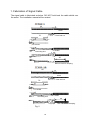
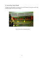
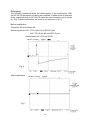
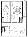
1
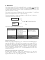
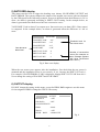
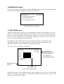
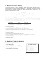
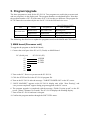
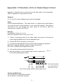
SATELLITE COMPASS
SC-50/110
The paper used in this manual
is elemental chlorine free.
FURUNO Authorized Distributor/Dealer
9-52 Ashihara-cho,
Nishinomiya 662-8580, JAPAN
Telephone :
0798-65-2111
Fax
0798-65-4200
:
All rights reserved.
Printed in Japan
Pub. No. SME-72510-A
( KAOK ) SC-50
FIRST EDITION : NOV. 2005
*00015891300*
*00015891300*
*00015891300*
*SME72510A00*
*SME72510A00*
*SME72510A00*
Contents
1. Overview ...................................................................................... 1
2. Maintenance Menu ....................................................................... 2
1) MONITOR display ..............................................................................2
2) COMPASS display .............................................................................3
3) R MONITOR display ..........................................................................3
4) R-CALIB display ................................................................................4
5) RATE ERR display ............................................................................5
6) OUTPUT display ................................................................................5
7) ALARM display ..................................................................................6
8) ANALOG display ................................................................................6
9) ANT MONI display .............................................................................6
10) MESSAGE display ...........................................................................8
11) REC MONI menu .............................................................................8
3. Replacement of Battery ................................................................ 9
4. Reading Program Number............................................................ 9
5. Program Upgrade ......................................................................... 10
1) MAIN board .......................................................................................10
2) CPU board .........................................................................................11
6. Maintenance ................................................................................. 12
6.1 Adjustment .......................................................................................12
6.2 Line voltage check ............................................................................12
6.3 Jumper setting....................................................................................12
6.4 LED ..................................................................................................12
7. Location of Parts........................................................................... 13
Appendix 1 Protection of ICs in Data Output Circuit ......................... 15
Appendix 2 Modification on Data Output Circuit ............................... 20
Exploded View (Parts List)
Radome Antanna, C7251-E01 .................................................................D-1
Processor Unit, C7251-E02 ....................................................................D-2
Schematic Diagrams
Interconnection Diagram, C7251-C01 ....................................................S-1
Processor Unit (SC-510), C7251-K01 ....................................................S-2
POWER Board (20P8181, 1/2), C7251-K02 ..........................................S-3
POWER Board (20P8181, 2/2), C7251-K03 ..........................................S-4
1. Overview
The satellite compass, SC-50/110 calculates the heading by using the carrier signal of the
GPS satellite signals. The system also calculates the heading with three rate sensors. When
the satellite signal is blocked, the system outputs the heading data based on the rate sensor
signal for a maximum of 5 minutes.
The system always compares GPS heading with rate sensor heading. If the difference
between two exceeds the preset value, an alarm is generated.
The system needs about 15 minutes for settling time at GPS cold start: 12 minutes for
cold start and 3 minutes for settling time.
GPS Heading
Calculated heading data
Rate sensor
Heading
Fig.1
Table below compares SC-50/110 to SC-60/120.
Number of output port
Output connector
Processor unit
Factory-default setting
SC-50/110
Heading and NAV
(IEC/AD-10): 5, Interval and
baud rate selectable
Heading (AD-10): 1
Pitch/Roll analog: 1
Terminal board
W: 300, B: 200, H: 60
Wall (Bulkhead) mount
SC-60/120
Heading (IEC/AD-10): 3
NAV: 1 (1 sec/4800 bps)
Waterproof connector
W: 335, B: 265, H: 103
Floor mount
Output of Heading Data
Heading data is output from HDG OUT ports. Either IEC or AD-10 heading data is
output from HDG OUT 1 to HDG OUT 5 ports according to menu setting. OUTPUT 6
port outputs only AD-10 format heading data. When the port is selected for IEC output,
two receivers are connected to the same port: #1(Data-H) and #2 (Data-C), and #3
(Data-H) and #4(Data-C). Thus, when HDG OUT ports 1 to 5 are used for IEC ports,
10 receivers can be connected to the system. Not only heading data but also NAV data
is output from IEC port.
Difference between 20P8178A and 20P8178B
The MAIN board, 20P8178A is for SC-50 and 20P8178B for SC-110. The board
carries a label “A” or “B.” The difference between A and B is software, but the
program number is the same on top of the program ROM.
1
2. Maintenance Menu
The system provides TEC menu or Maintenance menu for servicing. To show TEC menu,
press and hold down MENU and ENT keys simultaneously until the menu appears after
three beeps. It takes about 8 seconds to hear the third beep. Release the finger from MENU
key, and then ENT key. If you release the finger from ENT key first, Main menu appears.
This procedure is the same as SC-60/120.
TEC MENU
HDG SETUP
MONITOR
COMPASS
R MONITOR
R-CALIB
RATE ERR
OUTPUT
ALARMS
ANALOG
ANT MONI
MESSAGE
REC MONI
Fig. 2
TEC (Maintenance) menu
1) MONITOR display
Figure 2 shows MONITOR menu.
MONITOR
YAW
ROL
PIT
SC-OUT:
182.8
+0.1
+0.0
GPS:
182.8
+0.2
+0.1
ANG-V:
-1.8
+1.1
+1.7
R-OFF:
-204
0
CAL
0
0
CK-FLG
0
00
0
Fig.3 MONITOR menu
SC-OUT: Output of the satellite compass (degree)
GPS:
Values calculated by using GPS signal (degree)
ANG-V : Angular velocities of rate sensors (degree/sec)
R-OFF: Offset values of rate sensors.
CAL (Calculation): 0 when heading is calculated normally. (Base lines 1 and 2)
CK-FLG (Check Flag): Number of detected error flag (0 normally). The system
works normally even with a small number.
2
2) COMPASS display
MASK-EL is used to set a minimum elevation angle of the satellite. The satellite of which
elevation angle is lower than MASK-EL is not used for heading calculation.
Default: 5 degrees.
DO NOT change GPS DELAY, TIME CONST, SDEV-S, SDEV-C, and CHK NEW SV.
COMPASS
MASK-EL : 05°
GPS DELAY : 0.220 SEC
TIME CONST
: 01 SEC
SDEV-S
: 0.0016
SDEV-C
: 0.0069
CHK NEW SV
: 0.20
Fig.4 COMPASS display
3) R MONITOR display
“Rate sensor Monitor” display shows rate sensor errors as below.
WA SHIFT: Shows the difference between GPS and rate sensor.
DIFF RET: Shows an error if detected; 0: no error and 1: error.
WA SA: Compares succeeding two Heading (GPS + Rate sensor) outputs.
R MONITOR
18:52:49
1 normally
YAW
ROL
PIT
WA SHIFT
+0.0º
+0.0º
+0.0º
DIFF RET
0
0
B HEALTH
1
RATE SET
0000
WA SA
0
Shows difference between
GPS and rate sensor.
Shows an error.
1: error, 0: no error
Factory use
0.0
00
Fig.5 R MONITOR display
3
Factory use
4) R-CALIB display
R-CALIB (Rate sensor Calibration) is used to enter the calibration value of the rate sensor at
factory. It is not necessary to change this value when the rate sensor is replaced with new one.
However, the value on top of the original sensor is written on top of the replacement sensor
for future service.
R-CALIB
S1
: +0.0%
S2
: +0.0%
S3
: +0.0%
Fig.6
S2 (Roll*)
S3 (Yaw*)
S1 (Pitch*)
*: Default
Fig. 7 Rate sensors in Processor Unit
4
5) RATE ERR display
This menu sets the level to trigger the heading error alarms; NO HEADING OUTPUT and
RATE ERROR. The system compares the output of the angular rate sensor with one obtained
by the GPS signal. In the following example, an error is detected when the difference is 2.0º or
more. An alarm is generated according to SHIFT CONT setting. In the example below, an
alarm is generated when Roll sensor has four consecutive errors.
YAW LIMIT: Used to detect Yaw output error. Successive two yaw data (GPS + Rate sensor)
is compared. In the example below, an alarm is generated when the difference is 1.00º or
more.
RATE ERR
Yaw data error
alarm level
WA SHIFT YAW
: 2.0º
WA SHIFT ROL
: 2.0º
WA SHIFT PIT
: 2.0º
YAW LIMIT
: 1.00º
SHIFT CNT YAW
:0
SHIFT CNT ROL
:3
SHIFT CNT PIT
:3
Threshold level for
rate sensor error
Number of consecutive
errors (For example, an
error message appears
with three consecutive
ROL errors.)
Fig. 8 Rate error display
When the rate sensor error appears after the installation, first check that the rate sensor is
mounted and the installation menu is set correctly. If yes, increase the SHIFT CNT only 1.
For example, if RATE ERROR! (YAW) is displayed, change SHIFT CNT YAW from 0 to 1.
Never change the setting of WA SHIFT and YAW LIMIT.
6) OUTPUT display
DO NOT change the setting in this menu, except for HDM. R&D engineers use this menu
for investigation. HDM is changed to TRUE if necessary.
OUTPUT
M2 DATA
: OFF
GPS DATA
: OFF
LOG SENTENCE?
HDM
: MAG
WAAS
: OFF
PITCH
ROLL
: ABSOLUTE
Fig. 9
5
7) ALARM display
This menu sets the ALARM port signal. When ALARM MODE is set to “STOP,” the
alarm signal is not sent out after acknowledgement. When selected “Continue,” the system
continues to output the alarm signal.
ALARMS
ALARM MODE : STOP
BUZZER FREQ : 2.075 kHz
Fig. 10
8) ANALOG display
This menu is used to test and compensate the motion sensor output signal. Set the desired
angle on the ANGLE line and the set angle data is output from “ROLL” and “PITCH”
ports. If necessary, enter the Offset value (digital value).
ANALOG
ANGLE
: +00º
ROLL OFFSET
: +000D
PITCH OFFSET
: +000D
Fig. 11
9) ANT MONI display
Figure 12 shows an example of Antenna Monitor display.
Multipath Index for the baseline
between antenna 1 and antenna 3
1.01
BOW
Multipath Index for the baseline
between antenna 1 and antenna 2
0.91
01
02
12
03
1
04
2
11
05
07
Circular graph
9
4
8
08
09
10
5
7
Elapsed time
06
3
10
6
11
12
95:55
11
Fig.12 ANT MONI display
6
Bar graph showing
the tracking error
rate. The longer the
black bar, the higher
the error rate.
The display consists of four indications; a circular graph which shows direction where the
tracking error rate is the highest, a bar graph which shows tracking error rates in 12
directions, mutlipath indexes, and elapsed time.
Circular graph: Shows the relation of 12 directions to the bow. The direction of the highest
tracking error rate and its opposite direction are painted. Note that the sectors are painted even
when no heading loss problem occurs.
Bar graph: Shows tracking error rate in 12 directions. The bar number corresponds to the
sector number. The longer the bar, the more the error occurs. The blockage of the satellite
signal by surrounding may cause the tracking error. Note that the sector opposite to the
obstacle may have the longest bar.
Multipath indexes: Shows the effect of the multipath reflection. It is around 1.0 normally. If it
is 1.5 or above, the antenna must be relocated, because the system is affected by the multipath
reflection. The left figure is the index for the baseline 2 (antennas 1 and 3) and the right one
for the baseline 1 (antennas 1 and 2).
Elapsed time: Shows how long the data is collected. The timer starts at first power up after
installation and counts up to 99 hours and 59 minutes (99:59). No measurements are made
after 99 hours 59 minutes. Allow the system 12 hours or more to collect the data in various
satellite configurations because the satellite configuration has little change within 12 hours.
In the example of Figure 13, the tracking error occurs at the highest rate in 10 o’clock
direction. The satellite signal is blocked by an obstacle located at 10 o’clock on board a ship.
Center of
circular graph
Obstacle blocking
satellite signal
SC-50/110
antennas
Fig.13
7
Sector opposite to the
obstacle
(Reflected signal from
the obstacle may cause
the tracking error.)
10) MESSAGE display
Error messages appear in the display. If RATE ERROR! appears, first check Installation Setup
menu for correct setting: “Mounting” method and “Direction.”
MESSAGES
• NO HEADING OUTPUT !
• HEADING ERROR !
• RATE ERROR ! (YAW)
Fig.14 Error Message display
11) REC MONI menu
The REC MONI display, Figure 15 shows whether the system works normally or not. The
GPS receiver having the least tracking error rate reads 1.0. The error rate of other receivers is
between 0.7 and 0.9 normally. In the example of Figure 16, the receivers GPS2 and GPS3
have 20 % and 10% higher error rate than GPS1 respectively. If the error rate is 0.5 or less,
the receiver and/or the antenna may be defective.
The number of the satellite being used for heading calculation is displayed at the
right-hand side below CAL, and the number of the satellite being tracked below ALL.
The system requires 4 or more satellites for heading calculation.
The timer is reset by selecting “CNT Reset?”.
REC MONITOR
CAL ALL
GPS1
1.0
GPS2
0.8
9/10
GPS3
0.9
9/9
9/10
CAL: Number of
satellite being used for
heading calculation
ALL: Number of
satellite being tracked
CNT RESET ?
V_MASK : 05º
Elapsed time from
power-on
99:59
Tracking error rate
Fig.15 REC MONI display
V-MASK is used to set the angle where the satellite signal is not received for ANT MONI
display. For example, if 15 degrees is entered, the satellite signal between 0º and 15º is not
used to create ANT MONI display.
8
3. Replacement of Battery
The processor unit has a battery which backs up the RAM contents when the power is
removed. When the voltage of the battery drops to 2.5 V, the message “BATTERY!” appears
on the screen. To check the message, press [MENU] key and choose “MESSAGE.” The
lifetime of the batteries is 3 to 5 years.
CAUTION!
Take care to avoid short-circuit of the battery. This could create a
burn or fire hazard. Do not dispose of the battery in a fire or an
incinerator; this may cause an explosion.
When the message BATTERY! appears, save the contents of the RAM onto the flash memory
temporarily as soon as possible (within about 24 hours). If the data is transferred to the flash
memory, they are not erased during the replacement.
Parts Name
Lithium Battery
Type
Code No.
CR2450-F2ST2L
000-144-941
To transfer the memory;
1. Choose EXCHANGE BATTERY? in the SYS SETUP menu.
2. Follow the instructions on the menu. Use [ENT] key to proceed the step.
To replace the battery;
3. Loosen four screws and remove the front cover.
4. Remove the MAIN board by loosening screws fixing the board to the chassis.
5. Unsolder the battery.
6. Solder new battery.
4. Reading Program Number
To display the program number list;
1. Press [MENU] key.
SOFTWARE VERSION
2. Choose SOFT VER. and press [ENT] key.
The following list appears.
DISPLAY 205-1342-01.01
PROCESS 205-1341-01.02
GPS1 4850263003
GPS2 4850263003
GPS3 4850263003
3. Press [DISP] to close the menu.
Fig.16 SOFTWARE VERSION menu
9
5. Program Upgrade
The three programs are used for the SC-50/110. Two programs are used in the processor unit
and one program is in the display unit. The program numbers are tabulated below. Note that
the program number of SC-50 is the same as SC-110, but they are different. The program for
SC-50 cannot be overwritten by the one for SC-110 in the field and vise versa.
(As of February 2005)
Unit
Board
Processor unit
Display unit
Program No.
How to update
MAIN board
205-1341-01.02
By using a PC
GPS receiver
4850263003
By replacing GPS core
CPU board
205-1342-01.01
By using a PC
The following describes how to update the programs stored on the MAIN and CPU boards.
1) MAIN board (Processor unit)
To upgrade the program on the MAIN board;
1. Connect the serial port of the PC to J15 (D-sub) on MAIN board
PC (Serial port)
#3
#2
#6
#4
#6
#7
#8
SC-50/110 (J15)
#2 RXD
#3 TXD
#5 GND
2. Turn on the PC. Do not as yet turn on the SC-50/110.
3. Click the SCUP.bat file in the SC-50/110 program file.
4. Turn on the SC-50/110 after the message “TARGET POWER ON” on the PC screen.
5. “NOW LOADING” appears on the SC-50/110 display unit, while “Now Erasing”, and
“xxx percent completed” appear during program upgrade on the PC screen.
6. The program upgrade is completed with the message “Finish Version up.ted” on the PC
screen. (About 3 minutes 30 seconds) The SC-50/110 displays the Heading display.
7. Turn off the SC-50/110 and turn it on again.
8. Confirm the program number through the SOFT VER. menu.
10
2) CPU board (Display unit)
To upgrade the program on the CPU board;
1. Connect the serial port of the PC to J15 on MAIN board in the processor unit.
2. Turn on the PC. Do not as yet turn on the SC-50/110.
3. Click the SCUP.bat file in the SC-50/110 program file.
4. Turn on the SC-50/110 after the message “TARGET POWER ON” on the PC screen.
5. “NOW LOADING” appears on the SC-50/110 display unit, while “Now Erasing,” and
“xxx percent completed” appear during program upgrade on the PC screen,.
6. The program upgrade is completed with the message “Finish Version up.ted” on the PC
screen. (About 3 minutes 30 seconds) The SC-50/110 displays the Heading display.
7. Turn off the SC-50/110 and turn it on again.
8. Confirm the program number through the SOFT VER. menu.
11
6. Maintenance
6.1 Adjustment
1) PWR board
Switching regulator frequency is adjusted on PWR board, 20P8181 as below.
Test Point
GND
Rating
Adjuster
TP2
TP1
120.0 kHz ± 10 kHz
VR79
TP5
TP3
120.0 kHz ± 10 kHz
VR80
2) MAIN board
Vcc-c supply voltage to Rate sensor is adjusted by VR96 on MAIN board, 20P8178.
Test Point
GND
Rating
Adjuster
#1 of J20
#2 of J20
5.0 V (Vcc-c)
VR96
6.2 Line voltage check
Line voltages are checked at J3 on the MAIN board.
Line voltage
Test Points on MAIN board
Rating
3.3 V
#4 (+) and #5(-) of J3
3.15 to 3.45 V
5.1 V (5 V)
#1 (+) and #5(-) of J3
4.94 to 5.46 V
6.5 V
#8 (+) and #5(-) of J3
6.2 to 6.8 V
13.5 V (15 V)
#7 (+) and #5(-) of J3
12.5 to 14.4 V
6.3 Jumper setting
Jumper JP1 on the MAIN board is used at factory to set the MAIN board to A or B version.
6.4 LED
CR3 on the MAIN board blinks when the CPU is running.
12
7. Location of Parts
Rate Sensor
(Default: Roll)
Rate Sensor
(Default: Yaw)
Rate Sensor
(Default: Pitch)
PWR Board
(20P8181)
GPS Receivers
(1, 2, 3 from Top)
Main Board
(20P8178)
Fig. 17 Processor Unit with cover removed
F1, 3A
TP2
TP1
TP4
Fig.18 PWR Board, 20P8181
TP3
TP4 VR80
VR79 (not shown)
13
Log/Alarm
Roll (above)
Pitch
Beacon Ext
Data out 6
Data In
(AD-10)
Data out 1 to 5
(from right, IEC or AD-10 Heading data)
J3
J15 for system
update
R96
CR3 (CPU),
Blinking
No short bar
(for R&D)
TP1
JP1
BT1
(CR2450-F2ST2L)
Fig.19 MAIN Board, 20P8178
14
J 20 J19 J18
Appendix 1 Protection of ICs in Data Output Circuit
Appendix 1 describes how to prevent ICs in the data output circuit temporarily.
Refer to Appendix 2 for permanent remedy.
Symptom
U1, U2, and U3 in the heading output circuit are damaged.
Cause
Ground potential difference - The cable shield, or a signal return path between
the circuit grounds of the equipment is not connected securely. The shield is
connected to the unit through the cable clamp on SC-50/110, while the
connector pin is used on SC-60/120.
Remedy
At installation: Carry out 1) to 4).
When the symptom occurs: Carry out 1) to 5).
1)
Solder a grounding cable to the cable shield and ground it through the
screw fixing the MAIN board. See the attached sheet.
2) Ground SC-50/110 processor unit securely.
3) Connect the cable shield at the end of the interconnected unit as below.
IEC61162-1 and AD-10 (photo coupler): Frame Ground (FG)
IEC61162-2 (RS422/485): Signal Ground (SG)
4) Connect the interconnected unit securely
5) Add zener diodes in the heading output circuit to protect the
IC from being damaged by surge.
J2 to J7
Zener diodes added
Type: RD9.1EB3-T4
C/N: 000-138-700
Fig.1 Zener diodes added in data output circuit
Factory-modified sets
SC-110 (SC1101): 4404-0329 and after
SC-50 (SC501): 4403-2224 and after
15
1. Fabrication of Signal Cable
The signal cable is fabricated as below. DO NOT hold back the cable shield over
the armor. The installation manual will be revised.
80
Armor
70
Twist and cut.
FV1.25-M3
Grounding wire
Solder
40
Remove coat for clamping.
80
Armor
Twist and cut.
70
FV1.25-M3
Grounding wire
Solder
40
Vinyl tape
Fig. 2
16
Remove coat for clamping.
2. Grounding Cable Shield
Ground the cable shield or grounding wire to the chassis by using the screw fixing
the MAIN board, 20P8178 to the chassis.
Fig. 3 Connection of grounding wire
17
3. Adding Zener Diodes
Zener diodes are added to the data output circuit as below.
1. Fabricate the diode as shown in the figure below.
Type: RD9.1EB3-T4
4 mm
C/N: 000-138-700
4 mm
2 mm
4 mm
4 mm
Fig. 4 Fabrication of zener diode
2. Remove the coat and solder the diode. See Fig. 5.
3. Do the same for other pins and other ports.
J2
J3
J4
Remove the coat and then solder the anode.
Do the same for other diodes.
Fig. 5 Zener diodes on MAIN board, soldering side
18
Reference)
The following waveforms show the effectiveness of the modification. With
the SC-50/110 processor unit being not modified, a spike noise is observed
at the output terminal on SC-50/110 when the interconnected unit is turned
on. (Fig. 6) After modification, the noise is not observed. (Fig. 7)
Before modification
Condition: SC-50 switched off
Measuring points: CH1: TD1-A (pin #1) on DATA 5 port
CH2: TD1-B (pin #2) on DATA 5 port
Ground lead: SG (=FG) on SC-50
Fig. 6
After modification
Fig. 7
19
Appendix 2 Modification on Data Output Circuit
Appendix 1 describes the tentative remedy to prevent U1, U2, and U3 in the heading
output circuit from being damaged.
Following modification (Table below) is the permanent remedy. The connector is
changed from 4 pins to 5 pins for the connection of cable shield.
When installing the unit having the current MAIN board (-55);
1) Connect the cable shield to pin #5 of DATA OUT port.
2) Ground the frame of SC-50/110 securely.
3) Connect the other end of the cable shield to FG when data is IEC61162-1/AD-10
(photo coupler), or SG when data is IEC61162-2 (RS422/485).
4) Ground the frame of the unit connected to SC-50/110 securely.
Before modification
U1, U2, and U3
MAX3043EUE-T
CR7 to CR30
RD9.1EB3-T4
Connectors (J2 to J7), 231-334/001-000,
DATA1 to DATA 6
connector
Plugs (P2 to P7),
231-304/026-FUR,
DATA1 to DATA 6
4-pin plug
MAIN board
20P8178-33
After modification
SN75ALS172DE
4-pin
1SS226-TE85LF
231-335/001-000,
5-pin connector
231-305/026-FUR,
5-pin plug
20P8178-55
J2 to J7 (DATA OUT port)
DATA-H/TD-A
DATA-C/TD-B
SHIFT-H/TD’-A
SHIFT-C/TD’-B
FG
Fig.1 Connection on DATA OUT port
Factory-modified sets
SC-50 (SC501): 4403-2637 and after
SC-110 (SC1101): 4404-0360 and after
20