1
FUJITSU SEMICONDUCTOR
CM71-10106-1E
CONTROLLER MANUAL
FR30
32-Bit Microcontroller
MB91F109
Hardware Manual
FR30
32-Bit Microcontroller
MB91F109
Hardware Manual
FUJITSU LIMITED
PREFACE
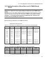
■ Objectives and Intended Reader
The MB91F109 has been developed as one of the "32-bit single-chip microcontroller FR30
series" products that use new RISC architecture CPUs as their cores. It has optimal
specifications for embedding applications that require high CPU processing power.
This manual explains the functions and operations of the MB91F109 for the engineers who
actually develop products using the MB91F109. Read this manual thoroughly. Refer to the
instruction manual for details on individual instructions.
■ Trademarks
FR stands for FUJITSU RISC controller, a product of Fujitsu Limited.
Embedded AlgorithmTM is a trademark of Advanced Micro Devices, Inc.
i
■ Organization of This Manual
This manual consists of 16 chapters and an appendix.
Chapter 1 Overview
Chapter 1 provides basic general information on the MB91F109, including its characteristics,
a block diagram, and function overview.
Chapter 2 CPU
Chapter 2 provides basic information on the FR series CPU core functions including the
architecture, specifications, and instructions.
Chapter 3 Clock Generator and Controller
Chapter 3 provides detailed information on the generation and control of the clock that
controls the MB91F109.
Chapter 4 Bus Interface
Chapter 4 explains the basic items of the external bus interface, register configuration and
functions, bus operations, bus timing, and provides bus operation program samples.
Chapter 5 I/O Ports
Chapter 5 provides an overview of I/O ports, explains the I/O port register configuration and
the conditions for using external terminals as I/O ports.
Chapter 6 External Interrupt/NMI Controller
Chapter 6 provides an overview of the external interrupt/NMI controller, explains the register
configuration and functions, and operations of the external interrupt/NMI controller.
Chapter 7 Delayed Interrupt Module
Chapter 7 provides an overview of the delayed interrupt module, explains the register
configuration and functions, and operations of the delayed interrupt module.
Chapter 8 Interrupt Controller
Chapter 8 provides an overview of the interrupt controller, explains the register configuration
and functions, and operations of the interrupt controller. The chapter also explains the hold
request cancel request function using examples.
Chapter 9 U-TIMER
Chapter 9 provides an overview of the U-TIMER, explains the register configuration and
functions, and operations of the U-TIMER.
Chapter 10 UART
Chapter 10 provides an overview of the UART, explains the register configuration and
functions, and operations of the UART.
Chapter 11 A/D Converter (Successive Approximation Type)
Chapter 11 provides an overview of the A/D converter, explains the register configuration
and functions, and operations of the A/D converter.
Chapter 12 16-bit Reload Timer
Chapter 12 provides an overview of the 16-bit reload timer, explains the register
configuration and functions, and operations of the 16-bit reload timer.
Chapter 13 Bit Search Module
Chapter 13 provides an overview of the bit search module, explains the register configuration
and functions, and operations and save/restore processing of the bit search module.
ii
Chapter 14 PWM Timer
Chapter 14 provides an overview of the PWM timer, explains the register configuration and
functions, and operations of the PWM timer.
Chapter 15 DMAC
Chapter 15 provides an overview of the DMAC, explains the register configuration and
functions, and operations of the DMAC.
Chapter 16 Flash Memory
Chapter 16 explains the flash memory functions and operations.
The chapter provides information on using the flash memory from the FR CPU.
For information on using the flash memory from the ROM writer, refer to the user’s guide for
the ROM writer.
Appendix
The appendix provides information on I/O maps, interrupt vectors, terminal states in each
CPU status, notes on using the little endian area, and a listing of instructions. It includes
details of these types of information that are not covered by the text that can be referenced
for programming.
iii
1. The contents of this document are subject to change without notice. Customers are advised to consult
with FUJITSU sales representatives before ordering.
2. The information and circuit diagrams in this document are presented as examples of semiconductor
device applications, and are not intended to be incorporated in devices for actual use. Also, FUJITSU is
unable to assume responsibility for infringement of any patent rights or other rights of third parties
arising from the use of this information or circuit diagrams.
3. The contents of this document may not be reproduced or copied without the permission of FUJITSU
LIMITED.
4. FUJITSU semiconductor devices are intended for use in standard applications (computers, office
automation and other office equipments, industrial, communications, and measurement equipments,
personal or household devices, etc.).
CAUTION:
Customers considering the use of our products in special applications where failure or abnormal
operation may directly affect human lives or cause physical injury or property damage, or where
extremely high levels of reliability are demanded (such as aerospace systems, atomic energy controls,
sea floor repeaters, vehicle operating controls, medical devices for life support, etc.) are requested to
consult with FUJITSU sales representatives before such use. The company will not be responsible for
damages arising from such use without prior approval.
5. Any semiconductor devices have inherently a certain rate of failure. You must protect against injury,
damage or loss from such failures by incorporating safety design measures into your facility and
equipment such as redundancy, fire protection, and prevention of over-current levels and other
abnormal operating conditions.
6. If any products described in this document represent goods or technologies subject to certain
restrictions on export under the Foreign Exchange and Foreign Trade Control Law of Japan, the prior
authorization by Japanese government should be required for export of those products from Japan.
©1999 FUJITSU LIMITED Printed in Japan
iv
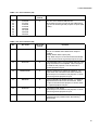
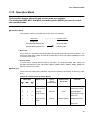
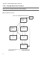
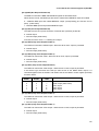
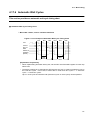
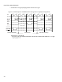
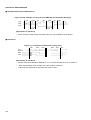
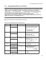
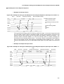
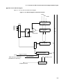
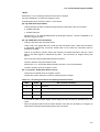
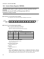
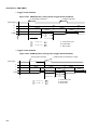
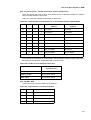
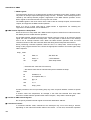
How to Read This Manual
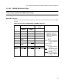
■ Description Format of this Manual
Major terms used in this manual are explained below:
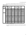
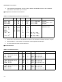
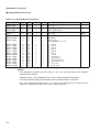
Term
Meaning
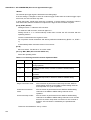
I-BUS
16-bit wide bus used for internal instructions. Since the FR series uses
an internal Harvard architecture, independent buses are used for
instructions and data. A bus converter is connected to the I-BUS.
D-BUS
Internal 32-bit wide data bus. Internal resources are connected to the
D-BUS.
C-BUS
Internal multiplex bus. The C-BUS is connected to the I-BUS and DBUS via a switch. An external interface module is connected to the CBUS. Data and instructions are multiplexed in the external data bus.
R-BUS
Internal 16-bit wide data bus. The R-BUS is connected to the D-BUS
via an adapter. Various I/O ports, the clock generator, and interrupt
controller are connected to the R-BUS. Since the R-BUS is 16 bits
wide in which addresses and data are multiplexed, it takes twice as
much or more cycle time than usual for the CPU to access these
resources.
E-unit
Operation executing unit
φ
System clock output from the clock generator to each internal resource
connected to the R-BUS. The system clock at the highest speed
shows the same cycle as source oscillation but is divided into 1, 1/2, 1/
4, and 1/8 (or 1/2, 1/4, 1/8, and 1/16) by PCK1 and PCK0 of the clock
generator GCR register.
θ
System clock or operation clock for the CPU and resources connected
to a bus other than the R-BUS. The system clock at the highest speed
shows the same cycle as source oscillation but is divided into 1, 1/2, 1/
4, and 1/8 (or 1/2, 1/4, 1/8, and 1/16) by CCK1 and CCK0 of the clock
generator GCR register.
v
vi
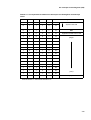
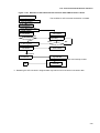
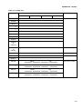
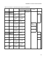
CONTENTS
CHAPTER 1
1.1
1.2
1.3
1.4
1.5
1.6
1.7
1.8
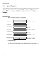
OVERVIEW ................................................................................................... 1
MB91F109 Characteristics .................................................................................................................... 2
General Block Diagram of MB91F109 ................................................................................................... 6
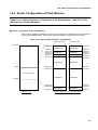
Outside Dimensions ............................................................................................................................... 7
Pin Arrangement Diagrams ................................................................................................................. 10
Pin Functions ....................................................................................................................................... 14
I/O Circuit Format ................................................................................................................................ 22
Memory Address Space ...................................................................................................................... 24
Handling of Devices ............................................................................................................................. 26
CHAPTER 2
CPU ............................................................................................................. 29
2.1 CPU Architecture ................................................................................................................................. 30
2.2 Internal Architecture ............................................................................................................................. 31
2.3 Programming Model ............................................................................................................................ 33
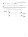
2.3.1 General-Purpose Registers ............................................................................................................ 35
2.3.2 Special Registers ............................................................................................................................ 36
2.3.3 Program Status Register (PS) ........................................................................................................ 39
2.4 Data Structure ...................................................................................................................................... 42
2.5 Word Alignment ................................................................................................................................... 43
2.6 Memory Map ........................................................................................................................................ 44
2.7 Instruction Overview ............................................................................................................................ 46
2.7.1 Branch Instructions with Delay Slots .............................................................................................. 48
2.7.2 Branch Instructions without Delay Slots ......................................................................................... 51
2.8 EIT (Exception, Interrupt, and Trap) .................................................................................................... 52
2.8.1 EIT Interrupt Levels ........................................................................................................................ 54
2.8.2 Interrupt Control Register (ICR) ...................................................................................................... 56
2.8.3 System Stack Pointer (SSP) ........................................................................................................... 57
2.8.4 Interrupt Stack ................................................................................................................................ 58
2.8.5 Table Base Register (TBR) ............................................................................................................ 59
2.8.6 EIT Vector Table ............................................................................................................................. 60
2.8.7 Multiple EIT Processing .................................................................................................................. 62
2.8.8 EIT Operation ................................................................................................................................. 64
2.9 Reset Sequence .................................................................................................................................. 68
2.10 Operation Mode ................................................................................................................................... 69
CHAPTER 3
3.1
3.2
3.3
3.4
3.5
3.6
3.7
3.8
CLOCK GENERATOR AND CONTROLLER ............................................. 73
Outline of Clock Generator and Controller ........................................................................................... 74
Reset Reason Resister (RSRR) and Watchdog Cycle Control Register (WTCR) ............................... 76
Standby Control Register (STCR) ....................................................................................................... 78
DMA Request Suppression Register (PDRR) ..................................................................................... 80
Timebase Timer Clear Register (CTBR) .............................................................................................. 81
Gear Control Register (GCR) .............................................................................................................. 82
Watchdog Timer Reset Delay Register (WPR) .................................................................................... 85
PLL Control Register (PCTR) .............................................................................................................. 86
vii
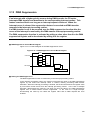
3.9 Gear Function ..................................................................................................................................... 87
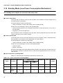
3.10 Standby Mode (Low Power Consumption Mechanism) ...................................................................... 90
3.10.1 Stop State ...................................................................................................................................... 92
3.10.2 Sleep State .................................................................................................................................... 95
3.10.3 Standby Mode State Transition ..................................................................................................... 98
3.11 Watchdog Function ............................................................................................................................. 99
3.12 Reset Source Hold Circuit ................................................................................................................. 101
3.13 DMA Suppression ............................................................................................................................. 103
3.14 Clock Doubler Function ..................................................................................................................... 105
3.15 Example of PLL Clock Setting .......................................................................................................... 108
CHAPTER 4
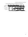
BUS INTERFACE ..................................................................................... 111
4.1 Outline of Bus Interface ....................................................................................................................
4.2 Chip Select Area ...............................................................................................................................
4.3 Bus Interface .....................................................................................................................................
4.4 Area Select Register (ASR) and Area Mask Register (AMR) ...........................................................
4.5 Area Mode Register 0 (AMD0) ..........................................................................................................
4.6 Area Mode Register 1 (AMD1) ..........................................................................................................
4.7 Area Mode Register 32 (AMD32) ......................................................................................................
4.8 Area Mode Register 4 (AMD4) ..........................................................................................................
4.9 Area Mode Register 5 (AMD5) ..........................................................................................................
4.10 DRAM Control Register 4/5 (DMCR4/5) ...........................................................................................
4.11 Refresh Control Register (RFCR) .....................................................................................................
4.12 External Pin Control Register 0 (EPCR0) .........................................................................................
4.13 External Pin Control Register 1 (EPCR1) .........................................................................................
4.14 DRAM Signal Control Register (DSCR) ............................................................................................
4.15 Little Endian Register (LER) .............................................................................................................
4.16 Relationship between Data Bus Widths and Control Signals ...........................................................
4.16.1 Bus Access with Big Endians ......................................................................................................
4.16.2 Bus Access with Little Endians ....................................................................................................
4.16.3 External Access ...........................................................................................................................
4.16.4 DRAM Relationships ....................................................................................................................
4.17 Bus Timing ........................................................................................................................................
4.17.1 Basic Read Cycle ........................................................................................................................
4.17.2 Basic Write Cycles .......................................................................................................................
4.17.3 Read Cycles in Each Mode .........................................................................................................
4.17.4 Write Cycles in Each Mode ..........................................................................................................
4.17.5 Read and Write Combination Cycles ...........................................................................................
4.17.6 Automatic Wait Cycles .................................................................................................................
4.17.7 External Wait Cycles ....................................................................................................................
4.17.8 Usual DRAM Interface: Read ......................................................................................................
4.17.9 Usual DRAM Interface: Write .......................................................................................................
4.17.10 Usual DRAM Read Cycles ...........................................................................................................
4.17.11 Usual DRAM Write Cycles ...........................................................................................................
4.17.12 Automatic Wait Cycles in Usual DRAM Interface ........................................................................
4.17.13 DRAM Interface in High-Speed Page Mode ................................................................................
4.17.14 Single DRAM Interface: Read ......................................................................................................
4.17.15 Single DRAM Interface: Write ......................................................................................................
4.17.16 Single DRAM Interface ................................................................................................................
viii
112
115
116
118
121
123
124
125
126
127
130
132
135
136
138
139
141
147
151
155
159
162
164
166
168
170
171
172
173
175
177
179
181
182
185
186
187
4.17.17 Hyper DRAM Interface: Read ....................................................................................................... 188
4.17.18 Hyper DRAM Interface: Write ....................................................................................................... 189
4.17.19 Hyper DRAM Interface ................................................................................................................. 190
4.17.20 DRAM Refresh ............................................................................................................................. 191
4.17.21 External Bus Request ................................................................................................................... 193
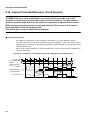
4.18 Internal Clock Multiplication (Clock Doubler) ..................................................................................... 194
4.19 Program Example for External Bus Operation ................................................................................... 196
CHAPTER 5
5.1
5.2
5.3
5.4
Outline of I/O Ports ............................................................................................................................ 202
Port Data Register (PDR) .................................................................................................................. 203
Data Direction Register (DDR) .......................................................................................................... 204
Using External Pins as I/O Ports ....................................................................................................... 205
CHAPTER 6
6.1
6.2
6.3
6.4
6.5
6.6
6.7
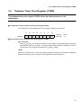
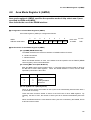
INTERRUPT CONTROLLER .................................................................... 223
Overview of Interrupt Controller ........................................................................................................ 224
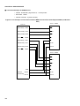
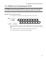
Interrupt Controller Block Diagram .................................................................................................... 227
Interrupt Control Register (ICR) ......................................................................................................... 228
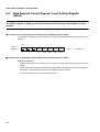
Hold Request Cancel Request Level Setting Register (HRCL) ......................................................... 230
Priority Check .................................................................................................................................... 231
Returning from the Standby Mode (Stop/Sleep) ................................................................................ 234
Hold Request Cancel Request .......................................................................................................... 235
Example of Using the Hold Request Cancel Request Function (HRCR) ........................................... 236
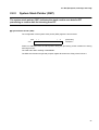
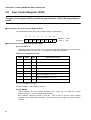
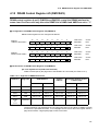
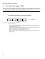
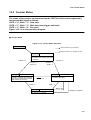
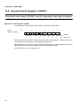
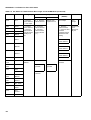
CHAPTER 9
9.1
9.2
9.3
DELAYED INTERRUPT MODULE ........................................................... 219
Overview of Delayed Interrupt Module ............................................................................................. 220
Delayed Interrupt Control Register (DICR) ........................................................................................ 221
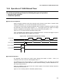
Operation of Delayed Interrupt Module .............................................................................................. 222
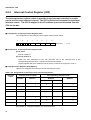
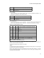
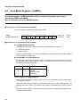
CHAPTER 8
8.1
8.2
8.3
8.4
8.5
8.6
8.7
8.8
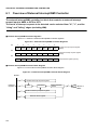
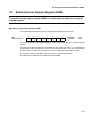
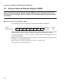
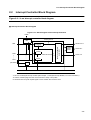
EXTERNAL INTERRUPT/NMI CONTROLLER ........................................ 211
Overview of External Interrupt/NMI Controller ................................................................................... 212
Enable Interrupt Request Register (ENIR) ........................................................................................ 213
External Interrupt Request Register (EIRR) ...................................................................................... 214
External Level Register (ELVR) ......................................................................................................... 215
External Interrupt Operation .............................................................................................................. 216
External Interrupt Request Levels ..................................................................................................... 217
Nonmaskable Interrupt (NMI) Operation ............................................................................................ 218
CHAPTER 7
7.1
7.2
7.3
I/O PORTS ................................................................................................. 201
U-TIMER .................................................................................................... 239
Overview of U-TIMER ........................................................................................................................ 240
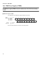
U-TIMER Registers ............................................................................................................................ 241
U-TIMER Operation ........................................................................................................................... 243
CHAPTER 10 UART ......................................................................................................... 245
10.1
10.2
10.3
10.4
Overview of UART ............................................................................................................................. 246
Serial Mode Register (SMR) .............................................................................................................. 248
Serial Control Register (SCR) ............................................................................................................ 250
Serial Input Data Register (SIDR) and Serial Output Data Register (SODR) .................................... 252
ix
10.5
10.6
10.7
10.8
10.9
10.10
10.11
Serial Status Register (SSR) ............................................................................................................
UART Operation ...............................................................................................................................
Asynchronous (Start-Stop) Mode ......................................................................................................
CLK Synchronous Mode ...................................................................................................................
UART Interrupt Occurrence and Flag Setting Timing .......................................................................
Notes on Using the UART and Example for Using the UART ..........................................................
Setting Examples of Baud Rates and U-TIMER Reload Values .......................................................
253
255
257
258
260
263
265
CHAPTER 11 A/D CONVERTER (Successive approximation type) ............................ 267
11.1
11.2
11.3
11.4
11.5
11.6
Overview of A/D Converter (Successive Approximation Type) .........................................................
Control Status Register (ADCS) .......................................................................................................
Data Register (ADCR) ......................................................................................................................
A/D Converter Operation ..................................................................................................................
Conversion Data Protection Function ...............................................................................................
Notes on Using the A/D Converter ....................................................................................................
268
270
275
276
278
280
CHAPTER 12 16-BIT RELOAD TIMER ........................................................................... 281
12.1
12.2
12.3
12.4
12.5
Overview of 16-bit Reload Timer ......................................................................................................
Control Status Register (TMCSR) .....................................................................................................
16-Bit Timer Register (TMR) and 16-Bit Reload Register (TMRLR) .................................................
Operation of 16-Bit Reload Timer ....................................................................................................
Counter States ..................................................................................................................................
282
284
286
287
289
CHAPTER 13 BIT SEARCH MODULE ............................................................................ 291
13.1 Overview of the Bit Search Module ................................................................................................... 292
13.2 Bit Search Module Registers ............................................................................................................ 293
13.3 Bit Search Module Operation and Save/Restore Processing ........................................................... 295
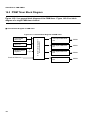
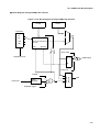
CHAPTER 14 PWM TIMER ............................................................................................. 299
14.1
14.2
14.3
14.4
14.5
14.6
14.7
14.8
14.9
14.10
14.11
14.12
14.13
Overview of PWM Timer ...................................................................................................................
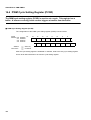
PWM Timer Block Diagram ...............................................................................................................
Control Status Register (PCNH, PCNL) ............................................................................................
PWM Cycle Setting Register (PCSR) ...............................................................................................
PWM Duty Cycle Setting Register (PDUT) .......................................................................................
PWM Timer Register (PTMR) ...........................................................................................................
General Control Register 1 (GCN1) ..................................................................................................
General Control Register 2 (GCN2) ..................................................................................................
PWM Operation ................................................................................................................................
One-Shot Operation ..........................................................................................................................
Interrupt ............................................................................................................................................
Constant "L" or Constant "H" Output from PWM Timer ....................................................................
Starting Multiple PWM Timer Channels ............................................................................................
300
302
304
308
309
310
311
314
315
317
319
320
321
CHAPTER 15 DMAC ........................................................................................................ 323
15.1
15.2
15.3
15.4
x
Overview of DMAC ...........................................................................................................................
DMAC Parameter Descriptor Pointer (DPDP) ..................................................................................
DMAC Control Status Register (DACSR) .........................................................................................
DMAC Pin Control Register (DATCR) ..............................................................................................
324
326
327
329
15.5 Descriptor Register in RAM ............................................................................................................... 332
15.6 DMAC Transfer Modes ...................................................................................................................... 335
15.7 Output of Transfer Request Acknowledgment and Transfer End signals .......................................... 338
15.8 Notes on DMAC ................................................................................................................................ 339
15.9 DMAC Timing Charts ......................................................................................................................... 342
15.9.1 Timing Charts of the Descriptor Access Block ............................................................................. 343
15.9.2 Timing Charts of Data Transfer Block .......................................................................................... 345
15.9.3 Transfer Stop Timing Charts in Continuous Transfer Mode ......................................................... 347
15.9.4 Transfer Termination Timing Charts ............................................................................................. 349
CHAPTER 16 FLASH MEMORY ...................................................................................... 351
16.1
16.2
16.3
16.4
16.5
16.6
16.7
Outline of Flash Memory .................................................................................................................... 352
Block Diagram of Flash Memory ........................................................................................................ 354
Flash Memory Status Register (FSTR) .............................................................................................. 355
Sector Configuration of Flash Memory .............................................................................................. 357
Flash Memory Access Modes ............................................................................................................ 359
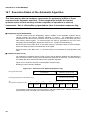
Starting the Automatic Algorithm ....................................................................................................... 361
Execution Status of the Automatic Algorithm ..................................................................................... 364
APPENDIX .......................................................................................................................... 369
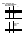
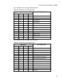
APPENDIX A I/O Maps ............................................................................................................................. 370
APPENDIX B Interrupt Vectors ................................................................................................................ 379
APPENDIX C Pin Status for Each CPU Status ......................................................................................... 383
APPENDIX D Notes on Using Little Endian Areas ................................................................................... 395
D.1 C Compiler (fcc911) ........................................................................................................................ 396
D.2 Assembler (fsm911) ........................................................................................................................ 399
D.3 Linker (flnk911) ............................................................................................................................... 401
D.4 Debuggers (sim911, eml911, and mon911) .................................................................................... 402
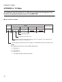
APPENDIX E Instructions ......................................................................................................................... 403
E.1 FR-Series Instructions ..................................................................................................................... 409
INDEX ................................................................................................................................. 425
xi
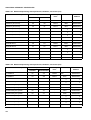
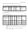
FIGURES
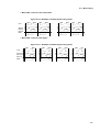
Figure 1.2-1
General Block Diagram of MB91F109 ........................................................................................ 6
Figure 1.3-1
Outside Dimensions of FPT-100P-M06 ...................................................................................... 7
Figure 1.3-2
Outside Dimensions of FPT-100P-M05 ...................................................................................... 8
Figure 1.3-3
Outside Dimensions of BGA-112P-M01 ..................................................................................... 9
Figure 1.4-1
QFP-100 Pin Arrangements ..................................................................................................... 10
Figure 1.4-2
LQFP-100 Pin Arrangements ................................................................................................... 11
Figure 1.4-3
FBGA-112 Pin Arrangements ................................................................................................... 12
Figure 1.7-1
MB91F109 Memory Map ......................................................................................................... 24
Figure 1.8-1
Example of Using an External Clock (Normal Method) ............................................................ 26
Figure 1.8-2
Example of Using an External Clock (Possible at 12.5 MHz or Lower) .................................... 27
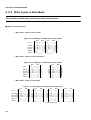
Figure 2.2-1
Internal Architecture .................................................................................................................. 31
Figure 2.2-2
Instruction Pipeline ................................................................................................................... 32
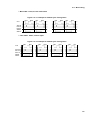
Figure 2.3-1
Configuration of general-purpose registers .............................................................................. 33
Figure 2.3-2
Configuration of special registers ............................................................................................. 34
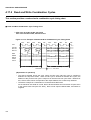
Figure 2.3-3
Configuration of General-Purpose Registers ............................................................................ 35
Figure 2.3-4
Configuration of Special Registers ........................................................................................... 36
Figure 2.4-1
Data Mapping in Bit Ordering Mode ......................................................................................... 42
Figure 2.4-2
Data Mapping in Byte Ordering Mode ...................................................................................... 42
Figure 2.6-1
MB91F109 Memory Map .......................................................................................................... 44
Figure 2.6-2
Memory Map Common to the FR Series. ................................................................................. 45
Figure 2.8-1
Example of Interrupt Stack ....................................................................................................... 58
Figure 2.8-2
Example of Multiple EIT Processing ......................................................................................... 63
Figure 2.10-1
Mode Register Configuration .................................................................................................... 70
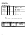
Figure 3.1-1
Clock Generator and Controller Registers ................................................................................ 74
Figure 3.1-2
Block Diagram of the Clock Generator and Controller .............................................................. 75
Figure 3.9-1
Gear Controller Block Diagram ................................................................................................. 87
Figure 3.9-2
Clock Selection Timing Chart ................................................................................................... 89
Figure 3.10-1
Stop Controller Block Diagram ................................................................................................. 92
Figure 3.10-2
Sleep Controller Block Diagram ................................................................................................ 95
Figure 3.10-3
Standby Mode State Transition ................................................................................................ 98
Figure 3.11-1
Watchdog Timer Block Diagram ............................................................................................... 99
Figure 3.11-2
Watchdog Timer Operating Timing ......................................................................................... 100
Figure 3.11-3
Timebase Timer Counter ........................................................................................................ 100
Figure 3.12-1
Block Diagram of Reset Source Hold Circuit .......................................................................... 101
Figure 3.13-1
DMA Suppression Circuit Block Diagram ............................................................................... 103
xii
Figure 3.15-1
Example of PLL Clock Setting ................................................................................................. 108
Figure 3.15-2
Clock System Reference Diagram .......................................................................................... 109
Figure 4.1-1
Bus Interface Registers ........................................................................................................... 113
Figure 4.1-2
Bus Interface Block Diagram ................................................................................................... 114
Figure 4.2-1
Example of Setting Chip Select Areas ..................................................................................... 115
Figure 4.4-1
Sample Maps of the Chip Select Areas ................................................................................... 120
Figure 4.16-1
Data bus Widths and Control Signals in Usual Bus Interface .................................................. 139
Figure 4.16-2
Data Bus Widths and Control Signals in DRAM Interface ....................................................... 139
Figure 4.16-3
Relationship between Internal Register and External Data Bus for Word Access .................. 141
Figure 4.16-4
Relationship between Internal Register and External Data Bus for Half-Word Access ........... 141
Figure 4.16-5
Relationship between Internal Register and External Data Bus for Byte Access .................... 142
Figure 4.16-6
Relationship between Internal Register and External Data Bus for 16-bit Bus Width ............. 142
Figure 4.16-7
Relationship between Internal Register and External Data Bus for 8-bit Bus Width ............... 143
Figure 4.16-8
External Bus Access for 16-bit Bus Width ............................................................................... 144
Figure 4.16-9
External Bus Access for 8-bit Bus Width ................................................................................. 145
Figure 4.16-10 Example of Connection between MB91F109 and External Devices ....................................... 146
Figure 4.16-11 Relationship between Internal Register and External Data Bus for Word Access .................. 147
Figure 4.16-12 Relationship between Internal Register and External Data Bus for Half-word Access ............ 148
Figure 4.16-13 Relationship between Internal Register and External Data Bus for Byte Access .................... 148
Figure 4.16-14 Relationship between Internal Register and External Data Bus for 16-bit Bus Width ............. 149
Figure 4.16-15 Relationship between Internal Register and External Data Bus for 8-bit Bus Width ............... 149
Figure 4.16-16 Example of Connection between MB91F109 and External Devices (16-Bit Bus Width) ......... 150
Figure 4.16-17 Example of Connection between MB91F109 and External Devices (8-Bit Bus Width) ........... 150
Figure 4.16-18 Example of Connection between MB91F109 and One 8-bit Output DRAM (8-Bit Data Bus) . 156
Figure 4.16-19 Example of Connection between MB91F109 and Two 8-Bit Output DRAMs
(16-Bit Data Bus) ..................................................................................................................... 157
Figure 4.16-20 Example of Connection between MB91F109 and Two 16-Bit Output DRAMs
(16-Bit Data Bus) ..................................................................................................................... 158
Figure 4.17-1
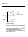
Example of Basic Read Cycle Timing Chart ............................................................................ 162
Figure 4.17-2
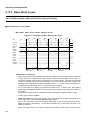
Example for Basic Write Cycle Timing .................................................................................... 164
Figure 4.17-3
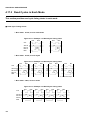
Example 1 of Read Cycle Timing Chart .................................................................................. 166
Figure 4.17-4
Example 2 of Read Cycle Timing Chart .................................................................................. 166
Figure 4.17-5
Example 3 of Read Cycle Timing Chart .................................................................................. 166
Figure 4.17-6
Example 4 of Read Cycle Timing Chart .................................................................................. 167
Figure 4.17-7
Example 5 of Read Cycle Timing Chart .................................................................................. 167
Figure 4.17-8
Example 1 of Write Cycle Timing Chart ................................................................................... 168
Figure 4.17-9
Example 2 of Write Cycle Timing Chart ................................................................................... 168
Figure 4.17-10 Example 3 of Write Cycle Timing Chart ................................................................................... 168
Figure 4.17-11 Example 4 of Write Cycle Timing Chart ................................................................................... 169
xiii
Figure 4.17-12 Example 5 of Write Cycle Timing Chart .................................................................................. 169
Figure 4.17-13 Example of Read and Write Combination Cycle Timing Chart ............................................... 170
Figure 4.17-14 Example of Automatic Wait Cycle Timing Chart ..................................................................... 171
Figure 4.17-15 Example of External Wait Cycle Timing Chart ........................................................................ 172
Figure 4.17-16 Example of Usual DRAM Interface Read Timing Chart .......................................................... 173
Figure 4.17-17 Example of Usual DRAM Interface Write Timing Chart .......................................................... 175
Figure 4.17-18 Example 1 of Usual DRAM Read Cycle Timing Chart ............................................................ 177
Figure 4.17-19 Example 2 of Usual DRAM Read Cycle Timing Chart ............................................................ 178
Figure 4.17-20 Example 3 of Usual DRAM Read Cycle Timing Chart ............................................................ 178
Figure 4.17-21 Example 1 of Usual DRAM Write Cycle Timing Chart ............................................................ 179
Figure 4.17-22 Example 2 of Usual DRAM Write Cycle Timing Chart ............................................................ 180
Figure 4.17-23 Example 3 of Usual DRAM Write Cycle Timing Chart ............................................................ 180
Figure 4.17-24 Example of Automatic Wait Cycle Timing Chart in Usual DRAM Interface ............................ 181
Figure 4.17-25 Example 1 of DRAM Interface Timing Chart in High-Speed Page Mode ............................... 182
Figure 4.17-26 Example 2 of DRAM Interface Timing Chart in High-Speed Page Mode ............................... 182
Figure 4.17-27 Example 3 of DRAM Interface Timing Chart in High-Speed Page Mode ............................... 183
Figure 4.17-28 Example 4 of DRAM Interface Timing Chart in High-Speed Page Mode ............................... 184
Figure 4.17-29 Example of Single DRAM Interface Read Timing Chart ......................................................... 185
Figure 4.17-30 Example of Single DRAM Interface Write Timing Chart ......................................................... 186
Figure 4.17-31 Example of Single DRAM Interface Timing Chart ................................................................... 187
Figure 4.17-32 Example of Hyper DRAM Interface Read Timing Chart ......................................................... 188
Figure 4.17-33 Example of Hyper DRAM Interface Write Timing Chart .......................................................... 189
Figure 4.17-34 Example of Hyper DRAM Interface Timing Chart ................................................................... 190
Figure 4.17-35 Example of CAS before RAS (CBR) Refresh Timing Chart .................................................... 191
Figure 4.17-36 Example of Timing Chart of CBR Refresh Automatic Wait Cycle ........................................... 192
Figure 4.17-37 Example of Selfrefresh Timing Chart ...................................................................................... 192
Figure 4.17-38 Example of Bus Control Release Timing Chart ...................................................................... 193
Figure 4.17-39 Example of Bus Control Acquisition Timing ............................................................................ 193
Figure 4.18-1
Example of Timing Chart for 2X Clock (BW-16bit, Access-Word Read) ................................ 194
Figure 4.18-2
Example of Timing for 1X Clock (BW-16bit, Access-Word Read) .......................................... 195
Figure 5.1-1
Basic I/O Port Block Diagram ................................................................................................. 202
Figure 6.1-1
External Interrupt/NMI Controller Registers ............................................................................ 212
Figure 6.1-2
External Interrupt/NMI Controller Block Diagram .................................................................... 212
Figure 6.5-1
External Interrupt Operation ................................................................................................... 216
Figure 6.6-1
Clearing the Interrupt Cause Hold Circuit at Level Setting for the Interrupt Request Mode ... 217
Figure 6.6-2
Input of an Interrupt Cause in Interrupt Enable Mode and a Request Issued to the Interrupt
Controller ................................................................................................................................ 217
Figure 6.7-1
NMI Request Detection Block ................................................................................................. 218
xiv
Figure 7.1-1
Delayed Interrupt Module Register .......................................................................................... 220
Figure 7.1-2
Delayed Interrupt Module Block Diagram ................................................................................ 220
Figure 8.1-1
Interrupt Controller Registers (1/2) .......................................................................................... 225
Figure 8.1-2
Interrupt Controller Registers (2/2) .......................................................................................... 226
Figure 8.2-1
Block Diagram of the Interrupt Controller ................................................................................ 227
Figure 8.8-1
Example of Hardware Configuration for Using the Hold Request Cancel Request Function .. 236
Figure 8.8-2
Example of Timing for Hold Request Cancel Request Sequence (Interrupt Level: HRCL > a) 237
Figure 8.8-3
Example of Timing for Hold Request Cancel Request Sequence
(Interrupt Level: HRCL > a > b) ............................................................................................... 237
Figure 9.1-1
U-TIMER Registers ................................................................................................................. 240
Figure 9.1-2
U-TIMER Block Diagram ......................................................................................................... 240
Figure 9.3-1
Example of Using U-TIMER Channels 0 and 1 in Cascade Mode .......................................... 243
Figure 10.1-1
UART Registers ....................................................................................................................... 246
Figure 10.1-2
UART Block Diagram .............................................................................................................. 247
Figure 10.7-1
Format of Data Transferred in Asynchronous (Start-Stop) Mode (Mode 0 or 1) ..................... 257
Figure 10.8-1
Format of Data Transferred in CLK Synchronous Mode (Mode 2) .......................................... 258
Figure 10.9-1
ORE, FRE, and RDRF Set Timing (Mode 0) ........................................................................... 260
Figure 10.9-2
ORE, FRE, and RDRF Set Timing (Mode 1) ........................................................................... 261
Figure 10.9-3
ORE and RDRF Set Timing (Mode 2) ..................................................................................... 261
Figure 10.9-4
TDRE Set Timing (Mode 0 or 1) .............................................................................................. 262
Figure 10.9-5
TDRE Set Timing (Mode 2) ..................................................................................................... 262
Figure 10.10-1 Sample System Structure for Mode 1 ...................................................................................... 263
Figure 10.10-2 Communication Flowchart for Mode 1 ..................................................................................... 264
Figure 11.1-1
A/D Converter Registers ......................................................................................................... 268
Figure 11.1-2
Block Diagram of the A/D Converter. ...................................................................................... 269
Figure 11.5-1
Workflow of the Data Protection Function when DMA Transfer is Used ................................. 279
Figure 12.1-1
16-Bit Reload Timer Registers ................................................................................................ 282
Figure 12.1-2
16-Bit Reload Timer Block Diagram ........................................................................................ 283
Figure 12.4-1
Counter Start and Operation Timing ........................................................................................ 287
Figure 12.4-2
Underflow Operation Timing .................................................................................................... 288
Figure 12.5-1
Counter States Transition ........................................................................................................ 289
Figure 13.1-1
Bit Search Module Registers ................................................................................................... 292
Figure 13.1-2
Block Diagram of the Bit Search Module ................................................................................. 292
Figure 14.1-1
PWM Timer Registers ............................................................................................................. 301
Figure 14.2-1
General Block Diagram of PWM Timer ................................................................................... 302
Figure 14.2-2
Block Diagram of Single PWM Timer Channel ........................................................................ 303
Figure 14.9-1
PWM Operation Timing Chart (Trigger Restart Disabled) ....................................................... 316
Figure 14.9-2
PWM Operation Timing Chart (Trigger Restart Enabled) ........................................................ 316
xv
Figure 14.10-1 One-Shot Operation Timing Chart (Trigger Restart Disabled) ................................................ 318
Figure 14.10-2 One-Shot Operation Timing Chart (Trigger Restart Enabled) ................................................ 318
Figure 14.11-1 Causes of Interrupts and Their Timing (PWM Output: Normal Polarity) ................................ 319
Figure 14.12-1 Example of Keeping PWM Output at a Lower Level ............................................................... 320
Figure 14.12-2 Example of Keeping PWM Output at a High Level ................................................................. 320
Figure 15.1-1
DMAC Registers ..................................................................................................................... 324
Figure 15.1-2
DMAC Block Diagram ............................................................................................................. 325
Figure 16.1-1
Flash Memory Registers ......................................................................................................... 352
Figure 16.2-1
Block diagram of the Flash Memory ....................................................................................... 354
Figure 16.4-1
Memory Map and Sector Configuration .................................................................................. 357
Figure 16.7-1
Structure of the Hardware Sequence Flag ............................................................................. 364
xvi
TABLES
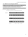
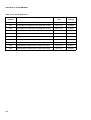
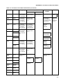
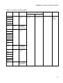
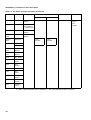
Table 1.4-1
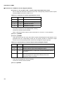
FBGA Package Pin Names ....................................................................................................... 13
Table 1.5-1
Pin Functions (1/5) .................................................................................................................... 14
Table 1.5-2
Pin Functions (2/5) .................................................................................................................... 15
Table 1.5-3
Pin Functions (3/5) .................................................................................................................... 17
Table 1.5-4
Pin Functions (4/5) .................................................................................................................... 18
Table 1.5-5
Pin Functions (5/5) .................................................................................................................... 20
Table 1.6-1
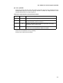
I/O circuit format (1/2) ................................................................................................................ 22
Table 1.6-2
I/O circuit format (1/2) ................................................................................................................ 23
Table 2.8-1
Interrupt Level .......................................................................................................................... 54
Table 2.8-2
Assignments of Interrupt Causes and Interrupt Vectors ............................................................ 56
Table 2.8-3
Vector Table ............................................................................................................................. 61
Table 2.8-4
Priority for EIT Event Acceptance and Masking Other Events .................................................. 62
Table 2.8-5
EIT Handler Execution Order .................................................................................................... 63
Table 2.10-1
Mode Pins and Setting Modes ................................................................................................... 69
Table 2.10-2
Bus Mode Setting Bit and the Function .................................................................................... 70
Table 3.2-1
Watchdog Timer Cycles Specified by WT1 and WT0 ................................................................ 77
Table 3.3-1
Oscillation Stabilization Wait Time Specified by OSC1 and OSC0 ........................................... 79
Table 3.6-1
CPU Machine Clock .................................................................................................................. 82
Table 3.6-2
Peripheral Machine Clock .......................................................................................................... 83
Table 3.7-1
Watchdog Timer Cycles Specified by WT1 and WT0 ................................................................ 85
Table 3.10-1
Types of Operation in Standby Mode ........................................................................................ 90
Table 3.14-1
Operating Frequency Combinations Depending on whether the Clock Doubler
Function is Enabled or Disabled .............................................................................................. 107
Table 4.3-1
Correspondence between Chip Select Areas and Selectable Bus Interfaces ......................... 116
Table 4.10-1
Page Size of DRAM Connected .............................................................................................. 127
Table 4.10-2
Combinations of Bus Widths Available in Areas 4 and 5 ......................................................... 129
Table 4.15-1
Mode Setting Using the Combination of Bits (LE2, LE1, and LE0) ........................................ 138
Table 4.16-1
Relationship between Data Bus Widths and Control Signals .................................................. 140
Table 4.16-2
Functions and Bus Widths of DRAM Control Pins ................................................................... 155
Table 4.16-3
Page Size Select Bits .............................................................................................................. 156
Table 5.4-1
External Bus Functions to be Selected (1/4) ........................................................................... 205
Table 5.4-2
External Bus Functions to be Selected (2/4) ........................................................................... 206
Table 5.4-3
External Bus Functions to be Selected (3/4) ........................................................................... 207
Table 5.4-4
External Bus Functions to be Selected (4/4) ........................................................................... 209
Table 6.4-1
External Interrupt Request Mode ............................................................................................. 215
xvii
Table 8.3-1
Correspondences between the Interrupt Level Setting Bits and Interrupt Levels ................... 229
Table 8.5-1
Relationships among Interrupt Causes, Numbers, and Levels (1/2) ...................................... 231
Table 8.5-2
Relationships among Interrupt Causes, Numbers, and Levels (2/2) ...................................... 232
Table 8.7-1
Settings for the Interrupt Levels for which a Hold Request Cancel Request is Issued ........... 235
Table 10.2-1
Selection of UART Operation Modes ...................................................................................... 248
Table 10.6-1
UART Operation Modes ......................................................................................................... 255
Table 10.11-1 Baud Rates and U-TIMER Reload Values in Asynchronous (Start-Stop) Mode .................... 265
Table 10.11-2 Baud Rates and U-TIMER Reload Values in CLK Synchronous Mode .................................. 265
Table 11.2-1
Selecting the Causes for Starting the A/D Converter ............................................................. 271
Table 11.2-2
Selecting the A/D Converter Operation Mode ........................................................................ 272
Table 11.2-3
Setting the A/D Conversion Start Channel ............................................................................. 273
Table 11.2-4
Setting the A/D Conversion End Channel ............................................................................... 273
Table 12.2-1
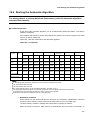
CSL Bit Setting Clock Source ................................................................................................. 284
Table 13.3-1
Bit Positions and Returned Values (Decimal) ......................................................................... 296
Table 14.3-1
Selection of the Count Clock .................................................................................................. 305
Table 14.3-2
PWM Output When "1" is Written to PGMS ............................................................................ 305
Table 14.3-3
Selection of Trigger Input Edge .............................................................................................. 305
Table 14.3-4
Selection of Interrupt Causes ................................................................................................. 306
Table 14.3-5
Specification of the Polarity of the PWM Output and the Edge .............................................. 306
Table 14.7-1
Selection of Ch3 Trigger Input ................................................................................................ 312
Table 14.7-2
Selection of Ch2 Trigger Input ................................................................................................ 312
Table 14.7-3
Selection of Ch1 Trigger Input ................................................................................................ 313
Table 14.7-4
Selection of Ch0 Trigger Input ................................................................................................ 313
Table 15.2-1
Channel Descriptor Addresses ............................................................................................... 326
Table 15.4-1
Selection of Transfer Input Detection Levels .......................................................................... 330
Table 15.4-2
Specification of Transfer Request Acknowledgment Output .................................................. 330
Table 15.4-3
Specification of Transfer End Output ...................................................................................... 331
Table 15.5-1
Specification of Transfer Source or Destination Address Update Modes ............................... 333
Table 15.5-2
Address Increment/Decrement Unit ........................................................................................ 333
Table 15.5-3
Specification of Transfer Data Size ........................................................................................ 333
Table 15.5-4
Transfer Mode Specification ................................................................................................... 334
Table 15.9-1
Codes Used in the Timing Charts ........................................................................................... 342
Table 16.4-1
Sector Addresses ................................................................................................................... 358
Table 16.6-1
Commands ............................................................................................................................. 361
Table 16.7-1
Statuses of the Hardware Sequence Flag .............................................................................. 365
Table A-1
I/O Map (1/6) ........................................................................................................................... 371
Table A-2
I/O Map (2/6) ........................................................................................................................... 372
Table A-3
I/O Map (3/6) ........................................................................................................................... 373
xviii
Table A-4
I/O Map (4/6) ........................................................................................................................... 375
Table A-5
I/O Map (5/6) ........................................................................................................................... 376
Table A-6
I/O Map .................................................................................................................................... 377
Table B-1
Interrupt Vectors (1/2) .............................................................................................................. 379
Table B-2
Interrupt Vectors (2/2) .............................................................................................................. 380
Table C-1
Explanation of Terms Used in the Pin Status List ................................................................... 383
Table C-2
Pin Status for 16-bit External Bus Length and 2CA1WR Mode .............................................. 384
Table C-3
Pin Status for 16-bit External Bus Length and 2CA1WR Mode .............................................. 387
Table C-4
Pin Status in 8-bit External Bus Mode .................................................................................... 390
Table C-5
Pin Status in Single Chip Mode .............................................................................................. 393
Table E-1
Explanation of Addressing Mode Codes ................................................................................. 405
Table E-2
Instruction Formats .................................................................................................................. 407
Table E.1-1
Addition and Subtraction Instructions ...................................................................................... 410
Table E.1-2
Compare Operation Instructions .............................................................................................. 410
Table E.1-3
Logical Operation Instructions ................................................................................................. 411
Table E.1-4
Bit Operation Instructions ........................................................................................................ 411
Table E.1-5
Multiplication and Division Instructions .................................................................................... 412
Table E.1-6
Shift Instructions ...................................................................................................................... 412
Table E.1-7
Immediate Value Setting or 16/32-Bit Immediate Value Transfer Instruction .......................... 413
Table E.1-8
Memory Load Instructions ....................................................................................................... 413
Table E.1-9
Memory Store Instructions ....................................................................................................... 414
Table E.1-10
Interregister Transfer Instructions ............................................................................................ 414
Table E.1-11
Standard Branch (Without Delay) Instructions ........................................................................ 415
Table E.1-12
Delayed Branch Instructions ................................................................................................... 416
Table E.1-13
Other Instructions ................................................................................................................... 417
Table E.1-14
20-Bit Standard Branch Macro Instructions ............................................................................. 418
Table E.1-15
20-Bit Delayed-Branch Macro Instructions .............................................................................. 419
Table E.1-16
32-Bit Standard Branch Macro Instructions ............................................................................. 420
Table E.1-17
32-Bit Delayed-Branch Macro Instructions .............................................................................. 421
Table E.1-18
Direct Addressing Instructions ................................................................................................ 422
Table E.1-19
Resource Instructions ............................................................................................................. 422
Table E.1-20
Coprocessor Control Instructions ........................................................................................... 423
xix
xx
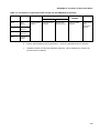
CHAPTER 1
OVERVIEW
This chapter provides basic general information on the MB91F109, including its
characteristics, block diagram, and function overview.
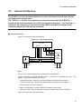
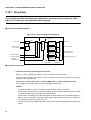
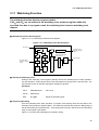
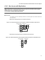
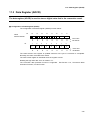
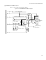
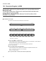
1.1 MB91F109 Characteristics
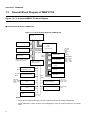
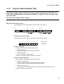
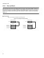
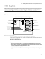
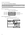
1.2 General Block Diagram of MB91F109
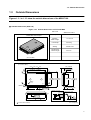
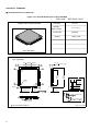
1.3 Outside Dimensions
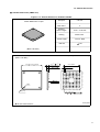
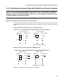
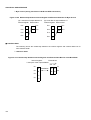
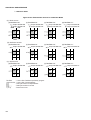
1.4 Pin Arrangement Diagrams
1.5 Pin Functions
1.6 I/O Circuit Format
1.7 Memory Address Space
1.8 Handling of Devices
1
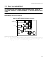
CHAPTER 1 OVERVIEW
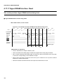
1.1
MB91F109 Characteristics
The MB91F109 is a standard single-chip microcontroller using a 32-bit RISC CPU
(FR30 series) as its core. It contains various I/O resources and bus control
mechanisms for embedded control applications that require high-speed CPU
processing.
This microcontroller contains 254-kilobyte flash ROM and 4-kilobyte RAM.
It has optimal specifications for embedding applications such as navigation systems,
high-performance facsimiles, and printer controls, which require high CPU processing
power.
■ Characteristics
❍ FR-CPU
•
32-bit RISC (FR30), load/store architecture, 5-stage pipeline
•
Operating frequency: Internal 25 MHz [external 25 MHz] (source oscillation 12.5 MHz with
PLL used)
•
General-purpose registers: 32 bits x 16
•
16-bit fixed-length instructions (basic instructions), one instruction per cycle
•
Inter-memory transfer, bit processing, and barrel shift instructions, which are suitable for
embedding applications
•
Function entry/exit instructions and register data multiload/store instructions, which are
compliant with high-level language instructions
•
Register interlock function, which eases assembler coding
•
Branch instruction with delay slot, which reduces overheads in branch processing
•
Built-in adder, supported in the instruction level
•
•
Signed 32-bit addition: 5 cycles
•
Signed 16-bit addition: 3 cycles
Interrupt (PC, PS saving): 6 cycles, 16 priority levels
❍ Bus interface
•
Operating frequency: Up to 25 MHz (internal), 25 MHz (external bus)
•
25-bit address bus (32-megabyte address space)
•
16-bit address output, 8-bit or 16-bit data input and output
•
Basic bus cycle: 2 clock cycles
•
Chip Select output that can be set in 64 kilobytes minimum: 6 lines
•
Interface support for each type of memory
•
2
DRAM interface (areas 4 and 5)
1.1 MB91F109 Characteristics
•
Automatic wait cycle: Any number of cycles (0 to 7) can be set for each area.
•
Unused data and address terminals can be used as I/O ports.
•
Support for little endian mode (selecting one of areas 1 to 5)
❍ DRAM interface
•
2-bank independent control (areas 4 and 5)
•
Double CAS DRAM (normal DRAM interface), single CAS DRAM, and hyper DRAM
•
Basic bus cycle: Five cycles in normal mode. Two-cycle access is enabled in high-speed
page mode.
•
Programmable waveform: Automatic 1-cycle wait can be inserted into RAS or CAS.
•
DRAM refresh
•
CBR refresh (The interval can be set as desired using the 6-bit timer.)
•
Self-refresh mode
•
Support for 8-, 9-, 10-, or 12-line column address
•
Choice between 2CAS/1WE and 2WE/1CAS
❍ DMAC (DMA controller)
•
Eight channels
•
Transfer cause: External terminal or internal resource interrupt request
•
Transfer sequence
•
Step transfer or block transfer
•
Burst transfer or continuous transfer
•
Transfer data length: Selectable from 8, 16, and 32 bits
•
A temporary stop is enabled by an NMI/interrupt request.
❍ UART
•
Independent three channels
•
Full duplex double buffer
•
Data length: 7 to 9 bits (no parity) or 6 to 8 bits (with parity)
•
Choice between asynchronous (start-stop synchronization) communication and clock
asynchronous communication
•
Multiprocessor mode
•
Built-in 16-bit timer (U-Timer) as a baud rate generator, which can generate a desired baud
rates
•
An external clock can be used as a transfer clock.
•
Error detection: Parity error, frame error, and overrun
❍ A/D converter (successive approximation conversion type)
•
10-bit resolution, 4 channels
•
Successive approximation conversion type: 5.6 µs at 25 MHz
•
Built-in sample and hold circuit
•
Conversion mode:
Selectable from single conversion, scan conversion, and repeat
3
CHAPTER 1 OVERVIEW
conversion
•
Starting: Selectable from software, external trigger, and internal timer
❍ Reload timer
•
16-bit timer: Three channels
•
Internal clock: 2-clock cycle resolution. Selectable from 2-, 8-, and 32-frequency division
mode
❍ Other interval timers
•
16-bit timer: Three channels (U-Timer)
•
PWM timer: Four channels
•
Watchdog timer: One channel
❍ Bit search module
•
Searches for the bit position that first changes between 1 and 0 beginning from MSB of a
word in one cycle.
❍ Interrupt controller
•
External interrupt input: Nonmaskable interrupt, normal interrupt × 4 (INT0 to INT3)
•
Internal interrupt causes: UART, DMAC, A/D, reload timer, PWM, UTIMER, and delayed
interrupt
•
Up to 16 priority levels are programmable for interrupts other than nonmaskable interrupts.
❍ Reset types
•
Power-on reset, watchdog timer reset, software reset, and external reset
❍ Power save mode
•
Sleep/stop mode
❍ Clock control
•
Gear function: Desired operating clock frequencies can be set for the CPU and peripherals
independently.
A gear clock can be selected from 1/1, 1/2, 1/4, and 1/8 (or 1/2, 1/4, 1/8, and 1/16).
However, the operating clock frequency for peripherals cannot exceed 25 MHz.
❍ Others
4
•
Packages: QFP-100, LQFP-100, FBGA-112
•
CMOS technology: 0.5 µm
•
Power supply: 3.3 V plus or minus 0.3 V
•
254-kilobyte flash ROM: Can be read, written, and erased by a single power supply.
1.1 MB91F109 Characteristics
■ Available Types
MB91V106
MB91106
MB91F109
IROM
-
63 Kbyte
-
IRAM
64 Kbyte
-
-
CROM
-
64 Kbyte
254 Kbyte
CRAM
64 Kbyte
-
2 Kbyte
RAM
2 Kbyte
2 Kbyte
2 Kbyte
I$
-
-
-
Others
-
-
-
5
CHAPTER 1 OVERVIEW
1.2
General Block Diagram of MB91F109
Figure 1.2.1 is a general MB91F109 block diagram.
■ General Block Diagram of MB91F109
Figure 1.2-1 General Block Diagram of MB91F109
FR CPU
I-bus(16bit)
RAM 2KB
Harvard
Princeton
Bit Search Module
Bus Converter
D-bus(32bit)
Bus Controller
DMAC (8ch)
C-bus
(32bit)
DREQ0 DREQ1 DREQ2
DACK0 DACK1 DACK2
EOP0 EOP1 EOP2
DRAM Controller
32bit
16bit
Bus Converter
X0 X1
RSTX
INT0-INT3
NMIX
AN0-AN3
AVCC AVRH
AVSS AVRL
ATGX
D31-D16
A24-A00
RDX
WR0X-1X
RDY
CLK
CS0X-5X
BRQ BGRNTX
RAS0 RAS1
CS0L CS1L
CS0H CS1H
DW0X DW1X
FLASH ROM
254KB
Clock Control Unit
(Watch Dog Timer)
Port 0-B
RAM 2KB
Interrupt Control Unit
R-bus
(16bit)
10bit A/D Converter
(4ch)
Reload Timer
(3 ch)
UART (3ch)
with Baud Rate Timer
SI0 SI1 SI2
SO0 SO1 SO2
SC0 SC1 SC2
PWM Timer (4ch)
OCPA0-OCPA3
TRG0-3
Port
Notes:
6
•
Terminals are represented by the function (some terminals are actually multiplexed).
•
When REALOS is used, perform time management using an external interrupt or internal
timer.
1.3 Outside Dimensions
1.3
Outside Dimensions
Figures 1.3.1 to 1.3.3 show the outside dimensions of the MB91F109.
■ Outside Dimensions (QFP-100)
Figure 1.3-1 Outside Dimensions of FPT-100P-M06
EIAJ code
:*
Lead pitch
Plastic QFP with 100 pins
Package
width x length
Lead shape
Sealing
Flat terminal
section length
QFP100-P-1420-4
0.65 mm
14 x 20 mm
Gull wing
Plastic mold
0.80 mm
(FPT-100P-M06)
Plastic QFP with 100 pins
(F PT -100P -M06 )
3.35(.132)MAX
(Mounting height)
0.05(.002)MIN
(STAND OFF)
23.90 0.40 (.941 .016)
20.00 0.20 (.787 .008)
80
51
81
50
14.00 0.20 17.90 0.40
(.551 .008) (.705 .016)
12.35(.486) 16.30 0.40
REF
(.642 .016)
INDEX
100
31
"A"
LEAD No. 1
30
0.65(.0256)TYP
0.30 0.10
(.012 .004)
0.13(.005)
0.15 0.05(.006 .002)
M
Details of "A" part
0.25(.010)
Details of "B" part
"B"
0.10(.004)
18.85(.742)REF
22.30 0.40(.878 .016)
c 1994 FUJITSU LIMITED F100008-3C-2
0.0(.012)
0.18(.007)MAX
0.53(.021)MAX
0 10
0.80 0.20
(.031 .008)
Unit: mm (inches)
7
CHAPTER 1 OVERVIEW
■ Outside Dimensions (LQFP-100)
Figure 1.3-2 Outside Dimensions of FPT-100P-M05
EIAJ code: * QFP100-P-1414-1
0.50 mm
Lead pitch
Plastic LQFP with 100 pins
Package
width x length
14 x 14 mm
Lead shape
Gull wing
Plastic mold
Sealing
(FPT-100P-M05)
Plastic LQFP with 100 pins
(FPT-100P-M05)
16.00 0.20(.630 .008)SQ
75
1.50
.059
51
14.00 0.10(.551 .004)SQ
76
+0.20
-0.10
+.008
-.004
(Mouting height)
50
12.00
(.472)
REF
15.00
(.591)
NOM
Details of "A" part
0.15(.006)
INDEX
100
0.15(.006)
26
0.15(.006)MAX
LEAD No.
1
"B"
25
0.40(.016)MAX
"A"
0.50(.0197)TYP
0.18
.007
+0.08
-0.03
+.003
-.001
0.08(.003)
M
0.127
.005
+0.05
-0.02
+.002
-.001
Details of "B" part
0.10 0.10
(STAND OFF)
(.004 .004)
0.10(.004)
C
8
1995 FUJITSU LIMITED F100007S-2C-3
0.50 0.20(.020 .008)
010
Unit: mm (inches)
1.3 Outside Dimensions
■ Outside Dimensions (FBGA-112)
Figure 1.3-3 Outside Dimensions of BGA-112P-M01
Ball pitch
0.80 mm
Ball matrix
11
Package
width x length
10.00 × 10.00 mm
Plastic FBGA with 112 pins
Sealing
Plastic mold
Mount height
1.45 mm MAX
Ball size
0.45
(BGA-112P-M01)
Plastic FBGA with 112 pins
(BGA-112P-M01)
10.00 0.10(.394 .004)SQ
Note: The actual corner shape may differ from the drawing.
+0.20
+.008
8.00(.314)REF
1.25 -0.10 .049 -.004
(Mounting height)
0.38 0.10(.015 .004)
(Stand off)
0.80(.031)TYP
11
10
9
8
7
6
5
0.10(.004)
4
3
INDEX
2
1
L
C0.80(.031)
C
1998 FUJITSU LIMITED B112001S-2C-2
K J H G F E D C B A
112- 0.45 0.10
(112- .018 .004)
0.08(.003)
M
Unit: mm (inches)
9
CHAPTER 1 OVERVIEW
1.4
Pin Arrangement Diagrams
Figures 1.4.1 to 1.4.3 show the pin arrangements of the MB91F109.
■ Pin Arrangements (QFP-100)
100
99
98
97
96
95
94
93
92
91
90
89
88
87
86
85
84
83
82
81
CS0L/PB1
RAS0/PB0
INT0/PE0
INT1/PE1
VCC
X0
X1
VSS
INT2/PE2/SC1
INT3/PE3/SC2
DREQ0/PE4
DREQ1/PE5
DACK0/PE6
DACK1/PE7
PF7/OCPA0/ATGX
SO2/PF6/OCPA2
SI2/PF5/OCPA1
SO1/PF4/TRG3
SI1/PF3/TRG2
SC0/PF2/OCPA3
Figure 1.4-1 QFP-100 Pin Arrangements
1
2
3
4
5
6
7
8
9
10
11
12
13
14
15
16
17
18
19
20
21
22
23
24
25
26
27
28
29
30
MB91F109
(TOP
VIEW)
FPT-100P-M06
P23/D19
P24/D20
P25/D21
P26/D22
P27/D23
P30/D24
P31/D25
P32/D26
P33/D27
P34/D28
P35/D29
P36/D30
VSS
P37/D31
P40/A00
VCC
P41/A01
P42/A02
P43/A03
P44/A04
31
32
33
34
35
36
37
38
39
40
41
42
43
44
45
46
47
48
49
50
PB2/CS0H
PB3/DW0X
EOP2/PB4/RAS1
DREQ2/PB5/CS1L
DACK2/PB6/CS1H
PB7/DW1X
VCC
PA6/CLK
PA5/CS5X
PA4/CS4X
EOP1/PA3/CS3X
PA2/CS2X
PA1/CS1X
PA0/CS0X
NMIX
VCC
RSTX
VSS
MD0
MD1
MD2
P80/RDY
P81/BGRNTX
P82/BRQ
P83/RDX
P84/WR0X
P85/WR1X
P20/D16
P21/D17
P22/D18
10
80
79
78
77
76
75
74
73
72
71
70
69
68
67
66
65
64
63
62
61
60
59
58
57
56
55
54
53
52
51
SO0/PF1/TRG1
SI0/PF0/TRG0
AN3
AN2
AN1
AN0
AVSS/AVRL
AVRH
AVCC
A24/EOP0/P70
A23/P67
A22/P66
VSS
A21/P65
A20/P64
A19/P63
A18/P62
A17/P61
A16/P60
A15/P57
A14/P56
A13/P55
A12/P54
A11/P53
A10/P52
A09/P51
A08/P50
A07/P47
A06/P46
A05/P45
1.4 Pin Arrangement Diagrams
■ Pin Arrangements (LQFP-100)
MB91F109
(TOP
VIEW)
FPT-100P-M05
75
74
73
72
71
70
69
68
67
66
65
64
63
62
61
60
59
58
57
56
55
54
53
52
51
AN3
AN2
AN1
AN0
AVSS/AVRL
AVRH
AVCC
A24/EOP0/P70
A23/P67
A22/P66
VSS
A21/P65
A20/P64
A19/P63
A18/P62
A17/P61
A16/P60
A15/P57
A14/P56
A13/P55
A12/P54
A11/P53
A10/P52
A09/P51
A08/P50
26
27
28
29
30
31
32
33
34
35
36
37
38
39
40
41
42
43
44
45
46
47
48
49
50
1
2
3
4
5
6
7
8
9
10
11
12
13
14
15
16
17
18
19
20
21
22
23
24
25
P21/D17
P22/D18
P23/D19
P24/D20
P25/D21
P26/D22
P27/D23
P30/D24
P31/D25
P32/D26
P33/D27
P34/D28
P35/D29
P36/D30
VSS
P37/D31
P40/A00
VCC
P41/A01
P42/A02
P43/A03
P44/A04
P45/A05
P46/A06
P47/A07
DREQ2/PB5/CS1L
DACK2/PB6/CS1H
PB7/DW1X
VCC
PA6/CLK
PA5/CS5X
PA4/CS4X
EOP1/PA3/CS3X
PA2/CS2X
PA1/CS1X
PA0/CS0X
NMIX
VCC
RSTX
VSS
MD0
MD1
MD2
P80/RDY
P81/BGRNTX
P82/BRQ
P83/RDX
P84/WR0X
P85/WR1X
P20/D16
100
99
98
97
96
95
94
93
92
91
90
89
88
87
86
85
84
83
82
81
80
79
78
77
76
RAS1/PB4/EOP2
DW0X/PB3
CS0H/PB2
CS0L/PB1
RAS0/PB0
INT0/PE0
INT1/PE1
VCC
X0
X1
VSS
INT2/PE2/SC1
INT3/PE3/SC2
DREQ0/PE4
DREQ1/PE5
DACK0/PE6
DACK1/PE7
PF7/OCPA0/ATGX
SO2/PF6/OCPA2
SI2/PF5/OCPA1
SO1/PF4/TRG3
SI1/PF3/TRG2
SC0/PF2/OCPA3
SO0/PF1/TRG1
SI0/PF0/TRG0
Figure 1.4-2 LQFP-100 Pin Arrangements
11
CHAPTER 1 OVERVIEW
■ Pin Arrangements (FBGA-112)
Figure 1.4-3 FBGA-112 Pin Arrangements
11
10
9
8
7
TOP VIEW
6
5
4
3
2
1
INDEX
A
B
C
D
E
F
G
H
J
K
Table 1.4.1 shows the cross-references of the FBGA package pin names.
12
L
1.4 Pin Arrangement Diagrams
Table 1.4-1 FBGA Package Pin Names
BALL-No.
PIN-NAME
BALL-No.
PIN-NAME
BALL-No.
H9
H10
H11
J1
J2
PIN-NAME
A14/ P56
A13/ P55
N.C.
RDX/ P83
WR0X/ P84
A1
A2
A3
A4
A5
N.C
RAS1/ PB4/ EOP2
CS0L/ PB1
INT1/ PE1
X1
D6
D7
D8
D9
D10
VCC
DREQ0/ PE4
OCPA0/ PF7/ ATGX
AN2
AVRH
A6
A7
A8
A9
A10
INT3/ SC2/ PE3
DACK1/ PE7
SI2/ OCPA1/ PF5
SC0/ OCPA3/ PF2
SI0/ TRG0/ PF0
D11
E1
E2
E3
E4
AVCC
CS1X/ PA1
CS0X/ PA0
NMIX
VCC
J3
J4
J5
J6
J7
D21/ P25
D24/ P30
N.C.
VSS
VCC
A11
B1
B2
B3
B4
N.C.
CS1L/ PB5/ DREQ2
CS1H/ PB6/ DACK2
CS0H/ PB2
INT0/ PE0
E8
E9
E10
E11
F1
AVSS/ AVRL
N.C.
A23/ P67
A22/ P66
RSTX
J8
J9
J10
J11
K1
A06/ P46
A12/ P54
A11/ P53
N.C.
D16/ P20
B5
B6
B7
B8
B9
X0
INT2/ SC1/ PE2
DACK0/ PE6
SO2/ OPCA2/ PF6
SI1/ TRG2/ PF3
F2
F3
F4
F8
F9
VSS
MD0
MD2
A24/ P70/ EOP0
VSS
K2
K3
K4
K5
K6
D18/ P22
D20/ P24
D23/ P27
D27/ P33
D30/ P36
B10
B11
C1
C2
C3
SO0/ TRG1/ PF1
AN3
DW1X/ PB7
VCC
CLK/ PA6
F10
F11
G1
G2
G3
A21/ P65
A20/ P64
N.C.
MD1
RDY/ P80
K7
K8
K9
K10
K11
A00/ P40
A02/ P42
A05/ P45
A10/ P52
A09/ P51
C4
C5
C6
C7
C8
DW0X/ PB3
N.C.
VSS
DREQ1/ PE5
N.C
G4
G8
G9
G10
G11
N.C.
A19/ P63
A18/ P62
A17/ P61
A16/ P60
L1
L2
L3
L4
L5
N.C.
D17/ P21
D19/ P23
D22/ P26
D26/ P32
C9
C10
C11
D1
D2
SO1/ TRG3/ PF4
AN1
AN0
CS5X/ PA5
CS4X/ PA4
H1
H2
H3
H4
H5
BGRNTX/ P81
BRQ/ P82
WR1X/ P85
D25/ P31
D28/ P34
L6
L7
L8
L9
L10
D29/ P35
D31/ P37
A01/ P41
A04/ P44
A07/ P47
D3
D4
D5
CS3X/ PA3/ EOP1
CS2X/ PA2
RAS0/ PB0
H6
H7
H8
N.C.
A03/ P43
A15/ P57
L11
A08/ P50
13
CHAPTER 1 OVERVIEW
1.5
Pin Functions
Tables 1.5.1 to 1.5.5 lists the MB91F109 pin functions.
The numbers shown in the tables has nothing to do with the package pin numbers.
Since pins have different pin numbers among QFP, LQFP, and FBGA, see Section 1.4,
"Pin Arrangement Diagrams."
■Pin Functions
Table 1.5-1 Pin Functions (1/5)
NO.
Pin name
I/O circuit
format
1
2
3
4
5
6
7
8
D16/P20
D17/P21
D18/P22
D19/P23
D20/P24
D21/P25
D22/P26
D23/P27
E
Bits 16 to 23 of external data bus.
When the external bus width is set to 8 bits or in
single-chip mode, these pins can be used as
general-purpose I/O ports (P20 to P27).
9
10
11
12
13
14
15
16
D24/P30
D25/P31
D26/P32
D27/P33
D28/P34
D29/P35
D30/P36
D31/P37
E
Bits 24 to 31 of external data bus.
When these pins are not used for the data bus, they
can be used as general-purpose I/O ports (P30 to
P37).
17
18
19
20
21
22
23
24
25
26
27
28
29
30
31
32
A00/P40
A01/P41
A02/P52
A03/P43
A04/P44
A05/P45
A06/P46
A07/P47
A08/P50
A09/P51
A10/P52
A11/P53
A12/P54
A13/P55
A14/P56
A15/P57
F
Bits 00 to 15 of external address bus.
When these pins are not used for the address bus,
they can be used as general-purpose I/O ports (P40
to P47 and P50 to P57).
14
Function
1.5 Pin Functions
Table 1.5-1 Pin Functions (1/5)
NO.
Pin name
I/O circuit
format
Function
33
34
35
36
37
38
39
40
A16/P60
A17/P61
A18/P62
A19/P63
A20/P64
A21/P65
A22/P66
A23/P67
F
Bits 16 to 23 of external address bus.
When these pins are not used for the address bus,
they can be used as general-purpose I/O ports (P60
to P67).
Table 1.5-2 Pin Functions (2/5)
NO.
Pin name
I/O circuit
format
Function
41
A24/P70/EOP0
F
Bit 24 of external address bus.
This pin is enabled when DMAC EOP output is
enabled.
[EOP0] DMAC EOP output (ch0)
[P70] When this pin is not used as A24 and EOP0,
the pin can be used as a general-purpose I/O port.
42
RDY/P80
E
External Ready input. 0 is input when the bus cycle
being executed is not completed. When the pin is
not used for this purpose, it can be used as a
general-purpose I/O port.
43
BGRNTX/P81
F
Output of external bus release acceptance. L is
output when the external bus has been released.
When the pin is not used for this purpose, it can be
used as a general-purpose I/O port.
44
BRQ/P82
E
Input of external bus release request. 1 is input to
request that the external bus be released. When
the pin is not used for this purpose, it can be used
as a general-purpose I/O port.
45
RDX/P83
F
External bus read strobe.
When the pin is not used for this purpose, it can be
used as a general-purpose I/O port.
46
WR0X/P84
F
External bus write strobe. Individual control signals
and data bus byte positions have the following
relationships:
15
CHAPTER 1 OVERVIEW
Table 1.5-2 Pin Functions (2/5)
NO.
Pin name
I/O circuit
format
47
WR1X/P85
F
Function
16-bit bus width
8-bit bus width
Single-chip mode
D15 to D08
WR0X
WR0X
(can be used as a port)
D07 to D00
WR1X
(can be used as a port)
(can be used as a port)
Note:
WR1X is Hi-Z while it is in reset state. When it is
used as a 16-bit bus, attach a pull-up resistor to
the outside.
[P84 or P85] When WR0X or WR1X is not used,
the pin can be used as a general-purpose I/O port.
16
48
49
50
CS0X/PA0
CS1X/PA1
CS2X/PA2
F
Chip Select 0 output (Low active)
Chip Select 1 output (Low active)
Chip Select 2 output (Low active)
[PA0, 1, or 2] When the pin is not used for the
above purpose, it can be used as a generalpurpose I/O port.
51
CS3X/PA3/EOP1
F
Chip Select 3 output (Low active)
[EOP1] DMAC EOP1 output (ch1). This function is
valid when DMAC EOP output is enabled.
[PA3] When CS3X and EOP1 are not used, the pin
can be used as a general-purpose I/O port.
52
53
CS4X/PA4
CS5X/PA5
F
Chip Select 4 output (Low active)
Chip Select 5 output (Low active)
[PA4 or 5] When the pin is not used for the above
purpose, it can be used as a general-purpose I/O
port.
54
CLK/PA6
F
System clock output. The pin outputs the same
clock frequency as the external bus operating
frequency.
[PA6] When the pin is not used for this purpose, it
can be used as a general-purpose I/O port.
1.5 Pin Functions
Table 1.5-3 Pin Functions (3/5)
NO.
Pin name
I/O circuit
format
Function
55
56
57
58
59
60
61
62
RAS0/PB0
CS0L/PB1
CS0H/PB2
DW0X/PB3
RAS1/PB4/EOP2
CS1L/PB5/DREQ2
CS1H/PB6/DACK2
DW1X/PB7
F
RAS output of DRAM bank 0
CASL output of DRAM bank 0
CASH output of DRAM bank 0
WE output of DRAM bank 0 (Low active)
RAS output of DRAM bank 1
CASL output of DRAM bank 1
CASH output of DRAM bank 1
WE output of DRAM bank 1 (Low active)
See the description of the DRAM interface for more
information.
[EOP2] DMAC EOP output (ch2). This function is
valid when DMAC EOP output is enabled.
[DREQ2] Input of DMA external transfer request.
This input is used from time to time when this pin is
selected for the DMAC transfer cause. Therefore, it
is needed to stop output by other functions except
when such output is performed intentionally.
[DACK2] Output of DMAC external transfer request
acceptance (ch2). This function is valid when the
output of DMAC transfer request acceptance is
enabled.
[PB0-7] When each pin is not used for the
corresponding purpose, the pin can be used as a
general-purpose I/O port.
63
64
65
MD0
MD1
MD2
C
Mode pins 0 to 2.
Use these pins to set the basic MCU operation
mode.
Connect these pins directly to Vcc or Vss.
66
67
X0
X1
A
Clock (oscillator) input
Clock (oscillator) output
68
RSTX
B
External reset input
69
VCC
-
Digital circuit power supply.
Be sure to connect the power supply to every VCC
pin.
70
NMIX
D
Nonmaskable interrupt (NMI) input (Low active)
71
72
INT0/PE0
INT1/PE1
F
[INT0, 1] Input of external interrupt request. This
input is used from time to time while the
corresponding external interrupt is enabled.
Therefore, it is needed to stop output by other
functions except when such output is performed
intentionally.
[PE0, 1] General-purpose I/O ports
17
CHAPTER 1 OVERVIEW
Table 1.5-3 Pin Functions (3/5)
NO.
Pin name
I/O circuit
format
73
INT2/SC1/PE2
F
Function
[INT2] Input of external interrupt request. This
input is used from time to time while the
corresponding external interrupt is enabled.
Therefore, it is needed to stop output by other
functions except when such output is performed
intentionally.
[SC1] UART1 clock I/O. Clock output can be used
when UART1 clock output is enabled.
[PE2] General-purpose I/O port. This function is
valid when UART1 clock output is disabled.
74
INT3/SC2/PE3
F
[INT3] Input of external interrupt request. This
input is used from time to time while the
corresponding external interrupt is enabled.
Therefore, it is needed to stop output by other
functions except when such output is performed
intentionally.
[SC2] UART2 clock I/O. Clock output can be used
when UART2 clock output is enabled.
[PE3] General-purpose I/O port. This function is
valid when UART2 clock output is disabled.
Table 1.5-4 Pin Functions (4/5)
NO.
Pin name
I/O circuit
format
Function
75
76
DREQ0/PE4
DREQ1/PE5
F
[DREQ0, 1] Input of DMA external transfer request.
This input is used from time to time when this pin is
selected for the DMAC transfer cause. Therefore, it
is needed to stop output by other functions except
when such output is performed intentionally.
[PE4, 5] General-purpose I/O ports
77
DACK0/PE6
F
[DACK0] Output of DMAC external transfer
request acceptance (ch0). This function is valid
when the output of DMAC transfer request
acceptance is enabled.
[PE6] General-purpose I/O port. This function is
valid when the output of DMAC transfer request
acceptance or DACK0 output is disabled.
18
1.5 Pin Functions
Table 1.5-4 Pin Functions (4/5)
NO.
Pin name
I/O circuit
format
78
DACK1/PE7
F
Function
[DACK1] Output of DMAC external transfer
request acceptance (ch1). This function is valid
when the output of DMAC transfer request
acceptance is enabled.
[PE7] General-purpose I/O port. This function is
valid when the output of DMAC transfer request
acceptance or DACK1 output is disabled.
79
SI0/TRG0/PF0
F
[SI0] UART0 data input
[TRG0] External trigger
input of PWM timer
The input of each pin
is used from time to
time while input
operation is selected.
Therefore, it is needed
to stop output by other
functions except when
such output is
performed
intentionally.
[PF1] General-purpose I/O port.
80
SO0/TRG1/PF1
F
[SO0] UART0 data output. This function is valid
when UART0 data output is enabled.
[TRG1] External trigger input of PWM timer. This
function is valid when PF1 and UART0 data output
is disabled.
[PF1] General-purpose I/O port. This function is
valid when UART0 data output is disabled.
81
SC0/OCPA3/PF2
F
[SC0] UART0 clock I/O. Clock output can be used
when UART0 clock output is enabled.
[OCPA3] PWM timer output. This function is valid
when PWM timer output is enabled.
[PF2] General-purpose I/O port. This function is
valid when UART0 clock output is disabled.
82
SI1/TRG2/PF3
F
[SI1] UART1 data input
[TRG2] External trigger
input of PWM timer
The input of each pin
is used from time to
time while input
operation is selected.
Therefore, it is needed
to stop output by other
functions except when
such output is
performed
intentionally.
[PF3] General-purpose I/O port.
19
CHAPTER 1 OVERVIEW
Table 1.5-4 Pin Functions (4/5)
NO.
Pin name
I/O circuit
format
83
SO1/TRG3/PF4
F
Function
[SO1] UART1 data output. This function is valid
when UART1 data output is enabled.
[TRG3] External trigger input of PWM timer. This
function is valid when PF4 and UART1 data output
is disabled.
[PF4] General-purpose I/O port. This function is
valid when UART1 data output is disabled.
Table 1.5-5 Pin Functions (5/5)
NO.
Pin name
I/O circuit
format
84
SI2/OCPA1/PF5
F
Function
[SI2] UART2 data input This input is used from
time to time while UART2 is operating for input.
Therefore, it is needed to stop output by other
functions except when such output is performed
intentionally.
[OCPA1] PWM timer output. This function is valid
when PWM timer output is enabled.
[PF5] General-purpose I/O port.
85
SO2/OCPA2/PF6
F
[SO2] UART2 data output. This function is valid
when UART2 data output is enabled.
[OCPA2] PWM timer output. This function is valid
when PWM timer output is enabled.
[PF6] General-purpose I/O port. This function is
valid when UART2 data output is disabled.
86
OCPA0/PF7/ATGX
F
[OCPA0] PWM timer output. This function is valid
when PWM timer output is enabled.
[PF7] General-purpose I/O port. This function is
valid when PWM timer output is disabled.
[ATGX] External trigger input for A/D converter.
This input is used from time to time when this pin is
selected for the A/D start cause. Therefore, it is
needed to stop output by other functions except
when such output is performed intentionally.
20
87
to
90
AN0 to AN3
G
[AN0-3] A/D converter analog input.
91
AVCC
-
VCC power supply for A/D converter
1.5 Pin Functions
Table 1.5-5 Pin Functions (5/5)
NO.
Pin name
I/O circuit
format
Function
92
AVRH
-
Reference voltage of A/D converter (high potential
side). Always turn the pin on or off while the
voltage equal to AVRH or higher is applied to VCC.
93
AVSS/AVRL
-
A/D converter VSS power supply and reference
voltage (low potential side)
94
to
96
VCC
-
Digital circuit power supply. Be sure to connect the
power supply to every VCC pin.
97
to
100
VSS
-
Digital circuit ground level
Note:
An I/O port and resource I/O are multiplexed, as shown like xxxx/Pxx, at most pins listed above.
If the port conflicts with resource output at this type of pin, the resource output is given priority.
21
CHAPTER 1 OVERVIEW
1.6
I/O Circuit Format
Tables 1.6.1 and 1.6.2 shows I/O circuit formats.
■ I/O Circuit Format
Table 1.6-1 I/O circuit format (1/2)
Classification
Circuit format
Remarks
A
•
•
X1
•
For 50 MHz
Oscillation feedback transistor:
About 1 MΩ
Standby control
•
•
•
CMOS level hysteresis input
No standby control
Pull-up resistance: About 50 kΩ
•
•
CMOS level input
High voltage control enabled for
flash test
Clock input
X0
STANDBY
B
R
P-channel transistor
N-channel transistor
Diffused resistor
Digital input
CMOS
C
Control signal
Mode input
Diffused resistor
22
1.6 I/O Circuit Format
Table 1.6-1 I/O circuit format (1/2)
Classification
Circuit format
Remarks
D
•
•
CMOS level hysteresis input
No standby control
P-channel transistor
N-channel transistor
Diffused resistor
Digital input
CMOS
Table 1.6-2 I/O circuit format (1/2)
Classification
Circuit format
Remarks
E
•
•
CMOS level output
Standby control
•
•
•
CMOS level output
CMOS level hysteresis input
Standby control
•
Analog input
Digital output
Diffused resistor
STANDBY
Digital output
Digital input
F
Digital output
Diffused resistor
STANDBY
Digital output
Digital input
G
Digital output
Diffused resistor
Digital output
Analog input
23
CHAPTER 1 OVERVIEW
1.7
Memory Address Space
The logical address space of the FR series consists of 4 gigabytes (232 addresses) and
the CPU accesses them linearly.
■ Memory map
Figure 1.7.1 shows the memory address space of the MB91F109.
Figure 1.7-1 MB91F109 Memory Map
External-ROM
external-bus mode
Internal-ROM
external-bus mode
Single-chip mode
0000 0000H
I/O
I/O
I/O
I/O
I/O
I/O
Direct
addressing
area
0000 0400H
I/O map
(See Appendix A.)
0000 0800H
Access inhibited
Access inhibited
Access inhibited
Internal RAM 2 KB
Internal RAM 2 KB
Internal RAM 2 KB
Access inhibited
Access inhibited
Access inhibited
0000 1000H
0000 1800H
0001 0000H
0001 0000H
External area
Access inhibited
Access inhibited
Access inhibited
Internal RAM 2 KB
Internal RAM 2 KB
0008 0000H
000C 0000H
External area
000C 0800H
FLASH ROM
FLASH ROM
254KB
254KB
0010 0000H
External area
Access inhibited
FFFF FFFFH
FFFF FFFFH
Note:
The CPU can access no external areas in single-chip mode.
To enable the CPU to access an external area, select internal ROM external bus mode using
the mode register.
24
1.7 Memory Address Space
❍ Direct addressing area
The following area in the address space is used for I/O. This area is called the direct
addressing area. The addresses in this area can be directly specified for instruction operands.
The direct addressing area varies depending on the size of accessed data as follows:
•
Byte data access: 0 to 0FFH
•
Half-word data access: 0 to 1FFH
•
Word data access: 0 to 3FFH
25
CHAPTER 1 OVERVIEW
1.8
Handling of Devices
This section provides notes on using devices.
■ Device Handling
❍ Latchup prevention
If voltage higher than Vcc or lower than Vss is applied to a CMOS IC input or output pin or if
voltage exceeding the rating is applied between Vcc and Vss, latchup may be caused. Latchup
rapidly increases supply current and may cause thermal damage to the device. To prevent
such damage, do not to let voltage exceed the maximum rated voltage.
Also, do not to let the analog power supply exceed the digital power supply.
❍ Treatment of unused input pin
Leaving an unused input pin open may cause a malfunction. To avoid this malfunction, pull it up
or push it down.
❍ Input of external reset signal
To ensure that the device is completely reset when the L level is input to the RSTX pin, the L
level input to the RSTX pin must continue for at least five machine cycles.
❍ Note on using an external clock
When an external clock is used, use the X0 pin unless otherwise specified and supply a
negative-phase clock to the X1 pin simultaneously. Do not use STOP mode (oscillation stop
mode) for this operation because the X1 pin is disabled when H is output at STOP.
At 12.5 MHz, an external clock can be used by supplying it to only the X0 pin.
Figures 1.8.1 and 1.8.2 show examples of using an external clock.
Figure 1.8-1 Example of Using an External Clock (Normal Method)
X0
X1
MB91F109
Note:
STOP mode (oscillation stop mode) cannot be used.
26
1.8 Handling of Devices
Figure 1.8-2 Example of Using an External Clock (Possible at 12.5 MHz or Lower)
X0
OPEN
X1
MB91F109
❍ Connection of power pins (Vcc and Vss)
When two or more Vcc or Vss pins are used, the device is designed so that the pins, which
should be at the same potential, are connected to one another inside the device to prevent a
malfunction such as a latchup. However, to minimize unnecessary radiation, prevent strobe
signal malfunction that might be caused by an increase of the ground level, and observe the
total output current standard, be sure to connect all power pins to the power supply and ground
outside.
In addition, consider measures so that impedance is minimized for connection from the power
supply to Vcc and Vss of the device.
It is recommended to insert a ceramic capacitor of about 0.1µF as a bypass capacitor, near the
device, between Vcc and Vss.
❍ Crystal oscillation circuit
Noise generated near the X0 or X1 pin causes the device to malfunction. Design the PC board
so that the X0 and X1 pins, crystal oscillator (or ceramic oscillator), and bypass capacitor to the
ground are located as near to one another as possible. Also, prevent the wiring of these
components from crossing the wiring of other components wherever possible.
Such PC board artwork that places the ground around the X0 and X1 pins is strongly
recommended for stable operation.
❍ Treatment of NC pin
Be sure to keep the NC pin open.
❍ Mode pins (MD0 to MD2)
Connect the mode pins directly to Vcc or Vss.
To prevent malfunction by noise, minimize the pattern length between each mode pin and Vcc
or Vss on the PC board and also minimize impedance for pattern connection.
❍ At power-on
When power is turned on, be sure to begin by putting the RSTX pin in the L level and secure the
time for at least five cycles of the internal operating clock after the power supply reaches the
Vcc level. Put the RSTX pin in the H level only after that.
❍ Pin conditions at power-on
The pin conditions at power-on are unstable. When power is turned on, oscillation begins and
the circuits are initialized.
❍ Input of source oscillation at power-on
When power is turned on, be sure to input clock signals until the oscillation stabilization wait flag
is reset.
27
CHAPTER 1 OVERVIEW
❍ Initialization by power-on reset
Devices contain registers that are initialized only by power-on reset. To initialize these
registers, turn the power off and turn it on again to execute power-on resetting.
❍ Recovery from sleep or stopped state
To recover from the sleep or stopped state that has been entered from a program in C-bus
RAM, do not use an interrupt but execute resetting.
28
CHAPTER 2
CPU
This chapter provides basic information on the FR series CPU core functions including
the architecture, specifications, and instructions.
2.1 CPU Architecture
2.2 Internal Architecture
2.3 Programming Model
2.4 Data Structure
2.5 Word Alignment
2.6 Memory Map
2.7 Instruction Overview
2.8 EIT (Exception, Interrupt, and Trap)
2.9 Reset Sequence
2.10 Operation Mode
29
CHAPTER 2 CPU
2.1
CPU Architecture
The FR30 CPU is a high performance core that uses the RISC architecture and
supports advanced functional instructions geared to embedding applications.
■ Characteristics of CPU Architecture
❍ RISC architecture
•
Basic instruction: One instruction per cycle
❍ 32-bit architecture
•
32-bit general-purpose register x 16
❍ Linear 4-gigabyte memory space
❍ Internal operation of the adder
•
Addition of 32 bits x 32 bits: Five cycles
•
Addition of 16 bits x 16 bits: Three cycles
❍ Enhanced interrupt processing function
•
High-speed response (six cycles)
•
Support of multiple concurrent interrupts
•
Level mask function (16 levels)
❍ Enhanced I/O operation instructions
•
Inter-memory transfer instruction
•
Bit processing instruction
❍ High coding efficiency
•
Basic instruction word length: 16 bits
❍ Low power consumption
•
30
Sleep mode and stop mode
2.2 Internal Architecture
2.2
Internal Architecture
The FR CPU uses the Harvard architecture in which the instruction bus and data bus
are independent of each other.
The "32 bits <--> 16 bits" bus converter is connected to the data bus (D-BUS) to
implement the interface between the CPU and peripheral resources. The "Harvard <-->
Princeton" bus converter is connected to both I-BUS and D-BUS to implement the
interface between the CPU and bus controller.
■ Internal Architecture
Figure 2.2.1 shows the internal architecture.
Figure 2.2-1 Internal Architecture
FR CPU
I-BUS
D-BUS
32
I-ADDR
16
I-DATA
32
32bit
D-ADDR
16bit
Bus
converter
16
32
Harvard
Princeton
Bus
converter
D-DATA
R-BUS
Resources
C-BUS
32
Bus controller
❍ CPU
The CPU is a compact implement of the 32-bit RISC FR architecture.
It uses a five-stage instruction pipeline system to execute one instruction per cycle.
pipeline consists of the following five stages:
•
Instruction fetch (IF): Outputs an instruction address and fetches the instruction.
•
Instruction decode (ID): Decodes the fetched instruction and also reads registers.
•
Execution (EX): Executes operation.
•
Memory access (MA): Accesses memory for loading or storing data.
•
Write back (WB): Writes the operation results (or loaded memory data) to registers.
The
Figure 2.2.2 shows the instruction pipeline.
31
CHAPTER 2 CPU
Figure 2.2-2 Instruction Pipeline
CLK
Instruction 1
WB
Instruction 2
MA
WB
Instruction 3
EX
MA
WB
Instruction 4
ID
EX
MA
WB
Instruction 5
IF
ID
EX
MA
WB
IF
ID
EX
MA
Instruction 6
WB
Instructions are always executed in order. That is, instruction A that is put into the pipeline
before instruction B always reaches the write back stage before instruction B.
Instructions are normally executed at a rate of one instruction per cycle. However, a load/store
instruction involving memory wait, branch instruction without a delay slot, or multiple-cycle
instruction, requires multiple cycles to complete execution. The instruction execution speed is
also slowed down when instruction supply takes time.
❍ "32 bits <--> 16 bits" bus converter
The "32 bits <--> 16 bits" bus converter interfaces between the D-BUS that allows high-speed
32-bit wide access and R-BUS that allows 16-bit wide access. It thus enables the CPU to
access data in the internal peripheral circuits.
Upon receipt of a 32-bit wide access from the CPU, the bus converter converts it into two 16-bit
wide accesses to implement access to the R-BUS. Some internal peripheral circuits have
restrictions on access width.
❍ "Harvard <--> Princeton" bus converter
The "Harvard <--> Princeton" bus converter coordinates the instruction access and data access
of the CPU to implement smooth interfacing with the external bus.
The CPU has Harvard architecture in which the instruction bus and data bus are independent of
each other. The bus controller that controls the external bus has Princeton architecture
consisting of a single bus. The bus converter gives priority to the instruction and data accesses
of the CPU to control accesses to the bus controller. This control always optimizes the order of
access to the external bus.
The bus converter has a two-word write buffer to eliminate the CPU’s bus wait time and a oneword prefetch buffer for instruction fetch.
32
2.3 Programming Model
2.3
Programming Model
This section explains the CPU registers that are essential for programming. The CPU
registers are classified into the following two groups:
• General-purpose registers
• Special registers
■ General-Purpose Registers
Figure 2.3.1 shows the configuration of general-purpose registers.
Figure 2.3-1 Configuration of general-purpose registers
32 bits
[Initial value]
R0
XXXX XXXXH
R1
R 12
R 13
A
C
R 14
F
P
XXXX XXXXH
R 15
S
P
0000 0000H
■ Special Registers
Figure 2.3.2 shows the configuration of special registers.
33
CHAPTER 2 CPU
Figure 2.3-2 Configuration of special registers
32 bits
Program counter
PC
Program status
PS
Table base register
TBR
Return pointer
RP
System stack pointer
SSP
User stack pointer
USP
Multiplication/division
result register
34
MDH
MDL
ILM
SCR
CCR
2.3 Programming Model
2.3.1
General-Purpose Registers
Registers R0 to R15 are general-purpose registers. They are used as accumulators for
various types of operation or memory access pointers.
■ General-Purpose Registers
Figure 2.3.3 shows the configuration of general-purpose registers.
Figure 2.3-3 Configuration of General-Purpose Registers
32 bits
[Initial value]
R0
XXXX XXXXH
R1
R 12
R 13
A
C
R 14
F
P
XXXX XXXXH
R 15
S
P
0000 0000H
Of 16 registers, the following registers are provided for special applications, with some
instructions being enhanced.
•
R13: Virtual accumulator
•
R14: Frame pointer
•
R15: Stack pointer
The initial values of R0 to R14 after resetting are undefined.
00000000H (SSP value).
The initial value of R15 is
35
CHAPTER 2 CPU
2.3.2
Special Registers
The special registers are used for special purposes. They are the program counter
(PC), program status (PS), table base register (TBR), return pointer (RP), system stack
pointer (SSP), user stack pointer (USP), and multiplication/division result register
(MDH/MDL).
■ Special Registers
Figure 2.3.4 shows the configuration of special registers.
Figure 2.3-4 Configuration of Special Registers
[Initial value]
Program counter
PC
Program status
PS
Table base register
Return pointer
System stack pointer
User stack pointer
Multiplication/division
result register
XXXX XXXXH (undefined)
TBR
000F FC00H
RP
XXXX XXXXH (undefined)
SSP
0000 0000H
USP
XXXX XXXXH (undefined)
MDH
XXXX XXXXH (undefined)
MDL
XXXX XXXXH (undefined)
❍ Program counter (PC)
The program counter indicates the address of the program being executed.
Bit 0 is set to 0 when the PC is updated according to instruction execution. Bit 0 may be set to 1
only when an odd-numbered address is specified for the branch destination address. Even at
this event, bit 0 is invalid and an instruction must be put at an address consisting of a multiple of
two.
The initial value after resetting is undefined.
36
2.3 Programming Model
❍ Program status (PS)
The program status register holds the program status in three parts, CCR, SCR, and ILM. See
Section 2.3.3 for more information.
The undefined bits are all reserved. When the register is read, 0 is always read from these bits.
No data can be written to this register.
❍ Table base register (TBR)
The table base register holds the first address of the vector table used for EIT processing.
The initial value after resetting is 000FFC00H.
❍ Return pointer (RP)
The return pointer register holds the address to which control returns from a subroutine.
When the CALL instruction is executed, the PC value is transferred to the RP.
When the RET instruction is executed, the RP value is transferred to the PC.
The initial value after resetting is undefined.
❍ System stack pointer (SSP)
SSP stands for system stack pointer.
When the S flag is 0, the SSP functions as R15.
The SSP can be specified explicitly.
It can also be used as a stack pointer to specify the stack for saving the PS and PC when EIT
occurs.
The initial value after resetting is 00000000H.
❍ User stack pointer (USP)
USP stands for user stack pointer.
When the S flag is 1, the USP functions as R15.
The USP can be specified explicitly.
The initial value after resetting is undefined.
The USP cannot be used for the RETI instruction.
❍ Multiplication/division result register (MDH/MDL)
The MDH and MDL are each 32 bits long.
The initial value after resetting is undefined.
[Multiplication]
When 32-bit data is multiplied by 32-bit data, the resultant 64-bit data is stored in the
multiplication/division result register as follows:
•
MDH: 32 high-order bits
•
MDL: 32 low-order bits
The result of multiplying 16 bits by 16 bits is stored as follows:
•
MDH: Undefined
•
MDL: Resultant 32-bit data
37
CHAPTER 2 CPU
[Division]
When calculation begins, a dividend is stored in the MDL.
The result of division by the DIV0S/DIV0U, DIV1, DIV2, DIV3, or DIV4S instruction is stored in
the MDL and MDH as follows:
38
•
MDH: Remainder
•
MDL: Quotient
2.3 Programming Model
2.3.3
Program Status Register (PS)
The program status register holds the program status in three parts, ILM, SCR, and
CCR. The undefined bits are all reserved. When the register is read, 0 is always read
from these bits.
No data can be written to this register.
■ Program Status Register (PS)
The configuration of the program status register (PS) is shown below:
31
20
16
10
ILM
8 7
SCR
0
CCR
❍ Condition code register (CCR)
The configuration of the condition code register (CCR) is shown below:
7
6
5
4
3
2
1
0
[Initial value]
S
I
N
Z
V
C
--00XXXXB
[bit 5] S: Stack flag
This bit specifies the stack pointer used as R15.
0: Uses SSP as R15.
The bit is automatically set to 0 when EIT occurs.
1: Uses USP as R15.
This bit is cleared to 0 by resetting.
Set the bit to 0 when the RETI instruction is executed.
[bit 4] I: Interrupt enable flag
This bit enables or disables a user interrupt request.
0: Disables user interrupts.
The bit is cleared to 0 when the INT instruction is executed.
(The value before the bit is cleared is saved to the stack.)
1: Enables user interrupts.
The masking of user interrupt requests is controlled by the value held in the ILM.
This bit is cleared to 0 by resetting.
39
CHAPTER 2 CPU
[bit 3] N: Negative flag
This bit indicates a sign applicable when the operation result is assumed to be an integer
that is represented in two’s complement.
0: Indicates that the operation result is a positive value.
1: Indicates that the operation result is a negative value.
The initial value after resetting is undefined.
[bit 2] Z: Zero flag
This bit indicates whether the operation result is 0.
0: Indicates that the operation result is a value other than 0.
1: Indicates that the operation result is 0.
The initial value after resetting is undefined.
[bit 1] V: Overflow flag
This bit assumes that the operands used for operation are each an integer represented in
two’s complement and indicates whether an overflow occurred as the result of operation.
0: Indicates that no overflow occurred as the result of operation.
1: Indicates that an overflow occurred as the result of operation.
The initial value after resetting is undefined.
[bit 0] C: Carry flag
This bit indicates whether carry from the most significant bit or borrow occurred during
operation.
0: Indicates that no carry and borrow occurred.
1: Indicates that carry or borrow occurred.
The initial value after resetting is undefined.
❍ System condition code register (SCR)
The configuration of the system condition code register (SCR) is as follows:
10
9
8
[Initial value]
D1
D0
T
XX0B
[bit 10, 9] D1, D0: Step division flag
These bits hold intermediate data during execution of step division.
They must not be changed during execution of step division.
When other processing is performed during execution of step division, continued operation
for step division is guaranteed by saving and restoring the value in the PS register.
The initial value after resetting is undefined.
When the DIV0S instruction is executed, the dividend and divisor are referenced and set.
Execution of the DIV0U instruction forcibly clears the bits.
40
2.3 Programming Model
[bit 8] T: Step-trace-trap flag
This flag specifies whether to enable step-trace-trap.
0: Disables step-trace-trap.
1: Enables step-trace-trap.
Setting the bit to 1 inhibits all user NMIs and user interrupts.
The flag is cleared to 0 by resetting.
The step-trace-trap function is used by an emulator. It cannot be used in user programs
while it is used by the emulator.
❍ Interrupt level mask register (ILM)
The configuration of the interrupt level mask register (ILM) is as follows:
20
19
18
17
16
[Initial value]
ILM4
ILM3
ILM2
ILM1
ILM0
01111B
The ILM register holds an interrupt level mask value. The value held by the ILM register is used
for level masking.
Of the interrupt requests input to the CPU, only those with higher interrupt levels than the level
indicated by the ILM are accepted.
The level values range in descending order of highness from 0 (00000B) to 31 (11111B).
The values that can be set from a program are limited. When the original value is in the range
from 16 to 31, a new value that can be set must be in the same range, i.e., from 16 to 31. If an
instruction that sets a value from 0 to 15 is executed, the "specified value + 16" is returned.
When the original value is in the range from 0 to 15, a desired value from 0 to 31 can be set.
The register is cleared to 15 (01111B) by resetting.
41
CHAPTER 2 CPU
2.4
Data Structure
FR-series data is mapped as follows:
• Bit ordering: Little endian
• Byte ordering: Big endian
■ Bit Ordering
The FR series uses little endian for bit ordering.
Figure 2.4.1 shows data mapping in bit ordering mode.
Figure 2.4-1 Data Mapping in Bit Ordering Mode
bit
31
29
30
27
28
25
26
23
24
21
22
19
20
17
18
15
16
13
14
11
12
9
10
7
8
5
6
3
4
1
2
0
LSB
MSB
■ Byte Ordering
The FR series uses big endian for byte ordering.
Figure 2.4.2 shows data mapping in byte ordering mode.
Figure 2.4-2 Data Mapping in Byte Ordering Mode
MSB
Memory
LSB
bit31
23
10101010
bit
7
42
0
Address n
10101010
Address (n+1)
11001100
Address (n+2)
11111111
Address (n+3)
00010001
11001100
15
11111111
7
0
00010001
2.5 Word Alignment
2.5
Word Alignment
Since instructions and data are accessed in bytes, mapping addresses vary depending
on instruction length or data width.
■ Program Access
A program running in the FR series must be placed at an address consisting of a multiple of
two.
Bit 0 of the program counter (PC) is set to 0 when the PC is updated according to instruction
execution. Bit 0 may be set to 1 only when an odd-numbered address is specified for the
branch destination address. Even at this event, bit 0 is invalid and an instruction must be
placed at an address consisting of a multiple of two.
No odd-numbered address exception occurs.
■ Data Access
When data access is made in the FR series, address alignment is performed forcibly in
accordance with access width as follows:
•
Word access: Addresses are aligned in multiples of four (the two least significant bits are
forcibly set to 00).
•
Half-word access:
forcibly set to 0).
•
Byte access: -
Addresses are aligned in multiples of two (on least significant bit is
As explained above, some bits are forcibly set to 0 when a word or half-word data access is
made, but this is applicable only to the calculation result of an effective address. For instance,
in @(R13, Ri) addressing mode, the register before addition is used as is for calculation (even if
the least significant bit is 1), and the least significant bit of the result of addition is masked.
Thus, the register before calculation is not masked.
[Example] LD @(R13, R2), R0
R13
00002222H
R2
00000003H
Result of addition
Address pin
00002225H
Forced masking of two LSBs
00002224H
43
CHAPTER 2 CPU
2.6
Memory Map
This section shows an MB91F109 memory map and a memory map common to the FR
series.
■ MB91F109 Memory Map
The address space is 32 bits long linearly.
Figure 2.6.1 shows an MB91F109 memory map.
Figure 2.6-1 MB91F109 Memory Map
0000 0000H
Byte data
0000 0100H
Half-word data
Direct addressing area
0000 0200H
Word data
0000 0400H
000F FC00H
Initial vector
table area
000F FFFFH
FFFF FFFFH
❍ Direct addressing area
The following area in the address space is used for I/O. The addresses in this area can be
directly specified for instruction operands.
The size of the direct addressing area varies depending on data length.
•
Byte data (8 bits): 0 to 0FFH
•
Half-word data (16 bits): 0 to 1FFH
•
Word data (32 bits): 0 to 3FFH
❍ Initial vector table area
The area ranging from 000FFC00H to 000FFFFFH is the EIT vector table initial area.
The vector table used for EIT processing can be mapped to desired addresses by rewriting the
TBR. The table is returned to these initial addresses when the TBR is reset.
44
2.6 Memory Map
■ Memory Map Common to the FR Series
The FR series defines the following memory map. This memory map is common throughout the
FR series regardless of types (except in single chip mode).
Figure 2.6.2 shows the memory map common to the FR series.
Figure 2.6-2 Memory Map Common to the FR Series.
00000000H
00000010H
00000100H
(PDR)
Byte I/O
HalfWord
00000200H
Direct addressing area
I/O
Word I/O
00000400H
Other I/O
00000800H
Access inhibited
00001000H
(60KB)
Internal RAM or
access inhibited
00010000H
00080000H
External area
Instruction ROM
or external area
000C0000H
(256KB)
Internal ROM
or external area
1KB
00100000H
Initial vector area
External area
FFFFFFFFH
<Note>
The external areas cannot be accessed in single chip mode.
The MB91F109 assigns internal ROM area 0C0000H to 0C07FFH to 2 kilobytes of internal RAM.
45
CHAPTER 2 CPU
2.7
Instruction Overview
The FR series supports logical operation, bit manipulation, and direct addressing
instructions, which are optimized for embedding applications, in addition to general
RISC instructions. Each instruction, which is 16 bits long (some are 32 bits or 48 bits
long), shows excellent memory use efficiency. See Appendix E, "Instructions," for
details about instructions.
The instruction set can be divided into the following function groups:
• Arithmetic operation
• Load and store
• Branch
• Logical operation and bit manipulation
• Direct addressing
• Others
■ Instruction Overview
❍ Arithmetic operation
Arithmetic operation includes the standard arithmetic operation instructions (addition,
subtraction, and comparison) and shift instructions (logical shift and arithmetic shift). For
addition and subtraction, operation with carry for multiword length operation, and operation
without changing the flag value, which is useful for address calculation, are also supported.
Furthermore, the "32 x 32 bits" and "16 x 16 bits" multiply instructions and "32/32 bits" step
divide instructions are available.
The FR series also supports immediate transfer instructions, which allow immediate data to be
set in registers, and inter-register transfer instructions.
Every arithmetic operation instruction executes using the general-purpose registers and
multiplication/division registers in the CPU.
❍ Load and store
Load or store instructions are used to read data from external memory or write data to it. They
are also used to read data from the peripheral circuits (I/O) inside the chip or write data to it.
Load and store instructions each use three types of access data length: byte, half word, and
word. The FR series supports not only general register indirect memory addressing but also, for
some instructions, register indirect memory addressing with displacement or with register
increment/decrement.
❍ Branch
The branch instruction group includes branch, call, interrupt, and recovery instructions. There
are two types of branch instructions. One has a delay slot and one does not. They can be used
most suitably for applications.
For more information on the branch instructions, see Sections 2.7.1, "Branch instructions with
delay slot," and 2.7.2, "Branch instructions without delay slot."
46
2.7 Instruction Overview
❍ Logical operation and bit manipulation
A logical operation instruction can execute AND, OR, or EOR logical operation between
general-purpose registers or between a general-purpose register and memory (or I/O). A bit
manipulation instruction can directly manipulate the contents of memory (or I/O). These
instructions use general register indirect memory addressing.
❍ Direct addressing
The direct addressing instructions are used for access between I/O and general-purpose
registers or between I/O and memory. Specifying an I/O address directly in an instruction, not
via a register, enables high-speed and highly efficient access. For some instructions, register
indirect memory addressing with register increment/decrement is also available.
❍ Others
Other instructions are available for PS register flag setting, stack operation, and sign/zero
extension. The FR series also supports function entry/exit and register multiload/store
instructions compliant with high-level languages.
47
CHAPTER 2 CPU
2.7.1
Branch Instructions with Delay Slots
A branch instruction causes the program to branch and execute the instruction at the
branch destination after the instruction (called the delay slot) placed immediately after
the branch instruction is executed.
■ Branch Instructions with Delay Slots
The following instructions execute branch operation with a delay slot:
JMP:D
@Ri
CALL:D
label12
CALL:D
@Ri
RET:D
BRA:D
label9
BNO:D
label9
BEQ:D
label9
BNE:D
label9
BC:D
label9
BNC:D
label9
BN:D
label9
BP:D
label9
BV:D
label9
BNV:D
label9
BLT:D
label9
BGE:D
label9
BLE:D
label9
BGT:D
label9
BLS:D
label9
BHI:D
label9
■ Theory of Operation of Branch Instructions with Delay Slots
A branch instruction causes the program to branch and execute the instruction at the branch
destination after the instruction (called the delay slot) placed immediately after the branch
instruction is executed.
Since a delay slot instruction is executed before branching, the execution speed seems one
cycle. However, when a valid instruction cannot be put at the delay slot, the NOP instruction
must be provided.
[Example]
;
Instruction list
ADD
R1, R2
;
BRA:D
LABEL
; Branch instruction
MOV
R2, R3
; Delayed slot---Executed before branching
R3, @R4
; Branch destination
:
LABEL :
ST
For a conditional branch instruction, the instruction placed at the delay slot is executed whether
the branch condition is satisfied or not.
For delayed branch instructions, the execution order of some instructions seems to be reversed.
This is only applicable to PC updating. Other operations, such as register updating and
referencing, are executed in order of coding.
Concrete examples are shown below.
48
2.7 Instruction Overview
❍ Ri that is referenced by the JMP:D @Ri or CALL:D @Ri instruction is not affected even
when the instruction in the delay slot updates the Ri.
[Example]
LDI:32
#Label,
JMP:D
@R0
LDI:8
#0,
R0
; Branches to Label.
R0
; Does not affect the branch destination
address.
:
❍ RP that is referenced by the RET:D instruction is not affected even when the instruction in
the delay slot updates the RP.
[Example]
RET:D
MOV
R8,
RP
;
Branches to the address indicated by the RP that
is set previously.
;
Does not affect the return operation.
:
❍ The flag that is referenced by the Bcc:D rel instruction is not affected by the instruction in
the delay slot.
[Example]
ADD
#1,
BC:D
ANDCCR
R0
;
Changes the flag.
Overflow
;
Branches according to the execution result of the
above instruction.
#0
;
Updates the flag which is not referenced by the
above branch instruction.
:
❍ When RP is referenced by the instruction in the delay slot of the CALL:D instruction, the
data updated by the CALL:D instruction is read.
[Example]
CALL:D
Label
MOV
RP,
R0
;
Updates RP and branches.
;
Transfers the RP; the execution result of
the above CALL:D instruction.
:
49
CHAPTER 2 CPU
■ Restrictions on Branch Instructions with Delay Slots
❍ Instructions that can be placed in delay slots
An instruction that can be executed in the delay slot must satisfy all of the following conditions:
•
One-cycle instruction
•
Non-branch instruction
•
Instruction whose operation is not affected even when the execution order changes
"One-cycle instruction" is an instruction for which 1, a, b, c, or d is indicated in the cycle count
column in the list of instructions.
❍ Step-trace-trap
No step-trace-trap is generated between the delay slot and the execution of the branch
instruction having the delay slot.
❍ Interrupt/NMI
No interrupt/NMI is accepted between the delay slot and the execution of the branch instruction
having the delay slot.
❍ Undefined-instruction exception
Even if an undefined instruction is placed in the delay slot, no undefined-instruction exception
occurs. The undefined instruction works as the NOP instruction
50
2.7 Instruction Overview
2.7.2
Branch Instructions without Delay Slots
Instructions including branch instructions without delay slots are executed in order of
coding.
■ Branch Instructions Without Delay Slots
The instructions represented as follows execute branching without delay slots:
JMP
@Ri
CALL
label12
CALL
@Ri
RET
BRA
label9
BNO
label9
BEQ
label9
BNE
label9
BC
label9
BNC
label9
BN
label9
BP
label9
BV
label9
BNV
label9
BLT
label9
BGE
label9
BLE
label9
BGT
label9
BLS
label9
BHI
label9
■ Theory of Operation of Branch Instructions Without Delay Slots
Instructions including branch instructions without delay slots are executed in order of coding.
The instruction provided immediately before the branch instruction is not executed before
branching.
[Example]
;
Instruction list
ADD
R1, R2
;
BRA
LABEL
; Branch instruction (without a delay slot)
MOV
R2, R3
; Not executed
R3, @R4
; Branch destination
:
LABEL :
ST
The number of execution cycles for a branch instruction without a delay slot is two cycles when
it involves branching, or one cycle when it does not involve branching.
Since no dummy instruction is placed in the delay slot, the instruction coding efficiency is better
than that of a branch instruction with a delay slot containing a NOP instruction.
Selecting an operation with a delay slot when an effective instruction can be placed in the delay
slot and selecting an operation without a delay slot otherwise can satisfy both execution speeds
and coding efficiency.
51
CHAPTER 2 CPU
2.8
EIT (Exception, Interrupt, and Trap)
EIT indicates that the program being executed is interrupted by an event and another
program is executed. EIT is a generic name coined from the words: exception,
interrupt, and trap.
An exception is an event that occurs in connection with the context of the current
execution. Program execution resumes from the instruction that has caused an
exception.
An interrupt is an event that occurs regardless of the context of the current execution.
The event is caused by hardware.
A trap is an event that occurs in connection with the context of the current execution.
Some traps such as a system call are indicated by a program. Execution resumes
from the instruction following the one that caused a trap.
■ EIT Characteristics
•
Support of multiple concurrent interrupts
•
Interrupt level mask function (The user can use 15 levels.)
•
Trap instruction (INT)
•
EIT for emulator activation (hardware and software)
■ EIT Causes
The EIT causes are as follows:
•
Reset
•
User interrupt (internal resource, external interrupt)
•
NMI
•
Delayed interrupt
•
Undefined-instruction exception
•
Trap instruction (INT)
•
Trap instruction (INTE)
•
Step-trace-trap
•
Coprocessor nonexistent trap
•
Coprocessor error trap
■ Return from EIT
Use the following instruction to return from EIT:
•
52
RETI instruction
2.8 EIT (Exception, Interrupt, and Trap)
■ Note on EIT
❍ Delay slot
The delay slot of a branch instruction has restrictions on EIT. See Section 2.7, "Instruction
Overview," for details of the restrictions.
53
CHAPTER 2 CPU
2.8.1
EIT Interrupt Levels
The EIT interrupt levels range from 0 to 31, which are managed using five bits.
■ Interrupt Levels
Table 2.8.1 summarizes the assignments of the EIT interrupt levels.
Table 2.8-1 Interrupt Level
Level
Cause
Binary
Decimal
00000
0
(Reserved by the system)
:
:
:
:
:
:
00011
3
(Reserved by the system)
INTE instruction
00100
4
Step-trace-trap
00101
5
Remarks
When the original value of ILM is
one from 16 to 31, no value within
this range can be set in ILM by a
program.
(Reserved by the system)
:
:
:
:
:
:
01110
14
(Reserved by the system)
01111
15
NMI (for the user)
10000
16
Interrupt
10001
17
Interrupt
:
:
:
:
:
:
11110
30
Interrupt
11111
31
-
When ILM is set, user interrupts are
inhibited.
When ICR is set, interrupts are
inhibited.
Operation can be performed on levels 16 to 31.
Undefined-instruction exceptions, coprocessor nonexistent traps, coprocessor error traps, and
INT instructions are not affected by interrupt levels. ILM is not changed either.
54
2.8 EIT (Exception, Interrupt, and Trap)
■ I Flag
The I flag specifies whether to enable or disable interrupts. It is provided at bit 4 of PS register
CCR.
Value
Function
0
Disables interrupts.
The bit is cleared to 0 when the INT instruction is executed.
(The value before the bit is cleared is saved to the stack.)
1
Enables interrupts.
The masking of interrupt requests is controlled by the value held in the ILM.
■ Interrupt Level Mask Register (ILM)
ILM is a part of the PS register (bits 16 to 20) that holds an interrupt level mask value.
Of the interrupt requests input to the CPU, only those with higher interrupt levels than the level
indicated by the ILM are accepted.
The level values range in descending order from 0 (00000B) to 31 (11111B).
The values that can be set from a program are limited. When the original value is in the range
from 16 to 31, a new value that can be set must be in the same range, i.e., from 16 to 31. If an
instruction that sets a value from 0 to 15 is executed, the "specified value + 16" is returned.
When the original value is in the range from 0 to 15, a desired value from 0 to 31 can be set.
<Note>
Use the SETILM instruction to set the level to the ILM register.
■ Level Mask for Interrupt/NMI
When an NMI or interrupt request is issued, the interrupt level (see Table 2.8.1) of the interrupt
cause is compared with the level mask value indicated by the ILM. The interrupt request is
masked and not accepted if the following condition is satisfied:
•
Interrupt level held by the cause is greater than or equal to Level mask value
55
CHAPTER 2 CPU
2.8.2
Interrupt Control Register (ICR)
The interrupt control register, which is provided in the interrupt controller, is used to
set the level for each interrupt request. The ICR is divided to correspond to individual
interrupt causes. The ICR is mapped in the I/O address space and accessed from the
CPU via the bus.
■ Configuration of Interrupt Control Register (ICR)
The configuration of the interrupt control register (ICR) is shown below:
7
6
5
4
IC R 4
R
3
2
1
0
IC R 3
IC R 2
IC R 1
IC R 0
R /W
R /W
R /W
R /W
Initial value
---11111
■ Bit Functions of Interrupt Control Register (ICR)
[bit 4] ICR4
This bit is always 1.
[bit 3 to 0] ICR3 to 0
These four bits correspond to the four low-order bits of the interrupt level of the
corresponding interrupt cause. The bits can be read and written.
The bits together with bit 4 enable the ICR to specify a value in the range from 16 to 31.
■ Interrupt Control Register (ICR) Mapping
Table 2.8.2 Assignments of interrupt causes and interrupt vectors
Table 2.8-2 Assignments of Interrupt Causes and Interrupt Vectors
Interrupt
cause
Interrupt control register
Number
Corresponding interrupt vector
Address
Number
Address
Hexadecimal
Decimal
IRQ00
ICR00
00000400H
10H
16
TBR+3BCH
IRQ01
ICR01
00000401H
11H
17
TBR+3B8H
IRQ02
ICR02
00000402H
12H
18
TBR+3B4H
:
:
:
:
:
:
:
:
:
:
:
:
IRQ45
ICR45
0000042DH
3DH
61
TBR+308H
IRQ46
ICR46
0000042EH
3EH
62
TBR+304H
IRQ47
ICR47
0000042FH
3FH
63
TBR+300H
See Chapter 8, "Interrupt Controller," for more information.
56
2.8 EIT (Exception, Interrupt, and Trap)
2.8.3
System Stack Pointer (SSP)
The system stack pointer (SSP) indicates the stack used to save data for EIT
processing or restore data for returning from EIT.
■ System Stack Pointer (SSP)
The configuration of the system stack pointer (SSP) register is shown below:
bit31
SSP
0
[Initial value]
00000000H
Value 8 is subtracted from the stack pointer during EIT processing, and 8 is added to it during
returning from EIT.
The initial value after resetting is 00000000H.
The SSP also functions as general-purpose register R15 when the S flag of the CCR is 0.
57
CHAPTER 2 CPU
2.8.4
Interrupt Stack
The interrupt stack is the area indicated by the system stack pointer (SSP). The PC or
PS value is saved to it or restored from it. After an interrupt is caused, the PC value is
stored at the address indicated by the SSP and the PS value is stored at the address
"SSP + 4."
■ Interrupt Stack
Figure 2.8.1 shows an example of the interrupt stack.
Figure 2.8-1 Example of Interrupt Stack
[Before interrupt]
SSP
80000000H
[After interrupt]
SSP
Memory
Memory
58
7FFFFFF8H
80000000H
80000000H
7FFFFFFCH
7FFFFFFCH
P
S
7FFFFFF8H
7FFFFFF8H
P
C
2.8 EIT (Exception, Interrupt, and Trap)
2.8.5
Table Base Register (TBR)
The table base register (TBR) indicates the first address of the EIT vector table.
■ Table Base Register (TBR)
The configuration of the table base register (TBR) is shown below:
bit31
TBR
0
[Initial value]
000FFC00H
The address obtained by adding the offset defined for each EIT cause to the TBR is a vector
address.
The initial value after resetting is 000FFC00H.
59
CHAPTER 2 CPU
2.8.6
EIT Vector Table
The 1-kilobyte area beginning from the address, indicated by the table base register
(TBR), is the EIT vector area.
■ EIT Vector Table
The area size per vector is 4 bytes. The relationship between a vector number and vector
address is represented as follows:
vctadr
=
TBR + vctofs
=
TBR + (3FCH - 4 x vct)
vctadr:
vector address
vctofs:
vector offset
vct:
vector number
The two low-order bits of the result of addition are always treated as 00.
The area ranging from 000FFC00H to 000FFFFFH is the initial area of the vector table after it is
reset.
60
2.8 EIT (Exception, Interrupt, and Trap)
Table 2.8.3 is the vector table in the architecture.
Special functions are assigned to some vectors.
Table 2.8-3 Vector Table
Vector offset
(hexadecimal)
Vector number
Explanation
Hexadecima
l
Decimal
3FC
00
0
Reset (*1)
3F8
01
1
Reserved by the system
3F4
02
2
Reserved by the system
3F0
03
3
Reserved by the system
:
:
:
:
:
:
:
:
3E0
07
7
Reserved by the system
3DC
08
8
Reserved by the system
3D8
09
9
INTE instruction
3D4
0A
10
Reserved by the system
3D0
0B
11
Reserved by the system
3CC
0C
12
Step-trace-trap
3C8
0D
13
Reserved by the system
3C4
0E
14
Undefined-instruction exception
3C0
0F
15
NMI (for user)
3BC
10
16
Maskable interrupt cause #0
3B8
11
17
Maskable interrupt cause #1 * 2
:
:
:
:
:
:
300
3F
63
Maskable interrupt cause/INT instruction
2FC
40
64
Reserved by the system (used for REALOS)
2F8
41
65
Reserved by the system (used for REALOS)
2F4
42
66
Maskable interrupt cause/INT instruction
:
:
:
:
:
:
000
FF
255
:
:
:
:
*1:
Fixed address 000FFFFCH is always used for the reset vector even when the TBR value is changed.
*2:
See Appendix B, "Interrupt Vector," for the vector table for the MB91F109.
61
CHAPTER 2 CPU
2.8.7
Multiple EIT Processing
When multiple EIT events occur concurrently, the CPU selects one EIT event, accepts
it, executes the EIT sequence, and then detects another EIT event. It repeats this
operation for all EIT events. When no more acceptable EIT event is detected, the CPU
executes the instruction of the handler of the EIT event accepted last.
When multiple EIT events occur concurrently, the execution order of the handlers of
individual events is determined according to the following two factors:
• Priority for EIT event acceptance
• Mode of masking other EIT events after one is accepted
■ Priority for EIT Event Acceptance
The priority for EIT event acceptance is the order in which an EIT event to be accepted for an
EIT sequence is selected. In the EIT sequence, PS and PC are saved, PC is updated (as
needed,) and the other EIT events are masked.
The handler of an EIT event accepted earlier is not always executed first. Table 2.8.4 lists the
priority levels for acceptance of individual EIT events.
Table 2.8-4 Priority for EIT Event Acceptance and Masking Other Events
Acceptance
priority
EIT event
Masking other events
1
Reset
The other events are discarded.
2
Undefined-instruction exception
Cancel
3
INT instruction
I flag=0
Coprocessor nonexistent trap
Coprocessor error trap
None
4
User interrupt
ILM = Level of accepted event
5
NMI (for user)
ILM = 15
6
Step-trace-trap
ILM = 4
7
INTE instruction
ILM = 4
After an EIT event is accepted and mask processing is performed for other events, the handlers
of the concurrent EIT events are executed in the order shown in Table 2.8.5.
62
2.8 EIT (Exception, Interrupt, and Trap)
Table 2.8-5 EIT Handler Execution Order
Handler execution order
Event
1
Reset (*1)
2
Undefined-instruction exception
3
Step-trace-trap *2
4
INTE instruction *2
5
NMI (for user)
6
INT instruction
7
User interrupt
8
Coprocessor nonexistent trap
Coprocessor error trap
*1:
The other EIT events are discarded.
*2:
The INTE instruction cannot be used in an environment where a step-trace-trap
EIT event occurs.
Figure 2.8.2 shows an example of multiple EIT processing.
Figure 2.8-2 Example of Multiple EIT Processing
Main routine
NMI handler
Priority
(High) NMI occurrence
INT instruction
handler
Executed first
(Low) INT instruction
execution
Executed next
63
CHAPTER 2 CPU
2.8.8
EIT Operation
This section explains EIT operation.
Suppose the transfer source "PC" appearing in the following explanation indicates the
address of the instruction that detected an EIT event.
"Next instruction address" appearing in the following explanation means the address
of the instruction that detected EIT as follows:
• LDI: 32 --- PC + 6
• LDI: 20, COPOP, COPLD, COPST, COPSV --- PC + 4
• Other instructions --- PC + 2
■ Operation for User Interrupt/NMI
When a user interrupt or user NMI interrupt request is issued, the system checks whether to
accept the request as follows:
❍ Checking whether to accept an interrupt request
1. The interrupt levels of the requests issued concurrently are compared, and the request
having the highest level (smallest numeric value) is selected. For maskable interrupts, the
values held by the corresponding ICRs are used for the compared levels. For nonmaskable
interrupts, the constants defined in advance are used.
2. When multiple interrupt requests have the same level, the interrupt request having the
smallest interrupt number is selected.
3. The interrupt level of the selected interrupt request is compared with the level mask value
indicated by the ILM.
•
When the interrupt level equals or exceeds the level mask value, the interrupt request is
masked and not accepted.
•
When the interrupt level is less than the level mask value, proceed to step 4).
4. If the I flag is 0 when the selected interrupt request is a maskable interrupt, the interrupt
request is masked and not accepted. If the I flag is 1, proceed to step 5).
•
When the selected interrupt request is an NMI, proceed to step 5) regardless of the I flag
value.
5. If the above conditions are satisfied, the interrupt request is accepted at the end of
processing of the current instruction.
If a user interrupt/NMI request is accepted when an EIT request is detected, the CPU, using the
interrupt number corresponding to the accepted interrupt request, operates as follows:
The parentheses ( ) in [Operation] represent the address indicated by the register.
64
2.8 EIT (Exception, Interrupt, and Trap)
[Operation]
SSP - 4 --> SSP
PS --> (SSP)
SSP - 4 --> SSP
Next instruction address --> (SSP)
Interrupt level of accepted request --> ILM
"0" --> S flag
(TBR + vector offset of accepted interrupt request) --> PC
Before executing the first instruction of the handler after the end of an interrupt sequence, the
CPU detects another EIT. If another acceptable EIT is detected, the CPU proceeds to an EIT
processing sequence.
■ Operation for INT Instruction
The operation for the INT #u8 instruction is shown below.
The CPU branches to the interrupt handler of the vector indicated by u8.
[Operation]
SSP - 4 --> SSP
PS --> (SSP)
SSP - 4 --> SSP
PC + 2 --> (SSP)
"0" --> I flag
"0" --> S flag
(TBR + 3FCH- 4 × u8) --> PC
■ Operation for INTE Instruction
The operation for the INTE instruction is shown below.
The CPU branches to the interrupt handler of the vector with vector number #9.
[Operation]
SSP - 4 --> SSP
PS --> (SSP)
SSP - 4 --> SSP
PC + 2 --> (SSP)
"00100" --> ILM
"0" --> S flag
(TBR + 3D8H) --> PC
Do not use the INTE instruction in an INTE instruction or step-trace-trap processing routine.
No INTE EIT occurs during step execution.
65
CHAPTER 2 CPU
■ Operation for Step-trace-trap
After the T flag in the PS SCR is set to enable the step-trace function, a trap occurs every time
an instruction is executed, resulting in a break.
A step-trace-trap is detected under the following conditions:
•
T flag = 1
•
Instruction other than a delayed branch instruction
•
During execution of something other than the INTE instruction or step-trace-trap processing
routine
If the above conditions are met, a break occurs at the end of the current instruction operation.
[Operation]
SSP - 4 --> SSP
PS --> (SSP)
SSP - 4 --> SSP
Next instruction address --> (SSP)
"00100" --> ILM
"0" --> S flag
(TBR + 3CCH) --> PC
After the T flag in the PS SCR is set to enable the step-trace function, user NMIs and user
interrupts are inhibited. No INTE EIT occurs, either.
■ Operation for Undefined-instruction Exception
If an instruction is found undefined during instruction decoding, an undefined-instruction
exception occurs.
An undefined-instruction exception occurs under the following conditions:
•
The instruction is found undefined during instruction decoding.
•
The instruction is provided at a location other than a delay slot (not immediately after a
delayed branch instruction).
If the above conditions are met, an undefined-instruction exception occurs and results in a
break.
[Operation]
SSP - 4 --> SSP
PS --> (SSP)
SSP - 4 --> SSP
PC --> (SSP)
"0" --> S flag
(TBR + 3C4H) --> PC
The address of the instruction that detected the undefined-instruction exception is saved to the
PC.
66
2.8 EIT (Exception, Interrupt, and Trap)
■ Coprocessor Nonexistent Trap
If a coprocessor instruction that attempts to use a coprocessor that is not installed is executed,
a coprocessor nonexistent trap occurs.
[Operation]
SSP - 4 --> SSP
PS --> (SSP)
SSP - 4 --> SSP
Next instruction address --> (SSP)
"0" --> S flag
(TBR + 3E0H) --> PC
■ Coprocessor Error Trap
If an error occurs while a coprocessor is used, a coprocessor error trap occurs when a
coprocessor instruction that uses the coprocessor is executed afterwards. (No coprocessor is
installed in this product.)
[Operation]
SSP - 4 --> SSP
PS --> (SSP)
SSP - 4 --> SSP
Next instruction address --> (SSP)
"0" --> S flag
(TBR + 3DCH) --> PC
■ Operation for RETI Instruction
The RETI instruction is used to return from the EIT processing routine.
[Operation]
(R15) --> PC
R15 + 4 --> R15
(R15) --> PS
R15 + 4 --> R15
The RETI instruction must be executed while the S flag is 0.
67
CHAPTER 2 CPU
2.9
Reset Sequence
This section explains CPU resetting.
■ Causes of Resetting
The causes of resetting are as follows:
•
Input from an external reset pin
•
Software reset by manipulation of the SRST bit of standby control register (STCR)
•
Expiration of watchdog timer
•
Power-on reset
■ Initialization by Resetting
When a cause for resetting occurs, the CPU is initialized.
❍ Releasing from the external reset pin or software reset
•
The pin is set to the predetermined state.
•
Each resource in the device is put in the reset state. The control register is initialized to the
predetermined value.
•
The lowest gear is selected for the clock frequency.
■ Reset Sequence
After the cause of resetting is cleared, the CPU executes the following reset sequence:
•
(000FFFFCH) --> PC
<Note>
After the CPU is reset, the operation mode is defined in details using the mode register.
For details, see the description of the mode register in Section 2.10, "Operation Mode."
68
2.10 Operation Mode
2.10 Operation Mode
Two operation modes, bus mode and access mode, are available.
The mode pins (MD2, MD1, and MD0) and mode register (MODR) are used to control
the operation mode.
■ Operation Mode
Two operation modes, bus mode and access mode, are available.
Bus mode
mode
@ @ @ @ @ @ @ Access
@
Single chip
Internal-ROM-external bus
16-bit bus width
External-ROM-external bus
8-bit bus width
❍ Bus mode
In bus mode, the operations of internal ROM and external access functions are controlled. The
mode pins (MD2, MD1, MD0), and the M1 and M0 bits of the mode register (MODR) are used
for control in this mode.
❍ Access mode
In access mode, external data bus width is controlled. The mode pins (MD2, MD1, MD0), and
the BW1 and BW0 bits of the area mode registers (AMD0, AMD1, AMD32, AMD4, AMD5) are
used for control in this mode.
■ Mode Pins
Three mode pins, MD2, MD1, and MD0, are used for operation specification as shown in Table
2.10.1.
Table 2.10-1 Mode Pins and Setting Modes
Mode pins
Mode name
Reset
vector
access area
External data
bus width
Remarks
MD
2
MD1
MD
0
0
0
0
External
vector mode 0
External
8 bit
External-ROMexternal bus mode
0
0
1
External
vector mode 1
External
16 bit
External-ROMexternal bus mode
0
1
0
-
-
-
0
1
1
Internal vector
mode
Internal
(Mode register)
1
-
-
-
-
-
Reserved
Single chip mode
Reserved
69
CHAPTER 2 CPU
■ Mode Data
Data that the CPU writes at 0000 07FFH after resetting is called mode data.
The mode register (MODR) exists at 0000 07FFH. After mode data is set to this register, the
CPU operates based on the mode set to the register.
Mode data can be written to the mode register only once after resetting. The mode set to the
register is validated immediately after it is set.
■ Mode Register (MODR)
Figure 2.10.1 shows the configuration of the mode register (MODR).
Figure 2.10-1 Mode Register Configuration
MODR address: 0000 07FFH
M1
M0
*
*
*
*
*
Initial value
Access
XXXXXXXX
W
*
Bus mode setting bits
❍ Bus mode setting bits (M1, M0)
These bits specify the bus mode that becomes valid after completion of writing to the mode
register.
Table 2.10.2 summarizes the functions that can be specified by combinations of these bits.
Table 2.10-2 Bus Mode Setting Bit and the Function
M1
M0
0
0
1
1
0
1
0
1
Function
Single chip mode
Internal-ROM-external bus mode
External-ROM-external bus mode
-
Remarks
Reserved
<Note>
Set only "10" for a model that has no internal ROM.
❍ Other bits (*)
Always write 0 to these bits.
■ Notes on Writing to the Mode Register (MODR)
Before writing to the MODR, be sure to set AMD0 to AMD5 to decide the bus width of each chip
select (CS) area.
The MODR has no bits used to set the bus width.
For a bus width, the value set to mode pins MD2 to MD0 is valid before writing to the MODR,
and the value set to BW1 and BW0 of AMD0 to AMD5 is valid after writing to the MODR.
For instance, external reset vectors are normally processed in the normal area 0 (in which
CS0X is active) and the bus width for this operation is determined by the MD2 to MD0 pins. If a
bus width of 16 bits is set to MD2 to MD0, and the MODR is written without writing to AMD0,
area 0 shifts to an 8-bit bus mode after writing to the MODR. This is because the default bus
width of AMD0 is 8 bits, and consequently causes a malfunction.
To prevent this problem, be sure to set AMD0 to AMD5 before writing to the MODR.
70
2.10 Operation Mode
MODR writing
RSTX (reset)
Bus width specification MD2,1,0
BW1 and BW0 of AMD0 to AMD5
71
CHAPTER 2 CPU
72
CHAPTER 3
CLOCK GENERATOR AND CONTROLLER
This chapter provides detailed information on the generation and control of clock
pulses that control the MB91F109.
3.1 Outline of Clock Generator and Controller
3.2 Reset Reason Resister (RSRR) and Watchdog Cycle Control Register
(WTCR)
3.3 Standby Control Register (STCR)
3.4 DMA Request Suppression Register (PDRR)
3.5 Timebase Timer Clear Register (CTBR)
3.6 Gear Control Register (GCR)
3.7 Watchdog Timer Reset Delay Register (WPR)
3.8 PLL Control Register (PCTR)
3.9 Gear Function
3.10 Standby Mode (Low Power Consumption Mechanism)
3.11 Watchdog function
3.12 Reset source hold circuit
3.13 DMA suppression
3.14 Clock doubler function
3.15 Example of PLL Clock Setting
73
CHAPTER 3 CLOCK GENERATOR AND CONTROLLER
3.1
Outline of Clock Generator and Controller
The clock generator and controller are the modules that have the following functions:
• CPU clock generation (including the gear function)
• Peripheral clock generation (including the gear function)
• Reset generation and cause retention
• Standby function
• Suppression of DMA request
• Built-in PLL (frequency multiplier circuit)
■ Registers of Clock Generator and Controller
Figure 3.1.1 shows the registers of the clock generator and controller.
Figure 3.1-1 Clock Generator and Controller Registers
15
14
13
12
11
10
RSRR/WTCR
PCTR
74
08
07
06
STCR
PDRR
GCR
09
CTBR
WPR
05
04
03
02
01
00
3.1 Outline of Clock Generator and Controller
■ Clock Generator and Controller Block Diagram
Figure 3.1.2 is a block diagram of the clock generator and controller.
Figure 3.1-2 Block Diagram of the Clock Generator and Controller
[Gear controller]
R
|
B
U
S
GCR register
CPU gear
CPU clock
Peripheral
gear
Oscillation
circuit
PLL
1/2
Internal interrupt
External bus clock
Peripheral
DMA clock
Internal peripheral
clock
Selector
circuit
PCTR register
X0
X1
Internal bus clock
Internal
clock
generation
circuit
[Stop/sleep controller]
Internal reset
STCR register
Stop state
Status
transition
control
circuit
CPU hold permission
Sleep state
CPU hold request
Reset
generation
F/F
DMA request
Internal reset
[DMA suppression
circuit]
PDRR register
[Reset reason circuit]
Power-on reset
RSTX pin
RSRR register
[Watchdog controller]
WPR register
Watchdog F/F
CTBR register
Timebase timer
Count clock
75
CHAPTER 3 CLOCK GENERATOR AND CONTROLLER
3.2
Reset Reason Resister (RSRR) and Watchdog Cycle
Control Register (WTCR)
The reset reason register (RSRR) holds the type of the reset event that occurred, and
the watchdog cycle control register (WTCR) specifies the cycle of the watchdog timer.
■ Configuration of Reset Reason Register (RSRR) and Watchdog Cycle Control Register (WTCR)
The configuration of the reset reason register (RSRR) and watchdog cycle control register
(WTCR) is shown below:
15
14
00000480H PONR
13
12
11
WDOG ERST SRST
RSRR(R)
10
09
08
WT1 WT0
After power-on
Initial value
1XXXX-00
Access
R/W
WTCR(W)
■ Bit Functions of the Reset Reason Register (RSRR) and Watchdog Cycle Control Register (WTCR)
[bit 15] PONR
When "1", the bit indicates that the reset that occurred previously was a power-on reset. It
also indicates that the other bits of this register are invalid.
[bit 14] (Reserved)
This bit is reserved. The value read from this bit undefined.
[bit 13] WDOG
When "1", the bit indicates that the reset that occurred previously was a watchdog reset.
[bit 12] ERST
When "1", the bit indicates that the reset that occurred previously was a reset caused by the
external reset pin.
[bit 11] SRST
When "1", the bit indicates that the reset that occurred previously was a reset caused by a
software reset request.
[bit 10] (Reserved)
This bit is reserved. The value read from this bit undefined.
76
3.2 Reset Reason Resister (RSRR) and Watchdog Cycle Control Register (WTCR)
[bit 09, 08] WT1, 0
These bits specify the cycle of the watchdog timer. The bits and the cycles selected by the
bits have the relationships shown in Table 3.2.1. These bits are initialized when the entire
register is reset.
Table 3.2-1 Watchdog Timer Cycles Specified by WT1 and WT0
WT1
WT0
Minimum WPR write interval
required to suppress watchdog
resetting
Time from last 5AH write to WPR to
occurrence of watchdog resetting
0
0
φ × 215 [Initial value]
φ × 215 to φ × 216
0
1
φ × 217
φ × 217 to φ × 218
1
0
φ × 219
φ × 219 to φ × 220
1
1
φ × 221
φ × 221 to φ × 222
φ is twice as large as X0 when GCR CHC is 1, and is the cycle of PLL oscillation frequency
when CHC is 0.
77
CHAPTER 3 CLOCK GENERATOR AND CONTROLLER
3.3
Standby Control Register (STCR)
The standby control register (STCR) is used to control standby operation and specify
the oscillation stabilization wait time.
■ Configuration of Standby Control Register (STCR)
The configuration of standby control register (STCR) is shown below:
07
06
05
04
03
02
01
00
Initial value
00000481H STOP SLEP HIZX SRST OSC1 OSC0
000111--
Access
R/W
■ Bit Functions of the Standby Control Register (STCR)
[bit 07] STOP
Writing "1" to this bit puts the system in a stopped state in which the internal peripheral clock,
internal CPU clock, and oscillation are stopped.
[bit 06] SLEP
Writing "1" to this bit puts the system in sleep state in which the internal CPU clock is
stopped.
If 1 is written to both bits 7 and 6, bit 7 is given priority and therefore the system is put in a
stopped state.
[bit 05] HIZX
Putting the system in a stopped state with "1" written to this bit sets the device pins at high
impedance.
[bit 04] SRST
Writing "0" to this bit generates a software reset request.
[bit 03, 02] OSC1, 0
These bits specify the oscillation stabilization wait time. The bits and the wait time selected
by the bits have the relationships shown in Table 3.3.1. These bits are initialized by poweron reset but are not affected by any other reset causes.
78
3.3 Standby Control Register (STCR)
Table 3.3-1 Oscillation Stabilization Wait Time Specified by OSC1 and OSC0
OSC1
OSC0
Oscillation stabilization wait time
0
0
φ × 215
0
1
φ × 217
1
0
φ × 219
1
1
φ × 221 [Initial value]
φ is twice as large as X0 when GCR CHC is 1, and is the cycle of PLL oscillation frequency
when CHC is 0.
[bit 01, 00] (Reserved)
These bits are reserved. The value read from this bit is undefined.
79
CHAPTER 3 CLOCK GENERATOR AND CONTROLLER
3.4
DMA Request Suppression Register (PDRR)
The DMA request suppression register (PDRR) is used to temporarily suppress DMA
requests to lighten the load to the CPU.
■ Configuration of the DMA Request Suppression Register (PDRR)
The configuration of the DMA request suppression register (PDRR) is shown below:
15
14
13
00000482H
12
11
D3
10
D2
09
D1
08
D0
Initial value Access
----0000
R/W
■ Bit Functions of the DMA Request Suppression Register (PDRR)
[bit 11 to bit 08] D3 to D0
Writing a value other than 0 to this register suppresses any subsequent DMA transfer
requests to the CPU. Thereafter, DMA transfer is disabled unless the register is set to 0.
80
3.5 Timebase Timer Clear Register (CTBR)
3.5
Timebase Timer Clear Register (CTBR)
The timebase timer clear register (CTBR) clears the timebase timer to 0 for
initialization.
■ Configuration of the Timebase Timer Clear Register (CTBR)
The configuration of the timebase timer clear register (CTBR) is shown below:
00000483H
07
06
05
04
03
02
01
00
D7
D6
D5
D4
D3
D2
D1
D0
Initial value Access
XXXXXXXX
W
■ Bit Functions of the Timebase Timer Clear Register (CTBR)
[bit 07 to bit 00]
When A5H and 5AH are written successively to this register, the timebase timer is cleared to
0 immediately after 5AH is written. The value read from this register is undefined. There is
no restriction on the time interval between A5H and 5AH writing.
<Note>
Clearing the timebase timer using this register temporarily changes the oscillation stabilization
wait time, watchdog cycle, and cycles of the peripherals using the time base.
81
CHAPTER 3 CLOCK GENERATOR AND CONTROLLER
3.6
Gear Control Register (GCR)
The gear control register (GCR) controls the gear functions of the CPU and peripheral
clocks.
■ Configuration of the Gear Control Register (GCR)
The configuration of the gear control register (GCR) is shown below:
15
00000484H
14
CCK1
CCK0
13
12
11
DBLAK DBLON PCK1
10
PCK0
09
08
CHC
Initial value
110011-1
Access
R/W
■ Bit Functions of the Gear Control Register (GCR)
[bit 15,14] CCK1, 0
These bits specify the CPU gear cycle. The bits and the cycles selected by the bits have the
relationships shown in Table 3.6.1. These bits are initialized by resetting.
Table 3.6-1 CPU Machine Clock
CCK1
CCK0
CHC
CPU machine clock
0
0
0
PLL × 1
0
1
0
PLL × 1/2
1
0
0
PLL × 1/4
1
1
0
PLL × 1/8
0
0
1
Source oscillation × 1/2
0
1
1
Source oscillation × 1/2 × 1/2
1
0
1
Source oscillation × 1/2 × 1/4
1
1
1
Source oscillation × 1/2 × 1/8 [Initial value]
PLL: PLL oscillation frequency
Source oscillation: Input frequency from X0
[bit 13] DBLAK
This bit indicates the clock doubler operation mode. Since the bit is read only, a write
attempt is ignored. This bit is initialized by resetting.
Bus frequency switching involves a time lag. This bit can be used to check whether
operation has actually been changed. This model does not support the clock doubler
function.
82
3.6 Gear Control Register (GCR)
DBLAK
Internal : external operating frequency
0
Operating at 1:1 [Initial value]
1
Operating at 2:1
[bit 12] DBLON
This bit specifies the clock doubler operation mode. This bit is initialized by resetting. This
model does not support the clock doubler function.
DBLON
Internal : external operating frequency
0
Operating at 1:1 [Initial value]
1
Operating at 2:1
[bit 11, 10] PCK1, 0
These bits specify the gear cycle of peripherals. These bits, and the cycles selected by the
bits, have the relationships shown in Table 3.6.2. These bits are initialized by resetting.
Table 3.6-2 Peripheral Machine Clock
PCK1
PCK0
CHC
Peripheral machine clock
(source oscillation: input frequency from X0)
0
0
0
PLL × 1
0
1
0
PLL × 1/2
1
0
0
PLL × 1/4
1
1
0
PLL × 1/8
0
0
1
Source oscillation × 1/2
0
1
1
Source oscillation × 1/2 × 1/2
1
0
1
Source oscillation × 1/2 × 1/4
1
1
1
Source oscillation × 1/2 × 1/8 [Initial value]
PLL: PLL oscillation frequency
Source oscillation: Input frequency from X0
When the CPU clock frequency is higher than 25 MHz, set the peripheral clock frequency to
less than half of the CPU clock frequency.
The maximum peripheral clock frequency is 25 MHz.
<Note>
To change both the CPU and peripheral gears, temporarily set both systems to the same gear
and then set each system to a desired gear.
When the gear settings of both CPU and peripherals are the same before changing, or the gear
of only one side will be changed, or when both will be set to the same gear, the gear(s) can be
set directly to the desired value.
83
CHAPTER 3 CLOCK GENERATOR AND CONTROLLER
When the clock doubler is set to ON, the CPU gear is fixed regardless of the GCR value and
therefore the gear can also be set directly to the desired value.
[Example of programming]
ldi
#0×484,
r1
ldi
#0×0d,
r0
stb
r0,
@r1
; CPU:1/1, Peripheral:1/8
:
:
ldi
#0×484,
r1
ldi
#0×cd,
r0
stb
r0,
@r1
ldi
#0×c5,
r0
stb
r0,
@r1
; CPU:1/8, Peripheral:1/8
Temporarily set to the same ratio
; CPU:1/8, Peripheral:
Set to the desired ratio
[bit 09] Reserved bit
Always write 1 to this bit.
[bit 08] CHC
This bit selects the source of the reference clock. This bit is initialized by resetting. While
the VSTP bit of the PCTR register is 1, an attempt to write 0 to this bit is ignored.
CHC
Clock source
1
Using two divisions of the oscillation circuit as the reference clock (initial value)
0
Using the oscillation output from PLL as the reference clock
<Note>
When the system shifts to stop mode while the VSTP bit of the PCTR is 0, PLL stops oscillation
but VSTP remains 0. When the system returns from the stop mode because of an external
interrupt, about 100 microseconds are required in addition to the oscillation stabilization wait
time set in STCR OSC1 and OSC0 before PLL oscillation stabilizes. Therefore, do not set this
bit to 0 before that.
See Section 3.10.1, "Stop state," for the procedure on returning from the stop mode and internal
operation.
84
3.7 Watchdog Timer Reset Delay Register (WPR)
3.7
Watchdog Timer Reset Delay Register (WPR)
The watchdog timer reset delay register (WPR) clears the flip-flop for the watchdog
timer. This register can be used to delay watchdog timer resets.
■ Configuration of Watchdog Timer Reset Delay Register (WPR)
The configuration of the watchdog timer reset delay register (WPR) is shown below:
00000485H
07
06
05
04
03
02
01
00
D7
D6
D5
D4
D3
D2
D1
D0
Initial value Access
XXXXXXXX W
■ Bit Functions of Watchdog Timer Reset Delay Register (WPR)
Bits 07 to 00 (D7 to D0)
When A5H and 5AH are written successively to this register, the flip-flop for the watchdog
timer is cleared to 0 immediately after 5AH is written to delay the watchdog timer reset.
The value read from this register is undefined. There are no restrictions on the time between
A5H and 5AH, but the watchdog timer is reset if the writing of both data items is not finished
within the time shown in Table 3.7.1. Because the flip-flop is automatically cleared during
the stop, sleep, or hold state, the watchdog timer reset is delayed automatically when these
conditions occur.
Table 3.7-1 Watchdog Timer Cycles Specified by WT1 and WT0
WT1
WT0
Minimum WPR write interval
required to suppress the
watchdog timer reset
Time from last 5AH writing to WPR
to watchdog timer reset
0
0
φ × 215
φ × 215 to φ × 216
0
1
φ × 217
φ × 217 to φ × 218
1
0
φ × 219
φ × 219 to φ × 220
1
1
φ × 221
φ × 221 to φ × 222
φ is twice as large as X0 when GCR CHC is 1, and becomes the PLL oscillation frequency
when CHC is 0.
85
CHAPTER 3 CLOCK GENERATOR AND CONTROLLER
3.8
PLL Control Register (PCTR)
The PLL control register (PCTR) is used to control PLL oscillation.
The setting of this register can be changed only when GCR CHC is 1.
■ Configuration of PLL Control Register (PCTR)
The PLL control register (PCTR) is used to control PLL oscillation. The setting of this register
can be changed only when GCR CHC is 1.
15
00000488H
14
13
12
SLCT1 SLCT0
11
10
09
08
Initial value Access
00--0--R/W
VSTP
■ Bit Functions of PLL Control Register (PCTR)
[bit 15, 14] SLCT1, 0
These bits control PLL multiplying ratios. The bits are initialized only at power-on.
The internal operating frequency applicable when GCR CHC is set to 0 is written to this
register.
SLCT1
SLCT0
Internal operating frequency (at 12.5 MHz oscillation)
0
0
12.5 MHz operation [Initial value]
0
1
25.0 MHz operation
1
X
Reserved
[bit 13, 12] Reserved
Always write 0 to these bits.
[bit 11] VSTP
This bit controls PLL oscillation. The bit is initialized only at power-on.
VSTP
PLL operation
0
Enable oscillation. [Initial value]
1
Stop oscillation.
<Note>
When the system shifts to the stop mode, PLL oscillation stops regardless of the setting of this
bit.
86
3.9 Gear Function
3.9
Gear Function
The gear function supplies clock pulses by slowing down the clock pulse intervals.
The function uses two independent circuits for the CPU and peripherals. Data can be
transferred between the CPU and peripherals even when both circuits use different
gear ratios. The function also permits a source clock to be selected from two choices.
One is the clock having the same cycle as the clock from PLL and one is the clock that
has passed through a divide-by-two frequency circuit.
■ Gear Controller Block Diagram
Figure 3.9.1 is a block diagram of the gear controller.
Figure 3.9-1 Gear Controller Block Diagram
CPU clock gear interval
indication signal
CCK
Internal bus
CPU clock
gear interval
generation circuit
PCK
DBLON
CHC
X0
X1
Oscillation
circuit
1/2
PLL
Selector
circuit
Peripheral clock
gear interval
generation circuit
CPU clock
Internal clock generation circuit
GCR
Internal bus clock
Internal DMA clock
External bus clock
Source clock
Internal peripheral clock
Peripheral clock gear interval
indication signal
■ Gear Function Setting
The desired gear ratio for CPU clock control can be set by setting the CCK1 and CCK0 bits of
the gear control register (GCR) to the desired values. Similarly, the desired gear ratio for
peripheral clock control can be set by setting the PCK1 and PCK0 bits of the same register to
the desired values.
87
CHAPTER 3 CLOCK GENERATOR AND CONTROLLER
[Example]
LDI:20
#GCR,R2
LDI:8
#11111110b,R1
; CCK=11,PCK=11,CHC=0
STB
R1.@R2
; CPU clock=1/8f, Peripheral clock=1/8f, f=direct
LDI:8
#01111010b,R1
; CCK=01,PCK=10,CHC=0
STB
R1,@R2
; CPU clock=1/2f, Peripheral clock=1/4f, f=direct
LDI:8
#00111010b,R1
; CCK=00,PCK=10,CHC=0
STB
R1,@R2
; CPU clock=f, Peripheral clock=1/4f, f=direct
LDI:8
#00110010b,R1
; CCK=00,PCK=00,CHC=0
STB
R1,@R2
; CPU clock=f, Peripheral clock=f, f=direct
LDI:8
#10110010b,R1
; CCK=10,PCK=00,CHC=0
STB
R1,@R2
; CPU clock=1/4f, Peripheral clock=f, f=direct
The output from the divide-by-two frequency circuit can be selected as the source clock by
setting the CHC bit of the gear control register to 1. Setting the CHC bit to 0 selects the clock
having the same cycle as the clock generated from the oscillation circuit. Since the source
clock is changed, the CPU and peripheral systems change simultaneously.
[Example]
LDI:8
#01110001b,R1
; CCK=01,PCK=00,CHC=1
LDI:20
#GCR,R2
STB
R1,@R2
LDI:8
#00110011b,R1
; CCK=00,PCK=00,CHC=1
STB
R1,@R2
; CPU clock=f, Peripheral clock=f, f=1/2xtal
LDI:8
#00110010b,R1
; CCK=00,PCK=00,CHC=0
STB
R1,@R2
; CPU clock=f, Peripheral clock=f, f=direct
; CPU clock=1/2f, Peripheral clock=f, f=1/2xtal
Figure 3.9.2 is a timing chart for clock selection
88
3.9 Gear Function
Figure 3.9-2 Clock Selection Timing Chart
Source clock
CPU clock (a)
CPU clock (b)
Peripheral clock (a)
Peripheral clock (b)
CHC
CCK value
01
PCK value
00
00
■ Blocks That Use the Peripheral Clock
The blocks listed below use the peripheral clock, which can be set by the gear function, as the
operating clock.
Calculate the operation time based on the frequency division ratio set to bits PCK0 and PCK1 of
the GCR register of the clock generator.
•
Clock generator
•
Interrupt controller
•
Ports D to F
•
U-TIMER (channels 0, 1, 2)
•
UART (channels 0, 1, 2)
•
A/D converter
•
16-bit reload timer (channels 0, 1, 2)
•
External interrupt
•
NMI controller
•
Delayed interrupt module
•
PWM timer
89
CHAPTER 3 CLOCK GENERATOR AND CONTROLLER
3.10 Standby Mode (Low Power Consumption Mechanism)
The standby mode implies the stop state and sleep state.
■ Outline of Stop State
In the stop state, all internal clocks and the operation of the oscillation circuit are stopped so as
to minimize power consumption.
Proceed as follows to shift to the stop state:
•
Using an instruction to write to the standby control register (STCR)
Perform one of the following to return to the operating state:
•
Interrupt request (limited to the peripherals that permit an interrupt request to occur even in
the stop state)
•
Applying the L level to the RSTX pin
Since all internal clocks are stopped in the stop state, internal peripherals other than those that
cause an interrupt to return remain stopped.
■ Outline of Sleep State
In the sleep state, the CPU clock and internal bus clock are stopped. Power consumption when
CPU operation is not required can be suppressed to a certain degree.
Proceed as follows to transit to the sleep state:
•
Using an instruction to write to the standby control register (STCR)
Perform one of the following to to return to the operating state:
•
Interrupt request
•
Issue a reset cause
Since the internal DMA clock and peripheral clock operate in the sleep state, the sleep state can
be canceled by causing an interrupt from any of the internal peripherals that use one of the two
clock sources.
■ Types of Operation in Standby Mode
Table 3.10.1 lists the types of operations performed in standby mode.
Table 3.10-1 Types of Operation in Standby Mode
Operating
status
Transition
condition
Run
Oscillator
Internal clock
Peripheral
Pin
CPU/
internal bus
DMA/
peripheral
Y
Y
Y
Y
Active
Sleep
STCR
SLEP = 1
Y
X
Y
Y
Active
Stop
STCR
STOP = 1
X
X
X
X
*
Y: Operating X: Stopped
90
Cancel
method
3.10 Standby Mode (Low Power Consumption Mechanism)
*: When STCR HIZX is "0", the previous state is held. Setting HIZX to "1" puts the pin to Hi-Z.
<Note>
Reset: RSTX = "0"
SRST bit of STCR register = "0"
Watchdog timer reset
Power-on reset
■ Mapping Addresses of Programs Used to Put Systems into Stop or Sleep State
Place programs which are used to put clock systems into stop or sleep state into C-bus ROM or
external memory address areas.
Do not place them in C-bus RAM.
91
CHAPTER 3 CLOCK GENERATOR AND CONTROLLER
3.10.1 Stop State
This section provides information on transition to and returning from the stop state.
Figure 3.10.1 shows a stop controller block diagram.
■ Stop Controller Block Diagram
Figure 3.10-1 Stop Controller Block Diagram
Stop state transition request signal
Stop signal
Internal interrupt
Internal reset
CPU hold enabled
CPU hold request
Stop state
indication signal
.or.
CPU clock
generation
Internal
bus clock
generation
Internal
DMA clock
generation
Internal
peripheral
clock
generation
Clock stop
request signal
CPU clock
Internal clock generation circuit
clear
State decoder
STOP
State transition control circuit
STCR
Internal bus
Internal bus clock
Internal DMA clock
External bus clock
Internal peripheral clock
Clock release
request signal
■ Transition to Stop State
❍ Transition to the stop state using an instruction
Write "1" to bit 7 of the STCR register to cause a transition to the stop state.
A stop request is issued, and when the CPU no longer uses the internal bus, the clocks are
stopped in the following order:
CPU clock --> internal bus clock --> internal DMA clock --> internal peripheral clock
The oscillation circuit stops when the internal peripheral clock stops.
<Notes>
92
•
Proceed as follows to cause a transition to the stop state using an instruction.
•
Before writing to the STCR, set the same value in CCK1/CCK0 and PCK1/PCK0 of the GCR
to match the CPU clock and peripheral clock gear ratios.
•
Do not cause a transition to the stop state while the GCR CHC bit is "0" (operating with PLL).
Before causing a transition to the stop state, always set the GCR CHC bit to "1" (divide-bytwo frequency system) to change the clock.
•
At least six consecutive NOP instructions must be provided immediately after writing to the
STCR.
3.10 Standby Mode (Low Power Consumption Mechanism)
[Example of setting the maximum gear speed:]
LDI:20
#GCR,R0
LDI:8
#00000011b,R1
; CHC = 1, CPU = Peripheral gear
ratio
STB
R1,@R0
; DBLON=0
BTSTH
#0010b,@R0
;
BNE
loop
; Wait until DBLAK becomes 0
LDI:20
#STCR,R0
LDI:8
#10010000b,R1
STB
R1@R0
loop
; STOP=1
NOP
;
NOP
;
NOP
;
NOP
;
NOP
;
NOP
;
■ Returning from the Stop State
An interrupt or resetting can be used to return from the stop state.
❍ Return by way of an interrupt
When the interrupt enable bit, which is one of the peripheral functions, is on, a peripheral
interrupt can be caused to return from the stop state.
The procedure for returning from the stop state to the normal run state is as follows:
Interrupt generation --> restart of oscillation circuit operation --> wait for oscillation
stabilization --> restart of internal peripheral clock supply after stabilization --> restart of
internal DMA clock supply --> restart of internal bus clock supply --> restart of internal
CPU clock supply
Program execution after the oscillation stabilization wait time is as follows:
•
When the level of the interrupt is enabled by the I flag of CPU ILM
•
•
The program saves the register, fetches the interrupt vector, and executes processing
beginning from the interrupt processing routine.
When the level of the interrupt is disabled by the I flag of CPU ILM
•
The program executes instructions beginning from the instruction following the instruction
that caused the transition to the stop state.
❍ Return by way of the RSTX pin
The procedure for returning from the stop state to the normal run state is as follows:
93
CHAPTER 3 CLOCK GENERATOR AND CONTROLLER
L level application to RSTX pin --> occurrence of internal reset --> restart of oscillation
circuit operation --> wait for oscillation stabilization --> restart of internal peripheral clock
supply after stabilization --> restart of internal DMA clock supply --> restart of internal
bus clock supply --> restart of internal CPU clock supply --> reset vector fetch --> restart
of instruction execution from reset entry address
<Notes>
94
•
If a peripheral interrupt request has already been issued when 1 is written to STCR register
bit 7, the writing is ignored and transition to the stop state does not occur.
•
After power-on resetting, every internal clock is supplied to initialize the internal states.
However, after resetting other than power-on resetting, no internal clock is supplied during
the oscillation stabilization wait time.
•
When transition to the sleep state has occurred because of a C-bus RAM program, do not
use an interrupt but use resetting to return from the sleep state.
3.10 Standby Mode (Low Power Consumption Mechanism)
3.10.2 Sleep State
This section provides information on transition to the sleep state and returning from
the sleep state. Figure 3.10.2 shows a block diagram of the sleep controller.
■ Sleep Controller Block Diagram
Figure 3.10-2 Sleep Controller Block Diagram
Sleep state transition request signal
Stop signal
Internal interrupt
Internal reset
CPU hold enabled
.or.
CPU hold request
Sleep state
indication signal
CPU clock
CPU clock
generation
Internal
bus clock
generation
Internal
DMA clock
generation
External
bus clock
generation
Internal clock generation circuit
clear
State decoder
SLEP
State transition control circuit
STCR
Internal bus
Internal
peripheral
clock
generation
Clock stop
request signal
Internal bus clock
Internal DMA clock
External bus clock
Internal peripheral clock
Clock release
request signal
■ Transition to Sleep State
Write "0" to STCR bit 7 and "1" to bit 6 to cause transition to the sleep state.
A sleep request is issued, and when the CPU no longer uses the internal bus, the clocks are
stopped in the following order:
CPU clock --> internal bus clock
<Notes>
•
Always use the following routine to cause transition to the sleep state using an instruction.
•
Before writing to the STCR, set the same value in CCK1/CCK0 and PCK1/PCK0 of the GCR
to match the CPU clock and peripheral clock gear ratios.
•
The GCR CHC bit can be any value.
•
At least six consecutive NOP instructions must be provided immediately after writing to the
STCR.
95
CHAPTER 3 CLOCK GENERATOR AND CONTROLLER
[Example of setting the maximum gear speed]
LDI:20
#GCR,R0
LDI:8
#00000011b,R1
; CHC=1,CPU=peripheral gear ratio
STB
R1,@R0
; If DBLON=0
LDI:20
#STCR,R0
LDI:8
#01010000b,R1
STB
R1,@R0
; SLEP=1
NOP
;
NOP
;
NOP
;
NOP
;
NOP
;
NOP
;
■ Returning from the Sleep State
An interrupt or resetting can be used to return from the sleep state.
❍ Return by way of an interrupt
When the enable bit for the interrupt, which is one of the peripheral functions, is on, a peripheral
interrupt can be used to return from the sleep state.
The procedure for returning from the stop state to the normal run state is as follows:
Interrupt generation --> restart of internal bus clock supply --> restart of internal CPU
clock supply
Program execution after clock supply is as follows:
•
When the level of the caused interrupt is enabled by the I flag of CPU ILM
•
•
The program saves the register, fetches the interrupt vector, and executes processing
beginning from the interrupt processing routine.
When the level of the caused interrupt is disabled by the I flag of CPU ILM
•
The program executes instructions beginning from the instruction following the instruction
that caused transition to the sleep state.
❍ Return by way of a reset request
The procedure for returning from the stop state to the normal run state is as follows:
Occurrence of internal reset --> restart of internal bus clock supply --> restart of internal
CPU clock supply --> reset vector fetch --> restart of instruction execution from reset
entry address
<Notes>
96
•
When a peripheral interrupt is used as a DMA transfer request, the interrupt cannot be used
to return from the sleep state.
•
If a peripheral interrupt request has already been issued when the STCR register bits 7 and
6 are written, transition to the sleep state does not occur. If a DMA request and sleep
3.10 Standby Mode (Low Power Consumption Mechanism)
request occur simultaneously, the DMA request is given priority.
•
When transition to the sleep state has been caused by a C-bus RAM program, do not use an
interrupt, but reset instead to return from the sleep state.
97
CHAPTER 3 CLOCK GENERATOR AND CONTROLLER
3.10.3 Standby Mode State Transition
Figure 3.10.3 is a standby mode state transition diagram.
■ Standby Mode State Transition
Figure 3.10-3 Standby Mode State Transition
Power-on
Oscillation
stabilization wait
reset state
(3)
(1)
Oscillation
stabilization wait
state
Reset state
(1)
(2)
(5)
(3)
(3)
Stop state
Run state
(6)
(4)
(5)
Sleep state
(3)
(1) End of oscillation stabilization wait time (4) STCR register SLEP = 1
(5) Input of interrupt or NMI
(2) Cancel of reset state
(6) STCR register STOP = 1
(3) Input of reset
98
3.11 Watchdog Function
3.11 Watchdog Function
The watchdog function detects program crashes.
If A5H and 5AH are not written to the watchdog reset postpone register within the
specified time due to a program crash, the watchdog timer issues a watchdog reset
request.
■ Watchdog Controller Block Diagram
Figure 3.11.1 is a watchdog controller block diagram.
Figure 3.11-1 Watchdog Timer Block Diagram
Internal bus
WPR
A5&5A
RSRR
WDOG
Timebase timer
Timebase timer
frequency division
output
clr
Select
Edge
sense
circuit
and
Watch
dog
F/F
Reset state transition
request signal
State decoder
Timebase timer
frequency division
output
Latch
State transition control circuit
CTBR
WTx
Reset
causing
F/F
Internal reset
Reset state
■ Starting the Watchdog Timer
Writing to the watchdog control register (WTCR) causes the watchdog timer to start operation.
For this operation, set the interval time of the watchdog timer using the WT1 and WT0 bits. The
interval time set first is valid but subsequent settings are ignored.
[Example]
LDI:8
#00000010b,R1
LDI:20
#WTCR,R2
STB
R1,@R2
; WT1,0=10
; Starts the watchdog timer.
■ Postponing Resetting
Once the watchdog timer starts operation, a program must regularly write A5H and 5AH to the
watchdog reset postpone register (WPR). The watchdog reset flip-flop stores the falling edge of
the tap selected by the timebase timer. If the flip-flop has not been cleared at the second falling
edge, a reset signal is generated.
Figure 3.11.2 shows the watchdog timer operation timing.
99
CHAPTER 3 CLOCK GENERATOR AND CONTROLLER
Figure 3.11-2 Watchdog Timer Operating Timing
Timebase timer overflow
Watchdog flip-flop
WTE write
Watchdog start
Watchdog clear
Watchdog resetting
<Note>
•
The time interval between the first A5H and the next 5AH is not specified. Watchdog
resetting is postponed only if the time interval from one 5AH to the next 5AH is within the time
specified by the WT bits and one A5H is written between them.
•
If the first A5H is followed by something other than 5AH, the first A5H is ignored. Therefore,
A5H must be written again.
■ Timebase Timer
The timebase timer is used to supply clock pulses to the watchdog timer and is used also as the
oscillation stabilization wait timer. The operating clock φ is double the X0 when the GCR CHC is
1 or the cycle of the PLL oscillation frequency when the GCR CHC is 0.
The value of this timebase timer is set in the RFCR and used as the count clock for the count
value for DRAM refresh.
Figure 3.11-3 Timebase Timer Counter
1/21
100
1/22
1/23
1/218
1/219
1/220
1/221
3.12 Reset Source Hold Circuit
3.12 Reset Source Hold Circuit
The reset source hold circuit holds the source of previous resetting. Reading the
circuit clears all flags to 0. Once a source flag is set, it is not cleared unless the circuit
is read.
■ Block Diagram of Reset Source Hold Circuit
Figure 3.12.1 is a block diagram of the reset source hold circuit.
Figure 3.12-1 Block Diagram of Reset Source Hold Circuit
Internal bus
From power-on cell
RSTX
input circuit
Watchdog reset
detection circuit
RSTX pin
PONR
PONR
WDOG
WDOG
ERST
ERST
SRST
SRST
clr
SRST
State = RST
Initialized
by reading
Decoder
STCR
.or.
State
transition
circuit
■ Setting for Reset Source Holding
No special settings are required to use the reset source hold function. Provide an instruction to
read the reset source register and an instruction to branch to the appropriate program, at the
beginning of the program to be placed at the reset entry address.
101
CHAPTER 3 CLOCK GENERATOR AND CONTROLLER
[Example]
RESET-ENTRY
LDI:20
#RSRR, R10
LDI:8
#10000000B, R2
LDUB
@R10, R1
; GET RSRR VALUE INTO R1
MOV
R1, R10
; R10 USED AS A TEMPORARY REGISTER
AND
R2, R10
; WAS PONR RESET?
BNE
PONR-RESET
LSR
#1, R2
; POINT NEXT BIT
MOV
R1, R10
; R10 USED AS A TEMPORARY REGISTER
AND
R2, R10
; WAS HARDWARE STANDBY RESET?
BNE
HSTB-RESET
LSR
#1, R2
; POINT NEXT BIT
MOV
R1, R10
; R10 USED AS A TEMPORARY REGISTER
AND
R2, R10
; WAS WATCH DOG RESET?
BNE
WDOG-RESET
:
<Notes>
102
•
When the PONR bit is 1, assume that the contents of the other bits are undefined. When it
is required to check reset sources, place a power-on reset check instruction at the beginning.
•
Check instructions other than the instruction for power-on reset checking can be placed
anywhere. Priorities are determined in the order of placement.
3.13 DMA Suppression
3.13 DMA Suppression
If an interrupt with a higher priority occurs during DMA transfer, the FR series
interrupts DMA transfer and branches to the corresponding interrupt routine. This
feature remains effective as long as an interrupt request continues. When the
interrupt cause is cleared, the suppression feature is canceled and DMA transfer
resumes in the interrupt processing routine.
It a DMA transfer is not to be resumed, use the DMA suppression function after the
cause of the interrupt is resolved by the DMA transfer interrupt processing routine.
The DMA suppression function is activated by writing a value other than 0 to the DMA
suppression register and is deactivated by writing 0 to the register.
■ DMA Suppression Circuit Block Diagram
Figure 3.13.1 is a block diagram of the DMA suppression circuit.
Figure 3.13-1 DMA Suppression Circuit Block Diagram
PDRR
Internal bus
D3
D2
D1
D0
.nor.
.and.
DMA request
State transition control circuit
■ Setting for DMA Suppression
The DMA suppression function is used mainly in the interrupt processing routine.
In the interrupt processing routing, the function increments the value in the DMA suppression
register by one before the interrupt cause is cleared, thereby preventing DMA transfer
thereafter. When the interrupt processing is finished, the function decrements the register value
by one before control returns from the interrupt processing routine. In the case of multiple
interrupts, decrementing the value by one does not clear the value in the DMA suppression
register and so DMA transfer remains suppressed. In the case of a single interrupt,
decrementing the value by one clears the register value and so DMA requests are soon
enabled.
103
CHAPTER 3 CLOCK GENERATOR AND CONTROLLER
[Example]
INT-ENTRY
LDI:20
#PDRR, R10
LD
@R10, R1
; GET PDRR VALUE INTO R1
ADD
#1, R1
ST
R1, @R10
; PDRR:=PDRR+1, DMA disabled
LDI:20
#int-REG, R10
; int occurred with int-REG
LDI:8
#10H, R1
; example, int-flag=#10h
ST
R1, @R10
; CLEAR int-REQ, (but still DMA disabled)
:
;
interrupt execute routine
:
LDI:20
#PDRR, R10
LD
@R10, R1
ADD2
#-1, R1
ST
R1, @R10
; GET PDRR VALUE INTO R1
; PDRR:=PDRR-1, DMA may be enabled
RETI
<Note>
Since the register consists of four bits, the DMA suppression function cannot be used for more
than 15 concurrent interrupts. Always give a DMA task a priority that is at least 15 levels higher
than that of other interrupts.
104
3.14 Clock Doubler Function
3.14 Clock Doubler Function
As the internal operating frequency goes higher, the external bus timing normally
becomes more complicated. To prevent this, the ratio of the external bus frequency to
the internal operating frequency can be adjusted to 1 to 2 (1 : 2).
This model does not support this function.
■ Enabling the Clock Doubler Function
The clock doubler function is enabled by setting the GCR DBLON bit to 1. When DBLON is set
to 1, the system waits for all C-BUS accesses to be finished and then switches the external bus
clock. Thus, there is a small time lag before the switching is completed, but the timing for
switching can be determined by the GCR DBLAK value.
When the clock doubler function is enabled, the CPU clock gear becomes 1/1 regardless of the
GCR setting.
This device permits a frequency up to double the oscillation to be set as the external bus
operating frequency. Therefore, code as follows to enable the clock doubler function:
[Example]
DOUBLER-ON
LDI:20
#GCR,R0
BORL
#0001B,@R0
; Switches to the divide-by-two clock (CHC
= 1)
BORH
#0001B,@R0
; Enables the clock doubler function
(DBLON = 1)
BTSTH
#0010B,@R0
; Checks DBLAK
BEQ
LOOP
; Loops until DBLAK becomes 1
BANDL
#1110B,@R0
; Switches to the PLL clock (CHC = 0)
LOOP
■ Disabling the Clock Doubler Function
The clock doubler function is disabled by setting the GCR DBLON bit to 0. The CPU clock gear
changes from 1/1 back to the setting in the CCK bit of the GCR register simultaneously
105
CHAPTER 3 CLOCK GENERATOR AND CONTROLLER
[Example]
DOUBLER-OFF
LDI:20
#GCR,R0
BORL
#0001B,@R0
; Switches to the divide-by-two clock
(CHC = 1)
BANDH
#1110B,@R0
; Disables the clock doubler function
(DBLON = 0)
Code as follows to use the PLL clock after the clock doubler function is disabled:
[Example]
DOUBLER-OFF
LDI:20
#GCR,R0
BORL
#0001B,@R0
; Switches to the divide-by-two clock
(CHC = 1)
BANDH
#1110B,@R0
; Disables the clock doubler function
(DBLON = 0)
LDI:20
#PCTR,R1
LDI:8
#01000000B,R2
STB
R2,@R1
; PLL=25 MHz
BANDL
#1110,@R0
; Switches to the PLL clock (CHC = 0)
■ Note on Enabling or Disabling the Clock Doubler Function
Enabling or disabling the clock doubler function may cause a dead cycle in the internal clock. A
dead cycle appears as an error if it occurs during time measurement by a timer or UART
transfer.
■ Operating Frequency Combinations Depending on whether the Clock Doubler Function is Enabled or
Disabled
Table 3.14.1 lists the operating frequencies of this device that are applicable depending on the
combination of settings in the GCR register and the SLCT1 and SLCT0 bits of the PCTR
106
3.14 Clock Doubler Function
register. (Table 3.14.1 shows an example for the case that a 12.5 MHz oscillation is used.)
Table 3.14-1 Operating Frequency Combinations Depending on whether the Clock Doubler Function is
Enabled or Disabled
Clock
doubler
Internal
operating
frequency
(MHz)
External
bus
frequency
(MHz)
1/1
OFF
6.25
6.25
1/2
OFF
3.12
3.12
1/4
OFF
1.56
1.56
1/8
OFF
0.78
0.78
(*1)
ON
6.25
3.12
GCR
CHC
Divideby-two
PLL *3
Gear
PLL
oscillation
frequency
(MHz)
-
50.0
OFF
50.0
50.0
1/1
25.0
OFF
25.0
25.0
1/2
25.0
OFF
12.5
12.5
1/4
25.0
OFF
6.25
6.25
1/8
25.0
OFF
3.12
3.12
1/1
12.5
OFF
12.5
12.5
1/2
12.5
OFF
6.25
6.25
1/4
12.5
OFF
3.12
3.12
1/8
12.5
OFF
1.56
1.56
*1
50.0
ON
50.0
25.0
*1
25.0
ON
25.0
12.5
*1
12.5
ON
12.5
6.25
Remarks
Initial value
Inhibited
*2
*1: Fixed to 1/1 regardless of settings
*2: To disable the clock doubler function, switch the clock to the divide-by-two clock in advance.
*3: When the PLL oscillation frequency is changed, the clock must be switched to the divide-bytwo clock.
107
CHAPTER 3 CLOCK GENERATOR AND CONTROLLER
3.15 Example of PLL Clock Setting
This section provides an example of PLL clock setting and an example of the
assembler source.
■ Example of PLL Clock Setting
An example of the procedure for switching to 25 MHz operation using PLL (in the case of 12.5
MHz oscillation) is shown below:
Figure 3.15-1 Example of PLL Clock Setting
No
CHC = 1
When making a PLL setting, switch the clock
CHC < -1
to the divide-by-two clock in advance.
Yes
No
DBLON = 0
Since this model does not support the clock doubler
DBLON < -0
Yes
function, use the initial setting as is.
DBLACK = 0
No
Yes
No
VSTP = 0
Restart the PLL if it is stopped. Design software
VSTP < -0
Yes
so that 100 microseconds or more are allowed until
WAIT 100
S
oscillation stabilizes after the PLL restarts.
SLCT0 < -1
Switch the PLL output tap to 25 MHz.
CHC < -0
Switch the divide-by-two clock to the PLL clock.
<Notes>
•
108
The DBLON, VSTP, and SLCT0 bits can be set in any order.
3.15 Example of PLL Clock Setting
•
The peripheral operating frequency must not exceed 25 MHz.
•
Design software so that 100 microseconds or more are allowed until oscillation stabilizes
after the PLL VC0 restarts. Do not allow cache on/off to cause a wait time shortage.
■ Clock System Reference Diagram
Figure 3.15-2 Clock System Reference Diagram
Input of divide-by-two clock
12.5MHz
1/2
Input of PLL clock
Input of oscillation
PLL
VSTP
STAND-BY
CHC
1
0
DBLON
DBLACK
CPU
Peripheral
1/2
50MHz
1/2
SLCT1,0
- 0 1
0 0
GCR register
25MHz
PCTR register
1/2
12.5MHz
■ Example of Assembler Source
; ************************************************************
;
PLL Sample Program
; ************************************************************
; Load Setting Data
ldi:20
#GCR, R0
ldi:20
#PCTR,R1
ldi:8
#GCR_MASK,R2
; GCR_MASK = 0000 0001 b
ldi:8
#PCTR_MASK,R3
; PCTR_MASK = 0000 1000 b
ldub
@R0,R4
; read GCR register
ldub
@R1,R5
; read PCTR register
st
PS,@-R15
; push processor status
stilm
#0x0
; disable interrupt
and
R4,R2
beq
CHC_0
bra
CHC_1
;
CHC_0:
borl
#0001B,@r0
; to 1/2 clock
@r0=GCR register
109
CHAPTER 3 CLOCK GENERATOR AND CONTROLLER
CHC_1:
call
VCO_RUN
PLL_SET_END:
ld
@R15+, PS
; pop processor status
; ************************************************************
;
VCO Setting
; ************************************************************
VCO_RUN:
st
R3, @-R15
; push R3
ldi:8
#PCTR _MASK, R3
; PCTR_MASK =0000 1000 b
and
R5, R3
; PTCR->VSTP=1 ?
beq
LOOP_100US_END
; if VSTP = 0 return
bandl
#0111B, @r1
; set VSTP = 0
st
R2, @-R15
; push R2 for Loop counter
ldi:20
#0x15E, R2
; wait 100 µS
WAIT_100US:
; 100us = 160ns(6.25MHz) * 7 * 100 (2BC)cycle
add2
#(-1), R2
; 2BCh/2 = 15Eh (if cache on)
bne
WAIT_100US
;
LOOP_100US_END:
ld
@R15+, R2
; Pop R2
ld
@R15+, R3
; Pop R3
ret
110
CHAPTER 4
BUS INTERFACE
This chapter explains the basic items of the external bus interface, register
configuration and functions, bus operations, and bus timing and provides bus
operation program samples.
4.1 Outline of Bus Interface
4.2 Chip Select Area
4.3 Bus Interface
4.4 Area Select Register (ASR) and Area Mask Register (AMR)
4.5 Area Mode Register 0 (AMD0)
4.6 Area Mode Register 1 (AMD1)
4.7 Area Mode Register 32 (AMD32)
4.8 Area Mode Register 4 (AMD4)
4.9 Area Mode Register 5 (AMD5)
4.10 DRAM Control Register 4/5 (DMCR4/5)
4.11 Refresh Control Register (RFCR)
4.12 External Pin Control Register 0 (EPCR0)
4.13 External Pin Control Register 1 (EPCR1)
4.14 DRAM Signal Control Register (DSCR)
4.15 Little Endian Register (LER)
4.16 Relationship between Data Bus Widths and Control Signals
4.17 Bus Timing
4.18 Internal Clock Multiplication (Clock Doubler)
4.19 Program Example for External Bus Operation
111
CHAPTER 4 BUS INTERFACE
4.1
Outline of Bus Interface
The bus interface controls the interface between external memory and I/O.
■ Features of the Bus Interface
112
•
25-bit (32 megabytes) address output
•
6 independent banks to be set by chip select function
•
Capable of setting a bank in an optional location in at least 64 kilobytes in the logical
address space
•
Capable of setting six 32-megabyte areas with address and chip select pins
•
Capable of setting a 16-bit or 8-bit bus width for each chip select area
•
Inserting programmable, automatic memory wait (7 or less cycles)
•
Support of DRAM interface
•
3 types of DRAM interface
Double CAS DRAM (usual DRAM interface)
Single CAS DRAM
Hyper DRAM
•
Independent control of 2 banks (RAS and CAS control signals)
•
Capable of selecting 2CAS/1WE and 1CAS/2WE DRAMs
•
Support of high-speed page mode
•
Support of CBR or selfrefresh
•
Programmable waveforms
•
Capable of using unused address or data pins as I/O ports
•
Support of little endian mode
4.1 Outline of Bus Interface
■ Bus Interface Registers
Figure 4.1.1 shows the bus interface registers.
Figure 4.1-1 Bus Interface Registers
31
--------
24 23
--------
16 15
--------
8 7
--------
0
ASR 1 (Area Select
Reg. 1)
AMR 1 (Area Mode Reg. 1)
ASR 2 (Area Select
Reg. 2)
AMR 2 (Area Mode Reg. 2)
ASR 3 (Area Select
Reg. 3)
AMR 3 (Area Mode Reg. 3)
ASR 4 (Area Select
Reg. 4)
AMR 4 (Area Mode Reg. 4)
ASR 5 (Area Select
Reg. 5)
AMR 5 (Area Mode Reg. 5)
AMD 0
AMD 1
AMD 5
DSCR
EPCR 0 (External
DMCR 4
Pin Control
(DRAMControl
Reg. 4)
AMD 32
AMD 4
RFCR (ReFresh Control
0)
EPCR 1 (External
DMCR 5
LER
Register)
Pin Control
(DRAMControl
1)
Reg. 5)
MODR
For details on the mode register (MODR), see Section 2.10, "Operation Mode."
113
CHAPTER 4 BUS INTERFACE
■ Block Diagram of the Bus Interface
Figure 4.1.2 shows a block diagram of the bus interface
Figure 4.1-2 Bus Interface Block Diagram
ADDRESS BUS
32
DATA BUS
32
A-OUT
EXTERNAL
DATA BUS
MUX
write
buffer
switch
read buffer
switch
DATA BLOCK
ADDRESS BLOCK
+1or+2
EXTERNAL
ADDRESS BUS
inpage
address buffer
shifter
ASR
CS0X-CS5X
AMR
comparator
DRAM control
underflow
DMCR
refresh
RAS0,RAS1
CS0L,CS1L
CS0H,CS1H
DW0X,DW1X
counter
from TBT
External pin control block
Control of all blocks
registers
&
control
114
RDX
WR0X,WR1X
BRQ
BGRNTX
CLK
RDY
4.2 Chip Select Area
4.2
Chip Select Area
A total of six types of chip select area are prepared for the bus interface.
■ Setting Chip Select Areas
Each area can be optionally located in units of at least 64 kilobytes in a 4 gigabyte area using
the area select registers (ASR1 to ASR5) and area mask registers (AMR1 to AMR5).
If an attempt is made to access the area specified by these registers via the external bus, the
corresponding chip select signals CS0X to CS5X become active "L".
When the registers are reset, these pins excluding CS0X become inactive and are set to "H."
<Note>
Area 0 is allocated to a space other than the areas specified by ASR1 to ASR5.
At reset time, the external area other than 00010000H to 0005FFFFH becomes area 0.
Figure 4.2.1 (a) shows an example of area 1 to area 5 located in units of 64 kilobytes from
00100000H to 0014FFFFH. Figure 4.2.1 (b) shows an example of area 1 located in 512
kilobytes from 00000000H to 0007FFFFH and area 2 to area 5 located in 1 megabyte units from
00100000H to 004FFFFFH.
Figure 4.2-1 Example of Setting Chip Select Areas
00000000H
CS0X(1Mbyte)
00080000H
00000000H
CS1X(512K)
00080000H
CS0X(512K)
000FFFFFH
CS2X(1Mbyte)
001FFFFFH
000FFFFFH
0010FFFFH
CS1X(64kbyte)
0011FFFFH
CS2X(64kbyte)
0012FFFFH
CS3X(64kbyte)
0013FFFFH
CS4X(64kbyte)
0014FFFFH
CS5X(64kbyte)
CS3X(1Mbyte)
002FFFFFH
CS4X(1Mbyte)
003FFFFFH
CS5X(1Mbyte)
004FFFFFH
CS0X
(a)
CS0X
(b)
115
CHAPTER 4 BUS INTERFACE
4.3
Bus Interface
The bus interface include the following:
• Usual bus interface
• DRAM interface
These interfaces can only be used in the predetermined area.
■ Chip Select Areas and Bus Interfaces
Table 4.3.1 shows the correspondence between each chip select area and available interface
functions.
The area mode register (AMD) specifies which interface to use. When not specified, the usual
bus interface is selected.
Table 4.3-1 Correspondence between Chip Select Areas and Selectable Bus Interfaces
Area
Selectable bus interface
Remarks
Usual bus
Time
sharing
DRAM
0
O
-
-
1
O
-
-
2
O
-
-
3
O
-
-
4
O
-
O
5
O
-
O
Reset time
❍ DRAM interface
Two channels of DRAM interface are prepared and use areas 4 and 5.
•
3 types of DRAM interface
•
Double CAS DRAM (usual DRAM interface)
•
Single CAS DRAM
•
116
Hyper DRAM
•
High-speed page mode
•
Selection of 2CAS/1WE and 1CAS/2WE
•
CBR refresh system
•
Selfrefresh mode
•
Output of RAS and CAS programmable waveforms
4.3 Bus Interface
❍ Bus size specification
A bus width can be optionally specified for each area by register setting.
A bus width, set by pins MD2, MD1, and MD0 at reset time, is specified for area 0. After writing
to the mode register (MODR), a bus size is specified by the value set in the AMD0 register.
117
CHAPTER 4 BUS INTERFACE
4.4
Area Select Register (ASR) and Area Mask Register (AMR)
The area select registers (ASR1 to ASR5) and area mask registers (AMR1 to AMR5)
specify the range of address space for chip select areas 1 to 5.
■ Configuration of Area Select Register (ASR) and Area Mask Register (AMR)
The area select register (ASR) and area mask register (AMR) are configured as shown below.
❍ Area select registers (ASR1 to ASR5)
ASR1
Address: 0000060CH
ASR2
Address: 00000610H
ASR3
Address: 00000614H
ASR4
Address: 00000618H
ASR5
Address: 0000061CH
15
14
13
A31
A30
A29
15
14
13
A31
A30
A29
15
14
13
A31
A30
A29
15
14
13
A31
A30
A29
15
14
13
A31
A30
A29
12
12
12
12
12
2
1
0
A18
A17
A16
2
1
0
A18
A17
A16
2
1
0
A18
A17
A16
2
1
0
A18
A17
A16
2
1
0
A18
A17
A16
2
1
0
A18
A17
A16
2
1
0
A18
A17
A16
2
1
0
A18
A17
A16
2
1
0
A18
A17
A16
2
1
0
A18
A17
A16
Initial value
0001H
Access
W
Initial value
0002H
Access
W
Initial value
0003H
Access
W
Initial value
0004H
Access
W
Initial value
0005H
Access
W
Initial value
0000H
Access
W
Initial value
0000H
Access
W
Initial value
0000H
Access
W
Initial value
0000H
Access
W
Initial value
0000H
Access
W
❍ Area mask registers (AMR1 to AMR5)
AMR1
Address: 0000060EH
AMR2
Address: 00000612H
AMR3
Address: 0000 0616H
AMR4
Address: 0000 061AH
AMR5
Address: 0000 061EH
118
15
14
13
A31
A30
A29
15
14
13
A31
A30
A29
15
14
13
A31
A30
A29
15
14
13
A31
A30
A29
15
14
13
A31
A30
A29
12
12
12
12
12
4.4 Area Select Register (ASR) and Area Mask Register (AMR)
The area select registers (ASR1 to ASR5) and area mask registers (AMR1 to AMR5) specify the
range of address space for chip select areas 1 to 5.
ASR1 to ASR5 specify the upper 16 bits (A31 to A16) of each address, and AMR1 to AMR5
mask the corresponding address bits. Each bit of AMR1 to AMR5 assumes "care" by "0" and
"don’t care" by "1".
When the value set in the ASR is "0", "care" indicates the address space as "0". When it is "1",
"care" indicates the address space as "1".
"Don’t care" indicates the address space for both "0" and "1", that is, irrespective of the value
set in the ASR.
The following is an example of specifying each chip select area by combination of the ASR and
AMR:
(Example 1)
When
ASR1
=
00000000
00000011B
and
AMR1
=
00000000
00000000B
are set, the AMR1 bits corresponding to the ASR bits that are set to "1" are "0", and the address
space of area 1 becomes 64 kilobytes, as shown below.
00000000
00000011
00000000
00000000B
(00030000H)
11111111B
(0003FFFFH)
to
00000000
00000011
11111111
(Example 2)
When
ASR2
=
00001111
11111111B
and
AMR2
=
00000000
00000011B
are set, the ASR2 bits corresponding to the AMR2 bits that are set to "0" are "1" and "0" to
indicate "care", while the ASR2 bits corresponding to the AMR2 bits that are set to "1" are "0" or
"1" to indicate "don’t care". Therefore, the address space of area 2 becomes 256 kilobytes, as
shown below.
00001111
11111100
00000000
00000000B
(0FFC0000H)
11111111B
(0FFFFFFFH)
to
00001111
11111111
11111111
The address space of each of areas 1 to 5 can be optionally located in at least 64 kilobytes in a
4 gigabyte space, using ASR1 to ASR5 and AMR1 to AMR5. When the area specified by these
registers is accessed via the bus, the corresponding chip select pins (CS0X to CS5X) are
handled as L outputs.
Area 0 is allocated to a space other than the areas specified by ASR1 to ASR5 and AMR1 to
AMR5. When these registers are reset, an area other than 00010000H and 0005FFFFH is
allocated by the initial values of ASR1 to ASR5 and AMR1 to AMR5.
<Note>
Set chip select areas such that overlapping does not occur.
119
CHAPTER 4 BUS INTERFACE
Figure 4.4.1 shows a map of the areas set in the 64 kilobytes by initial values during reset and a
map of the areas set in Examples 1 and 2.
Figure 4.4-1 Sample Maps of the Chip Select Areas
Values set in Examples 1 and 2
Initial value
00000000H
00000000H
Area 0
00010000H
Area 0
Area 1
64KB
00020000H
00030000H
Area 2
Area 1
64KB
00030000H
00040000H
Area 3
64KB
00040000H
Area 0
0FFC0000H
Area 4
64KB
Area 2
00050000H
Area 5
00060000H
64KB
10000000H
Area 0
FFFFFFFFH
120
64KB
Area 0
FFFFFFFFH
256KB
4.5 Area Mode Register 0 (AMD0)
4.5
Area Mode Register 0 (AMD0)
Area mode register 0 (AMD0) specifies the operation mode of chip select area 0 (area
other that those specified by ASR1 to ASR5 and AMR1 to AMR5). At reset time, area 0
is selected.
■ Configuration of Area Mode Register 0 (AMD0)
Area mode register 0 (AMD0) is configured as follows:
AMD0
Address: 0000 0620H
7
6
5
4
3
2
1
0
BW1 BW0 WTC2 WTC1 WTC0
Initial value
---00111H
Access
R/W
■ Bit Functions of Area Mode Register 0 (AMD0)
[bit 4 and 3] BW1 and 0 (Bus Width bit)
BW1 and BW0 specify the bus width of area 0.
BW1
BW0
0
0
1
1
0
1
0
1
Bus width
8 bits
16 bits
Setting not possible
Setting not possible
<Note>
The initial values of both BW1 and BW0 are "0"; however, not register values but the MD1 and
MD0 pin level outputs are read at read time until writing to the MODR.
[bit 2 to 0] WTC 2 to 0 (Wait Cycle bit)
WTC2 to WTC0 specify the number of wait cycles to be automatically inserted when the
usual bus interface is running.
WTC2
WTC1
WTC0
Number of inserted wait cycles
0
0
0
0
1
1
1
1
0
0
1
1
0
0
1
1
0
1
0
1
0
1
0
1
0
1
2
3
4
5
6
7
WTC2 to WTC0 of AMD0 are reset to "111", so that seven wait cycles are automatically
inserted at bus access time immediately after the reset is released.
121
CHAPTER 4 BUS INTERFACE
<Note>
Before writing to the MODR, set the bus width, equal to that set by the MD2, MD1, and MD0
pins, in BW1 and BW0 of AMD0.
The bus width of area 0 is specified by the MD2, MD1, and MD0 pins at reset time. After setting
the mode register (MODR), the bus width set in AMD0 becomes valid.
MODR write
RSTX (reset)
CS0 bus width
MD2, MD1, and MD0 pins
AMD0 register
Suppose that the width of area 0 is set to 16 bits by the MD2, MD1, and MD0 pins, and wiring to
the MODR is performed without setting AM0 with the bus width left as is. As the initial value of
BW1 and BW0 of AMD0 is "00", the bus width changes to 8 bits, thereby causing an error.
122
4.6 Area Mode Register 1 (AMD1)
4.6
Area Mode Register 1 (AMD1)
Area mode register 1 (AMD1) specifies the operation mode of chip select area 1 (area
specified by ASR1 and AMR1).
■ Configuration of Area Mode Register 1 (AMD1)
Area mode register 1 (AMD1) is configured as follows:
AMD1
Address: 0000 0621H
7
6
5
MPX
4
BW1
3
2
1
0
BW0 WTC2 WTC1 WTC0
Initial value
Access
0--00000
R/W
■ Bit Functions of Area Mode Register 1 (AMD1)
[bit 7] MPX (MultiPlex bit)
The MPX bit controls the time sharing I/O interface for address/data input-output.
This device type does not support employing a time sharing I/O bus.
Set this bit to "0".
[bit 4 and 3] BW1 and 0 (Bus Width bit)
BW1 and BW0 specify the bus width of area 1.
BW1
BW0
0
0
1
1
0
1
0
1
Bus width
8 bits
16 bits
Setting disabled
Reserved
[bit 2 to 0] WTC 2 to 0 (Wait Cycle bit)
The WTC bits specify the number of wait cycles to be automatically inserted when the usual
bus interface is operating. Their operation is similar to WTC2 to WTC0 of AMD0; however,
they are reset to "000", and the number of wait cycles to be inserted becomes "0".
123
CHAPTER 4 BUS INTERFACE
4.7
Area Mode Register 32 (AMD32)
Area mode register 32 (AMD32) controls the operation mode of chip select area 2 (area
specified by ASR2 and AMR2) and chip select area 3 (area specified by ASR3 and
AMR3).
These areas are accessed only via the usual bus and do not allow the use of special
DRAM interfaces.
The BW1 and BW0 bits can control the same bus width as those of areas 2 and 3. The
number of automatic wait cycles can be specified for each area.
■ Configuration of Area Mode Register 32 (AMD32)
Area mode register 32 (AMD32) is configured as follows:
AMD32
Address: 0000 0622H
7
6
BW1
5
4
3
2
1
0
BW0 WT32 WT31 WT30 WT22 WT21 WT20
Initial value
Access
00000000
R/W
■ Bit Functions of Area Mode Register 32 (AMD32)
[bit 7 and 6] BW1 and 0 (Bus Width bit)
BW1 and BW0 specify the bus width of area 2 or area 3.
BW1
BW0
0
0
1
1
0
1
0
1
Bus width
8 bits
16 bits
Setting disabled
Reserved
[bit 5 to 3] WT32 to 30 (Wait Cycle bit)
WT32 to WT30 specify the number of wait cycles to be inserted automatically when area 3 is
accessed via memory.
The operation of the bits is similar to WTC2 to WTC0 of AMD0.
The bits are reset to "000", and the number of wait cycles to be inserted becomes "0".
[bit 2 to 0] WT 22 to 20 (Wait Cycle bit)
WT22 to WT20 specify the number of wait cycles to be inserted automatically when area 2 is
accessed via memory.
The operation of the bits is similar to WTC2 to WTC0 of AMD0.
The bits are reset to "000", and the number of wait cycles to be inserted becomes "0".
124
4.8 Area Mode Register 4 (AMD4)
4.8
Area Mode Register 4 (AMD4)
Area mode register 4 (AMD4) specifies the operation mode of chip select area 4 (area
specified by ASR4 and AMR4).
Area 4 allows the use of the DRAM interface.
■ Configuration of Area Mode Register 4 (AMD4)
Area mode register 4 (AMD4) is configured as follows:
AMD4
Address: 0000 0623H
7
6
5
DRME
4
BW1
3
2
1
0
BW0 WTC2 WTC1 WTC0
Initial value Access
0--00000
R/W
■ Bit Functions of Area Mode Register 4 (AMD4)
[bit 7] DRME (DRaM Enable bit)
The DRME bit selects the usual bus interface or DRAM interface for area 4.
0: Usual bus interface
1: DRAM interface
When the DRAM interface is used, more details must be specified via the DMCR (DRAM
control register), which is described later.
[bit 4 and 3] BW1 and 0 (Bus Width bit)
BW1 and BW0 specify the bus width of area 4. These bits have functions similar to those of
the BW bits of other AMD registers. When the DRAM interface is used, the bus width
specified by these bits is also valid.
BW1
BW0
0
0
1
1
0
1
0
1
Bus width
8 bits
16 bits
Setting disabled
Reserved
[bit 2 to 0] WTC 2 to 0 (Wait Cycle bit)
WTC2 to WTC0 specify the number of wait cycles to be automatically inserted when area 4
is accessed via memory.
These bits have functions similar to those of the WTC bits of other AMD registers. By
resetting the bits to "000", the number of wait cycles to be inserted automatically becomes
"0".
When the DRAM interface is used because wait cycles are controlled by the DMCR, WTC2
to WTC0 become invalid.
125
CHAPTER 4 BUS INTERFACE
4.9
Area Mode Register 5 (AMD5)
Area mode register 5 (AMD5) specifies the bus mode of chip select area 5 (area
specified by ASR5 and AMR5).
Area 5 allows the use of the DRAM interface.
■ Configuration of Area Mode Register 5 (AMD5)
Area mode register 5 (AMD5) is configured as follows:
AMD5
Address: 0000 0624H
7
6
5
DRME
4
BW1
3
2
1
0
BW0 WTC2 WTC1 WTC0
Initial value
0--00000
Access
R/W
■ Bit Functions of Area Mode Register 5 (AMD5)
[bit 7] DRME (DRaM Enable bit)
The DRME bit selects the usual bus interface or DRAM interface for area 5.
0: Usual bus interface
1: DRAM interface
When the DRAM interface is used, more details must be specified via the DMCR (DRAM
control register) described later.
[bit 4 and 3] BW1 and 0 (Bus Width bit)
BW1 and BW0 specify the bus width of area 5. These bits have functions similar to those of
the BW bits of other AMD registers. When the DRAM interface is used, the bus width
specified by these bits is also valid.
BW1
BW0
0
0
1
1
0
1
0
1
Bus width
8 bits
16 bits
Setting disabled
Reserved
[bit 2 to 0] WTC 2 to 0 (Wait Cycle bit)
WTC2 to WTC0 specify the number of wait cycles to be automatically inserted when area 5
is accessed via memory.
These bits have functions similar to those of the WTC bits of other AMD registers. By
resetting these bits to "000", the number of wait cycles to be automatically inserted becomes
"0".
When the DRAM interface is used because wait cycles are controlled by the DMCR, WTC2
to WTC0 become invalid.
126
4.10 DRAM Control Register 4/5 (DMCR4/5)
4.10 DRAM Control Register 4/5 (DMCR4/5)
DRAM control registers 4 and 5 (DMCR4 and DMCR5) control the DRAM interface for
areas 4 and 5 and are valid only when the DRME bits of AMD4 and AMD5 are set to "1".
■ Configuration of DRAM Control Register 4/5 (DMCR4/5)
DRAM control register 4/5 are configured as follows:
DMCR4
Address: 0000 062CH
15
14
13
12
11
10
9
8
initial value
00000000
access
R/W
0
initial value
0000000-
access
R/W
8
initial value
00000000
access
R/W
initial value
0000000-
access
R/W
PGS3 PGS2 PGS1 PGS0 Q1W Q4W DSAS HYPR
7
6
5
4
3
2
1
PAGE C/W SLFR REFE PAR PERR PEIE
DMCR5
Address: 0000 062EH
15
14
13
12
11
10
9
PGS3 PGS2 PGS1 PGS0 Q1W Q4W DSAS HYPR
7
6
5
4
3
2
1
0
PAGE C/W SLFR REFE PAR PERR PEIE
■ Bit Functions of DRAM Control Register 4/5 (DMCR4/5)
[bit 15 to 12] PGS 3 to 0 (PaGe size Select bit)
PGS3 to PGS0 specify the page size of the DRAM to be connected (see Table 4.10.1).
Table 4.10-1 Page Size of DRAM Connected
PGS3 to 0
Page size
ROW Address
A31 to 16
A15 to 00
Column
address
Determine whether access
is within page
8-bit bus
16-bit bus
0000
256
A31 to 16
A23 to 08
A31 to 00
A31 to 08
A31 to 09
0001
512
A31 to 16
A24 to 09
A31 to 00
A31 to 09
A31 to 10
0010
1024
A31 to 16
A25 to 10
A31 to 00
A31 to 10
A31 to 11
0011
4096
A31 to 16
A27 to 12
A31 to 00
A31 to 12
A31 to 13
0100
to
1111
reserved
The bus interface unit determines the row size (page size) by the values of PGS3 to PGS0
as well as the specified bus width. If an intrapage access occurs when the register allows a
page access mode, a high-speed page access is executed.
127
CHAPTER 4 BUS INTERFACE
[bit 11] Q1W (Q1 wait bit)
The Q1W bit specifies whether to extend the Q1cycle (the "H" interval of RAS), specified at
DRAM access time, by one cycle.
0: Does not extend Q1 cycle (initial value).
1: Extends Q1 cycle.
[bit 10] Q4W (Q4 wait bit)
The Q4W bit specifies whether to extend the Q4 cycle (the "L" interval of CAS), specified at
DRAM access time, by one cycle. This bit is valid only when the DSAS bit (bit 9) is 0.
0: Does not extend Q4 cycle (initial value).
1: Extends Q4 cycle.
[bit 9] DSAS (Double/Single cas Access cycle Select bit)
The DSAS bit selects one cycle (single CAS access) or two cycles (double CAS access) for
CAS access when a high-speed DRAM access mode is used.
0: Double CAS access (initial value)
1: Single CAS access
[bit 8] HYPR (HYPeR page mode enable)
The HYPR bit is set to connect a DRAM with a hyper page mode to the outside.
0: Double/single CAS DRAM (initial value)
1: DRAM with hyper page mode
[bit 7] PAGE (PAGe Enable bit)
The PAGE bit specifies whether to enable the high-speed page mode.
0: Disables high-speed page mode (random access operation by initial value).
1: Enables high-speed page mode (enables high-speed access to intrapage specified by
PGS3 to PGS0).
[bit 6] C/W (1CAS-2WE/2CAS-1WE Select bit)
The C/W bit selects the 1CAS-2WE or 2CAS-1WE type memory interface when a 16-bit or
greater bus width is used.
0: 1CAS-2WE interface (initial value)
1: 2CAS-1WE interface
[bit 5] SLFR (SeLF Refresh bit)
When the SLFR bit is set to "1", the DRAM enters the selfrefresh mode. The selfrefresh
mode is enabled when the SLFR bit of DMCR4 or DMCR5 is set to "1", regardless of areas 4
and 5.
0: Disables selfrefresh mode (initial value).
1: Enables selfrefresh mode.
128
4.10 DRAM Control Register 4/5 (DMCR4/5)
[bit 4] REFE (REFresh Enable bit)
The REFE bit specifies whether to perform the cyclic refresh operation of the CAS before
RAS (CBR) type. When starting the cyclic refresh, regardless of areas 4 and 5, set the
REFE bit of DMCR4 or DMCR5 to "1" and set the STR bit of the refresh control register
(RFCF).
0: Does not perform a cyclic refresh (initial value).
1: Performs cyclic refresh with an interval specified by the refresh control register (RFCR).
[bit 3] PAR (PARity select bit)
This device supports no parity function.
Setting this bit has no effect.
[bit 2] PERR (Parity ERRor bit)
This device supports no parity function.
Setting this bit has no effect.
[bit 1] PEIE (Parity Error Interrupt Enable bit)
The PEIE bit specifies whether to output an interrupt request for a parity error.
This device supports no parity function.
Be sure to set this bit to "0".
■ Bus Width Combinations
Table 4.10.2 lists the combinations of bus widths available in areas 4 and 5.
Table 4.10-2 Combinations of Bus Widths Available in Areas 4 and 5
Combination
Area 4
Area 5
1
Usual: 16/8 bits
Usual: 16/8 bits
2
Usual: 16/8 bits
DRAM: 16 bits (C/W = 0, 1)
3
Usual: 16/8 bits
DRAM: 8 bits (C/W = 0, 1)
4
DRAM: 16 bits (C/W = 0, 1)
Usual: 16/8 bits
5
DRAM: 16 bits (C/W = 0, 1)
DRAM: 16 bits (C/W = 0, 1)
6
DRAM: 16 bits (C/W = 0, 1)
DRAM: 8 bits (C/W = 0, 1)
7
DRAM: 8 bits (C/W = 0, 1)
Usual: 16/8 bits
8
DRAM: 8 bits (C/W = 0, 1)
DRAM: 16 bits (C/W = 0, 1)
9
DRAM: 8 bits (C/W = 0, 1)
DRAM: 8 bits (C/W = 0, 1)
129
CHAPTER 4 BUS INTERFACE
4.11 Refresh Control Register (RFCR)
The refresh control register (RFCR) controls the CBR (CAS before RAS) refresh
operation when the DRAM interface is used.
This register has a 6-bit downward counter that uses the divide-by-32 output of a
timebase timer as a clock source and specifies a refresh interval by controlling its
reload value by the RFCR.
■ Configuration of Refresh Control Register (RFCR)
The refresh control register (RFCR) is configured as follows:
15
RFCR
Address: 0000 0626H
14
13
12
11
10
9
8
REL5 REL4 REL3 REL2 REL1 REL0
7
6
R1W
R3W
5
4
3
2
1
0
STR CKS1 CKS0
Initial value
--XXXXXX
Access
R/W
Initial value
00---000
Access
R/W
The timebase timer is a counter used for oscillation stabilization wait intervals. It operates with
a frequency that is one half of X0 when CHC=1 is set by the gear control register (GCR) and
with a frequency equal to the internal PLL oscillation frequency when CHC=0. For example,
when the PLL oscillation frequency is 25 MHz at CHC=0, one cycle equals 40 ns, and 40 × 32 =
1280 ns equals one refresh interval.
The refresh interval is counted with the output from the timebase timer.
■ Bit Functions of Refresh Control Register (RFCF)
[bit 13 to 8] REL (RELoad value bits)
The REL is a register to set refresh intervals.
At read time, the count of the refresh interval downward counter is read as is.
The DRAMs of areas 4 and 5 are refreshed at the same time with the interval indicated by
the REL.
[bit 7] R1W (Refresh 1 Wait)
The R1W bit extends the first refresh cycle (R1) by only one cycle.
0: no wait (initial value)
1: wait
[bit 6] R3W (Refresh 3 Wait)
The R3W bit extends the third refresh cycle (R3) by one cycle.
0: no wait (initial value)
1: wait
130
4.11 Refresh Control Register (RFCR)
[bit 2] STR (STaRt bit)
The STR bit controls or starts and stops the downward counter.
0: STOP (initial value)
1: START
When the STR is set, the REL value is loaded into the downward counter.
When the REFE bit of the DMCR and the STR bit are set to "1", the CRB refresh operation is
performed.
[bit 1 and 0] CKS (ClocK Select bit)
The CKS bits select a clock source for the downward counter.
The downward counter uses the divide-by-32 output Φ of the timebase timer as a clock.
CKS1
CKS0
Source clock
0
0
Φ (initial value
value)
0
1
Φ/8
1
0
reserved
1
1
reserved
Maximum number of clocks
26 (REL5 - 0: 6 bits) x 32 (divide-by-32 output) = 2048
26 (REL5 - 0: 6 bits) x 32 (divide-by-32 output) x 8 = 16384
131
CHAPTER 4 BUS INTERFACE
4.12 External Pin Control Register 0 (EPCR0)
External pin control register 0 (EPCR0) controls the output of each signal.
When output is permitted, this register outputs a desired timing signal in each bus
mode. When the input is valid, it receives an input signal from the outside.
When output is inhibited or the input is invalid, the register can be used as an I/O port.
■ Configuration of External Pin Control Register 0 (EPCR0)
External pin control register 0 (EPCR0) is configured as follows:
EPCR0
Address: 0000 0628H
15
14
13
12
11
10
9
8
WRE RDXE RDYE BRE
7
6
5
4
3
2
1
0
CKE COE5 COE4 COE3 COE2 COE1 COE0
Initial value
----1100
Access
W
Initial value
-1111111
Access
W
■ Bit Functions of External Pin Control Register 0 (EPCR0)
[bit 11] WRE (WRite pulse output Enable bit]
The WRE bit specifies whether to output the WR0X to WR1X write pulses.
When this bit is reset, output is permitted.
0: Inhibits output.
1: Permits output (initial value).
This device type supports no I/O port control for the WR0X to WR1X pins by the WRE bit.
Always set this bit to "1".
Even if the WRE bit is set to "1", the write pulse pin can be used as an I/O port according to
the bus width set by the AMD. (For example, the WR1X pulse is not output in 8-bit mode,
and the corresponding pin can be used as an I/O port.)
[bit 10] RDXE (ReaDX pulse output Enable bit)
The RDXE bit specifies whether to output RDX read pulses.
When this bit is reset, output is permitted.
0: Inhibits output (setting not possible).
1: Permits output (initial value).
When the external bus mode is used, the RDXE bit performs no I/O port control for the RDX
pin. Always set this bit to "1".
[bit 9] RDYE (ReaDY input Enable bit)
The RDYE bit controls the RDY input as described below.
When this bit is reset, the input becomes invalid.
0: Invalidates RDY input (initial value).
1: Validates RDY input.
132
4.12 External Pin Control Register 0 (EPCR0)
[bit 8] BRE (Bus Request Enable bit)
The BRE bit controls the BRQ and BGRNTX signals as described below.
When this bit is reset, the BRQ input becomes invalid and the BGRNTX output is inhibited.
0: Validates BRQ input and inhibits BGRNTX output (corresponding pins function as I/O
ports). (initial value)
1: Validates BRQ input and permits BGRNTX output.
[bit 6] CKE (Clock output Enable bit)
The CKE bit is the CLK (clock waveform of external bus operation) enable bit.
0: Inhibits output.
1: Permits output (initial value).
At a reset, this bit is set to "1", enabling CLK output.
[bit 5] COE5 (Chip select Output Enable 5)
The COE5 bit controls the CS5X output. When this bit is reset, output is permitted.
0: Inhibits output.
1: Permits output (initial value).
[bit 4] COE4 (Chip select Output Enable 4)
The C0E4 bit controls the CS4X. When this bit is reset, output is permitted.
0: Inhibits output.
1: Permits output (initial value).
[bit 3] COE 3 (Chip select Output Enable 3)
The C0E3 bit controls the CS3X output. When this bit is reset, output is permitted.
In this device type, because the CS3X pin also serves as the DMAC E0P1 output, it is
controlled together with the EPSE1 and EPDE1 bits of the DMAC control register (DATCR)
as shown below.
EPSE1
EPDE1
COE3
0
0
0
1
1
0
0
1
0
1
0
1
X
X
X
Port
CS3X output (initial value)
E0P1 output
E0P1 output
E0P1 output
[bit 2] COE2 (Chip select Output Enable 2)
The C0E2 bit controls the CS2X output. When this bit is reset, output is permitted.
0: Inhibits output.
1: Permits output (initial value).
[bit 1] COE1 (Chip select Output Enable 1)
The C0E1 bit controls the CS1X output. When this bit is reset, output is permitted.
0: Inhibits output.
1: Permits output (initial value).
133
CHAPTER 4 BUS INTERFACE
[bit 0] COE0 (Chip select Output Enable 0)
The C0E0 bit controls the CS0X output. When this bit is reset, output is permitted.
0: Inhibits output.
1: Permits output (initial value).
When the external bus mode is used, the C0E0 bit performs no I/O port control for the CS0X
pin. Always set this bit to "1".
134
4.13 External Pin Control Register 1 (EPCR1)
4.13 External Pin Control Register 1 (EPCR1)
External pin control register 1 (EPCR1) controls address signal output.
■ Configuration of External Pin Control Register 1 (EPCR1)
External pin control register 1 (EPCR1) is configured as follows:
15
EPCR1
Address: 0000 062AH
14
13
12
11
10
9
8
AE24
7
6
5
4
3
2
1
0
AE23 AE22 AE21 AE20 AE19 AE18 AE17 AE16
Initial value
-------1
Access
W
Initial value
11111111
Access
W
■ Bit Functions of External Pin Control Register 1 (EPCR1)
[bit 8 to 0] AE24 to AE16 (Address output Enable 24 to 16)
The AE24 to AE16 bits specify whether to output the corresponding addresses.
When the output is inhibited, the register can be used as an I/O port.
0: Inhibits output.
1: Permits output (initial value).
AE24 to AE16 are reset to "1FFH".
135
CHAPTER 4 BUS INTERFACE
4.14 DRAM Signal Control Register (DSCR)
The DRAM signal control register (DSCR) controls the output of each DRAM control
signal. When the output is inhibited, this register can be used as an I/O port.
■ Configuration of DRAM Signal Control Register (DSCR)
The DRAM signal control register (DSCR) is configured as follows:
DSCR
Address: 0000 0625H
7
6
5
4
3
2
1
0
DW1E DW0E C1HE C1LE C0HE C0LE RS1E RS0E
Initial value
00000000
Access
W
■ Bit Functions of DRAM Signal Control Register (DSCR)
[bit 7] DW1E
The DW1E bit controls the DW1X output. When this bit is reset, the output is inhibited.
0: Inhibits output (initial value).
1: Permits output.
[bit 6] DW0E
The DW0E bit controls the DW0X output. When this bit is reset, the output is inhibited.
0: Inhibits output (initial value).
1: Permits output.
[bit 5] C1HE
The C1HE bit controls the CS1H output. When this bit is reset, the output is inhibited.
In this device type, because the CS1H pin also serves as the DMAC DACK2 output, it is
controlled together with the AKSE2 and AKDE2 bits of the DMAC control register (DATCR)
as shown below.
AKSE2
AKDE2
C1HE
0
0
0
1
1
0
0
1
0
1
0
1
X
X
X
Port (initial value)
C1HE output
DACK2 output
DACK2 output
DACK2 output
[bit 4] C1LE
The C1LE bit controls the CS1L output. When this bit is reset, the output is inhibited.
0: Inhibits output (initial value).
1: Permits output.
136
4.14 DRAM Signal Control Register (DSCR)
[bit 3] C0HE
The C0HE bit controls the CS0H output. When this bit is reset, the output is inhibited.
0: Inhibits output (initial value).
1: Permits output.
[bit 2] C0LE
The C0LE bit controls the CS0L output. When this bit is reset, the output is inhibited.
0: Inhibits output (initial value).
1: Permits output.
[bit 1] RS1E
The RS1E bit controls the RAS1 output. When this bit is reset, the output is inhibited.
In this device type, because the RAS1 pin also serves as the DMAC E0P2 output, it is
controlled together with the EPSE2 and EPDE2 bits of the DMAC control register (DATCR)
as shown below.
EPSE2
EPDE2
RS1E
0
0
0
1
1
0
0
1
0
1
0
1
X
X
X
Port (initial value)
RAS1 output
E0P2 output
E0P2 output
E0P2 output
[bit 0] RS0E
The RS0E bit controls the RAS0 output. When this bit is reset, the output is inhibited.
0: Inhibits output (initial value).
1: Permits output.
137
CHAPTER 4 BUS INTERFACE
4.15 Little Endian Register (LER)
When bus access by the MB91F109 is performed, the whole area is usually composed
of big endians. However, setting the little endian register (LER) makes it possible to
handle one of areas 1 to 5 as a little endian area.
This register is supported for all bus modes independently of the usual, time sharing,
and DRAM interfaces. However, area 0 is outside the little endian areas.
■ Configuration of Little Endian Register (LER)
The little endian register (LER) is configured as follows:
LER
Address: 0000 07FEH
7
6
5
4
3
2
1
0
LE2
LE1
LE0
Initial value
-----000
Access
W
■ Bit Functions of Little Endian Register (LER)
As shown in Table 4.15-1, the LE2, LE1, and LE0 bits are combined to specify little endian
areas.
Table 4.15-1 Mode Setting Using the Combination of Bits (LE2, LE1, and LE0)
LE2
LE1
LE0
Mode
0
0
0
Initial value after reset.
No little endian area exists.
0
0
1
Area 1 is handled as a little endian.
Areas 0 and 2 to 5 are handled as big endians.
0
1
0
Area 2 is handled as a little endian.
Areas 0 to 1 and 3 to 5 are handled as big endians.
0
1
1
Area 3 is handled as a little endian.
Areas 0 to 2 and 4 to 5 are handled as big endians.
1
0
0
Area 4 is handled as a little endian.
Areas 0 to 3 and 5 are handled as big endians.
1
0
1
Area 5 is handled as a little endian.
Areas 0 to 4 are handled as big endians.
<Note>
Writing to the LER register can be performed only one time after it is reset.
138
4.16 Relationship between Data Bus Widths and Control Signals
4.16 Relationship between Data Bus Widths and Control Signals
Data bus control signals (WR0X-WR1X, CS0H, CS0L, CS1L, CS1H, DW0X, and DW1X)
always correspond to data bus byte locations on a one-to-one basis, regardless of big
and little endians and data bus widths.
■ Relationship between Data Bus Widths and Control Signals
The following outlines the byte locations of the data buses of this part number used in the
specified data bus width and the control signals corresponding to those locations for each bus
mode.
❍ Data bus widths and control signals for usual bus interface
Figure 4.16-1 Data bus Widths and Control Signals in Usual Bus Interface
16-bit bus width
Data bus
Control signal
D31
WR0X
8-bit bus width
Data bus
Control signal
D31
WR0X
D24
WR1X
D16
(D23 to D16 are unused.)
❍ Data bus widths and control signals in DRAM interface
Figure 4.16-2 Data Bus Widths and Control Signals in DRAM Interface
16-bit bus width
Data bus
D31
Control signal
8-bit bus width
Data bus
D31
CASL WEL
Control signal
CAS WE
D24
CASH WEH
D16
(D23 to D16 are unused.)
Table 4.16-1 outlines the bus widths and control signals.
139
CHAPTER 4 BUS INTERFACE
Table 4.16-1 Relationship between Data Bus Widths and Control Signals
Bus width
Data bus
140
16-bit bus width
8-bit bus width
WR
2CAS/1WE
1CAS/2WE
WR
2CAS/1WE
1CAS/2WE
D31-D24
WR0X
CASL
WEL
WR0X
CAS
WE
D23-D16
WRIX
CASH
WEH
4.16 Relationship between Data Bus Widths and Control Signals
4.16.1 Bus Access with Big Endians
When external bus access is performed for areas not set by the little endian register
(LER), those areas are handled as big endians.
The FR series usually employs big endians.
■ Data Format
The following shows the relationship between the internal register and external data bus for
each data format.
❍ Word access (during execution of LD and ST instructions)
Figure 4.16-3 Relationship between Internal Register and External Data Bus for Word Access
Internal register External bus
D31
AA
AA
CC
BB
BB
DD
D23
D31
D23
D15
CC
D07
DD
❍ Half-word access (during execution of LDUH and STH instructions)
Figure 4.16-4 Relationship between Internal Register and External Data Bus for Half-Word Access
Internal register
D31
AA
D23
D15
D07
External bus
BB
D31
D23
AA
BB
141
CHAPTER 4 BUS INTERFACE
❍ Byte access (during execution of LDUB and STB instructions)
Figure 4.16-5 Relationship between Internal Register and External Data Bus for Byte Access
(a) Lower bits of output address "0"
(b) Lower bits of output address "1"
Internal register External bus
Internal register External bus
D31
AA
D23
D31
D31
D23
D23
AA
D23
D15
D15
D07
D31
D07
AA
AA
■ Data Bus Width
The following shows the relationship between the internal register and external data bus for
each data bus width.
❍ 16-bit bus width
Figure 4.16-6 Relationship between Internal Register and External Data Bus for 16-bit Bus Width
Internal register
External bus
Lower part of the output address
"00" "10"
D31
AA
Read/Write
AA CC
D23
BB
D15
CC
D07
142
DD
BB DD
D31
D23
4.16 Relationship between Data Bus Widths and Control Signals
❍ 8-bit bus width
Figure 4.16-7 Relationship between Internal Register and External Data Bus for 8-bit Bus Width
Internal register
External bus
Lower part of the output address
"00" "01" "10" "11"
D31
Read/Write
AA
AA BB CC DD
D31
D23
BB
D15
CC
D07
DD
■ External Bus Access
Figure 4.16-8 and Figure 4.16-9 show external bus access (in a 16-bit or 8-bit bus width) in
words, half-words, and bytes. These figures also show the following items:
•
Access byte location
•
Program address and output address
•
Bus access count
<Note>
Because the MB91F109 detects no misalignment, even if the lower 2 bits of the address
specified by the program for word access are "00", "01", "10", or "11", the lower 2 bits of the
output address are set to "00". When these bits are "00" or "01" in half-word access, they are
set to "00", and when the bits are "10" or "11", they are set to "10".
143
CHAPTER 4 BUS INTERFACE
❍ 16-bit bus width
Figure 4.16-8 External Bus Access for 16-bit Bus Width
(A) Word access
(a) PA1/PA0='00'
(b) PA1/PA0='01'
(c) PA1/PA0='10'
(d) PA1/PA0='11'
Output A1/A0='00'
Output A1/A0='00'
Output A1/A0='00'
Output A1/A0='00'
Output A1/A0='10'
Output A1/A0='10'
Output A1/A0='10'
Output A1/A0='10'
MSB
LSB
00
01
00
01
00
01
00
01
10
11
10
11
10
11
10
11
16bit
(B) Half-word access
(a) PA1/PA0='00'
(b) PA1/PA0='01'
(c) PA1/PA0='10'
(d) PA1/PA0='11'
Output A1/A0='00'
Output A1/A0='00'
Output A1/A0='10'
Output A1/A0='10'
00
01
00
01
00
01
00
01
10
11
10
11
10
11
10
11
(C) Byte access
(a) PA1/PA0='00'
(b) PA1/PA0='01'
(c) PA1/PA0='10'
(d) PA1/PA0='11'
Output A1/A0='00'
Output A1/A0='01'
Output A1/A0='10'
Output A1/A0='11'
00
01
00
01
00
01
00
01
10
11
10
11
10
11
10
11
PA1/PA0
: Lower 2 bits of address specified by program
Output A1/A0 : Lower 2 bits of output address
: First byte location of output address
: Data byte location for access
1) to 2)
: Bus access count
144
4.16 Relationship between Data Bus Widths and Control Signals
❍ 8-bit bus width
Figure 4.16-9 External Bus Access for 8-bit Bus Width
(A) Word access
(a) PA1/PA0= '00'
(b) PA1/PA0= '01'
(c) PA1/PA0= '10'
(d) PA1/PA0= '11'
1)Output A1/A0 = '00'
1)Output A1/A0 = '00'
1)Output A1/A0 = '00'
1)Output A1/A0 = '00'
2)Output A1/A0 = '01'
2)Output A1/A0 = '01'
2)Output A1/A0 = '01'
2)Output A1/A0 = '01'
3)Output A1/A0 = '10'
3)Output A1/A0 = '10'
3)Output A1/A0 = '10'
3)Output A1/A0 = '10'
4)Output A1/A0 = '11'
4)Output A1/A0 = '11'
4)Output A1/A0 = '11'
4)Output A1/A0 = '11'
MSB LSB
00
01
10
11
00
00
00
01
01
01
10
10
10
11
11
11
8bit
(B) Half-word access
(a) PA1/PA0= '00'
(b) PA1/PA0= '01'
(c) PA1/PA0= '10'
(d) PA1/PA0= '11'
1)Output A1/A0 = '00'
2)Output A1/A0 = '01'
1)Output A1/A0 = '00'
2)Output A1/A0 = '01'
1)Output A1/A0 = '10'
2)Output A1/A0 = '11'
1)Output A1/A0 = '10'
2)Output A1/A0 = '11'
00
00
00
00
01
01
01
01
10
10
10
10
11
11
11
11
(C) Byte access
(a) PA1/PA0= '00'
(b) PA1/PA0= '01'
(c) PA1/PA0= '10'
(d) PA1/PA0= '11'
1)Output A1/A0 = '00'
1)Output A1/A0 = '01'
1)Output A1/A0 = '10'
1)Output A1/A0 = '11'
00
00
00
00
01
01
01
01
10
10
10
10
11
11
11
11
PA1/PA0
: Lower 2 bits of address specified by program
Output A1/A0 : Lower 2 bits of output address
: First byte location of output address
: Data byte location for access
1) to 4)
: Bus access count
145
CHAPTER 4 BUS INTERFACE
■ Example of Connection to External Devices
Figure 4.16-10 Example of Connection between MB91F109 and External Devices
MB91F109
W
D31 R
0
D24 X
W
D23 R
1
D16 X
0
1
D15 D08D07 D00
16-bit device*
X
D07 D00
8-bit device*
("0"/"1" is the lower 1 bit of the address; the lower 1 bit of the address in "X" can be set to "0" or "1".)
* For the 16/8-bit device, the data bus on the MSB side of the MB91F109 is used.
146
4.16 Relationship between Data Bus Widths and Control Signals
4.16.2 Bus Access with Little Endians
When external bus access is performed for areas set by the little endian register (LER),
those areas are handled as little endians.
■ Outline of Little Endians
Little endian bus access by the MB91F109 uses the bus access operation for big endians. The
address output sequence and control signal output for big endians are basically the same as
those for little endians, which are implemented by swapping data bus byte locations according
to the bus width.
When the devices are connected, exercise extreme caution, as the big and little endian areas
must be physically separated.
•
The address output sequence is the same for both big and little endians.
•
Word access: The MSB-side byte data, which corresponds to address 00 of big endians, is
the LSB-side data for little endians.
In word access, all 4 bytes in the word are binary inverted.
"00" --> "11", "01" --> "10", "10" --> "01", "11" --> "00"
•
Half-word access: The MSB-side byte data, which corresponds to address 00 of big
endians, is the LSB-side byte data for little endians.
In half-word access, all locations of 2 bytes in a half-word are exchanged for those having an
opposite value.
"0" --> "1", "1" --> "0"
•
Byte access: Same for both big and little endians
•
The data bus control signals used in a 16/8 bit bus width are the same for both big and little
endians.
■ Data Format
The following shows the relationship between the internal register and external data bus in each
data format:
❍ Word access (during execution of LD and ST instructions)
Figure 4.16-11 Relationship between Internal Register and External Data Bus for Word Access
Internal register
D31
D23
D15
D07
External bus
AA
DD BB
BB
CC AA
D31
D23
CC
DD
147
CHAPTER 4 BUS INTERFACE
❍ Half-word access (during execution of LDUH and STH instructions)
Figure 4.16-12 Relationship between Internal Register and External Data Bus for Half-word Access
Internal register External bus
D31
BB
D23
D15
D07
AA
D31
D23
AA
BB
❍ Byte access (during execution of LDUB and STB instructions)
Figure 4.16-13 Relationship between Internal Register and External Data Bus for Byte Access
(a) Lower bits of output address "0"
Internal register External bus
D31
AA
D23
D15
D07
148
(b) Lower bits of output address "1"
Internal register External bus
D31
D31
D23
D23
D31
AA
D15
AA
D07
AA
D23
4.16 Relationship between Data Bus Widths and Control Signals
■ Data Bus Width
The following shows the relationship between the internal register and external data bus for
each data bus width:
❍ 16-bit bus width
Figure 4.16-14 Relationship between Internal Register and External Data Bus for 16-bit Bus Width
Internal register
External bus
Lower part of the output address
"00" "10"
D31
AA
Read/Write
DD BB
D23
BB
CC AA
D31
D23
D15
CC
D07
DD
❍ 8-bit bus width
Figure 4.16-15 Relationship between Internal Register and External Data Bus for 8-bit Bus Width
Internal register
External bus
Lower part of the output address
"00" "01" "10" "11"
D31
Read/Write
AA
DD CC BB AA
D31
D23
BB
D15
CC
D07
DD
149
CHAPTER 4 BUS INTERFACE
■ Example of Connection to External Devices
❍ 16-bit bus width
Figure 4.16-16 Example of Connection between MB91F109 and External Devices (16-Bit Bus Width)
MB91F109
W
D31 R
0
D24 X
CSnX
CSmX
W
D23 R
1
D16 X
Big endian area
Little endian area
WR0X WR1X
D31-24 D23-16
MSB
LSB
WR1X WR0X
D23-16 D31-24
MSB
LSB
D15 D08D07 D00
D15 D08D07 D00
❍ 8-bit bus width
Figure 4.16-17 Example of Connection between MB91F109 and External Devices (8-Bit Bus Width)
MB91F109
W
D31 R
0
D24 X
W
D23 R
1
D16 X
Big endian area
D07 D00
150
CSnX
CSmX
Little endian area
D07 D00
4.16 Relationship between Data Bus Widths and Control Signals
4.16.3 External Access
This section lists several external accesses.
■ Word Access
Bus width
16-bit bus
width
Big endian mode
Internal register
External pin
address: '0' '2'
D31
D31
AA
AA CC
BB
BB DD
Control pin
WR0X CASL WEL
Little endian mode
Internal register External pin
D31
WR1X CASH WEH
D16
Control pin
address: 0 2
D31
AA
DD BB
WR0X CASL WEL
BB
WR1X CASH WEH
CC AA
D16
CC
CC
DD
DD
D00
D00
1) 2)
1) 2)
8-bit bus
width
Internal register External pin
address: 0 1 2 3
D31
D31
AA BB CC DD
AA
D24
BB
Control pin
WR0X CAS WE
Internal register
External pin
address: 0 1 2 3
D31
D31
AA
DD CC BB AA
D24
BB
CC
Control pin
WR0X CAS WE
CC
DD
DD
D00
1) 2) 3) 4)
D00
1) 2) 3) 4)
151
CHAPTER 4 BUS INTERFACE
■ Half-Word Access
Bus width
16-bit bus
width
Big endian mode
Internal register External pin
D31
Control pin
Little endian mode
Internal register
External pin
address: 0
D31
AA
WR0X CASL WEL
BB
WR1X CASH WEH
D31
D31
WR0X CAS0 WEL
AA
WR1X CAS1 WEH
AA
AA
BB
BB
D00
D00
1)
1)
Internal register External pin
D31
Control pin
address: 2
D31
CC
WR0X CASL WEL
DD
WR1X CASH WEH
Internal register External pin
D31
WR0X CASL WEL
CC
WR1X CASH WEH
D16
CC
DD
DD
D00
D00
1)
Internal register External pin
address: 0 1
D31
D31
AA BB
D24
1)
Control pin
WR0X CAS WE
Internal register External pin
address: 0 1
D31
D31
BB AA
D24
AA
WR0X CAS WE
BB
D00
D00
D00
1) 2)
Internal register External pin
address: 2 3
D31
D31
CC DD
D24
1) 2)
Control pin
WR0X CAS WE
Internal register External pin
address: 2 3
D31
D31
DD CC
D24
CC
CC
DD
DD
D00
Control pin
AA
BB
D00
Control pin
address: 0
D31
DD
D16
CC
D00
D00
1) 2)
152
BB
D16
D16
8-bit bus
width
Control pin
address: 0
D00
1) 2)
Control pin
WR0X CAS WE
4.16 Relationship between Data Bus Widths and Control Signals
■ Byte Access
Bus width
16-bit bus
width
Big endian mode
Internal register External pin
address: '0'
D31
D31
AA
Control pin
WR0X CASL WEL
Little endian mode
Internal register External pin
address: '0'
D31
D31
AA
Control pin
WR0X CASL WEL
D16
D16
AA
AA
D00
D00
1)
1)
Internal register External pin
address: '1'
D31
D31
BB
Control pin
Internal register External pin
Control pin
address: '1'
D31
D31
WR1X CASH WEH
BB
D16
WR1X CASH WEH
D16
BB
BB
D00
D00
1)
Internal register External pin
address: '2'
D31
D31
CC
1)
Control pin
WR0X CASL WEL
Internal register External pin
address: '2'
D31
D31
CC
Control pin
WR0X CASL WEL
D16
D16
CC
CC
D00
D00
1)
1)
Internal register External pin
address: '3'
D31
D31
DD
Control pin
Internal register External pin
address: '3'
D31
D31
DD
WR1X CASH WEH
Control pin
WR1X CASH WEH
D16
D16
DD
DD
D00
D00
1)
1)
153
CHAPTER 4 BUS INTERFACE
Bus width
Big endian mode
Little endian mode
8-bit bus width
Internal register External pin
address: '0'
D31
D31
AA
D24
Control pin
WR0X CAS WE
Internal register External pin
address: '0'
D31
D31
AA
D24
AA
WR0X CAS WE
AA
D00
D00
1)
Internal register External pin
address: '1'
D31
D31
BB
D24
1)
Control pin
WR0X CAS WE
Internal register External pin
address: '1'
D31
D31
BB
D24
BB
Control pin
WR0X CAS WE
BB
D00
D00
1)
Internal register External pin
address: '2'
D31
D31
CC
D24
1)
Control pin
WR0X CAS WE
Internal register External pin
address: '2'
D31
D31
CC
D24
CC
Control pin
WR0X CAS WE
CC
D00
D00
1)
Internal register External pin
address: '3'
D31
D31
DD
D24
1)
Control pin
Internal register External pin
D31
WR0X CAS WE
DD
address: '3'
D31
DD
D24
DD
D00
D00
1)
154
Control pin
1)
Control pin
WR0X CAS WE
4.16 Relationship between Data Bus Widths and Control Signals
4.16.4 DRAM Relationships
This section explains the DRAM relationships.
■ DRAM Control Pins
Table 4.16-2 lists the relationship between the pin functions and bus widths used in the DRAM
interface.
Table 4.16-2 Functions and Bus Widths of DRAM Control Pins
Pin name
Data bus in 16-bit mode
Data bus in 8-bit
mode
2CAS/1WE
mode
1CAS/2WE
mode
RAS0
Area 4 RAS
Area 4 RAS
Area 4 RAS
RAS1
Area 5 RAS
Area 5 RAS
Area 5 RAS
CS0L
Area 4 CASL
Area 4 CAS
Area 4 CAS
CS0H
Area 4
CASH
Area 4 WEL
Area 4 CAS
CS1L
Area 5 CASL
Area 5 CAS
Area 5 CAS
CS1H
Area 5
CASH
Area 5 WEL
Area 5 CAS
DW0X
Area 4 WE
Area 4 WEH
Area 4 WE
DW1X
Area 5 WE
Area 5 WEH
Area 5 WE
Remarks
•
Correspondence
between "L" and "H"
and lower 1 bit (A0) of
address for data bus in
16-bit mode
• "L":"0"
• "H":"1"
CASL: CAS corresponding
to area containing
"0" in A0
CASH: CAS
corresponding
to area containing
"1" in A0
WEL: WE corresponding
to area containing
"0" in A0
WEH: WE corresponding
to area containing
"1" in A0
155
CHAPTER 4 BUS INTERFACE
■ Row and Column Addresses
The page size select bits (PGS3 to PGS0) of DRAM control registers 4 and 5 (DMCR4 and
DMCR5) determines whether to create DRAM interface addresses. When the high-speed page
mode is used, PGS3 to PGS0 and the data bus width determine whether access is within a
page.
Table 4.16-3 Page Size Select Bits
PGS3 to 0
Page
size
Row address
A31-16
Column
address
A15-00
Determine whether access
is within page
8-bit bus
16-bit bus
0000
256
A31-16
A23-08
A31-00
A31-08
A31-09
0001
512
A31-16
A24-09
A31-00
A31-09
A31-10
0010
1024
A31-16
A25-10
A31-00
A31-10
A31-11
0011
4096
A31-16
A27-12
A31-00
A31-12
A31-13
0100 to 1111
reserved
-
-
-
-
-
When connecting a DRAM, shift the address to be output by this LSI such that it matches the
bus width to be used.
The following is an example of a DRAM connection using an x 8-bit, 256-page size for 8-bit and
16-bit data buses. When the 16-bit data bus is used, one bit of the LSB area of each output
address is left unconnected.
❍ 8-bit data bus (using 1 DRAM)
Figure 4.16-18 Example of Connection between MB91F109 and One 8-bit Output DRAM (8-Bit Data Bus)
This LSI
COLUMN Address A07 A06 A05 A04 A03 A02 A01 A00
ROW Address
A15 A14 A13 A12 A11 A10 A09 A08
External pin
A07 A06 A05 A04 A03 A02 A01 A00
A07 A06 A05 A04 A03 A02 A01 A00
1 DRAM
156
8
D07-00
RAS,CAS,WE
D31-24
4.16 Relationship between Data Bus Widths and Control Signals
❍ 16-bit data bus (using 2 DRAMs)
Figure 4.16-19 Example of Connection between MB91F109 and Two 8-Bit Output DRAMs (16-Bit Data
Bus)
This LSI
COLUMN Address
A08 A07 A06 A05 A04 A03 A02 A01 A00
ROW Address
A16 A15 A14 A13 A12 A11 A10 A09 A08
External pin
A08 A07 A06 A05 A04 A03 A02 A01 A00
A07 A06 A05 A04 A03 A02 A01 A00
D07-00
8
RAS,CASL,WE (RAS,CAS,WEL)
D31-24
A07 A06 A05 A04 A03 A02 A01 A00
8
D07-00
RAS,CASH,WE (RAS,CAS,WEH)
2 DRAMs
D23-16
( ): Values in parentheses are for 1CAS/2WE.
157
CHAPTER 4 BUS INTERFACE
■ Connection Example of DRAM Device
•
DRAM: 2CAS/1WE, page size 512, × 16-bit product
•
Bus width: 16 bits
•
Number of banks: 2 (areas 4 and 5)
Figure 4.16-20 Example of Connection between MB91F109 and Two 16-Bit Output DRAMs (16-Bit Data
Bus)
Area 4 DRAM
This LSI
(Area4 RAS) RAS0
RAS
(Area4 CASL) CSOL
UCAS
(Area4 CASH) CS0H
LCAS
(Area4 WE)
DW0X
WE
(Area5 RAS) RAS1
OE
(Area5 CASL) CS1L
A8-A0
(Area5 CASH) CS1H
D16-D1
(Area5 WE)
DW1X
Area 5 DRAM
RAS
UCAS
LCAS
WE
RDX
(A00 not
A09-01
connected)
D31-16
158
OE
A8-A0
D16-D1
4.17 Bus Timing
4.17 Bus Timing
This section provides bus access timing charts used in each mode and explains bus
access operation for the following items:
• Usual bus access
• Wait cycle
• DRAM interfaceDRAM interface
• DRAM refresh
• External bus request
■ Usual Bus Access
The usual bus interface handles read cycles and write cycles in the same way, as 2-clock
cycles. This manual represents the respective types of cycles as "BA1" and "BA2."
•
Basic read cycle
•
Basic write cycle
•
Read cycle in each mode
•
Write cycle in each mode
•
Read and write combination cycle
■ Wait Cycles
The wait cycles include automatic wait cycles specified by the WTC bit of the AMD register and
external wait cycles using the RDY pin.
The wait cycles take over the previous cycle and repeat the BA1 cycle until the wait request is
canceled.
•
Automatic wait cycle
•
External wait cycle
■ DRAM Interface
Chip select areas 4 and 5 can be used as DRAM spaces.
Set the DRME bit of AMD4 or AMD5 to control the operation by DMCR4 and DMCR5.
The DRAM interface has the following three modes, depending on the CAS output, which are
set by the DSAS and HYPR bits of DMCR4 and DMCR5:
•
Double CAS access (DSAS: 0, HYPR: 0): usual DRAM interface in this manual
•
Single CAS access (DSAS: 1, HYPR: 0): single DRAM interface in this manual
•
DRAM with hyper page mode (DSAS: 1, HYPR: 1): hyper DRAM interface in this manual
Set the C/W bit of DMCR4 and DMCR5 to select the 1CAS/2WE DRAM or 2CAS/1WE DRAM.
The page size specified by the PGS3 to PGS0 bits of the DMCR as well as the bus width
specified by the BW1 and BW0 bits of AMD4 or AMD5 determine row and column addresses.
159
CHAPTER 4 BUS INTERFACE
❍ Usual DRAM interface
The usual DRAM interface converts the CAS cycle to a 2-clock cycle by setting the DSAS and
HYPR bits of DMCR4 and DCMR5 to "0". It handles "5-clock cycles" as basic bus cycles during
read and write operations. This manual represents these cycles as Q1 to Q5.
The high-speed page mode provides high-speed memory access using column addresses and
CAS control on the same page pace specified by the same row address. When using this
mode, set 1 in the PAGE bit of DMCR4 and DMCR5.
Whether access is within the same page is determined by the PGS3 to PGS0 bits of DMCR4
and DMCR5 as well as the bus width.
Access in the high-speed page mode starts when the usual access from the Q1 to Q5 cycle
ends. When the high-speed page mode is entered, the Q4 to Q5 cycles are repeated. Once
the page mode is entered, the RAS control signal remains at "L" unless a nonpage access or
refresh cycle occurs.
The Q1 and Q4 wait cycles can also be set in the high-speed page mode, where the Q4, Q4W,
and Q5 cycles are repeated.
•
Usual DRAM interface: Read
•
Usual DRAM interface: Write
•
Usual DRAM read cycle
•
Usual DRAM write cycle
•
Automatic wait cycle in usual DRAM interface
•
DRAM interface in high-speed page mode
❍ Single DRAM interface
The single DRAM interface handles a CAS access as one clock cycle by setting "0" in the DSAS
bit of DMCR4 and DCMR5 and "1" in the HYPR bit. When using this mode, set "1" in the PAGE
bit of DMCR4 and DMCR5 to enable the high-speed page mode.
The single DRAM interface starts from the Q1 to Q2 cycle as with the usual DRAM interface.
When the Q4 cycle is entered, the CAS signal is controlled for one cycle and a read/write
operation is performed. This manual represents the Q4 cycle for a read operation by "Q4SR"
and by "Q4SW" for a write operation. Note that the page size, 1CAS/2WE and 2CAS/1WE
setting, and Q1 wait cycle are similar to those of the usual DRAM interface.
•
Single DRAM interface: Read
•
Single DRAM interface: Write
•
Single DRAM interface
❍ Hyper DRAM interface
The hyper DRAM interface handles a CAS access as one clock cycle and fetches an address
before data in a read cycle, thereby providing high-speed DRAM access by setting "1" in the
DSAS and HYPR bits of DMCR4 and DMCR5. Also, set "1" in the PAGE bit to enable the highspeed page mode.
The hyper DRAM interface starts from the Q1 to Q3 cycle as with the usual DRAM interface.
When the Q4 cycle is entered, the CAS signal is controlled for one cycle and a read/write
operation is performed. This manual represents the Q4 cycle for a read operation by Q4HR and
Q4HW for a write operation. Note that the page size, 1CAS/2WE and 2CAS/1WE setting, and
Q1 wait cycle are similar to those of the usual DRAM interface.
160
4.17 Bus Timing
•
Hyper DRAM interface: Read
•
Hyper DRAM interface: Write
•
Hyper DRAM interface
■ DRAM Refresh
•
CAS before RAS (CBR) refresh
•
Automatic wait cycle of CBR refresh
•
Selfrefresh
■ External Bus Request
•
Bus control release
•
Bus control acquisition
161
CHAPTER 4 BUS INTERFACE
4.17.1 Basic Read Cycle
This section provides a chart of the basic read cycle timing.
■ Basic Read Cycle Timing Chart
❍ Bus width: 16 bits, access: words, CS0 area access
Figure 4.17-1 Example of Basic Read Cycle Timing Chart
BA1
BA2
BA1
BA2
CLK
A24-00
D31-24
D23-16
#0
#2
#0
#1
#2
#3
RDX
WR0X
WR1X
CS0X
CS1X
CS2X
CS3X
CS4X
CS5X
(DACK0)
(EOP0)
Half-word access
of upper address
side
- # of A24-00 represents the lower 2 bits
of an address.
- # of D31-16 represents read data byte
addresses.
represents read data fetch times.
- (DACK0) and (E0P0) represent DMAC
bus cycles.
Half-word access
of lower address
side
[Explanation of operation]
162
•
CLK outputs external bus operation clocks.
When gear control is set, the CLK frequency is lowered according to the gear ratio.
•
A24 to A00 (address 24 to address 00) output the address of the first byte location, specified
in word, half-word, or byte access in read cycles, from the beginning (BA1) of bus cycles. In
the above example, word access is performed in a 16-bit bus width. Therefore, the address
(lower 2 bits: "0") of the upper 16 bits in the word access is output in the first bus cycle, and
the address (lower 2 bits: "2") of the lower 16 bits is output in the second bus cycle.
•
D31 to D16 (data 31 to data 16) represent read data from external memory and I/O. In read
cycles, D31 to D16 are read at the rising edge of RDX. In read cycles, all data from D31 to
D16 is read at the rising edge of RDX, regardless of the bus width and word, half-word, and
byte access. Whether the fetched data is valid is determined inside the chip.
•
RDX represents read strobe signals on the external data bus that are asserted at the falling
edge of BA1 and negated at the falling edge of BA2.
•
In read cycles, WR0X and WR1X are negated.
4.17 Bus Timing
•
Output of CS0X to CS5X (area chip select) signals is asserted from the beginning (BA1) of
bus cycles; that is, at the same time as A24-A00. The CS0X to CS5X signals are generated
from decoded output addresses and remain unchanged unless those addresses change,
thereby changing the chip select areas set by the ASR and AMR. Note that one of these
signals is always asserted.
•
DACK0 to DACK2 and E0P0 to E0P2 are output in the DMA external bus cycles. The
DMAC register specifies whether to output these signals. The output time is the same as for
RDX.
163
CHAPTER 4 BUS INTERFACE
4.17.2 Basic Write Cycles
This section provides a chart of the basic write cycle timing.
■ Basic Write Cycle Timing Chart
❍ Bus width: 8 bits, access: words, CS0 area access
Figure 4.17-2 Example for Basic Write Cycle Timing
BA1
BA2
BA1
BA2
BA1
BA2
BA1
BA2
CLK
A24-00
D31-24
D23-16
RDX
WR0X
WR1X
CS0X
CS1X
CS2X
CS3X
CS4X
CS5X
(DACK0)
(EOP0)
#0
#0
Byte access to
address '0' at the
lower 2bits
#1
#1
Byte access to
address '1' at the
lower 2bits
#2
#2
Byte access to
address '2' at the
lower 2bits
#3
#3
Byte access to
address '3' at the
lower 2bits
[Explanation of operation]
164
•
A24 to A00 (address 24 to address 00) output the address of the first byte location, specified
in word, half-word, or byte access in write cycles, from the beginning (BA1) of bus cycles. In
the above example, word access is performed in an 8-bit bus width. Therefore, the address
of the first byte (the lower side of the address: "0") in the word access is first output. The
following three addresses are then sequentially output: "1" (+1 byte from the first byte), "2"
(+2 bytes from the first byte), and "3" (+3 bytes from the first byte).
•
D31 to D16 (data 31 to data 16) represent write data to I/O. In write cycles, write data is
output from the beginning (BA1) of bus cycles and set to High-Z at the end (end of BA2) of
bus cycles.
As the above example has an 8-bit data bus width, write data is output from D31 to D24.
•
In write cycles, RDX is negated.
•
WR0X and WR1X are write strobe signals on the external data bus that are asserted at the
falling edge of BA1 and negated at the falling edge of BA2.
D31 to D24 and D23 to D16 are asserted, depending on the corresponding data buses,
WR0X and WR1X, respectively. As the above example has an 8-bit data bus width, only
WR0X is asserted.
•
When chip select areas 0 to 5 have a maximum bus width of 8 bits, that is, when all of the
4.17 Bus Timing
specified areas are 8 bits wide, D23 to D16 automatically become I/O ports, which are set to
High-Z.
The above example shows the case, where D23 to D16 and WR1X are used as I/O ports. If
the bus width of at least one of chip select areas 0 to 5 is set to 16 bits, D23 to D16 and
WR1X cannot be used as I/O ports.
Pin
D31-24
WR0X
D23-16
WRIX
16 bits
D31-24
WR0X
D23-16
WRIX
8 bits
D31-24
WR0X
I/O port
Maximum bus width
•
DACK0 to DACK2 and E0P0 to E0P2 are output in external bus cycles. The DMAC register
specifies whether to output these signals. The output time is the same as WR0X to WR1X.
165
CHAPTER 4 BUS INTERFACE
4.17.3 Read Cycles in Each Mode
This section provides read cycle timing charts in each mode.
■ Read Cycle Timing Charts
❍ Bus width: 16 bits, access: half-words
Figure 4.17-3 Example 1 of Read Cycle Timing Chart
BA1
BA2
BA1
BA2
CLK
A24-00
D31-24
D23-16
RDX
#0
#2
#0
#1
#2
#3
❍ Bus width: 16 bits, access: bytes
Figure 4.17-4 Example 2 of Read Cycle Timing Chart
BA1
BA2
BA1
BA2
BA1
BA2
BA1
BA
CLK
A24-00
D31-24
D23-16
RDX
#0
#1
#0
X
#2
X
#1
#3
#2
X
X
#3
X: Invalid data input
❍ Bus width: 8 bits, access: words
Figure 4.17-5 Example 3 of Read Cycle Timing Chart
BA1
BA2
BA1
BA2
BA1
BA2
BA1
BA2
CLK
A24-00
D31-24
D23-16
RDX
166
#0
#1
#0
#2
#1
#3
#2
#3
4.17 Bus Timing
❍ Bus width: 8 bits, access: half-words
Figure 4.17-6 Example 4 of Read Cycle Timing Chart
BA1
BA2
BA1
BA2
BA1
BA2
BA1
BA2
CLK
A24-00
D31-24
D23-16
RDX
#0
#1
#0
#2
#1
#3
#2
#3
❍ Bus width: 8 bits, access: bytes
Figure 4.17-7 Example 5 of Read Cycle Timing Chart
BA1
BA2
BA1
BA2
BA1
BA2
BA1
BA
CLK
A24-00
D31-24
D23-16
RDX
#0
#1
#0
#2
#1
#3
#2
#3
167
CHAPTER 4 BUS INTERFACE
4.17.4 Write Cycles in Each Mode
This section provides write cycle timing charts in each mode.
■ Write Cycle Timing Chart
❍ Bus width: 16 bits, access: words
Figure 4.17-8 Example 1 of Write Cycle Timing Chart
BA1
BA2
BA1
BA2
CLK
A24-00
D31-24
D23-16
WR0X
WR1X
#0
#0
#1
#2
#2
#3
❍ Bus width: 16 bits, access: half-words
Figure 4.17-9 Example 2 of Write Cycle Timing Chart
BA1
BA2
BA1
BA2
CLK
A24-00
D31-24
D23-16
WR0X
WR1X
#0
#0
#1
#2
#2
#3
❍ Bus width: 16 bits, access: bytes
Figure 4.17-10 Example 3 of Write Cycle Timing Chart
BA1
BA2
BA1
BA2
BA1
BA2
BA1
CLK
A24-00
D31-24
D23-16
WR0X
WR1X
#0
#0
X
#1
X
#1
#2
#2
X
X: Invalid data input
168
#3
X
#3
BA
4.17 Bus Timing
❍ Bus width: 8 bits, access: half-words
Figure 4.17-11 Example 4 of Write Cycle Timing Chart
BA1
BA2
BA1
BA2
BA1
BA2
BA1
BA2
CLK
A24-00
D31-24
D23-16
WR0X
WR1X
#0
#0
#1
#1
#2
#2
#3
#3
❍ Bus width: 8 bits, access: bytes
Figure 4.17-12 Example 5 of Write Cycle Timing Chart
BA1
BA2
BA1
BA2
BA1
BA2
BA1
BA
CLK
A24-00
D31-24
D23-16
WR0X
WR1X
#0
#0
#1
#1
#2
#2
#3
#3
169
CHAPTER 4 BUS INTERFACE
4.17.5 Read and Write Combination Cycles
This section provides a read and write combination cycle timing chart.
■ Read and Write Combination Cycle Timing Chart
❍ CS0 area: 16-bit bus width, word read
CS1 area: 8-bit bus width, half-word read
Figure 4.17-13 Example of Read and Write Combination Cycle Timing Chart
BA1
BA2
BA1
BA2
Idle
BA1
BA2
BA1
BA
Idle
CLK
A24-00
D31-24
D23-16
#0
#2
#0
#1
#2
#3
#0
#0
#1
#1
RDX
WR0X
WR1X
CS0X
CS1X
Word read cycle
CS0 area
Half-word write cycle
CS1 area
[Explanation of operation]
170
•
The above example shows the case, where an idle cycle (idle bus cycle) is inserted in
between the chip select areas. When an idle cycle is inserted in between bus cycles, the
address of the previous bus cycle is output as is until the next bus cycle starts. Because of
this, CS0 to CS5X, which corresponds to the output address, are continuously asserted.
•
The above example is a combination of 16-bit and 8-bit data buses.
As the maximum bus width is 16 bits, D23 to D16 and WR1X do not become I/O ports even
in the 8-bit access area (the CS1 area). D23 to D16 output indefinite data, and WR1X is
negated.
4.17 Bus Timing
4.17.6 Automatic Wait Cycles
This section provides an automatic wait cycle timing chart.
■ Automatic Wait Cycle Timing Chart
❍ Bus width: 16 bits, access: half-word read/write
Figure 4.17-14 Example of Automatic Wait Cycle Timing Chart
BA1
BA1
BA2
BA1
BA1
BA2
CLK
A24-00
D31-16
RDX
WR0X,1X
(DACK0)
(EOP0)
#0
#0:1
Wait
Read
#2
#2,3
Wait
Write
[Explanation of operation]
•
When implementing automatic wait cycles, set the WTC bit of the AMD register for each chip
select area.
•
The above example is an example the WTC bits are set "001" to insert one wait bus cycle in
the usual bus cycles. In this case, it follows that "2 usual clock bus cycles" + "1 wait clock
cycle" = "3 clock bus cycles".
Up to 7 clock cycles of automatic wait (usual bus cycles: 9 clock cycles) can be specified.
171
CHAPTER 4 BUS INTERFACE
4.17.7 External Wait Cycles
This section provides an external wait cycle timing chart.
■ External Wait Cycle Timing Chart
❍ Bus width: 16 bits, access: half-words
Figure 4.17-15 Example of External Wait Cycle Timing Chart
BA1
BA1
BA1
BA1
BA1
BA2
CLK
A24-00
Read
D31-16
RDX
Write
D31-16
WR0X,1X
#0
#0:1
#0,1
wait
wait
wait
RDY
RDY
Automatic
wait
Wait by RDY
Bus cycle
[Explanation of operation]
172
•
When implementing external wait cycles, set the RDYE bit of EPCR0 to "1" to validate the
input of the external RDY pin.
•
When using the external RDY signal, set at least 1 clock of automatic wait cycle; that is, set
"001" or more in the WTC bit of the AMD. The RDY signal is detected after, not during,
automatic wait cycles.
•
Enter the RDY signal synchronously with the falling edge of the CLK pin output. If the
external RDY is "L" at the falling edge of the CLK, a wait cycle is entered and the same BA1
cycle is repeated. If the external RDY is "H", the end of the wait cycle is assumed and the
BA2 cycle is entered.
4.17 Bus Timing
4.17.8 Usual DRAM Interface: Read
This section provides a usual DRAM interface read timing chart.
■ Usual DRAM Interface: Read Timing Chart
❍ Bus width: 16 bits, access: words, CS4 area access
Figure 4.17-16 Example of Usual DRAM Interface Read Timing Chart
Q1
Q2
Q3
Q4
Q5
Q1
Q2
Q3
Q4
Q5
CLK
1)1CAS/2WE
A24-00
D31-24
D23-16
RAS
CAS
WEL
WEH
RDX
CS4X
(DACK0)
(EOP0)
2)2CAS/1WE
A24-00
D31-24
D23-16
RAS
CASL
CASH
WE
RDX
CS4X
(DACK0)
(EOP0)
X
#0 row.adr.
#0 col.adr
#0
#1
X
#2 row.adr.
#2 col.adr
#2
#3
X
#0 row.adr.
#0 col.adr
#0
#1
X
#2 row.adr.
#2 col.adr
#2
#3
Half-word access of
upper address side
Half-word access of
lower address side
[Explanation of operation]
•
A24 to A00 (address 24 to address 00) output a row address from the rising edge of Q2 and
then output a column address from the rising edge of Q4 for the read address specified by
PGS3 to PGS0 of the DMCR as well as by the bus width.
The address output in the Q1 cycle is undefined.
•
D31 to D16 (data 31 to data 16) represent read data from external memory and I/O. In read
cycles, D31 to D16 are fetched at the rising edge of CAS for the 1CAS/2WE and at the rising
173
CHAPTER 4 BUS INTERFACE
edge of CASL or CASH for the 2CAS/1WE.
For the 1CAS/2WE, CAS corresponds to D31 to D16. For the 2CAS/1WE, CASL
corresponds to D31 to D24, and CASH corresponds to D23 to D16.
In read cycles, all of D31 to D16 are fetched, irrespective of the bus width and word, halfword, and byte access. Whether the read data is valid is determined inside the chip.
174
•
RAS is a row address strobe signal, which becomes "H" at the falling edge of Q1 and "L" at
the rising edge of Q3. When the PAGE bit is "0" (non-high-speed page mode), RAS
becomes Normally H.
•
CAS is a column address strobe signal. CASL of the 2CAS/1WE represents CAS of the
upper address side ("0" of the lower 1 bit), and CASH represents that of the lower address
side ("1" of the lower 1 bit).
This signal is asserted at the falling edge of Q4 and negated at the falling edge of Q5.
•
In read cycles, WE (including WEL and WEH) is negated.
•
In read cycles, RDX stays at "L" from the Q1 cycle.
•
CS4X and CS5X are output from the rising edge of the Q1 cycle.
•
DACK0 to DACK2 and E0P0 to E0P2 are output in external bus cycles. Whether to output
these signals is determined by DMAC register settings. The output time is the same as for
CAS.
4.17 Bus Timing
4.17.9 Usual DRAM Interface: Write
This section provides a usual DRAM interface write timing chart.
■ Usual DRAM Interface: Write Timing Chart
❍ Bus width: 16 bits, access: words, CS4 area access
Figure 4.17-17 Example of Usual DRAM Interface Write Timing Chart
Q1
Q2
Q3
Q4
Q5
Q1
Q2
Q3
Q4
Q5
CLK
1)1CAS/2WE
A24-00
D31-24
D23-16
RAS
CAS
WEL
WEH
RDX
CS4X
(DACK0)
(EOP0)
2)2CAS/1WE
A24-00
D31-24
D23-16
RAS
CASL
CASH
WE
RDX
CS4X
(DACK0)
(EOP0)
X
#0 row.adr.
#0
#1
#0 col.adr
X
#2 row.adr.
#2
#3
#2 col.adr
X
#0 row.adr.
#0
#1
#0 col.adr
X
#2 row.adr.
#2
#3
#2 col.adr
Half-word access of
upper address side
Half-word access of
lower address side
[Explanation of operation]
•
The output of A24 to A00 (address 24 to address 00) is similar to that at read cycles.
•
D31 to D16 (data 31 to data 16) represent write data to external memory and I/O. In write
cycles, write data is output from the Q1 cycle and set to High-Z when the Q5 cycle ends.
For the 1CAS/2WE, valid data is output while WEL corresponds to D31 to D24, and WEH
corresponds toD23 to D16. For the 2CAS/1WE, valid data is output while WE corresponds
to D31 to D16.
175
CHAPTER 4 BUS INTERFACE
In an 8-bit data bus width, write data is output from D31 to D24.
176
•
RAS is similar to that at read cycles.
•
CAS is also similar to that at read cycles.
•
WE is a write strobe signal to the DRAM. For the 1CAS/2WE, WEL represents WE of the
upper address side ("0" of lower 1 bit), and WEH represents WE of the lower address side
("1" of lower 1 bit).
This signal is output in write cycles, asserted at the rising edge of Q4, and negated at the
rising edge of the cycle next to Q5.
•
In write cycles, RDX stays at "H".
•
CS4X and CS5X are output from the rising edge of the Q1 cycle.
•
DACK0 to DACK2 and E0P0 to E0P2 are output in external bus cycles. Whether to output
these signals is determined by settings in the DMAC register. The output time is the same
as CAS.
4.17 Bus Timing
4.17.10 Usual DRAM Read Cycles
This section provides usual DRAM read cycle timing charts.
■ Usual DRAM Read Cycle Timing Charts
❍ Bus width: 16 bits, access: half-words
Figure 4.17-18 Example 1 of Usual DRAM Read Cycle Timing Chart
Q1
Q2
Q3
Q4
Q5
CLK
1) 1CAS/2WE
A24-00
D31-24
D23-16
RAS
CAS
WEL
WEH
2) 2CAS/1WE
A24-00
D31-24
D23-16
RAS
CASL
CASH
WE
X
#0 row.adr.
#0 col.adr
#0
#1
X
#0 row.adr.
#0 col.adr
#0
#1
177
CHAPTER 4 BUS INTERFACE
❍ Bus width: 16 bits, access: bytes
Figure 4.17-19 Example 2 of Usual DRAM Read Cycle Timing Chart
Q1
Q2
Q3
Q4
Q5
Q1
Q2
Q3
Q4
Q5
CLK
1)1CAS/2WE
A24-00
D31-24
D23-16
RAS
CAS
WEL
WEH
2)2CAS/1WE
A24-00
D31-24
D23-16
RAS
CASL
CASH
WE
X
#0 row.adr.
#0 col.adr
#0
X
X
#1 row.adr.
#1 col.adr
X
#1
X
#0 row.adr.
#0 col.adr
#0
X
X
#1 row.adr.
#1 col.adr
X
#1
Upper address side
Lower address side
❍ Bus width: 8 bits, access: half-words
Figure 4.17-20 Example 3 of Usual DRAM Read Cycle Timing Chart
Q1
Q2
Q3
Q4
Q5
Q1
Q2
Q3
Q4
Q5
CLK
A24-00
D31-24
D23-16
RAS
CAS
WE
178
X
#0 row.adr.
#0 col.adr
#0
X
#1 row.adr.
#1 col.adr
#1
4.17 Bus Timing
4.17.11 Usual DRAM Write Cycles
This section provides usual DRAM write cycle timing charts.
■ Usual DRAM Write Cycle Timing Charts
❍ Bus width: 16 bits, access: half-words
Figure 4.17-21 Example 1 of Usual DRAM Write Cycle Timing Chart
Q1
Q2
Q3
Q4
Q5
CLK
1)1CAS/2WE
A24-00
D31-24
D23-16
RAS
CAS
WEL
WEH
2) 2CAS/1WE
A24-00
D31-24
D23-16
RAS
CASL
CASH
WE
X
#0 row.adr.
#0
#1
#0 col.adr
X
#0 row.adr.
#0
#1
#0 col.adr
179
CHAPTER 4 BUS INTERFACE
❍ Bus width: 16 bits, access: bytes
Figure 4.17-22 Example 2 of Usual DRAM Write Cycle Timing Chart
Q1
Q2
Q3
Q4
Q5
Q1
Q2
Q3
Q4
Q5
CLK
1)1CAS/2WE
A24-00
D31-24
D23-16
RAS
CAS
WEL
WEH
X
#0 row.adr.
#0
X
#0 col.adr
X
#1 row.adr.
X
#1
#1 col.adr
Upper address side
Lower address side
2)2CAS/1WE
A24-00
D31-24
D23-16
RAS
CASL
CASH
WE
X
#0 row.adr.
#0
X
#0 col.adr
X
#1 row.adr.
#1
#1
#1 col.adr
Upper address side
Lower address side
❍ Bus width: 8 bits, access: half-words
Figure 4.17-23 Example 3 of Usual DRAM Write Cycle Timing Chart
Q1
Q2
Q3
Q4
Q5
Q1
Q2
Q3
Q4
Q5
CLK
A24-00
D31-24
D23-16
RAS
CAS
WE
180
X
#0 row.adr.
#0
#0 col.adr
X
#1 row.adr.
X
#1 col.adr
4.17 Bus Timing
4.17.12 Automatic Wait Cycles in Usual DRAM Interface
This section provides an automatic wait cycle timing chart in the usual DRAM
interface.
■ Automatic Wait Cycle Timing Chart in Usual DRAM Interface
❍ Bus width: 8 bits, access: bytes
Figure 4.17-24 Example of Automatic Wait Cycle Timing Chart in Usual DRAM Interface
Q1
Q1W
Q2
X
#0 row.adr.
Q3
Q4
Q4W
Q5
CLK
1)Read
A24-00
D31-24
D23-16
RAS
CAS
WE
RDX
2)Write
A24-00
D31-24
D23-16
RAS
CAS
WE
RDX
#0 col.adr.
#0
X
#0 row.adr.
#0 col.adr.
#0
Q1 wait
Q4 wait
Usual DRAM interface
[Explanation of operation]
•
When adding only one wait clock cycle to the Q1 and Q4 cycles, set the Q1W and Q4W bits
of DMCR4 and DMCR5. The inserted cycles are called the "Q1W" and "Q4W" cycles.
The Q1W and Q4W cycles execute the same cycles as the Q1 and Q4 cycles. By this
operation, the "H" width of RAS and the "L" width of CAS can be extended by one cycle,
respectively.
Set the widths according to the DRAM access time.
181
CHAPTER 4 BUS INTERFACE
4.17.13 DRAM Interface in High-Speed Page Mode
This section provides DRAM interface operation timing charts in high-speed page
mode.
■ DRAM Interface Timing Charts in High-Speed Page Mode
❍ Read cycle, bus width: 16 bits, access: words
Figure 4.17-25 Example 1 of DRAM Interface Timing Chart in High-Speed Page Mode
Q1
Q2
Q3
Q4
Q5
Q4
Q5
Q4
Q5
Q4
Q5
CLK
1) 1CAS/2WE
A24-00
D31-24
D23-16
RAS
CAS
WEL
WEH
RDX
X
#0 row.adr.
#0 col.adr
#0
#1
#2 col.adr
#2
#3
#4 col.adr
#4
#5
#6 col.adr
#6
#7
High-speed page High-speed page High-speed page
Usual DRAM bus cycle
[Explanation of operation]
•
Read control is performed with only the CAS control signals (including CASL and CASH)
while RAS is lowered to "L", and "H" of WE (including WEL and WEH) is held.
•
Column addresses are output in Q4 and Q5 cycles.
❍ Write cycle, bus width: 16 bits, access: words
Figure 4.17-26 Example 2 of DRAM Interface Timing Chart in High-Speed Page Mode
Q1
Q2
Q3
Q4
Q5
Q4
Q5
Q4
Q5
Q4
Q5
CLK
2) 2CAS/1WE
A24-00
D31-24
D23-16
RAS
CASL
CASH
WE
RDX
X
#0 row.adr.
#0 col.adr
#0
#1
Usual DRAM bus cycle
182
#2 col.adr
#2
#3
#4 col.adr
#4
#5
#6 col.adr
#6
#7
High-speed page High-speed page High-speed page
4.17 Bus Timing
[Explanation of operation]
•
Write control is performed with only the CAS control signals (including CASL and CASH)
while RAS is lowered to "L", and then WE (including WEL and WEH) is lowered to "L".
•
Column addresses and output data are output in Q4 and Q5 cycles.
❍ CS area (CS4/CS5) switch-over in high-speed page mode, read and write combination,
2CAS/1WE
Figure 4.17-27 Example 3 of DRAM Interface Timing Chart in High-Speed Page Mode
Q4
Q5
Idle
Q4
Q5
Q4
Q5
Q4
Q5
Q4
Q5
CLK
A24-00
D31-24
D23-16
CS4X
CS5X
RDX
CS5X col.adr
Read
Read
CS5X col.adr
Write
Write
CS5X col.adr
Write
Write
CS4X col.adr
Read
Read
CS4X col.adr
Read
Read
CS4:RAS
CS4:CASL
CS4:CASH
CS4:WE
CS5:RAS
CS5:CASL
CS5:CASH
CS5:WE
CS5 area
CS4 area
[Explanation of operation]
•
Even if the CS area is switched, RAS remains at "L" in high-speed page mode.
•
When a bus cycle starts from a high-speed page, RDX in a read cycle goes down to "L" from
the rising edge of Q4 and is negated when the Q5 cycle ends. In a write cycle, it goes down
to "L" from the rising edge of WE (including WEL and WEH) Q4 and is negated when the Q5
cycle ends.
•
CS4X and CS5X change at the same time as the output address. When a bus cycle starts
from a high-speed page, they change from the Q4 cycle as with the column address.
183
CHAPTER 4 BUS INTERFACE
❍ Combination of high-speed page mode and basic bus cycle
Figure 4.17-28 Example 4 of DRAM Interface Timing Chart in High-Speed Page Mode
Q4
Q5
BA1
BA2
BA1
BA2
Idle
Q4
Q5
Q4
Q5
CLK
A24-00
D31-24
D23-16
CS2X
CS4X
CS4X col.adr CS2X basic bus
Read
Write
Read
Write
CS2X basic bus
Read
Read
CS4X col.adr
Read
Read
CS4X col.adr
Read
Read
RDX
WR0X
CS4:RAS
CS4:CASL
CS4:CASH
CS4:WE
CS4 high-speed page
CS2 basic bus
CS4 high-speed page
[Explanation of operation]
•
184
Even if the CS area switches and another CS area is accessed, RAS remains at "L" in highspeed page mode.
4.17 Bus Timing
4.17.14 Single DRAM Interface: Read
This section provides a read timing chart for a single DRAM interface.
■ Single DRAM Interface: Read Timing Chart
❍ Bus width: 16 bits, access: words
Figure 4.17-29 Example of Single DRAM Interface Read Timing Chart
Q1
Q2
Q3
Q4SR
Q4SR
Q4SR
Q4SR
Idle
Q1
Q2
Q3
CLK
1)1CAS/2WE
A24-00
D31-24
D23-16
RAS
CAS
WEL
WEH
RDX
(DACK0)
(EOP0)
X
row.adr.
col.
col.
col.
col.
Read
Read
Read
Read
Read
Read
Read
Read
X
row.adr.
Outside of page
High speed High speed High speed
page
page
page
[Explanation of operation]
•
Column addresses are output in Q4SR cycles.
•
CAS is asserted at the falling edge of Q4SR
•
D31 to D16 are fetched at the rising edge of CAS (including CASL and CASH) as in the case
of the usual DRAM interface.
•
When a read cycle ends, at least one idle clock cycle is inserted so as to prevent conflicts
between the external data buses.
•
DACK0 to DACK2 and E0P0 to E002 are output at the same time as CAS.
185
CHAPTER 4 BUS INTERFACE
4.17.15 Single DRAM Interface: Write
This section provides a single DRAM interface write timing chart.
■ Single DRAM Interface: Write Timing Chart
❍ Bus width: 16 bits, access: words
Figure 4.17-30 Example of Single DRAM Interface Write Timing Chart
Q1
Q2
Q3
Q4SW
Q4SW
Q4SW
Q4SW
Q1
Q2
Q3
Q4SW
CLK
2)2CAS/1WE
A24-00
D31-24
D23-16
RAS
CASL
CASH
WE
RDX
(DACK0)
(EOP0)
X
W
W
row.adr.
col.
col.
W
W
col.
W
W
col.
W
W
X
W
W
row.adr.
col.
High speed High speed High speed
page
page
page
[Explanation of operation]
186
•
Column addresses and write data are output in Q4SW cycles.
•
CAS is asserted at the falling edge of Q4SW and negated at the rising edge or end of the
Q4SW cycle.
•
WE (including WEL and WEH) is asserted at the rising edge of the Q4SW cycle and negated
when Q4SW ends.
4.17 Bus Timing
4.17.16 Single DRAM Interface
This section provides a single DRAM interface timing chart.
■ Single DRAM Interface Timing Chart
❍ Combination of single DRAM and basic bus cycle, CS switch-over
Figure 4.17-31 Example of Single DRAM Interface Timing Chart
Q4SR
Idle
BA1
BA2
Q1
Q2
Q3
Q4SW
Q4SR
Idle
Q4SR
CLK
A24-00
D31-24
D23-16
CS2X
CS4X
CS5X
col.
Read
Read
CS2X basic bus
Write
Write
X
Write
Write
row.adr.
col.
col.
col.
Read
Read
Read
Read
RDX
WR0X
CS4:RAS
CS4:CASL
CS4:CASH
CS4:WE
CS5:RAS
CS5:CASL
CS5:CASH
CS5:WE
CS5 Single
CS2 usual
CS4 Single
CS5
[Explanation of operation]
•
When a bus cycle starts from a high-speed page, RDX in a read cycle goes down to "L" from
the rising edge of Q4SR and is negated when the Q4SR cycle ends. In a write cycle, it goes
down to "L" from the rising edge of WE (including WEL and WEH) Q4SW and is negated
when the Q4SW cycle ends.
•
CS4X and CS5X change at the same time as the output address. When a bus cycle starts
from a high-speed page, they change from the Q4SR and Q4SW cycles as with the column
address.
187
CHAPTER 4 BUS INTERFACE
4.17.17 Hyper DRAM Interface: Read
This section provides a hyper DRAM interface timing chart.
■ Hyper DRAM Interface: Read Timing Chart
❍ Bus width: 16 bits, access: words
Figure 4.17-32 Example of Hyper DRAM Interface Read Timing Chart
Q1
Q2
Q3
Q4HR
Q4HR
Q4HR
Q4HR
Q4HR
Idle
Q1
Q3
CLK
1) 1CAS/2WE
A24-00
D31-24
D23-16
RAS
CAS
WEL
WEH
RDX
(DACK0)
(EOP0)
X
row.adr.
col.0
col.2
col.4
col.6
Read0
Read2
Read4
Read6
Read1
Read3
Read5
Read7
High
speed
page
High
speed
page
X
row.a
Outside page
High
speed
page
High
speed
page
[Explanation of operation]
188
•
Column addresses are output in Q4HR cycles.
•
CAS is asserted at the falling edge of Q4HR and negated at the rising edge of Q4HR.
•
D31 to D16 are fetched at the falling edge of CAS to be output in the Q4HR cycle next to that
in which the corresponding column address is output.
•
After a read cycle ends, at least one idle clock cycle is inserted so as to prevent conflicts
between the external data buses.
•
DACK0 to DACK2 and E0P0 to E0P2 are output at the same time as CAS.
4.17 Bus Timing
4.17.18 Hyper DRAM Interface: Write
This section provides a hyper DRAM interface write timing chart.
■ Hyper DRAM Interface: Write Timing chart
❍ Bus width: 16 bits, access: words
Figure 4.17-33 Example of Hyper DRAM Interface Write Timing Chart
Q1
Q2
Q3
Q4HW
Q4HW
Q4HW
Q4HW
Q1
Q2
Q3
Q4HW
CLK
2) 2CAS/1WE
A24-00
D31-24
D23-16
RAS
CASL
CASH
WE
RDX
(DACK0)
(EOP0)
X
W
W
row.adr.
col.
col.
W
W
col.
W
W
col.
W
W
X
W
W
row.adr.
col.
[Explanation of operation]
•
Column addresses and write data are output in Q4HW cycles.
•
CAS is asserted at the falling edge of Q4HW and negated at the falling edge of Q4HW.
•
WE (including WEL and WEH) is asserted at the rising edge of the Q4HW cycle and negated
when Q4HW ends.
189
CHAPTER 4 BUS INTERFACE
4.17.19 Hyper DRAM Interface
This section provides a hyper DRAM interface timing chart.
■ Hyper DRAM Interface Timing Chart
❍ Combination of hyper DRAM and basic bus cycle, CS switch-over
Figure 4.17-34 Example of Hyper DRAM Interface Timing Chart
BA1
BA2
Q1
Q2
Q3
Q4HR
Q4HR Idle
Q4HW
Q4HR
Q4HR
CLK
A24-00
D31-24
D23-16
CS2X
CS4X
CS5X
CS2Xbasic bus
Write
Write
X
row.adr.
col.adr.
Read
Read
col.
Write
Write
col.
col.
Read
Read
RDX
WR0X
CS4:RAS
CS4:CASL
CS4:CASH
CS4:WE
CS5:RAS
CS5:CASL
CS5:CASH
CS5:WE
CS2 nomal
CS4 Hyper DRAM read
CS5 Hyper DRAM
write/read
[Explanation of operation]
190
•
When a bus cycle starts from a high-speed page, RDX in a read cycle goes down to "L" from
the falling edge of Q4HR and is negated when the Q4HR cycle ends. In a write cycle, it
goes down to "L" from the rising edge of WE (including WEL and WEH) Q4HW and is
negated when the Q4HW cycle ends.
•
CS4X and CS5X change at the same time as the output address. When a bus cycle starts
from a high-speed page, they change from the Q4HR and Q4HW cycles as with the column
address.
4.17 Bus Timing
4.17.20 DRAM Refresh
This section provides DRAM refresh timing charts.
■ CAS before RAS (CBR) Refresh
Figure 4.17-35 Example of CAS before RAS (CBR) Refresh Timing Chart
Q4
Q5
R1
R2
R3
R4
idle
Q1
Q2
xx
row.adr.
Q3
CLK
CBR
RAS
CAS
WE
A24-00
D31-16
col.adr.
[Explanation of operation]
•
When executing CBR refresh, set the REFE bit of DMCR4 and DMCR5 and the STR bit of
the RFCR.
•
This manual represent the CBR cycle by R1 to R4.
CAS is asserted at the falling edge of the R2 cycle and negated at the falling edge of the R4
cycle.
RAS is asserted at the rising edge of the R3 cycle and negated at the falling edge of the idle
cycle next to R4. WE is negated in the CBR cycle.
•
For the 1CAS/2WE, CAS is output ; for the 2CAS/1WE, both CASL and CASH are output at
the time describe above.
•
The priority of CRB refresh is higher than that of DRAM bus access.
During DRAM access, for example, during word access in an 8-bit bus width, four times of
bus access are required. In this case, even if a refresh request is detected from the first to
third bus access, the refresh is not executed until the fourth bus cycle ends.
CBR refresh is always executed when the last access cycle ends.
•
DRAM access at the end of CBR refresh always starts from the Q1 cycle that indicates the
start of that access, and data output starts with the row address even if the next bus access
is within a page.
•
CBR refresh is executed periodically even under the following conditions:
•
Usual bus access other DRAM access is performed.
•
The external bus is released (BGRNTX is "L").
•
The CPU is sleeping.
191
CHAPTER 4 BUS INTERFACE
■ Automatic Wait Cycle of CBR Refresh
Figure 4.17-36 Example of Timing Chart of CBR Refresh Automatic Wait Cycle
R1
R1W
R2
R3
R3W
R4
idle
CLK
RAS
CAS
wait
wait
[Explanation of operation]
•
When inserting a CBR refresh automatic wait cycle, set the R3W bit of the RFCR.
■ Selfrefresh
Figure 4.17-37 Example of Selfrefresh Timing Chart
SR1
SR2
SR3
SR3
SR3
idle
CLK
SLFR bit
RAS
CAS
[Explanation of operation]
192
•
Set the SLFR bit of DMCR4 or DMCR5 to "1" to start selfrefresh and set "0" to release it.
•
When the selfrefresh ends, at least seven idle cycles are inserted.
•
In this manual, selfrefresh is represented by "SR1 to SR3".
4.17 Bus Timing
4.17.21 External Bus Request
This section provides external bus request timing charts.
■ Bus Control Release
Figure 4.17-38 Example of Bus Control Release Timing Chart
CLK
A24-00
D31-16
RDX
#0:1
#0:1
high Z
high Z
high Z
BRQ
BGRNTX
1 cycle
[Explanation of operation]
•
When performing bus arbitration by BRQ and BGRNTX, set the BRE bit of EPCR0 to "1".
•
When releasing bus control, set the corresponding pins to High-Z and assert BGRNTX one
cycle later.
■ Bus Control Acquisition
Figure 4.17-39 Example of Bus Control Acquisition Timing
CLK
A24-00
D31-16
RDX
high Z
high Z
high Z
BRQ
BGRNTX
1 cycle
[Explanation of operation]
•
When performing bus arbitration by BRQ and BGRNTX, set the BRE bit of EPCR0 to "1".
•
When acquiring bus control, negate BGRNTX and activate each pin one clock later.
193
CHAPTER 4 BUS INTERFACE
4.18 Internal Clock Multiplication (Clock Doubler)
The MB91F109 has a clock multiplication circuit with which the inside of the CPU
operates at a frequency one or two times that of the bus interface. The bus interface
operates synchronously with the CLK output pin regardless of which clock is chosen.
When an external access request is generated from the CPU, access to the outside
starts and waits for the CLK output to rise.
This device type is not provided with this function.
■ How to Choose Clocks
For details on choosing the 1X and 2X clocks, see Section 3.14, "Clock Doubler Function."
A chosen clock can be optionally changed during chip operation. When the clock is being
switched, the bus operation is temporarily suppressed. When the chip is reset, the 1X clock is
selected automatically.
Figure 4.18-1 shows example of a 2X clock timing chart. Figure 4.18-2 shows an example of a
1X clock timing chart.
Figure 4.18-1 Example of Timing Chart for 2X Clock (BW-16bit, Access-Word Read)
Internal clock
Internal instruction
address
N+2
N
Internal instruction
data
CLK output
External address bus
External data bus
D
N
N+1
D
D+2
N+4
D+2
External RDX
External fetch (instruction fetch)
194
Prefetch
4.18 Internal Clock Multiplication (Clock Doubler)
Figure 4.18-2 Example of Timing for 1X Clock (BW-16bit, Access-Word Read)
Internal clock
Internal instruction
address
N
N+2
D
Internal instruction
data
CLK output
External address bus
External data bus
N
N+4
D+2
D
D+2
D+2
External RDX
External fetch (instruction fetch)
Prefetch
195
CHAPTER 4 BUS INTERFACE
4.19 Program Example for External Bus Operation
This section provides a simple program example for external bus operation.
■ Program Specification Examples for External Bus Operation
Register settings are as follows:
❍ Areas
•
Area 0 (AMD0): 16 bits, usual bus, automatic wait 0
•
Area 1 (AMD1): 16 bits, usual bus, automatic wait 2
•
Area 2 (AMD32): 16 bits, usual bus, automatic wait 1
•
Area 3 (AMD32): 16 bits, usual bus, automatic wait 1
•
Area 4 (AMD4): 16 bits, DRAM, page size 256, 1CAS/2WE, with wait, CBR refresh
•
Area 5 (AMD5): 16 bits, DRAM, page size 512, 2CAS/1WE, without wait, CBR refresh
❍ Other buses
•
Refresh (RFCR): without wait, 1/8 setting
•
External pin (EPCR0): external RDY reception, arbitration by BRQ and BGRNTX
•
External pin (DSCR): DRAM pin setting
•
Little endian (LER): area 2
Also, observe the following notes:
•
Pins MD2, MD1, and MD0 are "001", and external vector is in 16-bit mode.
•
Before setting the mode register (MODR), set area 0 to the same bus width.
•
Set area 1 to area 5 such that overlapping does not occur.
■ Program Example for External Bus Operation
For explanation, this program writes to the byte register in bytes and the half-word register in
half-words.
***** Program example *****
//Each register setting
init_epcr
init_dscr
196
ldi:20
#0xffff,r0
//
//
External pin setting
External RDY wait, bus arbitration by
BRQ and BGRNTX
ldi:20
#0x628,r1
//
epcr0 register address setting
sth
r0,@r1
//
Write to epcr0 register
ldi:8
#0xff,r0
//
//
DRAM pin setting
RAS, CAS, WE
ldi:20
#0x625,r1
//
dscr register address setting
4.19 Program Example for External Bus Operation
init_amd0
init_amd1
init_amd32
init_amd4
init_amd5
init_dmcr4
init_dmcr5
init_rfcr
stb
r0,@r1
Write to dscr register
ldi:8
#0x08,r0
//
16-bit bus, 0-wait
ldi:20
#0x620,r1
//
amd0 register address setting
stb
r0,@r1
//
Write to amd0 register
ldi:8
#0x0a,r0
//
16-bit bus, 2-wait
ldi:20
#0x621,r1
//
amd1 register address setting
stb
r0,@r1
//
Write to amd1 register
ldi:8
#0x49,r0
//
Usual, 16-bit bus, 1-wait
ldi:20
#0x622,r1
//
amd32 register address setting
stb
r0,@r1
//
Write to amd32 register
ldi:8
#0x88,r0
//
DRAM, 16-bit bus
ldi:20
#0x623,r1
//
amd4 register address setting
stb
r0,@r1
//
Write to amd4 register
ldi:8
#0x88,r0
//
DRAM, 16-bit bus
ldi:20
#0x624,r1
//
amd5 register address setting
stb
r0,@r1
//
Write to amd5 register
ldi:20
#0x0c90,r0
//
//
page size=256,Q1/Q4-wait,Page
1CAS-2WE, CBR, without parity
ldi:20
#0x62c,r1
//
dmcr4 register address setting
sth
r0,@r1
//
Write to dmcr4 register
ldi:20
#0x10c0,r0
//
//
page size=512, without Q1/Q4-wait,
Page
2CAS-1WE, CBR, without parity
ldi:20
#0x62e,r1
//
dmcr5 register address setting
sth
r0,@r1
//
Write to dmcr5 register
ldi:20
#0x0205,r0
//
REL=2, without R1W/R3W-wait,
refresh, 1/8
197
CHAPTER 4 BUS INTERFACE
init_asr
init_ler
init_modr
ldi:20
#0x626,r1
//
rfcr register address setting
sth
r0,@r1
//
write to rfcr register
ldi:32
#0x0013001,r0
//
asr1 and amr1 register setting values
ldi:32
#0x0015001,r1
//
asr2, amr2 register setting values
ldi:32
#0x0017001,r2
//
asr3, amr3 register setting values
ldi:32
#0x0019001,r3
//
asr4, amr4 register setting values
ldi:32
#0x001b001,r4
//
asr5, amr5 register setting values
ldi:20
#0x60c,r5
//
asr1 and amr1 register address setting
ldi:20
#0x610,r6
//
asr2, amr2 register address setting
ldi:20
#0x614,r7
//
asr3, amr3 register address setting
ldi:20
#0x618,r8
//
asr4, amr4 register address setting
ldi:20
#0x61C,r9
//
asr5, amr5 register address setting
st
r0,@r5
//
Write to asr1 and amr1 registers
st
r1,@r6
//
Write to asr2 and amr2 registers
st
r2,@r7
//
Write to asr3 and amr3 registers
st
r3,@r8
//
Write to asr4 and amr4 registers
st
r4,@r9
//
Write to asr5 and amr5 registers
ldi:8
#0x02,r0
//
CS2 little endian
ldi:20
#0x7fe,r1
//
ler register address setting
stb
r0,@r1
//
Write to ler register
ldi:8
#0x80,r0
//
External ROM external bus
ldi:20
#0x7ff,r1
//
modr register address setting
stb
r0,@r1
//
Write to modr register
ldi:32
#0x00136da0, r0
//
CS1 address
ldi:32
#0x00151300, r1
//
CS2 address
ldi:32
#0x00196434, r2
//
CS4 address (within the page)
ldi:32
#0x0019657c, r3
//
CS4 address (within the page)
ldi:32
#0x00196600, r4
//
CS4 address (outside of the page)
ldi:32
#0x001a6818, r5
//
CS5 address (within the page)
//External bus access
adr_set
198
4.19 Program Example for External Bus Operation
bus_acc
ldi:32
#0x001a6b8c, r6
//
CS5 address (within the page)
ldi:32
#0x001a6c00, r7
//
CS5 address (outside of the page)
ld
@r0, r8
//
CS1 data word load
lduh
@r1, r9
//
CS2 data half word load
ld
@r2, r10
//
CS4 data word load
ldub
@r3, r11
//
CS4 data byte load
st
r8, @r4
//
CS4 data word store
sth
r9, @r5
//
CS5 data half word store
st
r10, @r6
//
CS5 data word store
stb
r11, @r7
//
CS5 data byte store
199
CHAPTER 4 BUS INTERFACE
200
CHAPTER 5
I/O PORTS
This chapter outlines the I/O ports and explains the register configuration and the
requirements for using external pins as I/O pins.
5.1 Outline of I/O Ports
5.2 Port Data Register (PDR)
5.3 Data Direction Register (DDR)
5.4 Using External Pins as I/O Ports
201
CHAPTER 5 I/O PORTS
5.1
Outline of I/O Ports
When a resource is not allowed to use the corresponding pin as an I/O, the MB91F109
allows the pin to be used as an I/O port.
■ Basic Block Diagram of I/O Ports
Figure 5.1-1 shows the basic I/O port configuration.
Figure 5.1-1 Basic I/O Port Block Diagram
Resource input
Data Bus
0
PDR read
1
0
pin
PDR
Resource output 1
Resource output permission
DDR
PDR: Port Data Register
DDR: Data Direction Register
■ I/O Port Registers
I/O ports are composed of a port data register (PDR) and a data direction register (DDR).
❍ Input mode (DDR="0")
•
PDR read: Reads the output level of the corresponding external pin.
•
PDR write: Writes a value to the PDR.
❍ Output mode (DDR = "1")
202
•
PDR read: Reads the PDR value.
•
PDR write: Outputs the PDR value to the corresponding pin.
5.2 Port Data Register (PDR)
5.2
Port Data Register (PDR)
The port data registers (PDR2 to PDRF) are I/O port I/O data registers. The
corresponding data direction registers (DDR2 to DDRF) perform I/O control.
■ Configuration of Port Data Register (PDR)
The port data register (PDR) is configured as follows:
PDR2
Address: 000001H
PDR3
Address: 000000H
PDR4
Address: 000007H
PDR5
Address: 000006H
PDR6
Address: 000005H
7
6
5
4
P27
P26
P25
P24
7
6
5
4
P37
P36
P35
P34
7
6
5
4
P47
P46
P45
P44
7
6
5
4
P57
P56
P55
P54
7
6
5
4
P67
P66
P65
P64
7
6
5
4
3
2
1
0
P23
P22
P21
P20
3
2
1
0
P33
P32
P31
P30
3
2
1
0
P43
P42
P41
P40
3
2
1
0
P53
P52
P51
P50
3
2
1
0
P63
P62
P61
P60
3
2
1
0
PDR7
Address: 000004H
P70
7
6
5
4
P85
P84
6
5
4
PA6
PA5
PA4
7
6
5
4
PB7
PB6
PB5
PB4
7
6
5
4
PE7
PE6
PE5
PE4
7
6
5
4
PF7
PF6
PF5
PF4
PDR8
Address: 00000BH
7
PDRA
Address: 000009H
PDRB
Address: 000008H
PDRE
Address: 000012H
PDRF
Address: 000013H
3
2
1
0
P83
P82
P81
P80
3
2
1
0
PA3
PA2
PA1
PA0
3
2
1
0
PB3
PB2
PB1
PB0
3
2
1
0
PE3
PE2
PE1
PE0
3
2
1
0
PF3
PF2
PF1
PF0
Initial value
XXXXXXXXB
Access
R/W
Initial value
XXXXXXXXB
Access
R/W
Initial value
XXXXXXXXB
Access
R/W
Initial value
XXXXXXXXB
Access
R/W
Initial value
XXXXXXXXB
Access
R/W
Initial value
-------XB
Access
R/W
Initial value
--XXXXXXB
Access
R/W
Initial value
-XXXXXXXB
Access
R/W
Initial value
XXXXXXXXB
Access
R/W
Initial value
XXXXXXXXB
Access
R/W
Initial value
XXXXXXXXB
Access
R/W
203
CHAPTER 5 I/O PORTS
5.3
Data Direction Register (DDR)
The data direction registers (DDR2 to DDRF) control the I/O direction of the
corresponding I/O ports in bit units.
Set 0 to perform input control, and set 1 to perform output control.
■ Configuration of Data Direction Register (DDR)
The data direction register (DDR) is configured as follows:
DDR2
Address: 000601H
DDR3
Address: 000600H
DDR4
Address: 000607H
DDR5
Address: 000606H
DDR6
Address: 000605H
7
6
5
4
P27
P26
P25
P24
7
6
5
4
P37
P36
P35
P34
7
6
5
4
P47
P46
P45
P44
7
6
5
4
P57
P56
P55
P54
7
6
5
4
P67
P66
P65
P64
7
6
5
4
3
2
1
0
P23
P22
P21
P20
3
2
1
0
P33
P32
P31
P30
3
2
1
0
P43
P42
P41
P40
3
2
1
0
P53
P52
P51
P50
3
2
1
0
P63
P62
P61
P60
3
2
1
0
DDR7
Address: 000604H
P70
7
6
5
4
P85
P84
6
5
4
PA6
PA5
PA4
7
6
5
4
PB7
PB6
PB5
PB4
7
6
5
4
PE7
PE6
PE5
PE4
7
6
5
4
PF7
PF6
PF5
PF4
DDR8
Address: 00060BH
7
DDRA
Address: 000609H
DDRB
Address: 000608H
DDRE
Address: 0000D2H
DDRF
Address: 0000D3H
204
3
2
1
0
P83
P82
P81
P80
3
2
1
0
PA3
PA2
PA1
PA0
3
2
1
0
PB3
PB2
PB1
PB0
3
2
1
0
PE3
PE2
PE1
PE0
3
2
1
0
PF3
PF2
PF1
PF0
Initial value
00000000B
Access
W
Initial value
00000000B
Access
W
Initial value
00000000B
Access
W
Initial value
00000000B
Access
W
Initial value
00000000B
Access
W
Initial value
-------0B
Access
W
Initial value
--000000B
Access
W
Initial value
-0000000B
Access
W
Initial value
00000000B
Access
W
Initial value
00000000B
Access
W
Initial value
00000000B
Access
W
5.4 Using External Pins as I/O Ports
5.4
Using External Pins as I/O Ports
Table 5.4-1 lists the relationship between the initial value for each external pin and the
register specifying whether to use the external pin as an I/O port or control pin.
"Single chip: --- " and "External bus: --- " indicated in the table mean that the pin
function differs for the operation mode to be used. "8 bits: --- " and "16 bits: --- "
also mean that the pin function differs for each external bus width.
Pin numbers are the examples of QFP. As these numbers differ between LQFP and
FBGA, see Section 1.4, "Pin Assignments."
■ Selection of External Pin Function (I/O Port or Control Pin)
Table 5.4-1 External Bus Functions to be Selected (1/4)
Pin No.
Pin code
Initial value
Switch-over register
28 to 35
P20 to P27
P20 to P27
Function automatically switches
according to the mode set by MD0 to
MD2, AMD0 to AMD5, and M0 to
M1.
Single chip: P20 to P27
8 bits: P20 toP27
16 bits: D16 to D23
P30 to P37
Function automatically switches
according to the mode set by MD0 to
MD2 and M0 to M1.
Single chip: P30 to P37
External bus: D24 to D31
P40 to P47
P50 to P57
Function automatically switches
according to the mode set by MD0 to
MD2 and M0 to M1.
Single chip: P40 to P47, P50 to
P57
External bus: A00 to A15
P60 to P67
EPCR1 (AE16 to AE23 bits)
0: P60 to P67
1: A16 to A23
D16 to D23
36 to 42, 44
P30 to P37
D24 to D31
45, 47 to 61
P40 to P47
P50 to P57
A00 to A15
62 to 67,
69,70
P60 to P67
71
P70
A16 to A23
P70
EPCR1 (AE24 bit) and DATCR
(EPSE0 and EPDE0 bits)
AE24, EPSE0, EPDE0 000:P70
100: A24
Others:E0P0
P80
EPCR0 (RDYE bit)
0: P80
1: RDY
A24
EOP0
22
P80
RDY
205
CHAPTER 5 I/O PORTS
Table 5.4-1 External Bus Functions to be Selected (1/4)
Pin No.
Pin code
Initial value
23
P81
P81
EPCR0 (BRE bit)
0: P81
1: BGRNTX
P82
EPCR0 (BRE bit)
0: P82
1: BRQ
P83
EPCR0 (RDXE bit)
0 : P83
1 : RDX
BGRNTX
24
P82
BRQ
25
P83
RDX
Switch-over register
Table 5.4-2 External Bus Functions to be Selected (2/4)
Pin No.
26 to 27
Pin code
P84 to P85
Initial value
Switch-over register
P84, P85
Function automatically switches
according to the mode set by MD0 to
MD2, AMD0 to AMD5, and M0 to M1.
Single chip: P84 and P85
8 bits: WR0X and P85
16 bits: WR0X and WR1X
WR0X, WR1X
14 to 12
PA 0 to PA2
PA 0 to PA2
CS0X to CS2X
11
PA3
PA3
CS3X
E0P1
10 to 9
PA4 to PA5
PA4 to PA5
CS4X to CS5X
8
PA6
PA6
CLK
99 to 100
PB0 to PB3
1 to 2
RAS0
CS0L
CS0H
DW0X
3
PB4
RAS1
E0P2
206
PB0 to PB3
PB4
EPCR0 (C0E0 to C0E2 bits)
0: PA0 to PA2
1: CS0X to CS2X
EPCR0 (C0E3 bit) and DATCR
(EPSE1 and EPDE1 bits)
COE3, EPSE1, EPDE1 000:PA3
100: CS3X
Others: E0P1
EPCR0 (C0E4 to C0E5 bits)
0 : PA4 to PA5
1: CS4X to CS5X
EPCR0 (CKE bit)
0: PA6
1: CLK
DSCR (RS0E to DW1E bits)
0: PB0 to PB7
1: RAS0 to DW0X
DSCR (RS1E bit) and DATCR
(EPSE2, EPDE2 bits)
RS1E, EPSE2, EPDE2 000: PB4
100: RAS1
Other: EOP2
5.4 Using External Pins as I/O Ports
Table 5.4-2 External Bus Functions to be Selected (2/4)
Pin No.
Pin code
Initial value
Switch-over register
4
PB5
PB5/DREQ2
DSCR (C1LE)
0: PB5
1: CS1L
Pin values are always input to
DESQ2.
CS1L
DREQ2
5
PB6
PB6
DSCR (C1HE bit) and DATCR
(AKSE2, AKDE2 bits)
C1HE, AKSE2, AKDE2 000: PB6
100: CS1H
Other: DACK2
PB7
DSCR(DW1E)
0: PB7
1: DW1X
CS1H
DACK2
6
PB7
DW1X
19 to 21
MD0 to MD2
MD0 to MD2
-
15
NMIX
NMIX
-
75 to 78
AN0 to AN3
AN0 to AN3
98 to 97
PE0 to PE1
PE0/INT0 to PE1/
INT1
INT0 to INT1
AIC (AI0 to AI3 bits)
0: AN0 to AN3
1: setting not possible
Pin values are always input to INT0 to
INT1.
Table 5.4-3 External Bus Functions to be Selected (3/4)
Pin No.
Pin code
Initial value
92 to 91
PE2 to PE3
PE2/INT2 to PE3/
INT3
INT2 to INT3
SC1 to SC2
90 to 89
PE4 to PE5
DREQ0, DREQ1
88 to 87
PE6 to PE7
PE4/DREQ0 to PE5/
DREQ1
PE6 to PE7
DACK0, DACK1
79
PF0
PF0/SI0/TRG0
TRG0
Switch-over register
SMR (SCKE)
0: pin values are input to SC1 and
SC2.
1: SC1 and SC2 (output)
Pin values are always input to DREQ0
and DREQ1.
DATCR (AKSE0/1, AKDE0/1)
0: PE6, PE7
1: DACK0, DACK1
Pin values are always input to SI0 and
TRG0 (during operation).
SI0
80
PF1
TRG1
SO0
PF1/TRG1
SMR (SOE)
0: PF1
1: SO0 (output)
Pin values are always input to TRG1
(during operation).
207
CHAPTER 5 I/O PORTS
Table 5.4-3 External Bus Functions to be Selected (3/4)
Pin No.
Pin code
Initial value
Switch-over register
81
PF2
PF2/SC0
(input)
PCNL (POEN)
0: PF2
1: OPCA3
SMR (SCKE)
0: pin values are input to SC0 during
operation.
1: SC0 (output)
PF3/SI1/TRG2
Pin values are always input to SI1 and
TRG2 (during operation).
OPCA3
SC0
82
PF3
SI1
TRG2
83
PF4
PF4/TRG3
S01
TRG3
84
PF5
PF5/SI2
OPCA1
SI2
85
PF6
PCNL (POEN)
0: PF5
1: OPCA2
SMR (SOE)
0: PF6
1: SO2 (output)
PF7
PCNL (POEN)
0: PF6
1: OPCA2
SO2
PF7
OPCA0
208
PCNL (POEN)
0: PF5
1: OPCA1
Pin values are always input to SI2
(during operation).
PF6
OPCA2
86
SMR (SOE)
0: PF4
1: S01 (output)
Pin values are always input to TRG3
(during operation).
72
AVCC
AVCC
-
73
AVRH
AVRH
-
5.4 Using External Pins as I/O Ports
Table 5.4-4 External Bus Functions to be Selected (4/4)
Pin No.
Pin code
Initial value
Switch-over register
74
AVSS
(AVRL)
AVSS
(AVRL)
-
17
RSTX
RSTX
-
95
X0
X0
-
94
X1
X1
-
7, 16, 96, 46
Vcc
Vcc
-
18, 43, 68, 93
Vss
Vss
-
209
CHAPTER 5 I/O PORTS
210
CHAPTER 6
EXTERNAL INTERRUPT/NMI
CONTROLLER
This chapter explains the general outlines of the external interrupt/NMI controller,
configuration/functions of registers, and operations of the external interrupt/NMI
controller.
6.1 Overview of External Interrupt/NMI Controller
6.2 Enable Interrupt Request Register (ENIR)
6.3 External Interrupt Request Register (EIRR)
6.4 External Level Register (ELVR)
6.5 External Interrupt Operation
6.6 External Interrupt Request Levels
6.7 Nonmaskable Interrupt (NMI) Operation
211
CHAPTER 6 EXTERNAL INTERRUPT/NMI CONTROLLER
6.1
Overview of External Interrupt/NMI Controller
The external interrupt/NMI controller is a block that controls an external interrupt
request input to NMIX or INT0 to INT3.
The levels of interrupt requests to be detected can be selected from "H", "L", and the
"rising" and "falling" edges (excluding NMI).
■ External Interrupt/NMI Controller Registers
Figure 6.1-1 shows the external interrupt/NMI controller registers.
Figure 6.1-1 External Interrupt/NMI Controller Registers
bit
bit
bit
7
6
5
4
3
2
1
EN7
EN6
EN5
EN4
EN3
EN2
15
14
13
12
11
10
9
8
ER7
ER6
ER5
ER4
ER3
ER2
ER1
ER0
7
6
5
4
3
2
1
0
LB3
LA3
LB2
LA2
LB1
LA1
LB0
LA0
EN1
0
EN0
Enable interrupt request register
(ENIR)
External interrupt request register
(EIRR)
External level register (ELVR)
■ External Interrupt/NMI Controller Block Diagram
Figure 6.1-2 is an external interrupt/NMI controller block diagram.
Figure 6.1-2 External Interrupt/NMI Controller Block Diagram
R BUS
Interrupt
request
8
Enable interrupt request register
9
Gate
Cause F/F
Edge detection
circuit
5
INT0 to 3
NMIX
212
8
External interrupt request register
8
External level register
6.2 Enable Interrupt Request Register (ENIR)
6.2
Enable Interrupt Request Register (ENIR)
The enable interrupt request register (ENIR) is used to mask the output of an external
interrupt request.
■ Enable Interrupt Request Register (ENIR)
The configuration of the enable interrupt request register (ENIR) is shown below:
ENIR
Address:000095H
7
6
5
4
3
2
1
0
EN7
EN6
EN5
EN4
EN3
EN2
EN1
EN0
Initial value
00000000
Access
R/W
The enable interrupt request register (ENIR) is used to mask the output of an external interrupt
request.
The output of the interrupt requests corresponding to the register bits set to "1" is enabled (EN0
enables INT0), and the requests are output to the interrupt controller. The pins corresponding
to the bits set to "0" retain interrupt causes but issue no request to the interrupt controller.
For this device, writing to bits EN4 to EN7 has no effect. Write 0 to these bits.
No mask bits are provided for nonmaskable interrupts (NMI).
213
CHAPTER 6 EXTERNAL INTERRUPT/NMI CONTROLLER
6.3
External Interrupt Request Register (EIRR)
When the external interrupt request register (EIRR) is read, it indicates that there are
external interrupt requests. When it is written, the flip-flops indicating these requests
are cleared.
■ External Interrupt Request Register (EIRR)
The configuration of the external interrupt request register (EIRR) is shown below:
EIRR
Address:000094H
15
14
13
12
11
10
9
8
ER7
ER6
ER5
ER4
ER3
ER2
ER1
ER0
Initial value
00000000
Access
R/W
When the external interrupt request register (EIRR) is read, it indicates that there are external
interrupt requests. When it is written, the flip-flops indicating these requests are cleared.
If a bit of the register is "1" when it is read, it indicates that the corresponding pin has an
external interrupt request.
Writing "0" to a bit of the register clears the flip-flop of the interrupt request corresponding to the
bit. Writing "1" to the register is ignored.
When the register is read in read-modify-write mode, "1" is always read.
Users cannot read or write the NMI flag.
214
6.4 External Level Register (ELVR)
6.4
External Level Register (ELVR)
The external level register (ELVR) selects the request detection mode.
■ External Level Register (ELVR)
The configuration of the external level register (ELVR) is shown below:
ELVR
Address:000099H
7
6
5
4
3
2
1
0
LB3
LA3
LB2
LA2
LB1
LA1
LB0
LA0
Initial value
00000000
Access
R/W
The external level register (ELVR) selects the request detection mode.
Two bits each are assigned to INT0 to INT3 and defined as shown in Table 6.4-1.
Suppose the level is selected for the request detection mode. If input is in the active level even
after each EIRR bit is cleared, the corresponding bit is set again.
Table 6.4-1 External Interrupt Request Mode
LBx
LAx
Request detection mode
0
0
L level
0
1
H level
1
0
Rising edge
1
1
Falling edge
NMI is always detected at its falling edge (except when it stops).
When it stops, it is detected at the L level.
215
CHAPTER 6 EXTERNAL INTERRUPT/NMI CONTROLLER
6.5
External Interrupt Operation
After the external level register and enable interrupt request register are set, the
request set in the ELVR register is input to the corresponding pin. This module then
issues an interrupt request signal to the interrupt controller.
■ External Interrupt Operation
If multiple interrupt requests are issued to the interrupt controller, their priorities are checked. If
the priority of the interrupt request issued by this resource is the highest, an interrupt occurs.
Figure 6.5-1 shows external interrupt operation.
Figure 6.5-1 External Interrupt Operation
External interrupt
CPU
Interrupt controller
Resource
request
ELVR
ICR yy
EIRR
ENIR
IL
CMP
ICR xx
CMP
ILM
Cause
■ Returning from Stop State
When an external interrupt is used to return from the stop state in clock stop mode, select the H
level for the input request. Selecting the L level may result in a malfunction.
The edge request cannot be used to return from the stop state in clock stop mode.
■ External Interrupt Operation Procedure
To set the registers used for external interrupts, proceed as follows:
1. Disable the applicable bit of the interrupt enable register.
2. Set the applicable bit of the interrupt level register.
3. Clear the applicable bit of the interrupt request register.
4. Enable the applicable bit of the interrupt enable register.
The settings in 3) and 4) can be performed simultaneously using 16-bit data.
When setting the registers in this module, disable the interrupt enable register in advance. Also,
clear the interrupt request register before enabling the interrupt enable register to prevent an
interrupt from occurring inadvertently when registers are set or when interrupts are enabled.
216
6.6 External Interrupt Request Levels
6.6
External Interrupt Request Levels
When an edge is selected for the interrupt request mode, a pulse width of at least three
machine cycles (peripheral clock machine cycles) is required to detect an edge.
When a level is selected for the interrupt request mode, an external request that has
been input may be canceled later, though the request issued to the interrupt controller
remains active because an interrupt cause hold circuit exists inside.
The interrupt request register must be cleared to cancel the request issued to the
interrupt controller.
■ External Interrupt Request Levels
Figure 6.6-1 shows how the interrupt cause hold circuit is cleared when a level is selected for
the interrupt request mode. Figure 6.6-2 shows the input of an interrupt cause in interrupt
enable mode and a request issued to the interrupt controller.
Figure 6.6-1 Clearing the Interrupt Cause Hold Circuit at Level Setting for the Interrupt Request Mode
Input of interrupt
Level
detection
Cause F/F
(cause hold circuit)
Enable gate
To the interrupt
controller
The cause is held until the flip-flop is cleared.
Figure 6.6-2 Input of an Interrupt Cause in Interrupt Enable Mode and a Request Issued to the Interrupt
Controller
Input of interrupt
H level
Interrupt request to
the interrupt controller
Clearing the interrupt cause flip-flop deactivates the signal.
217
CHAPTER 6 EXTERNAL INTERRUPT/NMI CONTROLLER
6.7
Nonmaskable Interrupt (NMI) Operation
NMI is the interrupt with the highest priority among other user interrupts. It can only
be masked during the period from immediately after a reset to the completion of the
ILM setting.
■ NMI Operation
NMI is accepted as follows:
•
Normal state: Falling edge
•
Stop state: "L" level
NMI can be used to cancel the stop state. When the "L" level is input in the stop state, the stop
state is canceled and the oscillation stabilization time is spent.
If the NMIX pin receives the "H" level within the oscillation stabilization time, the NMI cause is
lost and NMI processing is not performed after the operation restarts. When NMI processing is
desired after the stop state is canceled, keep the NMIX pin at the "L" level and return it to the
"H" level within the NMI processing routine.
The NMI request detection block has an NMI bit, which is set by an NMI request and can be
cleared only when the NMI interrupt itself is received or during a reset. The NMI bit cannot be
read or written.
Figure 6.7-1 shows the NMI request detection block.
Figure 6.7-1 NMI Request Detection Block
NMI request
(canceling the stop state)
0
Q SX
R
Detection of
falling edge
NMIX
1
STOP
clear
(RST,interrupt
acknowledge)
<Note>
Since the interrupt cause is automatically cleared when NMI is accepted, DMA cannot be
controlled. When the NMI is accepted, DMA is retransferred, and when DMA transfer is
finished, NMI processing is performed.
218
CHAPTER 7
DELAYED INTERRUPT MODULE
This chapter provides an overview of the delayed interrupt module and explains the
register configuration and functions and the operations of the delayed interrupt
module.
7.1 Overview of Delayed Interrupt Module
7.2 Delayed Interrupt Control Register (DICR)
7.3 Operation of Delayed Interrupt Module
219
CHAPTER 7 DELAYED INTERRUPT MODULE
7.1
Overview of Delayed Interrupt Module
The delayed interrupt module causes an interrupt for changing a task.
Software can use this module to issue or cancel an interrupt request to the CPU.
■ Delayed Interrupt Module Register
Figure 7.1-1 shows the delayed interrupt module register.
Figure 7.1-1 Delayed Interrupt Module Register
bit7
6
5
4
3
2
1
Address:00000430H
0
DLYI
DICR
■ Delayed Interrupt Module Block Diagram
Figure 7.1-2 is a delayed interrupt module block diagram.
Figure 7.1-2 Delayed Interrupt Module Block Diagram
WRITE
Resource request
ICR
IL
CMP
DICR
Delayed interrupt
220
ICR
Interrupt controller
CMP
ILM
CPU
7.2 Delayed Interrupt Control Register (DICR)
7.2
Delayed Interrupt Control Register (DICR)
The delayed interrupt control register (DICR) is used to control delayed interrupts.
■ Configuration of the Delayed Interrupt Control Register (DICR)
The configuration of the delayed interrupt control register (DICR) is shown below:
bit7
6
5
4
3
2
1
0
DLYI
-------0
(Initial value)
R/W
■ Bit Function of the Delayed Interrupt Control Register (DICR)
[bit 0] DLYI
0
Clear the cause of a delayed interrupt respectively do not issue
a delayed interrupt request. [Initial value]
1
Generate the cause of a delayed interrupt.
This bit generates or clears an applicable interrupt cause.
221
CHAPTER 7 DELAYED INTERRUPT MODULE
7.3
Operation of Delayed Interrupt Module
The delayed interrupt module causes an interrupt for changing a task.
Software can use this module to issue or cancel an interrupt request to the CPU.
■ Interrupt Number
A delayed interrupt is assigned to the interrupt having the largest interrupt number.
This model assigns the delayed interrupt to interrupt number 63 (3FH).
■ DICR DLYI Bit
Writing "1" to the DLYI bit of the DICR register generates the cause of a delayed interrupt.
Writing "0" clears the cause of the delayed interrupt.
This bit is the same as the interrupt source flag for general interrupts. Clear the bit in the
interrupt routine and change the task.
222
CHAPTER 8
INTERRUPT CONTROLLER
This chapter provides an overview of the interrupt controller and explains the register
configuration and functions and the operations of the interrupt controller. The chapter
also explains the hold request cancel request function using examples.
8.1 Overview of Interrupt Controller
8.2 Interrupt Controller Block Diagram
8.3 Interrupt Control Register (ICR)
8.4 Hold Request Cancel Request Level Setting Register (HRCL)
8.5 Priority Check
8.6 Returning from Standby Mode (Stop/Sleep)
8.7 Hold Request Cancel Request
8.8 Example of Using the Hold Request Cancel Request Function (HRCR)
223
CHAPTER 8 INTERRUPT CONTROLLER
8.1
Overview of Interrupt Controller
The interrupt controller accepts interrupts and performs arbitration over them.
■ Interrupt Controller Hardware Configuration
The interrupt controller consists of the following:
•
ICR register
•
Interrupt priority check circuit
•
Interrupt level and number (vector) generator
•
Hold request cancel request generator
■ Major Interrupt Controller Functions
The major functions of the interrupt controller are as follows:
224
•
Detection of NMI/interrupt requests
•
Priority check (based on the level or number)
•
Transmission of the interrupt level of the cause selected as the result of checking (to the
CPU)
•
Transmission of the interrupt number of the cause selected as the result of checking (to the
CPU)
•
Indication of return from stop state in accordance with NMI/interrupt
•
Issuance of a hold request cancel request to the bus master
8.1 Overview of Interrupt Controller
■ Interrupt Controller Registers
Figure 8.1-1 shows the interrupt controller registers.
Figure 8.1-1 Interrupt Controller Registers (1/2)
bit7
6
5
4
3
2
1
0
Address:00000400H
ICR4
ICR3
ICR2
ICR1
ICR0
ICR00
Address:00000401H
ICR4
ICR3
ICR2
ICR1
ICR0
ICR01
Address:00000402H
ICR4
ICR3
ICR2
ICR1
ICR0
ICR02
Address:00000403H
ICR4
ICR3
ICR2
ICR1
ICR0
ICR03
Address:00000404H
ICR4
ICR3
ICR2
ICR1
ICR0
ICR04
Address:00000405H
ICR4
ICR3
ICR2
ICR1
ICR0
ICR05
Address:00000406H
ICR4
ICR3
ICR2
ICR1
ICR0
ICR06
Address:00000407H
ICR4
ICR3
ICR2
ICR1
ICR0
ICR07
Address:00000408H
ICR4
ICR3
ICR2
ICR1
ICR0
ICR08
Address:00000409H
ICR4
ICR3
ICR2
ICR1
ICR0
ICR09
Address:0000040AH
ICR4
ICR3
ICR2
ICR1
ICR0
ICR10
Address:0000040BH
ICR4
ICR3
ICR2
ICR1
ICR0
ICR11
Address:0000040CH
ICR4
ICR3
ICR2
ICR1
ICR0
ICR12
Address:0000040DH
ICR4
ICR3
ICR2
ICR1
ICR0
ICR13
Address:0000040EH
ICR4
ICR3
ICR2
ICR1
ICR0
ICR14
Address:0000040FH
ICR4
ICR3
ICR2
ICR1
ICR0
ICR15
Address:00000410H
ICR4
ICR3
ICR2
ICR1
ICR0
ICR16
Address:00000411H
ICR4
ICR3
ICR2
ICR1
ICR0
ICR17
Address:00000412H
ICR4
ICR3
ICR2
ICR1
ICR0
ICR18
Address:00000413H
ICR4
ICR3
ICR2
ICR1
ICR0
ICR19
Address:00000414H
ICR4
ICR3
ICR2
ICR1
ICR0
ICR20
Address:00000415H
ICR4
ICR3
ICR2
ICR1
ICR0
ICR21
Address:00000416H
ICR4
ICR3
ICR2
ICR1
ICR0
ICR22
Address:00000417H
ICR4
ICR3
ICR2
ICR1
ICR0
ICR23
Address:00000418H
ICR4
ICR3
ICR2
ICR1
ICR0
ICR24
Address:00000419H
ICR4
ICR3
ICR2
ICR1
ICR0
ICR25
Address:0000041AH
ICR4
ICR3
ICR2
ICR1
ICR0
ICR26
Address:0000041BH
ICR4
ICR3
ICR2
ICR1
ICR0
ICR27
Address:0000041CH
ICR4
ICR3
ICR2
ICR1
ICR0
ICR28
Address:0000041DH
ICR4
ICR3
ICR2
ICR1
ICR0
ICR29
Address:0000041EH
ICR4
ICR3
ICR2
ICR1
ICR0
ICR30
Address:0000041FH
ICR4
ICR3
ICR2
ICR1
ICR0
ICR31
R
R/W
R/W
R/W
R/W
225
CHAPTER 8 INTERRUPT CONTROLLER
Figure 8.1-2 Interrupt Controller Registers (2/2)
bit7
5
4
3
2
1
0
Address:00000420H
ICR32
Address:00000421H
ICR33
Address:00000422H
ICR34
Address:00000423H
ICR35
Address:00000424H
ICR36
Address:00000425H
ICR37
Address:00000426H
ICR38
Address:00000427H
ICR39
Address:00000428H
ICR40
Address:00000429H
ICR41
Address:0000042AH
ICR42
Address:0000042BH
ICR43
Address:0000042CH
ICR44
Address:0000042DH
ICR45
Address:0000042EH
ICR46
Address:0000042FH
Address:00000431H
226
6
ICR4
ICR3
ICR2
ICR1
ICR0
R
R/W
R/W
R/W
R/W
LVL4
LVL3
LVL2
LVL1
LVL0
R
R/W
R/W
R/W
R/W
ICR47
HRCL
8.2 Interrupt Controller Block Diagram
8.2
Interrupt Controller Block Diagram
Figure 8.2-1 is an interrupt controller block diagram.
■ Interrupt Controller Block Diagram
Figure 8.2-1 Block Diagram of the Interrupt Controller
INTO *2
Priority check
OR
5
/
4
LEVEL check
ICR00
RI00
6
VECTOR check /
ICR47
RI47
(DLYIRQ)
DLYI
LEVEL4 to 0
LEVEL and VECTOR
generation
NMI
processing
NMI
HLDREQ
cancel
request
HLDCAN *3
VCT5 to 0
*1
R-BUS
*1: DLYI is the delayed interrupt module (See Chapter 7, "Delayed Interrupt Module," for more information.)
*2: INT0 is a wakeup signal for the clock controller in sleep or stop state.
*3: HLDCAN is a bus yield request signal to a bus master other than the CPU.
227
CHAPTER 8 INTERRUPT CONTROLLER
8.3
Interrupt Control Register (ICR)
One interrupt control register is provided for each type of interrupt input and is used to
set the interrupt level of the corresponding interrupt request.
■ Configuration of Interrupt Control Register (ICR)
The configuration of the interrupt control register (ICR) is shown below:
bit7
ICR4
ICR3
ICR2
ICR1
ICR0
R
R/W
R/W
R/W
R/W
---11111
(Initial value)
■ 6
5
4of Interrupt
3
2
1
0 (ICR)
Bit Functions
Control
Register
[bit 4 to 0] ICR 4 to 0
These are the interrupt level setting bits that are used to specify the interrupt level of the
corresponding interrupt request.
When the interrupt level specified by this register equals or exceeds the level mask value set
in the CPU ILM register, the CPU masks the interrupt request.
When the register is reset, the bits are initialized to 11111B.
Table 8.3-1 summarizes the correspondence between the interrupt level setting bits and the
interrupt levels.
228
8.3 Interrupt Control Register (ICR)
Table 8.3-1 Correspondences between the Interrupt Level Setting Bits and Interrupt
Levels
ICR4
ICR3
ICR2
ICR1
ICR0
Interrupt level
0
0
0
0
0
0
0
1
1
1
0
14
0
1
1
1
1
15
NMI
1
0
0
0
0
16
Highest level that can be set
1
0
0
0
1
17
1
0
0
1
0
18
1
0
0
1
1
19
1
0
1
0
0
20
1
0
1
0
1
21
1
0
1
1
0
22
1
0
1
1
1
23
1
1
0
0
0
24
1
1
0
0
1
25
1
1
0
1
0
26
1
1
0
1
1
27
1
1
1
0
0
28
1
1
1
0
1
29
1
1
1
1
0
30
1
1
1
1
1
31
System reserved
(High)
(Low)
Interrupt prohibited
ICR4 is fixed to "1" and cannot be set to "0".
229
CHAPTER 8 INTERRUPT CONTROLLER
8.4
Hold Request Cancel Request Level Setting Register
(HRCL)
The HRCL register is used to set the interrupt level for issuing a hold request cancel
request.
■ Configuration of Hold Request Cancel Request Level Setting Register (HRCL)
The register configuration of the hold request cancel request/level setting register (HRCL) is as
follows:
bit7
Address
00000431H
LVL4
LVL3
LVL2
LVL1
LVL0
R
R/W
R/W
R/W
R/W
---11111
(Initial value)
6
5
4 of Hold
3
2
1
0Request Level Setting Register (HRCL)
■ Bit Functions
Request
Cancel
[bit4 to 0] LVL4 to 0
These bits specify the interrupt level for issuing a hold request cancel request to the bus
master.
When an interrupt request having a level higher than the interrupt level set in this register is
generated, a hold request cancel request is issued to the bus master.
The LVL4 bit is fixed to "1" and cannot be set to "0".
230
8.5 Priority Check
8.5
Priority Check
IWhen multiple interrupt causes are generated simultaneously, this module selects one
having the highest priority and posts the interrupt level and number of the cause to the
CPU.
NMI is given the highest priority among the interrupt causes handled by this module.
■ Priority Check
The criteria for checking the priority of interrupt causes are as follows:
1. NMI
2. Cause that satisfies the following conditions:
•
Causes in an interrupt level other than 31 (interrupt inhibited for level 31)
•
Causes in the lowest interrupt level
•
Among these causes, one with the smallest interrupt number
Table 8.5-1 summarizes the relationships among interrupt causes, numbers, and levels.
Table 8.5-1 Relationships among Interrupt Causes, Numbers, and Levels (1/2)
Cause of interrupt
Interrupt number
Interrupt
level
Offset
TBR default
address
Decimal
Hexadecimal
NMI request
15
0F
15(FH) fixed
3C0H
000FFFC0H
External interrupt 0
16
10
ICR00
3BCH
000FFFBCH
External interrupt 1
17
11
ICR01
3B8H
000FFFB8H
External interrupt 2
18
12
ICR02
3B4H
000FFFB4H
External interrupt 3
19
13
ICR03
3B0H
000FFFB0H
UART 0 reception complete
20
14
ICR04
3ACH
000FFFACH
UART 1 reception complete
21
15
ICR05
3A8H
000FFFA8H
UART 2 reception complete
22
16
ICR06
3A4H
000FFFA4H
UART 0 transmission
complete
23
17
ICR07
3A0H
000FFFA0H
UART 1 transmission
complete
24
18
ICR08
39CH
000FFF9CH
UART 2 transmission
complete
25
19
ICR09
398H
000FFF98H
DMAC 0 (end, error)
26
1A
ICR10
394H
000FFF94H
DMAC 1 (end, error)
27
1B
ICR11
390H
000FFF90H
231
CHAPTER 8 INTERRUPT CONTROLLER
Table 8.5-1 Relationships among Interrupt Causes, Numbers, and Levels (1/2)
Cause of interrupt
Interrupt number
Interrupt
level
Offset
TBR default
address
Decimal
Hexadecimal
DMAC 2 (end, error)
28
1C
ICR12
38CH
000FFF8CH
DMAC 3 (end, error)
29
1D
ICR13
388H
000FFF88H
DMAC 4 (end, error)
30
1E
ICR14
384H
000FFF84H
DMAC 5 (end, error)
31
1F
ICR15
380H
000FFF80H
DMAC 6 (end, error)
32
20
ICR16
37CH
000FFF7CH
DMAC 7 (end, error)
33
21
ICR17
378H
000FFF78H
A/D
34
22
ICR18
374H
000FFF74H
Reload timer 0
35
23
ICR19
370H
000FFF70H
Reload timer 1
36
24
ICR20
36CH
000FFF6CH
Reload timer 2
37
25
ICR21
368H
000FFF68H
PWM 0
38
26
ICR22
364H
000FFF64H
PWM 1
39
27
ICR23
360H
000FFF60H
PWM 2
40
28
ICR24
35CH
000FFF5CH
PWM 3
41
29
ICR25
358H
000FFF58H
Table 8.5-2 Relationships among Interrupt Causes, Numbers, and Levels (2/2)
Cause of interrupt
Interrupt number
Interrupt
level
Offset
TBR default
address
Decimal
Hexadecimal
U-TIMER 0
42
2A
ICR26
U-TIMER 1
43
2B
ICR27
350H
000FFF50H
U-TIMER 2
44
2C
ICR28
34CH
000FFF4CH
Flash memory
45
2D
ICR29
348H
000FFF48H
Reserved by the system
46
2E
ICR30
344H
000FFF44H
Reserved by the system
47
2F
ICR31
340H
000FFF40H
Reserved by the system
48
30
-
33CH
000FFF3CH
Reserved by the system
49
31
-
338H
000FFF38H
Reserved by the system
50
32
-
334H
000FFF34H
Reserved by the system
51
33
-
330H
000FFF30H
Reserved by the system
52
34
-
32CH
000FFF2CH
Reserved by the system
53
35
-
328H
000FFF28H
232
354H
000FFF54H
8.5 Priority Check
Table 8.5-2 Relationships among Interrupt Causes, Numbers, and Levels (2/2)
Cause of interrupt
Interrupt number
Interrupt
level
Offset
TBR default
address
Decimal
Hexadecimal
Reserved by the system
54
36
-
324H
000FFF24H
Reserved by the system
55
37
-
320H
000FFF20H
Reserved by the system
56
38
-
31CH
000FFF1CH
Reserved by the system
57
39
-
318H
000FFF18H
Reserved by the system
58
3A
-
314H
000FFF14H
Reserved by the system
59
3B
-
310H
000FFF10H
Reserved by the system
60
3C
-
30CH
000FFF0CH
Reserved by the system
61
3D
-
308H
000FFF08H
Reserved by the system
62
3E
-
304H
000FFF04H
Delayed interrupt cause bit
63
3F
ICR47
300H
000FFF00H
■ Nonmaskable Interrupt (NMI)
When NMI occurs simultaneously with other interrupts, NMI is always selected.
❍ When NMI occurs, the following types of information are posted to the CPU:
•
Interrupt level: 15 (01111B)
•
Interrupt number: 15 (001111B)
❍ NMI detection
NMI is set or detected by the external interrupt/NMI module. This module only generates an
interrupt level and number according to an NMI request.
■ Clearing Interrupt Causes
Some restrictions apply between interrupts used to clear interrupt causes and the RETI
instruction used in an interrupt routine. See Section 2.8, "EIT (Exception, Interrupt, and Trap),"
for details.
233
CHAPTER 8 INTERRUPT CONTROLLER
8.6
Returning from the Standby Mode (Stop/Sleep)
This module implements the function to return from standby mode when an interrupt
request is issued.
■ Returning from Standby Mode (Stop or Sleep State)
When a peripheral interrupt request including NMI occurs, a request to return from standby
mode is issued to the clock controller.
The priority check block restarts operation when clock pulses are supplied after returning from
the stop state. Therefore, the CPU executes instructions until the priority check block outputs
the check result.
The same operations are performed for returning from the sleep state.
In the sleep state, the register in this module can be accessed using DMAC.
<Notes>
234
•
An NMI request also causes a return from the stop state.
•
For an interrupt cause that should not trigger a return from the stop or sleep state, use the
corresponding peripheral control register to inhibit the output of the interrupt request. Since
the signal for requesting a return from the standby mode is the output of a simple logical sum
of all interrupt causes, the interrupt level set in the ICR is not used.
•
To perform DMA transfer in the sleep state, make settings in the DMA side to ensure that no
interrupt request is posted to this module and that a return from the sleep state does not
occur accidentally.
8.7 Hold Request Cancel Request
8.7
Hold Request Cancel Request
For processing a high-priority interrupt while the CPU is in hold state, cancellation of
the hold request must be requested from the source for the hold request. The interrupt
level used to determine whether to issue a cancel request must be set in the HRCL
register.
■ Criteria for Determining Whether to Issue a Hold Request Cancel Request
When an interrupt cause having a higher level than that set in the HRCL register is generated, a
hold request cancel request is issued.
Interrupt level set in the HRCL register
A cancel request is issued
@ Interrupt level after priority check
Interrupt level set in the HRCL register
No cancel request is issued
@Interrupt level after priority check
A cancel request remains valid and DMA transfer remains suppressed unless the interrupt
cause triggering the cancel request is cleared. To prevent this problem, clear the corresponding
interrupt cause.
■ Interrupt Levels for which a Hold Request Cancel Request is Available
The values that can be set in the HRCL register range from 10000 B to 11111B, as with the ICR
register.
When 11111B is set, a cancel request is issued for every interrupt level. When 10000B is set, a
cancel request is issued only for NMI.
Table 8.7-1 lists the settings for the interrupt levels for which a hold request cancel request is
issued.
Table 8.7-1 Settings for the Interrupt Levels for which a Hold Request Cancel Request is
Issued
HRCL register
Interrupt levels for which a hold request cancel request is issued
16
NMI only
17
NMI and interrupt level 16
18
NMI, and interrupt levels 16 and 17
31
NMI, and interrupt levels 16 to 30 (initial value)
After the HRCL register is reset, hold requests for all interrupt levels are canceled.
In this situation, DMA transfer is not performed if interrupts occur, and so set the HRCL register
value should be set to the appropriate value.
235
CHAPTER 8 INTERRUPT CONTROLLER
8.8
Example of Using the Hold Request Cancel Request
Function (HRCR)
When the CPU is to perform priority processing during DMA transfer, the DMA side
must cancel the hold request and release the CPU from the hold state. An example of
an interrupt occurring for DMA to cancel the hold request and allow CPU priority
operation is as follows.
■ Control Registers
❍ Hold request cancel request level register (HRCL): This module
When an interrupt having a level higher than that set in the HRCL register occurs, a hold
request cancel request is issued to DMA. Set the reference level for this operation.
❍ Interrupt control register (ICR): This module
Set a level higher than that set in the HRCL register in the ICR corresponding to the interrupt
cause used.
❍ Postpone DMA request register (PDRR): Clock controller
The PDRR is used to temporarily suppress a hold request from DMA and prevent the CPU from
returning to the hold state when the interrupt cause is cleared. A hold request from DMA is
transmitted to the CPU only when the value of this register is 0000B. Increment the value of this
register at the beginning of the interrupt routine and decrement it at the exit of the routine.
■ Hardware Configuration
A signal stream is shown below:
Figure 8.8-1 Example of Hardware Configuration for Using the Hold Request Cancel Request Function
Clock controller
This module
IRQ
(ICR)
(HRCL) HRCR
236
DMA
CPU
DHRQ (PDRR)
HRQ
DHRQ: DMA hold request
HRQ: Hold request
IRQ: Interrupt request
HRCR: Hold request cancel request
8.8 Example of Using the Hold Request Cancel Request Function (HRCR)
■ Hold Request Cancel Request Sequence
❍ Example of interrupt routine
Figure 8.8-2 Example of Timing for Hold Request Cancel Request Sequence (Interrupt Level: HRCL > a)
RUN
Bus hold
Interrupt processing
Bus hold (DMA transfer)
CP U
Example of interrupt routine
DHRQ
Incrementing PDRR
HRQ
Clearing the interrupt cause
HA CK
I RQ
Decrementing PDRR
LE V E L
a
R E TI
HRCR
P DRR
0000
0001
0000
The interrupt level changes when an interrupt request is issued. If the level is higher than that
set in the HRCL register, HRCR is activated for DMA, thereby causing DMA to cancel the hold
request, and the CPU returns from the hold state and performs interrupt processing. The
interrupt routine increments PDRR 1 to clear the interrupt cause 2, thereby changing the
interrupt level and rendering HRCR inactive. Accordingly, HRCR is inactivated to allow DMA to
issue a hold request, but the hold request is interrupted because PDRR is not 0. The hold
request is transmitted to the CPU to allow DMA transfer again only after PDRR is decremented
3.
❍ Example of multiple-interrupt routine
Figure 8.8-3 Example of Timing for Hold Request Cancel Request Sequence (Interrupt Level: HRCL > a
> b)
RUN
Bus hold
Interrupt I
Interrupt processing II
Interrupt processing I
Bus hold
CPU
DHRQ
HRQ
HACK
IRQ1
IRQ2
LEVEL
a
b
a
HRCR
PDRR
0000
0001
0002
0001
0000
237
CHAPTER 8 INTERRUPT CONTROLLER
Example of interrupt routines
Incrementing PDRR
Clearing the interrupt cause
Decrementing PDRR
RETI
The above example indicates that a priority interrupt is caused during execution of interrupt
routine I. In this case, incrementing PDRR at the beginning of each interrupt routine and
decrementing it at the exit of each routine can also prevent a hold request from being issued
accidentally.
<Notes>
238
•
Always increment PDRR at the beginning of the interrupt routine to be executed during DMA
transfer (in CPU hold state) and decrement it at the exit of the routine to prevent DMA
transfer during execution of the interrupt routine.
•
On the other hand, incrementing or decrementing PDRR during execution of an ordinary
interrupt routine prevents DMA transfer during execution of the interrupt routine and may
deteriorate performance.
•
Carefully note the relationship between the interrupt levels set in the HRCL and the ICR
registers.
CHAPTER 9
U-TIMER
This chapter provides an overview of the U-TIMER and explains the register
configuration and functions and the operations of the U-TIMER.
9.1 Overview of U-TIMER
9.2 U-TIMER Registers
9.3 U-TIMER Operation
239
CHAPTER 9 U-TIMER
9.1
Overview of U-TIMER
The U-TIMER is a 16-bit timer that generates a UART baud rate. Combining the chip
operating frequency and U-TIMER reload value can generate a desired baud rate.
Since a count underflow causes an interrupt, the U-TIMER can also be used as an
interval timer.
The MB91F109 contains three channels of U-TIMER. When the U-TIMER is used as an
interval timer, two channels (0 and 1) of U-TIMER can be cascaded to count up to 232 ×
φ interval.
■ U-TIMER Registers
Figure 9.1-1 shows the U-TIMER registers.
Figure 9.1-1 U-TIMER Registers
15
8
7
0
UTIM
(R)
UTIMR
(W)
UTIMC
(R/W)
■ U-TIMER Block Diagram
Figure 9.1-2 is a U-TIMER block diagram.
Figure 9.1-2 U-TIMER Block Diagram
15
0
UTIMR(reload register)
15
load
0
UTIM (timer)
clock
(Peripheral clock)
240
control
MUX
(Channel 0 only)
underflow
U-TIMER1
underflow
f.f.
to UART
9.2 U-TIMER Registers
9.2
U-TIMER Registers
The following three U-TIMER registers are used:
• U-TIMER (UTIM)
• Reload register (UTIMR)
• U-TIMER control register (UTIMC)
■ U-TIMER (UTIM)
The UTIM indicates the timer value. Access it using a 16-bit transfer instruction.
UTIM
ch0 Address:0000
ch1 Address:0000
ch2 Address:0000
0078H
007CH
0080H
15
14
2
1
0
b15
b14
b2
b1
b0
Access
initial value
R
0
■ Reload register (UTIMR)
The UTIMR stores the value to be reloaded to the UTIM when the UTIM underflows.
Access it using a 16-bit transfer instruction.
UTIMR
ch0
Address:0000
ch1
Address:0000
ch2
Address:0000
0078H
007CH
0080H
15
14
2
1
0
b15
b14
b2
b1
b0
W
0
Access
initial value
■ U-TIMER Control Register (UTIMC)
The UTIMC controls the U-TIMER operation.
UTIMC
ch0 Addr ess:0000 007B H
ch1 Addr ess:0000 007F H
ch2 Addr ess:0000 0083 H
7
6
5
UCC1
4
3
2
1
0
U TIE U N D R C LK S U TS T U TC R
R/W
0
R/W
0
R/W
0
R/W
0
R/W
0
R/W Access
Initial value
1
[bit 7] UCC1 (U-timer Count Control 1)
The UCC1 bit controls the U-TIMER counting method.
0
Normal operation.
α = 2n+2 [initial value]
1
+1 mode
α = 2n+3
n: Value set in UTIMR
α: Cycle of clock output to UART
241
CHAPTER 9 U-TIMER
In addition to a normal 2(n+1) cycle clock, an odd frequency clock can be set for the UART.
Setting 1 in UCC1 generates 2n+3 cycle clock pulses.
[Example of setting]
UTIMR = 5, UCC1 = 0 --> Generation cycle = 2n+2 = 12 cycles
UTIMR = 25, UCC1 = 1 --> Generation cycle = 2n+3 = 53 cycles
UTIMR = 60, UCC1 = 0 --> Generation cycle = 2n+2 = 122 cycles
When U-TIMER is used as an interval timer, set UCC1 to 0.
[bits 6, 5] (Reserved)
[bit 4] UTIE (U-TIMER Interrupt Enable)
UTIE specifies whether to enable an interrupt when the U-TIMER underflows.
1: Disable (initial value)
0: Enable
[bit 3] UNDR (UNDeR flow flag)
UNDR indicates that the U-TIMER has underflowed. An underflow interrupt occurs when
UNDR is set while "1" is set in UTIE. Resetting the register or writing "0" to the bit clears
UNDR. When the register is read by a read modify write instruction, "1" is always read from
the bit.
An attempt to write "1" to UNDR is ignored.
[bit 2] CLKS (clock select)
CLKS is a cascade specification bit for U-TIMER channels 0 and 1.
0: Use the peripheral clock (φ) as the clock source. (Initial value)
1: Use the underflow signal of channel 1 for the source clock timing of U-TIMER channel 0.
("f.f." in the block diagram)
CLKS is valid only for channel 0. Always set CLKS to "0" for channel 1.
[bit 1] UTST (U-TIMER STart]
UTST is the operation enable bit for the U-TIMER.
0: Stop. Writing "0" to this bit stops the U-TIMER even during operation. (Initial value)
1: Run: Writing "1" to this bit during operation continues operation.
[bit 0] UTCR (UTIMER CleaR)
Writing "0" to UTCR clears the U-TIMER to 0000H (also clears the flip-flop to 0).
"1" is always read from this bit.
<Notes>
242
•
Asserting (starting) the start bit UTST in the stop state automatically causes reloading.
•
Asserting the clear bit UTCR and start bit UTST simultaneously in the stop state clears the
counter to "0" and causes an underflow at the following count-down.
•
Asserting the clear bit UTCR during operation clears the counter to "0" and may cause short
whisker-like pulses in the output waveforms, which may result in a UART or high-order UTIMER malfunction in cascade mode. When the output clock is used, do not assert the clear
bit during operation.
•
If "0" or "1" is set in the low-order reload register (U-TIMER) in cascade mode, the timer does
not count normally.
9.3 U-TIMER Operation
9.3
U-TIMER Operation
This section explains how to calculate the U-TIMER baud rate and also explains the
cascade mode.
■ Calculating the Baud Rate
The UART uses the underflow flip-flop (f.f. in the figure) of the corresponding U-TIMER (UTIMERx --> UARTx, x = 0, 1, 2) as the baud rate clock source.
❍ Asynchronous (start-stop) mode
The UART uses the U-TIMER output by dividing it by 16.
n: UTIMR (Reload value)
bps =
bps =
(2n+2)
16
(2n+3)
16
UCC1=0
: Peripheral machine clock frequency
(variable with the gear)
UCC1=1
❍ CLK synchronous mode
bps =
bps =
n: UTIMR (Reload value)
UCC1=0
(2n+2)
: Peripheral machine clock frequency
(variable with the gear)
UCC1=1
(2n+3)
■ Cascade Mode
U-TIMER channels 0 and 1 can be used in cascade mode. Figure 9.3-1 shows an example of
cascade mode in which UTIMR channel 0 is set to 0100 and UTIMR channel 1 is set to 0002.
Figure 9.3-1 Example of Using U-TIMER Channels 0 and 1 in Cascade Mode
UTIM ch.1
f.f.
00
02
01
00
02
01
00
02
01
00
02
01
00
02
01
00
02
01
00
ch.1
UTIM ch.0
f.f.
01
0002
0001
0000
0100
ch.0
243
CHAPTER 9 U-TIMER
244
CHAPTER 10
UART
This chapter provides an overview of the UART and explains the register configuration,
functions and the operations of the UART.
10.1 Overview of UART
10.2 Serial Mode Register (SMR)
10.3 Serial Control Register (SCR)
10.4 Serial Input Data Register (SIDR) and Serial Output Data Register
(SODR)
10.5 Serial Status Register (SSR)
10.6 UART Operation
10.7 Asynchronous (Start-Stop) Mode
10.8 CLK Synchronous Mode
10.9 UART Interrupt Occurrence and Flag Setting Timing
10.10 Notes on Using the UART and Example for Using the UART
10.11 Setting Examples of Baud Rates and U-TIMER Reload Values
245
CHAPTER 10 UART
10.1 Overview of UART
The UART is a serial I/O port used to implement asynchronous (start-stop)
communication or CLK synchronous communication.
The MB91F109 contains three UART channels.
■ UART Characteristics
•
Full duplex double buffer
•
Support of both asynchronous (start-stop) and CLK synchronous communication
•
Support of multiprocessor mode
•
Fully programmable baud rate
•
Any baud rate can be set using the built-in timer (See Section 9.3, "U-TIMER Operation").
•
Support for setting any baud rate using external clocks
•
Error detection function (parity errors, framing errors, and overrun)
•
NRZ code for transfer signal
•
Support for starting DMA transfer by an interrupt
■ UART Registers
Figure 10.1-1 shows the UART registers.
Figure 10.1-1 UART Registers
15
8
7
0
SCR
(R/W)
SSR
SIDR(R)/SODR(W)
8 bit
8 bit
7
6
5
4
3
2
1
0
D7
D6
D5
D4
D3
D2
D1
D0
7
6
5
4
3
2
1
0
PE
ORE
RIE
TIE
7
6
1
0
MD1
246
SMR
FRE
5
RDRF TDRE
4
MD0
3
2
CS0
7
6
5
PEN
P
SBL
4
3
CL
A/D
SCKE
2
REC
1
RXE
SOE
(R/W)
Serial input data register/serial output
data register (SIDR/SODR)
(SIDR / SODR)
Serial status register
(SSR)
Serial mode register
(SMR)
0
TXE
Serial control register
(SCR)
10.1 Overview of UART
■ UART Block Diagram
Figure 10.1-2 is a UART block diagram.
Figure 10.1-2 UART Block Diagram
Control signal
Reception interrupt
(to CPU)
SC (clock)
Clock
selection
circuit
From U-TIMER
External clock
SC
Reception clock
Transmission
control circuit
Reception
control circuit
Tranmission
start circuit
Start bit
detection circuit
SI
(received data)
Transmision interrupt
(to CPU)
Transmission clock
Reception
bit counter
Tranmission
bit counter
Reception
parity counter
Tranmission
parity counter
SO
(Transmit data)
Reception status
check circuit
Reception shifter
Transmission shifter
End of reception
Start of transmission
SIDR
SODR
Reception error generation
signal for DMA (to DMAC)
R - BUS
MD1
MD0
SMR
register
CS0
SCKE
SOE
SCR
register
PEN
P
SBL
CL
A/D
REC
RXE
TXE
SSR
register
PE
ORE
FRE
RDRF
TDRE
RIE
TIE
Control signal
247
CHAPTER 10 UART
10.2 Serial Mode Register (SMR)
The serial mode register (SMR) specifies the UART operation mode.
Set the operation mode while UART operation is stopped. Do not write to the register
during UART operation.
■ Configuration of Serial Mode Register (SMR)
The configuration of the serial mode register (SMR) is shown below:
SMR
00001FH
Address: 000023H
000027H
7
6
MD1
MD0
R/W
5
4
3
CS0
R/W
W
2
1
0
SCKE SOE
R/W
Initial value
00--0-00B
R/W
■ Bit Functions of Serial Mode Register (SMR)
[bit 7, 6] MD1, MD0 (MoDe select)
These bits select the UART operation mode.
Table 10.2-1 Selection of UART Operation Modes
Mode
MD1
MD0
Operating mode
0
0
0
Asynchronous (start-stop) normal mode (Initial value)
1
0
1
Asynchronous (start-stop) multiprocessor mode
2
1
0
CLK synchronous mode
–
1
1
Reserved
<Note>
In CLK asynchronous multiprocessor mode (mode 1), multiple slave CPUs are connected to
one host CPU. This resource cannot recognize the format of received data and thus supports
only the master in multiprocessor mode.
Since the parity check function cannot be used, set PEN of the SCR register to "0".
[bit 5, 4] (reserved)
Always set these bits to "1".
[bit 3] CS0 (Clock Select)
This bit selects the UART operating clock.
0: Built-in timer (U-TIMER) (Initial value)
1: External clock
[bit 2] (reserved)
Always set this bit to "0".
248
10.2 Serial Mode Register (SMR)
[bit 1] SCKE (SCLK Enable)
When communication is performed in CLK synchronous mode (mode 2), this bit specifies
whether to use the SC pin as a clock input pin or a clock output pin.
Set this bit to "0" in CLK asynchronous mode or external clock mode.
0: Clock input pin (initial value)
1: Clock output pin
<Note>
To use the SC pin as a clock input pin, set the CS0 bit in advance to 1 to select the external
clock.
[bit 0] SOE (Serial Output Enable)
There is an external pin (SO) that is also designed to be used for a general-purpose I/O port
pin. This bit specifies whether to use the external pin (SO) as a serial output pin or an I/O
port pin.
0: General-purpose I/O port pin (initial value)
1: Serial data output pin (SO)
249
CHAPTER 10 UART
10.3 Serial Control Register (SCR)
The serial control register (SCR) controls the transfer protocol used for serial
communication.
■ Configuration of Serial Control Register (SSR)
The configuration of the serial control register (SCR) is shown below:
SCR
00001EH
Address:000022H
000026H
7
6
5
4
3
2
1
0
PEN
P
SBL
CL
A/D
REC
RXE
TXE
R/W
R/W
R/W
R/W
R/W
W
R/W
R/W
Initial value
00000100B
■ Bit Function of Serial Control Register (SSR)
[bit 7] PEN (Parity Enable)
This bit specifies whether to add a parity bit for data communication in serial communication
mode.
0: Add no parity bit. (Initial value)
1: Add a parity bit.
<Note>
A parity bit can be added only in normal mode (mode 0) for asynchronous (start-stop)
communication. No parity bit can be added in multiprocessor mode (mode 1) or CLK
synchronous communication mode (mode 2).
[bit 6] P (Parity)
This bit specifies whether to use even or odd parity when a parity bit is added for data
communication.
0: Even parity (Initial value)
1: Odd parity
[bit 5] SBL (Stop Bit Length)
This bit specifies the number of stop bits used as a frame end mark in asynchronous (startstop) communication mode.
0: One stop bit (Initial value)
1: Two stop bits
[bit 4] CL (Character Length)
This bit specifies the number of bits (data length) for a single transmitted frame.
0: 7-bit data (Initial value)
1: 8-bit data
250
10.3 Serial Control Register (SCR)
<Note>
Seven-bit data can be used only in normal mode (mode 0) for asynchronous (start-stop)
communication. Use eight-bit data in multiprocessor mode (mode 1) or CLK synchronous
communication mode (mode 2).
[bit 3] A/D (Address/Data)
This bit specifies the data format of frames that are transmitted in multiprocessor mode
(mode 1) for asynchronous (start-stop) communication.
0: Data frame (Initial value)
1: Address frame
[bit 2] REC (Receive Error Clear)
Setting this bit to "0" clears the error flags (PE, ORE, and FRE) of the SSR register.
Operations for setting this bit to "1" are invalid. The value read from the bit is always "1".
[bit 1] RXE (Receiver Enable)
This bit controls UART receive operation.
0: Disable UART receive operation. (Initial value)
1: Enable UART receive operation.
<Note>
If the UART receive operation is disabled during reception processing (while data is input to the
reception shift register), the receive operation is stopped when the reception of the current
frame is completed and the received data is stored in the receive data buffer SIDR register.
[bit 0] TXE (Transmitter Enable)
This bit controls UART transmit operation.
0: Disable UART transmit operation. (Initial value)
1: Enable UART transmit operation.
<Note>
If the UART transmit operation is disabled during transmission processing (while data is output
from the transmit register), the transmit operation is stopped when no data is left in the
transmission data buffer SODR register.
251
CHAPTER 10 UART
10.4 Serial Input Data Register (SIDR) and Serial Output Data
Register (SODR)
The serial input data register (SIDR) is a data buffer register for receiving data, and the
serial output data register (SODR) is a data buffer register for transmitting data.
When 7-bit data is used, bit 7 (D7) is invalid. Write to the SODR register when TDRE of
the SSR register is "1".
■ Configuration of Serial Input Data Register (SIDR) and Serial Output Data Register (SODR)
The configuration of the serial input data register (SIDR) and serial output data register (SODR)
is shown below:
SIDR 00001DH
Address: 000021H
000025H
SODR
Address: same as above
7
6
5
4
3
2
1
0
D7
D6
D5
D4
D3
D2
D1
D0
R
R
R
R
R
R
R
R
7
6
5
4
3
2
1
0
D7
D6
D5
D4
D3
D2
D1
D0
W
W
W
W
W
W
W
W
Initial value
Undefined
Undefined
<Note>
An instruction to write to the above address means to write to the SODR register, and an
instruction to read from the above address means to read the SIDR register.
252
10.5 Serial Status Register (SSR)
10.5 Serial Status Register (SSR)
The serial status register (SSR) consists of flags that show the UART operating status.
■ Configuration of Serial Status Register (SSR)
The configuration of the serial status register (SSR) is shown below:
SSR 00001CH
Address:000020H
000024H
7
6
PE
ORE
R
R
5
4
3
FRE RDRF TDRE
R
R
R
2
1
0
RIE
TIE
R/W
R/W
Initial value
00001-00B
■ Bit Function of Serial Status Register (SSR)
[bit 7] PE (Parity Error)
This bit is an interrupt request flag that is set when a parity error is detected for received
data.
To clear the flag once it is set, set the REC bit (bit 10) of the SCR register to "0".
When this bit is set, SIDR data is invalidated.
0: No parity error is present. (Initial value)
1: A parity error is present.
[bit 6] ORE (Over Run Error)
This bit is an interrupt request flag that is set when an overrun is detected for received data.
To clear the flag once it is set, set the REC bit of the SCR register to "0".
When this bit is set, SIDR data is invalidated.
0: No overrun is present. (Initial value)
1: An overrun is present.
[bit 5] FRE (FRaming Error)
This bit is an interrupt request flag that is set when a framing error is detected for received
data.
To clear the flag once it is set, set the REC bit of the SCR register to "0".
When this bit is set, SIDR data is invalidated.
0: No framing error is present. (Initial value)
1: A framing error is present.
253
CHAPTER 10 UART
[bit 4] RDRF (Receive Data Register Full)
This bit is an interrupt request flag indicating that received data is stored in the SIDR
register.
The bit is set when received data is loaded to the SIDR register and cleared automatically
when the received data is read from the SIDR register.
0: No received data is stored. (Initial value)
1: Received data is stored.
[bit 3] TDRE (Transmitter Data Register Empty)
This bit is an interrupt request flag indicating that transmission data can be written to the
SODR register.
The bit is cleared when transmission data has been written to the SODR register. When the
written data is loaded to the transmission shifter and transmission begins, the bit is set again
to indicate that the next instance of transmission data can be written.
0: Transmission data cannot be written.
1: Transmission data can be written. (Initial value)
[bit 2] (reserved)
[bit 1] RIE (Receiver Interrupt Enable)
This bit controls receiver interrupts.
0: Disable interrupts. (Initial value)
1: Enable interrupts.
<Note>
The causes of receiver interrupts include indication of normal data reception by RDRF in
addition to the errors indicated by PE, ORE, and FRE.
[bit 0] TIE (Transmitter Interrupt Enable)
This bit controls transmitter interrupts.
0: Disable interrupts. (Initial value)
1: Enable interrupts.
<Note>
Transmitter interrupts are caused by indicating transmission requests by TDRE.
254
10.6 UART Operation
10.6 UART Operation
UART has the following three operation modes, which can be changed by setting a
value in the SMR or SCR register.
• Asynchronous (start-stop) normal mode
• Asynchronous (start-stop) multiprocessor mode
• CLK synchronous mode
■ UART Operation Modes
Table 10.6-1 summarizes the UART operation modes.
Stop-bit length in asynchronous (start-stop) mode can be specified only for transmission. Stopbit length for data reception is always 1 bit. The UART does not operate in a mode other than
those listed below.
Table 10.6-1 UART Operation Modes
Mode
Parity
Data length
0
Yes/No
7
Yes/No
8
1
No
8+1
2
No
8
Operation mode
Asynchronous (start-stop) normal
mode
Stop-bit
length
1 bit or 2 bits
Asynchronous (start-stop)
multiprocessor mode
CLK synchronous mode
No bit
■ UART Clock Selection
❍ Internal timer
When the U-TIMER is selected while CS0 is set to "0", the baud rate is determined by the
reload value set for the U-TIMER. The baud rate is calculated as follows:
•
Asynchronous (start-stop): φ / (16 × β)
•
CLK synchronous: φ / β
φ: Peripheral machine clock frequency
β: Cycle set by the U-TIMER (2n+2 or 2n+3, where n is a reload value)
The baud rate for transmission in asynchronous (start-stop) mode can range from -1% to +1%
of the determined baud rate.
255
CHAPTER 10 UART
❍ External clock
When the external clock is selected with "1" set in CS0, the baud rate is determined as follows
(f is the external clock frequency):
•
Asynchronous (start-stop): f/16
•
CLK synchronous: f
f can be up to 3.125 MHz.
256
10.7 Asynchronous (Start-Stop) Mode
10.7 Asynchronous (Start-Stop) Mode
The UART handles data of only NRZ (nonreturn-to-zero) format.
Data transfer begins with a start bit (L-level data) for the specified number of data bits
in LSB first mode and ends with a stop bit (H-level data). When the external clock is
selected, always input the clock signal.
■ Format of Data Transferred in Asynchronous (Start-Stop) Mode
Figure 10.7-1 shows the format of data transferred in asynchronous (start-stop) mode.
The data length can be seven or eight bits in normal mode (mode 0), but must be eight bits in
multiprocessor mode (mode 1). An A/D bit is always added to data in multiprocessor mode
instead of a parity bit.
Figure 10.7-1 Format of Data Transferred in Asynchronous (Start-Stop) Mode (Mode 0 or 1)
SI,SO
0
Start
1
0
LSB
1
1
0
0
1
0
MSB Stop
A/D Stop
(Mode 0)
(Mode 1)
Transferred data is 01001101B
❍ Receive operation
The UART performs a receive operation as long as the RXE bit (bit 1) of the SCR register is "1".
When a start bit appears on the receiving line, one data frame is received based on the data
format specified by the SCR register. If an error occurs after a frame has been received, an
error flag is set and the RDRF flag (bit 4 of the SSR register) is set subsequently, thereby
causing a receiver interrupt to the CPU if the RIE bit (bit 1) of the same SSR register has been
set to "1". Ensure in the program design that the flags of the SSR register are checked and the
SIDR register is read if normal reception is indicated, while the necessary processing for a
countermeasure is performed if an error is indicated.
The RDRF flag is cleared when the SIDR register is read.
❍ Transmit operation
Transmission data is written to the SODR register when the TDRE flag (bit 11) of the SSR
register is "1". When the TXE bit (bit 0) of the SCR register is "1", the written data is
transmitted.
When the data written to the SODR register is loaded to the transmission shift register and
transmission begins, the TDRE flag is set again so that the next instance of transmission data
can be written. If the TIE bit (bit 0) of the same SSR register has been set to "1", a transmitter
interrupt occurs in the CPU and a request to write transmission data to the SODR register is
issued.
The TDRE flag is cleared when data is written to the SODR register.
257
CHAPTER 10 UART
10.8 CLK Synchronous Mode
The UART handles only data of NRZ (nonreturn-to-zero) format. Figure 10.8-1 shows
the relationship between the transmission/reception clock and the data.
■ Format of Data Transferred in CLK Synchronous Mode
Figure 10.8-1 Format of Data Transferred in CLK Synchronous Mode (Mode 2)
SODR write
Mark
SC
RXE,TXE
SI,SO
1
0
LSB
1
1
0
0
1
0
MSB
(Mode 2)
The transferred data item is 01001101B.
When CS0 is set to "0" to select U-TIMER output, transmitting data automatically generates
synchronizing clock pulses for receiving data.
When the external clock is selected, clock pulses of exactly one byte must be supplied after
ensuring that there is data in the transmission data buffer SODR register of the UART on the
transmitting end (The TDRE flag is "0"). The mark level before and after transmission must also
be ensured.
The data length can only be eight bits, and no parity bit can be added. Since no start and stop
bits are used, only overrun errors are detected.
❍ Initialization
The values that must be set in individual control registers for using CLK synchronous mode are
shown below:
•
258
SMR register
•
MD1, MD0: 10
•
CS: Clock input
•
SCKE: 1 for internal timer or 0 for external timer
•
SOE: 1 for transmission or 0 for reception only
10.8 CLK Synchronous Mode
•
•
SCR register
•
PEN: 0
•
P, SBL, A/D: These bits are invalid.
•
CL: 1
•
REC: 0 (for initialization)
•
RXE, TXE: At least one must be set to 1.
SSR register
•
1 for using interrupts or 0 for using no interrupt
•
TIE: 0
❍ Start of communication
Writing to the SODR register starts communication. Dummy transmission data must be written
to the SODR register, even for reception only.
❍ End of communication
The end of communication can be detected by the fact that the RDRF flag of the SSR register
changes to "1". Check the ORE bit of the SSR register to determine whether communication
has been successful.
259
CHAPTER 10 UART
10.9 UART Interrupt Occurrence and Flag Setting Timing
The UART has five flags and two interrupt causes.
The five flags are PE, ORE, FRE, RDRF, and TDRE.
One of the two interrupt causes is for data reception and the other is for data
transmission.
■ Interrupt Occurrence and Flags
PE indicates a parity error, ORE indicates an overrun, and FRE indicates a framing error. Each
flag is set when the corresponding error occurs while data is received and is cleared when "0" is
written to REC of the SCR register.
RDRF is set when received data is loaded to the SIDR register and is cleared when the data is
read from the SIDR register. Mode 1 does not support the parity check function, and mode 2
does not support the parity check and framing error detection functions.
TDRE is set when the SODR register is emptied and ready to accept the next instance of write
data and is cleared when the next data item is written to the SODR register.
In data receptuion mode, PE, ORE, FRE, or RDRF is used to request an interrupt.
In data transmission, TDRE is used to request an interrupt.
■ Interrupt Flag Set Timing for Data Reception in Mode 0
When the last stop bit is detected after data reception/transfer is completed, the PE, ORE, FRE,
and RDRF flags are set to issue an interrupt request to the CPU. If PE, ORE, or FRE is active,
the SIDR data is invalid.
Figure 10.9-1 ORE, FRE, and RDRF Set Timing (Mode 0)
Data
PE, ORE, FRE
RDRF
Reception interrupt
260
D6
D7
Stop
10.9 UART Interrupt Occurrence and Flag Setting Timing
■ Interrupt Flag Set Timing for Data Recepion in Mode 1
When the last stop bit is detected after data reception/transfer is completed, the ORE, FRE, and
RDRF flags are set to issue an interrupt request to the CPU. Since the length of data items that
can be received is eight bits, the data at the last bit, bit 9, indicates an address or that data is
invalid. If ORE or FRE is active, the SIDR data is invalid.
Figure 10.9-2 ORE, FRE, and RDRF Set Timing (Mode 1)
D7
Data
Address/
data
Stop
ORE, FRE
RDRF
Reception interrupt
■ Interrupt Flag Set Timing for Data Reception in Mode 2
When the last data item (D7) is detected after data reception/transfer is completed, the ORE
and RDRF flags are set to issue an interrupt request to the CPU. If ORE is active, the SIDR
data is invalid.
Figure 10.9-3 ORE and RDRF Set Timing (Mode 2)
Data
D5
D6
D7
ORE
RDRF
Reception interrupt
261
CHAPTER 10 UART
■ Interrupt Flag Set Timing for Data Transmission in Mode 0, 1, or 2
TDRE is cleared when data is written to the SODR register. After the written data is transferred
to the internal shift register and the SODR register is ready to accept the next item of write data,
TDRE is set again to issue an interrupt request to the CPU.
When "0" is written to TXE (or RXE in mode 2) of the SCR register during transmission, TDRE
of the SSR register is set to "1", thereby stopping the transmission shifter and inhibiting UART
transmit operation. When a "0" is written to TXE (or RXE in mode 2) of the SCR register during
transmission, data written to the SODR register before transmission is stopped is transmitted.
Figure 10.9-4 TDRE Set Timing (Mode 0 or 1)
Writing to SODR
TDRE
An interrupt request is issued to the CPU.
SO interrupt
SO output
ST: Starter bit
ST D0 D1 D2 D3 D4 D5 D6 D7 SP SP ST D0 D1 D2 D3
A/D
D0 to D7: Data bit
SP: Stop bit
A/D: Address/data multiplexer
Figure 10.9-5 TDRE Set Timing (Mode 2)
Writing to SODR
TDRE
An interrupt request is issued to the CPU.
SO interrupt
SO output
D0 D1 D2 D3 D4 D5 D6 D7 D0 D1 D2 D3 D4 D5 D6 D7
D0 to D7: Data bit
262
10.10 Notes on Using the UART and Example for Using the UART
10.10 Notes on Using the UART and Example for Using the UART
This section provides an example for use of the UART and notes on using the UART.
■ Notes on Using the UART
Set the communication mode while UART operation is stopped. Data transmitted during mode
setting cannot be assured.
If the timing for writing to the serial output data register (SODR) matches the timing for
requesting a receiver interrupt (RDRF = 1) during UART operation in synchronous transfer
mode (mode 2), the communication control circuit may stop. To prevent this problem, write to
the SODR after data transfer or immediately after transmission begins.
■ Example for Use of the UART
In mode 1, multiple slave CPUs are connected to one host CPU as shown in Figure 10.10-1.
This resource supports only the communication interface on the host end.
Figure 10.10-1 Sample System Structure for Mode 1
SO
SI
Host CPU
SO SI
Slave CPU#0
SO SI
Slave CPU#1
Communication begins with address data transfer by the host CPU.
Address data is indicated by the fact that the A/D bit of the SCR register is "1". Address data is
used to select the target slave CPU so that the host CPU can start to communicate with it.
Normal data is sent when the A/D bit of the SCR register is "0".
Figure 10.10-2 shows a flowchart for this operation.
Since the parity check function cannot be used in this mode, set the PEN bit of the SCR register
to "0".
263
CHAPTER 10 UART
Figure 10.10-2 Communication Flowchart for Mode 1
(Host CPU)
START
Set transfer mode to 1
Set address data in D0 to D7
to select the slave CPU and
set A/D to "1", then transfer
one byte
Set "0" in A/D
Enable the receive operation
Communication with slave CPU
Is the communication
finished?
No
Yes
Communicate with
another slave CPU?
No
Yes
Disable the receive operation
END
264
10.11 Setting Examples of Baud Rates and U-TIMER Reload Values
10.11 Setting Examples of Baud Rates and U-TIMER Reload
Values
Tables 10.11-1 and 10.11-2 are sample settings for baud rates and U-TIMER reload
values.
The frequencies in the tables indicate peripheral machine clock frequencies. UCC1
indicates the value to set in the UCC1 bit of the U-TIMER control register (UTIMC).
A hyphen "-" in the tables indicate that the corresponding value cannot be used
because the error exceeds plus or minus 1%.
■ Sample Settings for Baud Rates and U-TIMER Reload Values
❍ Asynchronous (start-stop) mode
Table 10.11-1 Baud Rates and U-TIMER Reload Values in Asynchronous (Start-Stop) Mode
Baud rate
µs
25 MHz
20 MHz
12.5 MHz
10 MHz
1200
833.33
650 (UCC1=0)
520 (UCC1=0)
324 (UCC1=1)
259 (UCC1=1)
2400
416.67
324 (UCC1=1)
259 (UCC1=1)
162 (UCC1=0)
129 (UCC1=0)
4800
208.33
162 (UCC1=0)
129 (UCC1=0)
80 (UCC1=1)
64 (UCC1=0)
9600
104.17
80 (UCC1=1)
64 (UCC1=0)
39 (UCC1=1)
31 (UCC1=1)
19200
52.08
39 (UCC1=1)
31 (UCC1=1)
19 (UCC1=1)
-
38400
26.04
19 (UCC1=1)
-
12 (UCC1=1)
-
57600
17.36
12 (UCC1=1)
-
-
-
10400
96.15
74 (UCC1=0)
59 (UCC1=0)
36 (UCC1=1)
29 (UCC1=0)
31250
32.00
24 (UCC1=0)
19 (UCC1=0)
11 (UCC1=1)
9 (UCC1=0)
62500
16.00
11 (UCC1=1)
9 (UCC1=0)
-
4 (UCC1=0)
❍ CLK synchronous mode
Table 10.11-2 Baud Rates and U-TIMER Reload Values in CLK Synchronous Mode
Baud rate
µs
25 MHz
20 MHz
12.5 MHz
10 MHz
250 K
4.00
49 (UCC1=0)
39 (UCC1=0)
24 (UCC1=0)
19 (UCC1=0)
500 K
2.00
24 (UCC1=0)
19 (UCC1=0)
11 (UCC1=1)
9 (UCC1=0)
1M
1.00
11 (UCC1=1)
9 (UCC1=0)
5 (UCC1=0)*1
4 (UCC1=0)
*1: The error exceeds plus or minus 1%.
265
CHAPTER 10 UART
266
CHAPTER 11
A/D CONVERTER (Successive
approximation type)
This chapter provides an overview of the A/D converter and explains the register
configuration and functions and the operations of the A/D converter.
11.1 Overview of A/D Converter (Successive Approximation Type)
11.2 Control Status Register (ADCS)
11.3 Data Register (ADCR)
11.4 A/D Converter Operation
11.5 Conversion Data Protection Function
11.6 Notes on Using the A/D Converter
267
CHAPTER 11 A/D CONVERTER (Successive approximation type)
11.1 Overview of A/D Converter (Successive Approximation
Type)
The A/D converter converts analog input voltage to digital values.
■ Characteristics of A/D Converter
•
Minimum conversion time: 5.6 µs/ch (for 25 MHz system clock)
•
Built-in sample & hold circuit
•
10- bit resolution
•
Program selection of analog input from four channels
•
Single conversion mode: One channel is selected and converted.
•
Scan conversion mode: Multiple consecutive channels are converted.
channels can be programmed.
•
Continuous conversion mode: The specified channel is converted repeatedly.
•
Convert-and-stop mode: When one channel is converted, the converter stops and waits
for the next activation (the beginning of conversion can be synchronized).
Up to four
•
DMA transfer activated by an interrupt
•
Choices of software, external trigger (falling edge), and reload timer (rising edge) for
activation
■ A/D Converter Registers
Figure 11.1-1 shows the A/D converter registers.
Figure 11.1-1 A/D Converter Registers
15
0
ADCS
ADCR
16bit
bit
bit
15
14
BUSY
INT
7
MD1
bit
bit
15
7
7
268
6
13
12
11
10
9
8
Control status register
INTE PAUS STS1 STS0 STRT
5
4
3
2
1
0
(ADCS)
MD0 ANS2 ANS1 ANS0 ANE2 ANE1 ANE0
14
6
6
13
5
5
12
4
4
11
3
3
10
2
2
9
8
9
8
1
0
1
0
Data register
(ADCR)
11.1 Overview of A/D Converter (Successive Approximation Type)
■ A/D Converter Block Diagram
Figure 11.1-2 is an A/D converter block diagram.
Figure 11.1-2 Block Diagram of the A/D Converter.
AVCC
AVR
AVSS
Internal voltage
generator
AN0
AN1
AN2
AN3
Input circuit
MPX
R
|
Successive
approximation
register
B
U
S
Comparator
Decoder
Sample & hold circuit
Data register
ADCR
A/D control register
ATGX
ADCS
Trigger activation
TIMO (internal connection)
[Reload timer channel 2]
Timer activation
Operating clock
Prescaler
(Peripheral clock)
269
CHAPTER 11 A/D CONVERTER (Successive approximation type)
11.2 Control Status Register (ADCS)
The control status register (ADCS) controls the A/D converter and displays status
information.
Do not rewrite the ADCS during A/D conversion. Do not use a Read Modify Write
(RMW) instruction to access it.
■ Configuration of Control Status Register (ADCS)
The configuration of the control status register (ADCS) is shown below:
ADCS
Address:00003AH
bit
bit
15
14
13
12
11
10
9
8
BUSY INT
INTE
PAUS STS1
STS0
STRT
0
R/W
0
R/W
0
R/W
0
R/W
0
R/W
0
R/W
0
W
0
R/W
7
6
5
4
3
2
1
0
MD1
MD0
ANS2 ANS1 ANS0 ANE2 ANE1 ANE0
0
R/W
0
R/W
0
R/W
0
R/W
0
R/W
0
R/W
0
R/W
0
R/W
Initial value
Bit attribute
Initial value
Bit attribute
■ Bit Function of Control Status Register (ADCS)
[bit 15] BUSY (BUSY flag and stop)
Read: This bit indicates whether the A/D converter is operating. The bit is set when A/D
conversion begins and is cleared when the conversion is finished.
Write: Setting this bit to "0" during A/D conversion forcibly stops the operation. The bit is
used for forced termination in continuous conversion or convert-and-stop mode.
The bit indicating information on operation cannot be set to "1". An RMW instruction reads
"1" from the bit.
In single mode, the bit is cleared when A/D conversion is finished.
In continuous conversion or convert-and-stop mode, the bit is not cleared until it is set to "0"
to forcibly terminate A/D conversion.
The bit is initialized to "0" when the register is reset.
Do not perform forced termination and software activation simultaneously (BUSY = 0, STRT
= 1).
[bit 14] INT (INTerrupt)
Data indication bit. This bit is set when conversion data has been written to the ADCR.
When the bit is set while INTE (bit 13) is "1", an interrupt request occurs and DMA starts if
the start of DMA transfer has been selected. Setting the bit to "1" has no effect.
Setting "0" or issuing the clear signal from the DMAC clears the bit.
270
11.2 Control Status Register (ADCS)
<Note>
Set the bit to "0" for clearing it while A/D conversion is stopped.
The bit is initialized to "0" when the register is reset.
A Read Modify Write instruction reads "1" from this bit.
[bit 13] INTE (INTerrupt Enable)
This bit specifies whether to enable issuing interrupt request at the end of conversion.
0: Disable interrupts.
1: Enable interrupts.
Set this bit to "1" for starting DMA transfer by issuing an interrupt. The bit is initialized to "0"
when the register is reset.
[bit 12] PAUS (A/D converter PAUSe)
This bit is set when A/D conversion stops.
There is only one register that can contain the A/D conversion result. When A/D conversion
is performed continuously, previously stored data is lost unless the conversion result is
transferred by DMA.
This bit is provided to prevent storing the following converted data items until the current
data in the data register is transferred by DMA. A/D conversion is stopped during this
period.
A/D conversion resumes after DMA transfer is finished.
This bit is effective only when DMA is used.
See Section 11.5, "Conversion Data Protection Function," for more information.
The bit is cleared when the register is reset.
[bit 11, 10] STS1, STS0 (STart Source select)
These bits are cleared when the register is reset.
The bits are used to select the cause for starting the A/D converter.
Table 11.2-1 Selecting the Causes for Starting the A/D Converter
STS1
STS0
A/D converter started by
0
0
Software
0
1
External pin trigger signal or software
1
0
Timer or software
1
1
External pin trigger signal, timer, or software
In a mode for which multiple trigger causes apply, the A/D converter is activated by the first
cause.
Since the specified start mode becomes effective soon after the bit setting is changed, be
careful when changing the bit setting during A/D conversion.
271
CHAPTER 11 A/D CONVERTER (Successive approximation type)
<Notes>
The external pin trigger signal is detected on the falling edge.
If the bit setting is changed to select an external trigger mode while the external trigger input
level is low, the A/D converter may start.
In timer start mode, reload timer channel 2 is selected. If the bit setting is changed to select a
timer start mode while the reload timer output level is high, the A/D converter may start.
[bit 9] STRT (STaRT)
Setting this bit to "1" starts the A/D converter.
To restart the A/D converter, set the bit again to"1".
Setting the bit to "1" in convert-and-stop mode does not start the A/D converter with the
operating function.
The bit is cleared when the register is reset.
Do not perform forced termination and start-by-software simultaneously (BUSY = 0, STRT =
1).
A Read Modify Write instruction reads "0" from this bit.
[bit 8]
Bit 8 is a test bit. Set this bit to "0" in write mode.
[bit 7, 6] MD1, MD0 (A/D converter MoDe set)
Select the operating mode.
Table 11.2-2 Selecting the A/D Converter Operation Mode
MD1
MD0
Operation mode
0
0
Single conversion mode, in which restart in any mode is enabled
during operation
0
1
Single conversion mode, in which no restart is enabled during
operation
1
0
Continuous conversion mode, in which no restart is enabled during
operation
1
1
Convert-and-stop mode, in which no restart is enabled during
operation
Single conversion mode:
A/D conversion is performed continuously from the ANS2 to
ANS0 setting channels to the ANE2 to ANE0 setting channels
and stops after one cycle of operation.
Continuous conversion
mode:
A/D conversion is performed from the ANS2 to ANS0 setting
channels to the ANE2 to ANE0 setting channels and is
repeated.
Convert-and-stop mode:
A/D conversion is performed from the ANS2 to ANS0 setting
channels to the ANE2 to ANE0 setting channels in such a mode
that A/D conversion stops when conversion for one channel is
finished. A/D conversion is restarted by the specified start
cause.
These bits are initialized to "00" by a reset.
272
11.2 Control Status Register (ADCS)
<Note>
A/D conversion that is started in continuous conversion mode or convert-and-stop mode
continues until the BUSY bit stops it.
Writing "0" to the BUSY bit stops A/D conversion.
"No restart is enabled" in single conversion, continuous conversion, or convert-and-stop mode
applies to all start causes including the timer, external trigger signal, and software.
[bit 5, 4, 3] ANS2, ANS1, ANS0 (ANalog Start channel set)
These bits are used to set the A/D conversion start channel.
When started, the A/D converter begins A/D conversion with the channel selected by these
bits.
Table 11.2-3 Setting the A/D Conversion Start Channel
ANS2
ANS1
ANS0
Start channel
0
0
0
AN0
0
0
1
AN1
0
1
0
AN2
0
1
1
AN3
1
0
0
Reserved
1
0
1
Reserved
1
1
0
Reserved
1
1
1
Reserved
When read, these bits indicates the channel over which A/D conversion is being performed.
When read while the A/D converter is stopped in convert-and-stop mode, the bits indicate
the channel over which A/D conversion has been previously completed.
These bits are initialized to "000" when the register is reset.
[bit2, 1, 0] ANE2, ANE1, ANE0 (ANalog End channel set)
These bits are used to set the A/D conversion end channel.
Table 11.2-4 Setting the A/D Conversion End Channel
ANE2
ANE1
ANE0
End channel
0
0
0
AN0
0
0
1
AN1
0
1
0
AN2
0
1
1
AN3
1
0
0
Reserved
1
0
1
Reserved
1
1
0
Reserved
1
1
1
Reserved
273
CHAPTER 11 A/D CONVERTER (Successive approximation type)
If the same channel as that set by ANS2 to ANS0 is set, only one channel is subjected to A/
D conversion (single conversion mode).
After A/D conversion is finished over the channel set by these bits in continuous conversion
or convert-and-stop mode, the A/D converter returns to the start channel set by ANS2 to
ANS0.
When setting the channels, observe the rule that ANE equals or exceeds ANS.
[Example]
ANS sets channel 1 and ANE sets channel 3 in single conversion mode.
A/D conversion is performed from channel 1 to channel 2 and then channel 3.
These bits are initialized to "000" when the register is reset.
274
11.3 Data Register (ADCR)
11.3 Data Register (ADCR)
The data register (ADCR) is used to store a digital value that is the conversion result.
■ Configuration of Data Register (ADCR)
The configuration of the data register (ADCR) is shown below:
ADCR
Address:000038H
bit
15
13
12
11
10
9
9
0
R
bit
14
0
R
0
R
0
R
0
R
0
R
X
R
8
8
X
R
7
6
5
4
3
2
1
0
7
6
5
4
3
2
1
0
X
R
X
R
X
R
X
R
X
R
X
R
X
R
X
R
Initial value
Bit attribute
Initial value
Bit attribute
The value stored in this register is updated whenever one cycle of conversion is completed.
Normally, the value converted last is stored.
The value of this register is undefined when the register is reset.
Reading the high-order bits 10 to 15 results in "0".
The conversion data protection function is supported. See Section 11.5, "Conversion Data
Protection Function," for this function.
275
CHAPTER 11 A/D CONVERTER (Successive approximation type)
11.4 A/D Converter Operation
The A/D converter operates in successive approximation mode and features a 10-bit
resolution.
The A/D converter has only one register (16 bits) to store the conversion results.
Therefore, the data register (ADCR) is updated whenever conversion is completed. For
performing continuous conversion, DMA transfer should be used.
■ A/D Converter Operation Modes
In single conversion mode, the A/D converter sequentially converts the analog inputs specified
by the ANS and ANE bits of the ADCS register and stops operation after converting the analog
input from the end channel specified by the ANE bits.
If the start and end channels are the same (ANS = ANE), the analog input from only one
channel is converted.
❍ Single conversion mode
In single mode, analog input set by the ANS bit and ANE bit of ADCS is converted in order.
When the conversion of the end channel set by the ANE bit is completed, the A/D converter
stops its operation.
If the start channel and the end channel are the same (ANS=ANE), one channel conversion is
adopted.
Example:
ANS = 000, ANE = 011
Start --> AN0 --> AN1 --> AN2 --> AN3 --> End
ANS = 010, ANE = 010
Start --> AN2 --> End
❍ Continuous conversion mode
In continuous conversion mode, the A/D converter sequentially converts the analog inputs
specified by the ANS and ANE bits of the ADCS register. When conversion is finished up to the
end channel specified by the ANE bits, the converter returns to the ANS analog input and
continues A/D conversion.
If the start and end channels are the same (ANS = ANE), conversion of the analog input from
only one channel is repeated.
Example:
ANS = 000, ANE = 011
Start --> AN0 --> AN1 --> AN2 --> AN3 --> AN0 ... --> iteration
ANS = 010, ANE = 010
Start --> AN2 --> AN2 --> AN2 ... --> iteration
276
11.4 A/D Converter Operation
In continuous conversion mode, the A/D converter continues conversion until the BUSY bit is
set to "0". Writing "0" to the BUSY bit forcibly terminates A/D conversion.
Note that forced termination interrupts conversion in progress.
When conversion is forcibly terminated, the data register contains previously converted data.
❍ Convert-and-stop mode
In convert-and-stop mode, the A/D converter sequentially converts the analog inputs specified
by the ANS and ANE bits of the ADCS register and stops whenever conversion of the analog
input from one channel is completed. The converter restarts conversion at the next start cause.
When conversion is completed up to the end channel specified by the ANE bits, the converter
returns to the ANS analog input and continues A/D conversion.
If the start and end channels are the same (ANS = ANE), conversion of the analog input from
only one channel is repeated.
Example:
ANS = 000, ANE = 011
Start --> AN0 --> stop --> start --> AN1 --> stop --> start --> AN2 --> stop --> start --> AN3 -->
stop --> start --> AN0 ... --> iteration
ANS = 010, ANE = 010
Start --> AN2 --> stop --> start --> AN2 --> stop --> start --> AN2 ... --> iteration
Only the start causes set by the STS1 and STS0 bits are applicable to the above operation.
Convert-and-stop mode can be used to synchronize the beginning of conversion.
277
CHAPTER 11 A/D CONVERTER (Successive approximation type)
11.5 Conversion Data Protection Function
The A/D converter of the MB91F109 has a conversion data protection function that
features continuous conversion using DMAC and securing multiple data items.
■ Conversion Data Protection Function
The A/D converter has only one conversion data register. That means that in continuous
conversion mode, new conversion data overwrites the previously stored data in the register
each time one cycle of A/D conversion is finished. The A/D converter has a function to prevent
this problem. If the previously stored data has not been transferred to memory using the DMAC
when conversion is finished, the A/D converter refrains from storing new conversion data in the
register and stops instead.
The A/D converter is released from the stop state after previous data is transferred to memory in
DMA transfer mode.
If previous data has already been transferred when current conversion is finished, the A/D
converter continues conversion without stopping.
<Notes>
The conversion data protection function is affected by the ADCS INT and INTE bits.
The function works only when interrupts are enabled (INTE = 1).
The function does not work when interrupts are disabled (INTE = 0), and conversion data
overwrites the register successively and previous data is lost if A/D conversion is performed
continuously.
If DMA transfer is not used when interrupts are enabled (INTE = 1), the INT bit is not cleared
and therefore the data protection function works and puts the A/D converter in the stopped
state. In this case, clearing the INT bit in the interrupt sequence releases the A/D converter
from the stopped state.
If interrupts are disabled while the A/D converter pauses in DMA operation mode, the A/D
converter works and may update the data register before previous data is transferred.
Restarting the A/D converter in stopped state may lead to loosing the held data.
Figure 11.5-1 shows the Workflow of the data protection function when DMA transfer is used.
278
11.5 Conversion Data Protection Function
Figure 11.5-1 Workflow of the Data Protection Function when DMA Transfer is Used
Set DMAC
Start of continuous
A/D conversion
The workflow for A/D converter termination is omitted.
End of one cycle
of conversion
Store conversion data
in data register
End of 2nd cycle
of conversion
NO
End of transfer?
YES
Store conversion data
in data register
End of third
conversion
Continue
End of last
conversion
Start DMAC
Stop A/D converter
temporarily
YES
*
NO
Start DMAC
Start DMAC
and transfer
DMAC end interrupt routine
End
Stop A/D
converter
*1: Restarting the A/D converter in stopped state may lead to loss of the stored conversion data.
279
CHAPTER 11 A/D CONVERTER (Successive approximation type)
11.6 Notes on Using the A/D Converter
This section provides notes on using the A/D converter
■ Notes on Using the A/D Converter
❍ Using an external trigger or internal timer to start the A/D converter
The A/D start cause bits STS1 and STS0 of the ADCS register specify whether an external
trigger or the internal timer is used to start the A/D converter. In this case, set the external
trigger or internal timer input value at the inactive side. Setting it on the active side causes
malfunction.
When setting STS1 and STS0, set the ATGX and reload timer as follows: ATGX = "1" input and
reload timer (channel 2) = "0" output.
■ Other Notes on Using the A/D Converter
If the external impedance is higher than the specified value, analog input values cannot be
sampled within the specified sampling time and accordingly normal conversion results cannot
be obtained.
280
CHAPTER 12
16-BIT RELOAD TIMER
This chapter provides an overview of the 16-bit reload timer, and explains the register
configuration and functions, and operations of the 16-bit reload timer.
12.1 Overview of 16-Bit Reload Timer
12.2 Control Status Register (TMCSR)
12.3 16-Bit Timer Register (TMR) and 16-bit Reload Register (TMRLR)
12.4 Operation of 16-Bit Reload Timer
12.5 Counter States
281
CHAPTER 12 16-BIT RELOAD TIMER
12.1 Overview of 16-bit Reload Timer
The 16-bit reload timer consists of a 16-bit decrementing counter, 16-bit reload
register, internal count clock pulse generation prescaler, and control register.
An input clock can be selected from three types of internal clock frequencies (machine
clock frequency divided by 2, 8, or 32).
An interrupt can be used to start DMA transfer.
The MB91F109 contains three channels of 16-bit reload timer.
The channel-2 T0 output of the reload timer is connected to the A/D converter inside
the LSI chip. Therefore, A/D conversion can be started periodically as specified in the
reload register.
■ 16-Bit Reload Timer Registers
Figure 12.1-1 shows the 16-bit reload timer registers.
Figure 12.1-1 16-Bit Reload Timer Registers
15
7
14
6
13
5
12
4
MOD0 OUTE OUTL RELD
15
11
10
CSL1
CSL0
3
2
INTE
UF
9
8
MOD2 MOD1
1
(TMCSR)
Control status register
0
CNTE TRG
0
16-bit timer register
(TMR)
15
0
16-bit reload register
(TMRLR)
282
12.1 Overview of 16-bit Reload Timer
■ 16-Bit Reload Timer Block Diagram
Figure 12.1-2 is a 16-bit reload timer block diagram.
Figure 12.1-2 16-Bit Reload Timer Block Diagram
16
/
R
|
B
U
16-bit reload register
/
8
Reload
RELD
16-bit decrementing counter
/
16
OUTE
OUTL
2
/
S
UF
OUT
CTL.
GATE
CSL1
Clock selector
INTE
UF
IRQ
CNTE
CSL0
/
2
/
2
TRG
Retrigger
EXCK
IN CTL.
PWM(ch.0,ch.1)
3
21
23
25
Prescaler clearing
A/D (ch.2)
MOD2
MOD1
Internal clock
MOD0
/
3
283
CHAPTER 12 16-BIT RELOAD TIMER
12.2 Control Status Register (TMCSR)
The control status register is used to control the 16-bit timer operation mode and
interrupts.
Set the bits other than UF, CNTE, and TRG again when CNTE is 0.
Simultaneous writing is enabled.
■ Configuration of Control Status Register (TMCSR)
The configuration of the control status register (TMCSR) is shown below:
11
TMCSR
Address:00002EH
000036H
000042H
10
9
8
7
6
5
4
3
2
1
0
CSL1
CSL0 MOD2 MOD1 MOD0 OUTE OUTL RELD
INTE
UF
CNTE
TRG
R/W
R/W
R/W
R/W
R/W
R/W
Initial value
-000H
R/W
R/W
R/W
R/W
R/W
R/W
■ Bit Functions of Control Status Register (TMCSR)
[bits 11, 10] CSL1, CSL0 (Count clock SLect)
These bits are used to select the count clock.
Table 12.2-1 lists the clock sources that can be selected.
Table 12.2-1 CSL Bit Setting Clock Source
CSL1
CSL0
φ: machine clock)
Clock source (φ:
0
0
φ/21
0
1
φ/23
1
0
φ/25
1
1
Reserved
[bits 9, 8, 7] MOD2, MOD1, MOD0 (MODe)
These bits specify the operation mode.
Always set these bits to "0".
[bit 6] OUTE (OUTput Enable)
Always set this bit to "0".
[bit 5] OUTL
Always set this bit to "0".
[bit 4] RELD
This is a reload enable bit. Setting this bit to "1" enables the reload mode. When the
counter value underflows from 0000H to FFFFH in reload mode, the value in the reload
register is loaded to the counter and the counter continues counting. When the counter
value underflows 0000 H to FFFFH while the bit is "0", the counter stops counting.
284
12.2 Control Status Register (TMCSR)
[bit 3] INTE
This is an interrupt enable bit. When the UF bit changes to "1" while this bit is "1", an
interrupt request is issued. No interrupt request is issued while this bit is "0".
[bit 2] UF
This is a timer interrupt request flag, which is set to "1" when the counter value underflows
0000H to FFFFH. Setting the bit to "0" clears the flag.
Setting the bit to "1" has no effect.
A Read Modify Write instruction reads "1" from this bit.
[bit 1] CNTE
This is a timer count enable bit. Setting this bit to "1" makes the timer wait for a start trigger
signal. Setting the bit to "0" stops the counter.
[bit 0] TRG
This is a software trigger bit. Setting the bit to "1" activates the software trigger, which loads
the value in the reload register to the counter to start counting.
Setting the bit to "0" has no effect. A read instruction always reads "0" from this bit.
The trigger input by this register works only when CNTE is "1". Nothing occurs when CNTE
is "0".
285
CHAPTER 12 16-BIT RELOAD TIMER
12.3 16-Bit Timer Register (TMR) and 16-Bit Reload Register
(TMRLR)
The 16-bit timer register (TMR) is used to read the count value of the 16-bit timer.
The 16-bit reload register (TMRLR) stores the initial count value.
■ 16-Bit Timer Register (TMR)
15
0
TMR
Address :00002AH
000032H
00003EH
R
R
R
R
R
R
R
R
R
Initial value
The 16-bit timer register is used to read the count value of the 16-bit timer. The initial value is
undefined.
Always use a 16-bit data transfer instruction to read the register.
■ 16-Bit Reload Register (TMRLR)
TMRLR
Address:000028H
000030H
00003CH
15
0
W
W
W
W
W
W
W
W
W
Initial value
The 16-bit reload register (TMRLR) holds the initial count value.
The initial value is undefined. Always use a 16-bit data transfer instruction to write to this
register.
286
12.4 Operation of 16-Bit Reload Timer
12.4 Operation of 16-Bit Reload Timer
The 16-bit reload timer performs the following two types of operation:
• Internal clock operation
• Underflow operation
■ Internal Clock Operation
When a frequency division clock of the internal clock is used to run the timer, a machine clock
frequency divided by 2, 8, or 32 can be selected as the clock source.
To make the counter start counting immediately when counting is enabled, set both the CNTE
and TRG bits of the control status register to "1". The trigger input by the TRG bit is always
effective, regardless of the operation mode, when the timer is active (CNTE = "1").
Figure 12.4-1 is a counter start and operation timing chart.
Time T (peripheral clock machine cycle) is required from when a counter start trigger is input to
when the reload register data is loaded to the counter.
Figure 12.4-1 Counter Start and Operation Timing
Count clock
Counter
Reload data
-1
-1
-1
Data loading
CNTE (register)
TRG (register)
T
■ Underflow Operation
An underflow occurs when the counter value changes from 0000H to FFFFH.
underflow occurs at a count of "reload register value + 1."
That is, an
If the RELD bit of the control register is "1" when an underflow occurs, the value in the reload
register is loaded to the counter and the counter continues counting. When the RELD bit is "0",
the counter stops at FFFFH.
When an underflow occurs, the UF bit of the control register is set, and an interrupt request is
issued when the INTE bit is "1".
Figure 12.4-2 is a timing chart for underflow operation timing.
287
CHAPTER 12 16-BIT RELOAD TIMER
Figure 12.4-2 Underflow Operation Timing
Count clock
Counter
0000H
Reload data
Data loading
Underflow setting
(RELD=1)
Count clock
Counter
0000H
Underflow set
(RELD=0)
288
FFFFH
-1
-1
-1
12.5 Counter States
12.5 Counter States
The states of the counter are determined by the CNTE bit of the control register and
the internal Wait signal as follows:
CNTE = "0", Wait = "1": Stop state
CNTE = "1", Wait = "1": Wait state (start trigger wait state)
CNTE = "1", Wait = "0": Run state
Figure 12.5-1 is a state transition diagram.
■ Counter States
Figure 12.5-1 Counter States Transition
R E S ET
State transition by hardware
State transition by register access
ST O P
'CNT E='0'
C N TE=0 ,WAIT=1
Counter: Holds the value at a stop.
Immediately after resetting, this value
is undefined.
CNT E='1'
C N TE='1 '
T RG ='0'
W A IT
C N TE='0 '
TR G='1 '
C NT E=1, W AI T =1
RUN
Counter: Holds the value at a stop.
The value is undefined immediately
after resetting until loading.
Counter: Operates
RE L D U F
T RG ='1'
LO AD
C N TE=1 ,WAIT=0
TR G='1 '
C N TE=1 ,WAIT=0
The contents of the reload register
are loaded to the counter.
R EL D U F
Loading is completed.
289
CHAPTER 12 16-BIT RELOAD TIMER
290
CHAPTER 13
BIT SEARCH MODULE
This chapter provides an overview of the bit search module. It explains the register
configuration, functions, operations, and the save/restore processing of the bit search
module.
13.1 Overview of the Bit Search Module
13.2 Bit Search Module Registers
13.3 Bit Search Module Operation and Save/Restore Processing
291
CHAPTER 13 BIT SEARCH MODULE
13.1 Overview of the Bit Search Module
The bit search module searches the data written to the input register for 0, 1, or a change
point, and returns the detected bit position.
■ Bit Search Module Registers
Figure 13.1-1 shows the bit search module registers.
Figure 13.1-1 Bit Search Module Registers
31
0
Address: 000003F0H
BSD0
0-detection data register
Address: 000003F4H
BSD1
1-detection data register
Address: 000003F8H
BSDC
Change-point detection data register
Address: 000003FCH
BSRR
Detection result register
■ Block Diagram of Bit Search Module
Figure 13.1-2 is a block diagram of the bit search module.
Figure 13.1-2 Block Diagram of the Bit Search Module
D-BUS
Input latch
Address
decoder
Detection
mode
1-detection data
Bit search circuit
Search result
292
13.2 Bit Search Module Registers
13.2 Bit Search Module Registers
The bit search module uses the following four registers:
• 0-detection data register (BSD0)
• 1-detection data register (BSD1)
• Change-point detection data register (BSDC)
• Detection result register (BSRR)
■ 0-Detection Data Register (BSD0)
31
0
000003F0H
Read/write
Initial value
W
Undefined
The module detects 0 for the value written to this register.
The initial value after resetting is undefined.
The value read from this register is undefined.
Use a 32-bit data transfer instruction for data transfer (do not use 8-bit and 16-bit data transfer
instructions).
■ 1-Detection Data Register (BSD1)
31
0
000003F4H
Read/write
Initial value
R/W
Undefined
Use a 32-bit data transfer instruction for data transfer (do not use 8-bit and 16-bit data transfer
instructions).
❍ Write
The module detects 1 for the value written to this register.
293
CHAPTER 13 BIT SEARCH MODULE
❍ Read
Data saved for the internal status of the bit search module is read from this register. When the
interrupt handler uses the bit search module, the register is used to save the current status and
restore it. Even when data is written to the 0-detection or change-point detection data register, the
original data can be saved and restored only by using the 1-detection data register.
The initial value after resetting is undefined.
■ Change-Point Detection Data Register (BSDC)
31
0
000003F8H
Read/write
Initial value
W
Undefined
The module detects a change point for the value written to this register.
The initial value after resetting is undefined.
The value read from this register is undefined.
Use a 32-bit data transfer instruction for data transfer (do not use 8-bit and 16-bit data transfer
instructions).
■ Detection Result Register (BSRR)
31
0
000003FCH
Read/write
R
Initial value
Undefined
The result of 0-detection, 1-detection or change-point detection is read from this register.
The type of the detection result that is read from this register is determined by the data register
written last.
294
13.3 Bit Search Module Operation and Save/Restore Processing
13.3 Bit Search Module Operation and Save/Restore Processing
This section explains the operations of the bit search module for 0-detection, 1-detection,
and change-point detection and also explains save and restore processing.
■ 0-Detection
The module scans the data written to the 0-detection data register from MSB to LSB and returns
the position where the first "0" is detected.
The detection result can be obtained by reading the detection result register.
The relationship between the detected positions and the values to be returned are summarized in
Table 13.3-1.
If no "0" is found (if the value is FFFFFFFFH), 32 is returned as the search result.
[Execution example]
Write data
Read value (decimal)
11111111 11111111 11110000 00000000B (FFFFF000H)
==>
20
11111000 01001001 11100000 10101010B (F849E0AAH)
==>
5
10000000 00000010 10101010 10101010B (8002AAAAH)
==>
1
11111111 11111111 11111111 11111111B (FFFFFFFFH)
==>
32
■ 1-Detection
The module scans the data written to the 1-detection data register from MSB to LSB and returns
the position where the first "1" is detected.
The detection result can be obtained by reading the detection result register.
The relationship between the detected positions and the values to be returned are summarized in
Table 13.3-1.
If no "1" is found (if the value is 00000000H), 32 is returned as the search result.
[Execution example]
Write data
Read value (decimal)
00100000 00000000 00000000 00000000B (20000000H)
==>
2
00000001 00100011 01000101 01100111B (01234567H)
==>
7
00000000 00000011 11111111 11111111B (0003FFFFH)
==>
14
00000000 00000000 00000000 00000001B (00000001H)
==>
31
00000000 00000000 00000000 00000000B (00000000H)
==>
32
295
CHAPTER 13 BIT SEARCH MODULE
■ Change-Point Detection
The module scans the data written to the change-point detection data register from bit 30 to LSB
while comparing each bit with the MSB value and returns the position where the value different
from the MSB was first detected.
The detection result can be obtained by reading the detection result register.
The relationships between the detected positions and the values to be returned are summarized in
Table 13.3-1.
If no change-point is detected, 32 is returned.
In change-point detection mode, 0 is not returned as the detection result.
[Execution example]
Write data
Read value (decimal)
00100000 00000000 00000000 00000000B (20000000H)
==>
2
00000001 00100011 01000101 01100111B (01234567H)
==>
7
00000000 00000011 11111111 11111111B (0003FFFFH)
==>
14
00000000 00000000 00000000 00000001B (00000001H)
==>
31
00000000 00000000 00000000 00000000B (00000000H)
==>
32
11111111 11111111 11110000 00000000B (FFFFF000H)
==>
20
11111000 01001001 11100000 10101010B (F849E0AAH)
==>
5
10000000 00000010 10101010 10101010B (8002AAAAH)
==>
1
11111111 11111111 11111111 11111111B (FFFFFFFFH)
==>
32
Table 13.3-1 Bit Positions and Returned Values (Decimal)
Detected
bit
position
Returned
value
Detected
bit
position
Returned
value
Detected
bit
position
Returned
value
Detected
bit
position
Returned
value
31
0
23
8
15
16
7
24
30
1
22
9
14
17
6
25
29
2
21
10
13
18
5
26
28
3
20
11
12
19
4
27
27
4
19
12
11
20
3
28
26
5
18
13
10
21
2
29
25
6
17
14
9
22
1
30
24
7
16
15
8
23
0
31
Not
detected
32
296
13.3 Bit Search Module Operation and Save/Restore Processing
■ Save/Restore Processing
When the internal status of the bit search module must be saved and restored, such as when the
module is used in the interrupt handler, proceed as follows:
1. Read the 1-detection data register and store the read data. (Save)
2. Use the bit search module.
3. Write the data saved in step 1) to the 1-detection data register. (Restore)
As a result of the above operation, the value obtained by reading the next detection result register
corresponds to the data written to the bit search module before step 1).
Even if the last register to which data was written is a 0-detection or point-change detection
register, the data can be restored by proceeding as above.
297
CHAPTER 13 BIT SEARCH MODULE
298
CHAPTER 14
PWM TIMER
This chapter provides an overview of the PWM timer and explains the register
configuration and functions and the operations of the PWM timer.
14.1 Overview of PWM Timer
14.2 PWM Timer Block Diagram
14.3 Control Status Register (PCNH, PCNL)
14.4 PWM Cycle Setting Register (PCSR)
14.5 PWM Duty Cycle Setting Register (PDUT)
14.6 PWM Timer Register (PTMR)
14.7 General Control Register 1 (GCN1)
14.8 General Control Register 2 (GCN2)
14.9 PWM Operation
14.10 One-shot Operation
14.11 Interrupts
14.12 Constant "L" or Constant "H" Output from PWM Timer
14.13 Starting Multiple PWM Timer Channels
299
CHAPTER 14 PWM TIMER
14.1 Overview of PWM Timer
The PWM timer can efficiently output accurate PWM waveforms.
The MB91F109 contains four channels of PWM timer.
Each channel consists of a 16-bit counter, a 16-bit data register with a cycle setting
buffer, a 16-bit compare register with a duty cycle setting buffer, and a pin controller.
■ Characteristics of PWM Timer
•
The count clock for the 16-bit counter can be selected from the following four types:
•
Internal clock: φ, φ/4, φ/16, φ/64
•
The counter value can be initialized to "FFFFH" by resetting or a counter borrow.
•
PWM output is enabled through each channel.
•
Registers
•
•
•
Cycle setting register: Data register for reloading containing a buffer
•
Duty cycle setting register: Compare register containing a buffer
•
Transfer from the buffer is triggered by a counter borrow.
Pin control
•
The pin is set to "1" when duty cycles match. (Priority)
•
The pin is reset to "0" when a counter borrow occurs.
•
Because the constant output level mode is supported, output can be maintained at a low
or high level.
•
Polarity specification is enabled.
The following events can be selected as causes for interrupt requests:
•
PWM timer activation
•
Occurrence of counter borrow (cycle matching)
•
Occurrence of duty cycle matching
•
Occurrence of counter borrow (cycle matching) or duty cycle matching
An interrupt request thus caused can start DMA transfer.
•
300
Software or another interval timer can activate multiple channels simultaneously. Restarting
during operation is also enabled.
14.1 Overview of PWM Timer
■ PWM Timer Registers
Figure 14.1-1 shows the PWM timer registers.
Figure 14.1-1 PWM Timer Registers
Address
15
0
R/W General control register 1
GCN1
000000DCH
000000DFH
GCN2
R/W General control register 2
000000E0H
PTMR
R
channel-0 timer register
000000E2H
PCSR
W
channel-0 cycle setting register
000000E4H
PDUT
W
channel-0 duty setting register
000000E6H
PCNH
PCNL
R/W channel-0 control status register
000000E8H
PTMR
R
channel-1 timer register
000000EAH
PCSR
W
channel-1 cycle setting register
000000ECH
PDUT
W
channel-1 duty cycle setting register
R/W
channel-1 control status register
000000EEH
PCNL
PCNH
000000F0H
PTMR
R
channel-2 timer register
000000F2H
PCSR
W
channel-2 cycle setting register
000000F4H
PDUT
W
channel-2 duty cycle setting register
R/W
channel-2 control status register
000000F6H
PCNL
PCNH
000000F8H
PTMR
R
channel-3 timer register
000000FAH
PCSR
W
channel-3 cycle setting register
000000FCH
PDUT
W
channel-3 duty cycle setting register
R/W
channel-3 control status register
000000FEH
PCNH
PCNL
301
CHAPTER 14 PWM TIMER
14.2 PWM Timer Block Diagram
Figure 14.2-1 is a general block diagram of the PWM timer. Figure 14.2-2 is a block
diagram of a single PWM timer channel.
■ General Block Diagram of PWM Timer
16-bit reload
timer ch0
16-bit reload
timer ch1
General control
register 2
External TRGs 0 to 3
302
4
General control register 1
(source selection)
Figure 14.2-1 General Block Diagram of PWM Timer
TRG input PWM timer
ch0
PWM0
TRG input PWM timer
ch1
PWM1
TRG input PWM timer
ch2
PWM2
TRG input PWM timer
ch3
PWM3
14.2 PWM Timer Block Diagram
■ Block Diagram of Single PWM Timer Channel
Figure 14.2-2 Block Diagram of Single PWM Timer Channel
PCSR
PDUT
Prescaler
1/1
cmp
Load
1/4
ck
1/16
16-bit decrementing
counter
1/64
Start
Borrow
PPG mask
Peripheral clock
S Q
PWM output
R
Inverse bit
TRG input
Edge
detection
interrupt
selection
Enable
IRQ
Software trigger
303
CHAPTER 14 PWM TIMER
14.3 Control Status Register (PCNH, PCNL)
The control status register (PCNH, PCNL) is used to control the PWM timer or indicate
the timer status. Note that the register has a bit that cannot be rewritten during PWM
timer operation.
■ Configuration of Control Status Registers (PCNH, PCNL)
The configuration of the control status register (PCNH, PCNL) is shown below:
PCNH
Address: ch0
ch1
ch2
ch3
bit
0000E6H
0000EEH
0000F6H
0000FE7
H
15
14
13
12
11
10
9
8
CNTE STGR MDSE RTRG CKS1 CKS0 PGMS
Attribute
6 R/W 5 R/W 4 R/W 3 R/W 2 R/W 1 R/W 0 R/W
0
0
0
0
0
0
Initial value
0
Rewriting enabled/disabled
during operation
PCNL
Address: ch0
ch1
ch2
ch3
bit
0000E7H
0000EFH
0000F7H
0000FFH
EGS1 EGS0
IREN
IRQF
IRS1
IRS0
POEN OSEL
R/W
R/W
R/W
R/W
R/W
R/W
R/W
R/W
0
0
0
0
0
0
0
0
Attribute
Initial value
Rewriting enabled/disabled
during operation
■ Bit Functions of Control Status Registers (PCNH, PCNL)
[bit 15] CNTE: Timer enable bit
This bit enables or disables the 16-bit decrementing counter.
0
Disable (Initial value)
1
Enable
[bit 14] STGR: Software trigger bit
Setting this bit to "1" enables a software trigger.
A read instruction always reads "0" from this bit.
[bit 13] MDSE: Mode select bit
This bit selects PWM operation that outputs continuous pulses or one-shot operation that
outputs a single pulse.
304
0
PWM operation (Initial value)
1
One-shot operation
14.3 Control Status Register (PCNH, PCNL)
[bit 12] RTRG: Restart enable bit
This bit enables or disables restart by a software trigger or trigger input.
0
Disable restart (Initial value)
1
Enable restart
[bits 11, 10] CKS1, CKS0: Counter clock select bit
These bits select the counter clock for the 16-bit decrementing counter.
Table 14.3-1 Selection of the Count Clock
CKS1
CKS0
Cycle
0
0
φ (Initial value)
0
1
φ/4
1
0
φ/16
1
1
φ/64
φ: Peripheral machine clock
[bit 9] PGMS: PWM output mask selection bit
Setting this bit to "1" can mask the PWM timer so that it outputs only "0" or "1" regardless of
the mode, cycle, or duty cycle settings.
Table 14.3-2 PWM Output When "1" is Written to PGMS
Polarity
PWM output
Normal polarity
Output of L
Inverse polarity
Output of H
To maintain output at a high level in normal polarity mode or at a low level in inverse polarity
mode, write the same value to the cycle setting and duty cycle setting registers, thereby
inverting the output of the above mask values.
[bit 8]: Reserved
[bits 7, 6] EGS1, SGS0: Trigger input edge select bits
These bits select the edge applicable to the start source selected by general control register
1.
In any edge mode, setting the software trigger bit to "1" enables the software trigger.
Table 14.3-3 Selection of Trigger Input Edge
EGS1
EGS0
Edge selection
0
0
Invalid (initial value)
0
1
Rising edge
1
0
Falling edge
1
1
Both edges
305
CHAPTER 14 PWM TIMER
[bit 5] IREN: Interrupt request enable bit
This bit enables or disables interrupt requests.
0
Disabled (initial value)
1
Enabled
[bit 4] IRQF: Interrupt request flag
When the interrupt cause selected by bits 3 and 2 (IRS1 and IRS0) is generated while bit 5
(IREN) is set to 1 (Enable), this bit is set to cause an interrupt request to the CPU. This
Executing an operation for setting the bit to 1 does not change the bit value.
DMA transfer also starts if DMA transfer activation has been selected.
This bit is cleared when "0" is written to it or by the clear signal from the DMAC.
Executing an operation for setting the bit to "1" does not change the bit value.
A Read Modify Write instruction reads "1" from this bit regardless of the bit value.
[bits 3, 2] IRS1, IRS0: Interrupt cause select bit
These bits select the cause that sets bit 4 (IRQF).
Table 14.3-4 Selection of Interrupt Causes
IRS1
IRS0
Interrupt cause
0
0
Software trigger, or trigger input (Initial value)
0
1
Occurrence of counter borrow (cycle matching)
1
0
Occurrence of duty cycle matching
1
1
Occurrence of counter borrow (cycle matching) or duty cycle
matching
[bit 1] POEN: PWM output enable bit
Setting this bit to "1" enables PWM output.
0
General-purpose port (Initial value)
1
PWM output pin
[bit 0] OSEL: PWM output polarity specification bit
This bit selects the polarity of PWM output.
This bit can be combined with bit 9 (PGMS) as shown below.
Table 14.3-5 Specification of the Polarity of the PWM Output and the Edge
306
PGMS
OSEL
0
0
Normal polarity (Initial value)
0
1
Inverse polarity
1
0
Output fixed to L
1
1
Output fixed to H
PWM output
14.3 Control Status Register (PCNH, PCNL)
Polarity
After
resetting
Normal
polarity
Output of L
Inverse
polarity
Output of H
Duty cycle matching
Counter borrow
307
CHAPTER 14 PWM TIMER
14.4 PWM Cycle Setting Register (PCSR)
The PWM cycle setting register (PCSR) is used to set a cycle. This register has a
buffer. A borrow occurring in the counter triggers a transfer from the buffer.
■ PWM Cycle Setting Register (PCSR)
The configuration of the PWM cycle setting register (PCSR) is shown below.
PCSR
Address: ch0
ch1
ch2
ch3
Attribute
Initial value
bit
0000E2H
0000EAH
0000F2H
0000FAH
15
14
13
12
11
10
9
8
7
6
5
4
3
2
1
0
Write only
Undefined
After the cycle setting register is initialized or rewritten, write to the duty cycle setting register.
Use a 16-bit data instruction to access the cycle setting register.
308
14.5 PWM Duty Cycle Setting Register (PDUT)
14.5 PWM Duty Cycle Setting Register (PDUT)
The PWM duty cycle setting register (PDUT) is used to set a duty cycle. This register
has a buffer. A borrow occurring in the counter triggers a transfer from the buffer.
■ PWM Duty Cycle Setting Register (PDUT)
The configuration of the PWM duty cycle setting register (PDUT) is shown below.
PDUT
Address: ch0
ch1
ch2
ch3
Attribute
Initial value
bit
0000E4H
0000ECH
0000F4H
0000FCH
15
14
13
12
11
10
9
8
7
6
5
4
3
2
1
0
Write only
Undefined
When the same value is set in the cycle setting register and duty cycle setting register, output is
kept at a high level in normal polarity mode or output is kept at a low level in inverse polarity
mode.
To ensure stable PWM output, set values that make PCSR smaller than PDUT.
Use a 16-bit data instruction to access the cycle setting register.
309
CHAPTER 14 PWM TIMER
14.6 PWM Timer Register (PTMR)
The PWM timer register (PTMR) is used to read the value of the 16-bit decrementing
counter.
■ PWM Timer Register (PTMR)
The configuration of the PWM timer register (PTMR) is shown below.
PTMR
Address: ch0
ch1
ch2
ch3
Attribute
Initial value
bit
0000E0H
0000E8H
0000F0H
0000F8H
15
14
13
12
11
10
9
8
7
6
5
4
3
2
1
Read only
FFFFH
Use a 16-bit data instruction to access the cycle setting register.
310
0
14.7 General Control Register 1 (GCN1)
14.7 General Control Register 1 (GCN1)
The general control register 1 (GCN1) is used to select the source of PWM timer trigger
input.
■ Configuration of General Control Register 1 (GCN1)
The configuration of the general control register 1 (GCN1) is shown below.
GCN1
Address: 0000DCH
bit
15
14
13
12
11
TSEL33:30
10
9
8
TSEL23:20
R/W
R/W
R/W
R/W
R/W
R/W
R/W
R/W
0
0
1
1
0
0
1
0
bit
7
6
5
4
3
TSEL13:10
2
1
Attribute
Initial value
0
TSEL03:00
R/W
R/W
R/W
R/W
R/W
R/W
R/W
R/W
0
0
0
1
0
0
0
0
Attribute
Initial value
311
CHAPTER 14 PWM TIMER
■ Bit Functions of General Control Register 1 (GCN1)
[bits 15-12] TSEL 33-30: ch3 trigger input select bits
Table 14.7-1 Selection of Ch3 Trigger Input
TSEL33-30
ch3 trigger input
15
14
13
12
0
0
0
0
GCN2 EN0 bit
0
0
0
1
GCN2 EN1 bit
0
0
1
0
GCN2 EN2 bit (Initial value)
0
0
1
1
GCN2 EN3 bit
0
1
0
0
16-bit reload timer channel 0
0
1
0
1
16-bit reload timer channel 1
0
1
1
X
Reserved
1
0
0
0
External TRG0
1
0
0
1
External TRG1
1
0
1
0
External TRG2
1
0
1
1
External TRG3
1
1
X
X
Reserved
[bits 11-8] TSEL 23-20: ch2 trigger input select bits
Table 14.7-2 Selection of Ch2 Trigger Input
TSEL23-20
312
ch2 trigger input
11
10
9
8
0
0
0
0
GCN2 EN0 bit
0
0
0
1
GCN2 EN1 bit (Initial value)
0
0
1
0
GCN2 EN2 bit
0
0
1
1
GCN2 EN3 bit
0
1
0
0
16-bit reload timer channel 0
0
1
0
1
16-bit reload timer channel 1
0
1
1
X
Reserved
1
0
0
0
External TRG0
1
0
0
1
External TRG1
1
0
1
0
External TRG2
1
0
1
1
External TRG3
1
1
X
X
Reserved
14.7 General Control Register 1 (GCN1)
[bits 7-4] TSEL 13-10: ch1 trigger input select bits
Table 14.7-3 Selection of Ch1 Trigger Input
TSEL13-10
ch1 trigger input
7
6
5
4
0
0
0
0
GCN2 EN0 bit
0
0
0
1
GCN2 EN1 bit (Initial value)
0
0
1
0
GCN2 EN2 bit
0
0
1
1
GCN2 EN3 bit
0
1
0
0
16-bit reload timer channel 0
0
1
0
1
16-bit reload timer channel 1
0
1
1
X
Setting prohibited
1
0
0
0
External TRG0
1
0
0
1
External TRG1
1
0
1
0
External TRG2
1
0
1
1
External TRG3
1
1
X
X
Reserved
[bits 3-0] TSEL 03-00: ch0 trigger input select bits
Table 14.7-4 Selection of Ch0 Trigger Input
TSEL03-00
ch0 trigger input
3
2
1
0
0
0
0
0
GCN2 EN0 bit (Initial value)
0
0
0
1
GCN2 EN1 bit
0
0
1
0
GCN2 EN2 bit
0
0
1
1
GCN2 EN3 bit
0
1
0
0
16-bit reload timer channel 0
0
1
0
1
16-bit reload timer channel 1
0
1
1
X
Reserved
1
0
0
0
External TRG0
1
0
0
1
External TRG1
1
0
1
0
External TRG2
1
0
1
1
External TRG3
1
1
X
X
Reserved
313
CHAPTER 14 PWM TIMER
14.8 General Control Register 2 (GCN2)
The general control register 2 (GCN2) is used for generating a start trigger by software.
■ General Control Register 2 (GCN2)
The configuration of the general control register 2 (GCN2) is shown below.
GCN2
Address: 0000DFH
bit
7
R/W
0
6
R/W
0
5
4
R/W
R/W
0
0
3
2
1
0
EN3
EN2
EN1
EN0
R/W
R/W
R/W
R/W
Attribute
0
0
0
0
Initial value
When an EN bit of this register is selected by the general control register 1 (GCN1), the value of
this register is transmitted as is to the PWM timer trigger input.
Multiple PWM timer channels can be activated simultaneously by making software generate the
edge selected by the EGS1 and EGS0 bits of the control status register.
Always set bits 7 to 4 of this register to "0".
314
14.9 PWM Operation
14.9 PWM Operation
PWM operation outputs pulses continuously.
■ PWM Operation.
Upon detection of a start trigger, the PWM timer outputs pulses continuously.
The cycle of output pulses can be controlled by changing the PCSR value, and the duty ratio
can be controlled by changing the PDUT value.
After writing data to the PCSR, write to the PDUT.
<Note>
When the external TRG input is selected for the start trigger, input pulses with a pulse width that
equals or exceeds the following minimum pulse width:
Pulse width: Two machine cycles or more
When pulses that do not satisfy the condition above are input, ensure that they are recognized
as effective pulses. Since this model has no filter function for external TRG input, add a filter to
the external input as required.
Figure 14.9-1 shows a timing chart for PWM operation performed while trigger restart is
disabled. Figure 14.9-2 shows a timing chart for PWM operation performed while trigger restart
is enabled.
315
CHAPTER 14 PWM TIMER
❍ Trigger restart disabled
Figure 14.9-1 PWM Operation Timing Chart (Trigger Restart Disabled)
A rising edge is detected.
A trigger is ignored.
Start trigger
m
n
0
PWM
= T (n + 1)
T: Count clock cycle
= T (m + 1)
m: PCSR value
n: PDUT value
❍ Trigger restart disabled
Figure 14.9-2 PWM Operation Timing Chart (Trigger Restart Enabled)
A rising edge is detected.
PWM operation is restarted by a trigger
Start trigger
m
n
0
PWM
= T (n + 1)
= T (m + 1)
316
T: Count clock cycle
m: PCSR value
n: PDUT value
14.10 One-Shot Operation
14.10 One-Shot Operation
One-shot operation outputs a single pulse.
■ One-Shot Operation
Upon detection of a trigger in one-shot operation mode, the PWM timer can output a single
pulse of arbitrary width.
When an edge is detected during operation while restart is enabled, the counter is reloaded.
Figure 14.10-1 shows a timing chart for one-short operation performed while trigger restart is
disabled. Figure 14.10-2 shows a timing chart for one-shot operation performed while trigger
restart is enabled.
317
CHAPTER 14 PWM TIMER
❍ Trigger restart disabled
Figure 14.10-1 One-Shot Operation Timing Chart (Trigger Restart Disabled)
A rising edge is detected.
A trigger is ignored.
Start trigger
m
n
0
PWM
= T (n + 1)
= T (m + 1)
T: Count clock cycle
m: PCSR value
n: PDUT value
❍ Trigger restart enabled
Figure 14.10-2 One-Shot Operation Timing Chart (Trigger Restart Enabled)
A rising edge is detected.
Operation is restarted by a trigger.
= T (n + 1)
T: Count clock cycle
m: PCSR value
n: PDUT value
Start trigger
m
n
0
PWM
= T (m + 1)
318
14.11 Interrupt
14.11 Interrupt
Figure 14.11-1 shows the causes of interrupts and their timing.
■ Interrupt
Figure 14.11-1 Causes of Interrupts and Their Timing (PWM Output: Normal Polarity)
Start trigger
Up to 2.5T
Load
Clock
Count value
0003
0002
0001
0000
0003
PWM
Interrupt
Effective
Effectiveedge
edge
Duty cycle matching
Counter borrow
*: A maximum of 2.5T (T = count clock cycle) is required until the count value is loaded after detection of a start trigger.
319
CHAPTER 14 PWM TIMER
14.12 Constant "L" or Constant "H" Output from PWM Timer
Figure 14.12-1 shows how the PWM timer can keep output at a low level. Figure 14.122 shows how the PWM timer can keep output at a high level.
■ Constant "L" or Constant "H" Output from PWM Timer
❍ Example of keeping PWM output at a lower level
Figure 14.12-1 Example of Keeping PWM Output at a Lower Level
PWM
Decrease the duty
value gradually.
An interrupt generated by a borrow causes "1" to be written to
PGMS (mask bit).
If an interrupt generated by a borrow causes "0" to be written to
PGMS (mask bit), PWM waveforms can be output with no whisker.
❍ Example of keeping PWM output at a high level
Figure 14.12-2 Example of Keeping PWM Output at a High Level
PWM
Increase the duty
value gradually.
320
An interrupt generated by a compare match causes
the same value as that in the cycle setting register to
be written to the duty cycle setting register.
14.13 Starting Multiple PWM Timer Channels
14.13 Starting Multiple PWM Timer Channels
General control registers 1 and 2 (GCN1 and GCN2) can be used to start multiple PWM
timer channels.
Selecting a start trigger with the GCN1 register enables simultaneous start of multiple
channels.
This section provides an example of starting multiple channels using software (based
on the GCN2 register) and another using the 16-bit reload timer.
■ Starting Multiple PWM Timer Channels Via Software
Proceed as follows:
1. Set the cycle in PCSR.
2. Set the duty cycle in PDUT.
•
Write to PCSR and then PDUT.
3. Set the source of trigger input for the channels to be started in GCN1.
•
Leave the GCN1 in the initial state because GCN2 is used in this example.
(ch0 --> EN0, ch1 --> EN1, ch2 --> EN2, ch3 --> EN3)
4. Set the control status register for the channels to be started as follows:
•
CNTE:1 --> Enable timer operation.
•
STGR:0 --> Leave this bit as is because GCN2 is used to issue a start trigger.
•
MDSE:0 --> PWM operation
•
RTRG:0 --> Disable restart.
•
CSK1, 0: 00 --> Count clock = φ
•
PGMS:0 --> Do not mask output.
(Bit 8 --> 0: Unused bit. Any value can be set.)
•
EGS1, 0:01 --> Start at a rising edge.
•
IREN:1 --> Enable interrupt requests.
•
IRQF:0 --> Clear the interrupt cause.
•
IRS1, 0:01 --> Issue an interrupt request when the counter generates a borrow.
•
POEN:1 --> Enable PWM output.
•
OSEL:0 --> Normal polarity
5. Write data to GCN2 to generate a start trigger.
•
To start channels 0 and 1 simultaneously under the above settings, write "1" to EN0 and
EN1 of GCN2, which generates a rising edge and causes pulses to be output from PWM0
and PWM1.
321
CHAPTER 14 PWM TIMER
■ Starting Multiple PWM Timer Channels Using the 16-Bit Reload Timer
In step 3) of the foregoing setting procedure, select the 16-bit reload timer as the start trigger in
GCN1 and then start the 16-bit reload timer instead of GCN2 in step 5).
The PWM timer can be restarted at regular intervals by setting toggle output for the 16-bit reload
timer by setting the following in the control status register:
RTRG:1 --> Enable restart.
EGS1, 0:11 --> Start at both edges.
322
CHAPTER 15
DMAC
This chapter provides an overview of the DMAC and explains the register configuration
and functions and the operations of the DMAC.
15.1 Overview of DMAC
15.2 DMAC Parameter Descriptor Pointer (DPDP)
15.3 DMAC Control Status Register (DACSR)
15.4 DMAC Pin Control Register (DATCR)
15.5 Descriptor Register in RAM
15.6 DMAC Transfer Modes
15.7 Output of Transfer Request Acknowledgment and Transfer End signals
15.8 Notes on DMAC
15.9 DMAC Timing Charts
323
CHAPTER 15 DMAC
15.1 Overview of DMAC
The DMAC is a built-in module of the MB91F109 that implements direct memory access
(DMA).
■ DMAC Characteristics
•
Eight channels
•
Three modes: Single/block transfer, burst transfer, and continuous transfer
•
Transfers from the total address area to the total address area
•
Transfer frequency of up to 65,536 pulses
•
Transfer end interrupt function
•
Transfer address increment/decrement selectable by software
•
Three external transfer request input pins, three external transfer request acknowledgment
output pins, and three external transfer end output pins
■ DMAC Registers
Figure 15.1-1 shows the DMAC registers.
Figure 15.1-1 DMAC Registers
[Inside DMAC: DMAC internal registers]
31
0
00000200H
DPDP
00000204H
DACSR
00000208H
DATCR
[On RAM: DMA descriptors]
31
0
DPDP + 0H
DMA
ch-0
descriptor
DPDP + 0CH
DMA
ch-1
descriptor
:
:
DPDP + 54H
DMA
ch-7
descriptor
324
15.1 Overview of DMAC
■ DMAC Block Diagram
Figure 15.1-2 is a DMAC block diagram.
Figure 15.1-2 DMAC Block Diagram
DREQ0-2
3
Edge/level
detection circuit
3
3
3
Sequencer
Internal resource
transfer request
8
DACK0-2
EOP0-2
Interrupt request
5
Data buffer
Switcher
DPDP
DACSR
DATCR
Mode
BLK DEC
Data bus
BLK
DMACT
INC/DEC
SADR
DADR
325
CHAPTER 15 DMAC
15.2 DMAC Parameter Descriptor Pointer (DPDP)
The DMAC parameter descriptor pointer (DPDP) is an internal register of the DMAC
and is used to store the first address of the DMAC descriptor table in RAM.
DPDP bits 6 to 0 are always 0, and the first address of the descriptor that can be set is
128 bytes.
■ DMAC Parameter Descriptor Pointer (DPDP)
The structure of the DMAC parameter descriptor pointer (DPDP) is shown below.
31
7 6
0000000
00000200H
0
Initial value: 0000000
Initial value: Undefined
This register is not initialized by resetting.
The register can be read and written.
Use a 32-bit transfer instruction to access the register.
Each descriptor that specifies the operation mode of each channel is placed at the address
specified by the DPDP. Table 15.2-1 lists the addresses at which individual descriptors are
placed.
Table 15.2-1 Channel Descriptor Addresses
DMA
channel
326
Descriptor address
DMA
channel
Descriptor address
0
DPDP + 0 (00H)
4
DPDP + 48 (30H)
1
DPDP + 12 (0CH)
5
DPDP + 60 (3CH)
2
DPDP + 24 (18CH)
6
DPDP + 72 (48H)
3
DPDP + 36 (24H)
7
DPDP + 84 (54H)
15.3 DMAC Control Status Register (DACSR)
15.3 DMAC Control Status Register (DACSR)
The DMAC control status register (DACSR) is an internal register of the DMAC that
specifies control status information on the entire DMAC.
■ Configuration of DMAC Control Status Register (DACSR)
The configuration of the DMAC control status register (DACSR) is shown below.
00000204H
31
30
29
28
27
26
25
24
DER7
DED7
DIE7
DOE7
DER6
DED6
DIE6
DOE6
R/W
R/W
R/W
R/W
R/W
R/W
R/W
R/W
23
22
21
20
19
18
17
16
DER5
DED5
DIE5
DOE5
DER4
DED4
DIE4
DOE4
R/W
R/W
R/W
R/W
R/W
R/W
R/W
R/W
15
14
13
12
11
10
9
8
DER3
DED3
DIE3
DOE3
DER2
DED2
DIE2
DOE2
R/W
R/W
R/W
R/W
R/W
R/W
R/W
R/W
7
6
5
4
3
2
1
0
DER1
DED1
DIE1
DOE1
DER0
DED0
DIE0
DOE0
R/W
R/W
R/W
R/W
R/W
R/W
R/W
R/W
Initial value: 00000000H
■ Bit Functions of DMAC Control Status Register (DACSR)
[bit 31, 27, 23, 19, 15, 11, 7, 3] DERn (DMA ERror)
Each of these bits indicates that DMA transfer was interrupted because an error occurred in
the DMA request source for the corresponding channel n.
- 0: No error
- 1: An error occurred.
Error occurrence depnds on the DMA request source (resource). Errors do not occur in
some DMA request sources.
327
CHAPTER 15 DMAC
These bits are initialized to "0" by resetting.
These bits can be both read and written, but can only be set to "0".
A Read Modify Write instruction always reads "1" from each of these bits.
[bit 30, 26, 22, 18, 14, 10, 6, 2] DEDn (DMA EnD)
Each of these bits indicates whether DMA transfer in the corresponding channel (n) is
finished.
- 0: DMA transfer has not been finished.
- 1: The counter reached 0 or an error occurred in the transfer request source.
These bits are initialized to "0" by resetting.
These bits can be both read and written, but can only be set to "0".
A Read Modify Write instruction always reads "1" from each of these bits.
[bit 29, 25, 21, 17, 13, 9, 5, 1] DIEn (DMA Operation Enable)
Each of these bits specifies whether to cause an interrupt request when DMA transfer is
finished in the corresponding channel n (when DEDn is 1).
- 0: Do not cause an interrupt request.
- 1: Cause an interrupt request.
These bits are initialized to "0" by resetting.
These bits can be both read and written.
[bit 28, 24, 20, 16, 12, 8, 4, 0] DOEn (DMA Operation Enable)
Each of these bits specifies whether to enable DMA transfer in the corresponding channel n.
- 0: Disable DMA transfer.
- 1: Enable DMA transfer.
DOEn is cleared when DMA transfer in the corresponding channel is completed.
If there are simultaneous attempts to clear DOEn because of the completion of transfer
respectively a bus write operation, setting has priority.
These bits are initialized to "0" by resetting.
These bits can be both read and written.
328
15.4 DMAC Pin Control Register (DATCR)
15.4 DMAC Pin Control Register (DATCR)
The DMAC pin control register (DATCR) is an internal register of the DMAC and is used
to control the external transfer request input pins, external transfer request
acknowledgment output pins, and external transfer end output pins.
■ Configuration of DMAC Pin Control Register (DATCR)
The configuration of the DMAC pin control register (DATCR) is shown below.
31
24
00000208H
23
15
7
Initial value:
22
14
6
21
LS21
20
LS20
19
18
17
16
AKSE2 AKDE2 EPSE2 EPDE2
R/W
R/W
R/W
R/W
R/W
R/W
13
12
11
10
9
8
LS11
LS10
R/W
R/W
5
LS01
4
LS00
R/W
R/W
--------B
AKSE1 AKDE1 EPSE1 EPDE1
R/W
R/W
R/W
R/W
3
2
1
0
AKSE0 AKDE0 EPSE0 EPDE0
--XX0000B
R/W
R/W
--XX0000B
R/W
R/W
--XX0000B
329
CHAPTER 15 DMAC
■ Bit Functions of DMAC Pin Control Register (DATCR)
[bit 21,20, 13, 12, 5, 4] LSn1, LSn0: Transfer request input detect level select
Each of these bits selects the detection level of the corresponding external transfer request
input pin DREQn as shown in Table 15.4-1.
Table 15.4-1 Selection of Transfer Input Detection Levels
LSn1
LSn0
Operation control function
0
0
Detection of rising edge
0
1
Detection of falling edge
1
0
Detection of H level
1
1
Detection of L level
The values of these bits are undefined after resetting.
The bits can be both read and written.
When continuous transfer mode is used, set the bits for "H" level or "L" level detection.
[bit 19, 11, 3] AKSEn
[bit 18, 10, 2] AKDEn
These bits specify the time when the transfer request acknowledgment output signal is to be
generated from the corresponding output pin and specify whether to enable the output
function of the corresponding transfer request acknowledgment output signal pin.
Table 15.4-2 Specification of Transfer Request Acknowledgment Output
AKSEn
AKDEn
Operation control function
0
0
Disables transfer request acknowledgment output.
0
1
Enables transfer request acknowledgment output.
1
0
Acknowledgement is output when transfer destination data is
accessed.
1
1
Enables transfer request acknowledgment output.
Acknowledgement is output when transfer source and
destination data is accessed.
These bits are initialized to "00" by resetting.
The bits can be both read and written.
[bit 17, 9, 1] EPSEn
330
15.4 DMAC Pin Control Register (DATCR)
[bit 16, 8, 0] EPDEn
These bits specifies the time when the transfer end output signal is to be generated from the
corresponding output pin and also specify whether to enable the output function of the
corresponding transfer end output signal pin.
Table 15.4-3 Specification of Transfer End Output
EPSEn
EPDEn
Operation control function
0
0
Disables transfer end output.
0
1
Enables transfer end output. Transfer end is output when
transfer destination data is accessed.
1
0
Transfer completion output enabled; output when accessing
the transfer source data access
1
1
Enables transfer end output. Transfer end is output when
transfer source and destination data is accessed.
These bits are initialized to "00" by resetting.
The bits can be both read and written.
331
CHAPTER 15 DMAC
15.5 Descriptor Register in RAM
This descriptor register has the setup information for the corresponding channel in
DMA transfer mode.
The descriptor register has a 12-byte area for each channel that is allocated to the
memory address specified by DPDP.
See Table 15.2-1, " Channel descriptor addresses," for the first address of the
descriptor for each channel.
■ First Word of a Descriptor
The structure of the first word of a descriptor is shown below.
31
16
DMACT
R/W
15
14
13
12
11
10
9
8
1
0
BLK
R/W
7
6
5
SCS1
SCS0
DCS1
R/W
R/W
R/W
4
3
2
DCS0
WS1
WS0
R/W
R/W
R/W
MOD1 MOD0
R/W
R/W
Initial value: undefined
[bits 31 to 16] DMACT: Transfer count
These bits specify the number of times DMA transfer is to be performed. When 0000H is
specified, DMA transfer is performed 65,536 times.
The value is decremented by 1 each time DMA transfer is performed.
[bits 15 to 12] Reserved
[bits 11 to 8] BLK: Block size specification
These bits specify the size of blocks to be transferred in single/block transfer mode.
When 0 is specified, a block size of 16 is assumed.
Specify 1 for single transfer.
[bits 7, 6] SCS1, SCS0: Transfer source address update mode
332
15.5 Descriptor Register in RAM
[bits 5, 4] DCS1, DCS0: Transfer destination address update mode
These bits specify the mode in which the transfer source or destination address is updated
each time DMA transfer is performed.
Table 15.5-1 lists the available combinations of these bits.
Table 15.5-1 Specification of Transfer Source or Destination Address Update Modes
SCS1
SCS0
DCS1
DCS0
Transfer source
address
0
0
0
0
Increment
Increment
0
0
0
1
Increment
Decrement
0
0
1
0
Increment
Do not update
0
1
0
0
Decrement
Increment
0
1
0
1
Decrement
Decrement
0
1
1
0
Decrement
Do not update
1
0
0
0
Do not update
Increment
1
0
0
1
Do not update
Decrement
1
0
1
0
Do not update
Do not update
Other
Transfer destination
address
Reserved
The unit in which an address is incremented or decremented in address update mode varies
depending on the specified transfer data size as shown below.
Table 15.5-2 Address Increment/Decrement Unit
Transfer data size
Address increment/
decrement unit
byte (8bit)
plus or minus 1 byte
halfword (16bit)
plus or minus 2 byte
word (32bit)
plus or minus 4 byte
[bits 3,2] WS1, WS0
These bits specify the size of data to be transferred.
Table 15.5-3 Specification of Transfer Data Size
WS1
WS0
Transfer data size
0
0
byte
0
1
halfword
1
0
word
1
1
Reserved
333
CHAPTER 15 DMAC
[bits 1, 0] MOD1, MOD0: Transfer mode
These bits specify the transfer mode.
Table 15.5-4 Transfer Mode Specification
MOD1
MOD0
Operation mode
0
0
Single/block mode
0
1
Burst mode
1
0
Continuos transfer mode
1
1
Reserved
The continuous transfer mode can be used for channels 0 to 2 only.
■ Second Word of a Descriptor
31
0
SADR
R/W
The second word contains the transfer source address.
The address is updated at every transfer operation based on the address update mode
specified by the SCS1 and SCS0 bits.
When the transfer data size is halfword, specify an address consisting of a multiple of two.
When the transfer data size is a word, specify an address consisting of a multiple of four.
■ Third Word of a Descriptor
31
0
DADR
R/W
The third word contains the transfer destination address.
The address is updated at every transfer operation based on the address update mode
specified by the DCS1 and DCS0 bits.
When the transfer data size is a halfword, specify an address consisting of a multiple of two.
When the transfer data size is a word, specify an address consisting of a multiple of four.
334
15.6 DMAC Transfer Modes
15.6 DMAC Transfer Modes
The DMAC supports the following three transfer modes:
This section explains the operation in these modes.
• Single/block transfer mode
• Continuous transfer mode
• Burst transfer mode
■ Single/Block Transfer Mode
1. The initialization routine sets the descriptor.
2. The program initializes the DMA transfer request source. To use the internal peripheral
circuit as the transfer request source, enable interrupt requests and disable interrupts in the
ICR of the interrupt controller.
3. The program sets the target DOEn bit of the DACSR to 1.
--- This completes the setting for DMA. --4. Upon detection of a DMA transfer request input, the DMAC requests bus control right from
the CPU.
5. When the bus control right is transferred from the CPU, the DMAC accesses three words of
information of the descriptor through the bus.
6. While decrementing DMACT, the DMAC performs a transfer based on the information stored
in the descriptor as many times as specified by BLK or until DMACT reaches 0. The DMAC
outputs a transfer request acknowledgment signal during data transfer (if external transfer
request input is used). When decremented DMACT reaches 0, the DMAC outputs a transfer
end signal during data transfer.
7. The DMAC clears the transfer request input.
8. The DMAC increments or decrements SADR or DADR and writes the result together with the
DMACT value back to the descriptor.
9. The DMAC returns the bus control right to the CPU.
10.If the DMACT value is 0, the DMAC sets DACSR DEDn to 1 and causes an interrupt to the
CPU if interrupts have been enabled.
The number of minimum required cycles per transfer is shown below (on the assumption that
the descriptor is stored in built-in RAM, data is transferred between external busses, and the
data length is counted in bytes):
•
When both transfer source and destination addresses are fixed: (6 + 5 × BLK) cycles
•
When one of the transfer source and destination addresses is fixed: (7 + 5 × BLK) cycles
•
When both transfer source and destination addresses are incremented or decremented: (8+
5 × BLK) cycles
335
CHAPTER 15 DMAC
■ Continuous Transfer Mode
1. The initialization routine sets the descriptor.
2. The program initializes the DMA transfer request source. Set the external transfer request
input pin to the H-level or L-level detection mode.
3. The program sets the target DOEn bit of the DACSR to 1.
--- This completes the setting for DMA. --4. Upon detection of a DMA transfer request input, the DMAC requests bus control right from
the CPU.
5. When the bus control right is transferred from the CPU, the DMAC accesses three words of
information of the descriptor through the bus.
6. While decrementing DMACT, the DMAC performs a transfer only once based on the
information stored in the descriptor. The DMAC outputs a transfer request acknowledgment
signal during data transfer. When decremented DMACT reaches 0, the DMAC outputs a
transfer end signal during data transfer.
7. If the DMACT value is not 0 and a DMA request from a peripheral device remains, the
DMAC repeats step 6) (via step 8) depending on the bus status).
8. When the DMACT value is 0 or the DMA requests from peripheral devices are canceled, the
DMAC increments or decrements SADR or DADR and writes the result together with the
DMACT value back to the descriptor.
9. The DMAC returns the bus control right to the CPU.
10.If the DMACT value is 0, the DMAC sets DACSR DEDn to 1 and causes an interrupt to the
CPU if interrupts have been enabled.
The number of minimum required cycles per transfer is shown below (on the assumption that
the descriptor is stored in built-in RAM, data is transferred between external busses and the
data length is counted in bytes):
336
•
When both transfer source and destination addresses are fixed: (6 + 5 × n) cycles
•
When either the transfer source or destination are fixed: (7 + 5 × n) cycles
•
When both transfer source and destination addresses are incremented or decremented: (8+
5 × n) cycles
15.6 DMAC Transfer Modes
■ Burst Transfer Mode
1. The initialization routine sets the descriptor.
2. The program initializes the DMA transfer request source. To use the internal peripheral
circuit as the transfer request source, enable interrupt requests and disable interrupts in the
ICR of the interrupt controller.
3. The program sets the target DOEn bit of the DACSR to 1.
--- This completes the setting for DMA. --4. Upon detection of a DMA transfer request input, the DMAC requests bus control right from
the CPU.
5. When the bus control right is transferred from the CPU, the DMAC accesses three words of
information of the descriptor through the bus.
6. While decrementing DMACT, the DMAC performs a transfer based on the information stored
in the descriptor as many times as specified by DMACT. The DMAC outputs a transfer
request acknowledgment signal during data transfer (if external transfer request input is
used). When the decremented DMACT reaches 0, the DMAC outputs a transfer end signal
during data transfer.
7. The DMAC increments or decrements SADR or DADR and writes the result together with the
DMACT value back to the descriptor.
8. The DMAC returns the bus control right to the CPU.
9. The DMAC sets DACSR DEDn to 1 and causes an interrupt to the CPU if interrupts have
been enabled.
The number of minimum required cycles per transfer is shown below (on the assumption that
the descriptor is stored in built-in RAM, data is transferred between external busses and the
data length is counted in bytes):
•
When both transfer source and destination addresses are fixed: (6 + 5 × n) cycles
•
When either the transfer source or destination address is fixed: (7 + 5 × n) cycles
•
When both transfer source and destination addresses are incremented or decremented: (8+
5 × n) cycles
337
CHAPTER 15 DMAC
15.7 Output of Transfer Request Acknowledgment and Transfer
End signals
Channels 0, 1, and 2 have a function that outputs transfer request acknowledgment
and transfer end signals from the corresponding pins.
When a transfer request input from the pin is received and DMA transfer is performed,
the DMAC outputs a transfer request acknowledgment signal.
When the transfer request input from the pin is received, DMA transfer is performed.
When the DMACT counter is reset to 0, the transfer is ended and the DMAC outputs a
transfer end signal.
■ Output of Transfer Request Acknowledgment Signal
The transfer request acknowledgment signal is an active low pulse to be output after access to
transfer data. The AKSn and AKDn bits of the DATCR specify whether to output the signal
synchronously with access to the transfer source or destination or both.
■ Output of Transfer End Signal
The transfer end signal is an active low pulse to be output after access to the last transfer data.
The EPSn and EPDn bits of the DATCR specify whether to output the signal synchronously with
access to the transfer source or destination or both.
338
15.8 Notes on DMAC
15.8 Notes on DMAC
This section provides notes on using the DMAC.
■ Interchannel Priority Order
Once the DMAC starts with a DMA transfer request from one channel, DMA transfer requests
from another channel are suspended until the current transfer ends.
When the DMAC detects DMA transfer requests from multiple channels which are active
simultaneously, these requests are accepted in the following priority order:
(High) ch 0> ch 1 > ch 2 > ch 3 > ch 4> ch 5> ch 6 > ch 7 (low)
Even when two or more channels issue DMA transfer requests simultaneously, DMA transfer is
performed for only one channel. After that, bus control returns to the CPU before performing
the DMA transfer for the next channel.
■ When Using a Resource Interrupt Request as a DMA Transfer Request
For performing a transfer by the DMAC, the interrupt level in the interrupt controller must be set
to the interrupt inhibition level.
When an interrupt is to be generated, the DMAC operation enable bit in the DMAC must be set
to disabled and the interrupt level must be set to an appropriate value.
■ Suppression of DMA Transfer for an Interrupt with a Higher Priority
If during DMA transfer in response to a DMA transfer request an interrupt request with a higher
priority arrives, the MB91F109 can stop the DMA transfer.
❍ HRCL register
For stopping a DMA transfer operation in response to an interrupt request, use the hold request
cancel level register (HRCL).
If the interrupt level for an interrupt request issued from a peripheral circuit is higher than that
set in the HRCL, the DMA transfer operation by the DMAC is suppressed. If the DMA transfer
operation is already in progress, it stops at this point in time and releases bus control to the
CPU. All DMA transfer requests generated in DMA transfer request wait state are suspended.
When the HRCL is reset to the lowest level (31), the DMA transfer operation is suppressed for
every interrupt request. For continuing DMA transfer even if an interrupt request is issued, the
HRCL register must be set to the appropriate value.
339
CHAPTER 15 DMAC
❍ PDRR register
The suppression function for a DMA transfer operation specified via the HRCL register is valid
only when an interrupt request with higher priority is active. Therefore, if the interrupt request is
cleared by the interrupt handler program, suppression of the DMA transfer operation via the
HRCL register is canceled and the CPU may lose bus control.
The PDRR register in the clock control unit is used to clear an interrupt request, receive another
request, and suppress the DMA transfer operation.
When it is set to a value other than 0, DMA transfer is suppressed. For releasing the
suppression of DMA transfer, set the PDRR to 0.
■ DMA Transfer Operation in Sleep Mode
When the CPU is in sleep state and a DMA transfer request is issued from an internal resource,
the DMAC performs a DMA transfer operation.
As the DMA transfer request signal from the internal resource serves as an interrupt request
signal, the CPU is released from sleep state. The sleep state is cleared even if the interrupt
level is set to interrupt inhibition level. When the DMA transfer operation ends, the CPU
resumes execution of the next instruction after that during which sleep state was entered.
When performing a transfer operation while the CPU is in sleep state, ensure through the
design of the program that the CPU checks the appropriate conditions and enters again sleep
state if required.
sleep_ mode:
ldi
#50h, r0
; Set SLEP bit.
ldi
#481h, r1
; STCR address
stb
r0, @r0
; Enter sleep mode.
;
; Determine the cause the CPU woke up.
; We assume here that an external interrupt has released the sleep
state.
ldi
# address, r0
ldi
# compared data, r1
ldub
@r1, r0
and
r0, r1
beq
sleep_mode
Control proceeds to the next processing step only when a specific address contains a specific
value.
If another cause was responsible, for example, if the CPU was released from sleep state
because of a DMA transfer operation after UART reception, sleep state is entered again.
■ Transfer to DMC Internal Register
Do not specify a DMAC internal register as a transfer destination address.
■ Continuous Transfer
In continuous transfer mode, write-back to the descriptor may occur even during a transfer,
depending on the internal bus buffer status of the device. In this case, the transfer operation
340
15.8 Notes on DMAC
itself continues.
■ External Transfer from Internal Memory
In block transfer mode, DMA transfer is performed twice for a single DREQ. In continuous
transfer mode, DMA transfer is performed even if DREQ is canceled. To prevent this, select
one of the following countermeasures:
•
Use DREQs in edge detection mode (valid in block mode only).
•
Set the transfer destination address in the external area to generate a DACK during access
to the transfer destination.
•
Set descriptors in external memory unless both transfer source and destination addresses
are fixed.
341
CHAPTER 15 DMAC
15.9 DMAC Timing Charts
This section provides the following DMAC timing charts:
• Timing charts for the descriptor access block
• Timing charts for the data transfer block
• Transfer stop timing charts in continuous transfer mode
• Transfer termination timing charts
■ Codes Used in the Timing Charts
Table 15.9-1 Codes Used in the Timing Charts
Code
#0
Descriptor No.0
#0H
Bit 31 to bit 16 of descriptor No. 0
#0L
Bit 15 to bit 0 of descriptor No. 0
#1
Descriptor No. 1
#1H
Bit 31 to bit 16 of descriptor No. 1
#1L
Bit 15 to bit 0 of descriptor No. 1
#2
Descriptor No. 2
#2H
Bit 31 to bit 16 of descriptor No. 2
#2L
Bit 15 to bit 0 of descriptor No. 2
#1/2
Descriptor No. 1 or No. 2 (determined by SCS1 and SCS0 and DCS1 and
DCS0)
#1/2H
Bits 31 to 16 of Descriptor No.1 or 2
#1/2L
Bit 15 to bit 0 of descriptor No. 1 or No. 2
S
342
Meaning
Transfer source
SH
Bits 31 to 16 of transfer source
SL
Bits 15 to 0 of transfer source
D
Transfer destination
DH
Bit 31 to bit 16 of the transfer destination
DL
Bit 15 to bit 0 of the transfer source
15.9 DMAC Timing Charts
15.9.1 Timing Charts of the Descriptor Access Block
This section shows timing charts of the descriptor access block.
■ Descriptor Access Block
❍ Required pin input mode: level, descriptor address: external
(A)
CLK
DREQn
Addr pin
Data pin
#0H
#0L
#0H
#1H
#0L
#1L
#1H
S
#2L
#2H
#1L
#2H
#2L
S
RDXD
WRnX
DACK
EOP
❍ Required pin input mode: level, descriptor address: internal
(A)
Interanl KB
CLK
DREQn
Addr pin
Data pin
S
S
RDXD
WRnX
DACK
EOP
343
CHAPTER 15 DMAC
❍ Required pin input mode: edge, descriptor address: external
(A)
CLK
DREQn
Addr pin
#0H
Data pin
#0L
#0H
#1H
#0L
#1L
#1H
#2L
#2H
#1L
#2H
S
#2L
S
RDXD
WRnX
DACK
EOP
❍ Required pin input mode: edge, descriptor address: internal
(A)
CLK
DREQn
Addr pin
S
Data pin
S
RDXD
WRnX
DACK
EOP
<Note>
The section from when a DREQn is generated to when the DMAC operation starts shows the
case where the DMAC operation starts first.
The DMAC operation may be delayed because the CPU fetches instructions and accesses
data, thereby creating bus contention.
344
15.9 DMAC Timing Charts
15.9.2 Timing Charts of Data Transfer Block
This section shows timing charts of the data transfer block.
■ Data Transfer Block for 16-Bit or 8-Bit Data
❍ Transfer source area: external, transfer destination area: external
(A)
CLK
DREQn
Addr pin
#2
Data pin
S
#2
S
D
S
D
S
D
S
D
D
S
S
D
D
S
D
RDXD
WRnX
W
W
W
DACK
EOP
❍ Transfer source area: external, transfer destination area: external RAM
(A)
CLK
DREQn
Addr pin
Data pin
#2
S
#2
S
S
S
S
S
S
S
RDXD
WRnX
DACK
EOP
345
CHAPTER 15 DMAC
❍ Transfer source area: internal RAM, transfer destination area: external
(A)
CLK
DREQn
Addr pin
Data pin
#2
#2
D
D
D
D
D
D
D
D
RDXD
WRnX
DACK
EOP
346
W
W
W
W
15.9 DMAC Timing Charts
15.9.3 Transfer Stop Timing Charts in Continuous Transfer Mode
This section shows transfer stop timing charts in continuous transfer mode.
■ Transfer Stop in Continuous Transfer Mode (When Either Address is Unchanged) for 16-Bit or 8-Bit
Data
❍ Transfer source area: external, transfer destination area: external
CLK
DREQn
Addr pin
D
Data pin
D
S
S
D
#0H
#1/2H
#1/2L
D
#0H
#1/2H
#1/2L
W
W
RDXD
WRnX
W
W
W
DACK
EOP
❍ Transfer source area: external, transfer destination area: internal RAM
CLK
DREQn
Addr pin
S
Data pin
S
S
S
#0H
#1/2H
#1/2L
#0H
#1/2H
#1/2L
W
W
RDXD
WRnX
W
DACK
EOP
❍ Transfer source area: internal RAM, transfer destination area: external
CLK
DREQn
Addr pin
D
D
D
#0H
#1/2H
#1/2L
Data pin
D
D
D
#0H
#1/2H
#1/2L
RDXD
WRnX
W
W
W
W
W
W
DACK
EOP
347
CHAPTER 15 DMAC
■ Transfer Stop in Continuous Transfer Mode (When Both Addresses are Changed) for 16-Bit or 8-Bit
Data
❍ Transfer source area: external, transfer destination area: external
CLK
DREQn
Addr pin
D
Data pin
D
S
S
D
#0H
#1H
#1L
#2H
#2L
D
#0H
#1H
#1L
#2H
#2L
RDXD
WRnX
W
W
W
W
W
W
W
DACK
EOP
❍ Transfer source area: external, transfer destination area: internal RAM
CLK
DREQn
Addr pin
S
Data pin
S
S
S
#0H
#1H
#1L
#2H
#2L
#0H
#1H
#1L
#2H
#2L
RDXD
WRnX
W
W
W
W
W
DACK
EOP
❍ Transfer source area: internal RAM, transfer destination area: external
CLK
DREQn
Addr pin
D
D
D
#0H
#1H
#1L
#2H
#2L
Data pin
D
D
D
#0H
#1H
#1L
#2H
#2L
RDXD
WRnX
DACK
EOP
348
W
W
W
W
W
W
W
W
15.9 DMAC Timing Charts
15.9.4 Transfer Termination Timing Charts
This section shows transfer termination timing charts.
■ Transfer Termination (When Either Address is Unchanged.)
❍ Bus width: 16 bits, data length: 8/16 bits
CLK
Addr pin
D
Data pin
D
S
S
D
S
S
D
D
#0H
#1/2H
#1/2L
D
#0H
#1/2H
#1/2L
W
W
RDXD
WRnX
W
W
W
W
AKSE=1
DACK
AKDE=1
Both are 1
EPSE=1
EOP
EPDE=1
Both are 1
❍ Bus width: 16 bits, data length: 32 bits
CLK
Addr pin
Data pin
SH
SL
SH
SL
DH
DL
DH
DL
SH
SL
SH
SL
DH
DL
#0H
#1/2H
#1/2L
DH
DL
#0H
#1/2H
#1/2L
W
W
RDXD
WRnX
W
W
W
W
W
AKSE=1
DACK
AKDE=1
Both are 1
EPSE=1
EOP
EPDE=1
Both are 1
349
CHAPTER 15 DMAC
■ Transfer Termination (When Both Addresses are Changed.)
❍ Bus width: 16 bits, data length: 8/16 bits
CLK
Addr pin
D
Data pin
D
S
S
D
S
S
D
D
#0H
#1H
#1L
#2H
#2L
D
#0H
#1H
#1L
#2H
#2L
RDXD
WRnX
W
W
W
W
W
W
W
W
DH
DL
#0H
#1H
#1L
DH
DL
#0H
#1H
#1L
AKSE=1
DACK
AKDE=1
Both are 1
EPSE=1
EOP
EPDE=1
Both are 1
❍ Bus width: 16 bits, data length: 32 bits
CLK
Addr pin
Data pin
SH
SL
SH
SL
DH
DL
DH
DL
SH
SL
SH
SL
RDXD
WRnX
W
AKSE=1
DACK
AKDE=1
Both are 1
EPSE=1
EOP
EPDE=1
Both are 1
CLK
Addr pin
#2H
#2L
Data pin
#2H
#2L
RDXD
WRnX
350
W
W
W
W
W
W
W
W
CHAPTER 16
FLASH MEMORY
This chapter explains the flash memory functions and operations.
The chapter provides information on using the flash memory from the FR-CPU.
For information on using the flash memory from the ROM writer, refer to the user’s
guide for the ROM writer.
16.1 Outline
16.2 Block Diagram of Flash Memory
16.3 Flash Memory Status Register (FSTR)
16.4 Sector Configuration of Flash Memory
16.5 Flash Memory Access Modes
16.6 Starting the Automatic Algorithm
16.7 Execution Status of the Automatic Algorithm
351
CHAPTER 16 FLASH MEMORY
16.1 Outline of Flash Memory
This device type has an internal flash memory of 254 kilobytes (2 megabits) that
enables to perform the following functions with a single +3 V power supply:
simultaneous erasure of all sectors, erasure in sector units, and writing in half-word
(16 bits) units via the FR-CPU.
The flash memory employed here is basically the same as the Fujitsu 2-megabit (254
kilobits × 8 or 127 kilobits × 16) flash memory MBM29LV200T (except for a part of the
sector configuration) and enables writing with a device-external ROM writer.
When this memory is used as FR-CPU internal ROM, it becomes possible to read
instructions and data in word units (32 bits), in addition to features equivalent to the
features of the MBH29LV200. This enables high-speed device operation.
Along with this manual, refer to the MBM29LV200T/200B-10/12/15 Data Sheet.
■ Outline of Flash Memory
The employed flash memory is an internal 254-kilobyte flash memory operated at 3 V.
The following features are implemented by combining flash memory macros and FR-CPU
interface circuits:
❍ Features for use as CPU memory, for storing programs and data
•
Accessibility through 32-bit bus when used as ROM
•
Allowing read, write, and erase (automatic program algorithm*1) by the CPU
❍ Features of a single flash memory product equivalent to MBM29LV200T
•
Allowing read or write (automatic program algorithm *1) by a ROM writer
*1: Automatic program algorithm: embedded algorithmTM
■ Flash Memory Registers
Figure 16.1-1 shows the flash memory register.
Figure 16.1-1 Flash Memory Registers
bit
0007C0H
352
7
0
FSTR
Flash memory status register
16.1 Outline of Flash Memory
■ Execution Status of the Automatic Algorithm
When the automatic algorithm is started in CPU programming mode, its operation status can be
checked with the internal Busy or Ready signal (RDY/BUSYX). The level of this signal can be
read from the "RDY" bit of the flash memory status register.
When the "RDY" bit is "0", the automatic algorithm performs a write or read and another Read
or Erase command cannot be accepted. Data cannot be read from a flash memory address
either.
Data read when the "RDY" bit is "0" determines the setting of a hardware sequence flag
indicating flash memory status (see Section 16.6, "Starting the Automatic Algorithm").
■ Interrupt Control
When the automatic algorithm sequence ends, an interrupt request can be issued to the CPU,
thereby making it possible to quickly recognize the end of an automatic algorithm sequence that
has continued for an extended period.
The "RDYINT" and "INTE" bits of the flash memory status register control the interrupt at the
end of the automatic algorithm.
The "RDYINT" bit is an interrupt flag set at the end of the automatic algorithm. When the rising
edge of the internal Ready or Busy signal (RDY/BUSYX) from "0" to "1" is detected, the interrupt
flag is set to "1". When the "INTE" bit is "1" and the "RDYINT" bit is set, an interrupt request is
output to the CPU.
When canceling the interrupt request, set the "RDYINT" or "INTE" bit to "0".
■ Writing by ROM Writer
This flash memory enables writing by a device-external ROM writer.
During writing by a device-external ROM writer, the pin functions equivalent to the functions of
the single flash memory MBM29LV200 are assigned to the external pins of the device and the
FR-CPU stops operation. In CPU mode, address line connections are changed and the
mapping in the memory area changes. For details, refer to the specification of the
corresponding ROM writer.
353
CHAPTER 16 FLASH MEMORY
16.2 Block Diagram of Flash Memory
Figure 16.2-1 is a block diagram of the flash memory.
■ Block Diagram of Flash Memory
Figure 16.2-1 Block diagram of the Flash Memory
Rising edge detection
RDY/BUSYX
RESETX
BYTEX
OEX
Control signal
generation
Flash memory
2Mbit (254K 8/127K
16)
WEX
INTE
RDYINT
RDY
WE
Bus control signal
Interrupt request
CEX
FR-C bus (instruction/data)
354
FA18-0
Address buffer
CA18-0
DI15-0
DO31-0
Data buffer
CD31-0
16.3 Flash Memory Status Register (FSTR)
16.3 Flash Memory Status Register (FSTR)
The flash memory status register (FSTR) indicates the operation status of the flash
memory.
This register also controls interrupts to the CPU and writing to the flash memory.
Only the CPU can access this register. Even if a writer is provided, it cannot access
this register.
Do not access this register with Read Modify Write instructions.
■ Flash Memory Status Register (FSTR)
The flash memory status register (FSTR) has the following structure:
bit (during byte access)
address
007C0h
initial value
Read/Write
7
6
INTE RDYINT
"0"
R/W
"0"
R/W
5
WE
"0"
R/W
4
3
2
1
RDY
Undefined Undefined Undefined Undefined
R
0
"0"
"0"
R/W
[bit 7] INTE (INTerrupt Enable)
The INTE bit controls interrupts generated by the termination of the automatic algorithm in
flash memory (for a write/erase operation etc.).
This bit is initialized to "0" during a reset. Read and write operations are enabled.
0: disables issuing interrupts at termination of the automatic algorithm.
(This is the initial value)
1: enables issuing interrupts at termination of the automatic algorithm.
[bit 6] RDYINT (ReaDY INTerrupt)
The PDYINT bit is set to "1" when the automatic algorithm (for a write/erase operation etc.) in
flash memory terminates.
When bit 7 (INT = "1") enables interrupt output and this bit (bit 6) is set to "1", an interrupt
request for terminating the automatic algorithm is generated.
After a reset, the bit is initialized "0". Read/Write operations for this bit are enabled. However,
only write operations with the value "0" are valid: even when a write operation attempts to set
"1", the value of this bit remains unchanged.
Cause for clearing: Clear is performed by writing "0" through an instruction.
Cause for setting: The bit is set by termination of the automatic algorithm (when the rising
edge of the RDY/BUSYX signal is detected).
[bit 5] WE (Write Enable)
The WE bit controls writing data and commands to the flash memory in CPU mode.
When this bit is "0", writing data and commands to the flash memory becomes invalid. Data
from flash memory is read in 32-bit access mode.
355
CHAPTER 16 FLASH MEMORY
When this bit is "1", writing data and commands to the flash memory becomes valid and the
automatic algorithm can be started. However, data from flash memory is read in 16-bit
access mode, during which flash memory cannot be used as program memory because 32bit access is inhibited.
When overwriting this bit, ensure that the RDY bit has caused a stop of the automatic
algorithm (write/erase). When the RDY bit is "0", the value of this bit cannot be changed.
This bit is initialized to "0" during a reset. Read and write operations are enabled.
0: inhibits writing to the flash memory and enables 32-bit read operations (ROM mode)
[this is the initial value].
1: enables writing to flash memory and inhibits 32-bit read operations (programming mode).
[bit 4] RDY (ReaDY)
The RDY bit indicates the operation status of the automatic algorithm (write/erase).
When this bit is "0", the automatic algorithm is executing a write or erase operation and
another Write or Erase command cannot be accepted. Data also cannot be read from an
address in flash memory. Reading this bit indicates the status of flash memory.
For details, see Section 16.7, "Execution Status of the Automatic Algorithm."
This bit is initialized to "0" during a reset. Read and write operations are enabled.
0: Writing or erasing is in progress, flash memory is not ready to accept a new Read,
Write, or Erase command
1: Flash memory is ready to accept a new Read, Write, or Erase command.
[bit 3 to 1] (reserved bit)
These bits are reserved bits. Their values during read operations are undefined, and they do
not affect write operations.
[bit 0] (reserved bit)
This bit is a reserved bit. Read operations for this bit return "0". Always set this bit to "0".
When the bit is set to "1", the results of subsequent operations may become uncertain.
This bit is initialized to "0" during a reset.
356
16.4 Sector Configuration of Flash Memory
16.4 Sector Configuration of Flash Memory
Figure 16.4-1 shows the sector configuration of the flash memory. Table 16.4.1 lists
the respective sector addresses.
■ Sector Configuration of the Flash Memory
Flash memory address mapping for access from the FR-CPU is different from the mapping for
access from the ROM writer. This section shows the mapping for access from the CPU.
Figure 16.4-1 Memory Map and Sector Configuration
MSB side 16 bits
31
FFFFFFFFh
16
LSB side 16 bits
15
0
0FFFFC-Dh
0FFFFE-Fh
SA4(16Kbyte)
0F8000-1h
0F7FFC-Dh
0F4000-1h
0F3FFF-Dh
0F0000-1h
SA9(16Kbyte)
SA3(8Kbyte)
SA8(8Kbyte)
SA2(8Kbyte)
SA7(8Kbyte)
0EFFFC-Dh
0EFFFE-Fh
SA1(32Kbyte)
SA6(32Kbyte)
0E0000-1h
0DFFFC-Dh
10000h
0F8002-3h
0F7FFE-Fh
0F4002-3h
0F3FFE-Fh
0F0002-3h
0E0002-3h
0DFFFE-Fh
Flash memory area
SA0(63Kbyte)
0C0800h
0C0800-1h
0C07FC-Dh
RAM(1Kbyte)
SA5(63Kbyte)
RAM(1Kbyte)
0C0000-1h
Memory map
0C0802-3h
0C07FE-Fh
0C0002-3h
Sector configuration (SA = sector address)
357
CHAPTER 16 FLASH MEMORY
Table 16.4-1 Sector Addresses
Sector
address
Address range
Corresponding
bits
Sector
capacity
SA0
000C0800-1h to 000DFFFC-Dh (MSB side 16 bits)
bit 31 to 16
63 Kbyte
SA1
000E0000-1h to 000EFFFC-Dh (MSB side 16 bits)
bit 31 to 16
32 Kbyte
SA2
000F0000-1h to 000F3FFC-Dh (MSB side 16 bits)
bit 31 to 16
8 Kbyte
SA3
000F4000-1h to 000F7FFC-Dh (MSB side 16 bits)
bit 31 to 16
8 Kbyte
SA4
000F8000-1h to 000FFFFC-Dh (MSB side 16 bits)
bit 31 to 16
16 Kbyte
SA5
000C0802-3h to 000DFFFE-Fh (LSB side 16 bits)
bit 15 to 0
63 Kbyte
SA6
000E0002-3h to 000EFFFE-Fh (LSB side 16 bits)
bit 15 to 0
32 Kbyte
SA7
000F0002-3h to 000F3FFE-Fh (LSB side 16 bits)
bit 15 to 0
8 Kbyte
SA8
000F4002-3h to 000F7FFE-Fh (LSB side 16 bits)
bit 15 to 0
8 Kbyte
SA9
000F8002-3h to 000FFFFE-Fh (LSB side 16 bits)
bit 15 to 0
16 Kbyte
358
16.5 Flash Memory Access Modes
16.5 Flash Memory Access Modes
The following two types of access mode are available for the FR-CPU:
• ROM mode: One word (32 bits) can be read in one cycle, but not written.
• Programming mode: Access to data with a length in words (32 bits) is inhibited but
writing data with a length in half-words (16 bits) is enabled.
■ FR-CPU ROM Mode (32 Bits, Read only)
In this mode, the flash memory serves as FR-CPU internal ROM. This mode enables to read
one word (32 bits) in one cycle but does not enable to write to flash memory or to start the
automatic algorithm.
❍ Mode specification
When specifying this mode, set the "WE" bit of the flash memory status register to "0".
This mode is always set after a reset occurs at CPU run time.
This mode can be set only when the CPU is running.
❍ Detailed operation
In this mode, one word (32 bits) can be read from the flash memory area in one cycle.
Depending on the read operation, two cycles may be required per word (when 1 wait cycle is
included), thereby making it possible to issue instructions to the FR-CPU with no wait.
❍ Restrictions
Address assignment and endians in this mode differ from those for writing with the ROM writer.
In this mode, commands and data cannot be written to flash memory together.
■ FR-CPU Programming Mode (16 Bits, Read/Write)
This mode enables data to be written and erased. As one word (32 bits) cannot be accessed in
one cycle, program execution in flash memory is disabled in this mode.
❍ Mode specification
When specifying this mode, set the "WE" bit of the flash memory status register to "1".
When a reset occurs at CPU run time, the "WE" bit indicates "0". When setting this mode, set
the "WE" bit to "1". If the "WE" bit is set again to "0" through a writing operation or because of a
reset, the device enters ROM mode.
When the "RDY" bit of the flash memory status register is "0", the "WE" bit cannot be
overwritten. When overwriting the "WE" bit, ensure that the "RDY" bit is set to "1".
❍ Detailed operation
One half-word (16 bits) can be read from the flash memory area in one cycle.
Depending on the read operation, two cycles can be required for reading a half-word (when 1
wait cycle is included).
The automatic algorithm can be started by writing a command to flash memory.
When the automatic algorithm starts, data can be written to or erased from flash memory.
359
CHAPTER 16 FLASH MEMORY
For details on the automatic algorithm, see Section 16.6, "Starting the Automatic Algorithm."
❍ Restrictions
Address assignment and endians in this mode differ from those for writing with the ROM writer.
This mode inhibits reading data in words (32 bits).
360
16.6 Starting the Automatic Algorithm
16.6 Starting the Automatic Algorithm
For writing data to or erasing data from flash memory, start the automatic algorithm
stored in flash memory.
■ Command Operation
At the start of the automatic algorithm, one to six half-words (16 bits) are written. This data is
called the command.
If the address and data to be written are invalid or are written in an incorrect sequence, the flash
memory is reset to read mode.
Table 16.6-1 lists the commands of the automatic algorithm.
Table 16.6-1 Commands
Command
sequen ce
Access
count
First wr ite cy cle
Address
Data
Second wr ite cyc le
Thir d writ e cycle
Address
Data
Address
Data
Fourth wr it e or
read cyc le
Address
Data
Fifth read cycle
Address
Read/
Reset
1
xxxxxxxxh
F0F0h
Read/
Reset
4
000D5556h
AAAAh
000EAAAAh
5555h
000D5556h
F0F0h
RA
RD
Program
4
000D5556h
AAAAh
000EAAAAh
5555h
000D5556h
A0A0h
PA
PD
Chip Erase
6
000D5556h
AAAAh
000EAAAAh
5555h
000D5556h
8080h
000D5556h AAAAh 000EAAAAh
Sector
Erase
6
000D5556h
AAAAh
000EAAAAh
5555h
000D5556h
8080h
000D5556h AAAAh
Temporarily Stop
Sector Erase
xxxxxxxxh
B0B0h
Start Sector Erase
xxxxxxxxh
3030h
Data
Sixt h write cyc le
Address
5555h 000D5556h
000EAAAAh 5555h
SA
Data
1010h
3030h
In FR-CPU programming mode, always issue the command in half-word write mode.
RA: read address; RD: read data
PA: write address; PD: write data
SA: sector address (specify one sector address arbitrarily. See Table 16.4-1.)
The Temporarily Stop Sector Erase or Temporarily Stop Erase command (B0H) and the Start Sector Erase
or Restart Erase command (30H) are valid only during a sector erase operation.
Both Reset commands can reset flash memory to the read mode.
❍ Read/Reset command
When returning to the read mode after the time limit was exceeded, a Read/Reset command
sequence can be issued. Data is read from the flash memory in the next read cycle.
The flash memory remains in reading state until another command is entered.
When the power is turned on, flash memory is automatically set to the read or reset state. In
361
CHAPTER 16 FLASH MEMORY
❍ Program (Write)
In CPU programming mode, data is basically written in half-word units. The write operation is
performed in four cycles of bus operation. The command sequence has two "unlock" cycles,
which are followed by a Write Setup command and a write data cycle. Writing to memory starts
in the last write cycle.
After an automatic write algorithm command sequence was executed, it becomes unnecessary
to control the flash memory externally. The flash memory itself internally generates write pulses
to check the margin of the cells to which data is written. The data polling function compares bit
7 of the original data with bit 7 of the written data, and if these bits are the same, the automatic
write operation ends (see "Hardware sequence flag," in Section 16.7, "Execution Status of the
Automatic Algorithm"). The automatic write operation then returns to the read mode and
accepts no more write addresses. After that, the flash memory requests the next valid address.
In this manner, the data polling function indicates a write operation in memory.
During a write operation, all commands written to the flash memory are ignored. If a hardware
reset starts during write operation, the data at the address for writing may become invalid.
Writing operations can be performed in any address sequence and outside of sector
boundaries. However, write operations cannot change a data item "0" to "1". If a "0" is
overwritten with a "1", the data polling algorithm either determines that the elements are
defective, or that "1" has been written. In the latter case, however, the respective data item is
read as "0" in reset or read mode. A data item "0" can be changed to "1" only after an erase
operation.
❍ Erase Chip
The Erase Chip command sequence ("erase all sectors simultaneously") is executed in six
access cycles. First, two "unlock" cycles are executed, then a "Setup" command is written.
After two more "unlock" cycles, the Erase Chip command is entered.
During the Erase Chip command sequence, the user does not have to write to flash memory
before the erase operation. When the automatic erase algorithm is executed, flash memory
checks cell states by writing a pattern of zeros before automatically erasing the contents of all
cells (preprogram). In this operation, flash memory does not have to be controlled externally.
The automatic erase operation starts with the write operation of the command sequence and
ends when bit 7 is set to "1", where flash memory returns to the read mode. The chip erase
time can be expressed as follows: time for sector erase x number of all sectors + time for writing
to the chip (preprogram).
❍ Sector Erase
The Sector Erase command sequence is executed in six access cycles. First, two "unlock"
cycles are executed, then a "Setup" command is written. After two more "unlock" cycles, the
Sector Erase command is entered in the sixth cycle for starting the sector erase operation. The
next Sector Erase command can be accepted within a time-out period of 50 µs after the last
Sector Erase command is written.
As already mentioned, multiple Sector Erase commands can be accepted during the six bus
cycles of the writing operation. During the command sequence, Sector Erase commands (30H)
for sectors whose contents are to be erased simultaneously are written consecutively to the
addresses for these sectors. The sector erase operation itself starts from the end of the timeout period of 50 µs after the last Sector Erase command is written. When the contents of
multiple sectors are erased simultaneously, the subsequent Sector Erase commands must be
input within the 50 µs time-out period to ensure that they are accepted. For checking whether
the succeeding Sector Erase command is valid, read bit 3 (see "Hardware sequence flag," in
Section 16.7, "Execution Status of the Automatic Algorithm").
362
16.6 Starting the Automatic Algorithm
During the time-out period, any command other than Sector Erase and Temporarily Stop Erase
is reset at read time, and the preceding command sequence is ignored. In the case of the
Temporary Stop Erase command, the contends of the sector are erased again and the erase
operation is completed.
Any combination and number (from 0 to 6) of sector addresses can be entered in the sector
erase buffers.
The user does not have to write to flash memory before the sector erase operation.
Flash memory automatically writes to all cells in a sector whose data is automatically erased
(preprogram). When the contents of a sector are erased, the other cells remain intact. In these
operations, flash memory does not have to be controlled externally.
The automatic sector erase operation starts from the end of the 50 µs time-out period after the
last Sector Erase command is written. When bit 7 is set to "1" (see "Hardware sequence flag,"
in Section 16.7, "Execution Status of the Automatic Algorithm"), the automatic sector erase
operation ends and flash memory returns to the read mode. At this time, other commands are
ignored.
The data polling function is enabled for any sector address in which data has been erased. The
time required for erasing the data of multiple sectors can be expressed as follows: time for
sector erase + time for sector write (preprogram) × number of erased sectors.
❍ Temporarily Stop Erase
The Temporarily Stop Erase command temporarily stops the automatic algorithm in flash
memory when the user is erasing the data of a sector, thereby making it possible to write data to
and read data from the other sectors. This command is valid only during the sector erase
operation and ignored during chip erase and write operations. The Temporarily Stop Erase
command (B0H) is valid only during the sector erase operation including the sector erase timeout period. When this command is entered within the time-out period, waiting for time-out ends
and the erase operation is suspended. The erase operation is restarted when a Restart Erase
command was written. Temporarily Stop Erase and Restart Erase commands can be entered
with any address.
When a Temporarily Stop Erase command is entered during sector erase operation, the flash
memory needs a maximum of 20 µs to stop the erase operation. When flash memory enters
temporary erase stop mode, a Ready or Busy signal is output, bit 7 outputs "1", and bit 6 stops
to toggle. For checking whether the erase operation has stopped, enter the address of the
sector whose data is being erased and read the values of bit 6 and bit 7. At this time, another
Temporarily Stop Erase command entry is ignored.
When the erase operation stops, flash memory enters the temporary erase stop and read mode.
Data reading is enabled in this mode for sectors that are not subject to temporary erase. Other
than that, there is no difference from the standard read operation. In this mode, bit 2 toggles for
consecutive reading operations from sectors subject to temporary erase stop (see "Hardware
sequence flag," in Section 16.7, "Execution Status of the Automatic Algorithm").
After the temporary erase stop and read mode is entered, the user can write to flash memory by
writing a Write command sequence. The write mode in this case is the temporary erase stop
and write mode. In this mode, data write operations become valid for sectors that are not
subject to temporary erase stop. Other than that, there is no difference from the standard byte
writing operation. In this mode, bit 2 toggles for consecutive reading operations from sectors
that are subject to temporary erase stop. The temporary erase stop bit (bit 6) can be used to
detect this operation.
Note that bit 6 can be read from any address, but bit 7 must be read from write addresses.
To restart the sector erase operation, a Restart Erase command (30H) must be entered.
Another Restart Erase command entry is ignored in this case. On the other hand, a Temporarily
Stop Erase command can be entered after flash memory restarts the erase operation.
363
CHAPTER 16 FLASH MEMORY
16.7 Execution Status of the Automatic Algorithm
This flash memory has two hardware components for performing a Write or Erase
sequence in the automatic algorithm. These components indicate the internal
operation status of flash memory and the completion of operations to external
components. One is a Ready/Busy signal and the other is a hardware sequence flag.
■ Ready/Busy Signal (RDY/BUSYX)
The flash memory uses the Ready/Busy signal in addition to the hardware sequence flag to
indicate whether the internal automatic algorithm is running. The Ready/Busy signal is
transmitted to the flash memory interface circuit, where it can be read via the "RDY" bit of the
flash memory status register. An interrupt signal can also be generated for the CPU at the
rising edge of this Ready/Busy signal (see Section 16.1, "Outline of Flash Memory").
When the value of the "RDY" bit is "0", the flash memory is executing a write or erase operation,
where new Write and Erase commands are not accepted.
When the value of the "RDY" bit is "1", the flash memory is in read/write or erase operation wait
state.
■ Hardware Sequence Flag
For obtaining the hardware sequence flag as data, read an arbitrary address (an odd address in
byte access) from flash memory when the automatic algorithm is executed. The data contains
five validity bits which indicate the status of the automatic algorithm.
Figure 16.7-1 shows the structure of the hardware sequence flag.
Reading in units of words is inhibited.
Figure 16.7-1 Structure of the Hardware Sequence Flag
During half-word read
(Undefined)
15
8 7
Hardware sequence flag
0
7
Hardware sequence flag
0
During byte read (from odd address only)
bit
(In half-word and byte access)
7
6
5
4
3
2
1
0
DPOLL TOGGLE TLOVER Undefined SETIMR TOGGL2 Undefined Undefined
The hardware sequence flag becomes invalid in FR-CPU ROM mode. Always use FR-CPU
programming mode and write only in half-words or bytes.
364
16.7 Execution Status of the Automatic Algorithm
Table 16.7-1 lists the possible statuses of the hardware sequence flag.
Table 16.7-1 Statuses of the Hardware Sequence Flag
Status
Executing
Time limit
exceeded
DPOLL
TOGGLE
TLOVER
SETIMR
TOGGL2
Automatic read operation
Reverse
data
Toggle
0
0
1
Automatic erase operation
0
Toggle
0
1
Toggle
Temporary
erase stop
mode
Temporary erase
stop and read
(from sectors in
temporary erase
stop)
1
1
0
0
Toggle*1
Temporary erase
stop and read
(from sectors not
in temporary
erase stop)
Data
Data
Data
Data
Data
Temporary erase
stop and write (to
sectors not in
temporary erase
stop)
Reverse
data
Toggle*2
0
0
1*3
Automatic write operation
Reverse
data
Toggle
1
0
1
Automatic erase operation
0
Toggle
1
1
Undefined
Write operation during
temporary erase stop
0
Toggle
1
1
Undefined
*1:
Bit 2 toggles for consecutive read operations from sectors in temporary erase stop.
*2:
Bit 6 toggles for consecutive read operations from any address.
*3:
During temporary erase stop and write operations, bit 2 indicates "1" while reading the address for
the write operation. However, bit 2 toggles for consecutive read operations from sectors in temporary
erase stop.
[bit 7] DPOLL (Data polling)
❍ Automatic write operation status
When a read operation is performed during execution of the automatic write algorithm, flash
memory outputs the inversion of the last written data. When read access is performed at the
end of the automatic write algorithm, flash memory outputs the data of bit 7 of the read data in
the address indicated by the address signal.
❍ Automatic erase operation status
When a read operation is performed during execution of the automatic erase algorithm, flash
memory outputs "0" irrespective of the address indicated by the address signal. Similarly, flash
memory outputs "1" at the end of the algorithm.
365
CHAPTER 16 FLASH MEMORY
❍ Temporary sector erase stop status
When a read operation is performed during temporary sector erase stop, flash memory outputs
"1" if the address indicated by the address signal is included in the sector in erase state. If the
address is not included in the sector in erase state, flash memory outputs the data of bit 7 of the
read value at the address indicated by the address signal.
For checking whether a sector is in temporary sector erase stop state and when determining
which sector is in erase state, read toggle bit 6, which is described later.
<Note>
When the automatic algorithm approaches the end of its operation, bit 7 (data polling)
asynchronously varies during a read operation, which means that flash memory outputs
operation status information to bit 7 and then outputs the determined data. When flash memory
terminates the automatic algorithm, or bit 7 is outputting the determined data, the data of the
other bits is undefined. The data of the other bits is read during the execution of consecutive
read operations.
[bit 6]: TOGGLE (Toggle bit)
❍ Automatic write/erase operation status
When consecutive read operations are performed during the execution of the automatic write or
erase algorithm, flash memory outputs the "1" and "0" toggle results to bit 6. When the
automatic write or erase algorithm ends, bit 6 stops to toggle for a consecutive read and outputs
valid data. The toggle bit becomes valid after the last write cycle of each command sequence.
If a write target sector is protected from overwriting during a write operation, the toggle bit
toggles for about 2 µs and stops to toggle without overwriting. If all selected sectors are writeprotected, the toggle bit toggles for about 100 µs and the system returns to the read mode
without changing data.
❍ Temporary sector erase stop status
When a read operation is performed during a temporary sector erase stop operation, flash
memory outputs "1" if the address indicated by the address signal is included in the sector in
erase state. If the address is not included in the sector in erase state, flash memory outputs the
data of bit 6 of the read value at the address indicated by the address signal.
[bit 5] TLOVER (Time limit over)
❍ Automatic write/erase operation status
Bit 5 indicates by becoming "1" that execution of the automatic algorithm has exceeded the time
limit (internal pulse count) specified in flash memory. In other words, when this flag outputs "1"
while the automatic algorithm is running, this indicates that a write or erase operation failed.
If an attempt is made to write to a nonblank area without erasing the data of that area, bit 5 also
indicates that the attempt failed. In this case, the data of bit 7 (data polling) is undefined, and
bit 6 (toggle bit) continues to toggle. If the time limit is exceeded in this status, bit 5 is set to "1".
Note that in this case, flash memory is not defective but is used incorrectly. If this state is
entered, perform a Reset.
[bit 3] SETIMR (Sector erase timer)
❍ Sector erase operation status
After execution of the Sector Erase command sequence, a sector erase wait period is entered.
Bit 3 is "0" in this state and becomes "1" if the limit of the sector erase wait period is exceeded.
The data polling and toggle bits become valid after the execution of the first Ease Sector
command sequence.
366
16.7 Execution Status of the Automatic Algorithm
Suppose that the data polling and toggle bit functions indicate that the erase algorithm is
running. If this flag is "1" in this case, an internally controlled erase operation has started and
succeeding command entries are ignored until the data polling or toggle bit indicates the end of
the erase operation. (Only the input of a temporary erase stop code is accepted.)
When this flag is "1", flash memory accepts another sector erase code entry. In this case, it is
recommended to check the status of this flag by software before writing the succeeding sector
erase code. If this flag is "1" at the second time of status check, the additional sector erase
code may not be accepted.
When a read operation is performed during a temporary sector erase stop operation, flash
memory outputs "1" if the address indicated by the address signal is included in the sector that
is subject to the erase operation. If the address is not included in the sector that is subject to
the erase operation, flash memory outputs the data of bit 3 of the read value at the address
indicated by the address signal.
[bit 2] TOGGL2 (Toggle bit)
❍ Sector erase operation status
Together with toggle bit 6, this toggle bit is used to indicate whether flash memory is subject to
automatic erase operation or temporary erase stop operation. If data is read consecutively from
a sector that is subject to erasing during an automatic erase operation, bit 2 toggles. If data is
consecutively read from a sector that is subject to a temporary erase stop operation when flash
memory is in temporary erase stop and read mode, bit 2 toggles also.
If addresses are read consecutively from a sector not subject to a temporary erase stop
operation when flash memory is in temporary erase stop and write mode, bit 2 becomes "1".
Unlike bit 2, bit 6 toggles only in usual write and erase or temporary erase stop and write
operations.
For example, bit 2 and bit 6 are used together to detect a temporary erase stop and read mode
(bit 2 toggles but bit 6 does not). Bit 2 is also used to detect sectors that are subject to erase
operations. If data is read from a sector that is subject to an erase operation for the flash
memory, bit 2 toggles.
367
CHAPTER 16 FLASH MEMORY
368
APPENDIX
The appendices provide more details and programming references concerning the I/O
maps, interrupt vectors, pin statuses in CPU states, precautions on using the little
endian area, and instructions.
A I/O Maps
B Interrupt Vectors
C. Pin Status for Each CPU Status
D. Notes on Using Little Endian Areas
E. Instruction
369
APPENDIX A I/O Maps
APPENDIX A I/O Maps
The addresses listed from Table A.1 to Table A.6 are assigned to the registers of the
functions for peripherals that are built-in in the MB91F109.
■ How to Read the I/O Maps
Register
Address
Internal resource
+0
000000H
+1
+2
PDR3
[R/W] PDR2
[R/W]
XXXXXXXX
XXXXXXXX
+3
Port data register
Read/write attribute
Initial register value after reset
Register name (the register listed in the first column is at address 4n, the register listed in
the second column is at address 4n+1, ...)
Leftmost register address (the first column register is on the MSB side of data in word access mode)
<Note>
The register bit value has one of the following initial values:
"1": Initial value "1"
"0": Initial value "0"
"X": Initial value "X"
"– ": No register actually exists at this position.
370
APPENDIX A I/O Maps
■ I-O Maps
Table A-1 I/O Map (1/6)
Address
Register
Internal resource
+0
+1
+2
+3
000000H
PDR3 [R/W]
XXXXXXXX
PDR2 [R/W]
XXXXXXXX
-
-
000004H
PDR7 [R/W]
-------X
PDR6 [R/W]
XXXXXXXX
PDR5 [R/W]
XXXXXXXX
PDR4 [R/W]
XXXXXXXX
000008H
PDRB [R/W]
XXXXXXXX
PDRA [R/W]
XXXXXXXX
-
PDR8 [R/W]
--XXXXXX
00000CH
Port data register
-
000010H
-
-
PDRE [R/W]
XXXXXXXX
PDRF [R/W]
XXXXXXXX
000014H
-
-
-
-
000018H
-
-
00001CH
SSR [R/W]
00001-00
SIDR [R/W]
XXXXXXXX
SCR [R/W]
00000100
SMR [R/W]
00--0-00
UART 0
000020H
SSR [R/W]
00001-00
SIDR [R/W]
XXXXXXXX
SCR [R/W]
00000100
SMR [R/W]
00--0-00
UART 1
000024H
SSR [R/W]
00001-00
SIDR [R/W]
XXXXXXXX
SCR [R/W]
00000100
SMR [R/W]
00--0-00
UART 2
000028H
TMRLR
[W]
XXXXXXXX XXXXXXXX
00002CH
-
000030H
TMRLR
[W]
XXXXXXXX XXXXXXXX
000034H
-
00038H
ADCR
------XX
-
TMR
XXXXXXXX
Reserved
[W]
XXXXXXXX
Reload Timer 0
TMCSR
[R/W]
----0000 00000000
TMR
XXXXXXXX
[W]
XXXXXXXX
Reload Timer 1
TMCSR
[R/W]
----0000 00000000
[W]
XXXXXXXX
ADCS
[R/W]
00000000 00000000
00003CH
TMRLR
[W]
XXXXXXXX XXXXXXXX
000040H
-
TMCSR
[R/W]
----0000 00000000
000044H
-
-
000048H
-
-
00004CH
-
-
000050H
-
-
TMR
XXXXXXXX
[W]
XXXXXXXX
A/D converter
(Serially
compared)
Reload Timer 2
Reserved
Reserved
371
APPENDIX A I/O Maps
Table A-1 I/O Map (1/6)
Address
Register
+0
+1
Internal resource
+2
+3
000054H
-
-
000058H
-
-
Reserved
Table A-2 I/O Map (2/6)
Address
Register
+0
+1
Internal resource
+2
+3
00005CH
-
-
000060H
-
-
000064H
-
-
Reserved
000068H
-
-
Reserved
00006CH
-
-
Reserved
000070H
-
-
000074H
-
-
000078H
UTIM/UTIMR
[R/W]
00000000 00000000
-
UTIMC [R/W]
0--00001
U-Timer 0
0007CH
UTIM/UTIMR
[R/W]
00000000 00000000
-
UTIMC [R/W]
0--00001
U-Timer 1
000080H
UTIM/UTIMR
[R/W]
00000000 00000000
-
UTIMC [R/W]
0--00001
U-Timer 2
000084H
-
-
000088H
-
-
00008CH
-
-
000090H
-
-
000094H
EIRR [R/W]
00000000
ENIR [R/W]
00000000
-
000098H
-
ELVR [R/W]
00000000
-
372
Reserved
Reserved
Reserved
Reserved
External interrupt /
NMI
APPENDIX A I/O Maps
Table A-2 I/O Map (2/6)
Address
Register
+0
00009CH
+1
Internal resource
+2
-
+3
-
0000A0H
-
0000A4H
-
0000A8H
-
0000ACH
-
0000B0H
-
0000B4H
-
0000B8H
-
Reserved
Table A-3 I/O Map (3/6)
Address
Register
+0
+1
+2
0000BCH
-
0000C0H
-
0000C4H
-
0000C8H
-
0000CCH
-
0000D0H
-
-
0000D4H
-
-
0000D8H
Internal resource
Reserved
DDRE [W]
00000000
-
+3
DDRF [W]
00000000
Data direction
register
Reserved
373
APPENDIX A I/O Maps
Table A-3 I/O Map (3/6)
Address
Register
+0
+1
0000DCH
GCN1
[R/W]
00110010 00010000
0000E0H
PTMR
[R]
11111111 11111111
0000E4H
PDUT
[W]
XXXXXXXX XXXXXXXX
0000E8H
PTMR
[R]
11111111 11111111
0000ECH
PDUT
[W]
XXXXXXXX XXXXXXXX
0000F0H
PTMR
[R]
11111111 11111111
000F4H
PDUT
[W]
XXXXXXXX XXXXXXXX
0000F8H
PTMR
[R]
11111111 11111111
0000FCH
PDUT
[W]
XXXXXXXX XXXXXXXX
Internal resource
+2
+3
-
GCN2 [R/W]
00000000
PCSR
[W]
XXXXXXXX XXXXXXXX
PCNH [R/W]
0000000-
PCNL [R/W]
00000000
PCSR
[W]
XXXXXXXX XXXXXXXX
PCNH [R/W]
0000000-
PCNL [R/W]
00000000
PCSR
[W]
XXXXXXXX XXXXXXXX
PCNH [R/W]
0000000-
PCNL [R/W]
00000000
PCSR
[W]
XXXXXXXX XXXXXXXX
PCNH [R/W]
0000000-
PCNL [R/W]
00000000
000100H
to
0001FCH
-
000200H
DPDP
[R/W]
-------- -------- -------- -0000000
000204H
DACSR
[R/W]
00000000 00000000 00000000 00000000
000208H
DATCR
[R/W]
-------- --XX0000 XX0000 XX0000
00020CH
-
000210H
to
000250H
-
374
PWM
Reserved
DMAC
Reserved
APPENDIX A I/O Maps
Table A-4 I/O Map (4/6)
Address
Register
+0
+1
Internal resource
+2
+3
000254H
-
000258H
-
00025CH
-
000260H
-
000264H
-
000268H
-
00026CH
-
000270H
-
000274H
-
000278H
to
0002FCH
-
000300H
to
0003E3H
-
Reserved
0003E4H
-
Reserved
0003E8H
-
Reserved
0003ECH
-
0003F0H
BSD0
[W]
XXXXXXXX XXXXXXXX XXXXXXXX XXXXXXXX
0003F4H
BSD1
[R/W]
XXXXXXXX XXXXXXXX XXXXXXXX XXXXXXXX
0003F8H
BSDC
[W]
XXXXXXXX XXXXXXXX XXXXXXXX XXXXXXXX
0003FCH
BSRR
[R]
XXXXXXXX XXXXXXXX XXXXXXXX XXXXXXXX
Reserved
Bit search module
375
APPENDIX A I/O Maps
Table A-5 I/O Map (5/6)
Address
Register
Internal resource
+0
+1
+2
+3
000400H
ICR00 [R/W]
---11111
ICR01 [R/W]
---11111
ICR02 [R/W]
---11111
ICR03 [R/W]
---11111
000404H
ICR04 [R/W]
---11111
ICR05 [R/W]
---11111
ICR06 [R/W]
---11111
ICR07 [R/W]
---11111
000408H
ICR08 [R/W]
---11111
ICR09 [R/W]
---11111
ICR10 [R/W]
---11111
ICR11 [R/W]
---11111
00040CH
ICR12 [R/W]
---11111
ICR13 [R/W]
---11111
ICR14 [R/W]
---11111
ICR13 [R/W]
---11111
000410H
ICR16 [R/W]
---11111
ICR17 [R/W]
---11111
ICR18 [R/W]
---11111
ICR19 [R/W]
---11111
000414H
ICR20 [R/W]
---11111
ICR21 [R/W]
---11111
ICR22 [R/W]
---11111
ICR23 [R/W]
---11111
000418H
ICR24 [R/W]
---11111
ICR25 [R/W]
---11111
ICR26 [R/W]
---11111
ICR27 [R/W]
---11111
00041CH
ICR28 [R/W]
---11111
ICR29 [R/W]
---11111
ICR30 [R/W]
---11111
ICR31 [R/W]
---11111
000420H
-
-
-
-
000424H
-
-
-
-
000428H
-
-
-
-
00042CH
-
-
-
ICR47 [R/W]
---11111
000430H
DICR [R/W]
-------0
HRCL [R/W]
---11111
-
-
-
000434H
to
00047CH
000480H
RSRR/WTCR
[R/W]
1XXXX-00
STCR [R/W]
000111--
000484H
GCR [R/W]
110011-1
WPR [W]
XXXXXXXX
000480H
PTCR [R/W]
00--0---
00048CH
to
0005FC
376
Interrupt controller
Delay interrupt
Reserved
PDRR [R/W]
----0000
CTBR [W]
XXXXXXXX
Clock control block
-
For PLL control
Reserved
APPENDIX A I/O Maps
Table A-5 I/O Map (5/6)
Address
Register
Internal resource
+0
+1
+2
+3
000600H
DDR3 [W]
00000000
DDR2 [W]
00000000
-
-
000604H
DDR7 [W]
-------0
DDR6 [W]
00000000
DDR5 [W]
00000000
DDR4 [W]
00000000
000608H
DDRB [W]
00000000
DDRA [W]
-0000000
-
DDR8 [W]
--000000
Data direction
register
Table A-6 I/O Map
Address
Register
+0
+1
Internal source
+2
+3
00060CH
ASR1
00000000
[W]
00000001
AMR1
00000000
[W]
00000000
000610H
ASR2
00000000
[W]
00000010
AMR2
00000000
[W]
00000000
000614H
ASR3
00000000
[W]
00000011
AMR3
00000000
[W]
00000000
000618H
ASR4
00000000
[W]
00000100
AMR4
00000000
[W]
00000000
00061CH
ASR5
00000000
[W]
00000101
AMR5
00000000
[W]
00000000
000620H
AMD0 [R/W]
---XX111
AMD1 [R/W]
0--00000
000624H
AMD5 [R/W]
0--00000
DSCR [W]
00000000
AMD32 [R/W]
00000000
AMD4 [R/W]
0--00000
RFCR [R/W]
--XXXXXX 00---000
000628H
EPCR0 [W]
----1100 -1111111
EPCR0 [W]
-------1 11111111
00062CH
DMCR4 [R/W]
00000000 0000000-
DMCR5 [R/W]
00000000 0000000-
000630H to
0007BCH
0007C0H
FSTR [R/W]
000XXXX0
0007C4H to
0007F8H
0007FCH
Reserved
-
-
-
External bus interface
Flash memory
Reserved
LER [W]
-----000
MODR [W]
XXXXXXXX
Little endian register
mode register
377
APPENDIX A I/O Maps
<Note>
Do not execute RMW instructions for registers for which a write-only bit is set.
RMW instructions (RMW: Read Modify Write)
AND Rj, @Ri
OR
Rj, @Ri
ANDH Rj, @Ri
ORH
Rj, @Ri
EORH
Rj, @Ri
ANDB Rj, @Ri
ORB
Rj, @Ri
EORB
Rj, @Ri
BANDL #u4, @Ri
BORL
#u4, @Ri
BEORL #u4, @Ri
BANDH #u4, @Ri
BORH
#u4, @Ri
BEORH #u4, @Ri
Data in areas marked as "Reserved" or "-" is undefined.
378
EOR
Rj, @Ri
APPENDIX B Interrupt Vectors
APPENDIX B Interrupt Vectors
Table B.1 and Table B.2 list the interrupt vectors.
The interrupt vector tables list causes for MB91F109 interrupts together with interrupt
vector or interrupt control register assignments.
■ Interrupt Vectors
Table B-1 Interrupt Vectors (1/2)
Interrupt No.
Interrupt
level *1
Offset
TBR default
address *2
00
–
3FCH
000FFFFCH
1
01
–
3F8H
000FFFF8H
Reserved for the system
2
02
–
3F4H
000FFFF4H
Reserved for the system
3
03
–
3F0H
000FFFF0H
Reserved for the system
4
04
–
3ECH
000FFFECH
Reserved for the system
5
05
–
3E8H
000FFFE8H
Reserved for the system
6
06
–
3E4H
000FFFE4H
Reserved for the system
7
07
–
3E0H
000FFFE0H
Reserved for the system
8
08
–
3DCH
000FFFDCH
Reserved for the system
9
09
–
3D8H
000FFFD8H
Reserved for the system
10
0A
–
3D4H
000FFFD4H
Reserved for the system
11
0B
–
3D0H
000FFFD0H
Reserved for the system
12
0C
–
3CCH
000FFFCCH
Reserved for the system
13
0D
–
3C8H
000FFFC8H
Undefined instruction exception
14
0E
–
3C4H
000FFFC4H
NMI request
15
0F
FH only
3C0H
000FFFC0H
External interrupt 0
16
10
ICR00
3BCH
000FFFBCH
External interrupt 1
17
11
ICR01
3B8H
000FFFB8H
External interrupt 2
18
12
ICR02
3B4H
000FFFB4H
External interrupt 3
19
13
ICR03
3B0H
000FFFB0H
UART 0 reception completion
20
14
ICR04
3ACH
000FFFACH
UART 1 reception completion
21
15
ICR05
3A8H
000FFFA8H
Cause for the interrupt
Decimal
Hexadecimal
Reset
0
Reserved for the system
379
APPENDIX B Interrupt Vectors
Table B-1 Interrupt Vectors (1/2)
Interrupt No.
Interrupt
level *1
Offset
TBR default
address *2
16
ICR06
3A4H
000FFFA4H
23
17
ICR07
3A0H
000FFFA0H
UART 1 send completion
24
18
ICR08
39CH
000FFF9CH
UART 2 send completion
25
19
ICR09
398H
000FFF98H
DMAC 0 (end, error)
26
1A
ICR10
394H
000FFF94H
DMAC 1 (end, error)
27
1B
ICR11
390H
000FFF90H
DMAC 2 (end, error)
28
1C
ICR12
38CH
000FFF8CH
DMAC 3 (end, error)
29
1D
ICR13
388H
000FFF88H
DMAC 4 (end, error)
30
1E
ICR14
384H
000FFF84H
DMAC 5 (end, error)
31
1F
ICR15
380H
000FFF80H
DMAC 6 (end, error)
32
20
ICR16
37CH
000FFF7CH
DMAC 7 (end, error)
33
21
ICR17
378H
000FFF78H
A/D (serial)
34
22
ICR18
374H
000FFF74H
Reload timer 0
35
23
ICR19
370H
000FFF70H
Reload timer 1
36
24
ICR20
36CH
000FFF6CH
Reload timer 2
37
25
ICR21
368H
000FFF68H
Interrupt
level *1
Offset
TBR default
address *2
Cause for the interrupt
Decimal
Hexadecimal
UART 2 reception completion
22
UART 0 send completion
Table B-2 Interrupt Vectors (2/2)
Interrupt number
Interrupt cause
Decimal
Hexadecimal
PWM 0
38
26
ICR22
364H
000FFF64H
PWM 1
39
27
ICR23
360H
000FFF60H
PWM 2
40
28
ICR24
35CH
000FFF5CH
PWM 3
41
29
ICR25
358H
000FFF58H
U-TIMER 0
42
2A
ICR26
354H
000FFF54H
U-TIMER 1
43
2B
ICR27
350H
000FFF50H
U-TIMER 2
44
2C
ICR28
34CH
000FFF4CH
FLASH memory
45
2D
ICR29
348H
000FFF48H
Reserved for the system
46
2E
ICR30
344H
000FFF44H
380
APPENDIX B Interrupt Vectors
Table B-2 Interrupt Vectors (2/2)
Interrupt number
Interrupt
level *1
Offset
TBR default
address *2
2F
ICR31
340H
000FFF40H
48
30
-
33CH
000FFF3CH
Reserved for the system
49
31
-
338H
000FFF38H
Reserved for the system
50
32
-
334H
000FFF34H
Reserved for the system
51
33
-
330H
000FFF30H
Reserved for the system
52
34
-
32CH
000FFF2CH
Reserved for the system
53
35
-
328H
000FFF28H
Reserved for the system
54
36
-
324H
000FFF24H
Reserved for the system
55
37
-
320H
000FFF20H
Reserved for the system
56
38
-
31CH
000FFF1CH
Reserved for the system
57
39
-
318H
000FFF18H
Reserved for the system
58
3A
-
314H
000FFF14H
Reserved for the system
59
3B
-
310H
000FFF10H
Reserved for the system
60
3C
-
30CH
000FFF0CH
Reserved for the system
61
3D
-
308H
000FFF08H
Reserved for the system
62
3E
-
304H
000FFF04H
Delay interrupt cause bit
63
3F
ICR47
300H
000FFF00H
System reservation (used by
REALOS) *3
64
40
–
2FCH
000FFEFCH
System reservation (used by
REALOS) *3
65
41
–
2F8H
000FFEF8H
Used for INT instruction
66
to
255
42
to
FF
–
2F4H
to
000H
000FFEF4H
to
000FFC00H
Interrupt cause
Decimal
Hexadecimal
Reserved for the system
47
Reserved for the system
*1
The ICR is a register provided in the interrupt controller that sets an interrupt level for
each interrupt request. It is provided for each interrupt request.
*2
The TBR is a register that indicates the first address of vector tables for EIT. The
address, given by adding an offset value specified for each TBR and EIT factor,
becomes a vector address.
*3
When using the REALOS or FR, use the 0x40 and 0x41 interrupts for system codes.
381
APPENDIX B Interrupt Vectors
Reference:
The area 1 kilobyte after the address indicated by the TBR is a vector address for EIT.
Each vector is 4 bytes in size. The relationship between the vector number and vector
address is as follows:
vctadr
=
TBR + vctofs
=
TBR + (3FCH - 4 × vct)
vctadr: Vector address
vctofs: Vector offset
vct: Vector number
382
APPENDIX C Pin Status for Each CPU Status
APPENDIX C Pin Status for Each CPU Status
Table C.1 explains the terms used in the pin status list. Table C-2 to Table C-5 list the
pin status for each CPU status.
Note that the pin status at reset differs between the external bus mode and single chip
mode.
■ Explanation of Terms Used in the Pin Status List
The terms used in the pin status list are explained below.
Table C-1 Explanation of Terms Used in the Pin Status List
Term
Explanation
Input possible
Input functions are ready to use.
Input fixed to 0
External inputs are blocked out and the value “0” is transmitted
internally from the input gate near the pin.
Output Hi-Z
Pin drive transistors are put in drive-inhibited status, and their pins
are put in high-impedance status.
Output retained
The output status immediately before this mode is entered is output
unchanged. For example, if an internal peripheral component with
an output is operating, this output is not inhibited. In case of an
output to a port, this output is retained.
The previous
status is retained
The output status immediately before this mode is entered is output
unchanged. Inputs are not inhibited either, and are processed
accordingly.
383
APPENDIX C Pin Status for Each CPU Status
■ Pin Status for Each CPU Status
Table C-2 Pin Status for 16-bit External Bus Length and 2CA1WR Mode
Pin name
Function
During sleep
During stop
HIZX=0
P20 to P27
D16-23
-
D24-31
-
HIZX=1
Reset time
Output retained
or Hi-Z
Output retained
or Hi-Z
A00-15
Output retained
(Address
output)
Output retained
(Address
output)
P60 to P67
A16-23
P: Previous
status retained
F: Address
output
P: Previous
status retained
F: Address
output
-
A24,
EOP0
Previous status
retained
Previous status
retained
P80
RDY
P: Previous
status retained
F: RDY input
P, F: Previous
status retained
P: Previous
status
retained
F: RDY input
P81
BGRNTX
P: Previous
status retained
F: H output
P, F: Previous
status retained
L output
P82
BRQ
P: Previous
status retained
F: BRQ input
P, F: Previous
status retained
BRQ input
-
RDX
WR0X
Previous status
retained
H output
-
Previous status
retained
P85
WR1X
P: Previous
status retained
F: H output
P, F: Previous
status retained
H output
-
CS0X
Previous status
retained
H output
L output
PA1 to
PA2
CS1XCS2X
P: Previous
status retained
F: CS output
P: Same as left
F: H output
H output
PA3
CS3X,
EOP1
P: Previous
status retained
F: CS/EOP
output
P: Same as left
F: H output/
Previous status
retained
PA4 to
PA5
CS4XCS5X
P: Previous
status retained
F: CS output
P: Same as left
F: H output
384
Output Hi-Z/
Input fixed to 0
Bus release
(BGRNT)
Output Hi-Z
FFH
output
APPENDIX C Pin Status for Each CPU Status
Table C-2 Pin Status for 16-bit External Bus Length and 2CA1WR Mode (Continued)
Pin name
Function
During sleep
During stop
HIZX=0
PA6
CLK
P: Previous
status retained
F: CLK output
P, F: Previous
status retained
PB0
RAS0
PB1
CS0L
PB2
CS0H
PB3
DW0X
P: Previous
status retained
F: Previous
value retained
Executed when
DRAM pin is
set.
P: Previous
status retained
F: Previous
value retained
During refresh
(*1)
PB4
RAS1
HIZX=1
Output Hi-Z/
Input fixed to 0
EOP2
PB5
Reset time
CLK Output
CLK
Output
P: Previous
status retained
F: Previous value
retained
Operation during
DRAM terminal
setting
Output Hi-Z/
Input
allowed for
all pins
Previous
value retained
CS1L
DREQ2
PB6
Bus release
(BGRNT)
Previous
value retained
CS1H
DACK2
PB7
DW1X
AN0 to
AN3
AN0-3
PE0 to
PE2
INT0-INT2
PE3
INT3
SC2
PE4 to
PE5
DREQ0DREQ1
PE6 to
PE7
DACK0DACK1
PF0
SI0, TRG0
PF1
SO0,
TRG1
PF2
SC0,
OCPA3
PF3
SI1, TRG2
Previous
value retained
Previous status
retained
Previous status
retained
Input
possible
Input
possible
Previous status
retained
385
APPENDIX C Pin Status for Each CPU Status
Table C-2 Pin Status for 16-bit External Bus Length and 2CA1WR Mode (Continued)
Pin name
Function
During sleep
During stop
HIZX=0
PF4
SO1,
TRG3
PF5
SI2,
OCPA1
PF6
SO2,
OCPA2
PF7
OCPA0,
ATGX
386
Previous status
retained
Previous status
retained
HIZX=1
Output Hi-Z/
Input fixed to 0
Bus release
(BGRNT)
Reset time
Previous status
retained
Output Hi-Z/
Input
allowed for
all pins
P:
when a general-purpose port is specified, F: when the specified function is selected
*1
Selfrefresh status is entered at selfrefresh start time. When selfrefresh is cleared, the
previous value is retained.
APPENDIX C Pin Status for Each CPU Status
Table C-3 Pin Status for 16-bit External Bus Length and 2CA1WR Mode
Pin name
Function
During sleep
During stop
HIZX=0
P20 to P27
D16-23
-
D24-31
-
HIZX=1
Output Hi-Z/
Input fixed to 0
Bus release
(BGRNT)
Reset time
Output retained
or Hi-Z
Output retained
or Hi-Z
Output Hi-Z
A00-15
Output retained
(Address
output)
Output retained
(Address
output)
P60 to P67
A16-23
P: Previous
status retained
F: Address
output
P: Previous
status retained
F: Address
output
-
A24,
EOP0
Previous status
retained
Previous status
retained
P80
RDY
P: Previous
status retained
F: RDY input
P, F: Previous
status retained
P: Previous
status
retained
F: RDY input
P81
BGRNTX
P: Previous
status retained
F: H output
P, F: Previous
status retained
L output
P82
BRQ
P: Previous
status retained
F: BRQ input
P, F: Previous
status retained
BRQ input
-
RDX
WR0X
Previous status
retained
H output
-
Previous status
retained
P85
WR1X
P: Previous
status retained
F: H output
P, F: Previous
status retained
H output
-
CS0X
Previous status
retained
H output
L output
PA1 to
PA2
CS1XCS2X
P: Previous
status retained
F: CS output
P: Same as left
F: H output
H output
PA3
CS3X,
EOP1
P: Previous
status retained
F: CS/EOP
output
P: Same as left
F: H output/
Previous status
retained
PA4 to
PA5
CS4XCS5X
P: Previous
status retained
F: CS output
P: Same as left
F: H output
FFH
output
387
APPENDIX C Pin Status for Each CPU Status
Table C-3 Pin Status for 16-bit External Bus Length and 2CA1WR Mode (Continued)
Pin name
Function
During sleep
During stop
HIZX=0
PA6
CLK
P: Previous
status retained
F: CLK output
P, F: Previous
status retained
PB0
RAS0
PB1
CS0L
PB2
CS0H
PB3
DW0X
P: Previous
status retained
F: Previous
value retained
Executed when
DRAM pin is
set.
P: Previous
status retained
F: Previous
value retained
During refresh
(*1)
PB4
RAS1
HIZX=1
Output Hi-Z/
Input fixed to 0
EOP2
PB5
P: Previous
status retained
F: Previous value
retained
Operation during
DRAM terminal
setting
Output Hi-Z/
Input
allowed for
all pins
Previous
value retained
CS1H
PB7
DW1X
AN0 to
AN3
AN0-3
PE0 to
PE2
INT0-INT2
PE3
INT3
SC2
PE4 to
PE5
DREQ0DREQ1
PE6 to
PE7
DACK0DACK1
PF0
SI0, TRG0
PF1
SO0,
TRG1
PF2
SC0,
OCPA3
PF3
SI1, TRG2
388
CLK
Output
CS1L
DACK2
Previous
value retained
Previous status
retained
Previous status
retained
Input
possible
Previous status
retained
Input
possible
Reset time
CLK Output
Previous
value retained
DREQ2
PB6
Bus release
(BGRNT)
APPENDIX C Pin Status for Each CPU Status
Table C-3 Pin Status for 16-bit External Bus Length and 2CA1WR Mode (Continued)
Pin name
Function
During sleep
During stop
HIZX=0
PF4
SO1,
TRG3
PF5
SI2,
OCPA1
PF6
SO2,
OCPA2
PF7
OCPA0,
ATGX
Previous status
retained
Previous status
retained
HIZX=1
Output Hi-Z/
Input fixed to 0
Bus release
(BGRNT)
Reset time
Previous status
retained
Output Hi-Z/
Input
allowed for
all pins
P:
when a general-purpose port is specified, F: when the specified function is selected
*1
Selfrefresh status is entered at selfrefresh start time. When selfrefresh is cleared, the
previous value is retained.
389
APPENDIX C Pin Status for Each CPU Status
Table C-4 Pin Status in 8-bit External Bus Mode
Pin name
Function
During sleep
During stop
HIZX=0
HIZX=1
Reset time
P20 to P27
Port
Previous status
retained
Previous status
retained
-
D24-31
Output Hi-Z/
Input fixed to 0
Output Hi-Z/
Input fixed to 0
-
A00-15
Output retained
(Address
output)
Output retained
(Address
output)
P60 to P67
A16-23
P: Previous
status retained
F: Address
output
P: Previous
status retained
F: Address
output
-
A24,
EOP0
Previous status
retained
Previous status
retained
P80
RDY
P: Previous
status retained
F: RDY input
P, F: Previous
status retained
P: Previous
status
retained
F: RDY input
P81
BGRNTX
P: Previous
status retained
F: H output
P, F: Previous
status retained
L output
P82
BRQ
P: Previous
status retained
F: BRQ input
P, F: Previous
status retained
BRQ input
-
RDX
-
WR0X
Previous status
retained
Previous status
retained
P85
Port
Previous status
retained
Previous status
retained
CS0X
Previous status
retained
H output
L output
PA1 to
PA2
CS1XCS2X
P: Previous
status retained
F: CS output
P: Same as left
F: H output
H output
PA3
CS3X,
EOP1
P: Previous
status retained
F: CS/EOP
output
P: Same as left
F: H output/
Previous status
retained
PA4 to
PA5
CS4XCS5X
P: Previous
status retained
F: CS output
P: Same as left
F: H output
390
Output Hi-Z/
Input fixed to 0
Bus release
(BGRNT)
Previous
status
retained
Output Hi-Z
FFH
output
H output
Previous
status
retained
APPENDIX C Pin Status for Each CPU Status
Table C-4 Pin Status in 8-bit External Bus Mode (Continued)
Pin name
Function
During sleep
During stop
HIZX=0
PA6
CLK
P: Previous
status retained
F: CLK output
P, F: Previous
status retained
PB0
RAS0
PB1
CS0L
P: Previous
status retained
F: Previous
value retained
(*2)
PB2
CS0H
PB3
DW0X
PB4
RAS1
EOP2
PB5
HIZX=1
Output Hi-Z/
Input fixed to 0
Reset time
CLK Output
CLK
Output
Same as left
during refresh
(*1)
P: Previous
status retained
F: Previous value
retained (*2)
Output Hi-Z/
Input
allowed for
all pins
P: Previous
status retained
F: Previous
value retained
P: Previous
status retained
F: Previous
value retained
Previous
status
retained
P: Previous
status retained
F: Previous
value retained
(*2)
Same as left
during refresh
(*1)
Previous
value retained
CS1L
DREQ2
PB6
Bus release
(BGRNT)
CS1H
DACK2
Previous
value retained
P: Previous
status retained
F: Previous
value retained
P: Previous
status retained
F: Previous
value retained
Same as left
during refresh
(*1)
PB7
DW1X
P: Previous
status retained
F: Previous
value retained
(*2)
AN0 to
AN3
AN0-3
Previous status
retained
PE0 to
PE2
INT0-INT2
PE3
INT3
SC2
PE4 to
PE5
DREQ0DREQ1
PE6 to
PE7
DACK0DACK1
PF0
SI0, TRG0
PF1
SO0,
TRG1
Previous
status
retained
Previous
value retained
Previous status
retained
Input
possible
Input
possible
Previous status
retained
391
APPENDIX C Pin Status for Each CPU Status
Table C-4 Pin Status in 8-bit External Bus Mode (Continued)
Pin name
Function
During sleep
During stop
HIZX=0
PF2
SC0,
OCPA3
PF3
SI1, TRG2
PF4
SO1,
TRG3
PF5
SI2,
OCPA1
PF6
SO2,
OCPA2
PF7
OCPA0,
ATGX
392
Previous status
retained
Previous status
retained
HIZX=1
Output Hi-Z/
Input fixed to 0
Bus release
(BGRNT)
Reset time
Previous status
retained
Output Hi-Z/
Input
allowed for
all pins
P:
when a general-purpose port is specified, F: when the specified function is selected
*1
Selfrefresh status is entered at selfrefresh start time. When selfrefresh is cleared,
the previous value is retained.
*2
Handled when DRAM pin is set.
APPENDIX C Pin Status for Each CPU Status
Table C-5 Pin Status in Single Chip Mode
Pin name
Function
During sleep
During stop
HIZX=0
P20 to P27
Port
Previous status
retained
P70
EOP0
P: Previous
status retained
F: EOP output
P80
Port
Previous status
retained
PA3
EOP1
P: Previous
status retained
F: EOP output
PA4 to
PA5
Port
Previous status
retained
EOP2
P: Previous
status retained
F: EOP output
P30 to P37
P40 to P47
Previous status
retained
—
Reset time
HIZX=1
Output Hi-Z/
Input fixed to 0
Output Hi-Z/
Input
allowed for
all pins
P50 to P57
P60 to P67
P81
P82
P83
P84
P85
PA0
PA1 to
PA2
PA6
PB0
PB1
PB2
PB3
PB4
393
APPENDIX C Pin Status for Each CPU Status
Table C-5 Pin Status in Single Chip Mode (Continued)
Pin name
Function
During sleep
During stop
HIZX=0
PB5
DREQ2
Previous status
retained
PB6
DACK2
P: Previous
status retained
F: DACK output
PB7
Port
Previous status
retained
AN0 to
AN3
AN0-3
Previous status
retained
PE0 to
PE2
INT0-INT2
PE3
INT3
—
Reset time
HIZX=1
Output Hi-Z/
All pins
Input
possible
Input
possible
Input
possible
SC2
PE4 to
PE5
DREQ0DREQ1
PE6 to
PE7
DACK0DACK1
PF0
SI0, TRG0
PF1
SO0,
TRG1
PF2
SC0,
OCPA3
PF3
SI1, TRG2
PF4
SO1,
TRG3
PF5
SI2,
OCPA1
PF6
SO2,
OCPA2
PF7
OCPA0,
ATGX
P: when a general-purpose port is specified, F: when the specified function is selected
394
APPENDIX D Notes on Using Little Endian Areas
APPENDIX D Notes on Using Little Endian Areas
This section contains notes on using little endian areas for each item below.
D.1 C Compiler (fcc911)
D.2 Assembler (fasm911)
D.3 Linker (flnk911)
D.4 Debugger (sim911, eml1911, mon911)
395
APPENDIX D Notes on Using Little Endian Areas
D.1
C Compiler (fcc911)
When the operations described below are performed for little endian areas from
programs in C, the results of the respective operations may be rendered uncertain.
• Allocating variables with initial values
• Assigning structures by referencing other structures
• Manipulating data other than character arrays with character string manipulation
functions
• Specifying the option -K lib when using a character string manipulation function
• Using the types double and long double
• Allocating a stack to a little endian area
■ Allocating Variables with Initial Values
Variables with initial values cannot be allocated to little endian areas.
The compiler has no function for creating the initial values of little endians. While variables can
be allocated to little endian areas, their initial values cannot be set during assignment.
Set the initial values at the beginning of the program.
[Example] When setting an initial value for the variable little_data of the little endian area
extern int little_data;
void little_init(void) {
little_data = Initial value;
}
void main(void) {
little_init();
...
}
■ Assigning Structures by Referencing Other Structures
When assigning structures by referencing other structures, the compiler selects the optimum
transfer method and performs a transfer for each byte, half-word, and word. If a structure is
defined by referencing a structure variable allocated to a little endian area and another allocated
to a non-little endian area, the correct result is not obtained.
Assign each structure member individually.
[Example] When assigning a structure to the structure variable little_st in the little
endian area
struct tag { char c; int i; } normal_st;
extern struct tag little_st;
396
APPENDIX D Notes on Using Little Endian Areas
#define STRMOVE(DEST,SRC) DEST.c=SRC.c;DEST.i=SRC.i;
void main(void) {
STRMOVE(little_st,normal_st);
}
Moreover, as the member allocation for a structure is different for each compiler, it may differ
from that of another compiler. In this a case, the correct result cannot be acquired.
When the member allocations for structures differ, do not allocate the corresponding structure
variables to a little endian area.
■ Manipulating Data Other Than Character Arrays with a Character String Manipulation Function
Character string manipulation functions provided by standard libraries perform processing in
byte-units. Therefore, the character string manipulation function does not produce the correct
results for variables of types other than char, unsigned char, and signed char, which are
allocated to little endian areas. Do not perform such operations.
[Example of incorrect processing] Transfer of word data by memcpy
int big = 0x01020304;
extern int little;
/* Big endian area
/* Little endian area
*/
*/
memcpy(&little,&big,4); /* Transfer by memcpy */
The result of the above transfer is rendered incorrect by word data transfer as follows:
(Big endian area)
01
02
(Little endian area)
03
memcpy
04
(Correct result)
01
02
03
04
04
03
02
01
■ Specifying the Option -K Lib when Using a Character String Manipulation Function
When the -K lib option is specified, the compiler performs inline expansion for various character
string manipulation functions. In this case, these functions may employ processing in half-word
or word units to optimize processing. Therefore, the processing for little endian areas is
executed incorrectly.
When processing a little endian area using a character string manipulation function, do not
specify the option -K lib. Also, do not specify the option -04 and -K speed, which include the
option -K lib.
■ Using the Types Double and Long Double
When variables of the types double and long double are accessed, the upper and lower word
are accessed, respectively. Therefore, if double and long double type variables allocated to
little endian areas are accessed, the correct result cannot be acquired.
Variables of the same type allocated to little endian areas can be assigned to each other. As a
result of optimization, however, these assigned variables may be replaced with constants.
397
APPENDIX D Notes on Using Little Endian Areas
Do not allocate double and long double type variables to little endian areas.
[Example of incorrect processing] Transfer of double type data
double big = 1.0; /* Big endian area
*/
extern int little;
/*
Little endian area
*/
little = big;
/* Transfer of double type data */
The execution result of the above transfer is rendered incorrect by the transfer of double type
data as follows:
(Big endian area)
3f
f0
(Little endian area)
00
00
00
00
00
00
(Correct result)
00
00
00
00
f0
3f
00
00
00
00
00
00
00
00
f0
3f
■ Allocating a Stack to a Little Endian Area
If some part or the whole area of a stack is allocated to a little endian area, the result of the
subsequent operation may be rendered invalid.
398
APPENDIX D Notes on Using Little Endian Areas
D.2
Assembler (fsm911)
The following two items require caution when using little endian areas during
programming in FR-series Assembler:
• Sections
• Data Access
■ Sections
Little endian areas are allocated primarily for data exchange data with little endian type CPUs.
Therefore, define little endian areas as data sections that store no initial value.
If a little endian area is specified as data section storing a code or initial stack value, the result
of an access by the MB91F109 cannot be guaranteed.
[Example]
/* Correct definition of endian area as a section*/
.SECTION Little_Area, DATA, ALIGN=4
Little_Word:
.RES.W 1
Little_Half:
.RES.H 1
Little_Byte:
.RES.B 1
■ Data Access
When accessing data in a little endian area, the data value can be coded independently of the
endian area. However, specify a size matching the size of the data when accessing the data of
the little endian area.
[Example]
LDI
#0x01020304, r0
LDI
#Little_Word, r1
LDI
#0x0102, r2
LDI
#Little_Half, r3
LDI
#0x01, r4
LDI
#Little_Byte, r5
399
APPENDIX D Notes on Using Little Endian Areas
/* 32-bit data is accessed with a ST (or LD) instruction.*/
ST
r0, @r1
/* 16-bit data is accessed with a STH (or LDH) instruction. */
STH
r2, @r3
/* 8-bit data is accessed with a STB (or LDB) instruction. */
STB
r4, @r5
If the MB91F109 accesses data with an operation for of a different size, the data value cannot
be guaranteed. For example, when two consecutive 16-bit data areas are simultaneously
accessed using a 32-bit access instruction, the data values cannot be assured.
400
APPENDIX D Notes on Using Little Endian Areas
D.3
Linker (flnk911)
The following two items require caution with respect to link-time section allocation
during program design when employing little endian areas.
• Restriction on section types
• No detection of errors
■ Restriction on Section Types
Only data sections with no initial value can be allocated to little endian areas.
If data, stack, and code sections with initial values are allocated to little endian areas, the result
of subsequent operations cannot be guaranteed because operations such as resolving
addresses are executed by the linker in big endian areas.
■ No Detection of Errors
The linker outputs no error messages for allocations that violate the above restriction because it
does not recognize little endian areas. Before using little endian areas, check the contents of
the sections allocated to those areas.
401
APPENDIX D Notes on Using Little Endian Areas
D.4
Debuggers (sim911, eml911, and mon911)
This section provides notes on the simulator debugger and emulator or monitor
debugger.
■ Simulator Debugger
There is no memory area specification command indicating little endian areas.
Memory manipulation commands and instructions to be executed are handled as if they applied
to big endian areas.
■ Emulator and Monitor Debuggers
When little endian areas are accessed with the following commands, an abnormal value is
assumed.
❍ set memory/show memory/enter/examine/set watch command
When floating point data (single/double) is handled, the specified value cannot be set or
displayed.
❍ search memory command
This command cannot search for half-word and word data with the specified value.
❍ line or reverse assemble (including reverse assemble display of source window)
Normal instruction codes cannot be specified or displayed (do not specify instruction codes in
little endian areas).
❍ call/show call command
When a stack area is set in a little endian area, an abnormality occurs (do not specify stack
areas in little endian areas).
402
APPENDIX E Instructions
APPENDIX E Instructions
This section lists the instructions for the FR-series. Before the instructions are listed,
the following items are explained:
• How to read instructions
• Addressing mode codes
• Instruction formats
■ How to Read Instructions
Mnemonic
ADD
*ADD
Rj,
#s5,
,
,
(1)
(2)
1)
OP
CYCLE
NZVC
Operation
A
C
,
,
AG
A4
,
,
1
1
,
,
CCCC
CCCC
,
,
Ri + Rj --> Rj
Ri + s5 --> Ri
,
,
(3)
(4)
(5)
(6)
(7)
Remarks
Indicates the instruction names
-
2)
Rj
Rj
Type
An asterisk (*) indicates extended or assembler instructions that were added to the
standard CPU specifications.
Codes indicating the addressing modes that can be specified in operands
-
For an explanation of codes, see "Addressing mode codes."
3)
Indicates instruction formats
4)
Operation codes are indicated by hexadecimal numbers
5)
Indicates the number of machine cycles
- a:
Indicates memory access cycles that may be extended by the Ready function.
- b:
Indicates memory access cycles that may be extended by the Ready function.
When the next instruction references a register subject to the LD operation, interlock
occurs, increasing the number of execution cycles by 1.
- c:
When the next instruction is a Read or Write instruction for the R15, SSP, or USP, or
is an instruction of format A, interlock occurs and the number of execution cycles
increases by 1 to 2.
- d:
When the next instruction references the MDH/MDL, interlock occurs and the number
of execution cycles increases to 2.
-
The codes a, b, c, and d indicate a minimum of 1 cycle.
403
APPENDIX E Instructions
6)
Indicates flag changes
Flag change
C
0
1
7)
404
...
...
...
...
Changes
Does not change
Cleared
Set
Indicates the operation for the instruction
Flag meaning
N ...
Z ...
V ...
C ...
Negative flag
Zero flag
Overflow flag
Carry flag
APPENDIX E Instructions
■ Addressing Mode Codes
Table E-1 Explanation of Addressing Mode Codes
Code
Meaning
Ri
Register using direct addressing (R0 toR15, AC, FP, SP)
Rj
Register using direct addressing (R0 to R15,AC,FP,SP)
R13
Register using direct addressing (R13,AC)
Ps
Register using direct addressing (Program status register)
Rs
Register using direct addressing (TBR,RP,SSP,USP,MDH,MDL)
CRi
Register using direct addressing (CR0 to CR15)
CRj
Register using direct addressing (CR0 to CR15)
#i4
Unsigned 4-bit immediate value
(0 to 15 or -16 to -1 according to instruction types)
#i8
Unsigned 8-bit immediate value (-128 to 255)
Note: Values from -128 to -1 are handled as 128 to 255.
#i20
Unsigned 20-bit immediate value (-0X80000 to 0XFFFFF)
Note: Values from -0X7FFFF to -1 are handled as 0X7FFFF
to 0XFFFFF.
#i32
Unsigned 32-bit immediate value (-0X80000000 to 0XFFFFFFFF)
Note: Values from -0X80000000 to -1 are handled as 0X80000000
to 0XFFFFFFFF.
#s5
Signed 5-bit immediate value (-16 to 15)
#s10
Signed 10-bit immediate value (-512 to 508, multiple of 4 only)
#u4
Unsigned 4-bit immediate value (0 to 15)
#u5
Unsigned 5-bit immediate value (0 to 31)
#u8
Unsigned 8-bit immediate value (0 to 255)
#u10
Unsigned 10-bit immediate value (0 to 1020, multiple of 4 only)
@dir8
Unsigned 8-bit direct address (0 to 0XFF)
@dir9
Unsigned 9-bit direct address (0 to 0X1FE, multiple of 2 only)
@dir10
Unsigned 10-bit direct address (0 to 0X3FC, multiple of 4 only)
label9
Signed 9-bit branch address (-0X100 to 0XFC, multiple of 2 only)
label12
Signed 12-bit branch address (-0X800 to 0X7FC, multiple of 2 only)
label20
Signed 20-bit branch address (-0X80000 to 0X7FFFF)
label32
Signed 32-bit branch address (-0X80000000 to 0X7FFFFFFF)
@Ri
Register using indirect addressing (R0 to R15, AC, FP, and SP)
@Rj
Register using indirect addressing (R0 to R15, AC, FP, and SP)
405
APPENDIX E Instructions
Table E-1 Explanation of Addressing Mode Codes
406
@(R13, Rj)
Register using relative and indirect addressing
(Rj: R0 to R15, AC, FP, and SP)
@(R14 ,disp10)
Register using relative and indirect addressing
(disp10: -0X200 to 0X1FC, multiple of 4 only)
@(R14, disp9)
Register using relative and indirect addressing
(disp9: -0X100 to 0XFE, multiple of 2 only)
@(R14, disp8)
Register using relative and indirect addressing
(disp8: -0X80 to 0X7F)
@(R15, udisp6)
Register using relative and indirect addressing
(udisp6: 0 to 60, multiple of 4 only)
@Ri+
Register using indirect addressing with postincrement
(R0 to R15, AC, FP, and SP)
@R13+
Register using indirect addressing with postincrement (R13, AC)
@SP+
Stack pop
@-SP
Stack push
(reglist)
Register list
APPENDIX E Instructions
■ Instruction Formats
Table E-2 Instruction Formats
Type
Instruction format
MSB
LSB
16bit
A
B
OP
Rj
Ri
8
4
4
OP
i8/o8
4
Ri
8
OP
C
4
u4/m4
Ri
4
4
8
ADD,ADDN,CMP,LSL,LSR and ASR instructions only
*C’
s5/u5
OP
7
Ri
5
OP
4
u8/rel8/dir/reglist
D
8
E
8
OP
8
SUB-OP
4
Ri
4
407
APPENDIX E Instructions
Table E-2 Instruction Formats
F
408
OP
rel11
5
11
APPENDIX E Instructions
E.1
FR-Series Instructions
This section describes the FR-series instructions in the following order:
■ FR-Series Instructions
Table E.1-1 Addition and Subtraction Instructions
Table E.1-2 Compare Operation Instructions
Table E.1-3 Logical Operation Instructions
Table E.1-4 Bit Operation Instructions
Table E.1-5 Multiplication and Division Instructions
Table E.1-6 Shift Instructions
Table E.1-7 Immediate Value Setting or 16/32-Bit Immediate Value Transfer Instruction
Table E.1-8 Memory Load Instructions
Table E.1-9 Memory Store Instructions
Table E.1-10 Interregister Transfer Instructions
Table E.1-11 Standard Branch (Without Delay) Instructions
Table E.1-12 Delayed-Branch Instructions
Table E.1-13 Other Instructions
Table E.1-14 20-Bit Standard Branch Macro Instructions
Table E.1-15 20-Bit Delayed-Branch Macro Instructions
Table E.1-16 32-Bit Standard Branch Macro Instructions
Table E.1-17 32-Bit Delayed-Branch Macro Instructions
Table E.1-18 Direct Addressing Instructions
Table E.1-19 Resource Instructions
Table E.1-20 Coprocessor Control Instructions
409
APPENDIX E Instructions
■ Addition and Subtraction Instructions
Table E.1-1 Addition and Subtraction Instructions
Mnemonic
Type
OP
Cycle
NZVC
Operation
Remarks
ADD Rj, Ri
*ADD #s5, Ri
A
C’
A6
A4
1
1
CCCC
CCCC
Ri + Rj --> Ri
Ri + s5 --> Ri
Upper 1 bit is read as a
code by the assembler.
ADD #i4, Ri
ADD2 #i4, Ri
C
C
A4
A5
1
1
CCCC
CCCC
Ri + extu(i4) --> Ri
Ri + extu(i4) --> Ri
Zero expansion
Negative expansion
ADDC Rj, Ri
A
A7
1
CCCC
Ri + Rj + c --> Ri
Addition with carry-over
ADDN Rj, Ri
*ADDN #s5, Ri
A
C'
A2
A0
1
1
-------
Ri + Rj --> Ri
Ri + s5 --> Ri
Upper 1 bit is read as a
code by the assembler.
ADDN #i4, Ri
ADDN2#i4, Ri
C
C
A0
A1
1
1
-------
Ri + extu(i4) --> Ri
Ri + extu(i4) --> Ri
Zero expansion
Negative expansion
SUB
Rj, Ri
A
AC
1
CCCC
Ri - Rj --> Ri
SUBC Rj, Ri
A
AD
1
CCCC
Ri - Rj - c --> Ri
SUBN Rj, Ri
A
AE
1
----
Subtraction with carryover
Ri - Rj --> Ri
■ Compare Operation Instructions
Table E.1-2 Compare Operation Instructions
Mnemonic
Type
OP
Cycle
NZVC
CMP Rj, Ri
*CMP #s5, Ri
A
C'
AA
A8
1
1
CCCC
CCCC
Ri - Rj
Ri - s5
Upper 1 bit is read as a
code by the assembler.
CMP #i4, Ri
CMP2 #i4, Ri
C
C
A8
A9
1
1
CCCC
CCCC
Ri + extu(i4)
Ri + extu(i4)
Zero expansion
Negative expansion
410
Operation
Remarks
APPENDIX E Instructions
■ Logical Operation Instructions
Table E.1-3 Logical Operation Instructions
Mnemonic
Type
OP
Cycle
NZVC
Operation
Remarks
AND
AND
ANDH
ANDB
Rj, Ri
Rj, @Ri
Rj, @Ri
Rj, @Ri
A
A
A
A
82
84
85
86
1
1+2a
1+2a
1+2a
CC-CC-CC-CC--
Ri &= Rj
(Ri) &= Rj
(Ri) &= Rj
(Ri) &= Rj
Word
Word
Half-word
Byte
OR
OR
ORH
ORB
Rj, Ri
Rj, @Ri
Rj, @Ri
Rj, @Ri
A
A
A
A
92
94
95
96
1
1+2a
1+2a
1+2a
CC-CC-CC-CC--
Ri |= Rj
(Ri)|= Rj
(Ri)|= Rj
(Ri)|= Rj
Word
Word
Half-word
Byte
EOR
EOR
EORH
EORB
Rj, Ri
Rj, @Ri
Rj, @Ri
Rj, @Ri
A
A
A
A
9A
9C
9D
9E
1
1+2a
1+2a
1+2a
CC-CC-CC-CC--
Ri ^= Rj
(Ri)^= Rj
(Ri)^= Rj
(Ri)^= Rj
Word
Word
Half-word
Byte
■ Bit Operation Instructions
Table E.1-4 Bit Operation Instructions
Mnemonic
BANDL #u4, @Ri
BANDH #u4, @Ri
*BAND #u8, @Ri*1
BORL #u4, @Ri
BORH #u4, @Ri
*BOR #u8, @Ri*2
BEORL #u4, @Ri
BEORH #u4, @Ri
*BEOR #u8, @Ri*3
BTSTL #u4, @Ri
BTSTH#u4, @Ri
Type
OP
Cycle
NZVC
Operation
C
80
1+2a
----
(Ri)&=(0xF0+u4)
C
81
1+2a
----
(Ri)&=((u4<<4)+0x0FH)
----
(Ri)&=u8
C
90
1+2a
----
(Ri)|= u4
C
91
1+2a
----
(Ri)|= (u4<<4)
----
(Ri)|= u8
Remarks
Lower 4 bits are subject
to operation.
Upper 4 bits are subject
to operation.
Lower 4 bits are subject
to operation.
Upper 4 bits are subject
to operation.
Lower 4 bits are subject
to operation.
C
98
1+2a
----
(Ri)^= u4
C
99
1+2a
----
(Ri)^= (u4<<4)
----
(Ri)^= u8
Upper 4 bits are subject
to operation.
C
88
2+a
0C--
(Ri) & u4
Lower 4-bit test
C
89
2+a
CC--
(Ri) & (u4<<4)
Upper-4 bit test
*1
The assembler creates BANDL if the bit is ON in u8&0x0F and BANDH if the bit is ON in u8&0xF0.
Both BANDL and BANDH may be created.
*2
The assembler creates BORL if the bit is ON in u8&0x0F and BORH if the bit is ON in u8&0xF0.
Both BORL and BORH may be created.
411
APPENDIX E Instructions
*3
The assembler creates BEORL if the bit is ON in u8&0x0F and BEORH if the bit is ON in u8&0xF0.
Both BEORL and BEORH may be created.
■ Multiplication and Division Instructions
Table E.1-5 Multiplication and Division Instructions
Mnemonic
Type
OP
Cycle
NZVC
MUL
Rj,Ri
MULU Rj,Ri
MULH Rj,Ri
MULUH Rj,Ri
A
A
A
A
AF
AB
BF
BB
5
5
3
3
CCCCCCCC-CC--
DIVOS
DIVOU
DIV1
DIV2
DIV3
DIV4S
*DIV
E
E
E
E
E
E
97-4
97-5
97-6
97-7
9F-6
9F-7
Ri*1
1
1
d
1
1
1
36
-------C-C
-C-C
-------C-C
*DIVU Ri*2
33
-C-C
Ri
Ri
Ri
Ri*3
Operation
Ri × Rj --> MDH,MDL
Ri × Rj --> MDH,MDL
Ri × Rj --> MDL
Ri × Rj --> MDL
Remarks
32-bit × 32-bit = 64-bit
Unsigned
16-bit × 16-bit = 32-bit
Unsigned
Step operation
32bit/32bit=32bit
MDL / Ri --> MDL ,
MDL % Ri --> MDH
MDL / Ri --> MDL ,
MDL % Ri --> MDH
*1
DIV0S, DIV1× 32, DIV2, DIV3, and DIV4S are created. The instruction code length becomes 72 bytes.
*2
DIV0U and DIV1× 32 are created. The instruction code length becomes 66 bytes.
*3
Put a DIV3 instruction after the DIV2 instruction.
■ Shift Instructions
Table E.1-6 Shift Instructions
Mnemonic
Type
OP
Cycle
NZVC
Operation
Rj, Ri
#u5, Ri (u5: 0 to 31)
#u4, Ri
#u4, Ri
A
C'
C
C
B6
B4
B4
B5
1
1
1
1
CC-C
CC-C
CC-C
CC-C
Ri << Rj --> Ri
Ri << u5 --> Ri
Ri << u4 --> Ri
Ri <<(u4+16) --> Ri
Logical shift
LSR Rj, Ri
*LSR #u5, Ri (u5: 0 to 31)
LSR #u4, Ri
LSR2 #u4, Ri
A
C'
C
C
B2
B0
B0
B1
1
1
1
1
CC-C
CC-C
CC-C
CC-C
Ri >> Rj --> Ri
Ri >> u5 --> Ri
Ri >> u4 --> Ri
Ri >>(u4+16) --> Ri
Logical shift
ASR
*ASR
ASR
ASR2
A
C'
C
C
BA
B8
B8
B9
1
1
1
1
CC-C
CC-C
CC-C
CC-C
Ri >> Rj --> Ri
Ri >> u5 --> Ri
Ri >> u4 --> Ri
Ri >>(u4+16) --> Ri
Logical shift
LSL
*LSL
LSL
LSL2
412
Rj, Ri
#u5, Ri (u5: 0 to 31)
#u4, Ri
#u4, Ri
Remarks
APPENDIX E Instructions
■ Immediate Value Setting or 16/32-Bit Immediate Value Transfer Instruction
Table E.1-7 Immediate Value Setting or 16/32-Bit Immediate Value Transfer Instruction
Mnemonic
Type
OP
Cycle
NZVC
LDI:32 #i32, Ri
LDI:20 #i20, Ri
E
C
9F-8
9B
3
2
-------
i32 --> Ri
i20 --> Ri
LDI:8
B
C0
1
----
i8 --> Ri
#i8, Ri
Remarks
Upper 12 bits are zeroexpanded.
Upper 24 bits are zeroexpanded.
{i8|i20|i32} --> Ri
*LDI #{i8|i20|i32},Ri*
*:
Operation
When the immediate value is an absolute value, the assembler automatically selects i8, i20, or i32.
If the immediate value includes a relative value or external reference symbol, i32 is selected.
■ Memory Load Instructions
Table E.1-8 Memory Load Instructions
Mnemonic
Type
OP
CYCLE
NZVC
Operation
Remarks
LD
LD
LD
LD
LD
LD
@Rj, Ri
@(R13,Rj), Ri
@(R14,disp10), Ri
@(R15,udisp6), Ri
@R15+, Ri
@R15+, Rs
A
A
B
C
E
E
04
00
20
03
07-0
07-8
b
b
b
b
b
b
-------------------
(Rj) --> Ri
(R13 + Rj) --> Ri
(R14 + disp10) --> Ri
(R15 + udisp6) --> Ri
(R15) --> Ri,R15 + = 4
(R15) --> Rs,R15 + = 4
LD
@R15+, PS
E
07-9
1+a+b
CCCC
(R15) --> PS,R15 + = 4
LDUH @Rj, Ri
LDUH @(R13,Rj), Ri
LDUH @(R14,disp9), Ri
A
A
B
05
01
40
b
b
b
----------
(Rj) --> Ri
(R13 + Rj) --> Ri
(R14 + disp9) --> Ri
Zero expansion
Zero expansion
Zero expansion
LDUB @Rj, Ri
LDUB @(R13,Rj), Ri
LDUB @(R14,disp8), Ri
A
A
B
06
02
60
b
b
b
----------
(Rj) --> Ri
(R13 + Rj) --> Ri
(R14 + disp8) --> Ri
Zero expansion
Zero expansion
Zero expansion
Rs: special
register*
*: Special register Rs: TBR, RP, USP, SSP, MDH, MDL
(Notes)
The assembler calculates and sets values in the o8 and o4 fields of hardware specifications as
follows:
Disp10/4 --> o8, disp9/2 --> o8, disp8 --> o8: Disp10, disp9, and disp8 are signed.
Udisp6/4 --> o4: Udisp6 is unsigned.
413
APPENDIX E Instructions
■ Memory Store Instructions
Table E.1-9 Memory Store Instructions
Mnemonic
Type
OP
Cycle
NZVC
Operation
Ri, @Rj
Ri, @(R13,Rj)
Ri, @(R14,disp10)
Ri, @(R15,udisp6)
Ri, @-R15
Rs, @-R15
PS, @-R15
A
A
B
C
E
E
E
14
10
30
13
17-0
17-8
17-9
a
a
a
a
a
a
a
----------------------
Ri-->(Rj)
Ri-->(R13 + Rj)
Ri-->(R14 + disp10)
Ri-->(R15 + udisp6)
R15 - = 4,Ri-->(R15)
R15 - = 4,Rs-->(R15)
R15- = 4,PS-->(R15)
Word
Word
Word
STH
STH
STH
Ri, @Rj
Ri, @(R13,Rj)
Ri, @(R14,disp9)
A
A
B
15
11
50
a
a
a
----------
Ri-->(Rj)
Ri-->(R13+Rj)
Ri-->(R14+disp9)
Half-word
Half-word
Half-word
STB
STB
STB
Ri, @Rj
Ri, @(R13,Rj)
Ri, @(R14,disp8)
A
A
B
16
12
70
a
a
a
----------
Ri-->(Rj)
Ri-->(R13+Rj)
Ri-->(R14+disp8)
Byte
Byte
Byte
ST
ST
ST
ST
ST
ST
ST
Remarks
Rs: Special register*
*: Special register Rs: TBR, RP, USP, SSP, MDH, MDL
(Notes)
The assembler calculates and sets values in the o8 and o4 fields of hardware specifications as
follows:
Disp10/4 --> o8, disp9/2 --> o8, disp8 --> o8: Disp10, disp9, and disp8 are signed.
Udisp6/4 --> o4: Udisp6 is unsigned.
■ Interregister Transfer Instructions
Table E.1-10 Interregister Transfer Instructions
Mnemonic
MOV
MOV
MOV
MOV
MOV
Rj, Ri
Rs, Ri
Ri, Rs
PS, Ri
Ri, PS
Type
OP
Cycle
NZVC
A
A
A
E
E
8B
B7
B3
17-1
07-1
1
1
1
1
c
------------CCCC
Operation
Rj --> Ri
Rs --> Ri
Ri --> Rs
PS --> Ri
Ri --> PS
*: Special register Rs: TBR, RP, USP, SSP, MDH, MDL
414
Remarks
Transfer between
general-purpose registers
Rs: special register*
Rs: special register*
APPENDIX E Instructions
■ Standard Branch (Without Delay) Instructions
Table E.1-11 Standard Branch (Without Delay) Instructions
Mnemonic
Type
OP
CYCLE
NZVC
Operation
JMP
@Ri
E
97-0
2
----
Ri --> PC
CALL
CALL
label12
@Ri
F
E
D0
97-1
2
2
-------
PC+2-->RP ,PC+2+(label12-PC-2) -->PC
PC+2-->RP ,Ri-->PC
E
97-2
2
----
RP --> PC
D
1F
3+3a
----
E
9F-3
3+3a
----
SSP-=4,PS-->(SSP),SSP-=4,PC+2-->(SSP),
0-->I flag,0-->S flag
(TBR+0x3FC-u8×4) -->PC
SSP-=4,PS-->(SSP),SSP-=4,PC+2-->(SSP),
0-->S flag,(TBR+0×3D8) -->PC
RET
INT
#u8
INTE
Remarks
Return
For the
emulator
RETI
E
97-3
2+2a
CCCC
BRA
BNO
BEQ
label9
label9
label9
D
D
D
E0
E1
E2
2
1
2/1
----------
BNE
BC
BNC
BN
BP
BV
BNV
BLT
BGE
BLE
BGT
BLS
BHI
label9
label9
label9
label9
label9
label9
label9
label9
label9
label9
label9
label9
label9
D
D
D
D
D
D
D
D
D
D
D
D
D
E3
E4
E5
E6
E7
E8
E9
EA
EB
EC
ED
EE
EF
2/1
2/1
2/1
2/1
2/1
2/1
2/1
2/1
2/1
2/1
2/1
2/1
2/1
----------------------------------------
(R15) -->PC,R15-=4,(R15) -->PS,R15-=4
PC+2+(label9-PC-2) -->PC
Nonbranch
if(Z==1) then
PC+2+(label9-PC-2) -->PC
s/Z==0
s/C==1
s/C==0
s/N==1
s/N==0
s/V==1
s/V==0
s/V xor N==1
s/V xor N==0
s/(V xor N) or Z==1
s/(V xor N) or Z==0
s/C or Z==1
s/C or Z==0
(Notes)
•
The number of cycles item "2/1" means 2 cycles for branch and 1 for nonbranch.
•
The assembler calculates and sets values in the rel11 and rel8 fields of the hardware
specifications as follows:
(label12-PC-2)/2 -> rel11, (label9-PC-2)/2 -> rel8: Label12 and label9 are signed.
•
When RETI is executed, the S flag must be “0”.
415
APPENDIX E Instructions
■ Delayed-Branch Instructions
Table E.1-12 Delayed Branch Instructions
Mnemonic
Type
OP
CYCLE
NZVC
JMP:D @Ri
E
9F-0
1
----
Ri --> PC
CALL:D label12
CALL:D @Ri
F
E
D8
9F-1
1
1
-------
PC+4-->RP ,PC+2+(label12-PC-2) -->PC
PC+4-->RP ,Ri-->PC
RET:D
E
9F-2
1
----
RP --> PC
BRA:D label9
BNO:D label9
BEQ:D label9
D
D
D
F0
F1
F2
1
1
1
----------
PC+2+(label9-PC-2) -->PC
Nonbranch
if(Z==1) then
PC+2+(label9-PC-2) -->PC
BNE:D
BC:D
BNC:D
BN:D
BP:D
D
D
D
D
D
D
D
D
D
D
D
D
D
F3
F4
F5
F6
F7
F8
F9
FA
FB
FC
FD
FE
FF
1
1
1
1
1
1
1
1
1
1
1
1
1
----------------------------------------
label9
label9
label9
label9
label9
BV:D label9
BNV:D label9
BLT:D
BGE:D
BLE:D
BGT:D
BLS:D
label9
label9
label9
label9
label9
BHI:D label9
Operation
Remarks
Return
s/Z==0
s/C==1
s/C==0
s/N==1
s/N==0
s/V==1
s/V==0
s/V xor N==1
s/V xor N==0
s/(V xor N) or Z==1
s/(V xor N) or Z==0
s/C or Z==1
s/C or Z==0
(Notes)
•
The assembler calculates and sets values in the rel11 and rel8 fields of the hardware
specification as follows:
(label12-PC-2)/2 -> rel11, (label9-PC-2)/2 -> rel8: Label12 and label9 are signed.
416
•
The next instruction (delay slot) is executed before delayed branch is executed.
•
All 1-cycle instructions including the a, b, c, and d cycle instructions can be placed in the
delay slot. Instructions of two or more cycles cannot be placed.
APPENDIX E Instructions
■ Other Instructions
Table E.1-13 Other Instructions
Mnemonic
Type
OP
CYCLE
NZVC
NOP
E
9F-A
1
----
Remains unchanged.
ANDCCR#u8
ORCCR #u8
D
D
83
93
c
c
CCCC
CCCC
CCR and u8 --> CCR
CCR or u8 --> CCR
STILM
D
87
1
----
i8 --> ILM
ILM immediate value setting
ADDSP #s10*1
D
A3
1
----
R15 += s10
ADD SP instruction
EXTSB
EXTUB
EXTSH
EXTUH
Ri
Ri
Ri
Ri
E
E
E
E
97-8
97-9
97-A
97-B
1
1
1
1
-------------
Code expansion 8 --> 32
bits
Zero expansion 8 --> 32
bits
Code expansion 16 --> 32
bits
Zero expansion 16 --> 32
bits
LDM0
(reglist)
D
8C
----
Multiple load R0-R7
LDM1
(reglist)
D
8D
----
*LDM
(reglist)*2
(R15) -->reglist,
R15 increment
(R15) -->reglist,
R15 increment
(R15) -->reglist,
R15 increment
STM0
(reglist)
D
8E
----
Multiple store R0-R7
STM1
(reglist)
D
8F
----
*STM
(reglist)*3
R15 decrement,
reglist-->(R15)
R15 decrement,
Reglist-->(R15)
R15 decrement,
reglist-->(R15)
#u8
----
----
Operation
Remarks
Multiple load R8-R15
Multiple load R0-R15
Multiple store R8-R15
Multiple store R0-R15
ENTER #u10*4
D
0F
1+a
----
R14 --> (R15 - 4),
R15 - 4 --> R14,
R15 - u10 --> R15
Entrance processing of function
LEAVE
E
9F-9
b
----
R14 + 4 --> R15,
(R15 - 4) --> R14
Exit processing of function
A
8A
2a
----
Ri --> TEMP
(Rj) --> Ri
TEMP --> (Rj)
For semaphore management
XCHB
@Rj, Ri
*1:
The assembler converts s10 to s8 by calculating s10/4, then sets the value in s8. S10 is signed.
*2:
If a register from R0 to R7 is specified in reglist, LDM0 is created. If a register from R8 to R15 is
specified in reglist, LDM1 is created. Both LDM0 and LDM1 may be created.
*3:
If a register from R0 to R7 is specified in reglist, STM0 is created. If a register from R8 to R15 is
specified in reglist, STM1 is created. Both STM0 and STM1 may be created.
*4:
The assembler converts u10 to u8 by calculating u10/4, then sets a value in u8. U10 is signed.
417
APPENDIX E Instructions
(Notes)
•
LDM0 (reglist) and LDM1 (reglist) have a*(n-1) +b+1 execution cycles when the specified
number of registers is n.
•
STM0 (reglist) and STM1 (reglist) have a*n+1 execution cycles when the specified number of
registers is n.
■ 20-Bit Standard Branch Macro Instructions
Table E.1-14 20-Bit Standard Branch Macro Instructions
Mnemonic
Operation
Remarks
*CALL20
label20,Ri
Next instruction address-->RP,
label20-->PC
Ri:Temporary register (See Reference 1.)
*BRA20
*BEQ20
label20,Ri
label20,Ri
label20-->PC
if(Z==1) then label20-->PC
Ri:Temporary register (See Reference 2.)
Ri:Temporary register (See Reference 3.)
*BNE20
*BC20
*BNC20
*BN20
*BP20
*BV20
*BNV20
*BLT20
*BGE20
*BLE20
*BGT20
*BLS20
*BHI20
label20,Ri
label20,Ri
label20,Ri
label20,Ri
label20,Ri
label20,Ri
label20,Ri
label20,Ri
label20,Ri
label20,Ri
label20,Ri
label20,Ri
label20,Ri
s/Z==0
s/C==1
s/C==0
s/N==1
s/N==0
s/V==1
s/V==0
s/V xor N==1
s/V xor N==0
s/(V xor N) or Z==1
s/(V xor N) or Z==0
s/C or Z==1
s/C or Z==0
[Reference 1] CALL20
1)
When label20-PC-2 is from -0x800 to +0x7fe, an instruction is created as follows:
CALL label12
2)
When label20-PC-2 is outside of the range in 1) and includes an external reference
symbol, an instruction is created as follows:
LDI:20 #label20,Ri
CALL @Ri
[Reference 2] BRA20
1)
When label20-PC-2 is from -0x100 to +0xfe, an instruction is created as follows:
BRA label9
2)
When label20-PC-2 is outside of the range in 1) and includes an external reference
symbol, an instruction is created as follows:
LDI:20 #label20,Ri
JMP @Ri
[Reference 3] Bcc20
1)
418
When label20-PC-2 is from -0x100 to +0xfe, an instruction is created as follows:
Bcc label9
APPENDIX E Instructions
2)
When label20-PC-2 is outside of the range in 1) and includes an external reference
symbol, an instruction is created as follows:
Bxcc false
xcc is the exclusion condition of cc.
LDI:20 #label20,Ri
JMP @Ri
false:
■ 20-Bit Delayed-Branch Macro Instructions
Table E.1-15 20-Bit Delayed-Branch Macro Instructions
Mnemonic
Operation
Remarks
*CALL20:D
label20,Ri
Next instruction address+2-->RP,
label20-->PC
Ri:Temporary register (See Reference 1.)
*BRA20:D
*BEQ20:D
label20,Ri
label20,Ri
label20-->PC
if(Z==1) then label20-->PC
Ri:Temporary register (See Reference 2.)
Ri:Temporary register (See Reference 3.)
*BNE20:D
*BC20:D
*BNC20:D
*BN20:D
*BP20:D
*BV20:D
*BNV20:D
*BLT20:D
*BGE20:D
*BLE20:D
*BGT20:D
*BLS20:D
*BHI20:D
label20,Ri
label20,Ri
label20,Ri
label20,Ri
label20,Ri
label20,Ri
label20,Ri
label20,Ri
label20,Ri
label20,Ri
label20,Ri
label20,Ri
label20,Ri
s/Z==0
s/C==1
s/C==0
s/N==1
s/N==0
s/V==1
s/V==0
s/V xor N==1
s/V xor N==0
s/(V xor N) or Z==1
s/(V xor N) or Z==0
s/C or Z==1
s/C or Z==0
[Reference 1] CALL20:D
1)
When label20-PC-2 is from -0x800 to +0x7fe, an instruction is created as follows:
CALL:D label12
2)
When label20-PC-2 is outside of the range in 1) and includes an external reference
symbol, an instruction is created as follows:
LDI:20 #label20,Ri
CALL:D @Ri
[Reference 2] BRA20:D
1)
When label20-PC-2 is from -0x100 to +0xfe, an instruction is created as follows:
BRA:D label9
2)
When label20-PC-2 is outside of the range in 1) and includes an external reference
symbol, an instruction is created as follows:
LDI:20 #label20,Ri
JMP:D @Ri
[Reference 3] Bcc20:D
1)
When label20-PC-2 is from -0x100 to +0xfe, an instruction is created as follows:
Bcc:D label9
419
APPENDIX E Instructions
2)
When label20-PC-2 is outside of the range in 1) and includes an external reference
symbol, an instruction is created as follows:
Bxcc
false
xcc: Counter condition of cc
LDI:20 #label20,Ri
JMP:D @Ri
false:
■ 32-Bit Standard Branch Macro Instructions
Table E.1-16 32-Bit Standard Branch Macro Instructions
Mnemonic
Operation
Remarks
*CALL32
label32,Ri
Next instruction address-->RP,
label32-->PC
Ri:Temporary register (See Reference 1.)
*BRA32
*BEQ32
label32,Ri
label32,Ri
label32-->PC
if(Z==1) then label32-->PC
Ri:Temporary register (See Reference 2.)
Ri:Temporary register (See Reference 3.)
*BNE32
*BC32
*BNC32
*BN32
*BP32
*BV32
*BNV32
*BLT32
*BGE32
*BLE32
*BGT32
*BLS32
*BHI32
label32,Ri
label32,Ri
label32,Ri
label32,Ri
label32,Ri
label32,Ri
label32,Ri
label32,Ri
label32,Ri
label32,Ri
label32,Ri
label32,Ri
label32,Ri
s/Z==0
s/C==1
s/C==0
s/N==1
s/N==0
s/V==1
s/V==0
s/V xor N==1
s/V xor N==0
s/(V xor N) or Z==1
s/(V xor N) or Z==0
s/C or Z==1
s/C or Z==0
[Reference 1] CALL32
1)
When label32-PC-2 is from -0x800 to +0x7fe, an instruction is created as follows:
CALL label12
2)
When label32-PC-2 is outside of the range in 1) and includes an external reference
symbol, an instruction is created as follows:
LDI:32 #label32,Ri
CALL @Ri
[Reference 2] BRA32
1)
When label32-PC-2 is from -0x100 to +0xfe, an instruction is created as follows:
BRA label9
2)
When label32-PC-2 is outside of the range in 1) and includes an external reference
symbol, an instruction is created as follows:
LDI:32 #label32,Ri
JMP @Ri
[Reference 3] Bcc32
1)
420
When label32-PC-2 is from -0x100 to +0xfe, an instruction is created as follows:
Bcc label9
APPENDIX E Instructions
2)
When label32-PC-2 is outside of the range in 1) and includes an external reference
symbol, an instruction is created as follows:
Bxcc
false
xcc is the exclusion condition of cc.
LDI:32 #label32,Ri
JMP @Ri
false:
■ 32-Bit Delayed-Branch Macro Instructions
Table E.1-17 32-Bit Delayed-Branch Macro Instructions
Mnemonic
Operation
Remarks
*CALL32:D
label32,Ri
Next instruction address+2-->RP,
label32-->PC
Ri:Temporary register (See Reference 1.)
*BRA32:D
*BEQ32:D
label32,Ri
label32,Ri
label32-->PC
if(Z==1) then label32-->PC
Ri:Temporary register (See Reference 2.)
Ri:Temporary register (See Reference 3.)
*BNE32:D
*BC32:D
*BNC32:D
*BN32:D
*BP32:D
*BV32:D
*BNV32:D
*BLT32:D
*BGE32:D
*BLE32:D
*BGT32:D
*BLS32:D
*BHI32:D
label32,Ri
label32,Ri
label32,Ri
label32,Ri
label32,Ri
label32,Ri
label32,Ri
label32,Ri
label32,Ri
label32,Ri
label32,Ri
label32,Ri
label32,Ri
s/Z==0
s/C==1
s/C==0
s/N==1
s/N==0
s/V==1
s/V==0
s/V xor N==1
s/V xor N==0
s/(V xor N) or Z==1
s/(V xor N) or Z==0
s/C or Z==1
s/C or Z==0
[Reference 1] CALL32:D
1)
When label32-PC-2 is from -0x800 to +0x7fe, an instruction is created as follows:
CALL:D label12
2)
When label32-PC-2 is outside of the range in 1) and includes an external reference
symbol, an instruction is created as follows:
LDI:32 #label32,Ri
CALL:D @Ri
[Reference 2] BRA32:D
1)
When label32-PC-2 is from -0x100 to +0xfe, an instruction is created as follows:
BRA:D label9
2)
When label32-PC-2 is outside of the range in 1) and includes an external reference
symbol, an instruction is created as follows:
LDI:32 #label32,Ri
JMP:D @Ri
[Reference 3] Bcc32:D
1)
When label32-PC-2 is from -0x100 to +0xfe, an instruction is created as follows:
Bcc:D label9
421
APPENDIX E Instructions
2)
When label32-PC-2 is outside of the range in 1) and includes an external reference
symbol, an instruction is created as follows:
Bxcc
false
xcc: Counter condition of cc
LDI:32 #label32,Ri
JMP:D @Ri
false:
■ Direct Addressing Instructions
Table E.1-18 Direct Addressing Instructions
Mnemonic
Type
OP
CYCLE
NZVC
Operation
Remarks
DMOV
DMOV
DMOV
DMOV
DMOV
DMOV
@dir10,
R13,
@dir10,
@R13+,
@dir10,
@R15+,
R13
@dir10
@R13+
@dir10*
@-R15
@dir10
D
D
D
D
D
D
08
18
0C
1C
0B
1B
b
a
2a
2a
2a
2a
-------------------
(dir10) --> R13
R13 -->(dir10)
(dir10) -->(R13),R13+=4
(R13) -->(dir10),R13+=4
R15-=4,(R15) -->(dir10)
(R15) -->(dir10),R15+=4
Word
Word
Word
Word
Word
Word
DMOVH
DMOVH
DMOVH
DMOVH
@dir9,
R13,
@dir9,
@R13+,
R13
@dir9
@R13+
@dir9*
D
D
D
D
09
19
0D
1D
b
a
2a
2a
-------------
(dir9) --> R13
R13 -->(dir9)
(dir9) -->(R13),R13+=2
(R13) -->(dir9),R13+=2
Half-word
Half-word
Half-word
Half-word
DMOVB
DMOVB
DMOVB
DMOVB
@dir8,
R13,
@dir8,
@R13+,
R13
@dir8
@R13+
@dir8*
D
D
D
D
0A
1A
0E
1E
b
a
2a
2a
-------------
(dir8) --> R13
R13 -->(dir8)
(dir8) -->(R13),R13++
(R13) -->(dir8),R13++
Byte
Byte
Byte
Byte
*: Place an NOP after the DMOV instruction that specifies R13+ as the transfer source.
(Note)
The assembler calculates and sets values in the dir8, dir9, and dir10 fields as follows:
dir8 -> dir, dir9/2 -> dir, dir10/4 -> dir dir 8, dir9, and dir10 are unsigned.
■ Resource Instructions
Table E.1-19 Resource Instructions
Mnemonic
Type
OP
CYCLE
NZVC
LDRES @Ri+,#u4
C
BC
a
----
STRES #u4, @Ri+
C
BD
a
----
422
Operation
(Ri) -->u4 resource
Ri+=4
u4 resource -->(Ri)
Ri+=4
Remarks
u4: Channel number
u4: Channel number
APPENDIX E Instructions
■ Coprocessor Control Instructions
Table E.1-20 Coprocessor Control Instructions
Mnemonic
COPOP
COPLD
COPST
COPSV
#u4,#u8,CRj,CRi
#u4,#u8,Rj, CRi
#u4,#u8,CRj,Ri
#u4,#u8,CRj,Ri
Type
OP
CYCLE
NZVC
E
E
E
E
9F-C
9F-D
9F-E
9F-F
2+a
1+2a
1+2a
1+2a
-------------
Operation
Operation indication
Rj --> CRi
CRj --> Ri
CRj --> Ri
Remarks
No error trap
Notes:
•
{CRi|CRj}:=
CR0|CR1|CR2|CR3|CR4|CR5|CR6|CR7|CR8|CR9|CR10|CR11|CR12|CR13|CR14|CR15
u4:= Channel specification
u8:= Command specification
•
As this device type does not have coprocessors, these instructions cannot be used.
423
APPENDIX E Instructions
424
INDEX
INDEX
The index follows on the next page.
This is listed in alphabetic order.
425
INDEX
Index
Numerics
0-detection ........................................................... 295
16/31-bit immediate value transfer or immediate
value setting ............................................... 413
16/8-bit data, data transfer block for .................... 345
16-bit bus width ............................ 142, 144, 149, 150
16-bit data bus ..................................................... 157
16-bit reload register (TMRLR)............................. 286
16-bit reload time register .................................... 282
16-bit reload timer block diagram .........................283
16-bit timer register (TMR) ................................... 286
1-detection ........................................................... 295
1-detection data register (BSD1).......................... 293
20-bit delayed-branch macro instruction .............. 419
20-bit standard branch macro instruction............. 418
32 bits - 16 bits bus converter ................................ 32
32-bit architecture .................................................. 30
32-bit delayed-branch macro instruction .............. 421
32-bit standard branch macro instruction............. 420
8-bit bus width .............................. 143, 145, 149, 150
8-bit data bus ....................................................... 156
A
A/D converter block diagram................................ 269
A/D converter operation mode ............................. 276
A/D converter register .......................................... 268
A/D converter, characteristic of ............................ 268
A/D converter, note on using................................ 280
A/D converter, other note on using ...................... 280
A/D converter, successive approximation conversion
type ................................................................ 3
access mode .......................................................... 69
addition and subtraction instruction...................... 410
addressing area, direct........................................... 25
addressing mode code......................................... 405
architecture, 32-bit ................................................. 30
architecture, RISC.................................................. 30
area mode register 0 (AMD0), bit function of ....... 121
area mode register 0 (AMD0), configuration of .... 121
area mode register 1 (AMD1), bit function of ....... 123
area mode register 1 (AMD1), configuration of .... 123
area mode register 32 (AMD32), bit function of ... 124
area mode register 32 (AMD32), configuration of 124
area mode register 4 (AMD4), bit function of ....... 125
426
area mode register 4 (AMD4), configuration of.... 125
area mode register 5 (AMD5), bit function of ....... 126
area mode register 5 (AMD5), configuration of.... 126
area select register (ASR) and area mask register
(AMR), configuration of.............................. 118
arithmetic operation ............................................... 46
assembler source, example of ............................. 109
asynchronous (start-stop) mode, format of data
transferred in.............................................. 257
asynchronous mode (start-stop) .......................... 243
automatic algorithm, execution status of.............. 353
automatic erase operation status......................... 365
automatic wait cycle of CBR refresh .................... 192
automatic wait cycle timing chart ......................... 171
automatic wait cycle timing chart in usual DRAM
interface ..................................................... 181
automatic write operation status .......................... 365
automatic write/erase operation status ................ 366
available type ........................................................... 5
B
basic read cycle timing chart................................ 162
basic write cycle timing chart ............................... 164
baud rate and U-TIMER reload value, sample
setting for ................................................... 265
baud rate calculation............................................ 243
Bit......................................................................... 284
bit operation instruction........................................ 411
bit ordering ............................................................. 42
bit search module..................................................... 4
bit search module register.................................... 292
bit search module, block diagram of .................... 292
block diagram of MB91F109, general ...................... 6
block that uses peripheral clock............................. 89
branch .................................................................... 46
branch instruction with delay slot ........................... 48
branch instruction with delay slot, restriction on .... 50
branch instruction with delay slot, theory of
operation of.................................................. 48
branch instruction without delay slot ...................... 51
branch instruction without delay slot, theory of
operation of.................................................. 51
built-in adder .......................................................... 30
burst transfer mode.............................................. 337
bus access, usual ................................................ 159
INDEX
bus control acquisition ......................................... 193
bus control release............................................... 193
bus converter, 32 bits - 16 bits............................... 32
bus converter, Harvard-Princeton .......................... 32
bus interface ............................................................ 2
bus interface register ........................................... 113
bus interface, block diagram of ............................ 114
bus interface, feature of ....................................... 112
bus mode ............................................................... 69
bus size specification ........................................... 117
bus width combination ......................................... 129
byte access .......................................... 142, 148, 153
byte ordering .......................................................... 42
C
CAS before RAS (CBR) refresh........................... 191
cascade mode...................................................... 243
CBR refresh, automatic wait cycle of ................... 192
change-point detection......................................... 296
change-point detection data register (BSDC) ...... 294
characteristic............................................................ 2
characteristic of CPU architecture ......................... 30
chip select area and bus interface ....................... 116
chip select area, setting ....................................... 115
CLK synchronous mode............................... 243, 265
CLK synchronous mode, format of data
transferred in.............................................. 258
clock control ............................................................. 4
clock doubler function, disabling .......................... 105
clock doubler function, enabling........................... 105
clock doubler function, note on enabling or
disabling..................................................... 106
clock generator and controller block diagram ........ 75
clock generator and controller, register of.............. 74
clock system reference diagram .......................... 109
clock, how to choose............................................ 194
code used in timing chart ..................................... 342
command operation ............................................. 361
communication, end of......................................... 259
communication, start of........................................ 259
compare operation instruction.............................. 410
condition code register (CCR)................................ 39
connection to external device, example of... 146, 150
continuous conversion mode ............................... 276
continuous transfer .............................................. 340
continuous transfer mode .................................... 336
continuous transfer mode for 16/8-bit data, transfer
stop in (both address are unchanged) ....... 348
continuous transfer mode for 16/8-bit data, transfer
stop in (either address is unchanged) ........347
control register......................................................236
control status register (ADCS), bit function of ......270
control status register (ADCS), configuration of ...270
control status register (PCNH, PCHL), bit
function of...................................................304
control status register (PCNH, PCHL),
configuration of...........................................304
control status register (TMCSR), bit function of....284
control status register (TMCSR), configuration of 284
conversion data protection function......................278
convert-and-stop mode.........................................277
coprocessor control instruction.............................423
coprocessor error trap ............................................67
coprocessor nonexistent trap .................................67
counter state.........................................................289
CPU ........................................................................31
CPU architecture. characteristic of .........................30
CPU status, pin status for each ............................384
crystal oscillation circuit ..........................................27
D
data access ....................................................43, 399
data bus width ..............................................142, 149
data bus width and control signal,
relationship between ..................................139
data direction register (DDR), configuration of .....204
data format ...................................................141, 147
data register (ADCR), configuration of .................275
data register, change-point detection (BSDC)......294
data transfer block for 16/8-bit data......................345
data transferred in asynchronous (start-stop)
mode, format of ..........................................257
data transferred in CLK synchronous mode,
format of .....................................................258
debugger, emulator and monitor ..........................402
debugger, simulator..............................................402
delay slot ................................................................53
delay slot, branch instruction with...........................48
delayed interrupt control register (DICR), bit
function of...................................................221
delayed interrupt control register (DICR),
configuration of...........................................221
delayed interrupt module block diagram...............220
delayed interrupt module register .........................220
delayed-branch instruction ...................................416
delayed-branch macro instruction, 20-bit .............419
delayed-branch macro instruction, 32-bit .............421
descriptor access block ........................................343
427
INDEX
descriptor, first word of......................................... 332
descriptor, second word of ................................... 334
descriptor, third word of........................................ 334
detection data register 0 (BSD0) .......................... 293
detection data register 1 (BSD1) .......................... 293
detection of error not found .................................. 401
detection result register (BSRR)........................... 294
detection, 0........................................................... 295
detection, 1........................................................... 295
detection, change-point........................................ 296
device handling ...................................................... 26
DICR DLYI bit....................................................... 222
direct addressing .................................................... 47
direct addressing area...................................... 25, 44
direct addressing instruction ................................ 422
DMA controller DMAC .............................................. 3
DMA request suppression register (PDRR), bit
function of .................................................... 80
DMA request suppression register (PDRR),
configuration of ............................................ 80
DMA suppression circuit block diagram ............... 103
DMA suppression, setting for ............................... 103
DMA transfer for interrupt with higher priority,
suppression of............................................339
DMA transfer request, using resource interrupt
request as a ............................................... 339
DMAC block diagram ........................................... 325
DMAC characteristic............................................. 324
DMAC control status register (DACSR),
bit function of.............................................. 327
DMAC control status register (DACSR),
configuration of .......................................... 327
DMAC internal register, transfer to....................... 340
DMAC parameter descripter pointer (DPDP) ....... 326
DMAC pin control register (DATCR),
bit function of.............................................. 330
DMAC pin control register (DATCR),
configuration of .......................................... 329
DMAC register...................................................... 324
DMAC transfer operation in sleep mode .............. 340
double type and long double type, using.............. 397
DRAM control pin ................................................. 155
DRAM control register 4/5 (DMCR4/5),
bit function of.............................................. 127
DRAM control register 4/5 (DMCR4/5),
configuration of .......................................... 127
DRAM device, connection example of ................. 158
DRAM interface........................................ 3, 116, 159
DRAM interface timing chart in high-speed
page mode ................................................. 182
428
DRAM interface, hyper......................................... 160
DRAM interface, single ........................................ 160
DRAM interface, usual ......................................... 160
DRAM refresh ...................................................... 161
DRAM signal control register (DSCR),
bit function of ............................................. 136
DRAM signal control register (DSCR),
configuration of .......................................... 136
E
EIT cause............................................................... 52
EIT characteristic ................................................... 52
EIT event acceptance, priority for .......................... 62
EIT vector table...................................................... 60
EIT, note on ........................................................... 53
EIT, return from...................................................... 52
emulator and monitor debuggers ......................... 402
enable interrupt request register (ENIR) .............. 213
enhanced I/O operation instruction ........................ 30
enhanced interrupt processing function ................. 30
erase chip ............................................................ 362
error not detected................................................. 401
execution status of automatic algorithm............... 353
external bus access ............................................. 143
external bus operation, program example for ...... 196
external bus operation, program specification
example for ................................................ 196
external bus request ............................................ 161
external clock ....................................................... 256
external clock, not on using an .............................. 26
external interrupt operation .................................. 216
external interrupt operation procedure................. 216
external interrupt request level............................. 217
external interrupt request register (EIRR) ............ 214
external interrupt/NMI controller block diagram ... 212
external interrupt/NMI controller register.............. 212
external level register (ELVR) .............................. 215
external pin control register 0 (EPCR0),
bit function of ............................................. 132
external pin control register 0 (EPCR0),
configuration of .......................................... 132
external pin control register 1 (EPCR1),
bit function of ............................................. 135
external pin control register 1 (EPCR1),
configuration of .......................................... 135
external pin function (I/O port or control pin),
selection of................................................. 205
external reset pin or software reset, releasing from68
external reset signal, input of ................................. 26
external transfer from internal memory ................ 341
INDEX
external trigger or internal timer to start A/D converter,
using .......................................................... 280
external wait cycle timing chart ............................ 172
hyper DRAM interface read timing chart ..............188
hyper DRAM write timing chart.............................189
hyper DRAM interface timing chart.......................190
F
I
FBGA-112, outside dimension ................................. 9
FBGA-112, pin arrangement.................................. 12
first word of descriptor.......................................... 332
flag and interrupt occurrence ............................... 260
flash memory register .......................................... 352
flash memory status register (FSTR) ................... 355
flash memory, block diagram of ........................... 354
flash memory, outline of....................................... 352
flash memory, sector configuration of .................. 357
FR-CPU ................................................................... 2
FR-CPU programming mode (16 bits, read/write) 359
FR-CPU ROM mode (32 bits, read only) ............. 359
frequency combination depending on clock doubler
function, operating ..................................... 106
FR-series instruction ............................................ 409
I flag........................................................................55
I/O circuit format .....................................................22
I/O map.................................................................371
I/O map, how to read ............................................370
I/O port register.....................................................202
I/O port, basic block diagram of............................202
immediate value setting or 16/31-bit immediate value
transfer .......................................................413
initial value, allocating variable with......................396
initial vector table area............................................44
initialization ...........................................................258
initialization by power-on reset ...............................28
initialization by resetting .........................................68
input of external reset signal...................................26
input of source oscillation at power-on ...................27
input pin, treatment of unused ................................26
instruction format ..................................................407
instruction overview ................................................46
instruction type .....................................................407
instruction, how to read ........................................403
INT instruction, operation for ..................................65
INTE instruction, operation for................................65
interchannel priority order.....................................339
internal architecture ................................................31
internal clock operation.........................................287
internal memory, external transfer from................341
internal timer.........................................................255
internal timer or external trigger to start
A/D converter, using...................................280
interregister transfer instruction ............................414
interrupt ................................................................319
interrupt cause, clearing .......................................233
interrupt control.....................................................353
interrupt control register (ICR) mapping .................56
interrupt control register (ICR), bit function of.56, 228
interrupt control register (ICR),
configuration of.....................................56, 228
interrupt controller.....................................................4
interrupt controller block diagram .........................227
interrupt controller hardware configuration ...........224
interrupt controller register....................................225
interrupt controller, major function ........................224
interrupt flag set timing for data reception in
mode 0 .......................................................260
G
gear control register (GCR), bit function of ............ 82
gear control register (GCR), configuration of ......... 82
gear controller block diagram................................. 87
gear function setting............................................... 87
general control register 1 (GCN1), bit function of 312
general control register 1 (GCN1),
configuration of .......................................... 311
general control register 2 (GCN2)........................ 314
general-purpose register.................................. 33, 35
H
half-word access .................................. 141, 148, 152
hardware configuration ........................................ 236
hardware sequence flag....................................... 364
Harvard-Princeton bus converter ........................... 32
high coding efficiency............................................. 30
high-speed page mode, DRAM interface timing
chart in ....................................................... 182
hold request cancel request level setting register
(HRCL), bit function of ............................... 230
hold request cancel request level setting register
(HRCL), configuration of ............................ 230
hold request cancel request sequence ................ 237
hold request cancel request, criteria for
determining ................................................ 235
hold request cancel request, interrupt level for .... 235
HRCL register ...................................................... 339
429
INDEX
interrupt flag set timing for data reception in
mode 1 ....................................................... 261
interrupt flag set timing for data reception in
mode 2 ....................................................... 261
interrupt flag set timing for data tranmission in mode
0, 1 or 2 ...................................................... 262
interrupt level.......................................................... 54
interrupt level mask register (ILM).................... 41, 55
interrupt number ...................................................222
interrupt occurrence and flag ............................... 260
interrupt stack......................................................... 58
interrupt vector ..................................................... 379
interrupt with higher priority, suppression DMA
transfer for.................................................. 339
interrupt, return by way of ................................ 93, 96
interrupt/NMI .......................................................... 50
interrupt/NMI, level mask for .................................. 55
interval timer, other .................................................. 4
K
-K lib option specifying when using character string
manipulation function ................................. 397
L
L or H output from PWM timer.............................. 320
latchup prevention.................................................. 26
level mask for interrupt/NMI ................................... 55
linear 4-gigabyte memory space ............................ 30
little endian area, allocating stack to .................... 398
little endian register (LER), bit function of ............138
little endian register (LER), configuration of ......... 138
little endian, outline of .......................................... 147
load and store ........................................................ 46
logical operation and bit manipulation .................... 47
logical operation instruction.................................. 411
low power consumption.......................................... 30
LQFP-100, outside dimension.................................. 8
LQFP-100, pin arrangement .................................. 11
M
manipulating data other than character array with
character string munipulation function ....... 397
mapping address of program used to put system into
stop or sleep state........................................ 91
MB91F109 memory map........................................ 44
MB91F109, general block diagram of ...................... 6
MDH/MDL .............................................................. 37
memory load instruction ....................................... 413
memory map .......................................................... 24
430
memory map commen to FR series....................... 45
memory store instruction...................................... 414
mode code addressing......................................... 405
mode data .............................................................. 70
mode pin ................................................................ 69
mode pin (MD0 to MD2)......................................... 27
mode register (MODR)........................................... 70
mode register (MODR), note on writing to ............. 70
multiple PWM timer channel using 16-bit reload timer,
starting ....................................................... 322
multiple PWM timer channel via software,
starting ....................................................... 321
multiplication and division instruction................... 412
multiplication/division result register (MDH/MDL) .. 37
N
NC pin, treatment of............................................... 27
NMI ...................................................................... 233
NMI operation ...................................................... 218
nonmaskable interrupt (NMI) ............................... 233
nstruction that can be placed in delay slot ............. 50
O
o-detection data register (BSD0) ......................... 293
one-shot operation ............................................... 317
operation mode ...................................................... 69
other instruction ................................................... 417
outside dimension, FBGA-112 ................................. 9
outside dimension, LQFP-100 ................................. 8
outside dimension, QFP-100 ................................... 7
P
peripheral clock, block that uses............................ 89
pin arrangement, FBGA-112.................................. 12
pin arrangement, LQFP-100 .................................. 11
pin arrangement, QFP-100 .................................... 10
pin condition at power-on....................................... 27
pin function............................................................. 14
pin status for each CPU status ............................ 384
pin status list, term used in .................................. 383
PLL clock setting, example of .............................. 108
PLL control register (PCTR), bit function of ........... 86
PLL control register (PCTR), configuration of ........ 86
port data register (PDR), configuration of ............ 203
postponing resetting............................................... 99
power pins (Vcc and Vss), connection of............... 27
power save mode..................................................... 4
power-on reset, initialization by.............................. 28
power-on, at ........................................................... 27
INDEX
power-on, input of source oscillation at.................. 27
power-on, pin condition at...................................... 27
PPDR register ...................................................... 340
priority check........................................................ 231
program (read) ..................................................... 362
program access ..................................................... 43
program counter (PC) ............................................ 36
program status (PS)............................................... 37
program status register (PS).................................. 39
PWM cycle setting register (PCSR) ..................... 308
PWM duty cycle setting register (PDUT) ............. 309
PWM operation .................................................... 315
PWM timer register .............................................. 301
PWM timer register (PTMR)................................. 310
PWM timer, characteristic of ................................ 300
PWM timer, general block diagram of.................. 302
PWM timer, L or H output from ............................ 320
Q
QFP-100, outside dimension ................................... 7
QFP-100, pin arrangement .................................... 10
R
read and write combination cycle timing chart ..... 170
read cycle timing chart ......................................... 166
read timing chart, hyper DRAM interface............. 188
read timing chart. single DRAM interface ............ 185
read/reset command ............................................ 361
ready/busy signal (RDY/BUSYX)......................... 364
receive operation ................................................. 257
recovery from sleep or stopped state..................... 28
refresh control register (RFCF), bit function of..... 130
refresh control register (RFCR), configuration of . 130
register of clock generator and controller............... 74
register, general-purpose................................. 33, 35
register, special................................................ 33, 36
releasing from external reset pin or software reset 68
reload register (UTIMR) ....................................... 241
reload timer .............................................................. 4
reset reason register (RSRR) and watchdog cycle
control register (WTCR), bit function of ....... 76
reset reason register (RSRR) and watchdog cycle
control register (WTCR), configuration of .... 76
reset request, return by way of .............................. 96
reset sequence ...................................................... 68
reset source hold circuit, block diagram of........... 101
reset source holding, setting for........................... 101
reset type ................................................................. 4
resetting, cause of.................................................. 68
resetting, initialization by ........................................68
resource instruction ..............................................422
resource interrupt request as a DMA transfer request,
using...........................................................339
RETI instruction, operation for................................67
return point (RP) .....................................................37
RISC architecture ...................................................30
ROM writer, writing by ..........................................353
row and column address ......................................156
RSTX pin, return by way of.....................................93
S
save/restore processing .......................................297
second word of descriptor ....................................334
section ..................................................................399
section type, restriction on....................................401
sector configuration of flash memory....................357
sector erase..........................................................362
sector erase operation status .......................366, 367
serial control register (SSR), bit function of ..........250
serial control register (SSR), configuration of.......250
serial input data register (SIDR) and serial output data
register (SODR), configuration of ...............252
serial mode register (SMR), bit function of ...........248
serial mode register (SMR), configuration of ........248
serial status register (SSR), bit function of ...........253
serial status register (SSR), configuration of ........253
shift instruction......................................................412
simulator debugger...............................................402
single conversion mode........................................276
single DRAM interface read timing chart ..............185
single DRAM interface write timing chart..............186
single DRAM interface timing chart ......................187
single PWM timer channel, block diagram of .......303
single/block transfer mode....................................335
sleep controller block diagram................................95
sleep mode, DMA transfer operation in ................340
sleep or stopped state, recovery from ....................28
sleep state, outline of..............................................90
sleep state, returning from......................................96
sleep state, transition to..........................................95
source oscillation at power-on, input of ..................27
special register .................................................33, 36
SSP ........................................................................37
standard branch (without delay) instruction..........415
standard branch macro instruction, 20-bit ............418
standard branch macro instruction, 32-bit ............420
standby control register (STCR), bit function of......78
standby control register (STCR), configuration of ..78
431
INDEX
standby mode (stop or sleep state),
returning from............................................. 234
standby mode state transition ................................ 98
standby mode, type of operation in ........................ 90
starting multiple PWM timer channel using 16-bit
reload timer ................................................ 322
starting multiple PWM timer channel via software321
step-trace-trap........................................................ 50
step-trace-trap, operation for.................................. 66
stop controller block diagram ................................. 92
stop erase, temporary .......................................... 363
stop or sleep state, mapping address of program
used to put system into ................................ 91
stop state, outline of ............................................... 90
stop state, returning from ............................... 93, 216
stop state, transition to ........................................... 92
structure assigning ............................................... 396
suppression of DMA transfer for interrupt with higher
priority ........................................................ 339
system condition code register (SCR).................... 40
system stack pointer (SSP) .............................. 37, 57
transfer end signal, output of ............................... 338
transfer mode, burst............................................. 337
transfer mode, continuous ................................... 336
transfer mode, single/block .................................. 335
transfer request acknowledgment signal,
output of..................................................... 338
transfer stop in continuous transfer mode for 16/8-bit
data (both address are changed)............... 348
transfer stop in continuous transfer mode for 16/8-bit
data (either address is unchanged) ........... 347
transfer termination (both address are changed). 350
transfer termination (either address is
unchanged)................................................ 349
transfer to DMC internal register.......................... 340
transition to sleep state .......................................... 95
transition to stop state............................................ 92
transition to stop state using intruction................... 92
transmit operation ................................................ 257
treatment of NC pin................................................ 27
treatment of unused input pin ................................ 26
U
T
table base register (TBR) ................................. 37, 59
TBR ........................................................................ 37
temporary sector erase stop status ...................... 366
temporary stop erase ........................................... 363
term used in pin status list, explanation of ........... 383
third word of descriptor......................................... 334
timebase timer...................................................... 100
timebase timer clear register (CTBR),
bit function of................................................ 81
timebase timer clear register (CTBR),
configuration of ............................................ 81
timing chart, automatic wait cycle.........................171
timing chart, basic read cycle ............................... 162
timing chart, basic write cycle............................... 164
timing chart, code used in .................................... 342
timing chart, external wait cycle ........................... 172
timing chart, hyper DRAM interface ..................... 190
timing chart, read and write combination cycle .... 170
timing chart, read cycle ........................................ 166
timing chart, single DRAM interface ..................... 187
timing chart, usual DRAM interface read.............. 173
timing chart, usual DRAM interface write ............175
timing chart, usual DRAM read cycle ...................177
timing chart, usual DRAM write cycle...................179
timing chart, write cycle........................................ 168
TMCSR ................................................................284
432
UART ....................................................................... 3
UART block diagram............................................ 247
UART characteristic ............................................. 246
UART clock selection........................................... 255
UART operation mode ......................................... 255
UART register ...................................................... 246
UART, example for use of.................................... 263
UART, note on using............................................ 263
undefined-instruction exception, operation for ....... 66
underflow operation ............................................. 287
user interrupt/NMI, operation for ............................ 64
user stack pointer (USP)........................................ 37
USP........................................................................ 37
usual DRAM interface read timing chart .............. 173
usual DRAM interface write timing chart............. 175
usual DRAM read cycle timing chart.................... 177
usual DRAM write cycle timing chart ................... 179
U-TIMER (UTIM).................................................. 241
U-TIMER block diagram....................................... 240
U-TIMER control register (UTIMC) ...................... 241
U-TIMER register ................................................. 240
UTIMIC................................................................. 241
UTIMR.................................................................. 241
V
variable allocation with initial value ...................... 396
INDEX
W
wait cycle ............................................................. 159
watchdog controller block diagram ........................ 99
watchdog timer reset delay register (WPR), bit
function of .................................................... 85
watchdog timer reset delay register (WPR),
configuration of ............................................ 85
watchdog timer, starting .........................................99
word access..........................................141, 147, 151
write cycle timing chart .........................................168
write timing chart, hyper DRAM interface .............189
write timing chart. single DRAM interface.............186
writing by ROM writer ...........................................353
433
INDEX
434
CM71-10106-1E
FUJITSU SEMICONDUCTOR • CONTROLLER MANUALl
FR30
32-Bit Microcontroller
MB91F109
Hardware Manual
February 2000 the first edition
Published
FUJITSU LIMITED
Edited
Technical Communication Dept.
Electronic Devices
FUJITSU SEMICONDUCTOR
FR30
32-Bit Microcontroller
MB91F109
Hardware Manual