1
FUJITSU MICROELECTRONICS
DATA SHEET
DS04-21215-3Ea
ASSP
IF Band
PLL Frequency Synthesizer
MB15C101
■ DESCRIPTION
The Fujitsu Microelectronics MB15C101 is an exclusive Intermediate Frequency (IF) band Phase Locked Loop (PLL)
frequency synthesizer with pulse swallow operation. The reference divider and comparison divider have fixed divide
ratios, so that it is not required to set the divide ratios by a microcontroller externally.
It operates with a supply voltage of 3.0 V typ. and dissipates 1.0 mA typ.(270MHz) of current realized through the
use of Fujitsu Microelectronics’s CMOS technology.
The MB15C101 is ideally suitable for PHS systems.
■ FEATURES
• Low power supply current: ICC = 1.0 mA typ. (VCC = 3 V, 270MHz)
• Pulse swallow function; Prescaler: 16/17
• Setting frequency (Selectable by Div input.)
– fosc = 19.2 MHz, fIF = 233.15 MHz (Div = “H”)
– fosc = 19.2 MHz, fIF = 259.20 MHz (Div = “L”)
• Lock detector
• Low power supply voltage: VCC = 2.4 V min.
• Wide operating temperature: Ta = –40 to +85°C
■ PACKAGE
8-pin plastic SSOP
16-pad plastic BCC
(FPT-8P-M03)
(LCC-16P-M06)
Copyright©1999-2008 FUJITSU MICROELECTRONICS LIMITED All rights reserved
1999.4
1
MB15C101
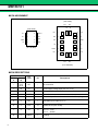
■ PIN ASSIGNMENT
(TOP VIEW)
N.C.
(TOP VIEW)
N.C.
16
VCC
1
8
OSC IN
DO
2
7
LD
GND
3
6
fout
fin
4
5
DIV
(FPT-8P-M03)
15
N.C.
1
14
N.C.
DIV
2
13
fin
fout
3
12
GND
LD
4
11
DO
OSCin
5
10
VCC
N.C.
6
9
N.C.
7
N.C.
8
N.C.
(LCC-16P-M06)
■ PIN DESCRIPTIONS
Pin No.
2
Pin
name
I/O
1,6,7,8,
9,14,
15,16
N.C
–
No connection
1
10
VCC
–
Power supply voltage input (2.4 V to 3.6 V).
2
11
DO
O
Charge pump output
3
12
GND
–
Ground
4
13
fin
I
Prescaler input. Connection should be with AC coupling.
5
2
Div
I
Divide ratio switching input. Two kinds of divide ratios are
selectable by Div input “H” or “L”.
6
3
fout
O
Test purpose output. This pin is an open drain output so that
should be left open usually.
7
4
LD
O
Lock detector output.
LD = H ; Lock
LD = L ; Unlock
8
5
OSCin
I
Reference counter input. Connection should be with AC
coupling.
SSOP8
BCC16
–
Descriptions
MB15C101
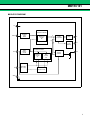
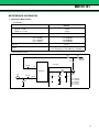
■ BLOCK DIAGRAM
VCC
Reference divider
OSCIN
DIV
Oscillator
input
buffer
Data
setting
circuit
fr
Reference
counter
(R)
charge
pump
Do
Lock
detector
LD
fp
Comparison divider
Output
selector
Swallow
counter
(A)
fin
Phase
comparator
fout
Main
counter
(N)
Prescaler
16 / 17(P)
Control circuit
GND
3
MB15C101
■ ABSOLUTE MAXIMUM RATINGS
Parameter
Rating
Symbol
Unit
Min.
Max.
VCC
–0.5
+4.0
V
VI
–0.5
VCC +0.5
V
Output voltage
VOUT
–0.5
VCC +0.5
V
Output current
IOUT
0
+5
mA
Storage temperature
TSTG
–55
+125
°C
Power supply voltage
Input voltage
WARNING: Semiconductor devices can be permanently damaged by application of stress (voltage, current,
temperature, etc.) in excess of absolute maximum ratings. Do not exceed these ratings.
■ RECOMMENDED OPERATING CONDITIONS
Parameter
Symbol
Value
Min.
Typ.
Max.
Unit
Power supply voltage
VCC
2.4
3.0
3.6
V
Input voltage
VIN
GND
–
VCC
V
Operating temperature
Ta
–40
–
+85
°C
Note
Handling Precautions
• This device should be transported and stored in anti-static containers.
• This is a static-sensitive device; take proper anti-ESD precautions. Ensure that personnel and equipment are
properly grounded. Cover workbenches with grounded conductive mats.
• Always turn the power supply off before inserting or removing the device from its socket.
• Protect leads with a conductive sheet when handling or transporting PC boards with devices.
4
MB15C101
■ ELECTRICAL CHARACTERISTICS
Recommended operating conditions unless otherwise noted.
Parameter
Symbol
Condition
ICC
Typ.
Max.
PLL is locked.(270MHz)
VCC = 3.0 V, Ta = +25°C
0.1
1.0
2.0
mA
fin
AC coupling by 1000 pF
capacitor
50
–
270
MHz
OSCIN
fosc
AC coupling by 1000 pF
capacitor
3
–
26
MHz
fin
Pfin
AC coupling by 1000 pF
capacitor
–10
–
+2
dBm
OSCIN
Vosc
AC coupling by 1000 pF
capacitor
0.5
–
–
Vpp
VIH
–
VCC ×
0.7
–
–
V
VIL
–
–
–
VCC ×
0.3
V
IIH
–
–
–
1.0
µA
IIL
–
–1.0
–
–
µA
IOSC
–
–100
–
100
µA
VOH
VCC = 3.0 V, IOH=–0.3mA
2.6
–
–
V
VOL
VCC = 3.0 V, IOL= 0.3mA
–
–
0.4
V
IOH
VCC = 3.0 V, VOH = 2V,
Ta = +25°C
–
–6.0
–
mA
IOL
VCC = 3.0 V, VOL = 1V,
Ta = +25°C
–
6.0
–
mA
IOFF
0 ≤ VDO ≤ VCC
–
–
3
nA
fin
Operating frequency
Input sensitivity
Div
Input current
Div
Input current
OSCIN
Output voltage
Do
Output current
High impedance cut off
current
Unit
Min.
Power supply current
Input voltage
Value
Do
Do
5
MB15C101
■ FUNCTIONAL DESCRIPTIONS
Two different frequencies can be selected by Div input “H” or “L”.
The divide ratios are calculated using the following equation:
fVCO = {(P × N) + A} × fOSC ÷ R
Symbol
(A < N)
Description
Div = “H”
Div = “L”
233.15 MHz
259.20 MHz
fvco
Output frequency of external VCO
fosc
Reference oscillation frequency
19.2 MHz
19.2 MHz
N
Divide ratio of the main counter
291
33
A
Divide ratio of the swallow counter
7
12
P
Preset divide ratio of dual modulus
prescaler
16/17
16/17
R
Divide ratio of the reference counter
384 (fr = 50 kHz)
40 (fr = 480 kHz)
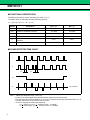
■ PHASE DETECTOR TIME CHART
fr
fp
tWU
tWL
LD
DO
High impedance
Note: • .Phase error detection range: –2π to +2π
• Pulses on Do output signal during locked state are output to prevent dead zone.
• LD output becomes low when phase is tWU or more. LD output becomes high when phase error is tWL or
less and continues to be so for three cycles or more.
• .tWU and tWL depend on OSCin input frequency.
tWU > 8/fosc (s) (e. g.tWU > 625.0ns, foscin = 12.8 MHz)
tWL < 16/fosc (s) (e. g. tWL < 1250.0ns, foscin = 12.8 MHz)
6
MB15C101
■ MEASURMENT CIRCUIT (for measuring input sensitivity fin/OSCin)
SSOP-8
VCC
S.G
1000 pF
1
8
2
7
0.1 µF
50 Ω
VCC
2 KΩ
3
6
4
5
Oscilloscope
S.G
DIV : H or L
1000 pF
50 Ω
BCC-16
8
7
9
6
10
5
11
4
VCC
S.G
1000 pF
0.1 µF
VCC
50 Ω
2 KΩ
12
3
13
2
14
1
Oscilloscope
S.G
DIV : H or L
1000 pF
50 Ω
15
16
7
MB15C101
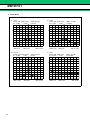
■ TYPICAL CHARACTERISTICS
;;
;;
1. fin Input Sensitivity
(dBm)
10
5
0
−5
Pfin (dBm)
−10
−15
−20
−25
−30
−35
−40
−45
Ta = +25 °C
SPEC
VCC = 2.4 V
VCC = 3.0 V
VCC = 3.6 V
−50
0
100
200
300
400
500
600
700
800
900
1000 (MHz)
fin (MHz)
;;;
2. OSCIN Input Sensitivity
(dBm)
10
5
0
−5
Vosc (dBm)
−10
−15
−20
Ta = +25 °C
VCC = 2.4 V
VCC = 3.0 V
VCC = 3.6 V
SPEC
−25
−30
−35
−40
−45
−50
0
10
20
30
40
50
fosc (MHz)
8
60
70
80
90
100 (MHz)
MB15C101
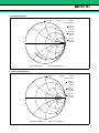
3. fin Input Impedance
4 : 11.867 Ω
−131.54 Ω
4.0331 pF
300.000 000 MHz
1 : 58.875 Ω
−850.16 kΩ
50 MHz
2 : 16.891 Ω
−416.2 Ω
100 MHz
3 : 12.047 Ω
−202.87 Ω
200 MHz
1
2
4
START .500 000 MHz
3
STOP 1 000.000 000 MHz
4. OSCIN Input Impedance
4 : 068.25 Ω
−1.4236 Ω
4.3 pF
26.000 000 MHz
1 : 5.1345 Ω
−10.288 kΩ
3 MHz
2 : 529.87 Ω
−3.6659 kΩ
10 MHz
3 : 114.44 Ω
−1.8514 kΩ
4
20 MHz
1
23
START .500 000 MHz
STOP 100.000 000 MHz
9
MB15C101
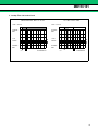
5. Do Outut Current
VOH – IOH
VCC = 3.0 V, Ta =+ 25 °C
3.0
2.5
VOH (V)
2.0
1.5
1.0
0.5
0.0
0
−2
−4
−6
−8
−10
−12
IOH (mA)
VOL – IOL
VCC = 3.0 V, Ta = +25 °C
3.0
2.5
VOL (V)
2.0
1.5
1.0
0.5
0.0
0
2
4
6
8
10
12
IOL (mA)
Measurement Circuit
VCC
fin
OSCin
S.G.
50 Ω
1000 pF
IOH
VCC
Parameter Analyzer
Do
GND
VCC
fin
S.G.
10
50 Ω
1000 pF
OSCin
IOL
VCC
Do
GND
Parameter Analyzer
MB15C101
■ REFERENCE INFORMATION
1. Application Measurement
• Test Results
Results
Lockup time ±1 kHz
Un lock → Lock
Power on → Lock
2.3 ms
3.4 ms
Reference leakage (∆f = 58 kHz)
Phase noise
–88.5 dBc
(∆f = 1 kHz)
(∆f = 10 kHz)
(∆f = 100 kHz)
(∆f = 1 MHz)
–88.0 dBc/Hz
–111.0 dBc/Hz
–118.0 dBc/Hz
–134.0 dBc/Hz
VCC (V)
3.0 V
Discrete VCO (Kv = 3.5 MHz/V)
Lock Frequency = 274.0 MHz (fr = 58 kHz)
VCO
• Measurement Circuit
18 Ω
VCC = 3.0 V
1000 pF
18 Ω
18 Ω
Spectrum
Analyzer
Loop Filter
fin
R1
MB15C101
VCO
S.G
1000 pF
50 Ω
OSCin
C1
R2
C2
C3
C1 = 6800 pF
C2 = 0.068 µF
C3 = 4800 pF
R1 = 3.0 kΩ
R2 = 3.9 KΩ
11
MB15C101
2. Phase Noise
∆ f = 1 kHz
ATTEN 10dB SPAN 2.0 kHz
RL −1.5 dBm
10 dB/
∆MKR −73.83 dB
1.000 kHz
D
∆MKR −91.83 dB
10.00 kHz
D
CENTER 273.999827 MHz
RBW 30 Hz
VBW 3.0 Hz
∆ f = 100 kHz
ATTEN 10 dB SPAN 200 kHz
RL −1.5 dBm
10 dB/
SPAN 2.000 kHz
SWP 3.00 sec
∆MKR −88.50 dB
58.0 kHz
D
CENTER 273.999827 MHz
RBW 100 Hz
VBW 30 Hz
∆ f = 1 MHz
ATTEN 10dB SPAN 2 MHz
RL −30.0 dBm
10 dB/
SPAN 20.00 kHz
SWP 30. 0 sec
∆MKR −105.5 dB
275.000 MHz
D
CENTER 274.0002 MHz
RBW 1.0 kHz
VBW 30 Hz
12
∆ f = 10 kHz
ATTEN 10dB SPAN 20 kHz
RL −1.5 dBm
10 dB/
SPAN 200.0 kHz
SWP 30.0 sec
START 274.000 MHz
RBW 1.0 Hz
VBW 100 Hz
STOP 276.000 MHz
SWP 100 sec
MB15C101
3. Lockup Time: Un-Lock to Lock
Un-Lock to Lock : DIV = “L” to “H”
VCC “OFF” to VCC “ON”
∆ Mkr : 2.30 ms
∆ Mkr : 3.40 ms
30.00300
MHz
30.00300
MHz
1.00
kHz/div
1.000
kHz/div
29.99800
MHz
29.99800
MHz
0s
20.0000000 ms
0s
10.0000000 ms
13
MB15C101
■ ORDERING INFORMATION
14
Part number
Package
MB15C101PFV
8-pin, Plastic SSOP
(FPT-8P-M03)
MB15C101PV1
16-pad, Plastic BCC
(LCC-16P-M06)
Remarks
MB15C101
■ PACKAGE DIMENSIONS
8-pin plastic SSOP
(FPT-8P-M03)
*: This dimension does not include resin protrusion.
+0.20
* 3.50±0.10
1.25 –0.10
+.008
.049 –.004
(.138±.004)
(Mounting height)
0.10(.004)
INDEX
4.20±0.10
(.165±.004)
5.20(.205)
NOM
6.20±0.20
(.244±.008)
"A"
0.80(.0315)
TYP
0.35±0.10
(.014±.004)
+0.05
0.10(.004)
M
0.15 –0.02
+.002
.006 –.001
Details of "A" part
0.10±0.10(.004±.004)
(STAND OFF)
2.40(.094)REF
C
1994 FUJITSU LIMITED F08005S-1C-2
0
10°
0.50±0.20
(.020±.008)
Dimensions in mm (inches)
(Continued)
15
MB15C101
(Continued)
16-pad plastic BCC
(LCC-16P-M06)
4.55±0.10
(.179±.004)
0.80(.031)MAX
Mounting height
14
3.40(.134)TYP
0.65(.026)
TYP
0.40±0.10
(.016±.004)
9
0.325±0.10
(.013±.004)
9
14
0.80(.031)
REF
INDEX AREA
3.40±0.10
(.134±.004)
2.45(.096)
TYP
"A"
1
6
0.075±0.025
(.003±.001)
(Stand off)
6
Details of "A" part
0.75±0.10
(.030±.004)
1.15(.045)
REF
"B"
1.725(.068)
REF
1
Details of "B" part
0.60±0.10
(.024±.004)
0.05(.002)
0.40±0.10
(.016±.004)
C
16
1999 FUJITSU LIMITED C16017S-1C-1
0.60±0.10
(.024±.004)
Dimensions in mm (inches)
MB15C101
MEMO
17
MB15C101
MEMO
18
MB15C101
MEMO
19
FUJITSU MICROELECTRONICS LIMITED
Shinjuku Dai-Ichi Seimei Bldg. 7-1, Nishishinjuku 2-chome, Shinjuku-ku,
Tokyo 163-0722, Japan
Tel: +81-3-5322-3347 Fax: +81-3-5322-3387
http://jp.fujitsu.com/fml/en/
For further information please contact:
North and South America
FUJITSU MICROELECTRONICS AMERICA, INC.
1250 E. Arques Avenue, M/S 333
Sunnyvale, CA 94085-5401, U.S.A.
Tel: +1-408-737-5600 Fax: +1-408-737-5999
http://www.fma.fujitsu.com/
Asia Pacific
FUJITSU MICROELECTRONICS ASIA PTE LTD.
151 Lorong Chuan, #05-08 New Tech Park,
Singapore 556741
Tel: +65-6281-0770 Fax: +65-6281-0220
http://www.fujitsu.com/sg/services/micro/semiconductor/
Europe
FUJITSU MICROELECTRONICS EUROPE GmbH
Pittlerstrasse 47, 63225 Langen,
Germany
Tel: +49-6103-690-0 Fax: +49-6103-690-122
http://emea.fujitsu.com/microelectronics/
FUJITSU MICROELECTRONICS SHANGHAI CO., LTD.
Rm.3102, Bund Center, No.222 Yan An Road(E),
Shanghai 200002, China
Tel: +86-21-6335-1560 Fax: +86-21-6335-1605
http://cn.fujitsu.com/fmc/
Korea
FUJITSU MICROELECTRONICS KOREA LTD.
206 KOSMO TOWER, 1002 Daechi-Dong,
Kangnam-Gu,Seoul 135-280
Korea
Tel: +82-2-3484-7100 Fax: +82-2-3484-7111
http://www.fmk.fujitsu.com/
FUJITSU MICROELECTRONICS PACIFIC ASIA LTD.
10/F., World Commerce Centre, 11 Canton Road
Tsimshatsui, Kowloon
Hong Kong
Tel: +852-2377-0226 Fax: +852-2376-3269
http://cn.fujitsu.com/fmc/tw
All Rights Reserved.
The contents of this document are subject to change without notice.
Customers are advised to consult with sales representatives before ordering.
The information, such as descriptions of function and application circuit examples, in this document are presented solely for the purpose
of reference to show examples of operations and uses of FUJITSU MICROELECTRONICS device; FUJITSU MICROELECTRONICS
does not warrant proper operation of the device with respect to use based on such information. When you develop equipment incorporating the device based on such information, you must assume any responsibility arising out of such use of the information.
FUJITSU MICROELECTRONICS assumes no liability for any damages whatsoever arising out of the use of the information.
Any information in this document, including descriptions of function and schematic diagrams, shall not be construed as license of the use
or exercise of any intellectual property right, such as patent right or copyright, or any other right of FUJITSU MICROELECTRONICS
or any third party or does FUJITSU MICROELECTRONICS warrant non-infringement of any third-party's intellectual property right or
other right by using such information. FUJITSU MICROELECTRONICS assumes no liability for any infringement of the intellectual
property rights or other rights of third parties which would result from the use of information contained herein.
The products described in this document are designed, developed and manufactured as contemplated for general use, including without
limitation, ordinary industrial use, general office use, personal use, and household use, but are not designed, developed and manufactured
as contemplated (1) for use accompanying fatal risks or dangers that, unless extremely high safety is secured, could have a serious effect
to the public, and could lead directly to death, personal injury, severe physical damage or other loss (i.e., nuclear reaction control in
nuclear facility, aircraft flight control, air traffic control, mass transport control, medical life support system, missile launch control in
weapon system), or (2) for use requiring extremely high reliability (i.e., submersible repeater and artificial satellite).
Please note that FUJITSU MICROELECTRONICS will not be liable against you and/or any third party for any claims or damages arising
in connection with above-mentioned uses of the products.
Any semiconductor devices have an inherent chance of failure. You must protect against injury, damage or loss from such failures by
incorporating safety design measures into your facility and equipment such as redundancy, fire protection, and prevention of over-current
levels and other abnormal operating conditions.
Exportation/release of any products described in this document may require necessary procedures in accordance with the regulations of
the Foreign Exchange and Foreign Trade Control Law of Japan and/or US export control laws.
The company names and brand names herein are the trademarks or registered trademarks of their respective owners.
Edited
Strategic Business Development Dept.