1
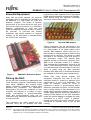
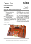
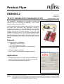
Product Flyer
DK86065-2
May 2011
Version 2.2
14-bit 1+GSa/s DAC Development Kit
The DK86065-2 development kit provides a simple and
effective means of evaluating the MB86065 14-bit 1+GSa/s
Digital to Analog Converter (DAC).
FME/MS/DAC80S/FL_2/5488
DK86065-2
Evaluation Platform
A user manual provides a step-by-step guide from configuring
the board and connecting test equipment, through to
evaluating performance of the MB86065. Schematics, PCB
overlays and connector pin-outs are included. The evaluation
platform requires two DC power supplies, 1.8V & 3.3V, each
capable of providing 1 amp. The PC USB programming cable
included combined with the control software available for free
download supports configuration and control of the device, as
well as downloading test vectors to the waveform memory
module.
Features
• Development kit for MB86065
• MB86065 Evaluation Board
• PC USB Programming Cable
• PC control software available for free download
• User Manual
• SMA data adaptors (optional)
• Xilinx® Virtex® 5 FPGA Platform Adaptor (optional)
PC Control Software
Applications
• Provides easy access to on-chip waveform memories to
perform initial performance tests, avoiding need for high
performance data generating equipment.
© 2004-2011 Fujitsu Semiconductor Europe GmbH
Disclaimer:
Production
Page 1 of 4
The contents of this document are subject to change without notice. Customers are advised to consult with FUJITSU
SEMICONDUCTOR sales representatives before ordering. The information and circuit diagrams in this document are
presented “as is”, no license is granted by implication or otherwise.
May 2011 Version 2.2
FME/MS/DAC80S/FL_2/5488
DK86065-2 14-bit 1+GSa/s DAC Development Kit
Essential Equipment
Apart from the power supplies, the minimum
equipment vital to conducting an evaluation of
the MB86065 is a high quality RF clock and
spectrum analyser. The phase & spurious
performance of the clock should be such as to
not limit the DAC performance (e.g. HP8664A).
However, performance of even the best
spectrum analysers available is inferior to that of
the converter. To overcome this, filtering
techniques and careful attention to analyser
settings, e.g. RF Attenuation, is essential during
the course of the evaluation.
programming cable supplied. Even if high speed
digital pattern generating equipment is available,
initial testing using the waveform memories
serves as a useful setup check.
Figure 2.
Figure 1.
DK86065-2 Evaluation Board
Driving the DAC
As with any DAC evaluation an appropriate test
vector stimulus is required. Unfortunately at data
rates above 300MSa/s this requires digital
pattern generation capabilities beyond most
standard test equipment. The DK86065-2
Development Kit has been designed to help
overcome this difficulty in a number of ways.
Initially, unmodulated or pseudo-modulated
single and multi-tone/carrier tests can be
conducted using waveforms downloaded to the
on-chip memories.
Test waveforms are easily loaded into the
memories using the PC software and USB
Page 2 of 4
Disclaimer:
Production
Optional SMA Adaptor
Pattern generators can be connected to the
evaluation board using either the onboard 2-row
0.1" data headers, or via ribbon cables to the
optional SMA adaptors. When using the 0.1"
data headers it is assumed that a custom wiring
harness will be required. This would be made
according to the connector type and pinout of
the generator’s output. The optional SMA
adaptors provide a convenient conversion from
SMA to the evaluation board’s 0.1" headers.
This alleviates the simultaneous removal of 28
SMAs (14-bit differential LVDS) when required
to be disconnected. One advantage of this is the
ability to easily swap the data generator
between DAC data ports if insufficient channels
are available to drive both ports simultaneously.
Rather than using general purpose test
equipment, customers may wish to use the
evaluation board to construct a platform more
representative of their end application. This
might, for example, involve an FPGA to
implement a variety of pre-processing and/or
waveform generation functions. At the simplest
level, a setup similar to that described for the
digital pattern generator could be used, where a
custom wiring harness interfaces a standard or
existing FPGA platform to the DAC evaluation
board. An optional adaptor is available for direct
connection to a Xilinx® Virtex® 5 platform.
Control of the DAC from the PC software can be
maintained to minimise effort to get up and
running.
© 2004-2011 Fujitsu Semiconductor Europe GmbH
The contents of this document are subject to change without notice. Customers are advised to consult with FUJITSU
SEMICONDUCTOR sales representatives before ordering. The information and circuit diagrams in this document are
presented “as is”, no license is granted by implication or otherwise.
May 2011 Version 2.2
FME/MS/DAC80S/FL_2/5488
DK86065-2 14-bit 1+GSa/s DAC Development Kit
The latest PC software can be downloaded,
following registration, from the Data Converters
‘Datasheet & Application Notes’ area of the
EMEA website.
Figure 3.
Optional Virtex® 5 Adaptor
Clock Inputs & Analog Outputs
The evaluation board is designed to
accommodate up to four SMA connectors - two
for the differential clock input and two for the
differential analog output. Boards are supplied
with transformers on-board to perform single
ended-to-differential and differential-to-single
ended conversions. As such, only two SMAs are
required. This facilitates easier connection to
standard test equipment.
PC Control & Software
The development kit includes a PC USB
programming cable which interfaces between a
host PC USB port and the DAC’s 4-wire serial
interface.
Figure 4.
PC Software User Interface
Ordering Information
Part
Order Reference
Complete
Development Kit
(includes Evaluation
Board with device
fitted, PC USB
Programming Cable
& User Manual)
DK86065-2
DAC DK FPGA
Adaptor (optional)
DKXC5VADAPT-1
SMA Adaptors
(optional)
DK86064-1-SMA
DK86065-2 User
Manual
Contact Fujitsu
MB86065 Data sheet
emea.fujitsu.com/semiconductor
PC USB Interface Adaptor
© 2004-2011 Fujitsu Semiconductor Europe GmbH
Disclaimer:
Figure 5.
Production
Page 3 of 4
The contents of this document are subject to change without notice. Customers are advised to consult with FUJITSU
SEMICONDUCTOR sales representatives before ordering. The information and circuit diagrams in this document are
presented “as is”, no license is granted by implication or otherwise.
May 2011 Version 2.2
FME/MS/DAC80S/FL_2/5488
DK86065-2 14-bit 1+GSa/s DAC Development Kit
Worldwide Headquarters
Japan
Asia
Tel: +81 45 473 8030
Tel: +65 281 0770
Fujitsu Semiconductor Limited
Nomura Fudosan Shin-Yokohama Building Fax: +65 281 0220
2-10-23 Shin-Yokohama, Kohoku-ku,
Yokohama
Kanagawa 222-8508
Japan
Fujitsu Semiconductor Asia Pte Ltd
151 Lorong Chuan
New Tech Park
#05-08
Singapore 556741
http://www.fujitsu.com/global/services/microelectronics
http://sg.fujitsu.com/semiconductor
Korea
China
Tel: +82 2 3484 7108
Fax: +82 2 3484 7111
Fujitsu Semiconductor Korea Limited
2nd Floor, Kosmo Tower Building
1002 Daechi-Dong
Kangnam-Gu
Seoul
Korea
Tel: +86-21 6416 3688
Fax: +86-21 6335 1615
Fujitsu Semiconductor (Shanghai) Ltd
Room 3102-3103 Bund Center
222 Yan An Rd (E)
Shanghai 200002
PRC
http://www.fujitsu.com/kr/fmk/
http://sg.fujitsu.com/semiconductor
USA
Europe
Tel: +1 408 737 5600
Fax: +1 408 737 5999
Fujitsu Semiconductor America, Inc.
1250 E. Arques Avenue, M/S 333
Sunnyvale, CA 94088-3470
USA
Tel: +49 6103 6900
Fax: +49 6103 690122
Fujitsu Semiconductor Europe GmbH
Pittlerstrasse 47
63225 Langen
Germany
Tel: +1 800 866 8608 Customer Response Center
Fax: +1 408 737 5984 Mon-Fri: 7am-5pm (PST)
http://www.fujitsu.com/us/services/edevices/microelectronics/ http://emea.fujitsu.com/semiconductor
The contents of this document are subject to change without notice. Customers are advised to consult with FUJITSU SEMICONDUCTOR
sales representatives before ordering.
The information and circuit diagrams in this document presented as examples of semiconductor device applications, and are not intended
to be incorporated in devices for actual use. Also, FUJITSU SEMICONDUCTOR is unable to assume responsibility for infringement of any
patent rights or other rights of third parties arising from the use of this information or circuit diagrams. No license is granted by implication
or otherwise under any patent or patent rights of Fujitsu Semiconductor Europe GmbH.
FUJITSU SEMICONDUCTOR devices are intended for use in standard applications (computers, office automation and other office
equipment, industrial, communications, and measurement equipment, personal or household devices, etc.).
CAUTION: Customers considering the use of our products in special applications where failure or abnormal operation may directly affect
human lives or cause physical injury or property damage, or where extremely high levels of reliability are demanded (such as aerospace
systems, atomic energy controls, sea floor repeaters, vehicle operating controls, medical devices for life support, etc.) are requested to
consult with FUJITSU SEMICONDUCTOR sales representatives before such use. The company will not be responsible for damages
arising from such use without prior approval.
Any semiconductor devices have inherently a certain rate of failure. You must protect against injury, damage or loss from such failures by
incorporating safety design measures into your facility and equipment such as redundancy, fire protection, and prevention of over-current
levels and other abnormal operating conditions.
If any products described in this document represent goods or technologies subject to certain restrictions on export under the Foreign
Exchange and Foreign Trade Control Law of Japan, the prior authorization by Japanese government should be required for export of
those products from Japan.
FME/MS/DAC80S/FL_2/5488
Page 4 of 4
Disclaimer:
Production
© 2004-2011 Fujitsu Semiconductor Europe GmbH
The contents of this document are subject to change without notice. Customers are advised to consult with FUJITSU
SEMICONDUCTOR sales representatives before ordering. The information and circuit diagrams in this document are
presented “as is”, no license is granted by implication or otherwise.