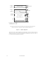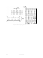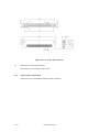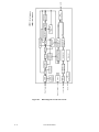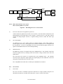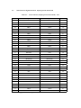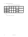
1
MAM3367MC/MP SERIES
MAM3184MC/MP SERIES
DISK DRIVES
PRODUCT/MAINTENANCE MANUAL
C141-E134-01EN
FOR SAFE OPERATION
Handling of This manual
This manual contains important information for using this product. Read thoroughly before using the
product. Use this product only after thoroughly reading and understanding especially the section “Important
Alert Items” in this manual. Keep this manual handy, and keep it carefully.
FUJITSU makes every effort to prevent users and bystanders from being injured or from suffering damage
to their property. Use the product according to this manual.
IMPORTANT NOTE TO USERS
READ THE ENTIRE MANUAL CAREFULLY BEFORE USING THIS PRODUCT.
INCORRECT USE OF THE PRODUCT MAY RESULT IN INJURY OR DAMAGE
TO USERS, BYSTANDERS OR PROPERTY.
While FUJITSU has sought to ensure the accuracy of all information in this manual, FUJITSU assumes no
liability to any party for any damage caused by any error or omission contained in this manual, its updates
or supplements, whether such errors or omissions result from negligence, accident, or any other cause. In
addition, FUJITSU assumes no liability with respect to the application or use of any porduct or system in
accordance with the descriptions or instructions contained herein; including any liability for incidental or
consequential damages arising therefrom.
FUJTSU DISCLAIMS ALL WARRANTIES REGARDING THE INFORMATION CONTAINED
HEREIN, WHETHER EXPRESSED, IMPLIED, OR STATUTORY.
FUJITSU reserves the right to make changes to any products described herein without further notice and
without obligation.
This product is designed and manufactured for use in standard applications such as office work, personal
devices and household appliances. This product is not intended for special uses (atomic controls,
aeronautic or space systems, mass transport vehicle operating controls, medical devices for life support, or
weapons firing controls) where particularly high reliability requirements exist, where the pertinent levels of
safety are not guaranteed, or where a failure or operational error could threaten a life or cause a physical
injury (hereafter referred to as "mission-critical" use). Customers considering the use of these products for
mission-critical applications must have safety-assurance measures in place beforehand. Moreover, they are
requested to consult our sales representative before embarking on such specialized use.
The contents of this manual may be revised without prior notice.
The contents of this manual shall not be disclosed in any way or reproduced in any media without the
express written permission of Fujitsu Limited.
All Right Reserved, Copyright © FUJITSU LIMITED 2001
C141-E134-01EN
REVISION RECORD
Edition
Date published
01
July., 2001
Revised contents
Specification No.: C141-E134-01EN
C141-E134-01EN
i
Related Standards
Specifications and functions of products covered by this manual comply with the following
standards.
Standard (Text) No.
ii
Name
Enacting Organization
ANSI X3.131-1994
Small Computer System Interface 2(SCSI-2)
American National
Standards Institute
(ANSI)
T10/1236-D Rev 19
SCSI Primary Commands-2 (SPC-2)
American National
Standards Institute
(ANSI)
ANSI NCITS. 306-1998
SCSI-3 Block Commands (SBC)
American National
Standards Institute
(ANSI)
ANSI X3.270-1996
SCSI-3 Architecture Model (SAM)
American National
Standards Institute
(ANSI)
ANSI NCITS. 336-2000
SCSI Parallel Interface-3 (SPI-3)
American National
Standards Institute
(ANSI)
C141-E134-01EN
PREFACE
This manual describes the MAM3367MC/MP, MAM3184MC/MP (hereafter, MAM series), 3.5 type fixed
disk drives with an embedded SCSI controller.
This manual details the specifications and functions of the above disk drive, and gives the requirements and
procedures for installing it into a host computer system.
This manual is written for users who have a basic understanding of fixed disk drives and their use in
computer systems. The MANUAL ORGANIZATION section describes organization and scope of this
manual. The need arises, use the other manuals.
Chapter 1
GENERAL DESCRIPTION
This chapter introduces the MAM series disk drives and discusses their standard features, hardware, and
system configuration.
Chapter 2
SPECIFICATIONS
This chapter gives detailed specifications of the MAM series disk drives and their installation environment.
Chapter 3
DATA FORMAT
This chapter describes the data structure of the disk, the address method, and what to do about media
defects.
Chapter 4
INSTALLATION REQUIREMENTS
This chapter describes the basic physical and electrical requirements for installing MAM series disk drives.
Chapter 5
INSTALLATION
This chapter explains how to install MAM series disk drives. It includes the notice and procedures for
setting device number and operation modes, mounting the disk drive, connecting the cables, and confirming
drive operation.
Chapter 6
DIAGNOSIS and MAINTENANCE
This chapter describes the automatic diagnosis, and maintenance of MAM series disk drive. This chapter
also describes diagnostic methods for operation check and the basics of troubleshooting the disk drives.
Chapter 7
ERROR ANALYSIS
This chapter describes in details how collect the information for error analysis and how analyze collected
error information.
Chapter 8
PRINCIPLE OF OPERATION
This chapter explains disk drives configuration and operation of MAM series.
C141-E134-01EN
iii
APPENDIX
A to D
The appendixes give supplementary information, including the locations of mounting setting terminals and
connectors, a list of setting items, the signal assignments of interface connectors, lists of model names and
product numbers, and SCSI interface functions.
The model numbers have a suffix that describes the electrical requirements of the SCSI interface between
host system and disk drive, the data formatted at the factory and device type.
CONVENTIONS
This manual uses the following conventions for alerts to prevent physical or property damages to users or
by standards.
DANGER
DANGER indicates that personal injury will occur if the user does not perform the procedure correctly.
WARNING
WARNING indicates that personal injury could occur if the user does not perform the procedure
correctly.
CAUTION
CAUTION indicates that either minor or moderate personal injury may occur if the user does not
perform the procedure correctly.
NOTICE
NOTICE indicates that inconvenience to the user such as damages to the product, equipment, data, and/or
other property may occur if the user does not pay attention or perform the procedure correctly.
IMPORTANT
IMPORTANT indicates information that the helps the user use the product more effectively.
Indicates
iv
C141-E134-01EN
This manual indicates;
Decimal number: Indicates as it is.
Hexadecimal number: Indicates as X’17B9’, 17B9h, or 17B9H
Binary number: Indicates as “010”
DISCLAIMER
Failure of the MAM series intelligent disk drive is defined as a failure requiring adjustments, repairs, or
replacement. Fujitsu is not responsible for drive failures caused by misuse by the user, poor environmental
conditions, power trouble, host problems, cable failures, or any failure not caused by the drive itself.
The suffix of the model name of the disk drive varies depending on the electrical requirements, capacity,
and data format at factory shipment of the SCSI, i.e., the interface for connecting the device type or host
system and the disk drives (Note 1). However, in this manual, the typical model names (Note 2) are used
unless otherwise noted. These disk drives may be called intelligent disk drives (IDD), drives, or devices in
this manual.
Note 1:
Model names
M AM 3 367 MC
Interface types
MC: LVD, 16-bit SCSI SCA2 connector 160MHz transfer
MP: LVD, 16-bit SCSI 68 pin connector 160MHz transfer
Formatted capacity (100 MB units)
Note 2:
Disk drive size
3: 3.5 type. Hard Disk Drive
Type
AM: Number of rotations 15,000min-1 (15,000rpm)
Type model name
Type model name
Model name
MAM3367
MAM3367MC, MAM3367MP
MAM3184
MAM3184MC, MAM3184MP
C141-E134-01EN
v
Important Alert Items
Important Alert Messages
The important alert messages in this manual are as follows:
A hazardous situation could result in minor or moderate personal injury if the
user does not perform the procedure correctly. This alert signal also indicates
that damages to the product or other property may occur if the user does not
perform the procedure correctly.
Task
Mounting Installation
Alert message
Data loss
For MAM series, Reed Solomon codes are applied for their ECC.
Page
2-5
The sector-data is divided into 6 interleaving sectors, and ECC is
performed in each sector where the maximum number of errors (up
to 5 byte) can be corrected. [Total maximum byte: 5 byte × 6 (
interleave) = 30 byte]
If the error of read sector keeps allowable error byte number,
correction is performed.
However, if error byte exceeds its allowable number, correction
may not be performed properly.
Hot temperature
To prevent injury, do not handle the drive until after the device has
cooled sufficiently after turning off the power. The DE and LSI
become hot during operation and remain hot immediately after
turning off the power.
5-1
Data loss
1. The user must not change the setting of terminals not described
in this section. Do not change setting status set at factory
shipment.
5-5
2. Do not change the setting of terminals except following setting
pins during the power is turned on.
• Write protect: CN2 9-10 (MP model only)
3. To short the setting terminal, use the short plug attached when
the device is shipped from the factory.
Damage
1. Make sure that system power is off before connecting or
disconnecting cables.
5-11
2. Do not connect or disconnect cables when power is on.(except
MC model)
Damage
1. Be careful of the insertion orientation of the SCSI connectors.
With the system in which terminating resistor power is supplied
via the SCSI cable, if the power is turned on, the overcurrent
vi
C141-E134-01EN
5-11
Task
Mounting Installation
Alert message
protection fuse of the terminating resistor power supplier may
be blown or the cable may be burnt if overcurrent protection is
not provided.
When the recommended parts listed in Table 4.2 are used,
inserting the cables in the wrong direction can be prevented.
2. To connect SCSI devices, be careful of the connection position
of the cable. Check that the SCSI device with the terminating
resistor is the last device connected to the cable.
Data loss
When the SEND DIAGNOSTIC command terminates with the
CHECK CONDITION status, the INIT must collect the error
information using the REQUEST SENSE command. The RECEIVE
DIAGNOSTIC RESULTS command cannot read out the error
information detected in the self-diagnostics.
Caution
1. To avoid shocks, turn off the power before connecting or
disconnecting a cable, connector, or plug.
2. To avoid injury, do not touch the mechanical assembly during
disk drive operation.
3. Do not use solvents to clean the disk drive.
Page
6-4
6-5
Caution
1. Always ground yourself with a wrist strap connected to ground
before handling. ESD (Electrostatics Discharge) may cause
the damage to the device.
2. To prevent electrical damage to the disk drive, turn the power
off before connecting or disconnecting a cable, connector, or
plug.
3. Do not remove a PCA. This operation is required to prevent
unexpected or unpredictable operation.
4. Do not use a conductive cleaner to clean a disk drive assembly.
5. Ribbon cables are marked with a colored line. Connect the
ribbon cable to a cable connector with the colored wire
connected to pin 1.
6-6
Damage
Never open the disk enclosure in the field. Opening the disk
enclosure in the field may cause an irreparable fault.
Data loss
Save data stored on the disk drive before requesting repair. Fujitsu
does not assume responsibility if data is destroyed during servicing
or repair.
6-6
6-15
C141-E134-01EN
6-7
vii
MANUAL ORGANIZATION
PRODUCT/
MAINTENANCE
MANUAL
(This manual)
viii
1.
2.
3.
4.
5.
6.
7.
8.
General Description
Specifications
Data Format
Installation Requirements
Installation
Diagnostics and Maintenance
Error Analysis
Principle of Operation
SCSI Physical
Interface
Specifications
1. SCSI Bus
2. SCSI Message
3. SCSI Bus Error Recovery Processing
SCSI Logical
Interface
Specifications
1.
2.
3.
4.
5.
Command Processing
Data Buffer Management
Command Specification
Sense Data and error Recovery Procedure
Disk Medium Management
C141-E134-01EN
CONTENTS
CHAPTER 1
page
GENERAL DESCRIPTION ........................................................................................1-1
1.1
Standard Features ..........................................................................................................................1-2
1.2
Hardware Structure........................................................................................................................1-5
1.3
System Configuration ....................................................................................................................1-8
CHAPTER 2
SPECIFICATIONS .......................................................................................................2-1
2.1
Hardware Specifications ................................................................................................................2-1
2.1.1
Model name and part number ........................................................................................................2-1
2.1.2
Function specifications ..................................................................................................................2-2
2.1.3
Environmental specifications.........................................................................................................2-4
2.1.4
Error rate........................................................................................................................................2-5
2.1.5
Reliability ......................................................................................................................................2-5
2.2
SCSI Function Specifications ........................................................................................................2-7
CHAPTER 3
DATA FORMAT...........................................................................................................3-1
3.1
Data Space .....................................................................................................................................3-1
3.1.1
Cylinder configuration ...................................................................................................................3-1
3.1.2
Alternate spare area .......................................................................................................................3-4
3.1.3
Track format ..................................................................................................................................3-5
3.1.4
Sector format .................................................................................................................................3-7
3.1.5
Format capacity .............................................................................................................................3-9
3.2
Logical Data Block Addressing ...................................................................................................3-10
3.3
Defect Management.....................................................................................................................3-11
3.3.1
Defect list.....................................................................................................................................3-11
3.3.2
Alternate block allocation............................................................................................................3-11
CHAPTER 4
INSTALLATION REQUIREMENTS .........................................................................4-1
4.1
Mounting Requirements.................................................................................................................4-1
4.1.1
External dimensions.......................................................................................................................4-1
4.1.2
Mounting .......................................................................................................................................4-4
4.1.3
Notes on mounting.........................................................................................................................4-4
4.2
Power Supply Requirements..........................................................................................................4-8
4.3
Connection Requirements............................................................................................................4-11
4.3.1
68 pin connector 16-bit SCSI model (MP model) .......................................................................4-11
C141-E134-01EN
ix
4.3.2
SCA2 type SCSI model (MC model)........................................................................................... 4-19
4.3.3
Cable connector requirements......................................................................................................4-20
4.3.4
External operator panel (MP model) ...........................................................................................4-22
CHAPTER 5
INSTALLATION ..........................................................................................................5-1
5.1
Notes on Handling Drives..............................................................................................................5-1
5.2
Connections ...................................................................................................................................5-3
5.3
Setting Terminals...........................................................................................................................5-5
5.3.1
SCSI ID setting (MP model only)..................................................................................................5-6
5.3.2
Each mode setting (MP model only)..............................................................................................5-7
5.3.3
Mode settings.................................................................................................................................5-9
5.4
Mounting Drives..........................................................................................................................5-10
5.4.1
Check before mounting................................................................................................................5-10
5.4.2
Mounting procedures ...................................................................................................................5-10
5.5
Connecting Cables .......................................................................................................................5-11
5.6
Confirming Operations after Installation and Preparation for use ...............................................5-12
5.6.1
Confirming initial operations .......................................................................................................5-12
5.6.2
Checking SCSI connection ..........................................................................................................5-13
5.6.3
Formatting ...................................................................................................................................5-16
5.6.4
Setting parameters .......................................................................................................................5-18
5.7
Dismounting Drives .....................................................................................................................5-22
5.8
Spare Disk Drive .........................................................................................................................5-22
CHAPTER 6
DIAGNOSTICS AND MAINTENANCE ....................................................................6-1
6.1
Diagnostics ....................................................................................................................................6-1
6.1.1
Self-diagnostics..............................................................................................................................6-1
6.1.2
Test programs ................................................................................................................................6-4
6.2
Maintenance Information...............................................................................................................6-5
6.2.1
Precautions ....................................................................................................................................6-5
6.2.2
Maintenance requirements .............................................................................................................6-6
6.2.3
Maintenance levels ........................................................................................................................6-8
6.2.4
Revision numbers ..........................................................................................................................6-9
6.2.5
Tools and test equipment .............................................................................................................6-10
6.2.6
Tests.............................................................................................................................................6-10
6.3
Operation Check ..........................................................................................................................6-12
6.3.1
Initial seek operation check .........................................................................................................6-12
6.3.2
Operation test...............................................................................................................................6-12
x
C141-E134-01EN
6.3.3
Diagnostic test .............................................................................................................................6-12
6.4
Troubleshooting Procedures ........................................................................................................6-13
6.4.1
Outline of troubleshooting procedures.........................................................................................6-13
6.4.2
Troubleshooting with disk drive replacement in the field............................................................6-13
6.4.3
Troubleshooting at the repair site ................................................................................................6-15
6.4.4
Troubleshooting with parts replacement in the factory................................................................6-16
6.4.5
Finding possibly faulty parts........................................................................................................6-16
CHAPTER 7
ERROR ANALYSIS .....................................................................................................7-1
7.1
Error Analysis Information Collection...........................................................................................7-1
7.1.1
Sense data ......................................................................................................................................7-1
7.1.2
Sense key, sense code, and subsense code.....................................................................................7-1
7.2
Sense Data Analysis.......................................................................................................................7-3
7.2.1
Error information indicated with sense data ..................................................................................7-3
7.2.2
Sense data (3-0C-03), (4-40-xx), (4-44-xx), and (4-C4-xx)...........................................................7-4
7.2.3
Sense data (1-1x-xx), (3-1x-xx) and (E-1D-00): Disk read error..................................................7-4
7.2.4
Sense data (5-2x-xx), (5-3D-00), (5-90-00), (B-47-xx), (B-49-00), (B-4D-xx)
and (B-4E-00): SCSI interface error .............................................................................................7-4
CHAPTER 8
PRINCIPLE OF OPERATION ...................................................................................8-1
8.1
Outline ...........................................................................................................................................8-1
8.2
Disk Drive Configuration ..............................................................................................................8-1
8.2.1
Disks ..............................................................................................................................................8-2
8.2.2
Heads .............................................................................................................................................8-2
8.2.3
Spindle mechanism ........................................................................................................................8-2
8.2.4
Actuator .........................................................................................................................................8-2
8.2.5
Air filters........................................................................................................................................8-2
8.3
Circuit Configuration.....................................................................................................................8-3
8.4
Power-On Sequence.......................................................................................................................8-5
8.5
Factory-Calibration........................................................................................................................8-6
8.6
Read/Write Circuit.........................................................................................................................8-7
8.6.1
Head IC..........................................................................................................................................8-7
8.6.2
Write circuit...................................................................................................................................8-7
8.6.3
Read circuit....................................................................................................................................8-9
8.7
Servo Control.................................................................................................................................8-9
8.7.1
Servo control circuit ......................................................................................................................8-9
8.7.2
Servo format ................................................................................................................................8-10
C141-E134-01EN
xi
8.7.3
Servo frame format ......................................................................................................................8-12
8.7.4
Spindle motor control ..................................................................................................................8-12
8.7.5
Voice coil motor control..............................................................................................................8-13
APPENDIX A
LOCATIONS OF CONNECTORS AND SETTING TERMINALS........................ A-1
A.1
Locations of Connector (MC model) ............................................................................................ A-2
A.2
Locations of Connectors and Setting Terminals (MP model) ....................................................... A-3
APPENDIX B
B.1
SETTING TERMINALS ............................................................................................. B-1
Setting Terminals (MP model)...................................................................................................... B-2
APPENDIX C
CONNECTOR SIGNAL ALLOCATION.................................................................. C-1
C.1
SCSI Connector Signal Allocation: SCA2 type LVD 16-bit SCSI .............................................. C-2
C.2
SCSI Connector Signal Allocation: 68 pin type LVD 16-bit SCSI.............................................. C-3
APPENDIX D
D.1
INDEX
xii
MODEL NAMES AND PRODUCT NUMBERS ...................................................... D-1
Model Names and Product Numbers ............................................................................................ D-2
...................................................................................................................................... IN-1
C141-E134-01EN
FIGURES
page
Figure 1.1
MC model outer view...........................................................................................................1-5
Figure 1.2
MP model outer view ...........................................................................................................1-6
Figure 1.3
Disk/head configuration .......................................................................................................1-7
Figure 1.4
System configuration............................................................................................................1-8
Figure 3.1
Cylinder configuration .........................................................................................................3-2
Figure 3.2
Spare area in cell ..................................................................................................................3-5
Figure 3.3
Alternate cylinder.................................................................................................................3-5
Figure 3.4
Track format.........................................................................................................................3-6
Figure 3.5
Track skew/cylinder skew ....................................................................................................3-7
Figure 3.6
Sector format........................................................................................................................3-8
Figure 3.7
Alternate block allocation by FORMAT UNIT command .................................................3-13
Figure 3.8
Alternate block allocation by REASSIGN BLOCKS command ........................................3-14
Figure 4.1
External dimensions (MC model) ........................................................................................4-2
Figure 4.2
External dimensions (MP model).........................................................................................4-3
Figure 4.3
IDD orientations...................................................................................................................4-4
Figure 4.4
Mounting frame structure.....................................................................................................4-5
Figure 4.5
Limitation of side-mounting.................................................................................................4-5
Figure 4.6
Surface temperature measurement points.............................................................................4-6
Figure 4.7
Service clearance area ..........................................................................................................4-7
Figure 4.8
Current waveform (+12 VDC) .............................................................................................4-8
Figure 4.9
Power on/off sequence (1)....................................................................................................4-9
Figure 4.10
Power on/off sequence (2)....................................................................................................4-9
Figure 4.11
Power on/off sequence (3)....................................................................................................4-9
Figure 4.12
AC noise filter (recommended) ..........................................................................................4-10
Figure 4.13
Connectors and terminals location (MP model) .................................................................4-11
Figure 4.14
16-bit SCSI interface connector .........................................................................................4-12
Figure 4.15
Power supply connector (16-bit SCSI model)....................................................................4-12
Figure 4.16
External operator panel connector (CN1) ..........................................................................4-13
Figure 4.17
External operator panel connector (CN2) ..........................................................................4-14
Figure 4.18
16-bit SCSI ID external input.............................................................................................4-15
Figure 4.19
Output signal for external LED ..........................................................................................4-17
Figure 4.20
SCSI cables connection......................................................................................................4-18
C141-E134-01EN
xiii
Figure 4.21
Connectors location of MC model .....................................................................................4-19
Figure 4.22
SCA2 type SCSI connector ................................................................................................4-20
Figure 4.23
External operator panel circuit example.............................................................................4-22
Figure 5.1
SCSI bus connections (1 of 2)..............................................................................................5-4
Figure 5.1
SCSI bus connections (2 of 2)..............................................................................................5-4
Figure 5.2
IDD setting terminals position (MP model only) .................................................................5-5
Figure 5.3
Setting terminator (CN2 on MP model only) .......................................................................5-6
Figure 5.4
Checking the SCSI connection (A) ....................................................................................5-14
Figure 5.5
Checking the SCSI connection (B).....................................................................................5-15
Figure 6.1
Revision label.......................................................................................................................6-9
Figure 6.2
Indicating revision numbers ...............................................................................................6-10
Figure 6.3
Test flowchart ....................................................................................................................6-11
Figure 7.1
Format of extended sense data .............................................................................................7-2
Figure 8.1
Circuit configuration ............................................................................................................8-4
Figure 8.2
IDD operation sequence at power-on...................................................................................8-5
Figure 8.3
Block diagram of read-write circuit .....................................................................................8-8
Figure 8.4
Block diagram of servo control circuit...............................................................................8-10
Figure 8.5
Position of servo track........................................................................................................8-12
Figure 8.6
Servo frame ........................................................................................................................8-12
Figure A.1
Locations of connector (MC model) ................................................................................... A-2
Figure A.2
Locations of connectors and setting terminals (MP model) ................................................ A-3
xiv
C141-E134-01EN
TABLES
page
Table 2.1
Function specifications.........................................................................................................2-2
Table 2.2
Environmental/power requirements .....................................................................................2-4
Table 2.3
SCSI function specifications ................................................................................................2-7
Table 3.1
Zone layout and track capacity.............................................................................................3-3
Table 3.4
Format capacity..................................................................................................................3-10
Table 4.1
Surface temperature check point ..........................................................................................4-6
Table 4.2
Recommended components for connection........................................................................4-21
Table 5.1
SCSI ID setting (CN2 on MP model only)...........................................................................5-7
Table 5.2
Setting SCSI terminal power supply (MP model only) ........................................................5-7
Table 5.3
Motor start mode setting (MP model only) ..........................................................................5-8
Table 5.4
Write protect setting (MP model only).................................................................................5-8
Table 5.5
Setting of the SCSI interface operation mode (MP model only) ..........................................5-9
Table 5.6
Setting the bus width of the SCSI interface (MP model only)..............................................5-9
Table 5.7
Default mode settings (by CHANGE DEFINITION command)..........................................5-9
Table 5.8
Setting check list (MP model only) .................................................................................... 5-10
Table 6.1
Self-diagnostic functions......................................................................................................6-1
Table 6.2
System-level field troubleshooting.....................................................................................6-14
Table 6.3
Disk drive troubleshooting .................................................................................................6-15
Table 7.1
Definition of sense data........................................................................................................7-3
Table B.1
Setting terminal: CN2 (MP model) .................................................................................... B-2
Table C.1
SCSI connector (SCA2 type LVD 16-bit SCSI): CN1 ....................................................... C-2
Table C.2
SCSI connector (68 pin type LVD 16-bit SCSI): CN1 ...................................................... C-3
Table D.1
MAN series model names and product numbers ................................................................. D-2
C141-E134-01EN
xv
This page is intentionally left blank.
CHAPTER 1
GENERAL DESCRIPTION
1.1
Standard Features
1.2
Hardware Structure
1.3
System Configuration
This chapter describes the feature and configuration of the intelligent disk drives (IDD).
IDDs are high performance large capacity 3.5 type fixed disk drives with an embedded SCSI controller.
The interface between the IDD and host system is based on SCSI (Small Computer System Interface)
standard [ANSI X3.131-1994: Small Computer System Interface - 2 (SCSI-2)].
The flexibility and expandability of the SCSI, as well as the powerful command set of the IDD, allow the
user to construct a high-performance reliable disk subsystem with large storage capacity. Refer to SCSI
Logical Interface Specifications for details.
C141-E134-01EN
1-1
1.1
Standard Features
(1)
Compactness
Since the SCSI controller circuit is embedded in the standard 3.5 type fixed disk drive form factor,
the IDD is extremely compact. The IDD can be connected directly to the SCSI bus of the host
system.
(2)
SCSI standard
The IDD provides not only SCSI basic functions but also the following features:
•
•
•
Arbitration
Disconnection/Reconnection
Data bus parity
The SCSI commands can manipulate data through logical block addressing regardless of the
physical characteristics of the disk drive. This allows software to accommodate future expansion
of system functions.
(3)
8-bit SCSI/16-bit SCSI
The IDD has 16-bit data bus width (16-bit SCSI), which have the wide transfer function suitable
for SCSI-2. This is also available as 8-bit data bus only MP model.
For the ultra SCSI model, number of connectable SCSI devices on the same SCSI bus is varied as
follows.
•
•
(4)
8-bit SCSI:
16-bit SCSI:
8 drives max.
16 drives max.
High speed data transfer
Such a high data transfer rate on the SCSI bus can be useful with the large capacity buffer in the
IDD.
1-2
•
8-bit SCSI:
The data transfer rate on the SCSI bus is 40 MB/s maximum in
synchronous mode.
•
16-bit SCSI:
The data transfer rate on the SCSI bus is 160 MB/s maximum in
synchronous mode.
C141-E134-01EN
Note:
The maximum data transfer rate in asynchronous mode may be limited by the response time of
initiator and the length of SCSI bus length. The maximum data transfer rate in synchronous
mode may be limited by the cable length, transmission characteristics of the SCSI bus and the
connected SCSI device number.
(5)
Continuous block processing
The addressing method of data blocks is logical block address. The initiator can access data by
specifying block number in a logically continuous data space without concerning the physical
structure of the track or cylinder boundaries.
The continuous processing up to [64K-1] blocks in a command can be achieved, and IDD can perform
continuous read/write operation when processing data blocks on several tracks or cylinder.
(6)
Programmable multi-segment data buffer
The data buffer is 8M bytes. Data is transferred between SCSI bus and disk media through this
data buffer. This feature provides the suitable usage environment for users.
Since the initiator can control the disconnect/reconnect timing on the SCSI bus by specifying the
condition of stored data to the data buffer or empty condition of the data buffer, the initiator can
perform the effective input/output operations with utilizing high data transfer capability of the
SCSI bus regardless of actual data transfer rate of the disk drive.
(7)
Read-ahead cache feature
After executing the READ command, the IDD reads automatically and stores (prefetches) the
subsequent data blocks into the data buffer (Read-ahead caching).
The high speed sequential data access can be achieved by transferring the data from the data buffer
without reaccessing the disk in case the subsequent command requests the prefetched data blocks.
(8)
Command queuing feature
The IDD can queue maximum 128 commands, and optimizes the issuing order of queued
commands by the reordering function. This feature realizes the high speed processing.
(9)
Reserve and release functions
The IDD can be accessed exclusively in the multi-host or multi-initiator environment by using the
reserve and release functions.
C141-E134-01EN
1-3
(10)
Error recovery
The IDD can try to recover from errors in SCSI bus or the disk drive using its powerful retry
processing. If a recoverable data check occurs, error-free data can be transferred to the initiator
after being corrected in the data buffer. The initiator software is released from the complicated
error recover processing by these error recovery functions of the IDD.
(11)
Automatic alternate block reassignment
If a defective data block is detected during read or write the IDD can automatically reassign its
alternate data block.
(12)
Programmable data block length
Data can be accessed in fixed-block length units. The data block length is programmable, and can
be specified at initializing with a multiple of four within the range of 512 to 528 bytes.
(13)
Defective block slipping
A logical data block can be reallocated in a physical sequence by slipping the defective data block
at formatting. This results in high speed contiguous data block processing without a revolution
delay due to defective data block.
(14)
High speed positioning
A rotary voice coil motor achieves fast positioning.
(15)
Large capacity
A large capacity can be obtained from 3.5 type disk drives by dividing all cylinders into several
partitions and changing the recording density on each partition (constant density recording). The
disk subsystem with large capacity can be constructed in the good space efficiency.
(16)
Start/Stop of spindle motor
Using the SCSI command, the host system can start and stop the spindle motor.
(17)
Diagnosis
The IDD has a diagnostic capability which checks internal controller functions and drive
operations to facilitate testing and repair.
1-4
C141-E134-01EN
(18)
Low power consumption
By using highly integrated LSI components, the power consumption of the IDD is very low, and
this enables the unit to be used in wide range of environmental conditions.
(19)
Low noise and low vibration
The noise level is low; approx. 3.9 bels. This makes it ideal for office use.
(20)
Microcode downloading
The IDD implements the microcode download feature. This feature achieves easy maintainability
of the IDD and function enhancing.
1.2
Hardware Structure
An outer view of the IDD is given in Figures 1.1 to 1.2. The IDD is composed of the disk, head,
spindle motor, mounted disk enclosure (DE) with actuator and air circulation filter, as well as
read/write pre-amp with the print card unit (PCA) of the controller.
Figure 1.1
MC model outer view
C141-E134-01EN
1-5
Figure 1.2
(1)
MP model outer view
Disks
The disks have an outer diameter of 70 mm (2.8 inch) outer diameter and 25 mm (0.98 inch) inner
diameter for MAM series. The disks are good for at least 20,000 contact starts and stops. Each
model contains following number of disks.
MAM3367: 4
MAM3184: 2
1-6
C141-E134-01EN
(2)
Heads
The MR (Magnet - Resistive) of the CSS (contact start/stop) type heads are in contact with the
disks when the disks are not rotating, and automatically float when the rotation is started. Figure
1.3 shows the configuration of disks and heads
MAM3367
MAM3184
0
1
0
1
2
3
4
5
6
7
2
3
Figure 1.3
(3)
Disk/head configuration
Spindle motor
The disks are rotated by a direct-drive hall-less DC motor. The motor speed is controlled by a
feedback circuit using the counter electromotive current to precisely maintain the specified speed.
(4)
Actuator
The actuator, which uses a rotary voice coil motor (VCM), consumes little power and generates
little heat. The heads at the end of the actuator arm is controlled and positioned via feedback of
servo information in the data.
The heads are positioned on the CCS zone over the disk when the power is off or the spindle motor
is stopped.
(5)
Air circulation (recirculation filter, breather filter)
The disk enclosure (DE) configures a sealed room to keep out dust and other pollutants. The DE
has a closed-loop air recirculation system. Using the movement of the rotating disks, air is
continuously cycled through a filter. This filter will trap any dust generated inside the enclosure
and keep the air inside the DE contaminant free. To prevent negative pressure in the vicinity of the
spindle when the disks begin rotating, a breather filter is attached. The breather filter also
equalizes the internal air pressure with the atmospheric pressure due to surrounding temperature
changes.
(6)
Read/write circuit
The read/write circuit utilizes a read channel mounted with a head IC that supports high-speed
transmission and an MEEPR4ML (Modified Enhanced Extended Partial Response Class 4
C141-E134-01EN
1-7
Maximum Likelihood) modulation/demodulation circuit in order to prevent errors being triggered
by external noise and to improve data reliability.
(7)
Controller circuit
The controller circuit uses LSIs to increase the reliability and uses a high speed microprocessing
unit (MPU) to increase the performance of the SCSI controller.
1.3
System Configuration
Figure 1.4 shows the system configuration. The IDDs are connected to the SCSI bus of host
systems and are always operated as target. The IDDs perform input/output operation as specified
by SCSI devices which operate as initiator.
SCSI bus
Figure 1.4
1-8
System configuration
C141-E134-01EN
(1)
SCSI bus configuration
Up to eight SCSI devices operating as an initiator or a target can be connected to the SCSI bus for
the 8-bit SCSI and up to 16 SCSI devices operating as an initiator or a target can be connected to
the SCSI bus for the 16-bit SCSI in any combination.
For example, the system can be configured as multi-host system on which multiple host computers
that operate as initiator or connected through the SCSI bus.
Using disconnect/reconnect function, concurrent input/output processing is possible on multi-SCSI
devices.
(2)
Addressing of peripheral device
Each SCSI device on the bus has its own unique address (SCSI ID:#n in Figure 1.4). For
input/output operation, a peripheral device attached to the SCSI bus that operates as target is
addressed in unit called as logical unit. A unique address (LUN: logical unit number) is assigned
for each logical unit.
The initiator selects one SCSI device by specifying that SCSI ID, then specifies the LUN to select
the peripheral device for input/output operation.
The IDD is constructed so that the whole volume of disk drive is a single logical unit, the
selectable number of SCSI ID and LUN are as follows:
•
SCSI ID:
8-bit SCSI:Selectable from 0 to 7 (switch selectable)
16-bit SCSI:Selectable from 0 to 15 (switch selectable)
•
LUN:
0 (fixed)
C141-E134-01EN
1-9
This page is intentionally left blank.
CHAPTER 2
SPECIFICATIONS
2.1
Hardware Specifications
2.2
SCSI Function Specifications
This chapter describes specifications of the IDD and the functional specifications of the SCSI.
2.1
Hardware Specifications
2.1.1
Model name and part number
Each model has a different recording capacities and interface connector type when shipped. (See
Appendix D for the model name (type) and product number.)
The data format can be changed by reinitializing with the user's system.
C141-E134-01EN
2-1
2.1.2
Function specifications
Table 2.1 shows the function specifications of the IDD.
Table 2.1
Item
Formatted capacity/device (*1)
Number of disks
Number of heads
Number of cylinders (*2)
Formatted capacity/track (B)
Number of rotations min-1 (rpm)
Average latency time
Function specifications
Specification
MAM3367 series
36.74 GB
4
8
18,754
Track to Track
Seek time (*3)
(Read/Write)
Average
3.5 ms/4.0 ms
Full stroke
8.0 ms/9.0 ms
Start/stop time Start time
(*4)
Stop time
Recording mode
Height:
External
Width:
dimensions
Depth:
Weight (max)
Power consumption (*5)
Interface
SingleEnded
11.5 W
9.5 W
Cable length: 6 m max
Fast 10 SCSI
Cable length: 3 m max
Fast 20 SCSI
Cable length: 3 m max (*6)
Cable length: 1.5 m max (*7)
Cable length: 25 m max (*8)
Cable length: 12 m max (*9)
Disk drive
Synchronous
SCSI
mode
Logical data block length (*11)
SCSI command specification
Data buffer
Acostic noise (Ready)
2-2
30 s typ. (60 s max.)
30 s typ.
32/34 MEEPRML
25.4 mm
101.6 mm
146.0 mm
0.8 kg
Fast 5 SCSI
LVD
Data
transfer
rate (*10)
MAM3184 series
18.37 GB
2
4
18,786
200, 704-265, 216
15,000
2.00 msec
0.4 ms/0.6 ms
68.6 to 88.0 MB/s
160 MB/s max.
512 to 528 byte (Fixed length)
ANSI X3.131-1994 conformity
SPC-2 (T10/1236-D Rev 19), SBC (ANSI NCITS.306-1998), SAM
(ANSI × 3.270-1996), SPI-3 (ANSI NCITS. 336-2000)
8 MB FIFO ring buffer
3.9 bels
C141-E134-01EN
The formatted capacity can be changed by changing the logical block length and using spare sector
space. See Chapter 3 for the further information. The formatted capacity listed in the table is an
estimate for 512 bytes per sector.
(*2)
The number of user cylinders indicates the max., and includes the alternate cylinder. The number
of user cylinders and alternate cylinders can be specified at format of the IDD.
(*3)
The positioning time is as follows:
Seek time (msec)
(*1)
Read seek
1 Pos. Time: 0.29 ms
Max.Diff.Time: 6.83 ms
Average Time: 3.49 ms
Seek difference (1024 Cyl/div)
(*4)
The start time is the time from power on or start command to when the IDD is ready, and the stop
time is the time for disks to completely stop from power off or stop command.
(*5)
This value indicates at ready mode.
(*6)
Up to 4 SCSI devices having capacitance of 25pF or less can use cable length of up to 3.0 m.
(*7)
5 to 8 SCSI devices having capacitance of 25pF or less can use cable length of up to 1.5 m.
(*8)
1 on 1 connection case.
(*9)
1 host, 15 devices case.
(*10)
The maximum data transfer rate may be restricted to the response speed of initiator and by
transmission characteristics.
(*11)
The terminator power pin (SCSI connector) which supplies power to other terminators is not used.
C141-E134-01EN
2-3
2.1.3
Environmental specifications
Table 2.2 lists environmental and power requirements.
Table 2.2
Environmental/power requirements
Specification
Item
MAM3367 series
Operating
Non-operating
Transport (within a
Temperature
week)
(*1)
DE surface temperature
at operating
Gradient
Operating
Non operating
Relative
Transport (within a
humidity
week)
Maximum wet bulb
temperature
Operating (*3)
Vibration (*2) Non-operating (*4)
Transport (packaged)
Operating
Shock (*2)
Non-operating
Transport (packaged)
Altitute
Operating
(above sea
Non-operating
level)
Ready
(Average)
Peak
within
+12 VDC
100 µs at
±5%
spin-up
Random
Power
W/R
requirements
(about 80
Input power
IOPS)
(*5)
Ready
Random
+5 VDC
W/R
±5% (*6)
(about 80
IOPS)
Ripple (*7)
MAM3184 series
5 to 50°C
–10 to 60°C
–40 to 60°C
5 to 55°C
15°C/h or less
20 to 80%RH
20 to 80%RH
5 to 90%RH
29°C (no condensation)
0.3 mm (5 to 20Hz)/9.8 m/s2 (1G) (20 to 300 Hz) or less
3.1 mm (5 to 20Hz)/49m/s2 (5G) (20 to 300Hz) or less
3.1 mm (5 to 20Hz)/49m/s2 (5G) (20 to 300Hz) or less
637.4m/s2 (65G) (2 ms)
1961.3m/s2 (200G) (2 ms)
1961.3m/s2 (200G) (2 ms)
–60 m to 3,000 m
–60 m to 12,000 m
0.78 A
0.61 A
3.0 A
1.0 A
0.8 A
0.4 A
1.0 A
+5 V/+12 V 250 mVp-p
(*1)
For detail condition, see Section 4.1.
(*2)
Vibration applied to the drive is measured at near the mounting screw hole on the frame as much
as possible.
(*3)
At random seek write/read and default on retry setting with log sweep vibration.
2-4
C141-E134-01EN
(*4)
At power-off state after installation
Vibration displacement should be less than 2.5 mm.
(*5)
Input voltages are specified at the connector.
(*6)
The terminator power pin (SCSI connector) which supplies power to other terminators is not used
(See Section 4.3).
(*7)
High frequency noise is less than 100 mVp-p.
2.1.4
Error rate
Errors detected during initialization and replaced by alternate block assignments are not included
in the error rate. Data blocks to be accessed should be distributed over the disk medium equally.
(1)
Unrecoverable error rate
Errors which cannot be recovered within 63 retries and ECC correction should not exceed 1 per
1015 bits.
CAUTION
Data loss
For MAM series, Reed Solomon codes are applied for their ECC.
The sector-data is divided into 6 interleaving sectors, and ECC is
performed in each sector where the maximum number of errors (up
to 5 byte) can be corrected. [Total maximum byte: 5 byte × 6 (
interleave) = 30 byte]
If the error of read sector keeps allowable error byte number,
correction is performed. However, if error byte exceeds its
allowable number, correction may not be performed properly.
(2)
Positioning error rate
Positioning errors which can be recovered by one retry should be 10 or less per 108 seeks.
2.1.5
Reliability
(1)
Mean Time Between Failures (MTBF)
MTBF of the IDD during its life time is 1,2000,000 hours (operating: 24 hours/day, 7 days/week
average DE surface temperature: 40°C or less).
Note:
The MTBF is defined as:
Operating time (hours) at all field sites
MTBF=
The number of equipment failures from all field sites
C141-E134-01EN
2-5
Failure of the equipment means failure that requires repair, adjustments, or replacement.
Mishandling by the operator, failures due to bad environmental conditions, power trouble, host
system trouble, cable failures, or other failures not caused by the equipment are not considered.
(2)
Mean Time To Repair (MTTR)
MTTR is the average time taken by a well-trained service mechanic to diagnose and repair a drive
malfunction. The drive is designed for a MTTR of 30 minutes or less.
(3)
Service life
The service life under suitable conditions and treatment is as follows.
The service life is depending on the environment temperature. Therefore, the user must design the
system cabinet so that the average DE surface temperature is as possible as low.
•
•
•
•
•
DE surface temperature:
DE surface temperature:
DE surface temperature:
DE surface temperature:
DE surface temperature:
40°C or less
41°C to 45°C
46°C to 50°C
51°C to 55°C
56°C and more
5 years
4.5 years
4 years
3.5 years
Strengthen cooling power so that DE surface
temperature is 55°C or less.
Even if the IDD is used intermittently, the longest service life is 5 years.
Note:
The "average DE surface temperature" means the average temperature at the DE surface
throughout the year when the IDD is operating.
(4)
Data security at power failure
Integrity of the data on the disk is guaranteed against all forms of DC power failure except on
blocks where a write operation is being performed. The above does not applied to formatting
disks or assigning alternate blocks.
2-6
C141-E134-01EN
2.2
SCSI Function Specifications
Table 2.3 shows the SCSI functions provided with the IDD.
Table 2.3
SCSI function specifications
Item
Specification
Single-ended type
Ο
HVD type (High Voltage Differential)
×
LVD type (Low Voltage Differential)
Ο
Electrical
160/m LVD type (Low Voltage Differential)
requirements
Position where the terminating
(*1)
Single-ended type
resistor is mounted on the PCA
Ο
Position where the terminating
resistor is mounted on the PCA
×
Differential type
×
Ο
TERMPWR signal send function
68 pin P cable connector
Ο (MP model)
80 pin SCA2 connector
Ο (MC model)
Connector
Data bus parity (Data bus CRC)
Ο
Bus arbitration function
Ο
Disconnection/reconnection function
Ο
SCSI ID
#0 to #15
(Jumper selection)
16-bit SCSI
Addressing
LUN (logical unit number)
#0 fixed
Ο
Ο
Ο
Ο
Ο
8-bit SCSI (Single-Ended type)
(LVD type)
Data transfer
(Synchronous 16-bit SCSI (Single-Ended type)
(LVD type)
mode)
(160/m LVD type)
20 MB/s max.
40 MB/s max.
40 MB/s max.
80 MB/s max.
160 MB/s max.
Data buffer
8 MB
Data block length (Logical data length=Physical data length) (*2)
Ο : Provided
512 to 528 bytes
(Fixed length)
× : Not provided
(*1) Single-Ended and LVD detect the driver mode by Diffsence signal and automatically change.
(*2) Refer to (12) of Section 1.1.
C141-E134-01EN
2-7
This page is intentionally left blank.
CHAPTER 3
DATA FORMAT
3.1
Data Space
3.2
Logical Data Block Addressing
3.3
Defect Management
This chapter explains data space definition, logical data block addressing, and defect management on the
IDD.
3.1
Data Space
The IDD manages the entire data storage area divided into the following three data spaces.
•
User space: Storage area for user data
•
Internal test space: Reserved area for diagnostic purposes
•
System space: Area for exclusive use of IDD itself
The user space allows a user access by specifying data. These space can be accessed with the
logical data block addressing method described in Section 3.2. The internal test space is used by
Read/write test of self-diagnostics test, but user can’t use direct access. The system space is
accessed inside the IDD at power-on or during the execution of a specific command, but the user
cannot directly access the system space.
3.1.1
Cylinder configuration
The IDD allocates cylinders to the user space, Internal test space, and system space. Figure 3.1 is
the cylinder configuration.
Spare areas (alternate areas) for defective sectors are provided in the user space. Several sectors in
the last track of one cylinder and several cylinders (alternate cylinders) in the user space are
allocated as alternate areas according to the user's assignment (MODE SELECT command). See
Subsection 3.1.2 for details.
C141-E134-01EN
3-1
Cylinder –85
to
Cylinder –78
~
Internal test cylinder
~
Cylinder –73
to
Cylinder –4
~
Internal test space
~
SAS69
~
•
SA0
~
~
System space
~
Cylinder 0
Cylinder 1
•
~•
Primary Cylinder 0
to
Primary Cylinder (n–1)
•
~
•
User space
n–2
n–1
n
Spare sector for each cylinder
n = MAM3367 series: 18,754
MAM3184 series: 18,786
Note: Spare sectors on the last track in each cylinder are not necessarily placed at the end of the track
because of a track skew or a cylinder skew. (Details are explained in Subsection 3.1.3.)
Figure 3.1
Cylinder configuration
Apart from the above logical configuration, the IDD intends to increase the storage capacity by
dividing all cylinders into several zones and changing a recording density of each zone. Tables 3.1
to 3.3 show the zone layout and the track capacity.
3-2
C141-E134-01EN
Table 3.1
Zone layout and track capacity
Cylinder
Zone
MAM3367 series
Byte/track
Sector/track
MAM3184 series
0
0 - 1,240
355,720
518
1
1,241 - 2,481
355,720
518
2
2,482 - 3,722
355,719
518
3
3,723 - 4,963
355,721
518
4
4,964 - 6,004
354,440
516
5
6,005 - 7,025
351,319
511
6
7,026 - 7,746
349,760
509
7
7,747 - 8,987
340,320
504
8
8,988 - 9,848
336,879
490
9
9,849 - 10,909
331,719
483
10
10,910 - 12,070
326,200
476
11
12,071 - 13,391
315,240
462
12
13,392 - 14,612
306,760
448
13
14,613 - 15,653
298,760
434
14
15,654 - 16,302
294,400
427
15
16,303 - 17,431
283,880
420
16
17,432 - 17,944
279,960
406
269,120
392
17
17,945 - 18,749
17,945- 18,785
Note: When the logical data block length is 512 bytes, the sector/track capacity indicates above amount
(1)
User space
The user space is a storage area for user data. The data format on the user space (the length of data
block and the number of data blocks) can be specified with the MODE SELECT or MODE
SELECT EXTENDED command.
The default value of cylinders in the user space is MAM3367 series = 18,754, MAM3184 series =
18,786. These also equal the maximum cylinders number for each series. The user can also
specify the number of logical data blocks to be placed in the user space with the MODE SELECT
or MODE SELECT EXTENDED command. When the number of logical data blocks is specified,
as many cylinders as required to place the specified data blocks are allocated in the user space.
C141-E134-01EN
3-3
A number staring with 0 is assigned to each cylinder required in the user space in ascending order.
If the number of cylinders do not reach the maximum, the rest of the cylinders will not be used.
Always one cylinder that is located at the end of each zone in the user space can be established as
an alternate cylinder. Alternate cylinders will be used for alternate blocks when primary cylinders
in the user space are used up. See Subsections 3.1.2 and 3.3.2 for details.
(2)
Internal test space
The Internal test space is an area for diagnostic purposes only and its data block length is always
512KByte. The Internal test space consists of 8 cylinders and outer-host cylinder is always
assigned. The user cannot change the number of cylinders in the Internal test space or their
positions.
(3)
System space
The system space is an area for exclusive use of the IDD itself and the following information are
recorded.
•
•
•
•
Defect list (P list and G list)
MODE SELECT parameter (saved value)
Statistical information (log data)
Controller control information
The above information is duplicated in several different locations for safety.
Note:
The system space is also called SA space.
3.1.2
Alternate spare area
The alternate spare area consists of the last track of each cell in the user space and an alternate
cylinder allocated to the last cylinder of each zone.
The spare area in each cylinder is placed at the end of the last track as shown in Figure 3.2. These
spare sectors are located in the end of the track logically, not necessarily located at the end
physically because of track skew or cylinder skew. (Details are explained on Subsection 3.1.3.)
Size can be specified by the MODE SELECT command.
The number of spare sectors per cylinder can be specified exceeding 32. The default for the spare
sectors number is 12.
3-4
C141-E134-01EN
Cell
Note:
This drive manages alternate spare areas for each cell, which is a set of cylinders. The
default value for the number of cylinders is four.
Figure 3.2
Spare area in cell
An alternate cylinder is used when spare sectors in a cell are used up or 0 is specified as the
number of spare sectors in a cell. 1 cylinder at the end of each zone of the user space is allocated
as alternate cylinders as shown in Figure 3.3.
The user space and the CE space share the alternate cylinders.
Zone
Figure 3.3
Alternate cylinder
Note:
Zero cannot be specified for both the number of spare sectors in each cylinder and the number
of alternate cylinders.
3.1.3
Track format
(1)
Physical sector allocation
Figure 3.4 shows the allocation of the physical sectors in a track. The length in bytes of each
physical sector and the number of sectors per track vary depending on the logical data block
length. The unused area (G4) exists at the end of the track in formats with most logical data block
lengths.
The interval of the sector pulse (length of the physical sector) is decided by multiple of 40MHz
free running frequency. This clock is not equal to the interval of the byte clock for each zone.
Therefore, the physical sector length cannot be described with a byte length.
C141-E134-01EN
3-5
4.00 msec
Servo frame
n = 289 (zone 0) ~ 382 (zone 17)
Figure 3.4
(2)
Track format
Track skew and cylinder skew
To avoid waiting for one turn involved in head and cylinder switching, the first logical data block
in each track is shifted by the number of sectors (track skew and cylinder skew) corresponding to
the switching time. Figure 3.5 shows how the data block is allocated in each track.
At the head switching location in a cylinder, the first logical data block in track t + 1 is allocated at
the sector position which locates the track skew behind the sector position of the last logical data
block sector in track t.
At the cylinder switching location, like the head switching location, the first logical data block in a
cylinder is allocated at the sector position which locates the cylinder skew behind the last logical
sector position in the preceding cylinder. The last logical sector in the cylinder is allocated when
formatting, and is an unused spare sector.
3-6
C141-E134-01EN
Figure 3.5
Track skew/cylinder skew
The number of physical sectors (track skew factor and cylinder skew factor) corresponding to the
skew time varies depending on the logical data block length because the track skew and the
cylinder skew are managed for individual sectors. The IDD automatically determines appropriate
values for the track skew factor and the cylinder skew factor according to the specified logical data
block length. The value can be read out by the MODE SENSE or MODE SENSE EXTENDED
command after the track has been formatted.
3.1.4
Sector format
Each sector on the track consists of an ID field, a data field, and a gap field which separates them.
Figure 3.6 gives sector format examples.
C141-E134-01EN
3-7
SCT
SCT
PLO
G1 Sync SM1 DATA1 SM2 DATA2
BCRC ECC PAD G2
Servo
SCT
PLO
G1 Sync SM1 DATA1 SM2 DATA3 PAD G2
SCT
PLO SM1 DATA1 SM2 DATA4 BCRC ECC
PAD G3
G1 Sync
G1
6 bytes
G2
12 bytes
G3
8 bytes
PLO Sync
SM1
36 bytes
4 bytes
SM2
2 bytes
BCRC
4 bytes
ECC
60 bytes
PAD
6 bytes
DATA1
24 bytes
DATA2
488 bytes
DATA3
n bytes (0≤n≤464,
n is a multiple of 4.)
DATA4
(464 – n) bytes
Figure 3.6
Sector format
Each sector on the track consists of the following fields:
(1)
Gaps (G1, G2, G3)
The gap length at the time of formatting (initializing) is listed in Figure 3.6. No pattern is written
on the gap field.
(2)
PLO Sync
In this field, pattern X'00' in the length in bytes listed in Figure 3.6 is written.
(3)
Sync Mark (SM1, SM2)
In this field, special pattern in the length in bytes listed in Figure 3.6 is written. This special
pattern indicates the beginning of the data field.
(4)
Data field (DATA1-DATA4)
User data is stored in the data field of the sector. The length of the data field is equal to that of the
logical data block which is specified with a parameter in the MODE SELECT command. Any
multiple of 4 between 512 and 528 bytes can be specified as the length.
3-8
C141-E134-01EN
(5)
BCRC
It is a 4-byte error detection code. Errors in the ID field. Single burst errors with lengths of up to
32 bits for each logical block can be detected.
(6)
ECC
This is the 60-byte code that allows detection and correction of errors in the data field, which is
capable of correcting the single burst error up to 240 bits max. on the fly.
(7)
PAD
A specified length of x‘00’ pattern shown in Figure 3.6 is written in this field. This field includes
the variation by rotation and circuit delay till reading/writing.
3.1.5
Format capacity
The size of the usable area for storing user data on the IDD (format capacity) varies according to
the logical data block or the size of the spare sector area. Table 3.4 lists examples of the format
capacity when the typical logical data block length and the default spare area are used. The
following is the general formula to calculate the format capacity.
[Number of sectors of each zone] = [number of sectors per track × number of tracks (heads) –
number of alternate spare sectors per cylinder] × [number of cylinders in the zone]
[Formatted capacity] = [total of sectors of all zones] – [number of sectors per track in last zone ×
number of tracks (heads) × number of alternate cylinders] ÷ [number of physical sectors in logical
block] × [logical data block length]
The following formula must be used when the number of logical data blocks are specified with the
parameter in the MODE SELECT or MODE SELECT EXTENDED command.
[Format capacity] = [logical data block length] × [number of logical data blocks]
The logical data block length, the maximum logical block address, and the number of the logical
data blocks can be read out by a READ CAPACITY, MODE SENSE, or MODE SENSE
EXTENDED command after initializing the disk medium.
C141-E134-01EN
3-9
Table 3.4
Format capacity
Model
Data heads
Data block length
User blocks
Format capacity (GB)
MAM3367 series
8
512
71,770,616
36.74
MAM3184 series
4
35,885,344
18.37
Note:
Total number of spare sectors is calculated by adding the number of spare sectors in each
primary cylinder and the number of sectors in the alternate cylinders.
3.2
Logical Data Block Addressing
Independently of the physical structure of the disk drive, the IDD adopts the logical data block
addressing as a data access method on the disk medium. The IDD relates a logical data block
address to each physical sector at formatting. Data on the disk medium is accessed in logical data
block units. The INIT specifies the data to be accessed using the logical data block address of that
data.
The logical data block addressing is a function whereby individual data blocks are given addresses
of serial binaries in each drive.
(1)
Block address of user space
The logical data block address number is consecutively assigned to all of the data blocks in the
user space starting with 0 to the first data block.
The IDD treats sector 0, track 0, cylinder 0 as the first logical data block. The data block is
allocated in ascending order of addresses in the following sequence (refer to Figure 3.5):
1) Logical data blocks are assigned in ascending order of sector number in the same track.
2) Subsequent logical data blocks are assigned to sectors in every track except the last track in
ascending order of track number in the same cylinder. Within the same track, logical data
blocks are assigned in the same way as step 1).
3) Subsequent logical data blocks are assigned to sectors in every track except the last track in
ascending order of track number in the same cell. Within the same track, logical data blocks
are assigned in the same way as step 1).
4) For the last track in the same cell, subsequent logical data blocks are assigned to sectors other
than spare sectors in ascending order of sector number.
5) After blocks have been assigned in the same cell according to steps 1) to 4), subsequent logical
data blocks are assigned in ascending order of cell number in the same way as in steps 1) to 4).
Logical data blocks are assigned starting from track 0 in the next cell until the last cylinder
(immediately preceding the alternate cylinder n-1 shown in Figure 3.1) of the zone except
alternate cylinders in cells in the user space.
3 - 10
C141-E134-01EN
When the logical data block is allocated, some sectors (track skew and cylinder skew) shown in
Figure 3.5 are provided to avoid waiting for one turn involving head and cylinder switching at the
location where the track or the cylinder is physically switched.
See Subsection 3.3.2 for defective/alternate block treatment and the logical data block allocation
method in case of defective sectors exist on the disk.
(2)
Alternate area
Alternate areas in the user space (spare sectors in the cylinder and alternate cylinders) are not
included in the above logical data block addresses. Access to sectors which are allocated as an
alternate block in the alternate area is made automatically by means of IDD sector slip treatment or
alternate block treatment (explained in Subsection 3.3.2), so the user does not have to worry about
accessing the alternate area. The user cannot access with specifying the data block on the alternate
area explicitly.
3.3
Defect Management
3.3.1
Defect list
Information of the defect location on the disk is managed by the defect list. The following are
defect lists which the IDD manages.
•
P list (Primary defect list): This list consists of defect location information available at the
disk drive shipment and is recorded in a system space. The defects in this list are permanent,
so the INIT must execute the alternate block allocation using this list when initializing the disk.
•
D list (Data defect list): This list consists of defect location information specified in a
FORMAT UNIT command by the INIT at the initialization of the disk. This information is
recorded in the system space of the disk drive as the G list. To execute the alternate block
allocation, the FORMAT UNIT command must be specified.
•
G list (Growth defect list): This list consists of defective logical data block location
information specified in a REASSIGN BLOCKS command by the INIT, information on
defective logical data blocks assigned alternate blocks by means of IDD automatic alternate
block allocation, information specified as the D list, and information generated as the C list.
They are recorded in the system space on the disk drive.
The INIT can read out the contents of the P and G lists by the READ DEFECT DATA command.
3.3.2
Alternate block allocation
The alternate data block is allocated to a defective data block (= sectors) in defective sector units
by means of the defect management method inside the IDD.
The INIT can access all logical data blocks in the user space, as long as there is no error.
Spare sectors to which alternate blocks are allocated can be provided in either "spare sectors in a
cylinder" or "alternate cylinders". See Subsection 3.1.2 for details.
C141-E134-01EN
3 - 11
The INIT can specify the size and area for spare sectors by the MODE SELECT command at the
time of the initialization of the disk.
Both of the following are applicable to the alternate block allocation.
•
Sector slip treatment: Defective sectors are skipped and the logical data block corresponding
to those sectors is allocated to the next physical sectors. This treatment is made on the same
cylinder as the defective sector's and is effective until all spare sectors in that cylinder are used
up.
•
Alternate sector treatment: The logical data block corresponding to defective sectors is
allocated to unused spare sectors in the same cylinder or unused spare sectors in the alternate
cylinder.
The alternate block allocation is executed by the FORMAT UNIT command, the REASSIGN
BLOCKS command, or the automatic alternate block allocation. Refer to OEM Manual–SCSI
Logical Specifications–for details of specifications on these commands. The logical data block is
allocated to the next physically continued sectors after the above sector slip treatment is made. On
the other hand, the logical data block is allocated to spare sectors which are not physically
consecutive to the adjacent logical data blocks. If a command which processes several logical data
blocks is specified, the IDD processes those blocks in ascending order of logical data block.
(1)
Alternate block allocation during FORMAT UNIT command execution
When the FORMAT UNIT command is specified, the allocation of the alternate block to those
defective sectors included in the specified lists (P, G, or D) is continued until all spare sectors in
the same cylinder are used up. When they are used up, unused spare sectors in the alternate
cylinder are allocated to the subsequent sectors in the cylinder by means of alternate sector
treatment. Figure 3.7 is examples of the alternate block allocation during the FORMAT UNIT
command execution.
3 - 12
C141-E134-01EN
: n represents a logical data block number
: Defective sector
: Unused spare sector
Figure 3.7
Alternate block allocation by FORMAT UNIT command
If the data block verifying operation (certification) is not permitted (DCRT flag = 0) in the
FORMAT UNIT command, the IDD checks all initialized logical data blocks by reading them out
after the above alternate block allocation is made to initialize (format) the disk. If a defective data
block is detected during the check, the IDD allocates the alternate block to the defective data
block. This alternate block allocation is made by means of alternate sector treatment only like
processing by the REASSIGN BLOCKS command even if unused spare sectors exists in the same
cylinder.
C141-E134-01EN
3 - 13
(2)
Alternate block allocation by REASSIGN BLOCKS command
When the REASSIGN BLOCKS command is specified, the alternate block is allocated to the
defective logical data block specified by the initiator by means of alternate sector treatment. If
there are unused spare sectors in the same cylinder as the specified defective logical data block, the
alternate block is allocated to these unused spare sectors. However, the alternate block is allocated
to unused spare sectors in the alternate cylinder when all spare sectors in the cylinder are used up.
Figure 3.8 is examples of the alternate block allocation by the REASSIGN BLOCKS command.
: n represents a logical data block number
: Defective sector
: Unused spare sector
Figure 3.8
(3)
Alternate block allocation by REASSIGN BLOCKS command
Automatic alternate block allocation
•
Automatic alternate block allocation at read operation
If the ARRE flag in the MODE SELECT parameter permits the automatic alternate block
allocation, the IDD automatically executes the alternate block allocation and data duplication on
the defective data block detected during the READ or READ EXTENDED command. This
allocation method is the same as with the REASSIGN BLOCKS command (alternate sector
treatment).
3 - 14
C141-E134-01EN
•
Automatic alternate block allocation at write operation
If AWRE flag in the MODE SELECT parameter permits the automatic alternate block allocation,
the IDD executes the automatic alternate processing during WRITE command processing as
described below:
1) Commands to be applied
WRITE
WRITE EXTEND
WRITE at executing WRITE AND VERIFY
2) Application requirements
When any of the above commands is issued to LBA registered in the uncorrectable error log of
the READ command (LBA log of uncorrectable error while the READ command is executed),
the AWRE processing is applied.
3) AWRE processing
The following processings are performed when the LBA matches the one in the uncorrectable
error log:
a) Primary media check
- Creates an uncorrectable error pattern (invalid LBA pattern) in the position of the
error LBA, repeats the primary media check up to three times. If the error still occurs
after the check repeated three times, it is judged to be defective. Then, it performs the
alternate processing.
b) Alternate processing
- Alternate media check
Writes the data that causes an unrecoverable error into the alternate block, and
performs the media check.
(If the alternate block is a defective sector, the block is registered to the G list, another
alternate block is allocated.)
c) SA and defect map update processing (on alternate side)
When an error occurs in the alternate processing, this WRITE command terminates with error.
When the alternate processing normally terminates, the WRITE command is executed.
Depending on the alternate processing result, one of the following sense codes is returned:
Alternate processing is succeeded: 01-OC-01
Alternate medium is defective:
03-OC-01
Fatal error (SA write retry out):
03-OC-02
C141-E134-01EN
3 - 15
IMPORTANT
Automatic alternate block allocation is made only once during the
execution of one command. If second defective block is detected, the
alternate block assignment processing for the first defective block is
executed but the alternate block assignment processing for the
second one is not executed and the command being executed
terminates. However, the initiator can recover the twice error by
issuing the same command again.
When an error is detected in a data block in the data area, recovery
data is rewritten and verified in automatic alternate block allocation
during the execution of the READ or READ EXTENDED command.
Alternate block allocation will not be made for the data block if
recovery is successful.
Example: Even if the data error which is recoverable by the WRITE
LONG command is simulated, automatic alternate block
allocation will not be made for the data block.
3 - 16
C141-E134-01EN
CHAPTER 4
INSTALLATION REQUIREMENTS
4.1
Mounting Requirements
4.2
Power Supply Requirements
4.3
Connection Requirements
This chapter describes the environmental, mounting, power supply, and connection requirements.
4.1
Mounting Requirements
4.1.1
External dimensions
Figures 4.1 to 4.2 show the external dimensions of the IDD and the positions of the holes for the
IDD mounting screws.
Note:
Dimensions are in mm.
C141-E134-01EN
4-1
The value marked with (*) indicates the dimension between mounting holes on the bottom
face.
Figure 4.1
4-2
External dimensions (MC model)
C141-E134-01EN
The value marked with (*) indicates the dimension between mounting holes on the bottom
face.
Figure 4.2
External dimensions (MP model)
C141-E134-01EN
4-3
4.1.2
Mounting
The permissible orientations of the IDD are shown in Figure 4.5, and the tolerance of the angle is
±5° from the horizontal plane.
(a) Horizontal –1
(c) Vertical –1
(b) Horizontal –2
(d) Vertical –2
(e) Upright mounting –1
(f) Upright mounting –2
Direction of
gravity
Figure 4.3
4.1.3
Notes on mounting
(1)
Mounting frame structure
IDD orientations
Special attention must be given to mount the IDD disk enclosure (DE) as follows.
4-4
a)
Use the frame with an embossed structure, or the like. Mount the IDD with making a gap
of 2.5 mm or more between the IDD and the frame of the system.
b)
As shown in Figure 4.4, the inward projection of the screw from the IDD frame wall at the
corner must be 6.35 mm or less.
c)
Tightening torque of screw must be secured with 0.59N·m (6kgf·cm).
d)
Impact caused by the electric driver must be within the device specifications.
C141-E134-01EN
e)
Must be handled on an anti-static mat.
6.35 or less
6.35 or less
Figure 4.4
(2)
Mounting frame structure
Limitation of side-mounting
Mount the IDD using the 4 screw holes at the both ends on the both sides as shown in Figure 4.5.
Do not use the center hole by itself.
In case of using the center hole, it must be used in combination with 2 holes on both ends.
(Total 6 screws for 6 holes enclosed)
4
Holes for
mounting
screw
3
2
Centor
holes
1
Holes for mounting screw
Use four holes (No.1-4) to mount.
Figure 4.5
(3)
Limitation of side-mounting
Limitation of bottom-mounting
Use all 4 mounting holes on the bottom face.
C141-E134-01EN
4-5
(4)
Environmental temperature
Temperature condition at installed in a cabinet is indicated with ambient temperature measured 3
cm from the disk drive. At designing the system cabinet, consider following points.
•
Make a suitable air flow so that the DE surface temperature does not exceed 55°C.
•
Cool the PCA side especially with air circulation inside the cabinet. Confirm the cooling effect
by measuring temperature of specific ICs and the DE. These measurement results should be
within a criteria listed in Table 4.1.
Table 4.1
No.
Surface temperature check point
Measurement point
Criteria
1
Center of DE cover
55°C
2
Read channel LSI
90°C
3
VCM/SPM Driver
92°C
4
HDC
89°C
5
MPU
88°C
3
1
4
5
2
Figure 4.6 Surface temperature measurement points
(5)
Service clearance area
The service clearance area, or the sides which must allow access to the IDD for installation or
maintenance, is shown in Figures 4.7.
4-6
C141-E134-01EN
[Surface P']
• Setting terminal(MP model only)
• External operator panel connector
[Surface R]
• Hole for mounting screw
[Surface P]
• Cable
connection
[Surface Q]
• Hole for mounting screw
Figure 4.7
(6)
Service clearance area
External magnetic field
The drive should not be installed near the ferromagnetic body like a speaker to avoid the influence
of the external magnetic field.
(7)
Leak magnetic flux
The IDD uses a high performance magnet to achieve a high speed seek. Therefore, a leak
magnetic flux at surface of the IDD is large. Mount the IDD so that the leak magnetic flux does
not affect to near equipment.
(8)
Others
Seals on the DE prevent the DE inside from the dust. Do not damage or peel off labels.
C141-E134-01EN
4-7
4.2
Power Supply Requirements
(1)
Allowable input voltage and current
The power supply input voltage measured at the power supply connector pin of the IDD (receiving
end) must satisfy the requirement given in Subsection 2.1.3. (For other requirements, see Items (4)
and (5) below.)
(2)
Current waveform (reference)
Figure 4.8 shows the waveform of +12 VDC.
MAM3184 series
Current (500 mA/div)
Current (500 mA/div)
MAM3367 series
Time (2 sec/div)
Time (2 sec/div)
Figure 4.8
(3)
Current waveform (+12 VDC)
Power on/off sequence
a) The order of the power on/off sequence of +5 VDC and +12 VDC, supplied to the IDD, does
not matter.
b) In a system which uses the terminating resistor power supply signal (TERMPWR) on the SCSI
bus, the requirements for +5 VDC given in Figure 4.9 must be satisfied between the IDD and
at least one of the SCSI devices supplying power to that signal.
4-8
C141-E134-01EN
Figure 4.9
Power on/off sequence (1)
c) In a system which does not use the terminating resistor power supply signal (TERMPWR) on
the SCSI bus, the requirements for +5 VDC given in Figure 4.10 must be satisfied between the
IDD and the SCSI device with the terminating resistor circuit.
SCSI devices with
the terminating
resistor
Figure 4.10 Power on/off sequence (2)
d) Between the IDD and other SCSI devices on the SCSI bus, the +5 VDC power on/off sequence
is as follows:
•
In a system with its all SCSI devices designed to prevent noise from leaking to the SCSI
bus when power is turned on or off, the power sequence does not matter if the
requirement in b) or c) is satisfied.
•
In a system containing an SCSI device which is not designed to prevent noise from
leaking to the SCSI bus, the requirement given in Figure 4.11 must be satisfied between
that SCSI device and the IDD.
SCSI devices
without noise
leaking designed
Figure 4.11 Power on/off sequence (3)
C141-E134-01EN
4-9
(4)
Sequential starting of spindle motors
After power is turned on to the IDD, a large amount of current flows in the +12 VDC line when the
spindle motor rotation starts. Therefore, if more than one IDD is used, the spindle motors should
be started sequentially using one of the following procedures to prevent overload of the power
supply unit. For how to set a spindle motor start control mode, see Subsection 5.3.2.
a) Issue START/STOP commands at more than 12-second intervals to start the spindle motors.
For details of this command specification, refer to SCSI Logical Interface Specifications.
b) Turn on the +12 VDC power in the power supply unit at more than 12-second intervals to start
the spindle motors sequentially.
(5)
Power supply to SCSI terminating resistor
If power for the terminating resistor is supplied from the IDD to other SCSI devices through the
SCSI bus, the current-carrying capacity of the +5 VDC power supply line to the IDD must be
designed with considering of an increase of up to 200 mA.
A method of power supply to the terminating resistor is selected with a setting terminal on the IDD
(MP model only). See Subsection 5.3.2 for this selection.
For the electrical condition of supplying power to the terminating resistor, refer to Subsection 1.4.2
in SCSI Physical Interface Specifications.
(6)
Noise filter
To eliminate AC line noise, a noise filter should be installed at the AC input terminal on the IDD
power supply unit. The specification of this noise filter is as follows:
•
•
Attenuation: 40 dB or more at 10 MHz
Circuit construction: T-configuration as shown in Figure 4.12 is recommended.
Figure 4.12 AC noise filter (recommended)
4 - 10
C141-E134-01EN
4.3
Connection Requirements
4.3.1
68 pin connector 16-bit SCSI model (MP model)
(1)
Connectors
Figures 4.13 show the locations of connectors and terminals on the 68 pin connector type 16-bit
SCSI (MP) model.
•
•
•
Power supply connector
SCSI connector
External operator panel connector
External operator panel
connector (CN2)
Power supply
connector
(CN1)
External operator
panel connector
(CN1)
SCSI connector
(CN1)
Figure 4.13 Connectors and terminals location (MP model)
(2)
SCSI connector and power supply connector
a. 16-bit SCSI
The connector for the SCSI bus is an unshielded P connector conforming to SCSI-3 type which
has two 34-pin rows spaced 1.27 mm (0.05 inch) apart. Figure 4.14 shows the SCSI
connector. See Section C.2 in Appendix C for the signal assignments on the SCSI connector.
For details on the physical/electrical requirements of the interface signals, refer to Sections 1.3
and 1.4 in the SCSI Physical Interface Specifications.
C141-E134-01EN
4 - 11
The tolerance is ±0.127 mm (0.005 inch) unless otherwise specified
Figure 4.14 16-bit SCSI interface connector
b. Power supply connector
Figure 4.15 shows the shape and the terminal arrangement of the output connector of DC
power supply.
Figure 4.15 Power supply connector (16-bit SCSI model)
(3)
SG terminal
The IDD is not provided with an SG terminal (fasten tab) for DC grounding. Therefore, when
connecting SG and FG in the system, use the +5 VDC RETURN (ground) inside the power supply
connector as the SG on the power supply side.
4 - 12
C141-E134-01EN
(4)
Connector for external operator panel
•
Connector for 16-bit SCSI external operator panel
CN1 provides connector for the external operator panel other than the SCSI bus as shown in
Figure 4.16. Also, a connector for the external operator panel are provided on the IDD as
shown in Figure 4.17. This allows connection of an external LED on the front panel, and an
SCSI ID setting switch. For the recommended circuit of the external operator panel, see
Subsection 4.3.4.
Pin
Signal
A1
–ID0
A2
Fault LED
A3
–ID1
A4
ESID
A5
–ID2
A6
(Reserved)
A7
–ID3
A8
–LED
A9
OPEN
A10
GND
A11
+5 V
A12
–WTP
Figure 4.16 External operator panel connector (CN1)
C141-E134-01EN
4 - 13
Figure 4.17 External operator panel connector (CN2)
4 - 14
C141-E134-01EN
(5)
External operator panel connector Signals
a. 16-bit SCSI –ID3, –ID2, –ID1, –ID0: Input signals (CN1-A1, A3, A5, A7 pin and CN2-02,
04, 06, 08 pin)
These signals are used for providing switches to set the SCSI ID of the IDD externally. Figure
4.18 shows the electrical requirements. For the recommended circuit examples, see Subsection
4.3.4.
Figure 4.18 16-bit SCSI ID external input
C141-E134-01EN
4 - 15
b. Fault LED: Output signal (CN1-A2 pin)
The IDD indicates that the write-protect status is in effect (CN1-A12 is connected to the GND, or the
CN2-9 and CN2-10 are short-circuited.) A signal for driving the LED is output.
(IDD)
74LS06 or equivalent
150 Ω
CN1-A2
IMPORTANT
This signal is temporarily driven at the GND level when the micro
program reads the SCSI ID immediately after the power supply to
the IDD has been switched on (it is possible to set up the SCSI ID by
short circuiting CN1-A1 and CN1-A2.)
c. CN1-A6 (reserved)
These pins are temporarily driven at the GND level when the micro program reads the SCSI ID
immediately after the power supply to the IDD has been switched on (it is possible to set up the SCSI
ID by short circuiting CN1-A3 and CN1-A4, and CN1-A5 and CN1-A6.)
These pins get high impedance status except above.
d. –LED and LED (+5V): Output signals (CN1-A8 pin and CN2-21, 22 pin)
These signals actuate the external LED as same as LED on the front panel of the disk drive.
The electrical requirements are given in Figure 4.19.
IMPORTANT
4 - 16
1.
The external LED is identical in indication to the LED on the front of the
IDD. The meaning of indication can be selected with the CHANGE
DEFINITION command. For details of command, refer to SCSI Logical
Interface Specifications.
2.
Any load other than the external LED (see Subsection 4.3.5) should not
be connected to the CN2-21, 22 pin (LED [V] and –LED terminals).
3.
This signal is temporarily driven at the GND level when the micro
program reads the SCSI ID immediately after the power supply to the
IDD has been switched on (it is possible to set up the SCSI ID by short
circuiting CN1-A7 and CN1-A8.)
C141-E134-01EN
Figure 4.19 Output signal for external LED
e. –WTP: Input signal (CN1-A12 and CN2-9, 10 pin)
By connecting the CN1-A12 and CN2-10 pins to the GND, writing operations into the IDD
disc media are set to disable.
C141-E134-01EN
4 - 17
(6)
Cable connection requirements
The requirements for cable connection between the IDD, host system, and power supply unit are
given in Figure 4.20. Recommended components for connection are listed in Table 4.2.
External operator panel
(example)
Figure 4.20 SCSI cables connection
4 - 18
C141-E134-01EN
4.3.2
SCA2 type SCSI model (MC model)
(1)
Connectors
Figure 4.21 shows the locations of connectors on the SCA2 type SCSI model. SCSI connector
(including power supply connector)
SCSI connector (CN1)
Figure 4.21 Connectors location of MC model
(2)
SCSI connector and power supply connector
a. SCA type SCSI
The connector for the SCSI bus is an unshielded SCA-2 connector conforming to SCSI-3 type
which has two 40-pin rows spaced 1.27 mm (0.05 inch) apart. Figure 4.22 shows the SCSI
connector. See Section C.5 in Appendix C for signal assignments on the connector.
For details on the physical/electrical requirements of the interface signals, refer to Sections 1.3
and 1.4 in SCSI Physical Interface Specifications.
C141-E134-01EN
4 - 19
Figure 4.22 SCA2 type SCSI connector
(3)
Connector for external operator panel
This connector is not available for MC model.
4.3.3
Cable connector requirements
Table 4.2 lists the recommended components cable connection.
4 - 20
C141-E134-01EN
Table 4.2
Applicable
model
Power supply
cable (CN1)
MP
External
operator
panel (CN1)
External
operator
panel (CN2)
(1)
Par number
(Size)
Name
SCSI cable
(CN1)
MC
Recommended components for connection
SCSI
connector
(CN1)
Manufacturer
Cable socket (closedDHJ-PAC68-2AN DDK
end type)
UL20528-FRX-68Fujikura
Signal cable
P0.635
Tyco Electronics
Cable socket housing 1-480424-0
AMP
Tyco Electronics
Contact
170148-1
AMP
Cable
(AWG18 to 24)
HIROSE
Cable socket housing A3B-12D-2C
ELECTRIC
HIROSE
Contact
A3B-2630SCC
ELECTRIC
Cable
(AWG26 to 36)
FUJITSU
Cable socket housing FCN-723J016/2M
TAKAMIZAWA
FUJITSU
Contact
FCN-723J-G/AM
TAKAMIZAWA
Cable
(AWG28)
Connector
71780-003
Reference
(Figures 4.25
and 4.30)
S1
S2
S3
S4
FCI
SCSI cable
See Section 1.3, “Physical Requirements”, and Section 1.4, “Electrical Requirements”, in SCSI
Physical Interface Specifications.
(2)
Power cable
IDDs must be star-connected to the DC power supply (one to one connection) to reduce the
influence of load variations.
(3)
DC ground
The DC ground cable must always be connected to the IDD because no fasten terminal dedicated
to SG is provided with the IDD. Therefore, when SG and FG are connected in the system, it is
necessary to connect SG and FG at the power supply or to connect SG of the power supply to FG
of the system.
(4)
External operator panel (MP model only)
The external operator panel is installed only when required for the system. When connection is not
required, leave open the following pins in the external operator panel connector of the IDD : Pins
21, 22 and pins 01 through 08 in CN2 and pins A1 through A12 in CN1.
C141-E134-01EN
4 - 21
4.3.4
External operator panel (MP model)
A recommended circuit of the external operator panel is shown in Figure 4.23. Since the external
operator panel is not provided as an option, this panel must be fabricated at the user site referring
to the recommendation if necessary.
(IDD)
CN1
S3
A1
-ID0
A3
-ID1
A5
-ID2
A7
-ID3
A10
ID0
ID1
ID2
ID3
GND
S3
A8
-LED
A11
+5V
(LED)
R
Approx. 300Ω
(*1)
CN2
S4
21
22
LED (+5V)
-LED
(LED)
(for 16-bit SCSI)
(*1) For connecting the external LED to CN2.
Figure 4.23 External operator panel circuit example
IMPORTANT
Do not connect the external LED to both CN1 and CN2. Connect it
to either of them.
4 - 22
C141-E134-01EN
CHAPTER 5
INSTALLATION
5.1
Notes on Handling Drives
5.2
Connections
5.3
Setting Terminals
5.4
Mounting Drives
5.5
Connecting Cables
5.6
Confirming Operations after Installation and Preparation
for Use
5.7
Dismounting Drives
5.8
Spare Disk Drive
This chapter describes the notes on handling drives, connections, setting switches and plugs, mounting
drives, connecting cables, confirming drive operations after installation and preparation for use, and
dismounting drives.
5.1
Notes on Handling Drives
The items listed in the specifications in Table 2.1 must be strictly observed.
(1)
General notes
a) Do not give the drive shocks or vibrations exceeding the value defined in the standard because
it may cause critical damage to the drive. Especially be careful when unpacking.
b) Do not leave the drive in a dirty or contaminated environment.
c) Since static discharge may destroy the CMOS semiconductors in the drive, note the following
after unpacking:
•
•
Use an antistatic mat and body grounding when handling the drive.
Hold the DE when handling the drive. Do not touch PCAs except for setting.
CAUTION
Hot temperature
To prevent injury, do not handle the drive until after the device has cooled
sufficiently after turning off the power. The DE and LSI become hot during
operation and remain hot immediately after turning off the power.
C141-E134-01EN
5-1
(2)
Unpackaging
a) Use a flat work area. Check that the "This Side Up" sign side is up. Handle the package on
soft material such as a rubber mat, not on hard material such as a desk.
b) Be careful not to give excess pressure to the internal unit when removing cushions.
c) Be careful not to give excess pressure to the PCAs and interface connector when removing the
drive from the antistatic bag.
d) Do not remove the sealing label or cover of the DE and screws.
(3)
Installation/removal/replacement
a) Do not attempt to connect or disconnect connections when power is on. The only pin settings
that may be altered are pins 9, 10 (Write Protect) in CN2. (MP model)
b) Do not move the drive when power is turned on or until the drive completely stops (for 30
seconds) after power is turned off.
c) Place and keep removed screws and other parts where they will not get lost or damaged.
d) Keep a record of all maintenance work for replacing.
(4)
Packaging
a) Store the drive in an antistatic vinyl pack.
b) It is recommended to use the same cushions and packages as those at delivery. If those at
delivery cannot be used, use a package with shock absorption so that the drive is free from
direct shocks. In this case, fully protect the PCAs and interface connector so that they are not
damaged.
c) Indicate "This Side Up" and "Handle With Care" on the outside of the package so that it is not
turned over.
(5)
Delivery
a) When delivering the drive, provide packaging and do not turn it over.
b) Minimize the delivery distance after unpacking and avoid shocks and vibrations with cushions.
For the carrying direction at delivery, use one of the mount allowable directions in Subsection
4.2.2 (vertical direction is recommended).
(6)
Storage
a) Provide vaporproof packaging for storage.
b) The storage environment must satisfy the requirements specified in Subsection 2.1.3 when the
drive is not operating.
c) To prevent condensation, avoid sudden changes in temperature.
5-2
C141-E134-01EN
5.2
Connections
Figure 5.1 shows examples of connection modes between the host system and the IDD. For the 16bit SCSI, up to 16 devices including the host adapter, IDD, and other SCSI devices can be
connected to the SCSI bus in arbitrary combinations. Install a terminating resistor on the SCSI
device connected to both ends of the SCSI cable.
See Section 4.4 for the cable connection requirements and power cable connections.
(1)
Connecting one IDD
C141-E134-01EN
5-3
(2)
Connecting more than one IDD (single host)
Figure 5.1
(3)
Connecting more than one IDD (multi-host)
Figure 5.1
5-4
SCSI bus connections (1 of 2)
SCSI bus connections (2 of 2)
C141-E134-01EN
5.3
Setting Terminals
A user sets up the following terminals and SCSI terminating resistor before installing the IDD in
the system as required.
•
Setting terminal:
CN2 (MP model only)
Figures 5.2 shows the setting terminal position. Figures 5.3 shows the allocation and default
settings.
CAUTION
Data loss
1. The user must not change the setting of terminals not described in this
section. Do not change setting status set at factory shipment.
2.
Do not change the setting of terminals except following setting pins
during the power is turned on.
•
3.
Write protect: CN2 9-10 (MP model only)
To short the setting terminal, use the short plug attached when the device
is shipped from the factory.
CN2
Pin 1
Figure 5.2
IDD setting terminals position (MP model only)
C141-E134-01EN
5-5
2
4
6
8
10
12
14
16 18 20
22 24
1
3
5
7
9
11
13
15 17 19
21 23
Terminator power supply: Supply
(LED signal)
(IDD Reset signal)
N.C.
Force Single Ended: LVD mode
Force Narrow: 16bit-SCSI
Motor start mode
Write protect: enabled
SCSI ID #15
Figure 5.3
5.3.1
Setting terminals (CN2 on MP model only)
SCSI ID setting (MP model only)
Table 5.1 shows the SCSI ID setting. Refer to Figures 5.2 and 5.3 for terminal positioning and
allocation.
IMPORTANT
When the SCSI ID is set using the external operator panel connector
CN1, all pins listed in Table 5.1 should be open. If any of pins are
shorted, unexpected SCSI ID is set.
5-6
C141-E134-01EN
Table 5.1
SCSI ID setting (CN2 on MP model only)
SCSI ID
0
1
2
3
4
5
6
7
8
9
10
11
12
13
14
15
7-8
Open
Open
Open
Open
Open
Open
Open
Open
Short
Short
Short
Short
Short
Short
Short
Short
5-6
Open
Open
Open
Open
Short
Short
Short
Short
Open
Open
Open
Open
Short
Short
Short
Short
CN2
3-4
Open
Open
Short
Short
Open
Open
Short
Short
Open
Open
Short
Short
Open
Open
Short
Short
1-2
Open
Short
Open
Short
Open
Short
Open
Short
Open
Short
Open
Short
Open
Short
Open
Short
(default)
IMPORTANT
1.
Set the SCSI ID so that there are no duplicates between SCSI devices on
the same SCSI bus.
2.
The priority of SCSI bus use in ARBITRATION phase is determined by
SCSI ID as follows:
7 > 6 > 5 > 4 > 3 > 2 > 1 > 0 > 15 > 14 > 13 > 12 > 11 > 10 > 9 > 8
5.3.2
Each mode setting (MP model only)
(1)
Setting terminator power supply
Refer to Table 5.2 for controlling the supply of power from the drive to the SCSI terminator power
source (TERMPOW). For information on MP model, refer to Figures 5.2 and 5.3.
Table 5.2
Setting SCSI terminator power supply (MP model only)
Supply on/off of SCSI terminator power from IDD
CN2 23-24
Supply off
Open
Supply on
Short
C141-E134-01EN
(default)
5-7
(2)
Motor start mode
Set how to control the starting of the IDD spindle motor according to Table 5.3. This setting only
determines the operation mode when the power supply is turned on or the microcode is
downloaded. In both modes, stopping or restarting the spindle motor can be controlled by
specifying the START/STOP UNIT command.
Table 5.3
Motor start mode setting (MP model only)
Start timing of the spindle motor
CN2 11-12
Starting of the motor is controlled with the START/STOP UNIT command.
Open
The motor is started immediately after the power supply is turned on or the
microcode is downloaded.
Short
(default)
Refer to Chapter 3 of the SCSI Logical Interface Specifications for details of the START/STOP
UNIT command.
(3)
Write protect
When the write protect function is enabled, writing to the disk medium is disabled.
Table 5.4
Write protect setting (MP model only)
Write protect
(4)
CN2 9-10
Write operation is enabled.
Open
Write operation is disable.
Short
(default)
Setting of the SCSI interface operation mode
By establishing a short-circuit between the 15 and 16 CN2 setting terminals, the SCSI interface
operation mode is forcibly set to the single-ended mode. When this setup terminal is open, the IDD
automatically identifies the DIFFSNS signal level on the SCSI bus and the IDD SCSI interface
operation mode is set to the operation mode.
5-8
C141-E134-01EN
Table 5.5
Setting of the SCSI interface operation mode (MP model only)
Operation mode
CN2 15-16
Follows the DIFFSNS signal level on the SCSI bus
Open
Single-Ended mode
Short
(5)
(default)
Setting the bus width of the SCSI interface
By establishing a short-circuit between the 13 and 14 CN2 setting terminals, the bus width for the
SCSI interface is forcibly set to the 8-bit bus mode. This setup terminal must be set in order to
guarantee the physical level of the SCSI interface’s upper bus (DB8-15, P1) inside the IDD only
when the top-level bus (DB8-15, P1) for the IDD SCSI interface is not connected to the external
part of the IDD.
Table 5.6
5.3.3
Setting the bus width of the SCSI interface (MP model only)
Bus width
CN2 13-14
16 bit bus
Open
8 bit bus
Short
(default)
Mode settings
In addition to the previously described settings using setting terminals, the IDD is provided with several
mode settings. The mode settings are enabled by specifying the CHANGE DEFINITION command.
Table 5.7 lists the mode settings and their settings at factory shipment.
Refer to Section 3.1.4 of the SCSI Logical Interface Specifications for details of the command.
Table 5.7
Default mode settings (by CHANGE DEFINITION command)
Mode setting
SCSI level
Contents
SCSI-2
SYNCHRONOUS DATA TRANSFER REQUEST message sending
UNIT ATTENTION report mode
Sent from IDD
Reported
Reselection retry count
Not restricted
WIDE DATA TRANSFER REQUEST message sending
Sent from IDD
Reselection time-out delay
250 ms
Spindle motor start delay time
0 sec (MP)
12 sec × SCSI ID (MC)
C141-E134-01EN
5-9
5.4
Mounting Drives
5.4.1
Check before mounting
Reconfirm if the setting terminals are set correctly according to Table 5.8 before mounting the MP
model drive in the system cabinet. For setting terminals location, see Section 5.3.
The MC model drive does not require the following check.
Table 5.8
Setting
terminal
CN2
5.4.2
No.
Setting check list (MP model only)
Setting contents
(Check item)
Setting
position
Check
! (SCSI ID = __)
1
SCSI ID
CN2
7-8
5-6
3-4
1-2
2
Write protect
CN2
9 - 10
! Short
! Open
3
Motor start mode
CN2
11 - 12 ! Short
! Open
4
Force Narrow
CN2
13 - 14 ! Short
! Open
5
Force single ended
CN2
15 - 16 ! Short
! Open
6
Terminal power supply
CN2
23 - 24 ! Short
! Open
Remarks
Upper bus
(DB 8 to 15 PI)
not connected
Mounting procedures
Since mounting the drive depends on the system cabinet structure, determine the work procedures
considering the requirements specific to each system. The general mounting method and items to
be checked are shown below.
See Subsection 4.1 for the details of requirements for installing the IDD.
1) With a system to which an external operator panel is mounted, if it is difficult to access the
connector after the drive is mounted on the system cabinet, connect the external operator panel
cable before mounting the drive.
2) Fix the drive in the system cabinet with four mounting screws as follows:
•
The drive has 10 mounting holes (both sides: 3 × 2, bottom: 4). Fix the drive by using
four mounting holes of both sides or the bottom. (See Figure 4.5)
•
Use mounting screws whose lengths inside the drive mounting frame are 6.35 mm or less
when the screws are tightened (see Figure 4.4).
•
When mounting the drive, be careful not to damage parts on the PCAs.
3) Check to ensure that the DE is not touching the frame on the system side after tightening the
screws. At least 2.5mm of clearance is required between the DE and the frame. (Indicated in
Figure 4.4)
5 - 10
C141-E134-01EN
4) When an electric driver is in use, less than device specifications must be used.
5.5
Connecting Cables
Connect the IDD and system with the following cables. See Section 4.3 for further details of the
requirements for IDD connector positions and connecting cables.
•
•
•
Power cable
SCSI cable
External operator panel cable (if required for MP model)
The general procedures and notes on connecting cables are described below. Especially, pay
attention to the inserting orientation of each cable connector.
CAUTION
Damage
1. Make sure that system power is off before connecting or disconnecting
cables.
2.
Do not connect or disconnect cables when power is on. (except MC
model)
a) Connect power cable.
b) Connect the external operator panel (if required for MP model).
c) Connect the SCSI cable.
d) Fix the cables so that they do not touch the DE and PCAs, or so that the smooth flow of the
cooling air in the system cabinet is assured.
CAUTION
Damage
1. Be careful of the insertion orientations of the SCSI connectors. With the
system in which terminating resistor power is supplied via the SCSI
cable, if the power is turned on, the overcurrent protection fuse of the
terminating resistor power supplier may be blown or the cable may be
burnt if overcurrent protection is not provided.
When the recommended parts listed in Table 4.2 are used, inserting the
cables in the wrong orientation can be prevented.
2.
To connect SCSI devices, be careful of the connection position of the
cable. Check that the SCSI device with the terminating resistor is the last
device connected to the cable.
C141-E134-01EN
5 - 11
5.6
Confirming Operations after Installation and Preparation for use
5.6.1
Confirming initial operations
This section describes the operation check procedures after power is turned on. Since the initial
operation of the IDD depends on the setting of the motor start mode, check the initial operation by
either of the following procedures.
(1)
Initial operation in the case of setting so that motor starts at powering-on
a) When power is turned on, the LED blinks an instant and the IDD executes initial selfdiagnosis.
b) If an error is detected in the initial self-diagnosis, the LED blinks periodically.
Remark:
The spindle motor may or may not start rotating in this stage.
c) When the IDD status is idle, the LED remains off (when the initiator accesses the IDD via the
SCSI bus, the LED lights).
(2)
Initial operation in the case of setting so that motor starts with START/STOP command
a) When power is turned on, the LED blinks an instant and the IDD executes initial selfdiagnosis.
b) If an error is detected in the initial self-diagnosis, the LED blinks.
c) The spindle motor does not start rotating until the START/STOP UNIT command for the start
is issued. The INIT needs to issue the START/STOP UNIT command to start the spindle
motor by the procedure in Subsection 5.6.2.
d) The disk drive enters the READY status in 60 seconds after the START/STOP UNIT
command is issued. At this time, the IDD reads "system information" from the system space
on the disk.
e) The LED blinks during command execution.
(3)
Check items at illegal operation
a) Check that cables are mounted correctly.
b) Check that power and voltages are supplied correctly (measure them with the IDD power
connection position).
c) Check the setting of each setting terminal. Note that the initial operation depends on the
setting of the motor start mode and LED display requirements.
5 - 12
C141-E134-01EN
d)
If an error is detected in initial self-diagnosis the LED blinks. In this case, it is recommended
to issue the REQUEST SENSE command from the initiator (host system) to obtain information
(sense data) for error analysis.
IMPORTANT
The LED lights during the IDD is executing a command. However,
in same commands, the lighting time is only an instant. Therefore, it
seems that the LED blinks or the LED remains off.
5.6.2
Checking SCSI connection
When the initial operation is checked normally after power is turned on, check that the IDD is
connected to the SCSI bus from the host system. Although checking the connection depends on
the structure of the host system, this section describes the general procedures.
(1)
Checking procedure
Issuing the commands and determining the end status depends on the start mode of the spindle
motor and UNIT ATTENTION report mode (specified with setting terminal). Figure 5.4 shows
the recommended checking procedure for the mode that the motor starts when power is turned on.
Figure 5.5 shows for the mode that the motor starts by the START/STOP command. In these
recommended checking procedures, following items are checked.
Note:
Following steps a) to e) correspond to a) to e) in Figures 5.4 and 5.5.
a)
Issue the TEST UNIT READY command and check that the IDD is connected correctly
to the SCSI bus and the initial operation after power is turned on ended normally. The
command issue period of the TEST UNIT READY command shall be more than 20 ms.
b)
To control starting of the spindle motor from the host system, issue the START/STOP
UNIT command to start the spindle motor.
c)
Check the SCSI bus operations with the WRITE BUFFER and READ BUFFER
commands. Use data whose data bus bits change to 0 or 1 at least once. (Example: Data
with an increment pattern of X'00' to X'FF')
d)
Start the IDD self-diagnostic test with the SEND DIAGNOSTIC command and check the
basic operations of the controller and disk drive.
C141-E134-01EN
5 - 13
Motor starts when power is turned on
(60
Figure 5.4
5 - 14
Checking the SCSI connection (A)
C141-E134-01EN
Motor starts by START/STOP command
* Executing time: about 60 seconds
Figure 5.5
Checking the SCSI connection (B)
C141-E134-01EN
5 - 15
(2)
Checking at abnormal end
a) When sense data can be obtained with the REQUEST SENSE command, analyze the sense
data and retry recovery for a recoverable error. Refer to Chapter 5 of SCSI Logical Interface
Specifications for further details.
b) Check the following items for the SCSI cable connection:
•
•
•
All connectors including other SCSI devices are connected correctly.
The terminating resistor is mounted on both ends of the cable.
Power is connected to the terminating resistor.
c) Check the setting of the terminals. Note that the checking procedure of SCSI connection
differs depending on the setting of the motor start mode and UNIT ATTENTION report mode.
5.6.3
Formatting
Since the disk drive is formatted with a specific (default) data format for each model (part number)
when shipped from the factory, the disk need not be formatted (initialized) when it is installed in
the system.
However, when the system needs data attributes different from the default format, all sides of the
disk must be formatted (initialized) according to the procedures below.
The user can change the following data attributes at initialization:
•
•
•
Logical data block length
Number of logical data blocks or number of cylinders in the user space
Alternate spare area size
This section outlines the formatting at installation. Refer to Chapters 3 and 6 of SCSI Logical
Interface Specifications for further details.
(1)
MODE SELECT/MODE SELECT EXTENDED command
Specify the format attributes on the disk with the MODE SELECT or MODE SELECT
EXTENDED command. The parameters are as follows.
a. Block descriptor
Specify the size (byte length) of the logical data block in the "data block length" field. To
explicitly specify the number of logical data blocks, specify the number in the "number of data
blocks" field. Otherwise, specify 0 in "number of data blocks" field. In this case, the number
of logical data blocks after initialization is determined by the value specified in the format
parameter (page code = 3) and drive parameter (page code = 4).
5 - 16
C141-E134-01EN
b. Format parameter (page code = 3)
Specify the number of spare sectors for each cylinder in the "alternate sectors/zone" field and
specify the number of tracks for alternate cylinders (= number of alternate cylinders × number
of disk drive heads) in the "alternate tracks/zone" field. It is recommended not to specify
values smaller than the IDD default value in this field.
(2)
FORMAT UNIT command
Initialize all sides of the disk with the FORMAT UNIT command. The FORMAT UNIT
command initializes all sides of the disk using the P lists, verifies data blocks after initialization,
and allocates an alternate block for a defect block detected with verification. With initialization,
the value "00" is written into all bytes of all logical data blocks. Only the position information of
defect blocks detected with verification is registered in the G list. The specifications are as
follows:
a. Specifying CDB
Specify 0 for the "FmtData" bit and the "CmpLst" bit on CDB, 000 for the "Defect List
Format" field, and data pattern written into the data block at initialization for the "initializing
data pattern" field.
b. Format parameter
When the values in step a. are specified with CDB, the format parameter is not needed.
C141-E134-01EN
5 - 17
5.6.4
Setting parameters
The user can specify the optimal operation mode for the user system environments by setting the
following parameters with the MODE SELECT or MODE SELECT EXTENDED command:
•
•
•
•
Error recovery parameter
Disconnection/reconnection parameter
Caching parameter
Control mode parameter
With the MODE SELECT or MODE SELECT EXTENDED command, specify 1 for the "SP" bit
on CDB to save the specified parameter value on the disk. This enables the IDD to operate by
using the parameter value set by the user when power is turned on again. When the system has
more than one INIT, different parameter value can be set for each INIT.
When the parameters are not set or saved with the MODE SELECT or MODE SELECT
EXTENDED command, the IDD sets the default values for parameters and operates when power is
turned on or after reset. Although the IDD operations are assured with the default values, the
operations are not always optimal for the system. To obtain the best performance, set the
parameters in consideration of the system requirements specific to the user.
This section outlines the parameter setting procedures. Refer to Chapter 3 of SCSI Logical
Interface Specifications for further details of the MODE SELECT and MODE SELECT
EXTENDED commands and specifying the parameters.
IMPORTANT
5 - 18
1.
At factory shipment of the IDD, the saving operation for the MODE
SELECT parameter is not executed. So, if the user does not set
parameters, the IDD operates according to the default value of each
parameter
2.
The model select parameter is not saved for each SCSI ID of but as the
common parameter for all IDs. In the multi-INIT System, parameter
setting cannot be changed for each INIT.
3.
Once parameters are saved, the saved value is effective as long as next
saving operation is executed from the INIT. For example, even if the
initialization of the disk is performed by the FORMAT UNIT command,
the saved value of parameters described in this section is not affected.
4.
When the IDD, to which the saving operation has been executed on a
system, is connected to another system, the user must pay attention to
that the IDD operates according to the saved parameter value if the
saving operation is not executed at installation.
C141-E134-01EN
5.
(1)
The saved value of the MODE SELECT parameter is assumed as the
initial value of each parameter after the power-on, the RESET condition,
or the BUS DEVICE RESET message. The INIT can change the
parameter value temporary (actively) at any timing by issuing the MODE
SELECT or MODE SELECT EXTENDED command with specifying "0"
to the SP bit in the CDB.
Error recovery parameter
The following parameters are used to control operations such as IDD internal error recovery:
a. Read/write error recovery parameters (page code = 1)
Parameter
• AWRE:
• ARRE:
• TB:
• EER:
• PER:
• DCR:
Automatic alternate block allocation at Write
operation
Automatic alternate block allocation at read
operation
Uncorrectable data transfer to the INIT
Immediate correction of correctable error
Report of recovered error
Suppression of ECC error correction
• Retry count at read operation
• Retry count at write operation
• Recovery time limit
Default value
1 (enabled)
1 (enabled)
1 (enabled)
1 (enabled)
0 (disabled)
0 (Correction is
enabled.)
63
63
30 sec
b. Verify error recovery parameters (page code = 7)
Parameter
• ERR:
• PER:
• DTE:
• DCR:
Immediate correction of recoverable error
Report of recovered error
Stop of command processing at successful
error recovery
Suppression of ECC error correction
• Retry count at verification
Default value
1 (enabled)
0 (disabled)
0 (Processing is
continued.)
0 (Correction is
enabled.)
63
c. Additional error recovery parameters (page code = 21)
Parameter
• Retry count at seek error
Default value
15
C141-E134-01EN
5 - 19
Notes:
1.
The user can arbitrarily specify the following parameters according to the system
requirements:
•
•
•
•
2.
(2)
ARRE
AWRE
TB
PER
The user also can arbitrarily specify parameters other than the above. However, it is
recommended to use the default setting in normal operations.
Disconnection/reconnection parameters (page code = 2)
The following parameters are used to optimize the start timing of reconnection processing to
transfer data on the SCSI bus at a read (READ or READ EXTENDED command) or write
operation (WRITE, WRITE EXTENDED, or WRITE AND VERIFY command) of the disk.
Refer to Chapter 2 of SCSI Logical Interface Specifications for further details.
Parameter
Default value
• Buffer full ratio
00 (HEX)
• Buffer empty ratio
00 (HEX)
Notes:
1.
In a system without the disconnection function, these parameters need not be specified.
2.
Determine the parameter values in consideration of the following performance factors of
the system:
•
•
•
Time required for reconnection processing
Average data transfer rate of the SCSI bus
Average amount of processing data specified with a command
Refer to Chapter 2 of SCSI Logical Interface Specifications for how to obtain the rough
calculation values for the parameter values to be set. It is recommended to evaluate the
validity of the specified values by measuring performance in an operation status under the
average system load requirements.
5 - 20
C141-E134-01EN
(3)
Caching parameters
The following parameters are used to optimize IDD Read-Ahead caching operations under the
system environments. Refer to Chapter 2 of SCSI Logical Interface Specifications for further
details.
Parameter
Default value
• IC:
Initiator control
0 (Drive-specific
control (page
cache))
• RCD:
Disabling Read-Ahead caching operations
0 (enabled)
• WCE:
Write Cache Enable
1 (enabled)
• MS:
Specifying the multipliers of "minimum
prefetch" and "maximum prefetch" parameters
0 (Specifying
absolute value)
• DISC:
Prefetch operation after track switching during
prefetching
1 (inhibit)
• Number of blocks for which prefetch is suppressed
X'FFFF'
• Minimum prefetch
X'0000'
• Maximum prefetch
X' XXXX'
(1 cache segment)
• Number of blocks with maximum prefetch restrictions
• Number of segments
X'FFFF'
X'08'
Notes:
(4)
1.
When Read-Ahead caching operations are disabled by the caching parameter, these
parameter settings have no meaning except write cache feature.
2.
Determine the parameters in consideration of how the system accesses the disk. When the
access form is not determined uniquely because of the processing method, the parameters
can be re-set actively.
3.
For sequential access, the effective access rate can be increased by enabling Read-Ahead
caching operations and Write Cache feature.
Control mode parameters
The following parameters are used to control the tagged queuing and error logging.
C141-E134-01EN
5 - 21
a. Control mode parameters
Parameter
• Queue algorithm modifier
5.7
Default value
0 (Execution
sequence of
read/write
commands is
optimized.)
• QErr:
Resume or abort remaining suspended
commands after sense pending state
• DQue:
Disabling tagged command queuing
0 (command is
resumed)
0 (enabled)
Dismounting Drives
Since dismounting the drive to check the setting terminals, change the setting, or change the drive
depends on the structure of the system cabinet, the work procedures must be determined in
consideration of the requirements specific to the system. This section describes the general
procedures and notes on dismounting the drive.
It is recommended before dismounting the drive to make sure the spindle motor completely stops
after power was turned off.
a) Remove the power cable.
b) Remove the SCSI cable.
MC Model uses a single cable for power supply and the SCSI interface.
c) When the external operator panel is mounted, remove the cable. If it is difficult to access the
connector position, the cable may be removed after step e).
d) Remove the DC ground cable.
e) Remove the four mounting screws securing the drive, then remove the drive from the system
cabinet.
f) To store or transport the drive, keep it in an antistatic vinyl pack and provide packing (see
Section 5.1).
5.8
Spare Disk Drive
See Appendix D, “Model Names and Product Numbers,” to order a disk drive for replacement or
as a spare
5 - 22
C141-E134-01EN
CHAPTER 6
DIAGNOSTICS AND MAINTENANCE
6.1
Diagnostics
6.2
Maintenance Information
6.3
Operation Check
6.4
Troubleshooting Procedures
This chapter describes diagnostics and maintenance information.
6.1
Diagnostics
6.1.1
Self-diagnostics
The IDD has the following self-diagnostic function. This function checks the basic operations of
the IDD.
•
•
Initial self-diagnostics
Online self-diagnostics (SEND DIAGNOSTIC command)
Table 6.1 lists the contents of the tests performed with the self-diagnostics. For a general check of
the IDD including the operations of the host system and interface, use a test program that runs on
the host system (see Subsection 6.1.2).
Table 6.1
Self-diagnostic functions
C141-E134-01EN
6-1
Brief test contents of self-diagnostics are as follows.
a. Hardware function test
This test checks the basic operation of the controller section, and contains following test.
•
•
•
•
RAM (microcode is stored)
Peripheral circuits of microprocessor (MPU)
Memory (RAM)
Data buffer
b. Seek test
This test checks the positioning operation of the disk drive using several seek modes (2 points
seek, 1 position sequential seek, etc.). The positioning operation is checked with confirming
the physical address information by reading the ID field (LBA) from the data block on track 0
after completion of the seek operation to the target cylinder.
c. Write/read test
This test checks the write/read function by using the Internal test space of the disk drive.
(1)
Initial self-diagnostics
When power is turned on, the IDD starts initial self-diagnostics. The initial self-diagnostics checks
the basic operations of the hardware functions.
If an error is detected in the initial self-diagnostics, the LED on the drive front panel blinks. In this
status, the IDD posts the CHECK CONDITION status to all I/O operation requests other than the
REQUEST SENSE command. When the CHECK CONDITION status is posted, the INIT should
issue the REQUEST SENSE command. The sense data obtained with the REQUEST SENSE
command details the error information detected with the initial self-diagnostics.
Even if CHECK CONDITION status and sense data are posted, the LED continues blinking. Only
when the power is turned off or re-turned on, this status can be cleared. When this status is
cleared, the IDD executes the initial self-diagnosis again.
6-2
C141-E134-01EN
The IDD does not reply to the SCSI bus for up to 2 seconds after the initial self-diagnostics is
started. After that, the IDD can accept the I/O operation request correctly, but the received
command, except the executable commands under the not ready state (such as INQUIRY,
START/STOP UNIT), is terminated with the CHECK CONDITION status (NOT READY
[=2]/logical unit is in process of becoming ready [=04-01] or logical unit not ready, initializing
command required [=04-02] ) during the interval from the spindle motor becomes stable to the
IDD becomes ready. The executable command under the not ready state is executed in parallel
with the initial self-diagnostics, or is queued by the command queuing feature and is executed after
completion of the initial self-diagnostics. When the command that comes under the exception
condition of the command queuing is issued at that time, the IDD posts the BUSY status for the
command. When the error is detected during the initial self-diagnostics, the CHECK
CONDITION status is posted for all commands that were stacked during the initial selfdiagnostics. For the command execution condition, refer to Section 1.4 and Subsection 1.7.4 in
SCSI Logical Interface Specifications.
(2)
Online self-diagnostics (SEND DIAGNOSTIC command)
The INIT can make the IDD execute self-diagnostics by issuing the SEND DIAGNOSTIC
command.
The INIT specifies the execution of self-diagnostics by setting 1 for the SelfTest bit on the CDB in the
SEND DIAGNOSTIC command and specifies the test contents with the UnitOfl bit.
When the UnitOfl bit on the CDB is set to 0, the IDD executes the hardware function test only
once. When UnitOfl bit is set to 1, the IDD executes the hardware function test, seek (positioning)
test, and data write/read test for the Internal test space only once.
a. Error recovery during self-diagnostics
During the self-diagnostics specified by the SEND DIAGNOSTIC command, when the
recoverable error is detected during the seek or the write/read test, the IDD performs the error
recovery according to the MODE SELECT parameter value (read/write error recovery
parameter, additional error recovery parameter) which the INIT specifies at the time of issuing
the SEND DIAGNOSTIC command.
PER
Operation of self-diagnostics
0
The self-diagnostics continues when the error is recovered. The selfdiagnostics terminates normally so far as the unrecoverable error is not
detected.
1
The self-diagnostics continues when the error is recovered. If the
unrecoverable error is not detected, the consecutive tests are executed till last
test but the self-diagnostics terminates with error. The error information
indicates that of the last recovered error.
b. Reporting result of self-diagnostics and error indication
When all specified self-diagnostics terminate normally, the IDD posts the GOOD status for the
SEND DIAGNOSTIC command.
C141-E134-01EN
6-3
When an error is detected in the self-diagnostics, the IDD terminates the SEND DIAGNOSTIC
command with the CHECK CONDITION status.
The INIT should issue the REQUEST SENSE command when the CHECK CONDITION
status is posted. The sense data collected by the REQUEST SENSE command indicates the
detail information of the error detected in the self-diagnostics.
The IDD status after the CHECK CONDITION status is posted differs according to the type of
the detected error.
a)
When an error is detected in the seek or write/read test, the subsequent command can be
accepted correctly. When the command other than the REQUEST SENSE and NO
OPERATION is issued from the same INIT, the error information (sense data) is cleared.
b)
When an error is detected in the hardware function test, the IDD posts the CHECK
CONDITION status for all I/O operation request except the REQUEST SENSE
command. The error status is not cleared even if the error information (sense data) is
read. Only when the power is turned off or re-turned on, the status can be cleared. When
this status is cleared, the IDD executes the initial self-diagnostics again (see item (1)).
Refer to Chapter 3 of SCSI Logical Interface Specifications for further details of the command
specifications.
CAUTION
Data loss
When the SEND DIAGNOSTIC command terminates with the
CHECK CONDITION status, the INIT must collect the error
information using the REQUEST SENSE command. The RECEIVE
DIAGNOSTIC RESULTS command cannot read out the error
information detected in the self-diagnostics.
6.1.2
Test programs
The basic operations of the IDD itself can be checked with the self-diagnostic function. However,
to check general operations such as the host system and interface operations in a status similar to
the normal operation status, a test program that runs on the host system must be used.
The structure and functions of the test program depend on the user system requirements.
Generally, it is recommended to provide a general input/output test program that includes SCSI
devices connected to the SCSI bus and input/output devices on other I/O ports.
Including the following test items in the test program is recommended to test the IDD functions
generally.
6-4
C141-E134-01EN
(1)
Interface (SCSI bus) test
The operations of the SCSI bus and data buffer on the IDD are checked with the WRITE BUFFER
and READ BUFFER commands.
(2)
Basic operation test
The basic operations of the IDD are checked by executing self-diagnosis with the SEND
DIAGNOSTIC command (see Subsection 6.1.1).
(3)
Random/sequential read test
The positioning (seek) operation and read operation are tested in random access and sequential
access modes with the READ, READ EXTENDED, or VERIFY command.
(4)
Write/read test
By using a data block in the internal test space, the write/read test can be executed with an arbitrary
pattern for a disk drive in which user data is stored.
6.2
Maintenance Information
6.2.1
Precautions
Take the following precautions to prevent injury during maintenance and troubleshooting:
CAUTION
1.
To avoid shocks, turn off the power before connecting or disconnecting a
cable, connector, or plug.
2.
To avoid injury, do not touch the mechanical assembly during disk drive
operation.
3.
Do not use solvents to clean the disk drive.
Take the following precautions to prevent disk drive damage during maintenance and
troubleshooting:
C141-E134-01EN
6-5
CAUTION
1.
Always ground yourself with a wrist strap connected to ground before
handling. ESD (Electrostatics Discharge) may cause the damage to the
device.
2.
To prevent electrical damage to the disk drive, turn the power off before
connecting or disconnecting a cable, connector, or plug.
3.
Do not remove a PCA.
4.
Do not use a conductive cleaner to clean a disk drive assembly.
5.
Ribbon cables are marked with a colored line. Connect the ribbon cable to a
cable connector with the colored wire connected to pin 1.
6.2.2
Maintenance requirements
(1)
Preventive maintenance
Preventive maintenance such as replacing air filters is not required.
CAUTION
Damage
Never open the disk enclosure in the field.
Opening the disk enclosure in the field may cause an irreparable
fault.
(2)
Service life
See "(3) Service life," in Section 2.1.5.
6-6
C141-E134-01EN
(3)
Parts that can be replaced in the field
The PCA cannot be replaced in the field. The DE cannot be replaced in the field.
(4)
Service system and repairs
Fujitsu has the service system and repair facility for the disk drive. Contact Fujitsu representative
to submit information for replacing or repairing the disk drive. Generally, the following
information must be included:
a) IDD model, part number (P/N), revision number, serial number (S/N), and date of
manufacturing
b) Error status
•
•
•
Date when the error occurred
System configuration
Environmental conditions (temperature, humidity, and voltage)
c) Error history
d) Error contents
•
•
•
•
Outline of inconvenience
Issued commands and specified parameters
Sense data
Other error analysis information
CAUTION
Data loss
Save data stored on the disk drive before requesting repair. Fujitsu
does not assume responsibility if data is destroyed during servicing
or repair.
C141-E134-01EN
6-7
See Section 5.1 for notes on packing and handling when returning the disk drive.
6.2.3
Maintenance levels
If a disk drive is faulty, replace the whole disk drive since repair requires special tools and
environment. This section explains the two maintenance levels.
(1)
(2)
6-8
Field maintenance (disk drive replacement)
•
This replacement is done at the user's site.
•
Replacement uses standard tools.
•
Replacement is usually done by the user, retail dealer, distributor, or OEM engineer.
Factory maintenance (parts replacement)
•
This replacement can only be done by Fujitsu.
•
Replacement includes maintenance training and OEM engineer support. OEM engineers
usually support retail dealers and distributors.
•
Replacement uses factory tools and test equipment.
C141-E134-01EN
6.2.4
Revision numbers
The revision number of the disk drive is represented with a letter and a number indicated on the
revision label attached to the DE. Figure 6.1 shows the revision label format.
Figure 6.1
(1)
Revision label
Indicating revision number at factory shipment
When the disk drive is shipped from the factory, the revision number is indicated by deleting
numbers in the corresponding letter line up to the corresponding number with = (see Figure 6.2).
(2)
Changing revision number in the field
To change the revision number because parts are replaced or other modification is applied in the
field, the new level is indicated by enclosing the corresponding number in the corresponding letter
line with ! (see Figure 6.2).
C141-E134-01EN
6-9
IMPORTANT
When the revision number is changed after the drive is shipped from
the factory, Fujitsu issues "Engineering Change Request/Notice" in
which the new revision number is indicated. When the user changes
the revision number, the user should update the revision label as
described in item (2) after applying the modification.
At shipment
Rev. A2
Revising at field
Rev. A3
Figure 6.2
6.2.5
Indicating revision numbers
Tools and test equipment
Disk drive troubleshooting and repair in the field require only standard hand tools. No special
tools or test equipment are required.
This manual does not describe the factory-level tools and test equipment.
6.2.6
Tests
This disk drive can be tested in the following ways:
•
•
•
Initial seek operation check (See Subsection 6.3.1)
Operation test (See Subsection 6.3.2)
Diagnostic test (See Subsection 6.3.3)
Figure 6.3 shows the flow of these tests.
6 - 10
C141-E134-01EN
Start
Start self-test by
turning the power on
No
Test results OK?
Check host system
(Table 6.2)
Yes
Host system
normal?
Execute an operation
test using a host
computer or test
equipment
No
Analyze system-related
error
Yes
Replaced or repair
disk drive
No
Test results OK?
Disk drive
normal?
Yes
No
Yes
Continue operation
Execute diagnostic
test using a host
computer or test
equipment
No
Test results OK?
Yes
Test using voltage or
temperature stress
Test results OK?
No
Analyze disk drive
error (Table 6.3)
Yes
Normal
Figure 6.3
Test flowchart
C141-E134-01EN
6 - 11
6.3
Operation Check
6.3.1
Initial seek operation check
If an error is detected during initialization by the initial seek operation check routine at power-on,
the LED on the front panel blinks. The spindle motor of the disk drive then stops, and the disk
drive is unusable.
For an explanation of the operation check before the initial seek, refer to the Section 5.6.
6.3.2
Operation test
While the host computer is processing data, the IDD monitors disk drive operation including data
processing, command processing, and seek operations. If the IDD detects an error, the IDD posts
the error to the INIT. The INIT then posts the error to the user.
The user may detect an intermittent or nonfatal error such as abnormal noise, abnormal odor, or
very slow operation.
An error posted in an operation test must be investigated. Replace the disk drive to see whether
the error was caused by the disk drive.
Often, errors posted in an operation test may be caused by the host system. Possible causes include
insufficient power capacity, loose cable connection, insufficient timing or insufficient mechanical
play, and problems related to other systems.
If an operation error is detected by the error detection circuit of the disk drive, an interrupt occurs.
The interrupt is posted to the MCU on the PCA. The MCU stops the currently processed
command, and causes the CHECK CONDITION status to post the error to the INIT.
When receiving the CHECK CONDITION status, the INIT issues a REQUEST SENSE command
to collect detailed information about the error. The INIT then issues a REZERO UNIT command
to return the read/write head to track 00. In normal processing, the IDD itself or INIT determines
how to handle the error (processing retry or stop).
To analyze the error posted in the operation test, reconstruct the conditions in which the error
occurred. Then, start troubleshooting the whole host system by replacing the disk drive.
6.3.3
Diagnostic test
The diagnostic test is executed to find a faulty subassembly in a faulty disk drive, or to check disk
drive performance. This test is usually a combination of specific disk drive functions or group of
functions. This test may be executed using a different host computers or test equipment and away
from the environment where the error first occurred.
To analyze the error posted in the diagnostic test, reconstruct the conditions in which the error
occurred. Then, look for a possibly faulty subassembly or part of the disk drive.
The procedures to be used in this test depend largely on the type of test equipment used, and are
not covered by this manual.
6 - 12
C141-E134-01EN
6.4
Troubleshooting Procedures
6.4.1
Outline of troubleshooting procedures
This section explains the troubleshooting procedures for disk drive errors.
Depending on the maintenance level, analyze the error to detect a possibly faulty part (disk drive,
or disk drive part).
Full-scale troubleshooting is usually required if the error cause is not known. If the error cause is
clear (e.g., abnormal noise in disk enclosure or burning of a PCA), troubleshooting is
straightforward.
6.4.2
Troubleshooting with disk drive replacement in the field
At this level of maintenance, we recommend replacing the disk drive as a unit. If replacing the
disk drive rectifies the fault, return the removed disk drive to the factory, for test and repair. If the
newly installed disk drive does not rectify the fault another part of the system is faulty.
Table 6.2 summarizes system-level field troubleshooting. Troubleshooting must be done in the
field, to find faulty part (disk drive or system).
C141-E134-01EN
6 - 13
Table 6.2
Item
System-level field troubleshooting
Recommended work
DC power cable
Check that the power cable is correctly connected to the disk drive and
power supply unit.
AC and DC power level
Check that the DC voltage is within the specified range (±5%).
Check that the +5 VDC value (pins 3 and 4 of the power connector) is
4.75 to 5.25 VDC.
Check that the +12 VDC supply (pins 1 and 2 of the power connector of
disk drive) is 11.4 to 12.6 VDC.
Electrical noise
Make sure the maximum ripple peak-to-peak value of +5 VDC is within
250 mV and +12 VDC is within 250 mV.
Interface cable connection
Check that the SCSI interface cable is correctly connected between the
disk drive and controller.
Terminating resistors
For a daisy chain connection, check the terminating resistor on the last
disk drive only. For a star-burst connection, check that the terminating
resistor is correctly mounted on all disk drives.
Drive selection address
Check that the disk drive selection address is set correctly.
Plug setup
Check that the jumpers on the PCA are set so that the disk drive and host
computer operate normally. See Section 5.3.
System cables
Check that all system cables are connected correctly.
System diagnostic test
When possible, execute the system level diagnostic routine as explained
in the host computer manual. This gives a detailed report of a possible
fault.
Intermittent or nonfatal errors
Check the AC voltage from the power supply. Check the DC voltage
level at the power connector for the disk drive.
If the AC voltage level is abnormal or there is a lot of electrical noise,
notify the user of the error.
If the DC voltage level is unstable, replace the power supply unit.
If possible, replace the disk drive. If replacing the disk drive does not
eliminate the error, the removed disk drive is probably not faulty. To
continue error analysis, refer to the hardware and software manuals
supplied with the system.
6 - 14
C141-E134-01EN
6.4.3
Troubleshooting at the repair site
For maintenance at this level, we recommend additional testing of the disk drive and signal
checking.
The sense data posted from the IDD helps with troubleshooting. This sense data makes the error type
clear (functional, mechanical, or electrical error). Chapter 7 error analysis by sense data, and gives
supplementary information on finding the error cause (faulty part).
Table 6.3 lists how to detect a faulty disk drive subassembly. This fault finding requires a working
host computer or disk drive test equipment to recreate the error conditions.
If the detected error cannot be recreated in an ordinary test, disk drive conditions can be changed
to force the error to recur. This is done by changing the DC voltage or the ambient temperature of
the disk drive.
If the error does not recur with changed conditions, the disk drive is not faulty. If no error occurs
in the disk drive test, notify the user of the test results, and find out from the user the environment
conditions where the disk drive is used.
Table 6.3
Item
Disk drive troubleshooting
Recommended action
Frequent or repeated seek errors
Collect sense data, and see Chapter 7.
Replace the disk drive, and check that the test method is correct. If the
error recurs, it is likely that the disk drive is normal but the test method
is incorrect.
Intermittent or nonfatal errors
Replace the disk drive, and check that the test method is correct. If the
error recurs, it is likely that the disk drive is normal but the test method
is incorrect.
To check performance, change the disk drive conditions by changing
the voltage or temperature.
If the disk drive error recurs or a possibly faulty part is found by troubleshooting, return the
complete disk drive to the factory for repair. A media defect list must be included with a disk
drive returned to the factory.
If the possibly faulty part is the disk enclosure, return the whole disk drive to the factory for repair.
Also if a clear error (erroneous servo track information or noisy drive) is detected in the disk
enclosure, return the whole disk drive to the factory. A media defect list must be included with a
disk drive returned to the factory.
CAUTION
Damage
Never open the disk enclosure in the field. Opening the disk
enclosure in the field may cause an irreparable fault.
C141-E134-01EN
6 - 15
6.4.4
Troubleshooting with parts replacement in the factory
This manual does not cover troubleshooting at the factory level.
6.4.5
Finding possibly faulty parts
Finding possibly faulty parts in the field was explained in Subsection 6.4.2. This manual does not
cover finding possibly faulty parts at the factory level.
6 - 16
C141-E134-01EN
CHAPTER 7
ERROR ANALYSIS
7.1
Error Analysis Information Collection
7.2
Sense Data Analysis
This chapter explains in detail how sense data collected from a disk drive is used for troubleshooting. Sense
data reflects an error in the disk drive, and helps with troubleshooting.
A sense key, sense code, and subsense code, taken from various sense data are repeated. Also in this
chapter, troubleshooting is performed using these three codes. Unless otherwise specified, "sense data"
means the above three codes. When sense data is represented as (x-xx-xx), the leftmost x is a sense key, the
middle xx is a sense code, and the rightmost x is a subsense code.
7.1
Error Analysis Information Collection
7.1.1
Sense data
When IDD posts a CHECK CONDITION status or detects a fatal error in the SCSI bus, the current
command or queued command is cleared. In such a case, the IDD generates sense data about the
command-issuing INIT. The INIT can read the sense data by issuing a REQUEST SENSE
command.
Even if a transfer byte length that is shorter than the sense data length of the tested device is
specified, the command terminates normally. In this case, however, the INIT receives part of the
sense data, but the remaining part of the sense data is lost.
For details of the REQUEST SENSE command, refer to the SCSI Logical Interface Specifications.
7.1.2
Sense key, sense code, and subsense code
If an error is detected in a disk drive, the error status is indicated in the sense data collected from
the disk drive. Figure 7.1 shows the positions of a sense key, sense code, and subsense code.
C141-E134-01EN
7-1
Bit 7
Byte 0
6
5
Valid
4
3
2
1
0
X‘70’ or X‘71’ (error code)
1
X‘00’
2
0
3
[MSB]
0
ILI
0
Sense key
4
Information
5
6
[LSB]
7
Basic
information
8
X‘28’ (additional sense data length)
[MSB]
9
Command-specific information
10
11
[LSB]
12
Sense code
13
Subsense code
14
X‘00’
15
SKSV
16
Sense key-specific information
17
18
X
0
0
19
Additional
information
0
CDB operation code
20
Detail information
47
Figure 7.1
7-2
Format of extended sense data
C141-E134-01EN
SCSI ID
7.2
Sense Data Analysis
7.2.1
Error information indicated with sense data
Subsection 7.2.2 onwards explain troubleshooting using sense data.
Table 7.1 lists the definition of sense data. For details of sense data, refer to the SCSI
Logical Interface Specifications.
Table 7.1
Definition of sense data
Sense data
Sense
key
Sense
Code
Sub
Sense
Code
00
00
00
Operation was normal.
3
0C
03
A write to a disk terminated abnormally.
4
32
40
44
C4
01
xx
xx
xx
Failed to update the defect list due to a disk medium write error, etc.
An error occurred in power-on self-diagnosis.
A hardware error occurred inside IDD.
A drive error occurred.
1
3
1x
1x
xx
xx
A disk read error occurred.
A disk read error occurred.
E
1D
00
Data discrepancy found by VERIFY command byte check.
5
2x
3D
90
xx
00
00
B
B
B
47
49
4D
xx
00
xx
An SCSI error, such as an invalid operation code, occurred.
The Reserve bit of the IDENTIFY message was set to 1.
The RESERVE or RELEASE command cannot be executed because
the SCSI ID of the INIT was not posted in the SELECTION phase.
A parity error occurred in the SCSI data bus.
An unmounted or inappropriate message was received.
Before completion of a command, a command with the same tag
number was issued.
An overlap command was issued.
B
4E
00
Definition
C141-E134-01EN
7-3
7.2.2
Sense data (3-0C-03), (4-40-xx), (4-44-xx), and (4-C4-xx)
Sense data (4-03-xx), (4-40-xx), (4-44-xx), and (4-C4-xx) indicate one of the following:
•
A target sector could not be detected using the sector counter.
•
A seek process overran the specified time.
•
A write to a disk terminated abnormally.
•
An error occurred in power-on self-diagnosis.
•
A hardware error occurred inside IDD.
•
A drive error occurred.
The symptoms above are generally caused by an error in a PCA or DE.
For details of the sense data above, refer to the SCSI Logical Interface Specifications.
7.2.3
Sense data (1-1x-xx), (3-1x-xx) and (E-1D-00): Disk read error
If sense data (1-1x-xx), (3-1x-xx) or (E-1D-00) occurs frequently in a specific block of a disk,
there is disk damage that was not recorded in the media defect list. In this case, assign an alternate
block to the error-detected block using a REASSIGN BLOCKS command. For an explanation of
the REASSIGN BLOCKS command, refer to the SCSI Logical Interface Specifications.
If this error occurs in different blocks, a PCA or DE is faulty.
For details of the above sense data, refer to the SCSI Logical Interface Specifications.
7.2.4
Sense data (5-2x-xx), (5-3D-00), (5-90-00), (B-47-xx), (B-49-00), (B-4D-xx) and (B-4E-00):
SCSI interface error
Sense data (5-2x-xx), (5-3D-00), (5-90-00), (B-47-xx), (B-49-00), (B-4D-xx) and (B-4E-00)
indicates one of the following symptoms:
•
An invalid or unsupported command was issued, or invalid or unsupported parameters were
specified.
•
A SCSI interface error occurred.
•
A parity error occurred in the SCSI bus.
If this error occurs, a PCA or the SCSI interface cable is faulty.
For details of the above sense data, refer to the SCSI Logical Interface Specifications.
7-4
C141-E134-01EN
CHAPTER 8
PRINCIPLE OF OPERATION
8.1
Outline
8.2
Disk Drive Configuration
8.3
Circuit Configuration
8.4
Power-On Sequence
8.5
Factory-Calibration
8.6
Read/Write Circuit
8.7
Servo Control
This chapter explains the general design concepts of the disk drive. It also explains the main parts,
sequences, servo control method, and the main electrical circuits of the drive at the block level.
8.1
Outline
The principle of operation of this disk drive can be divided into two parts. The first part explains
the mechanical parts of the drive (see Section 8.2). The second part explains the servo data
recorded on a magnetic disk and explains drive control (see Sections 8.3 to 8.7).
8.2
Disk Drive Configuration
The main disk drive subassemblies are a disk enclosure (DE) and printed-circuit boards (also
called printed circuit assemblies (PCA)).
The DE contains all the moving parts of the disk drive. That is, DE contains disks, heads, spindle
mechanism, and actuator, and also air filters.
These parts are explained in Subsections 8.2.1 to 8.2.5.
Each PCA contains the electric circuit of the disk drive. See Section 8.3 for explanations of these
electric circuits.
C141-E134-01EN
8-1
8.2.1
Disks
The disk configuration of each DE is shown in Figure 1.3.
•
•
The DE for the MAM3367 series contains 4 disks whose external diameter is 70 mm and
internal diameter is 25 mm.
The DE for the MAM3184 series contains 2 disks whose external diameter is 70 mm and
internal diameter is 25 mm.
Each time disk rotation stops, the read-write heads touch the disk surfaces.
withstand at least 20,000 head touch operations at disk rotation start and stop.
8.2.2
Disk surfaces
Heads
The read/write head configuration is shown in Figure 1.3.
There are 8 read/write heads for the MAM3367 series and 4 for the MAM3184 series. These
heads float up from the surface of the disk automatically when the spindle motor’s speed has
reached a certain speed.
8.2.3
Spindle mechanism
The spindle mechanism consists of a disk stack assembly and a spindle motor. The disk stack
assembly is directly driven by the direct drive type DC spindle motor. The rotational frequency of
this spindle motor is 15,000 min-1(15,000rpm). A counter-electromotive force is generated by the
drive current in the spindle motor coil. A fixed rotational frequency of the spindle is maintained
by comparing the frequency of the counter-electromotive voltage with the reference frequency
generated by the crystal oscillator.
8.2.4
Actuator
The actuator consists of a voice coil motor (VCM) and a head carriage. The voice coil motor
moves the head carriage to the inner or outer side of the disk. The head carriage position is
controlled by feeding back servo information read by the heads.
8.2.5
Air filters
There are two filters in the disk drive, the breathing filter and the circulation filter. The breathing
filter is used to conduct filtered air into and out of the DE. Starting or stopping the disk generates
heat in the spindle motor in the DE, causing temperature variation in the DE. This temperature
variation expands or compresses the air in the DE causing the filtered air to come in or go out of
the DE. At times when the atmospheric air pressure changes, such as when the disk drive is
shipped by airmail, filtered air enters the DE.
The circulation filter catches dust or dirt that may get inside the DE. Air is continuously
circulating inside the drive and passing through the circulation filter, utilizing a closed loop air
circulation system that uses the blower effect of the rotating disks.
8-2
C141-E134-01EN
8.3
Circuit Configuration
Figure 8.1 shows the circuit configuration of IDD.
(1)
Read/write circuit
The read/write circuit consists of 2 high performance LSIs, Read Channel and Head Preamp,
which perform reading and writing data. 32/34 Modified Extended EPRML (MEEPRML) is
adopted as recording method, which realizes high density recording.
(2)
Servo circuit
Voice coil motor position/speed control is carried out by a closed loop servo system and carries
out feedback control based on servo information recorded on the data surface. Analog servo data
is converted into a digital signal, and is then processed by a DSP. The digital signal is then
converted into an analog signal which then controls the voice coil motor.
The DSP accurately controls traffic positioning of each head using servo information on the data
surface.
(3)
Spindle motor drive circuit
The spindle motor drive circuit drives the spindle motor. A drive current in the motor coil
generates a counter-electromotive voltage. The frequency of the counter-electromotive voltage is
compared, by the DSP, with a reference frequency derived by dividing the oscillator frequency.
The DSP uses the result of the comparison to control the rotational frequency of the spindle motor.
(4)
Controller circuit
•
•
•
•
•
•
The controller circuit has the following main functions:
Data buffering (8 Mbyte, 4 to 32 segments)
SCSI protocol control and data transfer control
Sector format control
ECC
Error recovery and self-diagnosis
C141-E134-01EN
8-3
Figure 8.1
8-4
Circuit configuration
C141-E134-01EN
HOST
Hard Disc
Controller
Buffer RAM
2Mbit×32b
(=8Mbyte)
RAM
512K×16b
MCU
ARM7
Flash ROM
128K×8b
Drive I/F
LSI
SPM/VCM
Driver
Read
Channel
Servo
Demodulator
DSP
Voice
Coil
Motor
Spindle
Motor
Head
IC
RAN
Data
Head
8.4
Power-On Sequence
Figure 8.2 shows the operation sequence of the IDD at power-on. The processes shown in this
figure are explained below:
1) After the power is turned on, the IDD executes self-diagnosis 1 (MPU bus test, internal register
write/read test, and work RAM write/read test).
2) When self-diagnosis 1 terminates successfully, the IDD activates the spindle motor when the
motor start mode is set (SW1 is on; default setting at factory shipment).
3) The IDD executes self-diagnosis 2 (data buffer write/read test).
4) The IDD receives the START UNIT command, then the IDD activates the spindle motor when
the motor start mode is set. When the motor start mode is not set, the IDD terminates this
sequence and enters the command waiting state.
5) The IDD checks that the spindle motor rotation reaches a steady rotational speed.
6) The IDD executes self-configuration. This includes execution of the factory calibration which
is described on the next page and the processing of reading the format information and defect
position information written in the system zone.
7) The disk drive is in ready state and commands from the host system can be executed.
Power-on
(1)
Start
Self-diagnosis 1
• MPU bus test
• Internal register
write/read test
• Work RAM write/read
test
(4)
Motor start mode
switch setting
OFF
ON
(2)
Motor start mode
switch setting
ON
(5)
Check spindle motor
steady state rotation
(6)
Execute self-calibration
(7)
Drive ready state
(command waiting state)
OFF
Activate spindle motor
(3)
Self-diagnosis 2
• Data buffer write/read
test
End
Figure 8.2
IDD operation sequence at power-on
C141-E134-01EN
8-5
8.5
Factory-Calibration
Factory calibration is intended to correct errors in the mechanisms and circuits and maintain stable
seek, read or write operation.
(1)
External force adjustment
Even if the actuator stops at a fixed position, disturbing forces such as an FPC force and air
movement caused by disk rotation are exerted. Also, when an instruction that reduces the voice
coil motor current to 0 is issued, a very small offset current flows in the control circuit. Such
disturbing forces are collectively handled, as external forces, by the control circuit. The external
forces depend on the disk type and actuator position. Self-calibration measures and records
external forces on the 128 representative cylinders, from the outermost to innermost cylinder. To
compensate for the effect of the external forces, the offset values that were measured in each
actuator position are applied to the circuit. This provides stable seek operation.
(2)
Servo gain adjustment
The servo control circuit gives stable operation when the gain of the servo loop is constant.
However, servo loop gains vary slightly, depending on each device and cylinder position (outer,
center, and inner cylinders) according to the characteristics of the magnet used in the VCM. To
compensate, the servo gain is measured at representative positions, from the outermost to
innermost, for each device. Measurement is similar to the external force adjustment. Measured
values are stored, as a table, in flash memory. To adjust servo gain, the DSP refers to this table,
and creates a control table for constant loop gain. The DSP stores this table in flash memory.
(3)
Head position correction
When a write head is independent of the corresponding read head and both heads are driven by the
rotary actuator, the heads have different center positions depending on the cylinder position. To
compensate, the read head must be centered when writing. To adjust precisely, the offset value for
each head of each drive must be measured and stored in flash memory. At correction, the DSP
calculates the offset value for the head and cylinder position, and centers the read head when
writing.
(4)
Read/write parameter adjustment
To ensure stable read/write operation, write data modulation and read data demodulation systems
are adjusted to their optimums.
8-6
C141-E134-01EN
8.6
Read/Write Circuit
The write/read circuit consists of a head IC unit (in DE), write circuit, read circuit, and interface
circuit. Figure 8.3 is a block diagram of the read/write circuit.
8.6.1
Head IC
The head IC is mounted inside the DE. The head IC has a preamplifier and a write current driver,
and has a write error detection function. Each channel is connected to each data head, and is
switched by a serial port. If a write error, such as a head short-circuit or head disconnection is
detected, an error signal (WUS) is generated.
8.6.2
Write circuit
The write data is converted into the NRZ data (WDT by SCSI controller), and is sent, together
with the Write clock (WCLK) signal, to the write circuit. The NRZ data is converted into 32/34
RLL code by the encoder circuit, and is written to the disk.
C141-E134-01EN
8-7
Figure 8.3
8-8
Block diagram of read-write circuit
C141-E134-01EN
8.6.3
Read circuit
After fixing the data output from the head IC to a certain level by Automatic Gain Control (AGC),
the Read circuit converts the waveform digitally by Analog to Digital Converter (ADC) circuit via
analog filter circuit. And then, after equalization by Finite Impulser Response filter (FIR filter),
being converted to logic signal by Viterbi detection circuit, convert into NRZ data by 32/34
decoding circuit, and then the Read circuit sends the data to buffer memory.
(1)
AGC amplifier
The AGC amplifier automatically keeps the output amplitude level constant, even if the input
amplitude level changes. Even if the head output level changes with head characteristics and outer
or inner head position, the AGC amplifier output level is constant.
(2)
Analog filter, ADC, FIR filter and Viterbi detection circuits
AGC amplifier output is demodulated in MEEPRML method as a total process through analog
filter circuit, ADC circuit, FIR filter circuit and Viterbi detection circuit.
(3)
32/34 RLL decoding circuit
The 32/34 RLL decoding circuit decodes the viterbi detection circuit output signal. This decoding
circuit reverse converts (scrambles) the pseudorandom pattern (created at write) into NRZ data.
The NRZ data is then fed to the upper-level circuit.
8.7
Servo Control
The servomechanism is controlled using a digital servo technique by the firmware in the digital
signal processor (DSP).
DPS carries out VCM control. Control of the voice coil motor consists of track-following
operation control and seek operation control. Track-following operation is controlled to center the
data-head-mounted actuator over the target cylinder for read/write operation. The seek operation
moves the actuator to a different target cylinder at high speed. For stable operation, a variety of
calibration is done (see Section 8.5).
8.7.1
Servo control circuit
Figure 8.4 is the block diagram of the servo control circuit. The following explains each function
of the servo control circuit.
C141-E134-01EN
8-9
Processor
Data
Head
Head
IC
Read
Channel
bus16 DSP bus16 Drive
Servo
I/F LSI
Demodulator
bus8
bus16
HDC
Control
Signal
(PWM)
SPM/VCM
Combo
bus
16
MCU
ARM7
VCM
SPM
Notes: DSP controls actuator servo system.
MCU controls spindle servo system.
Figure 8.4
(1)
Block diagram of servo control circuit
Processor-ASIC (Processor-application specific IC)
A DSP controls the spindle motor and the voice coil motor. The SCSI sends an instruction to the
DSP through the SCSI control MCU via drive interface. The Processor is a 1-chip ASIC, and also
contains an analog-to-digital converter, a digital-to-analog converter, RAM, and other logic
circuits.
(2)
Servo demodulator
As explained in 8.7.2, servo signals consist of a training segment, a Servo Mark segment, a
Position segment and a Gray Code segment, and 84 frames for MAM series are arranged around
the circumference. In the servo demodulator, the Gray Code and Position signals from the servo
signal are demodulated and used to control head positioning.
(3)
SPM/VCM driver
The SPM driver consists of a controller and a power MOSFET driver. The controller controls the
sensor-less spindle motor by checking counter electro-motive voltage, and the driver drives the
spindle motor.
The VCM driver also consists of a controller and a power MOSFET driver. The controller
converts the power amp driver signal output by the digital signal processor (DSP) into a current for
driving the VCM, and the driver drives the VCM.
The 1-chip SPM/VCM Combo driver contains power MOSFET for VCM drive.
8.7.2
Servo format
(1)
Zone format
The voice coil motor is controlled to position a data head over a target cylinder, using the servo
data that has already been recorded on the data surface. Figure 8.5 shows zone format.
8 - 10
C141-E134-01EN
1) Dead space
The dead space is at the innermost position of a disk. At spindle start and stop, the head is in
contact with this area of the disk.
2) Inner guard band (IGB)
IGB is located in an inner position of a disk. IGB is used to detect that actuator operation has
exceeded the ordinary seek operation range.
3) Data zone
The servo zone is the data recording part on the data side. Ordinary head seek operations are
done within this zone.
4) Outer guard band (OGB)
OGB is located in an outer position of a disk. Like IGB, OGB is also used to detect that
actuator operation has exceeded the ordinary seek operation range.
(2)
Frame format
The servo pattern consists of 84 servo frames for MAM series per one revolution. One servo
frame is divided into 4 areas and these areas are separated with a gap. Figure 8.6 shows the servo
frame configuration.
1) Training area
The training area consists of a fixed-period burst signal and has following functions.
•
•
Preparation of servo mark detection
Gap
2) Servo mark area
Servo mark patterns are written in the servo mark areas and patterns are detected by the length
of the DC areas. The servo mark determines the starting point for detecting a position pattern
and gray code pattern.
3) Gap area
The gap area is located before and after the gray code area and position area. The gap area
prevents the misdetection of the gray code pattern or position pattern by releasing a
synchronization of the servo mark or delaying a reference counter.
C141-E134-01EN
8 - 11
4) Gray code area
The gray code is an encoded area which includes the head number, servo sector number and
cylinder information as gray code. Head position is recognized based on the cylinder
information embedded as a gray code pattern.
5) Position area
Information for recognizing head position is recorded in the position area. Head position in
cylinder unit is recognized by using the cylinder information in the gray code area, and head
position under one cylinder (resolution) is recognized by using the information in the position
area.
Outer side of disk
Center of disk
DS
IGB
Figure 8.5
8.7.3
Servo
zone
Data zone
Position of servo track
Servo frame format
W/R recovery
Servo
mark
Gap
Figure 8.6
8.7.4
OGB
Gray code/Position
Gap
Servo frame
Spindle motor control
The SCSI control MDU controls the senseless 3-phase spindle motor. It carries out start / normal
rotation control and spindle synch control in accordance with commands from the SCSI unit.
(1)
Activation
The SCSI control MPU carries out control of the spindle motor from the stopped condition to
normal rotation by the following sequence.
1) DSP intermittently supplies current between specific phases (e.g., phases U and V) to force a
fixed motor rotation position. This operation is called alignment.
8 - 12
C141-E134-01EN
2) In the next timing phase of 1) above, the DSP creates a rotating magnetic field. The motor
rotates from a low rotational frequency up to about 100 min-1(100rpm). This is called
synchronization control.
3) When the motor reaches a high rotational frequency, a counter-electromotive voltage (back
EMF) is generated. This voltage tells the DSP the rotational frequency and angular position of
the motor. Using the rotation position detection data, the spindle controller supplies current to
the correct phase to rotate the motor. The MPU then detects the rotational frequency, and the
spindle controller accelerates the motor up to the steady-state angular frequency.
(2)
Rotational speed control mode
When the activation mode terminates, the rotational speed control mode starts. The MPU controls
the controller to maintain the detected rotational speed.
8.7.5
Voice coil motor control
The voice coil motor is controlled by moving the head-mounted carriage according to the servo
data recorded on the specific data side. This control is done by firmware by digital servo control
using the DSP. This control provides return-to-zero (RTZ) operation, seek operation, and track
following operation.
(1)
RTZ operation
When the power is turned on, or when a REZERO UNIT COMMAND is issued from the host
computer, the DSP moves the head to the reference cylinder (cylinder 0) by an internal command
from the MPU.
(2)
Seek operation
When the host issues a data read/write request, the MPU issues a seek command to the DSP to move
the head to a target cylinder. When the DSP receives this command, the DSP drives the voice coil
motor, via the digital-to-analog converter and power amplifier, to move the head to the target cylinder.
A predetermined target speed is used depending on the distance to move. The head is accelerated or
decelerated to move to the target cylinder. Track following operation then begins.
(3)
Track following operation
To read or write data from or to a disk, the head must be correctly centered over the target
cylinder. The DSP receives a position signal from the servo head, converts it to a digital signal
using an analog-to-digital converter, then decodes the signal. The digital servo control circuit
controls the voice coil motor so that the position signal is constant. This centers the head over the
target cylinder.
C141-E134-01EN
8 - 13
This page is intentionally left blank.
APPENDIX A
LOCATIONS OF CONNECTORS AND SETTING
TERMINALS
A.1
Locations of Connector
(MC model)
A.2
Locations of Connectors and Setting Terminals
(MP model)
This appendix shows the locations of connectors and setting terminals.
C141-E134-01EN
A-1
A.1
Locations of Connector (MC model)
CN1
(Bottom view)
Pin 41
Pin 1
Pin 80
CN1
Pin 40
(Rear view)
Figure A.1
A-2
Locations of connector (MC model)
C141-E134-01EN
A.2
Locations of Connectors and Setting Terminals (MP model)
CN2
CN1
(Bottom view)
Pin A11
Pin1
Pin A1
Pin 1
Pin 34
Pin 35
Pin 68
Pin A12
SCSI connector (CN1)
Pin A2
Power connector (CN1)
Connector for external operator panel (CN1)
(Rear view)
Figure A.2
Locations of connectors and setting terminals (MP model)
C141-E134-01EN
A-3
This page is intentionally left blank.
APPENDIX B
SETTING TERMINALS
B.1
Setting Terminals (MP model)
This appendix describes setting terminals.
C141-E134-01EN
B-1
B.1
Setting Terminals (MP model)
Table B.1
Setting item
Pins
9 - 10
SCSI ID
Write protect
Setting terminal: CN2 (MP model)
Setting contents
7-8
5-6
3-4
1-2
(Open) Open
Open
Open
SCSI ID #0
(Common to 8-bit and 16-bit SCSI)
(Open) Open
Open
Short
SCSI ID #1
(Common to 8-bit and 16-bit SCSI)
(Open) Open
Short
Open
SCSI ID #2
(Common to 8-bit and 16-bit SCSI)
(Open) Open
Short
Short
SCSI ID #3
(Common to 8-bit and 16-bit SCSI)
(Open) Short
Open
Open
SCSI ID #4
(Common to 8-bit and 16-bit SCSI)
(Open) Short
Open
Short
SCSI ID #5
(Common to 8-bit and 16-bit SCSI)
(Open) Short
Short
Open
SCSI ID #6
(Common to 8-bit and 16-bit SCSI)
(Open) Short
Short
Short
SCSI ID #7
(Common to 8-bit and 16-bit SCSI)
Short
Open
Open
Open
SCSI ID #8
(16-bit SCSI only)
Short
Open
Open
Short
SCSI ID #9
(16-bit SCSI only)
Short
Open
Short
Open
SCSI ID #10
(16-bit SCSI only)
Short
Open
Short
Short
SCSI ID #11
(16-bit SCSI only)
Short
Short
Open
Open
SCSI ID #12
(16-bit SCSI only)
Short
Short
Open
Short
SCSI ID #13
(16-bit SCSI only)
Short
Short
Short
Open
SCSI ID #14
(16-bit SCSI only)
Short
Short
Short
Short
SCSI ID #15
(16-bit SCSI only) (*)
Open
Write operation is enabled. (*)
Short
Write operation is disabled.
Setting item
Pins
11 - 12
Motor start mode
Force Narrow
Force Single Ended
Terminating power supply
13 - 14
Setting contents
15 - 16
23 - 24
Open
Started by the START/STOP command
Short
Started by turning the power supply on (*)
Open
Width of 16 bit bus (*)
Short
Width of 8 bit bus
Open
Follows DIFFSNS signal level on SCSI bus (*)
Short
Single-Ended mode
Open
Does not supply terminating resistor power to SCSI BUS
Short
Supply terminating resistor power to SCSI BUS (*)
* Default
Note:
See the description of Section 5.3 for details of the setting requirements and notes.
B-2
C141-E134-01EN
APPENDIX C
CONNECTOR SIGNAL ALLOCATION
C.1
SCSI Connector Signal Allocation: SCA2 type LVD
16-bit SCSI
C.2
SCSI Connector Signal Allocation: 68 pin type LVD
16-bit SCSI
This appendix describes the connector signal allocation.
C.1
SCSI Connector Signal Allocation: SCA2 type LVD 16-bit SCSI
Table C.1
SCSI connector (SCA2 type LVD 16-bit SCSI): CN1
Pin No.
Signal
Signal
Pin No.
01
+12V (Charge)
12V RETURN (GND)
41
02
+12V
12V RETURN (GND)
42
03
+12V
12V RETURN (GND)
43
04
+12V
12V RETURN (MATED 1)
44
05
Reserved (N.C.)
Reserved (N.C.)
45
06
Reserved (N.C.)
DIFFSNS
46
07
–DB11
DB11
47
08
–DB10
DB10
48
09
–DB09
DB09
49
10
–DB08
DB08
50
11
–I/O
I/O
51
12
–REQ
REQ
52
13
–C/D
C/D
53
14
–SEL
SEL
54
15
–MSG
MSG
55
16
–RST
RST
56
17
–ACK
ACK
57
18
–BSY
BSY
58
19
–ATN
ATN
59
20
–P_CRCA
P_CRCA
60
21
–DB07
DB07
61
22
–DB06
DB06
62
23
–DB05
DB05
63
24
–DB04
DB04
64
25
–DB03
DB03
65
26
–DB02
DB02
66
27
–DB01
DB01
67
28
–DB00
DB00
68
29
–DBP1
DBP1
69
30
–DB15
DB15
70
31
–DB14
DB14
71
32
–DB13
DB13
72
33
–DB12
DB12
73
34
5V
5V RETURN (MATED 2)
74
35
5V
5V RETURN (GND)
75
36
5V (Charge)
5V RETURN (GND)
76
37
– SPINDLE SYNC
–LED
77
38
RMT START
DLYD START
78
39
SCSI ID0
SCSI ID1
79
40
SCSI ID2
SCSI ID3
80
C.2
SCSI Connector Signal Allocation: 68 pin type LVD 16-bit SCSI
Table C.2
SCSI connector (68 pin type LVD 16-bit SCSI): CN1
Pin No.
Signal
Signal
Pin No.
01
DB12
–DB12
35
02
DB13
–DB13
36
03
DB14
–DB14
37
04
DB15
–DB15
38
05
DBP1
–DBP1
39
06
DB00
–DB00
40
07
DB01
–DB01
41
08
DB02
–DB02
42
09
DB03
–DB03
43
10
DB04
–DB04
44
11
DB05
–DB05
45
12
DB06
–DB06
46
13
DB07
–DB07
47
14
P_CRCA
–P_CRCA
48
15
GND
GND
49
16
DIFFSNS
GND
50
17
TERMPWR*
TERMPWR*
51
18
TERMPWR*
TERMPWR*
52
19
(Reserved)
(Reserved)
53
20
GND
GND
54
21
ATN
–ATN
55
22
GND
GND
56
23
BSY
–BSY
57
24
ACK
–ACK
58
25
RST
–RST
59
26
MSG
–MSG
60
27
SEL
–SEL
61
28
C/D
–C/D
62
29
REQ
–REQ
63
30
I/O
–I/O
64
31
DB08
–DB08
65
32
DB09
–DB09
66
33
DB10
–DB10
67
–DB11
68
34
DB11
*1 Power supply for the terminating resistor
This page is intentionally left blank.
APPENDIX D
MODEL NAMES AND PRODUCT NUMBERS
D.1
Model Names and Product Numbers
This appendix lists model names (types) and product numbers.
C141-E134-01EN
D-1
D.1
Model Names and Product Numbers
Table D.1
(*1)
SCSI type
Model name
(type)
MAN series model names and product numbers
Data block
length
(at factory
shipment)
Total
storage
capacity
(user area)
Mounting
screw
Part number
Remarks
CA06102-B400
25.4mm height
15,000 min-1(15,000rpm)
4 disks
8 heads
MAM3367MC
SCA2, LVD
MAM3367MP
68-pin, LVD
CA06102-B460
MAM3184MC
SCA2, LVD
CA06102-B200
MAM3184MP
68-pin, LVD
512B
512B
36.74 GB
18.37 GB
#6-32UNC
#6-32UNC
CA06102-B260
(*1) 160 SCSI
Note:
Only above models are available currently.
D-2
C141-E134-01EN
25.4mm height
15,000 min-1(15,000rpm)
2 disks
4 heads
Index
basic operation test 6-5
BCRC 3-9
block address of user space 3-10
block descriptor 5-16
1-1x-xx 7-4
+12 VDC 4-8
16-bit SCSI 4-11, C-2, C-3
16-bit SCSI ID external input 4-15
16-bit SCSI interface connector 4-12
3-0C-03 7-4
3-1x-xx 7-4
4-40-xx 7-4
4-44-xx 7-4
4-C4-xx 7-4
5-2x-xx 7-4
5-3D-00 7-4
5-90-00 7-4
68-pin connector 16-bit SCSI model 4-11
68-pin type LVD C-3
8-bit SCSI/16-bit SCSI 1-2
C
A
AC noise filter 4-10
actuator 1-7, 8-2
addressing of peripheral device 1-9
air circulation (recirculation filter,
breather filter) 1-7
air filter 8-2
allowable input voltage and current 4-8
alternate area 3-11
alternate block allocation 3-11
alternate block allocation by FORMAT UNIT
command 3-13
alternate block allocation by REASSIGN
BLOCKS command 3-14,
alternate block allocation during FORMAT
UNIT command execution 3-12
alternate cylinder 3-5
alternate spare area 3-4
automatic alternate block allocation 3-14
automatic alternate block allocation at read
operation 3-14
automatic alternate block allocation at write
operation 3-14
automatic alternate block
reassignment 1-4
cable connection requirement 4-18
cable connector requirement 4-20
caching parameter 5-21
CHANGE DEFINITION command 5-9
changing revision number in field 6-9
check before mounting 5-10
checking at abnormal end 5-16
checking procedure 5-13
checking SCSI connection 5-13 to 5-15
check item at illegal operation 5-12
circuit configuration 8-3, 8-4
CN1 C-3
CN1-A12 and CN2-9, 10 pin 4-17
CN1-A2 pin 4-16
CN1-A6 4-16
CN1-A8 pin and CN2-21, 22 pin 4-16
CN2 5-5, B-2
command queuing feature 1-3
compactness 1-2
confirming initial operation 5-12
confirming operation after installation and
preparation for use 5-12
connecting cable 5-11
connection 5-3
connection requirement 4-11
connector 4-11, 4-19
connector and terminal location
(MP model) 4-11
connector for external operator panel 4-13,
4-20
connector location of MC model 4-19
connector signal allocation C-1
continuous block processing 1-3
controller circuit 1-8, 8-3
control mode parameter 5-21
current waveform 4-8
cylinder configuration 3-1
B
B-47-xx
B-49-00
B-4D-xx
B-4E-00
7-4
7-4
7-4
7-4
D
data field 3-8
data format 3-1
data security at power failure 2-6
C141-E134-01EN
IN-1
data space 3-1
DC ground 4-21
default mode setting 5-9
defective block slipping 1-4
defect list 3-11
defect management 3-11
definition of sense data 7-3
delivery 5-2
diagnosis 1-4
diagnostics 6-1
diagnostic test 6-12
diagnstics and maintenance 6-1
disconnection/reconnection parameter 5-20
disk 1-6, 8-2
disk drive configuration 8-1
disk drive replacement 6-8
disk drive troubleshooting 6-15
disk/head configuration 1-7
disk read error 7-4
dismounting drive 5-22
E
E-1D-00 7-4
each mode setting 5-7
ECC 3-9
environmental/power requirement 2-4
environmental specification 2-4
environmental temperature 4-6
error analysis 7-1
error analysis information collection 7-1
error information indicated with sense
data 7-3
error rate 2-5
error recovery during self-diagnostics 6-3
error recovery parameter 5-19
errror recovery 1-4
external dimension 4-1
external dimension (MC model) 4-2
external dimension (MP model) 4-3
external force adjustment 8-6
external magnetic field 4-7
external operator panel 4-22
external operator panel connector
4-11, 4-14
external operator panel connector signal 4-15
external opertor panel circut example 4-22
F
factory-calibration 8-6
factory maintenance 6-8
fault LED 4-16
field maintenance 6-8
finding possibly faulty parts 6-16
IN-2
format capacity 3-9, 3-10
format of extended sense data 7-2
format parameter 5-17,
formatting 5-16
FORMAT UNIT command 5-17
function specification 2-2
G
gap 3-8
general description 1-1
general note 5-1
H
hardware function test 6-2
hardware specification 2-1
hardware structure 1-5
head 1-7, 8-2
head IC 8-7
head position correction 8-6
high speed data transfer 1-2
high speed positioning 1-4
I
IDD operation sequence at power-on 8-5
IDD setting terminal position 5-5
indicating revision number 6-10
indicating revision number at factory shipment
6-9
initial seek operation check 6-12
initial self-diagnostics 6-2
input signal 4-17
installation 5-1
installation/removal/replacement 5-2
installation requirement 4-1
interface test 6-5
internal test space 3-4
L
large capacity 1-4
leak magnetic flux 4-7
-LED and LED (+5V) 4-16
limitation of bottom-mounting 4-5
limitation of side-mounting 4-5,
location of connector A-2
location of connector and setting terminal A-1,
A-3
logical data block addressing 3-10
low noise and low vibration 1-5
low power consumption 1-5
C141-E134-01EN
M
maintenance level 6-8
maintenance requirement 6-6
MAN series model name and product number
D-2
MC model 4-19, A-2
MC model outer view 1-5
microcode downloading 1-5
model name and part number 2-1
model name and product number D-1, D-2
MODE SELECT/MODE SELECT
EXTENDED command 5-16
mode setting 5-9
motor start mode 5-8
motor start mode setting 5-8
mounting 4-4
mounting drive 5-10
mounting frame structure 4-5
mounting procedure 5-10
mounting requirement 4-1
MP model 4-11, 5-7, A-3
MP model only 4-21
MP model outer view 1-6
MTBF 2-5
MTTR 2-6
N
noise filter 4-10
notes on handling drive 5-1
notes on mounting 4-4
power cable 4-21
powering-on 5-12
power on/off sequence 4-8, 4-9
power-on sequence 8-5
power supply connector 4-11, 4-12
power supply requirement 4-8
power supply to SCSI terminating
resistor 4-10
precaution 6-5
preventive maintenance 6-6
principle of operation 8-1
programmable data block length 1-4
programmable multi-segment data
buffer 1-3
R
random/sequential read test 6-5
read-ahead cache feature 1-3
read-write circuit 1-7, 8-3
read/write circuit 8-7
read/write error recovery parameter 5-19
recommended component for
connection 4-21
reliability 2-5
reporting result of self-diagnostics and error
indication 6-3
reserve and release function 1-3
reserved 4-16
revision label 6-9
revision number 6-9
S
O
online self-diagnostics 6-3
operation check 6-12
operation test 6-12
other 4-7
outline 8-1
output signal 4-16
output signal for external LED 4-17
P
packaging 5-2
PAD 3-9
page code=1 5-19
page code=2 5-20
page code=3 5-17
page code=7 5-19
parts replacement 6-8
parts that can be replaced in field 6-7
physical sector allocation 3-5
PLO Sync 3-8
positioning error rate 2-5
SCA2 type LVD C-2
SCA2 type SCSI connector 4-20
SCA2 type SCSI model 4-19,
SCSI bus 6-5
SCSI bus configuration 1-9
SCSI bus connection 5-4,
SCSI cable 4-21
SCSI cable connection 4-18
SCSI connector 4-11, C-2, C-3
SCSI connector and power supply
connector 4-11, 4-19
SCSI connector signal allocation C-2, C-3
SCSI function specification 2-7
SCSI ID setting 5-6, 5-7
SCSI interface error 7-4
SCSI standard 1-2
sector format 3-7
seek test 6-2
self-diagnostics 6-1
SEND DIAGNOSTIC command 6-3
sense data 7-1, 7-4
C141-E134-01EN
IN-3
sense data analysis 7-3
sense key, sense code, and subsense
code 7-1
sequential starting of spindle motor 4-10
service clearance area 4-6
service life 2-6, 6-6
service system and repair 6-7
servo circuit 8-3
servo gain adjustment 8-6
setting bus width of SCSI interface 5-9
setting check list 5-10
setting of SCSI interface operation mode 5-8
setting parameter 5-18
setting SCSI terminator power supply 5-7
setting terminal 5-4, 5-5, B-2
setting terminator power supply 5-7
SG terminal 4-12
spare area in cell 3-5
spare disk drive 5-22
specification 2-1
specifying CDB 5-17
spindle mechanism 8-2
spindle motor 1-7
spindle motor drive circuit 8-3
standard feature 1-2
START/STOP command 5-12
start/stop of spindle motor 1-4
storage 5-2
surface temerature measurement point 4-6
surface temperature check point 4-6
Sync Mark 3-8
system configuration 1-8,
system-level field troubleshooting 6-14
system space 3-4
IN-4
T
test 6-10
test flowchart 6-11
test program 6-4
tool and test equipment 6-10
track format 3-5
track skew and cylinder skew 3-6
track skew/cylinder skew 3-7
troubleshooting at repair site 6-15
troubleshooting procedure 6-13
troubleshooting with disk drive replacement in
field 6-13
troubleshooting with parts replacement in
factory 6-16
U
unpackaging 5-2
unrecoverable error rate 2-5
user space 3-3
V
verify error recovery parameter 5-19
W
write circuit 8-7
write protect 5-8
write protect setting 5-8
write-read test 6-5
write/read test 6-2
-WTP 4-1
C141-E134-01EN
Comments concerning this manual can be directed to one of the following addresses:
FUJITSU LIMITED
Storage Products Group
4-1-1 Kamikodanaka, Nakahara-ku, Kawasaki,
211-8588, Japan
TEL:
81-44-754-2130
FAX:
81-44-754-8346
FUJITSU COMPUTER PRODUCTS OF AMERICA, INC.
2904 Orchard Parkway, San Jose,
California 95134-2009, U.S.A.
TEL:
1-408-432-6333
FAX:
1-408-894-1709
FUJITSU CANADA INC.
2800 Matheson Blvd. East, Mississauga, Toronto,
Ontario L4W 4X5, CANADA
TEL:
1-905-602-5454
FAX:
1-905-602-5457
FUJITSU EUROPE LIMITED
Hayes Park Central, Hayes End Road,,
Hayes, UB4 8FE, U.K.
TEL:
44-20-8573-4444
FAX:
44-20-8573-2643
FUJITSU DEUTSCHLAND GmbH
Frankfurter Ring 211, 80807 München, GERMANY
TEL:
49-89-323780
FAX:
49-89-32378100
FUJITSU NORDIC AB
Kung Hans Väg 12, S-192 68 Sollentura, SWEDEN
TEL:
46-8-626-4500
FAX:
46-8-626-4588
FUJITSU ITALIA S.p.A.
Via Nazario Sauro, 38 20099 Sesto S. Giovanni (MI), ITALY
TEL:
39-2-26294-1
FAX:
39-2-26294-201
FUJITSU FRANCE S.A.
1, Place des Etats-Unis, SILIC 310,
94588 Rungis Cedex, FRANCE
TEL:
33-1-41-80-38-80
FAX:
33-1-41-80-38-66
FUJITSU ICL ESPAÑA S.A.
Almagro 40, 28010 Madrid, SPAIN
TEL:
34-91-581-8000
FAX:
34-91-581-8300
FUJITSU AUSTRALIA LIMITED
2 Julius Avenue (Cnr Delhi Road) North Ryde N.S.W. 2113,
AUSTRALIA
TEL:
61-2-9776-4555
FAX:
61-2-9776-4556
FUJITSU HONG KONG LTD.
10/F., Lincoln House, 979 King’s Road, Taikoo Place, Island East,
Hong Kong
TEL:
852-2827-5780
FAX:
852-2827-4724
FUJITSU KOREA LTD.
Coryo Finance Center Bldg, 23-6, YoulDo-Dong,
Young DungPo-Gu, Seoul, Republic of KOREA
TEL:
82-2-3787-6000
FAX:
82-2-3787-6029
FUJITSU COMPUTERS (SINGAPORE) PTE. LTD
20 Science Park Road #03-01,
TELETECH PARK SINGAPORE SCIENCE PARK II,
Singapore 117674
TEL:
65-777-6577
FAX:
65-771-5669
FUJITSU TAIWAN LTD.
8F, Hun Tai Center, 168-170, Tun Hwa North Road,
1st Sec., Taipei, TAIWAN
TEL:
886-2-545-7700
FAX:
886-2-717-4644
FUJITSU SYSTEMS BUSINESS (THAILAND) LTD.
12th F1., Olympia Thai Tower, 444 Rachadapisek Road,
Samsennok, Huay Kwang, Bangkok 10320, Thailand
TEL:
66-2-512-6066
FAX:
66-2-512-6068
11
This page is intentionally left blank.
FUJITSU LIMITED
Reader Comment Form
We would appreciate your comments and suggestions for improving this publication.
Publication No.
Rev. Letter
Title
Current Date
How did you use this publication?
Is the material presented effectively?
Learning
Installing
Sales
Reference
Maintaining
Operating
What is your overall rating of this publication?
Very Good
Fair
Good
Poor
Fully
covered
Well
Illustrated
What is your occupation?
Very Poor
Your other comments may be entered here. Please be specific and give page,
paragraph and line number references where applicable.
Your Name & Return Address
Thank you for your interest. Please send this sheet to one of the addresses in a left page.
Well
Organized
Clean
This page is intentionally left blank.