1
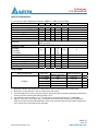
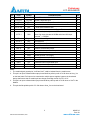
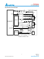
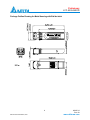
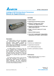
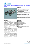
Preliminary
LCP-8500A4EDR
RoHS Compliant 8.5Gb/s Short Wavelength SFP+ Transceiver
FEATURES
Compliant with SFP+ MSA, SFF-8431
specification and Fiber Channel FC-PI-4
Compliant with SFF-8472 MSA
850nm VCSEL laser
Built-in digital diagnostic monitoring function
Backward compatible to 2G/4G Fiber Channel
Duplex LC connector
Power consumption <1W
Laser Class 1 Product which comply with the
requirements of IEC 60825-1 and IEC 60825-2
Description
Applications
The LCP-8500A4EDR is hot pluggable 3.3V
Small-Form-Factor transceiver modules designed
expressly
for
high-speed
communication
applications that require rates of up to 8.5Gb/s.
It is compliant with SFP+ MSA, SFF-8431
specification and Fiber Channel FC-PI-4, as well as
MSA SFF-8472.
High-speed storage area networks
Computer cluster cross-connect
Custom high-speed data pipes
The LCP-8500A4EDR transceivers provide with the
LC receptacle that is compatible with the industry
standard LCTM connector. The transceiver is also
compatible with industry standard RFT connector
and cage.
The post-amplifier of the LCP-8500A4EDR also
includes a LOS (Loss Of Signal) circuit that
provides a TTL logic-high output when an
unusable optical signal level is detected.
The LCP-8500A4EDR transceiver is a Class 1
eye safety product. The optical power levels,
under normal operation, are at eye safe level.
1
DELTA ELECTRONICS, INC.
2008/7/16
Rev. 0A
www.deltaww.com
Preliminary
LCP-8500A4EDR
Absolute Maximum Ratings
Parameter
Storage Temperature
Supply Voltage
Relative Humidity
Symbol
TS
VCC
RH
Min.
-40
0
5
Typ.
Max.
85
4
95
Unit
ºC
V
%
Note
Min.
-5
3.135
Typ.
Unit
ºC
V
Gbps
Note
8.5
Max.
70
3.465
9
Typ.
180
Max.
300
Unit
MA
Note
Recommended Operating Conditions
Parameter
Case Operating Temperature
Supply Voltage
Data Rate
Symbol
TC
VCC
Electrical Characteristics
(VCC=3.135V to 3.465V)
Parameter
Total Supply Current
Transmitter
Differential Input Voltage
Data Input Rise/Fall Time
Transmitter Disable Input-High
Transmitter Disable Input-Low
Transmitter Fault Output-High
Transmitter Fault Output-Low
Receiver
Differential Output Voltage
Data Output Rise/Fall Time
LOS Output Voltage-Low
LOS Output Voltage-High
RS0, RS1
Symbol
ICC
Min.
Vin,pp
1000
40
VCC+0.3
0.8
VCC+0.3
0.8
mVppd
Ps
V
V
V
V
1
2
VDISH
VDISL
VTXFH
VTXFL
120
15
2
0
2
0
Vout,pp
300
2
0
-0.3
2.0
mVppd
Ps
V
V
V
V
3
1
VLOSH
VLOSL
VIL
VIH
1000
45
VCC+0.3
0.8
0.8
Vcc+0.3
4
Notes:
1.
Internally AC coupled and terminated to 100 Ohm differential load.
2.
These are 20%~80% values.
3.
Internally AC coupled, but requires a 100 Ohm differential termination at or internal to Serializer/ Deserializer.
4.
Shall be pulled low to VeeT with a >30k ohms resistor in the module.
2
DELTA ELECTRONICS, INC.
2008/7/16
Rev. 0A
www.deltaww.com
Preliminary
LCP-8500A4EDR
Optical Characteristics
(VCC=3.135V to 3.465V, Data Rate=8.5Gb/sec, PRBS=27-1 NRZ, 50/125µm MMF)
Parameter
Transmitter
Output Optical Power (Avg.)
Optical Modulation Amplitude
Center Wavelength
Spectral Width (RMS)
Optical Rise/Fall Time (20% - 80%)
RIN12OMA
Output Eye
Receiver
Sensitivity in OMA
@8.5Gbps
@4.25Gbps
@2.125Gbps
Input Optical Wavelength
Average Received Power, max
LOS-De-asserted (Avg.)
LOS-Asserted (Avg.)
LOS-Hysteresis
Optical Return Loss
Symbol
Min.
PO
OMA
λ
σ
tr/ tf
-8.2
302
840
Typ.
Max.
Unit
Note
-1.8
dBm
1
µW
850
860
nm
0.65
nm
50/50
ps
2
-128 dB/Hz
3
Complies with the ANSI FC-PI-4 Rev. 6.01 specification, and is class
1 laser eye safety
PIN
λ
Rmax
PD
PA
PD -PA
ORL
840
0
850
76
61
49
860
-14
-30
0.5
12
µW
4
nm
dBm
dBm
dBm
dB
dB
Link Length
Data Rate/Standard
Fiber Type
62.5/125 µm
8.5Gbps
MMF
µm
MMF
50/125
50/125 µm MMF
50/125 µm MMF
50/125 µm MMF
Modal Bandwidth
@850nm (MHz*km)
200
500
900
1500
2000
Distance Range(m)
0.5 to 21
0.5 to 50
0.5 to 90
0.5 to 120
0.5 to 150
Notes
.
5
5
5
5
5
Notes:
1. Equivalent extinction ratio specification for Fiber Channel. Allows smaller ER at higher average power.
2. Measured at nominal data rate. These are unfiltered 20%~80% values.
3. Transmitter Dispersion Penalty is measured using the methods specified in the IEEE standard 802.3-2005 Clause
52 except that the transversal filter differential delay is 33 ps.
4. The sensitivity is tested at a BER of 1×10-12 or better with an input signal consisting of 27-1 NRZ PRBS.
5. Distance, shown in the “Link Length” table, are calculated for worst case fiber and transceiver characteristics
based on the optical and electrical specifications shown in this document using techniques utilized in IEEE 802.3.
In the nominal case, longer distances are achievable.
3
DELTA ELECTRONICS, INC.
2008/7/16
Rev. 0A
www.deltaww.com
Preliminary
LCP-8500A4EDR
SFP+ Transceiver Electrical Pad Layout
Module Electrical Pin Definition
4
DELTA ELECTRONICS, INC.
2008/7/16
Rev. 0A
www.deltaww.com
Preliminary
LCP-8500A4EDR
Pin
Logic
1
Symbol
VeeT
Name/Description
Module Transmitter Ground
1
Module Transmitter Fault
2
Transmitter Disable; Turns off transmitter laser output
3
2
LVTTL-O
TX_Fault
3
LVTTL-I
TX_Disable
4
LVTTL-I/O
SDA
2- write Serial Interface Data Line
5
LVTTL-I/O
SCL
2- write Serial Interface Clock
6
MOD_ABS
Note
Module Absent, connected to VeeT or VeeR in the module
4
Rate Select 0, optionally controls SFP+ module receiver.
When High input data rate>4.25GBd and when LOW input
data rate ≦ 4.25GBd.
7
LVTTL-I
RS0
8
LVTTL-O
RX_LOS
9
LVTTL-I
RS1
Not Implement
10
VeeR
Module Receiver Ground
1
11
VeeR
Module Receiver Ground
1
Receiver Loss of Signal Indication
12
CML-O
RD-
Receiver Inverted Data Output
13
CML-O
RD+
Receiver Non-Inverter Data Output
14
VeeR
Module Receiver Ground
15
VccR
Module Receiver 3.3V Supply
16
VccT
Module Transmitter 3.3V Supply
17
VeeT
Module Transmitter Ground
18
CML-I
TD+
Transmitter Non-Inverted Data Input
19
CML-I
TD-
Transmitter Inverted Data Input
20
VeeT
Module Transmitter Ground
2
1
1
1
Notes:
1. The module signal ground pins, VeeR and VeeT, shall be isolated from the module case.
2. This pin is an open collector/drain output pin and shall be pulled up with 4.7k-10k ohms to Host_Vcc
on the host board. Pull ups can be connected to multiple power supplies, however the host board
design shall ensure that no module pin has voltage exceeding module VccT/R + 0.5V.
3. This pin is an open collector/drain input pin and shall be pulled up with 4.7k-10k ohms to VccT in the
Module.
4. This pin shall be pulled up with 4.7k-10k ohms to Host_Vcc on the host board.
5
DELTA ELECTRONICS, INC.
2008/7/16
Rev. 0A
www.deltaww.com
Preliminary
LCP-8500A4EDR
Low speed electrical control pins and 2-wire interface
In addition to the 2-wire serial interface, the SFP+ module has the following low speed pins for control and
status:
‧ TX_Fault
‧ TX_Disable
‧ RS0/RS1
‧ MOD_ABS
‧ RX_LOS
1. TX_Fault
.TX_Fault is a module output pin that when High, indicates that the module transmitter has detected a fault
condition related to laser operation or safety.
The TX_Fault output pin is an open drain/collector and must be pulled p to the Host_Vcc with 4.7k-10k
ohms on the host board.
2. TX_Disable
TX_Disable is a module input pin. When TX_Disable is asserted High or Left open, the SFP+ module
transmitter output must be turned off. The TX_DIS pin must be pulled up to VccT in the SFP+ module.
3. RS0/RS1
RS0 and RS1 are module input rate select pins and are pulled low to VeeT with a > 30kΩ resistor in the
module. RS0 is an input hardware pin which optionally selects the optical receives data path rate
coverage for an SFP+ module. RS1 is an input hardware pin which optionally selects the optical transmits
path data rate coverage for an SFP+ module.
RS1 is commonly connected to VeeT or VeeR in the legacy SFP modules. The host needs to ensure that
it will not be damaged if this pin is connected to VeeT or VeeR in the module.
4. MOD_ABS
Mod_ABS is pulled up to Host_Vcc with 4.7k-10k ohms on the host board and connected to VeeT or VeeR
in the SFP+ module. MOD_ABS is then asserted “High” when the SFP+ module is physically absent from
a host slot. In the SFP MSA (INF8074i) this pin had the same function but is called MOD_DEF0.
5. SCL/SDA
SCL is the 2-wire interface clock and SDA is the 2-wire interface data line. SCL and SDA are pulled up to
a voltage in the range of 3.14V to 3.46V on the host.
6. RX_LOS
RX_LOS when High Indicated an optical signal level below that specified in the relevant standard. The
RX_LOS pin is an open drain/collector outpit and must be pulled up to host Vcc with a 4.7k-10k ohms on
the host board.
RX_LOS assert min and de-assert max are defined in the relevant standard. To avoid spurious transition
of RX_LOS a minimum hysteresis of 0.5 dBo is recommended.
6
DELTA ELECTRONICS, INC.
2008/7/16
Rev. 0A
www.deltaww.com
Preliminary
LCP-8500A4EDR
Recommend Circuit Schematic
VCC
1uH
3.3V
Protocol Vcc
10uF
0.1uF
DELTA SFP+ Module
1uH
RES1
0.1uF
VccT
10K Ohms
Tx_Disable
Tx_Disable
Tx_Fault
Tx_Fault
TD+
0.01uF
100 Ohms
0.01uF
Laser Diode
Laser Driver
TD-
Protocol IC
VeeT
SerDes IC
RES1
10uF
0.1uF
VccR
RD+
0.01uF
100 Ohms*
Preamp &
Quantizer
Photo Diode
RDRx_LOS
0.01uF
Rx_LOS
VeeR
Receiver Rate Select
RS0
Transmitter Rate Select
3.3V
RS1
30k Ohms
RES1 RES1 RES1
30k Ohms
SCL
PLD / PAL
Micro
Control
SDA
EEPROM
MOD-ABS
RES1 = 4.7k TO 10k Ohms
* Depands on SerDes IC used
7
DELTA ELECTRONICS, INC.
2008/7/16
Rev. 0A
www.deltaww.com
Preliminary
LCP-8500A4EDR
Complies with 21 CFR
1040.10 and 1040.11
Made in x
FS
Package Outline Drawing for Metal Housing with Bail de-latch
8
DELTA ELECTRONICS, INC.
2008/7/16
Rev. 0A
www.deltaww.com
Preliminary
LCP-8500A4EDR
Timing parameters for SFP+ management
Parameter
TX_DISABLE Assert time
TX_DISABLE Negate time
Time to initialize 2-wire
interfase
Time to initialize
Time to initialize cooled
module
Time to Power Up to Level 2
Time to Power Down from
Level 2
TX_Fault assert
TX_Fault assert for cooled
module
TX_Fault Reset
Module Reset
RS0, RS1 rate select timing
for FC
RS0, RS1 rate select timing
non FC
RX_LOS assert delay
RX_LOS negate delay
Symbol
t_off
t_on
Min.
Max.
10
2
Unit
µsec
msec
Note
1
2
t_2w_start_up
300
msec
3
t_start_up
300
msec
4
t_start_up_cooled
90
sec
4
t_power_level2
300
msec
5
T_power_down
300
msec
6
TX_Fault_on
1
msec
7
TX_Fault_on
50
msec
7
TBD
µsec
msec
8
TBD
500
µsec
9
t_RS0, t_RS1
10
msec
9
t_los_on
t_los_off
100
100
µsec
µsec
10
11
t_reset
t_module_reset
t_RS0_FC,
RS1_FC
10
Notes:
1)
Rising edge of TX_Disable to fall of output signal below 10% of nominal.
2)
Falling edge of TX_Disable to rise of output signal above 90% of nominal. This only applies in normal operation,
3)
From power on or negation of TX_Disable.
4)
From power on or TX_Disable negated during power up, or TX_Fault recovery, until non-cooled power level 1
not during start up or fault recovery.
part (or non-cooled power level 2 part already enabled at power level 2 for TX_Fault recovery) is fully operational.
5)
From falling edge of stop bit enabling power level 2 until non-cooled module is fully operational.
6)
From falling edge of stop bit disabling power level 2 until module is within power level 1 requirements.
7)
From Occurrence of fault to assertion of TX_Fault.
8)
Time TX_Disable must be held High to reset TX_Fault.
9)
From assertion till stable output.
10) From Occurrence of loss of signal to assertion of LOS.
11) From Occurrence of presence of signal to negation of RX_LOS.
9
DELTA ELECTRONICS, INC.
2008/7/16
Rev. 0A
www.deltaww.com
Preliminary
LCP-8500A4EDR
Enhanced Digital Diagnostic Interface
The memory map in the following describes an extension to the memory map defined in SFP+ MSA. The enhanced
interface uses the two wire serial bus address 1010001x (A2h) to provide diagnostic information about the module’s
present operating conditions.
2 wire address 1010000 X (A0h)
2 wire address 1010001 X (A2h)
0
0
Alarm and Warning Thresholds
(56 bytes)
55
Serial ID Defined by SFP MSA
(96 bytes)
56
Cal Constants
(40 bytes)
95
96
95
96
Real Time Diagnostic Interface
(24 bytes)
119
Vender Specific
(32 bytes)
120
Vender Specific(Note)
127
127
128
128
Reserved in SFP MSA
(128 bytes)
247
248
255
255
User Writable EEPROM
(120 bytes)
Vender Specific
(8 bytes)
Digital Diagnostic Memory Map Specific Data Field Descriptions
Note:
1) Write the password (11h, 11h, 11h, 11h) on the bytes of 123-126 of address A2h then the address of
bytes 128-255 (User Writable) can be read and written.
10
DELTA ELECTRONICS, INC.
2008/7/16
Rev. 0A
www.deltaww.com
Preliminary
LCP-8500A4EDR
EEPROM Serial ID Memory Contents (2-Wire Address A0h)
Address
00
01
02
03
04
05
06
07
08
09
10
11
12
13
14
15
16
17
18
19
20
21
22
23
24
25
26
27
28
29
30
31
32
33
34
35
36
37
38
39
40
41
42
Hex
03
04
07
03
00
00
00
40
40
0C
54
03
55
03
00
00
05
02
00
00
44
45
4C
54
41
20
20
20
20
20
20
20
20
20
20
20
00
00
00
00
4C
43
50
ASCII
D
E
L
T
A
L
C
P
Address
43
44
45
46
47
48
49
50
51
52
53
54
55
56
57
58
59
60
61
62
63
64
65
66
67
68
69
70
71
72
73
74
75
76
77
78
79
80
81
82
83
84
85
Hex
2D
38
35
30
30
41
34
45
44
52
30
30
30
41
20
20
20
03
52
00
CS1
00
3A
00
00
SN
SN
SN
SN
SN
SN
SN
SN
SN
SN
SN
SN
SN
SN
SN
SN
DC
DC
ASCII
8
5
0
0
A
4
E
D
R
Note 1
Note 2
Note 3
Address
86
87
88
89
90
91
92
93
94
95
96
97
98
99
100
101
102
103
104
105
106
107
108
109
110
111
112
113
114
115
116
117
118
119
120
121
122
123
124
125
126
127
128
Hex
DC
DC
DC
DC
DC
DC
68
FA
03
CS2
00
00
00
00
00
00
00
00
00
00
00
00
00
00
00
00
00
00
00
00
00
00
00
00
00
00
00
00
00
00
00
00
00
ASCII
Note 4
Note5
Notes:
1)
Byte 63: Check sum of bytes 0-62.
2)
Byte 68-83: Serial number.
3)
Byte 84-91: Date code.
4)
Byte 95: Check sum of bytes 64-94.
5)
Byte 128 to 255 had been set hex 00.
11
DELTA ELECTRONICS, INC.
2008/7/16
Rev. 0A
www.deltaww.com
Preliminary
LCP-8500A4EDR
Digital Diagnostic Monitoring Interface
Alarm and Warning Thresholds (2-Wire Address A2h)
Address
#
Bytes
00-01
02-03
04-05
06-07
08-09
10-11
12-13
14-15
16-17
18-19
20-21
22-23
24-25
26-27
28-29
30-31
32-33
34-35
36-37
38-39
40-45
56-91
92-94
95
96-97
98-99
100-101
102-103
104-105
106-109
110
111
112-119
2
2
2
2
2
2
2
2
2
2
2
2
2
2
2
2
2
2
2
2
16
36
3
1
2
2
2
2
2
4
1
1
8
Name
Temp High Alarm
Temp Low Alarm
Temp High Warning
Temp Low Warning
Voltage High Alarm
Voltage Low Alarm
Voltage High Warning
Voltage Low Warning
Bias High Alarm
Bias Low Alarm
Bias High Warning
Bias Low Warning
TX Power High Alarm
TX Power Low Alarm
TX Power High Warning
TX Power Low Warning
RX Power High Alarm
RX Power Low Alarm
RX Power High Warning
RX Power Low Warning
Reversed
External Calibration Constants
Reversed
Checksum
Real Time Temperature
Real Time Supply Voltage
Real Time Tx Bias Current
Real Time Tx Optical Power
Real Time Rx Received Power
Reserved
Optional Status/ Control Bits
Reserved
Optional Set of Alarm and Warning
Value (Dec.)
Unit
Note
TC (MAX.)+15
TC (MIN.)
TC (MAX.)+10
TC (MIN.)+10
Vcc+5%
Vcc-5%
Vcc+3%
Vcc-3%
IOP+10
IOP-5
IOP+7
IOP-3
P+3
P-3
P+2
P-2
P0+3
PS-2
P0+2
PS
℃
1
Volt
mA
2
dBm
3
dBm
4
5
6
7
Notes:
1) TC: Case operating temperature.
2) IOP: Operating current at room temperature. The min. setting current is 0 mA.
3) P: Operating optical power of transmitter at room temperature.
4) P0: Overload optical power of receiver.
PS: Sensitivity optical power of receiver.
5) Byte 95 contains the low order 8bits of sum of bytes 0-94.
12
DELTA ELECTRONICS, INC.
2008/7/16
Rev. 0A
www.deltaww.com
Preliminary
LCP-8500A4EDR
6)
State/ Control Bits
Byte
110
110
110
110
110
110
110
110
Bit
7
6
5
4
3
2
1
0
Name
Tx Disable State
Soft Tx Disable
Reserved
Rate Select tate
Soft Rate Select
Tx Fault
LOS
Data_Ready_Bar
Description
Digital state of the Tx disable input pin
Read/ Write bit that allow software disable of laser
NA
NA
Digital state of the Tx fault output pin
Digital state of the LOS output pin.
NA
7)
Optional Set of Alarm and Warning
Byte
112
112
112
112
112
112
112
112
113
113
113
116
116
116
116
116
116
116
116
117
117
117
Bit
7
6
5
4
3
2
1
0
7
6
5-0
7
6
5
4
3
2
1
0
7
6
5-0
Name
Temp High Alarm
Temp Low Alarm
Vcc High Alarm
Vcc Low Alarm
Tx Bias High Alarm
Tx Bias Low Alarm
Tx Power High Alarm
Tx Power Low Alarm
Rx Power High Alarm
Rx Power Low Alarm
Reserved
Temp High Warning
Temp Low Warning
Vcc High Warning
Vcc Low Warning
Tx Bias High Warning
Tx Bias Low Warning
Tx Power High Warning
Tx Power Low Warning
Rx Power High Warning
Rx Power Low Warning
Reserved
Description
Set when internal temperature exceeds high alarm level
Set when internal temperature is below low alarm level
Set when internal supply voltage exceeds high alarm level
Set when internal supply voltage is below low alarm level
Set when Tx Bias current exceeds high alarm level
Set when Tx Bias current is below low alarm level
Set when Tx output power exceeds high alarm level
Set when Tx output power is below low alarm level
Set when received power exceeds high alarm level
Set when received power is below low alarm level
Set when internal temperature exceeds high warning level
Set when internal temperature is below low warning level
Set when internal supply voltage exceeds high warning level
Set when internal supply voltage is below low warning level
Set when Tx Bias current exceeds high warning level
Set when Tx Bias current is below low warning level
Set when Tx output power exceeds high warning level
Set when Tx output power is below low warning level
Set when received power exceeds high warning level
Set when received power is below low warning level
Digital Diagnostic Monitor Accuracy
Parameter
Typical Value
Note
± 3℃
± 3%
± 10%
± 1.5dB
± 3dB
1
2
Transceiver Temperature
Power Supply Voltage
TX Bias Current
TX Optical Power
RX Optical Power
Notes:
1)
Temperature is measured internal to the transceiver.
2) Voltage is measured internal to the transceiver.
13
DELTA ELECTRONICS, INC.
2008/7/16
Rev. 0A
www.deltaww.com
Preliminary
LCP-8500A4EDR
Regulatory Compliance
Test Item
Reference
(#1)
FCC Class B
Electromagnetic Interference
EN 55022 Class B
EMC
CISPR 22
(#2) Immunity:
Qty’
5
EN 61000-4-3
Radio Frequency
Electromagnetic Field
IEC 1000-4-3
(#3) Immunity:
EN 61000-4-2
Electrostatic Discharge to the
Duplex SC Receptacle
IEC 1000-4-2
Evaluation
5
(1) Satisfied with electrical characteristics of
product spec.
5
(2) No physical damage
IEC 801.2
(#4) Electrostatic Discharge to MIL-STD-883C
the Electrical Pins
Method 3015.4
EIAJ#1988.3.2B
5
Version 2,
Machine model
14
DELTA ELECTRONICS, INC.
2008/7/16
Rev. 0A
www.deltaww.com