1
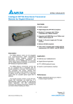
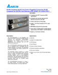
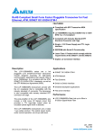
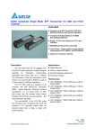
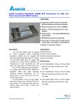
SPBD-155E4J1RD
Intelligent SFP Bi-Directional Transceiver Module
for Fast Ethernet, ATM, SONET OC-3/SDH STM-1
FEATURES
RoHS compliant
Digital Diagnostic SFF-8472, Rev. 9.5 MSA
compliant
Simplex LC connector with 1310nm
Transmitter and 1550nm Receiver
Single + 3.3V power supply and TTL logic
interface
Bellcore GR-468 compliant
Laser class 1 product which comply with the
requirements of IEC 60825-1 and IEC 60825-2
Description
Application
The SPBD-155xxxxx series are hot pluggable
3.3V Small-Form-Factor (SFP) Bi-Directional
transceiver module designed expressly for
high-speed communication applications that
require rates of up to 155Mbit/sec. It is compliant
with the Fast Ethernet, ATM, SONET OC-3/SDH
STM-1 standards, as well as the SFP Multisource
Agreement (MSA).
TTC TS-1000
ITU-T G.985
IEEE 802.3ah 100BASE-BX/ Fast Ethernet
SONET OC-3/SDH STM-1
FTTx WDM Broadband Access
The SPBD-155xxxxx transceivers provide with
the LC receptacle that is compatible with the
industry standard LC connector. The transceiver is
also compatible with industry standard RFT
connector and cage. It also includes a LOS (Loss
Of Signal) circuit that provides a TTL logic-high
output when an unusable optical signal level is
detected.
Switch to switch/backbone interface
Performance
SPBD-155E4J1RD data link up to 15km in
9/125um single mode fiber.
The module includes 1310nm un-cool FP laser,
InGaAs PIN, Preamplifer and WDM filter in a
high-integrated optical assembly for high-density
system application. The SFP Bi-Directional
transceiver can upgrade transmission capacity very
convenient without installing new fibers.
1
DELTA ELECTRONICS, INC.
Revision: S1
04/11/2007
www.deltaww.com
SPBD-155E4J1RD
1. Absolute Maximum Ratings
Parameter
Storage Temperature
Storage Ambient Humidity
Power Supply Voltage
Signal Input Voltage
Optical Input Power (Peak)
Symbol
Ts
HA
VCC
Min.
-40
5
0
-0.3
Typ.
Max.
85
95
5
Vcc+0.3
+4
Unit
ºC
%
V
V
dBm
Note
Min.
-5
5
3.135
Typ.
Max.
75
85
3.465
300
100
155.52
15
Unit
ºC
%
V
mA
mVp-p
Mbps
km
Note
Note (1)
Symbol
Min.
Typ.
Max.
PO
-14
-8
ER
10
λC
1260
1310
1360
σ
6
POff
-45
tr/tf
1.3
TJ
1
ORLT
14
-116
RIN
TDP
1
Compliant with Bellcore TR-NWT-000253
and ITU recommendation G.957
Unit
dBm
dB
nm
nm
dBm
ns
ns
dB
dB/Hz
dB
2. Recommended Operating Conditions
Parameter
Operating Case Temperature
Ambient Humidity
Power Supply Voltage
Power Supply Current
Power Supply Noise Rejection
Data Rate
Transmission Distance
Symbol
TC
HA
VCC
ICC
3.3
10
Non-condensing
100Hz to 1MHz
Note (1). Measured on topside of case front center.
3. Specification of Transmitter
Parameter
Average Launched Power
Optical Extinction Ratio
Center Wavelength
Spectrum Width (RMS)
Transmitter OFF Output Power
Optical Rise/Fall Time
Total Jitter
Optical Return Loss Tolerance
Relative Intensity Noise
Dispersion Penalty
Output Eye Mask
Note
Note (1)
FP Laser
Note (2)
Note (3)
Note (4)
Note (1). Launched power (avg.) is power coupled into a single mode fiber.
Note (2). These are unfiltered 20-80% values.
Note (3). Measure at 223-1 NRZ PRBS pattern.
Note (4). Eye Mask definition
1.20
Amplitude
1.00
Mean level of logical "1"
0.80
0.50
0.20
0.00
Mean level of logical "0"
-0.20
0.00 0.15
0.35
0.65
Time
2
0.85 1.00
Optical Pulse Mask with Bessel Filter Specified in ITU-T G.957
DELTA ELECTRONICS, INC.
Revision: S1
04/11/2007
www.deltaww.com
SPBD-155E4J1RD
4. Specification of Receiver
Parameter
Input Optical Wavelength
Receiver Sensitivity
Input Saturation Power (Overload)
LOS-Deassert Power
LOS-Assert Power
LOS Hysteresis
Optical Reflectance
Output Data Rise/Fall time
S/X Endurance
Optical Isolation
Symbol
λIN
PIN
PSAT
PA
PD
PA-PD
Min.
1480
-3
-44
0.5
Typ.
Max.
1600
-31
-31
2
5
-14
1.5
10
tr/tf
25
-10
Unit
nm
dBm
dBm
dBm
dBm
dB
dB
ns
dB
dB
Note
PIN-PD
Note (1)
Note (2)
Note (3)
Note (4)
Note (5)
Note (6)
23
Note (1). Measured with 1520nm, ER=10dB; BER =<10 @PRBS=2 -1 NRZ
Note (2). When LOS asserted, the data output is Low-level (fixed)
Note (3). When the terminal is viewed from the optical path, the reflection toward the optical path of the
optical signal with a central wavelength of 1480nm to 1580nm transmitted to terminal.
Note (4). These are 20%~80% values
Note (5). X=10 MHz, Rectangular BER =10-10
Note (6). Receiver isolation between 1260nm ~1360nm
5. Electrical Interface Characteristics
Parameter
Transmitter
Total Supply Current
Differential Data Input Swing
Differential line input Impedance
Transmitter Disable Input-High
Transmitter Disable Input-Low
Transmitter Fault Output-High
Transmitter Fault Output-Low
Transmitter Fault Pull up Resistor
Receiver
Total Supply Current
Differential Data Output Swing
LOS Output Voltage-High
LOS Output Voltage-Low
Receiver LOS Load
Symbol
Min.
ICC
VDT
RIN
VDISH
VDISL
VTXFH
VTXFL
RTX_FAULT
500
80
2
0
2
0
4.7
ICC
VDR
VLOSH
VLOSL
RRXLOS
400
2
0
4.7
Typ.
100
Max.
Unit
Note
A
2400
120
VCC
0.8
VCC+0.3
0.8
10
mA
mVp-p
Ohm
V
V
V
V
kΩ
Note (1)
B
2000
VCC+0.3
0.8
10
mA
mVp-p
V
V
kΩ
Note (1)
Note (4)
Note (2)
Note (3)
Note (3)
Note (1). A (TX)+ B (RX) = 300mA
(A: Not include termination circuit; B: using a resister of 150Ω between Data-output and ground)
Note (2). There is an internal 4.7 to 10kΩ pull-up resistor to VccT.
Note (3). Pull up to VCC on host Board.
Note (4). Internally AC coupled with LVPECL output, but requires a 100Ohm differential termination at or
internal to Serializer/ Deserializer.
3
DELTA ELECTRONICS, INC.
Revision: S1
04/11/2007
www.deltaww.com
SPBD-155E4J1RD
6. Enhanced Digital Diagnostic Interface
The memory map in the following describes an extension to the memory map defined in SFP MSA.
The enhanced interface uses the two wire serial bus address 1010001X(A2h) to provide diagnostic
information about the module’s present operating conditions.
2 wire address 1010000 X (A0h)
2 wire address 1010001 X (A2h)
0
0
Alarm and Warning Thresholds
(56 bytes)
Serial ID Defined by SFP MSA
(96 bytes)
55
56
Cal Constants
(40 bytes)
95
96
95
96
Real Time Diagnostic Interface
(24 bytes)
Vender Specific
(32 bytes)
119
120
Vender Specific
127
127
128
128
User Writable EEPROM
(120 bytes)
Reserved in SFP MSA
(128 bytes)
247
248
255
255
Vender Specific
(8 bytes)
7. Digital Diagnostic Monitor Accuracy
Parameter
Accuracy
± 3℃
Transceiver Internal Temperature
Power Supply Internal Voltage
± 3%
TX Bias Current
± 10%
TX Optical Power
± 3dB
RX Optical Power
± 3dB
Unit
℃
V
mA
dBm
dBm
Calibration
Internal
Internal
Internal
Internal
Internal
Note
TC=-5~+75℃
VCC=3.3V±5%
Specified by nominal bias value
-14 to -8dBm
-31 to -8dBm
Note. Temperature and Voltage is measured internal to the transceiver.
4
DELTA ELECTRONICS, INC.
Revision: S1
04/11/2007
www.deltaww.com
SPBD-155E4J1RD
8. Pin Description
SFP Transceiver Electrical Pad Layout
Host Board Connector Pad Layout
Pin Function Definitions
Pin Num.
1
2
3
4
5
6
7
8
9
10
11
12
13
14
15
16
17
18
19
20
Name
VeeT
TX Fault
TX Disable
MOD-DEF2
MOD-DEF1
MOD-DEF0
Rate Select
LOS
VeeR
VeeR
VeeR
RDRD+
VeeR
VccR
VccT
VeeT
TD+
TDVeeT
Function
Transmitter Ground
Transmitter Fault Indication
Transmitter Disable
Module Definition 2
Module Definition 1
Module Definition 0
Not Connect
Loss of Signal
Receiver Ground
Receiver Ground
Receiver Ground
Inv. Received Data Out
Received Data Out
Receiver Ground
Receiver Power
Transmitter Power
Transmitter Ground
Transmit Data In
Inv. Transmit Data In
Transmitter Ground
Plug Seq.
1
3
3
3
3
3
3
3
1
1
1
3
3
1
2
2
1
3
3
1
Notes
Note (1)
Note (2)
Note (3)
Note (4), 2 wire serial ID interface
Note (4), 2 wire serial ID interface
Note (4), Grounded in Module
Function not available
Note (5)
Note (6)
Note (6)
Note (7)
Note (7)
Note (8)
Note (8)
Plug Seq.: Pin engagement sequence during hot plugging.
5
DELTA ELECTRONICS, INC.
Revision: S1
04/11/2007
www.deltaww.com
SPBD-155E4J1RD
Notes:
1)
Circuit ground is internally isolated from frame (chassis) ground. Tx GND and Rx GND may be internally isolated
within the TRx module.
2)
TX Fault is an open collector/drain output, which should be pulled up with a 4.7K~10KΩ resistor on the host board.
Pull up voltage between 2.0V and VccT+0.3V. The output indicates Low when the transmitter is operating
normally, and High with a laser fault including laser end-of-life. In the low state, the output will be pulled to less
than 0.8V.
3)
TX disable is an input that is used to shut down the transmitter optical output. It is pulled up within the module
with a 4.7 – 10 K Ω resistor. Its states are:
4)
Low (0 – 0.8V):
Transmitter on
(>0.8, < 2.0V):
Undefined
High (2.0 – 3.465V):
Transmitter Disabled
Open:
Transmitter Disabled
Mod-Def 0,1,2. These are the module definition pins. They should be pulled up with a 4.7K – 10KΩresistor on the
host board. The pull-up voltage shall be VccT or VccR.
Mod-Def 0 is grounded by the module to indicate that the module is present
Mod-Def 1 is the clock line of two-wire serial interface for serial ID
Mod-Def 2 is the data line of two-wire serial interface for serial ID
5)
LOS (Loss of Signal) is an open collector/drain output, which should be pulled up with a 4.7K – 10KΩ resistor.
Pull up voltage between 2.0V and VccR+0.3V. When high, this output indicates the received optical power is
below the worst-case receiver sensitivity. Low indicates normal operation. In the low state, the output will be
pulled to less than 0.8V.
6)
RD-/+: These are the differential receiver outputs. They are AC coupled 100Ω differential lines which should be
terminated with 100Ω (differential) at the user SERDES. The AC coupling is done inside the module and is thus
not required on the host board. The voltage swing on these lines will be between 400 and 2000 mV differential
(200 – 1000 mV single ended) when properly terminated.
7)
VccR and VccT are the receiver and transmitter power supplies. They are defined as 3.3V ±5% at the SFP
connector pin. Recommended host board power supply filtering is shown below page. Inductors with DC
resistance of less than 1 Ohm should be used in order to maintain the required voltage at the SFP input pin with
3.3V supply voltage. When the recommended supply-filtering network is used, hot plugging of the SFP
transceiver module will result in an inrush current of no more than 30 mA greater than the steady state value.
8) TD-/+: These are the differential transmitter inputs. They are AC-coupled, differential lines with 100 Ω
differential termination inside the module. The AC coupling is done inside the module and is thus not
required on the host board. The inputs will accept differential swings of 500 – 2400 mV (250 – 1200
mV single-ended), though it is recommended that values between 500 and 1200 mV differential (250 –
600 mV single-ended) be used for best EMI performance.
6
DELTA ELECTRONICS, INC.
Revision: S1
04/11/2007
www.deltaww.com
SPBD-155E4J1RD
9. Recommend Interface Circuit
VCC
1uH
3.3V
Protocol Vcc
DELTA SFP Module
1uH
RES1
10uF
0.1uF
0.1uF
VccT
10k Ohms
Tx_Disable
Tx_Disable
Tx_Fault
Tx_Fault
TD +
0.01uF
100 Ohms
TD -
Protocol IC
Laser Driver
Laser Diode
0.01uF
VeeT
SerDes IC
VccR
RES1
10uF
0.1uF
RD +
0.01uF
RD -
0.01uF
100 Ohms*
Preamp &
Quantizer
Photo Diode
Rx_LOS
Rx_LOS
3.3V
VeeR
RES1
RES1
RES1
PLD / PAL
Mod_def 2
EEPROM
Mod_def 1
Mod_def 0
RES1 = 4.7k to 10k Ohms
* Depands on SerDes IC used
SFP Host Board Schematic
Design criterion of the capacitor used is the
resonant frequency and its value must be in the
order of the nominal data rate. Short trace
lengths are mandatory.
Recommended Host Board Supply Filtering Network
7
DELTA ELECTRONICS, INC.
Revision: S1
04/11/2007
www.deltaww.com
SPBD-155E4J1RD
10. Outline Dimensions
Complies with 21 CFR
1040.10 and 1040.11
Made in x
FS
Class 1 Laser Product
XXXX nm Tx / Rx XXXX nm
Week (52Weeks/Year) : 1月2日=01
Transmitter Wavelength
1310nm
1550nm
Latch Color Identifier
Black
Yellow
8
DELTA ELECTRONICS, INC.
Revision: S1
04/11/2007
www.deltaww.com
SPBD-155E4J1RD
11. Regulatory Compliance
Feature
Electrostatic Discharge
(ESD) to the Electrical
Pins
Test Method
Reference
Performance
Human Body Model MIL-STD-883E Method 3015.7
(HBM)
EIA-JESD22-A114
(1) Satisfied with
Machine Model (MM) EIA-JESD22-A115
Electrostatic Discharge
(ESD) to the Simplex
Receptacle
Contact Discharge
Air Discharge
Radio Frequency
Electromagnetic Field
Immunity
IEC/EN 61000-4-2
IEC/EN 61000-4-3
electrical
characteristics of
product spec.
(2) No physical damage
FCC Part 15 Class B
EN 55022 Class B
Electromagnetic
Interference (EMI)
Laser Eye Safety
IEC/EN 61000-4-2
(CISPR 22A)
FDA/CDRH
FDA 21CFR 1040.10, 1040.11
CDRH File # 0420993
TUV
IEC/EN 60825-1
IEC/EN 60825-2
TUV
Certificate
R50032471
TUV
IEC/EN 60950
UL/CSA
UL 60950
#
Component Recognition
UL File # E239394
Appendix A. Document Revision
Version No.
S0
Date
2006-09-05
S1
2007-04-11
Description
Preliminary datasheet
Change the Receiver Differential Data Output Swing from CML to LVPECL
output
9
DELTA ELECTRONICS, INC.
Revision: S1
04/11/2007
www.deltaww.com