1
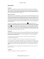
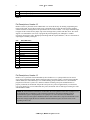
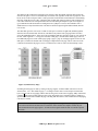
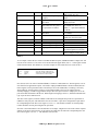
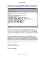
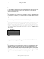
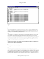
CRXi µCore Module CRµX Logic CRXi Manual For CRXi 122801.xxxxxxx, 22611.xxxxxxx Revision 5031.1 CRµX Logic, 2001 all rights reserved 1 2 CRXi µCore Module INTRODUCTION............................................................................................................ 3 Overview .................................................................................................................................................3 About this manual ...................................................................................................................................3 Disclaimer ...............................................................................................................................................3 Copyrights ...............................................................................................................................................3 Trademarks..............................................................................................................................................4 Warranty..................................................................................................................................................4 Safe Handling ..........................................................................................................................................4 Features ...................................................................................................................................................4 HARDWARE .................................................................................................................. 4 Pin Descriptions, Header J1 ....................................................................................................................4 Pin Descriptions, Header J2 ....................................................................................................................6 Pin Descriptions, Header J3 ....................................................................................................................6 Connections.............................................................................................................................................7 Power Input .............................................................................................................................................7 Resets ......................................................................................................................................................7 Serial Port Interface.................................................................................................................................7 NVSRAM Memory .................................................................................................................................8 Additional Scratchpad RAM ...................................................................................................................8 Flash ROM ..............................................................................................................................................8 External Chip Selects ............................................................................................................................10 CSIOP Register .....................................................................................................................................10 PROGRAMMING ..........................................................................................................12 Overview ...............................................................................................................................................12 Establishing Communication.................................................................................................................12 Bootloader Command Set......................................................................................................................13 ? - Help ..................................................................................................................................................13 P - Select memory page.........................................................................................................................14 E - Erase selected memory page............................................................................................................14 A - Erase all flash memory....................................................................................................................14 L - Load Intel hex file............................................................................................................................14 X - Examine ROM memory ..................................................................................................................14 S - Run checksum of selected ROM memory .......................................................................................14 I - Dump 8051 internal RAM memory..................................................................................................15 W - Write to RAM memory ..................................................................................................................15 Z - Clear RAM memory ........................................................................................................................15 C - Run checksum of RAM memory.....................................................................................................15 M - Run RAM memory test...................................................................................................................15 R - Read 8051 internal registers ............................................................................................................16 G - Execute user program......................................................................................................................16 CRµX Logic, 2001 all rights reserved CRXi µCore Module 3 Introduction Overview Thank you for your purchase of the CRXi core module. The CRXi is a state of the art microcontroller “engine” used in small control and data acquisition products. On this small form factor, measuring 3 by 2 inches, are the processor, flash ROM, non-volatile RAM, crystal, reset circuitry and expansion connector. This frees the design engineer of the many details of address/data bus connections and decoding glue logic normally associated with layout of these components. About this manual This manual will cover the CRXi module in 3 sections. The first section, Introduction, describes briefly the features of the CRXi, and very important disclaimer information. The user/buyer of this product is urged to read and fully understand the disclaimer and warranty section. If there are any questions in this area, user is urged to contact Crux Logic before using or purchasing this product. The second section, Hardware, will cover in greater detail the inner workings of the board, external chip selects, memory, expansion connector, specifications and related topics. The third section, Programming the CRXi, will cover how to program and use the internal bootloader, special registers unique to the CRXi, and more on the memory mapping and external chip selects. This manual is not intended as a tutorial on the 8051 microcontroller1 or PSD Flash architecture. It is beyond the scope of this document. The 8051 is covered in exhaustive detail from many sources, including web sites, books, datasheets and magazine articles, to name a few. The same holds true for the ST Micro PSD flash2 device. Crux Logic also does not support any toolsets, .ie assemblers, compilers, simulators or debuggers. The end user is assumed to have detailed knowledge of the 8051 architecture and the software tools he/she has chosen. References used by Crux Logic in the design of this product are given at the end of this document. The end user is urged to use these documents and data sheets in their design stage. These are easily obtainable through the manufacturers web sites. Disclaimer This manual has been checked for accuracy. Crux Logic assumes no liability for damages incurred directly or indirectly from errors and/or discrepancies between this manual and the CRXi. Crux Logic assumes no liability for the use or misuse of this product in the end users application, or the end users negligence or lack of knowledge in said application. Crux Logic products are intended for use in small, non-critical control systems, data acquisition, automation and education purposes. Crux Logic is not responsible or liable for any third party vendor product defects or discrepancies. Crux Logic products are not intended or authorized for use as critical components in life support systems, or in any systems where life or property or consequential damage are potential results of equipment failure. Such systems are systems which are used to support or sustain life, systems that are critical to property or equipment and whose failure could result in significant injury to the user and/or hardware or equipment failure. Use of this product in any form, or application, is the sole responsibility of the user/buyer. Design your application carefully . Copyrights This manual is copyright by Crux Logic, with all rights reserved. CRµX Logic, 2001 all rights reserved CRXi µCore Module 4 Trademarks Any brand and/or product names mentioned herein are trademarks or registered trademarks of their respective holders. Warranty Every effort has been made to insure a quality, reliable product. If any defects in materials are evident within a period of one year from the date of purchase Crux Logic will either , at its option, repair or replace products or individual components which are deemed defective. If a product should fail after this period, Crux Logic will repair or replace product at minimal cost. If product is deemed unacceptable for users application, for whatever reason, within a period of one year, Crux Logic will refund in full the entire amount of purchase, less shipping and handling, provided the item(s) are in working order. All shipping and handling costs for are the responsibility of the customer. Safe Handling As with any microcontroller and high speed digital products, safe, static free handling is mandatory. Controlling static and spurious noise/spikes is an obvious necessity in this environment , but sometimes its easier said than done. Crux Logic’s products are built and tested in a static controlled environment and shipped in static safe containers. Crux Logic recommends a static free workspace – static mats and grounding straps are highly recommended. Static discharge is a large cause of damaged parts. Features As stated previously, the CRXi module is a state of the art microcontroller engine. It uses the latest 8051 architecture, flash ROM and non-volatile RAM (no battery required). Also on board is a serial bootloader. The bootloader resides in a separate, protected memory space and has no effect on the final memory map. ! ! ! ! ! ! ! ! ! ! ! ! ! ! Dallas Semiconductor 80C320 high speed micro Executes 8051 instructions in 4 cycles as opposed to 12 Watchdog timer Dual data pointer 32K of non-volatile RAM – will store data with no power, no battery needed 2048 bytes of additional scratchpad RAM (volatile – not available on all models) Three 16 bit timer/counters Two full duplex serial ports 128K flash ROM – second 64K accessed via on chip page register Bootloader has no effect on memory map Three decoded active low chip selects Six general purpose memory mapped I/O Combination fourteen general purpose I/O, serial ports or 6 external interrupt sources Crystal and reset circuitry on board Hardware Pin Descriptions, Header J1 The header J1 is the 56 pin header running lengthwise along the board. Hole diameter is .040 inches. Pins are on .100 inch centers, accepting a wide variety of connector types. A few of the pins are marked with their pin numbers – these are pins 1 and 37, which are the VCC pins, and pins 20 and 56, which are the GROUND pins. Many pins have multiple functions, for example pin 2 can be used for either uController general purpose I/O port 1.0 or timer2 counter input. These are noted in the Table 1. U1 refers to the microcontroller, U2 refers to the PSD/Flash and U3 refers to the RAM memory chip. CRµX Logic, 2001 all rights reserved CRXi µCore Module PIN 1 2 3 4 5 6 7 8 9 10 11 12 13 14 15 16 17 18 19 20 21 22 23 24 25 26 27 28 29 30 31 32 33 34 35 36 37 38 39 40 41 42 43 44 45 46 47 48 49 50 51 52 53 DESCRIPTION VCC – 5 VDC power input P10 - U1 port 1.0 general purpose I/O or external I/O for timer/counter 2 P11 - U1 port 1.1 general purpose I/O or timer/counter 2 capture/reload trigger P12 - U1 port 1.2 general purpose I/O or serial port 1 input P13 - U1 port 1.3 general purpose I/O or serial port 1 output P14 - U1 port 1.4 general purpose I/O or external interrupt 2 (positive edge detect) P15 - U1 port 1.5 general purpose I/O or external interrupt 3 (negative edge detect) P16 - U1 port 1.6 general purpose I/O or external interrupt 4 (positive edge detect) P17 - U1 port 1.7 general purpose I/O or external interrupt 5 (negative edge detect) NC P30 - U1 port 3.0 general purpose I/O or serial port 0 input (RXD0) P31 - U1 port 3.1 general purpose I/O or serial port 0 output (TXD0) P32 - U1 port 3.2 general purpose I/O or external interrupt 0 P33 - U1 port 3.3 general purpose I/O or external interrupt 1 P43 - U1 port 3.4 general purpose I/O or timer 0 external input P35 - U1 port 3.5 general purpose I/O or timer 1 external input /WR – active low write line from U1 /RD – active low read line from U1 /RESET – system reset – a logic low on this pin resets U1 and U2 GND AD0 – multiplexed address/data bus AD1 – multiplexed address/data bus AD2 – multiplexed address/data bus AD3 – multiplexed address/data bus AD4 – multiplexed address/data bus AD5 – multiplexed address/data bus AD6 – multiplexed address/data bus AD7 – multiplexed address/data bus A8 – address bus, high byte A9 – address bus, high byte A10 – address bus, high byte A11 – address bus, high byte A12 – address bus, high byte A13 – address bus, high byte A14 – address bus, high byte A15 – address bus, high byte VCC – 5 VDC power input PC2 – U2 general purpose I/O PA0 – latched low order address byte PA1 – latched low order address byte PA2 – latched low order address byte PA3 – latched low order address byte PA4 – latched low order address byte PA5 – latched low order address byte PA6 – latched low order address byte PA7 – latched low order address byte PB0 – U2 general purpose I/O – optional CS3 active high chip select (addresses 8B00h – 8BFFh) PB1 – U2 general purpose I/O – optional CS4 active high chip select (addresses 8C00h – 8CFFh) PB2 – U2 general purpose I/O – optional CS5 active low chip select (addresses 8D00h – 8DFFh) PB3 – U2 general purpose I/O – optional CS6 active low chip select (addresses 8E00h – 8EFFh) /CS0 – active low external chip select (addresses 8800h – 88FFh) /CS1 – active low external chip select (addresses 8900h – 89FFh) /CS2 – active low external chip select (addresses 8A00h – 8AFFh) CRµX Logic, 2001 all rights reserved 5 CRXi µCore Module 6 54 55 56 PD1 – U2 general purpose I/O PD2 – U2 general purpose I/O GND Table 1 Pin Descriptions, Header J2 Header J2 is the 14 pin header on the CRXi board. It is used at the factory for initially programming and testing of the CRXi. It gives direct JTAG access to the PLD section for chip decodes, memory mapping scheme and other I/O configuration. The possibilities here are almost endless – Crux Logic could not begin to support all the various memory maps, chip selects and logic that is possible with this device. We do not support or recommend the user access or program the part through this port, although we wouldn’t necessarily discourage it either. With proper knowledge and the required hardware, this is a valid means of exploring the versatility of this part. PIN 1 2 3 4 5 6 7 8 9 10 11 12 13 14 DESCRIPTION NC NC GND NC PC5 – (JTAG TDI) PC3 – (JTAG TSTAT) VCC /RESET PC0 – (JTAG TMS) GND PC1 – (JTAG TCK) GND PC6 – (JTAG TDO) PC4 – (JTAG /TERR) Table 2 Pin Descriptions, Header J3 Header J3 is a 2 pin header located immediately above header J2. J3 is a jumper block used to control access to the bootloader program. With no shorting jumper across these points, execution begins at ROM address 0000h (user code) following a reset. With a shorting jumper installed across J3, the bootloader program is invoked on a system reset, with this condition: assuming serial port communications are properly connected, the bootloader will poll the serial port for a period of approximately 5 seconds after reset. If no character is received within this time period, bootloader will exit and begin executing user code at ROM address 0000h. NOTE: Be advised that the bootloader is invoked after all resets regardless of the state of jumper J3. It is the bootloader that is examining J3. This means the bootloader is using microcontroller resources (internal RAM, registers and peripherals) even if jumper J3 is removed to allow user ROM code execution. Therefor some registers and RAM will have data in them after a swap from bootloader to user ROM. It is strongly urged that the user initialize internal RAM and registers to known values in the beginning of their code. CRµX Logic, 2001 all rights reserved CRXi µCore Module 7 Connections Because the end users hardware applications are all different, no headers are soldered to the board. These are inexpensive and easy to install. This is not a cost saving measure – we believe this provides for more connection options. All header pins are on .100 centers with a .040 hole diameter. This will satisfy a wide range of connector types. Power Input Power is supplied to pins on header J1. A regulated 5 VDC, ±.125 volts is recommended. Apply +5 VDC at pin 1 or pin 37. Apply ground to pin 20 or pin 56. It does not matter which pin is used – pins 1 and 37 are connected internally as well as pins 20 and 56. Power supply must be capable of delivering a minimum of 80 mA of current. Additional circuitry using this supply will require additional current. Resets Reset circuitry is present on the CRXi to facilitate hardware resets. This consists of a microcontroller supervisor, U4, that holds the microcontroller and PSD in a reset until voltage reaches a stable operating level and a 74HC14 schmitt trigger, U5, to clean up reset edges and invert signals (PSD is low reset, microcontroller is a high reset). Additional circuitry can be added by the user if needed. Pin 19 on J1 is an active low reset input. For development a normally open momentary switch could be added between pins 19 and 20(GND) to facilitate resets. Holding this line low for a minimum 150 uS resets all hardware. Reset trip point is 4.625 VDC, ± .125 VDC. Serial Port Interface Communication with the CRXi module is accomplished through the microcontrollers serial port 0, pin 11 (receive) and pin 12 (transmit) on header J1. In order to establish connection with a PC, an RS-232 line driver/receiver is necessary. This hardware is not present on the CRXi and is needed to change voltage levels to be compatible with the CRXi. There are numerous IC’s available3 – consult the data sheet of the chosen device for wiring details and pinout. Connections are shown in Figure 1 below. Note the TXD (transmit) output from the micro connected (via the RS-232 driver/receiver) to the receive (DB-9 pin 2) of the PC and the RXD (receive) input to the micro connected to transmit (DB-9 pin 3) of the PC. Figure 1 (Serial Port Connection) CRµX Logic, 2001 all rights reserved CRXi µCore Module 8 This diagram (Figure 1) completes the requirement for a ‘NULL’ connection and would require a straight non-null serial cable. If the connection was wired RXD to RXD and TXD to TXD, use of a NULL serial cable would be required. No special software is needed – communication is established through a standard terminal emulator. The default settings are 19200 bps, 8, N, 1. Consult Crux Logic for baud rates other than this default. NVSRAM Memory The CRXi is furnished with a 32K byte non-volatile SRAM (U3). No battery is required – data can be retained in RAM practically indefinitely. Simtek claims 100 year data retention. This makes the CRXi ideal for data logging and applications where configuration data must remain intact yet be changeable. The Simtek STK15C88 is a fast SRAM with a nonvolatile EEPROM element incorporated in each memory cell. Data transfer from the non-volatile EEPROM to the SRAM occur automatically on powerup and transfer of the SRAM to the EEPROM occur automatically on powerdown. This action is completely transparent to the user and will appear as a battery backed SRAM would. In addition to the automatic store and recall operation, there are software initiated store (see Table 3) and recall operations. Using the software store cycle can insure data is copied to the EEPROM element before powerdown. Autostore on powerdown is limited to the following conditions. The STK15C88 uses system capacitance to perform an automatic store on powerdown. As long as the system power supply takes at least 10 mS to decay from 4.5 VDC to 3.6 VDC, the SRAM will safely and automatically store the SRAM data into EEPROM on powerdown. These conditions are usually easily met with a good power supply. If user cannot guarantee this decay ramp, the software store operation can be used. The software store is initiated by executing sequential reads from six specific address locations. These must be read in sequence and cannot be interrupted by any other read or write sequence, or the autostore will be aborted. Read address Read address Read address Read address Read address Read address 0E38h 31C7h 03E0h 3C1Fh 303Fh 0FC0h Table 3 The last entry, read of address 0FC0h initiates the store operation. To perform a recall operation, the same sequence of addresses are read with the exception of the last entry. The sixth read should be to address 0C63h. For detailed information on the Simtek NVSRAM, refer to SIMTEK4 data book. The NVSRAM is mapped to the 32767 (7FFFh) contiguous data bytes in the 80C320 data space beginning at address 0000h (see Figure 2). Additional Scratchpad RAM In certain CRXi modules, an additional 2048 (800h) bytes of SRAM is available. This memory is volatile and resides on the PSD flash (U2). Its location in the memory map is immediately following the NVSRAM and is mapped from 8000h to 87FFh (see Figure 2). In CRXi models without scatchpad RAM, the address space 8000h to 87FFh is not mapped. Reading or writing to this area will produce unwanted results and should be avoided. Flash ROM The heart of the CRXi module is the PDS/Flash part. PSD is an acronym for ‘Programmable System Device’ and contains 2 flash memory regions and a simple PLD (programmable logic device) that handles all the glue logic such as memory latches and chip selects. This is what gives the CRXi its versatility with such a low chip count. CRµX Logic, 2001 all rights reserved CRXi µCore Module 9 The flash area that contains the bootloader code consists of four 8K (2000h) segments and occupies the 80C320 code space at reset. It is automatically executed at reset regardless of the state of jumper J3. User has no access to this code space and it is write protected. The bootloader’s main function is downloading Intel .hex format files (users code), erasing the flash, reading and writing to memory and executing user code. Other functions were incorporated into the boot code during development. Upon receiving the ‘G’ (go) command from the bootloader or reading the state of jumper J3 on reset, the bootloader code is disabled and is overlayed with the users code and execution will again begin at address 0000h (80C320 reset vector). The main flash gives the user access to 128K of code space. It consists of eight 16K (4000h) segments. Since the 80C320 (and all 8051 derivatives) can address only 64K of code a paging scheme is used to access the additional memory. If the users code is within the 64K limit the page register is of no concern to the user. Flash segments 0 – 3 occupy the first 64K, called page 0, and this is the default page. There are two additional pages for a total of three pages (page 0, page 1, page 2). Each page appears to have its own 64K space, but notice the bottom 32K of each page is duplicated in each page. This is referred to as the common area and allows all pages to access a common area of code as well as all the interrupt vectors. Figure 2 (CRXi memory map) Switching between pages is done by writing to the page register, location C0E0h. The lower 2 bits are written with 0, 1 or 2. The default is page 0 – no changes need be done if code occupies less than 64K bytes. The user can use any paging scheme desired, being aware of the issues of paging. Many commercial compilers5 offer paging in their packages and is easily integrated. This is sometimes done by linking in a special file into users code to handle the page switching and other details. Some modification of the paging code may be needed. NOTE: Care must be taken when writing to the page register. The upper bits of the page register are reserved for internal use and must not be overwritten. Some commercial compiler vendors may not protect unused bits in the page register – all writes to this register should be done via a mask to protect these bits. CRµX Logic, 2001 all rights reserved CRXi µCore Module 10 External Chip Selects The CRXi comes standard with three active low chip selects. These can be used for external hardware such as I/O expanders, keypad encoding, LCD interface, A/D and D/A converters to name a few. Pins 51 – 53 on header J1 are chip selects /CS0, /CS1 and /CS2. These are each mapped to a 256 (FFh) byte address space beginning at address 8800h (see Table 4). Reading or writing to these addresses will strobe the pin low to select the device. This is a R/W strobe – the chip select pin will remain low as long as the read or write signal from the microcontroller remains low. The lower eight bits of this address are available on the latched address byte pins 39 – 46, PA0 – PA7. Pins 21 – 28 are the multiplexed data bus AD0 – AD7 and pins 17 – 18 are the /WR and /RD signals from the microcontroller. Addresses 8B00h – BFFFh are reserved and should not be read or written to. Additional chip selects may be available as well – contact Crux Logic for details. Chip Select /CS0 /CS1 /CS2 Address Range 8800h – 88FFh 8900h – 89FFh 8A00h – 8AFFh Pin # 51 52 53 Table 4 CSIOP Register Occupying upper data space from C000h – C0FFh are the PSD configuration registers. Only a few of these registers are needed for most applications. Some should not be written to under any circumstances. Writing to these registers may undermine the integrity of the memory map, address bus to NVSRAM, and the bootloader. These are noted below with a * preceding the register name. As noted, any writes to registers involving Port A are not allowed, as Port A is set up as the latched low order address bus for the NVSRAM and external peripherals (via /CS0 – /CS2). Addresses above C100h are undefined and should not be read or written. Register Name *Data In – Port A Address C000h Description Reads port A pin as input, MCU I/O input mode. Reads port B pin as input, MCU I/O input mode. Data In – Port B C001h Data In – Port C C010h Data In – Port D C011h *Control – Port A C002h Control – Port B C003h *Data Out – Port A C004h Select between I/O mode or address out mode. Writes data to Port A (output). Data Out – Port B C005h Writes data to Port B (output). Data Out – Port C C012h Writes data to Port C (output). Data Out – Port D C013h Writes data to Port D (output). *Direction – Port A C006h Configure Port A pin as input Reads port C pin as input, MCU I/O input mode. Reads port D pin as input, MCU I/O input mode. Select between I/O mode or address out mode. Additional Notes Not available to user – Port A used for latched low order address. 4 locations – PB0 – PB3 (pins 47 – 50) are available as general I/O. The upper 4, PB4 – PB7 are used for chip selects. Only PC2 (pin 38) is available as general purpose I/O. Only PD1 – PD2 (pins 54, 55) available as general purpose I/O. Do not change. Set as address out mode for NVSRAM access. Must read all ones, FFh. PB0 – PB3 available as general purpose I/O. Do not use – Port A used for address out. Write to Port pin if corresponding pin in Direction register is set to 1. PC2 is output pin if corresponding PC2 pin is set to 1 in Direction register Write to Port pin if corresponding pin in Direction register is set to 1. Do not change. Set direction as CRµX Logic, 2001 all rights reserved CRXi µCore Module or output. Direction – Port B C007h Configure Port B pin as input or output. Set pin as either CMOS or open drain. Set pins 0 – 3 on Port B as slow or fast slew rate, pins 4 – 7 as open drain or CMOS. *Drive Select – Port A C008h Drive Select – Port B C009h Drive Select – Port C C016h Drive Select – Port D C017h Set pin as either CMOS or open drain. Set as fast or slow slew rate. Flash Protection Flash Protection PMMR0 PMMR2 Page C0C0h C0C2h C0B0h C0B4h C0E0h Flash Protection Secondary Flash Protection Power management register 0 Power management register 2 Page register *VM C0E2h VM register 11 output mode for NVSRAM access. Must read all ones, FFh. 0 = input, 1 = output. Default is 0 (input). Do not change. Port A reserved as address out mode. 0 = slow slew rate, 1 = fast slew rate. Default is 0 (slow). 0 = CMOS, 1 = open drain. Default is 0 (CMOS). 0 = CMOS, 1 = open drain. Default is 0 (CMOS). 0 = slow slew rate, 1 = fast slew. Default is 0 (slow slew rate). Read only Read only Write to only bits0 and 1 (upper bits of this register are reserved). Do not write to this register. It is used to configure memory map. Table 5 As an example, assume the user wants to use PB0 and PB1 as inputs, and PB2 and PB3 as outputs. We will need to set bits 2 and 3 to 1, bits 0 and 1 to 0 and not affect the upper nibble, bits 4 – 7. This register resides at data location C007h. The default is 0, so in this example we will assume the lower 4 bits are all 0. movx movx xrl movx dptr, #0C007h a, @dptr a, #0Ch @dptr, a ;address of port B direction register ;copy the contents of direction reg ;exclusive or with mask and put in A ;write it back to location C007h Figure 3(Port B initialization example) Now the user is free to write to bits PB2 and PB3, at location C005h (Data Out – Port B register) to set or clear these bits as application requires. Also reads to input pins PB0 and PB1 at location C001h (Data In – Port B register) can be performed. These external bytes are not bit addressable, so masking is necessary when reading or writing to them. The above code would constitute a driver in its simplest form. In assembly language, it could be suggested that the port drivers be put in macros to simplify the use of the ports and to hide the details of the drivers. With a high level language, such as C, bitfields could make this type of port bit access almost trivial. The drive select registers, locations C009h, C016h and C017h configures the pin driver as open drain or CMOS for some port pins, and controls the slew rate for others. A pin can be configured for open drain if its corresponding bit in the drive select register is set to a ‘1’. The default is CMOS. An external pullup resistor should be used on pins configured as open drain. Slew rate is the measurement of rise and fall times of an output. A higher slew rate means a faster response and may create more electrical noise. A pin operates at a high slew rate when the corresponding bit in the drive select register is set to a ‘1’. The default is slow slew rate. CRµX Logic, 2001 all rights reserved CRXi µCore Module 12 This is a brief summary of the configuration registers that reside in the CSIOP data space, and how to use the basic I/O functions of the PSD (Flash) part. For more detail, refer to the ST Microelectronics data sheet on the PSD913F2. Programming Overview Programming the CRXi part is performed through the boards serial port 0. Minimal isolation hardware is required, as outlined in Figure 1. A standard terminal emulator is all that is needed, such as Microsoft HyperTerminal or Tera Term Pro6. The default serial port settings are 19200 baud, no parity, 8 data bits, 1 stop bit. User will need an assembler or compiler capable of generating Intel hex format files, targeted for the 8051 series of microcontrollers. The commands ‘E’ ‘A’ (erase) and ’L’ (load .hex file) are mandatory commands needed for loading user programs in the CRXi module. Other commands may or may not be needed – some were used during the development of the CRXi module, and they remain in the bootloader code. Checksum and memory dump can be used to verify NVSRAM is backing up data, write commands can be used to test peripherals, and other commands can be used to verify proper operation of the CRXi module. Establishing Communication When proper connections are made between PC and the CRXi, the terminal is started and the CRXi can be powered up. Immediately after powering up the CRXi, press any key on PC keyboard to establish communications. Terminal should show: Figure 4 CRµX Logic, 2001 all rights reserved CRXi µCore Module 13 Note the prompt 0>. The 0 indicates we are on the default page 0. At this prompt the command set of the bootloader can be run. To see the available commands at any time, type ‘?’. A review of commands will follow. Figure 5 All commands are single characters. Some commands take parameters and these are shown in the text to the right of the character. For example, the W (Write) command takes 3 parameters. The first is the value you want to write. The second and third are the start address and end address. Typing “W FC 0000 01FF” would fill data space (NVSRAM in this case) with the value 0FCh (252 decimal) into consecutive locations beginning at address 0000h end ending at 01FFh. Any valid data space can be written to – including chip selects and configuration registers (CSIOP). Note that jumper J3 must be in place for the bootloader to execute. After a reset, if no jumper is seen on J3, user code at address 0000h will execute. If jumper is present, the bootloader will poll the serial port for approximately 5 seconds. If a keypress is detected within this time, the bootloader will start. If the timeout occurs, bootloader is exited and user code is executed at address 0000h. Users developing custom serial interface software can use the bootup transmission character to determine if the CRXi has been reset. When the CRXi powers up or is reset, the bootloader transmits a single tilde (~) char out its serial port before beginning the polling sequence. Users software could read this character and perform some action. One possibility is upon receiving the tilde character, writing out any character will be received by the CRXi and keep the part in bootloader mode. Bootloader Command Set Detailed review of bootloader commands. ? Displays help page. See Figure 5. CRµX Logic, 2001 all rights reserved CRXi µCore Module 14 P Sets memory page. By default, page is set to 0. This is indicated by the number preceding the prompt, as in 0>. After executing the command “P1” page one is selected and displayed as 1>. The selected page only has effect on certain commands such as E (Erase), L(load), X(Examine code memory) and S(Run checksum of selected memory page). E Erases selected memory page. If prompt shows 0>, entering “E” will erase page 0, address 0000h – FFFFh. If page selected is 1 or 2 (prompt 1> or 2>), only the upper 32k bytes are erased in that selected page. The only way to erase the common memory area addressed 0000h – 7FFFh is to have page 0 selected. See Figure 2. A Erase all. Executing this command will erase the entire 128K Flash memory space. L Load Intel format .HEX file. After executing the “L” command, bootloader waits for the transfer of users code (.hex) file. The prompt will change to “load .HEX file:”. See your terminal emulator program for transferring a text file. There is no timeout period for receiving file. If user wishes to abort transfer after executing “L” command, CRXi must be reset. After load is executed, the load command returns certain values. If successful load was performed, CRXi returns a value of 0, displayed as “LOAD ERR = 0”. See Table 6 for details. Value 0 1 2 3 4 5 Description Load successful Flash write algorithm error File checksum error Write algorithm timeout error End record checksum error Flash memory not erased Table 6 X Examine, or dump selected flash ROM page code contents. This command takes two parameters – the starting address and the ending address. See Figure 6. S Run checksum of selected flash ROM page. D Dump external data memory. This command takes two parameters – the starting address and the ending address. The selected flash ROM page has no effect on the output as this command displays only the externally mapped data content. The NVSRAM is mapped from 0000h to 7FFFh. The area above 8000h may be examined as well. Addresses 8000h to 8800h are additional scratchpad RAM. This scratchpad RAM may not be available in all CRXi models. Not all addresses above 7FFFh are mapped, so dumping memory in these areas may or may not yield predictable results. See memory map (Figure 2) for details. Figure 6 shows a memory dump of NVSRAM contents 0000h through 00CCh. CRµX Logic, 2001 all rights reserved CRXi µCore Module 15 Figure 6 I Dump internal RAM contents. No parameters are necessary. A single ‘I’ command will dump the entire 80h (128 decimal) bytes of internal 8051 RAM. To maintain backward compatibility with the 8051, only 128 bytes are dumped. Note, however, that the 8032, which includes the Dallas 80C320 microcontroller, has 256 bytes of internal memory for general purpose use. W Write byte value to external memory. Three parameters are used with this command. The first is the value to fill to memory, the second the starting address and the third the ending address. To write to just one location, use the same starting and ending address. The write command can actually write to the entire 64K (FFFFh) of external data space. Note that not all areas of memory are mapped and writing to undefined areas will yield unpredictable results. Also the PLD configuration registers reside in upper memory and writing to these registers may produce unwanted results. Z Zero all external data memory. This command will clear all NVSRAM and additional scratchpad RAM (if applicable) between addresses 0000h and 8800h. C Run checksum of NVSRAM 0000h through 7FFFh. This command can be used to verify the non-volatile storage capabilities of the CRXi module. M Run memory test. This test actually consists of four separate tests. First a “walking ones” test is run to verify the data bus. Upon success this test will return 0, if failure a non-zero value. Next an address bus test is run, covering all “power of two” addresses. A successful address bus test will return 0, failure will return the offending address. The third test is a device test. This tests that the every bit in the device is capable of holding both 0 and 1, and takes a bit longer to run than the other tests. This test will return 0 on success, or CRµX Logic, 2001 all rights reserved 16 CRXi µCore Module the first address that contains an incorrect data value is returned. This test will also set all locations to 0 upon a successful exit, setting up the fourth test, a simple checksum, which should return 0. R Read 8051 register values. Read current contents of 8051 registers, along with the page register. Again, to maintain backward compatibility, the extended SFR registers of the 80C320 are not shown. G Execute user program at code address 0000h. The bootloader is swapped with the user code and the program counter is set to 0000h. User code will execute seamlessly with the bootloader code having no effect on the users code. However, be advised that the booloader uses microcontroller resources as well and the swap will leave some special function registers (SFR’s) and internal 8051 RAM with data. It is suggested users provide some initialization routines to set data and SFR’s to known values at the start of their code. 1 High-Speed Microcontroller Data Book, Dallas Semiconductor, www.dalsemi.com STMicroelectronics (formerly Waferscale) .pdf format manuals and app notes, www.psdst.com 3 Maxim integrated circuits, data and app notes, www.maxim-ic.com 4 Simtek nvSRAM Data Book, www.simtek.com 5 Keil Software, www.keil.com, Archimedes Software, www.archimedesoftware.com 6 Tera Term - http://softseek.zdnet.com/Internet/Telnet/Review_13741_index.html 2 CRµX Logic, 2001 all rights reserved