1
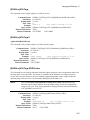
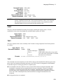
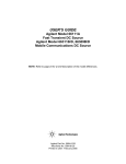
USER’S GUIDE
Agilent Technologies
Model 66319B/D, 66321B/D
Mobile Communications DC Source
Featuring programmable output resistance
(Refer to page 20 for a brief description of the model differences.)
Agilent Part No. 5964-8184
Microfiche No. 5964-8185
Printed in Malaysia: May, 2003
Warranty Information
CERTIFICATION
Agilent Technologies certifies that this product met its published specifications at time of shipment from the factory.
Agilent Technologies further certifies that its calibration measurements are traceable to the United States National
Bureau of Standards, to the extent allowed by the Bureau's calibration facility, and to the calibration facilities of other
International Standards Organization members.
WARRANTY
This Agilent Technologies hardware product is warranted against defects in material and workmanship for a period
of three years from date of delivery. Agilent Technologies software and firmware products, which are designated by
Agilent Technologies for use with a hardware product and when properly installed on that hardware product, are
warranted not to fail to execute their programming instructions due to defects in material and workmanship for a
period of 90 days from date of delivery. During the warranty period Agilent Technologies will, at its option, either
repair or replace products which prove to be defective. Agilent does not warrant that the operation for the software
firmware, or hardware shall be uninterrupted or error free.
For warranty service, with the exception of warranty options, this product must be returned to a service facility
designated by Agilent Technologies. Customer shall prepay shipping charges by (and shall pay all duty and taxes)
for products returned to Agilent Technologies for warranty service. Except for products returned to Customer from
another country, Agilent Technologies shall pay for return of products to Customer.
Warranty services outside the country of initial purchase are included in Agilent Technologies' product price, only if
Customer pays Agilent Technologies international prices (defined as destination local currency price, or U.S. or
Geneva Export price).
If Agilent is unable, within a reasonable time to repair or replace any product to condition as warranted, the
Customer shall be entitled to a refund of the purchase price upon return of the product to Agilent Technologies.
LIMITATION OF WARRANTY
The foregoing warranty shall not apply to defects resulting from improper or inadequate maintenance by the
Customer, Customer-supplied software or interfacing, unauthorized modification or misuse, operation outside of the
environmental specifications for the product, or improper site preparation and maintenance. NO OTHER
WARRANTY IS EXPRESSED OR IMPLIED. AGILENT TECHNOLOGIES SPECIFICALLY DISCLAIMS THE IMPLIED
WARRANTIES OF MERCHANTABILITY AND FITNESS FOR A PARTICULAR PURPOSE.
EXCLUSIVE REMEDIES
THE REMEDIES PROVIDED HEREIN ARE THE CUSTOMER'S SOLE AND EXCLUSIVE REMEDIES. AGILENT
SHALL NOT BE LIABLE FOR ANY DIRECT, INDIRECT, SPECIAL, INCIDENTAL, OR CONSEQUENTIAL
DAMAGES, WHETHER BASED ON CONTRACT, TORT, OR ANY OTHER LEGAL THEORY.
ASSISTANCE
The above statements apply only to the standard product warranty. Warranty options, extended support contacts,
product maintenance agreements and customer assistance agreements are also available. Contact your nearest
Agilent Technologies Sales and Service office for further information on Agilent Technologies' full line of Support
Programs.
2
Safety Summary
The following general safety precautions must be observed during all phases of operation of this instrument.
Failure to comply with these precautions or with specific warnings elsewhere in this manual violates safety
standards of design, manufacture, and intended use of the instrument. Agilent Technologies assumes no liability
for the customer's failure to comply with these requirements.
GENERAL
This product is a Safety Class 1 instrument (provided with a protective earth terminal). The protective features of
this product may be impaired if it is used in a manner not specified in the operation instructions.
Any LEDs used in this product are Class 1 LEDs as per IEC 825-1.
This ISM device complies with Canadian ICES-001. Cet appareil ISM est conforme à la norme NMB-001 du Canada.
ENVIRONMENTAL CONDITIONS
This instrument is intended for indoor use in an installation category II, pollution degree 2 environment. It is
designed to operate at a maximum relative humidity of 95% and at altitudes of up to 2000 meters. Refer to the
specifications tables for the ac mains voltage requirements and ambient operating temperature range.
BEFORE APPLYING POWER
Verify that the product is set to match the available line voltage, the correct fuse is installed, and all safety
precautions are taken. Note the instrument's external markings described under "Safety Symbols".
GROUND THE INSTRUMENT
To minimize shock hazard, the instrument chassis and cover must be connected to an electrical ground. The
instrument must be connected to the ac power mains through a grounded power cable, with the ground wire firmly
connected to an electrical ground (safety ground) at the power outlet. Any interruption of the protective (grounding)
conductor or disconnection of the protective earth terminal will cause a potential shock hazard that could result in
personal injury.
ATTENTION: Un circuit de terre continu est essentiel en vue du fonctionnement sécuritaire de l'appareil.
Ne jamais mettre l'appareil en marche lorsque le conducteur de mise … la terre est d‚branch‚.
FUSES
Only fuses with the required rated current, voltage, and specified type (normal blow, time delay, etc.) should be
used. Do not use repaired fuses or short-circuited fuseholders. To do so could cause a shock or fire hazard.
Vous devrez impérativement utiliser des fusibles calibrés aux spécifications de courant, tension et type
(coupure, délai de coupure, etc ...). N'utilisez jamais de fusibles réparés et ne court-circuitez pas les supports
de fusibles. Sinon, vous risquez de provoquer un choc électrique ou un incendie.
DO NOT OPERATE IN AN EXPLOSIVE ATMOSPHERE
Do not operate the instrument in the presence of flammable gases or fumes.
DO NOT REMOVE THE INSTRUMENT COVER
Operating personnel must not remove instrument covers. Component replacement and internal adjustments must be
made only by qualified service personnel.
Instruments that appear damaged or defective should be made inoperative and secured against unintended
operation until they can be repaired by qualified service personnel.
3
SAFETY SYMBOLS
Direct current
Alternating current
Both direct and alternating current
Three-phase alternating current
Earth (ground) terminal
Protective earth (ground) terminal
Frame or chassis terminal
Terminal is at earth potential. Used for measurement and control circuits designed to be
operated with one terminal at earth potential.
Terminal for Neutral conductor on permanently installed equipment
Terminal for Line conductor on permanently installed equipment
On (supply)
Off (supply)
Standby (supply). Units with this symbol are not completely disconnected from ac mains when
this switch is off. To completely disconnect the unit from ac mains, either disconnect the power
cord or have a qualified electrician install an external switch.
In position of a bi-stable push control
Out position of a bi-stable push control
Caution, risk of electric shock
Caution, hot surface
Caution (refer to accompanying documents)
WARNING
Caution
4
The WARNING sign denotes a hazard. It calls attention to a procedure, practice, or the like,
which, if not correctly performed or adhered to, could result in personal injury. Do not proceed
beyond a WARNING sign until the indicated conditions are fully understood and met.
The CAUTION sign denotes a hazard. It calls attention to an operating procedure, or the like,
which, if not correctly performed or adhered to, could result in damage to or destruction of part
or all of the product. Do not proceed beyond a CAUTION sign until the indicated conditions
are fully understood and met.
Declaration Page
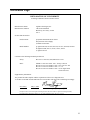
DECLARATION OF CONFORMITY
according to ISO/IEC Guide 22 and EN 45014
Manufacturer's Name:
Manufacturer's Address:
Agilent Technologies, Inc.
140 Green Pond Road
Rockaway, New Jersey 07866
U.S.A.
declares that the Product
Product Name:
a) Dynamic Measurement DC Source
b) System DC Power Supply
c) Remote Front Panel
Model Number:
a) Agilent 66311B, 66311D, 66312A, 66111A, 66321B, 66321D
b) Agilent 6612B, 6611C, 6612C, 6613C, 6614C
c) Agilent 14575A
conforms to the following Product Specifications:
Safety:
IEC 1010-1:1990+A1(1992)/EN61010-1:1993
EMC:
CISPR 11:1990 / EN 55011:1991 - Group 1 Class B
IEC 801-2:1991 / EN 50082-1:1992 - 4 kV CD, 8 kV AD
IEC 801-3:1984 / EN 50082-1:1992 - 3 V / m
IEC 801-4:1988 / EN 50082-1:1992 - 0.5 kV Signal Lines
1 kV Power Lines
Supplementary Information:
The product herewith complies with the requirements of the Low Voltage Directive
73/23/EEC//93/68/EEC and the EMC Directive 89/336/EEC and carries the CE-marking accordingly.
New Jersey
Location
May 1, 2000
Date
______
Bruce Krueger / Quality Manager
European Contact: Your local Agilent Technologies Sales and Service Office or Agilent Technologies GmbH,
Department TRE, Herrenberger Strasse 130, D-71034 Boeblingen (FAX:+49-7031-14-3143)
5
DECLARATION OF CONFORMITY
according to ISO/IEC Guide 22 and EN 45014
Manufacturer's Name:
Manufacturer's Address:
Agilent Technologies, Inc.
140 Green Pond Road
Rockaway, New Jersey 07866
U.S.A.
declares that the Product
Product Name:
a) Mobile Communication DC Source-Dual Output
Model Number:
a) Agilent 66319B, 66319D
conforms to the following Product Specifications:
Safety:
IEC 1010-1:1990+A1(1992)/EN61010-1:1993
EMC:
CISPR 11:1990 / EN 55011:1991 - Group 1 Class B
IEC 801-2:1991 / EN 50082-1:1992 - 4 kV CD, 8 kV AD
IEC 801-3:1984 / EN 50082-1:1992 - 3 V / m
IEC 801-4:1988 / EN 50082-1:1992 - 0.5 kV Signal Lines
1 kV Power Lines
Supplementary Information:
The product herewith complies with the requirements of the Low Voltage Directive
73/23/EEC//93/68/EEC and the EMC Directive 89/336/EEC and carries the CE-marking accordingly.
New Jersey
Location
May 1, 2000
Date
______
Bruce Krueger / Quality Manager
European Contact: Your local Agilent Technologies Sales and Service Office or Agilent Technologies GmbH,
Department TRE, Herrenberger Strasse 130, D-71034 Boeblingen (FAX:+49-7031-14-3143)
6
Acoustic Noise Information
Herstellerbescheinigung
Diese Information steht im Zusammenhang mit den Anforderungen der
Maschinenläminformationsverordnung vom 18 Januar 1991.
* Schalldruckpegel Lp <70 dB(A)
* Am Arbeitsplatz
* Normaler Betrieb
* Nach EN 27779 (Typprüfung).
Manufacturer's Declaration
This statement is provided to comply with the requirements of the German Sound Emission Directive,
from 18 January 1991.
* Sound Pressure Lp <70 dB(A)
* At Operator Position
* Normal Operation
* According to EN 27779 (Type Test).
Printing History
The edition and current revision of this manual are indicated below. Reprints of this manual containing
minor corrections and updates may have the same printing date. Revised editions are identified by a new
printing date. A revised edition incorporates all new or corrected material since the previous printing
date.
Changes to the manual occurring between revisions are covered by change sheets shipped with the
manual. In some cases, the manual change applies only to specific instruments. Instructions provided on
the change sheet will indicate if a particular change applies only to certain instruments.
This document contains proprietary information protected by copyright. All rights are reserved. No part
of this document may be photocopied, reproduced, or translated into another language without the prior
consent of Agilent Technologies. The information contained in this document is subject to change
without notice.
Copyright 2000 Agilent Technologies, Inc.
Edition 1 _______May, 2000
Update 1 ______January, 2001
Update 2 ______May, 2003
7
Table of Contents
Warranty Information
Safety Summary
Declaration Page
Acoustic Noise Information
Printing History
Table of Contents
1 - QUICK REFERENCE
The Front Panel - At a Glance
The Rear Panel - At a Glance
Instrument Configuration
Front Panel Number Entry
Front Panel Annunciators
Immediate Action Keys
Front Panel Menus - At a Glance
SCPI Programming Commands - At a Glance
2 - GENERAL INFORMATION
Document Orientation
Safety Considerations
Options and Accessories
Description and Model Differences
Option 521 Description (Agilent 66319B/D only)
3 - INSTALLATION
Installation and Operation Checklist
Inspection
Location
Input Connections
Output Connections
DVM Connections
External Protection and Trigger Input Connections
Digital I/O Connections
Computer Connections
4 - TURN-ON CHECKOUT
Checkout Procedure
In Case of Trouble
2
3
5
7
7
8
11
11
12
12
13
14
14
15
16
17
17
18
18
19
23
25
25
26
27
28
28
36
38
40
40
41
41
43
5 - FRONT PANEL OPERATION
45
Introduction
Front Panel Description
System Keys
Function Keys
Entry Keys
Examples of Front Panel Programming
45
45
47
48
51
52
6 - INTRODUCTION TO PROGRAMMING
61
External References
VXIplug&play Power Products Instrument Drivers
GPIB Capabilities of the DC Source
Introduction to SCPI
Types of SCPI Commands
61
62
63
63
64
8
Types of SCPI Messages
SCPI Data Formats
SCPI Command Completion
Using Device Clear
SCPI Conformance Information
7 - PROGRAMMING THE DC SOURCE
65
67
68
68
69
71
Introduction
Programming the Output
Triggering Output Changes
Making Basic Measurements
Making Enhanced Measurements
Making DVM Measurements
Triggered Measurements
Programming the Status Registers
Inhibit/Fault Indicator
71
71
73
75
76
79
80
84
89
8 - LANGUAGE DICTIONARY
91
Introduction
Calibration Commands
Display Commands
Measurement Commands
Output Commands
Status Commands
System Commands
Trigger Commands
Common Commands
91
96
99
100
110
119
123
124
132
A - SPECIFICATIONS
139
Specifications
Supplemental Characteristics
B - PERFORMANCE, CALIBRATION, AND CONFIGURATION
Introduction
Equipment Required
Measurement Techniques
Performance Tests
Constant Voltage Tests
Constant Current Tests
Resistance Tests
DVM Tests
Performance Test Equipment Form
Performance Test Record Form
Performing the Calibration Procedure
Performing the Configuration Procedure
C - ERROR MESSAGES
Error Number List
D - EXAMPLE PROGRAMS
Pulse Measurements
E - LINE VOLTAGE CONVERSION
139
140
143
143
143
144
145
146
148
152
152
153
154
156
161
163
163
167
167
173
9
1
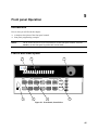
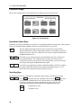
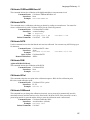
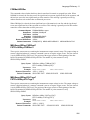
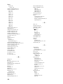
Quick Reference
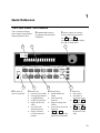
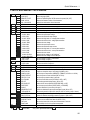
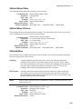
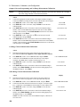
The Front Panel - At a Glance
1 A 14-character display
shows output measurements
and programmed values.
1
2 Annunciators indicate
3 Rotary control sets voltage,
operating modes and status
conditions.
current, and menu parameters.
Use " and !
to set the resolution; then adjust
the value with the knob.
2
3
66319D
DUAL OUTPUT
Mobile Communications DC Source
CV
Unr
CC
Dis
OCP
Prot
SYSTEM
Channel
1
Save
6
Addr
Err
SRQ
ENTRY
OV
Meter
3
Voltage
4
5
Prot Cir
7
.
0
9
Enter
Output
-
Number
Cal
Current
8
Cir Entry
Res
OCP
Protect
Recall
On
Rmt
Input
Address
2
Off
Shift
FUNCTION
Error
Local
LINE
Cal
Output
On/Off
Enter
Backspace
4
5
6
7
4 Turns the dc
5 System keys:
6 Function keys:
7
source on and off.
♦
♦
♦
♦
♦
♦
♦
♦
return to Local mode
select output channel
set GPIB address
set RS-232 interface
display SCPI error
codes
♦ save and recall
instrument states
♦ display firmware
revision and serial
number.
♦
♦
♦
♦
enable/disable the
output
select metering
functions
program voltage and
current
set and clear protection
functions
and %
$
scroll through the front
panel menu commands.
♦
♦
Entry keys:
enter values
increment or
decrement values
and #
&
select front panel
menu parameters.
"
and !
select a digit in
the numeric entry
field.
11
1 - Quick Reference
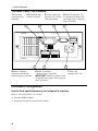
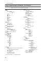
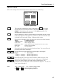
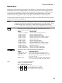
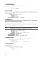
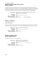
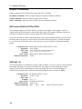
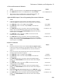
The Rear Panel - At a Glance
1 DVM inputs.
2 GPIB (IEEE-488)
3 Used to connect the
4 INH/FLT connector. Can
Connector plug is
removable.
interface connector.
Agilent 14575A remote
front panel display.
be configured for Digital I/O
and Trigger input. Connector
plug is removable.
2
1
WARNING:
3
NO OPERATOR SERVICEABLE PARTS
4
REFER SERVICING TO SERVICE TRAINED
INH
FLT
+
-
-
+
+
!
DVM
OUTPUT 2
0 - 12V / 0 - 1.5A
-S
WARNING:
-
+
-S
+S
FOR CONTINUED FIRE PROTECTION, USE SPECIFIED
5
OUTPUT 1
0 - 15V / 0 - 3A
-
+
+S
LINE
6
7
5 Output 2 connector
6 Output 1 connector.
7 Power cord
(Agilent 66319B/D only).
Connector plug is removable.
Connector plug is removable.
IMPORTANT: Install this connector with
its supplied sense jumpers before applying
power to the unit.
connector (IEC 320)
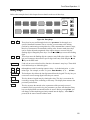
Instrument Configuration
Use the front panel Address key to configure the interface
Refer to “Front Panel Menus - At a Glance”
♦
Enter the GPIB bus address.
♦
Display the firmware revision and serial number.
12
Quick Reference - 1
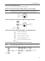
Front Panel Number Entry
Enter numbers from the front panel using one the following methods:
Use the arrow keys and knob to change voltage or current settings
NOTE:
The output must be ON to see the displayed values change in Meter mode. With the
output enabled, this method changes the output voltage or current immediately.
Use the Function keys and knob to change the displayed settings
Use the arrow keys to edit individual digits in the displayed setting
Increments the flashing digit
Decrements the flashing digit
Moves the flashing digit to the right
Moves the flashing digit to the left
Enters the value when editing is complete
Use the Function keys and Entry keys to enter a new value
NOTE:
If you make a mistake, use the Backspace key to delete the number, or press the Meter
key to return to meter mode.
13
1 - Quick Reference
Front Panel Annunciators
CV
Output 1 or output 2 is operating in constant voltage mode.
CC
Output 1 or output 2 is operating in constant current mode.
Unr
Output 1 or output 2 is unregulated.
Dis
The output is OFF. Press the Output On/Off key to turn the output on.
OCP
The over-current protection state is ON. Press the OCP key to turn over-current
protection off.
Prot
Indicates that the output has been disabled by one of the protection features.
Press the Prot Clear key to clear the protection condition.
Cal
Calibration mode is ON. Scroll to the Cal Off command and press the Enter key
to exit the calibration mode.
Shift
The Shift key has been pressed.
Rmt
The remote programming interface is active. Press the Local key to return the
unit to front panel control.
Addr
The interface is addressed to talk or listen.
Err
There is an error in the SCPI error queue. Press the Error key to view the error
code.
SRQ
The interface is requesting service.
Immediate Action Keys
Output
On/Off
Toggles the output of the selected output between the ON and OFF states.
When coupled, turns both output channels ON or OFF.
Activates front panel control when the unit is in remote mode (unless a Lockout
command is in effect).
Local
Shift
Prot Clr
Resets the protection circuit and allows the unit to return to its last programmed
state.
Shift
OCP
A toggle switch that enables or disables overcurrent protection.
14
Quick Reference - 1
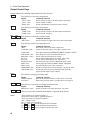
Front Panel Menus - At a Glance
Address
$
$
$
$
Recall
Shift
Save
Shift
Error
Shift
Channel
Meter
$
$
$
$
$
$
$
$
$
$
$
$
Voltage
Current
Shift
Res
Protect
Output
$
$
$
$
$
$
$
$
$
$
$
Shift
OV
$
Shift
Input
$
$
$
Shift
Cal
ADDRESS 7
LANG SCPI
REMOTE FP OFF
ROM: A.00.00
SN: US12345678
*RCL 0
*SAV 0
ERROR 0
2 5.000V 0.104A
1 12.000V 1 0.204A
1 12.500V MAX
1 1.000V MIN
1 12.330V HIGH
1 0.080V LOW
1 12.000V RMS
1 0.350A MAX
1 0.050A MIN
1 0.400A HIGH
1 0.012A LOW
1 0.210A RMS
1 12.000V DC:DVM
1 12.000V RMS:DVM
1 VOLT 12.000
2 VOLT 2.000
1 CURR 2.000
2 CURR 1.000
1 RES 1.000
OVERCURRENT
*RST
COUPLING ALL
COMP LLOCAL
PON:STATE RST
PROT:DLY 0.08
RI LATCHING
DFI OFF
DFI:SOUR OFF
PORT RIDFI
DIGIO 7
SENSE:PROT OFF
1 REL:MODE DD
VOLT:PROT 10.000
PROT:STAT ON
CURR:RANG MAX
CURR:DET ACDC
TINT 46.8
POINT 2048
CAL ON
Sets the GPIB Address
Selects language (SCPI)
Enables or disables Agilent 14575A remote front panel (ON | OFF)
Displays the firmware revision of the instrument
Displays the serial number of the instrument
Recalls the instrument state
Saves the present instrument state
Displays the number of errors in the SCPI error queue
Toggles the display between output 1 and output 2 (output 2 shown)
Measures the output voltage and current (output 1 shown)
Measures the peak output voltage
Measures the minimum output voltage
Measures the high level of a voltage pulse waveform
Measures the low level of a voltage pulse waveform
Measures the rms voltage
Measures the peak output current
Measures the minimum output current
Measures the high level of a current pulse waveform
Measures the low level of a current pulse waveform
Measures the rms current
Measures the dc voltage on the DVM input 1
Measures the rms voltage on the DVM input 1
Sets the voltage of output 1 on all models
Sets the voltage of output 2 2
Sets the current limit of output 1 on all models
Sets the current limit of output 2 2
Sets the resistance of output 1 on all models
Protection status (example shows overcurrent tripped)
Places the dc source in the factory-default state
Couples or decouples output 1 and output 2 (NONE or ALL) 1
Sets the output compensation (HREMOTE, LREMOTE, HLOCAL or LLOCAL)
Select the power-on state command (RST or RCL0)
Sets the output protection delay in seconds
Sets the remote inhibit mode (LATCHING, LIVE, or OFF)
Sets the discrete fault indicator state (ON or OFF)
Selects the DFI source (QUES, OPER, ESB, RQS, or OFF)
Sets the output port functions (RIDFI, DIGIO, or TRIGGER)
Sets and reads the I/O port value (0 through 7)
Enables or disables the open sense lead detect circuit (ON or OFF)
Sets the relay mode for Option 521 units (DD, HD, DH, or HH) (output 1 shown)
Sets the programmable voltage limit for output 1
Enables or disables overvoltage protection for output 1 (ON or OFF)
Sets the current range (3A, 1A, 0.02A, or AUTO)
Sets the current measurement detector (ACDC or DC)
Sets the time interval for a front panel measurement in seconds
Sets the buffer size for a front panel measurement
Accesses calibration menu (See Appendix B)
Use &
and #
to select parameters (table shows factory defaults).
Use Meter to exit any menu.
1Only valid for Agilent Model 66319B/D
2Only valid for Agilent Model 66321D/66319D
15
1 - Quick Reference
SCPI Programming Commands - At a Glance
NOTE:
Some [optional] commands have been included for clarity. Refer to chapter 8 for a
complete description of all programming commands.
ABORt
CALibrate
:CURRent [:POSitive]
:MEASure :LOWRange
:R3
:AC
:CURRent2 1
:DATA <n>
:DATE <date>
:DVM 2
:LEVel P1 | P2
:PASSword <n>
:RESistance
:SAVE
:STATe <bool> [, <n>]
:VOLTage [:DC]
:VOLTage2 1
DISPlay
<bool>
:CHANnel <channel> 1
:MODE NORMal | TEXT
:TEXT <display_string>
FORMat
[:DATA] ASCII | REAL [,length]
:BORDer NORM | SWAP
INITiate
:SEQuence[1|2]
:NAME TRANsient | ACQuire
:CONTinuous :SEQuence[1], <bool>
:NAME TRANsient, <bool>
INSTrument
:COUPling:OUTPut:STATe NONE | ALL 1
MEASure
:CURRent2 [:DC]? 1
:VOLTage2 [:DC]? 1
MEASure | FETCh
:ARRay :CURRent?
:VOLTage?
[:CURRent] [:DC]?
:ACDC?
:HIGH?
:LOW?
:MAX?
:MIN?
:DVM [:DC]? 2
:ACDC? 2
:VOLTage [:DC]?
:ACDC?
:HIGH?
:LOW?
:MAX?
:MIN?
OUTPut [1|2]
<bool>
:COMPensation :MODE LLOCAL | HLOCAL | LREMOTE | HREMOTE
:DFI <bool>
:SOURce QUES | OPER | ESB | RQS | OFF
:PON :STATe RST | RCL0
:PROTection :CLEar
:DELay <n>
:RELay :MODE DD | HD | DH | HH 1
:RI :MODE LATCHing | LIVE | OFF
1 Only
16
valid for Agilent 66319B/D
2 Only
valid for 66321D/66319D
SENSe
:CURRent :RANGe <n>
:DETector ACDC | DC
:FUNCtion “VOLT” | “CURR” | "DVM"
:LEAD :STATus?
:PROTection :STATe <bool>
:SWEep :OFFSet :POINts <n>
:POINts <n>
:TINTerval <n>
:WINDow :TYPE “HANN” | “RECT”
[SOURce:]
CURRent <n>
:TRIGgered <n>
:PROTection :STATe <bool>
CURRent2 <n> 1
:TRIGgered <n> 1
DIGital :DATA <n>
:FUNCtion RIDF | DIG | TRIG
RESistance <n>
:TRIGgered <n>
VOLTage <n>
:TRIGgered <n>
:PROTection <n>
:STATe <bool>
VOLTage2 <n> 1
:TRIGgered <n> 1
STATus
:PRESet
:OPERation [:EVENt]?
:CONDition?
:ENABle <n>
:NTRansition <n>
:PTRansition <n>
:QUEStionable [:EVENt]?
:CONDition?
:ENABle <n>
:NTRansition <n>
:PTRansition <n>
SYSTem
:ERRor?
:LANGuage SCPI
:VERSion?
TRIGger
:SEQuence2| :ACQuire [:IMMediate]
:COUNt :CURRent <n>
:DVM <n> 2
:VOLTage <n>
:HYSTeresis:CURRent <n>
:DVM <n> 2
:VOLTage <n>
:LEVel :CURRent <n>
:DVM <n> 2
:VOLTage <n>
:SLOPe :CURRent POS | NEG | EITH
:DVM POS | NEG | EITH 2
:VOLTage POS | NEG | EITH
:SOURce BUS | INT | EXT
[:SEQuence1| :TRANsient][:IMMediate]
:SOURce BUS
:SEQuence1 :DEFine TRANsient
:SEQuence2 :DEFine ACQuire
2
General Information
Document Orientation
This manual describes the operation of the Agilent Model 66321B/D Mobile Communications and the
Agilent Model 66319B/D Dual Output DC Source. Agilent Models 66321D and 66319D have an
additional DVM measurement input on the rear panel. Unless otherwise noted, all models will be
referred to by the description "dc source" throughout this manual.
The following Getting Started Map will help you find the information you need to complete the specific
task that you want to accomplish. Refer to the table of contents or index of each guide for a complete list
of the information contained within.
Getting Started Map
Task
Quick Reference Section
General information
Model differences
Capabilities and characteristics
Installing the unit
Line connections
Computer connections
Load connections
Checking out the unit
Verifying proper operation
Using the front panel
Calibrating the unit
Using the front panel
Front panel keys
Front panel examples
Using the programming interface
GPIB interface
Programming the unit using SCPI commands
SCPI commands
SCPI programming examples
SCPI language dictionary
Installing the VXIplug&play instrument driver
Where to find information
Chapter 1
Chapter 2
Chapter 3
Chapter 4
Chapter 5
Chapter 6
Chapters 7 and 8
Chapter 6
NOTE: The driver must be installed on your pc to access
the on-line information. Drivers are available on the web
at www.agilent.com/find/drivers.
17
2 - General Information
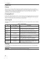
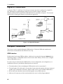
Safety Considerations
This dc source is a Safety Class 1 instrument, which means it has a protective earth terminal. That
terminal must be connected to earth ground through a power source equipped with a ground receptacle.
Refer to the Safety Summary page at the beginning of this guide for general safety information. Before
installation or operation, check the dc source and review this guide for safety warnings and instructions.
Safety warnings for specific procedures are located at appropriate places in the guide.
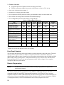
Options and Accessories
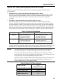
Table 2-1. Options
Option
Description
100
87−106 Vac, 47−63 Hz
120
104−127 Vac, 47−63 Hz
220
191−233 Vac, 47−63 Hz
230
207−253 Vac, 47−63 Hz
8ZJ
Delete instrument feet option
004
Output compensation is factory set to HRemote mode for best transient response.
(Refer to chapter 3, under "Output Compensation" for more information)
AXS1
Rack mount kit for two side-by-side units of equal depth. Consists of:
Lock-link kit (p/n 5061-9694) and Flange kit (p/n 5062-3974)
1CM1
Rack mount kit for one unit (p/n 5062-3972)
521
Solid-state relays to connect and disconnect the output of the dc source (Agilent 66319B/D
only). Provides the ability to either Hot-switch or Dry-switch the solid state relays.
052
Device characterization software for displaying current and voltage measurements.
1
Support rails are required when rack mounting units. Use E3663A support rails for Agilent rack cabinets. If you are
using non-Agilent rack cabinets, contact the rack manufacturer to obtain support rails for your cabinet.
Table 2-2. Accessories
Item
GPIB cables 1.0 meter (3.3 ft)
Agilent 10833A
2.0 meters (6.6 ft)
Agilent 10833B
4.0 meters (13.2 ft)
Agilent 10833C
0.5 meters (1.6 ft)
Agilent 10833D
Rack mount with slide - for two side-by-side units of different depths
Rack mount - for two side by side units of different depths
Rack mount with slide - for one unit
18
Part Number
5062-3996; 1494-0015
5062-3996
5062-3996; 1494-0015;
5062-4022
General Information - 2
Description and Model Differences
Agilent 66321B
The Agilent 66321B Mobile Communications DC Source is a high performance dc power source that
provides peak current sourcing and rapid, basic measurements in a compact, half-rack box. It is designed
to simplify the testing of digital wireless communications products. Excellent voltage transient response
characteristics prevent test interruptions due to triggering of low voltage phone shutdown. The 15 volt
source and 5A peak current capability provides compatibility with a number of communications
standards, including: GSM, CDMA, TDMA, PCS, DECT, TERA, PHS, NADC, PHS, and others.
Additional capabilities include fast dynamic measurement and analysis of voltage and current waveforms
combined with precision current measurement. This lets you characterize cellular phone current drain
under all operating conditions. Programmable output resistance lets you emulate the effects of the
internal resistance of a battery. Negative resistance programming lets you compensate for voltage drops
that occur between the remote sense points and the phone terminals. Programmable output compensation
lets you optimize the transient response for various wire lengths and phone capacitances. Figure 2-1
describes the output characteristic of the dc source.
Agilent 66319B
The Agilent 66319B Mobile Communications DC Source includes all of the capabilities of the Agilent
66321B with the addition of a second, electrically-isolated output. Figure 2-2 describes output
characteristic of this second output, which is primarily used to provide voltage or current for a charger
input on the device under test. The second output has all of the basic programmable features as the main
output, with the exception of the waveform measurement capability, open sense lead detect capability,
resistance programming, overvoltage protection, and low and middle current measurement ranges.
Agilent 66321D and 66319D
The Agilent 66321D and 66319D Mobile Communications DC Sources also contain an auxiliary DVM,
with input terminals located on the rear panel. This provides limited, low voltage dc and ac measurement
capability, which can be used to monitor test point voltages on the unit under test as well as on the test
fixture. The common mode voltage range is from −4.5 Vdc to +25 Vdc relative to the minus terminal of
output 1. The DVM is programmable from the front panel of the instrument as well as remotely using
SCPI programming commands.
Common Features
♦
Voltage, current, and resistance control with 12-bit programming resolution on output 1.
! 3-ampere current source capability (up to 5 amperes for 7 milliseconds).
!
!
♦
Output resistance programming capability from −40 milliohm to 1 ohm.
Four output compensation modes for a variety of wiring configurations.
Extensive measurement capability on output 1
! dc voltage and current.
! rms and peak voltage and current.
! Three-range current measurement capability up to approximately 7.0 amperes.
! 16-bit measurement resolution.
19
2 - General Information
!
!
Triggered acquisition of digitized current and voltage waveforms
External measurement trigger input on units with firmware revision A.03.01 and up
♦
Open sense lead protection on output 1.
♦
Automatic overvoltage protection tracking.
♦
Over-temperature, RI/DFI protection features, programmable voltage limit and current limit.
♦
Non-volatile state storage and recall with SCPI command language.
♦
User-configurable power-on/reset settings (see Appendix B).
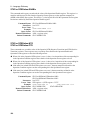
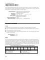
Table 2-3. Agilent Model Differences
Item
66321B
66321D
66319B
66319D
0 - 1 A range current
YES
YES
YES
YES
measurements (output 1)
0 - 20 mA range current
YES
YES
YES
YES
measurements (output 1)
4-mode output compensation
YES
YES
YES
YES
(output 1)
Auxiliary output (output2)
NO
NO
YES
YES
External DVM input
NO
YES
NO
YES
Output resistance
YES
YES
YES
YES
programming (output 1)
Automatic overvoltage
YES
YES
YES
YES
tracking (output 1)
RS-232 interface
NO
NO
NO
NO
Compatibility commands
NO
NO
NO
NO
External measurement trigger
YES
YES
YES
YES
input2
1
Earlier models not covered in this manual (order manual p/n 5964-8125)
2
Available only on units with firmware revision A.03.01 and up
66311B/D1
NO
66309B/D1
NO
YES
YES
2 modes
2 modes
NO
66311D only
NO
YES
66309D only
NO
NO
NO
YES
YES
NO
NO
NO
NO
Front Panel Controls
The front panel has both rotary and keypad controls for setting the output voltage and current. The panel
display provides digital readouts of a number of output measurements. Annunciators display the
operating status of the dc source. System keys let you perform system functions such as setting the GPIB
address and recalling operating states. Front panel Function keys access the dc source function menus.
Front panel Entry keys let you select and enter parameter values. Refer to chapter 5 for a complete
description of the front panel controls.
Remote Programming
NOTE:
The dc sources described in this manual can only be programmed using the SCPI
programming language.
The dc source may be remotely programmed via the GPIB bus. GPIB programming is with SCPI
commands (Standard Commands for Programmable Instruments), which make dc source programs
compatible with those of other GPIB instruments. Dc source status registers allow remote monitoring of a
wide variety of dc source operating conditions. Refer to chapters 6 and 7 for more information. Chapter 8
is a language dictionary of all SCPI commands that can be used to program the dc source.
20
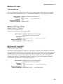
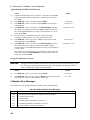
General Information - 2
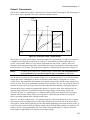
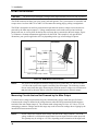
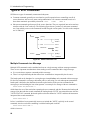
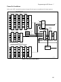
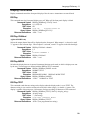
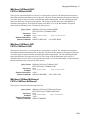
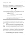
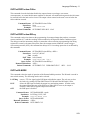
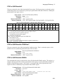
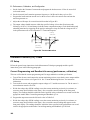
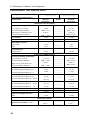
Output 1 Characteristic
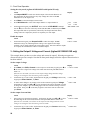
The dc source's main output (output 1) characteristic is shown in the following figure. The main output of
the dc source may be adjusted to any value within the boundaries shown.
Output
Voltage
ISET
15V
-1.2A
1
stive
load
line
VSET
CV
resi
2
CC
-2.8A
0
el
tiv
s
i
res
d
oa
e
lin
Peak Current
capability for up
to 7 ms shown
by dotted lines
+
3A
5A
Output
Current
Figure 2-1. Dc Source Output 1 Characteristic
The dc source is capable of providing a constant dc output of 15 volts with up to 3 amperes of current. It
is capable of sourcing peak currents of up to 5 amperes -- provided the peak current pulse does not
exceed 7 milliseconds, and the average current requirement does not exceed 3 amperes. If the unit
attempts to draw current for longer than 7 milliseconds, the current limit amplifier will limit the current
to a maximum of 3.0712 amps. The peak current capability is illustrated by the dotted line in Figure 2-1.
NOTE:
To source up to 5 amperes of current for up to 7 milliseconds, the current limit must
be programmed for greater than 3 amperes (up to a maximum of 3.0712 A).
The dc source can operate in either constant voltage (CV) or constant current (CC) over the rated output
voltage and current. Although the dc source can operate in either mode, it is designed as a constant
voltage source. This means that the unit turns on in constant voltage mode with the output voltage rising
to its Vset value. There is no command for constant current operation. The only way to turn the unit on in
constant current mode is by placing a short across the output and then enabling or turning the output on.
Note that the dc source cannot be programmed to operate in a specific mode. After initial turn-on, the
operating mode of the unit will be determined by the voltage setting, current setting, and the load
resistance. In figure 2-1, operating point 1 is defined by the load line traversing the positive operating
quadrant in the constant voltage region. Operating point 2 is defined by the load line traversing the
positive operating quadrant in the constant current region.
Figure 2-1 also shows a single range − two quadrant capability. This means that the dc source is capable
of sourcing as well as sinking current over the output voltage range from zero volts to the rated voltage.
This negative current sinking capability provides fast downprogramming of the output of the dc source. It
can also be used to sink current from a battery charger, thus providing battery charger test capability. The
negative current is not programmable, and varies linearly from approximately 1.2 amperes at the full
rated voltage, to approximately 2.8 amperes at zero output voltage.
21
2 - General Information
NOTE: Operating the dc source beyond its output ratings may cause the output to become unregulated.
This is indicated by the UNR annunciator on the front panel. The output may also become
unregulated if the ac line voltage drops below the minimum rating specified in Appendix A.
Programmable Output Resistance
Programmable output resistance lets you emulate the internal resistance of a cell phone battery, which
causes the voltage at the phone to drop as the phone draws more current. Different types of phone
batteries have different internal resistance values, which typically fall in a range of several hundred
milliohms. The internal resistance of a phone battery also changes with age and the number of times the
battery is recharged. Therefore, to evaluate the performance of a cell phone using various battery
characteristics, use this feature to specify a desired battery resistance.
Alternatively, programmable output resistance can be used to keep the voltage at the phone terminals as
constant as possible. In this case, you may program a negative output resistance. This compensates for
any additional voltage drop in the load leads between the remote sense points and the phone terminals
(see Figure 3-4). In phone test fixtures, the cell phone terminals may be located up to 50 centimeters
away from the connector where the remote sense terminals of the dc source are connected. This results in
a small voltage drop in the wires between the remote sense terminals and the phone terminals. If it is
critical that the steady-state voltage at the phone terminals be equal to the programmed voltage of the dc
source, a small negative output resistance can be programmed to compensate for this voltage drop.
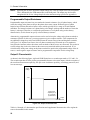
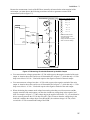
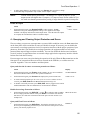
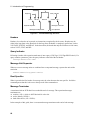
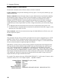
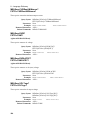
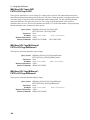
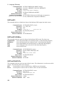
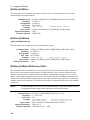
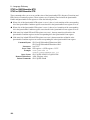
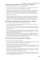
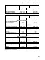
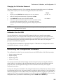
Output 2 Characteristic
As shown in the following figure, Agilent 66319B/D units have a second output rated at 12 V and 1.5A.
The second output has all of the primary programmable features as the main output, with the exception of
the waveform measurement capability, the open sense lead detect capability, overvoltage protection, and
low current range.
Output
Voltage
+12V
Peak Current
capability for up
to 1 ms shown
by dotted lines
+
0
1.5A
3.0A
Output
Current
Figure 2-2. Output 2 Characteristic
Tables A-1 through A-3 document the specifications and supplemental characteristics of the Agilent dc
sources documented in this manual.
22
General Information - 2
Option 521 Description (Agilent 66319B/D only)
Option 521 consists of the following enhancements to the output capabilities of Agilent models
66319B/66319D:
♦
Solid-state relays to connect and disconnect the output of the dc source.
The relays are available on the output and sense terminals of outputs 1 and 2. When the solid state
relays are open, the output impedance is effectively raised to about 500k ohms for output 1, and
about 200k ohms for output 2. Note that the relays open only in response to an Output OFF
command.
♦
The ability to either Hot switch or Dry switch the solid state relays.
With Hot switching, the relays control the on/off characteristics of the voltage at the output
terminals. With Dry switching, the power mesh controls the on/off characteristics of the voltage at
the output terminals. In general, Hot switching activates the relays when current is flowing through
them. Dry switching activates the relays when no current is flowing through them. You can specify
different relay options for the Output ON and Output OFF commands. The following table describes
the actions that occur based on the relay mode selection in response to the ON or OFF commands.
Table 2-5. Option 521 Relay Modes
Relay Mode
Dry (D)
Hot (H)
Output ON
1. Closes the output relay
2. Closes the sense relay
3. Programs the output
Output OFF
1. Downprograms the output
2. Opens the sense relay
3. Opens the output relay
1. Programs the power mesh
2. Closes the output relay
3. Closes the sense relay
1. Opens the sense relay
2. Opens the output relay
3. Downprograms the power mesh
The relay modes are stored in non-volatile memory. The last selected mode will be restored when the
unit is turned on. When shipped from the factory, the relay mode for both output 1 and output 2 is set
to Output ON Hot, Output OFF Hot (HH). The *RST command has no effect on the relay mode.
NOTES:
Even with open sense lead detection enabled, the dc source does not check for open
sense leads when output 1 is enabled if the Output ON relay mode is set to Hot.
On output 1 and output 2, with the Output OFF relay mode set to Hot, any external
output capacitors will not be downprogrammed or discharged. This is because the output
relay opens prior to the downprogramming of the power mesh.
With either output 1 or output 2 disabled, the output voltage readback will not be correct.
This is because the sense relay is open, effectively breaking the readback path. The
voltage readback will be a small negative number.
Table 2-6. Option 521 Factory Settings
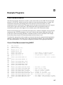
None
Output Coupling
(outputs not coupled)
Output Sense Protection
Off
Output Compensation
HRemote
Output 1 Relay Mode
HH
Output 2 Relay Mode
HH
23
3
Installation
Installation and Operation Checklist
Check the Output Compensation
# Check that the output compensation of the dc source is appropriate for your application. Refer to
“Output Compensation” in this chapter.
HRemote mode provides the best transient response and can be used with phones having input
capacitances from 5µF to 12000µF. Note that if the last two digits on the front panel display are fluctuating
when the phone is in standby, you may want to set the output compensation to a different mode.
LLocal mode offer the best stability with the lowest bandwidth.
Check the Phone Connections
# If you ARE remote sensing, are the + and − sense leads connected ONLY at the test fixture and
within 50 cm of the phone contacts? For best performance, the distance from sense lead termination to
the phone contacts should be as short as possible. Refer to “Remote Sense Connections” in this chapter.
# If you are NOT remote sensing, are the sense jumpers installed in the output connector? Ensure
that the output connector plug is installed in the unit with its supplied sense jumpers in place. Without
sense jumpers, the unit goes into a protect state with the output disabled.
Check the Operating Settings and Conditions
# Are you able to communicate remotely with the dc source? If not, check that the address is set
correctly. Refer to "GPIB Interface" in chapter 2.
# Is the Prot or Err annunciator on the front panel on? If yes, clear the fault condition before
continuing. Refer to “Clearing Output Protection” in chapter 5.
# Is the Overvoltage circuit shutting the unit down? If yes, you can disable the overvoltage circuit.
Refer to “Clearing Output Protection” in chapter 5.
# Is the output load regulation of the unit excessive? If yes, make sure that the output resistance of the
unit is set to zero ohms. Refer to “Output Resistance” in chapter 5.
Check the Measurement Settings
# Are the front panel readings unstable? If yes, check that the front panel sampling rate is correct. Also
check the setting of the output compensation. Refer to “Making Front Panel Measurements” in chapter 5
and “Output Compensation” in this chapter.
# Are you measuring dynamic output currents? If yes, check that the current detector is set to ACDC.
Refer to “Making Front Panel Measurements” in chapter 5.
# Are you measuring output currents < 1 A or < 20 mA? If yes, check that the current range is set
appropriately. Refer to “Making Front Panel Measurements” in chapter 5.
25
3 - Installation
Inspection
Damage
When you receive your dc source, inspect it for any obvious damage that may have occurred during
shipment. If there is damage, notify the shipping carrier and the nearest Agilent Sales and Support Office
immediately. The list of Agilent Sales and Support Offices is at the back of this guide. Warranty
information is printed in the front of this guide.
Packaging Material
Until you have checked out the dc source, save the shipping carton and packing materials in case the unit
has to be returned. If you return the dc source for service, attach a tag identifying the owner's name and
address, the model number, and a brief description of the problem.
Items Supplied
The following user-replaceable items are included with your dc source. Some of these items are installed
in the unit.
Table 3-1. Items Supplied
Item
Power Cord
Part Number
contact the nearest Agilent
Sales and Support Office
Description
A power cord appropriate for your location.
Digital I/O
connector
1252-1488
4-terminal digital plug for connecting digital I/O leads.
The connector installs in the back of the unit.
Output
connector
0360-2604
5-terminal output plug for connecting load and sense
leads. This connector installs in the back of the unit.
DVM
connector
1252-8670
3-terminal plug for DVM connections (66319B/D)
Sense jumpers
8120-8821
Jumpers that insert into output connector for local
sensing. Connect +s to +, and −s to −.
Line Fuse
2110-0638
2110-0773
3.15 AT (time delay) for 100/120 Vac operation
1.6 AT (time delay) for 220/230 Vac operation
Feet
5041-8801
feet for bench mounting
User's Guide
5964-8125
This manual. Contains installation, checkout, front
panel, and programming information.
Cleaning
Use a dry cloth or one slightly dampened with water to clean the external case parts. Do not attempt to
clean internally.
WARNING:
26
To prevent electric shock, unplug the unit before cleaning.
Installation - 3
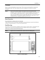
Location
Figure 3-1 gives the dimensions of your dc source. The dc source must be installed in a location that
allows sufficient space at the sides and back of the unit for adequate air circulation (see Bench
Operation).
NOTE:
This dc source generates magnetic fields that may affect the operation of other
instruments. If your instrument is susceptible to operating magnetic fields, do not locate
it in the immediate vicinity of the dc source. Typically, at three inches from the dc
source, the electromagnetic field is less than 5 gauss. Many CRT’s, such as those used in
computer displays, are susceptible to magnetic fields much lower than 5 gauss. Check
susceptibility before mounting any display near the dc source.
Bench Operation
Do not block the fan exhaust at the rear of the unit.
A fan cools the dc source by drawing air in through the sides and exhausting it out the back. Minimum
clearances for bench operation are 1 inch (25 mm) along the sides.
Rack Mounting
The dc source can be mounted in a standard 19-inch rack panel or cabinet. Table 2-1 documents the part
numbers for the various rack mounting options that are available for the dc source. Installation
instructions are included with each rack mount option.
NOTE:
Support rails or an instrument shelf is required when rack mounting units.
Figure 3-1. Outline Diagram
27
3 - Installation
Input Connections
Connect the Power Cord
Connect the power cord to the IEC 320 connector on the rear of the unit. If the wrong power cord was
shipped with your unit, contact your nearest Agilent Sales and Support Office to obtain the correct cord
(refer to the list at the back of this guide).
Check the line voltage rating label on the back of the unit to make sure that it agrees with your ac mains
voltage. Refer to appendix E if the voltage at your site is different from the voltage indicated on the unit.
Output Connections
Turn the unit off before connecting any wires.
Output 1
The main output connector (output 1) has a termination for the + and − output, the + and − sense
terminals, and an earth ground terminal. The 5-pin connector is removable and accepts wires sizes from
AWG 22 to AWG 12. Disconnect the mating plug from the unit by pulling it straight back.
IMPORTANT: You must connect the sense terminals on Output 1 for the unit to operate properly. Refer
to the section on "Open Sense Lead Protection" in this chapter. Install the connector plug
with its supplied sense jumpers before applying power to the unit.
Output 2
Agilent 66319B/D units have a second output connector (output 2). It has the same configuration as the
main output connector. It has a termination for the + and − output, the + and − sense terminals, and an
earth ground terminal. The 5-pin connector is removable and accepts wires sizes from AWG 22 to AWG
12. Disconnect the mating plug from the unit by pulling it straight back. You must connect the sense
terminals on Output 2 for the unit to meet its published specifications.
Current Ratings
Fire Hazard
To satisfy safety requirements, load wires must be large enough not to overheat when
carrying the maximum short-circuit current of the dc source.
The following table lists the characteristics of AWG (American Wire Gage) copper wire.
AWG No.
24
22
20
18
16
14
12
28
Table 3-2. Ampacity and Resistance of Stranded Copper Conductors
Maximum Ampacity (in
Resistance (at 20 deg. C)
free air)
Ω/ft
Ω/m
3.52
0.0843
0.0257
5.0
0.0531
0.0162
8.33
0.0331
0.0101
15.4
0.0210
0.00639
19.4
0.0132
0.00402
31.2
0.0083
0.00252
40
0.0052
0.00159
Installation - 3
Voltage Drops and Lead Resistance
To optimize the performance and transient response in your test system, please observe the following
guidelines:
♦
Twist the load leads together and keep them short. The shorter the leads, the better the performance.
♦
When remote sensing, twist the sense leads together but do not bundle them in with the load leads.
♦
For best performance, keep the total cable length to the load to 20 ft or less when remote sensing.
(Note that the unit has been tested with cable lengths of up to 40 feet.)
The load wires must also be of a diameter large enough to avoid excessive voltage drops due to the
impedance of the wires. In general, if the wires are heavy enough to carry the maximum short circuit
current without overheating, excessive voltage drops will not be a problem.
The maximum allowable value of load lead resistance is 4 ohms total (2 ohms per side). This may be
further limited to a lower value, based on peak current loading, by the maximum allowable dc voltage
drop of 8 volts total (4 volts per side) as specified for remote sense operation. To illustrate, for up to 3
amps peak, the maximum allowable resistance is 2.67 ohms total, resulting in a maximum voltage drop of
up to 8 volts. For 5 amps peak the maximum allowable resistance is 1.6 ohms total, again resulting in a
maximum allowable voltage drop of up to 8 volts.
In addition to keeping dc resistance low, you also need to minimize the total impedance. For higher slew
rate currents (0.2 amps/µs) and long wiring lengths (10 to 20 ft.) the inductance can have as much effect
as the resistance. To minimize inductance, twist the load leads. The inductance will be on the order of
0.25 µH/ft if twisted, and 0.4 µH/ft if untwisted. In addition to lowering the inductance, twisting the
leads will reduce noise pick up. If you are using remote sense leads, connect these as a second twisted
pair. Do not twist or bundle them with the load leads.
NOTE:
The use of relays between the dc source and the phone also increases impedance. Low
resistance relays will improve system performance.
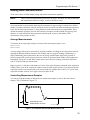
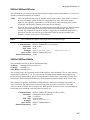
Remote Sense Connections
NOTE:
You must use remote sensing on both Output 1 and Output 2 for the unit to operate
properly and meet its published specifications. If you are not using output 1 and the open
sense protection feature is turned ON, you must jumper the + output 1 pin to its + sense
pin, and jumper the - output 1 pin to its - sense pin. Otherwise, the unit will go into a
protected state and disable the output (unless open sense protection is turned OFF).
Testing has verified stable performance with up to 20 inches of lead length between the sense lead
termination and the phone connection (see figure 3-4). However, for optimum performance, connect the
sense leads as close as possible to the phone under test. To minimize inductance, connect the sense leads
and load leads as separate twisted pairs (see figure 3-2).
Connect the sense leads carefully so that they do not become open-circuited. If the sense leads are left
unconnected or become open during operation, the dc source will not regulate the output voltage. See
"Open Sense Lead Protection".
29
3 - Installation
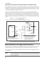
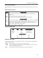
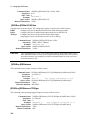
OUTPUT 1/OUTPUT 2
CONNECTOR
-S
-
+
+S
TWIST LEADS
TWIST PAIR
+
LOAD
_
WIRE RESISTANCE
Figure 3-2. Remote Sense Connections
Connect the remote sense leads only to the remote sense connections at the output connector and at the
location on the test fixture where you want to sense the output voltage. There must be not be any
continuity from the sense leads to earth ground or from the sense leads to the output leads other than at
the test fixture. The open sense detect circuit will check for continuity in the sense leads when the output
turned on (from disabled to enabled).
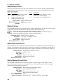
Figure 3-3 shows how to connect remote sense leads and load leads when external disconnect relays are
included in the load path.
NOTE:
In this arrangement, the output of the unit should be programmed OFF before the relays
are switched. This is because if the load leads are opened before the sense leads, the
overvoltage protection circuit will trip if it is enabled.
OUTPUT 1/OUTPUT 2
CONNECTOR
-S
-
+
+S
TWIST LEADS
TWIST PAIR
+
LOAD
_
WIRE RESISTANCE
DISCONNECT RELAYS
Figure 3-3. Remote Sense Connections with External Relays
30
Installation - 3
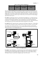
Figure 3-4 shows how to connect remote sense leads when using a removable test fixture. Note that in
this configuration, the wires in the part of the test fixture where the phone is located must be less than 50
cm (20 inches) in length. This is for stability as well as for the fact that the remote sense leads cannot
compensate for the voltage drop in this part of the test fixture.
Programming a negative output resistance lets you compensate for the unsensed voltage drop in the load
leads between the remote sense points and the phone terminals. First, you must measure or calculate the
resistance of the wires between the test fixture and the phone terminals (see table 3-2). Then you can
program the equivalent negative output resistance. This will compensate for the voltage drop in this short
section of wire. Note that the maximum negative resistance that you can program is −40 milliohms.
OUTPUT 1
CONNECTOR
-S
-
+
+S
CAN USE NEGATIVE
RESISTANCE
PROGRAMMING TO
COMPENSATE FOR
LEAD RESISTANCE
TWIST LEADS
TWIST PAIR
+
LOAD
_
WIRE RESISTANCE
FIXTURE
CONNECTIONS
LENGTH
MUST BE
UNDER 50 CM
(20 INCHES)
Figure 3-4. Remote Sense Connections with Test Fixture
NOTE:
The built-in overvoltage protection circuit automatically compensates for the voltage
drop between the output terminals and the remote sense lead connections. Refer to "OVP
Considerations" later in this chapter for more information.
Load Regulation and Voltage Drop in the Remote Sense Leads
The sense leads are part of the dc source's feedback path and must be kept at a low resistance to maintain
optimal performance. One way to accomplish this is to use larger diameter wires for the sense leads (see
Table 3-2).
If this is impractical, you can account for the voltage regulation and readback error that will occur when
using higher resistance remote sense leads. The voltage load regulation and readback error can be
calculated using the following formula:
RS+
RS+ VLD∆V = VLD+
RS+ + 251
RS- + 184
(
where:
)
(
)
VLD+ and VLD- are the voltage drops in the + and − load leads.
RS+ and RS- are the resistances of the + and − sense leads.
31
3 - Installation
Minimizing the load lead resistance reduces voltage drops VLD+ and VLD-. ∆V can be further minimized
by decreasing the resistance of the sense leads (RS+ and RS-) as much as possible. In situation where ∆V
cannot be minimized any further, it may be compensated by programming a negative output resistance as
previously discussed.
Maintaining Stability while Remote Sensing
The remote sense bandwidth and slew rate of standard dc power sources are adequate for compensating
for load lead voltage drop for slow to moderate rates of load changes. However, the high pulsed current
draw of digital cellular phones presents a challenge to standard dc power sources operating in remote
sense mode. Their bandwidth and slew rate are not adequate for dealing with the 0.05 to 0.2 amp/µs slew
rates imposed by these devices. A large voltage transient occurs at the load, due to the inability of the dc
source to keep up with the rate of load change.
The dc source effectively compensates for load lead voltage drops resulting from very high slew rate load
current transitions. This keeps the remotely sensed output voltage at a relatively constant level. For 0.05
amp/µs to 0.2 amp/µs slew rate loading in typical test applications, the transient voltage is reduced more
than an order of magnitude over that of other standard dc sources.
Open Sense Lead Protection
The main output (output 1) of the dc source has built-in open sense protection circuitry that detects if
there is an open in either the positive or the negative remote sense lead or load lead path. For battery
powered devices, undetected open sense connections can cause incorrect battery charger calibration,
incorrect test results due to erroneous voltage settings, and low voltage phone shutdown due to a large
transient voltage drop.
To enable open sense lead detection from the front panel, press the Output key, use ' to scroll to
SENS:PROT, press & to select ON, then press Enter. To have the unit turn on with open sense detection
enabled, save this state in location 0 and set the power-on state to RCL 0.
When this circuit is enabled, the sense and load leads are checked every time the output transitions
from disabled to enabled (off to on). If a lead opens while the output is enabled, this will not be
detected immediately by the open sense circuit. However, the output voltage will increase or decrease,
depending on which one of the leads is open. Turning the output off, then on again, will cause the unit to
check the output sense and load leads and determine if a sense lead is open.
If the open sense lead protection circuit detects an open sense lead, the Prot annunciator on the front
panel turns on and the output turns off. Bit 5 in the Questionable Status Registers is also set (see chapter
7 under "Programming the Status Registers"). On the front panel, press the Prot key, and one of the
following error messages will be reported on the front panel:
Message
+ sense open
- sense open
+/- sense open
sense open
32
Description
Positive sense or load lead is open
Negative sense or load lead is open
Both positive and negative sense or load leads are open
Incorrect resistance reading on the sense or load leads. This may be caused by an
external power source paralleled with the output, or in rare instances, by the voltage
being out of calibration.
Installation - 3
The default setting for the open sense lead protection circuit is disabled or OFF. This is because
applications that apply an external voltage to the output or that use external disconnect relays may
interfere with the operation of the open sense detect circuit. If you are using external voltages or relays,
you can enable the open sense detect at the beginning of the test procedure. Make sure that the external
voltage is disabled and that any relays are in the closed position. Perform the remote sense check by
cycling the output off, then on. Then disable the open sense detect circuit and continue using the unit.
Local Sensing
Local sensing is not recommended for optimal performance. You must use the remote sense connections
on both the main output (output 1) and on output 2 for the unit to operate properly and meet its published
specifications. If you are not using remote sensing and the open sense protection feature is ON, you must
jumper the + output 1 pin to its + sense pin, and jumper the - output 1 pin to its - sense pin. Otherwise,
the unit will go into a protected state with the output disabled.
♦
Keep load leads as short as possible. Load leads cannot exceed 18 inches (per side) when local
sensing.
♦ Bundle or twist the leads tightly together to minimize inductance.
♦ Jumper the + output 1 pin to its + sense pin, and the - output 1 pin to its - sense pin.
OUTPUT 1/OUTPUT 2
CONNECTOR
-S
-
+
+S
JUMPER
TWIST LEADS
+
EACH LEAD MUST
BE LESS THAN 20
INCHES IN LENGTH
LOAD
_
WIRE RESISTANCE
Figure 3-5. Local Sensing
Output Compensation
High bandwidth performance and stability are achieved by using a software-switchable output
compensation circuit. This compensation circuit has four bandwidth positions to optimize the response
for different ranges of phone capacitance. The compensation function is set using either the front panel
COMP command located in the Output menu (see chapter 5), or the OUTput:COMPensation:MODE
command as explained in chapter 8. The circuit covers the following approximate capacitance ranges:
♦
♦
♦
♦
LLocal mode: 0 to 12,000 µF
LRemote mode: 2 µF to 12,000 µF
HLocal mode: 0 to 12,000 µF
HRemote mode: 5 µF to 12,000 µF
33
3 - Installation
Refer to the previous discussion under "Remote Sense Connections" and "Local Sensing" for more
information about remote and local sensing. Standard dc source units are shipped from the factory with
the output compensation set to HRemote mode. This mode provides the fastest output response but
requires an external capacitor for stable operation.
To program the compensation mode from the front panel, press the Output key, use ' to scroll to the
COMP command, press & to select one of the four compensation mode settings, and then press Enter.
To have the unit turn on with a different output compensation setting, save this state in location 0 and set
the power-on state to RCL 0. The following table summarizes the four programmable compensation
modes.
Mode
LLocal1
LRemote
HLocal
HRemote2
Description
Used for slower response with short load leads or bench operation. This produces the
slowest output response, but provides the best stability (no external capacitor needed).
Used for slower response with long load leads using remote sensing.
Use for faster response with short load leads or bench operation (no external cap needed).
Used for faster response with long load leads using remote sensing. This produces the
fastest output response, but requires an external capacitor for stable operation.
1
Corresponds to Low mode on earlier models (66311B/D, 66309B/D).
Corresponds to High mode on earlier models (66311B/D, 66309B/D).
2
If you do not know the input capacitance of the phone that you are testing, leave the input capacitance set
to LLocal mode initially. This is because in LLocal mode, the output of the dc source will be stable when
testing cellular phones that have virtually any input capacitance (from 0 µF to 12,000 µF). LLocal mode
however, has the slowest transient response (see appendix A).
The HRemote mode output compensation setting provides the fastest transient response performance for
phones with input capacitances greater than 5µF. Most phones have input capacitances greater than 5 µF.
However, the operation of the dc source may be momentarily unstable with phones that have input
capacitances less than 5 µF, or if the output sense leads are not connected and you are operating in
HRemote mode.
Use the output sense detect circuit to first determine that the sense and load leads are properly connected
to the device under test. Then, if you are testing phones in HRemote mode and want to determine if the
input capacitance of your phone is less than 5 µF, perform the following test.
NOTE:
It is important that this test is done with the dc source installed in the test system where it
will be used, since system stability is also dependent on wiring and the phone impedance.
1. Connect the phone to the dc source and place it in standby mode.
2. Check the last two digits of the voltage reading on the front panel of the dc source.
3. If the last two digits are fluctuating, it is an indication that the phone capacitance may be less than
5 µF and the dc source is unstable.
4. Place the output compensation of the dc source in LLocal mode.
5. If the last two digits of the voltage reading are now stable, your phone most likely has an input
capacitance less than 5 µF.
34
Installation - 3
OVP Considerations
CAUTION:
Disabling the overvoltage protection circuit may cause excessive output voltages, which
can damage the phone under test.
The dc source is shipped from the factory with its overvoltage protection (OVP) circuit enabled. This
built-in overvoltage protection function is not programmable; it is set to automatically trip when the
output voltage measured at the sense lead terminals exceeds the programmed voltage by two volts.
Having the overvoltage and the output voltage sensing at the same point provides a more effective
method of load protection than if the overvoltage is sensed only at the output terminals of the dc source.
To disable the OVP circuit, use either the front panel VOLT PROT command located in the OV menu, or
the VOLTage:PROTection:STATe SCPI command as explained in chapter 8.
The built-in overvoltage protection circuit reduces the number of nuisance overvoltage shutdown events
since it trips only when the sense lead voltage exceeds the programmed voltage by two volts. In situations
such as where the external remote sense leads are shorted, the OVP circuit will shut down the unit if the
voltage measured at the output terminals exceeds the programmed voltage by three volts. Lastly, the OVP
circuit will shut the unit down if the voltage at the output terminals exceeds 18 volts for any reason, such
as when remote sensing around an excessive load lead resistance.
The OVP circuit contains a crowbar SCR, which effectively shorts the output of the dc source whenever
the OVP trips. However, if an external current source such as a battery is connected across the output and
the OVP is inadvertently triggered, the SCR will continuously sink a large current from the battery,
possibly damaging the dc source. To avoid this, you can either disable the OVP circuit or you can
connect an external protection diode in series with the output of the dc source. Connect the anode of the
diode to the + output terminal.
The OVP circuit's SCR crowbar has also been designed to discharge capacitances up to a specific limit,
which is 50,000 µF. If your load capacitance approaches this limit, it is recommended that you do not
intentionally trip the OVP and discharge the capacitance through the SCR as part of your normal testing
procedure, as this may lead to long-term failure of some components.
Programmable Voltage Protection
In addition to the automatic overvoltage protection circuit, the dc source includes programmable voltage
protection for output 1. This feature lets you limit the maximum allowable output voltage that can be
programmed either from the front panel or over the GPIB. This feature is useful in situations where
accidentally programming higher output voltages within the operating range of the dc source can
permanently damage the phone under test.
For example, suppose that a phone under test, which requires the output voltage to be adjusted up to 6 V,
can be damaged if the output voltage exceeds 9 volts. You can set the programmable voltage limit to 6
volts using either the front panel VOLT:PROT command in the OV menu, or the VOLTage:PROTection
SCPI command as explained in chapter 8. If an attempt is then made to program the output voltage to a
value greater than 6 volts, the unit goes into voltage protection mode and turns its output off.
NOTE:
The VOLT:PROT front panel and SCPI commands do not program the tracking OVP
circuit, which automatically tracks the output voltage and trips when the output voltage
exceeds the programmed voltage by two volts.
35
3 - Installation
DVM Connections
CAUTION:
The DVM may be damaged if voltages at the input terminals exceed ±50 Vdc to ground.
The DVM connector has three pins: plus, minus, and earth ground. The 3-pin connector is removable and
accepts wires sizes from AWG 22 to AWG 14. Disconnect the mating plug by pulling it straight back.
The DVM is designed as an auxiliary measurement input that can measure voltages on circuits that are
powered by the main output (output 1). Voltage measurements can be made on test points inside the
phone under test, or on test points located on the test fixture that is connected to the main output. Figure
3-6 illustrates a common measurement application for the DVM. This example is only provided for
illustration; your specific application will vary depending on the type of test and type of phone.
Test Fixture
66319D
66321D
lead resistance
+
load
current
+
battery
connector
OUTPUT 1
_
Minus
terminal
−
LOAD
lead resistance
V common mode
connector for
internal phone
circuits
DVM INPUT
-4Vdc < (V comon mode) < +25Vdc
Figure 3-6. DVM Measurement Example
NOTE:
The DVM is not designed to measure voltages that are greater than +25 Vdc or less than
−4.5 Vdc with respect to the negative terminal of the main output. The following sections
discuss restrictions that apply when using the DVM to measure voltages on circuits that are
not powered by the main output, or that are floating with respect to the main output.
Measuring Circuits that are Not Powered by the Main Output
To obtain correct voltage measurements, keep the common mode voltage within the specified limits.
Common mode voltage is defined as the voltage between either DVM input terminal and the negative
terminal of the main output (output 1). The common mode voltage range is from −4.5 Vdc to +25 Vdc.
Attempting to measure voltages outside this range may result in incorrect readings due to clipping by the
internal DVM measurement circuits.
NOTE:
36
Do not confuse the common mode voltage with the DVM voltage readback. The DVM
voltage readback is a differential measurement from one input lead to the other input lead.
This quantity may be as high as ±25 Vdc, depending on the orientation of the input leads.
Installation - 3
Because the measurement circuits of the DVM are internally referenced to the minus terminal of the
main output, you must observe the following restrictions in order to guarantee accurate DVM
measurements (refer to figure 3-7).
Test Fixture(for illustration only)
1
R1
12V
DVM
66319D
66321D
2
DVM INPUT
R2
12V
DVM
lead resistance
+
V
36 V + V
2
24 V + V
3
12 V + V
4
V
5
-2V + V
6
-4V + V
7
-6V + V
NOTE: The DVM common
mode voltage range is from
-4.5Vdc to +25Vdc.
voltages outside this range will
result in erroneous readings.
R3
12V
LOAD
−
1
3
load
current
OUTPUT
Minus −
terminal
36V
DC
Node # V Common Mode
4
+
lead resistance
R4
2V
5
R5
2V
DVM
6V
DC
6
R6
2V
DVM
7
Figure 3-7. Measuring Circuits Not Powered by the Main Output
♦
You cannot measure voltages greater than +25 Vdc with respect to the negative terminal of the main
output. A situation where this could occur is illustrated by R1 in figure 3-7, which has only a 12 Vdc
drop across it but is 36 Vdc + Vlead with respect to the negative terminal of the main output.
♦
You cannot measure voltages less than −4.5 Vdc with respect to the negative terminal of the main
output. A situation where this could occur is illustrated by R6 in figure 3-7, which has only a −2 Vdc
drop across it but is −6 Vdc + Vlead with respect to the negative terminal of the main output.
♦
When calculating the common mode voltage between the point that you wish to measure and the
negative terminal of the main output, you must also include any voltage drop in the negative load
lead. For example, in figure 3-7, if the voltage drop in the negative load lead is 2 V, you would not be
able to correctly measure the 12 Vdc drop across R2. This is because when the voltage drop in the
load lead is added to the voltage drops across R2 and R3, the resultant voltage is 26 Vdc, which
exceeds the +25 Vdc common mode rating of the DVM.
37
3 - Installation
Measuring Circuits that are Floating with Respect to the Main Output
In the example shown in figure 3-8, the common mode voltage between the DVM inputs and the minus
terminal of the main output (output 1) includes an undefined floating voltage that may result in incorrect
readings due to clipping by the internal DVM measurement circuits. This will occur when the −4.5 Vdc
to + 25 Vdc common mode voltage range is exceeded.
The solution to this problem would be to provide a known or controlled common mode voltage by
connecting a jumper wire from the floating voltage to be measured to the main output. In this example,
the main output is set to 5V, the ac voltage to be measured is approximately 6 Vac (±8.5 Vpeak), and a
jumper wire connects one side of the bias transformer to the + main output terminal. This stabilizes the
common mode voltage and offsets it by the output voltage value (5 V). The peak common mode voltage
is now:
+8.5V + 5 V = +13.5 V on the positive side, and
−8.5V + 5 V = −3.5 V on the negative side;
with both voltages now being within the common mode range of the DVM.
6 V Bias
Transformer
winding capacitance
66319D
66321D
AC
DVM INPUT
TO
DVM
6 Vac;
8.5 Vpk
ACC
jumper wire
winding capacitance
OUTPUT 1 +
−
+5V
stray
capacitance
GND
Typically, low voltage with respect to
GND due to internal bypass capacitors.
GND
GND
Undefined float voltage with respect to
GND due to capacitive currents.
Could be tens of volts ac or more.
Figure 3-8. Measuring Circuits Floating with Respect to the Main Output
External Protection and Trigger Input Connections
A 4-pin connector and a quick-disconnect mating plug are provided on each instrument for accessing the
Fault/Inhibit functions, the measurement Trigger input, or the Digital I/O functions (see Table 3-3).
The connector accepts wires sizes from AWG 22 to AWG 12. Disconnect the mating plug to make your
wire connections.
NOTE:
38
It is good engineering practice to twist and shield all signal wires to and from the digital
connectors. If shielded wire is used, connect only one end of the shield to chassis ground
to prevent ground loops.
Installation - 3
PIN
1
2
3
4
Table 3-3. 4-Pin Connector Configurations
TRIGGER
FAULT/INHIBIT
Not used
FLT Output
Not used
FLT Common
Trigger Input
INH Input
Trigger Common
INH Common
DIGITAL I/O
Output 0
Output 1
Input/Output 2
Common
When functioning in Fault/Inhibit mode, the fault (FLT) output, also referred to as the DFI (discrete fault
indicator) signal, is an open collector circuit that pulls the positive output low with respect to the negative
(chassis-referenced) common. The high impedance inhibit (INH) input, also referred to as the RI (remote
inhibit) signal, is used to shut down the dc source output whenever the INH + is pulled low with respect to
the INH (chassis-referenced) common. Figure 3-9 shows how you can connect the FLT/INH and trigger
input circuits of the dc source.
In example A, the INH input connects to a switch that shorts the Inhibit pin (+) to common whenever it
is necessary to disable output of the unit. This activates the remote inhibit (RI) circuit, which turns off the
dc output. The front panel Prot annunciator comes on and the RI bit is set in the Questionable Status
Event register. To re-enable the unit, first open the connection between pins INH + and common and then
clear the protection circuit. This can be done either from the front panel or over the GPIB.
In example B, the FLT output of one unit is connected to the INH input of another unit. A fault condition
in one of the units will disable all of them without intervention either by the controller or external circuitry.
The computer can be notified of the fault via a service request (SRQ) generated by the Questionable
Status summary bit. Note that the FLT output can also be used to drive an external relay circuit or signal
other devices whenever a user-definable fault occurs.
A) INH Example with One Unit
B) FLT Example with Multiple Units
4 3 2 1
4 3 2 1
NOTE: Connectors
are removable
Switch
(Normally
Open)
INH FLT
. . . .
+
-
+
INH Input
INH
FLT
. . . .
+
-
FLT
Output
+
INH Common
INH
Input
C) Measurement trigger example
4 3 2 1
4 3 2 1
NOTE: Connectors
are removable
TRG
N.U.
. . . .
Trigger signal
or contact closure
INH
Input
FLT
Output
+
Signal Common
Figure 3-9. FLT/INH Examples
In example C, when functioning as a measurement trigger input, a negative-going edge signal applied to
the TRG input sends an external trigger signal to the trigger system. You can either apply a negativegoing edge signal to the TRG input pin (referenced to common), or apply a contact switch to short the
TRG input to common. Note that in this configuration, pins 1 and 2 are not used.
39
3 - Installation
Digital I/O Connections
As shown in Table 3-3 and Figure 3-10, the 4-pin connector can also be configured as a digital I/O
port. Information on programming the digital I/O port is found in chapter 5 and under
[SOURce:]DIGital:DATA and [SOURce:]DIGital:FUNCtion commands in chapter 8. The electrical
characteristics of the digital connector are described in appendix A.
+16.5V Max.
Digital Output
Ports 0, 1, 2
TTL, AS, CMOS, HC
Coil Current
0.25A Max.
NOTE: Connectors
are removable
INH
FLT
Relay Driver
Ports 0, 1, 2
4 3 2 1
(contains internal
clamp diodes for
inductive flyback)
Digital Input
Port 2
. . . .
+ - +
A) Relay Circuits
B) Digital Interface Circuits
Figure 3-10. Digital I/O Examples
Computer Connections
The dc source can be controlled through a GPIB interface. Follow the GPIB card manufacturer's
directions for card installation and software driver setup.
GPIB Interface
Each dc source has its own GPIB bus address, which can be set using the front panel Address key as
described in chapter 5. GPIB address data is stored in non-volatile memory. The dc source is shipped
with its GPIB address set to 5.
Dc sources may be connected to the GPIB interface in series configuration, star configuration, or a
combination of the two, provided the following rules are observed:
♦
The total number of devices including the GPIB interface card is no more than 15.
♦
The total length of all cables used is no more than 2 meters times the number of devices connected
together, up to a maximum of 20 meters. (Refer to table 2-2 for a list of available GPIB cables.)
♦
Do not stack more than three connector blocks together on any GPIB connector.
♦
Make sure all connectors are fully seated and the lock screws are firmly finger-tightened.
40
4
Turn-On Checkout
Checkout Procedure
Successful tests in this chapter provide a high degree of confidence that your unit is operating properly.
For performance tests, see appendix B.
NOTE:
To perform the checkout procedure, you will need a wire for shorting the output
terminals together.
The following procedure assumes that the unit turns on in the factory-default state. If you need more
information about the factory default state, refer to the *RST command in chapter 8. Note that the values
shown in the Display column may not exactly match the values that appear on the front panel of the unit.
If you have not already done so, connect the power cord to the unit and plug it in. Connect the output
connector to the back of the unit with the sense jumpers installed.
Procedure
1.
Display
Turn the unit on. The dc
source undergoes a self-test
when you first turn it on.
NOTE:
**********
ADDRESS 5
0.000V
0.0001A
Explanation
During selftest, all display segments are briefly lit,
followed by the GPIB Address.
The display then goes into meter mode with the Dis
annunciator on, and all others off. In Meter mode the
n.nnnV digits indicate the output voltage and the
.nnnnA digits indicate the output current. The
flashing digit on the display indicates the digit that
will be affected if changes are made to the displayed
values using the rotary control or the # and & keys.
You will only see the changes if the output is ON.
Press the Meter key to exit a menu at any time and return to meter mode. If the Err
annunciator on the display is on, press the Shift key followed by the Error key to see the
error number. See table 4-1 at the end of this chapter.
2.
Check that the fan is on.
You should be able to hear the fan and feel the air
coming from the back of the unit.
3.
Unplug the output connector
from the back of the unit.
-0.224V
4
Press Output, scroll to
SENSE:PROT and select
ON. Press Enter
SENSE:PROT ON
Enables the open sense detect circuit.
5.
Press Output On/Off
-0.224V 0.0000A
The open sense detect circuit disables the output. The
Dis annunciator is off, but the Prot annunciator is on.
6.
Press Protect
+/- SENSE OPEN
Display indicates the protection condition.
0.0000A
The output voltage indicates approximately -0.2 volts
because the output sense connections have opened.
41
4 - Turn-On Checkout
Procedure
Display
Explanation
7.
Plug the output connector
back into the unit.
8.
Press Shift, Prot Clear
NO FAULT
Clears the protection condition. Prot is off; CV is on.
9.
Press Voltage
VOLT 0.000
Display shows the output voltage setting of the unit.
10.
Press Enter Number,
<15>, Enter
VOLT <15>
15.003V 0.0001A
Programs the main output to 15 volts. After the value
is entered, the display returns to Meter mode.
Because the output is enabled, the meter will indicate
the actual output voltage.
11.
Press Output On/Off
0.000V
Turn the output off.
12.
Connect a jumper wire
across the + and - output
terminals.
13.
Press Output On/Off.
14.
Press Current,
Enter Number,
<1>, Enter.
15.
Press Shift, OCP
0.001V
0.0003A
You enabled the overcurrent protection circuit. The
circuit then tripped because the unit was operating in
constant current mode. The CC annunciator turns off,
and the OCP and Prot annunciators turn on.
16.
Press Shift, OCP
0.001V
0.0003A
You have disabled the overcurrent protection circuit.
The OCP annunciator turns off.
17.
Press Shift, Prot Clear
0.004V
0.998A
Restores the output. The Prot annunciator turns off.
The CC annunciator turns on.
18.
Turn the unit off and remove
the shorting wire from the
output terminals.
Restores the output sense connections. The Prot
annunciator is still on.
0.0000A
Shorts the output of the unit.
0.004V
3.0712A
CURR <1>
The CC annunciator is on, indicating that the unit is
in constant current mode. The unit is sourcing output
current at the maximum rating, which is the default
output current limit setting.
Programs the output current to 1 ampere.
The next time the unit turns on it will be restored to
the *RST or factory default state.
Only perform steps 19 to 29 if you are verifying an Agilent 66319B or 66319D unit.
Procedure
Display
2
Shift Channel toggles between channel 1 and channel
2. The left-most digit of the display identifies the
output channel that is presently being controlled. It will
indicate a "1" for channel 1, or "2" for channel 2.
19.
Turn the unit on. Wait for
selftest to complete and
press Shift, Channel.
20.
Press Voltage,
Enter Number,
<12>, Enter.
21.
Press Output On/Off
2
12.005V 0.0002A
Turns the main output and output 2 on. The Dis
annunciator is off, but the CV annunciator is on.
22.
Press Output On/Off
2
0.000V
0.0000A
Turn all outputs off.
42
0.025V 0.0002A
Explanation
2
VOLT <12>
Programs the output 2 voltage to 12 volts.
Turn-On Checkout - 4
Procedure
Display
Explanation
Shorts output 2 of the unit.
23.
Connect a jumper wire
across the + and terminals of output 2.
24.
Press Output On/Off.
25.
Press Current,
Enter Number,
<1>, Enter.
26.
Press Shift, OCP
2
0.001V
0.0003A
You enabled the overcurrent protection circuit. The
circuit then tripped because output 2 was operating in
constant current mode. The CC annunciator turns off,
and the OCP and Prot annunciators turn on.
27.
Press Shift, OCP
2
0.001V
0.0003A
You have disabled the overcurrent protection circuit.
The OCP annunciator turns off.
28.
Press Shift, Prot Clear
2
29.
Turn the unit off and
remove the shorting wire
from the output terminals.
2
0.004V
2
1.520A
CURR <1>
0.004V
0.998A
The CC annunciator is on, indicating that output 2 is in
constant current mode. Output 2 is sourcing current at
its maximum rating, which is the default current limit
setting.
Programs the output 2 current to 1 ampere.
Restores output 2. The Prot annunciator turns off. The
CC annunciator turns on.
The next time the unit turns on it will be restored to the
*RST or factory default state.
In Case of Trouble
Dc source failure may occur during power-on selftest or during operation. In either case, the display may
show an error message that indicates the reason for the failure.
Selftest Error Messages
Pressing the Shift, Error keys will show the error number. Selftest error messages appear as: ERROR
<n> where "n" is a number listed in the following table. If this occurs, turn the power off and then back
on to see if the error persists. If the error message persists, the dc source requires service.
Table 4-1. Power-On Selftest Errors
Error No.
Failed Test
Error 0
Error 1
Error 2
Error 3
Error 4
Error 5
Error 10
Error 11 to 14
Error 15
Error 80
No error
Non-volatile RAM RD0 section checksum failed
Non-volatile RAM CONFIG section checksum failed
Non-volatile RAM CAL section checksum failed
Non-volatile RAM STATE section checksum failed
Non-volatile RST section checksum failed
RAM selftest
VDAC/IDAC selftest 1 to 4
OVDAC selftest
Digital I/O selftest error
43
4 - Turn-On Checkout
Runtime Error Messages
Appendix C lists other error messages that may appear at runtime. Some of these messages will also
appear on the front panel when the Prot key is pressed. To clear the error, you must remove the condition
that caused the error and then press the Prot Clear key.
Table 4-2. Runtime Error Messages
Error
Overvoltage
Overcurrent
Overtemperature
Remote inhibit
+ sense open
- sense open
+/- sense open
sense open
Description
an overvoltage condition has occurred
an overcurrent condition has occurred
an overtemperature condition has occurred
a remote inhibit signal has been applied to the RI input
a positive sense or load lead is open
a negative sense or load lead is open
a positive and negative sense or load lead is open
incorrect voltage reading on the sense leads, the unit may need to be
recalibrated
If the front panel display shows OVLD , this indicates that the output voltage or current is beyond the
range of the meter readback circuit. If this is the case, check that the setting of the output compensation is
correct for the phone you are testing. If the front panel display indicates -- -- -- -- -- , an GPIB
measurement is in progress.
Line Fuse
If the dc source appears "dead" with a blank display and the fan not running, check your ac mains to be
certain line voltage is being supplied to the dc source. If the ac mains is normal, the internal line fuse may
be defective.
Refer to Appendix E and follow the procedure described in the appendix for accessing and replacing the
line fuse located inside the unit. Do not change any of the line voltage connections.
NOTE:
44
If the dc source has a defective fuse, replace it only once. If it fails again, the dc source
requires service.
5
Front panel Operation
Introduction
Here is what you will find in this chapter:
♦
♦
a complete description of the front panel controls
front panel programming examples
NOTE:
The dc source must be in set to Local mode to use the front panel controls. Press the
Local key on the front panel to put the unit in local mode.
Front Panel Description
1
2
3
66319D
DUAL OUTPUT
Mobile Communications DC Source
CV
Unr
CC
Dis
OCP
Prot
SYSTEM
Channel
1
3
Save
6
Addr
Err
SRQ
ENTRY
OV
Meter
Address
Voltage
4
5
Prot Cir
7
.
0
9
Enter
Output
-
Number
Cal
Current
8
Cir Entry
Res
OCP
Protect
Recall
On
Rmt
FUNCTION
2
Off
Shift
Input
Error
Local
LINE
Cal
Output
On/Off
Enter
Backspace
4
5
6
7
Figure 5-1. Front Panel, Overall View
45
5 – Front Panel Operation
1 Display
14-character vacuum fluorescent display for showing output measurements and
programmed values.
2 Annunciators
Annunciators light to indicate operating modes and status conditions:
CV The dc source output is in constant-voltage mode.
CC The dc source output is in constant-current mode.
Unr The dc source output is in an unregulated state.
Dis The dc source output is disabled (off).
OCP The overcurrent protection state is enabled.
Prot One of the dc source's output protection features is activated.
Cal The dc source is in calibration mode.
Shift The Shift key is pressed to access an alternate key function.
Rmt The GPIB interface is in a remote state.
Addr The interface is addressed to talk or to listen.
Err There is a message in the SCPI error queue.
SRQ The interface is requesting service from the controller.
3 Rotary Control
The rotary control lets you set the output voltage or current as well as menu
parameters. Press " and ! to select the resolution, then adjust the value with
the knob.
4 Line
5 System Keys
This turns the dc source on or off.
6 Function Keys
Function access command menus that let you:
Enable or disable the output
Select metering functions
Program output voltage, current, and resistance
Display the protection status state
Set and clear protection functions
Set the output state at power-on
Calibrate the dc source
Select the output compensation
' and ( scroll through the front panel menu commands
7 Entry Keys
Entry keys let you:
Enter programming values
Increment or decrement programming values
# and & select the front panel menu parameters
46
The system keys let you:
Return to Local mode (front panel control)
Set the dc source GPIB address
Selects the remote programming interface
Select the output channel on units with more than one output
Display SCPI error codes and clear the error queue
Save and recall up to 4 instrument operating configurations
Select the programming language
Enable/disable the remote front panel interface
Front Panel Operation - 5
System Keys
Refer to the examples later in this chapter for more details on the use of these keys.
SYSTEM
Channel
Error
Local
Address
Save
Recall
Figure 5-2. System Keys
This is the blue, unlabeled key, which is also shown as Shift in this guide.
Pressing this key accesses the alternate or shifted function of a key (such as
ERROR ). Release the key after you press it. The Shift annunciator is lit,
indicating that the shifted keys are active.
Local
Press to change the dc source's selected interface from remote operation to local
(front panel) operation. Pressing the key will have no effect if the interface state
is already Local, Local-with-Lockout, or Remote-with-Lockout.
Address
Press to access the address menu. All entries are stored in non-volatile memory.
Display
Command Function
ADDRESS <value>
LANG <char>
REMOTE FP <char>
ROM <char>
SN: <char>
Recall
Shift
Press to place the dc source into a previously stored state. You can recall up to 4
previously stored states (0 through 3).
Channel
Pressing these keys toggles the display between output 1 and output 2.
Display
Measurement
1
2
Shift
Error
Shift
Save
Notes:
Sets the GPIB Address
Selects language (SCPI)
Enable/disable 14575A front panel interface (ON or OFF)
Firmware revision number
Unit serial number
<reading>V <reading>A
<reading>V <reading>A
Measures output channel 1
Measures output channel 2
Press to display the system error codes stored in the SCPI error queue. This
action also clears the queue. If there is no error in the queue, 0 is displayed.
Press to store an existing dc source state in non-volatile memory. The
parameters saved are listed under *SAV as described in chapter 8. You can save
up to 4 states (0 through 3).
value = a numeric value
char = a character string parameter
Use '
and (
to scroll through the command list.
Use #
and &
to scroll through the parameter list.
47
5 – Front Panel Operation
Function Keys
Refer to the examples later in this chapter for more details on the use of these keys.
FUNCTION
Input
OV
Res
Meter
Voltage
Output
Prot Cir
OCP
Cal
Protect
Current
Output
On/Off
Figure 5-3. Function Keys
Immediate Action Keys
Immediate action keys immediately execute their corresponding function when pressed. Other function
keys have commands underneath them that are accessed when the key is pressed.
Output
On/Off
This key toggles the output of the dc source between the on and off states.
When coupled, the key affects both output channels. It immediately executes its
function as soon as you press it. When off, the dc source output is disabled and
the Dis annunciator is on.
Shift
Prot Clr
Shift
OCP
Press this key to reset the protection circuit and allow the unit to return to its
last programmed state. The condition that caused the protection circuit to
become active must be removed prior to pressing this key, or the unit will shut
down again and display the Prot annunciator again.
Press this key to toggle between OCP enabled and disabled. If OCP is enabled
the output will become disabled if the output mode changes from CV to CC
mode. The OCP annunciator indicates the state of OCP.
Scrolling Keys
Scrolling keys let you move through the commands in the presently selected function menu.
%
$
(
(
(
48
'
Press
to bring up the next command in the list. Press
to go back
to the previous command in the list. Function menus are circular; you can
return to the starting position by continuously pressing either key. The
following example shows the commands in the Input function menu:
CURR:RANGE <char>
CURR:DET <char>
Front Panel Operation - 5
Metering Keys
Metering keys control the metering functions of the dc source. As set from the factory, all front panel
measurements from the main output (output 1), are calculated from a total of 2048 readings taken at a
46.8 microsecond sampling rate. Therefore, the factory default acquisition time for a single front panel
measurement is about 100 milliseconds. Refer to “Making Front Panel Measurements” for more
information about changing the front panel sampling rate and the number of measurement points.
All front panel measurements from the DVM and from output2 are fixed at 2048 measurement readings
taken at a 15.6 microsecond sampling rate.
NOTE:
The front panel sample rate and data point settings are separate and independent of the
sample rate and data point settings that are programmed over the GPIB interface. When
an GPIB measurement is in progress, the front panel display temporarily indicates
-- -- -- -- --. Front panel measurements resume when the GPIB measurement completes.
Meter
Press this key to access the meter menu list. Also use this key to exit a
menu at any time and return to meter mode.
Display
Measurement
<reading>V <reading>A
<reading>V MAX
<reading>V MIN
<reading>V HIGH
<reading>V LOW
<reading>V RMS
<reading>A MAX
<reading>A MIN
<reading>A HIGH
<reading>A LOW
<reading>A RMS
<reading>V DC:DVM
<reading>V RMS:DVM
Shift
Input
Press this key to access the following metering functions.
Display
Command Function
CURR:RANGE <char>
CURR:DET <char>
TINT <value>
POINTS <char>
Notes:
Measures output dc voltage and current
Measures peak output voltage
Measures minimum output voltage
Measures the high level of a voltage waveform
Measures the low level of a voltage waveform
Measures rms voltage
Measures peak output current
Measures minimum output current
Measures the high level of a current waveform
Measures the low level of a current waveform
Measures rms current
Measures dc voltage on DVM input1
Measures rms voltage on DVM input1
Select current range (3A | 1A | 0.02A | AUTO)
Select current measurement bandwidth (ACDC | DC)
Sets the front panel measurement interval in seconds
(15.6 µs to 1 second)
Sets the # of points in front panel measurement buffer
( 1, 2, 4, 8, 16, 32, 64, 128, 256, 512, 1024, 2048)
1
only valid for Agilent 66321D/66319D
reading = the returned measurement
value = a numeric value
char = a character string parameter
Use '
and (
to scroll through the menu commands.
Use #
and &
to scroll through the menu parameters.
Use "
and !
to select a digit in a numeric entry field.
49
5 – Front Panel Operation
Output Control Keys
Output control keys control the output functions of the dc source.
Voltage
Press this key to access the voltage menu.
Display
Command Function
1
VOLT <value>
VOLT <value>
1
LIMIT <char>
2
Current
Press this key to access the current menu.
Display
Command Function
1
2
Shift
Res
Output
CURR <value>
CURR <value>
RES <value>
Protect
OV
Cal
Status of the protection features (example shows overcurrent)
Status of the protection features (example shows none tripped)
Press this key to access the overvoltage protection menu.
Display
Command Function
PROT:STAT <char>
Enables or disables overvoltage protection (ON | OFF)
This key accesses the calibration menu (Refer to Appendix B for details).
1
These parameters are explained in chapter 3.
These status summary bits are explained in chapter 7.
3
These relay modes are explained in chapter 2
value = a numeric value
char = a character string parameter
Use ' and ( to scroll through the menu commands.
Use # and &
to scroll through the menu parameters.
Use " and ! to select a digit in a numeric entry field.
2
50
Places the dc source in the factory-default state
Couples or decouples output 1 and output 2 (NONE | ALL)
Sets output compensation (HREMOTE | LREMOTE | HLOCAL | LLOCAL) 1
Select the power-on state command (RST | RCL0)
Sets the output protection delay in seconds
Sets the remote inhibit mode (LATCHING | LIVE | OFF)
Sets the discrete fault indicator state (ON | OFF)
Selects the DFI source (QUES | OPER | ESB | RQS | OFF)2
Sets the output port functions (RIDFI | DIGIO | TRIGGER)
Sets and reads the I/O port value (0 through 7)
Enables or disables the open sense lead detect circuit (ON | OFF)
Sets the relay mode for option 521units (DD, HD, DH, or HH)3
(applies to both outputs; output 1 shown)
Press this key to display protection status.
Display
Command Function
OVER CURRENT
NO FAULT
Notes:
Sets the resistance of output 1 (the main output of all models)
Press this key to access the output menu list.
Display
Command Function
*RST
COUPLING <char>
COMP <char>
PON:STATE <char>
PROT:DLY <value>
RI <char>
DFI <char>
DFI:SOUR <char>
PORT <char>
DIGIO <char>
SENSE:PROT<char>
1
REL:MODE <char>
Shift
Sets the current of output 1 (the main output of all models)
Sets the current of output 2
Press this key to access the resistance menu.
Display
Command Function
1
Shift
Sets the voltage of output 1 (the main output of all models)
Sets the voltage of output 2
Sets the programmable voltage limit (output 1 shown)
Front Panel Operation - 5
Entry Keys
Refer to the examples later in this chapter for more details on the use of these keys.
ENTRY
Cir Entry
1
2
3
4
5
.
6
7
8
9
0
-
Enter
Number
Enter
Backspace
Figure 5-4. Entry Keys
#
&
"
!
Enter Number
0
.
,
Back space
Shift
Clear Entry
Enter
These keys let you scroll through choices in a parameter list that apply to a
specific command. Parameter lists are circular; you can return to the starting
position by continuously pressing either key. If the command has a numeric range,
these keys increment or decrement the existing value. In meter mode, these keys
can be used to adjust the magnitude of the output voltage or current. Only the
flashing digit is changed by these keys. Use the " and ! keys to move the flashing
digit.
These keys move the flashing digit in a numeric entry field to the right or left. This
lets you increment or decrement a specific digit in the entry field using the # and
& keys or the RPG knob.
Used only to access a third level key function - the numeric entry keys. These third
level function keys are labeled in green.
9
−
0 through 9 are used for entering numeric values. . is the decimal point. − is the
minus sign. For example, to enter 33.6 press: Enter Number, 3, 3, . , 6, Enter.
The backspace key deletes the last digit entered from the keypad. This key lets you
correct one or more wrong digits before they are entered.
This key aborts a keypad entry by clearing the value. This key is convenient for
correcting a wrong value or aborting a value entry. The display then returns to the
previously set function.
This key executes the entered value or parameter of the presently accessed
command. Until you press this key, the parameters you enter with the other Entry
keys are displayed but not entered into the dc source. Before pressing Enter, you
can change or abort anything previously entered into the display. After Enter is
pressed, the dc source returns to Meter mode.
51
5 – Front Panel Operation
Examples of Front Panel Programming
You will find these examples on the following pages:
1 Using the front panel display
2 Setting the output voltage, current, and compensation
3 Setting the output 2 voltage and current
4 Querying and clearing output protection
5 Making basic front panel measurements
6 Making enhanced front panel measurements
7 Making DVM measurements
8 Programming the digital port
9 Setting the GPIB address
10 Storing and recalling instrument states
1 - Using the Front Panel Display
Select an output on Agilent 66319B/D units
Action
Display
Press Meter to return the display to Meter mode. Press Shift Channel to toggle
between channel 1 and channel 2. The left-most digit of the front panel display
identifies the output channel that is presently being controlled by the front panel. It
will indicate either a "1" for channel 1, or "2" for channel 2.
2
7.003V 0.004A
You can only select an output when the unit is in metering mode. Once an output
has been selected, only the menu commands that apply to that output will appear
on the display. Output -specific menu commands are identified by a 1 or a 2. Also,
the CV, CC, and UNR annunciators apply to the selected channel.
Select the DVM on Agilent 66321D/66319D units
Action
Display
You must select output 1 to use the DVM. If output 1 is not selected, the DVM's
measurement menu is not displayed.
1
8.013V 0.003A
On the Function keypad press Meter and press ( repeatedly to access the DVM
measurement commands. DVM measurement commands are identified by the
"DVM" string segment. When accessed, DVM measurement functions are
automatically active. Refer to example 3 for more information.
1
<reading>V DC:DVM
Independently Control Output 1 and Output 2 on Agilent 66319B/D units
Action
Display
On the Function keypad, press Output. Scroll to the COUPLING command. To
uncouple the outputs, use the # numeric key to select NONE, then press Enter.
COUPLING NONE
2 - Setting the Output Voltage, Current, Resistance, Compensation, and
Relay Mode
This example shows you how to set the output voltage, current, and resistance. It also shows you how to
set the compensation circuit for either high or low capacitance cellular phones. Relay mode only applies
to units that have Option 521 installed. Note that no front panel changes affect the output of the unit
unless it has been enabled.
52
Front Panel Operation - 5
Set the output voltage
Action
Display
1.
To enter an approximate value without using the voltage menu: On the Entry keypad,
press " or ! to select the 1's digit in the voltage field. Then rotate the front panel
RPG knob to obtain 7 V.
If the unit is in CC mode, you won't see the output voltage change until the voltage
setting is low enough to cause the unit to go into CV mode.
7.003V 0.004A
2.
The easiest way to enter an accurate value: On the Function keypad, press Voltage.
On the Entry keypad, press Enter Number, 7, Enter.
VOLT 7.000
3.
To make minor changes to an existing value: On the Function keypad, press
Voltage. On the Entry keypad, press " or ! to select the digit in the numeric field
that you wish to change. For example, move the flashing digit to the ones column to
change a value in this column. Then, press # to scroll from 7.000 to 8.000. Then
press Enter.
VOLT 8.000
Set the output current limit
Action
Display
1.
To enter an approximate value without using the current menu: On the Entry keypad,
press " or ! to select the tenths digit in the current field. Rotate the front panel
RPG knob to obtain 0.4A.
If the unit is in CV mode, you will not see the output current change until the current
setting is low enough to cause the unit to go into CC mode.
8.003V 0.400A
2.
The easiest way to enter an accurate value: On the Function keypad, press Current.
On the Entry keypad, press Enter Number, .4, Enter.
CURR 0.400
3.
To make minor changes to an existing value, press Current. The procedure to
change an individual digit is explained in step 3 under "Set the output voltage."
NOTE:
To output currents pulses greater than 3 A and up to 5 A peak, you must set the output
current limit to greater than 3 amperes (3.0712 amperes max).
Set the output resistance
Action
Display
1.
On the Function keypad, press Shift Res. On the Entry keypad, press Enter
Number, 0.5, Enter.
RES 0.500
2.
To make minor changes to an existing value, press Shift Res. The procedure to
change an individual digit is explained in step 3 under "Set the output voltage."
Set the output compensation
1.
Action
Display
On the Function keypad, press Output. Then press ( until you obtain the COMP
command. Use the & key and select one of the four compensation modes. Then
press Enter. Use HREMOTE or HLOCAL compensation for faster transient
response when testing phones with input capacitances greater than 5 µF, which
applies for most phones. Select local or remote depending on your sensing setup.
If operation of the dc source becomes momentarily unstable when testing phones
that have input capacitances under 5 µF, Use either LREMOTE or LLOCAL
compensation.
COMP HREMOTE
53
5 – Front Panel Operation
Setting the relay mode (Agilent 66319B/66319D with Option 521 only)
Action
1.
Use Output ON/OFF to make sure that the output of the selected channel is off.
The output must be turned off before any relay settings take effect. If the Dis
annunciator is lit, the output is off.
2.
Press Meter to return the display to Meter mode.
3.
Press Shift Channel to select either output channel 1 or output channel 2.
Display
1
2
4.
On the Function keypad, press OUTPUT. Then scroll to the REL:MODE command.
Use the & key to select one of the relay modes (DD, DH, HD, or HH) then press Enter.
The Output ON mode is specified first, followed by the Output OFF mode. Relay
settings cannot be coupled; they must be set separately for each output.
2
3.6V
7.5V
2.04A
1.04A
REL:MODE HH
Enable the output
1.
Action
Display
On the Function keypad, press Output On/Off to enable the output. The Dis
annunciator will go off, indicating that the voltage is now applied to the output
terminals. The A display indicates the actual output current. Note that when the outputs
are coupled, this command also enables or disables output 2.
8.003V 0.500A
3 - Setting the Output 2 Voltage and Current (Agilent 66319B/66319D only)
This example shows you how to set the voltage and current for output 2. Selecting an output was
discussed in the previous example. Note that no front panel changes affect the output of the unit unless it
has been enabled.
Set the output 2 voltage
Action
Display
1.
Press Meter, then Shift, Channel to select output 2. On the Entry keypad, press " or
! to select the 1's digit in the voltage field. Then rotate the front panel RPG knob to
obtain 7 V.
If the unit is in CC mode, you won't see the output voltage change until the voltage
setting is low enough to cause the unit to go into CV mode.
2
7.003V 0.004A
2.
An alternate way to enter a value: On the Function keypad, press Voltage. On the Entry
keypad, press Enter Number, 7, Enter.
2
VOLT 7.000
3.
To make minor changes to an existing value: On the Function keypad, press Voltage.
On the Entry keypad, press " or ! to select the digit in the numeric field that you wish
to change. For example, move the flashing digit to the ones column to change a value in
this column. Then, press # on the Entry keypad to scroll from 7.000 to 8.000. Then
press Enter.
2
VOLT 8.000
Set the output 2 current limit
Action
Display
1.
Select output 2 as described in example 1. On the Entry keypad, press " or ! to select
the tenths digit in the current field. Rotate the front panel RPG knob to obtain 0.4A.
If the unit is in CV mode, you will not see the output current change until the current
setting is low enough to cause the unit to go into CC mode.
2
8.003V 0.400A
2.
An alternate way to enter a value: On the Function keypad, press Current. On the Entry
keypad, press Enter Number, .4, Enter.
2
CURR 0.400
54
Front Panel Operation - 5
3.
To make minor changes to an existing value, press Current. The procedure to change
an individual digit is explained in step 3 under "Set the output 2 voltage."
NOTE:
To draw current pulses greater than 1.5 A and up to 2.5 A peak on output 2, set the
output current limit higher than 1.5 amperes (1.52 amperes max). Do not enable OCP, or
else make sure that the protection delay setting is longer than the expected current pulse.
Enable the output
1.
Action
Display
On the Function keypad, press Output On/Off to enable output 2. The Dis
annunciator will go off, indicating that the voltage is now applied to the output
terminals. The display indicates the actual output values. Note that when the outputs
are coupled, this command also enables or disables output 1.
2
8.003V 0.500A
4 - Querying and Clearing Output Protection and Errors
If an overvoltage, overcurrent, overtemperature or remote inhibit condition occurs, the Prot annunciator
on the front panel will be on and the dc source will disable its output. If necessary, you can disable the
overcurrent or overvoltage protection circuit if its operation interferes with the proper operation of your
phone test. Note that if you disable the overvoltage protection, the equipment under test will not be
protected from output voltage overshoot conditions. You can also disable the broken sense lead detect
circuit if you have an application where an external voltage applied to the output may interfere with the
broken sense lead detect circuitry.
Error messages can occur at any time during the operation of the unit. When the Err annunciator on the
front panel is on it means that either an error has occurred on the GPIB bus, or a selftest error has
occurred. Appendix C lists error numbers and descriptions.
Query and clear the dc source overcurrent protection as follows:
Action
Display
1.
On the Function keypad, press Protect. In this example, an over current condition
has occurred. Refer to Table 4-2 for other protection indicators.
OVERCURRENT
2.
On the Function keypad, press Current. This displays the present current limit.
CURR 3.0712
3.
To restore normal operation after the cause of the overcurrent condition has been
removed, press Shift, Prot Clr. The Prot annunciator then will go off.
4.
To disable overcurrent protection, press Shift, OCP. This key toggles between OCP
enabled and disabled. The OCP annunciator is off when OCP is disabled.
Disable Overvoltage Protection as follows:
1.
On the Function keypad, press Shift, OV. Use the & key and select OFF to disable
the overvoltage protection function. Then press Enter. To recall this state when the
unit turns on, save this state in location 0 and set the power-on state to RCL 0 (see
example #10).
PROT:STAT OFF
Query and Clear Errors as follows:
1.
On the Function keypad, press Shift, Error. This displays and clears the error in
the error queue. Repeatedly press these keys to clear all errors in the queue. If errors
persist, your unit may require service.
ERROR 0
55
5 – Front Panel Operation
5 – Making Basic Front Panel Measurements
As shipped from the factory, front panel measurements for the main output (output 1) are calculated from
a total of 2048 readings taken at a 46.8 microsecond sampling rate. The unit alternates between voltage
and current measurements. Therefore, the data acquisition time for a single front panel voltage or current
measurement is about 100 milliseconds. This sampling rate and data acquisition time combined with a
built-in windowing function, reduces errors due to sampling a non-integral number of cycles of a
waveform for frequencies of 25 Hz or greater. Note that the windowing function is less accurate when
measuring output waveforms for frequencies less than 25 Hz, causing the front panel meter to jitter.
There are no trigger controls for front panel measurements. However, you can program both the sampling
rate and the number of data points in each front panel measurement using commands in the Input menu.
With this flexibility, measurement accuracy can be improved for waveforms with frequencies as low as
several Hertz. The sample buffer size may be varied from 1 to 2048 data points in discrete binary values.
The sampling rate may be varied from 15.6 microseconds to 1 second. Values are rounded to the nearest
15.6 microsecond interval. Note that the front panel sample interval and buffer size settings are
independent of the sample interval and buffer size that you program over the GPIB. This is because you
can qualify measurement triggers over the GPIB, which makes the GPIB measurements independent of
the front panel measurements. Refer to chapter 8 for more information about GPIB measurements.
To have the unit turn on with the reconfigured buffer size and sampling rate, save this state in location 0
and set the power-on state to RCL 0. Note that front panel measurements parameters for output 2 are not
programmable. They are fixed at 2048 data points with a 15.6 microsecond sampling rate.
NOTE:
If the front panel display indicates OVLD, the output has exceeded the measurement
capability of the instrument. If the front panel display indicates -- -- -- -- -- -- , an GPIB
measurement is in progress.
Use the Meter menu for making front panel measurements:
1.
Action
Display
On the Function keypad press Meter to access the following measurement
parameters:
dc voltage and current
<reading>V <reading>A
2.
To change the front panel time interval and buffer size for output waveform
measurements, press Shift, Input. Then press ( until you obtain the TINT
command. Use the Entry keys to enter a value from 15.6 microseconds to 1
second in seconds. Then press Enter.
TINT 0.002
3.
Continue by pressing Shift, Input and ( until you obtain the POINT command.
Press & to select a different buffer size. The choices are: 1, 2, 4, 8, 16, 32, 64,
128, 256, 512, 1024, and 2048. Then press Enter.
POINT 1024
One reason to change the front panel time interval and data points is if the
waveform being measured has a period shorter than 3 times the present front
panel acquisition time.
56
Front Panel Operation - 5
6 – Making Enhanced Front Panel Measurements
The following figure illustrates the enhanced measurement capabilities of Agilent Models 66321B/D and
66319B/D for measuring output waveforms. These include peak (max), minimum, high level, and low
level measurements as illustrated in the following figure. Rms and dc voltages are calculated from the
number of points in the measurement window.
V or A MAX
46.8 microsecond
sampling rate
V or A HIGH
NOTE:
Measurement samples may not
coincide with the actual maximum
or minimum point of the waveform.
V or A LOW
V or A MIN
100 millisecond
acquisition time
Figure 5-5. Default Front Panel Measurement Parameters
All models have three current measurement ranges that can be selected in the Input menu. A maximum
current range is available for measuring output currents of up to 7 amperes. A 1 A current range is
available for measuring currents up to 1A. A 0.02A current range is available for improved resolution
when measuring output currents below 20 milliamperes. The low current measurement range is accurate
to 0.1% of the reading ±2.5 microamperes. When the current Range is set to AUTO, the unit
automatically selects the range with the best measurement resolution.
NOTE:
In the 0.02A current measurement range, the current detector is fixed at DC. With the
current detector in dc, accurate current measurements cannot be made on waveforms
with frequency contents over 1 kilohertz.
Use the Meter menu for making front panel measurements:
1.
2.
Action
Display
On the Function keypad press Meter and press ( repeatedly
to access the following measurement parameters:
♦ dc voltage and current
♦ peak voltage
♦ minimum voltage
♦ high level of a voltage pulse waveform
♦ low level of a voltage pulse waveform
♦ rms voltage
♦ peak current
♦ minimum current
♦ high level of a current pulse waveform
♦ low level of a current pulse waveform
♦ rms current
<reading>V <reading>A
<reading>V MAX
<reading>V MIN
<reading>V HIGH
<reading>V LOW
<reading>V RMS
<reading>A MAX
<reading>A MIN
<reading>A HIGH
<reading>A LOW
<reading>A RMS
To change the front panel time interval and buffer size for output waveform
measurements, press Shift, Input. Then press ( until you obtain the TINT
command. Use the Entry keys to enter a value from 15.6 microseconds to 1
second in seconds. Then press Enter.
TINT 0.002
57
5 – Front Panel Operation
3.
Continue by pressing Shift, Input and ( until you obtain the POINT command.
Press & to select a different buffer size. The choices are: 1, 2, 4, 8, 16, 32, 64,
128, 256, 512, 1024, and 2048. Then press Enter.
POINT 1024
One reason to change the front panel time interval and data points is if the
waveform being measured has a period shorter than 3 times the present front
panel acquisition time.
4.
For current measurements, press Shift, Input. Then press & until you obtain the
CURR:RANG AUTO command. Press Enter to activate autoranging. Three
other selections are also available. Select the 3A range when measuring currents
up to 7A. Select the 1A range when measuring currents up to 1A. Select the
0.02A range for improved resolution when measuring currents below 20 mA.
Note that the 0.02A range is only appropriate for making dc measurements.
CURR:RANG AUTO
5.
For output waveform measurements, press Shift, Input. Then press ( until you
obtain the CURR:DET command. Check to make sure that the ACDC current
detector is selected. This provides the best accuracy for waveform measurements.
Only select the DC current detector if you are making dc current measurements
and you require a dc measurement offset better than 2mA on the High current
measurement range. Press Enter to activate any changes.
CURR:DET ACDC
7 – Making DVM Measurements (Agilent 66321D/66319D only)
The front panel DVM measurement function is only active when Output 1 is selected.
As shipped from the factory, DVM measurements are calculated from a total of 2048 readings taken at a
15.6 microsecond sampling rate. These parameters are fixed. Therefore, the data acquisition time for a
single measurement is about 30 milliseconds. This sampling rate and data acquisition time combined
with a built-in windowing function reduces errors due to sampling a non-integral number of cycles of a
waveform for frequencies of 47 Hz or greater.
NOTE:
If the front panel display indicates OVLD, the output has exceeded the measurement
capability of the instrument. If the front panel display indicates -- -- -- -- -- -- , a front
panel or an GPIB measurement is in progress.
Check that the DVM measurement points are within the DVM measurement capabilities:
The common mode voltage range of the DVM input is −4.5 V to +25 V from either DVM input with
respect to the negative output terminal of output 1. The maximum isolation voltage to ground is ±50 Vdc.
Refer to chapter 3 under "DVM Connection" for more information on how this affects the DVM's
measurement capability.
Use the Meter menu for making DVM measurements:
1.
58
Action
Display
On the Function keypad press Meter and press ( repeatedly
to access the following DVM measurement parameters:
♦ dc voltage
♦ rms voltage (ac + dc rms)
1
1
<reading>V DC:DVM
<reading>V RMS:DVM
Front Panel Operation - 5
8 - Programming Output Port Functions
You can configure the output port to perform three different functions. In RIDFI mode, the port functions
as a remote inhibit input with a discrete fault indicator output signal. In DIGIO mode, the port acts as a
digital Input/Output device. In TRIGGER mode, the port accepts external measurement trigger signals.
To configure the RIDFI mode of the port, proceed as follows:
Action
Display
1.
On the Function keypad, press Output.
*RST
2.
Scroll through the Output menu by pressing (. The PORT command lets you select
either the RIDFI, DIGIO, or TRIGGER function. Press Enter when done.
PORT RIDFI
3.
Scroll to the RI command to configure the Remote INHibit indicator. Use the # and
& keys to select either LIVE or LATCHING, either of which enable the RI indicator.
Then press Enter. With RI enabled, a low-true on the INH input will disable the
output of the unit. LIVE causes the output of the unit to track the state of the INH
input. LATCHING latches the output of the unit off in response to the inhibit signal.
RI LIVE
RI LATCHING
4.
Access the Output menu again and scroll through the menu. The DFI command lets
you enable the Discrete Fault Indicator. Use the & key and select ON to enable the
FLT output. Then press Enter. With the FLT output enabled, the open-collector logic
signal can be used to signal external devices when a fault condition is detected.
DFI ON
5.
Scroll to the DFI:SOUR command to select the internal source that drives this signal.
Use the & key to select from the RQS or ESB bits, or the Operation or Questionable
status registers. Then press Enter. Status summary bits are explained in chapter 7.
DFI:SOUR RQS
DFI:SOUR ESB
DFI:SOUR OPER
DFI:SOUR QUES
To configure the DIGIO mode of the port, proceed as follows:
Action
Display
1.
On the Function keypad, press Output.
*RST
2.
Scroll through the Output menu by pressing (. The PORT command lets you select
the DIGIO function. Press Enter when done.
PORT DIGIO
3.
Scroll to the DIGIO command to set and read the Digital Input/Output Port. Press
Enter Number and enter a number from 0 to 7 to program the three bits (0 programs
all bits low; 7 programs all bits high). Press Enter when done.
DIGIO 5
To configure the TRIGGER mode of the port, proceed as follows:
Action
Display
1.
On the Function keypad, press Output.
*RST
2.
Scroll through the Output menu by pressing (. The PORT command lets you select
the TRIGGER function. Press Enter when done.
PORT TRIGGER
9 - Setting the GPIB Address
Your dc source is shipped with the GPIB address set to 5. This address can only be changed from the
front panel using the Address menu located under the Address key.
Set the GPIB address as follows:
Action
Display
1.
On the System keypad, press Address.
ADDRESS 5
2.
Enter the new address. For example, Press Enter Number, 7, Enter.
ADDRESS 7
59
5 – Front Panel Operation
10 - Storing and Recalling Instrument States
You can save up to 4 states (from location 0 to location 3) in non-volatile memory and recall them from
the front panel. All programmable settings are saved. This capability is only available when the unit is set
to the SCPI programming language.
NOTE:
You can program the unit to automatically power-on according to the instrument state
that is saved in state 0 as shown in the third example.
Save an instrument state in location 0 as follows:
Action
1.
Set the instrument to the state that you want to save.
2.
Save this state to location 0. Press Save, Enter Number, 0, Enter.
Display
*SAV 0
Recall a saved state as follows:
1.
Action
Display
Recall the state saved in location 0 by pressing Recall, Enter Number, 0, Enter
*RCL 0
Select the power-on state of the dc source as follows:
Action
Display
1.
On the Function keypad, press Output, and scroll through the Output menu until you
get to the PON state command.
PON:STATE RST
2.
Use the # and & keys to select either RST or RCL0. RST sets the power-on state of
the unit as defined by the *RST command. RCL0 sets the power-on state of the unit to
the state saved in *RCL location 0. Press Enter when done.
Clear the non-volatile memory of the dc source as follows:
Action
Display
1.
On the Function keypad, press Output, Enter. This returns the unit to the factorydefault settings.
*RST
2.
Save these settings to location 0. Press Save, Enter Number, 0, Enter.
*SAV 0
3.
Repeat step #2 for memory locations 1 through 3.
*SAV 1
*SAV 2
*SAV 3
60
6
Introduction to Programming
External References
GPIB References
The most important GPIB documents are your controller programming manuals - BASIC, GPIB
Command Library for MS DOS, etc. Refer to these for all non-SCPI commands (for example: Local
Lockout).
The following are two formal documents concerning the GPIB interface:
♦ ANSI/IEEE Std. 488.1-1987 IEEE Standard Digital Interface for Programmable Instrumentation.
Defines the technical details of the GPIB interface. While much of the information is beyond the
need of most programmers, it can serve to clarify terms used in this guide and in related documents.
♦ ANSI/IEEE Std. 488.2-1987 IEEE Standard Codes, Formats, Protocols, and Common Commands.
Recommended as a reference only if you intend to do fairly sophisticated programming. Helpful for
finding precise definitions of certain types of SCPI message formats, data types, or common
commands.
The above two documents are available from the IEEE (Institute of Electrical and Electronics Engineers),
345 East 47th Street, New York, NY 10017, USA. The WEB address is www.ieee.org.
SCPI References
The following documents will assist you with programming in SCPI:
♦ Standard Commands for Programmable Instruments Volume 1, Syntax and Style
♦ Standard Commands for Programmable Instruments Volume 2, Command References
♦ Standard Commands for Programmable Instruments Volume 3, Data Interchange Format
♦ Standard Commands for Programmable Instruments Volume 4, Instrument Classes
To obtain a copy of the above documents, contact: Fred Bode, Executive Director, SCPI Consortium,
8380 Hercules Drive, Suite P3, Ls Mesa, CA 91942, USA
61
6 - Introduction to Programming
VXIplug&play Power Products Instrument Drivers
VXIplug&play instrument drivers for Microsoft Windows 95 and Windows NT are now available on
the Web at http://www.agilent.com/find/drivers. These instrument drivers provide a high-level
programming interface to your Agilent Technologies instrument. VXIplug&play instrument drivers are
an alternative to programming your instrument with SCPI command strings. Because the instrument
driver's function calls work together on top of the VISA I/O library, a single instrument driver can be
used with multiple application environments.
Supported Applications
(
(
(
(
(
(
Agilent VEE
Microsoft Visual BASIC
Microsoft Visual C/C++
Borland C/C++
National Instruments LabVIEW
National Instruments LabWindows/CVI
System Requirements
The VXIplug&play Power Products instrument driver complies with the following:
(
(
(
(
Microsoft Windows 95
Microsoft Windows NT 4.0
HP VISA revision F.01.02
National Instruments VISA 1.1
Downloading and Installing the Driver
NOTE:
Before installing the VXIplug&play instrument driver, make sure that you have one of
the supported applications installed and running on your computer.
1. Access Agilent Technologies' Web site at http://www.agilent.com/find/drivers.
2. Select the instrument for which you need the driver.
3. Click on the driver, either Windows 95 or Windows NT, and download the executable file to your pc.
4. Locate the file that you downloaded from the Web. From the Start menu select Run
<path>:\agxxxx.exe - where <path> is the directory path where the file is located, and agxxxx is the
instrument driver that you downloaded .
5. Follow the directions on the screen to install the software. The default installation selections will
work in most cases. The readme.txt file contains product updates or corrections that are not
documented in the on-line help. If you decide to install this file, use any text editor to open and read
it.
6. To use the VXIplug&play instrument driver, follow the directions in the VXIplug&play online help
under “Introduction to Programming”.
62
Introduction to Programming - 6
Accessing Online Help
A comprehensive online programming reference is provided with the driver. It describes how to get
started using the instrument driver with Agilent VEE, LabVIEW, and LabWindows. It includes
complete descriptions of all function calls as well as example programs in C/C++ and Visual BASIC.
(
To access the online help when you have chosen the default Vxipnp start folder, click on the Start
button and select Programs | Vxipnp | Agxxxx Help (32-bit).
- where agxxxx is the instrument driver.
GPIB Capabilities of the DC Source
All dc source functions except for setting the GPIB address are programmable over the GPIB. The IEEE
488.2 capabilities of the dc source are listed in the Specifications Table in Appendix A.
GPIB Address
The dc source operates from an GPIB address that is set from the front panel. To set the GPIB address,
press the Address key on the front panel and enter the address using the Entry keys. The address can be
set from 0 to 30. The GPIB address is stored in non-volatile memory.
ADDRESS <value>
Enter a value to set the GPIB Address
Introduction to SCPI
SCPI (Standard Commands for Programmable Instruments) is a programming language for controlling
instrument functions over the GPIB. SCPI is layered on top of the hardware-portion of IEEE 488.2. The
same SCPI commands and parameters control the same functions in different classes of instruments. For
example, you would use the same DISPlay command to control the dc source display and the display of a
SCPI-compatible multimeter.
Conventions Used in This Guide
Angle brackets
Vertical bar
{
>
|
Square Brackets
Braces
<
}
Items within angle brackets are parameter abbreviations. For example,
<NR1> indicates a specific form of numerical data.
Vertical bars separate alternative parameters. For example, NORM |
TEXT indicates that either "TEXT" or "NORM" can be used as a
parameter.
[
]
Items within square brackets are optional. The representation [SOURce:].
VOLTage means that SOURce: may be omitted.
Braces indicate parameters that may be repeated zero or more times. It is
used especially for showing arrays. The notation <A>{<,B>} shows that
parameter "A" must be entered, while parameter "B" may be omitted or
may be entered one or more times.
Boldface font
Boldface font is used to emphasize syntax in command definitions.
TRIGger:COUNt:CURRent <NRf> shows command definition.
Computer font
Computer font is used to show program lines in text.
TRIGger:COUNt:CURRent 10 shows a program line.
63
6 - Introduction to Programming
Types of SCPI Commands
SCPI has two types of commands, common and subsystem.
♦ Common commands generally are not related to specific operation but to controlling overall dc
source functions, such as reset, status, and synchronization. All common commands consist of a
three-letter mnemonic preceded by an asterisk: *RST
*IDN?
*SRE 8
♦ Subsystem commands perform specific dc source functions. They are organized into an inverted tree
structure with the "root" at the top. The following figure shows a portion of a subsystem command
tree, from which you access the commands located along the various paths. You can see the complete
tree in Table 8-1.
ROOT
:OUTPut
[:STATe]
:DFI
[:STATe]
:SOURce
:PON
:STATe
:PROTection
:CLEar
:DELay
:STATus
:OPERation
[:EVEN] ?
:CONDition?
Figure 6-1. Partial Command Tree
Multiple Commands in a Message
Multiple SCPI commands can be combined and sent as a single message with one message terminator.
There are two important considerations when sending several commands within a single message:
♦ Use a semicolon to separate commands within a message.
♦ There is an implied header path that affects how commands are interpreted by the dc source.
The header path can be thought of as a string that gets inserted before each command within a message.
For the first command in a message, the header path is a null string. For each subsequent command the
header path is defined as the characters that make up the headers of the previous command in the
message up to and including the last colon separator. An example of a message with two commands is:
OUTP:STAT ON;PROT:DEL 2
which shows the use of the semicolon separating the two commands, and also illustrates the header path
concept. Note that with the second command, the leading header "OUTP" was omitted because after the
"OUTP:STAT ON" command, the header path was became defined as "OUTP" and thus the instrument
interpreted the second command as:
OUTP:PROT:DEL 2
In fact, it would have been syntactically incorrect to include the "OUTP" explicitly in the second
command, since the result after combining it with the header path would be:
OUTP:OUTP:PROT:DEL 2
which is incorrect.
64
Introduction to Programming - 6
Moving Among Subsystems
In order to combine commands from different subsystems, you need to be able to reset the header path to
a null string within a message. You do this by beginning the command with a colon (:), which discards
any previous header path. For example, you could clear the output protection and check the status of the
Operation Condition register in one message by using a root specifier as follows:
OUTPut:PROTection:CLEAr;:STATus:OPERation:CONDition?
The following message shows how to combine commands from different subsystems as well as within
the same subsystem:
VOLTage:LEVel 20;PROTection 28;:CURRent:LEVel 3;PROTection:STATe ON
Note the use of the optional header LEVel to maintain the correct path within the voltage and current
subsystems, and the use of the root specifier to move between subsystems.
Including Common Commands
You can combine common commands with system commands in the same message. Treat the common
command as a message unit by separating it with a semicolon (the message unit separator). Common
commands do not affect the header path; you may insert them anywhere in the message.
VOLTage:TRIGgered 17.5;:INITialize;*TRG
OUTPut OFF;*RCL 2;OUTPut ON
Using Queries
Observe the following precautions with queries:
♦ Set up the proper number of variables for the returned data.
♦ Read back all the results of a query before sending another command to the dc source. Otherwise a
Query Interrupted error will occur and the unreturned data will be lost.
Types of SCPI Messages
There are two types of SCPI messages, program and response.
♦ A program message consists of one or more properly formatted SCPI commands sent from the
controller to the dc source. The message, which may be sent at any time, requests the dc source to
perform some action.
♦ A response message consists of data in a specific SCPI format sent from the dc source to the
controller. The dc source sends the message only when commanded by a program message "query."
Figure 6-2 illustrates the SCPI message structure.
The Message Unit
The simplest SCPI command is a single message unit consisting of a command header (or keyword)
followed by a message terminator. The message unit may include a parameter after the header. The
parameter can be numeric or a string.
ABORt<NL>
VOLTage 20<NL>
65
6 - Introduction to Programming
Data
Message Unit
Keywords
VOLT : LEV 20 ;
Query Indicator
PROT 21
Keyword Separator
Message Unit Separators
; : CURR? <NL>
Message Terminator
Root Specifier
Figure 6-2. Command Message Structure
Headers
Headers, also referred to as keywords, are instructions recognized by the dc source. Headers may be
either in the long form or the short form. In the long form, the header is completely spelled out, such as
VOLTAGE, STATUS, and DELAY. In the short form, the header has only the first three or four letters,
such as VOLT, STAT, and DEL.
Query Indicator
Following a header with a question mark turns it into a query (VOLTage?, VOLTage:PROTection?). If a
query contains a parameter, place the query indicator at the end of the last header.
VOLTage:PROTection? MAX
Message Unit Separator
When two or more message units are combined into a compound message, separate the units with a
semicolon.
STATus:OPERation?;QUEStionable?
Root Specifier
When it precedes the first header of a message unit, the colon becomes the root specifier. It tells the
command parser that this is the root or the top node of the command tree.
Message Terminator
A terminator informs SCPI that it has reached the end of a message. Three permitted messages
terminators are:
♦ newline (<NL>), which is ASCII decimal 10 or hex 0A.
♦ end or identify (<END>)
♦ both of the above (<NL><END>).
In the examples of this guide, there is an assumed message terminator at the end of each message.
66
Introduction to Programming - 6
SCPI Data Formats
All data programmed to or returned from the dc source is ASCII. The data may be numerical or character
string.
Numerical Data Formats
Symbol
Response Formats
<NR1>
Digits with an implied decimal point assumed at the right of the least-significant digit.
Examples: 273
<NR2>
Digits with an explicit decimal point. Example: .0273
<NR3>
Digits with an explicit decimal point and an exponent. Example: 2.73E+2
Parameter Formats
<Nrf>
Extended format that includes <NR1>, <NR2> and <NR3>. Examples: 273
273. 2.73E2
<Nrf+>
Expanded decimal format that includes <NRf> and MIN MAX. Examples: 273 273.
2.73E2 MAX. MIN and MAX are the minimum and maximum limit values that are
implicit in the range specification for the parameter.
<Bool>
Boolean Data. Example: 0 | 1 or ON | OFF
Suffixes and Multipliers
Class
Current
Amplitude
Time
Suffix
A
V
S
Unit
Unit with Multiplier
ampere
MA (milliampere)
volt
MV (millivolt)
second
MS (millisecond)
Common Multipliers
1E3
K
kilo
1E-3
M
milli
1E-6
U
micro
Response Data Types
Character strings returned by query statements may take either of the following forms, depending on the
length of the returned string:
<CRD>
Character Response Data. Permits the return of character strings.
<AARD>
Arbitrary ASCII Response Data. Permits the return of undelimited 7-bit ASCII. This data
type has an implied message terminator.
<SRD>
String Response Data. Returns string parameters enclosed in double quotes.
67
6 - Introduction to Programming
SCPI Command Completion
SCPI commands sent to the dc source are processed either sequentially or in parallel. Sequential
commands finish execution before a subsequent command begins. Parallel commands allow other
commands to begin executing while the parallel command is still executing. Commands that affect
trigger actions are among the parallel commands.
The *WAI, *OPC, and *OPC? common commands provide different ways of indicating when all
transmitted commands, including any parallel ones, have completed their operations. The syntax and
parameters for these commands are described in chapter 8. Some practical considerations for using these
commands are as follows:
*WAI
This prevents the dc source from processing subsequent commands until all pending
operations are completed.
*OPC?
This places a 1 in the Output Queue when all pending operations have completed.
Because it requires your program to read the returned value before executing the next
program statement, *OPC? can be used to cause the controller to wait for commands to
complete before proceeding with its program.
*OPC
This sets the OPC status bit when all pending operations have completed. Since your
program can read this status bit on an interrupt basis, *OPC allows subsequent
commands to be executed.
NOTE:
The trigger subsystem must be in the Idle state for the status OPC bit to be true. As far as
triggers are concerned, OPC is false whenever the trigger subsystem is in the Initiated
state.
Using Device Clear
You can send a device clear at any time abort a SCPI command that may be hanging up the GPIB
interface. The status registers, the error queue, and all configuration states are left unchanged when a
device clear message is received. Device clear performs the following actions:
♦ The input and output buffers of the dc source are cleared.
♦ The dc source is prepared to accept a new command string.
The following statement shows how to send a device clear over the GPIB interface using Agilent BASIC:
CLEAR 705
IEEE-488 Device Clear
The following statement shows how to send a device clear over the GPIB interface using the GPIB
command library for C or QuickBASIC:
IOCLEAR (705)
68
Introduction to Programming - 6
SCPI Conformance Information
SCPI Conformed Commands
The Agilent 66321B/D and 66319B/D conform to SCPI Version 1995.0.
ABOR
CAL:DATA
CAL:STAT
DISP[:WIND][:STAT]
DISP[:WIND]:TEXT[:DATA]
INIT[:IMM]:SEQ | NAME
INIT:CONT:SEQ | NAME
MEAS | FETC:ARR:CURR[:DC]?
MEAS | FETC:ARR:VOLT[:DC]?
MEAS | FETC[:SCAL]:CURR[:DC]?
MEAS | FETC[:SCAL]:CURR:HIGH?
MEAS | FETC[:SCAL]:CURR:LOW?
MEAS | FETC[:SCAL]:CURR:MAX?
MEAS | FETC[:SCAL]:CURR:MIN?
MEAS | FETC[:SCAL]:VOLT[:DC]?
MEAS | FETC[:SCAL]:VOLT:HIGH?
MEAS | FETC[:SCAL]:VOLT:LOW?
MEAS | FETC[:SCAL]:VOLT:MAX?
MEAS | FETC[:SCAL]:VOLT:MIN?
OUTP[:STAT]
OUTP:PROT:CLE
OUTP:PROT:DEL
OUT:PROT:STAT
[SOUR]:CURR[:LEV][:IMM][:AMPL]
[SOUR]:CURR[:LEV]:TRIG[:AMPL]
[SOUR]:CURR:PROT:STAT
[SOUR]:VOLT[:LEV][:IMM][:AMPL]
[SOUR]:VOLT[:LEV]:TRIG[:AMPL]
[SOUR]:VOLT:PROT
SENS:CURR[:DC]:RANG[:UPP]
SENS:FUNC
SENS:SWE:OFFS:POIN
SENS:SWE:POIN
SENS:SWE:TINT
STAT:OPER[:EVEN]?
STAT:OPER:COND?
STAT:OPER:ENAB
STAT:OPER:NTR
STAT:OPER:PTR
STAT:PRES
STAT:QUES[:EVEN]?
STAT:QUES:COND?
STAT:QUES:ENAB
STAT:QUES:NTR
STAT:QUES:PTR
SYST:ERR?
SYST:LANG
SYST:VERS?
TRIG[:SEQ1 | :TRAN][:IMM]
TRIG[:SEQ1 | :TRAN]:SOUR
TRIG:SEQ2 | ACQ[:IMM]
TRIG:SEQ2 | ACQ:SOUR
TRIG:SEQ:DEF
*CLS
*ESE*ESE?*ESR?
*IDN?
*OPC*OPC?*OPT?
*PSC*PSC?
*RCL*RST
*SAV*SRE*STB?
*TRG*TST?
*WAI
Non-SCPI Commands
CAL:CURR[:SOUR][:DC][:POS]
CAL:CURR[:SOUR][:DC]:NEG
CAL:MEAS[:DC]:LOWR
CAL:MEAS:AC
CAL:LEV
CAL:PASS
CAL:SAVE
CAL:VOLT[:DC]
CAL:VOLT:PROT
DISP[:WIND]:MODE
MEAS | FETC[:SCAL]:CURR:ACDC?
MEAS | FETC[:SCAL]:VOLT:ACDC?
OUTP:DFI[:STAT]
OUTP:DFI:SOUR
OUTP:PON:STAT
OUTP:RI:MODE
OUTP:TYPE
SENS:CURR:DET
SENS:LEAD:STAT?
[SOUR]:DIG:DATA[:VAL]
[SOUR]:DIG:FUNC
[SOUR]:RES[:LEV][:IMM][:AMPL]
TRIG:SEQ2 | ACQ:COUN:CURR | :VOLT
TRIG:SEQ2 | ACQ:HYST:CURR | :VOLT
TRIG:SEQ2 | ACQ:LEV:CURR | :VOLT
TRIG:SEQ2 | ACQ:SLOP:CURR | :VOLT
69
7
Programming the DC Source
Introduction
This chapter contains examples on how to program your dc source. Simple examples show you how to
program:
$ output functions such as voltage, current, and resistance
$ internal and external triggers
$ measurement functions
$ the status and protection functions
NOTE:
The examples in this chapter show which commands are used to perform a particular
function, but do not show the commands being used in any particular programming
environment. Refer to Appendix D for some examples of SCPI commands in a specific
programming environment.
Programming the Output
Power-on Initialization
When the dc source is first turned on, it wakes up with the output state set OFF. In this state the output
voltage is set to 0. The following commands are given implicitly at power-on:
*RST
*CLS
STAT:PRES
*SRE 0
*ESE 0
*RST is a convenient way to program all parameters to a known state. Refer to the *RST command in
chapter 8 to see how each programmable parameter is set by *RST. Refer to the *PSC command in
chapter 8 for more information on the power-on initialization of the *ESE and the *SRE registers.
Enabling the Output
To enable the output, use the command:
OUTP ON
Note that this command enables both outputs on Agilent 66319B/66319D units.
Output Voltage
The output voltage is controlled with the VOLTage command. To set the output voltage to 5 volts, use:
VOLT 5
VOLT2 5
or
for models that have a second output
71
7 - Programming the DC Source
Maximum Voltage
The maximum output voltage that can be programmed can be queried with:
VOLT? MAX
Overvoltage Protection
The dc source will turn off its output if the output voltage exceeds its programmed setting by two volts
when measured at the + sense and − sense terminals. If the operation of the overvoltage protection circuit
interferes with the proper operation of your phone test, you can disable overvoltage protection. As
explained in chapter 8, this protection feature is implemented with the following command:
VOLT:PROT:STAT <bool>
CAUTION:
where <bool> is the voltage protection state (0 | OFF; 1 | ON).
If overvoltage protection is disabled, the dc souce or the equipment under test will not be
protected from excessive external voltages.
Output Current
All models have a programmable current function. The command to program the current is:
CURR <n> or
CURR2 <n> for models that have a second output
where <n> is the current limit in amperes.
If the load attempts to draw more current than the programmed limit, the output voltage is reduced to
keep the current within the limit.
Maximum Current
The maximum output current that can be programmed can be queried with:
CURR? MAX
Overcurrent Protection
The dc source can also be programmed to turn off its output if the current limit is reached. As explained
in chapter 8, this protection feature is implemented the following command:
CURR:PROT:STAT
NOTE:
ON | OFF
Use the OUTPut:PROTection:DELay command to prevent momentary current limit
conditions caused by programmed output changes from tripping the overcurrent
protection.
Output Resistance
The output resistance is controlled with the RESistance command. To set the output resistance to 0.5
ohms, use:
RES
72
0.5
Programming the DC Source - 7
Triggering Output Changes
The dc source has two independent trigger systems. One is used for synchronizing output changes, and
the other is used for synchronizing measurements. This section describes the output trigger system. The
measurement trigger system is described under "Triggering Measurements".
SCPI Triggering Nomenclature
In SCPI terms, trigger systems are called sequences. When more than one trigger system exists, they are
differentiated by naming them SEQuence1 and SEQuence2. SEQuence1 is the transient trigger system
and SEQuence2 is the measurement trigger system. The dc source uses aliases with more descriptive
names for these sequences. These aliases can be used instead of the sequence forms.
Sequence Form
Alias
SEQuence1
TRANsient
SEQuence2
ACQuire
Output Trigger Model
Figure 7-1 is a model of the output trigger system. The rectangular boxes represent states. Arrows show
the transitions between states. These are labeled with the input or event that causes the transition to
occur.
INITiate:CONTinuous OFF
IDLE STATE
ABORt
*RST
*RCL
INITiate[:IMMediate]
INITiate:CONTinuous ON
INITIATED STATE
TRIGGER RECEIVED
OUTPUT
LEVEL
CHANGE
Figure 7-1. Model of Output Trigger System
Setting the Voltage, Current, or Resistance Transient Levels
To program output trigger levels, you must first specify a voltage or current trigger level that the output
will go to once a trigger signal is received. Use the following commands to set the output trigger level:
VOLT:TRIG <n>
VOLT2:TRIG <n>
CURR:TRIG <n>
CURR2:TRIG <n>
RES:TRIG <n>
NOTE:
for models that have a second output
for models that have a second output
only applies to output 1 (the main output)
Until they are programmed, trigger levels will be the same as the corresponding voltage
or current levels. For example, if a dc source is powered up and the voltage is
programmed to 6, the trigger level is also set to 6. Once you program a trigger level, it
will stay at that value until the output is changed by a transient trigger or reprogrammed.
73
7 - Programming the DC Source
Enabling the Output Trigger System
When the dc source is turned on, the trigger subsystem is in the idle state. In this state, the trigger
subsystem is disabled, ignoring all triggers. Sending the following commands at any time returns the
trigger system to the idle state:
ABOR
*RST
*RCL
The INITiate commands move the trigger system from the idle state to the initiated state. This enables
the dc source to receive triggers. To initiate for a single triggered action, use:
INIT:SEQ1
or
INIT:NAME TRAN
After a trigger is received and the action completes, the trigger system will return to the idle state. Thus it
will be necessary to enable the system each time a triggered action is desired.
To keep the transient trigger system initiated for multiple triggers without having to send an initiate
command for each trigger, use:
INIT:CONT:SEQ1 ON
or
INIT:CONT:NAME TRAN, ON
Selecting the Output Trigger Source
The only trigger source for output triggers is a command from the bus. Since BUS is the only trigger
source, the following command is provided for completeness only:
TRIG:SOUR BUS
Generating Triggers
Single Trigger
After you have specified the appropriate trigger source, you can generate triggers by sending one of the
following commands over the GPIB:
TRIG:IMM
*TRG
an IEEE-488 Group Execute Trigger bus command
When the trigger system enters the Output Change state upon receipt of a trigger (see figure 7-1), the
triggered functions are set to their programmed trigger levels. When the triggered actions are completed,
the trigger system returns to the idle state.
NOTE:
The external trigger input port does not support output triggers.
Multiple Triggers
When you have programmed INITiate:CONTinuous:SEQuence1 ON as previously discussed, the trigger
system does not need to be initiated for each trigger; it responds to the next trigger as soon as it is
received. When each triggered action completes, the trigger system returns to the initiated state to wait
for the next trigger. INITiate:CONTinuous:SEQuence1 OFF returns the system to single trigger mode.
74
Programming the DC Source - 7
Making Basic Measurements
All dc sources have excellent output voltage and current measurement capability.
NOTE:
There is only one measurement system in the dc source. Therefore, you can perform only
one measurement function (voltage, current, or DVM) at a time.
All measurements are performed by digitizing the instantaneous output voltage or current for a defined
number of samples and sample interval, storing the results in a buffer, and then calculating the measured
result. For the main output (output 1), many parameters of the measurement are programmable. These
include the number of samples, the time interval between samples, and the method of triggering. Note
that there is a tradeoff between these parameters and the speed, accuracy, and stability of the
measurement in the presence of noise.
Average Measurements
To measure the average output voltage or current for the main output (output 1), use:
MEAS:VOLT?
MEAS:CURR?
Average voltage and current is measured by acquiring a number of readings at the selected time interval,
applying the Hanning window function to the readings, and averaging the readings. Windowing is a
signal conditioning process that reduces the error in average measurements made in the presence of
periodic signals such as pulse current waveforms, which are generated when TDMA cellular phones are
transmitting. The power-on and *RST sample interval and sweep size settings yield a data acquisition
time of 32 milliseconds per measurement.
Ripple rejection is a function of the number of cycles of the ripple frequency contained in the acquisition
window. More cycles in the acquisition window results in better ripple rejection. If you increase the data
acquisition time for each measurement to 45 microseconds for example, this results in 5.53 cycles in the
acquisition window at 60 Hz, for a ripple rejection of about 70 dB.
Controlling Measurement Samples
You can vary both the number of data points in a measurement sample, as well as the time between
samples. This is illustrated in Figure 7-2.
SENS:SWE:TINT <time>
SENS:SWE:POIN <# of points>
Figure 7-2. Commands that Control Measurement Time
75
7 - Programming the DC Source
When the instrument is turned on and at *RST, the output voltage or current sampling rate is 15.6
microseconds, and the sweep size is set to 2048 data points. This means that it takes about 32
milliseconds to fill up 2048 data points in the data buffer. Adding a command processing overhead of
about 20 milliseconds results in a total measurement time of about 50 milliseconds per measurement.
You can vary this data sampling rate with:
SENS:SWE:TINT <sample_period>
SENS:SWE:POIN <points>
For example, to set the time interval to 46.8 microseconds per measurement with 1500 samples, use
SENS:SWE:TINT 46.8E-6;POIN 1500.
Note that reducing the number of sample points increases the speed of the measurement; however, the
tradeoff is greater measurement uncertainty in the presence of noise..
Window Functions
The dc source lets you select from two measurement window functions: Hanning and Rectangular. To
select a window function, use:
SENS:WIND: HANN | RECT
As shipped from the factory, the dc source measurement functions use a Hanning window. The Hanning
window applies a cos4 weighting function to the data in the measurement buffer when computing average
and rms measurements. This returns accurate data even if an integral number of waveform cycles are not
captured, provided that at least three or more waveform cycles are in the measurement buffer. If there are
only one or two waveform cycles, the Hanning window will not give accurate results.
With a Rectangular window, no weighting function is applied to the data in the measurement buffer.
However, to use the Rectangular window function to return accurate data for one or more waveform
cycles, an integral number of waveform cycles must be captured in the measurement buffer. This means
that you must accurately know the waveform period beforehand. In this way you can chose the sample
interval and the number of data points so that an integral number of waveform cycles will end up in the
measurement buffer.
Measuring Output 2 Voltage and Current (Agilent 66319B/66319D only)
The measurement parameters for output 2 are not programmable. They are fixed at 2048 data points with
a 15.6 microsecond sampling rate using a Hanning window. To measure the average output voltage or
current for output 2, use:
MEAS:VOLT2?
MEAS:CURR2?
Making Enhanced Measurements
Agilent Models 66321B/D and 66319B/D have the ability to make several types of voltage or current
waveform measurements. These expanded measurement capabilities are particularly useful for loads that
draw current in pulses. The SCPI language MEASure and FETCh queries are used to return the various
measurement parameters of voltage and current waveforms.
76
Programming the DC Source - 7
There are two ways to make enhanced measurements:
♦ Use the MEASure queries to immediately start acquiring new voltage or current data, and return
measurement calculations from this data as soon as the buffer is full. This is the easiest way to make
measurements, since it requires no explicit trigger programming. Additional calculations may be
obtained from the acquired data using FETCh queries.
♦ Use a triggered measurement when the measurement must be synchronized to a signal condition as
discussed under “Triggering Measurements”. Then use the FETCh queries to return calculations
from the data that was retrieved by the acquisition trigger. This method gives you the flexibility to
synchronize the data acquisition with a transition in the output voltage or current. FETCh queries do
not trigger the acquisition of new measurement data, but they can be used to return many different
calculations from the data that was retrieved by the acquisition trigger. Note that if you acquired
voltage data, you can fetch only voltage calculations.
NOTE:
For each MEASure query, there exists a corresponding FETCh query. FETCh queries
perform the same calculation as MEASure queries, but do not acquire new data.
Current Ranges and Measurement Detector
The dc source has three current measurement ranges. The command that controls the ranges is:
SENS:CURR:RANG <value> | MIN | MAX
Enter the value of the current that you expect to measure. When the range is set to 3A, the maximum
current that can be measured is the maximum rating of the unit. Other current ranges are as follows:
3A Range:
0 through MAX (see Table A-2)
1A Range:
0 through 1 A
0.02A Range: 0 through 0.02 A (MIN)
The dc source also has two measurement detectors. Check that the current detector is set to ACDC when
measuring current pulses or other waveforms with a frequency content greater than a few kilohertz.
SENS:CURR:DET ACDC
Select DC as the measurement detector if you are making only DC current measurements and you require
a measurement offset better than 2mA on the High current measurement range. Note that this selection
gives inaccurate results on current waveforms that have ac content.
SENS:CURR:DET DC
RMS Measurements
To read the rms content of a voltage or current waveform, use:
MEAS:VOLT:ACDC? or
MEAS:CURR:ACDC?
This returns the ac+dc rms measurement.
Making rms or average measurements on ac waveforms for which a non-integral number of cycles of data
has been acquired may result in measurement errors due to the last partial cycle of acquired data. The
instrument reduces this error by using a Hanning window function when making the measurement. If the
measurement readings vary from sample to sample, try increasing the data acquisition time to reduce
measurement error.
77
7 - Programming the DC Source
Pulse Measurements
After pulse data has been acquired, use FETCh queries to return measurement data in the shortest time.
FETCh queries do not trigger the acquisition of new measurement data, but return different calculations
from the data that was acquired. If you acquired voltage data, you can fetch only voltage measurements;
if you acquired current data you can fetch only current measurements, otherwise an error will occur.
The dc source has several measurement queries that return key parameters of pulse waveforms as shown
in Figure 7-3.
FETC:CURR:MAX?
FETC:VOLT:MAX?
FETC:CURR:HIGH?
FETC:VOLT:HIGH?
DATA POINTS
FETC:CURR:LOW?
FETC:VOLT:LOW?
FETC:CURR:MIN?
FETC:VOLT:MIN?
Figure 7-3. Measurement Commands Used to Return Pulse Data
Minimum and Maximum Measurements
To return the maximum or minimum value of a pulse or ac waveform use:
FETC:VOLT:MAX? or
FETC:VOLT:MIN?
FETC:CURR:MAX? or
FETC:CURR:MIN?
High/Low Measurements
The value of the high level or low level of a pulse can also be measured. High and low level
measurements are defined as follows: The instrument first measures the minimum and maximum data
points of the pulse waveform. It then generates a histogram of the pulse waveform using 16 bins between
the maximum and minimum data points. The bin containing the most data points above the 50% point is
the high bin. The bin containing the most data points below the 50% point is the low bin. The average of
all the data points in the high bin is returned as the High level. The average of all the data points in the
low bin is returned as the Low level. If no high or low bin contains more than 1.25% of the total number
of acquired points, then the maximum or minimum value is returned by these queries.
To return the average value of the high bin, use:
FETC:CURR:HIGH? or
FETC:VOLT:HIGH?
To return the average value of the low bin, use:
FETC:CURR:LOW?
FETC:VOLT:LOW?
78
or
Programming the DC Source - 7
Returning All Measurement Data From the Data Buffer
The MEASure:ARRay and FETCh:ARRay queries return all data values of the instantaneous voltage or
current buffer. No weighting function is applied, returning only raw data from the buffer. The commands
are:
MEAS:ARR:CURR?
MEAS:ARR:VOLT?
Making DVM Measurements
Agilent Models 66321D and 66319D have a DVM input on the rear panel for making independent
voltage measurements. The common mode voltage range of the DVM is −4.5 V to +25 V from either
DVM input with respect to the negative output terminal of output 1. To protect the DVM from damage,
keep the maximum isolation voltage to ground at less than ±50 Vdc. To obtain correct voltage
measurements, keep the common mode voltage within the specified limits. Refer to chapter 3 under
"DVM Connection" for more information.
The DVM can only measure average and rms voltage. Its measurement parameters are not programmable.
They are fixed at 2048 data points with a 15.6 microsecond sampling rate using a Hanning window. Use
the SCPI language MEASure and FETCh queries to return measurements. Note that all triggered
measurement functions discussed the next section also apply to DVM measurements.
NOTE:
There is only one measurement system in the dc source. Therefore, you can perform only
one measurement function (voltage, current, or DVM) at a time.
Average Measurements
To measure the average voltage, use:
MEAS:DVM:DC?
Average voltage measured by acquiring a number of readings at the selected time interval, applying a
Hanning window function to the readings, and averaging the readings. Windowing is a signal
conditioning process that reduces the error in average measurements made in the presence of periodic
signals. The DVM sampling rate and sweep size result in a data acquisition time of 32 milliseconds per
measurement. Adding a command processing overhead of about 20 milliseconds results in a total
measurement time of about 50 milliseconds per measurement.
RMS Measurements
To measure rms voltage, use:
MEAS:DVM:ACDC?
This returns the total rms measurement. If ac and dc are present, the DVM measures the total rms of
ac+dc.
Making rms or average measurements on ac waveforms for which a non-integral number of cycles of data
has been acquired may result in measurement errors due to the last partial cycle of acquired data. This
error is reduced by using a Hanning window function when making the measurement.
79
7 - Programming the DC Source
Triggered Measurements
Use the measurement trigger system to synchronize the acquisition of measurements with either a BUS or
internal trigger. You can trigger voltage and current measurements on the main output (output 1) and on
the DVM. An internal trigger synchronizes the acquisition to a signal condition. Use FETCh commands
to return different calculations from the data acquired by the measurement system. Briefly, to make a
triggered measurement:
1
2
3
4
5
6
Select a sweep interval and sample size
Set up the trigger levels
Setting the output 2 voltage and current
Select the trigger source
Enable the trigger system
Fetch the triggered measurements
SCPI Triggering Nomenclature
The dc source uses the following sequence name and alias for the measurement trigger system. The alias
can be used instead of the sequence form.
Sequence Form
SEQuence2
Alias
ACQuire
Measurement Trigger Model
Figure 7-4 is a model of the measurement trigger system. The rectangular boxes represent states. The
arrows show the transitions between states. These are labeled with the input or event that causes the
transition to occur.
IDLE STATE
INITiate[:IMMediate]
INITIATED STATE
TRIGGER RECEIVED
SENSe:SWEep:POINts
ACQUIRED
NO
TRIGger:COUNt
COMPLETE?
YES
Figure 7-4. Model of Measurement Trigger System
80
ABORt
*RST
*RCL
Programming the DC Source - 7
Enabling the Measurement Trigger System
When the dc source is turned on, the trigger system is in the idle state. In this state, the trigger system is
disabled and it ignores all triggers. Sending the following commands at any time returns the trigger
system to the idle state:
ABORt
*RST
*RCL
The INITiate commands move the trigger system from the idle state to the initiated state. This enables
the measurement system to receive triggers. To initiate the measurement trigger system, use:
INIT:SEQ2 or
INIT:NAME ACQ
After a trigger is received and the data acquisition completes, the trigger system will return to the idle
state (unless multiple triggers are desired). Thus it will be necessary to initiate the system each time a
triggered measurement is desired.
NOTE:
The measurement trigger system cannot be initiated continuously. However, it can be
repeated for a limited number of times as explained under "Multiple triggers".
Selecting the Measurement Trigger Source
The trigger system is waiting for a trigger signal in the initiated state. Before you generate a trigger, you
must select a trigger source. The following measurement trigger sources can be selected:
BUS -
Selects GPIB bus triggers. This synchronizes the measurement to the bus
trigger command
INTernal -
Selects the signal as the measurement trigger. This synchronizes the
measurement to the signal condition present at either the main output
(output1) terminals or the DVM inputs.
EXTernal -
Selects the external trigger input as the measurement trigger source. This
capability only applies to units with firmware revision A.03.01 and up.
To select GPIB bus triggers, use:
TRIG:SEQ2:SOUR BUS
or
TRIG:ACQ:SOUR BUS
To select internal triggers use:
TRIG:SEQ2:SOUR INT
or
TRIG:ACQ:SOUR INT
To select external triggers use:
TRIG:SEQ2:SOUR EXT
or
TRIG:ACQ:SOUR EXT
Selecting the Sensing Function
There is only one measurement system in the dc source. The measurement system supports voltage
measurements at the main output, current measurements at the main output, and DVM input
measurements. Before you generate a measurement trigger, you must specify one of the following
measurement functions:
SENS:FUNC "CURR"
SENS:FUNC "VOLT"
SENS:FUNC "DVM"
or
or
81
7 - Programming the DC Source
Generating Measurement Triggers
Single Triggers
After you specify the appropriate trigger source and sensing function, generate triggers as follows:
GPIB Triggers
Send one of the following commands over the GPIB:
TRIG:IMM (not affected by the trigger source setting)
*TRG
an IEEE-488 Group Execute Trigger bus command
Internal Triggers
To trigger off of the output signal, you must specify the output level that
generates the trigger, the rising or falling edge of the slope, and a hysteresis to
qualify trigger conditions. This is illustrated in figure 7-5 for current triggers.
External Triggers
To externally trigger the measurement, you must supply either a negative-going
edge signal or a contact closure to the external trigger input (see Appendix A).
This capability only applies to units with firmware revision A.03.01 and up.
Trigger occurs on rising edge
Trigger occurs on falling edge
when signal crosses positive
when signal crosses negative
hysteresis band limit
hysteresis band limit
TRIG:ACQ:HYST:CURR <value>
TRIG:ACQ:HYST:VOLT <value>
TRIG:ACQ:LEV:CURR <level>
TRIG:ACQ:LEV:VOLT <level>
TRIG:ACQ:SLOP:CURR POS
TRIG:ACQ:SLOP:VOLT NEG
TRIG:ACQ:SLOP:CURR NEG
TRIG:ACQ:SLOP:VOLT NEG
Measurement time = time interval X number of points
Figure 7-5. Commands Used to Control Internal Measurement Triggers
To specify the current level that will generate triggers for both positive- and negative-going signals use:
TRIG:SEQ2:LEV:CURR <value> or
TRIG:ACQ:LEV:CURR <value>
To specify the slope on which triggering occurs use the following commands. You can specify a
POSitive, a NEGative, or EITHer type of slope.
TRIG:SEQ2:SLOP:CURR <slope> or
TRIG:ACQ:SLOP:CURR <slope>
To specify a hysteresis band to qualify the positive- or negative-going signal use:
TRIG:SEQ2:HYST:CURR <value> or
TRIG:ACQ:HYST:CURR <value>
NOTE:
When using internal triggers, do not INITiate the measurement until after you have
specified the slope, level, and hysteresis.
When the acquisition finishes, any of the FETCh queries can be used to return the results. Once the
measurement trigger is initiated, if a FETCh query is sent before the data acquisition is triggered or
before it is finished, the response data will be delayed until the trigger occurs and the acquisition
completes. This may tie up the computer if the trigger condition does not occur immediately.
82
Programming the DC Source - 7
One way to wait for results without tying up the computer is to use the SCPI command completion
commands. For example, you can send the *OPC command after INITialize, then occasionally poll the
OPC status bit in the standard event status register for status completion while doing other tasks. You can
also set up an SRQ condition on the OPC status bit going true and do other tasks until the SRQ interrupts.
Multiple Triggers
As shown in Figure 7-6, the dc source also has the ability to set up several measurements in succession.
This is accomplished by specifying a trigger count.
NOTE:
Multiple triggers can only be programmed for voltage and current measurements on the
main output (output 1). Multiple triggers cannot be programmed for DVM
measurements.
trigger 1
trigger 2
trigger 3
trigger level
Measurement
Measurement
Measurement
(Measurement = time interval X # of points)
TRIG:ACQ:COUN:VOLT 3 or
TRIG:ACQ:COUN:CURR 3
Figure 7-6. Multiple Measurements
To set up the trigger system for a number of sequential acquisitions use:
TRIG:ACQ:COUN:CURR <number>
TRIG:ACQ:COUN:VOLT <number>
or
With this setup, the instrument performs each acquisition sequentially, storing the digitized readings in
the internal measurement buffer. It is only necessary to initialize the measurement once at the start; after
each completed acquisition the instrument will wait for the next valid trigger condition to start another.
When all measurements complete, use FETCh commands to return the data.
By varying the measurement parameters, you can accurately measure specific portions of an output pulse.
For example, if you set the measurement time to match the pulse width, you can measure just the high
level of a specific number of output pulses. If you increase the measurement time to include the entire
waveform, you will return measurement data based on the entire waveform. To calculate the correct time
interval for your measurement, simply divide the desired measurement time by the number of points or
samples in the measurement.
NOTE:
The total number of data points cannot exceed 4096. This means that the count
multiplied by the points in each measurement cannot exceed 4096; otherwise an error
will occur.
83
7 - Programming the DC Source
Pre-trigger and Post-trigger Data Acquisition
The measurement system lets you capture data before, after, or at the trigger signal. When a measurement
is initiated, the dc source continuously samples the instantaneous signal level of the sensing function. As
shown in figure 7-7, you can move the block of data being read into the acquisition buffer with reference
to the acquisition trigger. This permits pre-trigger or post-trigger data sampling.
OFFSET = -4095
4096 DATA POINTS
OFFSET = -2048
4096 DATA POINTS
OFFSET = 0
4096 DATA POINTS
OFFSET = 0 to 2
9
4096 DATA POINTS
TIME
ACQUISITION
TRIGGER
Figure 7-7. Pre-trigger and Post-trigger Acquisition
To offset the beginning of the acquisition buffer relative to the acquisition trigger, use:
SENS:SWE:OFFS:POIN <offset>
The range for the offset is -4095 to 2,000,000,000 points. As shown in the figure, when the offset is
negative, the values at the beginning of the data record represent samples taken prior to the trigger. When
the value is 0, all of the values are taken after the trigger. Values greater than zero can be used to
program a delay time from the receipt of the trigger until the data points that are entered into the buffer
are valid. (Delay time = offset x sample period).
NOTE:
If, during a pre-trigger data acquisition, a trigger occurs before the pre-trigger data count
is completed, the measurement system ignores this trigger. This will prevent the
completion of the measurement if another trigger is not generated.
Programming the Status Registers
Status register programming lets you determine the operating condition of the dc source at any time. For
example, you may program the dc source to generate an interrupt (SRQ) when an event such as a current
limit occurs. When the interrupt occurs, your program can act on the event in the appropriate fashion.
Figure 7-8 shows the status register structure of the dc source. Table 7-1 defines the status bits. The
Standard Event, Status Byte, and Service Request Enable registers and the Output Queue perform
standard GPIB functions as defined in the IEEE 488.2 Standard Digital Interface for Programmable
Instrumentation. The Operation Status and Questionable Status registers implement functions that are
specific to the dc source.
84
Programming the DC Source - 7
Power-On Conditions
Refer to the *RST command description in chapter 8 for the power-on conditions of the status registers.
QUESTIONABLE STATUS
CONDITION
0
OV
OC
N.U.
FP
OT
OS
N.U.
1
PTR/NTR
1
1
2
2
EVENT
ENABLE
1
2
1
2
2
3
4
8
8
8
8
16
16
16
16
32
32
32
32
5
6-7
8
256
256
256
256
9
512
512
512
512
UNR
10
1024
1024
1024
1024
N.U.
OC2
11
UNR2
RI
N.U.
OVLD
N.U.
12
LOGICAL
OR
OFF
OUTPut:DFI
:SOURce
4096
4096
4096
4096
16384
16384
16384
16384
13
14
SERVICE
15
STANDARD EVENT STATUS
STATUS BYTE
OUTPUT QUEUE
N.U.
EVENT
OPC
N.U.
QYE
DDE
EXE
CME
N.U.
PON
FLT
0
1
ENABLE
DATA
DATA
1
1
3
4
5
4
NOT
QUES
3
EMPTY
MAV
4
ESB
5
MSS
6
4
LOGICAL
OR
8
8
16
16
32
32
128
128
OPER
6
7
0-2
QUEUE
DATA
2
REQUEST
ENABLE
8
8
16
16
32
32
LOGICAL
OR
64
7
128
128
OPERATION STATUS
RQS
CONDITION
CAL
N.U.
WTG
N.U.
CV
CV2
0
EVENT
ENABLE
1
1
1
1
32
32
32
32
SERVICE
REQUEST
1-4
5
GENERATION
6,7
8
9
10
CC+
11
CC12
CC2
N.U.
PTR/NTR
256
256
256
256
512
512
512
512
1024
1024
1024
1024
2048
2048
2048
2048
4096
4096
4096
4096
LOGICAL
OR
13-15
FIG4-6.GAL
Figure 7-8. DC Source Status Model
85
7 - Programming the DC Source
Bit
0
5
8
9
10
11
12
0
1
3
4
5
8
9
10
12
14
0
2
3
4
5
7
3
4
5
6
7
Table 7-1. Bit Configurations of Status Registers
Meaning
Operation Status Group
The dc source is computing new calibration constants
CAL
The dc source is waiting for a trigger
WTG
The dc source is in constant voltage mode
CV
Output 2 is operating in constant voltage mode
CV2
The dc source is in constant current mode
CC+
The dc source is in negative constant current mode
CCOutput 2 is operating in constant current mode
CC2
Questionable Status Group
The overvoltage protection has tripped
OV
The overcurrent protection has tripped
OCP
A front panel key has been depressed while in local mode
FP
The overtemperature protection has tripped
OT
An open sense lead has been detected
OS
Output 2 is unregulated
UNR2
The remote inhibit state is active
RI
The output is unregulated
UNR
Output 2 overcurrent protection has tripped
OC2
Current measurement exceeded capability of low range
MeasOvld
Standard Event Status Group
Operation complete
OPC
Query error
QYE
Device-dependent error
DDE
Execution error
EXE
Command error
CME
Power-on
PON
Status Byte and Service Request Enable Registers
Questionable status summary bit
QUES
Message Available summary bit
MAV
Event Status Summary bit
ESB
Master Status Summary bit
MSS
Request Service bit
RQS
Operation status summary bit
OPER
Signal
Operation Status Group
The Operation Status registers record signals that occur during normal operation. As shown below, the
group consists of a Condition, PTR/NTR, Event, and Enable register. The outputs of the Operation Status
register group are logically-ORed into the OPERation summary bit (7) of the Status Byte register.
Register
Condition
Command
STAT:OPER:COND?
PTR Filter
STAT:OPER:PTR <n>
NTR Filter
STAT:OPER:NTR <n>
Event
STAT:OPER:EVEN?
Enable
STAT:OPER:ENAB <n>
86
Description
A register that holds real-time status of the circuits being monitored. It is a
read-only register.
A positive transition filter that functions as described under
STAT:OPER:NTR|PTR commands in chapter 8. It is a read/write register.
A negative transition filter that functions as described under
STAT:OPER:NTR|PTR commands in chapter 8. It is a read/write register.
A register that latches any condition that is passed through the PTR or NTR
filters. It is a read-only register that is cleared when read.
A register that functions as a mask for enabling specific bits from the Event
register. It is a read/write register.
Programming the DC Source - 7
Questionable Status Group
The Questionable Status registers record signals that indicate abnormal operation of the dc source. As
shown in figure 7-7, the group consists of the same type of registers as the Status Operation group. The
outputs of the Questionable Status group are logically-ORed into the QUEStionable summary bit (3) of
the Status Byte register.
Register
Condition
Command
STAT:QUES:COND?
PTR Filter
STAT:QUES:PTR <n>
NTR Filter
STAT:QUES:NTR <n>
Event
STAT:QUES:EVEN?
Enable
STAT:QUES:ENAB <n>
Description
A register that holds real-time status of the circuits being monitored. It is a
read-only register.
A positive transition filter that functions as described under
STAT:QUES:NTR|PTR commands in chapter 8. It is a read/write register.
A negative transition filter that functions as described under
STAT:QUES:NTR|PTR commands in chapter 8. It is a read/write
register.
A register that latches any condition that is passed through the PTR or NTR
filters. It is a read-only register that is cleared when read.
A register that functions as a mask for enabling specific bits from the Event
register. It is a read/write register..
Standard Event Status Group
This group consists of an Event register and an Enable register that are programmed by Common
commands. The Standard Event event register latches events relating to instrument communication status
(see figure 7-7). It is a read-only register that is cleared when read. The Standard Event enable register
functions similarly to the enable registers of the Operation and Questionable status groups.
Command
*ESE
*PSC ON
*ESR?
Action
programs specific bits in the Standard Event enable register.
clears the Standard Event enable register at power-on.
reads and clears the Standard Event event register.
The PON (Power On) Bit
The PON bit in the Standard Event event register is set whenever the dc source is turned on. The most
common use for PON is to generate an SRQ at power-on following an unexpected loss of power. To do
this, bit 7 of the Standard Event enable register must be set so that a power-on event registers in the ESB
(Standard Event Summary Bit), bit 5 of the Service Request Enable register must be set to permit an SRQ
to be generated, and *PSC OFF must be sent. The commands to accomplish these conditions are:
*PSC OFF
*ESE 128
*SRE 32
Status Byte Register
This register summarizes the information from all other status groups as defined in the IEEE 488.2
Standard Digital Interface for Programmable Instrumentation. See Table 7-1 for the bit configuration.
Command
*STB?
serial poll
Action
reads the data in the register but does not clear it (returns MSS in bit 6)
clears RQS inside the register and returns it in bit position 6 of the response.
87
7 - Programming the DC Source
The MSS Bit
This is a real-time (unlatched) summary of all Status Byte register bits that are enabled by the Service
Request Enable register. MSS is set whenever the dc source has one or more reasons for requesting
service. *STB? reads the MSS in bit position 6 of the response but does not clear any of the bits in the
Status Byte register.
The RQS Bit
The RQS bit is a latched version of the MSS bit. Whenever the dc source requests service, it sets the
SRQ interrupt line true and latches RQS into bit 6 of the Status Byte register. When the controller does a
serial poll, RQS is cleared inside the register and returned in bit position 6 of the response. The
remaining bits of the Status Byte register are not disturbed.
The MAV Bit and Output Queue
The Output Queue is a first-in, first-out (FIFO) data register that stores dc source-to-controller messages
until the controller reads them. Whenever the queue holds one or more bytes, it sets the MAV bit (4) of
the Status Byte register.
Determining the Cause of a Service Interrupt
You can determine the reason for an SRQ by the following actions:
Step 1
Determine which summary bits are active. Use:
*STB? or serial poll
Step 2
Read the corresponding Event register for each summary bit to determine which events
caused the summary bit to be set. Use:
STAT:QUES:EVEN?
STAT:OPER:EVEN?
ESR?
When an Event register is read, it is cleared. This also clears the corresponding
summary bit.
Step 3
Remove the specific condition that caused the event. If this is not possible, the event
may be disabled by programming the corresponding bit of the status group Enable
register or NTR|PTR filter. A faster way to prevent the interrupt is to disable the
service request by programming the appropriate bit of the Service Request Enable
register
Servicing Operation Status and Questionable Status Events
This example assumes you want a service request generated whenever the dc source switches to the CC
(constant current) operating mode, or whenever the dc source's overvoltage, overcurrent, or
overtemperature circuits have tripped. From figure 7-7, note the required path for a condition at bit 10
(CC) of the Operation Status register to set bit 6 (RQS) of the Status Byte register. Also note the
required path for Questionable Status conditions at bits 0, 1, and 4 to generate a service request (RQS) at
the Status Byte register. The required register programming is as follows:
88
Programming the DC Source - 7
Step 1
Program the Operation Status PTR register to allow a positive transition at bit 10 to
be latched into the Operation Status Event register, and allow the latched event to be
summed into the Operation summary bit. Use:
STAT:OPER:PTR 1024;ENAB 1024
Step 2
Program the Questionable Status PTR register to allow a positive transition at bits 0,
1, or 4 to be latched into the Questionable Status Event register, and allow the latched
event to be summed into the Questionable summary bit. Use:
STAT:QUES:PTR 19;ENAB 19
(1 + 2 + 16 = 19)
Step 3
Program the Service Request Enable register to allow both the Operation and the
Questionable summary bits from the Status Byte register to generate RQS. Use:
*SRE 136
(8 + 128 = 136)
Step 4
When you service the request, read the event registers to determine which Operation
Status and Questionable Status Event register bits are set, and clear the registers for
the next event. Use:
STAT:OPER:EVEN;QUES:EVEN?
Monitoring Both Phases of a Status Transition
You can monitor a status signal for both its positive and negative transitions. For example, to generate
RQS when the dc source either enters the CC+ (constant current) condition or leaves that condition,
program the Operational Status PTR/NTR filter as follows:
STAT:OPER:PTR 1024;NTR 1024
STAT:OPER:ENAB 1024;*SRE 128
The PTR filter will cause the OPERational summary bit to set RQS when CC+ occurs. When the
controller subsequently reads the event register with STATus:OPERational:EVENt?, the register is
cleared. When CC+ subsequently goes false, the NTR filter causes the OPERational summary bit to
again set RQS.
Inhibit/Fault Indicator
The remote inhibit(INH) and discrete fault(FLT) indicators are implemented through the respective INH
and FLT connections on the rear panel. Refer to Table A-2 for the electrical parameters. Refer to
Appendix E for a programming example.
Remote Inhibit (RI)
Remote inhibit is an external, chassis-referenced logic signal routed through the rear panel INH
connection, which allows an external device to disable the dc source output. To select an operating
modes for the remote inhibit signal, use:
OUTP:RI:MODE LATC | LIVE | OFF
89
7 - Programming the DC Source
Discrete Fault Indicator (DFI)
The discrete fault indicator is an open-collector logic signal connected to the rear panel FLT connection
that can be used to signal external devices when a fault condition is detected. To select the internal fault
source that drives this signal, use:
OUTPut:DFI:SOURce QUEStionable | OPERation | ESB | RQS | OFF
To enable or disable the DFI output, use:
OUTPut:DFI:STATe ON | OFF
Using the Inhibit/Fault Port as a Digital I/O
You can configure the inhibit/fault port to provide a digital input/output to be used with custom digital
interface circuits or relay circuits. As shipped from the factory, the port is shipped for inhibit/fault
operation. You can change the configuration of the port to operate as a general-purpose digital input
output port with the following command:
[SOURce:]DIGital:FUNCtion RIDFi | DIGio
The following table shows the pin assignments of the mating plug when used in RI/DFI mode as well as
Digital I/O mode. Refer to Table A-2 for the electrical characteristics of the port.
Pin
1
2
3
4
FAULT/INHIBIT
FLT Output
FLT Output
INH Input
INH Common
DIGITAL I/O
OUT 0
OUT 1
IN/OUT 2
Common
Bit Weight
0
1
2
not programmable
To program the digital I/O port use:
[SOURce:]DIGital:DATA <data>
where the data is an integer from 0 to 7 that sets pins 1 to 3 according to their binary weight. Refer to the
DIGital:DATA command for more information.
90
8
Language Dictionary
Introduction
This section gives the syntax and parameters for all the IEEE 488.2 SCPI commands and the Common
commands used by the dc source. It is assumed that you are familiar with the material in chapter 6, which
explains the terms, symbols, and syntactical structures used here and gives an introduction to
programming. You should also be familiar with chapter 5, in order to understand how the dc source
functions.
The programming examples are simple applications of SCPI commands. Because the SCPI syntax
remains the same for all programming languages, the examples given for each command are generic.
Syntax Forms
Syntax definitions use the long form, but only short form headers (or "keywords")
appear in the examples. Use the long form to help make your program selfdocumenting.
Parameters
Most commands require a parameter and all queries will return a parameter. The
range for a parameter may vary according to the model of dc source. When this is the
case, refer to the Specifications table in the Appendix A.
Related
Commands
Where appropriate, related commands or queries are included. These are listed
because they are either directly related by function, or because reading about them
will clarify or enhance your understanding of the original command or query.
Order of
Presentation
The dictionary is organized according to the following functions: calibration, display,
measurement, output, status, system, trigger, and common commands. Both the
subsystem commands and the common commands that follow are arranged in
alphabetical order under each heading.
Subsystem Commands
Subsystem commands are specific to functions. They can be a single command or a group of commands.
The groups are comprised of commands that extend one or more levels below the root.
The subsystem command groups are arranged according to function: Calibration, Display, Measurement,
Output, Status, System, and Trigger. Commands under each function are grouped alphabetically.
Commands followed by a question mark (?) take only the query form. When commands take both the
command and query form, this is noted in the syntax descriptions. Table 8-1 lists all of the subsystem
commands in alphabetical order.
91
8 – Language Dictionary
Table 8-1. Subsystem Commands Syntax
ABORt
CALibrate
:CURRent
[:SOURce] [:DC] [:POSitive]
:MEASure [:DC]
:R3
:LOWRange
:AC
:CURRent2
:DATE <date>
:DVM
:LEVel <level>
:PASSword <n>
:RESistance
:SAVE
:STATE <bool> [,<n>]
:VOLTage [:DC]
:VOLTage2
DISPlay
[:WINDow]
[:STATe] <bool>
:CHANnel <n>
:MODE <mode>
:TEXT [:DATA] <string>
FORMat
[:DATA] <type>
:BORDer <type>
INITiate
[:IMMediate]
:SEQuence[<n>]
:NAME <name>
CONTinuous
:SEQuence1, <bool>
:NAME TRANsient, <bool>
INSTrument
:COUPle
:OUTPut
:STATe <state>
MEASure
:CURRent2?
:VOLTage2?
MEASure | FETCh
:ARRay
:CURRent [:DC]?
:VOLTage [:DC]?
[:SCALar]
:CURRent [:DC]?
:ACDC?
:HIGH?
:LOW?
:MAX?
:MIN?
92
Resets the trigger system to the Idle state
Calibrate positive output current and high current measurement range
Calibrate middle current measurement range
Calibrate low current measurement range
Calibrate ac current measurement circuits
Calibrate output2 current
Sets and reads the calibration date
Calibrate DVM voltage readback
Advance to next calibration step (P1 | P2)
Set calibration password
Calibrate output resistance
Save new cal constants in non-volatile memory
Enable or disable calibration mode
Calibrate output voltage and voltage readback
Calibrate output2 voltage
Enable/disable front panel display
Select the output that is displayed ( 1 | 2)
Set display mode (NORM | TEXT)
Sets the text that is displayed
Specifies data type and length for all array queries
Specifies byte order for all array queries
Enable the numbered trigger system sequence (1 | 2)
Enable the named trigger system sequence (TRAN | ACQ)
Enable continuous output transient triggers
Enable continuous output transient triggers
Couples or decouples output 1 and output 2 (NONE or ALL)
Returns the output 2 current measurement
Returns the output 2 voltage measurement
Returns the digitized instantaneous current
Returns the digitized instantaneous voltage
Returns dc current
Returns the total rms current (ac+dc)
Returns the HIGH level of a current pulse
Returns the LOW level of a current pulse
Returns maximum current
Returns minimum current
Language Dictionary - 8
Table 8-1. Subsystem Commands Syntax (continued)
:DVM [:DC]?
:ACDC?
:VOLTage [:DC]?
:ACDC?
:HIGH?
:LOW?
:MAX?
:MIN?
OUTPut[1|2]
[:STATe] <bool>
:COMPensation
:MODE <mode>
:DFI
[:STATe] <bool>
:SOURce <source>
:PON
:STATe <state>
:PROTection
:CLEar
:DELay <n>
:RELay:
:MODE <mode>
:RI
:MODE <mode>
SENSe
:CURRent
[:DC] :RANGe [:UPPer] <n>
:DETector <detector>
:FUNCtion <function>
:LEAD
:STATus?
:PROTection
:STATe <state>
:SWEep
:OFFSet
:POINts <n>
:POINts <n>
:TINTerval <n>
:WINDow [:TYPE] <type>
[SOURce:]
CURRent
[:LEVel]
[:IMMediate][:AMPLitude] <n>
:TRIGgered [:AMPLitude] <n>
:PROTection
:STATe <bool>
CURRent2
[:LEVel]
[:IMMediate][:AMPLitude] <n>
:TRIGgered [:AMPLitude] <n>
DIGital
:DATA [:VALue] <n>
:FUNCtion <function>
RESistance
[:LEVel]
[:IMMediate][:AMPLitude] <n>
:TRIGgered [:AMPLitude] <n>
VOLTage
[:LEVel]
[:IMMediate][:AMPLitude] <n>
:TRIGgered [:AMPLitude] <n>
Returns DVM dc voltage measurement
Returns DVM rms voltage measurement
Returns dc voltage
Returns the total rms voltage (ac+dc)
Returns the HIGH level of a voltage pulse
Returns the LOW level of a voltage pulse
Returns maximum voltage
Returns minimum voltage
Enables/disables the dc source output
Sets output compensation (HREMOTE | LREMOTE | HLOCAL | LLOCAL)
Enables/disables the DFI output
Selects event source (QUES | OPER | ESB | RQS | OFF)
Set power-on state (*RST | RCL0)
Reset latched protection
Delay after programming/before protection
Specifies the output relay mode (DD, HD, DH, or HH).
Sets remote inhibit operating mode (LATC | LIVE | OFF)
Selects the high current measurement range
Selects the current measurement detector (ACDC | DC)
Configures the measurement sensor ("VOLT" | "CURR" | "DVM")
Returns the setting of the open sense detection circuit
Enables/disables open sense lead detection
Defines the pre/post data capture in the measurement
Define the number of data points in the measurement
Sets the digitizer sample spacing
Sets the measurement window function (HANN | RECT)
Sets the output current limit
Sets the triggered output current limit
Enables/disables current limit protection
Sets the output2 current level
Sets the triggered output2 current level
Sets and reads the digital control port
Configures digital control port (RIDF | DIG | TRIG)
Sets the output resistance
Sets the triggered output resistance
Sets the output voltage level
Sets the triggered output voltage level
93
8 – Language Dictionary
Table 8-1. Subsystem Commands Syntax (continued)
:PROTection
[:LEVel] <n>
:STATe <bool>
VOLTage2
[:LEVel]
[:IMMediate][:AMPLitude] <n>
:TRIGgered [:AMPLitude] <n>
STATus
:PRESet
:OPERation
[:EVENt]?
:CONDition?
:ENABle <n>
:NTRansition<n>
:PTRansition<n>
:QUEStionable
[:EVENt]?
:CONDition?
:ENABle <n>
:NTRansition<n>
:PTRansition<n>
SYSTem
:ERRor?
:LANGuage <language>
:VERSion?
TRIGger
:SEQuence2 | :ACQuire
[:IMMediate]
:COUNt
:CURRent <n>
:DVM <n>
:VOLTage <n>
:HYSTeresis
:CURRent <n>
:DVM <n>
:VOLTage <n>
:LEVel
:CURRent <n>
:DVM <n>
:VOLTage <n>
:SLOPe
:CURRent <slope>
:DVM <slope>
:VOLTage <slope>
:SOURce <source>
[:SEQuence1 | :TRANsient]
[:IMMediate]
:SOURce <source>
:SEQuence1
:DEFine TRANsient
:SEQuence2
:DEFine ACQuire
94
Sets the programmable output voltage limit
Enables/disables automatic overvoltage protection tracking
Sets the output2 voltage level
Sets the triggered output2 voltage level
Presets all enable and transition registers to power-on
Returns the value of the event register
Returns the value of the condition register
Enables specific bits in the Event register
Sets the Negative transition filter
Sets the Positive transition filter
Returns the value of the event register
Returns the value of the condition register
Enables specific bits in the Event register
Sets the Negative transition filter
Sets the Positive transition filter
Returns the error number and error string
Sets the programming language (SCPI)
Returns the SCPI version number
Triggers the measurement immediately
Sets the number of sweeps per current measurement
Sets the number of sweeps per DVM measurement
Sets the number of sweeps per voltage measurement
Qualifies the trigger when measuring current
Qualifies the trigger when making DVM measurements
Qualifies the trigger when measuring voltage
Sets the trigger level for measuring current
Sets the trigger level when making DVM measurements
Sets the trigger level for measuring voltage
Sets the triggered current slope (POS | NEG | EITH)
Sets the triggered DVM measurement slope (POS | NEG | EITH)
Sets the triggered voltage slope (POS | NEG | EITH)
Sets the trigger source (BUS | INT | TRIG)
Triggers the output immediately
Sets the trigger source (BUS)
Sets or queries the SEQ1 name
Sets or queries the SEQ2 name
Language Dictionary - 8
Common Commands
Common commands begin with an * and consist of three letters (command) or three letters and a ?
(query). They are defined by the IEEE 488.2 standard to perform common interface functions. Common
commands and queries are categorized under System, Status, or Trigger functions and are listed at the
end of the chapter. The dc source responds to the following common commands:
Table 8-2. Common Commands Syntax
Clear status
*CLS
Standard event status enable
*ESE <n>
Return standard event status enable
*ESE?
Return event status register
*ESR?
Return instrument identification
*IDN?
Enable "operation complete" bit in ESR
*OPC
Return a "1" when operation complete
*OPC?
Return option number
*OPT?
Power-on status clear state set/reset
*PSC <bool>
Return power-on status clear state
*PSC?
Recall instrument state
*RCL <n>
Reset
*RST
Save instrument state
*SAV <n>
Set service request enable register
*SRE <n>
Return service request enable register
*SRE?
Return status byte
*STB?
Trigger
*TRG
Perform selftest, then return result
*TST?
Hold off bus until all device commands done
*WAI
Programming Parameters
The following table lists the output programming parameters.
Table 8-3. Output Programming Parameters
Parameter
Value
[SOUR:]CURR[:LEV][:IMM] and
0 − 3.0712 A
[SOUR:]CURR[:LEV]:TRIG
[SOUR:]CURR2[:LEV][:IMM] and
0 − 1.52 A
[SOUR:]CURR2[:LEV]:TRIG
*RST Current Value
10% of MAXimum value
[SOUR:]VOLT[:LEV][:IMM] and
[SOUR:]VOLT[:LEV]:TRIG
0 − 15.535 V
[SOUR:]VOLT:PROT[:LEV]
0 − 22 V
[SOUR:]VOLT2[:LEV][:IMM] and
[SOUR:]VOLT2[:LEV]:TRIG
0 − 12.25 V
*RST Voltage Value
0V
[SOUR:]RES[:LEV][:IMM] and
−40 mΩ − 1 Ω
[SOUR:]RES[:LEV]:TRIG
*RST Resistance Value
0Ω
OUTP:PROT:DEL
0 − 2,147,483.647
*RST Protection Delay Value
0.08 seconds
SENS:CURR:RANG
0.02A range = 0 − 20 mA
1A range = 20 mA − 1 A
3A range = 1 A − MAX
*RST Current Range
Value MAXimum
95
8 – Language Dictionary
Calibration Commands
Calibration commands let you enable and disable the calibration mode, change the calibration password,
calibrate current and voltage programming, and store new calibration constants in nonvolatile memory.
NOTE:
If calibration mode has not been enabled with CALibrate:STATe, programming the
calibration commands will generate an error. You must also save any changes that you made
using CALibrate:SAVE, otherwise all changes will be lost when you exit calibration mode.
CALibrate:CURRent
This command initiates the calibration of the positive dc output current as well as the high-range current
measurement circuit.
Command Syntax CALibrate:CURRent[:SOURce][:DC][:POSitive]
Parameters None
! enable calibration
Examples CAL:STAT 1,
CAL:CURR,
! start current calibration
CAL:LEV,
CAL:DATA
Related Commands CAL:CURR:NEG,
CALibrate:CURRent2
Agilent 66319B/D only
This command initiates the current calibration of output 2.
Command Syntax
Parameters
Examples
Related Commands
CALibrate:CURRent2
None
CAL:CURR2
CAL:CURR:NEG,
CAL:LEV,
CAL:DATA
CALibrate:CURRent:MEASure:R3
This command initiates the calibration of the middle-range current measurement circuit.
Command Syntax
Parameters
Examples
Related Commands
CALibrate:CURRent:MEASure:R3
None
CAL:CURR:MEAS:R3
CAL:CURR
CALibrate:CURRent:MEASure:LOWRange
This command initiates the calibration of the low-range current measurement circuit.
Command Syntax
Parameters
Examples
Related Commands
96
CALibrate:CURRent:MEASure[:DC]:LOWRange
None
CAL:CURR:MEAS
CAL:CURR
Language Dictionary - 8
CALibrate:CURRent:MEASure:AC
This command initiates the calibration of the high bandwidth (ac) measurement circuit.
Command Syntax CALibrate:CURRent:MEASure:AC
Parameters None
Examples CAL:CURR:MEAS:AC
CALibrate:DATA
This command enters a calibration value that you obtain by reading an external meter. You must first
select a calibration level (with CALibrate:LEVel) for the value being entered.
Command Syntax CALibrate:DATA<NRf>
Parameters <external reading>
Unit A (amperes)
CAL:DATA 5.000
Examples CAL:DATA 3222.3 MA
Related Commands CAL:STAT CAL:LEV
CALibrate:DATE
Use this command to store the date that the unit was last calibrated. You can enter any ASCII string up to
10 characters.
Command Syntax CALibrate:DATE <date>
Parameters <date>
CAL:DATE "22.3.99"
Examples CAL:DATE "3/22/99"
Query Syntax CALibrate:DATE?
Returned Parameters <SRD>
CALibrate:DVM
Agilent 66321D/66319D only
This command initiates the calibration of the DVM.
Command Syntax CALibrate:DVM
Parameters None
Examples CAL:DVM
CALibrate:LEVel
This command selects the next point in the calibration sequence. P1 is the first calibration point,
P2 is the second calibration point.
Command Syntax CALibrate:LEVel <point>
Parameters P1 | P2
Examples CAL:LEV P2
CALibrate:PASSword
This command lets you change the calibration password. A new password is automatically stored in
nonvolatile memory and does not have to be stored with CALibrate:SAVE. If the password is set to 0,
password protection is removed and the ability to enter the calibration mode is unrestricted.
Command Syntax CALibrate:PASScode<NRf>
Parameters <model number> (default)
Examples CAL:PASS 6812
Related Commands CAL:SAV
97
8 – Language Dictionary
CALibrate:RESistance
This command calibrates initiates the calibration of the output resistance circuit.
Command Syntax CALibrate:RESistance
Parameters None
Examples CAL:RES
CALibrate:SAVE
This command saves any new calibration constants after a calibration procedure has been completed in
nonvolatile memory. If CALibrate:STATe OFF is programmed without a CALibrate:SAVE, the previous
calibration constants are restored..
Command Syntax CALibrate:SAVE
Parameters None
Examples CAL:SAVE
Related Commands CAL:PASS CAL:STAT
CALibrate:STATe
This command enables and disables calibration mode. The calibration mode must be enabled before the
dc source will accept any other calibration commands.
The first parameter specifies the enabled or disabled state. The second parameter is the password. A
password is required if the calibration mode is being enabled and the existing password is not 0. If the
password is not entered or is incorrect, an error is generated and the calibration mode remains disabled.
The query statement returns only the state, not the password.
NOTE:
Whenever the calibration state is changed from enabled to disabled, any new calibration
constants are lost unless they have been stored with CALibrate:SAVE.
Command Syntax
Parameters
*RST Value
Examples
Query Syntax
Returned Parameters
Related Commands
CALibrate:STATe<bool>[,<NRf>]
0 | 1 | OFF | ON [,<password>]
OFF
CAL:STAT 1,6812 CAL:STAT OFF
CALibrate:STATe?
<NR1>
CAL:PASS CAL:SAVE *RST
CALibrate:VOLTage
This command initiates the calibration of the output voltage and the voltage readback circuit.
Command Syntax CALibrate:VOLTage[:DC]
Parameters None
CAL:VOLT:DC
Examples CAL:VOLT
CALibrate:VOLTage2
Agilent 66319B/D only
This command initiates the voltage calibration of output 2.
Command Syntax CALibrate:VOLTage2
Parameters None
Examples CAL:VOLT2
98
Language Dictionary - 8
Display Commands
Display commands control the front panel display of the dc source. Annunciators are not affected.
DISPlay
This command turns the front panel display on or off. When off, the front panel display is blank.
Command Syntax DISPlay[:WINDow][:STATe] <bool>
Parameters 0 | 1| OFF| ON
*RST Value ON
DISPLAY:STATE ON
Examples DISP ON
Query Syntax DISPlay[:WINDow][STATe]?
Returned Parameters <NR1> 0 or 1
DISPlay:CHANnel
Agilent 66319B/D only
Selects the output channel that will be displayed on the front panel. When output 1 is selected, a small
"1" appears in the left-most digit. . When output 2 is selected, a small "2" appears in the left-most digit.
Command Syntax DISPlay:CHANnel <channel>
Parameters 1 | 2
*RST Value 1
Examples DISPLAY:CHANNEL 2
Query Syntax DISPlay:CHANnel?
Returned Parameters <NR1> 0 or 1
DISPlay:MODE
Switches the display between its normal instrument functions and a mode in which it displays text sent
by the user. Text messages are defined with the DISPlay:TEXT command.
Command Syntax DISPlay[:WINDow]:MODE <mode>
Parameters NORMal | TEXT
*RST Value NORM
Examples DISP:MODE NORM DISPLAY:MODE TEXT
Query Syntax DISPlay[:WINDow]:MODE?
Returned Parameters <CRD> NORMAL or TEXT
DISPlay:TEXT
This command sends character strings to the display when the display mode is set to TEXT. The
character string is case-sensitive and must be enclosed in either single (‘) or double (“) quotes. The
display is capable of showing up to 14 characters. Strings exceeding 14 characters will be truncated.
Command Syntax DISPlay[:WINDow]:TEXT [:DATA] <display_string>
Parameters <display string>
*RST Value " " (null string)
Examples DISP:TEXT "DEFAULT_MODE"
Query Syntax DISPlay[:WINDow]:TEXT?
Returned Parameters <STR> (Last programmed text string)
99
8 – Language Dictionary
Measurement Commands
Measurement commands consist of format, measure, and sense commands.
Format commands specify the data formatting of all array queries. You can specify the data type, type
length, and byte order.
Measure commands measure the output voltage or current. Measurements are performed by digitizing
the instantaneous output voltage or current for a specified number of samples, storing the results in a
buffer, and calculating the measured result. Two types of measurement commands are available:
MEASure and FETCh. MEASure commands trigger the acquisition of new data before returning the
reading. Measurement overflows return a reading of 9.91E+37. FETCh commands return a reading
computed from previously acquired data. If you take a voltage measurement, you can fetch only voltage
data.
♦ Use MEASure when the measurement does not need to be synchronized with any other event.
♦ Use FETCh when it is important that the measurement be synchronized with either a trigger or with a
particular part of the output waveform.
Sense commands control the current measurement range, the bandwidth detector of the dc source, and
the data acquisition sequence.
FORMat
This command selects the data type and the type length for all array queries. Supported types are ASCII
and REAL. When ASCII is selected, the response format for these queries is NR3 Numeric Response
Data. This format is selected at *RST. The only valid argument for <length> is 0, which means that the
dc source selects the number of significant digits to be returned.
When REAL is selected, the array response format is Definite Length Arbitrary Block Response Data.
The data within the Arbitrary Block is coded as IEEE single precision floating point, with 4 bytes per
value. The second argument to the FORMat:DATA command specifies the number of bits in the
returned data. Only the value 32 is permitted in dc source instruments. The byte order within a single
value is determined by the FORMat:BORDer command. Definite Length Arbitrary Block Response Data
format begins with a header that describes the number of data bytes in the response. The header begins
with a pound sign, followed by a single non-zero digit that defines the number of digits in the block
length, followed by the digits contained in the block.
For example: The response to the query "MEAS:ARR:CURR:[DC]? 1" which returns 45 numeric values
would be as follows: '#' '3' '1' '8' '0' <byte1> <byte2> ... <byte180> <newline>
Command Syntax
Parameters
*RST Value
Examples
Query Syntax
Returned Parameters
Related Commands
100
FORMat[:DATA] <type> [,length]
ASCii | REAL
ASCii
FORM REAL
FORMat?
<CRD>
FORM:BORD MEAS:ARR:CURR:DC? MEAS:ARR:VOLT:DC?
Language Dictionary - 8
FORMat:BORDer
This command selects whether the binary data is transferred in normal or swapped byte order. When
NORMal is selected, the first byte sent is the sign bit and seven most significant bits of the exponent, and
the last byte sent is the least significant byte of the mantissa. This ordering is generally used in bigendian controllers such as those that use Motorola processors.
When SWAPped is selected, the least significant byte of the mantissa is sent first and the sign bit and
seven most significant bits of the exponent are sent last. This ordering is generally used in little-endian
controllers such as those that use Intel processors.
Command Syntax
Parameters
*RST Value
Examples
Query Syntax
Returned Parameters
Related Commands
FORMat:BORDer <type>
NORMal | SWAPped
NORMal
FORM:BORD SWAP
FORMat:BORDer?
<CRD>
FORM[:DATA] MEAS:ARR:CURR:DC?
MEAS:ARR:VOLT:DC
MEASure:ARRay:CURRent?
FETCh:ARRay:CURRent?
These queries return an array containing the instantaneous output current in amps. The output voltage or
current is digitized whenever a measure command is sent or an acquire trigger occurs. The time interval
is set by SENSe:SWEep:TINTerval. The position of the trigger relative to the beginning of the data
buffer is determined by SENSe:SWEep:OFFSet. The number of points returned is set by
SENSe:SWEep:POINts.
Query Syntax MEASure:ARRay:CURRent[:DC]?
FETCh:ARRay:CURRent[:DC]?
Parameters None
FETC:ARR:CURR?
Examples MEAS:ARR:CURR?
Returned Parameters <NR3> [,<NR3>]
Related Commands SENS:SWE:TINT SENS:SWE:OFFS SENS:SWE:POIN
MEASure:ARRay:VOLTage?
FETCh:ARRay:VOLTage?
These queries return an array containing the instantaneous output voltage in volts. The output voltage or
current is digitized whenever a measure command is sent or an acquire trigger occurs. The time interval
is set by SENSe:SWEep:TINTerval. The position of the trigger relative to the beginning of the data
buffer is determined by SENSe:SWEep:OFFSet. The number of points returned is set by
SENSe:SWEep:POINts.
Query Syntax MEASure:ARRay:VOLTage[:DC]?
FETCh:ARRay:VOLTage[:DC]?
Parameters None
FETC:ARR:VOLT?
Examples MEAS:ARR:VOLT?
Returned Parameters <NR3> [,<NR3>]
SENS:SWE:OFFS SENS:SWE:POIN
Related Commands SENS:SWE:TINT
101
8 – Language Dictionary
MEASure:CURRent? [MAX | MIN | <NR3>]
FETCh:CURRent?
These queries return the dc output current. You can specifying an optional range parameter for the
MEASure:CURent? query. This lets you use a different current range for a single measurement instance
without having to change the current range using the SENSe:CURRent:RANGe command. Afer the
measurement completes, the range returns to the value specified by SENSe:CURRent:RANGe.
Query Syntax MEASure[:SCALar]:CURRent[:DC]? [MAX | MIN | <NR3>]
FETCh[:SCALar]:CURRent[:DC]?
Parameters None
Examples MEAS:CURR? FETC:CURR:DC?
Returned Parameters <NR3>
SENS:CURR:RANG
Related Commands MEAS:VOLT?
MEASure:CURRent2?
Agilent 66319B/D only
This query measures the output current at the auxiliary output. Output 2 measurements are calculated
from a total of 2048 readings taken at a 15.6 microsecond sampling rate. These parameters are fixed.
Query Syntax
Parameters
Examples
Returned Parameters
Related Commands
MEASure[:SCALar]:CURRent2[:DC]?
None
MEAS:CURR2? FETC:CURR2:DC?
<NR3>
MEAS:VOLT2?
MEASure:CURRent:ACDC?
FETCh:CURRent:ACDC?
These queries return the ac+dc rms output current.
Query Syntax MEASure[:SCALar]:CURRent:ACDC?
FETCh[:SCALar]:CURRent:ACDC?
Parameters None
FETC:CURR:ACDC?
Examples MEAS:CURR:ACDC?
Returned Parameters <NR3>
Related Commands MEAS:VOLT:ACDC?
102
Language Dictionary - 8
MEASure:CURRent:HIGH?
FETCh:CURRent:HIGH?
These queries return the High level current of a current pulse waveform. The instrument first measures
the minimum and maximum data points of the pulse waveform. It then generates a histogram of the pulse
waveform using 16 bins between the maximum and minimum data points. The bin containing the most
data points above the 50% point is the high bin. The average of all the data points in the high bin is
returned as the High level. If no high bin contains more than 1.25% of the total number of acquired
points, then the maximum value is returned by these queries.
Query Syntax MEASure[:SCALar]:CURRent:HIGH?
FETCh[:SCALar]:CURRent:HIGH?
Parameters None
FETC:CURR:HIGH?
Examples MEAS:CURR:HIGH?
Returned Parameters <NR3>
Related Commands MEAS:CURR:LOW? CALC:REF:HIGH
MEASure:CURRent:LOW?
FETCh:CURRent:LOW?
These queries return the Low level current of a current pulse waveform. The instrument first measures
the minimum and maximum data points of the pulse waveform. It then generates a histogram of the pulse
waveform using 16 bins between the maximum and minimum data points. The bin containing the most
data points below the 50% point is the low bin. The average of all the data points in the low bin is
returned as the Low level. If no low bin contains more than 1.25% of the total number of acquired points,
then the minimum value is returned by these queries.
Query Syntax MEASure[:SCALar]:CURRent:LOW?
FETCh[:SCALar]:CURRent:LOW?
Parameters None
FETC:CURR:LOW?
Examples MEAS:CURR:LOW?
Returned Parameters <NR3>
Related Commands MEAS:CURR:HIGH? CALC:REF:LOW
MEASure:CURRent:MAXimum?
FETCh:CURRent: MAXimum?
These queries return the maximum output current.
Query Syntax MEASure[:SCALar]:CURRent:MAXimum?
FETCh[:SCALar]:CURRent:MAXimum?
Parameters None
FETC:CURR:MAX?
Examples MEAS:CURR:MAX?
Returned Parameters <NR3>
Related Commands MEAS:CURR:MIN?
103
8 – Language Dictionary
MEASure:CURRent:MINimum?
FETCh:CURRent:MINimum?
These queries return the minimum output current.
Query Syntax MEASure[:SCALar]:CURRent:MINimum?
FETCh[:SCALar]:CURRent:MINimum?
Parameters None
FETC:CURR:MIN?
Examples MEAS:CURR:MIN?
Returned Parameters <NR3>
Related Commands MEAS:CURR:MAX?
MEASure:DVM?
FETCh:DVM?
Agilent 66321D/66319D only
These queries measure dc voltage.
Query Syntax MEASure[:SCALar]:DVM[:DC]?
FETCh[:SCALar]:DVM[:DC]?
Parameters None
FETC:DVM:DC?
Examples MEAS:DVM:DC?
Returned Parameters <NR3>
MEASure:DVM:ACDC?
FETCh:DVM:ACDC?
Agilent 66321D/66319D only
These queries measure ac+dc (rms) voltage.
Query Syntax MEASure[:SCALar]:DVM:ACDC?
FETCh[:SCALar]:DVM:ACDC?
Parameters None
FETC:DVM:ACDC?
Examples MEAS:DVM:ACDC?
Returned Parameters <NR3>
MEASure:VOLTage?
FETCh:VOLTage?
These queries return the dc output voltage.
Query Syntax MEASure[:SCALar]:VOLTage[:DC]?
MEASure[:SCALar]:VOLTage[:DC]?
Parameters None
FETC:VOLT:DC?
Examples MEAS:VOLT?
Returned Parameters <NR3>
Related Commands MEAS:CURR?
104
Language Dictionary - 8
MEASure:VOLTage2
Agilent 66319B/D only
This query measures the output voltage at the auxiliary output. Output 2 measurements are calculated
from a total of 2048 readings taken at a 15.6 microsecond sampling rate. These parameters are fixed.
Query Syntax
Parameters
Examples
Returned Parameters
Related Commands
MEASure[:SCALar]:VOLTage2[:DC]?
None
MEAS:VOLT2?
FETC:VOLT2:DC?
<NR3>
MEAS:CURR2?
MEASure:VOLTage:ACDC?
FETCh:VOLTage:ACDC?
These queries return the ac+dc rms output voltage.
Query Syntax MEASure[:SCALar]:VOLTage:ACDC?
FETCh[:SCALar]:VOLTage:ACDC?
Parameters None
FETC:VOLT:ACDC?
Examples MEAS:VOLT:ACDC?
Returned Parameters <NR3>
Related Commands MEAS:CURR:ACDC?
MEASure:VOLTage:HIGH?
FETCh:VOLTage:HIGH?
These queries return the High level voltage of a voltage pulse waveform. The instrument first measures
the minimum and maximum data points of the pulse waveform. It then generates a histogram of the pulse
waveform using 16 bins between the maximum and minimum data points. The bin containing the most
data points above the 50% point is the high bin. The average of all the data points in the high bin is
returned as the High level. If no high bin contains more than 1.25% of the total number of acquired
points, then the maximum value is returned by these queries.
Query Syntax MEASure[:SCALar]:VOLTage:HIGH?
FETCh[:SCALar]:VOLTage:HIGH?
Parameters None
FETC:VOLT:HIGH?
Examples MEAS:VOLT:HIGH?
Returned Parameters <NR3>
Related Commands MEAS:VOLT:LOW? CALC:REF:HIGH
105
8 – Language Dictionary
MEASure:VOLTage:LOW?
FETCh:VOLTage:LOW?
These queries return the Low level voltage of a voltage pulse waveform. The instrument first measures
the minimum and maximum data points of the pulse waveform. It then generates a histogram of the pulse
waveform using 16 bins between the maximum and minimum data points. The bin containing the most
data points below the 50% point is the low bin. The average of all the data points in the low bin is
returned as the Low level. If no low bin contains more than 1.25% of the total number of acquired points,
then the minimum value is returned by these queries.
Query Syntax MEASure[:SCALar]:VOLTage:LOW?
FETCh[:SCALar]:VOLTage:LOW?
Parameters None
FETC:VOLT:LOW?
Examples MEAS:VOLT:LOW?
Returned Parameters <NR3>
Related Commands MEAS:VOLT:HIGH? CALC:REF:LOW
MEASure:VOLTage:MAXimum?
FETCh:VOLTage:MAXimum?
These queries return the maximum output voltage.
Query Syntax MEASure[:SCALar]:VOLTage:MAXimum?
FETCh[:SCALar]:VOLTage:MAXimum?
Parameters None
FETC:VOLT:MAX?
Examples MEAS:VOLT:MAX?
Returned Parameters <NR3>
Related Commands MEAS:VOLT:MIN?
MEASure:VOLTage:MINimum?
FETCh:VOLTage:MINimum?
These queries return the minimum output voltage..
Query Syntax MEASure[:SCALar]:VOLTage:MINimum?
FETCh[:SCALar]:VOLTage:MINimum?
Parameters None
FETC:VOLT:MIN?
Examples MEAS:VOLT:MIN?
<NR3>
Returned Parameters
Related Commands MEAS:VOLT:MAX?
106
Language Dictionary - 8
SENSe:CURRent:DETector
This command lets you select the type of detector used for output current measurements. Two choices for
detecting current measurements are available:
ACDC
This is the preferred choice for all dynamic current measurements. When ACDC is selected,
the measured output current includes the current that flows in the instrument's output
capacitor. It is especially important to use ACDC detection when measuring pulse or other
waveforms with frequency contents greater than several kilohertz.
DC
Select DC only if you are making dc current measurements and you require a dc measurement
offset accuracy better than 2mA on the High current measurement range. When DC is
selected, the component of output current that is supplied by the instrument's output filter is
not sensed. Note that this selection gives inaccurate results on current waveforms with
frequency contents greater than several kilohertz.
NOTE:
This command only applies to the High current measurement range.
Command Syntax
Parameters
*RST Value
Examples
Query Syntax
Returned Parameters
SENSe:CURRent:DETector <detector>
ACDC or DC
ACDC
SENS:CURR:DET ACDC
SENS:CURR:DET DC
SENSe:CURRent:DETector?
<CRD>
SENSe:CURRent:RANGe
This command selects the dc current measurement range:
3A Range:
0 through MAX (see table A-2)
1A Range:
0 through 1 A
0.02A Range: 0 through 0.02 A
The 3A range covers the full current measurement capability of the instrument. The 1A range measures
currents up to a maximum of 1 A. This increases the mid-range current measurement sensitivity for
greater accuracy and resolution. The 0.02A range measures currents up to a maximum of 20 mA. This
increases the current measurement sensitivity for the best accuracy and resolution at the lowest range.
The value that you program with SENSe:CURRent:RANGe must be the maximum current that you
expect to measure. The instrument will select the range that gives the best resolution. The range
crossover values are 20 mA and 1A respectively. When queried, the returned value is the maximum dc
current that can be measured on the range that is presently set.
Command Syntax
Parameters
Unit
*RST Value
Examples
Query Syntax
Returned Parameters
SENSe:CURRent[:DC]:RANGe[:UPPer] <NRf+>
0 through MAX (see table A-2)
A (amperes)
3A (high range)
SENS:CURR:RANG 4.0
SENSe:CURRent:RANGe?
<NR3>
107
8 – Language Dictionary
SENSe:LEAD:STATus?
This query returns the status of the open sense detection circuit. The query must be performed with the
output disabled. Any external source such as an external capacitor must be discharged. The following
status code is returned:
Value Description
Value Description
Sense lead connections are normal
Sense lead status is unknown, possibly
0
4
Positive sense lead is open
caused by an external voltage
1
Negative sense lead is open
The output is not in the disabled state
2
5
Bothe
sense
leads
are
open
3
Query Syntax SENSe:LEAD:STATus?
Returned Parameters <NR3>
Examples SENS:LEAD:STAT?
SENSe:FUNCtion
This command configures the sensing function for triggered measurements. The dc source has up to three
measurement sensors as described below. The query returns the function setting.
CURRent Senses the current measurement at the main output (output 1)
Senses the voltage measurement at the DVM inputs (Agilent 66321D/66319D only)
DVM
VOLTage Senses the voltage measurement at the main output (output 1)
Command Syntax
Parameters
Examples
Query Syntax
Returned Parameters
SENSe:FUNCtion <function>
"VOLTage" | "CURRent" | "DVM"
SENS:FUNC "VOLT"
SENSe:FUNCtion?
<SRD>
SENSe:PROTection:STATe
This command enables or disables the open sense lead detection. The default setting for this function is
disabled. To permanently enable open sense lead detection, program this command on, save this state in
location 0 using *SAV 0, and set the output power-on state to recall state 0 (OUTP:PON:STAT RCL 0).
Command Syntax
Parameters
*RST Value
Examples
Query Syntax
Returned Parameters
SENSe:PROTection:STATe <bool>
0 | OFF | 1 | ON
0
SENS:PROT:STAT ON
SENSe:PROTect:STATe?
<NR3>
SENSe:SWEep:OFFSet:POINts
This command defines the offset in a data sweep when an acquire trigger is used. Negative values
represent data samples taken prior to the trigger. Positive values represent the delay after the trigger
occurs but before the samples are acquired.
Command Syntax
Parameters
*RST Value
Examples
Query Syntax
Returned Parameters
Related Commands
108
SENSe:SWEep:OFFSet:POINts <NRf+>
-4095 through 2,000,000,000
0
SENS:SWE:OFFS:POIN -2047
SENSe:SWEep:OFFSet:POINts?
<NR3>
SENS:SWE:TINT SENS:SWE:POIN MEAS:ARR
Language Dictionary - 8
SENSe:SWEep:POINts
This command defines the number of points in a measurement.
Command Syntax
Parameters
*RST Value
Examples
Query Syntax
Returned Parameters
Related Commands
SENSe:SWEep:POINts<NRf+>
1 through 4096
2048
SENS:SWE:POIN 1024
SENSe:SWEep:POINts?
<NR3>
SENS:SWE:TINT
SENS:SWE:OFFS
MEAS:ARR
SENSe:SWEep:TINTerval
This command defines the time period between samples. The value that you enter for the time interval
will be rounded to the nearest 15.6 microsecond increment.
Command Syntax
Parameters
*RST Value
Examples
Query Syntax
Returned Parameters
Related Commands
SENSe:SWEep:TINTerval<NRf+>
15.6 microseconds through 31200 seconds
15.6 microseconds
SENS:SWE:TINT 31.2E-6
SENSe:SWEep:TINTerval?
<NR3>
SENS:SWE:POIN SENS:SWE:OFFS MEAS:ARR
SENSe:WINDow
This command sets the window function that is used in dc and in ac+dc rms measurement calculations.
The following functions can be selected:
HANNing
A signal conditioning window that reduces errors in dc and rms measurement
calculations in the presence of periodic signals such as line ripple. It also reduces
jitter when measuring successive pulse waveforms. The Hanning window multiplies
each point in the measurement sample by the function cosine4. Do not use the
Hanning window when measuring single-shot pulse waveforms.
RECTangular
A window that returns measurement calculations without any signal conditioning.
This window may be used for pulse measurements where the exact period of the
pulse waveform is known and the measurement interval can be set accordingly using
the SENSe:SWEep:TINTerval command.
NOTE:
Neither window function alters the instantaneous voltage or current data returned in the
measurement array.
Command Syntax
Parameters
*RST Value
Examples
Query Syntax
Returned Parameters
SENSe:WINDow[:TYPE] <type>
HANNing | RECTangular
HANNing
SENS:WIND RECT
SENSe:WINDow[:TYPE]?
<CRD>
109
8 – Language Dictionary
Output Commands
Output commands consist of instrument, output and source commands.
Instrument commands control the output coupling on Agilent 66319B/66319D units.
Output commands control the output and digital port functions.
Source commands program the actual voltage, current, and digital port output.
INSTrument:COUPle:OUTPut:STATe
This command controls the ON/OFF function of Output 1 and Output 2. When outputs 1 and 2 are
coupled, ALL OUTPut commands will turn both outputs ON or OFF together. When not coupled, use
OUTPut1 or OUTPut2 to turn the specified output ON or OFF individually.
To have the unit turn on with the outputs uncoupled, set the output coupling to NONE, save this state in
location 0, and set the power-on state to RCL 0. Note that when an output state is recalled, the outputs
are set to the state in which they were in when the state was saved, regardless of the output coupling
setting.
Command Syntax
Parameters
*RST Value
Examples
Query Syntax
Returned Parameters
INSTrument:COUPle:OUTPut:STATe <state>
ALL | NONE
ALL (NONE for units with Option 521)
INST:COUP:OUTP:STAT ALL
INSTrument:COUPle:OUTPut:STATe?
<CRD>
OUTPut[1 | 2]
This command enables or disables the dc source output. If outputs 1 and 2 are coupled, it affects both the
main output and output 2 on Agilent 66319B/D units. If the outputs are not coupled and no output
channel is specified, the command applies to the main output. The state of a disabled output is a
condition of zero output voltage and a model-dependent minimum source current (see *RST).
Command Syntax
Parameters
*RST Value
Examples
Query Syntax
Returned Parameters
Related Commands
110
OUTPut[1|2][:STATe] <bool>
0 | OFF | 1 | ON
0
OUTP ON
OUTPut[1|2][:STATe]?
<NR1>0 or 1
*RST
*RCL *SAV
INST:COUP:OUTP:STAT
Language Dictionary - 8
OUTPut[1 | 2]:RELay:MODE
Agilent 66319B/66319D with Option 521 only
Specifies one of the relay modes (DD, DH, HD, or HH). The output must be turned off before any
programmed mode settings take effect. Relay settings cannot be coupled; they must be set separately for
each output. Relay modes are stored in non-volatile memory and will be restored when the unit is turned
on. When shipped from the factory, the relay mode for both output 1 and output 2 is set to HH.
DD
DH
HD
HH
Output ON
Dry
Dry
Hot1
Hot1
Output OFF
Dry
Hot
Dry
Hot
1
When the Output ON relay mode is set to Hot, the dc source does not check for open sense leads when the output
is turned on or enabled. With Hot output switching, the output is programmed before the sense relays are closed.
Command Syntax OUTPut[1|2]:RELay:MODE <mode>
Parameters DD | DH | HD | HH
Examples OUTP:REL:MODE DH (sets output 1 relay mode DH)
OUTP2:REL:MODE HH (sets output 2 relay mode HH)
Query Syntax OUTPut[1|2]:REL:MODE?
Returned Parameters <CRD>
CAUTION:
Non-volatile memory has a finite maximum number of write cycles. Programs that
repeatedly cause write cycles to non-volatile memory can eventually exceed the
maximum number of write cycles and cause the memory to fail.
OUTPut:COMPensation:MODE
This command programs the output compensation circuit. This circuit compensates the output of the dc
source according to the input capacitance of the phone being tested as well as the type of output
connections being used. The following table summarizes the four programmable compensation modes.
Mode
LLocal
LRemote
HLocal
HRemote
Description
Used for slower response with short load leads or bench operation. This produces the
slowest output response, but provides the best stability (no external capacitor needed).
Used for slower response with long load leads using remote sensing.
Use for faster response with short load leads or bench operation (no external cap needed).
Used for faster response with long load leads using remote sensing. This produces the
fastest output response, but requires an external capacitor for stable operation.
Standard dc source units are shipped from the factory with the output compensation set to HRemote
mode. HRemote mode setting provides the fastest transient response performance for phones with input
capacitances greater than 5µF. Most phones have input capacitances greater than 5 µF. However, the
operation of the dc source may be momentarily unstable with phones that have input capacitances less
than 5 µF, or if the output sense leads are not connected and you are operating in HRemote mode.
NOTE:
If you want the unit to power up with a different compensation setting, you must first save
the desired settings in non-volatile memory location 0 with the *SAV command. Use
OUTP:PON:STAT RCL0 to program the unit to power up with the location 0 settings.
111
8 – Language Dictionary
OUTPut:COMPensation:MODE <setting>
LLOCAL | LREMOTE | RLOCAL | RREMOTE
LLOCAL
OUTP:COMP:MODE HREMOTE
OUTPput:COMPensation:MODE?
<CRD>
OUTP:TYPE[:CAPacitance] (LOW mode corresponds to
(Agilent 66311B/D, 66309B/D) LLocal; HIGH mode corresponds to HRemote)
Command Syntax
Parameters
*RST Value
Examples
Query Syntax
Returned Parameters
Backward Compatibility
OUTPut:DFI
This command enables or disables the discrete fault indicator (DFI) output from the dc source.
Command Syntax
Parameters
*RST Value
Examples
Query Syntax
Returned Parameters
Related Commands
OUTPut:DFI[:STATe] <bool>
0 | 1 | OFF | ON
OFF
OUTP:DFI 1
OUTP:DFI ON
OUTPut:DFI[:STATe]?
0|1
OUTP:DFI:SOUR
OUTPut:DFI:SOURce
This command selects the source for discrete fault indicator (DFI) events. The choices are:
selects the Questionable event summary bit (bit 3 of the Status Byte Register)
QUEStionable
selects the Operation Event summary bit (bit 7 of the Status Byte Register)
OPERation
selects the Standard Event summary bit (bit 5 of the Status Byte Register)
ESB
selects the Request Service bit (bit 6 of the Status Byte Register)
RQS
selects no DFI source
OFF
Command Syntax
Parameters
*RST Value
Examples
Query Syntax
Returned Parameters
Related Commands
OUTP:DFI:SOUR <source>
QUES | OPER | ESB | RQS | OFF
OFF
OUTP:DFI:SOUR OPER
OUTPut:DFI:SOUR?
<CRD>
OUTP:DFI
OUTPut:PON:STATe
This command selects the power-on state of the dc source. This information is saved in non-volatile
memory. The following states can be selected:
Sets the power-on state to *RST. Refer to *RST for more information.
RST
Sets the power-on state to *RCL 0. Refer to *RCL for more information.
RCL0
Command Syntax
Parameters
Examples
Query Syntax
Returned Parameters
Related Commands
112
OUTPut:PON:STATe <state>
RST | RCL0
OUTP:PON:STAT RST
OUTPut:PON:STATe?
<CRD>
*RST *RCL
Language Dictionary - 8
OUTPut:PROTection:CLEar
This command clears the latch that disables the output when an overvoltage, overcurrent,
overtemperature, or remote inhibit status condition is detected. All conditions that generate the fault must
be removed before the latch can be cleared. The output is then restored to the state it was in before the
fault condition occurred.
Command Syntax
Parameters
Examples
Related Commands
OUTPut:PROTection:CLEar
None
OUTP:PROT:CLE
OUTP:PROT:DEL *RCL *SAV
OUTPut:PROTection:DELay
This command sets the time between the programming of an output change that produces a constant
current condition (CC) and the recording of that condition by the Operation Status Condition register.
The delay prevents the momentary changes in status that can occur during reprogramming from being
registered as events by the status subsystem. Since the constant current condition is used to trigger
overcurrent protection (OCP), this command also delays OCP. Overvoltage protection is not affected by
this command.
Command Syntax
Parameters
Unit
*RST Value
Examples
Query Syntax
Returned Parameters
Related Commands
OUTPut:PROTection:DELay <NRf+>
0 to 2,147,483.647
seconds
0.08 (Normal)
OUTP:PROT:DEL 75E-1
OUTPut:PROTection:DELay?
<NR3>
OUTP:PROT:CLE CURR:PROT:STAT
*RCL *SAV
OUTPut:RI:MODE
This command selects the mode of operation of the Remote Inhibit protection. The RI mode is stored in
non-volatile memory. The following modes can be selected:
LATChing
LIVE
OFF
causes a TTL low signal on the INH input to disable the output. The only way to clear
the latch is by sending OUTPut:PROTection:CLEAR while the INH input is false.
allows the INH input to disable the output in a non-latching manner. In other words,
the output follows the state of the INH input. When INH is low true, the output is
disabled. When INH is high the output is not affected.
the INH input is disabled.
Command Syntax
Parameters
Examples
Query Syntax
Returned Parameters
Related Commands
OUTPut:RI:MODE <mode>
LATChing | LIVE | OFF
OUTP:RI:MODE LIVE
OUTPut:RI:MODE?
<CRD>
OUTP:PROT:CLE
113
8 – Language Dictionary
[SOURce:]CURRent
This command sets the immediate current level of the dc source. The immediate level is the current
programmed for the output terminals.
Command Syntax
Parameters
Default Suffix
*RST Value
Examples
Query Syntax
Returned Parameters
Related Commands
[SOURce:]CURRent[:LEVel][:IMMediate][:AMPLitude] <NRf+>
see Table 8-3
A (amperes)
10% of MAX
CURR 200 MA
CURRENT:LEVEL 200 MA
[SOURce:]CURRent[:LEVel][:IMMediate][:AMPLitude]?
<NR3>
CURR:TRIG
[SOURce:]CURRent2
Agilent 66319B/66319D only
This command sets the output current level of the auxiliary output.
Command Syntax
Parameters
Default Suffix
*RST Value
Examples
Query Syntax
Returned Parameters
[SOURce:]CURRent2[:LEVel][:IMMediate][:AMPLitude] <NRf+>
see Table A-3
A (amperes)
10% of MAX
CURR2 200 MA
CURR2:LEVEL 200 MA
[SOURce:]CURRent2[:LEVel][:IMMediate][:AMPLitude]?
<NR3>
[SOURce:]CURRent:PROTection:STATe
This command enables or disables the overcurrent protection (OCP) function on all output channels. If
the dc source overcurrent protection function is enabled and the dc source goes into constant current
operation, then the output is disabled and the Questionable Condition status register OC bit is set (see
chapter 7 about programming the status registers). Note that the [SOURce:]CURRent command sets the
current limit, which determines when the dc source goes into constant current operation. An overcurrent
condition can be cleared with the OUTPut:PROTection:CLEar command after the cause of the condition
is removed.
NOTE:
Use OUTPut:PROTection:DELay to prevent momentary current limit conditions caused
by programmed output changes from tripping the overcurrent protection.
[SOURce:]CURRent:PROTection:STATe <bool>
0 | 1 | OFF | ON
OFF
CURR:PROT:STAT 0
!current protection off
CURR:PROT:STAT 1
!current protection on
Query Syntax Syntax [SOURce:]CURRent:PROTection:STATe?
Returned Parameters <NR1>0 or 1
Related Commands OUTP:PROT:CLE *RST
Command Syntax
Parameters
*RST Value
Examples
114
Language Dictionary - 8
[SOURce:]CURRent:TRIGger
This command sets the pending triggered current level of the dc source. The pending triggered level is a
stored current value that is transferred to the output terminals when a trigger occurs. In order for a trigger
to occur, the trigger subsystem must be initiated (see the INITiate command in the trigger subsystem).
[SOURce:]CURRent[:LEVel]:TRIGgered[:AMPLitude] <NRf+>
see Table 8-3
A ( amperes)
10% of MAX
CURR:TRIG 1CURRENT:LEVEL:TRIGGERED 1
SOURce:]CURRent[LEVel]:TRIGgered[:AMPLitude]?
<NR3>
Command Syntax
Parameters
Default Suffix
*RST Value
Examples
Query Syntax
Returned Parameters
[SOURce:]CURRent2:TRIGger
Agilent 66319B/66319D only
This command sets the triggered current level of the auxiliary output. The triggered level is a stored
value that is transferred to the output when a trigger occurs. In order for a trigger to occur, the trigger
subsystem must be initiated (see the INITiate command).
Command Syntax
Parameters
Default Suffix
*RST Value
Examples
Query Syntax
Returned Parameters
[SOURce:]CURRent2[:LEVel]:TRIGgered[:AMPLitude] <NRf+>
see Table A-3
A ( amperes)
10% of MAX
CURR2:TRIG 1
CURR2:LEV:TRIG 1
SOURce:]CURRent2[LEVel]:TRIGgered[:AMPLitude]?
<NR3>
[SOURce:]DIGital:DATA
This command programs the digital control port when the port is configured for Digital I/O operation.
The port has three signal pins and a digital ground pin. Pins 1 and 2 are output pins controlled by bits 0
and 1. Pin 3 is controlled by bit 2, and can be programmed to serve either as an input or an output. It
normally serves as an output. Bit 2 must be programmed high to use pin 3 as an input. Pin 4 is the digital
ground. Refer to the following chart for list of the programmable pin settings. The query returns the last
programmed value in bits 0 and 1, and the value read at pin 3 in bit 2.
Program
Value
0
1
2
3
4
5
6
7
Bit
Configuration
2
1
0
0
0
0
0
0
1
0
1
0
0
1
1
1
0
0
1
0
1
1
1
0
1
1
1
4
GND
GND
GND
GND
GND
GND
GND
GND
Pin Setting
3
2
Output
Output
Output
Output
Input
Input
Input
Input
Lo
Lo
Hi
Hi
Lo
Lo
Hi
Hi
1
Lo
Hi
Lo
Hi
Lo
Hi
Lo
Hi
115
8 – Language Dictionary
Command Syntax
Parameters
*RST Value
Examples
Query Syntax
Returned Parameters
[SOURce:]DIGital:DATA[:VALue] <NRf>
0 to 7
0
DIG:DATA 7
[SOURce:]DIGital:DATA?
<NR1>
[SOURce:]DIGital:FUNCtion
Configures the 4-pin control port. The configuration setting is saved in non-volatile memory.
Configures the port for Remote Inhibit/Discrete Fault Interrupt operation
RIDFi
Configures the port for Digital input/output operation (see DIG:DATA)
DIGio
Configures the port to accept external measurement triggers
TRIGger
(only applies to units with firmware revision A.03.01 and up)
Command Syntax
Parameters
Examples
Query Syntax
Returned Parameters
CAUTION:
[SOURce:]DIGital:FUNCtion <CRD>
RIDFi | DIGio | TRIGger
DIG:FUNC DIG
[SOURce:]DIGital:FUNC?
<CRD>
This command causes a write cycle to nonvolatile memory. Nonvolatile memory has a
finite maximum number of write cycles. Programs that repeatedly cause write cycles to
nonvolatile memory can eventually exceed the maximum number of write cycles and
cause the memory to fail.
[SOURce:]RESistance
This command sets the output resistance of the dc source.
Command Syntax
Parameters
*RST Value
Examples
Query Syntax
Returned Parameters
Related Commands
[SOURce:]RESistance[:LEVel][:IMMediate][:AMPLitude]<NRf+>
see Table 8-3
0
RES 0.5
!set output resistance to 0.5Ω
[SOURce:]RESistance[:LEVel][:IMMediate][:AMPLitude]?
<NR3>
RES:TRIG
[SOURce:]RESistance:TRIGger
This command sets the pending triggered output resistance of the dc source.
Command Syntax
Parameters
*RST Value
Examples
Query Syntax
Returned Parameters
Related Commands
116
[SOURce:]RESistance[:LEVel]:TRIGgered[:AMPLitude] <NRf+>
see Table 8-3
0
RES:TRIG 1
!set triggerd resistance to 1Ω
[SOURce:]RESistance[:LEVel]:TRIGgered[:AMPLitude]?
<NR3>
RES
Language Dictionary - 8
[SOURce:]VOLTage
This command sets the output voltage level of the dc source.
Command Syntax
Parameters
Default Suffix
*RST Value
Examples
Query Syntax
Returned Parameters
Related Commands
[SOURce:]VOLTage[:LEVel][:IMMediate][:AMPLitude]<NRf+>
see Table 8-3
V (volts)
0
VOLT 2.5
!set output voltage to 2.5V
[SOURce:]VOLTage[:LEVel][:IMMediate][:AMPLitude]?
<NR3>
VOLT:TRIG
VOLT:PROT
[SOURce:]VOLTage2
Agilent 66319B/66319D only
This command sets the output voltage level of the auxiliary output.
Command Syntax
Parameters
Default Suffix
*RST Value
Examples
Query Syntax
Returned Parameters
Related Commands
[SOURce:]VOLTage2[:LEVel][:IMMediate][:AMPLitude]<NRf+>
see Table A-3
V (volts)
0
VOLT2 500mV
!set output2 voltage to 0.5V
[SOURce:]VOLTage2[:LEVel][:IMMediate][:AMPLitude]?
<NR3>
VOLT2:TRIG
[SOURce:]VOLTage:PROTection
This command lets you limit the maximum allowable output voltage that can be programmed either from
the front panel or over the GPIB. This feature is in addition to the automatic overvoltage protection
circuit, and is useful in situations where accidentally programming higher output voltages within the
operating range of the dc source can permanently damage the phone under test.
NOTE:
This command does not program the tracking OVP circuit, which automatically
tracks the output voltage and trips when the output voltage exceeds the programmed
voltage by two volts. Also, the programmable voltage protection cannot be disabled by
VOLTage:PROTection:STATe.
Command Syntax
Parameters
Default Suffix
*RST Value
Examples
Query Syntax
Returned Parameters
Related Commands
[SOURce:]VOLTage:PROTection[:LEVel] <NRf+>
see Table 8-3
V (volts)
22 V
VOLT:PROT 10
!set voltage limit to 10V
[SOURce:]VOLTage:PROTection[:LEVel]?
<NR3>
VOLT
VOLT:TRIG
117
8 – Language Dictionary
[SOURce:]VOLTage:PROTection:STATe
This command enables or disables the automatic overvoltage protection tracking (OVP) function. It does
not disable the programmable VOLTage:PROTection level.
CAUTION:
Disabling the overvoltage protection function may cause excessive output voltages, such
as can occur if remote sense leads are disconnected, to damage the equipment under test.
[SOURce:]VOLTage:PROTection:STATe <bool>
0 | 1 | OFF | ON
OFF
VOLT:PROT:STAT 0
!voltage protection is OFF
VOLT:PROT:STAT 1
!voltage protection is ON
Query Syntax [SOURce:]VOLTage:PROTection:STATe?
Returned Parameters <NR1>0 or 1
Related Commands OUTP:PROT:CLE *RST VOLT:PROT
Command Syntax
Parameters
*RST Value
Examples
[SOURce:]VOLTage:TRIGger
This command sets the pending triggered voltage level of the dc source. The pending triggered level is a
stored voltage value that is transferred to the output terminals when a trigger occurs. In order for a trigger
to occur, the trigger subsystem must be initiated (see the INITiate command in the trigger subsystem).
Command Syntax
Parameters
Default Suffix
*RST Value
Examples
Query Syntax
Returned Parameters
Related Commands
[SOURce:]VOLTage[:LEVel]:TRIGgered[:AMPLitude] <NRf+>
see Table 8-3
V (volts)
0
VOLT:TRIG 20
VOLTAGE:LEVEL:TRIGGERED 20
[SOURce:]VOLTage[:LEVel]:TRIGgered[:AMPLitude]?
<NR3>
VOLT
VOLT:PROT
[SOURce:]VOLTage2:TRIGger
Agilent 66319B/66319D only
This command sets the triggered voltage level of the auxiliary output. The triggered level is a stored
value that is transferred to the output when a trigger occurs. In order for a trigger to occur, the trigger
subsystem must be initiated (see the INITiate command).
Command Syntax
Parameters
Default Suffix
*RST Value
Examples
Query Syntax
Returned Parameters
Related Commands
118
[SOURce:]VOLTage2[:LEVel]:TRIGgered[:AMPLitude] <NRf+>
see Table A-3
V (volts)
0
VOLT2:TRIG 20
VOLT2:LEV:TRIG 20
[SOURce:]VOLTage2[:LEVel]:TRIGgered[:AMPLitude]?
<NR3>
VOLT2
VOLT2:PROT
Language Dictionary - 8
Status Commands
Status commands program the dc source status registers. The dc source has three groups of status
registers; Operation, Questionable, and Standard Event. The Standard Event group is programmed with
Common commands as described later in this section. The Operation and Questionable status groups
each consist of the Condition, Enable, and Event registers and the NTR and PTR filters. Chapter 7
explains how to read specific register bits and use the information they return.
STATus:PRESet
This command sets all defined bits in the Status Subsystem PTR registers and clears all bits in the
subsytem NTR and Enable registers.
Command Syntax STATus:PRESet
Parameters None
Examples STAT:PRES STATUS:PRESET
STATus:OPERation?
This query returns the value of the Operation Event register. The Event register is a read-only register,
which holds (latches) all events that are passed by the Operation NTR and/or PTR filter. Reading the
Operation Event register clears it.
Query Syntax
Parameters
Returned Parameters
Examples
Related Commands
STATus:OPERtion[:EVENt]?
None
<NR1>(Register Value)
STAT:OPER?
*CLS STAT:OPER:NTR STAT:OPER:PTR
Table 8-4. Bit Configuration of Operation Status Registers
15–13
12
11
10
9
8
7-6
5
4-1
Bit Position
not
CC2
CCCC+
CV2
CV
not
WTG
not
Bit Name
used
used
used
4096 2048 1024
512
256
32
Bit Weight
CAL = The dc source is computing new calibration constants.
WTG = The dc source is waiting for a trigger.
CV = The dc source is operating in constant voltage mode.
CV2 = Output 2 is operating in constant voltage mode. (Agilent 66319B/D only)
CC+ = The dc source is operating in constant current mode.
CC- = The dc source is operating in negative constant current mode.
CC2 = Output 2 is operating in constant current mode. (Agilent 66319B/D only)
0
CAL
1
STATus:OPERation:CONDition?
This query returns the value of the Operation Condition register. That is a read-only register, which holds
the real-time (unlatched) operational status of the dc source.
Query Syntax
Parameters
Examples
Returned Parameters
STATus:OPERation:CONDition?
None
STAT:OPER:COND? STATUS:OPERATION:CONDITION?
<NR1> (register value)
119
8 – Language Dictionary
STATus:OPERation:ENABle
This command and its query set and read the value of the Operational Enable register. This register is a
mask for enabling specific bits from the Operation Event register to set the operation summary bit
(OPER) of the Status Byte register. This bit (bit 7) is the logical OR of all the Operatonal Event register
bits that are enabled by the Status Operation Enable register.
Command Syntax
Parameters
Preset Value
Examples
Query Syntax
Returned Parameters
Related Commands
STATus:OPERation:ENABle<NRf>
0 to 32767
0
STAT:OPER:ENAB 1312
STATus:OPERation:ENABle?
<NR1> (register value)
STAT:OPER:EVEN
STATus:OPERation:NTR
STATus:OPERation:PTR
These commands set or read the value of the Operation NTR (Negative-Transition) and PTR (PositiveTransition) registers. These registers serve as polarity filters between the Operation Enable and
Operation Event registers to cause the following actions:
$ When a bit in the Operation NTR register is set to 1, then a 1-to-0 transition of the corresponding bit
in the Operation Condition register causes that bit in the Operation Event register to be set.
$ When a bit of the Operation PTR register is set to 1, then a 0-to-1 transition of the corresponding bit
in the Operation Condition register causes that bit in the Operation Event register to be set.
$ If the same bits in both NTR and PTR registers are set to 1, then any transition of that bit at the
Operation Condition register sets the corresponding bit in the Operation Event register.
$ If the same bits in both NTR and PTR registers are set to 0, then no transition of that bit at the
Operation Condition register can set the corresponding bit in the Operation Event register.
Command Syntax STATus:OPERtion:NTRansition<NRf>
STATus:OPERtion:PTRansition<NRf>
Parameters 0 to 32767
Preset Value NTR register = 0; PTR register = 32767
STAT:OPER:PTR 1312
Examples STAT:OPER:NTR 32
STAT:OPER:PTR?
Query Syntax STAT:OPER:NTR?
Returned Parameters <NR1> (register value)
Related Commands STAT:OPER:ENAB
120
Language Dictionary - 8
STATus:QUEStionable?
This query returns the value of the Questionable Event register. The Event register is a read-only register
which holds (latches) all events that are passed by the Questionable NTR and/or PTR filter. Reading the
Questionable Event register clears it.
Query Syntax
Parameters
Examples
Returned Parameters
Related Commands
STATus:QUEStionable[:EVENt]?
None
STAT:QUES?
<NR1> (register value)
*CLS STAT:QUES:ENAB STAT:QUES:NTR STAT:QUES:PTR
Table 8-5. Bit Configuration of Questionable Status Registers
Bit Position
Bit Name
Bit Weight
15
14
13
12
11
10
9
8
7-6
5
4
3
2
1
0
not
used
Meas
Ovld
not
used
OC2
not
used
UNR
RI
UNR
2
not
used
SD
OT
FP
not
used
OCP
OV
1024
512
256
32
16
8
2
1
16384
4096
OV = overvoltage protection has tripped on the main output (output 1)
OCP = overcurrent protection has tripped on the main output (output 2)
FP = the front panel "Local" key has been depressed
OT = overtemperature protection has tripped
SD = opened sense lead detected
UNR2 = output 2 is unregulated (Agilent 66319B/D only)
RI = remote inhibit is active
UNR = the output is unregulated
OC2 = output 2 overcurrent protection has tripped (Agilent 66319B/D only)
Meas Ovld = measurement overload
STATus:QUEStionable:CONDition?
This query returns the value of the Questionable Condition register. That is a read-only register, which
holds the real-time (unlatched) questionable status of the dc source.
Query Syntax
Parameters
Examples
Returned Parameters
STATus:QUEStionable:CONDition?
None
STAT:QUES:COND?
<NR1> (register value)
STATus:QUEStionable:ENABle
This command and its query set and read the value of the Questionable Enable register. This register is a
mask for enabling specific bits from the Questionable Event register to set the questionable summary bit
(QUES) of the Status Byte register. This bit (bit 3) is the logical OR of all the Questionable Event
register bits that are enabled by the Questionable Status Enable register..
Command Syntax
Parameters
Preset Value
Examples
Query Syntax
Returned Parameters
Related Commands
STATus:QUEStionable:ENABle<NRf>
0 to 32767
0
STAT:QUES:ENAB 4098
!enables OC2 and OCP
STATus:QUEStionable:ENABle?
<NR1> (register value)
STAT:QUES?
121
8 – Language Dictionary
STATus:QUEStionable:NTR
STATus:QUEStionable:PTR
These commands allow you to set or read the value of the Questionable NTR (Negative-Transition) and
PTR (Positive-Transition) registers. These registers serve as polarity filters between the Questionable
Enable and Questionable Event registers to cause the following actions:
$ When a bit of the Questionable NTR register is set to 1, then a 1-to-0 transition of the corresponding
bit of the Questionable Condition register causes that bit in the Questionable Event register to be set.
$ When a bit of the Questionable PTR register is set to 1, then a 0-to-1 transition of the corresponding
bit in the Questionable Condition register causes that bit in the Questionable Event register to be set.
$ If the same bits in both NTR and PTR registers are set to 1, then any transition of that bit at the
Questionable Condition register sets the corresponding bit in the Questionable Event register.
$ If the same bits in both NTR and PTR registers are set to 0, then no transition of that bit at the
Questionable Condition register can set the corresponding bit in the Questionable Event register.
Command Syntax STATus:QUEStionable:NTRansition<NRf>
STATus:QUEStionable:PTRansition<NRf>
Parameters 0 to 32767
Preset Value NTR register = 0; PTR register = 32767
Examples STAT:QUES:NTR 16
STATUS:QUESTIONABLE:PTR 512
Query Syntax STAT:QUES:NTR?STAT:QUES:PTR?
Returned Parameters <NR1>(Register value)
Related Commands STAT:QUES:ENAB
122
Language Dictionary - 8
System Commands
System commands control system functions that are not directly related to output control or measurement
functions.
SYSTem:ERRor?
This query returns the next error number followed by its corresponding error message string from the
remote programming error queue. The queue is a FIFO (first-in, first-out) buffer that stores errors as they
occur. As it is read, each error is removed from the queue. When all errors have been read, the query
returns 0,NO ERROR. If more errors are accumulated than the queue can hold, the last error in the queue
will be -350,TOO MANY ERRORS (see Appendix C for other error codes).
You can use the front panel Error key to read errors from the queue. Errors generated at the front panel
are not put into the queue but appear immediately on the display.
Query Syntax
Parameters
Returned Parameters
Examples
SYSTem:ERRor?
None
<NR1>,<SRD>
SYST:ERR?
SYSTem:LANGuage
This command selects the command language. The SCPI command language is the only language
supported.
Command Syntax
Parameters
Power-on Value
Example
Query Syntax
Returned Parameters
SYSTem:LANGuage<string>
SCPI
SCPI
SYST:LANG SCPI
SYSTem:LANGuage?
<CRD>
SYSTem:VERSion?
This query returns the SCPI version number to which the instrument complies. The returned value is of
the form YYYY.V, where YYYY represents the year and V is the revision number for that year.
Query Syntax
Parameters
Returned Parameters
Examples
SYSTem:VERSion?
None
<NR2>
SYST:VERS?
123
8 – Language Dictionary
Trigger Commands
Trigger commands consist of trigger and initiate commands. They are used to generate output transients
and measurement triggers.
Initiate commands initialize the trigger system. Trigger commands control the remote triggering of the
dc source. Trigger commands (and Initate commands) are referenced either by name or by number. The
correspondence between names and numbers is:
Sequence Number
Sequence Name
Description
1 (the default)
TRANsient
Output transient trigger sequence
2
ACQuire
Measurement acquire trigger sequence
NOTE:
Before you generate a measurement trigger, you must specify either a voltage, current ,
or DVM measurement acquisition using the SENSe:FUNCtion command.
ABORt
This command cancels any trigger actions presently in process. Pending trigger levels are reset to their
corresponding immediate values. ABORt also resets the WTG bit in the Operation Condition Status
register (see chapter 7 about programming the status registers). If INITiate:CONTinuous ON has been
programmed, the trigger subsystem initiates itself immediately after ABORt, thereby setting WTG.
ABORt is executed at power turn on and upon execution of *RCL or RST.
Command Syntax
Parameters
Examples
Related Commands
ABORt
None
ABOR
INIT *RST
*TRG
TRIG
INITiate:SEQuence
INITiate:NAME
INITiate commands control the enabling of both output and measurement triggers. When a trigger is
enabled, an event on a selected trigger source causes the specified triggering action to occur. If the trigger
subsystem is not enabled, all triggers are ignored.
Command Syntax INITiate[:IMMediate]:SEQuence[ 1 | 2 ]
INITiate[:IMMediate]:NAME<name>
Parameters TRANsient | ACQuire (for INIT:NAME )
INIT:NAME TRAN
Examples INIT:SEQ2
ABOR
INIT:CONT
TRIG TRIG:SEQ:DEF
Related Commands
124
*TRG
Language Dictionary - 8
INITiate:CONTinuous:SEQuence1
INITiate:CONTinuous:NAME TRANsient
These commands control the output transient trigger system.
continuously initiates the output trigger system..
1 or ON
turns off continuous triggering. In this state, the output trigger system must be initiated
0 or OFF
for each trigger using INITiate:SEQuence.
Command Syntax INITiate:CONTinuous:SEQuence1 <bool>
INITiate:CONTinuous:NAME TRANsient <bool>
Parameters 0 | 1 | OFF | ON
Examples INIT:CONT:SEQ1 ON INIT:CONT:NAME TRAN, 1
*TRG
Related Commands ABOR INIT TRIG TRIG:SEQ:DEF
TRIGger
This command generates a BUS trigger for the output transient trigger system. If the transient trigger
system is enabled, the trigger will then:
1. Initiate a pending level change as specified by CURRent:TRIGger or VOLTage;TRIGger.
2. Clear the WTG bit in the Status Operation Condition register after both transient and acquire trigger
sequences have completed. (WTG is the logical-or of both transient and acquire sequences.)
3. If INITiate:CONTinuous ON has been programmed, the trigger subsystem is immediately re-enabled
for subsequent triggers. As soon as it is cleared, the WTG bit is again set to 1.
Command Syntax TRIGger[:SEQuence1][:IMMediate]
TRIGger[:TRANsient][:IMMediate]
Parameters None
TRIG:IMM
Examples TRIG
*TRG
Related Commands ABOR CURR:TRIG INIT
VOLT:TRIG
TRIGger:SOURce
This command selects the trigger source for the output transient trigger system. Since BUS is the only
trigger source for transient triggers, this command does not need to be used. It is included for
completeness only.
BUS
GPIB device, *TRG, or <GET> (Group Execute Trigger)
Command Syntax TRIGger[:SEQuence1]:SOURce<source>
TRIGger[:TRANsient]:SOURce<source>
Parameters BUS
*RST Value BUS
Examples TRIG:SOUR BUS
Query Syntax TRIGger[:SEQuence1]:SOURce?
TRIGger[:TRANsient]:SOURce?
Returned Parameters <CRD>
125
8 – Language Dictionary
TRIGger:SEQuence2
TRIGger:ACQuire
These commands generate a BUS trigger for the measurement trigger system. When the measurement
trigger system is enabled, the measurement trigger causes the dc source to measure either the voltage or
current on the main output or the DVM inputs and store the results in a buffer. The SENSe:FUNCtion
command selects the signal that will be measured.
Command Syntax TRIGger:SEQuence2[:IMMediate]
TRIGger:ACQuire:[:IMMediate]
Parameters None
TRIG:ACQ
Examples TRIG:SEQ2
Related Commands TRIG:SOUR TRIG:SEQ2:DEF TRIG:SEQ2:COUN
TRIG:SEQ2:LEV:VOLT TRIG:SEQ2:SLOP:CURR SENS:FUNC
TRIGger:SEQuence2:COUNt:CURRent
TRIGger:ACQuire:COUNt:CURRent
This command sets up a successive number of triggers for measuring current data. With this command,
the trigger system needs to be initialized only once at the start of the acquisition period. After each
completed measurement, the instrument waits for the next valid trigger condition to start another
measurement. This continues until the count has completed.
Command Syntax TRIGger:SEQuence2:COUNt:CURRent<NRf+>
TRIGger:ACQuire:COUNt:CURRent<NRf+>
Parameters 1 to 100
*RST Value 1
Examples TRIG:SEQ2:COUN:CURR 5 TRIG:ACQ:COUN:CURR 1
Query Syntax TRIGger:SEQuence2:COUNt:CURRent?
TRIGger:ACQuire:COUNt:CURRent?
Returned Parameters <NR3>
TRIG:ACQ
Related Commands TRIG:SEQ2
TRIGger:SEQuence2:COUNt:DVM
TRIGger:ACQuire:COUNt:DVM
Agilent 66321D/66319D only
This command specifies a DVM trigger count. Since the trigger count for DVM measurements cannot be
set to any value other than 1, this command does not need to be used. It is included for completeness
only.
Command Syntax TRIGger:SEQuence2:COUNt:DVM<NRf+>
TRIGger:ACQuire:COUNt:DVM<NRf+>
1
Parameters
*RST Value 1
Examples TRIG:ACQ:COUN:DVM 1
Query Syntax TRIGger:SEQuence2:COUNt:DVM?
TRIGger:ACQuire:COUNt:DVM?
Returned Parameters <NR3>
126
Language Dictionary - 8
TRIGger:SEQuence2:COUNt:VOLTage
TRIGger:ACQuire:COUNt:VOLTage
This command sets up a successive number of triggers for measuring voltage data. With this command,
the trigger system needs to be initialized only once at the start of the acquisition period. After each
completed measurement, the instrument waits for the next valid trigger condition to start another
measurement. This continues until the count has completed.
Command Syntax TRIGger:SEQuence2:COUNt:VOLTage<NRf+>
TRIGger:ACQuire:COUNt:VOLTage<NRf+>
Parameters 1 to 100
*RST Value 1
Examples TRIG:SEQ2:COUN:VOLT 5
TRIG:ACQ:COUN:VOLT 1
Query Syntax TRIGger:SEQuence2:COUNt:VOLTage?
TRIGger:ACQuire:COUNt:VOLTage?
Returned Parameters <NR3>
TRIG:ACQ
Related Commands TRIG:SEQ2
TRIGger:SEQuence2:HYSTeresis:CURRent
TRIGger:ACQuire:HYSTeresis:CURRent
This command defines a band around the trigger level through which the signal must pass before an
internal measurement can occur. The band limit above and below the trigger level is one half of the
hysteresis value added to or subtracted from the trigger level.
For a positive trigger to occur, the excursion of an output waveform in the positive direction must start
below the lower hysteresis band limit and pass through the upper hysteresis band limit. For a negative
trigger to occur, the excursion of an output waveform in the negative direction must start above the upper
hysteresis band limit and pass through the lower hysteresis band limit.
Command Syntax TRIGger:SEQuence2:HYSTeresis:CURRent<NRf+>
TRIGger:ACQuire:HYSTeresis:CURRent<NRf+>
0
to MAX (see table 8-3)
Parameters
Unit A (amperes)
*RST Value 0
Examples TRIG:SEQ2:HYST:CURR 0.5
TRIG:ACQ:HYST:CURR 0.5
Query Syntax TRIGger:SEQuence2:HYSTeresis:CURRent?
TRIGger:ACQuire:HYSTeresis:CURRent?
Returned Parameters <NR3>
TRIG:SEQ2:LEV:CURR
Related Commands TRIG:SEQ2:HYST:VOLT
127
8 – Language Dictionary
TRIGger:SEQuence2:HYSTeresis:DVM
TRIGger:ACQuire:HYSTeresis:DVM
Agilent 66321D/66319D only
This command defines a band around the trigger level through which the input signal must pass before a
DVM measurement can occur. The band limit above and below the trigger level is one half of the
hysteresis value added to or subtracted from the trigger level. For a positive trigger to occur, the
excursion of an input signal in the positive direction must start below the lower hysteresis band limit and
pass through the upper hysteresis band limit. For a negative trigger to occur, the excursion of an input
signal in the negative direction must start above the upper hysteresis band limit and pass through the
lower hysteresis band limit.
Command Syntax TRIGger:SEQuence2:HYSTeresis:DVM<NRf+>
TRIGger:ACQuire:HYSTeresis:DVM<NRf+>
Parameters 0 to MAX (see table A-3)
Unit V (volts)
*RST Value 0
Examples TRIG:SEQ2:HYST:DVM 0.5 TRIG:ACQ:HYST:DVM 0.5
Query Syntax TRIGger:SEQuence2:HYSTeresis:DVM?
TRIGger:ACQuire:HYSTeresis:DVM?
Returned Parameters <NR3>
Related Commands TRIG:SEQ2:LEV:DVM
TRIGger:SEQuence2:HYSTeresis:VOLTage
TRIGger:ACQuire:HYSTeresis:VOLTage
This command defines a band around the trigger level through which the signal must pass before an
internal measurement can occur. The band limit above and below the trigger level is one half of the
hysteresis value added to or subtracted from the trigger level.
For a positive trigger to occur, the excursion of an output waveform in the positive direction must start
below the lower hysteresis band limit and pass through the upper hysteresis band limit. For a negative
trigger to occur, the excursion of an output waveform in the negative direction must start above the upper
hysteresis band limit and pass through the lower hysteresis band limit.
Command Syntax TRIGger:SEQuence2:HYSTeresis:VOLTage<NRf+>
TRIGger:ACQuire:HYSTeresis:VOLTage<NRf+>
Parameters 0 to MAX (see table 8-3)
Unit V (volts)
*RST Value 0
Examples TRIG:SEQ2:HYST:VOLT 2
TRIG:ACQ:HYST:VOLT 2
Query Syntax TRIGger:SEQuence2:HYSTeresis:VOLTage?
TRIGger:ACQuire:HYSTeresis:VOLTage?
Returned Parameters <NR3>
TRIG:SEQ2:LEV:VOLT
Related Commands TRIG:SEQ2:HYST:CURR
128
Language Dictionary - 8
TRIGger:SEQuence2:LEVel:CURRent
TRIGger:ACQuire:LEVel:CURRent
This command sets the trigger level for internally triggered current measurements. A positive current
trigger occurs when the current level changes from a value less than the lower hysteresis band limit to a
value greater than the upper hysteresis band limit. Similarly, a negative current trigger occurs when the
current level changes from a value greater than the upper hysteresis band limit to a value less than the
lower hysteresis band limit.
Command Syntax TRIGger:SEQuence2:LEVel:CURRent<NRf+>
TRIGger:ACQuire:LEVel:CURRent<NRf+>
Parameters 0 to MAX (see table 8-3)
Unit A (amperes)
*RST Value 0
TRIG:ACQ:LEV:CURR MAX
Examples TRIG:SEQ2:LEV:CURR 5
TRIG:ACQ:LEV 2
Query Syntax TRIGger:SEQuence2:LEVel:CURRent?
TRIGger:ACQuire:LEVel:CURRent?
Returned Parameters <NR3>
TRIG:SEQ2:HYST:CURR
Related Commands TRIG:SEQ2:LEV:VOLT
TRIGger:SEQuence2:LEVel:DVM
TRIGger:ACQuire:LEVel:DVM
Agilent 66321D/66319D only
This command sets the trigger level for DVM measurements. A positive trigger occurs when the input
signal changes from a value less than the lower hysteresis band limit to a value greater than the upper
hysteresis band limit. Similarly, a negative trigger occurs when the input signal changes from a value
greater than the upper hysteresis band limit to a value less than the lower hysteresis band limit.
Command Syntax TRIGger:SEQuence2:LEVel:DVM<NRf+>
TRIGger:ACQuire:LEVel:DVM<NRf+>
Parameters 0 to MAX (see table A-3)
Unit V (volts)
*RST Value 0
TRIG:ACQ:LEV:DVM MAX
Examples TRIG:SEQ2:LEV:DVM 5
Query Syntax TRIGger:SEQuence2:LEVel:DVM?
TRIGger:ACQuire:LEVel:DVM?
Returned Parameters <NR3>
Related Commands TRIG:SEQ2:HYST:DVM
129
8 – Language Dictionary
TRIGger:SEQuence2:LEVel:VOLTage
TRIGger:ACQuire:LEVel:VOLTage
This command sets the trigger level for internally triggered voltage measurements. A positive voltage
trigger occurs when the voltage level changes from a value less than the lower hysteresis band limit to a
value greater than the upper hysteresis band limit. Similarly, a negative voltage trigger occurs when the
voltage level changes from a value greater than the upper hysteresis band limit to a value less than the
lower hysteresis band limit.
Command Syntax TRIGger:SEQuence2:LEVel:VOLTage<NRf+>
TRIGger:ACQuire:LEVel:VOLTage<NRf+>
Parameters 0 to MAX (see table 8-3)
Unit V (volts)
*RST Value 0
Examples TRIG:SEQ2:LEV:VOLT 5
TRIG:ACQ:LEV:VOLT MAX
Query Syntax TRIGger:SEQuence2:LEVel:VOLTage?
TRIGger:ACQuire:LEVel:VOLTage?
Returned Parameters <NR3>
Related Commands TRIG:SEQ2:LEV:CURR TRIG:SEQ2:HYST:VOLT
TRIGger:SEQuence2:SLOPe:CURRent
TRIGger:ACQuire:SLOPe:CURRent
This command sets the slope of an internally triggered current measurement.
triggering occurs on the rising edge.
POSitive
triggering occurs on the falling edge.
NEGative
triggering occurs on either edge.
EITHer
Command Syntax TRIGger:SEQuence2:SLOPe:CURRent<slope>
TRIGger:ACQuire:SLOPe:CURRent<slope>
Parameters EITHer | POSitive | NEGative
*RST Value POSitive
Examples TRIG:SEQ2:SLOP:CURR POS TRIG:ACQ:SLOP:CURR EITH
Query Syntax TRIGger:SEQuence2:SLOPe:CURRent?
TRIGger:ACQuire:SLOPe:CURRent?
Returned Parameters <CRD>
Related Commands TRIG:SEQ2:SLOP:VOLT
TRIGger:SEQuence2:SLOPe:DVM
TRIGger:ACQuire:SLOPe:DVM
Agilent 66321D/66319D only
This command sets the slope of the DVM input signal.
measurement triggering occurs on the rising edge.
POSitive
measurement triggering occurs on the falling edge.
NEGative
measurement triggering occurs on either edge.
EITHer
130
Language Dictionary - 8
Command Syntax TRIGger:SEQuence2:SLOPe:DVM<slope>
TRIGger:ACQuire:SLOPe:DVM<slope>
Parameters EITHer | POSitive | NEGative
*RST Value POSitive
Examples TRIG:SEQ2:SLOP:DVM POS TRIG:ACQ:SLOP:DVM EITH
Query Syntax TRIGger:SEQuence2:SLOPe:DVM?
TRIGger:ACQuire:SLOPe:DVM?
Returned Parameters <CRD>
Related Commands TRIG:SEQ2:LEV:DVM
TRIGger:SEQuence2:SLOPe:VOLTage
TRIGger:ACQuire:SLOPe:VOLTage
This command sets the slope of an internally triggered voltage measurement.
triggering occurs on the rising edge.
POSitive
triggering occurs on the falling edge.
NEGative
triggering occurs on either edge.
EITHer
Command Syntax TRIGger:SEQuence2:SLOPe:VOLTage<slope>
TRIGger:ACQuire:SLOPe:VOLTage<slope>
EITHer
| POSitive | NEGative
Parameters
*RST Value POSitive
Examples TRIG:SEQ2:SLOP:VOLT POS TRIG:ACQ:SLOP:VOLT EITH
Query Syntax TRIGger:SEQuence2:SLOPe:VOLTage?
TRIGger:ACQuire:SLOPe:VOLTage?
Returned Parameters <CRD>
Related Commands TRIG:SEQ2:SLOP:CURR
TRIGger:SEQuence2:SOURce
TRIGger:ACQuire:SOURce
These commands select the trigger source for measurement triggers as follows:
GPIB device, *TRG, or <GET> (Group Execute Trigger)
BUS
trigger is generated internally when the measured waveform crosses the trigger
INTernal
level with the selected slope.
Selects the external trigger input on the 4-pin control connector as the trigger
EXTernal
source (only applies to units with firmware revision A.03.01 and up)
Command Syntax TRIGger:SEQuence2:SOURce<source>
TRIGger:ACQuire:SOURce<source>
Parameters BUS | INTernal
*RST Value INTernal
Examples TRIG:ACQ:SOUR BUS
Query Syntax TRIGger:SEQuence2:SOURce?
TRIGger:ACQuire:SOURce?
Returned Parameters <CRD>
131
8 – Language Dictionary
TRIGger:SEQuence1:DEFine
TRIGger:SEQuence2:DEFine
These commands define the names that are aliased to trigger sequences 1 and 2. The command accepts
only ACQuire for sequence 2 and TRANsient for sequence 1 as predefined names. The query allows the
user to query the instrument names aliased to sequences 1 and 2.
Command Syntax TRIGger:SEQuence1:DEFine TRANsient
TRIGger:SEQuence2:DEFine ACQuire
Parameters TRANsient, ACQuire
SEQ2:DEF TRAN
Examples SEQ1:DEF ACQ
Query Syntax TRIGger:SEQuence1:DEFine?
TRIGger:SEQuence2:DEFine?
Returned Parameters <CRD>
Related Commands TRIG:SEQ2:ACQ TRIG:SEQ1:TRAN
Common Commands
*CLS
This command causes the following actions (see chapter 7 for the descriptions of all registers):
$ Clears the Standard Event Status, Operation Status Event, and Questionable Status Event registers
$ Clears the Status Byte and the Error Queue
$ If *CLS immediately follows a program message terminator (<NL>), then the output queue and the
MAV bit are also cleared.
Command Syntax *CLS
Parameters None
*ESE
This command programs the Standard Event Status Enable register bits. The programming determines
which events of the Standard Event Status Event register (see *ESR?) are allowed to set the ESB (Event
Summary Bit) of the Status Byte register. A "1" in the bit position enables the corresponding event. All
of the enabled events of the Standard Event Status Event Register are logically ORed to cause the Event
Summary Bit (ESB) of the Status Byte Register to be set. The query reads the Standard Event The query
reads the Standard Event Status Enable register.
Table 8-6. Bit Configuration of Standard Event Status Enable Register
Bit Position
7
6
5
4
3
2
1
0
Bit Name
PON
0
CME
EXE
DDE
QUE
0
OPC
Bit Weight
128
64
32
16
8
4
2
1
PON = Power-on has occurred
CME = Command error
EXE = Execution error
132
DDE = Device-dependent error
QUE = Query error
OPC = Operation complete
Language Dictionary - 8
Command Syntax
Parameters
Power-On Value
Examples
Query Syntax
Returned Parameters
Related Commands
CAUTION:
*ESE <NRf>
0 to 255
(See *PSC)
*ESE 129
*ESE?
<NR1>(Register value)
*ESR? *PSC *STB?
If *PSC is programmed to 0, the *ESE command causes a write cycle to nonvolatile
memory. Nonvolatile memory has a finite maximum number of write cycles. Programs
that repeatedly cause write cycles to nonvolatile memory can eventually exceed the
maximum number of write cycles and cause the memory to fail.
*ESR?
This query reads the Standard Event Status Event register. Reading the register clears it. The bit
configuration is the same as the Standard Event Status Enable register (see *ESE).
Query Syntax
Parameters
Returned Parameters
Related Commands
*ESR?
None
<NR1>(Register binary value)
*CLS *ESE *ESE? *OPC
*IDN?
This query requests the dc source to identify itself. It returns a string composed of four fields separated
by commas.
Query Syntax *IDN?
Returned Parameters <AARD>
Field
Information
Agilent Technologies Manufacturer
xxxxxA
model number followed by a letter suffix
0
zero or the unit's serial number if available
<A>.xx.xx
Revision levels of firmware.
AGILENT
TECHNOLOGIES,66321B,0,A.00.01
Example
*OPC
This command causes the instrument to set the OPC bit (bit 0) of the Standard Event Status register when
the dc source has completed all pending operations. (See *ESE for the bit configuration of the Standard
Event Status register.) Pending operations are complete when:
$ all commands sent before *OPC have been executed. This includes overlapped commands. Most
commands are sequential and are completed before the next command is executed. Overlapped
commands are executed in parallel with other commands. Commands that affect output voltage,
current or state, relays, and trigger actions are overlapped with subsequent commands sent to the dc
source. The *OPC command provides notification that all overlapped commands have been
completed.
$ all triggered actions are completed
133
8 – Language Dictionary
*OPC does not prevent processing of subsequent commands, but bit 0 will not be set until all pending
operations are completed.
*OPC? causes the instrument to place an ASCII "1" in the Output Queue when all pending operations are
completed. Unlike *OPC, *OPC? prevents processing of all subsequent commands. It is intended to be
used at the end of a command line so that the application program can then monitor the bus for data until
it receives the "1" from the dc source Output Queue.
Command Syntax
Parameters
Query Syntax
Returned Parameters
Related Commands
*OPC
None
*OPC?
<NR1> 1
*OPC *TRIG
*WAI
*OPT?
This query requests the dc source to identify any options that are installed. Options are identified by
number. A 0 indicates no options are installed.
Query Syntax *OPT?
Returned Parameters <AARD>
*PSC
This command controls the automatic clearing at power-on of the Service Request Enable and the
Standard Event Status Enable registers. The query returns the current state of *PSC.
*PSC ON | 1
*PSC OFF | 0
causes these registers to be cleared at power-on. This prevents a PON event from
generating SRQ at power-on.
causes the contents of the Standard Event Enable and Service Request Enable registers
to be saved in nonvolatile memory and recalled at power-on. This allows a PON event
to generate SRQ at power-on.
Command Syntax
Parameters
Example
Query Syntax
Returned Parameters
Related Commands
CAUTION:
134
*PSC <Bool>
0 | 1 | OFF | ON
*PSC 0
*PSC 1
*PSC?
<NR1>0|1
*ESE *SRE
*PSC causes a write cycle to nonvolatile memory. Nonvolatile memory has a finite
maximum number of write cycles. Programs that repeatedly cause write cycles to
nonvolatile memory can eventually exceed the maximum number of write cycles and
cause the memory to fail.
Language Dictionary - 8
*RCL
This command restores the dc source to a state that was previously stored in memory with the *SAV
command to the specified location. All states are recalled with the following exceptions:
$ the trigger system is set to the Idle state by an implied ABORt command (this cancels any
uncompleted trigger actions)
$ the calibration function is disabled by setting CAL:STATe to OFF
NOTE:
The device state stored in location 0 is automatically recalled at power turn-on when the
OUTPut:PON:STATe is set to RCL 0.
Command Syntax
Parameters
Example
Related Commands
*RCL <NRf>
0|1|2|3
*RCL 3
*PSC *RST
*SAV
*RST
This command resets the dc source to a factory-defined state as defined in the following table. *RST also
forces an ABORt command.
Table 8-7. *RST Settings
CAL:STAT
DIG:DATA
DISP:STAT
DISP:MODE
DISP:TEXT
INIT:CONT
INST:COUP:OUTP:STAT
OUTP
OUTP:COMP
OUTP:COUP
OUTP:DFI
OUTP:DFI:SOUR
OUTP:PROT:DEL
OUTP:PROT:STAT
OUTP:RELay
OUTP:TYPE
SENS:CURR:RANG
SENS:CURR:DET
SENS:FUNC
SENS:SWE:OFFS:POIN
SENS:SWE:POIN
SENS:SWE:TINT
[SOUR:]CURR
NOTE:
OFF
0
ON
NORM
“
“
OFF
ALL
NONE (option 521 units)
OFF
OFF
OFF
.08
OFF
LOW
3A
ACDC (all but 66321A)
DC (66321A only)
VOLT
0
2048
15.6 µs
10% of MAX*
[SOUR:]CURR:TRIG
[SOUR:]CURR2
[SOUR:]CURR2:TRIG
[SOUR:]CURR:PROT:STAT
[SOUR:]LIST:COUN
[SOUR:]VOLT
[SOUR:]VOLT:LIM
[SOUR:]VOLT:TRIG
[SOUR:]VOLT2
[SOUR:]VOLT2:LIM
[SOUR:]VOLT2:TRIG
[SOUR:]VOLT:PROT
[SOUR:]VOLT:PROT:STAT
TRIG:ACQ:COUN:CURR
TRIG:ACQ:COUN:VOLT
TRIG:ACQ:HYST:CURR
TRIG:ACQ:HYST:DVM
TRIG:ACQ:HYST:VOLT
TRIG:ACQ:LEV:CURR
TRIG:ACQ:LEV:DVM
TRIG:ACQ:LEV:VOLT
TRIG:ACQ:SLOP:CURR
TRIG:ACQ:SLOP:DVM
TRIG:ACQ:SLOP:VOLT
TRIG:ACQ:SOUR
TRIG:TRAN:SOUR
10% of MAX*
10% of MAX*
10% of MAX*
OFF
0
0
15 V0
0
0
12 V
0
MAX*
ON
1
1
0
0
0
0
0
0
POS
POS
POS
INTERNAL
BUS
You can change the factory default *RST settings for the OUTput COMPensation,
COUPling, RELay, and PROTection parameters. Refer to Appendix B for details.
Command Syntax *RST
Parameters None
Related Commands *PSC
*SAV
135
8 – Language Dictionary
*SAV
This command stores the present state of the dc source to the specified location in non-volatile memory.
Up to 4 states can be stored. If a particular state is desired at power-on, it should be stored in location 0.
It will then be automatically recalled at power turn-on if OUTPut:PON:STATe is set to RCL0. Use
*RCL to retrieve instrument states.
Command Syntax
Parameters
Example
Related Commands
CAUTION:
*SAV <NRf>
0|1|2|3
*SAV 3
*RCL *RST
*SAV causes a write cycle to nonvolatile memory. Nonvolatile memory has a finite
maximum number of write cycles. Programs that repeatedly cause write cycles to
nonvolatile memory can eventually exceed the maximum number of write cycles and
cause the memory to fail.
*SRE
This command sets the condition of the Service Request Enable Register. This register determines which
bits from the Status Byte Register (see *STB for its bit configuration) are allowed to set the Master
Status Summary (MSS) bit and the Request for Service (RQS) summary bit. A 1 in any Service Request
Enable Register bit position enables the corresponding Status Byte Register bit and all such enabled bits
then are logically ORed to cause Bit 6 of the Status Byte Register to be set.
When the controller conducts a serial poll in response to SRQ, the RQS bit is cleared, but the MSS bit is
not. When *SRE is cleared (by programming it with 0), the dc source cannot generate an SRQ to the
controller. The query returns the current state of *SRE.
Command Syntax
Parameters
Power-on Value
Example
Query Syntax
Returned Parameters
Related Commands
CAUTION:
*SRE <NRf>
0 to 255
see *PSC
*SRE 20
*SRE?
<NR1> (register binary value)
*ESE *ESR *PSC
If *PSC is programmed to 0, the *SRE command causes a write cycle to nonvolatile
memory. Nonvolatile memory has a finite maximum number of write cycles. Programs
that repeatedly cause write cycles to nonvolatile memory can eventually exceed the
maximum number of write cycles and cause the memory to fail.
*STB?
This query reads the Status Byte register, which contains the status summary bits and the Output Queue
MAV bit. Reading the Status Byte register does not clear it. The input summary bits are cleared when
the appropriate event registers are read. The MAV bit is cleared at power-on, by *CLS' or when there is
no more response data available.
136
Language Dictionary - 8
A serial poll also returns the value of the Status Byte register, except that bit 6 returns Request for
Service (RQS) instead of Master Status Summary (MSS). A serial poll clears RQS, but not MSS. When
MSS is set, it indicates that the dc source has one or more reasons for requesting service.
Table 8-8. Bit Configuration of Status Byte Register
Bit Position
7
6
5
4
3
2
1
0
Bit Name
OPER
MSS
(RQS)
ESB
MAV
QUES
0
0
0
Bit Weight
128
64
32
16
8
4
2
1
ESB = Event status byte summary
MAV = Message available
MSS = Master status summary
OPER = Operation status summary
QUES = Questionable status summary
RQS = Request for service
Query Syntax *STB?
Returned Parameters <NR1>(Register binary value)
*TRG
This common command generates a trigger when the trigger subsystem has BUS selected as its source.
The command has the same affect as the Group Execute Trigger (<GET>) command.
Command Syntax *TRG
Parameters None
Related Commands ABOR INIT
TRIG[:IMM]
<GET>
*TST?
This query causes the dc source to do a self-test and report any errors. 0 indicates that the dc source
passed self-test. 1 indicates that one or more tests failed. Selftest errors are written to the error queue (see
Appendix C).
Query Syntax TST?
Returned Parameters <NR1>
*WAI
This command instructs the dc source not to process any further commands until all pending operations
are completed. "Pending operations" are as defined under the *OPC command. *WAI can be aborted
only by sending the dc source an GPIB DCL (Device Clear) command.
Command Syntax *WAI
Parameters None
Related Commands *OPC* OPC?
137
A
Specifications
Specifications
Table A-1 lists the specifications of the dc source. Unless otherwise noted, specifications are warranted
over the ambient temperature range of 0 to 55 °C. Specifications apply with typical cellular phone
capacitive loads from 0µF to 12,000µF. Sensing is at the rear terminals of the power supply after a 30minute warm-up period. Sense terminals are externally jumpered to their respective output terminals.
Table A-1. Performance Specifications
Agilent 66321B/D;
Parameter
Agilent 66319B/D
output 1 only
Output Ratings
Voltage:
0 – 15 V
Current:
0–3A
Peak Current:
5 A1
Programming Accuracy
Voltage:
0.05% + 10 mV
(@ 25°C ±5°C)
+Current:
0.05% + 1.33 mA3
0.5% + 2 mΩ
Resistance:
DC Measurement Accuracy
0.03% + 5 mV
Voltage:
(via GPIB or front panel meters with
NA
Output 2 Current:
respect to actual output @ 25°C ±5°C)
3 A Current range
−3 A to +5 A:
0.2% + 0.5 mA4
1 A Current range
−1 A to +1A:
0.1% + 0.2 mA
0.02A Current range
0.1% + 2.5 µA5
−20 mA to +20 mA:
Ripple and Noise
Voltage (rms/p-p):
1 mV/6 mV6
(in the range of 20 Hz to 20 MHz with
Current (rms):
2 mA
outputs ungrounded or with either
terminal grounded)
Load Regulation
Voltage:
5 mV7
(change in output voltage or current
Current:
0.75 mA
for any load change within ratings)
Line Regulation
Voltage:
0.5 mV
(change in output voltage or current
Current:
0.75 mA
for any line change within ratings)
Transient Response Time
< 20 µs8
(for the output voltage to recover to
within 20 mV of its final value)
Agilent 66319B/D
output 2 only
0 – 12 V
0 – 1.5 A
2.5 A2
0.2% + 40 mV
0.2% + 4.5 mA
NA
0.2% + 15 mV
0.2% + 3 mA
NA
NA
NA
1 mV/6 mV6
2 mA
1.6 mV
0.375 mA
0.4 mV
0.25 mA
< 400 µs9
1
Peak current for up to a 7 millisecond time period. Average current cannot exceed 3 A.
Peak current for up to a 1 millisecond time period. Average current cannot exceed 1.5 A.
3
0.05% +2.3mA when programming between zero and 0.03% of full scale current
4
Applies with current detector set to DC. ACDC mode accuracy is 0.2% + 3mA for sourcing and 0.2% + 3.6 mA for sinking.
5
This specification may degrade slightly when the unit is subjected to an RF field ≥3 V/meter.
6
Specification is for phone capacitance greater than 6µF.
7
With resistance set to zero ohms.
8
Following a 0.1 A to 1.5 A load change in the HRemote compensation range.
9
Following a 0.75 A to 1.5 A load change.
2
139
A - Specifications
Supplemental Characteristics
Table A-2 lists the supplemental characteristics, which are not warranted but are descriptions of typical
performance determined either by design or type testing.
Table A-2. Supplemental Characteristics
Parameter
Agilent 66321B/D;
Agilent 66319B/D
output 1 only
Agilent 66319B/D
output 2 only
Output Programming Range
Voltage:
Current:
Resistance:
Voltage Limit:
0 – 15.535 V
0 – 3.0712 A
– 40 mΩ to 1 Ω
0 – 22 V
0 – 12.25 V
0 – 1.52 A
NA
NA
Average Programming Resolution
Voltage:
Current:
Resistance:
4.2 mV
0.825 mA
1.2 mΩ
14 mV
1.75 mA
NA
Tracking OVP Accuracy
(refer to page 35 for details)
Above programmed
voltage:
2.0V ± 2%
NA
Average Current Measurement
Resolution
3 A Range:
1 A Range:
0.02A Range:
214 µA
32 µA
0.6 µA
55 µA
NA
NA
Maximum Current Measurement
3 A Range:
1 A Range:
0.02A Range:
7A
1.05 A
21.5 mA
1.8A
NA
NA
- 2 A @ 7.5 V1
- 0.03 A @ 7.5 V
Sink Current
Programming Accuracy
Temperature Coefficient
(change/C°)
Voltage:
Current:
Resistance:
0.01% + 0.5 mV
0.01% + 15 µA
0.1% + 0.2 mΩ
0.03% + 1.5 mV
0.03% + 0.4 mA
NA
Readback Accuracy Temperature
Coefficient (change/C°)
Voltage:
3 A Current (dc):
3 A Current (acdc):
1 A Current range:
0.02A Current range:
0.01% + 300 µV
0.02% + 15 µA
0.05% + 120 µA
0.01% + 10 µA
0.01% + 0.3 µA
0.02% + 1.5 mV
0.02% + 0.4 mA
NA
NA
NA
Drift2
Voltage:
Current: +
0.01% + 1 mV
0.01% + 30 µA
0.03% + 3 mV
0.03% + 0.8 mA
Remote Sense Capability
In each load lead
up to 4 V3
up to 4 V4
Output Voltage Rise Time
Output Voltage Fall Time
10% to 90%:
90% to 10%:
< 200 µs
< 200 µs
< 200 µs
< 35 ms
Output Voltage Settling Time5
0 to rated voltage:
rated voltage to 0:
0.5 ms
1 ms
NA
NA
Output 2 OFF time
12 V to 2 V:
NA
< 200 µs 6
1
The sink current decreases linearly from 2.8A @ 0 V to 1.2 A @ 15 V. Sink current does not track the programmed current.
Following a 30 minute warm-up, the change in output over 8 hours, under constant ambient, load and line conditions.
3
Add 2 mV to the load regulation for each 1 V change in the positive output lead.
4
Add 3 mV to the load regulation for each 1 V change in the negative output lead.
5
To settle within 12 mV of the final value for Output 1.
6
When output 2 is turned off or disabled, the output voltage reduces from 12 V to less than 2 V in under 200 µs.
2
140
Specifications - A
Table A-2. Supplemental Characteristics (continued)
Parameter
Agilent 66321B/D;
Agilent 66319B/D
output 1 only
Typical Transient Voltage
Undershoot Values
(actual values are dependent on the
test setup)
With short load leads:
(< 1 meter)
With long load leads:
(up to 6 meters)
Dynamic Measurement System 1
Buffer Length:
Sample Rate Range:
Measurement Time
(includes 30 ms2 acquisition time
and 20 ms processing overhead)
voltage or current
GPIB Interface Capabilities
Language:
Interface:
FLT Output Characteristics
INH/Trigger Characteristics
Maximum ratings:
FLT Output Terminals:
INH/Trigger Terminals:
Maximum ratings:
Digital OUT Port 0,1,2
(open collector)
Digital IN Port 2:
(internal pull-up)
Mains Input Ratings
(at full load from 47–63 Hz)
NA
1 − 4096 points
15.6µs − 31200s
NA
50 ms average
4 (in locations 0 to 3)
Savable Instrument States
Isolation to Ground
30mV w/6µF load cap
25mV w/20µF load cap
40mV w/6µF load cap
30mV w/20µF load cap
4 ms average
Command Processing Time
(time for output to begin to change
following receipt of digital data)
Digital I/O Characteristics
Agilent 66319B/D
output 2 only
SCPI
AH1, C0, DC1, DT1, E1,
L4, PP0, RL1, SH1, SR1, T6
16.5 Vdc between terminals 1 and 2; 3 and 4;
and from terminals 1 or 2 to chassis ground
Low-level output current = 1.25 mA max.
Low-level output voltage = 0.5 V max.
Low-level input voltage = 0.8 V max.
High-level input voltage = 2 V min.
Low-level input current = 1 mA
Pulse width = 100 µs minimum
INH time delay = 4 ms typical
Trigger latency = − 15.6 µs to + 32 µs
same as FLT/INH/Trigger Characteristics
Output leakage @ 16V = 0.1 mA (ports 0,1)
= 12.5 mA (port 2)
Output leakage @ 5V = 0.1 mA (ports 0,1)
= 0.25 mA (port 2)
Low-level output sink current @ 0.5 V = 4 mA
Low-level output sink current @ 1 V = 50 mA
Low-level input current @ 0.4 V = 1.25 mA
High-level input current @ 5 V = 0.25 mA
Low-level input voltage = 0.8 V max.
High level input voltage = 2.0 V min.
Maximum from either
output terminal to chassis:
100 Vac (87-106 Vac):
120 Vac (104-127 Vac):
220 Vac (191-233 Vac):
230 Vac (207-253 Vac):
50 Vdc
66321B/D
1.6 A, 125 W
1.4 A, 125 W
0.8 A, 125 W
0.75A, 125 W
66319B/D
2.2 A, 170 W
1.7 A, 170 W
0.96 A, 170 W
0.85A, 170 W
1
For a pulse waveform, the accuracy of any individual data point in the buffer depends on the rise time of the pulse. For a current
pulse of 1.4A with a rise time constant of 50µs, the error in measurement of a single data point during the rise time is ≈ 10mA.
2
May be reduced by changing the default conditions of 2048 data points but measurement uncertainty due to noise will increase.
141
A - Specifications
Table A-2. Supplemental Characteristics (continued)
Parameter
All Models
from the date the unit is put into service
Calibration Interval
Listing pending:
Certified to:
Conforms to:
Complies with:
Regulatory Compliance
Height:
Width:
Depth:
Dimensions
(see figure 3-1)
1 year (recommended)
UL 3111-1
CSA 22.2 No. 1010.1
IEC 1010-1, EN 61010-1
EMC directive 89/336/EEC (ISM
Group1 Class B)
88.1 mm (3.5in.)
212.8 mm (8.4in.)
435 mm (17.125 in.)
9.07 kg (20 lbs.)
Net weight
11.1 kg (24.5 lbs.)
Shipping weight
Table A-3. Agilent 66321D/66319D DVM Specifications and Characteristics
Performance Specifications (warranted from 0 to 55 °C unless otherwise noted)
DC Readback Accuracy (@ 25°C ±5°C)
0.04% +5 mV
AC+DC rms Readback Accuracy
(@ 25°C ±5°C with dc plus a sinewave input > 25mV rms)
60 Hz to 10 kHz:
45-60 Hz and 10-20 kHz:
1% +5 mV1
4 % +5 mV1
− 4.5 Vpk to + 25
Vpk
Common Mode Voltage Range (from either DVM input with
respect to the negative output terminal of Output 1)
± 25 V peak
Maximum DC Differential Voltage
10 V rms2
Maximum AC Differential Voltage (with a sinewave input)
Supplemental Characteristics
50 V
Maximum Continuous Input Capability without damage
(between input terminals or from either input to chassis ground)
Input Resistance (from either DVM input with respect to
either output terminal of Output 1)
20 MΩ
Input Capacitance (on either input terminal)
< 60 pF
DC Common Mode Rejection Ratio
> 83 dB
Voltage Readback Resolution
Front panel:
GPIB:
Readback Temperature Coefficient (change per °C)
1 mV
< 0.2 mV
0.002% + 0.2 mV
1
+15 mV for dc plus sinewave input < 25 mV rms.
2
To accept 10 Vrms sinewave input, the common mode voltage with respect to the negative terminal of output 1 must be
10 Vdc. This is required to "center" the DVM in its common mode range.
Table A-4. Agilent 66319B/D Option 521 Characteristics
Output Impedance
(Output = OFF)
Output 1:
Ouptut 2:
500k ohms
200k ohms
Solid State Relay Current rise time
(from 10% to 90% of the total output change)
Relay mode =Hot
100 microseconds
Solid State Relay Current fall time
(from 10% to 90% of the total output change)
Relay mode =Hot
50 microseconds
142
B
Performance, Calibration, and Configuration
Introduction
This appendix contains test procedures to verify that the dc source is operating normally and is within
published specifications. There are four types of tests as follows:
Built-in Self Tests
These tests run automatically when the dc source is turned on. They check most of the
digital circuits and the programming and readback DACs.
Turn on Checkout
These tests, described in chapter four, provide a high degree of confidence that your unit
is operating properly.
Calibration
These tests verify that the dc source is properly calibrated.
Performance Tests
These tests check that the dc source meets all of the specifications listed in Appendix A.
NOTE:
If the dc source fails any of the tests or if abnormal test results are obtained, return the
unit to an Agilent Technologies repair facility.
This appendix also includes calibration procedures for the Agilent 66319B/D, 66321B/D Mobile
Communications DC Sources. Instructions are given for performing the procedures either from the front
panel or from a controller over the GPIB.
IMPORTANT: Perform the calibration verification before calibrating your dc source. If the dc source
passes the verification procedures, the unit is operating within its calibration limits and
does not need to be re-calibrated.
The configuration procedure documented at the end of this appendix lets you customize the power-on
(*RST) default settings of the dc source. This lets you customize the power-on settings of the dc source
to a specific application without always having to reconfigure the instrument each time power is applied.
Equipment Required
The equipment listed in the following table, or the equivalent to this equipment, is required for the
calibration and performance tests. A test record sheet with specification limits (when test using the
recommended test equipment) may be found at the back of this section.
Table B-1. Equipment Required
Type
Specifications
Digital Voltmeter
Resolution: 10 nV @ 1V;
Accuracy: 20 ppm
Current Monitor
15 A (0.1 ohm) 0.04%, TC=5ppm/°C
Load Resistor
(3 W min. TC=20ppm/°C)
Electronic Load
Recommended Model
Readout: 8 1/2 digits
400Ω (verification)
800Ω (calibration)
20 V, 5 A minimum, with transient capability and a
a slew rate of 833kA/s or better.
Agilent 3458A or
equivalent
Guildline 9230/15
p/n 0811-0942
p/n 0811-0600
Agilent N3300A mainframe,
with N3303A module
143
B - Performance, Calibration, and Configuration
DC Power Supply
8V @ 5A (for current sink verification/calibration)
25 V source (for DVM verification/calibration)
Agilent 6611C, 6631B
6631C, or 6633B
GPIB Controller
Full GPIB capabilities (only required if you are
calibrating the unit over the GPIB)
HP Series 200/300 or
equivalent
Oscilloscope
Sensitivity: 1 mV
Bandwidth Limit: 20 MHz
Probe: 1:1 with RF tip
Agilent 54504A or
equivalent
RMS Voltmeter
True RMS
Bandwidth: 20 MHz
Sensitivity: 100 µV
Agilent 3400B or
equivalent
Variable-Voltage Transformer
Adjustable to highest rated input voltage range.
Power: 500 VA
RC network (required for stable
operation in H-remote mode)
Capacitor: fixed film 25 µF, 50V
Resistor: 0.25Ω, 1W
Kit p/n 6950L#T03
Measurement Techniques
Test Setup
Figure B-1 shows the setup for the tests. Use load leads of sufficient wire gauge to carry the full output
current (see chapter 3).
-S
-
+
+S
-S
NOTE: Connector
-
+
-S
+S
+
+S
NOTE: Connector
NOTE: Connector
is removable
-
is removable
is removable
-
-
DVM, scope, or
rms Voltmeter
for CC tests
DVM, scope, or
rms Voltmeter
for CV tests
-
Current
DC
Ammeter
monitor
Load
resistor
+
+
+
-
+
-
b.
Electronic
Load
a.
+
Electronic
Load
c.
-S
-
+
+
+S
DVM connector
connect this lead only
when calibrating the unit
-S
-
+
+S
DC
Ammeter
Load
resistor
+
-
d.
+
400 ohm
+
Output 1
connector
DC
Voltmeter
External
DC supply
e.
+
External DC
Supply
(only for
verification)
Figure B-1. Verification and Calibration Test Setup
144
Performance, Calibration, and Configuration - B
Electronic Load
Many of the test procedures require the use of a variable load capable of dissipating the required power.
If a variable resistor is used, switches should be used to either; connect, disconnect, or short the load
resistor. For most tests, an electronic load can be used. The electronic load is considerably easier to use
than load resistors, but it may not be fast enough to test transient recovery time and may be too noisy for
the noise (PARD) tests.
Fixed load resistors may be used in place of a variable load, with minor changes to the test procedures.
Also, if computer controlled test setups are used, the relatively slow (compared to computers and system
voltmeters) settling times and slew rates of the dc source may have to be taken into account. "Wait"
statements can be used in the test program if the test system is faster than the dc source.
Current-Monitoring Resistor
The 4- terminal current shunt is used to eliminate output current measurement error caused by voltage
drops in the load leads and connections. It has special current-monitoring terminals inside the load
connection terminals. Connect the voltmeter directly to these current-monitoring terminals.
Performance Tests
NOTE:
Performance tests verify that the dc source complies with the specifications listed in
Table A-1. Performance tests are indicated by the word "performance" after the test.
Calibration verification tests are used to verify that the unit is within calibration, and are
indicated by the word "calibration" after the test
All of the performance test specifications are entered in the appropriate Performance Test Record Card
for your specific model. You can record the actual measured values in the column provided in this card.
Programming
You can program the dc source from the front panel keyboard or from an GPIB controller when
performing the tests. The test procedures are written assuming that you know how to program the dc
source either remotely from an GPIB controller, or locally using the control keys and indicators on the
front panel. Also, when performing the verification tests from an GPIB controller, you may have to
consider the relatively slow settling times and slew rates of the dc source as compared to computer and
system voltmeters. Suitable WAIT statements can be inserted into the test program to give the dc source
time to respond to the test commands.
Table B-2. Programming and Output Values
Agilent Model
66321B/D
66319B/D output 1
66319B/D output 2
Full scale
Voltage
15
15
12
Vmax
15.535
15.535
12.25
Full Scale
Current
3
3
1.5
Imax
Isink
3.0712
3.0712
1.52
- 2A
- 2A
N.A.
OV
Max
22.0
22.0
N.A.
145
B - Performance, Calibration, and Configuration
Constant Voltage (CV) Tests
CV Setup
If more than one meter or if a meter and an oscilloscope are used, connect each to the terminals by a
separate pair of leads to avoid mutual coupling effects. For constant voltage dc tests, connect only to +S
and -S, since the unit regulates the output voltage that appears between +S and -S, and not between the
(+) and (-) output terminals. Use coaxial cable or shielded two-wire cable to avoid noise pickup on the
test leads.
Voltage Programming and Readback Accuracy (performance, calibration)
This test verifies that the voltage programming, GPIB readback and front panel display functions are
within specifications. Note that values read back over the GPIB should be identical to those displayed on
the front panel.
a. Turn off the dc source and connect a DVM directly across the +S and -S terminals as shown in
Figure B-1a.
b. Turn on the dc source and program the output to zero volts and the maximum programmable current
(Imax in Table B-2) with the load off.
c. Record the output voltage readings on the digital voltmeter (DVM) and the front panel display. The
readings should be within the limits specified in the performance test record card for the appropriate
model under Voltage Programming and Readback @ 0 Volts. Also, note that the CV annunciator is
on. The output current reading should be approximately zero.
d. Program the output voltage to full-scale (see Table B-2) .
e. Record the output voltage readings on the DVM and the front panel display. The readings should be
within the limits specified in the performance test record card for the appropriate model under
Voltage Programming and Readback @ Full Scale.
CV Load Effect (performance)
This test measures the change in output voltage resulting from a change in output current from full load
to no load.
a. Turn off the dc source and connect a DVM directly across the +S and -S terminals as shown in
Figure B-1a.
b. Turn on the dc source and program the current to the maximum programmable value (Imax) and the
voltage to the full-scale value in Table B-2.
c. Adjust the load for the full-scale current in Table B-2 as indicated on the front panel display. The CV
annunciator on the front panel must be on. If it is not, adjust the load so that the output current drops
slightly.
d. Record the output voltage reading on the DVM connected to +S and -S.
e. Open the load and again record the DVM voltage reading. The difference between the DVM readings
in steps (d) and (e) is the load effect voltage, and should not exceed the value listed in the
performance test record card for the appropriate model under CV Load Effect.
146
Performance, Calibration, and Configuration - B
CV Source Effect (performance)
This test measures the change in output voltage that results from a change in ac line voltage from the
minimum to maximum value within the line voltage specifications.
a. Turn off the dc source and connect the ac power line through a variable voltage transformer.
b. Connect the output as shown in Figure B-1a with the DVM connected between the +S and the -S
terminals. Set the transformer to nominal line voltage.
c. Turn on the dc source and program the current to the maximum programmable value (Imax) and the
output voltage to the full-scale value in Table B-2.
d. Adjust the load for the full-scale current value in Table B-2 as indicated on the front panel display.
The CV annunciator on the front panel must be on. If it is not, adjust the load so that the output
current drops slightly.
e. Adjust the transformer to the lowest rated line voltage (e.g., 104 Vac for a 115 Vac nominal line
voltage input).
f.
Record the output voltage reading on the DVM.
g. Adjust the transformer to the highest rated line voltage (e.g., 127 Vac for 115 Vac nominal line
voltage input).
h. Record the output voltage reading on the DVM. The difference between the DVM reading is steps (f)
and (h) is the source effect voltage and should not exceed the value listed in the performance test
record card for the appropriate model under CV Source Effect.
CV Noise (performance)
Periodic and random deviations (PARD) in the output (ripple and noise) combine to produce a residual
ac voltage superimposed on the dc output voltage. CV PARD is specified as the rms or peak-to-peak
output voltage in the frequency range specified in Appendix A.
a. Turn off the dc source and connect the output as shown in Figure B-1a to an oscilloscope (ac
coupled) between the (+) and the (-) terminals. Set the scope's bandwidth limit to 20 MHz and use an
RF tip on the scope probe.
b. Turn on the dc source and program the current to the maximum programmable value (Imax) and the
output voltage to the full-scale value in Table B-2.
c. Adjust the load for the full-scale current value in Table B-2 as indicated on the front panel display.
d. Note that the waveform on the oscilloscope should not exceed the peak-to-peak limits in the
performance test record card for the appropriate model under CV Noise (PARD).
e. Disconnect the oscilloscope and connect an ac rms voltmeter in its place. The rms voltage reading
should not exceed the RMS limits in the performance test record card for the appropriate model
under CV Noise (PARD).
Transient Recovery Time (performance)
This test measures the time for the output voltage to recover to within the specified value following a
50% change in the load current.
a. Turn off the dc source and connect the output as in Figure B-1a with the oscilloscope across the +S
and -S terminals. Remember to connect the RC network.
b. Turn on the dc source and program the output current to the maximum programmable value (Imax)
and the voltage to the full-scale value in Table B-2.
147
B - Performance, Calibration, and Configuration
c. Set the load to the Constant Current mode and program the load current to 1/2 the dc source fullscale rated current.
d. Set the electronic load's transient generator frequency to 100 Hz and its duty cycle to 50%.
e. Program the load's transient current level to the dc source's full-scale current value and turn the
transient generator on.
f.
Adjust the oscilloscope for a waveform similar to that in Figure B-2.
g. The output voltage should return to within the specified voltage in less than 20 microseconds
following a 0.1A to 1.5A load change in the H-remote compensation range. Check both loading and
unloading transients by triggering on the positive and negative slope. Record the voltage at time “t”
in the performance test record card under CV Transient Response.
Loading
Transient
tttt
t
v
t
v
Unloading
Transient
Figure B-2. Transient Waveform
Constant Current (CC) Tests
CC Setup
Follow the general setup instructions in the Measurement Techniques paragraph and the specific
instructions given in the following paragraphs.
Current Programming and Readback Accuracy (performance, calibration)
This test verifies that the current programming and 3A range readback are within specification.
a. Turn off the dc source and connect the current monitoring resistor across the dc source output and the
DVM across the resistor as in Figure B-1b. See "Current Monitoring Resistor" for connection
information.
b. Turn on the dc source and program the output voltage to 5 V and the current to 0 A. The dc source’s
current detector must be set to DC.
c. Divide the voltage drop (DVM reading) across the current monitoring resistor by its resistance to
convert to amps and record this value (Iout). Also, record the current reading on the front panel
display. The readings should be within the limits specified in the performance test record card for the
appropriate model under Current Programming and Readback @ 0 A.
d. Program the output current to the full-scale value in Table B-2.
e. Divide the voltage drop (DVM reading) across the current monitoring resistor by its resistance to
convert to amps and record this value (Iout). Also, record the current reading that appears on the
front panel display. The readings should be within the limits specified in the performance test record
card for the appropriate model under Current Programming and Readback @ Full Scale.
148
Performance, Calibration, and Configuration - B
1A Range Current Readback Accuracy (performance, calibration)
This test verifies the readback accuracy of the 1 ampere current range.
a. Turn on the dc source and set the current range readback to 1 A. Program the output voltage to 5 V
and the current to 0 A. The dc source’s current detector must be set to DC.
b. Divide the voltage drop (DVM reading) across the current monitoring resistor by its resistance to
convert to amps and record this value (Iout). Also, record the current reading on the front panel
display. The difference between the two readings should be within the limits specified in the
performance test record card for the appropriate model under 1A Range Current Readback @ 0 A.
c. Program the output current to 1 A.
d. Divide the voltage drop (DVM reading) across the current monitoring resistor by its resistance to
convert to amps and record this value (Iout). Also, record the current reading on the front panel
display. The difference between the two readings should be within the limits specified in the
performance test record card for the appropriate model under 1A Range Current Readback @ 1A.
0.02A Range Current Readback Accuracy (performance, calibration)
This test verifies the readback accuracy of the 20 milliampere current range.
a. Turn off the dc source and connect the output as shown in Figure B-1c using the 400 ohm load
resistor. Set the DMM to operate in current mode.
b. Turn on the dc source and set the current range readback to 0.02A. Program the output voltage to
zero and the current to the full scale value in Table B-2. The current on the UUT display should be
approximately 0 mA.
c. Record the current reading on the DMM and the reading on the front panel display. The difference
between the two readings should be within the limits specified in the performance test record card
under 20mA Range Current Readback @ 0 A.
d. Program the output voltage to 8V and record the current reading on the DMM and the reading on the
front panel display. If the meter indicates overrange, lower the 8 volts slightly. The difference
between the readings should be within the limits specified in the performance test record card for the
appropriate model under 20mA Range Current Readback @ +20 mA
Current Sink (-CC) Operation (performance, calibration)
This test verifies current sink operation and readback.
a. Turn off the dc source and connect the output and an external power supply as shown in Figure B-1d
using the 400 ohm load resistor. Set the DMM to operate in current mode.
b. Turn on the dc source and set the current range readback to 0.02A
c. Turn on the external power supply and program it to 8V and 5A. Then program the dc source to 0V
and 1A. If the meter indicates overrange, lower the voltage of the external supply slightly. The UUT
display should read approximately −20 mA.
d. Record the current reading on the DMM and the reading on the front panel display. The difference
between the two readings should be within the limits specified in the performance test record card
under 20mA Range Current Readback Accuracy @ −20 mA.
e. Turn off the dc source and short out the 400 ohm load resistor by connecting a jumper across it.
Connect the current monitoring resistor across the input of the DMM as previously shown in figure
B-1b. Set the DMM to operate in voltage mode.
149
B - Performance, Calibration, and Configuration
f.
Turn on the dc source and set the current range readback to 3A. Program the output voltage to zero
and the current to full scale as in Table B-2.
g. Record the current reading on the front panel display. Divide the voltage drop (DVM reading) across
the current monitoring resistor by its resistance to convert to amperes and record this value. The
difference between the two current readings should be within the limits specified in the performance
test record card under 3A Range Current Readback Accuracy @ −3A.
CC Load and Line Regulation (performance)
The following CC Load Effect and CC Source Effect tests verify the dc regulation of the output current.
To insure that the values read are not the instantaneous measurement of the ac peaks of the output current
ripple, several dc measurements should be made and the average of these readings calculated. An
example of how to do this is given below using an Agilent 3458A System Voltmeter programmed from
the front panel. Set up the voltmeter and execute the "Average Reading" program follows:
a. Program 10 power line cycles per sample by pressing NPLC 1 0 ENTER .
b. Program 100 samples per trigger by pressing (N Rdgs/Trig) 1 0 0 ENTER .
c. Set up voltmeter to take measurements in the statistical mode as follows:
Press Shift key, f0, Shift key, N
Press ^ (up arrow) until MATH function is selected, then press >.
Press ^ (up arrow until STAT function is selected then press (ENTER).
d. Set up voltmeter to read the average of the measurements as follows:
Press Shift key, f1, Shift key, N.
Press down arrow until RMATH function is selected, then press >.
Press ^ (up arrow) until MEAN function is selected, then press ENTER.
e. Execute the program by pressing f0, ENTER, TRIG, ENTER
f.
Wait for 100 readings and then read the average measurement by pressing f1, ENTER.
To repeat the measurement, perform steps (e) and (f).
CC Load Effect (performance)
This test measures the change in output current for a change in load from full scale output voltage to
short circuit.
a. Turn off the dc source and connect the output as shown in Figure B-1b with the DVM connected
across the current monitoring resistor.
b. Turn on the dc source and if it was set to low range readback in the previous test, set it back to high
or auto. Program the current to full scale and the output voltage to the maximum programmable
voltage value (Vmax) in Table B-2.
c. Adjust the load in the CV mode for the UUT full scale voltage in Table B-2 as indicated on the front
panel display. Check that the CC annunciator of the UUT is on. If it is not, adjust the load so that the
output voltage drops slightly.
d. Record the output current reading (DVM reading/current monitor resistance value in ohms). You
may want to use the average reading program described under “CC Load and Line Regulation”.
e. Short the load switch and record the output current reading. The difference in the current readings in
steps (d) and (e) is the load effect and should not exceed the limit specified in the performance test
record card for the appropriate model under CC Load Effect.
150
Performance, Calibration, and Configuration - B
CC Source Effect (performance)
This test measures the change in output current that results when the AC line voltage changes from the
minimum to the maximum value within the specifications.
a. Turn off the dc source and connect the ac power line through a variable voltage transformer.
b. Connect the output terminals as shown in Figure B-1b with the DVM connected across the current
monitoring resistor. Set the transformer to the nominal line voltage.
c. Turn on the dc source and program the current to the full scale value and the output voltage to the
maximum programmable value (Vmax) in Table B-2.
d. Adjust the load in the CV mode for full scale voltage as indicated on the front panel display. Check
that the CC annunciator of the UUT is on. If it is not, adjust the load so that the output voltage drops
slightly.
e. Adjust the transformer to the lowest rated line voltage.
f.
Record the output current reading (DVM reading/current monitoring resistor in ohms). You may
want to use the average reading program described under “CC Load and Line Regulation”.
g. Adjust the transformer to the highest rated line voltage.
h. Record the output current reading again. The difference in the current readings in steps (f) and (h) is
the CC source effect and should not exceed the values listed in the performance test record card
under CC Source Effect.
CC Noise (performance)
Periodic and random deviations (PARD) in the output combine to produce a residual ac current, as well,
as an ac voltage superimposed on the dc output. Constant current (CC) PARD is specified as the rms
output current in a frequency range 20 Hz to 20 Mhz with the dc source in CC operation.
a. Turn off the dc source and connect the load, monitoring resistor, and rms voltmeter as shown in
Figure B-1b. The current monitoring resistor may have to be substituted by one with a higher
resistance and power rating, such as a 1 ohm 50W, to get the RMS voltage drop high enough to
measure with the RMS voltmeter. Leads should be as short as possible to reduce noise pick-up. An
electronic load may contribute ripple to the measurement so if the RMS noise is above the
specification a resistive load may have to be substituted for this test.
b. Check the test setup for noise with the dc source turned off. Other equipment (e.g. computers,
DVMs, etc.) may affect the reading.
c. Turn on the dc source and program the current to full scale and the output voltage to the maximum
programmable value (Vmax) in Table B-2.
d. The output current should be at the full scale rating with the CC annunciator on.
e. Divide the reading on the rms voltmeter by the current monitor resistance to obtain rms current. It
should not exceed the values listed in the performance test record card under CC Noise (RMS).
151
B - Performance, Calibration, and Configuration
Resistance Tests
Resistance Programming (performance, calibration)
This test verifies the resistance programming. Note that the current readback accuracy must be verified
before you can perform this test.
a. Turn off the dc source. Connect an electronic load directly to the output terminals of output 1 as
shown in Figure B-1a. Connect an external DMM (3458) directly to the sense terminals of output 1.
Turn on the dc source and select output 1.
Note: If you do not connect the RC network to the output, you must set the unit to operate in
LLOCAL compensation mode.
b. Turn on the electronic load. Program the load to operate in constant current mode. Set the load
voltage to 15 V and the current to 0 A.
c. Program output 1 to 10 V and set the output resistance to zero ohms.
d. Record the voltage reading on the external DMM (V1) and the current reading displayed on the front
panel of the dc source (I1).
e. Set the load current to 2.8 A. Record the voltage reading on the external DMM (V2) and the current
reading displayed on the front panel of the dc source (I2).
f. Calculate the Resistance value as follows: V2 − V1
= Rlow
I2 − I1
This is the low output resistance, which should not exceed the limits in the performance test record
card for the appropriate model under Low Resistance.
g. Set the load current back to 0 A. Then set the output resistance of the dc source to 1 ohm.
h. Record the voltage reading on the external DMM (V3) and the current reading displayed on the front
panel of the dc source (I3).
i.
j.
Set the load current to 2.8 A. Record the voltage reading on the external DMM (V4) and the current
reading displayed on the front panel of the dc source (I4).
Calculate the Resistance value as follows: V4 − V3 = Rhigh
I4 − I3
This is the high output resistance, which should not exceed the limits in the performance test record
card for the appropriate model under High Resistance.
DVM Tests
DVM Measurement Accuracy (calibration)
This test verifies the DVM measurement accuracy. Connect all equipment as shown in figure B-1e.
a. Turn off the dc source and connect the external DMM and the external power supply to the DVM
inputs as shown in figure B-1e. Connect only the negative output lead of output 1 to the DVM
inputs. Then turn on the dc source and select output 1.
b. Set output 1 to zero volts and the external power supply to 25 volts.
c. Record the external (3458) DMM reading and the internal DVM reading. The difference should be
within the positive limits specified for the DVM in Table A-2.
152
Performance, Calibration, and Configuration - B
d. Set output 1 to 15 V and repeat step c.
e. Reverse the leads of the external power supply to the DVM inputs. Keep all other connections the
same.
f.
With output 1 set to 15 V, lower the voltage on the external power supply until the external (3458)
DMM reads −4.5 V.
g. Record the external (3458) DMM reading and the internal DVM reading. The difference should be
within the negative limits specified for the DVM in Table A-2.
h. Set output 1 to zero volts and repeat step g.
Performance Test Equipment Form
Test Facility:_________________________
Report Number ________________________
____________________________________
Date _________________________________
____________________________________
Customer _____________________________
____________________________________
Tested By ____________________________
Model ______________________________
Ambient Temperature (C) ________________
Serial No. ____________________________
Relative Humidity (%) ___________________
Options _____________________________
Nominal Line Frequency __________________
Firmware Revision ____________________
Special Notes:
Test Equipment Used:
Description
Model No.
Trace No.
Cal. Due Date
AC Source
_________________
_________________
_________________
DC Voltmeter
_________________
_________________
_________________
RMS Voltmeter
_________________
_________________
_________________
Oscilloscope
_________________
_________________
_________________
Electronic Load
_________________
_________________
_________________
Current Shunt
_________________
_________________
_________________
_________________
_________________
_________________
153
B - Performance, Calibration, and Configuration
Performance Test Record Form
Model Agilent 66321B/D
Model Agilent 66319B/D Output 1
Report No ______________
Test Description
Minimum
Specification
Date __________________
Results
Maximum
Specification
Vout − 9.5mV
_________
_________
_________
_________
+ 10 mV
Vout + 5 mV
15.018 V
Vout + 9.5 mV
CV Load Effect
− 5.0mV
_________
+ 5.0mV
CV Source Effect
− 0.5mV
_________
+ 0.5 mV
PARD (Ripple and Noise)
peak-to-peak
RMS
− 0 mV
− 0 mV
_________
_________
+ 6 mV
+ 1 mV
− 20 mV
_________
+ 20 mV
_________
_________
_________
_________
+ 2.33 mA
Iout + 0.5mA
3.0028 A
Iout + 6.5mA
_________
_________
+ 0.2 mA
+ 1.2mA
_________
_________
+ 2.5 µA
+ 22.5 µA
+ 22.5 µA
+ 5.1 mA
CONSTANT VOLTAGE TESTS
Voltage Programming and Readback
Low Voltage (@ 0 V) Vout
Front Panel Display Readback
High Voltage (@ Full Scale) Vout
Front Panel Display Readback
− 10 mV
Vout − 5 mV
14.982 V
Transient Response
Voltage in 20 µs
CONSTANT CURRENT TESTS
Current Programming and Readback
Low current (@ 0 A) Iout
Front Panel Display Readback
High Current (@ Full Scale) Iout
Front Panel Display Readback
− 2.33 mA
Iout − 0.5mA
2.9972 A
Iout − 6.5mA
1A Range Current Readback
Front Panel Display Readback @ 0 A
Front Panel Display Readback @ 1 A
− 0.2 mA
20 mA Range Current Readback
Front Panel Display Readback @ 0 A
Front Panel Display Readback @ + 20 mA
− 2.5 µA
− 1.2mA
− 22.5 µA
Current Sink
Front Panel Display Readback @ − 20 mA
− 22.5 µA
Front Panel Display Readback @ − 3 A
− 5.1 mA
_________
_________
CC Load Effect
− 0.75mA
_________
+ 0.75mA
CC Source Effect
− 0.75mA
_________
+ 0.75mA
− 0 mA
_________
+ 2.0 mA
−2 mΩ
_________
+2 mΩ
0.993 Ω
_________
1.007 Ω
PARD (Current Ripple and Noise)
RMS
RESISTANCE TESTS
Low Resistance Readback (0 ohm)
High Resistance Readback (1 ohm)
154
Performance, Calibration, and Configuration - B
Model 66319D/66321D DVM Input
Report No _______________
Test Description
Minimum
Specification
Date __________________
Results
Maximum
Specification
DVM VOLTAGE CALIBRATION VERIFICATION
Positive Voltage Measurement
Negative Voltage Measurement
Model 66319B/D Output 2
Vmeas −15mV
_________
Vmeas +15mV
Vmeas −6.8mV
_________
Vmeas +6.8mV
Report No _______________
Test Description
Minimum
Specification
Date __________________
Results
Maximum
Specification
− 40 mV
__________
+ 40 mV
Vout2 − 15 mV
__________
Vout2 + 15 mV
11.936 V
__________
12.064 V
Vout2 − 39 mV
__________
Vout2 + 39 mV
Load Effect
− 1.6 mV
__________
+ 1.6mV
Source Effect
− 0.4 mV
__________
+ 0.4 mV
− 0 mV
__________
+ 6 mV
− 0 mV
__________
+ 1 mV
− 20 mV
__________
+ 20 mV
CONSTANT VOLTAGE TESTS
Voltage Programming and Readback
Output 2 Low Voltage @ 0 V
Output 2 Front Panel Display Readback
Output 2 High Voltage @ Full Scale
Output 2 Front Panel Display Readback
PARD (Ripple and Noise)
Peak-to-Peak
RMS (with phone capacitance <6µF)
Transient Response
1
Time in <400 µs
CONSTANT CURRENT TESTS
Current Programming and Readback
Output 2 Low Current @ 0 A
− 4.5 mA
__________
+ 4.5 mA
Output 2 High Current @ Full Scale
1.492 A
__________
1.508 A
Iout2 − 6 mA
__________
Iout2 + 6 mA
− 25 mA
__________
+ 39 mA
− 0 mA
__________
+ 2.0 mA
Load Effect
− 0.375 mA
__________
+ 0.375 mA
Source Effect
− 0.25 mA
__________
+ 0.25 mA
Output 2 Front Panel Display Readback
Current Sink (-0.032A @ 7.5V) Readback
PARD (Current Ripple and Noise)
RMS
1
Following a 0.75A to 1.5A load change
155
B - Performance, Calibration, and Configuration
Performing the Calibration Procedure
NOTE:
The calibration procedure can only be performed from the front panel or using the SCPI
language commands.
Table B-1 lists the equipment required for calibration. Figure B-1 shows the test setup.
You do not have to do a complete calibration each time. If appropriate, you may calibrate only the
voltage or current and proceed to "Saving the Calibration Constants". However, the voltage or current
calibration sequence must be performed in its entirety. The following parameters may be calibrated:
♦
♦
♦
♦
♦
♦
voltage programming and measurement
current programming and measurement
1 A and 0.02A range measurements
ac current measurement
resistance programming
internal DVM
Front Panel Calibration Menu
The Entry keypad is used for calibration functions.
Shift
Cal
Press this key to access the calibration menu.
Display
Command Function
CAL ON <value>
Notes:
156
CAL OFF
Turns calibration mode on when the correct password
value is entered.
Turns calibration mode off
CAL:LEV <char>
Advance to next step in sequence (P1 or P2).
CAL:DATA <value>
CAL:VOLT
CAL:VOLT2
CAL:RES
CAL:CURR
CAL:CURR2
CAL:CURR:MEAS:R3
CAL:CURR:MEAS:LOW
CAL:CURR:MEAS:AC
CAL:DVM
CAL:SAVE
DATE <char>
CAL:PASS <value>
Enter an external calibration measurement.
Begin voltage calibration sequence
Begin output 2 voltage calibration sequence
Begin resistance calibration
Begin high range current calibration sequence
Begin output 2 current calibration sequence
Begin 1A range current measurement calibration
Begin 0.02A range current measurement calibration
Begin ac current calibration sequence
Begin DVM calibration sequence
Saves the calibration constants in non-volatile memory.
Displays the calibration date. (0 if none is supplied)
Set new calibration password.
value = a numeric value
char = a character string parameter
Use '
and (
to scroll through the menu commands.
Use #
and &
to scroll through the menu parameters.
Use "
and !
to select a digit in a numeric entry field.
Performance, Calibration, and Configuration - B
Front Panel Calibration Procedure
These procedures assume you understand how to operate front panel keys (see chapter 5). Make sure the
sense terminals are directly jumpered to the output terminals.
Enable Calibration Mode
Action
1.
Reset the unit by selecting Output, scrolling to *RST and pressing Enter.
2.
Press Output On/Off to enable the output.
3.
To begin calibration press Shift Cal, scroll to CAL ON and press Enter.
4.
Enter the calibration password from Entry keypad and press Enter. lf the
password is correct the Cal annunciator will come on.
If CAL DENIED appears, then an internal switch has been set to prevent the
calibration from being changed.
lf the password is incorrect, an error occurs. If the active password is lost, the
calibration function can be recovered by setting an internal switch that defeats
password protection (contact the factory for details).
Display
*RST
00.003V
0.0006A
CAL ON 0.0
CAL DENIED
OUT OF RANGE
Voltage Programming and Measurement Calibration
Action
5.
Connect the external DMM (in voltage mode) directly to output 1.
Do not connect the load resistor or current shunt. Select output 1.
6.
Press Shift Cal, scroll to CAL VOLT, and press Enter.
7.
Press Shift Cal, scroll to CAL LEV, and press Enter to select the first
calibration point.
8.
Press Shift Cal, scroll to CAL DATA, press Enter Number, and enter the
voltage value displayed on the DMM. Press Enter.
9.
Press Shift Cal, scroll to CAL LEV, use & to scroll to P2 (the second
calibration point), and press Enter.
10.
Press Shift Cal, scroll to CAL DATA, press Enter Number, and enter the
second voltage value displayed on the DMM. Press Enter.
Display
CAL:VOLT
CAL:LEV P1
CAL:DATA 0.00
CAL:LEV P2
CAL:DATA 0.00
Agilent 66319B/D Output 2 Voltage Programming and Measurement Calibration
Action
Display
11.
Connect the external DMM (in voltage mode) directly to output 2.
Do not connect the load resistor or current shunt. Select output 2.
12.
Press Shift Cal, scroll to CAL VOLT2, and press Enter.
CAL:VOLT2
13.
Press Shift Cal, scroll to CAL LEV, and press Enter to select the first
calibration point.
CAL:LEV P1
14.
Press Shift Cal, scroll to CAL DATA, press Enter Number, and enter the
voltage value displayed on the DMM. Press Enter.
15.
Press Shift Cal, scroll to CAL LEV, use & to scroll to P2 (the second
calibration point), and press Enter.
16.
Press Shift Cal, scroll to CAL DATA, press Enter Number, and enter the
second voltage value displayed on the DMM. Press Enter.
CAL:DATA 0.00
CAL:LEV P2
CAL:DATA 0.00
157
B - Performance, Calibration, and Configuration
Output 1 Current Programming and 3A-Range Measurement Calibration
NOTE:
When performing a 3A-Range current calibration, you must also calibrate the 1A range,
the 0.02A range, and the ac current measurement.
17.
Action
Connect the appropriate current monitor to the output terminals of output 1.
Connect the DMM (in voltage mode) across the current shunt. Select output 1.
Display
18.
Press Shift Cal, scroll to CAL CURR, and press Enter.
CAL:CURR
19.
Press Shift Cal, scroll to CAL LEV, and press Enter to select the first
calibration point.
CAL:LEV P1
20.
Press Shift Cal and scroll to CAL DATA. Wait for the DMM reading to
stabilize. Then read the DMM and compute the first current value (DMM
reading ÷ shunt resistance). Press Enter Number and enter the first current
value in amperes. Press Enter.
21.
Press Shift Cal, scroll to CAL LEV, use & to scroll to P2 (the second
calibration point), and press Enter.
22.
Press Shift Cal and scroll to CAL DATA. Wait for the DMM reading to
stabilize. Then read the DMM and compute the second current value (DMM
reading ÷ shunt resistance). Press Enter Number and enter the second current
value in amperes. Press Enter.
CAL:DATA 0.00
CAL:LEV P2
CAL:DATA 0.00
1A-Range Current Measurement Calibration
23
24.
25.
Action
Disconnect all loads from the dc source but leave the sense jumpers in
place. Do not connect any equipment to the output until after step #24.
Press Shift Cal, scroll to CAL CURR MEAS R3, and press Enter.
Connect the external DMM (in current mode) directly to the output 1
terminals. The DMM must be capable of measuring up to 1A.
26.
Press Shift Cal, scroll to CAL LEV, and press Enter to select the first
calibration point.
27.
Press Shift Cal and scroll to CAL DATA. Wait for the DMM reading to
stabilize. Press Enter Number and enter the current reading displayed on
the DMM in amperes. Press Enter.
Display
CAL:CURR:MEAS:R3
CAL:LEV P1
CAL:DATA 0.00
0.02A-Range Current Measurement Calibration
28
29.
30.
Action
Disconnect all loads from the dc source but leave the sense jumpers in
place. Do not connect any equipment to the output until after step #29.
Press Shift Cal, scroll to CAL CURR MEAS LOW, and press Enter.
Connect the 800 ohm calibration load resistor to output 1 as shown in figure
B-1c. Connect the external DMM (in current mode) in series with the load.
31.
Press Shift Cal, scroll to CAL LEV, and press Enter to select the first
calibration point.
32.
Press Shift Cal and scroll to CAL DATA. Wait for the DMM reading to
stabilize. Press Enter Number and enter the current reading displayed on
the DMM in amperes. Press Enter.
NOTE: You must convert the value on the DMM to amperes, otherwise an
error will occur.
158
Display
CAL:CURR:MEAS:LOW
CAL:LEV P1
CAL:DATA 0.00
Performance, Calibration, and Configuration - B
AC Current Measurement Calibration
33.
34.
35.
Action
Disconnect all loads from the dc source but leave the sense jumpers in place.
Press Shift Cal and scroll to CAL CURR MEAS AC, and press Enter.
Wait for the dc source to compute the ac current calibration constant. The
display returns to Meter mode when the calculation is complete.
Display
CAL:CURR:MEAS AC
Agilent 66319B/D Output 2 Current Programming Measurement Calibration
36.
Action
Connect the appropriate current monitor to the output terminals of output 2.
Connect the DMM (in voltage mode) across the current shunt. Select output 2.
Display
37.
Press Shift Cal, scroll to CAL CURR2, and press Enter.
CAL:CURR2
38.
Press Shift Cal, scroll to CAL LEV, and press Enter to select the first
calibration point.
CAL:LEV P1
39.
Press Shift Cal and scroll to CAL DATA. Wait for the DMM reading to
stabilize. Then read the DMM and compute the first current value (DMM
reading ÷ shunt resistance). Press Enter Number and enter the first current
value in amperes. Press Enter.
40.
Press Shift Cal, scroll to CAL LEV, use & to scroll to P2 (the second
calibration point), and press Enter.
41.
Press Shift Cal and scroll to CAL DATA. Wait for the DMM reading to
stabilize. Then read the DMM and compute the second current value (DMM
reading ÷ shunt resistance). Press Enter Number and enter the second current
value in amperes. Press Enter.
CAL:DATA 0.00
CAL:LEV P2
CAL:DATA 0.00
Resistance Calibration
42.
43.
Action
Disconnect all loads from the dc source but leave the sense jumpers in place.
Connect an electronic load directly to the output terminals of output 1 as shown
in figure B-1a. Connect an external DMM directly to the sense terminals of
output 1.
Turn on the electronic load. Program the load to operate in constant current
mode and set the load current to 2 amperes.
44.
Press Shift Cal, scroll to CAL RES, and press Enter.
45.
Press Shift Cal, scroll to CAL LEV, and press Enter to select the first
calibration point.
46.
Press Shift Cal and scroll to CAL DATA. Wait for the DMM reading to
stabilize. Press Enter Number and enter the first current value in amperes.
Press Enter.
47.
Press Shift Cal, scroll to CAL LEV, use & to scroll to P2 (the second
calibration point), and press Enter.
48.
Press Shift Cal and scroll to CAL DATA. Wait for the DMM reading to
stabilize. Press Enter Number and enter the first current value in amperes.
Press Enter.
49.
Turn off and disconnect the electronic load. Then press Shift Cal, scroll to
CAL LEV, use & to scroll to P3 (the third calibration point), and press Enter.
50.
Press Shift Cal and scroll to CAL DATA. Wait for the DMM reading to
stabilize. Press Enter Number and enter the first current value in amperes.
Press Enter.
Display
CAL:RES
CAL:LEV P1
CAL:DATA 0.00
CAL:LEV P2
CAL:DATA 0.00
CAL:LEV P3
CAL:DATA 0.00
159
B - Performance, Calibration, and Configuration
Agilent 66321D, 66319D DVM Calibration
51.
Action
Connect the DVM inputs directly to output 1. Connect the external DMM
to the DVM inputs as shown in figure B-1e. Do not connect the Agilent
3478 DMM.
52.
Press Shift Cal, scroll to CAL DVM, and press Enter.
53.
Press Shift Cal, scroll to CAL LEV, and press Enter to select the first
calibration point.
54.
Press Shift Cal, scroll to CAL DATA, press Enter Number, and enter
the voltage value displayed on the external DMM. Numbers entered from
the external DMM should have an accuracy and resolution of 0.1 mV or
better. Press Enter.
Reverse the output 1 connections. Move the - lead to the + DVM
connector pin, and move the + lead to the - DVM connector pin.
55.
56.
Press Shift Cal, scroll to CAL LEV, use & to scroll to P2 (the second
calibration point), and press Enter.
57.
Press Shift Cal, scroll to CAL DATA, press Enter Number, and enter
the second voltage value displayed on the external DMM. Numbers
entered from the external DMM should have an accuracy and resolution of
0.1 mV or better.
Because this second value is negative, you must place a minus sign in front
of the value. Pressing the Enter Number key the second time enters the
minus sign. Then press Enter.
Display
CAL:DVM
CAL:LEV P1
CAL:DATA 0.00
CAL:LEV P2
CAL:DATA −0.00
Saving the Calibration Constants
WARNING:
Storing calibration constants overwrites the existing ones in non-volatile memory. If you
are not sure you want to permanently store the new constants, omit this step. The dc
source calibration will then remain unchanged.
Action
Display
58.
Press Shift Cal, scroll to CAL SAVE, and press Enter.
CAL:SAVE
59.
Press Shift Cal, select CAL OFF, and press Enter to exit Calibration mode.
*RST and *RCL will also set the calibration state to OFF.
CAL OFF
Calibration Error Messages
Errors that can occur during calibration are shown in the following table.
Table B-3. GPIB Calibration Error Messages
Error
401
402
403
404
405
406
160
Meaning
CAL switch prevents calibration (contact the factory for details).
CAL password is incorrect
CAL not enabled
Computed readback cal constants are incorrect
Computed programming cal constants are incorrect
Incorrect sequence of calibration commands
Performance, Calibration, and Configuration - B
Changing the Calibration Password
The factory default password is 0. You can change the password when the dc source is in calibration
mode (which requires you to enter the existing password). Proceed as follows:
Action
Display
1.
Begin by pressing Shift Cal and scrolling to the CAL ON command.
2.
Enter the existing password from Entry keypad and press Enter
3.
Press Shift Cal and scroll to the CAL PASS command.
4.
Enter the new password from the keypad. You can use any number with up
to six digits and an optional decimal point. If you want the calibration
function to operate without requiring any password, change the password to
0 (zero).
NOTE:
CAL ON 0.0
CAL:PASS 0
If you want the calibration function to operate without requiring any password, change
the password to 0 (zero).
Calibration Over the GPIB
You can calibrate the dc source by using SCPI commands within your controller programming
statements. Be sure you are familiar with calibration from the front panel before you calibrate from a
controller. Each front panel calibration command has a corresponding SCPI command. When you write
your calibration program, perform the calibration procedure in the same order as the front panel
procedure documented in this appendix.
The SCPI calibration commands are explained in chapter 8. Calibration error messages that can occur
during GPIB calibration are shown in table B-3.
Performing the Configuration Procedure
The configuration procedure lets you customize the power-on/*RST defaults of the following settings:
•
Output compensation mode
•
Output coupling
•
Output relay mode
•
Output OVP setting
You can only customize these default settings from the front panel by first accessing the calibration
menu. In this way, any changes to the configuration settings are secured by the calibration password
protection feature. All configuration settings can also be returned to the factory state using the
configuration procedure.
To access the front panel commands for the configuration function, the calibration state must be enabled.
If a calibration password is set, the password must be provided to enable calibration. Once calibration is
enabled, the front panel will be in Meter mode. The configuration function can only be invoked while in
meter mode. If for some reason the front panel is not in meter mode, press the Meter key. To access the
configuration menu, you must then simultaneously press the Local and the Recall keys.
161
B - Performance, Calibration, and Configuration
The Configuration function consists of the following menu commands.
Shift
Cal
Press this key to access the calibration menu.
Local
Recall
Simultaneously press these keys to access the configuration menu.
Display
Command Function
CFG EXIT
Notes:
CFG:FACTORY
Exits the configuration menu and returns to meter mode. Also
exits calibration mode. Changes not previously saved are lost.
Returns the *RST state to the factory default settings.
CFG:COMP <char>
CFG:COUP <char>
CFG:RELAY1<char>
CFG:RELAY2<char>
CFG:OVP <char>
CFG:SAVE
CFG:UNDO
Sets the output compensation mode.
Sets the output coupling mode.
Sets the output 1 relay mode (Option 521 units only).
Sets the output 2 relay mode (Option 521 units only).
Sets the overvoltage protection mode.
Stores the current settings in nonvolatile RAM.
Cancels any changes that have been made but not yet saved.
char = a character string parameter
Use '
and (
to scroll through the menu commands.
#
Use
and &
to scroll through the menu parameters.
Once the configuration function is started, the front panel will remain in the configuration mode. No
other functions can be accessed from the keypad. To exit the configuration function, the CFG:EXIT
command must be executed. Each configuration command is only executed after the Enter key is
pressed. An “OKAY” message is displayed to indicate that an action has been taken. When the
configuration parameters are changed, they are not immediately stored into non-volatile memory. To
store the change into non-volatile memory, the CFG:SAVE command must be executed
Note that the unit is put into the present *RST state upon entering and exiting the configuration function.
162
C
Error Messages
Error Number List
This appendix gives the error numbers and descriptions that are returned by the dc source. Error
numbers are returned in two ways:
♦
Error numbers are displayed on the front panel
♦
Error numbers and messages are read back with the SYSTem:ERRor? query. SYSTem:ERRor?
returns the error number into a variable and returns two parameters: an NR1 and a string.
The following table lists the errors that are associated with SCPI syntax errors and interface problems. It
also lists the device dependent errors. Information inside the brackets is not part of the standard error
message, but is included for clarification.
When errors occur, the Standard Event Status register records them in bit 2, 3, 4, or 5 as described in the
following table:
Table C-1. Error Numbers
Error
Number
Error String [Description/Explanation/Examples]
Command Errors –100 through –199 (sets Standard Event Status Register bit #5)
–100
Command error [generic]
–101
Invalid character
–102
Syntax error [unrecognized command or data type]
–103
Invalid separator
–104
Data type error [e.g., "numeric or string expected, got block data"]
–105
GET not allowed
–108
Parameter not allowed [too many parameters]
–109
Missing parameter [too few parameters]
–112
Program mnemonic too long [maximum 12 characters]
–113
Undefined header [operation not allowed for this device] Check the language setting.
–114
Header suffix out of range [value of numeric suffix is invalid]
–121
Invalid character in number [includes "9" in octal data, etc.]
–123
Numeric overflow [exponent too large; exponent magnitude >32 k]
–124
Too many digits [number too long; more than 255 digits received]
–128
Numeric data not allowed
163
C – Error Messages
Table C-1. Error Numbers (continued
–131
Invalid suffix [unrecognized units, or units not appropriate]
–138
Suffix not allowed
–141
Invalid character data [bad character, or unrecognized]
–144
Character data too long
–148
Character data not allowed
–150
String data error
–151
Invalid string data [e.g., END received before close quote]
–158
String data not allowed
–160
Block data error
–161
Invalid block data [e.g., END received before length satisfied]
–168
Block data not allowed
–170
Expression error
–171
Invalid expression
–178
Expression data not allowed
Execution Errors –200 through –299 (sets Standard Event Status Register bit #4)
–200
Execution error [generic]
–222
Data out of range [e.g., too large for this device]
–223
Too much data [out of memory; block, string, or expression too long]
–224
Illegal parameter value [device-specific]
–225
Out of memory
–270
Macro error
–272
Macro execution error
–273
Illegal macro label
–276
Macro recursion error
–277
Macro redefinition not allowed
System Errors –300 through –399 (sets Standard Event Status Register bit #3)
–310
System error [generic]
–350
Too many errors [errors beyond 9 lost due to queue overflow]
Query Errors –400 through –499 (sets Standard Event Status Register bit #2)
–400
Query error [generic]
–410
Query INTERRUPTED [query followed by DAB or GET before response complete]
–420
Query UNTERMINATED [addressed to talk, incomplete programming message received]
–430
Query DEADLOCKED [too many queries in command string]
–440
Query UNTERMINATED [after indefinite response]
164
Error Messages - C
Table C-1. Error Numbers (continued
Selftest Errors 0 through 99 (sets Standard Event Status Register bit #3)
0
No error
1
Non-volatile RAM RD0 section checksum failed
2
Non-volatile RAM CONFIG section checksum failed
3
Non-volatile RAM CAL section checksum failed
4
Non-volatile RAM STATE section checksum failed
5
Non-volatile RST section checksum failed
10
RAM selftest
11
VDAC/IDAC selftest 1
12
VDAC/IDAC selftest 2
13
VDAC/IDAC selftest 3
14
VDAC/IDAC selftest 4
15
OVDAC selftest
80
Digital I/O selftest error
Device-Dependent Errors 100 through 32767 (sets Standard Event Status Register bit #3)
213
Ingrd receiver buffer overrun
220
Front panel uart overrun
221
Front panel uart framing
222
Front panel uart parity
223
Front panel buffer overrun
224
Front panel timeout
401
CAL switch prevents calibration
402
CAL password is incorrect
403
CAL not enabled
404
Computed readback cal constants are incorrect
405
Computed programming cal constants are incorrect
406
Incorrect sequence of calibration commands
407
CV or CC status is incorrect for this command
601
Too many sweep points
603
CURRent or VOLTage fetch incompatible with last acquisition
604
Measurement overrange
606
Remote front panel communication error
165
D
Example Programs
Pulse Measurements
The following programs illustrate how to make a pulse measurement over the GPIB. The measurement
function is set to ACDC, which gives the best results for current waveforms that have ac content. The
measurement incorporates 100 readings taken at time intervals of 20 microseconds, for a total
measurement time of 2 milliseconds. The trigger point for the pulse measurement occurs at 0.1 amperes
on the positive slope of the current pulse. The measurement offset is programmed so that 20
measurement points prior to the trigger are also returned as part of the measurement sample.
Because measurement triggers are initiated by the output pulse, a FETCh command is used to return the
measurement data. FETCh commands are also used to return the MAXimum, MINimum, HIGH, and
LOW values of the measurement. MEASure commands cannot be used to return data in this example
because they always acquire NEW measurement data each time they are used.
To produce the output pulses in this example, an electronic load must be connected and programmed to
generate 3-ampere pulses with a duty cycle of 100 microseconds at 1000 Hz. The dc source address is
705, and the load address is 706. If required, change these parameters in the appropriate statements.
Current Pulse Measurement Using BASIC
10
!Rev A.00.00
20
OPTION BASE 1
30
DIM Curr_array(100)
40
!
50
ASSIGN @Ps TO 705
60
ASSIGN @Ld TO 706
80
OUTPUT @Ps;"*RST"
90
OUTPUT @Ps;"OUTP ON"
100
OUTPUT @Ps;"VOLT 5"
110
!
120
OUTPUT @Ld;"CURR:LEVEL 0"
pulses
130
OUTPUT @Ld;"CURR:TLEVEL 3"
140
!
150
OUTPUT @Ld;"TRAN:FREQ 1000"
160
OUTPUT @Ld;"TRAN:DCYCLE 10"
170
OUTPUT @Ld;"TRAN:MODE CONT"
180
OUTPUT @Ld;"TRAN:STATE ON"
190
!
200
OUTPUT @Ps;"SENS:CURR:DET ACDC"
210
OUTPUT @Ps;"SENS:CURR:RANG MAX"
220
OUTPUT @Ps;"TRIG:ACQ:SOUR INT"
230
OUTPUT @Ps;"SENS:FUNC ""CURR"""
240
OUTPUT @Ps;"TRIG:ACQ:LEV:CURR .1"
250
OUTPUT @Ps;"TRIG:ACQ:SLOPE:CURR POS"
260
OUTPUT @Ps;"TRIG:ACQ:HYST:CURR .05"
270
OUTPUT @Ps;"SENS:SWE:TINT 20E-6"
280
OUTPUT @Ps;"SENS:SWE:POIN 100"
in sweep
! Sets supply to default values
! Turn on power supply output
! Program power supply to 5 volts
! Set up electronic load to produce
!
!
!
!
!
!
!
!
!
Set meter to ACDC
High Current range
Set to trigger on pulse
Acquire current reading
Trigger at 0.1 amps
Trigger on positive slope
Set hysteresis of trigger
Set sample time interval to 20us
Set number of measurement samples
167
D – Example Programs
290
OUTPUT 705;"SENS:SWE:OFFS:POIN -20"
trigger
300
OUTPUT @Ps;"INIT:NAME ACQ"
310
!
to occur.
320
OUTPUT @Ps;"FETCH:ARRAY:CURR?"
completes.
330
!
340
ENTER @Ps;Curr_array(*)
350
PRINT Curr_array(*)
360
!
370
OUTPUT @Ps;"FETCH:CURR:MAX?"
measurement.
380
ENTER @Ps;Curr_max
390
PRINT "MAX CURRENT",Curr_max
400
!
410
OUTPUT @Ps;"FETCH:CURR:MIN?"
420
ENTER @Ps;Curr_min
430
PRINT "MIN CURRENT",Curr_min
440
!
450
OUTPUT @Ps;"FETCH:CURR:HIGH?"
460
ENTER @Ps;Curr_hi
470
PRINT "HIGH CURRENT",Curr_hi
480
!
490
OUTPUT @Ps;"FETCH:CURR:LOW?"
500
ENTER @Ps;Curr_low
510
PRINT "LOW CURRENT",Curr_low
520
!
530
END
! Number of sample points before
! Initiate the trigger system.
Controller now waits for trigger
! Get the data after measurement
! Enters all 100 data points
! Print all data points
! Get more data from previous
When this program runs, it returns 100 measurement data points as well as the MIN, MAX, HIGH, and
LOW data in the following format:
.030585
.031869
.0320825 .031449
.0327249 .031013
3.13817
3.13624
.0331529 .0350788
.031869
.0329389
.0320829 .0325109
.0320829 .030371
.031441
.0337949
.031441
.0337949
.0322969 .031655
3.13453
3.13731
.0329389 .0333669
MAX CURRENT
MIN CURRENT
HIGH CURRENT
LOW CURRENT
168
.0344369
.031227
.0325109
.977283
.0348648
.030371
.0333669
.031449
.030371
.0327249
.0327249
1.32438
.0322969
3.18632
.0245932
3.1371
.0314077
.031655
.031441
.0333669
.0667496
.0327249
.031655
.0340089
.031227
.031655
.031869
.0340089
.0836549
.0333669
.0320829
.0337949
3.09751
.0245932
.031227
.031869
.0348648
.031441
.031869
.031655
2.97661
.0258772
.0325109
.0327249
3.1814
.0280171
.0327249
.0329389
.0327249
.0337949
.0329389
.031655
3.18632
.0284451
.0333669
.031869
3.14266
.031013
.031227
.031869
.031227
.031449
.031869
.0320829
3.14523
.0275891
.0340089
.031655
3.13667
.031655
.030799
.0322869
.0327249
.0333669
.0293011
.031227
3.13496
.0329389
Example Programs - D
Voltage Pulse Measurement Using VISA Library Calls
#include <visa.h>
#include <stdio.h>
#include <stdlib.h>
/* for printf */
ViStatus main(void)
{
ViSession defRM, instrumentHandle;
ViStatus err;
ViReal64 measvoltage, meascurrent;
ViReal64 resultDC, resultRMS, resultMIN, resultMAX, resultHIGH, resultLOW;
ViReal64 voltArray[10];
ViInt32 i, numReadings ;
/* initialize the VISA session */
err = viOpenDefaultRM(&defRM);
if (err)
{
printf("viOpenDefaultRM error, check your hardware connections\n");
exit (-1);
}
/* Open the instrument at address 5 for Communication */
err = viOpen(defRM, "GPIB0::5::INSTR", VI_NULL, 5000, &instrumentHandle);
if (err)
{
viClose(defRM);
printf("viOpen error, check the device at address 5\n");
exit (-1);
}
/* Reset the instrument */
viPrintf(instrumentHandle, "*RST\n");
/* turn on the output */
viPrintf(instrumentHandle, "OUTP 1\n");
/* Set output voltage (2V) and current (1A) levels, turn output on*/
viPrintf(instrumentHandle, "VOLT %.5lg;:CURR %.5lg\n", 2.0, 1.0);
/* Measure the dc voltage level at the output terminals */
viQueryf(instrumentHandle, "MEAS:VOLT?\n", "%lf", &measvoltage);
/* Measure the dc current level at the output terminals */
viQueryf(instrumentHandle, "MEAS:CURR?\n", "%lf", &meascurrent);
printf ("Output Voltage = %f;
measvoltage,meascurrent);
Output Current = %f \n",
/* configure dc source for dynamic measurements */
/* change sweep parameters */
viPrintf(instrumentHandle, "SENS:SWE:TINT %.5lg;POIN %ld;OFFS:POIN %ld\n",
31.2E-6,/* sampling rate = 31.2us */
256,
/* sweep size = 256 points */
-4);
/* pre-trigger offset = 4 points (~125us) */
/*
/*
/*
/*
/*
/*
setup the voltage sensing triggered measurement parameters */
voltage trigger level to 2.75V */
hysteresis band to +/- 0.1V */
positive slope */
trigger count */
acquisition triggered by measurement */
169
D – Example Programs
viPrintf(instrumentHandle,
viPrintf(instrumentHandle,
viPrintf(instrumentHandle,
viPrintf(instrumentHandle,
viPrintf(instrumentHandle,
viPrintf(instrumentHandle,
"SENS:FUNC \"VOLT\"\n");
"TRIG:ACQ:LEV:VOLT %.5lg\n", 2.75);
"TRIG:ACQ:HYST:VOLT %.5lg\n", 0.1);
"TRIG:ACQ:SLOP:VOLT POS\n");
"TRIG:ACQ:COUN:VOLT %ld\n", 1);
"TRIG:ACQ:SOUR INT\n");
/* initiate the acquisition system for measurement trigger */
printf ("Arm acquisition system...\n");
viPrintf(instrumentHandle, "INIT:NAME ACQ\n");
/* must allow time for pre-triggered samples */
printf ("Pre-trigger delay...\n");
/* trigger the acquisition by changing the output voltage level to 5V */
printf ("Trigger acquisition...\n");
viPrintf(instrumentHandle, "VOLT %.5lg\n", 5.0);
/* fetch dynamic measurements from the same measurement data */
viQueryf(instrumentHandle, "FETC:VOLT?\n", "%lf", &resultDC);
viQueryf(instrumentHandle, "FETC:VOLT:ACDC?\n", "%lf", &resultRMS);
viQueryf(instrumentHandle, "FETC:VOLT:MAX?\n", "%lf", &resultMAX);
viQueryf(instrumentHandle, "FETC:VOLT:MIN?\n", "%lf", &resultMIN);
viQueryf(instrumentHandle, "FETC:VOLT:HIGH?\n", "%lf", &resultHIGH);
viQueryf(instrumentHandle, "FETC:VOLT:LOW?\n", "%lf", &resultLOW);
/* display measurement results */
printf("Dynamic voltage measurements:\n");
printf("dc=%f V\n rms=%f V\n max=%f V\n min=%f V\n high=%f V\n low=%f
V\n",
resultDC, resultRMS, resultMAX, resultMIN, resultHIGH, resultLOW);
/* fetch first 10 data points from the measurement */
numReadings = 10;
viQueryf(instrumentHandle, "FETC:ARR:VOLT?\n", "%,#lf%*t", &numReadings,
&voltArray[0]);
for (i=0; i<numReadings; i++)
printf(" Array Data[%d] = %f V\n", i, voltArray[i]);
/* reset sweep parameters for faster measurement */
viPrintf(instrumentHandle, "SENS:SWE:TINT %.5lg;POIN %ld;OFFS:POIN %ld\n",
15.6E-6,
/* sampling rate */
2048,
/* sweep size */
0);
/* pre-trigger points */
/* Measure final dc voltage level at the output terminals */
viQueryf(instrumentHandle, "MEAS:VOLT?\n", "%lf", &measvoltage);
printf (" Output Voltage = %f V\n", measvoltage);
/* close all opened sessions */
viClose(instrumentHandle);
viClose(defRM);
printf ( "PROGRAM COMPLETED \n");
printf("Press Enter key to continue...\n");
getchar();
return VI_SUCCESS ;
}
170
Example Programs - D
When this program runs, it returns the DC, RMS, MIN, MAX, HIGH, and LOW data in 10 measurement
data points in the following format:
Output Voltage = 1.999860; Output Current = -0.000043
Arm acquisition system...
Pre-trigger delay...
Trigger acquisition...
Dynamic voltage measurements:
dc = 5.002660 V
rms = 5.002660 V
max = 5.080140 V
min = 1.996970 V
high= 5.002310 V
low = 3.538550 V
Array Data[0] = 2.000360 V
Array Data[1] = 1.999680 V
Array Data[2] = 1.998320 V
Array Data[3] = 1.996970 V
Array Data[4] = 3.214240 V
Array Data[5] = 4.064840 V
Array Data[6] = 4.538600 V
Array Data[7] = 4.923570 V
Array Data[8] = 4.941870 V
Array Data[9] = 5.025240 V
Output Voltage = 5.002450 V
PROGRAM COMPLETED
Press Enter key to continue...
171
E
Line Voltage Conversion
WARNING:
Shock Hazard. Operating personnel must not remove instrument covers.
Component replacement and internal adjustments must be made only by qualified
service personnel.
Open the Unit
♦
Turn off ac power and disconnect the power cord from the unit.
♦
Use a #15 Torx drive and remove the two screws on the bottom of the unit. If your unit has feet, you
will need to remove one of the feet to access the screw.
♦
Use a #15 Torx drive and loosen the two screws on the rear bezel and remove the bezel.
♦
Slide the cover toward the back of the unit and remove it.
Configure the Power Transformer
♦
Locate the ac input wiring harness on the left side of the transformer
♦
Use a needle nose pliers and connect the ac input wiring harness according to the information in
figure E-1 on the following page.
Install the Correct Line Fuse
♦
Install the correct line fuse. The fuse is located on the bottom pc board directly behind the ac line
switch and is labeled F301.
For 100/120 Vac operation: 3.15 AT (time delay); part number 2110-0638
For 220/230 Vac operation: 1.6 AT (time delay); part number 2110-0773
♦
Mark the voltage setting that the unit has been set to on the rear panel label.
Close the Unit
♦
Slide the cover over the unit toward the front.
♦
Place the bezel on the rear of the unit and tighten the two screws using a #15 Torx drive.
♦
Replace the two screws on the bottom of the unit using a #15 Torx drive. Remember to replace the
foot if you previously removed it to access the screw.
♦
Reconnect the power cord and turn on the unit.
173
E – Line Voltage Conversion
grey
orange
orange
1
2
3
4
5
6
120 VAC
orange
Top part of
transformer
white/violet
white/yellow
7
orange
(spare)
1
2
3
4
5
6
220 VAC
Top part of
transformer
white/violet
white/yellow
7
grey
Front of unit
white/red/grey
Front of unit
grey
orange
(spare)
grey
orange
orange
white/red/grey
1
2
3
4
5
6
7
100 VAC
Top part of
transformer
orange
white/violet
white/yellow
1
2
3
4
5
6
230 VAC
Top part of
transformer
7
Front of unit
white/orange
white/red
white/black
white/brown
white/red/grey
All voltages
Bottom part of
transformer
Front of unit
white/red
red
black
white/black
white/grey
Front of unit
Figure E-1, Power Transformer AC Input Connections
174
white/violet
white/yellow
Index
——
-- -- -- -- --, 49, 56, 57, 58
- sense open, 32
—*—
*RST, 161
—+—
+ sense open, 32
+/- sense open, 32
+/- terminals, 28
+S/-S terminals, 28
—0—
0 ... 9, 51
—A—
AARD, 67
ABORT, 124
ac line conversion, 173
accessories, 18
ACDC, 107
ACDC current detector, 56, 57, 58
airflow, 27
annunciators
Addr, 46
Cal, 46
CC, 46
CV, 46
Dis, 46
Err, 46
OCP, 46
Prot, 46
Rmt, 46
Shift, 46
SRQ, 46
Unr, 46
average measurements, 75, 79
AWG ratings, 28
—B—
bus, 131
—C—
cables, 18
calibration, 156
ac current, 159
current programming - high range, 158
current programming - low range, 158
current programming - mid range, 158
DVM, 160
enable, 157
equipment, 143
error messages, 160
GPIB, 161
menu, 156
output 2, 159
password, 161
resistance, 159
saving, 160
setup, 144
voltage measurement, 157
voltage programming, 157
calibration commands, 96
CAL CURR, 96
CAL CURR MEAS AC, 97
CAL CURR MEAS LOWR, 96
CAL CURR MEAS R3, 96
CAL CURR2, 96
CAL DATA, 97
CAL DATE, 97
CAL DVM, 97
CAL LEV, 97
CAL PASS, 97
CAL SAVE, 98
CAL STAT, 98
CAL VOLT, 98
CAL VOLT PROT, 98
CAL VOLT2, 98
calibration verification
DVM, 152
capabilities, 19
capacitance
compensation, 33
HLocal, 33
HRemote, 33
LLocal, 33
LRemote, 33
switching, 33
capacitor discharge limit, 35
CC line regulation, 150
CC load effect, 150
CC load regulation, 150
CC mode, 53, 54
CC noise, 151
CC source effect, 151
character strings, 67
characteristics, 140
checklist, 25
checkout procedure, 41
cleaning, 26
clearing errors, 55
clearing protection, 55
combine commands
common commands, 65
from different subsystems, 65
root specifier, 65
command completion, 68
command summary
175
Index
format, 100
border, 100
common command syntax, 95
common commands, 119, 123
*CLS, 132
*ESE, 132
*ESR?, 133
*IDN?, 133
*OPC, 133
*OPT?, 134
*PSC, 134
*RCL, 135
*RST, 135
*SAV, 136
*SRE, 136
*STB?, 136
*TRG, 137
*TST, 137
*WAI, 137
common mode voltage, 36
compensation, 33
configuration procedure, 161
constant current tests, 148
constant voltage tests, 146
controller connections, 40
conventions used in this guide, 63
conversion, ac line, 173
CRD, 67
crowbar circuit, 35
current, 72
maximum, 72
measurement range, 77
current measurement detector, 107
current measurement range, 56, 57, 58, 107
current monitoring resistor, 145
current programming, 148
current range, 49, 56, 57, 58
current readback, 149
current sink, 149
current sinking, 21
CV load effect, 146
CV mode, 21, 53, 54
CV Noise, 147
CV source effect, 147
—D—
damage, 26
DC, 107
DC current detector, 56, 57, 58
description, 19
determining cause of interrupt, 88
device clear, 68
DFI, 90
DFI signal, 38
DIGIO, 59
digital connector, 26, 38
digital I/O, 38
connections, 39
digital I/O port, 90
digital output port, 59
dimensions, 27
disabling multiple units, 39
176
discrete fault indicator, 90
display commands, 99, 123
DISP, 99
DISP CHAN, 99
DISP MODE, 99
DISP TEXT, 99
downprogramming, 21
dry switch, 23, 111
DVM
common mode voltage, 36
connections, 36, 38
floating voltage measurement, 38
measurements, 36
—E—
either, 131
electronic load, 145
enabling the output, 71
enter value, 53, 54
entry keys, 51
", 51
0 ... 9, 51
Backspace, 51
Clear Entry, 51
Enter Number, 51
error messages, 43
error numbers, 163
errors, 55
example
programs, 167
pulse measurement, 167, 169
external relays, 29
—F—
fault indicator
discrete, 89
remote inhibit, 89
fetch commands, 75, 76, 79, 100
FLT, 59, 90
FLT output, 38
format commands, 100
FORM, 100
BORD, 101
front panel, 45
annunciators, 14
annuncuiators, 46
buffer size, 56, 57, 58
controls, 20
controls and indicators, 45
immediate actions, 14
keys, 46
measurements, 56, 57, 58
menus, 15
time interval, 56, 57, 58
using, 13
function keys, 48
', 48
Cal, 50
Current, 50
immediate action, 48
Input, 49
Index
Meter, 49
OCP, 48
Output, 50
Output On/Off, 48
OV, 50
Prot Clear, 48
Protect, 50
Voltage, 50
fuse, 26
—L—
—G—
generating measurement triggers, 81, 82
generating triggers, 74
GP-IB, 59
address, 59, 63
capabilities of the dc source, 63
command library for MS DOS, 61
connections, 40
controller programming, 61
IEEE Std for standard codes, 61
IEEE Std for standard digital interface, 61
interface, 40
references, 61
triggers, 82
ground, earth, 18
guide, user’s, 17
—H—
Hanning, 76, 109
header, 66
long form, 66
short form, 66
High measurements, 78
history, 7
HLocal, 34, 111
hot switch, 23, 111
HRemote, 34, 111
—I—
impedance, 29
INH, 59, 89
INH input, 38
initialization, 71
initiate commands, 124
INIT CONT NAME, 125
INIT CONT SEQ, 125
INIT NAME, 124
INIT SEQ, 124
initiating measurement trigger system, 81
initiating output trigger system, 74
input
connections, 28
power, 18
inspection, 26
instrument commands, 110
INST COUP OUTP STAT, 110
internal, 131
internal triggers, 82
internally triggered measurements, 80
language dictionary, 91
language setting, 20
latching, 113
lead resistance, 29
line fuse, 173
replacing, 44
line voltage, 28
line voltage conversion, 173
live, 113
LLocal, 34, 111
load line, 21
load voltage drops, 29
local sensing, 33
location, 27
low current readback, 149
Low measurements, 78
LRemote, 34, 111
—M—
making measurements, 56, 57, 58, 75, 76, 79
manuals, 26
MAV bit, 88
maximum measurements, 78
measure commands, 75, 76, 79, 100
MEAS ARR CURR?, 101
MEAS ARR VOLT?, 101
MEAS CURR ACDC?, 102
MEAS CURR HIGH?, 103
MEAS CURR LOW?, 103
MEAS CURR MAX?, 103
MEAS CURR MIN?, 104
MEAS CURR?, 102
MEAS CURR2?, 102
MEAS DVM ACDC?, 104
MEAS DVM?, 104
MEAS VOLT ACDC?, 105
MEAS VOLT HIGH?, 105
MEAS VOLT LOW?, 106
MEAS VOLT MAX?, 106
MEAS VOLT MIN?, 106
MEAS VOLT?, 104
MEAS VOLT2?, 105
measurement bandwidth, 49
measurement buffer, 49
measurement interval, 49
measurement ranges, 56, 57, 58
measurement samples, 75
measurement trigger system model, 80
measurements
Hanning window, 76
Rectangular window, 76
message terminator, 66
end or identify, 66
newline, 66
message unit
separator, 66
minimum measurements, 78
model differences, 19
monitoring both phases of status transition, 89
moving among subsystems, 65
177
Index
MSS bit, 88
multiple triggers, 74, 83
—P—
—N—
negative, 131
non-volatile memory
clearing, 60
storing, 47, 50
numerical data formats, 67
—O—
OC, 55
OCP, 72
open sense protection, 32
operation status group, 86
option 521
description, 23
optional header
example, 65
options, 18
OT, 55
output
characteristic, 21
compensation, 53
connections, 28
connector, 26
control keys, 50
current setting, 53, 54
enable, 54, 55
rating, 21
relays, 23, 111
resistance, 22, 53
voltage setting, 53, 54
output 2
characteristic, 22
rating, 22
output commands, 110
OUTP, 110
OUTP COMP, 111
OUTP DFI, 112
OUTP DFI SOUR, 112
OUTP PON STAT, 112
OUTP PROT CLE, 113
OUTP PROT DEL, 113
OUTP REL MODE, 111
OUTP RI MODE, 113
output compensation, 33, 50
output queue, 88
output trigger system model, 73
OV, 55
OVERCURRENT, 43
overcurrent protection, 72
OVERTEMPERATURE, 43
OVERVOLTAGE, 43
overvoltage protection, 35
OVLD, 43, 56, 57, 58
OVP
circuit, 35
disable, 35
disabling, 35, 50
178
PARD, 147, 151
performance
equipment, 143
resistance programming, 152
setup, 144
performance test form, 153
performance tests, 145
PON (power on) bit, 87
positive, 131
post-event triggering, 84
power cord, 26, 28
power receptacle, 18
power-on conditions, 85
power-on defaults, 161
power-on initialization, 71
pre-event triggering, 84
print date, 7
program examples, 167
programming, 145
programming and output values, 145
programming parameters, 95
programming status registers, 84
programming the output, 71
protection
FS, 55
OC, 55
OT, 55
OV, 55
RI, 55
pulse measurement example, 167, 169
pulse measurement queries, 78
—Q—
queries, 65
query
indicator, 66
query protection, 55
questionable status group, 87
—R—
rack mount kit, 18
rack mounting, 27
readback accuracy, 146
rear panel
at a glance, 12
connections, 38, 40
recalling operating states, 60
Rectangular, 76, 109
relay mode, 23
remote front panel, 18
REMOTE INHIBIT, 43, 89
remote programming, 20
remote sensing
load regulation, 31
stability, 32
with external relays, 30
with test fixture, 31
repacking, 26
resistance, 72
Index
negative, 31
sense leads, 32
resistance programming, 22
returning voltage or current data, 79
RI, 55, 89
signal, 38
RIDFI, 59
rms measurements, 77, 79
root specifier, 66
RQS bit, 88
RS-232, 59
—S—
safety class, 18
safety warning, 18
saving operating states, 60
SCPI
command completion, 68
command syntax, 91
command tree, 64
common commands, 64
conformance, 69
data format, 67
device clear, 68
header path, 64
message structure, 65
message types, 65
message unit, 65
multiple commands, 64
non-conformance, 69
program message, 65
references, 61
response message, 65
subsystem commands, 64, 91
triggering nomenclature, 73, 80
SCPI commands
at a glance, 16
selecting measurement trigger source, 81
selftest errors, 43
sense commands, 100, 108
SENS CURR DET, 107
SENS CURR RANG, 107
SENS FUNC, 108
SENS LEAD STAT?, 108
SENS PROT STAT, 108
SENS SWE OFFS POIN, 108
SENS SWE POIN, 109
SENS SWE TINT, 109
SENS WIND, 109
sense open, 32
servicing operation status, 88
servicing questionable status events, 88
setting output trigger system, 73
setting resistance, 53
setting voltage/current, 53, 54
shorting switch, 39
single triggers, 74, 82
source commands, 110
[SOUR] CURR, 114
[SOUR] CURR PROT STAT, 114
[SOUR] CURR TRIG, 115
[SOUR] CURR2, 114
[SOUR] CURR2 TRIG, 115
[SOUR] DIG DATA, 115
[SOUR] DIG FUNC, 116
[SOUR] RES, 116
[SOUR] RES TRIG, 116
[SOUR] VOLT, 117
[SOUR] VOLT PROT, 117
[SOUR] VOLT PROT STAT, 118
[SOUR] VOLT TRIG, 118
[SOUR] VOLT2, 117
[SOUR] VOLT2 TRIG, 118
specifications, 139
SRD, 67
stability with remote sensing, 32
standard event status group, 87
status bit configurations, 86
status byte register, 87
status commands, 119
STAT OPER COND?, 119
STAT OPER ENAB, 120
STAT OPER NTR, 120
STAT OPER PTR, 120
STAT OPER?, 119
STAT PRES, 119
STAT QUES COND?, 121
STAT QUES ENAB, 121
STAT QUES NTR, 122
STAT QUES PTR, 122
STAT QUES?, 121
status model, 85
subsystem commands syntax, 92
suffixes, 67
support rails, 27
system commands, 123
SYST ERR?, 123
SYST LANG, 123
SYST VERS?, 123
system errors, 163
system keys, 47
Address, 47
Error, 47
Interface, 47
Local, 47
RCL, 47
Save, 47
Shift, 47
—T—
transient recovery, 147
transient response, 139
trigger commands, 124
TRIG, 125
TRIG ACQ, 126
TRIG ACQ COUN CURR, 126
TRIG ACQ COUN DVM, 126
TRIG ACQ COUN VOLT, 127
TRIG ACQ HYST CURR, 127
TRIG ACQ HYST DVM, 128
TRIG ACQ HYST VOLT, 128
TRIG ACQ LEV CURR, 129
TRIG ACQ LEV DVM, 129
TRIG ACQ LEV VOLT, 130
179
Index
TRIG ACQ SLOP CURR, 130
TRIG ACQ SLOP DVM, 130
TRIG ACQ SLOP VOLT, 131
TRIG ACQ SOUR, 131
TRIG SEQ1 DEF, 132
TRIG SEQ2, 126
TRIG SEQ2 COUN CURR, 126
TRIG SEQ2 COUN DVM, 126
TRIG SEQ2 COUN VOLT, 127
TRIG SEQ2 DEF, 132
TRIG SEQ2 HYST CURR, 127
TRIG SEQ2 HYST DVM, 128
TRIG SEQ2 HYST VOLT, 128
TRIG SEQ2 LEV CURR, 129
TRIG SEQ2 LEV DVM, 129
TRIG SEQ2 LEV VOLT, 130
TRIG SEQ2 SLOP CURR, 130
TRIG SEQ2 SLOP DVM, 130
TRIG SEQ2 SLOP VOLT, 131
TRIG SEQ2 SOUR, 131
TRIG SOUR, 125
trigger offset, 84
triggering output changes, 73
180
triggers
multiple, 74, 83
single, 74, 82
types of SCPI commands, 64
—U—
UNR annunciator, 22
—V—
voltage, 71
maximum, 72
voltage programming, 146
VXIplug&play, 17
—W—
waiting for measurement results, 83
warranty, 2
wire
current ratings, 28
Agilent Sales and Support Office
For more information about Agilent Technologies test and measurement products, applications, services,
and for a current sales office listing, visit our web site: http://www.agilent.com/find/tmdir
You can also contact one of the following centers and ask for a test and measurement sales
representative.
United States:
Agilent Technologies
Test and Measurement Call Center
P.O. Box 4026
Englewood, CO 80155-4026
(tel) 1 800 452 4844
Latin America:
Agilent Technologies
Latin American Region Headquarters
5200 Blue Lagoon Drive, Suite #950
Miami, Florida 33126
U.S.A.
(tel) (305) 267 4245
(fax) (305) 267 4286
Canada:
Agilent Technologies Canada Inc.
5150 Spectrum Way
Mississauga, Ontario
L4W 5G1
(tel) 1 877 894 4414
Australia/New Zealand:
Agilent Technologies Australia Pty Ltd
347 Burwood Highway
Forest Hill, Victoria 3131
(tel) 1-800 629 485 (Australia)
(fax) (61 3) 9272 0749
(tel) 0 800 738 378 (New Zealand)
(fax) (64 4) 802 6881
Europe:
Agilent Technologies
Test & Measurement European Marketing Organisation
P.O. Box 999
1180 AZ Amstelveen
The Netherlands
(tel) (31 20) 547 9999
Asia Pacific:
Agilent Technologies
24/F, Cityplaza One, 1111 King's Road,
Taikoo Shing, Hong Kong
tel: (852)-3197-7777
fax: (852)-2506-9284
Japan:
Agilent Technologies Japan Ltd.
Measurement Assistance Center
9-1, Takakura-Cho, Hachioji-Shi,
Tokyo 192-8510, Japan
(tel) (81) 426 56 7832
(fax) (81) 426 56 7840
Technical data is subject to change.
Manual Updates
The following updates have been made to this manual since its publication.
1/10/01
The 14565 Remote Front Panel has been removed from Table 2-2.
The Maximum current range parameter has been changed from "Max" to "3A" throughout the manual.
Performance testing information has been added to Appendix B.
10/03/01
The Current Sink and Resistance Tests performance procedures have been corrected in Appendix B.
4/22/02
Mains Input Ratings have been corrected in Table A-2. Figure E-1 has been corrected in Appendix E.
5/02/03
Information about the external measurement trigger input has been added to all chapters. This capability
is only available on units with firmware revisions A.03.3 and up.
Corrections have also been made to the test record cards in Appendix B for ISO 17025.