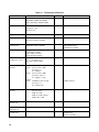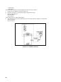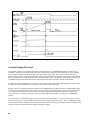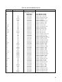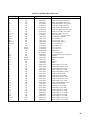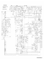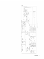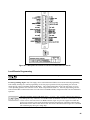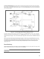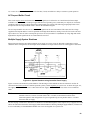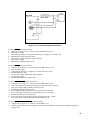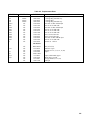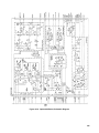
1
SERVICE MANUAL AUTORANGING DC POWER SUPPLY AGILENT MODELS 6023A and 6028A Agilent Part No. 5964-8283 FOR INSTRUMENTS WITH SERIAL NUMBERS Agilent Model 6023A; Serials US36490101 and above Agilent Model 6028A; Serials US36520101 and above For instruments with higher serial numbers, a change page may be included. Microfiche Part No. 5964-8284 Printed in USA: July 2001 CERTIFICATION Agilent Technologies certifies that this product met its published specifications at time of shipment from the factory. Agilent Technologies further certifies that its calibration measurements are traceable to the United States National Institute of Standards and Technology, to the extent allowed by the Institute’s calibration facility, and to the calibration facilities of other International Standards Organization members. WARRANTY This Agilent Technologies hardware product is warranted against defects in material and workmanship for a period of three years from date of delivery. Agilent Technologies software and firmware products, which are designated by Agilent Technologies for use with a hardware product and when properly installed on that hardware product, are warranted not to fail to execute their programming instructions due to defects in material and workmanship for a period of 90 days from date of delivery. During the warranty period Agilent Technologies will, at its option, either repair or replace products which prove to be defective. Agilent Technologies does not warrant that the operation of the software, firmware, or hardware shall be uninterrupted or error free. For warranty service, with the exception of warranty options, this product must be returned to a service facility designated by Agilent. Technologies. Customer shall prepay shipping charges by (and shall pay all duty and taxes) for products returned to Agilent Technologies. for warranty service. Except for products returned to Customer from another country, Agilent Technologies shall pay for return of products to Customer. Warranty services outside the country of initial purchase are included in Agilent Technologies’ product price, only if Customer pays Agilent Technologies international prices (defined as destination local currency price, or U.S. or Geneva Export price). If Agilent Technologies is unable, within a reasonable time to repair or replace any product to condition as warranted, the Customer shall be entitled to a refund of the purchase price upon return of the product to Agilent Technologies. LIMITATION OF WARRANTY The foregoing warranty shall not apply to defects resulting from improper or inadequate maintenance by the Customer, Customer-supplied software or interfacing, unauthorized modification or misuse, operation outside of the environmental specifications for the product, or improper site preparation and maintenance. NO OTHER WARRANTY IS EXPRESSED OR IMPLIED. AGILENT TECHNOLOGIES SPECIFICALLY DISCLAIMS THE IMPLIED WARRANTIES OF MERCHANTABILITY AND FITNESS FOR A PARTICULAR PURPOSE. EXCLUSIVE REMEDIES THE REMEDIES PROVIDED HEREIN ARE THE CUSTOMER’S SOLE AND EXCLUSIVE REMEDIES. AGILENT TECHNOLOGIES SHALL NOT BE LIABLE FOR ANY DIRECT, INDIRECT, SPECIAL, INCIDENTAL, OR CONSEQUENTIAL DAMAGES, WHETHER BASED ON CONTRACT, TORT, OR ANY OTHER LEGAL THEORY. ASSISTANCE The above statements apply only to the standard product warranty. Warranty options, extended support contracts, product maintenance agreements and customer assistance agreements are also available. Contact your nearest Agilent Technologies Sales and Service office for further information on Agilent Technologies’ full line of Support Programs. 2 SAFETY SUMMARY The following general safety precautions must be observed during all phases of operation, service and repair of this instrument. Failure to comply with these precautions or with specific warnings elsewhere in this manual violates safety standards of design, manufacture, and intended use of the instrument. Agilent Technologies, Inc. assumes no liability for the customer's failure to comply with these requirements. BEFORE APPLYING POWER. Verify that the product is set to match the available line voltage and the correct fuse is installed. GROUND THE INSTRUMENT. This product is a Safety Class 1 instrument (provided with a protective earth terminal). To minimize shock hazard, the instrument chassis and cabinet must be connected to an electrical ground. The instrument must be connected to the ac power supply mains through a threeconductor power cable, with the third wire firmly connected to an electrical ground (safety ground) at the power outlet. For instruments designed to be hard wired to the ac power lines (supply mains), connect the protective earth terminal to a protective conductor before any other connection is made. Any interruption of the protective (grounding) conductor or disconnection of the protective earth terminal will cause a potential shock hazard that could result in personal injury. If the instrument is to be energized via an external autotransformer for voltage reduction, be certain that the autotransformer common terminal is connected to the neutral (earth pole) of the ac power lines (supply mains). INPUT POWER MUST BE SWITCH CONNECTED. For instruments without a built-in line switch, the input power lines must contain a switch or another adequate means for disconnecting the instrument from the ac power lines (supply mains). DO NOT OPERATE IN AN EXPLOSIVE ATMOSPHERE. Do not operate the instrument in the presence of flammable gases or fumes. KEEP AWAY FROM LIVE CIRCUITS. Operating personnel must not remove instrument covers. Component replacement and internal adjustments must be made by qualified service personnel. Do not replace components with power cable connected. Under certain conditions, dangerous voltages may exist even with the power cable removed. To avoid injuries, always disconnect power, discharge circuits and remove external voltage sources before touching components. DO NOT SERVICE OR ADJUST ALONE. Do not attempt internal service or adjustment unless another person, capable of rendering first aid and resuscitation, is present. DO NOT EXCEED INPUT RATINGS. This instrument may be equipped with a line filter to reduce electromagnetic interference and must be connected to a properly grounded receptacle to minimize electric shock hazard. Operation at the line voltage or frequencies in excess of those stated on the data plate may cause leakage currents in excess of 5.0mA peak. SAFETY SYMBOLS. Instruction manual symbol: the product will be marked with this symbol when it is necessary for the user to refer to the instruction manual (refer to Table of Contents) . Indicates hazardous voltages. Indicate earth (ground) terminal. The WARNING sign denotes a hazard. It calls attention to a procedure, practice, or the like, which, if not correctly performed or adhered to, could result in personal injury. Do not proceed beyond a WARNING sign until the indicated conditions are fully understood and met. The CAUTION sign denotes a hazard. It calls attention to an operating procedure, or the like, which, if not correctly performed or adhered to, could result in damage to or destruction of part or all of the product. Do not proceed beyond a CAUTION sign until the indicated conditions are fully understood and met. DO NOT SUBSTITUTE PARTS OR MODIFY INSTRUMENT. Because of the danger of introducing additional hazards, do not install substitute parts or perform any unauthorized modification to the instrument. Return the instrument to a Agilent Technologies, Inc. Sales and Service Office for service and repair to ensure that safety features are maintained. Instruments which appear damaged or defective should be made inoperative and secured against unintended operation until they can be repaired by qualified service personnel. 3 SAFETY SYMBOL DEFINITIONS Symbol Description Symbol Description Direct current Terminal for Line conductor on permanently installed equipment Alternating current Caution, risk of electric shock Both direct and alternating current Caution, hot surface Three-phase alternating current Caution (refer to accompanying documents) Earth (ground) terminal In position of a bi-stable push control Protective earth (ground) terminal Out position of a bi-stable push control Frame or chassis terminal On (supply) Terminal for Neutral conductor on permanently installed equipment Off (supply) Terminal is at earth potential (Used for measurement and control circuits designed to be operated with one terminal at earth potential.) Standby (supply) Units with this symbol are not completely disconnected from ac mains when this switch is off. To completely disconnect the unit from ac mains, either disconnect the power cord or have a qualified electrician install an external switch. Printing History The edition and current revision of this manual are indicated below. Reprints of this manual containing minor corrections and updates may have the same printing date. Revised editions are identified by a new printing date. A revised edition incorporates all new or corrected material since the previous printing date. Changes to the manual occurring between revisions are covered by change sheets shipped with the manual. Also, if the serial number prefix of your power supply is higher than those listed on the title page of this manual, then it may or may not include a change sheet. That is because even though the higher serial number prefix indicates a design change, the change may not affect the content of the manual. Edition 1 July, 2001 © Copyright 2001 Agilent Technologies, Inc. This document contains proprietary information protected by copyright. All rights are reserved. No part of this document may be photocopied, reproduced, or translated into another language without the prior consent of Agilent Technologies, Inc. The information contained in this document is subject to change without notice. 4 TABLE OF CONTENTS Introduction ............................................................................................................................................................................ 7 Scope .................................................................................................................................................................................... 7 Calibration and Verification ............................................................................................................................................. 7 Troubleshooting................................................................................................................................................................ 7 Principles of Operation ..................................................................................................................................................... 7 Replaceable Parts.............................................................................................................................................................. 7 Circuit Diagrams............................................................................................................................................................... 7 Safety Considerations ........................................................................................................................................................... 7 Manual Revisions ................................................................................................................................................................. 8 Calibration and Verification.................................................................................................................................................. 9 Introduction........................................................................................................................................................................... 9 Test Equipment Required ..................................................................................................................................................... 9 Operation Verification Tests................................................................................................................................................. 9 Calibration Procedure ........................................................................................................................................................... 9 Initial Setup..................................................................................................................................................................... 11 Performance Tests .............................................................................................................................................................. 14 Measurement Techniques ............................................................................................................................................... 14 Constant Voltage (CV) Tests .......................................................................................................................................... 15 Constant Current (CC) Tests........................................................................................................................................... 21 Troubleshooting .................................................................................................................................................................... 23 Introduction......................................................................................................................................................................... 23 Initial Troubleshooting Procedures..................................................................................................................................... 23 Electrostatic Protection ....................................................................................................................................................... 25 Repair and Replacement ..................................................................................................................................................... 25 A2 Control Board Removal ............................................................................................................................................ 26 A4 Power Mesh Board Removal .................................................................................................................................... 27 A3 Front-Panel Board Removal...................................................................................................................................... 27 A1 Main Board Removal................................................................................................................................................ 27 Overall Troubleshooting Procedure.................................................................................................................................... 27 Using the Tables ............................................................................................................................................................. 28 Main Troubleshooting Setup .......................................................................................................................................... 29 Troubleshooting No-Output Failures .............................................................................................................................. 31 Front-Panel Troubleshooting .......................................................................................................................................... 31 Troubleshooting Bias Supplies ....................................................................................................................................... 33 Power Section Blocks ..................................................................................................................................................... 35 Troubleshooting AC-Turn-on Circuits............................................................................................................................ 35 Troubleshooting PWM & Clock..................................................................................................................................... 36 Troubleshooting DC-To-DC Converter .......................................................................................................................... 37 Troubleshooting CV Circuit ........................................................................................................................................... 38 Troubleshooting CC Circuit............................................................................................................................................ 38 Troubleshooting Down Programmer .............................................................................................................................. 39 Troubleshooting OVP Circuit ......................................................................................................................................... 39 Principles of Operation ........................................................................................................................................................ 43 Autoranging Power ............................................................................................................................................................. 43 Block Diagram Overview ................................................................................................................................................... 43 Simplified Schematic...................................................................................................................................................... 45 DC-to-DC Converter....................................................................................................................................................... 47 Down Programmer.......................................................................................................................................................... 47 Constant-Voltage (CV) Circuit ....................................................................................................................................... 48 Constant-Current (CC) Circuit........................................................................................................................................ 49 5 Overvoltage Protection (OVP) Circuit............................................................................................................................ 49 Power-Limit Comparator ................................................................................................................................................ 49 Control-Voltage Comparator .......................................................................................................................................... 49 Initial-Ramp Circuit........................................................................................................................................................ 50 Pulse-Width Modulator (PWM) ..................................................................................................................................... 50 Bias Voltage Detector..................................................................................................................................................... 50 AC-Surge Dropout Detector ........................................................................................................................................... 50 1-Second-Delay Circuit .................................................................................................................................................. 51 Display Circuits .................................................................................................................................................................. 51 Replaceable Parts.................................................................................................................................................................. 53 Introduction......................................................................................................................................................................... 53 Ordering Information.......................................................................................................................................................... 54 Component Location and Circuit Diagrams ...................................................................................................................... 69 System Option 002 ................................................................................................................................................................ 79 General Information............................................................................................................................................................ 79 Specifications.................................................................................................................................................................. 79 Option 002 Hardware...................................................................................................................................................... 79 Installation .......................................................................................................................................................................... 83 Connector Assembly Procedure...................................................................................................................................... 83 Operation ............................................................................................................................................................................ 84 Local/Remote Programming........................................................................................................................................... 85 Remote Resistance Programming ................................................................................................................................... 87 Remote Monitoring......................................................................................................................................................... 89 Status Indicators.............................................................................................................................................................. 90 Remote Control............................................................................................................................................................... 90 Power-On Preset ................................................................................................................................................................. 92 AC Dropout Buffer Circuit ............................................................................................................................................. 93 Multiple Supply System Shutdown ................................................................................................................................ 93 Bias Supplies .................................................................................................................................................................. 94 Maintenance........................................................................................................................................................................ 94 Troubleshooting.............................................................................................................................................................. 95 Troubleshooting Resistance and Voltage Programming................................................................................................. 95 Troubleshooting Current Programming .......................................................................................................................... 95 Backdating........................................................................................................................................................................... 107 6 1 Introduction Scope This manual contains information for troubleshooting the Agilent 6023A or 6028A 200W Autoranging Power Supply to the component level. Wherever applicable, the service instructions given in this manual refer to pertinent information provided in the Operation Manual. Both manuals cover Agilent Models 6023A/28A; differences between models are described as required. The following information is contained in this manual. Calibration and Verification Contains calibration procedures for Agilent Models 6023A/28A. Also contains verification procedures that check the operation of the supplies to ensure they meet the specifications of Chapter 1 in the Operating Manual. Troubleshooting Contains troubleshooting procedures to isolate a malfunction to a defective component on the main circuit board or to a defective assembly (front-panel, power transformer, or cable assembly). Board and assembly level removal and replacement procedures are also given in this section. Principles of Operation Provides block diagram level descriptions of the supply's circuits. The regulation & control, protection, input power, dc power conversion and output circuits are described. These descriptions are intended as an aid in troubleshooting. Replaceable Parts Provides a listing of replaceable parts for all electronic components and mechanical assemblies for Agilent Models 6023A/28A. Circuit Diagrams Contains functional schematics and component location diagrams for all Agilent 6023A/28A circuits. The names that appear on the functional schematics also appear on the block diagrams in Chapter 4. Thus, the descriptions in Chapter 4 can be correlated with both the block diagrams and the schematics. Safety Considerations This product is a Safety Class 1 instrument, which means that it is provided with a protective earth terminal. Refer to the Safety Summary page at the beginning of this manual for a summary of general safety information. Safety information for specific procedures is located at appropriate places in the manual. 7 Manual Revisions Agilent Technologies instruments are identified by a 10-digit serial number. The format is described as follows: first two letters indicate the country of manufacture. The next four digits are a code that identify either the date of manufacture or of a significant design change. The last four digits are a sequential number assigned to each instrument. Item Description US The first two letters indicates the country of manufacture, where US = USA; MY = Malaysia. 3648 This is a code that identifies either the date of manufacture or the date of a significant design change. 0101 The last four digits are a unique number assigned to each power supply. If the serial number prefix on your unit differs from that shown on the title page of this manual, a yellow Manual Change sheet may be supplied with the manual. It defines the differences between your unit and the unit described in this manual. The yellow change sheet may also contain information for correcting errors in the manual. Note that because not all changes to the product require changes to the manual, there may be no update information required for your version of the supply. Older serial number formats used with these instruments had a two-part serial number, i.e. 2701A-00101. This manual also applies to instruments with these older serial number formats. Refer to Appendix B for backdating information. 8 2 Calibration and Verification Introduction This section provides test and calibration procedures. The operation-verification tests comprise a short procedure to verify that the unit is performing properly, without testing all specified parameters. After troubleshooting and repair of a defective power supply you can usually verify proper operation with the turn-on checkout procedure in the Operating Manual. Repairs to the A1 main board and the A2 control board can involve circuits which, although functional, may prevent the unit from performing within specified limits. So, after A1 or A2 board repair, decide if recalibration and operation verification tests are needed according to the faults you discover. Use the calibration procedure both to check repairs and for regular maintenance. When verifying the performance of this instrument as described in this chapter, check only those specifications for which a performance test procedure is included. Test Equipment Required Table 2-1 lists the equipment required to perform the tests of this section. You can separately identify the equipment for performance tests, calibration and troubleshooting using the USE column of the table. Operation Verification Tests To assure that the unit is performing properly, without testing all specified parameters, first perform the turn-on checkout procedure in the Operating Manual. Then perform the following performance tests, in this section. CV Load Effect CC Load Effect Calibration Procedure Calibrate the unit twice per year and when required during repair. The following calibration procedures which follow should be performed in the sequence given. Table 2-2 describes in detail these calibration procedures and lists the expected results to which each adjustment must be made. Note: Some of the calibration procedures for this instrument can be performed independently, and some procedures must be performed together and/or in a prescribed order. If a procedure contains no references to other procedures, you may assume that it can be performed independently. To return a serviced unit to specifications as quickly as possible with minimal calibration, the technician need only perform calibration procedures that affect the repaired circuit. Table 2-3 lists various power supply circuits with calibration procedures that should be performed after those circuits are serviced. 9 Table 2-1. Test Equipment Required TYPE Oscilloscope REQUIRED CHARACTERISTICS Sensitivity: 1 mV Bandwidth: 20MHz & 100MHz Input: differential, 50Ω & 10MΩ USE P,T RECOMMENDED MODEL Agilent 1740A RMS Voltmeter True rms, 10MHz bandwidth Sensitivity: 1 mV Accuracy: 5% P Agilent 3400B Logic Pulser 4.5 to 5.5Vdc @ 35mA T Agilent 546A Multimeter Resolution: 100nV Accuracy: 0.0035%, 6½ digit P,A,T Agilent 3458A CC PARD Test Current Probe No saturation at 30Adc Bandwidth: 20Hz to 20MHz P Electronic Load* Voltage range: 60Vdc Current range: 60Adc Power range: 300 watts Open and short switches Value: 0.25 ohms >250W Accuracy: 1% Rheostat or Resistor Bank P,A Tektronix P6303 Probe/AM503 Amp/ TM500 Power Module Agilent 6060B 6023A Value: 30mV @ 30A (1mΩ ) Accuracy: 1% TC: 30ppm/°C Value: 30mV @ 30A (1mΩ) Accuracy: 0.05% ** TC: 30ppm/°C (A,P) 6028A Value 100MΩ ± 0.04% @ 25W Accuracy: 1% PC: 0.0004% 1W P,A Calibration and Test Resistors Value: A,T Terminating Resistors (4) Value: 50Ω ±5%, noninductive P Blocking Capacitors (2) Common-mode Toroidal Core Value: 0.01µF, 100Vdc P CC PARD Test & IP Cal Resistive Load* Current-Monitoring Resistors 10 100Ω, 5%, 1W 1Ω, 5%, 1/2W 1KΩ, 5% 1/4W 5KΩ, 5% 1/4W (6023A) 2KΩ, 0.01% 1/4W P,A Guidline 9230/15 P Ferrox-Cube 500T600-3C8, Agilent 9170-0061 Table 2-1. Test Equipment Required (continued) TYPE Switch DC Power Supply REQUIRED CHARACTERISTICS SPST, 30A @ 20V Voltage range: 0-60Vdc Current range: 0-3Adc USE P T,P Variable Voltage Transformer (autotransformer) Range greater than -13% to +6% of nominal input AC voltage 1KVA P,A P = performance testing A = calibration adjustments RECOMMENDED MODEL Agilent 6296A T = troubleshooting * Resistors may be substituted for test where an electronic load is not available. ** Less accurate, and less expensive, current-monitor resistors can be used, but the accuracy to which current programming and current meter reading can be checked must be reduced accordingly. Initial Setup Maintenance described herein is performed with power supplied to the instrument, and protective covers removed. Such maintenance should be performed only by service trained personnel who are aware of the hazards involved (for example, fire and electrical shock). Turn off ac power when making or removing connections to the power supply. Where maintenance can be performed without power applied, the power should be removed. a. b. c. d. e. f. g. h. i. j. k. l. Unplug the line cable and remove the top cover by removing three screws; the rear handle screw and the two top-rear corner screws. Do not remove the front handle screw as the retaining nut will fall into the unit. Slide the cover to the rear. Plug a control board test connector A2P3 onto the A2J3 card-edge fingers. Turn OVERVOLTAGE ADJUST control A3R59 fully clockwise. Disconnect all loads from output terminals. Connect power supply for local sensing, and ensure that MODE switches are set as shown below. Reconnect the line cable and turn on ac power. Allow unit to warm up for 30 minutes. When attaching the DVM, the minus lead of the DVM should be connected to the first node listed, and the plus lead should be connected to the second node listed. At the beginning of each calibration procedure, the power supply should be in its power-off state, with no external circuitry connected except as instructed. The POWER LIMIT adjustment (A2R25) must be adjusted at least coarsely before many of the calibration procedures can be performed. If you have no reason to suspect that the Power Limit circuit is out of adjustment, and you do not intend to recalibrate it, do not disturb its setting. Otherwise, center A2R25 before you begin to calibrate the power supply. To disable the power supply, short INHIBIT line A2J3 pin 8 to COMMON A2J3 pin 4. 11 Table 2-2. Calibration Procedure TEST Meter F/S Adjust. TESTED VARIABLE Meter Ref. Voltage TEST POINTS A2J3 pin 6 ( + ) M(-) TEST SEQUENCE AND ADJUSTMENTS a. b. Resistance Programming F/S Adjust. Prog. Voltage VP ( + ) P(-) a. b. c. V-MON Zero Adjust. V-MON VM ( + ) M(-) a. b. c. d. Common Mode Adjust. Residual Output Voltage VM( + ) VM ( + ) M(-) a. b. c. d. I-MON Zero Adjust. I-MON IM ( + ) M (-) I-MON F/S Adjust. I-MON IM ( + ) M(-) e. f. a. b. c. a. b. c. d. Rm ( + ) Rm ( - ) *IR = Initial Reading 12 e. Connect DVM across test points and turn on ac power. Adjust A2R24 to obtain the voltage range specified in the results. Connect a 2KΩ 0.01%, ¼W programming resistor and DVM between test points. Set MODE switch as in Figure 2-1 and turn on ac power. Adjust A2R23 to obtain the voltage range specified in the results. Set voltage and current controls to minimum settings. Disable power supply as in Initial Setup step i. Short circuit output terminals and connect the DVM between test points. Turn on power supply. Adjust V-MON Zero trim pot A2R22 to voltage range specified in the results. Set voltage and current controls to minimum. Disable power supply as Initial Setup step i. Turn on ac power and record the initial voltage (IR) with DVM across test points. Remove the - S( + ) and – OUT( - ) and connect a 1Vdc power supply between - S( + ) and – OUT( - ). See Figure 2-1. Adjust A2R21 to the voltage range specified. Remove the 1V supply and replace jumpers. Set voltage and current controls to minimum. Turn on ac power. Connect DVM across test points and adjust I-MON Zero trim pot A2R8 as shown in results. Perform I-MON Zero Adjust before proceeding . Connect a 0.001Ω 0.05% (6023A), 0.100Ω 0.05% (6028A) current monitoring resistor Rm across the output terminals. Turn on ac power and using the “Display Setting”, set current control to 30A (6023A), 10A (6028A), and voltage control to 5V. Connect DVM across test points and take an initial reading (IR). Connect DVM across Rm monitoring terminals and adjust A2R9 as shown in the results. EXPECTED RESULTS 0.5V ± 50µV 2.5V ±4mV 0 ± 20µV IR ± 20µV 0 ± 100µV (6023A) 0 ± 25µV (6028A) IR* 0.006 IR* +40µV (6023A), 0.200 ± 1µV (6028A) Table 2-2. Calibration Procedure (continued) TEST Power Limit Adjust. TESTED VARIABLE V(OUT) I(OUT) TEST POINTS TEST SEQUENCE AND ADJUSTMENTS a. Perform I-MON F/S Adjust before proceeding. b. Connect the unit to the ac power line via the external variable auto-transformer which is set to nominal line voltage. c. Connect a 0.25Ω, 250W (6023A), 2.3Ω, 250W (6028A) resistor across the unit's output and turn on ac power. d. Set voltage control to 9V (6023A) 9V≥ 3V (6028A) and current control to 30.2A (6023A), 10.2A (6028A) e. Set auto-transformer to minimum line voltage. f. Turn A2R25 fully counterclockwise. g. Slowly adjust A2R25 clockwise until CC LED just lights. EXPECTED RESULTS 30.2A 7.55V for CC operation (6023A) 10.2A, 23V for CC operation (6028A) Figure 2-1. Common Mode Setup 13 Table 2-3. Guide to Recalibration After Repair Printed Circuit Board A1 Main Board A1 Main Board A4 Power Mesh A4 Power Mesh A2 Control Board A2 Control Board A2 Control Board A2 Control Board A2 Control Board A2 Control Board 1. 2. 3. Block Name Constant Voltage (CV) Circuit Constant Voltage (CV) Circuit Constant Current (CC) Circuit Power Limit Comparator Bias Power Supplies Circuit Within Block All Except Current Source Current Source Ref. Designator R3 T1 T3 CR7 All Perform These Procedures* 4 4 then 5 4 then 5 Board 4 then 5 Board 1 then 2 All 6 All 3 then 4 All 4 then 5 All All U9, R79, R80, R24 7 * Code To Calibration Procedure To Be Performed V-MON Zero Calibration 4. I-MON Full Scale (F/S) Calibration Common-Mode Calibration 5. Power Limit Calibration I-MON Full Scale (F/S) Zero Calibration 6. Resistance Programming Full Scale (F/S) Calibration 7. Meter Full Scale (F/S) Calibration ± 15V Supplies Performance Tests The following paragraphs provide test procedures for verifying the unit's compliance with the specifications of Table 1-1 in the Operating Manual. Please refer to CALIBRATION PROCEDURE or TROUBLESHOOTING if you observe out-of-specification performance. Measurement Techniques Setup For All Tests. Measure the output voltage directly at the + S and - S terminals. Connect unit for local sensing, and ensure that MODE switches are set as shown below. Select an adequate wire gauge for load leads using the procedures given in the Operating Manual for connecting the load. Electronic Load. The test and calibration procedures use an electronic load to test the unit quickly and accurately. If an electronic load is not available, you may substitute a 2Ω 250W load resistor for the electronic load in these tests: CV Source Effect (Line Regulation) CC Load Effect (Load Regulation) You may substitute a 0.25Ω 250W load resistor in these tests: CV Load Effect (Load Regulation) CV PARD (Ripple and Noise) CC Source Effect (Line Regulation) CC PARD (Ripple and Noise) 14 The substitution of the load resistor requires adding a load switch to open and short the load in the CC or CV load regulation tests. The load transient recovery time test procedure cannot be performed using load resistors. An electronic load is considerably easier to use than a load resistor. It eliminates the need for connecting resistors or rheostats in parallel to handle the power, it is much more stable than a carbon-pile load, and it makes easy work of switching between load conditions as is required for the load regulation and load transient-response tests. Current-Monitoring Resistor Rm. To eliminate output current measurement error caused by voltage drops in the leads and connections, connect the current-monitoring resistor between -OUT and the load as a four-terminal device. Figure 2-2 shows correct connections. Select a resistor with stable characteristics: 0.001, 1% accuracy, 30 ppm/°C or lower temperature coefficient and 20W power rating (20 times actual power if other than 0.001Ω is used). Figure 2-2. Current-Monitoring Resistor Setup Constant Voltage (CV) Tests CV Setup. If more than one meter or a meter and an oscilloscope are used, connect each to the + S and - S terminals by a separate pair of leads to avoid mutual coupling effects. Connect only to + S and -S (except for peak-to-peak PARD) because the unit regulates the output voltage between + S and - S, not between + OUT and - OUT. Use coaxial cable or shielded 2-wire cable to avoid pickup on test leads. For all CV tests set the output current at full output to assure CV operation. Load Effect (Load Regulation). Constant-voltage load effect is the change in dc output voltage (Eo) resulting from a load-resistance change from open-circuit to full-load. Full-load is the resistance which draws the maximum rated output current at voltage Eo. Proceed as follows: a. Connect the test equipment as shown in Figure 2-3. Operate the load in constant resistance mode (Amps/Volt) and set resistance to maximum. b. Turn the unit's power on, and turn up current setting to full output. c. Turn up output voltage to: 7.0Vdc (6023A) 20.0Vdc (6028A) as read on the digital voltmeter. 15 Figure 2-3. Basic Test Setup d. e. f. g. Reduce the resistance of the load to draw an output current of: 29Adc (6023A) 10Adc (6028A) Check that the unit's CV LED remains lighted. Record the output voltage at the digital voltmeter. Open-circuit the load. When the reading settles, record the output voltage again. Check that the two recorded readings differ no more than: ± 0.0027Vdc (6023A) ± 0.0090Vdc (6028A) Source Effect (Line Regulation). Source effect is the change in dc output voltage resulting from a change in ac input voltage from the minimum to the maximum value as specified in Input Power Requirements in the Specifications Table, in the Operating Manual. Proceed as follows: a. Connect the test equipment as shown in Figure 2-3. Operate the load in constant resistance mode (Amps/Volt) and set resistance to maximum. b. Connect the unit to the ac power line through a variable autotransformer which is set for low line voltage (104Vac for 120Vac). c. Turn the unit's power on, and turn up current setting to full output. d. Turn up output voltage to: 20.0Vdc (6023A) 60Vdc (6028A) as read on the digital voltmeter. e. Reduce the resistance of the load to draw an output current of: 10Adc (0.010Vdc across Rm) (6023A) 3.3Adc(0.33Vdc across Rm) (6028A) Check that the unit's CV LED remains lighted. 16 f. g. h. Record the output voltage at the digital voltmeter. Adjust autotransformer to the maximum for your line voltage. When the reading settles record the output voltage again. Check that the two recorded readings differ no more than: ± 0.0030Vdc (6023A) ± 0.0080Vdc (6028A) PARD (Ripple And Noise). Periodic and random deviations (PARD) in the unit's output-ripple and noise-combine to produce a residual ac voltage superimposed on the dc output voltage. Constant-voltage PARD is specified as the root-mean-square (rms) or peak-to-peak (pp) output voltage in a frequency range of 20Hz to 20MHz. RMS Measurement Procedure. Figure 2-4 shows the interconnections of equipment to measure PARD in Vrms. To ensure that there is no voltage difference between the voltmeter's case and the unit's case, connect both to the same ac power outlet or check that the two ac power outlets used have the same earth-ground connection. Use the common-mode choke as shown to reduce ground-loop currents from interfering with measurement. Reduce noise pickup on the test leads by using 50Ω coaxial cable, and wind it five turns through the magnetic core to form the common-mode choke. Proceed as follows: a. Connect the test equipment as shown in Figure 2-4. Operate the load in constant resistance mode (Amps/Volt) and set resistance to maximum. b. Turn the unit's power on, and turn up current setting to full output. c. Turn up output voltage to: 7Vdc (6023A) 20Vdc (6028A) d. Reduce the resistance of the load to draw an output current of: 29Adc (6023A) 10Adc (6028A) Check that the unit's CV LED remains lighted. e. Check that the rms noise voltage at the true rms voltmeter is no more than: 3.0mV rms (6023A) 3.0mV rms (6028A) Figure 2-4. RMS Measurement Test Setup, CV PARD Test Peak Measurement Procedure. Figure 2-5 shows the interconnections of equipment to measure PARD in Vpp. The equipment grounding and power connection instructions of PARD rms test apply to this setup also. Connect the oscilloscope to the + OUT and - OUT terminals through 0.01µF blocking capacitors to protect the oscilloscope's input from 17 the unit's output voltage. To reduce common-mode noise pickup, set up the oscilloscope for a differential, two-channel voltage measurement. To reduce normal-mode noise pickup, use twisted, 1 meter or shorter, 50Ω coaxial cables with shields connected to the oscilloscope case and to each other at the other ends. Proceed as follows: a. b. c. d. e. f. Connect the test equipment as shown in Figure 2-5. Operate the load in constant resistance mode (Amps/Volt) and set resistance to maximum. Turn the unit's power on, and turn up current setting to full output. Turn up output voltage to: 7.0Vdc (6023A) 20Vdc (6028A) Reduce the resistance of the load to draw an output current of: 29.0Adc (6023A) 10Adc (6028A) Check that the unit's CV LED remains lighted. Set the oscilloscope's input impedance to 50Ω and bandwidth to 20MHz. Adjust the controls to show the 20KHz and higher frequency output-noise waveform of Figure 2-6. Check that the peak-to-peak is no more than 30mV. Figure 2-5. Peak-To-Peak Measurement Test Setup, CV PARD Test 18 6023A 6028A Figure 2-6. 20KHz Noise, CV Peak-to-Peak PARD Load Transient Recovery Time. Specified for CV operation only; load transient recovery time is the time for the output voltage to return to within a specified band around its set voltage following a step change in load. Proceed as follows: a. b. c. d. e. f. g. Connect the test equipment as shown in Figure 2-3. Operate the load in constant-current mode and set for minimum current. Turn the unit's power on, and turn up current setting to full output. Turn up output voltage to: 6.70Vdc (6023A) 20.0Vdc (6028A) as read on the digital voltmeter. Set the load to vary the load current between: 27 and 30Adc (6023A) 9 and 10Adc (6028A) at a 30Hz rate. Set the oscilloscope for ac coupling, internal sync and lock on either the positive or negative load transient. Adjust the oscilloscope to display transients as in Figure 2-7. Check that the pulse width of the transient pulse is no more than: 50mV (6023A) 75mV (6028A) 19 6023A 6028A Figure 2-7. Load Transient Recovery Waveform Temperature Coefficient. (6023A) Temperature coefficient (TC) is the change in output voltage for each °C change in ambient temperature with constant ac line voltage, constant output voltage setting and constant load resistance. Measure temperature coefficient by placing the unit in an oven, varying the temperature over a range within the unit's operating temperature range, and measuring the change in output voltage. Use a large, forced air oven for even temperature distribution. Leave the unit at each temperature measurement for half hour to ensure stability in the measured variable. Measure the output voltage with a stable DVM located outside the oven so voltmeter drift does not affect the measurement accuracy. To measure offset TC, repeat the procedure with output voltage set to 0.10Vdc. Proceed as follows: a. b. c. d. e. f. g. h. Connect DVM between +S and -S. Place power supply in oven, and set temperature to 30°C. Turn the unit's power on and turn up current setting to full output. Turn up output voltage to 20Vdc as read on the DVM. After 30 minutes stabilization record the temperature to the nearest 0.1°C. Record the output voltage at the DVM. Set oven temperature to 50°C. After 30 minutes stabilization, record the temperature to the nearest 0.1°C. Record output voltage. Check that the magnitude of the output voltage change is no greater than 32mV. Drift (Stability) (6023A). Drift is the change in output voltage beginning after a 30-minute warm-up during 8 hours operation with constant ac input line voltage, constant load resistance and constant ambient temperature. Use a DVM and record the output at intervals, or use a strip-chart recorder to provide a continuous record. Check that the DVM's or recorder's specified drift during the 8 hours will be no more than 0.001%. Place the unit in a location with constant air temperature preferably a large forced-air oven set to 30°C and verify that the ambient temperature does not change by monitoring with a thermometer near the unit. Typically the drift during 30 minute warm-up exceeds the drift during the 8-hour test. To measure offset drift, repeat the procedure with output voltage set to 0.10Vdc. a. b. c. d. e. 20 Connect DVM between + S and - S. Turn the unit's power on and turn up current setting to full output. Turn up output voltage to 20Vdc as read on the digital voltmeter. After a 30 minute warmup, note reading on DVM. The output voltage should not deviate more than 5mV from the reading obtained in step d over a period of 8 hours. Constant Current (CC) Tests CC Setup. Constant-current tests are analogous to constant-voltage tests, with the unit's output short circuited and the voltage set to full output to assure CC operation. Follow the general setup instructions. Load Effect (Load Regulation). Constant current load effect is the change in dc output current (Io) resulting from a load-resistance change from short-circuit to full-load, or full-load to short-circuit. Full-load is the resistance which develops the maximum rated output voltage at current Io. Proceed as follows: a. b. c. d. e. f. g. h. Connect the test equipment as shown in Figure 2-3. Operate the load in constant resistance mode (Amps/Volt) and set resistance to minimum. Turn the unit's power on, and turn up voltage setting to full output. Turn up output current to: 10.0Adc (0.010Vdc across Rm) (6023A). Check that the AMPS display reads about 10 amps. 3.3Adc (0.335Vdc across Rm) (6028A) Check that the AMPS display reads about 3.3 amps. Increase the load resistance until the output voltage at +S and -S increases to: 20Vdc (6023A). 60Vdc (6028A). Check that the CC LED is lighted and AMPS display still reads ≈ current setting. Record voltage across Rm. Short circuit the load. When the reading settles (≈ 10s), record the voltage across Rm again. Check that the two recorded readings differ no more than: ± 0.010mVdc (6023A) ± 0.0053mVdc (6028A) Disconnect the short across the load. Source Effect (Line Regulation). Constant current source effect is the change in dc output current resulting from a change in ac input voltage from the minimum to the maximum values listed in the Specifications Table in the Operating Manual. Proceed as follows: a. Connect the test equipment as shown in Figure 2-3. Operate the load in constant resistance mode (Amps/Volt) and set resistance to minimum. b. Connect the unit to the ac power line through a variable autotransformer set for low line voltage (e.g. 104Vac for 120Vac). c. Switch the unit's power on and turn up output voltage setting to full output. d. Turn up output current to: 29.0Adc (0.029Vdc across Rm) (6023A) 10.0Adc (1.0Vdc across Rm) (6028A) Check that the AMPS display reads ≈ current setting. e. Increase the load resistance until the output voltage between + S and - S increases to: 7.0Vdc (603A) 20.0Vdc (6028A) Check that the CC LED is still on and the AMPS display still reads ≈ current setting. f. Record the voltage across Rm. g. Adjust autotransformer to the maximum for your line voltage. h. When the reading settles record the voltage across Rm again. Check that the two recorded readings differ no more than: ± 0.0090mVdc (6023A) ± 0.030mVdc (6028A) PARD Ripple And Noise. Periodic and random deviations (PARD) in the unit's output (ripple and noise) combine to produce a residual ac current as well as an ac voltage super-imposed on the dc output. The ac voltage is measured as constant-voltage PARD. Constant-current PARD is specified as the root-mean-square (rms) output current in a frequency range 20Hz to 20MHz with the unit in CC operation. To avoid incorrect measurements, with the unit in CC operation, caused by the impedance of the electronic load at noise frequencies, use a: 21 0.25Ω (6023A) 2.0Ω (6028A) load resistor that is capable of safely dissipating 250 watts. Proceed as follows: a. Connect the test equipment as shown in Figure 2-8. b. Switch the unit's power on and turn the output voltage all the way up. c. Turn up output current to: 29.0Vdc (6023A) 10Vdc (6028A) Check that the unit's CC LED remains lighted. d. Check that the rms noise current measured by the current probe and rms voltmeter is no more than: 15mA rms (6023A). 5mA rms (6028A) Figure 2-8. CC PARD Test Setup 22 3 Troubleshooting Maintenance described herein is performed with power supplied to the instrument, and protective covers removed. Such maintenance should be performed only by service-trained personnel who are aware of the hazards involved (for example, fire and electrical shock). Where maintenance can be performed without power applied, the power should be removed. Introduction Before attempting to troubleshoot this instrument, ensure that the fault is with the instrument itself and not with an associated circuit. The performance test enables this to be determined without having to remove the covers from the supply. The most important aspect of troubleshooting is the formulation of a logical approach to locating the source of trouble. A good understanding of the principles of operation is particularly helpful, and it is recommended that Chapter 4 of this manual be reviewed before attempting to troubleshoot the unit. Often the user will then be able to isolate a problem simply by using the operating controls and indicators. Once the principles of operation are understood, refer to the following paragraphs. Table 2-1 lists the test equipment for troubleshooting. Chapter 6 contains schematic diagrams and information concerning the voltage levels and waveforms at many of the important test points. Most of the test points used for troubleshooting the supply are located on the control board test "fingers", which are accessible close to the top of the board. See Table 3-1. If a component is found to be defective, replace it and re-conduct the performance test. When a component is replaced, refer to Calibration Procedure (Chapter 2). It may be necessary to perform one or more of the adjustment procedures after a component is replaced. Initial Troubleshooting Procedures If a problem occurs, follow the steps below in sequence: a. b. c. d. Check that input power is available, and check the power cord and rear-panel circuit breaker. Check that the settings of mode switch A2S1 are correct for the desired mode of operation. (See Operating Manual). Check that all connections to the power supply are secure and that circuits between the supply and external devices are not interrupted. If the power supply fails turn-on self-test or gives any other indication of malfunction, remove the unit from the operating system before proceeding with further testing. Some circuits on the power mesh are connected directly to the ac power line. Exercise extreme caution when working on energized circuits. Energize the supply through an isolation transformer to avoid shorting ac energized circuits through the test instrument's input leads. The isolation transformer must have a power rating of at least 1KVA. During work on energized circuits, the safest practice is to disconnect power, make or change the test connections, and then re-apply power. Make certain that the supply's ground terminal (┴) is securely connected to an earth ground before applying power. Failure to do so will cause a potential shock hazard that could result in personal injury. 23 Table 3-1. Control Board Test Connector, A2J7 PIN NO. SIGNAL NAME Vdc Digital-Circuits Bias & Reference Voltages 1 +5V 22 + 20V(5V UNREG) 14 2.5V ref 6 0.5V ref 5.0 20.0 2.50 0.50 Analog-Circuits Bias Voltages 2 + 15V 21 - 15V 15.0 -15.0 WAVEFORM/CONDITIONS with 120Hz & 45KHz ripple SOURCE A2Q3 (emitter) A1CR6, A1CR7 A2U9 (OUT) A2R79,A2R80 A2U12 (OUT) A2U4 (OUT ) Status Signals 17 CV 16 CC 13 OV 11 DROPOUT TTL Lo TTL Lo TTL Hi TTL Hi if in CV operation if in CC operation if not OVP shutdown if ac mains okay A2Q6C-7 (collector) A2Q6F-14 (collector) A2U11D-11 A2U17D-11 12 OT TTL Hi if not overtemp shutdown A2U11B-6 Control Signals 25 PWM OFF 26 PWM ON 18 Ip MONITOR 8 INHIBIT 15 DOWN PROGRAM <0.5 <1.0 <0.5 TTL hi 1.7µs TTL pulses, 20KHz 1.7µs TTL pulses, 20KHz 1V pk, ½ sawtooth, 20KHz if not remotely inhibited U1A-5 U2B-6 A2CR26 (cathode) A2R185C, U19A-2 7 OVP PROGRAM 5 OV CLR 19 1.2-3.0 1/10 OVP (6023A) 1/30 OVP (6028A) +5V A2CR21, A2CR27 e.g.: 2Vdc if OVP set to 20 A3R6 (wiper) inverted OV reset line A7U29-5 PCLR 2 Commons & Current-Monitor 4 L COMMON +5V if +5V bias OK A2Q60-9 0.0 A2C20 (-), A2R50, A2U6-4 9 M COMMON 0.0 10 3 I-TEST NOT USED common return for all bias voltages, and status and control signals common return for 2.5V ref. and 0.5V ref. inboard-side monitoring res. 24 ≈0.005 ( Iout) A2R83, A21-20 A1R3,A1T2 Electrostatic Protection The following caution outlines important precautions which should be observed when working with static sensitive components in the power supply. This instrument uses components which can be damaged by static charge. Most semiconductors can suffer serious performance degradation as a result of static charges, even though complete failure may not occur. The following precautions should be observed when handling static-sensitive devices. a. b. c. d. e. f. Always turn power off before removing or installing printed-circuit boards. Always stored or transport static-sensitive devices (all semiconductors and thin-film devices) in conductive material. Attach warning labels to the container or bag enclosing the device. Handle static-sensitive devices only at static-free work stations. These work stations should include special conductive work surfaces (such as Agilent Part No. 9300-0797) grounded through a one-megohm resistor. Note that metal table tops and highly conductive carbon-impregnated plastic surfaces are too conductive; they can act as large capacitors and shunt charges too quickly. The work surfaces should have distributed resistance of between 106and 10l2 Ω per square. Ground all conductive equipment or devices that may come in contact with static-sensitive devices or subassemblies containing same. Where direct grounding of objects in the work area is impractical, a static neutralizer should be used (ionized air blower directed at work). Note that this method is considerably less effective than direct grounding and provides less protection for static-sensitive devices. While working with equipment on which no point exceeds 500 volts, use a conductive wrist strap in contact with skin. The wrist strap should be connected to ground through a one-megohm resistor. A wrist strap with insulated cord and built-in resistor is recommended, such as 3M Co. No. 1066 (Agilent Part No. 9300-0969 (small) and 9300-0970 [large]). Do not wear a conductive wrist strap when working with potentials in excess of 500 volts; the one-megohm resistor will provide insufficient current limiting for personal safety. g. All grounding (device being repaired, test equipment, soldering iron, work surface, wrist strap, etc.) should be done to the same point. h. Do not wear nylon clothing. Keep clothing of any kind from coming within 12 inches of static-sensitive devices. i. Low-impedance test equipment (signal generators, logic pulsers, etc.) should be connected to static-sensitive inputs only while the components are powered. j. Use a mildly activated rosin core solder (such as Alpha Metal Reliacor No. 1, Agilent Part No. 8090-0098) for repair. The flux residue of this type of solder can be left on the printed circuit board. Generally, it is safer not to clean the printed-circuit board after repair. Do not use Freon or other types of spray cleaners. If necessary, the printed-circuit board can be brushed using a natural-bristle brush only. Do not use nylon-bristle or other synthetic-bristle brushes. Do not use high-velocity air blowers (unless ionized). k. Keep the work area free of non-conductive objects such as Styrofoam-type cups, polystyrene foam, polyethylene bags, and plastic wrappers. Non-conductive devices that are necessary in the area can be kept from building up a static charge by spraying them with an anti-static chemical (Agilent Part No. 8500-3397). l. Do not allow long hair to come in contact with static-sensitive assemblies. m. Do not exceed the maximum rated voltages specified for the device. Repair and Replacement Repair and replacement of most components in the power supply require only standard techniques that should be apparent to the technician. The following paragraphs provide instructions for removing certain assemblies and components for which the procedure may not be obvious upon inspection. 25 To avoid the possibility of personal injury, remove the power supply from operation before opening the cabinet. Turn off ac power and disconnect the line cord, load, and remote sense leads before attempting any repair or replacement. When replacing any heatsink-mounted components except thermostat, smear a thin coating of heatsink compound between the component and heatsink. If a mica insulator is used, smear a thin coating of heatsink compound on both sides of the mica insulator. Do not use any heatsink compound containing silicone, which can migrate and foul electrical contacts elsewhere in the system. An organic zinc oxide cream, such as American Oil and Supply Company Heatsink Compound #100, is recommended. Most of thc attaching hardware in this unit is metric. The only non-metric (sometimes called English or inch) fittings are listed below. Be careful when both types of screws are removed not to get them mixed up. a. b. c. d. e. f. Lock-link/shelf-mounting blocks (4 on rear panel, one at each corner). Rear-panel fuse holder. Rear-panel ground binding post. Strap-handle screws (2). Screws that secure side chassis to front-frame casting (8, 4 on each side). Screws that secure front-panel to front-frame casting (4, 2 on top and 2 on bottom). Top Outside Cover Removal. Remove three screws, the rear handle screw (Phillips, 10x32) and two top-rear corner screws (Pozidriv, M4x.7) using a Size 1, Pozidriv screwdriver. A Phillips head screwdriver does not fully seat into Pozidriv screws and risks stripping the heads. Do not remove the front handle screw, as the retaining nut will fall into the unit. Remove the top cover by sliding it to the rear and lifting at the front. Bottom Cover Removal. Remove only for repair of main board. Remove two bottom-rear corner screws. (Pozidriv, M4x.7) and remove the bottom cover by sliding it to the rear. You do not need to remove the unit's feet. Inside Top Cover Removal. The unit includes an inside cover which secures the vertical board assemblies. Remove the inside cover for repair but not for calibration. Remove the six mounting screws (Pozidriv, M4x.7) – three on each side and five board fastening screws (Pozidriv, M4x.7) all on top. Remove the inside cover by lifting at the front edge. When installing the inside cover, insert it first at the right side. While holding it tilted up at the left, reach through the cutouts in the cover and fit the top tabs of the A2 control board into the mating slots in the cover. With the top cover in place reach through the cutout above the A4 power mesh board, align the board-fastening screw holes, and replace the rearmost screw to secure the A4 board. Press the inside cover down firmly while tightening screws that secure cover to chassis. Complete the installation by replacing the remaining ten screws. Be careful when replacing printed-circuit assemblies and covers not to bend any boards or components. A2 Control Board Removal After removing the inside cover, remove the A2 board by lifting first at the front edge and than pulling it up and out of the unit. Two connectors hold the A2 board at its bottom edge. When installing the A2 board, insert it first at the rear of the unit. While holding it tilted up at the front, fit the A2TB1 terminal strip into the mating cutout in the rear panel. Then lower the A2 board's bottom connectors into the mating connectors on the main board. Press the A2 board into the connectors. 26 A4 Power Mesh Board Removal After removing the inside cover, remove the A4 power mesh board by lifting, using the large aluminum heatsink as a handle. Two connectors hold the A4 board at its bottom edge. When installing the A4 power mesh board, lower it vertically into its connectors and press in place. A3 Front-Panel Board Removal Remove the A3 front-panel board by first removing the entire front-panel assembly. You do not need to remove the top cover. Follow this procedure: a. Remove the top plastic insert by prying up with a flat-blade screwdriver, and remove the front feet by lifting the tabs and sliding toward the front of the unit. b. Remove the four front-panel assembly mounting screws (Phillips 8-32) on the top and bottom at the corners using a Pozidriv or Phillips head screwdriver (Phillips head screwdriver may be used only with these four screws). c. Gently pull the front-panel assembly away from the unit as far as permitted by the connecting cables. d. Remove the ground-wire screw (Pozidriv, M4x.7) holding the green-yellow ground wire. e. Note the locations of the four power-wire connections to the power switch and then unplug the quick-connect plugs. f. Unplug the W3 3-wire cable from connector A1J3 on the A1 main board. g. Remove the A3 board from the front-panel assembly by removing the five mounting screws (Pozidriv, M4x.7) Install the A3 Board by reversing the steps above. The power wires are correctly connected to the power switch wires if they do not cross each other. A1 Main Board Removal Removing the A1 main board requires removing the rear panel, all boards except the A3 front-panel board, and 17 A1 board mounting screws. Component-access cutouts in the bottom inside cover allow unsoldering most A1-board components for repair without removing the A1 board. To remove the A1 board, proceed as follows: a. Remove the A2 and A4 boards according to the above instructions. b. Detach the rear panel by removing the four mounting screws (Pozidriv, M4x.7) two on each side. Gently pull the rear panel away from the unit as far as permitted by the four wires connected to the A1 board. c. Unplug the W1 ribbon cable from connector A1J1. d. Remove the A1 board by removing the 17 mounting screws (Pozdriv, M4x.7). e. Note locations and the unplug the two ac power wires and the two fan wires to the A1 board. Overall Troubleshooting Procedure Perform the troubleshooting and repair procedures which follow only if you are trained in equipment service and are aware of the danger from fire and electrical-shock hazards. Some of the procedures include removing the unit's protective covers which may expose you to potentially lethal electrical shock. Whenever possible, make test connections and perform service with the power removed. After performing the Initial Troubleshooting Procedures, focus on developing a logical approach to locating the source of the trouble. The underlying strategy for the troubleshooting procedures here is to guide you to the faulty circuit nodes which have improper signals or voltages. It relies on you to identify the particular functional circuit to troubleshoot from symptom tables and by understanding how the unit works. It then relies on you to discover the defective component or components which cause the faulty circuit nodes. So, read the BLOCK DIAGRAM overview in Chapter 4 and read the functional circuit descriptions for the circuits that you suspect may be defective. Then return to this section for help finding the faulty circuit nodes. 27 Table 3-1 gives the signals for each of the test points on the control board test connector. This connector is provided in service kit P/N 06033-60005. The measurements given here include bias and reference voltages as well as power supply status signals and waveform information. Table 3-2 provides troubleshooting information based on the status of the PWM-ON and PWM-OFF signals which drive the PFETs. This table is used for no-output failures. Tables 3-3 and 3-4 give measurements for the test points on the A3 front-panel board and possible failure symptoms respectively. Table 3-5 describes possible symptoms for overall performance failures of the power supply. It is necessary to have a properly working front-panel before using this table. Chapter 6 contains schematic diagrams and voltage levels, and component location diagrams to help you locate components and test points. Make most voltage measurements (except DC-to-DC Converter and ac mains-connected circuits) referenced to the unit's output common which is accessible at rear-panel terminal VM. All voltages are ± 5% unless a range is given. Using the Tables Typically there will be two types of power supply failures; no-output and performance failures. 1. No-OUTPUT FAILURE: Tables 3-1 and 3-3. 2. PERFORMANCE FAILURE: If the power supply produces an output but does not perform to specifications, begin by verifying the measurements at the A2J7 test connector using Table 3-1. Next, verify the front-panel by doing the procedure outlined in the FRONT-PANEL TROUBLESHOOTING section. After the front-panel has been verified consult Table 3-5 for the performance failure symptom which seems closest to the one observed and proceed to the functional circuit given for that failure. Start with the TROUBLESHOOTING NO-OUTPUT FAILURES section which references The circuits referenced in Tables 3-2 and 3-5 are derived from functional blocks of circuits in the power supply. These blocks are given in the Power Supply Blocks section starting on page 35. Troubleshooting information for each block will include a brief description of the circuit involved. The columns provided in each block are as follows: NODE: This column lists the nodes where the measurements should be taken. In some cases this will be stated as NODE ( + ) and NODE (- ) where the first is the test node and the second is the reference. SETUP: If a certain setup is required for the measurement, it will be given in this column. MEASUREMENT: This column indicates what the expected measurement is for the given node. SOURCE: If applicable, the components which generate the signal will be provided in this column . Some blocks will have Input and Output sections. The input section will have a source column to indicate which components generated the measured signal. The output section will list all the important output signals from that block. However, because the outputs of one block are the inputs to another, the schematic should be consulted if an output measurement is incorrect. This will indicate the next circuit block to be trouble shot. 28 Main Troubleshooting Setup Figure 3-1 shows the troubleshooting setup for troubleshooting all of the unit except the front-panel and initial no output failures (See page 31). The external power supply provides the unit's internal bus voltage. The ac mains cord connects to the unit's A1T3 bias transformer via an isolation transformer, thereby energizing the bias supplies, but it does not connect to the input rectifier and filter because that would create the bus voltage. With the external supply the unit operates as a dc-to-dc converter. The supply biases the A4Q3 and A4Q4 PFETs with a low voltage rather than the 320Vdc bus voltage. This protects the PFETs from failure from excess power dissipation if the power-limit comparator or the off-pulse circuitry are defective. It also reduces the possibility of electrical shock to the troubleshooter. Figure 3-1. Main Troubleshooting Setup The troubleshooting setup of Figure 3-1 connects high ac mains voltage to the A1F2 fuse, the A1S2 MainsVoltage Select Switch, the fan and printed-circuit traces at the left edge of the A1 main board. Be extremely careful when working on the unit with the protective inside cover removed to avoid touching the ac mains voltage. 29 As a convenience in implementing the troubleshooting setup, prepare cord sets as shown in Figure 3-2. This facilitates connecting the unit's input power receptacle to the external supply and connecting the bias transformer to the ac mains. Figure 3-2. Modified Mains Cord Set For Troubleshooting With the mains cord unplugged proceed as follows: a. Remove the top cover and the inside cover as described on page 26. Set switch S4 (front-left corner of the A1 main board) in TEST position. If switch is not in the TEST position and remains in the NORM position, completion of step e below will allow the unit to develop its 320Vdc bus voltage across PFETs A3Q3 and A3Q4 and will connect the ac mains voltage to the output of the external power supply. This will probably damage the external supply and is a shock hazard to you. b. c. 30 Install control board test connector onto the A2J3 card edge fingers. Connect a 50Ω, 10W, load resistor to the unit's output terminals. d. e. With the LINE switch off, connect an external dc supply to the outside prongs of the unit’s power receptacle. Ignore polarity as the unit’s input rectifying diodes steer the dc power to the correct nodes. Complete the setup of Figure 3-1 by attaching an ac mains cord to test points TP1 (L, black wire) and TP2 (N, white wire) and connect the green ground wire to the unit's case ground terminal or a suitably grounded cabinet screw. TP1 and TP2 are accessible through the cutout on the left side of the unit and are at the left edge of the A1 main board. Troubleshooting No-Output Failures No-output failures often include failure of the A4Q3 and A4Q4 PFETs and their fuses, A4F1 and A4F2. When either the off-pulses or the power-limit comparator fails, the PFETs can fail from excessive power dissipation. The strategy for localizing no-output failures is to check the voltages and waveforms at the control board test connector to predict if that circuit failure would cause the PFETs to fail. This makes it possible to develop your troubleshooting approach without an extensive equipment setup. Proceed as follows: a. b. c. d. With the mains cord unplugged remove the A4 power mesh board as described on page 27. Plug in the mains cord and switch on power. Using Table 3-1 check the bias voltages, the PWM-OFF, PWM-ON and other signals of interest at the A2 control board test fingers, A2J3. Check for the presence of program voltages, VP and IP, at the rear panel. Check for presence of the 320Vdc rail voltage between the cathodes of diodes A1CR3 and A1CR4. If there is no rail voltage, check diodes A1CR1 through A1CR4. Diodes A1CR1 through A1CR4 connect to the ac mains voltage. Use a voltmeter with both input terminals floating to measure the rail voltage. e. Select the functional circuit for troubleshooting based on your measurements and Table 3-2, which provides direction based on the status of the PWM OFF and PWM ON signals . Front-Panel Troubleshooting The A3 front-panel board can be troubleshot by first doing the following setup. a. Remove the top cover of the unit. b. Remove the 4 side screws holding the front-panel assembly to the power supply chassis and pull the entire assembly forward. c. Disconnect the W1 ribbon cable from connector A1J1 on the A1 main board and remove the ground wire screw holding the green/yellow ground wire. Unplug the four wires to the LINE switch noting the configuration. d. Detach the A3 board from the front-panel assembly by removing the five mounting screws. e. Reconnect the W1 jumper to connector A1J1 and place the A3 board vertically against the supply with a piece of insulating material between. The test connector can then be attached to the A3 board. The rest of the front-panel assembly can stand vertically so that the pots and the switches can be accessed while troubleshooting. f. Attach the external line cord and place switch A1S4 in the TEST position. The ac mains voltage connects directly to the LINE switch and to components and traces at the front of the A1 main board. Be extremely careful to avoid touching the ac mains voltage. Start troubleshooting by performing the tests given in Table 3-3. This table provides the measurements for the test points on the test connector as well as the source components for that measurement. Switch A1S4 should be in the TEST position for all measurements except where noted. Table 3-4 gives front-panel symptoms as well as the circuits or components that may cause the supply to exhibit those symptoms. Both Tables 3-3 and 3-4 should be used to check out and troubleshoot the front-panel. 31 Table 3-2. No-Output Failures (Bias supplies and AC turn-on circuit functioning) Status of PFET on/off-Pulses PWM-ON PWM-OFF DEFECTIVE A2J7-26 A2J7-25 BOARD lo lo A2 CHECK FUNCTIONAL CIRCUITS Control ckts: CV & CC thru on- & off-Pulse Oneshots * lo hi A2 & A4 PWM and DC-to-DC Converter: A4Q3 and A4Q4 probably failed hi lo A2 & A4 PWM and DC-to-DC Converter: A4Q3 and A4Q4 probably failed hi hi A2 & A4 lo N A2 N lo A2 & A4 Off-Pulse Oneshot and DC-to-DC: A4Q3 and A4Q4 probably failed hi N A2 & A4 N hi A2 & A4 A2U17A, on-Pulse Oneshot & DC-to-DC: A4Q3, and A4Q4 probably failed off-Pulse Oneshot and DC-to-DC: A4Q3 and A4Q4 probably failed N N A2 & A4 lo= TTL low hi= TTL high PWM and DC-to-DC Converter: A4Q3 and A4Q4 probably failed A2U17B,on-Pulse Oneshot and A2Q6A Power-Limit Comparator and DC-to-DC: A4Q3 and A4Q4 probably failed N = normal 20KHz pulse train, TTL levels * Decide which to troubleshoot -- the CV Circuit, the CC Circuit, or the PWM and Off-Pulse & On-Pulse Oneshots -- by measuring the CV CONTROL (A2CR24, cathode) and the CC CONTROL (A2CR19 cathode) voltages. Troubleshoot whichever is negative, and if neither is negative, troubleshoot the PWM. Make these voltage measurements after you have implemented the Main Troubleshooting Setup. Table 3-3. Front-Panel Board Tests . Pin No 1 2 *3 *4 5 6 *7 8 Signal Name +7.5V -1V CV VOLTAGE CC VOLTAGE VOLTS test AMPS test Description Source Derived from + 15V bias. Derived from –15V bias. For 0 to full scale output voltage. For 0 to full scale output current. Jumper to + 5V on A3 board. A3VR2, A3R3 A3R86, A3R85, A3C17 A3U2-2, A3R1, A3R87. A3U3A-1, A3R67 A3U4-37 Jumper to + 5V on A3 board. A3U5-37 For 0 to full scale output voltage. If VOLTS display is below 20 volts (press DISPLAY SETTINGS). 9 DISPLAY TTL high If DISPLAY SETTINGS switch on SETTINGS front-panel is depressed. 10 DISPLAY OVP TTL high If DISPLAY OVP switch on frontpanel is depressed. *11 AMPS input 0-150mV For 0 to full scale output current. 12 -5 V -5.0V Derived from -15 V bias. 13 buffered OVP 0-2.2V 1/10 of OVP voltage setting when DISPLAY OVP switch is depressed. Varies with OVP ADJUST pot. * Switch A1S4 should be in the NORM position for these tests. 32 VOLTS input VOLTS low range Measureme nt 7.5V -1.0V 0-5V 0-5V -1888 on volts display -1888 on amps display 0-1V TTL high A3R8,A3U7-2,3,10 A3U9C-13, A3U6B A3S1,A3R80 A3S2,A3R82, A3U6C-8 A3R65,A3R66,A3R67 A3VR1, A3R2 A3U3B-6,A3CR5,A3R72 Troubleshooting Bias Supplies +5V on A2 Control Board. The PWM A2U6 includes a clock generator (45KHz set by A2R53 and A2C26), and a current limit (2Adc set by 0.15Vdc across A2R50). It turns off each output pulse using the difference between the voltage at voltage divider A2R46-A2R47 and the 2.5Vdc set by voltage regulator A2U5. Circuit Included. + 5Vdc bias supply circuitry from connector pin A2P1-15 through jumper A2W3 on A2 control board. Setup. The Main Troubleshooting Setup, page 29. Apply the ac mains voltage to the bias transformer, and set the external supply to 0Vdc. Input: NODE + A2J3-22 MEASUREMENT ≈ 20Vdc SOURCE A1CR6,A1CR7 Outputs NODE A2U6-6 A2U6-12,13 A2Q3 (emit) A2U5 (OUT) A2R50, A2CR11 (anode) A2R161, A2R163 MEASUREMENT ≈ 2 to 4Vdc sawtooth, 45KHz ≈ 19Vpk, 15µs pulses, 45KHz ≈ 20Vpk, 5µs pulses, 45KHz 2.5 Vdc ≈ 0 > V > -0.07Vdc 2.5 Vdc To check if load on + 5 V is shorted, remove jumper A2W3 Table 3-4. A3 Front-Panel Board Failure Symptoms SYMPTOMS DEFECTIVE CIRCUIT CHECK COMPONENTS Error when pressing DISPLAY SETTINGS Limits display. A3U1, A3U9 Error in VOLTS or AMPS Input ranging or DVMS. A3U1,A3U2,A3U4,A3U5,A3U7 * one or more display digits out Display LEDs. A3DS1 through A3DS7 Unable to adjust VOLTAGE or CURRENT Potentiometers. A3R4, A3R5 or always max VOLTS decimal point error Decimal drivers. A3U6 * Note that the Volts and Amps tests (Table 3-3 pins 5 and 6) verify that all the current and voltage display segments light except for the decimal points. Table 3 5. Performance Failure Symptoms SYMPTOMS Unexplained OVP shutdowns DEFECTIVE BOARD A2 CHECK FUNCTIONAL CIRCUITS OVP Circuit, CV Circuit No current limit A2 CC Circuit Max current < 30Adc A2 CC Clamp, CC Circuit Max power < specified A2, A1 Power Limit, 20KHz clock, transformer A1T1 Max voltage < 20Vdc A2, A1 CV Circuit, diodes A1CR1-CR4 Cycles on & off randomly A2, A1 AC-Surge-&-Dropout Detector, Mains Voltage Select switch A1S2 33 Table 3 5. Performance Failure Symptoms (continued) SYMPTOMS DEFECTIVE BOARD A2 CV overshoots CHECK FUNCTIONAL CIRCUITS A2U10A, A2CR20, A2R94 Output noise ( < 1KHz) A2, A1 CV Circuit Output noise ( > 1KHz) A1, A4 CV regulation, transient response, programming time CC regulation A2, A1 Transformer A1T1, Output Filter, snubbers A4R7 /R8 /C5 / CR5, A4R13/ 14 / C6 /CR6, A4R33 /C13 Wrong sensing (paragraph 3-40), low ac mains voltage, CV Circuit Low ac mains voltage, CC circuit CV oscillates with capacitive loads A2 CC oscillates with inductive loads A2 A2 A2U10, A2C51, A2R95, A2R96, A2R86, A2C47, A2R71, A2C36 A2U10, A2R86, A2C47, A2C43, A2R77, A2U3D, A2R30, A2C44, A2R76, A2R75, A2C42, A2C41, A2R16 +15V on A2 Control Board. Voltage regulator A2U12 regulates the voltage across resistor A2R29 to be 1.25Vdc. That sets the current through zener diode A2VR1 at 7.5mAdc. The output voltage is 1.25Vdc plus 11.7Vdc across A2VR1 plus the voltage across A2R34. Circuit Included. + 15Vdc bias supply circuitry from connector pin A2P1-27 through test point A2J3-2 on A2 control board. Setup. The Main Troubleshooting Setup, page 29. Apply the ac mains voltage to the bias transformer, and set the external supply to 0Vdc. Input: NODE (+ ) A2U12(IN), A2C17(+) MEASUREMENT ≈ 24Vdc SOURCE A1U1, AlC1 (+) Outputs: NODE ( + ) A2U12 (OUT) A2U12 (cath.) A2U12 (anode.) A2VR1 (anode.) A2R34, A2R33 A2LR3 (cath.) A2VR3 (anode.) N0DE ( - ) A2U12 (ADJ) MEASUREMENT 1.25Vdc 11.7Vdc 2.05Vdc 6.2Vdc To check if load on + 15V is shorted, remove jumper A2W1 . -15V on A2 Control Board. Voltage regulator A2U4 regulates the voltage across resistor A2R32 to be 1.25Vdc. Circuit Included. -15Vdc bias supply circuitry from connector pin A2P1-30 through test point A2J3-21 on A2 control board. Setup. The Main Troubleshooting Setup, page 29. Apply the ac mains voltage to the bias transformer, and set the external supply to 0Vdc. 34 Input: NODE ( + ) A2U4 (IN), A2C16 (-) MEASUREMENT ≈ -24Vdc SOURCE A1U1, AlC1 ( + ) N0DE ( - ) A2U4 (OUT) A2VR2 (anode) A2VR2 (cath.) MEASUREMENT 1.25Vdc 11.7Vdc 2.05Vdc Outputs: NODE ( + ) A2U4 (ADJ) A2VR2 (cath.) A2R33, A2R34 To check if load on -15V is shorted, remove jumper A2W3. Refer to Down Programmer, page 39, for the + 8.9V bias supply, and refer to OVP Circuit, page 39, for the +2.5V bias supply. Power Section Blocks This section contains the blocks referenced in Tables 3-2 and 3-5. Troubleshooting AC-Turn-on Circuits Relay A1K1 closes at 1.0 seconds and DROPOUT goes high at 1.1 seconds after 20V (5V UNREG) reaches about 11Vdc. DROPOUT high enables the PWM if OVERVOLTAGE, and OVERTEMPERATURE are also high. Circuits Included. AC-Surge-&-Dropout Detector, Bias Voltage Detector, U11A, 1-Second Delay and Relay Driver--all on A2 control board. Setup. The Main Troubleshooting Setup, page 29. Apply the ac mains voltage to the bias transformer, and set the external supply to 0Vdc. Inputs: NODE ( + ) * A2J3-1 A2J3-22 A2U20-8,10 A2U22-13 SETUP wait 2s MEASUREMENT 5.0Vdc 20Vdc f.w.rect.,1-2Vpk TTL sq wave, 20KHz SETUP cycle power cycle power cycle power cycle power wait 2s wait 2s cycle power cycle power MEASUREMENT transition 0 to 13.5Vdc transition 0 to 1.4Vdc transition 0 to 5.0 to 0.3Vdc transition 0 to 0.3 to 5.0Vdc < 0.25Vdc hi (5Vdc) transition lo to hi to lo burst 1.25 KHz sq. wave 1.1s SOURCE A2Q3 (emit.) A1CR6, AlCR7 A1CR8,AlCR9 A2U22-6 Outputs: NODE ( + ) * A2U20-5 A2U20-2 A2Q6-1 A2Q6-9 A2U20-6 A2U20-1,14 A2U11-3 A2U18-10 35 A2U18-13 A2U18-12 A2U18-15 A2U17-8 A2U17-11 DROPOUT A2Q5 (col) (RELAY ENABLE) cycle power cycle power cycle power cycle power cycle power cycle power five 100ms pulses then hi two 200ms pulses then hi transition lo to hi at 800 msec transition lo to hi at 1.0 sec transition lo to hi at 1.1 sec transistion 5.0 to 0.3Vdc at 1.0s Troubleshooting PWM & Clock The inputs to inhibit Gate A2U19A and PWM gate A2U19B are the keys to PWM troubleshooting. The 20KHz clock starts each PWM output pulse, and the pulse stops when any of the inputs to A2U19A or A2U19B goes low. The PWM is inhibited and prevented from initiating output pulses as long as any of the eight inputs is low. Circuit Included. Pulse Width Modulator (PWM), Inhibit Gate A2U19A, Off-Pulse Oneshot, On-Pulse Oneshot, A2U17B, 20KHz Clock. Setup. The Main Troubleshooting Setup, page 29. Apply the ac mains voltage to the bias transformer and switch on the LINE switch. Adjust the units current setting above 1.0Adc. Set the external supply (EXTERNAL) and adjust the unit's voltage setting (INTERNAL) as instructed below. Inputs: NODE ( - ) = A2J7-4 NODE ( + ) A2J3-1 A2U19-1 A2U19-2 A2U19-4 A2U19-5 A2U19-10 A2U19-12 A2U19-12 SETUP POWER LIMIT fully CCW POWER LIMIT fully CW MEASUREMENT 5.0Vdc Hi Hi Hi Hi Hi Lo Hi SOURCE A2Q3 (emitter) A2U17D-11 remote inhibit A2U14-1,8 A2U11B-6 A2U16-7 A2U14-2 A2U14-2 Outputs: NODE ( + ) A2U21-7 A2U22-3 A2U22-6 A2U13-5 A2U13-9 A2U14-2 EXTERNAL 0 0 0 0 0 40 A2U19-5 A2U13-9 A2U17-6 A2U15-13 A2U15-5 A2U17-6 40 40 40 40 40 40 A2U17-5 40 36 SET VOLTAGE (Vdc) INTERNAL SETUP 0 0 0 0 0 0 POWER LIMIT fully CCW 0 0 0 0 0 0 POWER LIMIT fully CW 0 MEASUREMENT TTL sq wave, 320KHz TTL sq wave, 160KHz TTL sq wave, 20KHz 23.5µs TTL pulses, 20KHz 23.5µs TTL pulses, 20KHz lo lo lo lo lo lo groups of 4 pulses 1.7µs, TTL, 20KHz 1.7µs, TTL, 20KHz + OUT + OUT + OUT 40 40 40 10 2 2 short A2J3-4 to A2J3-8 3.8Vdc (OVERRANGE) 2.0Vdc (CV) 0.0Vdc Troubleshooting DC-To-DC Converter Parallel NOR gates A4U2A, A4U2B and A4U1A act as drivers and switch on FETs A4Q3 and A4Q4 through pulse transformer A4T1. NOR gate A4U1B turns off the PFETs through pulse transformer A4T2 and transistors A4Q1 and A4Q2. Circuits Included. On-Pulse Driver, Off-Pulse Driver, PFET Switches and Drivers on A4 power mesh board. Setup. The Main Troubleshooting Setup, page 29. Apply the ac mains voltage to the bias transformer, set the external supply to 40Vdc and switch on the LINE switch. Set the unit's output voltage to 20Vdc and current to above 1Adc. Verify the UNREGULATED LED lights. Inputs: NODE ( + ) A2J3-26 (PWM-ON) A2J3-25 (PWM-OFF) A4Q2-D NODE ( - ) VM MEASUREMENT waveform 1 SOURCE A2U17-6, A2P1-7, A4P1-24,C VM waveform 2 A2U15-5, A2P1-13, A4P1-26,A A4Q4-S 39Vdc A1C4 (+), A4P1-10, A,C A1C4 (-), A4P1-4,A,C NODE ( - ) A4Q3-S A4Q4-S A4Q3-S A4Q4-S A2J3-4 MEASUREMENT Waveform 3 Waveform 3 Waveform 4 Waveform 4 Waveform 5 Outputs: NODE ( + ) A4Q3-G A4Q4-G A4Q3-D A4Q4-D A2J3-18 Note The Gate (G) and Source (S) leads of PFETs A4Q3 and A4Q4 can be accessed from the circuit side of the board and used as test points. The Drain (D) of A4Q3 can be picked up at its case or from the cathode of A4CR13. The Drain of A4Q4 can be picked up at its case or from the anode of A4CR14. If all the INPUT measurements are correct but the OUTPUT Vgs waveform (3) is incorrect, the problem may be caused by weak PFETs. Two 6800pF capacitors (Agilent P/N 0160-0159) can be substituted for the PFETs (G to S) to check waveform 3. If the waveform is still incorrect, the problem may be located in the drive components. The PFETs are static sensitive and can be destroyed by relatively low levels of electrostatic voltage. Handle the A4 power mesh board and the PFETs only after you, your work surface and your equipment are properly grounded with appropriate resistive grounding straps. Avoid touching the PFET's gate and source pins. 37 Troubleshooting CV Circuit V-MON, the output of CV Monitor Amp A2U7, is 1/4 the voltage between + S and - S. CV Error Amp A2U8 compares V-MON to CV PROGRAM. Innerloop Amp A2U10A stabilizes the CV loop with IVS input from A2U10C. The measurements below verify that the operational amplifier circuits provide expected positive and negative dc voltage excursion when the CV loop is open and the power mesh shut down. Circuits Included. Constant Voltage (CV) Circuit and buffer amplifier A2U10C. Setup. The Main Troubleshooting Setup, page 29. Apply the ac mains voltage to the bias transformer, and disconnect the external supply Remove the + S jumper and connect A2J3-2 ( + 15V) to + S. Set MODE switch settings B4, B5 and B6 all to 0. Set VP to 0Vdc by connecting to P or set VP to + 5Vdc by connecting to A2J3-1 according to SETUP below. Outputs: NODE ( + ) VM A2U10C-8 A2U8-6 A2U10A-1 A2U8-6 A2U10A-1 SETUP VP = 0 VP = 0 VP = 5 VP = 5 MEASUREMENT 3.75Vdc 4.7Vdc -14Vdc -14Vdc 4.7Vdc 5.1Vdc If the failure symptoms include output voltage oscillation, check if the CV Error Amp circuit is at fault by shorting A2U8-6 to A2U8-2. If oscillations stop, the CV Error Amp circuit is probably at fault. Troubleshooting CC Circuit I-MON, the output of CC Monitor Amp A2U1, in volts is 1/6 the output current in amperes. CC Error Amp A2U2B compares I-MON to CC PROGRAM. Differentiator circuit A2U3D and A2U3C stabilizes the CC loop. It differentiates IVS and has a voltage gain of 16. Its output is summed with CC PROGRAM at CC Error Amp A2U2B. The measurements below verify that the operational amplifier circuits provide expected positive and negative do voltage gain when the CC loop is open and the power mesh shut down. Circuits Included. Constant Current (CC) Circuit on A2 control board. Setup. The Main Troubleshooting Setup, page 29, except connect the external supply with polarity reversed to the unit's + OUT ( - ) and - OUT ( + ) terminals. Apply the ac mains voltage to the bias transformer. Set the external supply to 3.0Adc constant current with a voltage limit in the range 5 to 20Vdc.Set IP to 0Vdc by connecting to P or set IP to + 5Vdc by connecting to A2J3-1 according to SETUP below. Outputs: NODE ( + ) SETUP IM A2U2B-7 A2U2B-7 A2U3D-13 A2U3C-9 A2U3C-8 IP = 0 IP = 5 +0.015Vdc +0.015Vdc +0.25Vdc 38 MEASUREMENT 0.50Vdc -14Vdc +14Vdc If the failure symptoms include output current oscillation, check if the differentiator circuit is at fault by removing resistor A2R16 (3.3M ohm ). If oscillations stop, the differentiator is probably at fault. Troubleshooting Down Programmer The down programmer decreases the output when either MASTER ENABLE is low or CV ERROR is more negative than about - 6Vdc. Comparator A4U3B triggers down programming when the voltage at A4U3B-5 is less than about 3Vdc. The collector-emitter current through transistor A4Q6 increases as the output voltage decreases because of feedback from voltage divider A4R24-A4R27 at A4U3A-2 Circuit Included. Down programmer and 8.9V bias supply on A4 power mesh board. Setup. The Main Troubleshooting Setup, Paragraph 5-73, except connect the external supply to the unit's + OUT ( + ) and OUT ( - ) terminals. Apply the ac mains voltage to the bias transformer. Set the external supply (EXTERNAL) and adjust unit’s voltage setting (INTERNAL) as instructed below. Outputs: NODE ( + ) A4U4(OUT) A4U3B-7 A4U3B-7 A4U3B-7 A4U3A-2 A4F1 A4Q6(base) A4U3A-1 A4F1 EXT 0 10 0 0 0 0 20 20 SET VOLTAGE (Vdc) INT SETUP 2 unplug TS1 0 reconnect TS1 2 2 unplug TS1 2 2 2 2 MEASUREMENT 8.9Vdc 0Vdc 0Vdc 0Vdc 0.43Vdc 0.2Vdc 1.0Vdc 4.0Vdc 0.11Vdc Troubleshooting OVP Circuit Comparator A2U14D sets and gate A2U17A resets, flipflop A2U14B-A2U14C. TTL low at A2U14-1,8,13 inhibits the PWM. Circuit included. OVP Circuit and 2.5V bias supply on A2 control board. Setup. The Main Troubleshooting Setup, page 29, except connect the external supply to the unit's + OUT ( + ) and - OUT ( - ) terminals. Apply the ac mains voltage to the bias transformer. Adjust the unit's OVP limit to 15Vdc. Set the external supply (EXTERNAL) as instructed below. 39 Figure 3-3. Waveforms 40 Outputs: NODE ( - ) = A2J7-4 NODE ( + ) A2U9 (OUT) A2U14-10 A2U14-11 A2J3-13 A2J3-13 A2J3-13 A2J3-13 Note SET VOLTAGE (Vdc) EXTERNAL INTERNAL 10 10 20 10 10 SETUP cycle power MEASUREMENT 2.5Vdc 1.0Vdc 1.5Vdc hi lo lo hi Connecting a test probe to either input of either comparator in the OV Flip flop (pins A2U14-1, 6, 7, 8, 9, 14 or A2U11-13) may cause the flip flop to change states and cause the probed input to be low. 41 4 Principles of Operation Autoranging Power Autoranging allows the unit to be compact and light weight and yet to deliver a range of output voltage current combinations which otherwise would require the use of more than one supply or a higher rated-power supply. Autoranging is a name for circuitry which automatically makes full power available at all but low rated output voltages and currents. By comparison, a conventional constant-voltage/constant-current (CV/CC) power supply can provide full output power only at maximum rated output voltage and current. For example the power available from a 200 watt, 20V, 10A CV/CC supply adjusted to deliver 10V is only 100 watts. The power available from the unit when adjusted to 10V is more than 200 watts. The permitted maximum voltage and current of the unit change as current and voltage are adjusted by the user. Thus the unit can be a 20V, 10A supply; a 10V, 20A supply; a 6.7V 30A supply, or any other supply in the range shown graphically in Figure 4-1. Figure 4-1. Output Characteristics: Typical CV/CC and Autoranging Power Supplies Block Diagram Overview This section is an overview. Using the block diagram, Figure 4-2, it explains how the unit works, how major circuits are interconnected and what signals are called. The next section, explains more thoroughly how major circuits operate and uses the simplified schematic, Figure 4-3. Power flows from the ac mains at the left of the block diagram through circuit blocks connected by heavy lines to the load on the output terminals at the right. The Down Programmer lowers the output voltage when required by the CV Circuit. Overvoltage Protection senses the output and shuts down the unit by inhibiting the Pulse Width Modulator (PWM) through the MASTER ENABLE input when an overvoltage is detected. Other protection circuits (not shown) can also inhibit the PWM through the Inhibit Gate. 43 Figure 4-2. Block Diagram 44 Control signals flow from right to left with separate circuits for constant-voltage, constant-current and power-limit control. These three control circuits jointly provide the Autoranging characteristic of Figure 4-lB. AC Turn-on Circuits limit inrush current to the input filter and assure transient free turn-on. Internal Bias Supplies provide five bias and two reference voltages to the unit's circuits and provide input signals to the AC Turn-on Circuits. The unit is a flyback switching power supply. The power transformer stores energy in its magnetic field while current flows in its primary, and energy transfers to the secondary when current flow in the primary turns off. A pair of PFET switches in series with the primary turns on and off at a 20KHz rate controlling the current flow; and the PWM varies the on-time of the PFET switches to regulate the output voltage or current. In CV or CC operation the PWM turns the PFET switches on at each clock pulse and turns them off when the IpRAMP VOLTAGE exceeds the CP control-port voltage. The IpRAMP VOLTAGE is derived from a sensing transformer in series with the power transformer primary and is proportional to the primary current. The CP control-port voltage is determined by the CV Control Circuit when the unit is in constant-voltage operation and is determined by the CC Control Circuit when in constant-current operation. Follow the block diagram from right to left to see how the output voltage is regulated during CV mode of operation. The output voltage is monitored both at the output sense terminals + S and--S (OVS outerloop voltage) and also before the two stages of output filter (IVS innerloop voltage). Sensing with output sense terminals provides accurate load-voltage control, and sensing before the output filter stabilizes the supply and permits it to power highly reactive loads. The CV Monitor Amplifier buffers the OVS outerloop voltage to produce the VMON output monitoring voltage. A buffer amplifier (not shown) monitors the voltage before the output filter to produce the IVS innerloop voltage. CV Error and Innerloop Amplifiers compare V-MON and IVS with the CV PROGRAM Voltage which is set by the front-panel VOLTAGE control or by remote programming to develop the CV CONTROL Voltage. When the CV CONTROL Voltage is lower than the CC CONTROL Voltage, CV determines CP and regulates the output voltage by controlling the turn-off of the PWM. While the PWM turns off when any of the four inputs shown go low, in CV and CC operation it is controlled by the CONTROL V LIMIT input from the Control Voltage Comparator. When the Ip-RAMP VOLTAGE exceeds CP, CONTROL V LIMIT goes low and the PWM turns off the PFET switches. The next clock pulse causes the PWM to turn on the PFET switches, and thus the cycle repeats at a 20KHz rate. Power is transferred through the transformer as required to produce the output voltage determined by the CV PROGRAM Voltage. When in CC operation, the output current is regulated in a similar manner. Output current is sensed as the OCS outerloop voltage across a Current Monitoring resistor. OCS is buffered to produce I-MON. IVS is differentiated to produce an innerloop current-sensing voltage; and CC Error amplifier compares these to the CC PROGRAM Voltage from the frontpanel CURRENT control or remote programming to develop the CC CONTROL Voltage. Simplified Schematic The simplified schematic, Figure 4-3, shows the basic operating circuits of the unit. Detailed descriptions follow for major circuits and components in clockwise order. The circuit names and layout of the simplified schematic are the same as used on the complete schematic in Section 7. The heavy lines are the path of power flow through the unit. Please see Figure 4-5 for the display circuits. Primary power comes to the Input Rectifier through a resistor which limits turn-on inrush current to the input filter. Jumper A1W1 connects the Input Rectifier and Filter as a voltage doubler for 120Vac mains. This jumper is not used for 220/240Vac; thus the Input Filter develops a dc bus voltage of about 300Vdc for either 120 or 220/240Vac ac mains voltages. Primary power also comes through Mains-Voltage Select switches to the Bias Power Supplies which provide the internal operating voltages for the unit. The Mains-Voltage Select switches connect the primary windings of the bias supplies transformer for operation at 120, 220, or 240Vac. 45 Figure 4-3. Simplified Schematic 46 The unit checks that the + 5Vdc bias voltage and the ac mains voltage are within acceptable limits as part of its turn on sequence. When + 5Vdc comes up, the Bias Voltage Detector resets the Overvoltage-Protection circuit, enables the On Pulse Driver for the PFET switches, and with the AC Surge-Dropout Detector starts the 1-Second-Delay circuit. After one second, relay A1K1 bypasses the Inrush-Current Limiting resistor. After 0.1 seconds more, the 1-Second-Delay circuit enables the PWM through the DROPOUT signal. The unit is then ready to deliver power. When the AC-Surge and Dropout Detector detects high or low mains voltage, the unit shuts down until an acceptable ac mains voltage returns. Then it repeats the above turn-on sequence. This protects the unit from damage from ac mains surges and brownouts. DC-to-DC Converter PFET switches A4Q3 and A4Q4 control current flow from the Input Filter through power transformer T1. The PWM triggers on-pulses and off-pulses for the PFETs. A train of on-pulses comes through diodes A4CR4 and A4CR3 to the PFETs' gates to turn on the PFETs. The PFETs' input capacitances hold the PFETs on between on-pulses. Off-pulses turn on transistors A4Q1 and A4Q2 which then short the PFETs input capacitances and turn off the PFETS . The on-Pulse one-shot A2U15B and off-Pulse one-shot A2U15A generate the on- and off-pulses. A2U15B produces a train of up-to four 160KHz on-pulses during the PWM output pulse. A2U15A triggers an off-pulse at each trailing edge of the PWM pulses. Figure 4-4 shows the timing. When the PFETs turn on, current flows through the primary of power transformer A1T1 and primary-current monitor transformer, A4T3. The Output Rectifier, A4CR7, is reverse biased and blocks current flow in the A1T1 secondary. consequently, the A1T1 transformer stores energy. When the PFETs apply the dc bus voltage to the primary, the primary current ramps up storing more and more energy. The A4T3 transformer senses the A1T1 primary current, and the secondary of A4T3 develops the Ip-Ramp Voltage across resistor A2R108. This linearly increasing voltage predicts the correction in the supply's output voltage or current which will occur when the PFETs are turned off. Comparators monitoring the Ip-Ramp Voltage signal the PWM to turn off the PFETs when it exceeds either the CP control-port voltage or the Power-Limit reference voltage. When the PFETs turn off, the collapsing magnetic field reverses the polarity of the voltages across the AlT1 primary and secondary, and current flows from the AlT1 secondary through output Rectifier A4CR7 to charge output capacitors A1C8, A1C9 and A1C10. When the PFETs turn off, the leakage inductance of Tl forces current to continue to flow in the primary. Flyback Diodes A4CR13 and A4CR14 protect the PFETs from excess reverse voltage by conducting this current around the PFETs and back to the input filter. Down Programmer The Down Programmer lowers the output voltage by rapidly discharging the output-filter capacitors. The Down Programmer causes the output voltage to drop more quickly than it would if only the load discharged the capacitors. Its negative resistance load characteristic discharges the output-filter capacitors at about a 1 ampere rate when the output voltage is high 60Vdc and increases to about a 4 ampere rate when the output voltage is low (1Vdc). Five conditions can trigger down programming: Programming of a lower output voltage, an overvoltage, an overtemperature, a remote disable, or a primary power failure. The Down-Programmer's input circuit is the diode-OR connection of the Master enable output from Inhibit Gate A2U19B and the CV Error Voltage from CV Error Amplifier A2U8. The Down Programmer turns on when either the Master Enable is low or when the CV Error Voltage is more negative than about -6Vdc. The + 8.9Vdc bias supply for the Down Programmer stores enough energy in its input capacitor to operate the Down Programmer after loss of primary power. This ensures that the Down Programmer will be able to discharge the output circuit when primary power is turned off. 47 Figure 4-4. PFET Control Signals Timing Diagram Constant-Voltage (CV) Circuit The Constant-Voltage Circuit compares the output voltage to the user-set CV PROGRAM Voltage to produce the CV CONTROL Voltage. Two comparison amplifier loops accomplish the comparison. In the outerloop, CV Error Amplifier A2U8 compares V-MON, a buffered fraction of the sensed output voltage OVS, to the program voltage from the CV Programming Switches to create the CV ERROR Voltage. Then in the innerloop, Innerloop Amplifier A2U10A compares this error voltage to IVS, a buffered fraction of the innerloop output voltage, to produce the CV CONTROL Voltage. The CV ERROR Voltage is also diode-OR connected through diode A2CR21 as an input to the Down Programmer. V-MON also connects through protective circuitry to rear-panel terminal VM for remote monitoring of the output voltage. It is equal to 1/4 of the sensed output voltage OVS, and is 5Vdc for 60Vdc full output. Settings of the CV Programming Switches, the B6, B5, and B4 MODE switch settings allow the CV PROGRAM Voltage to come from the front-panel VOLTAGE Control; from an external voltage applied between rear-panel terminals VP and sP; or from an external resistor between VP and sP. When using either the VOLTAGE Control or external resistor, current from the CV Constant-Current Source flows through the applicable resistance to develop the CV PROGRAM Voltage. In CV mode, the CV CONTROL Voltage varies between about -0.5Vdc and about + 1.0Vdc. It is most negative when the load is drawing no power. As the load draws more power, the voltage becomes more positive. The CV CONTROL Voltage is at the cathode of diode A2CR24, part of the diode-OR input to the Control-Voltage Comparator. Diode A2CR20 prevents voltage overshoots during transient load changes and program changes. 48 Constant-Current (CC) Circuit The Constant-Current Circuit compares the output current to the user-set CC PROGRAM Voltage to produce the CC CONTROL Voltage. As with the CV Circuit, two comparison amplifier loops accomplish the comparison. OCS is the voltage across Current-Monitoring resistor A1R3, and it senses the output current for the outer loop which is the unit's output current. To compensate for the fraction of the output current which flows through the unit's output-voltage sensing resistors and not through the load, CC Monitor Amplifier A2U1 adds a fraction of V-MON to OCS. It amplifies that sum to produce the outerloop current-sense voltage, I-MON. I-MON also connects through protective circuitry to rear-panel terminal IM for remote monitoring of the output current. In volts it is equal to 1/6 of the output current in amperes, and is 5Vdc for 10Adc full output. Differentiation of IVS develops a current-proportional voltage which senses the innerloop current flowing into the capacitive output filter. CC Error Amplifier A2U2B sums this differentiated innerloop voltage with I-MON and subtracts the sum from the CC PROGRAM Voltage to produce the CC CONTROL Voltage. In CC mode the CC CONTROL Voltage varies from about--0.5Vdc to +1.0Vdc at the cathode of diode A2CR19. CC Clamp A2U2A limits the CC PROGRAM Voltage to about 5.6 peak volts. Settings of the rear-panel CC Programming Switches the B3, B2 and B1 MODE switch settings allow the CC PROGRAM Voltage to come from the front-panel CURRENT Control, from an external voltage applied between terminals IP and /P, or from an external resistor between IP and /P. When using either the CURRENT Control or external resistor, current from the CC Constant-Current Source flows through the applicable resistance to develop the CC PROGRAM Voltage. Overvoltage Protection (OVP) Circuit The Overvoltage Protection Circuit (OVP) shuts down the unit when a monitored 1/30 fraction of the output voltage exceeds the limit voltage set by the front-panel op ADJUST Control. If the output voltage exceeds the preset limit, the OVP inhibits the PWM, triggers the Down Programmer, lights the OV LED and latches itself on until the unit is turned off. The Bias Voltage Detector resets the OVP at turn-on of the unit. option 002 allows remote reset of OVP. Power-Limit Comparator Two comparisons with the Ip-RAMP VOLTAGE provide POWER LIMIT and CONTROL V LIMIT, two of the four inputs for the PWM. POWER LIMIT is the output of the Power Limit Comparator A2U14A. The comparator compares the IpRAMP VOLTAGE with the power-limit reference voltage of about 1.0Vdc. The reference is adjustable with the POWER LIMIT calibration trim pot A2R25. The POWER LIMIT sets the maximum primary current in power transformer A1T1 by going low and turning off the PWM when the Ip-RAMP VOLTAGE exceeds the reference. Primary current is proportional to output power, and POWER LIMIT turns off the PWM when the CONTROL V LIMIT would otherwise allow the unit to deliver more than about 200 watts. This occurs during transient load increases, step increases in CV Program Voltage and when the combination of the CV PROGRAM Voltage and the CC PROGRAM Voltage calls for more than 200 watts. The Power-Limit Comparator produces the power-limited portion of the unit's output characteristic curve in Figure 4-1 and is the essence of the unit's Autoranging power. Control-Voltage Comparator The Control-Voltage Comparator A2U16 produces the CONTROL V LIMIT input to the PWM by comparing the IpRAMP VOLTAGE to the CP control-port voltage. In CV or CC operation CP is one diode-drop more than the lower of the CV and CC CONTROL Voltages. CONTROL V LIMIT goes low and turns off the PWM when the Ip-RAMP VOLTAGE exceeds CP. The A2R113-A2R114 voltage divider steers control of CP by its connection at the anodes of series diodes A2CR19 and 49 A2CR24. The A2R113-A2R114 voltage divider sets the maximum CP voltage to + 1.5Vdc and assures that the diode with the lower control voltage will be forward biased when its control voltage is less than + 1.5Vdc. As an illustration of CV-CC selection, suppose the unit is in CV operation and diode A2CR24 is forward biased by a low CV CONTRL Voltage: Then CV sets CP to less than + 1.5Vdc. CV keeps diode A2CR19 reverse biased and prevents CC control until the CC CONTROL Voltage is even lower. The lower of the control voltages varies between about--0.5Vdc and + 1.0Vdc regulating the unit's output. The higher control voltage has no effect on the output and increases in response to the error voltage in its circuit. When higher, the CC CONTROL Voltage limits at about 6Vdc. When higher, the CV CONTROL Voltage increases only slightly. In CV or CC mode CP remains one diode-drop more than the lower control voltage and varies from about 0.0 to + 1.5Vdc. In UNREGULATED mode CP is +1.5Vdc and both control voltages are more than about + 1.0Vdc. Initial-Ramp Circuit The Control Voltage and Ramp Voltage waveforms in Figure 4-4 show that there is a time delay between when the control voltage is exceeded and when the PFETs turn off. This cumulative circuit delay would cause the PFETs to deliver power even when no power is requested by the control circuits. To eliminate the delay, the Initial-Ramp Circuit adds a ramp voltage to the Ip-RAMP VOLTAGE at the input to the Control Voltage Comparator. The added ramp voltage starts with the 20KHz clock pulse and causes the combined-ramp voltage to exceed the control voltage earlier thereby essentially eliminating the PFET turn-off delay. A two-stage RC integrating network consisting of resistors A2R116 and A2R117 and capacitors A2C59 and A2C61 creates the Initial-Ramp by shaping the 20KHz clock pulses. Pulse-Width Modulator (PWM) The PWM generates 20KHz repetition-rate pulses which vary in length according to the unit's output requirements. The pulses start 1.5µ after each 20KHz clock pulse and turn off when any of these four inputs go low. The output of the Control-Voltage Comparator (CONTROL V LIMIT), the output of the Power-Limit Comparator (POWER LIMIT), the 20KHz clock pulse (50%-DUTY-CYCLE LIMIT), or the output of the Inhibit Gate A2U19A (MASTER ENABLE). As discussed earlier, the PFETs turn on during, and turn off at the trailing edges of PWM output pulses. The PWM generates pulses as follows: A 20KHz clock pulse holds the 1.5µ Delay Flip-flop A2U13B reset; 1.5µ after the trailing edge of the 20KHz pulse, the next pulse from the 320KHz Clock oscillator clocks the output of A2U13B high, and this initiates the PWM pulse from PWM Flip-flop A2U13A. When one of the above four inputs to AND-gate A2U19B goes low. A2U19B resets A2U13A, and the PWM pulse turns off. Bias Voltage Detector The Bias Voltage Detector prevents spurious operation which might occur at power-on of the unit if circuits tried to operate before the + 5Vdc bias voltage is at the clock, PWM, and logic circuits. After power-on, as the output of the + 5Vdc bias supply rises from 0Vdc through about 1Vdc, three transistor switches in the Bias Voltage Detector turn on. They inhibit the Relay Driver and the on-Pulse Driver, and they create the power-clear signal, PCLR2. The transistors inhibit the circuits and hold PCLR2 low until the unregulated input to the +5Vdc bias supply is greater than about 11Vdc, an input voltage sufficient to assure + 5Vdc bias output. PCLR2 resets the OVP at turn-on, and Option 002 uses PCLR2 in creating its DROPOUT, OVERVOLTAGE, and POWER-ON RESET outputs. AC-Surge Dropout Detector Dropout Detector protects the unit from damage from ac mains voltage surges and dropouts by shutting down the unit when there is either a 40% overvoltage or a 20 ms voltage interruption in the ac mains voltage. The detector shuts down the unit 50 by inhibiting the PWM through the DROPOUT signal from the l-Second-Delay Circuit. Mains Detect signal, which is fullwave-rectified ac from the + 5Vdc secondary of the bias-supplies transformer, senses the ac mains voltage. The Dropout Detector, including comparators A2U20A and A2U20C, operates by enabling a capacitor-timing ramp when Mains-Detect ceases. Comparator A2U20D monitors the amplitude of Mains-Detect to provide ac surge voltage detection. 1-Second-Delay Circuit The l-Second-Delay Circuit is the heart of the unit's controlled turn-on. It causes relay A1K1 to bypass inrush current-limiting resistor A1R1 one second after turn-on, and it enables the PWM 0.1 seconds later. When either the output of the AC-Surge and Dropout Detector or PCLR2 is low, NAND gate A2U11A holds the circuit reset. The circuit starts counting at 1/16 the clock frequency (1.25 kHz) when both inputs to A2U11A are high and causes Relay Enable to go high in 1.0 seconds and DROPOUT to go high in 1.1 seconds. When DROPOUT goes high, it stops the count, and it enables the PWM. option 002 uses DROPOUT in creating its DROPOUT output. Display Circuits Figure 4-5 is a simplified schematic for the display circuits. The named signals from the CV and CC Circuits are connected through semiconductor bilateral switches to the VOLTS digital voltage display and to the AMPS digital current display. Either a blank display or a depressing of the DISPLAY OVP switch changes the VOLTS display from low range to high range. A blank display occurs when the Voltage DVM A3U4 receives an over-range voltage, a voltage greater than 0.999Vdc. The blank display is detected by the Voltage-Range Switching Circuit. The diode-AND connection at inverting amplifier A3U9A senses when two selected segments of the 7-segment LED for the second digit are both not lighted. The detection scheme works because at least one of the selected segments is lighted for all digits 0 though 9. The normal display is the actual output voltage and current and has bilateral switches A3U1A and A3U1D closed. Switch A3UlA connects V-MON through buffer amplifier A3U2 and range-switching bilateral switches to the VOLTS DVM. Switch A3Ul D connects I-MON through buffer amplifier A3U3A to the AMPS DVM. Depress the DISPLAY LIMITS Switch, and CV and CC PROGRAM Voltages connect through bilateral switches A3U1B and A3U1C to display the programmed output voltage and current. Depress the DISPLAY OVP Switch, and OV PROGRAM Voltage from the OVP ADJUST Control connects through buffer amplifier A3U3B and bilateral switch A3U7B to display the programmed OVP voltage limit. The CV and CC CONTROL Voltages also control the front-panel mode LEDs. When CV CONTROL Voltage is more negative than CP, transistor A2Q6C lights CV LED A3DS9 showing that the unit is operating in constant-voltage mode. When CC CONTROL is more negative than CP, transistor A2Q6F lights CC LED A3DS10 showing that the unit is operating in constant-current mode. And when both CV and CC are more positive than CP, NAND-gate A2U11C lights UNREGULATED LED A3DS11 showing the unit is operating in power-limited, unregulated mode. 51 5 Replaceable Parts Introduction This chapter contains information for ordering replacement parts. Table 5-3 lists parts in alpha-numeric order by reference designators and provides the following information: a. b. c. d. Reference Designators. Refer to Table 5-1. Agilent Model in which the particular part is used. Agilent Part Number. Description. Refer to Table 5-2 for abbreviations. Parts not identified by reference designator are listed at the end of Table 5-3 under Mechanical and/or Miscellaneous. Table 5-1. Reference Designators A B C CR DS F FL G J K L Q R RT S T TB TS U VR W X Y Assembly Blower Capacitor Diode Signaling Device (light) Fuse Filter Pulse Generator Jack Relay Inductor Transistor Resistor Thermistor Disc Switch Transformer Terminal Block Thermal Switch Integrated Circuit Voltage Regulator (Zener diode) Wire (Jumper) Socket* Oscillator * Reference designator following "X" (e.g. XA2) indicates assembly or device mounted in socket. 53 Ordering Information To order a replacement part, address order or inquiry to your local Agilent Technolgies sales office. Specify the following information for each part: Model, complete serial number, and any option or special modification (J) numbers of the instrument; Agilent part number; circuit reference designator; and description. To order a part not listed in Table 5-3, give a complete description of the part, its function, and its location. Table 5-2. Description Abbreviations ADDR ASSY AWG BUFF CER COMP CONV DECODER/DEMULTI ELECT EPROM FET FF FXD IC INP LED MET MOS OP AMP OPTO OVP PCB PORC POS PRIOR ROM RAM RECT REGIS RES TBAX TRIG UNI VAR VLTG REG WW 54 Addressable Assembly American Wire Gauge Buffer Ceramic Carbon Film Composition Converter Decoder/Demultiplexer Electrolytic Erasable Programmable Read-Only Memory Field Effect Transistor Flip-Flop Fixed Integrated Circuit Input Light Emitting Diode Metalized Metal-Oxide Silicon Operational Amplifier Optical Over Voltage Protection Printed Circuit Board Porcelain Positive Priority Read-Only Memory Random Access Memory Rectifier Register Resistor Tube Axial Triggered Universal Variable Voltage Regulator Wire Wound Table 5-3. A1 Main Board Parts List Ref. Desig. Al Al C1 C2,3 C4 C5 C6,7 C8-10 C8-10 C11-12 C11-12 C13,14 C13,14 C15,16 C17 C17 C20,21 C22,23 C24,25 C26 CR1-4 CR1 CR2 CR3 CR4 CR6, 7 CR8, 9 CR13, 15 F2 F3 J1 J2 J3 K1 L1 L3 L3 Q1 Q2 R1 R2 R3 R4 R5 R5 R6 R7 R8-10 Agilent Model Agilent Part Number 6023A 6028A All All All All All 6023A 6028A 6023A 6028A 6023A 6028A All 6023A 6028A All All 6028A 6028A 6023A 6028A 6028A 6028A 6028A All All All All 6028A All All All All All 6023A 6028A 6028A 6028A All All 6023A All 6023A 6028A All 6028A 6023A ELECTRICAL PARTS 06038-60021 06038-61021 0160-4962 0180-3426 0180-3427 0160-4962 0160-5933 0180-3425 0160-3548 0160-5377 0160-6167 0160-7731 0160-5933 0160-4355 0160-5422 0160-4834 0180-3428 0160-4439 0160-4281 0160-4323 1901-1199 1901-1087 1901-0759 1901-1087 1901-0759 1901-0731 1901-0050 1901-0731 2110-0007 2110-0763 1251-5927 1251-5384 1251-8676 0490-1417 06024-80094 5080-1981 9140-0987 1854-0087 1854-0799 0811-3667 0811-1865 5080-2007 0683-1025 8151-0013 7175-0057 0683-1025 0699-1210 8151-0013 Description Main Board Assembly Main Board Assembly Capacitor, 1µF + 10% 50Vac Capacitor, 590µF + 50-10% 400V Capacitor, 300µF + 50-10% 200V Capacitor, lµF + 10% 50V Capacitor, 0.022µF + 10% 1500V Capacitor, 5500µF +50-10% 40V Capacitor, 1700µF 75V Capacitor, 2.2µF +10% 6.3V Capacitor, 2.2µF 63V Capacitor, 0.22µF + 10% 1500V Capacitor, 0.022µF + 10% 1500V Capacitor, 0.01µF + 10% 250V Capacitor, 0.047µF + 20% 50V Capacitor, 0.047µF + 20% 50V Capacitor, 1000µF 50V Capacitor, 4700µF 20% 250V Capacitor, 2200µF 20% 250V Capacitor, 0.047µF 20% 250V Diode power rectifier 600V 3A Diode power rectifier 600V 3A Diode power rectifier 600V 3A Diode power rectifier 600V 3A Diode power rectifier 600V 3A Diode power rectifier 600V 3A Diode power rectifier 600V 3A Diode power rectifier 600V 3A Fuse 1A 250V Fuse 1/4A 125V Connector, 26-contact Connector, 3-contact Connector, 5-contact Relay, DPST Choke RFI 3A (magnetic core 9170-0721) Choke, output 0.5µH Choke 3µH Transistor NPN SI Transistor NPN SI TIP41C Resistor 20Ω 5% 7W Resistor 2kΩ 10% 5W Sensing resistor 0.005 Resistor 1KΩ 5% 1/4W Wire, 22 AWG Wire, tinned copper, AWG 22 Resistor 1KΩ 5% 1/4W Resistor 80KΩ 0.1% 0.1W Wire, 22 AWG 55 Table 5-3. A1 Main Board Parts List (continued) Ref. Desig. R8 R9 R10 R11 R12 R14 R15 R15 R17,18 R19 R20,21 R22.23 R24,25 R26 R27A,28B R29 R30 R31 R32 R33 R34 S1 Agilent Model 6028A 6028A 6028A All All 6023A 6023A 6028A All All All All All All 6028A 6028A 6028A 6028A 6028A 6028A 6028A 6023A Agilent Part Number 0699-0118 7175-0057 0698-6359 0698-6322 0698-8695 0698-3572 8151-0013 0757-0270 0683-1005 0683-1055 0811-1867 0686-1065 0686-1035 0683-3315 0811-3823 0686-3335 0811-1865 0812-0098 0683-1035 0683-4745 0683-2035 3101-0402 S2 S4 T1 T1 T2 All All 6023A 6028A All 3101-1914 3101-2046 5080-1978 06038-80090 9170-1264 T3 T4 TP1, 2 U1 VR1, 2 W1, 2 XA2P1 XA2P2 XA4P1, 2 All All All All 6028A All All All All 9100-4864 5080-1984 1251-5613 1906-0006 1902-1377 06023-80003 1251-8665 1251-8667 1251-8806 6028A 6028A 6028A 6028A 6028A 6023A 6023A 6023A MECHANICAL PARTS 1480-0552 0380-1489 2110-0269 0360-2190 0360-1833 0515-0964 2190-0586 3050-0893 56 Description Resistor 20Ω 0.1% 0.1W Wire tinned copper AWG 22 Resistor 80KΩ 0.1% 1/8W Resistor 4KΩ 0.1% 1/8W Resistor 36KΩ 0.1% 1/8W Resistor 60.4Ω 1% 1/8W Wire 22 AWG Resistor 249KΩ 1% 1/4W Resistor 10Ω 5% 1/4W Resistor 1MΩ 5% 1/4W Resistor 15KΩ 5% 5W Resistor 10MΩ 5% 1/2W Resistor 10KΩ 5% 1/2W Resistor 330Ω 5% 1/4W Resistor 0.1Ω 5% 20W Resistor 33KΩ 5% 1/2W Resistor 2KΩ 1% 5W Resistor 135Ω 5% 5W Resistor 10KΩ 5% 1/4W Resistor 470Ω 5% 1/4W Resistor 20KΩ 5% 1/4W Switch DPST rocker (mounted on frontpanel) Switch 2-DPDT slide Switch DPDT slide Transformer, power Transformer, power Core magnetic (used with primary wire 06023-80004) Transformer bias Choke line 2mH Connector single contact Rectifier bridge 400V 1A Diode zener 6.19V 2% Jumper output 10 AWG Connector, 30-contact Connector, 20 contact Connector, DIN 32-contact Pin, escutcheon (L1) Snap-in-spacer Fuseholder, clip type F2 Jumper, locai sensing (2) Barrier block, 6-position screw washer, lock washer, flat Table 5-4. A2 Control Board Parts List Ref. Desig. A2 A2 C1 C2 C3 C3 C7 C8 C9 C10,11 C12,13 C14 C15 C16,17 C18,19 C18,19 C20 C21 C22 C23 C24 C25 C26 C27,28 C29 C29 C30 C31 C31 C32 C33-37 C33-35 C36 C37 C38 C38 C39,40 C41 C42 C43 C44 C45 C45 C46 C47 C48 C49 C49 Agilent Model Agilent Part Number All All 6023A 6028A All All All All All All All All 6023A 6028A All All All All All All All All 6023A 6028A All 6023A 6028A All 6023A 6028A 6028A 6028A 6023A 6028A All All All All All 6023A 6028A All All All 6023A 6028A ELECTRICAL PARTS 06038-61023 06023-60023 0160-5469 0160-5422 0160-4801 0160-4812 0160-5422 0160-4812 0160-5377 0160-5469 0160-5422 0180-0291 0180-1731 0180-0230 0180-0291 0180-0230 0180-2624 0180-5098 0180-4832 0180-3407 0180-5098 0160-4833 0160-0154 0160-5422 0160-4808 0160-4812 0160-4830 0160-4808 0160-4801 0160-4801 0160-5422 0160-5422 0160-4833 0160-5422 0160-4801 0I60-4803 0160-5422 0160-4835 0160-4805 0160-5422 0160-4805 0160-4808 0160-4810 0160-4807 0160-4822 0160-5422 0160-5644 0160-4833 Description Control Board Assembly Control Board Assembly Capacitor, lµF + 10% 50V Capacitor, 0.047µF 20% 50V Capacitor, 100pF 5% 100V Capacitor, 220pF 5% Capacitor, 0.047µF 20% 50V Capacitor, 220pF 5% 100V Capacitor, 2.2µF 10% 63V Capacitor, 1µF 10% 50V Capacitor, 0.047µF 20% 50V Capacitor, 1µF 10% 35V Capacitor, 4.7µF 10% 50V Capacitor, lµF + 20% 50V Capacitor, lµF 10% 35V Capacitor, lµF 20% 50V Capacitor, 2000µF 75-25% 10V Capacitor, 0.22µF 10% 50V Capacitor, 0.01µF 10% 100V Capacitor, 2200pF +50-10% 35V Capacitor, 0.22µF 10% 50V Capacitor, 0.022µF 10% 100V Capacitor, 2200pF 10% 200V Capacitor, 0.047µF 20% 50V Capacitor, 470pF 5% 100V Capacitor, 220pF 5% 100V Capacitor, 2200pF 10% 100V Capacitor, 470pF 5% 100V Capacitor, 100pF 5% 100V Capacitor, 100pF 5% 100V Capacitor, 0.047µF 20% 50V Capacitor, 0.047µF 20% 50V Capacitor, 0.022µF 10% 100V Capacitor, 0.047µF 20% 50V Capacitor, 100pF 5% 100V Capacitor, 68pF 5% 100V Capacitor, 0.047µF 20% 50V Capacitor, 0.lµF 10% 50V Capacitor, 47pF 5% 100V Capacitor, 0.047µF 20% 50V Capacitor, 47pF 5% 100V Capacitor, 470pF 5% 100V Capacitor, 330pF 5% 100V Capacitor, 33pF 5% 100V Capacitor, 1000pF 5% 100V Capacitor, 0.047µF 20% 50V Capacitor, 0.033µF 10% 50V Capacitor, 0.022µF 10% 100V 57 Table 5-4. A2 Control Board Parts List (continued) Ref. Desig. C50 C50 C51 C52,53 C54 C55,56 C57,58 C59 C60 C61 C62 C63 C64,65 C66 C67,68 C69 C70 C71 C72 CRl,2 CR3 CR5-7 CR8-10 CR11 CR12-16 CR18 CR19 CR20 CR21-30 J1,2 L1 P1 P2 Q1,2 Q3 Q4 Q5 Q6 Q7 R1 R2 R2 R3 R3 R4 R5 R5 58 Agilent Model 6023A 6028A All All All All All All All All All All All All All All All All 6028A All All All All All All All All All All All All All All All All All All All 6028A All 6023A 6028A 6023A 6028A All 6023A 6028A Agilent Part Number 0160-0167 0160-0168 0160-4801 0160-4831 0160-5422 0160-4801 0160-5422 0160-4812 0160-5422 0160-4812 0160-5422 0180-0116 0160-5422 0180-0376 0160-4812 0180-4832 0180-1980 0160-5422 0160-5422 1901-0033 1901-0050 1901-0033 1901-0050 1901-0992 1901-0033 1901-0033 1901-0050 1901-0033 1901-0050 1251-8417 06023-80090 1251-8664 1251-8666 1855-0413 1854-0635 1853-0012 1854-0823 1858-0023 1854-0087 0683-5125 0683-3925 0757-0419 0698-6329 0698-6393 0683-1035 0698-7880 0699-0774 Description Capacitor, 0.082µF 10% 200V Capacitor, 0.lµF 10% 200V Capacitor, 100pF 5% 100V Capacitor, 4700pF 10% 100V Capacitor, 0.047µF 20% 50V Capacitor, 100pF 5% 100V Capacitor, 0.047µF 20% 50V Capacitor, 220pF 5% 100V Capacitor, 0.047µF 20% 50V Capacitor, 220pF 5% 100V Capacitor, 0.047µF 20% 50V Capacitor, 6.8µF 10% 35V Capacitor, 0.047µF 20% 50V Capacitor, 0.47µF 10% 35V Capacitor, 220pF 5% 100V Capacitor, 0.01µF 10% 100V Capacitor, 1µF 5% 35V Capacitor, 0.047µF 20% 50V Capacitor, 0.047µF 20% 50V Diode general purpose 180V 200mA Diode switching 80V 200A Diode general purpose 180V 200mA Diode switching 80V 200A Diode power rectifier 40V 3A Diode general purpose 180V 200mA Diode general purpose 180V 200mA Diode switching 80V 200A Diode general purpose 180V 200mA Diode switching 80V 200A Connector, 16-contact Choke bias 820 µH Connector 30-contact Connector 20-contact Transistor J-FET P-chan 2N5116 Transistor NPN SI D44H5 Transistor PNP SI 2N2904A Transistor NPN SI Transistor array CA3081E Transistor NPN SI Resistor 51kΩ 1/2W Resistor 39KΩ 5% 1/4W Resistor 681Ω 1% 1/8W Resistor 845Ω 1% 1/8W Resistor 585Ω 1% 1/8W Resistor 10KΩ 5% 1/4W Resistor 28.7KΩ 1% 1/8W Resistor 6.65KΩ 1% 1/8W Table 5-4. A2 Control Board Parts List (continued) Ref. Desig. R6 R7 R8 R9 R9 R10 R10 R11 R11 R12 R13 R14 R15 R16 R16 R17 R17 R18 R18 R19 R19 R20 R21 R21 R22 R23 R24 R25 R26 R27 R28 R29 R30 R31 R32 R33 R34 R35 R36 R37,38 R39 R40 R41,42 R43 R44 R45 R46,47 Agilent Model All All All 6023A 6028A 6023A 6028A 6023A 6028A All All All All 6023A 6028A 6023A 6028A 6023A 6028A 6023A 6028A All 6023A 6028A All All All All All All All All All All All All All All All All All All All All All All All Agilent Part Number 0683-5125 0683-4745 2100-3353 2100-3350 2100-3993 0683-5625 0757-0427 0698-3136 0683-1025 0683-1025 0683-2735 0686-5125 0683-2015 0683-3355 0683-2255 0683-6835 0757-0289 0683-3035 0757-0449 0683-4735 0757-0449 0683-1035 2100-3350 2100-3273 2100-3353 2100-3273 2100-3350 2100-3207 0683-1045 0698-6322 0683-1045 0698-4416 0683-7545 0698-6322 0698-4416 0698-4447 0757-0404 0698-4608 0757-0438 0683-1035 0686-2005 0683-1005 0683-6215 0683-1515 0757-0434 0757-0442 0757-0283 Description Resistor 5.1KΩ 5% 1/4W Resistor 470K 5% 1/4W Trimmer 20KΩ side adjust Trimmer 200 side adjust Trimmer 200 side adjust Resistor 5.6KΩ 5% 1/4W Resistor 1.5KΩ 1% 1/8W Resistor 17.8KΩ 1% 1/8W Resistor 12KΩ 5% 1/4W Resistor 1KΩ 5% 1/4W Resistor 27KΩ 5% 1/4W Resistor 5.1KΩ 5% 1/4W Resistor 200Ω 5% 1/4W Resistor 3.3MΩ 5% 1/4W Resistor 2.2MΩ 5% 1/4W Resistor 68KΩ 5% 1/4W Resistor 13.3KΩ 1% 1/8W Resistor 50KΩ 5% 1/4W Resistor 20KΩ l% 1/8W Resistor 47KΩ 5% 1/4W Resistor 20KΩ 1% 1/8W Trimmer 200Ω side adjust Resistor 3.3MΩ 5% 1/4W Trimmer 2KΩ side adjust Trimmer 20KΩ side adjust Trimmer 2KΩ side adjust Trimmer 200Ω side adjust Trimmer 5KΩ side adjust Resistor 100KΩ 5% 1/4W Resistor 4KΩ 0.1% 1/8W Resistor 100KΩ 5% 1/4W Resistor 169Ω 1% 1/8W Resistor 750KΩ 5% 1/4W Resistor 4KΩ 0.1% 1/8W Resistor 169Ω 1% 1/8W Resistor 280Ω 1% 1/8W Resistor 130Ω 1% 1/8W Resistor 806Ω 1% 1/8W Resistor 5.11kΩ 1% 1/8W Resistor 10KΩ 5% 1/4W Resistor 20Ω 5% 1/2W Resistor 10Ω 5% 1/4W Resistor 620Ω 5% 1/2W Resistor 150Ω 5% 1/4W Resistor 3.65KΩ 1% 1/8W Resistor 10KΩ 1% 1/8W Resistor 2KΩ 1% 1/8W 59 Table 5-4. A2 Control Board Parts List (continued) Ref. Desig. R48,49 R50 R51 R52 R53 R54 R55 R55 R56 R56 R57 R57 R58 R59 R60 R61 R61 R62 R62 R63 R63 R64 R65,66 R65 R66 R67,68 R69 R70 R71 R71 R72 R72 R73,74 R73,74 R75 R76 R76 R77 R77 R78 R78 R79 R80 R81 R82 R83 R84 R84 60 Agilent Model All All All All All All 6023A 6028A 6023A 6028A 6023A 6028A All All All 6023A 6028A 6023A 6028A 6023A 6028A All 6023A 6028A 6028A All All All 6023A 6028A 6023A 6028A 6023A 6028A All 6023A 6028A 6023A 6028A 6023A 6028A All All All All All 6023A 6023A Agilent Part Number 0686-1315 0811-3174 0698-6076 0757-0280 0698-4121 0683-2015 0683-5655 0683-1055 0757-0408 0757-0269 0683-1325 0683-2015 0683-1045 0698-8816 0757-0199 0699-0059 0698-6360 0698-3432 8159-0005 0699-0059 0698-6360 0683-5125 0699-0118 0699-1210 0699-1211 0686-5125 0683-2225 0683-2015 0683-2735 0698-5089 0757-0465 0757-0470 0683-2035 0757-0452 0683-7545 0683-4735 0757-0446 0683-7545 0757-0469 0757-0415 0698-4014 0698-6983 0698-6320 0757-0459 0683-3325 0757-0270 0683-5125 0757-0442 Description Resistor 130Ω 5% 1/2W Resistor 0.07Ω 5% 5W Resistor 39KΩ 1% 1/8W Resistor 1KΩ 1% 1/8W Resistor 11.3KΩ 1% 1/8W Resistor 200Ω 5% 1/4W Resistor 5.6MΩ 5% 1/4W Resistor 1MΩ 5% 1/4W Resistor 243Ω 1% 1/4W Resistor 270Ω 1/4W Resistor 1.3KΩ 5% 1/4W Resistor 200Ω 5% 1/4W Resistor 100KΩ 5% 1/4W Resistor 2.15Ω 1% 1/8W Resistor 21.5KΩ 1% 1/8W Resistor 5KΩ 0.1% 0.1W Resistor 10KΩ 0.1% 1/8W Resistor 26.1Ω 1% 1/8W Wire tinned copper AWG 22 Resistor 5KΩ 0.1% 0.1W Resistor 10KΩ 1/8W Resistor 5.1KΩ 5% 1/4W Resistor 20KΩ 0.1% 0.1W Resistor 80KΩ 0.1% 0.1W Resistor 95KΩ 0.1% 0.1W Resistor 5.1KΩ 5% 1/2W Resistor 2.2KΩ 5% 1/4W Resistor 200Ω 5% 1/4W Resistor 27KΩ 5% 1/4W Resistor 33KΩ 1% 1/8W Resistor 100KΩ 1% 1/8W Resistor 162KΩ 1% 1/8W Resistor 20KΩ 5% 1/4W Resistor 27.4KΩ 1% 1/8W Resistor 750KΩ 5% 1/4W Resistor 47KΩ 5% 1/4W Resistor 15KΩ 1% 1/8W Resistor 750KΩ 5% 1/4W Resistor 150KΩ 1% 1/8W Resistor 475Ω 1% 1/8W Resistor 787Ω 1% 1/8W Resistor 20.4KΩ 0.1% 1/8W Resistor 5KΩ 0.1% 1/8W Resistor 56.2KΩ 0.1% 1/8W Resistor 3.3KΩ 5% 1/8W Resistor 249KΩ 1% 1/8W Resistor 5.1KΩ 5% 1/4W Resistor 10KΩ 1% 1/8W Table 5-4. A2 Control Board Parts List (continued) Ref. Desig. R85 R86 R87 R88,89 R90 R91 R92 R93 R94 R95 R96 R96 R97 R98 R99 R100,101 R102,103 R104 R105 R106 R107 R108 R109 R110 R111 R112 R113 R114 R115 R116 R117 R118 R119 R120 R121 R122 R123-126 R127 R128 R129 R130 R131 R132 R133 R134 R135,136 R137 R138 Agilent Model All All All All All All All All All All 6023A 6028A All All All All All All All All All All All All All All All All All All All All All All All All All All All All All All All All All All All All Agilent Part Number 0698-3450 0757-0452 0683-2715 0683-2225 0683-2715 0683-2225 0683-2015 0686-5125 0686-1035 0757-0472 0698-3572 0757-0455 0686-5125 0686-2735 0686-1035 1810-0365 0757-0449 0757-0280 0698-3430 0698-3449 0698-3153 0683-2035 0683-2225 0683-4725 0683-2025 0683-1125 0757-0442 0757-0424 0683-1015 0683-3498 0757-0438 1810-0365 0757-0288 0683-1005 0757-0442 0683-5135 0683-4725 0683-1855 0683-6835 0757-0439 0683-1055 0683-3335 0683-2225 0683-2735 0757-0466 0757-0442 0698-3455 0683-2045 Description Resistor 42.2KΩ 1% 1/8W Resistor 27.4KΩ 1% 1/8W Resistor 270Ω 5% 1/8W Resistor 2.2KΩ 5% 1/4W Resistor 270Ω 5% 1/8W Resistor 2.2KΩ 5% 1/4W Resistor 200Ω 5% 1/4W Resistor 5.1KΩ 5% 1/4W Resistor 10KΩ 5% 1/4W Resistor 200KΩ 1% 1/8W Resistor 60.4KΩ 1% 1/8W Resistor 36.5KΩ 1% 1/8W Resistor 5.1KΩ 5% 1/4W Resistor 27KΩ 5% 1/4W Resistor 10KΩ 5% 1/4W Network sip 2.2KΩ X5 Resistor 20KΩ 1% 1/8W Resistor 1KΩ l% 1/8W Resistor 21.5KΩ 1% 1/8W Resistor 28.7KΩ 1% 1/8W Resistor 3.38KΩ 1% 1/8W Resistor 20KΩ 5% 1/4W Resistor 2.2KΩ 5% 1/4W Resistor 4.7KΩ 5% 1/4W Resistor 2KΩ 5% 1/4W Resistor 1.1KΩ 5% 1/4W Resistor 10KΩ 1% 1/8W Resistor 1.1KΩ 1% 1/8W Resistor 100Ω 5% 1/4W Resistor 8.66KΩ 1% 1/8W Resistor 5.11KΩ 1% 1/8W Network sip 2.2KΩ X5 Resistor 9.09Ω 1% 1/8W Resistor 10Ω 5% 1/4W Resistor 10KΩ 1% 1/8W Resistor 51KΩ 5% 1/4W Resistor 4.7KΩ 5% 1/4W Resistor 1.8MO 5% 1/4W Resistor 68KΩ 5% 1/4W Resistor 6.8KΩ l% 1/8W Resistor 1MΩ 5% 1/4W Resistor 33KΩ 5% 1/4W Resistor 2.2KΩ 5% 1/4W Resistor 27KΩ 5% 1/4W Resistor 110KΩ 1% 1/8W Resistor 10KΩ 1% 1/8W Resistor 261KΩ 1% 1/8W Resistor 200KΩ 5% 1/4W 61 Table 5-4. A2 Control Board Parts List (continued) Ref. Desig. R139 R140 R141 R142 R143 R144 R145 R146,147 R148 R149 R150,151 R152 R153 R155,158 R155 R156-158 S1 U1 U2 U3 U4 U5 U6 U7,8 U9 U10 U11 U12 U13 U14 U15 U16 U17 U18 U19 U20 U21 U22 VR1,2 VR3 VR4 VR5 W1-3 Y1 62 Agilent Model All All All All All All All All All All All All 6028A 6023A 6028A 6028A All All All All All All All All All All All All All All All All All All All All All All All All All All All All Agilent Part Number 0757-0442 0698-3160 0683-1025 0683-2225 0683-1045 0683-4725 0683-4715 0683-1125 0683-3925 1810-0365 0683-1815 0683-1025 0683-1035 8159-0005 0683-1005 0683-1005 3101-2097 1826-0493 1826-0346 1826-0161 1826-0527 1826-0544 1826-0428 1826-0493 1826-0544 1826-0161 1820-1209 1826-0393 1820-1112 1820-0138 1820-1437 1820-0065 1820-1246 1820-0935 1820-1205 1826-0138 1826-0065 1820-2096 1902-0018 1902-0777 1902-3110 1902-0575 7175-0057 0960-0586 Description Resistor 10KΩ 1% 1/8W Resistor 31.6KΩ 1% 1/8W Resistor 1KΩ 5% 1/4W Resistor 2.2KΩ 5% 1/4W Resistor 100KΩ 5% 1/4W Resistor 4.7KΩ 5% 1/4W Resistor 470Ω 5% 1/4W Resistor l.1KΩ 5% 1/4W Resistor 3.9KΩ 5% 1/4W Network sip 2.2KΩ X5 Resistor 180Ω 5% 1/4W Resistor 1KΩ 5% 1/4W Resistor 10KΩ 5% 1/4W Resistor 0Ω Resistor 10Ω 5% 1/4W Resistor 10Ω 5% 1/4W Switch 6-lA slide IC op amp lo-bias hi-impedance IC op amp dual general purpose IC op amp quad general purpose IC voltage regulator 1.2/37V IC voltage reference 2.5V IC voltage regulator 1/40V IC op amp lo-bias hi-impedance IC voltage reference 2.5V IC op amp quad general purpose IC flip flop D-type IC voltage regulator 1.2/37V IC flip flop D-type IC comparator quad IC multivibrator monostable dual IC comparator precision IC gate quad AND IC counter binary CMOS IC gate dual AND IC comparator quad IC comparator precision IC counter binary dual Diode zener 11.7V 5% Diode zener 6.2V 5% Diode zener 5.9V 2% Diode zener 6.5V 2% Jumper wire 22 AWG Resonator 320kHz 6028A 6028A 6028A 6028A 6028A MECHANICAL PARTS 5060-2942 1200-0181 1200-0485 0360-2195 1531-0309 Heatsink (Q2, U15, 16) Insulator Socket (S1) Terminal block, 6-position Clevis, tapped Table 5-5. A3 Front-Panel Board Parts List Ref. Desig. A3 A3 C1 C2-4 C5 C6 C7 C8 C9 C10 C11 C12 C13 C14-15 C16 C17 C80 CR1,2 CR3,4 CR5 DS1-8 DS1 DS2-4 DS5 DS6-8 DS9,10 J1 R1 R2 R3 R4,5 R6 R7 R7 R8 R10-57 R58 R59 R60 R61,62 R63 R64 R65 R66 R67 R67 Agilent Model 6023A 6028A All All All All All All All All All All All All All All All All All All 6023A 6028A 6028A 6028A 6028A All All All All All 6023A All 6023A 6028A All All All All All All All All All All 6023A 6028A Agilent Part Number ELECTRICAL PARTS 06023-60020 06028-61020 0160-4807 0160-5422 0160-4805 0160-4835 0160-0168 0160-5893 0160-5422 0160-4805 0160-4835 0160-0168 0160-5893 0160-5422 0160-4831 0160-5422 0160-4835 1901-0033 1901-0050 1901-0033 1990-0985 1990-0681 1990-0540 1990-0681 1990-0540 1990-0951 1251-5055 0683-3925 0683-6815 0683-2025 2100-1775 0757-0415 0698-4457 0683-1045 0683-2015 0683-6215 0757-0458 0757-0270 0683-5615 0757-0458 0757-0270 0683-1045 0698-8498 0699-0721 0757-7929 Description Front-Panel Board Assembly Front-Panel Board Assembly Capacitor, fixed ceramic 33pF ±5% 100V Capacitor, fixed ceramic 0.047µF ±20% 5OV Capacitor, fixed ceramic 47pF ±5% 100V Capacitor, fixed ceramic 0.1µF ±10% 50V Capacitor, fixed ceramic 0.1/1F ±10% 200V Capacitor, fixed met 0.047µF ±10% 100V Capacitor, fixed ceramic 0.047µF ±20% 50V Capacitor, fixed ceramic 47pF ±5% 100V Capacitor, fixed ceramic 0.1µF ±10% 50V Capacitor, fixed ceramic 0.1µF ±10% 200V Capacitor, fixed ceramic 0.047µF ±10% 100V Capacitor, fixed ceramic 0.047µF ±20% 50V Capacitor, fixed ceramic 4700pF 10% 100V Capacitor, fixed ceramic 0.047µF ±20% 50V Capacitor, fixed ceramic 0.1µF ±10% 50V Diode general purpose 180V 200mA Diode switching 80V 200mA Diode general purpose 180V 200mA Display kit Display, analog Display, numeric Display, analog Display, numeric LED, green Connector, post type 26-contacts Resistor, composition 3.9KΩ 5% 1/4W Resistor, composition 680Ω 5% 1/2W Resistor, composition 2KΩ 5% 1/4W See Chassis Electrical Termistor 5KΩ 5% 1-turn side adjust Resistor, fixed film 475Ω 1% 1/8W Resistor, fixed film 576Ω 1% 1/8W Resistor, fixed composition 100KΩ 5% 1/4W Resistor, fixed composition 200Ω 5% 1/4W Resistor, fixed composition 620Ω 5% 1/2W Resistor, fixed film 51.1KΩ 1% 1/8W Resistor, fixed film 249KΩ 1% 1/8W Resistor, fixed composition 560Ω 5% 1/4W Resistor, fixed film 51.1KΩ 1% 1/8W Resistor, fixed film 249KΩ 1% 1/8W Resistor, fixed composition 100KΩ 5% 1/4W Resistor, fixed film 1.02KΩ 0.1% 1/8W Resistor, fixed film 33KΩ 0.1% 1/8W Resistor, fixed film 9.09KΩ 1% 1/8W 63 Table 5-5. A3 Front-Panel Board Parts List Ref. Desig. R68 R69 R71 R71 R72 R72 R73 R73 R74 R75 R77 R78 R79 R80 R81 R82 R83 R84 R85 R86 R87 R87 R88 R88 R89 R90 R91 R92,93 S1,2 U1 U2 U3 U4,5 U6 U7 U9 VR1 VR2 W4 W7 W8 W11 64 Agilent Model All All 6023A 6028A 6023A 6028A 6023A 6028A All All All All All All All All All All All All 6023A 6028A 6023A 6028A All All All All All All All All All All All All All All All 6028A 6023A All Agilent Part Number 0698-6362 0698-6343 0698-6363 0698-8861 0698-7353 0698-4493 0757-0280 0698-3476 0683-1025 0683-3025 0757-0458 0698-3159 0757-0441 0757-0438 0683-5135 0683-1025 0683-5125 0683-1025 0757-0280 0698-5808 0698-3201 0757-0449 0757-0449 0757-0453 0683-5135 0757-0199 0683-5235 0757-0452 5060-9436 1826-0502 1826-0493 1826-0346 1826-0876 1820-1144 1826-0502 1826-0138 1902-3092 1902-0064 7175-0057 7175-0057 7175-0057 7175-0057 Description Resistor, fixed film 1KΩ 0.1% 1/8W Resistor, fixed film 9KΩ 0.1% 1/8W Resistor, fixed film 40KΩ 0.1% 1/8W Resistor, fixed film 6.66KΩ 0.1% 1/8W Resistor, fixed film 19KΩ 1% 1/8W Resistor, fixed film 34KΩ 1% 1/8W Resistor, fixed film 1KΩ 1% 1/8W Resistor, fixed film 6.00KΩ 1% 1/8W Resistor, fixed film 1KΩ 5% 1/4W Resistor, fixed composition 3KΩ 5% 1/4W Resistor, fixed film 51.1KΩ 1% 1/8W Resistor, fixed film 26.1KΩ 1% 1/8W Resistor, fixed film 8.25KΩ 1% 1/8W Resistor, fixed film 5.11KΩ +1% 1/8W Resistor, fixed composition 51KΩ ± % 1/4W Resistor, fixed composition 1KΩ 5% 1/4W Resistor, fixed composition 5.1KΩ ~5% 1/4W Resistor, fixed composition 1KΩ 5% 1/4W Resistor, fixed film 1KΩ 1% 1/8W Resistor, fixed film 4KΩ 1% 1/8W Resistor, fixed film 80KΩ 1% 1/8W Resistor, fixed film 20KΩ 1% 1/8W Resistor, fixed film 20KΩ 1% 1/8W Resistor, fixed film 30.1KΩ 1% 1/8W Resistor, fixed composition 51KΩ 5% 1/4W Resistor, fixed film 21.5KΩ + 1% 1/4W Resistor, fixed composition 51KΩ 5% 1/4W Resistor, fixed film 27.4KΩ 1% 1/8W Switch lighted pusbutton IC switch analog quad IC op amp lo-bias hi-impedance IC op amp dual general purpose IC A/D CMOS 3-1/2 DGT IC gate TTL LS NOR quad IC switch analog quad IC comparator GP quad Diode zener 4.99V 2% Diode zener 7.5V 5% Wire 22 AWG Wire 22 AWG Wire 22 AWG Wire 22 AWG Table 5-6. A4 Power Mesh Parts List Ref. Desig. A4 C1 C2 C5,6 C7 C8 C9 C10 C11,12 C13 CR1-4 CR5,6 CR7 CR10,11 CR13,14 F1,2 F3 F3 L3 L4 P1,2 Q1,2 Q3,4 Q3,4 Q6 Q7 R1,2 R3 R4 R5 R6 R7 R8 R9 R10 R11 R12 R13 R14 R15 R16 R17 R18 R19 R20 R21,22 R23 Agilent Model All All All All All All All All All All All All All All All 6023A 6028A All All All All 6023A 6028A All All All All All All All All All All All All All All All All All All All All All All All Agilent Part Number 06038-61022 0160-5891 0160-5422 0160-4960 0180-0155 0160-0127 0180-2780 0160-4834 0160-4835 0160-0161 1901-0050 1901-1065 1901-1127 1901-0050 1901-1087 2110-0671 2110-0699 2110-0688 06024-80096 9170-1265 1251-8807 1854-0477 1855-0916 1855-0547 1854-0264 1855-0549 0686-0275 0683-3915 0683-1015 0683-4705 0683-1045 0811-1857 0698-3601 0683-3915 0683-1015 0683-4705 0683-1045 0811-1857 0698-3601 0757-0403 0683-3305 0683-1025 0683-0475 0683-2025 0683-0275 0683-0475 0683-2725 Description Power Mesh Assembly Fixed met 0.47µF +l0% 630V Fixed cer 0.047µF +20% 50V Fixed film 2200pF +10% 1.6kV Fixed elect 2.2µF +20% 20V Fixed ceramic lµF +20% 25V Fixed elect 470µF +75-10% 16V Fixed cer 0.047µF +10% 100V Fixed cer 0.1µF +10% 50V Fixed poly 0.01µF +10% 200V Switching 80V 200mA Pwr rect 400V lA Pwr rect 150V 70A Switching 80V 200mA Pwr rect 600V 3A Axial lead, 1/8A Fuse, 5A 125V Fuse, 5A 125V Inductor, 3A Core, ferrite, 5uH Connector, DIN type 32-contact F NPN SI MOSFET N-channel PFET NPN SI PFET Fixed comp. 2.7 5% 1/2W Fixed comp. 390 5% 1/4W Fixed comp. 100 5% 1/4W Fixed comp. 47 5% 1/4W Fixed comp. l00K 5% 1/4W Fixed ww 400 5% 5W Fixed met ox 10 5% 2W Fixed comp. 390 5% 1/4W Fixed comp. 100 5% 1/4W Fixed comp. 47 5% 1/4W Fixed comp. 100K 5% 1/4W Fixed ww 400 5% 5W Fixed met ox 10 5% 2W Fixed film 121 1% 1/8W Fixed comp. 33 5% 1/4W Fixed comp. 1K 5% 1/4W Fixed comp. 4.7 5% 1/4W Fixed comp. 2K 5% 1/4W Fixed comp. 2.7 5% 1/4W Fixed comp. 4.7 5%. 1/4W Fixed comp. 2.7K 5% 1/4W 65 Table 5-6. A4 Power Mesh Parts List (continued) Ref. Desig. R24 R25 R26 R27 R28 R29 R30 R31 R32 R33 R34 R35,36 R37 R39 T1,2 T3 TS1 TP1-4 U1,2 U3 U4 VR2 VR3 VR4 R4,R5 66 Agilent Model All All All All All All All All All All All All All All All All All All All All All All All All Agilent Part Number 0757-0464 0686-1005 0811-2490 0698-3225 0757-0279 0698-3159 0698-3202 0698-4046 0757-0442 0698-3601 0698-4484 0683-3305 0683-3325 0683-1055 5080-1983 9100-4350 3103-0116 1251-0646 1820-1050 1826-0346 1826-0393 1902-3002 1902-0057 1902-0575 CHASSIS ELECTRICAL 6023A All All All All All 2100-4060 3160-0343 9135-0223 8120-1348 8120-4353 8120-4383 Description Fixed film 90.9K 1% A 1/8W Fixed comp. 10 5% 1/2W Fixed ww 0.1 3% 5W Fixed film 1.43k 1% 1/8W Fixed film 3.16K 1%1/8W Fixed film 26.1K 1%1/8W Fixed film 1.74K 1% 1/8W Fixed film 732 1% 1/8W Fixed film 10K 1% 1/8W Fixed met ox 10 5% 2W Fixed film l9.1K 1% 1/8W Fixed comp. 33 5% 1/4W Fixed comp. 3.3k 5% 1/4W Fixed comp. 1M 5% 1/4W transformer, FET driver transformer, current Switch, thermal 100 C Contact connector, post type IC DRVR TTL NOR dual IC op amp GP dual IC voltage regulator 1.2/37V Zener 2.37V 5V Zener 6.49V 5V Zener 6.5V 2V Resistor, variable, 5K (ref. front-panel) Fan, axial tube Line filter, IEC Cable assembly (power cord) 18 AWG Cable assembly (A1 board to A3 board) Cable assembly (Line Cord) Table 5-7. Other Replacement Assemblies Ref. Desig. A1J1 A1J2 A1J3 XA2P1 XA2P2 XA4P1,P2 A1TB1 A2P1 A2P2 A2J1, J2 A1J1 A4P1,P2 TP1-4 Agilent Model 6023A All All All All All All All All All All All All All All All All All All All All All All 6023A 6028A All All All All 6028A All All All All All 6023A 6023A 6023A 6028A All Agilent Part Number Description A1 Board Mechanical Parts 1251-0600 Contact-conn M (Ref Fan) 1251-5927 Connector post type header 1251-5384 Connector post type header 1251-8676 Connector post type 1251-8665 Connector post type 1251-8667 Connector post type 1251-8806 Din Connector 1251-5613 Single contact connector (ref. AC line voltage select) 1480-0552 Pin, escutcheon (ref. L1) 2110-0269 Fuseholder, clip type (ref. F2) 0360-2192 Barrier block 0360-2190 Jumper, barrier block A2 Board Mechanical Parts 1251-8664 Connector post type 1251-8666 Connector post type 1251-8417 Din Connector 1200-0485 Socket, IC 14-contact (ref. 1205-0282 Heatsink (ref. Q2, U15, U16) 1531-0309 Clevis (ref. A2 Board) 0360-2195 Barrier block A3 Board Mechanical Parts 4040-2121 Plastic (ref. DS9-12) 1251-5055 Connector post type header A4 Board Mechanical Parts 1251-8807 Din Connector 0362-0335 Single contact Connector (AC) 1205-0919 Heatsink (ref. Q3, Q4) 1205-0256 Heatsink (ref. Q3, Q4) 1205-0282 Heatsink (ref. Q7) 1531-0309 Clevis (ref. A4 Board) 06023-20001 Heatsink (ref. CR7) 06023-80002 Jumper, 10 AWG 0380-1679 Hex head stand off (ref.Q3, Q4) 1251-0646 Connector single contact (pin) CHASSIS MECHANICAL PARTS 0380-1489 0370-1091 0403-0282 1510-0044 2110-0564 2110-0565 2110-0569 2110-0926 3160-0309 Spacer, snap in Knob, base round Bumper feet Binding post, single Fuseholder body (chassis fuse) Fuseholder cap (chassis fuse) Fuseholder nut (chassis fuse) Fuseholder assembly, (chassis fuse) Finger guard (ref. fan) 67 Table 5-7. Other Replacement Assemblies (continued) Ref. Desig. Agilent Model All 6023A All All All All All All All All All All All All 6023A 6028A All All 6023A 6023A 6023A 6023A 6023A All 6023A 6028A 6023A 6028A All All 6023A 6028A 6023A All All All All All All All All 68 Agilent Part Number 4040-1954 5020-8847 5041-8803 5001-0540 5021-8417 5041-8801 5041-8819 5041-8820 5041-0309 5062-3703 7120-1254 7120-8572 Description Window, display Trim strip Trim strip, top Trim, side 7in Frame front Foot Retainer, strap handle Retainer, strap handle Key cap, quarter Assembly, handle strap Nameplate Canadian Standards Association Label (ref. rear panel) 7121-2527 Metric and Inch Label (ref. rear panel) 7121-2794 Serial Identification Label (ref. rear panel) 06023-00016 Chassis 06023-00001 Chassis 06023-00020 Cover, top 06023-00022 Cover, bottom 06023-00004 Bracket, upper 06023-00014 Panel, sub 06023-00018 Sub panel, front 06023-00007 Bus bar, negative 06023-00008 Bus bar, positive 06023-00009 Cover, bar block 06023-00010 Cover,(top plate screened) 06023-00026 Cover,(top plate screened) 06023-00019 Rear panel, screened 06023-00011 Rear panel, screened 06028-00021 Front-panel, screened 06023-81003 Line Voltage Label (ref. rear panel) 28480 06023-90001 Operating and Service manual 06028-90001 Operating and Service manual 1990-0521 Cover, terminal block Option 220 (220V Operation) 2110-0055 Fuse 4A 250V (rear chassis) 2110-0383 Fuse 8A 250V (rear chassis) 7120-8572 Label, info 06023-81001 Label, info Option 240 (240V Operation) 2110-0055 2110-0383 7120-8572 06023-81002 Fuse 4A 250V (rear chassis) Fuse 8A 250V (rear chassis) Label, info Label, info 6 Component Location and Circuit Diagrams This chapter contains component location diagrams, schematics, and other drawings useful for maintenance of the power supply. Included in this section are: a. b. c. Component location illustrations (Figures 6-1 through 6-5), showing the physical location and reference designators of almost all electrical parts. (Components located on the rear panel are easily identified.) Notes (Table 6-1) that apply to all schematic diagrams. Figures 6-6 and 6-7 illustrate the detailed schematic of the unit. Test points are called out and short explanatory notes are positioned close to the related circuit to enhance schematic readibility. AC line voltage is present on the A1 Main Board Assembly whenever the power cord is connected to an ac power source. 69 Table 6-1. Schematic Diagram Notes 1. denotes front-panel marking. 2. denotes rear-panel marking. 3. Complete reference designator consists of component reference designator prefixed with assembly number (e.g.: A2R14). 4. Resistor values are in ohms. Unless otherwise noted, resistors are either 1/4W, 5% or 1/8W, 1%. Parts list provides power rating and tolerance for all resistors. 5. Unless otherwise noted, capacitor values are in microfarads. 6. Square p.c. pads indicate one of the following: a. pin 1 of an integrated circuit. b. the cathode of a diode or emitter of a transistor. c. the positive end of a polarized capacitor. 7. In schematic symbols drawn to show right-to-left signal flow, blocks of information are still read left to right. For example: 8. 9. 10. 70 indicates shift away from control block (normally down and to right). indicates shift toward control block (normally up and to left). indicates multiple paths represented by only one line. Reference designators with pin numbers indicate destination, or signal names identify individual paths. Numbers indicate number of paths represented by the line. Inter-board commons have letter identifications (e.g. : ); commons existing on a single assembly have number identifications (e.g.: ). For single in-line resistor packages, pin 1 is marked with a dot. For dual in-line integrated circuit packages, pin 1 is either marked with a dot, or pin 1 is to the left (as viewed from top) of indication at end of integrated circuit package. e.g.: Table 6-1. Schematic Diagram Notes (continued) Pin locations for other semi-conductors are shown below: 71 Figure 6-1. Top View, Top Covers Removed 72 Figure 6-2. Main Board (A1) Component Location 73 Figure 6-3. Control Board (A2) Component Location 74 Figure 6-4. Front-Panel Board (A3) Component Location 75 Figure 6-5. Power Mesh Board (A4) Component Location 76 A System Option 002 General Information This option facilitates the operation of the power supply in an automated system. Four major circuit blocks provide: 1 ) remote analog programming of the supply's output by three different control methods; 2) signals indicating the power supply modes and conditions; 3) two different digital methods of remote control; and 4) the outputs of three bias supplies for use with external circuitry. The power supply equipped with this option can be operated from either a 6940B Multiprogrammer equipped with a 69520A power supply programming card or a 6942A Multiprogrammer equipped with a 69709A power supply programming card. Remote Programming. Through this interface both the output voltage and current can be remote programmed by either an external voltage source, resistance, or a current sink. Status Indicators. Six optically isolated lines provide open-collector digital outputs which indicate the following states: constant voltage mode, constant current mode, output unregulated, ac dropout, overvoltage, and overtemperature. Remote Control. Two optically isolated methods of remote control are available. 0ne method requires a negative going edge, which sets a latch on the 002 card to inhibit the power supply. The latch and OVP are reset by a negative-going pulse on another input line. The second method of remote control requires a low logic level to inhibit the power supply for the duration of the low level. Bias Supplies. The outputs of three bias supplies are also available at the option connector. These outputs are + 15V, -15V, and +5V. Monitoring. The 002 Option Board provides two monitoring outputs (I.MON. and V.MON) available at the option connector. They both vary from 0 to 5V corresponding to a 0 to full scale output. Other modes of operation, such as multiple supply system control, are described in detail in later paragraphs. Modes such as Auto Series, Auto Parallel, and Auto Tracking Operation are described in the Operating Manual. Specifications Table A-1 provides specifications for the Option 002. This table is referred to periodically throughout the text of this Appendix. Option 002 Hardware The Option 002 hardware consists of a single printed circuit board installed at the right side (facing the front-panel) of the chassis. Two cables connect the option board to the A2 control board at A2J1 and A2J2. Connections between the option board and external circuits are made via the 37-pin connector mounted on the option board and available at the rear of the power supply. A mating connector is also included for the user's convenience. 79 Table A-1. Specifications, Option 002 Remote Programming Resistance Programming: 0 to 4K ohm provides 0 to maximum rated voltage or current output. Accuracy: @25°C CV: 0.5% + 12mV (6023A) CC: 1.0% + 110mA (6023A) 0.5% + 70mV (6028A) 1.0% + 500mA (6028A) Voltage Programming: 0 to 5V provides 0 to maximum rated voltage or current output. Accuracy: @25°C CV: 0.25% + 12mV (6023A) CC: 0.30% + 110mA (6023A) 0.33% + 70mV (6028A) 0.36% ± 500mA (6028A) Current Programming: 0 to 2mA current sink provides 0 to maximum rated voltage or current output. Accuracy: @25°C CV: 0.38% + 16mV (6023A) CC: 0.43% + 115mA (6023A) 0.43% ± 71mV (6028A) 0.50% + 500mV (6028A) Input Compliance Voltage: ± 1V Current Programming Enable: Relays K2 (CV) and K1 (CC) are biased from the Control Isolator Bias input (See Remote Shutdown and OVP Clear). Relay Bias Voltage: +4V minimum + 7V maximum Relay Resistance: 500Ω ± 10% Note For Control Isolator Bias voltages greater than 7V, a series resistor must be used to maintain the relay bias voltage within specified limits. Enabling either relay is accomplished by bringing CV or CC enable line to Control Isolator Bias common via a suitable driver; maximum driver off-state leakage =5mA. Output Voltage and Current Monitor: 0 to 5V output indicates 0 to maximum rated output voltage or current. Accuracy: @25°C CV: 0.25% + 2mV (6023A) CC: 0.30% + 15mA (6023A) 0.39% + 15mV (6028A) TC: 10ppm +0.2mV/°C 0.36% + 20mA (6028A) TC: 70ppm +1.5mA/°C Output Impedance: 10.2 k ohm ± 5% Temperature Coefficient: CV: 70 ppm/°C +600µV/°C (6023A) CC: 100 ppm/°C + 2.0mA/°C (6023A) 12.5 ppm/°C +810µV/°C (6028A) 47 ppm/°C + 1.6mA/°C (6028A) Status Indicators: Status Isolator Bias input (referred to Status Isolator Common). 80 Table A-1. Specifications, Option 002 (continued) Voltage Range: +4.75V to 16V Current Drain: 20mA maximum Status Indicator output: Open collector output: Maximum Output Voltage (logic high): + 16V Logic Low output: + 0.4V maximum at 8mA Remote Control (Trip, Reset, Inhibit) Control Isolator Bias Input Voltage Range: +4.75V to 16V Remote Control Inputs ( Remote Trip , Remote Reset ) Remote Inhibit . On State (logic low): Minimum forward current required (If): 1.6mA Isolator forward voltage (Vf) at 1.6mA (If): 1.4V typical, 1.75 maximum For Control Isolator Bias voltage greater than ± 5V, an optional resistor (Ropt) may be added to reduce drive current . Off state ( logic high) maximum leakage current: 100µA. REMOTE TRIP and REMOTE RESET Timing Pulse duration (TL): 15µS minimum Reset time (TH): 125µs minimum Set-up time (Ts): 25µs minimum OVP clear delay: 1 sec ± 30% Power-on Preset Output Ratings: open collector output (referred to power supply common) Maximum output voltage (logic high): + 16V Logic low output: +0.4V maximum at 8mA 81 Table A-1. Specifications, Option 002 (continued) Pulse Timing Low Bias or AC DROPOUT will go false after 5V supply stabilizes. Bias Supplies DC Output Ratings: (25°C ± 5) No Load to Full Load 104V to 127V line. + 5V ± 3% at 100mA +15V ± 3% at 75mA -15V ± 4% at 75mA Short Circuit Output Current: +5V + 15V -15V 125mA ± 6% 103mA ± 6% 103mA ± 6% PARD (Typical): + 5V + 15V -15V 25mV pk-pk Same Same 1.5mV Rms Same Same Isolation: Status Indicator lines and Remote Control lines may be floated a maximum of 240Vdc (6010A, 250Vdc, 6011A, 6012B) from ground from the power supply or from each other. These lines may not be connected to any primary circuits. Jumpers Designation W1--jumpered: OV indication @ A7J3-17 is active (lo) if OVP; Remote Trip or Remote Inhibit is active. W1--open: OV indication is active (lo) if OVP or Remote Trip is active. Normal operation as shipped: W3 and W4 jumpered W2 and W5 open. OVP Programmable CV: W2 jumpered; W3 open or CC: W5 jumpered; W4 open S1A,B in open position 82 Installation When installing the board, perform the following steps: a. Remove the top and inner cover of the power supply as discussed in Section 3 under Repair and Replacement. b. Remove the plate next to the barrier strip on the rear panel of the supply by unscrewing the 2 M3 screws. c. Insert the already prepared 002 board in the slot closest to the right side (looking from the front-panel) of the supply. d. Use the two M3 screws to connect the rear end of the 002 board to the rear panel of the supply. e. Attach ribbon cables from the A2 Control Board A2J1 to A7J1 and A2J2 to A7J2. f. Replace the inner and outer cover of the supply. Connector Assembly Procedure The following instructions describe assembly of the mating connector provided to interface the user's system with the option connector, J3. Figure A-1 identifies the parts of the mating connector. Proceed as follows: Note: It may be desirable to set up a test interface before final assembly of the mating connector to allow checkout of the system. A mating connector with pins accessible for temporary wiring is available from Agilent Technologies, Agilent part number 1251-4464. If the cable assembly presents RFI or ESD problems, a shielded cable assembly accessory Agilent Part Number 5060-2890 can be ordered. a. If a multi-wire cable is being used (as opposed to individual wires), remove approximately 1 1/2 inches of cable insulation from the end. Be careful not to cut the insulation on the individual wires. b. Strip 3/16 inch of insulation from the end of each wire to be used. c. Insert each wire into a contact pin (1) and crimp firmly. d. Insert each pin into a proper hole in connector-pin house (2) from rear. Pins will lock into housing when fully inserted. Note Once the pins are locked into the connector-pin housing, they are extremely difficult to remove. Therefore, be certain pin is in proper hole before inserting fully. e. Screw a slotted setscrew (3) partially into a square nut (4) and place in position in connector shield assembly (6). f. Place strain relief (5) in position in connector shield assembly (6), just under set screw (3). Be certain that strain relief is oriented as shown in Figure A-1. g. Place connector pin housing (2) in shield assembly (6) and route cable through cable entrance. h. Fold connector assembly (6) and secure with three screws. i. Strain relief set screw (3) can now be adjusted from top of connector to clamp firmly on cable. j. Clip fasteners (7) onto ends of connector pin housing (2). k. Connector can now be plugged onto option connector J3 and secured with two screws (8) into the threaded stand-offs on either side of J3. 83 Figure A-1. Mating Connector Assembly Operation The following paragraphs provide the operating instructions necessary to interface a 002-equipped power supply into an automated system. A brief description of some circuits is also provided. The unit is shipped for front-panel operation with mode switch settings as follows: B1 B2 B3 B4 B5 B6 0 1 1 0 1 1 Before beginning, switch the power supply's rear panel MODE switches B1 through B6 to their correct positions for the programming source being used, (See Table A-2). Next switch A1 and A2 also on the rear panel, to the correct program source function, See Figure A-2. All connections are made at the 37-pin rear panel connector J3, and can be wired directly into the mating connector supplied for this purpose. 84 Figure A-2. 002 Option Rear Panel Connector J3 and Switches A1 and A2. Local/Remote Programming When switching to local/ control, remember to set Front-Panel Voltage and Current Control to safe levels. Local Programming (Figure A-3). The supply can be switched back and forth between remote and local programming while initially checking out a remote programming circuit. For proper operation of local programming, the user must supply the bias voltage (CONTROL ISOLATOR BIAS). The Control Isolator Bias voltage can range from +4.75V to + 16V depending upon the user's interface circuits. Refer to Specifications Table A-1. For local programming, take the Control Isolator Bias common and connect it to both of the LOC/REM terminals, and position mode switch as indicated in Operation. Although CONTROL ISOLATOR BIAS can be + 4. 75V to + 16V, a supply voltage of more than 7V may damage the relays. Therefore, if CONTROL ISOLATOR BIAS exceeds 7V it is necessary to use a resistor in series with each of the LOC/REM terminals. Figure A-4 provides a graph from which the proper series resistance value can be determined. Note that the tolerances of both the Control Isolator Bias and the resistor must be taken into account. The actual Control Bias used in Figure A-4 is obtained after subtracting any driver gate voltage drop. 85 Figure A-3. Accessing Local Programming While In Remote Programming Mode If solid state circuitry is used, connect the Control Isolator Bias to a driver capable of sinking 10mA of current, then connect the driver's output to both of the LOC/REM terminals. Refer to Figure A-3. Either method will enable relays K1 (CV) and K2 (CC) to switch regulation to the front-panel VOLTAGE and CURRENT controls. For Control Isolator Bias voltages greater than 7V, a resistor (Ropt) must be used in series with the Control Isolator Bias common or the Driver's output. Figure A-4 provides a graph for determining the proper series resistance value depending on the Control Isolator Bias voltage being used. The supply can be returned to the remote programming mode by switching off the Control Isolator Bias common or by increasing the Driver's output signal to within 1V of the Control Isolator Bias voltage. If remote programming is solely desired, leave the LOC/REM terminals open and make the proper connections to the RESISTOR/VOLTAGE PROG. or CURRENT PROG. terminals (See Figures A-5, A-6, A-7). Table A-2. Mode Switch Settings For Enabling Different Programming Sources Program Source Resistance Voltage or Current 86 B1 0 0 Switch Pole Settings Mode B2 B3 B4 B5 0 1 0 0 1 0 0 1 B6 1 0 Figure A-4. Calculating Value of Series Dropping Resistor Remote Resistance Programming Check switches A1 and A2 on the rear panel, they must be in their correct positions for CV and CC resistance/voltage programming (See Figure A-2). A resistance variable from 0 to 4K ohms can be used to program the output voltage or current from 0 to full scale. To program the output voltage, connect the variable resistance between J3-25 (CV RES/VOLT PROG.) and J3-22 (E COM.). To program the output current, connect the variable resistance from J3-24 (CC RES/VOLT PROG.) to J3-22 (E COM.). If the programming lines become open circuited during resistance programming (user’s system becomes disconnected from J3), the power supply's output will tend to rise above rating. The supply will not be damaged if this occurs, but the user's load may be damaged. To protect the load, be sure that the overvoltage trip point is properly adjusted. The unit includes clamp circuits to prevent it from supplying more than about 120% of rated output voltage or current when the remote programming voltage is greater than 5Vdc or remote programming resistance is greater than 4K ohm. Do not intentionally operate the unit above 100% rated output. Limit your programming voltage to 5Vdc and programming resistance to 4K ohm to assure reliable operation. Remote Voltage Programming (Figure A-6). Check switches Al and A2 on the rear panel, they must be in the correct positions for CV and CC resistance/ voltage programming (See Figure A-2). A voltage source variable from 0 to 5 volts, can be used to program the output voltage or current from 0 to full scale. The load on the programming source is less than 1mA. To program voltage, the voltage source should be connected from J3-25 (CV RES & VOLT PROG) to J3-22 (E COM). To program current, the voltage source should be connected from J3-24 (CC RES & VOLT PROG) to J3-22 (E. COMMON). If the programming lines become open circuited (user's system becomes disconnected from J3) during voltage programming, the Programming Protection circuit will reduce the power supply output to zero. 87 Figure A-5. Remote Resistance Programming Figure A-6. Voltage Programming of Output Voltage and Current 88 Current Programming (Figure A-7). Check switches A1 and A2 on the rear panel, they must be in the correct positions for CV and CC current programming (See Figure A-2). A current sink variable from 0 to 2mA, can be used to program the output voltage or current from 0 to full scale (See Figure A-7). The following paragraph provides a brief circuit description, refer to schematic diagram. Figure A-7. Current Programming of Output Voltage and Current To program voltage, the current sink can be connected from J3-21 (CV CURRENT PROG) to J3-20 ( -15V). To program current, the current sink can be connected from J3-2 (CC CURRENT PROG) to J3-20 ( -15V). Current sinks can either be connected to the power supply ( -15V) or to an external negative supply that is referenced to the L. COMMON of the power supply. The 0 to 2mA current sink will cause the output signal of op-amps U17 and U18 to vary proportionally from 0 to 5 volts. These signals are then coupled through relays K1 and K2 and then on to the A2 Board's CV and CC circuits which, in-turn, will program the supply's output from 0 to full scale. If the programming lines become open circuited (user's system becomes disconnected from J3) during current programming, the Programming Protection circuit will bring the power supply output to zero. Remote Monitoring The 002 Option board provides a protected 0 to 5V output corresponding to a full scale voltage output. The voltage monitor output is available between pins J3-5 (V. Monitor) and J3-1 (D COMMON). Observe the caution described in Local Programming paragraph, page 85 (Figure A-3). 89 Output impedance is l0K ohm: the monitoring device input impedance should be at least 1M ohm to limit error to 1% + basic accuracy; 10M ohm to limit error to 0.1% + basic accuracy. The I. MON signal from the mainframe is also brought out through the 002 Option board. A 0 to full scale current-monitor output is available between pins J3-3 (I. MON) and J3-1 (D COMMON). Output impedance is l0K ohms: the monitoring device input impedance should be at least 1M ohm to limit error to 1% + basic accuracy. In some applications it may be desirable to install a noise-suppression capacitor on these monitor outputs to lessen the effects of noise induced in the monitor leads. The capacitors should be ceramic or tantalum type, from 0.1 to 1µF. The capacitor is installed directly across the monitor device input terminals . Status Indicators Six optically isolated lines provide open collector digital outputs which indicate certain modes and conditions of power supply operation. For proper supply operation of the opto-isolators, the user must supply the bias voltage, (ISOLATOR BIAS). This voltage can be from +4.75V to + 16V depending upon the user's interface circuits, refer to the specifications Table A-1. Connect the bias voltage ( + ) between J3-37, (ISOLATOR BIAS) and J3-34 (ISOLATOR COMMON). The status indicator outputs are open collector (referenced to ISOLATOR common); therefore, it is necessary to connect a pull-up resistor from each output to ISOLATOR BIAS. When choosing the resistor value observe the current sink capabilities of these lines as described in the Specifications Table A-1. Because of the relatively slow rise and fall times of opto-isolators, Schmitt-triggered devices should be used to interface these output lines to logic circuits. The following signals are in active low-form: a. CV MODE , J3-36, indicates that the power supply is in constant voltage operation. b. CC MODE , J3-35, indicates that the power supply is in constant current operation. c. OUTPUT UNREGULATED , J3-18, indicates that the power supply is in neither constant voltage nor constant current operation and cannot be guaranteed to meet specifications. OVERVOLTAGE , J3-17, indicates power supply shutdown because of: the voltage output exceeding the OV trip point set at the front-panel; or, a system-initiated shutdown as described in multiple supply system shutdown section, page 93. OVERTEMPERATURE , J3-16, indicates power supply shutdown due to an excessive temperature rise on the FET or output diode heatsink. d. e. The Low Bias AC DROPOUT signal, J3-19, is in active high form. This signal indicates: loss of primary power, momentary AC dropout. or "brownout'' conditions where the AC line voltage drops below approximately 70% nominal. Remote Control For operation of the opto-isolators, the user must supply the bias voltage (CONTROL ISOLATOR BIAS). This voltage can be from + 4.75V to + 16V depending on the requirements of the driving circuits. The type of driving logic and bias voltage will determine the amplitude of the high and low logic levels, refer to the Specification Table A-1 under Remote Control. Connect the bias voltage ( + ) to J3-10 CONTROL ISOLATOR BIAS, and reference the input signals to this bias supply's negative terminal. Two optically isolated methods of remote control are available. They are described in the following paragraphs. 90 Remote Trip. A negative-going edge applied to terminal J3-30 ( REMOTE TRIP ) will shut down the power supply, reducing the output voltage to near zero. For minimum pulse duration and timing considerations with respect to REMOTE RESET , See Table A-1. The following paragraph provides a brief circuit description (See schematic diagram and Figure A-8). A negative going edge at REMOTE TRIP coupled through opto-isolator (U9) causes one-shot U13B to set the TRIP/RESET latch (U5A) low. This sets terminal J1-13 ( INHIBIT ) low, thus inhibiting the Pulse Width Modulator of the power supply. It also lights the unregulated indicator on the front-panel and generates an unregulated signal from the opto-isolator U3. The low signal generated by the Trip/Reset Latch is also coupled through opto-isolator U2 and appears at J3-17 as an OVERVOLTAGE status signal. This signal does not affect the state of the power supply's OVP circuit. Remote Reset. A negative-going edge applied to terminal J3-29 ( REMOTE RESET ) will return the supply to its initial state following a system-initiated shutdown or an OVP shutdown caused by a temporary over voltage condition. For minimum pulse duration and timing considerations with respect to REMOTE TRIP See Table A-1 under Remote Control. The following paragraphs provide a brief description of this circuit (See schematic diagram and Figure A-8). A negative-going pulse applied to terminal J3-29 ( REMOTE RESET ) is coupled through opto-isolator U10. One-Shot U13A then triggers and resets the TRIP/RESET latch output high. This sets terminal J1-13 ( INHIBIT ) high, thus enabling the power supply's Pulse Width Modulator. The REMOTE RESET signal will also reset the power supply OVP circuit in the event that an overvoltage condition has shut down the supply. When a REMOTE RESET signal is present, ONE SHOT U13A goes low, this will produce an OV CLEAR pulse at terminal J1-12. The OV CLEAR pulse will cause the output of A2U2 to go low thus, resetting the OV FLIP FLOP. When this occurs the output of A2U24D goes high and simultaneously causes the front-panel OV LED to turn off and the OV signal (J1-6) to go high. The OVERVOLTAGE signal to U4B also goes high and enables the PWM of the power supply . Note By observing the OVERVOLTAGE status indicator or the power supply's output while applying a reset pulse to REMOTE RESET , the user can determine the cause of shutdown. If the output returns and OVERVOLTAGE goes high immediately, this indicates a controller-initiated shutdown. If the output takes about one second to return, this indicates that the output voltage had exceeded the OVP trip point. If the OVP circuit trips continually, check the load and/or the trip point setting. Alternate Method of Remote Control. The REMOTE INHIBIT input, J3-31, provides an alternate method of remote shutdown. By maintaining a low logic level at this input, the supply's output will be inhibited until REMOTE INHIBIT is returned to its initial high state. The following paragraph provides a brief description of this circuit (See schematic diagram and Figure A-8). A low logic level applied to terminal J3-31 ( REMOTE INHIBIT ) is coupled through opto-isolator U8 and causes U4B to inhibit the power supply's (PWM) Pulse Width Modulator. If jumper W1 is used (See Figure A-8) while a REMOTE INHIBIT signal is applied, an OVERVOLTAGE signal will appear at terminal J3-17 OVERVOLTAGE thus, indicating the power supply shut down. 91 Figure A-8. Remote Control Power-On Preset This open collector output line J3-6, provides a logic low pulse ( Power - On - Preset ) to the user that can be used to initialize or delay a system's operation until + 5V Reg. supply has stabilized. The pulse is generated after primary power is turned on and also after resumption of power following momentary ac dropout or conditions in which line voltage drops below approximately 70% of the nominal. See Table Al for Power - On - Preset signal specifications. The Power - On - Preset circuit also ensures that terminal J3-17 ( OVERVOLTAGE ) will be high when the supply is turned on. This protects against unwanted Multiple Supply System Shutdowns when using J3-17 ( OVERVOLTAGE ) to remote trip additional power supplies. The following paragraphs provide a brief description of the power-on preset circuit, refer to schematic diagram: Circuits on the Power Supply's A2 Control Board produce a power-clear signal, ( PCLR ), when the supply is turned on. These circuits hold PCLR low until the unregulated input to the A2 Board's + 5Vdc bias supply is greater than about 11Vdc, an input voltage sufficient to assure + 5Vdc bias output. This PCLR signal is coupled through terminal J1-15 to the 002 Option board's power-on preset circuit. When the power-on preset circuit receives the PCLR signal, transistors U14A and U14C turn off. Turning U14A off causes a DROPOUT signal to appear at terminal J3-19 ( DROPOUT ). Turning U14C off causes U14B and U14D to turn on. When U14B is on, it holds output J3-17 ( OVERVOLTAGE ) high. Holding J3-17 high will prevent any unwanted Multiple Supply Shutdowns from occurring when the supply is wired for such an application. When U10D is 92 on, it causes J3-6 ( Power - On - Preset ) to be low thus, if used, can initialize or delay a customer's system operation. AC Dropout Buffer Circuit This circuit couples, inverts and isolates the DROPOUT signal (received from the A2 Control Board) of status output terminal J3-19 ( DROPOUT ). The dropout signal indicates loss of primary power, momentary AC dropout, or "brownout" conditions where the AC line voltage drops below approximately 70% normal. The following paragraph provides a brief description of the AC Dropout Buffer circuit. Refer to the Schematic Diagram The AC Dropout Buffer Circuit receives a DROPOUT signal from the A2 Control Board. This causes the bias voltage supplied to the Dropout Buffer U14A to be pulled down through diode CR4 thus, turning U14A off. This in turn will cause opto-isolator U3 to turn off. Since external pull up resistors are used, terminal J3-19 (DROPOUT) will go high and remain high until the dropout signal from the A2 Control Board is removed. Multiple Supply System Shutdown When using more than one 002 Option equipped power supply in a system, it may be desirable to implement a system shutdown. In this configuration, an OVP trip or remote shutdown of a single unit will cause all of the supplies to shut down Figure A-9. System Shutdown using Controller Power Supply Figure A-9 shows one method of system shutdown. The advantages of this method are that one common is used for all status and control lines (useful for controller-operated systems), and the capability of system reset. As shown in Figure A-9, one supply's OVERVOLTAGE line is connected to the next supply's REMOTE TRIP line, and so on in a continuous chain. Note +5V REG/POWER SUPPLY common from Supply 1 can be used instead of the bias voltage from the controller. However, because of current limits of the + 5V REG, no more than four units can be connected together in this configuration. To prevent ground loops, do not parallel connect + 5V REG from more than one supply. The note on page 91 tells how to determine if a shutdown was initiated through the remote trip line or by a supply's OVP. This allows the controller to determine which supply initiated the shutdown. Following a multiple supply shutdown, each unit can be reset individually or all the REMOTE RESET lines can be tied together for a system reset. 93 If it is necessary to have all the supplies come up simultaneously after a system shutdown, follow this procedure: a. First bring the REMOTE INHIBIT line low. b. Provide a negative-going pulse to the REMOTE RESET . c. After at least one second, return REMOTE INHIBIT to a high level. Figure A-10. System Shutdown Using Bias Supply Output Figure A-10 shows a second method of system shutdown. This method is appropriate in systems which are not controller-operated and in which more than four supplies must be shutdown simultaneously. Because each supply derives its CONTROL ISOLATOR BIAS from the previous supply's + 5V REG, there is no limit to the number of supplies that can be shutdown. Each supply must be reset individually. Using either method of system shutdown, PCLR inhibits the OVERVOLTAGE indicator from going low and shutting down succeeding supplies upon initial sum-on. After the supplies have stabilized, PCLR returns to a high state. Bias Supplies The outputs of three current-limited bias supplies are available for user-supplied circuitry. These are + 15V @ 75mA at J3-4, -15V @ 75mA at J3-20, and +5 V @ 100mA at J3-23; all with respect to J3-7, L Common. It may be desirable to install noise-suppression capacitors on the bias supply outputs near the load circuits. The capacitors should be ceramic or tantalum type, approximately 0.1µF to 10µF. Maintenance The following paragraphs provide procedures and setups to aid in checking and troubleshooting the 002 Option Board. This information, used in conjunction with the schematic drawing and the Operation section of this Appendix, will help in the isolation and repair of faulty circuits. When testing the option, use of the test connector on page 83 will allow easier access to the J3 contacts. 94 Troubleshooting Before attempting to troubleshoot the 002 Option Board, ensure that the fault is with the option itself and not with the main power supply. This can be accomplished by removing the top cover, inside cover and disconnecting the two ribbon cables from the A2 Control board and checking the operation of the main supply. Otherwise troubleshoot the option board as described in the following paragraphs. Removal of the Option Board. To facilitate troubleshooting the 002 Option the board can be removed from the power supply and electrically connected via the ribbon cables from Service Kit's 06033-60005 or 5060-2665. To remove the circuit board proceed as follows: a. Turn off power supply and disconnect line cord. b. Disconnect option I/O cable from J3 on rear panel and remove the two screws that secure option board to rear panel. c. Disconnect the ribbon cables from the A2 Control board. d. Remove option board by lifting the board by the front edge and sliding the board toward the front of the power supply. e. Reconnect the option board to the A2 Control board using the extended ribbon cables from the Service Kit, and pace the option board on an insulated surface next to the power supply. f. Be careful that the option board lies securely on insulating material and does not touch any part of the main power supply. Isolating Faulty Circuit. It is apparent which function is not operating properly, proceed to the appropriate paragraph. If the problem involves more than one function check the bias voltages from connectors J1 and J2 and the ± 11.8V on the option board. Troubleshooting Resistance and Voltage Programming a. Confirm that the problem is on the option board by disconnecting the ribbon cables from the A2 Control Board and attempting to program the supply via the rear panel terminal strip. b. Check ± 15V and ± 11.8V supplies. c. Check for a problem in the programming protection circuit. This circuit should draw about 2µA from the programming lines. d. Check that W3 and W4 are installed and S1 is in proper position . Troubleshooting Current Programming a. Check ± 15V and ± 11.8V supplies. b. Proceed to test set-up shown in Figure A-11 and/or A-12. c. Put S1 in V, R position and see if varying the 0-20V voltage source produces a 0-5 volt DC level across R44 or R39. If not, check op-amps and associated circuitry. d. Put S1 in I position and see if varying voltage source from 0 to 20 volts produces a 0-5Vdc level at W3 or W4. If not check relay and programming protection circuit. 95 Figure A-11. Troubleshooting Current Programming of CV Mode Figure A-12. Troubleshooting Current Programming of CC Mode Troubleshooting Status Indicators. The test set-up shown in Figure A-13 can be used to check each of the six status indicators. This set-up will temporarily defeat the isolation of the status lines. Before attempting to troubleshoot a status indicator, check for + 5V Bias for proper operation of the opto-couplers. 96 Figure A-13. Troubleshooting Status Indicators To check CV Mode proceed as follows: a. Using test set-up, Figure A-13, connect to end of 2KΩ resistor to J3-36. b. Turn on power supply. c. Using "Display Setting'' set voltage and current or power supply for 1 volt and 1 amp. d. DVM should read between 0 and 0.4Vdc. e. Turn off power supply and short to output terminals. f. Turn on power supply. g. DVM should read approximately 5Vdc. To check CC Mode proceed as follows: a. Using test set-up, Figure A-13, connect top end of 2KΩ resistor to J3-35. b. Turn on power supply. c. Using "Display Settings'' set voltage for 1 volt and current for 1 Amp. d. DVM should read = 5Vdc. e. Turn off power supply and short the output terminals. f. Turn on power supply. g. DVM should read between 0 and 0.4Vdc. To check OVERVOLTAGE proceed as follows: a. Using test set-up, Figure A-13, connect top end of 2KΩ resistor to J3-17. b. Turn "OVP Adjust" fully clockwise and voltage control fully counter clockwise. c. Open power supply output terminals and turn on power. d. DVM should read approximately 5Vdc. e. Press "Display Settings" and increase voltage control for 15Vdc output. f. Turn "OVP Adjust'' counterclockwise until supply goes into overvoltage. g. DVM should read between 0 and 0.4Vdc. h. Turn "OVP Adjust" fully clockwise and turn off input power for 5 seconds. i. Turn on input power and DVM should read approximately 5Vdc. To check OUTPUT UNREGULATED proceed as follows: a. Using test set-up, Figure A-13, connect to end of 2KΩ to J3-18. b. Connect output terminals of power supply to an electronic load capable of exceed the power supplies output power rating by 50%. 97 c. d. e. f. a. Turn on power supply. DVM should read approximately 5Vdc. Set voltage and current controls of power supply to maximum. Decrease resistance of electronic load until "UNREGULATED" LED on front-panel lights. DVM should now read between 0 and 0.4Vdc. To check LOW BIAS or AC Dropout proceed as follows: a. Using test set-up, Figure A-13, connect top end of 2KΩ resistor to J3-19. b. Substitute an oscilloscope in place of DVM. Set vertical deflection for 1 volt/div on the DC input. c. Turn power on and observe oscilloscope trace. Voltage should increase to 5V at power-on and drop to between 0 and 0.4Vac approximately 3 sec. d. Turn power off. Voltage should go to about 5Vdc before decaying back to 0V. Note In this test, the Low BIAS or AC Dropout signal decays to 0V only because of loss of power to the + 5V REG Bias Supply used in the test set-up. If in doubt, use an external + 5V supply for this test. To check OVERTEMPERATURE proceed as follows: a. Turn off power supply and disconnect line cord. b. Wait at least two minutes for input capacitors to discharge . c. Remove top cover and inside cover. d. Using test set-up, Figure A-13, connect top end of 2KΩ resistor to J3-16. e. Turn on power supply. f. DVM should read approximately 5VAC. g. Turn off power and wait two minutes. h. Remove the A4 FET Assembly from the unit. i. Turn on power supply. DVM should read between 0 to 0.4Vdc. Note The FET heatsinks are connected to the primary circuit and hazardous voltage (up to between 300 to 400V) exists between the heatsinks and the heatsink and the chassis. These potentials remain for up to 2 minutes if the power supply is turned off. Do not touch the heatsinks or any components on the heatsink assemblies while the power supply is turned on or for at least two minutes after primary power is removed. Do not place any of the heatsink assemblies on extender boards. Troubleshooting Remote Shutdown. The following procedures check the Remote Shutdown features of 002 Option. Troubleshooting can be accomplished by using a logic probe and referring to the schematic and the circuit description on page 93. Before attempting to troubleshoot the Remote Shutdown section of the option, check for + 5Vdc internal bias. This voltage must be present for proper operation of these circuits To check the REMOTE TRIP and REMOTE RESET proceed as follows: a. Connect +5V (J3-23) to Control Isolator bias (J3-l0). b. Turn unit on and short REMOTE TRIP (J3-30) to + 5V common (J3-7) momentarily. Output should go into unregulated condition with output off. c. Short REMOTE RESET (J3-29) to + 5V common (J3-7) momentarily and OUTPUT should return to its initial state. To check REMOTE INHIBIT proceed as follows: a. Table A-3. Replacement Connect +5V (J3-23) to control isolator bias (J3-10). b. Turn unit on and short REMOTE INHIBIT (J3-31 ) to + 5V common (J3-7). Output should go to an unregulated output off condition. c. Remove short between REMOTE INHIBIT (J3-31 ) and + 5V common (J3-7) and output should return to its initial state. 98 Table A-3. Replacement Parts REF. DESIG. A7 C1,2 C3 C4 C5 C6 C7 C8,9 C10 C11 C12,13 C14 C15 C16 C17,18 C19 C20-22 CR1-4 CR5-10 CR11-14 CR15 CR16,17 CR18,19 CR20 CR21,22 CR23 CR24,25 CR26-29 CR30 K1,2 L1-3 Q1,2 R1-3 R4 R5 R6 R7 R8,9 R10 R11 R12 R13 R14 R15,16 R17 R18 R19 R20,21 MODEL NO. All All All All All All All All All All All All All All All All All All All All All All All All All All All All All All All All All All All All All All All All All All All All All All All All PART NO. 5060-2854 0180-0230 0180-2825 0160-4835 0160-4554 0160-4835 0160-4554 0180-0230 0180-2825 0160-4801 0160-5422 0160-4801 0160-5422 0160-5422 0180-0230 0180-2825 0160-0128 1901-0050 1901-0327 1901-0033 1901-0327 1901-0050 1901-0033 1901-0050 1901-0033 1901-0050 1901-0033 1901-0327 0490-1418 9170-1223 1854-0823 0683-2015 0683-3925 0683-2035 0683-3035 0683-6225 0683-2035 0683-1035 0683-5125 0757-0984 0683-1615 0683-4715 0683-1235 0686-1525 0683-1535 0683-4715 0683-1235 DESCRIPTION Opt. 002 Interface Board fxd elect. 1µF 20% 50V fxd elect. 22µF 50V fxd cer. 0.1µF 10% 50V fxd cer. 0.0µF 20% 50V fxd cer. 0.1µF l0% 50V fxd cer. 0.0µF 20% 50V fxd elect. 1µF 20% 50V fxd elect. 22µF 50V fxd cer. 100pf 5% l00V fxd cer. 0.047µF 20% 50V fxd cer. 100pfF 5% l00V fxd cer. 0.047µF 20% 50V fxd cer. 0.047µF 20% 50V fxd elect. 1µF 20% 50V fxd elect. 22µF 50V fxd cer. 2.2µF 20% 50V switching 80V 200ma pwr. rect. 300V 40A gen. prp. 180V 200ma zener 9.09V 10% PD=1.5W NOT USED switching 80V 200ma gen. prp. 180V 200ma switching 80V 200ma gen. prp. 180V 200ma switching 80V 200ma gen. prp. 180V 200ma zener 9.09V 10% PD=1.5W relay 250ma 28V,5V –coil 3VA core shielding bead NPN SI PD=300mW FT=200MHZ fxd. film 200 5% 1/4W fxd. film 3.9K 5% 1/4W fxd. film 20K 5% 1/4W fxd. film 30K 5% 1/4W fxd. film 6.2K 5% 1/4W fxd. film 20K 5% 1/4W fxd. film 10K 5% 1/4W fxd. film 5.1K 5% 1/4W fxd. film 10 1% 1/2W fxd. film 160 5% 1/4W fxd. film 410 5% 1/4W fxd. film 12K 5% 1/4W fxd. film 1.5K 5% 1/4W fxd. film 15K 5% 1/4W fxd. film 470 5% 1/4W fxd. film 12K 5% 1/4W 99 Table A-3. Replacement Parts REF. DESIG. R22 R23 R24 R25,26 R27 R28 R29,30 R31 R32 R33 R34 R35 R36 R37 R38 R39 R40 R41 R42 R43 R44 R45 R46 R47 R48 R49 R50,51 R52,53 R54 R55 R56 R57 S1 U1-3 U4 U5 U6 U6 U7 U7 U8-10 U11 U12 U13 U14 U15 U15 U16 U16 U17,18 100 MODEL NO. All All All All All All All All All All All All All All All All All All All All All All All All All All All All All All All All All All All All 6023A 6028A 6023A 6028A All All All All All 6023A 6028A 6023A 6028A All PART NO. 0686-1525 0683-1535 0683-4715 0683-1235 0686-1525 0683-1535 0698-4479 0686-5125 0683-5125 0686-5125 0683-5125 0757-0986 0757-0269 0683-4715 0683-1035 0698-6631 0683-4715 0813-0001 0683-4715 0683-l035 0698-6631 0683-4715 0813-0001 0683-1525 0683-3325 0683-2225 0683-3355 0683-1055 0757-0441 0757-0986 0757-0269 0698-3226 3101-2715 1990-0732 1820-1197 1820-1202 1826-0393 5060-2942 1826-0551 5060-2945 1990-0494 1820-1491 1820-1416 1820-l437 1858-0023 1826-0527 5060-2943 1826-0277 5060-2950 1826-0493 DESCRIPTION fxd. film 1.5K 5% 1/4W fxd. film 15K 5% 1/4W fxd. film 470 5% 1/4W fxd. film 12K 5% 1/4W fxd. film 1.5K 5% 1/4W fxd. film 15K 5% 1/4W fxd. film 14K 1% 1/8W fxd. comp. 5.lK 5% 1/2W fxd. film 5.1K 5% 1/4W fxd. comp. 5.1K 5% 1/4W fxd. film 5.1K 5% 1/4W fxd. film 12.1K 1% 1/2W fxd. film 270 1% 1/8W fxd. film 470 5% 1/4W fxd. film 10K 5% 1/4W fxd. film 2.5K .1% 1/8W fxd. film 470 5% 1/4W fxd. ww. 1K 5% 3W fxd. film 470 5% 1/4W fxd. film 10K 5% 1/4W fxd. film 2.5K .1% 1/8W fxd. film 470 5% 1/4W fxd. ww. 1K 5% 3W fxd. film 1.5K 5% 1/4W fxd. film 3.3K 5% 1/4W fxd. film 2.2K 5% 1/4W fxd. film 3.3M 5% 1/4W fxd. film 1M 5% 1/4W fxd. film 8.25K 1% 1/8W fxd. film 12.lK 1% 1/2W fxd. film 270 1% 1/8W fxd film 6.49K 1% 1/8W Switch-Slide 2-lA .1A 50V Opto-Isolator IF=20mA max. IC NAND gate TTL LS quad IC NAND gate TTL LS IC Voltage Reg. IC Voltage Reg. heatsink assy. IC Voltage Reg. IC Voltage Reg. heat sink assy. Opto-Isolator IF=20mA max. IC Buffer TTL LS, hex IC Schmitt-Trig. TTL LS, hex IC Multi. Vib. TTL LS Trans. Array 16-pin IC Voltage Reg. IC Voltage Reg. heatsink assy. IC Voltage Reg. IC Voltage Reg. heatsink assy. IC Op Amp Low-bias-High-Impd. Table A-3. Replacement Parts REF. DESIG. U19 U19 U20 U20 VR1-8 VR9 VR10 VR11 VR12 VR13 VR14 VR15 VR16 VR17 Z1 A7J3 W1 W2 W3,4 W5,6 MODEL NO. 6023A 6028A 6023A 6028A All All All All All All All All All All All PART NO. 1826-0393 5060-2942 1826-0607 5060-2946 1902-0556 1902-3185 1902-0556 1902-3256 1902-0779 1902-3180 1902-3110 1902-0575 1902-0556 1902-3256 1810-0276 Mechanical DESCRIPTION IC Voltage Reg. IC Voltage Reg. heatsink assy. IC Voltage Reg. IC Voltage Reg. heatsink assy. zener 20V 5% PD=1W IR=5µA zener 12.4V 5% PD=.4W zener 20V 5% PD=1W IR=5µA zener 23.7V 5% PD=.4W zener 11.8V 5% PD=.4W zener 11.8V 2% PD=.4W zener 5.9V 2% PD=.4W zener 6.5V 2% PD=.4W zener 20V 5% PD=.4W IR=5µA zener 23.7V 5% PD=.4W network res. 1.5K x 9 All All All All All All All All All 06023-00013 1251-6075 1205-0282 1258-0189 NOT USED 7175-0057 8120-4356 1251-8417 0360-1300 plate (ref. A7J3) connector 37-pin heatsink (ref. U6, 7, 15, 16, 19, 20) jumper jumper, solid tinned copper ribbon cable, 16 cond. post type header (ref. J1, J2) solder pin 101 Definitions High = more positive Low = less positive Indicator and Qualifier Symbols OR function Polarity indicator, shown outside logic symbol. Any marked input or output is active low; any unmarked input or output is active high. (Dynamic indicator) Any market input is edge-triggered, ie, active during transition between states. any unmarked input is level sensitive. (Schmitt trigger) indicates that hysteresis exists in device. (Non-logic indicator) Any marked input or output does not carry logic information. Open-collector or open emitter output t = xSec G C Monostable (one-shot) multivibrator. Indicates pulse width usually determined by external RC network. Gate input (a number following G indicates which inputs are gated) Control input (clock) R S Reset (clear) Set OLD SYMBOL NEW SYMBOL NOTES Output requires external components to achieve logic state A positive-going transition at A or a negative-going transition at B triggers the one-shot. External timing components connect to non-logic inputs. Output changes state rapidly regardless of input rate of change. Logic Symbols and Definitions 102 SCHEMATIC NOTES 1. ALL RESISTORS ARE IN OHMS, ± 5%, 1/4W, UNLESS OTHERWISE INDICATED. 2. ALL CAPACITORS ARE IN MICROFARADS, UNLESS OTHERWISE INDICATED. 3. WHITE SILKSCREENED DOTS ON P. C. BOARDS INDICATE ONE OF THE FOLLOWING: A. PIN 1 OF AN I. C. (EXCEPT FOR U18 SEE NOTE 4 ). B. POSITIVE END OF A POLARIZED CAPACITOR. C. CATHODE OF A DIODE OR THE EMITTER OF A TRANSISTOR. 4. PIN LOCATIONS FOR SEMICONDUCTORS ARE SHOWN BELOW: 5. ON VOLTAGE REGULATOR DEVICES, REF SUPPLY BIAS FOR REGULATORS INTERNAL REFERENCE. REF = OUTPUT FROM REGULATORS INTERNAL REFERENCE. BOOST OUTPUT = CONTROL FOR EXTERNAL PASS TRANSISTOR CS = CURRENT SENSE CL = CURRENT LIMIT INV = INVERTING INPUT TO REGULATORS ERROR AMPLIFIER NI = NON-INVERTING INPUT TO REGULATORS ERROR AMPLIFIER. COMP = FREQUENCY COMPENSATION Schematic Diagram Notes 103 1. 2. 3. 4. Schematic Notes W1 in normally open position. W3 & W4 jumpered Relays K1, K2 normally closed S1A and S1B are located at the rear panel Figure A-15. Option 002 Board, Component Location 104 Figure A-16. Option 002 Board, Schematic Diagram 105 B Backdating Manual backdating describes changes that must be made to this manual for power supplies whose serial numbers are lower than those listed in the title page to this manual. Look in the following table and located your Agilent Model. Then look at each serial number listed for this group. If the serial number of your power supply is prior to any of the serial number(s) listed, perform the change indicated in the Change column. Note that several changes can apply to your supply. You may also be instructed to update your power supply if certain components are being replaced during repair. Model 6023A Serial Numbers PREFIX NUMBER 3332A 01839-02233 3302A 01789-01838 3215A 01709-01788 3047A 01559-01708 2845A 01069-01558 2704A 00619-01068 2541A 00364-00618 2508A 00184-00363 2428A 00139-00183 2420A 00124-00136 2407A 00101-00123 Change 1 1,2 1-3 1-3 1-4 1-5 1-6 1-7 1-8 1-9 1-10 Model 6028A Serial Numbers PREFIX NUMBER 3544A 00101-00165 Change 1 CHANGE 1 All In the parts list for the A4 Power Mesh Board change Q3, Q4 to PFET p/n 1855-0547. Under A4 Power Mesh Board Mechanical change heatsink (Q3, Q4) to p/n 1205-0256. Add hex head standoff (Q3, Q4) p/n 0380-1679. CHANGE 2 6023A In the parts list for the A1 Main Board Assembly change CR1, 3 to p/n 1901-1087. Change CR2, CR4 to p/n 1901-0759. CHANGE 3 6023A In the parts list for the A1 Main Board Assembly change C13, C14 to 0.022µF 10% 1500V p/n 0160-5933. CHANGE 4 6023A In the parts list for the A1 Main Board Assembly change T3 bias transformer to p/n 5080-1982. Delete screw p/n 0515-0964, lock washer p/n 2190-0586 and flat washer p/n 3050-0893. CHANGE 5 107 6023A In the parts list for the Chassis Mechanical change the following: FROM TO Cover-top 06023-00020 06023-00002 Cover bottom 06023-00022 06023-00003 Trim top 5041-8803 5040-7203 Trim sides 5001-0540 5001-0440 Front Frame 5021-8417 5021-5817 Feet 5041-8801 5040-7201 Strap Handle Assy 5062-3703 5060-9803 Strap Retain Rear 5041-8820 5041-6820 Strap Retain Front 5041-8819 5041-6819 CHANGE 6 6023A In the parts list for the Appendix A delete resistor R57 .49K 1%, 1/8W p/n 0698-3226 and solder pin p/n 0360-1300. CHANGE 7 6023A In the parts list for the A2 Control Board Assembly delete R152, 1K 1/4W, R155, R158, 0 ohms p/n 8159-0005. CHANGE 8 6023A In the parts list for the Chassis Mechanical change the following: FROM TO Retainer Strap Handle 5041-6819 5040-7219 Retainer Strap Handle 5041-6820 5040-7220 Chassis 06023-00016 06023-00001 Rear panel screened 06023-00019 06023-00011 Front Frame 5021-5817 5020-8817 Delete sub panel, front p/n 06023-00018 CHANGE 9 6023A In the parts list for the A3 Front-Panel Board Assembly change DS1, DS5 to p/n 1990-0681, DS2-DS4, DS6-DS8 to p/n 1990-0050. CHANGE 10 6023A 108 In the parts list for the Chassis change panel sub from 06023-00014 to 06023-0006, change frontpanel from 06023-00015 to 06023-00012.