1
Thermal & Electrical Simulation for the Development of
Solid-Phase Polycrystalline Silicon TFTs
by
Seth M. Slavin
A Thesis Submitted in
Partial Fulfillment
of the
Requirements of the Degree of
Masters of Science
in
Microelectronic Engineering
Approved by:
Dr. Karl Hirschman
(Thesis Advisor)
______________________________________ Date __________
Dr. Sean Rommel
______________________________________ Date __________
(Committee Member)
Dr. Robert Pearson ______________________________________ Date __________
(Committee Member & Program Chair)
Dr. Robert Manley
(External Collaborator)
DEPARTMENT OF ELECTRICAL AND MICROELECTRONIC
ENGINEERING
COLLEGE OF ENGINEERING
ROCHESTER INSTITUTE OF TECHNOLOGY
ROCHESTER, NEW YORK
May 23, 2013
1 Introduction .............................................................................................................................................. 1
1.1 Motivation ........................................................................................................................................... 1
1.2 Objectives ........................................................................................................................................... 2
2 The Thin-Film Transistor (TFT) ............................................................................................................ 4
2.1 Review of Thin-Film Transistors ........................................................................................................ 4
2.1.1 Amorphous Silicon (a-Si) TFT .................................................................................................... 5
2.1.2 Polycrystalline Silicon (poly-Si) TFT .......................................................................................... 7
2.2 Low-Temperature poly-Si (LTPS) Manufacturing Technologies for Production............................... 8
2.2.1 Summary of LTPS Technologies ................................................................................................. 9
2.3 Solid-Phase Crystallization (SPC) as an LTPS Technology ............................................................ 10
3 Materials Science & Physics of a-Si & poly-Si as a TFT Channel..................................................... 14
3.1 Review of Si-SiO2 Trapping States ................................................................................................. 14
3.2 Crystalline Silicon Energy Levels & Bonding States ...................................................................... 15
3.3 Density of States, Distribution Functions, & Carrier Populations of c-Si ....................................... 16
3.4 Density of States, Distribution Functions, & Carrier Populations of n-Type c-Si ........................... 18
3.5 Potential Well Theory for Grain Boundaries .................................................................................... 20
3.5.1 Density of States in Disordered Silicon .................................................................................... 21
3.5.2 Distribution Functions of Disordered Silicon ........................................................................... 23
3.5.3 Carrier Populations of Disordered Silicon ................................................................................. 24
3.5.4 A Simple 1-D Analytic Model for Calculating Current ............................................................. 26
3.5.5 poly-Si Leakage Current ........................................................................................................... 29
3.6 How Trap States Effect TFT Device Performance: A Simple Analytic Model ................................ 30
4 Heat Transfer Simulations .................................................................................................................... 33
4.1 Purpose .............................................................................................................................................. 33
4.2 The RTA System............................................................................................................................... 33
4.3 Heat Transfer Mechanisms & RTA Radiation Regimes ................................................................... 34
4.4 2-D Representative Structure ............................................................................................................ 37
4.5 COMSOL Forced Convection Simulation ........................................................................................ 39
4.6 Results & Conclusions ...................................................................................................................... 43
5 Fabrication.............................................................................................................................................. 47
5.1 Substrate Definition to Gate Patterning & Etch ................................................................................ 47
5.2 Bottom Gate Dielectric Deposition to Solid-Phase Crystallization DOE ......................................... 50
5.3 Self-Aligned Backside Exposure for Source-Drain Implant to LTPS Mesa Isolation ...................... 53
II
5.4 Top Gate Dielectric Deposition to Source-Drain Metal Etch ........................................................... 57
5.5 ITO Deposition to ITO Sinter ........................................................................................................... 60
6 Testing a SPC Designed Experiment .................................................................................................... 62
6.1 Overview of Electroglas 2001x Auto-Prober .................................................................................... 62
6.2 Electroglas 2001x Standard Operating Procedure ............................................................................ 62
6.3 Multifactor Anova Theory ................................................................................................................ 62
6.4 Design of Experiment Analysis ........................................................................................................ 66
6.5 Conclusions ....................................................................................................................................... 73
7 Parameter Extraction and TFT Lot Analysis...................................................................................... 75
7.1 Parameter Extraction (Where are we now?) ..................................................................................... 75
7.2 Sub-Threshold Slope ......................................................................................................................... 75
7.3 MOS Transistor VT & Thin-Film Transistor VT............................................................................... 76
7.4 Slope of Leakage Current ................................................................................................................. 78
7.5 Others: Imax, Imin, ImaxLeakage, .................................................................................................. 79
7.6 Top-Gate ........................................................................................................................................... 79
7.7 Bottom-Gate ...................................................................................................................................... 82
7.8 Dual-Gate .......................................................................................................................................... 86
8 Device Simulation................................................................................................................................... 87
8.1 The Atlas TFT Module ..................................................................................................................... 88
8.2 Fitting Dual-Gate TFT Data: poly-Si Thin Film Trap States ............................................................ 89
8.3 Fitting Dual-Gate TFT Data: Interface Trap States .......................................................................... 93
8.4 Process for Extracting Oxide-Semiconductor Trap States ................................................................ 97
8.2 Fitting Bottom-Gate .......................................................................................................................... 95
8.3 Bottom-Gate ...................................................................................................................................... 97
9 Conclusion .............................................................................................................................................. 99
10 References ........................................................................................................................................... 120
III
List of Figures
Figure 2.1 Bottom-Gate TFT Design ............................................................................................................................. 5
Figure 2.2 The First a-Si:H TFT .................................................................................................................................... 5
Figure 2.3 A Current a-Si:H TFT .................................................................................................................................. 6
Figure 2.4 Normalized Crystallinity versus Annealing Time ...................................................................................... 10
Figure 2.5 a.) Phase I & b.) Phase II SPC Growth Rates for a-Si ................................................................................ 12
Figure 3.1 Types of Si-SiO2 Trapping States............................................................................................................... 15
Figure 3.2 Electron Energy Levels of Silicon Bonding States..................................................................................... 16
Figure 3.3 Intrinsic Semiconductor: Density of States, Distribution Functions, & Carrier Populations ..................... 17
Figure 3.4 n-Type Doped Semiconductor: Density of States, Distribution Functions, & Carrier Populations ........... 19
Figure 3.5 Density of States in Disordered Silicon ..................................................................................................... 21
Figure 3.6 n-Channel poly-Si TFT at Strong Inversion ............................................................................................... 26
Figure 3.7 poly-Si TFT Leakage Current .................................................................................................................... 29
Figure 3.8 Standard n-Type Transistor Characteristics ............................................................................................... 31
Figure 4.1 AG610 RTA System at RIT ...................................................................................................................... 33
Figure 4.2 AG610 RTA Chamber Dimensions ........................................................................................................... 34
Figure 4.3 Optical Transmission in Eagle XG Glass ................................................................................................... 37
Figure 4.4 Spectral Output of Halogen Lamps ............................................................................................................ 38
Figure 4.5 2D TFT Structure for COMSOL Simulation ............................................................................................. 38
Figure 4.6 RTA Ambient Temperature Plot ................................................................................................................ 41
Figure 4.7 COMSOL Pulsed Ambient Temperature Plot ............................................................................................ 43
Figure 4.8 Eagle XG Substrate Temperature Over Time ............................................................................................. 43
Figure 4.9 Temperature Gradient in TFT Structure at t=240s ..................................................................................... 44
Figure 4.10 Max Eagle XG Temperature Per Cycle ................................................................................................... 45
Figure 4.11 Temperature Gradient in Film Stack V-sec. Straight Molybdenum on Eagle XG ................................... 45
Figure 5.1 Bottom-Gate TFT After Molybdenum Gate Etch ...................................................................................... 49
Figure 5.3 Monte Carlo Simulated Implant Profiles .................................................................................................... 52
Figure 5.4 Bottom-Gate TFT After Screen Oxide Deposition ..................................................................................... 53
Figure 5.5 Bottom-Gate TFT Backside Exposure ....................................................................................................... 54
Figure 5.6 Bottom-Gate TFT Ion Implantation ........................................................................................................... 55
Figure 5.7 LTPS Active Mesa Areas ........................................................................................................................... 56
Figure 5.8 Bottom-Gate TFT After Source-Drain Metal is Etched ............................................................................. 59
Figure 5.9 Dual-Gate TFT with ITO Top Gate ........................................................................................................... 61
Figure 6.4 Test of Equal Variances Plot for Linear Mode VT ..................................................................................... 70
Figure 6.5 Linear Mode VT Normal Probability Plot .................................................................................................. 71
Figure 6.6 Linear Mode VT Residuals versus Fitted Values Plot ............................................................................... 72
IV
Figure 6.7 Linear Mode VT Observation Order versus Fitted Values Plot .................................................................. 72
Figure 6.8 Linear Mode VT Main Effects Plot ............................................................................................................ 73
Figure 7.1 RF6 V-sec. RF7 Overlays .......................................................................................................................... 80
Figure 7.2 RF6 Square Root Saturation Current .......................................................................................................... 81
Figure 7.3 Overlaid Bottom-Gate Treatments ............................................................................................................ 82
Figure 7.4 Top to Bottom-Gate Threshold Voltage Shifts ........................................................................................... 84
Figure 7.5 Top-Gate & Bottom-Gate Characteristic Comparison ............................................................................... 85
Figure 7.6 Top-Gate, Bottom-Gate, & Dual-Gate Characteristic Comparison ............................................................ 86
Figure 7.7 Dual-Gate CE0064 Overlaid ID-VG Characteristics ................................................................................... 87
Figure 8.1 Sideways Atlas TFT Structure ................................................................................................................... 90
Figure 8.2 Linear & Saturation Mode Overlaid Qf Sweeps ......................................................................................... 91
Figure 8.3 Qit as a Function of Gate Voltage .............................................................................................................. 92
Figure 8.4 Dual-Gate Simulation Fitted Curve ............................................................................................................ 93
Figure 8.5 Experimental Bottom-Gate & Simulated Curve with ITO Top Gate Removed ........................................ 94
Figure 8.6 Failure of Qf Method to Converge for Bottom-Gate .................................................................................. 94
V
List of Tables
Table 2.1 Phases of SPC .............................................................................................................................................. 10
Table 2.2 Summary of a-Si & poly-Si Mobilities ........................................................................................................ 13
Table 3.1 Summary of Atlas TFT Module Parameters ................................................................................................ 24
Table 4.1 TFT Heat Transfer Material Properties ....................................................................................................... 39
Table 4.2 Reynolds Number Material Parameters ....................................................................................................... 40
Table 5.1 Piranha Clean Recipe................................................................................................................................... 47
Table 5.2 Molybdenum Bottom Gate Sputter Recipe .................................................................................................. 48
Table 5.3 Level 1 Lithography: SSI Coat/Develop Recipes & GCA Stepper Job ....................................................... 49
Table 5.4 DryTek Mo Gate Etch Recipe ..................................................................................................................... 50
Table 5.5 TEOS Densification Anneal ........................................................................................................................ 50
Table 5.6 TEOS Densification Anneal ........................................................................................................................ 51
Table 5.7 S/D Backside Exposure ............................................................................................................................... 54
Table 5.8 S/D Implant Parameters ............................................................................................................................... 55
Table 5.9 Level 3 Lithography: SSI Coat/Develop Recipes & GCA Stepper Job ....................................................... 56
Table 5.10 LTPS Active Mesa Etch Parameters .......................................................................................................... 56
Table 5.11 Level 4 Lithography: SSI Coat/Develop Recipes & GCA Stepper Job ..................................................... 57
Table 5.12 ITO Top Gate Sputter Parameters ............................................................................................................. 60
Table 6.1 RingFET #6 Experiment .............................................................................................................................. 67
Table 6.2 RingFET #7 Experiment .............................................................................................................................. 67
Table 7.1 Steps to Calculate VTTFT .............................................................................................................................. 78
Table 7.2 Summarized Response Parameters for Top, Bottom, & Dual-Gate Lots..................................................... 87
Table 7.3 Steps to Fit a TFT Curve Using the Silvaco TFT Module ........................................................................... 90
VI
Abstract
Solid phase crystallization (SPC) is a processing technique used for conversion of
amorphous silicon (a-Si) to polycrystalline silicon (poly-Si). SPC can potentially be used as an
alternative to excimer laser annealing to fabricate the semiconductor layer for thin-film
transistors (TFTs) in active-matrix liquid crystal display (AMLCD). It is a technique suitable for
large-area applications since it involves easily scalable thermal processes in the form of rapid
thermal annealing (RTA) and furnace annealing (FA). The SPC parameter space involves the
time and temperature of the FA, and the time, temperature, and number of pulses in the RTA
process.
In developing new process flows for thin-film transistors (TFTs) using SPC, thermal and
electrical device simulation are invaluable tools. Comsol® was utilized to explore this SPC
experimental parameter space, and provided important insight on temperature conditions not
directly measureable on glass substrates (see Fig. 1). Silvaco’s Atlas® was utilized to evaluate
the TFT response variables of sub-threshold slope (SS), threshold voltage (VT), and maximum
current (Imax).
Further, a procedure for fitting TFT device characteristics using Atlas was
developed. From this simulation fit (see Fig. 2), theoretical trap state distributions for the
semiconducting film can be extracted, as well as the trap state distributions at the oxidesemiconductor interfaces.
VII
1 Introduction
This thesis work seeks to quantitatively assess the thin-film transistor fabrication
processes currently being developed at RIT. Electrical characterization and analysis of multiple
TFT lots with parameter extraction are coupled with simulation using Silvaco Atlas software. By
calibrating simulation models, not only is an understanding of the materials science of the thinfilms utilized in fabrication garnered, but areas for improvement are identified as well.
1.1 Motivation
Corning Incorporated is an industrial manufacturer of glass and related materials for use
in consumer electronics as well as numerous scientific applications. A partnership between
Corning Incorporated and the Rochester Institute of Technology (RIT) Microelectronic
Engineering program was formed several years ago, in an effort to investigate proof-of-concepts
in various manufacturing processes related to the display industry. Initial work involved
engineering low-temperature manufacturing processes for thin-film transistor (TFT) fabrication.
These initial devices were built, subject to the glass substrate thermal constraints, on anodically
bonded crystalline silicon (c-Si) on glass, and commonly referred to as silicon-on-glass (SiOG).
High quality devices were realized; however, the technology was abandoned due to the
complications of scaling this technology to large format display manufacturing.
As such research efforts were transitioned into the exploration of low-temperature
polysilicon (LTPS) technologies. Aptly self-titled due to the thermal constraints of processing on
glass substrates, these techniques refer to processes used to convert amorphous silicon (a-Si) to
polycrystalline silicon (poly-Si) for use as a TFT semiconducting channel material. LTPS
technologies include but are not limited to: excimer laser annealing (ELA), metal-induced lateral
1
crystallization (MILC), and solid-phase crystallization (SPC). LTPS methods are of particular
interest to Corning Incorporated due to their ability to integrate backplane circuitry of activematrix liquid crystal displays (AMLCDs) onto the substrate itself. In the display industry, glass
generations such as generation 8 (Gen 8) and generation 10 (Gen 10), provide large economies of
scale for AMLCD manufacturers. For example a nine foot by ten foot Gen 10 sheet of glass can
accommodate fifteen forty-two inch AMLCD televisions. Hence, SPC as a form of LTPS
processing technology, is being investigated because these simple thermal processes are easily
scaled to accommodate large format glass generations and have future potential for roll-to-roll
manufacturability.
In order to fully understand and characterize a TFT fabricated with a poly-Si channel
layer produced via SPC, simulation is used in conjunction with parameter extraction in order to
better understand the nature of the semi-conducting channel layer of the TFT. Several iterations
of devices were fabricated in RIT’s Semiconductor & Microsystems Fabrication Laboratory
(SMFL) including, top-gate, bottom-gate, and dual-gate TFT designs. These multiple iterations
provide excellent calibration of simulated devices to the experimental TFT characteristics.
Further, simulation provides insight on non-ideal device behavior and suggests methods for
general process improvement.
1.2 Objectives
The main overall goals of the thesis are the components necessary to provide a
technology roadmap of TFT fabrication at the RIT SMFL. These components aim to identify and
address the following fundamental concerns: what is the performance of our current fabrication
2
process? What is the device performance level achievable using SPC for LTPS device
fabrication? And lastly, how do we make this transition towards improvement?
The methodology outlines the tangible goals that address the above theoretical questions.
This is to be achieved by contributing to the design and fabrication of TFTs using SPC as the
LTPS technology by gaining a thorough understanding of the process flow. In addition the most
current dual-gate fabrication process will be outlined. Use of this knowledge gained is used to
explain any significant differences between multiple gate designs. The most recent TFT lots
fabricated, using alternative gate designs, are electrically characterized and key parameters are
extracted. Use thermal to first determine what the appropriate SPC parameters should be for the
process flow. Electrical simulation is also used to have a simulation benchmark from which trap
state distributions can be extracted both in the TFT film itself, and at the oxide-semiconductor
interfaces. The parameters extracted from the experimental electrical data are used to calibrate
simulation models.
3
2 The Thin-Film Transistor
The first ever TFT patent, issued to J.E. Lilienfeld, was filed in 1933; however, the solidstate amplifiers entrance into commercial production would come much later with the rise of the
liquid-crystal display (LCD) market. The first functioning TFT is credited to P. Weimer in his
1961 publication [1]. Ten years later early application of TFTs to display work was conducted at
Westinghouse, and government funded by U.S. Army Electronics and Wright-Patterson Air
Force Base [2]. Early research and prototype displays were predominantly fabricated utilizing
lead sulfide, tellurium (Te), and cadmium selenium (CdSe) based transistors.
In the late 1970’s and early 1980’s many of the kinks of active matrix addressing were
finally being worked out, and the need for low-power, fast switching, and compact displays for
portable personal computing seemed not far off. As a result, a surge in research and more
importantly corporate and government funding followed. The main outcome of this renewed
interest in TFTs was the replacement of the CdSe transistors with hydrogenated a-Si (a-Si:H),
and subsequently (poly-Si) transistors.
2.1 Review of Thin-Film Transistors
The need for a compact display in order to replace the bulky cathode-ray tube (CRT)
monitors was critical for the evolution of portable personal computing. When a-Si:H and poly-Si
were introduced into the TFT fabrication world interest exploded, because these TFTs could be
fabricated using the same tools utilized for c-Si integrated circuit fabrication. While there are
many different designs of transistors (top, bottom, dual-gate, as well as planar and co-planar
electrode designs) there are components that are common to all including: source and drain
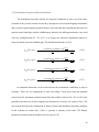
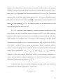
4
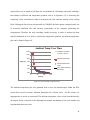
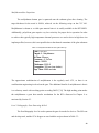
Source
Electrode
Channel
Gate Insulator
Gate Electrode
Implant
Drain
Electrode
Implant
Substrate
Figure 2.1: Bottom-Gate TFT Design.
electrodes for contacts, gate electrode, a gate dielectric, a semiconducting channel layer, ion
implant (or in situ doping) for source drain regions and ohmic contacts, and the underlying
substrate upon which the device is fabricated. Figure 2.1 illustrates a typical TFT design of the
bottom gate variety.
2.1.1 Amorphous Silicon (a-Si) TFTs
The TFT never truly took off as a manufacturable solid state electronic until a-Si:H was
introduced as a viable semiconductor material. Early work of Spear & LeComber in 1979
provided proof of concept for the materials use in a thin-film logic gate [3].
Figure 2.2: The First a-Si:H TFT [3].
5
It was discovered that doping a-Si with hydrogen effectively passivated a significant number of
dangling bonds in the amorphous material. In addition it had already been established that a-Si
could be doped with standard materials in order to achieve n-type and p-type regions for
electrical junctions [4]. Initial TFTs were fabricated utilizing a silicon nitride (Si3N4) gate
dielectric and an in-situ hydrogen doped a-Si channel layer. Both undoped and phosphorus doped
n-type functioning devices were realized as potential switching mechanisms for a display panel.
Since the first a-Si:H TFT, significant engineering has essentially perfected the
technology to what it is today. Research groups such as those at Kyung Hee University have
fabricated devices that maximize the potential of a-Si:H as a channel material:
Figure 2.3: A Current a-Si:H TFT [5].
Along with smaller dimensions, today’s a-Si:H TFTs also have slightly lower threshold voltages
(VT), near theoretically minimized sub-threshold swing (SS), lower supply voltages (VD), lower
off-state currents (IOFF), and slightly higher max current drives at high-drain bias (IMAX). As the
current needs of the display industry progress, the cost benefit of being able to integrate circuitry
6
on an active-matrix (AM) display panel has become critical; however, as a channel layer a-Si:H
produces TFTs with very poor electron channel mobility, on the order of
~1 cm2/V-sec.
Therefore as AM display sizes increase the need for faster switching circuitry also increases. In
order to achieve any type of system circuitry integration on glass for large format AM displays,
which reduces cost and produces more compact products, low-temperature polycrystalline
silicon (LTPS) manufacturing techniques are being researched and implemented. These include
fabrication processes that, while remaining within the strain point of the substrate material
(typically glass), provide a means to crystallize the a-Si channel layer to increase carrier mobility
and circuit performance. In doing so this allows for not only the AM addressing TFTs to be
integrated onto the substrate, but also the driving circuitry as well.
2.1.2 Polycrystalline Silicon (poly-Si) TFTs
There are numerous benefits from increasing the mobility of AM display circuitry beyond
system on panel integration. Increasing mobility allows for smaller geometry transistor
fabrication resulting in the ability to address more tightly packed pixel arrays leading to
increased screen resolutions. To the consumer this means sharper and brighter displays that are
easier to look at for extended periods of time. Additionally, the faster switching TFT reduces
power consumption, allows for more compact panel designs, and provides higher refresh
frequencies.
Poly-Si TFTs are currently used in mass production where the LTPS technology is
feasible. Feasibility is when the cost of the technology remains less than the savings it introduces
by eliminating the need for a separate driving circuitry component. Currently, this market is
predominately small diagonal displays such as those used in cellphones and small portable media
7
devices. The dominant LTPS technology used in this instance is excimer laser annealing (ELA)
which provides a viable fabrication process for producing poly-Si TFTs with electron mobilitys
around 120 cm2/V-sec. Emerging LTPS technologies also exist, such as Phase Modulated ELA,
can produce TFTs fabricated on a region that is single grain and therefore essentially single
crystal. These devices can achieve a low-field electron mobility between 450 and 900 cm2/V-sec;
however, these processes are still in the research stages and are not yet ready for high volume
manufacturing [6].
There are several challenges associated with utilizing poly-Si as the TFT channel layer
and these include: drain bias-stress instability, field-enhanced leakage current at high drain
biases, and low output impedances. Temperature bias stress issues arise from increased scattering
events, leading to phonons which generate excess heat. Since the switching matrix is typically
integrated on glass, a thermal insulator, this excess heat remains within the devices and can cause
hot-carrier degradation effects. Field-enhanced leakage occurs as a result of a large electric field
at the drain edge, and this can be reduced to a point, via incorporation of lightly-doped drains. In
spite of these challenges modern LTPS technologies provide a significant performance benefit
over its amorphous silicon precursor.
2.2 LTPS Manufacturing Technologies for Production
Now that the fundamental differences between a-Si:H and poly-Si for use as a TFT
channel layer have been identified, the techniques used to move from the former to the latter can
be investigated. The term LTPS captures all the manufacturing techniques available that convert
the channel layer of an a-Si:H to poly-Si by some mechanism of grain growth. The main
techniques in production and being researched include: ELA, metal-induced lateral
8
crystallization (MILC), and solid-phase crystallization (SPC). While ELA is in production for
small-format displays as mentioned earlier, MILC and SPC offer potential methods with which
to produce high performance poly-Si TFTs for large format technology.
2.2.1 Summary of LTPS Technologies
Excimer laser annealing refers to a technology introduced in 1997, where a 308nm laser
is used to scan the a-Si channel layer which absorbs the ultraviolet radiation. The absorption
results in a partial melt of the surface and poly-Si is formed, while the underlying glass is kept
well below its thermal strain point. Of significant importance to this process is the laser beams
homogeneity which determines the end uniformity of the resulting film. It is due to this
constraint that ELA has had challenges being scaled to large format LTPS manufacturing.
MILC refers to a process by which a metal is deposited in select areas on top of the a-Si
and then is subjected to a furnace anneal, typically between 150 ºC and 400 ºC. The heat
absorbed by the metal is transferred to the underlying a-Si layer and results in crystallization into
poly-Si. Preferably metal would be deposited in the source and drain or street regions, and the
channel regions of the TFT would be laterally crystallized. This is because the areas underlying
the metallized regions have remaining metal contaminants.
SPC is the simplest of the LTPS technologies in practice. Utilizing this technique, a-Si is
subjected to a furnace anneal (FA), rapid thermal anneal (RTA), or combination of the two that
remains within the strain point of the glass, resulting in grain growth and a poly-Si film. Since
the work of this thesis revolves around characterizing TFTs fabricated utilizing this method, the
next section is devoted to exploring the science behind solid-phase crystallization in more depth.
9
2.3 Solid-Phase Crystallization as an LTPS Technology
While solid-phase crystallization results in a poly-Si film with lower carrier mobility than
ELA, there are several potential advantages of SPC which include: smoother interface surfaces
resulting in less potential trapping sites, better film uniformity, and adaptability for high
throughput. One of the easiest ways to characterize a crystallization process is to examine the
degree of crystallinity throughout the duration of the experiment. A general crystallization
process, adapted from [7], is outlined below in Table 2.1.
Table 2.1: Phases of SPC.
Phase I
Transient Activation
During this time the required energy
in order to induce grain nuclei
formation is acquired.
Phase II
Grain/Crystal Growth
At the onset of this phase nuclei are
formed, and the additional thermal
energy activates and extends grain
growth outward from these nuclei.
Phase III
End Primary Crystallization
After a given duration for any
combination of FA, RTA, or FA &
RTA, the maximum grain size is
reached and grain growth saturates.
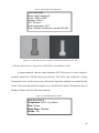
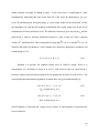
With transmission electron microscopy (TEM), the average grain size of a given SPC process
can be obtained throughout the duration of the experiment cycle, and the degree of crystallinity
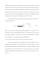
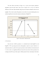
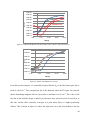
plotted versus the duration [7]. Analysis of plots such as Figure 2.4 with consideration of Table
2.1, can give significant insight into the mechanisms at work during SPC.
Figure 2.4: Normalized Crystallinity versus Annealing Time [7].
10
The first thing to note is the time lag until onset of crystalline growth. As indicated by
Table 2.1 this is the point at which nucleation sites, from which grain boundaries grow, have
formed. Also shown is that the energy required is significantly less in RTA than FA. The reduced
time and energy required to achieve maximum normalized crystallinity can be explained by the
different mechanisms of heating. While FA relies on heating of the entire ambient and
convection as the heat transfer mechanism, RTA utilizes more intense radiation and forced
convection to heat the a-Si. The latter mechanism is more energetic and intense, which can result
in generation of photo-carriers in the a-Si film that can subsequently break weak bonds within
the thin film. This produces a cascading effect where photocarriers are generated at these sites of
breaking bonds resulting in localized heating and expedited nuclei formation [7].
Further investigation into the crystalline structure formed during Phase II of SPC for FA
yields defects within the poly-Si grains, when annealed at or below the temperature constraint of
high quality display glass (~630ºC). A portion of these defects called microtwins are not stable in
the poly-Si film and can be eliminated via a higher temperature RTA process post FA [8]. Hence,
it is likely beneficial to have a short cycle, high temperature, RTA process after FA. The
nucleation rates and growth rates for Phases I & II, respectively are both strongly temperature
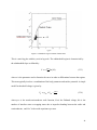
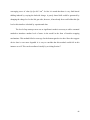
dependent, as shown in Figure 2.5. Additionally, it has been shown that the presence of
microtwins (twin-mediated) enhances the growth rate during Phase II as can be seen in Figure
2.5 and is further supported by [8]. However, it is noted that other intra-grain defects that cannot
be removed by a currently known process, is the main limitation of SPC technology [9].
11
Figure 2.5: a.) Phase I Nucleation & b.) Phase II Growth Velocity Rates During Crystallization of a-Si [9].
A significant limitation of SPC when using only FA, shown in Figure 2.4(a), is the fact
that the nucleation during Phase I takes a significant amount of time. For this reason many
researchers have introduced a RTA step to reduce the duration of Phase I, in combination with
either another RTA or FA step for the primary grain growth during Phase II [10], [11], [12]. This
reduces the long times required for FA incubation of nuclei, resulting in a cheaper manufacturing
process. From the discussion above, it is easily discerned that the combination of RTA and FA is
of utmost importance. In terms of designed experiments, for the case of RTA the important input
12
factors are temperature, time, ambient gas, and number of pulses. For FA the input factors
include temperature, time and ambient gas. Therefore, when conducting experiments on SPC for
development of transistors, the input factors as well as the combination and order of RTA and
FA are significant.
Revisiting the previously discussed material theories of a-Si and poly-Si previously
discussed in Section 2.1.1 & 2.1.2, the potential benefits of SPC LTPS over a-Si are apparent. A
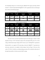
summary table of typical mobility values for both a-Si and poly-Si is presented in Table 2.2. The
next chapter will provide further insight on the influence of defect states on LTPS device
operation.
Table 2.2: Summary of a-Si & poly-Si Operating Parameters
2
Mobility (cm /V-sec)
Max ID (μA/μm)
VDD (V)
a-Si
0.1-1
0.1
20
poly-Si
50-200
15
10
13
3 Materials Science & Physics of a-Si & poly-Si as a TFT Channel
The primary degradation mechanism in non-crystalline silicon TFTs is a result of
trapping states. There are three primary regions of trap states in a TFT: the top interface of the
channel film, the bottom interface of the channel film, and the trap states contained within the
channel film itself due to the non-crystalline defects associated with the a-Si and poly-Si films. A
thorough understanding of how these trapping mechanisms affect the physics of device
performance is critical for identifying areas for device improvement.
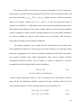
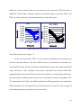
3.1 Review of Si-SiO2 Interface Trapping States
The types of top and bottom channel interface trapping states can be described by
standard c-Si theory. These are typically attributed to four different types of charge: interface
trapped charge, fixed oxide charge, oxide trapped charge, and mobile ionic charge. The location
of these charges relative to the interface (identical for both top and bottom) are shown in Figure
3.1. Interface trapped charge includes both positive and negative charges that are attributed to:
induced crystal defects, contaminants such as metal, and other defects resulting from broken and
imperfect silicon bonding arrangements. The fixed oxide charge is strongly correlated to the
oxidizing ambient and is positive charge due to dangling silicon bonds that are produced during
oxidation. Annealing in a hydrogen ambient will passivate the majority of this charge, and it is
quantified by performing capacitance-voltage (C-V) measurements before and after such an
anneal. Oxide trapped charge refers to positive and negative charge due to electrons and holes
that are trapped within the bulk. Lastly, mobile ionic charge is due to impurities such as
positively ionized sodium, potassium, lithium, and hydrogen [13].
14
Figure 3.1: Types of Si-SiO2 Trapping Sites.
Mobile ion contaminations have been significantly reduced via incorporation of anhydrous
hydrochlorine (< 6%) into the oxidizing ambient, which also results in an increase in the linear
and parabolic growth rate constants of SiO2 [14].
Without advanced techniques it is impossible to detect the differences between the
volumes of interface trapped, oxide trapped, and mobile ionic charge. For this reason they are
typically all grouped together. As stated previously, the fixed oxide charge volume can typically
be ascertained via C-V measurements pre and post-annealing, in a hydrogen ambient.
3.2 Crystalline Silicon Energy Levels & Bonding States
Silicon bonding in a crystalline lattice involves bonds to other adjacent silicon atoms.
These bonds are arranged in a well-defined tetrahedral lattice with a 0.35nm lattice constant (a),
and a corresponding bond angle of 109º (ϴ). Due to the nature of the silicon atom having 4
valence electrons, when two neighboring atoms interact and form a bond in the crystalline lattice,
this results in an sp3 orbital being formed. This minimizes the energy required to form the
maximum amount of four bonds with neighboring atoms. The result is a bonded silicon atom
where pairs of electrons now exist, resulting in a lowering of the energy level of the state. This
causes the sp3 energy level to arrange into anti-bonding states corresponding to the states of the
15
conduction band of the silicon, and bonding states which correspond to the states of the valence
band [15]. This is depicted in Figure 3.2.
Figure 3.2: Electron Energy Levels of Silicon Bonding States.
3.3 Density of States, Distribution Functions, & Carrier Populations of c-Si
It is useful to recall that in solid-state physics electron and hole quantities are treated as
free-particle gases. This refreshes the readers mind to the fact that even at room temperature
electron and hole distributions are in constant movement. From the discussion of the previous
section it is known that the sp3 bonding configuration for uniformly bonded c-Si results in two
density of states functions, gv(E) and gc(E), that extend into the valence and conduction bands of
the Si atoms respectively. These functions represent the potential states of occupancy for a given
vibrational frequency, which is typically dominated by the substrate temperature. Figure 3.3
shows these functions plotted for an intrinsic semiconductor at room temperature.
16
Figure 3.3: Intrinsic Semiconductor: Density of States,
Distribution Function, and Carrier Populations.
Solid state physics theory states that the electrons in the conduction band, and holes in the
valence band can be mathematically represented as [16]:
Where h is Planck’s constant,
( )
√
√
(3.1)
( )
√
√
(3.2)
is the electron effective mass, Ec is the conduction band edge,
and Ev is the valence band edge.
Interpretation of Equations 3.1 & 3.2 lends insight to the fact that the decrease in the
electron and hole states falls off significantly as a function of energy E, above and below the
conduction and valence band edges. This means that in intrinsic c-Si nearly the entire electron
and hole populations reside at the bottoms of the respective band edges. Mathematically, the
distribution functions represented by the red line above and below the Fermi Energy, Ef, in
Figure 3.3 can be expressed as:
17
( )
( )
(
(
)
(3.3)
)
(3.4)
)
(
These are representations of the very common Fermi-Dirac statistical distribution function.
Lastly, the population distributions represented by the blue population plots in Figure 3.3 are
found by integrating the product of the density of states and distribution functions over the
respective bands, and are given by:
( )
∫
( )
( )
(3.5)
( )
∫
( )
( )
(3.6)
The functions of Equations 3.5 & 3.6 represent near step functions. The red plotted line in Figure
3.3 is exaggerated for a clearer understanding; however, its contribution inside of the band edges
is typically very small which leads to a mathematical approximation discussed in the next section.
Lastly, it is explicitly noted that the last two equations of this sub-section are necessary for
calculating current densities.
3.4 Density of States, Distribution Functions, & Carrier Populations of n-type Doped c-Si
The previous section introduced the functions necessary to calculate electron and hole
carrier populations in terms of the c-Si energy band and solid-state physics theory. In the
previous section there was no impurity doping and Figure 3.3 shows that the electron and hole
carrier populations are equivalent. This means that the electron and hole free particle gases per
unit volume net out and no carriers remain for conduction. If the intrinsic semi-conductor of
Section 3.3 is doped with an n-type impurity such as phosphorus or arsenic, the electron
18
population of the conduction band exceeds the hole population of the valence band, leaving
electrons available for conduction. This is a result of the shifting of the Fermi energy level
towards the conduction band as a result of the impurity doping. The case of an n-type doped
semiconductor is shown below in Figure 3.4.
Figure 3.4: n-Type Doped Semiconductor: Density of States,
Distribution Function, and Carrier Populations.
Standard doping of silicon is either a p-type group III atom such as boron, gallium or
indium, or an n-type group IV atom like phosphorus, arsenic, or antimony. For transistor
fabrication the doping levels remain within a concentration per volume such that the Fermi level
still lies deep within the forbidden gap. However the small shift in Ef that results due to doping
can be seen by comparing Figure 3.3 & 3.4. For n-type transistor fabrication doping levels
(~1013-1019cm-3) the tail of the Fermi distribution function of the material shifts into the valence
or conduction band edge; however, this portion overlapping into the band edge is very small
indicating that the probability of the impurity atom electron being in a donor state is small.
Therefore at room temperature, it is reasonable to assume that all dopant electrons are ionized
19
and contribute to conduction. Hence in Figure 3.4 the electron population significantly exceeds
the hole population.
The density of states functions as given by Equations 3.1 & 3.2 are modified by the
changing of the weighting of the effective masses
and
, where clearly the effective mass
of the electron now exceeds that of the hole for the case of n-type doping. For the distribution
functions represented in Equations 3.3 & 3.4 for transistor doping levels the Maxwell-Boltzmann
(MB) approximation is used. The doping levels utilized in transistor fabrication indicated as
stated earlier that the distribution function located within the bands is very small. Mathematically
this means that:
[16]. Therefore utilizing the MB approximation these equations
can be re-written as:
( )
(3.7)
( )
(3.8)
The population distributions are calculated in the same manner as Equations 3.5 & 3.6, where
since the significant majority of carriers lies within a few hundredths of electron volts from the
band edge, minimal error is introduced by introducing infinite boundaries on the integrals.
3.5 Potential Well Theory for Grain Boundaries
Now that the electron energy potentials have been described via band theory in the
previous sections for crystalline silicon, the case of disordered silicon such as a-Si and poly-Si
can be examined. Whereas previously the density of states functions behaved properly extending
from the valence and conduction band edges due to uniform sp3 bonding arrangements within the
lattice; in poly-Si there are grain boundaries where the uniform tetrahedral network of the Si is
20
no longer preserved. A grain boundary is a region where two differently oriented c-Si grains
attempt to meet. At these transition regions there are weak and dangling bonds as the two c-Si
grains attempt to bond together.
3.5.1 Density of States in Disordered Silicon
Weak bonds result in the density of states from within the band regions to overlap into
the forbidden region of the Si energy band. Additionally, dangling bonds are present as a result
of broken sp3 bonds, which form mid-gap trapping states [15] as shown in Figure 3.5.
Figure 3.5: Density of States in Disordered Silicon [17].
These additional densities of states as a result of the dangling broken sp3 bonds at the grain
boundaries are represented by Gaussian distributions. The standard c-Si densities of states that
are overlapping into the forbidden region are modeled as exponential decay functions. These four
functions serve as the mathematical definition of the trapping mechanisms in a disordered silicon
channel film for a TFT. In the numerical analysis software Silvaco Atlas used to conduct TFT
device simulations for this work, these densities of states are defined as [18]:
21
( )
.
( )
Where,
.
/
(3.9)
/
(3.10)
( )
[ .
/ ]
(3.11)
( )
[ .
/ ]
(3.12)
( ) represents the density of donor-like valence band tail-states,
the density of acceptor-like conduction band tail-states,
( ) represents
( ) represents the density of donor-
like deep-level states lying below the Fermi energy level, and
( ) represents the density of
acceptor-like deep-level states lying above the Fermi energy level.
Equations 3.9 & 3.10 are the exponential decay of the densities of states that overlap into
the forbidden region from the band edges. Equations 3.11 & 3.12 are mathematical functions
representing the quantity of dangling sp3 bonds around the Fermi energy, both above and below.
It is noted that a dangling sp3 bond is 50% occupied with a single electron, indicating an energy
level by definition nearly identical to that of the Fermi energy. The total density of states is thus
represented by the sum of its parts:
( )
( )
( )
( )
( )
(3.13)
Equation 3.13 serves as one component in quantifying trapping sites that seize carriers and
reduce current. Additionally, charge builds up at the site of the trapped carriers resulting in
formation of potential barriers. From Sections 3.3 & 3.4 it is clear that the distribution function is
needed to calculate the carrier populations.
22
3.5.2 Distribution Functions of Disordered Silicon
The distribution functions utilized for numerical simulation in Atlas vary from those
presented in the previous section because they incorporate cross-sectional trapping mechanisms
that account for grain boundary potential barriers. Note also that these distribution functions also
span the entire band edges and the forbidden gap; therefore, the MB approximation is not valid
since the assumption that,
, is no longer true when the distribution function is
being calculated across the forbidden gap. The distribution functions are [18]:
(
)
(
)
(
)
(
)
.
.
.
//
.
.
.
.
//
.
//
.
.
//
.
//
.
//
.
//
.
//
/
.
.
.
/
.
.
.
/
/
(3.14)
(3.15)
(3.16)
(3.17)
An important distinction can be made between the mechanisms contributing to poly-Si
resistance. There are two components at work: the filling of trap states removing potential
carriers from the maximum potential current flow that would be achieved in c-Si, as well as the
potential wells that exist at these trapping sites that must be overcome for current to flow. The
next section shows how the combination of density of states and distribution functions contribute
to this reduction in current drive. Table 3.1 provides a summary of the Atlas TFT Module
parameters presented with the default values for poly-Si [18].
23
Table 3.1: Summary of Atlas TFT Module Parameters.
ATLAS DENSITY OF STATES & DISTRIBUTION FUNCTION PARAMETERS
Parameter
NTA
Exponential
Tail
Distributions
4.0 x 10
WTA
0.025
WTD
0.05
NGD
1.0 x 10
3.0 x 10
Units
21
20
18
18
Description
-3
cm /eV Exponentional tail distribution acceptor edge intercept density
-3
cm /eV Exponentional tail distribution donor edge intercept density
eV
Exponential tail distribution characteristic acceptor decay energy
eV
Exponential tail distribution characteristic donor decay energy
-3
cm /eV Max acceptor density of states f(μ)
-3
cm /eV Max donor density of states f(μ)
EGA
0.4
eV
Acceptor energy which gives the peak (μ)
EGD
0.4
eV
Donor energy which gives the peak (μ)
WGA
0.1
eV
Acceptor decay energy (σ)
WGD
0.1
eV
Donor decay energy (σ)
SIGTAE
SIGTAH
SIGTDE
Distribution
Function
Parameters
1.12 x 10
NTD
NGA
Deep Level
Gaussian
Distributions
poly-Si
SIGTDH
SIGGAE
SIGGAH
SIGGDE
SIGGDH
1.0 x 10
1.0 x 10
1.0 x 10
1.0 x 10
1.0 x 10
1.0 x 10
1.0 x 10
1.0 x 10
-16
2
cm
-14
2
cm
-14
2
cm
-16
2
cm
-16
2
cm
-14
2
cm
-14
2
cm
-16
2
cm
Electron capture cross-section for the acceptor tail
Hole capture cross-section for the acceptor tail
Electron capture cross-section for the donor tail
Hole capture cross-section for the donor tail
Electron capture cross-section for the acceptor Gaussian states
Hole capture cross-section for the acceptor Gaussian states
Electron capture cross-section for the donor Gaussian states
Hole capture cross-section for the donor Gaussian states
3.5.3 Population Distributions of Disordered Silicon
The population distribution in disordered silicon is calculated by the methodology
presented in Section 3.4 combined with a subtractive process whereby the trapped carriers are
removed from the calculated current as described in Sections 3.5.1 & 3.5.2. The available carrier
charge that is calculated as [18]:
∫
( )
(
)
(3.18)
∫
( )
(
)
(3.19)
24
Above
∫
( )
(
)
(3.20)
∫
( )
(
)
(3.21)
is the concentration of ionized acceptors less the donor-like tail trap states,
is the
concentration of ionized acceptors less the donor-like deep-level trap states below the Fermi
level,
is the concentration of ionized donors less the acceptor-like tail trap states, and
is
the concentration of ionized donors less the acceptor-like deep-level trap states above the Fermi
level.
It is therefore useful to sum the total ionized carriers:
(3.22)
(3.23)
Then Equations 3.22 & 3.23 represent the ionized acceptors less donor-like trap states and
ionized donors less acceptor-like trap states respectively. Assuming, the densities of states and
distribution functions above only modeled the forbidden gap, then the total population
distributions would be given by the similar theory of Section 3.3 as:
( )
∫
( )
( )
∫
( )
( )
( )
(3.24)
(3.25)
Equations 3.24 & 3.25 are shown simply to relate the theory back to that of c-Si; however, it is
noted that the degradation in current due to trapped carriers is implicit within the previously
shown Atlas equations since they span the band edges as well as the band gap.
25
3.5.4 A Simple 1-D Analytic Model for Calculating Current
For simple single-dimension analytical models of a-Si and poly-Si grain boundary theory
the following assumptions are made: traps are neutral until charged by a trapped carrier, the
width of a grain boundary is significantly less than the length of the grain, the Si is uniformly
doped, grain lengths are equivalently described by L, and traps are located at a single discrete
energy level [19]. These simplifications allow for application of the depletion approximation,
across grain boundary depletion regions which are shown visually for the two-dimensional
condition of strong inversion in Figure 3.6 [20]. In this region of operation the depletion regions
on either side of the grain boundary would be equal. Note for the single-dimension problem a
horizontal cutline from left-to-right intersecting the vertical grains represents the problem being
solved.
Figure 3.6: n-Channel poly-Si TFT at Strong Inversion.
Utilizing the depletion approximation in conjunction with Poisson’s equation from 0 to 0.5 L,
where L is the uniformly assumed (typically averaged) grain boundary length gives [16]:
(3.26)
26
Equation 3.9 is twice differentiable and integrable given a boundary condition that the varying
potential at the edge of the depletion region is both equal to the bulk crystalline potential and
continuous [19].
At strong inversion such as shown in the above figure the depletion regions have
overlapped; however, a grain prior to strong inversion can be either partially or potentially fully
depleted, depending upon the trap distributions and doping concentrations. A general condition
for full depletion is that the per volume trap concentration exceeds the doping concentration
multiplied by the grain length and width, (or per area trap concentration is greater than the
doping concentration multiplied by L). For the spatial coordinates identified for the onedimension problem and used to derive Equation 3.9, when a grain becomes fully depleted this
region is described by x=0. In other words, x=0 describes the midway point between two
adjacent grains.
This is consistent with the two-dimensional problem shown in Figure 3.6, where (x,y) =
(0,0) defines the coordinate of full depletion between two grain boundaries at the Si-SiO2
interface (y=0). For the single dimensional problem the barrier potential at partial depletion is
represented by [19]:
(3.27)
up until full depletion where, stated previously,
. Hence Equation 3.9 becomes:
(3.28)
27
For current conduction under forward bias carriers need to either pass over or through the
potential barriers introduced by poly-Si grains. When a carrier gains enough energy, usually in
the form of heat as a result of applied gate bias, it can pass over the potential barrier; this is
referred to as thermionic emission. The other method of conduction is tunnel current as a result
of Fowler-Nordheim tunneling in the presence of a high electric field. The main contributor to
current conduction, under both forward and reverse bias in poly-Si, is thermionic field emission
[19], [21], [22]; therefore, direct field emission tunneling is omitted from current density
calculation.
For small drain biases (VD) where mobility degradation is negligible, the current density
can be calculated as [23]:
. /
.
/
(3.29)
This analytic model does not hold for high drain biases (VD >> kT), because it neglects
scattering; however it provides a good basic example of how the above theory of calculating
population distributions would be utilized to subsequently calculate current density. Basic
semiconductor device physics can be used to derive mobility and conductivity from Equation
3.29 as:
(3.30)
(3.31)
28
The numerical simulator Atlas utilizes similar yet significantly more robust techniques including
high-field mobility models which incorporate mobility degradation due to scattering mechanisms
that are introduced as the drain bias is ramped.
3.5.5 poly-Si Leakage Current
An important phenomenon in poly-Si TFTs when compared to their a-Si counterparts is a
significant increase in leakage currents under reverse gate bias at VDD. Figure 3.7 shows this via
an Atlas example file. The dominant mechanisms at work for current conduction as stated
previously and further supported are: thermionic emission, thermionic field emission, and field
emission (carrier tunneling due to the Fowler-Nordheim mechanism).
Figure 3.7: poly-Si TFT Leakage Current.
While [21] supported that thermionic and field assisted thermionic emission were the dominant
leakage mechanisms, it is also reported that under high reverse bias tunneling becomes the
29
dominant leakage mechanism. It is noted that thermionic field emission is dominated by the midgap trap states [21], [24]. This is because emission is a two-stage process whereby a trap state is
captured from the valence (conduction) band and then emitted to the conduction (valence) band.
While it requires less energy to fill (i.e. capture) a tail-state than a mid-gap state, the energy
required to emit the carrier to the opposing band is nearly the entire Si bandgap Eg. Tunnel
current becomes active when the electric field begins to exceed 106 V/cm [21].
A first order analytic model is presented that incorporates the thermionic emission as well
as tunnel current by [21] as:
(
(
)⁄
)
(3.32)
(
)
Where Te and Tp are the electron and hole tunneling probabilities, W is the width,
normal electric field,
is the trap distribution, and
is the
is the activation energy of the average
single discrete trapping state. From the previous sections it is known that Atlas will adapt a
variant of Equation 3.32 to accommodate 4 full trap-state distributions.
3.6 How Trap States Effect TFT Device Performance: A Simple Analytic Model
Now that the governing physics behind trapping states has been defined in detail, it is
useful to explore from a higher level how these degrade overall device performance. It is well
known that trap states degrade the subthreshold characteristics of transistors. Therefore electrical
characterization in the form of drain current versus gate voltage plots are one of the general
standards of benchmarking transistor performance. A typical n-type characteristic is shown in
Figure 3.8.
30
Figure 3.8: Standard n-Type Transistor Characteristic.
This is a semi-log plot with the y-axis in log scale. The subthreshold region is characterized by
the subthreshold slope as defined by:
. / (
)
(3.33)
where n is the parameter used to linearize the curve in order to differentiate between the regions.
This term typically involves a combination of the body parameter and surface potential. A simple
model for threshold voltage is given by:
(3.34)
where
is the metal-semiconductor work function,
is the flatband voltage,
is the
number of interface states or trapping states due to imperfect bonding between the oxide and
semiconductor, and
is the oxide capacitance per area.
31
Now to see how trap states can degrade these parameters define the trapped charge as
[25]:
.∫
Here
1
),
/
∫
is the “effective” trapped charge (C/cm2),
(3.35)
is the interface trapped charge (cm-2 eV-
is the density of bulk traps in the gate dielectric (cm-3), and
is the total net trap
density in the LTPS active layer (cm-3 eV-1). Further define the trap-state capacitance per unit
area in F/cm2 as [25]:
(
)
(3.36)
Then the subthreshold slope and threshold voltage will be degraded by trap states within the
poly-Si film as follows:
.
/
(3.37)
(3.38)
Then reviewing Equation 3.37 in consideration of Figure 3.8 it can be seen that the poly-Si trap
states contribute to an increase in subthreshold slope, or a decrease in the slope of the ID-VG
curve, indicating a decrease in shut off capability of the device. A similar analysis of Equation
3.38 shows that the trap states result in a positive VT shift for n-type devices, and a negative VT
shift for p-type devices.
32
4 Heat Transfer Simulations
4.1 Purpose
In order to effectively conduct an SPC experiment using RTA a baseline for the amount
of heat being transferred to the glass wafers needed to be established. The following simulation
work was performed to determine a reasonable number of pre and post FA RTP cycles. From
Section 2.3 it was established that a pre-furnace annealing RTA cycle is beneficial in order to
reduce the time required to complete the nucleation of Phase I. Additionally, it was identified
that a post-furnace RTA cycle approaching 850ºC is ideal for eliminating the microtwin defects
that contribute to excessive trapping states in the poly-Si thin film. Understanding the RTA
system and its’ capabilities are therefore critical for engineering an ideal poly-Si film using a
combination of RTA and FA for SPC.
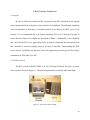
4.2 The RTA System
The RTA system in the RIT SMFL is an AG 610A Rapid Thermal Processor. A picture
of the system is shown in Figure 4.1. The processing chamber has both top and bottom light
Figure 4.1: AG610 RTA System at RIT.
33
banks, with 10 top lamps and 11 bottom lamps. Each tungsten-halogen lamp is rated 1200W, for
a total of 25,200W. Nitrogen flows into the chamber via a quarter-inch inlet hole at a rate of 3
liters per minute. The chamber itself is one inch tall, by eight inches wide, by ten inches deep,
indicating a volume of eighty cubic inches. The chamber dimensions are outline in Figure 4.2.
Figure 4.2: AG610 RTA Chamber Dimensions.
4.3 Heat Transfer Mechanisms & Radiation Regimes
The basic methods of heat transfer are: conduction, convection, and radiation.
Conduction refers to heat being transferred between two objects that remain in intimate contact
with one another. A ubiquitous example of conduction is a pot of boiling water. The pot is being
heated and it conducts this thermal energy to the water. The heat flow density (or flux) of
conduction is represented by [26]:
( )
( )
(4.1)
In Equation 4.1, k(T) is measured in Watts/cm-K and is the thermal conductivity of the material,
is the temperature gradient across the area of interest, and
is the distance between the points
of measurement. Therefore heat flux has the units of Watts/cm2.
34
Convection is the transfer of heat away from a source through the net displacement of
some medium such as a gas via this mediums own velocity. An example is a fireplace heating a
room. A variant of convection is forced convection and refers to convection that is mediated by
an external mediums velocity. Of interest in this scenario is the ability of the medium to transfer
heat represented by a heat transfer coefficient h, and measured in Watts/cm2-K. Then the heat
flux of convection is given by [26]:
( )
(
)
(4.2)
Both the heat transfer of convection and conduction are linearly related to temperature. This is
not the case for radiation.
Lastly, radiation is the transfer of heat via photons that can either be reflected or absorbed.
The heat transfer between two bodies due to radiation via absorption of light can be calculated
via the radiated power per area per unit wavelength and calculated via [26]:
( )
( )
(4.3)
(
)
Equation 4.2 is commonly referred to as the spectral radiant exitance where: c1 = 3.7142x10⁻¹⁶
W-m2, c2 = 1.4388x10⁻² m-K, and
( ) is the emissivity of the absorbing material as a function
of wavelength. If the emissivity is not wavelength dependent then Equation 4.2 simplifies to:
( )
( )
(4.4)
where =5.6697x10⁸ W/m2K4 the Stefan-Boltzmann constant. The simplified version shown in
Equation 4.2, shows that radiation is not linearly dependent meaning convection is the dominant
mechanism at low temperatures; however, at high temperature radiation has greater influence in
35
heat transfer. Lastly, the change in temperature can be described in terms of the heat flux as
[26]:
( )
where Cp is the specific heat of the absorbing layer,
(4.5)
is the density of the material, and t is the
thickness. Therefore it is easily seen that if the RTA cycle number is too high or the cycle
duration too long, the temperature ramp rate will be enormous if radiation is allowed to become
the dominant heat transfer mechanism.
RTA radiation regimes can be described by first defining a characteristic depth of
radiation penetration referred to as the redistribution depth [27]:
(
where
)
(4.6)
is the thermal diffusivity in cm2/s of the absorbing layer, and
time. Then define the absorbing layers thickness as
is the RTA processing
, and the total wafer thickness as d. Then
for the case of standard silicon RTA there are three regimes: adiabatic where
delivered via pulsed lasers and electron guns, thermal flux where
characteristic of flash lamps, and lastly heat balance where
usually
typically
, the standard case for
halogen lamps [27].
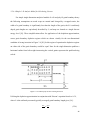
4.4 2-D Representative TFT Structure
From the previous section a general knowledge of heat transfer and radiation has been
gathered; however, this was in the context of silicon wafers. The glass substrate upon which the
TFTs are fabricated has only a little absorption of the halogen lamps of the RTA system, and
36
therefore will not heat due to radiation if the pulses are kept short enough and/or the times
between pulses long enough. This is supported by Corning documentation and standard spectral
output plots of halogen lamps shown in Figures 4.3 and Figure 4.4. From analyzing the inlay of
Figure 4.4 and realizing that halogen lamps do not output any energy at wavelengths less than
300nm; it is then apparent from Figure 4.3 that the Eagle XG glass will have negligible
absorption since the optical transmission is roughly 92% for the majority of the energy
distribution.
Figure 4.3: Optical Transmission in Eagle XG Glass.
Similarly, the thin-films of the transistor are thin enough such that there is negligible absorption
within the a-Si precursor film as well. However, initial experiments with molybdenum as a heat
transfer material, chosen for ease of process flow since it is the TFT gate material, resulted in
destruction of the film due to thermal induced stress. This proved the viability of molybdenum as
a heat transfer material.
37
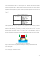
Figure 4.4: Spectral Output of Halogen Lamps.
The initial structure chosen for simulation mimicked a top-gate TFT process flow and its’
Comsol construct is shown in Figure 4.3.
Figure 4.5: 2D TFT Structure for COMSOL Simulation.
38
The film stack from top to bottom is: molybdenum, SiO2, a-Si, SiO2, Eagle XG glass.
The bottom layer of SiO2 was reasonably neglected since it is on top of glass and the thermal
properties are similar. The relevant material parameters are summarized in Table 4.1.
Table 4.1: TFT Heat Transfer Material Parameters
Heat Capacity (J/kg-K)
a-Si
703
SiO2
730
Molybdenum Eagle-XG
250
1067
Density (kg/m3)
2330
2200
10,200
2380
Thermal Conductivity (m2/s)
163
1.4
138
1.34
Initial simulation resulted in numerical problems due to the meshing of 4.2. In this version the
thin-films on top of the comparatively much thicker glass substrate were having trouble being
meshed appropriately. Fortunately, during the time of simulation, COMSOL version 4.2a was
released. This version introduced a Sweep/Scale feature for meshing which enables manual
scaling of the mesh between boundaries of multiple materials. Essentially sweeping allows for
complete control of the number of elements within a layer and their distribution for a given free
tetrahedral mesh.
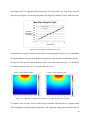
4.5 COMSOL Forced Convection Simulation
From analysis of Section 4.3 it is clear that to first order RTA for use in SPC should
avoid extended periods at high temperature where radiation is the dominant mechanism. This is
because the temperature ramps in this range are extremely significant and would result in
warping of the Eagle XG glass and delamination of the molybdenum film due to thermal stress
(as was experimentally verified). Therefore for simulation the forced convection feature of the
conjugate heat transfer module in COMSOL was utilized as the dominant heat transfer
mechanism.
39
In order to set up the simulation a number of boundary conditions, input functions, initial
values, and RTA machine dependent parameters must be set. First the initial values of the
structure were set to room temperature. The top and bottom interfaces of the structure were given
the forced convection heat transfer mechanism, meaning Equation 4.2 was applied to these
interfaces and modified via the Reynolds number in order to account for the cooling gas N2, its’
material properties and flow rate. The Reynolds number is given by [28]:
(4.7)
where
is the gas density in kg/m3,
m, and
is the dynamic viscosity of the gas in Pa∙s.
is the bulk velocity in m/s,
is the characteristic length in
Table 4.2: Reynolds Number Material Parameters
PARAMETER
Gas Density
Bulk Velocity
Characteristic Length
Dynamic Viscosity
Units
kg/m
m/s
m
Pa∙s
3
Symbol
Value
ρ
U
L
μ
rho(pA[1/Pa],T[1/K])
0.00969
0.0008
eta(T[1/K])
These parameters are summarized in Table 4.2 with values for N2. Note that the gas density and
dynamic viscosity are composite functions depending upon, pressure and temperature, and
temperature respectively. The functions associated with their calculation can be found in the
table. Lastly, the N2 flows into the chamber at 3 l/min, the gas is room temperature, and the inlet
and outlet pressures are both set to atmosphere. This concludes the information needed to
calculate the Reynold’s number in order to facilitate numerical solutions of the heat transfer
problem incorporating forced convection.
The basic convective parameters needed for calculation are now reviewed. From
Equation 4.2 it is clear that minimally a heat transfer coefficient and external temperature are
40
required; however as noted in [28] there are two methods for calculating convection: utilizing a
heat transfer coefficient and temperature gradient such as in Equation 4.2, or increasing the
complexity of the calculation in order to incorporate the flow and heat transfer of the cooling
fluid. Utilizing the forced convection module in COMSOL the latter option is adopted at the cost
of increased simulation time and memory requirements of the computer performing the
computations. Therefore the only remaining variable necessary in order to perform the heat
transfer simulations is to be able to calculate the temperature gradient. An ambient temperature
plot can be found in Figure 4.4.
Ambient Temp V-sec Time
1350
y = -0.0004x3 + 0.1126x2 12.112x + 637.25
1150
950
Measured RTP Temp
Temp [C] 750
Expected Actual RTP
Temp
550
Poly. (Expected Actual
RTP Temp)
350
150
0
50
100
150
Time [s]
Figure 4.6: RTA Ambient Temperature Plot
The ambient temperature plot was generated from a bare wire thermocouple within the RTA
system that is used to measure radiation absorption for a silicon wafer. For this reason it is
inappropriate to use the as measured RTA ambient temperature, since as has been theoretically
developed, forced convection is the dominant heat transfer mechanism at low cycle number and
long durations between cycles.
41
The ambient temperature plot is functionally analyzed and broken into three sections: the
first segment from 0s < t < 15s shows the temperature of the thermocouple due to direct radiation
from the lamps when they are on during the 15 second cycle, the second section from 15s < t <
25s represents the rapid cooling of the pyrometer as it is no longer being irradiated, and the third
section from 25s < t < 120s shows a significantly different dependence representing the slower
forced convective cooling of the chamber ambient. Now since duration as well as number of
pulses in the RTA process are of interest an interpolated polynomial must be generated. It is
necessary that this polynomial have identical start and finish points so that when it is pulsed (i.e.
repeated) it is a continuous function. This prevents error in the numerical calculations.
Additionally, there is a limitation in COMSOL in that it only accepts up to third order
polynomial functions. A Lagrange third order interpolating polynomial was calculated in Matlab
using the script found in Appendix A.
The polynomial generated is given by:
(4.8)
Where x is measured in Kelvin. This function was then pulsed for the desired number of cycles.
From the above given values a total number of 8 pulses were conducted to see the output. The
COMSOL ambient temperature plot is shown in Figure 4.5.
42
Figure 4.7: COMSOL Pulsed Ambient Temperature Plot.
4.6 Results & Conclusions
A total of eight cycles were simulated and the resulting maximum temperature versus
overall time is shown in Figure 4.6. The main constraint to RTA processing is staying within the
thermal strain point of the Eagle XG glass substrate which is ~640ºC.
Maximum Temp vs Time
700
600
500
400
Temp [degC]
300
200
100
0
-75
25
125
225
325
425
525
625
Time [s]
Figure 4.8: Eagle XG Substrate Temperature over Time.
43
The maximum temperature gradient was observed at the very beginning of the simulation t = 0,
and at the end of the first cycle at peak temperature this gradient in the glass was negligible. In
terms of the theory presented in Section 4.3, this suggests that the halogen RTA system is indeed
in the heat balance regime (albeit for forced convection). That is to say that the heat flux is
penetrating the entire absorbing layer as well as the underlying thin films and the entire Eagle
XG glass substrate nearly uniformly. Therefore of critical interest is the peak temperature of each
of these cycles as it represents within a one percent tolerance the entire heat of the system, as
supported by the output of Figure 4.7.
The maximum glass temperature per cycle is plotted versus the cycle number. This plot
shown in Figure 4.8 shows a distinct linear relationship. This is to be expected since from
Equation 4.2 it is known that the heat transfer of convection is linearly related to temperature.
Figure 4.9: Temperature Gradient in TFT Structure at t=240s.
44
From Figure 4.10 it is suggested that not more than 10 cycles of RTA are used at any one point
since this may begin to exceed the strain point of the Eagle XG substrate. Lastly, while all of the
Max Glass Temp Per Cycle
680
660
640
620
Max Glass 600
Temp at End of
580
Cycle [degC]
560
540
520
500
y = 15.5x + 516
R² = 0.9961
0
2
4
6
8
10
Cycle Number
Figure 4.10: Max Eagle XG Temperature Per Cycle.
simulations were actually carried out on the film stack as presented in Section 4.4, it is noted that
in certain instances the temperature gradient throughout a glass with only molybdenum directly
on Eagle XG glass provides almost identical results. At the end of the first cycle t=15, the results
are identical; however, there is a five percent difference at t=1.
Figure 4.11: Temperature Gradient with Film Stack vs. Straight Molybdenum on Eagle XG.
To remain on the safe side, and to avoid having to simulate both structures to compare results
when changing heat transfer models, parameters, and simulation settings, the thin-film stack was
45
used. Nevertheless, it may be possible to save computational power in certain instances by
approximating the thin-films.
Lastly, the reliability of the ambient temperature plot utilized is brought into question.
While it serves as a reasonable baseline to carry out rough simulations for gaining knowledge for
the SPC experiments conducted, the use of the thermocouple brings the validity of the function
generated from this experimental data into question. To get a more accurate plot and simulation
results it is recommended that an appropriate high temperature thermometer capable of reading
the ambient temperature, that is not significantly influenced by the radiation of the heat lamps,
such as a thermocouple be used.
46
5 Fabrication
5.1 Substrate Definition to Gate Patterning & Etch
From analysis of Section 4.3 it is clear that to first order RTA for use in SPC should
avoid extended periods at high temperature where radiation is the dominant mechanism. Eagle
XG® glass manufactured by Corning Incorporated was designed to meet the demands of the
AMLCD display industry in the form of a thinner and lighter alkaline earth boro-aluminosilicate
substrate glass. The glass can be produced in as large as five feet by six feet Generation 6 glass
sheets with a thickness of 0.3 millimeters. This is of importance to the AMLCD industry because
older glasses were generally subjected to a thinning process via acid mixtures. Eagle XG glass
saves the manufacturer from incurring these extra costs. The Eagle XG glass used to fabricate
transistors in RIT’s SMFL was cut to resemble six inch diameter wafers with an approximate
thickness of 600μm.
The substrate glass arrives from Corning Incorporated with a serial number along the flat.
In addition each wafer is scribed with a diamond scribe. All incoming glass wafers are then
subjected to a piranha clean in order to remove any surface contamination on the glass. The
recipe for the piranha clean is outlined in Table 5.1:
Table 5.1: Piranha Clean Recipe.
Tool: Megasonics RCA Bench
Piranha: 50:1 :: H2SO4:H2O2
H2SO4: 5250 mL
H2O2: 105 mL
Time: 10 min
Temp: 130 °C
47
Molybdenum Gate Deposition
The molybdenum bottom gate is sputtered onto the substrate glass after cleaning. The
target thickness for the metal is 5000Å, achieved via the following recipe on the CVC 601.
Molybdenum is chosen as a viable gate material since it is readily available in the RIT SMFL.
Additionally, polysilicon gates require very low resistivity for proper device operation. In order
to achieve this typically high temperature thermal processes are used to drive-in high dose ion
implant profiles; however, this is not possible due to the thermal constraints of the glass substrate.
Table 5.2: Molybdenum Bottom Gate Sputter Recipe.
Tool: CVC 601
Target: 2 - Molybdenum
Ar Flow: 20sccm
Pressure: ~2.7mTorr
Power: 1000W
Thickness: 5000 Ǻ
Presputter: 300 sec (use shutter)
Dep. Time: 2080 seconds
The approximate workfunction of molybdenum is the regularly used 4.5V, as there is no
workfunction engineering involved on the gate. The additional benefit of molybdenum is that it
is a refractory metal with a melting point exceeding 2600ºC [30]. The high melting point makes
the molybdenum a great heat transfer mechanism for the RTA discussed in Chapter 4 as
motivated by Section 2.3.
Level 1 Lithography: Gate Patterning & Etch
The first lithography level is used to pattern the gate electrodes for devices. The SSI coat
and develop track, and the GCA Stepper are used with the recipes shown in Table 5.3:
48
Gate Electrode
Substrate
Figure 5.1: Bottom-Gate TFT After Molybdenum Gate Etch Design.
Table 5.3: Level 1 Lithography: SSI Coat/Develop Recipes & GCA Stepper Job.
Tool: SSI - Nodispense.rcp, manual
coat with HPR504 resist
Tool: GCA - Lithography
Tool: SSI - Develop.rcp
Job: FIPOS1.SIX
Pass: 1
Mask: Gate (Clear Field)
Time: ~2.8 sec
Focus: 0
The GCA stepper is used because as will be seen for later lithography levels, self-aligned
backside exposure is utilized. The GCA stepper utilizes g-line lithography with a spectral line of
436nm. While access to an i-line stepper capable of resolving smaller features is available within
the RIT SFML, this i-line lithography utilizes a spectral line of 365nm. The Eagle XG glass
begins to absorb light around this wavelength, and it is thus avoided for lithography in order
toutilize this self-aligned backside exposure.
Once patterned the g-line HPR504 photoresist serves as protection to the defined gate,
and the remaining molybdenum is etched in the Drytek Quad using SF6 with the following
additional chamber details. The time is dependent upon thickness and endpoint is detected by
visual observation of a change in the plasma wavelength. Experimental photographs of the
molybdenum gate process are shown in Figure 5.2.
49
Table 5.4: DryTek Mo Gate Etch Recipe.
Tool: Drytek Quad
Recipe: Moly Chamber #2
Power: 150W or 140W
Pressure: 125mT
SF6: 125 sccm
Chiller temperature: 48°C
Time: Depends on thickness (can be 5:30-6:00)
Figure 5.2: a.) Mo Gate After Level 1 Litho b.) Final Patterned Mo Gate After Etch.
5.2 Bottom Gate Dielectric Deposition to Solid-Phase Crystallization DOE
A plasma enhanced chemical vapor deposition (PECVD) process is used to deposit a
tetraethyl orthosilicate (TEOS) bottom gate dielectric. The wafers used a high flow Corning
Incorporated recipe for this process step, and specific deposition conditions are omitted for this
reason. After oxide deposition the samples receive a densification anneal. This anneal is done in
the Bruce Furnace under the following conditions:
Table 5.5: TEOS Densification Anneal.
Tool: BruceTube 5
Temperature: 600˚C in N2 Ambient
Time: 2 hours
Ramp Down: Standard
Recipe: 535
50
The TEOS is deposited by a hydrolysis reaction where:
Si(OC2H5)4 + 2H2O SiO2 + 4C2H5OH
This chemical reaction, depending upon the processing condition, typically results in extra –OH
groups within the deposited SiO2 thin film. For this reason the densification anneal is used in
order to remove these extra hydroxyl groups. These defect states in the oxide exist predominately
at the Si-SiO2 interface as surface states (Nss) and are significantly reduced by up to an order of
magnitude by a densification anneal. The result is a denser oxide with a higher breakdown
voltage [31].
Hydrogenated a-Si (a-Si:H) Deposition & Dehydrogenation Anneal
The a-Si:H deposition utilizes a Corning Incorporated recipe, and the substrates are
shipped to Corning for this process. At the time of fabrication the RIT SMFL did not have
hydrogen plumbed to the P5000 for the ability to deposit in-situ hydrogen doped a-Si.
Hydrogenated amorphous silicon is chosen for deposition as it is a fully engineered process at
Corning Incorporated and the resulting film has good uniformity and favorable characteristics for
TFTs. The thickness of the deposited a-Si:H layer is 60nm.
The wafers are then subjected to a dehydrogenation anneal at the RIT SMFL. The details
of which follow below:
Table 5.6: TEOS Densification Anneal.
Tool: Bruce Tube 5
Recipe: 537
Time: 2hours
Temperature: 450˚C
51
A dehyrdogenation anneal is performed since there is little literature pertaining to the structural
changes of a-Si:H during SPC, and hydrogen inhibits crystallization. However, it is known that
a-Si:H has more structural uniformity than undoped a-Si, due to increased order in the lattice
network as a result of dangling bond passivation [32].
TEOS Screen Oxide Deposition
The screen oxide serves two fundamental purposes: it allows for use of higher implant
energies resulting in faster throughput, and it was also used to tailor the placement of the implant
profile. Figure 5.2 shows how varying the screen oxide thickness changes the simulated implant
profile depths. The screen oxide depth will thus significantly impact the integrated dose profile
and have a direct impact on dopant activation and subsequent mobility calculations. This is a
critical step for dopant activation in the source-drain regions; for more technical detail of this
engineering the reader is referred to [33].
(a) Boron Profiles
(b) Phosphorus Profiles
5
(B1)
3.5
3
(B1) 60nm ox
(B2) 90nm ox
(B3) 120nm ox
SIMS_B2
2.5
2
(B2)
1.5
1
0.5
(B3)
0
0
0.05
0.1
0.15
Distance (µm)
Concentration (×1020 cm-3)
Concentration (×1020 cm-3)
4
(P1)
(P1) 60keV 60nm ox
4
(P2) 75keV 60nm ox
3
(P4) 60keV 90nm ox
(P3) 75keV 90nm ox
SIMS_P3
2
(P2)
1
(P4)
(P3)
0
0.2
0
0.05
0.1
0.15
Distance (µm)
0.2
Figure 5.3: Monte Carlo simulated profiles using Silvaco Athena and the BCA implant module. The
vertical line at a distance of 60nm delineates between 60nm and 100nm oxide thickness. a.) Boron
profiles with constant energy (E=35keV) and dose (𝜙=4x1015cm-2). A measured SIMS profile is
shown for comparison to simulated profiles (B2). b.) Phosphorus implant profiles with constant
dose of (𝜙=4x1015cm-2). An experimentally measured SIMS profile is shown for comparison to
simulated profiles (P3) [33].
52
Solid-Phase Crystallization Design of Experiment
The SPC design of experiment (DOE) is chosen based upon the specific factors of
interest. These factors were outlined in Section 2.3 as the time, temperature, and cycle number of
the RTA and furnace annealing SPC processes. Additionally, the option to perform a pre and
post furnace annealing RTA step is available adding further complexity. The specific designed
experiments used for the SPC processing will be outlined in greater detail in the testing section.
Channel
Gate Insulator
Gate Electrode
Substrate
Figure 5.4: Bottom-Gate TFT After Screen Oxide Deposition.
The bottom-gate structure is shown in Figure 5.4, where the top insulator is the screen oxide.
5.3 Self-Aligned Backside Exposure for Source-Drain Implant to LTPS Mesa Isolation
In order to block ion implantation of the channel region, and to retain the integrity of the
molybdenum gate electrode and Si-SiO2 interfaces, a self-aligned backside exposure is used in
order to pattern a masking layer of photoresist over the gates. This is the second level of
lithography. The details of this step are shown in Table 5.6. A thick photoresist is needed, so the
HPR-504 g-line resist was chosen and manually dispensed on the SSI track.
53
Table 5.7: S/D Backside Exposure.
Tool: SSI
Tool: Karl Suss MA150
Tool: CEE Developer,
Job: Blank exposure
Time: 2:30
Figure 5.5: Bottom-Gate TFT Backside Exposure.
Figure 5.5 shows visually the process of using the molybdenum gate for a self-aligned backside
exposure, after the photoresist (in red) has been exposed and developed.
Source-Drain Ion Implantation
After the masking photoresist layer is patterned the wafers are implanted. Figure 5.2
shows ion implantation simulation used to engineer correct profile placement. At the most basic
analytic level ion implantation is a function of the implant dose, and energy. From the energy an
associated range, Rp, and straggle, ΔRp, can be calculated such that the profile is described
statistically by a Gaussian distribution [14]:
( )
[
(
)
]
(5.1)
Here Np is the peak of the distribution profile and the range is equivalent to the mean and the
straggle to the standard deviation. This would be useful considering a dose that is contained
completely within the silicon; however, as can be seen from Figure 5.2 and considering varying
54
screen oxide thicknesses this is not necessarily the case. Therefore the numerical simulator
Athena in conjunction with its’ Binary Collision Analysis (BCA) model were used to simulate
implantation and integrated dose profiles. The final experimental parameters used are shown in
Table 5.7:
Table 5.8: S/D Implant Parameters.
P+ S/D Implant
N+ S/D Implant
Tool: Varian 350D
Dose: 4e15
Energy: 35KeV
Species: B11
Tool: Varian 350D
Dose: 4e15
Energy: 60KeV
Species: P31
After implantation the wafers are subjected to a long implantation anneal, since they cannot be
ramped to high temperature. This anneal is a twenty four hour anneal at 630ºC in an inert
nitrogen ambient using SMFL Recipe #716 in Bruce Tube 5. After annealing the wafers are
measured for changes in contraction for the next lithography step and the screen oxide is etched.
Figure 5.6: Bottom-Gate TFT Ion Implantation.
Figure 5.6 depicts the use of the photoresist blocking layer during ion implantation for the
source-drain regions.
Level 3 Lithography: LTPS Mesa Isolation
55
In order to achieve device isolation the insulating nature of the Eagle XG material is used
and the newly formed LTPS is etched to form active mesa regions on the substrate.
Figure 5.7: LTPS Active Mesa Areas
Figure 5.2 shows the patterned LTPS mesa regions that run over the bottom gate molybdenum.
These mesas are patterned via level 3 lithography using the following recipes and stepper job.
Table 5.9: Level 3 Lithography: SSI Coat/Develop Recipes & GCA Stepper Job.
Tool: SSI Track Nodispense.rcp, manually coat
HPR 504 resist
Tool: GCA - Lithography
Tool: SSI - Develop, rcp
Job: FIPOS2.SIX
Pass # 1
Mask: Active
Exposure Time: ~2.8 sec
Focus: 0
These non-mesa regions are etched in the LTPS using the following dry etch parameters:
56
Table 5.10: LTPS Active Mesa Etch Parameters
Tool: Drytek Quad
Recipe: EagleSi
Chamber #1
Power: 200W
Pressure: 150mT
SF6: 40 sccm
O2: 50 sccm
Chiller temperature: 38°C
Time: Depends on thickness
The etch time depends on the LTPS layer thickness which is thin for the TFTs being
manufactured, typically between 60nm and 100nm. Therefore, it is critical to watch the endpoint
detection to determine when the plasma emission spectra changes.
5.4 Top Gate Dielectric to Source-Drain Metal Etch
Once active mesas are formed another TEOS oxide layer is deposited and annealed in a
process identical to that outlined in Section 5.2. In addition to being the top gate dielectric, this
oxide also serves as the ILD for isolation between the source-drain electrodes and the channel.
Level 4 Lithography: Contact Cut Definition & Etch
Since the glass has been subjected to thermal processing during the TEOS densification
anneal, and the SPC DOE, new wafer expansion and contraction measurements need to be
gathered. These die-to-die measurements are used to determine offsets for the job in the GCA
stepper for this lithography process which uses the tools and recipes in Table 5.11.
57
Table 5.11: Level 4 Lithography: SSI Coat/Develop Recipes & GCA Stepper Job.
Tool: SSI - Nodispense.recipe,
hand coat HPR504 resist
Tool: GCA - Lithography
Tool: SSI - Develop.rcp
Job: FIPOS2.SIX*
Pass: 1
Mask: CONTACT
Time: 2.8-3.0 sec (Over-expose
Contacts)
Focus: 0
Once the contact windows are exposed in the photoresist the underlying TEOS needs to be
etched to open the contacts for the source-drain electrodes to the LTPS channel. The contacts are
opened in a wet 10:1 buffered oxide etch (BOE) with agitation. The BOE used in the SMFL is a
mixture of hydrofluoric acid (HF) and ammonium fluoride (NH4F). The addition of the
ammonium fluoride allows for an increase in the solubility of oxide etching byproducts, thus
allowing a BOE bath to last for a longer period of time than just a dilute HF bath [34]. The etch
rate should be checked against current process runs, at the time of fabrication it was 660Å/min.
Wafers are then observed under the microscope to verify that the contacts have in fact cleared to
the underlying LTPS.
Aluminum Evaporation versus Aluminum Sputtering
Initially process runs were not considering a top gate, and therefore the dielectric furthest
from the substrate was simply an ILD. When the concept of a dual-gate was introduced
appropriate process integration considerations were made. Due to the brutal nature of sputter
deposition, it was noted that there was the potential for injection (unintentional implantation) of
aluminum into the exposed top gate dielectric. For this reason it was thought that evaporated
aluminum would be a gentler deposition process resulting in better devices. Injected metal atoms
would manifest as mobile trapping mechanisms and degrade device quality. This theory was put
58
to the test by comparing metal-insulator-semiconductor (MIS) capacitors with the metal being
deposited by both evaporation and sputtering.
Four inch p-type (100) silicon wafers were used for the experiment, on top of which
500Å of thermal oxide was grown. The tubes were not cleaned prior to the oxide growth. The
logic behind using a thermally grown oxide as opposed to the PECVD oxide is that it would
provide “best case” scenarios of interface states making differences between the depositions
easier to identify. The sputtered aluminum used the CVC-601 with the following parameters:
5mT sputter pressure, 20sccm argon flow, 1000W of power, and a duration of 2760 seconds. The
resulting thickness was 5,800Å. The flash evaporation was done at high vacuum. The wafers
were then subjected to a 425ºC sinter in an H2/N2 ambient for 30 minutes. The resulting
capacitance-voltage (C-V) characteristics are shown in Appendix B. From the experiment it was
verified that the evaporated aluminum provided a more forgiving deposition process. This was
concluded by comparing the surface/bulk states of the flash-evaporated aluminum, 1.72e10cm-2,
to the states of the sputtered aluminum, -1.08e11cm-2.
Level 5 Lithography: Aluminum Source-Drain Metal & Etch
Once the aluminum is evaporated it is then patterned using the same SSI recipes and
GCA stepper job outlined in Table 5.11. The reticle used for this step is the Metal mask. The
expansion and contraction offsets that were programmed into the job for the contact cut
lithography will also be used for the aluminum source-drain electrode lithography. After
exposure the aluminum is wet etched in Fuji 16:1:1:2 (phosphoric acid/nitric acid/acetic
acid/water) aluminum etchant. The etchant follows an Arrhenius relationship with temperature.
The bath in the SMFL is set to 40ºC, typically giving an etch rate between 2,300Å and 3,200Å.
59
After the aluminum electrodes are etched, the photoresist is removed in the PRS-2000
photoresist strip baths and inspected under the microscope to ensure full etch clearance.
Figure 5.8: Bottom-Gate TFT After Source-Drain Metal is Etched
5.5 ITO Deposition to ITO Sinter
Figure 5.8 shows a completed bottom-gate thin-film transistor. However, for a dual-gate
TFT design the processing continues. Indium tin oxide (ITO) is sputter deposited via the CVC601. It is noted that a sputter process was just outlined and experimentally proven to be
detrimental to the top gate oxide; however, the added electrostatic control of a dual-gate is
thought to outweigh the adverse effects. The ITO is sputtered via the following recipe:
Table 5.12: ITO Top Gate Sputter Parameters
Tool: CVC 601
Target: 4
Ar Flow: 40sccm
Pressure: ~5mTorr
Power: 180W
Thickness: 1600 Ǻ
Presputter: 600 sec
Dep. Time: 3000 seconds
Pulse Mode: Pulsed DC
Pulse Width: 1616ns
Pulse Freq.: 250kHz
The high transmission rate of the ITO, PECVD Oxide, LTPS, and Eagle XG glass, for the g-line
lithography spectra of 436nm, again make a self-aligned backside exposure possible. This
60
lithography step is identical to that presented in Section 5.3, and after the ITO is etched, results
in a top gate that mirrors the bottom gate and source drain electrodes. The ITO is etched in
dilute HF in a 4:1 ratio. After etching the resist is stripped in PRS-2000, and the wafers are
subjected to a 425ºC sinter in H2/N2 ambient for 30 minutes. The final device structure is shown
in Figure 5.9.
Figure 5.9: Dual-Gate TFT with ITO Top Gate
61
6 Testing an SPC Designed Experiment
6.1 Overview of Electroglas 2001x Auto-Prober
The Electroglas 2001x wafer prober is able to probe wafers of 75mm to 150mm diameter.
An optional networking ability is taken advantage of in order to write large volume data sets to
output files. The accuracy of the step and repeat linear motor is within a 0.2mil or 5μm accuracy
from center to edge. It is capable of moving the platen at a maximum x-y speed of 250 mm/s.
The rotation is set via die-to-die optical comparison via CCD image processing and is accurate to
within ±10º. This system has an optional loader that is capable of holding 25 wafers; however,
the motor in the handler of the system is broken at the time of this writing. In order to connect
the system the following is needed: 75PSI of air at 3cfm, a vacuum connection with 25in/hg, and
standard 120V electrical power [35].
6.2 Electroglas 2001x Auto-Prober Standard Operating Procedure
The auto-probe station used is very particular in its’ order of operation due to its age. As
such a detailed standard operating procedure found to work the most successfully for operation is
provided in Appendix C. This extensive standard operating procedure was documented over
numerous testing iterations by the author. Later, a final hand written standard operating
procedure was transcribed in the author's lab notebook, and a word processed version was
created by Team Eagle group member Harold Mendoza.
6.3 Multifactor Anova Theory
The benefit of utilizing the Electroglas 2001x for testing is twofold: first it saves time
spent on testing since it can be automated, and second it provides the ability for large volume
62
datasets to be collected. The reason the latter is important is that it lends to the statistical
credibility of designed experiments. From basic statistics it is known that for a dataset of,
chosen from a given population, the Central Limit Theorem (CLT) can be used. The theorem
states that given a sufficiently large random sample (
and variance
mean
that the mean of this sample,
and variance,
) with a well-defined mean
, is approximately normally distributed with
. The larger the sample (i.e. the greater value of n) the
more accurate this prediction becomes [36].
The CLT is important when considering designed experiments because they nearly
always involve some type of multifactor analysis of variance (ANOVA). This type of statistical
procedure tests for inequality of means between experiments run with more than one factor and a
certain number of levels for that factor. For example, in the terminology of the SPC thermal
experiments a factor could be, furnace annealing temperature, with varying levels of: 500ºC,
550ºC, 600ºC, and 650ºC. Then to outline the mathematics behind a multifactor ANOVA
analysis, consider two factors: factor A, and factor B. These two factors each have an associated
number of levels indicated by
*
+, and
{
}, respectively.
Therefore, for this simple abstract design, there would be IJ total treatment combinations to
analyze, and each arbitrary treatment is denoted by (
taken from each treatment be described as,
). Then let the total number of samples
(i.e. n).
A statistical model for each treatment combination ij must be derived. It is noted that a
simple model such as shown by Equation 6.1 will not work.
(6.1)
63
In the above each
represents a random, normally distributed, and independent amount by
which the treatment mean differs from the true mean. Hence each
variance,
will differ based upon the
. However, consider the alternate hypothesis Ha, then under this condition at least
one of the treatment means is not equivalent to the remaining. Therefore for this case, each
can take on any value, and likewise the variance
can be any value greater than or equal to
zero. So the number of degrees of freedom present within the model of Equation 6.1 is given by
IJ + 1, and the number of treatment combinations is given by IJ. Hence there is no way to
estimate the true variance,
after each observed value,
, is used to estimate the true average
response for when factor A is set to i, and factor B is set to j, denoted by
.
It is for this reason that when using ANOVA tests that an additive model is chosen.
Rather than grouping the true average response for each treatment into one variable, it is broken
up into a linear combination such that: I parameters exist comprising the set *
J parameters exist comprising the set {
+, and
}. This gives:
(6.2)
So following the structure of Equation 6.2 the model for the predicted random variable that is
given by the experimental measurement for a given treatment combination is given by:
(6.3)
It is easily seen then that the degrees of freedom,
, no longer exceeds the number of
treatment observations, IJ.
There is however, one further modification that must be made to make this model robust
in its application. Recalling linear algebra one can easily see that Equation 6.3 can take on an
64
infinite solution set simply by adding a scalar c to all of the factor A contributing
simultaneously subtracting this same scalar from all of the factor B contributing
, while
(or vice-
versa). By introducing the true grand mean, , a new unique model can be formulated. Let the
null hypotheses be such that all treatment combinations have equal output true means for all
combinations of factors and factor levels. The difference between a given true mean
grand mean , within a normally distributed tolerance
variance
and the
with a mean of 0 and a common
, would then be 0. This is equivalent to saying that ∑
, and that ∑
.
Therefore the model of Equation 6.3 can be adapted to be unique by adding these conditions and
reformulating as [36]:
(6.4)
Equation 6.4 provides the standard model used in ANOVA testing. Each
representative of a deviation of factor A at level i with respect to the true grand mean
Likewise, each
is
.
represents this deviation from the grand mean for factor level B at level j. The
corresponding null and alternate hypotheses as stated above are given mathematically by:
(6.5)
(6.6)
where Equation 6.5 represents the varying levels of factor A, and Equation 6.6 represents the
levels of factor B.
65
Now that the general model for ANOVA analysis has been presented in Equation 6.4 the
reasoning behind why it is important to obtain large volume data sets for treatment combinations
can be explored. By collecting sufficient data from each treatment via auto probing with the
Electroglas 2001x, the inflation of Type I error can be significantly reduced which can be a
serious problem in small sample size ANOVA. Recall that Type I error is the inappropriate
rejection of the null hypothesis for the alternate hypothesis. In the framework of SPC designed
experiments an example of a Type I error would be the claim that a certain treatment
combination of RTA and FA steps had different device performance characteristics, likely due to
increased grain growth in the channel region, when it in fact did not.
Since small sample size ANOVA has questionable credibility, for this reason, statistical
data collection at beginning R&D processing runs is sometimes skipped, because there is a large
degree of variance and standard deviation. However, if enough data is collected such that the
distribution approximation is more fully defined then this Type I error is minimized. In general,
it is also for this reason that t-test statistics (measures of normalized means) are not used but are
abandoned for the ANOVA test statistic, which compares between treatment variation to within
sample variation [36]. The next section considers the evaluation of an SPC design of experiment
using the statistical analysis software Minitab.
6.4 Design of Experiment Analysis
The DOE analysis looks at the PFETs fabricated for RingFET #7. A similar ANOVA
process for the dual-gate could not be performed since only one device wafer remained with
functioning devices after processing making such an analysis impossible. The reason the PFETs
were analyzed is because there were no functioning dual-gate NFETs to allow for comparison.
66
The functioning dual-gate was created using the additional ITO top-gate processing outlined
Section 5.5, with the already fabricated RingFET#7 lot. The experiments for the two bottom-gate
lots are shown in the following figures.
Table 6.1: RingFET #6 Experiment
Wafer ID
(tc#)
Group
RTA preanneal
Furnace
activation
anneal
RTA postimplant
Implant
8
PFET
60 cycles
12hr
0 cycles
B11 50keV
9
PFET
60 cycles
12hr
60 cycles
B11 50keV
Table 6.2: RingFET #7 Experiment
Group
RTA preanneal
Furnace
activation
anneal
RTA preimplant
Implant
5
PFET
0 cycles
12hr
0 cycles
B11 40keV
6
PFET
1 cycle
12hr
0 cycles
B11 40keV
7
PFET
0 cycles
12hr
10 cycles
B11 40keV
8
PFET
1 cycle
12hr
10 cycles
B11 40keV
Wafer ID
(tc#)
All of the wafers across both experimental runs have the following in common: a 60nm
deposited a-Si layer, a 630ºC 12hr furnace anneal in N2, and common RTP cycle of 15s at 110%
voltage with the thermocouple cooling to 200ºC between cycles. The RingFET #6 experiment is
characterized by very aggressive RTA processing, whereas the RingFET #7 experiment uses
much more conservative cycle numbers for this treatment. Notice in Figure 6.2 that one of the
wafers, TC# ID of 6, for this lot was broken during processing. This concludes the discussion of
the input factors and levels for the use in the ANOVA testing.
67
The response variables were chosen to be a selection of standard ID-VG device parameters,
since the goal is to produce the best performing TFTs possible. The list of parameters that could
have been used include: Imin, Imax, SS, VT, max gm, mobility, and more. The three parameters
chosen to be response variables were SS, VT, and Imax, as they best capture the modes of
operation of a standard ID-VG. Additionally, factors such as largely fluctuating minimum currents
and maximum transconductances makes these variables unlikely to satisfy the equal population
variance assumption of ANOVA testing. The largest sample size for each treatment combination
was chosen excluding the edge die which tended to not test favorably. Thus twenty-five
observations were made on each treatment combination.
The response parameters were extracted from the measured data for each observation
both at high and low drain biases. The first step for the ANOVA analysis was to determine which
parameters are appropriate to test. In order to satisfy the assumptions of the ANOVA test statistic
each response parameter must exhibit approximately equal variance amongst treatment
combinations. Minitab’s® Fisher’s Test for equality of variance is employed to verify this
assumption with the following null and alternative hypotheses:
(6.6)
(for a two-tailed test)
A sample output is presented in Figure 6.3. The F-Test and Levene’s Test statistics are shown
along with the 95% Bonferroni confidence intervals. The upper confidence limit (UCL) and
lower confidence limit (LCL) for the confidence intervals are calculated by [37]:
,(
)
-
(6.7)
,(
)
-
(6.8)
68
where U is the inverse cumulative chi-square distribution function of K using n-1 degrees of
freedom, K is the desired error rate divided by two times the numbers of factor levels, and L is
the inverse cumulative chi-square distribution for 1-K using n-1 degrees of freedom.
The difference between the F-Test and Levene’s test is that while both test for differences
in variance, the Levene’s test does not assume normality of the underlying dataset and is thus
considered more robust. Either way it is seen from Figure 6.4 from evaluating the p-values from
both tests that the null hypothesis (for linear threshold voltage) would not be rejected indicating
that the variances are equal for this statistic. The remaining tests for equal variances for the used
response parameters are shown in Appendix D.
There were no significant differences in
variance, except among the saturation mode subthreshold swing and maximum current
parameters. These two could have been rejected under the Levene’s test; however, it is noted
from analysis of the boxplot that there are significant outliers that make this rejection possible.
After removal of these outliers, the alternative hypotheses of the tests are again rejected,
indicating approximately equal underlying variance.
69
Test for Equal Variances for Vt_Lin
RTA -Post A nneal
F-Test
Test Statistic
P-Value
0
Levene's Test
Test Statistic
P-Value
60
3
RTA -Post A nneal
1.33
0.503
4
5
6
95% Bonferroni Confidence Intervals for StDevs
0.76
0.387
7
0
60
*
-20.0
-17.5
-15.0
-12.5
Vt_Lin
-10.0
-7.5
-5.0
Figure 6.4: Test of Equal Variances Plot for Linear Mode V T
The full Minitab statistical outputs for the ANOVA tests are shown in Appendix E. From
analysis of the p-values it is seen that the null hypothesis cannot be rejected for any of the
response parameters for either experiment, both RingFET #6 and RingFET #7, at any reasonable
significance level. This is because the p-values are very large. If there was a p-value < 0.10 then
the null hypothesis given by Equations 6.5 and 6.6 could be rejected at the 90% confidence level.
An ANOVA test from experiment to experiment would most likely yield this rejection; however,
the gate voltage sweep values are not the same making this direct comparison inappropriate. The
results are visually apparent however and a lot analysis is given in a later section. The remainder
of this section will outline briefly the ANOVA procedure for the case when there is a statistically
significant p-value.
The next step would be to validate the ANOVA assumptions which are: the normality,
constant variance, and independence of the response parameter data.
70
The normality of the data is assessed by evaluating a normal probability plot of the data as that
shown in Figure 6.4.
Normal Probability Plot
(response is Vt)
99.9
99
Percent
95
90
80
70
60
50
40
30
20
10
5
1
0.1
-3
-2
-1
0
Residual
1
2
3
Figure 6.5: Linear Mode VT Normal Probability Plot
The data is considered normal if the plot of the residuals exhibits a straight line. Therefore it can
be concluded that this response parameter is approximately normally distributed. The variance is
considered constant if the residuals versus fits plot doesn’t show any trend. This plot is shown in
Figure 6.5. From viewing this output graph it is clear that the variance is approximately constant
since the residuals appear to be randomly dispersed about the mean. Lastly, the independence of
the data is assessed by plotting the residual versus the observation order. This introduces a time
dependence since the data is collected in sequence. This plot is shown in Figure 6.6 and also
demonstrates no discernible trend, validating the independence of the data set. After verifying
the ANOVA assumptions the effects of the factor on the output response can be plotted.
71
Versus Fits
(response is Vt)
1.5
1.0
Residual
0.5
0.0
-0.5
-1.0
-1.5
-2.0
-34.72
-34.70
-34.68
-34.66
-34.64
Fitted Value
-34.62
-34.60
Figure 6.6: Linear Mode VT Residuals versus Fitted Values Plot
Versus Order
(response is Vt)
1.5
1.0
Residual
0.5
0.0
-0.5
-1.0
-1.5
-2.0
1
5
10
15
20
25
30 35 40 45 50
Observation Order
55
60
65
70
Figure 6.7: Linear Mode VT Observation Order versus Fitted Values Plot
72
The main effects plot shown in Figure 6.8 is a plot of the response parameter’s
dependence upon the input factors. From review of Figure 6.8 it is easy to see that the
differences in the linear mode threshold voltage from one treatment combination to the next are
negligible. This is what why the null hypothesis was not able to be rejected, indicating there is no
statistical significance between the treatment combinations of RingFET #7.
Main Effects Plot for Vt
Data Means
RTA Pre-Anneal
RTA Post-Anneal
-34.60
-34.61
Mean
-34.62
-34.63
-34.64
-34.65
-34.66
0
1
0
10
Figure 6.8: Linear Mode VT Main Effects Plot
6.5 Conclusions
From the above ANOVA procedure it is concluded that for both RingFET #6 and
RingFET #7 TFT processing lots that the null hypotheses cannot be rejected. Therefore it is
statistically sound to say that for the response parameters tested, both linear and saturation mode
VT, SS, Imax, there is no significant difference between the mean values of these parameters due
to changes in the RTA steps of the respective DOEs presented. From visual analysis of the data it
73
is easily seen that within treatment combinations there is statistically different characteristics
however. For the Imax response parameter this would be expected; however, this is not the case
for the VT, and SS. This is discussed further in the qualitative analysis section that follows.
74
7 Parameter Extraction & TFT Lot Analysis
7.1 Parameter Extraction
In order to quantitatively assess a TFTs performance standard characteristics of device
operation are examined, some of which were discussed in terms of response parameters in the
previous section. From transistor current and voltage data sets certain parameters of interest are
extracted in order to benchmark device performance. The parameters chosen for extraction and
evaluation are: sub-threshold swing SS, threshold voltage VT, thin-film transistor threshold
voltage VTTFT, slope of the leakage current LSS, maximum current Imax, minimum current Imin,
and the maximum leakage current ImaxL. Not only do these extracted parameters allow for
quantitative assessment of TFT lots over time, they also serve as fitting targets for simulation
work performed in the next section.
7.2 Sub-Threshold Swing
The sub-threshold swing was briefly discussed in Section 3.6, and it is restated that it is a
measure of a transistors ability to turn off effectively in the sub-threshold region of operation as
shown in Figure 3.8. A steeper slope indicates a better turn-off capability and vice-versa. This
parameter is extracted from experimental data gathered on the Electroglas 2001x by analyzing
the point by point data output. Let the first data point be given by (
)
(
) and the
resulting data be described by the set:
*(
)(
)
(
)(
)
(
)+
Additionally, impose the condition that if the transistor being tested is n-type then:
(
)
(
)
(
). Conversely, if the transistor tested is p-type
75
then: (
)
(
)
(
) . If the point by point derivatives are
found from the data set as:
(
)
(
)
(
)
(7.1)
Then the simplest method to extract sub-threshold slope is to take the maximum of Equation 7.1.
(
.
)
/
(7.2)
This can be modeled more robustly as a function of surface potential [38]. Define n to be:
√
(
)
(7.3)
Then the sub-threshold swing for the given model is a given by SS = 1/n. Where the chosen
model determines the voltage for which the surface potential will be evaluated in Equation 7.3,
and , is the well-known body effect coefficient.
Hence, the function dependence of the surface potential on the voltage (source-body for
source-referenced, gate-body for body referenced) can be used as a fitting parameter in order to
fit the SS using Equation 7.3 as well. Lastly, it is noted that the sub-threshold slope should be
calculated and fitted for both the linear and saturation mode curves. While theoretically they
should be the same, there exists the possibility that they are different due excessive trapping
states reacting differently to a higher drain bias than a lower.
7.3 MOS Transistor VT & Thin-Film Transistor VT (VTTFT)
The threshold voltage for crystalline silicon MOS transistors is typically defined as the
extrapolated line from the maximum transconductance, gm, of the linear scale IDS-VGS transistor
76
plots. Since mobility values for the devices are typically calculated as a function of threshold
voltage it is important that this value is extracted properly. Mathematically the MOS VT would
be calculated by first finding the maximum transconductance as in Equation 7.4. The
transconductance is a quantitative measure that calculates the ratio of the change in the current at
the drain due to the change in the voltage at the gate.
(
)
.
/
.
/
(7.4)
Then for the low drain bias curve the VT would be found by extrapolating a line with this slope
and defined as the point at which it intersects the x-axis. Therefore the linear mode VT is given
by:
Linear
(
)
(7.5)
The saturation mode threshold voltage would be calculated similarly however, it is noted
that in the saturation regime the IDS-VGS curve exhibits a squared relationship. Therefore, the
square root of the drain current data must first be taken before calculating the VT giving:
Saturation
(
√
√
)
√
(7.6)
The methodology employed in Equations 7.5 & 7.6 will tend to overestimate the threshold
voltage for poly-Si TFTs [39]. As such another extraction parameter called the TFT threshold
voltage, VTTFT, is defined and can be calculated two different ways. The first method is to
perform capacitance-voltage (C-V) tests in order to find the gate-to-channel capacitance Cgc,
found as a function of VGS. As the gate voltage sweeps for a p-channel devices, the gate-to-
77
channel capacitance will start at a maximum of Cox and decline to its’ minimum. By this method
the VTTFT is defined to be the point at which Cgs is two-thirds down this transition region,
typically occurring at the transition point [39].
An easier way to extract the VTTFT is to note that this inflection point on the C-V curve
will occur where the IDS-VGS curve, when viewed on semi-log scale, stops exhibiting its’
exponential dependence. This can be done point wise for the dataset in Excel by following the
procedure presented in Table 7.1.
Step 1
Choose and set an error tolerance
Step 2
Identify the smallest most linear section of the curve on semi-log scale that exhibits
exponential dependence and fit an exponential trendline
Step 3
Generate a column of data for the trendline as a function of gate voltage
Step 4
Find the differences between the experimental data and the trendline
Step 5
Identify the VTTFT as the largest magnitude gate voltage value from Step 4 such that
the difference between the trendline and the experimental data does not exceed
Table 7.1: Steps to Calculate VTTFT
The poly-Si TFT threshold voltage is always smaller than that of c-Si MOSFET because there is
a significant loss of carriers due to grain and intra-grain trapping states. This latter methodology
is also more robust in that it is not dependent upon transistor geometry [39].
7.4 Slope of Leakage Current
The leakage current as discussed in Section 3.5.5 with example shown in Figure 3.7 is an
important parameter to extract. This is because it allows for fitting of the leakage current in highdrain bias during simulation. This information lends insight into the physics of the tunneling
78
mechanisms at work. Fitting this parameter is very similar to finding the sub-threshold slope
except now instead of finding the maximum point-by-point derivative, the minimum is now
sought (for n-type and vice-versa for p-type). Thus the slope of the leakage current is given by:
.
(
)
/
(7.7)
7.5 Others: Imax, Imin, ImaxL
Other parameters were extracted in order to characterize the TFTs and fit simulation
models. These parameters included maximum current Imax, minimum current Imin, maximum
leakage current ImaxL, as well as arbitrarily defined points. The maximum currents in a properly
functioning TFT for both linear and saturation mode are found easily in Excel as the
corresponding current value for the maximum applied gate bias. The minimum currents were
found by taking the minimum values of the linear and saturation mode currents in Excel. The
minimum currents tended to fluctuate erratically in the offstate and it was for this reason that
they were not used as a statistical response parameter or a fitting parameter when simulating. The
maximum leakage currents were calculated by taking the maximum current value within the
reverse bias gate voltage sweep range. The analysis of the bottom-gate and dual-gate lots will
now follow.
7.6 Top-Gate
Recalling from Section 2.3 the theory of SPC for poly-Si TFT fabrication it is known that
a RTP process both before and after FA is beneficial. The edges of this design space were
explored with RingFET#6 and RingFET#7, where both a conservative and aggressive RTP
regime was used in varying capacities. The aggressive RTP of RingFET#6 resulted in significant
79
differences in device behavior that was not observed in the conservative RTP processing of
RingFET#7. This includes a dramatic reduction in threshold voltage for both the NFETs and
PFETs as well as a relatively steep sub-threshold slope in the linear region.
RF7 PFETs
1.E-04
1.E-05
1.E-06
1.E-07
1.E-08
1.E-09
1.E-10
1.E-11
1.E-12
Current (A)
Current (A)
RF6
-20
-10
0
1.E-04
1.E-05
1.E-06
1.E-07
1.E-08
1.E-09
1.E-10
1.E-11
1.E-12
-40
Voltage (V)
Voltage (V)
Figure 7.1: RF6 V-sec. RF7 Overlays
These effects can be seen in Figure 7.1.
For the conservative RTP of RF7 all of the treatment combinations demonstrated good
yield and consistent behavior. The wafer CE0056; however, fractured and was not able to be
auto-probed for testing. All of the results show high threshold voltages and a high sub-shreshold
swing. This data is more consistent with previous experiments that did not utilize RTP
suggesting that the conservative RTP may not have been sufficient, yet the data from the bottomgate heat transfer lot indicates other factors may have contributed to the device degradation. The
TFT characteristics for CE0051 and CE0056 which had no RTP processing are not significantly
different than the other wafers that did receive RTP either pre-FA or post-FA. This is supported
by the statistical analysis presented in the previous section.
80
For the aggressiver RTP of RF6 the results again demonstrated consistent behavior and
good device yield. The linear mode characteristics showed promise with a low threshold voltage
and a steep subthreshold swing; nevertheless, the saturation characteristics were degraded by an
unacceptable level of leakage current. From the theory presented previously it is postulated that
the aggressive RTP processing causes microcrystalline expansion and contraction of the glass
substrate resulting in deep-level trapping states with high activation energy. This results in
properly behaving linear mode characteristics and the degradation of the high drain bias curve.
This can be seen in more detail by viewing Figure 7.2 which shows the square root of the
saturation current. It is clear that the saturation current exhibits more than a quadratic
relationship in saturation by the fact that the square root current curve is still non-linear. This
indicates the presence of trapping mechanisms that are being overcome with the application of
higher gate voltage.
RF6 SQRT(Idsat)
9.00E-03
8.00E-03
7.00E-03
6.00E-03
5.00E-03
4.00E-03
3.00E-03
2.00E-03
1.00E-03
0.00E+00
-5
0
5
10
15
20
Figure 7.2: RF6 Square Root Saturation Current
Concluding, the RF#6 lot linear and saturation-mode testing displayed an enhanced two
stage TFT turn-on, where the device initially shows linear behavior, and then shows a more
81
quadratic response as the gate bias increases. RF#7 only showed this phenomenon during
saturation mode testing. RF#6, as stated, had a significant increase in leakage current at high
drain bias. The between treatment results for both RF#6 and RF#7 both showed no statistically
significant differences in the response parameters of : SS, VT, and Imax.
7.7 Bottom-Gate
It is noted that a statistical analysis of the bottom-gate device lot was omitted from this
work. The reason for this was that visually the top-gate lots showed much more promise of
having a statistically significant difference between response parameters, and the alternative
hypotheses were still rejected. The treatment combinations for the bottom-gate lot virtually
identical as shown by Figure 7.3.
1.00E-03
1.00E-04
1.00E-05
Current (A)
1.00E-06
1.00E-07
1.00E-08
1.00E-09
1.00E-10
1.00E-11
1.00E-12
1.00E-13
1.00E-14
5
-5
-15
-25
-35
-45
-55
Voltage (V)
Figure 7.3: Overlaid Bottom-Gate Treatments
The only parameter that exhibits a different characteristic is the minimum current in the off-state
and that is likely do to the noise floor of the probe station. It is noted that the variance of the data
82
in the bottom-gate device lot is significantly less than that of the top-gate device lots. Since the
processing conditions were virtually identical this is attributed to the movement from a top gate
to a bottom gate. Since the molybdenum gate electrode is sputtered via the CVC-601, in the topgate design the gate dielectric is being exposed to this sputter plasma during gate deposition.
Since this sputter process wasn’t engineered specifically for poly-Si TFTs it is likely that this is
resulting in an unwanted injection of charge and increased number of trap states in the thin films.
By moving from a top to bottom-gate design, the gate dielectric is no longer exposed to a sputter
plasma thus reducing these trapping states.
This is further confirmed by recalling Equations 3.38 and noticing the shift inwards of the
threshold voltages for the bottom-gate design. This is exhibited in Figure 7.4.
83
Bottom-Gate
Top-Gate (RF7)
NFET
1.00E-06
1.00E-06
8.00E-07
8.00E-07
6.00E-07
6.00E-07
4.00E-07
4.00E-07
2.00E-07
2.00E-07
0.00E+00
0.00E+00
-5
PFET
15
35
-5
1.E-06
1.00E-06
8.E-07
8.00E-07
6.E-07
6.00E-07
4.E-07
4.00E-07
2.E-07
2.00E-07
0.E+00
0.00E+00
0
-20
-40
5
15
0
-20
25
35
-40
Figure 7.4: Top to Bottom-Gate Threshold Voltage Shifts
It can be seen that there is a shift in the threshold voltage from 25V for the top-gate NFETs to
15V for the bottom-gate NFETs. Similarly, there is a shift in threshold voltage from -30V for the
top-gate PFETs to -20 volts for the bottom-gate PFETs. Thus, there is a net shift inwards for both
NFET and PFET threshold voltage magnitude of 10V. This represents a 40% improvement for
the NFETs and a 33% enhancement for the PFETs.
Lastly, from reviewing Equation 3.37 if the superior performance is due to a reduction in
trap states in the gate dielectric and poly-Si channel then the sub-threshold slope would be
84
expected to improve as well. This in fact did happen and the enhancement is shown in the
compared top-gate and bottom-gate device characteristics in Figure 7.5.
1.00E-03
1.00E-04
Drain current (A)
1.00E-05
1.00E-06
Bottom-Gate
1.00E-07
1.00E-08
Top-Gate
1.00E-09
1.00E-10
1.00E-11
1.00E-12
5
0
-5
-10
-15
-20
-25
-30
-35
-40
Gate voltage (V)
Figure 7.5: Top-Gate & Bottom-Gate Characteristic Comparison
The average sub-threshold swing for the RF7 top-gate device lot was 3.6 V/dec, and this was
improved to an average value of 2.8 V/dec for the bottom-gate device lot. This represents a 22%
enhancement in the shut of capability of the devices. Lastly, the maximum current also increased.
For a 24μm wide device, the top-gate device gave a maximum current of 2.6μA and the bottomgate device measured a maximum current of 25.1μA. This is a significant increase of 865%.
Therefore the integration benefits of the bottom-gate device design over the top-gate
device are numerous and significant. As mentioned before it avoids the plasma processes post
gate dielectric deposition. In other words the molybdenum sputter is done prior to the gate
dielectric deposition resulting in a cleaner oxide and oxide-semiconductor interface. Second, it
avoids additional plasma enhanced chemical vapor deposition TEOS ILD following the source85
drain implants. Third, the implant screen oxide is deposited using PECVD; however,the regions
are better protected from the defects induced by the plasma because: the moly gate electrode is
buried, and the gate dielectric is beneath the silicon mesa preserving the oxide-semiconductor
interface. Additional integration advantages include: there is no concern of over etching the
molybdenum gate, the gate oxide and screen oxide thicknesses are no longer dependent, and the
contact cut etch will over-etch in the silicon regions without an extended over-etch to the
molybdenum regions.
7.8 Dual-Gate
The dual-gate TFTs were fabricated from the bottom-gate structures with the addition of
the processing outlined in Section 5.5. The ITO top-gate dielectric provides significant
enhancement in passivation and electrostatic control of trap states on the opposite side of the
bottom gate. The resulting characteristic is shown in Figure 7.6.
1.00E-03
Dual-Gate
1.00E-04
Bottom-Gate
Drain current (A)
1.00E-05
1.00E-06
1.00E-07
Top-Gate
1.00E-08
1.00E-09
1.00E-10
1.00E-11
1.00E-12
5
0
-5
-10
-15
-20
-25
-30
-35
-40
Gate voltage (V)
Figure 7.6: Top-Gate, Bottom-Gate, & Dual-Gate Characteristic Comparison
86
Only a single wafer yielded functioning devices making between treatment analyses impossible;
however, there is a significant improvement in response parameter variability. Figure 7.7 shows
this visually in overlaid ID-VG plots. Table 7.2 shows the summarized average response
parameters for top-gate device (RF7), bottom-gate device, and dual-gate device.
1.00E-03
1.00E-04
Drain Current (A)
1.00E-05
1.00E-06
1.00E-07
1.00E-08
1.00E-09
1.00E-10
1.00E-11
1.00E-12
5
-5
-15
-25
-35
Gate Voltage (V)
Figure 7.7: Dual-Gate CE0064 Overlaid ID-VG Characteristics
Table 7.2: Summarized Response Parameters for Top, Bottom, & Dual-Gate Lots
W/L (µ)
Max Current (µA)
Vt (V)
SS (V/dec)
Top
gate
24/12
2.6
-29.6
3.6
Bottom
gate
24/12
25.1
-20.2
2.8
Dual
gate
24/12
249
-8.2
1.6
Now with the aid of device simulation further information can be gained about the nature of the
electrostatic control gained by adding a second gate, as well as the trap state distributions in the
TFT.
87
8 Device Simulation
8.1 The Atlas TFT Module
Device simulation offers a unique way in which to fit numerically simulated ID-VG
curves to their experimentally produced counterparts. In doing so it enables the simulator to draw
conclusions about semiconductor processing based on data that can then be extracted from this
simulated fit. For the case of polycrystalline TFTs produced using SPC, the most appropriate
simulator module within the Silvaco Atlas framework, is the thin-film transistor simulator. This
model is discussed in quantitative and theoretical detail in Section 3. The TFT module allows
simulation of disordered material systems and is combined with S-PISCES for polycrystalline
material parameters. As seen from Section 3, the c-Si current calculations are modified in order
to account for the energy dependent distribution of defect states found within poly-Si. The
continuous density of states functions are generally considered to be more accurate since poly-Si
has such a large number of defect states found within the bandgap.
This section outlines a procedure for fitting the TFTs produced at RIT and the subsequent
extraction of density of states distributions. This information is useful for multiple reasons. First
it lends insight and quantitative explanation of the differences between the fabricated bottom,
and dual-gate lots. It can also be used with a future DOE for a process that is expected to greatly
influence trap states, either within the semiconductor film, or at the oxide-semiconductor
interface. This method will allow for characterization of the trap state distributions for such an
experiment and enhance the data analysis.
8.2 Fitting Experimental TFT Data: Semiconductor Film Trap States
88
It was found from working with the TFT simulation module that all of the trap states both
within the silicon thin-film bulk and at the oxide-semiconductor interfaces are lumped together.
In other words, the TFT module assumes all of the trapping states fall into the four trap
distributions outlined in Section 3. This limitation of the software can be verified by introducing
interface trap states without any effect. The TFT distribution of defect densities overrides any
additional trap states introduced regardless of orientation. Figure 8.1 shows a sideways device
constructed in an unsuccessful attempt to overcome this problem.
Figure 8.1: Sideways Atlas TFT Structure
As is the case in this work, if the TFTs have a significant amount of trap states, it may
be near impossible to fit TFT data without interface traps. Therefore, a methodology was arrived
upon which overcomes this limitation and is further outlined in Section 8.3. In order to begin this
process, first the data must be fit as accurately as possible with the TFT module. This procedure
is outlined in Table 8.1.
89
Table 7.3: Steps to Fit a TFT Curve Using the Silvaco TFT Module
Step 1
Step2
Step3
Step 4
Step 5
Step 6
Input Variable(s)
NTD
EGA
EGD
NGD
WGA, EGD, NGD
x1, x2, … , xn
to calibrate
to calibrate
to fine tune
to calibrate
to fine tune
to fine tune
Response Parameter(s)
Imax
SS, IminL
SSs
VT, DIBL
VT, SSs, Imax
all parameters
The above table was the most efficient methodology found. It was developed by conducting a
comprehensive planned experiment of how changing the density of states parameters for the
poly-Si impacted the resulting ID-VG output.
For this investigation the poly-Si defaults were chosen and varied above and below these
default parameter values by fifteen and thirty percent and the resulting data plotted and analyzed.
The percentage changes were relative to the difference between a-Si and poly-Si default
parameters. In Table 7.3 the values x1, x2, … , xn, represent any number of arbitrary points
chosen from the experimental curve anywhere there is still a poor fit after Step 5. These
additional points tend to have a diminishing marginal return after n=5. This process provides
decent fit but tends to fail in the region between the standard poly-Si two-stage turn on, around
the onset of weak inversion to the onset of strong inversion. To get a better fit the inclusion of
interface trap states is introduced manually.
8.3 Fitting Dual-Gate TFT Data: Interface Trap States
In order to achieve a better fit of the simulated curve to the experimental curve a
distribution of interface trap states is generated. Since the TFT Module does not allow for
inclusion of interface trapping mechanisms this distribution must be generated manually. This is
done by sweeping a fixed oxide charge (Qf) over fine increments and generating an IDS-VGS
curve for each increment of Qf. These increments are done to the previously calibrated curve
90
described in the preceding section. After this performing the sweep the experimental data is
overlaid. Then a better fit can be achieved by finding the intersection of these curves with the
experimental data in the regions the previous model failed. By doing this the cumulative number
of interface traps (Qit) per square centimeter, detracting from current flow, are generated as a
function of gate voltage until the maximum Qit is reached.
To illustrate this more clearly, the previously described plots are shown in Figure 8.1,
separated by linear mode VDS=-1V and saturation mode VDS=-35V.
1.00E-06
1.00E-06
1.00E-08
VDS = -1V
1.00E-10
IDS (A)
1.00E-04
IDS (A)
1.00E-04
1.00E-08
VDS = -35V
1.00E-10
1.00E-12
1.00E-12
5.00
-5.00
-15.00 -25.00 -35.00
VGS (V)
5.00
-5.00 -15.00 -25.00 -35.00
VGS (V)
Figure 8.2: Linear & Saturation Mode Overlaid Qf Sweeps
In the above as described in the previous paragraph, the Qit is set for each level of VGS where
the experimental data, depicted by the red curve, intersects the calibrated TFT Dual gate curves
of varying Qf’s shown as various colors.
It is noted that for the calibration of the previous section the default TFT Module poly-Si
thin film non-degraded mobilities were used. Since the source-drain regions of the device are
heavily doped this is the non-degraded low-field silicon mobility which is then given S-PISCES
material properties to calculate the effective poly-Si mobility. The Atlas TFT modules default
mobility model is the S-PISCES improved local field-dependent mobility model which was
designed explicitly for MOSFETs [18], [40]. As such the SRH mobility model was chosen
91
instead as it involved the most parameters available for poly-Si scattering events in order to
accurately reflect the reduction in low-field mobility under high drain bias [18].
Once the curves are overlaid as in Figure 8.1 the Qit concentration per area as a function
of gate voltage can be determined by the intersections. This is plotted in Figure 8.3. This plot
shows that the maximum Qit ~ 8e11 cm-2. After VGS reaches -15V no more carrier charge
9.00E+11
8.00E+11
y = 7E+06x6 + 4E+08x5 + 1E+10x4 + 1E+11x3 + 9E+11x2 +
3E+12x + 5E+12
7.00E+11
Total Qit (cm-2)
6.00E+11
5.00E+11
4.00E+11
3.00E+11
2.00E+11
1.00E+11
0.00E+00
0.00
-5.00
-10.00
-15.00
-20.00
VGS (V)
Figure 8.3: Qit as a Function of Gate Voltage
is trapped, and the remainder of the ID-VG curve follows the calibrated TFT Module curve for
Qf=Qit(-15V)=8e11cm-2. The fixed charge was swept identically at both the ITO side and Mo
side interfaces. This is consistent with previous experimentation in the RIT SMFL specifically
the work of G. Fenger done in 2010 which investigated the concentration of Qit for various gate
dieletrics on bulk crystalline silicon. The PECVD TEOS provides Qit values ranging from
1010cm-2 to 1011 cm-2. The higher extracted Qit value is consistent with the fact that the interface
between poly-Si and TEOS oxide will be much more uneven than that of c-Si to TEOS oxide due
to the dangling Si bonds and lattice stress at the grain boundaries of the poly-Si. The resulting
fitted curve is shown in Figure 8.4. The step like behavior of the simulated fit can be removed by
92
decreasing the steps taken between each Qf. The maximum currents at both high and low drain
bias undershoot the experimental current due to the fact that the curve in that portion of the
model follows the Qf=Qit=8.5e11cm-2 curve, since it was the last to trap current. This could
corrected with another iteration which used a slightly increased bulk silicon mobility.
1.00E-03
1.00E-04
1.00E-05
1.00E-06
Drain Current (A)
1.00E-07
1.00E-08
1.00E-09
1.00E-10
1.00E-11
1.00E-12
1.00E-13
5.00
-5.00
-15.00
-25.00
-35.00
Gate Voltage (V)
Figure 8.4: Dual-Gate Simulation Fitted Curve
8.4 Fitting Bottom-Gate & Top-Gate Devices
After removing the ITO top gate from the structure the resulting device characteristic
does not look as close to the bottom-gate device experimental data as would be expected. It is
thus apparent from Figure 8.5 that electrostatics alone cannot account for the significant
difference in device behavior. Most notable is the lack of DIBL in the bottom-gate device
simulated curve. However, attempting to follow the same methodology to fit the bottom-gate
device experimental data does provide useful information. Using the procedure of Section 8.3 for
the bottom-gate device shows that the Qf curves necessary to induce left shift of the magnitude
necessary is not possible.
93
1.00E-03
1.00E-04
1.00E-05
IDS (A)
1.00E-06
1.00E-07
Bottom-Gate
1.00E-08
1.00E-09
1.00E-10
1.00E-11
1.00E-12
5.00
-5.00
-15.00
-25.00
-35.00
VGS (V)
Figure 8.5: Experimental Bottom-Gate & Simulated Curve with ITO Top Gate Removed
1.00E-05
1.00E-06
1.00E-07
IDS (A)
1.00E-08
1.00E-09
1.00E-10
1.00E-11
1.00E-12
5.00
-5.00
-15.00
-25.00
-35.00
VGS (V)
Figure 8.6: Failure of Qf Method To Converge
From the previous analysis it is reasonably assumed that the Qit of the Mo bottom gate side is
fixed at 8.0e11cm-2. Then sweeping the Qit of the backside where the ITO gate was removed
shows diminishing marginal effect as Qit reaches a maximum at 9e12 cm-2. This is due to the
fact that as the backside charge is added it just becomes more and more of an electron layer at
this side, and the effect eventually converges to a point where there is a higher performing
offstate. This is shown in Figure 8.6 where the right most curve (left most shifted) is the last
94
converging curve of value Qf=Qit=9e12 cm-2. In fact it is noted that there is very little lateral
shifting induced by varying the backside charge. A purely lateral shift could be generated by
changing the charge level at the Mo gate side; however, it has already been verified that this Qit
level at this interface is backed by experimental data.
The level of trap states per area was so significant it made it necessary to utilize a manual
method to introduce another level of states in the model in the form of interface trapping
mechanisms. This method failed to converge for the bottom-gate device data. Since the top-gate
device data is even more degraded it is easy to conclude that this method would fail in this
instance as well. This can be confirmed visually by revisiting Section 7.
95
9 Conclusion
An overview of TFT history has provided insight into the fact that a breakthrough in SPC
would benefit the large format display industry in providing cost savings in terms of a simplified
manufacturing process. Heat transfer simulations were conducted to explore the SPC parameter
space. Calibration data and thermal simulation provided a model for SPC RTA cycle settings
where ambient and substrate temperatures are not easily measured due to the optical properties of
the glass substrate and the thin film LTPS. It was discovered that RTA cycles should remain
short so radiation does not become too significant of a heat transfer mechanism. This was shown
to be a problem in heat transfer experiments where the glass was warped to the point where the
differences in coefficients of thermal expansion caused the molybdenum to delaminate from the
Eagle XG glass. The RTA recipe formed from the results of thermal simulation ensured effective
heat transfer without exceeding the thermal strain point of the glass.
The materials science of the semiconducting channel layers formed of LTPS for use in
SPC processing showed that there was significant device degradation due to trap states in the
top-gate lots. This degradation is suspected to be a result of subjecting the gate dielectric to the
molybdenum gate sputter. It is hypothesized this plasma compromises the oxide-LTPS interface.
Movement to a bottom-gate lot produced markedly better results as confirmed by reduced
threshold voltage magnitude and subthreshold swing and an increase in maximum current.
A furnace anneal in conjunction with pre-implant conservative RTA cycles was used for
device comparisons, and it is noted that aggressive RTA should be revisited in future
experiments. From the comparison of top-gate lots it was found that an aggressive post-implant
RTA demonstrated good low-drain bias subthreshold but had pronounced leakage. The
96
aggressive RTA also demonstrated issues with glass dimensional stability, indicating that a fewer
number of cycles should be investigated. Analyses of designed experiments determined that
there was no statistically significant difference between treatment combinations within a process
lot when comparing the responses parameters; Linear & saturation mode VT, SS, and Imax. There
is no significant difference between the mean values of these parameters due to changes in the
RTA steps of the respective DOEs presented. There is however significant differences in the
characteristics from experiment to experiment. This is encouraging as it indicates that within the
performed DOEs the changes between factor levels were either too small, or simply dominated
by external factors.
An Atlas model was developed in order to fit TFTs produced within the RIT SMFL. This
method worked for the dual-gate TFT and provided an extracted interface state level of
8x1011 cm-2 at each gate interface, which is consistent with previous TEOS oxide experiments.
However, the method failed to converge for bottom-gate and top-gate lots. The failure of this
method suggests a number of things about the ITO gate. First is that the electrostatics play a role
in improving the ability to invert the poly-Si thin film channel layer; however, it is not
significant enough that this effect alone is the cause of the demonstrated improvement. It is seen
that even a low level of trap states on the backside of the device degrades device performance,
but this marginal degradation diminishes and cannot account for all of the trapping mechanisms
operative in the bottom-gate device. This suggests that the ITO processing has significant
reduction effect on the trap states of the device, not only at the interface but potentially within
the poly-Si thin film channel region as well.
It is hypothesized that the ITO deposition and sinter process produces a large quantity of
monatomic hydrogen that serves as excellent passivation of the trap states both at the interface
97
and within the LTPS. It would be useful to test a dual-gate lot prior to sinter to isolate the effects
of this process. It is possible that the LTPS trap state distributions initially used to fit the model
are underestimating the true value of Qit. As a result it is noted that the gate dielectrics should
avoid being subjected to plasma processes. For integration purposes this suggests that metals be
evaporated rather than sputtered if possible. Further investigations on a dual-gate TFT which
avoids subjecting the gate dielectrics to high power sputter plasmas are in progress. A mask
design is being utilized with an increase in overlay tolerances to improve the yield of functioning
devices, along with a modified aluminum lift-off process, and a sacrificial screen oxide for ionimplantation.
98
Appendix A
Matlab Lagrange Interpolating Polynomial Script
99
APPENDIX B
Flash Evaporated Aluminum C-V Characteristic (Sintered)
CVC601 DC 1000W Sputtered Aluminum C-V Characteristic (Sintered)
100
APPENDIX C
Electroglass Model 2001x Probe Station SOP
Written & Documented By: Seth Slavin
Word Processed by: Harold Mendoza
Workstation is a dual boot and automatically is set to start up in Linux. If you desire to startup in
windows watch for visual prompts during boot up stage.
Machine Access
Username: rgm3104
Root user: root
Root user: root
Password: eagle1
Password: bob$
Old Password: Comp^q dx2450
Electroglass Standard Operation Procedure
1. Please look at the instruction videos as a precursor to this training manual. Found under the
(\\kgcoe-file.main.ad.rit.edu\morbo-eagle\Electrical Test documentation\2011-01-16 Test Info
Videos) shared folder
2. Make sure that all cables (GPIB), switch matrix, and analyzer are properly connected in the back
of the computer.
3. Turn on compressed air.
4. Move probe stand to the lower right corner of the air table and press the home button located on
the left hand side of the joystick . The probe stand should move effortlessly on the air table if not
push the button on the left hand side of the joystick to disengage the motor lock.
5. Boot computer in Linux OS (default)
6. Turn on the monitor and verify that the die size is set to the appropriate dimension (i.e. 12.7mm x
12.7 mm)
7. Place wafer on the stage flat side away from yourself.
8. Press program button near the monitor -> Profile Sample (option 4). The Electroglass should
profile correctly. If not hit the home button again and readjust the stage position. If this doesn't
solve the problem Electroglass might need to be recalibrated, however this should only be done
by a certified technician. Do not modify any of the calibration control without speaking to a
certified technician.
9. Set the height of the probe tips. Use hand light into microscope's eyepiece. If the lamp is not on
push the lamp button located near the joystick. Then lower the stage where there are no devices.
Press Z -> The monitor should now read "Z-Height"
10. Bring the probes down until they touch with the joystick . (i.e. 270-307). BE VERY
CAREFULL! Too much "Z-Height" can damage probe tips. Then probe card might need to be
replaced!
11. Press 3 on the monitor keyboard to reset the height of the probes. The Electroglass will now
remember that height for future measurements. FYI - Electroglass will add 3.0 to your chosen ZHeight to establish good contact. Press Enter to leave the menu.
101
12. Press Z to re-lift the probes. DO NOT MOVE STAGE WITH PROBE TIPS DOWN!!!
13. Align sample by pressing "Find target" button on the monitor keyboard. Monitor will display the
die. If using glass make sure the camera lighting is set to coaxial or oblique for silicon wafers.
Find an eagle and align by placing the target on the V of the eagle. Press Pause\Continue to align
on other die. If alignment is good it will ask for separate reference. Don't need it, hit Enter. It will
also ask for an edge, hit Enter. Target is now aligned but now requires a reference position.
FYI - Joystick control 3 position #1 - Jog - Furthest Counter Clockwise turn on the joystick, #2 Index /Die Step - Middle position turn on the joystick, #3 - Fast Scan - Furthest Clockwise turn
on the joystick. Hold Red button for a faster jog or a fast scan.
14. Find the first device to be tested and using the microscope align it to the starting position (i.e. On
the 24 x24 um nFET for Test Chip #4) Hit "First" button on monitor keyboard. Home reference
position has now been logged.
15. After the wafer has been tested, just hit "Load" to remove already tested wafer and then place
new wafer on the stage, Press the program button near the monitor -> Profile Sample (option 4).
After it successfully completes, push "Auto Align" and it will align to the reference point set
before. Note, if the machine freezes or is shutdown you will have to repeat the above sequence
again. Once you feel comfortable with the system you should be able to complete the above
sequence in under 15 minutes.
Electroglass Reboot Sequence
1. If the Electroglass freezes it will need to be rebooted. Turn the lowest light module off, then one
above off, and the Model TC 2000 Controller. Wait 1 min. Then turn them back on in the reverse
order.
2. If the monitor appears to be frozen try hitting: "enter" or "pause/cont" on the monitor pad or
camera on joystick pad.
Running Utmost Software
1. Open a terminal -> "utmost -mos"
2. Load a Setup File Configuration, Files-> File Manager ->(i.e. Path
/team_eagle/UTMOS_files/ringFET/ringFET6_NEW). Different files maybe loaded depending
on the testing configuration chosen. Then load it by clicking and drag the file onto the Setup
Mailbox.
3. If you want to save a setup file configuration, Files -> File Manager -> Setup & Log -> Type the
configuration name in the Setup File Name line -> Click Store -> Quit
4. Check Hardware-> Configuration from Utmost main window
Plotter: Postscript
Scanner: K1707 (appropriate switch matrix)
DC analyzer: HD4145/56
GPIB:18 for scanner
GPIB:17 for DC Analyzer
5. Click Hardware -> Probing
102
Prober Setup
Prober Type: EG2001 - Loaded
X Position: 0 & Y Position: 0
Station Number: 0
Interface Type: Serial
Prober address: 1
Init Delay: 1
Prober Delay: 0
#Wafer <1-64>: 1
Select Unit: Metric
Stop Option: Disable
Skip Unused Wafers: Disable
6. Do "Polling" to make sure it sees the equipment by verifying that all devices such as Electroglass,
DC Analyzer, and switch matrix are online. -> Quit
Die Map
Make sure the following configurations are set to the appropriate specifications depending on the
wafer.
Example
Diameter: 120
Delta X: 12.7
Delta Y: 12.7
Wafer Type: 2
Set Home (Small Cross to Die Starting Location) : Bottom Right
Activate all regions to be tested and make you activate the cell in the order that you want the
machine to do the electrical measurements.
Group Map
Make sure the following configurations are set to the appropriate specifications depending on the
wafer.
Delta X: 0.24
Delta Y: 0.72
Activate the regions within the die to be tested and set home starting point. Again make you
activate the cell in the order that you want the machine to do the electrical measurements.
Devices
Make sure the following configurations are set to the appropriate specifications depending on the
wafer.
Example
Group 1
Structure Name: 1
103
Drain: 7
Gate: 11
Source: 10
Bulk: 0
If the probe tips happen to line up then it is possible to test more than one device per group.
However, usually one device per group is done.
7. Click Strategy ->
Activate Device 1 in Group 1, 2, 3, & 4
Set the width, length, device type according to the device tested.
(i.e. PMOS, Fit, 24 W, 24 L,
(i.e. PMOS, Fit, 24 W, 12 L,
(i.e. NMOS, Fit, 24 W, 24 L,
(i.e. NMOS, Fit, 24 W, 12 L,
Group 1)
Group 2)
Group 3)
Group 4)
8. Click Setup -> Set Measurement
Select the measurement you want to run. Usually you can run only one measurement type per
wafer run unless you have a customized macros or want to manual extract the data from the
text file.
Example - ID/VG- VD
VG_Start: -5
VG_Stop: 20
points: 101
VB: 0
VD_Start: 1
VD_Step: 19
V-SEC: 0
V-sec1: 0
V-sec2: 0
coml_d: 0.01
coml_g: 0.01
coml_s: 0.01
coml_b: 0.01
coml_V-sec: 0.01
wait: 0
IDS_low_cut:1E-9
Meas. Sections: 2
9. Set Output File, File -> Output LogFiles -> Specify location (i.e.
/team_eagle/UTMOS_files/ringFET/filename) -> OPEN NEW -> Quit
104
10. Extract Data to a file, Extraction -> Measure -> wait until it says "Prober tips return to back to
position successfully -> Load another wafer by following step 15 in the Electroglass Standard
Operation Procedure.
105
APPENDIX D
RingFET #6 Equality of Variance Tests
Test for Equal Variances for Imax_Lin
RTA -Post A nneal
F-Test
Test Statistic
P-Value
0
Levene's Test
Test Statistic
P-Value
60
0.0000010
RTA -Post A nneal
0.64
0.361
0.0000015
0.0000020
0.0000025
0.0000030
0.0000035
95% Bonferroni Confidence Intervals for StDevs
0.96
0.334
0.0000040
0
60
*
0.000000
0.000002
0.000004
Imax_Lin
0.000006
0.000008
Test for Equal Variances for SS_Lin
RTA -Post A nneal
F-Test
Test Statistic
P-Value
0
Levene's Test
Test Statistic
P-Value
60
100
RTA -Post A nneal
0.59
0.284
150
200
250
300
95% Bonferroni Confidence Intervals for StDevs
2.64
0.114
350
0
60
*
200
300
400
500
SS_Lin
600
700
800
106
Test for Equal Variances for Vt_Sat
RTA -Post A nneal_1
F-Test
Test Statistic
P-Value
0
Levene's Test
Test Statistic
P-Value
60
4
RTA -Post A nneal_1
0.53
0.071
5
6
7
8
9
95% Bonferroni Confidence Intervals for StDevs
10
1.20
0.277
11
0
60
-40
-30
-20
Vt_Sat
-10
0
Test for Equal Variances for SS_Sat
RTA -Post A nneal_1
F-Test
Test Statistic
P-Value
0
Levene's Test
Test Statistic
P-Value
60
5000
RTA -Post A nneal_1
0.08
0.000
10000
15000
20000
25000
30000
95% Bonferroni Confidence Intervals for StDevs
35000
20000
120000
3.51
0.065
0
60
0
40000
60000
SS_Sat
80000
100000
107
Test for Equal Variances for Imax_Sat
RTA -Post A nneal_1
F-Test
Test Statistic
P-Value
0
Levene's Test
Test Statistic
P-Value
60
0.000010
0.000015
0.000020
0.000025
95% Bonferroni Confidence Intervals for StDevs
RTA -Post A nneal_1
0.22
0.000
0.63
0.429
0.000030
0
60
0.00000
0.00002
0.00004
0.00006
Imax_Sat
0.00008
0.00010
0.00012
108
APPENDIX E
RINGFET #6 DOE MINITAB OUTPUT
Linear Mode Response Parameter Statistical Outputs
General Linear Model: Vt, SS, Imax versus RTA Post-Anneal
Factor
RTA Post-Anneal
Type
fixed
Levels
2
Values
0, 60
Analysis of Variance for Vt, using Adjusted SS for Tests
Source
RTA Post-Anneal
Error
Total
S = 4.86410
DF
1
68
69
Seq SS
16.65
1608.85
1625.50
R-Sq = 1.02%
Adj SS
16.65
1608.85
Adj MS
16.65
23.66
F
0.70
P
0.404
R-Sq(adj) = 0.00%
Unusual Observations for Vt
Obs
14
40
50
Vt
-1.9671
-3.2714
-0.7861
Fit
-11.9225
-12.8980
-12.8980
SE Fit
0.8222
0.8222
0.8222
Residual
9.9554
9.6266
12.1119
St Resid
2.08 R
2.01 R
2.53 R
R denotes an observation with a large standardized residual.
Analysis of Variance for SS, using Adjusted SS for Tests
Source
RTA Post-Anneal
Error
Total
S = 4558.39
DF
1
68
69
Seq SS
49692742
1412968980
1462661722
R-Sq = 3.40%
Adj SS
49692742
1412968980
Adj MS
49692742
20778956
F
2.39
P
0.227
R-Sq(adj) = 1.98%
Unusual Observations for SS
Obs
24
29
SS
24942.3
29301.4
Fit
2400.6
2400.6
SE Fit
770.5
770.5
Residual
22541.7
26900.7
St Resid
5.02 R
5.99 R
R denotes an observation with a large standardized residual.
Analysis of Variance for Imax, using Adjusted SS for Tests
Source
RTA Post-Anneal
Error
Total
DF
1
68
69
Seq SS
0.0000001
0.0000046
0.0000047
Adj SS
0.0000001
0.0000046
Adj MS
0.0000001
0.0000001
F
1.31
P
0.257
109
S = 0.000261363
R-Sq = 1.89%
R-Sq(adj) = 0.45%
Unusual Observations for Imax
Obs
49
Imax
0.002193
Fit
0.000072
SE Fit
0.000044
Residual
0.002120
St Resid
8.23 R
R denotes an observation with a large standardized residual.
Saturation Mode Response Parameter Statistical Output
General Linear Model: Vt, SS, Imax versus RTA Post-Anneal
Factor
RTA Post-Anneal
Type
fixed
Levels
2
Values
0, 60
Analysis of Variance for Vt, using Adjusted SS for Tests
Source
RTA Post-Anneal
Error
Total
S = 6.53571
DF
1
68
69
Seq SS
76.07
2904.65
2980.72
R-Sq = 2.55%
Adj SS
76.07
2904.65
Adj MS
76.07
42.72
F
1.78
P
0.287
R-Sq(adj) = 1.12%
Unusual Observations for Vt
Obs
10
50
Vt
-26.2724
-41.3604
Fit
-9.5583
-11.6431
SE Fit
1.1047
1.1047
Residual
-16.7142
-29.7173
St Resid
-2.59 R
-4.61 R
R denotes an observation with a large standardized residual.
Analysis of Variance for SS, using Adjusted SS for Tests
Source
RTA Post-Anneal
Error
Total
S = 16892.4
DF
1
68
69
Seq SS
811335467
19404040495
20215375962
R-Sq = 4.01%
Adj SS
811335467
19404040495
Adj MS
811335467
285353537
F
2.84
P
0.196
R-Sq(adj) = 2.60%
Unusual Observations for SS
Obs
39
50
SS
69602
106449
Fit
13133
13133
SE Fit
2855
2855
Residual
56469
93316
St Resid
3.39 R
5.60 R
R denotes an observation with a large standardized residual.
Analysis of Variance for Imax, using Adjusted SS for Tests
Source
DF
Seq SS
Adj SS
Adj MS
F
P
110
RTA Post-Anneal
Error
Total
1
68
69
S = 0.0000155549
0.0000000
0.0000000
0.0000000
0.0000000
0.0000000
R-Sq = 0.57%
0.0000000
0.0000000
0.39
0.536
R-Sq(adj) = 0.00%
Unusual Observations for Imax
Obs
5
61
Imax
0.000048
0.000115
Fit
0.000009
0.000011
SE Fit
0.000003
0.000003
Residual
0.000039
0.000104
St Resid
2.55 R
6.77 R
R denotes an observation with a large standardized residual.
RINGFET #7 DOE MINITAB OUTPUT
Linear Mode Response Parameter Statistical Output
General Linear Model for ANOVA: Vt, SS, Imax versus RTA Pre-Anne, RTA Post-Ann
Factor
RTA Pre-Anneal
RTA Post-Anneal
Type
fixed
fixed
Levels
2
2
Values
0, 1
0, 10
Analysis of Variance for Vt, using Adjusted SS for Tests
Source
RTA Pre-Anneal
RTA Post-Anneal
Error
Total
S = 0.807746
DF
1
1
60
62
Seq SS
0.0536
0.1030
39.1472
39.3038
R-Sq = 0.40%
Adj SS
0.1303
0.1030
39.1472
Adj MS
0.1303
0.1030
0.6525
F
0.20
0.16
P
0.657
0.693
R-Sq(adj) = 0.00%
Unusual Observations for Vt
Obs
23
Vt
-36.5602
Fit
-34.6115
SE Fit
0.1763
Residual
-1.9487
St Resid
-2.47 R
R denotes an observation with a large standardized residual.
Analysis of Variance for SS, using Adjusted SS for Tests
Source
RTA Pre-Anneal
RTA Post-Anneal
Error
Total
S = 366.226
DF
1
1
60
62
Seq SS
1913230
3954990
8047271
13915490
R-Sq = 42.17%
Adj SS
4805917
3954990
8047271
Adj MS
4805917
3954990
134121
F
35.83
29.49
P
0.231
0.340
R-Sq(adj) = 40.24%
111
Unusual Observations for SS
Obs
33
35
49
SS
-845.930
700.702
655.027
Fit
-111.036
-111.036
-111.036
SE Fit
79.917
79.917
79.917
Residual
-734.894
811.738
766.063
St Resid
-2.06 R
2.27 R
2.14 R
R denotes an observation with a large standardized residual.
Analysis of Variance for Imax, using Adjusted SS for Tests
Source
RTA Pre-Anneal
RTA Post-Anneal
Error
Total
DF
1
1
60
62
Seq SS
0.0000000
0.0000000
0.0000000
0.0000000
Adj SS
0.0000000
0.0000000
0.0000000
Adj MS
0.0000000
0.0000000
0.0000000
F
**
**
P
** Denominator of F-test is zero or undefined.
S = 3.375094E-07
R-Sq = 1.00%
R-Sq(adj) = 0.00%
Unusual Observations for Imax
Obs
1
71
Imax
0.000001
0.000001
Fit
0.000000
0.000001
SE Fit
0.000000
0.000000
Residual
0.000001
0.000001
St Resid
2.39 R
2.55 R
R denotes an observation with a large standardized residual.
Saturation Mode Response Parameter Statistical Output
General Linear Model: Vt, SS, Imax versus RTA Pre-Anne, RTA Post-Ann
Factor
RTA Pre-Anneal
RTA Post-Anneal
Type
fixed
fixed
Levels
2
2
Values
0, 1
0, 10
Analysis of Variance for Vt, using Adjusted SS for Tests
Source
RTA Pre-Anneal
RTA Post-Anneal
Error
Total
S = 0.965185
DF
1
1
72
74
Seq SS
1.5471
0.1191
67.0739
68.7401
R-Sq = 2.42%
Adj SS
1.5618
0.1191
67.0739
Adj MS
1.5618
0.1191
0.9316
F
1.68
0.13
P
0.200
0.722
R-Sq(adj) = 0.00%
Unusual Observations for Vt
Obs
21
Vt
-29.1773
Fit
-31.3577
SE Fit
0.1930
Residual
2.1804
St Resid
2.31 R
R denotes an observation with a large standardized residual.
112
Analysis of Variance for SS, using Adjusted SS for Tests
Source
RTA Pre-Anneal
RTA Post-Anneal
Error
Total
S = 1149.25
DF
1
1
72
74
Seq SS
2960810
6165116
95095219
104221145
R-Sq = 8.76%
Adj SS
7461927
6165116
95095219
Adj MS
7461927
6165116
1320767
F
5.65
4.67
P
0.120
0.224
R-Sq(adj) = 6.22%
Unusual Observations for SS
Obs
22
71
SS
5348.0
2020.7
Fit
8095.4
8025.1
SE Fit
229.8
229.8
Residual
-2747.4
-6004.3
St Resid
-2.44 R
-5.33 R
R denotes an observation with a large standardized residual.
Analysis of Variance for Imax, using Adjusted SS for Tests
Source
RTA Pre-Anneal
RTA Post-Anneal
Error
Total
DF
1
1
72
74
S = 2.233817E-06
Seq SS
0.0000000
0.0000000
0.0000000
0.0000000
Adj SS
0.0000000
0.0000000
0.0000000
R-Sq = 1.88%
Adj MS
0.0000000
0.0000000
0.0000000
F
0.55
0.18
P
0.461
0.676
R-Sq(adj) = 0.00%
Unusual Observations for Imax
Obs
1
46
51
Imax
0.000008
0.000009
0.000008
Fit
0.000003
0.000003
0.000004
SE Fit
0.000000
0.000000
0.000000
Residual
0.000005
0.000005
0.000005
St Resid
2.12 R
2.44 R
2.10 R
R denotes an observation with a large standardized residual.
113
114
References
[0] SiOG ECS 2008.
[1] P. K. Weimer, "An evaporated thin film triode," Proceedings of the IRE, vol. 31, pp. 1462,
1961.
[2] T. P. Brody, "The thin film transistor: a late flowering bloom," Electron Devices, IEEE
Transactions on, vol. 31, pp. 1614-1628, 1984.
[3] P. G. LeComber, et Al., "Amorphous silicon field-effect device and possible application,"
Electronics Letters, vol. 15, pp. 179-181, 1979.
[4] W. E. Spear, et Al., "Amorphous silicon p-n junction," Applied Physics Letters, vol. 28, pp.
105-109, 1976.
[5] J. Jang, "Hydrogenated amorphous silicon TFT Lecture," ADRC, Kyung Hee University.
[6] Brotherton S.: Polycrystalline Silicon Thin Film Transistors (Poly-Si TFTs). In: Chen J.,
Cranton W., Fihn M. (Ed.) Handbook of Visual Display Technology: SpringerReference
(www.springerreference.com). Springer-Verlag Berlin Heidelberg, 2012. DOI:
10.1007/SpringerReference_313814 2012-04-20 13:51:55 UTC
[7] R. Kingi, et Al., "Amorphous silicon p-n junction," Intevec RTP Systems, Electronic
Materials Processing and Research Laboratory, Penn State University.
[8] D. Girginoudi, et Al., "Stability of structural defects of polycrystalline silicon grown by rapid
thermal annealing of amorphous silicon films," Thin Solid Films, vol. 268, pp. 1-4, 1995.
[9] M. Smith, et Al., "Modelling of flash-lamp-induced crystallization of amorphous silicon thin
films on glass," Journal of Crystal Growth, vol. 285, pp. 249-260, 2005.
[10] K. Nam, et Al., "Thin-film transistors with polycrystalline silicon prepared by a new
annealing method," Jpn. J. Appl. Phys., vol. 32, pp. 1908-1912, 1993.
[11] H. Cheng, et Al., "Thin-film transistors with polycrystalline silicon films prepared by twostep rapid thermal annealing," Jpn. J. Appl. Phys., vol. 39, pp. L19-L21, 1993.
115
[12] V. Subramanian, et Al., "Controlled two-step solid-phase crystallization for highperformance polysilicon TFTs,"IEEE Elec. Dev. Letters, vol. 18, pp. 378-380, 1997.
[13] B. Deal, "Standardized terminology for oxide charges associated with thermally oxidized
silicon," IEEE Trans. on Elec. Dev., vol. 27, pp. 606-608, 1980.
[14] R. Jaeger, Introduction to Microelectronic Fabrication. Upper Saddle River, NJ: Prentice
Hall, 2002.
[15] Y. Kuo, Thin Film Transistors. Norwell, MA: Kluwer Academic Publishers, 2004.
[16] J. McKelvey, Solid State Physics. Malabar, FL: Krieger Publishing Company, 1993.
[17] M. Miroslav, (2009). Current status and progress in the new generation’s silicon based
solar cells. Retrieved February 25, 2013 from the Posterus Website:
http://www.posterus.sk/?p=1247.
[18] Silvaco Inc., Atlas User’s Manual. Santa Clara, CA: Silvaco, 2011.
[19] J.Y. W Seto, “The electrical properties of polycrystalline silicon films,” J. Appl.
Phys., vol. 46, pp. 5247-5254, 1975.
[20] W. Wu, et. Al., “A new analytical threshold voltage model for the doped polysilicon
thin-film transistors," Solid State Electronics, vol. 53, pp. 607-612, 2009.
[21] K. Olasupo, et al., “Leakage current mechanism in sub-micron polysilicon transistors,”
IEEE Trans. Electron Dev., vol. 43, pp. 1218-1223, 1996.
[22] P. Migliorato, et al., “Anomalous off-current mechanisms in n-channel poly-Si thin film
transistors,” Solid State Electronics, vol. 38, pp. 2075-2079, 1995.
[23] J. Levinson, et al., “Conductivity behavior in polycrystalline semiconductor thin
film transistors,” J. Appl. Phys., vol. 53, pp. 1193-1202, 1982.
[24] W. Wu., et al., “A new extraction method of poly-Si TFT model parameters in the leakage
region,” Solid-State Electronics, vol. 51, pp. 778-783, 2007.
116
[25] C. Kagan, Thin-Film Transistors. New York, NY: Marcel Dekker, 2003.
[26] A. Doolittle, "Rapid Thermal Processing Lecture," Georgia Tech University.
[27] V. Borisenko, Rapid Thermal Processing of Semiconductors. New York, NY: Plenum Press,
1997.
[28] COMSOL Inc., Heat Transfer Module Users Guide. Burlington, MA: COMSOL, Inc., 2011.
[29] Corning Incorporated, (2013). Eagle XG® Slim Glass Substrates. Retrieved April 1, 2013
from the
Corning Incorporated Website.
[30] M. Winter, (2005). Molybdenum thermal properties and temperatures. Retrieved May 5,
2013 from The University of Sheffield Website:
http://www.webelements.com/webelements/elements/text/Mo/heat.html
[31] A. da Silva, et. Al., “The influence of process parameters on the electrical behavior of
silicon oxide thin films deposited by PECVD-TEOS,” University of Rennes, 2004.
[32] Y. Masaki, et. Al., “Solid phase crystallization of thin films of Si prepared by plasmaenhanced chemical vapor deposition,” J. Appl. Phys, vol. 74, pp. 126-134, 1993.
[33] K. Hirschman, et. Al., “A comparative study on the activation behavior of implanted boron
and phosphorus for LTPS using solid-phase crystallization,” Materials Research Society
Proceedings, July 2012.
[34] General Chemicals Group, (2013). BOE premixed etchants. Retrieved April 12, 2013 from
the Rochester Institute of Technology SMFL Website:
http://www.smfl.rit.edu/pdf/productinfo/productinfo_General_Chem_BOE.pdf.
[35] Probe Specialist Inc., (2013). 2001 Spec Sheet. Retrieved April 12, 2013 from
the Probe Specialist Inc. Website: http://www.probespecialists.com/2001specs.php.
117
[36] J. Devore, Probability and Statistics for Engineering and the Sciences. Belmont, CA:
Thomson Higher Education, 2008.
[37] The Lean Six Sigma Institute, (2013). ANOVA Analysis of Variance. Retrieved April 12,
2013 from The Lean Six Sigma’s Website:
http://www.lean-six-sigma.pro/Documents/ANOVAa.pdf.
[38] Y. Tsividis, Operation and Modeling of the MOS Transistor. New York, NY: Oxford
University Press, 2011.
[39] M. Jacunski, et. Al., “Threshold voltage, field effect mobility, and gate-to-channel
capacitance in polysilicon TFTs,” IEEE Trans. Electron Devices, vol. 43, pp. 1433-1440,
1996.
[40] H. Shin, et Al., "A new approach to verify and derive a transverse-field-dependent mobility
model for electrons in MOS inversion layers,"IEEE Trans. Elec. Dev., vol. 36, pp. 11171123, 1989.
[41] G. Fenger, “Development of plasma enhanced chemical vapor deposition (PECVD) gate
dielectrics for TFT application,” MS Thesis, Rochester Institute of Technology, 2010.
118