1
PCI-1718 Series
12-bit Multifunction Cards with
Universal PCI Bus
User Manual
Copyright
The documentation and the software included with this product are copyrighted 2005 by Advantech Co., Ltd. All rights are reserved. Advantech
Co., Ltd. reserves the right to make improvements in the products
described in this manual at any time without notice. No part of this manual may be reproduced, copied, translated or transmitted in any form or
by any means without the prior written permission of Advantech Co., Ltd.
Information provided in this manual is intended to be accurate and reliable. However, Advantech Co., Ltd. assumes no responsibility for its use,
nor for any infringements of the rights of third parties, which may result
from its use.
Acknowledgements
Intel and Pentium are trademarks of Intel Corporation.
Microsoft Windows and MS-DOS are registered trademarks of
Microsoft Corp.
All other product names or trademarks are properties of their respective
owners.
This Manual Covers the Following Models
• PCI-1718HDU
• PCI-1718HGU
Part No. 2003171800
1st Edition
Printed in Taiwan
March 2005
PCI-1718 Series User Manual
ii
Product Warranty (2 years)
Advantech warrants to you, the original purchaser, that each of its products will be free from defects in materials and workmanship for two years
from the date of purchase.
This warranty does not apply to any products which have been repaired or
altered by persons other than repair personnel authorized by Advantech,
or which have been subject to misuse, abuse, accident or improper installation. Advantech assumes no liability under the terms of this warranty as
a consequence of such events.
Because of Advantech’s high quality-control standards and rigorous testing, most of our customers never need to use our repair service. If an
Advantech product is defective, it will be repaired or replaced at no
charge during the warranty period. For out-of-warranty repairs, you will
be billed according to the cost of replacement materials, service time and
freight. Please consult your dealer for more details.
If you think you have a defective product, follow these steps:
1.
Collect all the information about the problem encountered. (For
example, CPU speed, Advantech products used, other hardware
and software used, etc.) Note anything abnormal and list any
onscreen messages you get when the problem occurs.
2.
Call your dealer and describe the problem. Please have your manual, product, and any helpful information readily available.
3.
If your product is diagnosed as defective, obtain an RMA (return
merchandize authorization) number from your dealer. This allows
us to process your return more quickly.
4.
Carefully pack the defective product, a fully-completed Repair and
Replacement Order Card and a photocopy proof of purchase date
(such as your sales receipt) in a shippable container. A product
returned without proof of the purchase date is not eligible for warranty service.
5.
Write the RMA number visibly on the outside of the package and
ship it prepaid to your dealer.
iii
CE
This product has passed the CE test for environmental specifications
when shielded cables are used for external wiring. We recommend the use
of shielded cables. This kind of cable is available from Advantech. Please
contact your local supplier for ordering information.
Technical Support and Assistance
Step 1. Visit the Advantech web site at www.advantech.com/support
where you can find the latest information about the product.
Step 2. Contact your distributor, sales representative, or Advantech's customer service center for technical support if you need additional
assistance. Please have the following information ready before
you call:
- Product name and serial number
- Description of your peripheral attachments
- Description of your software (operating system, version, application software, etc.)
- A complete description of the problem
- The exact wording of any error messages
Packing List
Before setting up the system, check that the items listed below are
included and in good condition. If any item does not accord with the
table, please contact your dealer immediately.
• PCI-1718HDU/HGU DA&C card
• PCI-1718HDU/HGU User Manual
• Companion CD-ROM with DLL drivers
Safety Precaution - Static Electricity
Follow these simple precautions to protect yourself from harm and the
products from damage.
1.
To avoid electrical shock, always disconnect the power from your
PC chassis before you work on it. Don't touch any components on
the CPU card or other cards while the PC is on.
2.
Disconnect power before making any configuration changes. The
sudden rush of power as you connect a jumper or install a card may
damage sensitive electronic components.
PCI-1718 Series User Manual
iv
Contents
Chapter
Chapter
Chapter
1 Introduction ..................................................... 2
1.1
1.2
1.3
Features ............................................................................. 3
Applications ..................................................................... 4
Installation Guide ............................................................. 5
1.4
1.5
1.6
Software Overview ........................................................... 7
Device Driver Programming Roadmap ............................ 8
Accessories...................................................................... 10
Figure 1.1:Installation Flow Chart ................................. 6
2 Installation ..................................................... 12
2.1
2.2
Unpacking ....................................................................... 12
Driver Installation ........................................................... 13
2.3
2.4
Hardware Installation ...................................................... 15
Device Setup & Configuration ....................................... 16
Figure 2.1:Setup Screen of Automation Software ....... 14
Figure 2.2:Different Options for Driver Setup ............ 14
Figure 2.3:The Device Manager Dialog Box ............... 16
Figure 2.4:The Device Setting Dialog Box ................. 17
Figure 2.5:Device Name Appearing on the List of Devices Box .............................................................. 17
Figure 2.6:The Test Utility Dialog Box ....................... 18
3 Signal Connections ........................................ 20
3.1
3.2
Overview ......................................................................... 20
Switch and Jumper Settings ........................................... 20
3.2.1
3.2.2
3.2.3
3.2.4
3.2.5
3.2.6
3.2.7
3.2.8
3.3
Figure 3.1:Card Conn., Jumper & Switch Locations ... 20
Setting the BoardID Switch (SW1) ............................. 21
Table 3.1:Board ID Setting (SW1) .............................. 21
Channel Configuration, S/E or DIFF (SW2) ............... 22
Table 3.2:Summary of Switch SW2 Settings .............. 22
D/A Reference Voltage, int./ext. (JP11) ...................... 22
Table 3.3:Summary of Jumper JP11 Settings .............. 22
Internal Voltage Reference, -10 V or -5 V (JP10) ....... 23
Table 3.4:Summary of Jumper JP10 Settings .............. 23
Timer Clock Selection (JP8) ........................................ 24
Table 3.5:Summary of Jumper JP8 Settings ................ 24
Ext. trigger and Counter Gate 0 Control (JP5) ............ 25
Table 3.6:Summary of Jumper Settings ....................... 25
Digital Output, 20-pin or 37-pin Connector (JP1) ....... 25
Table 3.7:Summary of Jumper Settings ....................... 26
Setting the Time to Reset Digital Outputs ................... 27
Table 3.8:JP21 Jumper Settings ................................... 27
Signal Connections.......................................................... 28
3.3.1
Figure 3.2:I/O Connector Pin Assignments for the PCI1718 Series ....................................................... 28
I/O Connector Signal Description ................................ 29
v
3.3.2
3.3.3
3.4
Chapter
Table 3.9:I/O Connector Signal Descriptions .............. 29
Analog Input Connections ........................................... 30
Figure 3.3:Analog Output Connections ....................... 33
Digital Signal Connections .......................................... 34
Field Wiring Considerations .......................................... 35
4 Programming Guide ..................................... 38
4.1
4.2
4.3
4.4
Overview ......................................................................... 38
Programming with the Driver ......................................... 38
Register Programming..................................................... 38
4.3.1
4.3.2
4.3.3
Software Trigger and Polling ....................................... 39
Pacer Trigger Mode with Interrupt .............................. 41
Pacer Trigger Mode with Interrupt and FIFO .............. 45
Programming with LabVIEW and ActiveDAQ .............. 49
Appendix A Specifications ................................................. 52
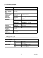
A.1
A.2
A.3
A.4
A.5
A.6
Analog Input.................................................................... 52
Analog Output ................................................................. 53
Digital Input .................................................................... 53
Digital Output.................................................................. 54
Counter/Timer ................................................................. 54
General ............................................................................ 55
Appendix B Block Diagrams ............................................. 58
Appendix C Register Structure & Format ....................... 60
C.1
C.2
Overview ......................................................................... 60
I/O Port Address Map .................................................... 60
C.3
A/D Data and Channels — BASE+00H~01H ................ 64
C.4
Software A/D Trigger — BASE+00H ............................ 64
C.5
A/D Range Control — BASE+01H ............................... 65
C.6
MUX Scan Channel Control — BASE+02H.................. 67
C.7
MUX Scan Channel Status — BASE+02H .................... 68
C.8
Digital I/O Registers - BASE + 03/0BH ......................... 68
C.9
D/A Output — BASE+04/05H ....................................... 69
C.10
FIFO Interrupt Control — BASE+06H........................... 70
C.11
Clear Interrupt Request — BASE+08H .......................... 71
C.12
A/D Status — BASE+08H.............................................. 71
Table C.1:PCI-1718HDU/HGU Reg. Format (Part 1) 61
Table C.2:PCI-1718HDU/HGU Reg. Format (Part 2) 62
Table C.3:PCI-1718HDU/HGU Reg. Format (Part 3) 63
Table C.4:Register for A/D Data and Channels .......... 64
Table C.5:Register for Software A/D Trigger ............. 64
Table C.6:Register for A/D Range Control ................. 65
Table C.7:Register for MUX Scan Channel Control ... 67
Table C.8:Register for MUX Scan Channel Status ..... 68
Table C.9:Register for Digital Output ......................... 68
Table C.10:Register for Digital Output ...................... 69
Table C.11:Register for D/A Output ........................... 69
Table C.12:Register for FIFO Interrupt Control .......... 70
Table C.13:Register for Clear Interrupt Request ......... 71
Table C.14:Register for A/D Status ............................. 71
PCI-1718 Series User Manual
vi
C.13
A/D Control — BASE+09H ........................................... 73
C.14
Timer/Counter Enable — BASE+0AH........................... 74
C.15
C.16
Programmable Timer/Counter — BASE+0C~0FH ........ 74
Clear FIFO Interrupt Request — BASE+14H ................ 75
C.17
A/D Data and Channel from FIFO - BASE + 17/18H .... 75
C.18
FIFO Status — BASE+19H ............................................ 76
C.19
FIFO Clear — BASE+19H ............................................. 76
C.20
Register Programming Flow Chart ................................. 77
Table C.15:Register for A/D Control ......................... 73
Table C.16:Register for Timer/Counter Enable ........... 74
Table C.17:Register for Clear FIFO Interrupt Request 75
Table C.18:Register for A/D Data and Channel from
FIFO ................................................................. 75
Table C.19:Register for FIFO Status ........................... 76
Table C.20:Register for FIFO Clear ............................ 76
C.20.1 Software Trigger Mode with Polling ........................... 77
C.20.2 Pacer Trigger Mode with Interrupt .............................. 78
C.20.3 Pacer Trigger Mode with Interrupt [FIFO Used] ......... 79
Appendix D Calibration ..................................................... 82
D.1
VR Assignment .............................................................. 83
D.2
D.3
A/D Calibration ............................................................... 84
D/A Calibration ............................................................... 85
Figure D.1:PCI-1718 VR Assignment ......................... 83
vii
PCI-1718 Series User Manual
viii
CHAPTER
1
2
Introduction
This chapter introduces the PCI-1718
cards and their typical applications.
Sections include:
• Features
• Applications
• Installation Guide
• Software Overview
• Device Driver Programming Roadmap
• Accessories
Chapter 1 Introduction
Thank you for buying the Advantech PCI-1718HDU/HGU. PCI1718HDU/HGU is a PCI-Bus multifunction card for IBM PC/XT/AT or
compatible computers. It offers the five most desired measurement and
control functions:
• 12-bit A/D conversion
• D/A conversion
• Digital input
• Digital output
• Timer/counter.
A programmable-gain instrument amplifier lets you acquire different
input signals without external signal conditioning. An onboard 1 K word
FIFO buffer provides high-speed data transfer and predictable performance under Windows. Automatic channel scanning circuitry and
onboard SRAM let you perform multiple-channel A/D conversion with
DMA and individual gains for each channel.
PCI-1718HDU/HGU is compatible* with its ISA-Bus predecessor, the
PCL-818HD/HG. This puts rich software support and a wide variety of
external signal conditioning boards at your disposal.
The following sections of this chapter will provide further information
about features of the multifunction cards, a Quick Start for installation,
together with some brief information on software and accessories for the
PCI-1718 cards.
Note*
1. PCI-1718HDU/HGU is register-level- programming compatible with PCL-818HD/HG
2. Due to the difference between ISA and PCI
architecture, we use “interrupt + FIFO” to emulate the DMA function. But it makes no difference to your programming and applications.
PCI-1718 Series User Manual
2
1.1 Features
• Register level programming compatible with PCL-818HD/HG
• 16 single-ended or 8 differential A/D inputs, switch selectable
• 12-bit A/D converter, up to 100 kHz sampling rate
• Programmable gain for each input channel
• Automatic Channel/Gain Scanning
• On-board 1 K word FIFO buffer with software selectable interrupt
• Software selectable Bipolar/Unipolar analog input ranges
• 16 digital inputs and 16 digital outputs, TTL/DTL compatible
• One 12-bit analog output channel
• Data transfers by program control and interrupt handler routine
• Universal PCI-Bus (Support 3.3V or 5V PCI-Bus signal)
• BoardID switch
PCI-1718HDU/HGU offers the following main features:
PCI-Bus Plug & Play
The PCI-1718 cards use a PCI controller to interface the card to the PCI
bus. The controller fully implements the PCI bus specification Rev 2.2.
All configurations related to the bus, such as base address and interrupt
assignment, are automatically controlled by software. No jumper or
switch is required for user configuration.
Automatic Channel/Gain Scanning
PCI-1718HDU/HGU features an automatic channel/gain scanning circuit.
This circuit, instead of your software, controls multiplexer switching during sampling. On-board SRAM stores different gain values for each channel. This combination lets user perform multi-channel high-speed
sampling (up to 100 kHz) for each channel.
3
Chapter 1
Onboard FIFO
There are 1 K samples FIFO for A/D (AI) on PCI-1718HDU/HGU. This
is an important feature for faster data transfer and more predictable performance under Windows system.
Onboard Programmable Timer/Counter
PCI-1718HDU/HGU provides a programmable timer counter for generating pacer trigger for the A/D conversion. The timer/counter chip is
82C54, which includes three 16-bit counters of 10 MHz clock. One
counter is used as an event counter for counting events coming from the
input channel. The other two are cascaded together to make a 32-bit timer
for pacer trigger time base.
BoardID Switch
PCI-1718HDU/HGU has a built-in DIP switch that helps define each
card’s ID when multiple PCI-1718HDU/HGU cards have been installed
on the same PC chassis. The BoardID setting function is very useful when
building a system with multiple PCI-1718 cards. With the correct BoardID settings, you can easily identify and access each card during hardware configuration and software programming.
Note:
For detailed specifications of the PCI1718HDU/HGU, please refer to Appendix A.
1.2 Applications
• Transducer and sensor measurements
• Waveform acquisition and analysis
• Process control and monitoring
• Vibration and transient analysis
PCI-1718 Series User Manual
4
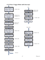
1.3 Installation Guide
Before you install your PCI-1718HDU/HGU card, please make sure you
have the following necessary components:
• PCI-1718HDU/HGU DA&C card
• PCI-1718HDU/HGU User Manual
• Driver software Advantech DLL drivers (included in the companion
CD-ROM)
• Personal computer or workstation with a PCI-bus slot (running Windows 98/2000/XP)
• PCL-10120 or PCL-10137 Wiring cable (optional)
• ADAM-3920/3937, PCLD-7216/780/782/782B/785/785B/786/788/
789D/880/885/8115 Wiring board (optional)
Some other optional components are also available for enhanced operation:
• ActiveDAQ, ADAQView, LabView or other third-party software packages
After you get the necessary components and maybe some of the accessories for enhanced operation of your multifunction card, you can then
begin the installation procedure. Figure 1.1 on the next page provides a
concise flow chart to give users a broad picture of the software and hardware installation procedures:
5
Chapter 1
Figure 1.1: Installation Flow Chart
PCI-1718 Series User Manual
6
1.4 Software Overview
Advantech offers a rich set of DLL drivers, third-party driver support and
application software to help fully exploit the functions of your PCI1718HDU/HGU card:
• Device Drivers (on the companion CD-ROM)
• LabVIEW driver
• Advantech ActiveDAQ
• Advantech ADAQView
Programming choices for DA&C cards
You may use Advantech application software such as Advantech Device
Drivers. On the other hand, advanced users can use register-level programming, although this is not recommended due to its laborious and
time-consuming nature.
Device Drivers
Advantech Device Driver software is included on the companion CDROM at no extra charge. It also comes with all Advantech DA&C cards.
Advantech’s Device Drivers features a complete I/O function library to
help boost your application performance. Advantech Device Drivers for
Windows 98/2000/XP works seamlessly with development tools such as
Visual C++, Visual Basic, Borland C++ Builder and Borland Delphi.
Register-level Programming
Register-level programming is available for experienced programmers
who find it necessary to write code directly at the level of the device register. Since register-level programming requires much effort and time, we
recommend that you use the Advantech Device Drivers instead. However, if register-level programming is indispensable, you should refer to
the relevant information in Appendix C, Register Structure and Format,
or to the example codes included on the companion CD-ROM.
7
Chapter 1
1.5 Device Driver Programming Roadmap
This section will provide you a roadmap to demonstrate how to build an
application from scratch using Advantech Device Drivers with your
favorite development tools such as Visual C++, Visual Basic, Delphi and
C++ Builder. The step-by-step instructions on how to build your own
applications using each development tool will be given in the Device
Drivers Manual. Moreover, a rich set of example source code is also
given for your reference.
Programming Tools
Programmers can develop application programs with their favorite development tools:
• Visual C++
• Visual Basic
• Delphi
• C++ Builder
For instructions on how to begin programming works in each development tool, Advantech offers a Tutorial Chapter in the Device Drivers
Manual for your reference. Please refer to the corresponding sections in
this chapter on the Device Drivers Manual to begin your programming
efforts. You can also look at the example source code provided for each
programming tool, since they can get you very well oriented.
The Device Drivers Manual can be found on the companion CD-ROM.
Alternatively, if you have already installed the Device Drivers on your
system, The Device Drivers Manual can be readily accessed through the
Start button:
Start\Advantech Automation\Device Manager\Device Driver's Manual
The example source code could be found under the corresponding installation folder such as the default installation path:
Program Files\Advantech\ADSAP\Examples
For information about using other function groups or other development
tools, please refer to the Creating Windows 98/2000/XP Application with
Device Drivers chapter and the Function Overview chapter on the Device
Drivers Manual.
PCI-1718 Series User Manual
8
Programming with Device Drivers Function Library
Advantech Device Drivers offer a rich function library that can be utilized in various application programs. This function library consists of
numerous APIs that support many development tools, such as Visual
C++, Visual Basic, Delphi and C++ Builder.
According to their specific functions or services, APIs can be categorized
into several function groups:
• Analog Output Function Group
• Digital Input/Output Function Group
• Counter Function Group
• Port Function Group (direct I/O)
• Event Function Group
For the usage and parameters of each function, please refer to the Function Overview chapter in the Device Drivers Manual.
Troubleshooting Device Drivers Error
Driver functions will return a status code when they are called to perform
a certain task for the application. When a function returns a code that is
not zero, it means the function has failed to perform its designated function. To troubleshoot the Device Drivers error, you can pass the error
code to DRV_GetErrorMessage function to return the error message.
Alternatively, you can refer to the Device Drivers Error Codes Appendix
in the Device Drivers Manual for a detailed listing of Error Codes, Error
IDs and Error Messages.
9
Chapter 1
1.6 Accessories
Advantech offers a complete set of accessory products to support the
PCI-1718HDU/HGU card. These accessories include:
Wiring Cables
PCL-10120
The PCL-10120 cable is a 20-pin flat cable for PCI-1718HDU/HGU
cards.
PCL-10137
The PCL-10137 shielded cable is specially designed for PCI-1718HDU/
HGU cards to provide high resistance to noise. To achieve a better signal
quality, the signal wires are twisted in such a way as to form a “twistedpair cable”, reducing cross-talk and noise from other signal sources. Furthermore, its analog and digital lines are separately sheathed and shielded
to neutralize EMI/EMC problems.
Wiring Boards
• ADAM-3920
20-pin wiring terminal for DIN-rail mounting
• ADAM-3937
37-pin D-type wiring terminal for DIN-rail mounting
• PCLD-7216
16-channel SSR I/O module carrier board
• PCLD-780
Universal screw-terminal board
• PCLD-782
16-channel opto-isolated D/I board
• PCLD-782B
24-channel opto-isolated D/I board
• PCLD-785
16-channel relay output board
• PCLD-785B
24-channel relay output board
• PCLD-786
8-channel SSR I/O module carrier board
• PCLD-788
16-channel relay multiplexer board
• PCLD-789D
Amplifier and multiplexer board
• PCLD-880
Universal screw-terminal board
• PCLD-885
16-channel power relay output board
• PCLD-8115
Industrial wiring terminal with CJC circuit
PCI-1718 Series User Manual
10
CHAPTER
2
2
Installation
This chapter provides a packaged item
checklist, proper instructions for
unpacking and step-by-step procedures
for both driver and card installation..
Sections include:
• Unpacking
• Driver Installation
• Hardware Installation
• Device Setup & Configuration
Chapter 2 Installation
2.1 Unpacking
After receiving your PCI-1718HDU/HGU package, please inspect its
contents first. The package should contain the following items:
• PCI-1718HDU or PCI-1718HGU card
• Companion CD-ROM (Device Drivers included)
• User Manual
The PCI-1718 cards harbor certain electronic components vulnerable to
electrostatic discharge (ESD). ESD can easily damage the integrated circuits and certain components if preventive measures are ignored.
Before removing the card from the antistatic plastic bag, you should take
the following precautions to ward off possible ESD damage:
• Touch the metal part of your computer chassis with your hand to discharge the static electricity accumulated on your body. Alternatively,
one can also use a grounding strap.
• Touch the anti-static bag to a metal part of your computer chassis
before opening the bag.
• Take hold of the card only by the metal bracket when removing it out of
the bag.
After taking out the card, you should first:
• Inspect the card for any possible signs of external damage (loose or
damaged components, etc.). If the card is visibly damaged, please
notify our service department or our local sales representative immediately. Do not install a damaged card into your system.
Also, pay extra caution to the following aspects during installation:
• Avoid physical contact with materials that could hold static electricity
such as plastic, vinyl and Styrofoam.
• Whenever you handle the card, grasp it only by its edges. DO NOT
TOUCH the exposed metal pins of the connector or the electronic components.
PCI-1718 Series User Manual
12
.
Note:
Keep the anti-static bag for future use. You
might need the original bag to store the card if
you have to remove the card from a PC or transport it elsewhere.
2.2 Driver Installation
We recommend you install the driver before you install the PCI1718HDU/HGU card into your system, since this will guarantee a smooth
installation process.
The Advantech Device Drivers Setup program for the PCI-1718HDU/
HGU card is included in the companion CD-ROM that is shipped with
your DA&C card package. Please follow the steps below to install the
driver software:
1.
Insert the companion CD-ROM into your CD-ROM drive.
2.
The Setup program will be launched automatically if you have the
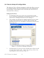
autoplay function enabled on your system. When the Setup Program is launched, you will see the following Setup Screen.
Note:
If the autoplay function is not enabled on
your computer, use Windows Explorer or
Windows Run command to execute
SETUP.EXE on the companion CD-ROM.
13
Chapter 2
Figure 2.1: Setup Screen of Advantech Automation Software
3.
Select the Device Drivers option.
4.
Select the specific device then just follow the installation instructions step by step to complete your device driver installation and
setup.
Figure 2.2: Different Options for Driver Setup
For further information on driver-related issues, an online version of the
Device Drivers Manual is available by accessing the following path:
Start/Advantech Automation/Device Manager/Device Driver’s Manual
PCI-1718 Series User Manual
14
2.3 Hardware Installation
Note:
Make sure you have installed the
driver before you install the card
(please refer to chapter 2.2 Driver
Installation)
After the Device Drivers installation is completed you can install the PCI1718HDU/HGU card into any PCI slot on your computer. However, it is
suggested that you refer to the computer’s user manual or related documentation if you have any doubts. Please follow the steps below to install
the card onto your system.
1.
Turn off your computer and unplug the power cord and cables.
TURN OFF your computer before installing or removing any components on the computer.
2.
Remove the cover of your computer.
3.
Remove the slot cover on the back panel of your computer.
4.
Touch the metal part on the surface of your computer to neutralize
the static electricity that might be on your body.
5.
Insert the PCI-1718HDU/HGU card into a PCI slot. Hold the card
only by its edges and carefully align it with the slot. Insert the card
firmly into place. Use of excessive force must be avoided; otherwise, the card might be damaged.
6.
Fasten the bracket of the PCI card on the back panel rail of the
computer with screws.
7.
Connect appropriate accessories (37-pin cable, wiring terminals,
etc. if necessary) to the PCI card.
8.
Replace the cover of your computer chassis. Re-connect the cables
you removed in step 2.
9.
Plug in the power cord and turn on the computer.
After your card is properly installed on your system, you can now configure your device using the Advantech Device Manager Program that has
itself already been installed on your system during driver setup. A complete device installation procedure should include device setup, configuration and testing. The following sections will guide you through the
Setup, Configuration and Testing of your device.
15
Chapter 2
2.4 Device Setup & Configuration
The Advantech Device Manager program is a utility that allows you to set
up, configure and test your device, and later stores your settings on the
system registry. These settings will be used when you call the APIs of
Advantech Device Drivers.
Setting Up the Device
1.
To install the I/O device for your card, you must first run the
Device Installation program (by accessing Start/Advantech Automation/Device Manager/Advantech Device Manager ).
2.
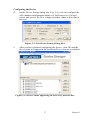
You can then view the device(s) already installed on your system
(if any) on the Installed Devices list box. Since you have not
installed any device yet, you might see a blank list such as the one
below (Fig. 2-3).
Figure 2.3: The Device Manager Dialog Box
3.
Scroll down the List of Devices box to find the device that you wish
to install, then click the Add… button. You will see a Device Setting dialog box such as the one in Fig. 2-4.
PCI-1718 Series User Manual
16
Configuring the Device
4.
On the Device Setting dialog box (Fig. 2-4), you can configure the
A/D channels configuration either as 8 Differential or 16 Singleended, and specify the D/A voltage reference either as External or
Internal.
Figure 2.4: The Device Setting Dialog Box
5.
After you have finished configuring the device, click OK and the
device name will appear in the Installed Devices box as seen below:
Figure 2.5: Device Name Appearing on the List of Devices Box
17
Chapter 2
After your card is properly installed and configured, you can click the
Test… button to test your hardware by using the testing utility supplied.
Figure 2.6: The Test Utility Dialog Box
For more detailed information, please refer to Chapter 2 of the Device
Drivers Manual.
You can also find rich examples on the CD-ROM to speed up your programming.
PCI-1718 Series User Manual
18
CHAPTER
3
2
Signal Connections
This chapter provides useful information about how to connect input and
output signals to the PCI-1718 cards
via the I/O connector..
Sections include:
• Overview
• Switch and Jumper Settings
• Signal Connections
• Field Wiring Considerations
Chapter 3 Signal Connections
3.1 Overview
Maintaining signal connections is one of the most important factors in
ensuring that your application system is sending and receiving data correctly. A good signal connection can avoid unnecessary and costly damage to your PC and other hardware devices. This chapter provides useful
information about how to connect input and output signals to the PCI1718 cards via the I/O connector.
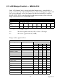
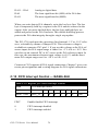
3.2 Switch and Jumper Settings
PCI-1718 cards have two function switches and five jumper settings.
Figure 3.1: Card Connector, Jumper and Switch Locations
JP
Description
SW/CN
Description
JP1
JP5
Digital Output Connector Setting
Trigger Source & Gate Control
Setting
Timer Clock Setting
Internal Reference Voltage Setting
D/A Reference Voltage Setting
Reset Protection Setting
SW1
SW2
CN1
CN2
BoardID Setting
S.E/Diff Connection
Setting
IDE 20-pin Header 1
IDE 20-pin Header 2
CN3
DB-37 Pin Connector
JP8
JP10
Jp11
JP21
PCI-1718 Series User Manual
20
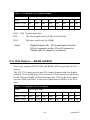
3.2.1 Setting the BoardID Switch (SW1)
BoardID settings are used to set a board’s unique identifier when multiple
identical cards are installed in the same system.
PCI-1718 cards have a built-in DIP switch (SW1), which is used to define
each card’s unique identifier. You can determine the unique identifier in
the register as shown in Table 3.1. If there are multiple identical cards in
the same chassis, the BoardID switch helps differentiate the boards by
identifying each card’s device number with the switch setting. The BoardID switch’s unique identifier has been set to 0 at the factory.
If you need to adjust it to other numbers, set SW1 by referring to DIP
switch settings below.
Table 3.1: Board ID Setting (SW1)
SW1
3
2
1
0
BoardID
ID3
ID2
ID1
ID0
0
ON
ON
ON
ON
1
ON
ON
ON
OFF
2
ON
ON
OFF
ON
3
ON
ON
OFF
OFF
4
ON
OFF
ON
ON
5
ON
OFF
ON
OFF
6
ON
OFF
OFF
ON
7
ON
OFF
OFF
OFF
8
OFF
ON
ON
ON
9
OFF
ON
ON
OFF
10
OFF
ON
OFF
ON
11
OFF
ON
OFF
OFF
12
OFF
OFF
ON
ON
13
OFF
OFF
ON
OFF
14
OFF
OFF
OFF
ON
15
OFF
OFF
OFF
OFF
Default Setting is 0
21
Chapter 3
3.2.2 Channel Configuration, S/E or DIFF (SW2)
The PCI-1718 cards offer 16 single-ended or eight differential analog
input channels. Slide switch SW2 changes the channels between singleended or differential input. Slide the switch to the left-hand position,
marked DIFF, for eight differential inputs (the default) or to the righthand position, marked S/E, for 16 single-ended inputs.
Table 3.2: Summary of Switch SW2 Settings
Switch
Function description
SW2
Differential (default)
Single-ended
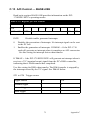
3.2.3 D/A Reference Voltage, int./ext. (JP11)
Jumper JP11 selects reference voltage source for PCI-1718 cards’ D/A
converters. You can use the cards’ internal reference, or supply an external reference.
Table 3.3: Summary of Jumper JP11 Settings
Jumper
Function description
JP11
External
Internal (default)
When you set JP11 to INT, the D/A converter takes its reference voltage
input from the card's onboard reference. Jumper JP10 selects either -5 V
or -10 V onboard reference voltage. With JP11 set to INT the D/A channel has an output range of 0 to +5 V or 0 to +10 V, respectively.
PCI-1718 Series User Manual
22
When you set JP11 to EXT, the D/A converter takes its reference voltage
input from pin 31 of connector CN3. You can apply any voltage between
-10 V and +10 V to this pin to function as the external reference. The reference input can be either DC or AC (<100 kHz).
When you use an external reference with voltage Vref you can program
the D/A channel to output from 0 V to -Vref, you can also use the D/A
converter as a programmable attenuator. The attenuation factor between
reference input and analog output is:
Attenuation factor = G / 4095
G is a value you write to the D/A registers between 0 and 4095. For
example, if you set G to 2048, then the attenuation factor is 0.5. A sine
wave of 10 V amplitude applied to the reference input will generate a sine
wave of 5 V amplitude on the analog output.
3.2.4 Internal Voltage Reference, -10 V or -5 V (JP10)
If you use an internal reference voltage (set with JP11), the PCI-1718
cards provide a choice between -5 V or -10 V DC internal reference voltage sources.
Table 3.4: Summary of Jumper JP10 Settings
Jumper
Function description
JP10
5 V (default)
10 V
Table 3-1: Summary of jumper JP10 settings
23
Chapter 3
3.2.5 Timer Clock Selection (JP8)
PCI-1718’s JP8 controls the input clock frequency for the 8254 programmable clock/timer. You have two choices: 10 or 1 MHz. This lets you
generate pacer output frequencies from 2.5 MHz to 0.00023 Hz (71 minutes/pulse).
The following equation gives the pacer rate:
Pacer rate = Fclk / (Divl * Div2)
Fclk is 1 MHz or 10 MHz, as set by jumper JP8. Div 1 and Div2 are the
dividers set in counter 1 and counter 2 in the 8254.
Table 3.5: Summary of Jumper JP8 Settings
Jumper
Function description
JP8
1 MHz (default)
10 MHz
PCI-1718 Series User Manual
24
3.2.6 Ext. trigger and Counter Gate 0 Control (JP5)
JP5 has two jumpers. The upper jumper selects the card's A/D trigger
source when you use external triggering. The lower jumper selects the
gate control for counter 0 of the card's 8254 timer/counter.
Table 3.6: Summary of Jumper Settings
Jumper
Function description
JP5
(Upper)
G0 (default)
DI2
Ext. (default)
JP5
(Lower)
DI0
3.2.7 Digital Output, 20-pin or 37-pin Connector (JP1)
The PCI-1718 cards’ JP1 switch digital output channels 0 to 3 between
the card's 20-pin connector and 37-pin connector. If you set the jumpers
to the left (D) side, the digital output signals will come out on connector
CN1 (20-pin). If you set the jumpers to the right (S) side, the output signals will come out on connector CN3 (37-pin).
These four digital output signals select the analog input channel when
you use a multiplexer/amplifier daughter board. Daughter boards with a
DB-37 connector, such as the PCLD-789D, read the digital output signals
from the DB-37 connector (CN3). With other daughter boards you will
need to connect an external 20-pin flat cable from CN1 to the daughter
board.
25
Chapter 3
Table 3.7: Summary of Jumper Settings
Jumper
Function Description
JP1 (first)
S0
D0 (default)
S1
JP1 (second)
D1 (default)
S2
JP1 (third)
D2 (default)
S3
JP1
(fourth)
PCI-1718 Series User Manual
D3 (default)
26
3.2.8 Setting the Time to Reset Digital Outputs
Some users will want the capability of clearing each digital output when
the system (or PC) issues a reset signal on the PCI bus. Other users will
want to clear their signal outputs only as part of system power-on.
PCI-1718 cards satisfy both these needs with jumper JP21. Depending on
the application, this capability may allow digital outputs to be “OFF”
without requiring a complete shutdown of processes controlled by the
card.
Complete loss of power to the chip clears the chip memory. Thus, no matter how JP21 is set, if the power to the PCI-1718 card is disconnected, the
digital output channel’s initial power-on state will be “OFF”.
Table 3.8: JP21 Jumper Settings
Jumper
Function description
JP21
Keep last status after hot reset.
Reset status after hot reset
(default)
27
Chapter 3
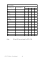
3.3 Signal Connections
Pin Assignment
Figure 3-2 shows the pin assignments for the 37-pin I/O connector on the
PCI-1718HDU/HGU.
D/O 0
D/O 2
D/O 4
D/O 6
D/O 8
D/O 10
D/O 12
D/O 14
D.GND
+5 V
CN1
1
3
5
7
9
11
13
15
17
19
2
4
6
8
10
12
14
16
18
20
D/O 1
D/O 3
D/O 5
D/O 7
D/O 9
D/O 11
D/O 13
D/O 15
D.GND
+12 V
D/I 0
D/I 2
D/I 4
D/I 6
D/I 8
D/I 10
D/I 12
D/I 14
D.GND
+5 V
CN3 (Single ended)
CN2
1
3
5
7
9
11
13
15
17
19
2
4
6
8
10
12
14
16
18
20
D/I 1
D/I 3
D/I 5
D/I 7
D/I 9
D/I 11
D/I 13
D/I 15
D.GND
+12 V
CN3 (Differential)
A/D S0
A/D S1
A/D S2
A/D S3
A/D S4
A/D S5
A/D S6
A/D S7
A.GND
A.GND
VREF
S0*
+12 V
S2*
D.GND
NC
Counter
1
2
3
4
5
6
7
8
9
10
11
12
13
14
15
16
17
20
21
22
23
24
25
26
27
28
29
30
31
32
33
34
35
36
A/D S8
A/D S9
A/D S10
A/D S11
A/D S12
A/D S13
A/D S14
A/D S15
A.GND
A.GND
DA0.OUT
DA0.VREF
S1*
S3*
D.GND
EXT.TRIG
Counter 0
Counter
18
37 PACER
+5 V
19
A/D H0
A/D H1
A/D H2
A/D H3
A/D H4
A/D H5
A/D H6
A/D H7
A.GND
A.GND
VREF
S0*
+12 V
S2*
D.GND
1
2
3
4
5
6
7
8
9
10
11
12
13
14
15
NC
16
Counter 0 17
20
21
22
23
24
25
26
27
28
29
30
31
32
33
34
35
36
Counter 0 18
37 PACER
+5 V
.
A/D L0
A/D L1
A/D L2
A/D L3
A/D L4
A/D L5
A/D L6
A/D L7
A.GND
A.GND
DA0.OUT
DA0.VREF
S1*
S3*
D.GND
EXT.TRIG
Counter 0
19
.
Figure 3.2: I/O Connector Pin Assignments for the PCI-1718 Series
Note: S0/S1 is NC, and S2/S3 is AGND for PCI-1718HGU
PCI-1718 Series User Manual
28
3.3.1 I/O Connector Signal Description
Table 3.9: I/O Connector Signal Descriptions
Signal Refere
Name nce
Direct Description
ion
A/D S
A.GND
<0..15>
Input
Analog input (single-ended), channels 0
through 15.
A/D H
<0..7>
A.GND
Input
Analog input high (differential), channels 0
through 7.
A/D L
<0..7>
A.GND
Input
Analog input low (differential), channels 0
through 7.
D/A
A.GND
Output Analog output
AGND
-
-
D/O
D.GND
Output Digital output, channels 0 through 15.
D/I
D.GND
Input
Digital input, channels 0 through 15.
CLK
D.GND
Input
Clock input for the 8254.
GATE
D.GND
Input
Gate input for the 8254.
OUT
D.GND
Output Signal output for the 8254.
VREF
D.GND
Output Voltage reference.
Analog Ground. The two ground references
(A.GND and D.GND) are connected together
on the PCI-1718HDU/HGU card.
REFIN D.GND
Input
External voltage reference input.
S1-S4
D.GND
Output Daughterboard channel select.
DGND
-
-
Digital Ground. The two ground references
(A.GND and D.GND) are connected together
on the PCI-1718HDU/HGU card.
+12V
D.GND
Output
+12 VDC Source (from ISA bus directly with
FUSE protection).
+5V
D.GND
Output
+5 VDC Source (from ISA bus directly with
FUSE protection).
NC
-
-
No connection.
29
Chapter 3
3.3.2 Analog Input Connections
PCI-1718HDU/HGU supports either 16 single-ended or 8 differential
analog inputs. Switch SW2 selects the input channel configuration.
Single-ended Channel Connections
Single-ended connections use only one signal wire per channel. The voltage on the line references to the common ground on the card. A signal
source without a local ground is called a "floating" source. It is fairly simple to connect a single ended channel to a floating signal source. A standard wiring diagram looks like this:
Signal Input
+
Vs
-
To A/D
A.GND
A.GND
Differential Channel Connections
Differential input connections use two signal wires per channel. The card
measures only the voltage difference between these two wires, the HI
wire and the LOW wire. If the signal source has no connection to ground,
it is called a "floating" source. A connection must exist between LOW
and ground to define a common reference point for floating signal
sources. To measure a floating sources connect the input channels as
shown below:
HIGH
+
+
Vs
-
LOW
+
Vin
-
A.GND
PCI-1718 Series User Manual
30
If the signal source has one side connected to a local ground, the signal
source ground and the PCI-1718HDU/HGU ground will not be at exactly
the same voltage, as they are connected through the ground return of the
equipment and building wiring. The difference between the ground voltages forms a common-mode voltage.
To avoid the ground loop noise effect caused by common-mode voltages,
connect the signal ground to the LOW input. Do not connect the LOW
input to the PCI-1718HDU/HGU ground directly. In some cases you may
also need a wire connection between the PCI-1718HDU/HGU ground
and the signal source ground for better grounding. The following two diagrams show correct and incorrect connections for a differential input with
local ground:
Correct Connection
HIGH
+
+
Vs
-
+
Vin
-
LOW
Vin=Vs
-
- +
Vcm
GND
Incorrect Connection
HIGH
+
+
Vin
-
+
Vs
-
Vin=Vs+Vcm
LOW
-
- +
Vcm
GND
31
Chapter 3
Expanding Analog Inputs
You can expand any or all of the PCI-1718HDU/HGU's A/D input channels using multiplexing daughterboards. Daughterboards without D-type
connectors require the PCLD-774 Analog Expansion Board.
The PCLD-789(D) Amplifier and Multiplexer multiplexes 16 differential
inputs to one A/D input channel. You can cascade up to eight PCLD789(D)s to the PCI-1718HDU/HGU for a total of 128 channels. See the
PCLD-789(D) user's manual for complete operating instructions.
The PCLD-774 Analog Expansion Board accommodates multiple external signal-conditioning daughter boards, such as PCLD-779 and PCLD789(D). It features five sets of on-board 20-pin header connectors. A special star-type architecture lets you cascade multiple signal-conditioning
boards without the signal-attenuation and current-loading problems of
normal cascading.
The PCLD-8115 Screw Terminal Board makes wiring connections easy.
It provides 20-pin flat cable and DB-37 cable connectors. It also includes
CJC (Cold Junction Compensation) circuits.
Special circuit pads on the PCLD-8115 accommodate passive signal conditioning components. You can easily implement a low-pass filter, attenuator or current shunt by adding resistors and capacitors.
PCI-1718 Series User Manual
32
Analog Output Connection
The PCI-1718HDU/HGU provides one D/A output channel. You can use
the internal precision -5 V or -10 V reference to generate 0 to +5 V or 0 to
+10 V D/A output. Use an external reference for other D/A output ranges.
The maximum reference input voltage is ±10 V and maximum output
scaling is ±10 V. Loading current for D/A outputs should not exceed 5
mA.
Connector CN3 provides D/A signals. Important D/A signal connections
such as input reference, D/A outputs and analog ground appear below:
CN3-31 D/A REF IN
D/A
CN3-30 D/A OUT
CN3-9,10,28,29 A.GND
JP11
ON-Board
-5V
REF
CN3-11 VREF
-10V
JP10
Figure 3.3: Analog Output Connections
33
Chapter 3
3.3.3 Digital Signal Connections
The PCI-1718HDU/HGU has 16 digital input and 16 digital output channels. The digital I/O levels are TTL compatible. The following figure
shows connections to exchange digital signals with other TTL devices:
TTL Devices
DO
DI
D.GND D.GND
To receive an OPEN/SHORT signal from a switch or relay, add a pull-up
resistor to ensure that the input is held at a high level when the contacts
are open. See the figure below:
+5V
4.7K
D.GND
PCI-1718 Series User Manual
34
3.4 Field Wiring Considerations
When you use PCI-1718 cards to acquire data from outside, noises in the
environment might significantly affect the accuracy of your measurements if due cautions are not taken. The following measures will be helpful to reduce possible interference running signal wires between signal
sources and the PCI-1718 card.
• The signal cables must be kept away from strong electromagnetic
sources such as power lines, large electric motors, circuit breakers or
welding machines, since they may cause strong electromagnetic interference. Keep the analog signal cables away from any video monitor,
since it can significantly affect a data acquisition system.
• If the cable travels through an area with significant electromagnetic
interference, you should adopt individually shielded, twisted-pair wires
as the analog input cable. This type of cable has its signal wires twisted
together and shielded with a metal mesh. The metal mesh should only
be connected to one point at the signal source ground.
• Avoid running the signal cables through any conduit that might have
power lines in it.
• If you have to place your signal cable parallel to a power line that has a
high voltage or high current running through it, try to keep a safe distance between them. Alternatively, you can place the signal cable at a
right angle to the power line to minimize the undesirable effect.
• The signals transmitted on the cable will be directly affected by the
quality of the cable. In order to ensure better signal quality, we recommend that you use the PCL-10137 shielded cable.
35
Chapter 3
PCI-1718 Series User Manual
36
CHAPTER
4
2
Programming Guide
This chapter provides useful information about how to do register level programming for PCI-1718 cards.
Sections include:
• Overview
• Programming with the Driver
• Register Programming
• Programming with LabVIEW and
ActiveDAQ
Chapter 4 Programming Guide
4.1 Overview
The PCI-1718 cards are delivered with an easy-to-use 32-bit Device
Driver for user programming under the Windows 98/2000/XP operating
systems.
At the Windows driver level, PCI-1718 cards are fully compatible with
the PCL-818 series so you can easily use older applications of the PCL818 series with PCI-1718 cards.We also advise users to program the PCI1718 cards using the 32-bit Device Drivers provided by Advantech to
avoid the complexity of low- level registry programming.
4.2 Programming with the Driver
Your program can perform A/D by writing all the I/O port instructions
directly, or you can take advantage of the PCI-1718 driver. We suggest
that you make use of the driver functions in your program. This will make
you programming job easier and improve your program’s performance.
See the Software Driver User’s Manual for more information.
Start/Advantech Automation/Device Manager/Device Driver’s Manual
4.3 Register Programming.
The most important consideration in programming the PCI-1718 cards at
register level is to understand the function of the card's registers and the
process of programming. The information in the following sections is
provided only for users who would like to do their own low- level programming.
Without the driver you would do the following: perform software trigger,
pacer trigger with interrupt, pacer trigger with interrupt and FIFO, and
program a controlled data transfer.
PCI-1718 Series User Manual
38
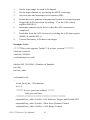
4.3.1 Software Trigger and Polling
Set Scan Channel
MUX Scan
Channel Control &
A/D Range
Control
Set Software
Trigger and
Disable Generated
Interrupt
w Base+0 2H
w Base+0 1H
w Base+ 09H
Software A/D
Trigger
w Base+ 00H
Check EOC
r Base+ 08H
EOC!=0
Yes
EOC=0
Get Data
r Base+ 00H
r Base+01H
More Data?
No
1.
Set the input range for each A/D channel
2.
Set the input channel by specifying the MUX scan range
3.
Trigger the A/D conversion by writing to the A/D low byte register
(BASE+0) with any value.
4.
Check for the end of the conversion by reading the A/D status register (BASE+8) EOC bit.
5.
Read data from the A/D converter by reading the A/D data register
(BASE+0 and BASE+1)
6.
Convert the binary A/D data to an integer.
39
Chapter 4
Example Code:
/********This code supports TurboC 3.0 or later versions********/
#include <stdio.h>
#include <DOS.h>
#define AD_NO 4096; // Number of Samples
int base_addr;
void main(void)
{
int ad_lb,ad_hb; //Declaration
int i;
int eoc;
/****** Access your base address ******/
//Add your code here
/*******************************************/
outportb(base_addr+0x02,0x00); //Set Channel 0
outportb(base_addr+0x01,0x00); //Set A/D range
outportb(base_addr+0x02,0x11); //Set Channel 1
outportb(base_addr+0x01,0x01); //Set A/D range
outportb(base_addr+0x02,0x10); //Scan Channel 0-1
outportb(base_addr+0x09,0x00);
while(i<AD_NO){
outportb(base_addr+0x00,0);
//Software Trigger
do {eoc=inportb(base_addr+0x08);
eoc=eoc&0x01;//Get EOC}
while(eoc!=0);
//Check EOC
ad_lb=inportb(base_addr+0x00);// A/D LowByte
ad_hb=inportb(base_addr+0x01);// A/D HighByte
i++;
}
}
PCI-1718 Series User Manual
40
4.3.2 Pacer Trigger Mode with Interrupt
ISR
Set to Software
Trigger Mode To
Disable Trigger.
MUX Scan
Channel Control &
A/D Range
Control
w Base+ 09H
Get Data
r Base+ 00H
r Base+01H
Clear Device
Interrupt Request
w Base+0 2H
w Base+0 1H
Clear System
Device Interrupt
w Base+0 2H
w Base+ 08H
Set Scan Channel
End of ISR
Set Pacer Rate
Base+0 CH~
Base+0FH
Set ISR
Stop ISR
Set To Pacer
Trigger Mode and
Enable Device
Interrupt
w Base+ 09H
Set To Software
Trigger Mode To
Disable Trigger
Enable System To
Accept Interrupt
Clear Device
Interrupt Request
Restore ISR
w Base+ 08H
Disable Generated
Interrupt
Clear System
Interrupt Request
Set To Pacer
Trigger Mode To
Enable Trigger
w Base+0 9H
Disable System
To Accept
Interrupt
w Base+0 9H
w Base+ 09H
System Ready For
Data Acquisition
Interrupt
41
Chapter 4
1.
Set the input range for each A/D channel
2.
Set the input channel by specifying the MUX scan range
3.
Set pacer rate and interrupt service routine (ISR)
4.
Enable device to generate interrupts and system to accept interrupts
5.
Trigger the A/D conversion by writing “1” to the A/D control
register (BASE+9)
6.
Interrupts generate by the device when the A/D conversion is
completed.
7.
Read data from the A/D converter by reading the A/D data register
(BASE+0 and BASE+1)
8.
Convert the binary A/D data to an integer.
Example Code:
/******This code supports TurboC 3.0 or later versions********/
#include <stdio.h>
#include <DOS.h>
void interrupt isr(void);
#define AD_NO 4096; //Number of Samples
int iflag;
int base_addr;
void main(void)
{
int ad_lb,ad_hb; //Declaration
int i=1;
/****** Access your base address ******/
Add you code here
/*******************************************/
outportb(base_addr+9,0x00); //Set Software Trigger and Disable INT.
outportb(base_addr+2,0x00); //Mux Scan Channel Control
outportb(base_addr+1,0x00); //A/D Range Control
PCI-1718 Series User Manual
42
/***** Set Pacer *****/
outportb(base_addr+0x0f,0x7E); //Pacer=1M/clk1/clk2
outportb(base_addr+0x0d,0x0A); //clk1
outportb(base_addr+0x0d,0x00); //10=0x0A ; 100=0x64 ;
1000=0x3E8
outportb(base_addr+0x0f,0xBE);
outportb(base_addr+0x0e,0x0A); //clk2
outportb(base_addr+0x0e,0x00);
/***** Pacer=1M/10/10=10k ******/
/***** Set ISR *****/
Add you code here
/********************/
/***** Set Interrupt *****/
Add you code here
/********************/
outportb(base_addr+8,0);
//Clear Interrupt
outportb(base_addr+9,0xf3); //Set Pacer Trigger and Enable INT
/***** Ready for Data Acquisition *****/
while(i<AD_NO)
{
while(iflag==0) {;}//Wait for Interrupt
ad_lb=inportb(base_addr+0);
//Get A/D LowByte
ad_hb=inprrtb(base_addr+1);//Get A/D HighByte
i++
}
/***** END *****/
}
43
Chapter 4
void interrupt isr(void)
{
disable();
/***** Add code on here *****/
iflag = 1; //Interrupt Flag
outportb(base_addr+0x08,0);// Clear Interrupt
/****************************/
outportb(0x20,0x20);
outportb(0xA0,0x20);
enable();
}
PCI-1718 Series User Manual
44
4.3.3 Pacer Trigger Mode with Interrupt and FIFO
Set To Software
Trigger Mode To
Disable Trigger
MUX Scan
Channel Control &
A/D Range
Control
w Base+ 09H
Start ISR
w Base+0 2H
Get 512
Samples data
(Half-Full of FIFO)
r Base+ 17H
r Base+18H
Clear FIFO
Interrupt Request
w Base+ 14 H
w Base+0 1H
Set Scan Channel
w Base+0 2 H
Set Pacer Rate
Base+0 CH~
Base+0FH
Clear System
Interrupt request
Set ISR
End of ISR
Enable System To
Accept Interrupt
Stop ISR
Set Pacer Trigger
and Disable
Generated
Interrupt
w Base+0 9H
Enable FIFO
Interrupt
w Base+0 6H
Set To Software
Trigger Mode To
Disable Trigger
w Base+0 9H
Restore ISR
Clear FIFO
Interrupt Request
w Base+ 14 H
Disable Generated
Interrupt
Clear System
Interrupt Request
Clear FIFO
w Base+ 19H
Set To Pacer
Trigger Mode To
Enable Trigger
w Base+ 0AH
w Base+0 9 H
Disable System
To Accept
Interrupt
Clear FIFO
w Base+ 19H
System Ready For
Data Acquisition
Interrupt
45
Chapter 4
1.
Set the input range for each A/D channel
2.
Set the input channel by specifying the MUX scan range
3.
Set pacer rate and interrupt service routine (ISR)
4.
Enable FIFO to generate interrupts and system to accept interrupts
5.
Trigger the A/D conversion by writing “1” to the A/D control
register (BASE+9)
6.
Interrupts generate by FIFO when FIFO is half-full.
7.
Read data from the A/D converter by reading the FIFO A/D data
register (BASE+17 and BASE+18)
8.
Convert the binary A/D data to an integer.
Example Code:
/**********This code supports TurboC 3.0 or later versions********/
#include <stdio.h>
#include <DOS.h>
void interrupt isr(void);
#define AD_NO 4096;
int iflag;
int base_addr;
void main(void)
{
int ad_lb,ad_hb;
int i=1;
int k=0; //FIFO index
/****** Access your base address ******/
Add you code here
/*******************************************/
// Set Software Trigger and Disable Nor INT
outportb(base_addr+0x09,0x00);
PCI-1718 Series User Manual
46
outportb(base_addr+0x02,0x00); //MUX Scan Channel Control
outportb(base_addr+0x01,0x03); //Channel 1 Gain Setting
outportb(base_addr+0x02,0x11); // MUX Scan Channel Control
outportb(base_addr+0x01,0x08); // Channel 2 Gain Setting
outportb(base_addr+0x02,0x10); //Scan Channel 0-1
/***** Set Pacer *****/
outportb(base_addr+0x0f,0x7e);
outportb(base_addr+0x0d,10); //Divide By 1
outportb(base_addr+0x0d,0);
outportb(base_addr+0x0f,0xbe);
outportb(base_addr+0x0e,20); //Divide By 2
outportb(base_addr+0x0e,0);
/***** Set ISR *****/
Add your code here
/********************/
/***** Set System Interrupt *****/
Add your code here
/*********************************/
outportb(base_addr+0x09,0x00); // Disable Nor INT and Set Pacer
Trigger
outportb(base_addr+0x06,0x01); // Enable FIFO INT
outportb(base_addr+0x14,0x00); // Clear FIFO Interrupt
/***** Clear System Interrupt*****/
Add you code here
/*********************************/
outportb(base_addr+0x19,0x00); // Clear FIFO
outportb(base_addr+10,0);
// Enable Pacer
while(i<=AD_NO)
{
47
Chapter 4
while(iflag==0) {;}
/***** FIFO HALF Interrupt and Get Data *****/
for(k=0;k<512;k++)
{
iflag=0;
ad_lb=inportb(base_addr+0x17);
ad_hb=inportb(base_addr+0x18);
/***** Save to Memory *****/
Add your code here
/**************************/
i++;
}
/*******************************************/
}
}
void interrupt isr(void)
{
disable();
iflag = 1;
/***** Add your code here *****/
outportb(base_addr+0x14,0);
// Clear FIFO Interrupt
/******************************/
outportb(0x20,0x20);
outportb(0xA0,0x20);
enable();
}
PCI-1718 Series User Manual
48
4.4 Programming with LabVIEW and ActiveDAQ
Advantech offers not only a rich set of DLL drivers, but also third-party
driver support and application software to help fully exploit the functions
of your PCI-1718 cards. For more detailed information for these
applications, please refer to:
LabView
Start\Advantech Automation\LabVIEW\LabVIEW Driver's Manual
(To install Labview driver, please access: \CDROM\LabVIEW)
ActiveDAQ
Start\Advantech Automation\ ActiveDAQ \ ActiveDAQ Driver's Manual
(To install ActiveDAQ, please access: \CDROM\ActiveDAQ)
49
Chapter 4
PCI-1718 Series User Manual
50
APPENDIX
A
2
Specifications
Appendix A Specifications
A.1 Analog Input
Channels
16 single-ended or 8 differential or combination
Resolution
12-bit
FIFO Size
1K samples
Max. Sampling Rate 100 kS/s
Input range and
Gain List for PCI1718HDU
Gain
0.5
1
2
4
8
Unipolar
N/A
0~10
0~5
0~2.5
0~1.25
Bipolar
±10
±5
±2.5
±1.25
±0.625
Bandwidth
4
Mhz
0.01
400
kHz
0.01
400
kHz
0.04
(1LSB)
350
kHz
0.07
(3LSB)
300
kHz
0.1
(4LSB)
Gain error
(% FSR)
PCI-1718HDU
Accuracy
DC
AC
Zero Drift ( µV/°C)
Range
Range
DNLE: ±1LSB
INLE: ±1LSB
Offset error: Adjustable to 0
THD: -80 dB
ENOB: 11 bits
0~10 0~5
0~2.5
480
240
120
±10 ±5
±2.5
±1.25
160 80
40
20
0~1.25
60
±0.625
10
Gain Drift (PPM/°C)
40
Common Mode
Voltage
±11 V max. (operational)
Max. Input Voltage
±15 V
Input Protect
30 Vp-p
Input Impedance
100 MΩ/10pF(Off); 100 MΩ/100pF(On)
Trigger Mode
Software, on-board Programmable Pacer or External
External TTL
Trigger Input
Low
High
PCI-1718 Series User Manual
0.8 V max.
2.0 V min.
52
A.2 Analog Output
Channels
1
Resolution
12-bit
Max. Transfer
Rate
100 kS/s
Output Range
(Internal &
External
Reference)
Using Internal
Reference
0~+5V,0~+10 V
Using External
Reference
0 ~ x V @ x V (-10 =< x =< 10)
Accuracy
INLE
±1LSB
DNLE
±1LSB (monotonic)
Offset error
Adjustable to ±1 LSB
Gain error
Adjustable to ±1 LSB
Dynamic
Performance
Slew Rate
10 V / µs
Settling Time
2 µs to 0.01% of FSR
Driving
Capability
±10mA
Output
Impedance
0.1 Ω max.
A.3 Digital Input
Input Channels
16
Input Voltage
Low
0.4V max.
High
2.4 V min.
Low
0.4 V max.@ -0.2mA
High
2.7 V min.@20µA
Input Load
53
Appendix A
A.4 Digital Output
Output Channels
16
Output Voltage
Low
0.4 V max.@ +8.0mA (sink)
High
2.4 V min.@ -0.4mA(source)
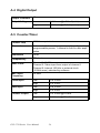
A.5 Counter/Timer
Counter chip
82C54 or equivalent
Channels
3 channels, 2 channels are permanently configured as
programmable pacers; 1 channel is free for user application
Resolution
16-bit
Compatibility
TTL level
Base Clock
Channel 1: 10 MHz
Channel 2: Takes input from output of channel 1
Channel 0: Internal 100 kHz or external clock
(10 MHz max.) selected by software
Max. Input
Frequency
10 MHz
Clock Input
Low
0.8 V max.
High
2.0 V min.
Low
0.8 V max.
High
2.0 V min.
Low
0.5 V max.@+24 mA
High
2.4 V min.@-15 mA
Gate Input
Counter Output
PCI-1718 Series User Manual
54
A.6 General
I/O Connector
Type
37-pin DSUB female for Analog
One 20-pin Box Header for DI
One 20-pin Box Header for DO
Dimensions
175 x 100 mm (6.9" x 3.9")
Power
Consumption
Typical
+5 V @ 850 mA
Max.
+5 V @ 1 A
Operating
0~60° C (32~158° F)
(refer to IEC 68-2-1,2)
Storage
-20~ 70° C (-4~158° F)
Operating
5~85%RH non-condensing
(refer to IEC 68-1,-2,-3)
Storage
5~95%RH non-condensing
(refer to IEC 68-1,-2,-3)
Temperature
Relative Humidity
Certifications
CE certified
55
Appendix A
PCI-1718 Series User Manual
56
B
APPENDIX
2
Block Diagrams
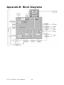
Appendix B Block Diagrams
PCI-1718 Series User Manual
58
C
APPENDIX
2
Register Structure &
Format
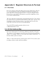
Appendix C Register Structure & Format
C.1 Overview
PCI-1718 cards are delivered with an easy-to-use 32-bit Device Drivers
for user programming under the Windows 98/2000/XP operating systems. We advise users to program the PCI-1718 cards using the 32-bit
Device Drivers provided by Advantech to avoid the complexity of lowlevel registry programming.
The most important consideration in programming the PCI-1718 cards at
the register level is to understand the function of the cards’ registers. The
information in the following sections is provided only for users who
would like to do their own low-level programming.
To get the DOS example programs, please access:
\CDROM\DOS\PCI\1718\
C.2 I/O Port Address Map
PCI-1718 cards require 32 consecutive addresses in the PC's I/O space.
The address of each register is specified as an offset from the card's base
address. For example, BASE+0 is the card's base address and BASE+7 is
the base address plus seven bytes.
Table C.1 shows the function of each register of PCI-1718 or driver, and
its address relative to the card's base address.
PCI-1718 Series User Manual
60
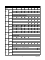
Table C.1: PCI-1718HDU/HGU Register Format (Part 1)
Base Addr.
+HEX
R
00H
W
R
01H
W
R
02H
W
R
03H
W
R
04H
W
R
05H
W
R
06H
W
R
07H
W
7
6
5
4
3
2
1
0
C3
C2
C1
C0
AD7
AD6
AD5
AD4
G3
G2
G1
G0
CC3
CC2
CC1
CC0
CH0
CL3
CL2
CL1
CL0
DI4
DI3
DI2
DI1
DI0
A/D low byte data and channels
AD3
AD2
AD1
AD0
Software A/D trigger
A/D high byte data and channels
AD11
AD10
AD9
AD8
A/D range control
MUX scan channel status
MUX scan channel control
CH3
CH2
CH1
Digital Input (low byte)
DI7
DI6
DI5
Digital Output (low byte)
DO7
DO6
DO5 DO4
DO3 DO2 DO1 DO0
N/A
D/A output data
DA3
DA2
DA1
DA0
DA9
DA8
N/A
D/A output data
DA11
DA10
DA7
DA6
DA5
DA4
N/A
AD resolution & FIFO interrupt control
AD12_16
FINT
N/A
N/A
61
Appendix C
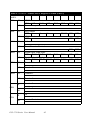
Table C.2: PCI-1718HDU/HGU Register Format (Part 2)
Base Addr.
+HEX
08H
R
W
09H
R
0BH
0DH
5
4
A/D Status
EOC U/B
MUX INT
Clear interrupt request
3
2
1
0
CN3
CN2
CN1
CN0
DMAE
ST1
ST0
ST1
ST0
TC1
TC0
DI9
DI8
R
W
Timer/Counter Control
R
R
Digital Input (high byte)
DI15 DI14
DI13 DI12 DI11
DI10
Digital Output (high byte)
DO15 DO14 DO13 DO12 DO11 DO10
Counter 0
W
Counter 0
R
Counter 1
W
Counter 1
W
0CH
6
A/D Control
INTE I2
A/D Control
INTE
N/A
W
0AH
7
R
0EH
W
R
0FH
W
I1
I0
Counter 2
Counter 2
N/A
Counter Control
PCI-1718 Series User Manual
62
DO9 DO8
Table C.3: PCI-1718HDU/HGU Register Format (Part 3)
Base Addr.
+HEX
R
14H
W
R
17H
W
R
18H
W
R
19H
W
7
6
5
4
3
2
1
0
ID3
ID2
ID1
ID0
C2
C1
C0
AD6
AD5
AD4
FF
HF
EF
BoardID
Clear FIFO Interrupt Request
A/D data and channels from FIFO
AD3
AD2
AD1
AD0
C3
N/A
A/D data and channels from FIFO
AD11
AD10 AD9
AD8
AD7
N/A
FIFO status
FIFO clear
63
Appendix C
C.3 A/D Data and Channels — BASE+00H~01H
Table C.4: Register for A/D Data and Channels
Read
A/D data and channels
Bit #
7
6
5
4
3
2
1
0
BASE + 00H
AD3
AD2
AD1
AD0
C3
C2
C1
C0
BASE + 01H
AD11 AD10 AD9
AD8
AD7
AD6
AD5
AD4
AD11 ~ AD0
Analog to digital data
AD0
The least significant bit (LSB) of the A/D data
AD11
The most significant bit (MSB)
C3 ~ C0
A/D channel number from which the data is derived
C0
The least significant bit (LSB) of the channels
C3
The most significant bit (MSB)
C.4 Software A/D Trigger — BASE+00H
You can trigger an A/D conversion from software, the card's onboard
pacer or an external pulse. If you select software triggering, a write to the
register BASE+00H with any value will trigger an A/D conversion.
Bits 1 and 0 of register BASE+09H select the trigger source. See page 67
for BASE+09H register layout and programming information.
Table C.5: Register for Software A/D Trigger
Write
Software A/D trigger
Bit #
7
6
5
4
3
2
1
0
BASE + 00H
X
X
X
X
X
X
X
X
PCI-1718 Series User Manual
64
C.5 A/D Range Control — BASE+01H
Each A/D channel has its own individual input range, controlled by a
range code stored in onboard RAM. If you want to change the range code
for a given channel, select the channel as the start channel in register
BASE+02H, MUX scan (described in the next section), then write the
range code to bits 0 to 3 of BASE+01H.
Table C.6: Register for A/D Range Control
Write
A/D range control
Bit #
7
6
5
4
3
2
1
0
BASE + 01H
X
X
X
X
G3*
G2*
G1
G0
G3 ~ G0
A/D range control
G0
The least significant bit (LSB) of the A/D range
G3
The most significant bit (MSB)
Range codes appear below:
PCI-1718HDU
Input Range (V)
Unipolar/Bipolar
Gain Code
G3
G2
G1
G0
-5 to +5
B
0
0
0
0
-2.5 to +2.5
B
0
0
0
1
-1.25 to +1.25
B
0
0
1
0
-0.625 to +0.625
B
0
0
1
1
0 to 10V
U
0
1
0
0
0 to 5V
U
0
1
0
1
0 to 2.5V
U
0
1
1
0
0 to 1.25V
U
0
1
1
1
-10V to +10V
B
1
0
0
0
N/A
1
0
0
1
N/A
1
0
1
0
N/A
1
0
1
1
N/A
1
1
0
0
N/A
1
1
0
1
N/A
1
1
1
0
N/A
1
1
1
1
65
Appendix C
PCI-1718HGU
Input Range (V)
Unipolar/Bipolar
±5V
Gain Code
G3
G2
G1
G0
B
0
0
0
0
±0.5V
B
0
0
0
1
±0.05V
B
0
0
1
0
±0.005V
B
0
0
1
1
0 to 10V
U
0
1
0
0
0 to 1V
U
0
1
0
1
0 to 0.1V
U
0
1
1
0
0 to 0.01V
U
0
1
1
1
±10V
B
1
0
0
0
±1V
B
1
0
0
1
±0.1V
B
1
0
1
0
±0.01V
B
1
0
1
1
N/A
1
1
0
0
N/A
1
1
0
1
N/A
1
1
1
0
N/A
1
1
1
1
Note:
G3 and G2 are not used for PCL-818L
PCI-1718 Series User Manual
66
C.6 MUX Scan Channel Control — BASE+02H
The write register at BASE+02H controls multiplexer (MUX) scanning.
The high nibble provides the stop scan channel number, and the low nibble provides the start scan channel number. Writing to this register automatically initializes the MUX to the start channel. Each A/D conversion
trigger sets the MUX to the next channel.
With continuous triggering the MUX will scan from the start channel to
the end channel, then repeat. For example, if the start channel is 3 and the
stop channel is 7, then the scan sequence is 3, 4, 5, 6, 7, 3, 4, 5, 6, 7, 3, 4.
Table C.7: Register for MUX Scan Channel Control
Write
MUX scan channel control
Bit #
7
6
5
4
3
2
1
0
BASE + 02H
CH3
CH2
CH1
CH0
CL3
CL2
CL1
CL0
CH3 ~ CH0
Stop scan channel number
CH0
The least significant bit (LSB) of the stop channel
CH3
The most significant bit (MSB)
CL3 ~ CL0
Start scan channel number
CL0
The least significant bit (LSB) of the start channel
CL3
The most significant bit (MSB)
The MUX scan register low nibble, CL3 to CL0, also acts as a pointer
when you program the A/D input range (see previous section). When you
set the MUX start channel to N, the range code written to the register
BASE+01H is for channel N.
Programming example for PCI-1718HDU
This BASIC code fragment sets the range for channel 5 to ±0.625 V:
200 OUT BASE+2, 5 'SET POINTER TO CH.5
210 OUT BASE+1, 3 'RANGE CODE=3 FOR ±0.625 V
Note:
The MUX start/stop channel changes each time
you change the input range. Do not forget to reset
the MUX start and stop channels to the correct
values after you finish setting the range.
67
Appendix C
C.7 MUX Scan Channel Status — BASE+02H
Read register BASE+02H to get the current multiplexer (MUX) channel.
Table C.8: Register for MUX Scan Channel Status
Read
MUX scan channel status
Bit #
7
6
5
4
BASE + 02H
3
2
1
0
CC3
CC2
CC1
CC0
CC3 ~ CC0 Current channel number
CC0
The least significant bit (LSB) of the stop channel
CC3
The most significant bit (MSB)
C.8 Digital I/O Registers - BASE + 03/0BH
The PCI-1718HDU/HGU provides 16 digital input channels and 16 digital output channels. You read digital input data from registers
BASE+03H and BASE+0BH. After the read operation the input lines go
to three-state (data is not latched).
You write digital output data to registers BASE+03H and BASE+0BH.
The registers latch the output value (you cannot read it back).
Using the PCL-818HD/HD/L's input and output functions is fairly
straightforward. Chapter 3 gives some ideas for digital signal connections.
Table C.9: Register for Digital Output
Write
Digital Output
Bit #
7
6
BASE + 03H
DO7
DO6 DO5 DO4 DO3 DO2 DO1 DO0
BASE + 0BH
DO15 DO14 DO13 DO12 DO11 DO10 DO9 DO8
5
4
3
2
1
0
DO15 ~ DO0
Digital output data
DO0
The least significant bit (LSB) of the DO data
DO15
The most significant bit (MSB)
PCI-1718 Series User Manual
68
Table C.10: Register for Digital Output
Read
Digital Input
Bit #
7
6
5
4
3
2
1
0
BASE + 03H
DI7
DI6
DI5
DI4
DI3
DI2
DI1
DI0
BASE + 0BH
DI15
DI14
DI13
DI12
DI11
DI10
DI9
DI8
DI15 ~ DI0 Digital input data
DI0
The least significant bit (LSB) of the DI data
DI15
The most significant bit (MSB)
Note:
Digital Outputs D0 - D3 is selectable from the
20-pin connector or the 37-pin D connector.
Please refer to chapter 2 for details.
C.9 D/A Output — BASE+04/05H
Write-only registers BASE+04H and BASE+05H accept data for D/A
output.
The PCI-1718 cards provide one D/A output channel with two doublebuffered 12-bit multiplying D/A converters. Write registers at addresses
BASE+04H and BASE+05H hold output data. DA0 is the least significant bit (LSB) and DA11 is the most significant bit (MSB) of the D/A
data.
Table C.11: Register for D/A Output
Write
D/A output data
Bit #
7
6
5
4
3
2
1
0
BASE + 04H
DA3
DA2
DA1
DA0
X
X
X
X
BASE + 05H
DA11 DA10 DA9
DA8
DA7
DA6
DA5
DA4
69
Appendix C
DA11 ~ DA0
Analog to digital data
DA0
The least significant bit (LSB) of the D/A data
DA11
The most significant bit (MSB)
When you write data to D/A channels, write the low byte first. The low
byte is temporarily held by a register in the D/A and not released to the
output. After you write the high byte, the low byte and high byte are
added and passed to the D/A converter. This double buffering process
protects the D/A data integrity through a single step update.
The PCi-1718 cards provide a precision fixed internal -5 V or -10 V reference, selectable by means of Jumper JP10. This reference voltage is
available at connector CN3 pin 11. If you use this voltage as the D/A reference input, the D/A output range is either 0 to +5 V or 0 to +10 V. You
can also use an external DC or AC source as the D/A reference input. In
this case, the maximum reference input voltage is ±10 V, and the maximum D/A output ranges are 0 to +10 V or 0 to -10 V.
Connector CN3 supports all D/A signal connections. Chapter 3 gives connector pin assignments and a wiring diagram for D/A signal connections.
C.10 FIFO Interrupt Control — BASE+06H
Table C.12: Register for FIFO Interrupt Control
Write
FIFO interrupt control
Bit #
7
6
5
4
3
2
1
0
BASE + 06H
AD12_16
X
X
X
X
X
X
FINT
FINT
Enable/disable FIFO interrupt
0
FIFO interrupt disabled
1
FIFO interrupt enabled
PCI-1718 Series User Manual
70
C.11 Clear Interrupt Request — BASE+08H
Write any value to register BASE+08H to clear the interrupt request.
Table C.13: Register for Clear Interrupt Request
Write
A/D control
Bit #
7
6
5
4
3
2
1
0
BASE + 09H
X
X
X
X
X
X
X
X
C.12 A/D Status — BASE+08H
Read-only register BASE+08H provides information on the A/D configuration and operation. Including:
• Bipolar or unipolar input for the channel to be converted next
• Single-ended or differential input
• Interrupt status for the channel already converted
• End of conversion for the channel already converted
• Channel to be converted next
Writing to this I/O port with any data value clears its INT bit. The other
data bits do not change.
Table C.14: Register for A/D Status
Read
A/D status
Bit #
7
6
5
BASE + 08H
EOC
U/B
MUX INT
EOC
4
3
2
1
0
CN3
CN2
CN1
CN0
End of Conversion
0
The A/D conversion is idle, ready for the next conversion. Data from
the previous conversion is available in the A/D data registers.
1
The A/D converter is busy, implying that the A/D conversion is in
progress.
71
Appendix C
U/B
Unipolar/bipolar mode indicator
0
Bipolar mode
1
Unipolar mode
MUX
Single-ended/differential channel indicator
0
8 differential channels
1
16 single-ended channels
INT
Data valid
0
No A/D conversion has been completed since the last time the INT
bit was cleared. Values in the A/D data registers are not valid data.
1
The A/D conversion has finished, and converted data is ready. If the
INTE bit of the control register (BASE +09H) is set, an interrupt
signal will be sent to the PC bus through interrupt level IRQn, where
n is specified by bits I2, I1 and I0 of the control register. Though the
A/D status register is read-only, writing to it with any value will
clear the INT bit.
CN3 to CN0 When EOC = 0, these status bits contain the channel
number of the next channel to be converted.
Note:
If you trigger the A/D conversion with the on-board pacer or an external
pulse, your software should check the INT bit, not the EOC bit, before it
reads the conversion data.
EOC can equal 0 in two different situations: the conversion has completed or no conversion has been started. Your software should therefore
wait for the signal SNT = 1 before it reads the conversion data. It should
then clear the INT bit by writing any value to the A/D status register
BASE+08H.
PCI-1718 Series User Manual
72
C.13 A/D Control — BASE+09H
Read/write register BASE+09H provides information on the PCI1718HDU/HGU's operating modes.
Table C.15: Register for A/D Control
Read/Write
A/D control
Bit #
7
BASE + 09H
INTE
INTE
6
5
4
3
2
1
0
ST1
ST0
Disable/enable generated interrupts
0
Disables the generation of interrupts. No interrupt signal can be sent
to the PC bus.
1
Enables the generation of interrupts. If DMAE = O the PCI-1718
card will generate an interrupt when it completes an A/D conversion.
Use this setting for interrupt driven data transfer.
If DMAE = 1 the PCI-1718HDU/HGU will generate an interrupt when it
receives a T/C (terminal count) signal from the PC's DMA controller,
indicating that a DMA transfer has completed.
Use this setting for DMA data transfer. The DMA transfer is stopped by
the interrupt caused by the T/C signal. See DMAE below.
ST1 to ST0 Trigger source
Trigger source
ST1
ST0
Software trigger
0
X
External trigger
1
0
Pacer trigger
1
1
73
Appendix C
C.14 Timer/Counter Enable — BASE+0AH
Write register BASE+0AH enables or disables the PCI-1718 card’s timer/
counter.
Table C.16: Register for Timer/Counter Enable
Write
Timer/Counter enable
Bit #
7
6
5
4
3
BASE + 0AH
2
1
0
TC1
TC0
TC0 Disable/enable pacer
0
Pacer enabled
1
Pacer controlled by TRIG0. This blocks trigger pulses sent from the
pacer to the A/D until TRIG0 is taken high.
TC1 Counter 0 input source mode
0
Sets Counter 0 to accept external clock pulses
1
Connects Counter 0 internally to a 100 KHz clock source
C.15 Programmable Timer/Counter — BASE+0C~0FH
The four registers located at addresses BASE+0CH, BASE+0DH,
BASE+0EH and BASE+0FH are used for the Intel 8254 programmable
timer/counter. Please refer to the 8254 product literature for detailed
application information.
PCI-1718 Series User Manual
74
C.16 Clear FIFO Interrupt Request — BASE+14H
Write any value to this I/O port to clear the FIFO's interrupt request.
Table C.17: Register for Clear FIFO Interrupt Request
Write
Clear FIFO Interrupt Request
Bit #
7
6
5
4
3
2
1
0
BASE + 14H X
X
X
X
X
X
X
X
C.17 A/D Data and Channel from FIFO - BASE + 17/18H
The PCL-818HD/HG stores data from A/D conversions in a 1 K word
First-In First-Out (FIFO) data buffer. Registers at BASE+17H and
BASE+18H store the channel number and data. The register at
BASE+19H clears the FIFO buffer and sets its empty flag (EF).
Table C.18: Register for A/D Data and Channel from FIFO
Read
A/D data and channels from FIFO
Bit #
7
6
5
4
3
2
1
0
BASE + 17H
AD3
AD2
AD1
AD0
C3
C2
C1
C0
BASE + 18H
AD11 AD10
AD9
AD8
AD7
AD6 AD5 AD4
AD11 ~ AD0
Analog to digital data
AD0
The least significant bit (LSB) of the A/D data
AD11
The most significant bit (MSB)
C3 ~ C0
A/D channel number from which the data is derived
C0
The least significant bit (LSB) of the channels
C3
The most significant bit (MSB)
75
Appendix C
C.18 FIFO Status — BASE+19H
The register at BASE+19H clears the FIFO buffer and sets its empty flag
(EF). The FIFO status register, address BASE+19H, has flags which you
can read to determine the current state of the FIFO buffer, including full
flag, half-full flag, and empty flag.
Table C.19: Register for FIFO Status
Read
FIFO status
Bit #
7
6
5
4
3
BASE + 19H
EF
FIFO empty flag
1
FIFO is empty
0
FIFO is not empty
HF
FIFO half-full flag
1
FIFO is half-full or more than half-full
0
FIFO is less than half-full
FF
FIFO full flag
1
FIFO is full
0
FIFO is not full
2
1
0
FF
HF
EF
C.19 FIFO Clear — BASE+19H
Writing any value to BASE+19H clears all data in the FIFO and sets the
empty flag (EF) to 1.
Table C.20: Register for FIFO Clear
Write
FIFO clear
Bit #
7
6
5
4
3
2
1
0
BASE + 19H X
X
X
X
X
X
X
X
PCI-1718 Series User Manual
76
C.20 Register Programming Flow Chart
C.20.1 Software Trigger Mode with Polling
Set Scan Channel
MUX Scan
Channel Control &
A/D Range
Control
Set Software
Trigger and
Disable Generated
Interrupt
w Base+0 2H
w Base+0 1H
w Base+ 09H
Software A/D
Trigger
w Base+ 00H
Check EOC
r Base+ 08H
EOC!=0
Yes
EOC=0
Get Data
r Base+ 00H
r Base+01H
More Data?
No
77
Appendix C
C.20.2 Pacer Trigger Mode with Interrupt
ISR
Set to Software
Trigger Mode To
Disable Trigger.
MUX Scan
Channel Control &
A/D Range
Control
w Base+ 09H
Get Data
r Base+ 00H
r Base+01H
Clear Device
Interrupt Request
w Base+0 2H
w Base+0 1H
Clear System
Device Interrupt
w Base+0 2H
w Base+ 08H
Set Scan Channel
End of ISR
Set Pacer Rate
Base+0 CH~
Base+0FH
Set ISR
Stop ISR
Set To Pacer
Trigger Mode and
Enable Device
Interrupt
w Base+ 09H
Set To Software
Trigger Mode To
Disable Trigger
Enable System To
Accept Interrupt
Clear Device
Interrupt Request
Restore ISR
w Base+ 08H
Disable Generated
Interrupt
Clear System
Interrupt Request
Set To Pacer
Trigger Mode To
Enable Trigger
w Base+0 9H
Disable System
To Accept
Interrupt
w Base+ 09H
System Ready For
Data Acquisition
Interrupt
PCI-1718 Series User Manual
78
w Base+0 9H
C.20.3 Pacer Trigger Mode with Interrupt [FIFO Used]
Set To Software
Trigger Mode To
Disable Trigger
MUX Scan
Channel Control &
A/D Range
Control
w Base+ 09H
Start ISR
w Base+0 2H
Get 512
Samples data
(Half-Full of FIFO)
r Base+ 17H
r Base+18H
Clear FIFO
Interrupt Request
w Base+ 14 H
w Base+0 1H
Set Scan Channel
w Base+0 2 H
Set Pacer Rate
Base+0 CH~
Base+0FH
Clear System
Interrupt request
Set ISR
End of ISR
Enable System To
Accept Interrupt
Stop ISR
Set Pacer Trigger
and Disable
Generated
Interrupt
w Base+0 9H
Enable FIFO
Interrupt
w Base+0 6H
Set To Software
Trigger Mode To
Disable Trigger
w Base+0 9H
Restore ISR
Clear FIFO
Interrupt Request
w Base+ 14 H
Disable Generated
Interrupt
Clear System
Interrupt Request
Clear FIFO
w Base+ 19H
Set To Pacer
Trigger Mode To
Enable Trigger
w Base+ 0AH
w Base+0 9 H
Disable System
To Accept
Interrupt
Clear FIFO
w Base+ 19H
System Ready For
Data Acquisition
Interrupt
79
Appendix C
PCI-1718 Series User Manual
80
APPENDIX
D
2
Calibration
This appendix provides brief information on PCI-1718 card calibration. Regular calibration checks are important to
maintain accuracy in data acquisition
and control applications.
Appendix D Calibration
PCI-1718 cards are calibrated at the factory for initial use. However, a
recalibration of the analog input and the analog output function is recommended:
1. Every six months.
2. Everytime the analog output range is changed.
We provide a calibration program on the companion CD-ROM to assist
you with D/A calibration. The calibration programs make calibration an
easy job. With a variety of prompts and graphic displays, these programs
will lead you through the calibration and setup procedures, showing you
all the correct settings and adjustments.
Note:
If you installed the program to another directory,
you can find these programs in the corresponding
subfolders in your destination directory.
To perform a satisfactory calibration, you will need a 4½-digit digital
multi-meter and a voltage calibrator or a stable, noise-free DC voltage
source.
Note:
Before you calibrate the D/A function, you must
turn on the power at least 15 minutes to make sure
the DA&C card is already stable.
This calibration utility is designed for the Microsoft© DOS environment.
Access this program from the default location:
\Program Files\Advantech\ADSAPI\Utilities\PCI-1718
PCI-1718 Series User Manual
82
D.1 VR Assignment
The six variable resistors (VRs) on the PCI-1718HDU/HGU board help
you make accurate adjustment on all A/D and D/A channels. See the figure in Appendix B for help finding the VRs. The following list shows the
function of each VR:
VR
Function
VR1
A/D unipolar offset
VR2
A/D full scale
VR3
A/D bipolar offset
VR4
PGA offset
VR5
D/A full scale
VR6
D/A offset
Figure D.1: PCI-1718 VR Assignment
83
Appendix D
D.2 A/D Calibration
Note:
Using a precision voltmeter to calibrate the
A/D outputs is recommended.
Regular and accurate calibration ensures maximum possible accuracy.
The CALB.EXE calibration program leads you through the whole A/D
offset and gain adjustment procedure. The basic steps are outlined below:
Short the A/D input channel 0 to ground and measure the voltage at TP1
on the PCB (see the figure in Appendix B). Adjust VR4 until TP1 is as
close as possible to 0 V.
Connect a DC voltage source with value equal to 0.5 LSB (such as the D/
A output) to A/D Channel O (pin 1 on connector CN3).
Adjust VR3 until the output from the card's A/D converter flickers
between 0 and 1.
Connect a DC voltage source with a value of 4094.5 LSB (such as the D/
A output) to A/D channel 0.
Adjust VR2 until the A/D reading flickers between 4094 and 4095.
Repeat steps 2 to step 5, adjusting VR2 and VR3.
Select unipolar input configuration. Connect a DC voltage source with a
value of 0.5 LSB (such as the D/A output) to A/D channel0. Adjust VR1
until the reading of the A/D flickers between 0 and 1.
PCI-1718 Series User Manual
84
D.3 D/A Calibration
Note:
Using a precision voltmeter to calibrate the D/A
outputs is recommended.
Connect a reference voltage within the range ±10 V to the reference input
of the D/A channel you want to calibrate. You can use either the on-board
-5 V (-10 V) reference or an external reference. Adjust the full-scale gain
and zero offset of the D/A channel with VR5 and VR6, respectively. Use
a precision voltmeter to calibrate the D/A output.
Set the D/A data register to 0 and adjust VR6 until the output voltage
equals 0 V.
Set the D/A data to 4095 and adjust VR5 until the D/A output voltage
equals the reference voltage minus 1 LSB, but with the opposite sign, For
example, if Vref is -5 V, then Vout should be +4.9988 V.
85
Appendix D
PCI-1718 Series User Manual
86