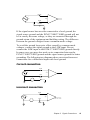
1
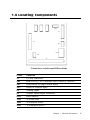
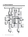
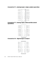
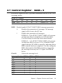
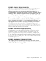
PCM-3718H/3718HG
PC/104 12-bit DAS Module
with Programmable Gain
User's manual
2nd Edition
Printed in Taiwan
May 1999
Contents
CHAPTER 1: General Information ........................ 1
1.1
1.2
1.3
1.4
1.5
1.6
1.7
Introduction .......................................................................... 2
Features ................................................................................. 2
Specifications ......................................................................... 3
Locating Components ............................................................ 5
Daughterboards ..................................................................... 6
Software Support................................................................... 7
Block Diagram ....................................................................... 8
CHAPTER 2: Installation ........................................ 9
2.1
2.2
2.3
2.4
2.5
Initial Inspection ................................................................... 10
Switch and Jumper Settings .................................................. 10
Connector Pin Assignments .................................................. 13
Hardware Installation ........................................................... 15
Software Installation ............................................................. 16
CHAPTER 3: Signal Connections ........................ 17
3.1 Analog Input Signal Connections .......................................... 18
3.2 Expanding Analog Inputs ...................................................... 20
3.3 Digital Signal Connections .................................................... 20
CHAPTER 4: Register Structure and Format .... 23
4.1
4.2
4.3
4.4
4.5
A/D Data Registers - BASE+0/1.......................................... 25
Software A/D Trigger - BASE+0 ......................................... 25
A/D Range Control - BASE+1............................................. 26
MUX Scan Register -BASE+2 ............................................ 27
Digital I/O Registers - BASE+3/11 ....................................... 28
4.6
4.7
4.8
4.9
A/Dstatus Register - BASE+8 .............................................. 29
Control Register - BASE+9 ................................................. 31
Pacer Enable Register - BASE+10 ....................................... 32
Programmable Pacer Registers - BASE+12/13/14/15........... 33
CHAPTER 5: A/D Conversion .............................. 35
5.1
5.2
5.3
5.4
5.5
5.6
A/D Data Format and Status Register ................................... 36
Input Range Selection ........................................................... 37
MUX Setting ....................................................................... 37
Trigger Mode ....................................................................... 38
A/D Data Transfer ................................................................ 39
How to Make an A/D Conversion ........................................ 40
CHAPTER 6: Digital Input/Output....................... 41
CHAPTER 7: Programmable Pacer .................... 43
7.1
7.2
7.3
7.4
7.5
The Intel 8254 ..................................................................... 44
Counter Read/write and Control Register.............................. 45
Counter Operating Modes.................................................... 48
Counter Operations .............................................................. 50
Counter Applications............................................................ 51
CHAPTER 8: Direct Memory Access Operation 53
8.1 Using DMA Transfer with the PCM-3718H/3718HG ........... 54
CHAPTER 9: Calibration ...................................... 57
9.1 VR Assignment .................................................................... 58
9.2 A/D Calibration.................................................................... 58
CHAPTER
1
General Information
1.1 Introduction
The PCM-3718H/3718HG is a high performance multifunction data
acquisition module that attaches to the PC/104 connector on your
CPU card or PC/104 module. It offers 12-bit A/D conversion and
digital input/output.
The automatic channel scanning circuitry and the on-board SRAM let
you perform multiple-channel A/D conversion with DMA and
individual channel gains.
The PCM-3718H/3718HG is an advanced new version of our popular
PCL-818 multifunction data acquisition card series. A custom 160pin ASIC chip integrates the functions of a full-size DAS card. This
chip gives you maximum accuracy and reliability, along with
minimum cost, size and power consumption.
The resulting PC/104 module is fully software compatible with the
PCL-818H/818HG. This puts rich software support and a wide variety
of external signal conditioning boards at your disposal.
The PCM-3718H/3718HG is excellent for data acquisition, process
control, automatic testing and factory automation.
1.2 Features
• 16 single-ended or 8 differential analog inputs, jumper selectable
• 12-bit A/D converter, up to 100 kHz sampling rate with DMA
transfer
• Software programmable gain value for each analog input channel
• Software selectable input range for each analog input channel
• Two 8-bit digital input/output channels, TTL compatible
• Flexible triggering options: software trigger, programmable pacer
trigger and external pulse trigger
• Data transfer by program control, interrupt handler routine or DMA
• New-technology 160-pin 1.0µm CMOS ASIC chip
2
PCM-3718H/3718HG User's Manual
1.3 Specifications
Analog Input:
• Channels: 16 single-ended or 8 differential, jumper selectable
• Resolution: 12 bits
• Input range: (software programmable, VDC)
PCM-3718H
Bipolar: ±10, ±5, ±2.5, ±1.25, ±0.625
Unipolar: 0 ~ 10, 0 ~ 5, 0 ~ 2.5, 0 ~ 1.25
PCM-3718HG
Bipolar: ±10, ±5, ±1, ±0.5, ±0.1, ±0.05, ±0.01, ±0.005
Unipolar: 0 ~ 10, 0 ~ 1, 0 ~ 0.1, 0 ~ 0.01
• Maximum data throughput
PCM-3718H: 100 kHz
PCM-3718HG: (variable, depending on PGIA settling time)
Gain
Speed
0.5, 1
100 kHz
5,10
35 kHz
50,100
7 kHz
500,1000
770 Hz
• Accuracy: (depending on gain values)
PCM-3718H
Gain
Accuracy
0.5,1
0.01% of FSR±1 LSB
2,4
0.02% of FSR±1 LSB
8
0.04% of FSR±1 LSB
PCM-3718HG
Gain
Accuracy
0.5,1
0.01% of FSR±1 LSB
5,10
0.02% of FSR±1 LSB
50,100
0.04% of FSR±1 LSB for differential mode
500,1000
0.08% of FSR±1 LSB for differential mode
Chapter 1 Gerneral Information
3
•
•
•
•
Differential nonlinearity error: ±1 LSB
Input impedance: 1GΩ
Trigger mode: Software, pacer or external trigger
External trigger: TTL compatible
Digital Input/ Output:
• Channels: two 8-bit
• Level: TTL compatible
• Input voltage:
Logic 0: 0.8 V max.
Logic 1: 2.0 V min.
• Output voltage:
Logic 0: 0.33 V max. @ 6 mA (sink)
Logic 1: 3.84 V min. @ 6 mA (source)
Programmable pacer:
• Device: Intel 8254 or equivalent
• Counters: 3 channels, 16-bit.
Counter 1 and Counter 2 are permanently configured as a 32-bit
programmable pacer. Counter 0 is reserved for future development.
• Time base: (for Counter 1’s clock input)
10 MHz or 1 MHz, jumper selectable.
General:
• Power consumption: +5VDC @ 180mA (Typical)
+5VDC @ 400mA (Max.)
• Digital I/O connector: 20-pin post headers for I/O connection.
• Analog input connector: 20-pin post headers for I/O connection.
• Operating temperature: 0 to +60°C (refer to IEC 68-2-1, 2)
• Storage temperature: -20 to +70°C
• Operating humidity: 5 to 95% non-condensing
(refer to IEC 68-2-3)
• MTBF: over 235,346 hrs @ 25°C, ground, fix environment
4
PCM-3718H/3718HG User's Manual
1.4 Locating Components
JP 2
VR1
VR2
VR3
P1
P2
JP 1
SW 1
JP 3
J1
Connectors, switches and VR locations
Label
J1
JP1
JP2
JP3
P1
P2
SW1
VR1
VR2
VR3
Function
PC-bus connector
DMA level (1 or 3) and time base (1MHz or 10MHz)
Differential or single-ended inputs
DIO0 or external input
Analog input
Digital input/output connector
Base address
A/D full scale
A/D bipolar offset
A/D unipolar offset
Chapter 1 Gerneral Information
5
1.5 Daughterboards
We offer a wide variety of optional daughterboards to help you get
the most from your PCM-3718H/3718HG. You will need the PCLD780/880 Screw-terminal Board or the PCLD-8115 Wiring Terminal
Board to make connections.
PCLD-789D Amplifier/Multiplexer Board
This analog input-signal conditioning board multiplexes 16 differential inputs to one A/D input channel. A high-grade instrumentation
amplifier provides switch selectable gains of 1, 2, 10, 50, 100, 200,
1000.
PCLD-788 Relay Multiplexer Board
This board multiplexes up to 16 differential inputs to one analog
output channel. It offers isolated break-before-make high voltage
switching and a CJC circuit for thermocouple measurement.
PCLD-786 SSR I/O Module Carrier Board
This board holds eight opto-isolated solid state relay modules and
provides an additional eight outputs to drive external.
PCLD-785B and PCLD-885 Relay Output Boards
These boards let you control relays through the PCM-3718H/3718HG
16-bit digital output channels. The PCLD-785B provides 24 SPDT
relays, while the PCLD-885 provides 16 SPDT power relays.
PCLD-782B Isolated D/I Board
This board provides 24 opto-isolated digital inputs for connecting to
the PCM-3718H/3718HG digital input channels.
PCLD-779 Relay-isolated Multiplexer and Amplifier
Board
This board lets you easily make multi-channel temperature measurements. We designed it for the cost-sensitive customer who requires
precision, low-level signal measurement and isolation for industrial
applications.
6
PCM-3718H/3718HG User's Manual
1.6 Software Support
The PCM-3718H/3718HG comes with a powerful and easy-to-use
software driver. This driver makes application programming much
easier, especially when you use sophisticated features like interrupt or
DMA data transfer.
For building up a high performance Human Machine Interface (HMI),
you may need other supporting software beside our included driver to
the PCM-3718/3718HG. Please consult your manufacturer representative for appropriate software packages.
GeniDAQ
GeniDAQ is a Windows-based data acquisition, control, analysis and
presentation development software package. In addition to typical
Human Machine Interface (HMI) functions, GeniDAQ features a Visual
Basic programming environment, and it provides numerous graphical
control and display icons to assist you in developing user’s HMI.
ActiveDAQ
ActiveDAQ is a collection of add-on ActiveX Control which provides
an easy-to-use property sheet interface for configuring analog/digital
input/output, counter/frequency, high-speed data acquisition and
controls. You can use ActiveX control in Visual Basic, Delphi, Visual
C++ development environments for Windows 95/98/NT.
LabVIEW Driver
LabVIEW Driver supports National Instruments LabVIEW
4.1/5.0 and runs in Microsoft Windows 95/98 and Windows NT 4.0
environments.
Chapter 1 Gerneral Information
7
1.7 Block Diagram
PC BUS
Addre ss B us
Status
D ata
Buffer
D M A S ignals
IR Q Signals
R egister
Select
ASIC A D1801
Addre ss
D ecoder
Internal D ata B us
DMA
Logic
IR Q
Logic
EO C
C LK 1
C LK 2
D ata M U X
1 MHz
10 M Hz
C ounter #0
C ounter #1
C ounter #2
R AM
12-bit A/D C onverter
w ith
Sam ple and H old
D ivider
O ut 1
O ut 2
C hannel
Scan Logic
Prog. G ain
Am plifie r
10 M H z
O SC
Trigger
Logic
Tw o 8-b it
D igital In/O ut
MUX
16 S/E
or
8 D iff.
D igital
Input / O utput
E xternal
Trigger
A nalog
Input
PCM-3718H/3718HG User's Manual
8
CHAPTER
2
Installation
2.1 Initial Inspection
We carefully inspected the PCM-3718H/3718HG mechanically and
electrically before we shipped it. It should be free of marks and
scratches and in perfect order on receipt.
As you unpack the PCM-3718H/3718HG, check it for signs of
shipping damages (damaged box, scratches, dents, etc.). If it is
damaged or fails to meet specifications, notify our service department
or your local sales representative immediately. We will then make
arrangement to repair or to replace the unit for you.
Discharge any static electricity on your body before touching the
board by touching the back of the system unit (grounded metal).
Also keep from materials of static electricity such as plastic, vinyl and
styrofoam.
Remove the PCM-3718H/3718HG from its protective packaging by
grasping the rear metal panel. Handle the module only by its edges to
avoid static electricity which could damage its integrated circuits.
Keep the anti-static packaging material for storage and protection
when you have to remove the module from its connector.
2.2 Switch and Jumper Settings
Ease-of-use is the primary design goal when we designed the PCM3718H/3718HG. This module has one function switch and seven
jumper settings.
The following sections tell you how to configure the module. You
may want to refer to the figure on page 5 for details of module
components.
Base address selection (SW1)
You control the PCM-3718H/3718HG’s operation by reading or
writing data to the PC’s I/O (input/output) port addresses. The PCM3718H/3718HG requires 16 consecutive address locations. The
switch SW1 sets the module’s base (beginning) address. Valid base
10
PCM-3718H/3718HG User's Manual
addresses range from Hex 000 to Hex 3F0. Other devices in your
system can use some of these addresses.
We set the PCM-3718H/3718HG for a base address of Hex 300 at the
factory. If you need to adjust it to other address ranges, set SW1 by
referring to the following table:
Module I/O addresses (SW1)
Range (hex)
Switch position
1
2
000 - 00F
l
l
010 - 01F
l
l
:
200 - 20F
¡
l
210 - 21F
¡
l
:
*300 - 30F
¡
¡
:
3F0 - 3FF
¡
¡
¡ = Off l = On * = default
3
l
l
4
l
l
5
l
l
6
l
¡
l
l
l
l
l
l
l
¡
l
l
l
l
¡
¡
¡
¡
Note:
Switches 1-6 of the SW1 control the PC bus address
lines as follows:
Switch
Line
1
A9
2
A8
3
A7
4
A6
5
A5
6
A4
Chapter 2 Installation
11
DMA channel and timer clock selection (JP1)
The PCM-3718H/3718HG supports DMA data transfer. The bottom
pins of JP1 provide selection of DMA channel 1 or 3, as shown in the
following figure.
Channel 1
Channel 3 (default)
1M
1 0M
1M
1 0M
DM1
DM3
DM1
DM3
The upper jumper of JP1 controls the input clock frequency for the
8254 programmable clock/timer of the module. You have two
choices: 10MHz and 1MHz. This lets you generate pacer output
frequencies from 2.5 MHz to 0.00023 Hz (71 minutes/pulse).
The following equation gives the pacer rate:
Pacer rate = Fclk / ( Div1 * Div2 )
(Fclk, 1MHz or 10MHz, is set by JP1 as illustrated above. Div1 and
Div2 are dividers set in counter 1 and counter 2 in the Intel 8254
counter. See page 51 for more information on the counter/timer
applications).
10 MHz
1 MHz (default)
1M
10M
1M
10M
DM1
DM3
DM1
DM3
Channel configuration, S. E. or diff. (JP2)
The PCM-3718H/3718HG offers 16 single-ended or eight differential
analog input channels. Jumper JP2 sets the analog input channels as
16 single-ended or 8 differential inputs as below:
16 S.E. inputs
S/E
12
DIFF
Eight differential inputs (default)
S/E
PCM-3718H/3718HG User's Manual
DIFF
External input or DIO selection (JP3)
You can use pin 1 on connector P2 for connection to digital I/O line 0
or to an external A/D trigger source jumper setting. Jumper JP3
provides the selection, as shown below:
External trigger input
DIO0
EXT
Digital I/O line DIO 0 (default)
DIO0
EXT
2.3 Connector Pin Assignments
The PCM-3718H/3718HG has two on-board 20-pin flat-cable
connectors (insulation displacement, mass termination).
The figure on page 5 shows locations of both connectors.
Refer to the table below for abbreviations of the pin assignment.
Abbreviations
A/D S
A/D H
A/D L
A.GND
DIO
D.GND
Description
Analog input (single-ended)
Analog input high (differential)
Analog input low (differential)
Analog ground
Digital input/output
Digital and power supply ground
Chapter 2 Installation
13
Connector P1 - Analog input, single-ended operation
A /D S 0
A /D S 1
A /D S 2
A /D S 3
A /D S 4
A /D S 5
A /D S 6
A /D S 7
A .G N D
A .G N D
1
3
5
7
9
11
13
15
17
19
2
4
6
8
10
12
14
16
18
20
A /D S 8
A /D S 9
A /D S 1 0
A /D S 11
A /D S 1 2
A /D S 1 3
A /D S 1 4
A /D S 1 5
A .G N D
A .G N D
Connector P1 - Analog input, differential-ended
operation
A /D H 0
A /D H 1
A /D H 2
A /D H 3
A /D H 4
A /D H 5
A /D H 6
A /D H 7
A .G N D
A .G N D
1
3
5
7
9
11
13
15
17
19
2
4
6
8
10
12
14
16
18
20
A /D L 0
A /D L 1
A /D L 2
A /D L 3
A /D L 4
A /D L 5
A /D L 6
A /D L 7
A .G N D
A .G N D
Connector P2 - Digital input /output
D IO 0
D IO 2
D IO 4
D IO 6
D IO 8
D IO 1 0
D IO 1 2
D IO 1 4
D .G N D
+5V
14
PCM-3718H/3718HG User's Manual
1
3
5
7
9
11
13
15
17
19
2
4
6
8
10
12
14
16
18
20
D IO 1
D IO 3
D IO 5
D IO 7
D IO 9
D IO 11
D IO 1 3
D IO 1 5
D .G N D
+ 1 2V
2.4 Hardware Installation
Warning! TURN OFF your PC power supply whenever you install
or remove the PCM-3718H/3718HG or connect and
disconnect Cables.
Installing the module
1. Turn off the PC’s power. Turn off the power of any peripheral
devices such as printers and monitors.
2. Disconnect the power cord and any other cables from the back of
the computer.
3. Remove the system unit cover (see the user’s guide of your chassis if
necessary).
4. Remove the CPU card from the chassis (if necessary) to gain access
to the card’s PC/104 connector.
5. Connect the connector J1 of the PCM-3718H/3718HG to the PC/
104 connector. Carefully align the pins to the PC/104 connector.
Slide the module into the connector. The module pins may not slide
all the way into the connector; do not force the pins into place, or
the module may be damaged.
6. Fasten the module to the CPU card by using the included brass
screw. Screw the brass spacer into the threaded hole on the CPU
card. Do not tighten too much, or the threads may be damaged.
7. Attach any accessories to the PCM-3718H/3718HG using 20 pin
cables.
8. Reinstall the CPU card and replace the system unit cover. Reconnect the cables you removed in step 2. Plug in and turn on the
power.
This completes the hardware installation. Install the software driver
as described in the following section.
Chapter 2 Installation
15
2.5 Software Installation
The PCM-3718H/3718HG includes a CD-ROM with utility software.
The CD-ROM contains:
1. A comprehensive I/O driver for A/D and digital I/O applications.
This driver lets you use standard functions, written in common
programming languages, to operate the PCM-3718H/3718HG. You
do not need to perform detailed register programming. The driver
supports the following languages: Microsoft Visual Basic, Visual
C++, Borland C++, C++ Builder and Delphi. Please refer to the
Software Driver User’s Manual for more information.
2. Demonstration programs
3. A calibration program
4. A test program
16
PCM-3718H/3718HG User's Manual
CHAPTER
3
Signal Connections
Correct signal connections ensure that your application sends and
receives data accurately. Good signal connections can also avoid a
lot of unnecessary damage to the PC and other hardware. This chapter
provides information on signal connections for different types of data
acquisition applications.
3.1 Analog Input Signal Connections
The PCM-3718H/3718HG supports either 16 single-ended or eight
differential analog inputs. Jumper JP2 selects the input channel
configuration. The major difference between single-ended and
differential input connections is the number of signal wires per input
channel.
Single-ended channel connections
Single-ended connections use only one signal wire per channel. The
voltage on the line refers to the common ground on the card. A
signal sources without a local ground is called a “floating” source. It
is fairly simple to connect a signal-ended channel to a floating signal
source. A standard wiring diagram looks like this:
Signal Input
+
Vs
-
To A/D
A.GND
A.GND
Differential channel connection
The differential input configuration uses two signal wires per channel. The card measures the voltage difference between these two wires,
the HIGH wire and the LOW wire. If the signal source has no connection to local ground, it is called a “floating’ source. A connection
must exist between LOW and ground to define a common reference
point for floating signal sources. To measure a floating source connect
the input channel as shown below:
18
PCM-3718H/3718HG User's Manual
HIGH
+
+
Vs
-
LOW
+
Vin
-
A.GND
If the signal source has one side connected to a local ground, the
signal source ground and the PCM-3718H/3718HG ground will not
be at exactly the same voltage, as they are connected through the
ground return of the equipment and building wiring. The difference
between the ground voltages forms a common-mode voltage.
To avoid the ground loop noise effect caused by common-mode
voltages, connect the signal ground to the LOW input. Do not
connect the LOW input to the PCM-3718H/3718HG ground directly.
In some cases you may also need a wire connection between the
PCM-3718H/3718HG ground and the signal source ground for better
grounding. The following two diagrams show correct and incorrect
connections for a differential input with local ground:
Correct connection
HIGH
+
+
Vs
-
LOW
_
+
Vin
-
Vin=Vs
-
GND
+
Vcm
Incorrect connection
HIGH
+
+
Vs
_ +
Vcm
LOW
+
Vin
-
Vin=Vs+Vcm
-
GND
Chapter 3 Signal Connections
19
3.2 Expanding Analog Inputs
You can expand any or all of the PCM-3718H/3718HG’s A/D input
channels by using the multiplexing daughterboards. Most daughterboards are connected directly to the module’s 20-pin connectors. You
may require the PCLD-8115 Screw-terminal Board for connections.
The PCLD-789 Amplifier and Multiplexer multiplexes 16 differential
inputs to one A/D input channel. You can cascade up to eight PCLD789s to the PCM-3718H/3718HG for a total of 128 channels.
The PCLD-8115 Screw-terminal Board makes wiring connections
easy. It provides 20-pin flat cable connectors and a CJC (Cold
Junction Compensation) circuit which lets you directly measure
thermocouples. You can handle all types of thermocouples with
software compensation and linearization.
Special circuit pads on the PCLD-8115 accommodate passive signal
contioning components. You can easily implement a low-pass filter,
attenuator or current shunt by adding resisters and capacitors.
3.3 Digital Signal Connections
The PCM-3718H/3718HG has two 8-bit digital input/output channels. The digital I/O levels are TTL compatible. The following figure
shows connections of digital signals with other TTL devices:
TTL D evices
D IO
or
D .G N D
20
PCM-3718H/3718HG User's Manual
D .G N D
To receive an OPEN/SHORT signal from a switch or relay, add a pullup resistor to ensure that the input is held at a high level when the
contacts are open. See the figure below:
+5V
4.7K
D.GND
Chapter 3 Signal Connections
21
22
PCM-3718H/3718HG User's Manual
CHAPTER
4
Register Structure and
Format
The key to programming the PCM-3718H/3718HG is to understand
the function of the card’s 16 registers. The PCM-3718H/3718HG
requires 16 consecutive addresses in the PC’s I/O space. Each address
corresponds to a card register. The address of each register is specified
as an offset from the card’s base address. For example, BASE+0 is the
card’s base address and BASE+7 is the base address plus seven bytes.
If the card’s base address is 300h, the register’s address is 307h. The
following sections give detailed information on the layout and
function of each of the card’s registers.
I/O port address map
The following table shows the function of each register or driver and
its address relative to the base address of the module.
I/O port address assignments
Address Read
BASE+0 A/D low byte & channel
BASE+1 A/D high byte
BASE+2 MUX scan
BASE+3
BASE+4
BASE+5
BASE+6
BASE+7
BASE+8
BASE+9
BASE+10
BASE+11
BASE+12
BASE+13
BASE+14
BASE+15
24
Write
Software A/D trigger
A/D range control
MUX scan channel & range
control pointer
DIO low byte (DIO 0-7) DIO low byte (DIO 0-7)
N/A
N/A
N/A
N/A
N/A
N/A
N/A
N/A
Status
Clear interrupt request
Control
Control
N/A
Counter enable
DIO high byte (DIO 8-15) DIO high byte (DIO 8-15)
Counter 0
Counter 0
Counter 1
Counter 1
Counter 2
Counter 2
N/A
Counter control
PCM-3718H/3718HG User's Manual
4.1 A/D Data Registers - BASE+0/1
Two read-only registers at BASE+0 and BASE+1 hold A/D conversion
data. The 12 bits of data from the A/D conversion are stored in
BASE+1 bit 7 to bit 0 and BASE+0 bit 7 to bit 4. BASE+0 bits 3 to 0
store the source A/D channel number.
BASE+0 (read only) - A/D low byte & channel number
Bit
D7
D6
D5
D4
D3
D2
D1
Value AD3 AD2 AD1 AD0 C3
C2
C1
D0
C0
BASE+1 (read only) - A/D high byte
Bit
D7
D6
D5
D4
D3
Value AD11 AD10 AD9 AD8 AD7
D0
AD4
D2
AD6
D1
AD5
AD11 to AD0 Analog to digital data. AD0 is the least significant bit
(LSB) of the A/D data, and AD11 is the most significant bit (MSB)
C3 to C0
A/D channel number from which the data is derived.
C3 is the MSB and C0 is the LSB
4.2 Software A/D Trigger - BASE+0
You can trigger an A/D conversion from software, the module’s onboard pacer or from an external pulse. Bits 1 and 0 of register
BASE+9 (shown on pages 31~32) select the trigger source. If you
select software triggering, a write to the register BASE+0 with any
value will trigger an A/D conversion.
Chapter 4 Register Structure and Format
25
4.3 A/D Range Control - BASE+1
Each A/D channel has its own individual input range, controlled by a
range code stored in the on-board RAM. If you want to change the
range code for a given channel, select the channel as the start channel
in register BASE+2, MUX scan (described in the next section), then
write the range code to bits 0 to 3 of BASE+1.
BASE+1 (write only) - A/D range control code
Bit
D7
D6
D5
D4
D3
D2
Value N/A N/A N/A N/A G3
G2
D1
G1
D0
G0
PCM-3718H range code:
Input Range(V) Unipolar/Bipolar
±5
±2.5
±1.25
±0.625
0 to 10
0 to 5
0 to 2.5
0 to 1.25
±10
N/A
N/A
N/A
N/A
N/A
N/A
N/A
26
B
B
B
B
U
U
U
U
B
PCM-3718H/3718HG User's Manual
G3
0
0
0
0
0
0
0
0
1
1
1
1
1
1
1
1
Range Code
G2
G1
0
0
0
0
0
1
0
1
1
0
1
0
1
1
1
1
0
0
0
0
0
1
0
1
1
0
1
0
1
1
1
1
G0
0
1
0
1
0
1
0
1
0
1
0
1
0
1
0
1
PCM-3718HG range code:
Input Range(V) Unipolar/Bipolar
±5
±0.5
±0.05
±0.005
0 to 10
0 to 1
0 to 0.1
0 to 0.01
±10
±1
±0.1
±0.01
N/A
N/A
N/A
N/A
B
B
B
B
U
U
U
U
B
B
B
B
G3
0
0
0
0
0
0
0
0
1
1
1
1
1
1
1
1
Range Code
G2
G1
0
0
0
0
0
1
0
1
1
0
1
0
1
1
1
1
0
0
0
0
0
1
0
1
1
0
1
0
1
1
1
1
G0
0
1
0
1
0
1
0
1
0
1
0
1
0
1
0
1
4.4 MUX Scan Register -BASE+2
Read/write register BASE+2 controls multiplexer (MUX) scanning.
The high nibble provides the stop scan channel number, and the low
nibble provides the start scan channel number. The MUX initializes
automatically to the start channel when you write to this register.
Each A/D trigger sets the MUX to the next channel.
With continuous triggering, the MUX will scan from the start channel
to the end channel, and then repeat the process. For example, if the
start channel is 3 and the stop channel is 7, then the scan sequence is
3, 4, 5, 6, 7, 3, 4, 5, 6, 7, 3, 4 ...
Chapter 4 Register Structure and Format
27
BASE+2 (write) - start and stop scan channels
Bit
D7
D6
D5
D4
D3
D2
Value CH3 CH2 CH1 CH0 CL3 CL2
CH3 to CH0
Stop scan channel number
CL3 to CL0
Start scan channel number
D1
CL1
D0
CL0
The MUX scan register low nibble, CL3 to CL0, also acts as a pointer
when you program the A/D input range (see previous section). When
you set the MUX start channel to N, the range code written to the
register BASE+1 is for channel N.
Programming example
This C code sets the range for channel 5 to ±0.625 V:
OUTPORTB (BASE+2, 5); /* SET POINTER TO CHANNEL 5*/
OUTPORTB (BASE+1, 3); /* RANGE CODE FOR ±0.625V*/
Note:
The MUX start/stop channel changes each time when
you change the input range. Do not forget to reset the
MUX start and stop channels to the correct values
after your range setting.
4.5 Digital I/O Registers - BASE+3/11
The PCM-3718H/3718HG offers two 8-bit digital input/output
channels. These I/O channels use the input or output ports at addresses Base+3 and BASE+11.
28
PCM-3718H/3718HG User's Manual
BASE+3 (read port) -DIO low byte
Bit
D7
D6
D5
D4
D3
D2
D1
D0
Value DIO7 DIO6 DIO5 DIO4 DIO3 DIO2 DIO1 DIO0
BASE+3 (write port) DIO low byte
Bit
D7
D6
D5
D4
D3
D2
D1
D0
Value DIO7 DIO6 DIO5 DIO4 DIO3 DIO2 DIO1 DIO0
BASE+11 (read port) - DIO high byte
Bit
D7
D6
D5
D4
D3
D2
D1
D0
Value DIO15 DIO14 DIO13 DIO12 DIO11 DIO10 DIO9 DIO8
BASE+11 (write port) - DIO high byte
Bit
D7
D6
D5
D4
D3
D2
D1
D0
Value DIO15 DIO14 DIO13 DIO12 DIO11 DIO10 DIO9 DIO8
4.6 A/D Status Register - BASE+8
Read-only register BASE+8 provides information on the A/D configuration and operation. Writing to this I/O port with any data value
clears its INT bit. The other data bits do not change.
BASE+8 - A/D status
Bit
D7
D6
D5
D4
Value EOC N/A MUX INT
D3
CN3
D2
CN2
D1
CN1
D0
CN0
Chapter 4 Register Structure and Format
29
EOC
MUX
INT
End of Conversion.
0
The A/D converter is idle, ready for the next conversion. Data from the previous conversion is available
in the A/D data registers.
1
The A/D converter is busy, implying that the A/D
conversion is in progress.
Single-ended/differential channel indicator.
0
8 differential channels
1
16 single-ended channels
Data valid.
0
No A/D conversion has been completed since the last
time the INT bit was cleared. Values in the A/D data
registers are not valid data.
1
The A/D conversion is completed, and converted data
is ready. If the INTE bit of the control register
(BASE+9) is set, an interrupt signal will be sent to the
PC bus through interrupt level IRQn, where n is
specified by bits I2, I1 and I0 of the control register.
Though the A/D status register is read-only, writing to
it with any value clears the INT bit.
CN3 to CN0
When EOC = 0, these status bits contain the channel
number of the next channel to be converted.
Remarks
If you trigger the A/D conversion by the on-board pacer, your software
should check the INT bit, not the EOC bit, before it reads the conversion data.
EOC can equal 0 in two different situations: the conversion is
completed or no conversion has been started. Your software should
therefore wait for the signal INT = 1 before it reads the conversion
data. It should then clear the INT bit by writing any value to the A/D
status register BASE+8.
30
PCM-3718H/3718HG User's Manual
4.7 Control Register - BASE+9
Read/write register BASE+9 provides information on the PCM-3718’s
operating modes.
BASE+9 - Control
Bit
D7
D6
Value INTE I2
D5
I1
D4
I0
D3
X
D2
D1
DMAE ST1
D0
ST0
INTE Disable/enable PCM-3718H/3718HG interrupt generation
0
Disables the generation of interrupts. No interrupt
signal will be sent to the PC bus.
1
Enables the generation of interrupts.
If DMAE = 0, the PCM-3718H/3718HG will generate
an interrupt when it completes an A/D conversion.
Use this setting for interrupt driven data transfer.
If DMAE = 1, the PCM-3718H/3718HG will generate
an interrupt when it receives a T/C (terminal count)
signal from the PC’s DMA controller, indicating that a
DMA transfer has been completed. Use this setting for
DMA data transfer. The DMA transfer is stopped by
the interrupt caused by the T/C signal. See DMAE
below.
I2 to I0
Interrupt level
N/A
N/A
IRQ2
IRQ3
IRQ4
IRQ5
IRQ6
IRQ7
Selects the interrupt level.
INL2
0
0
0
0
1
1
1
1
INL1
0
0
1
1
0
0
1
1
INL0
0
1
0
1
0
1
0
1
Chapter 4 Register Structure and Format
31
Note:
Make sure that the IRQ level you choose is not being
used by another I/O device.
DMAE Disable/Enable PCM-3718H/3718HG DMA transfers.
0
Disables DMA transfer.
1
Enables DMA transfer. Each A/D conversion initiates
two successive DMA request signals. These signals
cause the 8237 DMA controller to transfer two bytes
of conversion data from the PCM-3718H/3718HG to
memory.
Note:
You must program the PC’s 8237 DMA controller as
the DMA page register before you set DMAE to1.
ST1 to ST0
Trigger source
Software trigger
External trigger
Pacer trigger
Trigger source
ST1
0
1
1
ST0
X
0
1
4.8 Pacer Enable Register - BASE+10
Register BASE+10 enables or disables the PCM-3718H/3718HG
pacer.
TC0
32
Disalbe/enable pacer
0
Pacer enabled
1
Pacer disabled
PCM-3718H/3718HG User's Manual
4.9 Programmable Pacer Registers BASE+12/13/14/15
These four registers located at addresses BASE+12, BASE+13,
BASE+14 and BASE+15 are used for the Intel 8254 programmable
pacer. Please refer to Chapter 7 Programmable Pacer or 8254 product
literature for detailed application information.
Chapter 4 Register Structure and Format
33
34
PCM-3718H/3718HG User's Manual
CHAPTER
5
A/D Conversion
This chapter explains how to use the PCM-3718H/3718HG’s A/D
conversion functions. The first five sections describe A/D data
format, input range selection, status register settings, MUX scan
setting, trigger modes and data transfer. The last section gives step by
step implementation guidelines for A/D operations.
5.1 A/D Data Format and Status Register
Since the PCM-3718H/3718HG uses 12-bit A/D conversions, a single
8-bit register will not accommodate all the data. The PCM-3718H/
3718HG therefore stores A/D data in two registers located at addresses
BASE+0 and BASE+1.
It stores the A/D low byte data in bits D4 to D7 (AD0 to AD3) of
BASE+0 and high byte data in bits D0 to D7 (AD4 to AD11) of
BASE+1. The least significant bit is AD0 and the most significant bit
is AD11. You can read the source channel number corresponding to
the A/D data from bits D0 to D3 (C0 to C3) of BASE+0.
A/D data register format is:
BASE+0 (read only) - A/D low byte & channel number
Bit
D7
D6
D5
D4
D3
D2
D1
Value AD3 AD2 AD1 AD0 C3
C2
C1
D0
C0
BASE+1 (read only) - A/D high byte
Bit
D7
D6
D5
D4
D3
Value AD11 AD10 AD9 AD8 AD7
D0
AD4
D2
AD6
D1
AD5
The A/D status register at BASE+8 (read only) gives information on
A/D configuration and operation.
36
PCM-3718H/3718HG User's Manual
A/D status register format is:
BASE+8 - A/D status
Bit
D7
D6
D5
D4
Value EOC N/A MUX INT
D3
CN3
D2
CN2
D1
CN1
D0
CN0
Bits in this register indicate the end of conversion status, singleended/differential input, interrupt status and the number of the
channel to be converted next. Refer to page 29, A/D Status Register,
for more information.
5.2 Input Range Selection
Each A/D channel has its own individual input range, controlled by a
range code stored in the on-board RAM. Please refer to pages 26~27,
A/D Range Control, for more information.
5.3 MUX Setting
The PCM-3718H/3718HG offers 16 single-ended or eight differential
analog input channels. Set jumper JP2 for the channel configuration
before you set the multiplexer scan range. The MUX scan register
specifies the high and low limits of the scan range. The MUX scan
register is a read/write register at address BASE+2. Bits D0 to D3
hold the starting channel number, and positions D4 to D7 hold the
stop scan channel number. When you set the PCM-3718H/3718HG
for eight differential input channels, set bits CH3 and CL3 to zero.
Chapter 5 A/D Conversion
37
The MUX scan register data format is as below:
BASE+2 (write) - start and stop scan channels
Bit
D7
D6
D5
D4
D3
D2
Value CH3 CH2 CH1 CH0 CL3 CL2
D1
CL1
D0
CL0
If you require only one A/D input channel, you should set the high
and low scan limits to the same value. If you specify a range of input
channels, the PCM-3718H/3718HG automatically performs an A/D
conversion on each channel in the range, beginning with the start
channel. When it reaches the stop channel, it loops back to the start
channel and continues. This looping continues until the specified
number of conversions is completed. Note that writing to the MUX
automatically resets to the start channel.
You can specify channel settings by writing directly to the MUX scan
register. Use the MUX scan register to assign to a specified channel
when you set channel input ranges (with BASE+1). After you set the
input range, you will need to reset the MUX register for the proper
start and stop channels.
5.4 Trigger Mode
You can trigger an A/D conversion from software, from the module’s
on-board pacer or from an external signal. Bits 1 and 0 of register
BASE+9 select the trigger source.
1. If you select software triggering, write to register BASE+0 with any
value to trigger an A/D conversion. High-speed A/D applications
do not normally use software triggering because the triggering rate
is too slow.
2. The PCM-3718H/3718HG’s on-board Intel 8254 programmable
interval timer/counter can generate periodic timing signals.
Counters 1 and 2 of the Intel 8254 provide A/D converter trigger
pulses with precise periods. You can select pacer output between
38
PCM-3718H/3718HG User's Manual
2.5 MHz and 71 minutes per pulse. Chapter 7 cover the details of
the Intel 8254 timer/counter.
Pacer triggering is ideal for interrupt and DMA data transfer,
normally used in A/D applications which require higher conversion
speeds.
3. You can also trigger the A/D conversion from an external signal.
Wire the external signal to pin 1 on connector P2 and switch jumper
JP3 to EXT. You would normally use external triggering if your
application requires A/D conversions not periodically, but conditionally, e. g., to measure a voltage when a limit switch closes. The
A/D conversion starts at the rising edge of the external trigger pulse.
5.5 A/D Data Transfer
You can perform A/D data transfer by Program Control, Interrupt
Routine or DMA.
1. Program controlled data transfer operates by polling the A/D status
register. After the A/D conversion has been triggered, your application program checks the INT bit (data valid) of the A/D status
register. When it detects that the INT bit is on (1), it sends the A/D
data to the PC’s memory using DMA. Reset the INT bit (by writing
to register BASE+8 with any value) after you transfer the A/D data.
When you use software triggering, you can check either the INT or
EOC bits for data validity. Since you use the program to trigger the
A/D conversion, you do not need to poll the INT bit to see if the
conversion has occurred. It is easier to use the EOC bit, because
you do not need to clear it after you transfer the data.
2. With interrupt data transfer, you write an interrupt routine handler
program, which transfers data from the module’s A/D data registers
to a previously defined memory segment in the PC. At the end of
each conversion, the EOC signal generates an interrupt, and the
interrupt handler routine performs the transfer. You must specify the
interrupt control bit and the interrupt level selection bits in the
PCM-3718H/3718HG control register (BASE+9) before using the
Chapter 5 A/D Conversion
39
interrupt routine. Writing to the A/D status register address
(BASE+8) resets the PCM-3718H/3718HG interrupt request and reenables the PCM-3718H/3718HG interrupt.
3. Direct Memory Access (DMA) Transfer moves the A/D data from the
PCM-3718H/3718HG hardware device to the PC system memory
without the system CPU. DMA is very useful in high-speed data
transfer, but it is complicated to operate. Before the DMA operation
you must set the DMA level (JP1), the DMA enable bit control
register (BASE+9) and the registers in the 8237 DMA controller.
We recommend that you use the PCM-3718H/3718HG driver to
perform DMA operations. See Chapter 8 for more Information on
the 8237 DMA controller and PCM-3718H/3718HG DMA operations.
5.6 How to Make an A/D Conversion
To perform A/D conversion, you can write all I/O port instructions
directly in your program, or you can take advantage of the PCM3718H/3718HG driver. We suggest that you apply the driver functions in your program. This will make your programming job easier
and improve the program performance. See the User’s Manual of the
software driver for more information.
Do the following to perform software trigger and program controlled
data transfer without the PCM-3718H/3718HG driver:
1. Set the input range for each A/D channel.
2. Set the input channel by specifying the MUX scan range.
3. Trigger the A/D conversion by writing to the A/D low byte register
(BASE+0) with any value.
4. Check for the end of the conversion by reading the A/D status
register (BASE+8) INT bit.
5. Read data from the A/D converter by reading the A/D data registers
(BASE+0 and BASE+1).
6. Convert the binary A/D data to an integer.
40
PCM-3718H/3718HG User's Manual
CHAPTER
6
Digital Input/Output
The PCM-3718H/3718HG provides two 8-bit digital input/output
channels. The registers at addresses BASE+3 and BASE+11 can input
or latch output data. Data format for each register appears as below:
BASE+3 (read port) -DIO low byte
Bit
D7
D6
D5
D4
D3
D2
D1
D0
Value DIO7 DIO6 DIO5 DIO4 DIO3 DIO2 DIO1 DIO0
BASE+3 (write port) DIO low byte
Bit
D7
D6
D5
D4
D3
D2
D1
D0
Value DIO7 DIO6 DIO5 DIO4 DIO3 DIO2 DIO1 DIO0
BASE+11 (read port) - DIO high byte
Bit
D7
D6
D5
D4
D3
D2
D1
D0
Value DIO15 DIO14 DIO13 DIO12 DIO11 DIO10 DIO9 DIO8
BASE+11 (wirte port) - DIO high byte
Bit
D7
D6
D5
D4
D3
D2
D1
D0
Value DIO15 DIO14 DIO13 DIO12 DIO11 DIO10 DIO9 DIO8
Using the PCM-3718H/3718HG’s input and output functions is fairly
straightforward. Page 20 shows some ideas for digital signal connections.
42
PCM-3718H/3718HG User's Manual
CHAPTER
7
Programmable Pacer
7.1 The Intel 8254
The PCM-3718H/3718HG uses the Intel 8254 programmable interval
timer/counter version 2. The popular 8254 offers three independent
16-bit down counters. Each counter has a clock input, control gate
and an output. You can program each counter for maximum count
values from 2 to 65535.
Version 2 of the 8254 has a maximum input clock frequency of 10
MHz. The PCM-3718H/3718HG provides 1 MHz and 10 MHz input
frequencies to the 8254 from an on-board crystal oscillator. Jumper
JP1 controls the input frequency. See page 12 for more information.
Counters 1 and 2 on the 8254 are cascaded and operated in a fixed
divider configuration. Counter 1 input is connected to the 1 MHz or
10 MHz clock frequency, and the output of Counter 1 is connected to
the input of Counter 2. The output of Counter 2 is internally configured to provide trigger pulses to the A/D converter, as shown below:
COUNTER 1
1MHZ
OR
10MHZ
OSC.
CLK IN
OUT
COUNTER 2
CLK IN
OUT
PACER
The Intel 8254 has six operational modes, from Mode 0 through
Mode 5. To generate a pacer clock, program both Counter 1 and
Counter 2 for Mode 3 (square wave generation).
Note!: Counter 0 is reserved for future development.
44
PCM-3718H/3718HG User's Manual
7.2 Counter Read/write and Control
Register
The 8254 programmable interval timer uses four registers at addresses
BASE+12, BASE+13, BASE+14 and BASE+15. Register functions
are listed below:
Register
BASE+12
BASE+13
BASE+14
BASE+15
Function
Counter 0 read/write
Counter 1 read/write
Counter 2 read/write
Counter control word
Since the 8254 counter uses a 16-bit structure, each section of read/
write data is split into a least significant byte (LSB) and most
significant byte (MSB). To avoid errors it is important that you make
read/write operations in pairs and keep track of the byte order.
The data format for the control register appears below:
BASE+15 - 8254 control, standard mode
Bit
D7
D6
D5
D4
D3
Value SC1 SC0 RW1 RW0 M2
SC1 & SC0
D2
M1
D1
M0
D0
BCD
Select counter
Counter
0
1
2
Read-back command
SC1
0
0
1
1
SC0
0
1
0
1
Chapter 7 Programmable Pacer
45
RW1 & RW0
Select read/write operation
Operation
Counter latch
Read/write LSB
Read/write MSB
Read/write LSB first, then MSB
RW1
0
0
1
1
RW0
0
1
0
1
M2, M1 & M0 Select operating mode
M2
0
0
X
X
1
1
BCD
BCD
0
1
M1
0
0
1
1
0
0
M0
0
1
0
1
0
1
Mode
0
1
2
3
4
5
Description
programmable one shot
programmable one shot
Rate generator
Square wave rate generator
Software triggered strobe
Hardware triggered strobe
Select binary or BCD counting
Type
Binary counting 16-bits
Binary coded decimal (BCD) counting
If you set the module for binary counting, the count can be any
number from 0 up to 65535. If you set it for BCD (Binary Coded
Decimal) counting, the count can be any number from 0 to 9999.
If you set both SC1 and SC0 bits to 1, the counter control register is
in read-back command mode. The control register data format
becomes:
BASE+15 - 8254 control, read-back mode
Bit
D7
D6
D5
D4
D3
Value 1
1
CNT STA C2
46
PCM-3718H/3718HG User's Manual
D2
C1
D1
C0
D0
X
CNT = 0
Latch count of selected counter(s).
STA = 0
Latch status of selected counter(s).
C2, C1 & C0
Select counter for a read-back operation.
C2 = 1 select Counter 2
C1 = 1 select Counter 1
C0 = 1 select Counter 0
If you set both SC1 and SC0 to 1 and STA to 0, the register selected
by C2 to C0 contains a byte which shows the status of the counter.
The data format of the counter read/write register then becomes:
BASE+12/13/14 - status read-back mode
Bit
D7
D6
D5
D4
D3
Value OUT NC
RW1 RW0 M2
D2
M1
D1
M0
D0
BCD
OUT
Current status of counter output
NC
Null count is 1 when the last count written to the
counter register has been loaded into the counting
element
The pacer enable register, located at address BASE+10, has a close
relationship with the counter operation. Refer to pages 32~33, Pacer
Enable Register, for the register data format. The TC0 bit enables and
disables the pacer. If TC0 is 0, the pacer is enabled. If TC0 is 1, the
pacer is disabled.
Chapter 7 Programmable Pacer
47
7.3 Counter Operating Modes
MODE 0 - Stop on Terminal Count
The output will be initially low when you set mode 0. After you load
the count into the selected count register, the output will remain low
and the counter will count. When the counter reaches the terminal
count, its output will go high and remain high until you reload it with
the mode or a new count value. The counter continues to decrement
after it reaches the terminal count. Rewriting a counter register during
counting has the following results:
1. Writing to the first byte stops the current counting.
2. Writing to the second byte starts the new count.
MODE 1 - Programmable One-shot
The output is initially high. The output will go low on the count
following the rising edge of the gate input. It will then go high on the
terminal count. If you load a new count value while the output is low,
the new value will not affect the duration of the one-shot pulse until
the succeeding trigger. You can read the current count at any time
without affecting the one-shot pulse. The one-shot is retriggerable,
thus the output will remain low for the full count after any rising edge
at the gate input.
MODE 2 - Rate Generator
The output will be low for one period of the input clock. The period
from one output pulse to the next equals the number of input counts
in the counter register. If you reload the counter register between
output pulses, the present period will not be affected, but the subsequent period will reflect the value.
The gate input, when low, will force the output high. When the gate
input goes to high, the counter will start from the initial count. You
can thus use the gate input to synchronize the counter.
With this mode the output will remain high until you load the count
register. You can also synchronize the output by software.
48
PCM-3718H/3718HG User's Manual
MODE 3 - Square Wave Generator
This mode is similar to Mode 2, except that the output will remain
high until one half of the count has been completed (for even
numbers), and will go low for the other half of the count. This is
accomplished by decreasing the counter by two on the falling edge of
each clock pulse. When the counter reaches the terminal count, the
state of the output is changed, the counter is reloaded with the full
count and the whole process is repeated.
If the count is odd and the output is high, the first clock pulse (after
the count is loaded) decrements the count by 1. Subsequent clock
pulses decrement the count by 2. After timeout, the output goes low
and the full count is reloaded. The first clock pulse (following the
reload) decrements the counter by 3. Subsequent clock pulses
decrement the count by two until timeout, then the whole process is
repeated. In this way, if the count is odd, the output will be high for
(N+1)/2 counts and low for (N-1)/2 counts.
MODE 4 - Software triggered strobe
After the mode is set, the output will be high. When the count is
loaded, the counter will begin counting. On terminal count, the
output will go low for one input clock period, then go high again.
If you reload the count register during counting, the new count will
be loaded on the next CLK pulse. The count will be inhibited while
the GATE input is low.
MODE 5 - Hardware Triggered Strobe
The counter will start counting after the rising edge of the trigger
input and will go low for one clock period when the terminal count is
reached. The counter is retriggerable.
Chapter 7 Programmable Pacer
49
7.4 Counter Operations
Read/Write Operation
Before you write the initial count to each counter, you must first
specify the read/write operation type, operating mode and counter
type in the control byte and write the control byte to the control
register (BASE+15).
Since the control byte register and all three counter read/write
registers have separate addresses, and each control byte specifies the
counter it applies to (set by SC1 and SC0), no instructions on the
operating sequence are required. Any programming sequence
following the 8254 convention is acceptable.
There are three types of counter operation: read/load LSB, read/load
MSB and read/load LSB followed by MSB. It is important that you
make your read/write operations in pairs and keep track of the byte
order.
Counter Read-back Command
The 8254 counter read-back command lets you check the count
value, programmed mode and current states of the OUT pin and Null
Count flag of the selected counter(s). You write this command to the
control word register. Format is as shown at the beginning of the
chapter.
The read-back command can latch multiple counter output latches.
Simply set the CNT bit to 0 and select the desired counter(s). This
single command is functionally equivalent to multiple counter latch
commands, one for each counter latched.
The read-back command can also latch status information for selected
counter(s) by setting the STA bit to 0. The status must be latched to
be read; the status of a counter is accessed by a read from that counter.
For the counter status format please see the beginning of the chapter.
Counter Latch Operation
Users often want to read the value of a counter without disturbing the
count in progress. You can enable this function by latching the count
value for the specific counter and then reading the value.
50
PCM-3718H/3718HG User's Manual
The 8254 supports the counter latch operation in two ways. The first
way is to set bits RW1 and RW0 to 0. This setting latches the count of
the selected counter in a 16-bit hold register. The second way is to
perform a latch operation under the read-back command. Set bits SC1
and SC0 to 1 and CNT to 0. The latter method has the advantage of
operating several counters at the same time. A subsequent read
operation on the selected counter will retrieve the latched value.
7.5 Counter Applications
The 8254 programmable Interval timer/counter on your PCM-3718H/
3718HG interface module is a very useful device. You can program
counters 1 and 2 as pacers to generate A/D conversion trigger pulses.
Counter 0 is reserved for later module development.
Setting the Pacer Rate
The following equation gives the pacer rate:
Pacer rate = FCLK / (C1 *C2)
FCLK is either 1 MHz or 10 MHz, as set by jumper JP1. The following steps tell you how to set the counter modes and constants:
1. Set Counter 1 to Mode 3 by writing ’76h’ to address BASE+15.
2. Set Counter 2’s divisor constant C1 by writing to BASE+13.
Constant C1 can be any 16-bit value from 2 to 65535. Because the
8254 has 8-bit registers, you should first write the low byte of C1 to
BASE+13, then write the high byte of C1 to BASE+13.
3. Set Counter 2 to Mode 3 by writing ‘B6h’ to address BASE+15.
4. Set Counter 2’s divisor constant C2 by writing to BASE+14.
Constant C2 can be any 16-bit value from 2 to 65535. Because the
8254 has 8-bit registers, you should first write the low byte of C2 to
BASE+14, then write the high byte of C2 to BASE+14.
Chapter 7 Programmable Pacer
51
Programming example
The following program (written in C) sets the pacer rate to 25 KHz. It
uses FCLK of 10 MHz, C1 of 40 and C2 of 10.25KHz = 19 MHz/
(40*10).
OUTPORTB (BASE+3, 0x76); /* SET COUNTER 1 TO MODE 3*/
OUTPORTB (BASE+1, 40); /* WRITE LOW BYTE OF C1*/
OUTPORTB (BASE+1, 0); /* WRITE HIGH BYTE OF C1*/
OUTPORTB (BASE+3, 0xB6); /* SET COUNTER 2 TO MODE 3*/
OUTPORTB (BASE+2, 10); /*WRITE LOW BYTE OF C2*/
OUTPORTB (BASE+2, 0); /*WRITE HIGH BYTE OF C2*/
52
PCM-3718H/3718HG User's Manual
CHAPTER
8
Direct Memory Access
Operation
Direct Memory Access (DMA) improves system performance by
allowing external devices to transfer information directly to or from
the PC’s memory without using the CPU. The PCM-3718H/3718HG’s
DMA capability significantly improves the system performance in
high-speed A/D applications.
Introduction to the 8237 DMA Controller
The 8237 DMA controller chip on the PC system board handles the
DMA operation. This chip has four prioritized direct memory access
channels. Channel 0 is reserved by the PC system to refresh its
dynamic RAM. Channel 2 supports floppy disk operations. Channel
3 is generally used for hard disk operations. Channel 1 is not for any
internal operations and is reserved for your applications.
Each channel has two associated control signals. The DMA Request
Signal (DRQ) triggers a DMA operation, and the DMA Acknowledge
Signal (DACK) authorizes the 8237 to start the data transfer.
The 8237 DMA chip has four operating modes (single, demand, block
and cascade) and four control registers. These registers are:
1. Operation mode register (set mode of operation)
2. Address register (specify memory segment starting address)
3. Word count register (specify the number of transfers)
4. Initialization register (enable and disable DMA channels)
You must properly set all four registers before requesting the DMA
operation.
8.1 Using DMA Transfer with the PCM3718H/3718HG
DMA transfer is a powerful but complicated operation. Related
descriptions of the DMA transfer have been covered in other paragraphs of this manual ( for details please see pages 38~40). The
following steps summarize how to use DMA transfer with the PCM3718H/3718HG:
54
PCM-3718H/3718HG User's Manual
1. When you configure your hardware, check if any PC DMA channel
is available (level 1 or level 3) and set PCM-3718H/3718HG
jumper JP1 accordingly.
2. If you will be using the PCM-3718H/3718HG driver for your DMA
transfer programming, see the Software Drivers User’s Manual for
more information.
3. If you choose to conduct your own DMA operation, you will need
to have a solid understanding of the PC, 8237 DMA controller and
the PCM-3718H/3718HG. Make sure you perform the following
steps in your DMA transfer:
a. Initialize the 8237 DMA controller register and page register.
b. Send DMA enable and trigger source data to the PCM-3718H/
3718HG control register (located at address BASE+9).
c. Set an external trigger pulse or pacer trigger rate.
d. Enable the trigger source to start the A/D conversion.
Chapter 8 Direct Memory Access Operation
55
56
PCM-3718H/3718HG User's Manual
CHAPTER
9
Calibration
Regular calibration checks are key factors for accuracy maintenance.
We provide a calibration program, CALB.EXE, in the PCM-3718H/
3718HG’s CD-ROM to assist you in this task.
The CALB.EXE makes calibration easy. It leads you through the
calibration and setup procedures with a variety of prompts and
graphic displays, showing you all of the correct settings and adjustments. The explanatory material in this section is brief, intended for
use in conjunction with the calibration program.
To perform a satisfactory calibration, you need a 4½-digit digital
multimeter and a voltage calibrator or a stable, noise-free D. C.
voltage source.
9.1 VR Assignment
The five variable resistors (VRs) on the PCM-3718H/3718HG board
help you make accurate adjustments on all A/D. See the figure on
page 5 for the VR locations on the board. The following list shows the
function of each VR:
VR
VR1
VR2
VR3
Function
A/D full scale adjustment
A/D bipolar offset
A/D unipolar offset
9.2 A/D Calibration
Regular and accurate calibration procedures ensure the maximal
accuracy. The CALB.EXE calibration program leads you through the
whole A/D offset and gain adjustment procedure. The basic steps are
outlined below:
1. Connect an external DC voltage source with value of 0.5 LSB to A/
D Channel 0 (pin 1 on connector P1).
58
PCM-3718H/3718HG User's Manual
2. Adjust VR2 until the output from the card’s A/D converter flickers
between 0 and 1.
3. Connect an external DC voltage source with a value of 4094.5 LSB
to A/D channel 0.
4. Adjust VR1 until the A/D reading flickers between 4094 and 4095.
5. Repeat steps 2 to step 4, adjusting VR1 and VR2.
6. Select unipolar input configuration. Connect an external DC
voltage source with a value of 0.5 LSB to A/D channel 0. Adjust
VR3 until the reading of the A/D flickers between 0 and 1.
Chapter 9 Calibration
59
60
PCM-3718H/3718HG User's Manual
62
PCM-3718H/3718HG User's Manual
Appendix A
Software Driver User Note
63
64
PCM-3718H/3718HG User's Manual