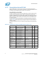
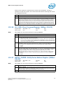
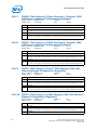
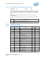
1
Intel® Xeon® Processor D-1500 Product Family Datasheet- Volume 1 of 4: Integrated Platform Controller Hub March 2015 Doc. No.: 332050-001 Legal Lines and Disclaimers Intel technologies features and benefits depend on system configuration and may require enabled hardware, software, or service activation. Learn more at intel.com, or from the OEM or retailer. No computer system can be absolutely secure. Intel does not assume any liability for lost or stolen data or systems or any damages resulting from such losses. You may not use or facilitate the use of this document in connection with any infringement or other legal analysis concerning Intel products described herein. You agree to grant Intel a non-exclusive, royalty-free license to any patent claim thereafter drafted which includes subject matter disclosed herein. No license (express or implied, by estoppel or otherwise) to any intellectual property rights is granted by this document. The products described may contain design defects or errors known as errata which may cause the product to deviate from published specifications. Current characterized errata are available on request. This document contains information on products, services and/or processes in development. All information provided here is subject to change without notice. Contact your Intel representative to obtain the latest Intel product specifications and roadmaps. Intel disclaims all express and implied warranties, including without limitation, the implied warranties of merchantability, fitness for a particular purpose, and non-infringement, as well as any warranty arising from course of performance, course of dealing, or usage in trade. Warning: Altering PC clock or memory frequency and/or voltage may (i) reduce system stability and use life of the system, memory and processor; (ii) cause the processor and other system components to fail; (iii) cause reductions in system performance; (iv) cause additional heat or other damage; and (v) affect system data integrity. Intel assumes no responsibility that the memory, included if used with altered clock frequencies and/or voltages, will be fit for any particular purpose. Check with memory manufacturer for warranty and additional details Copies of documents which have an order number and are referenced in this document may be obtained by calling 1-800-5484725 or by visiting www.intel.com/design/literature.htm. I2C is a two-wire communications bus/protocol developed by Philips. SMBus is a subset of the I2C bus/protocol and was developed by Intel. Implementations of the I2C bus/protocol may require licenses from various entities, including Philips Electronics N.V. and North American Philips Corporation. Intel, Intel Enhanced SpeedStep Technology, and the Intel logo are trademarks of Intel Corporation in the U. S. and/or other countries. *Other names and brands may be claimed as the property of others. Copyright © 2015, Intel Corporation. All Rights Reserved. 2 Intel® Xeon® Processor D-1500 Product Family Datasheet - Volume 1 of 4: Integrated Platform Controller Hub March 2015 Content 1 Introduction.....................................................................................................................24 1.1 About This Manual ....................................................................................................24 1.1.1 Chapter Descriptions .....................................................................................25 1.2 Overview .................................................................................................................26 1.2.1 Capability Overview .......................................................................................27 1.3 Intel® Xeon® Processor D-1500 Product Family Integrated Chipset Definition ..................32 1.4 Device and Revision ID Table .....................................................................................32 2 Intel® Xeon® Processor D-1500 Product Family and System Clocks................................35 2.1 Straps Related to Clock Configuration ..........................................................................35 2.2 SoC Clocking Requirements ........................................................................................35 2.3 Functional Blocks ......................................................................................................37 2.4 Clock Configuration Access Overview ...........................................................................37 2.5 Integrated Clock Controller (ICC) Registers ..................................................................38 2.5.1 ICC Registers under Intel® Management Engine (Intel® ME) Control ....................38 3 Functional Description .....................................................................................................49 3.1 PCI-to-PCI Bridge .....................................................................................................49 3.1.1 PCI Legacy Mode...........................................................................................49 3.2 PCI Express* Root Ports (D28:F0~F7) .........................................................................49 3.2.1 Supported PCIe* Port Configurations ...............................................................50 3.2.2 Interrupt Generation......................................................................................50 3.2.3 Power Management .......................................................................................51 3.2.4 SERR# Generation ........................................................................................52 3.2.5 Hot-Plug ......................................................................................................53 3.3 Gigabit Ethernet Controller (B0:D25:F0) ......................................................................55 3.3.1 GbE PCI Express* Bus Interface ......................................................................56 3.3.2 Error Events and Error Reporting .....................................................................57 3.3.3 Ethernet Interface .........................................................................................58 3.3.4 PCI Power Management .................................................................................58 3.3.5 Configurable LEDs .........................................................................................60 3.3.6 Function Level Reset Support (FLR) .................................................................61 3.4 Low Pin Count (LPC) Bridge (with System and Management Functions) (D31:F0)...............62 3.4.1 LPC Interface................................................................................................62 3.5 DMA Operation (D31:F0) ...........................................................................................67 3.5.1 Channel Priority ............................................................................................68 3.5.2 Address Compatibility Mode ............................................................................68 3.5.3 Summary of DMA Transfer Sizes .....................................................................69 3.5.4 Autoinitialize.................................................................................................69 3.5.5 Software Commands......................................................................................70 3.6 Low Pin Count (LPC) DMA ..........................................................................................70 3.6.1 Asserting DMA Requests.................................................................................70 3.6.2 Abandoning DMA Requests .............................................................................71 3.6.3 General Flow of DMA Transfers........................................................................71 3.6.4 Terminal Count .............................................................................................72 3.6.5 Verify Mode ..................................................................................................72 3.6.6 DMA Request De-assertion .............................................................................72 3.6.7 SYNC Field / LDRQ# Rules..............................................................................73 3.7 8254 Timers (D31:F0) ...............................................................................................74 3.7.1 Timer Programming .......................................................................................74 3.7.2 Reading from the Interval Timer......................................................................75 3.8 8259 Programmable Interrupt Controllers (PIC) (D31:F0)...............................................77 3.8.1 Interrupt Handling.........................................................................................78 3.8.2 Initialization Command Words (ICWx)..............................................................79 3.8.3 Operation Command Words (OCW)..................................................................80 3.8.4 Modes of Operation .......................................................................................80 3.8.5 Masking Interrupts ........................................................................................82 3.8.6 Steering PCI Interrupts ..................................................................................83 3.9 Advanced Programmable Interrupt Controller (APIC) (D31:F0)........................................83 3.9.1 Interrupt Handling.........................................................................................83 3.9.2 Interrupt Mapping .........................................................................................84 3.9.3 PCI / PCI Express* Message-Based Interrupts ...................................................85 3.9.4 IOxAPIC Address Remapping ..........................................................................85 3.9.5 External Interrupt Controller Support ...............................................................85 Intel® Xeon® Processor D-1500 Product Family Datasheet - Volume 1 of 4: Integrated Platform Controller Hub March 2015 3 3.10 3.11 3.12 3.13 3.14 3.15 3.16 3.17 4 Serial Interrupt (D31:F0)........................................................................................... 85 3.10.1 Start Frame ................................................................................................. 86 3.10.2 Data Frames ................................................................................................ 86 3.10.3 Stop Frame .................................................................................................. 87 3.10.4 Specific Interrupts Not Supported Using SERIRQ ............................................... 87 3.10.5 Data Frame Format ....................................................................................... 87 Real Time Clock (D31:F0) .......................................................................................... 88 3.11.1 Update Cycles .............................................................................................. 89 3.11.2 Interrupts .................................................................................................... 89 3.11.3 Lockable RAM Ranges.................................................................................... 89 3.11.4 Century Rollover........................................................................................... 89 3.11.5 Clearing Battery-Backed RTC RAM................................................................... 90 Power Management .................................................................................................. 91 3.12.1 Features ...................................................................................................... 91 3.12.2 Intel® Xeon® Processor D-1500 Product Family and System Power States ......................................................................................................... 92 3.12.3 System Power Planes .................................................................................... 93 3.12.4 SMI# / SCI Generation .................................................................................. 94 3.12.5 C-States ...................................................................................................... 97 3.12.6 Sleep States ................................................................................................ 97 3.12.7 Event Input Signals and Their Usage ............................................................. 100 3.12.8 ALT Access Mode ........................................................................................ 103 3.12.9 System Power Supplies, Planes, and Signals ................................................... 106 3.12.10 Legacy Power Management Theory of Operation ............................................. 110 3.12.11 Reset Behavior ........................................................................................... 110 System Management (D31:F0)................................................................................. 112 3.13.1 Theory of Operation .................................................................................... 112 3.13.2 TCO Modes ................................................................................................ 114 General Purpose I/O (D31:F0).................................................................................. 115 3.14.1 Power Wells ............................................................................................... 116 3.14.2 SMI# SCI and NMI Routing .......................................................................... 116 3.14.3 Triggering .................................................................................................. 116 3.14.4 GPIO Registers Lockdown ............................................................................ 116 3.14.5 Serial POST Codes over GPIO ....................................................................... 117 SATA Host Controller (D31:F2, F5) ........................................................................... 119 3.15.1 SATA 6 Gb/s Support .................................................................................. 120 3.15.2 SATA Feature Support ................................................................................. 120 3.15.3 Theory of Operation .................................................................................... 121 3.15.4 SATA Swap Bay Support .............................................................................. 121 3.15.5 Hot-Plug Operation ..................................................................................... 122 3.15.6 Function Level Reset Support (FLR) ............................................................... 122 3.15.7 Power Management Operation ...................................................................... 122 3.15.8 SATA Device Presence ................................................................................. 124 3.15.9 SATA LED .................................................................................................. 125 3.15.10 AHCI Operation .......................................................................................... 125 3.15.11 SGPIO Signals ............................................................................................ 126 High Precision Event Timers (HPET) .......................................................................... 130 3.16.1 Timer Accuracy........................................................................................... 130 3.16.2 Interrupt Mapping ....................................................................................... 130 3.16.3 Periodic versus Non-Periodic Modes ............................................................... 131 3.16.4 Enabling the Timers .................................................................................... 132 3.16.5 Interrupt Levels .......................................................................................... 132 3.16.6 Handling Interrupts ..................................................................................... 133 3.16.7 Issues Related to 64-Bit Timers with 32-Bit Processors .................................... 133 USB EHCI Host Controllers (D29:F0) ......................................................................... 133 3.17.1 EHC Initialization ........................................................................................ 134 3.17.2 Data Structures in Main Memory ................................................................... 134 3.17.3 USB 2.0 Enhanced Host Controller DMA ......................................................... 134 3.17.4 Data Encoding and Bit Stuffing ..................................................................... 135 3.17.5 Packet Formats........................................................................................... 135 3.17.6 USB 2.0 Interrupts and Error Conditions ........................................................ 135 3.17.7 USB 2.0 Power Management ........................................................................ 136 3.17.8 USB 2.0 Legacy Keyboard Operation ............................................................. 137 3.17.9 USB 2.0 Based Debug Port ........................................................................... 137 3.17.10 EHCI Caching ............................................................................................. 142 3.17.11 Intel® USB Pre-Fetch Based Pause ................................................................ 142 Intel® Xeon® Processor D-1500 Product Family Datasheet - Volume 1 of 4: Integrated Platform Controller Hub March 2015 3.18 3.19 3.20 3.21 3.22 3.23 3.24 3.25 3.17.12 Function Level Reset Support (FLR) ............................................................... 143 3.17.13 USB Overcurrent Protection .......................................................................... 143 Integrated USB 2.0 Rate Matching Hub ...................................................................... 144 3.18.1 Overview ................................................................................................... 144 3.18.2 Architecture ............................................................................................... 144 xHCI Controller (D20:F0) ......................................................................................... 145 SMBus Controller (D31:F3) ...................................................................................... 145 3.20.1 Host Controller ........................................................................................... 146 3.20.2 Bus Arbitration............................................................................................ 150 3.20.3 Bus Timing ................................................................................................. 151 3.20.4 Interrupts / SMI#........................................................................................ 151 3.20.5 SMBALERT# ............................................................................................... 152 3.20.6 SMBus CRC Generation and Checking............................................................. 152 3.20.7 SMBus Slave Interface ................................................................................. 152 Thermal Management .............................................................................................. 158 3.21.1 Thermal Sensor .......................................................................................... 158 3.21.2 Intel® Xeon® Processor D-1500 Product Family Thermal Throttling ................... 160 3.21.3 Thermal Reporting Over System Management Link 1 Interface (SMLink0) ........... 161 Intel® Management Engine (Intel® ME) and Intel® Management Engine Firmware (Intel® ME FW) 9.0 ................................................................................................. 166 3.22.1 Intel® Management Engine (Intel® ME) Requirements ..................................... 167 Serial Peripheral Interface (SPI)................................................................................ 168 3.23.1 SPI Supported Feature Overview ................................................................... 169 3.23.2 Flash Descriptor .......................................................................................... 170 3.23.3 Flash Access ............................................................................................... 172 3.23.4 Serial Flash Device Compatibility Requirements ............................................... 173 3.23.5 Multiple Page Write Usage Model ................................................................... 176 3.23.6 Flash Device Configurations .......................................................................... 177 3.23.7 SPI Flash Device Recommended Pinout .......................................................... 177 3.23.8 Serial Flash Device Package .......................................................................... 178 3.23.9 PWM Outputs.............................................................................................. 179 3.23.10 TACH Inputs ............................................................................................... 179 Feature Capability Mechanism .................................................................................. 179 Intel® Virtualization Technology (Intel® VT) ............................................................... 180 3.25.1 Intel® Virtualization Technology (Intel® VT) for Directed I/O (Intel® VTd) Objectives .............................................................................................. 180 3.25.2 Intel® VT-d Features Supported .................................................................... 180 3.25.3 Support for Function Level Reset (FLR) in Intel® Xeon® Processor D1500 Product Family .................................................................................... 180 3.25.4 Virtualization Support for Intel® Xeon® Processor D-1500 Product Family IOxAPIC..................................................................................................... 181 3.25.5 Virtualization Support for High Precision Event Timer (HPET)............................. 181 4 Register and Memory Mapping .......................................................................................182 4.1 PCI Devices and Functions ....................................................................................... 183 4.2 PCI Configuration Map ............................................................................................. 184 4.3 I/O Map................................................................................................................. 184 4.3.1 Fixed I/O Address Ranges ............................................................................ 184 4.3.2 Variable I/O Decode Ranges ......................................................................... 186 4.4 Memory Map .......................................................................................................... 187 4.4.1 Boot-Block Update Scheme........................................................................... 189 5 Chipset Configuration Registers .....................................................................................191 5.1 Chipset Configuration Registers (Memory Space)......................................................... 191 5.1.1 RPC—Root Port Configuration Register ........................................................... 192 5.1.2 RPFN—Root Port Function Number and Hide for PCI Express* Root Ports Register ..................................................................................................... 192 5.1.3 FLRSTAT—Function Level Reset Pending Status Register................................... 194 5.1.4 TRSR—Trap Status Register.......................................................................... 194 5.1.5 TRCR—Trapped Cycle Register ...................................................................... 194 5.1.6 TWDR—Trapped Write Data Register.............................................................. 195 5.1.7 IOTRn—I/O Trap Register (0–3) .................................................................... 195 5.1.8 V0CTL—Virtual Channel 0 Resource Control Register ........................................ 195 5.1.9 V0STS—Virtual Channel 0 Resource Status Register ......................................... 196 5.1.10 V1CTL—Virtual Channel 1 Resource Control Register ........................................ 196 5.1.11 V1STS—Virtual Channel 1 Resource Status Register ......................................... 196 Intel® Xeon® Processor D-1500 Product Family Datasheet - Volume 1 of 4: Integrated Platform Controller Hub March 2015 5 5.2 6 5.1.12 REC—Root Error Command Register .............................................................. 197 5.1.13 CIR2314—Chipset Initialization Register 2314................................................. 197 5.1.14 CIR2320—Chipset Initialization Register 2320................................................. 197 5.1.15 TCTL—TCO Configuration Register................................................................. 197 5.1.16 D31IP—Device 31 Interrupt Pin Register ........................................................ 198 5.1.17 D30IP—Device 30 Interrupt Pin Register ........................................................ 198 5.1.18 D29IP—Device 29 Interrupt Pin Register ........................................................ 198 5.1.19 D28IP—Device 28 Interrupt Pin Register ........................................................ 199 5.1.20 D27IP—Device 27 Interrupt Pin Register ........................................................ 200 5.1.21 D26IP—Device 26 Interrupt Pin Register ........................................................ 200 5.1.22 D25IP—Device 25 Interrupt Pin Register ........................................................ 200 5.1.23 D22IP—Device 22 Interrupt Pin Register ........................................................ 201 5.1.24 D20IP—Device 20 Interrupt Pin Register ........................................................ 201 5.1.25 D31IR—Device 31 Interrupt Route Register .................................................... 201 5.1.26 D30IR—Device 30 Interrupt Route Register .................................................... 202 5.1.27 D29IR—Device 29 Interrupt Route Register .................................................... 202 5.1.28 D28IR—Device 28 Interrupt Route Register .................................................... 203 5.1.29 D27IR—Device 27 Interrupt Route Register .................................................... 204 5.1.30 D26IR—Device 26 Interrupt Route Register .................................................... 205 5.1.31 D25IR—Device 25 Interrupt Route Register .................................................... 206 5.1.32 D22IR—Device 22 Interrupt Route Register .................................................... 207 5.1.33 D20IR—Device 20 Interrupt Route Register .................................................... 207 5.1.34 OIC—Other Interrupt Control Register ........................................................... 208 5.1.35 WADT_AC—Wake Alarm Device Timer – AC Register........................................ 209 5.1.36 WADT_DC—Wake Alarm Device Timer – DC Register ....................................... 209 5.1.37 WADT_EXP_AC—Wake Alarm Device Expired Timer – AC Register ..................... 210 5.1.38 WADT_EXP_DC—Wake Alarm Device Expired Timer: DC Register ...................... 210 5.1.39 PRSTS—Power and Reset Status Register ....................................................... 210 5.1.40 CIR3314—Chipset Initialization Register 3314................................................. 211 5.1.41 PM_CFG—Power Management Configuration Register....................................... 211 5.1.42 CIR3324—Chipset Initialization Register 3324................................................. 212 5.1.43 DCIR3340—Chipset Initialization Register 3340............................................... 213 5.1.44 CIR3344—Chipset Initialization Register 3344................................................. 213 5.1.45 CIR3348—Chipset Initialization Register 3348................................................. 213 5.1.46 CIR3350—Chipset Initialization Register 3350................................................. 213 5.1.47 CIR3360—Chipset Initialization Register 3360................................................. 214 5.1.48 CIR3368—Chipset Initialization Register 3368................................................. 214 5.1.49 CIR3378—Chipset Initialization Register 3378................................................. 214 5.1.50 CIR337C—Chipset Initialization Register 337C ................................................ 214 5.1.51 CIR3388—Chipset Initialization Register 3388................................................. 214 5.1.52 CIR3390—Chipset Initialization Register 3390................................................. 214 5.1.53 CIR33A0—Chipset Initialization Register 33A0 ................................................ 215 5.1.54 CIR33B0—Chipset Initialization Register 33B0 ................................................ 215 5.1.55 CIR33C0—Chipset Initialization Register 33C0 ................................................ 215 5.1.56 PMSYNC_CFG—PMSYNC Configuration ........................................................... 215 5.1.57 CIR33D0—Chipset Initialization Register 33D0 ................................................ 215 5.1.58 CIR33D4—Chipset Initialization Register 33D4 ................................................ 216 5.1.59 RC—RTC Configuration Register .................................................................... 216 5.1.60 HPTC—High Precision Timer Configuration Register.......................................... 216 5.1.61 GCS—General Control and Status Register ..................................................... 217 5.1.62 BUC—Backed Up Control Register ................................................................. 218 5.1.63 FD—Function Disable Register ...................................................................... 219 5.1.64 CG—Clock Gating Register ........................................................................... 220 5.1.65 DISPBDF—Display Bus, Device and Function Initialization Register .................... 221 5.1.66 FD2—Function Disable 2 Register .................................................................. 221 5.1.67 CIR3A28—Chipset Initialization Register 3A28 ................................................ 221 5.1.68 CIR3A2C—Chipset Initialization Register 3A2C ................................................ 221 5.1.69 CIR3A6C—Chipset Initialization Register 3A6C ................................................ 222 5.1.70 CIR3A80—Chipset Initialization Register 3A80 ................................................ 222 5.1.71 CIR3A84—Chipset Initialization Register 3A84 ................................................ 222 5.1.72 CIR3A88—Chipset Initialization Register 3A88 ................................................ 222 Thermal Configuration Registers ............................................................................... 222 5.2.1 TIRC0—Thermal Initialization Register C0 ...................................................... 223 5.2.2 TIRC4—Thermal Initialization Register C4 ...................................................... 223 5.2.3 TIRC8—Thermal Initialization Register C8 ...................................................... 223 5.2.4 TIRCC—Thermal Initialization Register CC ...................................................... 223 5.2.5 TIRD0—Thermal Initialization Register D0 ...................................................... 223 Intel® Xeon® Processor D-1500 Product Family Datasheet - Volume 1 of 4: Integrated Platform Controller Hub March 2015 5.2.6 5.2.7 TIRE0—Thermal Initialization Register E0 ....................................................... 223 TIRF0—Thermal Initialization Register F0........................................................ 224 6 Gigabit LAN Configuration Registers ..............................................................................225 6.1 Gigabit LAN Configuration Registers (Gigabit LAN—D25:F0) .......................................... 225 6.1.1 VID—Vendor Identification Register (Gigabit LAN—D25:F0)............................... 226 6.1.2 DID—Device Identification Register (Gigabit LAN—D25:F0) ............................... 226 6.1.3 PCICMD—PCI Command Register (Gigabit LAN—D25:F0) .................................. 226 6.1.4 PCISTS—PCI Status Register (Gigabit LAN—D25:F0) ........................................ 227 6.1.5 RID—Revision Identification Register (Gigabit LAN—D25:F0) ............................. 228 6.1.6 CC—Class Code Register (Gigabit LAN—D25:F0).............................................. 228 6.1.7 CLS—Cache Line Size Register (Gigabit LAN—D25:F0)...................................... 228 6.1.8 PLT—Primary Latency Timer Register (Gigabit LAN—D25:F0) ............................ 228 6.1.9 HEADTYP—Header Type Register (Gigabit LAN—D25:F0) .................................. 228 6.1.10 MBARA—Memory Base Address Register A (Gigabit LAN—D25:F0) ..................... 229 6.1.11 MBARB—Memory Base Address Register B (Gigabit LAN—D25:F0) ..................... 229 6.1.12 MBARC—Memory Base Address Register C (Gigabit LAN—D25:F0) ..................... 229 6.1.13 SVID—Subsystem Vendor ID Register (Gigabit LAN—D25:F0) ........................... 230 6.1.14 SID—Subsystem ID Register (Gigabit LAN—D25:F0) ........................................ 230 6.1.15 ERBA—Expansion ROM Base Address Register (Gigabit LAN—D25:F0) ................ 230 6.1.16 CAPP—Capabilities List Pointer Register (Gigabit LAN—D25:F0) ......................... 230 6.1.17 INTR—Interrupt Information Register (Gigabit LAN—D25:F0) ............................ 230 6.1.18 MLMG—Maximum Latency / Minimum Grant Register (Gigabit LAN—D25:F0)....... 231 6.1.19 STCL—System Time Control Low Register (Gigabit LAN—D25:F0) ...................... 231 6.1.20 STCH—System Time Control High Register (Gigabit LAN—D25:F0) ..................... 231 6.1.21 LTRCAP—System Time Control High Register (Gigabit LAN—D25:F0).................. 231 6.1.22 CLIST1—Capabilities List Register 1 (Gigabit LAN—D25:F0) .............................. 232 6.1.23 PMC—PCI Power Management Capabilities Register (Gigabit LAN—D25:F0) ......... 232 6.1.24 PMCS—PCI Power Management Control and Status Register (Gigabit LAN— D25:F0) ..................................................................................................... 233 6.1.25 DR—Data Register (Gigabit LAN—D25:F0) ...................................................... 233 6.1.26 CLIST2—Capabilities List Register 2 (Gigabit LAN—D25:F0) .............................. 234 6.1.27 MCTL—Message Control Register (Gigabit LAN—D25:F0) .................................. 234 6.1.28 MADDL—Message Address Low Register (Gigabit LAN—D25:F0) ........................ 234 6.1.29 MADDH—Message Address High Register (Gigabit LAN—D25:F0) ....................... 234 6.1.30 MDAT—Message Data Register (Gigabit LAN—D25:F0) ..................................... 235 6.1.31 FLRCAP—Function Level Reset Capability (Gigabit LAN—D25:F0) ....................... 235 6.1.32 FLRCLV—Function Level Reset Capability Length and Version Register (Gigabit LAN—D25:F0)................................................................................. 235 6.1.33 DEVCTRL—Device Control Register (Gigabit LAN—D25:F0)................................ 236 6.2 Gigabit LAN Capabilities and Status Registers (CSR) .................................................... 236 6.2.1 GBECSR_00—Gigabit Ethernet Capabilities and Status Register 00 ..................... 237 6.2.2 GBECSR_18—Gigabit Ethernet Capabilities and Status Register 18 ..................... 237 6.2.3 GBECSR_20—Gigabit Ethernet Capabilities and Status Register 20 ..................... 237 6.2.4 GBECSR_2C—Gigabit Ethernet Capabilities and Status Register 2C .................... 238 6.2.5 GBECSR_F00—Gigabit Ethernet Capabilities and Status Register F00.................. 238 6.2.6 GBECSR_F10—Gigabit Ethernet Capabilities and Status Register F10.................. 238 6.2.7 GBECSR_5400—Gigabit Ethernet Capabilities and Status Register 5400 .............. 239 6.2.8 GBECSR_5404—Gigabit Ethernet Capabilities and Status Register 5404 .............. 239 6.2.9 GBECSR_5800—Gigabit Ethernet Capabilities and Status Register 5800 .............. 239 6.2.10 GBECSR_5B54—Gigabit Ethernet Capabilities and Status Register 5B54.............. 239 7 LPC Interface Bridge Registers (D31:F0) .......................................................................240 7.1 PCI Configuration Registers (LPC I/F—D31:F0) ........................................................... 240 7.1.1 VID—Vendor Identification Register (LPC I/F—D31:F0)..................................... 241 7.1.2 DID—Device Identification Register (LPC I/F—D31:F0) ..................................... 241 7.1.3 PCICMD—PCI COMMAND Register (LPC I/F—D31:F0) ....................................... 241 7.1.4 PCISTS—PCI Status Register (LPC I/F—D31:F0) .............................................. 242 7.1.5 RID—Revision Identification Register (LPC I/F—D31:F0) ................................... 243 7.1.6 PI—Programming Interface Register (LPC I/F—D31:F0) .................................... 243 7.1.7 SCC—Sub Class Code Register (LPC I/F—D31:F0)............................................ 243 7.1.8 BCC—Base Class Code Register (LPC I/F—D31:F0) .......................................... 243 7.1.9 PLT—Primary Latency Timer Register (LPC I/F—D31:F0)................................... 243 7.1.10 HEADTYP—Header Type Register (LPC I/F—D31:F0) ........................................ 243 7.1.11 SS—Sub System Identifiers Register (LPC I/F—D31:F0) ................................... 244 7.1.12 CAPP—Capability List Pointer Register (LPC I/F—D31:F0).................................. 244 7.1.13 PMBASE—ACPI Base Address Register (LPC I/F—D31:F0) ................................. 244 Intel® Xeon® Processor D-1500 Product Family Datasheet - Volume 1 of 4: Integrated Platform Controller Hub March 2015 7 7.2 7.3 7.4 7.5 7.6 7.7 8 7.1.14 ACPI_CNTL—ACPI Control Register (LPC I/F — D31:F0) ................................... 244 7.1.15 GPIOBASE—GPIO Base Address Register (LPC I/F — D31:F0) ........................... 245 7.1.16 GC—GPIO Control Register (LPC I/F — D31:F0) .............................................. 245 7.1.17 PIRQ[n]_ROUT—PIRQ[A,B,C,D] Routing Control Register (LPC I/F—D31:F0) ....... 246 7.1.18 SIRQ_CNTL—Serial IRQ Control Register (LPC I/F—D31:F0) ............................. 247 7.1.19 PIRQ[n]_ROUT—PIRQ[E,F,G,H] Routing Control Register (LPC I/F—D31:F0) ....... 247 7.1.20 LPC_IBDF—IOxAPIC Bus:Device:Function (LPC I/F—D31:F0) ............................ 248 7.1.21 LPC_HnBDF—HPET n Bus:Device:Function (LPC I/F—D31:F0) ........................... 248 7.1.22 LPC_I/O_DEC—I/O Decode Ranges Register (LPC I/F—D31:F0)......................... 249 7.1.23 LPC_EN—LPC I/F Enables Register (LPC I/F—D31:F0) ...................................... 249 7.1.24 GEN1_DEC—LPC I/F Generic Decode Range 1 Register (LPC I/F—D31:F0) .......... 250 7.1.25 GEN2_DEC—LPC I/F Generic Decode Range 2 Register (LPC I/F—D31:F0) .......... 251 7.1.26 GEN3_DEC—LPC I/F Generic Decode Range 3 Register (LPC I/F—D31:F0) .......... 251 7.1.27 GEN4_DEC—LPC I/F Generic Decode Range 4 Register (LPC I/F—D31:F0) .......... 251 7.1.28 ULKMC—USB Legacy Keyboard / Mouse Control Register (LPC I/F—D31:F0) ....... 252 7.1.29 LGMR—LPC I/F Generic Memory Range Register (LPC I/F—D31:F0) ................... 253 7.1.30 BIOS_SEL1—BIOS Select 1 Register (LPC I/F—D31:F0) ................................... 253 7.1.31 BIOS_SEL2—BIOS Select 2 Register (LPC I/F—D31:F0) ................................... 254 7.1.32 BIOS_DEC_EN1—BIOS Decode Enable Register (LPC I/F—D31:F0) .................... 254 7.1.33 BIOS_CNTL—BIOS Control Register (LPC I/F—D31:F0) .................................... 256 7.1.34 FDCAP—Feature Detection Capability ID Register (LPC I/F—D31:F0).................. 257 7.1.35 FDLEN—Feature Detection Capability Length Register (LPC I/F—D31:F0)............ 257 7.1.36 FDVER—Feature Detection Version Register (LPC I/F—D31:F0) ......................... 257 7.1.37 FVECIDX—Feature Vector Index Register (LPC I/F—D31:F0) ............................. 257 7.1.38 FVECD—Feature Vector Data Register (LPC I/F—D31:F0) ................................. 258 7.1.39 Feature Vector Space .................................................................................. 258 7.1.40 RCBA—Root Complex Base Address Register (LPC I/F—D31:F0) ........................ 259 DMA I/O Registers .................................................................................................. 259 7.2.1 DMABASE_CA—DMA Base and Current Address Registers ................................. 261 7.2.2 DMABASE_CC—DMA Base and Current Count Registers.................................... 261 7.2.3 DMAMEM_LP—DMA Memory Low Page Registers ............................................. 262 7.2.4 DMACMD—DMA Command Register ............................................................... 262 7.2.5 DMASTA—DMA Status Register ..................................................................... 262 7.2.6 DMA_WRSMSK—DMA Write Single Mask Register ............................................ 263 7.2.7 DMACH_MODE—DMA Channel Mode Register.................................................. 263 7.2.8 DMA Clear Byte Pointer Register ................................................................... 264 7.2.9 DMA Master Clear Register ........................................................................... 264 7.2.10 DMA_CLMSK—DMA Clear Mask Register ......................................................... 264 7.2.11 DMA_WRMSK—DMA Write All Mask Register ................................................... 264 Timer I/O Registers ................................................................................................ 265 7.3.1 TCW—Timer Control Word Register ............................................................... 265 7.3.2 SBYTE_FMT—Interval Timer Status Byte Format Register ................................. 267 7.3.3 Counter Access Ports Register ...................................................................... 268 8259 Interrupt Controller (PIC) Registers................................................................... 268 7.4.1 Interrupt Controller I/O MAP ........................................................................ 268 7.4.2 ICW1—Initialization Command Word 1 Register .............................................. 269 7.4.3 ICW2—Initialization Command Word 2 Register .............................................. 270 7.4.4 ICW3—Master Controller Initialization Command Word 3 Register...................... 270 7.4.5 ICW3—Slave Controller Initialization Command Word 3 Register ....................... 271 7.4.6 ICW4—Initialization Command Word 4 Register .............................................. 271 7.4.7 OCW1—Operational Control Word 1 (Interrupt Mask) Register .......................... 271 7.4.8 OCW2—Operational Control Word 2 Register .................................................. 272 7.4.9 OCW3—Operational Control Word 3 Register .................................................. 272 7.4.10 ELCR1—Master Controller Edge/Level Triggered Register.................................. 273 7.4.11 ELCR2—Slave Controller Edge/Level Triggered Register.................................... 273 Advanced Programmable Interrupt Controller (APIC) ................................................... 274 7.5.1 APIC Register Map ...................................................................................... 274 7.5.2 IND—Index Register.................................................................................... 275 7.5.3 DAT—Data Register..................................................................................... 275 7.5.4 EOIR—EOI Register..................................................................................... 275 7.5.5 ID—Identification Register ........................................................................... 276 7.5.6 VER—Version Register ................................................................................. 276 7.5.7 REDIR_TBL—Redirection Table Register ......................................................... 276 Real Time Clock Registers........................................................................................ 278 7.6.1 I/O Register Address Map ............................................................................ 278 7.6.2 Indexed Registers ....................................................................................... 279 Processor Interface Registers ................................................................................... 281 Intel® Xeon® Processor D-1500 Product Family Datasheet - Volume 1 of 4: Integrated Platform Controller Hub March 2015 7.8 7.9 7.10 8 7.7.1 NMI_SC—NMI Status and Control Register...................................................... 282 7.7.2 NMI_EN—NMI Enable (and Real Time Clock Index) Register .............................. 283 7.7.3 PORT92—Init Register.................................................................................. 283 7.7.4 COPROC_ERR—Coprocessor Error Register ..................................................... 283 7.7.5 RST_CNT—Reset Control Register.................................................................. 283 Power Management Registers ................................................................................... 284 7.8.1 Power Management PCI Configuration Registers (PM—D31:F0).......................... 284 7.8.2 APM I/O Decode Register ............................................................................. 292 7.8.3 Power Management I/O Registers .................................................................. 293 System Management TCO Registers .......................................................................... 307 7.9.1 TCO_RLD—TCO Timer Reload and Current Value Register ................................. 307 7.9.2 TCO_DAT_IN—TCO Data In Register .............................................................. 308 7.9.3 TCO_DAT_OUT—TCO Data Out Register ......................................................... 308 7.9.4 TCO1_STS—TCO1 Status Register ................................................................. 308 7.9.5 TCO2_STS—TCO2 Status Register ................................................................. 309 7.9.6 TCO1_CNT—TCO1 Control Register ................................................................ 310 7.9.7 TCO2_CNT—TCO2 Control Register ................................................................ 311 7.9.8 TCO_MESSAGE1 and TCO_MESSAGE2 Registers .............................................. 311 7.9.9 TCO_WDCNT—TCO Watchdog Control Register................................................ 312 7.9.10 SW_IRQ_GEN—Software IRQ Generation Register ........................................... 312 7.9.11 TCO_TMR—TCO Timer Initial Value Register.................................................... 312 General Purpose I/O Registers .................................................................................. 312 7.10.1 GPIO_USE_SEL—GPIO Use Select Register ..................................................... 313 7.10.2 GP_IO_SEL—GPIO Input/Output Select Register .............................................. 314 7.10.3 GP_LVL—GPIO Level for Input or Output Register ............................................ 314 7.10.4 GPO_BLINK—GPO Blink Enable Register ......................................................... 315 7.10.5 GP_SER_BLINK—GP Serial Blink Register........................................................ 316 7.10.6 GP_SB_CMDSTS—GP Serial Blink Command Status Register ........................................................................................... 316 7.10.7 GP_SB_DATA—GP Serial Blink Data Register ................................................... 317 7.10.8 GPI_NMI_EN—GPI NMI Enable Register .......................................................... 317 7.10.9 GPI_NMI_STS—GPI NMI Status Register......................................................... 317 7.10.10 GPI_INV—GPIO Signal Invert Register ........................................................... 318 7.10.11 GPIO_USE_SEL2—GPIO Use Select 2 Register ................................................. 318 7.10.12 GP_IO_SEL2—GPIO Input/Output Select 2 Register ......................................... 319 7.10.13 GP_LVL2—GPIO Level for Input or Output 2 Register........................................ 319 7.10.14 GPIO_USE_SEL3—GPIO Use Select 3 Register ................................................. 319 7.10.15 GP_IO_SEL3—GPIO Input/Output Select 3 Register ......................................... 320 7.10.16 GP_LVL3—GPIO Level for Input or Output 3 Register........................................ 320 7.10.17 GP_RST_SEL1 — GPIO Reset Select Register .................................................. 321 7.10.18 GP_RST_SEL2—GPIO Reset Select Register .................................................... 321 7.10.19 GP_RST_SEL3—GPIO Reset Select Register .................................................... 322 SATA Controller Registers (D31:F2) ...............................................................................323 8.1 PCI Configuration Registers (SATA–D31:F2) ............................................................... 323 8.1.1 VID—Vendor Identification Register (SATA—D31:F2) ....................................... 324 8.1.2 DID—Device Identification Register (SATA—D31:F2) ........................................ 324 8.1.3 PCICMD—PCI Command Register (SATA–D31:F2)............................................ 325 8.1.4 PCISTS — PCI Status Register (SATA–D31:F2) ................................................ 325 8.1.5 RID—Revision Identification Register (SATA—D31:F2)...................................... 326 8.1.6 PI—Programming Interface Register (SATA–D31:F2)........................................ 326 8.1.7 SCC—Sub Class Code Register (SATA–D31:F2) ............................................... 327 8.1.8 BCC—Base Class Code Register (SATA–D31:F2SATA–D31:F2) ........................... 327 8.1.9 PMLT—Primary Master Latency Timer Register (SATA–D31:F2).......................... 327 8.1.10 HTYPE—Header Type Register (SATA–D31:F2) ................................................ 327 8.1.11 PCMD_BAR—Primary Command Block Base Address Register (SATA–D31:F2)...... 328 8.1.12 PCNL_BAR—Primary Control Block Base Address Register (SATA–D31:F2) .......... 328 8.1.13 SCMD_BAR—Secondary Command Block Base Address Register (SATA D31:F2) ..................................................................................................... 328 8.1.14 SCNL_BAR—Secondary Control Block Base Address Register (SATA D31:F2) ....... 328 8.1.15 BAR—Legacy Bus Master Base Address Register (SATA–D31:F2) ....................... 329 8.1.16 ABAR/SIDPBA1—AHCI Base Address Register / Serial ATA Index Data Pair Base Address (SATA–D31:F2) ....................................................................... 329 8.1.17 SVID—Subsystem Vendor Identification Register (SATA–D31:F2) ...................... 330 8.1.18 SID—Subsystem Identification Register (SATA–D31:F2) ................................... 330 8.1.19 CAP—Capabilities Pointer Register (SATA–D31:F2)........................................... 330 8.1.20 INT_LN—Interrupt Line Register (SATA–D31:F2) ............................................. 331 Intel® Xeon® Processor D-1500 Product Family Datasheet - Volume 1 of 4: Integrated Platform Controller Hub March 2015 9 8.1.21 8.1.22 8.1.23 8.1.24 8.1.25 8.1.26 8.1.27 8.2 8.3 8.4 9 10 INT_PN—Interrupt Pin Register (SATA–D31:F2) .............................................. 331 IDE_TIM—IDE Timing Register (SATA–D31:F2) ............................................... 331 SIDETIM—Slave IDE Timing Register (SATA–D31:F2) ...................................... 331 SDMA_CNT—Synchronous DMA Control Register (SATA–D31:F2) ...................... 332 SDMA_TIM—Synchronous DMA Timing Register (SATA–D31:F2)........................ 332 IDE_CONFIG—IDE I/O Configuration Register (SATA–D31:F2) .......................... 332 PID—PCI Power Management Capability Identification Register (SATA– D31:F2) .................................................................................................... 333 8.1.28 PC—PCI Power Management Capabilities Register (SATA–D31:F2) ..................... 333 8.1.29 PMCS—PCI Power Management Control and Status Register (SATA–D31:F2)....... 333 8.1.30 MSICI—Message Signaled Interrupt Capability Identification Register (SATA– D31:F2) .................................................................................................... 334 8.1.31 MSIMC—Message Signaled Interrupt Message Control Register (SATA– D31:F2) .................................................................................................... 334 8.1.32 MSIMA— Message Signaled Interrupt Message Address Register (SATA– D31:F2) .................................................................................................... 335 8.1.33 MSIMD—Message Signaled Interrupt Message Data Register (SATA–D31:F2) ...... 336 8.1.34 MAP—Address Map Register (SATA–D31:F2)................................................... 336 8.1.35 PCS—Port Control and Status Register (SATA–D31:F2) .................................... 337 8.1.36 SCLKCG—SATA Clock Gating Control Register ................................................. 338 8.1.37 SGC—SATA General Configuration Register .................................................... 339 8.1.38 SATACR0—SATA Capability Register 0 (SATA–D31:F2)..................................... 339 8.1.39 SATACR1—SATA Capability Register 1 (SATA–D31:F2)..................................... 340 8.1.40 FLRCID—FLR Capability Identification Register (SATA–D31:F2) ......................... 340 8.1.41 FLRCLV—FLR Capability Length and Version Register (SATA–D31:F2) ................ 341 8.1.42 FLRC—FLR Control Register (SATA–D31:F2) ................................................... 341 8.1.43 ATC—APM Trapping Control Register (SATA–D31:F2)....................................... 341 8.1.44 ATS—APM Trapping Status Register (SATA–D31:F2) ........................................ 342 8.1.45 SP—Scratch Pad Register (SATA–D31:F2) ...................................................... 342 8.1.46 BFCS—BIST FIS Control/Status Register (SATA–D31:F2).................................. 342 8.1.47 BFTD1—BIST FIS Transmit Data1 Register (SATA–D31:F2) .............................. 344 8.1.48 BFTD2—BIST FIS Transmit Data2 Register (SATA–D31:F2) .............................. 344 Bus Master IDE I/O Registers (D31:F2) ..................................................................... 344 8.2.1 BMIC[P,S]—Bus Master IDE Command Register (D31:F2)................................. 345 8.2.2 BMIS[P,S]—Bus Master IDE Status Register (D31:F2)...................................... 345 8.2.3 BMID[P,S]—Bus Master IDE Descriptor Table Pointer Register (D31:F2) ............. 346 8.2.4 AIR—AHCI Index Register (D31:F2) .............................................................. 346 8.2.5 AIDR—AHCI Index Data Register (D31:F2)..................................................... 346 Serial ATA Index/Data Pair Superset Registers ........................................................... 347 8.3.1 SINDX—Serial ATA Index Register (D31:F2) ................................................... 347 8.3.2 SDATA—Serial ATA Data Register (D31:F2) .................................................... 347 AHCI Registers (D31:F2) ......................................................................................... 350 8.4.1 AHCI Generic Host Control Registers (D31:F2) ................................................ 351 8.4.2 Port Registers (D31:F2) ............................................................................... 356 SATA Controller Registers (D31:F5)............................................................................... 371 9.1 PCI Configuration Registers (SATA–D31:F5)............................................................... 371 9.1.1 VID—Vendor Identification Register (SATA—D31:F5) ....................................... 372 9.1.2 DID—Device Identification Register (SATA—D31:F5) ....................................... 372 9.1.3 PCICMD—PCI Command Register (SATA–D31:F5) ........................................... 372 9.1.4 PCISTS — PCI Status Register (SATA–D31:F5) ............................................... 373 9.1.5 RID—Revision Identification Register (SATA—D31:F5) ..................................... 374 9.1.6 PI—Programming Interface Register (SATA–D31:F5) ....................................... 374 9.1.7 SCC—Sub Class Code Register (SATA–D31:F5) ............................................... 374 9.1.8 BCC—Base Class Code Register (SATA–D31:F5SATA–D31:F5) .......................... 374 9.1.9 PCMD_BAR—Primary Command Block Base Address Register (SATA–D31:F5) ..... 375 9.1.10 PCNL_BAR—Primary Control Block Base Address Register (SATA–D31:F5) .......... 375 9.1.11 SCMD_BAR—Secondary Command Block Base Address Register (SATA D31:F5) .................................................................................................... 375 9.1.12 SCNL_BAR—Secondary Control Block Base Address Register (SATA D31:F5)....... 375 9.1.13 BAR — Legacy Bus Master Base Address Register (SATA–D31:F5) ..................... 376 9.1.14 SIDPBA — SATA Index/Data Pair Base Address Register (SATA–D31:F5) ............ 376 9.1.15 SVID—Subsystem Vendor Identification Register (SATA–D31:F5) ...................... 377 9.1.16 SID—Subsystem Identification Register (SATA–D31:F5)................................... 377 9.1.17 CAP—Capabilities Pointer Register (SATA–D31:F5) .......................................... 377 9.1.18 INT_LN—Interrupt Line Register (SATA–D31:F5)............................................. 377 9.1.19 INT_PN—Interrupt Pin Register (SATA–D31:F5) .............................................. 377 Intel® Xeon® Processor D-1500 Product Family Datasheet - Volume 1 of 4: Integrated Platform Controller Hub March 2015 9.1.20 9.1.21 9.1.22 9.1.23 9.1.24 9.2 9.3 10 IDE_TIM—IDE Timing Register (SATA–D31:F5) ............................................... 378 SDMA_CNT—Synchronous DMA Control Register (SATA–D31:F5) ....................... 378 SDMA_TIM—Synchronous DMA Timing Register (SATA–D31:F5) ........................ 378 IDE_CONFIG—IDE I/O Configuration Register (SATA–D31:F5)........................... 379 PID—PCI Power Management Capability Identification Register (SATA– D31:F5) ..................................................................................................... 379 9.1.25 PC—PCI Power Management Capabilities Register (SATA–D31:F5) ..................... 379 9.1.26 PMCS—PCI Power Management Control and Status Register (SATA–D31:F5) ....... 380 9.1.27 MAP—Address Map Register (SATA–D31:F5) ................................................... 381 9.1.28 PCS—Port Control and Status Register (SATA–D31:F5)..................................... 381 9.1.29 SATACR0—SATA Capability Register 0 (SATA–D31:F5) ..................................... 382 9.1.30 SATACR1—SATA Capability Register 1 (SATA–D31:F5) ..................................... 382 9.1.31 FLRCID—FLR Capability ID Register (SATA–D31:F5) ........................................ 382 9.1.32 FLRCLV—FLR Capability Length and Value Register (SATA–D31:F5) ................... 383 9.1.33 FLRCTRL—FLR Control Register (SATA–D31:F5) .............................................. 383 9.1.34 ATC—APM Trapping Control Register (SATA–D31:F5) ....................................... 383 9.1.35 ATC—APM Trapping Control Register (SATA–D31:F5) ....................................... 383 Bus Master IDE I/O Registers (D31:F5)...................................................................... 384 9.2.1 BMIC[P,S]—Bus Master IDE Command Register (D31:F5) ................................. 384 9.2.2 BMIS[P,S]—Bus Master IDE Status Register (D31:F5) ...................................... 385 9.2.3 BMID[P,S]—Bus Master IDE Descriptor Table Pointer Register (D31:F5).............. 386 Serial ATA Index/Data Pair Superset Registers ............................................................ 386 9.3.1 SINDX—SATA Index Register (D31:F5) .......................................................... 386 9.3.2 SDATA—SATA Index Data Register (D31:F5) .................................................. 386 EHCI Controller Registers (D29:F0) ...............................................................................391 10.1 USB EHCI Configuration Registers (USB EHCI—D29:F0) ............................................... 391 10.1.1 VID—Vendor Identification Register (USB EHCI—D29:F0) ................................. 392 10.1.2 DID—Device Identification Register (USB EHCI—D29:F0).................................. 392 10.1.3 PCICMD—PCI Command Register (USB EHCI—D29:F0) .................................... 392 10.1.4 PCISTS—PCI Status Register (USB EHCI—D29:F0) .......................................... 393 10.1.5 RID—Revision Identification Register (USB EHCI—D29:F0) ............................... 394 10.1.6 PI—Programming Interface Register (USB EHCI—D29:F0) ................................ 394 10.1.7 SCC—Sub Class Code Register (USB EHCI—D29:F0) ........................................ 394 10.1.8 BCC—Base Class Code Register (USB EHCI—D29:F0) ....................................... 395 10.1.9 PMLT—Primary Master Latency Timer Register (USB EHCI—D29:F0) .................. 395 10.1.10 HEADTYP—Header Type Register (USB EHCI—D29:F0) ..................................... 395 10.1.11 MEM_BASE—Memory Base Address Register (USB EHCI—D29:F0) ..................... 395 10.1.12 SVID—USB EHCI Subsystem Vendor ID Register (USB EHCI—D29:F0) ............... 396 10.1.13 SID—USB EHCI Subsystem ID Register (USB EHCI—D29:F0) ............................ 396 10.1.14 CAP_PTR—Capabilities Pointer Register (USB EHCI—D29:F0) ............................ 396 10.1.15 INT_LN—Interrupt Line Register (USB EHCI—D29:F0) ...................................... 396 10.1.16 INT_PN—Interrupt Pin Register (USB EHCI—D29:F0) ....................................... 397 10.1.17 PWR_CAPID—PCI Power Management Capability Identification Register (USB EHCI—D29:F0) ........................................................................................... 397 10.1.18 NXT_PTR1—Next Item Pointer #1 Register (USB EHCI—D29:F0) ....................... 397 10.1.19 PWR_CAP—Power Management Capabilities Register (USB EHCI—D29:F0).......... 397 10.1.20 PWR_CNTL_STS—Power Management Control / Status Register (USB EHCI— D29:F0) ..................................................................................................... 398 10.1.21 DEBUG_CAPID—Debug Port Capability ID Register (USB EHCI—D29:F0)............. 399 10.1.22 NXT_PTR2—Next Item Pointer #2 Register (USB EHCI—D29:F0) ....................... 399 10.1.23 DEBUG_BASE—Debug Port Base Offset Register (USB EHCI—D29:F0) ................ 399 10.1.24 USB_RELNUM—USB Release Number Register (USB EHCI—D29:F0)................... 399 10.1.25 FL_ADJ—Frame Length Adjustment Register (USB EHCI—D29:F0) ..................... 399 10.1.26 PWAKE_CAP—Port Wake Capability Register (USB EHCI—D29:F0) ..................... 400 10.1.27 PDO—Port Disable Override Register .............................................................. 401 10.1.28 RMHDEVR—RMH Device Removable Field Register ........................................... 401 10.1.29 LEG_EXT_CAP—USB EHCI Legacy Support Extended Capability Register (USB EHCI—D29:F0) ................................................................................... 401 10.1.30 LEG_EXT_CS—USB EHCI Legacy Support Extended Control / Status Register (USB EHCI—D29:F0) ....................................................................... 402 10.1.31 SPECIAL_SMI—Intel® Specific USB 2.0 SMI Register (USB EHCI—D29:F0).......... 403 10.1.32 OCMAP—Over-Current Mapping Register ........................................................ 404 10.1.33 RMHWKCTL—RMH Wake Control Register ....................................................... 405 10.1.34 ACCESS_CNTL—Access Control Register (USB EHCI—D29:F0) ........................... 405 10.1.35 EHCIIR1—EHCI Initialization Register 1 (USB EHCI—D29:F0) ............................ 406 10.1.36 FLR_CID—Function Level Reset Capability ID Register (USB EHCI—D29:F0) ........ 406 Intel® Xeon® Processor D-1500 Product Family Datasheet - Volume 1 of 4: Integrated Platform Controller Hub March 2015 11 10.2 10.1.37 FLR_NEXT—Function Level Reset Next Capability Pointer Register (USB EHCI—D29:F0) ........................................................................................... 406 10.1.38 FLR_CLV—Function Level Reset Capability Length and Version Register (USB EHCI—D29:F0) ................................................................................... 407 10.1.39 FLR_CTRL—Function Level Reset Control Register (USB EHCI—D29:F0) ............. 407 10.1.40 FLR_STS—Function Level Reset Status Register (USB EHCI—D29:F0) ................ 407 Memory-Mapped I/O Registers ................................................................................. 407 10.2.1 Host Controller Capability Registers............................................................... 408 10.2.2 Host Controller Operational Registers ............................................................ 410 10.2.3 USB 2.0-Based Debug Port Registers ............................................................. 420 11 xHCI Controller Registers (D20:F0) ............................................................................... 423 11.1 USB xHCI Configuration Registers (USB xHCI—D20:F0) ............................................... 423 11.2 VID—Vendor Identification Register (USB xHCI—D20:F0) ............................................ 424 11.2.1 DID—Device Identification Register (USB xHCI—D20:F0) ................................. 424 11.2.2 PCICMD—PCI Command Register (USB xHCI—D20:F0) .................................... 424 11.2.3 PCISTS—PCI Status Register (USB xHCI—D20:F0) .......................................... 425 11.2.4 RID—Revision Identification Register (USB xHCI—D20:F0) ............................... 426 11.2.5 PI—Programming Interface Register (USB xHCI—D20:F0) ................................ 426 11.2.6 SCC—Sub Class Code Register (USB xHCI—D20:F0) ........................................ 426 11.2.7 BCC—Base Class Code Register (USB xHCI—D20:F0)....................................... 426 11.2.8 PMLT—Primary Master Latency Timer Register (USB xHCI—D20:F0) .................. 427 11.2.9 HEADTYP—Header Type Register (USB xHCI—D20:F0)..................................... 427 11.2.10 MEM_BASE_L—Memory Base Address Low Register (USB xHCI—D20:F0) ........... 427 11.2.11 MEM_BASE_H—Memory Base Address High Register (USB xHCI—D20:F0).......... 427 11.2.12 SVID—USB xHCI Subsystem Vendor ID Register (USB xHCI—D20:F0) ............... 428 11.2.13 SID—USB xHCI Subsystem ID Register (USB xHCI—D20:F0) ............................ 428 11.2.14 CAP_PTR—Capabilities Pointer Register (USB xHCI—D20:F0) ............................ 428 11.2.15 INT_LN—Interrupt Line Register (USB xHCI—D20:F0)...................................... 428 11.2.16 INT_PN—Interrupt Pin Register (USB xHCI—D20:F0) ....................................... 428 11.2.17 XHCC—xHC System Bus Configuration Register (USB xHCI—D20:F0)................. 429 11.2.18 XHCC2—xHC System Bus Configuration Register 2 (USB xHCI—D20:F0) ............ 429 11.2.19 SBRN—Serial Bus Release Number Register (USB xHCI—D20:F0)...................... 429 11.2.20 FL_ADJ—Frame Length Adjustment Register (USB xHCI—D20:F0) ..................... 430 11.2.21 PWR_CAPID—PCI Power Management Capability ID Register (USB xHCI— D20:F0) .................................................................................................... 430 11.2.22 NXT_PTR1—Next Item Pointer #1 Register (USB xHCI—D20:F0) ....................... 431 11.2.23 PWR_CAP—Power Management Capabilities Register (USB xHCI—D20:F0) ......... 431 11.2.24 PWR_CNTL_STS—Power Management Control / Status Register (USB xHCI— D20:F0) .................................................................................................... 432 11.2.25 MSI_CAPID—Message Signaled Interrupt Capability ID Register (USB xHCI— D20:F0) .................................................................................................... 432 11.2.26 NEXT_PTR2— Next Item Pointer Register #2 (USB xHCI—D20:F0) .................... 432 11.2.27 MSI_MCTL— MSI Message Control Register (USB xHCI—D20:F0) ...................... 433 11.2.28 MSI_LMAD—MSI Lower Message Address Register (USB xHCI—D20:F0)............. 433 11.2.29 MSI_UMAD—MSI Upper Message Address Register (USB xHCI—D20:F0) ............ 433 11.2.30 MSI_MD—MSI Message Data Register (USB xHCI—D20:F0).............................. 433 11.2.31 U2OCM1 - XHCI USB2 Overcurrent Mapping Register1 (USB xHCI—D20:F0) ....... 434 11.2.32 U2OCM2 - XHCI USB2 Overcurrent Mapping Register 2 (USB xHCI— D20:F0) .................................................................................................... 434 11.2.33 U3OCM1 - XHCI USB3 Overcurrent Pin Mapping 1 (USB xHCI—D20:F0) ............. 435 11.2.34 U3OCM2 - XHCI USB3 Overcurrent Pin Mapping 2 (USB xHCI—D20:F0) ............. 436 11.2.35 XUSB2PR —xHC USB 2.0 Port Routing Register (USB xHCI—D20:F0) ................. 436 11.2.36 XUSB2PRM—xHC USB 2.0 Port Routing Mask Register (USB xHCI—D20:F0)........ 437 11.2.37 USB3_PSSEN—USB 3.0 Port SuperSpeed Enable Register (USB xHCI— D20:F0) .................................................................................................... 437 11.2.38 USB3PRM—USB 3.0 Port Routing Mask Register (USB xHCI—D20:F0) ................ 437 11.2.39 USB2PDO—xHCI USB Port Disable Override Register (USB xHCI—D20:F0).......... 438 11.2.40 USB3PDO - USB3 Port Disable Override (USB xHCI—D20:F0) ........................... 438 11.3 Memory-Mapped I/O Registers ................................................................................. 438 11.3.1 Host Controller Capability Registers............................................................... 439 11.3.2 Host Controller Operational Registers ............................................................ 442 11.3.3 Host Controller Runtime Registers ................................................................. 458 11.3.4 Doorbell Registers....................................................................................... 462 12 SMBus Controller Registers (D31:F3) ............................................................................ 465 12.1 PCI Configuration Registers (SMBus—D31:F3) ............................................................ 465 12 Intel® Xeon® Processor D-1500 Product Family Datasheet - Volume 1 of 4: Integrated Platform Controller Hub March 2015 12.1.1 12.1.2 12.1.3 12.1.4 12.1.5 12.1.6 12.1.7 12.1.8 12.1.9 12.2 13 VID—Vendor Identification Register (SMBus—D31:F3)...................................... 465 DID—Device Identification Register (SMBus—D31:F3) ...................................... 465 PCICMD—PCI Command Register (SMBus—D31:F3)......................................... 466 PCISTS—PCI Status Register (SMBus—D31:F3) ............................................... 466 RID—Revision Identification Register (SMBus—D31:F3) .................................... 467 PI—Programming Interface Register (SMBus—D31:F3)..................................... 467 SCC—Sub Class Code Register (SMBus—D31:F3) ............................................ 467 BCC—Base Class Code Register (SMBus—D31:F3) ........................................... 467 SMBMBAR0—D31_F3_SMBus Memory Base Address 0 Register (SMBus— D31:F3) ..................................................................................................... 467 12.1.10 SMBMBAR1—D31_F3_SMBus Memory Base Address 1 Register (SMBus— D31:F3) ..................................................................................................... 468 12.1.11 SMB_BASE—SMBus Base Address Register (SMBus—D31:F3)............................ 468 12.1.12 SVID—Subsystem Vendor Identification Register (SMBus—D31:F2/F4) ............... 468 12.1.13 SID—Subsystem Identification Register (SMBus—D31:F2/F4)............................ 468 12.1.14 INT_LN—Interrupt Line Register (SMBus—D31:F3) .......................................... 469 12.1.15 INT_PN—Interrupt Pin Register (SMBus—D31:F3)............................................ 469 12.1.16 HOSTC—Host Configuration Register (SMBus—D31:F3) .................................... 469 SMBus I/O and Memory Mapped I/O Registers ............................................................ 469 12.2.1 HST_STS—Host Status Register (SMBus—D31:F3)........................................... 470 12.2.2 HST_CNT—Host Control Register (SMBus—D31:F3) ......................................... 471 12.2.3 HST_CMD—Host Command Register (SMBus—D31:F3)..................................... 472 12.2.4 XMIT_SLVA—Transmit Slave Address Register (SMBus—D31:F3) ....................... 473 12.2.5 HST_D0—Host Data 0 Register (SMBus—D31:F3) ............................................ 473 12.2.6 HST_D1—Host Data 1 Register (SMBus—D31:F3) ............................................ 473 12.2.7 Host_BLOCK_dB—Host Block Data Byte Register (SMBus—D31:F3).................... 474 12.2.8 PEC—Packet Error Check (PEC) Register (SMBus—D31:F3) ............................... 474 12.2.9 RCV_SLVA—Receive Slave Address Register (SMBus—D31:F3) .......................... 474 12.2.10 SLV_DATA—Receive Slave Data Register (SMBus—D31:F3) .............................. 475 12.2.11 AUX_STS—Auxiliary Status Register (SMBus—D31:F3) ..................................... 475 12.2.12 AUX_CTL—Auxiliary Control Register (SMBus—D31:F3) .................................... 475 12.2.13 SMLINK_PIN_CTL—SMLink Pin Control Register (SMBus—D31:F3) ..................... 476 12.2.14 SMBus_PIN_CTL—SMBus Pin Control Register (SMBus—D31:F3) ....................... 476 12.2.15 SLV_STS—Slave Status Register (SMBus—D31:F3).......................................... 476 12.2.16 SLV_CMD—Slave Command Register (SMBus—D31:F3).................................... 477 12.2.17 NOTIFY_DADDR—Notify Device Address Register (SMBus—D31:F3) ................... 477 12.2.18 NOTIFY_DLOW—Notify Data Low Byte Register (SMBus—D31:F3)...................... 478 12.2.19 NOTIFY_DHIGH—Notify Data High Byte Register (SMBus—D31:F3) .................... 478 PCI Express* Configuration Registers ............................................................................479 13.1 PCI Express* Configuration Registers (PCI Express*—D28:F0/F1/F2/F3/F4/F5/F6/F7) ...... 479 13.1.1 VID—Vendor Identification Register (PCI Express*— D28:F0/F1/F2/F3/F4/F5/F6/F7) ..................................................................... 481 13.1.2 DID—Device Identification Register (PCI Express*— D28:F0/F1/F2/F3/F4/F5/F6/F7) ..................................................................... 481 13.1.3 PCICMD—PCI Command Register (PCI Express*—D28:F0/F1/F2/F3/F4/F5/F6/F7) 481 13.1.4 PCISTS—PCI Status Register (PCI Express*—D28:F0/F1/F2/F3/F4/F5/F6/F7) ...... 482 13.1.5 RID—Revision Identification Register (PCI Express*— D28:F0/F1/F2/F3/F4/F5/F6/F7) ..................................................................... 483 13.1.6 PI—Programming Interface Register (PCI Express*— D28:F0/F1/F2/F3/F4/F5/F6/F7) ..................................................................... 483 13.1.7 SCC—Sub Class Code Register (PCI Express*—D28:F0/F1/F2/F3/F4/F5/F6/F7).... 483 13.1.8 BCC—Base Class Code Register (PCI Express*—D28:F0/F1/F2/F3/F4/F5/F6/F7) .. 483 13.1.9 CLS—Cache Line Size Register (PCI Express*—D28:F0/F1/F2/F3/F4/F5/F6/F7).... 483 13.1.10 PLT—Primary Latency Timer Register (PCI Express*— D28:F0/F1/F2/F3/F4/F5/F6/F7) ..................................................................... 484 13.1.11 HEADTYP—Header Type Register (PCI Express*—D28:F0/F1/F2/F3/F4/F5/F6/F7) 484 13.1.12 BNUM—Bus Number Register (PCI Express*—D28:F0/F1/F2/F3/F4/F5/F6/F7) ..... 484 13.1.13 SLT—Secondary Latency Timer Register (PCI Express*— D28:F0/F1/F2/F3/F4/F5/F6/F7) ..................................................................... 484 13.1.14 IOBL—I/O Base and Limit Register (PCI Express*— D28:F0/F1/F2/F3/F4/F5/F6/F7) ..................................................................... 484 13.1.15 SSTS—Secondary Status Register (PCI Express*— D28:F0/F1/F2/F3/F4/F5/F6/F7) ..................................................................... 485 13.1.16 MBL—Memory Base and Limit Register (PCI Express*— D28:F0/F1/F2/F3/F4/F5/F6/F7) ..................................................................... 485 Intel® Xeon® Processor D-1500 Product Family Datasheet - Volume 1 of 4: Integrated Platform Controller Hub March 2015 13 13.1.17 PMBL—Prefetchable Memory Base and Limit Register (PCI Express*— D28:F0/F1/F2/F3/F4/F5/F6/F7) .................................................................... 486 13.1.18 PMBU32—Prefetchable Memory Base Upper 32 Bits Register (PCI Express*— D28:F0/F1/F2/F3/F4/F5/F6/F7) .................................................................... 486 13.1.19 PMLU32—Prefetchable Memory Limit Upper 32 Bits Register (PCI Express*— D28:F0/F1/F2/F3/F4/F5/F6/F7) .................................................................... 486 13.1.20 CAPP—Capabilities List Pointer Register (PCI Express*— D28:F0/F1/F2/F3/F4/F5/F6/F7) .................................................................... 487 13.1.21 INTR—Interrupt Information Register (PCI Express*— D28:F0/F1/F2/F3/F4/F5/F6/F7) .................................................................... 487 13.1.22 BCTRL—Bridge Control Register (PCI Express*—D28:F0/F1/F2/F3/F4/F5/F6/F7) . 487 13.1.23 CLIST—Capabilities List Register (PCI Express*—D28:F0/F1/F2/F3/F4/F5/F6/F7) 488 13.1.24 XCAP—PCI Express* Capabilities Register (PCI Express*— D28:F0/F1/F2/F3/F4/F5/F6/F7) .................................................................... 488 13.1.25 DCAP—Device Capabilities Register (PCI Express*— D28:F0/F1/F2/F3/F4/F5/F6/F7) .................................................................... 489 13.1.26 DCTL—Device Control Register (PCI Express*—D28:F0/F1/F2/F3/F4/F5/F6/F7)... 489 13.1.27 DSTS—Device Status Register (PCI Express*—D28:F0/F1/F2/F3/F4/F5/F6/F7).... 490 13.1.28 LCAP—Link Capabilities Register (PCI Express*—D28:F0/F1/F2/F3/F4/F5/F6/F7) . 491 13.1.29 LCTL—Link Control Register (PCI Express*—D28:F0/F1/F2/F3/F4/F5/F6/F7) ....... 492 13.1.30 LSTS—Link Status Register (PCI Express*—D28:F0/F1/F2/F3/F4/F5/F6/F7)........ 493 13.1.31 SLCAP—Slot Capabilities Register (PCI Express*—D28:F0/F1/F2/F3/F4/F5/F6/F7) 493 13.1.32 SLCTL—Slot Control Register (PCI Express*—D28:F0/F1/F2/F3/F4/F5/F6/F7) ..... 494 13.1.33 SLSTS—Slot Status Register (PCI Express*—D28:F0/F1/F2/F3/F4/F5/F6/F7) ...... 494 13.1.34 RCTL—Root Control Register (PCI Express*—D28:F0/F1/F2/F3/F4/F5/F6/F7) ...... 495 13.1.35 RSTS—Root Status Register (PCI Express*—D28:F0/F1/F2/F3/F4/F5/F6/F7)....... 495 13.1.36 DCAP2—Device Capabilities 2 Register (PCI Express*— D28:F0/F1/F2/F3/F4/F5/F6/F7) .................................................................... 496 13.1.37 DCTL2—Device Control 2 Register (PCI Express*— D28:F0/F1/F2/F3/F4/F5/F6/F7) .................................................................... 496 13.1.38 LCTL2—Link Control 2 Register (PCI Express*—D28:F0/F1/F2/F3/F4/F5/F6/F7) .. 497 13.1.39 LSTS2—Link Status 2 Register (PCI Express*—D28:F0/F1/F2/F3/F4/F5/F6/F7) ... 498 13.1.40 MID—Message Signaled Interrupt Identifiers Register (PCI Express*— D28:F0/F1/F2/F3/F4/F5/F6/F7) .................................................................... 499 13.1.41 MC—Message Signaled Interrupt Message Control Register (PCI Express*— D28:F0/F1/F2/F3/F4/F5/F6/F7) .................................................................... 499 13.1.42 MA—Message Signaled Interrupt Message Address ................................... Register (PCI Express*—D28:F0/F1/F2/F3/F4/F5/F6/F7) .............................................. 499 13.1.43 MD—Message Signaled Interrupt Message Data Register (PCI Express*— D28:F0/F1/F2/F3/F4/F5/F6/F7) .................................................................... 499 13.1.44 SVCAP—Subsystem Vendor Capability Register (PCI Express*— D28:F0/F1/F2/F3/F4/F5/F6/F7) .................................................................... 500 13.1.45 SVID—Subsystem Vendor Identification Register (PCI Express*— D28:F0/F1/F2/F3/F4/F5/F6/F7) .................................................................... 500 13.1.46 PMCAP—Power Management Capability Register (PCI Express*— D28:F0/F1/F2/F3/F4/F5/F6/F7) .................................................................... 500 13.1.47 PMC—PCI Power Management Capabilities Register (PCI Express*— D28:F0/F1/F2/F3/F4/F5/F6/F7) .................................................................... 500 13.1.48 PMCS—PCI Power Management Control and Status Register (PCI Express*— D28:F0/F1/F2/F3/F4/F5/F6/F7) .................................................................... 501 13.1.49 MPC2—Miscellaneous Port Configuration Register 2 (PCI Express*— D28:F0/F1/F2/F3/F4/F5/F6/F7) .................................................................... 501 13.1.50 MPC—Miscellaneous Port Configuration Register (PCI Express*— D28:F0/F1/F2/F3/F4/F5/F6/F7) .................................................................... 502 13.1.51 SMSCS—SMI/SCI Status Register (PCI Express*—D28:F0/F1/F2/F3/F4/F5/F6/F7)503 13.1.52 RPDCGEN—Root Port Dynamic Clock Gating Enable Register (PCI Express— D28:F0/F1/F2/F3/F4/F5/F6/F7) .................................................................... 504 13.1.53 PECR3—PCI Express* Configuration Register 3 (PCI Express*— D28:F0/F1/F2/F3/F4/F5/F6/F7) .................................................................... 504 13.1.54 UES—Uncorrectable Error Status Register (PCI Express*— D28:F0/F1/F2/F3/F4/F5/F6/F7) .................................................................... 505 13.1.55 UEM—Uncorrectable Error Mask Register (PCI Express*— D28:F0/F1/F2/F3/F4/F5/F6/F7) .................................................................... 505 13.1.56 UEV—Uncorrectable Error Severity Register (PCI Express*— D28:F0/F1/F2/F3/F4/F5/F6/F7) .................................................................... 506 13.1.57 CES—Correctable Error Status Register (PCI Express*— D28:F0/F1/F2/F3/F4/F5/F6/F7) .................................................................... 507 14 Intel® Xeon® Processor D-1500 Product Family Datasheet - Volume 1 of 4: Integrated Platform Controller Hub March 2015 13.1.58 CEM—Correctable Error Mask Register (PCI Express*— D28:F0/F1/F2/F3/F4/F5/F6/F7) ..................................................................... 507 13.1.59 AECC—Advanced Error Capabilities and Control Register (PCI Express*— D28:F0/F1/F2/F3/F4/F5/F6/F7) ..................................................................... 507 13.1.60 RES—Root Error Status Register (PCI Express*—D28:F0/F1/F2/F3/F4/F5/F6/F7) . 508 13.1.61 PECR2—PCI Express* Configuration Register 2 (PCI Express*— D28:F0/F1/F2/F3/F4/F5/F6/F7) ..................................................................... 508 13.1.62 PEETM—PCI Express* Extended Test Mode Register (PCI Express*— D28:F0/F1/F2/F3/F4/F5/F6/F7) ..................................................................... 508 13.1.63 PEC1—PCI Express* Configuration Register 1 (PCI Express*— D28:F0/F1/F2/F3/F4/F5/F6/F7) ..................................................................... 509 14 High Precision Event Timer Registers.............................................................................511 14.1 Memory Mapped Registers ....................................................................................... 511 14.1.1 GCAP_ID—General Capabilities and Identification Register ................................ 512 14.1.2 GEN_CONF—General Configuration Register.................................................... 512 14.1.3 GINTR_STA—General Interrupt Status Register ............................................... 513 14.1.4 MAIN_CNT—Main Counter Value Register ....................................................... 514 14.1.5 TIMn_CONF—Timer n Configuration and Capabilities Register ............................ 514 14.1.6 TIMn_COMP—Timer n Comparator Value Register ............................................ 516 14.1.7 TIMERn_PROCMSG_ROUT—Timer n Processor Message Interrupt Rout Register ..................................................................................................... 517 15 Serial Peripheral Interface (SPI) ...................................................................................519 15.1 Serial Peripheral Interface Memory Mapped Configuration Registers............................... 519 15.1.1 BFPR –BIOS Flash Primary Region Register (SPI Memory Mapped Configuration Registers)............................................................................... 520 15.1.2 HSFS—Hardware Sequencing Flash Status Register (SPI Memory Mapped Configuration Registers)............................................................................... 521 15.1.3 HSFC—Hardware Sequencing Flash Control Register (SPI Memory Mapped Configuration Registers)............................................................................... 522 15.1.4 FADDR—Flash Address Register (SPI Memory Mapped Configuration Registers) .................................................................................................. 522 15.1.5 FDATA0—Flash Data 0 Register (SPI Memory Mapped Configuration Registers) .................................................................................................. 523 15.1.6 FDATAN—Flash Data [N] Register (SPI Memory Mapped Configuration Registers) .................................................................................................. 523 15.1.7 FRAP—Flash Regions Access Permissions Register (SPI Memory Mapped Configuration Registers)............................................................................... 523 15.1.8 FREG0—Flash Region 0 (Flash Descriptor) Register (SPI Memory Mapped Configuration Registers)............................................................................... 524 15.1.9 FREG1—Flash Region 1 (BIOS Descriptor) Register (SPI Memory Mapped Configuration Registers)............................................................................... 524 15.1.10 FREG2—Flash Region 2 (Intel® ME) Register (SPI Memory Mapped Configuration Registers)............................................................................... 525 15.1.11 FREG3—Flash Region 3 (GbE) Register (SPI Memory Mapped Configuration Registers) .................................................................................................. 525 15.1.12 FREG4—Flash Region 4 (Platform Data) Register (SPI Memory Mapped Configuration Registers)............................................................................... 525 15.1.13 PR0—Protected Range 0 Register (SPI Memory Mapped Configuration Registers) .................................................................................................. 526 15.1.14 PR1—Protected Range 1 Register (SPI Memory Mapped Configuration Registers) .................................................................................................. 526 15.1.15 PR2—Protected Range 2 Register (SPI Memory Mapped Configuration Registers) .................................................................................................. 526 15.1.16 PR3—Protected Range 3 Register (SPI Memory Mapped Configuration Registers) .................................................................................................. 527 15.1.17 PR4—Protected Range 4 Register (SPI Memory Mapped Configuration Registers) .................................................................................................. 527 15.1.18 SSFS—Software Sequencing Flash Status Register (SPI Memory Mapped Configuration Registers)............................................................................... 528 15.1.19 SSFC—Software Sequencing Flash Control Register (SPI Memory Mapped Configuration Registers)............................................................................... 528 15.1.20 PREOP—Prefix Opcode Configuration Register (SPI Memory Mapped Configuration Registers)............................................................................... 529 15.1.21 OPTYPE—Opcode Type Configuration Register (SPI Memory Mapped Configuration Registers)............................................................................... 530 Intel® Xeon® Processor D-1500 Product Family Datasheet - Volume 1 of 4: Integrated Platform Controller Hub March 2015 15 15.2 15.3 15.4 16 16 15.1.22 OPMENU—Opcode Menu Configuration Register (SPI Memory Mapped Configuration Registers) .............................................................................. 530 15.1.23 BBAR—BIOS Base Address Configuration Register (SPI Memory Mapped Configuration Registers) .............................................................................. 531 15.1.24 FDOC—Flash Descriptor Observability Control Register (SPI Memory Mapped Configuration Registers) .............................................................................. 531 15.1.25 FDOD—Flash Descriptor Observability Data Register (SPI Memory Mapped Configuration Registers) .............................................................................. 532 15.1.26 AFC—Additional Flash Control Register (SPI Memory Mapped Configuration Registers) .................................................................................................. 532 15.1.27 LVSCC— Host Lower Vendor Specific Component Capabilities Register (SPI Memory Mapped Configuration Registers)....................................................... 532 15.1.28 UVSCC— Host Upper Vendor Specific Component Capabilities Register (SPI Memory Mapped Configuration Registers)....................................................... 533 15.1.29 FPB—Flash Partition Boundary Register (SPI Memory Mapped Configuration Registers) .................................................................................................. 534 15.1.30 SRDL—Soft Reset Data Lock Register (SPI Memory Mapped Configuration Registers) .................................................................................................. 535 15.1.31 SRDC—Soft Reset Data Control Register (SPI Memory Mapped Configuration Registers) .............................................................................. 535 15.1.32 SRD—Soft Reset Data Register (SPI Memory Mapped Configuration Registers) .................................................................................................. 535 Flash Descriptor Records ......................................................................................... 535 OEM Section .......................................................................................................... 535 GbE SPI Flash Program Registers.............................................................................. 536 15.4.1 GLFPR –Gigabit LAN Flash Primary Region Register (GbE LAN Memory Mapped Configuration Registers)................................................................... 537 15.4.2 HSFS—Hardware Sequencing Flash Status Register (GbE LAN Memory Mapped Configuration Registers)................................................................... 537 15.4.3 HSFC—Hardware Sequencing Flash Control Register (GbE LAN Memory Mapped Configuration Registers)................................................................... 538 15.4.4 FADDR—Flash Address Register (GbE LAN Memory Mapped Configuration Registers) .................................................................................................. 538 15.4.5 FDATA0—Flash Data 0 Register (GbE LAN Memory Mapped Configuration Registers) .................................................................................................. 539 15.4.6 FRAP—Flash Regions Access Permissions Register (GbE LAN Memory Mapped Configuration Registers)................................................................... 539 15.4.7 FREG0—Flash Region 0 (Flash Descriptor) Register (GbE LAN Memory Mapped Configuration Registers)................................................................... 540 15.4.8 FREG1—Flash Region 1 (BIOS Descriptor) Register (GbE LAN Memory Mapped Configuration Registers)................................................................... 540 15.4.9 FREG2—Flash Region 2 (Intel® ME) Register (GbE LAN Memory Mapped Configuration Registers) .............................................................................. 540 15.4.10 FREG3—Flash Region 3 (GbE) Register (GbE LAN Memory Mapped Configuration Registers) .............................................................................. 540 15.4.11 PR0—Protected Range 0 Register (GbE LAN Memory Mapped Configuration Registers) .................................................................................................. 541 15.4.12 PR1—Protected Range 1 Register (GbE LAN Memory Mapped Configuration Registers) .................................................................................................. 541 15.4.13 SSFS—Software Sequencing Flash Status Register (GbE LAN Memory Mapped Configuration Registers)................................................................... 542 15.4.14 SSFC—Software Sequencing Flash Control Register (GbE LAN Memory Mapped Configuration Registers)................................................................... 542 15.4.15 PREOP—Prefix Opcode Configuration Register (GbE LAN Memory Mapped Configuration Registers) .............................................................................. 543 15.4.16 OPTYPE—Opcode Type Configuration Register (GbE LAN Memory Mapped Configuration Registers) .............................................................................. 543 15.4.17 OPMENU—Opcode Menu Configuration Register (GbE LAN Memory Mapped Configuration Registers) .............................................................................. 544 Thermal Sensor Registers (D31:F6) ............................................................................... 545 16.1 PCI Bus Configuration Registers ............................................................................... 545 16.1.1 VID—Vendor Identification Register............................................................... 545 16.1.2 DID—Device Identification Register ............................................................... 546 16.1.3 CMD—Command Register ............................................................................ 546 16.1.4 STS—Status Register .................................................................................. 546 16.1.5 RID—Revision Identification Register ............................................................. 547 Intel® Xeon® Processor D-1500 Product Family Datasheet - Volume 1 of 4: Integrated Platform Controller Hub March 2015 16.1.6 16.1.7 16.1.8 16.1.9 16.1.10 16.1.11 16.1.12 16.1.13 16.1.14 16.1.15 16.1.16 16.1.17 16.1.18 16.1.19 16.1.20 16.2 17 PI— Programming Interface Register ............................................................. 547 SCC—Sub Class Code Register ...................................................................... 547 BCC—Base Class Code Register ..................................................................... 547 CLS—Cache Line Size Register ...................................................................... 547 LT—Latency Timer Register .......................................................................... 548 HTYPE—Header Type Register ....................................................................... 548 TBAR—Thermal Base Register ....................................................................... 548 TBARH—Thermal Base High DWord Register ................................................... 548 SVID—Subsystem Vendor ID Register ............................................................ 549 SID—Subsystem ID Register......................................................................... 549 CAP_PTR—Capabilities Pointer Register .......................................................... 549 INTLN—Interrupt Line Register...................................................................... 549 INTPN—Interrupt Pin Register ....................................................................... 550 TBARB—BIOS Assigned Thermal Base Address Register .................................... 550 TBARBH—BIOS Assigned Thermal Base High DWord Register........................................................................................... 550 16.1.21 PID—PCI Power Management Capability ID Register......................................... 550 16.1.22 PC—Power Management Capabilities Register.................................................. 551 16.1.23 PCS—Power Management Control And Status Register ..................................... 551 Thermal Memory Mapped Configuration Registers (Thermal Sensor – D31:F26)............... 551 16.2.1 TEMP—Temperature Register ........................................................................ 552 16.2.2 TSC—Thermal Sensor Control Register ........................................................... 552 16.2.3 TSS—Thermal Sensor Status Register ............................................................ 553 16.2.4 TSEL — Thermal Sensor Enable and Lock Register ........................................... 553 16.2.5 TSREL—Thermal Sensor Reporting Enable and Lock Register ............................. 553 16.2.6 TSMIC—Thermal Sensor SMI Control Register ................................................. 554 16.2.7 CTT—Catastrophic Trip Point Register ............................................................ 554 16.2.8 TAHV—Thermal Alert High Value Register ....................................................... 554 16.2.9 TALV—Thermal Alert Low Value Register ........................................................ 554 16.2.10 TL—Throttle Levels Register.......................................................................... 554 16.2.11 PHL—Intel® Xeon® Processor D-1500 Product Family Hot Level Register ........... 555 16.2.12 PHLC—PHL Control Register .......................................................................... 555 16.2.13 TAS — Thermal Alert Status Register ............................................................. 555 16.2.14 TSPIEN — PCI Interrupt Event Enables Register .............................................. 556 16.2.15 TSGPEN—General Purpose Event Enables Register ........................................... 556 Intel® Management Engine Subsystem Registers (D22:F[3:0]) .....................................557 17.1 First Intel® Management Engine Interface (Intel® MEI) Configuration Registers (Intel® MEI 1 — D22:F0) ......................................................................................... 557 17.1.1 PCI Configuration Registers (Intel® MEI 1—D22:F0) ........................................ 557 17.1.2 MEI0_MBAR—Intel® MEI 1 MMIO Registers..................................................... 567 17.2 Second Intel® Management Engine Interface (Intel® MEI 2) Configuration Registers (Intel® MEI 2—D22:F1) ........................................................................................... 569 17.2.1 PCI Configuration Registers (Intel® MEI 2—D22:F2) ........................................ 569 17.2.2 MEI1_MBAR—Intel® MEI 2 MMIO Registers..................................................... 576 17.3 IDE Redirect IDER Registers (IDER — D22:F2)............................................................ 578 17.3.1 PCI Configuration Registers (IDER—D22:F2) ................................................... 578 17.3.2 IDER BAR0 Registers ................................................................................... 585 17.3.3 IDER BAR1 Registers ................................................................................... 592 17.3.4 IDER BAR4 Registers ................................................................................... 593 17.4 Serial Port for Remote Keyboard and Text (KT) Redirection (KT — D22:F3)..................... 598 17.4.1 PCI Configuration Registers (KT — D22:F3) .................................................... 598 17.4.2 KT IO/Memory Mapped Device Registers ........................................................ 603 Figures 3-1 3-2 3-3 3-4 3-5 3-6 3-7 3-8 Generation of SERR# to Platform .......................................................................................53 LPC Interface Diagram ......................................................................................................63 Intel® Xeon® Processor D-1500 Product Family DMA Controller ............................................67 DMA Request Assertion through LDRQ# ..............................................................................71 Conceptual Diagram of SLP_LAN# .................................................................................... 108 TCO Legacy/Compatible Mode SMBus Configuration ............................................................ 114 Advanced TCO Mode....................................................................................................... 115 Serial Post over GPIO Reference Circuit............................................................................. 117 Intel® Xeon® Processor D-1500 Product Family Datasheet - Volume 1 of 4: Integrated Platform Controller Hub March 2015 17 3-9 Flow for Port Enable / Device Present Bits ......................................................................... 125 3-10 Serial Data transmitted over the SGPIO Interface .............................................................. 129 3-11 EHCI with USB 2.0 with Rate Matching Hub ....................................................................... 144 3-12 Intel® Xeon® Processor D-1500 Product Family Intel® Management Engine (Intel® ME) High-Level Block Diagram ............................................................................................... 167 3-13 Flash Descriptor Sections................................................................................................ 171 Tables 1-1 Industry Specifications ..................................................................................................... 24 1-2 Intel® Xeon® Processor D-1500 Product Family Integrated .................................................. 32 1-1 Intel® Xeon® Processor D-1500 Product Family Device and Revision ID ................................. 32 2-1 SoC Clock Inputs ............................................................................................................. 36 2-2 Clock Outputs ................................................................................................................. 36 2-3 Intel® Xeon® Processor D-1500 Product Family PLLs........................................................... 37 2-4 Modulator Blocks ............................................................................................................. 37 2-5 ICC Registers under Intel® Management Engine (Intel® ME) Control ...................................... 38 3-1 PCI Express* Ports 1 thru 4 - Supported Configurations ........................................................ 50 3-2 PCI Express* Ports 5 thru 8 - Supported Configurations ........................................................ 50 3-3 MSI versus PCI IRQ Actions .............................................................................................. 50 3-4 LAN Mode Support ........................................................................................................... 58 3-5 LPC Cycle Types Supported ............................................................................................... 63 3-6 Start Field Bit Definitions .................................................................................................. 64 3-7 Cycle Type Bit Definitions ................................................................................................. 64 3-8 Transfer Size Bit Definition................................................................................................ 64 3-9 SYNC Bit Definition .......................................................................................................... 65 3-10 DMA Transfer Size ........................................................................................................... 69 3-11 Address Shifting in 16-Bit I/O DMA Transfers ...................................................................... 69 3-12 Counter Operating Modes ................................................................................................. 75 3-13 Interrupt Controller Connections ........................................................................................ 77 3-14 Interrupt Status Registers................................................................................................. 78 3-15 Content of Interrupt Vector Byte........................................................................................ 78 3-16 APIC Interrupt Mapping1 .................................................................................................. 84 3-17 Stop Frame Explanation ................................................................................................... 87 3-18 Data Frame Format.......................................................................................................... 87 3-19 Configuration Bits Reset by RTCRST# Assertion ................................................................... 90 3-20 General Power States for Systems Using Intel® Xeon® Processor D-1500 Product Family............................................................................................................................ 92 3-21 State Transition Rules for Intel® Xeon® Processor D-1500 Product Family.............................. 92 3-22 System Power Plane......................................................................................................... 93 3-23 Causes of SMI and SCI ..................................................................................................... 94 3-24 Sleep Types .................................................................................................................... 97 3-25 Causes of Wake Events .................................................................................................... 98 3-26 GPI Wake Events ............................................................................................................. 99 3-27 Transitions Due to Power Failure...................................................................................... 100 3-28 Transitions Due to Power Button ...................................................................................... 100 3-29 Transitions Due to RI# Signal.......................................................................................... 101 3-30 Write Only Registers with Read Paths in ALT Access Mode ................................................... 104 3-31 PIC Reserved Bits Return Values...................................................................................... 105 3-32 Register Write Accesses in ALT Access Mode...................................................................... 106 3-33 SUSPWRDNACK / SUSWARN# / GPIO30 Pin Behavior ......................................................... 109 3-34 SUSPWRDNACK during Reset .......................................................................................... 109 3-35 Causes of Host and Global Resets .................................................................................... 111 3-36 Event Transitions that Cause Messages............................................................................. 114 3-37 Multi-activity LED Message Type ...................................................................................... 128 3-38 Legacy Replacement Routing........................................................................................... 130 3-39 Debug Port Behavior ...................................................................................................... 139 3-40 I2C* Block Read ............................................................................................................ 149 3-41 Enable for SMBALERT#................................................................................................... 151 3-42 Enables for SMBus Slave Write and SMBus Host Events ...................................................... 152 3-43 Enables for the Host Notify Command .............................................................................. 152 3-44 Slave Write Registers ..................................................................................................... 153 3-45 Command Types ........................................................................................................... 154 3-46 Slave Read Cycle Format ................................................................................................ 155 18 Intel® Xeon® Processor D-1500 Product Family Datasheet - Volume 1 of 4: Integrated Platform Controller Hub March 2015 3-47 Data Values for Slave Read Registers................................................................................ 155 3-48 Host Notify Format .........................................................................................................158 3-49 Intel® Xeon® Processor D-1500 Product Family Thermal Throttle States (T-states)................ 160 3-50 Intel® Xeon® Processor D-1500 Product Family Thermal Throttling Configuration Registers ......................................................................................................................160 3-51 Region Size versus Erase Granularity of Flash Components .................................................. 170 3-52 Region Access Control Table ............................................................................................ 172 3-53 Hardware Sequencing Commands and Opcode Requirements ............................................... 175 3-54 Flash Protection Mechanism Summary .............................................................................. 177 3-55 Recommended Pinout for 8-Pin Serial Flash Device ............................................................. 178 3-56 Recommended Pinout for 16-Pin Serial Flash Device ........................................................... 178 4-1 PCI Devices and Functions .............................................................................................. 183 4-2 Fixed I/O Ranges Decoded by Intel® Xeon® Processor D-1500 Product Family ...................... 184 4-3 Variable I/O Decode Ranges ............................................................................................ 186 4-4 Memory Decode Ranges from Processor Perspective ........................................................... 187 4-5 SPI Mode Address Swapping............................................................................................ 189 5-1 Chipset Configuration Register Memory Map (Memory Space) .............................................. 191 5-2 Thermal Initialization Registers ........................................................................................ 222 6-1 Gigabit LAN Configuration Registers Address Map (Gigabit LAN—D25:F0) .............................. 225 6-2 Gigabit LAN Capabilities and Status Registers Address Map (Gigabit LAN—MBARA) ................. 236 7-1 LPC Interface PCI Register Address Map (LPC I/F—D31:F0) ................................................. 240 7-2 DMA Registers ...............................................................................................................259 7-3 PIC Registers................................................................................................................. 268 7-4 APIC Direct Registers ..................................................................................................... 274 7-5 APIC Indirect Registers ................................................................................................... 274 7-6 RTC I/O Registers .......................................................................................................... 278 7-7 RTC (Standard) RAM Bank .............................................................................................. 279 7-8 Processor Interface PCI Register Address Map.................................................................... 282 7-9 Power Management PCI Register Address Map (PM—D31:F0) ............................................... 284 7-10 APM Register Map .......................................................................................................... 292 7-11 ACPI and Legacy I/O Register Map ................................................................................... 293 7-12 TCO I/O Register Address Map ......................................................................................... 307 7-13 Registers to Control GPIO Address Map ............................................................................. 312 8-1 SATA Controller PCI Register Address Map (SATA–D31:F2) .................................................. 323 8-2 Bus Master IDE I/O Register Address Map ......................................................................... 344 8-3 AHCI Register Address Map ............................................................................................. 351 8-4 Generic Host Controller Register Address Map .................................................................... 351 8-5 Port [5:0] DMA Register Address Map ............................................................................... 356 9-1 SATA Controller PCI Register Address Map (SATA–D31:F5) .................................................. 371 9-2 Bus Master IDE I/O Register Address Map ......................................................................... 384 10-1 USB EHCI PCI Register Address Map (USB EHCI—D29:F0) ................................................... 391 10-2 Enhanced Host Controller Capability Registers.................................................................... 408 10-3 Enhanced Host Controller Operational Register Address Map ................................................ 410 10-4 Debug Port Register Address Map..................................................................................... 420 11-1 USB xHCI PCI Register Address Map (USB xHCI—D20:F0) ................................................... 423 11-2 Enhanced Host Controller Capability Registers.................................................................... 439 11-3 Enhanced Host Controller Operational Register Address Map ................................................ 442 11-4 Enhanced Host Controller Operational Register Address Map ................................................ 458 12-1 SMBus Controller PCI Register Address Map (SMBus—D31:F3) ............................................. 465 12-2 SMBus I/O and Memory Mapped I/O Register Address Map .................................................. 470 13-1 PCI Express* Configuration Registers Address Map (PCI Express*—D28:F0/F1/F2/F3/F4/F5/F6/F7) ................................................................. 479 14-1 Memory-Mapped Register Address Map ............................................................................. 511 15-1 Serial Peripheral Interface (SPI) Register Address Map (SPI Memory Mapped Configuration Registers) ................................................................................................. 519 15-2 Gigabit LAN SPI Flash Program Register Address Map (GbE LAN Memory Mapped Configuration Registers) ................................................................................................. 536 16-1 Thermal Sensor Register Address Map .............................................................................. 545 16-2 Thermal Memory Mapped Configuration Register Address Map.............................................. 552 17-1 Intel® MEI 1 Configuration Registers Address Map (Intel® MEI 1—D22:F0) ............................ 557 17-2 Intel® MEI 1 MMIO Register Address Map.......................................................................... 567 17-3 Intel® MEI 2 Configuration Registers Address Map (Intel® MEI 2—D22:F1) ............................ 569 17-4 Intel® MEI 2 MMIO Register Address Map.......................................................................... 576 17-5 IDE Redirect Function IDER Register Address Map .............................................................. 578 17-6 IDER BAR0 Register Address Map ..................................................................................... 585 17-7 IDER BAR1 Register Address Map ..................................................................................... 592 Intel® Xeon® Processor D-1500 Product Family Datasheet - Volume 1 of 4: Integrated Platform Controller Hub March 2015 19 17-8 IDER BAR4 Register Address Map .................................................................................... 593 17-9 Serial Port for Remote Keyboard and Text (KT) Redirection Register Address Map .................. 598 17-10KT IO/Memory Mapped Device Register Address Map ........................................................ 603 20 Intel® Xeon® Processor D-1500 Product Family Datasheet - Volume 1 of 4: Integrated Platform Controller Hub March 2015 Revision History Revision Number 001 Description • Initial Release. Intel® Xeon® Processor D-1500 Product Family Datasheet - Volume 1 of 4: Integrated Platform Controller Hub March 2015 Revision Date March 2015 21 Platform Controller Hub Features 22 PCI Express* — Up to eight PCI Express root ports — Supports PCI Express Rev 2.0 running at up to 5.0 GT/s — Ports 1-4 and 5-8 can independently be configured to support multiple port configurations — Module based Hot-Plug supported (that is, ExpressCard*) — NEW: Latency Tolerance Reporting — NEW: Optimized Buffer Flush/Fill Integrated Serial ATA Host Controller — Up to six SATA ports — Data transfer rates supported: 6.0 Gb/s, 3.0 Gb/s, and 1.5 Gb/s on all ports — Integrated AHCI controller Eight TACH signals and one PWM signal Platform Environmental Control Interface (PECI) and Simple Serial Transport (SST) 1.0 Bus Integrated Clock Controller — Full featured platform clocking without need for a discrete clock chip — Eight PCIe* 2.0 specification compliant clocks, four PCIe 3.0 specification compliant clocks, five 33 MHz PCI clocks, and two Flex Clocks that can be configured for various frequencies System TCO Reduction Circuits — Timers to generate SMI# and Reset upon detection of system hang — Timers to detect improper processor reset — Supports ability to disable external devices JTAG — Boundary Scan for testing during board manufacturing External Glue Integration — Integrated Pull-down and Series resistors on USB Enhanced DMA Controller — Two cascaded 8237 DMA controllers — Supports LPC DMA Firmware Hub I/F supports BIOS Memory size up to 8 MB Low Pin Count (LPC) I/F — Supports two Master/DMA devices. — Support for Security Device (Trusted Platform Module) connected to LPC Interrupt Controller — Supports up to eight legacy interrupt pins — Supports PCI 2.3 Message Signaled Interrupts — Two cascaded 8259 with 15 interrupts — Integrated IO APIC capability with 24 interrupts — Supports Processor System Bus interrupt delivery USB — xHCI Host Controller, supports up to four SuperSpeed USB 3.0 connections and four USB 2.0 connections — More flexibility in pairing USB 3.0 and USB 2.0 signals to the same connector — One EHCI Host Controller, supporting up to four external USB 2.0 ports — Support for dynamic power gating and Intel® Power Management Framework (PMF) — Per-Port-Disable Capability — Includes one USB 2.0 High-speed Debug Ports — Supports wake-up from sleeping states S1-S4 Integrated Gigabit LAN Controller — Connection utilizes PCI Express pins — Integrated ASF Management Controller — Network security with System Defense — Supports IEEE 802.3 — 10/100/1000 Mbps Ethernet Support — Jumbo Frame Support Intel® IO Virtualization (Intel® VT-d) Support Intel® Trusted Execution Technology (Intel® TXT) Support Power Management Logic — Supports ACPI 4.0a — ACPI-defined power states (processor driven C states) — ACPI Power Management Timer — SMI# generation — All registers readable/restorable for proper resume from 0 V core well suspend states — Support for APM-based legacy power management for non-ACPI implementations Serial Peripheral Interface (SPI) — Supports up to two SPI devices — Supports 20 MHz, 33 MHz, and 50 MHz SPI devices — NEW: Supports Quad IO Fast Read, Quad Output Fast Read, Dual IO Fast Read — NEW: Support for TPM over SPI with the addition of SPI_CS2# chip select pin — NEW: Supports Serial Flash Discoverable Parameter (SFDP) — Support up to two different erase granularities SMBus — Interface speeds of up to 100 kbps — Supports SMBus 2.0 Specification — Host interface allows processor to communicate using SMBus — Slave interface allows an internal or external microcontroller to access system resources — Supports most two-wire components that are also I2C* compatible Intel® Xeon® Processor D-1500 Product Family Datasheet - Volume 1 of 4: Integrated Platform Controller Hub March 2015 1.05 V operation with tolerance up to 3.3 V IO 1.05 V Core Voltage Integrated Voltage Regulators for select power rails GPIO — Open-Drain, Inversion — GPIO lock down SMLink — Provides independent manageability bus through SMLink0 and SMLink1 — SMLink0 dedicated to EC or BMC, operating up to 100 kHz High Precision Event Timers — Advanced operating system interrupt scheduling Timers Based on 8254 — System timer, Refresh request, Speaker tone output Real-Time Clock — 256 byte battery-backed CMOS RAM — Integrated oscillator components — Lower Power DC/DC Converter implementation § Intel® Xeon® Processor D-1500 Product Family Datasheet - Volume 1 of 4: Integrated Platform Controller Hub March 2015 23 Introduction 1 Introduction 1.1 About This Manual This document is intended for Original Equipment Manufacturers and BIOS vendors creating products based on the Integrated Intel® Xeon® Processor D-1500 Product Family Logic Platform Controller Hub. See Section 1.3 for definitions and supported features). Note: Throughout this document, Intel® Xeon® Processor D-1500 Product Family is used as a general term and refers to all Intel® Xeon® Processor D-1500 Product Family Integrated Logic Platform Controller Hub, unless specifically noted otherwise. This manual assumes a working knowledge of the vocabulary and principles of PCI Express*, USB, AHCI, SATA, SMBus, ACPI and Low Pin Count (LPC). Although some details of these features are described within this manual, refer to the individual industry specifications listed in Table 1-1 for the complete details. All PCI buses, devices and functions in this manual are abbreviated using the following nomenclature; Bus:Device:Function. This manual abbreviates buses as Bn, devices as Dn and functions as Fn. For example Device 31 Function 0 is abbreviated as D31:F0, Bus 1 Device 8 Function 0 is abbreviated as B1:D8:F0. Generally, the bus number will not be used, and can be considered to be Bus 0. Table 1-1. Industry Specifications (Sheet 1 of 2) Specification PCI Express* Base Specification, Revision 2.0 Location http://www.pcisig.com/specifications Low Pin Count Interface Specification, Revision 1.1 (LPC) http://developer.intel.com/design/chipsets/industry/lpc.htm System Management Bus Specification, Version 2.0 (SMBus) http://www.smbus.org/specs/ PCI Local Bus Specification, Revision 2.3 (PCI) http://www.pcisig.com/specifications PCI Power Management Specification, Revision 1.2 http://www.pcisig.com/specifications Universal Serial Bus Specification (USB), Revision 2.0 http://www.usb.org/developers/docs Advanced Configuration and Power Interface, Version 4.0a (ACPI) http://www.acpi.info/spec.htm Enhanced Host Controller Interface Specification for Universal Serial Bus, Revision 1.0 (EHCI) http://developer.intel.com/technology/usb/ehcispec.htm eXtensible Host Controller Interface for Universal Serial Bus (xHCI), Revision 1.0 http://www.intel.com/technology/usb/xhcispec.htm Serial ATA Specification, Revision 3.0 http://www.serialata.org/ Serial ATA II: Extensions to Serial ATA 1.0, Revision 1.0 http://www.serialata.org Serial ATA II Cables and Connectors Volume 2 Gold http://www.serialata.org Alert Standard Format Specification, Version 1.03 http://www.dmtf.org/standards/asf IEEE 802.3 Fast Ethernet http://standards.ieee.org/getieee802/ AT Attachment - 6 with Packet Interface (ATA/ATAPI - 6) http://T13.org (T13 1410D) IA-PC HPET (High Precision Event Timers) Specification, Revision 1,0a http://www.intel.com/hardwaredesign/hpetspec_1.pdf Trusted Platform Module (TPM) Specification 1.3 Note: TPM over SPI supports 8 bytes transactions max. http://www.trustedcomputinggroup.org/specs/TPM 24 Intel® Xeon® Processor D-1500 Product Family Datasheet - Volume 1 of 4: Integrated Platform Controller Hub March 2015 Introduction Table 1-1. Industry Specifications (Sheet 2 of 2) Specification Intel ® Virtualization Technology Location http://www.intel.com/technology/virtualization/index.htm SFF-8485 Specification for Serial GPIO (SGPIO) Bus, Revision 0.7 http://www.intel.com/technology/virtualization/index.htm Advanced Host Controller Interface specification for Serial ATA, Revision 1.3 http://www.intel.com/technology/serialata/ahci.htm 1.1.1 Chapter Descriptions Chapter 1, “Introduction” introduces Intel® Xeon® Processor D-1500 Product Family, provides information on the organization of the manual and gives a general overview of Intel® Xeon® Processor D-1500 Product Family. Chapter 2, “Intel® Xeon® Processor D-1500 Product Family and System Clocks” provides a list of each clock domain associated with Intel® Xeon® Processor D-1500 Product Family. Chapter 3, “Functional Description” provides a detailed description of the functions in Intel® Xeon® Processor D-1500 Product Family. Chapter 4, “Register and Memory Mapping” provides an overview of the registers, fixed I/O ranges, variable I/O ranges and memory ranges decoded by Intel® Xeon® Processor D-1500 Product Family. Chapter 5, “Chipset Configuration Registers” provides a detailed description of registers and base functionality that is related to chipset configuration. It contains the root complex register block, which describes the behavior of the upstream internal link. Chapter 6, “Gigabit LAN Configuration Registers” provides a detailed description of registers that reside in Intel® Xeon® Processor D-1500 Product Family’s integrated LAN controller. The integrated LAN Controller resides at Device 25, Function 0 (D25:F0). Chapter 7, “LPC Interface Bridge Registers (D31:F0)” provides a detailed description of registers that reside in the LPC bridge. This bridge resides at Device 31, Function 0 (D31:F0). This function contains registers for many different units within Intel® Xeon® Processor D-1500 Product Family including DMA, Timers, Interrupts, Processor Interface, GPIO, Power Management, System Management and RTC. Chapter 8, “SATA Controller Registers (D31:F2)” provides a detailed description of registers that reside in the SATA controller #1. This controller resides at Device 31, Function 2 (D31:F2). provides a detailed description of registers that reside in the SATA controller #2. This controller resides at Device 31, Function 5 (D31:F5). Chapter 9, “PCI Configuration Registers (SATA–D31:F5)” Chapter 10, “EHCI Controller Registers (D29:F0)” provides a detailed description of registers that reside in the two EHCI host controllers. These controllers reside at Device 29, Function 0 (D29:F0) and Device 26, Function 0 (D26:F0). Chapter 11, “xHCI Controller Registers (D20:F0)” provides a detailed description of registers that reside in the xHCI. This controller resides at Device 20, Function 0 (D20:F0). Intel® Xeon® Processor D-1500 Product Family Datasheet - Volume 1 of 4: Integrated Platform Controller Hub March 2015 25 Introduction Chapter 12, “SMBus Controller Registers (D31:F3)” provides a detailed description of registers that reside in the SMBus controller. This controller resides at Device 31, Function 3 (D31:F3). Chapter 13, “PCI Express* Configuration Registers” provides a detailed description of registers that reside in the PCI Express controller. This controller resides at Device 28, Functions 0 to 7 (D28:F0-F7). Chapter 14, “High Precision Event Timer Registers” provides a detailed description of registers that reside in the multimedia timer memory mapped register space. Chapter 15, “Serial Peripheral Interface (SPI)” provides a detailed description of registers that reside in the SPI memory mapped register space. Chapter 16, “Thermal Sensor Registers (D31:F6)” provides a detailed description of registers that reside in the thermal sensors PCI configuration space. The registers reside at Device 31, Function 6 (D31:F6). Chapter 17, “Intel® Management Engine Subsystem Registers (D22:F[3:0])” provides a detailed description of registers that reside in the Intel® Management Engine (Intel® ME) controller. The registers reside at Device 22, Function 0 (D22:F0). 1.2 Overview Intel® Xeon® Processor D-1500 Product Family provides extensive I/O support. Functions and capabilities include: • PCI Express* Base Specification, Revision 2.0 support for up to eight ports with transfers up to 5 GT/s • ACPI Power Management Logic Support, Revision 4.0a • Enhanced DMA controller, interrupt controller, and timer functions • Integrated Serial ATA host controllers with independent DMA operation on up to six ports • xHCI USB controller provides support for up to 4 USB ports, of which four can be configured as SuperSpeed USB 3.0 ports. • One legacy EHCI USB controller provides a USB debug port. • Integrated 10/100/1000 Gigabit Ethernet MAC with System Defense • System Management Bus (SMBus) Specification, Version 2.0 with additional support for I2C* devices • Supports Intel® Virtualization Technology for Directed I/O (Intel® VT-d) • Supports Intel® Trusted Execution Technology (Intel® TXT) • Integrated Clock Controller • Low Pin Count (LPC) interface • Firmware Hub (FWH) interface support • Serial Peripheral Interface (SPI) support • JTAG Boundary Scan support Note: 26 See Section 1.3 for details on feature availability. Intel® Xeon® Processor D-1500 Product Family Datasheet - Volume 1 of 4: Integrated Platform Controller Hub March 2015 Introduction 1.2.1 Capability Overview The following sub-sections provide an overview of Intel® Xeon® Processor D-1500 Product Family’s capabilities. PCI Express* Interface Intel® Xeon® Processor D-1500 Product Family provides up to 8 PCI Express Root Ports, supporting the PCI Express Base Specification, Revision 2.0. Each Root Port x1 lane supports up to 5 Gb/s bandwidth in each direction (10 GB/s concurrent). PCI Express Root Ports 1–4 or Ports 5–8 can independently be configured to support multiple port width configurations. See Section 1.3 for details on feature availability. Serial ATA (SATA) Controller Intel® Xeon® Processor D-1500 Product Family has two integrated SATA host controllers that support independent DMA operation on up to six ports and support data transfer rates of up to 6.0 GB/s on all ports. The SATA controller contains two modes of operation – a legacy mode using I/O space, and an AHCI mode using memory space. Software that uses legacy mode will not have AHCI capabilities. Intel® Xeon® Processor D-1500 Product Family supports the Serial ATA Specification, Revision 3.0. Intel® Xeon® Processor D-1500 Product Family also supports several optional sections of the Serial ATA II: Extensions to Serial ATA 1.0 Specification, Revision 1.0 (AHCI support is required for some elements). See Section 1.3 for details on feature availability. AHCI Intel® Xeon® Processor D-1500 Product Family provides hardware support for Advanced Host Controller Interface (AHCI), a standardized programming interface for SATA host controllers. Platforms supporting AHCI may take advantage of performance features such as no master/slave designation for SATA devices – each device is treated as a master – and hardware-assisted native command queuing. AHCI also provides usability enhancements, such as Hot-Plug. AHCI requires appropriate software support (such as, an AHCI driver) and for some features, hardware support in the SATA device or additional platform hardware. See Section 1.3 for details on feature availability. Low Pin Count (LPC) Interface Intel® Xeon® Processor D-1500 Product Family implements an LPC Interface as described in the LPC 1.1 Specification. The Low Pin Count (LPC) bridge function of Intel® Xeon® Processor D-1500 Product Family is mapped as PCI D31:F0 and supports a memory size up to 8 MB, two master/DMA devices, interrupt controllers, timers, power management, system management, Super IO, and RTC. Serial Peripheral Interface (SPI) In addition to the standard Dual Output Fast Read mode, the SPI interface in Intel® Xeon® Processor D-1500 Product Family supports new Dual IO Fast Read, Quad IO Fast Read and Quad Output Fast Read. To enable the new Quad IO operation modes, all data transfer signals in the interface are bidirectional and two new signals (SPI_IO2 and SPI_IO3) have been added to the basic four-wire interface: Clock, Master Out Slave In (MOSI), Master In Slave Out (MISO) and active-low chip selects (CS#). Intel® Xeon® Processor D-1500 Product Family supports three chip selects: SPI_CS0# and Intel® Xeon® Processor D-1500 Product Family Datasheet - Volume 1 of 4: Integrated Platform Controller Hub March 2015 27 Introduction SPI_CS1# are used to access two separate SPI Flash components in Descriptor Mode. SPI_CS2# is dedicated only to support Trusted Platform Module (TPM) on SPI (TPM can be configured through Intel® Xeon® Processor D-1500 Product Family soft straps to operate over LPC or SPI, but no more than 1 TPM is allowed in the system). SPI_CS2# may not be used for any purpose other than TPM. The SPI Flash Controller supports running instructions at 20 MHz, 33 MHz, and 50 MHz, and can be used by Intel® Xeon® Processor D-1500 Product Family for BIOS code, to provide chipset configuration settings, internal micro-processor code, and integrated Gigabit Ethernet MAC/PHY configuration. The SPI Flash Controller supports the Serial Flash Discoverable Parameter (SFDP) JEDEC standard that provides a consistent way of describing the functional and feature capabilities of serial flash devices in a standard set of internal parameter tables. The SPI Flash Controller queries these parameter tables to discover the attributes to enable divergent features from multiple SPI part vendors, such as Quad IO Fast Read capabilities or device storage capacity, among others. Compatibility Modules (DMA Controller, Timer/Counters, Interrupt Controller) The DMA controller incorporates the logic of two 8237 DMA controllers, with seven independently programmable channels. Channels 0–3 are hardwired to 8-bit, count-bybyte transfers, and channels 5–7 are hardwired to 16-bit, count-by-word transfers. Any two of the seven DMA channels can be programmed to support fast Type-F transfers. Channel 4 is reserved as a generic bus master request. Intel® Xeon® Processor D-1500 Product Family supports LPC DMA, which is similar to ISA DMA, through Intel® Xeon® Processor D-1500 Product Family DMA controller. LPC DMA is handled through the use of the LDRQ# lines from peripherals and special encoding on LAD[3:0] from the host. Single, Demand, Verify, and Increment modes are supported on the LPC interface. The timer/counter block contains three counters that are equivalent in function to those found in one 8254 programmable interval timer. These three counters are combined to provide the system timer function, and speaker tone. The 14.318 MHz oscillator input provides the clock source for these three counters. Intel® Xeon® Processor D-1500 Product Family provides an ISA-compatible Programmable Interrupt Controller (PIC) that incorporates the functionality of two 8259 interrupt controllers. The two interrupt controllers are cascaded so that 14 external and two internal interrupts are possible. In addition, Intel® Xeon® Processor D-1500 Product Family supports a serial interrupt scheme. All of the registers in these modules can be read and restored. This is required to save and restore system state after power has been removed and restored to the platform. Advanced Programmable Interrupt Controller (APIC) In addition to the standard ISA-compatible Programmable Interrupt controller (PIC) described in the previous section, Intel® Xeon® Processor D-1500 Product Family incorporates the Advanced Programmable Interrupt Controller (APIC). 28 Intel® Xeon® Processor D-1500 Product Family Datasheet - Volume 1 of 4: Integrated Platform Controller Hub March 2015 Introduction Universal Serial Bus (USB) Controllers Intel® Xeon® Processor D-1500 Product Family contains one eXtensible Host Controller Interface (xHCI) controller and one Enhanced Host Controller Interface (EHCI) controllers. The xHCI controller is mapped as PCI D20:F0 and it supports up to 4 USB 2.0 ports of which all 4 can be configured as SuperSpeed (USB 3.0) ports. EHCI controller 1 (EHCI1) is located at D29:F0 and it supports up to 4 USB 2.0 ports. One of the USB 2.0 ports in the EHCI controller can be used for a Debug Port (not available through xHCI). 1. See Section 1.3 for details on feature availability. Gigabit Ethernet Controller The Gigabit Ethernet Controller provides a system interface using a PCI function. The controller provides a full memory-mapped or IO mapped interface along with a 64-bit address master support for systems using more than 4 GB of physical memory and DMA (Direct Memory Addressing) mechanisms for high performance data transfers. Its bus master capabilities enable the component to process high-level commands and perform multiple operations. This lowers processor utilization by off-loading communication tasks from the processor. Two large configurable transmit and receive FIFOs (up to 20 KB each) help prevent data underruns and overruns while waiting for bus accesses. This enables the integrated LAN controller to transmit data with minimum interframe spacing (IFS). The LAN controller can operate at multiple speeds (10/100/1000 MB/s) and in either full duplex or half duplex mode. In full duplex mode the LAN controller adheres with the IEEE 802.3x Flow Control Specification. Half duplex performance is enhanced by a proprietary collision reduction mechanism. See Section 3.3 for details. RTC Intel® Xeon® Processor D-1500 Product Family contains a Motorola MC146818Bcompatible real-time clock with 256 bytes of battery-backed RAM. The real-time clock performs two key functions – keeping track of the time of day and storing system data, even when the system is powered down. The RTC operates on a 32.768-kHz crystal and a 3-V battery. The RTC also supports two lockable memory ranges. By setting bits in the configuration space, two 8-byte ranges can be locked to read and write accesses. This prevents unauthorized reading of passwords or other system security information. The RTC also supports a date alarm that allows for scheduling a wake up event up to 30 days in advance, rather than just 24 hours in advance. GPIO Various general purpose inputs and outputs are provided for custom system design. The number of inputs and outputs varies depending on Intel® Xeon® Processor D1500 Product Family configuration. Intel® Xeon® Processor D-1500 Product Family Datasheet - Volume 1 of 4: Integrated Platform Controller Hub March 2015 29 Introduction Enhanced Power Management Intel® Xeon® Processor D-1500 Product Family’s power management functions fully support the Advanced Configuration and Power Interface (ACPI) Specification, Revision 4.0a, and include enhanced clock control and various low-power (suspend) states (such as Suspend-to-RAM and Suspend-to-Disk). A hardware-based thermal management circuit permits software-independent entrance to low-power states. Manageability Intel® Xeon® Processor D-1500 Product Family integrates several functions designed to manage the system and lower the total cost of ownership (TCO) of the system. These system management functions are designed to report errors, diagnose the system, and recover from system lockups without the aid of an external microcontroller. • TCO Timer. Intel® Xeon® Processor D-1500 Product Family’s integrated programmable TCO timer is used to detect system locks. The first expiration of the timer generates an SMI# that the system can use to recover from a software lock. The second expiration of the timer causes a system reset to recover from a hardware lock. • Processor Present Indicator. Intel® Xeon® Processor D-1500 Product Family looks for the processor to fetch the first instruction after reset. If the processor does not fetch the first instruction, Intel® Xeon® Processor D-1500 Product Family will reboot the system. • ECC Error Reporting. When detecting an ECC error, the host controller has the ability to send one of several messages to Intel® Xeon® Processor D-1500 Product Family. The host controller can instruct Intel® Xeon® Processor D-1500 Product Family to generate either an SMI#, NMI, SERR#, or TCO interrupt. • Function Disable. Intel® Xeon® Processor D-1500 Product Family provides the ability to disable the following integrated functions: LAN, USB, LPC, SATA, PCI Express* or SMBus. Once disabled, these functions no longer decode I/O, memory, or PCI configuration space. Also, no interrupts or power management events are generated from the disabled functions. • Intruder Detect. Intel® Xeon® Processor D-1500 Product Family provides an input signal (INTRUDER#) that can be used to inform the system in the event of the case being opened. Intel® Xeon® Processor D-1500 Product Family can be programmed to generate an SMI# or TCO interrupt due to an active INTRUDER# signal. System Management Bus (SMBus 2.0) Intel® Xeon® Processor D-1500 Product Family contains an SMBus Host interface that allows the processor to communicate with SMBus slaves. This interface is compatible with most I2C devices. Special I2C commands are implemented. Intel® Xeon® Processor D-1500 Product Family SMBus host controller provides a mechanism for the processor to initiate communications with SMBus peripherals (slaves). Also, Intel® Xeon® Processor D-1500 Product Family supports slave functionality, including the Host Notify protocol. Hence, the host controller supports eight command protocols of the SMBus interface (see System Management Bus (SMBus) Specification, version 2.0): Quick Command, Send Byte, Receive Byte, Write Byte/Word, Read Byte/Word, Process Call, Block Read/Write, and Host Notify. 30 Intel® Xeon® Processor D-1500 Product Family Datasheet - Volume 1 of 4: Integrated Platform Controller Hub March 2015 Introduction Intel® Xeon® Processor D-1500 Product Family SMBus also implements hardwarebased Packet Error Checking for data robustness and the Address Resolution Protocol (ARP) to dynamically provide addresses to all SMBus devices. Intel® Virtualization Technology for Directed I/O (Intel® VT-d) Intel® Xeon® Processor D-1500 Product Family provides hardware support for implementation of Intel Virtualization Technology with Directed I/O (Intel VT-d). Intel VT-d consists of technology components that support the virtualization of platforms based on Intel Architecture processors. Intel VT-d enables multiple operating systems and applications to run in independent partitions. A partition behaves like a virtual machine (VM) and provides isolation and protection across partitions. Each partition is allocated its own subset of host physical memory. JTAG Boundary-Scan Intel® Xeon® Processor D-1500 Product Family implements the industry standard JTAG interface and enables Boundary-Scan. Boundary-Scan can be used to ensure device connectivity during the board manufacturing process. The JTAG interface allows system manufacturers to improve efficiency by using industry available tools to test Intel® Xeon® Processor D-1500 Product Family on an assembled board. Since JTAG is a serial interface, it eliminates the need to create probe points for every pin in an XOR chain. This eases pin breakout and trace routing and simplifies the interface between the system and a bed-of-nails tester. Note: The TRST# JTAG signal is an optional signal in the IEEE* 1149 JTAG Specification and is not implemented in Intel® Xeon® Processor D-1500 Product Family. Integrated Clock Controller Intel® Xeon® Processor D-1500 Product Family contains an Integrated Clock Controller (ICC) that generates various platform clocks from a 25 MHz crystal source. The ICC contains PLLs, Modulators, and Dividers for generating various clocks suited to the platform needs. The ICC supplies up to eight 100 MHz PCI Express 2.0 Specification compliant clocks, one 100 MHz PCI Express* 3.0 Specification compliant clock for BCLK, two 100 MHz PCI Express 3.0 Specification compliant clocks for PEG slots, one 100 MHz PCI Express 3.0 Specification compliant clock for Intel® In-Target Probe (Intel® ITP) or a third PEG slot five 33 MHz PCI 2.3 Local Bus Specification compliant single-ended clocks for LPC/TPM devices and two Flex Clocks that can be configured to various frequencies that include 14.318 MHz, 33 MHz, and 24/48 MHz for use with SIO, TPM, EC, LPC, and any other legacy functions. Serial Over LAN (SOL) Function This function supports redirection of keyboard and text screens to a terminal window on a remote console. The keyboard and text redirection enables the control of the client machine through the network without the need to be physically near that machine. Text and keyboard redirection allows the remote machine to control and configure a client system. The SOL function emulates a standard PCI device and redirects the data from the serial port to the management console using the integrated LAN. Intel® KVM Technology Intel KVM technology provides enhanced capabilities to its predecessor – SOL. In addition to the features set provided by SOL, Intel KVM technology provides mouse and graphic redirection across the integrated LAN. Unlike SOL, Intel KVM technology does Intel® Xeon® Processor D-1500 Product Family Datasheet - Volume 1 of 4: Integrated Platform Controller Hub March 2015 31 Introduction not appear as a host accessible PCI device, but is instead almost completely performed by Firmware with minimal BIOS interaction. The Intel KVM technology feature is only available with internal graphics. IDE-R Function The IDE-R function is an IDE Redirection interface that provides client connection to management console ATA/ATAPI devices, such as hard disk drives and optical disk drives. A remote machine can setup a diagnostic software or operating system installation image and direct the client to boot an IDE-R session. The IDE-R interface is the same as the IDE interface; although, the device is not physically connected to the system and supports the ATA/ATAPI-6 specification. IDE-R does not conflict with any other type of boot and can, instead, be implemented as a boot device option. The device attached through IDE-R is only visible to software during a management boot session. During normal boot session, the IDE-R controller does not appear as a PCI present device. 1.3 Intel® Xeon® Processor D-1500 Product Family Integrated Chipset Definition Table 1-2. Intel® Xeon® Processor D-1500 Product Family Integrated Feature Set BDE Integrated Chipset PCI Express* 2.0 Ports 8 Total number of USB ports: 8 • USB 3.0 Capable Ports (SuperSpeed and all USB 2.0 speeds) 4 • USB 2.0 Only Ports 4 Total number of SATA ports: 6 • SATA Ports (6 Gb/s, 3 Gb/s, and 1.5 Gb/s) 6 • SATA Ports (3 Gb/s and 1.5 Gb/s only) 0 Notes: 1. PCI Legacy Mode may optionally be used allowing external PCI bus support through a PCIe-to-PCI bridge. 1.4 Device and Revision ID Table The Revision ID (RID) register is an 8-bit register located at offset 08h in the PCI header of every PCI/PCIe function. The RID register is used by software to identify a particular component stepping when a driver change or patch unique to that stepping is needed. Table 1-1. Device Function D31:F2 32 Intel® Xeon® Processor D-1500 Product Family Device and Revision ID (Sheet 1 of 2) Description SATA1 Comments Dev ID V1 SRID 2822h 05h If AIE (D31:F2 Offset 9Ch bit 7) = 0 AND AIES (D31:F2 Offset 9Ch bit 6) = 0. 8C06h 05h If AIE (D31:F2 Offset 9Ch bit 7) = 1. 2826h 05h If AIE (D31:F2 Offset 9Ch bit 7) = 0 AND AIES (D31:F2 Offset 9Ch bit 6) = 1. 8C06h 05h If AIE (D31:F2 Offset 9Ch bit 7) = 1. Intel® Xeon® Processor D-1500 Product Family Datasheet - Volume 1 of 4: Integrated Platform Controller Hub March 2015 Introduction Table 1-1. Intel® Xeon® Processor D-1500 Product Family Device and Revision ID (Sheet 2 of 2) Device Function Description Dev ID V1 SRID D31:F5 SATA 8C08h 05h Non-AHCI and Non-RAID Mode (Ports 4 and 5) D28:F0 PCI Express* Port 1 8C10h 05h When D28:F0:ECh:bit 1= 0) 244Eh 05h When D28:F0:ECh:bit 1 = 1 D28:F1 PCI Express Port 2 D28:F2 PCI Express Port 3 D28:F3 PCI Express Port 4 D28:F4 PCI Express Port 5 D28:F5 PCI Express Port 6 D28:F6 PCI Express Port 7 D28:F7 PCI Express Port 8 D31:F3 8C12h 05h 244Eh 05h 8C14h 05h 244Eh 05h 8C16h 05h 244Eh 05h 8C18h 05h 244Eh 05h Comments When D28:F1:ECh:bit 1 = 0 When D28:F1:ECh:bit 1 = 1 When D28:F2:ECh:bit 1 = 0 When D28:F2:ECh:bit 1 = 1 When D28:F3:ECh:bit 1 = 0 When D28:F3:ECh:bit 1 = 1 When D28:F4:ECh:bit 1 = 0 When D28:F4:ECh:bit 1 = 1 8C1Ah 05h 244Eh 05h 8C1Ch 05h 244Eh 05h 8C1Eh 05h 244Eh 05h SMBus 8C22h 05h All SKUs. D31:F6 Thermal 8C24h 05h All SKUs. D29:F0 USB EHCI #1 8C26h 05h All SKUs. D20:F0 USB xHCI 8C31h 05h All SKUs. LAN 8C33h 05h All SKUs. 8C3Ah 04h All SKUs. D25:F0 D22:F0 Intel® ME Interface #1 When D28:F5:ECh:bit 1 = 0 When D28:F5:ECh:bit 1 = 1 When D28:F6:ECh:bit 1 = 0 When D28:F6:ECh:bit 1 = 1 When D28:F7:ECh:bit 1 = 0 When D28:F7:ECh:bit 1 = 1 D22:F1 Intel ME Interface #2 8C3Bh 04h All SKUs. D22:F2 IDE-R 8C3Ch 04h All SKUs. D22:F3 KT 8C3Dh 04h All SKUs. D31:F0 LPC 8C54h 05h LPC Controller Notes: 1. PCH contains two SATA controllers. The SATA Device ID is dependent upon which SATA mode is selected by BIOS and what RAID capabilities exist in the SKU. 2. The SATA RAID Controller Device ID is dependent upon the AIE bit setting (bit 7 of D31:F2:Offset 9Ch). 3. SATA Controller 2 (D31:F5) is only visible when D31:F2 CC.SCC =01h. 4. LAN Device ID is loaded from EEPROM. If EEPROM contains either 0000h or FFFFh in the Device ID location, then 8C33h is used. Refer to the appropriate Intel® GbE physical layer Transceiver (PHY) datasheet for LAN Device IDs. 5. For a given stepping, not all SKUs may be available. Intel® Xeon® Processor D-1500 Product Family Datasheet - Volume 1 of 4: Integrated Platform Controller Hub March 2015 33 Introduction 6. This table shows the default PCI Express Function Number-to-Root Port mapping. Function numbers for a given root port are assignable through the “Root Port Function Number and Hide for PCI Express Root Ports” register (RCBA+0404h) § 34 Intel® Xeon® Processor D-1500 Product Family Datasheet - Volume 1 of 4: Integrated Platform Controller Hub March 2015 Intel® Xeon® Processor D-1500 Product Family and System Clocks 2 Intel® Xeon® Processor D1500 Product Family and System Clocks Intel® Xeon® Processor D-1500 Product Family provides a complete system clocking solution through Integrated Clocking. Intel® Xeon® Processor D-1500 Product Family-based platforms require several single-ended and differential clocks to synchronize signal operation and data propagation between system-wide interfaces, and across clock domains. In Integrated Clock mode, all the system clocks will be provided by Intel® Xeon® Processor D-1500 Product Family from a 25 MHz crystal-generated clock input. The output signals from Intel® Xeon® Processor D-1500 Product Family are: • One 100 MHz differential source for BCLK (PCI Express* 3.0 jitter tolerant) • Eight 100 MHz differential sources for PCI Express 2.0 devices • Two 100 MHz differential source for PCI Express Graphics devices (PCI Express 3.0 jitter tolerant) • One 100 MHz differential clock for XDP/Intel ITP which can be used as a clock to a 3rd PEG slot (PCI Express 3.0 jitter tolerant) • Five 33 MHz single-ended source for other devices (One of these is reserved as loopback clock) • Four flexible single-ended outputs that can be used for 14.31818/24/33/48 MHz for legacy platform functions, discrete graphics devices, external USB controllers, and so on. 2.1 Straps Related to Clock Configuration Hardware functional straps (that is, pins): None required for clock configuration. Soft straps implemented in the SPI flash device for Intel® Xeon® Processor D-1500 Product Family clock configuration: Integrated Clocking Profile Select (3 Profile select bits allow up to 8 different clock profiles to be specified). In addition, 3 RTC well backed host register bits are also defined for Integrated Clocking Profile Selection through BIOS. 2.2 SoC Clocking Requirements Providing a platform-level clocking solution uses multiple system components including: • The SoC • 25 MHz crystal source Intel® Xeon® Processor D-1500 Product Family Datasheet - Volume 1 of 4: Integrated Platform Controller Hub March 2015 35 Intel® Xeon® Processor D-1500 Product Family and System Clocks A summary is given in the following tables; Table 2-1 shows the system clock input to Intel® Xeon® Processor D-1500 Product Family. Table 2-2 shows system clock outputs generated by Intel® Xeon® Processor D-1500 Product Family. Table 2-1. SoC Clock Inputs Clock Domain CLKIN_GND2_P/N N/A Unused. Tie each signal to GND through a 10 KΩ resistor. N/A Unused. Tie each signal to GND through a 10 KΩ resistor. CLKIN_GND4_P/N N/A Unused. Tie each signal to GND through a 10 KΩ resistor. CLKIN_GND_P/N N/A Unused. Tie each signal to GND through a 10 KΩ resistor. REFCLK14IN XTAL25_IN 33 MHz 33 MHz clock feedBack input to reduce skew between Intel® Xeon® Processor D-1500 Product Family 33MHz clocks and buses such as LPC. This signal must be connected to one of the pins in the group CLKOUT_33MHz[4:0] 14.31818 MHz Unused. Tie signal to GND through a 10 KΩ resistor. 25 MHz Crystal input source used by Intel® Xeon® Processor D1500 Product Family. Clock Outputs Frequency Spread Spectrum 33 MHz Yes Single Ended 33 MHz outputs. One of these signals must be connected to CLKIN_33MHZLOOPBACK to function as a clock loopback. This allows skew control for variable lengths of CLKOUT_33MHz[4:0]. CLKOUT_PCIE[7:0]_P/N 100 MHz Yes 100 MHz PCIe 2.0 specification compliant differential output to PCI Express devices. CLKOUT_PEG_A_P/N CLKOUT_PEG_B_P/N 100 MHz Yes 100 MHz PCIe 3.0 specification compliant differential outputs to PCI Express Graphics devices. CLKOUT_ITPXDP_P/N 100 MHz Yes Primarily used as 100 MHz Clock to processor XDP/Intel ITP on the platform or can be configured as CLKOUT_PEG_C_P/N. CLKOUTFLEX1/ GPIO65 CLKOUTFLEX3/ GPIO67 33 MHz / 14.31818 MHz / 48 MHz / 24 MHz Yes Programmable 33 MHz, 48/24 MHz or 14.31818 MHz outputs for various platform devices. 17.86 MHz / 31.25 MHz / 50 MHz No Drive SPI devices connected to Intel® Xeon® Processor D-1500 Product Family. Generated by Intel® Xeon® Processor D1500 Product Family. 25 MHz No Crystal output source by Intel® Xeon® Processor D-1500 Product Family. Clock Domain CLKOUT_33MHz[4:0] SPI_CLK XTAL25_OUT 36 Usage description CLKIN_GND3_P/N CLKIN_33MHZLOOPBACK Table 2-2. Frequency Usage Intel® Xeon® Processor D-1500 Product Family Datasheet - Volume 1 of 4: Integrated Platform Controller Hub March 2015 Intel® Xeon® Processor D-1500 Product Family and System Clocks 2.3 Functional Blocks Intel® Xeon® Processor D-1500 Product Family has 1 main PLL in which its output is divided down through Modulators and Dividers to provide great flexibility in clock source selection, configuration, and better power management. Table 2-3 describes the PLLs on Intel® Xeon® Processor D-1500 Product Family and the clock domains that are driven from the PLLs. Table 2-3. Intel® Xeon® Processor D-1500 Product Family PLLs Outputs1 Description/Usage Four 2.7 GHz outputs 90° apart. Outputs are routed to each of the Spread Modulator blocks before hitting the various dividers and the other PLLs to provide clocks to all of the I/O interface logic. This PLL also provides 5.4 GHz and 2.7 GHz CMOS outputs for use by various dividers to create non-spread output clocks. Main Reference PLL. Always enabled in Integrated Clocking mode. Resides in core power well and is not powered in S3 and below states. Powered in sub-S0 states by a Suspend well Ring oscillator. PLL XCK_PLL Notes: 1. Indicates the source clock frequencies driven to other internal logic for delivering functionality needed. Does not indicate external outputs. Spread Spectrum adjustment can be made without platform reboot. Table 2-4 provides a basic description of spread modulators that operate on the XCK PLL’s 2.7 GHz outputs. Table 2-4. 2.4 Modulator Blocks Modulator Description MOD1 Used for spread modulation, or bending, on 135 MHz clock to integrated graphics display. Typical display usage model is 0.5% down-spread. In certain usage case, this modulator can be shut off for 0% spread with or without clock bending. Used by the display driver only. MOD2 Used for spread modulation and fine grain frequency synthesis on nominal 100 MHz overclockable clock to PEG. This modulator also subject to adaptive clocking adjustment (for EMC) when left on at nominal 100 MHz frequency. MOD3 Used for spread modulation (and adaptive clocking) on 100 M Hz clock to processor PEG, PCIe*, USB 3.0, SATA, Single Ended 33 MHz, and Thermal Sensor. MOD4 Used for fine grain frequency synthesis on nominal 135 MHz, non-spread clock to integrated graphics display. Used by the display driver only. MOD5 Used for fine grain frequency synthesis of a wide variety of integrated graphics display VGA clocking needs. Used by the display driver only. MOD6 Used for fine grain frequency synthesis of 96 MHz non-spread clock to USB PLL and Intel® Xeon® Processor D-1500 Product Family logic. 48/24 MHz to Flex Clocks are further derived from 96 MHz output. MOD7 Used for fine grain frequency synthesis of 14.31818 MHz non-spread clock to Flex Clocks and Intel® Xeon® Processor D-1500 Product Family logic. Clock Configuration Access Overview Intel® Xeon® Processor D-1500 Product Family provides increased flexibility of host equivalent configurability of clocks, using Intel ME FW. In the Intel ME FW assisted configuration mode, control settings for PLLs, Spread Modulators, and other clock configuration registers will be handled by the Intel ME. The parameters to be loaded will reside in the Intel ME data region of the SPI Flash device. BIOS would only have access to the register set through a set of Intel MEI commands to the Intel ME. Intel® Xeon® Processor D-1500 Product Family Datasheet - Volume 1 of 4: Integrated Platform Controller Hub March 2015 37 Intel® Xeon® Processor D-1500 Product Family and System Clocks 2.5 Integrated Clock Controller (ICC) Registers This section describes all registers and base functionality that is related to the Integrated Clock Controller. The ICC registers are not visible using PCI Configuration access and it is not mapped to I/O memory as other devices within Intel® Xeon® Processor D-1500 Product Family. The control settings for the ICC clock structure is located in registers directly under the control of the Intel Management Engine (Intel ME). ICC register access is only accessible using Intel ME FW and must be programmed using available FW access tools. The ICC registers disclosed in this chapter cover user adjustable features within the ICC subsystem programmable through available FW access tools. 2.5.1 ICC Registers under Intel® Management Engine (Intel® ME) Control Table 2-5. ICC Registers under Intel® Management Engine (Intel® ME) Control Mnemonic 2.5.1.1 Default 100 MHz SSC Divider Integer Phase Control for Intel® Xeon® Processor D-1500 Product Family PCIe Clocks 0000_0032h SSCTRIPARAM_PCHPCIE100 100 MHz SSC Triangle Parameter for Intel® Xeon® Processor D-1500 Product Family PCIe Clocks 1240_4038h SSCCTL_PCHPCIE100 100 MHz SSC Control for Intel® Xeon® Processor D-1500 Product Family PCIe Clocks 0000_0000h DIV_PCI33 33 MHz Single Ended Clock Divide and Spread Enable 0003_0203h DIV_FLEX4824 48/24 MHz Single Ended Flex Clock Divide Enable 0003_0103h OCKEN Output Clock Enables 7DFF_0F8Fh SEFLXBP Single Ended Flex Buffer Parameters 0000_9999h SEPCICLKBP Single Ended 33 MHz Clock Buffer Parameters 0009_9999h DCOSS Differential Clock Out Source Select 0000_0400h SECOSS Single Ended Clock Out Source Select 0000_2516h MCSS Miscellaneous Clock Source Select 0000_0001h PLLRCS PLL Reference Clock Select 0001_1114h ICCCTL ICC Control 0000_0008h PMPCI Power Management 33 MHz Clock 0000_0000h PM1PCIECLK Power Management 1 PCIe Clock 7654_3210h PM2PCIECLK Power Management 2 PCIe Clock 0000_0098h SSCDIVINTPHASE_PCHPCIE100—100 MHz Intel® Xeon® Processor D1500 Product Family PCIe Clock SSC Divider Integer Phase Register Default Value: 38 Register Name SSCDIVINPHASE_PCHPCIE100 00000032h Attribute: Size: R/W 32-bit Bit Description 31:0 100 MHz PCIe* Clock SSC Phase Control — R/W. This register is used for tuning PCIe Adaptive Clocking frequency. Firmware may program this field with various values when adjusting PCIe adaptive clocking values. Intel® Xeon® Processor D-1500 Product Family Datasheet - Volume 1 of 4: Integrated Platform Controller Hub March 2015 Intel® Xeon® Processor D-1500 Product Family and System Clocks 2.5.1.2 SSCTRIPARAM_PCHPCIE100—100 MHz Intel® Xeon® Processor D1500 Product Family PCIe Clock SSC Triangle Register Default Value: 12404038h Bit 31:0 2.5.1.3 R/W 32-bit Description 100 MHz PCIe Clock SSC Triangle Control — R/W. This register is used for Intel® Xeon® Processor D-1500 Product Family PCIe clock SSC control. Firmware may program this field with various values when SSC is enabled. SSCCTL_PCHPCIE100—100 MHz Intel® Xeon® Processor D-1500 Product Family PCIe* Clock SSC Control Register Default Value: 00000000h Bit 31:0 2.5.1.4 Attribute: Size: Attribute: Size: R/W 32-bit Description 100 MHz PCIe Clock SSC Control — R/W. This register is used for Intel® Xeon® Processor D1500 Product Family PCIe clock SSC control. Should only use the default value. DIV_PCI33—33 MHz Single Ended Clock Divide and Spread Enable Register Default Value: 00030203h Bit Attribute: Size: R/W 32-bit Description 31:23 Reserved 22:21 DIV_PCI33 Clock Mux Control 1— R/W. Internal multiplex control for 33.33 MHz clock direction. 00 = 33.33 MHz SSC (Default) 10 = 33.33 MHz non-SSC All other values are not supported. 20:17 Reserved 16 DIV_PCI33 Clock Mux Control 2 — R/W. Internal multiplex control for 33.33 MHz clock direction. 0 = 33.33 MHz SSC (Default) 1 = 33.33 MHz non-SSC 15 DIV_PCI33 Enable/Disable — R/W. 0 = Enables divider for SSC. (Default) 1 = Enables divider with no SSC. 14:13 12 11 10:8 7 6:0 Reserved DIV_PCI33 Clock Internal Gating Enable — R/W. 0 = 33.33 MHz SSC (Default) 1 = 33.33 MHz non-SSC Reserved DIV_PCI33 Divider Selection — R/W. 010 =Divide by 3 from an internal 100 MHz clock source for 33 MHz single ended clocks. All other values are not supported. Reserved DIV_PCI33 Divider Value Counter — R/W. Bit value only valid when use in non-SSC configurations. 001_1001 = 33.33 MHz frequency All other values are not supported. Intel® Xeon® Processor D-1500 Product Family Datasheet - Volume 1 of 4: Integrated Platform Controller Hub March 2015 39 Intel® Xeon® Processor D-1500 Product Family and System Clocks 2.5.1.5 DIV_FLEX4824—48 MHz and 24 MHz Single Ended FLEX Clock Divide Enable Register Default Value: Attribute: Size: 00030103h Bit 31:16 15 14:11 10:8 7:0 2.5.1.6 Description Reserved DIV_FLEX4824 Enable/Disable — R/W. This register controls the 48 MHz and 24 MHz single ended FLEX clock divider from a 96 MHz internal clock source. 0 = Enables divider 1 = Disables divider Reserved DIV_FLEX4824 Divider Selection — R/W. 001 = Enables a divide by 2 from an internal 96 MHz clock source for 48 MHz single ended clock FLEX clock output frequency. (Default) 100 = Enables a divide by 4 from an internal 96 MHz clock source for a 24 MHz single ended clock FLEX clock output frequency. All other values are not supported. Reserved OCKEN—Output Clock Enable Register Default Value: Attribute: Size: 7DFF0F8Fh Bit 31 Reserved 30 DPNS Clock Output Clock Enable — R/W. 0 = Output is gated to a low state. 1 = Output is enabled to toggle (Default) 29 R/W 32-bit Description Note: 40 R/W 32-bit This clock must be connected to the processor (and functional) regardless of internal graphics configuration support. DP Clock Output Clock Enable — R/W. 0 = Output is gated to a low state. 1 = Output is enabled to toggle (Default) 28 Reserved 27 PEG_B Clock Output Clock Enable — R/W. 0 = Output is gated to a low state. 1 = Output is enabled to toggle (Default) 26 PEG_A Clock Output Clock Enable — R/W. 0 = Output is gated to a low state. 1 = Output is enabled to toggle (Default) 25 Reserved 24 ITPXDP Clock Output Clock Enable — R/W. 0 = Output is gated to a low state. 1 = Output is enabled to toggle (Default) 23 PCIe* Clock 7 Output Clock Enable — R/W. 0 = Output is gated to a low state. 1 = Output is enabled to toggle (Default). 22 PCIe Clock 6 Output Clock Enable — R/W. 0 = Output is gated to a low state. 1 = Output is enabled to toggle (Default). 21 PCIe Clock 5 Output Clock Enable — R/W. 0 = Output is gated to a low state. 1 = Output is enabled to toggle (Default). Intel® Xeon® Processor D-1500 Product Family Datasheet - Volume 1 of 4: Integrated Platform Controller Hub March 2015 Intel® Xeon® Processor D-1500 Product Family and System Clocks Bit 20 PCIe Clock 4 Output Clock Enable — R/W. 0 = Output is gated to a low state. 1 = Output is enabled to toggle (Default). 19 PCIe Clock 3 Output Clock Enable — R/W. 0 = Output is gated to a low state. 1 = Output is enabled to toggle (Default). 18 PCIe Clock 2 Output Clock Enable — R/W. 0 = Output is gated to a low state. 1 = Output is enabled to toggle (Default). 17 PCIe Clock 1 Output Clock Enable — R/W. 0 = Output is gated to a low state. 1 = Output is enabled to toggle (Default). 16 PCIe* Clock 0 Output Clock Enable — R/W. 0 = Output is gated to a low state. 1 = Output is enabled to toggle (Default). 15:12 Reserved 11 33MHz Clock 4 Output Clock Enable — R/W. 0 = Output is gated to a low state. 1 = Output is enabled to toggle (Default). 10 33 MHz Clock 3 Output Clock Enable — R/W. 0 = Output is gated to a low state. 1 = Output is enabled to toggle (Default). 9 33MHz Clock 2 Output Clock Enable — R/W. 0 = Output is gated to a low state. 1 = Output is enabled to toggle (Default). 8 33MHz Clock 1 Output Clock Enable — R/W. 0 = Output is gated to a low state. 1 = Output is enabled to toggle (Default). 7 33MHz Clock 0 Output Clock Enable — R/W. 0 = Output is gated to a low state. 1 = Output is enabled to toggle (Default). 6:4 2.5.1.7 Description Reserved 3 FLEX Clock 3 Output Clock Enable — R/W. 0 = Output is gated to a low state. 1 = Output is enabled to toggle (Default). 2 Reserved 1 FLEX Clock 1 Output Clock Enable — R/W. 0 = Output is gated to a low state. 1 = Output is enabled to toggle (Default). 0 Reserved SEFLXBP—Single Ended Flex Buffer Parameter Register Default Value: 00009999h Bit Attribute: Size: R/W 32-bit Description 31:16 Reserved 15:13 FLEX3 Clock Buffer Slew Rate Selection — R/W. This parameter controls slew rate of FLEX clock 3. Each bit step change corresponds to ~0.2 V/ns. 000 = 0.6 V/ns minimum 100 = 1.4 V/ns (Default) 111 = 2.0 V/ns maximum Intel® Xeon® Processor D-1500 Product Family Datasheet - Volume 1 of 4: Integrated Platform Controller Hub March 2015 41 Intel® Xeon® Processor D-1500 Product Family and System Clocks Bit Description 12 FLEX3 Clock Buffer Resistance Selection — R/W. This parameter controls Single/Double load series resistance. 0 = 25 Ω single load usage 1 = 17 Ω double load usage (Default). 11:8 7:5 4 3:0 2.5.1.8 Reserved FLEX1 Clock Buffer Slew Rate Selection — R/W. This parameter controls slew rate of FLEX clock 3. Each bit step change corresponds to ~0.2 V/ns. 000 = 0.6 V/ns minimum 100 = 1.4 V/ns (Default) 111 = 2.0 V/ns maximum FLEX1 Clock Buffer Resistance Selection — R/W. This parameter controls Single/Double load series resistance. 0 = 25Ω single load usage 1 = 17Ω double load usage (Default). Reserved SEPCICLKBP—Single Ended 33 MHz Clock Buffer Parameter Register Default Value: Bit Attribute: Size: R/W 32-bit Description 31:20 Reserved 19:17 CLKOUT_33MHz_4 Clock Buffer Slew Rate Selection — R/W. This parameter controls slew rate of 33 MHz clock 4. Each bit step change corresponds to ~0.2 V/ns. 000 = 0.6 V/ns minimum 100 = 1.4 V/ns (Default) 111 = 2.0 V/ns maximum 16 15:13 12 11:9 8 7:5 42 00099999h CLKOUT_33MHz_4 Clock Buffer Resistance Selection — R/W. This parameter controls Single/ Double load series resistance. 0 = 25 Ω single load usage 1 = 17 Ω double load usage (Default). CLKOUT_33MHz_3 Clock Buffer Slew Rate Selection — R/W. This parameter controls slew rate of 33 MHz clock 3. Each bit step change corresponds to ~0.2 V/ns. 000 = 0.6 V/ns minimum 100 = 1.4 V/ns (Default) 111 = 2.0 V/ns maximum CLKOUT_33MHz_3 Clock Buffer Resistance Selection — R/W. This parameter controls Single/ Double load series resistance. 0 = 25 Ω single load usage 1 = 17 Ω double load usage (Default). CLKOUT_33MHz_2 Clock Buffer Slew Rate Selection — R/W. This parameter controls slew rate of 33 MHz clock 2. Each bit step change corresponds to ~0.2 V/ns. 000 = 0.6 V/ns minimum 100 = 1.4 V/ns (Default) 111 = 2.0 V/ns maximum CLKOUT_33MHz_2 Clock Buffer Resistance Selection — R/W. This parameter controls Single/ Double load series resistance. 0 = 25 Ω single load usage 1 = 17 Ω double load usage (Default). CLKOUT_33MHz_1 Clock Buffer Slew Rate Selection — R/W. This parameter controls slew rate of 33 MHz clock 1. Each bit step change corresponds to ~0.2 V/ns. 000 = 0.6 V/ns minimum 100 = 1.4 V/ns (Default) 111 = 2.0 V/ns maximum Intel® Xeon® Processor D-1500 Product Family Datasheet - Volume 1 of 4: Integrated Platform Controller Hub March 2015 Intel® Xeon® Processor D-1500 Product Family and System Clocks Bit 4 3:1 0 2.5.1.9 Description CLKOUT_33MHz_1 Clock Buffer Resistance Selection — R/W. This parameter controls Single/ Double load series resistance. 0 = 25 Ω single load usage 1 = 17 Ω double load usage (Default). CLKOUT_33MHz_0 Clock Buffer Slew Rate Selection — R/W. This parameter controls slew rate of 33 MHz clock 0. Each bit step change corresponds to ~0.2 V/ns. 000 = 0.6 V/ns minimum 100 = 1.4 V/ns (Default) 111 = 2.0 V/ns maximum CLKOUT_33MHz_0 Clock Buffer Resistance Selection — R/W. This parameter controls Single/ Double load series resistance. 0 = 25 Ω single load usage 1 = 17 Ω double load usage (Default) DCOSS—Differential Clock Out Source Select Register Default Value: 00000400h Bit 31:10 2.5.1.10 Attribute: Size: R/W 32-bit Description Reserved 9:8 Reserved 7:6 CLKOUT_PEGB Source Select — R/W. This parameter selects the source of clock to be driven out on CLKOUT_PEGB. When not over-clocking this output should be sourced by the PCIe clock source MODIV3. 00 = Non-Overclockable source MODIV3 (Default) 01 = Reserved 10 = Reserved 11 = Reserved 5:4 CLKOUT_PEGA Source Select — R/W. This parameter selects the source of clock to be driven out on CLKOUT_PEGA. When not over-clocking this output should be sourced by the PCIe clock source MODIV3. 00 = Non-Overclockable source MODIV3 (Default) 01 = Reserved 10 = Reserved 11 = Reserved 3:0 Reserved SECOSS—Single Ended Clock Out Source Select Register Default Value: 00002516h Bit Attribute: Size: R/W 32-bit Description 31:15 Reserved 14:12 CLKOUTFLEX3 Source Select — R/W. This field selects the source of clock to be driven out on CLKOUTFLEX3. 000 = 33.33 MHz Clock Source 001 = 14.31818 MHz Clock Source 010 = 48/24 MHz Clock Source (Default) All other values are not supported. 11:7 6:4 Reserved CLKOUTFLEX1 Source Select — R/W. This field selects the source of clock to be driven out on CLKOUTFLEX1. 000 = 33.33 MHz Clock Source 001 = 14.31818 MHz Clock Source (Default) 010 = 48/24 MHz Clock Source All other values are not supported. Intel® Xeon® Processor D-1500 Product Family Datasheet - Volume 1 of 4: Integrated Platform Controller Hub March 2015 43 Intel® Xeon® Processor D-1500 Product Family and System Clocks Bit 3:0 2.5.1.11 Description Reserved ICCCTL—ICC Control Register Default Value: 00000008h Bit 31:5 4 2.5.1.12 R/W 32-bit Description Reserved Dynamic Power Management for 96MHz Clock Source MODIV6 — R/W. This field enables power management for all clocks that use this source to be brought down to the lowest power state when hardware detects an idle condition. 0 = Power Management is Disabled (Default) 1 = Power Management is Enabled 3 Reserved 2 Warm Reset Gating of CLKOUT_DPNS — R/W. This field enabled whether CLKOUT_DPNS is gated during Warm Reset. 0 = CLKOUT_DPNS is not gated (Default) 1 = CLKOUT_DPNS is gated 1 Warm Reset Gating of CLKOUT_PEGA/PEGB — R/W. This field enabled whether CLKOUT_PEGA/PEGB are gated during Warm Reset. 0 = CLKOUT_PEGA/PEGB are not gated (Default) 1 = CLKOUT_PEGA/PEGB are gated 0 Reserved PMPCI—33MHz Single Ended Clock Power Management Register Default Value: Bit 31:9 8 44 Attribute: Size: 00000000h Attribute: Size: R/W 32-bit Description Reserved CLKRUN Control Enable for 33 MHz Single Ended Clocks on CLKOUTFLEX3 — R/W. Controls the enabling of support for CLKRUN protocol for 33 MHz clocks multiplexed out on CLKOUTFLEX3 pin. 0 = CLKRUN Control is disabled and clock is free running (Default) 1 = CLKRUN Control is enabled and clock output can be turned off 7 Reserved 6 CLKRUN Control Enable for 33 MHz Single Ended Clocks on CLKOUTFLEX1 — R/W. Controls the enabling of support for CLKRUN protocol for 33 MHz clocks multiplexed out on CLKOUTFLEX1 pin. 0 = CLKRUN Control is disabled and clock is free running (Default) 1 = CLKRUN Control is enabled and clock output can be turned off 5 Reserved 4 CLKRUN Control Enable for fixed 33 MHz Single Ended Clock Output 4 — R/W. Controls the enabling of support for CLKRUN protocol for fixed 33 MHz clock outputs. 0 = CLKRUN Control is disabled and clock is free running (Default) 1 = CLKRUN Control is enabled and clock output can be turned off 3 CLKRUN Control Enable for fixed 33 MHz Single Ended Clock Output 3 — R/W. Controls the enabling of support for CLKRUN protocol for fixed 33 MHz clock outputs. 0 = CLKRUN Control is disabled and clock is free running (Default) 1 = CLKRUN Control is enabled and clock output can be turned off 2 CLKRUN Control Enable for fixed 33 MHz Single Ended Clock Output 2 — R/W. Controls the enabling of support for CLKRUN protocol for fixed 33 MHz clock outputs. 0 = CLKRUN Control is disabled and clock is free running (Default) 1 = CLKRUN Control is enabled and clock output can be turned off Intel® Xeon® Processor D-1500 Product Family Datasheet - Volume 1 of 4: Integrated Platform Controller Hub March 2015 Intel® Xeon® Processor D-1500 Product Family and System Clocks 2.5.1.13 Bit Description 1 CLKRUN Control Enable for fixed 33 MHz Single Ended Clock Output 1 — R/W. Controls the enabling of support for CLKRUN protocol for fixed 33 MHz clock outputs. 0 = CLKRUN Control is disabled and clock is free running (Default) 1 = CLKRUN Control is enabled and clock output can be turned off 0 CLKRUN Control Enable for fixed 33 MHz Single Ended Clock Output 0 — R/W. Controls the enabling of support for CLKRUN protocol for fixed 33 MHz clock outputs. 0 = CLKRUN Control is disabled and clock is free running (Default) 1 = CLKRUN Control is enabled and clock output can be turned off PM1PCIECLK—Power Management 1 PCIe Clock Register Default Value: 76543210h Attribute: Size: R/W 32-bit Bit Description 31:28 CLKRQ# Select for CLKOUT_PCIE7_P/N — R/W. Select version of external input CLKRQ# for dynamic control of the output CLKOUT_PCIE7_P/N. 0000 0001 0010 0011 0100 0101 0110 0111 1000 1001 1010 27:24 CLKRQ# Select for CLKOUT_PCIE6_P/N — R/W. Select version of external input CLKRQ# for dynamic control of the output CLKOUT_PCIE6_P/N. 0000 0001 0010 0011 0100 0101 0110 0111 1000 1001 1010 23:20 = PCIECLKRQ0# controls CLKOUT_PCIE7_P/N = PCIECLKRQ1# controls CLKOUT_PCIE7_P/N = PCIECLKRQ2# controls CLKOUT_PCIE7_P/N = PCIECLKRQ3# controls CLKOUT_PCIE7_P/N = PCIECLKRQ4# controls CLKOUT_PCIE7_P/N = PCIECLKRQ5# controls CLKOUT_PCIE7_P/N = PCIECLKRQ6# controls CLKOUT_PCIE7_P/N = PCIECLKRQ7# controls CLKOUT_PCIE7_P/N (Default) = PEG_A_CLKRQ# controls CLKOUT_PCIE7_P/N = PEG_B_CLKRQ# controls CLKOUT_PCIE7_P/N – 1111 = RSVD = PCIECLKRQ0# controls CLKOUT_PCIE6_P/N = PCIECLKRQ1# controls CLKOUT_PCIE6_P/N = PCIECLKRQ2# controls CLKOUT_PCIE6_P/N = PCIECLKRQ3# controls CLKOUT_PCIE6_P/N = PCIECLKRQ4# controls CLKOUT_PCIE6_P/N = PCIECLKRQ5# controls CLKOUT_PCIE6_P/N = PCIECLKRQ6# controls CLKOUT_PCIE6_P/N (Default) = PCIECLKRQ7# controls CLKOUT_PCIE6_P/N = PEG_A_CLKRQ# controls CLKOUT_PCIE6_P/N = PEG_B_CLKRQ# controls CLKOUT_PCIE76_P/N – 1111 = RSVD CLKRQ# Select for CLKOUT_PCIE5_P/N — R/W. Select version of external input CLKRQ# for dynamic control of the output CLKOUT_PCIE5_P/N. 0000 0001 0010 0011 0100 0101 0110 0111 1000 1001 1010 = PCIECLKRQ0# controls CLKOUT_PCIE5_P/N = PCIECLKRQ1# controls CLKOUT_PCIE5_P/N = PCIECLKRQ2# controls CLKOUT_PCIE5_P/N = PCIECLKRQ3# controls CLKOUT_PCIE5_P/N = PCIECLKRQ4# controls CLKOUT_PCIE5_P/N = PCIECLKRQ5# controls CLKOUT_PCIE5_P/N (Default) = PCIECLKRQ6# controls CLKOUT_PCIE5_P/N = PCIECLKRQ7# controls CLKOUT_PCIE5_P/N = PEG_A_CLKRQ# controls CLKOUT_PCIE5_P/N = PEG_B_CLKRQ# controls CLKOUT_PCIE5_P/N – 1111 = RSVD Intel® Xeon® Processor D-1500 Product Family Datasheet - Volume 1 of 4: Integrated Platform Controller Hub March 2015 45 Intel® Xeon® Processor D-1500 Product Family and System Clocks Bit Description 19:16 CLKRQ# Select for CLKOUT_PCIE4_P/N — R/W. Select version of external input CLKRQ# for dynamic control of the output CLKOUT_PCIE4_P/N. 0000 0001 0010 0011 0100 0101 0110 0111 1000 1001 1010 15:12 CLKRQ# Select for CLKOUT_PCIE3_P/N — R/W. Select version of external input CLKRQ# for dynamic control of the output CLKOUT_PCIE3_P/N. 0000 0001 0010 0011 0100 0101 0110 0111 1000 1001 1010 11:8 = PCIECLKRQ0# controls CLKOUT_PCIE2_P/N = PCIECLKRQ1# controls CLKOUT_PCIE2_P/N = PCIECLKRQ2# controls CLKOUT_PCIE2_P/N (Default) = PCIECLKRQ3# controls CLKOUT_PCIE2_P/N = PCIECLKRQ4# controls CLKOUT_PCIE2_P/N = PCIECLKRQ5# controls CLKOUT_PCIE2_P/N = PCIECLKRQ6# controls CLKOUT_PCIE2_P/N = PCIECLKRQ7# controls CLKOUT_PCIE2_P/N = PEG_A_CLKRQ# controls CLKOUT_PCIE2_P/N = PEG_B_CLKRQ# controls CLKOUT_PCIE2_P/N – 1111 = RSVD CLKRQ# Select for CLKOUT_PCIE1_P/N — R/W. Select version of external input CLKRQ# for dynamic control of the output CLKOUT_PCIE1_P/N. 0000 0001 0010 0011 0100 0101 0110 0111 1000 1001 1010 46 = PCIECLKRQ0# controls CLKOUT_PCIE3_P/N = PCIECLKRQ1# controls CLKOUT_PCIE3_P/N = PCIECLKRQ2# controls CLKOUT_PCIE3_P/N = PCIECLKRQ3# controls CLKOUT_PCIE3_P/N (Default) = PCIECLKRQ4# controls CLKOUT_PCIE3_P/N = PCIECLKRQ5# controls CLKOUT_PCIE3_P/N = PCIECLKRQ6# controls CLKOUT_PCIE3_P/N = PCIECLKRQ7# controls CLKOUT_PCIE3_P/N = PEG_A_CLKRQ# controls CLKOUT_PCIE3_P/N = PEG_B_CLKRQ# controls CLKOUT_PCIE3_P/N – 1111 = RSVD CLKRQ# Select for CLKOUT_PCIE2_P/N — R/W. Select version of external input CLKRQ# for dynamic control of the output CLKOUT_PCIE2_P/N. 0000 0001 0010 0011 0100 0101 0110 0111 1000 1001 1010 7:4 = PCIECLKRQ0# controls CLKOUT_PCIE4_P/N = PCIECLKRQ1# controls CLKOUT_PCIE4_P/N = PCIECLKRQ2# controls CLKOUT_PCIE4_P/N = PCIECLKRQ3# controls CLKOUT_PCIE4_P/N = PCIECLKRQ4# controls CLKOUT_PCIE4_P/N (Default) = PCIECLKRQ5# controls CLKOUT_PCIE4_P/N = PCIECLKRQ6# controls CLKOUT_PCIE4_P/N = PCIECLKRQ7# controls CLKOUT_PCIE4_P/N = PEG_A_CLKRQ# controls CLKOUT_PCIE4_P/N = PEG_B_CLKRQ# controls CLKOUT_PCIE4_P/N – 1111 = RSVD = PCIECLKRQ0# controls CLKOUT_PCIE1_P/N = PCIECLKRQ1# controls CLKOUT_PCIE1_P/N (Default) = PCIECLKRQ2# controls CLKOUT_PCIE1_P/N = PCIECLKRQ3# controls CLKOUT_PCIE1_P/N = PCIECLKRQ4# controls CLKOUT_PCIE1_P/N = PCIECLKRQ5# controls CLKOUT_PCIE1_P/N = PCIECLKRQ6# controls CLKOUT_PCIE1_P/N = PCIECLKRQ7# controls CLKOUT_PCIE1_P/N = PEG_A_CLKRQ# controls CLKOUT_PCIE1_P/N = PEG_B_CLKRQ# controls CLKOUT_PCIE1_P/N – 1111 = RSVD Intel® Xeon® Processor D-1500 Product Family Datasheet - Volume 1 of 4: Integrated Platform Controller Hub March 2015 Intel® Xeon® Processor D-1500 Product Family and System Clocks Bit Description 3:0 CLKRQ# Select for CLKOUT_PCIE0_P/N — R/W. Select version of external input CLKRQ# for dynamic control of the output CLKOUT_PCIE0_P/N. 0000 0001 0010 0011 0100 0101 0110 0111 1000 1001 1010 2.5.1.14 = PCIECLKRQ0# controls CLKOUT_PCIE0_P/N (Default) = PCIECLKRQ1# controls CLKOUT_PCIE0_P/N = PCIECLKRQ2# controls CLKOUT_PCIE0_P/N = PCIECLKRQ3# controls CLKOUT_PCIE0_P/N = PCIECLKRQ4# controls CLKOUT_PCIE0_P/N = PCIECLKRQ5# controls CLKOUT_PCIE0_P/N = PCIECLKRQ6# controls CLKOUT_PCIE0_P/N = PCIECLKRQ7# controls CLKOUT_PCIE0_P/N = PEG_A_CLKRQ# controls CLKOUT_PCIE0_P/N = PEG_B_CLKRQ# controls CLKOUT_PCIE0_P/N – 1111 = RSVD PM2PCIECLK—Power Management 2 PCIe Clock Register Default Value: 00000098h Bit 31:27 Attribute: Size: R/W 32-bit Description Reserved 26 Enable CLKREQ# for CLKOUT_ ITPXDP_P/N — R/W. Enable dynamic control of CLKOUT_ ITPXDP_P/N by the mapped CLKREQ#. This register bit may be updated dynamically. 0 = Disable dynamic control of CLKOUT_ ITPXDP_P/N (Default) 1 = Enable dynamic control of CLKOUT_ ITPXDP_P/N 25 Enable CLKREQ# for CLKOUT_ PEG_B_P/N — R/W. Enable dynamic control of CLKOUT_PEG_B_P/N by the mapped CLKREQ#. This register bit may be updated dynamically. 0 = Disable dynamic control of CLKOUT_PEG_B_P/N (Default) 1 = Enable dynamic control of CLKOUT_PEG_B_P/N 24 Enable CLKREQ# for CLKOUT_ PEG_A_P/N — R/W. Enable dynamic control of CLKOUT_ PEG_A_P/N by the mapped CLKREQ#. This register bit may be updated dynamically. 0 = Disable dynamic control of CLKOUT_ PEG_A_P/N (Default) 1 = Enable dynamic control of CLKOUT_ PEG_A_P/N 23 Enable CLKREQ# for CLKOUT_ PCIE7_P/N — R/W. Enable dynamic control of CLKOUT_ PCIE7_P/N by the mapped CLKREQ#. This register bit may be updated dynamically. 0 = Disable dynamic control of CLKOUT_ PCIE7_P/N (Default) 1 = Enable dynamic control of CLKOUT_ PCIE7_P/N 22 Enable CLKREQ# for CLKOUT_ PCIE6_P/N — R/W. Enable dynamic control of CLKOUT_ PCIE6_P/N by the mapped CLKREQ#. This register bit may be updated dynamically. 0 = Disable dynamic control of CLKOUT_ PCIE6_P/N (Default) 1 = Enable dynamic control of CLKOUT_ PCIE6_P/N 21 Enable CLKREQ# for CLKOUT_ PCIE5_P/N — R/W. Enable dynamic control of CLKOUT_ PCIE5_P/N by the mapped CLKREQ#. This register bit may be updated dynamically. 0 = Disable dynamic control of CLKOUT_ PCIE5_P/N (Default) 1 = Enable dynamic control of CLKOUT_ PCIE5_P/N 20 Enable CLKREQ# for CLKOUT_ PCIE4_P/N — R/W. Enable dynamic control of CLKOUT_ PCIE4_P/N by the mapped CLKREQ#. This register bit may be updated dynamically. 0 = Disable dynamic control of CLKOUT_ PCIE4_P/N (Default) 1 = Enable dynamic control of CLKOUT_ PCIE4_P/N 19 Enable CLKREQ# for CLKOUT_ PCIE3_P/N — R/W. Enable dynamic control of CLKOUT_ PCIE3_P/N by the mapped CLKREQ#. This register bit may be updated dynamically. 0 = Disable dynamic control of CLKOUT_ PCIE3_P/N (Default) 1 = Enable dynamic control of CLKOUT_ PCIE3_P/N 18 Enable CLKREQ# for CLKOUT_ PCIE2_P/N — R/W. Enable dynamic control of CLKOUT_ PCIE2_P/N by the mapped CLKREQ#. This register bit may be updated dynamically. 0 = Disable dynamic control of CLKOUT_ PCIE2_P/N (Default) 1 = Enable dynamic control of CLKOUT_ PCIE2_P/N Intel® Xeon® Processor D-1500 Product Family Datasheet - Volume 1 of 4: Integrated Platform Controller Hub March 2015 47 Intel® Xeon® Processor D-1500 Product Family and System Clocks Bit Description 17 Enable CLKREQ# for CLKOUT_ PCIE1_P/N — R/W. Enable dynamic control of CLKOUT_ PCIE1_P/N by the mapped CLKREQ#. This register bit may be updated dynamically. 0 = Disable dynamic control of CLKOUT_ PCIE1_P/N (Default) 1 = Enable dynamic control of CLKOUT_ PCIE1_P/N 16 Enable CLKREQ# for CLKOUT_ PCIE0_P/N — R/W. Enable dynamic control of CLKOUT_ PCIE0_P/N by the mapped CLKREQ#. This register bit may be updated dynamically. 0 = Disable dynamic control of CLKOUT_ PCIE0_P/N (Default) 1 = Enable dynamic control of CLKOUT_ PCIE0_P/N 15:12 11:8 Reserved CLKRQ# Select for CLKOUT_ITPXDP_P/N — R/W. Select version of external input CLKRQ# for dynamic control of the output CLKOUT_ITPXDP_P/N. 0000 0001 0010 0011 0100 0101 0110 0111 1000 1001 1010 7:4 CLKRQ# Select for CLKOUT_PEG_B_P/N — R/W. Select version of external input CLKRQ# for dynamic control of the output CLKOUT_PEG_B_P/N. 0000 0001 0010 0011 0100 0101 0110 0111 1000 1001 1010 3:0 = PCIECLKRQ0# (GPIO 73) controls CLKOUT_PEG_B_P/N = PCIECLKRQ1# (GPIO 18) controls CLKOUT_PEG_B_P/N = PCIECLKRQ2# (GPIO 20) controls CLKOUT_PEG_B_P/N = PCIECLKRQ3# (GPIO 25) controls CLKOUT_PEG_B_P/N = PCIECLKRQ4# (GPIO 26) controls CLKOUT_PEG_B_P/N = PCIECLKRQ5# (GPIO 44) controls CLKOUT_PEG_B_P/N = PCIECLKRQ6# (GPIO 45) controls CLKOUT_PEG_B_P/N = PCIECLKRQ7# (GPIO 46) controls CLKOUT_PEG_B_P/N = PEG_A_CLKRQ# controls CLKOUT_PEG_B_P/N = PEG_B_CLKRQ# controls CLKOUT_PEG_B_P/N (Default) – 1111 = RSVD CLKRQ# Select for CLKOUT_PEG_A_P/N — R/W. Select version of external input CLKRQ# for dynamic control of the output CLKOUT_PEG_A_P/N. 0000 0001 0010 0011 0100 0101 0110 0111 1000 1001 1010 48 = PCIECLKRQ0# (GPIO 73) controls CLKOUT_ITPXDP_P/N (Default) = PCIECLKRQ1# (GPIO 18) controls CLKOUT_ITPXDP_P/N = PCIECLKRQ2# (GPIO 20) controls CLKOUT_ITPXDP_P/N = PCIECLKRQ3# (GPIO 25) controls CLKOUT_ITPXDP_P/N = PCIECLKRQ4# (GPIO 26) controls CLKOUT_ITPXDP_P/N = PCIECLKRQ5# (GPIO 44) controls CLKOUT_ITPXDP_P/N = PCIECLKRQ6# (GPIO 45) controls CLKOUT_ITPXDP_P/N = PCIECLKRQ7# (GPIO 46) controls CLKOUT_ITPXDP_P/N = PEG_A_CLKRQ# controls CLKOUT_ITPXDP_P/N = PEG_B_CLKRQ# controls CLKOUT_ITPXDP_P/N – 1111 = RSVD = PCIECLKRQ0# (GPIO 73) controls CLKOUT_PEG_A_P/N = PCIECLKRQ1# (GPIO 18) controls CLKOUT_PEG_A_P/N = PCIECLKRQ2# (GPIO 20) controls CLKOUT_PEG_A_P/N = PCIECLKRQ3# (GPIO 25) controls CLKOUT_PEG_A_P/N = PCIECLKRQ4# (GPIO 26) controls CLKOUT_PEG_A_P/N = PCIECLKRQ5# (GPIO 44) controls CLKOUT_PEG_A_P/N = PCIECLKRQ6# (GPIO 45) controls CLKOUT_PEG_A_P/N = PCIECLKRQ7# (GPIO 46) controls CLKOUT_PEG_A_P/N = PEG_A_CLKRQ# controls CLKOUT_PEG_A_P/N (Default) = PEG_B_CLKRQ# controls CLKOUT_PEG_A_P/N – 1111 = RSVD Intel® Xeon® Processor D-1500 Product Family Datasheet - Volume 1 of 4: Integrated Platform Controller Hub March 2015 Functional Description 3 Functional Description This chapter describes the functions and interfaces of Intel® Xeon® Processor D-1500 Product Family. 3.1 PCI-to-PCI Bridge The PCI-to-PCI bridge resides in PCI. The arbitration for the PCI bus is handled by this PCI device. The PCI decoder in this device must decode the ranges for the SoC. All register contents are lost when core well power is removed. To provide for true isochronous transfers and configurable Quality of Service (QoS) transactions, Intel® Xeon® Processor D-1500 Product Family supports two virtual channels VC0 and VC1. These two channels provide a fixed arbitration scheme where VC1 is always the highest priority. VC0 is always enabled. VC1 must be specifically enabled and configured in the SoC. 3.1.1 PCI Legacy Mode PCI functionality is not supported on new generation of Intel® Xeon® Processor D1500 Product Family requiring methods such as using PCIe*-to-PCI bridges to enable external PCI I/O devices. To be able to use PCIe-to-PCI bridges and attached legacy PCI devices, Intel® Xeon® Processor D-1500 Product Family provides PCI Legacy Mode. PCI Legacy Mode allows both the PCI Express* root port and PCIe-to-PCI bridge look like subtractive PCI-to-PCI bridges. This allows the PCI Express root port to subtractively decode and forward legacy cycles to the bridge, and the PCIe-to-PCI bridge continues forwarding legacy cycles to downstream PCI devices. Note: Software must ensure that only one Intel® Xeon® Processor D-1500 Product Family device is enabled for Subtractive decode at a time. 3.2 PCI Express* Root Ports (D28:F0~F7) There are eight root ports available in Intel® Xeon® Processor D-1500 Product Family. The root ports are compliant to the PCI Express 2.0 specification running at 5.0 GT/s. The ports all reside in Device 28, and take Function 0 – 7. Port 1 is Function 0, Port 2 is Function 1, Port 3 is Function 2, Port 4 is Function 3, Port 5 is Function 4, Port 6 is Function 5, Port 7 is Function 6, and Port 8 is Function 7. Note: This section assumes the default PCI Express Function Number-to-Root Port mapping is used. Function numbers for a given root port are assignable through the Root Port Function Number and Hide for PCI Express Root Ports register (RCBA+404h). In accordance with the PCI Local Bus Specification, all multi-function devices must have a Function 0 assigned. Intel® Xeon® Processor D-1500 Product Family Datasheet - Volume 1 of 4: Integrated Platform Controller Hub March 2015 49 Functional Description 3.2.1 Supported PCIe* Port Configurations PCI Express Root Ports 1–4 or Ports 5–8 can independently be configured as four x1s, two x2s, one x2 and two x1s, or one x4 port widths, as shown in Table 3-1 and Table 3-2. Function disable is covered in Section 5.1.63. Table 3-1. PCI Express* Ports 1 thru 4 - Supported Configurations Port 1 Port 2 Port 3 Port 4 x4 x2 x2 x2 x1 Table 3-2. x1 x1 x1 x1 x1 PCI Express* Ports 5 thru 8 - Supported Configurations Port 5 Port 6 Port 7 Port 8 x4 x2 x2 x2 x1 3.2.2 x1 x1 x1 x1 x1 Interrupt Generation The root port generates interrupts on behalf of Hot-Plug and power management events, when enabled. These interrupts can either be pin based, or can be MSIs, when enabled. When an interrupt is generated using the legacy pin, the pin is internally routed to Intel® Xeon® Processor D-1500 Product Family interrupt controllers. The pin that is driven is based upon the setting of the chipset configuration registers. Specifically, the chipset configuration registers used are the D28IP (Base address + 310Ch) and D28IR (Base address + 3146h) registers. Table 3-3 summarizes interrupt behavior for MSI and wire-modes. In the table “bits” refers to the Hot-Plug and PME interrupt bits. Table 3-3. MSI versus PCI IRQ Actions Interrupt Register Wire-Mode Action All bits 0 Wire inactive No action One or more bits set to 1 Wire active Send message One or more bits set to 1, new bit gets set to 1 Wire active Send message One or more bits set to 1, software clears some (but not all) bits Wire active Send message One or more bits set to 1, software clears all bits Software clears one or more bits, and one or more bits are set on the same clock 50 MSI Action Wire inactive No action Wire active Send message Intel® Xeon® Processor D-1500 Product Family Datasheet - Volume 1 of 4: Integrated Platform Controller Hub March 2015 Functional Description 3.2.3 Power Management 3.2.3.1 S4/S5 Support Software initiates the transition to S4/S5 by performing an I/O write to the Power Management Control register in Intel® Xeon® Processor D-1500 Product Family. After the I/O write completion has been returned to the processor, each root port will send a PME_Turn_Off TLP (Transaction Layer Packet) message on its downstream link. The device attached to the link will eventually respond with a PME_TO_Ack TLP message followed by sending a PM_Enter_L23 DLLP (Data Link Layer Packet) request to enter the L2/L3 Ready state. When all of Intel® Xeon® Processor D-1500 Product Family root ports links are in the L2/L3 Ready state, Intel® Xeon® Processor D-1500 Product Family power management control logic will proceed with the entry into S4/S5. Prior to entering S4, software is required to put each device into D3HOT. When a device is put into D3HOT, it will initiate entry into a L1 link state by sending a PM_Enter_L1 DLLP. Thus, under normal operating conditions when the root ports sends the PME_Turn_Off message, the link will be in state L1. However, when the root port is instructed to send the PME_Turn_Off message, it will send it whether or not the link was in L1. Endpoints attached to Intel® Xeon® Processor D-1500 Product Family can make no assumptions about the state of the link prior to receiving a PME_Turn_Off message. 3.2.3.2 Resuming from Suspended State The root port contains enough circuitry in the suspend well to detect a wake event through the WAKE# signal and to wake the system. When WAKE# is detected asserted, an internal signal is sent to the power management controller of Intel® Xeon® Processor D-1500 Product Family to cause the system to wake up. This internal message is not logged in any register, nor is an interrupt/GPE generated due to it. 3.2.3.3 Device Initiated PM_PME Message When the system has returned to a working state from a previous low power state, a device requesting service will send a PM_PME message continuously, until acknowledged by the root port. The root port will take different actions depending upon whether this is the first PM_PME that has been received, or whether a previous message has been received but not yet serviced by the operating system. If this is the first message received (RSTS.PS - D28:F0/F1/F2/F3/F4/F5/F6/F7:Offset 60h:bit 16 is cleared), the root port will set RSTS.PS, and log the PME Requester ID into RSTS.RID (D28:F0/F1/F2/F3/F4/F5/F6/F7:Offset 60h:bits 15:0). If an interrupt is enabled using RCTL.PIE (D28:F0/F1/F2/F3/F4/F5/F6/F7:Offset 5Ch:bit 3), an interrupt will be generated. This interrupt can be either a pin or an MSI if MSI is enabled using MC.MSIE (D28:F0/F1/F2/F3/F4/F5/F6/F7:Offset 82h:Bit 0). See Section 3.2.3.4 for SMI/SCI generation. If this is a subsequent message received (RSTS.PS is already set), the root port will set RSTS.PP (D28:F0/F1/F2/F3/F4/F5/F6/F7:Offset 60h:Bit 17) and log the PME Requester ID from the message in a hidden register. No other action will be taken. When the first PME event is cleared by software clearing RSTS.PS, the root port will set RSTS.PS, clear RSTS.PP, and move the requester ID from the hidden register into RSTS.RID. Intel® Xeon® Processor D-1500 Product Family Datasheet - Volume 1 of 4: Integrated Platform Controller Hub March 2015 51 Functional Description If RCTL.PIE is set, an interrupt will be generated. If RCTL.PIE is not set, a message will be sent to the power management controller so that a GPE can be set. If messages have been logged (RSTS.PS is set), and RCTL.PIE is later written from a 0 to a 1, an interrupt will be generated. This last condition handles the case where the message was received prior to the operating system re-enabling interrupts after resuming from a low power state. 3.2.3.4 SMI/SCI Generation Interrupts for power management events are not supported on legacy operating systems. To support power management on non-PCI Express aware operating systems, PM events can be routed to generate SCI. To generate SCI, MPC.PMCE must be set. When set, a power management event will cause SMSCS.PMCS (D28:F0/F1/F2/F3/F4/ F5/F6/F7:Offset DCh:Bit 31) to be set. Additionally, BIOS workarounds for power management can be supported by setting MPC.PMME (D28:F0/F1/F2/F3/F4/F5/F6/F7:Offset D8h:Bit 0). When this bit is set, power management events will set SMSCS.PMMS (D28:F0/F1/F2/F3/F4/F5/F6/ F7:Offset DCh:Bit 0), and SMI # will be generated. This bit will be set regardless of whether interrupts or SCI is enabled. The SMI# may occur concurrently with an interrupt or SCI. 3.2.3.5 Latency Tolerance Reporting (LTR) The root port supports the extended Latency Tolerance Reporting (LTR) capability. LTR provides a means for device endpoints to dynamically report their service latency requirements for memory access to the root port. Endpoint devices should transmit a new LTR message to the root port each time its latency tolerance changes (and initially during boot). Intel® Xeon® Processor D-1500 Product Family uses the information to make better power management decision. The processor uses the worst case tolerance value communicated by Intel® Xeon® Processor D-1500 Product Family to optimize cstate transitions. This results in better platform power management without impacting endpoint functionality. Note: Endpoint devices the support LTR must implement the reporting and enable mechanism detailed in the PCIe* Latency Tolerance Reporting Engineering Change Notice. 3.2.4 SERR# Generation SERR# may be generated using two paths – through PCI mechanisms involving bits in the PCI header, or through PCI Express* mechanisms involving bits in the PCI Express capability structure. 52 Intel® Xeon® Processor D-1500 Product Family Datasheet - Volume 1 of 4: Integrated Platform Controller Hub March 2015 Functional Description Figure 3-1. Generation of SERR# to Platform 3.2.5 Hot-Plug Each root port implements a Hot-Plug controller that performs the following: • Messages to turn on/off/blink LEDs • Presence and attention button detection • Interrupt generation The root port only allows Hot-Plug with modules (such as, ExpressCard*). Edgeconnector based Hot-Plug is not supported. 3.2.5.1 Presence Detection When a module is plugged in and power is supplied, the physical layer will detect the presence of the device, and the root port sets SLSTS.PDS (D28:F0/F1/F2/F3/F4/ F5:Offset 5Ah:Bit 6) and SLSTS.PDC (D28:F0/F1/F2/F3:Offset 6h:Bit 3). If SLCTL.PDE (D28:F0/F1/F2/F3/F4/F5/F6/F7:Offset 58h:Bit 3) and SLCTL.HPE (D28:F0/F1/F2/F3/ F4/F5/F6/F7:Offset 58h:Bit 5) are both set, the root port will also generate an interrupt. When a module is removed (using the physical layer detection), the root port clears SLSTS.PDS and sets SLSTS.PDC. If SLCTL.PDE and SLCTL.HPE are both set, the root port will also generate an interrupt. 3.2.5.2 Message Generation When system software writes to SLCTL.AIC (D28:F0/F1/F2/F3/F4/F5/F6/F7:Offset 58h:Bits 7:6) or SLCTL.PIC (D28:F0/F1/F2/F3/F4/F5/F6/F7:Offset 58h:Bits 9:8), the root port will send a message down the link to change the state of LEDs on the module. Writes to these fields are non-postable cycles, and the resulting message is a postable cycle. When receiving one of these writes, the root port performs the following: • Changes the state in the register. • Generates a completion into the upstream queue • Formulates a message for the downstream port if the field is written to regardless of if the field changed. Intel® Xeon® Processor D-1500 Product Family Datasheet - Volume 1 of 4: Integrated Platform Controller Hub March 2015 53 Functional Description • Generates the message on the downstream port • When the last message of a command is transmitted, sets SLSTS.CCE (D28:F0/F1/ F2/F3/F4/F5/F6/F7:Offset 58h:Bit 4) to indicate the command has completed. If SLCTL.CCE and SLCTL.HPE (D28:F0/F1/F2/F3/F4/F5/F6/F7:Offset 58h:Bit 5) are set, the root port generates an interrupt. The command completed register (SLSTS.CC) applies only to commands issued by software to control the Attention Indicator (SLCTL.AIC), Power Indicator (SLCTL.PIC), or Power Controller (SLCTL.PCC). However, writes to other parts of the Slot Control Register would invariably end up writing to the indicators and power controller fields. Hence, any write to the Slot Control Register is considered a command and if enabled, will result in a command complete interrupt. The only exception to this rule is a write to disable the command complete interrupt which will not result in a command complete interrupt. A single write to the Slot Control register is considered to be a single command, and, hence, receives a single command complete, even if the write affects more than one field in the Slot Control Register. 3.2.5.3 Attention Button Detection When an attached device is ejected, an attention button could be pressed by the user. This attention button press will result in a the PCI Express* message “Attention_Button_Pressed” from the device. Upon receiving this message, the root port will set SLSTS.ABP (D28:F0/F1/F2/F3/F4/F5/F6/F7:Offset 5Ah:Bit 0). If SLCTL.ABE (D28:F0/F1/F2/F3/F4/F5:Offset 58h:bit 0) and SLCTL.HPE (D28:F0/F1/ F2/F3/F4/F5/F6/F7:Offset 58h:Bit 5) are set, the Hot-Plug controller will also generate an interrupt. The interrupt is generated on an edge-event. For example, if SLSTS.ABP is already set, a new interrupt will not be generated. 3.2.5.4 SMI/SCI Generation Interrupts for Hot-Plug events are not supported on legacy operating systems. To support Hot-Plug on n on-PCI Express aware operating systems, Hot-Plug events can be routed to generate SCI. To generate SCI, MPC.HPCE (D28:F0/F1/F2/F3/F4/F5/F6/ F7:Offset D8h:Bit 30) must be set. When set, enabled Hot-Plug events will cause SMSCS.HPCS (D28:F0/F1/F2/F3/F4/F5/F6/F7:Offset DCh:Bit 30) to be set. Additionally, BIOS workarounds for Hot-Plug can be supported by setting MPC.HPME (D28:F0/F1/F2/F3/F4/F5/F6/F7:Offset D8h:Bit 1). When this bit is set, Hot-Plug events can cause SMI status bits in SMSCS to be set. Supported Hot-Plug events and their corresponding SMSCS bit are: • Command Completed – SCSCS.HPCCM (D28:F0/F1/F2/F3/F4/F5/F6/F7:Offset DCh:Bit 3) • Presence Detect Changed – SMSCS.HPPDM (D28:F0/F1/F2/F3/F4/F5/F6/F7:Offset DCh:Bit 1) • Attention Button Pressed – SMSCS.HPABM (D28:F0/F1/F2/F3/F4/F5/F6/F7:Offset DCh:Bit 2) • Link Active State Changed – SMSCS.HPLAS (D28:F0/F1/F2/F3/F4/F5/F6/F7:Offset DCh:Bit 4) 54 Intel® Xeon® Processor D-1500 Product Family Datasheet - Volume 1 of 4: Integrated Platform Controller Hub March 2015 Functional Description When any of these bits are set, SMI# will be generated. These bits are set regardless of whether interrupts or SCI is enabled for Hot-Plug events. The SMI# may occur concurrently with an interrupt or SCI. 3.3 Gigabit Ethernet Controller (B0:D25:F0) Intel® Xeon® Processor D-1500 Product Family integrates a Gigabit Ethernet (GbE) controller. The integrated GbE controller is compatible with the Intel® Ethernet Network Connection I127LM/V Platform LAN Connect device. The integrated GbE controller provides two interfaces for 10/100/1000 Mb/s and manageability operation: • Based on PCI Express* – A high-speed SerDes interface using PCI Express electrical signaling at half speed while keeping the custom logical protocol for active state operation mode. • System Management Bus (SMBus) SMLink – A low speed connection for low power state mode for manageability communication only. The frequency of this connection can be configured to one of three different speeds (100 KHz, 400 KHz or 1 MHz). At this low power state mode the Ethernet link speed is reduced to 10 Mb/s. Note: The SMBus Specification Version 2.0 defines a maximum bus frequency of 100 kHz. Speeds faster than this are not SMBus compliant and are used by Intel to support higher bandwidth manageability communication in the Sx states. The Intel Ethernet Network Connection I127LM/V only runs at a speed of 1250 Mb/s, which is 1/2 of the 2.5 Gb/s PCI Express* frequency. Each of the fixed signal PCI Express root ports in Intel® Xeon® Processor D-1500 Product Family have the ability to run at the 1250 Mb/s rate. There is no need to implement a mechanism to detect that the Platform LAN Device is connected. The port configuration (if any), attached to the Platform LAN Device, is pre-loaded from the NVM. The selected port adjusts the transmitter to run at the 1250 Mb/s rate and does not need to be PCI Express compliant. Note: PCIe validation tools cannot be used for electrical validation of this interface; however, PCIe layout rules apply for on-board routing. The integrated GbE controller operates at full-duplex at all supported speeds or halfduplex at 10/100 Mb/s. It also adheres to the IEEE 802.3x Flow Control Specification. Note: GbE operation (1000 Mb/s) is only supported in S0 mode. In Sx modes, SMBus is the only active bus and is used to support manageability/remote wake-up functionality. The integrated GbE controller provides a system interface using a PCI Express function. A full memory-mapped or I/O-mapped interface is provided to the software, along with DMA mechanisms for high performance data transfer. The integrated GbE controller features are: • Network Features — Compliant with the 1 Gb/s Ethernet 802.3, 802.3u, 802.3z, 802.3ab specifications — Multi-speed operation: 10/100/1000 Mb/s — Full-duplex operation at 10/100/1000 Mb/s: Half-duplex at 10/100 Mb/s — Flow control support compliant with the 802.3X specification as well as the specific operation of asymmetrical flow control defined by 802.3z Intel® Xeon® Processor D-1500 Product Family Datasheet - Volume 1 of 4: Integrated Platform Controller Hub March 2015 55 Functional Description — VLAN support compliant with the 802.3q specification — MAC address filters: perfect match unicast filters; multicast hash filtering, broadcast filter and promiscuous mode — PCI Express/SMBus interface to GbE PHYs • Host Interface Features — 64-bit address master support for systems using more than 4 GB of physical memory — Programmable host memory receive buffers (256 Bytes to 16 KB) — Intelligent interrupt generation features to enhance driver performance — Descriptor ring management hardware for transmit and receive — Software controlled reset (resets everything except the configuration space) — Message Signaled Interrupts • Performance Features — Configurable receive and transmit data FIFO, programmable in 1 KB increments — TCP segmentation capability compatible with Windows NT* 5.x off loading features — Fragmented UDP checksum offload for packet reassembly — IPv4 and IPv6 checksum offload support (receive, transmit, and TCP segmentation offload) — Split header support to eliminate payload copy from user space to host space — Receive Side Scaling (RSS) with two hardware receive queues — Supports 9018 bytes of jumbo packets — Packet buffer size — LinkSec offload compliant with 802.3ae specification — TimeSync offload compliant with 802.1as specification • Virtualization Technology Features — Warm function reset – function level reset (FLR) — VMDq1 • Power Management Features — Magic Packet* wake-up enable with unique MAC address — ACPI register set and power down functionality supporting D0 and D3 states — Full wake up support (APM, ACPI) — MAC power down at Sx, DMoff with and without WoL — Auto connect battery saver at S0 no link and Sx no link — Energy Efficient Ethernet (EEE) support — Latency Tolerance Reporting (LTR) — ARP and ND proxy support through LAN Connected Device proxy 3.3.1 GbE PCI Express* Bus Interface The GbE controller has a PCI Express interface to the host processor and host memory. The following sections detail the bus transactions. 56 Intel® Xeon® Processor D-1500 Product Family Datasheet - Volume 1 of 4: Integrated Platform Controller Hub March 2015 Functional Description 3.3.1.1 Transaction Layer The upper layer of the host architecture is the transaction layer. The transaction layer connects to the device GbE controller using an implementation specific protocol. Through this GbE controller-to-transaction-layer protocol, the application-specific parts of the device interact with the subsystem and transmit and receive requests to or from the remote agent, respectively. 3.3.1.2 Data Alignment 3.3.1.2.1 4-KB Boundary PCI requests must never specify an address/length combination that causes a memory space access to cross a 4 KB boundary. It is hardware’s responsibility to break requests into 4 KB-aligned requests (if needed). This does not pose any requirement on software. However, if software allocates a buffer across a 4-KB boundary, hardware issues multiple requests for the buffer. Software should consider aligning buffers to a 4-KB boundary in cases where it improves performance. The alignment to the 4-KB boundaries is done by the GbE controller. The transaction layer does not do any alignment according to these boundaries. 3.3.1.2.2 64 Bytes PCI requests are 128 bytes or less and are aligned to make better use of memory controller resources. Writes, however, can be on any boundary and can cross a 64-byte alignment boundary. 3.3.1.3 Configuration Request Retry Status The integrated GbE controller might have a delay in initialization due to an NVM read. If the NVM configuration read operation is not completed and the device receives a configuration request, the device responds with a configuration request retry completion status to terminate the request, and thus effectively stalls the configuration request until such time that the sub-system has completed local initialization and is ready to communicate with the host. 3.3.2 Error Events and Error Reporting 3.3.2.1 Data Parity Error The PCI host bus does not provide parity protection, but it does forward parity errors from bridges. The integrated GbE controller recognizes parity errors through the internal bus interface and sets the Parity Error bit in PCI configuration space. If parity errors are enabled in configuration space, a system error is indicated on the PCI host bus. The offending cycle with a parity error is dropped and not processed by the integrated GbE controller. 3.3.2.2 Completion with Unsuccessful Completion Status A completion with unsuccessful completion status (any status other than 000) is dropped and not processed by the integrated GbE controller. Furthermore, the request that corresponds to the unsuccessful completion is not retried. When this unsuccessful Intel® Xeon® Processor D-1500 Product Family Datasheet - Volume 1 of 4: Integrated Platform Controller Hub March 2015 57 Functional Description completion status is received, the System Error bit in the PCI configuration space is set. If the system errors are enabled in configuration space, a system error is indicated on the PCI host bus. 3.3.3 Ethernet Interface The integrated GbE controller provides a complete CSMA/CD function supporting IEEE 802.3 (10 Mb/s), 802.3u (100 Mb/s) implementations. It also supports the IEEE 802.3z and 802.3ab (1000 Mb/s) implementations. The device performs all of the functions required for transmission, reception, and collision handling called out in the standards. The mode used to communicate between Intel® Xeon® Processor D-1500 Product Family and the Intel® Ethernet Network Connection I127LM/V Platform LAN Connect Device supports 10/100/1000 Mb/s operation, with both half- and full-duplex operation at 10/100 Mb/s, and full-duplex operation at 1000 Mb/s. 3.3.3.1 Intel® Ethernet Network Connection I127LM/V Platform LAN Connect Device Interface The integrated GbE controller and the Intel® Ethernet Network Connection I127LM/V Platform LAN Connect Device communicate through the PCIe and SMLink interfaces. All integrated GbE controller configuration is performed using device control registers mapped into system memory or I/O space. The Platform LAN Connect Device is configured using the PCI Express* or SMBus interface. The integrated GbE controller supports various modes as listed in Table 3-4. Table 3-4. LAN Mode Support System State Interface Active Connections Normal 10/100/1000 Mb/s Mode S0 PCI Express or SMLink1 Intel Ethernet Network Connection I127LM/V Manageability and Remote Wake-up Sx SMLink Intel Ethernet Network Connection I127LM/V Notes: 1. GbE operation is not supported in Sx states. 3.3.4 PCI Power Management The integrated GbE controller supports the Advanced Configuration and Power Interface (ACPI) specification as well as Advanced Power Management (APM). This enables the network-related activity (using an internal host wake signal) to wake up the host. The integrated GbE controller contains power management registers for PCI and supports D0 and D3 states. PCIe* transactions are only allowed in the D0 state, except for host accesses to the integrated GbE controller’s PCI configuration registers. 3.3.4.1 Wake Up The integrated GbE controller supports two types of wake-up mechanisms: 1. Advanced Power Management (APM) Wake Up 2. ACPI Power Management Wake Up 58 Intel® Xeon® Processor D-1500 Product Family Datasheet - Volume 1 of 4: Integrated Platform Controller Hub March 2015 Functional Description Both mechanisms use an internal logic signal to wake the system up. The wake-up steps are as follows: 1. Host wake event occurs (packet is not delivered to host). 2. The Platform LAN Connect Device receives a WoL packet/link status change. 3. The Platform LAN Connect Device sends a wake indication to Intel® Xeon® Processor D-1500 Product Family (this requires the WAKELAN_N pin from the Intel® Ethernet Network Connection I127LM/V Platform LAN Connect Device to be connected to Intel® Xeon® Processor D-1500 Product Family GPIO27 pin. 4. The Platform LAN Connect Device wakes up the integrated GbE controller using an SMBus message on SMLink. 5. The integrated GbE controller sets the PME_STATUS bit. 6. System wakes from Sx state to S0 state. 7. The host LAN function is transitioned to D0. 8. The host clears the PME_STATUS bit. 3.3.4.1.1 Advanced Power Management Wake Up Advanced Power Management Wake Up or APM Wake Up was previously known as Wake on LAN (WoL). It is a feature that has existed in the 10/100 Mb/s NICs for several generations. The basic premise is to receive a broadcast or unicast packet with an explicit data pattern and then to assert a signal to wake up the system. In earlier generations, this was accomplished by using a special signal that ran across a cable to a defined connector on the motherboard. The NIC would assert the signal for approximately 50 ms to signal a wake up. The integrated GbE controller uses (if configured to) an in-band PM_PME message for this. At power up, the integrated GbE controller reads the APM Enable bits from the NVM PCI Init Control Word into the APM Enable (APME) bits of the Wake Up Control (WUC) register. These bits control enabling of APM wake up. When APM wake up is enabled, the integrated GbE controller checks all incoming packets for Magic Packets. Once the integrated GbE controller receives a matching Magic Packet, it: • Sets the Magic Packet Received bit in the Wake Up Status (WUS) register. • Sets the PME_Status bit in the Power Management Control/Status Register (PMCSR). APM wake up is supported in all power states and only disabled if a subsequent NVM read results in the APM Wake Up bit being cleared or the software explicitly writes a 0b to the APM Wake Up (APM) bit of the WUC register. Note: APM wake up settings will be restored to NVM default by Intel® Xeon® Processor D1500 Product Family when LAN connected Device (PHY) power is turned off and subsequently restored. Some example host WoL flows are: • When system transitions to G3 after WoL is disabled from the BIOS, APM host WoL would get enabled. • Anytime power to the LAN Connected Device (PHY) is cycled while in S4/S5 after WoL is disabled from the BIOS, APM host WoL would get enabled. Anytime power to the LAN Connected Device (PHY) is cycled while in S3, APM host WoL configuration is lost. Intel® Xeon® Processor D-1500 Product Family Datasheet - Volume 1 of 4: Integrated Platform Controller Hub March 2015 59 Functional Description 3.3.4.1.2 ACPI Power Management Wake Up The integrated GbE controller supports ACPI Power Management based Wake ups. It can generate system wake-up events from three sources: • Receiving a Magic Packet*. • Receiving a Network Wake Up Packet. • Detecting a link change of state. Activating ACPI Power Management Wakeup requires the following steps: • The software device driver programs the Wake Up Filter Control (WUFC) register to indicate the packets it needs to wake up from and supplies the necessary data to the IPv4 Address Table (IP4AT) and the Flexible Filter Mask Table (FFMT), Flexible Filter Length Table (FFLT), and the Flexible Filter Value Table (FFVT). It can also set the Link Status Change Wake Up Enable (LNKC) bit in the Wake Up Filter Control (WUFC) register to cause wake up when the link changes state. • The operating system (at configuration time) writes a 1b to the PME_EN bit of the Power Management Control/Status Register (PMCSR.8). Normally, after enabling wake up, the operating system writes a 11b to the lower two bits of the PMCSR to put the integrated GbE controller into low-power mode. Once wake up is enabled, the integrated GbE controller monitors incoming packets, first filtering them according to its standard address filtering method, then filtering them with all of the enabled wake-up filters. If a packet passes both the standard address filtering and at least one of the enabled wake-up filters, the integrated GbE controller: • Sets the PME_Status bit in the PMCSR • Sets one or more of the Received bits in the Wake Up Status (WUS) register. (More than one bit is set if a packet matches more than one filter.) If enabled, a link state change wake up causes similar results, setting the Link Status Changed (LNKC) bit in the Wake Up Status (WUS) register when the link goes up or down. After receiving a wake-up packet, the integrated GbE controller ignores any subsequent wake-up packets until the software device driver clears all of the Received bits in the Wake Up Status (WUS) register. It also ignores link change events until the software device driver clears the Link Status Changed (LNKC) bit in the Wake Up Status (WUS) register. Note: ACPI wake up settings are not preserved when the LAN Connected Device (PHY) power is turned off and subsequently restored. Some example host WoL flows are: • Anytime power to the LAN Connected Device (PHY) is cycled while in S4, ACPI host WoL configuration is lost. 3.3.5 Configurable LEDs The integrated GbE controller supports three controllable and configurable LEDs that are driven from the Intel Ethernet Network Connection I127LM/V Platform LAN Connect Device. Each of the three LED outputs can be individually configured to select the 60 Intel® Xeon® Processor D-1500 Product Family Datasheet - Volume 1 of 4: Integrated Platform Controller Hub March 2015 Functional Description particular event, state, or activity that is indicated on that output. In addition, each LED can be individually configured for output polarity as well as for blinking versus nonblinking (steady-state) indication. The configuration for LED outputs is specified using the LEDCTL register. Furthermore, the hardware-default configuration for all the LED outputs, can be specified using NVM fields; thereby, supporting LED displays configurable to a particular OEM preference. Each of the three LEDs might be configured to use one of a variety of sources for output indication. The MODE bits control the LED source: • LINK_100/1000 is asserted when link is established at either 100 or 1000 Mb/s. • LINK_10/1000 is asserted when link is established at either 10 or 1000 Mb/s. • LINK_UP is asserted when any speed link is established and maintained. • ACTIVITY is asserted when link is established and packets are being transmitted or received. • LINK/ACTIVITY is asserted when link is established AND there is NO transmit or receive activity. • LINK_10 is asserted when a 10 Mb/s link is established and maintained. • LINK_100 is asserted when a 100 Mb/s link is established and maintained. • LINK_1000 is asserted when a 1000 Mb/s link is established and maintained. • FULL_DUPLEX is asserted when the link is configured for full duplex operation. • COLLISION is asserted when a collision is observed. • PAUSED is asserted when the device's transmitter is flow controlled. • LED_ON is always asserted; LED_OFF is always de-asserted. The IVRT bits enable the LED source to be inverted before being output or observed by the blink-control logic. LED outputs are assumed to normally be connected to the negative side (cathode) of an external LED. The BLINK bits control whether the LED should be blinked while the LED source is asserted, and the blinking frequency (either 200 ms on and 200 ms off or 83 ms on and 83 ms off). The blink control can be especially useful for ensuring that certain events, such as ACTIVITY indication, cause LED transitions, which are sufficiently visible to a human eye. The same blinking rate is shared by all LEDs. 3.3.6 Function Level Reset Support (FLR) The integrated GbE controller supports FLR capability. FLR capability can be used in conjunction with Intel® Virtualization Technology. FLR allows an operating system in a Virtual Machine to have complete control over a device, including its initialization, without interfering with the rest of the platform. The device provides a software interface that enables the operating system to reset the entire device as if a PCI reset was asserted. 3.3.6.1 FLR Steps 3.3.6.1.1 FLR Initialization 1. FLR is initiated by software by writing a 1b to the Initiate FLR bit. Intel® Xeon® Processor D-1500 Product Family Datasheet - Volume 1 of 4: Integrated Platform Controller Hub March 2015 61 Functional Description 2. All subsequent requests targeting the function are not claimed and will be master aborted immediately on the bus. This includes any configuration, I/O or memory cycles. However, the function will continue to accept completions targeting the function. 3.3.6.1.2 FLR Operation Function resets all configuration, I/O, and memory registers of the function except those indicated otherwise and resets all internal states of the function to the default or initial condition. 3.3.6.1.3 FLR Completion The Initiate FLR bit is reset (cleared) when the FLR reset completes. This bit can be used to indicate to the software that the FLR reset completed. Note: From the time the Initiate FLR bit is written to 1b, software must wait at least 100 ms before accessing the function. 3.4 Low Pin Count (LPC) Bridge (with System and Management Functions) (D31:F0) The LPC bridge function of Intel® Xeon® Processor D-1500 Product Family resides in PCI D31:F0. In addition to the LPC bridge function, D31:F0 contains other functional units including DMA, Interrupt controllers, Timers, Power Management, System Management, GPIO, and RTC. In this chapter, registers and functions associated with other functional units (power management, GPIO, USB, and so on) are described in their respective sections. Note: The LPC bridge cannot be configured as a subtractive decode agent. 3.4.1 LPC Interface Intel® Xeon® Processor D-1500 Product Family implements an LPC interface as described in the Low Pin Count Interface Specification, Revision 1.1. The LPC interface to Intel® Xeon® Processor D-1500 Product Family is shown in Figure 3-2. Intel® Xeon® Processor D-1500 Product Family implements all of the signals that are shown as optional, but peripherals are not required to do so. 62 Intel® Xeon® Processor D-1500 Product Family Datasheet - Volume 1 of 4: Integrated Platform Controller Hub March 2015 Functional Description Figure 3-2. LPC Interface Diagram PLT_RST# Intel Xeon Processor D-1500 Product Family 33 MHz CLK LAD[3:0] LPC Device LFRAME# LDRQ[1:0] #( Optional) LPCPD#( Optional) SMI#( Optional) 3.4.1.1 LPC Cycle Types Intel® Xeon® Processor D-1500 Product Family implements all of the cycle types described in the Low Pin Count Interface Specification, Revision 1.1. Table 3-5 shows the cycle types supported by Intel® Xeon® Processor D-1500 Product Family. Table 3-5. LPC Cycle Types Supported Cycle Type Memory Read Memory Write Comment 1 byte only. (See Note 1 below) 1 byte only. (See Note 1 below) I/O Read 1 byte only. Intel® Xeon® Processor D-1500 Product Family breaks up 16-bit and 32-bit processor cycles into multiple 8-bit transfers. I/O Write 1 byte only. Intel® Xeon® Processor D-1500 Product Family breaks up 16-bit and 32-bit processor cycles into multiple 8-bit transfers. DMA Read Can be 1 or 2 bytes DMA Write Can be 1 or 2 bytes Bus Master Read Can be 1, 2 or 4 bytes. (See Note 2 below) Bus Master Write Can be 1, 2 or 4 bytes. (See Note 2 below) Notes: 1. Intel® Xeon® Processor D-1500 Product Family provides a single generic memory range (LGMR) for decoding memory cycles and forwarding them as LPC Memory cycles on the LPC bus. The LGMR memory decode range is 64 KB in size and can be defined as being anywhere in the 4 GB memory space. This range needs to be configured by BIOS during POST to provide the necessary memory resources. BIOS should advertise the LPC Generic Memory Range as Reserved to the OS in order to avoid resource conflict. For larger transfers, Intel® Xeon® Processor D-1500 Product Family performs multiple 8-bit transfers. If the cycle is not claimed by any peripheral, it is subsequently aborted, and Intel® Xeon® Processor D-1500 Product Family returns a value of all 1s to the processor. This is done to maintain compatibility with ISA memory cycles where pull-up resistors would keep the bus high if no device responds. 2. Bus Master Read or Write cycles must be naturally aligned. For example, a 1-byte transfer can be to any address. However, the 2-byte transfer must be word-aligned (that is, with an address where A0=0). A DWord transfer must be DWord-aligned (that is, with an address where A1 and A0 are both 0). Intel® Xeon® Processor D-1500 Product Family Datasheet - Volume 1 of 4: Integrated Platform Controller Hub March 2015 63 Functional Description 3.4.1.2 Start Field Definition Table 3-6. Start Field Bit Definitions Bits[3:0] Encoding 0000 Start of cycle for a generic target 0010 Grant for bus master 0 0011 Grant for bus master 1 1111 Stop/Abort: End of a cycle for a target. Note: 3.4.1.3 Definition All other encodings are RESERVED. Cycle Type / Direction (CYCTYPE + DIR) Intel® Xeon® Processor D-1500 Product Family always drives Bit 0 of this field to 0. Peripherals running bus master cycles must also drive Bit 0 to 0. Table 3-7 shows the valid bit encodings. Table 3-7. 3.4.1.4 Cycle Type Bit Definitions Bits[3:2] Bit1 00 0 Definition I/O Read 00 1 I/O Write 01 0 Memory Read 01 1 Memory Read 10 0 DMA Read 10 1 DMA Write 11 x Reserved. If a peripheral performing a bus master cycle generates this value, Intel® Xeon® Processor D-1500 Product Family aborts the cycle. Size Bits[3:2] are reserved. Intel® Xeon® Processor D-1500 Product Family always drives them to 00. Peripherals running bus master cycles are also supposed to drive 00 for Bits 3:2; however, Intel® Xeon® Processor D-1500 Product Family ignores those bits. Bits[1:0] are encoded as listed in Table 3-8. Table 3-8. Transfer Size Bit Definition Bits[1:0] 64 Size 00 8-bit transfer (1 byte) 01 16-bit transfer (2 bytes) 10 Reserved. Intel® Xeon® Processor D-1500 Product Family never drives this combination. If a peripheral running a bus master cycle drives this combination, Intel® Xeon® Processor D1500 Product Family may abort the transfer. 11 32-bit transfer (4 bytes) Intel® Xeon® Processor D-1500 Product Family Datasheet - Volume 1 of 4: Integrated Platform Controller Hub March 2015 Functional Description 3.4.1.5 SYNC Valid values for the SYNC field are shown in Table 3-9. Table 3-9. SYNC Bit Definition Bits[3:0] Indication 0000 Ready: SYNC achieved with no error. For DMA transfers, this also indicates DMA request deassertion and no more transfers desired for that channel. 0101 Short Wait: Part indicating wait-states. For bus master cycles, Intel® Xeon® Processor D-1500 Product Family does not use this encoding. Instead, Intel® Xeon® Processor D-1500 Product Family uses the Long Wait encoding (see next encoding below). 0110 Long Wait: Part indicating wait-states, and many wait-states will be added. This encoding driven by Intel® Xeon® Processor D-1500 Product Family for bus master cycles, rather than the Short Wait (0101). 1001 Ready More (Used only by peripheral for DMA cycle): SYNC achieved with no error and more DMA transfers desired to continue after this transfer. This value is valid only on DMA transfers and is not allowed for any other type of cycle. 1010 Error: Sync achieved with error. This is generally used to replace the SERR# or IOCHK# signal on the PCI/ISA bus. It indicates that the data is to be transferred, but there is a serious error in this transfer. For DMA transfers, this not only indicates an error, but also indicates DMA request de-assertion and no more transfers desired for that channel. Notes: 1. All other combinations are RESERVED. 2. If the LPC controller receives any SYNC returned from the device other than short (0101), long wait (0110), or ready (0000) when running a FWH cycle, indeterminate results may occur. A FWH device is not allowed to assert an Error SYNC. 3.4.1.6 SYNC Time-Out There are several error cases that can occur on the LPC interface. Intel® Xeon® Processor D-1500 Product Family responds as defined in Section 4.2.1.9 of the Low Pin Count Interface Specification, Revision 1.1 to the stimuli described therein. There may be other peripheral failure conditions; however, these are not handled by Intel® Xeon® Processor D-1500 Product Family. 3.4.1.7 SYNC Error Indication Intel® Xeon® Processor D-1500 Product Family responds as defined in Section 4.2.1.10 of the Low Pin Count Interface Specification, Revision 1.1. Upon recognizing the SYNC field indicating an error, Intel® Xeon® Processor D-1500 Product Family treats this as a SERR by reporting this into the Device 31 Error Reporting Logic. 3.4.1.8 LFRAME# Usage Intel® Xeon® Processor D-1500 Product Family follows the usage of LFRAME# as defined in the Low Pin Count Interface Specification, Revision 1.1. Intel® Xeon® Processor D-1500 Product Family performs an abort for the following cases (possible failure cases): • Intel® Xeon® Processor D-1500 Product Family starts a Memory, I/O, or DMA cycle, but no device drives a valid SYNC after four consecutive clocks. • Intel® Xeon® Processor D-1500 Product Family starts a Memory, I/O, or DMA cycle, and the peripheral drives an invalid SYNC pattern. • A peripheral drives an illegal address when performing bus master cycles. Intel® Xeon® Processor D-1500 Product Family Datasheet - Volume 1 of 4: Integrated Platform Controller Hub March 2015 65 Functional Description • A peripheral drives an invalid value. 3.4.1.9 I/O Cycles For I/O cycles targeting registers specified in Intel® Xeon® Processor D-1500 Product Family’s decode ranges, Intel® Xeon® Processor D-1500 Product Family performs I/O cycles as defined in the Low Pin Count Interface Specification, Revision 1.1. These are 8-bit transfers. If the processor attempts a 16-bit or 32-bit transfer, Intel® Xeon® Processor D-1500 Product Family breaks the cycle up into multiple 8-bit transfers to consecutive I/O addresses. Note: If the cycle is not claimed by any peripheral (and subsequently aborted), Intel® Xeon® Processor D-1500 Product Family returns a value of all 1s (FFh) to the processor. This is to maintain compatibility with ISA I/O cycles where pull-up resistors would keep the bus high if no device responds. 3.4.1.10 Bus Master Cycles Intel® Xeon® Processor D-1500 Product Family supports Bus Master cycles and requests (using LDRQ#) as defined in the Low Pin Count Interface Specification, Revision 1.1. Intel® Xeon® Processor D-1500 Product Family has two LDRQ# inputs, and thus supports two separate bus master devices. It uses the associated START fields for Bus Master 0 (0010b) or Bus Master 1 (0011b). Note: Intel® Xeon® Processor D-1500 Product Family does not support LPC Bus Masters performing I/O cycles. LPC Bus Masters should only perform memory read or memory write cycles. 3.4.1.11 LPC Power Management LPCPD# Protocol Same timings as for SUS_STAT#. Upon driving SUS_STAT# low, LPC peripherals drive LDRQ# low or tri-state it. Intel® Xeon® Processor D-1500 Product Family shuts off the LDRQ# input buffers. After driving SUS_STAT# active, Intel® Xeon® Processor D-1500 Product Family drives LFRAME# low, and tri-states (or drives low) LAD[3:0]. Note: The Low Pin Count Interface Specification, Revision 1.1 defines the LPCPD# protocol where there is at least 30 µs from LPCPD# assertion to LRST# assertion. This specification explicitly states that this protocol only applies to entry/exit of low power states which does not include asynchronous reset events. Intel® Xeon® Processor D1500 Product Family asserts both SUS_STAT# (connects to LPCPD#) and PLTRST# (connects to LRST#) at the same time during a global reset. This is not inconsistent with the LPC LPCPD# protocol. 3.4.1.12 Configuration and Intel® Xeon® Processor D-1500 Product Family Implications LPC I/F Decoders To allow the I/O cycles and memory mapped cycles to go to the LPC interface, Intel® Xeon® Processor D-1500 Product Family includes several decoders. During configuration, Intel® Xeon® Processor D-1500 Product Family must be programmed with the same decode ranges as the peripheral. The decoders are programmed using the D 31:F0 configuration space. 66 Intel® Xeon® Processor D-1500 Product Family Datasheet - Volume 1 of 4: Integrated Platform Controller Hub March 2015 Functional Description Note: Intel® Xeon® Processor D-1500 Product Family cannot accept PCI write cycles from PCI-to-PCI bridges or devices with similar characteristics (specifically those with a “Retry Read” feature which is enabled) to an LPC device if there is an outstanding LPC read cycle towards the same PCI device or bridge. These cycles are not part of normal system operation, but may be encountered as part of platform validation testing using custom test fixtures. Bus Master Device Mapping and START Fields Bus Masters must have a unique START field. In the case of Intel® Xeon® Processor D1500 Product Family that supports two LPC bus masters, it drives 0010 for the START field for grants to Bus Master 0 (requested using LDRQ0#) and 0011 for grants to Bus Master 1 (requested using LDRQ1#.). Thus, no registers are needed to configure the START fields for a particular bus master. 3.5 DMA Operation (D31:F0) Intel® Xeon® Processor D-1500 Product Family supports LPC DMA using Intel® Xeon® Processor D-1500 Product Family’s DMA controller. The DMA controller has registers that are fixed in the lower 64 KB of I/O space. The DMA controller is configured using registers in the PCI configuration space. These registers allow configuration of the channels for use by LPC DMA. The DMA circuitry incorporates the functionality of two 8237 DMA controllers with seven independently programmable channels (Figure 3-3). DMA Controller 1 (DMA-1) corresponds to DMA Channels 0–3 and DMA Controller 2 (DMA-2) corresponds to Channels 5–7. DMA Channel 4 is used to cascade the two controllers and defaults to cascade mode in the DMA Channel Mode (DCM) Register. Channel 4 is not available for any other purpose. In addition to accepting requests from DMA slaves, the DMA controller also responds to requests that software initiates. Software may initiate a DMA service request by setting any bit in the DMA Channel Request Register to a 1. Floppy disk is not supported (or validated) in this Intel® Xeon® Processor D-1500 Product Family. Figure 3-3. Intel® Xeon® Processor D-1500 Product Family DMA Controller Channel 4 Channel 0 Channel 1 Channel 5 DMA-1 Channel 2 Channel 6 Channel 3 Channel 7 DMA-2 Each DMA channel is hardwired to the compatible settings for DMA device size: Channels [3:0] are hardwired to 8-bit, count-by-bytes transfers, and Channels [7:5] are hardwired to 16-bit, count-by-words (address shifted) transfers. Intel® Xeon® Processor D-1500 Product Family provides 24-bit addressing in compliance with the ISA-Compatible specification. Each channel includes a 16-bit ISACompatible Current Register which holds the sixteen least-significant bits of the 24-bit address, an ISA-Compatible Page Register which contains the eight next most significant bits of address. Intel® Xeon® Processor D-1500 Product Family Datasheet - Volume 1 of 4: Integrated Platform Controller Hub March 2015 67 Functional Description The DMA controller also features refresh address generation, and auto-initialization following a DMA termination. 3.5.1 Channel Priority For priority resolution, the DMA consists of two logical channel groups: Channels 0–3 and Channels 4–7. Each group may be in either fixed or rotate mode, as determined by the DMA Command Register. DMA I/O slaves normally assert their DREQ line to arbitrate for DMA service. However, a software request for DMA service can be presented through each channel's DMA Request Register. A software request is subject to the same prioritization as any hardware request. See the detailed register description for Request Register programming information in Section 7.2. 3.5.1.1 Fixed Priority The initial fixed priority structure is as follows: High priority Low priority 0, 1, 2, 3 5, 6, 7 The fixed priority ordering is 0, 1, 2, 3, 5, 6, and 7. In this scheme, channel 0 has the highest priority, and channel 7 has the lowest priority. Channels [3:0] of DMA-1 assume the priority position of channel 4 in DMA-2, thus taking priority over Channels 5, 6, and 7. 3.5.1.2 Rotating Priority Rotation allows for “fairness” in priority resolution. The priority chain rotates so that the last channel serviced is assigned the lowest priority in the channel group (0–3, 5–7). Channels 0–3 rotate as a group of 4. They are always placed between Channel 5 and Channel 7 in the priority list. Channel 5–7 rotate as part of a group of 4. That is, Channels (5–7) form the first three positions in the rotation, while Channel Group (0–3) comprises the fourth position in the arbitration. 3.5.2 Address Compatibility Mode When the DMA is operating, the addresses do not increment or decrement through the High and Low Page Registers. Therefore, if a 24-bit address is 01FFFFh and increments, the next address is 010000h, not 020000h. Similarly, if a 24-bit address is 020000h and decrements, the next address is 02FFFFh, not 01FFFFh. However, when the DMA is operating in 16-bit mode, the addresses still do not increment or decrement through the High and Low Page Registers but the page boundary is now 128 K. Therefore, if a 24-bit address is 01FFFEh and increments, the next address is 000000h, not 0100000h. Similarly, if a 24-bit address is 020000h and decrements, the next address is 03FFFEh, not 02FFFEh. This is compatible with the 8237 and Page Register implementation used in the PC-AT. This mode is set after CPURST is valid. 68 Intel® Xeon® Processor D-1500 Product Family Datasheet - Volume 1 of 4: Integrated Platform Controller Hub March 2015 Functional Description 3.5.3 Summary of DMA Transfer Sizes Table 3-10 lists each of the DMA device transfer sizes. The column labeled “Current Byte/Word Count Register” indicates that the register contents represents either the number of bytes to transfer or the number of 16-bit words to transfer. The column labeled “Current Address Increment/Decrement” indicates the number added to or taken from the Current Address register after each DMA transfer cycle. The DMA Channel Mode Register determines if the Current Address Register will be incremented or decremented. 3.5.3.1 Address Shifting When Programmed for 16-Bit I/O Count by Words Table 3-10. DMA Transfer Size Current Byte/Word Count Register Current Address Increment / Decrement 8-Bit I/O, Count By Bytes Bytes 1 16-Bit I/O, Count By Words (Address Shifted) Words 1 DMA Device Date Size And Word Count Intel® Xeon® Processor D-1500 Product Family maintains compatibility with the implementation of the DMA in the PC AT that used the 8237. The DMA shifts the addresses for transfers to/from a 16-bit device count-by-words. Note: The least significant bit of the Low Page Register is dropped in 16-bit shifted mode. When programming the Current Address Register (when the DMA channel is in this mode), the Current Address must be programmed to an even address with the address value shifted right by one bit. The address shifting is shown in Table 3-11. Table 3-11. Address Shifting in 16-Bit I/O DMA Transfers Note: 3.5.4 Output Address 8-Bit I/O Programmed Address (Ch 0–3) 16-Bit I/O Programmed Address (Ch 5–7) (Shifted) A0 A[16:1] A[23:17] A0 A[16:1] A[23:17] 0 A[15:0] A[23:17] The least significant bit of the Page Register is dropped in 16-bit shifted mode. Autoinitialize By programming a bit in the DMA Channel Mode Register, a channel may be set up as an autoinitialize channel. When a channel undergoes autoinitialization, the original values of the Current Page, Current Address and Current Byte/Word Count Registers are automatically restored from the Base Page, Address, and Byte/Word Count Registers of that channel following Terminal Count (TC). The Base Registers are loaded simultaneously with the Current Registers by the microprocessor when the DMA channel is programmed and remain unchanged throughout the DMA service. The mask bit is not set when the channel is in autoinitialize. Following autoinitialize, the channel is ready to perform another DMA service, without processor intervention, as soon as a valid DREQ is detected. Intel® Xeon® Processor D-1500 Product Family Datasheet - Volume 1 of 4: Integrated Platform Controller Hub March 2015 69 Functional Description 3.5.5 Software Commands There are three additional special software commands that the DMA controller can execute. The three software commands are: • Clear Byte Pointer Flip-Flop • Master Clear • Clear Mask Register They do not depend on any specific bit pattern on the data bus. 3.6 Low Pin Count (LPC) DMA DMA on LPC is handled through the use of the LDRQ# lines from peripherals and special encodings on LAD[3:0] from the host. Single, Demand, Verify, and Increment modes are supported on the LPC interface. Channels 0–3 are 8-bit channels. Channels 5–7 are 16-bit channels. Channel 4 is reserved as a generic bus master request. 3.6.1 Asserting DMA Requests Peripherals that need DMA service encode their requested channel number on the LDRQ# signal. To simplify the protocol, each peripheral on the LPC I/F has its own dedicated LDRQ# signal (they may not be shared between two separate peripherals). Intel® Xeon® Processor D-1500 Product Family has two LDRQ# inputs, allowing at least two devices to support DMA or bus mastering. LDRQ# is synchronous with LCLK (PCI clock). As shown in Figure 3-4, the peripheral uses the following serial encoding sequence: • Peripheral starts the sequence by asserting LDRQ# low (start bit). LDRQ# is high during idle conditions. • The next three bits contain the encoded DMA channel number (MSB first). • The next bit (ACT) indicates whether the request for the indicated DMA channel is active or inactive. The ACT bit is 1 (high) to indicate if it is active and 0 (low) if it is inactive. The case where ACT is low is rare, and is only used to indicate that a previous request for that channel is being abandoned. • After the active/inactive indication, the LDRQ# signal must go high for at least one clock. After that one clock, LDRQ# signal can be brought low to the next encoding sequence. If another DMA channel also needs to request a transfer, another sequence can be sent on LDRQ#. For example, if an encoded request is sent for Channel 2, and then Channel 3 needs a transfer before the cycle for Channel 2 is run on the interface, the peripheral can send the encoded request for Channel 3. This allows multiple DMA agents behind an I/O device to request use of the LPC interface, and the I/O device does not need to self-arbitrate before sending the message. 70 Intel® Xeon® Processor D-1500 Product Family Datasheet - Volume 1 of 4: Integrated Platform Controller Hub March 2015 Functional Description Figure 3-4. DMA Request Assertion through LDRQ# LCLK LDRQ# 3.6.2 Start MSB LSB ACT Start Abandoning DMA Requests DMA Requests can be de-asserted in two fashions: on error conditions by sending an LDRQ# message with the ‘ACT’ bit cleared to 0, or normally through a SYNC field during the DMA transfer. This section describes boundary conditions where the DMA request needs to be removed prior to a data transfer. There may be some special cases where the peripheral desires to abandon a DMA transfer. The most likely case of this occurring is due to a floppy disk controller which has overrun or underrun its FIFO, or software stopping a device prematurely. In these cases, the peripheral wishes to stop further DMA activity. It may do so by sending an LDRQ# message with the ACT bit as 0. However, since the DMA request was seen by Intel® Xeon® Processor D-1500 Product Family, there is no assurance that the cycle has not been granted and will shortly run on LPC. Therefore, peripherals must take into account that a DMA cycle may still occur. The peripheral can choose not to respond to this cycle, in which case the host will abort it, or it can choose to complete the cycle normally with any random data. This method of DMA de-assertion should be prevented whenever possible, to limit boundary conditions both on Intel® Xeon® Processor D-1500 Product Family and the peripheral. 3.6.3 General Flow of DMA Transfers Arbitration for DMA channels is performed through the 8237 within the host. Once the host has won arbitration on behalf of a DMA channel assigned to LPC, it asserts LFRAME# on the LPC I/F and begins the DMA transfer. The general flow for a basic DMA transfer is as follows: 1. Intel® Xeon® Processor D-1500 Product Family starts transfer by asserting 0000b on LAD[3:0] with LFRAME# asserted. 2. Intel® Xeon® Processor D-1500 Product Family asserts ‘cycle type’ of DMA, direction based on DMA transfer direction. 3. Intel® Xeon® Processor D-1500 Product Family asserts channel number and, if applicable, terminal count. 4. Intel® Xeon® Processor D-1500 Product Family indicates the size of the transfer: 8 or 16 bits. 5. If a DMA reads… — Intel® Xeon® Processor D-1500 Product Family drives the first 8 bits of data and turns the bus around. Intel® Xeon® Processor D-1500 Product Family Datasheet - Volume 1 of 4: Integrated Platform Controller Hub March 2015 71 Functional Description — The peripheral acknowledges the data with a valid SYNC. — If a 16-bit transfer, the process is repeated for the next 8 bits. 6. If a DMA writes… — Intel® Xeon® Processor D-1500 Product Family turns the bus around and waits for data. — The peripheral indicates data ready through SYNC and transfers the first byte. — If a 16-bit transfer, the peripheral indicates data ready and transfers the next byte. 7. The peripheral turns around the bus. 3.6.4 Terminal Count Terminal count is communicated through LAD[3] on the same clock that DMA channel is communicated on LAD[2:0]. This field is the CHANNEL field. Terminal count indicates the last byte of transfer, based upon the size of the transfer. For example, on an 8-bit transfer size (SIZE field is 00b), if the TC bit is set, then this is the last byte. On a 16-bit transfer (SIZE field is 01b), if the TC bit is set, then the second byte is the last byte. The peripheral, therefore, must internalize the TC bit when the CHANNEL field is communicated, and only signal TC when the last byte of that transfer size has been transferred. 3.6.5 Verify Mode Verify mode is supported on the LPC interface. A verify transfer to the peripheral is similar to a DMA write, where the peripheral is transferring data to main memory. The indication from the host is the same as a DMA write, so the peripheral will be driving data onto the LPC interface. However, the host will not transfer this data into main memory. 3.6.6 DMA Request De-assertion An end of transfer is communicated to Intel® Xeon® Processor D-1500 Product Family through a special SYNC field transmitted by the peripheral. An LPC device must not attempt to signal the end of a transfer by de-asserting LDREQ#. If a DMA transfer is several bytes (such as, a transfer from a demand mode device) Intel® Xeon® Processor D-1500 Product Family needs to know when to de-assert the DMA request based on the data currently being transferred. The DMA agent uses a SYNC encoding on each byte of data being transferred, which indicates to Intel® Xeon® Processor D-1500 Product Family whether this is the last byte of transfer or if more bytes are requested. To indicate the last byte of transfer, the peripheral uses a SYNC value of 0000b (ready with no error), or 1010b (ready with error). These encodings tell Intel® Xeon® Processor D-1500 Product Family that this is the last piece of data transferred on a DMA read (Intel® Xeon® Processor D-1500 Product Family to peripheral), or the byte that follows is the last piece of data transferred on a DMA write (peripheral to Intel® Xeon® Processor D-1500 Product Family). 72 Intel® Xeon® Processor D-1500 Product Family Datasheet - Volume 1 of 4: Integrated Platform Controller Hub March 2015 Functional Description When Intel® Xeon® Processor D-1500 Product Family sees one of these two encodings, it ends the DMA transfer after this byte and de-asserts the DMA request to the 8237. Therefore, if Intel® Xeon® Processor D-1500 Product Family indicated a 16bit transfer, the peripheral can end the transfer after one byte by indicating a SYNC value of 0000b or 1010b. Intel® Xeon® Processor D-1500 Product Family does not attempt to transfer the second byte, and de-asserts the DMA request internally. If the peripheral indicates a 0000b or 1010b SYNC pattern on the last byte of the indicated size, then Intel® Xeon® Processor D-1500 Product Family only de-asserts the DMA request to the 8237 since it does not need to end the transfer. If the peripheral wishes to keep the DMA request active, then it uses a SYNC value of 1001b (ready plus more data). This tells the 8237 that more data bytes are requested after the current byte has been transferred, so Intel® Xeon® Processor D-1500 Product Family keeps the DMA request active to the 8237. Therefore, on an 8-bit transfer size, if the peripheral indicates a SYNC value of 1001b to Intel® Xeon® Processor D-1500 Product Family, the data will be transferred and the DMA request will remain active to the 8237. At a later time, Intel® Xeon® Processor D-1500 Product Family will then come back with another START–CYCTYPE–CHANNEL–SIZE and so on combination to initiate another transfer to the peripheral. The peripheral must not assume that the next START indication from Intel® Xeon® Processor D-1500 Product Family is another grant to the peripheral if it had indicated a SYNC value of 1001b. On a single mode DMA device, the 8237 will re-arbitrate after every transfer. Only demand mode DMA devices can be assured that they will receive the next START indication from Intel® Xeon® Processor D-1500 Product Family. Note: Indicating a 0000b or 1010b encoding on the SYNC field of an odd byte of a 16-bit channel (first byte of a 16-bit transfer) is an error condition. Note: The host stops the transfer on the LPC bus as indicated, fills the upper byte with random data on DMA writes (peripheral to memory), and indicates to the 8237 that the DMA transfer occurred, incrementing the 8237’s address and decrementing its byte count. 3.6.7 SYNC Field / LDRQ# Rules Since DMA transfers on LPC are requested through an LDRQ# assertion message, and are ended through a SYNC field during the DMA transfer, the peripheral must obey the following rule when initiating back-to-back transfers from a DMA channel. The peripheral must not assert another message for eight LCLKs after a de-assertion is indicated through the SYNC field. This is needed to allow the 8237, that typically runs off a much slower internal clock, to see a message de-asserted before it is re-asserted so that it can arbitrate to the next agent. Under default operation, the host only performs 8-bit transfers on 8-bit channels and 16-bit transfers on 16-bit channels. The method by which this communication between host and peripheral through system BIOS is performed is beyond the scope of this specification. Since the LPC host and LPC peripheral are motherboard devices, no “plug-n-play” registry is required. Intel® Xeon® Processor D-1500 Product Family Datasheet - Volume 1 of 4: Integrated Platform Controller Hub March 2015 73 Functional Description The peripheral must not assume that the host is able to perform transfer sizes that are larger than the size allowed for the DMA channel, and be willing to accept a SIZE field that is smaller than what it may currently have buffered. To that end, it is recommended that future devices that may appear on the LPC bus, that require higher bandwidth than 8-bit or 16-bit DMA allow, do so with a bus mastering interface and not rely on the 8237. 3.7 8254 Timers (D31:F0) Intel® Xeon® Processor D-1500 Product Family contains three counters that have fixed uses. All registers and functions associated with the 8254 timers are in the core well. The 8254 unit is clocked by a 14.318-MHz clock. Counter 0, System Timer This counter functions as the system timer by controlling the state of IRQ0 and is typically programmed for Mode 3 operation. The counter produces a square wave with a period equal to the product of the counter period (838 ns) and the initial count value. The counter loads the initial count value 1 counter period after software writes the count value to the counter I/O address. The counter initially asserts IRQ0 and decrements the count value by two each counter period. The counter negates IRQ0 when the count value reaches 0. It then reloads the initial count value and again decrements the initial count value by two each counter period. The counter then asserts IRQ0 when the count value reaches 0, reloads the initial count value, and repeats the cycle, alternately asserting and negating IRQ0. Counter 1, Refresh Request Signal This counter provides the refresh request signal and is typically programmed for Mode 2 operation and only impacts the period of the REF_TOGGLE bit in Port 61. The initial count value is loaded one counter period after being written to the counter I/O address. The REF_TOGGLE bit will have a square wave behavior (alternate between 0 and 1) and will toggle at a rate based on the value in the counter. Programming the counter to anything other than Mode 2 will result in undefined behavior for the REF_TOGGLE bit. Counter 2, Speaker Tone This counter provides the speaker tone and is typically programmed for Mode 3 operation. The counter provides a speaker frequency equal to the counter clock frequency (1.193 MHz) divided by the initial count value. The speaker must be enabled by a write to port 061h (see NMI Status and Control ports). 3.7.1 Timer Programming The counter/timers are programmed in the following fashion: 1. Write a control word to select a counter. 2. Write an initial count for that counter. 3. Load the least and/or most significant bytes (as required by Control Word Bits 5, 4) of the 16-bit counter. 4. Repeat with other counters. 74 Intel® Xeon® Processor D-1500 Product Family Datasheet - Volume 1 of 4: Integrated Platform Controller Hub March 2015 Functional Description Only two conventions need to be observed when programming the counters. First, for each counter, the control word must be written before the initial count is written. Second, the initial count must follow the count format specified in the control word (least significant byte only, most significant byte only, or least significant byte and then most significant byte). A new initial count may be written to a counter at any time without affecting the counter's programmed mode. Counting is affected as described in the mode definitions. The new count must follow the programmed count format. If a counter is programmed to read/write two-byte counts, the following precaution applies: A program must not transfer control between writing the first and second byte to another routine which also writes into that same counter. Otherwise, the counter will be loaded with an incorrect count. The Control Word Register at port 43h controls the operation of all three counters. Several commands are available: • Control Word Command. Specifies which counter to read or write, the operating mode, and the count format (binary or BCD). • Counter Latch Command. Latches the current count so that it can be read by the system. The countdown process continues. • Read Back Command. Reads the count value, programmed mode, the current state of the OUT pins, and the state of the Null Count Flag of the selected counter. Table 3-12 lists the six operating modes for the interval counters. Table 3-12. Counter Operating Modes Mode 3.7.2 Function Description 0 Out signal on end of count (=0) Output is 0. When count goes to 0, output goes to 1 and stays at 1 until counter is reprogrammed. 1 Hardware retriggerable one-shot Output is 0. When count goes to 0, output goes to 1 for one clock time. 2 Rate generator (divide by n counter) Output is 1. Output goes to 0 for one clock time, then back to 1 and counter is reloaded. 3 Square wave output Output is 1. Output goes to 0 when counter rolls over, and counter is reloaded. Output goes to 1 when counter rolls over, and counter is reloaded, and so on. 4 Software triggered strobe Output is 1. Output goes to 0 when count expires for one clock time. 5 Hardware triggered strobe Output is 1. Output goes to 0 when count expires for one clock time. Reading from the Interval Timer It is often desirable to read the value of a counter without disturbing the count in progress. There are three methods for reading the counters: a simple read operation, counter Latch command, and the Read-Back command. Each is explained below. With the simple read and counter latch command methods, the count must be read according to the programmed format; specifically, if the counter is programmed for two byte counts, two bytes must be read. The two bytes do not have to be read one right after the other. Read, write, or programming operations for other counters may be inserted between them. Intel® Xeon® Processor D-1500 Product Family Datasheet - Volume 1 of 4: Integrated Platform Controller Hub March 2015 75 Functional Description 3.7.2.1 Simple Read The first method is to perform a simple read operation. The counter is selected through Port 40h (Counter 0), 41h (Counter 1), or 42h (Counter 2). Note: Performing a direct read from the counter does not return a determinate value, because the counting process is asynchronous to read operations. However, in the case of Counter 2, the count can be stopped by writing to the GATE bit in Port 61h. 3.7.2.2 Counter Latch Command The Counter Latch command, written to Port 43h, latches the count of a specific counter at the time the command is received. This command is used to ensure that the count read from the counter is accurate, particularly when reading a two-byte count. The count value is then read from each counter’s Count register as was programmed by the Control register. The count is held in the latch until it is read or the counter is reprogrammed. The count is then unlatched. This allows reading the contents of the counters on the fly without affecting counting in progress. Multiple Counter Latch Commands may be used to latch more than one counter. Counter Latch commands do not affect the programmed mode of the counter in any way. If a Counter is latched and then, some time later, latched again before the count is read, the second Counter Latch command is ignored. The count read is the count at the time the first Counter Latch command was issued. 3.7.2.3 Read Back Command The Read Back command, written to Port 43h, latches the count value, programmed mode, and current states of the OUT pin and Null Count flag of the selected counter or counters. The value of the counter and its status may then be read by I/O access to the counter address. The Read Back command may be used to latch multiple counter outputs at one time. This single command is functionally equivalent to several counter latch commands, one for each counter latched. Each counter's latched count is held until it is read or reprogrammed. Once read, a counter is unlatched. The other counters remain latched until they are read. If multiple count Read Back commands are issued to the same counter without reading the count, all but the first are ignored. The Read Back command may additionally be used to latch status information of selected counters. The status of a counter is accessed by a read from that counter's I/O port address. If multiple counter status latch operations are performed without reading the status, all but the first are ignored. Both count and status of the selected counters may be latched simultaneously. This is functionally the same as issuing two consecutive, separate Read Back commands. If multiple count and/or status Read Back commands are issued to the same counters without any intervening reads, all but the first are ignored. If both count and status of a counter are latched, the first read operation from that counter returns the latched status, regardless of which was latched first. The next one or two reads, depending on whether the counter is programmed for one or two type counts, returns the latched count. Subsequent reads return unlatched count. 76 Intel® Xeon® Processor D-1500 Product Family Datasheet - Volume 1 of 4: Integrated Platform Controller Hub March 2015 Functional Description 3.8 8259 Programmable Interrupt Controllers (PIC) (D31:F0) Intel® Xeon® Processor D-1500 Product Family incorporates the functionality of two 8259 interrupt controllers that provide system interrupts for the ISA compatible interrupts. These interrupts can include: system timer, keyboard controller, serial ports, parallel ports, floppy disk, mouse, and DMA channels. In addition, this interrupt controller can support the PCI based interrupts, by mapping the PCI interrupt onto the compatible ISA interrupt line. Each 8259 controller supports eight interrupts, numbered 0–7. Table 3-13 shows how the controllers are connected. Table 3-13. Interrupt Controller Connections 8259 8259 Input Master 0 Internal 1 Keyboard IRQ1 using SERIRQ 2 Internal Slave controller INTR output 3 Serial Port A IRQ3 using SERIRQ, 4 Serial Port B IRQ4 using SERIRQ, PIRQ# 5 Parallel Port / Generic IRQ5 using SERIRQ, PIRQ# 6 Floppy Disk IRQ6 using SERIRQ, PIRQ# Slave Typical Interrupt Source Connected Pin / Function Internal Timer / Counter 0 output / HPET #0 7 Parallel Port / Generic IRQ7 using SERIRQ, PIRQ# 0 Internal Real Time Clock Internal RTC / HPET #1 1 Generic IRQ9 using SERIRQ, SCI, TCO, or PIRQ# 2 Generic IRQ10 using SERIRQ, SCI, TCO, or PIRQ# 3 Generic IRQ11 using SERIRQ, SCI, TCO, or PIRQ#, or HPET #2 4 PS/2 Mouse IRQ12 using SERIRQ, SCI, TCO, or PIRQ#, or HPET #3 5 Internal State Machine output based on processor FERR# assertion. May optionally be used for SCI or TCO interrupt if FERR# not needed. 6 SATA SATA Primary (legacy mode), or using SERIRQ or PIRQ# 7 SATA SATA Secondary (legacy mode) or using SERIRQ or PIRQ# Intel® Xeon® Processor D-1500 Product Family cascades the slave controller onto the master controller through master controller interrupt input 2. This means there are only 15 possible interrupts for Intel® Xeon® Processor D-1500 Product Family PIC. Interrupts can individually be programmed to be edge or level, except for IRQ0, IRQ2, IRQ8#, and IRQ13. Note: Active-low interrupt sources (such as, the PIRQ#s) are inverted inside Intel® Xeon® Processor D-1500 Product Family. In the following descriptions of the 8259s, the interrupt levels are in reference to the signals at the internal interface of the 8259s, after the required inversions have occurred. Therefore, the term “high” indicates “active,” which means “low” on an originating PIRQ#. Intel® Xeon® Processor D-1500 Product Family Datasheet - Volume 1 of 4: Integrated Platform Controller Hub March 2015 77 Functional Description 3.8.1 Interrupt Handling 3.8.1.1 Generating Interrupts The PIC interrupt sequence involves three bits, from the IRR, ISR, and IMR, for each interrupt level. These bits are used to determine the interrupt vector returned, and status of any other pending interrupts. Table 3-14 defines the IRR, ISR, and IMR. Table 3-14. Interrupt Status Registers 3.8.1.2 Bit Description IRR Interrupt Request Register. This bit is set on a low to high transition of the interrupt line in edge mode, and by an active high level in level mode. This bit is set whether or not the interrupt is masked. However, a masked interrupt will not generate INTR. ISR Interrupt Service Register. This bit is set, and the corresponding IRR bit cleared, when an interrupt acknowledge cycle is seen, and the vector returned is for that interrupt. IMR Interrupt Mask Register. This bit determines whether an interrupt is masked. Masked interrupts will not generate INTR. Acknowledging Interrupts The processor generates an interrupt acknowledge cycle that is translated by the host bridge into a PCI Interrupt Acknowledge Cycle to Intel® Xeon® Processor D-1500 Product Family. The PIC translates this command into two internal INTA# pulses expected by the 8259 cores. The PIC uses the first internal INTA# pulse to freeze the state of the interrupts for priority resolution. On the second INTA# pulse, the master or slave sends the interrupt vector to the processor with the acknowledged interrupt code. This code is based upon Bits 7:3 of the corresponding ICW2 register, combined with three bits representing the interrupt within that controller. Table 3-15. Content of Interrupt Vector Byte 3.8.1.3 Master, Slave Interrupt Bits [7:3] IRQ7,15 ICW2[7:3] Bits [2:0] 111 IRQ6,14 110 IRQ5,13 101 IRQ4,12 100 IRQ3,11 011 IRQ2,10 010 IRQ1,9 001 IRQ0,8 000 Hardware/Software Interrupt Sequence 1. One or more of the Interrupt Request lines (IRQ) are raised high in edge mode, or seen high in level mode, setting the corresponding IRR bit. 2. The PIC sends INTR active to the processor if an asserted interrupt is not masked. 3. The processor acknowledges the INTR and responds with an interrupt acknowledge cycle. The cycle is translated into a PCI interrupt acknowledge cycle by the host bridge. This command is broadcast over PCI by Intel® Xeon® Processor D-1500 Product Family. 4. Upon observing its own interrupt acknowledge cycle on PCI, Intel® Xeon® Processor D-1500 Product Family converts it into the two cycles that the internal 8259 pair can respond to. Each cycle appears as an interrupt acknowledge pulse on the internal INTA# pin of the cascaded interrupt controllers. 78 Intel® Xeon® Processor D-1500 Product Family Datasheet - Volume 1 of 4: Integrated Platform Controller Hub March 2015 Functional Description 5. Upon receiving the first internally generated INTA# pulse, the highest priority ISR bit is set and the corresponding IRR bit is reset. On the trailing edge of the first pulse, a slave identification code is broadcast by the master to the slave on a private, internal three bit wide bus. The slave controller uses these bits to determine if it must respond with an interrupt vector during the second INTA# pulse. 6. Upon receiving the second internally generated INTA# pulse, the PIC returns the interrupt vector. If no interrupt request is present because the request was too short in duration, the PIC returns vector 7 from the master controller. 7. This completes the interrupt cycle. In AEOI mode the ISR bit is reset at the end of the second INTA# pulse. Otherwise, the ISR bit remains set until an appropriate EOI command is issued at the end of the interrupt subroutine. 3.8.2 Initialization Command Words (ICWx) Before operation can begin, each 8259 must be initialized. In Intel® Xeon® Processor D-1500 Product Family, this is a four byte sequence. The four initialization command words are referred to by their acronyms: ICW1, ICW2, ICW3, and ICW4. The base address for each 8259 initialization command word is a fixed location in the I/O memory space: 20h for the master controller, and A0h for the slave controller. 3.8.2.1 ICW1 An I/O write to the master or slave controller base address with data bit 4 equal to 1 is interpreted as a write to ICW1. Upon sensing this write, Intel® Xeon® Processor D1500 Product Family’s PIC expects three more byte writes to 21h for the master controller, or A1h for the slave controller, to complete the ICW sequence. A write to ICW1 starts the initialization sequence during which the following automatically occur: 1. Following initialization, an interrupt request (IRQ) input must make a low-to-high transition to generate an interrupt. 2. The Interrupt Mask Register is cleared. 3. IRQ7 input is assigned priority 7. 4. The slave mode address is set to 7. 5. Special mask mode is cleared and Status Read is set to IRR. 3.8.2.2 ICW2 The second write in the sequence (ICW2) is programmed to provide bits [7:3] of the interrupt vector that will be released during an interrupt acknowledge. A different base is selected for each interrupt controller. 3.8.2.3 ICW3 The third write in the sequence (ICW3) has a different meaning for each controller. • For the master controller, ICW3 is used to indicate which IRQ input line is used to cascade the slave controller. Within Intel® Xeon® Processor D-1500 Product Family, IRQ2 is used. Therefore, Bit 2 of ICW3 on the master controller is set to a 1, and the other bits are cleared to 0s. Intel® Xeon® Processor D-1500 Product Family Datasheet - Volume 1 of 4: Integrated Platform Controller Hub March 2015 79 Functional Description • For the slave controller, ICW3 is the slave identification code used during an interrupt acknowledge cycle. On interrupt acknowledge cycles, the master controller broadcasts a code to the slave controller if the cascaded interrupt won arbitration on the master controller. The slave controller compares this identification code to the value stored in its ICW3, and if it matches, the slave controller assumes responsibility for broadcasting the interrupt vector. 3.8.2.4 ICW4 The final write in the sequence (ICW4) must be programmed for both controllers. At the very least, Bit 0 must be set to a 1 to indicate that the controllers are operating in an Intel® architecture-based system. 3.8.3 Operation Command Words (OCW) These command words reprogram the Interrupt controller to operate in various interrupt modes. • OCW1 masks and unmasks interrupt lines. • OCW2 controls the rotation of interrupt priorities when in rotating priority mode, and controls the EOI function. • OCW3 sets up ISR/IRR reads, enables/disables the special mask mode (SMM), and enables/disables polled interrupt mode. 3.8.4 Modes of Operation 3.8.4.1 Fully Nested Mode In this mode, interrupt requests are ordered in priority from 0 through 7, with 0 being the highest. When an interrupt is acknowledged, the highest priority request is determined and its vector placed on the bus. Additionally, the ISR for the interrupt is set. This ISR bit remains set until: the processor issues an EOI command immediately before returning from the service routine; or if in AEOI mode, on the trailing edge of the second INTA#. While the ISR bit is set, all further interrupts of the same or lower priority are inhibited, while higher levels generate another interrupt. Interrupt priorities can be changed in the rotating priority mode. 3.8.4.2 Special Fully-Nested Mode This mode is used in the case of a system where cascading is used, and the priority has to be conserved within each slave. In this case, the special fully-nested mode is programmed to the master controller. This mode is similar to the fully-nested mode with the following exceptions: • When an interrupt request from a certain slave is in service, this slave is not locked out from the master's priority logic and further interrupt requests from higher priority interrupts within the slave are recognized by the master and initiate interrupts to the processor. In the normal-nested mode, a slave is masked out when its request is in service. • When exiting the Interrupt Service routine, software has to check whether the interrupt serviced was the only one from that slave. This is done by sending a Non- 80 Intel® Xeon® Processor D-1500 Product Family Datasheet - Volume 1 of 4: Integrated Platform Controller Hub March 2015 Functional Description Specific EOI command to the slave and then reading its ISR. If it is 0, a nonspecific EOI can also be sent to the master. 3.8.4.3 Automatic Rotation Mode (Equal Priority Devices) In some applications, there are a number of interrupting devices of equal priority. Automatic rotation mode provides for a sequential 8-way rotation. In this mode, a device receives the lowest priority after being serviced. In the worst case, a device requesting an interrupt has to wait until each of seven other devices are serviced at most once. There are two ways to accomplish automatic rotation using OCW2; the Rotation on Non-Specific EOI Command (R=1, SL=0, EOI=1) and the rotate in automatic EOI mode which is set by (R=1, SL=0, EOI=0). 3.8.4.4 Specific Rotation Mode (Specific Priority) Software can change interrupt priorities by programming the bottom priority. For example, if IRQ5 is programmed as the bottom priority device, then IRQ6 is the highest priority device. The Set Priority Command is issued in OCW2 to accomplish this, where: R=1, SL=1, and LO–L2 is the binary priority level code of the bottom priority device. In this mode, internal status is updated by software control during OCW2. However, it is independent of the EOI command. Priority changes can be executed during an EOI command by using the Rotate on Specific EOI Command in OCW2 (R=1, SL=1, EOI=1 and LO–L2=IRQ level to receive bottom priority. 3.8.4.5 Poll Mode Poll mode can be used to conserve space in the interrupt vector table. Multiple interrupts that can be serviced by one interrupt service routine do not need separate vectors if the service routine uses the poll command. Poll mode can also be used to expand the number of interrupts. The polling interrupt service routine can call the appropriate service routine, instead of providing the interrupt vectors in the vector table. In this mode, the INTR output is not used and the microprocessor internal Interrupt Enable flip-flop is reset, disabling its interrupt input. Service to devices is achieved by software using a Poll command. The Poll command is issued by setting P=1 in OCW3. The PIC treats its next I/O read as an interrupt acknowledge, sets the appropriate ISR bit if there is a request, and reads the priority level. Interrupts are frozen from the OCW3 write to the I/O read. The byte returned during the I/O read contains a 1 in Bit 7 if there is an interrupt, and the binary code of the highest priority level in Bits 2:0. 3.8.4.6 Edge and Level Triggered Mode In ISA systems this mode is programmed using Bit 3 in ICW1, which sets level or edge for the entire controller. In Intel® Xeon® Processor D-1500 Product Family, this bit is disabled and a register for edge and level triggered mode selection, per interrupt input, is included. This is the Edge/Level control Registers ELCR1 and ELCR2. If an ELCR bit is 0, an interrupt request will be recognized by a low-to-high transition on the corresponding IRQ input. The IRQ input can remain high without generating another interrupt. If an ELCR bit is 1, an interrupt request will be recognized by a high Intel® Xeon® Processor D-1500 Product Family Datasheet - Volume 1 of 4: Integrated Platform Controller Hub March 2015 81 Functional Description level on the corresponding IRQ input and there is no need for an edge detection. The interrupt request must be removed before the EOI command is issued to prevent a second interrupt from occurring. In both the edge and level triggered modes, the IRQ inputs must remain active until after the falling edge of the first internal INTA#. If the IRQ input goes inactive before this time, a default IRQ7 vector is returned. 3.8.4.7 End of Interrupt (EOI) Operations An EOI can occur in one of two fashions: by a command word write issued to the PIC before returning from a service routine, the EOI command; or automatically when AEOI bit in ICW4 is set to 1. 3.8.4.8 Normal End of Interrupt In normal EOI, software writes an EOI command before leaving the interrupt service routine to mark the interrupt as completed. There are two forms of EOI commands: Specific and Non-Specific. When a Non-Specific EOI command is issued, the PIC clears the highest ISR bit of those that are set to 1. Non-Specific EOI is the normal mode of operation of the PIC within Intel® Xeon® Processor D-1500 Product Family, as the interrupt being serviced currently is the interrupt entered with the interrupt acknowledge. When the PIC is operated in modes that preserve the fully nested structure, software can determine which ISR bit to clear by issuing a Specific EOI. An ISR bit that is masked is not cleared by a Non-Specific EOI if the PIC is in the special mask mode. An EOI command must be issued for both the master and slave controller. 3.8.4.9 Automatic End of Interrupt Mode In this mode, the PIC automatically performs a Non-Specific EOI operation at the trailing edge of the last interrupt acknowledge pulse. From a system standpoint, this mode should be used only when a nested multi-level interrupt structure is not required within a single PIC. The AEOI mode can only be used in the master controller and not the slave controller. 3.8.5 Masking Interrupts 3.8.5.1 Masking on an Individual Interrupt Request Each interrupt request can be masked individually by the Interrupt Mask Register (IMR). This register is programmed through OCW1. Each bit in the IMR masks one interrupt channel. Masking IRQ2 on the master controller masks all requests for service from the slave controller. 3.8.5.2 Special Mask Mode Some applications may require an interrupt service routine to dynamically alter the system priority structure during its execution under software control. For example, the routine may wish to inhibit lower priority requests for a portion of its execution but enable some of them for another portion. The special mask mode enables all interrupts not masked by a bit set in the Mask register. Normally, when an interrupt service routine acknowledges an interrupt without issuing an EOI to clear the ISR bit, the interrupt controller inhibits all lower priority 82 Intel® Xeon® Processor D-1500 Product Family Datasheet - Volume 1 of 4: Integrated Platform Controller Hub March 2015 Functional Description requests. In the special mask mode, any interrupts may be selectively enabled by loading the Mask Register with the appropriate pattern. The special mask mode is set by OCW3 where: SSMM=1, SMM=1, and cleared where SSMM=1, SMM=0. 3.8.6 Steering PCI Interrupts Intel® Xeon® Processor D-1500 Product Family can be programmed to allow PIRQA#PIRQH# to be routed internally to interrupts 3–7, 9–12, 14 or 15. The assignment is programmable through the PIRQx Route Control registers, located at 60–63h and 68– 6Bh in D31:F0. One or more PIRQx# lines can be routed to the same IRQx input. If interrupt steering is not required, the Route registers can be programmed to disable steering. The PIRQx# lines are defined as active low, level sensitive to allow multiple interrupts on a PCI board to share a single line across the connector. When a PIRQx# is routed to specified IRQ line, software must change the IRQ's corresponding ELCR bit to level sensitive mode. Intel® Xeon® Processor D-1500 Product Family internally inverts the PIRQx# line to send an active high level to the PIC. When a PCI interrupt is routed onto the PIC, the selected IRQ can no longer be used by an active high device (through SERIRQ). However, active low interrupts can share their interrupt with PCI interrupts. Internal sources of the PIRQs, including SCI and TCO interrupts, cause the external PIRQ to be asserted. Intel® Xeon® Processor D-1500 Product Family receives the PIRQ input, like all of the other external sources, and routes it accordingly. 3.9 Advanced Programmable Interrupt Controller (APIC) (D31:F0) In addition to the standard ISA-compatible PIC described in the previous section, Intel® Xeon® Processor D-1500 Product Family incorporates the APIC. While the standard interrupt controller is intended for use in a uni-processor system, APIC can be used in either a uni-processor or multi-processor system. 3.9.1 Interrupt Handling The I/O APIC handles interrupts very differently than the 8259. Briefly, these differences are: • Method of Interrupt Transmission. The I/O APIC transmits interrupts through memory writes on the normal data path to the processor, and interrupts are handled without the need for the processor to run an interrupt acknowledge cycle. • Interrupt Priority. The priority of interrupts in the I/O APIC is independent of the interrupt number. For example, interrupt 10 can be given a higher priority than interrupt 3. • More Interrupts. The I/O APIC in Intel® Xeon® Processor D-1500 Product Family supports a total of 24 interrupts. • Multiple Interrupt Controllers. The I/O APIC architecture allows for multiple I/O APIC devices in the system with their own interrupt vectors. Intel® Xeon® Processor D-1500 Product Family Datasheet - Volume 1 of 4: Integrated Platform Controller Hub March 2015 83 Functional Description 3.9.2 Interrupt Mapping The I/O APIC within Intel® Xeon® Processor D-1500 Product Family supports 24 APIC interrupts. Each interrupt has its own unique vector assigned by software. The interrupt vectors are mapped as shown in the following table: Table 3-16. APIC Interrupt Mapping1 Using SERIRQ Direct from Pin 0 No No No 1 Yes No Yes 2 No No No 3 Yes No Yes 4 Yes No Yes 5 Yes No Yes 6 Yes No Yes 7 Yes No Yes 8 No No No RTC, HPET #1 (legacy mode) 9 Yes No Yes Option for SCI, TCO 10 Yes No Yes Option for SCI, TCO 11 Yes No Yes HPET #2, Option for SCI, TCO (Note 2) 12 Yes No Yes HPET #3 (Note 3) 13 No No No FERR# logic 14 Yes No Yes SATA Primary (legacy mode) 15 Yes No Yes SATA Secondary (legacy mode) Yes Internal devices are routable; see Section 5.1.16 though Section 5.1.32. Yes Option for SCI, TCO, HPET #0,1,2, 3. Other internal devices are routable; see Section 5.1.16 though Section 5.1.32. IRQ # 16 PIRQA# PIRQA# 17 PIRQB# PIRQB# 18 PIRQC# PIRQC# 19 PIRQD# PIRQD# 20 N/A PIRQE#4 21 N/A PIRQF#4 22 N/A PIRQG#4 23 N/A PIRQH#4 Using PCI Message Internal Modules Cascade from 8259 #1 8254 Counter 0, HPET #0 (legacy mode) Notes: 1. When programming the polarity of internal interrupt sources on the APIC, interrupts 0 through 15 receive active-high internal interrupt sources, while interrupts 16 through 23 receive active-low internal interrupt sources. 2. If IRQ 11 is used for HPET #2, software should ensure IRQ 11 is not shared with any other devices to ensure the proper operation of HPET #2. Intel® Xeon® Processor D-1500 Product Family hardware does not prevent sharing of IRQ 11. 3. If IRQ 12 is used for HPET #3, software should ensure IRQ 12 is not shared with any other devices to ensure the proper operation of HPET #3. Intel® Xeon® Processor D-1500 Product Family hardware does not prevent sharing of IRQ 12. 4. PIRQ[E:H] are Multiplexed with GPIO pins. Interrupts PIRQ[E:H] will not be exposed if they are configured as GPIOs. 84 Intel® Xeon® Processor D-1500 Product Family Datasheet - Volume 1 of 4: Integrated Platform Controller Hub March 2015 Functional Description 3.9.3 PCI / PCI Express* Message-Based Interrupts When external devices through PCI/PCI Express wish to generate an interrupt, they will send the message defined in the PCI Express* Base Specification, Revision 2.0 for generating INTA# – INTD#. These will be translated internal assertions/de-assertions of INTA# – INTD#. 3.9.4 IOxAPIC Address Remapping To support Intel Virtualization Technology, interrupt messages are required to go through similar address remapping as any other memory request. Address remapping allows for domain isolation for interrupts, so a device assigned in one domain is not allowed to generate an interrupt to another domain. The address remapping is based on the Bus: Device: Function field associated with the requests. The internal APIC is required to initiate the interrupt message using a unique Bus: Device: Function. Intel® Xeon® Processor D-1500 Product Family allows BIOS to program the unique Bus: Device: Function address for the internal APIC. This address field does not change the APIC functionality and the APIC is not promoted as a stand-alone PCI device. See Device 31: Function 0 Offset 6Ch for additional information. 3.9.5 External Interrupt Controller Support Intel® Xeon® Processor D-1500 Product Family supports external APICs off of PCI Express ports but does not support APICs on the PCI bus. The EOI special cycle is only forwarded to PCI Express ports. 3.10 Serial Interrupt (D31:F0) Intel® Xeon® Processor D-1500 Product Family supports a serial IRQ scheme. This allows a single signal to be used to report interrupt requests. The signal used to transmit this information is shared between Intel® Xeon® Processor D-1500 Product Family and all participating peripherals. The signal line, SERIRQ, is synchronous to PCI clock, and follows the sustained tri-state protocol that is used by all PCI signals. This means that if a device has driven SERIRQ low, it will first drive it high synchronous to PCI clock and release it the following PCI clock. The serial IRQ protocol defines this sustained tri-state signaling in the following fashion: • S – Sample Phase. Signal driven low • R – Recovery Phase. Signal driven high • T – Turn-around Phase. Signal released Intel® Xeon® Processor D-1500 Product Family supports a message for 21 serial interrupts. These represent the 15 ISA interrupts (IRQ0–1, 3–15), the four PCI interrupts, and the control signals SMI# and IOCHK#. The serial IRQ protocol does not support the additional APIC interrupts (20–23). Note: When the SATA controller is configured for legacy IDE mode, IRQ14 and IRQ15 are expected to behave as ISA legacy interrupts that cannot be shared (that is, through the Serial Interrupt pin). If IRQ14 and IRQ15 are shared with Serial Interrupt pin then Intel® Xeon® Processor D-1500 Product Family Datasheet - Volume 1 of 4: Integrated Platform Controller Hub March 2015 85 Functional Description abnormal system behavior may occur. For example, IRQ14/15 may not be detected by Intel® Xeon® Processor D-1500 Product Family's interrupt controller. When the SATA controller is not running in Native IDE mode, IRQ14 and IRQ15 are used as special interrupts. If the SATA controller is in native mode, these interrupts can be mapped to other devices accordingly. 3.10.1 Start Frame The serial IRQ protocol has two modes of operation which affect the start frame. These two modes are: Continuous, where Intel® Xeon® Processor D-1500 Product Family is solely responsible for generating the start frame; and Quiet, where a serial IRQ peripheral is responsible for beginning the start frame. The mode that must first be entered when enabling the serial IRQ protocol is continuous mode. In this mode, Intel® Xeon® Processor D-1500 Product Family asserts the start frame. This start frame is 4, 6, or 8 PCI clocks wide based upon the Serial IRQ Control Register, bits 1:0 at 64h in D31:F0 configuration space. This is a polling mode. When the serial IRQ stream enters quiet mode (signaled in the Stop Frame), the SERIRQ line remains inactive and pulled up between the Stop and Start Frame until a peripheral drives the SERIRQ signal low. Intel® Xeon® Processor D-1500 Product Family senses the line low and continues to drive it low for the remainder of the Start Frame. Since the first PCI clock of the start frame was driven by the peripheral in this mode, Intel® Xeon® Processor D-1500 Product Family drives the SERIRQ line low for 1 PCI clock less than in continuous mode. This mode of operation allows for a quiet, and therefore lower power, operation. 3.10.2 Data Frames Once the Start frame has been initiated, all of the SERIRQ peripherals must start counting frames based on the rising edge of SERIRQ. Each of the IRQ/DATA frames has exactly 3 phases of 1 clock each: • Sample Phase. During this phase, the SERIRQ device drives SERIRQ low if the corresponding interrupt signal is low. If the corresponding interrupt is high, then the SERIRQ devices tri-state the SERIRQ signal. The SERIRQ line remains high due to pull-up resistors (there is no internal pull-up resistor on this signal, an external pull-up resistor is required). A low level during the IRQ0–1 and IRQ2–15 frames indicates that an active-high ISA interrupt is not being requested, but a low level during the PCI INT[A:D], SMI#, and IOCHK# frame indicates that an active-low interrupt is being requested. • Recovery Phase. During this phase, the device drives the SERIRQ line high if in the Sample Phase it was driven low. If it was not driven in the sample phase, it is tri-stated in this phase. • Turn-around Phase. The device tri-states the SERIRQ line 86 Intel® Xeon® Processor D-1500 Product Family Datasheet - Volume 1 of 4: Integrated Platform Controller Hub March 2015 Functional Description 3.10.3 Stop Frame After all data frames, a Stop Frame is driven by Intel® Xeon® Processor D-1500 Product Family. The SERIRQ signal is driven low by Intel® Xeon® Processor D-1500 Product Family for 2 or 3 PCI clocks. The number of clocks is determined by the SERIRQ configuration register. The number of clocks determines the next mode. Table 3-17. Stop Frame Explanation Stop Frame Width 3.10.4 Next Mode 2 PCI clocks Quiet Mode. Any SERIRQ device may initiate a Start Frame 3 PCI clocks Continuous Mode. Only the host (Intel® Xeon® Processor D-1500 Product Family) may initiate a Start Frame Specific Interrupts Not Supported Using SERIRQ There are three interrupts seen through the serial stream that are not supported by Intel® Xeon® Processor D-1500 Product Family. These interrupts are generated internally, and are not sharable with other devices within the system. These interrupts are: • IRQ0. Heartbeat interrupt generated off of the internal 8254 counter 0. • IRQ8#. RTC interrupt can only be generated internally. • IRQ13. Floating point error interrupt generated off of the processor assertion of FERR#. Intel® Xeon® Processor D-1500 Product Family ignores the state of these interrupts in the serial stream, and does not adjust their level based on the level seen in the serial stream. 3.10.5 Data Frame Format Table 3-18 shows the format of the data frames. For the PCI interrupts (A–D), the output from Intel® Xeon® Processor D-1500 Product Family is AND’d with the PCI input signal. This way, the interrupt can be signaled using both the PCI interrupt input signal and using the SERIRQ signal (they are shared). Table 3-18. Data Frame Format (Sheet 1 of 2) Data Frame # Interrupt Clocks Past Start Frame 1 IRQ0 2 2 IRQ1 5 3 SMI# 8 4 IRQ3 11 5 IRQ4 14 6 IRQ5 17 7 IRQ6 20 8 IRQ7 23 9 IRQ8 26 10 IRQ9 29 11 IRQ10 32 Intel® Xeon® Processor D-1500 Product Family Datasheet - Volume 1 of 4: Integrated Platform Controller Hub March 2015 Comment Ignored. IRQ0 can only be generated using the internal 8524 Causes SMI# if low. Will set the SERIRQ_SMI_STS bit. Ignored. IRQ8# can only be generated internally. 87 Functional Description Table 3-18. Data Frame Format (Sheet 2 of 2) 3.11 Data Frame # Interrupt Clocks Past Start Frame 12 IRQ11 35 13 IRQ12 38 14 IRQ13 41 Ignored. IRQ13 can only be generated from FERR# 15 IRQ14 44 Not attached to SATA logic 16 IRQ15 47 Not attached to SATA logic 17 IOCHCK# 50 Same as ISA IOCHCK# going active. 18 PCI INTA# 53 Drive PIRQA# 19 PCI INTB# 56 Drive PIRQB# 20 PCI INTC# 59 Drive PIRQC# 21 PCI INTD# 62 Drive PIRQD# Comment Real Time Clock (D31:F0) The Real Time Clock (RTC) module provides a battery backed-up date and time keeping device with two banks of static RAM with 128 bytes each, although the first bank has 114 bytes for general purpose usage. Three interrupt features are available: time of day alarm with once a second to once a month range, periodic rates of 122 µs to 500 ms, and end of update cycle notification. Seconds, minutes, hours, days, day of week, month, and year are counted. Daylight savings compensation is no longer supported. The hour is represented in twelve or twenty-four hour format, and data can be represented in BCD or binary format. The design is functionally compatible with the Motorola MS146818B. The time keeping comes from a 32.768 kHz oscillating source, which is divided to achieve an update every second. The lower 14 bytes on the lower RAM block has very specific functions. The first ten are for time and date information. The next four (0Ah to 0Dh) are registers, which configure and report RTC functions. The time and calendar data should match the data mode (BCD or binary) and hour mode (12 or 24 hour) as selected in register B. It is up to the programmer to make sure that data stored in these locations is within the reasonable values ranges and represents a possible date and time. The exception to these ranges is to store a value of C0–FFh in the Alarm bytes to indicate a don’t care situation. All Alarm conditions must match to trigger an Alarm Flag, which could trigger an Alarm Interrupt if enabled. The SET bit must be 1 while programming these locations to avoid clashes with an update cycle. Access to time and date information is done through the RAM locations. If a RAM read from the ten time and date bytes is attempted during an update cycle, the value read do not necessarily represent the true contents of those locations. Any RAM writes under the same conditions are ignored. Note: The leap year determination for adding a 29th day to February does not take into account the end-of-the-century exceptions. The logic simply assumes that all years divisible by 4 are leap years. According to the Royal Observatory Greenwich, years that are divisible by 100 are typically not leap years. In every fourth century (years divisible by 400, like 2000), the 100-year-exception is over-ridden and a leap-year occurs. The year 2100 will be the first time in which the current RTC implementation would incorrectly calculate the leap-year. Intel® Xeon® Processor D-1500 Product Family does not implement month/year alarms. 88 Intel® Xeon® Processor D-1500 Product Family Datasheet - Volume 1 of 4: Integrated Platform Controller Hub March 2015 Functional Description 3.11.1 Update Cycles An update cycle occurs once a second, if the SET bit of register B is not asserted and the divide chain is properly configured. During this procedure, the stored time and date are incremented, overflow is checked, a matching alarm condition is checked, and the time and date are rewritten to the RAM locations. The update cycle will start at least 488 µs after the UIP bit of register A is asserted, and the entire cycle does not take more than 1984 µs to complete. The time and date RAM locations (0–9) are disconnected from the external bus during this time. To avoid update and data corruption conditions, external RAM access to these locations can safely occur at two times. When a updated-ended interrupt is detected, almost 999 ms is available to read and write the valid time and date data. If the UIP bit of Register A is detected to be low, there is at least 488 µs before the update cycle begins. Warning: The overflow conditions for leap years adjustments are based on more than one date or time item. To ensure proper operation when adjusting the time, the new time and data values should be set at least two seconds before leap year occurs. 3.11.2 Interrupts The real-time clock interrupt is internally routed within Intel® Xeon® Processor D1500 Product Family both to the I/O APIC and the 8259. It is mapped to interrupt vector 8. This interrupt does not leave Intel® Xeon® Processor D-1500 Product Family, nor is it shared with any other interrupt. IRQ8# from the SERIRQ stream is ignored. However, the High Performance Event Timers can also be mapped to IRQ8#; in this case, the RTC interrupt is blocked. 3.11.3 Lockable RAM Ranges The RTC battery-backed RAM supports two 8-byte ranges that can be locked using the configuration space. If the locking bits are set, the corresponding range in the RAM will not be readable or writable. A write cycle to those locations will have no effect. A read cycle to those locations will not return the location’s actual value (resultant value is undefined). Once a range is locked, the range can be unlocked only by a hard reset, which will invoke the BIOS and allow it to relock the RAM range. 3.11.4 Century Rollover Intel® Xeon® Processor D-1500 Product Family detects a rollover when the Year byte (RTC I/O space, index Offset 09h) transitions form 99 to 00. Upon detecting the rollover, Intel® Xeon® Processor D-1500 Product Family sets the NEWCENTURY_STS bit (TCOBASE + 04h, Bit 7). If the system is in an S0 state, this causes an SMI#. The SMI# handler can update registers in the RTC RAM that are associated with century value. If the system is in a sleep state (S1–S5) when the century rollover occurs, Intel® Xeon® Processor D-1500 Product Family also sets the NEWCENTURY_STS bit, but no SMI# is generated. When the system resumes from the sleep state, BIOS should check the NEWCENTURY_STS bit and update the century value in the RTC RAM. Intel® Xeon® Processor D-1500 Product Family Datasheet - Volume 1 of 4: Integrated Platform Controller Hub March 2015 89 Functional Description 3.11.5 Clearing Battery-Backed RTC RAM Clearing CMOS RAM in a Intel® Xeon® Processor D-1500 Product Family-based platform can be done by using a jumper on RTCRST# or GPI. Implementations should not attempt to clear CMOS by using a jumper to pull VccRTC low. Using RTCRST# to Clear CMOS A jumper on RTCRST# can be used to clear CMOS values, as well as reset to default, the state of those configuration bits that reside in the RTC power well. When the RTCRST# is strapped to ground, the RTC_PWR_STS bit (D31:F0:A4h Bit 2) will be set and those configuration bits in the RTC power well will be set to their default state. BIOS can monitor the state of this Bit, and manually clear the RTC CMOS array once the system is booted. The normal position would cause RTCRST# to be pulled up through a weak pull-up resistor. Table 3-19 shows which bits are set to their default state when RTCRST# is asserted. This RTCRST# jumper technique allows the jumper to be moved and then replaced—all while the system is powered off. Then, once booted, the RTC_PWR_STS can be detected in the set state. Table 3-19. Configuration Bits Reset by RTCRST# Assertion (Sheet 1 of 2) Bit Name 90 Register Location Bit(s) Default State Alarm Interrupt Enable (AIE) Register B (General Configuration) (RTC_REGB) I/O space (RTC Index + 0Bh) 5 X Alarm Flag (AF) Register C (Flag Register) (RTC_REGC) I/O space (RTC Index + 0Ch) 5 X SWSMI_RATE_SEL General PM Configuration 3 Register GEN_PMCON_3 D31:F0:A4h 7:6 0 SLP_S4# Minimum Assertion Width General PM Configuration 3 Register GEN_PMCON_3 D31:F0:A4h 5:4 0 SLP_S4# Assertion Stretch Enable General PM Configuration 3 Register GEN_PMCON_3 D31:F0:A4h 3 0 RTC Power Status (RTC_PWR_STS) General PM Configuration 3 Register GEN_PMCON_3 D31:F0:A4h 2 0 Power Failure (PWR_FLR) General PM Configuration 3 Register (GEN_PMCON_3) D31:F0:A4h 1 0 AFTERG3_EN General PM Configuration 3 Register GEN_PMCON_3 D31:F0:A4h 0 0 Power Button Override Status (PRBTNOR_STS) Power Management 1 Status Register (PM1_STS) PMBase + 00h 11 0 RTC Event Enable (RTC_EN) Power Management 1 Enable Register (PM1_EN) PMBase + 02h 10 0 Sleep Type (SLP_TYP) Power Management 1 Control (PM1_CNT) PMBase + 04h 12:10 0 PME_EN General Purpose Event 0 Enables Register (GPE0_EN) PMBase + 2Ch 11 0 RI_EN General Purpose Event 0 Enables Register (GPE0_EN) PMBase + 2Ch 8 0 Intel® Xeon® Processor D-1500 Product Family Datasheet - Volume 1 of 4: Integrated Platform Controller Hub March 2015 Functional Description Table 3-19. Configuration Bits Reset by RTCRST# Assertion (Sheet 2 of 2) Bit Name Register Location Bit(s) Default State NEWCENTURY_STS TCO1 Status Register (TCO1_STS) TCOBase + 04h 7 0 Intruder Detect (INTRD_DET) TCO2 Status Register (TCO2_STS) TCOBase + 06h 0 0 Top Swap (TS) Backed Up Control Register (BUC) Chipset Config Registers:Offset 3414h 0 X Using a GPI to Clear CMOS A jumper on a GPI can also be used to clear CMOS values. BIOS would detect the setting of this GPI on system boot-up, and manually clear the CMOS array. Note: The GPI strap technique to clear CMOS requires multiple steps to implement. The system is booted with the jumper in new position, then powered back down. The jumper is replaced back to the normal position, then the system is rebooted again. Warning: Do not implement a jumper on VccRTC to clear CMOS. 3.12 Power Management 3.12.1 Features • Support for Advanced Configuration and Power Interface, Version 4.0a (ACPI) providing power and thermal management — ACPI 24-Bit Timer SCI and SMI# Generation • PCI PME# signal for Wake Up from Low-Power states • System Sleep State Control — ACPI S4 state – Suspend-to-Disk (STD) — ACPI G2/S5 state – Soft Off (SOFF) — Power Failure Detection and Recovery • Intel Management Engine (Intel ME) Power Management Support — Wake events from the Intel Management Engine (enabled from all S-States including Catastrophic S5 conditions) Intel® Xeon® Processor D-1500 Product Family Datasheet - Volume 1 of 4: Integrated Platform Controller Hub March 2015 91 Functional Description 3.12.2 Intel® Xeon® Processor D-1500 Product Family and System Power States Table 3-20 shows the power states defined for INTEL® XEON® PROCESSOR D-1500 PRODUCT FAMILY-based platforms. The state names generally match the corresponding ACPI states. Table 3-20. General Power States for Systems Using Intel® Xeon® Processor D-1500 Product Family State/ Substates Legacy Name / Description G0/S0/C0 Full On: Processor operating. Individual devices may be shut down or be placed into lower power states to save power. G0/S0/Cx Cx State: Cx states are processor power states within the S0 system state that provide for various levels of power savings. The processor initiates C-state entry and exit while interacting with Intel® Xeon® Processor D-1500 Product Family. Intel® Xeon® Processor D1500 Product Family will base its behavior on the processor state. G1/S1 S1: Intel® Xeon® Processor D-1500 Product Family provides the S1 messages and the S0 messages on a wake event. It is preferred for systems to use C-states than S1. G1/S3 Suspend-To-RAM (STR): The system context is maintained in system DRAM, but power is shut off to non-critical circuits. Memory is retained and refreshes continue. All external clocks stop except RTC. G1/S4 Suspend-To-Disk (STD): The context of the system is maintained on the disk. All power is then shut off to the system except for the logic required to resume. G2/S5 Soft Off (SOFF): System context is not maintained. All power is shut off except for the logic required to restart. A full boot is required when waking. G3 Mechanical OFF (MOFF): System context not maintained. All power is shut off except for the RTC. No “Wake” events are possible. This state occurs if the user removes the main system batteries , turns off a mechanical switch, or if the system power supply is at a level that is insufficient to power the “waking” logic. When system power returns, transition will depend on the state just prior to the entry to G3 and the AFTERG3_EN bit in the GEN_PMCON_3 register (D31:F0, offset A4). Refer to Table 3-27 for more details. Table 3-21 shows the transitions rules among the various states. Transitions among the various states may appear to temporarily transition through intermediate states. For example, in going from S0 to S3, it may appear to pass through the G1/S1 states. These intermediate transitions and states are not listed in the table. Table 3-21. State Transition Rules for Intel® Xeon® Processor D-1500 Product Family (Sheet 1 of 2) Present State 92 Transition Trigger Next State G0/S0/C0 • • • • Internal Msg SLP_EN bit set Power Button Override3 Mechanical Off/Power Failure • • • • G0/S0/Cx G1/Sx or G2/S5 state G2/S5 G3 G0/S0/Cx • • • Internal Msg Power Button Override3 Mechanical Off/Power Failure • • • G0/S0/C0 S5 G3 G1/S1 or G1/S3 • • • • • • G0/S0/C02 G2/S5 G3 • Any Enabled Wake Event Power Button Override3 Conditions met as described in Section 3.12.7 Mechanical Off/Power Failure G1/S4 • Any Enabled Wake Event • G0/S0/C02 • Power Button Override3 • G2/S5 • Mechanical Off/Power Failure • G3 Intel® Xeon® Processor D-1500 Product Family Datasheet - Volume 1 of 4: Integrated Platform Controller Hub March 2015 Functional Description Table 3-21. State Transition Rules for Intel® Xeon® Processor D-1500 Product Family (Sheet 2 of 2) Present State G2/S5 G2 G3 Transition Trigger Next State • Any Enabled Wake Event • G0/S0/C02 • Mechanical Off/Power Failure • G3 • • Any Enabled Wake Event Mechanical Off/Power Failure • • • G0/S0/C02 G1/S3, G1/S4 or G2/S5 (see Section 3.12.7) G3 • Power Returns • S0/C0 (reboot) or G2/S54 (stay off until power button pressed or other wake event)1,2 Notes: 1. Some wake events can be preserved through power failure. 2. N/A 3. Includes all other applicable types of events that force the host into and stay in G2/S5. 4. If the system was in G1/S4 before G3 entry, then the system will go to S0/C0 or G1/S4. 3.12.3 System Power Planes The system has several independent power planes, as described in Table 3-22. When a particular power plane is shut off, it should go to a 0 V level. Table 3-22. System Power Plane Plane Controlled By Description Processor SLP_S3# signal The SLP_S3# signal can be used to cut the power to the processor completely. Main SLP_S3# signal When SLP_S3# goes active, power can be shut off to any circuit not required to wake the system from the S3 state. Since the S3 state requires that the memory context be preserved, power must be retained to the main memory. The processor, devices on the PCI bus, LPC I/F, and graphics will typically be shut off when the Main power plane is off, although there may be small subsections powered. Memory SLP_S4# signal When SLP_S4# goes active, power can be shut off to any circuit not required to wake the system from the S4. Since the memory context does not need to be preserved in the S4 state, the power to the memory can also be shut down. Intel® ME SLP_A# LAN SLP_LAN# This signal is asserted in Sx/Moff when both host and Intel ME WoL are not supported. This signal can be use to control power to the Intel GbE PHY. Suspend Well SLP_SUS# This signal is asserted when the Sus rails can be externally shut off for enhanced power saving. DEVICE[n] Implementation Specific Individual subsystems may have their own power plane. For example, GPIO signals may be used to control the power to disk drives, audio amplifiers, or the display screen. This signal is asserted when the manageability platform goes to MOff. Depending on the platform, this pin may be used to control the Intel Management Engine power planes, LAN subsystem power, and the SPI flash power. Intel® Xeon® Processor D-1500 Product Family Datasheet - Volume 1 of 4: Integrated Platform Controller Hub March 2015 93 Functional Description 3.12.4 SMI# / SCI Generation Upon any enabled SMI event taking place while the End of SMI (EOS) bit is set, Intel® Xeon® Processor D-1500 Product Family will clear the EOS bit and assert SMI to the processor, which will cause it to enter SMM space. SMI assertion is performed using a Virtual Legacy Wire (VLW) message. Prior system generations (those based upon legacy processors) used an actual SMI# pin. Once the SMI VLW has been delivered, Intel® Xeon® Processor D-1500 Product Family takes no action on behalf of active SMI events until Host software sets the End of SMI (EOS) bit. At that point, if any SMI events are still active, Intel® Xeon® Processor D1500 Product Family will send another SMI VLW message. The SCI is a level-mode interrupt that is typically handled by an ACPI-aware operating system. In non-APIC systems (which is the default), the SCI IRQ is routed to one of the 8259 interrupts (IRQ 9, 10, or 11). The 8259 interrupt controller must be programmed to level mode for that interrupt. In systems using the APIC, the SCI can be routed to interrupts 9, 10, 11, 20, 21, 22, or 23. The interrupt polarity changes depending on whether it is on an interrupt shareable with a PIRQ or not (see Section 7.1.14). The interrupt remains asserted until all SCI sources are removed. Table 3-23 shows which events can cause an SMI and SCI. Some events can be programmed to cause either an SMI or SCI. The usage of the event for SCI (instead of SMI) is typically associated with an ACPI-based system. Each SMI or SCI source has a corresponding enable and status bit. Table 3-23. Causes of SMI and SCI (Sheet 1 of 3) Cause SCI SMI Additional Enables Where Reported PME# Yes Yes PME_EN=1 PME_STS PME_B0 (Internal, Bus 0, PME-Capable Agents) Yes Yes PME_B0_EN=1 PME_B0_STS PCI Express* PME Messages Yes Yes PCI_EXP_EN=1 (Not enabled for SMI) PCI_EXP_STS PCI Express Hot-Plug Message Yes Yes HOT_PLUG_EN=1 (Not enabled for SMI) HOT_PLUG_STS Power Button Press Yes Yes PWRBTN_EN=1 PWRBTN_STS Power Button Override (Note 7) Yes No None PRBTNOR_STS RTC Alarm Yes Yes RTC_EN=1 RTC_STS Ring Indicate Yes Yes RI_EN=1 RI_STS ACPI Timer overflow (2.34 sec.) Yes Yes TMROF_EN=1 TMROF_STS Any GPI[15:0] Yes Yes GPI[x]_Route=10; GPI[x]_EN=1 (SCI) GPI[x]_Route=01; ALT_GPI[x]_SMI_EN=1 (SMI) GPI[x]_STS ALT_GPI[x]_SMI_STS GPIO[27] Yes Yes GP27_EN=1 GP27_STS TCO SCI Logic Yes No TCOSCI_EN=1 TCOSCI_STS GPIO[17] Yes Yes GPI[17] Route = 10 GP17_EN=1 (SCI); GPI[17]_Route=01 ALT_GP17_SMI_EN=1 (SMI) GP17_STS ALT_GPI17_SMI_STS 94 Intel® Xeon® Processor D-1500 Product Family Datasheet - Volume 1 of 4: Integrated Platform Controller Hub March 2015 Functional Description Table 3-23. Causes of SMI and SCI (Sheet 2 of 3) Cause SCI SMI Additional Enables Where Reported GPIO[19] Yes Yes GPI[19] Route = 10 GP19_EN=1 (SCI); GPI[19]_Route=01 ALT_GP19_SMI_EN=1 (SMI) GP19_STS ALT_GPI19_SMI_STS GPIO[21] Yes Yes GPI[21] Route=10 GP21_EN=1 (SCI); GPI[21]_Route=01 ALT_GP21_SMI_EN=1 (SMI) GP21_STS ALT_GPI21_SMI_STS GPIO[22] Yes Yes GPI[22] Route = 10 GP22_EN=1 (SCI); GPI[22]_Route=01 ALT_GP22_SMI_EN=1 (SMI) GP22_STS ALT_GPI22_SMI_STS GPIO[43] Yes Yes GPI[43] Route = 10 GP43_EN=1 (SCI); GPI[43]_Route=01 ALT_GP43_SMI_EN=1 (SMI) GP43_STS ALT_GPI43_SMI_STS GPIO[56] Yes Yes GPI[56] Route = 10 GP56_EN=1 (SCI); GPI[56]_Route=01 ALT_GP56_SMI_EN=1 (SMI) GP56_STS ALT_GPI56_SMI_STS GPIO[57] Yes Yes GPI[57] Route = 10 GP57_EN=1 (SCI); GPI[57]_Route=01 ALT_GP57_SMI_EN=1 (SMI) GP57_STS ALT_GPI57_SMI_STS GPIO[60] Yes Yes GPI[60] Route = 10 GP60_EN=1 (SCI); GPI[60]_Route=01 ALT_GP60_SMI_EN=1 (SMI) GP60_STS ALT_GPI60_SMI_STS TCO SCI message from processor Yes No None BDXSCI_STS TCO SMI Logic No Yes TCO_EN=1 TCO_STS TCO SMI – – TCO TIMEROUT TCO SMI – OS writes to TCO_DAT_IN No Yes None NEWCENTURY_STS TCO SMI No Yes None TIMEOUT No Yes None SW_TCO_SMI register TCO SMI – Internal Message TCO SMI – NMI occurred (and NMIs mapped to SMI) TCO SMI – INTRUDER# signal goes active No Yes None BDXSMI_STS No Yes NMI2SMI_EN=1 NMI2SMI_STS No Yes INTRD_SEL=10 INTRD_DET Intel® Xeon® Processor D-1500 Product Family Datasheet - Volume 1 of 4: Integrated Platform Controller Hub March 2015 95 Functional Description Table 3-23. Causes of SMI and SCI (Sheet 3 of 3) Cause TCO SMI – Change of the BIOSWE (D31:F0:DCh, Bit 0) bit from 0 to 1 TCO SMI – Write attempted to BIOS BIOS_RLS written to SCI No SMI Yes Additional Enables BLE=1 Where Reported BIOSWR_STS No Yes BIOSWE=1 BIOSWR_STS Yes No GBL_EN=1 GBL_STS GBL_RLS written to No Yes BIOS_EN=1 BIOS_STS Write to B2h register No Yes APMC_EN = 1 APM_STS Periodic timer expires No Yes PERIODIC_EN=1 PERIODIC_STS 64 ms timer expires No Yes SWSMI_TMR_EN=1 SWSMI_TMR_STS Enhanced USB Legacy Support Event No Yes LEGACY_USB2_EN = 1 LEGACY_USB2_STS Enhanced USB Intel Specific Event No Yes INTEL_USB2_EN = 1 INTEL_USB2_STS SERIRQ_SMI_STS Serial IRQ SMI reported No Yes None Device monitors match address in its range No Yes None SMBus Host Controller No Yes SMB_SMI_EN Host Controller Enabled SMBus host status reg. SMBus Slave SMI message No Yes None SMBUS_SMI_STS DEVTRAP_STS SMBus SMBALERT# signal active No Yes None SMBUS_SMI_STS SMBus Host Notify message received No Yes HOST_NOTIFY_INTREN SMBUS_SMI_STS HOST_NOTIFY_STS Access microcontroller 62h/66h No Yes MCSMI_EN MCSMI_STS SLP_EN bit written to 1 No Yes SLP_SMI_EN=1 SLP_SMI_STS SPI Command Completed No Yes None SPI_STS Software Generated GPE Yes Yes SWGPE_EN=1 SWGPE_STS USB Per-Port Registers Write Enable bit changes to 1 No Yes INTEL_USB2_EN=1, Write_Enable_SMI_Enable=1 INTEL_USB2_STS, Write Enable Status GPIO Lockdown Enable bit changes from ‘1’ to ‘0’ No Yes GPIO_UNLOCK_SMI_EN=1 GPIO_UNLOCK_SMI_STS Wake Alarm Device Timer Yes Yes WADT_EN WADT_STS Notes: 1. SCI_EN must be 1 to enable SCI, except for BIOS_RLS. SCI_EN must be 0 to enable SMI. 2. SCI can be routed to cause interrupt 9:11 or 20:23 (20:23 only available in APIC mode). 3. GBL_SMI_EN must be 1 to enable SMI. 4. EOS must be written to 1 to re-enable SMI for the next 1. 5. Intel® Xeon® Processor D-1500 Product Family must have SMI fully enabled when Intel® Xeon® Processor D-1500 Product Family is also enabled to trap cycles. If SMI is not enabled in conjunction with the trap enabling, then hardware behavior is undefined. 6. Only GPI[15:0] may generate an SMI or SCI. 7. When a power button override first occurs, the system will transition immediately to S5. The SCI will only occur after the next wake to S0 if the residual status bit (PRBTNOR_STS) is not cleared prior to setting SCI_EN. 8. GBL_STS being set will cause an SCI, even if the SCI_EN bit is not set. Software must take great care not to set the BIOS_RLS bit (which causes GBL_STS to be set) if the SCI handler is not in place. 3.12.4.1 PCI Express* SCI PCI Express ports and the processor have the ability to cause PME using messages. When a PME message is received, Intel® Xeon® Processor D-1500 Product Family will set the PCI_EXP_STS bit. If the PCI_EXP_EN bit is also set, Intel® Xeon® Processor D1500 Product Family can cause an SCI using the GPE1_STS register. 96 Intel® Xeon® Processor D-1500 Product Family Datasheet - Volume 1 of 4: Integrated Platform Controller Hub March 2015 Functional Description 3.12.4.2 PCI Express* Hot-Plug PCI Express has a Hot-Plug mechanism and is capable of generating a SCI using the GPE1 register. It is also capable of generating an SMI. However, it is not capable of generating a wake event. 3.12.5 C-States Intel® Xeon® Processor D-1500 Product Family-based systems implement C-states by having the processor control the states. The chipset exchanges messages with the processor as part of the C-state flow, but the chipset does not directly control any of the processor impacts of C-states, such as voltage levels or processor clocking. In addition to the messages, Intel® Xeon® Processor D-1500 Product Family also provides additional information to the processor using a sideband pin (PMSYNCH). All of the legacy C-state related pins (STPCLK#, STP_CPU#, DPRSLP#, DPRSLPVR#, and so on) do not exist on Intel® Xeon® Processor D-1500 Product Family. 3.12.6 Sleep States 3.12.6.1 Sleep State Overview Intel® Xeon® Processor D-1500 Product Family directly supports different sleep states (S1–S5), which are entered by methods such as setting the SLP_EN bit or due to a Power Button press. The entry to the Sleep states is based on several assumptions: • The G3 state cannot be entered using any software mechanism. The G3 state indicates a complete loss of power. 3.12.6.2 Initiating Sleep State Sleep states (S1–S5) are initiated by: • Masking interrupts, turning off all bus master enable bits, setting the desired type in the SLP_TYP field, and then setting the SLP_EN bit. The hardware then attempts to gracefully put the system into the corresponding Sleep state. • Pressing the PWRBTN# Signal for more than 4 seconds to cause a Power Button Override event. In this case the transition to the S5 state is less graceful, since there are no dependencies on internal messages from the processing unit or on clocks other than the RTC clock. • Assertion of the THRMTRIP# signal will cause a transition to the S5 state. This can occur when system is in S0 or S1 state. • Shutdown by integrated manageability functions • Internal watchdog timer time-out events Table 3-24. Sleep Types Sleep Type Comment S1 System lowers the processor’s power consumption. No snooping is possible in this state. S4 Intel® Xeon® Processor D-1500 Product Family asserts SLP_S3# and SLP_S4#. The SLP_S4# signal shuts off the power to the memory subsystem. Only devices needed to wake from this state should be powered. Intel® Xeon® Processor D-1500 Product Family Datasheet - Volume 1 of 4: Integrated Platform Controller Hub March 2015 97 Functional Description 3.12.6.3 Exiting Sleep States Sleep states (S1–S5) are exited based on Wake events. The Wake events forces the system to a full on state (S0), although some non-critical subsystems might still be shut off and have to be brought back manually. For example, the hard disk may be shut off during a sleep state and have to be enabled using a GPIO pin before it can be used. Upon exit from Intel® Xeon® Processor D-1500 Product Family-controlled Sleep states, the WAK_STS bit is set. The possible causes of Wake Events (and their restrictions) are shown in Table 3-25. Table 3-25. Causes of Wake Events Cause How Enabled Wake from S1, Sx Wake from S1, Sx After Power Loss (Note 1) Wake from “Reset” Types (Note 2) RTC Alarm Set RTC_EN bit in PM1_EN register. Yes Yes No Power Button Always enabled as Wake event. Yes Yes Yes GPI[15:0] GPIO17, GPIO19, GPIO21, GPIO22, GPIO43, GPIO57, GPIO60 GPE0_EN register Note: GPIs that are in the core well are not capable of waking the system from sleep states when the core well is not powered. Yes No No GPIO27 Set GP27_EN in GPE0_EN Register. (Intel LAN solution uses GPIO27 for PHY Wake) Yes Yes Yes LAN Will use PME#. Wake enable set with LAN logic. Yes Yes No RI# Set RI_EN bit in GPE0_EN register. Yes Yes No Primary PME# PME_B0_EN bit in GPE0_EN register. Yes Yes No Secondary PME# Set PME_EN bit in GPE0_EN register. Yes Yes No PCI_EXP_WAKE# PCI_EXP_WAKE bit. (Note 3) Yes Yes No SATA Set PME_EN bit in GPE0_EN register. (Note 4) Yes (S1 only) Yes (S1 only) No PCI_EXP PME Message Must use the PCI Express* WAKE# pin rather than messages for wake from S4 or S5. Yes (S1 only) Yes (S1 only) No SMBALERT# Always enabled as Wake event. Yes Yes Yes SMBus Slave Wake Message (01h) Wake/SMI# command always enabled as a Wake event. Note: SMBus Slave Message can wake the system from S1–S5, as well as from S5 due to Power Button Override. Yes Yes Yes SMBus Host Notify message received HOST_NOTIFY_WKEN bit SMBus Slave Command register. Reported in the SMB_WAK_STS bit in the GPEO_STS register. Yes Yes Yes Intel® ME NonMaskable Wake Always enabled as a wake event. Yes Yes Yes Integrated WoL Enable Override WoL Enable Override bit (in Configuration Space). Yes Yes Yes Wake Alarm Device WADT_EN in GPE0_EN Yes No No Notes: 1. This column represents what Intel® Xeon® Processor D-1500 Product Family would honor as wake events but there may be enabling dependencies on the device side which are not enabled after a power loss. 98 Intel® Xeon® Processor D-1500 Product Family Datasheet - Volume 1 of 4: Integrated Platform Controller Hub March 2015 Functional Description 2. 3. 4. Reset Types include: Power Button override, Intel ME initiated power button override, Intel ME initiated host partition reset with power down, Intel ME Watchdog Timer, SMBus unconditional power down, processor thermal trip, Intel® Xeon® Processor D-1500 Product Family catastrophic temperature event. When the WAKE# pin is active and the PCI Express device is enabled to wake the system, Intel® Xeon® Processor D-1500 Product Family will wake the platform. SATA can only trigger a wake event in S1, but if PME is asserted prior to S4/S5 entry and software does not clear the PME_B0_STS, a wake event would still result. It is important to understand that the various GPIs have different levels of functionality when used as wake events. The GPIs that reside in the core power well can only generate wake events from sleep states where the core well is powered. Also, only certain GPIs are “ACPI Compliant,” meaning that their Status and Enable bits reside in ACPI I/O space. Table 3-26 summarizes the use of GPIs as wake events. Table 3-26. GPI Wake Events GPI Power Well Wake From Notes GPI[7:0] Core S1 ACPI Compliant GPI[15:8] Suspend S1–S5 ACPI Compliant The latency to exit the various Sleep states varies greatly and is heavily dependent on power supply design, so much so that the exit latencies due to Intel® Xeon® Processor D-1500 Product Family are insignificant. 3.12.6.4 PCI Express* WAKE# Signal and PME Event Message PCI Express ports can wake the platform from any sleep state (S1, S4, or S5) using the WAKE# pin. WAKE# is treated as a wake event, but does not cause any bits to go active in the GPE_STS register. PCI Express ports have the ability to cause PME using messages. When a PME message is received, Intel® Xeon® Processor D-1500 Product Family will set the PCI_EXP_STS bit. 3.12.6.5 Sx-G3-Sx, Handling Power Failures Depending on when the power failure occurs and how the system is designed, different transitions could occur due to a power failure. The AFTERG3_EN bit provides the ability to program whether or not the system should boot once power returns after a power loss event. If the policy is to not boot, the system remains in an S5 state (unless previously in S4). There are only three possible events that will wake the system after a power failure. 1. PWRBTN#: PWRBTN# is always enabled as a wake event. When RSMRST# is low (G3 state), the PWRBTN_STS bit is reset. When Intel® Xeon® Processor D-1500 Product Family exits G3 after power returns (RSMRST# goes high), the PWRBTN# signal is already high (because VCC-standBy goes high before RSMRST# goes high) and the PWRBTN_STS bit is 0. 2. RI#: RI# does not have an internal pull-up. Therefore, if this signal is enabled as a wake event, it is important to keep this signal powered during the power loss event. If this signal goes low (active), when power returns the RI_STS bit is set and the system interprets that as a wake event. 3. RTC Alarm: The RTC_EN bit is in the RTC well and is preserved after a power loss. Like PWRBTN_STS the RTC_STS bit is cleared when RSMRST# goes low. Intel® Xeon® Processor D-1500 Product Family Datasheet - Volume 1 of 4: Integrated Platform Controller Hub March 2015 99 Functional Description Intel® Xeon® Processor D-1500 Product Family monitors both Intel® Xeon® Processor D-1500 Product Family PWROK and RSMRST# to detect for power failures. If Intel® Xeon® Processor D-1500 Product Family PWROK goes low, the PWROK_FLR bit is set. If RSMRST# goes low, PWR_FLR is set. Note: Although PME_EN is in the RTC well, this signal cannot wake the system after a power loss. PME_EN is cleared by RTCRST#, and PME_STS is cleared by RSMRST#. Table 3-27. Transitions Due to Power Failure 3.12.7 State at Power Failure AFTERG3_EN bit Transition When Power Returns S0, S1 1 0 S5 S0 S4 1 0 S4 S0 S5 1 0 S5 S0 Event Input Signals and Their Usage Intel® Xeon® Processor D-1500 Product Family has various input signals that trigger specific events. This section describes those signals and how they should be used. 3.12.7.1 PWRBTN# (Power Button) Intel® Xeon® Processor D-1500 Product Family PWRBTN# signal operates as a “Fixed Power Button” as described in the Advanced Configuration and Power Interface, Version 2.0b. PWRBTN# signal has a 16 ms de-bounce on the input. The state transition descriptions are included in Table 3-28. The transitions start as soon as the PWRBTN# is pressed (but after the debounce logic), and does not depend on when the Power Button is released. Note: During the time that the SLP_S4# signal is stretched for the minimum assertion width (if enabled), the Power Button is not a wake event. Refer to the following Power Button Override Function section for further details. Table 3-28. Transitions Due to Power Button Present State Event Transition/Action Comment S0/Cx PWRBTN# goes low SMI or SCI generated (depending on SCI_EN, PWRBTN_EN and GLB_SMI_EN) Software typically initiates a Sleep state S1–S5 PWRBTN# goes low Wake Event. Transitions to S0 state Standard wakeup G3 PWRBTN# pressed None No effect since no power Not latched nor detected PWRBTN# held low for at least 4 consecutive seconds Unconditional transition to S5 state No dependence on any subsystem S0–S4 Power Button Override Function If PWRBTN# is observed active for at least four consecutive seconds, the state machine should unconditionally transition to the G2/S5 state, regardless of present state (S0– S4), even if Intel® Xeon® Processor D-1500 Product Family PWROK is not active. In 100 Intel® Xeon® Processor D-1500 Product Family Datasheet - Volume 1 of 4: Integrated Platform Controller Hub March 2015 Functional Description this case, the transition to the G2/S5 state should not depend on any particular response from the processor (such as, Messages), nor any similar dependency from any other subsystem. The PWRBTN# status is readable to check if the button is currently being pressed or has been released. The status is taken after the de-bounce, and is readable using the PWRBTN_LVL bit. Note: The 4-second PWRBTN# assertion should only be used if a system lock-up has occurred. The 4-second timer starts counting when Intel® Xeon® Processor D-1500 Product Family is in a S0 state. If the PWRBTN# signal is asserted and held active when the system is in a suspend state (S1–S5), the assertion causes a wake event. Once the system has resumed to the S0 state, the 4-second timer starts. Note: During the time that the SLP_S4# signal is stretched for the minimum assertion width (if enabled by D31:F0:A4h Bit 3), the Power Button is not a wake event. As a result, it is conceivable that the user will press and continue to hold the Power Button waiting for the system to awake. Since a 4-second press of the Power Button is already defined as an Unconditional Power down, the power button timer will be forced to inactive while the power-cycle timer is in progress. Once the power-cycle timer has expired, the Power Button awakes the system. Once the minimum SLP_S4# power cycle expires, the Power Button must be pressed for another 4 to 5 seconds to create the Override condition to S5. Sleep Button The Advanced Configuration and Power Interface, Version 2.0b defines an optional Sleep button. It differs from the power button in that it only is a request to go from S0 to S1–S4 (not S5). Also, in an S5 state, the Power Button can wake the system, but the Sleep Button cannot. Although Intel® Xeon® Processor D-1500 Product Family does not include a specific signal designated as a Sleep Button, one of the GPIO signals can be used to create a “Control Method” Sleep Button. See the Advanced Configuration and Power Interface, Version 2.0b for implementation details. 3.12.7.2 RI# (Ring Indicator) The Ring Indicator can cause a wake event (if enabled) from the S1–S5 states. Table 3-29 shows when the wake event is generated or ignored in different states. If in the G0/S0/Cx states, Intel® Xeon® Processor D-1500 Product Family generates an interrupt based on RI# active, and the interrupt will be set up as a Break event. Table 3-29. Transitions Due to RI# Signal Present State Note: Event RI_EN Event S0 RI# Active X Ignored S1–S5 RI# Active 0 1 Ignored Wake Event Filtering/Debounce on RI# will not be done in INTEL® XEON® PROCESSOR D-1500 PRODUCT FAMILY. Can be in modem or external. Intel® Xeon® Processor D-1500 Product Family Datasheet - Volume 1 of 4: Integrated Platform Controller Hub March 2015 101 Functional Description 3.12.7.3 PME# (PCI Power Management Event) The PME# signal comes from a PCI Express* device to request that the system be restarted. The PME# signal can generate an SMI#, SCI, or optionally a Wake event. The event occurs when the PME# signal goes from high to low. No event is caused when it goes from low to high. There is also an internal PME_B0 bit. This is separate from the external PME# signal and can cause the same effect. 3.12.7.4 SYS_RESET# Signal When the SYS_RESET# pin is detected as active after the 16 ms debounce logic, Intel® Xeon® Processor D-1500 Product Family attempts to perform a “graceful” reset, by waiting up to 25 ms for the SMBus to go idle. If the SMBus is idle when the pin is detected active, the reset occurs immediately; otherwise, the counter starts. If at any point during the count the SMBus goes idle the reset occurs. If, however, the counter expires and the SMBus is still active, a reset is forced upon the system even though activity is still occurring. Once the reset is asserted, it remains asserted for 5 to 6 ms regardless of whether the SYS_RESET# input remains asserted or not. It cannot occur again until SYS_RESET# has been detected inactive after the debounce logic, and the system is back to a full S0 state with PLTRST# inactive. If bit 3 of the CF9h I/O register is set, then SYS_RESET# will result in a full power cycle reset. 3.12.7.5 THRMTRIP# Signal If THRMTRIP# goes active, the processor is indicating an overheat condition, and Intel® Xeon® Processor D-1500 Product Family immediately transitions to an S5 state, driving SLP_S3#, SLP_S4#, and setting the CTS bit. The transition looks like a power button override. When a THRMTRIP# event occurs, Intel® Xeon® Processor D-1500 Product Family will power down immediately without following the normal S0 -> S5 path. Intel® Xeon® Processor D-1500 Product Family will immediately drive SLP_S3#, and SLP_S4#after sampling THRMTRIP# active. If the processor is running extremely hot and is heating up, it is possible (although very unlikely) that components around it, such as Intel® Xeon® Processor D-1500 Product Family, are no longer executing cycles properly. Therefore, if THRMTRIP# goes active, and Intel® Xeon® Processor D-1500 Product Family is relying on state machine logic to perform the power down, the state machine may not be working, and the system will not power down. Intel® Xeon® Processor D-1500 Product Family provides filtering for short low glitches on the THRMTRIP# signal in order to prevent erroneous system shut downs from noise. Glitches shorter than 25 nsec are ignored. During boot, THRMTRIP# is ignored until SLP_S3#, PCH_PWROK, and PLTRST# are all ‘1’. During entry into a powered-down state (due to S4, S5 entry, power cycle reset, and so on) THRMTRIP# is ignored until either SLP_S3# = 0, or Intel® Xeon® Processor D-1500 Product Family PCH_PWROK = 0, or SYS_PWROK = 0. 102 Intel® Xeon® Processor D-1500 Product Family Datasheet - Volume 1 of 4: Integrated Platform Controller Hub March 2015 Functional Description Note: A thermal trip event will: • Clear the PWRBTN_STS bit • Clear all the GPE0_EN register bits • Clear the SMB_WAK_STS bit only if SMB_SAK_STS was set due to SMBus slave receiving message and not set due to SMBAlert 3.12.8 ALT Access Mode Before entering a low power state, several registers from powered down parts may need to be saved. In the majority of cases, this is not an issue, as registers have read and write paths. However, several of the ISA compatible registers are either read only or write only. To get data out of write-only registers, and to restore data into read-only registers, Intel® Xeon® Processor D-1500 Product Family implements an ALT access mode. If the ALT access mode is entered and exited after reading the registers of Intel® Xeon® Processor D-1500 Product Family timer (8254), the timer starts counting faster (13.5 ms). The following steps listed below can cause problems: 1. BIOS enters ALT access mode for reading Intel® Xeon® Processor D-1500 Product Family timer related registers. 2. BIOS exits ALT access mode. 3. BIOS continues through the execution of other needed steps and passes control to the operating system. After getting control in step #3, if the operating system does not reprogram the system timer again, the timer ticks may be happening faster than expected. For example Microsoft* MS-DOS* and its associated software assume that the system timer is running at 54.6 ms and as a result the time-outs in the software may be happening faster than expected. Operating systems (such as Microsoft Windows* 98 and Windows* 2000) reprogram the system timer and therefore do not encounter this problem. For other operating systems (such as Microsoft MS-DOS*), the BIOS should restore the timer back to 54.6 ms before passing control to the operating system. If the BIOS is entering ALT access mode before entering the suspend state it is not necessary to restore the timer contents after the exit from ALT access mode. 3.12.8.1 Write Only Registers with Read Paths in ALT Access Mode The registers described in Table 3-30 have read paths in ALT access mode. The access number field in the table indicates which register will be returned per access to that port. Intel® Xeon® Processor D-1500 Product Family Datasheet - Volume 1 of 4: Integrated Platform Controller Hub March 2015 103 Functional Description Table 3-30. Write Only Registers with Read Paths in ALT Access Mode (Sheet 1 of 2) Restore Data Restore Data I/O Addr # of Rds Access 00h 2 1 DMA Chan 0 base address low byte 2 01h 02h 03h 04h 05h 06h 07h 08h 104 2 2 2 2 2 2 2 6 I/O Addr # of Rds Access 40h 7 1 Timer Counter 0 status, bits [5:0] DMA Chan 0 base address high byte 2 Timer Counter 0 base count low byte 1 DMA Chan 0 base count low byte 3 Timer Counter 0 base count high byte 2 DMA Chan 0 base count high byte 4 Timer Counter 1 base count low byte 1 DMA Chan 1 base address low byte 5 Timer Counter 1 base count high byte 2 DMA Chan 1 base address high byte 6 Timer Counter 2 base count low byte 1 DMA Chan 1 base count low byte 7 Timer Counter 2 base count high byte 2 DMA Chan 1 base count high byte 41h 1 Timer Counter 1 status, bits [5:0] 1 DMA Chan 2 base address low byte 42h 1 Timer Counter 2 status, bits [5:0] 2 DMA Chan 2 base address high byte 70h 1 Bit 7 = NMI Enable, Bits [6:0] = RTC Address 1 DMA Chan 2 base count low byte C4h 2 2 DMA Chan 2 base count high byte 1 DMA Chan 3 base address low byte 2 DMA Chan 3 base address high byte 1 DMA Chan 3 base count low byte 2 DMA Chan 3 base count high byte 1 DMA Chan 0–3 Command2 2 DMA Chan 0–3 Request 3 DMA Chan 0 Mode: Bits(1:0) = 00 4 DMA Chan 1 Mode: Bits(1:0) = 01 5 DMA Chan 2 Mode: Bits(1:0) = 10 6 DMA Chan 3 Mode: Bits(1:0) = 11. Data C6h C8h CAh CCh CEh 2 2 2 2 2 Data 1 DMA Chan 5 base address low byte 2 DMA Chan 5 base address high byte 1 DMA Chan 5 base count low byte 2 DMA Chan 5 base count high byte 1 DMA Chan 6 base address low byte 2 DMA Chan 6 base address high byte 1 DMA Chan 6 base count low byte 2 DMA Chan 6 base count high byte 1 DMA Chan 7 base address low byte 2 DMA Chan 7 base address high byte 1 DMA Chan 7 base count low byte 2 DMA Chan 7 base count high byte Intel® Xeon® Processor D-1500 Product Family Datasheet - Volume 1 of 4: Integrated Platform Controller Hub March 2015 Functional Description Table 3-30. Write Only Registers with Read Paths in ALT Access Mode (Sheet 2 of 2) Restore Data Restore Data I/O Addr # of Rds Access I/O Addr # of Rds Access 20h 12 1 PIC ICW2 of Master controller D0h 6 1 DMA Chan 4–7 Command2 2 3 PIC ICW3 of Master controller 2 DMA Chan 4–7 Request PIC ICW4 of Master controller 3 DMA Chan 4 Mode: Bits(1:0) = 00 4 PIC OCW1 of Master controller1 4 DMA Chan 5 Mode: Bits(1:0) = 01 5 PIC OCW2 of Master controller 5 DMA Chan 6 Mode: Bits(1:0) = 10 6 PIC OCW3 of Master controller 6 DMA Chan 7 Mode: Bits(1:0) = 11. 7 PIC ICW2 of Slave controller 8 PIC ICW3 of Slave controller 9 PIC ICW4 of Slave controller Data 10 PIC OCW1 of Slave controller1 11 PIC OCW2 of Slave controller 12 PIC OCW3 of Slave controller Data Notes: 1. The OCW1 register must be read before entering ALT access mode. 2. Bits 5, 3, 1, and 0 return 0. 3.12.8.2 PIC Reserved Bits Many bits within the PIC are reserved, and must have certain values written in order for the PIC to operate properly. Therefore, there is no need to return these values in ALT access mode. When reading PIC registers from 20h and A0h, the reserved bits shall return the values listed in Table 3-31. Table 3-31. PIC Reserved Bits Return Values 3.12.8.3 PIC Reserved Bits Value Returned ICW2(2:0) 000 ICW4(7:5) 000 ICW4(3:2) 00 ICW4(0) 0 OCW2(4:3) 00 OCW3(7) 0 OCW3(5) Reflects bit 6 OCW3(4:3) 01 Read Only Registers with Write Paths in ALT Access Mode The registers described in Table 3-32 have write paths to them in ALT access mode. Software restores these values after returning from a powered down state. These registers must be handled special by software. When in normal mode, writing to the base address/count register also writes to the current address/count register. Therefore, the base address/count must be written first, then the part is put into ALT access mode and the current address/count register is written. Intel® Xeon® Processor D-1500 Product Family Datasheet - Volume 1 of 4: Integrated Platform Controller Hub March 2015 105 Functional Description Table 3-32. Register Write Accesses in ALT Access Mode I/O Address Register Write Value 08h DMA Status Register for Channels 0–3 D0h DMA Status Register for Channels 4–7 3.12.9 System Power Supplies, Planes, and Signals 3.12.9.1 Power Plane Control with SLP_S3#, SLP_S4#, SLP_A# and SLP_LAN# The SLP_S3# output signal can be used to cut power to the system core supply, since it only goes active for the Suspend-to-RAM state (typically mapped to ACPI S3). Power must be maintained to Intel® Xeon® Processor D-1500 Product Family suspend well, and to any other circuits that need to generate Wake signals from the Suspend-to-RAM state. Cutting power to the core may be done using the power supply, or by external FETs on the motherboard. The SLP_S4# output signal can be used to cut power to the system core supply, as well as power to the system memory, since the context of the system is saved on the disk. Cutting power to the memory may be done using the power supply, or by external FETs on the motherboard. The SLP_S4# output signal is used to remove power to additional subsystems that are powered during SLP_S3#. SLP_A# output signal can be used to cut power to the Intel Management Engine and SPI flash on a platform that supports the M3 state. SLP_LAN# output signal can be used to cut power to the external Clarkville GbE PHY device. 3.12.9.2 SLP_S4# and Suspend-To-RAM Sequencing The system memory suspend voltage regulator is controlled by the Glue logic. The SLP_S4# signal should be used to remove power to system memory rather than the SLP_S5# signal. The SLP_S4# logic in Intel® Xeon® Processor D-1500 Product Family provides a mechanism to fully cycle the power to the DRAM and/or detect if the power is not cycled for a minimum time. Note: To use the minimum DRAM power-down feature that is enabled by the SLP_S4# Assertion Stretch Enable bit (D31:F0:A4h Bit 3), the DRAM power must be controlled by the SLP_S4# signal. 3.12.9.3 PCH_PWROK Signal When asserted, PCH_PWROK is an indication to Intel® Xeon® Processor D-1500 Product Family that its core well power rails are powered and stable. PCH_PWROK can be driven asynchronously. When Intel® Xeon® Processor D-1500 Product Family PCH_PWROK is low, Intel® Xeon® Processor D-1500 Product Family asynchronously asserts PLTRST#. PCH_PWROK must not glitch, even if RSMRST# is low. 106 Intel® Xeon® Processor D-1500 Product Family Datasheet - Volume 1 of 4: Integrated Platform Controller Hub March 2015 Functional Description It is required that the power associated with PCIe* have been valid for 99 ms prior to PCH_PWROK assertion in order to comply with the 100 ms PCIe 2.0 specification on PLTRST# de-assertion. Note: SYS_RESET# is recommended for implementing the system reset button. This saves external logic that is needed if the PCH_PWROK input is used. Additionally, it allows for better handling of the SMBus and processor resets and avoids improperly reporting power failures. 3.12.9.4 SLP_LAN# Pin Behavior Intel® Xeon® Processor D-1500 Product Family controls the voltage rails into the external LAN PHY using the SLP_LAN# pin. • The LAN PHY is always powered when the Host & ME systems are running. — SLP_LAN#=’1’ whenever SLP_S3#=’1’ or SLP_A#=’1’. • If the LAN PHY is required by ME in Sx/Moff, ME must configure SLP_LAN#=’1’ irrespective of the power source and the destination power state. ME must be powered at least once after G3 to configure this. • If the LAN PHY is required after a G3 transition, the host BIOS must set AG3_PP_EN (B0:D31:F0:A2h bit 12). • If the LAN PHY is required in Sx/Moff, the host BIOS must set SX_PP_EN (B0:D31:F0:A2h bit 11). • If the LAN PHY is not required if the source of power is battery, the host BIOS must set DC_PP_DIS (B0:D31:F0:A2h bit 14). Note: Intel ME configuration of SLP_LAN# in Sx/Moff is dependant on Intel ME power policy configuration. The flow chart below shows how a decision is made to drive SLP_LAN# every time its policy needs to be evaluated. Intel® Xeon® Processor D-1500 Product Family Datasheet - Volume 1 of 4: Integrated Platform Controller Hub March 2015 107 Functional Description Figure 3-5. Conceptual Diagram of SLP_LAN# State Transition Change (Sx or Mx) or ACPRESENT change S0 or Sx/M3 or ME configure WOL Enabled YES SLP_LAN#=1 NO NO After G3 YES NO NO AG3_PP_EN=1 Sx_PP_EN=1 SLP_LAN#=0 YES NO ACPRESENT or not(DC_PP_DIS) YES YES SLP_LAN#=0 YES Going to DeepSx and DSX_PP_DIS NO AG3_PP_EN = After G3 PHY Power Enable SX_PP_EN = SX PHY Power Enable (Regular SX entry) DC_PP_DIS = On DC PHY Power Disable DSX_PP_DIS = In Deep_SX PHY Power Disable SLP_LAN#=1 108 Intel® Xeon® Processor D-1500 Product Family Datasheet - Volume 1 of 4: Integrated Platform Controller Hub March 2015 Functional Description 3.12.9.5 SLP_WLAN# Pin Behavior Intel® Xeon® Processor D-1500 Product Family controls the voltage rails into the external wireless LAN PHY using the SLP_WLAN# pin. • The wireless LAN PHY is always powered when the Host is running. — SLP_WLAN#=’1’ whenever SLP_S3#=’1’. • If Wake on Wireless LAN (WoWLAN) is required from S4/S5 states, the host BIOS must set HOST_WLAN_PP_EN (RCBA+3318h bit 4). • If ME has access to the Wireless LAN device — The Wireless LAN device must always be powered as long as Intel ME is powered. SLP_WLAN#=’1’ whenever SLP_A#=’1’. — If Wake on Wireless LAN (WoWLAN) is required from Moff state, Intel ME will configure SLP_WLAN#=’1’ in Sx/Moff. Intel ME configuration of SLP_WLAN# in Sx/Moff is dependant on Intel ME power policy configuration. 3.12.9.6 SUSPWRDNACK / SUSWARN# / GPIO30 Steady State Pin Behavior The following tables summarize SUSPWRDNACK/SUSWARN#/GPIO30 Pin Behavior. Table 3-33. SUSPWRDNACK / SUSWARN# / GPIO30 Pin Behavior GPIO30 Setting Pin Value in S0 Pin Value in Sx/ Moff Pin Value in Sx/ M3 SUSPWRDNACK Native 0 Depends on ME power package and source (note 1) 0 SUSWARN# GPIO30 Native 1 1 (note 2) 1 IN High-Z High-Z High-Z OUT Depends on GPIO30 output data value Depends on GPIO30 output data value Depends on GPIO30 output data value Notes: 1. Intel® Xeon® Processor D-1500 Product Family will drive SPDA pin based on INtel ME power policy configuration. Table 3-34. SUSPWRDNACK during Reset 3.12.9.7 PIC Reserved Bits Value Returned Power Cycle Reset 0 Global Reset 0 Straight to S5 Intel® Xeon® Processor D-1500 Product Family initially drive to ‘0’ and then drive per ME power policy configuration. RTCRST# and SRTCRST# RTCRST# is used to reset Intel® Xeon® Processor D-1500 Product Family registers in the RTC Well to their default value. If a jumper is used on this pin, it should only be pulled low when system is in the G3 state and then replaced to the default jumper position. Upon booting, BIOS should recognize that RTCRST# was asserted and clear internal Intel® Xeon® Processor D-1500 Product Family registers accordingly. It is imperative that this signal not be pulled low in the S0 to S5 states. Intel® Xeon® Processor D-1500 Product Family Datasheet - Volume 1 of 4: Integrated Platform Controller Hub March 2015 109 Functional Description SRTCRST# is used to reset portions of the Intel Management Engine and should not be connected to a jumper or button on the platform. The only time this signal gets asserted (driven low in combination with RTCRST#) should be when the coin cell battery is removed or not installed and the platform is in the G3 state. Pulling this signal low independently (without RTCRST# also being driven low) may cause the platform to enter an indeterminate state. Similar to RTCRST#, it is imperative that SRTCRST# not be pulled low in the S0 to S5 states. 3.12.10 Legacy Power Management Theory of Operation Instead of relying on ACPI software, legacy power management uses BIOS and various hardware mechanisms. The scheme relies on the concept of detecting when individual subsystems are idle, detecting when the whole system is idle, and detecting when accesses are attempted to idle subsystems. However, the operating system is assumed to be at least APM enabled. Without APM calls, there is no quick way to know when the system is idle between keystrokes. Intel® Xeon® Processor D-1500 Product Family does not support burst modes. 3.12.10.1 APM Power Management Intel® Xeon® Processor D-1500 Product Family has a timer that, when enabled by the 1MIN_EN bit in the SMI Control and Enable register, generates an SMI once per minute. The SMI handler can check for system activity by reading the DEVTRAP_STS register. If none of the system bits are set, the SMI handler can increment a software counter. When the counter reaches a sufficient number of consecutive minutes with no activity, the SMI handler can then put the system into a lower power state. If there is activity, various bits in the DEVTRAP_STS register will be set. Software clears the bits by writing a 1 to the bit position. The DEVTRAP_STS register allows for monitoring various internal devices, or Super I/O devices (SP, PP, FDC) on LPC, keyboard controller accesses, or audio functions on LPC. 3.12.11 Reset Behavior When a reset is triggered, Intel® Xeon® Processor D-1500 Product Family will send a warning message to the processor to allow the processor to attempt to complete any outstanding memory cycles and put memory into a safe state before the platform is reset. When the processor is ready, it will send an acknowledge message to Intel® Xeon® Processor D-1500 Product Family. Once the message is received, Intel® Xeon® Processor D-1500 Product Family asserts PLTRST#. Intel® Xeon® Processor D-1500 Product Family does not require an acknowledge message from the processor to trigger PLTRST#. A global reset will occur after 4 seconds if an acknowledge from the processor is not received. A reset in which the host platform is reset and PLTRST# is asserted is called a Host Reset or Host Partition Reset. Depending on the trigger, a host reset may also result in power cycling (see Table 3-35 for details). If a host reset is triggered and Intel® Xeon® Processor D-1500 Product Family times out before receiving an acknowledge message from the processor, a Global Reset with power cycle will occur. 110 Intel® Xeon® Processor D-1500 Product Family Datasheet - Volume 1 of 4: Integrated Platform Controller Hub March 2015 Functional Description A reset in which the host and Intel ME partitions of the platform are reset is called a Global Reset. During a Global Reset, all Intel® Xeon® Processor D-1500 Product Family functionality is reset except RTC Power Well backed information and Suspend well status, configuration, and functional logic for controlling and reporting the reset. Intel ME and Host power back up after the power cycle period. Straight to S5 is another reset type where all power wells that are controlled by the SLP_S3#, SLP_S4#, and SLP_A# pins, as well as SLP_S5# and SLP_LAN# (if pins are not configured as GPIOs), are turned off. All Intel® Xeon® Processor D-1500 Product Family functionality is reset, except RTC Power Well backed information and Suspend well status, configuration, and functional logic for controlling and reporting the reset. The host stays there until a valid wake event occurs. Table 3-35 shows the various reset triggers. Table 3-35. Causes of Host and Global Resets (Sheet 1 of 2) Host Reset without Power Cycle1 Host Reset with Power Cycle2 Global Reset with Power Cycle3 Write of 0Eh to CF9h (RST_CNT Register) No Yes No (Note 4) Write of 06h to CF9h (RST_CNT Register) Yes No No (Note 4) SYS_RESET# Asserted and CF9h (RST_CNT Register) Bit 3=0 Yes No No (Note 4) SYS_RESET# Asserted and CF9h (RST_CNT Register) Bit 3=1 No Yes No (Note 4) SMBus Slave Message received for Reset with Power Cycle No Yes No (Note 4) SMBus Slave Message received for Reset without Power Cycle Yes No No (Note 4) SMBus Slave Message received for unconditional Power Down No No No TCO Watchdog Timer reaches zero two times Yes No No (Note 4) Power Failure: PCH_PWROK signal goes inactive in S0/S1 or DPWROK drops No No Yes SYS_PWROK Failure: SYS_PWROK signal goes inactive in S0/S1 No No Yes Processor Thermal Trip (THRMTRIP#) causes transition to S5 and reset asserts No No No Yes Intel® Xeon® Processor D-1500 Product Family internal thermal sensors signals a catastrophic temperature condition No No No Yes Power Button 4 second override causes transition to S5 and reset asserts No No No Yes Special shutdown cycle from processor causes CF9h-like PLTRST# and CF9h (RST_CNT Register) Bit 3 = 1 No Yes No (Note 4) Special shutdown cycle from processor causes CF9h-like PLTRST# and CF9h (RST_CNT Register) Bit 3 = 0 Yes No No (Note 4) Intel® Management Engine Triggered Host Reset without power cycle Yes No No (Note 4) Intel Management Engine Triggered Host Reset with power cycle No Yes No (Note 4) Intel Management Engine Triggered Power Button Override No No No Yes Intel Management Engine Watchdog Timer Timeout No No No Yes Trigger Intel® Xeon® Processor D-1500 Product Family Datasheet - Volume 1 of 4: Integrated Platform Controller Hub March 2015 Straight to S5 (Host Stays there) Yes 111 Functional Description Table 3-35. Causes of Host and Global Resets (Sheet 2 of 2) Host Reset without Power Cycle1 Host Reset with Power Cycle2 Global Reset with Power Cycle3 Intel Management Engine Triggered Global Reset No No Yes Intel Management Engine Triggered Host Reset with power down (host stays there) No Yes (Note 5) No (Note 4) PLTRST# Entry Time-out No No Yes S4/5 Entry Timeout No No No PROCPWRGD Stuck Low No No Yes Trigger Straight to S5 (Host Stays there) Yes Power Management Watchdog Timer No No No Yes Intel Management Engine Hardware Uncorrectable Error No No No Yes Notes: 1. Intel® Xeon® Processor D-1500 Product Family drops this type of reset request if received while the system is in S4/S5. 2. Intel® Xeon® Processor D-1500 Product Family does not drop this type of reset request if received while system is in a software-entered S4/S5 state. However, Intel® Xeon® Processor D-1500 Product Family will perform the reset without executing the RESET_WARN protocol in these states. 3. Intel® Xeon® Processor D-1500 Product Family does not send warning message to processor, reset occurs without delay. 4. Trigger will result in Global Reset with power cycle if the acknowledge message is not received by Intel® Xeon® Processor D-1500 Product Family. 5. Intel® Xeon® Processor D-1500 Product Family waits for enabled wake event to complete reset. 3.13 System Management (D31:F0) Intel® Xeon® Processor D-1500 Product Family provides various functions to make a system easier to manage and to lower the Total Cost of Ownership (TCO) of the system. Features and functions can be augmented using external A/D converters and GPIO, as well as an external microcontroller. The following features and functions are supported by Intel® Xeon® Processor D-1500 Product Family: • Processor present detection — Detects if processor fails to fetch the first instruction after reset • Various Error detection (such as ECC Errors) indicated by host controller — Can generate SMI#, SCI, SERR, NMI, or TCO interrupt • Intruder Detect input — Can generate TCO interrupt or SMI# when the system cover is removed — INTRUDER# allowed to go active in any power state, including G3 • Detection of bad BIOS Flash (FWH or Flash on SPI) programming — Detects if data on first read is FFh (indicates that BIOS flash is not programmed) Note: Voltage ID from the processor can be read using GPI signals. 3.13.1 Theory of Operation The System Management functions are designed to allow the system to diagnose failing subsystems. The intent of this logic is that some of the system management functionality can be provided without the aid of an external microcontroller. 112 Intel® Xeon® Processor D-1500 Product Family Datasheet - Volume 1 of 4: Integrated Platform Controller Hub March 2015 Functional Description 3.13.1.1 Detecting a System Lockup When the processor is reset, it is expected to fetch its first instruction. If the processor fails to fetch the first instruction after reset, the TCO timer times out twice and Intel® Xeon® Processor D-1500 Product Family asserts PLTRST#. 3.13.1.2 Handling an Intruder Intel® Xeon® Processor D-1500 Product Family has an input signal, INTRUDER#, that can be attached to a switch that is activated by the system’s case being open. This input has a two RTC clock debounce. If INTRUDER# goes active (after the debouncer), this will set the INTRD_DET bit in the TCO2_STS register. The INTRD_SEL bits in the TCO_CNT register can enable Intel® Xeon® Processor D-1500 Product Family to cause an SMI# or interrupt. The BIOS or interrupt handler can then cause a transition to the S5 state by writing to the SLP_EN bit. The software can also directly read the status of the INTRUDER# signal (high or low) by clearing and then reading the INTRD_DET bit. This allows the signal to be used as a GPI if the intruder function is not required. If the INTRUDER# signal goes inactive some point after the INTRD_DET bit is written as a 1, then the INTRD_DET bit will go to a 0 when INTRUDER# input signal goes inactive. This is slightly different than a classic sticky bit, since most sticky bits would remain active indefinitely when the signal goes active and would immediately go inactive when a 1 is written to the bit. Note: The INTRD_DET bit resides in Intel® Xeon® Processor D-1500 Product Family’s RTC well, and is set and cleared synchronously with the RTC clock. Thus, when software attempts to clear INTRD_DET (by writing a 1 to the bit location) there may be as much as two RTC clocks (about 65 µs) delay before the bit is actually cleared. Also, the INTRUDER# signal should be asserted for a minimum of 1 ms to ensure that the INTRD_DET bit will be set. Note: If the INTRUDER# signal is still active when software attempts to clear the INTRD_DET bit, the bit remains set and the SMI is generated again immediately. The SMI handler can clear the INTRD_SEL bits to avoid further SMIs. However, if the INTRUDER# signal goes inactive and then active again, there will not be further SMIs, since the INTRD_SEL bits would select that no SMI# be generated. 3.13.1.3 Detecting Improper Flash Programming Intel® Xeon® Processor D-1500 Product Family can detect the case where the BIOS flash is not programmed. This results in the first instruction fetched to have a value of FFh. If this occurs, Intel® Xeon® Processor D-1500 Product Family sets the BAD_BIOS bit. The BIOS flash may reside in FWH or flash on the SPI bus. 3.13.1.4 Heartbeat and Event Reporting using SMLink/SMBus Heartbeat and event reporting using SMLink/SMBus is no longer supported. The Intel AMT logic in Intel® Xeon® Processor D-1500 Product Family can be programmed to generate an interrupt to the Intel Management Engine (Intel ME) when an event occurs. The Intel ME will poll the TCO registers to gather appropriate bits to send the event message to the Gigabit Ethernet controller, if the Intel ME is programmed to do so. Intel® Xeon® Processor D-1500 Product Family Datasheet - Volume 1 of 4: Integrated Platform Controller Hub March 2015 113 Functional Description 3.13.2 TCO Modes 3.13.2.1 TCO Legacy / Compatible Mode In TCO Legacy/Compatible mode, only the host SMBus is used. The TCO Slave is connected to the host SMBus internally by default. In this mode, the Intel ME SMBus controllers are not used and should be disabled by soft strap. Figure 3-6. TCO Legacy/Compatible Mode SMBus Configuration Intel Xeon Processor D1500 Product Family Intel ME SMBus Controller 3 X Intel ME SMBus Controller 2 X Intel ME SMBus Controller 1 X TCO Legacy/Compatible Mode SPD (Slave) PCI/PCIe* Device uCtrl SMBus Host SMBus Legacy Sensors (Master or Slave with ALERT) TCO Slave 3 rd Party NIC In TCO Legacy/Compatible mode Intel® Xeon® Processor D-1500 Product Family can function directly with an external LAN controller or equivalent external LAN controller to report messages to a network management console without the aid of the system processor. This is crucial in cases where the processor is malfunctioning or cannot function due to being in a low-power state. Table 3-36 includes a list of events that will report messages to the network management console. Table 3-36. Event Transitions that Cause Messages Event De-assertion? Comments INTRUDER# pin Yes No Must be in “S1 or hung S0” state THRM# pin Yes Yes Must be in “S1 or hung S0” state. The THRM# pin is isolated when the core power is off, thus preventing this event in S4–S5. Watchdog Timer Expired Yes No (NA) GPIO[11]/ SMBALERT# pin Yes Yes Must be in “S1 or hung S0” state CPU_PWR_FLR Yes No “S1 or hung S0” state entered Note: 114 Assertion? “S1 or hung S0” state entered The GPIO11/SMBALERT# pin will trigger an event message (when enabled by the GPIO11_ALERT_DISABLE bit) regardless of whether it is configured as a GPI or not. Intel® Xeon® Processor D-1500 Product Family Datasheet - Volume 1 of 4: Integrated Platform Controller Hub March 2015 Functional Description 3.13.2.2 Advanced TCO Mode Intel® Xeon® Processor D-1500 Product Family supports the Advanced TCO mode in which SMLink0 and SMLink1 are used in addition to the host SMBus. See Figure 3-7 for more details. In this mode, the Intel ME SMBus controllers must be enabled by soft strap in the flash descriptor. SMLink1 is used for a Node Power Monitor. The interface could be running at the frequency of up to 1 MHz depending on different factors such as board routing or bus loading when the Fast Mode is enabled using a soft strap. SMLink0 is dedicated to Embedded Controller (EC) or Baseboard Management Controller (BMC) use. In the case where a BMC is connected to SMLink0, the BMC communicates with the Intel ME through the Intel ME SMBus connected to SMLink0. The host and TCO slave communicate with BMC through SMBus. Figure 3-7. Advanced TCO Mode Intel Xeon Processor D-1500 Product Family Intel ME SMBus Controller 3 Intel ME SMBus Controller 2 Advanced TCO Mode SMLink1 Node Power Monitor SMLink0 EC or BMC Intel ME SMBus Controller 1 SPD (Slave) PCIe* Device Host SMBus TCO Slave 3.14 SMBus Legacy Sensors (Master or Slave with ALERT) General Purpose I/O (D31:F0) Intel® Xeon® Processor D-1500 Product Family contains up to 68 General Purpose Input/Output (GPIO) signals for Intel® Xeon® Processor D-1500 Product Family . Each GPIO can be configured as an input or output signal. The number of inputs and outputs varies depending on the configuration. Following is a brief summary of GPIO features. • Capability to mask Suspend well GPIOs from CF9h events (configured using GP_RST_SEL registers) • Added capability to program GPIO prior to switching to output Intel® Xeon® Processor D-1500 Product Family Datasheet - Volume 1 of 4: Integrated Platform Controller Hub March 2015 115 Functional Description 3.14.1 Power Wells Some GPIOs exist in the suspend power plane. Care must be taken to make sure GPIO signals are not driven high into powered-down planes. Some Intel® Xeon® Processor D-1500 Product Family GPIOs may be connected to pins on devices that exist in the core well. If these GPIOs are outputs, there is a danger that a loss of core power (PCH_PWROK low) or a Power Button Override event results in Intel® Xeon® Processor D-1500 Product Family driving a pin to a logic 1 to another device that is powered down. 3.14.2 SMI# SCI and NMI Routing The routing bits for GPIO[15:0] allow an input to be routed to SMI#, SCI, NMI or neither. A bit can be routed to either an SMI# or an SCI, but not both. 3.14.3 Triggering GPIO[15:0] have “sticky” bits on the input. Refer to the GPE0_STS register and the ALT_GPI_SMI_STS register. As long as the signal goes active for at least 2 clock cycles, Intel® Xeon® Processor D-1500 Product Family keeps the sticky status bit active. The active level can be selected in the GP_INV register. This does not apply to GPI_NMI_STS residing in GPIO I/O space. If the system is in an S0 or an S1 state, the GPI inputs are sampled at 33 MHz, so the signal only needs to be active for about 60 ns to be latched. In the S4–S5 states, the GPI inputs are sampled at 32.768 kHz, and thus must be active for at least 61 microseconds to be latched. Note: GPIs that are in the core well are not capable of waking the system from sleep states where the core well is not powered. If the input signal is still active when the latch is cleared, it will again be set. Another edge trigger is not required. This makes these signals “level” triggered inputs. 3.14.4 GPIO Registers Lockdown The following GPIO registers are locked down when the GPIO Lockdown Enable (GLE) bit is set. The GLE bit resides in D31:F0:GPIO Control (GC) register. • Offset 00h: GPIO_USE_SEL[31:0] • Offset 04h: GP_IO_SEL[31:0] • Offset 0Ch: GP_LVL[31:0] • Offset 28h: GPI_NMI_EN[15:0] • Offset 2Ch: GPI_INV[31:0] • Offset 30h: GPIO_USE_SEL2[63:32] • Offset 34h: GPI_IO_SEL2[63:32] • Offset 38h: GP_LVL2[63:32] • Offset 40h: GPIO_USE_SEL3[95:64] 116 Intel® Xeon® Processor D-1500 Product Family Datasheet - Volume 1 of 4: Integrated Platform Controller Hub March 2015 Functional Description • Offset 44h: GPI_IO_SEL3[95:64] • Offset 48h: GP_LVL3[95:64] • Offset 60h: GP_RST_SEL[31:0] • Offset 64h: GP_RST_SEL2[63:32] • Offset 68h: GP_RST_SEL3[95:64] Note: All other GPIO registers not listed here are not to be locked by GLE. Once these registers are locked down, they become Read-Only registers and any software writes to these registers will have no effect. To unlock the registers, the GPIO Lockdown Enable (GLE) bit is required to be cleared to ‘0’. When the GLE bit changes from a ‘1’ to a ‘0’ a System Management Interrupt (SMI#) is generated if enabled. Once the GPIO_UNLOCK_SMI bit is set, it can not be changed until a PLTRST# occurs. This ensures that only BIOS can change the GPIO configuration. If the GLE bit is cleared by unauthorized software, BIOS will set the GLE bit again when the SMI# is triggered and these registers will continue to be locked down. 3.14.5 Serial POST Codes over GPIO Intel® Xeon® Processor D-1500 Product Family adds the extended capability allowing system software to serialize POST or other messages on GPIO. This capability negates the requirement for dedicated diagnostic LEDs on the platform. 3.14.5.1 Theory of Operation For Intel® Xeon® Processor D-1500 Product Family generation POST code serialization logic will be shared with GPIO. These GPIOs will likely be shared with LED control offered by the Super I/O (SIO) component. Figure 3-8 shows a likely configuration. Figure 3-8. Serial Post over GPIO Reference Circuit V_3P3_STBY Intel Xeon Processor D1500 Product Family R SIO LED Note: The pull-up value is based on the brightness required. Intel® Xeon® Processor D-1500 Product Family Datasheet - Volume 1 of 4: Integrated Platform Controller Hub March 2015 117 Functional Description The anticipated usage model is that either Intel® Xeon® Processor D-1500 Product Family or the SIO can drive a pin low to turn off an LED. In the case of the power LED, the SIO would normally leave its corresponding pin in a high-Z state to allow the LED to turn on. In this state, Intel® Xeon® Processor D-1500 Product Family can blink the LED by driving its corresponding pin low and subsequently tri-stating the buffer. The I/ O buffer should not drive a ‘1’ when configured for this functionality and should be capable of sinking 24 mA of current. An external optical sensing device can detect the on/off state of the LED. By externally post-processing the information from the optical device, the serial bit stream can be recovered. The hardware will supply a ‘sync’ byte before the actual data transmission to allow external detection of the transmit frequency. The frequency of transmission should be limited to 1 transition every 1 μs to ensure the detector can reliably sample the on/off state of the LED. To allow flexibility in pull-up resistor values for power optimization, the frequency of the transmission is programmable using the DRS field in the GP_GB_CMDSTS register. The serial bit stream is Manchester encoded. This choice of transmission ensures that a transition will be seen on every clock. The 1 or 0 data is based on the transmission happening during the high or low phase of the clock. As the clock will be encoded within the data stream, hardware must ensure that the Z0 and 0-Z transitions are glitch-free. Driving the pin directly from a flop or through glitch-free logic are possible methods to meet the glitch-free requirement. A simplified hardware/software register interface provides control and status information to track the activity of this block. Software enabling the serial blink capability should implement an algorithm referenced below to send the serialized message on the enabled GPIO. 1. Read the Go/Busy status bit in the GP_GB_CMDSTS register and verify it is cleared. This will ensure that the GPIO is idled and a previously requested message is still not in progress. 2. Write the data to serialize into the GP_GB_DATA register. 3. Write the DLS and DRS values into the GP_GB_CMDSTS register and set the Go bit. This may be accomplished using a single write. The reference diagram shows the LEDs being powered from the suspend supply. By providing a generic capability that can be used both in the main and the suspend power planes maximum flexibility can be achieved. A key point to make is that Intel® Xeon® Processor D-1500 Product Family will not unintentionally drive the LED control pin low unless a serialization is in progress. System board connections utilizing this serialization capability are required to use the same power plane controlling the LED as Intel® Xeon® Processor D-1500 Product Family GPIO pin. Otherwise, Intel® Xeon® Processor D-1500 Product Family GPIO may float low during the message and prevent the LED from being controlled from the SIO. The hardware will only be serializing messages when the core power well is powered and the processor is operational. Care should be taken to prevent Intel® Xeon® Processor D-1500 Product Family from driving an active ‘1’ on a pin sharing the serial LED capability. Since the SIO could be driving the line to 0, having Intel® Xeon® Processor D-1500 Product Family drive a 1 would create a high current path. A recommendation to avoid this condition involves choosing a GPIO defaulting to an input. The GP_SER_BLINK register should be set first before changing the direction of the pin to an output. This sequence ensures the opendrain capability of the buffer is properly configured before enabling the pin as an output. 118 Intel® Xeon® Processor D-1500 Product Family Datasheet - Volume 1 of 4: Integrated Platform Controller Hub March 2015 Functional Description 3.14.5.2 Serial Message Format In order to serialize the data onto the GPIO, an initial state of high-Z is assumed. The SIO is required to have its LED control pin in a high-Z state as well to allow Intel® Xeon® Processor D-1500 Product Family to blink the LED (refer to the reference diagram). The three components of the serial message include the sync, data, and idle fields. The sync field is 7 bits of ‘1’ data followed by 1 bit of ‘0’ data. Starting from the high-Z state (LED on) provides external hardware a known initial condition and a known pattern. In case one or more of the leading 1 sync bits are lost, the 1s followed by 0 provide a clear indication of ‘end of sync’. This pattern will be used to ‘lock’ external sampling logic to the encoded clock. The data field is shifted out with the highest byte first (MSB). Within each byte, the most significant bit is shifted first (MSb). The idle field is enforced by the hardware and is at least 2 bit times long. The hardware will not clear the Busy and Go bits until this idle time is met. Supporting the idle time in hardware prevents time-based counting in BIOS as the hardware is immediately ready for the next serial code when the Go bit is cleared. The idle state is represented as a high-Z condition on the pin. If the last transmitted bit is a 1, returning to the idle state will result in a final 0-1 transition on the output Manchester data. Two full bit times of idle correspond to a count of 4 time intervals (the width of the time interval is controlled by the DRS field). The following waveform shows a 1-byte serial write with a data byte of 5Ah. The internal clock and bit position are for reference purposes only. The Manchester D is the resultant data generated and serialized onto the GPIO. Since the buffer is operating in open-drain mode the transitions are from high-Z to 0 and back. Bit 7 6 5 4 3 2 1 0 Internal Clock Manchester D 8-bit sync field (1111_1110) 3.15 5A data byte 2 clk idle SATA Host Controller (D31:F2, F5) The SATA function in Intel® Xeon® Processor D-1500 Product Family has three modes of operation to support different operating system conditions. In the case of Native IDE enabled operating systems, Intel® Xeon® Processor D-1500 Product Family uses two controllers to enable all six ports of the bus. The first controller (Device 31: Function 2) supports ports 0 – 3 and the second controller (Device 31: Function 5) supports ports 4 and 5. When using a legacy operating system, only one controller (Device 31: Function 2) is available that supports ports 0 – 3. In AHCI or RAID mode, only one controller (Device 31: Function 2) is utilized enabling all six ports and the second controller (Device 31: Function 5) shall be disabled. Intel® Xeon® Processor D-1500 Product Family Datasheet - Volume 1 of 4: Integrated Platform Controller Hub March 2015 119 Functional Description The MAP register, Section 9.1.27, provides the ability to share PCI functions. When sharing is enabled, all decode of I/O is done through the SATA registers. Device 31, Function 1 (IDE controller) is hidden by software writing to the Function Disable Register (D31, F0, Offset F2h, bit 1), and its configuration registers are not used. Intel® Xeon® Processor D-1500 Product Family SATA controllers feature six sets of interface signals (ports) that can be independently enabled or disabled (they cannot be tri-stated or driven low). Each interface is supported by an independent DMA controller. Intel® Xeon® Processor D-1500 Product Family SATA controllers interact with an attached mass storage device through a register interface that is equivalent to that presented by a traditional IDE host adapter. The host software follows existing standards and conventions when accessing the register interface and follows standard command protocol conventions. Note: SATA interface transfer rates are independent of UDMA mode settings. SATA interface transfer rates will operate at the bus’s maximum speed, regardless of the UDMA mode reported by the SATA device or the system BIOS. 3.15.1 SATA 6 Gb/s Support Intel® Xeon® Processor D-1500 Product Family supports SATA 6 Gb/s transfers with all capable SATA devices. 3.15.2 SATA Feature Support Intel® Xeon® Processor D-1500 Product Family (AHCI/RAID Disabled) Intel® Xeon® Processor D-1500 Product Family (AHCI/RAID Enabled) Native Command Queuing (NCQ) N/A Supported Auto Activate for DMA N/A Supported Hot-Plug Support N/A Supported Feature Asynchronous Signal Recovery N/A Supported Supported Supported ATAPI Asynchronous Notification N/A Supported Host & Link Initiated Power Management N/A Supported Supported Supported 6 Gb/s Transfer Rate Staggered Spin-Up Command Completion Coalescing N/A N/A External SATA N/A Supported Feature 120 Description Native Command Queuing (NCQ) Allows the device to reorder commands for more efficient data transfers Auto Activate for DMA Collapses a DMA Setup then DMA Activate sequence into a DMA Setup only Hot-Plug Support Allows for device detection without power being applied and ability to connect and disconnect devices without prior notification to the system Asynchronous Signal Recovery Provides a recovery from a loss of signal or establishing communication after Hot-Plug 6 Gb/s Transfer Rate Capable of data transfers up to 6 Gb/s ATAPI Asynchronous Notification A mechanism for a device to send a notification to the host that the device requires attention Intel® Xeon® Processor D-1500 Product Family Datasheet - Volume 1 of 4: Integrated Platform Controller Hub March 2015 Functional Description Feature Description Host & Link Initiated Power Management Capability for the host controller or device to request Partial and Slumber interface power states Staggered Spin-Up Enables the host the ability to spin up hard drives sequentially to prevent power load problems on boot Command Completion Coalescing Reduces interrupt and completion overhead by allowing a specified number of commands to complete and then generating an interrupt to process the commands 3.15.3 Theory of Operation 3.15.3.1 Standard ATA Emulation Intel® Xeon® Processor D-1500 Product Family contains a set of registers that shadow the contents of the legacy IDE registers. The behavior of the Command and Control Block registers, PIO, and DMA data transfers, resets, and interrupts are all emulated. Note: Intel® Xeon® Processor D-1500 Product Family will assert INTR when the master device completes the EDD command regardless of the command completion status of the slave device. If the master completes EDD first, an INTR is generated and BSY will remain '1' until the slave completes the command. If the slave completes EDD first, BSY will be '0' when the master completes the EDD command and asserts INTR. Software must wait for busy to clear (0) before completing an EDD command, as required by the ATA5 through ATA7 (T13) industry standards. 3.15.3.2 48-Bit LBA Operation The SATA host controller supports 48-bit LBA through the host-to-device register FIS when accesses are performed using writes to the task file. The SATA host controller will ensure that the correct data is put into the correct byte of the host-to-device FIS. There are special considerations when reading from the task file to support 48-bit LBA operation. Software may need to read all 16-bits. Since the registers are only 8-bits wide and act as a FIFO, a bit must be set in the device/control register, which is at offset 3F6h for primary and 376h for secondary (or their native counterparts). If software clears Bit 7 of the control register before performing a read, the last item written will be returned from the FIFO. If software sets Bit 7 of the control register before performing a read, the first item written will be returned from the FIFO. 3.15.4 SATA Swap Bay Support Intel® Xeon® Processor D-1500 Product Family provides for basic SATA swap bay support using the PSC register configuration bits and power management flows. A device can be powered down by software and the port can then be disabled, allowing removal and insertion of a new device. Note: This SATA swap bay operation requires board hardware (implementation specific), BIOS, and operating system support. Intel® Xeon® Processor D-1500 Product Family Datasheet - Volume 1 of 4: Integrated Platform Controller Hub March 2015 121 Functional Description 3.15.5 Hot-Plug Operation Intel® Xeon® Processor D-1500 Product Family supports Hot-Plug Surprise removal and Insertion Notification. An internal SATA port with a Mechanical Presence Switch can support PARTIAL and SLUMBER with Hot-Plug Enabled. Software can take advantage of power savings in the low power states while enabling Hot-Plug operation. Refer to chapter 7 of the AHCI specification for details. 3.15.6 Function Level Reset Support (FLR) The SATA Host Controller supports the Function Level Reset (FLR) capability. The FLR capability can be used in conjunction with Intel Virtualization Technology. FLR allows an operating system in a Virtual Machine to have complete control over a device, including its initialization, without interfering with the rest of the platform. The device provides a software interface that enables the Operating System to reset the whole device as if a platform reset was asserted. 3.15.6.1 FLR Steps 3.15.6.1.1 FLR Initialization 1. A FLR is initiated by software writing a ‘1’ to the Initiate FLR bit. 2. All subsequent requests targeting the Function will not be claimed and will be Master Abort Immediate on the bus. This includes any configuration, I/O or Memory cycles, however, the Function shall continue to accept completions targeting the Function. 3.15.6.1.2 FLR Operation The Function will Reset all configuration, I/O and memory registers of the Function except those indicated otherwise and reset all internal states of the Function to the default or initial condition. 3.15.6.1.3 FLR Completion The Initiate FLR bit is reset (cleared) when the FLR reset is completed. This bit can be used to indicate to the software that the FLR reset is completed. Note: From the time Initiate FLR bit is written to 1 software must wait at least 100 ms before accessing the function. 3.15.7 Power Management Operation Power management of Intel® Xeon® Processor D-1500 Product Family SATA controller and ports will cover operations of the host controller and the SATA wire. 3.15.7.1 Power State Mappings The D0 PCI power management state for device is supported by Intel® Xeon® Processor D-1500 Product Family SATA controller. SATA devices may also have multiple power states. From parallel ATA, three device states are supported through ACPI. They are: 122 Intel® Xeon® Processor D-1500 Product Family Datasheet - Volume 1 of 4: Integrated Platform Controller Hub March 2015 Functional Description • D0 – Device is working and instantly available. • D1 – Device enters when it receives a STANdBY IMMEDIATE command. Exit latency from this state is in seconds • D3 – From the SATA device’s perspective, no different than a D1 state, in that it is entered using the STANdBY IMMEDIATE command. However, an ACPI method is also called which will reset the device and then cut its power. Each of these device states are subsets of the host controller’s D0 state. Finally, SATA defines three PHY layer power states, which have no equivalent mappings to parallel ATA. They are: • PHY READY – PHY logic and PLL are both on and active • Partial – PHY logic is powered, but in a reduced state. Exit latency is no longer than 10 ns • Slumber – PHY logic is powered, but in a reduced state. Exit latency can be up to 10 ms. Since these states have much lower exit latency than the ACPI D1 and D3 states, the SATA controller defines these states as sub-states of the device D0 state. 3.15.7.2 Power State Transitions 3.15.7.2.1 Partial and Slumber State Entry/Exit The partial and slumber states save interface power when the interface is idle. It would be most analogous to CLKRUN# (in power savings, not in mechanism), where the interface can have power saved while no commands are pending. The SATA controller defines PHY layer power management (as performed using primitives) as a driver operation from the host side, and a device proprietary mechanism on the device side. The SATA controller accepts device transition types, but does not issue any transitions as a host. All received requests from a SATA device will be ACKed. When an operation is performed to the SATA controller such that it needs to use the SATA cable, the controller must check whether the link is in the Partial or Slumber states, and if so, must issue a COM_WAKE to bring the link back online. Similarly, the SATA device must perform the same action. 3.15.7.2.2 Device D1, D3 States These states are entered after some period of time when software has determined that no commands will be sent to this device for some time. The mechanism for putting a device in these states does not involve any work on the host controller, other then sending commands over the interface to the device. The command most likely to be used in ATA/ATAPI is the “STANdBY IMMEDIATE” command. 3.15.7.2.3 Host Controller D3HOT State After the interface and device have been put into a low power state, the SATA host controller may be put into a low power state. This is performed using the PCI power management registers in configuration space. There are two very important aspects to note when using PCI power management. 1. When the power state is D3, only accesses to configuration space are allowed. Any attempt to access the memory or I/O spaces will result in master abort. Intel® Xeon® Processor D-1500 Product Family Datasheet - Volume 1 of 4: Integrated Platform Controller Hub March 2015 123 Functional Description 2. When the power state is D3, no interrupts may be generated, even if they are enabled. If an interrupt status bit is pending when the controller transitions to D0, an interrupt may be generated. When the controller is put into D3, it is assumed that software has properly shut down the device and disabled the ports. Therefore, there is no need to sustain any values on the port wires. The interface will be treated as if no device is present on the cable, and power will be minimized. When returning from a D3 state, an internal reset will not be performed. 3.15.7.2.4 Non-AHCI Mode PME# Generation When in non-AHCI mode (legacy mode) of operation, the SATA controller does not generate PME#. This includes attach events (since the port must be disabled), or interlock switch events (using the SATAGP pins). 3.15.7.3 SMI Trapping (APM) D31:F2:Offset C0h (see Section 8.1.43) contain control for generating SMI# on accesses to the IDE I/O spaces. These bits map to the legacy ranges (1F0–1F7h, 3F6h, 170–177h, and 376h) and native IDE ranges defined by PCMdBA, PCTLBA, SCMdBA an SCTLBA. If the SATA controller is in legacy mode and is using these addresses, accesses to one of these ranges with the appropriate bit set causes the cycle to not be forwarded to the SATA controller, and for an SMI# to be generated. If an access to the Bus-Master IDE registers occurs while trapping is enabled for the device being accessed, then the register is updated, an SMI# is generated, and the device activity status bits (Section 8.1.44) are updated indicating that a trap occurred. 3.15.8 SATA Device Presence In legacy mode, the SATA controller does not generate interrupts based on Hot-Plug/ unplug events. However, the SATA PHY does know when a device is connected (if not in a partial or slumber state), and it s beneficial to communicate this information to host software as this will greatly reduce boot times and resume times. The flow used to indicate SATA device presence is shown in Figure 3-9. The ‘PxE’ bit refers to PCS.P[3:0]E bits, depending on the port being checked and the ‘PxP’ bits refer to the PCS.P[3:0]P bits, depending on the port being checked. If the PCS/PxP bit is set a device is present, if the bit is cleared a device is not present. If a port is disabled, software can check to see if a new device is connected by periodically re-enabling the port and observing if a device is present, if a device is not present it can disable the port and check again later. If a port remains enabled, software can periodically poll PCS.PxP to see if a new device is connected. 124 Intel® Xeon® Processor D-1500 Product Family Datasheet - Volume 1 of 4: Integrated Platform Controller Hub March 2015 Functional Description Figure 3-9. Flow for Port Enable / Device Present Bits 3.15.9 SATA LED The SATALED# output is driven whenever the BSY bit is set in any SATA port. The SATALED# is an active-low open-drain output. When SATALED# is low, the LED should be active. When SATALED# is high, the LED should be inactive. 3.15.10 AHCI Operation Intel® Xeon® Processor D-1500 Product Family provides hardware support for Advanced Host Controller Interface (AHCI), a programming interface for SATA host controllers developed through a joint industry effort. AHCI defines transactions between the SATA controller and software and enables advanced performance and usability with SATA. Platforms supporting AHCI may take advantage of performance features such as no master/slave designation for SATA devices—each device is treated as a master—and hardware assisted native command queuing. AHCI also provides usability enhancements such as Hot-Plug. AHCI requires appropriate software support (such as, an AHCI driver) and for some features, hardware support in the SATA device or additional platform hardware. Intel® Xeon® Processor D-1500 Product Family supports all of the mandatory features of the Serial ATA Advanced Host Controller Interface Specification, Revision 1.3 and many optional features, such as hardware assisted native command queuing, aggressive power management, LED indicator support, and Hot-Plug through the use of interlock switch support (additional platform hardware and software may be required depending upon the implementation). Note: For reliable device removal notification while in AHCI operation without the use of interlock switches (surprise removal), interface power management should be disabled Intel® Xeon® Processor D-1500 Product Family Datasheet - Volume 1 of 4: Integrated Platform Controller Hub March 2015 125 Functional Description for the associated port. See Section 7.3.1 of the AHCI Specification for more information. 3.15.11 SGPIO Signals The SGPIO signals, in accordance to the SFF-8485 specification, support per-port LED signaling. These signals are not related to SATALED#, which allows for simplified indication of SATA command activity. The SGPIO group interfaces with an external controller chip that fetches and serializes the data for driving across the SGPIO bus. The output signals then control the LEDs. This feature is only valid in AHCI/RAID mode. Note: Intel does not validate all possible usage cases of this feature. Customers should validate their specific design implementation on their own platforms. 3.15.11.1 Mechanism The enclosure management for SATA Controller 1 (Device 31: Function 2) involves sending messages that control LEDs in the enclosure. The messages for this function are stored after the normal registers in the AHCI BAR, at Offset 580h bytes for Intel® Xeon® Processor D-1500 Product Family from the beginning of the AHCI BAR as specified by the EM_LOC global register (Section 8.4.1.6). Software creates messages for transmission in the enclosure management message buffer. The data in the message buffer should not be changed if CTL.TM bit is set by software to transmit an update message. Software should only update the message buffer when CTL.TM bit is cleared by hardware otherwise the message transmitted will be indeterminate. Software then writes a register to cause hardware to transmit the message or take appropriate action based on the message content. The software should only create message types supported by the controller, which is LED messages for Intel® Xeon® Processor D-1500 Product Family. If the software creates other non LED message types (such as, SAF-TE, SES-2), the SGPIO interface may hang and the result is indeterminate. During reset all SGPIO pins will be in tri-state state. The interface will continue staying in tri-state state after reset until the first transmission occurs, when software programs the message buffer and sets the transmit bit CTL.TM. The SATA host controller will initiate the transmission by driving SCLOCK and at the same time driving the SLOAD to “0‟ prior to the actual bit stream transmission. The Host will drive SLOAD low for at least 5 SCLOCK then only start the bit stream by driving the SLOAD to high. SLOAD will be driven high for 1 SCLOCK, followed by vendor-specific pattern that is default to “0000” if software is yet to program the value. A total of 18-bit streams from 6 ports (Port0, Port1, Port2, Port3, Port4 and Port5) of 3-bit per port LED message will be transmitted on SDATAOUT0 pin after the SLOAD is driven high for 1 SCLOCK. Only 2 ports (port4, and port 5) of 6-bit total LED message follow by 12 bits of tri-state value will be transmitted out on SDATAOUT1 pin. All the default LED message values will be high prior to software setting them, except the Activity LED message that is configured to be hardware driven that will be generated based on the activity from the respective port. All the LED message values will be driven to ‘1’ for the port that is unimplemented as indicated in the Port Implemented register regardless of the software programmed value through the message buffer. 126 Intel® Xeon® Processor D-1500 Product Family Datasheet - Volume 1 of 4: Integrated Platform Controller Hub March 2015 Functional Description There are 2 different ways of resetting Intel® Xeon® Processor D-1500 Product Family’s SGPIO interface, asynchronous reset and synchronous reset. Asynchronous reset is caused by platform reset to cause the SGPIO interface to be tri-state asynchronously. Synchronous reset is caused by setting the CTL.RESET bit, clearing the GHC.AE bit or HBA reset, where Host Controller will complete the existing full bit stream transmission then only tri-state all the SGPIO pins. After the reset, both synchronous and asynchronous, the SGPIO pins will stay tri-stated. Note: Intel® Xeon® Processor D-1500 Product Family Host Controller does not ensure that it will cause the target SGPIO device or controller to be reset. Software is responsible to keep Intel® Xeon® Processor D-1500 Product Family SGPIO interface in tri-state for 2 second to cause a reset on the target of the SGPIO interface. 3.15.11.2 Message Format Messages shall be constructed with a one DWord header that describes the message to be sent followed by the actual message contents. The first DWord shall be constructed as follows: Bit Description 31:28 Reserved 27:24 Message Type (MTYPE): Specifies the type of the message. The message types are: 0h = LED 1h = SAF-TE 2h = SES-2 3h = SGPIO (register based interface) All other values reserved 23:16 Data Size (DSIZE): Specifies the data size in bytes. If the message (enclosure services command) has a data buffer that is associated with it that is transferred, the size of that data buffer is specified in this field. If there is no separate data buffer, this field shall have a value of ‘0’. The data directly follows the message in the message buffer. For Intel® Xeon® Processor D-1500 Product Family, this value should always be ‘0’. 15:8 Message Size (MSIZE): Specifies the size of the message in bytes. The message size does not include the one DWord header. A value of ‘0’ is invalid. For Intel® Xeon® Processor D-1500 Product Family, the message size is always 4 bytes. 7:0 Reserved The SAF-TE, SES-2, and SGPIO message formats are defined in the corresponding specifications, respectively. The LED message type is defined in Section 3.15.11.3. It is the responsibility of software to ensure the content of the message format is correct. If the message type is not programmed as 'LED' for this controller, the controller shall not take any action to update its LEDs. For LED message type, the message size always consists of 4 bytes. 3.15.11.3 LED Message Type The LED message type specifies the status of up to three LEDs. Typically, the usage for these LEDs is activity, fault, and locate. Not all implementations necessarily contain all LEDs (for example, some implementations may not have a locate LED). The message identifies the HBA port number and the Port Multiplier port number that the slot status applies to. If a Port Multiplier is not in use with a particular device, the Port Multiplier port number shall be ‘0’. The format of the LED message type is defined in Table 3-37. The LEDs shall retain their values until there is a following update for that particular slot. Intel® Xeon® Processor D-1500 Product Family Datasheet - Volume 1 of 4: Integrated Platform Controller Hub March 2015 127 Functional Description Table 3-37. Multi-activity LED Message Type Byte 3-2 Description Value (VAL): This field describes the state of each LED for a particular location. There are three LEDs that may be supported by the HBA. Each LED has 3 bits of control. LED values are: 000b – LED shall be off 001b – LED shall be solid on as perceived by human eye All other values reserved The LED bit locations are: Bits 2:0 – Activity LED (may be driven by hardware) Bits 5:3 – Vendor Specific LED (such as locate) Bits 8:6 - Vendor Specific LED (such as fault) Bits 15:9 – Reserved Vendor specific message is: Bit 3:0 – Vendor Specific Pattern Bit 15:4 – Reserved Note: 128 If Activity LED Hardware Driven (ATTR.ALHD) bit is set, host will output the hardware LED value sampled internally and will ignore software written activity value on bit [2:0]. Since Intel® Xeon® Processor D-1500 Product Family Enclosure Management does not support port multiplier based LED message, the LED message will be generated independently based on respective port’s operation activity. Vendor specific LED values Locate (Bits 5:3) and Fault (Bits 8:6) always are driven by software. 1 Port Multiplier Information: Specifies slot specific information related to Port Multiplier. Bits 3:0 specify the Port Multiplier port number for the slot that requires the status update. If a Port Multiplier is not attached to the device in the affected slot, the Port Multiplier port number shall be '0'. Bits 7:4 are reserved. Intel® Xeon® Processor D-1500 Product Family does not support LED messages for devices behind a Port MUltiplier. This byte should be 0. 0 HBA Information: Specifies slot specific information related to the HBA. Bits 4:0 – HBA port number for the slot that requires the status update. Bit 5 – If set to '1', value is a vendor specific message that applies to the entire enclosure. If cleared to '0', value applies to the port specified in bits 4:0. Bits 7:6 – Reserved Intel® Xeon® Processor D-1500 Product Family Datasheet - Volume 1 of 4: Integrated Platform Controller Hub March 2015 Functional Description 3.15.11.4 SGPIO Waveform Figure 3-10. Serial Data transmitted over the SGPIO Interface Intel® Xeon® Processor D-1500 Product Family Datasheet - Volume 1 of 4: Integrated Platform Controller Hub March 2015 129 Functional Description 3.16 High Precision Event Timers (HPET) This function provides a set of timers that can be used by the operating system. The timers are defined such that the operating system may be able to assign specific timers to be used directly by specific applications. Each timer can be configured to cause a separate interrupt. Intel® Xeon® Processor D-1500 Product Family provides eight timers. The timers are implemented as a single counter, and each timer has its own comparator and value register. The counter increases monotonically. Each individual timer can generate an interrupt when the value in its value register matches the value in the main counter. The registers associated with these timers are mapped to a memory space (much like the I/O APIC). However, it is not implemented as a standard PCI function. The BIOS reports to the operating system the location of the register space. The hardware can support an assignable decode space; however, the BIOS sets this space prior to handing it over to the operating system. It is not expected that the operating system will move the location of these timers once it is set by the BIOS. 3.16.1 Timer Accuracy The timers are accurate over any 1 ms period to within 0.05% of the time specified in the timer resolution fields. Within any 100 microsecond period, the timer reports a time that is up to two ticks too early or too late. Each tick is less than or equal to 100 ns, so this represents an error of less than 0.2%. The timer is monotonic. It does not return the same value on two consecutive reads (unless the counter has rolled over and reached the same value). The main counter is clocked by the 14.31818 MHz clock. The accuracy of the main counter is as accurate as the 14.31818 MHz clock. 3.16.2 Interrupt Mapping Mapping Option #1 (Legacy Replacement Option) In this case, the Legacy Replacement Rout bit (LEG_RT_CNF) is set. This forces the mapping found in Table 3-38. Table 3-38. Legacy Replacement Routing Timer 8259 Mapping APIC Mapping 0 IRQ0 IRQ2 In this case, the 8254 timer will not cause any interrupts 1 IRQ8 IRQ8 In this case, the RTC will not cause any interrupts. 2&3 Per IRQ Routing Field. Per IRQ Routing Field 4, 5, 6, 7 not available not available Note: 130 Comment The Legacy Option does not preclude delivery of IRQ0/IRQ8 using processor interrupts messages. Intel® Xeon® Processor D-1500 Product Family Datasheet - Volume 1 of 4: Integrated Platform Controller Hub March 2015 Functional Description Mapping Option #2 (Standard Option) In this case, the Legacy Replacement Rout bit (LEG_RT_CNF) is 0. Each timer has its own routing control. The interrupts can be routed to various interrupts in the 8259 or I/O APIC. A capabilities field indicates which interrupts are valid options for routing. If a timer is set for edge-triggered mode, the timers should not be shared with any legacy interrupts. For Intel® Xeon® Processor D-1500 Product Family, the only supported interrupt values are as follows: Timer 0 and 1: IRQ20, 21, 22 & 23 (I/O APIC only). Timer 2: IRQ11 (8259 or I/O APIC) and IRQ20, 21, 22 & 23 (I/O APIC only). Timer 3: IRQ12 (8259 or I/O APIC) and IRQ 20, 21, 22 & 23 (I/O APIC only). Interrupts from Timer 4, 5, 6, 7 can only be delivered using processor message interrupts. Mapping Option #3 (Processor Message Option) In this case, the interrupts are mapped directly to processor messages without going to the 8259 or I/O (x) APIC. To use this mode, the interrupt must be configured to edgetriggered mode. The Tn_PROCMSG_EN_CNF bit must be set to enable this mode. When the interrupt is delivered to the processor, the message is delivered to the address indicated in the Tn_PROCMSG_INT_ADDR field. The data value for the write cycle is specified in the Tn_PROCMSG_INT_VAL field. Notes: 1. The processor message interrupt delivery option has HIGHER priority and is mutually exclusive to the standard interrupt delivery option. Thus, if the Tn_PROCMSG_EN_CNF bit is set, the interrupts will be delivered directly to the processor, rather than using the APIC or 8259. The processor message interrupt delivery can be used even when the legacy mapping is used. 3.16.3 Periodic versus Non-Periodic Modes Non-Periodic Mode Timer 0 is configurable to 32 (default) or 64-bit mode, whereas whereas Timers 1:7 only support 32-bit mode (See Section 14.1.5). All of the timers support non-periodic mode. Refer to Section 2.3.9.2.1 of the IA-PC HPET Specification for a description of this mode. Periodic Mode Timer 0 is the only timer that supports periodic mode. Refer to Section 2.3.9.2.2 of the IA-PC HPET Specification for a description of this mode. Intel® Xeon® Processor D-1500 Product Family Datasheet - Volume 1 of 4: Integrated Platform Controller Hub March 2015 131 Functional Description The following usage model is expected: 1. Software clears the ENABLE_CNF bit to prevent any interrupts. 2. Software Clears the main counter by writing a value of 00h to it. 3. Software sets the TIMER0_VAL_SET_CNF bit. 4. Software writes the new value in the TIMER0_COMPARATOR_VAL register. 5. Software sets the ENABLE_CNF bit to enable interrupts. The Timer 0 Comparator Value register cannot be programmed reliably by a single 64-bit write in a 32-bit environment except if only the periodic rate is being changed during run-time. If the actual Timer 0 Comparator Value needs to be reinitialized, then the following software solution will always work regardless of the environment: 1. Set TIMER0_VAL_SET_CNF bit. 2. Set the lower 32 bits of the Timer0 Comparator Value register. 3. Set TIMER0_VAL_SET_CNF bit. 4. Set the upper 32 bits of the Timer0 Comparator Value register. 3.16.4 Enabling the Timers The BIOS or operating system PnP code should route the interrupts. This includes the Legacy Rout bit, Interrupt Rout bit (for each timer), interrupt type (to select the edge or level type for each timer) The Device Driver code should do the following for an available timer: 1. Set the Overall Enable bit (Offset 10h, bit 0). 2. Set the timer type field (selects one-shot or periodic). 3. Set the interrupt enable. 4. Set the comparator value. 3.16.5 Interrupt Levels Interrupts directed to the internal 8259s are active high. See Section 3.9 for information regarding the polarity programming of the I/O APIC for detecting internal interrupts. If the interrupts are mapped to the 8259 or I/O APIC and set for level-triggered mode, they can be shared with legacy interrupts. They may be shared although it is unlikely for the operating system to attempt to do this. If more than one timer is configured to share the same IRQ (using the TIMERn_INT_ROUT_CNF fields), then the software must configure the timers to leveltriggered mode. Edge-triggered interrupts cannot be shared. 132 Intel® Xeon® Processor D-1500 Product Family Datasheet - Volume 1 of 4: Integrated Platform Controller Hub March 2015 Functional Description 3.16.6 Handling Interrupts If each timer has a unique interrupt and the timer has been configured for edgetriggered mode, then there are no specific steps required. No read is required to process the interrupt. If a timer has been configured to level-triggered mode, then its interrupt must be cleared by the software. This is done by reading the interrupt status register and writing a 1 back to the bit position for the interrupt to be cleared. Independent of the mode, software can read the value in the main counter to see how much time has passed between when the interrupt was generated and when it was first serviced. If Timer 0 is set up to generate a periodic interrupt, the software can check to see how much time remains until the next interrupt by checking the timer value register. 3.16.7 Issues Related to 64-Bit Timers with 32-Bit Processors A 32-bit timer can be read directly using processors that are capable of 32-bit or 64-bit instructions. However, a 32-bit processor may not be able to directly read 64-bit timer. A race condition comes up if a 32-bit processor reads the 64-bit register using two separate 32-bit reads. The danger is that just after reading one half, the other half rolls over and changes the first half. If a 32-bit processor needs to access a 64-bit timer, it must first halt the timer before reading both the upper and lower 32-bits of the timer. If a 32-bit processor does not want to halt the timer, it can use the 64-bit timer as a 32-bit timer by setting the TIMERn_32MODE_CNF bit. This causes the timer to behave as a 32-bit timer. The upper 32-bits are always 0. Alternatively, software may do a multiple read of the counter while it is running. Software can read the high 32 bits, then the low 32 bits, the high 32 bits again. If the high 32 bits have not changed between the two reads, then a rollover has not happened and the low 32 bits are valid. If the high 32 bits have changed between reads, then the multiple reads are repeated until a valid read is performed. Note: On a 64-bit platform, if software attempts a 64 bit read of the 64-bit counter, software must be aware that some platforms may split the 64 bit read into two 32 bit reads. The read maybe inaccurate if the low 32 bits roll over between the high and low reads. 3.17 USB EHCI Host Controllers (D29:F0) Intel® Xeon® Processor D-1500 Product Family contains one Enhanced Host Controller Interface (EHCI) host controllers which support up to four USB 2.0 high-speed root ports. USB 2.0 allows data transfers up to 480 Mb/s. USB 2.0 based Debug Port is also implemented in Intel® Xeon® Processor D-1500 Product Family. Intel® Xeon® Processor D-1500 Product Family Datasheet - Volume 1 of 4: Integrated Platform Controller Hub March 2015 133 Functional Description 3.17.1 EHC Initialization The following descriptions step through the expected Intel® Xeon® Processor D-1500 Product Family Enhanced Host Controller (EHC) initialization sequence in chronological order, beginning with a complete power cycle in which the suspend well and core well have been off. 3.17.1.1 BIOS Initialization BIOS performs a number of platform customization steps after the core well has powered up. Contact your Intel Field Representative for additional Intel® Xeon® Processor D-1500 Product Family BIOS information. 3.17.1.2 Driver Initialization See Chapter 4 of the Enhanced Host Controller Interface Specification for Universal Serial Bus, Revision 1.0. 3.17.1.3 EHC Resets In addition to the standard Intel® Xeon® Processor D-1500 Product Family hardware resets, portions of the EHC are reset by the HCRESET bit and the transition from the D3HOT device power management state to the D0 state. The effects of each of these resets are: Reset Does Reset Does Not Reset Comments HCRESET bit set. Memory space registers except Structural Parameters (which is written by BIOS). Configuration registers. The HCRESET must only affect registers that the EHCI driver controls. PCI Configuration space and BIOS-programmed parameters cannot be reset. Software writes the Device Power State from D3HOT (11b) to D0 (00b). Core well registers (except BIOS-programmed registers). Suspend well registers; BIOSprogrammed core well registers. The D3-to-D0 transition must not cause wake information (suspend well) to be lost. It also must not clear BIOS-programmed registers because BIOS may not be invoked following the D3-to-D0 transition. If the detailed register descriptions give exceptions to these rules, those exceptions override these rules. This summary is provided to help explain the reasons for the reset policies. 3.17.2 Data Structures in Main Memory See Section 3 and Appendix B of the Enhanced Host Controller Interface Specification for Universal Serial Bus, Revision 1.0 for details. 3.17.3 USB 2.0 Enhanced Host Controller DMA Intel® Xeon® Processor D-1500 Product Family USB 2.0 EHC implements three sources of USB packets. They are, in order of priority on USB during each microframe: 1. The USB 2.0 Debug Port, 2. The Periodic DMA engine, and 3. The Asynchronous DMA engine. 134 Intel® Xeon® Processor D-1500 Product Family Datasheet - Volume 1 of 4: Integrated Platform Controller Hub March 2015 Functional Description Intel® Xeon® Processor D-1500 Product Family always performs any currentlypending debug port transaction at the beginning of a microframe, followed by any pending periodic traffic for the current microframe. If there is time left in the microframe, then the EHC performs any pending asynchronous traffic until the end of the microframe (EOF1). The debug port traffic is only presented on Port 1 and Port 9, while the other ports are idle during this time. 3.17.4 Data Encoding and Bit Stuffing See Chapter 8 of the Universal Serial Bus Specification, Revision 2.0. 3.17.5 Packet Formats See Chapter 8 of the Universal Serial Bus Specification, Revision 2.0. Intel® Xeon® Processor D-1500 Product Family EHCI allows entrance to USB test modes, as defined in the USB 2.0 specification, including Test J, Test Packet, and so on. However, Intel® Xeon® Processor D-1500 Product Family Test Packet test mode interpacket gap timing may not meet the USB 2.0 specification. 3.17.6 USB 2.0 Interrupts and Error Conditions Section 4 of the Enhanced Host Controller Interface Specification for Universal Serial Bus, Revision 1.0 goes into detail on the EHC interrupts and the error conditions that cause them. All error conditions that the EHC detects can be reported through the EHCI Interrupt status bits. Only Intel® Xeon® Processor D-1500 Product Family-specific interrupt and error-reporting behavior is documented in this section. The EHCI Interrupts section must be read first, followed by this section of the datasheet to fully comprehend the EHC interrupt and error-reporting functionality. • Based on the EHC Buffer sizes and buffer management policies, the Data Buffer Error can never occur on Intel® Xeon® Processor D-1500 Product Family. • Master Abort and Target Abort responses from hub interface on EHC-initiated read packets will be treated as Fatal Host Errors. The EHC halts when these conditions are encountered. • Intel® Xeon® Processor D-1500 Product Family may assert the interrupts which are based on the interrupt threshold as soon as the status for the last complete transaction in the interrupt interval has been posted in the internal write buffers. The requirement in the Enhanced Host Controller Interface Specification for Universal Serial Bus, Revision 1.0 (that the status is written to memory) is met internally. • Since Intel® Xeon® Processor D-1500 Product Family supports the 1024-element Frame List size, the Frame List Rollover interrupt occurs every 1024 milliseconds. • Intel® Xeon® Processor D-1500 Product Family delivers interrupts using PIRQH#. • Intel® Xeon® Processor D-1500 Product Family does not modify the CERR count on an Interrupt IN when the “Do Complete-Split” execution criteria are not met. • For complete-split transactions in the Periodic list, the “Missed Microframe” bit does not get set on a control-structure-fetch that fails the late-start test. If subsequent Intel® Xeon® Processor D-1500 Product Family Datasheet - Volume 1 of 4: Integrated Platform Controller Hub March 2015 135 Functional Description accesses to that control structure do not fail the late-start test, then the “Missed Microframe” bit will get set and written back. 3.17.6.1 Aborts on USB 2.0-Initiated Memory Reads If a read initiated by the EHC is aborted, the EHC treats it as a fatal host error. The following actions are taken when this occurs: • The Host System Error status bit is set. • The DMA engines are halted after completing up to one more transaction on the USB interface. • If enabled (by the Host System Error Enable), then an interrupt is generated. • If the status is Master Abort, then the Received Master Abort bit in configuration space is set. • If the status is Target Abort, then the Received Target Abort bit in configuration space is set. • If enabled (by the SERR Enable bit in the function’s configuration space), then the Signaled System Error bit in configuration bit is set. 3.17.7 USB 2.0 Power Management 3.17.7.1 Pause Feature This feature allows platforms to dynamically enter low-power states during brief periods when the system is idle (that is, between keystrokes). This is useful for enabling power management features in Intel® Xeon® Processor D-1500 Product Family. The policies for entering these states typically are based on the recent history of system bus activity to incrementally enter deeper power management states. Normally, when the EHC is enabled, it regularly accesses main memory while traversing the DMA schedules looking for work to do; this activity is viewed by the power management software as a non-idle system, thus preventing the power managed states to be entered. Suspending all of the enabled ports can prevent the memory accesses from occurring, but there is an inherent latency overhead with entering and exiting the suspended state on the USB ports that makes this unacceptable for the purpose of dynamic power management. As a result, the EHCI software drivers are allowed to pause the EHC DMA engines when it knows that the traffic patterns of the attached devices can afford the delay. The pause only prevents the EHC from generating memory accesses; the SOF packets continue to be generated on the USB ports (unlike the suspended state). 3.17.7.2 Suspend Feature The Enhanced Host Controller Interface (EHCI) For Universal Serial Bus Specification, Section 4.3 describes the details of Port Suspend and Resume. 3.17.7.3 ACPI Device States The USB 2.0 function only supports the D0 and D3 PCI Power Management states. Notes regarding Intel® Xeon® Processor D-1500 Product Family implementation of the Device States: 136 Intel® Xeon® Processor D-1500 Product Family Datasheet - Volume 1 of 4: Integrated Platform Controller Hub March 2015 Functional Description 1. The EHC hardware does not inherently consume any more power when it is in the D0 state than it does in the D3 state. However, software is required to suspend or disable all ports prior to entering the D3 state such that the maximum power consumption is reduced. 2. In the D0 state, all implemented EHC features are enabled. 3. In the D3 state, accesses to the EHC memory-mapped I/O range will master abort. Since the Debug Port uses the same memory range, the Debug Port is only operational when the EHC is in the D0 state. 4. In the D3 state, the EHC interrupt must never assert for any reason. The internal PME# signal is used to signal wake events, and so on. 5. When the Device Power State field is written to D0 from D3, an internal reset is generated. See Section 3.17.1.3, “EHC Resets” for general rules on the effects of this reset. 6. Attempts to write any other value into the Device Power State field other than 00b (D0 state) and 11b (D3 state) will complete normally without changing the current value in this field. 3.17.7.4 ACPI System States The EHC behavior as it relates to other power management states in the system is summarized in the following list: • The System is always in the S0 state when the EHC is in the D0 state. However, when the EHC is in the D3 state, the system may be in any power management state (including S0). • When in D0, the Pause feature (See Section 3.17.7.1) enables dynamic processor low-power states to be entered. • The PLL in the EHC is disabled when entering the S4/S5 states (core power turns off). • All core well logic is reset in the S4/S5 states. 3.17.8 USB 2.0 Legacy Keyboard Operation Intel® Xeon® Processor D-1500 Product Family must support the possibility of a keyboard downstream from either a full-speed/low-speed or a high-speed port. The description of the legacy keyboard support is unchanged from USB 1.1. The EHC provides the basic ability to generate SMIs on an interrupt event, along with more sophisticated control of the generation of SMIs. 3.17.9 USB 2.0 Based Debug Port Intel® Xeon® Processor D-1500 Product Family supports the elimination of the legacy COM ports by providing the ability for debugger software to interact with devices on a USB 2.0 port. High-level restrictions and features are: • Operational before USB 2.0 drivers are loaded. • Functions even when the port is disabled. Intel® Xeon® Processor D-1500 Product Family Datasheet - Volume 1 of 4: Integrated Platform Controller Hub March 2015 137 Functional Description • Allows normal system USB 2.0 traffic in a system that may only have one USB port. • Debug Port device (DPD) must be high-speed capable and connect directly to Port 1 on Intel® Xeon® Processor D-1500 Product Family-based systems (such as, the DPD cannot be connected to Port 1 through a hub. When a DPD is detected Intel® Xeon® Processor D-1500 Product Family EHCI will bypass the integrated Rate Matching Hub and connect directly to the port and the DPD.). • Debug Port FIFO always makes forward progress (a bad status on USB is simply presented back to software). • The Debug Port FIFO is only given one USB access per microframe. The Debug port facilitates operating system and device driver debug. It allows the software to communicate with an external console using a USB 2.0 connection. Because the interface to this link does not go through the normal USB 2.0 stack, it allows communication with the external console during cases where the operating system is not loaded, the USB 2.0 software is broken, or where the USB 2.0 software is being debugged. Specific features of this implementation of a debug port are: • Only works with an external USB 2.0 debug device (console) • Implemented for a specific port on the host controller • Operational anytime the port is not suspended AND the host controller is in D0 power state. • Capability is interrupted when port is driving USB RESET 3.17.9.1 Theory of Operation There are two operational modes for the USB debug port: 1. Mode 1 is when the USB port is in a disabled state from the viewpoint of a standard host controller driver. In Mode 1, the Debug Port controller is required to generate a “keepalive” packets less than 2 ms apart to keep the attached debug device from suspending. The keepalive packet should be a standalone 32-bit SYNC field. 2. Mode 2 is when the host controller is running (that is, host controller’s Run/Stop# bit is 1). In Mode 2, the normal transmission of SOF packets will keep the debug device from suspending. Behavioral Rules 1. In both modes 1 and 2, the Debug Port controller must check for software requested debug transactions at least every 125 microseconds. 2. If the debug port is enabled by the debug driver, and the standard host controller driver resets the USB port, USB debug transactions are held off for the duration of the reset and until after the first SOF is sent. 3. If the standard host controller driver suspends the USB port, then USB debug transactions are held off for the duration of the suspend/resume sequence and until after the first SOF is sent. 4. The ENABLED_CNT bit in the debug register space is independent of the similar port control bit in the associated Port Status and Control register. Table 3-39 shows the debug port behavior related to the state of bits in the debug registers as well as bits in the associated Port Status and Control register. 138 Intel® Xeon® Processor D-1500 Product Family Datasheet - Volume 1 of 4: Integrated Platform Controller Hub March 2015 Functional Description Table 3-39. Debug Port Behavior OWNER_CNT ENABLED_CT Port Enable Run / Stop Suspend 0 X X X X Debug port is not being used. Normal operation. 1 0 X X X Debug port is not being used. Normal operation. 1 1 0 0 X Debug port in Mode 1. SYNC keepalives sent plus debug traffic 1 1 0 1 X Debug port in Mode 2. SOF (and only SOF) is sent as keepalive. Debug traffic is also sent. No other normal traffic is sent out this port, because the port is not enabled. 1 1 1 0 0 Invalid. Host controller driver should never put controller into this state (enabled, not running and not suspended). 1 1 1 0 1 Port is suspended. No debug traffic sent. 1 1 1 1 0 Debug port in Mode 2. Debug traffic is interspersed with normal traffic. 1 1 1 1 1 Port is suspended. No debug traffic sent. 3.17.9.1.1 Debug Port Behavior OUT Transactions An Out transaction sends data to the debug device. It can occur only when the following are true: • The debug port is enabled • The debug software sets the GO_CNT bit • The WRITE_READ#_CNT bit is set The sequence of the transaction is: 1. Software sets the appropriate values in the following bits: — USB_ADDRESS_CNF — USB_ENDPOINT_CNF — DATA_BUFFER[63:0] — TOKEN_PID_CNT[7:0] — SEND_PID_CNT[15:8] — DATA_LEN_CNT — WRITE_READ#_CNT: (note: this will always be 1 for OUT transactions) — GO_CNT: (note: this will always be 1 to initiate the transaction) 2. The debug port controller sends a token packet consisting of: — SYNC — TOKEN_PID_CNT field — USB_ADDRESS_CNT field — USB_ENDPOINT_CNT field — 5-bit CRC field 3. After sending the token packet, the debug port controller sends a data packet consisting of: — SYNC Intel® Xeon® Processor D-1500 Product Family Datasheet - Volume 1 of 4: Integrated Platform Controller Hub March 2015 139 Functional Description — SEND_PID_CNT field — The number of data bytes indicated in DATA_LEN_CNT from the DATA_BUFFER — 16-bit CRC NOTE: A DATA_LEN_CNT value of 0 is valid in which case no data bytes would be included in the packet. 4. After sending the data packet, the controller waits for a handshake response from the debug device. — If a handshake is received, the debug port controller: a. Places the received PID in the RECEIVED_PID_STS field b. Resets the ERROR_GOOD#_STS bit c. Sets the DONE_STS bit — If no handshake PID is received, the debug port controller: a. Sets the EXCEPTION_STS field to 001b b. Sets the ERROR_GOOD#_STS bit c. Sets the DONE_STS bit 3.17.9.1.2 IN Transactions An IN transaction receives data from the debug device. It can occur only when the following are true: • The debug port is enabled • The debug software sets the GO_CNT bit • The WRITE_READ#_CNT bit is reset The sequence of the transaction is: 1. Software sets the appropriate values in the following bits: — USB_ADDRESS_CNF — USB_ENDPOINT_CNF — TOKEN_PID_CNT[7:0] — DATA_LEN_CNT — WRITE_READ#_CNT: (note: this will always be 0 for IN transactions) — GO_CNT: (note: this will always be 1 to initiate the transaction) 2. The debug port controller sends a token packet consisting of: — SYNC — TOKEN_PID_CNT field — USB_ADDRESS_CNT field — USB_ENDPOINT_CNT field — 5-bit CRC field. 3. After sending the token packet, the debug port controller waits for a response from the debug device. If a response is received: — The received PID is placed into the RECEIVED_PID_STS field — Any subsequent bytes are placed into the DATA_BUFFER 140 Intel® Xeon® Processor D-1500 Product Family Datasheet - Volume 1 of 4: Integrated Platform Controller Hub March 2015 Functional Description — The DATA_LEN_CNT field is updated to show the number of bytes that were received after the PID. 4. If a valid packet was received from the device that was one byte in length (indicating it was a handshake packet), then the debug port controller: — Resets the ERROR_GOOD#_STS bit — Sets the DONE_STS bit 5. If a valid packet was received from the device that was more than one byte in length (indicating it was a data packet), then the debug port controller: — Transmits an ACK handshake packet — Resets the ERROR_GOOD#_STS bit — Sets the DONE_STS bit 6. If no valid packet is received, then the debug port controller: — Sets the EXCEPTION_STS field to 001b — Sets the ERROR_GOOD#_STS bit — Sets the DONE_STS bit. 3.17.9.1.3 Debug Software Enabling the Debug Port There are two mutually exclusive conditions that debug software must address as part of its startup processing: • The EHCI has been initialized by system software • The EHCI has not been initialized by system software Debug software can determine the current ‘initialized’ state of the EHCI by examining the Configure Flag in the EHCI USB 2.0 Command Register. If this flag is set, then system software has initialized the EHCI. Otherwise, the EHCI should not be considered initialized. Debug software will initialize the debug port registers depending on the state of the EHCI. However, before this can be accomplished, debug software must determine which root USB port is designated as the debug port. Determining the Debug Port Debug software can easily determine which USB root port has been designated as the debug port by examining bits 20:23 of the EHCI Host Controller Structural Parameters register. This 4-bit field represents the numeric value assigned to the debug port (that is, 0001=port 1). Debug Software Startup with Non-Initialized EHCI Debug software can attempt to use the debug port if after setting the OWNER_CNT bit, the Current Connect Status bit in the appropriate (See Determining the Debug Port Presence) PORTSC register is set. If the Current Connect Status bit is not set, then debug software may choose to terminate or it may choose to wait until a device is connected. If a device is connected to the port, then debug software must reset/enable the port. Debug software does this by setting and then clearing the Port Reset bit the PORTSC register. To ensure a successful reset, debug software should wait at least 50 ms before Intel® Xeon® Processor D-1500 Product Family Datasheet - Volume 1 of 4: Integrated Platform Controller Hub March 2015 141 Functional Description clearing the Port Reset bit. Due to possible delays, this bit may not change to 0 immediately; reset is complete when this bit reads as 0. Software must not continue until this bit reads 0. If a high-speed device is attached, the EHCI will automatically set the Port Enabled/ Disabled bit in the PORTSC register and the debug software can proceed. Debug software should set the ENABLED_CNT bit in the Debug Port Control/Status register, and then reset (clear) the Port Enabled/Disabled bit in the PORTSC register (so that the system host controller driver does not see an enabled port when it is first loaded). Debug Software Startup with Initialized EHCI Debug software can attempt to use the debug port if the Current Connect Status bit in the appropriate (See Determining the Debug Port) PORTSC register is set. If the Current Connect Status bit is not set, then debug software may choose to terminate or it may choose to wait until a device is connected. If a device is connected, then debug software must set the OWNER_CNT bit and then the ENABLED_CNT bit in the Debug Port Control/Status register. Determining Debug Peripheral Presence After enabling the debug port functionality, debug software can determine if a debug peripheral is attached by attempting to send data to the debug peripheral. If all attempts result in an error (Exception bits in the Debug Port Control/Status register indicates a Transaction Error), then the attached device is not a debug peripheral. If the debug port peripheral is not present, then debug software may choose to terminate or it may choose to wait until a debug peripheral is connected. 3.17.10 EHCI Caching EHCI Caching is a power management feature in the USB (EHCI) host controllers which enables the controller to execute the schedules entirely in cache and eliminates the need for the DMA engine to access memory when the schedule is idle. EHCI caching allows the processor to maintain longer C-state residency times and provides substantial system power savings. 3.17.11 Intel® USB Pre-Fetch Based Pause The Intel USB Pre-Fetch Based Pause is a power management feature in USB (EHCI) host controllers to ensure maximum C3/C4 processor power state time with C2 popup. This feature applies to the period schedule, and works by allowing the DMA engine to identify periods of idleness and preventing the DMA engine from accessing memory when the periodic schedule is idle. Typically in the presence of periodic devices with multiple millisecond poll periods, the periodic schedule will be idle for several frames between polls. The Intel USB Pre-Fetch Based Pause feature is disabled by setting bit 4 of EHCI Configuration Register Section 10.2.1. 142 Intel® Xeon® Processor D-1500 Product Family Datasheet - Volume 1 of 4: Integrated Platform Controller Hub March 2015 Functional Description 3.17.12 Function Level Reset Support (FLR) The USB EHCI Controllers support the Function Level Reset (FLR) capability. The FLR capability can be used in conjunction with Intel Virtualization Technology. FLR allows an Operating System in a Virtual Machine to have complete control over a device, including its initialization, without interfering with the rest of the platform. The device provides a software interface that enables the Operating System to reset the whole device as if a platform reset was asserted. 3.17.12.1 FLR Steps 3.17.12.1.1 FLR Initialization 1. A FLR is initiated by software writing a ‘1’ to the Initiate FLR bit. 2. All subsequent requests targeting the Function will not be claimed and will be Master Abort Immediate on the bus. This includes any configuration, I/O or Memory cycles, however, the Function shall continue to accept completions targeting the Function. 3.17.12.1.2 FLR Operation The Function will Reset all configuration, I/O and memory registers of the Function except those indicated otherwise and reset all internal states of the Function to the default or initial condition. 3.17.12.1.3 FLR Completion The Initiate FLR bit is reset (cleared) when the FLR reset is completed. This bit can be used to indicate to the software that the FLR reset is completed. Note: From the time Initiate FLR bit is written to 1, software must wait at least 100 ms before accessing the function. 3.17.13 USB Overcurrent Protection Intel® Xeon® Processor D-1500 Product Family has implemented programmable USB Overcurrent signals. Intel® Xeon® Processor D-1500 Product Family provides a total of 8 overcurrent pins to be shared across the 4 USB 2.0 and 4 USB 3.0 ports. Each pin is mapped to one or more ports by setting bits in the Over-Current Map registers, depending on whether the port is mapped to EHCI or XHCI. Please refer to the following sections for more details: 1. EHCI (USB 2.0 Ports): Section 3.17.13, “USB Overcurrent Protection” . 2. XHCI (USB 2.0 Ports): Section 11.2.31, “U2OCM1 - XHCI USB2 Overcurrent Mapping Register1 (USB xHCI—D20:F0)” . 3. XHCI (USB 2.0 Ports): Section 11.2.32, “U2OCM2 - XHCI USB2 Overcurrent Mapping Register 2 (USB xHCI—D20:F0)” . 4. XHCI (USB 3.0 Ports): Section 11.2.33, “U3OCM1 - XHCI USB3 Overcurrent Pin Mapping 1 (USB xHCI—D20:F0)” . 5. XHCI (USB 3.0 Ports): Section 11.2.34, “U3OCM2 - XHCI USB3 Overcurrent Pin Mapping 2 (USB xHCI—D20:F0)” . Intel® Xeon® Processor D-1500 Product Family Datasheet - Volume 1 of 4: Integrated Platform Controller Hub March 2015 143 Functional Description It is system BIOS’ responsibility to ensure that each port is mapped to only one over current pin. Operation with more than one overcurrent pin mapped to a port is undefined. It is expected that multiple ports are mapped to a single overcurrent pin, however they should be connected at the port and not at Intel® Xeon® Processor D1500 Product Family pin. Shorting these pins together may lead to reduced test capabilities. By default, two ports are routed to each of the OC[6:0]# pins. OC7# is not used by default. NOTES: 1. All USB ports routed out of the package must have Overcurrent protection. It is system BIOS responsibility to ensure all used ports have OC protection. 2. USB Ports that are either unused or only routed within the system (such as, that do not connect to a walk-up port) should not have OC pins assigned to them. 3.18 Integrated USB 2.0 Rate Matching Hub 3.18.1 Overview Intel® Xeon® Processor D-1500 Product Family has integrated one USB 2.0 Rate Matching Hubs (RMH). One hub is connected to the EHCI controllers as shown in Figure 3-11. The Hub converts low and full-speed traffic into high-speed traffic. When the RMH is enabled, it will appear to software like an external hub is connected to Port 0 of the EHCI controller. In addition, port 1 of each of the RMH is multiplexed with Port 1 of the EHCI controller and is able to bypass the RMH for use as the Debug Port. The hub operates like any USB 2.0 Discrete Hub and will consume one tier of hubs allowed by the USB 2.0 Specification. Section 4.1.1. A maximum of four additional nonroot hubs can be supported on any of Intel® Xeon® Processor D-1500 Product Family USB Ports. Figure 3-11. EHCI with USB 2.0 with Rate Matching Hub 3.18.2 Architecture A hub consists of three components: the Hub Repeater, the Hub Controller, and the Transaction Translator. 1. The Hub Repeater is responsible for connectivity setup and tear-down. It also supports exception handling, such as bus fault detection and recovery and connect/ disconnect detect. 144 Intel® Xeon® Processor D-1500 Product Family Datasheet - Volume 1 of 4: Integrated Platform Controller Hub March 2015 Functional Description 2. The Hub Controller provides the mechanism for host-to-hub communication. Hubspecific status and control commands permit the host to configure a hub and to monitor and control its individual downstream facing ports. 3. The Transaction Translator (TT) responds to high-speed split transactions and translates them to full-/low-speed transactions with full-/low-speed devices attached on downstream facing ports. There is 1 TT per RMH in Intel® Xeon® Processor D-1500 Product Family. See chapter 11 of the USB 2.0 Specification for more details on the architecture of the hubs. 3.19 xHCI Controller (D20:F0) Intel® Xeon® Processor D-1500 Product Family contains an eXtensible Host Controller Interface (xHCI) host controller which supports up to 4 USB 2.0 ports of which up to 4 can be used as USB 3.0 ports with board routing, ACPI table and BIOS considerations. This controller allows data transfers of up to 5 Gb/s. The controller supports SuperSpeed (SS), high-speed (HS), full-speed (FS) and low speed (LS) traffic on the bus. The xHCI controller does not have a USB Debug port. If USB debug port functionality is desired then the system SW must use the EHCI-based debug port discussed in Section 3.17.9. Note: Some USB 3.0 motherboard down devices do not require support for USB 2.0 speed and it is possible to route only the SuperSpeed signals, as allowed by the USB 3.0 specification. In this special case, USB 2.0 and USB 3.0 signals will not need to be paired together, thereby allowing support for more than 4 USB connections. 3.20 SMBus Controller (D31:F3) Intel® Xeon® Processor D-1500 Product Family provides an System Management Bus (SMBus) 2.0 host controller as well as an SMBus Slave Interface. The host controller provides a mechanism for the processor to initiate communications with SMBus peripherals (slaves). Intel® Xeon® Processor D-1500 Product Family is also capable of operating in a mode in which it can communicate with I2C compatible devices. The host SMBus controller supports up to 100 KHz clock speed. Intel® Xeon® Processor D-1500 Product Family can perform SMBus messages with either packet error checking (PEC) enabled or disabled. The actual PEC calculation and checking is performed in hardware by Intel® Xeon® Processor D-1500 Product Family. The Slave Interface allows an external master to read from or write to Intel® Xeon® Processor D-1500 Product Family. Write cycles can be used to cause certain events or pass messages, and the read cycles can be used to determine the state of various status bits. Intel® Xeon® Processor D-1500 Product Family’s internal host controller cannot access Intel® Xeon® Processor D-1500 Product Family’s internal Slave Interface. Intel® Xeon® Processor D-1500 Product Family SMBus logic exists in D31:F3 configuration space, and consists of a transmit data path, and host controller. The transmit data path provides the data flow logic needed to implement the seven Intel® Xeon® Processor D-1500 Product Family Datasheet - Volume 1 of 4: Integrated Platform Controller Hub March 2015 145 Functional Description different SMBus command protocols and is controlled by the host controller. Intel® Xeon® Processor D-1500 Product Family’s SMBus controller logic is clocked by RTC clock. The SMBus Address Resolution Protocol (ARP) is supported by using the existing host controller commands through software, except for the Host Notify command (which is actually a received message). The programming model of the host controller is combined into two portions: a PCI configuration portion, and a system I/O mapped portion. All static configuration, such as the I/O base address, is done using the PCI configuration space. Real-time programming of the Host interface is done in system I/O space. Intel® Xeon® Processor D-1500 Product Family SMBus host controller checks for parity errors as a target. If an error is detected, the detected parity error bit in the PCI Status Register (D31:F3:Offset 06h:Bit 15) is set. If Bit 6 and Bit 8 of the PCI Command Register (D31:F3:Offset 04h) are set, an SERR# is generated and the signaled SERR# bit in the PCI Status Register (bit 14) is set. 3.20.1 Host Controller The SMBus host controller is used to send commands to other SMBus slave devices. Software sets up the host controller with an address, command, and, for writes, data and optional PEC; and then tells the controller to start. When the controller has finished transmitting data on writes, or receiving data on reads, it generates an SMI# or interrupt, if enabled. The host controller supports 8 command protocols of the SMBus interface (see System Management Bus (SMBus) Specification, Version 2.0): Quick Command, Send Byte, Receive Byte, Write Byte/Word, Read Byte/Word, Process Call, Block Read/Write, Block Write–Block Read Process Call, and Host Notify. The SMBus host controller requires that the various data and command fields be setup for the type of command to be sent. When software sets the START bit, the SMBus Host controller performs the requested transaction, and interrupts the processor (or generates an SMI#) when the transaction is completed. Once a START command has been issued, the values of the “active registers” (Host Control, Host Command, Transmit Slave Address, Data 0, Data 1) should not be changed or read until the interrupt status message (INTR) has been set (indicating the completion of the command). Any register values needed for computation purposes should be saved prior to issuing of a new command, as the SMBus host controller updates all registers while completing the new command. Intel® Xeon® Processor D-1500 Product Family supports the System Management Bus (SMBus) Specification, Version 2.0. Slave functionality, including the Host Notify protocol, is available on the SMBus pins. The SMLink and SMBus signals can be tied together externally depending on TCO mode used. Refer to Section 3.13.2 for more details. Using the SMB host controller to send commands to Intel® Xeon® Processor D-1500 Product Family SMB slave port is not supported. 146 Intel® Xeon® Processor D-1500 Product Family Datasheet - Volume 1 of 4: Integrated Platform Controller Hub March 2015 Functional Description 3.20.1.1 Command Protocols In all of the following commands, the Host Status Register (offset 00h) is used to determine the progress of the command. While the command is in operation, the HOST_BUSY bit is set. If the command completes successfully, the INTR bit will be set in the Host Status Register. If the device does not respond with an acknowledge, and the transaction times out, the DEV_ERR bit is set. If software sets the KILL bit in the Host Control Register while the command is running, the transaction will stop and the FAILED bit will be set. Quick Command When programmed for a Quick Command, the Transmit Slave Address Register is sent. The PEC byte is never appended to the Quick Protocol. Software should force the PEC_EN bit to 0 when performing the Quick Command. Software must force the I2C_EN bit to 0 when running this command. See Section 5.5.1 of the System Management Bus (SMBus) Specification, Version 2.0 for the format of the protocol. Send Byte / Receive Byte For the Send Byte command, the Transmit Slave Address and Device Command Registers are sent. For the Receive Byte command, the Transmit Slave Address Register is sent. The data received is stored in the DATA0 register. Software must force the I2C_EN bit to 0 when running this command. The Receive Byte is similar to a Send Byte, the only difference is the direction of data transfer. See Sections 5.5.2 and 5.5.3 of the System Management Bus (SMBus) Specification, Version 2.0 for the format of the protocol. Write Byte/Word The first byte of a Write Byte/Word access is the command code. The next 1 or 2 bytes are the data to be written. When programmed for a Write Byte/Word command, the Transmit Slave Address, Device Command, and Data0 Registers are sent. In addition, the Data1 Register is sent on a Write Word command. Software must force the I2C_EN bit to 0 when running this command. See Section 5.5.4 of the System Management Bus (SMBus) Specification, Version 2.0 for the format of the protocol. Read Byte/Word Reading data is slightly more complicated than writing data. First Intel® Xeon® Processor D-1500 Product Family must write a command to the slave device. Then it must follow that command with a repeated start condition to denote a read from that device's address. The slave then returns 1 or 2 bytes of data. Software must force the I2C_EN bit to 0 when running this command. When programmed for the read byte/word command, the Transmit Slave Address and Device Command Registers are sent. Data is received into the DATA0 on the read byte, and the DAT0 and DATA1 registers on the read word. See Section 5.5.5 of the System Management Bus (SMBus) Specification, Version 2.0 for the format of the protocol. Process Call The process call is so named because a command sends data and waits for the slave to return a value dependent on that data. The protocol is simply a Write Word followed by a Read Word, but without a second command or stop condition. Intel® Xeon® Processor D-1500 Product Family Datasheet - Volume 1 of 4: Integrated Platform Controller Hub March 2015 147 Functional Description When programmed for the Process Call command, Intel® Xeon® Processor D-1500 Product Family transmits the Transmit Slave Address, Host Command, DATA0 and DATA1 registers. Data received from the device is stored in the DATA0 and DATA1 registers. The Process Call command with I2C_EN set and the PEC_EN bit set produces undefined results. Software must force either I2C_EN or PEC_EN to 0 when running this command. See Section 5.5.6 of the System Management Bus (SMBus) Specification, Version 2.0 for the format of the protocol. Note: For process call command, the value written into bit 0 of the Transmit Slave Address Register (SMB I/O register, Offset 04h) needs to be 0. Note: If the I2C_EN bit is set, the protocol sequence changes slightly: the Command Code (Bits 18:11 in the bit sequence) are not sent - as a result, the slave will not acknowledge (Bit 19 in the sequence). Block Read/Write Intel® Xeon® Processor D-1500 Product Family contains a 32-byte buffer for read and write data which can be enabled by setting bit 1 of the Auxiliary Control register at offset 0Dh in I/O space, as opposed to a single byte of buffering. This 32-byte buffer is filled with write data before transmission, and filled with read data on reception. In Intel® Xeon® Processor D-1500 Product Family, the interrupt is generated only after a transmission or reception of 32 bytes, or when the entire byte count has been transmitted/received. Note: When operating in I2C* mode (I2C_EN bit is set), Intel® Xeon® Processor D-1500 Product Family will never use the 32-byte buffer for any block commands. The byte count field is transmitted but ignored by Intel® Xeon® Processor D-1500 Product Family as software will end the transfer after all bytes it cares about have been sent or received. For a Block Write, software must either force the I2C_EN bit or both the PEC_EN and AAC bits to 0 when running this command. The block write begins with a slave address and a write condition. After the command code Intel® Xeon® Processor D-1500 Product Family issues a byte count describing how many more bytes will follow in the message. If a slave had 20 bytes to send, the first byte would be the number 20 (14h), followed by 20 bytes of data. The byte count may not be 0. A Block Read or Write is allowed to transfer a maximum of 32 data bytes. When programmed for a block write command, the Transmit Slave Address, Device Command, and Data0 (count) registers are sent. Data is then sent from the Block Data Byte register; the total data sent being the value stored in the Data0 Register. On block read commands, the first byte received is stored in the Data0 register, and the remaining bytes are stored in the Block Data Byte register. See Section 5.5.7 of the System Management Bus (SMBus) Specification, Version 2.0 for the format of the protocol. Note: 148 For Block Write, if the I2C_EN bit is set, the format of the command changes slightly. Intel® Xeon® Processor D-1500 Product Family will still send the number of bytes (on writes) or receive the number of bytes (on reads) indicated in the DATA0 register. However, it will not send the contents of the DATA0 register as part of the message. Also, the Block Write protocol sequence changes slightly: the Byte Count (bits 27:20 in the bit sequence) are not sent - as a result, the slave will not acknowledge (bit 28 in the sequence). Intel® Xeon® Processor D-1500 Product Family Datasheet - Volume 1 of 4: Integrated Platform Controller Hub March 2015 Functional Description I2C Read This command allows Intel® Xeon® Processor D-1500 Product Family to perform block reads to certain I2C* devices, such as serial E2PROMs. The SMBus Block Read supports the 7-bit addressing mode only. However, this does not allow access to devices using the I2C “Combined Format” that has data bytes after the address. Typically these data bytes correspond to an offset (address) within the serial memory chips. Note: This command is supported independent of the setting of the I2C_EN bit. The I2C Read command with the PEC_EN bit set produces undefined results. Software must force both the PEC_EN and AAC bit to 0 when running this command. For I2C Read command, the value written into bit 0 of the Transmit Slave Address Register (SMB I/O register, offset 04h) needs to be 0. The format that is used for the command is shown in Table 3-40. Table 3-40. I2C* Block Read Bit 1 8:2 9 10 18:11 Description Start Slave Address – 7 bits Write Acknowledge from slave Send DATA1 register 19 Acknowledge from slave 20 Repeated Start 27:21 Slave Address – 7 bits 28 Read 29 Acknowledge from slave 37:30 38 46:39 47 Data byte 1 from slave – 8 bits Acknowledge Data byte 2 from slave – 8 bits Acknowledge – Data bytes from slave / Acknowledge – Data byte N from slave – 8 bits – NOT Acknowledge – Stop Intel® Xeon® Processor D-1500 Product Family will continue reading data from the peripheral until the NAK is received. Block Write–Block Read Process Call The block write-block read process call is a two-part message. The call begins with a slave address and a write condition. After the command code the host issues a write byte count (M) that describes how many more bytes will be written in the first part of the message. If a master has 6 bytes to send, the byte count field will have the value 6 (0000 0110b), followed by the 6 bytes of data. The write byte count (M) cannot be 0. Intel® Xeon® Processor D-1500 Product Family Datasheet - Volume 1 of 4: Integrated Platform Controller Hub March 2015 149 Functional Description The second part of the message is a block of read data beginning with a repeated start condition followed by the slave address and a Read bit. The next byte is the read byte count (N), which may differ from the write byte count (M). The read byte count (N) cannot be 0. The combined data payload must not exceed 32 bytes. The byte length restrictions of this process call are summarized as follows: • M ≥ 1 byte • N ≥ 1 byte • M + N ≤ 32 bytes The read byte count does not include the PEC byte. The PEC is computed on the total message beginning with the first slave address and using the normal PEC computational rules. It is highly recommended that a PEC byte be used with the Block Write-Block Read Process Call. Software must do a read to the command register (offset 2h) to reset the 32 byte buffer pointer prior to reading the block data register. There is no STOP condition before the repeated START condition, and that a NACK signifies the end of the read transfer. Note: E32B bit in the Auxiliary Control register must be set when using this protocol. See Section 5.5.8 of the System Management Bus (SMBus) Specification, Version 2.0 for the format of the protocol. 3.20.2 Bus Arbitration Several masters may attempt to get on the bus at the same time by driving the SMBDATA line low to signal a start condition. Intel® Xeon® Processor D-1500 Product Family continuously monitors the SMBDATA line. When Intel® Xeon® Processor D1500 Product Family is attempting to drive the bus to a 1 by letting go of the SMBDATA line, and it samples SMBDATA low, then some other master is driving the bus and Intel® Xeon® Processor D-1500 Product Family will stop transferring data. If Intel® Xeon® Processor D-1500 Product Family sees that it has lost arbitration, the condition is called a collision. Intel® Xeon® Processor D-1500 Product Family will set the BUS_ERR bit in the Host Status Register, and if enabled, generate an interrupt or SMI#. The processor is responsible for restarting the transaction. When Intel® Xeon® Processor D-1500 Product Family is a SMBus master, it drives the clock. When Intel® Xeon® Processor D-1500 Product Family is sending address or command as an SMBus master, or data bytes as a master on writes, it drives data relative to the clock it is also driving. It will not start toggling the clock until the start or stop condition meets proper setup and hold time. Intel® Xeon® Processor D-1500 Product Family will also ensure minimum time between SMBus transactions as a master. Note: 150 Intel® Xeon® Processor D-1500 Product Family supports the same arbitration protocol for both the SMBus and the System Management (SMLink) interfaces. Intel® Xeon® Processor D-1500 Product Family Datasheet - Volume 1 of 4: Integrated Platform Controller Hub March 2015 Functional Description 3.20.3 Bus Timing 3.20.3.1 Clock Stretching Some devices may not be able to handle their clock toggling at the rate that Intel® Xeon® Processor D-1500 Product Family as an SMBus master would like. They have the capability of stretching the low time of the clock. When Intel® Xeon® Processor D1500 Product Family attempts to release the clock (allowing the clock to go high), the clock will remain low for an extended period of time. Intel® Xeon® Processor D-1500 Product Family monitors the SMBus clock line after it releases the bus to determine whether to enable the counter for the high time of the clock. While the bus is still low, the high time counter must not be enabled. Similarly, the low period of the clock can be stretched by an SMBus master if it is not ready to send or receive data. 3.20.3.2 Bus Time Out (Intel® Xeon® Processor D-1500 Product Family as SMBus Master) If there is an error in the transaction, such that an SMBus device does not signal an acknowledge, or holds the clock lower than the allowed time-out time, the transaction will time out. Intel® Xeon® Processor D-1500 Product Family will discard the cycle and set the DEV_ERR bit. The time out minimum is 25 ms (800 RTC clocks). The time-out counter inside Intel® Xeon® Processor D-1500 Product Family will start after the last bit of data is transferred by Intel® Xeon® Processor D-1500 Product Family and it is waiting for a response. The 25-ms time-out counter will not count under the following conditions: 1. BYTE_DONE_STATUS bit (SMBus I/O Offset 00h, Bit 7) is set 2. The SECOND_TO_STS bit (TCO I/O Offset 06h, Bit 1) is not set (this indicates that the system has not locked up). 3.20.4 Interrupts / SMI# Intel® Xeon® Processor D-1500 Product Family SMBus controller uses PIRQB# as its interrupt pin. However, the system can alternatively be set up to generate SMI# instead of an interrupt, by setting the SMBUS_SMI_EN bit (D31:F0:Offset 40h:Bit 1). Table 3-42 and Table 3-43 specify how the various enable bits in the SMBus function control the generation of the interrupt, Host and Slave SMI, and Wake internal signals. The rows in the tables are additive, which means that if more than one row is true for a particular scenario then the Results for all of the activated rows will occur. Table 3-41. Enable for SMBALERT# Event SMBALERT# asserted low (always reported in Host Status Register, Bit 5) INTREN (Host Control I/O Register, Offset 02h, Bit 0) SMB_SMI_EN (Host Configuration Register, D31:F3:Offset 40h, Bit 1) SMBALERT_DIS (Slave Command I/O Register, Offset 11h, Bit 2) X X X Wake generated X 1 0 Slave SMI# generated (SMBUS_SMI_STS) 1 0 0 Interrupt generated Intel® Xeon® Processor D-1500 Product Family Datasheet - Volume 1 of 4: Integrated Platform Controller Hub March 2015 Result 151 Functional Description Table 3-42. Enables for SMBus Slave Write and SMBus Host Events INTREN (Host Control I/O Register, Offset 02h, Bit 0) SMB_SMI_EN (Host Configuration Register, D31:F3:Offset 40h, Bit 1) Slave Write to Wake/SMI# Command X X Wake generated when asleep. Slave SMI# generated when awake (SMBUS_SMI_STS). Slave Write to SMLINK_SLAVE_SMI Command X X Slave SMI# generated when in the S0 state (SMBUS_SMI_STS) Any combination of Host Status Register [4:1] asserted 0 X None 1 0 Interrupt generated 1 1 Host SMI# generated Event Event Table 3-43. Enables for the Host Notify Command HOST_NOTIFY_INTREN (Slave Control I/O Register, Offset 11h, Bit 0) 3.20.5 SMB_SMI_EN (Host Config Register, D31:F3:Off40h, Bit 1) HOST_NOTIFY_WKEN (Slave Control I/O Register, Offset 11h, Bit 1) Result 0 X 0 None X X 1 Wake generated 1 0 X Interrupt generated 1 1 X Slave SMI# generated (SMBUS_SMI_STS) SMBALERT# SMBALERT# is multiplexed with GPIO[11]. When enable and the signal is asserted, Intel® Xeon® Processor D-1500 Product Family can generate an interrupt, an SMI#, or a wake event from S1–S5. 3.20.6 SMBus CRC Generation and Checking If the AAC bit is set in the Auxiliary Control register, Intel® Xeon® Processor D-1500 Product Family automatically calculates and drives CRC at the end of the transmitted packet for write cycles, and will check the CRC for read cycles. It will not transmit the contents of the PEC register for CRC. The PEC bit must not be set in the Host Control register if this bit is set, or unspecified behavior will result. If the read cycle results in a CRC error, the DEV_ERR bit and the CRCE bit in the Auxiliary Status register at Offset 0Ch will be set. 3.20.7 SMBus Slave Interface Intel® Xeon® Processor D-1500 Product Family SMBus Slave interface is accessed using the SMBus. The SMBus slave logic will not generate or handle receiving the PEC byte and will only act as a Legacy Alerting Protocol device. The slave interface allows 152 Intel® Xeon® Processor D-1500 Product Family Datasheet - Volume 1 of 4: Integrated Platform Controller Hub March 2015 Functional Description Intel® Xeon® Processor D-1500 Product Family to decode cycles, and allows an external microcontroller to perform specific actions. Key features and capabilities include: • Supports decode of three types of messages: Byte Write, Byte Read, and Host Notify. • Receive Slave Address register: This is the address that Intel® Xeon® Processor D1500 Product Family decodes. A default value is provided so that the slave interface can be used without the processor having to program this register. • Receive Slave Data register in the SMBus I/O space that includes the data written by the external microcontroller. • Registers that the external microcontroller can read to get the state of Intel® Xeon® Processor D-1500 Product Family. • Status bits to indicate that the SMBus slave logic caused an interrupt or SMI# due to the reception of a message that matched the slave address. — Bit 0 of the Slave Status Register for the Host Notify command — Bit 16 of the SMI Status Register (Section 7.8.3.8) for all others Note: The external microcontroller should not attempt to access Intel® Xeon® Processor D1500 Product Family SMBus slave logic until either: — 800 milliseconds after both: RTCRST# is high and RSMRST# is high, OR — The PLTRST# de-asserts If a master leaves the clock and data bits of the SMBus interface at 1 for 50 µs or more in the middle of a cycle, Intel® Xeon® Processor D-1500 Product Family slave logic's behavior is undefined. This is interpreted as an unexpected idle and should be avoided when performing management activities to the slave logic. Note: When an external microcontroller accesses the SMBus Slave Interface over the SMBus a translation in the address is needed to accommodate the least significant bit used for read/write control. For example, if Intel® Xeon® Processor D-1500 Product Family slave address (RCV_SLVA) is left at 44h (default), the external micro controller would use an address of 88h/89h (write/read). 3.20.7.1 Format of Slave Write Cycle The external master performs Byte Write commands to Intel® Xeon® Processor D1500 Product Family SMBus Slave I/F. The “Command” field (bits 11:18) indicate which register is being accessed. The Data field (bits 20:27) indicate the value that should be written to that register. Table 3-44 has the values associated with the registers. Table 3-44. Slave Write Registers (Sheet 1 of 2) Register 0 1–3 Function Command Register. See Table 3-45 for legal values written to this register. Reserved 4 Data Message Byte 0 5 Data Message Byte 1 Intel® Xeon® Processor D-1500 Product Family Datasheet - Volume 1 of 4: Integrated Platform Controller Hub March 2015 153 Functional Description Table 3-44. Slave Write Registers (Sheet 2 of 2) Register 6–7 Note: Function Reserved 8 Reserved 9–FFh Reserved The external microcontroller is responsible to make sure that it does not update the contents of the data byte registers until they have been read by the system processor. Intel® Xeon® Processor D-1500 Product Family overwrites the old value with any new value received. A race condition is possible where the new value is being written to the register just at the time it is being read. Intel® Xeon® Processor D-1500 Product Family will not attempt to cover this race condition (that is, unpredictable results in this case). Table 3-45. Command Types Command Type 0 Reserved 1 WAKE/SMI#. This command wakes the system if it is not already awake. If system is already awake, an SMI# is generated. Note: The SMB_WAK_STS bit will be set by this command, even if the system is already awake. The SMI handler should then clear this bit. 2 Unconditional Powerdown. This command sets the PWRBTNOR_STS bit, and has the same effect as the Powerbutton Override occurring. 3 HARD RESET WITHOUT CYCLING: This command causes a hard reset of the system (does not include cycling of the power supply). This is equivalent to a write to the CF9h register with Bits 2:1 set to 1, but Bit 3 clear to 0. 4 HARD RESET SYSTEM. This command causes a hard reset of the system (including cycling of the power supply). This is equivalent to a write to the CF9h register with Bits 3:1 set to 1. 5 Disable the TCO Messages. This command will disable Intel® Xeon® Processor D-1500 Product Family from sending Heartbeat and Event messages (as described in Section 3.13). Once this command has been executed, Heartbeat and Event message reporting can only be re-enabled by assertion and de-assertion of the RSMRST# signal. 6 WD RELOAD: Reload watchdog timer. 7 Reserved 8 SMLINK_SLV_SMI. When Intel® Xeon® Processor D-1500 Product Family detects this command type while in the S0 state, it sets the SMLINK_SLV_SMI_STS bit (see Section 7.9.5). This command should only be used if the system is in an S0 state. If the message is received during S1–S5 states, Intel® Xeon® Processor D-1500 Product Family acknowledges it, but the SMLINK_SLV_SMI_STS bit does not get set. Note: It is possible that the system transitions out of the S0 state at the same time that the SMLINK_SLV_SMI command is received. In this case, the SMLINK_SLV_SMI_STS bit may get set but not serviced before the system goes to sleep. Once the system returns to S0, the SMI associated with this bit would then be generated. Software must be able to handle this scenario. 9–FFh 3.20.7.2 Description Reserved. Format of Read Command The external master performs Byte Read commands to Intel® Xeon® Processor D1500 Product Family SMBus Slave interface. The “Command” field (bits 18:11) indicate which register is being accessed. The Data field (bits 30:37) contain the value that should be read from that register. 154 Intel® Xeon® Processor D-1500 Product Family Datasheet - Volume 1 of 4: Integrated Platform Controller Hub March 2015 Functional Description Table 3-46. Slave Read Cycle Format Bit 1 Description Driven by Comment Start External Microcontroller Slave Address - 7 bits External Microcontroller Must match value in Receive Slave Address register 9 Write External Microcontroller Always 0 10 ACK Intel® Xeon® Processor D1500 Product Family Command code – 8 bits External Microcontroller 19 ACK Intel® Xeon® Processor D1500 Product Family 20 Repeated Start External Microcontroller Slave Address - 7 bits External Microcontroller Must match value in Receive Slave Address register Always 1 2–8 11–18 21–27 28 Read External Microcontroller 29 ACK Intel® Xeon® Processor D1500 Product Family 30–37 Data Byte Intel® Xeon® Processor D1500 Product Family 38 NOT ACK External Microcontroller 39 Stop External Microcontroller Indicates which register is being accessed. See Table 3-47 for a list of implemented registers. Value depends on register being accessed. See Table 3-47 for a list of implemented registers. Table 3-47. Data Values for Slave Read Registers (Sheet 1 of 2) Register Bits 0 7:0 Reserved for capabilities indication. Should always return 00h. Future chips may return another value to indicate different capabilities. 1 2:0 System Power State 000 = S0 001 = S1 010 = Reserved 011 = Reserved 100 = S4 101 = S5 110 = Reserved 111 = Reserved 7:3 Reserved 2 3 Description 3:0 Reserved 7:4 Reserved 5:0 Watchdog Timer current value. The Watchdog Timer has 10 bits, but this field is only 6 bits. If the current value is greater than 3Fh, Intel® Xeon® Processor D-1500 Product Family will always report 3Fh in this field. 7:6 Reserved Intel® Xeon® Processor D-1500 Product Family Datasheet - Volume 1 of 4: Integrated Platform Controller Hub March 2015 155 Functional Description Table 3-47. Data Values for Slave Read Registers (Sheet 2 of 2) Register Bits 4 0 1 = The Intruder Detect (INTRD_DET) bit is set. This indicates that the system cover has probably been opened. 1 1 = BTI Temperature Event occurred. This bit will be set if Intel® Xeon® Processor D-1500 Product Family THRM# input signal is active. Else this bit will read “0.” 2 DOA Processor Status. This bit will be 1 to indicate that the processor is dead 3 1 = SECOND_TO_STS bit set. This bit will be set after the second time-out (SECOND_TO_STS bit) of the Watchdog Timer occurs. 6:4 5 3.20.7.2.1 Description Reserved. Will always be 0, but software should ignore. 7 Reflects the value of the GPIO[11]/SMBALERT# pin (and is dependent upon the value of the GPI_INV[11] bit. If the GPI_INV[11] bit is 1, then the value in this bit equals the level of the GPI[11]/SMBALERT# pin (high = 1, low = 0). If the GPI_INV[11] bit is 0, then the value of this bit will equal the inverse of the level of the GPIO[11]/SMBALERT# pin (high = 0, low = 1). 0 FWH bad bit. This bit will be 1 to indicate that the FWH read returned FFh, which indicates that it is probably blank. 1 Reserved 2 SYS_PWROK Failure Status: This bit will be 1 if the SYSPWR_FLR bit in the GEN_PMCON_2 register is set. 3 Reserved 4 Reserved 5 POWER_OK_BAD: Indicates the failure core power well ramp during boot/resume. This bit will be active if the SLP_S3# pin is de-asserted and PCH_PWROK pin is not asserted. 6 Thermal Trip: This bit will shadow the state of processor Thermal Trip status bit (CTS) (16.2.1.2, GEN_PMCON_2, bit 3). Events on signal will not create a event message 7 Reserved: Default value is “X” Note: Software should not expect a consistent value when this bit is read through SMBUS/SMLink 6 7:0 Contents of the Message 1 register. Refer to Section 7.9.8 for the description of this register. 7 7:0 Contents of the Message 2 register. Refer to Section 7.9.8 for the description of this register. 8 7:0 Contents of the TCO_WDCNT register. Refer to Section 7.9.9 for the description of this register. 9 7:0 Seconds of the RTC A 7:0 Minutes of the RTC Hours of the RTC B 7:0 C 7:0 “Day of Week” of the RTC D 7:0 “Day of Month” of the RTC E 7:0 Month of the RTC F 7:0 Year of the RTC 10h–FFh 7:0 Reserved Behavioral Notes According to SMBus protocol, Read and Write messages always begin with a Start bit – Address– Write bit sequence. When Intel® Xeon® Processor D-1500 Product Family detects that the address matches the value in the Receive Slave Address register, it will assume that the protocol is always followed and ignore the Write bit (Bit 9) and signal an Acknowledge during bit 10. In other words, if a Start –Address–Read occurs (which 156 Intel® Xeon® Processor D-1500 Product Family Datasheet - Volume 1 of 4: Integrated Platform Controller Hub March 2015 Functional Description is illegal for SMBus Read or Write protocol), and the address matches Intel® Xeon® Processor D-1500 Product Family’s Slave Address, Intel® Xeon® Processor D-1500 Product Family will still grab the cycle. Also according to SMBus protocol, a Read cycle contains a Repeated Start–Address– Read sequence beginning at Bit 20. Once again, if the Address matches Intel® Xeon® Processor D-1500 Product Family’s Receive Slave Address, it will assume that the protocol is followed, ignore bit 28, and proceed with the Slave Read cycle. Note: An external microcontroller must not attempt to access Intel® Xeon® Processor D1500 Product Family’s SMBus Slave logic until at least 1 second after both RTCRST# and RSMRST# are de-asserted (high). 3.20.7.3 Slave Read of RTC Time Bytes Intel® Xeon® Processor D-1500 Product Family SMBus slave interface allows external SMBus master to read the internal RTC’s time byte registers. The RTC time bytes are internally latched by Intel® Xeon® Processor D-1500 Product Family’s hardware whenever RTC time is not changing and SMBus is idle. This ensures that the time byte delivered to the slave read is always valid and it does not change when the read is still in progress on the bus. The RTC time will change whenever hardware update is in progress, or there is a software write to the RTC time bytes. Intel® Xeon® Processor D-1500 Product Family SMBus slave interface only supports Byte Read operation. The external SMBus master will read the RTC time bytes one after another. It is software’s responsibility to check and manage the possible time rollover when subsequent time bytes are read. For example, assuming the RTC time is 11 hours: 59 minutes: 59 seconds. When the external SMBus master reads the hour as 11, then proceeds to read the minute, it is possible that the rollover happens between the reads and the minute is read as 0. This results in 11 hours: 0 minute instead of the correct time of 12 hours: 0 minutes. Unless it is certain that rollover will not occur, software is required to detect the possible time rollover by reading multiple times such that the read time bytes can be adjusted accordingly if needed. 3.20.7.4 Format of Host Notify Command Intel® Xeon® Processor D-1500 Product Family tracks and responds to the standard Host Notify command as specified in the System Management Bus (SMBus) Specification, Version 2.0. The host address for this command is fixed to 0001000b. If Intel® Xeon® Processor D-1500 Product Family already has data for a previouslyreceived host notify command which has not been serviced yet by the host software (as indicated by the HOST_NOTIFY_STS bit), then it will NACK following the host address byte of the protocol. This allows the host to communicate non-acceptance to the master and retain the host notify address and data values for the previous cycle until host software completely services the interrupt. Note: Host software must always clear the HOST_NOTIFY_STS bit after completing any necessary reads of the address and data registers. Table 3-48 shows the Host Notify format. Intel® Xeon® Processor D-1500 Product Family Datasheet - Volume 1 of 4: Integrated Platform Controller Hub March 2015 157 Functional Description Table 3-48. Host Notify Format Bit 1 Description Driven By Comment Start External Master SMB Host Address – 7 bits External Master Always 0001_000 Write External Master Always 0 ACK (or NACK) Intel® Xeon® Processor D-1500 Product Family Intel® Xeon® Processor D-1500 Product Family NACKs if HOST_NOTIFY_STS is 1 Device Address – 7 bits External Master Indicates the address of the master; loaded into the Notify Device Address Register 18 Unused – Always 0 External Master 7-bit-only address; this bit is inserted to complete the byte 19 ACK Intel® Xeon® Processor D-1500 Product Family Data Byte Low – 8 bits External Master ACK Intel® Xeon® Processor D-1500 Product Family Data Byte High – 8 bits External Master 37 ACK Intel® Xeon® Processor D-1500 Product Family 38 Stop External Master 8:2 9 10 17:11 27:20 28 36:29 3.21 Thermal Management 3.21.1 Thermal Sensor Loaded into the Notify Data Low Byte Register Loaded into the Notify Data High Byte Register Intel® Xeon® Processor D-1500 Product Family incorporates one on-die Digital thermal sensor (DTS) for thermal management. The thermal sensor can provide Intel® Xeon® Processor D-1500 Product Family temperature information to an EC or SIO device that can be used to determine how to control the fans. The on-die thermal sensor is placed as close as possible to the hottest on-die location to reduce thermal gradients and to reduce the error on the sensor trip thresholds. The thermal sensor trip points may be programmed to generate various interrupts including SCI, SMI and other General Purpose events. 3.21.1.1 Internal Thermal Sensor Operation The internal thermal sensor reports four trip points: Aux2, Aux, Hot and Catastrophic trip points in the order of increasing temperature. Aux, Aux2 Temperature Trip Points These trip points may be set dynamically if desired and provides an interrupt to ACPI (or other software) when it is crossed in either direction. These auxiliary temperature trip points do not automatically cause any hardware throttling but may be used by software to trigger interrupts. This trip point is set below the Hot temperature trip point and responses are separately programmable from the hot temperature settings, in order to 158 Intel® Xeon® Processor D-1500 Product Family Datasheet - Volume 1 of 4: Integrated Platform Controller Hub March 2015 Functional Description provide incrementally more aggressive actions. Aux and Aux2 trip points are fully Software programmable during system runtime. Aux2 trip point is set below the Aux temperature trip point. Hot Temperature Trip Point This trip point may be set dynamically if desired and provides an interrupt to ACPI (or other software) when it is crossed in either direction. Software could optionally set this as an Interrupt when the temperature exceeds this level setting. Hot trip does not provide any default hardware based thermal throttling, and is available only as a customer configurable interrupt when Tj,max has been reached. Catastrophic Trip Point Thermometer Mode 3.21.1.1.1 This trip point is set at the temperature at which Intel® Xeon® Processor D-1500 Product Family must be shut down immediately without any software support. The catastrophic trip point must correspond to a temperature ensured to be functional in order for the interrupt generation and Hardware response. Hardware response using THRMTRIP# would be an unconditional transition to S5. The catastrophic transition to the S5 state does not enforce a minimum time in the S5 state. It is assumed that the S5 residence and the reboot sequence cools down the system. If the catastrophic condition remains when the catastrophic power down enable bit is set by BIOS, then the system will re-enter S5. The thermometer is implemented using a counter that starts at 0 and increments during each sample point until the comparator indicates the temperature is above the current value. The value of the counter is loaded into a read-only register (Thermal Sensor Thermometer Read) when the comparator first trips. Recommended Programming for Available Trip Points There may be a ±2 °C offset due to thermal gradient between the hot-spot and the location of the thermal sensor. Trip points should be programmed to account for this temperature offset between the hot-spot Tj,max and the thermal sensor. Aux Trip Points should be programmed for software and firmware control using interrupts. Hot Trip Point should be set to throttle at 108 °C (Tj,max) due to DTS trim accuracy adjustments. Hot trip points should also be programmed for a software response. Catastrophic Trip Point should be set to halt operation to avoid maximum Tj of about 120 °C. Note: Crossing a trip point in either direction may generate several types of interrupts. Each trip point has a register that can be programmed to select the type of interrupt to be generated. Crossing a trip point is implemented as edge detection on each trip point to generate the interrupts. Intel® Xeon® Processor D-1500 Product Family Datasheet - Volume 1 of 4: Integrated Platform Controller Hub March 2015 159 Functional Description 3.21.1.1.2 Thermal Sensor Accuracy (Taccuracy) Taccuracy for Intel® Xeon® Processor D-1500 Product Family is ±5 °C in the temperature range 90 °C to 120 °C. Taccuracy is ±10 °C for temperatures from 45 °C – 90 °C. Intel® Xeon® Processor D-1500 Product Family may not operate above +108 °C. This value is based on product characterization and is not ensured by manufacturing test. Software has the ability to program the Tcat, Thot, and Taux trip points, but these trip points should be selected with consideration for the thermal sensor accuracy and the quality of the platform thermal solution. Overly conservative (unnecessarily low) temperature settings may unnecessarily degrade performance due to frequent throttling, while overly aggressive (dangerously high) temperature settings may fail to protect the part against permanent thermal damage. 3.21.2 Intel® Xeon® Processor D-1500 Product Family Thermal Throttling Occasionally Intel® Xeon® Processor D-1500 Product Family may operate in conditions that exceed its maximum operating temperature. In order to protect itself and the system from thermal failure, Intel® Xeon® Processor D-1500 Product Family is capable of reducing its overall power consumption and as a result, lower its temperature. This is achieved by: • Forcing the SATA device and interface in to a lower power state • Reducing the Intel Management Engine (Intel ME) clock frequency The severity of the throttling response is defined by four global Intel® Xeon® Processor D-1500 Product Family throttling states referred to as T-states. In each Tstate, the throttling response will differ per interface, but will operate concurrently when a global T-state is activated. A T-state corresponds to a temperature range. The T-states are defined in Table 3-49. Table 3-49. Intel® Xeon® Processor D-1500 Product Family Thermal Throttle States (Tstates) State Description T0 Normal operation, temperature is less than the T1 trip point temperature T1 Temperature is greater than or equal to the T1 trip point temperature, but less than the T2 trip point temperature. The default temperature is Tj,max at 108 °C T2 Temperature is greater than or equal to the T2 trip point temperature, but less than the T3 trip point temperature. The default temperature is 112 °C T3 Temperature is greater than or equal to the T3 trip point temperature. The default temperature is 116 °C Enabling of this feature requires appropriate Intel Management Engine firmware and configuration of the following registers shown in Table 3-50. Table 3-50. Intel® Xeon® Processor D-1500 Product Family Thermal Throttling Configuration Registers Register Name TL – Throttle Levels 160 Register Location TBARB+40h Section 16.2.10 Intel® Xeon® Processor D-1500 Product Family Datasheet - Volume 1 of 4: Integrated Platform Controller Hub March 2015 Functional Description 3.21.3 Thermal Reporting Over System Management Link 1 Interface (SMLink0) SMLink0 interface in Intel® Xeon® Processor D-1500 Product Family is the SMBus link to an optional external controller. A SMBus protocol is defined on Intel® Xeon® Processor D-1500 Product Family to allow compatible devices such as Embedded Controller (EC) or SIO to obtain system thermal data from Intel® Xeon® Processor D1500 Product Family sensors using the SMLink0 interface. This solution allows an external device or controller to use the system thermal data for system thermal management. Note: To enable Thermal Reporting: Set Section 16.2.4, “TSEL — Thermal Sensor Enable and Lock Register” bit 0 = 1 (Enable TS) and Section 16.2.5, “TSREL—Thermal Sensor Reporting Enable and Lock Register” bit 0 = 1 (Enable SMBus Temperature Reporting). There are two uses for Intel® Xeon® Processor D-1500 Product Family's thermal reporting capability: 1. To provide system thermal data to an external controller. The controller can manage the fans and other cooling elements based on this data. In addition, Intel® Xeon® Processor D-1500 Product Family can be programmed by setting appropriate bits in the Section 16.2.7, “CTT—Catastrophic Trip Point Register” , Section 16.2.8, “TAHV—Thermal Alert High Value Register” and Section 16.2.9, “TALV—Thermal Alert Low Value Register” to alert the controller when a device has gone outside of its temperature limits. The alert causes the assertion of Intel® Xeon® Processor D-1500 Product Family TEMP_ALERT# (SML1ALERT#/ TEMP_ALERT#/GPIO74) signal. See Section 3.21.3.5 for more details. 2. To provide an interface between the external controller and host software. This software interface has no direct affect on Intel® Xeon® Processor D-1500 Product Family's thermal collection. It is strictly a software interface to pass information or data. Intel® Xeon® Processor D-1500 Product Family responds to thermal requests only when the system is in S0 or S1. Once Intel® Xeon® Processor D-1500 Product Family has been programmed, it will start responding to a request while the system is in S0 or S1. To implement this thermal reporting capability, the platform is required to have appropriate BIOS support and compatible devices that support the SMBus protocol. 3.21.3.1 Block Read Address Intel® Xeon® Processor D-1500 Product Family supports the Block Read Address for reads. This address is used for reads from Intel® Xeon® Processor D-1500 Product Family. • The address is set by soft straps or BIOS. It can be set to any value the platform requires. • This address only supports SMBus Block Read command and not Byte or Word Read. • The Block Read command is supported as defined in the SMBus 2.0 specification, with the command being 44h, and the byte count being provided by Intel® Xeon® Processor D-1500 Product Family following the block read format in the SMBus specification. Intel® Xeon® Processor D-1500 Product Family Datasheet - Volume 1 of 4: Integrated Platform Controller Hub March 2015 161 Functional Description • Writes are not allowed to this address, and result in indeterminate behavior. • Packet Error Code (PEC) may be enabled or not, which is set up by BIOS. 3.21.3.2 Block Read Command The external controller may read thermal information from Intel® Xeon® Processor D1500 Product Family using the SMBus Block Read Command. Byte-read and Word-read SMBus commands are not supported. The reads use a different address than the writes. The command format follows the Block Read format of the SMBus specification. Intel® Xeon® Processor D-1500 Product Family returns a single byte of data, indicating the temperature between 0 °C (0x00) and 254 °C (0xFE). A read of 0xFF indicates that the sensor is not yet enabled. For more information, see Section 3.21.3.3.1. 3.21.3.3 Read Data Format For each of the data fields an ERROR Code is listed below. This code indicates that Intel® Xeon® Processor D-1500 Product Family failed in its access to the device. This would be for the case where the read returned no data, or some illegal value. In general that would mean the device is broken. The EC can treat the device that failed the read as broken or with some fail-safe mechanism. 3.21.3.3.1 Intel® Xeon® Processor D-1500 Product Family Temperature The temperature readings for Intel® Xeon® Processor D-1500 Product Family are 8-bit unsigned values from 0–255. The minimum granularity supported by the internal thermal sensor is 1 °C. Thus, there are no fractional values for Intel® Xeon® Processor D-1500 Product Family temperatures. The device returns a temperature between 0 °C (0x00) and 254 °C (0xFE). Devices that are not yet enabled return the value 0xFF. Note: Sensors used within the components do not support values below 0°C, so this field is treated as 8 bits (0-255) absolute. 3.21.3.4 Thermal Data Update Rate The temperature values are updated every 1 ms in Intel® Xeon® Processor D-1500 Product Family, so reading more often than that simply returns the same data multiple times. Also, the data may be up to 1 ms old if the external controller reads the data right before the next update window. 3.21.3.5 Temperature Comparator and Alert Intel® Xeon® Processor D-1500 Product Family has the ability to alert the external controller when temperatures are out of range. This is done using Intel® Xeon® Processor D-1500 Product Family TEMP_ALERT# signal. The alert is a simple comparator. If any device's temperature is outside the limit range for that device, then the signal is asserted (electrical low). This alert does not use the SML1ALERT#. Intel® Xeon® Processor D-1500 Product Family supports 2 ranges: an upper and lower limit (8 bits each, in degrees C) for Intel® Xeon® Processor D-1500 Product Family temperature. 162 Intel® Xeon® Processor D-1500 Product Family Datasheet - Volume 1 of 4: Integrated Platform Controller Hub March 2015 Functional Description The comparator checks if the device is within the specified range, including the limits. For example, a device that is at 100 degrees when the upper limit is 100 will not trigger the alert. Likewise, a device that is at 70 degrees when the lower limit is 70 will not trigger the alert. The compares are done only on devices that have been enabled by BIOS for checking. The compares are done in firmware, so all the compares are executed in one software loop and at the end, if there is any out of bound temperature, Intel® Xeon® Processor D-1500 Product Family’s TEMP_ALERT# signal is asserted. When the external controller sees the TEMP_ALERT# signal low, it knows the device is out of range. It can read the temperature and then change the limit for the device. It may take up to 250 ms before the actual writes cause the signal to change state. For instance, if Intel® Xeon® Processor D-1500 Product Family is at 105 degrees and the limit is 100, the alert is triggered. If the controller changes the limits to 110, the TEMP_ALERT# signal may remain low until the next thermal sampling window (every 1 ms) occurs and only then go high, assuming Intel® Xeon® Processor D-1500 Product Family was still within its limits. At boot, the controller can monitor the TEMP_ALERT# signal state. When BIOS has finished all the initialization and enabled the temperature comparators, the TEMP_ALERT# signal will be asserted since the default state of the limit registers is 0h; hence, when Intel® Xeon® Processor D-1500 Product Family first reads temperatures, they will be out of range. This is the positive indication that the external controller may now read thermal information and get valid data. If the TEMP_ALERT# signal is enabled and not asserted within 30 seconds after PLTRST#, the external controller should assume there is a fatal error and handle accordingly. In general the TEMP_ALERT# signal will assert within a 1–4 seconds, depending on the actual BIOS implementation and flow. Note: The TEMP_ALERT# assertion is only valid when PLTRST# is de-asserted. The controller should mask the state of this signal when PLTRST# is asserted. Since the controller may be powered even when Intel® Xeon® Processor D-1500 Product Family and the rest of the platform are not, the signal may glitch as power is being asserted; thus, the controller should wait until PLTRST# has de-asserted before monitoring the signal. 3.21.3.5.1 Special Conditions The external controller should have a graceful means of handling when TEMP_ALERT# asserts, and the controller reads Intel® Xeon® Processor D-1500 Product Family, but all temperature values are within limits. In this case, the controller should assume that by the time the controller could read the data, it had changed and moved back within the limits. 3.21.3.6 BIOS Set Up In order for Intel® Xeon® Processor D-1500 Product Family to properly report temperature and enable alerts, the BIOS must configure Intel® Xeon® Processor D1500 Product Family at boot or from suspend/resume state by writing the following information to Intel® Xeon® Processor D-1500 Product Family MMIO space. This information is NOT configurable using the external controller. • Enables for Intel® Xeon® Processor D-1500 Product Family thermal alerts. • Enables for reading Intel® Xeon® Processor D-1500 Product Family temperatures. Intel® Xeon® Processor D-1500 Product Family Datasheet - Volume 1 of 4: Integrated Platform Controller Hub March 2015 163 Functional Description • Setting up the temperature calculation equations. 3.21.3.7 SMBus Rules Intel® Xeon® Processor D-1500 Product Family may NACK an incoming SMBus transaction. In certain cases Intel® Xeon® Processor D-1500 Product Family will NACK the address, and in other cases it will NACK the command depending on internal conditions (such as errors, busy conditions). Given that most of the cases are due to internal conditions, the external controller must alias a NACK of the command and a NACK of the address to the same behavior. The controller must not try to make any determination of the reason for the NACK, based on the type of NACK (command versus address). Intel® Xeon® Processor D-1500 Product Family will NACK when it is enabled but busy. The external controller is required to retry up to 3 times when they are NACK'ed. In reality if there is a NACK because of Intel® Xeon® Processor D-1500 Product Family being busy, in almost all cases the next read will succeed since the update internally takes very little time. In the case of a long delay, the external controller must assume that Intel® Xeon® Processor D-1500 Product Family will never return good data. 3.21.3.7.1 During Block Read On the Block Read, Intel® Xeon® Processor D-1500 Product Family will respect the NACK and Stop indications from the external controller, but will consider this an error case. It will recover from this case and correctly handle the next SMBus request. Intel® Xeon® Processor D-1500 Product Family will honor STOP during the block read command and cease providing data. On the next Block Read, the data will start with byte 0 again. However, this is not a recommended usage except for 'emergency cases'. In general the external controller should read the entire length of data that was originally programmed. 3.21.3.7.2 Power On On the Block Read, Intel® Xeon® Processor D-1500 Product Family will respect the NACK and Stop indications from the external controller, but will consider this an error case. It will recover from this case and correctly handle the next SMBus request. Intel® Xeon® Processor D-1500 Product Family will honor STOP during the block read command and cease providing data. On the next Block Read, the data will start with byte 0 again. However, this is not a recommended usage except for 'emergency cases'. In general the external controller should read the entire length of data that was originally programmed. 3.21.3.8 Case for Considerations Below are some corner cases and some possible actions that the external controller could take. A 1-byte sequence number is available to the data read by the external controller. Each time Intel® Xeon® Processor D-1500 Product Family updates the thermal information it will increment the sequence number. The external controller can use this value as an indication that the thermal FW is actually operating. The sequence number will roll over to 00h when it reaches FFh. 1. Power on: 164 Intel® Xeon® Processor D-1500 Product Family Datasheet - Volume 1 of 4: Integrated Platform Controller Hub March 2015 Functional Description a. Intel® Xeon® Processor D-1500 Product Family will not respond to any SMBus activity (on SMLink0 interface) until it has loaded the thermal Firmware (FW), which in general would take 1–4 ms. During this period, Intel® Xeon® Processor D-1500 Product Family will NACK any SMBus transaction from the external controller. b. The load should take 1-4 ms, but the external controller should design for 30 seconds based on long delays for S4 resume which takes longer than normal power up. This would be an extreme case, but for larger memory footprints and non-optimized recovery times, 30 seconds is a safe number to use for the time-out. c. Recover/Failsafe: if Intel® Xeon® Processor D-1500 Product Family has not responded within 30 seconds, the external controller can assume that the system has had a major error and the external controller should ramp the fans to some reasonably high value. The only recover from this is an internal reset on Intel® Xeon® Processor D1500 Product Family, which is not visible to the external controller. Therefore the external controller might choose to poll every 10-60 seconds (some fairly long period) hereafter to see if Intel® Xeon® Processor D-1500 Product Family's thermal reporting has come alive. 2. Intel® Xeon® Processor D-1500 Product Family Thermal FW hangs and requires an internal reset which is not visible to the external controller. a. Intel® Xeon® Processor D-1500 Product Family will NACK any SMBus transaction from the external controller. Intel® Xeon® Processor D-1500 Product Family may not be able to respond for up to 30 seconds while the FW is being reset and reconfigured. The external controller could choose to poll every 1-10 seconds to see if the thermal FW has been successfully reset and is now providing data. b. General recovery for this case is about 1 second, but 30 seconds should be used by the external controller at the time-out. c. Recovery/Failsafe: same as in case #1. 3. Fatal Intel® Xeon® Processor D-1500 Product Family error, causes a global reset of all components. a. When there is a fatal Intel® Xeon® Processor D-1500 Product Family error, a global reset may occur, and then case #1 applies. The external controller can observe, if desired, PLTRST# assertion as an indication of this event. 4. Intel® Xeon® Processor D-1500 Product Family thermal FW fails or is hung, but no reset occurs a. The sequence number will not be updated, so the external controller knows to go to failsafe after some number of reads (8 or so) return the same sequence number. The external controller could choose to poll every 1-10 seconds to see if the thermal FW has been successfully reset and working again. b. In the absence of other errors, the updates for the sequence number should never be longer than 400 ms, so the number of reads needed to indicate that there is a hang should be at around 2 seconds. But when there is an error, the sequence number may not get updated for seconds. In the case that the external controller sees a NACK from Intel® Xeon® Processor D-1500 Product Family, then it should restart its sequence counter, or otherwise be aware that the NACK condition needs to be factored into the sequence number usage. c. The use of sequence numbers is not required, but is provided as a means to ensure correct Intel® Xeon® Processor D-1500 Product Family FW operation. Intel® Xeon® Processor D-1500 Product Family Datasheet - Volume 1 of 4: Integrated Platform Controller Hub March 2015 165 Functional Description 5. When Intel® Xeon® Processor D-1500 Product Family updates the Block Read data structure, the external controller gets a NACK during this period. a. To ensure atomicity of the SMBus data read with respect to the data itself, when the data buffer is being updated, Intel® Xeon® Processor D-1500 Product Family will NACK the Block Read transaction. b. The update is only a few micro-seconds, so very short in terms of SMBus polling time; therefore, the next read should be successful. The external controller should attempt 3 reads to handle this condition before moving on. c. If the Block read has started (that is, the address is ACK'ed) then the entire read will complete successfully, and Intel® Xeon® Processor D-1500 Product Family will update the data only after the SMBus read has completed. 6. System is going from S0 to S4/S5. The thermal monitoring FW is fully operational if the system is in S0/S1, so the following only applies to S4/S5. a. When Intel® Xeon® Processor D-1500 Product Family detects the OS request to go to S4/S5, it will take the SMLink0 controller offline as part of the system preparation. The external controller will see a period where its transactions are getting NACK'ed, and then see SLP_S3# assert. This period is relatively short (a couple of seconds depending on how long all the devices take to place themselves into the D3 state), and would be far less than the 30 second limit mentioned above. 7. TEMP_ALERT# – Since there can be an internal reset, the TEMP_ALERT# may get asserted after the reset. The external controller must accept this assertion and handle it. 3.21.3.8.1 Example Algorithm for Handling Transaction One algorithm for the transaction handling could be summarized as follows. This is just an example to illustrate the above rules. There could be other algorithms that can achieve the same results. 1. Perform SMBus transaction. 2. If ACK, then continue 3. If NACK 3.22 a. Try again for 2 more times, in case Intel® Xeon® Processor D-1500 Product Family is busy updating data. b. If 3 successive transactions receive NACK, then - Ramp fans, assuming some general long reset or failure - Try every 1-10 seconds to see if SMBus transactions are now working - f they start then return to step 1 - If they continue to fail, then stay in this step and poll, but keep the fans ramped up or implement some other failure recovery mechanism. Intel® Management Engine (Intel® ME) and Intel® Management Engine Firmware (Intel® ME FW) 9.0 Key properties of Intel Management Engine (Intel ME): • Connectivity 166 Intel® Xeon® Processor D-1500 Product Family Datasheet - Volume 1 of 4: Integrated Platform Controller Hub March 2015 Functional Description — Integration into I/O subsystem of Intel® Xeon® Processor D-1500 Product Family — Delivery of advanced I/O functions • Security — More secure (Intel root of trust) & isolated execution — Increased security of flash file system • Modularity & Partitioning — OSV, VMM & SW Independence — Rapid response to competitive changes • Power — Always On Always Connected — Advanced functions in low power S4-S5 operation — OS independent PM & thermal heuristics Intel to high-level ME FW provides end-userasoftware variety ofbased services IT manageability that range from services. low-level hardware initialization and provisioning Figure 3-12. Intel® Xeon® Processor D-1500 Product Family Intel® Management Engine (Intel® ME) High-Level Block Diagram 3.22.1 Intel® Management Engine (Intel® ME) Requirements The following list of components compose the Intel ME hardware infrastructure: • The Intel ME is the general purpose controller that resides in Intel® Xeon® Processor D-1500 Product Family. It operates in parallel to, and is resource-isolated from, the host processor. Intel® Xeon® Processor D-1500 Product Family Datasheet - Volume 1 of 4: Integrated Platform Controller Hub March 2015 167 Functional Description • The SPI flash device stores Intel ME Firmware code that is executed by the Intel ME for its operations. Intel® Xeon® Processor D-1500 Product Family controls the flash device through the SPI interface and internal logic. • In the M0 power state, the Intel ME FW code is loaded from SPI flash into DRAM and cached in secure and isolated SRAM. In order to interface with DRAM, the Intel ME utilizes the integrated memory controller (IMC). Communication between the IMC and the intel ME occurs in only M0 power state. In the lower Intel ME power state, M3, code is executed exclusively from secure and isolated Intel ME local RAM. • The LAN controller embedded in Intel® Xeon® Processor D-1500 Product Family as well as the Intel Gigabit Platform LAN Connect device are required for Intel ME. • BIOS provides asset detection and POST diagnostics. 3.23 Serial Peripheral Interface (SPI) The Serial Peripheral Interface (SPI) is a 4-pin interface that provides a lower-cost alternative for system flash versus the Firmware Hub on the LPC bus. The 4-pin SPI interface consists of clock (CLK), master data out (Master Out Slave In (MOSI)), master data in (Master In Slave Out (MISO)) and an active low chip select (SPI_CS[1:0]#). SPI also adds 2 extra pins SPI_IO2 and SPI_IO3 for Quad I/O operation. Intel® Xeon® Processor D-1500 Product Family supports up to two SPI flash devices using two separate Chip Select pins. Each SPI flash device can be up to 16 MB. Intel® Xeon® Processor D-1500 Product Family SPI interface supports 20 MHz, 33 MHz, and 50 MHz SPI devices. A SPI Flash device on with Chip Select 0 with a valid descriptor MUST be attached directly to Intel® Xeon® Processor D-1500 Product Family. Note: When operating at 50 MHz, because of the 40% duty cycle Intel® Xeon® Processor D1500 Product Family must use by dividing down from a 125 MHz clock, Intel® Xeon® Processor D-1500 Product Family SPI Flash Controller cannot meet the minimum high timing requirements of a 50 MHz SPI Flash component and a 66 MHz rated or faster SPI Flash component must be used. Intel® Xeon® Processor D-1500 Product Family supports fast read which consist of: 1. Dual Output Fast Read (Single Input Dual Output) 2. Dual I/O Fast Read (Dual Input Dual Output) 3. Quad Output Fast Read (Single Input Quad Output) 4. Quad I/O Fast Read (Quad Input Quad Output) Fast Read function will be enabled if the particular SPI part supports one of the function mentioned above along with support for SFDP (Serial Flash Discoverable Parameter). Intel® Xeon® Processor D-1500 Product Family adds support for SFDP. SFDP is a JEDEC* standard that provides consistent method for describing functional and feature capabilities of serial flash devices in a standard set of internal parameter table. Intel® Xeon® Processor D-1500 Product Family SPI controller reads the internal parameter table and enables divergent features of multiple SPI vendor parts. 168 Intel® Xeon® Processor D-1500 Product Family Datasheet - Volume 1 of 4: Integrated Platform Controller Hub March 2015 Functional Description Intel® Xeon® Processor D-1500 Product Family adds third chip select SPI_CS2# for TPM support over SPI. TPM Bus will use SPI_CLK, SPI_MISO, SPI_MOSI and SPI_CS2# SPI signals. Note: Communication on the SPI bus is done with a Master – Slave protocol. The Slave is connected to Intel® Xeon® Processor D-1500 Product Family and is implemented as a tri-state bus.If Boot BIOS Strap =’00’ then LPC is selected as the location for BIOS. BIOS may still be placed on LPC, but all platforms with Intel® Xeon® Processor D-1500 Product Family require a SPI flash connected directly to Intel® Xeon® Processor D1500 Product Family's SPI bus with a valid descriptor connected to Chip Select 0 in order to boot. Note: When SPI is selected by the Boot BIOS Destination Strap and a SPI device is detected by Intel® Xeon® Processor D-1500 Product Family, LPC based BIOS flash is disabled. 3.23.1 SPI Supported Feature Overview SPI Flash on Intel® Xeon® Processor D-1500 Product Family has two operational modes, descriptor and non-descriptor. 3.23.1.1 Non-Descriptor Mode Non-Descriptor Mode is not supported as a valid flash descriptor is required for all Intel® Xeon® Processor D-1500 Product Family Platforms. 3.23.1.2 Descriptor Mode Descriptor Mode is required. It enables many features of the chipset: • Integrated Gigabit Ethernet and Host processor for Gigabit Ethernet Software • Intel Management Engine Firmware • PCI Express* root port configuration • Supports up to two SPI components using two separate chip select pins • Hardware enforced security restricting master accesses to different regions • Chipset Soft Strap regions provides the ability to use Flash NVM as an alternative to hardware pull-up/pull-down resistors for Intel® Xeon® Processor D-1500 Product Family and processor • Supports the SPI Fast Read instruction and frequencies of up to 50 MHz • Support Single Input, Dual Output Fast read • Uses standardized Flash Instruction Set 3.23.1.2.1 SPI Flash Regions In Descriptor Mode the Flash is divided into five separate regions: Region Content 0 Flash Descriptor 1 BIOS 2 Intel Management Engine 3 Gigabit Ethernet 4 Platform Data Intel® Xeon® Processor D-1500 Product Family Datasheet - Volume 1 of 4: Integrated Platform Controller Hub March 2015 169 Functional Description Only three masters can access the four regions: Host processor running BIOS code, Integrated Gigabit Ethernet and Host processor running Gigabit Ethernet Software, and Intel Management Engine. The Flash Descriptor is in Region 0 and it must be located in the first sector of Device 0 (Offset 0). Flash Region Sizes SPI flash space requirements differ by platform and configuration. The Flash Descriptor requires one 4 KB or larger block. GbE requires two 4 KB or larger blocks. The amount of flash space consumed is dependent on the erase granularity of the flash part and the platform requirements for the Intel ME and BIOS regions. Table 3-51. Region Size versus Erase Granularity of Flash Components Region 3.23.2 Size with 4 KB Blocks Size with 8 KB Blocks Size with 64 KB Blocks Descriptor 4 KB 8 KB 64 KB GbE 8 KB 16 KB 128 KB BIOS Varies by Platform Varies by Platform Varies by Platform Intel ME Varies by Platform Varies by Platform Varies by Platform Flash Descriptor The maximum size of the Flash Descriptor is 4 KB. If the block/sector size of the SPI flash device is greater than 4 KB, the flash descriptor will only use the first 4 KB of the first block. The flash descriptor requires its own block at the bottom of memory (00h). The information stored in the Flash Descriptor can only be written during the manufacturing process as its read/write permissions must be set to Read only when the computer leaves the manufacturing floor. The Flash Descriptor is made up of eleven sections (see Figure 3-13). 170 Intel® Xeon® Processor D-1500 Product Family Datasheet - Volume 1 of 4: Integrated Platform Controller Hub March 2015 Functional Description Figure 3-13. Flash Descriptor Sections 4KB OEM Section Descriptor Upper MAP Management Engine VSCC Table Reserved Soft Straps Master Region Component Descriptor MAP 10 h Signature 1. The Flash signature selects Descriptor Mode as well as verifies if the flash is programmed and functioning. The data at the bottom of the flash (offset 10h) must be 0FF0A55Ah in order to be in Descriptor mode. 2. The Descriptor map has pointers to the other five descriptor sections as well as the size of each. 3. The component section has information about the SPI flash in the system including: the number of components, density of each, illegal instructions (such as chip erase), and frequencies for read, fast read and write/erase instructions. Intel® Xeon® Processor D-1500 Product Family Datasheet - Volume 1 of 4: Integrated Platform Controller Hub March 2015 171 Functional Description 4. The Region section points to the three other regions as well as the size of each region. 5. The master region contains the security settings for the flash, granting read/write permissions for each region and identifying each master by a requestor ID. See Section 3.23.2.1 for more information. 6. The processor and Intel® Xeon® Processor D-1500 Product Family soft strap sections contain processor and Intel® Xeon® Processor D-1500 Product Family configurable parameters. 7. (same as 6) The processor and Intel® Xeon® Processor D-1500 Product Family soft strap sections contain processor and Intel® Xeon® Processor D-1500 Product Family configurable parameters. 8. The Reserved region between the top of the processor strap section and the bottom of the OEM Section is reserved for future chipset usages. 9. The Descriptor Upper MAP determines the length and base address of the Management Engine VSCC Table. 10. The Management Engine VSCC Table holds the JEDEC ID and the VSCC information of the entire SPI Flash supported by the NVM image. 11. OEM Section is 256 Bytes reserved at the top of the Flash Descriptor for use by OEM. 3.23.2.1 Descriptor Master Region The master region defines read and write access setting for each region of the SPI device. The master region recognizes three masters: BIOS, Gigabit Ethernet, and Management Engine. Each master is only allowed to do direct reads of its primary regions. Table 3-52. Region Access Control Table Master Read/Write Access Region Descriptor Intel® ME GbE Controller N/A N/A N/A Processor and BIOS can always read from and write to BIOS Region Read / Write Read / Write Management Engine Read / Write Intel® ME can always read from and write to Intel ME Region Read / Write Gigabit Ethernet Read / Write Read / Write GbE software can always read from and write to GbE region N/A N/A N/A BIOS Platform Data Region 3.23.3 Processor and BIOS Flash Access There are two types of flash accesses: Direct Access: • Masters are allowed to do direct read only of their primary region 172 Intel® Xeon® Processor D-1500 Product Family Datasheet - Volume 1 of 4: Integrated Platform Controller Hub March 2015 Functional Description — Gigabit Ethernet region can only be directly accessed by the Gigabit Ethernet controller. Gigabit Ethernet software must use Program Registers to access the Gigabit Ethernet region. • Master's Host or Management Engine virtual read address is converted into the SPI Flash Linear Address (FLA) using the Flash Descriptor Region Base/Limit registers Program Register Access: • Program Register Accesses are not allowed to cross a 4 KB boundary and can not issue a command that might extend across two components • Software programs the FLA corresponding to the region desired — Software must read the devices Primary Region Base/Limit address to create a FLA. 3.23.3.1 Direct Access Security • Requester ID of the device must match that of the primary Requester ID in the Master Section • Calculated Flash Linear Address must fall between primary region base/limit • Direct Write not allowed • Direct Read Cache contents are reset to 0's on a read from a different master — Supports the same cache flush mechanism in ICH7 which includes Program Register Writes 3.23.3.2 Register Access Security • Only primary region masters can access the registers Note: Processor running Gigabit Ethernet software can access Gigabit Ethernet registers • Masters are only allowed to read or write those regions they have read/write permission • Using the Flash Region Access Permissions, one master can give another master read/write permissions to their area • Using the five Protected Range registers, each master can add separate read/write protection above that granted in the Flash Descriptor for their own accesses — Example: BIOS may want to protect different regions of BIOS from being erased — Ranges can extend across region boundaries 3.23.4 Serial Flash Device Compatibility Requirements A variety of serial flash devices exist in the market. For a serial flash device to be compatible with Intel® Xeon® Processor D-1500 Product Family SPI bus, it must meet the minimum requirements detailed in the following sections. Note: All Intel® Xeon® Processor D-1500 Product Family platforms require Intel Management Engine Firmware. Intel® Xeon® Processor D-1500 Product Family Datasheet - Volume 1 of 4: Integrated Platform Controller Hub March 2015 173 Functional Description 3.23.4.1 Intel® Xeon® Processor D-1500 Product Family SPI Based BIOS Requirements A serial flash device must meet the following minimum requirements when used explicitly for system BIOS storage. • Erase size capability of at least one of the following: 64 Kbytes, 8 Kbytes, 4 Kbytes, or 256 bytes. • Device must support multiple writes to a page without requiring a preceding erase cycle (Refer to Section 3.23.5) • Serial flash device must ignore the upper address bits such that an address of FFFFFFh aliases to the top of the flash memory. • SPI Compatible Mode 0 support (clock phase is 0 and data is latched on the rising edge of the clock). • If the device receives a command that is not supported or incomplete (less than 8 bits), the device must complete the cycle gracefully without any impact on the flash content. • An erase command (page, sector, block, chip, and so on) must set all bits inside the designated area (page, sector, block, chip, and so on) to 1 (Fh). • Status Register bit 0 must be set to 1 when a write, erase or write to status register is in progress and cleared to 0 when a write or erase is NOT in progress. • Devices requiring the Write Enable command must automatically clear the Write Enable Latch at the end of Data Program instructions. • Byte write must be supported. The flexibility to perform a write between 1 byte to 64 bytes is recommended. • Hardware Sequencing requirements are optional in BIOS only platforms. • SPI flash parts that do not meet Hardware sequencing command set requirements may work in BIOS only platforms using software sequencing. 3.23.4.2 Integrated LAN Firmware SPI Flash Requirements A serial flash device that will be used for system BIOS and Integrated LAN or Integrated LAN only must meet all the SPI Based BIOS Requirements plus: • Hardware sequencing • 4, 8, or 64 KB erase capability must be supported. 3.23.4.2.1 SPI Flash Unlocking Requirements for Integrated LAN BIOS must ensure there is no SPI flash based read/write/erase protection on the GbE region. GbE firmware and drivers for the integrated LAN need to be able to read, write and erase the GbE region at all times. 3.23.4.3 Intel® Management Engine Firmware (Intel® ME FW) SPI Flash Requirements Intel Management Engine Firmware must meet the SPI flash based BIOS Requirements plus: • Hardware Sequencing. 174 Intel® Xeon® Processor D-1500 Product Family Datasheet - Volume 1 of 4: Integrated Platform Controller Hub March 2015 Functional Description • Flash part must be uniform 4-KB erasable block throughout the entire device or have 64 KB blocks with the first block (lowest address) divided into 4-KB or 8-KB blocks. • Write protection scheme must meet SPI flash unlocking requirements for Intel ME. 3.23.4.3.1 SPI Flash Unlocking Requirements for Intel® Management Engine (Intel® ME) Flash devices must be globally unlocked (read, write and erase access on the ME region) from power on by writing 00h to the flash’s status register to disable write protection. If the status register must be unprotected, it must use the enable write status register command 50h or write enable 06h. Opcode 01h (write to status register) must then be used to write a single byte of 00h into the status register. This must unlock the entire part. If the SPI flash’s status register has non-volatile bits that must be written to, bits [5:2] of the flash’s status register must be all 0h to indicate that the flash is unlocked. If bits [5:2] return a non zero values, the Intel ME firmware will send a write of 00h to the status register. This must keep the flash part unlocked. If there is no need to execute a write enable on the status register, then opcodes 06h and 50h must be ignored. After global unlock, BIOS has the ability to lock down small sections of the flash as long as they do not involve the Intel ME or GbE region. 3.23.4.4 Hardware Sequencing Requirements Table 3-53 contains a list of commands and the associated opcodes that a SPI-based serial flash device must support in order to be compatible with hardware sequencing. Table 3-53. Hardware Sequencing Commands and Opcode Requirements Commands Opcode Notes Write to Status Register 01h Writes a byte to SPI flash’s status register. Enable Write to Status Register command must be run prior to this command. Program Data 02h Single byte or 64 byte write as determined by flash part capabilities and software. Read Data 03h Write Disable 04h Read Status 05h Write Enable 06h Outputs contents of SPI flash’s status register Fast Read 0Bh Enable Write to Status Register 50h or 60h Enables a bit in the status register to allow an update to the status register Erase Programm able 256B, 4 Kbyte, 8 Kbyte or 64 Kbyte Full Chip Erase C7h JEDEC ID 9Fh Intel® Xeon® Processor D-1500 Product Family Datasheet - Volume 1 of 4: Integrated Platform Controller Hub March 2015 See Section 3.23.4.4.3. 175 Functional Description 3.23.4.4.1 Single Input, Dual Output Fast Read Intel® Xeon® Processor D-1500 Product Family now supports the functionality of a single input, dual output fast read. Opcode and address phase are shifted in serially to the serial flash SI (Serial In) pin. Data is read out after 8 clocks (dummy bits or wait states) from the both the SI and SO pin effectively doubling the through put of each fast read output. In order to enable this functionality, both Single Input Dual Output Fast Read Supported and Fast Read supported must be enabled 3.23.4.4.2 Serial Flash Discoverable Parameters (SFDP) As the number of features keeps growing in the serial flash, the need for correct, accurate configuration increases. A method of determining configuration information is Serial Flash Discoverable Parameters (SFDP). Information such as VSCC values and flash attributes can be read directly from the flash parts. The discoverable parameter read opcode behaves like a fast read command. The opcode is 5Ah and the address cycle is 24 bits long. After the opcode 5Ah and address are clocked in, there will then be eight clocks (8 wait states) before valid data is clocked out. SFDP is a capability of the flash part, please confirm with target flash vendor to see if it is supported. In order for BIOS to take advantage of the 5Ah opcode it needs to be programmed in the Software sequencing registers. 3.23.4.4.3 JEDEC ID Since each serial flash device may have unique capabilities and commands, the JEDEC ID is the necessary mechanism for identifying the device so the uniqueness of the device can be comprehended by the controller (master). The JEDEC ID uses the opcode 9Fh and a specified implementation and usage model. This JEDEC Standard Manufacturer and Device ID read method is defined in Standard JESD21-C, PRN03-NV. 3.23.5 Multiple Page Write Usage Model The system BIOS and Intel Management Engine firmware usage models require that the serial flash device support multiple writes to a page (minimum of 512 writes) without requiring a preceding erase command. BIOS commonly uses capabilities such as counters that are used for error logging and system boot progress logging. These counters are typically implemented by using byte-writes to ‘increment’ the bits within a page that have been designated as the counter. The Intel ME firmware usage model requires the capability for multiple data updates within any given page. These data updates occur using byte-writes without executing a preceding erase to the given page. Both the BIOS and Intel ME firmware multiple page write usage models apply to sequential and non-sequential data writes. Note: This usage model requirement is based on any given bit only being written once from a ‘1’ to a ‘0’without requiring the preceding erase. An erase would be required to change bits back to the 1 state. 3.23.5.1 Soft Flash Protection There are two types of flash protection that are not defined in the flash descriptor supported by Intel® Xeon® Processor D-1500 Product Family: 1. BIOS Range Write Protection 2. SMI#-Based Global Write Protection 176 Intel® Xeon® Processor D-1500 Product Family Datasheet - Volume 1 of 4: Integrated Platform Controller Hub March 2015 Functional Description Both mechanisms are logically OR’d together such that if any of the mechanisms indicate that the access should be blocked, then it is blocked. Table 3-54 provides a summary of the mechanisms. Table 3-54. Flash Protection Mechanism Summary Mechanism Accesses Blocked Range Specific? Reset-Override or SMI#Override? Equivalent Function on FWH BIOS Range Write Protection Writes Yes Reset Override FWH Sector Protection Write Protect Writes No SMI# Override Same as Write Protect in Intel® ICHs for FWH A blocked command will appear to software to finish, except that the Blocked Access status bit is set in this case. 3.23.5.2 BIOS Range Write Protection Intel® Xeon® Processor D-1500 Product Family provides a method for blocking writes to specific ranges in the SPI flash when the Protected BIOS Ranges are enabled. This is achieved by checking the Opcode type information (which can be locked down by the initial Boot BIOS) and the address of the requested command against the base and limit fields of a Write Protected BIOS range. Note: Once BIOS has locked down the Protected BIOS Range registers, this mechanism remains in place until the next system reset. 3.23.5.3 SMI# Based Global Write Protection Intel® Xeon® Processor D-1500 Product Family provides a method for blocking writes to the SPI flash when the Write Protected bit is cleared (that is, protected). This is achieved by checking the Opcode type information (which can be locked down by the initial Boot BIOS) of the requested command. The Write Protect and Lock Enable bits interact in the same manner for SPI BIOS as they do for the FWH BIOS. 3.23.6 Flash Device Configurations Intel® Xeon® Processor D-1500 Product Family-based platform must have a SPI flash connected directly to Intel® Xeon® Processor D-1500 Product Family with a valid descriptor and Intel Management Engine Firmware. BIOS may be stored in other locations such as Firmware Hub and SPI flash hooked up directly to an embedded controller. Note this will not avoid the direct SPI flash connected to Intel® Xeon® Processor D-1500 Product Family requirement. 3.23.7 SPI Flash Device Recommended Pinout Table 3-55 contains the recommended serial flash device pin-out for an 8-pin device. Use of the recommended pin-out on an 8-pin device reduces complexities involved with designing the serial flash device onto a motherboard and allows for support of a common footprint usage model (refer to Section 3.23.8.1). Intel® Xeon® Processor D-1500 Product Family Datasheet - Volume 1 of 4: Integrated Platform Controller Hub March 2015 177 Functional Description Table 3-55. Recommended Pinout for 8-Pin Serial Flash Device Pin # Signal 1 Chips Select 2 Data Output 3 Write Protect 4 Ground 5 Data Input 6 Serial Clock 7 Hold / Reset 8 Supply Voltage Although an 8-pin device is preferred over a 16-pin device due to footprint compatibility, the following table contains the recommended serial flash device pin-out for a 16-pin SOIC. 3.23.8 Serial Flash Device Package Table 3-56. Recommended Pinout for 16-Pin Serial Flash Device Pin # 3.23.8.1 Signal Pin # Signal Write Protect 1 Hold / Reset 9 2 Supply Voltage 10 Ground 3 No Connect 11 No Connect 4 No Connect 12 No Connect 5 No Connect 13 No Connect 6 No Connect 14 No Connect 7 Chip Select 15 Serial Data In 8 Serial Data Out 16 Serial Clock Common Footprint Usage Model In order to minimize platform motherboard redesign and to enable platform Bill of Material (BOM) selectability, many PC System OEMs design their motherboard with a single common footprint. This common footprint allows population of a soldered down device or a socket that accepts a leadless device. This enables the board manufacturer to support, using selection of the appropriate BOM, either of these solutions on the same system without requiring any board redesign. The common footprint usage model is desirable during system debug and by flash content developers since the leadless device can be easily removed and reprogrammed without damage to device leads. When the board and flash content is mature for highvolume production, both the socketed leadless solution and the soldered down leaded solution are available through BOM selection. 3.23.8.2 Serial Flash Device Package Recommendations It is highly recommended that the common footprint usage model be supported. An example of how this can be accomplished is as follows: • The recommended pinout for 8-pin serial flash devices is used (see Section 3.23.7). 178 Intel® Xeon® Processor D-1500 Product Family Datasheet - Volume 1 of 4: Integrated Platform Controller Hub March 2015 Functional Description • The 8-pin device is supported in either an 8-contact VDFPN (6x5 mm MLP) package or an 8-contact WSON (5x6 mm) package. These packages can fit into a socket that is land pattern compatible with the wide body SO8 package. • The 8-pin device is supported in the SO8 (150 mil) and in the wide-body SO8 (200 mil) packages. The 16-pin device is supported in the SO16 (300 mil) package. 3.23.9 PWM Outputs This signal is driven as open-drain. An external pull-up resistor is integrated into the fan to provide the rising edge of the PWM output signal. The PWM output is driven low during reset, which represents 0% duty cycle to the fans. After reset de-assertion, the PWM output will continue to be driven low until one of the following occurs: • The internal PWM control register is programmed to a non-zero value by appropriate firmware. • The watchdog timer expires (enabled and set at 4 seconds by default). • The polarity of the signal is inverted by firmware. If a PWM output will be programmed to inverted polarity for a particular fan, then the low voltage driven during reset represents 100% duty cycle to the fan. 3.23.10 TACH Inputs This signal is driven as an open-collector or open-drain output from the fan. An external pull-up is expected to be implemented on the motherboard to provide the rising edge of the TACH input. This signal has analog hysteresis and digital filtering due to the potentially slow rise and fall times. This signal has a weak internal pull-up resistor to keep the input buffer from floating if the TACH input is not connected to a fan. 3.24 Feature Capability Mechanism A set of registers is included in Intel® Xeon® Processor D-1500 Product Family LPC Interface (Device 31, Function 0, offset E0h–EBh) that allows the system software or BIOS to easily determine the features supported by Intel® Xeon® Processor D-1500 Product Family. These registers can be accessed through LPC PCI configuration space, thus allowing for convenient single point access mechanism for chipset feature detection. This set of registers consists of: • Capability ID (FDCAP) • Capability Length (FDLEN) • Capability Version and Vendor-Specific Capability ID (FDVER) • Feature Vector (FVECT) Intel® Xeon® Processor D-1500 Product Family Datasheet - Volume 1 of 4: Integrated Platform Controller Hub March 2015 179 Functional Description 3.25 Intel® Virtualization Technology (Intel® VT) Intel Virtualization Technology (Intel VT) makes a single system appear as multiple independent systems to software. This allows for multiple, independent operating systems to be running simultaneously on a single system. Intel VT comprises technology components to support virtualization of platforms based on Intel architecture microprocessors and chipsets. The first revision of this technology (Intel VT-x) added hardware support in the processor to improve the virtualization performance and robustness. The second revision of this specification (Intel VT-d) adds chipset hardware implementation to improve I/O performance and robustness. The Intel VT-d specification and other VT documents can be referenced here: http:// www.intel.com/technology/platform-technology/virtualization/index.htm 3.25.1 Intel® Virtualization Technology (Intel® VT) for Directed I/O (Intel® VT-d) Objectives The key Intel VT-d objectives are domain based isolation and hardware based virtualization. A domain can be abstractly defined as an isolated environment in a platform to which a subset of host physical memory is allocated. Virtualization allows for the creation of one or more partitions on a single system. This could be multiple partitions in the same OS or there can be multiple operating system instances running on the same system offering benefits such as system consolidation, legacy migration, activity partitioning or security. 3.25.2 Intel® VT-d Features Supported • The following devices and functions support FLR in Intel® Xeon® Processor D-1500 Product Family: — SATA Host Controller 1 (Device 31: Function 2) — SATA Host Controller 2 (Device 31: Function 5) — USB2 (EHCI) Host Controller 1 (Device 29: Function 0) — GbE Lan Host Controller (Device 25: Function 0) • Interrupt virtualization support for IOxAPIC • Virtualization support for HPETs 3.25.3 Support for Function Level Reset (FLR) in Intel® Xeon® Processor D-1500 Product Family Intel VT-d allows system software (VMM/OS) to assign I/O devices to multiple domains. The system software, then, requires ways to reset I/O devices or their functions within, as it assigns/re-assigns I/O devices from one domain to another. The reset capability is required to ensure the devices have undergone proper re-initialization and are not keeping the stale state. A standard ability to reset I/O devices is also useful for the VMM in case where a guest domain with assigned devices has become unresponsive or has crashed. 180 Intel® Xeon® Processor D-1500 Product Family Datasheet - Volume 1 of 4: Integrated Platform Controller Hub March 2015 Functional Description PCI Express defines a form of device hot reset which can be initiated through the Bridge Control register of the root/switch port to which the device is attached. However, the hot reset cannot be applied selectively to specific device functions. Also, no similar standard functionality exists for resetting root-complex integrated devices. Current reset limitations can be addressed through a function level reset (FLR) mechanism that allows software to independently reset specific device functions. 3.25.4 Virtualization Support for Intel® Xeon® Processor D-1500 Product Family IOxAPIC The Intel VT-d architecture extension requires Interrupt Messages to go through the similar Address Remapping as any other memory requests. This is to allow domain isolation for interrupts such that a device assigned in one domain is not allowed to generate interrupts to another domain. The Address Remapping for Intel VT-d is based on the Bus:Device:Function field associated with the requests. Hence, it is required for the internal IOxAPIC to initiate the Interrupt Messages using a unique Bus:Device:Function. Intel® Xeon® Processor D-1500 Product Family supports BIOS programmable unique Bus:Device:Function for the internal IOxAPIC. The Bus:Device:Function field does not change the IOxAPIC functionality in anyway, nor promoting IOxAPIC as a stand-alone device. The field is only used by the IOxAPIC in the following: • As the Requestor ID when initiating Interrupt Messages to the processor • As the Completer ID when responding to the reads targeting the IOxAPIC’s Memory-Mapped I/O registers 3.25.5 Virtualization Support for High Precision Event Timer (HPET) The Intel VT-d architecture extension requires Interrupt Messages to go through the similar Address Remapping as any other memory requests. This is to allow domain isolation for interrupts such that a device assigned in one domain is not allowed to generate interrupts to another domain. The Address Remapping for Intel VT-d is based on the Bus:Device:Function field associated with the requests. Hence, it is required for the HPET to initiate the direct FSB Interrupt Messages using unique Bus:Device:Function. Intel® Xeon® Processor D-1500 Product Family supports BIOS programmable unique Bus:Device:Function for each of the HPET timers. The Bus:Device:Function field does not change the HPET functionality in anyway, nor promoting it as a stand-alone device. The field is only used by the HPET timer in the following: • As the Requestor ID when initiating direct interrupt messages to the processor • As the Completer ID when responding to the reads targeting its Memory-Mapped registers • The registers for the programmable Bus:Device:Function for HPET timer 7:0 reside under the D31:F0 LPC Bridge’s configuration space. Intel® Xeon® Processor D-1500 Product Family Datasheet - Volume 1 of 4: Integrated Platform Controller Hub March 2015 181 Register and Memory Mapping 4 Register and Memory Mapping Intel® Xeon® Processor D-1500 Product Family contains registers that are located in the processor I/O space and memory space and sets of PCI configuration registers that are located in PCI configuration space. This chapter describes Intel® Xeon® Processor D-1500 Product Family I/O and memory maps at the register-set level. Register access is also described. Register-level address maps and Individual register bit descriptions are provided in the following chapters. The following notations and definitions are used in the register/instruction description chapters. Note: 182 All Chipset Registers are located in the core well unless otherwise indicated. RO Read Only. In some cases, if a register is read only, writes to this register location have no effect. However, in other cases, two separate registers are located at the same location where a read accesses one of the registers and a write accesses the other register. See the I/O and memory map tables for details. WO Write Only. In some cases, if a register is write only, reads to this register location have no effect. However, in other cases, two separate registers are located at the same location where a read accesses one of the registers and a write accesses the other register. See the I/O and memory map tables for details. R/W Read/Write. A register with this attribute can be read and written. R/WC Read/Write Clear. A register bit with this attribute can be read and written. However, a write of 1 clears (sets to 0) the corresponding bit and a write of 0 has no effect. R/WO Read/Write-Once. A register bit with this attribute can be written only once after power up. After the first write, the bit becomes read only. R/WL Read/Write Lockable. A register bit with the attribute can be read at any time but writes may only occur if the associated lock bit is set to unlock. If the associated lock bit is set to lock, this register bit becomes RO unless otherwise indicated. R/WLO Read/Write, Lock-Once. A register bit with this attribute can be written to the non-locked value multiple times, but to the locked value only once. After the locked value has been written, the bit becomes read only. R/W/SN Read/Write register initial value loaded from NVM. Reserved The value of reserved bits must never be changed. For details see Section 4.2. Default When Intel® Xeon® Processor D-1500 Product Family is reset, it sets its registers to predetermined default states. It is the responsibility of the system initialization software to determine configuration, operating parameters, and optional system features that are applicable, and to program Intel® Xeon® Processor D-1500 Product Family registers accordingly. Intel® Xeon® Processor D-1500 Product Family Datasheet - Volume 1 of 4: Integrated Platform Controller Hub March 2015 Register and Memory Mapping Bold 4.1 Register bits that are highlighted in bold text indicate that the bit is implemented in Intel® Xeon® Processor D-1500 Product Family. Register bits that are not implemented or are hardwired will remain in plain text. PCI Devices and Functions Intel® Xeon® Processor D-1500 Product Family incorporates a variety of PCI devices and functions, as shown in Table 4-1. Device Functions can individually be disabled. The integrated Gigabit Ethernet controller will be disabled if no Platform LAN Connect component is detected (See Section 3.3). When a function is disabled, it does not appear at all to the software. A disabled function will not respond to any register reads or writes, insuring that these devices appear hidden to software. Table 4-1. PCI Devices and Functions Bus:Device:Function Function Description LPC Controller1 Bus 0:Device 31:Function 0 Bus 0:Device 31:Function 2 SATA Controller #1 Bus 0:Device 31:Function 3 SMBus Controller Bus 0:Device 31:Function 5 SATA Controller #22 Bus 0:Device 31:Function 6 Thermal Subsystem 3 Bus 0:Device 29:Function 0 USB EHCI Controller #1 Bus 0:Device 28:Function 0 PCI Express* Port 1 Bus 0:Device 28:Function 1 PCI Express Port 2 Bus 0:Device 28:Function 2 PCI Express Port 3 Bus 0:Device 28:Function 3 PCI Express Port 4 Bus 0:Device 28:Function 4 PCI Express Port 5 Bus 0:Device 28:Function 5 PCI Express Port 6 Bus 0:Device 28:Function 6 PCI Express Port 7 Bus 0:Device 28:Function 7 PCI Express Port 8 Bus 0:Device 25:Function 0 Gigabit Ethernet Controller Bus 0:Device 22:Function 0 Intel® Management Engine Interface #1 Bus 0:Device 22:Function 1 Intel Management Engine Interface #2 Bus 0:Device 22:Function 2 IDE-R Bus 0:Device 22:Function 3 KT Bus 0:Device 20:Function 0 xHCI Controller Notes: 1. The PCI-to-LPC bridge contains registers that control LPC, Power Management, System Management, GPIO, Processor Interface, RTC, Interrupts, Timers, and DMA. 2. SATA controller 2 (D31:F5) is only visible when D31:F2 CC.SCC=01h. 3. Prior to BIOS initialization of Intel® Xeon® Processor D-1500 Product Family USB subsystem, the EHCI controller will appear as Function 7. After BIOS initialization, the EHCI controllers will be Function 0. 4. This table shows the default PCI Express* Function Number-to-Root Port mapping. Function numbers for a given root port are assignable through the “Root Port Function Number and Hide for PCI Express Root Ports” register (RCBA+0404h). Intel® Xeon® Processor D-1500 Product Family Datasheet - Volume 1 of 4: Integrated Platform Controller Hub March 2015 183 Register and Memory Mapping 4.2 PCI Configuration Map Each PCI function on Intel® Xeon® Processor D-1500 Product Family has a set of PCI configuration registers. The register address map tables for these register sets are included at the beginning of the chapter for the particular function. Configuration Space registers are accessed through configuration cycles on the PCI bus by the Host bridge using configuration mechanism #1 detailed in the PCI Local Bus Specification, Revision 2.3. Some of the PCI registers contain reserved bits. Software must deal correctly with fields that are reserved. On reads, software must use appropriate masks to extract the defined bits and not rely on reserved bits being any particular value. On writes, software must ensure that the values of reserved bit positions are preserved. That is, the values of reserved bit positions must first be read, merged with the new values for other bit positions and then written back. The software does not need to perform read, merge, write operation for the configuration address register. In addition to reserved bits within a register, the configuration space contains reserved locations. Software should not write to reserved PCI configuration locations in the device-specific region (above address offset 3Fh). 4.3 I/O Map The I/O map is divided into Fixed and Variable address ranges. Fixed ranges cannot be moved, but in some cases can be disabled. Variable ranges can be moved and can also be disabled. 4.3.1 Fixed I/O Address Ranges Table 4-2 shows the Fixed I/O decode ranges from the processor perspective. For each I/O range, there may be separate behavior for reads and writes. Internal message cycles that go to target ranges that are marked as “Reserved” will not be decoded by Intel® Xeon® Processor D-1500 Product Family, and will be passed to PCI, unless the Subtractive Decode Policy bit is set (D31:F0:Offset 42h, bit 0). If a PCI master targets one of the fixed I/O target ranges, it will be positively decoded by Intel® Xeon® Processor D-1500 Product Family in medium speed. Address ranges that are not listed or marked “Reserved” are not decoded by Intel® Xeon® Processor D-1500 Product Family (unless assigned to one of the variable ranges). Table 4-2. Fixed I/O Ranges Decoded by Intel® Xeon® Processor D-1500 Product Family (Sheet 1 of 3) I/O Address Read Target 00h–08h DMA Controller DMA Controller DMA 09h–0Eh RESERVED DMA Controller DMA 0Fh DMA Controller DMA Controller DMA 10h–18h DMA Controller DMA Controller DMA 19h–1Eh RESERVED DMA Controller DMA 1Fh DMA Controller DMA Controller DMA 184 Write Target Internal Unit Intel® Xeon® Processor D-1500 Product Family Datasheet - Volume 1 of 4: Integrated Platform Controller Hub March 2015 Register and Memory Mapping Table 4-2. Fixed I/O Ranges Decoded by Intel® Xeon® Processor D-1500 Product Family (Sheet 2 of 3) I/O Address Read Target Write Target Internal Unit 20h–21h Interrupt Controller Interrupt Controller Interrupt 24h–25h Interrupt Controller Interrupt Controller Interrupt 28h–29h Interrupt Controller Interrupt Controller Interrupt 2Ch–2Dh Interrupt Controller Interrupt Controller Interrupt 2Eh–2Fh LPC SIO LPC SIO Forwarded to LPC 30h–31h Interrupt Controller Interrupt Controller Interrupt 34h–35h Interrupt Controller Interrupt Controller Interrupt Interrupt 38h–39h Interrupt Controller Interrupt Controller 3Ch–3Dh Interrupt Controller Interrupt Controller Interrupt 40h–42h Timer/Counter Timer/Counter PIT (8254) 43h RESERVED Timer/Counter PIT 4Eh–4Fh LPC SIO LPC SIO Forwarded to LPC 50h–52h Timer/Counter Timer/Counter PIT 53h RESERVED Timer/Counter PIT 60h Microcontroller Microcontroller Forwarded to LPC 61h NMI Controller NMI Controller Processor I/F 62h Microcontroller Microcontroller Forwarded to LPC 64h Microcontroller Microcontroller Forwarded to LPC 66h Microcontroller Microcontroller Forwarded to LPC 70h RESERVED1 NMI and RTC Controller RTC 71h RTC Controller RTC Controller RTC 72h RTC Controller NMI and RTC Controller RTC 73h RTC Controller RTC Controller RTC 74h RTC Controller NMI and RTC Controller RTC 75h RTC Controller RTC Controller RTC 76h RTC Controller NMI and RTC Controller RTC 77h RTC Controller RTC Controller RTC 80h DMA Controller, LPC, PCI, or PCIe* DMA Controller and LPC, PCI, or PCIe DMA 81h–83h DMA Controller DMA Controller DMA 84h–86h DMA Controller DMA Controller and LPC, PCI, or PCIe DMA 87h DMA Controller DMA Controller DMA DMA 88h DMA Controller DMA Controller and LPC, PCI, or PCIe 89h–8Bh DMA Controller DMA Controller DMA 8Ch–8Eh DMA Controller DMA Controller and LPC, PCI, or PCIe DMA 8Fh DMA Controller DMA Controller DMA 90h–91h DMA Controller DMA Controller DMA 92h Reset Generator Reset Generator Processor I/F 93h–9Fh DMA Controller DMA Controller DMA A0h–A1h Interrupt Controller Interrupt Controller Interrupt A4h–A5h Interrupt Controller Interrupt Controller Interrupt A8h–A9h Interrupt Controller Interrupt Controller Interrupt ACh–ADh Interrupt Controller Interrupt Controller Interrupt B0h–B1h Interrupt Controller Interrupt Controller Interrupt Intel® Xeon® Processor D-1500 Product Family Datasheet - Volume 1 of 4: Integrated Platform Controller Hub March 2015 185 Register and Memory Mapping Table 4-2. Fixed I/O Ranges Decoded by Intel® Xeon® Processor D-1500 Product Family (Sheet 3 of 3) I/O Address Read Target Write Target Internal Unit B2h–B3h Power Management Power Management Power Management B4h–B5h Interrupt Controller Interrupt Controller Interrupt B8h–B9h Interrupt Controller Interrupt Controller Interrupt BCh–BDh Interrupt Controller Interrupt Controller Interrupt C0h–D1h DMA Controller DMA Controller DMA D2h–DDh RESERVED DMA Controller DMA DEh–DFh DMA Controller DMA Controller DMA F0h FERR# / Interrupt Controller FERR# / Interrupt Controller Processor I/F 170h–177h SATA Controller, PCI, or PCIe SATA Controller, PCI, or PCIe* SATA 1F0h–1F7h SATA Controller, PCI, or PCIe SATA Controller, PCI, or PCIe SATA 200h–207h Gameport Low Gameport Low Forwarded to LPC 208h–20Fh Gameport High Gameport High Forwarded to LPC 376h SATA Controller, PCI, or PCIe SATA Controller, PCI, or PCIe SATA 3F6h SATA Controller, PCI, or PCIe SATA Controller, PCI, or PCIe SATA 4D0h–4D1h Interrupt Controller Interrupt Controller Interrupt CF9h Reset Generator Reset Generator Processor I/F Note: 1. See Section 7.7.2 4.3.2 Variable I/O Decode Ranges Table 4-3 shows the Variable I/O Decode Ranges. They are set using Base Address Registers (BARs) or other configuration bits in the various PCI configuration spaces. The PNP software (PCI or ACPI) can use their configuration mechanisms to set and adjust these values. Warning: The Variable I/O Ranges should not be set to conflict with the Fixed I/O Ranges. Unpredictable results if the configuration software allows conflicts to occur. Intel® Xeon® Processor D-1500 Product Family does not perform any checks for conflicts. Table 4-3. Variable I/O Decode Ranges (Sheet 1 of 2) Range Name 186 Mappable Size (Bytes) Target ACPI Anywhere in 64 KB I/O Space 64 Power Management IDE Bus Master Anywhere in 64 KB I/O Space 1. 16 or 32 2. 16 1. SATA Host Controller #1, #2 2. IDE-R Native IDE Command Anywhere in 64 KB I/O Space1 8 1. SATA Host Controller #1, #2 2. IDE-R Native IDE Control Anywhere in 64 KB I/O Space1 4 1. SATA Host Controller #1, #2 2. IDE-R SATA Index/Data Pair Anywhere in 64 KB I/O Space 16 SATA Host Controller #1, #2 SMBus Anywhere in 64 KB I/O Space 32 SMB Unit TCO 96 Bytes above ACPI Base 32 TCO Unit GPIO Anywhere in 64 KB I/O Space 128 GPIO Unit Intel® Xeon® Processor D-1500 Product Family Datasheet - Volume 1 of 4: Integrated Platform Controller Hub March 2015 Register and Memory Mapping Table 4-3. Variable I/O Decode Ranges (Sheet 2 of 2) Mappable Size (Bytes) Target Parallel Port 3 Ranges in 64 KB I/O Space 83 LPC Peripheral Serial Port 1 8 Ranges in 64 KB I/O Space 8 LPC Peripheral Serial Port 2 8 Ranges in 64 KB I/O Space 8 LPC Peripheral Floppy Disk Controller 2 Ranges in 64 KB I/O Space 8 LPC Peripheral LAN Anywhere in 64 KB I/O Space 322 LAN Unit LPC Generic 1 Anywhere in 64 KB I/O Space 4 to 256 LPC Peripheral LPC Generic 2 Anywhere in 64 KB I/O Space 4 to 256 LPC Peripheral LPC Generic 3 Anywhere in 64 KB I/O Space 4 to 256 LPC Peripheral LPC Generic 4 Anywhere in 64 KB I/O Space 4 to 256 LPC Peripheral Range Name I/O Trapping Ranges 1 to 256 Trap on Backbone PCI Bridge Anywhere in 64 KB I/O Space Anywhere in 64 KB I/O Space I/O Base/ Limit PCI Bridge PCI Express* Root Ports Anywhere in 64 KB I/O Space I/O Base/ Limit PCI Express Root Ports 1–8 KT Anywhere in 64 KB I/O Space 8 KT Notes: 1. All ranges are decoded directly from internal messages. The I/O cycles will not be seen on PCI, except the range associated with PCI bridge. 2. The LAN range is typically not used, as the registers can also be accessed using a memory space. 3. There is also an alias 400h above the parallel port range that is used for ECP parallel ports. 4.4 Memory Map Table 4-4 shows (from the processor perspective) the memory ranges that Intel® Xeon® Processor D-1500 Product Family decodes. Cycles that arrive from internal messages that are not directed to any of the internal memory targets that decode directly from internal messages will be driven out on PCI unless the Subtractive Decode Policy bit is set (D31:F0:Offset 42h, bit 0). PCI cycles generated by external PCI masters will be positively decoded unless they fall in the PCI-to-PCI bridge memory forwarding ranges (those addresses are reserved for PCI peer-to-peer traffic). If the cycle is not in the internal LAN controller’s range, it will be forwarded up to the processing unit. Software must not attempt locks to Intel® Xeon® Processor D-1500 Product Family memory-mapped I/O ranges for EHCI and HPET. If attempted, the lock is not honored which means potential deadlock conditions may occur. Table 4-4. Memory Decode Ranges from Processor Perspective (Sheet 1 of 3) Memory Range Target 0000 0000h–000D FFFFh 0010 0000h–TOM (Top of Memory) Main Memory 000E 0000h–000E FFFFh LPC or SPI Bit 6 in BIOS Decode Enable register is set 000F 0000h–000F FFFFh LPC or SPI Bit 7 in BIOS Decode Enable register is set FEC_ _000h–FEC_ _040h IO(x) APIC inside Intel® Xeon® Processor D-1500 Product Family FEC1 0000h–FEC1 7FFF PCI Express* Port 1 Intel® Xeon® Processor D-1500 Product Family Datasheet - Volume 1 of 4: Integrated Platform Controller Hub March 2015 Dependency/Comments TOM registers in Host controller _ _is controlled using APIC Range Select (ASEL) field and APIC Enable (AEN) bit PCI Express* Root Port 1 I/OxAPIC Enable (PAE) set 187 Register and Memory Mapping Table 4-4. Memory Decode Ranges from Processor Perspective (Sheet 2 of 3) Memory Range Target FEC1 8000h–FEC1 FFFFh PCI Express* Port 2 Dependency/Comments FEC2 0000h–FEC2 7FFFh PCI Express* Port 3 PCI Express* Root Port 3 I/OxAPIC Enable (PAE) set FEC2 8000h–FEC2 FFFFh PCI Express* Port 4 PCI Express* Root Port 4 I/OxAPIC Enable (PAE) set FEC3 0000h–FEC3 7FFFh PCI Express* Port 5 PCI Express* Root Port 5 I/OxAPIC Enable (PAE) set FEC3 8000h–FEC3 FFFFh PCI Express* Port 6 PCI Express* Root Port 6 I/OxAPIC Enable (PAE) set PCI Express* Root Port 2 I/OxAPIC Enable (PAE) set FEC4 0000h–FEC4 7FFF PCI Express* Port 7 PCI Express* Root Port 7 I/OxAPIC Enable (PAE) set FEC4 8000h–FEC4 FFFF PCI Express* Port 8 PCI Express* Root Port 8 I/OxAPIC Enable (PAE) set FFC0 0000h–FFC7 FFFFh FF80 0000h–FF87 FFFFh LPC or SPI (or PCI)2 Bit 8 in BIOS Decode Enable register is set FFC8 0000h–FFCF FFFFh FF88 0000h–FF8F FFFFh LPC or SPI (or PCI)2 Bit 9 in BIOS Decode Enable register is set FFD0 0000h–FFD7 FFFFh FF90 0000h–FF97 FFFFh LPC or SPI (or PCI)2 Bit 10 in BIOS Decode Enable register is set FFD8 0000h–FFDF FFFFh FF98 0000h–FF9F FFFFh LPC or SPI (or PCI)2 Bit 11 in BIOS Decode Enable register is set FFE0 000h–FFE7 FFFFh FFA0 0000h–FFA7 FFFFh LPC or SPI (or PCI)2 Bit 12 in BIOS Decode Enable register is set FFE8 0000h–FFEF FFFFh FFA8 0000h–FFAF FFFFh LPC or SPI (or PCI)2 Bit 13 in BIOS Decode Enable register is set FFF0 0000h–FFF7 FFFFh FFB0 0000h–FFB7 FFFFh LPC or SPI (or PCI)2 Bit 14 in BIOS Decode Enable register is set FFF8 0000h–FFFF FFFFh FFB8 0000h–FFBF FFFFh LPC or SPI (or PCI)2 Always enabled. The top two 64 KB blocks of this range can be swapped, as described in Section 4.4.1. FF70 0000h–FF7F FFFFh FF30 0000h–FF3F FFFFh LPC or SPI (or PCI)2 Bit 3 in BIOS Decode Enable register is set FF60 0000h–FF6F FFFFh FF20 0000h–FF2F FFFFh LPC or SPI (or PCI)2 Bit 2 in BIOS Decode Enable register is set FF50 0000h–FF5F FFFFh FF10 0000h–FF1F FFFFh LPC or SPI (or PCI)2 Bit 1 in BIOS Decode Enable register is set FF40 0000h–FF4F FFFFh FF00 0000h–FF0F FFFFh LPC or SPI (or PCI)2 Bit 0 in BIOS Decode Enable register is set 128 KB anywhere in 4 GB range Integrated LAN Controller Enable using BAR in D25:F0 (Integrated LAN Controller MBARA) 4 KB anywhere in 4 GB range Integrated LAN Controller Enable using BAR in D25:F0 (Integrated LAN Controller MBARB) 1 KB anywhere in 4 GB range USB EHCI Controller #11 Enable using standard PCI mechanism (D29:F0) 64 KB anywhere in 4 GB range USB xHCI Controller Enable using standard PCI mechanism (D20:F0) FED0 X000h–FED0 X3FFh High Precision Event Timers 1 BIOS determines the “fixed” location which is one of four, 1KB ranges where X (in the first column) is 0h, 1h, 2h, or 3h. FED4 0000h–FED4 FFFFh TPM on LPC None Memory Base/Limit anywhere in 4 GB range PCI Bridge Enable using standard PCI mechanism (D30:F0) Prefetchable Memory Base/Limit anywhere in 64-bit address range PCI Bridge Enable using standard PCI mechanism (D30:F0) 64 KB anywhere in 4 GB range LPC 32 Bytes anywhere in 64-bit address range SMBus 188 LPC Generic Memory Range. Enable using setting bit[0] of the LPC Generic Memory Range register (D31:F0:offset 98h). Enable using standard PCI mechanism (D31:F3) Intel® Xeon® Processor D-1500 Product Family Datasheet - Volume 1 of 4: Integrated Platform Controller Hub March 2015 Register and Memory Mapping Table 4-4. Memory Decode Ranges from Processor Perspective (Sheet 3 of 3) Memory Range Target Dependency/Comments 2 KB anywhere above 64 KB to 4 GB range SATA Host Controller #1 AHCI memory-mapped registers. Enable using standard PCI mechanism (D31:F2) Memory Base/Limit anywhere in 4 GB range PCI Express* Root Ports 1-8 Enable using standard PCI mechanism (D28: F 0-7) Prefetchable Memory Base/Limit anywhere in 64-bit address range PCI Express Root Ports 1-8 Enable using standard PCI mechanism (D28:F 0-7) 4 KB anywhere in 64-bit address range Thermal Reporting Enable using standard PCI mechanism (D31:F6 TBAR/ TBARH) 4 KB anywhere in 64-bit address range Thermal Reporting Enable using standard PCI mechanism (D31:F6 TBARB/ TBARBH) 16 Bytes anywhere in 64-bit address range Intel® MEI #1, #2 Enable using standard PCI mechanism (D22:F 1:0) 4 KB anywhere in 4 GB range KT 16 KB anywhere in 4 GB range Root Complex Register Block (RCRB) Enable using standard PCI mechanism (D22:F3) Enable using setting bit[0] of the Root Complex Base Address register (D31:F0:offset F0h). Notes: 1. Software must not attempt locks to memory mapped I/O ranges for USB EHCI or High Precision Event Timers. If attempted, the lock is not honored, which means potential deadlock conditions may occur. 2. PCI is the target when the Boot BIOS Destination selection bits are set to 10b (Chipset Config Registers:Offset 3401 bits 11:10). When PCI selected, the Firmware Hub Decode Enable bits have no effect. 4.4.1 Boot-Block Update Scheme Intel® Xeon® Processor D-1500 Product Family supports a “Top Swap” mode that has Intel® Xeon® Processor D-1500 Product Family swap the top block in the FWH or SPI flash (the boot-block) with another location. This allows for safe update of the bootblock (even if a power failure occurs). When the “Top Swap” Enable bit is set, Intel® Xeon® Processor D-1500 Product Family will invert A16 for cycles going to the upper two 64 KB blocks in the FWH or appropriate address lines as selected in BIOS BootBlock size soft strap for SPI. Specifically for FHW, in this mode accesses to FFFF_0000h–FFFF_FFFFh are directed to FFFE_0000h–FFFE_FFFFh and vice versa. When the Top Swap Enable bit is 0, Intel® Xeon® Processor D-1500 Product Family will not invert A16. Specifically for SPI, in this mode the “Top Swap” behavior is as described below. When the Top Swap Enable bit is 0, Intel® Xeon® Processor D-1500 Product Family will not invert any address bit. Table 4-5. SPI Mode Address Swapping BIOS Boot-Block size Value Accesses to Being Directed to 000 (64 KB) FFFF_0000h–FFFF_FFFFh FFFE_0000h–FFFE_FFFFh and vice versa 001 (128 KB) FFFE_0000h–FFFF_FFFFh FFFC_0000h–FFFD_FFFFh and vice versa 010 (256 KB) FFFC_0000h–FFFF_FFFFh FFF8_0000h–FFFB_FFFFh and vice versa 011 (512 KB) FFF8_0000h–FFFF_FFFFh FFF0_0000h–FFF7_FFFFh and vice versa 100 (1 MB) FFF0_0000h–FFFF_FFFFh FFE0_0000h–FFEF_FFFFh and vice versa 101–111 Reserved Reserved This bit is automatically set to 0 by RTCRST#, but not by PLTRST#. Intel® Xeon® Processor D-1500 Product Family Datasheet - Volume 1 of 4: Integrated Platform Controller Hub March 2015 189 Register and Memory Mapping The scheme is based on the concept that the top block is reserved as the “boot” block, and the block immediately below the top block is reserved for doing boot-block updates. The algorithm is: 1. Software copies the top block to the block immediately below the top 2. Software checks that the copied block is correct. This could be done by performing a checksum calculation. 3. Software sets the Top Swap bit. This will invert the appropriate address bits for the cycles going to the FWH or SPI. 4. Software erases the top block 5. Software writes the new top block 6. Software checks the new top block 7. Software clears the Top Swap bit If a power failure occurs at any point after step 3, the system will be able to boot from the copy of the boot-block that is stored in the block below the top. This is because the Top Swap bit is backed in the RTC well. Note: The “Top Swap” mode may be forced by an external strapping option. When top swap mode is forced in this manner, the Top Swap bit cannot be cleared by software. A reboot with the strap removed will be required to exit a forced top-block swap mode. Note: Top swap mode only affects accesses to the Firmware Hub space, not feature space for FWH. Note: The top swap mode has no effect on accesses below FFFE_0000h for FWH. § 190 Intel® Xeon® Processor D-1500 Product Family Datasheet - Volume 1 of 4: Integrated Platform Controller Hub March 2015 Chipset Configuration Registers 5 Chipset Configuration Registers This section describes all registers and base functionality that is related to chipset configuration and not a specific interface (such as LPC, USB, or PCI Express*). It contains the root complex register block that describes the behavior of the upstream internal link. This block is mapped into memory space, using the Root Complex Base Address (RCBA) register of the PCI-to-LPC bridge. Accesses in this space must be limited to 32 bit (DW) quantities. Burst accesses are not allowed. 5.1 Chipset Configuration Registers (Memory Space) Note: Address locations that are not shown should be treated as Reserved (see Section 4.2 for details). Table 5-1. Chipset Configuration Register Memory Map (Memory Space) (Sheet 1 of 2) Offset Mnemonic 0400h–0403 RPC 0404h–0407h RPFN 0408h–040Bh FLRSTAT Default Attribute Root Port Configuration Register Name 0000000yh R/W, RO Root Port Function Number and Hide for PCI Express Root Ports 76543210h R/W, R/WO Function Level Reset Pending Status Summary 00000000h RO/V 1E00h–1E03h TRSR Trap Status 00000000h R/WC, RO 1E10h–1E17h TRCR Trapped Cycle 0000000000000000h RO 1E18h–1E1Fh TWDR Trapped Write Data 0000000000000000h RO 1E80h–1E87h IOTR0 I/O Trap Register 0 0000000000000000h R/W 1E88h–1E8Fh IOTR1 I/O Trap Register 1 0000000000000000h R/W 1E90h–1E97h IOTR2 I/O Trap Register 2 0000000000000000h R/W 0000000000000000h R/W 80000010h R/WL, RO 1E98h–1E9Fh IOTR3 I/O Trap Register 3 2014h–2017h V0CTL Virtual Channel 0 Resource Control 201Ah–201Bh V0STS Virtual Channel 0 Resource Status 0000h RO 2020h–2023h V1CTL Virtual Channel 1 Resource Control 00000000h R/W, RO, R/ WL 2026h–2027h V1STS 20ACh–20AFh REC 3000h TCTL 3100h–3103h D31IP Virtual Channel 1 Resource Status 0000h RO Root Error Command 0000h R/W TCO Configuration Device 31 Interrupt Pin 00h R/W 03243200h R/W, RO 3104h–3107h D30IP Device 30 Interrupt Pin 00000000h RO 3108h–310Bh D29IP Device 29 Interrupt Pin 10004321h R/W 310Ch–310Fh D28IP Device 28 Interrupt Pin 00214321h R/W 3110h–3113h D27IP Device 27 Interrupt Pin 00000001h R/W R/W 3114h–3117h D26IP Device 26 Interrupt Pin 30000321h 3118h–311Bh D25IP Device 25 Interrupt Pin 00000001h R/W 3124h–3127h D22IP Device 22 Interrupt Pin 00004321h R/W 3128h–312Bh D20IP Device 20 Interrupt Pin 00000021h R/W Intel® Xeon® Processor D-1500 Product Family Datasheet - Volume 1 of 4: Integrated Platform Controller Hub March 2015 191 Chipset Configuration Registers Table 5-1. Chipset Configuration Register Memory Map (Memory Space) (Sheet 2 of 2) Offset Mnemonic Default Attribute 3140h–3141h D31IR Device 31 Interrupt Route Register Name 3210h R/W 3144h–3145h D29IR Device 29 Interrupt Route 3210h R/W 3146h–3147h D28IR Device 28 Interrupt Route 3210h R/W 3148h–3149h D27IR Device 27 Interrupt Route 3210h R/W 314Ch–314Dh D26IR Device 26 Interrupt Route 3210h R/W R/W 3150h–3151h D25IR Device 25 Interrupt Route 3210h 315Ch–315Dh D22IR Device 22 Interrupt Route 3210h R/W 3160h–3161h D20IR Device 20 Interrupt Route 3210h R/W 31FEh–31FFh OIC Other Interrupt Control 0000h R/W 3300h–3303h WADT_AC Wake Alarm Device Timer – AC FFFFFFFFh R/W 3304h–3307h WADT_DC Wake Alarm Device Timer – DC FFFFFFFFh R/W 3308h–330Bh WADT_EXP_AC Wake Alarm Device Expired Timer – AC FFFFFFFFh R/W 330Ch–330Fh WADT_EXP_DC Wake Alarm Device Expired Timer – DC FFFFFFFFh R/W Power and Reset Status 05000000h RO, R/WC Power Management Configuration 00000020h R/W PMSYNC Configuration 00000000h R/W RTC Configuration 00000000h R/W, R/WLO 3310h–3313h PRSTS 3318h–331Bh PM_CFG 33C8h–33CBh PMSYNC_CFG 3400h–3403h RC 3404h–3407h HPTC High Precision Timer Configuration 00000000h R/W 3410h–3413h GCS General Control and Status 000000yy0h R/W, R/WLO 3414h BUC Backed Up Control 00h R/W 3418h–341Bh FD Function Disable 00000000h R/W 341Ch–341Fh CG Clock Gating 00000000h R/W 3424h–3425h DISPBDF Display Bus, Device and Function Initialization 00040010h R/W 3428h–342Bh FD2 Function Disable 2 00000000h R/W 5.1.1 RPC—Root Port Configuration Register Offset Address: Default Value: 0400–0403h 0000000yh (y = 00xxb) Bit 31:0 5.1.2 Attribute: Size: R/W, RO 32-bit Description Reserved. BIOS may write to this register, as needed. RPFN—Root Port Function Number and Hide for PCI Express* Root Ports Register Offset Address: Default Value: 0404–0407h 76543210h Attribute: Size: R/W, R/WO 32-bit For the PCI Express root ports, the assignment of a function number to a root port is not fixed. BIOS may re-assign the function numbers on a port by port basis. This capability will allow BIOS to disable/hide any root port and still have functions 0 thru N1 where N is the total number of enabled root ports. Port numbers will remain fixed to a physical root port. 192 Intel® Xeon® Processor D-1500 Product Family Datasheet - Volume 1 of 4: Integrated Platform Controller Hub March 2015 Chipset Configuration Registers The existing root port Function Disable registers operate on physical ports (not functions). Port Configuration (1x4, 4x1, and so on) is not affected by the logical function number assignment and is associated with physical ports. Note: The difference between hiding vs disabling a port is that a hidden port is not able to claim downstream Config cycles only. Memory and I/O cycles are still claimed by that hidden port. A disabled port is turned off and not able to claim downstream Configuration, Memory and I/O cycles – it saves power.Function disable is covered in Chapter 5, “FD—Function Disable Register”. Bit Description 31 Root Port 8 Config Hide (RP8CH) — R/W. This bit is used to hide the root port and any devices behind it from being discovered by the OS. When set to 1, the root port will not claim any downstream configuration transactions. 30:28 Root Port 8 Function Number (RP8FN) — R/WO. These bits set the function number for PCI Express* Root Port 8. This root port function number must be a unique value from the other root port function numbers 27 Root Port 7 Config Hide (RP7CH) — R/W. This bit is used to hide the root port and any devices behind it from being discovered by the OS. When set to 1, the root port will not claim any downstream configuration transactions. 26:24 Root Port 7 Function Number (RP7FN) — R/WO. These bits set the function number for PCI Express Root Port 7. This root port function number must be a unique value from the other root port function numbers 23 Root Port 6 Config Hide (RP6CH) — R/W. This bit is used to hide the root port and any devices behind it from being discovered by the OS. When set to 1, the root port will not claim any downstream configuration transactions. 22:20 Root Port 6 Function Number (RP6FN) — R/WO. These bits set the function number for PCI Express Root Port 6. This root port function number must be a unique value from the other root port function numbers 19 Root Port 5 Config Hide (RP5CH) — R/W. This bit is used to hide the root port and any devices behind it from being discovered by the OS. When set to 1, the root port will not claim any downstream configuration transactions. 18:16 Root Port 5 Function Number (RP5FN) — R/WO. These bits set the function number for PCI Express Root Port 5. This root port function number must be a unique value from the other root port function numbers 15 Root Port 4 Config Hide (RP4CH) — R/W. This bit is used to hide the root port and any devices behind it from being discovered by the OS. When set to 1, the root port will not claim any downstream configuration transactions. 14:12 Root Port 4 Function Number (RP4FN) — R/WO. These bits set the function number for PCI Express Root Port 4. This root port function number must be a unique value from the other root port function numbers 11 Root Port 3 Config Hide (RP3CH) — R/W. This bit is used to hide the root port and any devices behind it from being discovered by the OS. When set to 1, the root port will not claim any downstream configuration transactions. 10:8 Root Port 3 Function Number (RP3FN) — R/WO. These bits set the function number for PCI Express Root Port 3. This root port function number must be a unique value from the other root port function numbers 7 Root Port 2 Config Hide (RP2CH) — R/W. This bit is used to hide the root port and any devices behind it from being discovered by the OS. When set to 1, the root port will not claim any downstream configuration transactions. 6:4 Root Port 2 Function Number (RP2FN) — R/WO. These bits set the function number for PCI Express* Root Port 2. This root port function number must be a unique value from the other root port function numbers 3 Root Port 1 Config Hide (RP1CH) — R/W. This bit is used to hide the root port and any devices behind it from being discovered by the OS. When set to 1, the root port will not claim any downstream configuration transactions. 2:0 Root Port 1 Function Number (RP1FN) — R/WO. These bits set the function number for PCI Express Root Port 1. This root port function number must be a unique value from the other root port function numbers Intel® Xeon® Processor D-1500 Product Family Datasheet - Volume 1 of 4: Integrated Platform Controller Hub March 2015 193 Chipset Configuration Registers 5.1.3 FLRSTAT—Function Level Reset Pending Status Register Offset Address: Default Value: 0408–040Bh 00000000h Attribute: Size: Bit 31:24 23 22:16 15 14:0 5.1.4 Description Reserved FLR Pending Status for D29:F0, EHCI #1 — RO/V. 0 = Function Level Reset is not pending. 1 = Function Level Reset is pending. Reserved FLR Pending Status for D26:F0, EHCI #2 — RO/V. 0 = Function Level Reset is not pending. 1 = Function Level Reset is pending. Reserved TRSR—Trap Status Register Offset Address: Default Value: 1E00–1E03h 00000000h Attribute: Size: Bit 31:4 3:0 5.1.5 RO/V 32-bit R/WC, RO 32-bit Description Reserved Cycle Trap SMI# Status (CTSS) — R/WC. These bits are set by hardware when the corresponding Cycle Trap register is enabled and a matching cycle is received (and trapped). These bits are OR’ed together to create a single status bit in the Power Management register space. The SMI# and trapping must be enabled in order to set these bits. These bits are set before the completion is generated for the trapped cycle, thereby ensuring that the processor can enter the SMI# handler when the instruction completes. Each status bit is cleared by writing a 1 to the corresponding bit location in this register. TRCR—Trapped Cycle Register Offset Address: Default Value: 1E10–1E17h 0000000000000000h Attribute: Size: RO 64-bit This register saves information about the I/O Cycle that was trapped and generated the SMI# for software to read. Bit 63:25 24 Reserved Read/Write# (RWI) — RO. 0 = Trapped cycle was a write cycle. 1 = Trapped cycle was a read cycle. 23:20 Reserved 19:16 Active-high Byte Enables (AHBE) — RO. This is the DWord-aligned byte enables associated with the trapped cycle. A 1 in any bit location indicates that the corresponding byte is enabled in the cycle. 15:2 1:0 194 Description Trapped I/O Address (TIOA) — RO. This is the DWord-aligned address of the trapped cycle. Reserved Intel® Xeon® Processor D-1500 Product Family Datasheet - Volume 1 of 4: Integrated Platform Controller Hub March 2015 Chipset Configuration Registers 5.1.6 TWDR—Trapped Write Data Register Offset Address: Default Value: 1E18–1E1Fh 0000000000000000h Attribute: Size: RO 64-bit This register saves the data from I/O write cycles that are trapped for software to read. Bit 63:32 31:0 5.1.7 Description Reserved Trapped I/O Data (TIOD) — RO. DWord of I/O write data. This field is undefined after trapping a read cycle. IOTRn—I/O Trap Register (0–3) Offset Address: Default Value: 1E80–1E87h Register 0 1E88–1E8Fh Register 1 1E90–1E97h Register 2 1E98–1E9Fh Register 3 0000000000000000h Attribute: R/W Size: 64-bit These registers are used to specify the set of I/O cycles to be trapped and to enable this functionality. Bit 63:50 Reserved 49 Read/Write Mask (RWM) — R/W. 0 = The cycle must match the type specified in bit 48. 1 = Trapping logic will operate on both read and write cycles. 48 Read/Write# (RWIO) — R/W. 0 = Write 1 = Read Note: The value in this field does not matter if bit 49 is set. 47:40 Reserved 39:36 Byte Enable Mask (BEM) — R/W. A 1 in any bit position indicates that any value in the corresponding byte enable bit in a received cycle will be treated as a match. The corresponding bit in the Byte Enables field, below, is ignored. 35:32 Byte Enables (TBE) — R/W. Active-high DWord-aligned byte enables. 31:24 Reserved 23:18 Address[7:2] Mask (ADMA) — R/W. A 1 in any bit position indicates that any value in the corresponding address bit in a received cycle will be treated as a match. The corresponding bit in the Address field, below, is ignored. The mask is only provided for the lower 6 bits of the DWord address, allowing for traps on address ranges up to 256 bytes in size. 17:16 Reserved 15:2 5.1.8 Description I/O Address[15:2] (IOAD) — R/W. DWord-aligned address 1 Reserved 0 Trap and SMI# Enable (TRSE) — R/W. 0 = Trapping and SMI# logic disabled. 1 = The trapping logic specified in this register is enabled. V0CTL—Virtual Channel 0 Resource Control Register Offset Address: Default Value: 2014–2017h 80000010h Bit 31 30:27 Attribute: Size: R/WL, RO 32-bit Description Virtual Channel Enable (EN) — RO. Always set to 1. VC0 is always enabled and cannot be disabled. Reserved Intel® Xeon® Processor D-1500 Product Family Datasheet - Volume 1 of 4: Integrated Platform Controller Hub March 2015 195 Chipset Configuration Registers Bit 26:24 Virtual Channel Identifier (ID) — RO. Indicates the ID to use for this virtual channel. 23:16 Reserved 15:10 Extended TC/VC Map (ETVM)— R/WL. Defines the upper 8-bits of the VC0 16-bit TC/VC mapping registers. These registers use the PCI Express reserved TC[3] traffic class bit. These bits are locked if the TCLOCKDN bit (RCBA+0050h:bit 31) is set. 9:7 Reserved 6:1 Transaction Class / Virtual Channel Map (TVM) — R/WL. Indicates which transaction classes are mapped to this virtual channel. When a bit is set, this transaction class is mapped to the virtual channel. These bits are locked if the TCLOCKDN bit (RCBA+0050h:bit 31) is set. 0 5.1.9 Description Reserved V0STS—Virtual Channel 0 Resource Status Register Offset Address: Default Value: 201A–201Bh 0000h Bit 15:2 5.1.10 Reserved 1 VC Negotiation Pending (NP) — RO. When set, this bit indicates the virtual channel is still being negotiated with ingress ports. 0 Reserved V1CTL—Virtual Channel 1 Resource Control Register 2020–2023h 00000000h Attribute: Size: R/W, RO, R/WL 32-bit Bit Description 31 Virtual Channel Enable (EN) — R/W. Enables the VC when set. Disables the VC when cleared. 30:28 Reserved 27:24 Virtual Channel Identifier (ID) — R/W. Indicates the ID to use for this virtual channel. 23:16 Reserved 15:10 Extended TC/VC Map (ETVM) — R/WL. Defines the upper 8-bits of the VC0 16-bit TC/VC mapping registers. These registers use the PCI Express* reserved TC[3] traffic class bit. These bits are locked if the TCLOCKDN bit (RCBA+0050h:bit 31) is set. 9:8 Reserved 7:1 Transaction Class / Virtual Channel Map (TVM) — R/WL. Indicates which transaction classes are mapped to this virtual channel. When a bit is set, this transaction class is mapped to the virtual channel. These bits are locked if the TCLOCKDN bit (RCBA+0050h:bit 31) is set. 0 Reserved V1STS—Virtual Channel 1 Resource Status Register Offset Address: Default Value: Bit 15:2 196 RO 16-bit Description Offset Address: Default Value: 5.1.11 Attribute: Size: 2026–2027h 0000h Attribute: Size: RO 16-bit Description Reserved 1 VC Negotiation Pending (NP) — RO. When set, this bit indicates the virtual channel is still being negotiated with ingress ports. 0 Reserved Intel® Xeon® Processor D-1500 Product Family Datasheet - Volume 1 of 4: Integrated Platform Controller Hub March 2015 Chipset Configuration Registers 5.1.12 REC—Root Error Command Register Offset Address: Default Value: 31 Drop Poisoned Downstream Packets (DPDP) — R/W. Determines how downstream packets for internal messaging are handled that are received with the EP field set, indicating poisoned data: 0 = Packets are forwarded downstream without forcing the UT field set. 1 = This packet and all subsequent packets with data received internally for any VC will have their Unsupported Transaction (UT) field set causing them to master Abort downstream. Packets without data such as memory, I/O and config read requests are allowed to proceed. Reserved CIR2314—Chipset Initialization Register 2314 2314–2317h 0A000000h Bit 31:0 Attribute: Size: R/W 32-bit Description CIR2314 Field 1 — R/W. BIOS may program this field. CIR2320—Chipset Initialization Register 2320 Offset Address: Default Value: 2320–2323h 00000000h Bit 31:0 5.1.15 R/W 32-bit Description Offset Address: Default Value: 5.1.14 Attribute: Size: Bit 30:0 5.1.13 20AC–20AFh 0000h Attribute: Size: R/W 32-bit Description CIR2320 Field 1 — R/W. BIOS may program this field. TCTL—TCO Configuration Register Offset Address: Default Value: 3000h 00h Bit 7 Attribute: Size: R/W 8-bit Description TCO IRQ Enable (IE) — R/W. 0 = TCO IRQ is disabled. 1 = TCO IRQ is enabled, as selected by the TCO_IRQ_SEL field. 6:3 Reserved 2:0 TCO IRQ Select (IS) — R/W. Specifies on which IRQ the TCO will internally appear. If not using the APIC, the TCO interrupt must be routed to IRQ9–11, and that interrupt is not sharable with the SERIRQ stream, but is shareable with other PCI interrupts. If using the APIC, the TCO interrupt can also be mapped to IRQ20–23, and can be shared with other interrupt. 000 = IRQ 9 001 = IRQ 10 010 = IRQ 11 011 = Reserved 100 = IRQ 20 (only if APIC enabled) 101 = IRQ 21 (only if APIC enabled) 110 = IRQ 22 (only if APIC enabled) 111 = IRQ 23 (only if APIC enabled) When setting the these bits, the IE bit should be cleared to prevent glitching. When the interrupt is mapped to APIC interrupts 9, 10, or 11, the APIC should be programmed for active-high reception. When the interrupt is mapped to APIC interrupts 20 through 23, the APIC should be programmed for active-low reception. Intel® Xeon® Processor D-1500 Product Family Datasheet - Volume 1 of 4: Integrated Platform Controller Hub March 2015 197 Chipset Configuration Registers 5.1.16 D31IP—Device 31 Interrupt Pin Register Offset Address: Default Value: 3100–3103h 03243200h Bit Description Reserved 27:24 Thermal Throttle Pin (TTIP) — R/W. Indicates which pin the Thermal Throttle controller drives as its interrupt. 0h = No interrupt 1h = INTA# 2h = INTB# 3h = INTC# (Default) 4h = INTD# 5h–Fh = Reserved 23:20 SATA Pin 2 (SIP2) — R/W. Indicates which pin the SATA controller 2 drives as its interrupt. 0h = No interrupt 1h = INTA# 2h = INTB# (Default) 3h = INTC# 4h = INTD# 5h–Fh = Reserved 19:16 Reserved 15:12 SMBus Pin (SMIP) — R/W. Indicates which pin the SMBus controller drives as its interrupt. 0h = No interrupt 1h = INTA# 2h = INTB# 3h = INTC# (Default) 4h = INTD# 5h–Fh = Reserved SATA Pin (SIP) — R/W. Indicates which pin the SATA controller drives as its interrupt. 0h = No interrupt 1h = INTA# 2h = INTB# (Default) 3h = INTC# 4h = INTD# 5h–Fh = Reserved 7:4 Reserved 3:0 LPC Bridge Pin (LIP) — RO. Currently, the LPC bridge does not generate an interrupt, so this field is read-only and 0h. D30IP—Device 30 Interrupt Pin Register Offset Address: Default Value: 3104–3107h 00000000h Bit 31:0 5.1.18 Attribute: Size: RO 32-bit Description Reserved D29IP—Device 29 Interrupt Pin Register Offset Address: Default Value: Bit 31:4 198 R/W, RO 32-bit 31:28 11:8 5.1.17 Attribute: Size: 3108–310Bh 10004321h Attribute: Size: R/W 32-bit Description Reserved Intel® Xeon® Processor D-1500 Product Family Datasheet - Volume 1 of 4: Integrated Platform Controller Hub March 2015 Chipset Configuration Registers 5.1.19 Bit Description 3:0 EHCI #1 Pin (E1P) — R/W. Indicates which pin the EHCI controller #1 drives as its interrupt, if controller exists. 0h = No interrupt 1h = INTA# (Default) 2h = INTB# 3h = INTC# 4h = INTD# 5h–7h = Reserved Note: EHCI Controller #1 is mapped to Device 29 Function 0. D28IP—Device 28 Interrupt Pin Register Offset Address: Default Value: 310C–310Fh 00214321h Attribute: Size: R/W 32-bit Bit Description 31:28 PCI Express* #8 Pin (P8IP) — R/W. Indicates which pin the PCI Express* port #8 drives as its interrupt. 0h = No interrupt 1h = INTA# 2h = INTB# 3h = INTC# 4h = INTD# (Default) 5h–7h = Reserved 27:24 PCI Express #7 Pin (P7IP) — R/W. Indicates which pin the PCI Express port #7 drives as its interrupt. 0h = No interrupt 1h = INTA# 2h = INTB# 3h = INTC# (Default) 4h = INTD# 5h–7h = Reserved 23:20 PCI Express* #6 Pin (P6IP) — R/W. Indicates which pin the PCI Express* port #6 drives as its interrupt. 0h = No interrupt 1h = INTA# 2h = INTB# (Default) 3h = INTC# 4h = INTD# 5h–7h = Reserved 19:16 PCI Express #5 Pin (P5IP) — R/W. Indicates which pin the PCI Express port #5 drives as its interrupt. 0h = No interrupt 1h = INTA# (Default) 2h = INTB# 3h = INTC# 4h = INTD# 5h–7h = Reserved 15:12 PCI Express #4 Pin (P4IP) — R/W. Indicates which pin the PCI Express* port #4 drives as its interrupt. 0h = No interrupt 1h = INTA# 2h = INTB# 3h = INTC# 4h = INTD# (Default) 5h–7h = Reserved 11:8 PCI Express #3 Pin (P3IP) — R/W. Indicates which pin the PCI Express port #3 drives as its interrupt. 0h = No interrupt 1h = INTA# 2h = INTB# 3h = INTC# (Default) 4h = INTD# 5h–7h = Reserved Intel® Xeon® Processor D-1500 Product Family Datasheet - Volume 1 of 4: Integrated Platform Controller Hub March 2015 199 Chipset Configuration Registers Bit 5.1.20 Description 7:4 PCI Express #2 Pin (P2IP) — R/W. Indicates which pin the PCI Express port #2 drives as its interrupt. 0h = No interrupt 1h = INTA# 2h = INTB# (Default) 3h = INTC# 4h = INTD# 5h–7h = Reserved 3:0 PCI Express #1 Pin (P1IP) — R/W. Indicates which pin the PCI Express port #1 drives as its interrupt. 0h = No interrupt 1h = INTA# (Default) 2h = INTB# 3h = INTC# 4h = INTD# 5h–7h = Reserved D27IP—Device 27 Interrupt Pin Register Offset Address: Default Value: 3110–3113h 00000001h Bit 31:0 5.1.21 Reserved D26IP—Device 26 Interrupt Pin Register 3114–3117h 30000321h Bit 31:4 3:0 Attribute: Size: R/W 32-bit Description Reserved EHCI #2 Pin (E2P) — R/W. Indicates which pin EHCI controller #2 drives as its interrupt, if controller exists. 0h = No Interrupt 1h = INTA# (Default) 2h = INTB# 3h = INTC# 4h = INTD# 5h–Fh = Reserve Note: EHCI Controller #2 is mapped to Device 26 Function 0. D25IP—Device 25 Interrupt Pin Register Offset Address: Default Value: Bit 31:4 3:0 200 R/W 32-bit Description Offset Address: Default Value: 5.1.22 Attribute: Size: 3118–311Bh 00000001h Attribute: Size: R/W 32-bit Description Reserved GbE LAN Pin (LIP) — R/W. Indicates which pin the internal GbE LAN controller drives as its interrupt 0h = No Interrupt 1h = INTA# (Default) 2h = INTB# 3h = INTC# 4h = INTD# 5h–Fh = Reserved Intel® Xeon® Processor D-1500 Product Family Datasheet - Volume 1 of 4: Integrated Platform Controller Hub March 2015 Chipset Configuration Registers 5.1.23 D22IP—Device 22 Interrupt Pin Register Offset Address: Default Value: 3124–3127h 00004321h Bit 5.1.24 R/W 32-bit Description 31:16 Reserved 15:12 KT Pin (KTIP) — R/W. Indicates which pin the Keyboard text PCI functionality drives as its interrupt 0h = No Interrupt 1h = INTA# 2h = INTB# 3h = INTC# 4h = INTD# (Default) 5h–Fh = Reserved 11:8 IDE-R Pin (IDERIP) — R/W. Indicates which pin the IDE Redirect PCI functionality drives as its interrupt 0h = No Interrupt 1h = INTA# 2h = INTB# 3h = INTC# (Default) 4h = INTD# 5h–Fh = Reserved 7:4 Intel® MEI #2 Pin (MEI2IP) — R/W. Indicates which pin the Management Engine Interface #2 drives as its interrupt 0h = No Interrupt 1h = INTA# 2h = INTB# (Default) 3h = INTC# 4h = INTD# 5h–Fh = Reserved 3:0 Intel® MEI #1 Pin (MEI1IP) — R/W. Indicates which pin the Management Engine Interface controller #1 drives as its interrupt 0h = No Interrupt 1h = INTA# (Default) 2h = INTB# 3h = INTC# 4h = INTD# 5h–Fh = Reserved D20IP—Device 20 Interrupt Pin Register Offset Address: Default Value: 3128–312bh 00000021h Bit 31:4 3:0 5.1.25 Attribute: Size: Attribute: Size: R/W 32-bit Description Reserved xHCI Pin (XHCIIP) — R/W. Indicates which pin the xHCI drives as its interrupt 0h = No Interrupt 1h = INTA# (Default) 2h = INTB# 3h = INTC# 4h = INTD# 5h–Fh = Reserved D31IR—Device 31 Interrupt Route Register Offset Address: Default Value: 3140–3141h 3210h Bit 15 Attribute: Size: R/W 16-bit Description Reserved Intel® Xeon® Processor D-1500 Product Family Datasheet - Volume 1 of 4: Integrated Platform Controller Hub March 2015 201 Chipset Configuration Registers Bit 14:12 11 10:8 7 6:4 3 2:0 5.1.26 Description Interrupt D Pin Route (IDR) — R/W. Indicates which physical pin on Intel® Xeon® Processor D-1500 Product Family is connected to the INTD# pin reported for device 31 functions. 0h = PIRQA# 1h = PIRQB# 2h = PIRQC# 3h = PIRQD# (Default) 4h = PIRQE# 5h = PIRQF# 6h = PIRQG# 7h = PIRQH# Reserved Interrupt C Pin Route (ICR) — R/W. Indicates which physical pin on Intel® Xeon® Processor D-1500 Product Family is connected to the INTC# pin reported for device 31 functions. 0h = PIRQA# 1h = PIRQB# 2h = PIRQC# (Default) 3h = PIRQD# 4h = PIRQE# 5h = PIRQF# 6h = PIRQG# 7h = PIRQH# Reserved Interrupt B Pin Route (IBR) — R/W. Indicates which physical pin on Intel® Xeon® Processor D-1500 Product Family is connected to the INTB# pin reported for device 31 functions. 0h = PIRQA# 1h = PIRQB# (Default) 2h = PIRQC# 3h = PIRQD# 4h = PIRQE# 5h = PIRQF# 6h = PIRQG# 7h = PIRQH# Reserved Interrupt A Pin Route (IAR) — R/W. Indicates which physical pin on Intel® Xeon® Processor D-1500 Product Family is connected to the INTA# pin reported for device 31 functions. 0h = PIRQA# (Default) 1h = PIRQB# 2h = PIRQC# 3h = PIRQD# 4h = PIRQE# 5h = PIRQF# 6h = PIRQG# 7h = PIRQH# D30IR—Device 30 Interrupt Route Register Offset Address: Default Value: 3142–3143h 0000h Bit 15:0 5.1.27 RO 16-bit Description Reserved. No interrupts generated from Device 30. D29IR—Device 29 Interrupt Route Register Offset Address: Default Value: Bit 15 202 Attribute: Size: 3144–3145h 3210h Attribute: Size: R/W 16-bit Description Reserved Intel® Xeon® Processor D-1500 Product Family Datasheet - Volume 1 of 4: Integrated Platform Controller Hub March 2015 Chipset Configuration Registers Bit Description 14:12 Interrupt D Pin Route (IDR) — R/W. Indicates which physical pin on Intel® Xeon® Processor D1500 Product Family is connected to the INTD# pin reported for device 29 functions. 0h = PIRQA# 1h = PIRQB# 2h = PIRQC# 3h = PIRQD# (Default) 4h = PIRQE# 5h = PIRQF# 6h = PIRQG# 7h = PIRQH# 11 10:8 7 6:4 3 2:0 5.1.28 Reserved Interrupt C Pin Route (ICR) — R/W. Indicates which physical pin on Intel® Xeon® Processor D1500 Product Family is connected to the INTC# pin reported for device 29 functions. 0h = PIRQA# 1h = PIRQB# 2h = PIRQC# (Default) 3h = PIRQD# 4h = PIRQE# 5h = PIRQF# 6h = PIRQG# 7h = PIRQH# Reserved Interrupt B Pin Route (IBR) — R/W. Indicates which physical pin on Intel® Xeon® Processor D1500 Product Family is connected to the INTB# pin reported for device 29 functions. 0h = PIRQA# 1h = PIRQB# (Default) 2h = PIRQC# 3h = PIRQD# 4h = PIRQE# 5h = PIRQF# 6h = PIRQG# 7h = PIRQH# Reserved Interrupt A Pin Route (IAR) — R/W. Indicates which physical pin on Intel® Xeon® Processor D1500 Product Family is connected to the INTA# pin reported for device 29 functions. 0h = PIRQA# (Default) 1h = PIRQB# 2h = PIRQC# 3h = PIRQD# 4h = PIRQE# 5h = PIRQF# 6h = PIRQG# 7h = PIRQH# D28IR—Device 28 Interrupt Route Register Offset Address: Default Value: 3146–3147h 3210h Bit 15 14:12 11 Attribute: Size: R/W 16-bit Description Reserved Interrupt D Pin Route (IDR) — R/W. Indicates which physical pin on Intel® Xeon® Processor D-1500 Product Family is connected to the INTD# pin reported for device 28 functions. 0h = PIRQA# 1h = PIRQB# 2h = PIRQC# 3h = PIRQD# (Default) 4h = PIRQE# 5h = PIRQF# 6h = PIRQG# 7h = PIRQH# Reserved Intel® Xeon® Processor D-1500 Product Family Datasheet - Volume 1 of 4: Integrated Platform Controller Hub March 2015 203 Chipset Configuration Registers Bit 10:8 7 6:4 3 2:0 5.1.29 Description Interrupt C Pin Route (ICR) — R/W. Indicates which physical pin on Intel® Xeon® Processor D-1500 Product Family is connected to the INTC# pin reported for device 28 functions. 0h = PIRQA# 1h = PIRQB# 2h = PIRQC# (Default) 3h = PIRQD# 4h = PIRQE# 5h = PIRQF# 6h = PIRQG# 7h = PIRQH# Reserved Interrupt B Pin Route (IBR) — R/W. Indicates which physical pin on Intel® Xeon® Processor D-1500 Product Family is connected to the INTB# pin reported for device 28 functions. 0h = PIRQA# 1h = PIRQB# (Default) 2h = PIRQC# 3h = PIRQD# 4h = PIRQE# 5h = PIRQF# 6h = PIRQG# 7h = PIRQH# Reserved Interrupt A Pin Route (IAR) — R/W. Indicates which physical pin on Intel® Xeon® Processor D-1500 Product Family is connected to the INTA# pin reported for device 28 functions. 0h = PIRQA# (Default) 1h = PIRQB# 2h = PIRQC# 3h = PIRQD# 4h = PIRQE# 5h = PIRQF# 6h = PIRQG# 7h = PIRQH# D27IR—Device 27 Interrupt Route Register Offset Address: Default Value: Bit 15 14:12 11 10:8 7 204 3148–3149h 3210h Attribute: Size: R/W 16-bit Description Reserved Interrupt D Pin Route (IDR) — R/W. Indicates which physical pin on Intel® Xeon® Processor D-1500 Product Family is connected to the INTD# pin reported for device 27 functions. 0h = PIRQA# 1h = PIRQB# 2h = PIRQC# 3h = PIRQD# (Default) 4h = PIRQE# 5h = PIRQF# 6h = PIRQG# 7h = PIRQH# Reserved Interrupt C Pin Route (ICR) — R/W. Indicates which physical pin on Intel® Xeon® Processor D-1500 Product Family is connected to the INTC# pin reported for device 27 functions. 0h = PIRQA# 1h = PIRQB# 2h = PIRQC# (Default) 3h = PIRQD# 4h = PIRQE# 5h = PIRQF# 6h = PIRQG# 7h = PIRQH# Reserved Intel® Xeon® Processor D-1500 Product Family Datasheet - Volume 1 of 4: Integrated Platform Controller Hub March 2015 Chipset Configuration Registers Bit 6:4 3 2:0 5.1.30 Description Interrupt B Pin Route (IBR) — R/W. Indicates which physical pin on Intel® Xeon® Processor D-1500 Product Family is connected to the INTB# pin reported for device 27 functions. 0h = PIRQA# 1h = PIRQB# (Default) 2h = PIRQC# 3h = PIRQD# 4h = PIRQE# 5h = PIRQF# 6h = PIRQG# 7h = PIRQH# Reserved Interrupt A Pin Route (IAR) — R/W. Indicates which physical pin on Intel® Xeon® Processor D-1500 Product Family is connected to the INTA# pin reported for device 27 functions. 0h = PIRQA# (Default) 1h = PIRQB# 2h = PIRQC# 3h = PIRQD# 4h = PIRQE# 5h = PIRQF# 6h = PIRQG# 7h = PIRQH# D26IR—Device 26 Interrupt Route Register Offset Address: Default Value: 314C–314Dh 3210h Bit 15 14:12 11 10:8 7 6:4 3 Attribute: Size: R/W 16-bit Description Reserved Interrupt D Pin Route (IDR) — R/W. Indicates which physical pin on Intel® Xeon® Processor D-1500 Product Family is connected to the INTD# pin reported for device 26 functions: 0h = PIRQA# 1h = PIRQB# 2h = PIRQC# 3h = PIRQD# (Default) 4h = PIRQE# 5h = PIRQF# 6h = PIRQG# 7h = PIRQH# Reserved Interrupt C Pin Route (ICR) — R/W. Indicates which physical pin on Intel® Xeon® Processor D-1500 Product Family is connected to the INTC# pin reported for device 26 functions. 0h = PIRQA# 1h = PIRQB# 2h = PIRQC# (Default) 3h = PIRQD# 4h = PIRQE# 5h = PIRQF# 6h = PIRQG# 7h = PIRQH# Reserved Interrupt B Pin Route (IBR) — R/W. Indicates which physical pin on Intel® Xeon® Processor D-1500 Product Family is connected to the INTB# pin reported for device 26 functions. 0h = PIRQA# 1h = PIRQB# (Default) 2h = PIRQC# 3h = PIRQD# 4h = PIRQE# 5h = PIRQF# 6h = PIRQG# 7h = PIRQH# Reserved Intel® Xeon® Processor D-1500 Product Family Datasheet - Volume 1 of 4: Integrated Platform Controller Hub March 2015 205 Chipset Configuration Registers Bit 2:0 5.1.31 Description Interrupt A Pin Route (IAR) — R/W. Indicates which physical pin on Intel® Xeon® Processor D-1500 Product Family is connected to the INTA# pin reported for device 26 functions. 0h = PIRQA# (Default) 1h = PIRQB# 2h = PIRQC# 3h = PIRQD# 4h = PIRQE# 5h = PIRQF# 6h = PIRQG# 7h = PIRQH# D25IR—Device 25 Interrupt Route Register Offset Address: Default Value: Bit 15 14:12 11 10:8 7 6:4 3 2:0 206 3150–3151h 3210h Attribute: Size: R/W 16-bit Description Reserved Interrupt D Pin Route (IDR): — R/W. Indicates which physical pin on Intel® Xeon® Processor D-1500 Product Family is connected to the INTD# pin reported for device 25 functions: 0h = PIRQA# 1h = PIRQB# 2h = PIRQC# 3h = PIRQD# (Default) 4h = PIRQE# 5h = PIRQF# 6h = PIRQG# 7h = PIRQH# Reserved Interrupt C Pin Route (ICR) — R/W. Indicates which physical pin on Intel® Xeon® Processor D-1500 Product Family is connected to the INTC# pin reported for device 25 functions. 0h = PIRQA# 1h = PIRQB# 2h = PIRQC# (Default) 3h = PIRQD# 4h = PIRQE# 5h = PIRQF# 6h = PIRQG# 7h = PIRQH# Reserved Interrupt B Pin Route (IBR) — R/W. Indicates which physical pin on Intel® Xeon® Processor D-1500 Product Family is connected to the INTB# pin reported for device 25 functions. 0h = PIRQA# 1h = PIRQB# (Default) 2h = PIRQC# 3h = PIRQD# 4h = PIRQE# 5h = PIRQF# 6h = PIRQG# 7h = PIRQH# Reserved Interrupt A Pin Route (IAR) — R/W. Indicates which physical pin on Intel® Xeon® Processor D-1500 Product Family is connected to the INTA# pin reported for device 25 functions. 0h = PIRQA# (Default) 1h = PIRQB# 2h = PIRQC# 3h = PIRQD# 4h = PIRQE# 5h = PIRQF# 6h = PIRQG# 7h = PIRQH# Intel® Xeon® Processor D-1500 Product Family Datasheet - Volume 1 of 4: Integrated Platform Controller Hub March 2015 Chipset Configuration Registers 5.1.32 D22IR—Device 22 Interrupt Route Register Offset Address: Default Value: 315C–315Dh 3210h Bit 15 14:12 11 10:8 7 6:4 3 2:0 5.1.33 Attribute: Size: R/W 16-bit Description Reserved Interrupt D Pin Route (IDR): — R/W. Indicates which physical pin on Intel® Xeon® Processor D-1500 Product Family is connected to the INTD# pin reported for device 22 functions: 0h = PIRQA# 1h = PIRQB# 2h = PIRQC# 3h = PIRQD# (Default) 4h = PIRQE# 5h = PIRQF# 6h = PIRQG# 7h = PIRQH# Reserved Interrupt C Pin Route (ICR) — R/W. Indicates which physical pin on Intel® Xeon® Processor D-1500 Product Family is connected to the INTC# pin reported for device 22 functions. 0h = PIRQA# 1h = PIRQB# 2h = PIRQC# (Default) 3h = PIRQD# 4h = PIRQE# 5h = PIRQF# 6h = PIRQG# 7h = PIRQH# Reserved Interrupt B Pin Route (IBR) — R/W. Indicates which physical pin on Intel® Xeon® Processor D-1500 Product Family is connected to the INTB# pin reported for device 22 functions. 0h = PIRQA# 1h = PIRQB# (Default) 2h = PIRQC# 3h = PIRQD# 4h = PIRQE# 5h = PIRQF# 6h = PIRQG# 7h = PIRQH# Reserved Interrupt A Pin Route (IAR) — R/W. Indicates which physical pin on Intel® Xeon® Processor D-1500 Product Family is connected to the INTA# pin reported for device 22 functions. 0h = PIRQA# (Default) 1h = PIRQB# 2h = PIRQC# 3h = PIRQD# 4h = PIRQE# 5h = PIRQF# 6h = PIRQG# 7h = PIRQH# D20IR—Device 20 Interrupt Route Register Offset Address: Default Value: 3160–3161h 3210h Bit 15 Attribute: Size: R/W 16-bit Description Reserved Intel® Xeon® Processor D-1500 Product Family Datasheet - Volume 1 of 4: Integrated Platform Controller Hub March 2015 207 Chipset Configuration Registers Bit 14:12 11 10:8 7 6:4 3 2:0 5.1.34 Description Interrupt D Pin Route (IDR) — R/W. Indicates which physical pin on Intel® Xeon® Processor D-1500 Product Family is connected to the INTD# pin reported for device 20 functions: 0h = PIRQA# 1h = PIRQB# 2h = PIRQC# 3h = PIRQD# (Default) 4h = PIRQE# 5h = PIRQF# 6h = PIRQG# 7h = PIRQH# Reserved Interrupt C Pin Route (ICR) — R/W. Indicates which physical pin on Intel® Xeon® Processor D-1500 Product Family is connected to the INTC# pin reported for device 20 functions. 0h = PIRQA# 1h = PIRQB# 2h = PIRQC# (Default) 3h = PIRQD# 4h = PIRQE# 5h = PIRQF# 6h = PIRQG# 7h = PIRQH# Reserved Interrupt B Pin Route (IBR) — R/W. Indicates which physical pin on Intel® Xeon® Processor D-1500 Product Family is connected to the INTB# pin reported for device 20 functions. 0h = PIRQA# 1h = PIRQB# (Default) 2h = PIRQC# 3h = PIRQD# 4h = PIRQE# 5h = PIRQF# 6h = PIRQG# 7h = PIRQH# Reserved Interrupt A Pin Route (IAR) — R/W. Indicates which physical pin on Intel® Xeon® Processor D-1500 Product Family is connected to the INTA# pin reported for device 20 functions. 0h = PIRQA# (Default) 1h = PIRQB# 2h = PIRQC# 3h = PIRQD# 4h = PIRQE# 5h = PIRQF# 6h = PIRQG# 7h = PIRQH# OIC—Other Interrupt Control Register Offset Address: Default Value: Bit 15:10 208 31FE–31FFh 0000h Attribute: Size: R/W 16-bit Description Reserved 9 Coprocessor Error Enable (CEN) — R/W. 0 = FERR# will not generate IRQ13 nor IGNNE#. 1 = If FERR# is low, Intel® Xeon® Processor D-1500 Product Family generates IRQ13 internally and holds it until an I/O port F0h write. It will also drive IGNNE# active. 8 APIC Enable (AEN) — R/W. 0 = The internal IOxAPIC is disabled. 1 = Enables the internal IOxAPIC and its address decode. Note: Software should read this register after modifying APIC enable bit prior to access to the IOxAPIC address range. Intel® Xeon® Processor D-1500 Product Family Datasheet - Volume 1 of 4: Integrated Platform Controller Hub March 2015 Chipset Configuration Registers Bit Description 7:0 APIC Range Select (ASEL) — R/W. These bits define address bits 19:12 for the IOxAPIC range. The default value of 00h enables compatibility with prior Intel® Xeon® Processor D-1500 Product Family products as an initial value. This value must not be changed unless the IOxAPIC Enable bit is cleared. Note: 5.1.35 FEC1_0000h–FEC3_FFFFh is allocated to PCIe when I/OxAPIC Enable (PAE) bit is set. WADT_AC—Wake Alarm Device Timer – AC Register Offset Address: Default Value: 5.1.36 3300–3303h FFFFFFFFh Attribute: Size: R/W 32-bit Bit Description 31:0 Wake Alarm Device Timer Value for AC Mode (WADT_AC_VAL): R/W. This field contains the 32-bit wake alarm device timer value (1 second granularity) for AC power. The timer begins decrementing when written to a value other than FFFFFFFFh (regardless of the power source when the write occurs). Upon counting down to 0: • If on AC power, GPE0_STS.WADT_STS will be set. This status bit being set will generate a host wake if GPE0_EN.WADT_EN is ‘1’. • If power source is DC at this time, the status bit is not set. However, if AC power subsequently returns to the platform, the AC Expired Timer begins running. Refer to WADT_EXP_AC for more details. • The timer returns to its default value of FFFFFFFFh. WADT_DC—Wake Alarm Device Timer – DC Register Offset Address: Default Value: 3304–3307h FFFFFFFFh Attribute: Size: R/W 32-bit Bit Description 31:0 Wake Alarm Device Timer Value for DC Mode (WADT_DC_VAL): R/W. This field contains the 32-bit wake alarm device timer value (1 second granularity) for DC power. The timer begins decrementing when written to a value other than FFFFFFFFh (regardless of the power source when the write occurs). Upon counting down to 0: • If on DC power, GPE0_STS.WADT_STS will be set. This status bit being set will generate a host wake if GPE0_EN.WADT_EN is ‘1’. • If power source is AC at this time, the status bit is not set. However, if DC power subsequently returns to the platform, the DC Expired Timer begins running. Refer to WADT_EXP_DC for more details. • The timer returns to its default value of FFFFFFFFh. Note: Bits in this register only need to be valid for reading when the Main power well is up. Intel® Xeon® Processor D-1500 Product Family Datasheet - Volume 1 of 4: Integrated Platform Controller Hub March 2015 209 Chipset Configuration Registers 5.1.37 WADT_EXP_AC—Wake Alarm Device Expired Timer – AC Register Offset Address: Default Value: Attribute: Size: R/W 32-bit Bit Description 31:0 Wake Alarm Device Expired Timer Value for AC Mode (WADT_EXP_AC_VAL): R/W. This field contains the 32-bit wake alarm device “Expired Timer” value (1 second granularity) for AC power. The timer begins decrementing after switching from DC to AC power, in the case where the WADT_AC timer has already expired while platform was on DC power. This timer only decrements while operating on AC power. So if the power source switches back to DC power, the timer will stop (but not reset). When AC power returns, the timer will again begin decrementing. Upon expiration of this timer: • If on AC power, GPE0_STS.WADT_STS will be set. This status bit being set will generate a host wake if GPE0_EN.WADT_EN is ‘1’. • Both the AC and DC Expired TImers return to their default value of FFFFFFFFh. Note: Note: 5.1.38 3308–330Bh FFFFFFFFh This timer will only begin decrementing under the conditions described above if this field has been configured for something other than its default value of FFFFFFFFh. Bits in this register only need to be valid for reading when the Main power well is up. WADT_EXP_DC—Wake Alarm Device Expired Timer: DC Register Offset Address: Default Value: 330C–330Fh FFFFFFFFh Attribute: Size: R/W 32-bit Bit Description 31:0 Wake Alarm Device Expired Timer Value for DC Mode (WADT_EXP_DC_VAL): R/W. This field contains the 32-bit wake alarm device “Expired Timer” value (1 second granularity) for DC power. The timer begins decrementing after switching from AC to DC power, in the case where the WADT_DC timer has already expired while platform was on AC power. This timer only decrements while operating on DC power. So if the power source switches back to AC power, the timer will stop (but not reset). When DC power returns, the timer will again begin decrementing. Upon expiration of this timer: • If on DC power, GPE0_STS.WADT_STS will be set. This status bit being set will generate a host wake if GPE0_EN.WADT_EN is ‘1’. • Both the AC and DC Expired TImers return to their default value of FFFFFFFFh. • Note: This timer will only begin decrementing under the conditions described above if this field has been configured for something other than its default value of FFFFFFFF. Note: Bits in this register only need to be valid for reading when the Main power well is up. 5.1.39 PRSTS—Power and Reset Status Register Offset Address: Default Value: Bit 31:16 15 14:7 6 210 3310–3313h 05000000h Attribute: Size: RO, R/WC 32-bit Description Reserved Power Management Watchdog Timer — R/WC. This bit is set when the Power Management watchdog timer causes a global reset. This bit is cleared when the software writes it with a 1b. Reserved Intel® Management Engine Watchdog Timer Status — R/WC. This bit is set when the Intel Management Engine watchdog timer causes a global reset. This bit is cleared when the software writes it with a 1b. Intel® Xeon® Processor D-1500 Product Family Datasheet - Volume 1 of 4: Integrated Platform Controller Hub March 2015 Chipset Configuration Registers 5.1.40 Bit Description 5 Wake On LAN Override Wake Status (WOL_OVR_WK_STS) — R/WC. This bit gets set when all of the following conditions are met: • Integrated LAN Signals a Power Management Event • The system is not in S0 • The “WoL Enable Override” bit is set in configuration space. BIOS can read this status bit to determine this wake source. Software clears this bit by writing a 1 to it. 4 PRSTS Field 1 — R/WC. BIOS may program this field. 3 Intel ME Host Power Down (ME_HOST_PWRDN) — R/WC. This bit is set when the Intel Management Engine generates a host reset with power down. 2 Intel ME Host Reset Warm Status (ME_HRST_WARM_STS) — R/WC. This bit is set when the Intel Management Engine generates a Host reset without power cycling. Software clears this bit by writing a 1 to this bit position. 1 Intel ME Host Reset Cold Status (ME_HRST_COLD_STS) — R/WC. This bit is set when the Intel Management Engine generates a Host reset with power cycling. Software clears this bit by writing a 1 to this bit position. 0 Intel ME WAKE STATUS (ME_WAKE_STS) — R/WC. This bit is set when the Intel Management Engine generates a Non-Maskable wake event, and is not affected by any other enable bit. When this bit is set, the Host Power Management logic wakes to S0. CIR3314—Chipset Initialization Register 3314 Offset Address: Default Value: 3314–3317h 00000000h Bit 31:11 10:0 5.1.41 Attribute: Size: R/W 32-bit Description Reserved CIR3314 Field 1— R/W. BIOS may write to this field. PM_CFG—Power Management Configuration Register Offset Address: Default Value: 3318–331Bh 00000020h Bit 31:27 Attribute: Size: R/W 32-bit Description Reserved 26:24 PM_CFG Field 1 — R/W. BIOS must program this field to 101b. 23:20 Reserved 19:18 SLP_SUS# Minimum Assertion Width (SLP_SUS_MIN_ASST_WDTH)— R/WL. This field indicates the minimum assertion width of the SLP_SUS# signal to guarantee that the SUS power supplies have been fully power cycled. This value may be modified per platform depending on power supply capacitance, board capacitance, power circuits, and so on. Valid values are: 11 = 4 seconds 10 = 1 second 01 = 500 ms 00 = 0 ms (that is, stretching disabled - default) These bits are cleared by RTCRST# assertion. Notes: 1. This field is RO when the SLP Stretching Policy Lock-Down bit is set. 2. This field is ignored when exiting G3 states if the “Disable SLP Stretching After SUS Well Power Up” bit is set. Unlike with all other SLP_* pin stretching, this disable bit only impacts SLP_SUS# stretching during G3 exit, rather than both G3 exit. Intel® Xeon® Processor D-1500 Product Family Datasheet - Volume 1 of 4: Integrated Platform Controller Hub March 2015 211 Chipset Configuration Registers Bit Description 17:16 SLP_A# Minimum Assertion Width (SLP_A_MIN_ASST_WDTH) — R/W. This field indicates the minimum assertion width of the SLP_A# signal to guarantee that the VCCIOIN supplies have been fully power cycled. This value may be modified per platform depending on power supply capacitance, board capacitance, power circuits, and so on. Valid values are: 11 = 2 seconds 10 = 98 ms 01 = 4 seconds 00 = 0 ms (that is, stretching disabled – default) These bits are cleared by RTCRST# assertion. Notes: 15:14 13:10 9:8 1. This field is RO when the SLP Stretching Policy Lock-Down bit is set. 2. This field is ignored when exiting G3 states if the “Disable SLP Stretching After SUS Well Power Up” bit is set. SLP_LAN# Minimum Assertion Width (SLP_LAN_MIN_ASST_WDTH) — R/WL. This field indicates the minimum assertion width of the SLP_LAN# signal to guarantee that the PHY power supplies have been fully power cycled. This value may be modified per platform depending on power supply capacitance, board capacitance, power circuits, and so on. Valid values are: 11 = 2 seconds 10 = 50 ms 01 = 1 ms 00 = 0 ms (that is, stretching disabled – default) These bits are cleared by RTCRST# assertion. Note: This field is RO when the SLP Stretching Policy Lock-Down bit is set. Reserved Reset Power Cycle Duration (PWR_CYC_DUR) — R/WL. This field indicates the minimum time a platform will stay in reset (SLP_S3#, SLP_S4#, SLP_S5# asserted and SLP_A# and SLP_LAN# asserted if applicable) during a host reset with power cycle, host reset with power down or a global reset. The duration programmed in this register takes precedence over the applicable SLP_# stretch timers in these reset scenario. Valid values are: 11 = 1-2 seconds 10 = 2-3 seconds 01 = 3-4 seconds 00 = 4-5 seconds (default) These bits are cleared by RTCRST# assertion. Notes: 1. This field is RO when the SLP Stretching Policy Lock-Down bit is set. 2. The duration programmed in this register should never be smaller than the stretch duration programmed in the following registers: — — — — 7:5 4 3:0 5.1.42 Reserved Host Wireless LAN PHY Power Enable (HOST_WLAN_PP_EN) - R/W. Set by host software when it desires the WiFi LAN PHY to be powered in Sx power states for Wake Over WiFi (WoWLAN). See SLP_WLAN# for more information. Default = 0b. Reserved CIR3324—Chipset Initialization Register 3324 Offset Address: Default Value: Bit 31:0 212 GEN_PMCON_3.SLP_S3_MIN_ASST_WDTH GEN_PMCON_3.SLP_S4_MIN_ASST_WDTH PM_CFG.SLP_A_MIN_ASST_WDTH PM_CFG.SLP_LAN_MIN_ASST_WDTH 3324–3327h 00000000h Attribute: Size: R/W 32-bit Description CIR3324 Field 1 — R/W. BIOS must program this field to 04000000h. Intel® Xeon® Processor D-1500 Product Family Datasheet - Volume 1 of 4: Integrated Platform Controller Hub March 2015 Chipset Configuration Registers 5.1.43 DCIR3340—Chipset Initialization Register 3340 Offset Address: Default Value: 3340–3343h 00000000h Bit 31:20 19:0 5.1.44 Reserved CIR3340 Field 1 — R/W. BIOS may program this register. CIR3344—Chipset Initialization Register 3344 3344–3347h 00000000h Bit 31:2 1:0 Attribute: Size: R/W 32-bit Description Reserved CIR3344 Field 1 — R/W. BIOS must program this field to 10b. CIR3348—Chipset Initialization Register 3348 Offset Address: Default Value: 3348–334Bh 00000000h Bit 31:8 7 5.1.46 R/W 32-bit Description Offset Address: Default Value: 5.1.45 Attribute: Size: Attribute: Size: R/W 32-bit Description Reserved CIR3348 Field 8 — R/W. BIOS may program this field for PCIe port 8. 6 CIR3348 Field 7 — R/W. BIOS may program this field for PCIe port 7. 5 CIR3348 Field 6 — R/W. BIOS may program this field for PCIe port 6. 4 CIR3348 Field 5 — R/W. BIOS may program this field for PCIe port 5. 3 CIR3348 Field 4 — R/W. BIOS may program this field for PCIe port 4. 2 CIR3348 Field 3 — R/W. BIOS may program this field for PCIe port 3. 1 CIR3348 Field 2 — R/W. BIOS may program this field for PCIe port 2. 0 CIR3348 Field 1 — R/W. BIOS may program this field for PCIe port 1. CIR3350—Chipset Initialization Register 3350 Offset Address: Default Value: 3350–3353h 00000000h Bit 31:8 Attribute: Size: R/W 32-bit Description Reserved 7 CIR3350 Field 8 — R/W. BIOS may program this field for PCIe port 8. 6 CIR3350 Field 7 — R/W. BIOS may program this field for PCIe port 7. 5 CIR3350 Field 6 — R/W. BIOS may program this field for PCIe port 6. 4 CIR3350 Field 5 — R/W. BIOS may program this field for PCIe port 5. 3 CIR3350 Field 4 — R/W. BIOS may program this field for PCIe port 4. 2 CIR3350 Field 3 — R/W. BIOS may program this field for PCIe port 3. 1 CIR3350 Field 2 — R/W. BIOS may program this field for PCIe port 2. 0 CIR3350 Field 1 — R/W. BIOS may program this field for PCIe port 1. Intel® Xeon® Processor D-1500 Product Family Datasheet - Volume 1 of 4: Integrated Platform Controller Hub March 2015 213 Chipset Configuration Registers 5.1.47 CIR3360—Chipset Initialization Register 3360 Offset Address: Default Value: 3360–3363h 00000000h Bit 31:0 5.1.48 CIR3360 Field 1 — R/W. BIOS must program this field to 0001C000h. CIR3368—Chipset Initialization Register 3368 3368–336Bh 00000000h Bit 31:0 CIR3378—Chipset Initialization Register 3378 31:0 3378–337Bh 00000000h R/W 32-bit CIR3378 Field 1 — R/W. BIOS may program this register. CIR337C—Chipset Initialization Register 337C 337C–337Fh 00000000h Bit 31:0 Attribute: Size: R/W 32-bit Description CIR337C Field 1 — R/W. BIOS may program this register. CIR3388—Chipset Initialization Register 3388 Offset Address: Default Value: 3388–338Bh 00000000h Bit 31:0 Attribute: Size: R/W 32-bit Description CIR3388 Field 1 — R/W. BIOS must program this field to 00001000h. CIR3390—Chipset Initialization Register 3390 Offset Address: Default Value: Bit 31:0 214 Attribute: Size: Description Offset Address: Default Value: 5.1.52 R/W 32-bit Description Bit 5.1.51 Attribute: Size: CIR3368 Field 1 — R/W. BIOS may program this register. Offset Address: Default Value: 5.1.50 R/W 32-bit Description Offset Address: Default Value: 5.1.49 Attribute: Size: 3390–3393h 00000000h Attribute: Size: R/W 32-bit Description CIR3390 Field 1 — R/W. BIOS must program this field to 0001C000h. Intel® Xeon® Processor D-1500 Product Family Datasheet - Volume 1 of 4: Integrated Platform Controller Hub March 2015 Chipset Configuration Registers 5.1.53 CIR33A0—Chipset Initialization Register 33A0 Offset Address: Default Value: 33A0–33A3h 00000000h Bit CIR33A0 Field 1 — R/W. BIOS must program this field to 00000800h. CIR33B0—Chipset Initialization Register 33B0 Offset Address: Default Value: 33B0–33B3h 00000000h Bit 31:0 5.1.55 R/W 32-bit Description CIR33C0—Chipset Initialization Register 33C0 33C0–33C3h 00000000h Bit 31:0 Attribute: Size: R/W 32-bit Description CIR33C0 Field 1 — R/W. BIOS may program this register. PMSYNC_CFG—PMSYNC Configuration Offset Address: Default Value: 33C8–33CBh 00000000h Bit 31:12 Attribute: Size: R/W 32-bit Description Reserved 11 GPIO_D Pin Selection (GPIO_D_SEL) — R/W. There are one possible GPIO that this can be routed to the GPIO_D PMSYNC state. This bit must be set as ‘0b’ 0 = GPIO5 (default) 1 = Undefined 10 GPIO_C Pin Selection (GPIO_C_SEL) — R/W. There are two possible GPIOs that can be routed to the GPIO_C PMSYNC state. This bit selects between them: 0 = GPIO37 (default) 1 = GPIO4 9 GPIO_B Pin Selection (GPIO_B_SEL) — R/W. There are one possible GPIO that this can be routed to the GPIO_B PMSYNC state. This bit must be set as ‘1b’ 0 = Undefined (default) 1 = GPIO37 8 GPIO_A Pin Selection (GPIO_A_SEL) — R/W. There are two possible GPIOs that can be routed to the GPIO_A PMSYNC state. This bit selects between them: 0 = GPIO4 (default) 1 = GPIO5 7:0 5.1.57 Attribute: Size: CIR33B0 Field 1 — R/W. BIOS must program this field to 00001000h. Offset Address: Default Value: 5.1.56 R/W 32-bit Description 31:0 5.1.54 Attribute: Size: Reserved CIR33D0—Chipset Initialization Register 33D0 Offset Address: Default Value: 33D0–33D3h 00000000h Bit 31:0 Attribute: Size: R/W 32-bit Description CIR33D0 Field 1 — R/W. BIOS may program this register. Intel® Xeon® Processor D-1500 Product Family Datasheet - Volume 1 of 4: Integrated Platform Controller Hub March 2015 215 Chipset Configuration Registers 5.1.58 CIR33D4—Chipset Initialization Register 33D4 Offset Address: Default Value: 33D4–33D7h 00000000h Bit Description GPIO_D to PMSYNC Enable (GPIO_D_PMSYNC_EN) — R/W. 0 = GPIO_D (as selected in RCBA+33C8h) pin state not sent to processor over PMSYNC. 1 = GPIO_D state sent to processor over PMSYNC. 30 GPIO_C to PMSYNC Enable (GPIO_C_PMSYNC_EN) — R/W. 0 = GPIO_C (as selected in RCBA+33C8h) pin state not sent to processor over PMSYNC. 1 = GPIO_C state sent to processor over PMSYNC. 29 GPIO_B to PMSYNC Enable (GPIO_B_PMSYNC_EN) — R/W. 0 = GPIO_B (as selected in RCBA+33C8h) pin state not sent to processor over PMSYNC. 1 = GPIO_B state sent to processor over PMSYNC. 28 GPIO_A to PMSYNC Enable (GPIO_A_PMSYNC_EN) — R/W. 0 = GPIO_A (as selected in RCBA+33C8h) pin state not sent to processor over PMSYNC. 1 = GPIO_A state sent to processor over PMSYNC. CIR33D4 Field 1 — R/W. BIOS may program this register. RC—RTC Configuration Register Offset Address: Default Value: 3400–3403h 00000000h Bit 31:5 R/W, R/WLO 32-bit Description Reserved Upper 128 Byte Lock (UL) — R/WLO. 0 = Bytes not locked. 1 = Bytes 38h–3Fh in the upper 128-byte bank of RTC RAM are locked and cannot be accessed. Writes will be dropped and reads will not return any ensured data. Bit reset on system reset. 3 Lower 128 Byte Lock (LL) — R/WLO. 0 = Bytes not locked. 1 = Bytes 38h–3Fh in the lower 128-byte bank of RTC RAM are locked and cannot be accessed. Writes will be dropped and reads will not return any ensured data. Bit reset on system reset. 2 Upper 128 Byte Enable (UE) — R/W. 0 = Bytes locked. 1 = The upper 128-byte bank of RTC RAM can be accessed. Reserved HPTC—High Precision Timer Configuration Register Offset Address: Default Value: Bit 31:8 7 216 Attribute: Size: 4 1:0 5.1.60 R/W 32-bit 31 27:0 5.1.59 Attribute: Size: 3404–3407h 00000000h Attribute: Size: R/W 32-bit Description Reserved Address Enable (AE) — R/W. 0 = Address disabled. 1 = Intel® Xeon® Processor D-1500 Product Family will decode the High Precision Timer memory address range selected by bits 1:0 below. 6:2 Reserved 1:0 Address Select (AS) — R/W. This 2-bit field selects 1 of 4 possible memory address ranges for the High Precision Timer functionality. The encodings are: 00 = FED0_0000h – FED0_03FFh 01 = FED0_1000h – FED0_13FFh 10 = FED0_2000h – FED0_23FFh 11 = FED0_3000h – FED0_33FFh Intel® Xeon® Processor D-1500 Product Family Datasheet - Volume 1 of 4: Integrated Platform Controller Hub March 2015 Chipset Configuration Registers 5.1.61 GCS—General Control and Status Register Offset Address: Default Value: 3410–3413h 00000yy0h (yy = xx0000x0b) Attribute: Size: Bit R/W, R/WLO 32-bit Description 31:12 Reserved 11:10 Boot BIOS Straps (BBS) — R/W. This field determines the destination of accesses to the BIOS memory range. The default values for these bits represent the strap values of GPIO51 (bit 11) at the rising edge of PCH_PWROK and SATA1GP/GPIO19 (bit 10) at the rising edge of PCH_PWROK. Bits 11:10 Description 00b LPC 01b Reserved 10b Reserved 11b SPI When SPI or LPC is selected, the range that is decoded is further qualified by other configuration bits described in the respective sections. The value in this field can be overwritten by software as long as the BIOS Interface Lock-Down (bit 0) is not set. Boot BIOS Destination Select to LPC by functional strap or using Boot BIOS Destination Bit will not affect SPI accesses initiated by Intel Management Engine or Integrated GbE LAN. 9 8:6 Server Error Reporting Mode (SERM) — R/W. 0 = Intel® Xeon® Processor D-1500 Product Family is the final target of all errors. The processor sends a messages to Intel® Xeon® Processor D-1500 Product Family for the purpose of generating NMI. 1 = The processing unit is the final target of all errors from PCI Express* and internal messages. In this mode, if Intel® Xeon® Processor D-1500 Product Family detects a fatal, non-fatal, or correctable error internally or its downstream ports, it sends a message to the processor. If Intel® Xeon® Processor D-1500 Product Family receives an ERR_* message from the downstream port, it sends that message to the processing unit. Reserved 5 No Reboot (NR) — R/W. This bit is set when the “No Reboot” strap (SPKR pin on Intel® Xeon® Processor D-1500 Product Family) is sampled high on PCH_PWROK. This bit may be set or cleared by software if the strap is sampled low but may not override the strap when it indicates “No Reboot”. 0 = System will reboot upon the second timeout of the TCO timer. 1 = The TCO timer will count down and generate the SMI# on the first timeout, but will not reboot on the second timeout. 4 Alternate Access Mode Enable (AME) — R/W. 0 = Disabled. 1 = Alternate access read only registers can be written, and write only registers can be read. Before entering a low power state, several registers from powered down parts may need to be saved. In the majority of cases, this is not an issue, as registers have read and write paths. However, several of the ISA compatible registers are either read only or write only. To get data out of write-only registers, and to restore data into read-only registers, Intel® Xeon® Processor D-1500 Product Family implements an alternate access mode. For a list of these registers see Section 3.12.8. 3 Shutdown Policy Select (SPS) — R/W. 0 = Intel® Xeon® Processor D-1500 Product Family will drive INIT# in response to the shutdown Vendor Defined Message (VDM). (default) 1 = Intel® Xeon® Processor D-1500 Product Family will treat the shutdown VDM similar to receiving a CF9h I/O write with data value 06h, and will drive PLTRST# active. Intel® Xeon® Processor D-1500 Product Family Datasheet - Volume 1 of 4: Integrated Platform Controller Hub March 2015 217 Chipset Configuration Registers 5.1.62 Bit Description 2 Reserved Page Route (RPR) — R/W. Determines where to send the reserved page registers. These addresses are sent to PCI or LPC for the purpose of generating POST codes. The I/O addresses modified by this field are: 80h, 84h, 85h, 86h, 88h, 8Ch, 8Dh, and 8Eh. 0 = Writes will be forwarded to LPC, shadowed within Intel® Xeon® Processor D-1500 Product Family, and reads will be returned from the internal shadow 1 = Writes will be forwarded to PCI, shadowed within Intel® Xeon® Processor D-1500 Product Family, and reads will be returned from the internal shadow. Note: if some writes are done to LPC/PCI to these I/O ranges, and then this bit is flipped, such that writes will now go to the other interface, the reads will not return what was last written. Shadowing is performed on each interface. The aliases for these registers, at 90h, 94h, 95h, 96h, 98h, 9Ch, 9Dh, and 9Eh, are always decoded to LPC. 1 Reserved 0 BIOS Interface Lock-Down (BILD) — R/WLO. 0 = Disabled. 1 = Prevents BUC.TS (offset 3414, bit 0) and GCS.BBS (offset 3410h, bits 11:10) from being changed. This bit can only be written from 0 to 1 once. BUC—Backed Up Control Register Offset Address: Default Value: 3414h 0000000xb Attribute: Size: R/W 8-bit All bits in this register are in the RTC well and only cleared by RTCRST#. Bit 7:6 5 LAN Disable — R/W. 0 = LAN is Enabled 1 = LAN is Disabled. Changing the internal GbE controller from disabled to enabled requires a system reset (write of 0Eh to CF9h (RST_CNT Register)) immediately after clearing the LAN disable bit. A reset is not required if changing the bit from enabled to disabled. This bit is locked by the Function Disable SUS Well Lockdown register. Once locked, this bit cannot be changed by software. 4 Daylight Savings Override (SDO) — R/W. 0 = Daylight Savings is Enabled and configurable by software. 1 = The DSE bit in RTC Register B bit[0] is set to Read-only with a value of 0 to disable daylight savings. Note: System BIOS shall configure this bit accordingly during the boot process before RTC time is initialized. 3:1 0 218 Description Reserved Reserved Top Swap (TS) — R/W. 0 = Intel® Xeon® Processor D-1500 Product Family will not allow invert the boot block. 1 = Intel® Xeon® Processor D-1500 Product Family will allow boot block invert, for cycles going to the BIOS space. Note: If Top Swap is enabled (TS = 1b): 1. If booting from SPI, then the BIOS boot block size (BOOT_BLOCK_SIZE) soft strap determines if A16, A17, A18, A19 or A20 should be inverted. 2. If booting from LPC (FWH), then the boot-block size is hard-set to 64 KB and only A16 is inverted (soft strap is ignored in this case). 3. If Intel® Xeon® Processor D-1500 Product Family is strapped for Top Swap (GPIO55 is low at rising edge of PCH_PWROK), then this bit cannot be cleared by software. The strap jumper should be removed and the system rebooted. Intel® Xeon® Processor D-1500 Product Family Datasheet - Volume 1 of 4: Integrated Platform Controller Hub March 2015 Chipset Configuration Registers 5.1.63 FD—Function Disable Register Offset Address: Default Value: 3418–341Bh See bit description Attribute: Size: R/W 32-bit When disabling a function, only the configuration space is disabled. Software must ensure that all functionality within a controller that is not desired (such as memory spaces, I/O spaces, and DMA engines) is disabled prior to disabling the function. When a function is disabled, software must not attempt to re-enable it. A disabled function can only be re-enabled by a platform reset. Bit 31:28 Description Reserved 27 XHCI Disable (XHD) — R/W. Default is 0. 0 = The XHCI controller is enabled. 1 = The XHCI controller is disabled. 26 Reserved 25 Serial ATA Disable 2 (SAD2) — R/W. Default is 0. 0 = The SATA controller #2 (D31:F5) is enabled. 1 = The SATA controller #2 (D31:F5) is disabled. 24 Thermal Sensor Registers Disable (TTD) — R/W. Default is 0. 0 = Thermal Sensor Registers (D31:F6) are enabled. 1 = Thermal Sensor Registers (D31:F6) are disabled. 23 PCI Express* 8 Disable (PE8D) — R/W. Default is 0. When disabled, the link for this port is put into the “link down” state. 0 = PCI Express* port #8 is enabled. 1 = PCI Express port #8 is disabled. 22 PCI Express 7 Disable (PE7D) — R/W. Default is 0. When disabled, the link for this port is put into the link down state. 0 = PCI Express port #7 is enabled. 1 = PCI Express port #7 is disabled. 21 PCI Express* 6 Disable (PE6D) — R/W. Default is 0. When disabled, the link for this port is put into the “link down” state. 0 = PCI Express* port #6 is enabled. 1 = PCI Express port #6 is disabled. 20 PCI Express 5 Disable (PE5D) — R/W. Default is 0. When disabled, the link for this port is put into the link down state. 0 = PCI Express port #5 is enabled. 1 = PCI Express port #5 is disabled. 19 PCI Express 4 Disable (PE4D) — R/W. Default is 0. When disabled, the link for this port is put into the “link down” state. 0 = PCI Express port #4 is enabled. 1 = PCI Express port #4 is disabled. Note: This bit must be set when Port 1 is configured as a x4. 18 PCI Express 3 Disable (PE3D) — R/W. Default is 0. When disabled, the link for this port is put into the link down state. 0 = PCI Express port #3 is enabled. 1 = PCI Express port #3 is disabled. Note: This bit must be set when Port 1 is configured as a x4. 17 PCI Express* 2 Disable (PE2D) — R/W. Default is 0. When disabled, the link for this port is put into the link down state. 0 = PCI Express port #2 is enabled. 1 = PCI Express port #2 is disabled. Note: This bit must be set when Port 1 is configured as a x4 or a x2. 16 PCI Express 1 Disable (PE1D) — R/W. Default is 0. When disabled, the link for this port is put into the link down state. 0 = PCI Express port #1 is enabled. 1 = PCI Express port #1 is disabled. 15 EHCI #1 Disable (EHCI1D) — R/W. Default is 0. 0 = The EHCI #1 is enabled. 1 = The EHCI #1 is disabled. Intel® Xeon® Processor D-1500 Product Family Datasheet - Volume 1 of 4: Integrated Platform Controller Hub March 2015 219 Chipset Configuration Registers Bit Description 14 LPC Bridge Disable (LBD) — R/W. Default is 0. 0 = The LPC bridge is enabled. 1 = The LPC bridge is disabled. Unlike the other disables in this register, the following additional spaces will no longer be decoded by the LPC bridge: • Memory cycles below 16 MB (1000000h) • I/O cycles below 64 KB (10000h) • The Internal I/OxAPIC at FEC0_0000 to FECF_FFFF Memory cycle in the LPC BIOS range below 4 GB will still be decoded when this bit is set; however, the aliases at the top of 1 MB (the E and F segment) no longer will be decoded. 13 EHCI #2 Disable (EHCI2D) — R/W. Default is 0. 0 = The EHCI #2 is enabled. 1 = The EHCI #2 is disabled. 12:5 5.1.64 Reserved 4 Intel® High Definition Audio Disable (HDAD) — R/W. Default is 0. 0 = The Intel High Definition Audio controller is enabled. 1 = The Intel High Definition Audio controller is disabled and its PCI configuration space is not accessible. Note: HD Audio is not supported. This bit will be set to 1. 3 SMBus Disable (SD) — R/W. Default is 0. 0 = The SMBus controller is enabled. 1 = The SMBus controller is disabled. Setting this bit only disables the PCI configuration space. 2 Serial ATA Disable 1 (SAD1) — R/W. Default is 0. 0 = The SATA controller #1 (D31:F2) is enabled. 1 = The SATA controller #1 (D31:F2) is disabled. 1 Reserved. 0 BIOS must program this field to 1b. CG—Clock Gating Register Offset Address: Default Value: 341C–341Fh 00000000h Attribute: Size: Bit 31 30:24 23 22:17 16 15:6 5 4:0 220 R/W 32-bit Description Legacy (LPC) Dynamic Clock Gate Enable — R/W. 0 = Legacy Dynamic Clock Gating is Disabled 1 = Legacy Dynamic Clock Gating is Enabled Reserved LAN Static Clock Gating Enable (LANSCGE) — R/W. 0 = LAN Static Clock Gating is Disabled 1 = LAN Static Clock Gating is Enabled when the LAN Disable bit is set in the Backed Up Control RTC register. Reserved PCI Dynamic Gate Enable — R/W. 0 = PCI Dynamic Gating is Disabled 1 = PCI Dynamic Gating is Enabled Reserved SMBus Clock Gating Enable (SMBCGEN) — R/W. 0 = SMBus Clock Gating is Disabled. 1 = SMBus Clock Gating is Enabled. Note: Setting this bit will also clock gate all the TCO logic functionality. Reserved Intel® Xeon® Processor D-1500 Product Family Datasheet - Volume 1 of 4: Integrated Platform Controller Hub March 2015 Chipset Configuration Registers 5.1.65 DISPBDF—Display Bus, Device and Function Initialization Register Offset Address: Default Value: 3424–3427h 00040010h Bit 5.1.66 Description Reserved. 18:16 Display Target Block (DTB) — R/W. The Target BLK field that Intel® Xeon® Processor D-1500 Product Family South Display controller should use when sending RAVDM messages to the processor. BIOS must program this field to 110h. 15:8 Display Bus Number (DBN) — R/W. The bus number of the Display in the processor. BIOS must program this field to 0h. 7:3 Display Device Number (DDN) — R/W. The device number of the Display in the processor. BIOS must program this field to 2h. 2:0 Display Function Number (DFN) — R/W. The function number of the Display in the processor. BIOS must program this field to 0h. FD2—Function Disable 2 Register 3428–342Bh 00000000h Bit 31:5 Attribute: Size: R/W 32-bit Description Reserved 4 KT Disable (KTD) —R/W. Default is 0. 0 = Keyboard Text controller (D22:F3) is enabled. 1 = Keyboard Text controller (D22:F3) is Disabled 3 IDE-R Disable (IRERD) —R/W. Default is 0. 0 = IDE Redirect controller (D22:F2) is Enabled. 1 = IDE Redirect controller (D22:F2) is Disabled. 2 Intel® MEI #2 Disable (MEI2D) —R/W. Default is 0. 0 = Intel MEI controller #2 (D22:F1) is enabled. 1 = Intel MEI controller #2 (D22:F1) is disabled. 1 Intel MEI #1 Disable (MEI1D) —R/W. Default is 0. 0 = Intel MEI controller #1 (D22:F0) is enabled. 1 = Intel MEI controller #1 (D22:F0) is disabled. 0 Display BDF Enable (DBDFEN) —R/W. Default is 0. CIR3A28—Chipset Initialization Register 3A28 Offset Address: Default Value: 3A28–3A2Bh 00000000h Bit 31:0 5.1.68 R/W 32-bit 31:19 Offset Address: Default Value: 5.1.67 Attribute: Size: Attribute: Size: R/W 32-bit Description CIR3A28 Field 1 — R/W. BIOS must program this field to 01010000h. CIR3A2C—Chipset Initialization Register 3A2C Offset Address: Default Value: 3A2C–3A2Fh 00000000h Bit 31:0 Attribute: Size: R/W 32-bit Description CIR3A2C Field 1 — R/W. BIOS must program this field to 01010404h. Intel® Xeon® Processor D-1500 Product Family Datasheet - Volume 1 of 4: Integrated Platform Controller Hub March 2015 221 Chipset Configuration Registers 5.1.69 CIR3A6C—Chipset Initialization Register 3A6C Offset Address: Default Value: 3A6C–3A6Fh 00000000h Attribute: Size: Bit Description 31:0 5.1.70 CIR3A6C Field 1 — R/W. BIOS must program this field to 00000001h. CIR3A80—Chipset Initialization Register 3A80 Offset Address: Default Value: 3A80–3A83h 00000000h Attribute: Size: Bit CIR3A80 Field 1 — R/W. BIOS may program this register. CIR3A84—Chipset Initialization Register 3A84 Offset Address: Default Value: 3A84–3A87h 00000000h Attribute: Size: Bit R/W 32-bit Description 31:25 24 Reserved CIR3A84 Field 3 — R/W. BIOS may program this field. 23:19 18 Reserved CIR3A84 Field 2 — R/W. BIOS may program this field. 17:16 15:0 5.1.72 R/W 32-bit Description 31:0 5.1.71 R/W 32-bit Reserved CIR3A84 Field 1 — R/W. BIOS may program this register. CIR3A88—Chipset Initialization Register 3A88 Offset Address: Default Value: 3A88–3A8Ch 00000000h Attribute: Size: Bit Description 31:1 0 R/W 32-bit Reserved CIR3A88 Field 1 — R/W. BIOS may program this field. 5.2 Thermal Configuration Registers Note: All registers here are an offset of TBARB (see Section 16.1.19). Table 5-2. Thermal Initialization Registers 222 Offset Mnemonic C0h-C3h TIRC0 C4h-C7h TIRC4 C8h-CBh TIRC8 Register Name Default Attribute Thermal Initialization Register C0 00000000h R/W Thermal Initialization Register C4 00000000h R/W Thermal Initialization Register C8 00000000h R/W R/W CCh-CFh TIRCC Thermal Initialization Register CC 00000000h D0h-D3h TIRD0 Thermal Initialization Register D0 00000000h R/W E0h-E3h TIRE0 Thermal Initialization Register E0 00000000h R/W F0h-F3h TIRF0 Thermal Initialization Register F0 00000000h R/W Intel® Xeon® Processor D-1500 Product Family Datasheet - Volume 1 of 4: Integrated Platform Controller Hub March 2015 Chipset Configuration Registers 5.2.1 TIRC0—Thermal Initialization Register C0 Offset Address: Default Value: C0–C3h 00000000h Bit R/W. BIOS must program this field to 8000390Bh. No other values are supported. TIRC4—Thermal Initialization Register C4 Offset Address: Default Value: C4–C7h 00000000h Bit 31:0 5.2.3 TIRC8—Thermal Initialization Register C8 31:0 C8–CBh 00000000h Attribute: Size: R/W 32-bit Description R/W. BIOS must program this field to 05800000h. No other values are supported. TIRCC—Thermal Initialization Register CC Offset Address: Default Value: CC–CFh 00000000h Bit 31:0 Attribute: Size: R/W 32-bit Description R/W. BIOS must program this field to 0000C000h. No other values are supported. TIRD0—Thermal Initialization Register D0 Offset Address: Default Value: D0–D3h 00000000h Bit 31:0 5.2.6 R/W 32-bit Description Bit 5.2.5 Attribute: Size: R/W. BIOS must program this field to C11F0201h. No other values are supported. Offset Address: Default Value: 5.2.4 R/W 32-bit Description 31:0 5.2.2 Attribute: Size: Attribute: Size: R/W 32-bit Description R/W. BIOS must program this field to 00000320h. No other values are supported. TIRE0—Thermal Initialization Register E0 Offset Address: Default Value: E0–E3h 00000000h Bit 31:0 Attribute: Size: R/W 32-bit Description R/W. BIOS must program this field to 80001E4Fh. No other values are supported. Intel® Xeon® Processor D-1500 Product Family Datasheet - Volume 1 of 4: Integrated Platform Controller Hub March 2015 223 Chipset Configuration Registers 5.2.7 TIRF0—Thermal Initialization Register F0 Offset Address: Default Value: Bit 31:0 F0–F3h 00000000h Attribute: Size: R/W 32-bit Description R/W. BIOS must program this field to 00000003h. No other values are supported. § 224 Intel® Xeon® Processor D-1500 Product Family Datasheet - Volume 1 of 4: Integrated Platform Controller Hub March 2015 Gigabit LAN Configuration Registers 6 Gigabit LAN Configuration Registers 6.1 Gigabit LAN Configuration Registers (Gigabit LAN—D25:F0) Note: Register address locations that are not shown in Table 6-1 should be treated as Reserved. All GbE registers are located in the VccIOIN power well. / Table 6-1. Gigabit LAN Configuration Registers Address Map (Gigabit LAN—D25:F0) (Sheet 1 of 2) Offset Mnemonic Register Name Default Attribute 00h–01h VID Vendor Identification 8086h RO 02h–03h DID Device Identification See register description RO 04h–05h PCICMD PCI Command 0000h R/W, RO 06h–07h PCISTS PCI Status 0010h R/WC, RO 08h RID See register description RO Revision Identification 09h–0Bh CC Class Code 020000h RO 0Ch CLS Cache Line Size 00h R/W 0Dh PLT Primary Latency Timer 00h RO 0Eh HEADTYP 10h–13h MBARA Header Type Memory Base Address A 00h RO 00000000h R/W, RO 14h–17h MBARB Memory Base Address B 00000000h R/W, RO 18h–1Bh MBARC Memory Base Address C 00000001h R/W, RO 2Ch–2Dh SVID Subsystem Vendor ID See register description RO 2Eh–2Fh SID Subsystem ID See register description RO 30h–33h ERBA Expansion ROM Base Address See register description RO 34h CAPP Capabilities List Pointer C8h RO 3Ch–3Dh INTR Interrupt Information See register description R/W, RO RO 3Eh–3Fh MLMG Maximum Latency / Minimum Grant 0000h A0h–A3h STCL System Time Capture Low 00000000h RO A4h–A7h STCH System Time Capture High 00000000h RO Latency Tolerance Reporting 00000000h R/W A8h–ABh LTR C8h–C9h CLIST1 CAh–CBh PMC CCh–CDh PMCS CFh DR D0h–D1h CLIST2 Capabilities List 1 D001h RO PCI Power Management Capability See register description RO PCI Power Management Control and Status See register description R/WC, R/W, RO Data Register See register description RO E005h R/WO, RO Capabilities List 2 Intel® Xeon® Processor D-1500 Product Family Datasheet - Volume 1 of 4: Integrated Platform Controller Hub March 2015 225 Gigabit LAN Configuration Registers Table 6-1. Gigabit LAN Configuration Registers Address Map (Gigabit LAN—D25:F0) (Sheet 2 of 2) Offset 6.1.1 Mnemonic MCTL 0080h R/W, RO MADDL Message Address Low See register description R/W D8h–dBh MADDH Message Address High See register description R/W DCh–DDh MDAT Message Data See register description R/W E0h–E1h FLRCAP Function Level Reset Capability E2h–E3h FLRCLV Function Level Reset Capability Length and Value E4h–E5h DEVCTRL Device Control 0009h RO See register description R/WO, RO 0000h R/W, RO VID—Vendor Identification Register (Gigabit LAN— D25:F0) 00h–01h 8086h Attribute: Size: RO 16 bits Bit Description 15:0 Vendor ID — RO. This is a 16-bit value assigned to Intel. The field may be auto-loaded from the NVM at address 0Dh during init time depending on the “Load Vendor/Device ID” bit field in NVM word 0Ah with a default value of 8086h. DID—Device Identification Register (Gigabit LAN—D25:F0) 02h–03h See bit description Attribute: Size: RO 16 bits Bit Description 15:0 Device ID — RO. This is a 16-bit value assigned to Intel® Xeon® Processor D-1500 Product Family Gigabit LAN controller. The field may be auto-loaded from the NVM word 0Dh during initialization time depending on the "Load Vendor/Device ID" bit field in NVM word 0Ah. PCICMD—PCI Command Register (Gigabit LAN—D25:F0) Address Offset: Default Value: Bit 15:11 10 226 Attribute D4h–D7h Address Offset: Default Value: 6.1.3 Message Control Default D2h–D3h Address Offset: Default Value: 6.1.2 Register Name 04h–05h 0000h Attribute: Size: R/W, RO 16 bits Description Reserved Interrupt Disable — R/W. This disables pin-based INTx# interrupts on enabled Hot-Plug and power management events. This bit has no effect on MSI operation. 0 = Internal INTx# messages are generated if there is an interrupt for Hot-Plug or power management and MSI is not enabled. 1 = Internal INTx# messages will not be generated. This bit does not affect interrupt forwarding from devices connected to the root port. Assert_INTx and Deassert_INTx messages will still be forwarded to the internal interrupt controllers if this bit is set. 9 Fast Back to Back Enable (FBE) — RO. Hardwired to 0. 8 SERR# Enable (SEE) — R/W. 0 = Disable 1 = Enables the Gb LAN controller to generate an SERR# message when PSTS.SSE is set. Intel® Xeon® Processor D-1500 Product Family Datasheet - Volume 1 of 4: Integrated Platform Controller Hub March 2015 Gigabit LAN Configuration Registers Bit 6.1.4 Description 7 Wait Cycle Control (WCC) — RO. Hardwired to 0. 6 Parity Error Response (PER) — R/W. 0 = Disable. 1 = Indicates that the device is capable of reporting parity errors as a master on the backbone. 5 Palette Snoop Enable (PSE) — RO. Hardwired to 0. 4 Postable Memory Write Enable (PMWE) — RO. Hardwired to 0. 3 Special Cycle Enable (SCE) — RO. Hardwired to 0. 2 Bus Master Enable (BME) — R/W. 0 = Disable. All cycles from the device are master aborted 1 = Enable. Allows the root port to forward cycles onto the backbone from a Gigabit LAN* device. 1 Memory Space Enable (MSE) — R/W. 0 = Disable. Memory cycles within the range specified by the memory base and limit registers are master aborted on the backbone. 1 = Enable. Allows memory cycles within the range specified by the memory base and limit registers can be forwarded to the Gigabit LAN device. 0 I/O Space Enable (IOSE) — R/W. This bit controls access to the I/O space registers. 0 = Disable. I/O cycles within the range specified by the I/O base and limit registers are master aborted on the backbone. 1 = Enable. Allows I/O cycles within the range specified by the I/O base and limit registers can be forwarded to the Gigabit LAN device. PCISTS—PCI Status Register (Gigabit LAN—D25:F0) Address Offset: Default Value: 06h–07h 0010h Bit Attribute: Size: R/WC, RO 16 bits Description 15 Detected Parity Error (DPE) — R/WC. 0 = No parity error detected. 1 = Set when the Gb LAN controller receives a command or data from the backbone with a parity error. This is set even if PCIMD.PER (D25:F0, bit 6) is not set. 14 Signaled System Error (SSE) — R/WC. 0 = No system error signaled. 1 = Set when the Gb LAN controller signals a system error to the internal SERR# logic. 13 Received Master Abort (RMA) — R/WC. 0 = Root port has not received a completion with unsupported request status from the backbone. 1 = Set when the GbE LAN controller receives a completion with unsupported request status from the backbone. 12 Received Target Abort (RTA) — R/WC. 0 = Root port has not received a completion with completer abort from the backbone. 1 = Set when the Gb LAN controller receives a completion with completer abort from the backbone. 11 Signaled Target Abort (STA) — R/WC. 0 = No target abort received. 1 = Set whenever the Gb LAN controller forwards a target abort received from the downstream device onto the backbone. 10:9 DEVSEL# Timing Status (DEV_STS) — RO. Hardwired to 0. 8 Master Data Parity Error Detected (DPED) — R/WC. 0 = No data parity error received. 1 = Set when the Gb LAN Controller receives a completion with a data parity error on the backbone and PCIMD.PER (D25:F0, bit 6) is set. 7 Fast Back to Back Capable (FB2BC) — RO. Hardwired to 0. 6 Reserved 5 66 MHz Capable — RO. Hardwired to 0. 4 Capabilities List — RO. Hardwired to 1. Indicates the presence of a capabilities list. Intel® Xeon® Processor D-1500 Product Family Datasheet - Volume 1 of 4: Integrated Platform Controller Hub March 2015 227 Gigabit LAN Configuration Registers Bit 3 2:0 6.1.5 Description Interrupt Status — RO. Indicates status of Hot-Plug and power management interrupts on the root port that result in INTx# message generation. 0 = Interrupt is de-asserted. 1 = Interrupt is asserted. This bit is not set if MSI is enabled. If MSI is not enabled, this bit is set regardless of the state of PCICMD.Interrupt Disable bit (D25:F0:04h:bit 10). Reserved RID—Revision Identification Register (Gigabit LAN— D25:F0) Offset Address: Default Value: 08h See bit description Attribute: Size: Bit 7:0 6.1.6 Description Revision ID — RO. This field indicates the device specific revision identifier. CC—Class Code Register (Gigabit LAN—D25:F0) Address Offset: Default Value: 09h–0Bh 020000h Attribute: Size: Bit 23:0 6.1.7 Class Code— RO. Identifies the device as an Ethernet Adapter. 020000h = Ethernet Adapter. CLS—Cache Line Size Register (Gigabit LAN—D25:F0) 0Ch 00h Attribute: Size: Bit 7:0 Cache Line Size — R/W. This field is implemented by PCI devices as a read write field for legacy compatibility purposes but has no impact on any device functionality. PLT—Primary Latency Timer Register (Gigabit LAN— D25:F0) 0Dh 00h Attribute: Size: Bit 7:0 RO 8 bits Description Latency Timer (LT) — RO. Hardwired to 0. HEADTYP—Header Type Register (Gigabit LAN—D25:F0) Address Offset: Default Value: Bit 7:0 228 R/W 8 bits Description Address Offset: Default Value: 6.1.9 RO 24 bits Description Address Offset: Default Value: 6.1.8 RO 8 bits 0Eh 00h Attribute: Size: RO 8 bits Description Header Type (HT) — RO. 00h = Indicates this is a single function device. Intel® Xeon® Processor D-1500 Product Family Datasheet - Volume 1 of 4: Integrated Platform Controller Hub March 2015 Gigabit LAN Configuration Registers 6.1.10 MBARA—Memory Base Address Register A (Gigabit LAN— D25:F0) Address Offset: Default Value: 10h–13h 00000000h Attribute: Size: R/W, RO 32 bits The internal CSR registers and memories are accessed as direct memory mapped offsets from the base address register. SW may only access whole DWord at a time. Bit 31:17 16:4 3 2:1 0 6.1.11 Description Base Address (BA) — R/W. Software programs this field with the base address of this region. Memory Size (MSIZE) — RO. Memory size is 128 KB. Prefetchable Memory (PM) — RO. The GbE LAN controller does not implement prefetchable memory. Memory Type (MT) — RO. Clear to 00b indicating a 32 bit BAR. Memory / IO Space (MIOS) — RO. Clear to 0 indicating a Memory Space BAR. MBARB—Memory Base Address Register B (Gigabit LAN— D25:F0) Address Offset: Default Value: 14h–17h 00000000h Attribute: Size: R/W, RO 32 bits The internal registers that are used to access the LAN Space in the External FLASH device. Access to these registers are direct memory mapped offsets from the base address register. Software may only access a DWord at a time. Bit 31:12 11:4 3 2:1 0 6.1.12 Description Base Address (BA) — R/W. Software programs this field with the base address of this region. Memory Size (MSIZE) — RO. Memory size is 4 KB. Prefetchable Memory (PM) — RO. Clear to 0b indicating the Gb LAN controller does not implement prefetchable memory. Memory Type (MT) — RO. Clear to 00b indicating a 32 bit BAR. Memory / IO Space (MIOS) — RO. Clear to 0 indicating a Memory Space BAR. MBARC—Memory Base Address Register C (Gigabit LAN— D25:F0) Address Offset: Default Value: 18h–1Bh 00000001h Attribute: Size: R/W, RO 32 bits Internal registers, and memories, can be accessed using I/O operations. There are two 4 Byte registers in the I/O mapping window: Addr Reg and Data Reg. Software may only access a DWord at a time. Bit 31:5 4:1 0 Description Base Address (BA) — R/W. Software programs this field with the base address of this region. I/O Size (IOSIZE) — RO. I/O space size is 32 Bytes. Memory / I/O Space (MIOS) — RO. Set to 1 indicating an I/O Space BAR. Intel® Xeon® Processor D-1500 Product Family Datasheet - Volume 1 of 4: Integrated Platform Controller Hub March 2015 229 Gigabit LAN Configuration Registers 6.1.13 SVID—Subsystem Vendor ID Register (Gigabit LAN— D25:F0) Address Offset: Default Value: 6.1.14 Description Subsystem Vendor ID (SVID) — RO. This value may be loaded automatically from the NVM Word 0Ch upon power up or reset depending on the "Load Subsystem ID" bit field in NVM word 0Ah. A value of 8086h is default for this field upon power up if the NVM does not respond or is not programmed. All functions are initialized to the same value. SID—Subsystem ID Register (Gigabit LAN—D25:F0) 2Eh–2Fh See bit description RO 16 bits Description 15:0 Subsystem ID (SID) — RO. This value may be loaded automatically from the NVM Word 0Bh upon power up or reset depending on the “Load Subsystem ID” bit field in NVM word 0Ah with a default value of 0000h. This value is loadable from NVM word location 0Ah. ERBA—Expansion ROM Base Address Register (Gigabit LAN—D25:F0) 30h–33h See bit description Attribute: Size: RO 32 bits Bit Description 31:0 Expansion ROM Base Address (ERBA) — RO. This register is used to define the address and size information for boot-time access to the optional FLASH memory. If no Flash memory exists, this register reports 00000000h. CAPP—Capabilities List Pointer Register (Gigabit LAN— D25:F0) 34h C8h Bit 7:0 Attribute: Size: RO 8 bits Description Capabilities Pointer (PTR) — RO. Indicates that the pointer for the first entry in the capabilities list is at C8h in configuration space. INTR—Interrupt Information Register (Gigabit LAN— D25:F0) Address Offset: 3Ch–3Dh Default Value: 0100h Function Level Reset: No Bit 15:8 7:0 230 Attribute: Size: Bit Address Offset: Default Value: 6.1.17 RO 16 bits Bit Address Offset: Default Value: 6.1.16 Attribute: Size: 15:0 Address Offset: Default Value: 6.1.15 2Ch–2Dh See bit description Attribute: Size: R/W, RO 16 bits Description Interrupt Pin (IPIN) — RO. Indicates the interrupt pin driven by the GbE LAN controller. 01h = The GbE LAN controller implements legacy interrupts on INTA. Interrupt Line (ILINE) — R/W. Default = 00h. Software written value to indicate which interrupt line (vector) the interrupt is connected to. No hardware action is taken on this register. Intel® Xeon® Processor D-1500 Product Family Datasheet - Volume 1 of 4: Integrated Platform Controller Hub March 2015 Gigabit LAN Configuration Registers 6.1.18 MLMG—Maximum Latency / Minimum Grant Register (Gigabit LAN—D25:F0) Address Offset: Default Value: 3Eh–3Fh 0000h Bit 7:0 6.1.19 Description STCL—System Time Control Low Register (Gigabit LAN— D25:F0) A0h–A3h 00000000h Attribute: Size: RO 32 bits Bit Description 31:0 System Time Control Low (STCL) — RO. Lower 32 bits of the system time capture used for audio stream synchronization. STCH—System Time Control High Register (Gigabit LAN— D25:F0) Address Offset: Default Value: 6.1.21 RO 16 bits Maximum Latency/Minimum Grant (MLMG) — RO. Not used. Hardwired to 00h. Address Offset: Default Value: 6.1.20 Attribute: Size: A4h–A7h 00000000h Attribute: Size: RO 32 bits Bit Description 31:0 System Time Control High (STCH) — RO. Upper 32 bits of the system time capture used for audio stream synchronization. LTRCAP—System Time Control High Register (Gigabit LAN—D25:F0) Address Offset: Default Value: A8h–ABh 00000000h Bit Attribute: Size: R/W 32 bits Description 31:29 Reserved 28:26 Maximum Non-Snoop Latency Scale (MNSLS) — R/W. Provides a scale for the value contained within the Maximum Non-Snoop Latency Value field. 000b = Value times 1 ns 001b = Value times 32 ns 010b = Value times 1,024 ns 011b = Value times 32,768 ns 100b = Value times 1,048,576 ns 101b = Value times 33,554,432 ns 110b-111b – Reserved 25:16 Maximum Non-Snoop Latency (MNSL) — R/W. Specifies the maximum non-snoop latency that a device is permitted to request. Software should set this to the platform’s maximum supported latency or less. This field is also an indicator of the platforms maximum latency, should an endpoint send up LTR Latency Values with the Requirement bit not set. 15:13 Reserved Intel® Xeon® Processor D-1500 Product Family Datasheet - Volume 1 of 4: Integrated Platform Controller Hub March 2015 231 Gigabit LAN Configuration Registers Bit 12:10 9:0 6.1.22 Description Maximum Snoop Latency Scale (MSLS) — R/W. Provides a scale for the value contained within the Maximum Snoop Latency Value field. 000b = Value times 1 ns 001b = Value times 32 ns 010b = Value times 1,024 ns 011b = Value times 32,768 ns 100b = Value times 1,048,576 ns 101b = Value times 33,554,432 ns 110b-111b – Reserved Maximum Snoop Latency (MSL) — R/W. Specifies the maximum snoop latency that a device is permitted to request. Software should set this to the platform’s maximum supported latency or less. This field is also an indicator of the platforms maximum latency, should an endpoint send up LTR Latency Values with the Requirement bit not set. CLIST1—Capabilities List Register 1 (Gigabit LAN— D25:F0) Address Offset: Default Value: C8h–C9h D001h Attribute: Size: Bit 15:8 7:0 6.1.23 RO 16 bits Description Next Capability (NEXT) — RO. Value of D0h indicates the location of the next pointer. Capability ID (CID) — RO. Indicates the linked list item is a PCI Power Management Register. PMC—PCI Power Management Capabilities Register (Gigabit LAN—D25:F0) Address Offset: CAh–CBh Default Value: See bit descriptions Function Level Reset:No (Bits 15:11 only) Attribute: Size: Bit 15:11 RO 16 bits Description PME_Support (PMES) — RO. This five-bit field indicates the power states in which the function may assert PME#. It depend on PM Ena and AUX-PWR bits in word 0Ah in the NVM: Condition Functionality Value PM Ena=0 No PME at all states 0000b PM Ena & AUX-PWR=0 PME at D0 and D3hot 01001b PM Ena & AUX-PWR=1 PME at D0, D3hot and D3cold 11001b These bits are not reset by Function Level Reset. 10 D2_Support (D2S) — RO. The D2 state is not supported. 9 D1_Support (D1S) — RO. The D1 state is not supported. 8:6 Device Specific Initialization (DSI) — RO. Set to 1. The GbE LAN Controller requires its device driver to be executed following transition to the D0 un-initialized state. 4 Reserved 3 2:0 232 Aux_Current (AC) — RO. Required current defined in the Data Register. 5 PME Clock (PMEC) — RO. Hardwired to 0. Version (VS) — RO. Hardwired to 010b to indicate support for Revision 1.1 of the PCI Power Management Specification. Intel® Xeon® Processor D-1500 Product Family Datasheet - Volume 1 of 4: Integrated Platform Controller Hub March 2015 Gigabit LAN Configuration Registers 6.1.24 PMCS—PCI Power Management Control and Status Register (Gigabit LAN—D25:F0) Address Offset: CCh–CDh Default Value: See bit description Function Level Reset:No (Bit 8 only) Bit 15 R/WC, R/W, RO 16 bits Description PME Status (PMES) — R/WC. This bit is set to 1 when the function detects a wake-up event independent of the state of the PMEE bit. Writing a 1 will clear this bit. 14:13 Data Scale (DSC) — RO. This field indicates the scaling factor to be used when interpreting the value of the Data register. For the GbE LAN and common functions this field equals 01b (indicating 0.1 watt units) if the PM is enabled in the NVM, and the Data_Select field is set to 0, 3, 4, 7, (or 8 for Function 0). Else it equals 00b. For the manageability functions this field equals 10b (indicating 0.01 watt units) if the PM is enabled in the NVM, and the Data_Select field is set to 0, 3, 4, 7. Else it equals 00b. 12:9 Data Select (DSL) — R/W. This four-bit field is used to select which data is to be reported through the Data register (offset CFh) and Data_Scale field. These bits are writeable only when the Power Management is enabled using NVM. 0h = D0 Power Consumption 3h = D3 Power Consumption 4h = D0 Power Dissipation 7h = D3 Power Dissipation 8h = Common Power All other values are reserved. 8 PME Enable (PMEE) — R/W. If Power Management is enabled in the NVM, writing a 1 to this register will enable Wakeup. If Power Management is disabled in the NVM, writing a 1 to this bit has no affect, and will not set the bit to 1. This bit is not reset by Function Level Reset. 7:4 3 2 1:0 6.1.25 Attribute: Size: Reserved – Returns a value of 0000. No Soft Reset (NSR) — RO. Defines if the device executed internal reset on the transition to D0. the LAN controller always reports 0 in this field. Reserved – Returns a value of 0b. Power State (PS) — R/W. This field is used both to determine the current power state of the GbE LAN Controller and to set a new power state. The values are: 00 = D0 state (default) 01 = Ignored 10 = Ignored 11 = D3 state (Power Management must be enabled in the NVM or this cycle will be ignored). DR—Data Register (Gigabit LAN—D25:F0) Address Offset: Default Value: CFh See bit description Attribute: Size: RO 8 bits Bit Description 7:0 Reported Data (RD) — RO. This register is used to report power consumption and heat dissipation. This register is controlled by the Data_Select field in the PMCS (Offset CCh, bits 12:9), and the power scale is reported in the Data_Scale field in the PMCS (Offset CCh, bits 14:13). The data of this field is loaded from the NVM if PM is enabled in the NVM or with a default value of 00h otherwise. Intel® Xeon® Processor D-1500 Product Family Datasheet - Volume 1 of 4: Integrated Platform Controller Hub March 2015 233 Gigabit LAN Configuration Registers 6.1.26 CLIST2—Capabilities List Register 2 (Gigabit LAN— D25:F0) Address Offset: D0h–D1h Default Value: E005h Function Level Reset: No (Bits 15:8 only) Bit 15:8 7:0 6.1.27 Next Capability (NEXT) — R/WO. Value of E0h points to the Function Level Reset capability structure. These bits are not reset by Function Level Reset. Capability ID (CID) — RO. Indicates the linked list item is a Message Signaled Interrupt Register. MCTL—Message Control Register (Gigabit LAN—D25:F0) D2h–D3h 0080h Bit 15:8 7 R/W, RO 16 bits Reserved 64-bit Capable (CID) — RO. Set to 1 to indicate that the GbE LAN Controller is capable of generating 64-bit message addresses. 6:4 Multiple Message Enable (MME) — RO. Returns 000b to indicate that the GbE LAN controller only supports a single message. 3:1 Multiple Message Capable (MMC) — RO. The GbE LAN controller does not support multiple messages. 0 MSI Enable (MSIE) — R/W. 0 = MSI generation is disabled. 1 = The Gb LAN controller will generate MSI for interrupt assertion instead of INTx signaling. MADDL—Message Address Low Register (Gigabit LAN— D25:F0) D4h–D7h See bit description Attribute: Size: R/W 32 bits Bit Description 31:0 Message Address Low (MADDL) — R/W. Written by the system to indicate the lower 32 bits of the address to use for the MSI memory write transaction. The lower two bits will always return 0 regardless of the write operation. MADDH—Message Address High Register (Gigabit LAN— D25:F0) Address Offset: Default Value: Bit 31:0 234 Attribute: Size: Description Address Offset: Default Value: 6.1.29 R/WO, RO 16 bits Description Address Offset: Default Value: 6.1.28 Attribute: Size: D8h–dBh See bit description Attribute: Size: R/W 32 bits Description Message Address High (MADDH) — R/W. Written by the system to indicate the upper 32 bits of the address to use for the MSI memory write transaction. Intel® Xeon® Processor D-1500 Product Family Datasheet - Volume 1 of 4: Integrated Platform Controller Hub March 2015 Gigabit LAN Configuration Registers 6.1.30 MDAT—Message Data Register (Gigabit LAN—D25:F0) Address Offset: Default Value: 6.1.31 Attribute: Size: R/W 16 bits Bit Description 31:0 Message Data (MDAT) — R/W. Written by the system to indicate the lower 16 bits of the data written in the MSI memory write DWord transaction. The upper 16 bits of the transaction are written as 0000h. FLRCAP—Function Level Reset Capability (Gigabit LAN— D25:F0) Address Offset: Default Value: E0h–E1h 0009h Attribute: Size: RO 16 bits Bit Description 15:8 Next Pointer — RO. This field provides an offset to the next capability item in the capability list. The value of 00h indicates the last item in the list. 7:0 6.1.32 DCh–DDh See bit description Capability ID — RO. The value of this field depends on the FLRCSSEL bit. 13h = If FLRCSSEL = 0 09h = If FLRCSSEL = 1, indicating vendor specific capability. FLRCSSEL is located at RCBA + 3410(bit 12). See Chapter 10-Chipset Configuration Registers. FLRCLV—Function Level Reset Capability Length and Version Register (Gigabit LAN—D25:F0) Address Offset: E2h–E3h Attribute: Default Value: See Description. Size: Function Level Reset: No (Bits 9:8 Only When FLRCSSEL = 0) R/WO, RO 16 bits When FLRCSSEL = 0, this register is defined as follows: Bit 15:10 Description Reserved 9 Function Level Reset Capability — R/WO. 1 = Support for Function Level Reset. This bit is not reset by Function Level Reset. 8 TXP Capability — R/WO. 1 = Indicates support for the Transactions Pending (TXP) bit. TXP must be supported if FLR is supported. 7:0 Capability Length — RO. The value of this field indicates the number of bytes of the vendor specific capability as require by the PCI specification. It has the value of 06h for the Function Level Reset capability. When FLRCSSEL = 1, this register is defined as follows: Bit Description 15:12 Vendor Specific Capability ID — RO. A value of 2h in this field identifies this capability as Function Level Reset. 11:8 7:0 Capability Version— RO. The value of this field indicates the version of the Function Level Reset Capability. Default is 0h. Capability Length — RO. The value of this field indicates the number of bytes of the vendor specific capability as require by the PCI specification. It has the value of 06h for the Function Level Reset capability. Intel® Xeon® Processor D-1500 Product Family Datasheet - Volume 1 of 4: Integrated Platform Controller Hub March 2015 235 Gigabit LAN Configuration Registers 6.1.33 DEVCTRL—Device Control Register (Gigabit LAN—D25:F0) Address Offset: Default Value: E4–E5h 0000h Bit 15:9 8 7:1 0 6.2 Attribute: Size: R/W 16 bits Description Reserved Transactions Pending (TXP) — R/W. 1 = Indicates the controller has issued Non-Posted requests which have not been completed. 0 = Indicates that completions for all Non-Posted requests have been received. Reserved Initiate Function Level Reset — R/W. This bit is used to initiate an FLT transition. A write of 1 initiates the transition. Since hardware must not respond to any cycles until Function Level Reset completion, the value read by software from this bit is 0. Gigabit LAN Capabilities and Status Registers (CSR) The internal CSR registers and memories are accessed as direct memory mapped offsets from the base address register in Section 6.1.10. Software may only access whole DWord at a time. Note: Register address locations that are not shown in Table 6-1 should be treated as Reserved. Table 6-2. Gigabit LAN Capabilities and Status Registers Address Map (Gigabit LAN— MBARA) 236 MBARA + Offset Mnemonic 00h–03h GBECSR_00 18h–1Bh Register Name Default Attribute Gigabit Ethernet Capabilities and Status Register 00 00100241h R/W GBECSR_18 Gigabit Ethernet Capabilities and Status Register 18 01501000h R/W/SN 20h–23h GBECSR_20 Gigabit Ethernet Capabilities and Status Register 20 1000XXXXh R/W/V 2Ch–2Fh GBECSR_2C Gigabit Ethernet Capabilities and Status Register 2C 00000000h R/W F00h–F03h GBECSR_F00 Gigabit Ethernet Capabilities and Status Register F00 00010008h R/W/V F10h–F13h GBECSR_F10 Gigabit Ethernet Capabilities and Status Register F10 0004000Ch R/W/SN 5400h–5403h GBECSR_5400 Gigabit Ethernet Capabilities and Status Register 5400 XXXXXXXXh R/W 5404h–5407h GBECSR_5404 Gigabit Ethernet Capabilities and Status Register 5404 XXXXXXXXh R/W 5800h–5803h GBECSR_5800 Gigabit Ethernet Capabilities and Status Register 5800 00000008h R/W/SN 5B54h–5B57h GBECSR_5B54 Gigabit Ethernet Capabilities and Status Register 5B54 60000040h RO Intel® Xeon® Processor D-1500 Product Family Datasheet - Volume 1 of 4: Integrated Platform Controller Hub March 2015 Gigabit LAN Configuration Registers 6.2.1 GBECSR_00—Gigabit Ethernet Capabilities and Status Register 00 Address Offset: Default Value: MBARA + 00h 00100241h Bit 31:25 24 23:0 6.2.2 R/W 32 bit Description Reserved PHY Power Down (PHYPDN) — R/W. When cleared (0b), the PHY power down setting is controlled by the internal logic of Intel® Xeon® Processor D-1500 Product Family. Reserved GBECSR_18—Gigabit Ethernet Capabilities and Status Register 18 Address Offset: Default Value: MBARA + 18h 01501000h Bit 31:21 20 19:0 6.2.3 Attribute: Size: Attribute: Size: R/W/SN 32 bit Description Reserved PHY Power Down Enable (PHYPDEN) — R/W/SN. When set, this bit enables the PHY to enter a low-power state when the LAN controller is at the DMoff/D3 or with no WOL. Reserved GBECSR_20—Gigabit Ethernet Capabilities and Status Register 20 Address Offset: Default Value: MBARA + 20h 1000XXXXh Attribute: Size: R/W/V 32 bit Bit Description 31 WAIT — RO. Set to 1 by the Gigabit Ethernet Controller to indicate that a PCI Express* to SMBus transition is taking place. The ME/Host should not issue new MDIC transactions while this bit is set to 1. This bit is auto cleared by HW after the transition has occurred. 30 Error — R/W/V. Set to 1 by the Gigabit Ethernet Controller when it fails to complete an MDI read. Software should make sure this bit is clear before making an MDI read or write command. 29 Reserved 28 Ready Bit (RB) — R/W/V. Set to 1 by the Gigabit Ethernet Controller at the end of the MDI transaction. This bit should be reset to 0 by software at the same time the command is written. 27:26 MDI Type — R/W/V. 01 = MDI Write 10 = MDI Read All other values are reserved. 25:21 LAN Connected Device Address (PHYADD) — R/W/V. 20:16 LAN Connected Device Register Address (PHYREGADD) — R/W/V. 15:0 DATA — R/W/V. Intel® Xeon® Processor D-1500 Product Family Datasheet - Volume 1 of 4: Integrated Platform Controller Hub March 2015 237 Gigabit LAN Configuration Registers 6.2.4 GBECSR_2C—Gigabit Ethernet Capabilities and Status Register 2C Address Offset: Default Value: MBARA + 2Ch 00000000h Bit Description WOL Indication Valid (WIV) — R/W. Set to 1 by BIOS to indicate that the WOL indication setting in bit 30 of this register is valid. 30 WOL Enable Setting by BIOS (WESB) — R/W. 1 = WOL Enabled in BIOS. 0 = WOL Disabled in BIOS. Reserved GBECSR_F00—Gigabit Ethernet Capabilities and Status Register F00 Address Offset: Default Value: MBARA + F00h 00010008h Bit 31:6 5 4:0 6.2.6 Attribute: Size: R/W/V 32 bits Description Reserved SW Semaphore FLAG (SWFLAG) — R/W/V. This bit is set by the device driver to gain access permission to shared CSR registers with the firmware and hardware. Reserved GBECSR_F10—Gigabit Ethernet Capabilities and Status Register F10 Address Offset: Default Value: Bit 31:7 6 5:4 238 R/W 32 bits 31 29:0 6.2.5 Attribute: Size: MBARA + F10h 0004000Ch Attribute: Size: R/W/SN 32 bits Description Reserved Global GbE Disable (GGD)— R/W/SN. Prevents the PHY from auto-negotiating 1000Mb/s link in all power states. Reserved 3 GbE Disable at non D0a — R/W/SN. Prevents the PHY from auto-negotiating 1000Mb/s link in all power states except D0a. This bit must be set since GbE is not supported in Sx states. 2 LPLU in non D0a (LPLUND) — R/W/SN. Enables the PHY to negotiate for the slowest possible link in all power states except D0a. 1 LPLU in D0a (LPLUD) — R/W/SN. Enables the PHY to negotiate for the slowest possible link in all power states. This bit overrides bit 2. 0 Reserved Intel® Xeon® Processor D-1500 Product Family Datasheet - Volume 1 of 4: Integrated Platform Controller Hub March 2015 Gigabit LAN Configuration Registers 6.2.7 GBECSR_5400—Gigabit Ethernet Capabilities and Status Register 5400 Address Offset: Default Value: MBARA + 5400h XXXXXXXXh Bit 31:0 6.2.8 Description GBECSR_5404—Gigabit Ethernet Capabilities and Status Register 5404 MBARA + 5404h XXXXXXXXh Bit 31 30:16 15:0 Attribute: Size: R/W 32 bits Description Address Valid— R/W. Reserved Receive Address High (RAH)— R/W. The lower 16 bits of the 48 bit Ethernet Address. GBECSR_5800—Gigabit Ethernet Capabilities and Status Register 5800 Address Offset: Default Value: MBARA + 5800h 00000008h Bit 31:1 0 6.2.10 R/W 32 bits Receive Address Low (RAL)— R/W. The lower 32 bits of the 48 bit Ethernet Address. Address Offset: Default Value: 6.2.9 Attribute: Size: Attribute: Size: R/W/SN 32 bits Description Reserved Advanced Power Management Enable (APME) — R/W/SN. 1 = APM Wakeup is enabled 0 = APM Wakeup is disabled GBECSR_5B54—Gigabit Ethernet Capabilities and Status Register 5B54 Address Offset: Default Value: MBARA + 5B54h 60000040h Bit 31:16 15 14:0 Attribute: Size: RO 32 bits Description Reserved Firmware Valid Bit (FWVAL) — RO. 1 = Firmware is ready 0 = Firmware is not ready Reserved Intel® Xeon® Processor D-1500 Product Family Datasheet - Volume 1 of 4: Integrated Platform Controller Hub March 2015 239 LPC Interface Bridge Registers (D31:F0) 7 LPC Interface Bridge Registers (D31:F0) The LPC bridge function of Intel® Xeon® Processor D-1500 Product Family resides in PCI D31:F0. This function contains many other functional units, such as DMA and Interrupt controllers, Timers, Power Management, System Management, GPIO, RTC, and LPC Configuration Registers. Registers and functions associated with other functional units are described in their respective sections. 7.1 PCI Configuration Registers (LPC I/F—D31:F0) Note: Address locations that are not shown should be treated as Reserved. Table 7-1. LPC Interface PCI Register Address Map (LPC I/F—D31:F0) (Sheet 1 of 2) Offset 240 Mnemonic Register Name Default Attribute 00h–01h VID Vendor Identification 8086h RO 02h–03h DID Device Identification See register description RO 04h–05h PCICMD PCI Command 0007h R/W, RO 06h–07h PCISTS PCI Status 0210h R/WC, RO 08h RID Revision Identification See register description R/WO 09h PI Programming Interface 00h RO 0Ah SCC Sub Class Code 01h RO 0Bh BCC Base Class Code 06h RO 0Dh PLT Primary Latency Timer 00h RO 0Eh HEADTYP Header Type 80h RO 2Ch–2Fh SS 40h–43h PMBASE 44h ACPI_CNTL ACPI Control 48h–4Bh GPIOBASE GPIO Base Address 4Ch GC 60h–63h PIRQ[n]_ROUT 64h SIRQ_CNTL 68h–6Bh PIRQ[n]_ROUT 6Ch–6Dh LPC_IBDF 70h–7Fh LPC_HnBDF 80h LPC_I/O_DEC 82h–83h LPC_EN Sub System Identifiers 00000000h R/WO ACPI Base Address 00000001h R/W, RO GPIO Control PIRQ[A,B,C,D] Routing Control Serial IRQ Control PIRQ[E,F,G,H] Routing Control 00h R/W 00000001h R/W, RO 00h R/W 80808080h R/W 10h R/W, RO 80808080h R/W IOxAPIC Bus:Device:Function 00F8h R/W HPET Configuration 00F8h R/W I/O Decode Ranges 0000h R/W LPC I/F Enables 0000h R/W 84h–87h GEN1_DEC LPC I/F Generic Decode Range 1 00000000h R/W 88h–8Bh GEN2_DEC LPC I/F Generic Decode Range 2 00000000h R/W 8Ch–8Eh GEN3_DEC LPC I/F Generic Decode Range 3 00000000h R/W 90h–93h GEN4_DEC LPC I/F Generic Decode Range 4 00000000h R/W Intel® Xeon® Processor D-1500 Product Family Datasheet - Volume 1 of 4: Integrated Platform Controller Hub March 2015 LPC Interface Bridge Registers (D31:F0) Table 7-1. LPC Interface PCI Register Address Map (LPC I/F—D31:F0) (Sheet 2 of 2) Offset Mnemonic Register Name Default Attribute 94h–97h ULKMC USB Legacy Keyboard / Mouse Control 00002000h RO, R/WC, R/ W 98h–9Bh LGMR LPC I/F Generic Memory Range 00000000h R/W A0h–CFh 7.1.1 Power Management (See Section 7.8.1) D0h–D3h BIOS_SEL1 BIOS Select 1 00112233h R/W, RO D4h–D5h BIOS_SEL2 BIOS Select 2 4567h R/W D8h–D9h BIOS_DEC_EN1 BIOS Decode Enable 1 FFCFh R/W, RO DCh BIOS_CNTL 20h R/WLO, R/W, RO E0h–E1h FDCAP Feature Detection Capability ID E2h FDLEN Feature Detection Capability Length Feature Detection Version BIOS Control RO E3h FDVER 10h RO FVECIDX Feature Vector Index 00000000h R/W E8h–EBh FVECD Feature Vector Data See Description RO F0h–F3h RCBA Root Complex Base Address 00000000h R/W VID—Vendor Identification Register (LPC I/F—D31:F0) 00h–01h 8086h No Bit 15:0 Attribute: Size: Power Well: RO 16 bits Core Description Vendor ID — RO. This is a 16-bit value assigned to Intel. Intel VID = 8086h DID—Device Identification Register (LPC I/F—D31:F0) Offset Address: Default Value: Lockable: 02h–03h See bit description No Bit 15:0 7.1.3 RO 0Ch E4h–E7h Offset Address: Default Value: Lockable: 7.1.2 0009h Attribute: Size: Power Well: RO 16 bits Core Description Device ID — RO. This is a 16-bit value assigned to Intel® Xeon® Processor D-1500 Product Family LPC bridge.. PCICMD—PCI COMMAND Register (LPC I/F—D31:F0) Offset Address: Default Value: Lockable: 04h–05h 0007h No Bit 15:10 Attribute: Size: Power Well: R/W, RO 16 bits Core Description Reserved 9 Fast Back to Back Enable (FBE) — RO. Hardwired to 0. 8 SERR# Enable (SERR_EN) — R/W. The LPC bridge generates SERR# if this bit is set. 7 Wait Cycle Control (WCC) — RO. Hardwired to 0. Intel® Xeon® Processor D-1500 Product Family Datasheet - Volume 1 of 4: Integrated Platform Controller Hub March 2015 241 LPC Interface Bridge Registers (D31:F0) 7.1.4 Bit Description 6 Parity Error Response Enable (PERE) — R/W. 0 = No action is taken when detecting a parity error. 1 = Enables Intel® Xeon® Processor D-1500 Product Family LPC bridge to respond to parity errors detected on backbone interface. 5 VGA Palette Snoop (VPS) — RO. Hardwired to 0. 4 Memory Write and Invalidate Enable (MWIE) — RO. Hardwired to 0. 3 Special Cycle Enable (SCE) — RO. Hardwired to 0. 2 Bus Master Enable (BME) — RO. Bus Masters cannot be disabled. 1 Memory Space Enable (MSE) — RO. Memory space cannot be disabled on LPC. 0 I/O Space Enable (IOSE) — RO. I/O space cannot be disabled on LPC. PCISTS—PCI Status Register (LPC I/F—D31:F0) Offset Address: Default Value: Lockable: Note: Attribute: Size: Power Well: RO, R/WC 16 bits Core For the writable bits, software must write a 1 to clear bits that are set. Writing a 0 to the bit has no effect. Bit Description 15 Detected Parity Error (DPE) — R/WC. Set when the LPC bridge detects a parity error on the internal backbone. Set even if the PCICMD.PERE bit (D31:F0:04, bit 6) is 0. 0 = Parity Error Not detected. 1 = Parity Error detected. 14 Signaled System Error (SSE)— R/WC. Set when the LPC bridge signals a system error to the internal SERR# logic. 13 Master Abort Status (RMA) — R/WC. 0 = Unsupported request status not received. 1 = The bridge received a completion with unsupported request status from the backbone. 12 Received Target Abort (RTA) — R/WC. 0 = Completion abort not received. 1 = Completion with completion abort received from the backbone. 11 Signaled Target Abort (STA) — R/WC. 0 = Target abort Not generated on the backbone. 1 = LPC bridge generated a completion packet with target abort status on the backbone. 10:9 DEVSEL# Timing Status (DEV_STS) — RO. 01 = Medium Timing. 8 Data Parity Error Detected (DPED) — R/WC. 0 = All conditions listed below Not met. 1 = Set when all three of the following conditions are met: • LPC bridge receives a completion packet from the backbone from a previous request, • Parity error has been detected (D31:F0:06, bit 15) • PCICMD.PERE bit (D31:F0:04, bit 6) is set. 7 Fast Back to Back Capable (FBC) — RO. Hardwired to 0. 6 Reserved 5 66 MHz Capable (66MHZ_CAP) — RO. Hardwired to 0. 4 Capabilities List (CLIST) — RO. Capability list exists on the LPC bridge. 3 2:0 242 06h–07h 0210h No Interrupt Status (IS) — RO. The LPC bridge does not generate interrupts. Reserved Intel® Xeon® Processor D-1500 Product Family Datasheet - Volume 1 of 4: Integrated Platform Controller Hub March 2015 LPC Interface Bridge Registers (D31:F0) 7.1.5 RID—Revision Identification Register (LPC I/F—D31:F0) Offset Address: Default Value: 08h See bit description Bit 7:0 7.1.6 Revision ID (RID) — R/WO. This field indicates the device specific revision identifier. PI—Programming Interface Register (LPC I/F—D31:F0) 09h 00h Bit 7:0 SCC—Sub Class Code Register (LPC I/F—D31:F0) 7:0 0Ah 01h Attribute: Size: RO 8-bit Description Sub Class Code — RO. 8-bit value that indicates the category of bridge for the LPC bridge. 01h = PCI-to-ISA bridge. BCC—Base Class Code Register (LPC I/F—D31:F0) Offset Address: Default Value: 0Bh 06h Bit 7:0 Attribute: Size: RO 8-bit Description Base Class Code — RO. 8-bit value that indicates the type of device for the LPC bridge. 06h = Bridge device. PLT—Primary Latency Timer Register (LPC I/F—D31:F0) Offset Address: Default Value: 0Dh 00h Bit 7.1.10 RO 8 bits Description Bit 7.1.9 Attribute: Size: Programming Interface — RO. Offset Address: Default Value: 7.1.8 R/WO 8 bits Description Offset Address: Default Value: 7.1.7 Attribute: Size: Attribute: Size: RO 8-bit Description 7:3 Master Latency Count (MLC) — Reserved 2:0 Reserved HEADTYP—Header Type Register (LPC I/F—D31:F0) Offset Address: Default Value: 0Eh 80h Bit 7 6:0 Attribute: Size: RO 8-bit Description Multi-Function Device — RO. This bit is 1 to indicate a multi-function device. Header Type — RO. This 7-bit field identifies the header layout of the configuration space. Intel® Xeon® Processor D-1500 Product Family Datasheet - Volume 1 of 4: Integrated Platform Controller Hub March 2015 243 LPC Interface Bridge Registers (D31:F0) 7.1.11 SS—Sub System Identifiers Register (LPC I/F—D31:F0) Offset Address: Default Value: 2Ch–2Fh 00000000h Attribute: Size: R/WO 32 bits This register is initialized to logic 0 by the assertion of PLTRST#. This register can be written only once after PLTRST# de-assertion. Bit 7.1.12 Description 31:16 Subsystem ID (SSID) — R/WO. This is written by BIOS. No hardware action taken on this value. 15:0 Subsystem Vendor ID (SSVID) — R/WO. This is written by BIOS. No hardware action taken on this value. CAPP—Capability List Pointer Register (LPC I/F—D31:F0) Offset Address: Default Value: 34h E0h Bit 7:0 7.1.13 Attribute: Size: RO 8 bits Description Capability Pointer (CP) — RO. Indicates the offset of the first Capability Item. PMBASE—ACPI Base Address Register (LPC I/F—D31:F0) Offset Address: Default Value: Lockable: 40h–43h 00000001h No Attribute: Size: Usage: Power Well: R/W, RO 32 bits ACPI, Legacy Core Sets base address for ACPI I/O registers, GPIO registers and TCO I/O registers. These registers can be mapped anywhere in the 64-K I/O space on 128-byte boundaries. Bit 31:16 15:7 6:1 0 7.1.14 Description Reserved Base Address — R/W. This field provides 128 bytes of I/O space for ACPI, GPIO, and TCO logic. This is placed on a 128-byte boundary. Reserved Resource Type Indicator (RTE) — RO. Hardwired to 1 to indicate I/O space. ACPI_CNTL—ACPI Control Register (LPC I/F — D31:F0) Offset Address: Default Value: Lockable: Bit 7 6:3 244 44h 00h No Attribute: Size: Usage: Power Well: R/W 8 bits ACPI, Legacy Core Description ACPI Enable (ACPI_EN) — R/W. 0 = Disable. 1 = Decode of the I/O range pointed to by the ACPI base register is enabled, and the ACPI power management function is enabled. The APM power management ranges (B2/B3h) are always enabled and are not affected by this bit. Reserved Intel® Xeon® Processor D-1500 Product Family Datasheet - Volume 1 of 4: Integrated Platform Controller Hub March 2015 LPC Interface Bridge Registers (D31:F0) Bit Description 2:0 SCI IRQ Select (SCI_IRQ_SEL) — R/W. Specifies on which IRQ the SCI will internally appear. If not using the APIC, the SCI must be routed to IRQ9–11, and that interrupt is not sharable with the SERIRQ stream, but is shareable with other PCI interrupts. If using the APIC, the SCI can also be mapped to IRQ20–23, and can be shared with other interrupts. Bits SCI Map 000b IRQ9 001b IRQ10 010b IRQ11 011b Reserved 100b IRQ20 (Only available if APIC enabled) 101b IRQ21 (Only available if APIC enabled) 110b IRQ22 (Only available if APIC enabled) 111b IRQ23 (Only available if APIC enabled) When the interrupt is mapped to APIC interrupts 9, 10 or 11, the APIC should be programmed for active-high reception. When the interrupt is mapped to APIC interrupts 20 through 23, the APIC should be programmed for active-low reception. 7.1.15 GPIOBASE—GPIO Base Address Register (LPC I/F — D31:F0) Offset Address: Default Value: 48h–4Bh 00000001h Attribute: Size: Bit 31:16 15:7 6:1 0 7.1.16 R/W, RO 32 bits Description Reserved. Always 0. Base Address (BA) — R/W. Provides the 128 bytes of I/O space for GPIO. Reserved. Always 0. RO. Hardwired to 1 to indicate I/O space. GC—GPIO Control Register (LPC I/F — D31:F0) Offset Address: Default Value: 4Ch 00h Bit 7:5 4 3:1 Attribute: Size: R/W 8 bits Description Reserved GPIO Enable (EN) — R/W. This bit enables/disables decode of the I/O range pointed to by the GPIO Base Address register (D31:F0:48h) and enables the GPIO function. 0 = Disable. 1 = Enable. Reserved Intel® Xeon® Processor D-1500 Product Family Datasheet - Volume 1 of 4: Integrated Platform Controller Hub March 2015 245 LPC Interface Bridge Registers (D31:F0) 7.1.17 Bit Description 0 GPIO Lockdown Enable (GLE) — R/W. This bit enables lockdown of the following GPIO registers: • Offset 00h: GPIO_USE_SEL • Offset 04h: GP_IO_SEL • Offset 0Ch: GP_LVL • Offset 30h: GPIO_USE_SEL2 • Offset 34h: GP_IO_SEL2 • Offset 38h: GP_LVL2 • Offset 40h: GPIO_USE_SEL3 • Offset 44h: GP_IO_SEL3 • Offset 48h: GP_LVL3 • Offset 60h: GP_RST_SEL 0 = Disable. 1 = Enable. When this bit is written from 1-to-0, an SMI# is generated, if enabled. This ensures that only SMM code can change the above GPIO registers after they are locked down. PIRQ[n]_ROUT—PIRQ[A,B,C,D] Routing Control Register (LPC I/F—D31:F0) Offset Address: PIRQA – 60h, PIRQB – 61h, PIRQC – 62h, PIRQD – 63h 80h No Default Value: Lockable: Bit 7 R/W Size: Power Well: 8 bits Core Description Interrupt Routing Enable (IRQEN) — R/W. 0 = The corresponding PIRQ is routed to one of the ISA-compatible interrupts specified in bits[3:0]. 1 = The PIRQ is not routed to the 8259. Note: BIOS must program this bit to 0 during POST for any of the PIRQs that are being used. The value of this bit may subsequently be changed by the OS when setting up for I/O APIC interrupt delivery mode. 6:4 Reserved 3:0 IRQ Routing — R/W. (ISA compatible.) Value IRQ Value 0000b 246 Attribute: Reserved 1000b IRQ Reserved 0001b Reserved 1001b IRQ9 0010b Reserved 1010b IRQ10 0011b IRQ3 1011b IRQ11 0100b IRQ4 1100b IRQ12 0101b IRQ5 1101b Reserved 0110b IRQ6 1110b IRQ14 0111b IRQ7 1111b IRQ15 Intel® Xeon® Processor D-1500 Product Family Datasheet - Volume 1 of 4: Integrated Platform Controller Hub March 2015 LPC Interface Bridge Registers (D31:F0) 7.1.18 SIRQ_CNTL—Serial IRQ Control Register (LPC I/F— D31:F0) Offset Address: Default Value: Lockable: 64h 10h No Attribute: Size: Power Well: Bit Description 7 Serial IRQ Enable (SIRQEN) — R/W. 0 = The buffer is input only and internally SERIRQ will be a 1. 1 = Serial IRQs will be recognized. The SERIRQ pin will be configured as SERIRQ. 6 Serial IRQ Mode Select (SIRQMD) — R/W. 0 = The serial IRQ machine will be in quiet mode. 1 = The serial IRQ machine will be in continuous mode. Note: 7.1.19 R/W, RO 8 bits Core For systems using Quiet Mode, this bit should be set to 1 (Continuous Mode) for at least one frame after coming out of reset before switching back to Quiet Mode. Failure to do so will result in Intel® Xeon® Processor D-1500 Product Family not recognizing SERIRQ interrupts. 5:2 Serial IRQ Frame Size (SIRQSZ) — RO. Fixed field that indicates the size of the SERIRQ frame as 21 frames. 1:0 Start Frame Pulse Width (SFPW) — R/W. This is the number of PCI clocks that the SERIRQ pin will be driven low by the serial IRQ machine to signal a start frame. In continuous mode, Intel® Xeon® Processor D-1500 Product Family will drive the start frame for the number of clocks specified. In quiet mode, Intel® Xeon® Processor D-1500 Product Family will drive the start frame for the number of clocks specified minus one, as the first clock was driven by the peripheral. 00 = 4 clocks 01 = 6 clocks 10 = 8 clocks 11 = Reserved PIRQ[n]_ROUT—PIRQ[E,F,G,H] Routing Control Register (LPC I/F—D31:F0) Offset Address: PIRQE – 68h, PIRQF – 69h, PIRQG – 6Ah, PIRQH – 6Bh 80h No Default Value: Lockable: Attribute: R/W Size: Power Well: 8 bits Core Bit Description 7 Interrupt Routing Enable (IRQEN) — R/W. 0 = The corresponding PIRQ is routed to one of the ISA-compatible interrupts specified in bits[3:0]. 1 = The PIRQ is not routed to the 8259. Note: BIOS must program this bit to 0 during POST for any of the PIRQs that are being used. The value of this bit may subsequently be changed by the OS when setting up for I/O APIC interrupt delivery mode. 6:4 Reserved 3:0 IRQ Routing — R/W. (ISA compatible.) Value 0000b IRQ Reserved Value 1000b IRQ Reserved 0001b Reserved 1001b IRQ9 0010b Reserved 1010b IRQ10 0011b IRQ3 1011b IRQ11 0100b IRQ4 1100b IRQ12 0101b IRQ5 1101b Reserved 0110b IRQ6 1110b IRQ14 0111b IRQ7 1111b IRQ15 Intel® Xeon® Processor D-1500 Product Family Datasheet - Volume 1 of 4: Integrated Platform Controller Hub March 2015 247 LPC Interface Bridge Registers (D31:F0) 7.1.20 LPC_IBDF—IOxAPIC Bus:Device:Function (LPC I/F— D31:F0) Offset Address: Default Value: 6Ch–6Dh 00F8h Attribute: Size: R/W 16 bits Bit Description 15:0 IOxAPIC Bus:Device:Function (IBDF)— R/W. this field specifies the bus:device:function that Intel® Xeon® Processor D-1500 Product Family’s IOxAPIC will be using for the following: • As the Requester ID when initiating Interrupt Messages to the processor. • As the Completer ID when responding to the reads targeting the IOxAPIC’s Memory-Mapped I/O registers. The 16-bit field comprises the following: Bits Description 15:8 Bus Number 7:3 Device Number 2:0 Function Number This field defaults to Bus 0: Device 31: Function 0 after reset. BIOS can program this field to provide a unique bus:device:function number for the internal IOxAPIC. 7.1.21 LPC_HnBDF—HPET n Bus:Device:Function (LPC I/F— D31:F0) Address Offset Default Value: H0BDF H1BDF H2BDF H3BDF H4BDF H5BDF H6BDF H7BDF 00F8h 70h–71h 72h–73h 74h–75h 76h–77h 78h–79h 7Ah–7Bh 7Ch–7Dh 7Eh–7Fh Attribute: Size: Bit 15:0 R/W 16 bits Description HPET n Bus:Device:Function (HnBDF)— R/W. This field specifies the bus:device:function that Intel® Xeon® Processor D-1500 Product Family’s HPET n will be using in the following: • As the Requester ID when initiating Interrupt Messages to the processor • As the Completer ID when responding to the reads targeting the corresponding HPET’s MemoryMapped I/O registers The 16-bit field comprises the following: Bits 15:8 Description Bus Number 7:3 Device Number 2:0 Function Number This field is default to Bus 0: Device 31: Function 0 after reset. BIOS shall program this field accordingly if unique bus:device:function number is required for the corresponding HPET. 248 Intel® Xeon® Processor D-1500 Product Family Datasheet - Volume 1 of 4: Integrated Platform Controller Hub March 2015 LPC Interface Bridge Registers (D31:F0) 7.1.22 LPC_I/O_DEC—I/O Decode Ranges Register (LPC I/F— D31:F0) Offset Address: Default Value: 80h 0000h Bit 15:13 12 11:10 9:8 7 6:4 3 2:0 7.1.23 Attribute: Size: R/W 16 bits Description Reserved FDD Decode Range — R/W. Determines which range to decode for the FDD Port 0 = 3F0h–3F5h, 3F7h (Primary) 1 = 370h–375h, 377h (Secondary) Reserved LPT Decode Range — R/W. This field determines which range to decode for the LPT Port. 00 = 378h–37Fh and 778h–77Fh 01 = 278h–27Fh (port 279h is read only) and 678h–67Fh 10 = 3BCh –3BEh and 7BCh–7BEh 11 = Reserved Reserved COMB Decode Range — R/W. This field determines which range to decode for the COMB Port. 000 = 3F8h–3FFh (COM1) 001 = 2F8h–2FFh (COM2) 010 = 220h–227h 011 = 228h–22Fh 100 = 238h–23Fh 101 = 2E8h–2EFh (COM4) 110 = 338h–33Fh 111 = 3E8h–3EFh (COM3) Reserved COMA Decode Range — R/W. This field determines which range to decode for the COMA Port. 000 = 3F8h–3FFh (COM1) 001 = 2F8h–2FFh (COM2) 010 = 220h–227h 011 = 228h–22Fh 100 = 238h–23Fh 101 = 2E8h–2EFh (COM4) 110 = 338h–33Fh 111 = 3E8h–3EFh (COM3) LPC_EN—LPC I/F Enables Register (LPC I/F—D31:F0) Offset Address: Default Value: 82h–83h 0000h Bit 15:14 Attribute: Size: Power Well: R/W 16 bits Core Description Reserved 13 CNF2_LPC_EN — R/W. Microcontroller Enable #2. 0 = Disable. 1 = Enables the decoding of the I/O locations 4Eh and 4Fh to the LPC interface. This range is used for a microcontroller. 12 CNF1_LPC_EN — R/W. Super I/O Enable. 0 = Disable. 1 = Enables the decoding of the I/O locations 2Eh and 2Fh to the LPC interface. This range is used for Super I/O devices. 11 MC_LPC_EN — R/W. Microcontroller Enable # 1. 0 = Disable. 1 = Enables the decoding of the I/O locations 62h and 66h to the LPC interface. This range is used for a microcontroller. Intel® Xeon® Processor D-1500 Product Family Datasheet - Volume 1 of 4: Integrated Platform Controller Hub March 2015 249 LPC Interface Bridge Registers (D31:F0) Bit Description 10 KBC_LPC_EN — R/W. Keyboard Enable. 0 = Disable. 1 = Enables the decoding of the I/O locations 60h and 64h to the LPC interface. This range is used for a microcontroller. 9 GAMEH_LPC_EN — R/W. High Gameport Enable 0 = Disable. 1 = Enables the decoding of the I/O locations 208h to 20Fh to the LPC interface. This range is used for a gameport. 8 GAMEL_LPC_EN — R/W. Low Gameport Enable 0 = Disable. 1 = Enables the decoding of the I/O locations 200h to 207h to the LPC interface. This range is used for a gameport. 7:4 7.1.24 Reserved 3 FDD_LPC_EN — R/W. Floppy Drive Enable 0 = Disable. 1 = Enables the decoding of the FDD range to the LPC interface. This range is selected in the LPC_FDD/LPT Decode Range Register (D31:F0:80h, bit 12). 2 LPT_LPC_EN — R/W. Parallel Port Enable 0 = Disable. 1 = Enables the decoding of the LPTrange to the LPC interface. This range is selected in the LPC_FDD/LPT Decode Range Register (D31:F0:80h, bit 9:8). 1 COMB_LPC_EN — R/W. Com Port B Enable 0 = Disable. 1 = Enables the decoding of the COMB range to the LPC interface. This range is selected in the LPC_COM Decode Range Register (D31:F0:80h, bits 6:4). 0 COMA_LPC_EN — R/W. Com Port A Enable 0 = Disable. 1 = Enables the decoding of the COMA range to the LPC interface. This range is selected in the LPC_COM Decode Range Register (D31:F0:80h, bits 3:2). GEN1_DEC—LPC I/F Generic Decode Range 1 Register (LPC I/F—D31:F0) Offset Address: Default Value: Bit Attribute: Size: Power Well: R/W 32 bits Core Description 31:24 Reserved 23:18 Generic I/O Decode Range Address[7:2] Mask — R/W. A 1 in any bit position indicates that any value in the corresponding address bit in a received cycle will be treated as a match. The corresponding bit in the Address field, below, is ignored. The mask is only provided for the lower 6 bits of the DWord address, allowing for decoding blocks up to 256 bytes in size. 17:16 15:2 250 84h–87h 00000000h Reserved Generic I/O Decode Range 1 Base Address (GEN1_BASE) — R/W. Note: Intel® Xeon® Processor D-1500 Product Family does not provide decode down to the word or byte level 1 Reserved 0 Generic Decode Range 1 Enable (GEN1_EN) — R/W. 0 = Disable. 1 = Enable the GEN1 I/O range to be forwarded to the LPC I/F Intel® Xeon® Processor D-1500 Product Family Datasheet - Volume 1 of 4: Integrated Platform Controller Hub March 2015 LPC Interface Bridge Registers (D31:F0) 7.1.25 GEN2_DEC—LPC I/F Generic Decode Range 2 Register (LPC I/F—D31:F0) Offset Address: Default Value: 88h–8Bh 00000000h Bit Description Reserved 23:18 Generic I/O Decode Range Address[7:2] Mask — R/W. A 1 in any bit position indicates that any value in the corresponding address bit in a received cycle will be treated as a match. The corresponding bit in the Address field, below, is ignored. The mask is only provided for the lower 6 bits of the DWord address, allowing for decoding blocks up to 256 bytes in size. 15:2 Reserved Generic I/O Decode Range 2 Base Address (GEN1_BASE) — R/W. Note: Intel® Xeon® Processor D-1500 Product Family does not provide decode down to the word or byte level. 1 Reserved 0 Generic Decode Range 2 Enable (GEN2_EN) — R/W. 0 = Disable. 1 = Enable the GEN2 I/O range to be forwarded to the LPC I/F GEN3_DEC—LPC I/F Generic Decode Range 3 Register (LPC I/F—D31:F0) Offset Address: Default Value: 8Ch–8Eh 00000000h Bit Attribute: Size: Power Well: R/W 32 bits Core Description 31:24 Reserved 23:18 Generic I/O Decode Range Address[7:2] Mask — R/W. A 1 in any bit position indicates that any value in the corresponding address bit in a received cycle will be treated as a match. The corresponding bit in the Address field, below, is ignored. The mask is only provided for the lower 6 bits of the DWord address, allowing for decoding blocks up to 256 bytes in size. 17:16 15:2 7.1.27 R/W 32 bits Core 31:24 17:16 7.1.26 Attribute: Size: Power Well: Reserved Generic I/O Decode Range 3 Base Address (GEN3_BASE) — R/W. Note: Intel® Xeon® Processor D-1500 Product Family Does not provide decode down to the word or byte level 1 Reserved 0 Generic Decode Range 3 Enable (GEN3_EN) — R/W. 0 = Disable. 1 = Enable the GEN3 I/O range to be forwarded to the LPC I/F GEN4_DEC—LPC I/F Generic Decode Range 4 Register (LPC I/F—D31:F0) Offset Address: Default Value: 90h–93h 00000000h Bit Attribute: Size: Power Well: R/W 32 bits Core Description 31:24 Reserved 23:18 Generic I/O Decode Range Address[7:2] Mask — R/W. A 1 in any bit position indicates that any value in the corresponding address bit in a received cycle will be treated as a match. The corresponding bit in the Address field, below, is ignored. The mask is only provided for the lower 6 bits of the DWord address, allowing for decoding blocks up to 256 bytes in size. 17:16 Reserved Intel® Xeon® Processor D-1500 Product Family Datasheet - Volume 1 of 4: Integrated Platform Controller Hub March 2015 251 LPC Interface Bridge Registers (D31:F0) 7.1.28 Bit Description 15:2 Generic I/O Decode Range 4 Base Address (GEN4_BASE) — R/W. Note: Intel® Xeon® Processor D-1500 Product Family Does not provide decode down to the word or byte level 1 Reserved 0 Generic Decode Range 4 Enable (GEN4_EN) — R/W. 0 = Disable. 1 = Enable the GEN4 I/O range to be forwarded to the LPC I/F ULKMC—USB Legacy Keyboard / Mouse Control Register (LPC I/F—D31:F0) Offset Address: Default Value: Bit 31:16 15 14:12 252 94h–97h 00002000h Attribute: Size: Power Well: RO, R/WC, R/W 32 bits Core Description Reserved SMI Caused by End of Pass-Through (SMIBYENDPS) — R/WC. This bit indicates if the event occurred. Even if the corresponding enable bit is not set in bit 7, this bit will still be active. It is up to the SMM code to use the enable bit to determine the exact cause of the SMI#. 0 = Software clears this bit by writing a 1 to the bit location in any of the controllers. 1 = Event Occurred Reserved 11 SMI Caused by Port 64 Write (TRAPBY64W) — R/WC. This bit indicates if the event occurred. Even if the corresponding enable bit is not set in bit 3, this bit will still be active. It is up to the SMM code to use the enable bit to determine the exact cause of the SMI#. The A20Gate Pass-Through Logic allows specific port 64h writes to complete without setting this bit. 0 = Software clears this bit by writing a 1 to the bit location in any of the controllers. 1 = Event Occurred. 10 SMI Caused by Port 64 Read (TRAPBY64R) — R/WC. This bit indicates if the event occurred. Even if the corresponding enable bit is not set in bit 2, this bit will still be active. It is up to the SMM code to use the enable bit to determine the exact cause of the SMI#. 0 = Software clears this bit by writing a 1 to the bit location in any of the controllers. 1 = Event Occurred. 9 SMI Caused by Port 60 Write (TRAPBY60W) — R/WC. This bit indicates if the event occurred. Even if the corresponding enable bit is not set in bit 1, this bit will still be active. It is up to the SMM code to use the enable bit to determine the exact cause of the SMI#. The A20Gate Pass-Through Logic allows specific port 64h writes to complete without setting this bit. 0 = Software clears this bit by writing a 1 to the bit location in any of the controllers. 1 = Event Occurred. 8 SMI Caused by Port 60 Read (TRAPBY60R) — R/WC. This bit indicates if the event occurred. Even if the corresponding enable bit is not set in the bit 0, this bit will still be active. It is up to the SMM code to use the enable bit to determine the exact cause of the SMI#. 0 = Software clears this bit by writing a 1 to the bit location in any of the controllers. 1 = Event Occurred. 7 SMI at End of Pass-Through Enable (SMIATENDPS) — R/W. This bit enables SMI at the end of a pass-through. This can occur if an SMI is generated in the middle of a pass-through, and needs to be serviced later. 0 = Disable 1 = Enable 6 Pass Through State (PSTATE) — RO. 0 = If software needs to reset this bit, it should set bit 5 in all of the host controllers to 0. 1 = Indicates that the state machine is in the middle of an A20GATE pass-through sequence. 5 A20Gate Pass-Through Enable (A20PASSEN) — R/W. 0 = Disable. 1 = Enable. Allows A20GATE sequence Pass-Through function. A specific cycle sequence involving writes to port 60h and 64h does not result in the setting of the SMI status bits. Note: A20M# functionality is not supported. Intel® Xeon® Processor D-1500 Product Family Datasheet - Volume 1 of 4: Integrated Platform Controller Hub March 2015 LPC Interface Bridge Registers (D31:F0) Bit 7.1.29 Description 4 SMI on USB IRQ Enable (USBSMIEN) — R/W. 0 = Disable 1 = Enable. USB interrupt will cause an SMI event. 3 SMI on Port 64 Writes Enable (64WEN) — R/W. 0 = Disable 1 = Enable. A 1 in bit 11 will cause an SMI event. 2 SMI on Port 64 Reads Enable (64REN) — R/W. 0 = Disable 1 = Enable. A 1 in bit 10 will cause an SMI event. 1 SMI on Port 60 Writes Enable (60WEN) — R/W. 0 = Disable 1 = Enable. A 1 in bit 9 will cause an SMI event. 0 SMI on Port 60 Reads Enable (60REN) — R/W. 0 = Disable 1 = Enable. A 1 in bit 8 will cause an SMI event. LGMR—LPC I/F Generic Memory Range Register (LPC I/F— D31:F0) Offset Address: Default Value: 98h–9Bh 00000000h Bit R/W 32 bits Core Description 31:16 Memory Address[31:16] — R/W. This field specifies a 64 KB memory block anywhere in the 4 GB memory space that will be decoded to LPC as standard LPC memory cycle if enabled. 15:1 Reserved 0 7.1.30 Attribute: Size: Power Well: LPC Memory Range Decode Enable — R/W. When this bit is set to 1, then the range specified in bits 31:16 of this register is enabled for decoding to LPC. BIOS_SEL1—BIOS Select 1 Register (LPC I/F—D31:F0) Offset Address: Default Value: D0h–D3h 00112233h Bit Attribute: Size: R/W, RO 32 bits Description 31:28 BIOS_F8_IDSEL — RO. IDSEL for two 512-KB BIOS memory ranges and one 128-KB memory range. This field is fixed at 0000. The IDSEL programmed in this field addresses the following memory ranges: FFF8 0000h–FFFF FFFFh FFB8 0000h–FFBF FFFFh 000E 0000h–000F FFFFh 27:24 BIOS_F0_IDSEL — R/W. IDSEL for two 512-KB BIOS memory ranges. The IDSEL programmed in this field addresses the following memory ranges: FFF0 0000h–FFF7 FFFFh FFB0 0000h–FFB7 FFFFh 23:20 BIOS_E8_IDSEL — R/W. IDSEL for two 512-KB BIOS memory ranges. The IDSEL programmed in this field addresses the following memory ranges: FFE8 0000h–FFEF FFFFh FFA8 0000h–FFAF FFFFh 19:16 BIOS_E0_IDSEL — R/W. IDSEL for two 512-KB BIOS memory ranges. The IDSEL programmed in this field addresses the following memory ranges: FFE0 0000h–FFE7 FFFFh FFA0 0000h–FFA7 FFFFh Intel® Xeon® Processor D-1500 Product Family Datasheet - Volume 1 of 4: Integrated Platform Controller Hub March 2015 253 LPC Interface Bridge Registers (D31:F0) 7.1.31 Bit Description 15:12 BIOS_D8_IDSEL — R/W. IDSEL for two 512-KB BIOS memory ranges. The IDSEL programmed in this field addresses the following memory ranges: FFD8 0000h–FFDF FFFFh FF98 0000h–FF9F FFFFh 11:8 BIOS_D0_IDSEL — R/W. IDSEL for two 512-KB BIOS memory ranges. The IDSEL programmed in this field addresses the following memory ranges: FFD0 0000h–FFD7 FFFFh FF90 0000h–FF97 FFFFh 7:4 BIOS_C8_IDSEL — R/W. IDSEL for two 512-KB BIOS memory ranges. The IDSEL programmed in this field addresses the following memory ranges: FFC8 0000h–FFCF FFFFh FF88 0000h–FF8F FFFFh 3:0 BIOS_C0_IDSEL — R/W. IDSEL for two 512-KB BIOS memory ranges. The IDSEL programmed in this field addresses the following memory ranges: FFC0 0000h–FFC7 FFFFh FF80 0000h–FF87 FFFFh BIOS_SEL2—BIOS Select 2 Register (LPC I/F—D31:F0) Offset Address: Default Value: 7.1.32 Attribute: Size: R/W 16 bits Bit Description 15:12 BIOS_70_IDSEL — R/W. IDSEL for two, 1-M BIOS memory ranges. The IDSEL programmed in this field addresses the following memory ranges: FF70 0000h–FF7F FFFFh FF30 0000h–FF3F FFFFh 11:8 BIOS_60_IDSEL — R/W. IDSEL for two, 1-M BIOS memory ranges. The IDSEL programmed in this field addresses the following memory ranges: FF60 0000h–FF6F FFFFh FF20 0000h–FF2F FFFFh 7:4 BIOS_50_IDSEL — R/W. IDSEL for two, 1-M BIOS memory ranges. The IDSEL programmed in this field addresses the following memory ranges: FF50 0000h–FF5F FFFFh FF10 0000h–FF1F FFFFh 3:0 BIOS_40_IDSEL — R/W. IDSEL for two, 1-M BIOS memory ranges. The IDSEL programmed in this field addresses the following memory ranges: FF40 0000h–FF4F FFFFh FF00 0000h–FF0F FFFFh BIOS_DEC_EN1—BIOS Decode Enable Register (LPC I/F— D31:F0) Offset Address: Default Value: 254 D4h–D5h 4567h D8h–D9h FFCFh Attribute: Size: R/W, RO 16 bits Bit Description 15 BIOS_F8_EN — RO. This bit enables decoding two 512-KB BIOS memory ranges, and one 128-KB memory range. 0 = Disable 1 = Enable the following ranges for the BIOS FFF80000h–FFFFFFFFh FFB80000h–FFBFFFFFh 14 BIOS_F0_EN — R/W. This bit enables decoding two 512-KB BIOS memory ranges. 0 = Disable. 1 = Enable the following ranges for the BIOS: FFF00000h–FFF7FFFFh FFB00000h–FFB7FFFFh Intel® Xeon® Processor D-1500 Product Family Datasheet - Volume 1 of 4: Integrated Platform Controller Hub March 2015 LPC Interface Bridge Registers (D31:F0) Bit Description 13 BIOS_E8_EN — R/W. This bit enables decoding two 512-KB BIOS memory ranges. 0 = Disable. 1 = Enable the following ranges for the BIOS: FFE80000h–FFEFFFFh FFA80000h–FFAFFFFFh 12 BIOS_E0_EN — R/W. This bit enables decoding two 512-KB BIOS memory ranges. 0 = Disable. 1 = Enable the following ranges for the BIOS: FFE00000h–FFE7FFFFh FFA00000h–FFA7FFFFh 11 BIOS_D8_EN — R/W. This bit enables decoding two 512-KB BIOS memory ranges. 0 = Disable. 1 = Enable the following ranges for the BIOS FFD80000h–FFDFFFFFh FF980000h–FF9FFFFFh 10 BIOS_D0_EN — R/W. This bit enables decoding two 512-KB BIOS memory ranges. 0 = Disable. 1 = Enable the following ranges for the BIOS FFD00000h–FFD7FFFFh FF900000h–FF97FFFFh 9 BIOS_C8_EN — R/W. This bit enables decoding two 512-KB BIOS memory ranges. 0 = Disable. 1 = Enable the following ranges for the BIOS FFC80000h–FFCFFFFFh FF880000h–FF8FFFFFh 8 BIOS_C0_EN — R/W. This bit enables decoding two 512-KB BIOS memory ranges. 0 = Disable. 1 = Enable the following ranges for the BIOS FFC00000h–FFC7FFFFh FF800000h–FF87FFFFh 7 BIOS_Legacy_F_EN — R/W. This enables the decoding of the legacy 64KB range at F0000h– FFFFFh. 0 = Disable. 1 = Enable the following legacy ranges for the BIOS F0000h–FFFFFh Note: The decode for the BIOS legacy F segment is enabled only by this bit and is not affected by the GEN_PMCON_1.iA64_EN bit. 6 BIOS_Legacy_E_EN — R/W. This enables the decoding of the legacy 64KB range at E0000h– EFFFFh. 0 = Disable. 1 = Enable the following legacy ranges for the BIOS E0000h–EFFFFh Note: The decode for the BIOS legacy E segment is enabled only by this bit and is not affected by the GEN_PMCON_1.iA64_EN bit. 5:4 Reserved 3 BIOS_70_EN — R/W. Enables decoding two 1-M BIOS memory ranges. 0 = Disable. 1 = Enable the following ranges for the BIOS FF70 0000h–FF7F FFFFh FF30 0000h–FF3F FFFFh 2 BIOS_60_EN — R/W. Enables decoding two 1-M BIOS memory ranges. 0 = Disable. 1 = Enable the following ranges for the BIOS FF60 0000h–FF6F FFFFh FF20 0000h–FF2F FFFFh 1 BIOS_50_EN — R/W. Enables decoding two 1-M BIOS memory ranges. 0 = Disable. 1 = Enable the following ranges for the BIOS FF50 0000h–FF5F FFFFh FF10 0000h–FF1F FFFFh Intel® Xeon® Processor D-1500 Product Family Datasheet - Volume 1 of 4: Integrated Platform Controller Hub March 2015 255 LPC Interface Bridge Registers (D31:F0) Bit 0 Note: 7.1.33 Description BIOS_40_EN — R/W. Enables decoding two 1-M BIOS memory ranges. 0 = Disable. 1 = Enable the following ranges for the BIOS FF40 0000h–FF4F FFFFh FF00 0000h–FF0F FFFFh This register effects the BIOS decode regardless of whether the BIOS is resident on LPC or SPI. The concept of Feature Space does not apply to SPI-based flash. Intel® Xeon® Processor D-1500 Product Family simply decodes these ranges as memory accesses when enabled for the SPI flash interface. BIOS_CNTL—BIOS Control Register (LPC I/F—D31:F0) Offset Address: Default Value: Lockable: DCh 20h No Attribute: Size: Power Well: Bit 7:6 R/WLO, R/W, RO 8 bits Core Description Reserved 5 SMM BIOS Write Protect Disable (SMM_BWP)— R/WL. This bit set defines when the BIOS region can be written by the host. 0 = BIOS region SMM protection is disabled. The BIOS Region is writable regardless if processors are in SMM or not. (Set this field to 0 for legacy behavior). 1 = BIOS region SMM protection is enabled. The BIOS Region is not writable unless all processors are in SMM and BIOS Write Enable (BIOSWE) is set to ‘1’. 4 Top Swap Status (TSS) — RO. This bit provides a read-only path to view the state of the Top Swap bit that is at offset 3414h, bit 0. 3:2 SPI Read Configuration (SRC) — R/W. This 2-bit field controls two policies related to BIOS reads on the SPI interface: Bit 3 – Prefetch Enable Bit 2 – Cache Disable Settings are summarized below: Bits 3:2 256 Description 00b No prefetching, but caching enabled. 64B demand reads load the read buffer cache with “valid” data, allowing repeated code fetches to the same line to complete quickly. 01b No prefetching and no caching. One-to-one correspondence of host BIOS reads to SPI cycles. This value can be used to invalidate the cache. 10b Prefetching and Caching enabled. This mode is used for long sequences of short reads to consecutive addresses (that is, shadowing). 11b Reserved. This is an invalid configuration, caching must be enabled when prefetching is enabled. 1 BIOS Lock Enable (BLE) — R/WLO. 0 = Transition of BIOSWE from ‘0’ to ‘1’ will not cause an SMI to be asserted. 1 = Enables setting the BIOSWE bit to cause SMIs and locks SMM_BWP. Once set, this bit can only be cleared by a PLTRST#. 0 BIOS Write Enable (BIOSWE) — R/W. 0 = Only read cycles result in Firmware Hub or SPI I/F cycles. 1 = Access to the BIOS space is enabled for both read and write cycles. When this bit is written from a 0 to a 1 and BIOS Lock Enable (BLE) is also set, an SMI# is generated. This ensures that only SMI code can update BIOS. Intel® Xeon® Processor D-1500 Product Family Datasheet - Volume 1 of 4: Integrated Platform Controller Hub March 2015 LPC Interface Bridge Registers (D31:F0) 7.1.34 FDCAP—Feature Detection Capability ID Register (LPC I/ F—D31:F0) Offset Address: Default Value: E0h–E1h 0009h Bit 15:8 7:0 7.1.35 Next Item Pointer (NEXT) — RO. Configuration offset of the next Capability Item. 00h indicates the last item in the Capability List. Capability ID — RO. Indicates a Vendor Specific Capability FDLEN—Feature Detection Capability Length Register (LPC I/F—D31:F0) E2h 0Ch Attribute: Size: Power Well: RO 8 bits Core Bit Description 7:0 Capability Length — RO. Indicates the length of this Vendor Specific capability, as required by PCI Specification. FDVER—Feature Detection Version Register (LPC I/F— D31:F0) Offset Address: Default Value: E3h 10h Bit 7.1.37 RO 16 bits Core Description Offset Address: Default Value: 7.1.36 Attribute: Size: Power Well: Attribute: Size: Power Well: RO 8 bits Core Description 7:4 Vendor-Specific Capability ID — RO. A value of 1h in this 4-bit field identifies this Capability as Feature Detection Type. This field allows software to differentiate the Feature Detection Capability from other Vendor-Specific capabilities 3:0 Capability Version — RO. This field indicates the version of the Feature Detection capability FVECIDX—Feature Vector Index Register (LPC I/F— D31:F0) Offset Address: Default Value: E4h–E7h 00000000h Bit 31:6 Attribute: Size: Power Well: R/W 32 bits Core Description Reserved 5:2 Index (IDX) — R/W. 4-bit index pointer into the 64-byte Feature Vector space. Data is read from the FVECD register. This points to a DWord register. 1:0 Reserved Intel® Xeon® Processor D-1500 Product Family Datasheet - Volume 1 of 4: Integrated Platform Controller Hub March 2015 257 LPC Interface Bridge Registers (D31:F0) 7.1.38 FVECD—Feature Vector Data Register (LPC I/F—D31:F0) Offset Address: Default Value: E8h–EBh See Description Attribute: Size: Power Well: Bit 31:0 Description Data (DATA) — RO. 32-bit data value that is read from the Feature Vector offset pointed to by FVECIDX. 7.1.39 Feature Vector Space 7.1.39.1 FVEC0—Feature Vector Register 0 FVECIDX.IDX: Default Value: 0000b See Description Attribute: Size: Power Well: Bit Reserved 11:10 USB Port Count Capability — RO 00 = 14 ports 01 = 12 ports 10 = 10 ports 11 = Reserved 7.1.39.2 Reserved 7 RAID Capability Bit 1 — RO See bit 5 Description. 6 SATA Ports 2 and 3 — RO 0 = Capable 1 = Disabled 5:4 Reserved 3 SATA Port 1 6 Gb/s Capability— RO 0 = Capable 1 = Disabled 2 SATA Port 0 6 Gb/s Capability— RO 0 = Capable 1 = Disabled 1 PCI Interface Capability — RO 0 = Capable 1 = Disabled 0 Reserved FVEC1—Feature Vector Register 1 FVECIDX.IDX: Default Value: 0001b See Description Bit 31:23 22 21:0 258 RO 32 bits Core Description 31:12 9:8 RO 32 bits Core Attribute: Size: Power Well: RO 32 bits Core Description Reserved USB Redirect (USBr) Capability— RO 0 = Capable 1 = Disabled Reserved Intel® Xeon® Processor D-1500 Product Family Datasheet - Volume 1 of 4: Integrated Platform Controller Hub March 2015 LPC Interface Bridge Registers (D31:F0) 7.1.39.3 FVEC2—Feature Vector Register 2 FVECIDX.IDX: Default Value: 0010b See Description Attribute: Size: Power Well: Bit 31:22 21 20:18 17 16:0 7.1.39.4 Description Reserved PCI Express* Ports 7 and 8— RO 0 = Capable 1 = Disabled Reserved Intel® Xeon® Processor D-1500 Product Family Integrated Graphics Support Capability — RO 0 = Capable 1 = Disabled Reserved FVEC3—Feature Vector Register 3 FVECIDX.IDX: Default Value: 0011b See Description Bit 31:14 Attribute: Size: Power Well: RO 32 bits Core Description Reserved 13 Data Center Manageability Interface (DCMI) Capability — RO 0 = Capable 1 = Disabled 12 Node Manager Capability — RO 0 = Capable 1 = Disabled 11:0 7.1.40 RO 32 bits Core Reserved RCBA—Root Complex Base Address Register (LPC I/F— D31:F0) Offset Address: Default Value: F0–F3h 00000000h Bit 31:14 13:1 0 Attribute: Size: R/W 32 bits Description Base Address (BA) — R/W. Base Address for the root complex register block decode range. This address is aligned on a 16-KB boundary. Reserved Enable (EN) — R/W. When set, this bit enables the range specified in BA to be claimed as the Root Complex Register Block. 7.2 DMA I/O Registers Table 7-2. DMA Registers (Sheet 1 of 2) Port Alias 00h 10h 01h 11h 02h 03h Register Name Default Type Channel 0 DMA Base and Current Address Undefined R/W Channel 0 DMA Base and Current Count Undefined R/W 12h Channel 1 DMA Base and Current Address Undefined R/W 13h Channel 1 DMA Base and Current Count Undefined R/W Intel® Xeon® Processor D-1500 Product Family Datasheet - Volume 1 of 4: Integrated Platform Controller Hub March 2015 259 LPC Interface Bridge Registers (D31:F0) Table 7-2. DMA Registers (Sheet 2 of 2) Port Alias 04h 14h Default Type Channel 2 DMA Base and Current Address Register Name Undefined R/W R/W 05h 15h Channel 2 DMA Base and Current Count Undefined 06h 16h Channel 3 DMA Base and Current Address Undefined R/W 07h 17h Channel 3 DMA Base and Current Count Undefined R/W 08h 18h Channel 0–3 DMA Command Undefined WO Undefined RO 0Ah 1Ah Channel 0–3 DMA Write Single Mask 000001XXb WO 0Bh 1Bh Channel 0–3 DMA Channel Mode 000000XXb WO 0Ch 1Ch Channel 0–3 DMA Clear Byte Pointer Undefined WO 0Dh 1Dh Channel 0–3 DMA Master Clear Undefined WO 0Eh 1Eh Channel 0–3 DMA Clear Mask Undefined WO 0Fh 1Fh Channel 0–3 DMA Write All Mask 0Fh R/W 80h 90h Reserved Page Undefined R/W 81h 91h Channel 2 DMA Memory Low Page Undefined R/W 82h — Channel 3 DMA Memory Low Page Undefined R/W 83h 93h Channel 1 DMA Memory Low Page Undefined R/W 84h–86h 94h–96h Reserved Pages Undefined R/W Channel 0–3 DMA Status 87h 97h Channel 0 DMA Memory Low Page Undefined R/W 88h 98h Reserved Page Undefined R/W 89h 99h Channel 6 DMA Memory Low Page Undefined R/W 8Ah 9Ah Channel 7 DMA Memory Low Page Undefined R/W 8Bh 9Bh 8Ch–8Eh 9Ch–9Eh Channel 5 DMA Memory Low Page Undefined R/W Reserved Page Undefined R/W 8Fh 9Fh Refresh Low Page Undefined R/W C0h C1h Channel 4 DMA Base and Current Address Undefined R/W C2h C3h Channel 4 DMA Base and Current Count Undefined R/W C4h C5h Channel 5 DMA Base and Current Address Undefined R/W C6h C7h Channel 5 DMA Base and Current Count Undefined R/W C8h C9h Channel 6 DMA Base and Current Address Undefined R/W CAh CBh Channel 6 DMA Base and Current Count Undefined R/W CCh CDh Channel 7 DMA Base and Current Address Undefined R/W CEh CFh Channel 7 DMA Base and Current Count Undefined R/W D0h D1h Channel 4–7 DMA Command Undefined WO Undefined RO D4h D5h Channel 4–7 DMA Write Single Mask 000001XXb WO 000000XXb WO Undefined WO WO Channel 4–7 DMA Status 260 D6h D7h Channel 4–7 DMA Channel Mode D8h D9h Channel 4–7 DMA Clear Byte Pointer DAh dBh Channel 4–7 DMA Master Clear Undefined DCh DDh Channel 4–7 DMA Clear Mask Undefined WO DEh DFh Channel 4–7 DMA Write All Mask 0Fh R/W Intel® Xeon® Processor D-1500 Product Family Datasheet - Volume 1 of 4: Integrated Platform Controller Hub March 2015 LPC Interface Bridge Registers (D31:F0) 7.2.1 DMABASE_CA—DMA Base and Current Address Registers I/O Address: Default Value: Lockable: 7.2.2 Ch. #0 = 00h; Ch. #1 = 02h Ch. #2 = 04h; Ch. #3 = 06h Ch. #5 = C4h Ch. #6 = C8h Ch. #7 = CCh; Undefined No Attribute: Size: R/W 16 bits (per channel), but accessed in two 8 bits quantities Power Well: Core Bit Description 15:0 Base and Current Address — R/W. This register determines the address for the transfers to be performed. The address specified points to two separate registers. On writes, the value is stored in the Base Address register and copied to the Current Address register. On reads, the value is returned from the Current Address register. The address increments/decrements in the Current Address register after each transfer, depending on the mode of the transfer. If the channel is in auto-initialize mode, the Current Address register will be reloaded from the Base Address register after a terminal count is generated. For transfers to/from a 16-bit slave (channels 5–7), the address is shifted left one bit location. Bit 15 will be shifted into Bit 16. The register is accessed in 8 bit quantities. The byte is pointed to by the current byte pointer flip/ flop. Before accessing an address register, the byte pointer flip/flop should be cleared to ensure that the low byte is accessed first. DMABASE_CC—DMA Base and Current Count Registers I/O Address: Default Value: Lockable: Ch. #0 = 01h; Ch. #1 = 03h Attribute: Ch. #2 = 05h; Ch. #3 = 07h Size: Ch. #5 = C6h; Ch. #6 = CAh Ch. #7 = CEh; Undefined No Power Well: R/W 16 bits (per channel), but accessed in two 8 bits quantities Core Bit Description 15:0 Base and Current Count — R/W. This register determines the number of transfers to be performed. The address specified points to two separate registers. On writes, the value is stored in the Base Count register and copied to the Current Count register. On reads, the value is returned from the Current Count register. The actual number of transfers is one more than the number programmed in the Base Count Register (that is, programming a count of 4h results in 5 transfers). The count is decrements in the Current Count register after each transfer. When the value in the register rolls from 0 to FFFFh, a terminal count is generated. If the channel is in auto-initialize mode, the Current Count register will be reloaded from the Base Count register after a terminal count is generated. For transfers to/from an 8-bit slave (channels 0–3), the count register indicates the number of bytes to be transferred. For transfers to/from a 16-bit slave (channels 5–7), the count register indicates the number of words to be transferred. The register is accessed in 8 bit quantities. The byte is pointed to by the current byte pointer flip/ flop. Before accessing a count register, the byte pointer flip/flop should be cleared to ensure that the low byte is accessed first. Intel® Xeon® Processor D-1500 Product Family Datasheet - Volume 1 of 4: Integrated Platform Controller Hub March 2015 261 LPC Interface Bridge Registers (D31:F0) 7.2.3 DMAMEM_LP—DMA Memory Low Page Registers I/O Address: Default Value: Lockable: 7.2.4 Ch. #0 = 87h; Ch. #1 = 83h Ch. #2 = 81h; Ch. #3 = 82h Ch. #5 = 8Bh; Ch. #6 = 89h Ch. #7 = 8Ah; Undefined No Description 7:0 DMA Low Page (ISA Address bits [23:16]) — R/W. This register works in conjunction with the DMA controller's Current Address Register to define the complete 24-bit address for the DMA channel. This register remains static throughout the DMA transfer. Bit 16 of this register is ignored when in 16 bit I/O count by words mode as it is replaced by the bit 15 shifted out from the current address register. DMACMD—DMA Command Register Default Value: Lockable: Ch. #0–3 = 08h; Ch. #4–7 = D0h Undefined No Bit 7:5 4 Attribute: Size: Power Well: WO 8 bits Core Description Reserved. Must be 0. DMA Group Arbitration Priority — WO. Each channel group is individually assigned either fixed or rotating arbitration priority. At part reset, each group is initialized in fixed priority. 0 = Fixed priority to the channel group 1 = Rotating priority to the group. 3 Reserved. Must be 0. 2 DMA Channel Group Enable — WO. Both channel groups are enabled following part reset. 0 = Enable the DMA channel group. 1 = Disable. Disabling channel group 4–7 also disables channel group 0–3, which is cascaded through channel 4. 1:0 Reserved. Must be 0. DMASTA—DMA Status Register I/O Address: Default Value: Lockable: 262 R/W 8 bits Core Bit I/O Address: 7.2.5 Attribute: Size: Power Well: Ch. #0–3 = 08h; Ch. #4–7 = D0h Undefined No Attribute: Size: Power Well: RO 8 bits Core Bit Description 7:4 Channel Request Status — RO. When a valid DMA request is pending for a channel, the corresponding bit is set to 1. When a DMA request is not pending for a particular channel, the corresponding bit is set to 0. The source of the DREQ may be hardware or a software request. Channel 4 is the cascade channel; thus, the request status of channel 4 is a logical OR of the request status for channels 0 through 3. 4 = Channel 0 5 = Channel 1 (5) 6 = Channel 2 (6) 7 = Channel 3 (7) 3:0 Channel Terminal Count Status — RO. When a channel reaches terminal count (TC), its status bit is set to 1. If TC has not been reached, the status bit is cleared to 0. Channel 4 is programmed for cascade; thus, the TC bit response for channel 4 is irrelevant: 0 = Channel 0 1 = Channel 1 (5) 2 = Channel 2 (6) 3 = Channel 3 (7) Intel® Xeon® Processor D-1500 Product Family Datasheet - Volume 1 of 4: Integrated Platform Controller Hub March 2015 LPC Interface Bridge Registers (D31:F0) 7.2.6 DMA_WRSMSK—DMA Write Single Mask Register I/O Address: Default Value: Lockable: Ch. #0–3 = 0Ah; Ch. #4–7 = D4h 0000 01xx No Bit 7:3 2 1:0 7.2.7 Attribute: Size: Power Well: WO 8 bits Core Description Reserved. Must be 0. Channel Mask Select — WO. 0 = Enable DREQ for the selected channel. The channel is selected through bits [1:0]. Therefore, only one channel can be masked / unmasked at a time. 1 = Disable DREQ for the selected channel. DMA Channel Select — WO. These bits select the DMA Channel Mode Register to program. 00 = Channel 0 (4) 01 = Channel 1 (5) 10 = Channel 2 (6) 11 = Channel 3 (7) DMACH_MODE—DMA Channel Mode Register I/O Address: Default Value: Lockable: Ch. #0–3 = 0Bh; Ch. #4–7 = D6h 0000 00xx No Attribute: Size: Power Well: WO 8 bits Core Bit Description 7:6 DMA Transfer Mode — WO. Each DMA channel can be programmed in one of four different modes: 00 = Demand mode 01 = Single mode 10 = Reserved 11 = Cascade mode 5 Address Increment/Decrement Select — WO. This bit controls address increment/decrement during DMA transfers. 0 = Address increment. (default after part reset or Master Clear) 1 = Address decrement. 4 Autoinitialize Enable — WO. 0 = Autoinitialize feature is disabled and DMA transfers terminate on a terminal count. A part reset or Master Clear disables autoinitialization. 1 = DMA restores the Base Address and Count registers to the current registers following a terminal count (TC). 3:2 DMA Transfer Type — WO. These bits represent the direction of the DMA transfer. When the channel is programmed for cascade mode, (bits [7:6] = 11) the transfer type is irrelevant. 00 = Verify – No I/O or memory strobes generated 01 = Write – Data transferred from the I/O devices to memory 10 = Read – Data transferred from memory to the I/O device 11 = Invalid 1:0 DMA Channel Select — WO. These bits select the DMA Channel Mode Register that will be written by bits [7:2]. 00 = Channel 0 (4) 01 = Channel 1 (5) 10 = Channel 2 (6) 11 = Channel 3 (7) Intel® Xeon® Processor D-1500 Product Family Datasheet - Volume 1 of 4: Integrated Platform Controller Hub March 2015 263 LPC Interface Bridge Registers (D31:F0) 7.2.8 DMA Clear Byte Pointer Register I/O Address: Default Value: Lockable: 7.2.9 7:0 Clear Byte Pointer — WO. No specific pattern. Command enabled with a write to the I/O port address. Writing to this register initializes the byte pointer flip/flop to a known state. It clears the internal latch used to address the upper or lower byte of the 16-bit Address and Word Count Registers. The latch is also cleared by part reset and by the Master Clear command. This command precedes the first access to a 16-bit DMA controller register. The first access to a 16-bit register will then access the significant byte, and the second access automatically accesses the most significant byte. DMA Master Clear Register Ch. #0–3 = 0Dh; Ch. #4–7 = DAh xxxx xxxx Attribute: Size: WO 8 bits Bit Description 7:0 Master Clear — WO. No specific pattern. Enabled with a write to the port. This has the same effect as the hardware Reset. The Command, Status, Request, and Byte Pointer flip/flop registers are cleared and the Mask Register is set. DMA_CLMSK—DMA Clear Mask Register I/O Address: Default Value: Lockable: Ch. #0–3 = 0Eh; Ch. #4–7 = DCh xxxx xxxx No Bit 7:0 Attribute: Size: Power Well: WO 8 bits Core Description Clear Mask Register — WO. No specific pattern. Command enabled with a write to the port. DMA_WRMSK—DMA Write All Mask Register I/O Address: Default Value: Lockable: Ch. #0–3 = 0Fh; Ch. #4–7 = DEh 0000 1111 No Bit 7:4 264 WO 8 bits Core Description Default Value: 7.2.11 Attribute: Size: Power Well: Bit I/O Address: 7.2.10 Ch. #0–3 = 0Ch; Ch. #4–7 = D8h xxxx xxxx No Attribute: Size: Power Well: R/W 8 bits Core Description Reserved. Must be 0. Intel® Xeon® Processor D-1500 Product Family Datasheet - Volume 1 of 4: Integrated Platform Controller Hub March 2015 LPC Interface Bridge Registers (D31:F0) Bit Description 3:0 Channel Mask Bits — R/W. This register permits all four channels to be simultaneously enabled/ disabled instead of enabling/disabling each channel individually, as is the case with the Mask Register – Write Single Mask Bit. In addition, this register has a read path to allow the status of the channel mask bits to be read. A channel's mask bit is automatically set to 1 when the Current Byte/ Word Count Register reaches terminal count (unless the channel is in auto-initialization mode). Setting the bit(s) to a 1 disables the corresponding DREQ(s). Setting the bit(s) to a 0 enables the corresponding DREQ(s). Bits [3:0] are set to 1 upon part reset or Master Clear. When read, bits [3:0] indicate the DMA channel [3:0] ([7:4]) mask status. Bit 0 = Channel 0 (4)1 = Masked, 0 = Not Masked Bit 1 = Channel 1 (5)1 = Masked, 0 = Not Masked Bit 2 = Channel 2 (6)1 = Masked, 0 = Not Masked Bit 3 = Channel 3 (7)1 = Masked, 0 = Not Masked Note: 7.3 Disabling channel 4 also disables channels 0–3 due to the cascade of channels 0–3 through channel 4. Timer I/O Registers Port Aliases 40h 50h Register Name Counter 0 Interval Time Status Byte Format Counter 0 Counter Access Port 41h 51h Counter 1 Interval Time Status Byte Format Counter 1 Counter Access Port 42h 52h Counter 2 Interval Time Status Byte Format Counter 2 Counter Access Port 43h 53h Timer Control Word Timer Control Word Register Counter Latch Command 7.3.1 Default Value Type 0XXXXXXXb RO Undefined R/W 0XXXXXXXb RO Undefined R/W 0XXXXXXXb RO Undefined R/W Undefined WO XXXXXXX0b WO X0h WO TCW—Timer Control Word Register I/O Address: Default Value: 43h All bits undefined Attribute: Size: WO 8 bits This register is programmed prior to any counter being accessed to specify counter modes. Following part reset, the control words for each register are undefined and each counter output is 0. Each timer must be programmed to bring it into a known state. Bit Description 7:6 Counter Select — WO. The Counter Selection bits select the counter the control word acts upon as shown below. The Read Back Command is selected when bits[7:6] are both 1. 00 = Counter 0 select 01 = Counter 1 select 10 = Counter 2 select 11 = Read Back Command 5:4 Read/Write Select — WO. These bits are the read/write control bits. The actual counter programming is done through the counter port (40h for counter 0, 41h for counter 1, and 42h for counter 2). 00 = Counter Latch Command 01 = Read/Write Least Significant Byte (LSB) 10 = Read/Write Most Significant Byte (MSB) 11 = Read/Write LSB then MSB Intel® Xeon® Processor D-1500 Product Family Datasheet - Volume 1 of 4: Integrated Platform Controller Hub March 2015 265 LPC Interface Bridge Registers (D31:F0) Bit 3:1 Description Counter Mode Selection — WO. These bits select one of six possible modes of operation for the selected counter. Bit Value 0 Mode 000b Mode 0 Out signal on end of count (=0) 001b Mode 1 Hardware retriggerable one-shot x10b Mode 2 Rate generator (divide by n counter) x11b Mode 3 Square wave output 100b Mode 4 Software triggered strobe 101b Mode 5 Hardware triggered strobe Binary/BCD Countdown Select — WO. 0 = Binary countdown is used. The largest possible binary count is 216 1 = Binary coded decimal (BCD) count is used. The largest possible BCD count is 104 There are two special commands that can be issued to the counters through this register, the Read Back Command and the Counter Latch Command. When these commands are chosen, several bits within this register are redefined. These register formats are described as follows: RdBK_CMD—Read Back Command The Read Back Command is used to determine the count value, programmed mode, and current states of the OUT pin and Null count flag of the selected counter or counters. Status and/or count may be latched in any or all of the counters by selecting the counter during the register write. The count and status remain latched until read, and further latch commands are ignored until the count is read. Both count and status of the selected counters may be latched simultaneously by setting both bit 5 and bit 4 to 0. If both are latched, the first read operation from that counter returns the latched status. The next one or two reads, depending on whether the counter is programmed for one or two byte counts, returns the latched count. Subsequent reads return an unlatched count. Bit 7:6 266 Description Read Back Command. Must be 11 to select the Read Back Command 5 Latch Count of Selected Counters. 0 = Current count value of the selected counters will be latched 1 = Current count will not be latched 4 Latch Status of Selected Counters. 0 = Status of the selected counters will be latched 1 = Status will not be latched 3 Counter 2 Select. 1 = Counter 2 count and/or status will be latched 2 Counter 1 Select. 1 = Counter 1 count and/or status will be latched 1 Counter 0 Select. 1 = Counter 0 count and/or status will be latched. 0 Reserved. Must be 0. Intel® Xeon® Processor D-1500 Product Family Datasheet - Volume 1 of 4: Integrated Platform Controller Hub March 2015 LPC Interface Bridge Registers (D31:F0) LTCH_CMD—Counter Latch Command The Counter Latch Command latches the current count value. This command is used to insure that the count read from the counter is accurate. The count value is then read from each counter's count register through the Counter Ports Access Ports Register (40h for counter 0, 41h for counter 1, and 42h for counter 2). The count must be read according to the programmed format; that is, if the counter is programmed for two byte counts, two bytes must be read. The two bytes do not have to be read one right after the other (read, write, or programming operations for other counters may be inserted between the reads). If a counter is latched once and then latched again before the count is read, the second Counter Latch Command is ignored. Bit 7.3.2 Description 7:6 Counter Selection. These bits select the counter for latching. If “11” is written, then the write is interpreted as a read back command. 00 = Counter 0 01 = Counter 1 10 = Counter 2 5:4 Counter Latch Command. 00 = Selects the Counter Latch Command. 3:0 Reserved. Must be 0. SBYTE_FMT—Interval Timer Status Byte Format Register I/O Address: Default Value: Counter 0 = 40h, Counter 1 = 41h, Counter 2 = 42h Bits[6:0] undefined, Bit 7=0 Attribute: Size: RO 8 bits per counter Each counter's status byte can be read following a Read Back Command. If latch status is chosen (bit 4=0, Read Back Command) as a read back option for a given counter, the next read from the counter's Counter Access Ports Register (40h for counter 0, 41h for counter 1, and 42h for counter 2) returns the status byte. The status byte returns the following: Bit Description 7 Counter OUT Pin State — RO. 0 = OUT pin of the counter is also a 0 1 = OUT pin of the counter is also a 1 6 Count Register Status — RO. This bit indicates when the last count written to the Count Register (CR) has been loaded into the counting element (CE). The exact time this happens depends on the counter mode, but until the count is loaded into the counting element (CE), the count value will be incorrect. 0 = Count has been transferred from CR to CE and is available for reading. 1 = Null Count. Count has not been transferred from CR to CE and is not yet available for reading. 5:4 Read/Write Selection Status — RO. These reflect the read/write selection made through bits[5:4] of the control register. The binary codes returned during the status read match the codes used to program the counter read/write selection. 00 = Counter Latch Command 01 = Read/Write Least Significant Byte (LSB) 10 = Read/Write Most Significant Byte (MSB) 11 = Read/Write LSB then MSB Intel® Xeon® Processor D-1500 Product Family Datasheet - Volume 1 of 4: Integrated Platform Controller Hub March 2015 267 LPC Interface Bridge Registers (D31:F0) Bit Description 3:1 Mode Selection Status — RO. These bits return the counter mode programming. The binary code returned matches the code used to program the counter mode, as listed under the bit function above. 000 = Mode 0 — Out signal on end of count (=0) 001 = Mode 1 — Hardware retriggerable one-shot x10 = Mode 2 — Rate generator (divide by n counter) x11 = Mode 3 — Square wave output 100 = Mode 4 — Software triggered strobe 101 = Mode 5 — Hardware triggered strobe 0 7.3.3 Countdown Type Status — RO. This bit reflects the current countdown type. 0 = Binary countdown 1 = Binary Coded Decimal (BCD) countdown. Counter Access Ports Register I/O Address: Counter 0 – 40h, Counter 1 – 41h, Counter 2 – 42h All bits undefined Default Value: Attribute: R/W Size: 8 bits Bit Description 7:0 Counter Port — R/W. Each counter port address is used to program the 16-bit Count Register. The order of programming, either LSB only, MSB only, or LSB then MSB, is defined with the Interval Counter Control Register at port 43h. The counter port is also used to read the current count from the Count Register, and return the status of the counter programming following a Read Back Command. 7.4 8259 Interrupt Controller (PIC) Registers 7.4.1 Interrupt Controller I/O MAP The interrupt controller registers are located at 20h and 21h for the master controller (IRQ 0–7), and at A0h and A1h for the slave controller (IRQ 8–13). These registers have multiple functions, depending upon the data written to them. Table 7-3 shows the different register possibilities for each address. Table 7-3. PIC Registers Port Aliases 20h 24h, 28h, 2Ch, 30h, 34h, 38h, 3Ch Master PIC ICW1 Init. Cmd Word 1 25h, 29h, 2Dh, 31h, 35h, 39h, 3Dh Master PIC ICW2 Init. Cmd Word 2 A4h, A8h, ACh, B0h, B4h, B8h, BCh 21h A0h 268 Register Name Default Value Type Undefined WO Master PIC OCW2 Op Ctrl Word 2 001XXXXXb WO Master PIC OCW3 Op Ctrl Word 3 X01XXX10b WO Undefined WO Master PIC ICW3 Init. Cmd Word 3 Undefined WO Master PIC ICW4 Init. Cmd Word 4 01h WO Master PIC OCW1 Op Ctrl Word 1 00h R/W Slave PIC ICW1 Init. Cmd Word 1 Undefined WO Slave PIC OCW2 Op Ctrl Word 2 001XXXXXb WO Slave PIC OCW3 Op Ctrl Word 3 X01XXX10b WO Intel® Xeon® Processor D-1500 Product Family Datasheet - Volume 1 of 4: Integrated Platform Controller Hub March 2015 LPC Interface Bridge Registers (D31:F0) Table 7-3. PIC Registers Port Aliases A1h A5h, A9h, ADh, B1h, B5h, B9h, BDh Default Value Type Slave PIC ICW2 Init. Cmd Word 2 Register Name Undefined WO Slave PIC ICW3 Init. Cmd Word 3 Undefined WO Slave PIC ICW4 Init. Cmd Word 4 01h WO Slave PIC OCW1 Op Ctrl Word 1 00h R/W 4D0h – Master PIC Edge/Level Triggered 00h R/W 4D1h – Slave PIC Edge/Level Triggered 00h R/W Note: Refer to note addressing active-low interrupt sources in 8259 Interrupt Controllers section (Section 3.8). 7.4.2 ICW1—Initialization Command Word 1 Register Offset Address: Default Value: Master Controller – 20h Slave Controller – A0h All bits undefined Attribute: Size: WO 8 bits /controller A write to Initialization Command Word 1 starts the interrupt controller initialization sequence, during which the following occurs: 1. The Interrupt Mask register is cleared. 2. IRQ7 input is assigned priority 7. 3. The slave mode address is set to 7. 4. Special mask mode is cleared and Status Read is set to IRR. Once this write occurs, the controller expects writes to ICW2, ICW3, and ICW4 to complete the initialization sequence. Bit 7:5 Description ICW/OCW Select — WO. These bits are MCS-85 specific, and not needed. 000 = Should be programmed to “000” 4 ICW/OCW Select — WO. 1 = This bit must be a 1 to select ICW1 and enable the ICW2, ICW3, and ICW4 sequence. 3 Edge/Level Bank Select (LTIM) — WO. Disabled. Replaced by the edge/level triggered control registers (ELCR, D31:F0:4D0h, D31:F0:4D1h). 2 ADI — WO. 0 = Ignored for Intel® Xeon® Processor D-1500 Product Family. Should be programmed to 0. 1 Single or Cascade (SNGL) — WO. 0 = Must be programmed to a 0 to indicate two controllers operating in cascade mode. 0 ICW4 Write Required (IC4) — WO. 1 = This bit must be programmed to a 1 to indicate that ICW4 needs to be programmed. Intel® Xeon® Processor D-1500 Product Family Datasheet - Volume 1 of 4: Integrated Platform Controller Hub March 2015 269 LPC Interface Bridge Registers (D31:F0) 7.4.3 ICW2—Initialization Command Word 2 Register Offset Address: Default Value: Master Controller – 21h Slave Controller – A1h All bits undefined Attribute: Size: WO 8 bits /controller ICW2 is used to initialize the interrupt controller with the five most significant bits of the interrupt vector address. The value programmed for bits[7:3] is used by the processor to define the base address in the interrupt vector table for the interrupt routines associated with each IRQ on the controller. Typical ISA ICW2 values are 08h for the master controller and 70h for the slave controller. Bit 7.4.4 Description 7:3 Interrupt Vector Base Address — WO. Bits [7:3] define the base address in the interrupt vector table for the interrupt routines associated with each interrupt request level input. 2:0 Interrupt Request Level — WO. When writing ICW2, these bits should all be 0. During an interrupt acknowledge cycle, these bits are programmed by the interrupt controller with the interrupt to be serviced. This is combined with bits [7:3] to form the interrupt vector driven onto the data bus during the second INTA# cycle. The code is a three bit binary code: Code Master Interrupt Slave Interrupt 000b IRQ0 001b IRQ1 IRQ8 IRQ9 010b IRQ2 IRQ10 011b IRQ3 IRQ11 100b IRQ4 IRQ12 101b IRQ5 IRQ13 110b IRQ6 IRQ14 111b IRQ7 IRQ15 ICW3—Master Controller Initialization Command Word 3 Register Offset Address: Default Value: 21h All bits undefined Attribute: Size: Bit 7:3 2 1:0 270 WO 8 bits Description 0 = These bits must be programmed to 0. Cascaded Interrupt Controller IRQ Connection — WO. This bit indicates that the slave controller is cascaded on IRQ2. When IRQ8#–IRQ15 is asserted, it goes through the slave controller’s priority resolver. The slave controller’s INTR output onto IRQ2. IRQ2 then goes through the master controller’s priority solver. If it wins, the INTR signal is asserted to the processor, and the returning interrupt acknowledge returns the interrupt vector for the slave controller. 1 = This bit must always be programmed to a 1. 0 = These bits must be programmed to 0. Intel® Xeon® Processor D-1500 Product Family Datasheet - Volume 1 of 4: Integrated Platform Controller Hub March 2015 LPC Interface Bridge Registers (D31:F0) 7.4.5 ICW3—Slave Controller Initialization Command Word 3 Register Offset Address: Default Value: A1h All bits undefined Bit 7.4.6 WO 8 bits Description 7:3 0 = These bits must be programmed to 0. 2:0 Slave Identification Code — WO. These bits are compared against the slave identification code broadcast by the master controller from the trailing edge of the first internal INTA# pulse to the trailing edge of the second internal INTA# pulse. These bits must be programmed to 02h to match the code broadcast by the master controller. When 02h is broadcast by the master controller during the INTA# sequence, the slave controller assumes responsibility for broadcasting the interrupt vector. ICW4—Initialization Command Word 4 Register Offset Address: Default Value: Master Controller – 021h Slave Controller – 0A1h 01h Bit 7:5 7.4.7 Attribute: Size: Attribute: Size: WO 8 bits Description 0 = These bits must be programmed to 0. 4 Special Fully Nested Mode (SFNM) — WO. 0 = Should normally be disabled by writing a 0 to this bit. 1 = Special fully nested mode is programmed. 3 Buffered Mode (BUF) — WO. 0 = Must be programmed to 0 for Intel® Xeon® Processor D-1500 Product Family. This is nonbuffered mode. 2 Master/Slave in Buffered Mode — WO. Not used. 0 = Should always be programmed to 0. 1 Automatic End of Interrupt (AEOI) — WO. 0 = This bit should normally be programmed to 0. This is the normal end of interrupt. 1 = Automatic End of Interrupt (AEOI) mode is programmed. 0 Microprocessor Mode — WO. 1 = Must be programmed to 1 to indicate that the controller is operating in an Intel Architecture-based system. OCW1—Operational Control Word 1 (Interrupt Mask) Register Offset Address: Default Value: Master Controller – 021h Slave Controller – 0A1h 00h Attribute: Size: R/W 8 bits Bit Description 7:0 Interrupt Request Mask — R/W. When a 1 is written to any bit in this register, the corresponding IRQ line is masked. When a 0 is written to any bit in this register, the corresponding IRQ mask bit is cleared, and interrupt requests will again be accepted by the controller. Masking IRQ2 on the master controller will also mask the interrupt requests from the slave controller. Intel® Xeon® Processor D-1500 Product Family Datasheet - Volume 1 of 4: Integrated Platform Controller Hub March 2015 271 LPC Interface Bridge Registers (D31:F0) 7.4.8 OCW2—Operational Control Word 2 Register Offset Address: Default Value: Master Controller – 020h Attribute: Slave Controller – 0A0h Size: Bit[4:0]=undefined, Bit[7:5]=001 WO 8 bits Following a part reset or ICW initialization, the controller enters the fully nested mode of operation. Non-specific EOI without rotation is the default. Both rotation mode and specific EOI mode are disabled following initialization. 7.4.9 Bit Description 7:5 Rotate and EOI Codes (R, SL, EOI) — WO. These three bits control the Rotate and End of Interrupt modes and combinations of the two. 000 = Rotate in Auto EOI Mode (Clear) 001 = Non-specific EOI command 010 = No Operation 011 = *Specific EOI Command 100 = Rotate in Auto EOI Mode (Set) 101 = Rotate on Non-Specific EOI Command 110 = *Set Priority Command 111 = *Rotate on Specific EOI Command *L0 – L2 Are Used 4:3 OCW2 Select — WO. When selecting OCW2, bits 4:3 = 00 2:0 Interrupt Level Select (L2, L1, L0) — WO. L2, L1, and L0 determine the interrupt level acted upon when the SL bit is active. A simple binary code, outlined below, selects the channel for the command to act upon. When the SL bit is inactive, these bits do not have a defined function; programming L2, L1 and L0 to 0 is sufficient in this case. Code Interrupt Level Code Interrupt Level 000b IRQ0/8 000b IRQ4/12 001b IRQ1/9 001b IRQ5/13 010b IRQ2/10 010b IRQ6/14 011b IRQ3/11 011b IRQ7/15 OCW3—Operational Control Word 3 Register Offset Address: Default Value: Master Controller – 020h Attribute: Slave Controller – 0A0h Size: Bit[6,0]=0, Bit[7,4:2]=undefined, Bit[5,1]=1 Bit Description 7 Reserved. Must be 0. 6 Special Mask Mode (SMM) — WO. 1 = The Special Mask Mode can be used by an interrupt service routine to dynamically alter the system priority structure while the routine is executing, through selective enabling/disabling of the other channel's mask bits. Bit 5, the ESMM bit, must be set for this bit to have any meaning. 5 Enable Special Mask Mode (ESMM) — WO. 0 = Disable. The SMM bit becomes a “don't care”. 1 = Enable the SMM bit to set or reset the Special Mask Mode. 4:3 2 272 WO 8 bits OCW3 Select — WO. When selecting OCW3, bits 4:3 = 01 Poll Mode Command — WO. 0 = Disable. Poll Command is not issued. 1 = Enable. The next I/O read to the interrupt controller is treated as an interrupt acknowledge cycle. An encoded byte is driven onto the data bus, representing the highest priority level requesting service. Intel® Xeon® Processor D-1500 Product Family Datasheet - Volume 1 of 4: Integrated Platform Controller Hub March 2015 LPC Interface Bridge Registers (D31:F0) 7.4.10 Bit Description 1:0 Register Read Command — WO. These bits provide control for reading the In-Service Register (ISR) and the Interrupt Request Register (IRR). When bit 1=0, bit 0 will not affect the register read selection. When bit 1=1, bit 0 selects the register status returned following an OCW3 read. If bit 0=0, the IRR will be read. If bit 0=1, the ISR will be read. Following ICW initialization, the default OCW3 port address read will be “read IRR”. To retain the current selection (read ISR or read IRR), always write a 0 to bit 1 when programming this register. The selected register can be read repeatedly without reprogramming OCW3. To select a new status register, OCW3 must be reprogrammed prior to attempting the read. 00 = No Action 01 = No Action 10 = Read IRQ Register 11 = Read IS Register ELCR1—Master Controller Edge/Level Triggered Register Offset Address: Default Value: 4D0h 00h Attribute: Size: R/W 8 bits In edge mode, (bit[x] = 0), the interrupt is recognized by a low to high transition. In level mode (bit[x] = 1), the interrupt is recognized by a high level. The cascade channel, IRQ2, the heart beat timer (IRQ0), and the keyboard controller (IRQ1), cannot be put into level mode. Bit IRQ7 ECL — R/W. 0 = Edge 1 = Level 6 IRQ6 ECL — R/W. 0 = Edge 1 = Level 5 IRQ5 ECL — R/W. 0 = Edge 1 = Level 4 IRQ4 ECL — R/W. 0 = Edge 1 = Level 3 IRQ3 ECL — R/W. 0 = Edge 1 = Level 2:0 7.4.11 Description 7 Reserved. Must be 0. ELCR2—Slave Controller Edge/Level Triggered Register Offset Address: Default Value: 4D1h 00h Attribute: Size: R/W 8 bits In edge mode, (bit[x] = 0), the interrupt is recognized by a low to high transition. In level mode (bit[x] = 1), the interrupt is recognized by a high level. The real time clock, IRQ8#, and the floating point error interrupt, IRQ13, cannot be programmed for level mode. Bit 7 Description IRQ15 ECL — R/W. 0 = Edge 1 = Level Intel® Xeon® Processor D-1500 Product Family Datasheet - Volume 1 of 4: Integrated Platform Controller Hub March 2015 273 LPC Interface Bridge Registers (D31:F0) Bit Description 6 IRQ14 ECL — R/W. 0 = Edge 1 = Level 5 Reserved. Must be 0. 4 IRQ12 ECL — R/W. 0 = Edge 1 = Level 3 IRQ11 ECL — R/W. 0 = Edge 1 = Level 2 IRQ10 ECL — R/W. 0 = Edge 1 = Level 1 IRQ9 ECL — R/W. 0 = Edge 1 = Level 0 Reserved. Must be 0. 7.5 Advanced Programmable Interrupt Controller (APIC) 7.5.1 APIC Register Map The APIC is accessed using an indirect addressing scheme. Two registers are visible by software for manipulation of most of the APIC registers. These registers are mapped into memory space. The address bits 19:12 of the address range are programmable through bits 7:0 of OIC register (Chipset Config Registers:Offset 31FEh) The registers are shown in Table 7-4. Table 7-4. APIC Direct Registers Address Mnemonic Register Name Size Type FEC_ _0000h IND FEC_ _0010h DAT Index 8 bits R/W Data 32 bits FEC_ _0040h EOIR R/W EOI 32 bits WO Table 7-5 lists the registers that can be accessed within the APIC using the Index Register. When accessing these registers, accesses must be done one DWord at a time. For example, software should never access byte 2 from the Data register before accessing bytes 0 and 1. The hardware will not attempt to recover from a bad programming model in this case. Table 7-5. APIC Indirect Registers Index 274 Mnemonic 00 ID 01 VER Register Name Size Type Identification 32 bits R/W Version 32 bits RO 02–0F — — RO 10–11 REDIR_TBL0 Reserved Redirection Table 0 64 bits R/W, RO 12–13 REDIR_TBL1 Redirection Table 1 64 bits R/W, RO Intel® Xeon® Processor D-1500 Product Family Datasheet - Volume 1 of 4: Integrated Platform Controller Hub March 2015 LPC Interface Bridge Registers (D31:F0) Table 7-5. 7.5.2 APIC Indirect Registers Index Mnemonic ... ... 3E–3F REDIR_TBL23 40–FF — Register Name Size Type ... ... 64 bits R/W, RO — RO ... Redirection Table 23 Reserved IND—Index Register Memory Address Default Value: FEC_ _0000h 00h Attribute: Size: R/W 8 bits The Index Register will select which APIC indirect register to be manipulated by software. The selector values for the indirect registers are listed in Table 7-5. Software will program this register to select the desired APIC internal register. . Bit 7:0 7.5.3 Description APIC Index — R/W. This is an 8-bit pointer into the I/O APIC register table. DAT—Data Register Memory Address Default Value: FEC_ _0000h 00000000h Attribute: Size: R/W 32 bits This is a 32-bit register specifying the data to be read or written to the register pointed to by the Index register. This register can only be accessed in DWord quantities. Bit 7:0 7.5.4 Description APIC Data — R/W. This is a 32-bit register for the data to be read or written to the APIC indirect register (Figure 7-5) pointed to by the Index register (Memory Address FEC0_0000h). EOIR—EOI Register Memory Address Default Value: FEC_ _0000h N/A Attribute: Size: R/W 32 bits The EOI register is present to provide a mechanism to maintain the level triggered semantics for level-triggered interrupts issued on the parallel bus. When a write is issued to this register, the I/O APIC will check the lower 8 bits written to this register, and compare it with the vector field for each entry in the I/O Redirection Table. When a match is found, the Remote_IRR bit (Index Offset 10h, bit 14) for that I/O Redirection Entry will be cleared. Note: If multiple I/O Redirection entries, for any reason, assign the same vector for more than one interrupt input, each of those entries will have the Remote_IRR bit reset to 0. The interrupt, which was prematurely reset, will not be lost because if its input remained active when the Remote_IRR bit was cleared, the interrupt will be reissued and serviced at a later time. Only bits 7:0 are actually used. Bits 31:8 are ignored by Intel® Xeon® Processor D-1500 Product Family. Note: To provide for future expansion, the processor should always write a value of 0 to Bits 31:8. Intel® Xeon® Processor D-1500 Product Family Datasheet - Volume 1 of 4: Integrated Platform Controller Hub March 2015 275 LPC Interface Bridge Registers (D31:F0) Bit 31:8 7:0 7.5.5 Description Reserved. To provide for future expansion, the processor should always write a value of 0 to Bits 31:8. Redirection Entry Clear — WO. When a write is issued to this register, the I/O APIC will check this field, and compare it with the vector field for each entry in the I/O Redirection Table. When a match is found, the Remote_IRR bit for that I/O Redirection Entry will be cleared. ID—Identification Register Index Offset: Default Value: 00h 00000000h Attribute: Size: R/W 32 bits The APIC ID serves as a physical name of the APIC. The APIC bus arbitration ID for the APIC is derived from its I/O APIC ID. This register is reset to 0 on power-up reset. Bit Reserved 27:24 APIC ID — R/W. Software must program this value before using the APIC. 23:16 15 14:0 7.5.6 Description 31:28 Reserved Scratchpad Bit Reserved VER—Version Register Index Offset: Default Value: 01h 00170020h Attribute: Size: RO, R/WO 32 bits Each I/O APIC contains a hardwired Version Register that identifies different implementation of APIC and their versions. The maximum redirection entry information also is in this register, to let software know how many interrupt are supported by this APIC. Bit Reserved 23:16 Maximum Redirection Entries (MRE) — R/WO. This is the entry number (0 being the lowest entry) of the highest entry in the redirection table. It is equal to the number of interrupt input pins minus one and is in the range 0 through 239. In Intel® Xeon® Processor D-1500 Product Family this field is hardwired to 17h to indicate 24 interrupts. BIOS must write to this field after PLTRST# to lockdown the value. this allows BIOS to utilize some of the entries for its own purpose and thus advertising fewer IOxAPIC Redirection Entries to the OS. 15 14:8 7:0 7.5.7 Description 31:24 Pin Assertion Register Supported (PRQ) — RO. Indicate that the IOxAPIC does not implement the Pin Assertion Register. Reserved Version (VS) — RO. This is a version number that identifies the implementation version. REDIR_TBL—Redirection Table Register Index Offset: Default Value: 276 10h–11h (vector 0) through 3E–3Fh (vector 23) Bit 16 = 1. All other bits undefined Attribute: R/W, RO Size: 64 bits each, (accessed as two Intel® Xeon® Processor D-1500 Product Family Datasheet - Volume 1 of 4: Integrated Platform Controller Hub March 2015 LPC Interface Bridge Registers (D31:F0) 32 bit quantities) The Redirection Table has a dedicated entry for each interrupt input pin. The information in the Redirection Table is used to translate the interrupt manifestation on the corresponding interrupt pin into an APIC message. The APIC will respond to an edge triggered interrupt as long as the interrupt is held until after the acknowledge cycle has begun. Once the interrupt is detected, a delivery status bit internally to the I/O APIC is set. The state machine will step ahead and wait for an acknowledgment from the APIC unit that the interrupt message was sent. Only then will the I/O APIC be able to recognize a new edge on that interrupt pin. That new edge will only result in a new invocation of the handler if its acceptance by the destination APIC causes the Interrupt Request Register bit to go from 0 to 1. (In other words, if the interrupt was not already pending at the destination.) Bit Description 63:56 Destination — R/W. If bit 11 of this entry is 0 (Physical), then bits 59:56 specifies an APIC ID. In this case, bits 63:59 should be programmed by software to 0. If bit 11 of this entry is 1 (Logical), then bits 63:56 specify the logical destination address of a set of processors. 55:48 Extended Destination ID (EDID) — RO. These bits are sent to a local APIC only when in Processor System Bus mode. They become bits 11:4 of the address. 47:17 Reserved 16 Mask — R/W. 0 = Not masked: An edge or level on this interrupt pin results in the delivery of the interrupt to the destination. 1 = Masked: Interrupts are not delivered nor held pending. Setting this bit after the interrupt is accepted by a local APIC has no effect on that interrupt. This behavior is identical to the device withdrawing the interrupt before it is posted to the processor. It is software's responsibility to deal with the case where the mask bit is set after the interrupt message has been accepted by a local APIC unit but before the interrupt is dispensed to the processor. 15 Trigger Mode — R/W. This field indicates the type of signal on the interrupt pin that triggers an interrupt. 0 = Edge triggered. 1 = Level triggered. 14 Remote IRR — R/W. This bit is used for level triggered interrupts; its meaning is undefined for edge triggered interrupts. 0 = Reset when an EOI message is received from a local APIC. 1 = Set when Local APIC/s accept the level interrupt sent by the I/O APIC. 13 Interrupt Input Pin Polarity — R/W. This bit specifies the polarity of each interrupt signal connected to the interrupt pins. 0 = Active high. 1 = Active low. 12 Delivery Status — RO. This field contains the current status of the delivery of this interrupt. Writes to this bit have no effect. 0 = Idle. No activity for this interrupt. 1 = Pending. Interrupt has been injected, but delivery is not complete. 11 Destination Mode — R/W. This field determines the interpretation of the Destination field. 0 = Physical. Destination APIC ID is identified by bits 59:56. 1 = Logical. Destinations are identified by matching bit 63:56 with the Logical Destination in the Destination Format Register and Logical Destination Register in each Local APIC. 10:8 Delivery Mode — R/W. This field specifies how the APICs listed in the destination field should act upon reception of this signal. Certain Delivery Modes will only operate as intended when used in conjunction with a specific trigger mode. These encodings are listed in the note below: 7:0 Note: Vector — R/W. This field contains the interrupt vector for this interrupt. Values range between 10h and FEh. Delivery Mode encoding: 000 = Fixed. Deliver the signal on the INTR signal of all processor cores listed in the destination. Trigger Mode can be edge or level. Intel® Xeon® Processor D-1500 Product Family Datasheet - Volume 1 of 4: Integrated Platform Controller Hub March 2015 277 LPC Interface Bridge Registers (D31:F0) 001 = Lowest Priority. Deliver the signal on the INTR signal of the processor core that is executing at the lowest priority among all the processors listed in the specified destination. Trigger Mode can be edge or level. 010 = SMI (System Management Interrupt). Requires the interrupt to be programmed as edge triggered. The vector information is ignored but must be programmed to all 0s for future compatibility: not supported 011 = Reserved 100 = NMI. Deliver the signal on the NMI signal of all processor cores listed in the destination. Vector information is ignored. NMI is treated as an edge triggered interrupt even if it is programmed as level triggered. For proper operation this redirection table entry must be programmed to edge triggered. The NMI delivery mode does not set the RIRR bit. If the redirection table is incorrectly set to level, the loop count will continue counting through the redirection table addresses. Once the count for the NMI pin is reached again, the interrupt will be sent again: not supported 101 = INIT. Deliver the signal to all processor cores listed in the destination by asserting the INIT signal. All addressed local APICs will assume their INIT state. INIT is always treated as an edge triggered interrupt even if programmed as level triggered. For proper operation this redirection table entry must be programmed to edge triggered. The INIT delivery mode does not set the RIRR bit. If the redirection table is incorrectly set to level, the loop count will continue counting through the redirection table addresses. Once the count for the INIT pin is reached again, the interrupt will be sent again: not supported 110 = Reserved 111 = ExtINT. Deliver the signal to the INTR signal of all processor cores listed in the destination as an interrupt that originated in an externally connected 8259A compatible interrupt controller. The INTA cycle that corresponds to this ExtINT delivery will be routed to the external controller that is expected to supply the vector. Requires the interrupt to be programmed as edge triggered. 7.6 Real Time Clock Registers 7.6.1 I/O Register Address Map The RTC internal registers and RAM are organized as two banks of 128 bytes each, called the standard and extended banks. The first 14 bytes of the standard bank contain the RTC time and date information along with four registers, A–D, that are used for configuration of the RTC. The extended bank contains a full 128 bytes of battery backed SRAM, and will be accessible even when the RTC module is disabled (using the RTC configuration register). Registers A–D do not physically exist in the RAM. All data movement between the host processor and the real-time clock is done through registers mapped to the standard I/O space. The register map is shown in Table 7-6. Table 7-6. RTC I/O Registers I/O Locations If U128E bit = 0 70h and 74h Also alias to 72h and 76h 71h and 75h Also alias to 73h and 77h Function Real-Time Clock (Standard RAM) Index Register Real-Time Clock (Standard RAM) Target Register 72h and 76h Extended RAM Index Register (if enabled) 73h and 77h Extended RAM Target Register (if enabled) Notes: 1. I/O locations 70h and 71h are the standard legacy location for the real-time clock. The map for this bank is shown in Table 7-7. Locations 72h and 73h are for accessing the extended RAM. The extended RAM bank is also accessed using an indexed scheme. I/O address 72h is used as the address pointer and I/O address 278 Intel® Xeon® Processor D-1500 Product Family Datasheet - Volume 1 of 4: Integrated Platform Controller Hub March 2015 LPC Interface Bridge Registers (D31:F0) 73h is used as the data register. Index addresses above 127h are not valid. If the extended RAM is not needed, it may be disabled. 2. Software must preserve the value of bit 7 at I/O addresses 70h and 74h. When writing to this address, software must first read the value, and then write the same value for bit 7 during the sequential address write. Port 70h is not directly readable. The only way to read this register is through Alt Access mode. Although RTC Index bits 6:0 are readable from port 74h, bit 7 will always return 0. If the NMI# enable is not changed during normal operation, software can alternatively read this bit once and then retain the value for all subsequent writes to port 70h. 7.6.2 Indexed Registers The RTC contains two sets of indexed registers that are accessed using the two separate Index and Target registers (70/71h or 72/73h), as shown in Table 7-7. Table 7-7. RTC (Standard) RAM Bank Index 00h 01h Seconds Alarm 02h Minutes 03h Minutes Alarm 04h Hours 05h Hours Alarm 06h Day of Week 07h Day of Month 08h Month 09h Year 0Ah Register A 0Bh Register B 0Ch Register C 0Dh Register D 0Eh–7Fh 7.6.2.1 Name Seconds 114 Bytes of User RAM RTC_REGA—Register A RTC Index: Default Value: Lockable: 0A Undefined No Attribute: Size: Power Well: R/W 8 bits RTC This register is used for general configuration of the RTC functions. None of the bits are affected by RSMRST# or any other Intel® Xeon® Processor D-1500 Product Family reset signal. Bit Description 7 Update In Progress (UIP) — R/W. This bit may be monitored as a status flag. 0 = The update cycle will not start for at least 488 µs. The time, calendar, and alarm information in RAM is always available when the UIP bit is 0. 1 = The update is soon to occur or is in progress. Intel® Xeon® Processor D-1500 Product Family Datasheet - Volume 1 of 4: Integrated Platform Controller Hub March 2015 279 LPC Interface Bridge Registers (D31:F0) Bit 7.6.2.2 Description 6:4 Division Chain Select (DV[2:0]) — R/W. These three bits control the divider chain for the oscillator, and are not affected by RSMRST# or any other reset signal. 010 = Normal Operation 11X = Divider Reset 101 = Bypass 15 stages (test mode only) 100 = Bypass 10 stages (test mode only) 011 = Bypass 5 stages (test mode only) 001 = Invalid 000 = Invalid 3:0 Rate Select (RS[3:0]) — R/W. Selects one of 13 taps of the 15 stage divider chain. The selected tap can generate a periodic interrupt if the PIE bit is set in Register B. Otherwise this tap will set the PF flag of Register C. If the periodic interrupt is not to be used, these bits should all be cleared to 0. RS3 corresponds to bit 3. 0000 = Interrupt never toggles 0001 = 3.90625 ms 0010 = 7.8125 ms 0011 = 122.070 µs 0100 = 244.141 µs 0101 = 488.281 µs 0110 = 976.5625 µs 0111 = 1.953125 ms 1000 = 3.90625 ms 1001 = 7.8125 ms 1010 = 15.625 ms 1011 = 31.25 ms 1100 = 62.5 ms 1101 = 125 ms 1110 = 250 ms 1111= 500 ms RTC_REGB—Register B (General Configuration) RTC Index: Default Value: Lockable: Attribute: Size: Power Well: R/W 8 bits RTC Bit Description 7 Update Cycle Inhibit (SET) — R/W. Enables/Inhibits the update cycles. This bit is not affected by RSMRST# nor any other reset signal. 0 = Update cycle occurs normally once each second. 1 = A current update cycle will abort and subsequent update cycles will not occur until SET is returned to 0. When set is one, the BIOS may initialize time and calendar bytes safely. Note: 280 0Bh U0U00UUU (U: Undefined) No This bit should be set then cleared early in BIOS POST after each powerup directly after coin-cell battery insertion. 6 Periodic Interrupt Enable (PIE) — R/W. This bit is cleared by RSMRST#, but not on any other reset. 0 = Disable. 1 = Enable. Allows an interrupt to occur with a time base set with the RS bits of register A. 5 Alarm Interrupt Enable (AIE) — R/W. This bit is cleared by RTCRST#, but not on any other reset. 0 = Disable. 1 = Enable. Allows an interrupt to occur when the AF is set by an alarm match from the update cycle. An alarm can occur once a second, one an hour, once a day, or one a month. 4 Update-Ended Interrupt Enable (UIE) — R/W. This bit is cleared by RSMRST#, but not on any other reset. 0 = Disable. 1 = Enable. Allows an interrupt to occur when the update cycle ends. 3 Square Wave Enable (SQWE) — R/W. This bit serves no function in Intel® Xeon® Processor D1500 Product Family. It is left in this register bank to provide compatibility with the Motorola 146818B. Intel® Xeon® Processor D-1500 Product Family has no SQW pin. This bit is cleared by RSMRST#, but not on any other reset. Intel® Xeon® Processor D-1500 Product Family Datasheet - Volume 1 of 4: Integrated Platform Controller Hub March 2015 LPC Interface Bridge Registers (D31:F0) 7.6.2.3 Bit Description 2 Data Mode (DM) — R/W. This bit specifies either binary or BCD data representation. This bit is not affected by RSMRST# nor any other reset signal. 0 = BCD 1 = Binary 1 Hour Format (HOURFORM) — R/W. This bit indicates the hour byte format. This bit is not affected by RSMRST# nor any other reset signal. 0 = Twelve-hour mode. In twelve-hour mode, the seventh bit represents AM as 0 and PM as one. 1 = Twenty-four hour mode. 0 Daylight Savings Legacy Software Support (DSLSWS) — R/W. Daylight savings functionality is no longer supported. This bit is used to maintain legacy software support and has no associated functionality. If BUC.DSO bit is set, the DSLSWS bit continues to be R/W. RTC_REGC—Register C (Flag Register) RTC Index: Default Value: Lockable: 0Ch 00U00000 (U: Undefined) No Attribute: Size: Power Well: RO 8 bits RTC Writes to Register C have no effect. Bit Interrupt Request Flag (IRQF) — RO. IRQF = (PF * PIE) + (AF * AIE) + (UF *UFE). This bit also causes the RTC Interrupt to be asserted. This bit is cleared upon RSMRST# or a read of Register C. 6 Periodic Interrupt Flag (PF) — RO. This bit is cleared upon RSMRST# or a read of Register C. 0 = If no taps are specified using the RS bits in Register A, this flag will not be set. 1 = Periodic interrupt Flag will be 1 when the tap specified by the RS bits of register A is 1. 5 Alarm Flag (AF) — RO. 0 = This bit is cleared upon RTCRST# or a read of Register C. 1 = Alarm Flag will be set after all Alarm values match the current time. 4 Update-Ended Flag (UF) — RO. 0 = The bit is cleared upon RSMRST# or a read of Register C. 1 = Set immediately following an update cycle for each second. 3:0 7.6.2.4 Description 7 Reserved. Will always report 0. RTC_REGD—Register D (Flag Register) RTC Index: Default Value: Lockable: Attribute: Size: Power Well: R/W 8 bits RTC Bit Description 7 Valid RAM and Time Bit (VRT) — R/W. 0 = This bit should always be written as a 0 for write cycle, however it will return a 1 for read cycles. 1 = This bit is hardwired to 1 in the RTC power well. 6 5:0 7.7 0Dh 10UUUUUU (U: Undefined) No Reserved. This bit always returns a 0 and should be cleared to 0 for write cycles. Date Alarm — R/W. These bits store the date of month alarm value. If set to 000000b, then a don’t care state is assumed. The host must configure the date alarm for these bits to do anything, yet they can be written at any time. If the date alarm is not enabled, these bits will return 0s to mimic the functionality of the Motorola 146818B. These bits are not affected by any reset assertion. Processor Interface Registers Table 7-8 is the register address map for the processor interface registers. Intel® Xeon® Processor D-1500 Product Family Datasheet - Volume 1 of 4: Integrated Platform Controller Hub March 2015 281 LPC Interface Bridge Registers (D31:F0) Table 7-8. Processor Interface PCI Register Address Map Offset 7.7.1 Mnemonic Default Attribute 61h NMI_SC NMI Status and Control 00h R/W, RO 70h NMI_EN NMI Enable 80h R/W (special) 92h PORT92 Init 00h R/W F0h COPROC_ERR Coprocessor Error 00h WO CF9h RST_CNT Reset Control 00h R/W NMI_SC—NMI Status and Control Register I/O Address: Default Value: Lockable: 282 Register Name 61h 00h No Attribute: Size: Power Well: R/W, RO 8 bits Core Bit Description 7 SERR# NMI Source Status (SERR#_NMI_STS) — RO. 1 = Bit is set if a PCI agent detected a system error and pulses the PCI SERR# line and if bit 2 (PCI_SERR_EN) is cleared. This interrupt source is enabled by setting bit 2 to 0. To reset the interrupt, set bit 2 to 1 and then set it to 0. When writing to port 61h, this bit must be 0. Note: This bit is set by any of Intel® Xeon® Processor D-1500 Product Family internal sources of SERR; this includes SERR assertions forwarded from the secondary PCI bus, errors on a PCI Express* port, or other internal functions that generate SERR#. 6 IOCHK# NMI Source Status (IOCHK_NMI_STS) — RO. 1 = Bit is set if an LPC agent (using SERIRQ) asserted IOCHK# and if bit 3 (IOCHK_NMI_EN) is cleared. This interrupt source is enabled by setting bit 3 to 0. To reset the interrupt, set bit 3 to 1 and then set it to 0. When writing to port 61h, this bit must be a 0. 5 Timer Counter 2 OUT Status (TMR2_OUT_STS) — RO. This bit reflects the current state of the 8254 counter 2 output. Counter 2 must be programmed following any PCI reset for this bit to have a determinate value. When writing to port 61h, this bit must be a 0. 4 Refresh Cycle Toggle (REF_TOGGLE) — RO. This signal toggles from either 0 to 1 or 1 to 0 at a rate that is equivalent to when refresh cycles would occur. When writing to port 61h, this bit must be a 0. 3 IOCHK# NMI Enable (IOCHK_NMI_EN) — R/W. 0 = Enabled. 1 = Disabled and cleared. 2 PCI SERR# Enable (PCI_SERR_EN) — R/W. 0 = SERR# NMIs are enabled. 1 = SERR# NMIs are disabled and cleared. 1 Speaker Data Enable (SPKR_DAT_EN) — R/W. 0 = SPKR output is a 0. 1 = SPKR output is equivalent to the Counter 2 OUT signal value. 0 Timer Counter 2 Enable (TIM_CNT2_EN) — R/W. 0 = Disable 1 = Enable Intel® Xeon® Processor D-1500 Product Family Datasheet - Volume 1 of 4: Integrated Platform Controller Hub March 2015 LPC Interface Bridge Registers (D31:F0) 7.7.2 NMI_EN—NMI Enable (and Real Time Clock Index) Register I/O Address: Default Value: Lockable: Note: 70h 80h No 7 6:0 Description NMI Enable (NMI_EN) — R/W (special). 0 = Enable NMI sources. 1 = Disable All NMI sources. Real Time Clock Index Address (RTC_INDX) — R/W (special). This data goes to the RTC to select which register or CMOS RAM address is being accessed. PORT92—Init Register I/O Address: Default Value: Lockable: 92h 00h No Bit 7:2 7.7.4 Attribute: Size: Power Well: R/W 8 bits Core Description Reserved 1 Alternate A20 Gate (ALT_A20_GATE) — R/W. Functionality reserved. A20M# functionality is not supported. 0 INIT_NOW — R/W. When this bit transitions from a 0 to a 1, Intel® Xeon® Processor D-1500 Product Family will force INIT# active for 16 PCI clocks. COPROC_ERR—Coprocessor Error Register I/O Address: Default Value: Lockable: 7.7.5 R/W (special) 8 bits Core The RTC Index field is write-only for normal operation. This field can only be read in AltAccess Mode. Note, however, that this register is aliased to Port 74h (documented in Table 7-6), and all bits are readable at that address. Bits 7.7.3 Attribute: Size: Power Well: F0h 00h No Attribute: Size: Power Well: WO 8 bits Core Bits Description 7:0 Coprocessor Error (COPROC_ERR) — WO. Any value written to this register will cause IGNNE# to go active, if FERR# had generated an internal IRQ13. For FERR# to generate an internal IRQ13, the COPROC_ERR_EN bit must be 1. RST_CNT—Reset Control Register I/O Address: Default Value: Lockable: CF9h 00h No Bit 7:4 Attribute: Size: Power Well: R/W 8 bits Core Description Reserved Intel® Xeon® Processor D-1500 Product Family Datasheet - Volume 1 of 4: Integrated Platform Controller Hub March 2015 283 LPC Interface Bridge Registers (D31:F0) Bit Description 3 Full Reset (FULL_RST) — R/W. This bit is used to determine the states of SLP_S3#, SLP_S4#, and SLP_S5# after a CF9 hard reset (SYS_RST =1 and RST_CPU is set to 1), after PCH_PWROK going low (with RSMRST# high), or after two TCO timeouts. 0 = Intel® Xeon® Processor D-1500 Product Family will keep SLP_S3#, SLP_S4# and SLP_S5# high. 1 = Intel® Xeon® Processor D-1500 Product Family will drive SLP_S3#, SLP_S4# and SLP_S5# low for 3–5 seconds. Note: 7.8 When this bit is set, it also causes the full power cycle (SLP_S3/4/5# assertion) in response to SYS_RESET#, PWROK#, and Watchdog timer reset sources. 2 Reset Processor (RST_CPU) — R/W. When this bit transitions from a 0 to a 1, it initiates a hard or soft reset, as determined by the SYS_RST bit (bit 1 of this register). 1 System Reset (SYS_RST) — R/W. This bit is used to determine a hard or soft reset to the processor. 0 = When RST_CPU bit goes from 0 to 1, Intel® Xeon® Processor D-1500 Product Family performs a soft reset by activating INIT# for 16 PCI clocks. 1 = When RST_CPU bit goes from 0 to 1, Intel® Xeon® Processor D-1500 Product Family performs a hard reset by activating PLTRST# and SUS_STAT# active for a minimum of about 1 milliseconds. In this case, SLP_S3#, SLP_S4# and SLP_S5# state (assertion or de-assertion) depends on FULL_RST bit setting. Intel® Xeon® Processor D-1500 Product Family main power well is reset when this bit is 1. It also resets the resume well bits (except for those noted throughout this document). 0 Reserved Power Management Registers The power management registers are distributed within the PCI Device 31: Function 0 space, as well as a separate I/O range. Each register is described below. Unless otherwise indicated, bits are in the main (core) power well. Bits not explicitly defined in each register are assumed to be reserved. When writing to a reserved bit, the value should always be 0. Software should not attempt to use the value read from a reserved bit, as it may not be consistently 1 or 0. 7.8.1 Power Management PCI Configuration Registers (PM— D31:F0) Table 7-9 shows a small part of the configuration space for PCI Device 31: Function 0. It includes only those registers dedicated for power management. Some of the registers are only used for Legacy Power management schemes. Table 7-9. 284 Power Management PCI Register Address Map (PM—D31:F0) (Sheet 1 of 2) Offset Mnemonic A0h–A1h GEN_PMCON_1 A2–A3h Default Attribute General Power Management Configuration 1 0000h R/W, R/WLO, RO GEN_PMCON_2 General Power Management Configuration 2 2000h R/W, R/WC, RO A4h–A5h GEN_PMCON_3 General Power Management Configuration 3 4206h R/W, R/WC, RO, R/WL A6h GEN_PMCON_LOCK General Power Management Configuration Lock 00h RO, R/WL A9h CIR4 AAh BM_BREAK_EN_2 ABh BM_BREAK_EN Register Name Chipset Initialization Register 4 03h R/W, RO BM_BREAK_EN Register #2 00h R/W, RO BM_BREAK_EN Register 00h R/W, RO Intel® Xeon® Processor D-1500 Product Family Datasheet - Volume 1 of 4: Integrated Platform Controller Hub March 2015 LPC Interface Bridge Registers (D31:F0) Table 7-9. 7.8.1.1 Power Management PCI Register Address Map (PM—D31:F0) (Sheet 2 of 2) Offset Mnemonic ACh–AFh PMIR B8h–BBh GPI_ROUT BCh–BFh GPI_ROUT2 Register Name Default Attribute 00000000h R/W, R/WLO GPI Routing Control Register 00000000h R/W GPI Routing Control Register #2 00000000h R/W Power Management Initialization GEN_PMCON_1—General PM Configuration 1 Register (PM—D31:F0) Offset Address: Default Value: Lockable: A0–A1h 0000h No Bit 15 Attribute: Size: Usage: Power Well: R/W, RO, R/WLO 16 bits ACPI, Legacy Core Description Reserved 14 GEN_PMCON_1 Field 4 — R/W. BIOS may write to this field. 13 GEN_PMCON_1 Field 3 — R/W. BIOS may write to this field. 12 GEN_PMCON_1 Field 2 — R/W. BIOS may write to this field. 11 GEN_PMCON_1 Field 1 — R/W. BIOS must program this field to 1b. 10 BIOS_PCI_EXP_EN — R/W. This bit acts as a global enable for the SCI associated with the PCI Express* ports. 0 = The various PCI Express ports and processor cannot cause the PCI_EXP_STS bit to go active. 1 = The various PCI Express ports and processor can cause the PCI_EXP_STS bit to go active. 9 8:7 PWRBTN_LVL — RO. This bit indicates the current state of the PWRBTN# signal. 0 = Low 1 = High Reserved 6 SMI_LOCK_GP22 — R/WLO. When this bit is set, writes to GPI_ROUT2[7:6], ALT_GPI_SMI_EN2[3], and GP_IO_SEL[22] will have no effect. Once the SMI_LOCK_GP22 bit is set, writes of 0 to SMI_LOCK_GP22 have no effect (that is, once set, this bit can only be cleared by PLTRST#). 5 SMI_LOCK_GP6 — R/WLO. When this bit is set, writes to GPI_ROUT[13:12], ALT_GPI_SMI_EN[6] and GP_IO_SEL[6] will have no effect. Once the SMI_LOCK_GP6 bit is set, writes of 0 to SMI_LOCK_GP6 have no effect (that is, once set, this bit can only be cleared by PLTRST#). 4 SMI_LOCK — R/WLO. When this bit is set, writes to the GLB_SMI_EN bit (PMBASE + 30h, bit 0) will have no effect. Once the SMI_LOCK bit is set, writes of 0 to SMI_LOCK bit will have no effect (that is, once set, this bit can only be cleared by PLTRST#). 3 Pseudo CLKRUN_EN(PSEUDO_CLKRUN_EN) — R/W. 0 = Disable. 1 = Enable internal CLKRUN# logic to allow BDX PLL shutdown. This bit has no impact on state of external CLKRUN# pin. Notes: 1. PSEUDO_CLKRUN_EN bit does not result in STP_PCI# assertion to actually stop the external PCICLK. 2. This bit should be set mutually exclusive with the CLKRUN_EN bit. 2 1:0 Reserved Periodic SMI# Rate Select (PER_SMI_SEL) — R/W. Set by software to control the rate at which periodic SMI# is generated. 00 = 64 seconds 01 = 32 seconds 10 = 16 seconds 11 = 8 seconds Intel® Xeon® Processor D-1500 Product Family Datasheet - Volume 1 of 4: Integrated Platform Controller Hub March 2015 285 LPC Interface Bridge Registers (D31:F0) 7.8.1.2 GEN_PMCON_2—General PM Configuration 2 Register (PM—D31:F0) Offset Address: Default Value: Lockable: Bit 15:13 A2–A3h 2000h No Attribute: Size: Usage: Power Well: R/W, RO, R/WC 16 bits ACPI, Legacy RTC, SUS Description Reserved 12 AG3_PP_EN - R/W. After G3 PHY Power Enable. • When this bit is cleared (default), SLP_LAN# will be driven low upon exiting G3. • When this bit is set, SLP_LAN# value is dependant on DSX_PP_DIS and Sx_PP_EN setting. Refer to Section 3.12.9.4 for more details on SLP_LAN# value. This bit is reset by RTCRST#. 11 Sx_PP_EN - R/W. Sx PHY Power Enable (Non G3 to Sx entry) • When this bit is cleared (default), SLP_LAN# will be driven low in Sx/Moff. • When this bit is set, SLP_LAN# will be driven high in Sx/Moff. Refer to Section 3.12.9.4 for more details on SLP_LAN# value. This bit is on VccSUS3_3 and is reset when Suspend is reset. 10:8 7 Reserved DRAM Initialization Bit — R/W. This bit does not affect hardware functionality in any way. BIOS is expected to set this bit prior to starting the DRAM initialization sequence and to clear this bit after completing the DRAM initialization sequence. BIOS can detect that a DRAM initialization sequence was interrupted by a reset by reading this bit during the boot sequence. • If the bit is 1, then the DRAM initialization was interrupted. • This bit is reset by the assertion of the RSMRST# pin. 6 Reserved 5 Memory Placed in Self-Refresh (MEM_SR) — RO. • If the bit is 1, DRAM should have remained powered and held in Self-Refresh through the last power state transition (that is, the last time the system left S0). • This bit is reset by the assertion of the RSMRST# pin. 4 System Reset Status (SRS) — R/WC. Software clears this bit by writing a 1 to it. 0 = SYS_RESET# button Not pressed. 1 = Intel® Xeon® Processor D-1500 Product Family sets this bit when the SYS_RESET# button is pressed. BIOS is expected to read this bit and clear it, if it is set. Notes: 3 1. This bit is also reset by RSMRST# and CF9h resets. 2. The SYS_RESET# is implemented in the Main power well. This pin must be properly isolated and masked to prevent incorrectly setting this Suspend well status bit. Processor Thermal Trip Status (CTS) — R/WC. 0 = Software clears this bit by writing a 1 to it. 1 = This bit is set when PLTRST# is inactive and THRMTRIP# goes active while the system is in an S0 or S1 state. Notes: 286 1. This bit is also reset by RSMRST#, and CF9h resets. It is not reset by the shutdown and reboot associated with the processor THRMTRIP# event. 2. The CF9h reset in the description refers to CF9h type core well reset which includes SYS_RESET#, PCH_PWROK/SYS_PWROK low, SMBus hard reset, TCO Timeout. This type of reset will clear CTS bit. Intel® Xeon® Processor D-1500 Product Family Datasheet - Volume 1 of 4: Integrated Platform Controller Hub March 2015 LPC Interface Bridge Registers (D31:F0) Bit Description 2 Minimum SLP_S4# Assertion Width Violation Status — R/WC. 0 = Software clears this bit by writing a 1 to it. 1 = Hardware sets this bit when the SLP_S4# assertion width is less than the time programmed in the SLP_S4# Minimum Assertion Width field (D31:F0:Offset A4h:bits 5:4). Intel® Xeon® Processor D-1500 Product Family begins the timer when SLP_S4# is asserted during S4/S5 entry or when the RSMRST# input is de-asserted during SUS well power-up. This bit is functional regardless of the values in the SLP_S4# Assertion Stretch Enable (D31:F0:Offset A4h:bit 3) and in the Disable SLP Stretching after SUS Well Power Up (D31:F0:Offset A4h:bit 12). Note: 7.8.1.3 This bit is reset by the assertion of the RSMRST# pin, but can be set in some cases before the default value is readable. 1 SYS_PWROK Failure (SYSPWR_FLR) — R/WC. 0 = This bit will be cleared only be software writing a 1 back to the bit or by SUS well power loss. 1 = This bit will be set any time SYS_PWROK drops unexpectedly when the system was in S0 or S1 state. 0 PWROK Failure (PWROK_FLR) — R/WC. 0 = This bit will be cleared only be software writing a 1 back to the bit or by SUS well power loss. 1 = This bit will be set any time PWROK goes low when the system was in S0 or S1 state. Note: See Section 3.12.9.3 for more details about the PWROK pin functionality. GEN_PMCON_3—General PM Configuration 3 Register (PM—D31:F0) Offset Address: Default Value: Lockable: A4-A5h 4206h No Attribute: Size: Usage: Power Well: R/W, R/WC, RO, R/WL 16 bits ACPI, Legacy RTC, SUS Bit Description 15 PME B0 S5 Disable (PME_B0_S5_DIS)— R/W. When set to 1, this bit blocks wake events from PME_B0_STS in S5, regardless of the state of PME_B0_EN. When cleared (default), wake events from PME_B0_STS are allowed in S5 if PME_B0_EN = 1. Wakes from power states other than S5 are not affected by this policy bit. The net effect of setting PME_B0_S5_DIS = '1' is described by the truth table below: Y = Wake; N = Don't wake; B0 = PME_B0_EN; OV = WoL Enable Override B0/OV S1/S4 S5 00 N N 01 N Y (LAN only) 11 Y (all PME B0 sources) Y (LAN only) 10 Y (all PME B0 sources) N This bit is cleared by the RTCRST# pin. 14 SUS Well Power Failure (SUS_PWR_FLR) — R/WC. 0 = Software writes a 1 to this bit to clear it. 1 = This bit is set to '1' whenever SUS well power is lost, as indicated by RSMRST# assertion. This bit is in the SUS well, and defaults to '1' based on RSMRST# assertion (not cleared by any type of reset). 13 WoL Enable Override (WOL_EN_OVRD) — R/W. 0 = WoL policies are determined by PMEB0 enable bit and appropriate LAN status bits 1 = Enable appropriately configured integrated LAN to wake the system in S5 only regardless of the value in the PME_B0_EN bit in the GPE0_EN register. This bit is cleared by the RTCRST# pin. Intel® Xeon® Processor D-1500 Product Family Datasheet - Volume 1 of 4: Integrated Platform Controller Hub March 2015 287 LPC Interface Bridge Registers (D31:F0) Bit 12 Description Disable SLP Stretching After SUS Well Power Up (DIS_SLP_STRCH_SUS_UP): R/WL 0 = Enables stretching on SLP signals after SUS power failure as enabled and configured in other fields. 1 = Disables stretching on SLP signals when powering up after a SUS well power loss. regardless of the state of the SLP_S4# Assertion Stretch Enable (bit 3). This bit is cleared by the RTCRST# pin. Notes: 1. This field is RO when the SLP Stretching Policy Lock-Down bit is set. 2. If this bit is cleared, SLP stretch timers start on SUS well power up (Intel® Xeon® Processor D-1500 Product Family has no ability to count stretch time while the SUS well is powered down). 3. This policy bit has a different effect on SLP_SUS# stretching than on the other SLP_* pins since SLP_SUS# is the control signal for one of the scenarios where SUS well power is lost the effect of setting this bit to '1' on: — SLP_S3# and SLP_S4# stretching: disabled after any SUS power loss. — SLP_SUS# stretching: disabled after G3, 11:10 SLP_S3# Minimum Assertion Width (SLP_S3_MIN_ASST_WDTH): R/WL This 2-bit value indicates the minimum assertion width of the SLP_S3# signal to ensure that the Main power supplies have been fully power-cycled. Valid Settings are: 00 = 60 us 01 = 1 ms 10 = 50 ms 11 = 2 s This bit is cleared by the RSMRST# pin. 9 General Reset Status (GEN_RST_STS) — R/WC. This bit is set by hardware whenever PLTRST# asserts for any reason other than going into a software-entered sleep state (using PM1CNT.SLP_EN write) or a suspend well power failure (RSMRST# pin assertion). BIOS is expected to consult and then write a 1 to clear this bit during the boot flow before determining what action to take based on PM1_STS.WAK_STS = 1. If GEN_RST_STS = 1, the cold reset boot path should be followed rather than the resume path, regardless of the setting of WAK_STS. This bit is cleared by the RSMRST# pin. Note: 8 7:6 288 This field is RO when the SLP Stretching Policy Lock-Down bit is set. Reserved. SWSMI_RATE_SEL — R/W. This field indicates when the SWSMI timer will time out. Valid values are: 00 = 1.5 ms ± 0.6 ms 01 = 16 ms ± 4 ms 10 = 32 ms ± 4 ms 11 = 64 ms ± 4 ms These bits are not cleared by any type of reset except RTCRST#. Intel® Xeon® Processor D-1500 Product Family Datasheet - Volume 1 of 4: Integrated Platform Controller Hub March 2015 LPC Interface Bridge Registers (D31:F0) Bit Description 5:4 SLP_S4# Minimum Assertion Width(SLP_S4_MIN_ASST_WDTH)— R/WL. This field indicates the minimum assertion width of the SLP_S4# signal to ensure that the DRAM modules have been safely power-cycled. Valid values are: 11 = 1 second 10 = 2 seconds 01 = 3 seconds 00 = 4 seconds This value is used in two ways: 1. If the SLP_S4# assertion width is ever shorter than this time, a status bit is set for BIOS to read when S0 is entered. 2. If enabled by bit 3 in this register, the hardware will prevent the SLP_S4# signal from deasserting within this minimum time period after asserting. RTCRST# forces this field to the conservative default state (00b). Notes: 1. This field is RO when the SLP Stretching Policy Lock-Down bit is set. 2. The logic that measures this time is in the suspend power well. Therefore, when leaving a G3 state, the minimum time is measured from the de-assertion of the internal suspend well reset (unless the “Disable SLP Stretching After SUS Well Power Up” bit is set). 3 SLP_S4# Assertion Stretch Enable — R/WL. 0 = The SLP_S4# minimum assertion time is defined in Power Sequencing and Reset Signal Timings table. 1 = The SLP_S4# signal minimally assert for the time specified in bits 5:4 of this register. This bit is cleared by RTCRST#. 2 RTC Power Status (RTC_PWR_STS) — R/W. This bit is set when RTCRST# indicates a weak or missing battery. The bit is not cleared by any type of reset. The bit will remain set until the software clears it by writing a 0 back to this bit position. 1 Power Failure (PWR_FLR) — R/WC. This bit is in the DeepSx well and defaults to 1 based on DPWROK de-assertion (not cleared by any type of reset). 0 = Indicates that the trickle current has not failed since the last time the bit was cleared. Software clears this bit by writing a 1 to it. 1 = Indicates that the trickle current (from the main battery or trickle supply) was removed or failed. Note: Note: 0 Note: 7.8.1.4 This bit is RO when the SLP Stretching Policy Lock-Down bit is set. Clearing CMOS in a Intel® Xeon® Processor D-1500 Product Family-based platform can be done by using a jumper on RTCRST# or GPI. Implementations should not attempt to clear CMOS by using a jumper to pull VccRTC low. AFTERG3_EN — R/W. This bit determines what state to go to when power is re-applied after a power failure (G3 state). This bit is in the RTC well and is only cleared by RTCRST# assertion. 0 = System will return to S0 state (boot) after power is re-applied. 1 = System will return to the S5 state (except if it was in S4, in which case it will return to S4). In the S5 state, the only enabled wake event is the Power Button or any enabled wake event that was preserved through the power failure. RSMRST# is sampled using the RTC clock. Therefore, low times that are less than one RTC clock period may not be detected by Intel® Xeon® Processor D-1500 Product Family. GEN_PMCON_LOCK—General Power Management Configuration Lock Register Offset Address: Default Value: Lockable: Power Well: A6h 00h No Core Bit 7:3 Attribute: Size: Usage: RO, R/WLO 8 bits ACPI Description Reserved Intel® Xeon® Processor D-1500 Product Family Datasheet - Volume 1 of 4: Integrated Platform Controller Hub March 2015 289 LPC Interface Bridge Registers (D31:F0) 7.8.1.5 Bit Description 2 SLP Stretching Policy Lock-Down (SLP_STR_POL_LOCK) — R/WLO. When set to 1, this bit locks down the Disable SLP Stretching After SUS Well Power Up, SLP_S3# Minimum Assertion Width, SLP_S4# Minimum Assertion Width, SLP_S4# Assertion Stretch Enable bits in the GEN_PMCON_3 register, making them read-only. This bit becomes locked when a value of 1b is written to it. Writes of 0 to this bit are always ignored. This bit is cleared by platform reset. 1 ACPI_BASE_LOCK — R/WLO. When set to 1, this bit locks down the ACPI Base Address Register (ABASE) at offset 40h. The Base Address Field becomes read-only. This bit becomes locked when a value of 1b is written to it. Writes of 0 to this bit are always ignored. Once locked by writing 1, the only way to clear this bit is to perform a platform reset. 0 Reserved CIR4—Chipset Initialization Register 4 (PM—D31:F0) Offset Address: Default Value: Lockable: Power Well: A9h 03h No Core Bit 7:0 7.8.1.6 CIR4 Field 1 — R/W. BIOS may program this register. BM_BREAK_EN_2 Register #2 (PM—D31:F0) AAh 00h No Core Bit 7:2 Attribute: Size: Usage: R/W, RO 8 bits ACPI, Legacy Description Reserved 1 xHCI Break Enable (xHCI_BREAK_EN) — R/W. 0 = xHCI traffic will not cause BM_STS to be set. 1 = xHCI traffic will cause BM_STS to be set. 0 SATA3 Break Enable (SATA3_BREAK_EN) — R/W. 0 = SATA3 traffic will not cause BM_STS to be set. 1 = SATA3 traffic will cause BM_STS to be set. BM_BREAK_EN Register (PM—D31:F0) Offset Address: Default Value: Lockable: Power Well: Bit ABh 00h No Core Attribute: Size: Usage: Storage Break Enable (STORAGE_BREAK_EN) — R/W. 0 = Serial ATA traffic will not cause BM_STS to be set. 1 = Serial ATA traffic will cause BM_STS to be set. 6 PCIE_BREAK_EN — R/W. 0 = PCI Express* traffic will not cause BM_STS to be set. 1 = PCI Express traffic will cause BM_STS to be set. 2 R/W, RO 8 bits ACPI, Legacy Description 7 5:3 290 R/W 8 bits ACPI, Legacy Description Offset Address: Default Value: Lockable: Power Well: 7.8.1.7 Attribute: Size: Usage: Reserved EHCI_BREAK_EN — R/W. 0 = EHCI traffic will not cause BM_STS to be set. 1 = EHCI traffic will cause BM_STS to be set. Intel® Xeon® Processor D-1500 Product Family Datasheet - Volume 1 of 4: Integrated Platform Controller Hub March 2015 LPC Interface Bridge Registers (D31:F0) Bit 1:0 7.8.1.8 Description Reserved GPI_ROUT—GPI Routing Control Register (PM—D31:F0) Offset Address: Default Value: Lockable: B8h–BBh 00000000h No Bit Attribute: Size: Power Well: R/W 32 bits Suspend Description 31:30 GPI 15 Route — R/W. See bits 1:0 for description. 29:28 GPI 14 Route — R/W. See bits 1:0 for description. 27:26 Reserved 25:24 GPI 12 Route — R/W. See bits 1:0 for description. 23:22 GPI 11 Route — R/W. See bits 1:0 for description. 21:20 GPI 10 Route — R/W. See bits 1:0 for description. 19:18 GPI 9 Route — R/W. See bits 1:0 for description. 17:16 GPI 8 Route — R/W. See bits 1:0 for description. 15:14 GPI 7 Route — R/W. See bits 1:0 for description. 13:12 GPI 6 Route — R/W. See bits 1:0 for description. 11:10 GPI 5 Route — R/W. See bits 1:0 for description. 9:8 GPI 4 Route — R/W. See bits 1:0 for description. 7:6 GPI 3 Route — R/W. See bits 1:0 for description. 5:4 GPI 2 Route — R/W. See bits 1:0 for description. 3:2 GPI 1 Route — R/W. See bits 1:0 for description. 1:0 GPI 0 Route — R/W. If the corresponding GPIO is implemented and is configured as an Input, then a ‘1’ in the corresponding GP_LVL bit can be routed to cause an interrupt. The type of interrupt (that is, NMI, SMI# or SCI) depends on the configuration bits in this register as well as the configuration bits in related registers, as described below. 00 01 10 11 = = = = No effect. SMI# (if corresponding ALT_GPI_SMI_EN bit is also set). SCI (if corresponding GPE0_EN bit is also set). NMI (if corresponding GPI_NMI_EN is also set). If the system is in an S4–S5 state and if the GPE0_EN bit is also set, then the GPIO can cause a Wake event from Sx state, even if the GPIO is NOT routed to cause an NMI, SMI#, or SCI. Exception: If the system is in S5 state due to a power button override, then the GPIs will not cause wake events. Further, Core well GPIs are not capable of waking the system from sleep states where the Core well is not powered. Note: 7.8.1.9 If the GPIO is not set to an input, or if the Native function is selected, then the corresponding field in this register has no effect. GPI_ROUT2—GPI Routing Control Register #2 (PM-D31:F0) Offset Address: Default Value: Lockable: BCh–BFh 00000000h No Bit Attribute: Size: Power Well: Description 31:16 Reserved 15:14 GPI60 Route — R/W. See bits 1:0 for description. 13:12 GPI57 Route — R/W. See bits 1:0 for description. 11:10 Reserved 9:8 R/W 32 bits Suspend GPI43 Route — R/W. See bits 1:0 for description. Intel® Xeon® Processor D-1500 Product Family Datasheet - Volume 1 of 4: Integrated Platform Controller Hub March 2015 291 LPC Interface Bridge Registers (D31:F0) Bit Description 7:6 GPI22 Route — R/W. See bits 1:0 for description. 5:4 GPI21 Route — R/W. See bits 1:0 for description. 3:2 GPI19 Route — R/W. See bits 1:0 for description. 1:0 GPI17 Route — R/W. If the corresponding GPIO is implemented and is configured as an Input, then a ‘1’ in the corresponding GP_LVL bit can be routed to cause an interrupt. The type of interrupt (that is, NMI, SMI# or SCI) depends on the configuration bits in this register as well as the configuration bits in related registers, as described below. 00 01 10 11 = = = = No effect. SMI# (if corresponding ALT_GPI_SMI_EN2 bit is also set). SCI (if corresponding GPE0_EN bit is also set). NMI (if corresponding GPI_NMI_EN is also set). If the system is in an S4-S5 state and if the GPE0_EN bit is also set, then the GPIO can cause a Wake event from Sx state, even if the GPIO is NOT routed to cause an NMI, SMI# or SCI. Exception: If the system is in S5 state due to a power button override, then the GPIs will not cause wake events. Further, Core well GPIs are not capable of waking the system from sleep states where the Core well is not powered. Note: 7.8.2 If the GPIO is not set to an input, or if the Native function is selected, then the corresponding field in this register has no effect. APM I/O Decode Register Table 7-10 shows the I/O registers associated with APM support. This register space is enabled in the PCI Device 31: Function 0 space (APMDEC_EN), and cannot be moved (fixed I/O location). Table 7-10. APM Register Map 7.8.2.1 Address Mnemonic B2h APM_CNT Advanced Power Management Control Port 00h R/W B3h APM_STS Advanced Power Management Status Port 00h R/W B2h 00h No Core Bit 7:0 Type Attribute: Size: Usage: R/W 8 bits Legacy Only Description Used to pass an APM command between the OS and the SMI handler. Writes to this port not only store data in the APMC register, but also generates an SMI# when the APMC_EN bit is set. APM_STS—Advanced Power Management Status Port Register I/O Address: Default Value: Lockable: Power Well: 292 Default APM_CNT—Advanced Power Management Control Port Register I/O Address: Default Value: Lockable: Power Well: 7.8.2.2 Register Name B3h 00h No Core Attribute: Size: Usage: R/W 8 bits Legacy Only Bit Description 7:0 Used to pass data between the OS and the SMI handler. Basically, this is a scratchpad register and is not affected by any other register or function (other than a PCI reset). Intel® Xeon® Processor D-1500 Product Family Datasheet - Volume 1 of 4: Integrated Platform Controller Hub March 2015 LPC Interface Bridge Registers (D31:F0) 7.8.3 Power Management I/O Registers Table 7-11 shows the registers associated with ACPI and Legacy power management support. These registers locations are all offsets from the ACPI base address defined in the PCI Device 31: Function 0 space (PMBASE), and can be moved to any 128-byte aligned I/O location. In order to access these registers, the ACPI Enable bit (ACPI_EN) must be set. The registers are defined to support the ACPI 4.0a specification and generally use the same bit names. Note: All reserved bits and registers will always return 0 when read, and will have no effect when written. Table 7-11. ACPI and Legacy I/O Register Map 7.8.3.1 PMBASE + Offset Mnemonic 00h–01h PM1_STS 02h–03h PM1_EN 04h–07h Register Name Default Attribute PM1 Status 0000h R/WC PM1 Enable 0000h R/W PM1_CNT PM1 Control 00000000h R/W, WO 08h–0Bh PM1_TMR PM1 Timer 00000000h RO 20h–27h GPE0_STS General Purpose Event 0 Status 000000000000 0000h RO, R/WC 28h–2Fh GPE0_EN General Purpose Event 0 Enables 00000000 00000000h RO, R/W 30h–33h SMI_EN SMI# Control and Enable 00000002h R/W, WO, R/WO 34h–37h SMI_STS SMI Status 00000000h R/WC, RO 38h–39h ALT_GPI_SMI_EN Alternate GPI SMI Enable 0000h R/W 3Ah–3Bh ALT_GPI_SMI_STS Alternate GPI SMI Status 0000h R/WC 42h GPE_CNTL 44h–45h DEVACT_STS 50h PM2_CNT 5Ch–5Dh ALT_GPI_SMI_EN2 5Eh–5Fh ALT_GPI_SMI_STS2 60h–7Fh — General Purpose Event Control Device Activity Status PM2 Control 00h R/W 0000h R/WC 00h R/W Alternate GPI SMI Enable 2 Register 0000h R/W, RO Alternate GPI SMI Status 2 Register 0000h RO, RWC — — Reserved for TCO PM1_STS—Power Management 1 Status Register I/O Address: Default Value: Lockable: Power Well: PMBASE + 00h 0000h No Bits 0–7: Core, Bits 12-15: Suspend Bit 11: RTC, Bits 8, 10 and 14: Suspend Attribute: Size: Usage: R/WC 16 bits ACPI or Legacy If bit 10 or 8 in this register is set, and the corresponding _EN bit is set in the PM1_EN register, then Intel® Xeon® Processor D-1500 Product Family will generate a Wake Event. Once back in an S0 state (or if already in an S0 state when the event occurs), Intel® Xeon® Processor D-1500 Product Family will also generate an SCI if the SCI_EN bit is set, or an SMI# if the SCI_EN bit is not set. Note: Bit 5 does not cause an SMI# or a wake event. Bit 0 does not cause a wake event but can cause an SMI# or SCI. Intel® Xeon® Processor D-1500 Product Family Datasheet - Volume 1 of 4: Integrated Platform Controller Hub March 2015 293 LPC Interface Bridge Registers (D31:F0) Bit Description 15 Wake Status (WAK_STS) — R/WC. This bit is not affected by hard resets caused by a CF9 write, but is reset by RSMRST#. 0 = Software clears this bit by writing a 1 to it. 1 = Set by hardware when the system is in one of the sleep states (using the SLP_EN bit) and an enabled wake event occurs. Upon setting this bit, Intel® Xeon® Processor D-1500 Product Family will transition the system to the ON state. If the AFTERG3_EN bit is not set and a power failure (such as removed batteries) occurs without the SLP_EN bit set, the system will return to an S0 state when power returns, and the WAK_STS bit will not be set. If the AFTERG3_EN bit is set and a power failure occurs without the SLP_EN bit having been set, the system will go into an S5 state when power returns, and a subsequent wake event will cause the WAK_STS bit to be set. Any subsequent wake event would have to be caused by either a Power Button press, or an enabled wake event that was preserved through the power failure (enable bit in the RTC well). 14 PCI Express* Wake Status (PCIEXPWAK_STS) — R/WC. 0 = Software clears this bit by writing a 1 to it. If the WAKE# pin is still active during the write or the PME message received indication has not been cleared in the root port, then the bit will remain active (that is, all inputs to this bit are level-sensitive). 1 = This bit is set by hardware to indicate that the system woke due to a PCI Express wakeup event. This wakeup event can be caused by the PCI Express WAKE# pin being active or receipt of a PCI Express PME message at a root port. This bit is set only when one of these events causes the system to transition from a non-S0 system power state to the S0 system power state. This bit is set independent of the state of the PCIEXP_WAKE_DIS bit. Note: This bit does not itself cause a wake event or prevent entry to a sleeping state. Thus, if the bit is 1 and the system is put into a sleeping state, the system will not automatically wake. 13:12 Reserved 11 Power Button Override Status (PWRBTNOR_STS) — R/WC. 0 = Software clears this bit by writing a 1 to it. 1 = This bit is set any time a Power Button Override occurs (that is, the power button is pressed for at least 4 consecutive seconds), due to the corresponding bit in the SMBus slave message, Intel ME Initiated Power Button Override, Intel ME Initiated Host Reset with Power down or due to an internal thermal sensor catastrophic condition. The power button override causes an unconditional transition to the S5 state. The BIOS or SCI handler clears this bit by writing a 1 to it. This bit is not affected by hard resets using CF9h writes, and is not reset by RSMRST#. Thus, this bit is preserved through power failures. If this bit is still asserted when the global SCI_EN is set, an SCI will be generated. 10 RTC Status (RTC_STS) — R/WC. This bit is not affected by hard resets caused by a CF9 write, but is reset by DPWROK. 0 = Software clears this bit by writing a 1 to it. 1 = Set by hardware when the RTC generates an alarm (assertion of the IRQ8# signal). Additionally if the RTC_EN bit (PMBASE + 02h, bit 10) is set, the setting of the RTC_STS bit will generate a wake event. 9 Reserved 8 Power Button Status (PWRBTN__STS) — R/WC. This bit is not affected by hard resets caused by a CF9 write but is reset by DPWROK. 0 = If the PWRBTN# signal is held low for more than 4 seconds, the hardware clears the PWRBTN_STS bit, sets the PWRBTNOR_STS bit, and the system transitions to the S5 state with only PWRBTN# enabled as a wake event. This bit can be cleared by software by writing a one to the bit position. 1 = This bit is set by hardware when the PWRBTN# signal is asserted Low, independent of any other enable bit. In the S0 state, while PWRBTN_EN and PWRBTN_STS are both set, an SCI (or SMI# if SCI_EN is not set) will be generated. In any sleeping state S1–S5, while PWRBTN_EN (PMBASE + 02h, bit 8) and PWRBTN_STS are both set, a wake event is generated. Note: 7:6 5 294 If the PWRBTN_STS bit is cleared by software while the PWRBTN# signal is sell asserted, this will not cause the PWRBN_STS bit to be set. The PWRBTN# signal must go inactive and active again to set the PWRBTN_STS bit. Reserved Global Status (GBL _STS) — R/WC. 0 = The SCI handler should then clear this bit by writing a 1 to the bit location. 1 = Set when an SCI is generated due to BIOS wanting the attention of the SCI handler. BIOS has a corresponding bit, BIOS_RLS, which will cause an SCI and set this bit. Intel® Xeon® Processor D-1500 Product Family Datasheet - Volume 1 of 4: Integrated Platform Controller Hub March 2015 LPC Interface Bridge Registers (D31:F0) Bit Description 4 Bus Master Status (BM_STS) — R/WC. This bit will not cause a wake event, SCI or SMI#. 0 = Software clears this bit by writing a 1 to it. 1 = Set by Intel® Xeon® Processor D-1500 Product Family when a Intel® Xeon® Processor D-1500 Product Family-visible bus master requests access to memory or the BMBUSY# signal is active. 3:1 0 7.8.3.2 Reserved Timer Overflow Status (TMROF_STS) — R/WC. 0 = The SCI or SMI# handler clears this bit by writing a 1 to the bit location. 1 = This bit gets set any time bit 22 of the 24-bit timer goes high (bits are numbered from 0 to 23). This will occur every 2.3435 seconds. When the TMROF_EN bit (PMBASE + 02h, bit 0) is set, then the setting of the TMROF_STS bit will additionally generate an SCI or SMI# (depending on the SCI_EN). PM1_EN—Power Management 1 Enable Register I/O Address: Default Value: Lockable: Power Well: PMBASE + 02h Attribute: 0000h Size: No Usage: Bits 0–7: Core, Bits 8–9, 11–13, 15: Suspend, Bit 14: Suspend, Bit 10: RTC Bit R/W 16 bits ACPI or Legacy Description 15 Reserved 14 PCI Express* Wake Disable(PCIEXPWAK_DIS) — R/W. Modification of this bit has no impact on the value of the PCIEXP_WAKE_STS bit. 0 = Inputs to the PCIEXP_WAKE_STS bit in the PM1 Status register enabled to wake the system. 1 = Inputs to the PCIEXP_WAKE_STS bit in the PM1 Status register disabled from waking the system. 13:11 10 Reserved RTC Event Enable (RTC_EN) — R/W. This bit is in the RTC well to allow an RTC event to wake after a power failure. 0 = No SCI (or SMI#) or wake event is generated then RTC_STS (PMBASE + 00h, bit 10) goes active. 1 = An SCI (or SMI#) or wake event will occur when this bit is set and the RTC_STS bit goes active. 9 Reserved 8 Power Button Enable (PWRBTN_EN) — R/W. This bit is used to enable the setting of the PWRBTN_STS bit to generate a power management event (SMI#, SCI). PWRBTN_EN has no effect on the PWRBTN_STS bit (PMBASE + 00h, bit 8) being set by the assertion of the power button. The Power Button is always enabled as a Wake event. 0 = Disable. 1 = Enable. 7:6 5 4:1 0 Reserved Global Enable (GBL_EN) — R/W. When both the GBL_EN and the GBL_STS bit (PMBASE + 00h, bit 5) are set, an SCI is raised. 0 = Disable. 1 = Enable SCI on GBL_STS going active. Reserved Timer Overflow Interrupt Enable (TMROF_EN) — R/W. Works in conjunction with the SCI_EN bit (PMBASE + 04h, bit 0) as described below: TMROF_EN SCI_EN Effect when TMROF_STS is set 0 X No SMI# or SCI 1 0 SMI# 1 1 SCI Intel® Xeon® Processor D-1500 Product Family Datasheet - Volume 1 of 4: Integrated Platform Controller Hub March 2015 295 LPC Interface Bridge Registers (D31:F0) 7.8.3.3 PM1_CNT—Power Management 1 Control Register I/O Address: PMBASE + 04h Default Value: Lockable: Power Well: 00000000h No Bits 0–9, 13-31: Core, Bits 10–12: RTC Bit 31:14 13 12:10 7.8.3.4 Reserved Sleep Enable (SLP_EN) — WO. Setting this bit causes the system to sequence into the Sleep state defined by the SLP_TYP field. Sleep Type (SLP_TYP) — R/W. This 3-bit field defines the type of Sleep the system should enter when the SLP_EN bit is set to 1. These bits are only reset by RTCRST#. Master Interrupt 000b ON: Typically maps to S0 state. 001b Puts Processor Core in S1 state. 010b Reserved 011b Reserved 100b Reserved 101b Suspend-To-RAM. Assert SLP_S3#: Typically maps to S3 state. 110b Suspend-To-Disk. Assert SLP_S3#, and SLP_S4#: Typically maps to S4 state. 111b Soft Off. Assert SLP_S3#, SLP_S4#, and SLP_S5#: Typically maps to S5 state. Reserved 2 Global Release (GBL_RLS) — WO. 0 = This bit always reads as 0. 1 = ACPI software writes a 1 to this bit to raise an event to the BIOS. BIOS software has a corresponding enable and status bits to control its ability to receive ACPI events. 1 Bus Master Reload (BM_RLD) — R/W. This bit is treated as a scratchpad bit. This bit is reset to 0 by PLTRST# 0 = Bus master requests will not cause a break from the C3 state. 1 = Enables Bus Master requests (internal or external) to cause a break from the C3 state. If software fails to set this bit before going to C3 state, Intel® Xeon® Processor D-1500 Product Family will still return to a snoopable state from C3 or C4 states due to bus master activity. 0 SCI Enable (SCI_EN) — R/W. Selects the SCI interrupt or the SMI# interrupt for various events including the bits in the PM1_STS register (bit 10, 8, 0), and bits in GPE0_STS. 0 = These events will generate an SMI#. 1 = These events will generate an SCI. PM1_TMR—Power Management 1 Timer Register I/O Address: Default Value: Lockable: Power Well: Bit 31:24 296 R/W, WO 32 bits ACPI or Legacy Description Code 9:3 Attribute: Size: Usage: PMBASE + 08h 00000000h No Core Attribute: Size: Usage: RO 32 bits ACPI Description Reserved Intel® Xeon® Processor D-1500 Product Family Datasheet - Volume 1 of 4: Integrated Platform Controller Hub March 2015 LPC Interface Bridge Registers (D31:F0) 7.8.3.5 Bit Description 23:0 Timer Value (TMR_VAL) — RO. Returns the running count of the PM timer. This counter runs off a 3.579545 MHz clock (14.31818 MHz divided by 4). It is reset to 0 during a PCI reset, and then continues counting as long as the system is in the S0 state. After an S1 state, the counter will not be reset (it will continue counting from the last value in S0 state. Anytime bit 22 of the timer goes HIGH to LOW (bits referenced from 0 to 23), the TMROF_STS bit (PMBASE + 00h, bit 0) is set. The High-to-Low transition will occur every 2.3435 seconds. If the TMROF_EN bit (PMBASE + 02h, bit 0) is set, an SCI interrupt is also generated. GPE0_STS—General Purpose Event 0 Status Register I/O Address: PMBASE + 20h Attribute: Default Value: Lockable: Power Well: 0000000000000000h Size: No Usage: Bits 0–34, 36-37, 56–63: Suspend, Bit 35, 38: Suspend Bits 0:32,35 R/WC Bits 33:34, 36:63 RO 64-bit ACPI This register is symmetrical to the General Purpose Event 0 Enable Register. Unless indicated otherwise below, if the corresponding _EN bit is set, then when the _STS bit get set, Intel® Xeon® Processor D-1500 Product Family will generate a Wake Event. Once back in an S0 state (or if already in an S0 state when the event occurs), Intel® Xeon® Processor D-1500 Product Family will also generate an SCI if the SCI_EN bit is set, or an SMI# if the SCI_EN bit (PMBASE + 04h, bit 0) is not set. Bits 31:16 are reset by a CF9h full reset; bits 63:32 and 15:0 are not. All bits (except bit 35) are reset by RSMRST#. Bit 35 is reset by DPWROK. Bit Description 63 GPI60_STS - R/WC. Refer to bit[56] in this register for description. 62 GPI57_STS - R/WC. Refer to bit[56] in this register for description. 61 Reserved 60 GPI43_STS - R/WC. Refer to bit[56] in this register for description. 59 GPI22_STS - R/WC. Refer to bit[56] in this register for description. 58 GPI21_STS - R/WC. Refer to bit[56] in this register for description. 57 GPI19_STS - R/WC. Refer to bit[56] in this register for description. 56 GPI17_STS — R/WC. 0 = Software clears this bit by writing a 1 to it. 1 = These bits are set any time the corresponding GPIO is set up as an input and the corresponding GPIO signal is high (or low if the corresponding GP_INV bit is set). If the corresponding enable bit is set in the GPE0_EN register, then when the GPI[n]_STS bit is set: • If the system is in an S1–S5 state, the event will also wake the system. • If the system is in an S0 state (or upon waking back to an S0 state), a SCI will be caused depending on the GPI_ROUT2 bits (D31:F0:BCh, bits 15:0) for the corresponding GPI. 55-39 38 37:36 35 34:32 Reserved Wake Alarm Device Timer Status (WADT_STS) — R/WC. This bit is set whenever any of the wake alarm device timers signal a timer expiration. Reserved GPI27_STS — R/WC. 0 = Disable. 1 = Set by hardware and can be reset by writing a one to this bit position or a resume well reset. This bit is set whenever GPIO27 is seen asserted low. GPIO27 is always monitored as an input for the purpose of setting this bit, regardless of the actual GPIO configuration. Reserved Intel® Xeon® Processor D-1500 Product Family Datasheet - Volume 1 of 4: Integrated Platform Controller Hub March 2015 297 LPC Interface Bridge Registers (D31:F0) Bit Description 31:16 GPIn_STS — R/WC. 0 = Software clears this bit by writing a 1 to it. 1 = These bits are set any time the corresponding GPIO is set up as an input and the corresponding GPIO signal is high (or low if the corresponding GP_INV bit is set). If the corresponding enable bit is set in the GPE0_EN register, then when the GPI[n]_STS bit is set: • If the system is in an S1–S5 state, the event will also wake the system. • If the system is in an S0 state (or upon waking back to an S0 state), a SCI will be caused depending on the GPI_ROUT bits (D31:F0:B8h, bits 31:30) for the corresponding GPI. Note: 15:14 13 Mapping is as follows: bit 31 corresponds to GPI[15]... and bit 16 corresponds to GPI[0]. GPIO[13] is not supported. Reserved PME_B0_STS — R/WC. This bit will be set to 1 by Intel® Xeon® Processor D-1500 Product Family when any internal device with PCI Power Management capabilities on bus 0 asserts the equivalent of the PME# signal. Additionally, if the PME_B0_EN bit and SCI_EN bits are set, and the system is in an S0 state, then the setting of the PME_B0_STS bit will generate an SCI (or SMI# if SCI_EN is not set). If the PME_B0_EN bit is set, and the system is in an S1–S4 state (or S5 state due to SLP_TYP and SLP_EN), then the setting of the PME_B0_STS bit will generate a wake event. If the system is in an S5 state due to power button override, then the PME_B0_STS bit will not cause a wake event or SCI. The The • • • • default for this bit is 0. Writing a 1 to this bit position clears this bit. following are internal devices which can set this bit: Intel Management Engine “maskable” wake events Integrated LAN SATA EHCI 12 Reserved 11 PME_STS — R/WC. 0 = Software clears this bit by writing a 1 to it. 1 = Set by hardware when the PME# signal goes active. Additionally, if the PME_EN and SCI_EN bits are set, and the system is in an S0 state, then the setting of the PME_STS bit will generate an SCI or SMI# (if SCI_EN is not set). If the PME_EN bit is set, and the system is in an S1–S4 state (or S5 state due to setting SLP_TYP and SLP_EN), then the setting of the PME_STS bit will generate a wake event. If the system is in an S5 state due to power button override or a power failure, then PME_STS will not cause a wake event or SCI. 10 Reserved 9 PCI_EXP_STS — R/WC. 0 = Software clears this bit by writing a 1 to it. 1 = Set by hardware to indicate that: — The PME event message was received on one or more of the PCI Express* ports — An Assert PMEGPE message received from the processor. Notes: 8 298 1. The PCI WAKE# pin has no impact on this bit. 2. If the PCI_EXP_STS bit went active due to an Assert PMEGPE message, then a Deassert PMEGPE message must be received prior to the software write in order for the bit to be cleared. 3. If the bit is not cleared and the corresponding PCI_EXP_EN bit is set, the level-triggered SCI will remain active. 4. A race condition exists where the PCI Express device sends another PME message because the PCI Express device was not serviced within the time when it must resend the message. This may result in a spurious interrupt, and this is comprehended and approved by the PCI Express* Specification, Revision 1.0a. The window for this race condition is approximately 95–105 milliseconds. RI_STS — R/WC. 0 = Software clears this bit by writing a 1 to it. 1 = Set by hardware when the RI# input signal goes active. Intel® Xeon® Processor D-1500 Product Family Datasheet - Volume 1 of 4: Integrated Platform Controller Hub March 2015 LPC Interface Bridge Registers (D31:F0) Bit Description 7 SMBus Wake Status (SMB_WAK_STS) — R/WC. Software clears this bit by writing a 1 to it. 0 = Wake event not caused by Intel® Xeon® Processor D-1500 Product Family’s SMBus logic. 1 = Set by hardware to indicate that the wake event was caused by Intel® Xeon® Processor D1500 Product Family’s SMBus logic. The SMI handler should then clear this bit. NOTES: 6 5:3 7.8.3.6 1. The SMBus controller will independently cause an SMI# so this bit does not need to do so (unlike the other bits in this register). 2. This bit is set by the SMBus slave command 01h (Wake/SMI#) even when the system is in the S0 state. Therefore, to avoid an instant wake on subsequent transitions to sleep states, software must clear this bit after each reception of the Wake/SMI# command or just prior to entering the sleep state. 3. The SMBALERT_STS bit (SMB_BASE+00h:Bit 5) should be cleared by software before the SMB_WAK_STS bit is cleared. TCOSCI_STS — R/WC. Software clears this bit by writing a 1 to it. 0 = TOC logic or thermal sensor logic did Not cause SCI. 1 = Set by hardware when the TCO logic or thermal sensor logic causes an SCI. Reserved 2 SWGPE_STS — R/WC. The SWGPE_CTRL bit (bit 1 of GPE_CTRL reg) acts as a level input to this bit. 1 HOT_PLUG_STS — R/WC. 0 = This bit is cleared by writing a 1 to this bit position. 1 = When a PCI Express* Hot-Plug event occurs. This will cause an SCI if the HOT_PLUG_EN and SCI_EN bits are set. 0 Reserved GPE0_EN—General Purpose Event 0 Enables Register I/O Address: Default Value: Lockable: Power Well: PMBASE + 28h 0000000000000000h No Bits 0–7, 9, 12, 14–34, 36–63 Bits 8, 10–11, 13, 35 RTC Attribute: Size: Usage: Suspend, R/W 64-bit ACPI This register is symmetrical to the General Purpose Event 0 Status Register. Bit Description 63 GPI[60]_EN - R/W. Refer to bit 56 for description. 62 GPI[57]_EN - R/W. Refer to bit 56 for description. 61 GPI[56]_EN - R/W. Refer to bit 56 for description. 60 GPI[43]_EN - R/W. Refer to bit 56 for description. 59 GPI[22]_EN - R/W. Refer to bit 56 for description. 58 GPI[21]_EN - R/W. Refer to bit 56 for description. 57 GPI[19]_EN - R/W. Refer to bit 56 for description. 56 GPI[17]_EN - R/W. This bit enables the corresponding GPI[n]_STS bits being set to cause an SCI and/or wake event. 55:39 38 37-36 35 Reserved WADT_EN - R/W. Used to enable the setting of the WADT_STS bit to generate wake/SMI#/SCI. Reserved GPI27_EN — R/W. 0 = Disable. 1 = Enable the setting of the GPI27_STS bit to generate a wake event/SCI/SMI#. Note: 34:32 Host wake events from the PHY through GPIO27 cannot be disabled by clearing this bit. Reserved Intel® Xeon® Processor D-1500 Product Family Datasheet - Volume 1 of 4: Integrated Platform Controller Hub March 2015 299 LPC Interface Bridge Registers (D31:F0) Bit Description 31:16 GPIn_EN — R/W. These bits enable the corresponding GPI[n]_STS bits being set to cause a SCI, and/or wake event. These bits are cleared by RSMRST#. Note: Mapping is as follows: bit 31 corresponds to GPI15... and bit 16 corresponds to GPI0. 15:14 Reserved 13 PME_B0_EN — R/W. 0 = Disable Note: 12 Reserved 11 PME_EN — R/W. 0 = Disable. 1 = Enables the setting of the PME_STS to generate a wake event and/or an SCI. PME# can be a wake event from the S1–S4 state or from S5 (if entered using SLP_EN, but not power button override). 10 Reserved 9 PCI_EXP_EN — R/W. 0 = Disable SCI generation upon PCI_EXP_STS bit being set. 1 = Enables Intel® Xeon® Processor D-1500 Product Family to cause an SCI when PCI_EXP_STS bit is set. This is used to allow the PCI Express* ports, including the link to the processor, to cause an SCI due to wake/PME events. 8 RI_EN — R/W. The value of this bit will be maintained through a G3 state and is not affected by a hard reset caused by a CF9h write. 0 = Disable. 1 = Enables the setting of the RI_STS to generate a wake event. 7 Reserved 6 TCOSCI_EN — R/W. 0 = Disable. 1 = Enables the setting of the TCOSCI_STS to generate an SCI. 5:3 7.8.3.7 Reserved 2 SWGPE_EN— R/W. This bit allows software to control the assertion of SWGPE_STS bit. This bit This bit, when set to 1, enables the SW GPE function. If SWGPE_CTRL is written to a 1, hardware will set SWGPE_STS (acts as a level input) If SWGPE_STS, SWGPE_EN, and SCI_EN are all 1s, an SCI will be generated If SWGPE_STS = 1, SWGPE_EN = 1, SCI_EN = 0, and GBL_SMI_EN = 1 then an SMI# will be generated 1 HOT_PLUG_EN — R/W. 0 = Disables SCI generation upon the HOT_PLUG_STS bit being set. 1 = Enables Intel® Xeon® Processor D-1500 Product Family to cause an SCI when the HOT_PLUG_STS bit is set. This is used to allow the PCI Express* ports to cause an SCI due to Hot-Plug events. 0 Reserved SMI_EN—SMI Control and Enable Register I/O Address: Default Value: Lockable: Power Well: Note: Enables the setting of the PME_B0_STS bit to generate a wake event and/or an SCI or SMI#. PMBASE + 30h 00000002h No Core Attribute: Size: Usage: This register is symmetrical to the SMI status register. Bit 300 R/W, R/WO, WO 32 bit ACPI or Legacy Description 31 xHCI SMI Enable (xHCI _SMI_EN) — R/W. 0 = Disable 1 = Enables xHCI to generate an SMI# 30 ME SMI Enable (ME _SMI_EN) — R/W. 0 = Disable 1 = Enables ME to generate an SMI# Intel® Xeon® Processor D-1500 Product Family Datasheet - Volume 1 of 4: Integrated Platform Controller Hub March 2015 LPC Interface Bridge Registers (D31:F0) Bit 29:28 27 26:19 Description Reserved GPIO_UNLOCK_SMI_EN— R/WO. Setting this bit will cause Intel® Xeon® Processor D-1500 Product Family to generate an SMI# when the GPIO_UNLOCK_SMI_STS bit is set in the SMI_STS register. Once written to 1, this bit can only be cleared by PLTRST#. Reserved 18 INTEL_USB2_EN — R/W. 0 = Disable 1 = Enables Intel-Specific EHCI SMI logic to cause SMI#. 17 LEGACY_USB2_EN — R/W. 0 = Disable 1 = Enables legacy EHCI logic to cause SMI#. 16:15 Reserved 14 PERIODIC_EN — R/W. 0 = Disable. 1 = Enables Intel® Xeon® Processor D-1500 Product Family to generate an SMI# when the PERIODIC_STS bit (PMBASE + 34h, bit 14) is set in the SMI_STS register (PMBASE + 34h). 13 TCO_EN — R/W. 0 = Disables TCO logic generating an SMI#. If the NMI2SMI_EN bit is set, SMIs that are caused by re-routed NMIs will not be gated by the TCO_EN bit. Even if the TCO_EN bit is 0, NMIs will still be routed to cause SMIs. 1 = Enables the TCO logic to generate SMI#. Note: This bit cannot be written once the TCO_LOCK bit is set. 12 Reserved 11 MCSMI_EN Microcontroller SMI Enable (MCSMI_EN) — R/W. 0 = Disable. 1 = Enables Intel® Xeon® Processor D-1500 Product Family to trap accesses to the microcontroller range (62h or 66h) and generate an SMI#. The “trapped’ cycles will be claimed by Intel® Xeon® Processor D-1500 Product Family on PCI, but not forwarded to LPC. 10:8 Reserved 7 BIOS Release (BIOS_RLS) — WO. 0 = This bit will always return 0 on reads. Writes of 0 to this bit have no effect. 1 = Enables the generation of an SCI interrupt for ACPI software when a one is written to this bit position by BIOS software. Note: GBL_STS being set will cause an SCI, even if the SCI_EN bit is not set. Software must take great care not to set the BIOS_RLS bit (which causes GBL_STS to be set) if the SCI handler is not in place. 6 Software SMI# Timer Enable (SWSMI_TMR_EN) — R/W. 0 = Disable. Clearing the SWSMI_TMR_EN bit before the timer expires will reset the timer and the SMI# will not be generated. 1 = Starts Software SMI# Timer. When the SWSMI timer expires (the timeout period depends upon the SWSMI_RATE_SEL bit setting), SWSMI_TMR_STS is set and an SMI# is generated. SWSMI_TMR_EN stays set until cleared by software. 5 APMC_EN — R/W. 0 = Disable. Writes to the APM_CNT register will not cause an SMI#. 1 = Enables writes to the APM_CNT register to cause an SMI#. 4 SLP_SMI_EN — R/W. 0 = Disables the generation of SMI# on SLP_EN. This bit must be 0 before the software attempts to transition the system into a sleep state by writing a 1 to the SLP_EN bit. 1 = A write of 1 to the SLP_EN bit (bit 13 in PM1_CNT register) will generate an SMI#, and the system will not transition to the sleep state based on that write to the SLP_EN bit. 3 LEGACY_USB_EN — R/W. 0 = Disable. 1 = Enables legacy USB circuit to cause SMI#. 2 BIOS_EN — R/W. 0 = Disable. 1 = Enables the generation of SMI# when ACPI software writes a 1 to the GBL_RLS bit (D31:F0:PMBase + 04h:bit 2). If the BIOS_STS bit (D31:F0:PMBase + 34h:bit 2), which gets set when software writes 1 to GBL_RLS bit, is already a 1 at the time that BIOS_EN becomes 1, an SMI# will be generated when BIOS_EN gets set. Intel® Xeon® Processor D-1500 Product Family Datasheet - Volume 1 of 4: Integrated Platform Controller Hub March 2015 301 LPC Interface Bridge Registers (D31:F0) Bit 1 Description End of SMI (EOS) — R/W (special). This bit controls the arbitration of the SMI signal to the processor. This bit must be set for Intel® Xeon® Processor D-1500 Product Family to assert SMI# low to the processor after SMI# has been asserted previously. 0 = Once Intel® Xeon® Processor D-1500 Product Family asserts SMI# low, the EOS bit is automatically cleared. 1 = When this bit is set to 1, SMI# signal will be de-asserted for 4 PCI clocks before its assertion. In the SMI handler, the processor should clear all pending SMIs (by servicing them and then clearing their respective status bits), set the EOS bit, and exit SMM. This will allow the SMI arbiter to re-assert SMI upon detection of an SMI event and the setting of a SMI status bit. Note: 0 GBL_SMI_EN — R/W. 0 = No SMI# will be generated by Intel® Xeon® Processor D-1500 Product Family. This bit is reset by a PCI reset event. 1 = Enables the generation of SMI# in the system upon any enabled SMI event. Note: 7.8.3.8 Intel® Xeon® Processor D-1500 Product Family is able to generate 1st SMI after reset even though EOS bit is not set. Subsequent SMI require EOS bit is set. When the SMI_LOCK bit is set, this bit cannot be changed. SMI_STS—SMI Status Register I/O Address: Default Value: Lockable: Power Well: Note: Attribute: Size: Usage: RO, R/WC 32 bits ACPI or Legacy If the corresponding _EN bit is set when the _STS bit is set, Intel® Xeon® Processor D1500 Product Family will cause an SMI# (except bits 8–10 and 12, which do not need enable bits since they are logic ORs of other registers that have enable bits). Intel® Xeon® Processor D-1500 Product Family uses the same GPE0_EN register (I/O address: PMBase+2Ch) to enable/disable both SMI and ACPI SCI general purpose input events. ACPI OS assumes that it owns the entire GPE0_EN register per the ACPI specification. Problems arise when some of the general-purpose inputs are enabled as SMI by BIOS, and some of the general purpose inputs are enabled for SCI. In this case ACPI OS turns off the enabled bit for any GPIx input signals that are not indicated as SCI general-purpose events at boot, and exit from sleeping states. BIOS should define a dummy control method which prevents the ACPI OS from clearing the SMI GPE0_EN bits. Bit 31:28 Description Reserved 27 GPIO_UNLOCK_SMI_STS — R/WC. This bit will be set if the GPIO registers lockdown logic is requesting an SMI#. Writing a 1 to this bit position clears this bit to 0. 26 SPI_STS — RO. This bit will be set if the SPI logic is generating an SMI#. This bit is read only because the sticky status and enable bits associated with this function are located in the SPI registers. 25:22 302 PMBASE + 34h 00000000h No Core Reserved 21 MONITOR_STS — RO. This bit will be set if the Trap/SMI logic has caused the SMI. This will occur when the processor or a bus master accesses an assigned register (or a sequence of accesses). See Section 5.1.16 through Section 5.1.32 for details on the specific cause of the SMI. 20 PCI_EXP_SMI_STS — RO. PCI Express* SMI event occurred. This could be due to a PCI Express* PME event or Hot-Plug event. 19 Reserved 18 INTEL_USB2_STS — RO. This non-sticky read-only bit is a logical OR of each of the SMI status bits in the Intel-Specific EHCI SMI Status Register ANDed with the corresponding enable bits. This bit will not be active if the enable bits are not set. Writes to this bit will have no effect. All integrated EHCIs are represented with this bit. 17 LEGACY_USB2_STS — RO. This non-sticky read-only bit is a logical OR of each of the SMI status bits in the EHCI Legacy Support Register ANDed with the corresponding enable bits. This bit will not be active if the enable bits are not set. Writes to this bit will have no effect. All integrated ECHIs are represented with this bit. Intel® Xeon® Processor D-1500 Product Family Datasheet - Volume 1 of 4: Integrated Platform Controller Hub March 2015 LPC Interface Bridge Registers (D31:F0) Bit Description 16 SMBus SMI Status (SMBUS_SMI_STS) — R/WC. Software clears this bit by writing a 1 to it. 0 = This bit is set from the 64 kHz clock domain used by the SMBus. Software must wait at least 15.63 μs after the initial assertion of this bit before clearing it. 1 = Indicates that the SMI# was caused by: 1. The SMBus Slave receiving a message that an SMI# should be caused, or 2. The SMBALERT# signal goes active and the SMB_SMI_EN bit is set and the SMBALERT_DIS bit is cleared, or 3. The SMBus Slave receiving a Host Notify message and the HOST_NOTIFY_INTREN and the SMB_SMI_EN bits are set, or 4. Intel® Xeon® Processor D-1500 Product Family detecting the SMLINK_SLAVE_SMI command while in the S0 state. 15 SERIRQ_SMI_STS — RO. 0 = SMI# was not caused by the SERIRQ decoder. 1 = Indicates that the SMI# was caused by the SERIRQ decoder. Note: This is not a sticky bit 14 PERIODIC_STS — R/WC. Software clears this bit by writing a 1 to it. 0 = Software clears this bit by writing a 1 to it. 1 = This bit is set at the rate determined by the PER_SMI_SEL bits. If the PERIODIC_EN bit (PMBASE + 30h, bit 14) is also set, Intel® Xeon® Processor D-1500 Product Family generates an SMI#. 13 TCO_STS — R/WC. Software clears this bit by writing a 1 to it. 0 = SMI# not caused by TCO logic. 1 = Indicates the SMI# was caused by the TCO logic. This is not a wake event. 12 Device Monitor Status (DEVMON_STS) — RO. 0 = SMI# not caused by Device Monitor. 1 = Set if bit 0 of the DEVACT_STS register (PMBASE + 44h) is set. The bit is not sticky, so writes to this bit will have no effect. 11 Microcontroller SMI# Status (MCSMI_STS) — R/WC. Software clears this bit by writing a 1 to it. 0 = Indicates that there has been no access to the power management microcontroller range (62h or 66h). 1 = Set if there has been an access to the power management microcontroller range (62h or 66h) and the Microcontroller Decode Enable #1 bit in the LPC Bridge I/O Enables configuration register is 1 (D31:F0:Offset 82h:bit 11). This implementation assumes that the Microcontroller is on LPC. If this bit is set, and the MCSMI_EN bit is also set, Intel® Xeon® Processor D-1500 Product Family will generate an SMI#. 10 GPE1_STS — RO. This bit is a logical OR of the bits in the ALT_GPI_SMI_STS and the ALT_GPI_SMI_STS2 registers that are also set up to cause an SMI# (as indicated by the GPI_ROUT and GPI_ROUT2 registers) and have the corresponding bit set in the ALT_GPI_SMI_EN and ALT_GPI_SMI_EN2 registers. Bits that are not routed to cause an SMI# will have no effect on this bit. 0 = SMI# was not generated by a GPI assertion. 1 = SMI# was generated by a GPI assertion. 9 GPE0_STS — RO. This bit is a logical OR of the bits 35, 13, 11, 10, 8 and 2 in the GPE0_STS register (PMBASE + 28h) that also have the corresponding bit set in the GPE0_EN register (PMBASE + 2Ch). 0 = SMI# was not generated by a GPE0 event. 1 = SMI# was generated by a GPE0 event. 8 PM1_STS_REG — RO. This is an ORs of the bits in the ACPI PM1 Status Register (offset PMBASE+00h) that can cause an SMI#. 0 = SMI# was not generated by a PM1_STS event. 1 = SMI# was generated by a PM1_STS event. 7 Reserved 6 SWSMI_TMR_STS — R/WC. Software clears this bit by writing a 1 to it. 0 = Software SMI# Timer has Not expired. 1 = Set by the hardware when the Software SMI# Timer expires. 5 APM_STS — R/WC. Software clears this bit by writing a 1 to it. 0 = No SMI# generated by write access to APM Control register with APMCH_EN bit set. 1 = SMI# was generated by a write access to the APM Control register with the APMC_EN bit set. 4 SLP_SMI_STS — R/WC. Software clears this bit by writing a 1 to the bit location. 0 = No SMI# caused by write of 1 to SLP_EN bit when SLP_SMI_EN bit is also set. 1 = Indicates an SMI# was caused by a write of 1 to SLP_EN bit when SLP_SMI_EN bit is also set. Intel® Xeon® Processor D-1500 Product Family Datasheet - Volume 1 of 4: Integrated Platform Controller Hub March 2015 303 LPC Interface Bridge Registers (D31:F0) Bit 3 LEGACY_USB_STS — RO. This bit is a logical OR of each of the SMI status bits in the USB Legacy Keyboard/Mouse Control Registers ANDed with the corresponding enable bits. This bit will not be active if the enable bits are not set. 0 = SMI# was not generated by USB Legacy event. 1 = SMI# was generated by USB Legacy event. 2 BIOS_STS — R/WC. 0 = No SMI# generated due to ACPI software requesting attention. 1 = This bit gets set by hardware when a 1 is written by software to the GBL_RLS bit (D31:F0:PMBase + 04h:bit 2). When both the BIOS_EN bit (D31:F0:PMBase + 30h:bit 2) and the BIOS_STS bit are set, an SMI# will be generated. The BIOS_STS bit is cleared when software writes a 1 to its bit position. 1:0 7.8.3.9 Description Reserved ALT_GPI_SMI_EN—Alternate GPI SMI Enable Register I/O Address: Default Value: Lockable: Power Well: Attribute: Size: Usage: Description 15:0 Alternate GPI SMI Enable — R/W. These bits are used to enable the corresponding GPIO to cause an SMI#. For these bits to have any effect, the following must be true. • The corresponding bit in the ALT_GPI_SMI_EN register is set. • The corresponding GPI must be routed in the GPI_ROUT register to cause an SMI. • The corresponding GPIO must be implemented. Mapping is as follows: bit 15 corresponds to GPI15... bit 0 corresponds to GPI0. GPIO[13] is not supported. ALT_GPI_SMI_STS—Alternate GPI SMI Status Register I/O Address: Default Value: Lockable: Power Well: PMBASE +3Ah 0000h No Suspend Attribute: Size: Usage: Bit 15:0 Alternate GPI SMI Status — R/WC. These bits report the status of the corresponding GPIOs. 0 = Inactive. Software clears this bit by writing a 1 to it. 1 = Active These bits are sticky. If the following conditions are true, then an SMI# will be generated and the GPE0_STS bit set: • The corresponding bit in the ALT_GPI_SMI_EN register (PMBASE + 38h) is set • The corresponding GPIO must be routed in the GPI_ROUT register to cause an SMI. • The corresponding GPIO must be implemented. All bits are in the resume well. Default for these bits is dependent on the state of the GPIO pins. GPIO[13] is not supported GPE_CNTL—General Purpose Control Register I/O Address: Default Value: Lockable: Power Well: Bit 7:2 304 R/WC 16 bits ACPI or Legacy Description Note: 7.8.3.11 R/W 16 bits ACPI or Legacy Bit Note: 7.8.3.10 PMBASE +38h 0000h No Suspend PMBASE +42h 00h No Bits 0–1, 3–7: Suspend Bit 2: RTC Attribute: Size: Usage: R/W 8 bits ACPI or Legacy Description Reserved Intel® Xeon® Processor D-1500 Product Family Datasheet - Volume 1 of 4: Integrated Platform Controller Hub March 2015 LPC Interface Bridge Registers (D31:F0) 7.8.3.12 Bit Description 1 SWGPE_CTRL— R/W. This bit allows software to control the assertion of SWGPE_STS bit. This bit is used by hardware as the level input signal for the SWGPE_STS bit in the GPE0_STS register. When SWGPE_CTRL is 1, SWGPE_STS will be set to 1, and writes to SWGPE_STS with a value of 1 to clear SWGPE_STS will result in SWGPE_STS being set back to 1 by hardware. When SWGPE_CTRL is 0, writes to SWGPE_STS with a value of 1 will clear SWGPE_STS to 0. In addition to being cleared by RSMRST# assertion, Intel® Xeon® Processor D-1500 Product Family also clears this bit due to a Power Button Override event, Intel ME Initiated Power Button Override, Intel ME Initiated Host Reset with Power down, SMBus unconditional power down, processor thermal trip event, or due to an internal thermal sensor catastrophic condition. 0 Reserved DEVACT_STS—Device Activity Status Register I/O Address: Default Value: Lockable: Power Well: PMBASE +44h 0000h No Core Attribute: Size: Usage: R/WC 16 bits Legacy Only Each bit indicates if an access has occurred to the corresponding device’s trap range, or for bits 6:9 if the corresponding PCI interrupt is active. This register is used in conjunction with the Periodic SMI# timer to detect any system activity for legacy power management. The periodic SMI# timer indicates if it is the right time to read the DEVACT_STS register (PMBASE + 44h). Note: Software clears bits that are set in this register by writing a 1 to the bit position. Bit 15:13 12 11:10 Reserved KBC_ACT_STS — R/WC. KBC (60/64h). 0 = Indicates that there has been no access to this device I/O range. 1 = This device I/O range has been accessed. Clear this bit by writing a 1 to the bit location. Reserved 9 PIRQDH_ACT_STS — R/WC. PIRQ[D or H]. 0 = The corresponding PCI interrupts have not been active. 1 = At least one of the corresponding PCI interrupts has been active. Clear this bit by writing a 1 to the bit location. 8 PIRQCG_ACT_STS — R/WC. PIRQ[C or G]. 0 = The corresponding PCI interrupts have not been active. 1 = At least one of the corresponding PCI interrupts has been active. Clear this bit by writing a 1 to the bit location. 7 PIRQBF_ACT_STS — R/WC. PIRQ[B or F]. 0 = The corresponding PCI interrupts have not been active. 1 = At least one of the corresponding PCI interrupts has been active. Clear this bit by writing a 1 to the bit location. 6 PIRQAE_ACT_STS — R/WC. PIRQ[A or E]. 0 = The corresponding PCI interrupts have not been active. 1 = At least one of the corresponding PCI interrupts has been active. Clear this bit by writing a 1 to the bit location. 5:0 7.8.3.13 Description Reserved PM2_CNT—Power Management 2 Control Register I/O Address: Default Value: Lockable: Power Well: PMBASE + 50h 00h No Core Bit 7:1 Attribute: Size: Usage: R/W 8 bits ACPI Description Reserved Intel® Xeon® Processor D-1500 Product Family Datasheet - Volume 1 of 4: Integrated Platform Controller Hub March 2015 305 LPC Interface Bridge Registers (D31:F0) Bit 0 7.8.3.14 Description Arbiter Disable (ARB_DIS) — R/W This bit is a scratchpad bit for legacy software compatibility. ALT_GPI_SMI_EN2 - Alternate GPI SMI Enable 2 Register I/O Address: Default Value: Lockable: Power Well: PMBASE + 5Ch 0000h No Suspend Bit 15:8 7 7.8.3.15 R/W, RO 16 bits ACPI Description Reserved Alternate GPI[60] SMI Enable (ALT_GPI60_SMI_EN) — R/W. Refer to bit [0] in this register for description. 6 Alternate GPI[57] SMI Enable (ALT_GPI57_SMI_EN) — R/W. Refer to bit [0] in this register for description. 5 Reserved 4 Alternate GPI[43] SMI Enable (ALT_GPI43_SMI_EN) — R/W. Refer to bit [0] in this register for description. 3 Alternate GPI[22] SMI Enable (ALT_GPI22_SMI_EN) — R/W. Refer to bit [0] in this register for description. 2 Alternate GPI[21] SMI Enable (ALT_GPI21_SMI_EN) — R/W. Refer to bit [0] in this register for description. 1 Alternate GPI[19] SMI Enable (ALT_GPI19_SMI_EN) — R/W. Refer to bit [0] in this register for description. 0 Alternate GPI[17] SMI Enable (ALT_GPI17_SMI_EN) — R/W. These bits are used to enable the corresponding GPIO to cause an SMI#. For these bits to have any effect, the following must be true. • The corresponding bit in the ALT_GPI_SMI_STS2 register is set. • The corresponding GPI must be routed in the GPI_ROUT2 register to cause an SMI. • The corresponding GPIO must be implemented. ALT_GPI_SMI_STS2—Alternate GPI SMI Status 2 Register I/O Address: Default Value: Lockable: Power Well: Bit 15:8 306 Attribute: Size: Usage: PMBASE + 5E-5Fh 00h No Suspend Attribute: Size: Usage: R/W, RO 16 bits ACPI Description Reserved 7 Alternate GPI[60] SMI Status (ALT_GPI60_SMI_STS) - R/W. Refer to bit[0] in this register for description. 6 Alternate GPI[57] SMI Status (ALT_GPI57_SMI_STS) - R/W. Refer to bit[0] in this register for description. 5 Reserved 4 Alternate GPI[43] SMI Status (ALT_GPI43_SMI_STS) - R/W. Refer to bit[0] in this register for description. 3 Alternate GPI[22] SMI Status (ALT_GPI22_SMI_STS) - R/W. Refer to bit[0] in this register for description. 2 Alternate GPI[21] SMI Status (ALT_GPI21_SMI_STS) - R/W. Refer to bit[0] in this register for description. 1 Alternate GPI[19] SMI Status (ALT_GPI19_SMI_STS) - R/W. Refer to bit[0] in this register for description. Intel® Xeon® Processor D-1500 Product Family Datasheet - Volume 1 of 4: Integrated Platform Controller Hub March 2015 LPC Interface Bridge Registers (D31:F0) Bit Alternate GPI[17] SMI Status (ALT_GPI17_SMI_STS) - R/W. These bits report the status of the corresponding GPIOs. 0 = Inactive. Software clears this bit by writing a 1 to it. 1 = Active These bits are sticky. If the following conditions are true, then an SMI# will be generated and the GPE0_STS bit set: • The corresponding bit in the ALT_GPI_SMI_EN2 register (PMBASE + 5Ch) is set • The corresponding GPIO must be routed in the GPI_ROUT2 register to cause an SMI. • The corresponding GPIO must be implemented. 0 7.9 Description System Management TCO Registers The TCO logic is accessed using registers mapped to the PCI configuration space (D31:F0) and the system I/O space. For TCO PCI Configuration registers, see LPC D31:F0 PCI Configuration registers. TCO Register I/O Map The TCO I/O registers reside in a 32-byte range pointed to by a TCOBASE value, which is, PMBASE + 60h in the PCI config space. The following table shows the mapping of the registers within that 32-byte range. Each register is described in the following sections. Table 7-12. TCO I/O Register Address Map 7.9.1 TCOBASE + Offset Mnemonic 00h–01h TCO_RLD 02h TCO_DAT_IN 03h TCO_DAT_OUT 04h–05h TCO1_STS Register Name Default Attribute 0000h R/W TCO Data In 00h R/W TCO Data Out 00h R/W 0000h R/WC, RO TCO Timer Reload and Current Value TCO1 Status 06h–07h TCO2_STS TCO2 Status 0000h R/WC 08h–09h TCO1_CNT TCO1 Control 0000h R/W, R/WLO, R/WC TCO2 Control 0Ah–0Bh TCO2_CNT 0008h R/W 0Ch–0Dh TCO_MESSAGE1, TCO_MESSAGE2 TCO Message 1 and 2 00h R/W 0Eh TCO_WDCNT TCO Watchdog Control 00h R/W 0Fh — 10h SW_IRQ_GEN 11h — 12h–13h TCO_TMR 14h–1Fh — Reserved Software IRQ Generation Reserved TCO Timer Initial Value Reserved — — 03h R/W — — 0004h R/W — — TCO_RLD—TCO Timer Reload and Current Value Register I/O Address: Default Value: Lockable: TCOBASE +00h 0000h No Bit 15:10 Attribute: Size: Power Well: R/W 16 bits Core Description Reserved Intel® Xeon® Processor D-1500 Product Family Datasheet - Volume 1 of 4: Integrated Platform Controller Hub March 2015 307 LPC Interface Bridge Registers (D31:F0) Bit 9:0 7.9.2 Description TCO Timer Value — R/W. Reading this register will return the current count of the TCO timer. Writing any value to this register will reload the timer to prevent the timeout. TCO_DAT_IN—TCO Data In Register I/O Address: Default Value: Lockable: TCOBASE +02h 00h No Bit 7:0 7.9.3 Description TCO_DAT_OUT—TCO Data Out Register TCOBASE +03h 00h No Bit 7:0 Attribute: Size: Power Well: R/W 8 bits Core Description TCO Data Out Value — R/W. This data register field is used for passing commands from the SMI handler to the OS. Writes to this register will set the TCO_INT_STS bit in the TCO1_STS register. It will also cause an interrupt, as selected by the TCO_INT_SEL bits. TCO1_STS—TCO1 Status Register I/O Address: Default Value: Lockable: Bit 15:14 TCOBASE +04h 2000h No Attribute: Size: Power Well: R/WC, RO 16 bits Core (Except bit 7, in RTC) Description Reserved 13 TCO_SLVSEL (TCO Slave Select) — RO. This register bit is Read Only by Host and indicates the value of TCO Slave Select Soft Strap. Refer to Intel® Xeon® Processor D-1500 Product Family Soft Straps section of the SPI Chapter for details. 12 BDXSERR_STS — R/WC. 0 = Software clears this bit by writing a 1 to it. 1 = Intel® Xeon® Processor D-1500 Product Family received a special cycle message indicating that it wants to cause an SERR#. The software must read the processor to determine the reason for the SERR#. 11 Reserved 10 BDXSMI_STS — R/WC. 0 = Software clears this bit by writing a 1 to it. 1 = Intel® Xeon® Processor D-1500 Product Family received a special cycle message indicating that it wants to cause an SMI. The software must read the processor to determine the reason for the SMI. 9 308 R/W 8 bits Core TCO Data In Value — R/W. This data register field is used for passing commands from the OS to the SMI handler. Writes to this register will cause an SMI and set the SW_TCO_SMI bit in the TCO1_STS register (D31:F0:04h). I/O Address: Default Value: Lockable: 7.9.4 Attribute: Size: Power Well: BDXSCI_STS — R/WC. 0 = Software clears this bit by writing a 1 to it. 1 = Intel® Xeon® Processor D-1500 Product Family received a special cycle message indicating that it wants to cause an SCI. The software must read to determine the reason for the SCI. Intel® Xeon® Processor D-1500 Product Family Datasheet - Volume 1 of 4: Integrated Platform Controller Hub March 2015 LPC Interface Bridge Registers (D31:F0) Bit Description 8 BIOSWR_STS — R/WC. 0 = Software clears this bit by writing a 1 to it. 1 = Intel® Xeon® Processor D-1500 Product Family sets this bit and generates and SMI# to indicate an invalid attempt to write to the BIOS. This occurs when either: a) The BIOSWP bit is changed from 0 to 1 and the BLD bit is also set, or b) any write is attempted to the BIOS and the BIOSWP bit is also set. Note: On write cycles attempted to the 4 MB lower alias to the BIOS space, the BIOSWR_STS will not be set. 7 NEWCENTURY_STS — R/WC. This bit is in the RTC well. 0 = Cleared by writing a 1 to the bit position or by RTCRST# going active. 1 = This bit is set when the Year byte (RTC I/O space, index offset 09h) rolls over from 99 to 00. Setting this bit will cause an SMI# (but not a wake event). Note: The NEWCENTURY_STS bit is not valid when the RTC battery is first installed (or when RTC power has not been maintained). Software can determine if RTC power has not been maintained by checking the RTC_PWR_STS bit (D31:F0:A4h, bit 2), or by other means (such as a checksum on RTC RAM). If RTC power is determined to have not been maintained, BIOS should set the time to a valid value and then clear the NEWCENTURY_STS bit. The NEWCENTURY_STS bit may take up to 3 RTC clocks for the bit to be cleared after a 1 is written to the bit to clear it. After writing a 1 to this bit, software should not exit the SMI handler until verifying that the bit has actually been cleared. This will ensure that the SMI is not re-entered. 6:4 7.9.5 Reserved 3 TIMEOUT — R/WC. 0 = Software clears this bit by writing a 1 to it. 1 = Set by Intel® Xeon® Processor D-1500 Product Family to indicate that the SMI was caused by the TCO timer reaching 0. 2 TCO_INT_STS — R/WC. 0 = Software clears this bit by writing a 1 to it. 1 = SMI handler caused the interrupt by writing to the TCO_DAT_OUT register (TCOBASE + 03h). 1 SW_TCO_SMI — R/WC. 0 = Software clears this bit by writing a 1 to it. 1 = Software caused an SMI# by writing to the TCO_DAT_IN register (TCOBASE + 02h). 0 NMI2SMI_STS — RO. 0 = Cleared by clearing the associated NMI status bit. 1 = Set by Intel® Xeon® Processor D-1500 Product Family when an SMI# occurs because an event occurred that would otherwise have caused an NMI (because NMI2SMI_EN is set). TCO2_STS—TCO2 Status Register I/O Address: Default Value: Lockable: TCOBASE +06h 0000h No Bit 15:5 Attribute: Size: Power Well: R/WC 16 bits Resume (Except Bit 0, in RTC) Description Reserved 4 SMLink Slave SMI Status (SMLINK_SLV_SMI_STS) — R/WC. Allow the software to go directly into a pre-determined sleep state. This avoids race conditions. Software clears this bit by writing a 1 to it. 0 = The bit is reset by RSMRST#, but not due to the PCI Reset associated with exit from S4–S5 states. 1 = Intel® Xeon® Processor D-1500 Product Family sets this bit to 1 when it receives the SMI message on the SMLink Slave Interface. 3 Reserved Intel® Xeon® Processor D-1500 Product Family Datasheet - Volume 1 of 4: Integrated Platform Controller Hub March 2015 309 LPC Interface Bridge Registers (D31:F0) Bit Description 2 BOOT_STS — R/WC. 0 = Cleared by Intel® Xeon® Processor D-1500 Product Family based on RSMRST# or by software writing a 1 to this bit. Software should first clear the SECOND_TO_STS bit before writing a 1 to clear the BOOT_STS bit. 1 = Set to 1 when the SECOND_TO_STS bit goes from 0 to 1 and the processor has not fetched the first instruction. If rebooting due to a second TCO timer timeout, and if the BOOT_STS bit is set, Intel® Xeon® Processor D-1500 Product Family will reboot using the ‘safe’ multiplier (1111). This allows the system to recover from a processor frequency multiplier that is too high, and allows the BIOS to check the BOOT_STS bit at boot. If the bit is set and the frequency multiplier is 1111, then the BIOS knows that the processor has been programmed to an invalid multiplier. 1 SECOND_TO_STS — R/WC. 0 = Software clears this bit by writing a 1 to it, or by a RSMRST#. 1 = Intel® Xeon® Processor D-1500 Product Family sets this bit to 1 to indicate that the TIMEOUT bit had been (or is currently) set and a second timeout occurred before the TCO_RLD register was written. If this bit is set and the NO_REBOOT config bit is 0, then Intel® Xeon® Processor D-1500 Product Family will reboot the system after the second timeout. The reboot is done by asserting PLTRST#. 0 Intruder Detect (INTRD_DET) — R/WC. 0 = Software clears this bit by writing a 1 to it, or by RTCRST# assertion. 1 = Set by Intel® Xeon® Processor D-1500 Product Family to indicate that an intrusion was detected. This bit is set even if the system is in G3 state. Notes: 1. This bit has a recovery time. After writing a 1 to this bit position (to clear it), the bit may be read back as a 1 for up 65 microseconds before it is read as a 0. Software must be aware of this recovery time when reading this bit after clearing it. 2. If the INTRUDER# signal is active when the software attempts to clear the INTRD_DET bit, the bit will remain as a 1, and the SMI# will be generated again immediately. The SMI handler can clear the INTRD_SEL bits (TCOBASE + 0Ah, bits 2:1), to avoid further SMIs. However, if the INTRUDER# signals goes inactive and then active again, there will not be further SMI’s (because the INTRD_SEL bits would select that no SMI# be generated). 3. If the INTRUDER# signal goes inactive some point after the INTRD_DET bit is written as a 1, then the INTRD_DET signal will go to a 0 when INTRUDER# input signal goes inactive. This is slightly different than a classic sticky bit, since most sticky bits would remain active indefinitely when the signal goes active and would immediately go inactive when a 1 is written to the bit. 7.9.6 TCO1_CNT—TCO1 Control Register I/O Address: Default Value: Lockable: Bit 15:13 310 TCOBASE +08h 0000h No Attribute: Size: Power Well: R/W, R/WLO, R/WC 16 bits Core Description Reserved 12 TCO_LOCK — R/WLO. When set to 1, this bit prevents writes from changing the TCO_EN bit (in offset 30h of Power Management I/O space). Once this bit is set to 1, it can not be cleared by software writing a 0 to this bit location. A core-well reset is required to change this bit from 1 to 0. This bit defaults to 0. 11 TCO Timer Halt (TCO_TMR_HLT) — R/W. 0 = The TCO Timer is enabled to count. 1 = The TCO Timer will halt. It will not count, and thus cannot reach a value that will cause an SMI# or set the SECOND_TO_STS bit. When set, this bit will prevent rebooting and prevent Alert On LAN event messages from being transmitted on the SMLink (but not Alert On LAN* heartbeat messages). 10 Reserved Intel® Xeon® Processor D-1500 Product Family Datasheet - Volume 1 of 4: Integrated Platform Controller Hub March 2015 LPC Interface Bridge Registers (D31:F0) Bit 9 8 7:0 7.9.7 Description NMI2SMI_EN — R/W. 0 = Normal NMI functionality. 1 = Forces all NMIs to instead cause SMIs. The functionality of this bit is dependent upon the settings of the NMI_EN bit and the GBL_SMI_EN bit as detailed in the following table: NMI_EN GBL_SMI_EN 0b 0b 0b 1b SMI# will be caused due to NMI events 1b 0b No SMI# at all because GBL_SMI_EN = 0 1b 1b No SMI# due to NMI because NMI_EN = 1 NMI_NOW — R/WC. 0 = Software clears this bit by writing a 1 to it. The NMI handler is expected to clear this bit. Another NMI will not be generated until the bit is cleared. 1 = Writing a 1 to this bit causes an NMI. This allows the BIOS or SMI handler to force an entry to the NMI handler. Reserved TCO2_CNT—TCO2 Control Register I/O Address: Default Value: Lockable: TCOBASE +0Ah 0008h No Bit 15:6 5:4 3 2:1 0 Attribute: Size: Power Well: R/W 16 bits Resume Description Reserved OS_POLICY — R/W. OS-based software writes to these bits to select the policy that the BIOS will use after the platform resets due the WDT. The following convention is recommended for the BIOS and OS: 00 = Boot normally 01 = Shut down 10 = Do not load OS. Hold in pre-boot state and use LAN to determine next step 11 = Reserved Note: 7.9.8 Description No SMI# at all because GBL_SMI_EN = 0 These are just scratchpad bits. They should not be reset when the TCO logic resets the platform due to Watchdog Timer. GPIO11_ALERT_DISABLE — R/W. At reset (using RSMRST# asserted) this bit is set and GPIO[11] alerts are disabled. 0 = Enable. 1 = Disable GPIO11/SMBALERT# as an alert source for the heartbeats and the SMBus slave. INTRD_SEL — R/W. This field selects the action to take if the INTRUDER# signal goes active. 00 = No interrupt or SMI# 01 = Interrupt (as selected by TCO_INT_SEL). 10 = SMI 11 = Reserved Reserved TCO_MESSAGE1 and TCO_MESSAGE2 Registers I/O Address: Default Value: Lockable: TCOBASE +0Ch (Message 1) TCOBASE +0Dh (Message 2) 00h No Bit 7:0 Attribute: R/W Size: Power Well: 8 bits Resume Description TCO_MESSAGE[n] — R/W. BIOS can write into these registers to indicate its boot progress. The external microcontroller can read these registers to monitor the boot progress. Intel® Xeon® Processor D-1500 Product Family Datasheet - Volume 1 of 4: Integrated Platform Controller Hub March 2015 311 LPC Interface Bridge Registers (D31:F0) 7.9.9 TCO_WDCNT—TCO Watchdog Control Register Offset Address: Default Value: Power Well: TCOBASE + 0Eh 00h Resume Attribute: Size: Bit 7:0 7.9.10 Description The BIOS or system management software can write into this register to indicate more details on the boot progress. The register will reset to 00h based on a RSMRST# (but not PLTRST#). The external microcontroller can read this register to monitor boot progress. SW_IRQ_GEN—Software IRQ Generation Register Offset Address: Default Value: Power Well: TCOBASE + 10h 03h Core Attribute: Size: Bit 7:2 7.9.11 R/W 8 bits Description Reserved 1 IRQ12_CAUSE — R/W. When software sets this bit to 1, IRQ12 will be asserted. When software sets this bit to 0, IRQ12 will be de-asserted. 0 IRQ1_CAUSE — R/W. When software sets this bit to 1, IRQ1 will be asserted. When software sets this bit to 0, IRQ1 will be de-asserted. TCO_TMR—TCO Timer Initial Value Register I/O Address: Default Value: Lockable: TCOBASE +12h 0004h No Attribute: Size: Power Well: Bit 15:10 9:0 7.10 R/W 8 bits R/W 16 bits Core Description Reserved TCO Timer Initial Value — R/W. Value that is loaded into the timer each time the TCO_RLD register is written. Values of 0000h or 0001h will be ignored and should not be attempted. The timer is clocked at approximately 0.6 seconds, and thus allows timeouts ranging from 1.2 second to 613.8 seconds. Note: The timer has an error of ±1 tick (0.6 S). The TCO Timer will only count down in the S0 state. General Purpose I/O Registers The control for the general purpose I/O signals is handled through a 128-byte I/O space. The base offset for this space is selected by the GPIOBASE register. Table 7-13. Registers to Control GPIO Address Map (Sheet 1 of 2) 312 GPIOBASE + Offset Mnemonic 00h–03h GPIO_USE_SEL 04h–07h GP_IO_SEL 08h–0Bh — 0Ch–0Fh GP_LVL 10h–13h — Reserved 14h–17h — Reserved 0h — 18h–1Bh GPO_BLINK GPIO Blink Enable 00040000h R/W 1Ch–1Fh GP_SER_BLINK GP Serial Blink 00000000h R/W Register Name Default Attribute GPIO Use Select B96BA1FFh R/W GPIO Input/Output Select EEFF6EFFh R/W 0h — 02FE0100h R/W 0h — Reserved GPIO Level for Input or Output Intel® Xeon® Processor D-1500 Product Family Datasheet - Volume 1 of 4: Integrated Platform Controller Hub March 2015 LPC Interface Bridge Registers (D31:F0) Table 7-13. Registers to Control GPIO Address Map (Sheet 2 of 2) GPIOBASE + Offset Mnemonic 20h–23h GP_SB_CMDSTS 24h–27h 28h–29h 2Ah–2Bh GPI_NMI_STS 2Ch–2Fh GPI_INV GPIO Signal Invert 30h–33h GPIO_USE_SEL2 GPIO Use Select 2 Register Name Default Attribute GP Serial Blink Command Status 00080000h R/W GP_SB_DATA GP Serial Blink Data 00000000h R/W GPI_NMI_EN GPI NMI Enable 0000h R/W 0000h R/WC 00000000h R/W GPI NMI Status R/W 020300FFh 7.10.1 34h–37h GP_IO_SEL2 38h–3Bh GP_LVL2 3Ch–3Fh — 40h–43h GPIO_USE_SEL3 44h–47h GP_IO_SEL3 48h–4Bh GP_LVL3 4Ch–5Fh — 60h–63h GP_RST_SEL1 64h–67h GPIO Input/Output Select 2 1F57FFF4h R/W GPIO Level for Input or Output 2 A4AA0007h R/W Reserved 0h — GPIO Use Select 3 00000130h R/W GPIO Input/Output Select 3 00000FF0h R/W GPIO Level for Input or Output 3 000000C0h R/W Reserved — — GPIO Reset Select 1 01000000h R/W GP_RST_SEL2 GPIO Reset Select 2 00000000h R/W 68h–6Bh GP_RST_SEL3 GPIO Reset Select 3 00000000h R/W 6Ch–7Fh — — — Reserved GPIO_USE_SEL—GPIO Use Select Register Offset Address: Default Value: Lockable: GPIOBASE + 00h B96BA1FFh Yes Bit 31:14 Attribute: Size: Power Well: R/W 32 bits Core for 0:7, 16:23, Resume for 8:15, 24:31 Description GPIO_USE_SEL[31:14] — R/W. Each bit in this register enables the corresponding GPIO (if it exists) to be used as a GPIO, rather than for the native function. 0 = Signal used as native function. 1 = Signal used as a GPIO. Notes: 13 1. The following bits are always 1 because they are always unmultiplexed: 8, 15, 24, 27, and 28. 2. After a full reset (RSMRST#) all multiplexed signals in the resume and core wells are configured as their default function. After only a PLTRST#, the GPIOs in the core well are configured as their default function. 3. When configured to GPIO mode, the multiplexing logic will present the inactive state to native logic that uses the pin as an input. 4. All GPIOs are reset to the default state by CF9h reset. Other resume well GPIOs' reset behavior can be programmed using GP_RST_SEL registers. Reserved Intel® Xeon® Processor D-1500 Product Family Datasheet - Volume 1 of 4: Integrated Platform Controller Hub March 2015 313 LPC Interface Bridge Registers (D31:F0) Bit Description 12:0 GPIO_USE_SEL[12:0] — R/W. Each bit in this register enables the corresponding GPIO (if it exists) to be used as a GPIO, rather than for the native function. 0 = Signal used as native function. 1 = Signal used as a GPIO. Notes: 7.10.2 1. The following bits are always 1 because they are always unmultiplexed: 8, 15, 24, 27, and 28. 2. After a full reset (RSMRST#) all multiplexed signals in the resume and core wells are configured as their default function. After only a PLTRST#, the GPIOs in the core well are configured as their default function. 3. When configured to GPIO mode, the multiplexing logic will present the inactive state to native logic that uses the pin as an input. 4. All GPIOs are reset to the default state by CF9h reset. Other resume well GPIOs' reset behavior can be programmed using GP_RST_SEL registers. GP_IO_SEL—GPIO Input/Output Select Register Offset Address: Default Value: Lockable: R/W 32 bits Core for 0:7, 16:23, Resume for 8:15, 24:31 Bit Description GP_IO_SEL[31:14] — R/W. When configured in native mode (GPIO_USE_SEL[n] is 0), writes to these bits have no effect. The value reported in this register is undefined when programmed as native mode. 0 = Output. The corresponding GPIO signal is an output. 1 = Input. The corresponding GPIO signal is an input. 13 Reserved GP_IO_SEL[12:0] — R/W. When configured in native mode (GPIO_USE_SEL[n] is 0), writes to these bits have no effect. The value reported in this register is undefined when programmed as native mode. 0 = Output. The corresponding GPIO signal is an output. 1 = Input. The corresponding GPIO signal is an input. GP_LVL—GPIO Level for Input or Output Register Offset Address: Default Value: Lockable: GPIOBASE +0Ch 02FE0100h Yes Attribute: Size: Power Well: R/W 32 bits Core for 0:7, 16:23, Resume for 8:15, 24:31 Bit Description 31:14 GP_LVL[31:14]— R/W. These registers are implemented as dual read/write with dedicated storage each. Write value will be stored in the write register, while read is coming from the read register which will always reflect the value of the pin. If GPIO[n] is programmed to be an output (using the corresponding bit in the GP_IO_SEL register), then the corresponding GP_LVL[n] write register value will drive a high or low value on the output pin. 1 = high, 0 = low. When configured in native mode (GPIO_USE_SEL[n] is 0), writes to these bits are stored but have no effect to the pin value. The value reported in this register is undefined when programmed as native mode. 13 314 Attribute: Size: Power Well: 31:14 12:0 7.10.3 GPIOBASE +04h EEFF6EFFh Yes Reserved Intel® Xeon® Processor D-1500 Product Family Datasheet - Volume 1 of 4: Integrated Platform Controller Hub March 2015 LPC Interface Bridge Registers (D31:F0) 7.10.4 Bit Description 12:0 GP_LVL[12:0]— R/W. These registers are implemented as dual read/write with dedicated storage each. Write value will be stored in the write register, while read is coming from the read register which will always reflect the value of the pin. If GPIO[n] is programmed to be an output (using the corresponding bit in the GP_IO_SEL register), then the corresponding GP_LVL[n] write register value will drive a high or low value on the output pin. 1 = high, 0 = low. When configured in native mode (GPIO_USE_SEL[n] is 0), writes to these bits are stored but have no effect to the pin value. The value reported in this register is undefined when programmed as native mode. GPO_BLINK—GPO Blink Enable Register Offset Address: Default Value: Lockable: GPIOBASE +18h 00040000h No Attribute: Size: Power Well: R/W 32 bits Core for 0:7, 16:23, Resume for 8:15, 24:31 Bit Description 31:14 GP_BLINK[31:14] — R/W. The setting of this bit has no effect if the corresponding GPIO signal is programmed as an input. 0 = The corresponding GPIO will function normally. 1 = If the corresponding GPIO is programmed as an output, the output signal will blink at a rate of approximately once per second. The high and low times have approximately 0.5 seconds each. The GP_LVL bit is not altered when this bit is set. The value of the corresponding GP_LVL bit remains unchanged during the blink process, and does not effect the blink in any way. The GP_LVL bit is not altered when programmed to blink. It will remain at its previous value. These bits correspond to GPIO in the Resume well. These bits revert to the default value based on RSMRST# or a write to the CF9h register (but not just on PLTRST#). 13 Reserved 12:0 Note: GP_BLINK[12:0] — R/W. The setting of this bit has no effect if the corresponding GPIO signal is programmed as an input. 0 = The corresponding GPIO will function normally. 1 = If the corresponding GPIO is programmed as an output, the output signal will blink at a rate of approximately once per second. The high and low times have approximately 0.5 seconds each. The GP_LVL bit is not altered when this bit is set. The value of the corresponding GP_LVL bit remains unchanged during the blink process, and does not effect the blink in any way. The GP_LVL bit is not altered when programmed to blink. It will remain at its previous value. These bits correspond to GPIO in the Resume well. These bits revert to the default value based on RSMRST# or a write to the CF9h register (but not just on PLTRST#). GPIO18 will blink by default immediately after reset. This signal could be connected to an LED to indicate a failed boot (by programming BIOS to clear GP_BLINK18 after successful POST). Intel® Xeon® Processor D-1500 Product Family Datasheet - Volume 1 of 4: Integrated Platform Controller Hub March 2015 315 LPC Interface Bridge Registers (D31:F0) 7.10.5 GP_SER_BLINK—GP Serial Blink Register Offset Address: Default Value: Lockable: R/W 32 bits Core for 0:7, 16:23, Resume for 8:15, 24:31 Description 31:14 GP_SER_BLINK[31:14] — R/W. The setting of this bit has no effect if the corresponding GPIO is programmed as an input or if the corresponding GPIO has the GPO_BLINK bit set. When set to a 0, the corresponding GPIO will function normally. When using serial blink, this bit should be set to a 1 while the corresponding GP_IO_SEL bit is set to 1. Setting the GP_IO_SEL bit to 0 after the GP_SER_BLINK bit ensures Intel® Xeon® Processor D1500 Product Family will not drive a 1 on the pin as an output. When this corresponding bit is set to a 1 and the pin is configured to output mode, the serial blink capability is enabled. Intel® Xeon® Processor D-1500 Product Family will serialize messages through an open-drain buffer configuration. The value of the corresponding GP_LVL bit remains unchanged and does not impact the serial blink capability in any way. Writes to this register have no effect when the corresponding pin is configured in native mode and the read value returned is undefined. 13 Reserved GP_SER_BLINK[12:0] — R/W. The setting of this bit has no effect if the corresponding GPIO is programmed as an input or if the corresponding GPIO has the GPO_BLINK bit set. When set to a 0, the corresponding GPIO will function normally. When using serial blink, this bit should be set to a 1 while the corresponding GP_IO_SEL bit is set to 1. Setting the GP_IO_SEL bit to 0 after the GP_SER_BLINK bit ensures Intel® Xeon® Processor D1500 Product Family will not drive a 1 on the pin as an output. When this corresponding bit is set to a 1 and the pin is configured to output mode, the serial blink capability is enabled. Intel® Xeon® Processor D-1500 Product Family will serialize messages through an open-drain buffer configuration. The value of the corresponding GP_LVL bit remains unchanged and does not impact the serial blink capability in any way. Writes to this register have no effect when the corresponding pin is configured in native mode and the read value returned is undefined. GP_SB_CMDSTS—GP Serial Blink Command Status Register Offset Address: Default Value: Lockable: Bit GPIOBASE +20h 00080000h No Attribute: Size: Power Well: R/W, RO 32 bits Core Description 31:24 Reserved 23:22 Data Length Select (DLS) — R/W. This field determines the number of bytes to serialize on GPIO. 00 = Serialize bits 7:0 of GP_SB_DATA (1 byte) 01 = Serialize bits 15:0 of GP_SB_DATA (2 bytes) 10 = Undefined – Software must not write this value 11 = Serialize bits 31:0 of GP_SB_DATA (4 bytes) Software should not modify the value in this register unless the Busy bit is clear. Writes to this register have no effect when the corresponding pin is configured in native mode and the read value returned is undefined. 21:16 Data Rate Select (DRS) — R/W. This field selects the number of 120ns time intervals to count between Manchester data transitions. The default of 8h results in a 960 ns minimum time between transitions. A value of 0h in this register produces undefined behavior. Software should not modify the value in this register unless the Busy bit is clear. 15:9 8 316 Attribute: Size: Power Well: Bit 12:0 7.10.6 GPIOBASE +1Ch 00000000h No Reserved Busy — RO. This read-only status bit is the hardware indication that a serialization is in progress. Hardware sets this bit to 1 based on the Go bit being set. Hardware clears this bit when the Go bit is cleared by the hardware. Intel® Xeon® Processor D-1500 Product Family Datasheet - Volume 1 of 4: Integrated Platform Controller Hub March 2015 LPC Interface Bridge Registers (D31:F0) Bit 7:1 0 7.10.7 Description Reserved Go — R/W. This bit is set to 1 by software to start the serialization process. Hardware clears the bit after the serialized data is sent. Writes of 0 to this register have no effect. Software should not write this bit to 1 unless the Busy status bit is cleared. GP_SB_DATA—GP Serial Blink Data Register Offset Address: Default Value: Lockable: 7.10.8 Attribute: Size: Power Well: R/W 32 bits Core Bit Description 31:0 GP_SB_DATA[31:0] — R/W. This register contains the data serialized out. The number of bits shifted out are selected through the DLS field in the GP_SB_CMDSTS register. This register should not be modified by software when the Busy bit is set. GPI_NMI_EN—GPI NMI Enable Register Offset Address: Default Value: Lockable: GPIOBASE +28h 00000h No Attribute: Size: Power Well: R/W 16 bits Core for 0:7 Resume for 8:15 Bit Description 15:14 GPI_NMI_EN[15:14]. GPI NMI Enable: This bit only has effect if the corresponding GPIO is used as an input and its GPI_ROUT register is being programmed to NMI functionality. When set to 1, it used to allow active-low and active-high inputs (depends on inversion bit) to cause NMI. 13 12:0 7.10.9 GPIOBASE +24h 00000000h No Reserved GPI_NMI_EN[12:0]. GPI NMI Enable: This bit only has effect if the corresponding GPIO is used as an input and its GPI_ROUT register is being programmed to NMI functionality. When set to 1, it used to allow active-low and active-high inputs (depends on inversion bit) to cause NMI. GPI_NMI_STS—GPI NMI Status Register Offset Address: Default Value: Lockable: GPIOBASE +2Ah 00000h Yes Attribute: Size: Power Well: R/WC 16 bits Core for 0:7 Resume for 8:15 Bit Description 15:14 GPI_NMI_STS[15:14]. GPI NMI Status: GPI_NMI_STS[15:0]. GPI NMI Status: This bit is set if the corresponding GPIO is used as an input, and its GPI_ROUT register is being programmed to NMI functionality and also GPI_NMI_EN bit is set when it detects either: 1) active-high edge when its corresponding GPI_INV is configured with value 0. 2) active-low edge when its corresponding GPI_INV is configured with value 1. Note: 13 12:0 Writing value of 1 will clear the bit, while writing value of 0 have no effect. Reserved GPI_NMI_STS[12:0]. GPI NMI Status: GPI_NMI_STS[15:0]. GPI NMI Status: This bit is set if the corresponding GPIO is used as an input, and its GPI_ROUT register is being programmed to NMI functionality and also GPI_NMI_EN bit is set when it detects either: 1) active-high edge when its corresponding GPI_INV is configured with value 0. 2) active-low edge when its corresponding GPI_INV is configured with value 1. Note: Writing value of 1 will clear the bit, while writing value of 0 have no effect. Intel® Xeon® Processor D-1500 Product Family Datasheet - Volume 1 of 4: Integrated Platform Controller Hub March 2015 317 LPC Interface Bridge Registers (D31:F0) 7.10.10 GPI_INV—GPIO Signal Invert Register Offset Address: Default Value: Lockable: GPIOBASE +2Ch 00000000h No Bit R/W 32 bits Core for 17, 16, 7:0 Description 31:16 Reserved 15:14 Input Inversion (GP_INV[n]) — R/W. This bit only has effect if the corresponding GPIO is used as an input and used by the GPE logic, where the polarity matters. When set to ‘1’, then the GPI is inverted as it is sent to the GPE logic that is using it. This bit has no effect on the value that is reported in the GP_LVL register. These bits are used to allow both active-low and active-high inputs to cause SMI# or SCI. In the S0 or S1 state, the input signal must be active for at least two PCI clocks to ensure detection by Intel® Xeon® Processor D-1500 Product Family. In the S4, or S5 states the input signal must be active for at least 2 RTC clocks to ensure detection. The setting of these bits has no effect if the corresponding GPIO is programmed as an output. These bits correspond to GPI that are in the resume well, and will be reset to their default values by RSMRST# or by a write to the CF9h register. 0 = The corresponding GPI_STS bit is set when Intel® Xeon® Processor D-1500 Product Family detects the state of the input pin to be high. 1 = The corresponding GPI_STS bit is set when Intel® Xeon® Processor D-1500 Product Family detects the state of the input pin to be low. 13 12:0 7.10.11 Attribute: Size: Power Well: Reserved Input Inversion (GP_INV[n]) — R/W. This bit only has effect if the corresponding GPIO is used as an input and used by the GPE logic, where the polarity matters. When set to ‘1’, then the GPI is inverted as it is sent to the GPE logic that is using it. This bit has no effect on the value that is reported in the GP_LVL register. These bits are used to allow both active-low and active-high inputs to cause SMI# or SCI. In the S0 or S1 state, the input signal must be active for at least two PCI clocks to ensure detection by Intel® Xeon® Processor D-1500 Product Family. In the S4, or S5 states the input signal must be active for at least 2 RTC clocks to ensure detection. The setting of these bits has no effect if the corresponding GPIO is programmed as an output. These bits correspond to GPI that are in the resume well, and will be reset to their default values by RSMRST# or by a write to the CF9h register. 0 = The corresponding GPI_STS bit is set when Intel® Xeon® Processor D-1500 Product Family detects the state of the input pin to be high. 1 = The corresponding GPI_STS bit is set when Intel® Xeon® Processor D-1500 Product Family detects the state of the input pin to be low. GPIO_USE_SEL2—GPIO Use Select 2 Register Offset Address: Default Value: Lockable: GPIOBASE +30h 020300FFh Yes Attribute: Size: Power Well: R/W 32 bits Core for 0:7, 16:23, Resume for 8:15, 24:31 This register corresponds to GPIO[63:32]. Bit 31:0 Description GPIO_USE_SEL2[63:32]— R/W. Each bit in this register enables the corresponding GPIO (if it exists) to be used as a GPIO, rather than for the native function. 0 = Signal used as native function. 1 = Signal used as a GPIO. Notes: 1. The following bits are always 1 because they are always unmultiplexed: 3, 25. The following bit is unmultiplexed and is also 1: 0. 2. If GPIO[n] does not exist, then, the (n-32) bit in this register will always read as 0 and writes will have no effect. 3. After a full reset RSMRST# all multiplexed signals in the resume and core wells are configured as their default function. After only a PLTRST#, the GPIOs in the core well are configured as their default function. 4. When configured to GPIO mode, the multiplexing logic will present the inactive state to native logic that uses the pin as an input. 5. Bit 26 is ignored, functionality is configured by bits 9:8 of FLMAP0 register. 318 Intel® Xeon® Processor D-1500 Product Family Datasheet - Volume 1 of 4: Integrated Platform Controller Hub March 2015 LPC Interface Bridge Registers (D31:F0) 7.10.12 GP_IO_SEL2—GPIO Input/Output Select 2 Register Offset Address: Default Value: Lockable: GPIOBASE +34h 1F57FFF4h Yes Attribute: R/W Power Well: Core for 0:7, 16:23, Resume for 8:15, 24:31 This register corresponds to GPIO[63:32]. Bit 31:0 Description GP_IO_SEL2[63:32] — R/W. 0 = GPIO signal is programmed as an output. 1 = Corresponding GPIO signal (if enabled in the GPIO_USE_SEL2 register) is programmed as an input. Notes: If GPIO[n] does not exist, then, the (n-32) bit in this register will always read as 0 and writes will have no effect. 7.10.13 GP_LVL2—GPIO Level for Input or Output 2 Register Offset Address: Default Value: Lockable: GPIOBASE +38h A4AA0007h Yes Attribute: Size: Power Well: R/W 32 bits Core for 0:7, 16:23, Resume for 8:15, 24:31 This register corresponds to GPIO[63:32]. Bit Description 31:0 GP_LVL[63:32] — R/W. These registers are implemented as dual read/write with dedicated storage each. Write value will be stored in the write register, while read is coming from the read register which will always reflect the value of the pin. If GPIO[n] is programmed to be an output (using the corresponding bit in the GP_IO_SEL register), then the corresponding GP_LVL[n] write register value will drive a high or low value on the output pin. 1 = high, 0 = low. When configured in native mode (GPIO_USE_SEL[n] is 0), writes to these bits are stored but have no effect to the pin value. The value reported in this register is undefined when programmed as native mode. Notes: If GPIO[n] does not exist, then, the (n-32) bit in this register will always read as 0 and writes will have no effect. 7.10.14 GPIO_USE_SEL3—GPIO Use Select 3 Register Offset Address: Default Value: Lockable: GPIOBASE +40h 00000130h Yes Attribute: Size: Power Well: R/W 32 bits Core for 0:7, 16:23, Resume for 8:15, 24:31 This register corresponds to GPIO[75:64]. Bit 0 corresponds to GPIO64 and bit 11 corresponds to GPIO75. Bit 31:12 Description Always 0. No corresponding GPIO. Intel® Xeon® Processor D-1500 Product Family Datasheet - Volume 1 of 4: Integrated Platform Controller Hub March 2015 319 LPC Interface Bridge Registers (D31:F0) Bit 11:0 Description GPIO_USE_SEL3[75:64]— R/W. Each bit in this register enables the corresponding GPIO (if it exists) to be used as a GPIO, rather than for the native function. 0 = Signal used as native function. 1 = Signal used as a GPIO. Notes: 7.10.15 1. The following bit is always 1 because it is always unmultiplexed: 8 2. If GPIO[n] does not exist, then, the (n-64) bit in this register will always read as 0 and writes will have no effect. 3. After a full reset RSMRST# all multiplexed signals in the resume and core wells are configured as their default function. After only a PLTRST#, the GPIOs in the core well are configured as their default function. 4. When configured to GPIO mode, the multiplexing logic will present the inactive state to native logic that uses the pin as an input. GP_IO_SEL3—GPIO Input/Output Select 3 Register Offset Address: Default Value: Lockable: GPIOBASE +44h 00000FF0h Yes Attribute: Size: Power Well: R/W 32 bits Core for 0:7, 16:23, Resume for 8:15, 24:31 This register corresponds to GPIO[75:64]. Bit 0 corresponds to GPIO64 and bit 11 corresponds to GPIO75. Bit 31:12 11:0 Description Always 0. No corresponding GPIO. GP_IO_SEL3[75:64]— R/W. 0 = GPIO signal is programmed as an output. 1 = Corresponding GPIO signal (if enabled in the GPIO_USE_SEL3 register) is programmed as an input. Notes: If GPIO[n] does not exist, then, the (n-64) bit in this register will always read as 0 and writes will have no effect. 7.10.16 GP_LVL3—GPIO Level for Input or Output 3 Register Offset Address: Default Value: Lockable: GPIOBASE +48h 000000C0h Yes Attribute: Size: Power Well: R/W 32 bits Core for 0:7, 16:23, Resume for 8:15, 24:31 This register corresponds to GPIO[75:64]. Bit 0 corresponds to GPIO64 and bit 11 corresponds to GPIO75. Bit 31:12 320 Description Always 0. No corresponding GPIO. Intel® Xeon® Processor D-1500 Product Family Datasheet - Volume 1 of 4: Integrated Platform Controller Hub March 2015 LPC Interface Bridge Registers (D31:F0) Bit Description 11:0 GP_LVL[75:64] — R/W. These registers are implemented as dual read/write with dedicated storage each. Write value will be stored in the write register, while read is coming from the read register which will always reflect the value of the pin. If GPIO[n] is programmed to be an output (using the corresponding bit in the GP_IO_SEL register), then the corresponding GP_LVL[n] write register value will drive a high or low value on the output pin. 1 = high, 0 = low. When configured in native mode (GPIO_USE_SEL[n] is 0), writes to these bits are stored but have no effect to the pin value. The value reported in this register is undefined when programmed as native mode. Notes: If GPIO[n] does not exist, then, the (n-64) bit in this register will always read as 0 and writes will have no effect. 7.10.17 GP_RST_SEL1 — GPIO Reset Select Register Offset Address: Default Value: Lockable: Attribute: Size: Power Well: R/W 32 bits Core for 0:7, 16:23, Resume for 8:15, 24:31 Bit Description 31:24 GP_RST_SEL[31:24] — R/W. 0 = Corresponding GPIO registers will be reset by PWROK de-assertion, CF9h reset (06h or 0Eh), or SYS_RESET# assertion. 1 = Corresponding GPIO registers will be reset by RSMRST# assertion only. 23:16 Reserved 15:14 GP_RST_SEL[15:14] — R/W. 0 = Corresponding GPIO registers will be reset by PWROK de-assertion, CF9h reset (06h or 0Eh), or SYS_RESET# assertion. 1 = Corresponding GPIO registers will be reset by RSMRST# assertion only. Note: 13 12:8 7:0 7.10.18 GPIOBASE +60h 01000000h Yes GPIO[24] register bits are not cleared by CF9h reset by default. Reserved GP_RST_SEL[12:8] — R/W. 0 = Corresponding GPIO registers will be reset by PWROK de-assertion, CF9h reset (06h or 0Eh), or SYS_RESET# assertion. 1 = Corresponding GPIO registers will be reset by RSMRST# assertion only. Reserved GP_RST_SEL2—GPIO Reset Select Register Offset Address: Default Value: Lockable: GPIOBASE +64h 00000000h Yes Bit 31 Attribute: Size: Power Well: R/W 32 bits Core for 0:7, 16:23, Resume for 8:15, 24:31 Description Reserved 30:25 GP_RST_SEL[62:57] — R/W. 0 = Corresponding GPIO registers will be reset by PWROK de-assertion, CF9h reset (06h or 0Eh), or SYS_RESET# assertion. 1 = Corresponding GPIO registers will be reset by RSMRST# assertion only. 24:15 Reserved Intel® Xeon® Processor D-1500 Product Family Datasheet - Volume 1 of 4: Integrated Platform Controller Hub March 2015 321 LPC Interface Bridge Registers (D31:F0) Bit Description 14:8 GP_RST_SEL[46:40] — R/W. 0 = Corresponding GPIO registers will be reset by PWROK de-assertion, CF9h reset (06h or 0Eh), or SYS_RESET# assertion. 1 = Corresponding GPIO registers will be reset by RSMRST# assertion only. 7:0 7.10.19 Reserved GP_RST_SEL3—GPIO Reset Select Register Offset Address: Default Value: Lockable: Bit Attribute: Size: Power Well: R/W 32 bits Core for 0:7, 16:23, Resume for 8:15, 24:31 Description 31:12 Reserved 11:10 GP_RST_SEL[75:74] — R/W. 0 = Corresponding GPIO registers will be reset by PWROK de-assertion, CF9h reset (06h or 0Eh), or SYS_RESET# assertion. 1 = Corresponding GPIO registers will be reset by RSMRST# assertion only. 9 Reserved 8 GP_RST_SEL[72] — R/W. 0 = Corresponding GPIO registers will be reset by PWROK de-assertion, CF9h reset (06h or 0Eh), or SYS_RESET# assertion. 1 = Corresponding GPIO registers will be reset by RSMRST# assertion only. 7:0 322 GPIOBASE +68h 00000000h Yes Reserved Intel® Xeon® Processor D-1500 Product Family Datasheet - Volume 1 of 4: Integrated Platform Controller Hub March 2015 SATA Controller Registers (D31:F2) 8 SATA Controller Registers (D31:F2) 8.1 PCI Configuration Registers (SATA–D31:F2) Note: Address locations that are not shown should be treated as Reserved. All of the SATA registers are in the core well. None of the registers can be locked. Table 8-1. Offset SATA Controller PCI Register Address Map (SATA–D31:F2) (Sheet 1 of 2) Mnemonic Register Name Default Attribute 00h–01h VID Vendor Identification 8086h RO 02h–03h DID Device Identification See register description RO 04h–05h PCICMD PCI Command 0000h R/W, RO 06h–07h PCISTS PCI Status 02B0h R/WC, RO 08h RID Revision Identification See register description RO 09h PI Programming Interface See register description See register description 0Ah SCC Sub Class Code See register description See register description 0Bh BCC Base Class Code 01h RO 0Dh PMLT 0Eh HTYPE Primary Master Latency Timer 00h RO Header Type 00h RO 10h–13h PCMD_BAR Primary Command Block Base Address 00000001h R/W, RO 14h–17h PCNL_BAR Primary Control Block Base Address 00000001h R/W, RO 18h–1Bh SCMD_BAR Secondary Command Block Base Address 00000001h R/W, RO 1Ch–1Fh SCNL_BAR Secondary Control Block Base Address 00000001h R/W, RO 20h–23h BAR Legacy Bus Master Base Address 00000001h R/W, RO 24h–27h ABAR / SIDPBA AHCI Base Address / SATA Index Data Pair Base Address See register description See register description 2Ch–2Dh SVID Subsystem Vendor Identification 0000h R/WO 2Eh–2Fh SID Subsystem Identification 0000h R/WO 34h CAP Capabilities Pointer 80h RO 3Ch INT_LN Interrupt Line 00h R/W 3Dh INT_PN Interrupt Pin See register description RO 40h–41h IDE_TIM Primary IDE Timing 0000h R/W 42h–43h IDE_TIM Secondary IDE Timing 0000h R/W 44h SIDETIM Slave IDE Timing 00h R/W 48h SDMA_CNT Synchronous DMA Control 00h R/W 4Ah–4Bh SDMA_TIM Synchronous DMA Timing 0000h R/W 54h–57h IDE_CONFIG IDE I/O Configuration 00000000h R/W PCI Power Management Capability Identification See register description RO 70h–71h PID Intel® Xeon® Processor D-1500 Product Family Datasheet - Volume 1 of 4: Integrated Platform Controller Hub March 2015 323 SATA Controller Registers (D31:F2) Table 8-1. SATA Controller PCI Register Address Map (SATA–D31:F2) (Sheet 2 of 2) Offset Mnemonic 72h–73h PC Default Attribute PCI Power Management Capabilities 74h–75h See register description RO PMCS PCI Power Management Control and Status See register description R/W, RO, R/WC 80h–81h MSICI Message Signaled Interrupt Capability Identification 7005h RO 82h–83h MSIMC Message Signaled Interrupt Message Control 0000h RO, R/W 84h–87h MSIMA Message Signaled Interrupt Message Address 00000000h RO, R/W 88h–89h MSIMD 90h MAP 92h–93h PCS 94h–97h SCLKCG Register Name Message Signaled Interrupt Message Data 0000h R/W Address Map 0000h R/W, R/WO Port Control and Status SATA Clock Gating Control 0000h R/W, RO 00000000h R/W 9Ch–9Fh SGC SATA General Configuration 00000000h R/W, R/WO A8h–ABh SATACR0 SATA Capability Register 0 0010B012h RO, R/WO ACh–AFh SATACR1 SATA Capability Register 1 00000048h RO B0h–B1h FLRCID FLR Capability Identification 0009h RO B2h–B3h FLRCLV FLR Capability Length and Version See register description R/WO, RO B4h–B5h FLRC FLR Control 0000h RO, R/W C0h ATC APM Trapping Control 00h R/W C4h ATS APM Trapping Status 00h R/WC D0h–D3h SP E0h–E3h BFCS Scratch Pad 00000000h R/W BIST FIS Control/Status 00000000h R/W, R/WC E4h–E7h BFTD1 BIST FIS Transmit Data, DW1 00000000h R/W E8h–EBh BFTD2 BIST FIS Transmit Data, DW2 00000000h R/W Note: Intel® Xeon® Processor D-1500 Product Family SATA controller is not arbitrated as a PCI device; therefore, it does not need a master latency timer. 8.1.1 VID—Vendor Identification Register (SATA—D31:F2) Offset Address: Default Value: Lockable: 00h–01h 8086h No Bit 15:0 8.1.2 RO 16 bit Core Description Vendor ID — RO. This is a 16-bit value assigned to Intel. Intel VID = 8086h DID—Device Identification Register (SATA—D31:F2) Offset Address: Default Value: Lockable: 02h–03h See bit description No Attribute: Size: Power Well: RO 16 bit Core Bit Description 15:0 Device ID — RO. This is a 16-bit value assigned to Intel® Xeon® Processor D-1500 Product Family SATA controller. Note: 324 Attribute: Size: Power Well: The value of this field will change dependent upon the value of the MAP Register. See Section 8.1.34 Intel® Xeon® Processor D-1500 Product Family Datasheet - Volume 1 of 4: Integrated Platform Controller Hub March 2015 SATA Controller Registers (D31:F2) 8.1.3 PCICMD—PCI Command Register (SATA–D31:F2) Address Offset: Default Value: 04h–05h 0000h Bit 15:11 10 9 8.1.4 RO, R/W 16 bits Description Reserved Interrupt Disable — R/W. This disables pin-based INTx# interrupts. This bit has no effect on MSI operation. 0 = Internal INTx# messages are generated if there is an interrupt and MSI is not enabled. 1 = Internal INTx# messages will not be generated. Fast Back to Back Enable (FBE) — RO. Hardwired to 0. 8 SERR# Enable (SERR_EN) — RO. Hardwired to 0. 7 Wait Cycle Control (WCC) — RO. Hardwired to 0. 6 Parity Error Response (PER) — R/W. 0 = Disabled. SATA controller will not generate PERR# when a data parity error is detected. 1 = Enabled. SATA controller will generate PERR# when a data parity error is detected. 5 VGA Palette Snoop (VPS) — RO. Hardwired to 0. 4 Postable Memory Write Enable (PMWE) — RO. Hardwired to 0. 3 Special Cycle Enable (SCE) — RO. Hardwired to 0. 2 Bus Master Enable (BME) — R/W. This bit controls the SATA controller’s ability to act as a master for data transfers. This bit does not impact the generation of completions for split transaction commands. 1 Memory Space Enable (MSE) — R/W / RO. Controls access to the SATA controller’s target memory space (for AHCI). This bit is RO 0 when not in AHCI/RAID modes. 0 I/O Space Enable (IOSE) — R/W. This bit controls access to the I/O space registers. 0 = Disables access to the Legacy or Native IDE ports (both Primary and Secondary) as well as the Bus Master I/O registers. 1 = Enable. The Base Address register for the Bus Master registers should be programmed before this bit is set. PCISTS — PCI Status Register (SATA–D31:F2) Address Offset: Default Value: Note: Attribute: Size: 06h–07h 02B0h Attribute: Size: R/WC, RO 16 bits For the writable bits, software must write a 1 to clear bits that are set. Writing a 0 to the bit has no effect. Bit Description 15 Detected Parity Error (DPE) — R/WC. 0 = No parity error detected by SATA controller. 1 = SATA controller detects a parity error on its interface. 14 Signaled System Error (SSE) — RO. Hardwired to 0. 13 Received Master Abort (RMA) — R/WC. 0 = Master abort not generated. 1 = SATA controller, as a master, generated a master abort. 12 Reserved — R/WC. 11 Signaled Target Abort (STA) — RO. Hardwired to 0. 10:9 DEVSEL# Timing Status (DEV_STS) — RO. 01 = Hardwired; Controls the device select time for the SATA controller’s PCI interface. 8 Data Parity Error Detected (DPED) — R/WC. For Intel® Xeon® Processor D-1500 Product Family, this bit can only be set on read completions received from the bus when there is a parity error. 0 = No data parity error received. 1 = SATA controller, as a master, either detects a parity error or sees the parity error line asserted, and the parity error response bit (bit 6 of the command register) is set. 7 Fast Back to Back Capable (FB2BC) — RO. Hardwired to 1. 6 Reserved Intel® Xeon® Processor D-1500 Product Family Datasheet - Volume 1 of 4: Integrated Platform Controller Hub March 2015 325 SATA Controller Registers (D31:F2) Bit 5 66MHz Capable (66MHZ_CAP) — RO. Hardwired to 1. 4 Capabilities List (CAP_LIST) — RO. This bit indicates the presence of a capabilities list. The minimum requirement for the capabilities list must be PCI power management for the SATA controller. 3 Interrupt Status (INTS) — RO. Reflects the state of INTx# messages, IRQ14 or IRQ15. 0 = Interrupt is cleared (independent of the state of Interrupt Disable bit in the command register [offset 04h]). 1 = Interrupt is to be asserted 2:0 8.1.5 Description Reserved RID—Revision Identification Register (SATA—D31:F2) Offset Address: Default Value: 08h See bit description Bit 7:0 Attribute: Size: RO 8 bits Description Revision ID — RO. This field indicates the device specific revision identifier. 8.1.6 PI—Programming Interface Register (SATA–D31:F2) 8.1.6.1 When Sub Class Code Register (D31:F2:Offset 0Ah) = 01h Address Offset: Default Value: 09h 8Ah Bit 7 6:4 8.1.6.2 R/W, RO 8 bits Description Reserved. This read-only bit is a 1 to indicate that Intel® Xeon® Processor D-1500 Product Family supports bus master operation Reserved. Will always return 0. 3 Secondary Mode Native Capable (SNC) — RO. Hardwired to ‘1’ to indicate secondary controller supports both legacy and native modes. 2 Secondary Mode Native Enable (SNE) — R/W. Determines the mode that the secondary channel is operating in. 0 = Secondary controller operating in legacy (compatibility) mode 1 = Secondary controller operating in native PCI mode. If this bit is set by software, then the PNE bit (bit 0 of this register) must also be set by software. While in theory these bits can be programmed separately, such a configuration is not supported by hardware. 1 Primary Mode Native Capable (PNC) — RO. Hardwired to ‘1’ to indicate primary controller supports both legacy and native modes. 0 Primary Mode Native Enable (PNE) — R/W. Determines the mode that the primary channel is operating in. 0 = Primary controller operating in legacy (compatibility) mode. 1 = Primary controller operating in native PCI mode. If this bit is set by software, then the SNE bit (bit 2 of this register) must also be set by software simultaneously. When Sub Class Code Register (D31:F2:Offset 0Ah) = 04h Address Offset: Default Value: Bit 7:0 326 Attribute: Size: 09h 00h Attribute: Size: RO 8 bits Description Interface (IF) — RO. When configured as RAID, this register becomes read only 0. Intel® Xeon® Processor D-1500 Product Family Datasheet - Volume 1 of 4: Integrated Platform Controller Hub March 2015 SATA Controller Registers (D31:F2) 8.1.6.3 When Sub Class Code Register (D31:F2:Offset 0Ah) = 06h Address Offset: Default Value: 09h 01h Attribute: Size: Bit 7:0 8.1.7 Description Interface (IF) — RO. Indicates that the SATA Controller is an AHCI HBA that has a major revision of 1. SCC—Sub Class Code Register (SATA–D31:F2) Address Offset: Default Value: 0Ah See bit description Bit 7:0 SCC Register Value 00b 01h (IDE Controller) 01b 06h (AHCI Controller) 10b 04h (RAID Controller) BCC—Base Class Code Register (SATA–D31:F2SATA– D31:F2) 0Bh 01h Bit 7:0 Attribute: Size: RO 8 bits Description Base Class Code (BCC) — RO. 01h = Mass storage device PMLT—Primary Master Latency Timer Register (SATA– D31:F2) Address Offset: Default Value: 0Dh 00h Bit 7:0 8.1.10 RO 8 bits Sub Class Code (SCC) This field specifies the sub-class code of the controller, per the table below: Address Offset: Default Value: 8.1.9 Attribute: Size: Description MAP.SMS (D31:F2:Offset 90h:bit 7:6) Value 8.1.8 RO 8 bits Attribute: Size: RO 8 bits Description Master Latency Timer Count (MLTC) — RO. 00h = Hardwired. The SATA controller is implemented internally, and is not arbitrated as a PCI device, so it does not need a Master Latency Timer. HTYPE—Header Type Register (SATA–D31:F2) Address Offset: Default Value: 0Eh 00h Bit 7 6:0 Attribute: Size: RO 8 bits Description Multi-function Device (MFD) — RO. Indicates this SATA controller is not part of a multifunction device. Header Layout (HL) — RO. Indicates that the SATA controller uses a target device layout. Intel® Xeon® Processor D-1500 Product Family Datasheet - Volume 1 of 4: Integrated Platform Controller Hub March 2015 327 SATA Controller Registers (D31:F2) 8.1.11 PCMD_BAR—Primary Command Block Base Address Register (SATA–D31:F2) Address Offset: Default Value: 10h–13h 00000001h Bit 31:16 15:3 2:1 0 Note: 8.1.12 Description Base Address — R/W. This field provides the base address of the I/O space (8 consecutive I/O locations). Reserved Resource Type Indicator (RTE) — RO. Hardwired to 1 to indicate a request for I/O space. This 8-byte I/O space is used in native mode for the Primary Controller’s Command Block. PCNL_BAR—Primary Control Block Base Address Register (SATA–D31:F2) 14h–17h 00000001h Bit 31:16 15:2 R/W, RO 32 bits Description Reserved Base Address — R/W. This field provides the base address of the I/O space (4 consecutive I/O locations). Reserved 0 Resource Type Indicator (RTE) — RO. Hardwired to 1 to indicate a request for I/O space. This 4-byte I/O space is used in native mode for the Primary Controller’s Control Block. SCMD_BAR—Secondary Command Block Base Address Register (SATA D31:F2) Address Offset: Default Value: 18h–1Bh 00000001h Bit 31:16 15:3 2:1 0 Note: Attribute: Size: R/W, RO 32 bits Description Reserved Base Address — R/W. This field provides the base address of the I/O space (8 consecutive I/O locations). Reserved Resource Type Indicator (RTE) — RO. Hardwired to 1 to indicate a request for I/O space. This 8-byte I/O space is used in native mode for the Secondary Controller’s Command Block. SCNL_BAR—Secondary Control Block Base Address Register (SATA D31:F2) Address Offset: Default Value: Bit 31:16 15:2 328 Attribute: Size: 1 Note: 8.1.14 R/W, RO 32 bits Reserved Address Offset: Default Value: 8.1.13 Attribute: Size: 1Ch–1Fh 00000001h Attribute: Size: R/W, RO 32 bits Description Reserved Base Address — R/W. This field provides the base address of the I/O space (4 consecutive I/O locations). Intel® Xeon® Processor D-1500 Product Family Datasheet - Volume 1 of 4: Integrated Platform Controller Hub March 2015 SATA Controller Registers (D31:F2) Bit 1 Reserved 0 Resource Type Indicator (RTE) — RO. Hardwired to 1 to indicate a request for I/O space. Note: 8.1.15 Description This 4-byte I/O space is used in native mode for the Secondary Controller’s Control Block. BAR—Legacy Bus Master Base Address Register (SATA– D31:F2) Address Offset: Default Value: 20h–23h 00000001h Attribute: Size: R/W, RO 32 bits The Bus Master IDE interface function uses Base Address register 5 to request a 16byte I/O space to provide a software interface to the Bus Master functions. Only 12 bytes are actually used (6 bytes for primary, 6 bytes for secondary). Only bits [15:4] are used to decode the address. Bit 31:16 Reserved 15:5 Base Address — R/W. This field provides the base address of the I/O space (16 consecutive I/O locations). 4 Base— R/W / RO. When SCC is 01h, this bit will be R/W resulting in requesting 16B of I/O space. When SCC is not 01h, this bit will be Read Only 0, resulting in requesting 32B of I/O space. 3:1 0 8.1.16 Description Reserved Resource Type Indicator (RTE) — RO. Hardwired to 1 to indicate a request for I/O space. ABAR/SIDPBA1—AHCI Base Address Register / Serial ATA Index Data Pair Base Address (SATA–D31:F2) When the programming interface is not IDE (that is, SCC is not 01h), this register is named ABAR. When the programming interface is IDE, this register becomes SIDPBA. Hardware does not clear those BA bits when switching from IDE component to non-IDE component or vice versa. BIOS is responsible for clearing those bits to 0 since the number of writable bits changes after component switching (as indicated by a change in SCC). In the case, this register will then have to be re-programmed to a proper value. 8.1.16.1 When SCC is not 01h When the programming interface is not IDE, the register represents a memory BAR allocating space for the AHCI memory registers defined in Section 8.4. Address Offset: Default Value: 24–27h 00000000h Bit 31:11 10:4 3 2:1 0 Attribute: Size: R/W, RO 32 bits Description Base Address (BA) — R/W. Base address of register memory space (aligned to 2 KB) Reserved Prefetchable (PF) — RO. Indicates that this range is not pre-fetchable Type (TP) — RO. Indicates that this range can be mapped anywhere in 32-bit address space. Resource Type Indicator (RTE) — RO. Hardwired to 0 to indicate a request for register memory space. Intel® Xeon® Processor D-1500 Product Family Datasheet - Volume 1 of 4: Integrated Platform Controller Hub March 2015 329 SATA Controller Registers (D31:F2) Note: 8.1.16.2 The ABAR register must be set to a value of 0001_0000h or greater. When SCC is 01h When the programming interface is IDE, the register becomes an I/O BAR allocating 16 bytes of I/O space for the I/O-mapped registers defined in Section 8.2. Although 16 bytes of locations are allocated, only 8 bytes are used as SINDX and SDATA registers; with the remaining 8 bytes preserved for future enhancement. Address Offset: Default Value: 24h–27h 00000001h Bit 31:16 15:4 3:1 0 8.1.17 Reserved Base Address (BA) — R/W. Base address of the I/O space. Reserved Resource Type Indicator (RTE) — RO. Indicates a request for I/O space. SVID—Subsystem Vendor Identification Register (SATA– D31:F2) Bit 15:0 R/WO 16 bits Core Description SID—Subsystem Identification Register (SATA–D31:F2) Bit 15:0 Attribute: Size: Power Well: R/WO 16 bits Core Description Subsystem ID (SID) — R/WO. Value is written by BIOS. No hardware action taken on this value. CAP—Capabilities Pointer Register (SATA–D31:F2) Address Offset: Default Value: 330 Attribute: Size: Power Well: Subsystem Vendor ID (SVID) — R/WO. Value is written by BIOS. No hardware action taken on this value. Address Offset: 2Eh–2Fh Default Value: 0000h Lockable: No Function Level Reset: No 8.1.19 R/WO 32 bits Description Address Offset: 2Ch–2Dh Default Value: 0000h Lockable: No Function Level Reset:No 8.1.18 Attribute: Size: 34h 80h Attribute: Size: RO 8 bits Bit Description 7:0 Capabilities Pointer (CAP_PTR) — RO. Indicates that the first capability pointer offset is 80h. This value changes to 70h if the Sub Class Code (SCC) (Dev 31:F2:0Ah) is configure as IDE mode (value of 01). Intel® Xeon® Processor D-1500 Product Family Datasheet - Volume 1 of 4: Integrated Platform Controller Hub March 2015 SATA Controller Registers (D31:F2) 8.1.20 INT_LN—Interrupt Line Register (SATA–D31:F2) Address Offset: 3Ch Default Value: 00h Function Level Reset:No Bit 7:0 8.1.21 R/W 8 bits Description Interrupt Line — R/W. This field is used to communicate to software the interrupt line that the interrupt pin is connected to. Interrupt Line register is not reset by FLR. INT_PN—Interrupt Pin Register (SATA–D31:F2) Address Offset: Default Value: 3Dh See Register Description Bit 7:0 8.1.22 Attribute: Size: Attribute: Size: RO 8 bits Description Interrupt Pin — RO. This reflects the value of D31IP.SIP (Chipset Config Registers:Offset 3100h:bits 11:8). IDE_TIM—IDE Timing Register (SATA–D31:F2) Address Offset: Default Value: Primary: 40h–41h Secondary: 42h–43h 0000h Attribute: R/W Size: 16 bits Bits 14:12 and 9:0 of this register are R/W to maintain software compatibility. These bits have no effect on hardware. Bit 15 14:12 11:10 9:0 8.1.23 Description IDE Decode Enable (IDE) — R/W. Individually enable/disable the Primary or Secondary decode. 0 = Disable. 1 = Enables Intel® Xeon® Processor D-1500 Product Family to decode the associated Command Block (1F0–1F7h for primary, 170–177h for secondary, or their native mode BAR equivalents) and Control Block (3F6h for primary, 376h for secondary, or their native mode BAR equivalents). This bit effects the IDE decode ranges for both legacy and native-mode decoding. IDE_TIM Field 2 — R/W. This field is R/W to maintain software compatibility. This field has no effect on hardware. Reserved IDE_TIM Field 1 — R/W. This field is R/W to maintain software compatibility. This field has no effect on hardware. SIDETIM—Slave IDE Timing Register (SATA–D31:F2) Address Offset: Default Value: Note: 44h 00h Attribute: Size: R/W 8 bits This register is R/W to maintain software compatibility. These bits have no effect on hardware. Bit Description 7:0 SIDETIM Field 1 — R/W. This field is R/W to maintain software compatibility. This field has no effect on hardware. Intel® Xeon® Processor D-1500 Product Family Datasheet - Volume 1 of 4: Integrated Platform Controller Hub March 2015 331 SATA Controller Registers (D31:F2) 8.1.24 SDMA_CNT—Synchronous DMA Control Register (SATA– D31:F2) Address Offset: Default Value: Note: 48h 00h Description 7:4 Reserved 3:0 SDMA_CNT Field 1 — R/W. This field is R/W to maintain software compatibility. This field has no effect on hardware. SDMA_TIM—Synchronous DMA Timing Register (SATA– D31:F2) Address Offset: Default Value: Note: 4Ah–4Bh 0000h Description Reserved 13:12 SDMA_TIM Field 4— R/W. This field is R/W to maintain software compatibility. This field has no effect on hardware. 11:10 Reserved 9:8 SDMA_TIM Field 3— R/W. This field is R/W to maintain software compatibility. This field has no effect on hardware. 7:6 Reserved 5:4 SDMA_TIM Field 2— R/W. This field is R/W to maintain software compatibility. This field has no effect on hardware. 3:2 Reserved 1:0 SDMA_TIM Field 1 — R/W. This field is R/W to maintain software compatibility. This field has no effect on hardware. IDE_CONFIG—IDE I/O Configuration Register (SATA– D31:F2) 54h–57h 00000000h Attribute: Size: R/W 32 bits This register is R/W to maintain software compatibility. These bits have no effect on hardware. Bit Description 31:24 Reserved 23:12 IDE_CONFIG Field 2 — R/W. This field is R/W to maintain software compatibility. This field has no effect on hardware. 11:8 7:0 332 R/W 16 bits 15:14 Address Offset: Default Value: Note: Attribute: Size: This register is R/W to maintain software compatibility. These bits have no effect on hardware. Bit 8.1.26 R/W 8 bits This register is R/W to maintain software compatibility. These bits have no effect on hardware. Bit 8.1.25 Attribute: Size: Reserved IDE_CONFIG Field 1 — R/W. This field is R/W to maintain software compatibility. This field has no effect on hardware. Intel® Xeon® Processor D-1500 Product Family Datasheet - Volume 1 of 4: Integrated Platform Controller Hub March 2015 SATA Controller Registers (D31:F2) 8.1.27 PID—PCI Power Management Capability Identification Register (SATA–D31:F2) Address Offset: Default Value: 70h–71h See Register Description Bits 15:8 7:0 8.1.28 RO 16 bits Description Next Capability (NEXT) — R/W. A8h is the location of the Serial ATA capability structure. A8h is the recommended setting for non-IDE mode. If the controller is to operate in IDE mode, BIOS is requested to program this field to 00h. Note: Refer to the SGC.REGLOCK description in order to lock the register to become RO. Capability ID (CID) — RO. Hardwired to 01h. Indicates that this pointer is a PCI power management. PC—PCI Power Management Capabilities Register (SATA– D31:F2) Address Offset: Default Value: 72h–73h See Register Description Bits 15:11 Attribute: Size: RO 16 bits Description PME Support (PME_SUP) — RO. 00000 = If SCC = 01h, indicates no PME support in IDE mode. 01000 = If SCC is not 01h, in a non-IDE mode, indicates PME# can be generated from the D3HOT state in the SATA host controller. 10 D2 Support (D2_SUP) — RO. Hardwired to 0. The D2 state is not supported 9 D1 Support (D1_SUP) — RO. Hardwired to 0. The D1 state is not supported 8:6 5 Auxiliary Current (AUX_CUR) — RO. PME# from D3COLD state is not supported, therefore this field is 000b. Device Specific Initialization (DSI) — RO. Hardwired to 0 to indicate that no device-specific initialization is required. 4 Reserved 3 PME Clock (PME_CLK) — RO. Hardwired to 0 to indicate that PCI clock is not required to generate PME#. 2:0 8.1.29 Attribute: Size: Version (VER) — RO. Hardwired to 011 to indicates support for Revision 1.2 of the PCI Power Management Specification. PMCS—PCI Power Management Control and Status Register (SATA–D31:F2) Address Offset: 74h–75h Default Value: 0008h Function Level Reset: No (Bits 8 and 15) Bits 15 Attribute: Size: R/W, R/WC 16 bits Description PME Status (PMES) — R/WC. Bit is set when a PME event is to be requested, and if this bit and PMEE is set, a PME# will be generated from the SATA controller Note: When SCC = 01h, hardware will automatically change the attribute of this bit to RO 0. Software is advised to clear PMEE and PMES together prior to changing SCC thru MAP.SMS. This bit is not reset by Function Level Reset. 14:9 Reserved Intel® Xeon® Processor D-1500 Product Family Datasheet - Volume 1 of 4: Integrated Platform Controller Hub March 2015 333 SATA Controller Registers (D31:F2) Bits Description 8 PME Enable (PMEE) — R/W. When set, the SATA controller asserts PME# when exiting D3HOT on a wake event. Note: When SCCSCC = 01h, hardware will automatically change the attribute of this bit to RO 0. Software is advised to clear PMEE and PMES together prior to changing SCC thru MAP.SMS. This bit is not reset by Function Level Reset. 7:4 3 2 1:0 8.1.30 Reserved No Soft Reset (NSFRST) — RO. These bits are used to indicate whether devices transitioning from D3HOT state to D0 state will perform an internal reset. 0 = Device transitioning from D3HOT state to D0 state perform an internal reset. 1 = Device transitioning from D3HOT state to D0 state do not perform an internal reset. Configuration content is preserved. Upon transition from the D3HOT state to D0 state initialized state, no additional operating system intervention is required to preserve configuration context beyond writing to the PowerState bits. Regardless of this bit, the controller transition from D3HOT state to D0 state by a system or bus segment reset will return to the state D0 uninitialized with only PME context preserved if PME is supported and enabled. Reserved Power State (PS) — R/W. These bits are used both to determine the current power state of the SATA controller and to set a new power state. 00 = D0 state 11 = D3HOT state When in the D3HOT state, the controller’s configuration space is available; however, the I/O and memory spaces are not. Additionally, interrupts are blocked. MSICI—Message Signaled Interrupt Capability Identification Register (SATA–D31:F2) Address Offset: Default Value: Note: 80h–81h 7005h Attribute: Size: RO 16 bits There is no support for MSI when the software is operating in legacy (IDE) mode when AHCI is not enabled. Prior to switching from AHCI to IDE mode, software must make sure that MSI is disabled. Bits 15:8 Description Next Pointer (NEXT) — R/W. Indicates the next item in the list is the PCI power management pointer. BIOS may program this field to A8h indicating that the next item is Serial ATA Capability Structure. Note: Refer to the SGC.REGLOCK description in order to lock the register to become RO. This bit is not reset by a Function Level Reset 7:0 8.1.31 Capability ID (CID) — RO. Capabilities ID indicates MSI. MSIMC—Message Signaled Interrupt Message Control Register (SATA–D31:F2) Address Offset: Default Value: Note: 334 82h–83h 0000h Attribute: Size: R/W, RO 16 bits There is no support for MSI when the software is operating in legacy (IDE) mode when AHCI is not enabled. Prior to switching from AHCI to IDE mode, software must make sure that MSI is disabled. Intel® Xeon® Processor D-1500 Product Family Datasheet - Volume 1 of 4: Integrated Platform Controller Hub March 2015 SATA Controller Registers (D31:F2) Bits 15:8 7 6:4 Description Reserved 64 Bit Address Capable (C64) — RO. Capable of generating a 32-bit message only. Multiple Message Enable (MME) — RO. = 000 (and MSIE is set), a single MSI message will be generated for all SATA ports, and bits [15:0] of the message vector will be driven from MD[15:0]. For 6 port components: MME Value Driven on MSI Memory Write Bits[15:3] Bit[2] Bit[1] Bit[0] 000, 001, 010 MD[15:3] MD[2] MD[1] MD[0] 011 MD[15:3] For 4 port components: MME Port Port Port Port Port Port 0: 1: 2: 3: 4: 5: 0 0 0 0 1 1 Port Port Port Port Port Port 0: 1: 2: 3: 4: 5: 0 0 1 1 0 0 Port Port Port Port Port Port 0: 1: 2: 3: 4: 5: 0 1 0 1 0 1 Value Driven on MSI Memory Write Bits[15:3] Bit[2] Bit[1] Bit[0] 000, 001, 010 MD[15:3] MD[2] MD[1] MD[0] 011 MD[15:3] Port Port Port Port 0: 1: 4: 5: 0 0 1 1 Port Port Port Port 0: 1: 2: 3: 0 0 0 0 Port Port Port Port 0: 1: 2: 3: 0 1 0 1 All other MME values are reserved. If this field is set to one of these reserved values, the results are undefined. Note: The CCC interrupt is generated on unimplemented port (AHCI PI register bit equal to 0). If CCC interrupt is disabled, no MSI shall be generated for the port dedicated to the CCC interrupt. When CCC interrupt occurs, MD[2:0] is dependant on CCC_CTL.INT (in addition to MME). 3:1 0 Multiple Message Capable (MMC) — RO. MMC is not supported. MSI Enable (MSIE) — R/W /RO. If set, MSI is enabled and traditional interrupt pins are not used to generate interrupts. This bit is R/W when SC.SCC is not 01h and is read-only 0 when SCC is 01h. The CMD.ID bit has no effect on MSI. Note: 8.1.32 Software must clear this bit to 0 to disable MSI first before changing the number of messages allocated in the MMC field. Software must also make sure this bit is cleared to ‘0’ when operating in legacy mode (when GHC.AE = 0). MSIMA— Message Signaled Interrupt Message Address Register (SATA–D31:F2) Address Offset: Default Value: Note: 84h–87h 00000000h Attribute: Size: R/W 32 bits There is no support for MSI when the software is operating in legacy (IDE) mode when AHCI is not enabled. Prior to switching from AHCI to IDE mode, software must make sure that MSI is disabled. Bits 31:2 1:0 Description Address (ADDR) — R/W. Lower 32 bits of the system specified message address, always DWord aligned. Reserved Intel® Xeon® Processor D-1500 Product Family Datasheet - Volume 1 of 4: Integrated Platform Controller Hub March 2015 335 SATA Controller Registers (D31:F2) 8.1.33 MSIMD—Message Signaled Interrupt Message Data Register (SATA–D31:F2) Address Offset: Default Value: Note: 88h–89h 0000h R/W 16 bits There is no support for MSI when the software is operating in legacy (IDE) mode when AHCI is not enabled. Prior to switching from AHCI to IDE mode, software must make sure that MSI is disabled. Bits 15:0 8.1.34 Attribute: Size: Description Data (DATA) — R/W. This 16-bit field is programmed by system software if MSI is enabled. Its content is driven onto the lower word of the data bus of the MSI memory write transaction. When the MME field is set to ‘001’ or ‘010’, bit [0] and bits [1:0] respectively of the MSI memory write transaction will be driven based on the source of the interrupt rather than from MD[2:0]. See the description of the MME field. MAP—Address Map Register (SATA–D31:F2) Address Offset: 90h Attribute: Default Value: 0000h Size: Function Level Reset:No (Bits 7:5 and 13:8 only) Bits 15:8 7:6 R/W, R/WO 16 bits Description Reserved SATA Mode Select (SMS) — R/W. Software programs these bits to control the mode in which the SATA Controller should operate: 00b = IDE mode 01b = AHCI mode 10b = RAID mode 11b = Reserved Notes: 1. The SATA Function Device ID will change based on the value of this register. 2. When switching from AHCI or RAID mode to IDE mode, a 2 port SATA controller (Device 31, Function 5) will be enabled. 3. SW shall not manipulate SMS during runtime operation; that is. the OS will not do this. The BIOS may choose to switch from one mode to another during POST. These bits are not reset by Function Level Reset. 5 SATA Port-to-Controller Configuration (SC) — R/W. This bit changes the number of SATA ports available within each SATA Controller. 0 = Up to 4 SATA ports are available for Controller 1 (Device 31 Function 2) with ports [3:0] and up to 2 SATA ports are available for Controller 2 (Device 31 Function 5) with ports [5:4]. 1 = Up to 6 SATA ports are available for Controller 1 (Device 31 Function 2) with ports [5:0] and no SATA ports are available for Controller 2 (Device 31 Function 5). Note: 4:0 336 This bit should be set to 1 in AHCI/RAID mode. This bit is not reset by Function Level Reset. Reserved Intel® Xeon® Processor D-1500 Product Family Datasheet - Volume 1 of 4: Integrated Platform Controller Hub March 2015 SATA Controller Registers (D31:F2) 8.1.35 PCS—Port Control and Status Register (SATA–D31:F2) Address Offset: 92h–93h Default Value: 0000h Function Level Reset: No Attribute: Size: R/W, RO 16 bits By default, the SATA ports are set to the disabled state (bits [5:0] = 0). When enabled by software, the ports can transition between the on, partial, and slumber states and can detect devices. When disabled, the port is in the “off” state and cannot detect any devices. If an AHCI-aware or RAID enabled operating system is being booted, then system BIOS shall insure that all supported SATA ports are enabled prior to passing control to the OS. Once the AHCI aware OS is booted, it becomes the enabling/disabling policy owner for the individual SATA ports. This is accomplished by manipulating a port’s PxSCTL and PxCMD fields. Because an AHCI or RAID aware OS will typically not have knowledge of the PxE bits and because the PxE bits act as master on/off switches for the ports, preboot software must insure that these bits are set to 1 prior to booting the OS, regardless as to whether or not a device is currently on the port. Bits Description 15 OOB Retry Mode (ORM) — R/W. 0 = The SATA controller will not retry after an OOB failure 1 = The SATA controller will continue to retry after an OOB failure until successful (infinite retry) 14 Reserved 13 Port 5 Present (P5P) — RO. The status of this bit may change at any time. This bit is cleared when the port is disabled using P5E. This bit is not cleared upon surprise removal of a device. 0 = No device detected. 1 = The presence of a device on Port 5 has been detected. 12 Port 4 Present (P4P) — RO. The status of this bit may change at any time. This bit is cleared when the port is disabled using P4E. This bit is not cleared upon surprise removal of a device. 0 = No device detected. 1 = The presence of a device on Port 4 has been detected. 11 Port 3 Present (P3P) — RO. The status of this bit may change at any time. This bit is cleared when the port is disabled using P3E. This bit is not cleared upon surprise removal of a device. 0 = No device detected. 1 = The presence of a device on Port 3 has been detected. 10 Port 2 Present (P2P) — RO. The status of this bit may change at any time. This bit is cleared when the port is disabled using P2E. This bit is not cleared upon surprise removal of a device. 0 = No device detected. 1 = The presence of a device on Port 2 has been detected. 9 Port 1 Present (P1P) — RO. The status of this bit may change at any time. This bit is cleared when the port is disabled using P1E. This bit is not cleared upon surprise removal of a device. 0 = No device detected. 1 = The presence of a device on Port 1 has been detected. 8 Port 0 Present (P0P) — RO. The status of this bit may change at any time. This bit is cleared when the port is disabled using P0E. This bit is not cleared upon surprise removal of a device. 0 = No device detected. 1 = The presence of a device on Port 0 has been detected. 7:6 Reserved Intel® Xeon® Processor D-1500 Product Family Datasheet - Volume 1 of 4: Integrated Platform Controller Hub March 2015 337 SATA Controller Registers (D31:F2) Bits 5 4 3 Description Port 5 Enabled (P5E) — R/W / RO. 0 = Disabled. The port is in the ‘off’ state and cannot detect any devices. 1 = Enabled. The port can transition between the on, partial, and slumber states and can detect devices. Notes: 1. This bit takes precedence over P5CMD.SUD (offset ABAR+398h:bit 1) 2. If MAP.SC is 0, SCC is 01h, MAP.SPD[5] is 1h,or set to a PCIe* Port then this bit will be read only 0. Port 4 Enabled (P4E) — R/W / RO. 0 = Disabled. The port is in the ‘off’ state and cannot detect any devices. 1 = Enabled. The port can transition between the on, partial, and slumber states and can detect devices. Note: 1. This bit takes precedence over P4CMD.SUD (offset ABAR+318h:bit 1) 2. If MAP.SC is 0, SCC is 01h, MAP.SPD[4] is 1h,or set to a PCIe Port then this bit will be read only 0. Port 3 Enabled (P3E) — R/W / RO. 0 = Disabled. The port is in the ‘off’ state and cannot detect any devices. 1 = Enabled. The port can transition between the on, partial, and slumber states and can detect devices. Notes: 1. 2 Port 2 Enabled (P2E) — R/W / RO. 0 = Disabled. The port is in the ‘off’ state and cannot detect any devices. 1 = Enabled. The port can transition between the on, partial, and slumber states and can detect devices. Notes: 1. 8.1.36 This bit takes precedence over P3CMD.SUD (offset ABAR+298h:bit 1). When MAP.SPD[3] is 1 this is reserved and is read-only 0. This bit takes precedence over P2CMD.SUD (offset ABAR+218h:bit 1). When MAP.SPD[2] is 1 this is reserved and is read-only 0. 1 Port 1 Enabled (P1E) — R/W / RO. 0 = Disabled. The port is in the ‘off’ state and cannot detect any devices. 1 = Enabled. The port can transition between the on, partial, and slumber states and can detect devices. Note: This bit takes precedence over P1CMD.SUD (offset ABAR+198h:bit 1). When MAP.SPD[1] is 1 this is reserved and is read-only 0. 0 Port 0 Enabled (P0E) — R/W / RO. 0 = Disabled. The port is in the ‘off’ state and cannot detect any devices. 1 = Enabled. The port can transition between the on, partial, and slumber states and can detect devices. Note: This bit takes precedence over P0CMD.SUD (offset ABAR+118h:bit 1). When MAP.SPD[0] is 1 this is reserved and is read-only 0. SCLKCG—SATA Clock Gating Control Register Address Offset: Default Value: Bit 31:30 338 94h–97h 00000000h Attribute: Size: R/W 32 bits Description Reserved Intel® Xeon® Processor D-1500 Product Family Datasheet - Volume 1 of 4: Integrated Platform Controller Hub March 2015 SATA Controller Registers (D31:F2) Bit Description 29:24 Port Clock Disable (PCD) — R/W. 0 = All clocks to the associated port logic will operate normally. 1 = The backbone clock driven to the associated port logic is gated and will not toggle. Bit 29: Port 5 Bit 28: Port 4 Bit 27: Port 3 BIt 26: Port 2 Bit 25: Port 1 Bit 24: Port 0 If a port is not available, software shall set the corresponding bit to 1. Software can also set the corresponding bits to 1 on ports that are disabled. Software cannot set the PCD [port x]=1 if the corresponding PCS.PxE=1 in either Dev31Func2 or Dev31Func5 (dual controller IDE mode) or AHCI GHC.PI[x] = “1”. 23:0 8.1.37 Reserved SGC—SATA General Configuration Register Address Offset: 9Ch–9Fh Default Value: 00000000h Function Level Reset: No Attribute: Size: R/W, R/WO 32 bits Bit Description 31 Register Lock (REGLOCK) — R/WO. 0 = Will not lock CAP.CAP_PTR, PID.NEXT, MSICI.NEXT, or SATACR0.NEXT 1 = Setting this bit will lock CAP.CAP_PTR, PID.NEXT, MSICI.NEXT, and SATACR0.NEXT. Once locked these register bits will become RO. BIOS is requested to program this field prior to IOS handoff. This bit is not reset by a Function Level Reset. 30:8 Reserved 7 Alternate ID Enable (AIE) — R/WO. BIOS must write to this bit field. 6 Alternate ID Select (AIES) — R/WO. BIOS must write to this bit field. 5 4:1 0 Reserved - BIOS may write to this field. Reserved SATA 4-port All Master Configuration Indicator (SATA4PMIND) — RO. 0 = Normal configuration. 1 = Two IDE Controllers are implemented, each supporting two ports for a Primary Master and a Secondary Master. Note: BIOS must also make sure that corresponding port clocks are gated (using SCLKCG configuration register). 8.1.37.1 8.1.38 SATACR0—SATA Capability Register 0 (SATA–D31:F2) Address Offset: A8h–ABh Default Value: 0010B012h Function Level Reset: No (Bits 15:8 only) Note: Attribute: Size: RO, R/WO 32 bits This register is read-only 0 when SCC is 01h. Bit Description 31:24 Reserved 23:20 Major Revision (MAJREV) — RO. Major revision number of the SATA Capability Pointer implemented. Intel® Xeon® Processor D-1500 Product Family Datasheet - Volume 1 of 4: Integrated Platform Controller Hub March 2015 339 SATA Controller Registers (D31:F2) Bit 19:16 15:8 7:0 Description Minor Revision (MINREV) — RO. Minor revision number of the SATA Capability Pointer implemented. Next Capability Pointer (NEXT) — R/WO. Points to the next capability structure. These bits are not reset by Function Level Reset. Capability ID (CAP)— RW. The value 00h indicates the final item in the SATA Capability List. Note: 8.1.39 Refer to the SGC.REGLOCK description in order to lock the register to become RO. SATACR1—SATA Capability Register 1 (SATA–D31:F2) Address Offset: Default Value: Note: ACh–AFh 00000048h 31:16 Description Reserved 15:4 BAR Offset (BAROFST) — RO. Indicates the offset into the BAR where the Index/Data pair are located (in DWord granularity). The Index and Data I/O registers are located at offset 10h within the I/O space defined by LBAR. A value of 004h indicates offset 10h. 000h = 0h offset 001h = 4h offset 002h = 8h offset 003h = Bh offset 004h = 10h offset ... FFFh = 3FFFh offset (max 16KB) 3:0 BAR Location (BARLOC) — RO. Indicates the absolute PCI Configuration Register address of the BAR containing the Index/Data pair (in DWord granularity). The Index and Data I/O registers reside within the space defined by LBAR in the SATA controller. A value of 8h indicates offset 20h, which is LBAR. 0000 – 0011b = reserved 0100b = 10h => BAR0 0101b = 14h => BAR1 0110b = 18h => BAR2 0111b = 1Ch => BAR3 1000b = 20h => LBAR 1001b = 24h => BAR5 1010–1110b = Reserved 1111b = Index/Data pair in PCI Configuration space. This is not supported in Intel® Xeon® Processor D-1500 Product Family. FLRCID—FLR Capability Identification Register (SATA– D31:F2) Address Offset: Default Value: B0–B1h 0009h Bit 15:8 7:0 Attribute: Size: RO 16 bits Description Next Capability Pointer — RO. 00h indicates the final item in the capability list. Capability ID — RO. The value of this field depends on the FLRCSSEL (RCBA+3410h:bit 12) bit. FLRCSSEL (RCBA+3410h:bit 12) Value 340 RO 32 bits When SCC is 01h, this register is read-only 0. Bit 8.1.40 Attribute: Size: Capability ID Register Value 0b 13h 1b 00h (Vendor Specific) Intel® Xeon® Processor D-1500 Product Family Datasheet - Volume 1 of 4: Integrated Platform Controller Hub March 2015 SATA Controller Registers (D31:F2) 8.1.41 FLRCLV—FLR Capability Length and Version Register (SATA–D31:F2) Address Offset: B2–B3h Attribute: Default Value: xx06h Size: Function Level Reset:No (Bit 9:8 Only when FLRCSSEL = 0) RO, R/WO 16 bits When FLRCSSEL (RCBA+3410h:bit 12) = 1, this register is RO: Bit 15:10 Reserved 9 FLR Capability — R/WO. 1 = Support for Function Level reset. This bit is not reset by the Function Level Reset. 8 TXP Capability — R/WO. 1 = Support for Transactions Pending (TXP) bit. TXP must be supported if FLR is supported. 7:0 8.1.42 Description Vendor-Specific Capability ID — RO. This field indicates the number of bytes of this Vendor Specific capability as required by the PCI specification. It has the value of 06h for the FLR capability. FLRC—FLR Control Register (SATA–D31:F2) Address Offset: Default Value: B4–B5h 0000h Attribute: Size: RO, R/W 16 bits When FLRCSSEL (RCBA+3410h:bit 12) = 1, this register is RO. Bit 15:9 8 7:1 0 8.1.43 Description Reserved Transactions Pending (TXP) — RO. 0 = Controller has received all non-posted requests. 1 = Controller has issued non-posted requests which has not been completed. Reserved Initiate FLR — R/W. Used to initiate FLR transition. A write of 1 indicates FLR transition. Since hardware must not respond to any cycles till FLR completion the value read by software from this bit is 0. ATC—APM Trapping Control Register (SATA–D31:F2) Address Offset: C0h Default Value: 00h Function Level Reset:No Attribute: Size: R/W 8 bits . Bit 7:4 Description Reserved 3 Secondary Slave Trap (SST) — R/W. Enables trapping and SMI# assertion on legacy I/O accesses to 170h–177h and 376h. The active device on the secondary interface must be device 1 for the trap and/or SMI# to occur. 2 Secondary Master Trap (SPT) — R/W. Enables trapping and SMI# assertion on legacy I/O accesses to 170h-177h and 376h. The active device on the secondary interface must be device 0 for the trap and/or SMI# to occur. 1 Primary Slave Trap (PST) — R/W. Enables trapping and SMI# assertion on legacy I/O accesses to 1F0h–1F7h and 3F6h. The active device on the primary interface must be device 1 for the trap and/ or SMI# to occur. 0 Primary Master Trap (PMT) — R/W. Enables trapping and SMI# assertion on legacy I/O accesses to 1F0h–1F7h and 3F6h. The active device on the primary interface must be device 0 for the trap and/or SMI# to occur. Intel® Xeon® Processor D-1500 Product Family Datasheet - Volume 1 of 4: Integrated Platform Controller Hub March 2015 341 SATA Controller Registers (D31:F2) 8.1.44 ATS—APM Trapping Status Register (SATA–D31:F2) Address Offset: C4h Default Value: 00h Function Level Reset:No Attribute: Size: R/WC 8 bits . Bit 7:4 8.1.45 Description Reserved 3 Secondary Slave Trap (SST) — R/WC. Indicates that a trap occurred to the secondary slave device. 2 Secondary Master Trap (SPT) — R/WC. Indicates that a trap occurred to the secondary master device. 1 Primary Slave Trap (PST) — R/WC. Indicates that a trap occurred to the primary slave device. 0 Primary Master Trap (PMT) — R/WC. Indicates that a trap occurred to the primary master device. SP—Scratch Pad Register (SATA–D31:F2) Address Offset: Default Value: D0h 00000000h Attribute: Size: R/W 32 bits . Bit 31:0 8.1.46 Description Data (DT) — R/W. This is a read/write register that is available for software to use. No hardware action is taken on this register. BFCS—BIST FIS Control/Status Register (SATA–D31:F2) Address Offset: Default Value: E0h–E3h 00000000h Bits 31:16 342 Attribute: Size: R/W, R/WC 32 bits Description Reserved 15 Port 5 BIST FIS Initiate (P5BFI) — R/W. When a rising edge is detected on this bit field, Intel® Xeon® Processor D-1500 Product Family initiates a BIST FIS to the device on Port 5, using the parameters specified in this register and the data specified in BFTD1 and BFTD2. The BIST FIS will only be initiated if a device on Port 5 is present and ready (not partial/slumber state). After a BIST FIS is successfully completed, software must disable and re-enable the port using the PxE bits at offset 92h prior to attempting additional BIST FISs or to return Intel® Xeon® Processor D1500 Product Family to a normal operational mode. If the BIST FIS fails to complete, as indicated by the BFF bit in the register, then software can clear then set the P5BFI bit to initiate another BIST FIS. This can be retried until the BIST FIS eventually completes successfully. 14 Port 4 BIST FIS Initiate (P4BFI) — R/W. When a rising edge is detected on this bit field, Intel® Xeon® Processor D-1500 Product Family initiates a BIST FIS to the device on Port 4, using the parameters specified in this register and the data specified in BFTD1 and BFTD2. The BIST FIS will only be initiated if a device on Port 4 is present and ready (not partial/slumber state). After a BIST FIS is successfully completed, software must disable and re-enable the port using the PxE bits at offset 92h prior to attempting additional BIST FISs or to return Intel® Xeon® Processor D1500 Product Family to a normal operational mode. If the BIST FIS fails to complete, as indicated by the BFF bit in the register, then software can clear then set the P4BFI bit to initiate another BIST FIS. This can be retried until the BIST FIS eventually completes successfully. 13 Port 3 BIST FIS Initiate (P3BFI) — R/W. When a rising edge is detected on this bit field, Intel® Xeon® Processor D-1500 Product Family initiates a BIST FIS to the device on Port 3, using the parameters specified in this register and the data specified in BFTD1 and BFTD2. The BIST FIS will only be initiated if a device on Port 3 is present and ready (not partial/slumber state). After a BIST FIS is successfully completed, software must disable and re-enable the port using the PxE bits at offset 92h prior to attempting additional BIST FISs or to return Intel® Xeon® Processor D1500 Product Family to a normal operational mode. If the BIST FIS fails to complete, as indicated by the BFF bit in the register, then software can clear then set the P3BFI bit to initiate another BIST FIS. This can be retried until the BIST FIS eventually completes successfully. Intel® Xeon® Processor D-1500 Product Family Datasheet - Volume 1 of 4: Integrated Platform Controller Hub March 2015 SATA Controller Registers (D31:F2) Bits Description 12 Port 2 BIST FIS Initiate (P2BFI) — R/W. When a rising edge is detected on this bit field, Intel® Xeon® Processor D-1500 Product Family initiates a BIST FIS to the device on Port 2, using the parameters specified in this register and the data specified in BFTD1 and BFTD2. The BIST FIS will only be initiated if a device on Port 2 is present and ready (not partial/slumber state). After a BIST FIS is successfully completed, software must disable and re-enable the port using the PxE bits at offset 92h prior to attempting additional BIST FISes or to return Intel® Xeon® Processor D-1500 Product Family to a normal operational mode. If the BIST FIS fails to complete, as indicated by the BFF bit in the register, then software can clear then set the P2BFI bit to initiate another BIST FIS. This can be retried until the BIST FIS eventually completes successfully. 11 BIST FIS Successful (BFS) — R/WC. 0 = Software clears this bit by writing a 1 to it. 1 = This bit is set any time a BIST FIS transmitted by Intel® Xeon® Processor D-1500 Product Family receives an R_OK completion status from the device. 10 BIST FIS Failed (BFF) — R/WC. 0 = Software clears this bit by writing a 1 to it. 1 = This bit is set any time a BIST FIS transmitted by Intel® Xeon® Processor D-1500 Product Family receives an R_ERR completion status from the device. Note: Note: This bit must be cleared by software prior to initiating a BIST FIS. This bit must be cleared by software prior to initiating a BIST FIS. 9 Port 1 BIST FIS Initiate (P1BFI) — R/W. When a rising edge is detected on this bit field, Intel® Xeon® Processor D-1500 Product Family initiates a BIST FIS to the device on Port 1, using the parameters specified in this register and the data specified in BFTD1 and BFTD2. The BIST FIS will only be initiated if a device on Port 1 is present and ready (not partial/slumber state). After a BIST FIS is successfully completed, software must disable and re-enable the port using the PxE bits at offset 92h prior to attempting additional BIST FISes or to return Intel® Xeon® Processor D-1500 Product Family to a normal operational mode. If the BIST FIS fails to complete, as indicated by the BFF bit in the register, then software can clear then set the P1BFI bit to initiate another BIST FIS. This can be retried until the BIST FIS eventually completes successfully. 8 Port 0 BIST FIS Initiate (P0BFI) — R/W. When a rising edge is detected on this bit field, Intel® Xeon® Processor D-1500 Product Family initiates a BIST FIS to the device on Port 0, using the parameters specified in this register and the data specified in BFTD1 and BFTD2. The BIST FIS will only be initiated if a device on Port 0 is present and ready (not partial/slumber state). After a BIST FIS is successfully completed, software must disable and re-enable the port using the PxE bits at offset 92h prior to attempting additional BIST FISes or to return Intel® Xeon® Processor D-1500 Product Family to a normal operational mode. If the BIST FIS fails to complete, as indicated by the BFF bit in the register, then software can clear then set the P0BFI bit to initiate another BIST FIS. This can be retried until the BIST FIS eventually completes successfully. 7:2 BIST FIS Parameters (BFP) — R/W. These 6 bits form the contents of the upper 6 bits of the BIST FIS Pattern Definition in any BIST FIS transmitted by Intel® Xeon® Processor D-1500 Product Family. This field is not port specific — its contents will be used for any BIST FIS initiated on port 0, port 1, port 2, or port 3. The specific bit definitions are: Bit 7: T – Far End Transmit mode Bit 6: A – Align Bypass mode Bit 5: S – Bypass Scrambling Bit 4: L – Far End Retimed Loopback Bit 3: F – Far End Analog Loopback Bit 2: P – Primitive bit for use with Transmit mode 1:0 Reserved Intel® Xeon® Processor D-1500 Product Family Datasheet - Volume 1 of 4: Integrated Platform Controller Hub March 2015 343 SATA Controller Registers (D31:F2) 8.1.47 BFTD1—BIST FIS Transmit Data1 Register (SATA–D31:F2) Address Offset: Default Value: 8.1.48 E4h–E7h 00000000h R/W 32 bits Bits Description 31:0 BIST FIS Transmit Data 1 — R/W. The data programmed into this register will form the contents of the second DWord of any BIST FIS initiated by Intel® Xeon® Processor D-1500 Product Family. This register is not port specific—its contents will be used for BIST FIS initiated on any port. Although the 2nd and 3rd DWs of the BIST FIS are only meaningful when the “T” bit of the BIST FIS is set to indicate “Far-End Transmit mode”, this register’s contents will be transmitted as the BIST FIS 2nd DW regardless of whether or not the “T” bit is indicated in the BFCS register (D31:F2:E0h). BFTD2—BIST FIS Transmit Data2 Register (SATA–D31:F2) Address Offset: Default Value: 8.2 Attribute: Size: E8h–EBh 00000000h Attribute: Size: R/W 32 bits Bits Description 31:0 BIST FIS Transmit Data 2 — R/W. The data programmed into this register will form the contents of the third DWord of any BIST FIS initiated by Intel® Xeon® Processor D-1500 Product Family. This register is not port specific—its contents will be used for BIST FIS initiated on any port. Although the 2nd and 3rd DWs of the BIST FIS are only meaningful when the “T” bit of the BIST FIS is set to indicate “Far-End Transmit mode”, this register’s contents will be transmitted as the BIST FIS 3rd DW regardless of whether or not the “T” bit is indicated in the BFCS register (D31:F2:E0h). Bus Master IDE I/O Registers (D31:F2) The bus master IDE function uses 16 bytes of I/O space, allocated using the BAR register, located in D31:F2 Configuration space, offset 20h. All bus master IDE I/O space registers can be accessed as byte, word, or DWord quantities. Reading reserved bits returns an indeterminate, inconsistent value, and writes to reserved bits have no affect (but should not be attempted). These registers are only used for legacy operation. Software must not use these registers when running AHCI. All I/O registers are reset by Function Level Reset. The register address I/O map is shown in Table 8-2. Table 8-2. 344 Bus Master IDE I/O Register Address Map BAR+ Offset Mnemonic 00h BMICP 01h — 02h BMISP 03h — Register Command Register Primary Reserved Bus Master IDE Status Register Primary Reserved 04h–07h BMIDP Bus Master IDE Descriptor Table Pointer Primary 08h BMICS Command Register Secondary 09h — 0Ah BMISS 0Bh — 0Ch–0Fh BMIDS 10h AIR 14h AIDR Reserved Bus Master IDE Status Register Secondary Reserved Default Attribute 00h R/W — RO 00h R/W, R/WC, RO — RO xxxxxxxxh R/W 00h R/W — RO 00h R/W, R/WC, RO — RO Bus Master IDE Descriptor Table Pointer Secondary xxxxxxxxh R/W AHCI Index Register 00000000h R/W, RO AHCI Index Data Register xxxxxxxxh R/W Intel® Xeon® Processor D-1500 Product Family Datasheet - Volume 1 of 4: Integrated Platform Controller Hub March 2015 SATA Controller Registers (D31:F2) 8.2.1 BMIC[P,S]—Bus Master IDE Command Register (D31:F2) Address Offset: Default Value: Primary: BAR + 00h Secondary: BAR + 08h 00h Bit 7:4 3 2:1 0 8.2.2 Attribute: R/W Size: 8 bits Description Reserved. Returns 0. Read / Write Control (R/WC) — R/W. This bit sets the direction of the bus master transfer. This bit must NOT be changed when the bus master function is active. 0 = Memory reads 1 = Memory writes Reserved. Returns 0. Start/Stop Bus Master (START) — R/W. 0 = All state information is lost when this bit is cleared. Master mode operation cannot be stopped and then resumed. If this bit is reset while bus master operation is still active (that is, the Bus Master IDE Active bit (D31:F2:BAR + 02h, bit 0) of the Bus Master IDE Status register for that IDE channel is set) and the drive has not yet finished its data transfer (the Interrupt bit in the Bus Master IDE Status register for that IDE channel is not set), the bus master command is said to be aborted and data transferred from the drive may be discarded instead of being written to system memory. 1 = Enables bus master operation of the controller. Bus master operation does not actually start unless the Bus Master Enable bit (D31:F2:04h, bit 2) in PCI configuration space is also set. Bus master operation begins when this bit is detected changing from 0 to 1. The controller will transfer data between the IDE device and memory only when this bit is set. Master operation can be halted by writing a 0 to this bit. Note: This bit is intended to be cleared by software after the data transfer is completed, as indicated by either the Bus Master IDE Active bit being cleared or the Interrupt bit of the Bus Master IDE Status register for that IDE channel being set, or both. Hardware does not clear this bit automatically. If this bit is cleared to 0 prior to the DMA data transfer being initiated by the drive in a device to memory data transfer, then Intel® Xeon® Processor D1500 Product Family will not send DMAT to terminate the data transfer. SW intervention (such as, sending SRST) is required to reset the interface in this condition. BMIS[P,S]—Bus Master IDE Status Register (D31:F2) Address Offset: Default Value: Primary: BAR + 02h Secondary: BAR + 0Ah 00h Bit Attribute: R/W, R/WC, RO Size: 8 bits Description 7 Simplex Only — RO. 0 = Both bus master channels (primary and secondary) can be operated independently and can be used at the same time. 1 = Only one channel may be used at the same time. 6 Drive 1 DMA Capable — R/W. 0 = Not Capable. 1 = Capable. Set by device dependent code (BIOS or device driver) to indicate that drive 1 for this channel is capable of DMA transfers, and that the controller has been initialized for optimum performance. Intel® Xeon® Processor D-1500 Product Family does not use this bit. It is intended for systems that do not attach BMIDE to the PCI bus. 5 Drive 0 DMA Capable — R/W. 0 = Not Capable 1 = Capable. Set by device dependent code (BIOS or device driver) to indicate that drive 0 for this channel is capable of DMA transfers, and that the controller has been initialized for optimum performance. Intel® Xeon® Processor D-1500 Product Family does not use this bit. It is intended for systems that do not attach BMIDE to the PCI bus. 4:3 2 Reserved. Returns 0. Interrupt — R/WC. 0 = Software clears this bit by writing a 1 to it. 1 = Set when a device FIS is received with the ‘I’ bit set, provided that software has not disabled interrupts using the IEN bit of the Device Control Register. Intel® Xeon® Processor D-1500 Product Family Datasheet - Volume 1 of 4: Integrated Platform Controller Hub March 2015 345 SATA Controller Registers (D31:F2) Bit 8.2.3 Description 1 Error — R/WC. 0 = Software clears this bit by writing a 1 to it. 1 = This bit is set when the controller encounters a target abort or master abort when transferring data on PCI. 0 Bus Master IDE Active (ACT) — RO. 0 = This bit is cleared by Intel® Xeon® Processor D-1500 Product Family when the last transfer for a region is performed, where EOT for that region is set in the region descriptor. It is also cleared by Intel® Xeon® Processor D-1500 Product Family when the Start Bus Master bit (D31:F2:BAR+ 00h, bit 0) is cleared in the Command register. When this bit is read as a 0, all data transferred from the drive during the previous bus master command is visible in system memory, unless the bus master command was aborted. 1 = Set by Intel® Xeon® Processor D-1500 Product Family when the Start bit is written to the Command register. BMID[P,S]—Bus Master IDE Descriptor Table Pointer Register (D31:F2) Address Offset: Default Value: Attribute: R/W Size: 32 bits Bit Description 31:2 Address of Descriptor Table (ADDR) — R/W. The bits in this field correspond to bits [31:2] of the memory location of the Physical Region Descriptor (PRD). The Descriptor Table must be DWordaligned. The Descriptor Table must not cross a 64-K boundary in memory. 1:0 8.2.4 Primary: BAR + 04h–07h Secondary: BAR + 0Ch–0Fh All bits undefined Reserved AIR—AHCI Index Register (D31:F2) Address Offset: Default Value: Primary: BAR + 10h 00000000h Attribute: Size: R/W 32 bits This register is available only when SCC is not 01h. Bit 31:11 10:2 1:0 8.2.5 Description Reserved Index (INDEX)— R/W. This Index register is used to select the DWord offset of the Memory Mapped AHCI register to be accessed. A DWord, Word or Byte access is specified by the active byte enables of the I/O access to the Data register. Reserved AIDR—AHCI Index Data Register (D31:F2) Address Offset: Default Value: Primary: BAR + 14h All bits undefined Attribute: Size: R/W 32 bits This register is available only when SCC is not 01h. 346 Bit Description 31:0 Data (DATA)— R/W: This Data register is a “window” through which data is read or written to the AHCI memory mapped registers. A read or write to this Data register triggers a corresponding read or write to the memory mapped register pointed to by the Index register. The Index register must be setup prior to the read or write to this Data register. A physical register is not actually implemented as the data is actually stored in the memory mapped registers. Since this is not a physical register, the “default” value is the same as the default value of the register pointed to by Index. Intel® Xeon® Processor D-1500 Product Family Datasheet - Volume 1 of 4: Integrated Platform Controller Hub March 2015 SATA Controller Registers (D31:F2) 8.3 Serial ATA Index/Data Pair Superset Registers All of these I/O registers are in the core well. They are exposed only when SCC is 01h (that is, IDE programming interface). These are Index/Data Pair registers that are used to access the SerialATA superset registers (SerialATA Status (PxSSTS), SerialATA Control (PxSCTL) and SerialATA Error (PxSERR)). The I/O space for these registers is allocated through SIDPBA. Locations with offset from 08h to 0Fh are reserved for future expansion. Software-write operations to the reserved locations will have no effect while software-read operations to the reserved locations will return 0. 8.3.1 Offset Mnemonic 00h–03h SINDEX Serial ATA Index Register Serial ATA Data 04h–07h SDATA 08h–0Ch — Reserved 0Ch–0Fh — Reserved SINDX—Serial ATA Index Register (D31:F2) Address Offset: Default Value: SIDPBA + 00h 00000000h Bit 31:16 8.3.2 Attribute: Size: R/W 32 bits Description Reserved 15.8 Port Index (PIDX)—R/W. This Index field is used to specify the port of the SATA controller at which the port-specific SSTS, SCTL, and SERR registers are located. 00h = Primary Master (Port 0) 01h = Primary Slave (Port 2) 02h = Secondary Master (Port 1) 03h = Secondary Slave (Port 3) All other values are Reserved. 7:0 Register Index (RIDX)—R/W. This index field is used to specify one out of three registers currently being indexed into. These three registers are the Serial ATA superset SStatus, SControl and SError memory registers and are port specific, hence for this SATA controller, there are four sets of these registers. Refer to Section 8.4.2.10, Section 8.4.2.11, and Section 8.4.2.12 for definitions of the SStatus, SControl and SError registers. 00h = SSTS 01h = SCTL 02h = SERR All other values are Reserved. SDATA—Serial ATA Data Register (D31:F2) Address Offset: Default Value: SIDPBA + 04h 00000000h Attribute: Size: R/W 32 bits Bit Description 31:0 Data (DATA)—R/W. This Data register is a “window” through which data is read or written to from the register pointed to by the Serial ATA Index (SINDX) register above. A physical register is not actually implemented as the data is actually stored in the memory mapped registers. Since this is not a physical register, the “default” value is the same as the default value of the register pointed to by SINDX.RIDX field. Intel® Xeon® Processor D-1500 Product Family Datasheet - Volume 1 of 4: Integrated Platform Controller Hub March 2015 347 SATA Controller Registers (D31:F2) 8.3.2.1 PxSSTS—Serial ATA Status Register (D31:F2) Address Offset: Default Value: Attribute: Size: 00000000h RO 32 bits SDATA when SINDX.RIDX is 00h. This is a 32-bit register that conveys the current state of the interface and host. Intel® Xeon® Processor D-1500 Product Family updates it continuously and asynchronously. When Intel® Xeon® Processor D-1500 Product Family transmits a COMRESET to the device, this register is updated to its reset values. Bit 31:12 11:8 Description Reserved Interface Power Management (IPM) — RO. Indicates the current interface state: Value 0h Description Device not present or communication not established 1h Interface in active state 2h Interface in PARTIAL power management state 6h Interface in SLUMBER power management state All other values reserved. 7:4 Current Interface Speed (SPD) — RO. Indicates the negotiated interface communication speed. Value Description 0h Device not present or communication not established 1h Generation 1 communication rate negotiated 2h Generation 2 communication rate negotiated 3h Generation 3 communication rate negotiated All other values reserved Intel® Xeon® Processor D-1500 Product Family Supports Generation 1 communication rates (1.5 Gb/s), Gen 2 rates (3.0 Gb/s) and Gen 3 rates (6.0Gb/s) 3:0 Device Detection (DET) — RO. Indicates the interface device detection and Phy state: Value Description 0h No device detected and Phy communication not established 1h Device presence detected but Phy communication not established 3h Device presence detected and Phy communication established 4h Phy in offline mode as a result of the interface being disabled or running in a BIST loopback mode All other values reserved. 8.3.2.2 PxSCTL—Serial ATA Control Register (D31:F2) Address Offset: Default Value: 00000000h Attribute: Size: R/W, RO 32 bits SDATA when SINDX.RIDX is 01h. This is a 32-bit read-write register by which software controls SATA capabilities. Writes to the SControl register result in an action being taken by Intel® Xeon® Processor D-1500 Product Family or the interface. Reads from the register return the last value written to it. Bit 348 Description 31:20 Reserved 19:16 Port Multiplier Port (PMP) — R/W. This field is not used by AHCI. 15:12 Select Power Management (SPM) — R/W. This field is not used by AHCI. Intel® Xeon® Processor D-1500 Product Family Datasheet - Volume 1 of 4: Integrated Platform Controller Hub March 2015 SATA Controller Registers (D31:F2) Bit Description 11:8 Interface Power Management Transitions Allowed (IPM) — R/W. Indicates which power states Intel® Xeon® Processor D-1500 Product Family is allowed to transition to: Value Description 0h No interface restrictions 1h Transitions to the PARTIAL state disabled 2h Transitions to the SLUMBER state disabled 3h Transitions to both PARTIAL and SLUMBER states disabled All other values reserved 7:4 Speed Allowed (SPD) — R/W. Indicates the highest allowable speed of the interface. This speed is limited by the CAP.ISS (ABAR+00h:bit 23:20) field. Value Description 0h No speed negotiation restrictions 1h Limit speed negotiation to Generation 1 communication rate 2h Limit speed negotiation to Generation 2 communication rate 3h Limit speed negotiation to Generation 3 communication rate All other values reserved. Intel® Xeon® Processor D-1500 Product Family Supports Generation 1 communication rates (1.5 Gb/s), Gen 2 rates (3.0 Gb/s) and Gen 3 rates (6.0Gb/s) 3:0 Device Detection Initialization (DET) — R/W. Controls Intel® Xeon® Processor D-1500 Product Family’s device detection and interface initialization. Value Description 0h No device detection or initialization action requested 1h Perform interface communication initialization sequence to establish communication. This is functionally equivalent to a hard reset and results in the interface being reset and communications re-initialized 4h Disable the Serial ATA interface and put Phy in offline mode All other values reserved. When this field is written to a 1h, Intel® Xeon® Processor D-1500 Product Family initiates COMRESET and starts the initialization process. When the initialization is complete, this field shall remain 1h until set to another value by software. This field may only be changed to 1h or 4h when PxCMD.ST is 0. Changing this field while Intel® Xeon® Processor D-1500 Product Family is running results in undefined behavior. 8.3.2.3 PxSERR—Serial ATA Error Register (D31:F2) Address Offset: Default Value: 00000000h Attribute: Size: R/WC 32 bits SDATA when SINDx.RIDX is 02h. Bits 26:16 of this register contains diagnostic error information for use by diagnostic software in validating correct operation or isolating failure modes. Bits 11:0 contain error information used by host software in determining the appropriate response to the error condition. If one or more of bits 11:8 of this register are set, the controller will stop the current transfer. Bit 31:27 26 Description Reserved Exchanged (X): When set to one, this bit indicates that a change in device presence has been detected since the last time this bit was cleared. This bit shall always be set to 1 anytime a COMINIT signal is received. This bit is reflected in the P0IS.PCS bit. Intel® Xeon® Processor D-1500 Product Family Datasheet - Volume 1 of 4: Integrated Platform Controller Hub March 2015 349 SATA Controller Registers (D31:F2) Bit Description 25 Unrecognized FIS Type (F): Indicates that one or more FISs were received by the Transport layer with good CRC, but had a type field that was not recognized. 24 Transport state transition error (T): Indicates that an error has occurred in the transition from one state to another within the Transport layer since the last time this bit was cleared. 23 Link Sequence Error (S): Indicates that one or more Link state machine error conditions was encountered. The Link Layer state machine defines the conditions under which the link layer detects an erroneous transition. 22 Handshake (H). Indicates that one or more R_ERR handshake response was received in response to frame transmission. Such errors may be the result of a CRC error detected by the recipient, a disparity or 8b/10b decoding error, or other error condition leading to a negative handshake on a transmitted frame. 21 CRC Error (C). Indicates that one or more CRC errors occurred with the Link Layer. 20 Disparity Error (D). This field is not used by AHCI. 19 10b to 8b Decode Error (B). Indicates that one or more 10b to 8b decoding errors occurred. 18 Comm Wake (W). Indicates that a Comm Wake signal was detected by the Phy. 17 Phy Internal Error (I). Indicates that the Phy detected some internal error. 16 PhyRdy Change (N): When set to 1, this bit indicates that the internal PhyRdy signal changed state since the last time this bit was cleared. In Intel® Xeon® Processor D-1500 Product Family, this bit will be set when PhyRdy changes from a 0 -> 1 or a 1 -> 0. The state of this bit is then reflected in the PxIS.PRCS interrupt status bit and an interrupt will be generated if enabled. Software clears this bit by writing a 1 to it. 15:12 Reserved 11 Internal Error (E). The SATA controller failed due to a master or target abort when attempting to access system memory. 10 Protocol Error (P). A violation of the Serial ATA protocol was detected. Note: Intel® Xeon® Processor D-1500 Product Family does not set this bit for all protocol violations that may occur on the SATA link. 9 Persistent Communication or Data Integrity Error (C). A communication error that was not recovered occurred that is expected to be persistent. Persistent communications errors may arise from faulty interconnect with the device, from a device that has been removed or has failed, or a number of other causes. 8 Transient Data Integrity Error (T): A data integrity error occurred that was not recovered by the interface. 7:2 Reserved 1 Recovered Communications Error (M). Communications between the device and host was temporarily lost but was re-established. This can arise from a device temporarily being removed, from a temporary loss of Phy synchronization, or from other causes and may be derived from the PhyNRdy signal between the Phy and Link layers. 0 Recovered Data Integrity Error (I). A data integrity error occurred that was recovered by the interface through a retry operation or other recovery action. 8.4 AHCI Registers (D31:F2) Note: These registers are AHCI-specific and available when Intel® Xeon® Processor D-1500 Product Family is properly configured. The Serial ATA Status, Control, and Error registers are special exceptions and may be accessed on all Intel® Xeon® Processor D1500 Product Family components if properly configured; see Section 8.3 for details. The memory mapped registers within the SATA controller exist in non-cacheable memory space. Additionally, locked accesses are not supported. If software attempts to perform locked transactions to the registers, indeterminate results may occur. Register accesses shall have a maximum size of 64-bits; 64-bit access must not cross an 8-byte alignment boundary. All memory registers are reset by Function Level Reset unless specified otherwise. 350 Intel® Xeon® Processor D-1500 Product Family Datasheet - Volume 1 of 4: Integrated Platform Controller Hub March 2015 SATA Controller Registers (D31:F2) The registers are broken into two sections – generic host control and port control. The port control registers are the same for all ports, and there are as many registers banks as there are ports. Table 8-3. AHCI Register Address Map ABAR + Offset Mnemonic 00–1Fh GHC 20h–FFh — Register Generic Host Control Reserved 100h–17Fh P0PCR 180h–1FFh P1PCR Port 0 port control registers Port 1 port control registers 200h–27Fh P2PCR Port 2 port control registers 280h–2FFh P3PCR Port 3 port control registers 300h–37Fh P4PCR Port 4 port control registers 380h–3FFh P5PCR Port 5 port control registers 8.4.1 AHCI Generic Host Control Registers (D31:F2) Table 8-4. Generic Host Controller Register Address Map 8.4.1.1 ABAR + Offset Mnemonic 00h–03h CAP 04h–07h GHC 08h–0Bh IS Interrupt Status 00000000h R/WC 0Ch–0Fh PI Ports Implemented 00000000h R/WO, RO 10h–13h VS AHCI Version 00010300h RO Register Default Attribute Host Capabilities FF22FFC2h R/WO, RO Global Intel® Xeon® Processor D-1500 Product Family Control 00000000h R/W, RO 1Ch–1Fh EM_LOC Enclosure Management Location 01600002h RO 20h–23h EM_CTRL Enclosure Management Control 07010000h R/W, R/WO, RO 24h–27h CAP2 HBA Capabilities Extended 00000004h RO CAP—Host Capabilities Register (D31:F2) Address Offset: ABAR + 00h–03h Default Value: FF22FFC2h Function Level Reset:No Attribute: Size: R/WO, RO 32 bits All bits in this register that are R/WO are reset only by PLTRST#. Bit Description 31 Supports 64-bit Addressing (S64A) — RO. Indicates that the SATA controller can access 64bit data structures. The 32-bit upper bits of the port DMA Descriptor, the PRD Base, and each PRD entry are read/write. 30 Supports Command Queue Acceleration (SCQA) — R/WO. When set to 1, indicates that the SATA controller supports SATA command queuing using the DMA Setup FIS. Intel® Xeon® Processor D-1500 Product Family handles DMA Setup FISes natively, and can handle autoactivate optimization through that FIS. 29 Supports SNotification Register (SSNTF) — R/WO. Intel® Xeon® Processor D-1500 Product Family SATA Controller does not support the SNotification register. BIOS must write a 0 to this field. Intel® Xeon® Processor D-1500 Product Family Datasheet - Volume 1 of 4: Integrated Platform Controller Hub March 2015 351 SATA Controller Registers (D31:F2) Bit Description 28 Supports Mechanical Presence Switch (SMPS) — R/WO. When set to 1, indicates whether the SATA controller supports mechanical presence switches on its ports for use in Hot-Plug operations. This value is loaded by platform BIOS prior to OS initialization. If this bit is set, BIOS must also map the SATAGP pins to the SATA controller through GPIO space. 27 Supports Staggered Spin-up (SSS) — R/WO. Indicates whether the SATA controller supports staggered spin-up on its ports, for use in balancing power spikes. This value is loaded by platform BIOS prior to OS initialization. 0 = Staggered spin-up not supported. 1 = Staggered spin-up supported. 26 Supports Aggressive Link Power Management (SALP) — R/WO. 0 = Software shall treat the PxCMD.ALPE and PxCMD.ASP bits as reserved. 1 = The SATA controller supports auto-generating link requests to the partial or slumber states when there are no commands to process. 25 Supports Activity LED (SAL) — RO. Indicates that the SATA controller supports a single output pin (SATALED#) which indicates activity. 24 Supports Command List Override (SCLO) — R/WO. When set to 1, indicates that the Controller supports the PxCMD.CLO bit and its associated function. When cleared to 0, the Controller is not capable of clearing the BSY and DRQ bits in the Status register in order to issue a software reset if these bits are still set from a previous operation. 23:20 Interface Speed Support (ISS) — R/WO. Indicates the maximum speed the SATA controller can support on its ports. 1h = 1.5 Gb/s; 2h =3 Gb/s; 3h = 6 Gb/s 19 Supports Non-Zero DMA Offsets (SNZO) — RO. Reserved, as per the AHCI Revision 1.3 specification 18 Supports AHCI Mode Only (SAM) — RO. The SATA controller may optionally support AHCI access mechanism only. 0 = SATA controller supports both IDE and AHCI Modes 1 = SATA controller supports AHCI Mode Only 17:16 PIO Multiple DRQ Block (PMD) — RO. Hardwired to 1. The SATA controller supports PIO Multiple DRQ Command Block 14 Slumber State Capable (SSC) — R/WO. When set to 1, the SATA controller supports the slumber state. 13 Partial State Capable (PSC) — R/WO. When set to 1, the SATA controller supports the partial state. 12:8 Number of Command Slots (NCS) — RO. Hardwired to 1Fh to indicate support for 32 slots. 7 Command Completion Coalescing Supported (CCCS) — R/WO. 0 = Command Completion Coalescing Not Supported 1 = Command Completion Coalescing Supported 6 Enclosure Management Supported (EMS) — R/WO. 0 = Enclosure Management Not Supported 1 = Enclosure Management Supported 5 Supports External SATA (SXS) — R/WO. 0 = External SATA is not supported on any ports 1 = External SATA is supported on one or more ports When set, software can examine each SATA port’s Command Register (PxCMD) to determine which port is routed externally. 4:0 352 Reserved 15 Number of Ports (NPS) — RO. Indicates number of supported ports. The number of ports indicated in this field may be more than the number of ports indicated in the PI (ABAR + 0Ch) register. Intel® Xeon® Processor D-1500 Product Family Datasheet - Volume 1 of 4: Integrated Platform Controller Hub March 2015 SATA Controller Registers (D31:F2) 8.4.1.2 GHC—Global Intel® Xeon® Processor D-1500 Product Family Control Register (D31:F2) Address Offset: Default Value: Attribute: Size: R/W, RO 32 bits Bit Description 31 AHCI Enable (AE) — R/W. When set, this bit indicates that an AHCI driver is loaded and the controller will be talked to using AHCI mechanisms. This can be used by an Intel® Xeon® Processor D-1500 Product Family that supports both legacy mechanisms (such as SFF-8038i) and AHCI to know when the controller will not be talked to as legacy. 0 = Software will communicate with Intel® Xeon® Processor D-1500 Product Family using legacy mechanisms. 1 = Software will communicate with Intel® Xeon® Processor D-1500 Product Family using AHCI. Intel® Xeon® Processor D-1500 Product Family will not have to allow command processing using both AHCI and legacy mechanisms. Software shall set this bit to 1 before accessing other AHCI registers. 30:3 Reserved 2 MSI Revert to Single Message (MRSM) — RO: When set to 1 by hardware, this bit indicates that the host controller requested more than one MSI vector but has reverted to using the first vector only. When this bit is cleared to 0, the controller has not reverted to single MSI mode (that is, hardware is already in single MSI mode, software has allocated the number of messages requested, or hardware is sharing interrupt vectors if MC.MME < MC.MMC). "MC.MSIE = 1 (MSI is enabled) "MC.MMC > 0 (multiple messages requested) "MC.MME > 0 (more than one message allocated) "MC.MME!= MC.MMC (messages allocated not equal to number requested) When this bit is set to 1, single MSI mode operation is in use and software is responsible for clearing bits in the IS register to clear interrupts. This bit shall be cleared to 0 by hardware when any of the four conditions stated is false. This bit is also cleared to 0 when MC.MSIE = 1 and MC.MME = 0h. In this case, the hardware has been programmed to use single MSI mode, and is not “reverting” to that mode. For Intel® Xeon® Processor D-1500 Product Family, the controller shall always revert to single MSI mode when the number of vectors allocated by the host is less than the number requested. This bit is ignored when GHC.HR = 1. 1 Interrupt Enable (IE) — R/W. This global bit enables interrupts from Intel® Xeon® Processor D1500 Product Family. 0 = All interrupt sources from all ports are disabled. 1 = Interrupts are allowed from the AHCI controller. 0 Controller Reset (HR) — R/W. Resets Intel® Xeon® Processor D-1500 Product Family AHCI controller. 0 = No effect 1 = When set by software, this bit causes an internal reset of Intel® Xeon® Processor D-1500 Product Family AHCI controller. All state machines that relate to data transfers and queuing return to an idle condition, and all ports are re-initialized using COMRESET. Note: 8.4.1.3 ABAR + 04h–07h 00000000h For further details, consult Section 10.4.3 of the Serial ATA Advanced Host Controller Interface Specification, Revision 1.3. IS—Interrupt Status Register (D31:F2) Address Offset: Default Value: ABAR + 08h–0Bh 00000000h Attribute: Size: R/WC 32 bits This register indicates which of the ports within the controller have an interrupt pending and require service. Bit 31:6 5 Description Reserved. Returns 0. Interrupt Pending Status Port[5] (IPS[5]) — R/WC. 0 = No interrupt pending. 1 = Port 5 has an interrupt pending. Software can use this information to determine which ports require service after an interrupt. Intel® Xeon® Processor D-1500 Product Family Datasheet - Volume 1 of 4: Integrated Platform Controller Hub March 2015 353 SATA Controller Registers (D31:F2) 8.4.1.4 Bit Description 4 Interrupt Pending Status Port[4] (IPS[4]) — R/WC. 0 = No interrupt pending. 1 = Port 4 has an interrupt pending. Software can use this information to determine which ports require service after an interrupt. 3 Interrupt Pending Status Port[3] (IPS[3]) — R/WC. 0 = No interrupt pending. 1 = Port 3 has an interrupt pending. Software can use this information to determine which ports require service after an interrupt. 2 Interrupt Pending Status Port[2] (IPS[2]) — R/WC. 0 = No interrupt pending. 1 = Port 2 has an interrupt pending. Software can use this information to determine which ports require service after an interrupt. 1 Interrupt Pending Status Port[1] (IPS[1]) — R/WC. 0 = No interrupt pending. 1 = Port 1has an interrupt pending. Software can use this information to determine which ports require service after an interrupt. 0 Interrupt Pending Status Port[0] (IPS[0]) — R/WC. 0 = No interrupt pending. 1 = Port 0 has an interrupt pending. Software can use this information to determine which ports require service after an interrupt. PI—Ports Implemented Register (D31:F2) Address Offset: ABAR + 0Ch–0Fh Default Value: 00000000h Function Level Reset:No Attribute: Size: R/WO, RO 32 bits This register indicates which ports are exposed to Intel® Xeon® Processor D-1500 Product Family. It is loaded by platform BIOS. It indicates which ports that the device supports are available for software to use. For ports that are not available, software must not read or write to registers within that port. After BIOS issues initial write to this register, BIOS is requested to issue two reads to this register. If BIOS accesses any of the port specific AHCI address range before setting PI bit, BIOS is required to read the PI register before the initial write to the PI register. Bit 31:6 354 Description Reserved. Returns 0. 5 Ports Implemented Port 5 (PI5) — R/WO. 0 = The port is not implemented. 1 = The port is implemented. This bit is read-only 0 if this is a PCIe Port, MAP.SC = 0 or SCC = 01h. 4 Ports Implemented Port 4 (PI4) — R/WO. 0 = The port is not implemented. 1 = The port is implemented. This bit is read-only 0 if this is a PCIe Port, MAP.SC = 0 or SCC = 01h. 3 Ports Implemented Port 3 (PI3) — R/WO. 0 = The port is not implemented. 1 = The port is implemented. 2 Ports Implemented Port 2 (PI2)— R/WO. 0 = The port is not implemented. 1 = The port is implemented. 1 Ports Implemented Port 1 (PI1) — R/WO. 0 = The port is not implemented. 1 = The port is implemented. 0 Ports Implemented Port 0 (PI0) — R/WO. 0 = The port is not implemented. 1 = The port is implemented. Intel® Xeon® Processor D-1500 Product Family Datasheet - Volume 1 of 4: Integrated Platform Controller Hub March 2015 SATA Controller Registers (D31:F2) 8.4.1.5 VS—AHCI Version Register (D31:F2) Address Offset: Default Value: ABAR + 10h–13h 00010300h Attribute: Size: RO 32 bits This register indicates the major and minor version of the AHCI specification. It is BCD encoded. The upper two bytes represent the major version number, and the lower two bytes represent the minor version number. Example: Version 3.12 would be represented as 00030102h. The current version of the specification is 1.30 (00010300h). Bit 31:16 15:0 8.4.1.6 Description Major Version Number (MJR) — RO. Indicates the major version is 1 Minor Version Number (MNR) — RO. Indicates the minor version is 30. EM_LOC—Enclosure Management Location Register (D31:F2) Address Offset: Default Value: ABAR + 1Ch–1Fh 01600002h Attribute: Size: RO 32 bits This register identifies the location and size of the enclosure management message buffer. This register is reserved if enclosure management is not supported (that is, CAP.EMS = 0). 8.4.1.7 Bit Description 31:16 Offset (OFST) — RO. The offset of the message buffer in DWords from the beginning of the ABAR. 15:0 Buffer Size (SZ) — RO. Specifies the size of the transmit message buffer area in DWords. Intel® Xeon® Processor D-1500 Product Family SATA controller only supports transmit buffer. A value of 0 is invalid. EM_CTRL—Enclosure Management Control Register (D31:F2) Address Offset: Default Value: ABAR + 20h–23h 07010000h Attribute: Size: R/W, R/WO, RO 32 bits This register is used to control and obtain status for the enclosure management interface. This register includes information on the attributes of the implementation, enclosure management messages supported, the status of the interface, whether any message are pending, and is used to initiate sending messages. This register is reserved if enclosure management is not supported (CAP_EMS = 0). Bit 31:27 Description Reserved 26 Activity LED Hardware Driven (ATTR.ALHD) — R/WO. 1 = The SATA controller drives the activity LED for the LED message type in hardware and does not utilize software for this LED. The host controller does not begin transmitting the hardware based activity signal until after software has written CTL.TM=1 after a reset condition. 25 Transmit Only (ATTR.XMT) — RO. 0 = The SATA controller supports transmitting and receiving messages. 1 = The SATA controller only supports transmitting messages and does not support receiving messages. 24 Single Message Buffer (ATTR.SMB) — RO. 0 = There are separate receive and transmit buffers such that unsolicited messages could be supported. 1 = The SATA controller has one message buffer that is shared for messages to transmit and messages received. Unsolicited receive messages are not supported and it is software’s responsibility to manage access to this buffer. 23:20 Reserved Intel® Xeon® Processor D-1500 Product Family Datasheet - Volume 1 of 4: Integrated Platform Controller Hub March 2015 355 SATA Controller Registers (D31:F2) Bit 19 SGPIO Enclosure Management Messages (SUPP.SGPIO) — RO. 1 = The SATA controller supports the SGPIO register interface message type. 18 SES-2 Enclosure Management Messages (SUPP.SES2) — RO. 1 = The SATA controller supports the SES-2 message type. 17 SAF-TE Enclosure Management Messages (SUPP.SAFTE) — RO. 1 = The SATA controller supports the SAF-TE message type. 16 LED Message Types (SUPP.LED) — RO. 1 = The SATA controller supports the LED message type. 15:10 Reserved 9 Reset (RST): — R/W. 0 = A write of 0 to this bit by software will have no effect. 1 = When set by software, The SATA controller resets all enclosure management message logic and takes all appropriate reset actions to ensure messages can be transmitted / received after the reset. After the SATA controller completes the reset operation, the SATA controller sets the value to 0. 8 Transmit Message (CTL.TM) — R/W. 0 = A write of 0 to this bit by software will have no effect. 1 = When set by software, The SATA controller transmits the message contained in the message buffer. When the message is completely sent, the SATA controller sets the value to 0. Software must not change the contents of the message buffer while CTL.TM is set to 1. 7:1 0 8.4.1.8 Description Reserved Message Received (STS.MR): — RO. Message Received is not supported in Intel® Xeon® Processor D-1500 Product Family. CAP2—HBA Capabilities Extended Register Address Offset: ABAR + 24h–27h Default Value: 00000004h Function Level Reset:No Bit 31:3 2 1:0 8.4.2 Attribute: Size: RO 32 bits Description Reserved Automatic Partial to Slumber Transitions (APST) 0= Not supported 1= Supported Reserved Port Registers (D31:F2) Ports not available will result in the corresponding Port DMA register space being reserved. The controller shall ignore writes to the reserved space on write cycles and shall return 0 on read cycle accesses to the reserved location. Table 8-5. Port [5:0] DMA Register Address Map (Sheet 1 of 3) ABAR + Offset 356 Mnemonic 100h–103h P0CLB 104h–107h P0CLBU Register Port 0 Command List Base Address Port 0 Command List Base Address Upper 32-Bits 108h–10Bh P0FB 10Ch–10Fh P0FBU Port 0 FIS Base Address 110h–113h P0IS Port 0 Interrupt Status 114h–117h P0IE Port 0 Interrupt Enable 118h–11Bh P0CMD 11Ch–11Fh — Port 0 FIS Base Address Upper 32-Bits Port 0 Command Reserved Intel® Xeon® Processor D-1500 Product Family Datasheet - Volume 1 of 4: Integrated Platform Controller Hub March 2015 SATA Controller Registers (D31:F2) Table 8-5. Port [5:0] DMA Register Address Map (Sheet 2 of 3) ABAR + Offset Mnemonic 120h–123h P0TFD Port 0 Task File Data Register Port 0 Signature 124h–127h P0SIG 128h–12Bh P0SSTS Port 0 Serial ATA Status 12Ch–12Fh P0SCTL Port 0 Serial ATA Control 130h–133h P0SERR Port 0 Serial ATA Error 134h–137h P0SACT Port 0 Serial ATA Active 138h–13Bh P0CI Port 0 Command Issue 13Ch–17Fh — 180h–183h P1CLB Reserved Port 1 Command List Base Address 184h–187h P1CLBU 188h–18Bh P1FB 18Ch–18Fh P1FBU 190h–193h P1IS Port 1 Interrupt Status Port 1 Interrupt Enable 194h–197h P1IE 198h–19Bh P1CMD 19Ch–19Fh — 1A0h–1A3h P1TFD 1A4h–1A7h P1SIG 1A8h–1ABh P1SSTS Port 1 Command List Base Address Upper 32-Bits Port 1 FIS Base Address Port 1 FIS Base Address Upper 32-Bits Port 1 Command Reserved Port 1 Task File Data Port 1 Signature Port 1 Serial ATA Status 1ACh–1AFh P1SCTL Port 1 Serial ATA Control 1B0h–1B3h P1SERR Port 1 Serial ATA Error 1B4h–1B7h P1SACT Port 1 Serial ATA Active 1B8h–1BBh P1CI Port 1 Command Issue 1BCh–1FFh — 200h–203h P2CLB Reserved Port 2 Command List Base Address 204h–207h P2CLBU 208h–20Bh P2FB Port 2 Command List Base Address Upper 32-Bits 20Ch–20Fh P2FBU 210h–213h P2IS Port 2 Interrupt Status Port 2 Interrupt Enable Port 2 FIS Base Address Port 2 FIS Base Address Upper 32-Bits 214h–217h P2IE 218h–21Bh P2CMD 21Ch–21Fh — 220h–223h P2TFD Port 2 Task File Data Port 2 Signature Port 2 Command Reserved 224h–227h P2SIG 228h–22Bh P2SSTS Port 2 Serial ATA Status 22Ch–22Fh P2SCTL Port 2 Serial ATA Control 230h–233h P2SERR Port 2 Serial ATA Error 234h–237h P2SACT Port 2 Serial ATA Active 238h–23Bh P2CI Port 2 Command Issue 23Ch–27Fh — 280h–283h P3CLB 284h–287h P3CLBU 288h–28Bh P3FB 28Ch–28Fh P3FBU Reserved Port 3 Command List Base Address Port 3 Command List Base Address Upper 32-Bits Port 3 FIS Base Address Port 3 FIS Base Address Upper 32-Bits Intel® Xeon® Processor D-1500 Product Family Datasheet - Volume 1 of 4: Integrated Platform Controller Hub March 2015 357 SATA Controller Registers (D31:F2) Table 8-5. 358 Port [5:0] DMA Register Address Map (Sheet 3 of 3) ABAR + Offset Mnemonic 290h–293h P3IS 294h–297h P3IE 298h–29Bh P3CMD 29Ch–29Fh — 2A0h–2A3h P3TFD Register Port 3 Interrupt Status Port 3 Interrupt Enable Port 3 Command Reserved Port 3 Task File Data 2A4h–2A7h P3SIG 2A8h–2ABh P3SSTS Port 3 Serial ATA Status 2ACh–2AFh P3SCTL Port 3 Serial ATA Control 2B0h–2B3h P3SERR Port 3 Serial ATA Error Port 3 Serial ATA Active 2B4h–2B7h P3SACT 2B8h–2BBh P3CI 2BCh–2FFh — 300h–303h P4CLB 304h–307h P4CLBU 308h–30Bh P4FB 30Ch–30Fh P4FBU 310h–313h P4IS 314h–317h P4IE 318h–31Bh P4CMD 31Ch–31Fh — 320h–323h P4TFD Port 3 Signature Port 3 Command Issue Reserved Port 4 Command List Base Address Port 4 Command List Base Address Upper 32-Bits Port 4 FIS Base Address Port 4 FIS Base Address Upper 32-Bits Port 4 Interrupt Status Port 4 Interrupt Enable Port 4 Command Reserved Port 4 Task File Data 324h–327h P4SIG 328h–32Bh P4SSTS Port 4 Serial ATA Status 32Ch–32Fh P4SCTL Port 4 Serial ATA Control 330h–333h P4SERR Port 4 Serial ATA Error 334h–337h P4SACT Port 4 Serial ATA Active 338h–33Bh P4CI Port 4 Command Issue 33Ch–37Fh — 380h–383h P5CLB 384h–387h P5CLBU 388h–38Bh P5FB 38Ch–38Fh P5FBU 390h–393h P5IS 394h–397h P5IE 398h–39Bh P5CMD 39Ch–39Fh — 3A0h–3A3h P5TFD Port 4 Signature Reserved Port 5 Command List Base Address Port 5 Command List Base Address Upper 32-Bits Port 5 FIS Base Address Port 5 FIS Base Address Upper 32-Bits Port 5 Interrupt Status Port 5 Interrupt Enable Port 5 Command Reserved Port 5 Task File Data 3A4h–3A7h P5SIG 3A8h–3ABh P5SSTS Port 5 Serial ATA Status Port 5 Signature 3ACh–3AFh P5SCTL Port 5 Serial ATA Control 3B0h–3B3h P5SERR Port 5 Serial ATA Error 3B4h–3B7h P5SACT Port 5 Serial ATA Active 3B8h–3BBh P5CI Port 5 Command Issue 3BCh–FFFh — Reserved Intel® Xeon® Processor D-1500 Product Family Datasheet - Volume 1 of 4: Integrated Platform Controller Hub March 2015 SATA Controller Registers (D31:F2) 8.4.2.1 PxCLB—Port [5:0] Command List Base Address Register (D31:F2) Address Offset: Default Value: 100h Attribute: R/W 180h 200h (if port available; see Section 1.3) 280h (if port available; see Section 1.3) 300h 380h Size: 32 bits Bit Description Command List Base Address (CLB) — R/W. Indicates the 32-bit base for the command list for this port. This base is used when fetching commands to execute. The structure pointed to by this address range is 1 KB in length. This address must be 1-KB aligned as indicated by bits 31:10 being read/ write. These bits are not reset on a controller reset. Reserved PxCLBU—Port [5:0] Command List Base Address Upper 32-Bits Register (D31:F2) Address Offset: Default Value: 8.4.2.3 + + + + + + 31:10 9:0 8.4.2.2 Port 0: ABAR Port 1: ABAR Port 2: ABAR Port 3: ABAR Port 4: ABAR Port 5: ABAR Undefined Port 0: ABAR Port 1: ABAR Port 2: ABAR Port 3: ABAR Port 4: ABAR Port 5: ABAR Undefined + + + + + + 104h Attribute: R/W 184h 204h (if port available; see Section 1.3) 284h (if port available; see Section 1.3) 304h 384h Size: 32 bits Bit Description 31:0 Command List Base Address Upper (CLBU) — R/W. Indicates the upper 32-bits for the command list base address for this port. This base is used when fetching commands to execute. These bits are not reset on a controller reset. PxFB—Port [5:0] FIS Base Address Register (D31:F2) Address Offset: Default Value: Port 0: ABAR Port 1: ABAR Port 2: ABAR Port 3: ABAR Port 4: ABAR Port 5: ABAR Undefined + + + + + + 108h Attribute: R/W 188h 208h (if port available; see Section 1.3) 288h (if port available; see Section 1.3) 308h 388h Size: 32 bits Bit Description 31:8 FIS Base Address (FB) — R/W. Indicates the 32-bit base for received FISes. The structure pointed to by this address range is 256 bytes in length. This address must be 256-byte aligned, as indicated by bits 31:3 being read/write. These bits are not reset on a controller reset. 7:0 Reserved Intel® Xeon® Processor D-1500 Product Family Datasheet - Volume 1 of 4: Integrated Platform Controller Hub March 2015 359 SATA Controller Registers (D31:F2) 8.4.2.4 PxFBU—Port [5:0] FIS Base Address Upper 32-Bits Register (D31:F2) Address Offset: Default Value: Port 0: ABAR Port 1: ABAR Port 2: ABAR Port 3: ABAR Port 4: ABAR Port 5: ABAR Undefined + + + + + + Bit 31:0 8.4.2.5 Description FIS Base Address Upper (FBU) — R/W. Indicates the upper 32-bits for the received FIS base for this port. These bits are not reset on a controller reset. PxIS—Port [5:0] Interrupt Status Register (D31:F2) Address Offset: Default Value: Bit Port 0: ABAR Port 1: ABAR Port 2: ABAR Port 3: ABAR Port 4: ABAR Port 5: ABAR 00000000h + + + + + + 110h Attribute: R/WC, RO 190h 210h (if port available; see Section 1.3) 290h (if port available; see Section 1.3) 310h 390h Size: 32 bits Description 31 Cold Port Detect Status (CPDS) — RO. Cold presence detect is not supported. 30 Task File Error Status (TFES) — R/WC. This bit is set whenever the status register is updated by the device and the error bit (PxTFD.bit 0) is set. 29 Host Bus Fatal Error Status (HBFS) — R/WC. Indicates that Intel® Xeon® Processor D-1500 Product Family encountered an error that it cannot recover from due to a bad software pointer. In PCI, such an indication would be a target or master abort. 28 Host Bus Data Error Status (HBDS) — R/WC. Indicates that Intel® Xeon® Processor D-1500 Product Family encountered a data error (uncorrectable ECC / parity) when reading from or writing to system memory. 27 Interface Fatal Error Status (IFS) — R/WC. Indicates that Intel® Xeon® Processor D-1500 Product Family encountered an error on the SATA interface which caused the transfer to stop. 26 Interface Non-fatal Error Status (INFS) — R/WC. Indicates that Intel® Xeon® Processor D-1500 Product Family encountered an error on the SATA interface but was able to continue operation. 25 Reserved 24 Overflow Status (OFS) — R/WC. Indicates that Intel® Xeon® Processor D-1500 Product Family received more bytes from a device than was specified in the PRD table for the command. 23 Incorrect Port Multiplier Status (IPMS) — R/WC. Intel® Xeon® Processor D-1500 Product Family SATA controller does not support Port Multipliers. 22 PhyRdy Change Status (PRCS) — RO. When set to one, this bit indicates the internal PhyRdy signal changed state. This bit reflects the state of PxSERR.DIAG.N. Unlike most of the other bits in the register, this bit is RO and is only cleared when PxSERR.DIAG.N is cleared. The internal PhyRdy signal also transitions when the port interface enters partial or slumber power management states. Partial and slumber must be disabled when Surprise Removal Notification is desired, otherwise the power management state transitions will appear as false insertion and removal events. 21:8 7 360 10Ch Attribute: R/W 18Ch 20Ch (if port available; see Section 1.3) 28Ch (if port available; see Section 1.3) 30Ch 38Ch Size: 32 bits Reserved Device Interlock Status (DIS) — R/WC. When set, this bit indicates that a platform mechanical presence switch has been opened or closed, which may lead to a change in the connection state of the device. This bit is only valid in systems that support an mechanical presence switch (CAP.SIS [ABAR+00:bit 28] set). For systems that do not support an mechanical presence switch, this bit will always be 0. Intel® Xeon® Processor D-1500 Product Family Datasheet - Volume 1 of 4: Integrated Platform Controller Hub March 2015 SATA Controller Registers (D31:F2) 8.4.2.6 Bit Description 6 Port Connect Change Status (PCS) — RO. This bit reflects the state of PxSERR.DIAG.X. (ABAR+130h/1D0h/230h/2D0h, bit 26) Unlike other bits in this register, this bit is only cleared when PxSERR.DIAG.X is cleared. 0 = No change in Current Connect Status. 1 = Change in Current Connect Status. 5 Descriptor Processed (DPS) — R/WC. A PRD with the I bit set has transferred all its data. 4 Unknown FIS Interrupt (UFS) — RO. When set to 1, this bit indicates that an unknown FIS was received and has been copied into system memory. This bit is cleared to 0 by software clearing the PxSERR.DIAG.F bit to 0. This bit does not directly reflect the PxSERR.DIAG.F bit. PxSERR.DIAG.F is set immediately when an unknown FIS is detected, whereas this bit is set when the FIS is posted to memory. Software should wait to act on an unknown FIS until this bit is set to 1 or the two bits may become out of sync. 3 Set Device Bits Interrupt (SdBS) — R/WC. A Set Device Bits FIS has been received with the I bit set and has been copied into system memory. 2 DMA Setup FIS Interrupt (DSS) — R/WC. A DMA Setup FIS has been received with the I bit set and has been copied into system memory. 1 PIO Setup FIS Interrupt (PSS) — R/WC. A PIO Setup FIS has been received with the I bit set, it has been copied into system memory, and the data related to that FIS has been transferred. 0 Device to Host Register FIS Interrupt (DHRS) — R/WC. A D2H Register FIS has been received with the I bit set, and has been copied into system memory. PxIE—Port [5:0] Interrupt Enable Register (D31:F2) Address Offset: Default Value: Port 0: ABAR Port 1: ABAR Port 2: ABAR Port 3: ABAR Port 4: ABAR Port 5: ABAR 00000000h + + + + + + 114h Attribute: R/W, RO 194h 214h (if port available; see Section 1.3) 294h (if port available; see Section 1.3) 314h 394h Size: 32 bits This register enables and disables the reporting of the corresponding interrupt to system software. When a bit is set (1) and the corresponding interrupt condition is active, then an interrupt is generated. Interrupt sources that are disabled (0) are still reflected in the status registers. Bit Description 31 Cold Presence Detect Enable (CPDE) — RO. Cold Presence Detect is not supported. 30 Task File Error Enable (TFEE) — R/W. When set, and GHC.IE and PxTFD.STS.ERR (due to a reception of the error register from a received FIS) are set, Intel® Xeon® Processor D-1500 Product Family will generate an interrupt. 29 Host Bus Fatal Error Enable (HBFE) — R/W. When set, and GHC.IE and PxS.HBFS are set, Intel® Xeon® Processor D-1500 Product Family will generate an interrupt. 28 Host Bus Data Error Enable (HBDE) — R/W. When set, and GHC.IE and PxS.HBDS are set, Intel® Xeon® Processor D-1500 Product Family will generate an interrupt. 27 Host Bus Data Error Enable (HBDE) — R/W. When set, GHC.IE is set, and PxIS.HBDS is set, Intel® Xeon® Processor D-1500 Product Family will generate an interrupt. 26 Interface Non-fatal Error Enable (INFE) — R/W. When set, GHC.IE is set, and PxIS.INFS is set, Intel® Xeon® Processor D-1500 Product Family will generate an interrupt. 25 Reserved 24 Overflow Error Enable (OFE) — R/W. When set, and GHC.IE and PxS.OFS are set, Intel® Xeon® Processor D-1500 Product Family will generate an interrupt. 23 Incorrect Port Multiplier Enable (IPME) — R/W. Intel® Xeon® Processor D-1500 Product Family SATA controller does not support Port Multipliers. BIOS and storage software should keep this bit cleared to 0. 22 PhyRdy Change Interrupt Enable (PRCE) — R/W. When set, and GHC.IE is set, and PxIS.PRCS is set, Intel® Xeon® Processor D-1500 Product Family shall generate an interrupt. 21:8 Reserved Intel® Xeon® Processor D-1500 Product Family Datasheet - Volume 1 of 4: Integrated Platform Controller Hub March 2015 361 SATA Controller Registers (D31:F2) 8.4.2.7 Bit Description 7 Device Interlock Enable (DIE) — R/W. When set, and PxIS.DIS is set, Intel® Xeon® Processor D1500 Product Family will generate an interrupt. For systems that do not support an mechanical presence switch, this bit shall be a read-only 0. 6 Port Change Interrupt Enable (PCE) — R/W. When set, and GHC.IE and PxS.PCS are set, Intel® Xeon® Processor D-1500 Product Family will generate an interrupt. 5 Descriptor Processed Interrupt Enable (DPE) — R/W. When set, and GHC.IE and PxS.DPS are set, Intel® Xeon® Processor D-1500 Product Family will generate an interrupt. 4 Unknown FIS Interrupt Enable (UFIE) — R/W. When set, and GHC.IE is set and an unknown FIS is received, Intel® Xeon® Processor D-1500 Product Family will generate this interrupt. 3 Set Device Bits FIS Interrupt Enable (SdBE) — R/W. When set, and GHC.IE and PxS.SdBS are set, Intel® Xeon® Processor D-1500 Product Family will generate an interrupt. 2 DMA Setup FIS Interrupt Enable (DSE) — R/W. When set, and GHC.IE and PxS.DSS are set, Intel® Xeon® Processor D-1500 Product Family will generate an interrupt. 1 PIO Setup FIS Interrupt Enable (PSE) — R/W. When set, and GHC.IE and PxS.PSS are set, Intel® Xeon® Processor D-1500 Product Family will generate an interrupt. 0 Device to Host Register FIS Interrupt Enable (DHRE) — R/W. When set, and GHC.IE and PxS.DHRS are set, Intel® Xeon® Processor D-1500 Product Family will generate an interrupt. PxCMD—Port [5:0] Command Register (D31:F2) Address Offset: Port 0: ABAR + 118h Attribute: R/W, RO, R/WO Port 1: ABAR + 198h Port 2: ABAR + 218h (if port available; see Section 1.3) Port 3: ABAR + 298h (if port available; see Section 1.3) Port 4: ABAR + 318h Port 5: ABAR + 398h Default Value: 0000w00wh Size: 32 bits where w = 00?0b (for?, see bit description) Function Level Reset:No (Bit 21, 19 and 18 only) Bit Description 31:28 Interface Communication Control (ICC) — R/W.This is a four bit field that can be used to control reset and power states of the interface. Writes to this field will cause actions on the interface, either as primitives or an OOB sequence, and the resulting status of the interface will be reported in the PxSSTS register (Address offset Port 0:ABAR+124h, Port 1: ABAR+1A4h, Port 2: ABAR+224h, Port 3: ABAR+2A4h, Port 4: ABAR+224h, Port 5: ABAR+2A4h). Value Definition Fh–7h 6h 5h–3h Reserved Slumber: This will cause Intel® Xeon® Processor D-1500 Product Family to request a transition of the interface to the slumber state. The SATA device may reject the request and the interface will remain in its current state Reserved 2h Partial: This will cause Intel® Xeon® Processor D-1500 Product Family to request a transition of the interface to the partial state. The SATA device may reject the request and the interface will remain in its current state. 1h Active: This will cause Intel® Xeon® Processor D-1500 Product Family to request a transition of the interface into the active 0h No-Op / Idle: When software reads this value, it indicates Intel® Xeon® Processor D-1500 Product Family is not in the process of changing the interface state or sending a device reset, and a new link command may be issued. When system software writes a non-reserved value other than No-Op (0h), Intel® Xeon® Processor D-1500 Product Family will perform the action and update this field back to Idle (0h). If software writes to this field to change the state to a state the link is already in (such as, interface is in the active state and a request is made to go to the active state), Intel® Xeon® Processor D-1500 Product Family will take no action and return this field to Idle. Note: When the ALPE bit (bit 26) is set, this register should not be set to 02h or 06h. 362 Intel® Xeon® Processor D-1500 Product Family Datasheet - Volume 1 of 4: Integrated Platform Controller Hub March 2015 SATA Controller Registers (D31:F2) Bit Description 27 Aggressive Slumber / Partial (ASP) — R/W. When set to 1, and the ALPE bit (bit 26) is set, Intel® Xeon® Processor D-1500 Product Family shall aggressively enter the slumber state when it clears the PxCI register and the PxSACT register is cleared. When cleared, and the ALPE bit is set, Intel® Xeon® Processor D-1500 Product Family will aggressively enter the partial state when it clears the PxCI register and the PxSACT register is cleared. If CAP.SALP is cleared to 0, software shall treat this bit as reserved. 26 Aggressive Link Power Management Enable (ALPE) — R/W. When set to 1, Intel® Xeon® Processor D-1500 Product Family will aggressively enter a lower link power state (partial or slumber) based upon the setting of the ASP bit (bit 27). 25 Drive LED on ATAPI Enable (DLAE) — R/W. When set to 1, Intel® Xeon® Processor D-1500 Product Family will drive the LED pin active for ATAPI commands (PxCLB[CHz.A] set) in addition to ATA commands. When cleared, Intel® Xeon® Processor D-1500 Product Family will only drive the LED pin active for ATA commands. See Section 3.15.9 for details on the activity LED. 24 Device is ATAPI (ATAPI) — R/W. When set to 1, the connected device is an ATAPI device. This bit is used by Intel® Xeon® Processor D-1500 Product Family to control whether or not to generate the server LED when commands are active. See Section 3.15.9 for details on the activity LED. 23 Automatic Partial Slumber Transitions Enabled (APSTE)— R/W. 0 = This port will not perform Automatic Partial to Slumber Transitions. 1 = The HBA may perform Automatic Partial to Slumber Transitions. Note: Software should only set this bit to ‘1’ if CAP2.APST is set to ‘1’. 22 Reserved 21 External SATA Port (ESP) — R/WO. 0 = This port supports internal SATA devices only. 1 = This port will be used with an external SATA device and Hot-Plug is supported. When set, CAP.SXS must also be set. This bit is not reset by Function Level Reset. 20 Reserved 19 Mechanical Switch Attached to Port (MPSP) — R/WO. If set to 1, Intel® Xeon® Processor D1500 Product Family supports a mechanical presence switch attached to this port. Intel® Xeon® Processor D-1500 Product Family takes no action on the state of this bit – it is for system software only. For example, if this bit is cleared, and an mechanical presence switch toggles, Intel® Xeon® Processor D-1500 Product Family still treats it as a proper mechanical presence switch event. 18 Hot-Plug Capable Port (HPCP) — R/WO. 0 = Port is not capable of Hot-Plug. 1 = Port is Hot-Plug capable. This indicates whether the platform exposes this port to a device which can be Hot-Plugged. SATA by definition is hot-pluggable, but not all platforms are constructed to allow the device to be removed (it may be screwed into the chassis, for example). This bit can be used by system software to indicate a feature such as “eject device” to the end-user. Intel® Xeon® Processor D1500 Product Family takes no action on the state of this bit — it is for system software only. For example, if this bit is cleared, and a Hot-Plug event occurs, Intel® Xeon® Processor D-1500 Product Family still treats it as a proper Hot-Plug event. Note: Note: 17:16 15 This bit is not reset on a Controller reset or by a Function Level Reset. This bit is not reset on a Controller reset or by a Function Level Reset. Reserved Controller Running (CR) — RO. When this bit is set, the DMA engines for a port are running. 14 FIS Receive Running (FR) — RO. When set, the FIS Receive DMA engine for the port is running. 13 Mechanical Presence Switch State (MPSS) — RO. The MPSS bit reports the state of a mechanical presence switch attached to this port. If CAP.SMPS is set to 1 and the mechanical presence switch is closed then this bit is cleared to 0. If CAP.SMPS is set to 1 and the mechanical presence switch is open then this bit is set to 1. If CAP.SMPS is set to '0' then this bit is cleared to 0. Software should only use this bit if both CAP.SMPS and PxCMD.MPSP are set to 1. Intel® Xeon® Processor D-1500 Product Family Datasheet - Volume 1 of 4: Integrated Platform Controller Hub March 2015 363 SATA Controller Registers (D31:F2) Bit 12:8 7:5 8.4.2.8 Description Current Command Slot (CCS) — RO. Indicates the current command slot Intel® Xeon® Processor D-1500 Product Family is processing. This field is valid when the ST bit is set in this register, and is constantly updated by Intel® Xeon® Processor D-1500 Product Family. This field can be updated as soon as Intel® Xeon® Processor D-1500 Product Family recognizes an active command slot, or at some point soon after when it begins processing the command. This field is used by software to determine the current command issue location of Intel® Xeon® Processor D-1500 Product Family. In queued mode, software shall not use this field, as its value does not represent the current command being executed. Software shall only use PxCI and PxSACT when running queued commands. Reserved 4 FIS Receive Enable (FRE) — R/W. When set, Intel® Xeon® Processor D-1500 Product Family may post received FISes into the FIS receive area pointed to by PxFB (ABAR+108h/188h/208h/ 288h) and PxFBU (ABAR+10Ch/18Ch/20Ch/28Ch). When cleared, received FISes are not accepted by Intel® Xeon® Processor D-1500 Product Family, except for the first D2H (device-to-host) register FIS after the initialization sequence. System software must not set this bit until PxFB (PxFBU) have been programmed with a valid pointer to the FIS receive area, and if software wishes to move the base, this bit must first be cleared, and software must wait for the FR bit (bit 14) in this register to be cleared. 3 Command List Override (CLO) — R/W. Setting this bit to 1 causes PxTFD.STS.BSY and PxTFD.STS.DRQ to be cleared to 0. This allows a software reset to be transmitted to the device regardless of whether the BSY and DRQ bits are still set in the PxTFD.STS register. The Controller sets this bit to 0 when PxTFD.STS.BSY and PxTFD.STS.DRQ have been cleared to 0. A write to this register with a value of 0 shall have no effect. This bit shall only be set to 1 immediately prior to setting the PxCMD.ST bit to 1 from a previous value of 0. Setting this bit to 1 at any other time is not supported and will result in indeterminate behavior. Software must wait for CLO to be cleared to 0 before setting PxCMD.ST to 1. 2 Power On Device (POD) — RO. Cold presence detect not supported. Defaults to 1. 1 Spin-Up Device (SUD) — R/W / RO This bit is R/W and defaults to 0 for systems that support staggered spin-up (R/W when CAP.SSS (ABAR+00h:bit 27) is 1). Bit is RO 1 for systems that do not support staggered spin-up (when CAP.SSS is 0). 0 = No action. 1 = On an edge detect from 0 to 1, Intel® Xeon® Processor D-1500 Product Family starts a COMRESET initialization sequence to the device. Clearing this bit to 0 does not cause any OOB signal to be sent on the interface. When this bit is cleared to 0 and PxSCTL.DET=0h, the controller will enter listen mode. 0 Start (ST) — R/W. When set, Intel® Xeon® Processor D-1500 Product Family may process the command list. When cleared, Intel® Xeon® Processor D-1500 Product Family may not process the command list. Whenever this bit is changed from a 0 to a 1, Intel® Xeon® Processor D-1500 Product Family starts processing the command list at entry 0. Whenever this bit is changed from a 1 to a 0, the PxCI register is cleared by Intel® Xeon® Processor D-1500 Product Family upon Intel® Xeon® Processor D-1500 Product Family putting the controller into an idle state. Refer to Section 10.3 of the Serial ATA AHCI Specification for important restrictions on when ST can be set to 1 and cleared to 0. PxTFD—Port [5:0] Task File Data Register (D31:F2) Address Offset: Default Value: Port 0: ABAR Port 1: ABAR Port 2: ABAR Port 3: ABAR Port 4: ABAR Port 5: ABAR 0000007Fh + + + + + + 120h Attribute: RO 1A0h 220h (if port available; see Section 1.3) 2A0h (if port available; see Section 1.3) 320h 3A0h Size: 32 bits This is a 32-bit register that copies specific fields of the task file when FISes are received. The FISes that contain this information are: D2H Register FIS,PIO Setup FIS and Set Device Bits FIS Bit 31:16 15:8 364 Description Reserved Error (ERR) — RO. Contains the latest copy of the task file error register. Intel® Xeon® Processor D-1500 Product Family Datasheet - Volume 1 of 4: Integrated Platform Controller Hub March 2015 SATA Controller Registers (D31:F2) Bit 7:0 8.4.2.9 Description Status (STS) — RO. Contains the latest copy of the task file status register. Fields in this register that affect AHCI. Bit Field 7 BSY Indicates the interface is busy Definition 6:4 N/A Not applicable 3 DRQ Indicates a data transfer is requested 2:1 N/A Not applicable 0 ERR Indicates an error during the transfer PxSIG—Port [5:0] Signature Register (D31:F2) Address Offset: Default Value: Port 0: ABAR Port 1: ABAR Port 2: ABAR Port 3: ABAR Port 4: ABAR Port 5: ABAR FFFFFFFFh + + + + + + 124h Attribute: RO 1A4h 224h (if port available; see Section 1.3) 2A4h (if port available; see Section 1.3) 324h 3A4h Size: 32 bits This is a 32-bit register which contains the initial signature of an attached device when the first D2H Register FIS is received from that device. It is updated once after a reset sequence. Bit Description 31:0 Signature (SIG) — RO. Contains the signature received from a device on the first D2H register FIS. The bit order is as follows: Bit LBA High Register 23:16 LBA Mid Register 15:8 LBA Low Register 7:0 8.4.2.10 Field 31:24 Sector Count Register PxSSTS—Port [5:0] Serial ATA Status Register (D31:F2) Address Offset: Default Value: Port 0: ABAR Port 1: ABAR Port 2: ABAR Port 3: ABAR Port 4: ABAR Port 5: ABAR 00000000h + + + + + + 128h Attribute: RO 1A8h 228h (if port available; see Section 1.3) 2A8h (if port available; see Section 1.3) 328h 3A8h Size: 32 bits This is a 32-bit register that conveys the current state of the interface and host. Intel® Xeon® Processor D-1500 Product Family updates it continuously and asynchronously. When Intel® Xeon® Processor D-1500 Product Family transmits a COMRESET to the device, this register is updated to its reset values. Bit 31:12 Description Reserved Intel® Xeon® Processor D-1500 Product Family Datasheet - Volume 1 of 4: Integrated Platform Controller Hub March 2015 365 SATA Controller Registers (D31:F2) Bit 11:8 Description Interface Power Management (IPM) — RO. Indicates the current interface state: Value Description 0h Device not present or communication not established 1h Interface in active state 2h Interface in PARTIAL power management state 6h Interface in SLUMBER power management state All other values reserved. 7:4 Current Interface Speed (SPD) — RO. Indicates the negotiated interface communication speed. Value Description 0h Device not present or communication not established 1h Generation 1 communication rate negotiated 2h Generation 2 communication rate negotiated 3h Generation 3 communication rate negotiated All other values reserved. Intel® Xeon® Processor D-1500 Product Family supports Gen 1 communication rates (1.5 Gb/s), Gen 2 rates (3.0 Gb/s) and Gen 3 rates (6.0 Gb/s) 3:0 Device Detection (DET) — RO. Indicates the interface device detection and Phy state: Value Description 0h No device detected and Phy communication not established 1h Device presence detected but Phy communication not established 3h Device presence detected and Phy communication established 4h Phy in offline mode as a result of the interface being disabled or running in a BIST loopback mode All other values reserved. 8.4.2.11 PxSCTL — Port [5:0] Serial ATA Control Register (D31:F2) Address Offset: Default Value: Port 0: ABAR Port 1: ABAR Port 2: ABAR Port 3: ABAR Port 4: ABAR Port 5: ABAR 00000004h + + + + + + 12Ch Attribute: R/W, RO 1ACh 22Ch (if port available; see Section 1.3) 2ACh (if port available; see Section 1.3) 32Ch 3ACh Size: 32 bits This is a 32-bit read-write register by which software controls SATA capabilities. Writes to the SControl register result in an action being taken by Intel® Xeon® Processor D1500 Product Family or the interface. Reads from the register return the last value written to it. Bit 366 Description 31:20 Reserved 19:16 Port Multiplier Port (PMP) — R/W. This field is not used by AHCI 15:12 Select Power Management (SPM) — R/W. This field is not used by AHCI Intel® Xeon® Processor D-1500 Product Family Datasheet - Volume 1 of 4: Integrated Platform Controller Hub March 2015 SATA Controller Registers (D31:F2) Bit Description 11:8 Interface Power Management Transitions Allowed (IPM) — R/W. Indicates which power states Intel® Xeon® Processor D-1500 Product Family is allowed to transition to: Value Description 0h No interface restrictions 1h Transitions to the PARTIAL state disabled 2h Transitions to the SLUMBER state disabled 3h Transitions to both PARTIAL and SLUMBER states disabled All other values reserved 7:4 Speed Allowed (SPD) — R/W. Indicates the highest allowable speed of the interface. This speed is limited by the CAP.ISS (ABAR+00h:bit 23:20) field. Value Description 0h No speed negotiation restrictions 1h Limit speed negotiation to Generation 1 communication rate 2h Limit speed negotiation to Generation 2 communication rate 3h Limit speed negotiation to Generation 3 communication rate Intel® Xeon® Processor D-1500 Product Family Supports Gen 1 communication rates (1.5 Gb/s), Gen 2 rates (3.0 Gb/s) and Gen 3 rates (6.0 Gb/s). If software changes SPD after port has been enabled, software is required to perform a port reset using DET=1h. This field shall remain 1h until set to another value by software. 3:0 Device Detection Initialization (DET) — R/W. Controls Intel® Xeon® Processor D-1500 Product Family’s device detection and interface initialization. Value Description 0h No device detection or initialization action requested 1h Perform interface communication initialization sequence to establish communication. This is functionally equivalent to a hard reset and results in the interface being reset and communications re-initialized 4h Disable the Serial ATA interface and put Phy in offline mode All other values reserved. When this field is written to a 1h, Intel® Xeon® Processor D-1500 Product Family initiates COMRESET and starts the initialization process. When the initialization is complete, this field shall remain 1h until set to another value by software. This field may only be changed to 1h or 4h when PxCMD.ST is 0. Changing this field while Intel® Xeon® Processor D-1500 Product Family is running results in undefined behavior. Note: 8.4.2.12 It is permissible to implement any of the Serial ATA defined behaviors for transmission of COMRESET when DET=1h. PxSERR—Port [5:0] Serial ATA Error Register (D31:F2) Address Offset: Default Value: Port 0: ABAR Port 1: ABAR Port 2: ABAR Port 3: ABAR Port 4: ABAR Port 5: ABAR 00000000h + + + + + + 130h Attribute: R/WC 1B0h 230h (if port available; see Section 1.3) 2B0h (if port available; see Section 1.3) 330h 3B0h Size: 32 bits Bits 26:16 of this register contain diagnostic error information for use by diagnostic software in validating correct operation or isolating failure modes. Bits 11:0 contain error information used by host software in determining the appropriate response to the error condition. If one or more of bits 11:8 of this register are set, the controller will stop the current transfer. Intel® Xeon® Processor D-1500 Product Family Datasheet - Volume 1 of 4: Integrated Platform Controller Hub March 2015 367 SATA Controller Registers (D31:F2) Bit 31:27 Description Reserved 26 Exchanged (X) — R/WC. When set to 1, this bit indicates that a change in device presence has been detected since the last time this bit was cleared. This bit shall always be set to 1 anytime a COMINIT signal is received. This bit is reflected in the P0IS.PCS bit. 25 Unrecognized FIS Type (F) — R/WC. Indicates that one or more FISs were received by the Transport layer with good CRC, but had a type field that was not recognized. 24 Transport state transition error (T) — R/WC. Indicates that an error has occurred in the transition from one state to another within the Transport layer since the last time this bit was cleared. 23 Link Sequence Error (S): Indicates that one or more Link state machine error conditions was encountered. The Link Layer state machine defines the conditions under which the link layer detects an erroneous transition. 22 Handshake (H) — R/WC. Indicates that one or more R_ERR handshake response was received in response to frame transmission. Such errors may be the result of a CRC error detected by the recipient, a disparity or 8b/10b decoding error, or other error condition leading to a negative handshake on a transmitted frame. 21 CRC Error (C) — R/WC. Indicates that one or more CRC errors occurred with the Link Layer. 20 Disparity Error (D) — R/WC. This field is not used by AHCI. 19 10b to 8b Decode Error (B) — R/WC. Indicates that one or more 10b to 8b decoding errors occurred. 18 Comm Wake (W) — R/WC. Indicates that a Comm Wake signal was detected by the Phy. 17 Phy Internal Error (I) — R/WC. Indicates that the Phy detected some internal error. 16 PhyRdy Change (N) — R/WC. When set to 1, this bit indicates that the internal PhyRdy signal changed state since the last time this bit was cleared. In Intel® Xeon® Processor D-1500 Product Family, this bit will be set when PhyRdy changes from a 0 -> 1 or a 1 -> 0. The state of this bit is then reflected in the PxIS.PRCS interrupt status bit and an interrupt will be generated if enabled. Software clears this bit by writing a 1 to it. 15:12 Reserved 11 Internal Error (E) — R/WC. The SATA controller failed due to a master or target abort when attempting to access system memory. 10 Protocol Error (P) — R/WC. A violation of the Serial ATA protocol was detected. Note: 9 Persistent Communication or Data Integrity Error (C) — R/WC. A communication error that was not recovered occurred that is expected to be persistent. Persistent communications errors may arise from faulty interconnect with the device, from a device that has been removed or has failed, or a number of other causes. 8 Transient Data Integrity Error (T) — R/WC. A data integrity error occurred that was not recovered by the interface. 7:2 368 Intel® Xeon® Processor D-1500 Product Family does not set this bit for all protocol violations that may occur on the SATA link. Reserved. 1 Recovered Communications Error (M) — R/WC. Communications between the device and host was temporarily lost but was re-established. This can arise from a device temporarily being removed, from a temporary loss of Phy synchronization, or from other causes and may be derived from the PhyNRdy signal between the Phy and Link layers. 0 Recovered Data Integrity Error (I) — R/WC. A data integrity error occurred that was recovered by the interface through a retry operation or other recovery action. Intel® Xeon® Processor D-1500 Product Family Datasheet - Volume 1 of 4: Integrated Platform Controller Hub March 2015 SATA Controller Registers (D31:F2) 8.4.2.13 PxSACT—Port [5:0] Serial ATA Active Register (D31:F2) Address Offset: Default Value: 8.4.2.14 Port 0: ABAR Port 1: ABAR Port 2: ABAR Port 3: ABAR Port 4: ABAR Port 5: ABAR 00000000h + + + + + + 134h Attribute: R/W 1B4h 234h (if port available; see Section 1.3) 2B4h (if port available; see Section 1.3) 334h 3B4h Size: 32 bits Bit Description 31:0 Device Status (DS) — R/W. System software sets this bit for SATA queuing operations prior to setting the PxCI.CI bit in the same command slot entry. This field is cleared using the Set Device Bits FIS. This field is also cleared when PxCMD.ST (ABAR+118h/198h/218h/298h:bit 0) is cleared by software, and as a result of a COMRESET or SRST. PxCI—Port [5:0] Command Issue Register (D31:F2) Address Offset: Default Value: Port 0: ABAR Port 1: ABAR Port 2: ABAR Port 3: ABAR Port 4: ABAR Port 5: ABAR 00000000h + + + + + + 138h Attribute: R/W 1B8h 238h (if port available; see Section 1.3) 2B8h (if port available; see Section 1.3) 338h 3B8h Size: 32 bits Bit Description 31:0 Commands Issued (CI) — R/W. This field is set by software to indicate to Intel® Xeon® Processor D-1500 Product Family that a command has been built-in system memory for a command slot and may be sent to the device. When Intel® Xeon® Processor D-1500 Product Family receives a FIS which clears the BSY and DRQ bits for the command, it clears the corresponding bit in this register for that command slot. Bits in this field shall only be set to 1 by software when PxCMD.ST is set to 1. This field is also cleared when PxCMD.ST (ABAR+118h/198h/218h/298h:bit 0) is cleared by software. Intel® Xeon® Processor D-1500 Product Family Datasheet - Volume 1 of 4: Integrated Platform Controller Hub March 2015 369 SATA Controller Registers (D31:F2) 370 Intel® Xeon® Processor D-1500 Product Family Datasheet - Volume 1 of 4: Integrated Platform Controller Hub March 2015 SATA Controller Registers (D31:F5) 9 SATA Controller Registers (D31:F5) 9.1 PCI Configuration Registers (SATA–D31:F5) Note: Address locations that are not shown should be treated as Reserved. All of the SATA registers are in the core well. None of the registers can be locked. Table 9-1. SATA Controller PCI Register Address Map (SATA–D31:F5) (Sheet 1 of 2) Offset Mnemonic Register Name Default Attribute 00h–01h VID Vendor Identification 8086h RO 02h–03h DID Device Identification See register description RO 04h–05h PCICMD PCI Command 0000h R/W, RO 06h–07h PCISTS PCI Status 02B0h R/WC, RO 08h RID Revision Identification See register description RO 09h PI Programming Interface See register description See register description 0Ah SCC Sub Class Code See register description See register description 0Bh BCC 01h RO 10h–13h PCMD_BAR Primary Command Block Base Address 00000001h R/W, RO 14h–17h PCNL_BAR Primary Control Block Base Address 00000001h R/W, RO 18h–1Bh SCMD_BAR Secondary Command Block Base Address 00000001h R/W, RO 1Ch–1Fh SCNL_BAR Secondary Control Block Base Address 00000001h R/W, RO 20h–23h BAR 24h–27h SIDPBA 2Ch–2Dh SVID 2Eh–2Fh SID Base Class Code Legacy Bus Master Base Address 00000001h R/W, RO Serial ATA Index / Data Pair Base Address 00000000h See register description Subsystem Vendor Identification 0000h R/WO Subsystem Identification 0000h R/WO 34h CAP Capabilities Pointer 80h RO 3Ch INT_LN Interrupt Line 00h R/W 3Dh INT_PN Interrupt Pin See register description RO R/W 40h–41h IDE_TIM Primary IDE Timing 0000h 42h–43h IDE_TIM Secondary IDE Timing 0000h R/W 44h SIDETIM Slave IDE Timing 00h R/W R/W 48h SDMA_CNT Synchronous DMA Control 00h 4Ah–4Bh SDMA_TIM Synchronous DMA Timing 0000h R/W 54h–57h IDE_CONFIG IDE I/O Configuration 00000000h R/W 70h–71h PID PCI Power Management Capability Identification See register description RO 72h–73h PC PCI Power Management Capabilities 4003h RO 74h–75h PMCS PCI Power Management Control and Status 0008h R/W, RO, R/WC Intel® Xeon® Processor D-1500 Product Family Datasheet - Volume 1 of 4: Integrated Platform Controller Hub March 2015 371 SATA Controller Registers (D31:F5) Table 9-1. SATA Controller PCI Register Address Map (SATA–D31:F5) (Sheet 2 of 2) Offset Mnemonic Default Attribute 90h–91h MAP Address Map 0000h R/W 92h–93h PCS Port Control and Status 0000h R/W, RO, R/WC A8h–ABh SATACR0 SATA Capability Register 0 0010B012h RO, R/WO ACh–AFh SATACR1 SATA Capability Register 1 00000048h RO B0h–B1h FLRCID FLR Capability ID 0009h RO B2h–B3h FLRCLV FLR Capability Length and Value 2006h RO B4h–B5h FLRCTRL FLR Control 0000h R/W, RO C0h ATC APM Trapping Control 00h R/W C4h ATS APM Trapping Status 00h R/WC Note: 9.1.1 Register Name Intel® Xeon® Processor D-1500 Product Family SATA controller is not arbitrated as a PCI device; therefore, it does not need a master latency timer. VID—Vendor Identification Register (SATA—D31:F5) Offset Address: Default Value: Lockable: 00h–01h 8086h No Bit 15:0 9.1.2 Vendor ID — RO. This is a 16-bit value assigned to Intel. Intel VID = 8086h DID—Device Identification Register (SATA—D31:F5) 02h–03h See bit description No Attribute: Size: Power Well: RO 16 bit Core Bit Description 15:0 Device ID — RO. This is a 16-bit value assigned to Intel® Xeon® Processor D-1500 Product Family SATA controller. Note: The value of this field will change dependent upon the value of the MAP Register. PCICMD—PCI Command Register (SATA–D31:F5) Address Offset: Default Value: Bit 15:11 10 9 372 RO 16 bit Core Description Offset Address: Default Value: Lockable: 9.1.3 Attribute: Size: Power Well: 04h–05h 0000h Attribute: Size: RO, R/W 16 bits Description Reserved Interrupt Disable — R/W. This disables pin-based INTx# interrupts. This bit has no effect on MSI operation. 0 = Internal INTx# messages are generated if there is an interrupt and MSI is not enabled. 1 = Internal INTx# messages will not be generated. Fast Back to Back Enable (FBE) — RO. Hardwired to 0. 8 SERR# Enable (SERR_EN) — RO. Hardwired to 0. 7 Wait Cycle Control (WCC) — RO. Hardwired to 0. 6 Parity Error Response (PER) — R/W. 0 = Disabled. SATA controller will not generate PERR# when a data parity error is detected. 1 = Enabled. SATA controller will generate PERR# when a data parity error is detected. Intel® Xeon® Processor D-1500 Product Family Datasheet - Volume 1 of 4: Integrated Platform Controller Hub March 2015 SATA Controller Registers (D31:F5) Bit 9.1.4 Description 5 VGA Palette Snoop (VPS) — RO. Hardwired to 0. 4 Postable Memory Write Enable (PMWE) — RO. Hardwired to 0. 3 Special Cycle Enable (SCE) — RO. Hardwired to 0. 2 Bus Master Enable (BME) — R/W. This bit controls Intel® Xeon® Processor D-1500 Product Family ability to act as a PCI master for IDE Bus Master transfers. This bit does not impact the generation of completions for split transaction commands. 1 Memory Space Enable (MSE) — RO. This controller does not support AHCI; therefore, no memory space is required. 0 I/O Space Enable (IOSE) — R/W. This bit controls access to the I/O space registers. 0 = Disables access to the Legacy or Native IDE ports (both Primary and Secondary) as well as the Bus Master I/O registers. 1 = Enable. The Base Address register for the Bus Master registers should be programmed before this bit is set. PCISTS — PCI Status Register (SATA–D31:F5) Address Offset: Default Value: Note: 06h–07h 02B0h Attribute: Size: R/WC, RO 16 bits For the writable bits, software must write a 1 to clear bits that are set. Writing a 0 to the bit has no effect. Bit 15 Description Detected Parity Error (DPE) — R/WC. 0 = No parity error detected by SATA controller. 1 = SATA controller detects a parity error on its interface. 14 Signaled System Error (SSE) — RO. Hardwired to 0. 13 Received Master Abort (RMA) — R/WC. 0 = Master abort Not generated. 1 = SATA controller, as a master, generated a master abort. 12 Reserved 11 10:9 Signaled Target Abort (STA) — RO. Hardwired to 0. DEVSEL# Timing Status (DEV_STS) — RO. 01 = Hardwired; Controls the device select time for the SATA controller’s PCI interface. 8 Data Parity Error Detected (DPED) — R/WC. For Intel® Xeon® Processor D-1500 Product Family , this bit can only be set on read completions received from SiBUS where there is a parity error. 1 = SATA controller, as a master, either detects a parity error or sees the parity error line asserted, and the parity error response bit (bit 6 of the command register) is set. 7 Fast Back to Back Capable (FB2BC) — RO. Hardwired to 1. 6 User Definable Features (UDF) — RO. Hardwired to 0. 5 66MHz Capable (66MHZ_CAP) — RO. Hardwired to 1. 4 Capabilities List (CAP_LIST) — RO. This bit indicates the presence of a capabilities list. The minimum requirement for the capabilities list must be PCI power management for the SATA controller. 3 Interrupt Status (INTS) — RO. Reflects the state of INTx# messages, IRQ14 or IRQ15. 0 = Interrupt is cleared (independent of the state of Interrupt Disable bit in the command register [offset 04h]). 1 = Interrupt is to be asserted 2:0 Reserved Intel® Xeon® Processor D-1500 Product Family Datasheet - Volume 1 of 4: Integrated Platform Controller Hub March 2015 373 SATA Controller Registers (D31:F5) 9.1.5 RID—Revision Identification Register (SATA—D31:F5) Offset Address: Default Value: 08h See bit description Bit 7:0 9.1.6 Attribute: Size: RO 8 bits Description Revision ID — RO. This field indicates the device specific revision identifier. PI—Programming Interface Register (SATA–D31:F5) Address Offset: Default Value: 09h 85h Attribute: Size: RO 8 bits When SCC = 01h Bit 7 6:4 9.1.7 Description This read-only bit is a 1 to indicate that Intel® Xeon® Processor D-1500 Product Family supports bus master operation Reserved 3 Secondary Mode Native Capable (SNC) — RO. Indicates whether or not the secondary channel has a fixed mode of operation. 0 = Indicates the mode is fixed and is determined by the (read-only) value of bit 2. This bit will always return 0. 2 Secondary Mode Native Enable (SNE) — RO. Determines the mode that the secondary channel is operating in. 1 = Secondary controller operating in native PCI mode. This bit will always return 1. 1 Primary Mode Native Capable (PNC) — RO. Indicates whether or not the primary channel has a fixed mode of operation. 0 = Indicates the mode is fixed and is determined by the (read-only) value of bit 0. This bit will always return 0. 0 Primary Mode Native Enable (PNE) — RO. Determines the mode that the primary channel is operating in. 1 = Primary controller operating in native PCI mode. This bit will always return 1. SCC—Sub Class Code Register (SATA–D31:F5) Address Offset: Default Value: 0Ah 01h Bit 7:0 9.1.8 RO 8 bits Description Sub Class Code (SCC) — RO. The value of this field determines whether the controller supports legacy IDE mode. BCC—Base Class Code Register (SATA–D31:F5SATA– D31:F5) Address Offset: Default Value: 0Bh 01h Bit 7:0 374 Attribute: Size: Attribute: Size: RO 8 bits Description Base Class Code (BCC) — RO. 01h = Mass storage device Intel® Xeon® Processor D-1500 Product Family Datasheet - Volume 1 of 4: Integrated Platform Controller Hub March 2015 SATA Controller Registers (D31:F5) 9.1.9 PCMD_BAR—Primary Command Block Base Address Register (SATA–D31:F5) Address Offset: Default Value: 10h–13h 00000001h Bit 31:16 15:3 2:1 0 Note: 9.1.10 Description Base Address — R/W. This field provides the base address of the I/O space (8 consecutive I/O locations). Reserved Resource Type Indicator (RTE) — RO. Hardwired to 1 to indicate a request for I/O space. This 8-byte I/O space is used in native mode for the Primary Controller’s Command Block. PCNL_BAR—Primary Control Block Base Address Register (SATA–D31:F5) 14h–17h 00000001h Bit 31:16 15:2 Attribute: Size: R/W, RO 32 bits Description Reserved Base Address — R/W. This field provides the base address of the I/O space (4 consecutive I/O locations). 1 Reserved 0 Resource Type Indicator (RTE) — RO. Hardwired to 1 to indicate a request for I/O space. Note: This 4-byte I/O space is used in native mode for the Primary Controller’s Command Block. SCMD_BAR—Secondary Command Block Base Address Register (SATA D31:F5) Address Offset: Default Value: 18h–1Bh 00000001h Bit 31:16 15:3 2:1 0 Note: 9.1.12 R/W, RO 32 bits Reserved Address Offset: Default Value: 9.1.11 Attribute: Size: Attribute: Size: R/W, RO 32 bits Description Reserved Base Address — R/W. This field provides the base address of the I/O space (8 consecutive I/O locations). Reserved Resource Type Indicator (RTE) — RO. Hardwired to 1 to indicate a request for I/O space. This 8-byte I/O space is used in native mode for the Secondary Controller’s Command Block. SCNL_BAR—Secondary Control Block Base Address Register (SATA D31:F5) Address Offset: Default Value: 1Ch–1Fh 00000001h Bit 31:16 15:2 Attribute: Size: R/W, RO 32 bits Description Reserved Base Address — R/W. This field provides the base address of the I/O space (4 consecutive I/O locations). Intel® Xeon® Processor D-1500 Product Family Datasheet - Volume 1 of 4: Integrated Platform Controller Hub March 2015 375 SATA Controller Registers (D31:F5) Bit 1 Reserved 0 Resource Type Indicator (RTE) — RO. Hardwired to 1 to indicate a request for I/O space. Note: 9.1.13 Description This 4-byte I/O space is used in native mode for the Secondary Controller’s Command Block. BAR — Legacy Bus Master Base Address Register (SATA– D31:F5) Address Offset: Default Value: 20h–23h 00000001h Attribute: Size: R/W, RO 32 bits The Bus Master IDE interface function uses Base Address register 5 to request a 16byte I/O space to provide a software interface to the Bus Master functions. Only 12 bytes are actually used (6 bytes for primary, 6 bytes for secondary). Only bits [15:4] are used to decode the address. Bit 31:16 15:5 4 3:1 0 9.1.14 Description Reserved Base Address — R/W. This field provides the base address of the I/O space (16 consecutive I/O locations). Base Address 4 (BA4)— R/W. When SCC is 01h, this bit will be R/W resulting in requesting 16B of I/O space. Reserved Resource Type Indicator (RTE) — RO. Hardwired to 1 to indicate a request for I/O space. SIDPBA — SATA Index/Data Pair Base Address Register (SATA–D31:F5) Address Offset: Default Value: 24h–27h 00000000h Attribute: Size: R/W, RO 32 bits When SCC is 01h When the programming interface is IDE, the register represents an I/O BAR allocating 16B of I/O space for the I/O mapped registers defined in Section 9.3. While 16B of locations are allocated, some maybe reserved. Bit 31:16 15:4 3:1 0 376 Description Reserved Base Address (BA) — R/W. Base address of register I/O space Reserved Resource Type Indicator (RTE) — RO. Hardwired to 1 to indicate a request for I/O space. Intel® Xeon® Processor D-1500 Product Family Datasheet - Volume 1 of 4: Integrated Platform Controller Hub March 2015 SATA Controller Registers (D31:F5) 9.1.15 SVID—Subsystem Vendor Identification Register (SATA– D31:F5) Address Offset: 2Ch–2Dh Default Value: 0000h Lockable: No Function Level Reset:No Bit 15:0 9.1.16 Description SID—Subsystem Identification Register (SATA–D31:F5) 2Eh–2Fh 0000h No Bit 15:0 R/WO 16 bits Core Description CAP—Capabilities Pointer Register (SATA–D31:F5) 34h 70h Bit 7:0 Attribute: Size: RO 8 bits Description Capabilities Pointer (CAP_PTR) — RO. Indicates that the first capability pointer offset is 70h if the Sub Class Code (SCC) (Dev 31:F2:0Ah) is configure as IDE mode (value of 01). INT_LN—Interrupt Line Register (SATA–D31:F5) Address Offset: 3Ch Default Value: 00h Function Level Reset: No Bit 7:0 9.1.19 Attribute: Size: Power Well: Subsystem ID (SID) — R/WO. Value is written by BIOS. No hardware action taken on this value. Address Offset: Default Value: 9.1.18 R/WO 16 bits Core Subsystem Vendor ID (SVID) — R/WO. Value is written by BIOS. No hardware action taken on this value. Address Offset: Default Value: Lockable: 9.1.17 Attribute: Size: Power Well: Attribute: Size: R/W 8 bits Description Interrupt Line — R/W. This field is used to communicate to software the interrupt line that the interrupt pin is connected to. These bits are not reset by FLR. INT_PN—Interrupt Pin Register (SATA–D31:F5) Address Offset: Default Value: 3Dh See Register Description Bit 7:0 Attribute: Size: RO 8 bits Description Interrupt Pin — RO. This reflects the value of D31IP.SIP1 (Chipset Config Registers:Offset 3100h:bits 11:8). Intel® Xeon® Processor D-1500 Product Family Datasheet - Volume 1 of 4: Integrated Platform Controller Hub March 2015 377 SATA Controller Registers (D31:F5) 9.1.20 IDE_TIM—IDE Timing Register (SATA–D31:F5) Address Offset: Default Value: Primary: 40h–41h Secondary: 42h–43h 0000h Attribute: R/W Size: 16 bits Bits 14:12 and 9:0 of this register are R/W to maintain software compatibility. These bits have no effect on hardware. Bit 15 14:12 IDE_TIM Field 2 — R/W. This field is R/W to maintain software compatibility. This field has no effect on hardware. 11:10 Reserved 9:0 9.1.21 Description IDE Decode Enable (IDE) — R/W. Individually enable/disable the Primary or Secondary decode. 0 = Disable. 1 = Enables Intel® Xeon® Processor D-1500 Product Family to decode the associated Command Block and Control Block. IDE_TIM Field 1 — R/W. This field is R/W to maintain software compatibility. This field has no effect on hardware. SDMA_CNT—Synchronous DMA Control Register (SATA– D31:F5) Address Offset: Default Value: Note: 48h 00h Bit 2 Description Reserved Secondary Master ATAxx Enable (SDAE0) — R/W. 0 = Disable (default) 1 = Enable DMA timing modes for the secondary master device. 1 Reserved 0 Primary Master ATAxx Enable (PDAE0) — R/W. 0 = Disable (default) 1 = Enable DMA timing modes for the primary master device SDMA_TIM—Synchronous DMA Timing Register (SATA– D31:F5) Address Offset: Default Value: Note: 4Ah–4Bh 0000h Attribute: Size: R/W 16 bits This register is R/W to maintain software compatibility. These bits have no effect on hardware. Bit 15:10 378 R/W 8 bits This register is R/W to maintain software compatibility. These bits have no effect on hardware. 7:3 9.1.22 Attribute: Size: Description Reserved 9:8 SDMA_TIM Field 2— R/W. This field is R/W to maintain software compatibility. This field has no effect on hardware. 7:2 Reserved 1:0 SDMA_TIM Field 1 — R/W. This field is R/W to maintain software compatibility. This field has no effect on hardware. Intel® Xeon® Processor D-1500 Product Family Datasheet - Volume 1 of 4: Integrated Platform Controller Hub March 2015 SATA Controller Registers (D31:F5) 9.1.23 IDE_CONFIG—IDE I/O Configuration Register (SATA– D31:F5) Address Offset: Default Value: Note: 54h–57h 00000000h Description 31:24 Reserved 23:16 IDE_CONFIG Field 6 — R/W. This field is R/W to maintain software compatibility. This field has no effect on hardware. 15 Reserved 14 IDE_CONFIG Field 5 — R/W. This field is R/W to maintain software compatibility. This field has no effect on hardware. 13 Reserved 12 IDE_CONFIG Field 4 — R/W. This field is R/W to maintain software compatibility. This field has no effect on hardware. 11:8 7:4 Reserved IDE_CONFIG Field 3 — R/W. This field is R/W to maintain software compatibility. This field has no effect on hardware. 3 Reserved 2 IDE_CONFIG Field 2 — R/W. This field is R/W to maintain software compatibility. This field has no effect on hardware. 1 Reserved 0 IDE_CONFIG Field 1 — R/W. This field is R/W to maintain software compatibility. This field has no effect on hardware. PID—PCI Power Management Capability Identification Register (SATA–D31:F5) Address Offset: Default Value: 70h–71h B001h Bits 15:8 7:0 9.1.25 R/W 32 bits This register is R/W to maintain software compatibility. These bits have no effect on hardware. Bit 9.1.24 Attribute: Size: Attribute: Size: RO 16 bits Description Next Capability (NEXT) — RO. When SCC is 01h, this field will be B0h indicating the next item is FLR Capability Pointer in the list. Capability ID (CID) — RO. Indicates that this pointer is a PCI power management. PC—PCI Power Management Capabilities Register (SATA– D31:F5) Address Offset: Default Value: 72h–73h 4003h Attribute: Size: RO 16 bits Bits Description 15:11 PME Support (PME_SUP) — RO. By default with SCC = 01h, the default value of 00000 indicates no PME support in IDE mode. 10 D2 Support (D2_SUP) — RO. Hardwired to 0. The D2 state is not supported 9 D1 Support (D1_SUP) — RO. Hardwired to 0. The D1 state is not supported 8:6 Auxiliary Current (AUX_CUR) — RO. PME# from D3COLD state is not supported, therefore this field is 000b. Intel® Xeon® Processor D-1500 Product Family Datasheet - Volume 1 of 4: Integrated Platform Controller Hub March 2015 379 SATA Controller Registers (D31:F5) Bits 5 Device Specific Initialization (DSI) — RO. Hardwired to 0 to indicate that no device-specific initialization is required. 4 Reserved 3 PME Clock (PME_CLK) — RO. Hardwired to 0 to indicate that PCI clock is not required to generate PME#. 2:0 9.1.26 Description Version (VER) — RO. Hardwired to 011 to indicates support for Revision 1.2 of the PCI Power Management Specification. PMCS—PCI Power Management Control and Status Register (SATA–D31:F5) Address Offset: 74h–75h Default Value: 0008h Function Level Reset:No (Bits 8 and 15 only) Bits 15 Attribute: Size: RO, R/W, R/WC 16 bits Description PME Status (PMES) — R/WC. Bit is set when a PME event is to be requested, and if this bit and PMEE is set, a PME# will be generated from the SATA controller. Note: When SCC=01h this bit will be RO 0. Software is advised to clear PMEE together with PMES prior to changing SCC through MAP.SMS. This bit is not reset by Function Level Reset. 14:9 8 Reserved PME Enable (PMEE) — R/W. When SCC is not 01h, this bit R/W. When set, the SATA controller generates PME# form D3HOT on a wake event. Note: When SCC=01h, this bit will be RO 0. Software is advised to clear PMEE together with PMES prior to changing SCC through MAP.SMS. This bit is not reset by Function Level Reset. 7:4 3 No Soft Reset (NSFRST) — RO. These bits are used to indicate whether devices transitioning from D3HOT state to D0 state will perform an internal reset. 0 = Device transitioning from D3HOT state to D0 state perform an internal reset. 1 = Device transitioning from D3HOT state to D0 state do not perform an internal reset. Configuration content is preserved. Upon transition from the D3HOT state to D0 state initialized state, no additional operating system intervention is required to preserve configuration context beyond writing to the PowerState bits. Regardless of this bit, the controller transition from D3HOT state to D0 state by a system or bus segment reset will return to the state D0 uninitialized with only PME context preserved if PME is supported and enabled. 2 Reserved 1:0 380 Reserved Power State (PS) — R/W. These bits are used both to determine the current power state of the SATA controller and to set a new power state. 00 = D0 state 11 = D3HOT state When in the D3HOT state, the controller’s configuration space is available, but the I/O and memory spaces are not. Additionally, interrupts are blocked. Intel® Xeon® Processor D-1500 Product Family Datasheet - Volume 1 of 4: Integrated Platform Controller Hub March 2015 SATA Controller Registers (D31:F5) 9.1.27 MAP—Address Map Register (SATA–D31:F5) Address Offset: 90h–91h Default Value: 0000h Function Level Reset: No (Bits 9:8 only) Bits 15:8 9.1.28 Attribute: Size: R/W, R/WO, RO bits Description Reserved 7:6 SATA Mode Select (SMS) — R/W. Software programs these bits to control the mode in which the SATA Controller should operate. 00b = IDE Mode All other combinations are reserved. 5:2 Reserved 1:0 Map Value (MV)— Reserved. PCS—Port Control and Status Register (SATA–D31:F5) Address Offset: 92h–93h Default Value: 0000h Function Level Reset: No Attribute: Size: R/W, RO 16 bits By default, the SATA ports are set to the disabled state (bits [5:0] = 0). When enabled by software, the ports can transition between the on, partial, and slumber states and can detect devices. When disabled, the port is in the “off” state and cannot detect any devices. If an AHCI-aware or RAID enabled operating system is being booted, then system BIOS shall insure that all supported SATA ports are enabled prior to passing control to the OS. Once the AHCI aware OS is booted, it becomes the enabling/disabling policy owner for the individual SATA ports. This is accomplished by manipulating a port PxSCTL and PxCMD fields. Because an AHCI or RAID aware OS will typically not have knowledge of the PxE bits and because the PxE bits act as master on/off switches for the ports, preboot software must insure that these bits are set to 1 prior to booting the OS, regardless as to whether or not a device is currently on the port. Bits 15:10 Description Reserved 9 Port 5 Present (P5P) — RO. The status of this bit may change at any time. This bit is cleared when the port is disabled using P1E. This bit is not cleared upon surprise removal of a device. 0 = No device detected. 1 = The presence of a device on Port 1 has been detected. 8 Port 4 Present (P4P) — RO. The status of this bit may change at any time. This bit is cleared when the port is disabled using P0E. This bit is not cleared upon surprise removal of a device. 0 = No device detected. 1 = The presence of a device on Port 0 has been detected. 7:2 1 Reserved Port 5 Enabled (P5E) — R/W. 0 = Disabled. The port is in the ‘off’ state and cannot detect any devices. 1 = Enabled. The port can transition between the on, partial, and slumber states and can detect devices. This bit is read-only 0 when MAP.SPD[1]= 1 pr is a PCIe Port. Intel® Xeon® Processor D-1500 Product Family Datasheet - Volume 1 of 4: Integrated Platform Controller Hub March 2015 381 SATA Controller Registers (D31:F5) Bits 0 9.1.29 Description Port 4 Enabled (P4E) — R/W. 0 = Disabled. The port is in the ‘off’ state and cannot detect any devices. 1 = Enabled. The port can transition between the on, partial, and slumber states and can detect devices. This bit is read-only 0 when MAP.SPD[0]= 1 or is a PCIe Port. SATACR0—SATA Capability Register 0 (SATA–D31:F5) Address Offset: A8h–ABh Default Value: 0010B012h Function Level Reset: No (Bits 15:8 only) Attribute: Size: RO, R/WO 32 bits When SCC is 01h, this register is read-only 0. Bit Reserved 23:20 Major Revision (MAJREV) — RO. Major revision number of the SATA Capability Pointer implemented. 19:16 Minor Revision (MINREV) — RO. Minor revision number of the SATA Capability Pointer implemented. 15:8 7:0 9.1.30 Description 31:24 Next Capability Pointer (NEXT) — R/WO. Points to the next capability structure. Capability ID (CAP) — RO. The value of 12h has been assigned by the PCI SIG to designate the SATA capability pointer. SATACR1—SATA Capability Register 1 (SATA–D31:F5) Address Offset: Default Value: ACh–AFh 00000048h Attribute: Size: RO 32 bits When SCC is 01h, this register is read-only 0. Bit 31:16 9.1.31 Description Reserved 15:4 BAR Offset (BAROFST) — RO. Indicates the offset into the BAR where the index/Data pair are located (in DWord granularity). The index and Data I/O registers are located at offset 10h within the I/O space defined by LBAR (BAR4). A value of 004h indicates offset 10h. 3:0 BAR Location (BARLOC) — RO. Indicates the absolute PCI Configuration Register address of the BAR containing the Index/Data pair (in DWord granularity). The Index and Data I/O registers reside within the space defined by LBAR (BAR4) in the SATA controller. a value of 8h indicates and offset of 20h, which is LBAR (BAR4). FLRCID—FLR Capability ID Register (SATA–D31:F5) Address Offset: Default Value: Bit 15:8 7:0 382 B0h–B1h 0009h Attribute: Size: RO 16 bits Description Next Capability Pointer — RO. A value of 00h indicates the final item in the Capability List. Capability ID — RO. The value of this field depends on the FLRCSSECL bit. If FLRCSSEL = 0, this field is 13h If FLRCSSEL = 1, this field is 00h. Intel® Xeon® Processor D-1500 Product Family Datasheet - Volume 1 of 4: Integrated Platform Controller Hub March 2015 SATA Controller Registers (D31:F5) 9.1.32 FLRCLV—FLR Capability Length and Value Register (SATA– D31:F5) Address Offset: B2h–B3h Default Value: 2006h Function Level Reset:No (Bits 9:8 only) Attribute: Size: RO, R/WO 16 bits When FLRCSSEL = 0, this register is RO: Bit 15:10 Reserved 9 FLR Capability — R/WO. This field indicates support for Function Level Reset. 8 TXP Capability — R/WO. This field indicates support for the Transactions Pending (TXP) bit. TXP must be supported if FLR is supported. 7:0 9.1.33 Description Capability Length — RO. This field indicates the number of bytes of the Vendor Specific capability as required by the PCI specification. It has the value of 06h for FLR Capability. FLRCTRL—FLR Control Register (SATA–D31:F5) Address Offset: Default Value: B4h–B5h 0000h Bit 15:9 8 7:1 0 9.1.34 Description Transactions Pending (TXP) — RO. 0 = Completions for all Non-Posted requests have been received by the controller. 1 = Controller has issued Non-Posted request which has not been completed. Reserved Initiate FLR — R/W. Used to initiate FLR transition. A write of 1 indicates FLR transition. ATC—APM Trapping Control Register (SATA–D31:F5) C0h 00h Bit R/W 8 bits Description Reserved ATC—APM Trapping Control Register (SATA–D31:F5) Address Offset: Default Value: Note: Attribute: Size: This SATA controller does not support legacy I/O access. Therefore, this register is reserved. Software shall not change the default values of the register; otherwise, the result will be undefined. 7:0 9.1.35 R/W, RO 16 bits Reserved Address Offset: Default Value: Note: Attribute: Size: C4h 00h Attribute: Size: R/WC 8 bits This SATA controller does not support legacy I/O access. Therefore, this register is reserved. Software shall not change the default values of the register; otherwise the result will be undefined. Bit 7:0 Description Reserved Intel® Xeon® Processor D-1500 Product Family Datasheet - Volume 1 of 4: Integrated Platform Controller Hub March 2015 383 SATA Controller Registers (D31:F5) 9.2 Bus Master IDE I/O Registers (D31:F5) The bus master IDE function uses 16 bytes of I/O space, allocated using the BAR register, located in D31:F2 Configuration space, offset 20h. All bus master IDE I/O space registers can be accessed as byte, word, or DWord quantities. Reading reserved bits returns an indeterminate, inconsistent value, and writes to reserved bits have no affect (but should not be attempted). These registers are only used for legacy operation. Software must not use these registers when running AHCI. The description of the I/O registers is shown in Table 9-2. Table 9-2. 9.2.1 Bus Master IDE I/O Register Address Map BAR+ Offset Mnemonic 00 BMICP 01 — 02 BMISP Default Attribute 00h R/W Command Register Primary Reserved 03 — 04–07 BMIDP 08 BMICS 09 — 0Ah BMISS Bus Master IDE Status Register Primary Reserved Bus Master IDE Descriptor Table Pointer Primary 0Bh — BMIDS RO 00h R/W, R/WC, RO — RO R/W 00h R/W — RO 00h R/W, R/WC, RO Command Register Secondary Bus Master IDE Status Register Secondary Reserved Bus Master IDE Descriptor Table Pointer Secondary — xxxxxxxxh Reserved 0Ch–0Fh — RO xxxxxxxxh R/W BMIC[P,S]—Bus Master IDE Command Register (D31:F5) Address Offset: Default Value: Bit 7:4 3 2:1 384 Register Primary: BAR + 00h Secondary: BAR + 08h 00h Attribute: R/W Size: 8 bits Description Reserved Read / Write Control (R/WC) — R/W. This bit sets the direction of the bus master transfer: This bit must NOT be changed when the bus master function is active. 0 = Memory reads 1 = Memory writes Reserved Intel® Xeon® Processor D-1500 Product Family Datasheet - Volume 1 of 4: Integrated Platform Controller Hub March 2015 SATA Controller Registers (D31:F5) Bit Description 0 Start/Stop Bus Master (START) — R/W. 0 = All state information is lost when this bit is cleared. Master mode operation cannot be stopped and then resumed. If this bit is reset while bus master operation is still active (that is, the Bus Master IDE Active bit (D31:F5:BAR + 02h, bit 0) of the Bus Master IDE Status register for that IDE channel is set) and the drive has not yet finished its data transfer (the Interrupt bit in the Bus Master IDE Status register for that IDE channel is not set), the bus master command is said to be aborted and data transferred from the drive may be discarded instead of being written to system memory. 1 = Enables bus master operation of the controller. Bus master operation does not actually start unless the Bus Master Enable bit (D31:F5:04h, bit 2) in PCI configuration space is also set. Bus master operation begins when this bit is detected changing from 0 to 1. The controller will transfer data between the IDE device and memory only when this bit is set. Master operation can be halted by writing a 0 to this bit. Note: 9.2.2 This bit is intended to be cleared by software after the data transfer is completed, as indicated by either the Bus Master IDE Active bit being cleared or the Interrupt bit of the Bus Master IDE Status register for that IDE channel being set, or both. Hardware does not clear this bit automatically. If this bit is cleared to 0 prior to the DMA data transfer being initiated by the drive in a device to memory data transfer, then Intel® Xeon® Processor D1500 Product Family will not send DMAT to termi