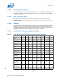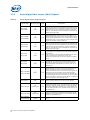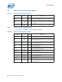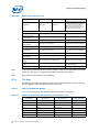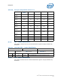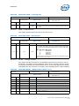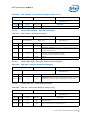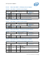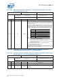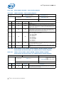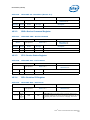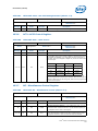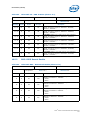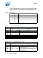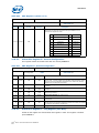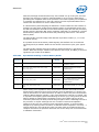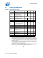
1
Intel® Atom™ Processor E6xx Series
Datasheet
April 2013
Revision 005US
Document Number: 324208-005US
INFORMATION IN THIS DOCUMENT IS PROVIDED IN CONNECTION WITH INTEL PRODUCTS. NO LICENSE, EXPRESS OR IMPLIED, BY ESTOPPEL OR
OTHERWISE, TO ANY INTELLECTUAL PROPERTY RIGHTS IS GRANTED BY THIS DOCUMENT. EXCEPT AS PROVIDED IN INTEL'S TERMS AND CONDITIONS
OF SALE FOR SUCH PRODUCTS, INTEL ASSUMES NO LIABILITY WHATSOEVER AND INTEL DISCLAIMS ANY EXPRESS OR IMPLIED WARRANTY, RELATING
TO SALE AND/OR USE OF INTEL PRODUCTS INCLUDING LIABILITY OR WARRANTIES RELATING TO FITNESS FOR A PARTICULAR PURPOSE,
MERCHANTABILITY, OR INFRINGEMENT OF ANY PATENT, COPYRIGHT OR OTHER INTELLECTUAL PROPERTY RIGHT.
Legal Lines and Disclaimers
A "Mission Critical Application" is any application in which failure of the Intel Product could result, directly or indirectly, in personal injury or death.
SHOULD YOU PURCHASE OR USE INTEL'S PRODUCTS FOR ANY SUCH MISSION CRITICAL APPLICATION, YOU SHALL INDEMNIFY AND HOLD INTEL AND
ITS SUBSIDIARIES, SUBCONTRACTORS AND AFFILIATES, AND THE DIRECTORS, OFFICERS, AND EMPLOYEES OF EACH, HARMLESS AGAINST ALL
CLAIMS COSTS, DAMAGES, AND EXPENSES AND REASONABLE ATTORNEYS' FEES ARISING OUT OF, DIRECTLY OR INDIRECTLY, ANY CLAIM OF PRODUCT
LIABILITY, PERSONAL INJURY, OR DEATH ARISING IN ANY WAY OUT OF SUCH MISSION CRITICAL APPLICATION, WHETHER OR NOT INTEL OR ITS
SUBCONTRACTOR WAS NEGLIGENT IN THE DESIGN, MANUFACTURE, OR WARNING OF THE INTEL PRODUCT OR ANY OF ITS PARTS.
Intel may make changes to specifications and product descriptions at any time, without notice. Designers must not rely on the absence or characteristics
of any features or instructions marked "reserved" or "undefined". Intel reserves these for future definition and shall have no responsibility whatsoever
for conflicts or incompatibilities arising from future changes to them. The information here is subject to change without notice. Do not finalize a design
with this information.
The products described in this document may contain design defects or errors known as errata which may cause the product to deviate from published
specifications. Current characterized errata are available on request.
Contact your local Intel sales office or your distributor to obtain the latest specifications and before placing your product order.
Copies of documents which have an order number and are referenced in this document, or other Intel literature, may be obtained by calling 1-800-5484725, or go to: http://www.intel.com/#/en_US_01.
α Intel® Hyper-Threading Technology requires a computer system with a processor supporting Intel® HT Technology and an Intel® HT Technologyenabled chipset, BIOS and operating system. Performance will vary depending on the specific hardware and software you use. For more information
including details on which processors support Intel® HT Technology, see http://www.intel.com/products/ht/hyperthreading_more.htm.
β Intel® High Definition Audio requires a system with an appropriate Intel® chipset and a motherboard with an appropriate CODEC and the necessary
drivers installed. System sound quality will vary depending on actual implementation, controller, CODEC, drivers and speakers. For more information
about Intel® HD audio, refer to http://www.intel.com/.
χ 64-bit computing on Intel® architecture requires a computer system with a processor, chipset, BIOS, operating system, device drivers and applications
enabled for Intel® 64 architecture. Performance will vary depending on your hardware and software configurations. Consult with your system vendor for
more information.
δ Intel® Virtualization Technology requires a computer system with an enabled Intel® processor, BIOS, virtual machine monitor (VMM) and, for some
uses, certain computer system software enabled for it. Functionality, performance or other benefits will vary depending on hardware and software
configurations and may require a BIOS update. Software applications may not be compatible with all operating systems. Please check with your
application vendor.
ε The original equipment manufacturer must provide Intel® Trusted Platform Module (Intel® TPM) functionality, which requires an Intel® TPM-supported
BIOS. Intel® TPM functionality must be initialized and may not be available in all countries.
θ For Enhanced Intel SpeedStep® Technology, see the http://processorfinder.intel.com/ or contact your Intel representative for more information.
I2C* is a two-wire communications bus/protocol developed by Philips. SMBus is a subset of the I2C* bus/protocol and was developed by Intel.
Implementations of the I2C* bus/protocol may require licenses from various entities, including Philips Electronics N.V. and North American Philips
Corporation.
BunnyPeople, Celeron, Celeron Inside, Centrino, Centrino Inside, Core Inside, i960, Intel, the Intel logo, Intel AppUp, Intel Atom, Intel Atom Inside, Intel
Core, Intel Inside, the Intel Inside logo, Intel NetBurst, Intel NetMerge, Intel NetStructure, Intel SingleDriver, Intel SpeedStep, Intel Sponsors of
Tomorrow., the Intel Sponsors of Tomorrow. logo, Intel StrataFlash, Intel Viiv, Intel vPro, Intel XScale, InTru, the InTru logo, InTru soundmark, Itanium,
Itanium Inside, MCS, MMX, Moblin, Pentium, Pentium Inside, skoool, the skoool logo, Sound Mark, The Journey Inside, vPro Inside, VTune, Xeon, and
Xeon Inside are trademarks of Intel Corporation in the U.S. and other countries.
*Other names and brands may be claimed as the property of others.
Copyright © 2013, Intel Corporation. All rights reserved.
Intel® Atom™ Processor E6xx Series Datasheet
2
Contents
Contents
1.0
Introduction ............................................................................................................ 23
1.1
Terminology ..................................................................................................... 24
1.2
Reference Documents ........................................................................................ 25
1.3
Components Overview ....................................................................................... 26
1.3.1 Low-Power Intel® Architecture Core.......................................................... 27
1.3.2 System Memory Controller ...................................................................... 27
1.3.3 Graphics ............................................................................................... 27
1.3.4 Video Decode ........................................................................................ 28
1.3.5 Video Encode......................................................................................... 28
1.3.6 Display Interfaces .................................................................................. 28
1.3.6.1 LVDS Interface ......................................................................... 28
1.3.6.2 Serial DVO (SDVO) Display Interface ........................................... 28
1.3.7 PCI Express* ......................................................................................... 28
1.3.8 LPC Interface......................................................................................... 28
1.3.9 Intel® High Definition Audioβ (Intel® HD Audioβ) Controller .......................... 29
1.3.10 SMBus Host Controller ............................................................................ 29
1.3.11 General Purpose I/O (GPIO)..................................................................... 29
1.3.12 Serial Peripheral Interface (SPI) ............................................................... 29
1.3.13 Power Management ................................................................................ 29
1.3.14 Watchdog Timer (WDT)........................................................................... 30
1.3.15 Real Time Clock (RTC) ............................................................................ 30
1.3.16 Package ................................................................................................ 30
1.3.17 Intel® Atom™ Processor E6xx Series SKU.................................................. 30
2.0
Signal Description ................................................................................................... 31
2.1
System Memory Signals ..................................................................................... 32
2.2
Integrated Display Interfaces .............................................................................. 33
2.2.1 LVDS Signals ......................................................................................... 33
2.2.2 Serial Digital Video Output (SDVO) Signals ................................................ 34
2.3
PCI Express* Signals ......................................................................................... 35
2.4
Intel® High Definition Audioβ Interface Signals ...................................................... 35
2.5
LPC Interface Signals ......................................................................................... 36
2.6
SMBus Interface Signals..................................................................................... 36
2.7
SPI Interface Signals ......................................................................................... 36
2.8
Power Management Interface Signals ................................................................... 37
2.9
Real Time Clock Interface Signals ........................................................................ 38
2.10 JTAG and Debug Interface .................................................................................. 38
2.11 Miscellaneous Signals and Clocks......................................................................... 39
2.12 General Purpose I/O .......................................................................................... 42
2.13 Functional Straps .............................................................................................. 42
2.14 Power and Ground Signals .................................................................................. 43
3.0
Pin States ................................................................................................................ 45
3.1
Pin Reset States ................................................................................................ 45
3.2
System Memory Signals ..................................................................................... 45
3.3
Integrated Display Interfaces .............................................................................. 46
3.3.1 LVDS Signals ......................................................................................... 46
3.3.2 Serial Digital Video Output (SDVO) Signals ................................................ 46
3.4
PCI Express* Signals ......................................................................................... 47
3.5
Intel® High Definition Audioβ Interface Signals ...................................................... 47
3.6
LPC Interface Signals ......................................................................................... 48
3.7
SMBus Interface Signals..................................................................................... 48
Intel® Atom™ Processor E6xx Series Datasheet
3
Contents
3.8
3.9
3.10
3.11
3.12
3.13
3.14
SPI Interface Signals..........................................................................................48
Power Management Interface Signals ...................................................................48
Real Time Clock Interface Signals ........................................................................49
JTAG and Debug Interface ..................................................................................49
Miscellaneous Signals and Clocks .........................................................................49
General Purpose I/O...........................................................................................50
Integrated Termination Resistors .........................................................................50
4.0
System Clock Domains .............................................................................................51
5.0
Register and Memory Mapping .................................................................................53
5.1
Address Map .....................................................................................................53
5.2
Introduction ......................................................................................................53
5.3
System Memory Map..........................................................................................54
5.3.1 I/O Map.................................................................................................56
5.3.1.1 Fixed I/O Address Range ............................................................56
5.3.1.2 Variable I/O Address Range ........................................................57
5.3.2 PCI Devices and Functions .......................................................................57
5.4
Register Access Method ......................................................................................58
5.4.1 Direct Register Access .............................................................................58
5.4.1.1 Hard Coded IO Access................................................................58
5.4.1.2 IO BAR ....................................................................................59
5.4.1.3 Hard-Coded Memory Access........................................................59
5.4.1.4 Memory BAR.............................................................................59
5.4.2 Indirect Register Access...........................................................................59
5.4.2.1 PCI Config Space.......................................................................59
5.5
Bridging and Configuration..................................................................................60
5.5.1 Root Complex Topology Capability Structure...............................................60
5.5.1.1 Offset 0000h: RCTCL – Root Complex Topology Capabilities List ......60
5.5.1.2 Offset 0004h: ESD – Element Self Description ...............................61
5.5.1.3 Offset 0010h: HDD – Intel® High Definition Audioβ Description ........61
5.5.1.4 Offset 0018h: HDBA – Intel® High Definition Audioβ Base Address ...61
5.5.2 Interrupt Pin Configuration.......................................................................62
5.5.2.1 Offset 3100h: D31IP – Device 31 Interrupt Pin ..............................62
5.5.2.2 Offset 3110h: D27IP – Device 27 Interrupt Pin ..............................62
5.5.2.3 Offset 3118h: D02IP – Device 2 Interrupt Pin................................62
5.5.2.4 Offset 3120h: D26IP – Device 26 Interrupt Pin ..............................63
5.5.2.5 Offset 3124h: D25IP – Device 25 Interrupt Pin ..............................63
5.5.2.6 Offset 3128h: D24IP – Device 24 Interrupt Pin ..............................63
5.5.2.7 Offset 312Ch: D23IP – Device 23 Interrupt Pin..............................63
5.5.2.8 Offset 3130h: D03IP – Device 3 Interrupt Pin................................64
5.5.3 Interrupt Route Configuration...................................................................64
5.5.3.1 Offset 3140h: D31IR – Device 31 Interrupt Route..........................64
5.5.3.2 Offset 3148h: D27IR – Device 27 Interrupt Route..........................65
5.5.3.3 Offset 314Ah: D26IR – Device 26 Interrupt Route..........................65
5.5.3.4 Offset 314Ch: D25IR – Device 25 Interrupt Route .........................65
5.5.3.5 Offset 314Eh: D24IR – Device 24 Interrupt Route..........................66
5.5.3.6 Offset 3150h: D23IR – Device 23 Interrupt Route..........................66
5.5.3.7 Offset 3160h: D02IR – Device 2 Interrupt Route ...........................66
5.5.3.8 Offset 3162h: D03IR – Device 3 Interrupt Route ...........................67
5.5.4 General Configuration..............................................................................67
5.5.4.1 Offset 3400h: RC – RTC Configuration..........................................67
5.5.4.2 Offset 3410h: BNT– Boot Configuration ........................................67
6.0
Memory Controller ...................................................................................................69
6.1
Overview ..........................................................................................................69
6.1.1 DRAM Frequencies and Data Rates ............................................................69
6.2
DRAM Burst Length ............................................................................................69
Intel® Atom™ Processor E6xx Series Datasheet
4
Contents
6.3
6.4
6.5
6.6
6.7
6.8
6.9
7.0
DRAM Partial Writes........................................................................................... 69
DRAM Power Management .................................................................................. 69
6.4.1 Powerdown Modes .................................................................................. 70
6.4.2 Self Refresh Mode .................................................................................. 70
6.4.3 Dynamic Self Refresh Mode ..................................................................... 70
6.4.4 Page Management .................................................................................. 70
Refresh Mode.................................................................................................... 70
Supported DRAM Configurations .......................................................................... 71
Supported DRAM Devices ................................................................................... 72
Supported Rank Configurations ........................................................................... 72
Address Mapping and Decoding ........................................................................... 73
Graphics, Video, and Display ................................................................................... 75
7.1
Chapter Contents .............................................................................................. 75
7.2
Overview ......................................................................................................... 75
7.2.1 3D Graphics .......................................................................................... 75
7.2.2 Shading Engine Key Features ................................................................... 76
7.2.3 Vertex Processing................................................................................... 77
7.2.3.1 Vertex Transform Stages ........................................................... 77
7.2.3.2 Lighting Stages ........................................................................ 77
7.2.4 Pixel Processing ..................................................................................... 78
7.2.4.1 Hidden Surface Removal ............................................................ 78
7.2.4.2 Applying Textures and Shading................................................... 78
7.2.4.3 Final Pixel Formatting ................................................................ 78
7.2.5 Unified Shader ....................................................................................... 78
7.2.6 Multi Level Cache ................................................................................... 79
7.3
Video Encode.................................................................................................... 79
7.3.1 Supported Input Formats ........................................................................ 79
7.3.1.1 Encoding Pipeline...................................................................... 79
7.3.1.2 Encode Codec Support............................................................... 80
7.3.1.3 Encode Specifications Supported................................................. 80
7.4
Video Decode ................................................................................................... 81
7.4.1 Entropy Coding ...................................................................................... 81
7.4.1.1 Motion Compensation ................................................................ 82
7.4.1.2 Deblocking............................................................................... 82
7.4.1.3 Output Reference Frame Storage Format ..................................... 82
7.4.1.4 Pixel Format............................................................................. 83
7.5
Display ........................................................................................................... 83
7.5.1 Display Output Stages ............................................................................ 85
7.5.1.1 Planes ..................................................................................... 85
7.5.1.2 Display Pipes............................................................................ 86
7.5.2 Display Ports ......................................................................................... 86
7.5.2.1 LVDS Port ................................................................................ 87
7.5.2.2 LVDS Backlight Control .............................................................. 88
7.5.2.3 SDVO Digital Display Port .......................................................... 88
7.5.2.4 SDVO DVI/HDMI....................................................................... 89
7.6
Control Bus ...................................................................................................... 89
7.7
Configuration Registers ...................................................................................... 90
7.7.1 D2:F0 PCI Configuration Registers ............................................................ 90
7.7.2 D3:F0 PCI Configuration Registers .......................................................... 102
7.7.2.1 Offset 00h: ID – Identifiers ...................................................... 103
7.7.2.2 Offset 04h: CMD – PCI Command ............................................. 103
7.7.2.3 Offset 06h: STS - PCI Status .................................................... 104
7.7.2.4 Offset 08h: RID - Revision Identification .................................... 104
7.7.2.5 Offset 09h: CC - Class Codes.................................................... 104
7.7.2.6 Offset 0Eh: HDR - Header Type ................................................ 105
7.7.2.7 Offset 10h: MMADR - Memory Mapped Base Address ................... 105
Intel® Atom™ Processor E6xx Series Datasheet
5
Contents
7.7.2.8
7.7.2.9
7.7.2.10
7.7.2.11
7.7.2.12
7.7.2.13
7.7.2.14
7.7.2.15
7.7.2.16
7.7.2.17
7.7.2.18
7.7.2.19
7.7.2.20
7.7.2.21
7.7.2.22
8.0
Offset
Offset
Offset
Offset
Offset
Offset
Offset
Offset
Offset
Offset
Offset
Offset
Offset
Offset
Offset
14h: IOBAR - I/O Base Address ....................................... 106
2Ch: SS - Subsystem Identifiers ...................................... 106
34h: CAP_PTR - Capabilities Pointer.................................. 106
3Ch: INTR - Interrupt Information.................................... 106
58h: SSRW - Software Scratch Read Write ........................ 107
60h: HSRW - Hardware Scratch Read Write ....................... 107
90h: MID - Message Signaled Interrupts Capability ............. 107
92h: MC - Message Control ............................................. 107
94h: MA - Message Address............................................. 108
98h: MD - Message Data................................................. 108
C4h: FD - Functional Disable ........................................... 108
E0h: SWSCISMI - Software SCI/SMI................................. 109
E4h: ASLE - System Display Event Register ....................... 109
F0h: GCR - Graphics Clock Ratio ...................................... 109
F4h: LBB - Legacy Backlight Brightness............................. 110
PCI Express* ......................................................................................................... 111
8.1
Functional Description ...................................................................................... 111
8.1.1 Interrupt Generation ............................................................................. 111
8.1.2 Power Management............................................................................... 111
8.1.2.1 Sleep State Support ................................................................ 111
8.1.2.2 Resuming from Suspended State ............................................... 111
8.1.2.3 Device Initiated PM_PME Message ............................................. 111
8.1.2.4 SMI/SCI Generation................................................................. 112
8.1.3 Additional Clarifications ......................................................................... 112
8.1.3.1 Non-Snoop Cycles Are Not Supported ........................................ 112
8.2
PCI Express* Configuration Registers ................................................................. 112
8.2.1 PCI Type 1 Bridge Header ...................................................................... 112
8.2.1.1 VID — Vendor Identification...................................................... 113
8.2.1.2 DID — Device Identification ...................................................... 113
8.2.1.3 CMD — PCI Command.............................................................. 114
8.2.1.4 PSTS — Primary Status ............................................................ 114
8.2.1.5 RID — Revision Identification .................................................... 115
8.2.1.6 CC — Class Code..................................................................... 115
8.2.1.7 CLS — Cache Line Size............................................................. 116
8.2.1.8 HTYPE — Header Type ............................................................. 116
8.2.1.9 PBN — Primary Bus Number ..................................................... 116
8.2.1.10 SCBN — Secondary Bus Number ............................................... 116
8.2.1.11 SBBN — Subordinate Bus Number ............................................. 117
8.2.1.12 IOBASE — I/O Base Address ..................................................... 117
8.2.1.13 IOLIMIT — I/O Limit Address .................................................... 118
8.2.1.14 SSTS — Secondary Status ........................................................ 118
8.2.1.15 MB — Memory Base Address ..................................................... 119
8.2.1.16 ML — Memory Limit Address ..................................................... 119
8.2.1.17 PMB — Prefetchable Memory Base Address ................................. 119
8.2.1.18 PML — Prefetchable Memory Limit Address ................................. 120
8.2.1.19 CAPP — Capabilities Pointer ...................................................... 120
8.2.1.20 ILINE — Interrupt Line ............................................................. 120
8.2.1.21 IPIN — Interrupt Pin ................................................................ 121
8.2.1.22 BCTRL — Bridge Control ........................................................... 121
8.2.2 Root Port Capability Structure ................................................................ 122
8.2.2.1 CLIST — Capabilities List .......................................................... 123
8.2.2.2 XCAP — PCI Express* Capabilities ............................................. 123
8.2.2.3 DCAP — Device Capabilities ...................................................... 123
8.2.2.4 DCTL — Device Control ............................................................ 124
8.2.2.5 DSTS — Device Status ............................................................. 125
8.2.2.6 LCAP — Link Capabilities .......................................................... 125
8.2.2.7 LCTL — Link Control ................................................................ 126
8.2.2.8 LSTS — Link Status ................................................................. 126
Intel® Atom™ Processor E6xx Series Datasheet
6
Contents
8.2.3
8.2.4
8.2.5
8.2.6
9.0
8.2.2.9 SLCAP — Slot Capabilities ........................................................ 127
8.2.2.10 SLCTL — Slot Control .............................................................. 127
8.2.2.11 SLSTS — Slot Status ............................................................... 128
8.2.2.12 RCTL — Root Control ............................................................... 129
8.2.2.13 RCAP — Root Capabilities......................................................... 129
8.2.2.14 RSTS — Root Status................................................................ 129
PCI Bridge Vendor Capability ................................................................. 130
8.2.3.1 SVCAP — Subsystem Vendor Capability ..................................... 130
8.2.3.2 SVID — Subsystem Vendor IDs ................................................ 130
PCI Power Management Capability .......................................................... 130
8.2.4.1 PMCAP — Power Management Capability ID................................ 131
8.2.4.2 PMC — PCI Power Management Capabilities................................ 131
8.2.4.3 PMCS — PCI Power Management Control And Status ................... 131
Port Configuration ................................................................................ 132
8.2.5.1 MPC — Miscellaneous Port Configuration .................................... 133
8.2.5.2 SMSCS — SMI / SCI Status ...................................................... 134
Miscellaneous Configuration ................................................................... 135
8.2.6.1 FD — Functional Disable .......................................................... 135
Intel® High Definition Audioβ D27:F0 ..................................................................... 137
9.1
Overview ....................................................................................................... 137
9.2
Docking ......................................................................................................... 137
9.2.1 Dock Sequence .................................................................................... 138
9.2.2 Undock Sequence................................................................................. 139
9.2.3 Relationship Between HDA_DOCKRST_B and HDA_RST_B.......................... 139
9.2.4 External Pull-Ups/Pull-Downs ................................................................. 140
9.3
PCI Configuration Register Space ...................................................................... 140
9.3.1 Registers............................................................................................. 140
9.3.1.1 Offset 00h: VID – Vendor Identification ..................................... 142
9.3.1.2 Offset 02h: DID – Device Identification ...................................... 142
9.3.1.3 Offset 04h: PCICMD – PCI Command Register ............................ 142
9.3.1.4 Offset 06h: PCISTS – PCI Status Register .................................. 143
9.3.1.5 Offset 08h: RID – Revision Identification Register ....................... 143
9.3.1.6 Offset 09h: CC – Class Codes Register ....................................... 143
9.3.1.7 Offset 0Ch: CLS - Cache Line Size Register................................. 144
9.3.1.8 Offset 0Dh: LT – Latency Timer Register .................................... 144
9.3.1.9 Offset 0Eh: HEADTYP - Header Type Register ............................. 144
9.3.1.10 Offset 10h: LBAR – Lower Base Address Register ........................ 144
9.3.1.11 Offset 14h: UBAR – Upper Base Address Register........................ 145
9.3.1.12 Offset 2Ch: SVID—Subsystem Vendor Identifier.......................... 145
9.3.1.13 Offset 2Eh: SID—Subsystem Identifier....................................... 146
9.3.1.14 Offset 34h – CAP_PTR – Capabilities Pointer Register ................... 146
9.3.1.15 Offset 3Ch – INTLN: Interrupt Line Register ............................... 146
9.3.1.16 Offset 3Dh – INTPN—Interrupt Pin Register ................................ 147
9.3.1.17 Offset 40h – HDCTL— Intel® High Definition Audioβ Control
Register................................................................................. 147
9.3.1.18 Offset 4Ch – DCKCTL—Docking Control Register ......................... 147
9.3.1.19 Offset 4Dh – DCKSTS—Docking Status Register .......................... 148
9.3.1.20 Offset 50h: PM_CAPID - PCI Power Management Capability ID
Register................................................................................. 148
9.3.1.21 Offset 52h: PM_CAP – Power Management Capabilities Register .... 148
9.3.1.22 Offset 54h: PM_CTL_STS - Power Management Control And Status
Register................................................................................. 149
9.3.1.23 Offset 60h: MSI_CAPID - MSI Capability ID Register.................... 150
9.3.1.24 Offset 62h: MSI_CTL - MSI Message Control Register .................. 150
9.3.1.25 Offset 64h: MSI_ADR - MSI Message Address Register................. 150
9.3.1.26 Offset 68h: MSI_DATA - MSI Message Data Register ................... 150
9.3.1.27 Offset 70h: PCIE_CAPID – PCI Express* Capability Identifiers
Register................................................................................. 151
Intel® Atom™ Processor E6xx Series Datasheet
7
Contents
9.3.1.28
9.3.1.29
9.3.1.30
9.3.1.31
9.3.1.32
9.3.1.33
9.3.1.34
9.3.1.35
9.3.1.36
9.3.1.37
9.3.1.38
9.3.1.39
9.3.1.40
9.3.1.41
9.3.1.42
9.3.1.43
9.3.1.44
9.3.2
Offset 72h: PCIECAP – PCI Express* Capabilities Register ............. 151
Offset 74h: DEVCAP – Device Capabilities Register....................... 151
Offset 78h: DEVC – Device Control ............................................ 151
Offset 7Ah: DEVS – Device Status Register ................................. 152
Offset FCh – FD: Function Disable Register ................................. 152
Offset 100h: VCCAP – Virtual Channel Enhanced Capability Header 153
Offset 104h: PVCCAP1 – Port VC Capability Register 1.................. 153
Offset 108h: PVCCAP2 – Port VC Capability Register 2.................. 154
Offset 10Ch: PVCCTL – Port VC Control Register .......................... 154
Offset 10Eh: PVCSTS – Port VC Status Register ........................... 154
Offset 110h: VC0CAP – VC0 Resource Capability Register ............. 154
Offset 114h: VC0CTL – VC0 Resource Control Register ................. 155
Offset 11Ah: VC0STS – VC0 Resource Status Register .................. 155
Offset 11Ch: VC1CAP – VC1 Resource Capability Register ............. 155
Offset 120h: VC1CTL – VC1 Resource Control Register ................. 155
Offset 126h: VC1STS – VC1 Resource Status Register .................. 156
Offset 130h: RCCAP – Root Complex Link Declaration Enhanced
Capability Header Register........................................................ 156
9.3.1.45 Offset 134h: ESD – Element Self Description Register .................. 156
9.3.1.46 Offset 140h: L1DESC – Link 1 Description Register ...................... 157
9.3.1.47 Offset 148h: L1ADD – Link 1 Address Register ............................ 157
Memory Mapped Configuration Registers.................................................. 157
9.3.2.1 Intel® HD Audioβ Registers ....................................................... 157
10.0 LPC Interface (D31:F0) .......................................................................................... 187
10.1 Functional Overview ......................................................................................... 187
10.1.1 Memory Cycle Notes ............................................................................. 187
10.1.2 Intel® Trusted Platform Moduleε 1.2 Support ............................................ 187
10.1.3 FWH Cycle Notes .................................................................................. 187
10.1.4 LPC Output Clocks ................................................................................ 187
10.2 PCI Configuration Registers............................................................................... 188
10.2.1 ID—Identifiers...................................................................................... 188
10.2.2 CMD—Device Command Register ............................................................ 189
10.2.3 STS—Device Status Register .................................................................. 189
10.2.4 RID—Revision ID Register ...................................................................... 189
10.2.5 CC—Class Code Register ........................................................................ 190
10.2.6 HDTYPE—Header Type Register .............................................................. 190
10.2.7 SS—Subsystem Identifiers Register......................................................... 190
10.3 ACPI Device Configuration ................................................................................ 191
10.3.1 SMBA—SMBus Base Address Register ...................................................... 191
10.3.2 GBA—GPIO Base Address Register .......................................................... 191
10.3.3 PM1BLK—PM1_BLK Base Address Register ............................................... 191
10.3.4 GPE0BLK—GPE0_BLK Base Address Register ............................................ 192
10.3.5 LPCS—LPC Clock Strength Control Register .............................................. 192
10.3.6 ACTL—ACPI Control Register .................................................................. 193
10.3.7 MC - Miscellaneous Control Register ........................................................ 193
10.4 Interrupt Control ............................................................................................. 195
10.4.1 PxRC—PIRQx Routing Control Register..................................................... 195
10.4.2 SCNT—Serial IRQ Control Register .......................................................... 196
10.4.3 WDTBA-WDT Base Address .................................................................... 196
10.5 FWH Configuration Registers ............................................................................. 196
10.5.1 FS—FWH ID Select Register ................................................................... 196
10.5.2 BDE—BIOS Decode Enable ..................................................................... 197
10.5.3 BC—BIOS Control Register ..................................................................... 198
10.6 Root Complex Register Block Configuration ......................................................... 199
10.6.1 RCBA—Root Complex Base Address Register ............................................ 199
Intel® Atom™ Processor E6xx Series Datasheet
8
Contents
11.0 ACPI Devices ......................................................................................................... 201
11.1 8254 Timer .................................................................................................... 201
11.1.1 Counter 0, System Timer ...................................................................... 201
11.1.2 Counter 1, Refresh Request Signal.......................................................... 201
11.1.3 Counter 2, Speaker Tone....................................................................... 201
11.1.4 Timer I/O Registers .............................................................................. 201
11.1.5 Offset 43h: TCW - Timer Control Word Register........................................ 201
11.1.5.1 Read Back Command .............................................................. 202
11.1.5.2 Counter Latch Command.......................................................... 203
11.1.5.3 Offset 40h, 41h, 42h: Interval Timer Status Byte Format Register . 203
11.1.5.4 Offset 40h, 41h, 42h: Counter Access Ports Register ................... 204
11.1.6 Timer Programming .............................................................................. 204
11.1.7 Reading from the Interval Timer............................................................. 205
11.1.7.1 Simple Read........................................................................... 205
11.1.7.2 Counter Latch Command.......................................................... 205
11.1.7.3 Read Back Command .............................................................. 206
11.2 High Precision Event Timer ............................................................................... 206
11.2.1 Registers............................................................................................. 206
11.2.1.1 Offset 000h: GCID – General Capabilities and ID......................... 207
11.2.1.2 Offset 010h: GC – General Configuration ................................... 207
11.2.1.3 Offset 020h: GIS – General Interrupt Status............................... 208
11.2.1.4 Offset 0F0h: MCV – Main Counter Value..................................... 208
11.2.1.5 Offset 100h, 120h, 140h: T[0-2]C – Timer [0-2] Config and
Capabilities ............................................................................ 208
11.2.1.6 Offset 108h, 128h, 148h: T[0-2]CV – Timer [0-2] Comparator
Value .................................................................................... 209
11.2.2 Theory Of Operation ............................................................................. 210
11.2.2.1 Non-Periodic Mode – All timers ................................................. 210
11.2.2.2 Periodic Mode – Timer 0 only.................................................... 211
11.2.2.3 Interrupts .............................................................................. 211
11.2.2.4 Mapping Option #2: Standard Option (GC.LRE cleared)................ 212
11.3 8259 Interrupt Controller ................................................................................. 212
11.3.1 Overview ............................................................................................ 212
11.3.2 I/O Registers ....................................................................................... 213
11.3.2.1 Offset 20h, A0h: ICW1 – Initialization Command Word 1.............. 213
11.3.2.2 Offset 21h, A1h: ICW2 – Initialization Command Word 2.............. 214
11.3.2.3 Offset 21h: MICW3 – Master Initialization Command Word 3 ........ 215
11.3.2.4 Offset A1h: SICW3 – Slave Initialization Command Word 3........... 215
11.3.2.5 Offset 21h, A1h: ICW4 – Initialization Command Word 4 Register . 215
11.3.2.6 Offset 21h, A1h: OCW1 – Operational Control Word 1 (Interrupt
Mask).................................................................................... 216
11.3.2.7 Offset 20h, A0h: OCW2 – Operational Control Word 2.................. 216
11.3.2.8 Offset 4D0h: ELCR1 – Master Edge/Level Control ........................ 217
11.3.2.9 Offset 4D1h: ELCR2 – Slave Edge/Level Control .......................... 218
11.3.3 Interrupt Handling................................................................................ 218
11.3.3.1 Generating............................................................................. 218
11.3.3.2 Acknowledging ....................................................................... 218
11.3.3.3 Hardware/Software Interrupt Sequence ..................................... 219
11.3.4 Initialization Command Words (ICW) ...................................................... 219
11.3.4.1 ICW1 .................................................................................... 219
11.3.4.2 ICW2 .................................................................................... 220
11.3.4.3 ICW3 .................................................................................... 220
11.3.4.4 ICW4 .................................................................................... 220
11.3.5 Operation Command Words (OCW) ......................................................... 220
11.3.6 Modes of Operation .............................................................................. 220
11.3.6.1 Fully Nested Mode................................................................... 220
11.3.6.2 Special Fully Nested Mode........................................................ 221
Intel® Atom™ Processor E6xx Series Datasheet
9
Contents
11.4
11.5
11.6
11.7
11.3.6.3 Automatic Rotation Mode (Equal Priority Devices) ........................ 221
11.3.6.4 Specific Rotation Mode (Specific Priority) .................................... 221
11.3.6.5 Poll Mode ............................................................................... 221
11.3.6.6 Edge and Level Triggered Mode ................................................. 222
11.3.7 End Of Interrupt (EOI) .......................................................................... 222
11.3.7.1 Normal EOI ............................................................................ 222
11.3.7.2 Automatic EOI ........................................................................ 222
11.3.8 Masking Interrupts................................................................................ 222
11.3.8.1 Masking on an Individual Interrupt Request ................................ 222
11.3.8.2 Special Mask Mode .................................................................. 222
11.3.9 Steering of PCI Interrupts ...................................................................... 223
Advanced Peripheral Interrupt Controller (APIC) .................................................. 223
11.4.1 Memory Registers ................................................................................. 223
11.4.1.1 Address FEC00000h: IDX – Index Register ................................. 223
11.4.1.2 Address FEC00010h: WDW – Window Register ............................ 223
11.4.1.3 Address FEC00040h: EOI – EOI Register .................................... 223
11.4.2 Index Registers .................................................................................... 224
11.4.2.1 Offset 00h: ID – Identification Register ...................................... 224
11.4.2.2 Offset 01h: VS – Version Register.............................................. 224
11.4.2.3 Offset 10-11h – 3E-3Fh: RTE[0-23] – Redirection Table Entry ....... 225
11.4.3 Unsupported Modes .............................................................................. 226
11.4.4 Interrupt Delivery ................................................................................. 226
11.4.4.1 Theory of Operation................................................................. 226
11.4.4.2 EOI ....................................................................................... 226
11.4.4.3 Interrupt Message Format ........................................................ 226
11.4.4.4 Interrupt Delivery Address Value ............................................... 226
11.4.4.5 Interrupt Delivery Data Value ................................................... 227
11.4.5 PCI Express* Interrupts......................................................................... 227
11.4.6 Routing of Internal Device Interrupts....................................................... 227
Serial Interrupt ............................................................................................... 227
11.5.1 Overview ............................................................................................. 227
11.5.2 Start Frame ......................................................................................... 228
11.5.3 Data Frames ........................................................................................ 228
11.5.4 Stop Frame.......................................................................................... 228
11.5.5 Serial Interrupts Not Supported .............................................................. 229
11.5.6 Data Frame Format and Issues ............................................................... 229
Real Time Clock............................................................................................... 230
11.6.1 Overview ............................................................................................. 230
11.6.2 I/O Registers ....................................................................................... 230
11.6.3 Indexed Registers ................................................................................. 230
11.6.3.1 Offset 0Ah: Register A ............................................................. 231
11.6.3.2 Offset 0Bh: Register B - General Configuration ............................ 232
11.6.3.3 Offset 0Ch: Register C - Flag Register (RTC Well) ........................ 232
11.6.3.4 Offset 0Dh: Register D - Flag Register (RTC Well) ........................ 233
11.6.4 Update Cycles ...................................................................................... 233
11.6.5 Interrupts ............................................................................................ 233
General Purpose I/O......................................................................................... 234
11.7.1 Core Well GPIO I/O Registers ................................................................. 234
11.7.1.1 Offset 00h: CGEN – Core Well GPIO Enable................................. 234
11.7.1.2 Offset 04h: CGIO – Core Well GPIO Input/Output Select............... 235
11.7.1.3 Offset 08h: CGLVL – Core Well GPIO Level for Input or Output ...... 235
11.7.1.4 Offset 0Ch: CGTPE – Core Well GPIO Trigger Positive Edge Enable . 235
11.7.1.5 Offset 10h: CGTNE – Core Well GPIO Trigger Negative Edge Enable236
11.7.1.6 Offset 14h: CGGPE – Core Well GPIO GPE Enable ........................ 236
11.7.1.7 Offset 18h: CGSMI – Core Well GPIO SMI Enable......................... 236
11.7.1.8 Offset 1Ch: CGTS – Core Well GPIO Trigger Status ...................... 237
11.7.2 Resume Well GPIO I/O Registers............................................................. 237
Intel® Atom™ Processor E6xx Series Datasheet
10
Contents
11.7.2.1
11.7.2.2
11.7.2.3
11.7.2.4
Offset 20h: RGEN – Resume Well GPIO Enable............................ 237
Offset 24h: RGIO – Resume Well GPIO Input/Output Select.......... 238
Offset 28h: RGLVL – Resume Well GPIO Level for Input or Output . 238
Offset 2Ch: RGTPE – Resume Well GPIO Trigger Positive Edge
Enable................................................................................... 239
11.7.2.5 Offset 30h: RGTNE – Resume Well GPIO Trigger Negative Edge
Enable................................................................................... 239
11.7.2.6 Offset 34h: RGGPE – Resume Well GPIO GPE Enable ................... 239
11.7.2.7 Offset 38h: RGSMI – Resume Well GPIO SMI Enable.................... 240
11.7.2.8 Offset 3Ch: RGTS – Resume Well GPIO Trigger Status ................. 240
11.7.3 Theory of Operation.............................................................................. 240
11.7.3.1 Power Wells ........................................................................... 240
11.7.3.2 SMI# and SCI Routing............................................................. 240
11.7.3.3 Triggering.............................................................................. 240
11.8 SMBus Controller............................................................................................. 241
11.8.1 Overview ............................................................................................ 241
11.8.2 I/O Registers ....................................................................................... 241
11.8.2.1 Offset 00h: HCTL - Host Control Register ................................... 241
11.8.2.2 Offset 01h: HSTS - Host Status Register .................................... 242
11.8.2.3 Offset 02h: HCLK – Host Clock Divider....................................... 243
11.8.2.4 Offset 04h: TSA - Transmit Slave Address .................................. 243
11.8.2.5 Offset 05h: HCMD - Host Command Register .............................. 243
11.8.2.6 Offset 06h: HD0 - Host Data 0.................................................. 244
11.8.2.7 Offset 07h: HD1 - Host Data 1.................................................. 244
11.8.2.8 Offset 20h – 3Fh: HBD – Host Block Data................................... 244
11.8.3 Overview ............................................................................................ 244
11.8.4 Bus Arbitration..................................................................................... 245
11.8.5 Bus Timings......................................................................................... 245
11.8.5.1 Clock Stretching ..................................................................... 245
11.8.5.2 Bus Time Out ......................................................................... 246
11.8.6 SMI#.................................................................................................. 246
11.9 Serial Peripheral Interface ................................................................................ 246
11.9.1 Overview ............................................................................................ 246
11.9.2 Features ............................................................................................. 246
11.9.3 External Interface ................................................................................ 246
11.9.4 SPI Protocol......................................................................................... 247
11.9.4.1 SPI Pin Level Protocol.............................................................. 247
11.9.5 Host Side Interface............................................................................... 249
11.9.5.1 SPI Host Interface Registers..................................................... 249
11.9.5.2 Offset 00h: SPIS – SPI Status .................................................. 250
11.9.5.3 Offset 02h: SPIC – SPI Control ................................................. 251
11.9.5.4 Offset 04h: SPIA – SPI Address ................................................ 252
11.9.5.5 Offset 08h: SPID0 – SPI Data 0 ................................................ 252
11.9.5.6 Offset 10h, 18h, 20h, 28h, 30h, 38h, 40h: SPID[0-6] – SPI Data N 253
11.9.5.7 Offset 50h: BBAR – BIOS Base Address ..................................... 253
11.9.5.8 Offset 54h: PREOP – Prefix Opcode Configuration........................ 253
11.9.5.9 Offset 56h: OPTYPE – Opcode Type Configuration ....................... 254
11.9.5.10Offset 58h: OPMENU – Opcode Menu Configuration ..................... 254
11.9.5.11Offset 60h: PBR0 – Protected BIOS Range [0-2] ......................... 255
11.9.5.12Running SPI Cycles from the Host ............................................. 256
11.9.5.13Generic Programmed Commands .............................................. 258
11.9.5.14Flash Protection...................................................................... 258
11.9.6 SPI Clocking ........................................................................................ 260
11.9.7 BIOS Programming Considerations ......................................................... 260
11.9.7.1 Run Time Updates................................................................... 261
11.9.7.2 BIOS Sector Updates............................................................... 261
11.9.7.3 SPI Initialization ..................................................................... 262
11.10 Watchdog Timer.............................................................................................. 263
Intel® Atom™ Processor E6xx Series Datasheet
11
Contents
11.10.1Overview ............................................................................................. 263
11.10.2Features .............................................................................................. 263
11.10.3Watchdog Timer Register Details ............................................................ 263
11.10.3.1Offset 00h: PV1R0 - Preload Value 1 Register 0 ........................... 264
11.10.3.2Offset 01h: PV1R1 - Preload Value 1 Register 1 ........................... 265
11.10.3.3Offset 02h: PV1R2 - Preload Value 1 Register 2 ........................... 265
11.10.3.4Offset 04h: PV2R0 - Preload Value 2 Register 0 ........................... 266
11.10.3.5Offset 05h: PV2R1 - Preload Value 2 Register 1 ........................... 266
11.10.3.6Offset 06h: PV2R2 - Preload Value 2 Register 2 ........................... 266
11.10.3.7Offset 0Ch: RR0 - Reload Register 0 .......................................... 267
11.10.3.8Offset 0Dh: RR1 - Reload Register 1 .......................................... 267
11.10.3.9Offset 10h: WDTCR - WDT Configuration Register........................ 268
11.10.3.10Offset 14h: DCR0 - Down Counter Register 0 ............................ 268
11.10.3.11Offset 15h: DCR1 - Down Counter Register 1 ............................ 269
11.10.3.12Offset 16h: DCR2 - Down Counter Register 2 ............................ 269
11.10.3.13Offset 18h: WDTLR - WDT Lock Register................................... 269
11.10.4Theory Of Operation.............................................................................. 270
11.10.4.1RTC Well and WDT_TOUT Functionality ...................................... 270
11.10.4.2Register Unlocking Sequence .................................................... 270
11.10.4.3Reload Sequence..................................................................... 271
11.10.4.4Low Power State ..................................................................... 271
12.0 Absolute Maximum Ratings .................................................................................... 273
12.1 Absolute Maximum Rating................................................................................. 274
13.0 DC Characteristics.................................................................................................. 275
13.1 Signal Groups ................................................................................................. 275
13.2 Power and Current Characteristics...................................................................... 276
13.3 General DC Characteristics................................................................................ 277
14.0 Ballout and Package Information ........................................................................... 281
14.1 Package Diagrams ........................................................................................... 282
14.2 Ballout Definition and Signal Locations................................................................ 284
Figures
1
2
3
4
5
6
7
8
9
10
11
12
13
14
15
16
17
System Block Diagram Example .................................................................................23
Components of the Intel® Atom™ Processor E6xx Series ...............................................26
System Address Map.................................................................................................55
PCI Devices .............................................................................................................58
Graphics Unit ...........................................................................................................75
Display Link Interface ...............................................................................................84
Display Resolutions...................................................................................................87
LVDS Control Signal Solution .....................................................................................88
Basic SPI Protocol................................................................................................... 247
Intel® Atom™ Processor E6xx Series Silicon and Die Side Capacitor (Top View) .............. 282
Intel® Atom™ Processor E6xx Series Package Dimensions ........................................... 283
Intel® Atom™ Processor E6xx Series Package Ball Pattern ........................................... 284
Intel® Atom™ Processor E6xx Series Ball Map (Sheet 1 of 5) ....................................... 285
Intel® Atom™ Processor E6xx Series Ball Map (Sheet 2 of 5) ....................................... 286
Intel® Atom™ Processor E6xx Series Ball Map (Sheet 3 of 5) ....................................... 287
Intel® Atom™ Processor E6xx Series Ball Map (Sheet 4 of 5) ....................................... 288
Intel® Atom™ Processor E6xx Series Ball Map (Sheet 5 of 5) ....................................... 289
Intel® Atom™ Processor E6xx Series Datasheet
12
Contents
Tables
1
2
3
4
5
6
7
8
9
10
11
12
13
14
15
16
17
18
19
20
21
22
23
24
25
26
27
28
29
30
31
32
33
34
35
36
37
38
39
40
41
42
43
44
45
46
47
48
49
50
51
52
53
PCI Devices and Functions......................................................................................... 26
Intel® Atom™ Processor E6xx Series SKU for Different Segments................................... 30
Buffer Types............................................................................................................ 31
System Memory Signals............................................................................................ 32
LVDS Signals........................................................................................................... 33
Serial Digital Video Output Signals ............................................................................. 34
PCI Express* Signals ................................................................................................ 35
Intel® High Definition Audioβ Interface Signals ............................................................. 35
LPC Interface Signals................................................................................................ 36
SMBus Interface Signals ........................................................................................... 36
SPI Interface Signals ................................................................................................ 36
Power Management Interface Signals.......................................................................... 37
Real Time Clock Interface Signals............................................................................... 38
JTAG and Debug Interface Signals .............................................................................. 38
Miscellaneous Signals and Clocks ............................................................................... 39
General Purpose I/O Signals ...................................................................................... 42
Functional Straps ..................................................................................................... 42
Power and Ground Signals......................................................................................... 43
Reset State Definitions ............................................................................................. 45
System Memory Signals............................................................................................ 45
LVDS Signals........................................................................................................... 46
Serial Digital Video Output Signals ............................................................................. 46
PCI Express* Signals ................................................................................................ 47
Intel® High Definition Audioβ Interface Signals ............................................................. 47
LPC Interface Signals................................................................................................ 48
SMBus Interface Signals ........................................................................................... 48
SPI Interface Signals ................................................................................................ 48
Power Management Interface Signals.......................................................................... 48
Real Time Clock Interface Signals............................................................................... 49
JTAG and Debug Interface Signals .............................................................................. 49
Miscellaneous Signals and Clocks ............................................................................... 49
General Purpose I/O Signals ...................................................................................... 50
Integrated Termination Resistors ............................................................................... 50
Intel® Atom™ Processor E6xx Series Clock Domains..................................................... 51
Register Access Types and Definitions......................................................................... 53
Memory Map ........................................................................................................... 55
Fixed I/O Range Decoded by the Processor.................................................................. 56
Variable I/O Range Decoded by the Processor .............................................................. 57
PCI Devices and Functions......................................................................................... 57
PCI Configuration PORT CF8h Mapping ........................................................................ 59
PCI Configuration Memory Bar Mapping ...................................................................... 60
PCI Express* Capability List Structure......................................................................... 60
0000h: RCTCL – Root Complex Topology Capabilities List .............................................. 60
0004h: ESD – Element Self Description....................................................................... 61
0010h: HDD – Intel® High Definition Audioβ Description................................................ 61
0018h: HDBA – Intel® High Definition Audioβ Base Address ........................................... 61
Interrupt Pin Configuration ........................................................................................ 62
3100h: D31IP – Device 31 Interrupt Pin...................................................................... 62
3110h: D27IP – Device 27 Interrupt Pin...................................................................... 62
3118h: D02IP – Device 2 Interrupt Pin ....................................................................... 62
3120h: D26IP – Device 26 Interrupt Pin...................................................................... 63
3124h: D25IP – Device 25 Interrupt Pin...................................................................... 63
3128h: D24IP – Device 24 Interrupt Pin...................................................................... 63
Intel® Atom™ Processor E6xx Series Datasheet
13
Contents
54
55
56
57
58
59
60
61
62
63
64
65
66
67
68
69
70
71
72
73
74
75
76
77
78
79
80
81
82
83
84
85
86
87
88
89
90
91
92
93
94
95
96
97
98
99
100
101
102
103
104
105
106
107
108
312Ch: D23IP – Device 23 Interrupt Pin ......................................................................63
3130h: D03IP – Device 3 Interrupt Pin ........................................................................64
Interrupt Route Configuration ....................................................................................64
3140h: D31IR – Device 31 Interrupt Route ..................................................................64
3148h: D27IR – Device 27 Interrupt Route ..................................................................65
314Ah: D26IR – Device 26 Interrupt Route ..................................................................65
314Ch: D25IR – Device 25 Interrupt Route ..................................................................65
314Eh: D24IR – Device 24 Interrupt Route ..................................................................66
3150h: D23IR – Device 23 Interrupt Route ..................................................................66
3160h: D02IR – Device 2 Interrupt Route ....................................................................66
3162h: D03IR – Device 3 Interrupt Route ....................................................................67
3400h: RC – RTC Configuration ..................................................................................67
3410h: BNT– Boot Configuration ................................................................................67
Memory Controller Supported Frequencies and Data Rates .............................................69
Supported Memory Configurations for DDR2.................................................................71
Supported DDR2 DRAM Devices..................................................................................72
Memory Size Per Rank ..............................................................................................72
DRAM Address Decoder .............................................................................................73
Encode Profiles and Levels of Support .........................................................................80
Hardware Accelerated Video Decoding Support .............................................................81
Pixel Format for the Luma (Y) Plane ............................................................................83
Pixel Formats for the Cr/Cb (V/U) Plane.......................................................................83
PCI Header for D2 ....................................................................................................90
00h: GVD.ID – D2: PCI Device and Vendor ID Register..................................................91
04h: GVD.PCICMDSTS – PCI Command and Status Register...........................................91
08h: GVD.RIDCC - Revision Identification and Class Code ..............................................92
0Ch: GVD.HDR – Header Type ...................................................................................92
10h: GVD.MMADR – Memory Mapped Address Range ....................................................93
14h: GVD.GFX_IOBAR – I/O Base Address ...................................................................93
18h: GVD.GMADR – Graphics Memory Address Range ...................................................94
1Ch: GVD.GTTADR – Graphics Translation Table Address Range .....................................94
2Ch: GVD.SSID – Subsystem Identifiers ......................................................................95
34h: GVD.CAPPOINT – Capabilities Pointer...................................................................95
3Ch: GVD.INTR – Interrupt........................................................................................95
50h: GVD.MGGC – Graphics Control............................................................................96
5Ch: GVD.BSM – Base of Stolen Memory .....................................................................97
60h: GVD.MSAC – Multi Size Aperture Control ..............................................................97
90h: GVD.MSI_CAPID – Message Signaled Interrupts Capability ID and Control Register....97
94h: GVD.MA – Message Address ...............................................................................98
98h: GVD.MD – Message Data....................................................................................98
B0h: GVD.VCID – Vendor Capability ID .......................................................................99
B4h: GVD.VC – Vendor Capabilities.............................................................................99
C4h: GVD.FD – Functional Disable ..............................................................................99
D0h: GVD.PMCAP – Power Management Capabilities ................................................... 100
D4h: GVD.PMCS – Power Management Control/Status ................................................. 100
E0h: GVD.SWSMISCI – Software SMI or SCI .............................................................. 100
E4h: GVD.ASLE – System Display Event Register........................................................ 101
F4h: GVD.LBB – Legacy Backlight Brightness ............................................................. 101
FCh: GVD.ASLS ASL – ASL Storage........................................................................... 102
PCI Header ............................................................................................................ 102
Offset 00h: ID – Identifiers ...................................................................................... 103
Offset 04h: CMD – PCI Command ............................................................................. 103
Offset 06h: STS - PCI Status.................................................................................... 104
Offset 08h: RID - Revision Identification .................................................................... 104
Offset 09h: CC - Class Codes ................................................................................... 104
Intel® Atom™ Processor E6xx Series Datasheet
14
Contents
109
110
111
112
113
114
115
116
117
118
119
120
121
122
123
124
125
126
127
128
129
130
131
132
133
134
135
136
137
138
139
140
141
142
143
144
145
146
147
148
149
150
151
152
153
154
155
156
157
158
159
160
161
162
163
Offset 0Eh: HDR - Header Type................................................................................ 105
Offset 10h: MMADR - Memory Mapped Base Address .................................................. 105
Offset 14h: IOBAR - I/O Base Address ...................................................................... 106
Offset 34h: CAP_PTR - Capabilities Pointer ................................................................ 106
Offset 3Ch: INTR - Interrupt Information .................................................................. 106
Offset 58h: SSRW - Software Scratch Read Write ....................................................... 107
Offset 60h: HSRW - Hardware Scratch Read Write...................................................... 107
Offset 90h: MID - Message Signaled Interrupts Capability............................................ 107
Offset 92h: MC - Message Control ............................................................................ 107
Offset 94h: MA - Message Address ........................................................................... 108
Offset 98h: MD - Message Data ............................................................................... 108
Offset C4h: FD - Functional Disable .......................................................................... 108
Offset E0h: SWSCISMI - Software SCI/SMI ............................................................... 109
Offset E4h: ASLE - System Display Event Register...................................................... 109
Offset F0h: GCR - Graphics Clock Ratio ..................................................................... 109
Offset F4h: LBB - Legacy Backlight Brightness ........................................................... 110
MSI vs. PCI IRQ Actions .......................................................................................... 111
PCI Type 1 Bridge Header ....................................................................................... 112
Offset 00h: VID — Vendor Identification.................................................................... 113
Offset 02h: DID — Device Identification .................................................................... 114
Offset 04h: CMD — PCI Command............................................................................ 114
Offset 06h: PSTS — Primary Status .......................................................................... 115
Offset 08h: RID — Revision Identification .................................................................. 115
Offset 09h: CC — Class Code................................................................................... 115
Offset 0Ch: CLS — Cache Line Size........................................................................... 116
Offset 0Eh: HTYPE — Header Type ........................................................................... 116
Offset 18h: PBN — Primary Bus Number ................................................................... 116
Offset 19h: SCBN — Secondary Bus Number ............................................................. 117
Offset 1Ah: SBBN — Subordinate Bus Number ........................................................... 117
Offset 1Ch: IOBASE — I/O Base Address................................................................... 117
Offset 1Dh: IOLIMIT — I/O Limit Address .................................................................. 118
Offset 1Eh: SSTS — Secondary Status ...................................................................... 118
Offset 20h: MB — Memory Base Address ................................................................... 119
Offset 22h: ML — Memory Limit Address ................................................................... 119
Offset 24h: PMB — Prefetchable Memory Base Address ............................................... 120
Offset 26h: PML — Prefetchable Memory Limit Address ............................................... 120
Offset 34h: CAPP — Capabilities Pointer .................................................................... 120
Offset 3Ch: ILINE — Interrupt Line........................................................................... 121
Offset 3Dh: IPIN — Interrupt Pin.............................................................................. 121
Offset 3Eh: BCTRL — Bridge Control ......................................................................... 121
Root Port Capability Structure.................................................................................. 122
Offset 40h: CLIST — Capabilities List ........................................................................ 123
Offset 42h: XCAP — PCI Express* Capabilities ........................................................... 123
Offset 44h: DCAP — Device Capabilities .................................................................... 123
Offset 48h: DCTL — Device Control .......................................................................... 124
Offset 4Ah: DSTS — Device Status ........................................................................... 125
Offset 4Ch: LCAP — Link Capabilities ........................................................................ 125
Offset 50h: LCTL — Link Control .............................................................................. 126
Offset 52h: LSTS — Link Status ............................................................................... 126
Offset 54h: SLCAP — Slot Capabilities....................................................................... 127
Offset 58h: SLCTL — Slot Control............................................................................. 127
Offset 5Ah: SLSTS — Slot Status ............................................................................. 128
Offset 5Ch: RCTL — Root Control ............................................................................. 129
Offset 5Eh: RCAP — Root Capabilities ....................................................................... 129
Offset 60h: RSTS — Root Status .............................................................................. 129
Intel® Atom™ Processor E6xx Series Datasheet
15
Contents
164
165
166
167
168
169
170
171
172
173
174
175
176
177
178
179
180
181
182
183
184
185
186
187
188
189
190
191
192
193
194
195
196
197
198
199
200
201
202
203
204
205
206
207
208
209
210
211
212
213
214
215
216
217
218
PCI Bridge Vendor Capability.................................................................................... 130
Offset 90h: SVCAP — Subsystem Vendor Capability .................................................... 130
Offset 94h: SVID — Subsystem Vendor IDs ............................................................... 130
PCI Power Management Capability ............................................................................ 130
Offset A0h: PMCAP — Power Management Capability ID............................................... 131
Offset A2h: PMC — PCI Power Management Capabilities .............................................. 131
Offset A4h: PMCS — PCI Power Management Control And Status .................................. 131
Port Configuration .................................................................................................. 132
Offset D8h: MPC — Miscellaneous Port Configuration ................................................... 133
Offset DCh: SMSCS — SMI / SCI Status .................................................................... 134
Miscellaneous Configuration ..................................................................................... 135
Offset FCh: FD — Functional Disable ......................................................................... 135
External Resistors................................................................................................... 140
Intel® High Definition Audioβ PCI Configuration Registers............................................. 140
00h: VID – Vendor Identification .............................................................................. 142
02h: DID – Device Identification............................................................................... 142
04h: PCICMD – PCI Command Register ..................................................................... 142
06h: PCISTS – PCI Status Register ........................................................................... 143
08h: RID – Revision Identification Register ................................................................ 143
09h: CC – Class Codes Register................................................................................ 143
0Ch: CLS - Cache Line Size Register ......................................................................... 144
0Dh: LT – Latency Timer Register ............................................................................. 144
0Eh: HEADTYP - Header Type Register ...................................................................... 144
10h: LBAR – Lower Base Address Register ................................................................. 145
14h: UBAR – Upper Base Address Register................................................................. 145
2Ch: SVID—Subsystem Vendor Identifier................................................................... 145
2Eh: SID—Subsystem Identifier ............................................................................... 146
34h – CAP_PTR – Capabilities Pointer Register............................................................ 146
3Ch – INTLN: Interrupt Line Register ........................................................................ 146
3Dh – INTPN — Interrupt Pin Register ....................................................................... 147
40h – HDCTL— Intel® High Definition Audioβ Control Register ...................................... 147
4Ch – DCKCTL — Docking Control Register ................................................................ 147
4Dh: DCKSTS – Docking Status Register ................................................................... 148
50h: PM_CAPID - PCI Power Management Capability ID Register .................................. 148
52h: PM_CAP – Power Management Capabilities Register ............................................. 148
54h: PM_CTL_STS - Power Management Control And Status Register ............................ 149
60h: MSI_CAPID - MSI Capability ID Register............................................................. 150
62h: MSI_CTL - MSI Message Control Register ........................................................... 150
64h: MSI_ADR - MSI Message Address Register ......................................................... 150
68h: MSI_DATA - MSI Message Data Register ............................................................ 150
70h: PCIE_CAPID – PCI Express* Capability Identifiers Register ................................... 151
72h: PCIECAP – PCI Express* Capabilities Register ..................................................... 151
74h: DEVCAP – Device Capabilities Register ............................................................... 151
78h: DEVC – Device Control..................................................................................... 151
7Ah: DEVS – Device Status Register ......................................................................... 152
FCh – FD: Function Disable Register.......................................................................... 152
100h: VCCAP – Virtual Channel Enhanced Capability Header ........................................ 153
104h: PVCCAP1 – Port VC Capability Register 1 .......................................................... 153
108h: PVCCAP2 – Port VC Capability Register 2 .......................................................... 154
10Ch: PVCCTL – Port VC Control Register .................................................................. 154
10Eh: PVCSTS – Port VC Status Register ................................................................... 154
110h: VC0CAP – VC0 Resource Capability Register...................................................... 154
114h: VC0CTL – VC0 Resource Control Register.......................................................... 155
11Ah: VC0STS – VC0 Resource Status Register .......................................................... 155
11Ch: VC1CAP – VC1 Resource Capability Register ..................................................... 155
Intel® Atom™ Processor E6xx Series Datasheet
16
Contents
219
220
221
222
223
224
225
226
227
228
229
230
231
232
233
234
235
236
237
238
239
240
241
242
243
244
245
246
247
248
249
250
251
252
253
254
255
256
257
258
259
260
261
262
263
264
265
120h: VC1CTL – VC1 Resource Control Register ......................................................... 155
126h: VC1STS – VC1 Resource Status Register .......................................................... 156
130h: RCCAP – Root Complex Link Declaration Enhanced Capability Header Register ...... 156
134h: ESD – Element Self Description Register .......................................................... 156
140h: L1DESC – Link 1 Description Register .............................................................. 157
148h: L1ADD – Link 1 Address Register .................................................................... 157
Intel® HD Audioβ Register Summary......................................................................... 158
00h: GCAP – Global Capabilities Register................................................................... 160
02h: VMIN – Minor Version Register ......................................................................... 160
03h: VMAJ – Major Version...................................................................................... 161
04h: OUTPAY – Output Payload Capability Register..................................................... 161
06h: INPAY – Input Payload Capability Register ......................................................... 161
08h: GCTL – Global Control ..................................................................................... 162
0Ch: WAKEEN – Wake Enable .................................................................................. 163
0Eh: STATESTS – State Change Status ..................................................................... 164
10h: GSTS – Global Status ...................................................................................... 164
14h: ECAP - Extended Capabilities............................................................................ 165
18h: STRMPAY – Stream Payload Capability Register .................................................. 165
20h: INTCTL - Interrupt Control Register................................................................... 165
24h: INTSTS - Interrupt Status Register ................................................................... 166
30h: WALCLK – Wall Clock Counter Register .............................................................. 167
38h: SSYNC –Stream Synchronization Register .......................................................... 167
40h: CORBBASE - CORB Base Address Register ......................................................... 168
48h: CORBWP - CORB Write Pointer Register ............................................................. 168
4Ah: CORBRP - CORB Read Pointer Register .............................................................. 168
4Ch: CORBCTL - CORB Control Register .................................................................... 169
4Dh: CORBSTS - CORB Status Register..................................................................... 169
4Eh: CORBSIZE - CORB Size Register ....................................................................... 170
50h: RIRBBASE - RIRB Base Address Register ........................................................... 170
58h: RIRBWP - RIRB Write Pointer Register ............................................................... 170
5Ah: RINTCNT – Response Interrupt Count Register ................................................... 171
5Ch: RIRBCTL - RIRB Control Register ...................................................................... 171
5Dh: RIRBSTS - RIRB Status Register....................................................................... 172
5Eh: RIRBSIZE - RIRB Size Register ......................................................................... 172
60h: IC – Immediate Command Register................................................................... 173
64h: IR – Immediate Response Register ................................................................... 173
68h: ICS – Immediate Command Status ................................................................... 173
70h: DPBASE – DMA Position Base Address Register ................................................... 174
80h, A0h, C0h, E0h: ISD0CTL, ISD1CTL, OSD0CTL, OSD1CTL – Input/Output Stream
Descriptor [0-1] Control Register ............................................................................. 175
83h, A3h, C3h, E3h: ISD0STS, ISD1STS, OSD0STS, OSD1STS – Input/Output Stream
Descriptor [0-1] Status Register............................................................................... 176
84h, A4h, C4h, E4h: ISD0LPIB, ISD1LPIB, OSD0LPIB, OSD1LPIB – Input/Output Stream
Descriptor [0-1] Link Position in Buffer Register ......................................................... 177
88h, A8h, C8h, E8h: ISD0CBL, ISD1CBL, OSD0CBL, OSD1CBL– Input/Output Stream
Descriptor [0-1] Cyclic Buffer Length Register............................................................ 177
8Ch, ACh, CCh, ECh: ISD0LVI, ISD1LVI, OSD0LVI, OSD1LVI– Input/Output Stream
Descriptor [0-1] Last Valid Index Register ................................................................. 177
8Eh, AEh, CEh, EEh: ISD0FIFOW, ISD1FIFOW, OSD0FIFOW, OSD1FIFOW– Input/Output
Stream Descriptor [0-1] FIFO Watermark Register ..................................................... 178
90h, B0h: ISD0FIFOS, ISD1FIFOS – Input Stream Descriptor [0-1] FIFO Size Register .... 179
D0h, F0h: OSD0FIFOS, OSD1FIFOS – Output Stream Descriptor [0-1] FIFO Size Register 179
92h, B2h, D2h, F2h: ISD0FMT, ISD1FMT, OSD0FMT, OSD1FMT – Input/Output Stream
Descriptor [0-1] Format Register.............................................................................. 180
Intel® Atom™ Processor E6xx Series Datasheet
17
Contents
266 98h, B8h, D8h, F8h: ISD0BDPL, ISD1BDPL, OSD0BDPL, OSD1BDPL – Input/Output
Stream Descriptor [0-1] Buffer Descriptor List Pointer Register ..................................... 181
267 1000h: EM1 – Extended Mode 1 Register ................................................................... 182
268 1004h: INRC – Input Stream Repeat Count Register ................................................... 183
269 1008h: OUTRC – Output Stream Repeat Count Register............................................... 183
270 100Ch: FIFOTRK – FIFO Tracking Register ................................................................. 184
271 1010h, 1014h, 1020h, 1024h: I0DPIB, I1DPIB, O0DPIB, O1DPIB – Input/Output Stream
Descriptor [0-1] DMA Position in Buffer Register ......................................................... 184
272 1030h: EM2 – Extended Mode 2 Register ................................................................... 185
273 2030h: WLCLKA – Wall Clock Alias Register ............................................................... 185
274 2084h, 20A4h, 2104h, 2124h: ISD0LPIBA, ISD1LPIBA, OSD0LPIBA, OSD1LPIBA – Input/
Output Stream Descriptor [0-1] Link Position in Buffer Alias Register............................. 186
275 LPC Interface PCI Register Address Map .................................................................... 188
276 Offset 00h: ID – Identifiers ...................................................................................... 188
277 Offset 04h: CMD – Device Command......................................................................... 189
278 Offset 06h: STS – Device Status............................................................................... 189
279 Offset 08h: RID – Revision ID .................................................................................. 189
280 Offset 09h: CC – Class Code .................................................................................... 190
281 Offset 0Eh: HDTYPE – Header Type........................................................................... 190
282 Offset 2Ch: SS – Subsystem Identifiers ..................................................................... 190
283 Offset 40h: SMBA – SMBus Base Address .................................................................. 191
284 Offset 44h: GBA – GPIO Base Address....................................................................... 191
285 Offset 48h: PM1BLK – PM1_BLK Base Address ............................................................ 191
286 Offset 4Ch: GPE0BLK – GPE0_BLK Base Address......................................................... 192
287 Offset 54h: LPCS – LPC Clock Strength Control........................................................... 192
288 Offset 58h: ACTL – ACPI Control............................................................................... 193
289 Offset 5Ch: MC – Miscellaneous Control ..................................................................... 193
290 Offset 60h – 67h: PxRC – PIRQ[A-H] Routing Control .................................................. 195
291 Offset 68h: SCNT – Serial IRQ Control....................................................................... 196
292 Offset 84h: WDTBA – WDT Base Address ................................................................... 196
293 Offset D0h: FS – FWH ID Select ............................................................................... 196
294 Offset D4h: BDE – BIOS Decode Enable..................................................................... 197
295 Offset D8h: BC – BIOS Control ................................................................................. 198
296 Offset F0h: RCBA – Root Complex Base Address ......................................................... 199
297 Timer I/O Registers ................................................................................................ 201
298 43h: TCW - Timer Control Word Register ................................................................... 202
299 43h: RBC – Read Back Command ............................................................................. 203
300 43h: CLC – Counter Latch Command......................................................................... 203
301 40h, 41h, 42h: Interval Timer Status Byte Format Register .......................................... 204
302 40h, 41h, 42h: Counter Access Ports Register ............................................................ 204
303 HPET Registers....................................................................................................... 206
304 000h: GCID – General Capabilities and ID ................................................................. 207
305 010h: GC – General Configuration ............................................................................ 207
306 020h: GIS – General Interrupt Status ....................................................................... 208
307 0F0h: MCV – Main Counter Value.............................................................................. 208
308 100h, 120h, 140h: T[0-2]C – Timer [0-2] Config and Capabilities ................................. 208
309 108h, 128h, 148h: T[0-2]CV – Timer [0-2] Comparator Value ...................................... 210
310 Timer Interrupt Mapping: Legacy Option.................................................................... 211
311 Master 8259 Input Mapping ..................................................................................... 212
312 Slave 8259 Input Mapping ....................................................................................... 212
313 8259 I/O Register Mapping ..................................................................................... 213
314 20h, A0h: ICW1 – Initialization Command Word 1....................................................... 213
315 21h, A1h: ICW2 – Initialization Command Word 2....................................................... 214
316 21h: MICW3 – Master Initialization Command Word 3 ................................................. 215
317 A1h: SICW3 – Slave Initialization Command Word 3 ................................................... 215
Intel® Atom™ Processor E6xx Series Datasheet
18
Contents
318
319
320
321
322
323
324
325
326
327
328
329
330
331
332
333
334
335
336
337
338
339
340
341
342
343
344
345
346
347
348
349
350
351
352
353
354
355
356
357
358
359
360
361
362
363
364
365
366
367
368
369
370
371
372
21h, A1h: ICW4 – Initialization Command Word 4 Register .......................................... 215
21h, A1h: OCW1 – Operational Control Word 1 (Interrupt Mask) .................................. 216
20h, A0h: OCW2 – Operational Control Word 2 .......................................................... 216
20h, A0h: OCW3 – Operational Control Word 3 .......................................................... 217
4D0h: ELCR1 – Master Edge/Level Control................................................................. 217
4D1h: ELCR2 – Slave Edge/Level Control .................................................................. 218
Content of Interrupt Vector Byte .............................................................................. 219
APIC Registers....................................................................................................... 223
Index Registers ..................................................................................................... 224
00h: ID – Identification Register .............................................................................. 224
01h: VS – Version Register...................................................................................... 224
10-11h – 3E-3Fh: RTE[0-23] – Redirection Table Entry ............................................... 225
Interrupt Delivery Address Value.............................................................................. 226
Interrupt Delivery Data Value .................................................................................. 227
Serial Interrupt Mode Selection ................................................................................ 228
Data Frame Format ................................................................................................ 229
RTC Registers........................................................................................................ 230
RTC Indexed Registers............................................................................................ 231
0Ah: Register A ..................................................................................................... 231
0Bh: Register B - General Configuration .................................................................... 232
0Ch: Register C - Flag Register ................................................................................ 233
0Dh: Register D - Flag Register (RTC Well) ................................................................ 233
GPIO I/O Register .................................................................................................. 234
00h: CGEN – Core Well GPIO Enable......................................................................... 234
04h: CGIO – Core Well GPIO Input/Output Select....................................................... 235
08h: CGLVL – Core Well GPIO Level for Input or Output .............................................. 235
0Ch: CGTPE – Core Well GPIO Trigger Positive Edge Enable ......................................... 235
10h: CGTNE – Core Well GPIO Trigger Negative Edge Enable ....................................... 236
14h: CGGPE – Core Well GPIO GPE Enable ................................................................ 236
18h: CGSMI – Core Well GPIO SMI Enable................................................................. 236
1Ch: CGTS – Core Well GPIO Trigger Status .............................................................. 237
Resume Well GPIO Registers ................................................................................... 237
20h: RGEN – Resume Well GPIO Enable .................................................................... 237
24h: RGIO – Resume Well GPIO Input/Output Select .................................................. 238
28h: RGLVL – Resume Well GPIO Level for Input or Output ......................................... 238
2Ch: RGTPE – Resume Well GPIO Trigger Positive Edge Enable .................................... 239
30h: RGTNE – Resume Well GPIO Trigger Negative Edge Enable................................... 239
34h: RGGPE – Resume Well GPIO GPE Enable............................................................ 239
38h: RGSMI – Resume Well GPIO SMI Enable ............................................................ 240
3Ch: RGTS – Resume Well GPIO Trigger Status.......................................................... 240
SMBus Controller Registers...................................................................................... 241
00h: HCTL - Host Control Register............................................................................ 241
01h: HSTS - Host Status Register............................................................................. 242
02h: HCLK – Host Clock Divider ............................................................................... 243
04h: TSA - Transmit Slave Address .......................................................................... 243
05h: HCMD - Command Register.............................................................................. 243
06h: HD0 - Host Data 0 .......................................................................................... 244
07h: HD1 - Host Data 1 .......................................................................................... 244
20h – 3Fh: HBD – Host Block Data ........................................................................... 244
SMBus Timings ...................................................................................................... 245
SPI Pin Interface.................................................................................................... 246
GPIO Boot Source Selection..................................................................................... 247
Instructions........................................................................................................... 248
SPI Cycle Timings .................................................................................................. 249
Bus 0, Device 31, Function 0, PCI Register Mapped Through RCBA BAR ......................... 250
Intel® Atom™ Processor E6xx Series Datasheet
19
Contents
373
374
375
376
377
378
379
380
381
382
383
384
385
386
387
388
389
390
391
392
393
394
395
396
397
398
399
400
401
402
403
404
405
406
407
00h: SPIS - SPI Status............................................................................................ 250
02h: SPIC - SPI Control........................................................................................... 251
04h: SPIA - SPI Address.......................................................................................... 252
08h: SPID0 - SPI Data 0 ......................................................................................... 252
10h, 18h, 20h, 28h, 30h, 38h, 40h: SPID[0-6] - SPI Data [0-6] ................................... 253
50h: BBAR - BIOS Base Address............................................................................... 253
54h: PREOP - Prefix Opcode Configuration ................................................................. 254
56h: OPTYPE - Opcode Type .................................................................................... 254
58h: OPMENU - OPCODE Menu Configuration ............................................................. 255
60h: PBR0 - Protected BIOS Range #0 ...................................................................... 255
Byte Enable Handling on Direct Memory Reads ........................................................... 257
Flash Protection Summary ....................................................................................... 259
Flash Erase Time .................................................................................................... 261
Flash Write Time .................................................................................................... 262
Watchdog Timer Register Summary: IA F Base (IO) View............................................. 264
00h: PV1R0 - Preload Value 1 Register 0 ................................................................... 264
01h: PV1R1 - Preload Value 1 Register 1 ................................................................... 265
02h: PV1R2 - Preload Value 1 Register 2 ................................................................... 265
04h: PV2R0 - Preload Value 2 Register 0 ................................................................... 266
05h: PV2R1 - Preload Value 2 Register 1 ................................................................... 266
06h: PV2R2 - Preload Value 2 Register 2 ................................................................... 266
0Ch: RR0 - Reload Register 0................................................................................... 267
0Dh: RR1 - Reload Register 1................................................................................... 267
10h: WDTCR - WDT Configuration Register ................................................................ 268
14h: DCR0 - Down Counter Register 0 ...................................................................... 268
15h: DCR1 - Down Counter Register 1 ...................................................................... 269
16h: DCR2 - Down Counter Register 2 ...................................................................... 269
18h: WDTLR - WDT Lock Register ............................................................................. 269
Absolute Maximum Ratings ...................................................................................... 274
Memory Controller Buffer Types ............................................................................... 275
Thermal Design Power ............................................................................................ 276
DC Current Characteristics....................................................................................... 276
Operating Condition Power Supply and Reference DC Characteristics ............................. 277
Active Signal DC Characteristics ............................................................................... 278
Pin List.................................................................................................................. 290
Intel® Atom™ Processor E6xx Series Datasheet
20
Revision History
Revision History
Date
April 2013
July 2011
January 2011
Revision
Description
005
Updated Section 5.2, “Introduction” on page 53
Updated Table 96, “C4h: GVD.FD – Functional Disable” on page 99
Updated Table 104, “Offset 00h: ID – Identifiers” on page 103
Updated Section 11.10.1, “Overview” on page 263
Updated Section 11.10.4.2, “Register Unlocking Sequence” on page 270
Updated Table 363, “05h: HCMD - Command Register” on page 243
Updated Table 364, “06h: HD0 - Host Data 0” on page 244
Updated Table 365, “07h: HD1 - Host Data 1” on page 244
Updated Table 404, “DC Current Characteristics” on page 276
Updated Table 405, “Operating Condition Power Supply and Reference DC Characteristics” on
page 277
Updated Table 406, “Active Signal DC Characteristics” on page 278
004
Updated Section 1.3.11, “General Purpose I/O (GPIO)” on page 29
Updated Table 2, “Intel® Atom™ Processor E6xx Series SKU for Different Segments” on page 30
Updated Table 11, “SPI Interface Signals” on page 36
Updated Table 15, “Miscellaneous Signals and Clocks” on page 39
Updated Table 16, “General Purpose I/O Signals” on page 42
Updated Table 18, “Power and Ground Signals” on page 43
Updated Table 34, “Intel® Atom™ Processor E6xx Series Clock Domains” on page 51
Updated Table 36, “Memory Map” on page 55
Updated Section 5.4.2.1, “PCI Config Space” on page 59
Updated Table 71, “DRAM Address Decoder” on page 73
Updated Table 79, “08h: GVD.RIDCC - Revision Identification and Class Code” on page 92
Updated Table 107, “Offset 08h: RID - Revision Identification” on page 104
Updated Table 108, “Offset 09h: CC - Class Codes” on page 104
Updated Table 126, “PCI Type 1 Bridge Header” on page 112
Updated Section 8.1.2.4, “SMI/SCI Generation” on page 112
Updated Table 131, “Offset 08h: RID — Revision Identification” on page 115
Updated Table 177, “Intel® High Definition Audiob PCI Configuration Registers” on page 140
Updated Table 182, “08h: RID – Revision Identification Register” on page 143
Updated Table 275, “LPC Interface PCI Register Address Map” on page 188
Updated Table 279, “Offset 08h: RID – Revision ID” on page 189
Updated Section 10.3.4, “GPE0BLK—GPE0_BLK Base Address Register” on page 192
Updated Section 11.9.4.1, “SPI Pin Level Protocol” on page 247
Updated Table 368, “SPI Pin Interface” on page 246
Updated Table 371, “SPI Cycle Timings” on page 249
Updated Table 401, “Absolute Maximum Ratings” on page 274
Updated Table 403, “Thermal Design Power” on page 276 - Table 406, “Active Signal DC
Characteristics” on page 278
003
Updated Table 2, “Intel® Atom™ Processor E6xx Series SKU for Different Segments” on page 30
Updated Table 403, “Thermal Design Power” on page 276
Updated Table 405, “Operating Condition Power Supply and Reference DC Characteristics” on
page 277
Updated Table 406, “Active Signal DC Characteristics” on page 278
Added missing information to register tables in Chapter 7.0, “Graphics, Video, and Display,”
Chapter 11.0, “ACPI Devices.”
Intel® Atom™ Processor E6xx Series Datasheet
21
Revision History
Date
Revision
Description
October 2010
002
Updated Table 2, “Intel® Atom™ Processor E6xx Series SKU for Different Segments” on page 30
Updated Table 15.
Added an additional step in WDT mode — users need to program the preload value 1 register to all
0’s.
Added Overshoot/Undershoot specs
Updated Table 34, “Intel® Atom™ Processor E6xx Series Clock Domains” on page 57
Updated Section 5.3, “System Memory Map” on page 60
Corrected PCI-E port number Section 8.1, “Functional Description” on page 131
Changed PCI Express*-G to PCI Express* (removed ‘G’)
Changed SDVO and Ref Clock Specs
Added Premium SKU info
Changed DC Characteristics Voltage Supply tolerance
Changed SMB_CLK specs
September 2010
001
Initial release
§§
Intel® Atom™ Processor E6xx Series Datasheet
22
Introduction
1.0
Introduction
The Intel® Atom™ Processor E6xx Series is the next-generation Intel® architecture
(IA) CPU for the small form factor ultra low power embedded segments based on a new
architecture partitioning. The new architecture partitioning integrates the 3D graphics
engine, memory controller and other blocks with the IA CPU core. Please refer to
subsequent chapters for a detailed description of functionality.
The processor departs from the proprietary chipset interfaces used by other IA CPUs to
an open-standard, industry-proven PCI Express* v1.0 interface. This allows it to be
paired with customer-defined IOH, ASIC, FPGA and off-the-shelf discrete components.
This provides utmost flexibility in IO solutions. This is important for deeply embedded
applications, in which IOs differ from one application to another, unlike traditional PClike applications. Figure 1 shows an example system block diagram. Section 1.3
provides an overview of the major features of the processor.
Figure 1.
System Block Diagram Example
Intel® Atom™ Processor
E6xx Series
Core Processor
LVDS panel
LVDS
Integrated
Graphic and
Video
SDVO
SDVO display
Memory
Controller
SPI
LPC
System Management
Controller and Clocks
Generator
SPI flash (BIOS)
GPIO
SMBus 1.0
PCIe* 4x1
DDR2 (memory down)
Intel® High
Definition
Audio
SLIC/Codec
Segment dependent PCIe*
devices
Discrete Component
IOH
Proprietary ASIC
Proprietary FPGA
Intel® Atom™ Processor E6xx Series Datasheet
23
Introduction
1.1
Terminology
Term
Description
ACPI
Advanced Configuration and Power Interface
ADD2
Advanced Digital Display 2. An interface specification that accepts serial DVO inputs and
translates them into different display outputs such as DVO, TVOUT, and LVDS.
Cold Reset
Full reset is when PWROK is de-asserted and all system rails except VCCRTC are powered
down
Core
A core is a processing unit that may include one or more logical processors (with or without
Intel® Hyper-Threading Technologyα (Intel® HT Technologyα).
CRT
Cathode Ray Tube
CRU
Clock Reset Unit
DDR2
A second-generation Double Data Rate SDRAM memory technology.
DVI
Digital Video Interface. DVI is a specification that defines the connector and interface for
digital displays.
EIOB
Electronic In/Out Board
HDMI
High Definition Multimedia Interface. HDMI supports standard, enhanced, or high-definition
video, plus multi-channel digital audio on a single cable. HDMI transmits all Advanced
Television Systems Committee (ATSC) HDTV standards and supports 8-channel digital audio,
with bandwidth to spare for future requirements and enhancements (additional details
available at http://www.hdmi.org/).
IA
Intel® architecture
IGD
Internal Graphics Unit
Intel®
Thermal
Monitor 2
Intel® Thermal Monitor 2 is a feature of the Intel® Atom™ Processor E6xx Series. The Intel®
Thermal Monitor 2 contains the Enhanced Thermal Control Circuit (TCC). When the Monitor is
enabled and active due to the die temperature reaching the pre-determined activation
temperature, the Enhanced TCC attempts to cool the processor by first reducing the core to a
specific bus ratio, then stepping down the VID.
Intel® HyperThreading
Technologyα
(Intel® HT
Technologyα)
®
Intel
Thermal
Monitor
Intel® Hyper-Threading Technologyα (Intel® HT Technologyα) enables two logical processors
in a core.
Intel® Thermal Monitor is a feature of the Intel® Atom™ Processor E6xx Series. The Intel®
Thermal Monitor contains the Thermal Control Circuit (TCC). When the Monitor is enabled and
active due to the die temperature reaching the pre-determined activation temperature, the
TCC attempts to cool the processor by stopping the processor clocks for a period of time and
then allowing them to run full speed for a period of time (duty cycle ~30% – 50%) until the
processor temperature drops below the activation temperature.
LCD
Liquid Crystal Display
LVDS
Low Voltage Differential Signaling. LVDS is a high speed, low power data transmission
standard used for display connections to LCD panels.
MPEG
Moving Picture Experts Group
MSI
Message Signaled Interrupt. MSI is a transaction initiated outside the host, conveying
interrupt information to the receiving agent through the same path that normally carries read
and write commands.
MSR
Model Specific Register, as the name implies, is model-specific and may change from
processor model number (n) to processor model number (n+1). An MSR is accessed by
setting ECX to the register number and executing either the RDMSR or WRMSR instruction.
The RDMSR instruction will place the 64 bits of the MSR in the EDX: EAX register pair. The
WRMSR writes the contents of the EDX: EAX register pair into the MSR.
PCI Express*
PCI Express* (PCIe*) is a high-speed serial interface. The PCIe* configuration is softwarecompatible with the existing PCI specifications.
Rank
A unit of DRAM corresponding to a number of SDRAM devices in parallel such that a full 64-bit
data bus is formed.
Intel® Atom™ Processor E6xx Series Datasheet
24
Introduction
Term
SCI
System Control Interrupt. SCI is used in the ACPI protocol.
SDRAM
Synchronous Dynamic Random Access Memory
SDVO
Serial Digital Video Out. SDVO is a digital display channel that serially transmits digital
display data to an external SDVO device. The SDVO device accepts this serialized format and
then translates the data into the appropriate display format (i.e., TMDS, LVDS, TV-Out).
SDVO Device
Third-party codec that uses SDVO as an input; may have a variety of output formats,
including DVI, LVDS, HDMI, TV-Out, etc.
SERR
System Error. SERR is an indication that an unrecoverable error has occurred on an I/O bus.
SMC
System Management Controller or External Controller refers to a separate system
management controller that handles reset sequences, sleep state transitions, and other
system management tasks.
SMI
System Management Interrupt is used to indicate any of several system conditions (such as
thermal sensor events, throttling activated, access to System Management RAM, chassis
open, or other system state related activity).
TDMA
Time Division Multiple Access
TEL
Throttle Enforcement Limit
TCC
Thermal Control Circuit. A feature of the Intel® Atom™ Processor E6xx Series that is used to
cool the processor should its temperature exceed a predetermined activation temperature.
TMDS
Transition Minimized Differential Signaling. TMDS is a signaling interface from Silicon Image*
that is used in DVI and HDMI. TMDS is based on low-voltage differential signaling and
converts an 8-bit signal into a 10-bit transition minimized and DC-balanced signal (equal
number of 0s and 1s) in order to reduce EMI generation and improve reliability.
VCO
Voltage Controlled Oscillator
®
Intel
VTδ
Warm Reset
1.2
Description
Intel® Virtualization Technologyδ
Warm reset is when both RESET_B and PWROK are asserted.
Reference Documents
Document
Document Number / Location
Advanced Configuration and Power Interface,
Version 3.0 (ACPI)
http://www.acpi.info/spec.htm
IA-PC HPET (High Precision Event Timers)
Specification, Revision 1.0
http://www.intel.com/hardwaredesign/hpetspec_1.pdf
Intel® Atom™ Processor E6xx Series Specification
Update
http://download.intel.com/embedded/processor/specup
dt/324209.pdf
Intel® Atom™ Processor E6xx Series Thermal and
Mechanical Design Guidelines
http://download.intel.com/embedded/processor/designg
uide/324210.pdf
Low Pin Count Interface Specification, Revision 1.1
(LPC)
http://developer.intel.com/design/chipsets/industry/lpc.
htm
PCI Express* Base Specification, Rev. 1.0a
http://www.pcisig.com/specifications
System Management Bus Specification, Version
1.0 (SMBus)
http://www.smbus.org/specs/
Notes:
1.
Contact your Intel Field Representative for the latest version of this document.
Intel® Atom™ Processor E6xx Series Datasheet
25
Introduction
1.3
Components Overview
The Intel® Atom™ Processor E6xx Series incorporates a variety of PCI functions as
listed in Table 1.
Table 1.
PCI Devices and Functions
Device
Function
Function Description
0
0
Host Bridge
2
0
Integrated Graphics and Video Device
3
0
SDVO Display Unit
23
0
PCI Express* Port 0
24
0
PCI Express* Port 1
25
0
PCI Express* Port 2
26
0
PCI Express* Port 3
27
0
Intel® High Definition Audioβ (Intel® HD Audioβ) Controller
31
0
LPC interface
Note:
All devices are on PCI Bus 0.
Figure 2.
Components of the Intel® Atom™ Processor E6xx Series
Intel® Atom™ Processor
E6xx Series
LPIA Core
0.6GHz,
0.6GHz,
1.0GHz,
1.0GHz,
1.3GHz,
1.3GHz
1.6GHz
512KB L2 Cache
2D/3D
Graphics
DDR2
Controller
Video Decode
LVDS (Display)
Video Encode
SDVO (Display)
8254 Timer
8259 APIC
RTC
SPI
Watchdog timer
LPC
Intel® HD Audio
GPIO (14)
Intel® Atom™ Processor E6xx Series Datasheet
26
SMBus
PCIe* x1 (4)
Introduction
1.3.1
Low-Power Intel® Architecture Core
• 600 MHz (Ultra Low Power SKU), 1.0 GHz (Entry SKU), 1.3 GHz (Mainstream SKU)
and 1.6 GHz (Premium SKU)
• Macro-operation execution support
• 2-wide instruction decode and in-order execution
• On die, 32 kB 4-way L1 Instruction Cache and 24 kB 6-way L1 Data Cache
• On die, 512 kB, 8-way L2 cache
• L2 Dynamic Cache Sizing
• 32-bit physical address, 48-bit linear address size support
• Support for IA 32-bit architecture
• Supports Intel® Virtualization Technologyδ (Intel® VT-xδ)
• Supports Intel® Hyper-Threading Technologyα — two threads
• Advanced power management features including Enhanced Intel SpeedStep®
Technologyθ
• Deep Power Down Technology (C6)
• Intel® Streaming SIMD Extension 2 and 3 (Intel® SSE2 and Intel® SSE3) and
Supplemental Streaming SIMD Extensions 3 (SSSE3) support
1.3.2
System Memory Controller
• Single-channel DDR2 memory controller
• 32-bit data bus
• Supports DDR2 800 MT/s data rates
• Supports 1 or 2 ranks
• Supports x8 or x16 DRAM chips
• One rank - two x16 or four x8 DRAM chips
• Two ranks - two x16 DRAM chips per rank, or four x8 DRAM chips per rank
• Supports up to 2 GB of extended memory
• Supports total memory size of 128 MB, 256 MB, 512 MB, 1 GB and 2 GB
• Supports 256 Mb, 512 Mb, 1 Gb and 2 Gb chip densities for the x8 DRAM
• Supports 512 Mb, 1 Gb and 2 Gb chip densities for the x16 DRAM
• Aggressive power management to reduce power consumption, including shallow
self-refresh and a new deep self-refresh support
• Proactive page closing policies to close unused pages
• Supports partial writes through data mask pins
• Supports only soldered-down DRAM configurations. The memory controller does
not support SODIMM or any type of DIMMs.
1.3.3
Graphics
The Intel® Atom™ Processor E6xx Series provides integrated 2D/3D graphic engine
that performs pixel shading and vertex shading within a single hardware accelerator.
The processing of pixels is deferred until they are determined to be visible, which
minimizes access to memory and improves render performance.
Intel® Atom™ Processor E6xx Series Datasheet
27
Introduction
1.3.4
Video Decode
The Intel® Atom™ Processor E6xx Series supports MPEG2, MPEG4, VC1, WMV9, H.264
(main, baseline at L3 and high-profile level 4.0/4.1), and DivX*.
1.3.5
Video Encode
The Intel® Atom™ Processor E6xx Series supports MPEG4, H.264 (baseline at L3), and
VGA.
1.3.6
Display Interfaces
The Intel® Atom™ Processor E6xx Series supports LVDS and Serial DVO display ports
permitting simultaneous independent operation of two displays.
1.3.6.1
LVDS Interface
The Intel® Atom™ Processor E6xx Series supports a Low-Voltage Differential Signaling
interface that allows the Graphics and Video adaptor to communicate directly to an onboard flat-panel display. The LVDS interface supports pixel color depths of 18 and 24
bits, maximum resolution up to 1280x768 @ 60 Hz. Minimum pixel clock is 19.75 MHz.
Maximum pixel clock rate up to 80 MHz.
The processor does provides LVDS backlight control related signal in order to support
LVDS panel backlight adjustment.
1.3.6.2
Serial DVO (SDVO) Display Interface
Digital display channel capable of driving SDVO adapters that provide interfaces to a
variety of external display technologies (e.g., DVI, TV-Out, analog CRT). Maximum
resolution up to 1280x1024 @ 85 Hz. Maximum pixel clock rate up to 160 MHz.
SDVO lane reversal is not supported.
1.3.7
PCI Express*
The Intel® Atom™ Processor E6xx Series has four x1 lane PCI Express* (PCIe*) root
ports supporting the PCI Express* Base Specification, Rev. 1.0a. The processor does
not support the “ganging” of PCIe* ports. The four x1 PCIe* ports operate as four
independent PCIe* controllers. Each root port supports up to 2.5 Gb/s bandwidth in
each direction per lane.
The PCIe* ports may be used to attach discrete I/O components or a custom I/O Hub
for increased I/O expansion.
1.3.8
LPC Interface
The Intel® Atom™ Processor E6xx Series implements an LPC interface as described in
the LPC1.1 Specification.
The LPC interface has three PCI-based clock outputs that may be provided to different
I/O devices such as legacy I/O chip. The LPC_CLKOUT signals support a total of six
loads (two loads per clock pair) with no external buffering.
Intel® Atom™ Processor E6xx Series Datasheet
28
Introduction
1.3.9
Intel® High Definition Audioβ (Intel® HD Audioβ) Controller
The Intel® High Definition Audioβ Specification defines a digital interface that can be
used to attach different types of codecs (such as audio and modem codecs). The Intel®
HD Audioβ controller supports up to four audio streams, two in and two out.
With the support of multi-channel audio stream, 32-bit sample depth, and sample rate
up to 192 kHz, the Intel® High Definition Audioβ (Intel® HD Audioβ) controller provides
audio quality that can deliver consumer electronic (CE) levels of audio experience. On
the input side, the Intel® Atom™ Processor E6xx Series adds support for an array of
microphones.
The Intel® HD Audioβ controller uses a set of DMA engines to effectively manage the
link bandwidth and support simultaneous independent streams on the link. The Intel®
HD Audioβ controller also supports isochronous data transfers allowing glitch-free audio
to the system.
1.3.10
SMBus Host Controller
The Intel® Atom™ Processor E6xx Series contains an SMBus host interface that allows
the processor to communicate with SMBus slaves. This interface is compatible with
most I2C* devices.
The SMBus host controller provides a mechanism for the processor to initiate
communications with SMBus peripherals (slaves). See the System Management Bus
(SMBus) Specification, Version 1.0.
1.3.11
General Purpose I/O (GPIO)
The Intel® Atom™ Processor E6xx Series contains a total of 14 GPIO pins.
Five of these GPIOs are powered by core power rail and are turned off during sleep
mode (S3 and higher). Nine of these GPIOs are powered by the suspend power well
and remained active during S3. Five of the GPIOs in suspend power well can be used to
wake the system from the Suspend-to-RAM state, provided that current OS will not
clear the GPE0E register before entering S3 state. The five GPIOs that can be use are
GPIO_SUS[1], GPIO_SUS[2], GPIO_SUS[3], GPIO_SUS[4] and GPIO_SUS[7].
GPIO_SUS[4: 1] can be use to wake the system from Suspend-to-RAM state provided
LVDS is disabled on the platform as these signals are being used by LVDS display.
The GPIOs are not 5 V tolerant.
1.3.12
Serial Peripheral Interface (SPI)
The Intel® Atom™ Processor E6xx Series contains an SPI interface that supports boot
from SPI flash. This interface only supports BIOS boot.
1.3.13
Power Management
The Intel® Atom™ Processor E6xx Series contains a mechanism to allow flexible
configuration of various device maintenance routines as well as power management
functions including enhanced clock control and low-power state transitions (e.g.,
Suspend-to-RAM and Suspend-to-Disk). A hardware-based thermal management
circuit permits software-independent entrance to low-power states. The processor
contains full support for the Advanced Configuration and Power Interface (ACPI)
Specification, Revision 3.0.
Intel® Atom™ Processor E6xx Series Datasheet
29
Introduction
1.3.14
Watchdog Timer (WDT)
The Intel® Atom™ Processor E6xx Series supports a user configurable watchdog timer.
It contains selectable prescaler approximately 1 µs to 10 min. When the WDT triggers,
GPIO[4] is asserted.
1.3.15
Real Time Clock (RTC)
The Intel® Atom™ Processor E6xx Series supports a RTC that provides a battery
backed-up date and time keeping device. The time keeping comes from a 32.768 kHz
oscillating source.
1.3.16
Package
The Intel® Atom™ Processor E6xx Series comes in an Flip-Chip Ball Grid Array (FCBGA)
package and consists of a silicon die mounted face down on an organic substrate
populated with 676 solder balls with 0.8 mm ball pitch on the bottom side. The package
dimensions are 22 mm x 22 mm, Z-height is 2.097 mm - 2.35 mm.
1.3.17
Intel® Atom™ Processor E6xx Series SKU
Table 2.
Intel® Atom™ Processor E6xx Series SKU for Different Segments
SKU
E620
E640
E660
E680
E620T
E640T
E660T
E680T
Core Frequency
(GHz)
0.6
1.0
1.3
1.6
0.6
1.0
1.3
1.6
L2 Cache (KB)
512
512
512
512
512
512
512
512
Memory
Frequency (MHz)
800
800
800
800
800
800
800
800
2
2
2
2
2
2
2
2
Gfx. Frequency
(MHz)
320
320
400
400
320
320
400
400
Video Decode
Frequency (MHz)
267
267
267
267
267
267
267
267
Video Encode
Frequency (MHz)
Disabled
267
267
267
Disabled
267
267
267
Maximum Memory
Size (GB)
PCIe* ports
4
4
4
4
4
4
4
4
Intel® HyperThreading
Technologyα
Yes
Yes
Yes
Yes
Yes
Yes
Yes
Yes
Intel® VT-xδ×
(requires software
support)
Yes
Yes
Yes
Yes
Yes
Yes
Yes
Yes
Commercial
Temperature
(0 to 70 °C)
Yes
Yes
Yes
Yes
No
No
No
No
Extended
Temperature
(-40 to 85 °C)
No
No
No
No
Yes
Yes
Yes
Yes
TDP (W)
3.3
3.6
3.6
4.5
3.3
3.6
3.6
4.5
§§
Intel® Atom™ Processor E6xx Series Datasheet
30
Signal Description
2.0
Signal Description
This chapter provides a detailed description of the signals and boot strap definitions.
The processor signals are arranged in functional groups according to their associated
interface.
Each signal description table has the following headings:
• Signal: The name of the signal/pin
• Type: The buffer direction and type. Buffer direction can be either input, output, or
I/O (bidirectional). See Table 3 for definitions of the different buffer types.
• Power Well: The power plane used to supply power to that signal. Choices are
core, DDR, Suspend, and RTC.
• Description: A brief explanation of the signal’s function
Table 3.
Buffer Types
Buffer Type
Buffer Description
AGTL+
Assisted Gunning Transceiver Logic Plus. CMOS Open Drain interface signals that require
termination. Refer to the AGTL+ I/O Specification for complete details.
CMOS,
CMOS_OD
1.05-V CMOS buffer, or CMOS Open Drain
CMOS_HDA
CMOS buffers for Intel® HD Audioβ interface that can be configured for either 1.5-V or 3.3V operation. The processor will only support 3.3-V
CMOS1.8
1.8-V CMOS buffer. These buffers can be configured as Stub Series Termination Logic
(SSTL1.8)
CMOS3.3,
CMOS3.3_OD
3.3-V CMOS buffer, or CMOS 3.3-V open drain
CMOS3.3-5
3.3-V CMOS buffer, 5-V tolerant
PCIe*
PCI Express* interface signals. These signals are compatible with PCI Express* Base
Specification, Rev. 1.0a Signaling Environment AC Specifications and are AC coupled. The
buffers are not 3.3-V tolerant.
SDVO
Serial-DVO differential buffers. These signals are AC coupled. These buffers are not 3.3-V
tolerant.
LVDS
Low Voltage Differential Signal output buffers. These pure outputs should drive across a
100-Ω resistor at the receiver when driving.
A
Analog reference or output maybe used as a threshold voltage or for buffer compensation.
Intel® Atom™ Processor E6xx Series Datasheet
31
Signal Description
2.1
System Memory Signals
Table 4.
System Memory Signals
Signal
Direction/Type
Power Well
Description
M_ODT[1:0]
O
CMOS1.8
Core
On-Die Termination Enable: (active high) One pin per
rank (2 ranks supported)
M_CKP
O
CMOS1.8
Core
Differential DDR Clock: The crossing of the positive edge
of M_CKP and the negative edge of M_CKN is used to
sample the address and control signals on memory.
M_CKN
O
CMOS1.8
Core
Complementary Differential DDR Clock
M_CKE[1:0]
O
CMOS1.8
SUS
Clock Enable: (active high) M_CKE is used for power
control of the DRAM devices. There is one M_CKE per rank.
M_SRFWEN
I
CMOS1.8
SUS
S3 Firewall Enable: DDR in self-refresh enable signal.
Should be connected to VCC180SR with an external pullup resistor.
M_CSB[1:0]
O
CMOS1.8
Core
Chip Select: These signals determine whether a
command is valid in a given cycle for the devices
connected to it. There is one M_CSB for each rank.
M_RASB
O
CMOS1.8
Core
Row Address Strobe: (active low) This signal is used
with M_CASB and M_WEB (along with M_CSB) to define
commands.
M_CASB
O
CMOS1.8
Core
Column Address Strobe: (active low) This signal is used
with M_RASB, M_WEB, and M_CSB to define commands.
M_WEB
O
CMOS1.8
Core
Write Enable: (active low) Used with M_CASB, M_RASB,
and M_CSB to define commands.
M_BS[2:0]
O
CMOS1.8
Core
Bank Select: (active high) Defines which banks are being
addressed within each rank. (Some call this Bank Address
(M_BA))
M_MA[14:0]
O
CMOS1.8
Core
Multiplexed Address: Provides multiplexed row and
column address to memory.
M_DQ[31:0]
I/O
CMOS1.8
Core
Data Lines: M_DQ signals interface to the DRAM data bus
M_DQS[3:0]
I/O
CMOS1.8
Core
Data Strobes: These signals are used during writes,
driven by the processor, offset so as to be centered in the
data phase. During reads, these signals are driven by
memory devices edge aligned with data. The following list
matches the data strobe with the data bytes.
M_DQS[3] matches M_DQ[31:24]
M_DQS[2] matches M_DQ[23:16]
M_DQS[1] matches M_DQ[15:8]
M_DQS[0] matches M_DQ[7:0]
M_DM[3:0]
I/O
CMOS1.8
Core
Data Mask: One bit per byte indicating which bytes
should be written.
M_RCVENIN
I
CMOS1.8
Core
Receive Enable In: (active high) Connects to
M_RCVENOUT on the motherboard. This input enables the
M_DQS input buffers during reads.
M_RCVENOUT
O
CMOS1.8
Core
Receive Enable Out: (active high) Connects to
M_RCVENIN on the motherboard. Part of the feedback
used to enable the M_DQS input buffers during reads.
M_RCOMPOUT
I
A
Core
RCOMPOUT: Connected to a reference resistor to
dynamically calibrate the driver strengths.
Intel® Atom™ Processor E6xx Series Datasheet
32
Signal Description
2.2
Integrated Display Interfaces
2.2.1
LVDS Signals
Table 5.
LVDS Signals
Signal
Direction/Type
Power Well
Description
LVD_DATAN_0
O
LVDS
Core
Channel A Differential Data Output (Negative):
Differential signal pair.
LVD_DATAN_1
O
LVDS
Core
Channel A Differential Data Output (Negative):
Differential signal pair.
LVD_DATAN_2
O
LVDS
Core
Channel A Differential Data Output (Negative):
Differential signal pair.
LVD_DATAN_3
O
LVDS
Core
Channel A Differential Data Output (Negative):
Differential signal pair.
LVD_DATAP_0
O
LVDS
Core
Channel A Differential Data Output (Positive):
Differential signal pair.
LVD_DATAP_1
O
LVDS
Core
Channel A Differential Data Output (Positive):
Differential signal pair.
LVD_DATAP_2
O
LVDS
Core
Channel A Differential Data Output (Positive):
Differential signal pair.
LVD_DATAP_3
O
LVDS
Core
Channel A Differential Data Output (Positive):
Differential signal pair.
LVD_CLKN
O
LVDS
Core
Channel A Differential Clock Output (Negative):
Differential signal pair.
LVD_CLKP
O
LVDS
Core
Channel A Differential Clock Output (Positive):
Differential signal pair.
LVD_IBG
I
A
Core
Reference Current: Resistor on motherboard
LVD_VBG
I
Power
Core
External Voltage Ref BG: 1.25 V ± 1.5%
LVD_VREFL
I
A
Core
VREFL: Needed for analog loop back
LVD_VREFH
I
A
Core
VREFH: Needed for analog loop back
Intel® Atom™ Processor E6xx Series Datasheet
33
Signal Description
2.2.2
Serial Digital Video Output (SDVO) Signals
Table 6.
Serial Digital Video Output Signals
Signal Name
SDVO_REDP
SDVO_REDN
SDVO_GREENP
SDVO_GREENN
SDVO_BLUEP
SDVO_BLUEN
Direction/Type
O
PCIe*
O
PCIe*
O
PCIe*
SDVO_CLKP
SDVO_CLKN
O
PCIe*
SDVO_INTP
SDVO_INTN
I
PCIe*
Power
Well
Description
Core
Serial Digital Video Red: SDVO_RED[±] is a differential
data pair that provides red pixel data for the SDVO channel
during Active periods. During blanking periods it may provide
additional such as sync information, auxiliary configuration
data, etc. This data pair must be sampled with respect to the
SDVO_CLK[±] signal pair.
Core
Serial Digital Video Green: SDVO_GREEN[±] is a
differential data pair that provides green pixel data for the
SDVO channel during Active periods. During blanking periods
it may provide additional such as sync information, auxiliary
configuration data, etc. This data pair must be sampled with
respect to the SDVO_CLK[±] signal pair.
Core
Serial Digital Video Blue: SDVO_BLUE[±] is a differential
data pair that provides blue pixel data for the SDVO channel
during Active periods. During blanking periods it may provide
additional such as sync information, auxiliary configuration
data, etc. This data pair must be sampled with respect to the
SDVO_CLK[±] signal pair.
Core
Serial Digital Video Clock: This differential clock signal pair
is generated by the internal PLL and runs between 100 MHz
and 200 MHz.
If TV-out mode is used, the SDVO_TVCLKIN[±] clock input is
used as the frequency reference for the PLL. The
SDVO_CLK[±] output pair is then driven back to the SDVO
device.
Core
Serial Digital Video Input Interrupt: Differential input
pair that may be used as an interrupt notification from the
SDVO device. This signal pair can be used to monitor hot
plug attach/detach notifications for a monitor driven by an
SDVO device.
SDVO_TVCLKINP
SDVO_TVCLKINN
I
PCIe*
Core
Serial Digital Video TV-OUT Synchronization Clock:
Differential clock pair that is driven by the SDVO device. If
SDVO_TVCLKIN[±] is used, it becomes the frequency
reference for the dot clock PLL, but will be driven back to the
SDVO device through the SDVO_CLK[±] differential pair.
This signal pair has an operating range of 100–200 MHz, so if
the desired display frequency is less than 100 MHz, the SDVO
device must apply a multiplier to get the SDVO_TVCLKIN[±]
frequency into the 100- to 200-MHz range.
SDVO_STALLP
SDVO_STALLN
I
PCIe*
Core
Serial Digital Video Field Stall: Differential input pair that
allows a scaling SDVO device to stall the pixel pipeline.
SDVO_CTRLCLK
I/O
CMOS3.3_OD
Core
SDVO Control Clock: Single-ended control clock line to the
SDVO device. Similar to I2C* clock functionality, but may run
at faster frequencies. SDVO_CTRLCLK is used in conjunction
with SDVO_CTRLDATA to transfer device config, PROM, and
monitor DDC information. This interface directly connects to
the SDVO device.
SDVO_CTRLDATA
I/O
CMOS3.3_OD
Core
SDVO Control Data: SDVO_CTRLDATA is used in
conjunction with SDVO_CTRLCLK to transfer device config,
PROM, and monitor DDC information. This interface directly
connects to the SDVO device.
I
SDVO
Core
SDVO Reference Clock: Display PLL Positive/Negative Ref
Clock
SDVO_REFCLKP
SDVO_REFCLKN
Intel® Atom™ Processor E6xx Series Datasheet
34
Signal Description
2.3
PCI Express* Signals
Table 7.
PCI Express* Signals
Direction/Type
Power
Well
PCIE_PETp[3:0]
PCIE_PETn[3:0]
O
PCIe*
Core
PCI Express* Transmit: PCIE_PET[3:0] are PCI Express*
Ports 3:0 transmit pair (P and N) signals.
PCIE_PERp[3:0]
PCIE_PERn[3:0]
I
PCIe*
Core
PCI Express* Receive: PCIE_PER[3:0] PCI Express* Ports
3:0receive pair (P and N) signals.
PCIE_CLKINP
PCIE_CLKINN
I
PCIe*
Core
PCI Express* Input Clock: 100-MHz differential clock
signals.
PCIE_ICOMPO
I/O
A
Core
PCI Express* Compensation Pin: Output compensation
for both current and resistance.
PCIE_ICOMPI
I/O
A
Core
PCI Express* Compensation Pin: Input compensation for
current.
PCIE_RCOMPO
I/O
A
Core
PCI Express* Compensation Pin: PCI Express* Resistance
Compensation
PCIE_RBIAS
I/O
A
Core
PCI Express* Compensation Pin: PCI Express* Bias
control
Signal Name
Description
2.4
Intel® High Definition Audioβ Interface Signals
Table 8.
Intel® High Definition Audioβ Interface Signals
Direction/
Type
Power
Well
Description
HDA_RST_B
O
CMOS_HDA
Core
Intel® HD Audioβ Reset: This signal is the reset to external
codecs
HDA_SYNC
O
CMOS_HDA
Core
Intel® HD Audioβ Sync: This signal is an 48-kHz fixed rate
sample sync to the codec(s). It is also used to encode the
stream number.
HDA_CLK
O
CMOS_HDA
Core
Intel® HD Audioβ Clock (Output): This signal is a
24.000 MHz serial data clock generated by the Intel® HD
Audioβ controller. This signal contains an integrated pulldown resistor so that it does not float when an Intel® HD
Audioβ codec (or no codec) is connected.
HDA_SDO
O
CMOS_HDA
Core
Intel® HD Audioβ Serial Data Out: This signal is a serial
TDM data output to the codec(s). The serial output is doublepumped for a bit rate of 48 MB/s for Intel® HD Audioβ.
HDA_SDI[1:0]
I
CMOS_HDA
Core
Intel® HD Audioβ Serial Data In: These serial inputs are
single-pumped for a bit rate of 24 MB/s. They have
integrated pull-down resistors that are always enabled.
Signal Name
HDA_DOCKEN_B
O
CMOS_HDA
Core
Intel® HD Audioβ Dock Enable: This active low signal
controls the external Intel® HD Audioβ docking isolation logic.
When deasserted, the external docking switch is in isolate
mode. When asserted, the external docking switch
electrically connects the Intel® HD Audioβ dock signals to the
corresponding processor signals.
HDA_DOCKRST_B
O
CMOS_HDA
Core
Intel® HD Audioβ Dock Reset: This signal is a dedicated
reset signal for the codec(s) in the docking station. It works
similar to, but independent of, the normal HDA_RST_B
signal.
Intel® Atom™ Processor E6xx Series Datasheet
35
Signal Description
2.5
LPC Interface Signals
Table 9.
LPC Interface Signals
Direction/
Type
Power
Well
LPC_AD[3:0]
I/O
CMOS3.3
Core
LPC Address/Data: Multiplexed Command, Address, Data
LPC_FRAME_B
O
CMOS3.3
Core
LPC Frame: This signal indicates the start of an LPC cycle.
LPC_SERIRQ
I/O
CMOS3.3
Core
Serial Interrupt Request: This signal conveys the serial
interrupt protocol.
LPC_CLKRUN_B
I/O
CMOS3.3
Core
Clock Run: This signal gates the operation of the
LPC_CLKOUTx. Once an interrupt sequence has started,
LPC_CLKRUN_B should remain asserted to allow the
LPC_CLKOUTx to run.
LPC_CLKOUT[2:0]
O
CMOS3.3
Core
LPC Clock: These signals are the clocks driven by the
processor to LPC devices. Each clock can support up to two
loads.
Note: The primary boot device like SPI (behind SMC)
should be connected to LPC_CLKOUT[0]
Signal Name
Note:
Boot from LPC is not supported.
2.6
SMBus Interface Signals
Table 10.
SMBus Interface Signals
Description
Direction/
Type
Power
Well
Description
SMB_DATA
I/O
CMOS3.3_OD
Core
SMBus Data: This signal is the SMBus data pin. An external
pull-up resistor is required.
SMB_CLK
I/O
CMOS3.3_OD
Core
SMBus Clock: This signal is the SMBus clock pin. An external
pull-up resistor is required.
I
CMOS3.3
Core
SMBus Alert: This signal can be used to generate an
interrupt, or generate an SMI_B.
Signal Name
SMB_ALERT_B
2.7
SPI Interface Signals
Table 11.
SPI Interface Signals
Direction/
Type
Power
Well
Description
SPI_MOSI
O
CMOS3.3
Core
SPI Data Output: Unidirectional output data for the SPI IF.
SPI_MISO
I
CMOS3.3
Core
SPI Data Input: Unidirectional input data for the SPI IF.
SPI_CS_B
O
CMOS3.3
Core
SPI Chip Select Signal: When asserted low, the SPI
peripheral is selected.
SPI_SCK
O
CMOS3.3
Core
SPI Clock Output: Serial clock accompanying data.
Signal Name
Intel® Atom™ Processor E6xx Series Datasheet
36
Signal Description
2.8
Power Management Interface Signals
Table 12.
Power Management Interface Signals
Direction/
Type
Power
Well
Description
RESET_B
I
CMOS3.3
SUS
System Reset: Active Low Hard Reset for the processor.
When asserted, the processor will immediately initialize itself
and return to its default state. This signal is driven by the
Power Management IC.
PWROK
I
CMOS3.3
RTC
Power OK: When asserted, PWROK is an indication to the
system that core power is stable. PWROK can be driven
asynchronously.
RSMRST_B
I
CMOS3.3
RTC
Resume Well Reset: This signal is used for resetting the
resume well. An external RC circuit is required to ensure that
the resume well power is valid prior to RSMRST_B going high.
Signal Name
RTCRST_B
I
CMOS3.3
RTC
RTC Well Reset: This signal is normally held high, but can
be driven low on the motherboard to test the RTC power well
and reset some bits in the RTC well registers that are
otherwise not reset by SLPMODE or RSMRST_B. An external
RC circuit on the RTCRST_B signal creates a time delay such
that RTCRST_B will go high some time after the battery
voltage is valid. This allows the chip to detect when a new
battery has been installed. The RTCRST_B input must always
be high when other non-RTC power planes are on.
SUSCLK
O
CMOS3.3
SUS
Suspend Clock: This signal is an output of the RTC
generator circuit (32.768 kHz). SUSCLK can have a duty
cycle from 30% to 70%.
WAKE_B
I
CMOS3.3
SUS
PCI Express* Wake Event: This signal indicates a PCI
Express* port wants to wake the system.
This is a single signal that can be driven by any of the devices
sitting on the PCIe* slots on the board. It is normally pulled
high (by the devices), but any devices that need to wake the
processor will drive this signal low.
SLPMODE
O
CMOS3.3
SUS
Sleep Mode: SLPMODE determines which sleep state is
entered. When SLPMODE is high, S3 will be chosen. When
SLPMODE is low, S4/S5 will be the selected sleep mode.
RSTWARN
I
CMOS3.3
SUS
Reset Warning: Asserting the RSTWARN signal tells the chip
to enter a sleep state or begin to power down. A system
management controller might do so after an external event,
such as pressing of the power button or occurrence of a
thermal event.
SLPRDY_B
O
CMOS3.3
SUS
Sleep Ready: The processor will drive the SLPRDY_B signal
low to indicate to the system management controller that the
processor is awake and able to placed into a sleep state.
Deassertion of this signal indicates that a wake is being
requested from a system device.
O
CMOS3.3
SUS
Reset Ready: Assertion of the RSTRDY_B signal indicates to
the system management controller that it is ready to be
placed into a low power state. During a transition from S0 to
S3/4/5 sleep states, the chip asserts RSTRDY_B and
CPURST_B after detecting assertion of the RSTWARN signal
from the external system management controller
I
CMOS3.3_OD
SUS
General Purpose Event: GPE_B is asserted by an external
device (typically, the system management controller) to log
an event in the chip’s ACPI space and cause an SCI (if
enabled).
RSTRDY_B
GPE_B
Intel® Atom™ Processor E6xx Series Datasheet
37
Signal Description
2.9
Real Time Clock Interface Signals
Table 13.
Real Time Clock Interface Signals
Direction/
Type
Power
Well
Description
RTCX1
Special
A
RTC
Crystal Input 1: This signal is connected to the 32.768-kHz
crystal. If no external crystal is used, then RTCX1 can be
driven with the desired clock rate.
RTCX2
Special
A
RTC
Crystal Output 2: This signal is connected to the 32.768kHz crystal. If no external crystal is used, then RTCX2 should
be left floating.
VCCRTCEXT
I
Power
RTC
External capacitor connection
Signal Name
2.10
JTAG and Debug Interface
The JTAG interface is accessible only after PWROK is asserted.
Table 14.
JTAG and Debug Interface Signals
Direction/
Type
Power
Well
TCK
I
CMOS
Core
CPU JTAG Test Clock: Provides the clock input for the
processor Test Bus (also known as the Test Access Port).
TDI
I
CMOS
Core
CPU JTAG Test Data Input: Transfers serial test data into
the processor. TDI provides the serial input needed for JTAG
specification support.
TDO
O
CMOS_OD
Core
CPU JTAG Test Data Output: Transfers serial test data out
of the processor. TDO provides the serial output needed for
JTAG specification support.
TMS
I
CMOS
Core
CPU JTAG Test Mode Select: A JTAG specification support
signal used by debug tools.
TRST_B
I
CMOS
Core
CPU JTAG Test Reset: Asynchronously resets the Test
Access Port (TAP) logic. TRST_B must be driven asserted
(low) during CPU power on Reset.
IO_TDI
I
CMOS
Core
JTAG Test Data In: TDI is used to serially shift data and
instructions into the TAP.
IO_TDO
O
CMOS_OD
Core
JTAG Test Data Out: TDO is used to serially shift data out
of the device.
IO_TMS
I
CMOS
Core
JTAG Test Mode Select: This signal is used to control the
state of the TAP controller.
IO_TCK
I
CMOS
Core
JTAG Test Clock: Provides the clock input for TAP controller.
IO_TRST_B
I
CMOS
Core
JTAG Test Reset: Asynchronously resets the Test Access
Port (TAP) logic. IO_TRST_B must be driven asserted (low)
during power on Reset.
Signal Name
Intel® Atom™ Processor E6xx Series Datasheet
38
Description
Signal Description
2.11
Miscellaneous Signals and Clocks
Table 15.
Miscellaneous Signals and Clocks (Sheet 1 of 4)
Signal Name
Direction/
Type
Power
Well
Description
Legacy (North Complex)
CMREF
I
Power
Core
Non-Strobe Signals’ Reference Voltage for DMI:
Externally set via passive voltage divider.
1 KΩ to Vccp. 1 KΩ to Vss.
GTLREF
I
Power
Core
Strobe Signals’ Reference Voltage for DMI: Externally
set via passive voltage divider.
1 KΩ to Vccp. 1 KΩ to Vss.
Core
RCOMP: Connected to high-precision resistors on the
motherboard. Used for compensating DMI pull-up / pull-down
impedances.
COMP0[0] externally connects to 27.4 Ω 1% to Vss
COMP0[1] externally connects to 54.9 Ω 1% to Vss
COMP0[1:0]
I
A
COMP1[1:0]
I
A
Core
RCOMP: Connected to high-precision resistors on the
motherboard. Used for compensating pull-up / pull-down
impedances.
COMP1[0] externally connects to 18.2 Ω 1% to Vss.
COMP1[1] externally connects to 35.7 Ω 1% to Vss.
BPM_B[3:0]
I/O
AGTL+
Core
Break/Perf Monitor: Various debug input and output
functions.
NCTDO
O
OD
Core
North TAP TDO: If the CPU TAP selects NCTAP mode, this
pin is used as TDO output for the NCTAP. When NCTAP is not
enabled, this pin is undef.
When used as NCTAP TDO, requires external 56 Ω pullup to
vccp (open drain).
NCTDI
I
CMOS
Core
North Complex JTAG Test Data Input: Transfers serial
test data into the processor. TDI provides the serial input
needed for JTAG specification support.
NCTCK
I
CMOS
Core
NCTAP TCLK or Low Yield Analysis (Negative): If the
CPU TAP selects NCTAP mode, this pin is used as TCLK input
for the NCTAP. Otherwise, this pin is used for testing of CPU’s
L2 cache. When used as NCTAP TCLK, requires external 56 Ω
resistor to Vss
NCTMS
I
CMOS
Core
NCTAP TMS or Low Yield Analysis (Positive): If the CPU
TAP selects NCTAP mode, this pin is used as TMS input for the
NCTAP. Otherwise, this pin is used for testing of CPU’s L2
cache.
When used as NCTAP TMS, requires external 56 Ω pullup to
vccp.
PRDY_B
I/O
AGTL+
Core
Probe Mode Ready: CPU is response to PREQ_B assertion.
Indicates CPU is in probe mode. Input unused.
PREQ_B
I/O
AGTL+
Core
Probe Mode Request: Assertion is a Request for the CPU to
enter probe mode. CPU will response with PRDY_B assertion
once it has entered. PREQ_B can be enabled to cause the
CPU to break from C4 and C6.
GTLPREF
I/O
Power
Core
Voltage Reference for GPIO_B. 2/3 Vccp via external
voltage divider: 1 kΩ to Vccp, 2 KΩ to VSS.
Core
Processor Hot: CPU and optionally GMCH drives when it is
throttling due to temperature. Can also be an input which
causes the CPU and optional GMCH to throttle.
External 22.1 ± 1% Ω resistor in series with 60.4 ± 1% Ω
pull-up to Vccp.
PROCHOT_B
I/O
I:CMOS
O:OD
Intel® Atom™ Processor E6xx Series Datasheet
39
Signal Description
Table 15.
Miscellaneous Signals and Clocks (Sheet 2 of 4)
Signal Name
GPIO_B
THERMTRIP_B
Direction/
Type
Power
Well
Description
Core
General Purpose I/O / External Thermal Sensor: Same
pin type as BPM[]. GPIO in this case is NOT the ACPI notion
with lots of software configurability. Instead, this is
essentially a spare pin that can be configured as a input or
output which the microcontroller can respond to. It can also
be configured as an external thermal sensor input.
I/O
OD
Core
Catastrophic Thermal Trip: The processor has reached an
operating temperature that may damage the part. Platform
should immediately cut power to the processor.
THERMTRIP_B is not valid in M0, M2, and M3 PWRMODE
states.
I
A
Core
Voltage Reference for GPIO_B. 2/3 Vccp via external
voltage divider: 1 kΩ to Vccp, 2 KΩ to vss.
I/O
AGTL+
GTLVREF
Reference Frequency Select / Internal Error: Depending
on PowerMode[2:0]:
PowerMode[2:0]
BSEL/IERR Select
M0
INVALID
M2
INVALID -> BSEL
M3, M1
BSEL
M5
IERR
M7, M6, M4
Undef
BSEL: Combined with BSEL[1] and BSEL[2], Selects External
Reference Clock and DDR frequencies.
BSEL[0]/IERR
O
CMOS
Core
000
001
010
011
100
101
110
110
- SKU_100 (DDR: 800)
- Reserved
- Reserved
- Reserved
- Reserved
- Reserved
- Reserved
– Reserved
IERR: Internal Error indication (debug). Positively asserted.
Asserted when CPU has had an internal error and may have
unexpectedly stopped executing. Assertion of IERR is usually
accompanied by a SHUTDOWN transaction internal to the
processor which may result in assertion of NMI to the CPU.
The processor will keep IERR asserted until the
POWERMODE[] pins take the processor to reset.
BSEL[2:1]
O
CMOS
Core
Bus Frequency Select: Like BSEL[0]/IERR, this pin reflects
the processor External Reference Clock and DDR2 frequency.
PWRMODE[2:0]
I
CMOS
Core
Power Mode: System management controller is expected to
sequence the processor through various states using the
POWERMODE[] pins to facilitate cold reset and warm reset.
I
Diff
Core
Reference Clock: Differential - 100 MHz.
I/O
CMOS
Core
Voltage ID: Indicates a desired voltage for either VCC or the
VNN depending on the VIDEN pins. Resolution of 12.5 mV
according to the Intel® MVP-6 spec.
BCLKP/BLCKN
VID[6:0]
Intel® Atom™ Processor E6xx Series Datasheet
40
Signal Description
Table 15.
Miscellaneous Signals and Clocks (Sheet 3 of 4)
Signal Name
Direction/
Type
Power
Well
Description
O
CMOS
Core
Voltage ID Enable: Indicates which voltage is being
specified on the VID pins:
00: VID is Invalid
01: VID = Vcc
10: VID = Vnn
11: Unused
TEST_B
I
CMOS3.3
SUS
TEST: When asserted, component is put into TEST modes
combinatorially.
RCOMP
I
A
Core
Connect 249 Ω resistor to 1.05 V
IOCMREF
I/O
A
Core
CMOS VREF
1 kΩ ± 1% pullup to V1P05_S and 1 kΩ ± 1% pull-down to
GND
IOCOMP1[1:0]
I/O
A
Core
IOCOMP1[0] externally connects to 18.2 Ω resistor 1% to Vss
IOCOMP1[1] externally connects to 35.7 Ω resistor 1% to Vss
IOCOMP0[1:0]
I/O
A
Core
IOCOMP0[0] externally connects to 27.4 Ω resistor 1% to Vss
IOCOMP0[1] externally connects to 54.9 Ω resistor 1% to Vss
IO_RX_CVREF
I/O
A
Core
CMOS VREF
510 Ω ± 5% pullup to V1P05_S and 1 kΩ ± 1% pull-down to
GND
IO_RX_GVREF
I/O
A
Core
GTL VREF
510 Ω ± 5% pullup to V1P05_S and 1 kΩ ± 1% pull-down to
GND
I
Power
Core
Connect to VCCP
1 kΩ ± 1% pullup to V1P05_S and 2 kΩ ± 1% pull-down to
GND
I/O
A
Core
GTL VREF
1 kΩ ± 1% pullup to V1P05_S and 1 kΩ ± 1% pull-down to
GND
I
Power
Core
Connect to VCCP
1 kΩ ± 1% pullup to V1P05_S and 2 kΩ ± 1% pull-down to
GND
I
A
Core
VIDEN[1:0]
DLIOCMREF
IOGTLREF
DLIOGTLREF
VNNSENSE
VCC_VSSSENSE
VCCSENSE
Voltage sense: Connects to Intel® MVP-6. Voltage
Regulator must connect feedback lines for VCC, VSS
and VNN to these pins on the package.
Thermal
THRMDA
I
A
Passiv
e
Thermal Diode - Anode
THRMDC
O
A
Passiv
e
Thermal Diode - Cathode
Core
Oscillator Clock: This signal is used for 8254 timers and
HPET. It runs at 14.31818 MHz. This clock stops (and should
be low) during S3, S4, and S5 states. CLK14 must be
accurate to within 500 ppm over 100 us (and longer periods)
to meet HPET accuracy requirements.
SPKR
O
CMOS3.3
Core
Speaker: The SPKR signal is the output of counter 2 and is
internally ANDed with Port 61h bit 1 to provide Speaker Data
Enable. This signal drives an external speaker driver device,
which in turn drives the system speaker. Upon SLPMODE, its
output state is 0.
SMI_B
I
CMOS3.3
Core
System Management Interrupt: This signal is generated
by the external system management controller.
CLK14
I
CMOS3.3
Intel® Atom™ Processor E6xx Series Datasheet
41
Signal Description
Table 15.
Miscellaneous Signals and Clocks (Sheet 4 of 4)
Signal Name
THRM_B
Direction/
Type
Power
Well
I
CMOS3.3
Core
Description
Thermal Alarm: Generated by external hardware to
generate SMI_B/SCI.
CRU/PLL
HPLL_REFCLK_P
HPLL_REFCLK_N
I
CMOS
Core
2.12
General Purpose I/O
Table 16.
General Purpose I/O Signals
Signal Name
2.13
Type
Reference clock: Host PLL CLK Differential pair: 100 MHz.
Power
Well
Description
GPIO_SUS[8:0]
I/O
CMOS3.3
SUS
General Purpose IO: These signals are powered off of the
suspend well power plane within the processor. They are
accessible during the S3 sleep state. GPIO_SUS[7] can be
used to wake the system from Suspend-to-RAM while
GPIO_SUS[1:4] can be used to wake the system from
Suspend-to-RAM, provided LVDS is disabled on the platform.
GPIO_SUS[7] is required to strap to 1 during platform
boot up for Intel® Atom™ Processor E6xx Series B-1
Stepping.
GPIO[4:0]
I/O
CMOS3.3
Core
General Purpose IO: These signals are powered off of the
core well power plane within the processor.
Functional Straps
The following signals are used to configure certain processor features.
Table 17.
Functional Straps (Sheet 1 of 2)
Signal Name
Strap Definition
GPIO_SUS[0]
STRAP_MEM_DEV_WIDTH: Defines the memory device width.
0: x16 devices
1: x8 devices
GPIO_SUS[6:5]
STRAP_MEM_DEV[1:0] = GPIO_SUS[6:5].
Defines the memory device densities connected.
11: 2 Gb
10: 1 Gb
01: 512 Mb
00: 256 Mb
GPIO_SUS[8]
STRAP_MEM_RANK: Defines the number of ranks enabled.
1: 1 Rank
0: 2 Rank
Intel® Atom™ Processor E6xx Series Datasheet
42
Signal Description
Table 17.
Functional Straps (Sheet 2 of 2)
Signal Name
2.14
Strap Definition
GPIO[0]
STRAP_BOOT_FLASH: Defines whether TC boots from SPI or LPC
1: SPI
0: LPC
Notes: Boot from LPC is not supported.
GPIO[3:2]
STRAP_CMC_BA[1:0] = GPIO[3:2]. CMC Base Address, defined the address the
CMC will start fetching and executing code from
10 = 0xFFFE0000
11 = 0xFFFD0000
01 = 0xFFFC0000
00 = 0xFFFB0000
GPIO[4]
STRAP_LPCCLK_STRENGTH: LPC_CLKOUT[0] Buffer Strength Control.
Select the drive strength of the LPC_CLKOUT[0] clock
0 = 1 load driver strength
1 = 2 load driver strength
Power and Ground Signals
This section provides power and ground signals for the Intel® Atom™ Processor E6xx Series.
Table 18.
Power and Ground Signals (Sheet 1 of 2)
Signal
Name
Nominal Voltage
Description
Processor Core Supply Voltage. Power supply is required for processor
cycles.
VCC
0.75 - 1.15 V
VNN
0.75 - 0.9875 V
North Cluster Logic and Graphics Supply Voltage
VCCP
1.05 V
Needed for most bus accesses
VCCF
1.05 V
Can be connected to VCCP
VCCPQ
1.05 V
Can be connected to VCCP
VCCPDDR
1.05 V
DDR DLL and logic Supply Voltage. Required for memory bus accesses.
Requires a separate rail with noise isolation.
VCCPA
1.05 V
JTAG, C6 SRAM, Fuse Supply Voltage. Needs to be on in Active or
Standby. This rail is connected to the VCCP rail.
VCCQ
1.05 V
Connect to 1.05 V
LVD_VBG
1.25 V
LVDS Band Gap Supply Voltage. Needed for LVDS display
VCCA
1.5 V
Core PLL, core thermal sensor and sensor
VCCA180
1.8 V
LVDS Analog Supply Voltage. Needed for LVDS display. Requires a
separate rail with noise isolation.
VCCD180
1.8 V
LVDS I/O Supply Voltage. Needed for LVDS display.
VCC180SR
AON
DDR2 Self Refresh Supply Voltage. Powered during Active,
Standby, and Self-Refresh states.
VCC180
1.8 V
DDR2 I/O Supply Voltage. Required for memory bus accesses. Cannot be
connected to VCC180SR during Standby or Self- Refresh states.
VCCD
1.05 V
Core supply voltage
VCCDSUS
1.05 V
Core suspend rail
VCCP33
3.3 V
Legacy I/O and SDVO supply voltage
VCCP33SUS
3.3 V
3.3 V suspend power supply
VCCPSUS
3.3 V
RTC suspend well voltage supply
VCC33RTC
3.3 V
RTC well voltage supply
Intel® Atom™ Processor E6xx Series Datasheet
43
Signal Description
Table 18.
Power and Ground Signals (Sheet 2 of 2)
Signal
Name
Nominal Voltage
Description
VCCD_DPL
1.05 V
DPLL dedicated supply
VCCA_PEG
1.05 V
Used by PCIe* and SDVO
VCCSFR_EXP
1.8 V
PCIe* superfilter regulator
VCCSFRDPLL
1.8 V
SDVO superfilter regulator
VCCSFRHPLL
1.8 V
HPLL superfilter regulator
VCCQHPLL
1.05 V
HPLL quiet supply
VCCFHV
1.05 V
Can be connected to VCCP
VMM
1.05 V
Connect to 1.05 V
VSS
0V
Ground pin.
N/A
Voltage sensing pins, voltage regulator must connect feedback lines for
VCC, VCCD, VNN and VSS to these pins on the package. It appears that
random VCC, VCCD, VNN and VSS bumps were picked for this, not
adding to the total bump count.
VCCSENSE,
VCCDSENSE,
VNNSENSE,
VSSSEMNSE
§§
Intel® Atom™ Processor E6xx Series Datasheet
44
Pin States
3.0
Pin States
This chapter describes the states of each Intel® Atom™ Processor E6xx Series signal in
and around reset. It also documents what signals have internal pull-up/pulldown/series termination resistors and their values.
3.1
Pin Reset States
Table 19.
Reset State Definitions
Buffer Type
Buffer Description
High-Z
The processor places this output in a high-impedance state. For IOs, external drivers are
not expected
Don’t Care
The state of the input (driven or tri-stated) does not affect the processor. For IO, it is
assumed the output buffer is in a high-impedance state.
VOH
The processor drives this signal high
VOL
The processor drives this signal low
VOX-known
The processor drives this signal to a level defined by internal function configuration
VOX-unknown
The processor drives this signal, but to an indeterminate value
VIH
The processor expects/requires the signal to be driven high
VIL
The processor expects/requires the signal to be driven low
pull-up
This signal is pulled high by a pull-up resistor (internal or external)
pull-down
This signal is pulled low by a pull-down resistor (internal or external)
VIX-unknown
The processor expects the signal to be driven by an external source, but the exact electrical
level of that input is unknown
Running
The clock is toggling or the signal is transitioning because the function has not stopped
Off
The power plane for this signal is powered down. The processor does not drive outputs and
inputs should not be driven to the processor.
3.2
System Memory Signals
Table 20.
System Memory Signals (Sheet 1 of 2)
Signal Name
M_ODT[1:0]
Direction
Reset
Post-Reset
S3
S4/S5
O
High-Z
High-Z
High-Z
High-Z
M_CKP
O
High-Z
VOH
High-Z
High-Z
M_CKN
O
High-Z
VOL
High-Z
High-Z
M_CKE[1:0]
O
High-Z
VOL
VOL
VOL
M_CSB[1:0]
O
High-Z
VOH
High-Z
High-Z
M_RASB
O
High-Z
VOH
High-Z
High-Z
M_CASB
O
High-Z
VOH
High-Z
High-Z
M_WEB
O
High-Z
VOH
High-Z
High-Z
M_BS[2:0]
O
High-Z
VOL
High-Z
High-Z
M_MA[14:0]
O
High-Z
VOL
High-Z
High-Z
M_DQ[31:0]
I/O
High-Z
High-Z
High-Z
High-Z
M_DQS[3:0]
I/O
High-Z
High-Z
High-Z
High-Z
Intel® Atom™ Processor E6xx Series Datasheet
45
Pin States
Table 20.
System Memory Signals (Sheet 2 of 2)
Signal Name
M_DM[3:0]
Direction
Reset
Post-Reset
S3
S4/S5
O
High-Z
High-Z
High-Z
High-Z
VIXunknown
M_RCVENIN
I
VIX-unknown
VIX-unknown
VIXunknown
M_RCVENOUT
O
High-Z
VOL
High-Z
High-Z
VIX-unknown
VIXunknown
VIXunknown
M_RCOMPOUT
I
VIX-unknown
3.3
Integrated Display Interfaces
3.3.1
LVDS Signals
Table 21.
LVDS Signals
Signal Name
Direction
Reset
Post-Reset
S3
S4/S5
LVD_DATAN_0
O
High-Z
High-Z
Off
Off
LVD_DATAN_1
O
High-Z
High-Z
Off
Off
LVD_DATAN_2
O
High-Z
High-Z
Off
Off
LVD_DATAN_3
O
High-Z
High-Z
Off
Off
LVD_DATAP_0
O
High-Z
High-Z
Off
Off
LVD_DATAP_1
O
High-Z
High-Z
Off
Off
LVD_DATAP_2
O
High-Z
High-Z
Off
Off
LVD_DATAP_3
O
High-Z
High-Z
Off
Off
LVD_CLKN
O
High-Z
High-Z
Off
Off
LVD_CLKP
O
High-Z
High-Z
Off
Off
LVD_IBG
I
High-Z
High-Z
Off
Off
LVD_VBG
I
High-Z
High-Z
Off
Off
LVD_VREFL
I
High-Z
High-Z
Off
Off
LVD_VREFH
I
High-Z
High-Z
Off
Off
3.3.2
Serial Digital Video Output (SDVO) Signals
Table 22.
Serial Digital Video Output Signals (Sheet 1 of 2)
Signal Name
Direction
Reset
Post-Reset
S3
S4/S5
SDVO_REDP
SDVO_REDN
O
VOL
VOL
Off
Off
SDVO_GREENP
SDVO_GREENN
O
VOL
VOL
Off
Off
SDVO_BLUEP
SDVO_BLUEN
O
VOL
VOL
Off
Off
SDVO_CLKP
SDVO_CLKN
O
VOL
VOL
Off
Off
SDVO_INTP
SDVO_INTN
I
VIX-unknown
VIX-unknown
Off
Off
Intel® Atom™ Processor E6xx Series Datasheet
46
Pin States
Table 22.
Serial Digital Video Output Signals (Sheet 2 of 2)
Signal Name
Direction
Reset
Post-Reset
S3
S4/S5
SDVO_TVCLKINP
SDVO_TVCLKINN
I
VIX-unknown
VIX-unknown
Off
Off
SDVO_STALLP
SDVO_STALLN
I
VIX-unknown
VIX-unknown
Off
Off
SDVO_CTRLCLK
I/O
High-Z
High-Z
Off
Off
SDVO_CTRLDATA
I/O
High-Z
High-Z
Off
Off
Direction
Reset
Post-Reset
S3
S4/S5
PCIE_PETp[3:0]
O
pull-up
VOL
Off
Off
PCIE_PETn[3:0]
O
VOH
VOH
Off
Off
PCIE_PERp[3:0]
I
VIX-unknown
VIX-unknown
Off
Off
PCIE_PERn[3:0]
I
VIX-unknown
VIX-unknown
Off
Off
PCIE_CLKINP
PCIE_CLKINN
I
VIX-unknown
VIX-unknown
Off
Off
PCIE_ICOMPO
I/O
High-Z
High-Z
Off
Off
3.4
PCI Express* Signals
Table 23.
PCI Express* Signals
Signal Name
PCIE_ICOMPI
I/O
High-Z
High-Z
Off
Off
PCIE_RCOMPO
I/O
High-Z
High-Z
Off
Off
PCIE_RBIAS
I/O
High-Z
High-Z
Off
Off
S3
S4/S5
3.5
Intel® High Definition Audioβ Interface Signals
Table 24.
Intel® High Definition Audioβ Interface Signals
Signal Name
Direction
Reset
Post-Reset
HDA_RST_B
O
VOL
VOL
Off
Off
HDA_SYNC
O
High-Z
High-Z
Off
Off
HDA_CLK
O
VOL
VOL
Off
Off
HDA_SDO
O
High-Z
High-Z
Off
Off
HDA_SDI[1:0]
I
Don’t Care
Don’t Care
Off
Off
HDA_DOCKEN_B
O
VOH
VOH
Off
Off
HDA_DOCKRST_B
O
VOH
VOH
Off
Off
Intel® Atom™ Processor E6xx Series Datasheet
47
Pin States
3.6
LPC Interface Signals
Table 25.
LPC Interface Signals
Signal Name
LPC_AD[3:0]
LPC_FRAME_B
Direction
Reset
Post-Reset
S3
S4/S5
I/O
High-Z
High-Z
Off
Off
O
VOH
VOH
Off
Off
LPC_SERIRQ
I/O
High-Z
High-Z
Off
Off
LPC_CLKRUN_B
I/O
VOL
VOL
Off
Off
O
VOH
VOH
Off
Off
LPC_CLKOUT[2:0]
3.7
SMBus Interface Signals
Table 26.
SMBus Interface Signals
Signal Name
Direction
Reset
Post-Reset
S3
S4/S5
SMB_DATA
I/O
High-Z
High-Z
Off
Off
SMB_CLK
I/O
High-Z
High-Z
Off
Off
I
High-Z
High-Z
Off
Off
Direction
Reset
Post-Reset
S3
S4/S5
O
VOH
VOH
Off
Off
SMB_ALERT_B
3.8
SPI Interface Signals
Table 27.
SPI Interface Signals
Signal Name
SPI_MOSI
SPI_MISO
I
VIH
VIH
Off
Off
SPI_CS_B
I/O
VOH
VOH
Off
Off
O
VOL
VOL
Off
Off
SPI_SCK
3.9
Power Management Interface Signals
Table 28.
Power Management Interface Signals (Sheet 1 of 2)
Signal Name
Direction
Reset
Post-Reset
S3
S4/S5
RESET_B
I
VIH
VIH
VIL
Off
PWROK
I
VIX-unknown
VIH
VIL
VIL
RSMRST_B
I
VIX-unknown
VIH
VIH
VIL
RTCRST_B
I
VIX-unknown
VIH
VIH
VIH
SUSCLK
O
Running
Running
Running
Off
WAKE_B
I
VIX-unknown
VIX-unknown
VIX-unknown
Off
SLPMODE
O
VOL
VOL
VOL
Off
RSTWARN
I
VIH
VIH
VIH
Off
Intel® Atom™ Processor E6xx Series Datasheet
48
Pin States
Table 28.
Power Management Interface Signals (Sheet 2 of 2)
Signal Name
Direction
Reset
Post-Reset
S3
SLPRDY_B
O
VOH
VOH
VOH
Off
RSTRDY_B
O
VOH
VOH
VOH
Off
GPE_B
I
VIX-unknown
VIX-unknown
VIX-unknown
Off
3.10
Real Time Clock Interface Signals
Table 29.
Real Time Clock Interface Signals
Signal Name
3.11
S4/S5
Direction
Reset
Post-Reset
S3
S4/S5
RTCX1
I
Running
Running
Running
Running
RTCX2
I
Running
Running
Running
Running
JTAG and Debug Interface
The JTAG interface is accessible only after PWROK is asserted.
Table 30.
JTAG and Debug Interface Signals
Signal Name
TCK
Direction
Reset
Post-Reset
S3
S4/S5
I
VIL
VIL
Off
Off
TDI
I
VIH
VIH
Off
Off
TDO
O
High-Z
High-Z
Off
Off
TMS
I
VIH
VIH
Off
Off
TRST_B
I
VIX-known
VIH
Off
Off
IO_TDI
I
VIL
VIL
Off
Off
IO_TDO
O
High-Z
High-Z
Off
Off
IO_TMS
I
VIL
VIL
Off
Off
IO_TCK
I
VIL
VIL
Off
Off
IO_TRST_B
I
VIH
VIH
Off
Off
Post-Reset
S3
S4/S5
3.12
Miscellaneous Signals and Clocks
Table 31.
Miscellaneous Signals and Clocks
Signal Name
Direction
Reset
Thermal
CLK14
I
Running
Running
Off
Off
SPKR
O
VOL
VOL
Off
Off
SMI_B
I
VIX-unknown
VIX-unknown
Off
Off
THRM_B
I
VIX-unknown
VIX-unknown
Off
Off
Running
Off
Off
CRU/PLL
HPLL_REFCLK_P
HPLL_REFCLK_N
I
Running
Intel® Atom™ Processor E6xx Series Datasheet
49
Pin States
3.13
General Purpose I/O
Table 32.
General Purpose I/O Signals
Signal Name
Direction
Reset
Post-Reset
S3
S4/S5
GPIOSUS[8:0]
I/O
High-Z
High-Z
Unknown
Off
GPIO[4:0]
I/O
High-Z
High-Z
Off
Off
3.14
Integrated Termination Resistors
Table 33.
Integrated Termination Resistors
Signal
Resistor Type
Nominal Value
(Ω)
Tolerance
PCIE_PETP[3:0]
pull-down
50
20%
PCIE_PETN[3:0]
pull-down
50
20%
PCIE_PERP[3:0]
pull-down
50
20%
PCIE_PERN[3:0]
pull-down
50
20%
SDVO_REDP
pull-down
55
20%
SDVO_REDN
pull-down
55
20%
SDVO_GREENP
pull-down
55
20%
SDVO_GREENN
pull-down
55
20%
SDVO_BLUEP
pull-down
55
20%
SDVO_BLUEN
pull-down
55
20%
SDVO_TVCLKINP
pull-down
50
20%
SDVO_TVCLKINN
pull-down
50
20%
SDVO_INTP
pull-down
50
20%
SDVO_INTN
pull-down
50
20%
SDVO_CLKP
pull-down
55
20%
SDVO_CLKN
pull-down
55
20%
SDVO_STALLP
pull-down
50
20%
SDVO_STALLN
pull-down
50
20%
§§
Intel® Atom™ Processor E6xx Series Datasheet
50
System Clock Domains
4.0
System Clock Domains
The Intel® Atom™ Processor E6xx Series contains many clock frequency domains to
support its various interfaces.
Table 34 summarizes these domains.
Table 34.
Intel® Atom™ Processor E6xx Series Clock Domains
Clock
Domain
Signal Name
Frequency
Source
Usage
Processor
BCLKP/BCLKN
100 MHz
Main clock
generator
Processor reference clock
Processor
HPLL_REFCLK_P
HPLL_REFCLK_N
100 MHz
Main clock
generator
Processor reference clock
CLK14
CLK14
14.31818 MHz
Main clock
generator
Used by 8254 timers and HPET. It
runs at 14.31818 MHz. This clock
stops during S3, S4, and S5
states.
PCI Express*
PCIE_CLKINP
PCIE_CLKINN
100 MHz
Main clock
generator
PCI Express* ports
Display
reference clock
SDVO_REFCLKP
SDVO_REFCLKN
96 MHz
Main clock
generator
Primary clock source for display
clocks and Intel® High Definition
Audioβ
RTC
RTCX1
RTCX2
32.768 KHz
Crystal oscillator
RTC and power management.
Always running
Derivative Clocks
(These are clock domains that are fractional multiples of existing clock frequencies.)
DDR2
M_CKP
M_CKN
400 MHz
From Host PLL
Drives SDRAM ranks 0 and 1.
Data Rate is 2x the clock rate.
LVDS
LVD_CLKP
LVD_CLKN
20 MHz 80 MHz
From Display PLL
LVDS display clock outputs
SDVO
SDVO_CLKP
SDVO_CLKN
100 MHz 160 MHz
From Display PLL
SDVO display clock outputs
LPC
LPC_CLKOUT[2:0]
Up to 33 MHz
From CRU
Supplied for external devices
requiring PCICLK
Intel® HD
Audioβ
HDA_CLK
24 MHz
From CRU
Drives external codecs
SMBus
SMB_CLK
Up to 1 MHz
From CRU
Drives external SMBus device
SPI
SPI_SCLK
20/33 MHz
From CRU
Drives external SPI flash device
§§
Intel® Atom™ Processor E6xx Series Datasheet
51
System Clock Domains
Intel® Atom™ Processor E6xx Series Datasheet
52
Register and Memory Mapping
5.0
Register and Memory Mapping
This chapter describes the I/O and memory map settings for the Intel® Atom™
Processor E6xx Series in the MCP.
5.1
Address Map
The Intel® Atom™ Processor E6xx Series contains registers that are located in the
processor’s memory and I/O space. It also contains sets of PCI configuration registers
that are located in a separate configuration space.
Table 35.
Register Access Types and Definitions
Access Type
Meaning
Read Only
In some cases, if a register is read only, writes to this
register location have no effect. However, in other cases,
two separate registers are located at the same location
where a read accesses one of the registers and a write
accesses the other register. See the I/O and memory map
tables for details.
WO
Write Only
In some cases, if a register is write only, reads to this
register location have no effect. However, in other cases,
two separate registers are located at the same location
where a read accesses one of the registers and a write
accesses the other register. See the I/O and memory map
tables for details.
R/W
Read/Write
A register with this attribute can be read and written.
R/WC
Read/Write Clear
A register bit with this attribute can be read and written.
However, a write of 1 clears (sets to 0) the corresponding
bit and a write of 0 has no effect.
R/WO
Read/Write-Once
A register bit with this attribute can be written only once
after power up. After the first write, the bit becomes read
only.
R/WLO
Read/Write, LockOnce
A register bit with this attribute can be written to the nonlocked value multiple times, but to the locked value only
once. After the locked value has been written, the bit
becomes read only.
Default
When the processor is reset, it sets its registers to
predetermined default states. The default state represents
the minimum functionality feature set required to
successfully bring up the system. Hence, it does not
represent the optimal system configuration. It is the
responsibility of the system initialization software to
determine configuration, operating parameters, and
optional system features that are applicable, and to
program the processor registers accordingly.
RO
Default
5.2
Description
Introduction
The Intel® Atom™ Processor E6xx Series contains two sets of software accessible
registers accessed via the host processor I/O address space: Control registers and
internal configuration registers.
Intel® Atom™ Processor E6xx Series Datasheet
53
Register and Memory Mapping
• Control registers are I/O mapped into the processor I/O space that controls access
to PCI and PCI Express* configuration space.
• Internal configuration registers residing within the processor are partitioned into
nine logical device register sets, one for each PCI device listed in Table 39. (These
are “logical” devices because they reside within a single physical device.)
The processor’s internal registers (I/O Mapped, Configuration and PCI Express*
Extended Configuration registers) are accessible by the host processor. The registers
that reside within the lower 256 bytes of each device can be accessed as Byte, Word
(16-bit), or DWord (32-bit) quantities, with the exception of CONFIG_ADDRESS, which
can only be accessed as a DWord. All multi-byte numeric fields use little-endian
ordering (i.e., lower addresses contain the least significant parts of the field). Registers
which reside in bytes 256 through 4095 of each device may only be accessed using
memory mapped transactions in DWord (32-bit) quantities. Some of the registers
described in this section contain reserved bits. These bits are labeled Reserved.
Software must deal correctly with fields that are reserved. On reads, software must use
appropriate masks to extract the defined bits and not rely on reserved bits being any
particular value. On writes, software must ensure that the values of reserved bit
positions are preserved. That is, the values of reserved bit positions must first be read,
merged with the new values for other bit positions and then written back.
Note:
Software does not need to perform read, merge, and write operations for the
configuration address register.
Software must not generate configuration requests from memory-mapped accesses
that cross DWORD boundary, as this will result in unpredictable behavior.
In addition to reserved bits within a register, the processor contains address locations
in the configuration space of the Host Bridge entity that are marked either Reserved or
Intel Reserved. The processor responds to accesses to Reserved address locations by
completing the host cycle. When a Reserved register location is read, a zero value is
returned. (Reserved registers can be 8, 16, or 32 bits in size). Writes to Reserved
registers have no effect on the processor. Registers that are marked as Intel Reserved
must not be modified by system software. Writes to Intel Reserved registers may cause
system failure. Reads from Intel Reserved registers may return a non-zero value.
Upon a Cold Reset, the processor sets all configuration registers to predetermined
default states. Some default register values are determined by external strapping
options. The default state represents the minimum functionality feature set required to
successfully bring up the system; it does not represent the optimal system
configuration. It is the responsibility of the system initialization software (usually BIOS)
to properly determine the DRAM configurations and to program the system memory
accordingly.
5.3
System Memory Map
The Intel® Atom™ Processor E6xx Series supports up to 2 GB of physical DDR2
memory space and 64 kB + 3 of addressable I/O space. There is a programmable
memory address space under the 1 MB region which is divided into regions that can be
individually controlled with programmable attributes such as Disable, Read/Write, Write
Only, or Read Only. This section describes how the memory space is partitioned and
how those partitions are used.
Top of Memory (TOM) is the highest address of physical memory actually installed in
the system. A TOM of greater than 2 GB is not supported. Memory addresses above 2
GB will be routed to internal controllers or external I/O devices.
Figure 3 represents the system memory address map in a simplified form.
Intel® Atom™ Processor E6xx Series Datasheet
54
Register and Memory Mapping
Figure 3.
System Address Map
4GB
PCI Memory
Address Range
Top of Memory
2GB
Main Memory
Address Range
1 MB
Legacy Address
Range
0
Table 36.
Memory Map (Sheet 1 of 2)
Device
Start Address
End Address
Comments
Legacy Address Range (0 to 1 MB)
DOS_DRAM
00000000
0009FFFF
Legacy Video (VGA)
000A0000
000DFFFF
PAM
000E0000
000EFFFF
PAM
000F0000
000FFFFF
BIOS (LPC)
000F0000
000FFFFF
LPC
000E0000
000FFFFF
Provided PAM is not enabled
Main Memory (1 MB to TOM)
TSEG
Variable
Variable
Graphics
Variable
Variable
PCI Configuration Space (2 GB to 4 GB)
IOxAPIC
FEC00000
FEC00040
HPET
FED00000h
FED003FFh
High Performance Event Timer
FED40000
FED4BFFF
LPC
®
Intel Trusted Platform
Moduleε 1.2
Intel® Atom™ Processor E6xx Series Datasheet
55
Register and Memory Mapping
Table 36.
Memory Map (Sheet 2 of 2)
Device
Start Address
High BIOS
FFC00000
End Address
Comments
The Chipset Microcode (CMC) base
address lives within the LPC space
and consumes 64 kB of space.
Make sure to avoid using the
same starting address for other
LPC devices in the system.
FFFFFFFF
Configurable Main Memory Configuration Spaces
PCI Express* Port 0
Anywhere in 32-bit range
Configured via D23:F0:MB/ML
PCI Express* Port 0
(prefetchable)
Anywhere in 32-bit range
Configured via D23:F0:PMB/PML
PCI Express* Port 1
Anywhere in 32-bit range
Configured via D24:F0:MB/ML
PCI Express* Port 1
(prefetchable)
Anywhere in 32-bit range
Configured via D24:F0:PMB/PML
PCI Express* Port 2
Anywhere in 32-bit range
Configured via D25:F0:MB/ML
PCI Express* Port 2
(prefetchable)
Anywhere in 32-bit range
Configured via D25:F0:PMB/PML
PCI Express* Port 3
Anywhere in 32-bit range
Configured via D26:F0:MB/ML
PCI Express* Port 3
(prefetchable)
Anywhere in 32-bit range
Configured via D26:F0:PMB/PML
Root Complex Base
Register
16 kB anywhere in the 32 bit range
Configured via D31:F0:RCBA
Intel® High Definition
Audioβ
16 kB anywhere in 32-bit range
Configured via
D27:F0:LBAR/UBAR
Display
512 kB anywhere in 32-bit range
Configured via D3:F0:MMBAR
Note:
All accesses to addresses within the main memory range will be forwarded to the DRAM
unless they fall into one of the optional ranges specified in this section.
Note:
Boot with the LPC interface is not validated.
5.3.1
I/O Map
The I/O map is divided into separate types. Fixed ranges cannot be moved, but some
may be disabled, while variable ranges can be moved.
5.3.1.1
Fixed I/O Address Range
Table 37 shows the fixed I/O decode ranges from the CPU perspective.
Table 37.
Fixed I/O Range Decoded by the Processor (Sheet 1 of 2)
I/O Address
Read Target
Write Target
Can be disabled?
20h-3Ch
8259 Master
8259 Master
No
40h-53h
8254
8254
No
61h-67h
NMI Controller
NMI Controller
No
70h
None
NMI and RTC
No
71h
RTC
RTC
No
72h
RTC
NMI and RTC
Yes, with 73h
73h
RTC
RTC
Yes, with 72h
Intel® Atom™ Processor E6xx Series Datasheet
56
Register and Memory Mapping
Table 37.
Fixed I/O Range Decoded by the Processor (Sheet 2 of 2)
I/O Address
5.3.1.2
Read Target
Write Target
Can be disabled?
74h
RTC
NMI and RTC
No
75h
RTC
RTC
No
76h
RTC
NMI and RTC
No
77h
RTC
RTC
No
84h-86h
Internal
Internal
No
88h
Internal
Internal
No
8Ch-8Eh
Internal
Internal
No
A0h-ACh
8259 Slave
8259 Slave
No
B0h
8259 Slave
8259 Slave
No
B2h-B3h
Power Management
Power Management
No
B4h-BCh
8259 Slave
8259 Slave
No
3B0h-3BBh
VGA
VGA
Yes
3C0h-3DFh
VGA
VGA
Yes
CF8h, CFCh
Internal
Internal
No
CF9h
Reset Generator
Reset Generator
No
Variable I/O Address Range
Table 38 shows the variable I/O decode ranges. They are set using base address
registers (BARs) or other configuration bits in various configuration spaces. The PnP
software (PCI or ACPI) can use their configuration mechanisms to set and adjust these
values.
Warning:
The variable I/O ranges should not be set to conflict with the fixed I/O ranges. There
will be unpredictable results if the configuration software allows conflicts to occur. The
Intel® Atom™ Processor E6xx Series does not check for conflicts.
Table 38.
Variable I/O Range Decoded by the Processor
Range Name
5.3.2
Mappable
Size (bytes)
16
Target
ACPI P_BLK
Anywhere in 64k I/O space
Power Management
SMBus
Anywhere in 64k I/O space
32
SMB Unit
GPIO
Anywhere in 64k I/O space
64
GPIO
PCI Devices and Functions
The Intel® Atom™ Processor E6xx Series incorporates a variety of PCI devices and
functions, as shown in Table 39.
Table 39.
PCI Devices and Functions (Sheet 1 of 2)
Bus: Device: Function #
Functional Description
Bus 0: Device 0: Function 0
Host Bridge
Bus 0: Device 2: Function 0
Integrated Graphics and Video Device
Bus 0: Device 3: Function 0
SDVO Display Unit
Bus 0: Device 23: Function 0
PCI Express* Port 0
Bus 0: Device 24: Function 0
PCI Express* Port 1
Intel® Atom™ Processor E6xx Series Datasheet
57
Register and Memory Mapping
Table 39.
PCI Devices and Functions (Sheet 2 of 2)
Bus: Device: Function #
Figure 4.
Functional Description
Bus 0: Device 25: Function 0
PCI Express* Port 2
Bus 0: Device 26: Function 0
PCI Express* Port 3
Bus 0: Device 27: Function 0
Intel® High Definition Audioβ Controller
Bus 0: Device 31: Function 0
LPC Interface
PCI Devices
Intel® Atom™ Processor
E6xx Series
PCI-E2
PCI-E3
IOH
5.4
Register Access Method
The registers and the connected devices can be accessed by the host through either a
direct register access method or an indirect register access method.
5.4.1
Direct Register Access
5.4.1.1
Hard Coded IO Access
The Intel® Atom™ Processor E6xx Series decodes the 16-bit address for a PORT IN
and/or PORT OUT from the CPU and directly accesses the register. These addresses are
unmovable.
Intel® Atom™ Processor E6xx Series Datasheet
58
Register and Memory Mapping
5.4.1.2
IO BAR
The Intel® Atom™ Processor E6xx Series uses a programmable base address (BAR) to
set a range of IO locations that it will use to decode PORT IN and/or PORT OUT from the
CPU and directly accesses a register(s). The BAR register is generally located in the PCI
configuration space and is programmable by the BIOS/OS.
5.4.1.3
Hard-Coded Memory Access
The Intel® Atom™ Processor E6xx Series decodes CPU memory reads/writes to
memory locations not covered by system DRAM. These locations are unmovable.
5.4.1.4
Memory BAR
The Intel® Atom™ Processor E6xx Series uses a programmable base address (BAR) to
set a range of memory locations that it will use to decode CPU memory reads/writes (to
memory locations not covered by system DRAM) and directly accesses a register(s).
The BAR register is generally located in PCI configuration space and is programmable
by the BIOS/OS.
5.4.2
Indirect Register Access
5.4.2.1
PCI Config Space
Each PCI device (as defined in Table 39) has a standard PCI header defined consisting
of 256 bytes. Access to PCI configuration space is through two methods: I/O indexed
and memory mapped.
5.4.2.1.1
PCI Configuration Access - I/O Indexed Scheme
Accesses to configuration space may be performed via the hard-coded DWORD I/O
ports CF8h and CFCh. In this mode, software uses CF8h as an index register, indicating
which configuration space to access, and CFCh as the data register. Accesses to CF8h
will be captured internally and stored. Upon a read or write access to CFCh, a
configuration cycle will be generated with the address specified from the data stored in
CF8h. The format of the address is as shown in Table 40.
Table 40.
PCI Configuration PORT CF8h Mapping
Field
Configuration Cycle Bits
I/O CF8h Cycle Bits
Bus Number
31:24
23:16
Device Number
23:19
15:11
Function Number
18:16
10:08
Register Number
07:02
07:02
Note:
Bit 31 of offset CF8h must be set for a configuration cycle to be generated.
5.4.2.1.2
PCI Config Access - Memory Mapped Scheme
A flat, 256 MB memory space may also be allocated to perform configuration
transactions. This is enabled through a special register on the message network. This
sets a 4-bit base which is compared against bits 31:28 of the incoming memory
address. If these four bits match, the cycle is turned into a configuration cycle with the
fields shown in Table 41.
Intel® Atom™ Processor E6xx Series Datasheet
59
Register and Memory Mapping
Table 41.
PCI Configuration Memory Bar Mapping
Field
5.5
Configuration Cycle Bits
Memory Cycle Bits
Bus Number
31:24
27:20
Device Number
23:19
19:15
Function Number
18:16
14:12
Register Number
11:02
11:02
Bridging and Configuration
This describes all registers and base functionality that is related to chipset configuration
and not a specific interface. It contains the root complex register block. This block is
mapped into memory space, using RCBA. Accesses in this space are limited to 32-bit
quantities. Burst accesses are not allowed.
5.5.1
Root Complex Topology Capability Structure
The following registers follow the PCI Express* capability list structure as defined in the
PCI Express* specification, to indicate the capabilities of the component.
Table 42.
PCI Express* Capability List Structure
Start
End
Symbol
Register Name
0000
0003
RCTCL
0004
0007
ESD
Element Self Description
0010
0013
HDD
Intel® High Definition Audioβ Description (port 15)
0014
0017
Reserved
0018
008F
HDBA
Root Complex Topology Capability List
Reserved
Intel® High Definition Audioβ Base Address (port 15)
5.5.1.1
Offset 0000h: RCTCL – Root Complex Topology Capabilities List
Table 43.
0000h: RCTCL – Root Complex Topology Capabilities List
Size: 32 bit
Default:
Memory Mapped IO
Bit Range Default
Power Well:
BAR: RCBA
Access
Acronym
Offset: 0000h - 0003h
Description
31 :20
000h
RO
NEXT
19 :16
1h
RO
CV
Capability Version: Indicates the version of the capability structure
15 :00
0005h
RO
CID
Capability ID: Indicates that this is a PCI Express* link capability
section of an RCRB
Intel® Atom™ Processor E6xx Series Datasheet
60
Next Capability: Indicates the next item in the list
Register and Memory Mapping
5.5.1.2
Offset 0004h: ESD – Element Self Description
Table 44.
0004h: ESD – Element Self Description
Size: 32 bit
Default:
Memory Mapped IO
Bit Range Default
Power Well:
BAR: RCBA
Access
Acronym
Offset: 0004h - 0007h
Description
31 :24
00h
RO
PN
Port Number: A value of 0 indicates the egress port.
23 :16
00h
RWO
CID
Component ID: This indicates the component ID assigned to this
element by software. This is written once by the platform BIOS and is
locked until a platform reset.
15 :08
01h
RO
NLE
Number of Link Entries: Indicates that one link entry is described by
this RCRB
07 :04
0
RO
RSVD
03 :00
2h
RO
ET
Reserved
Element Type: Indicates that the element type is a root complex
internal link
5.5.1.3
Offset 0010h: HDD – Intel® High Definition Audioβ Description
Table 45.
0010h: HDD – Intel® High Definition Audioβ Description
Size: 32 bit
Default:
Memory Mapped IO
Bit Range Default
Power Well:
BAR: RCBA
Access
Acronym
Offset: 0010h - 0013h
Description
Target Port Number: Indicates that the target port number is 15
(Intel® HD Audioβ)
31 :24
Fh
RO
PN
23 :16
Variable
RO
TCID
Target Component ID: This field returns the value of the ESD.CID field
programmed by the platform BIOS, since the root port is in the same
component as the RCRB.
15 :02
0
RO
RSVD
Reserved
01
1
RO
LT
Link Type: Indicates that the link points to a root port
00
1
RO
LV
Link Valid: Link is always valid.
5.5.1.4
Offset 0018h: HDBA – Intel® High Definition Audioβ Base Address
Table 46.
0018h: HDBA – Intel® High Definition Audioβ Base Address
Size: 64 bit
Default:
Memory Mapped IO
Bit Range Default
Power Well:
BAR: RCBA
Access
Acronym
Offset: 0018h - 008Fh
Description
63 :32
0h
RO
CBAU
Config Space Base Address Upper: Reserved
31 :28
0h
RO
CBAL
Config Space Base Address Lower: Reserved
27 :20
0h
RO
BN
Bus Number: Indicates Intel® HD Audioβ is on bus #0
19 :15
1Bh
RO
DN
Device Number: Indicates Intel® HD Audioβ is in device #27
14 :12
0h
RO
FN
Function Number: Indicates Intel® HD Audioβ is in function #0
11 :00
0
RO
RSVD
Reserved
Intel® Atom™ Processor E6xx Series Datasheet
61
Register and Memory Mapping
5.5.2
Interrupt Pin Configuration
The following registers tell each device which interrupt pint to report in the IPIN
register of their configuration space, as shown in Table 47.
Table 47.
Interrupt Pin Configuration
Bits
Pin
Bits
Pin
0h
No Interrupt
1h
INTA_B
2h
INTB_B
3h
INTC_B
4h
INTD_B
5h-Fh
Reserved
5.5.2.1
Offset 3100h: D31IP – Device 31 Interrupt Pin
Table 48.
3100h: D31IP – Device 31 Interrupt Pin
Size: 32 bit
Default:
Access
Memory Mapped IO
Bit Range Default
Access
Acronym
Power Well:
BAR: RCBA
31 :04
0
RO
RSVD
03 :00
0h
RO
LIP
Offset: 3100h
Description
Reserved
LPC Bridge Pin: The LPC bridge does not generate an interrupt.
5.5.2.2
Offset 3110h: D27IP – Device 27 Interrupt Pin
Table 49.
3110h: D27IP – Device 27 Interrupt Pin
Size: 32 bit
Default:
Power Well:
Access
Memory Mapped IO
Bit Range Default
Access
Acronym
RO
RSVD
Reserved
HDAIP
Intel® HD Audioβ Pin: Indicates which pin
the Intel® HD Audioβ controller uses
31 :04
03 :00
0
1h
RW
BAR: RCBA
Offset: 3110h
Description
5.5.2.3
Offset 3118h: D02IP – Device 2 Interrupt Pin
Table 50.
3118h: D02IP – Device 2 Interrupt Pin
Size: 32 bit
Default:
Memory Mapped IO
Bit Range Default
Power Well:
BAR: RCBA
Access
Acronym
31 :04
0
RO
RSVD
03 :00
1h
RW
GP
Intel® Atom™ Processor E6xx Series Datasheet
62
Offset: 3118h
Description
Reserved
Graphics Pin: Indicates which pin the graphics controller uses for
interrupts
Register and Memory Mapping
5.5.2.4
Offset 3120h: D26IP – Device 26 Interrupt Pin
Table 51.
3120h: D26IP – Device 26 Interrupt Pin
Size: 32 bit
Default:
Memory Mapped IO
Bit Range Default
Power Well:
BAR: RCBA
Access
Acronym
Offset: 3120h
Description
31 :04
0
RO
RSVD
Reserved
03 :00
1h
RW
P4IP
PCI Express* #4 Pin: Indicates which pin PCI Express* port #3 uses
5.5.2.5
Offset 3124h: D25IP – Device 25 Interrupt Pin
Table 52.
3124h: D25IP – Device 25 Interrupt Pin
Size: 32 bit
Default:
Memory Mapped IO
Bit Range Default
Power Well:
BAR: RCBA
Access
Acronym
Offset: 3124h
Description
31 :04
0
RO
RSVD
Reserved
03 :00
1h
RW
P3IP
PCI Express* #3 Pin: Indicates which pin PCI Express* port #2 uses
5.5.2.6
Offset 3128h: D24IP – Device 24 Interrupt Pin
Table 53.
3128h: D24IP – Device 24 Interrupt Pin
Size: 32 bit
Default:
Memory Mapped IO
Bit Range Default
Power Well:
BAR: RCBA
Access
Acronym
Offset: 3128h
Description
31 :04
0
RO
RSVD
Reserved
03 :00
1h
RW
P2IP
PCI Express* #2 Pin: Indicates which pin PCI Express* port #1 uses
5.5.2.7
Offset 312Ch: D23IP – Device 23 Interrupt Pin
Table 54.
312Ch: D23IP – Device 23 Interrupt Pin
Size: 32 bit
Default:
Memory Mapped IO
Bit Range Default
Power Well:
BAR: RCBA
Access
Acronym
Offset: 312Ch
Description
31 :04
0
RO
RSVD
Reserved
03 :00
1h
RW
P1IP
PCI Express* #1 Pin: Indicates which pin PCI Express* port #0 uses
Intel® Atom™ Processor E6xx Series Datasheet
63
Register and Memory Mapping
5.5.2.8
Offset 3130h: D03IP – Device 3 Interrupt Pin
Table 55.
3130h: D03IP – Device 3 Interrupt Pin
Size: 32 bit
Default:
Memory Mapped IO
Bit Range Default
31 :04
03 :00
0
1h
5.5.3
BAR: RCBA
Access
Acronym
RO
RSVD
RW
Power Well:
Offset: 3130h
Description
Reserved
Display Pin: Indicates which pin the graphics controller uses for
interrupts
DP
Interrupt Route Configuration
Indicates which interrupt routing is connected to the INTA/B/C/D pins reported in the
“DxIP” register fields. This will be the internal routing; the device interrupt is connected
to the interrupt controller.
Table 56.
Interrupt Route Configuration
Bits
Pin
Bits
Pin
0h
PIRQA_B
4h
PIRQE_B
1h
PIRQB_B
5h
PIRQF_B
2h
PIRQC_B
6h
PIRQG_B
3h
PIRQD_B
7h
PIRQH_B
8h-Fh
Reserved
5.5.3.1
Offset 3140h: D31IR – Device 31 Interrupt Route
Table 57.
3140h: D31IR – Device 31 Interrupt Route
Size: 16 bit
Default:
Memory Mapped IO
Bit Range Default
Power Well:
BAR: RCBA
Access
Acronym
Offset: 3140h
Description
15 :12
3h
RW
IDR
Interrupt D Pin Route: Indicates which routing is used for INTD_B of
device 31
11 :08
2h
RW
ICR
Interrupt C Pin Route: Indicates which routing is used for INTC_B of
device 31
07 :04
1h
RW
IBR
Interrupt B Pin Route: Indicates which routing is used for INTB_B of
device 31
03 :00
0h
RW
IAR
Interrupt A Pin Route: Indicates which routing is used for INTA_B of
device 31
Intel® Atom™ Processor E6xx Series Datasheet
64
Register and Memory Mapping
5.5.3.2
Offset 3148h: D27IR – Device 27 Interrupt Route
Table 58.
3148h: D27IR – Device 27 Interrupt Route
Size: 16 bit
Default:
Memory Mapped IO
Bit Range Default
Power Well:
BAR: RCBA
Access
Acronym
Offset: 3148h
Description
15 :12
3h
RW
IDR
Interrupt D Pin Route: Indicates which routing is used for INTD_B of
device 27
11 :08
2h
RW
ICR
Interrupt C Pin Route: Indicates which routing is used for INTC_B of
device 27
07 :04
1h
RW
IBR
Interrupt B Pin Route: Indicates which routing is used for INTB_B of
device 27
03 :00
0h
RW
IAR
Interrupt A Pin Route: Indicates which routing is used for INTA_B of
device 27
5.5.3.3
Offset 314Ah: D26IR – Device 26 Interrupt Route
Table 59.
314Ah: D26IR – Device 26 Interrupt Route
Size: 16 bit
Default:
Memory Mapped IO
Bit Range Default
Power Well:
BAR: RCBA
Access
Acronym
Offset: 314Ah
Description
15 :12
3h
RW
IDR
Interrupt D Pin Route: Indicates which routing is used for INTD_B of
device 26
11 :08
2h
RW
ICR
Interrupt C Pin Route: Indicates which routing is used for INTC_B of
device 26
07 :04
1h
RW
IBR
Interrupt B Pin Route: Indicates which routing is used for INTB_B of
device 26
03 :00
0h
RW
IAR
Interrupt A Pin Route: Indicates which routing is used for INTA_B of
device 26
5.5.3.4
Offset 314Ch: D25IR – Device 25 Interrupt Route
Table 60.
314Ch: D25IR – Device 25 Interrupt Route
Size: 16 bit
Default:
Memory Mapped IO
Bit Range Default
Power Well:
BAR: RCBA
Access
Acronym
Offset: 314Ch
Description
15 :12
3h
RW
IDR
Interrupt D Pin Route: Indicates which routing is used for INTD_B of
device 25
11 :08
2h
RW
ICR
Interrupt C Pin Route: Indicates which routing is used for INTC_B of
device 25
07 :04
1h
RW
IBR
Interrupt B Pin Route: Indicates which routing is used for INTB_B of
device 25
03 :00
0h
RW
IAR
Interrupt A Pin Route: Indicates which routing is used for INTA_B of
device 25
Intel® Atom™ Processor E6xx Series Datasheet
65
Register and Memory Mapping
5.5.3.5
Offset 314Eh: D24IR – Device 24 Interrupt Route
Table 61.
314Eh: D24IR – Device 24 Interrupt Route
Size: 16 bit
Default:
Memory Mapped IO
Bit Range Default
Power Well:
BAR: RCBA
Access
Acronym
Offset: 314Eh
Description
15 :12
3h
RW
IDR
Interrupt D Pin Route: Indicates which routing is used for INTD_B of
device 24
11 :08
2h
RW
ICR
Interrupt C Pin Route: Indicates which routing is used for INTC_B of
device 24
07 :04
1h
RW
IBR
Interrupt B Pin Route: Indicates which routing is used for INTB_B of
device 24
03 :00
0h
RW
IAR
Interrupt A Pin Route: Indicates which routing is used for INTA_B of
device 24
5.5.3.6
Offset 3150h: D23IR – Device 23 Interrupt Route
Table 62.
3150h: D23IR – Device 23 Interrupt Route
Size: 16 bit
Default:
Memory Mapped IO
Bit Range Default
Power Well:
BAR: RCBA
Access
Acronym
Offset: 3150h
Description
15 :12
3h
RW
IDR
Interrupt D Pin Route: Indicates which routing is used for INTD_B of
device 23
11 :08
2h
RW
ICR
Interrupt C Pin Route: Indicates which routing is used for INTC_B of
device 23
07 :04
1h
RW
IBR
Interrupt B Pin Route: Indicates which routing is used for INTB_B of
device 23
03 :00
0h
RW
IAR
Interrupt A Pin Route: Indicates which routing is used for INTA_B of
device 23
5.5.3.7
Offset 3160h: D02IR – Device 2 Interrupt Route
Table 63.
3160h: D02IR – Device 2 Interrupt Route
Size: 16 bit
Default:
Memory Mapped IO
Bit Range Default
Power Well:
BAR: RCBA
Access
Acronym
Offset: 3160h
Description
15 :12
3h
RW
IDR
Interrupt D Pin Route: Indicates which routing is used for INTD_B of
device 2
11 :08
2h
RW
ICR
Interrupt C Pin Route: Indicates which routing is used for INTC_B of
device 2
07 :04
1h
RW
IBR
Interrupt B Pin Route: Indicates which routing is used for INTB_B of
device 2
03 :00
0h
RW
IAR
Interrupt A Pin Route: Indicates which routing is used for INTA_B of
device 2
Intel® Atom™ Processor E6xx Series Datasheet
66
Register and Memory Mapping
5.5.3.8
Offset 3162h: D03IR – Device 3 Interrupt Route
Table 64.
3162h: D03IR – Device 3 Interrupt Route
Size: 16 bit
Default:
Memory Mapped IO
Bit Range Default
Power Well:
BAR: RCBA
Access
Acronym
Offset: 3162h
Description
15 :12
3h
RW
IDR
Interrupt D Pin Route: Indicates which routing is used for INTD_B of
device 3
11 :08
2h
RW
ICR
Interrupt C Pin Route: Indicates which routing is used for INTC_B of
device 3
07 :04
1h
RW
IBR
Interrupt B Pin Route: Indicates which routing is used for INTB_B of
device 3
03 :00
0h
RW
IAR
Interrupt A Pin Route: Indicates which routing is used for INTA_B of
device 3
5.5.4
General Configuration
5.5.4.1
Offset 3400h: RC – RTC Configuration
Table 65.
3400h: RC – RTC Configuration
Size: 32 bit
Default:
Memory Mapped IO
Bit Range Default
31 :03
Access
Power Well:
BAR: RCBA
Offset: 3400h
Acronym
Description
0
RO
RSVD
Reserved
02
0
RWLO
RSVD
Reserved for future use
01
0
RWLO
UL
Upper 128-byte Lock: When set, bytes 38h-3Fh in the upper 128-byte
bank of RTC RAM are locked. Writes will be dropped, and reads will not
return any guaranteed data.
00
0
RWLO
LL
Lower 128-byte Lock: When set, bytes 38h-3Fh in the lower 128-byte
bank of RTC RAM are locked. Writes will be dropped, and reads will not
return any guaranteed data.
5.5.4.2
Offset 3410h: BNT– Boot Configuration
Table 66.
3410h: BNT– Boot Configuration
Size: 32 bit
Default:
Memory Mapped IO
Bit Range Default
31 :02
0
Power Well:
BAR: RCBA
Access
Acronym
RO
RSVD
01
0
RWO
UL
00
0
RO
RSVD
Offset: 3410h
Description
Reserved
Boot BIOS Strap Status:
1: Boot with the LPC interface
0: Boot from the SPI interface
Reserved
§§
Intel® Atom™ Processor E6xx Series Datasheet
67
Register and Memory Mapping
Intel® Atom™ Processor E6xx Series Datasheet
68
Memory Controller
6.0
Memory Controller
6.1
Overview
The Intel® Atom™ Processor E6xx Series contains an integrated 32-bit single-channel
memory controller that supports DDR2 memory in soldered down DRAM configurations
only. The memory controller supports data rates of 800 MT/s. There is no support for
ECC in the memory controller.
6.1.1
DRAM Frequencies and Data Rates
The memory controller supports the clock frequencies and data rates for DRAM listed in
Table 67.
Table 67.
6.2
Memory Controller Supported Frequencies and Data Rates
Memory Clock
DRAM Clock
DRAM Data Rate
DRAM Type
Peak Bandwidth
200 MHz
400 MHz
800 MT/s
DDR2
3.2 GB/s
DRAM Burst Length
The memory controller only supports a DRAM burst length of four 32-bit data chunks.
For 32-byte read/write transactions, the memory controller performs two back-to-back
16-byte DRAM transactions. For 64-byte read/write transactions, the memory
controller performs four back-to-back 16-byte DRAM transactions.
6.3
DRAM Partial Writes
The memory controller has support for partial writes to DRAM. There are four data
mask pins (M_DM[3:0]), one pin per byte used to indicate which bytes should be
written.
6.4
DRAM Power Management
Power Management involves managing and reducing the power consumed by both the
memory controller and the DRAM devices. The DRAM devices provide two ways to
reduce power consumption: Power Down mode and Self Refresh. The memory
controller manages these two power saving modes and, in addition, controls a number
of its own components to further reduce power consumption.
The memory controller supports memory power management in the following
conditions:
• C0–C1: Power Down
• C2–C6: Dynamic Self Refresh
• S3: Self Refresh
Intel® Atom™ Processor E6xx Series Datasheet
69
Memory Controller
6.4.1
Powerdown Modes
The memory controller employs aggressive use of memory power management
features. When a rank is not being accessed, the CKE for that rank is deasserted,
bringing the devices into a Power Down state. The memory controller supports Fast
Power Down for DDR2 DRAMs.
6.4.2
Self Refresh Mode
Self Refresh can be used to retain data in the DRAM devices, even if the remainder of
the system is powered down. When the memory is in Self Refresh, the memory
controller disables all output signals except the CKE signals. The controller will enter
Self Refresh as part of the S3 sequence, and stay in Self Refresh until an exit sequence
is initiated.
There are two Self Refresh modes that the memory controller provides: Shallow and
Deep. Deep Self Refresh provides for additional power savings over Shallow Self
Refresh, but at the cost of increased exit latency. The power savings for Deep Self
Refresh are achieved by optimizations in power gating and clock gating for the DDRIO
PHY circuits. Both Self Refresh modes are transparent to the DRAM device, and the
entry and exit commands are the same.
6.4.3
Dynamic Self Refresh Mode
The memory controller also supports Dynamic Self Refresh when the Intel® Atom™
Processor E6xx Series is in C2–C6 idle states. It wakes the memory from Self Refresh
whenever memory access is needed; then it re-enters Self Refresh mode when no
more requests are needed. Both Deep and Shallow Self Refresh modes are supported
for Dynamic Self Refresh, selected by means of a configuration bit .
6.4.4
Page Management
The memory controller is capable of closing pages after these pages have been idle for
an optimized period of time. This page management mechanism provides both power
and performance benefits. From a performance standpoint, it helps since it can reduce
the number of page misses encountered. From a power perspective, it allows the
memory devices to reach the precharge power management state (power down when
all banks are closed), which has better power saving characteristics on most memory
devices than when the pages are left open and the device is in Active Power-Down
mode.
6.5
Refresh Mode
The memory controller handles all DRAM refresh operations when the device is not in
Self Refresh. To reduce the performance impact of DRAM refreshes, the memory
controller can wait until eight refreshes are required and then issue all of these
refreshes. This provides some increase in efficiency (overall lower percentage of impact
to the available bandwidth), but there will also be a longer period of time that the
memory will be unavailable, roughly 8 x tRFC (refresh cycle time).
Intel® Atom™ Processor E6xx Series Datasheet
70
Memory Controller
6.6
Supported DRAM Configurations
The memory controller supports a single, 32-bit channel and up to eight soldered down
DDR2 DRAM devices. The memory controller does not support SODIMM or any type of
DIMMs. Table 68 shows the different supported memory configurationsIntel® Atom™
Processor E6x5C Series-based – Platform Design Guide.
Table 68.
Supported Memory Configurations for DDR2
Total
System
Memory
Size
Rank 0
Rank
Mem
Size
Density/
DRAM
Chip
Rank 1
DRAM
Chips/
Rank
Chip
Data
Width
Rank
Mem
Size
Density/
DRAM
Chip
DRAM
Chips/
Rank
Chip
Data
Width
Config
128 MB
128 MB
256 Mb
4
x8
2Top + 2Bot
256 MB
256 MB
512 Mb
4
x8
2Top + 2Bot
512 MB
512 MB
1 Gb
4
x8
2Top + 2Bot
1 GB
1 GB
2 Gb
4
x8
2Top + 2Bot
128 MB
128 MB
512 Mb
2
x16
1Top + 1Bot or
2Top or 2Bot
256 MB
256 MB
1 Gb
2
x16
1Top + 1Bot or
2Top or 2Bot
512 MB
512 MB
2 Gb
2
x16
1Top + 1Bot or
2Top or 2Bot
256 MB
128 MB
512 Mb
2
x16
128 MB
512 Mb
512 MB
256 MB
1 Gb
2
x16
256 MB
1 Gb
2
x16
2Top + 2Bot
1 GB
512 MB
2 Gb
2
x16
512 MB
2 Gb
2
x16
2Top + 2Bot
1 GB
512 MB
1 Gb
4
X8
512 MB
1 Gb
4
x8
4Top + 4Bot
2 GB
1 GB
2 Gb
4
x8
1 GB
2 Gb
4
x8
4Top + 4Bot
2
x16
2Top + 2Bot
Intel® Atom™ Processor E6xx Series Datasheet
71
Memory Controller
6.7
Supported DRAM Devices
Table 69.
Supported DDR2 DRAM Devices
DRAM Density
Data Width
Banks
Bank Address
Row Address
Column Address
Page Size
256 Mb
x8
4
BA[1:0]
MA[12:0]
MA[9:0]
1 kB
512 Mb
x8
4
BA[1:0]
MA[13:0]
MA[9:0]
1 kB
1 Gb
x8
8
BA[2:0]
MA[13:0]
MA[9:0]
1 kB
2 Gb
x8
8
BA[2:0]
MA[14:0]
MA[9:0]
1 kB
512 Mb
x16
4
BA[1:0]
MA[12:0]
MA[9:0]
2 kB
1 Gb
x16
8
BA[2:0]
MA[12:0]
MA[9:0]
2 kB
2 Gb
x16
8
BA[2:0]
MA[13:0]
MA[9:0]
2 kB
6.8
Supported Rank Configurations
Table 70.
Memory Size Per Rank
Memory
Size/Rank
DRAM
Chips/Rank
DRAM Chip
Density
DRAM Chip
Data Width
Banks/C
hip
Page
Size/Chip
Page Size @
32-bit Data Bus
128 MB
4
256 Mb
x8
4
1 kB
4 kB = 1 kB x 4
Chips
256 MB
4
512 Mb
x8
4
1 kB
4 kB = 1 kB x 4
Chips
512 MB
4
1 Gb
x8
8
1 kB
4 kB = 1 kB x 4
Chips
1 GB
4
2 Gb
x8
8
1 kB
4 kB = 1 kB x 4
Chips
128 MB
2
512 Mb
x16
4
2 kB
4 kB = 2 kB x 2
Chips
256 MB
2
1 Gb
x16
8
2 kB
4 kB = 2 kB x 2
Chips
512 MB
2
2 Gb
x16
8
2 kB
4 kB = 2 kB x 2
Chips
Intel® Atom™ Processor E6xx Series Datasheet
72
Memory Controller
6.9
Address Mapping and Decoding
For any rank, the address range it implements is mapped into the physical address
regions of the devices on that rank. This is addressable by bank (B), row (R), and
column (C) addresses. Once a rank is selected as described above, the range that it is
implementing is mapped into the device’s physical address as described in Table 71.
Table 71.
DRAM Address Decoder (Sheet 1 of 2)
Tech
DDR2
DDR2
DDR2
DDR2
DDR2
DDR2
DDR2
DDR2
Rank Size
128 MB
128 MB
256 MB
256 MB
512 MB
512 MB
512 MB
1 GB
Density
256 Mb
512 Mb
512 Mb
1 Gb
1 Gb
1 Gb
2 Gb
2 Gb
Width
x8
x16
x8
x16
x8
x8
x16
x8
Bank Bits
2
2
2
3
3
3
3
3
Row Bits
13
13
14
13
14
14
14
15
Column Bits
10
10
10
10
10
10
10
10
A[31]
A[30]
RS
A[29]
A[28]
RS
RS
R14
RS
RS
R13
R13
R13
R13
A[27]
RS
RS
R13
B2
B2
B2
B2
B2
A[26]
R12
R12
R12
R12
R12
R12
R12
R12
A[25]
R11
R11
R11
R11
R11
R11
R11
R11
A[24]
R10
R10
R10
R10
R10
R10
R10
R10
A[23]
R9
R9
R9
R9
R9
R9
R9
R9
A[22]
R8
R8
R8
R8
R8
R8
R8
R8
A[21]
R7
R7
R7
R7
R7
R7
R7
R7
A[20]
B1
B1
B1
B1
B1
B1
B1
B1
A[19]
R6
R6
R6
R6
R6
R6
R6
R6
A[18]
R5
R5
R5
R5
R5
R5
R5
R5
A[17]
R4
R4
R4
R4
R4
R4
R4
R4
A[16]
R3
R3
R3
R3
R3
R3
R3
R3
A[15]
R2
R2
R2
R2
R2
R2
R2
R2
A[14]
R1
R1
R1
R1
R1
R1
R1
R1
Notes:
1.
2.
3.
4.
R = Row Address bit
C = Column Address bit
B = Bank Select bit (M_BS[2:0])
RS = Rank select. If RS = 0, then Chip Select bit (M_CS[0]#). If RS = 1, the Chip Select bit
(M_CS[1]#).
Intel® Atom™ Processor E6xx Series Datasheet
73
Memory Controller
Table 71.
DRAM Address Decoder (Sheet 2 of 2)
A[13]
R0
R0
R0
R0
R0
R0
R0
R0
A[12]
B0
B0
B0
B0
B0
B0
B0
B0
A[11]
C9
C9
C9
C9
C9
C9
C9
C9
A[10]
C8
C8
C8
C8
C8
C8
C8
C8
A[9]
C7
C7
C7
C7
C7
C7
C7
C7
A[8]
C6
C6
C6
C6
C6
C6
C6
C6
A[7]
C5
C5
C5
C5
C5
C5
C5
C5
A[6]
C4
C4
C4
C4
C4
C4
C4
C4
A[5]
C3
C3
C3
C3
C3
C3
C3
C3
A[4]
C2
C2
C2
C2
C2
C2
C2
C2
A[3]
C1
C1
C1
C1
C1
C1
C1
C1
A[2]
C0
C0
C0
C0
C0
C0
C0
C0
Notes:
1.
2.
3.
4.
R = Row Address bit
C = Column Address bit
B = Bank Select bit (M_BS[2:0])
RS = Rank select. If RS = 0, then Chip Select bit (M_CS[0]#). If RS = 1, the Chip Select bit
(M_CS[1]#).
§§
Intel® Atom™ Processor E6xx Series Datasheet
74
Graphics, Video, and Display
7.0
Graphics, Video, and Display
7.1
Chapter Contents
This chapter contains the following information:
• Overview
• 3D Core Key Features
• Video Encode Overview
• Video Decode Overview
• Display Overview
• Register Description
7.2
Overview
The Intel® Atom™ Processor E6xx Series contains an integrated graphics engine, video
decode and encode capabilities, and a display controller that can support one LVDS
display and one SDVO display (see Figure 5).
Figure 5.
Graphics Unit
Intel® Atom™ Processor E6xx Series
Memory
Controller
Core Processor
Graphics Unit
3D Graphics
Video
Encoder
Video
Decoder
2D and Display
Controller
(Pipe A & B)
LVDS Panel
7.2.1
SDVO
3D Graphics
The following lists the key features of the 3D graphics engine.
• Two pipe scalable unified shader implementation
Intel® Atom™ Processor E6xx Series Datasheet
75
Graphics, Video, and Display
— 3D peak performance
— Fill rate: two pixels per clock
— Vertex rate: One triangle 15 clocks (transform only)
— Vertex/Triangle ratio average = 1 vtx/tri, peak 0.5 vtx/tri
• Texture maximum size = 2048 x 2048
• Programmable 4x multi-sampling anti-aliasing (MSAA)
— Rotated grid
— ISP performance related to AA mode, TSP performance unaffected by AA mode
• Optimized memory efficiency using multi-level cache architecture
7.2.2
Shading Engine Key Features
The unified pixel/vertex shader engine supports a broad range of instructions.
• Unified programming model
— Multi-threaded with four concurrently running threads
— Zero-cost swapping in/out of threads
— Cached program execution model – unlimited program size
— Dedicated pixel processing instructions
— Dedicated vertex processing instructions
— 2048 32-bit registers
• SIMD pipeline supporting operations in:
— 32-Bit IEEE Float
— 2-way, 16-bit fixed point
— 4-way, 8-bit integer
— 32-bit, bit-wise (logical only)
• Static and dynamic flow control
— Subroutine calls
— Loops
— Conditional branches
— Zero-cost instruction predication
• Procedural geometry
— Allows generation of more primitives on output compared with input data
— Effective geometry compression
— High order surface support
• External data access
— Permits reads from main memory by cache (can be bypassed)
— Permits writes to main memory
— Data fence facility provided
— Dependent texture reads
Intel® Atom™ Processor E6xx Series Datasheet
76
Graphics, Video, and Display
7.2.3
Vertex Processing
Modern graphics processors perform two main procedures to generate 3D graphics.
First, vertex geometry information is transformed and lit to create a 2D representation
in the screen space. Those transformed and lit vertices are then processed to create
display lists in memory. The pixel processor then rasterizes these display lists on a
regional basis to create the final image.
The integrated graphic processor supports DMA data accesses from main memory. DMA
accesses are controlled by a main scheduler and data sequencer engine. This engine
coordinates the data and instruction flow for the vertex processing, pixel processing,
and general purpose operations.
Transform and lighting operations are performed by the vertex processing pipeline. A
3D object is usually expressed in terms of triangles, each of which is made up of three
vertices defined by X–Y–Z coordinate space. The transform and lighting process is
performed by processing data through the unified shader core. The results of this
process are sent to the pixel processing function. The steps to transform and light a
triangle or vertex are explained below.
7.2.3.1
Vertex Transform Stages
• Local space—Relative to the model itself (e.g., using the model center at the
reference point). Prior to being placed into a scene with other objects.
• World space: (transform LOCAL to WORLD)—This is needed to bring all objects
in the scene together into a common coordinate system.
• Camera space (transform WORLD to CAMERA (also called EYE))—This is
required to transform the world in order to align it with camera view. In OpenGL
the local to world and world to camera transformation matrix is combined into one,
called the ModelView matrix.
• Clip space (transform CAMERA to CLIP)—The projection matrix defines the
viewing frustum onto which the scene will be projected. Projection can be
orthographic, or perspective. Clip is used because clipping occurs in clip space.
• Perspective space (transform CLIP to PERSPECTIVE)—The perspective divide
is basically what enables 3D objects to be projected onto a 2D space. A divide is
necessary to represent distant objects as smaller on the screen. Coordinates in
perspective space are called normalized device coordinates ([-1,1] in each axis).
• Screen space (transform PERSPECTIVE to SCREEN)—This space is where 2D
screen coordinates are finally computed, by scaling and biasing the normalized
device coordinates according to the required render resolution.
7.2.3.2
Lighting Stages
Lighting is used to generate modifications to the base color and texture of vertices;
examples of different types of lighting are:
• Ambient lighting is constant in all directions and the same color to all pixels of an
object. Ambient lighting calculations are fast, but objects appear flat and
unrealistic.
• Diffuse lighting takes into account the light direction relative to the normal vector
of the object’s surface. Calculating diffuse lighting effects takes more time because
the light changes for each object vertex, but objects appear shaded with more
three-dimensional depth.
• Specular lighting identifies bright reflected highlights that occur when light hits an
object surface and reflects toward the camera. It is more intense than diffuse light
and falls off more rapidly across the object surface. Although it takes longer to
Intel® Atom™ Processor E6xx Series Datasheet
77
Graphics, Video, and Display
calculate specular lighting than diffuse lighting, it adds significant detail to the
surface of some objects.
• Emissive lighting is light that is emitted by an object, such as a light bulb.
7.2.4
Pixel Processing
After vertices are transformed and lit by the vertex processing pipeline, the pixel
processor takes the vertex information and generates the final rasterized pixels to be
displayed. The steps of this process include removing hidden surfaces, applying
textures and shading, and converting pixels to the final display format. The vertex/pixel
shader engine is described in Section 7.2.5.
The pixel processing operations also have their own data scheduling function that
controls image processor functions and the texture and shader routines.
7.2.4.1
Hidden Surface Removal
The image processor takes the floating-point results of the vertex processing and
further converts them to polygons for rasterization and depth processing. During depth
processing, the relative positions of objects in a scene, relative to the camera, are
determined. The surfaces of objects hidden behind other objects are then removed
from the scene, thus preventing the processing of un-seen pixels. This improves the
efficiency of subsequent pixel-processing.
7.2.4.2
Applying Textures and Shading
After hidden surfaces are removed, textures and shading are applied. Texture maps are
fetched, mipmaps calculated, and either is applied to the polygons. Complex pixelshader functions are also applied at this stage.
7.2.4.3
Final Pixel Formatting
The pixel formatting module is the final stage of the pixel-processing pipeline and
controls the format of the final pixel data sent to the memory. It supplies the unified
shader with an address into the output buffer, and the shader core returns the relevant
pixel data. The pixel formatting module also contains scaling functions, as well as a
dithering and data format packing function.
7.2.5
Unified Shader
The unified shader engine contains a specialized programmable microcontroller with
capabilities specifically suited for efficient processing of graphics geometries (vertex
shading), graphics pixels (pixel shading), and general-purpose video and image
processing programs. In addition to data processing operations, the unified shader
engine has a rich set of program-control functions permitting complex branches,
subroutine calls, tests, etc., for run-time program execution.
The unified shader core also has a task and thread manager which tries to maintain
maximum performance utilization by using a 16-deep task queue to keep the 16
threads full.
The unified store contains 16 banks of 128 registers. These 32-bit registers contain all
temporary and output data, as well as attribute information. The store employs
features which reduce data collisions such as data forwarding, pre-fetching of a source
argument from the subsequent instruction. It also contains a write back queue.
Like the register store, the arithmetic logic unit (ALU) pipelines are 32-bits wide. For
floating-point instructions, these correlate to IEEE floating point values. However, for
integer instructions, they can be considered as one 32-bit value, two 16-bit values, or
Intel® Atom™ Processor E6xx Series Datasheet
78
Graphics, Video, and Display
four 8-bit values. When considered as four 8-bit values, the integer unit effectively acts
like a four-way SIMD ALU, performing four operations per clock. It is expected that in
legacy applications pixel processing will be done on 8-bit integers, roughly quadrupling
the pixel throughput compared to processing on float formats.
7.2.6
Multi Level Cache
The multi-level cache is a three-level cache system consisting of two modules, the main
cache module and a request management and formatting module. The request
management module also provides Level-0 caching for texture and unified shader core
requests.
The request management module can accept requests from the data scheduler, unified
shaders and texture modules. Arbitration is performed between the three data
streams, and the cache module also performs any texture decompression that may be
required.
7.3
Video Encode
The Intel® Atom™ Processor E6xx Series supports full hardware video encode. The
video encode hardware accelerator improves video capture performance by providing
dedicated hardware-based acceleration. Other benefits are low power consumption, low
host processor load, and high picture quality. The processor supports full hardware
acceleration of the following video encode:
• Permits 720P30 H.264 BP encode
• MPEG4 encode and H.263 video conferencing
With integrated hardware encoding the host processor only needs to deal with higherlevel control code functions, such as providing the image to encode and processing the
video elementary stream.
The processor supports a standard definition video encoder that has as an input, a
series of frames which are encoded to produce an elementary bit stream. This section
describes the top level interactions between all modules contained in encode hardware.
7.3.1
Supported Input Formats
The following input formats are supported for the video input planar Luma and planar
or interleaved Chroma 4:2:0. The following is a list of the formats:
• YUV IMC2 Planar Pixel Format
• YUV YV12 Planar Pixel Format
• YUV PL8 Planar Pixel Format
• YUV PL12 Planar Pixel Format
The first stage is to fetch the data in its original format UYVYUYVYUYVYUYVY and then
translate this to the following format UVUVUVUV YYYYYYYY. Only the Chroma data is
TDMA’d back to the EIOB and then TDMA’d from the EIOB back into the ESB again to
de-interleave the chroma components.
7.3.1.1
Encoding Pipeline
In general, the encoding process is pipelined into a number of stages. For MPEG4/H.263/H.264 encoding, the data is processed in macroblocks, with a minimum of
interaction from the embedded controller within each processing stage.
Intel® Atom™ Processor E6xx Series Datasheet
79
Graphics, Video, and Display
7.3.1.2
Encode Codec Support
The Intel® Atom™ Processor E6xx Series supports the following profiles and levels as
shown in Table 72.
Table 72.
7.3.1.3
Encode Profiles and Levels of Support
Standard
Profile
Maximum Bit Rate
(bps)
Typical Picture and Frame Rate
H.264
BP
128K
QCIF @15 fps
H.264
BP
192K
QCIF @30 fps
H.264
BP
384K
CIF @15 fps or QVGA @ 20 fps
H.264
BP
2M
CIF @ 30 fps or QVGA @ 30 fps
H.264
BP
10M
720x480 @ 30 fps, 720x576 @ 25 fps,
VGA @ 30 fps
MPEG4
SP
64K
QCIF @ 15 fps
MPEG4
SP
128K
QCIF @ 30 fps, CIF @ 15 fps, QVGA @ 15 fps
MPEG4
SP
384K
CIF @ 30 fps or QVGA @ 30 fps
MPEG4
SP
128K
QCIF @ 15 fps
MPEG4
SP
384K
QCIF @ 30 fps, CIF @ 15 fps, QVGA @ 15 fps
MPEG4
SP
768K
CIF @ 30 fps or QVGA @ 30 fps
MPEG4
SP
8M
720x480 @ 30 fps, 720x576 @ 25 fps,
VGA @ 30 fps
H.263
BP
64K
QCIF @ 15 fps
H.263
BP
128K
QCIF @ 30 fps, CIF @ 15 fps, QVGA @ 15 fps
H.263
BP
384K
CIF @ 30 fps, QVGA @ 30 fps
H.263
BP
2M
CIF @ 30 fps, QVGA @ 30 fps
H.263
BP
128K
H.263
BP
4M
CIF @ 60 fps
H.263
BP
8M
720x240 @ 60 fps, 720x288 @ 50 fps
14M
H.264
MP
MPEG4
SP
H.263
BP
QCIF @ 15 fps
1280x720 @ 30 fps
1280x720 @ 30 fps
16M
720x480 @ 60 fps, 720x576 @ 50 fps
Encode Specifications Supported
ITU-T H.264 (03/2005)
• Series H—Audio-visual and multimedia systems. Infrastructure of audio-visual
services—Coding of moving video—Advanced video coding for generic audio-visual
services
H.263 (01/2005)
• Series H—Audio-visual and multimedia systems. Infrastructure of audio-visual
services—Coding of moving video – Video coding for low bit rate communication
MPEG4 (06/2004)
• ISO/IEC 14496-2 Second edition, Information Technology—Coding of audio-visual
objects - Part 2: Visual
Intel® Atom™ Processor E6xx Series Datasheet
80
Graphics, Video, and Display
7.4
Video Decode
The video decode accelerator improves video performance/power by providing
hardware-based acceleration at the macroblock level (variable length decode stage
entry point). The Intel® Atom™ Processor E6xx Series supports full hardware
acceleration of the following video decode standards.
Table 73.
Hardware Accelerated Video Decoding Support
Codec
Profile
Level
H.264
Baseline profile
L3
H.264
Main profile
L4.1
(1080p @ 30 fps)
H.264
High profile
L4.1
(1080p @ 30 fps)
MPEG2
Main profile
High
MPEG4
Simple profile
L3
MPEG4
Advanced simple profile
L5
VC1
Simple profile
Medium
VC1
Main profile
High
VC1
Advanced profile
L3 up to
(1080p @ 30 fps)
WMV9
Simple profile
Medium
WMV9
Main profile
High
Note
Video Decode is performed in four processing modules, which are described in the
following sections:
• Entropy coding processing
• Motion compensation
• Deblocking
• Final pixel formatting
7.4.1
Entropy Coding
The entropy encoding module serves as the master controller for the video accelerator.
The master data stream control and bitstream parsing functions for the macroblock
level and below are performed here. Required control parameters are sent to the
motion compensation and deblocking modules.
The macroblock bit-stream parsing performs the entropy encoding functions for VLC,
CALVC, and CABAC techniques used in video codecs. The entropy encoding module also
performs the motion vector reconstruction using the motion vector predictors.
After entropy encoding, the iDCT coefficients are extracted and inverse scan ordered.
Then inverse quantization, rescaling, and AC/DC coefficient processing is performed.
The re-scaled coefficients are passed to the Inverse Transform engine for processing.
The Hadamard transform is also supported and performed. The inverse-transformed
data is connected to the output port of entropy coding module, which provides the
residual data to the motion compensation module.
Intel® Atom™ Processor E6xx Series Datasheet
81
Graphics, Video, and Display
7.4.1.1
Motion Compensation
The entropy encoder or host can write a series of commands to define the type of
motion predication used. The motion predicated data is then combined with residual
data, and the resulting reconstructed data is passed to the de-blocker.
The Motion Compensation module is made-up of four sub-modules:
• The Module Control Unit module controls the overall motion compensation
operation. It parses the command stream to detect errors in the commands sent,
and extracts control parameters for use in later parts of the processing pipeline.
The Module Control Unit also accepts residual data (either direct from VEC or by a
system register), and re-orders the frame/field format to match the predicted tile
format.
• The Reference Cache module accepts the Inter/Intra prediction commands, along
with the motion vectors and index to reference frame in the case of Inter
prediction. The module calculates the location of reference data in the frame store
(including out-of-bounds processing requirements). The module includes cache
memory, which is checked before external system memory reads are requested
(the cache can significantly reduce system memory bandwidth requirements). In
H264 mode, the module also extracts and stores Intra-boundary data, which is
used in Intra prediction. The output of the reference cache is passed to the 2D filter
module.
• The 2D filter module implements up to eight tap Vertical and Horizontal filters to
generate predicted data for sub-pixel motion vectors (to a resolution of up to 1/8th
of a pixel). The 2D filter module also generates H.264 intra prediction tiles (based
on the intra prediction mode and boundary data extracted by the reference cache).
For VC1 and WMV9, the 2D filter module also implements Range scaling and
Intensity Compensation on inter reference data prior to sub-pixel filtering.
• The Pixel Reconstruction Unit combines predicted data from the 2D filter with the
re-ordered residual data from the Module Control Unit. In the case of bidirectional
macroblocks with two motion vectors per tile, the Pixel Reconstruction Unit
combines the two tiles of predicted data prior to combining the result with residual
data. In the case of H.264, the Pixel Reconstruction Unit also implements weighted
averaging. The final reconstructed data is then passed to the VDEB for de-blocking
(as well as being fed-back to the reference cache so that intra-boundary data can
be extracted).
7.4.1.2
Deblocking
The deblocking module is responsible for codec back-end video filtering. It is the last
module within the high definition video decoder module pipeline. The deblocking
module performs overlap filtering and in-loop de-blocking of the reconstructed data
generated by the motion-compensation module. The frames generated are used for
display and for reference of subsequent decoded frames.
The deblocking module performs the following specific codec functions:
• H.264 Deblocking, including ASO modes
• VC-1/WMV9 overlap filter and in-loop deblocking
• Range-mapping
• Pass-through of reconstructed data for codec-modes that do not require deblocking
(MPEG2, MPEG4).
7.4.1.3
Output Reference Frame Storage Format
Interlaced pictures (as opposed to progressive pictures) are always stored in system
memory as interlaced frames, including interlaced field pictures.
Intel® Atom™ Processor E6xx Series Datasheet
82
Graphics, Video, and Display
7.4.1.4
Pixel Format
The pixel format has the name 420PL12YUV8. This consists of a single plane of luma
(Y) and a second plane consisting of interleaved Cr/Cb (V/U) components. For
420PL12YUV8, the number of chroma samples is a quarter of the quantity of luma
samples—half as many vertically, half as many horizontally. See Table 74 and Table 75
for pixel formats.
Table 74.
Table 75.
Pixel Format for the Luma (Y) Plane
Bit
Symbol
Description
63:56
Y7[7:0]
8-bit Y luma component
55:48
Y6[7:0]
8-bit Y luma component
47:40
Y5[7:0]
8-bit Y luma component
39:32
Y4[7:0]
8-bit Y luma component
31:24
Y3[7:0]
8-bit Y luma component
23:16
Y2[7:0]
8-bit Y luma component
15:8
Y1[7:0]
8-bit Y luma component
Pixel Formats for the Cr/Cb (V/U) Plane
Bit
Symbol
Description
Format 1
7:0
Y0[7:0]
8-bit Y luma component
63:56
U3[7:0]
8-bit U/Cb chroma component
55:48
V3[7:0]
8-bit V/Cr chroma component
47:40
U2[7:0]
8-bit U/Cb chroma component
39:32
V2[7:0]
8-bit V/Cr chroma component
31:24
U1[7:0]
8-bit U/Cb chroma component
23:16
V1[7:0]
8-bit V/Cr chroma component
15:8
U0[7:0]
8-bit U/Cb chroma component
7:0
V0[7:0]
8-bit V/Cr chroma component
Format 2 (Cr and Cb are reversed relative to Format 1)
7.5
63:56
V3[7:0]
8-bit U/Cr chroma component
55:48
U3[7:0]
8-bit V/Cb chroma component
47:40
V2[7:0]
8-bit U/Cr chroma component
39:32
U2[7:0]
8-bit V/Cb chroma component
31:24
V1[7:0]
8-bit U/Cr chroma component
23:16
U1[7:0]
8-bit V/Cb chroma component
15:8
V0[7:0]
8-bit U/Cr chroma component
7:0
U0[7:0]
8-bit V/Cb chroma component
Display
The Display Controller provides the 2D graphics functionalities for the display pipeline.
The Display Controller converts a set of source images or surfaces, and merges them
and delivers them at the proper timing to output interfaces that are connected to the
Intel® Atom™ Processor E6xx Series Datasheet
83
Graphics, Video, and Display
LVDS display devices (see Figure 6). Along the display pipe, the display data can be
converted from one format to another, stretched or shrunk, and color corrected or
gamma converted.
Figure 6.
Display Link Interface
Intel® Atom™ Processor
E6xx Series
Pipe A
LVDS
LVDS
Panel
Internal
Display
Display
Controller
text
Pipe B
SDVO
SDVO
Panel
External
Display
The Display Controller supports five display planes and two cursor planes and is
running in the core display clock domain.
The Display Controller supports the following features:
• Seven planes: Display Plane A, B, Display C/sprite, Overlay, Cursor A, Cursor B,
and VGA
• Dual Independent display pipes, Pipe A and Pipe B
— Display Pipe A: Outputs directly as LVDS
— Display Pipe B: Outputs directly as SDVO
• Supports 64-bit FP color format, NPO2 Tiling, and 180 degree rotation
• Output pixel width: 24-bit RGB (LVDS 24.1, 24.0 and 18.0 as well).
Intel® Atom™ Processor E6xx Series Datasheet
84
Graphics, Video, and Display
• Supports NV12 data format
• 3x3 Panel Fitter shared by two pipes
• Support Constant Alpha mode on Display C/Video sprite plane
• DPST 3.0
The display contains the following functions:
• Display data fetching
• Out of order display data handling
• Display blending
• Gamma correction
• Panel fitter function
7.5.1
Display Output Stages
The display output can be divided into three stages:
• Planes
— Request/Receive data from memory
— Format memory data into pixels
— Handle fragmentation, tiling, physical address mapping
• Pipes
— Generate display timing
— Scaling, LUT
• Ports
— Format pixels for output (LVDS or SDVO)
— Interface to physical layer
7.5.1.1
Planes
The Display Controller contains a variety of planes (such as Display and Cursor). A
plane consists of a rectangular shaped image that has characteristics (such as source,
size, position, method, and format). These planes get attached to source surfaces,
which are rectangular areas in memory with a similar set of characteristics. They are
also associated with a particular destination pipe.
• Display Plane—The primary and secondary display plane works in an indexed
mode, hi-color mode, or a true color mode. The true color mode allows for an 8-bit
alpha channel. One of the primary operations of the display plane is the set mode
operation. The set-mode operation occurs when it is desired to enable a display,
change the display timing, or source format. The secondary display plane can be
used as a primary surface on the secondary display or as a sprite planes on either
the primary or secondary display.
• Cursor Plane—The cursor plane is one of the simplest display planes. With a few
exceptions, the cursor plane supports sizes of 64 x 64, 128 x 128 and 256 x 256
fixed Z-order (top). In legacy modes, cursor can cause the display data below it to
be inverted.
• VGA Plane—VGA mode provides compatibility for pre-existing software that set
the display mode using the VGA CRTC registers. VGA Timings are generated based
on the VGA register values (the hi-resolution timing generator registers are not
used).
Intel® Atom™ Processor E6xx Series Datasheet
85
Graphics, Video, and Display
Note:
The Intel® Atom™ Processor E6xx Series has limited support for a VGA Plane. The VGA
plane is suitable for usages, such as BIOS boot screens, pre-OS splash screens, etc.
Other usages of the VGA plane (like DOS-based games, for example) are not
supported.
7.5.1.2
Display Pipes
The display consists of two pipes:
• Display Pipe A
• Display Pipe B
A pipe consists of a set of combined planes and a timing generator. The timing
generators provide timing information for each of the display pipes. The Intel® Atom™
Processor E6xx Series has two independent display pipes that can allow for support of
two independent display streams. A port is the destination for the result of the pipe.
Pipe A can operate in a single-wide mode.
The Clock Generator Units (DPLLA) provides a stable frequency for driving display
devices. It operates by converting an input reference frequency into an output
frequency. The timing generators take their input from internal DPLL devices that are
programmable to generate pixel clocks to a maximum pixel clock rate up to 80 MHz for
LVDS and 160 MHz for SDVO.
Note:
Unused display PLLs can be disabled to save power.
7.5.2
Display Ports
Display ports are the destination for the display pipe. These are the places where the
display data finally appears to devices outside the graphics device. The Intel® Atom™
Processor E6xx Series has one dedicated LVDS and one SDVO port.
Since two display ports available for its two pipes, the processor can support up to two
different images on two different display devices. Timings and resolutions for these two
images may be different.
Intel® Atom™ Processor E6xx Series Datasheet
86
Graphics, Video, and Display
Figure 7.
Display Resolutions
7.5.2.1
LVDS Port
A single LVDS channel only is supported. The single LVDS channel can support clock
frequency ranges up to a maximum pixel clock rate up to 80 MHz.
The graphics core is responsible to read the EDID ROM from the installed panel (if
present) specifications through I2C* interface and the software driver uses it to
program the pipe A timing registers.
The Intel® Atom™ Processor E6xx Series supports a single LVDS channel with several
modes and data formats. The single LVDS channel consists of 4 data pairs and a clock
pair. The phase locked transmit clock is transmitted over the LVDS clock pair in parallel
with the data being sent out over the data pairs. The pixel serializer supports 8-bit or
6-bit per color channel. The display data from the display pipe is sent to the LVDS
Intel® Atom™ Processor E6xx Series Datasheet
87
Graphics, Video, and Display
transmitter port at the dot clock frequency, which is determined by the panel timing
requirements. The serialized output of LVDS is running at the serial clock of 7x dot
clock frequency.
The transmitter can operate in a variety of modes and supports several data formats.
The serializer supports 6-bit or 8-bit color per lane (for 18-bit and 24-bit color
respectively) and single-channel operating modes. The display stream from the display
pipe is sent to the LVDS transmitter port at the dot clock frequency, which is
determined by the panel timing requirements. The output of LVDS is running at a fixed
multiple of the dot clock frequency.
The single LVDS channel can take 18 or 24 bits of RGB pixel data plus 3 bits of timing
control (HSYNC/VSYNC/DE) and output them on four differential data pair outputs.
This display port is normally used in conjunction with the pipe functions of panel upscaling and 6-to 8-bit dither. This display port is also used in conjunction with the panel
power sequencing and additional associated functions.
When enabled, the LVDS constant current drivers consume significant power. Individual
pairs or sets of pairs can be selected to be powered down when not being used.
However, when disabled, individual or sets of pairs will enter a low power state. When
the port is disabled, all pairs enters a low power mode. The panel power sequencing
can be set to override the selected power state of the drivers during power sequencing.
7.5.2.2
LVDS Backlight Control
To support LVDS Backlight Control, the Intel® Atom™ Processor E6xx Series will
generate five types of messages to the display cluster. The display cluster will in turn
drive VDDEN and BKLTEN and modulate the duty cycle before driving it out through
BKLTCTL. These three signals are multiplexed with the normal GPIO pins under the
LVDS_CTL_MODE (address to be defined). The DDC_CLK and DDC_DATA is emulated
through software.
Figure 8.
LVDS Control Signal Solution
LVDS Signals
LVD_DATAP_[3:0]
LVD_DATAN_[3:0]
LVD_CLKP
LVD_CLKN
Control
Signals
DDC_CLK
DDC_DATA
VDDEN
BKLTEN
BKLTCTL
7.5.2.3
GPIO
Interface
Intel® Atom™
Processor E6xx
Series
GPIO_SUS[3]
GPIO_SUS[4]
GPIO_SUS[0]
GPIO_SUS[1]
GPIO_SUS[2]
SDVO Digital Display Port
Display Pipe B is configured to use the SDVO port. The SDVO port can support a variety
of display types (VGA, LVDS, DVI, TV-Out, etc.) by an external SDVO device. SDVO
devices translate SDVO protocol and timings to the desired display format and timings.
Intel® Atom™ Processor E6xx Series Datasheet
88
Graphics, Video, and Display
A maximum pixel clock of 160 MHz is supported on the SDVO interface.
7.5.2.4
SDVO DVI/HDMI
DVI (and HDMI), a 3.3-V interface standard supporting the TMDS protocol, is a prime
candidate for SDVO. The Intel® Atom™ Processor E6xx Series provides an unscaled
mode where the display data is centered within the attached display area. Monitor Hot
Plug functionality is supported.
7.5.2.4.1
SDVO LVDS
The Intel® Atom™ Processor E6xx Series can use the SDVO port to drive an LVDS
transmitter. Flat Panel is a fixed resolution display. The processor supports panel fitting
in the transmitter, receiver or an external device, but has no native panel fitting
capabilities. The processor provides an unscaled mode where the display data is
centered within the attached display area. Scaling in the LVDS transmitter through the
SDVO stall input pair is also supported.
7.5.2.4.2
SDVO TV-Out
The SDVO port supports both standard and high-definition TV displays in a variety of
formats. The SDVO port generates the proper blank and sync timing, but the external
encoder is responsible for generation of the proper format signal and output timings.
The processor will support NTSC/PAL/SECAM standard definition formats. The
processor will generate the proper timing for the external encoder. The external
encoder is responsible for generation of the proper format signal.
7.5.2.4.3
Flicker Filter and Overscan Compensation
The overscan compensation scaling and the flicker filter is done in the external TV
encoder chip. Care must be taken to allow for support of TV sets with high performance
de-interlacers and progressive scan displays connected to by way of a non-interlaced
signal. Timing will be generated with pixel granularity to allow more overscan ratios to
be supported.
7.6
Control Bus
The SDVO port defines a two-wire (SDVO_CTRLCLK and SDVO_CTRLDATA)
communication path between the SDVO device and the processor. Traffic destined for
the PROM or DDC will travel across the control bus, and will then require the SDVO
device to act as a switch and direct traffic from the control bus to the appropriate
receiver. The control bus is able to operate at up to 1 MHz.
Display Pipe B is configured to use the SDVO port. The SDVO port can support a variety
of display types (VGA, LVDS, DVI, TV-Out, etc.) by an external SDVO device. SDVO
devices translate SDVO protocol and timings to the desired display format and timings.
A maximum pixel clock of 160 MHz is supported on the SDVO interface.
Intel® Atom™ Processor E6xx Series Datasheet
89
Graphics, Video, and Display
7.7
Configuration Registers
7.7.1
D2:F0 PCI Configuration Registers
Table 76.
PCI Header for D2
Offset
Register
Description
00h
GVD.ID
D2: PCI Device and Vendor ID Register
04h
GVD.PCICMDSTS
PCI Command and Status Register
08h
GVD.RIDCC
Revision Identification and Class Codes
0Ch
GVD.HDR
Header Type
10h
GVD.MMADR
Memory Mapped Address Range. This is the base address for all
memory mapped registers.
14h
GVD.GFX_IOBAR
I/O Base Address. This is used only by SBIOS and is the base address
for the MMIO_INDEX and MMIO_DATA registers.
18h
GVD.GMADR
Graphics Memory Address Range
1Ch
GVD.GTTADR
Graphics Translation Table Address Range
2Ch
GVD.SSID
Subsystem Identifiers
34h
GVD.CAPPOINT
Capabilities Pointer
3Ch
GVD.INTR
Interrupt. This register is programmed by SBIOS. It is not used by the
graphics/display driver.
50h
GVD.MGGC
Graphics Control
5Ch
GVD.BSM
Base of Stolen Memory
60h
GVD.MSAC
Multi Size Aperture Control
90h
GVD.MSI_CAPID
Message Signaled Interrupts Capability ID and Control Register
94h
GVD.MA
Message Address
98h
GVD.MD
Message Data
B0h
GVD.VCID
Vendor Capability ID
B4h
GVD.VC
Vendor Capabilities
C4h
GVD.FD
Functional Disable. This register is used by SBIOS, not by driver.
D0h
GVD.PMCAP
Power Management Capabilities
D4h
GVD.PMCS
Power Management Control/Status. Driver does not use this register.
SBIOS doesn’t use this register.
E0h
GVD.SWSMISCI
Software SMI or SCI
E4h
GVD.ASLE
System Display Event Register. SBIOS writes this register to generate
an interrupt to the graphics/display driver.
F4h
GVD.LBB
Legacy Backlight Brightness. The display driver in the processor does
not use this register since ASLE is available.
F8h
GVD.MANUFACTURI
NG_ID
Manufacturing ID
FCh
GVD.ASLS ASL
Storage. The processor display driver does not need this register since
memory Operational Region (OpRegion) is available. This register is
kept for use as scratch space.
Intel® Atom™ Processor E6xx Series Datasheet
90
Graphics, Video, and Display
Table 77.
00h: GVD.ID – D2: PCI Device and Vendor ID Register
Size: 32 bit
Default: 41088086h
Access
Bit Range Default
PCI Configuration
B:D:F 0:2:0
Message Bus
Port: 06h
Access
Acronym
Power Well: Core
Offset Start: 00h
Offset End: 01h
Register Address: 00h
Description
31 :20
410h
RO
DIDH: Identifier assigned to the Device 2 Graphics PCI device.
Bits[31:20] of this register are strapped at the processor top level.
19 :16
fus_Gfx
DevID_
nczfwoh
[3:0]
RO
DIDL: Identifier assigned to the Device 2 Graphics PCI device.
Bits[19:16] of this register are determined by fuse
fus_GfxDevID_nczfwoh.
8086h
RO
VID: PCI standard identification for Intel.
15 :0
Table 78.
04h: GVD.PCICMDSTS – PCI Command and Status Register (Sheet 1 of 2)
Size: 32 bit
Default: 00100000h
Access
Bit Range Default
31 :21
0h
PCI Configuration
B:D:F 0:2:0
Message Bus
Port: 06h
Access
Acronym
RO
RESERVED
Power Well: Core
Offset Start: 04h
Offset End:
Register Address: 01h
Description
Reserved
20
1b
RO
CAP: Indicates that the CAPPOINT register at 34h provides an offset into
CAPABILITY_LI PCI Configuration Space containing a pointer to the location of the first
ST
item in the list.
19
0b
RO
IS: Reflects the state of the interrupt in the graphics device. Is set to 1 if
INTERRUPT_ST the aggregate display/gfx/ved/vpb/vec interrupt (as determined by IIR
ATUS
and IER memory interface registers) is set to 1. Otherwise is set to 0.
18 :16
0h
RO
RESERVED
Reserved
15 :11
0000b
RO
RESERVED
Reserved
10
ID: When 1, blocks the sending of a Message bus interrupt. The interrupt
INTERRUPT_DI
status is not blocked from; being reflected in PCICMDSTS.IS. When 0,
SABLE
permits the sending of a Message bus interrupt.
0b
RW
9 :3
000000
0b
RO
2
0b
RW
BME: Enables GVD to function as a PCI compliant master. When 0, blocks
BUS_MASTER_ the sending of MSI interrupts. When 1, permits the sending of MSI
ENABLE
interrupts.
RW
MSE: When set, accesses to this device’s memory space is enabled.
When 1, the GVD will compare scldown3_address[31:20] with;
MMADR[31:20]. As well, GVD will compare the address
scldown3_address[31:29,28, or 27] with GMADR[31:29,28, or 27],
respectively. (Whether the comparison is 31:29, 31:28 or 31:27 depends
on the value of MSAC[17:16].) As well, the GVD will check if
MEMORY_SPAC scldown3_address[31:0] is in the VGA memory range. (The VGA memory
E_ENABLE
range is A0000h to BFFFFh). If there is a match (with MMADR, or
GMADR, or VGA memory address range) and if the SCL command is
either a MEMRD or MEMWR, the GVD will select the command (i.e. issue
a scldown3_hit). Care should be taken in setting up MMADR and GMADR
that more than 1 match is not made as this will result in unpredictable
behavior. When 0, the GVD will not select a MEMRD or MEMWR SCL
command.
1
0b
RESERVED
Reserved
Intel® Atom™ Processor E6xx Series Datasheet
91
Graphics, Video, and Display
Table 78.
04h: GVD.PCICMDSTS – PCI Command and Status Register (Sheet 2 of 2)
Size: 32 bit
Default: 00100000h
Access
Bit Range Default
0
0b
Table 79.
PCI Configuration
B:D:F 0:2:0
Message Bus
Port: 06h
Access
RW
Acronym
Power Well: Core
Offset Start: 04h
Offset End:
Register Address: 01h
Description
IOSE: When set, accesses to this device’s I/O space is enabled. When 1,
the GVD will check if scldown3_address[15:0] is in the VGA IO range.
(The VGA IO range is 03B0h - 03BBh and 03C0h - 03DFh.) As well, the
GVD will check scldown3_address[15:3] with GFX_IOBAR[15:3]. If there
IO_SPACE_ENA is a match (with VGA IO address range or GFX_IOBAR) and if the SCL
BLE
command is either an IORD or IOWR, the GVD will select the command
(i.e. issue a scldown3_hit). Care should be taken in setting up
GFX_IOBAR that more than 1 match is not made as this will result in
unpredictable behavior. When 0, the GVD will not select a IORD or IOWR
SCL command.
08h: GVD.RIDCC - Revision Identification and Class Code
Size: 32 bit
Default:
Access
Bit Range Default
Power Well: Core
PCI Configuration
B:D:F 0:2:0
Message Bus
Port: 06h
Access
Acronym
Offset Start: 08h
Offset End:
Register Address: 02h
Description
31 :24
03h
RO
BASE_CLASS_C BCC: Indicates a display controller.
ODE
23 :16
00h
RO
SUB_CLASS_C When MGGC[1] = VD = 0b (default), this value is 00h. When MGGC[1] =
ODE
VD = 0b or when MGGC[6:4] = GMS = 000b, this value is 80h.
15 :8
00h
RO
PROGRAMMING PI: Indicates a display controller.
_INTERFACE
Refer to
bit
descript
ion
RO
7 :0
Table 80.
Revision Identification Number: This is an 8-bit value that indicates
REVISION_ID the revision identification number for the device. For the B-0 Stepping,
this value is 03h. For B-1 Stepping, this value is 05h.
0Ch: GVD.HDR – Header Type
Size: 32 bit
Default: 00000000h
Access
Bit Range Default
31 :24
23
22 :16
15 :0
00h
0b
00h
PCI Configuration
B:D:F 0:2:0
Message Bus
Port: 06h
Access
RO
Acronym
RESERVED
Power Well: Core
Offset Start:
0Ch
Offset End:
Register Address: 03h
Description
Reserved
RO
MULTI_FUNCTI MFUNC: Integrated graphics is a single function.
ON_STATUS
RO
HEADER_CODE HDR: Indicates a type 0 header format.
RO
RESERVED
Intel® Atom™ Processor E6xx Series Datasheet
92
Reserved
Graphics, Video, and Display
Table 81.
10h: GVD.MMADR – Memory Mapped Address Range
Size: 32 bit
Default: 00000000h
Access
Bit Range Default
31 :20
19 :1
000h
PCI Configuration
B:D:F 0:2:0
Message Bus
Port: 06h
Access
RW
0000h
RO
0b
RO
0
Table 82.
Bit Range Default
2 :1
0
Register
04h
Address:
Description
BA: Set by the OS, these bits correspond to address signals [31:20].
The GVD will compare the SCL address scldown3_address[31:20] with
MMADR[31:20]. If there is a match, and PCICMDSTS[1] = MSE = 1 and
the SCL command is either a MEMRD or MEMWR, the GVD will select
the command and present it on the RMbus. The MMADR is to be used
for register programming the GVD memory interface registers, the
BASE_ADDRESS
display controller registers, the graphics cluster (GFX) registers, the
video decode (VED) registers, the video encode (VEC) registers, and
the video processing block (VPB) registers. If the display controller
registers don’t assert claim, then GVD will report a miss on the SCL
bus. For all other register address that are part of this address range,
GVD will assert a hit on the SCL bus.
RESERVED
Reserved
RESOURCE_TYPE RTE: Indicates a request for memory space.
Default: 00000001h
Access
15 :3
Offset Start: 10h
Offset End:
14h: GVD.GFX_IOBAR – I/O Base Address
Size: 32 bit
31 :16
Acronym
Power Well: Core
0000h
PCI Configuration
B:D:F 0:2:0
Message Bus
Port: 06h
Access
Acronym
RO
RESERVED
Offset Start: 14h
Offset End:
Register Address: 05h
Description
Reserved
BA: Set by the OS, these bits correspond to address signals [15:3]. The
GVD will compare the SCL address scldown3_address[15:3] with
GFX_IOBAR[15:3]. If there is a match, and PCICMDSTS[0] = IOSE = 1
and the SCL command is either an IORD or IOWR, the GVD will select the
command (i.e. issue a scldown3_hit). The GFX_IOBAR is to be used for
BASE_ADDRESS register programming the GVD memory interface registers, the display
controller registers, the graphics cluster (GFX) registers, the video
decode (VED) registers, the video encode (VEC) registers, and the video
processing block (VPB) registers using the indirect register access
method. The GFX_IOBAR is to be used for GTT write on SCL using the
indirect access method.
0000h
RW
0h
RO
RESERVED
RO
RESOURCE_
TYPE_RTE
1h
Power Well: Core
Reserved
Indicates a request for I/O space.
Intel® Atom™ Processor E6xx Series Datasheet
93
Graphics, Video, and Display
Table 83.
18h: GVD.GMADR – Graphics Memory Address Range
Size: 32 bit
Default: 00000000h
Access
Bit Range Default
PCI Configuration
B:D:F 0:2:0
Message Bus
Port: 06h
Access
Acronym
Power Well: Core
Offset Start: 18h
Offset End:
Register Address: 06h
Description
0h
RW
BA: Set by the OS, these bits correspond to address signals [31:28]. The
GVD will compare the SCL address scldown3_address[31:29,28, or 27]
with GMADR[31:29,28, or 27], respectively. (Whether the comparison is
31:29, 31:28 or 31:27 depends on the value of MSAC[17:16].) If there is
BASE_ADDRESS
a match, and MSE =1 and the SCL command is either a MEMRD or
MEMWR, the GVD will select the command (i.e. issue a scldown3_hit).
The GMADR is to be used for the graphics cluster (GFX) tiled memory
space.
28
0b
RWL
M512M: This bit is either part of the Memory Base Address (RW) or part
512_MB_ADDR of the Address Mask (RO), depending on the value of MSAC.UAS. If this
ESS_MASK
bit is used in the address comparison, the address space is limited to 256
MB.
27
0b
RWL
M256M: This bit is either part of the Memory Base Address (RW) or part
256_MB_ADDR of the Address Mask (RO), depending on the value of MSAC.UAS. If this
ESS_MASK
bit is used in the address comparison, the address space is limited to 128
MB.
26 :1
0h
RO
RESERVED
Reserved
0b
RO
RESOURCE
_TYPE_RTE
Indicates a request for memory space.
31 :29
0
Table 84.
1Ch: GVD.GTTADR – Graphics Translation Table Address Range
Size: 32 bit
Default: 00000000h
Access
Bit Range Default
PCI Configuration
B:D:F 0:2:0
Message Bus
Port: 06h
Access
Acronym
Power Well: Core
Offset Start: 1Ch
Offset End:
Register Address: 07h
Description
0h
RW
BA: Set by the OS, these bits correspond to address signals [31:19]. The
GVD will compare the SCL address scldown3_address[31:19,18, or 17]
with GTTBAR[31:19,18, or 17], respectively. (Whether the comparison is
31:19, 31:18 or 31:17 depends on the value of MSAC[17:16].) If there is
a match, and MSE = 1 and the SCL command is either a MEMRD or
BASE_ADDRESS
MEMWR, the GVD will select the command (i.e. issue a scldown3_hit).
The GVD will then issue a memory read/write (via the LP arbiter
RequestGB1 interface with Bunit). The address of the read/write will be
an offset from Page Table Base Address[31:1] defined in MMIO register
02020h.
18
0b
RWL
M512K: This bit is either part of the GTT Base Address (RW) or part of
512_KB_ADDRE the Address Mask (RO), depending on the value of MSAC.UAS. If this bit
SS_MASK
is used in the address comparison, the address space is limited to 256
kB.
17
0b
RWL
M256K: This bit is either part of the GTT Base Address (RW) or part of
256_KB_ADDRE the Address Mask (RO), depending on the value of MSAC.UAS. If this bit
SS_MASK
is used in the address comparison, the address space is limited to 128
kB.
16 :1
0h
RO
0b
RO
31 :19
0
RESERVED
Reserved
BASE_ADDRESS RTE: Indicates a request for memory space.
Intel® Atom™ Processor E6xx Series Datasheet
94
Graphics, Video, and Display
Table 85.
2Ch: GVD.SSID – Subsystem Identifiers
Size: 32 bit
Default: 00000000h
Access
Bit Range Default
31 0
0h
Table 86.
PCI Configuration
B:D:F 0:2:0
Message Bus
Port: 06h
Access
WOARnROAW
Access
Bit Range Default
The value in this field is programmed by the system BIOS. According to
the PCI spec, only the BIOS can write it, and only once after reset. After
SUBSYSTEM_ID the first write, this register becomes read-only. The content of this
ENTIFIERS
register may also be read (not written) from the Device 0 subsystem
register address.
PCI Configuration
B:D:F 0:2:0
Message Bus
Port: 06h
Access
Acronym
000000
h
RO
RESERVED
D0h
RO
Table 87.
Power Well: Core
Offset Start: 34h
Offset End:
Register Address: 0Dh
Description
Reserved
CAPABILITIES_ The first item in the capabilities list is at address D0h.
POINTER
3Ch: GVD.INTR – Interrupt
Size: 32 bit
Default: 00000100h
Access
Bit Range Default
31 :16
Register Address: 0Bh
Description
Default: 000000D0h
7 :0
Offset Start: 2Ch
Offset End:
34h: GVD.CAPPOINT – Capabilities Pointer
Size: 32 bit
31 :8
Acronym
Power Well: Core
0000h
PCI Configuration
B:D:F 0:2:0
Message Bus
Port: 06h
Access
Acronym
RO
RESERVED
Power Well: Core
Offset Start: 3Ch
Offset End:
Register Address: 0Fh
Description
Reserved
15 :8
01h
RO
IPIN: Value indicates which interrupt pin this device uses. This field is
INTERRUPT_PI hard coded to 1h since the processor Device 2 is a single function device.
N
The PCI spec requires that it use INTA#.
7 :0
00h
RW
INTERRUPT_LI ILIN: BIOS written value to communicate interrupt line routing
NE
information to the device driver.
Intel® Atom™ Processor E6xx Series Datasheet
95
Graphics, Video, and Display
Table 88.
50h: GVD.MGGC – Graphics Control
Size: 32 bit
Default: 00300000h
Access
Bit Range Default
31 :23
0
PCI Configuration
B:D:F 0:2:0
Message Bus
Port: 06h
Access
Acronym
RO
RESERVED
22 :20
011b
RW
19 :18
0
RO
17
16 :0
0b
RW
00000h
RO
Power Well: Core
Offset Start: 50h
Offset End:
Register Address: 14h
Description
GMS: This field is used to select the amount of memory pre-allocated to
support the graphics device in VGA (non-linear) and Native (linear)
modes. If graphics is disabled, this value must be programmed to 000h.
000 = No memory pre-allocated. Graphics does not claim VGA cycles
(Mem and IO), and CC.SCC is 80h.
001 = DVMT (UMA) mode, 1 MB of memory pre-allocated for frame
buffer
010 = DVMT (UMA) mode, 4 MB of memory pre-allocated for frame
buffer
011 = DVMT (UMA) mode, 8 MB of memory pre-allocated for frame
buffer
100 = DVMT (UMA) mode, 16 MB of memory pre-allocated for frame
buffer
101 = DVMT (UMA) mode, 32 MB of memory pre-allocated for frame
buffer
GRAPHICS_MO 110 = DVMT (UMA) mode, 48 MB of memory pre-allocated for frame
DE_SELECT buffer
111 = DVMT (UMA) mode, 64 MB of memory pre-allocated for frame
buffer
When GMS not equal to 000 (and VD=0) the GVD will check if the SCL
address scldown3_address[31:0] is in the VGA memory range. (The VGA
memory range is A0000h to BFFFFh.) If there is a match and MSE = 1
and the SCL command is either a MEMRD or MEMWR, the GVD will initiate
an RMdwvgamemen_cr cycle on the RMbus. If the RMbus returns a hit
the GVD will select the command. As well, when 0 the GVD will check if
scldown3_address[15:0] is one of the VGA IO register range. (The VGA
IO range is 03B0h - 03BBh and 03C0h - 03DFh.) If there is a match and
IOSE = 1 and the SCL command is either an IORD or IOWR, the GVD will
initiate a (VGA) register cycle on the RMbus. If the RMbus returns a hit
the GVD will select the command.When GMS is equal to 000, the GVD will
not check if the SCL address is in the VGA memory range or in the VGA
IO register address range. Also, when GMS is set to 3’b000, then
CC[15:8] is changed to 8’h80 from 8’h00.
RESERVED
Reserved
VD: When set, VGA memory or I/O cycles are not claimed, and CC.SCC is
set to 80h. When cleared, VGA memory and I/O cycles are enabled, and
CC.SCC is set to 00h.
When 0 (and GMS not equal to 000), the GVD will check if the SCL
address scldown3_address[31:0] is in the VGA memory range. (The VGA
memory range is A0000h to BFFFFh.) If there is a match and MSE=1 and
the SCL command is either a MEMRD or MEMWR, the GVD will initiate an
RMdwvgamemen_cr cycle on the RMbus. If the RMbus returns a hit the
VGA_DISABLE GVD will select the command. As well, when 0 the GVD will check if
scldown3_address[15:0] is one of the VGA IO register range. (The VGA
IO range is 03B0h - 03BBh and 03C0h - 03DFh.) If there is a match and
IOSE = 1 and the SCL command is either an IORD or IOWR, the GVD will
initiate a (VGA) register cycle on the RMbus. If the RMbus returns a hit
then the command will be claimed by the GVD. When 1, the GVD will not
check if the SCL address is in the VGA memory range or in the VGA IO
register address range. Also, when the field is set 1’b1 and GMS =
3’b000, then CC[15:8] is changed to 8’h80 from 8’h00.
RESERVED
Intel® Atom™ Processor E6xx Series Datasheet
96
Reserved
Graphics, Video, and Display
Table 89.
5Ch: GVD.BSM – Base of Stolen Memory
Size: 32 bit
Default: 00000000h
Access
Bit Range Default
31 :20
19 :0
PCI Configuration
B:D:F 0:2:0
Message Bus
Port: 06h
Access
000h
RW
00000h
RO
Table 90.
Access
Bit Range Default
15 :0
0000h
BSM: This register contains bits 31 to 20 of the base address of stolen
DRAM memory. When the GVD receives a VGA memory request
BASE_OF_STOL address[19:5] from the vrdunit or vrhunit, the GVD appends the base
EN_MEMORY
address BSM[31:20] to form the full physical address to send to the
Bunit.
RESERVED
Reserved
B:D:F 0:2:0
Message Bus
Port: 06h
Access
Acronym
RW
SCRATCH
RW
0000h
RW
Power Well: Core
Offset Start: 60h
Offset End:
Register Address: 18h
Description
Spare bits
This register determines the size of the graphics memory aperture and
untrusted space. by default the aperture size is 256 MB. Only BIOS writes
this register based on address allocation efforts. Drivers may read this
register to determine the correct aperture size. BIOS must restore this
data upon S3 resume. The value in this field affects the size of the
GMADR and the size of the GTTBAR that is formed and used by the GVD.
UN_TRUSTED_
APERTURE_SIZ 00 - Reserved.
E_UAS
01 - 512 MB. Bits 28 and 27 of GMADR are read-only, allowing 512 MB of
address space to be mapped. The un-trusted GTT is 512 kB.
10 - 256 MB. Bit 28 is read-write and bit 27 of GMADR is read-only
limiting the address space to 256 MB. The un-trusted GTT is 256 KB
11 - 128 MB. Bits 28 and 27 of GMADR are read-write limiting the
address space to 128 MB. The un-trusted GTT is 128 KB.
SCRATCH
Spare bits
90h: GVD.MSI_CAPID – Message Signaled Interrupts Capability ID and
Control Register (Sheet 1 of 2)
Size: 32 bit
Default: 00000005h
Access
Bit Range Default
23
Description
PCI Configuration
10b
Table 91.
31 :24
Register Address: 17h
Acronym
Default: 00020000h
17 :16
Offset Start: 5Ch
Offset End:
60h: GVD.MSAC – Multi Size Aperture Control
Size: 32 bit
31 :18
Power Well: Core
00h
0
PCI Configuration
B:D:F 0:2:0
Message Bus
Port: 06h
Access
RO
RO
Acronym
RESERVED
Power Well: Core
Offset Start: 90h
Offset End:
Register Address: 24h
Description
Reserved
64_BIT_ADDRE C64: 32-bit capable only.
SS_CAPABLE
Intel® Atom™ Processor E6xx Series Datasheet
97
Graphics, Video, and Display
Table 91.
90h: GVD.MSI_CAPID – Message Signaled Interrupts Capability ID and
Control Register (Sheet 2 of 2)
Size: 32 bit
Default: 00000005h
Access
Bit Range Default
PCI Configuration
B:D:F 0:2:0
Message Bus
Port: 06h
Access
Acronym
Power Well: Core
Offset Start: 90h
Offset End:
Register Address: 24h
Description
22 :20
000b
RW
MULTIPLE_MES MME: This field is RW for software compatibility, but only a single
SAGE_ENABLE message is ever generated.
19 :17
000b
RO
MULTIPLE_MES
MMC: This device is only single message capable.
SAGE_CAPABLE
16
0b
RW
15 :8
00h
RO
POINTER_TO_N
EXT_CAPABILIT Indicates this is the last item in the list.
Y
7 :0
05h
RO
CAPABILITY_ID CAPID: Indicates an MSI capability.
_
Table 92.
MSI_ENABLE
MSIE: If set, MSI is enabled and traditional interrupts are not used to
generate interrupts. PCICMDSTS.BME must be set for an MSI to be
generated.
When 0, blocks the sending of a MSI interrupt and permits the sending of
a Message bus interrupt. (The interrupt status is not blocked from being
reflected in the PCICMDSTS.IS bit.)
When 1, permits sending of a MSI interrupt and blocks the sending of a
Message bus interrupt. (The interrupt status is not blocked from being
reflected in the PCICMDSTS.IS bit.)
94h: GVD.MA – Message Address
Size: 32 bit
Default: 00000000h
Access
Bit Range Default
31 :2
PCI Configuration
B:D:F 0:2:0
Message Bus
Port: 06h
Power Well: Core
Offset Start: 94h
Offset End:
Register Address: 25h
Access
Acronym
Description
000000
00h
RW
ADDRESS
MA: Lower 32-bits of the system specified message address, always DW
aligned. When the GVD issues an MSI interrupt as a MEMWR on the SCL,
the memory address corresponds to the value of this field.
00b
RO
RESERVED
Reserved
1 :0
Table 93.
98h: GVD.MD – Message Data
Size: 32 bit
Default: 00000000h
Access
Bit Range Default
PCI Configuration
B:D:F 0:2:0
Message Bus
Port: 06h
Access
Acronym
31 :16
0000h
RO
RESERVED
15 :0
0000h
RW
DATA
Intel® Atom™ Processor E6xx Series Datasheet
98
Power Well: Core
Offset Start: 98h
Offset End:
Register Address: 26h
Description
Reserved
MD: This 16-bit field is programmed by system software and is driven
onto the lower word of data during the data phase of the MSI write
transaction. When the GVD issues an MSI interrupt as a MEMWR on the
SCL, the write data corresponds to the value of this field.
Graphics, Video, and Display
Table 94.
B0h: GVD.VCID – Vendor Capability ID
Size: 32 bit
Default: 01070009h
Access
Bit Range Default
31 :24
01h
PCI Configuration
B:D:F 0:2:0
Message Bus
Port: 06h
Power Well: Core
Offset Start: B0h
Offset End:
Register Address: 2Ch
Access
Acronym
Description
RO
VERSION
VS: Identifies this as the first revision of the CAPID register definition.
LENGTH
LEN: This field has the value 07h to indicate the structure length (8
bytes).
23 :16
07h
RO
15 :8
00h
RO
NEXT_CAPABIL If FD.MD is cleared, this reports 90h (MSI capability). If FD.MD is set, this
ITY_POINTER reports 00h (last item in the list).
7 :0
09h
RO
CAPABILITY_ID Identifies this as a vendor dependent capability pointers.
_CID
Table 95.
B4h: GVD.VC – Vendor Capabilities
Size: 32 bit
Default: 00000000h
Access
Bit Range Default
31 :0
0h
Table 96.
PCI Configuration
B:D:F 0:2:0
Message Bus
Port: 06h
Access
Acronym
RO
RESERVED
Power Well: Core
Offset Start: B4h
Offset End:
Register Address: 2Dh
Description
Reserved
C4h: GVD.FD – Functional Disable
Size: 32 bit
Default: C4h
Access
Bit Range Default
PCI Configuration
B:D:F 0:2:0
Message Bus
Port: 06h
Power Well: Core
Offset Start: C4h
Offset End:
Register Address: 31h
Access
Acronym
000000
00h
RO
RESERVED
1
0b
RW
MD: When set, the MSI capability pointer is not available - the item
MSI_DISABLE which points to the MSI capability (the power management capability),
will instead indicate that this is the last item in the list.
0
0b
RW
FD: When set, the function is disabled (configuration space is disabled).
FUNCTION_DIS When set, the GVD stops accepting any new requests on the SCL bus
ABLE
including any new configuration cycle requests to clear this bit.
31 :2
Description
Reserved
Intel® Atom™ Processor E6xx Series Datasheet
99
Graphics, Video, and Display
Table 97.
D0h: GVD.PMCAP – Power Management Capabilities
Size: 32 bit
Default: 0022B001h
Access
Bit Range Default
31 :27
26
25
PCI Configuration
B:D:F 0:2:0
Message Bus
Port: 06h
Access
Acronym
Power Well: Core
Offset Start: D0h
Offset End:
Register Address: 34h
Description
00h
RO
0b
RO
PME_SUPPORT PMES The graphics controller does not generate PME#.
D2_SUPPORT D2S: The D2 power management state is not supported.
D1_SUPPORT D1S: The D1 power management state is not supported.
0b
RO
000b
RO
1b
RO
20 :19
00b
RO
RESERVED
18 :16
010b
RO
VERSION
15 :8
B0h
RO
NEXT_POINTER Indicates the next item in the capabilities list.
7 :0
01h
RO
CAPABILITIES_ CAPID: SIG defines this ID is 01h for power management.
ID
24 :22
21
Table 98.
RESERVED
DEVICE_SPECI Hardwired to 1 to indicate that special initialization of the graphics
FIC_INITIALIZA
controller is required before generic class device driver is to use it.
TION
Bit Range Default
PCI Configuration
B:D:F 0:2:0
Message Bus
Port: 06h
Access
Acronym
000000
00h
RO
RESERVED
00b
RW
1 :0
Table 99.
Offset Start: D4h
Offset End:
Register Address: 35h
Description
Reserved
E0h: GVD.SWSMISCI – Software SMI or SCI (Sheet 1 of 2)
Default: 00000000h
Access
Bit Range Default
14 :1
Power Well: Core
In the processor, power management is implemented by writing to
POWER_STATE
control registers in the Punit. This field may be programmed by the
_PS
software driver, but no action is taken based on writing to this field.
Size: 32 bit
15
VS: Indicates compliance with revision 1.1 of the PCI Power Management
Specification.
Default: 00000000h
Access
31 :16
Reserved
D4h: GVD.PMCS – Power Management Control/Status
Size: 32 bit
31 :2
Reserved
PCI Configuration
B:D:F 0:2:0
Message Bus
Port: 06h
Power Well: Core
Offset Start: E0h
Offset End:
Register Address: 38h
Access
Acronym
0000h
RO
RESERVED
0b
RW
SMI_OR_SCI_E MCS: SMI or SCI event select. 0 = SMI 1 = SCI
VENT_SELECT
0000h
RW
SOFTWARE_SC Used by driver to communicate information to SBIOS. No hardware
RATCH_BITS functionality.
Intel® Atom™ Processor E6xx Series Datasheet
100
Description
Reserved
Graphics, Video, and Display
Table 99.
E0h: GVD.SWSMISCI – Software SMI or SCI (Sheet 2 of 2)
Size: 32 bit
Default: 00000000h
Access
Bit Range Default
0
0b
Table 100.
PCI Configuration
B:D:F 0:2:0
Message Bus
Port: 06h
Access
RW
Bit Range Default
15 :8
7 :0
00h
00h
00h
00h
Table 101.
Description
MCE: If MCS=1, setting this bit causes an SCI. If MCS=0, setting this bit
SMI_OR_SCI_E causes an SMI. A 1 to 0, 0 to 0 or 1 to 1 transition of this bit does not
VENT
trigger any events. The graphics driver writes to this register as a means
to interrupt the SBIOS.
PCI Configuration
B:D:F 0:2:0
Message Bus
Port: 06h
Access
Acronym
Offset Start: E4h
Offset End:
Register Address: 39h
Description
RW
RW
AST2: The writing of this by field (byte) - even if just writing back the
original contents - will trigger a display controller interrupt (when the
ASLE_SCRATCH memory interface register bits IER[0] = 1 and IMR[0] = 0). If written as
_TRIGGER_2
part of a 16-bit or 32-bit write, only one interrupt is generated in
common.
RW
AST1: The writing of this by field (byte) - even if just writing back the
original contents - will trigger a display controller interrupt (when the
ASLE_SCRATCH
_TRIGGER_1 memory interface register bits IER[0] = 1 and IMR[0] = 0). If written as
part of a 16-bit or 32-bit write, only one interrupt is generated in
common.
RW
AST0: The writing of this by field (byte) - even if just writing back the
original contents - will trigger a display controller interrupt (when the
ASLE_SCRATCH memory interface register bits IER[0] = 1 and IMR[0] = 0). If written as
_TRIGGER_0
part of a 16-bit or 32-bit write, only one interrupt is generated in
common.
F4h: GVD.LBB – Legacy Backlight Brightness (Sheet 1 of 2)
Default: 00000000h
Access
Bit Range Default
00h
Power Well: Core
AST3: The writing of this by field (byte) - even if just writing back the
original contents - will trigger a display controller interrupt (when the
ASLE_SCRATCH memory interface register bits IER[0] = 1 and IMR[0] = 0). If written as
_TRIGGER_3
part of a 16-bit or 32-bit write, only one interrupt is generated in
common.
Size: 32 bit
31 :24
Register Address: 38h
Acronym
Default: 00000000h
Access
23 :16
Offset Start: E0h
Offset End:
E4h: GVD.ASLE – System Display Event Register
Size: 32 bit
31 :24
Power Well: Core
PCI Configuration
B:D:F 0:2:0
Message Bus
Port: 06h
Access
Acronym
RW
SCRATCH_3
Power Well: Core
Offset Start: F4h
Offset End:
Register Address: 39h
Description
Software scratch byte 3. Any write to this byte, even writing back the
same value read, will trigger GVD to send the contents of
LEGACY_BACKLIGHT_BRIGHTNESS byte to the VSunit.
Intel® Atom™ Processor E6xx Series Datasheet
101
Graphics, Video, and Display
Table 101.
F4h: GVD.LBB – Legacy Backlight Brightness (Sheet 2 of 2)
Size: 32 bit
Default: 00000000h
Access
PCI Configuration
B:D:F 0:2:0
Message Bus
Port: 06h
Bit Range Default
Access
Acronym
Power Well: Core
Offset Start: F4h
Offset End:
Register Address: 39h
Description
23 :16
00h
RW
SCRATCH_2
Software scratch byte 2. Any write to this byte, even writing back the
same value read, will trigger GVD to send the contents of
LEGACY_BACKLIGHT_BRIGHTNESS byte to the VSunit.
15 :8
00h
RW
SCRATCH_1
Software scratch byte 1. Any write to this byte, even writing back the
same value read, will trigger GVD to send the contents of
LEGACY_BACKLIGHT_BRIGHTNESS byte to the VSunit.
7 :0
00h
Table 102.
LBES: The value of zero is the lowest brightness setting and the value of
255 is the brightest. A write to this register will cause a flag to be set
LEGACY_BACKL (LBES) in the PIPEBSTATUS register and cause an interrupt if Backlight
IGHT_BRIGHTN
event in the PIPEBSTATUS register and cause an Interrupt if Backlight
ESS
Event (LBEE) and Display B Event is enabled by software. The field value
(byte) is forwarded by the GVD to the Vsunit.
RW
FCh: GVD.ASLS ASL – ASL Storage
Size: 32 bit
Default: 00000000h
Access
PCI Configuration
B:D:F 0:2:0
Message Bus
Port: 06h
Bit Range Default
31 :0
Access
000000
00h
RW
Power Well: Core
Offset Start: FCh
Offset End:
Register Address: 3Fh
Acronym
Description
SCRATCH
This register provides a means for the BIOS to communicate with the
driver. This definition of this scratch register is worked out in common
between System BIOS and driver software. Storage for up to 6 devices is
possible. For each device, the ASL control method requires two bits for
_DOD (BIOS detectable yes or no, VGA/NonVGA), one bit for _DGS
(enable/disable requested), and two bits for DCS (enabled now/disabled
now, connected or not).
7.7.2
D3:F0 PCI Configuration Registers
Table 103.
PCI Header (Sheet 1 of 2)
Start
End
Symbol
Register Name
00
03
ID
Identifiers
04
05
CMD
Command
06
07
STS
Device Status
08
08
RID
Revision Identification
09
0B
CC
Class Codes
0E
0E
HTYPE
Header Type
10
13
MMABR
Memory Mapped Base Address
14
17
IOBAR
I/O Base Address
2C
2F
SS
Intel® Atom™ Processor E6xx Series Datasheet
102
Subsystem Identifiers
Graphics, Video, and Display
Table 103.
PCI Header (Sheet 2 of 2)
Start
End
Symbol
Register Name
34
35
CAP_PT
R
3C
3D
INTR
Interrupt Information
58
5B
SSRW
Software Scratch Read Write
60
61
HSRW
Hardware Scratch Read Write
90
91
MID
Message Signaled Interrupts Capability
92
93
MC
Message Control
94
97
MA
Message Address
98
99
MD
Message Data
C4
C7
FD
Functional Disable
E0
E1
SWSCI
SMI
Software SCI/SMI
E4
E7
ASLE
System Display Event Register
F0
F1
GCR
Graphics Clock Ratio
F4
F7
LBB
Legacy Backlight Brightness
Capabilities Pointer
7.7.2.1
Offset 00h: ID – Identifiers
Table 104.
Offset 00h: ID – Identifiers
Size: 32 bit
Default: 81828086h
Access
PCI Configuration
Bit Range Default
Power Well: Core
Offset Start: 00h
Offset End: 03h
B:D:F 0:3:0
Access
Acronym
Description
31 : 16
8182h
RO
DID
Device Identification Number: Identifier assigned to the processor
core/primary PCI device. The lower 3 bits of this register are determined
by a fuse.
15 : 00
8086h
RO
VID
Vendor Identification Number: PCI standard identification for Intel.
7.7.2.2
Offset 04h: CMD – PCI Command
Table 105.
Offset 04h: CMD – PCI Command (Sheet 1 of 2)
Size: 16 bit
Default: 0000h
Access
PCI Configuration
Bit Range Default
15 : 11
10
09 : 03
Access
00h
0
B:D:F 0:3:0
Acronym
RSVD
RW
0
ID
RSVD
Power Well: Core
Offset Start: 04h
Offset End: 05h
Description
Reserved
Interrupt Disable: This bit disables the device from asserting INTx_B.
When cleared, enables the assertion of this device’s INTx_B signal. When
set, disables the assertion of this device’s INTx_B signal.
Reserved
02
0
RW
BME
Bus Master Enable: Enables the IGD to function as a PCI compliant
master.
01
0
RW
MSE
Memory Space Enable: When set, accesses to this device’s memory
space is enabled.
Intel® Atom™ Processor E6xx Series Datasheet
103
Graphics, Video, and Display
Table 105.
Offset 04h: CMD – PCI Command (Sheet 2 of 2)
Size: 16 bit
Default: 0000h
Access
PCI Configuration
Bit Range Default
00
0
B:D:F 0:3:0
Access
Acronym
RW
IOSE
I/O Space Enable: When set, accesses to this device’s I/O space is
enabled.
Offset 06h: STS - PCI Status
Table 106.
Offset 06h: STS - PCI Status
Default: 0010h
Access
PCI Configuration
Bit Range Default
15 : 05
0
B:D:F 0:3:0
Access
Acronym
RO
RSVD
Offset Start: 04h
Offset End: 05h
Description
7.7.2.3
Size: 16 bit
Power Well: Core
Power Well: Core
Offset Start: 06h
Offset End: 07h
Description
Reserved
04
1
RO
CAP
Capability List: Indicates that the register at 34h provides an offset into
PCI Configuration Space containing a pointer to the location of the first
item in the list.
03
0
RO
IS
Interrupt Status: Reflects the state of the interrupt in the device in the
graphics device.
000b
RO
RSVD
02 : 00
7.7.2.4
Reserved
Offset 08h: RID - Revision Identification
This value matches the revision ID register of the LPC bridge.
Table 107.
Offset 08h: RID - Revision Identification
Size: 8 bit
Default:
Access
PCI Configuration
Bit Range Default
7 :0
Refer to
bit
descript
ion
Refer to bit description
B:D:F 0:3:0
Acronym
Description
RO
RID
Revision ID: Refer to the Intel® Atom™ Processor E6x5C Series
Specification Update for the value of the Revision ID Register. For the B-0
Stepping, this value is 01h. For B-1 Stepping, this value is 02h.
Offset 09h: CC - Class Codes
Table 108.
Offset 09h: CC - Class Codes (Sheet 1 of 2)
Size: 24 bit
Bit Range Default
Refer to
bit
23 : 16 descript
ion
Offset Start: 08h
Offset End: 08h
Access
7.7.2.5
Access
Power Well: Core
Default: 00000000h
PCI Configuration
B:D:F 0:3:0
Access
Acronym
RO
BCC
Intel® Atom™ Processor E6xx Series Datasheet
104
Power Well: Core
Offset Start: 09h
Offset End: 0Bh
Description
Base Class Code: Indicates a display controller.
For B-0 stepping, this value is 03h. For B-1 stepping, this value is 04h.
Graphics, Video, and Display
Table 108.
Offset 09h: CC - Class Codes (Sheet 2 of 2)
Size: 24 bit
Default: 00000000h
Access
PCI Configuration
Bit Range Default
B:D:F 0:3:0
Acronym
Description
Sub-Class Code: When GC.VD is cleared, this value is 00h. When GC.VD
is set, this value is 80h.
00h/80
h
RO
SCC
07 : 00
00h
RO
PI
Programming Interface: Indicates a display controller.
7.7.2.6
Offset 0Eh: HDR - Header Type
Table 109.
Offset 0Eh: HDR - Header Type
Size: 8 bit
Default: 00000000h
PCI Configuration
Bit Range Default
06 : 00
B:D:F 0:3:0
Access
Acronym
0
RO
MFUNC
00h
RO
HDR
07
7.7.2.7
Offset Start: 09h
Offset End: 0Bh
Access
15 : 08
Access
Power Well: Core
Power Well: Core
Offset Start: 0Eh
Offset End: 0Eh
Description
Multi Function Status: Integrated graphics is a single function.
Header Code: Indicates a type 0 header format.
Offset 10h: MMADR - Memory Mapped Base Address
This register requests allocation for the IGD registers and instruction ports. The
allocation is for 512 KB.
Table 110.
Offset 10h: MMADR - Memory Mapped Base Address
Size: 32 bit
Default: 00000000h
Access
PCI Configuration
Bit Range Default
B:D:F 0:3:0
Access
Acronym
RW
BA
31 : 19
0000h
18 : 01
0000h
RO
RSVD
0
RO
RTE
00
Power Well: Core
Offset Start: 10h
Offset End: 13h
Description
Base Address: Set by the OS, these bits correspond to address signals
[31:19].
Reserved
Resource Type: Indicates a request for memory space.
Intel® Atom™ Processor E6xx Series Datasheet
105
Graphics, Video, and Display
7.7.2.8
Offset 14h: IOBAR - I/O Base Address
This register provides the base offset of 8 bytes of I/O registers within this device.
Access to I/O space is allowed in the D0 state when CMD.IOSE is set. Access is
disallowed in states D1-D3 or if CMD.IOSE is cleared. Access to this space is
independent of VGA functionality.
Table 111.
Offset 14h: IOBAR - I/O Base Address
Size: 32 bit
Default: 00000001h
Access
PCI Configuration
Bit Range Default
31 : 16
0000h
15 : 03
0000h
02 : 01
B:D:F 0:3:0
Access
Acronym
RO
RSVD
BA
00
RO
RSVD
1
RO
RTE
7.7.2.9
Offset Start: 14h
Offset End: 17h
Description
Reserved
Base Address: Set by the OS, these bits correspond to address signals
[15:3].
RW
00
Power Well: Core
Reserved
Resource Type: Indicates a request for I/O space.
Offset 2Ch: SS - Subsystem Identifiers
This register matches the value written to the LPC bridge.
7.7.2.10
Offset 34h: CAP_PTR - Capabilities Pointer
Table 112.
Offset 34h: CAP_PTR - Capabilities Pointer
Size: 8 bit
Default: D0h
Access
PCI Configuration
Bit Range Default
07 : 00
D0h
B:D:F 0:3:0
Access
Acronym
RO
PTR
Pointer: The first item in the capabilities list is at address D0h.
Offset 3Ch: INTR - Interrupt Information
Table 113.
Offset 3Ch: INTR - Interrupt Information
Access
PCI Configuration
Bit Range Default
Offset Start: 34h
Offset End: 34h
Description
7.7.2.11
Size: 16 bit
Power Well: Core
Default: xx00h
Power Well: Core
B:D:F 0:3:0
Offset Start: 3Ch
Offset End: 3Dh
Access
Acronym
15 : 08 Variable
RO
IPIN
Interrupt Pin: This value reflects the value of D02IP.GP in the LPC
configuration space.
07 : 00
RW
ILIN
Interrupt Line: Software written value to indicate which interrupt line
(vector) the interrupt is connected to. No hardware action is taken on this
bit.
00h
Intel® Atom™ Processor E6xx Series Datasheet
106
Description
Graphics, Video, and Display
7.7.2.12
Offset 58h: SSRW - Software Scratch Read Write
Table 114.
Offset 58h: SSRW - Software Scratch Read Write
Size: 32 bit
Default: 00000000h
Access
PCI Configuration
Bit Range Default
31 : 00
00h
Power Well: Core
Offset Start: 58h
Offset End: 5Bh
B:D:F 0:3:0
Access
Acronym
RO
S
Description
Scratch: Scratchpad bits.
7.7.2.13
Offset 60h: HSRW - Hardware Scratch Read Write
Table 115.
Offset 60h: HSRW - Hardware Scratch Read Write
Size: 16 bit
Default: 0000h
Access
PCI Configuration
Bit Range Default
15 : 00
00h
Power Well: Core
Offset Start: 60h
Offset End: 61h
B:D:F 0:3:0
Access
Acronym
RW
RSVD
Description
Reserved
7.7.2.14
Offset 90h: MID - Message Signaled Interrupts Capability
Table 116.
Offset 90h: MID - Message Signaled Interrupts Capability
Size: 16 bit
Default: 0005h
Access
PCI Configuration
Bit Range Default
Power Well: Core
Offset Start: 90h
Offset End: 91h
B:D:F 0:3:0
Access
Acronym
15 : 08
00
RO
NEXT
07 : 00
05h
RO
ID
Description
Pointer to Next Capability: Indicates this is the last item in the list.
Capability ID: Indicates an MSI capability.
7.7.2.15
Offset 92h: MC - Message Control
Table 117.
Offset 92h: MC - Message Control (Sheet 1 of 2)
Size: 16 bit
Default: 0000h
Access
PCI Configuration
Bit Range Default
15 : 08
Access
B:D:F 0:3:0
Acronym
Power Well: Core
Offset Start: 92h
Offset End: 93h
Description
00h
RO
000h
RO
C64
64-bit Address Capable: 32-bit capable only.
06 : 04
000h
RW
MME
Multiple Message Enable: This field is RW for software compatibility,
but only a single message is ever generated.
03 : 01
000
RO
MMC
Multiple Message Capable: This device is only single message capable.
07
Reserved
Intel® Atom™ Processor E6xx Series Datasheet
107
Graphics, Video, and Display
Table 117.
Offset 92h: MC - Message Control (Sheet 2 of 2)
Size: 16 bit
Default: 0000h
Access
PCI Configuration
Bit Range Default
00
0
Access
RW
Power Well: Core
Offset Start: 92h
Offset End: 93h
B:D:F 0:3:0
Acronym
Description
MSIE
MSI Enable: If set, MSI is enabled and traditional interrupts are not
used to generate interrupts. CMD.BME must be set for an MSI to be
generated.
Note: Overall, a MSI interrupt is sent when the expression (IS & ~ID &
BME & MSIE) changes from 0 to 1. Overall, a Message bus interrupt
assert is sent when the expression (IS & ~ID & ~MSIE) changes from 0
to 1. The corresponding Message bus interrupt de-assert is sent when the
expression (IS & ~ID & ~MSIE) changes from 1 to 0. See IS description
for conditions that cause IS bit to be set to 1 and cleared to 0.
7.7.2.16
Offset 94h: MA - Message Address
Table 118.
Offset 94h: MA - Message Address
Size: 32 bit
Default: 00000000h
Access
PCI Configuration
Bit Range Default
Power Well: Core
Offset Start: 94h
Offset End: 97h
B:D:F 0:3:0
Access
Acronym
Description
31 : 02
0
RW
ADDR
Address: Lower 32-bits of the system specified message address,
always DW aligned.
01 : 00
0h
RO
RSVD
Reserved.
7.7.2.17
Offset 98h: MD - Message Data
Table 119.
Offset 98h: MD - Message Data
Size: 16 bit
Default: 0000h
Access
PCI Configuration
Bit Range Default
15 : 00
0
Power Well: Core
Offset Start: 98h
Offset End: 99h
B:D:F 0:3:0
Access
Acronym
RW
DATA
Description
Data: This 16-bit field is programmed by system software and is driven
onto the lower word of data during the data phase of the MSI write
transaction
7.7.2.18
Offset C4h: FD - Functional Disable
Table 120.
Offset C4h: FD - Functional Disable (Sheet 1 of 2)
Size: 32 bit
Default: 00000000h
Access
PCI Configuration
Bit Range Default
31 : 02
01
B:D:F 0:3:0
Access
Acronym
0
RO
RSVD
0h
RW
MD
Intel® Atom™ Processor E6xx Series Datasheet
108
Power Well: Core
Offset Start: C4h
Offset End: C7h
Description
Reserved
MSI Disable: When set, the MSI capability pointer is not available - the
item which points to the MSI capability (the power management
capability), will instead indicate that this is the last item in the list.
Graphics, Video, and Display
Table 120.
Offset C4h: FD - Functional Disable (Sheet 2 of 2)
Size: 32 bit
Default: 00000000h
Access
PCI Configuration
Bit Range Default
00
0h
Power Well: Core
Offset Start: C4h
Offset End: C7h
B:D:F 0:3:0
Access
Acronym
RW
D
Description
Disable: When set, the function is disabled (configuration space is
disabled).
7.7.2.19
Offset E0h: SWSCISMI - Software SCI/SMI
Table 121.
Offset E0h: SWSCISMI - Software SCI/SMI
Size: 16 bit
Default: 0000h
Access
PCI Configuration
Bit Range Default
15
14 : 01
00
0
Power Well: Core
Offset Start: E0h
Offset End: E1h
B:D:F 0:3:0
Access
Acronym
Description
RWO
MCS
SCI or SC Event Select: When set, SCI is selected. When cleared, SMI
is selected.
0h
RW
SS
0h
RW
SWSCI
Software Scratch Bits: Used by software. No hardware functionality.
Software SCI Event: If MCS is set, setting this bit causes an SCI.
7.7.2.20
Offset E4h: ASLE - System Display Event Register
Table 122.
Offset E4h: ASLE - System Display Event Register
Size: 32 bit
Default: N/A
Access
PCI Configuration
Bit Range Default
B:D:F 0:3:0
Power Well: Core
Offset Start: E4h
Offset End: E7h
Access
Acronym
Description
31 : 24
N/A
RW
AST3
ASLE Scratch Trigger 3: When written, this scratch byte triggers an
interrupt when IER bit 0 is enabled and IMR bit 0 is unmasked. If written
as part of a 16-bit or 32-bit write, only one interrupt is generated in
common.
23 : 16
N/A
RW
AST2
ASLE Scratch Trigger 2: Same definition as AST3.
15 : 08
N/A
RW
AST1
ASLE Scratch Trigger 1: Same definition as AST3.
07 : 00
N/A
RW
AST0
ASLE Scratch Trigger 0: Same definition as AST3.
7.7.2.21
Offset F0h: GCR - Graphics Clock Ratio
Table 123.
Offset F0h: GCR - Graphics Clock Ratio (Sheet 1 of 2)
Size: 16 bit
Default: 0006h
Access
PCI Configuration
Bit Range Default
15 : 04
0
B:D:F 0:3:0
Access
Acronym
RO
RSVD
Power Well: Core
Offset Start: F0h
Offset End: F1h
Description
Reserved
Intel® Atom™ Processor E6xx Series Datasheet
109
Graphics, Video, and Display
Table 123.
Offset F0h: GCR - Graphics Clock Ratio (Sheet 2 of 2)
Size: 16 bit
Default: 0006h
Access
PCI Configuration
Bit Range Default
Access
03 : 02
01
RW
01 : 00
10
RW
Power Well: Core
Offset Start: F0h
Offset End: F1h
B:D:F 0:3:0
Acronym
Description
graphics 2x Clock to Graphics Clock Ratio: This field should be set by
software to correspond with the gfx2xclkp (graphics 2x clock) to gfxclkp
(graphics clock) ratio. The field is used to configure the graphics 2D
processing engine.
GFX2X_GFX_R
00: gfx2xclkp to gfxclkp ratio is 1:1
ATIO
01: gfx2xclkp to gfxclkp ratio is 2:1
10: Reserved
11: Reserved
GCCR
Graphics Clock to Core Clock Ratio: Set by SW to correspond with the
graphics clock to core clock ratio.
7.7.2.22
Offset F4h: LBB - Legacy Backlight Brightness
Table 124.
Offset F4h: LBB - Legacy Backlight Brightness
Size: 32 bit
Default: N/A
Access
PCI Configuration
Bit Range Default
Power Well: Core
Offset Start: F4h
Offset End: F7h
B:D:F 0:3:0
Access
Acronym
Description
31 : 24
N/A
RW
LST3
LBPC Scratch Trigger 3: When written, triggers an interrupt when LBEE
is enabled in Pipe B Status register and the Display B Event is enabled in
IER and unmasked in IMR etc. If written as part of a 16-bit or 32-bit
write, only one interrupt is generated in common.
23 : 16
N/A
RW
LST2
LBPC Scratch Trigger 2: Same definition as LST3.
15 : 08
N/A
RW
LST1
LBPC Scratch Trigger 1: Same definition as LST3.
LBES
Legacy Backlight Brightness: The value of zero is the lowest
brightness setting and 255 is the brightest. If field LBES is written as part
of a 16-bit (word) or 32-bit (dword) write to LBB, this will cause a flag to
be set (LBES) in the PIPEBSTATUS register and cause an interrupt if
Backlight event in the PIPEBSTATUS register and cause an interrupt if
Backlight Event (LBEE) and Display B Event is enabled by software. (If
field LBES is written as a (one) byte write to LBB (i.e. if only least
significant byte of LBB is written), no flag or interrupt will be generated.)
07 : 00
N/A
RW
§§
Intel® Atom™ Processor E6xx Series Datasheet
110
PCI Express*
8.0
PCI Express*
8.1
Functional Description
There are four PCI Express* root ports available in the Intel® Atom™ Processor E6xx
Series. They reside in device 23, 24, 25, and 26, and all take function 0. Port 0 is
device 23, Port 1 is device 24, Port 2 is device 25 and Port 3 is device 26.
8.1.1
Interrupt Generation
The processor generates interrupts on behalf of hot plug and power management
events, when enabled. These interrupts can either be pin-based or can be MSIs. When
pin-based, the pin that is driven is based on the setting of the D23/24/25/26IP and
D23/24/25/26IR registers. Table 125 summarizes interrupt behavior for Message
Signal Interrupt (MSI) and wire-modes. In the table, “bits” refers to the hot plug and
PME interrupt bits.
Table 125.
MSI vs. PCI IRQ Actions
Interrupt Register
Wire-mode Action
MSI Action
All bits ‘0’
Wire inactive
No action
One or more bits set to ‘1’
Wire active
Send message
One or more bits set to ‘1,’ new bit gets set to ‘1’
Wire active
Send message
One or more bits set to ‘1,’ software clears some (but not all) bits
Wire active
Send message
One or more bits set to ‘1,’ software clears all bits
Wire inactive
No action
Software clears one or more bits, and one or more bits are set on
the same clock.
Wire active
Send message
8.1.2
Power Management
8.1.2.1
Sleep State Support
Software initiates the transition to S3/S4/S5 by performing a write to PM1C.SLPEN.
After the write completion has been returned to the CPU, each root port will send a
PME_Turn_Off message on its link. The device attached to the link eventually responds
with a PME_TO_Ack followed by a PM_Enter_L23 DLLP to enter L23. When all ports
links are in the L2/3 state, the power management control logic will proceed with the
entry into S3/S4/S5.
8.1.2.2
Resuming from Suspended State
The root port can detect a wake event through the WAKE_B signal and wake the
system. When the root port detects WAKE_B assertion, an internal signal is sent to the
processor power management controller to cause the system to wake up. This internal
message is not logged in any register, nor is an interrupt/GPE generated.
8.1.2.3
Device Initiated PM_PME Message
When the system has returned to S0, a device requesting service sends PM_PME
messages until acknowledged by the processor. If RSTS.PS is cleared, the root port sets
RSTS.PS, and logs the PME Requester ID into RSTS.RID. If RSTS.PS is set, the root port
sets RSTS.PP and logs the PME Requester ID in a hidden register. When RSTS.PS is
cleared, the root port sets RSTS.PS, clears RSTS.PP, and moves the requester ID from
the hidden register into RSTS.RID.
Intel® Atom™ Processor E6xx Series Datasheet
111
PCI Express*
If RCTL.PIE is set, an interrupt is generated. If RCTL.PIE is not set, an SCI/SMI_B may
be set. If RSTS.PS is set, and RCTL.PIE is later written from a ‘0’ to a ‘1,’ an interrupt is
generated.
8.1.2.4
SMI/SCI Generation
To support power management on non PCI Express* aware operating systems, power
management events can be routed to generate SCI, by setting MPC.PMCE. In addition,
RTSTS.PS and PMCES.PME must be set and root port must be in D3hot power state (by
setting PMCS.PS) to generate SCI. When set, a power management event causes
SMSCS.PMCS to be set. BIOS workarounds for power management are supported by
setting MPC.PMME. When set, power management events set SMSCS.PMMS, and
SMI_B is generated. This bit is set regardless of whether interrupts or SCI are enabled.
The SMI_B may occur concurrently with an interrupt or SCI.
8.1.3
Additional Clarifications
8.1.3.1
Non-Snoop Cycles Are Not Supported
The processor does not support No Snoop cycles on PCIe*. DCTL.ENS can never be set.
Platform BIOS must disable generation of these cycles in all installed PCIe* devices.
Generation of a No Snoop request by a PCIe* device may result in a protocol violation
and lead to errors.
For example, a no-snoop read by a device may be returned by a snooped completion,
and this attribute difference, a violation of the specification, will cause the device to
ignore the completion.
8.2
PCI Express* Configuration Registers
8.2.1
PCI Type 1 Bridge Header
Table 126.
PCI Type 1 Bridge Header (Sheet 1 of 2)
Register Name
Register
Symbol
Register Start
Register End
Default Value
Vendor
Identification
VID
0
1
8086h
Device
Identification
DID
2
3
Access
RO;
RO;
PCI Command
CMD
4
5
0000h
RO; RW;
PCI Status
PSTS
6
7
0010h
RO; RWC;
RID
8
8
01h (for B-0
Stepping)
02h (for B-1
Stepping)
RO;
Revision
Identification
Class Code
CC
9
B
060400h
RO;
Cache Line Size
CLS
C
C
00h
RW;
Header Type
HTYPE
E
E
01h
RO;
Primary Bus
Number
PBN
18
18
00h
RW;
SCBN
19
19
00h
RW;
Secondary Bus
Number
Intel® Atom™ Processor E6xx Series Datasheet
112
PCI Express*
Table 126.
PCI Type 1 Bridge Header (Sheet 2 of 2)
Register Name
Register
Symbol
Register Start
Register End
Default Value
SBBN
1A
1A
00h
RW;
I/O Base
Address
IOBASE
1C
1C
00h
RW; RO;
I/O Limit
Address
IOLIMIT
1D
1D
00h
RW; RO;
SSTS
1E
1F
0000h
RWC; RO;
Memory Base
Address
MB
20
21
0000h
RW;
Memory Limit
Address
ML
22
23
0000h
RW;
Prefetchable
Memory Base
Address
PMB
24
25
0000h
RW;
Prefetchable
Memory Limit
Address
PML
26
27
0000h
RW;
Capabilities
Pointer
CAPP
34
34
40h
RO;
Interrupt Line
ILINE
3C
3C
00h
RW;
IPIN
3D
3D
01h
BCTRL
3E
3F
0000h
Subordinate Bus
Number
Secondary
Status
Interrupt Pin
Bridge Control
8.2.1.1
Access
RO;
RO; RW;
VID — Vendor Identification
This register combined with the Device Identification register uniquely identifies any
PCI device.
Table 127.
Offset 00h: VID — Vendor Identification
Size: 16 bit
Default: 8086h
Access
PCI Configuration
Bit Range Default
15 : 00
8.2.1.2
8086h
B:D:F 0:23-26:0
Access
Acronym
RO
VID1
Power Well: Core
Offset Start: 0h
Offset End: 1h
Description
Vendor Identification: PCI standard identification for Intel.
DID — Device Identification
This register combined with the Vendor Identification register uniquely identifies any
PCI device.
Intel® Atom™ Processor E6xx Series Datasheet
113
PCI Express*
Table 128.
Offset 02h: DID — Device Identification
Size: 16 bit
Default:
Access
PCI Configuration
Bit Range Default
15 : 00
Access
RO
Power Well: Core
B:D:F 0:23-26:0
Acronym
DID(UB)
Description
Device Identification Number: Identifier assigned to the device
(virtual PCI-to-PCI bridge)
PCIe* Device 23 = 8184h
PCIe* Device 24 = 8185h
PCIe* Device 25 = 8180h
PCIe* Device 26 = 8181h
8.2.1.3
CMD — PCI Command
Table 129.
Offset 04h: CMD — PCI Command
Size: 16 bit
Default: 0000h
Access
PCI Configuration
Bit Range Default
15 : 11
00h
B:D:F 0:23-26:0
Access
Acronym
RO
RSVD
10
0b
RW
ID
09
0b
RO
RSVD
08
0b
07 : 03 00000b
RW
SEE
RO
RSVD
Offset Start: 2h
Offset End: 3h
Power Well: Core
Offset Start: 4h
Offset End: 5h
Description
Reserved
Interrupt Disable: This disables pin-based INTx_B interrupts on
enabled hot plug and power management events. When set, internal
INTx_B messages will not be generated. When cleared, internal INTx_B
messages are generated if there is an interrupt for hot plug or power
management.
This bit does not effect interrupt forwarding from devices connected to
the root port. Assert_INTx and Deassert_INTx messages will still be
forwarded to the internal interrupt controllers if this bit is set.
Reserved
SERR_B Enable: When set, this enables the root port to generate
SERR_B when PSTS.SSE is set.
Reserved
02
0b
RW
BME
Bus Master Enable: When set, allows the root port to forward cycles
onto the backbone from a PCI Express* device. When cleared, all cycles
from the device are master aborted.
01
0b
RW
MSE
Memory Space Enable: When set, memory cycles within the range
specified by the memory base and limit registers can be forwarded to the
PCI Express* device. When cleared, these memory cycles are master
aborted on the backbone.
00
0b
RW
IOSE
I/O Space Enable: When set, I/O cycles within the range specified by
the I/O base and limit registers can be forwarded to the PCI Express*
device. When cleared, these cycles are master aborted on the backbone.
8.2.1.4
PSTS — Primary Status
This register reports the occurrence of error conditions associated with the primary side
of the “virtual” Host-PCI Express* bridge embedded within the processor.
Intel® Atom™ Processor E6xx Series Datasheet
114
PCI Express*
Table 130.
Offset 06h: PSTS — Primary Status
Size: 16 bit
Default: 0010h
Access
PCI Configuration
Bit Range Default
15
0b
14
B:D:F 0:23-26:0
Access
Acronym
RO
RSVD
Power Well: Core
Offset Start: 6h
Offset End: 7h
Description
Reserved
Signaled System Error: This bit is set when this device sends an SERR
due to detecting an ERR_FATAL or ERR_NONFATAL condition and the
SERR Enable bit in the Command register is ‘1.’ Both received (if enabled
by BCTRL1[1]) and internally detected error messages do not effect this
field.
0b
RWC
SSE
000000
000b
RO
RSVD
Reserved
04
1b
RO
CLIST
Capabilities List: Indicates the presence of a capabilities list
03
0b
RO
IS
000b
RO
RSVD
13 : 05
02 : 00
8.2.1.5
Interrupt Status: Indicates status of hot plug and power management
interrupts on the root port that result in INTx_B message generation.
This bit is set regardless of the state of CMD.ID.
Reserved
RID — Revision Identification
This register contains the revision number of the device. These bits are read only and
writes to this register have no effect.
Table 131.
Offset 08h: RID — Revision Identification
Size: 8 bit
Default: Refer to bit description
Access
PCI Configuration
Bit Range Default
07 : 00
Refer to
bit
descript
ion
8.2.1.6
B:D:F 0:23-26:0
Access
Acronym
RO
RID1
Power Well: Core
Offset Start: 8h
Offset End: 8h
Description
Revision Identification Number: This is an 8-bit value that indicates
the revision identification number for the device. For the B-0 Stepping,
this value is 01h. For B-1 Stepping, this value is 02h.
CC — Class Code
This register identifies the basic function of the device, a more specific sub-class, and a
register-specific programming interface.
Table 132.
Offset 09h: CC — Class Code
Size: 24 bit
Default: 060400h
Access
PCI Configuration
Bit Range Default
B:D:F 0:23-26:0
Power Well: Core
Offset Start: 9h
Offset End: Bh
Access
Acronym
Description
Base Class Code: This indicates the base class code for this device. This
code has the value 06h, indicating a Bridge device.
23 : 16
06h
RO
BCC
15 : 08
04h
RO
SUBCC
Sub-Class Code: This indicates the sub-class code for this device. The
code is 04h indicating a PCI-to-PCI bridge.
07 : 00
00h
RO
PI
Programming Interface: This indicates the programming interface of
this device. This value does not specify a particular register set layout
and provides no practical use for this device.
Intel® Atom™ Processor E6xx Series Datasheet
115
PCI Express*
8.2.1.7
CLS — Cache Line Size
Table 133.
Offset 0Ch: CLS — Cache Line Size
Size: 8 bit
Default: 00h
Access
PCI Configuration
Bit Range Default
07 : 00
00h
8.2.1.8
B:D:F 0:23-26:0
Power Well: Core
Offset Start: Ch
Offset End: Ch
Access
Acronym
Description
RW
CLS
Cache Line Size: Implemented by PCI Express* devices as a read-write
field for legacy compatibility purposes but has no impact on any PCI
Express* device functionality.
HTYPE — Header Type
This register identifies the header layout of the configuration space. No physical
register exists at this location.
Table 134.
Offset 0Eh: HTYPE — Header Type
Size: 8 bit
Default: 01h
Access
PCI Configuration
Bit Range Default
07 : 00
01h
8.2.1.9
B:D:F 0:23-26:0
Access
Acronym
RO
HDR
Power Well: Core
Offset Start: Eh
Offset End: Eh
Description
Header Type Register: Returns 01h to indicate that this is a single
function device with a bridge header layout.
PBN — Primary Bus Number
This register identifies that this “virtual” Host-PCI Express* bridge is connected to PCI
bus #0.
Table 135.
Offset 18h: PBN — Primary Bus Number
Size: 8 bit
Default: 00h
Access
PCI Configuration
Bit Range Default
07 : 00
8.2.1.10
00h
B:D:F 0:23-26:0
Power Well: Core
Offset Start: 18h
Offset End: 18h
Access
Acronym
Description
RW
PBN
Primary Bus Number: Configuration software typically programs this
field with the number of the bus on the primary side of the bridge. Since
the device is an internal device, its primary bus is always 0.
SCBN — Secondary Bus Number
This register identifies the bus number assigned to the second bus side of the “virtual”
bridge, in other words, to the PCI Express* device. This number is programmed by the
PCI configuration software to allow mapping of configuration cycles to the PCI Express*
device.
Intel® Atom™ Processor E6xx Series Datasheet
116
PCI Express*
Table 136.
Offset 19h: SCBN — Secondary Bus Number
Size: 8 bit
Default: 00h
Access
PCI Configuration
Bit Range Default
07 : 00
00h
8.2.1.11
Power Well: Core
Offset Start: 19h
Offset End: 19h
B:D:F 0:23-26:0
Access
Acronym
RW
SCBN
Description
Secondary Bus Number: This field is programmed by configuration
software with the bus number assigned to the PCI Express* device.
SBBN — Subordinate Bus Number
This register identifies the subordinate bus (if any) that resides at the level below the
PCI Express* device. This number is programmed by the PCI configuration software to
allow mapping of configuration cycles to the PCI Express* device.
Table 137.
Offset 1Ah: SBBN — Subordinate Bus Number
Size: 8 bit
Default: 00h
Access
PCI Configuration
Bit Range Default
07 : 00
00h
8.2.1.12
B:D:F 0:23-26:0
Power Well: Core
Offset Start: 1Ah
Offset End: 1Ah
Access
Acronym
Description
RW
SBBN
Subordinate Bus Number: This register is programmed by
configuration software with the number of the highest subordinate bus
that lies behind the device bridge. When only a single PCI device resides
on the segment, this register will contain the same value as the SCBN
register.
IOBASE — I/O Base Address
This register controls the CPU to PCI Express* I/O access routing based on the
following formula: IO_BASE =< address =< IO_LIMIT. Only the upper four bits are
programmable. For the purpose of address decode, address bits A[11:0] are treated as
0. Thus, the bottom of the defined I/O address range will be aligned to a 4 kB
boundary.
Table 138.
Offset 1Ch: IOBASE — I/O Base Address
Size: 8 bit
Default: 00h
Access
PCI Configuration
Bit Range Default
Access
B:D:F 0:23-26:0
Power Well: Core
Offset Start: 1Ch
Offset End: 1Ch
Acronym
Description
07 : 04
0h
RW
IOBA
I/O Base Address: I/O Base bits corresponding to address lines 15:12
for 4 kB alignment. Bits 11:0 are assumed to be padded to 000h. The
BIOS must not set this register to 00h; otherwise, 0CF8h/0CFCh
accesses will be forwarded to the PCI Express* hierarchy associated with
this device.
03 : 00
0h
RO
IOBC
I/O Base Address Capability: The bridge does not support 32-bit I/O
addressing.
Intel® Atom™ Processor E6xx Series Datasheet
117
PCI Express*
8.2.1.13
IOLIMIT — I/O Limit Address
This register controls the CPU to PCI Express* I/O access routing based on the
following formula: IO_BASE =< address =< IO_LIMIT. Only the upper four bits are
programmable. For the purpose of address decode, address bits A[11:0] are assumed
to be FFFh. Thus, the top of the defined I/O address range will be at the top of a 4 kB
aligned address block.
Table 139.
Offset 1Dh: IOLIMIT — I/O Limit Address
Size: 8 bit
Default: 00h
Access
PCI Configuration
Bit Range Default
B:D:F 0:23-26:0
Power Well: Core
Offset Start: 1Dh
Offset End: 1Dh
Access
Acronym
Description
07 : 04
0h
RW
IOLA
I/O Address Limit: I/O Base bits corresponding to address lines 15:12
for 4 kB alignment. Bits 11:0 are assumed to be padded to FFFh.
Devices between this upper limit and IOBASE will be passed to the PCI
Express* hierarchy associated with this device.
03 : 00
0h
RO
IOLC
I/O Limit Address Capability: Indicates that the bridge does not
support 32-bit I/O addressing.
8.2.1.14
SSTS — Secondary Status
SSTS is a 16-bit status register that reports the occurrence of error conditions
associated with secondary side of the “virtual” PCI-to-PCI bridge embedded within the
processor.
Table 140.
Offset 1Eh: SSTS — Secondary Status (Sheet 1 of 2)
Size: 16 bit
Default: 0000h
Access
PCI Configuration
Bit Range Default
B:D:F 0:23-26:0
Power Well: Core
Offset Start: 1Eh
Offset End: 1Fh
Access
Acronym
Description
15
0b
RWC
DPE
Detected Parity Error: This bit is set by the Secondary Side for a Type
1 Configuration Space header device whenever it receives a Poisoned
TLP, regardless of the state of the Parity Error Response Enable bit in the
Bridge Control Register.
14
0b
RWC
RSE
Received System Error: This bit is set when the Secondary Side for a
Type 1 configuration space header device receives an ERR_FATAL or
ERR_NONFATAL.
13
0b
RWC
RMA
Received Master Abort: This bit is set when the Secondary Side for
Type 1 Configuration Space Header Device (for requests initiated by the
Type 1 Header Device itself) receives a Completion with Unsupported
Request Completion Status.
12
0b
RWC
RTA
Received Target Abort: This bit is set when the Secondary Side for
Type 1 Configuration Space Header Device (for requests initiated by the
Type 1 Header Device itself) receives a Completion with Completer Abort
Completion Status.
11
0b
RO
STA
Signaled Target Abort: Not applicable or implemented — hardwired to
0. The processor does not generate Target Aborts (the processor will
never complete a request using the Completer Abort Completion status).
00b
RO
SDTS
Secondary DEVSEL_B Timing Status: Reserved per PCI Express*
Base Specification
0b
RWC
DPD
Data Parity Error Detected: When set, this indicates that the MCH
received across the link (upstream) a Read Data Completion Poisoned
TLP (EP=1). This bit can only be set when the Parity Error Enable bit
BCTRL.PERE in the Bridge Control register is set.
10 : 09
08
Intel® Atom™ Processor E6xx Series Datasheet
118
PCI Express*
Table 140.
Offset 1Eh: SSTS — Secondary Status (Sheet 2 of 2)
Size: 16 bit
Default: 0000h
Access
PCI Configuration
Bit Range Default
07 : 00
000000
00b
8.2.1.15
Power Well: Core
Offset Start: 1Eh
Offset End: 1Fh
B:D:F 0:23-26:0
Access
Acronym
RO
RSVD
Description
Reserved
MB — Memory Base Address
Accesses that are within the ranges specified in this register and the ML register will be
sent to the attached device if the Memory Space Enable bit of PCICMD is set. Accesses
from the attached device that are outside the ranges specified will be forwarded to the
internal processor if the Bus Master Enable bit of PCICMD is set.
Table 141.
Offset 20h: MB — Memory Base Address
Size: 16 bit
Default: 0000h
Access
PCI Configuration
Bit Range Default
Offset Start: 20h
Offset End: 21h
B:D:F 0:23-26:0
Access
Acronym
Description
Memory Base: These bits are compared with bits 31:20 of the incoming
address to determine the lower 1 MB aligned value of the range.
15 : 04
000h
RW
MB
03 : 00
0h
RO
RSVD
Reserved
8.2.1.16
ML — Memory Limit Address
Table 142.
Offset 22h: ML — Memory Limit Address
Size: 16 bit
Default: 0000h
Access
PCI Configuration
Bit Range Default
Power Well: Core
Offset Start: 22h
Offset End: 23h
B:D:F 0:23-26:0
Access
Acronym
Description
Memory Limit: These bits are compared with bits 31:20 of the incoming
address to determine the upper 1 MB aligned value of the range.
15 : 04
000h
RW
ML
03 : 00
0h
RO
RSVD
8.2.1.17
Power Well: Core
Reserved
PMB — Prefetchable Memory Base Address
This register controls the CPU to PCI Express* prefetchable memory access routing
based on the following formula: PREFETCHABLE_MEMORY_BASE =< address =<
PREFETCHABLE_MEMORY_LIMIT. The upper 12 bits of this register are read/write and
correspond to address bits A[31:20] of the 32-bit address. This register must be
initialized by the configuration software. For the purpose of address decode, address
bits A[19:0] are assumed to be 0. Thus, the bottom of the defined memory address
range will be aligned to a 1 MB boundary.
Intel® Atom™ Processor E6xx Series Datasheet
119
PCI Express*
Table 143.
Offset 24h: PMB — Prefetchable Memory Base Address
Size: 16 bit
Default: 0000h
Access
PCI Configuration
Bit Range Default
B:D:F 0:23-26:0
Offset Start: 24h
Offset End: 25h
Access
Acronym
Description
Prefetchable Memory Base Address: This corresponds to A[31:20] of
the lower limit of the memory range that will be passed to PCI Express*.
15 : 04
000h
RW
PMB
03 : 00
0h
RW
RSVD
8.2.1.18
Power Well: Core
Reserved
PML — Prefetchable Memory Limit Address
This register controls the CPU to PCI Express* prefetchable memory access routing
based on the following formula: PREFETCHABLE_MEMORY_BASE =< address =<
PREFETCHABLE_MEMORY_LIMIT. The upper 12 bits of this register are read/write and
correspond to address bits A[31:20] of the 32-bit address. This register must be
initialized by the configuration software. For the purpose of address decode, address
bits A[19:0] are assumed to be FFFFFh. Thus, the top of the defined memory address
range will be at the top of a 1 MB aligned memory block. Note that prefetchable
memory range is supported to allow segregation by the configuration software between
the memory ranges that must be defined as UC and the ones that can be designated as
USWC (in other words, prefetchable) from the CPU perspective.
Table 144.
Offset 26h: PML — Prefetchable Memory Limit Address
Size: 16 bit
Default: 0000h
Access
PCI Configuration
Bit Range Default
B:D:F 0:23-26:0
Offset Start: 26h
Offset End: 27h
Access
Acronym
Description
Prefetchable Memory Address Limit: This corresponds to A[31:20] of
the upper limit of the address range passed to PCI Express*.
15 : 04
000h
RW
PML
03 : 00
0h
RW
RSVD
8.2.1.19
Power Well: Core
Reserved
CAPP — Capabilities Pointer
The capabilities pointer provides the address offset to the location of the first entry in
this device’s linked list of capabilities.
Table 145.
Offset 34h: CAPP — Capabilities Pointer
Size: 8 bit
Default: 40h
Access
PCI Configuration
Bit Range Default
07 : 00
8.2.1.20
40h
B:D:F 0:23-26:0
Power Well: Core
Offset Start: 34h
Offset End: 34h
Access
Acronym
Description
RO
PTR
First Capability: The first capability in the list is the Subsystem ID and
Subsystem Vendor ID Capability.
ILINE — Interrupt Line
This register contains interrupt line routing information. The device itself does not use
this value, rather it is used by device drivers and operating systems to determine
priority and vector information.
Intel® Atom™ Processor E6xx Series Datasheet
120
PCI Express*
Table 146.
Offset 3Ch: ILINE — Interrupt Line
Size: 8 bit
Default: 00h
Access
PCI Configuration
Bit Range Default
07 : 00
00h
8.2.1.21
B:D:F 0:23-26:0
Power Well: Core
Offset Start: 3Ch
Offset End: 3Ch
Access
Acronym
Description
RW
ILINE
Interrupt Line: This software written value indicates to which interrupt
line (vector) the interrupt is connected. No hardware action is taken on
this register.
IPIN — Interrupt Pin
This register specifies which interrupt pin this device uses.
Table 147.
Offset 3Dh: IPIN — Interrupt Pin
Size: 8 bit
Default: 01h
Access
PCI Configuration
Bit Range Default
07 : 00
01h
8.2.1.22
Access
RO
B:D:F 0:23-26:0
Power Well: Core
Offset Start: 3Dh
Offset End: 3Dh
Acronym
Description
IPIN
Interrupt Pin (IPIN): This indicates the interrupt pin driven by the root
port. At reset, this register takes on the following values, which reflect
the reset state of the D23/24/25/26IP register in chipset configuration
space:
Port Bits[15:12] Bits[11:08]
0
0h
D23IP.P1IP
1
0h
D24IP.P1IP
2
0h
D25IP.P1IP
3
0h
D26IP.P1IP
The value that is programmed into Interrupt Pin Configuration register is
always reflected in this register.
BCTRL — Bridge Control
This register provides extensions to the PCICMD1 register that are specific to PCI-toPCI bridges. The BCTRL provides additional control for the secondary interface as well
as some bits that effect the overall behavior of the “virtual” Host-PCI Express* bridge
embedded within the processor, for example, VGA compatible address ranges mapping.
Table 148.
Offset 3Eh: BCTRL — Bridge Control (Sheet 1 of 2)
Size: 16 bit
Default: 0000h
Access
PCI Configuration
Bit Range Default
15 : 12
B:D:F 0:23-26:0
Access
Acronym
Power Well: Core
Offset Start: 3Eh
Offset End: 3Fh
Description
0h
RO
RSVD
Reserved
11
0b
RO
DTSE
Discard Timer SERR_B Enable: Reserved per PCI Express* spec.
10
0b
RO
DTS
Discard Timer Status: Reserved per PCI Express* spec.
09
0b
RO
SDT
Secondary Discard Timer: Reserved per PCI Express* spec.
08
0b
RO
PDT
Primary Discard Timer: Reserved per PCI Express* spec.
07
0b
RO
FBE
Fast Back to Back Enable: Reserved per PCI Express* spec.
06
0b
RW
SBR
Secondary Bus Reset: This triggers a Hot Reset on the PCI Express*
port.
Intel® Atom™ Processor E6xx Series Datasheet
121
PCI Express*
Table 148.
Offset 3Eh: BCTRL — Bridge Control (Sheet 2 of 2)
Size: 16 bit
Default: 0000h
Access
PCI Configuration
Bit Range Default
05
04
03
0b
0b
Offset Start: 3Eh
Offset End: 3Fh
B:D:F 0:23-26:0
Access
Acronym
RO
MAM
Master Abort Mode: Reserved per PCI Express* spec.
V16
VGA 16-Bit Decode: When set, this indicates that the I/O aliases of the
VGA range (see BCTRL.VE definition below) are not enabled and only the
base I/O ranges can be decoded.
VE
VGA Enable: When set, the following ranges will be claimed off the
backbone by the root port:
• Memory ranges A0000h-BFFFFh
• I/O ranges 3B0h–3BBh and 3C0h–3DFh, and all aliases of bits 15:10
in any combination of 1s
RW
0b
Power Well: Core
RW
Description
02
0b
RW
IE
ISA Enable: This bit only applies to I/O addresses that are enabled by
the I/O Base and I/O Limit registers and are in the first 64 kB of PCI I/O
space. If this bit is set, the root port will block any forwarding from the
backbone to the device of I/O transactions addressing the last 768 bytes
in each 1 kB block (offsets 100h to 3FFh).
01
0b
RW
SE
SERR_B Enable: When set, ERR_COR, ERR_NONFATAL, and ERR_FATAL
messages received are forwarded to the backbone. When cleared, they
are not.
00
0b
RW
PERE
8.2.2
Parity Error Response Enable: When set, poisoned write TLPs and
completions indicating poisoned TLPs will set the SSTS.DPD.
Root Port Capability Structure
The following registers follow the PCI Express* capability list structure as defined in the
PCI Express* specification, to indicate the capabilities of the root interconnect.
Table 149.
Root Port Capability Structure
Start
End
Symbol
42
43
XCAP
PCI Express* Capabilities
44
47
DCAP
Device Capabilities
48
49
DCTL
Device Control
4A
4B
DSTS
Device Status
4C
4F
LCAP
Link Capabilities
50
51
LCTL
Link Control
52
53
LSTS
Link Status
54
57
SLCAP
Slot Capabilities
58
59
SLCTL
Slot Control
5A
5B
SLSTS
Slot Status
5C
5D
RCTL
Root Control
5E
5F
RCAP
Root Capabilities
60
63
RSTS
Root Status
64
65
LCTL2
Link Control 2
66
67
LSTS2
Link Status 2
Intel® Atom™ Processor E6xx Series Datasheet
122
Register Name
PCI Express*
8.2.2.1
CLIST — Capabilities List
Table 150.
Offset 40h: CLIST — Capabilities List
Size: 16 bit
Default: 9010h
Access
PCI Configuration
Bit Range Default
Power Well: Core
Offset Start: 40h
Offset End: 41h
B:D:F 0:23-26:0
Access
Acronym
15 : 08
90h
RO
NEXT
07 : 00
10h
RO
CID
Description
Next Capability: Value of 90h indicates the location of the next pointer.
Capability ID: This indicates this is a PCI Express* capability.
8.2.2.2
XCAP — PCI Express* Capabilities
Table 151.
Offset 42h: XCAP — PCI Express* Capabilities
Size: 16 bit
Default: 0041h
Access
PCI Configuration
Bit Range Default
15 : 14
13 : 09
0h
B:D:F 0:23-26:0
Access
Acronym
RO
RSVD
Power Well: Core
Offset Start: 42h
Offset End: 43h
Description
Reserved
Interrupt Message Number: The processor does not have multiple
MSI interrupt numbers.
0h
RO
IMN
0b
RWO
SI
Slot Implemented: This indicates whether the root port is connected to
a slot. Slot support is platform-specific. The BIOS programs this field,
and it is maintained until a platform reset.
07 : 04
4h
RO
DT
Device/Port Type: This indicates this is a PCI Express* root port.
03 : 00
1h
RO
CV
Capability Version: This indicates PCI Express* 1.0a.
08
8.2.2.3
DCAP — Device Capabilities
Table 152.
Offset 44h: DCAP — Device Capabilities (Sheet 1 of 2)
Size: 32 bit
Default: 00008FC0h
Access
PCI Configuration
Bit Range Default
B:D:F 0:23-26:0
Access
Acronym
Power Well: Core
Offset Start: 44h
Offset End: 47h
Description
31 : 28
0h
RO
RSVD
Reserved
27 : 26
00b
RO
CSPS
Captured Slot Power Limit Scale: Not supported
25 : 18
0h
RO
CSPV
Captured Slot Power Limit Value: Not supported
17 : 16
00b
RO
RSVD
Reserved
Role-based Error Reporting: Indicates that this device implements the
functionality defined in the Error Reporting ECN for the PCI Express* 1.0a
specification
15
1b
RO
RBER
14
0b
RO
PIP
Power Indicator Present: This indicates that no power indicator is
present on the root port.
13
0b
RO
AIP
Attention Indicator Present: This indicates that no attention indicator
is present on the root port.
12
0b
RO
ABP
Attention Button Present: This indicates that no attention button is
present on the root port.
Intel® Atom™ Processor E6xx Series Datasheet
123
PCI Express*
Table 152.
Offset 44h: DCAP — Device Capabilities (Sheet 2 of 2)
Size: 32 bit
Default: 00008FC0h
Access
PCI Configuration
Bit Range Default
B:D:F 0:23-26:0
Access
Acronym
Power Well: Core
Offset Start: 44h
Offset End: 47h
Description
11 : 09
111b
RO
E1AL
Endpoint L1 Acceptable Latency: This indicates more than 4 µs. This
field essentially has no meaning for root ports since root ports are not
endpoints.
08 : 06
111b
RO
E0AL
Endpoint L0 Acceptable Latency: This indicates more than 64 µs. This
field essentially has no meaning for root ports since root ports are not
endpoints.
0b
RO
ETFS
Extended Tag Field Supported: This bit indicates that 5-bit tag fields
are supported.
04 : 03
00b
RO
PFS
Phantom Functions Supported: No phantom functions supported
02 : 00
000b
RO
MPS
Max Payload Size Supported: This indicates that the maximum
payload size supported is 128B.
05
8.2.2.4
DCTL — Device Control
Table 153.
Offset 48h: DCTL — Device Control
Size: 16 bit
Default: 0000h
Access
PCI Configuration
Bit Range Default
B:D:F 0:23-26:0
Power Well: Core
Offset Start: 48h
Offset End: 49h
Access
Acronym
0b
RO
RSVD
Reserved
000b
RO
MRRS
Max Read Request Size: Hardwired to 0
11
0b
RO
ENS
10
0b
RW
APME
09
0b
RO
PFE
Phantom Functions Enable: Not supported
08
0b
RO
ETFE
Extended Tag Field Enable: Not supported
000b
RW
MPS
Max Payload Size: The root port only supports 128B payloads,
regardless of the programming of this field.
04
0b
RO
ERO
Enable Relaxed Ordering: Not supported
03
0b
RW
URE
Unsupported Request Reporting Enable: When set, the root port will
generate errors when detecting an unsupported request.
02
0b
RW
FEE
Fatal Error Reporting Enable: When set, the root port will generate
errors when detecting a fatal error. When cleared, the root port will
ignore fatal errors.
01
0b
RW
NFE
Non-Fatal Error Reporting Enable: When set, the root port will
generate errors when detecting a non-fatal error. When cleared, the root
port will ignore non-fatal errors.
00
0b
RW
CEE
Correctable Error Reporting Enable: When set, the root port will
generate errors when detecting a correctable error. When cleared, the
root port will ignore correctable errors.
15
14 : 12
07 : 05
Intel® Atom™ Processor E6xx Series Datasheet
124
Description
Enable No Snoop: Not supported. The root port will never issue nonsnoop requests.
AUX Power PM Enable: This must be RW for OS testing. The OS will set
this bit to ‘1’ if the device connected has detected AUX power. It has no
effect on the root port otherwise.
PCI Express*
8.2.2.5
DSTS — Device Status
Table 154.
Offset 4Ah: DSTS — Device Status
Size: 16 bit
Default: 0010h
Access
PCI Configuration
Bit Range Default
15 : 06
0
B:D:F 0:23-26:0
Access
Acronym
RO
RSVD
Power Well: Core
Offset Start: 4Ah
Offset End: 4Bh
Description
Reserved
05
0
RO
TDP
Transactions Pending: This bit has no meaning for the root port since
only one transaction may be pending to the processor. A read of this
cannot occur until it has already returned to ‘0.’
04
1
RO
APD
AUX Power Detected: The root port contains AUX power for wake-up.
03
0
RWC
URD
Unsupported Request Detected: This indicates that an unsupported
request was detected.
02
0
RWC
FED
Fatal Error Detected: This indicates that a fatal error was detected. It is
set when a fatal error occurred on from a data link protocol error, buffer
overflow, or malformed TLP.
01
0
RWC
NFED
Non-Fatal Error Detected: This indicates that a non-fatal error was
detected. It is set when an received a non-fatal error occurred from a
poisoned TLP, unexpected completions, unsupported requests, completer
abort, or completer time-out.
00
0
RWC
CED
Correctable Error Detected: This indicates that a correctable error was
detected. It is set when received an internal correctable error from
receiver errors / framing errors, TLP CRC error, DLLP CRC error, replay
num. rollover, or replay time-out.
8.2.2.6
LCAP — Link Capabilities
Table 155.
Offset 4Ch: LCAP — Link Capabilities
Size: 32 bit
Default: XX154C11h
Access
PCI Configuration
Bit Range Default
B:D:F 0:23-26:0
Access
Acronym
Power Well: Core
Offset Start: 4Ch
Offset End: 4Fh
Description
31 : 24
01h,
02h,
03h or
04h
RO
PN
23 : 21
0b
RO
RSVD
Reserved
20
1b
RO
LARC
Link Active Reporting Capable: This port supports the optional
capability of reporting the DL_Active state of the Data Link Control and
Management State Machine.
19
0b
RO
RSVD
Port Number: This indicates the port number for the root port. This
value is different for each implemented port. Port 0 reports 01h. Port 1
reports 02h. Port 2 reports 03h. Port 3 reports 04h.
Reserved
1b
RO
CPM
Clock Power Management: This indicates that clock power
management is supported.
17 : 15
010b
RO
EL1
L1 Exit Latency: This indicates an exit latency of 2 µs to 4 µs.
14 : 12
100h
RO
EL0
L0s Exit Latency: This indicates an exit latency based on common-clock
configuration. When cleared, it uses MPC.UCEL. When set, it uses
MPC.CCEL
11 : 10
3h
RO
APMS
Active State Link PM Support: This indicates that both L0s and L1 are
supported.
09 : 04
01h
RO
MLW
Maximum Link Width: May only be a single lane
03 : 00
1h
RO
MLS
Maximum Link Speed: This indicates that the link speed is 2.5 Gb/s
18
Intel® Atom™ Processor E6xx Series Datasheet
125
PCI Express*
8.2.2.7
LCTL — Link Control
Table 156.
Offset 50h: LCTL — Link Control
Size: 16 bit
Default: 0000h
Access
PCI Configuration
Bit Range Default
15 :
0
B:D:F 0:23-26:0
Access
Acronym
RO
RSVD
Power Well: Core
Offset Start: 50h
Offset End: 51h
Description
Reserved
Extended Synch: When set, this forces extended transmission of FTS
ordered sets in FTS and extra TS2 at exit from L1 prior to entering L0.
07
0b
RW
ES
06
0b
RW
CCC
Common Clock Configuration: When set, this indicates that the
processor and device are operating with a distributed common reference
clock.
05
0b
RO/W
RL
Retrain Link: When set, the root port will train its downstream link. This
bit always returns ‘0’ when read. Software uses LSTS.LT and LSTS.LTE to
check the status of training.
04
0b
RW
LD
Link Disable: When set, the root port will disable the link.
03
0b
RO
RCBC
Read Completion Boundary Control: Read completion boundary is 64
bytes.
02
0b
RO
RSVD
Reserved
APMC
Active State Link PM Control: This indicates if the root port should
enter L0s or L1 or both.
00 = Disabled (The processor does not support disable mode; writing 00
has no effect.)
01 = L0s Entry Enabled
10 = L1 Entry Enabled
11 = L0s and L1 Entry Enabled
01 : 00
0h
RW
8.2.2.8
LSTS — Link Status
Table 157.
Offset 52h: LSTS — Link Status
Size: 16 bit
Default: 1001h
Access
PCI Configuration
Bit Range Default
B:D:F 0:23-26:0
Power Well: Core
Offset Start: 52h
Offset End: 53h
Access
Acronym
Description
13
0
RO
LA
Link Active: This is set to 1b when the Data Link Control and
Management State Machine is in the DL_Active state; it is 0b otherwise.
12
1
RO
SCC
Slot Clock Configuration: The processor uses the same reference clock
as on the platform and does not generate its own clock.
11
0
RO
LT
10
0
RO
LTE
Link Training Error: Not supported
09 : 04
00h
RO
NLW
Negotiated Link Width: This may only take the value of a single link
(01h). The value of this register is undefined if the link has not
successfully trained.
03 : 00
1h
RO
LS
Intel® Atom™ Processor E6xx Series Datasheet
126
Link Training: The root port sets this bit whenever link training is
occurring. It clears the bit on completion of link training.
Link Speed: Link is 2.5 Gb/s.
PCI Express*
8.2.2.9
SLCAP — Slot Capabilities
Table 158.
Offset 54h: SLCAP — Slot Capabilities
Size: 32 bit
Default: 00000060h
Access
PCI Configuration
Bit Range Default
Access
Acronym
Description
Physical Slot Number: This is a value that is unique to the slot number.
The BIOS sets this field and it remains set until a platform reset.
0000h
RWO
PSN
18 : 17
00b
RO
RSVD
14 : 07
06
00b
Offset Start: 54h
Offset End: 57h
B:D:F 0:23-26:0
31 : 19
16 : 15
Power Well: Core
RWO
Reserved
SLS
Slot Power Limit Scale: This specifies the scale used for the slot power
limit value. The BIOS sets this field and it remains set until a platform
reset.
Slot Power Limit Value: This specifies the upper limit (in conjunction
with SLS value), on the upper limit on power supplied by the slot. The
two values together indicate the amount of power in watts allowed for
the slot. The BIOS sets this field, and it remains set until a platform
reset.
00h
RWO
SLV
1b
RO
HPC
Hot Plug Capable: This indicates that hot plug is supported.
05
1b
RO
HPS
Hot Plug Surprise: This indicates that the device may be removed from
the slot without prior notification.
04
0b
RO
PIP
Power Indicator Present: This indicates that a power indicator LED is
not present for this slot.
03
0b
RO
AIP
Attention Indicator Present: This indicates that an attention indicator
LED is not present for this slot.
02
0b
RO
MSP
MRL Sensor Present: This indicates that an MRL sensor is not present.
01
0b
RO
PCP
Power Controller Present: This indicates that a power controller is not
implemented for this slot.
00
0b
RO
ABP
Attention Button Present: This indicates that an attention button is not
implemented for this slot.
8.2.2.10
SLCTL — Slot Control
Table 159.
Offset 58h: SLCTL — Slot Control (Sheet 1 of 2)
Size: 16 bit
Default: 0000h
Access
PCI Configuration
Bit Range Default
15 : 13
12
B:D:F 0:23-26:0
Power Well: Core
Offset Start: 58h
Offset End: 59h
Access
Acronym
Description
0h
RO
RSVD
Reserved
0b
RW
LACE
Link Active Changed Enable: When set, this field enables generation of
a hot plug interrupt when the Data Link Layer Link Active field is
changed.
11 : 10
0b
RO
RSVD
09 : 08
00b
RW
PIC
Reserved
07 : 06
00b
RW
AIC
Attention Indicator Control: AIC is not supported
Power Indicator Control: PIC is not supported
05
0b
RW
HPE
Hot Plug Interrupt Enable: When set, enables generation of a hot plug
interrupt on enabled hot plug events.
04
0b
RO
CCE
Command Completed Interrupt Enable: CCE is not supported
Intel® Atom™ Processor E6xx Series Datasheet
127
PCI Express*
Table 159.
Offset 58h: SLCTL — Slot Control (Sheet 2 of 2)
Size: 16 bit
Default: 0000h
Access
PCI Configuration
Bit Range Default
B:D:F 0:23-26:0
Access
Acronym
Power Well: Core
Offset Start: 58h
Offset End: 59h
Description
03
0b
RW
PDE
Presence Detect Changed Enable: When set, enables the generation
of a hot plug interrupt or wake message when the presence detect logic
changes state.
02
0b
RO
MSE
MRL Sensor Changed Enable: MSE is not supported, but it is
read/write for ease of implementation and to easily draft off of the PCI
Express* specification.
01
0b
RW
PFE
Power Fault Detected Enable: PFE is not supported, but is it is
read/write for ease of implementation and to easily draft off of the PCI
Express* specification.
00
0b
RW
ABE
Attention Button Pressed Enable: ABE is not supported, but it is
read/write for ease of implementation and to easily draft off of the PCI
Express* specification.
8.2.2.11
SLSTS — Slot Status
Table 160.
Offset 5Ah: SLSTS — Slot Status
Size: 16 bit
Default: 0000h
Access
PCI Configuration
Bit Range Default
15 : 09
0
B:D:F 0:23-26:0
Access
Acronym
RO
RSVD
Reserved
Power Well: Core
Offset Start: 5Ah
Offset End: 5Bh
Description
08
0
RWC
LASC
Link Active State Changed: This bit is set when the value reported in
the Data Link Layer Link Active field of the Link Status register is
changed. In response to a Data Link Layer State Changed event,
software must read the Data Link Layer Link Active field of the Link
Status register to determine if the link is active before initiating
configuration cycles to the hot plugged device.
07
0
RO
RSVD
Reserved
06
0
RO
PDS
Presence Detect State: If XCAP.SI is set (indicating that this root port
spawns a slot), this bit indicates whether a device is connected (‘1’) or
empty (‘0’). If XCAP.SI is cleared, this bit is a ‘1.’
MRL Sensor State: Reserved as the MRL sensor is not implemented
05
0
RO
MS
04
0
RO
RSVD
03
0
RWC
PDC
02
0
RO
MSC
MRL Sensor Changed: Reserved as the MRL sensor is not implemented
Reserved
Presence Detect Changed: This bit is set by the root port when the
PDS bit changes state.
01
0
RO
PFD
Power Fault Detected: Reserved as a power controller is not
implemented
00
0
RO
ABP
Attention Button Pressed: Reserved as Attention Button Pressed is not
implemented
Intel® Atom™ Processor E6xx Series Datasheet
128
PCI Express*
8.2.2.12
RCTL — Root Control
Table 161.
Offset 5Ch: RCTL — Root Control
Size: 16 bit
Default: 0000h
Access
PCI Configuration
Bit Range Default
15 : 04
0
B:D:F 0:23-26:0
Access
Acronym
RO
RSVD
Power Well: Core
Offset Start: 5Ch
Offset End: 5Bh
Description
Reserved
03
0
RW
PIE
PME Interrupt Enable: When set, this enables interrupt generation
when RSTS.PS is in a set state (either due to a ‘0’ to ‘1’ transition, or due
to this bit being set with RSTS.PS already set).
02
0
RW
SFE
SERR_B on FE Enable: When set, SERR_B is generated if a fatal error is
reported on this port, including fatal errors in this port. This bit is not
dependant on CMD.SEE being set.
01
0
RW
SNE
SERR_B on NFE Enable: When set, SERR_B is generated if a non-fatal
error is reported on the port, including non-fatal errors in the port. This
bit is not dependant on CMD.SEE being set.
00
0
RW
SCE
SERR_B on CE Enable: When set, SERR_B is generated if a correctable
error is reported on this port, including correctable errors in this port.
This bit is not dependant on CMD.SEE being set.
8.2.2.13
RCAP — Root Capabilities
Table 162.
Offset 5Eh: RCAP — Root Capabilities
Size: 16 bit
Default: 0000h
Access
PCI Configuration
Bit Range Default
15 : 01
00
B:D:F 0:23-26:0
Access
Acronym
0
RO
RSVD
0
RO
CSV
Reserved
CRS Software Visibility: This bit is not supported by the processor. This
bit, when set, indicates that the Root Port is capable of returning
Configuration Request Retry Status (CRS) Completion Status to software.
RSTS — Root Status
Table 163.
Offset 60h: RSTS — Root Status
Default: 00000000h
Access
PCI Configuration
Bit Range Default
31 : 18
B:D:F 0:23-26:0
Access
Acronym
Offset Start: 5Eh
Offset End: 5Fh
Description
8.2.2.14
Size: 32 bit
Power Well: Core
Power Well: Core
Offset Start: 60h
Offset End: 63h
Description
0
RO
RSVD
17
0
RO
PP
PME Pending: This will never be set by the processor.
16
0
RWC
PS
PME Status: This indicates that PME was asserted by the requestor ID in
RID. Subsequent PMEs are kept pending until this bit is cleared.
0
RO
RID
PME Requestor ID: This indicates the PCI requestor ID of the last PME
requestor. Valid only when PS is set. Root ports are capable of storing the
requester ID for two PM_PME messages, with one active (this register)
and a one deep pending queue. Subsequent PM_PME messages will be
dropped.
15 : 00
Reserved
Intel® Atom™ Processor E6xx Series Datasheet
129
PCI Express*
8.2.3
PCI Bridge Vendor Capability
Table 164.
PCI Bridge Vendor Capability
Start
End
Symbol
90
91
SVCAP
94
97
SVID
Register Name
Subsystem Vendor Capability ID
Subsystem Vendor IDs
8.2.3.1
SVCAP — Subsystem Vendor Capability
Table 165.
Offset 90h: SVCAP — Subsystem Vendor Capability
Size: 16 bit
Default: 0000h
Access
PCI Configuration
Bit Range Default
B:D:F 0:23-26:0
Access
Acronym
15 : 08
A0h
RO
NEXT
07 : 00
0Dh
RO
CID
Next Capability: This indicates the location of the next pointer in the
list.
Capability Identifier: The value of 0Dh indicates that this is a PCI
bridge subsystem vendor capability.
SVID — Subsystem Vendor IDs
Table 166.
Offset 94h: SVID — Subsystem Vendor IDs
Default: 0000h
Access
PCI Configuration
Bit Range Default
31 : 00 000000
00h
B:D:F 0:23-26:0
Power Well: Core
Offset Start: 94h
Offset End: 97h
Access
Acronym
Description
RO
SVID
Subsystem Vendor ID: The value in this register matches the value of
the SS register in the LPC bridge.
8.2.4
PCI Power Management Capability
Table 167.
PCI Power Management Capability
Start
Offset Start: 90h
Offset End: 91h
Description
8.2.3.2
Size: 32 bit
Power Well: Core
End
Symbol
A0
A1
PMCAP
A2
A3
PMC
A4
A7
PMCS
Intel® Atom™ Processor E6xx Series Datasheet
130
Register Name
Power Management Capability ID
Power Management Capabilities
Power Management Control And Status
PCI Express*
8.2.4.1
PMCAP — Power Management Capability ID
Table 168.
Offset A0h: PMCAP — Power Management Capability ID
Size: 16 bit
Default: 0001h
Access
PCI Configuration
Bit Range Default
15 : 08
00h
07 : 00
01h
Offset Start: A0h
Offset End: A1h
B:D:F 0:23-26:0
Access
Acronym
RO
NEXT
RO
Power Well: Core
Description
Next Capability: Last item in the list
Capability Identifier: The value of 01h indicates that this is a PCI power
management capability.
CID
8.2.4.2
PMC — PCI Power Management Capabilities
Table 169.
Offset A2h: PMC — PCI Power Management Capabilities
Size: 16 bit
Default: C802h
Access
PCI Configuration
Bit Range Default
B:D:F 0:23-26:0
Power Well: Core
Offset Start: A2h
Offset End: A3h
Access
Acronym
Description
11001
RO
PMES
PME Support: This indicates that PME_B is supported for states D0,
D3HOT and D3COLD. The root port does not generate PME_B, but reporting
that it does is necessary for legacy Microsoft* operating systems to
enable PME_B in devices connected behind this root port.
10
0
RO
D2S
D2 Support: The D2 state is not supported.
09
0
RO
D1S
D1 Support: The D1 state is not supported.
000
RO
AC
AUX Current: This reports the 375 mA maximum suspend well current
when in the D3COLD state.
05
0
RO
DSI
Device Specific Initialization: This indicates that no device-specific
initialization is required.
04
0
RO
RSVD
Reserved
PME Clock: This indicates that the PCI clock is not required to generate
PME_B.
15 : 11
08 : 06
03
02 : 00
0
RO
PMEC
010
RO
VS
Version: This indicates support for Revision 1.1 of the PCI Power
Management Specification.
8.2.4.3
PMCS — PCI Power Management Control And Status
Table 170.
Offset A4h: PMCS — PCI Power Management Control And Status (Sheet 1 of 2)
Size: 32 bit
Default: 00000000h
Access
PCI Configuration
Bit Range Default
31 : 16
15
14 : 09
0
B:D:F 0:23-26:0
Access
Acronym
RO
RSVD
Reserved
Power Well: Core
Offset Start: A4h
Offset End: A7h
Description
0
RO
PMES
PME Status: This indicates that a PME was received on the downstream
link.
0
RO
RSVD
Reserved
Intel® Atom™ Processor E6xx Series Datasheet
131
PCI Express*
Table 170.
Offset A4h: PMCS — PCI Power Management Control And Status (Sheet 2 of 2)
Size: 32 bit
Default: 00000000h
Access
PCI Configuration
Bit Range Default
08
07 : 02
01 : 00
B:D:F 0:23-26:0
Power Well: Core
Offset Start: A4h
Offset End: A7h
Access
Acronym
Description
0
RW
PMEE
PME Enable: The root port takes no action on this bit, but it must be RW
for legacy Microsoft* operating systems to enable PME on devices
connected to this root port.
0
RO
RSVD
00
RW
PS
8.2.5
Port Configuration
Table 171.
Port Configuration
Start
End
D8
DB
MPC
DC
DF
SMSCS
Reserved
Power State: This field is used both to determine the current power state
of the root port and to set a new power state. The values are:
00 = D0 state
11 = D3HOT state
When in D3HOT, the port’s configuration space is available, but I/O,
memory, and type 1 configuration cycles are not accepted. Interrupts are
blocked as software disables interrupts prior to placing the port into
D3HOT. Writes of ‘10’ or ‘01’ are ignored.
Symbol
Intel® Atom™ Processor E6xx Series Datasheet
132
Register Name
Miscellaneous Port Configuration
SMI / SCI Status
PCI Express*
8.2.5.1
MPC — Miscellaneous Port Configuration
Table 172.
Offset D8h: MPC — Miscellaneous Port Configuration
Size: 32 bit
Default: 00110000h
Access
PCI Configuration
Bit Range Default
B:D:F 0:23-26:0
Access
Acronym
Power Well: Core
Offset Start: D8h
Offset End: DBh
Description
31
0
RW
PMCE
Power Management SCI Enable: This enables SCI for power
management events.
30
0
RW
HPCE
Hot Plug SCI Enable: This enables SCI for hot plug events.
29
0
RW
LHO
Link Hold Off: When set, the port will not take any TLP. It is used during
loopback mode to fill the downstream queue.
28
0
RW
ATE
Address Translator Enable: This enables address translation via AT
during loopback mode.
27 : 21 0000000
RO
RSVD
Reserved
20 : 18
100
RW
UCEL
Unique Clock Exit Latency: L0s Exit Latency when LCAP.CCC is cleared.
17 : 15
010
RW
CCEL
Common Clock Exit Latency: L0s Exit Latency when LCAP.CCC is set.
14 : 12
000
RW
RSVD
Reserved
11 : 08
0
RW
AT
07 : 02
000000
RO
RSVD
Reserved
01
0
RW
HPME
Hot Plug SMI Enable: This enables the port to generate SMI for hot
plug events.
00
0
RW
PMME
Power Management SMI Enable: This enables the port to generate
SMI for power management events.
Address Translator: During loopback, these bits are XORd with bits
[31:28] of the receive address when ATE is set.
Intel® Atom™ Processor E6xx Series Datasheet
133
PCI Express*
8.2.5.2
SMSCS — SMI / SCI Status
Table 173.
Offset DCh: SMSCS — SMI / SCI Status
Size: 32 bit
Default: 00000000h
Access
PCI Configuration
Bit Range Default
B:D:F 0:23-26:0
Power Well: Core
Offset Start: DCh
Offset End: DFh
Access
Acronym
Description
31
0
RWC
PMCS
Power Management SCI Status: This is set if the root port PME control
logic needs to generate an interrupt and this interrupt has been routed to
generate an SCI.
30
0
RWC
HPCS
Hot Plug SCI Status: This is set if the hot plug controller needs to
generate an interrupt and this interrupt has been routed to generate an
SCI.
0
RO
RSVD
Reserved
29 : 05
0
RWC
HPLAS
Hot Plug Link Active State Changed SMI Status: This is set when
SLSTS.LASC transitions from ‘0’ to ‘1’ and MPC.HPME is set. When set,
SMI_B is generated.
0
RO
RSVD
Reserved
01
0
RWC
HPPDM
00
0
RWC
PMMS
04
03 : 02
Intel® Atom™ Processor E6xx Series Datasheet
134
Hot Plug Presence Detect SMI Status: This is set when SLSTS.PDC
transitions from ‘0’ to ‘1’ and MPC.HPME is set. When set, SMI_B is
generated.
Power Management SMI Status: This is set when RSTS.PS transitions
from ‘0’ to ‘1’ and MPC.PMME is set. When set, SMI_B is generated.
PCI Express*
8.2.6
Miscellaneous Configuration
Table 174.
Miscellaneous Configuration
Start
FC
End
FF
Symbol
FD
Register Name
Functional Disable
8.2.6.1
FD — Functional Disable
Table 175.
Offset FCh: FD — Functional Disable
Size: 32 bit
Default: 00000000h
Access
PCI Configuration
Bit Range Default
31 :03
Access
Acronym
Description
0
RO
RSVD
Reserved
0
RW
CGD
Reserved
01
0
RO
RSVD
0
RW
Offset Start: FCh
Offset End: FFh
B:D:F 0:23-26:0
02
00
Power Well: Core
D
Reserved
Disable: When set, the function is disabled (configuration space is
disabled).
§§
Intel® Atom™ Processor E6xx Series Datasheet
135
PCI Express*
Intel® Atom™ Processor E6xx Series Datasheet
136
Intel® High Definition Audioβ D27:F0
9.0
Intel® High Definition Audioβ D27:F0
9.1
Overview
The Intel® High Definition Audioβ controller consists of a set of DMA engines that are
used to move samples of digitally encoded data between system memory and an
external codec(s). The controller communicates with the external codec(s) over the
Intel® HD Audioβ serial link. The Intel® Atom™ Processor E6xx Series implements two
output DMA engines and two input DMA engines. The Output DMA engines move digital
data from system memory to a D-A converter in a codec. The processor implements a
single Serial Data Output signal (HDA_SDO) that is connected to all external codecs.
The Input DMA engines move digital data from the A-D converter in the codec to
system memory. The processor supports up to two external codecs by implementing
two Serial Data Input signals (HDA_SDI[1:0]), one dedicated to each of the supported
codecs.
Audio software renders outbound, and processes inbound data to/from buffers in
system memory. The location of the individual buffers is described by a Buffer
Descriptor List (BDL) that is fetched and processed by the controller. The data in the
buffers is arranged in a pre-defined format. The output DMA engines fetch the digital
data from memory and reformat it based on the programmed sample rate, bits/sample
and number of channels. The data from the output DMA engines is then combined and
serially sent to the external codec(s) over the Intel® HD Audioβ link. The Input DMA
engines receive data from the codec(s) over the Intel® HD Audioβ link and format the
data based on the programmable attributes for that stream. The data is then written to
memory in the pre-defined format for software to process. Each DMA engine moves
one “stream” of data. A single codec can accept or generate multiple “streams” of data,
one for each A-D or D-A converter in the codec. Multiple codecs can accept the same
output “stream” processed by a single DMA engine.
Codec commands and responses are also transported to and from the codec via DMA
engines. The DMA engine dedicated to transporting commands from the Command
Output Ring Buffer (CORB) in memory to the codec(s) is called the CORB engine. The
DMA engine dedicated to transporting responses from the codec(s) to the Response
Input Ring Buffer in memory is called the RIRB engine. Every command sent to a codec
yields a response from that codec. Some commands are “broadcast” type commands in
which case a response will be generated from each codec. A codec may also be
programmed to generate unsolicited responses, which the RIRB engine also processes.
The processor also supports Programmed IO-based Immediate Command/Response
transport mechanism that can be used by BIOS for memory initialization.
9.2
Docking
The processor controls an external switch that is used to either electrically connect or
isolate a dock codec in the docking station from the processor and the Intel® HD Audioβ
codec(s) on the motherboard. Prior to and during the physical docking process the dock
codec will be electrically isolated from the processor’s Intel® HD Audioβ interface. When
the physical docking occurs, software will be notified via ACPI control methods.
Software then initiates the docking sequence in the Intel® HD Audioβ controller. The
Intel® HD Audioβ controller manages the external switch such that the electrical
connection between the dock codec and the processor’s Intel® HD Audioβ interface
occurs during the proper time within the frame sequence and when the signals are not
transitioning.
The processor also drives a dedicated reset signal to the dock codec(s). It sequences
the switch control signal and dedicated reset signal correctly such that the dock codec
experiences a “normal” reset as specified in the Intel® HD Audioβ specification.
Intel® Atom™ Processor E6xx Series Datasheet
137
Intel® High Definition Audioβ D27:F0
Prior to the physical undocking process the user normally requests undocking. Software
then gracefully halts the streams to the codecs in the docking station and then initiates
the undocking sequence in the Intel® HD Audioβ controller. Intel® HD Audioβ controller
asserts dock reset and then manages the external switch to electrically isolate the dock
codec from the processor’s Intel® HD Audioβ interface prior to physical undocking.
Electrical isolation during surprise undocking is handled external to the Intel® HD
Audioβ controller, and software invokes the undocking sequence in the Intel® HD Audioβ
controller as part of the clean-up process simply to prepare for a subsequent docking
event. The Intel® HD Audioβ controller isn’t aware that a surprise undock occurred.
9.2.1
Dock Sequence
Note:
This sequence is followed when the system is running and a docking event occurs as
well as when resuming from S3 (RESET_B asserted) and Intel® HD Audioβ controller
D3.
1. Since the processor supports docking, the Docking Supported (DCKSTS. DS) bit
defaults to a 1. Post BIOS and ACPI Software use this bit to determine if the Intel®
HD Audioβ controller supports docking. BIOS may write a 0 to this RWO bit during
POST to effectively turn off the docking feature.
2. After reset in the undocked quiescent state, the Dock Attach (DCKCTL.DA) bit and
the Dock Mate (DCKSTS.DM) bit are both de-asserted. The HDA_DOCK_EN_B
signal is de-asserted and HDA_DOCKRST_B is asserted. HDA_CLK, HDA_SYNC and
HDA_SDO signals may or may not be running at the point in time that the docking
event occurs.
3. The physical docking event is signaled to ACPI BIOS software via ACPI control
methods. How this is done is outside the scope of this specification.
4. ACPI BIOS software first checks that the docking is supported via DCKSTS.DS=1
and that the DCKSTS.DM=0 and then initiates the docking sequence by writing a 1
to the DCKCTL.DA bit.
5. The Intel® HD Audioβ controller then asserts the HDA_DOCK_EN_B signal so that
the HDA_CLK signal begins toggling to the dock codec. HDA_DOCK_EN_B shall be
asserted synchronously to HDA_CLK and timed such that HDA_CLK is low,
HDA_SYNC is low, and HDA_SDO is low. The first 8 bits of the Command field are
“reserved” and always driven to 0. This creates a predictable point in time to
always assert HDA_DOCK_EN_B.
6. After the controller asserts HDA_DOCK_EN_B it waits for a minimum of 2400
HDA_CLKs (100 µs) and then de-asserts HDA_DOCKRST_B. This is done in such a
way to meet the Intel® HD Audioβ link reset exit specification. HDA_DOCKRST_B
de-assertion should be synchronous to HDA_CLK and timed such that there are
least four full HDA_CLKs from the de-assertion of HDA_DOCKRST_B to the first
frame HDA_SYNC assertion.
7. The Connect/Turnaround/Address Frame hardware initialization sequence will now
occur on the dock codecs’ HDA_SDI signals. A dock codec is detected when
HDA_SDI is high on the last HDA_CLK cycle of the Frame Sync of a Connect Frame.
The appropriate bit(s) in the State Change Status (STATESTS) register will be set.
The Turnaround and Address Frame initialization sequence then occurs on the dock
codecs’ HDA_SDI(s).
8. After this hardware initialization sequence is complete (approximately 32 frames),
the controller hardware sets the DCKSTS.DM bit to 1 indicating that the dock is now
mated. ACPI BIOS polls the DCKSTS.DM bit and when it detects it is set to 1,
conveys this to the OS through a plug-N-play IRP. This eventually invokes the
Intel® HD Audioβ Bus Driver which then begins it’s codec discovery, enumeration,
and configuration process. Intel® HD Audioβ Bus Driver software “discovers” the
dock codecs by comparing the bits now set in the STATESTS register with the bits
that were set prior to the docking event.
Intel® Atom™ Processor E6xx Series Datasheet
138
Intel® High Definition Audioβ D27:F0
9.2.2
Undock Sequence
There are two possible undocking scenarios. The first is the one that is initiated by the
user that invokes software and gracefully shuts down the dock codecs before they are
undocked. The second is referred to as the “surprise undock” where the user undocks
while the dock codec is running. Both of these situations appear the same to the
controller as it is not cognizant of the “surprise removal”.
1. In the docked quiescent state, the Dock Attach (DCKCTL.DA) bit and the Dock Mate
(DCKSTS.DM) bit are both asserted. The HDA_DOCK_EN_B signal is asserted and
HDA_DOCKRST_B is de-asserted.
2. The user initiates an undock event through the GUI interface or by pushing a
button. This mechanism is outside the scope of this section of the document. Either
way ACPI BIOS software will be invoked to manage the undock process.
3. ACPI BIOS will call the The Intel® HD Audioβ Bus Driver driver software in order to
halt the stream to the dock codec(s) prior to electrical undocking. If the Intel® HD
Audioβ Bus Driver is not capable of halting the stream to the docked codec, ACPI
BIOS will initiate the hardware undocking sequence as described in the next step
while the dock stream is still running. From this standpoint, the result is similar to
the “surprise undock” scenario where an audio glitch may occur to the docked
codec(s) during the undock process.
4. The ACPI BIOS initiates the hardware undocking sequence by writing a 0 to the
DCKCTL.DA bit.
5. The Intel® HD Audioβ controller asserts HDA_DOCKRST_B. HDA_DOCKRST_B
assertion shall be synchronous to HDA_CLK. HDA_DOCKRST_B assertion will occur
a minimum of 4 HDA_CLKs after the completion of the current frame. Note that the
Intel® HD Audioβ link reset specification requirement that the last Frame sync be
skipped will not be met.
6. A minimum of four HDA_CLKs after HDA_DOCKRST_B the controller will de-assert
HDA_DOCK_EN_B to isolate the dock codec signals from the Intel® HD Audioβ link
signals. HDA_DOCK_EN_B is de-asserted synchronously to HDA_CLK and timed
such that HDA_CLK, HDA_SYNC, and HDA_SDO are low.
7. After this hardware undocking sequence is complete, the controller hardware clears
the DCKSTS.DM bit to 0 indicating that the dock is now un-mated. ACPI BIOS
software polls DCKSTS.DM and when it sees DM set, conveys to the end user that
physical undocking can proceed. The controller is now ready for a subsequent
docking event.
9.2.3
Relationship Between HDA_DOCKRST_B and HDA_RST_B
HDA_RST_B will be asserted when a RESET_B occurs or when the CRST_B bit is 0. As
long as HDA_RST_B is asserted, the HDA_DOCKRST_B signal will also be asserted.
When RESET_B is asserted, the DCKCTL.DA and DCKSTS.DM bits will be get cleared to
their default state (0’s), and the dock state machine will be reset such that
HDA_DOCK_EN_B will be de-asserted, and HDA_DOCKRST_B will be asserted. After
any RESET_B, POST BIOS software is responsible for detecting that a dock is attached
and then writing a “1” to the DCKCTL.DA bit prior to the Intel® HD Audioβ Bus Driver
de-asserting CRST_B.
When CRST_B bit is “0” (asserted), the DCKCTL.DA bit is not cleared. The dock state
machine will be reset such that HDA_DOCK_EN_B will be de-asserted,
HDA_DOCKRST_B will be asserted and the DCKSTS.DM bit will be cleared to reflect this
state. When the CRST_B bit is de-asserted, the dock state machine will detect that
DCKCTL.DA is set to “1” and will begin sequencing through the dock process. Note that
this does not require any software intervention.
Intel® Atom™ Processor E6xx Series Datasheet
139
Intel® High Definition Audioβ D27:F0
9.2.4
External Pull-Ups/Pull-Downs
The following table shows the resistors that should be mounted on the dock side of the
isolation switch. The resistors are used to discharge the signals to reduce the chance of
getting charge-sharing induced glitches when the switch is turned on via
HDA_DOCK_EN_B assertion. Pull-downs have been specified to match the level of the
signals when HDA_DOCK_EN_B is asserted as well as to not conflict with the internal
resistors.
Table 176.
External Resistors
Internal Resistors1
Signal
HDA_CLK
Weak Pull-down
None
HDA_SYNC
None
Weak Pull-Down
HDA_SDO
None
Weak Pull-Down
HDA_SDI (from docked
codec(s))
Weak Pull-down
None
HDA_RST_B
None
NA
HDA_DOCK_EN_B
None
NA
HDA_DOCKRST_B
None
Weak Pull-Down
Note:
1.
9.3
External Resistors on Dock Side of
Isolation Switch1
Weak Pull-down is about 10 kΩ.
PCI Configuration Register Space
The Intel® HD Audioβ controller resides in PCI Device 27, Function 0 on Bus 0. This
function contains a set of DMA engines that are used to move samples of digitally
encoded data between system memory and external codecs.
All controller registers (including the memory mapped registers) must be addressable
as byte, word, and D-word quantities. The software must always make register
accesses on natural boundaries (i.e., D-word accesses must be on D-word boundaries,
word accesses on word boundaries, etc.). Note that the Intel® HD Audioβ memorymapped register space must not be accessed with the LOCK semantic exclusive-access
mechanism. If software attempts exclusive-access mechanisms to the Intel® HD Audioβ
memory-mapped register space, the results are undefined.
9.3.1
Registers
Table 177.
Intel® High Definition Audioβ PCI Configuration Registers (Sheet 1 of 3)
Start
End
00
01
Symbol
Register Name
VID
Vendor Identification
Reset Value
8086h
Access
RO
02
03
DID
Device Identification
811Bh
RO
04
05
PCICMD
PCI Command
0000h
RW, RO
06
07
PCISTS
PCI Device Status
0010h
RO
RO
RO
08
08
RID
Revision Identification
01h (for B-0
Stepping)
02h (for B-1
Stepping)
09
0B
CC
Class Codes
040300h
Intel® Atom™ Processor E6xx Series Datasheet
140
Intel® High Definition Audioβ D27:F0
Intel® High Definition Audioβ PCI Configuration Registers (Sheet 2 of 3)
Table 177.
Start
End
Symbol
Register Name
Reset Value
Access
0C
0C
CLS
Cache Line Size
00h
RW
0D
0D
LT
Latency Timer
00h
RO
0E
0E
HEADTYP
Header Type
00h
RO
10
13
LBAR
Intel® HD Audioβ Lower Base Address (Memory)
00000004h
RW, RO
®
β
HD Audio Upper Base Address (Memory)
00000000h
RW
0000h
RWO
14
17
UBAR
Intel
2C
2D
SVID
Subsystem Vendor Identifier
2E
2F
SID
Subsystem Identifier
0000h
RWO
34
34
CAP_PTR
Capabilities Pointer
50h
RO
3C
3C
INTLN
Interrupt Line
00h
RW
3D
3D
INTPN
Interrupt Pin
Variable
RO
40
40
HDCTL
Intel®
00h
RW, RO
4C
4C
DCKCTL
Docking Control
00h
RW, RO
β
HD Audio Control
4D
4D
DCKSTS
Docking Status
80h
RWO, RO
50
51
PM_CAPID
PCI Power Management Capability ID
01h
RO
52
53
PM_CAP
Power Management Capabilities
C842h
RO
54
57
PM_CTL_STS
Power Management Control and Status
0000h
RW, RO, RWC
60
61
MSI_CAPID
MSI Capability ID
0005h
RO
62
63
MSI_CTL
MSI Message Control
0080h
RW, RO
64
67
MSI_ADR
MSI Message Address
0000_0000h
RW, RO
68
69
MSI_DATA
MSI Message Data
0000h
RW
70
71
PCIE_CAPID
PCI Express* Capability Identifiers
10h
RO
72
73
PCIECAP
PCI Express* Capabilities
0091h
RO
74
77
DEVCAP
Device Capabilities
0000_0000h
RO
78
79
DEVC
Device Control
0800h
RW, RO
7A
7B
DEVS
Device Status
0000h
RO
FC
FF
FD
Function Disable
0000_0000h
RW, RO
100
103
VCCAP
Virtual Channel Enhanced Capability Header
1301_0002h
RO
104
107
PVCCAP1
Port VC Capability Register 1
0000_0001h
RO
108
10B
PVCCAP2
Port VC Capability Register 2
0000_0000h
RO
10C
10D
PVCCTL
Port VC Control
0000h
RO
10E
10F
PVCSTS
Port VC Status
0000h
RO
110
113
VC0CAP
VC0 Resource Capability
0000_0000h
RO
114
117
VC0CTL
VC0 Resource Control
8000_00FFh
RW, RO
11A
11B
VC0STS
VC0 Resource Status
0000h
RO
11C
11F
VC1CAP
VC1 Resource Capability
0000_0000h
RO
120
123
VC1CTL
VC1 Resource Control
0000_0000h
RW, RO
126
127
VC1STS
VC1 Resource Status
0000h
RO
130
133
RCCAP
Root Complex Link Declaration Enhanced Capability Header
0001_0005h
RO
Intel® Atom™ Processor E6xx Series Datasheet
141
Intel® High Definition Audioβ D27:F0
Intel® High Definition Audioβ PCI Configuration Registers (Sheet 3 of 3)
Table 177.
Start
End
Symbol
Register Name
Reset Value
Access
134
137
ESD
Element Self Description
0F00_0100h
RO
140
143
L1DESC
Link 1 Description
0000_0001
RO
148
14B
L1ADD
Link 1 Address Register
Variable
RW, RO
9.3.1.1
Offset 00h: VID – Vendor Identification
Table 178.
00h: VID – Vendor Identification
Size: 16 bit
Default: 8086h
Access
PCI Configuration
Bit Range Default
15 :00
8086h
B:D:F 0:27:0
Access
Acronym
RO
VID
Vendor ID: This is a 16-bit value assigned to Intel. Intel VID=8086h
Offset 02h: DID – Device Identification
Table 179.
02h: DID – Device Identification
Default: 811Bh
Access
PCI Configuration
Bit Range Default
15 :00
811Bh
Offset Start: 00h
Offset End: 01h
Description
9.3.1.2
Size: 16 bit
Power Well: Core
B:D:F 0:27:0
Access
Acronym
RO
DID
Power Well: Core
Offset Start: 02h
Offset End: 03h
Description
Device ID: This is a 16-bit value assigned to the Intel® HD Audioβ
controller.
9.3.1.3
Offset 04h: PCICMD – PCI Command Register
Table 180.
04h: PCICMD – PCI Command Register (Sheet 1 of 2)
Size: 16 bit
Default: 0000h
Access
PCI Configuration
Bit Range Default
15 :11
10
09 :03
B:D:F 0:27:0
Access
Acronym
0
RO
RSVD
0
RW
ID
0
RO
RSVD
Power Well: Core
Offset Start: 04h
Offset End: 05h
Description
Reserved
Interrupt Disable: Enables the device to assert an INTx_B. When set,
the Intel® HD Audioβ controller’s INTx_B signal will be de-asserted. When
cleared, the INTx_B signal may be asserted. Note that this bit does not
affect the generation of MSI’s.
Reserved
02
0
RW
BME
Bus Master Enable: Controls standard PCI Express* bus mastering
capability for Memory and I/O, reads and writes. Note that this bit also
controls MSI generation since MSI’s are essentially Memory writes.
0= Disable
1= Enable
01
0
RW
MSE
Memory Space Enable: When set, enables memory space accesses to
the Intel® HD Audioβ controller.
0= Disable
1= Enable
Intel® Atom™ Processor E6xx Series Datasheet
142
Intel® High Definition Audioβ D27:F0
Table 180.
04h: PCICMD – PCI Command Register (Sheet 2 of 2)
Size: 16 bit
Default: 0000h
Access
PCI Configuration
Bit Range Default
00
0
Power Well: Core
Offset Start: 04h
Offset End: 05h
B:D:F 0:27:0
Access
Acronym
RO
RSVD
Description
Reserved
9.3.1.4
Offset 06h: PCISTS – PCI Status Register
Table 181.
06h: PCISTS – PCI Status Register
Size: 16 bit
Default: 0010h
Access
PCI Configuration
Bit Range Default
15 :05
0
Offset Start: 06h
Offset End: 07h
B:D:F 0:27:0
Access
Acronym
RO
RSVD
04
1
RO
CAP_LIST
03
0
RO
IS
0
RO
RSVD
02 :00
Power Well: Core
Description
Reserved
Capabilities List Exists: Hardwired to 1. Indicates that the controller
contains a capabilities pointer list. The first item is pointed to by looking
at configuration offset 34h.
Interrupt Status:
0= This bit is 0 after the interrupt is cleared.
1= This bit is 1 when the INTx_B is asserted.
Reserved
9.3.1.5
Offset 08h: RID – Revision Identification Register
Table 182.
08h: RID – Revision Identification Register
Size: 8 bit
Default:
Access
PCI Configuration
Bit Range Default
07 :00
Refer to
bit
descript
ion
Refer to bit description
Power Well: Core
Offset Start: 08h
Offset End: 08h
B:D:F 0:27:0
Access
Acronym
Description
RO
RID
Revision ID: Indicates the device specific revision identifier. For the B-0
Stepping, this value is 01h. For the B-1 Stepping, this value is 02h.
9.3.1.6
Offset 09h: CC – Class Codes Register
Table 183.
09h: CC – Class Codes Register (Sheet 1 of 2)
Size: 24 bit
Access
PCI Configuration
Bit Range Default
Default: 040300h
Power Well: Core
B:D:F 0:27:0
Offset Start: 09h
Offset End: 0Bh
Access
Acronym
Description
23 :16
04h
RO
BCC
Base Class Code: This register indicates that the function implements a
multimedia device.
15 :08
03h
RO
SCC
Sub Class Code: This indicates the device is an Intel® HD Audioβ audio
device, in the context of a multimedia device.
Intel® Atom™ Processor E6xx Series Datasheet
143
Intel® High Definition Audioβ D27:F0
Table 183.
09h: CC – Class Codes Register (Sheet 2 of 2)
Size: 24 bit
Access
Power Well: Core
B:D:F 0:27:0
Offset Start: 09h
Offset End: 0Bh
PCI Configuration
Bit Range Default
07 :00
Default: 040300h
00h
Access
Acronym
RO
PI
Description
Programming Interface: Indicates Intel® HD Audioβ programming
interface.
9.3.1.7
Offset 0Ch: CLS - Cache Line Size Register
Table 184.
0Ch: CLS - Cache Line Size Register
Size: 8 bit
Default: 00h
Access
PCI Configuration
Bit Range Default
07 :00
00h
Offset Start: 0Ch
Offset End: 0Ch
B:D:F 0:27:0
Access
Acronym
Description
RW
CLS
Cache Line Size: Doesn’t apply to PCI Express*. The PCI Express*
specification requires this to be implemented as a RW register but has no
functional impact on the Intel® HD Audioβ controller.
9.3.1.8
Offset 0Dh: LT – Latency Timer Register
Table 185.
0Dh: LT – Latency Timer Register
Size: 8 bit
Default: 00h
Access
PCI Configuration
Bit Range Default
07 :00
Power Well: Core
00h
Power Well: Core
Offset Start: 0Dh
Offset End: 0Dh
B:D:F 0:27:0
Access
Acronym
RO
LT
Description
Latency Timer: Doesn’t apply to PCI Express*. Hardwired to 00h.
9.3.1.9
Offset 0Eh: HEADTYP - Header Type Register
Table 186.
0Eh: HEADTYP - Header Type Register
Size: 8 bit
Default: 00h
Access
PCI Configuration
Bit Range Default
07 :00
9.3.1.10
00h
B:D:F 0:27:0
Access
Acronym
RO
HEADTYP
Power Well: Core
Offset Start: 0Eh
Offset End: 0Eh
Description
Header Type: Implements Type 0 Configuration header.
Offset 10h: LBAR – Lower Base Address Register
This BAR creates 16 Kbytes of memory space to signify the base address of Intel® HD
Audioβ memory mapped configuration registers.
Intel® Atom™ Processor E6xx Series Datasheet
144
Intel® High Definition Audioβ D27:F0
Table 187.
10h: LBAR – Lower Base Address Register
Size: 32 bit
Default: 00000004h
Access
PCI Configuration
Bit Range Default
31 :14
0
13 :04
Acronym
RW
LBA
Lower Base Address: Base address for the Intel® HD Audioβ
controller’s memory mapped configuration registers. 16 Kbytes are
requested by hardwiring bits 13:4 to 0’s.
Prefetchable: Indicates that this BAR is NOT pre-fetchable.
0
RO
RO
PREF
10
RO
ADDRNG
0
RO
RTE
00
Offset Start: 10h
Offset End: 13h
Access
0
03
02 :01
B:D:F 0:27:0
Power Well: Core
Description
Hardwired to 0.
Address Range: Indicates that this BAR can be located anywhere in 32bit address space.
Resource Type: Indicates that this BAR is located in memory space.
9.3.1.11
Offset 14h: UBAR – Upper Base Address Register
Table 188.
14h: UBAR – Upper Base Address Register
Size: 32 bit
Default: 00000000h
Access
PCI Configuration
Bit Range Default
31 :00
0
9.3.1.12
B:D:F 0:27:0
Access
Acronym
RW
UBA
Power Well: Core
Offset Start: 14h
Offset End: 17h
Description
Upper Base Address: Upper 32 bits of the Base address for the Intel®
HD Audioβ controller’s memory mapped configuration registers.
Offset 2Ch: SVID—Subsystem Vendor Identifier
This register should be implemented for any function that could be instantiated more
than once in a given system, for example, a system with 2 audio subsystems, one
down on the motherboard and the other plugged into a PCI expansion slot, should have
the SVID register implemented. The SVID register, in combination with the Subsystem
ID register, enables the operating environment to distinguish one audio subsystem
from the other.
Software (BIOS) will write the value to this register. After that, the value can be read,
but writes to the register will have no effect. The write to this register should be
combined with the write to the SID to create one 32-bit write. This register is not
affected by D3HOT to D0 reset.
Table 189.
2Ch: SVID—Subsystem Vendor Identifier
Size: 16 bit
Access
Bit Range Default
15 :00
0000h
PCI Configuration
Default: 0000h
Power Well: Core
B:D:F 0:27:0
Offset Start: 2Ch
Offset End: 2Dh
Access
Acronym
RWO
SVID
Description
Subsystem Vendor ID: These RWO bits have no functionality.
Intel® Atom™ Processor E6xx Series Datasheet
145
Intel® High Definition Audioβ D27:F0
9.3.1.13
Offset 2Eh: SID—Subsystem Identifier
This register should be implemented for any function that could be instantiated more
than once in a given system, for example, a system with 2 audio subsystems, one
down on the motherboard and the other plugged into a PCI expansion slot. The SID
register, in combination with the Subsystem Vendor ID register make it possible for the
operating environment to distinguish one audio subsystem from the other.
Software (BIOS) will write the value to this register. After that, the value can be read,
but writes to the register will have no effect. The write to this register should be
combined with the write to the SVID to create one 32-bit write. This register is not
affected by D3HOT to D0 reset.
Table 190.
2Eh: SID—Subsystem Identifier
Size: 16 bit
Default: 0000h
Access
PCI Configuration
Bit Range Default
15 :00
0000h
Power Well: Core
Offset Start: 2Eh
Offset End: 2Fh
B:D:F 0:27:0
Access
Acronym
RWO
SID
Description
Subsystem ID: These RWO bits have no functionality.
9.3.1.14
Offset 34h – CAP_PTR – Capabilities Pointer Register
Table 191.
34h – CAP_PTR – Capabilities Pointer Register
Size: 8 bit
Default: 50h
Access
PCI Configuration
Bit Range Default
07 :00
50h
Power Well: Core
Offset Start: 34h
Offset End: 34h
B:D:F 0:27:0
Access
Acronym
RO
SID
Description
Capability Pointer: Indicates that the first capability pointer offset is
offset 50h (Power Management Capability).
9.3.1.15
Offset 3Ch – INTLN: Interrupt Line Register
Table 192.
3Ch – INTLN: Interrupt Line Register
Size: 8 bit
Default: 00h
Access
PCI Configuration
Bit Range Default
07 :00
00h
Access
B:D:F 0:27:0
Acronym
RW
Intel® Atom™ Processor E6xx Series Datasheet
146
Power Well: Core
Offset Start: 3Ch
Offset End: 3Ch
Description
Interrupt Line: The processor does not use this field directly. It is used
to communicate to software the interrupt line that the interrupt pin is
connected to.
Intel® High Definition Audioβ D27:F0
9.3.1.16
Offset 3Dh – INTPN—Interrupt Pin Register
Table 193.
3Dh – INTPN — Interrupt Pin Register
Size: 8 bit
Default: Variable
Access
PCI Configuration
Bit Range Default
B:D:F 0:27:0
Access
Acronym
RSVD
07 :04
0
RO
03 :00
0
RO
Power Well: Core
Offset Start: 3Dh
Offset End: 3Dh
Description
Reserved
Interrupt Pin: This reflects the value of D27IP.ZIP (Chipset Config
Registers: Offset 3110h:bits 3:0).
9.3.1.17
Offset 40h – HDCTL— Intel® High Definition Audioβ Control Register
Table 194.
40h – HDCTL— Intel® High Definition Audioβ Control Register
Size: 8 bit
Default: 00h
Access
PCI Configuration
Bit Range Default
07 :01
00
B:D:F 0:27:0
Power Well: Core
Offset Start: 40h
Offset End: 40h
Access
Acronym
Description
0
RO
RSVD
Reserved
0
RO
LMVE
Low Voltage Mode Enable:
LVM is not supported.
0 = The Intel® HD Audioβ controller operates in high voltage mode.
1= The Intel® HD Audioβ controller’s AFE operates in low voltage mode.
9.3.1.18
Offset 4Ch – DCKCTL—Docking Control Register
Table 195.
4Ch – DCKCTL — Docking Control Register
Size: 8 bit
Default: 00h
Access
PCI Configuration
Bit Range Default
07 :01
00
0
0
B:D:F 0:27:0
Access
Acronym
RO
RSVD
RW/RO
DA
Power Well: Core
Offset Start: 4Ch
Offset End: 4Ch
Description
Reserved
Dock Attach: Software writes a 1 to this bit to initiate the docking
sequence on the HDA_DOCK_EN_B and HDA_DOCKRST_B signals. When
the docking sequence is complete hardware will set the Dock Mated
(DCKSTS.DM) status bit to 1.
Software writes a 0 to this bit to initiate the undocking sequence on the
HDA_DOCK_EN_B and HDA_DOCKRST_B signals. When the undocking
sequence is complete hardware will set the Dock Mated (DCKSTS.DM)
status bit to 0.
Note that software must check the state of the Dock Mated (DCKSTS.DM)
bit prior to writing to the Dock Attach bit. Software shall only change the
DA bit from 0 to 1 when DM=0. Likewise, software shall only change the
DA bit from 1 to 0 when DM=1. If these rules are violated, the results are
undefined.
Note that this bit is reset on RESET_B. This bit is not reset on CRST_B.
Note that this bit is Read Only when the DCKSTS.DS bit = 0.
Intel® Atom™ Processor E6xx Series Datasheet
147
Intel® High Definition Audioβ D27:F0
9.3.1.19
Offset 4Dh – DCKSTS—Docking Status Register
Table 196.
4Dh: DCKSTS – Docking Status Register
Size: 8 bit
Default: 80h
Access
PCI Configuration
Bit Range Default
07
06 :01
00
Access
B:D:F 0:27:0
Description
Docking Supported: A 1 indicates that the processor supports Intel®
HD Audioβ Docking. The DCKCTL.DA bit is only writable when this DS bit
is 1. Intel® HD Audioβ driver software should only branch to its docking
routine when this DS bit is 1. BIOS may clear this bit to 0 to prohibit the
Intel® HD Audioβ driver software from attempting to run the docking
routines.
Note that this bit is reset to its default value only on a RESET_B, but not
on a CRST_B or D3hot-to-D0 transition.
RWO
DS
0
RO
RSVD
RO
Offset Start: 4Dh
Offset End: 4Dh
Acronym
1
0
Power Well: Core
Reserved
Dock Mated: This bit effectively communicates to software that an
Intel® HD Audioβ docked codec is physically and electrically attached.
Controller hardware sets this bit to 1 after the docking sequence
triggered by writing a 1 to the Dock Attach (DCKCTL.DA) bit is completed
(HDA_DOCKRST_B deassertion). This bit indicates to software that the
docked codec(s) may be discovered via the STATESTS register and then
enumerated.
Controller hardware sets this bit to 0 after the undocking sequence
triggered by writing a 0 to the Dock Attach (DCKCTL.DA) bit is completed
(HDA_DOCK_EN_B deasserted). This bit indicates to software that the
docked codec(s) may be physically undocked.
Note that this bit is reset on RST_B. It is not directly reset on CRST_B,
however because the dock state machine is reset on CRST_B and the
dock will be electrically isolated, this DM bit will be read as ‘0’ reflecting
the undocked state.
This bit is Read Only. Writes to this bit have no effect.
DM
9.3.1.20
Offset 50h: PM_CAPID - PCI Power Management Capability ID
Register
Table 197.
50h: PM_CAPID - PCI Power Management Capability ID Register
Size: 16 bit
Default: 7001h
Access
PCI Configuration
Bit Range Default
B:D:F 0:27:0
Access
Acronym
Power Well: Core
Offset Start: 50h
Offset End: 51h
Description
15 :08
70h
RO
NEXT
Next Capability: Points to the next capability structure (PCI Express*).
07 :00
01h
RO
CAP
Cap ID: Indicates that this pointer is a PCI power management capability
9.3.1.21
Offset 52h: PM_CAP – Power Management Capabilities Register
Table 198.
52h: PM_CAP – Power Management Capabilities Register (Sheet 1 of 2)
Size: 16 bit
Default: 4802h
Access
Bit Range Default
15 :11
01001
PCI Configuration
Access
B:D:F 0:27:0
Acronym
RO
Intel® Atom™ Processor E6xx Series Datasheet
148
Power Well: Core
Offset Start: 52h
Offset End: 53h
Description
PME Support: Indicates PME_B can be generated from D3HOT and D0
states.
Intel® High Definition Audioβ D27:F0
Table 198.
52h: PM_CAP – Power Management Capabilities Register (Sheet 2 of 2)
Size: 16 bit
Default: 4802h
Access
PCI Configuration
Bit Range Default
10 :03
02 :00
0
010
B:D:F 0:27:0
Access
Acronym
RO
RSVD
RO
Power Well: Core
Offset Start: 52h
Offset End: 53h
Description
Reserved
Version: Indicates support for Revision 1.1 of the PCI Power
Management Specification.
VS
9.3.1.22
Offset 54h: PM_CTL_STS - Power Management Control And Status
Register
Table 199.
54h: PM_CTL_STS - Power Management Control And Status Register
Size: 32 bit
Default: 0000h
Access
PCI Configuration
Bit Range Default
31 :16
15
14 :09
08
07 :02
01 :00
0
B:D:F 0:27:0
Power Well: Core
Offset Start: 54h
Offset End: 57h
Access
Acronym
Description
RO
RSVD
Reserved
PME Status:
0 = Software clears the bit by writing a 1 to it.
1 = This bit is set when the Intel® HD Audioβ controller would normally
assert the PME_B signal independent of the state of the PME_EN bit (bit 8
in this register)
0
RWC
PMES
0
RO
RSVD
Reserved
PME Enable:
0= Disable
1 = If corresponding PMES also set, the Intel® HD Audioβ controller sets
the generates an internal power management event.
0
RW
PMEE
0
RO
RSVD
00
RO
PS
Reserved
Power State: This field is used both to determine the current power
state of the Intel® HD Audioβ controller and to set a new power state.
The values are:
00 = D0 state
11 = D3HOT state
Others = Reserved
Notes:
If software attempts to write a value of 01b or 10b in to this field, the
write operation must complete normally; however, the data is discarded
and no state change occurs.
When in the D3HOT states, the Intel® HD Audioβ controller’s configuration
space is available, but the I/O and memory spaces are not. Additionally,
interrupts are blocked.
When software changes this value from the D3 HOT state to the D0 state,
an internal warm (soft) reset is generated, and software must re-initialize
the function.
Intel® Atom™ Processor E6xx Series Datasheet
149
Intel® High Definition Audioβ D27:F0
9.3.1.23
Offset 60h: MSI_CAPID - MSI Capability ID Register
Table 200.
60h: MSI_CAPID - MSI Capability ID Register
Size: 16 bit
Default: 0005h
Access
PCI Configuration
Bit Range Default
B:D:F 0:27:0
Access
Acronym
15 :08
00h
RO
NEXT
07 :00
05h
RO
CAP
Power Well: Core
Offset Start: 60h
Offset End: 61h
Description
Next Capability: Points to the next item in the capability list. Wired to
00h to indicate this is the last capability in the list.
Cap ID: Indicates that this pointer is a MSI capability
9.3.1.24
Offset 62h: MSI_CTL - MSI Message Control Register
Table 201.
62h: MSI_CTL - MSI Message Control Register
Size: 16 bit
Default: 0h
Access
PCI Configuration
Bit Range Default
15 :01
00
B:D:F 0:27:0
Access
Acronym
0
RO
RSVD
0
RW
ME
Power Well: Core
Offset Start: 62h
Offset End: 63h
Description
Reserved
MSI Enable:
0 = An MSI may not be generated
1 = An MSI will be generated instead of an INTx signal
9.3.1.25
Offset 64h: MSI_ADR - MSI Message Address Register
Table 202.
64h: MSI_ADR - MSI Message Address Register
Size: 32 bit
Default: 0000_0000h
Access
PCI Configuration
Bit Range Default
Access
B:D:F 0:27:0
Acronym
31 :02
0
RW
MLA
01 :00
0
RO
RSVD
Power Well: Core
Offset Start: 64h
Offset End: 67h
Description
Message Lower Address: Lower Address used for MSI Message.
Reserved
9.3.1.26
Offset 68h: MSI_DATA - MSI Message Data Register
Table 203.
68h: MSI_DATA - MSI Message Data Register
Size: 16 bit
Default: 0000h
Access
PCI Configuration
Bit Range Default
15 :00
0
B:D:F 0:27:0
Access
Acronym
RW
MD
Intel® Atom™ Processor E6xx Series Datasheet
150
Power Well: Core
Offset Start: 68h
Offset End: 69h
Description
Message Data: Data used for MSI Message.
Intel® High Definition Audioβ D27:F0
9.3.1.27
Offset 70h: PCIE_CAPID – PCI Express* Capability Identifiers Register
Table 204.
70h: PCIE_CAPID – PCI Express* Capability Identifiers Register
Size: 16 bit
Default: 10h
Access
PCI Configuration
Bit Range Default
Access
B:D:F 0:27:0
Power Well: Core
Offset Start: 70h
Offset End: 71h
Acronym
Description
15 :08
60h/00
h
RO
NEXT
Next Capability: Defaults to 60h, the address of the next capability
structure in the list.
However, if the FD.MD bit is set, the MSI capability will be disabled and
this register will report 00h indicating this capability is the last capability
in the list.
07 :00
10h
RO
CAP
Cap ID: Indicates that this pointer is a PCI Express* capability structure.
9.3.1.28
Offset 72h: PCIECAP – PCI Express* Capabilities Register
Table 205.
72h: PCIECAP – PCI Express* Capabilities Register
Size: 16 bit
Default: 0091h
Access
PCI Configuration
Bit Range Default
15 :08
00
07 :04
1001
03 :00
0001
B:D:F 0:27:0
Power Well: Core
Offset Start: 72h
Offset End: 73h
Access
Acronym
RO
RO
Reserved
RO
Device/Port Type: Indicates that this is a Root Complex Integrated
Endpoint Device.
RO
Capability Version: Indicates version 1.0a PCI Express* capability
RO
Description
9.3.1.29
Offset 74h: DEVCAP – Device Capabilities Register
Table 206.
74h: DEVCAP – Device Capabilities Register
Size: 32 bit
Default: 0000_0000h
Access
PCI Configuration
Bit Range Default
31 :00
0
B:D:F 0:27:0
Access
Acronym
RO
RSVD
Reserved
Offset 78h: DEVC – Device Control
Table 207.
78h: DEVC – Device Control (Sheet 1 of 2)
Default: 0800h
Access
PCI Configuration
Bit Range Default
15
0
B:D:F 0:27:0
Access
Acronym
RO
RSVD
Offset Start: 74h
Offset End: 77h
Description
9.3.1.30
Size: 16 bit
Power Well: Core
Power Well: Core
Offset Start: 78h
Offset End: 79h
Description
Reserved
Intel® Atom™ Processor E6xx Series Datasheet
151
Intel® High Definition Audioβ D27:F0
Table 207.
78h: DEVC – Device Control (Sheet 2 of 2)
Size: 16 bit
Default: 0800h
Access
PCI Configuration
Bit Range Default
14 :12
000
11
B:D:F 0:27:0
Access
Acronym
RO
MRRS
Power Well: Core
Offset Start: 78h
Offset End: 79h
Description
Max Read Request Size: Hardwired to 000 enabling 128 B maximum
read request size.
Enable No Snoop:
0 = The Intel® HD Audioβ controller will not set the No Snoop bit. In this
case, isochronous transfers will not use VC1 (VCi) even if it is enabled
since VC1 is never snooped. Isochronous transfers will use VC0.
1 = The Intel® HD Audioβ controller is permitted to set the No Snoop bit
in the Requester Attributes of a bus master transaction. In this case, VC0
or VC1 may be used for isochronous transfers.
Note: This bit is not reset on D3HOT to D0 transition.
1
RW
NSNPEN
0
RO
RSVD
03
0
RW
URREN
Unsupported Request Reporting Enable: Functionality not
implemented. This bit is RW to pass PCIe* compliance testing.
02
0
RW
FEREN
Fatal Error Reporting Enable: Functionality not implemented. This bit
is RW to pass PCIe* compliance testing.
01
0
RW
NFEREN
00
0
RW
CEREN
10 :04
Reserved
Non-Fatal Error Reporting Enable: Functionality not implemented.
This bit is RW to pass PCIe* compliance testing.
Correctable Error Reporting Enable: Functionality not implemented.
This bit is RW to pass PCIe* compliance testing.
9.3.1.31
Offset 7Ah: DEVS – Device Status Register
Table 208.
7Ah: DEVS – Device Status Register
Size: 16 bit
Default: 0000h
Access
PCI Configuration
Bit Range Default
15 :06
05
04 :00
B:D:F 0:27:0
Access
Acronym
0
RO
RSVD
0
RO
TXP
0
RO
RSVD
Power Well: Core
Offset Start: 7Ah
Offset End: 7Bh
Description
Reserved
Transactions Pending:
0 = Completions for all Non-Posted Requests have been received.
1 = The Intel® HD Audioβ controller has issued Non-Posted requests
which have not been completed.
Reserved
9.3.1.32
Offset FCh – FD: Function Disable Register
Table 209.
FCh – FD: Function Disable Register (Sheet 1 of 2)
Size: 32 bit
Default: 0000_0000h
Access
PCI Configuration
Bit Range Default
31 :03
0
B:D:F 0:27:0
Access
Acronym
RO
RSVD
Intel® Atom™ Processor E6xx Series Datasheet
152
Power Well: Core
Offset Start: FCh
Offset End: FFh
Description
Reserved
Intel® High Definition Audioβ D27:F0
Table 209.
FCh – FD: Function Disable Register (Sheet 2 of 2)
Size: 32 bit
Default: 0000_0000h
Access
PCI Configuration
Bit Range Default
Power Well: Core
Offset Start: FCh
Offset End: FFh
B:D:F 0:27:0
Access
Acronym
02
0
RW
GCD
01
0
RW
MD
00
0
RW
D
Description
Clock Gating Disable:
0 = Clock gating within the device is enabled (Default)
1 = Clock gating within the device is disabled.
MSI Disable:
0 = The MSI capability is visible. The NXT_PTR2 register will contain 60h.
1 = The MSI capability is disabled. The NXT_PTR2 register will contain
00h, indicating it’s the last capability in the list.
Disable:
1 = D27:F0 is disabled.
9.3.1.33
Offset 100h: VCCAP – Virtual Channel Enhanced Capability Header
Table 210.
100h: VCCAP – Virtual Channel Enhanced Capability Header
Size: 32 bit
Default: 1301_0002h
Access
PCI Configuration
Bit Range Default
31 :20
130h
Power Well: Core
Offset Start: 100h
Offset End: 103h
B:D:F 0:27:0
Access
Acronym
RO
NXTCAP
Description
Next Capability Offset: Points to the next capability header, which is
the Root Complex Link Declaration Enhanced Capability Header
19 :16
1h
RO
Capability Version
15 :00
0002h
RO
PCI Express* Extended Capability
9.3.1.34
Offset 104h: PVCCAP1 – Port VC Capability Register 1
Table 211.
104h: PVCCAP1 – Port VC Capability Register 1
Size: 32 bit
Default: 0000_0001h
Access
PCI Configuration
Bit Range Default
31 :03
02 :00
0
001
B:D:F 0:27:0
Power Well: Core
Offset Start: 104h
Offset End: 107h
Access
Acronym
RO
RSVD
Reserved
VCCNT
Extended VC Count: Indicates that one extended VC (in addition to
VC0) is supported by the Intel® HD Audioβ controller.
RO
Description
Intel® Atom™ Processor E6xx Series Datasheet
153
Intel® High Definition Audioβ D27:F0
9.3.1.35
Offset 108h: PVCCAP2 – Port VC Capability Register 2
Table 212.
108h: PVCCAP2 – Port VC Capability Register 2
Size: 32 bit
Default: 0000 0000h
Access
PCI Configuration
Bit Range Default
31 :00
0
B:D:F 0:27:0
Access
Acronym
RO
RSVD
Power Well: Core
Offset Start: 108h
Offset End: 10Bh
Description
Reserved
9.3.1.36
Offset 10Ch: PVCCTL – Port VC Control Register
Table 213.
10Ch: PVCCTL – Port VC Control Register
Size: 16 bit
Default: 00000h
Access
PCI Configuration
Bit Range Default
15 :00
0
B:D:F 0:27:0
Access
Acronym
RO
RSVD
Power Well: Core
Offset Start: 10Ch
Offset End: 10Dh
Description
Reserved
9.3.1.37
Offset 10Eh: PVCSTS – Port VC Status Register
Table 214.
10Eh: PVCSTS – Port VC Status Register
Size: 16 bit
Access
PCI Configuration
Bit Range Default
15 :00
0
Default: 0000h
Power Well: Core
B:D:F 0:27:0
Offset Start: 10Eh
Offset End: 10Fh
Access
Acronym
RO
RSVD
Description
Reserved
9.3.1.38
Offset 110h: VC0CAP – VC0 Resource Capability Register
Table 215.
110h: VC0CAP – VC0 Resource Capability Register
Size: 32 bit
Default: 0000 0000h
Access
PCI Configuration
Bit Range Default
31 :00
0
B:D:F 0:27:0
Access
Acronym
RO
RSVD
Intel® Atom™ Processor E6xx Series Datasheet
154
Power Well: Core
Offset Start: 110h
Offset End: 113h
Description
Reserved
Intel® High Definition Audioβ D27:F0
9.3.1.39
Offset 114h: VC0CTL – VC0 Resource Control Register
Table 216.
114h: VC0CTL – VC0 Resource Control Register
Size: 32 bit
Default: 8000 00FFh
Access
PCI Configuration
Bit Range Default
31
30 :08
07 :00
Acronym
1
RO
VC0EN
0
RO
RSVD
RW/RO
Offset Start: 114h
Offset End: 117h
B:D:F 0:27:0
Access
FFh
Power Well: Core
VC0MAP
Description
VC0 Enable: Hardwired to 1 for VC0.
Reserved
TC/VC0 Map: Bit 0 is hardwired to 1 since TC0 is always mapped to
VC0. Bits [7:1] are implemented as RW bits.
9.3.1.40
Offset 11Ah: VC0STS – VC0 Resource Status Register
Table 217.
11Ah: VC0STS – VC0 Resource Status Register
Size: 16 bit
Access
PCI Configuration
Bit Range Default
15 :00
0
Default: 0000h
Power Well: Core
B:D:F 0:27:0
Offset Start: 11Ah
Offset End: 11Bh
Access
Acronym
RO
RSVD
Description
Reserved
9.3.1.41
Offset 11Ch: VC1CAP – VC1 Resource Capability Register
Table 218.
11Ch: VC1CAP – VC1 Resource Capability Register
Size: 32 bit
Default: 0000_0000h
Access
PCI Configuration
Bit Range Default
31 :00
0
B:D:F 0:27:0
Access
Acronym
RO
RSVD
Power Well: Core
Offset Start: 11Ch
Offset End: 11Fh
Description
Reserved
9.3.1.42
Offset 120h: VC1CTL – VC1 Resource Control Register
Table 219.
120h: VC1CTL – VC1 Resource Control Register (Sheet 1 of 2)
Size: 32 bit
Default: 0000_0000h
Access
PCI Configuration
Bit Range Default
31
30 :27
26 :24
B:D:F 0:27:0
Power Well: Core
Offset Start: 120h
Offset End: 123h
Access
Acronym
0
RW
VC1EN
0
RO
RSVD
Reserved
VC1ID
VC1 ID: This field assigns a VC ID to the VC1 resource. This field is not
used by the processor, but it is RW to avoid confusing software.
000
RW
Description
VC1 Enable:
0 = VC1 is disabled
1 = VC1 is enabled
Note: This bit is not reset on D3HOT to D1 transition.
Intel® Atom™ Processor E6xx Series Datasheet
155
Intel® High Definition Audioβ D27:F0
Table 219.
120h: VC1CTL – VC1 Resource Control Register (Sheet 2 of 2)
Size: 32 bit
Default: 0000_0000h
Access
PCI Configuration
Bit Range Default
23 :08
0
07 :00
00h
Power Well: Core
Offset Start: 120h
Offset End: 123h
B:D:F 0:27:0
Access
Acronym
RO
RSVD
Description
Reserved
TC/VC Map: This field indicates the TCs that are mapped to the VC1
resource. Bit 0 is hardwired to 0 indicating it can not be mapped to VC1.
Bits [7:1] are implemented as RW bits. This field is not used by the
processor, but it is RW to avoid confusing software.
RW/RO
9.3.1.43
Offset 126h: VC1STS – VC1 Resource Status Register
Table 220.
126h: VC1STS – VC1 Resource Status Register
Size: 16 bit
Access
PCI Configuration
Bit Range Default
15 :00
0
Default: 0000h
Power Well: Core
B:D:F 0:27:0
Offset Start: 126h
Offset End: 127h
Access
Acronym
RO
RSVD
Description
Reserved
9.3.1.44
Offset 130h: RCCAP – Root Complex Link Declaration Enhanced
Capability Header Register
Table 221.
130h: RCCAP – Root Complex Link Declaration Enhanced Capability Header
Register
Size: 32 bit
Default: 0001_0005h
Access
PCI Configuration
Bit Range Default
Power Well: Core
Offset Start: 130h
Offset End: 133h
B:D:F 0:27:0
Access
Acronym
000h
RO
NXTCAP
19 :16
1h
RO
Capability Version
15 :00
0005h
RO
PCI Express* Extended Capability ID
31 :20
Description
Next Capability Offset: Indicates this is the last capability.
9.3.1.45
Offset 134h: ESD – Element Self Description Register
Table 222.
134h: ESD – Element Self Description Register (Sheet 1 of 2)
Size: 32 bit
Default: 0F00_0100h
Access
PCI Configuration
Bit Range Default
Access
Power Well: Core
Offset Start: 134h
Offset End: 137h
B:D:F 0:27:0
Acronym
31 :24
0Fh
RO
PORT
23 :16
00h
RO
COMPID
Intel® Atom™ Processor E6xx Series Datasheet
156
Description
Port Number:
Intel®
HD Audioβ assigned as Port _B15.
Component ID: This field returns the value of the ESD.CID field of the
chip configuration section. ESD.CID is programmed by BIOS.
Intel® High Definition Audioβ D27:F0
Table 222.
134h: ESD – Element Self Description Register (Sheet 2 of 2)
Size: 32 bit
Default: 0F00_0100h
Access
PCI Configuration
Bit Range Default
Power Well: Core
Offset Start: 134h
Offset End: 137h
B:D:F 0:27:0
Access
Acronym
Description
Number of Link Entries: The Intel® HD Audioβ controller only connects
to one device, the processor egress port. Therefore this field reports a
value of 1h.
15 :08
01h
RO
LNKENT
07 :04
0h
RO
RSVD
Reserved
ELTYP
Element Type: The Intel® HD Audioβ controller is an Integrated Root
Complex Device. Therefore this field reports a value of 0h.
03 :00
0h
RO
9.3.1.46
Offset 140h: L1DESC – Link 1 Description Register
Table 223.
140h: L1DESC – Link 1 Description Register
Size: 32 bit
Default: 0000_0001
Access
PCI Configuration
Bit Range Default
Power Well: Core
Offset Start: 140h
Offset End: 143h
B:D:F 0:27:0
Access
Acronym
Description
Target Port Number: The Intel® HD Audioβ controller targets the
processor RCRB egress port, which is port _B0.
31 :24
00h
RO
TPORT
23 :16
Variable
RO
TCOMPID
15 :02
0h
RO
RSVD
01
0
RO
LNKTYP
Link Type: Indicates Type 0.
00
1
RO
LNKVLD
Link Valid: Hardwired to 1.
Target Component ID: This field returns the value of the ESD.COMPID
field of the chip configuration section. ESD.COMPID is programmed by
BIOS.
Reserved
9.3.1.47
Offset 148h: L1ADD – Link 1 Address Register
Table 224.
148h: L1ADD – Link 1 Address Register
Size: 32 bit
Default: Variable
Access
PCI Configuration
Bit Range Default
Power Well: Core
Offset Start: 148h
Offset End: 14Bh
B:D:F 0:27:0
Access
Acronym
Description
31 :14
Variable
RW
RCBA
R/W
Base (BASE): Hardwired to match the RCBA register value in the PCILPC bridge (D31:F0h).
13 :00
0h
RO
RSVD
Reserved
9.3.2
Memory Mapped Configuration Registers
9.3.2.1
Intel® HD Audioβ Registers
The base memory location for these memory mapped configuration registers is
specified in the LBAR and UBAR (D27:F0 - offset 10h and D27:F0 - offset 14h)
registers. The individual registers are then accessible at LBAR + Offset as indicated in
the following table.
Intel® Atom™ Processor E6xx Series Datasheet
157
Intel® High Definition Audioβ D27:F0
These memory mapped registers must be accessed a byte, word, or Dword quantities.
Addresses not shown must be treated as reserved.
Table 225.
Intel® HD Audioβ Register Summary (Sheet 1 of 3)
Offset
Start
Offset
End
Symbol
00
01
GCAP
Global Capabilities
02
02
VMIN
Minor Version
03
03
VMAJ
04
05
OUTPAY
06
07
08
0B
0C
0C
WAKEEN
0E
0E
STATESTS
Full Name
Major Version
Reset Value
Access
4401h
RO
00h
RO
01h
RO
Output Payload Capability
003Ch
RO
INPAY
Input Payload Capability
001Dh
RO
GCTL
Global Control
0000h
RO, R/W
Wake Enable
0000h
RO, R/W
State Change Status
0000h
RO, RWC
10
11
GSTS
18
1B
STRMPAY
Global Status
0000h
RO, RWC
0018_0030
RO
20
23
INTCTL
24
27
INTSTS
Interrupt Control
0000_0000h
RW, RO
Interrupt Status
0000_0000h
RO
30
33
WALCLK
38
3B
SSYNC
40
43
48
49
4A
4C
4D
4D
4E
4E
50
53
RIRBBASE
RIRB Base Address
0000_0000h
RW, RO
58
59
RIRBWP
RIRB Write Pointer
0000h
WO, RO
5A
5B
RINTCNT
Response Interrupt Count
0000h
RW, RO
5C
5C
RIRBCTL
RIRB Control
00h
RW, RO
5D
5D
RIRBSTS
RIRB Status
00h
RWC, RO
5E
5E
RIRBSIZE
RIRB Size
40h
RO
Stream Payload Capability (Input and Output)
Wall Clock Counter
0000_0000h
RO
Stream Synchronization
0000_0000h
RW, RO
CORBBASE
CORB Base Address
0000_0000h
RW, RO
CORBWP
CORB Write Pointer
0000h
RW, RO
4B
CORBRP
CORB Read Pointer
0000h
RW, RO
4C
CORBCTL
CORB Control
00h
RW, RO
CORBSTS
CORB Status
00h
RW, RO
CORBSIZE
CORB Size
42h
RO
60
63
IC
Immediate Command
0000_0000h
RW
64
67
IR
Immediate Response
0000_0000h
RO
68
69
ICS
0000h
RW, RWC, RO
70
73
DPBASE
0000_0000h
RW, RO
80
82
ISD0CTL
Input Stream Descriptor 0 (ISD0) Control
83
83
ISD0STS
ISD0 Status
84
87
ISD0LPIB
ISD0 Link Position in Buffer
0000_0000h
RO
88
8B
ISD0CBL
ISD0 Cyclic Buffer Length
0000_0000h
RW
8C
8D
ISD0LVI
ISD0 Last Valid Index
0000h
RW, RO
8E
8F
ISD0FIFOW
ISD0 FIFO Watermark
0004h
RW, RO
90
91
ISD0FIFOS
92
93
ISD0FMT
Immediate Command Status
DMA Position Base Address
04_0000h
RW, RO
00h
RWC, RO
ISD0 FIFO Size
0077h
RO
ISD0 Format
0000h
RW, RO
Intel® Atom™ Processor E6xx Series Datasheet
158
Intel® High Definition Audioβ D27:F0
Table 225.
Intel® HD Audioβ Register Summary (Sheet 2 of 3)
Offset
Start
Offset
End
Symbol
Full Name
ISD0 Buffer Descriptor List Pointer
Reset Value
Access
0000_0000h
RW, RO, WO
04_0000h
RW, RO
98
9B
ISD0BDPL
A0
A2
ISD1CTL
Input Stream Descriptor 1 (ISD1) Control
A3
A3
ISD1STS
ISD1 Status
00h
RWC, RO
A4
A7
ISD1LPIB
ISD1 Link Position in Buffer
0000_0000h
RO
A8
AB
ISD1CBL
ISD1 Cyclic Buffer Length
0000_0000h
RW
AC
AD
ISD1LVI
ISD1 Last Valid Index
0000h
RW, RO
AE
AF
ISD1FIFOW
ISD1 FIFO Watermark
0004h
RW, RO
B0
B1
ISD1FIFOS
ISD1 FIFO Size
0077h
RO
B2
B3
ISD1FMT
ISD1 Format
B8
BB
ISD1BDPL
ISD1 Buffer Descriptor List Pointer
0000h
RW, RO
0000_0000h
RW, RO, WO
C0
C2
OSD0CTL
Output Stream Descriptor 0 (OSD0) Control
C3
C3
OSD0STS
OSD0 Status
C4
C7
OSD0LPIB
OSD0 Link Position in Buffer
0000_0000h
RO
C8
CB
OSD0CBL
OSD0 Cyclic Buffer Length
0000_0000h
RW
CC
CD
OSD0LVI
OSD0 Last Valid Index
0000h
RW, RO
CE
CF
OSD0FIFOW
OSD0 FIFO Watermark
0004h
RW, RO
D0
D1
OSD0FIFOS
OSD0 FIFO Size
00BFh
RW, RO
D2
D3
OSD0FMT
OSD0 Format
0000h
RW, RO
D8
DB
OSD0BDPL
OSD0 Buffer Descriptor List Pointer
0000_0000h
RW, RO, WO
E0
E2
OSD1CTL
04_0000h
RW, RO
Output Stream Descriptor 1 (OSD1) Control
04_0000h
RW, RO
00h
RWC, RO
E3
E3
OSD1STS
OSD1 Status
00h
RWC, RO
E4
E7
OSD1LPIB
OSD1 Link Position in Buffer
0000_0000h
RO
E8
EB
OSD1CBL
OSD1 Cyclic Buffer Length
0000_0000h
RW
EC
ED
OSD1LVI
OSD1 Last Valid Index
0000h
RW, RO
EE
EF
OSD1FIFOW
OSD1 FIFO Watermark
0004h
RW, RO
F0
F1
OSD1FIFOS
OSD1 FIFO Size
00BFh
RW, RO
F2
F3
OSD1FMT
OSD1 Format
F8
FB
OSD1BDPL
OSD1 Buffer Descriptor List Pointer
0000h
RW, RO
0000_0000h
RW, RO, WO
0C00_0000h
RW, RO
Vendor Specific Memory Mapped Registers
1000
1003
EM1
1004
1007
INRC
1008
100B
OUTRC
100C
100F
FIFOTRK
1010
1013
I0DPIB
Extended Mode 1
Input Stream Repeat Count
0000_0000h
RO
Output Stream Repeat Count
0000_0000h
RO
FIFO Tracking
000F_F800h
RO, RW
Input Stream 0 DMA Position in Buffer
0000_0000h
RO
1014
1017
I1DPIB
Input Stream 1 DMA Position in Buffer
0000_0000h
RO
1020
1023
O0DPIB
Output Stream 0 DMA Position in Buffer
0000_0000h
RO
1024
1027
O1DPIB
1030
1033
EM2
2030
2033
WLCLKA
2084
2087
ISD0LPIBA
Output Stream 1 DMA Position in Buffer
0000_0000h
RO
Extended Mode 2
0000_0000h
RW, RO
Wall Clock Counter Alias
0000_0000h
RO
ISD0 Link Position in Buffer Alias
0000_0000h
RO
Intel® Atom™ Processor E6xx Series Datasheet
159
Intel® High Definition Audioβ D27:F0
Intel® HD Audioβ Register Summary (Sheet 3 of 3)
Table 225.
Offset
Start
Offset
End
Symbol
Full Name
20A4
20A7
ISD1LPIBA
ISD1 Link Position in Buffer Alias
0000_0000h
RO
2104
2107
OSD0LPIBA
OSD0 Link Position in Buffer Alias
0000_0000h
RO
2124
2127
OSD1LPIBA
OSD1 Link Position in Buffer Alias
0000_0000h
RO
9.3.2.1.1
Offset 00h: GCAP – Global Capabilities Register
Table 226.
00h: GCAP – Global Capabilities Register
Size: 16 bit
Default: 4401h
Access
PCI Configuration
B:D:F 0:27:0
Memory Mapped IO
Bit Range Default
BAR: LBAR
Access
Acronym
Reset Value
Access
Power Well: Core
Offset Start: 00h
Offset End: 01h
Offset:
Description
15 :12
0010
RO
OSS
Number of Output Streams Supported: 0010b indicates that the
processor Intel® HD Audioβ controller supports two output streams.
11 :08
0010
RO
ISS
Number of Input Streams Supported: 0010b indicates that the
processor Intel® HD Audioβ controller supports two output streams.
07 :03
00000
RO
BSS
Number of Bidirectional Streams Supported: 00000b indicates that
the processor Intel® HD Audioβ controller supports 0 bidirectional
streams.
0
RO
RSVD
Reserved
NSDO
Number of Serial Data Out Signals: 00b indicates that the processor
Intel® HD Audioβ controller supports one Serial Data Output signal.
02
01
0
RO
00
0
RO
64 Bit Address Supported: A 1 indicates that the processor Intel® HD
Audioβ controller supports 64-bit addressing for BDL addresses, data
buffer addresses, and command buffer addresses.
9.3.2.1.2
Offset 02h: VMIN – Minor Version Register
Table 227.
02h: VMIN – Minor Version Register
Size: 8 bit
Default: 00h
Access
PCI Configuration
B:D:F 0:27:0
Memory Mapped IO
Bit Range Default
07 :00
00h
BAR: LBAR
Access
Acronym
RO
VMIN
Intel® Atom™ Processor E6xx Series Datasheet
160
Power Well: Core
Offset Start: 02h
Offset End: 02h
Offset:
Description
Minor Version: Indicates that the processor supports minor revision
number 00h of the Intel® HD Audioβ specification.
Intel® High Definition Audioβ D27:F0
9.3.2.1.3
Offset 03h: VMAJ – Major Version
Table 228.
03h: VMAJ – Major Version
Size: 8 bit
Default: 01h
Access
PCI Configuration
Memory Mapped IO
Bit Range Default
07 :00
01h
B:D:F 0:27:0
Power Well: Core
Offset Start: 03h
Offset End: 03h
BAR: LBAR
Access
Acronym
RO
VMAJ
Offset:
Description
Major Version: Indicates that the processor supports major revision
number 1 of the Intel® HD Audioβ specification.
9.3.2.1.4
Offset 04h: OUTPAY – Output Payload Capability Register
Table 229.
04h: OUTPAY – Output Payload Capability Register
Size: 16 bit
Default: 003Ch
Access
PCI Configuration
Memory Mapped IO
Bit Range Default
15 :07
06 :00
0
3Ch
B:D:F 0:27:0
BAR: LBAR
Access
Acronym
RO
RSVD
RO
OUTPAY
Power Well: Core
Offset Start: 04h
Offset End: 05h
Offset:
Description
Reserved
Output Payload Capability: Indicates the total output payload
available on the link. This does not include bandwidth used for command
and control. This measurement is in 16-bit word quantities per 48 kHz
frame. The default link clock speed of 24.000 MHz (the data is double
pumped) provides 1000 bits per frame, or 62.5 words in total. 40 bits are
used for command and control, leaving 60 words available for data
payload.
00h: 0 words
01h: 1 word payload
…
FFh: 255h word payload
9.3.2.1.5
Offset 06h: INPAY – Input Payload Capability Register
Table 230.
06h: INPAY – Input Payload Capability Register (Sheet 1 of 2)
Size: 16 bit
Default: 001Dh
Access
PCI Configuration
Memory Mapped IO
Bit Range Default
15 :07
0
B:D:F 0:27:0
BAR: LBAR
Access
Acronym
RO
RSVD
Power Well: Core
Offset Start: 06h
Offset End: 07h
Offset:
Description
Reserved
Intel® Atom™ Processor E6xx Series Datasheet
161
Intel® High Definition Audioβ D27:F0
Table 230.
06h: INPAY – Input Payload Capability Register (Sheet 2 of 2)
Size: 16 bit
Default: 001Dh
Access
PCI Configuration
B:D:F 0:27:0
Memory Mapped IO
Bit Range Default
06 :00
1Dh
Access
RO
BAR: LBAR
INPAY
Input Payload Capability: Indicates the total input payload available
on the link. This does not include bandwidth used for response. This
measurement is in 16-bit word quantities per 48 kHz frame. The default
link clock speed of 24.000 MHz provides 500 bits per frame, or 31.25
words in total. 36 bits are used for response, leaving 29 words for data
payload.
00h: 0 words
01h: 1 word payload
…
FFh: 255h word payload
Table 231.
08h: GCTL – Global Control (Sheet 1 of 2)
Size: 32 bit
Default: 0000_0000h
PCI Configuration
B:D:F 0:27:0
Memory Mapped IO
31 :09
08
07 :02
01
0
BAR: LBAR
Access
Acronym
RO
RSVD
0
RW
UNSOL
0
RO
RSVD
0
RW
Offset:
Description
Offset 08h: GCTL – Global Control
Bit Range Default
Offset Start: 06h
Offset End: 07h
Acronym
9.3.2.1.6
Access
Power Well: Core
FCNTRL
Intel® Atom™ Processor E6xx Series Datasheet
162
Power Well: Core
Offset Start: 08h
Offset End: 0Bh
Offset:
Description
Reserved
Accept Unsolicited Response Enable:
0 = Unsolicited responses from the codecs are not accepted.
1 = Unsolicited response from the codecs are accepted by the controller
and placed into the Response Input Ring Buffer.
Reserved
Flush Control: Writing a 1 to this bit initiates a flush. When the flush
completion is received by the controller, hardware sets the Flush Status
bit and clears this Flush Control bit. Before a flush cycle is initiated, the
DMA Position Buffer must be programmed with a valid memory address
by software, but the DMA Position Buffer bit 0 need not be set to enable
the position reporting mechanism. Also, all streams must be stopped (the
associated RUN bit must be 0).
When the flush is initiated, the controller will flush pipelines to memory
to guarantee that the hardware is ready to transition to a D3 state.
Setting this bit is not a critical step in the power state transition if the
content of the FIFOs is not critical.
Intel® High Definition Audioβ D27:F0
Table 231.
08h: GCTL – Global Control (Sheet 2 of 2)
Size: 32 bit
Default: 0000_0000h
Access
PCI Configuration
Memory Mapped IO
Bit Range Default
00
0
Access
RW
B:D:F 0:27:0
BAR: LBAR
CRST_B
Controller Reset #:
0 = Writing a 0 to this bit causes the Intel® HD Audioβ controller to be
reset. All state machines, FIFO’s and non-resume well memory mapped
configuration registers (not PCI Configuration Registers) in the controller
will be reset. The Intel® HD Audioβ link RESET_B signal will be asserted
and all other link signals will be driven to their default values. After the
hardware has completed sequencing into the reset state, it will report a 0
in this bit. Software must read a 0 from this bit to verify that the
controller is in reset.
1 = Writing a 1 to this bit causes the controller to exit its reset state and
deassert the Intel® HD Audioβ link RESET_B signal. Software is
responsible for setting/clearing this bit such that the minimum Intel® HD
Audioβ link RESET_B signal assertion pulse width specification is
met. When the controller hardware is ready to begin operation, it will
report a 1 in this bit. Software must read a 1 from this bit before
accessing any controller registers. This bit defaults to a 0 after hardware
reset, therefore, software needs to write a 1 to this bit to begin
operation.
Notes:
The CORB/RIRB RUN bits and all Stream RUN bits must be verified
cleared to zero before writing a 0 to this bit in order to assure a clean
restart.
When setting or clearing this bit, software must ensure that minimum
link timing requirements (minimum RESET_B assertion time, etc.) are
met.
When this bit is 0 indicating that the controller is in reset, writes to all
Intel® HD Audioβ memory mapped registers are ignored as if the device
is not present. The only exception is the this register itself. The Global
Control register is write-able as a DWord, Word, or Byte even when
CRST_B (this bit) is 0 if the byte enable for the byte containing the
CRST_B bit (Byte Enable 0) is active. If Byte Enable 0 is not active, writes
to the Global Control register will be ignored when CRST_B is 0. When
CRST_B is 0, reads to Intel® HD Audioβ memory mapped registers will
return their default value except for registers that are not reset with
RESET_B or on a D3hot -> D0 transition.
Table 232.
0Ch: WAKEEN – Wake Enable
PCI Configuration
Memory Mapped IO
Bit Range Default
15 :02
01 :00
0
0
Default: 0000h
Power Well: Core
B:D:F 0:27:0
Offset Start: 0Ch
Offset End: 0Dh
BAR: LBAR
Access
Acronym
RO
RSVD
RW,
SUS
Offset:
Description
Offset 0Ch: WAKEEN – Wake Enable
Access
Offset Start: 08h
Offset End: 0Bh
Acronym
9.3.2.1.7
Size: 16 bit
Power Well: Core
SDIWEN
Offset:
Description
Reserved
SDIN Wake Enable Flags (SDIWEN): These bits control which SDI
signal(s) may generate a wake event. A 1 in the bit mask indicates that
the associated SDIN signal is enabled to generate a wake.
Bit 0 is for SDI0,
Bit 1 is for SDI1
These bits are in the suspend well and only cleared on a power-on reset.
Software must not make assumptions about the reset state of these bits
and must set them appropriately.
Intel® Atom™ Processor E6xx Series Datasheet
163
Intel® High Definition Audioβ D27:F0
9.3.2.1.8
Offset 0Eh: STATESTS – State Change Status
Table 233.
0Eh: STATESTS – State Change Status
Size: 16 bit
Default: 0000h
Access
PCI Configuration
B:D:F 0:27:0
Memory Mapped IO
Bit Range Default
15 :02
01 :00
0
0
BAR: LBAR
Access
Acronym
RO
RSVD
RWC
SDIWAKE
SDIN State Change Status Flags: Flag bits that indicate which SDI
signal(s) received a “State Change” event. The bits are cleared by writing
a 1 to them.
Bit 0 is for SDI0,
Bit 1 is for SDI1
Bit 2 is for SDI2.
These bits are in the suspend well and only cleared on a power-on reset.
Software must not make assumptions about the reset state of these bits
and must set them appropriately.
Table 234.
10h: GSTS – Global Status
Default: 0000h
PCI Configuration
B:D:F 0:27:0
Memory Mapped IO
Bit Range Default
15 :04
03
0
0
Offset:
Reserved
Offset 10h: GSTS – Global Status
Access
Offset Start: 0Eh
Offset End: 0Fh
Description
9.3.2.1.9
Size: 16 bit
Power Well: Core
BAR: LBAR
Power Well: Core
Offset Start: 10h
Offset End: 11h
Offset:
Access
Acronym
RO
RSVD
Reserved
DMIS
Dock Mated Interrupt Status: A 1 indicates that the dock mating or
unmating process has completed. For the docking process it indicates
that dock is electrically isolated and that software may report to the user
that physical undocking may commence. This bit gets set to a 1 by
hardware when the DM bit transitions from a 0 to a 1 (docking) or from a
1 to a 0 (undocking). Note that this bit is set regardless of the state of
the DMIE bit.
Software clears this bit by writing a 1 to it. Writing a 0 to this bit has no
affect.
RWC
Description
02
0
RO
DM
Dock Mated: This bit effectively communicates to software that an
Intel® HD Audioβ docked codec is physically and electrically attached.
Controller hardware sets this bit to 1 after the docking sequence
triggered by writing a 1 to the Dock Attach (GCTL.DA) bit is completed
(HDA_DOCKRST_B deassertion). This bit indicates to software that the
docked codec(s) may be discovered via the STATESTS register and then
enumerated.
Controller hardware sets this bit to 0 after the undocking sequence
triggered by writing a 0 to the Dock Attach (GCTL.DA) bit is completed
(HDA_DOCK_EN_B deasserted). This bit indicates to software that the
docked codec(s) may be physically undocked.
This bit is Read Only. Writes to this bit have no effect.
01
0
RWC
FSTS
Flush Status: This bit is set to a 1 by the hardware to indicate that the
flush cycle initiated when the FCNTRL bit (LBAR+08h, bit 1) was set has
completed. Software must write a 1 to clear this bit before the next time
FCNTRL is set.
00
0
RO
RSVD
Reserved
Intel® Atom™ Processor E6xx Series Datasheet
164
Intel® High Definition Audioβ D27:F0
9.3.2.1.10
Offset 14h: ECAP - Extended Capabilities
Table 235.
14h: ECAP - Extended Capabilities
Size: 32 bit
Default: 0000_0000h
Access
PCI Configuration
31 :1
0
0
0h
BAR: LBAR
Access
Acronym
RO
RSVD
R/WO
Offset Start: 14h
Offset End: 17h
B:D:F 0:27:0
Memory Mapped IO
Bit Range Default
Power Well: Core
Offset:
Description
Reserved
Docking Supported: A 1 indicates that processor supports Intel® HD
Audioβ Docking. The GCTL.DA bit is only writable when this bit is 1. This
bit is reset to its default value only on RESET_B, but not on a CRST_B or
D3HOT-to-D0 transition.
DS
9.3.2.1.11
Offset 18h: STRMPAY – Stream Payload Capability Register
Table 236.
18h: STRMPAY – Stream Payload Capability Register
Size: 32 bit
Default: 0018_0030h
Access
PCI Configuration
BAR: LBAR
Access
Acronym
31 :24
0
RO
RSVD
23 :16
18h
RO
IN
15 :08
0
RO
RSVD
07 :00
30h
RO
Offset Start: 18h
Offset End: 1Bh
B:D:F 0:27:0
Memory Mapped IO
Bit Range Default
Power Well: Core
Offset:
Description
Reserved
Input: Indicates the number of words per frame for the input streams is
24 words. This measurement is in 16 bit word quantities per 48kHz
frame.
Reserved
Output: Indicates the number of words per frame for output streams is
48 words. This measurement is in 16-bit word quantities per 48kHz
frame.
OUT
9.3.2.1.12
Offset 20h: INTCTL - Interrupt Control Register
Table 237.
20h: INTCTL - Interrupt Control Register (Sheet 1 of 2)
Size: 32 bit
Default: 0000_0000h
Access
PCI Configuration
B:D:F 0:27:0
Memory Mapped IO
Bit Range Default
Access
BAR: LBAR
Acronym
Power Well: Core
Offset Start: 20h
Offset End: 23h
Offset:
Description
31
0
RW
GIE
Global Interrupt Enable: Global bit to enable device interrupt
generation. When set to 1 the Intel® HD Audioβ function is enabled to
generate an interrupt. This control is in addition to any bits in the bus
specific address space, such as the Interrupt Enable bit in the PCI
Configuration Space.
Note: This bit is not affected by the D3HOT to D0 transition.
30
0
RW
CIE
Controller Interrupt Enable: Enables the general interrupt for
controller functions. When set to 1, the controller generates an interrupt
when the corresponding status bit gets set due to a Response Interrupt,
a Response Buffer Overrun, and State Change events.
Note: This bit is not affected by the D3HOT to D0 transition.
Intel® Atom™ Processor E6xx Series Datasheet
165
Intel® High Definition Audioβ D27:F0
Table 237.
20h: INTCTL - Interrupt Control Register (Sheet 2 of 2)
Size: 32 bit
Default: 0000_0000h
Access
PCI Configuration
B:D:F 0:27:0
Memory Mapped IO
Bit Range Default
29 :04
03 :00
0
0h
Acronym
RO
RSVD
Reserved
Stream Interrupt Enable: When set to 1 the individual Streams are
enabled to generate an interrupt when the corresponding stream status
(INTSTS) bits get set.
The streams are numbered and the SIE bits assigned sequentially, based
on their order in the register set.
Bit 3: Output Stream 2 (OS2)
Bit 2: Output Stream 1 (OS1)
Bit 1: Input Stream 2 (IS2)
Bit 0: Input Stream 1 (IS1)
SIE
Offset 24h: INTSTS - Interrupt Status Register
Table 238.
24h: INTSTS - Interrupt Status Register
Size: 32 bit
Default: 0000_0000h
PCI Configuration
B:D:F 0:27:0
Memory Mapped IO
Bit Range Default
31
30
29 :04
03 :00
9.3.2.1.14
0
Power Well: Core
Offset Start: 24h
Offset End: 27h
BAR: LBAR
Offset:
Access
Acronym
Description
RO
GIS
Global Interrupt Status: This bit is an OR of all of the interrupt status
bits in this register.
Note: This bit is not affected by the D3HOT to D0 transition.
Controller Interrupt Status: Status of general controller interrupt.
1 = indicates that an interrupt condition occurred due to a Response
Interrupt, a Response Buffer Overrun Interrupt or a SDIN State Change
event. The exact cause can be determined by interrogating other
registers. This bit is an OR of all of the stated interrupt status bits for this
register.
Note:
This bit is set regardless of the state of the corresponding interrupt
enable bit, but a hardware interrupt will not be generated unless the
corresponding enable bit is set.
This bit is not affected by the D3HOT to D0 transition.
0
RO
CIS
0
RO
RSVD
0h
Offset:
Description
9.3.2.1.13
Access
Offset Start: 20h
Offset End: 23h
BAR: LBAR
Access
RW
Power Well: Core
RO
SIS
Reserved
Stream Interrupt Status: A 1 indicates that an interrupt condition
occurred on the corresponding Stream. Note that a HW interrupt will not
be generated unless the corresponding enable bit is set. This bit is an OR
of all of an individual stream’s interrupt status bits.
The streams are numbered and the SIS bits assigned sequentially, based
on their order in the register set.
Bit 3: Output Stream 2 (OS2)
Bit 2: Output Stream 1 (OS1)
Bit 1: Input Stream 2 (IS2)
Bit 0: Input Stream 1 (IS1)
Offset 30h: WALCLK – Wall Clock Counter Register
The 32 bit monotonic counter provides a ‘wall clock’ that can be used by system
software to synchronize independent audio controllers. The counter must be
implemented.
Intel® Atom™ Processor E6xx Series Datasheet
166
Intel® High Definition Audioβ D27:F0
Table 239.
30h: WALCLK – Wall Clock Counter Register
Size: 32 bit
Default: 0000_0000h
Access
PCI Configuration
Memory Mapped IO
Bit Range Default
31 :00
0000_
0000h
Access
RO
Power Well: Core
Offset Start: 30h
Offset End: 33h
B:D:F 0:27:0
BAR: LBAR
Offset:
Acronym
Description
Counter
Wall Clock Counter:
32 bit counter that is incremented on each link Bit Clock period and rolls
over from FFFF_FFFFh to 0000_0000h. This counter will roll over to zero
with a period of approximately 179 seconds.
This counter is enabled while the Bit Clock bit is set to 1. Software uses
this counter to synchronize between multiple controllers. Will be reset on
controller reset.
9.3.2.1.15
Offset 38h: SSYNC –Stream Synchronization Register
Table 240.
38h: SSYNC –Stream Synchronization Register
Size: 32 bit
Default: 0000_0000h
Access
PCI Configuration
Memory Mapped IO
Bit Range Default
31 :04
03 :00
0
0h
B:D:F 0:27:0
BAR: LBAR
Power Well: Core
Offset Start: 38h
Offset End: 3Bh
Offset:
Access
Acronym
RO
RSVD
Reserved
SSYNC
Stream Synchronization Bits: The Stream Synchronization bits, when
set to 1, block data from being sent on or received from the link. Each bit
controls the associated Stream Descriptor; bit 0 corresponds to the first
Stream Descriptor, etc.
To synchronously start a set of DMA engines, the bits in the SSYNC
register are first set to a 1. The RUN bits for the associated Stream
Descriptors are then set to a 1 to start the DMA engines. When all
streams are ready (FIFORDY=1), the associated SSYNC bits can all be set
to 0 at the same time, and transmission or reception of bits to or from
the link will begin together at the start of the next full link frame.
To synchronously stop streams, first the bits are set in the SSYNC
register, and then the individual RUN bits in the Stream Descriptors are
cleared by software.
The streams are numbered and the SSYNC bits assigned sequentially,
based on their order in the register set.
Bit 3: Output Stream 2 (OS2)
Bit 2: Output Stream 1 (OS1)
Bit 1: Input Stream 2 (IS2)
Bit 0: Input Stream 1 (IS1)
RW
Description
Intel® Atom™ Processor E6xx Series Datasheet
167
Intel® High Definition Audioβ D27:F0
9.3.2.1.16
Offset 40h: CORBBASE - CORB Base Address Register
Table 241.
40h: CORBBASE - CORB Base Address Register
Size: 32 bit
Default: 0000_0000h
Access
PCI Configuration
B:D:F 0:27:0
Memory Mapped IO
Bit Range Default
Power Well: Core
Offset Start: 40h
Offset End: 43h
BAR: LBAR
Offset:
Access
Acronym
Description
CORB Base Address: This field is the address of the Command Output
Ring Buffer, allowing the CORB Base Address to be assigned on any 128B boundary. This register field must not be written when the DMA engine
is running or the DMA transfer may be corrupted.
31 :07
0
RW
CORBBASE
06 :00
0
RO
RSVD
Reserved
9.3.2.1.17
Offset 48h: CORBWP - CORB Write Pointer Register
Table 242.
48h: CORBWP - CORB Write Pointer Register
Size: 16 bit
Default: 0000h
Access
PCI Configuration
B:D:F 0:27:0
Memory Mapped IO
Bit Range Default
Power Well: Core
Offset Start: 48h
Offset End: 49h
BAR: LBAR
Access
Acronym
15 :08
0
RO
RSVD
07 :00
0
RW
CORBWP
Offset:
Description
Reserved
CORB Write Pointer: Software writes the last valid CORB entry offset
into this field in Dword granularity. The DMA engine fetches commands
from the CORB until the Read Pointer matches the Write Pointer.
Supports 256 CORB entries (256 x 4B=1KB). This field may be written
while the DMA engine is running.
9.3.2.1.18
Offset 4Ah: CORBRP - CORB Read Pointer Register
Table 243.
4Ah: CORBRP - CORB Read Pointer Register (Sheet 1 of 2)
Size: 16 bit
Default: 0000h
Access
PCI Configuration
B:D:F 0:27:0
Memory Mapped IO
Bit Range Default
15
14 :08
Access
BAR: LBAR
Power Well: Core
Offset Start: 4Ah
Offset End: 4Bh
Offset:
Acronym
Description
CORB Read Pointer Reset: Software writes a 1 to this bit to reset the
CORB Read Pointer to 0 and clear any residual prefetched commands in
the CORB hardware buffer within the Intel® HD Audioβ controller. The
hardware will physically update this bit to 1 when the CORB Pointer reset
is complete. Software must read a 1 to verify that the reset completed
correctly. Software must clear this bit back to 0 and read back the 0 to
verify that the clear completed correctly. The CORB DMA engine must be
stopped prior to resetting the Read Pointer or else DMA transfer may be
corrupted.
0
RW
RSVD
0
RO
CORBWP
Intel® Atom™ Processor E6xx Series Datasheet
168
Reserved
Intel® High Definition Audioβ D27:F0
Table 243.
4Ah: CORBRP - CORB Read Pointer Register (Sheet 2 of 2)
Size: 16 bit
Default: 0000h
Access
PCI Configuration
Memory Mapped IO
Bit Range Default
07 :00
0
Access
Power Well: Core
Offset Start: 4Ah
Offset End: 4Bh
B:D:F 0:27:0
BAR: LBAR
Offset:
Acronym
Description
CORB Read Pointer: Software reads this field to determine how many
commands it can write to the CORB without over-running. The value read
indicates the CORB Read Pointer offset in Dword granularity. The offset
entry read from this field has been successfully fetched by the DMA
controller and may be over-written by software. Supports 256 CORB
entries (256 x 4B=1KB). This field may be read while the DMA engine is
running.
RO
9.3.2.1.19
Offset 4Ch: CORBCTL - CORB Control Register
Table 244.
4Ch: CORBCTL - CORB Control Register
Size: 8 bit
Default: 0000h
Access
PCI Configuration
Memory Mapped IO
Bit Range Default
07 :02
0
B:D:F 0:27:0
BAR: LBAR
Access
Acronym
RO
RSVD
Power Well: Core
Offset Start: 4Ch
Offset End: 4Ch
Offset:
Description
Reserved
01
0
RW
CORBRUN
Enable CORB DMA Engine:
0 = DMA Stop
1 = DMA Run
After software writes a 0 to this bit, the hardware may not stop
immediately. The hardware will physically update the bit to a 0 when the
DMA engine is truly stopped. Software must read a 0 from this bit to
verify that the DMA is truly stopped.
00
0
RW
CMEIE
CORB Memory Error Interrupt Enable: If this bit is set, the controller
will generate an interrupt if the MEI status bit (LBAR + 4Dh: bit 0) is set.
9.3.2.1.20
Offset 4Dh: CORBSTS - CORB Status Register
Table 245.
4Dh: CORBSTS - CORB Status Register
Size: 8 bit
Access
PCI Configuration
Memory Mapped IO
Bit Range Default
07 :01
00
0
0
Default: 0000h
Power Well: Core
B:D:F 0:27:0
Offset Start: 4Dh
Offset End: 4Dh
BAR: LBAR
Offset:
Access
Acronym
RO
RSVD
Reserved
CMEI
CORB Memory Error Indication: If this status bit is set, the controller
has detected an error in the pathway between the controller and
memory. This may be an ECC bit error or any other type of detectable
data error which renders the command data fetched invalid. Software can
clear this bit by writing a 1 to it. However, this type of error leaves the
audio subsystem in an unviable state and typically requires a CRST_B.
RW
Description
Intel® Atom™ Processor E6xx Series Datasheet
169
Intel® High Definition Audioβ D27:F0
9.3.2.1.21
Offset 4Eh: CORBSIZE - CORB Size Register
Table 246.
4Eh: CORBSIZE - CORB Size Register
Size: 8 bit
Default: 42h
Access
PCI Configuration
B:D:F 0:27:0
Memory Mapped IO
Bit Range Default
Offset:
Access
Acronym
Description
CORB Size Capability: 0100b indicates that the processor only supports
a CORB size of 256 CORB entries (1024B).
0100b
RO
CORBSZCAP
03 :02
0
RO
RSVD
10b
Offset Start: 4Eh
Offset End: 4Eh
BAR: LBAR
07 :04
01 :00
Power Well: Core
RO
CORBSIZE
Reserved
CORB Size: Hardwired to 10b which sets the CORB size to 256 entries
(1024B).
9.3.2.1.22
Offset 50h: RIRBBASE - RIRB Base Address Register
Table 247.
50h: RIRBBASE - RIRB Base Address Register
Size: 32 bit
Default: 0000_0000h
Access
PCI Configuration
B:D:F 0:27:0
Memory Mapped IO
Bit Range Default
Power Well: Core
Offset Start: 50h
Offset End: 53h
BAR: LBAR
Offset:
Access
Acronym
Description
RIRB Base Address: This field is the address of the Response Input
Ring Buffer, allowing the RIRB Base Address to be assigned on any 128-B
boundary. This register field must not be written when the DMA engine is
running or the DMA transfer may be corrupted.
31 :07
0
RW
RIRBBASE
06 :00
0
RO
RSVD
Reserved
9.3.2.1.23
Offset 58h: RIRBWP - RIRB Write Pointer Register
Table 248.
58h: RIRBWP - RIRB Write Pointer Register
Size: 16 bit
Default: 0000h
Access
PCI Configuration
B:D:F 0:27:0
Memory Mapped IO
Bit Range Default
15
14 :08
07 :00
BAR: LBAR
Power Well: Core
Offset Start: 58h
Offset End: 59h
Offset:
Access
Acronym
Description
0
WO
RIRBWPRST
RIRB Write Pointer Reset: Software writes a 1 to this bit to reset the
RIRB Write Pointer to 0. The RIRB DMA engine must be stopped prior to
resetting the Write Pointer or else DMA transfer may be corrupted. This
bit will always be read as 0.
0
RO
RSVD
0
RO
RIRBWP
Intel® Atom™ Processor E6xx Series Datasheet
170
Reserved
RIRB Write Pointer: Indicates the last valid RIRB entry written by the
DMA controller. Software reads this field to determine how many
responses it can read from the RIRB. The value read indicates the RIRB
Write Pointer offset in 2 Dword RIRB entry units (since each RIRB entry is
2 Dwords long). Supports up to 256 RIRB entries (256 x 8B=2KB). This
field may be read while the DMA engine is running.
Intel® High Definition Audioβ D27:F0
9.3.2.1.24
Offset 5Ah: RINTCNT – Response Interrupt Count Register
Table 249.
5Ah: RINTCNT – Response Interrupt Count Register
Size: 16 bit
Default: 0000h
Access
PCI Configuration
Memory Mapped IO
Bit Range Default
15 :08
07 :00
0
00h
B:D:F 0:27:0
BAR: LBAR
Access
Acronym
RO
RSVD
RW
RINTCNT
N Response Interrupt Count:
0000_0001b = 1 Response sent to RIRB
…
1111_1111b = 255 Responses sent to RIRB
0000_0000b = 256 Responses sent to RIRB
The DMA engine should be stopped when changing this field or else an
interrupt may be lost.
Note that each Response occupies 2 Dwords in the RIRB.
This is compared to the total number of responses that have been
returned, as opposed to the number of frames in which there were
responses. If more than one codec responds in one frame, then the count
is increased by the number of responses received in the frame.
Table 250.
5Ch: RIRBCTL - RIRB Control Register
Default: 00h
PCI Configuration
Memory Mapped IO
Bit Range Default
07 :03
02
01
00
0
0
0
0
B:D:F 0:27:0
BAR: LBAR
Access
Acronym
RO
RSVD
RW
RW
RW
Offset:
Reserved
Offset 5Ch: RIRBCTL - RIRB Control Register
Access
Offset Start: 5Ah
Offset End: 5Bh
Description
9.3.2.1.25
Size: 8 bit
Power Well: Core
Power Well: Core
Offset Start: 5Ch
Offset End: 5Ch
Offset:
Description
Reserved
RIRBOIC
Response Overrun Interrupt Control: If this bit is set, the hardware
will generate an interrupt when the Response Overrun Interrupt Status
bit (LBAR + 5Dh: bit 2) is set.
RIRBRUN
Enable RIRB DMA Engine:
0 = DMA Stop
1 = DMA Run
After software writes a 0 to this bit, the hardware may not stop
immediately. The hardware will physically update the bit to a 0 when the
DMA engine is truly stopped. Software must read a 0 from this bit to
verify that the DMA is truly stopped.
RINTCTL
Response Interrupt Control:
0 = Disable Interrupt
1 = Generate an interrupt after N number of Responses are sent to the
RIRB buffer OR when an empty Response slot is encountered on all
HDA_SDI[x] inputs (whichever occurs first). The N counter is reset when
the interrupt is generated.
Intel® Atom™ Processor E6xx Series Datasheet
171
Intel® High Definition Audioβ D27:F0
9.3.2.1.26
Offset 5Dh: RIRBSTS - RIRB Status Register
Table 251.
5Dh: RIRBSTS - RIRB Status Register
Size: 8 bit
Default: 00h
Access
PCI Configuration
B:D:F 0:27:0
Memory Mapped IO
Bit Range Default
07 :03
0
BAR: LBAR
Access
Acronym
RO
RSVD
02
0
RWC
RIRBOIS
01
0
RO
RSVD
00
0
RWC
RINTFL
Response Overrun Interrupt Status: Hardware sets this bit to a 1
when the RIRB DMA engine is not able to write the incoming responses to
memory before additional incoming responses overrun the internal FIFO.
When the overrun occurs, the hardware will drop the responses which
overrun the buffer. An interrupt may be generated if the Response
Overrun Interrupt Control bit is set. Note that this status bit is set even if
an interrupt is not enabled for this event. Software clears this flag by
writing a 1 to this bit.
Reserved
Response Interrupt: Hardware sets this bit to a 1 when an interrupt
has been generated after N number of Responses are sent to the RIRB
buffer OR when an empty Response slot is encountered on all
HDA_SDI[x] inputs (whichever occurs first). Note that this status bit is
set even if an interrupt is not enabled for this event. Software clears this
flag by writing a 1 to this bit.
Table 252.
5Eh: RIRBSIZE - RIRB Size Register
Default: 42h
PCI Configuration
B:D:F 0:27:0
Memory Mapped IO
Bit Range Default
Offset:
Reserved
Offset 5Eh: RIRBSIZE - RIRB Size Register
Access
Offset Start: 5Dh
Offset End: 5Dh
Description
9.3.2.1.27
Size: 8 bit
Power Well: Core
BAR: LBAR
Power Well: Core
Offset Start: 5Eh
Offset End: 5Eh
Offset:
Access
Acronym
Description
RIRB Size Capability: 0100b indicates that the processor only supports
a RIRB size of 256 RIRB entries (2048B).
07 :04
0100b
RO
RIRBSZCAP
03 :02
0
RO
RSVD
01 :00
10
RO
RIRBSIZE
Intel® Atom™ Processor E6xx Series Datasheet
172
Reserved
RIRB Size: Hardwired to 10b which sets the RIRB size to 256 entries
(2048B).
Intel® High Definition Audioβ D27:F0
9.3.2.1.28
Offset 60h: IC – Immediate Command Register
Table 253.
60h: IC – Immediate Command Register
Size: 32 bit
Default: 0000_0000h
Access
PCI Configuration
31 :00
0
Offset Start: 60h
Offset End: 63h
B:D:F 0:27:0
Memory Mapped IO
Bit Range Default
Power Well: Core
BAR: LBAR
Offset:
Access
Acronym
Description
RW
ICW
Immediate Command Write: The command to be sent to the codec via
the Immediate Command mechanism is written to this register. The
command stored in this register is sent out over the link during the next
available frame after a 1 is written to the ICB bit (LBAR +68h: bit 0).
9.3.2.1.29
Offset 64h: IR – Immediate Response Register
Table 254.
64h: IR – Immediate Response Register
Size: 32 bit
Default: 0000_0000h
Access
PCI Configuration
31 :00
0
Access
RO
Offset Start: 64h
Offset End: 67h
B:D:F 0:27:0
Memory Mapped IO
Bit Range Default
Power Well: Core
BAR: LBAR
Offset:
Acronym
Description
IRR
Immediate Response Read: This register contains the response
received from a codec resulting from a command sent via the Immediate
Command mechanism.
If multiple codecs responded in the same frame, there is no guarantee as
to which response will be latched. Therefore broadcast-type commands
must not be issued via the Immediate Command mechanism.
9.3.2.1.30
Offset 68h: ICS – Immediate Command Status
Table 255.
68h: ICS – Immediate Command Status (Sheet 1 of 2)
Size: 16 bit
Default: 0000h
Access
PCI Configuration
B:D:F 0:27:0
Memory Mapped IO
Bit Range Default
15 :02
01
0
0
BAR: LBAR
Access
Acronym
RO
RSVD
RWC
IRV
Power Well: Core
Offset Start: 68h
Offset End: 69h
Offset:
Description
Reserved
Immediate Result Valid: This bit is set to a ‘1’ by hardware when a
new response is latched into the IRR register. This is a status flag
indicating that software may read the response from the Immediate
Response register.
Software must clear this bit (by writing a one to it) before issuing a new
command so that the software may determine when a new response has
arrived.
Intel® Atom™ Processor E6xx Series Datasheet
173
Intel® High Definition Audioβ D27:F0
Table 255.
68h: ICS – Immediate Command Status (Sheet 2 of 2)
Size: 16 bit
Default: 0000h
Access
PCI Configuration
B:D:F 0:27:0
Memory Mapped IO
Bit Range Default
00
0
Access
RW
Power Well: Core
Offset Start: 68h
Offset End: 69h
BAR: LBAR
Offset:
Acronym
Description
ICB
Immediate Command Busy: When this bit as read as a 0 it indicates
that a new command may be issued using the Immediate Command
mechanism. When this bit transitions from a 0 to a 1 (via software
writing a 1), the controller issues the command currently stored in the
Immediate Command register to the codec over the link. When the
corresponding response is latched into the Immediate Response register,
the controller hardware sets the IRV flag and clears the ICB bit back to 0.
Note that an Immediate Command must not be issued while the
CORB/RIRB mechanism is operating, otherwise the responses conflict.
This must be enforced by software.
9.3.2.1.31
Offset 70h: DPBASE – DMA Position Base Address Register
Table 256.
70h: DPBASE – DMA Position Base Address Register
Size: 32 bit
Default: 0000_0000h
Access
PCI Configuration
B:D:F 0:27:0
Memory Mapped IO
Bit Range Default
Access
BAR: LBAR
Offset:
Description
DMA Position Base Address: This field is the 32 bits of the DMA
Position Buffer Base Address. This register field must not be written when
any DMA engine is running or the DMA transfer may be corrupted. This
same address is used by the Flush Control, and must be programmed
with a valid value before the FLCNRTL bit (LBAR + 08h: bit 1) is set.
0
RW
DPBASE
06 :01
0
RO
RSVD
0
Offset Start: 70h
Offset End: 73h
Acronym
31 :07
00
Power Well: Core
RW
Intel® Atom™ Processor E6xx Series Datasheet
174
Reserved
DMA Position Buffer Enable: When this bit is set to a ‘1’, the controller
will write the DMA positions of each of the DMA engines to the buffer in
main memory periodically (typically once/frame). Software can use this
value to know what data in memory is valid data.
Intel® High Definition Audioβ D27:F0
9.3.2.1.32
Offset 80h, A0h, C0h, E0h: ISD0CTL, ISD1CTL, OSD0CTL, OSD1CTL –
Input/Output Stream Descriptor [0-1] Control Register
Table 257.
80h, A0h, C0h, E0h: ISD0CTL, ISD1CTL, OSD0CTL, OSD1CTL – Input/Output
Stream Descriptor [0-1] Control Register (Sheet 1 of 2)
Size: 24 bit
Default: 04_0000h
Access
PCI Configuration
B:D:F 0:27:0
Memory Mapped IO
Bit Range Default
23 :20
Access
BAR: LBAR
Power Well: Core
Offset Start: 80h, A0h, C0h, E0h
Offset End: 82h, A2h, C2h, E2h
Offset:
Acronym
Description
Stream Number: This value reflects the Tag associated with the data
being transferred on the link.
When data controlled by this descriptor is sent out over the link, it will
have this stream number encoded on the HDA_SYNC signal.
When an input stream is detected on any of the HDA_SDI[x] signals that
match this value, the data samples are loaded into the FIFO associated
with this descriptor.
Note that while a single HDA_SDI[x] input may contain data from more
than one stream number, two different HDA_SDI[x] inputs may not be
configured with the same stream number.
0000=Reserved (Indicates Unused)
0001=Stream 1
…
1110=Stream 14
1111=Stream 15
0
RW
STRM
19
0
RO
DIR
18
1
RO
TP
Traffic Priority: Hardwired to 1 indicating that all streams will use VC1 if
it is enabled throughout the PCI Express* registers.
17 :16
00
RO
STRIPE
Stripe Control: This field is meaningless for input streams. Therefore it
is hardwired to 0’s.
15 :05
0
RO
RSVD
Reserved
0
RW
DEIE
Descriptor Error Interrupt Enable:
0 = Disable
1 = An interrupt is generated when the Descriptor Error Status (DESE)
bit is set.
04
Bidirectional Direction Control: This bit is only meaningful for
Bidirectional streams. Therefore this bit is hardwired to 0.
03
0
RW
FEIE
FIFO Error Interrupt Enable: This bit controls whether the occurrence
of a FIFO error (overrun for input or underrun for output) will cause an
interrupt or not. If this bit is not set, bit 3 in the Status register will be
set, but the interrupt will not occur. Either way, the samples will be
dropped.
02
0
RW
IOCE
Interrupt On Completion Enable: This bit controls whether or not an
interrupt occurs when a buffer completes with the IOC bit set in its
descriptor. If this bit is not set, bit 2 in the Status register will be set, but
the interrupt will not occur
RUN
Stream Run:
0 = The DMA engine associated with this input stream will be disabled.
Hardware will report a 0 in this bit when the DMA engine is actually
stopped. Software must read a 0 from this bit before modifying related
control registers or restarting the DMA engine.
1 = The DMA engine associated with this input stream will be enabled to
transfer data from the FIFO to main memory. The SSYNC bit must also be
cleared in order for the DMA engine to run. For output streams, the
cadence generator is reset whenever the RUN bit is set.
01
0
RW
Intel® Atom™ Processor E6xx Series Datasheet
175
Intel® High Definition Audioβ D27:F0
Table 257.
80h, A0h, C0h, E0h: ISD0CTL, ISD1CTL, OSD0CTL, OSD1CTL – Input/Output
Stream Descriptor [0-1] Control Register (Sheet 2 of 2)
Size: 24 bit
Default: 04_0000h
Access
PCI Configuration
B:D:F 0:27:0
Memory Mapped IO
Bit Range Default
00
0
Access
RW
BAR: LBAR
Power Well: Core
Offset Start: 80h, A0h, C0h, E0h
Offset End: 82h, A2h, C2h, E2h
Offset:
Acronym
Description
SRST
Stream Reset:
0 = Writing a 0 causes the corresponding stream to exit reset. When the
stream hardware is ready to begin operation, it will report a 0 in this bit.
Software must read a 0 from this bit before accessing any of the stream
registers.
1 = Writing a 1 causes the corresponding stream to be reset. The Stream
Descriptor registers (except the SRST bit itself) and FIFO’s for the
corresponding stream are reset. After the stream hardware has
completed sequencing into the reset state, it will report a 1 in this bit.
Software must read a 1 from this bit to verify that the stream is in reset.
The RUN bit must be cleared before SRST is asserted.
9.3.2.1.33
Offset 83h, A3h, C3h, E3h: ISD0STS, ISD1STS, OSD0STS, OSD1STS –
Input/Output Stream Descriptor [0-1] Status Register
Table 258.
83h, A3h, C3h, E3h: ISD0STS, ISD1STS, OSD0STS, OSD1STS – Input/Output
Stream Descriptor [0-1] Status Register
Size: 8 bit
Default: 00h
Access
PCI Configuration
B:D:F 0:27:0
Memory Mapped IO
Bit Range Default
07 :06
05
04
0
0
0
BAR: LBAR
Power Well: Core
Offset Start: 83h, A3h, C3h, E3h
Offset End: 83h, A3h, C3h, E3h
Offset:
Access
Acronym
RW
RO
Reserved
RO
FIFO Ready: For output streams, the Intel® High Definition Audioβ
controller hardware will set this bit to a 1 while the output DMA FIFO
contains enough data to maintain the stream on then link. This bit
defaults to 0 on reset because the FIFO is cleared on a reset.
For input streams, the Intel® High Definition Audioβ controller hardware
will set this bit to 1 when a valid descriptor is loaded and the engine is
ready for the RUN bit to be set.
RWC
Descriptor Error: When set, this bit Indicates that a serious error
occurred during the fetch of a descriptor. This could be a result of a
Master Abort, a Parity or ECC error on the bus, or any other error which
renders the current Buffer Descriptor or Buffer Descriptor List useless.
This error is treated as a fatal stream error, as the stream cannot
continue running. The RUN bit will be cleared and the stream will stop.
Software may attempt to restart the stream engine after addressing the
cause of the error and writing a ‘1’ to this bit to clear it.
RO
RO
Description
03
0
RO
RWC
FIFO Error: This bit is set when a FIFO error occurs. This bit is set even
if an interrupt is not enabled.
For an input stream, this indicates a FIFO overrun occurring while the
RUN bit is set. When this happens, the FIFO pointers don’t increment and
the incoming data is not written into the FIFO, thereby being lost.
For an output stream, this indicates a FIFO under run when there are still
buffers to send. The hardware should not transmit anything on the link
for the associated stream if there is not valid data to send.
02
0
RO
RWC
Buffer Completion Interrupt Status: This bit is set to 1 by the
hardware after the last sample of a buffer has been processed, AND if the
Interrupt on Completion (IOC) bit is set in the command byte of the
buffer descriptor. It remains active until software clears it by writing a 1
to this bit position.
0
RW
RO
01 :00
Intel® Atom™ Processor E6xx Series Datasheet
176
Reserved
Intel® High Definition Audioβ D27:F0
9.3.2.1.34
Offset 84h, A4h, C4h, E4h: ISD0LPIB, ISD1LPIB, OSD0LPIB, OSD1LPIB –
Input/Output Stream Descriptor [0-1] Link Position in Buffer Register
Table 259.
84h, A4h, C4h, E4h: ISD0LPIB, ISD1LPIB, OSD0LPIB, OSD1LPIB –
Input/Output Stream Descriptor [0-1] Link Position in Buffer Register
Size: 32 bit
Default: 0000_0000h
Access
PCI Configuration
B:D:F 0:27:0
Memory Mapped IO
Bit Range Default
31 :00
0
BAR: LBAR
Power Well: Core
Offset Start: 84h, A4h, C4h,E4h
Offset End: 87h, A7h, C7h, E7h
Offset:
Access
Acronym
Description
RO
LPIB
Link Position in Buffer: Indicates the number of bytes that have been
received off the link. This register will count from 0 to the value in the
Cyclic Buffer Length register and then wrap to 0.
9.3.2.1.35
Offset 88h, A8h, C8h, E8h: ISD0CBL, ISD1CBL, OSD0CBL, OSD1CBL–
Input/Output Stream Descriptor [0-1] Cyclic Buffer Length Register
Table 260.
88h, A8h, C8h, E8h: ISD0CBL, ISD1CBL, OSD0CBL, OSD1CBL– Input/Output
Stream Descriptor [0-1] Cyclic Buffer Length Register
Size: 32 bit
Default: 0000_0000h
Access
PCI Configuration
B:D:F 0:27:0
Memory Mapped IO
Bit Range Default
31 :00
0
Access
RW
BAR: LBAR
Power Well: Core
Offset Start: 88h, A8h, C8h, E8h
Offset End: 8Bh, ABh, CBh, EBh
Offset:
Acronym
Description
CBL
Length: Indicates the number of bytes in the complete cyclic buffer. CBL
must represent an integer number of samples. Link Position in Buffer
(LPIB) will be reset when it reaches this value.
Software may only write to this register after Global Reset, Controller
Reset, or Stream Reset has occurred. This value should only be modified
when the RUN bit is ‘0’. Once the RUN bit has been set to enable the
engine, software must not write to this register until after the next reset
is asserted, or transfers may be corrupted.
9.3.2.1.36
Offset 8Ch, ACh, CCh, ECh: ISD0LVI, ISD1LVI, OSD0LVI, OSD1LVI–
Input/Output Stream Descriptor [0-1] Last Valid Index Register
Table 261.
8Ch, ACh, CCh, ECh: ISD0LVI, ISD1LVI, OSD0LVI, OSD1LVI– Input/Output
Stream Descriptor [0-1] Last Valid Index Register (Sheet 1 of 2)
Size: 16 bit
Default: 0000h
Access
PCI Configuration
Memory Mapped IO
Bit Range Default
15 :08
0
B:D:F 0:27:0
BAR: LBAR
Access
Acronym
RO
RSVD
Power Well: Core
Offset Start: 8Ch, ACh
CCh, ECh
Offset End: 8Dh, ADh
CDh, EDh
Offset:
Description
Reserved
Intel® Atom™ Processor E6xx Series Datasheet
177
Intel® High Definition Audioβ D27:F0
Table 261.
8Ch, ACh, CCh, ECh: ISD0LVI, ISD1LVI, OSD0LVI, OSD1LVI– Input/Output
Stream Descriptor [0-1] Last Valid Index Register (Sheet 2 of 2)
Size: 16 bit
Default: 0000h
Access
PCI Configuration
B:D:F 0:27:0
Memory Mapped IO
Bit Range Default
07 :00
00h
Access
RW
BAR: LBAR
Power Well: Core
Offset Start: 8Ch, ACh
CCh, ECh
Offset End: 8Dh, ADh
CDh, EDh
Offset:
Acronym
Description
LVI
Last Valid Index: The value written to this register indicates the index
for the last valid Buffer Descriptor in the BDL. After the controller has
processed this descriptor, it will wrap back to the first descriptor in the list
and continue processing.
LVI must be at least 1; i.e., there must be at least two valid entries in the
buffer descriptor list before DMA operations can begin.
This value should only be modified when the RUN bit is ‘0’
9.3.2.1.37
Offset 8Eh, AEh, CEh, EEh: ISD0FIFOW, ISD1FIFOW, OSD0FIFOW,
OSD1FIFOW– Input/Output Stream Descriptor [0-1] FIFO Watermark
Register
Table 262.
8Eh, AEh, CEh, EEh: ISD0FIFOW, ISD1FIFOW, OSD0FIFOW, OSD1FIFOW–
Input/Output Stream Descriptor [0-1] FIFO Watermark Register
Size: 16 bit
Default: 0004h
Access
PCI Configuration
B:D:F 0:27:0
Memory Mapped IO
Bit Range Default
15 :03
02 :00
0
100b
BAR: LBAR
Power Well: Core
Offset Start: 8Eh, AEh, CEh, EEh
Offset End: 8Fh, AFh, CFh, EFh
Offset:
Access
Acronym
RO
RSVD
Reserved
FIFOW
FIFO Watermark: Indicates the minimum number of bytes
accumulated/free in the FIFO before the controller will start a
fetch/eviction of data.
010 8B Supported
011 16B Supported
100 32B Supported (Default)
other Unsupported
Note: When the bit field is programmed to an unsupported size, the
hardware sets itself to the default value.
Software must read the bit field to test if the value is supported after
setting the bit field.
RW
Intel® Atom™ Processor E6xx Series Datasheet
178
Description
Intel® High Definition Audioβ D27:F0
9.3.2.1.38
Offset 90h, B0h: ISD0FIFOS, ISD1FIFOS – Input Stream Descriptor [0-1] FIFO
Size Register
,
Table 263.
90h, B0h: ISD0FIFOS, ISD1FIFOS – Input Stream Descriptor [0-1] FIFO Size
Register
Size: 16 bit
Default: 0077h
Access
PCI Configuration
Memory Mapped IO
Bit Range Default
15 :08
0
Power Well: Core
Offset Start: 90h, B0h
Offset End: 91h, B1h
B:D:F 0:27:0
BAR: LBAR
Access
Acronym
RO
RSVD
Offset:
Description
Reserved
FIFO Size: Indicates the maximum number of bytes that could be
fetched by the controller at one time. This is the maximum number of
bytes that may have been DMA’d into memory but not yet transmitted on
the link, and is also the maximum possible value that the PICB count will
increase by at one time.
The value in this field is different for input and output streams. It is also
dependent on the Bits per Sample setting for the corresponding stream.
Following table shows the values read/written from/to this register for
input and output streams, and for non-padded and padded bit formats:
For Output Stream, FIFOS is a RW field. The default after reset is BFh:
07 :00
77h
RO
FIFOS
Value1
Output Streams
0Fh = 16B
8, 16, 20, 24 or 32 bit Output Streams
1Fh = 32B
8, 16, 20, 24 or 32 bit Output Streams
3Fh = 64B
8, 16, 20, 24 or 32 bit Output Streams
7Fh = 128B
8, 16, 20, 24 or 32 bit Output Streams
BFh = 192B
8, 16 or 32 bit Output Streams
FFh = 256B
20, 24 bit Output Streams
Notes:
1.
All other values are Not Supported.
2.
When the output stream is programmed to an unsupported size,
the hardware sets itself to the default value (BFh)
3.
Software must read the bit field to test if the value is supported
after setting the bit field.
For Input Stream, FIFOS is a RO field with the following value:
8, 16, 32-bit Input Streams: 120B = 77h
20, 24-bit Input Streams: 160B = 9Fh
Note the default value is different for input and output streams, and
reflects the default state of the BITS fields (in Stream Descriptor Format
registers) for the corresponding stream.
9.3.2.1.39
Offset D0h, F0h: OSD0FIFOS, OSD1FIFOS – Output Stream Descriptor [0-1]
FIFO Size Register
Table 264.
D0h, F0h: OSD0FIFOS, OSD1FIFOS – Output Stream Descriptor [0-1] FIFO
Size Register (Sheet 1 of 2)
Size: 16 bit
Default: 00BFh
Access
PCI Configuration
Memory Mapped IO
Bit Range Default
15 :08
0
B:D:F 0:27:0
BAR: LBAR
Access
Acronym
RO
RSVD
Power Well: Core
Offset Start: D0h, F0h
Offset End: D1h, F1h
Offset:
Description
Reserved
Intel® Atom™ Processor E6xx Series Datasheet
179
Intel® High Definition Audioβ D27:F0
Table 264.
D0h, F0h: OSD0FIFOS, OSD1FIFOS – Output Stream Descriptor [0-1] FIFO
Size Register (Sheet 2 of 2)
Size: 16 bit
Default: 00BFh
Access
PCI Configuration
Access
Offset Start: D0h, F0h
Offset End: D1h, F1h
B:D:F 0:27:0
Memory Mapped IO
Bit Range Default
Power Well: Core
BAR: LBAR
Offset:
Acronym
Description
FIFO Size: Indicates the maximum number of bytes that could be
fetched by the controller at one time. This is the maximum number of
bytes that may have been DMA’d into memory but not yet transmitted on
the link, and is also the maximum possible value that the PICB count will
increase by at one time.
The value in this field is different for input and output streams. It is also
dependent on the Bits per Sample setting for the corresponding stream.
Following table shows the values read/written from/to this register for
input and output streams, and for non-padded and padded bit formats:
For Output Stream, FIFOS is a RW field. The default after reset is BFh:
07 :00
BFh
RW
FIFOS
Value1
Output Streams
0Fh = 16B
8, 16, 20, 24 or 32 bit Output Streams
1Fh = 32B
8, 16, 20, 24 or 32 bit Output Streams
3Fh = 64B
8, 16, 20, 24 or 32 bit Output Streams
7Fh = 128B
8, 16, 20, 24 or 32 bit Output Streams
BFh = 192B
8, 16 or 32 bit Output Streams
FFh = 256B
20, 24 bit Output Streams
Notes:
1.
All other values are Not Supported.
2.
When the output stream is programmed to an unsupported size,
the hardware sets itself to the default value (BFh)
3.
Software must read the bit field to test if the value is supported
after setting the bit field.
For Input Stream, FIFOS is a RO field with the following value:
8, 16, 32-bit Input Streams: 120B = 77h
20, 24-bit Input Streams: 160B = 9Fh
Note the default value is different for input and output streams, and
reflects the default state of the BITS fields (in Stream Descriptor Format
registers) for the corresponding stream.
9.3.2.1.40
Offset 92h, B2h, D2h, F2h: ISD0FMT, ISD1FMT, OSD0FMT, OSD1FMT –
Input/Output Stream Descriptor [0-1] Format Register
Table 265.
92h, B2h, D2h, F2h: ISD0FMT, ISD1FMT, OSD0FMT, OSD1FMT – Input/Output
Stream Descriptor [0-1] Format Register (Sheet 1 of 2)
Size: 16 bit
Default: 0000h
Access
PCI Configuration
B:D:F 0:27:0
Memory Mapped IO
Bit Range Default
BAR: LBAR
Access
Acronym
Offset Start: 92h, B2h, D2h, F2h
Offset End: 93h, B3h, D3h, F3h
Offset:
Description
15
0
RO
RSVD
Reserved
14
0
RW
BASE
Sample Base Rate:
0=48 kHz
1=44.1 kHz
Intel® Atom™ Processor E6xx Series Datasheet
180
Power Well: Core
Intel® High Definition Audioβ D27:F0
Table 265.
92h, B2h, D2h, F2h: ISD0FMT, ISD1FMT, OSD0FMT, OSD1FMT – Input/Output
Stream Descriptor [0-1] Format Register (Sheet 2 of 2)
Size: 16 bit
Default: 0000h
Access
PCI Configuration
B:D:F 0:27:0
Memory Mapped IO
Bit Range Default
13 :11
10 :08
000b
03 :00
RW
Offset Start: 92h, B2h, D2h, F2h
Offset End: 93h, B3h, D3h, F3h
BAR: LBAR
Acronym
MULT
Offset:
Description
Sample Base Rate Multiple:
000=48 kHz/44.1 kHz or less
001=x2 (96 kHz, 88.2 kHz, 32 kHz)
010=x3 (144 kHz)
011=x4 (192 kHz, 176.4 kHz)
100-111=Reserved
Sample Base Rate Divisor:
000=Divide by 1 (48 kHz, 44.1 kHz)
001=Divide by 2 (24 kHz, 22.05 kHz)
010=Divide by 3 (16 kHz, 32 kHz)
011=Divide by 4 (11.025 kHz)
100=Divide by 5 (9.6 kHz)
101=Divide by 6 (8 kHz)
110=Divide by 7
111=Divide by 8 (6 kHz)
000b
RW
DIV
0
RO
RSVD
Reserved
BITS
Bits per Sample:
000=8 bits. The data will be packed in memory in 8-bit containers on 16bit boundaries
001=16 bits. The data will be packed in memory in 16-bit containers on
16-bit boundaries
010=20 bits. The data will be packed in memory in 32-bit containers on
32- bit boundaries
011=24 bits. The data will be packed in memory in 32-bit containers on
32- bit boundaries
100=32 bits. The data will be packed in memory in 32-bit containers on
32- bit boundaries
Others =Reserved
CHAN
Number of Channels: Number of channels in each frame of the stream:
0000=1
0001=2
…
1111=16
07
06 :04
Access
Power Well: Core
000b
0000
RW
RW
9.3.2.1.41
Offset 98h, B8h, D8h, F8h: ISD0BDPL, ISD1BDPL, OSD0BDPL, OSD1BDPL –
Input/Output Stream Descriptor [0-1] Buffer Descriptor List Pointer Register
Table 266.
98h, B8h, D8h, F8h: ISD0BDPL, ISD1BDPL, OSD0BDPL, OSD1BDPL –
Input/Output Stream Descriptor [0-1] Buffer Descriptor List Pointer Register
(Sheet 1 of 2)
Size: 32 bit
Default: 0000_0000h
Access
PCI Configuration
Memory Mapped IO
Bit Range Default
31 :07
0
B:D:F 0:27:0
BAR: LBAR
Power Well: Core
Offset Start: 98h, B8h, D8h, F8h
Offset End: 9Bh, BBh, DBh, FBh
Offset:
Access
Acronym
Description
RW
BDLBASE
Buffer Descriptor List Base Address: Lower address of the Buffer
Descriptor List. This value should only be modified when the RUN bit is ‘0’
or DMA transfers may be corrupted.
Intel® Atom™ Processor E6xx Series Datasheet
181
Intel® High Definition Audioβ D27:F0
Table 266.
98h, B8h, D8h, F8h: ISD0BDPL, ISD1BDPL, OSD0BDPL, OSD1BDPL –
Input/Output Stream Descriptor [0-1] Buffer Descriptor List Pointer Register
(Sheet 2 of 2)
Size: 32 bit
Default: 0000_0000h
Access
PCI Configuration
B:D:F 0:27:0
Memory Mapped IO
Bit Range Default
06 :01
00
BAR: LBAR
Power Well: Core
Offset Start: 98h, B8h, D8h, F8h
Offset End: 9Bh, BBh, DBh, FBh
Offset:
Access
Acronym
Description
0
RO
RSVD
Reserved
0
RW/WO
PROT
Protect: When this bit is set to 1, bits [31:7, 0] of this register are Write
Only and will return 0 when read. When this bit is cleared to 0, bits
[31:7, 0] are RW. Tis bit can only be changed when all four bytes of this
register are written in a single write operation. If less than four bytes are
written this bit retains its previous value.
9.3.2.1.42
Offset 1000h: EM1 – Extended Mode 1 Register
Table 267.
1000h: EM1 – Extended Mode 1 Register (Sheet 1 of 2)
Size: 32 bit
Default: 0000_0000h
Access
PCI Configuration
B:D:F 0:27:0
Memory Mapped IO
Bit Range Default
BAR:
Access
Acronym
0
RO
RSVD
0
RW
LPBKEN
0
RW
25
0
RW
PSEL
24
1
RW
128_4K
31 :24
28
27 :26
23 :21
20
19 :15
Power Well: Core
Offset Start: 1000h
Offset End: 1003h
Offset:
Description
Reserved
Loopback Enable: When set, output data is rerouted to the input. Each
input has its own loopback enable.
Free Count Request: This field determines the clock in which freecnt
will be requested from the XFR layer. BIOS or software must set
FREECNTREQ FREECNTREQ to “11”
Any other selection will cause RIRB failures.
Phase Select: Sets the input data sample point within phyclk.
1 = Phase C,
0 = Phase D
Boundary Break: Sets the break boundary for reads.
0 = 4KB
1 = 128B
000
RW
CORBPACE
CORB Pace: Determines the rate at which CORB commands are issued
on the link.
000 = Every Frame
001 = Every 2 Frames
......
111 = Every 8 Frames
0
RW
FRS
FIFO Ready Select: When cleared, SDS.FRDY is asserted when there
are 2 or more packets available in the FIFO. When set, SDS.FRDY is
asserted when there are one or more packets available in the FIFO.
0
RO
RSVD
14
0
RW
48k_EN
13
0
RW
DETS
Intel® Atom™ Processor E6xx Series Datasheet
182
Reserved
48 KHz Enable: When set, the processor adds one extra bitclk to every
twelfth frame. When cleared, it will use the normal functionality and send
500 bitclks per frame.
Dock Enable Signal Transition Select: When set, HDA_DOCK_EN_B
transitions off the falling edge of BCLK (phase C). When cleared,
HDA_DOCK_EN_B transitions 1/4 BCLK after the falling edge of BCLK
(phase D).
Intel® High Definition Audioβ D27:F0
Table 267.
1000h: EM1 – Extended Mode 1 Register (Sheet 2 of 2)
Size: 32 bit
Default: 0000_0000h
Access
PCI Configuration
B:D:F 0:27:0
Memory Mapped IO
Bit Range Default
Power Well: Core
Offset Start: 1000h
Offset End: 1003h
BAR:
Access
Acronym
Offset:
Description
12 :11
0
RW
RSVD
Reserved
10 : 06
0
RO
RSVD
Reserved
05 :04
0
WO
IRCR
Input Repeat Count Resets: Software writes a 1 to clear the
respective Repeat Count to 00h. Reads from these bits return 0.
Bit 5 = Input Stream 1 Repeat Count Reset
Bit 4 = Input Stream 0 Repeat Count Reset
03 :02
0
RO
RSVD
Reserved
01 :00
0
WO
ORCR
Output Repeat Count Resets: Software writes a 1 to clear the
respective Repeat Count to 00h. Reads from these bits return 0.
Bit 1 = Output Stream 1 Repeat Count Reset
Bit 0 = Output Stream 0 Repeat Count Reset
9.3.2.1.43
Offset 1004h: INRC – Input Stream Repeat Count Register
Table 268.
1004h: INRC – Input Stream Repeat Count Register
Size: 32 bit
Default: 0000_0000h
Access
PCI Configuration
Memory Mapped IO
Bit Range Default
B:D:F 0:27:0
BAR:
Access
Acronym
Power Well: Core
Offset Start: 1004h
Offset End: 1007h
Offset:
Description
31 :16
00h
RO
RSVD
Reserved
15 :08
00h
RO
IN1RC
Input Stream 1 Repeat Count: This field reports the number of times a
buffer descriptor list has been repeated.
07 :00
00h
RO
IN0RC
Input Stream 0 Repeat Count: This field reports the number of times a
buffer descriptor list has been repeated.
9.3.2.1.44
Offset 1008h: OUTRC – Output Stream Repeat Count Register
Table 269.
1008h: OUTRC – Output Stream Repeat Count Register
Size: 32 bit
Default: 0000_0000h
Access
PCI Configuration
Memory Mapped IO
Bit Range Default
B:D:F 0:27:0
BAR:
Access
Acronym
Power Well: Core
Offset Start: 1008h
Offset End: 100Bh
Offset:
Description
31 :16
00h
RO
RSVD
Reserved
15 :08
00h
RO
OUT1RC
Output Stream 1 Repeat Count: This field reports the number of times
a buffer descriptor list has been repeated.
07 :00
00h
RO
OUT0RC
Output Stream 0 Repeat Count: This field reports the number of times
a buffer descriptor list has been repeated.
Intel® Atom™ Processor E6xx Series Datasheet
183
Intel® High Definition Audioβ D27:F0
9.3.2.1.45
Offset 100Ch: FIFOTRK – FIFO Tracking Register
Table 270.
100Ch: FIFOTRK – FIFO Tracking Register
Size: 32 bit
Default: 000F_F800h
Access
PCI Configuration
B:D:F 0:27:0
Memory Mapped IO
Bit Range Default
BAR:
Access
Acronym
Power Well: Core
Offset Start: 100Ch
Offset End: 100Fh
Offset:
Description
31 :20
0
RO
RSVD
Reserved
19 :11
1FFh
RO
MSTS
Minimum Status: Tracks the minimum FIFO free count for inbound
engines, and the minimum avail count for outbound engines when the EN
is set and the R is de-asserted. The FIFO of the DMA selected by the
DMASEL will be tracked.
10 :05
0h
RO
EC
Error Count; Increment each time a FIFO error occurs in the FIFO which
the DMA select is pointing to when the enable bit is set and R is deasserted. When the EC reaches the max count of 1FFh (63), the count
saturates and hold the max count until it is reset.
0h
RW
SEL
Select: The MSTS and EC track the FIFO for the DMA select by this
register. The mapping is as follows:
000: Output DMA 0
001: Output DMA 1
010: Reserved
011: Reserved
100: Input DMA 0
101: Input DMA 1
110: Reserved
111: Reserved
01
0
RW
EN
Enable: When set to 1, the MSTS and the EC fields in this register track
the minimum FIFO status or error count. When set to 0, the MSTS and
the EC fields hold its previous value.
00
0
RW
R
04 :02
Reset: When set to 1, the MSTS and the EC are reset to their default
value.
9.3.2.1.46
Offset 1010h, 1014h, 1020h, 1024h: I0DPIB, I1DPIB, O0DPIB, O1DPIB –
Input/Output Stream Descriptor [0-1] DMA Position in Buffer Register
Table 271.
1010h, 1014h, 1020h, 1024h: I0DPIB, I1DPIB, O0DPIB, O1DPIB –
Input/Output Stream Descriptor [0-1] DMA Position in Buffer Register
Size: 32 bit
Default: 0000_0000h
Access
PCI Configuration
B:D:F 0:27:0
Memory Mapped IO
Bit Range Default
31 :00
00h
BAR:
Power Well: Core
Offset Start: 1010h, 1014h, 1020h,
1024h
Offset End: 1013h, 1017h, 1023h,
1027h
Offset:
Access
Acronym
Description
RO
POS
Position: Indicates the number of bytes “processed” by the DMA engine
from the beginning of the BDL. For output streams, it is incremented
when data is loaded into the FIFO.
Intel® Atom™ Processor E6xx Series Datasheet
184
Intel® High Definition Audioβ D27:F0
9.3.2.1.47
Offset 1030h: EM2 – Extended Mode 2 Register
Table 272.
1030h: EM2 – Extended Mode 2 Register
Size: 32 bit
Default: 0000_0000h
Access
PCI Configuration
Memory Mapped IO
Bit Range Default
31 :09
08
07 :00
Power Well: Core
Offset Start: 1030h
Offset End: 1033h
B:D:F 0:27:0
BAR:
Access
Acronym
0
RO
RSVD
0
RW
CORBRPDIS
0
RO
RSVD
Offset:
Description
Reserved
CORB Reset Pointer Change Disable: When this bit is 0 the CORB
Reset Pointer Reset works as described. When this bit is set to 1 the
CORB FIFO is not reset and the CORB Reset Pointer Reset bit is Write
Only and always read as 0.
Reserved
9.3.2.1.48
Offset 2030h: WLCLKA – Wall Clock Alias Register
Table 273.
2030h: WLCLKA – Wall Clock Alias Register
Size: 32 bit
Default: 0000_0000h
Access
PCI Configuration
Memory Mapped IO
Bit Range Default
31 :00
0
Access
RO
B:D:F 0:27:0
BAR:
Power Well: Core
Offset Start: 2030h
Offset End: 2033h
Offset:
Acronym
Description
CounterA
Wall Clock Counter Alias: This is an alias of the WALCK register. 32 bit
counter that is incremented on each link Bit Clock period and rolls over
from FFFF_FFFFh to 0000_0000h. This counter will roll over to zero with a
period of approximately 179 seconds.
This counter is enabled while the Bit Clock bit is set to 1. Software uses
this counter to synchronize between multiple controllers. Will be reset on
controller reset.
Intel® Atom™ Processor E6xx Series Datasheet
185
Intel® High Definition Audioβ D27:F0
9.3.2.1.49
Offset 2084h, 20A4h, 2104h, 2124h: ISD0LPIBA, ISD1LPIBA, OSD0LPIBA,
OSD1LPIBA – Input/Output Stream Descriptor [0-1] Link Position in Buffer
Alias Register
Table 274.
2084h, 20A4h, 2104h, 2124h: ISD0LPIBA, ISD1LPIBA, OSD0LPIBA,
OSD1LPIBA – Input/Output Stream Descriptor [0-1] Link Position in Buffer
Alias Register
Size: 32 bit
Default: 0000_0000h
Power Well: Core
Access
PCI Configuration
Memory Mapped IO
Bit Range Default
31 :00
0
Offset Start: 2084h, 20A4h, 2104h,
2124h
Offset End: 2087h, 20A7h, 2107h,
2127h
B:D:F 0:27:0
BAR:
Access
Acronym
RO
POS
Offset:
Description
Position: This is an alias of the corresponding LPIB register. Indicates
the number of bytes that have been received off the link. This register
will count from 0 to the value in the Cyclic Buffer Length register and
then wraps.
§§
Intel® Atom™ Processor E6xx Series Datasheet
186
LPC Interface (D31:F0)
10.0
LPC Interface (D31:F0)
10.1
Functional Overview
The LPC controller implements a low pin count interface that supports the LPC 1.1
specification:
• LSMI_B can be connected to any of the SMI capable GPIO signals.
• The EC’s PME_B should connect it to GPE_B.
• The LPC controller’s SUS_STAT_B signal is connected directly to the LPCPD_B
signal.
The LPC controller does not implement DMA or bus mastering cycles.
The LPC bridge function resides in PCI Device 31:Function 0. This function contains
many other functional units, such as DMA and Interrupt controllers, Timers, Power
Management, System Management, GPIO, RTC, and LPC Configuration Registers. This
section contains the PCI configuration registers for the primary LPC interface. Power
Management details are found in a separate chapter, and other ACPI functions (RTC,
SMBus, GPIO, Interrupt controllers, Timers, etc.) can be found in the ACPI chapter.
10.1.1
Memory Cycle Notes
For cycles below 16M, the LPC Controller will perform standard LPC memory cycles. For
cycles targeting firmware, firmware memory cycles are used. Only 8-bit transfers are
performed. If a larger transfer appears, the LPC controller will break it into multiple
8-bit transfers until the request is satisfied.
If the cycle is not claimed by any peripheral (and subsequently aborted), the LPC
Controller will return a value of all 1’s to the processor.
10.1.2
Intel® Trusted Platform Moduleε 1.2 Support
The LPC interface supports accessing Intel® Trusted Platform Moduleε (Intel® TPMε) 1.2
devices by LPC Intel® TPMε START encoding. Memory addresses within the range
FED40000h to FED4BFFFh will be accepted by the LPC bridge and sent on LPC as Intel®
TPMε special cycles. No additional checking of the memory cycle is performed.
10.1.3
FWH Cycle Notes
If the LPC controller receives any SYNC returned from the device other than short wait
(0101), long wait (0110), or ready (0000) when running a FWH cycle, indeterminate
results may occur. A FWH device is not allowed to assert an Error SYNC. The usage of
FWH will not be validated or supported.
10.1.4
LPC Output Clocks
The processor provides three output clocks to drive external LPC devices that may
require a PCI-like clock (33 MHz). The LPC output clocks operate at 1/4th the frequency
of H_CLKIN[P/N].
LPC_CLKOUT0 is the first clock to be used in the system, configuring its drive strength
is done by a strapping option on the GPIO4 pin. The buffer strengths of LPC_CLKOUT1
and LPC_CLKOUT2 default to 2-loads per clock and can be reprogrammed through LPC
configuration space.
Intel® Atom™ Processor E6xx Series Datasheet
187
LPC Interface (D31:F0)
Note:
By default, the LPC clocks are only active when LPC bus transfers occur. Because of this
behavior, LPC clocks must be routed directly to the bus devices; they cannot go
through a clock buffer or other circuit that could delay the signal going to the end
device.
10.2
PCI Configuration Registers
Note:
Address locations that are not shown should be treated as Reserved.
.
Table 275.
LPC Interface PCI Register Address Map
Offset
Mnemonic
Register Name
ID
Identifiers
81868086h
RO
04h–05h
CMD
Device Command
0003h
RO
06h–07h
STS
Device Status
0000h
RO
08h
RID
Revision Identification
01h (for B-0
stepping)
02h (for B-1
stepping)
RO
09h–0Bh
CC
Class Codes
060100h
RO
0Eh
HDTYPE
Header Type
80h
RO
2Ch–2Fh
SS
Subsystem Identifiers
00000000h
R/WO
40h–43h
SMBA
SMBus Base Address
00000000h
RO, R/W
44h–47h
GBA
GPIO Base Address
00000000h
R/W, RO
48h–4Bh
PM1BLK
PM1_BLK Base Address
00000000h
RO/ R/W
4Ch–4Fh
GPE0BLK
GPE0_BLK Base Address
00000000h
RO, R/W
54h–57h
LPCS
LPC Clock Strength Control
See description
RO, R/W
58h–5Bh
ACTL
ACPI Control
00000003h
RO, R/W
5Ch–5Fh
MC
Miscellaneous Control
00000000h
RO, R/W
60h–67h
PxRC
PIRQ[A-H] Routing Control
80h
RO, R/W
68h-6Bhh
SCNT
Serial IRQ Control
00h
R/W, RO
84h-87h
WDTBA
WDT Base Address
00000000h
R/W, RO
D0h–D3h
FS
FWH ID Select
00112233h
RO, R/W
D4h-D7h
BDE
BIOS Decode Enable
FF000000h
RO, R/W
D8h-DBh
BC
BIOS Control
00000100h
RO, R/W
F0h-F3h
RCBA
Root Complex Base Address
00000000h
R/W, RO
ID—Identifiers
Table 276.
Offset 00h: ID – Identifiers (Sheet 1 of 2)
Size: 32 bit
Default: 81868086h
Access
31 : 16
Type
00h-03h
10.2.1
Bit Range
Default
PCI Configuration
B:D:F X:31:0
Default
Access
Acronym
8186h
RO
DID
Intel® Atom™ Processor E6xx Series Datasheet
188
Power Well:
Offset Start: 00h
Offset End: 03h
Description
Device Identification: PCI device ID for LPC
LPC Interface (D31:F0)
Table 276.
Offset 00h: ID – Identifiers (Sheet 2 of 2)
Size: 32 bit
Default: 81868086h
Access
Bit Range
PCI Configuration
B:D:F X:31:0
Default
Access
Acronym
8086h
RO
VID
15 : 00
Vendor Identification: This is a 16-bit value assigned to Intel.
CMD—Device Command Register
Table 277.
Offset 04h: CMD – Device Command
Default: 0003h
Access
Bit Range
PCI Configuration
B:D:F X:31:0
Default
Access
Acronym
0
RO
RSVD
1
RO
MSE
15 : 02
01
Memory Space Enable: Memory space cannot be disabled on LPC.
Table 278.
Offset 06h: STS – Device Status
Default: 0000h
Bit Range
PCI Configuration
B:D:F X:31:0
Default
Access
Acronym
0
RO
RSVD
15 : 00
Table 279.
Offset 08h: RID – Revision ID
Default: Refer to bit description
Bit Range
Default
07 : 00
Refer to
bit
descript
ion
PCI Configuration
Access
RWO
B:D:F 0:31:0
Acronym
RID
Offset Start: 06h
Offset End: 07h
Reserved
RID—Revision ID Register
Access
Power Well:
Description
10.2.4
Size: 8 bit
Offset Start: 04h
Offset End: 05h
Reserved
STS—Device Status Register
Access
Power Well:
Description
10.2.3
Size: 16 bit
Offset Start: 00h
Offset End: 03h
Description
10.2.2
Size: 16 bit
Power Well:
Power Well:
Offset Start: 08h
Offset End: 08h
Description
Revision ID: Refer to the Intel® Atom™ Processor E6x5C Series
Specification Update for the value of the Revision ID Register. For the
B-0 Stepping, this value is 01h. For the B-1 Stepping, this value is
02h.
Intel® Atom™ Processor E6xx Series Datasheet
189
LPC Interface (D31:F0)
10.2.5
CC—Class Code Register
Table 280.
Offset 09h: CC – Class Code
Size: 24 bit
Default: 060100h
Access
Bit Range
PCI Configuration
B:D:F X:31:0
Power Well:
Offset Start: 09h
Offset End: 0Bh
Default
Access
Acronym
Description
23 : 16
06h
RO
BCC
Base Class Code: Indicates the device is a bridge device.
15 : 08
01h
RO
SCC
Sub-Class Code: Indicates the device a PCI to ISA bridge.
07 : 00
00h
RO
PI
Programming Interface: The LPC bridge has no programming
interface.
10.2.6
HDTYPE—Header Type Register
Table 281.
Offset 0Eh: HDTYPE – Header Type
Size: 8 bit
Default: 80h
Access
Bit Range
PCI Configuration
B:D:F X:31:0
Default
Access
Acronym
1
RO
MFD
00h
RO
HTYPE
07
06 : 00
10.2.7
Power Well:
Offset Start: 0Eh
Offset End: 0Eh
Description
Multi-function Device: This bit is ‘1’ to indicate a multi-function
device.
Header Type: Identifies the header layout is a generic device.
SS—Subsystem Identifiers Register
This register is initialized to logic 0 by the assertion of RESET_B. This register can be
written only once after RESET_B de-assertion.
Table 282.
Offset 2Ch: SS – Subsystem Identifiers
Size: 32 bit
Default: 00000000h
Access
Bit Range
PCI Configuration
B:D:F X:31:0
Power Well:
Offset Start: 2Ch
Offset End: 2Fh
Default
Access
Acronym
Description
31 : 16
0000h
RWO
SSID
Subsystem ID: This is written by BIOS. No hardware action is taken.
15 : 00
0000h
RWO
SSVID
Subsystem Vendor ID: This is written by BIOS. No hardware action
is taken.
Intel® Atom™ Processor E6xx Series Datasheet
190
LPC Interface (D31:F0)
10.3
ACPI Device Configuration
10.3.1
SMBA—SMBus Base Address Register
Table 283.
Offset 40h: SMBA – SMBus Base Address
Size: 32 bit
Default: 00000000h
Access
Bit Range
PCI Configuration
Access
Acronym
0
RW
EN
30 : 16
0h
RO
RSVD
15 : 06
0h
RW
BA
05 : 00
0h
RO
RSVD
Description
Enable:
1 = Decode of the I/O range pointed to by the SMBASE.BA field is
enabled.
Reserved.
Base Address: This field provides the 64 bytes of I/O space for
SMBus
Reserved.
10.3.2
GBA—GPIO Base Address Register
Table 284.
Offset 44h: GBA – GPIO Base Address
Size: 32 bit
Default: 00000000h
Access
Bit Range
Offset Start: 40h
Offset End: 43h
B:D:F X:31:0
Default
31
Power Well:
PCI Configuration
Offset Start: 44h
Offset End: 47h
B:D:F X:31:0
Default
Access
Acronym
0
RW
EN
30 : 16
0h
RO
RSVD
15 : 06
0h
RW
BA
05 : 00
0h
RO
RSVD
31
Power Well:
Description
Enable:
1 = Decode of the I/O range pointed to by the GPIOBASE.BA is
enabled.
Reserved.
Base Address: This field provides the 64 bytes of I/O space for GPIO.
Reserved.
10.3.3
PM1BLK—PM1_BLK Base Address Register
Table 285.
Offset 48h: PM1BLK – PM1_BLK Base Address (Sheet 1 of 2)
Size: 32 bit
Default: 00000000h
Access
Bit Range
31
30 : 16
15 : 04
PCI Configuration
B:D:F X:31:0
Power Well:
Offset Start: 48h
Offset End: 4Bh
Default
Access
Acronym
Description
0
RW
EN
Enable:
1 = Decode of the I/O range pointed to by the PM1BASE.BA is enabled.
0h
RO
RSVD
0h
RW
BA
Reserved.
Base Address: This field provides the 64 bytes of I/O space for
PM1_BLK.
Intel® Atom™ Processor E6xx Series Datasheet
191
LPC Interface (D31:F0)
Table 285.
Offset 48h: PM1BLK – PM1_BLK Base Address (Sheet 2 of 2)
Size: 32 bit
Default: 00000000h
Access
Bit Range
PCI Configuration
B:D:F X:31:0
Default
Access
Acronym
0h
RO
RSVD
03 : 00
Power Well:
Offset Start: 48h
Offset End: 4Bh
Description
Reserved.
10.3.4
GPE0BLK—GPE0_BLK Base Address Register
Table 286.
Offset 4Ch: GPE0BLK – GPE0_BLK Base Address
Size: 32 bit
Default: 00000000h
Access
Bit Range
PCI Configuration
B:D:F X:31:0
Default
Access
Acronym
0
RW
EN
0h
RO
RSVD
31
30 : 16
Offset Start: 4Ch
Offset End: 4Fh
Description
Enable:
1 = Decode of the IO range pointed to by the GPE0BASE.BA is
enabled.
Reserved.
Base Address: This field provides the 64 bytes of I/O space for
GPE0_BLK.
15 : 06
0h
RW
BA
05 : 00
0h
RO
RSVD
10.3.5
Power Well:
Reserved.
LPCS—LPC Clock Strength Control Register
The LPC Clock 2 and 1 are controlled via the SoftStrap software.
Table 287.
Offset 54h: LPCS – LPC Clock Strength Control (Sheet 1 of 2)
Size: 32 bit
Default:
Access
Bit Range
31 : 19
PCI Configuration
Power Well:
B:D:F X:31:0
Default
Access
Acronym
0h
RO
RSVD
Reserved.
Offset Start: 54h
Offset End: 57h
Description
18
1b
RW
C2EN
Clock 2 Enable:
1 = Enabled.
0 = Disabled.
17
1b
RW
C1EN
Clock 1 Enable:
1 = Enabled.
0 = Disabled.
0h
RO
RSVD
Reserved
1b
RW
C22M
Clock 2 2m Strength: Clock 2 2m Strength Control
16 : 06
05
04
1b
RW
C24M
Clock 2 4m Strength: Clock 2 4m Strength Control
03
1b
RW
C12M
Clock 1 2m Strength: Clock 1 2m Strength Control
02
1b
RW
C14M
Clock 1 4m Strength: Clock 1 4m Strength Control
01
1b
RW
C02M
Clock 0 2m Strength: Clock 0 2m Strength Control
Intel® Atom™ Processor E6xx Series Datasheet
192
LPC Interface (D31:F0)
Table 287.
Offset 54h: LPCS – LPC Clock Strength Control (Sheet 2 of 2)
Size: 32 bit
Default:
Access
Bit Range
PCI Configuration
Access
Acronym
Strap
RW
C04M
Description
Clock 0 4m Strength: Clock 0 4m Strength Control
10.3.6
ACTL—ACPI Control Register
Table 288.
Offset 58h: ACTL – ACPI Control
Size: 32 bit
Default: 00000003h
Access
Bit Range
Offset Start: 54h
Offset End: 57h
B:D:F X:31:0
Default
00
Power Well:
PCI Configuration
Offset Start: 58h
Offset End: 5Bh
B:D:F X:31:0
Default
Access
Acronym
0h
RO
RSVD
31 : 03
Power Well:
Description
Reserved
SCI IRQ Select: This field specifies on which IRQ SCI will rout to. If
not using APIC, SCI must be routed to IRQ9-11, and that interrupt is
not sharable with SERIRQ, but is shareable with other interrupts. If
using APIC, SCI can be mapped to IRQ20-23, and can be shared with
other interrupts.
02 : 00
011b
RW
SCIS
Bits
SCI Map
Bits
SCI Map
000
IRQ9
100
IRQ20
001
IRQ10
101
IRQ21
010
IRQ11
110
IRQ22
011
SCI Disabled
111
IRQ23
When the interrupt is mapped to APIC interrupts 9, 10 or 11, APIC
must be programmed for active-high reception. When the interrupt is
mapped to APIC interrupts 20 through 23, APIC must be programmed
for active-low reception.
10.3.7
MC - Miscellaneous Control Register
Table 289.
Offset 5Ch: MC – Miscellaneous Control (Sheet 1 of 3)
Size: 32 bit
Default: 00000000h
Access
Bit Range
31 : 29
28
27 : 24
PCI Configuration
B:D:F X:31:0
Power Well:
Offset Start: 5Ch
Offset End: 5Fh
Default
Access
Acronym
Description
0h
RW
RSVD
Reserved
0h
RW
LPCFS
LPC Clock Frequency Select: ‘0’-1/2x of BB legacy clock; ‘1’-1x of
BB legacy clock. This register value is only applicable when the LPC
clock fuse is blown. when the fuse bit is ‘0’, the LPCCLK frequency is
1x, irrespective of the value of this register.
0h
RW
NTT
Number of Timer Ticks to Count: Indicates how many timer ticks
will be collected before a break event will be signalled to the power
management controller. Up to 16 timer ticks may be collected.
Intel® Atom™ Processor E6xx Series Datasheet
193
LPC Interface (D31:F0)
Table 289.
Offset 5Ch: MC – Miscellaneous Control (Sheet 2 of 3)
Size: 32 bit
Default: 00000000h
Access
Bit Range
23 : 21
PCI Configuration
B:D:F X:31:0
Default
Access
Acronym
0h
RO
RSVD
Reserved
Power Well:
Offset Start: 5Ch
Offset End: 5Fh
Description
0
RW
BTC6
Block Timer Ticks in C6: When set, timer ticks will be blocked up to
NTT while the processor is in the C6 state. If not set, timer ticks will
not be blocked in the C6 state.
0h
RW
RSVD
Reserved
19
0
RW
BTC5
Block Timer Ticks in C5: Same definition as BTC6, but for the C5
state.
18
0
RW
BTC4
Block Timer Ticks in C4: Same definition as BTC6, but for the C4
state.
17
0
RW
BTC3
Block Timer Ticks in C3: Same definition as BTC6, but for the C3
state.
16
0
RW
BTC2
Block Timer Ticks in C2: Same definition as BTC6, but for the C2
state.
0h
RO
Reserved
20
31 : 29
15 : 13
12
0
RW
BIC6
Block Interrupts in C6: When set, interrupts will be blocked while
the processor is in the C6 state, until a timer tick occurs. If not set,
interrupts will not be blocked in the C6 state. Blocking may occur for
NTT timer ticks if BTC6 is set.
11
0
RW
BIC5
Block Interrupts in C5: Same definition as BIC6, but for the C5
state.
10
0
RW
BIC4
Block Interrupts in C4: Same definition as BIC6, but for the C4
state.
09
0
RW
BIC3
Block Interrupts in C3: Same definition as BIC6, but for the C3
state.
08
0
RW
BIC2
Block Interrupts in C2: Same definition as BIC6, but for the C2
state.
07
06
05
Strap
Strap
Strap
RO
RO
RO
MEMID3
Bootstrap MEMID3: Bootstrap for memory controller configuration
ID3.
Defines the number of ranks enabled.
1: 1 Rank
0: 2 Rank
MEMID2
Bootstrap MEMID2: Bootstrap for memory controller configuration
ID2.
Defines the memory device densities that the processor is connected
to.
[MEMID2: MEMID1]
11: 2 Gb
10: 1 Gb
01: 512 Mb
00: 256 Mb
MEMID1
Bootstrap MEMID1: Bootstrap for memory controller configuration
ID1.
Defines the memory device densities that the processor is connected
to.
Please refer to MEMID2.
Bootstrap MEMID0: Bootstrap for memory controller configuration
ID0.
Defines the memory device width:
0: x16 devices
1: x8 devices
04
Strap
RO
MEMID0
03
0
RW
DRTC
Intel® Atom™ Processor E6xx Series Datasheet
194
Disable RTC: When set, decodes to the RTC will be disabled, and the
accesses instead will be sent to LPC. This allows testing to determine
whether these functions are needed for XP and Vista.
LPC Interface (D31:F0)
Table 289.
Offset 5Ch: MC – Miscellaneous Control (Sheet 3 of 3)
Size: 32 bit
Default: 00000000h
Access
Bit Range
PCI Configuration
Power Well:
Offset Start: 5Ch
Offset End: 5Fh
B:D:F X:31:0
Default
Access
Acronym
Description
02
0
RW
D8259
Disable 8259: When set, decodes to the 8259 will be disabled, and
the accesses instead will be sent to LPC. This allows testing to
determine whether these functions are needed for XP and Vista.
01
0
RW
D8254
Disable 8254: When set, decodes to the 8254 will be disabled, and
the accesses instead will be sent to LPC. This allows testing to
determine whether these functions are needed for XP and Vista.
00
0
RW
RSVD
Reserved
10.4
Interrupt Control
10.4.1
PxRC—PIRQx Routing Control Register
Offset 60h routes PIRQA, 61h routes PIRQB, 62h routes PIRQC, 63h routes PIRQD, 64h
routes PIRQE, 65h routes PIRQF, 66h routes PIRQG, and 67h routes PIRQH.
Table 290.
Offset 60h – 67h: PxRC – PIRQ[A-H] Routing Control
Size: 8 bit
Default: 80h
Access
Bit Range
07
PCI Configuration
Default
1
Access
RW
Power Well:
Acronym
REN
Description
Interrupt Routing Enable (REN):
0 = The corresponding PIRQ is routed to one of the legacy interrupts
specified in bits[3:0].
1 = The PIRQ is not routed to the 8259.
Note:
06 : 04
000b
RO
Offset Start: 60h
Offset End: 67h
B:D:F X:31:0
RSVD
BIOS must program this bit to 0 during POST for any of the
PIRQs that are being used. The value of this bit may
subsequently be changed by the OS when setting up for I/O
APIC interrupt delivery mode.
Reserved
IRQ Routing: Indicates how to route PIRQx_B
03 : 00
0
RW
IR
Bits
Mapping
Bits
Mapping
0h
Reserved
8h
Reserved
1h
Reserved
9h
IRQ9
2h
Reserved
Ah
IRQ10
3h
IRQ3
Bh
IRQ11
4h
IRQ4
Ch
IRQ12
5h
IRQ5
Dh
Reserved
6h
IRQ6
Eh
IRQ14
7h
IRQ7
Fh
IRQ15
Intel® Atom™ Processor E6xx Series Datasheet
195
LPC Interface (D31:F0)
10.4.2
SCNT—Serial IRQ Control Register
Table 291.
Offset 68h: SCNT – Serial IRQ Control
Size: 8 bit
Default: 80h
Access
Bit Range
PCI Configuration
Default
07
06 : 00
Access
B:D:F X:31:0
Description
Mode:
This bit must be set to ensure that the first action of the processor is a
start frame.
0 = Processor is in quiet mode
1 = Processor is in continuous mode
RW
MD
00h
RO
RSVD
Reserved
10.4.3
WDTBA-WDT Base Address
Table 292.
Offset 84h: WDTBA – WDT Base Address
Size: 32 bit
Bit Range
Default: 00000000h
PCI Configuration
B:D:F X:31:0
Default
Access
Acronym
0
RW
RW
31
Offset Start: 68h
Offset End: 6Bh
Acronym
0
Access
Power Well:
Power Well:
Offset Start: 84h
Offset End: 87h
Description
Enable: When set, decode of the IO range pointed to by the BA is
enabled.
30 : 16
0h
RO
Reserved. Always 0
15 : 06
0h
RW
Base Address: Provides the 64 bytes of I/O space for WDT.
05 : 00
0h
RO
Reserved.
RO
10.5
FWH Configuration Registers
10.5.1
FS—FWH ID Select Register
This register contains the IDSEL fields the LPC Bridge uses for memory cycles going to
the FWH.
Note:
The usage of FWH will not be validated or supported.
Table 293.
Offset D0h: FS – FWH ID Select (Sheet 1 of 2)
Size: 32 bit
Default: 00112233h
Access
Bit Range
31 : 28
PCI Configuration
B:D:F X:31:0
Default
Access
Acronym
0h
RO
IF8
Intel® Atom™ Processor E6xx Series Datasheet
196
Power Well:
Offset Start: D0h
Offset End: D3h
Description
F8-FF IDSEL: IDSEL to use in FWH cycle for range enabled by
BDE.EF8. The Address ranges are: FFF80000h – FFFFFFFFh,
FFB80000h – FFBFFFFFh and 000E0000h – 000FFFFFh
LPC Interface (D31:F0)
Table 293.
Offset D0h: FS – FWH ID Select (Sheet 2 of 2)
Size: 32 bit
Default: 00112233h
Access
Bit Range
PCI Configuration
B:D:F X:31:0
Power Well:
Offset Start: D0h
Offset End: D3h
Default
Access
Acronym
Description
27 : 24
0h
RW
IF0
F0-F7 IDSEL: IDSEL to use in FWH cycle for range enabled by
BDE.EF0. The Address ranges are: FFF00000h – FFF7FFFFh,
FFB00000h – FFB7FFFFh
23 : 20
1h
RW
IE8
E8-EF IDSEL: IDSEL to use in FWH cycle for range enabled by
BDE.EE8. The Address ranges are: FFE80000h – FFEFFFFFh,
FFA80000h – FFAFFFFFh
19 : 16
1h
RW
IE0
E0-E7 IDSEL: IDSEL to use in FWH cycle for range enabled by
BDE.EE0. The Address ranges are: FFE00000h – FFE7FFFFh,
FFA00000h – FFA7FFFFh
15 : 12
2h
RW
ID8
D8-DF IDSEL: IDSEL to use in FWH cycle for range enabled by
BDE.ED8. The Address ranges are: FFD80000h – FFDFFFFFh,
FF980000h – FF9FFFFFh
11 : 08
2h
RW
ID0
D0-D7 IDSEL: IDSEL to use in FWH cycle for range enabled by
BDE.ED0. The Address ranges are: FFD00000h – FFD7FFFFh,
FF900000h – FF97FFFFh
07 : 04
3h
RW
IC8
C8-CF IDSEL: IDSEL to use in FWH cycle for range enabled by
BDE.EC8. The Address ranges are: FFC80000h – FFCFFFFFh,
FF880000h – FF8FFFFFh
03 : 00
3h
RW
IC0
C0-C7 IDSEL: IDSEL to use in FWH cycle for range enabled by
BDE.EC0. The Address ranges are: FFC00000h – FFC7FFFFh,
FF800000h – FF87FFFFh
10.5.2
BDE—BIOS Decode Enable
Table 294.
Offset D4h: BDE – BIOS Decode Enable (Sheet 1 of 2)
Size: 32 bit
Default: FF000000h
Access
Bit Range
31
PCI Configuration
B:D:F X:31:0
Power Well:
Offset Start: D4h
Offset End: D7h
Default
Access
Acronym
Description
1b
RO
EF8
F8-FF Enable: Enables decoding of BIOS range FFF80000h –
FFFFFFFFh and FFB80000h – FFBFFFFFh.
0 = Disable
1 = Enable
30
1b
RW
EF0
F0-F8 Enable: Enables decoding of BIOS range FFF00000h –
FFF7FFFFh and FFB00000h – FFB7FFFFh.
0 = Disable
1 = Enable
29
1b
RW
EE8
E8-EF Enable: Enables decoding of BIOS range FFE80000h –
FFEFFFFFh and FFA80000h - FFAFFFFFh
0 = Disable
1 = Enable
EE0
E0-E8 Enable: Enables decoding of BIOS range FFE00000h –
FFE7FFFFh and FFA00000h – FFA7FFFFh.
0 = Disable
1 = Enable
28
1b
RW
Intel® Atom™ Processor E6xx Series Datasheet
197
LPC Interface (D31:F0)
Table 294.
Offset D4h: BDE – BIOS Decode Enable (Sheet 2 of 2)
Size: 32 bit
Default: FF000000h
Access
Bit Range
PCI Configuration
Power Well:
Offset Start: D4h
Offset End: D7h
B:D:F X:31:0
Default
Access
Acronym
1b
RW
ED8
D8-DF Enable: Enables decoding of BIOS range FFD80000h –
FFDFFFFFh and FF980000h – FF9FFFFFh.
0 = Disable,
1 = Enable
27
Description
26
1b
RW
ED0
D0-D7 Enable: Enables decoding of BIOS range FFD00000h –
FFD7FFFFh and FF900000h – FF97FFFFh.
0 = Disable
1 = Enable
25
1b
RW
EC8
C8-CF Enable: Enables decoding of BIOS range FFC80000h –
FFCFFFFFh and FF880000h – FF8FFFFFh.
0 = Disable
1 = Enable
C0-C7 Enable: Enables decoding of BIOS range FFC00000h –
FFC7FFFFh and FF800000h – FF87FFFFh.
0 = Disable
1 = Enable
24
23 : 00
1b
RW
EC0
000000
h
RO
RSVD
Reserved
10.5.3
BC—BIOS Control Register
Table 295.
Offset D8h: BC – BIOS Control (Sheet 1 of 2)
Size: 32 bit
Default: 00000100h
Access
Bit Range
31 : 09
08
PCI Configuration
Access
Acronym
0h
RO
RSVD
1b
RW
PFE
Description
Reserved
Prefetch Enable:
0 = Disable.
1 = Enable BIOS prefetching. An access to BIOS causes a 64-byte
fetch of the line starting at that region. Subsequent accesses
within that region result in data being returned from the prefetch
buffer.
Note:
07 : 03
02
01
Offset Start: D8h
Offset End: DBh
B:D:F X:31:0
Default
Power Well:
The prefetch buffer is invalidated when this bit is cleared, or a
BIOS access occurs to a different line than what is currently in
the buffer.
000000
b
RO
RSVD
0b
RW
CD
Cache Disable: Enable caching in read buffer for direct memory read.
LE
Lock Enable: When set, setting the WP bit will cause SMIs. When
cleared, setting the WP bit will not cause SMIs. Once set, this bit can
only be cleared by a RESET_B.
0 = Setting the BIOSWE will not cause SMIs.
1 = Enables setting the BIOSWE bit to cause SMIs.
Once set, this bit can only be cleared by a RESET_B.
0b
RWLO
Intel® Atom™ Processor E6xx Series Datasheet
198
Reserved
LPC Interface (D31:F0)
Table 295.
Offset D8h: BC – BIOS Control (Sheet 2 of 2)
Size: 32 bit
Default: 00000100h
Access
Bit Range
PCI Configuration
Power Well:
Offset Start: D8h
Offset End: DBh
B:D:F X:31:0
Default
Access
Acronym
Description
0b
RW
WP
Write Protect: When set, access to BIOS is enabled for both read and
write cycles. When cleared, only read cycles are permitted to BIOS.
When written from a 0 to a 1 and LE is also set, an SMI_B is
generated. This ensures that only SMM code can update BIOS.
00
10.6
Root Complex Register Block Configuration
10.6.1
RCBA—Root Complex Base Address Register
Table 296.
Offset F0h: RCBA – Root Complex Base Address
Size: 32 bit
Default: 00000000h
Access
PCI Configuration
Bit Range Default
Offset Start: F0h
Offset End: F3h
B:D:F X:31:0
Access
Acronym
31 : 14
0h
RW
BA
13 : 01
0h
RO
RSVD
0
RW
EN
00
Power Well:
Description
Base Address: Base Address for the root complex register block
decode range. This address is aligned on a 16KB boundary.
Reserved
Enable:
1 = Enables the range specified in BA to be claimed as the RCRB.
§§
Intel® Atom™ Processor E6xx Series Datasheet
199
LPC Interface (D31:F0)
Intel® Atom™ Processor E6xx Series Datasheet
200
ACPI Devices
11.0
ACPI Devices
11.1
8254 Timer
The 8254 contains three counters which have fixed uses. All registers are in the core
well and clocked by a 14.31818 MHz clock.
11.1.1
Counter 0, System Timer
This counter functions as the system timer by controlling the state of IRQ0 and is
programmed for Mode 3 operation. The counter produces a square wave with a period
equal to the product of the counter period (838 ns) and the initial count value. The
counter loads the initial count value one counter period after software writes the count
value to the counter I/O address. The counter initially asserts IRQ0 and decrements the
count value by two each counter period. The counter negates IRQ0 when the count
value reaches 0. It then reloads the initial count value and again decrements the initial
count value by two each counter period. The counter then asserts IRQ0 when the count
value reaches 0, reloads the initial count value, and repeats the cycle, alternately
asserting and negating IRQ0.
11.1.2
Counter 1, Refresh Request Signal
This counter is programmed for Mode 2 operation and impacts the period of the
NSC.RTS. Programming the counter to anything other than Mode 2 results in undefined
behavior.
11.1.3
Counter 2, Speaker Tone
This counter provides the speaker tone and is typically programmed for Mode 3
operation.
11.1.4
Timer I/O Registers
Table 297.
Timer I/O Registers
Port
40h/50h
41h/51h
42h/52h
43h/53h
Register Name/Function
Counter 0 Interval Time Status Byte Format
Counter 0 Counter Access Port Register
Counter 1 Interval Time Status Byte Format
Counter 1 Counter Access Port Register
Type
0XXXXXXXb
Read Only
Undefined
Read/Write
0XXXXXXXb
Read Only
Undefined
Read/Write
0XXXXXXXb
Read Only
Counter 2 Counter Access Port Register
Undefined
Read/Write
Timer Control Word Register
Undefined
Write Only
Counter 2 Interval Time Status Byte Format
Timer Control Word Register Read Back
Counter Latch Command
11.1.5
Default Value
XXXXXXX0b
Write Only
X0h
Write Only
Offset 43h: TCW - Timer Control Word Register
This register is programmed prior to any counter being accessed to specify counter
modes. Following reset, the control words for each register are undefined and each
counter output is 0. Each timer must be programmed to bring it into a known state.
Intel® Atom™ Processor E6xx Series Datasheet
201
ACPI Devices
Table 298.
43h: TCW - Timer Control Word Register
Size: 8 bit
Default: Undefined
Fixed IO
Bit Range Default
07 :06
05 :04
03 :01
00
Undef
Undef
Access
WO
WO
Power Well: Core
Address: 43h
Acronym
CS
Description
Counter Select: The Counter Selection bits select the counter the
control word acts upon as shown below. The Read Back Command is
selected when bits[7:6] are both 1.
00 = Counter 0 select
01 = Counter 1 select
10 = Counter 2 select
11 = Read Back Command
RWS
Read/Write Select: The counter programming is done through the
counter port (40h for counter 0, 41h for counter 1, and 42h for counter
2)
00 = Counter Latch Command
01 = Read/Write Least Significant Byte (LSB)
10 = Read/Write Most Significant Byte (MSB)
11 = Read/Write LSB then MSB
Undef
WO
CMS
Counter Mode Selection: Selects one of six modes of operation for the
selected counter.
000 = Out signal on end of count (=0)
001 = Hardware retriggerable one-shot
x10 = Rate generator (divide by n counter)
x11 = Square wave output
100 = Software triggered strobe
101 = Hardware triggered strobe
Undef
WO
BCS
Binary/BCD Countdown Select:
0 = Binary countdown is used. The largest possible binary count is 216
1 = Binary coded decimal (BCD) count is used. The largest possible BCD
count is 104
There are two special commands that can be issued to the counters through this
register, the Read Back Command and the Counter Latch Command. When these
commands are chosen, several bits within this register are redefined. These register
formats are described below.
11.1.5.1
Read Back Command
This is used to determine the count value, programmed mode, and current states of the
OUT pin and Null count flag of the selected counter or counters. Status and/or count
may be latched in any or all of the counters by selecting the counter during the register
write. The count and status remain latched until read, and further latch commands are
ignored until the count is read.
Both count and status of the selected counters may be latched simultaneously by
setting both bit 5 and bit 4 to 0. If both are latched, the first read operation from that
counter returns the latched status. The next one or two reads, depending on whether
the counter is programmed for one or two byte counts, returns the latched count.
Subsequent reads return an unlatched count.
Intel® Atom™ Processor E6xx Series Datasheet
202
ACPI Devices
Table 299.
43h: RBC – Read Back Command
Size: 8 bit
Default: XXXXXXX0b
Fixed IO
Bit Range Default
Power Well: Core
Address: 43h
Access
Acronym
Description
00
RW
RBC
Read Back Command: Must be “11” to select the Read Back Command
05
0
RW
LC
Latch Count: When cleared, the current count value of the selected
counters will be latched
04
0
RW
LS
Latch Status: When cleared, the status of the selected counters will be
latched
03
0
RW
C2S
Counter 2 Select: When set to 1, Counter 2 count and/or status will be
latched
02
0
RW
C1S
Counter 1 Select: When set to 1, Counter 1 count and/or status will be
latched
01
0
RW
C0S
Counter 0 Select: When set to 1, Counter 0 count and/or status will be
latched.
00
0
RO
RSVD
07 :06
11.1.5.2
Reserved
Counter Latch Command
This latches the current count value and is used to ensure the count read from the
counter is accurate. The count value is then read from each counter’s count register
through the Counter Ports Access Ports Register (40h for counter 0, 41h for counter 1,
and 42h for counter 2). The count must be read according to the programmed format,
i.e., if the counter is programmed for two byte counts, two bytes must be read. The two
bytes do not have to be read one right after the other (read, write, or programming
operations for other counters may be inserted between the reads). If a counter is
latched once and then latched again before the count is read, the second Counter Latch
Command is ignored.
Table 300.
43h: CLC – Counter Latch Command
Size: 8 bit
Default: X0h
Fixed IO
Bit Range Default
Access
07 :06
00
RW
05 :04
0
RW
03 :00
0
RO
11.1.5.3
Power Well: Core
Address: 43h
Acronym
CL
Description
Counter Selection: Selects the counter for latching. If “11” is written,
then the write is interpreted as a read back command.
00 = Counter 0
01 = Counter 1
10 = Counter 2
Counter Latch Command: Write “00” to select the Counter Latch
Command.
RSVD
Reserved. Must be 0.
Offset 40h, 41h, 42h: Interval Timer Status Byte Format Register
Each counter’s status byte can be read following a Read Back Command. If latch status
is chosen (bit 4=0, Read Back Command) as a read back option for a given counter, the
next read from the counter’s Counter Access Ports Register (40h for counter 0, 41h for
counter 1, and 42h for counter 2) returns the status byte. The status byte returns the
following:
Intel® Atom™ Processor E6xx Series Datasheet
203
ACPI Devices
Table 301.
40h, 41h, 42h: Interval Timer Status Byte Format Register
Size: 8 bit
Default: 0XXXXXXXb
Access
PCI Configuration
Bit Range Default
Power Well: Core
Offset Start: 40h, 41h, 42h
Offset End:
B:D:F
Access
Acronym
Description
CL
Counter State: When set, OUT of the counter is set. When cleared, OUT
of the counter is 0.
07
0
RO
06
Undef
RO
Count Register: When cleared, indicates when the last count written to
the Count Register (CR) has been loaded into the counting element (CE)
and is available for reading. The time this happens depends on the
counter mode.
RO
Read/Write Selection: These reflect the read/write selection made
through bits[5:4] of the control register. The binary codes returned
during the status read match the codes used to program the counter
read/write selection.
00 = Counter Latch Command
01 = Read/Write Least Significant Byte (LSB)
10 = Read/Write Most Significant Byte (MSB)
11 = Read/Write LSB then MSB
05 :04
Undef
Mode: Returns the counter mode programming. The binary code
returned matches the code used to program the counter mode, as listed
under the bit function above.
03 :01
Undef
RO
RSVD
Bits
Mode
Description
000
0
Out signal on end of count (=0)
001
1
Hardware retriggerable one-shot
x10
2
Rate generator (divide by n counter)
x11
3
Square wave output
100
4
Software triggered strobe
101
5
Hardware triggered strobe
11.1.5.4
Offset 40h, 41h, 42h: Counter Access Ports Register
Table 302.
40h, 41h, 42h: Counter Access Ports Register
Size: 8 bit
Default: Undefined
Access
PCI Configuration
Bit Range Default
07 :00
11.1.6
Undef
Access
Offset Start: 40h, 41h, 42h
Offset End:
B:D:F
Acronym
RW
Power Well: Core
Description
Counter Port: Each counter port address is used to program the 16-bit
Count Register. The order of programming, either LSB only, MSB only, or
LSB then MSB, is defined with the Interval Counter Control Register at
port 43h. The counter port is also used to read the current count from the
Count Register, and return the status of the counter programming
following a Read Back Command.
Timer Programming
The counter/timers are programmed in the following fashion:
1. Write a control word to select a counter
2. Write an initial count for that counter.
Intel® Atom™ Processor E6xx Series Datasheet
204
ACPI Devices
3. Load the least and/or most significant bytes (as required by Control Word bits 5, 4)
of the 16- bit counter.
4. Repeat with other counters
Only two conventions need to be observed when programming the counters. First, for
each counter, the control word must be written before the initial count is written.
Second, the initial count must follow the count format specified in the control word
(least significant byte only, most significant byte only, or least significant byte and then
most significant byte).
A new initial count may be written to a counter at any time without affecting the
counter’s programmed mode. Counting will be affected as described in the mode
definitions. The new count must follow the programmed count format.
If a counter is programmed to read/write two-byte counts, the following precaution
applies: A program must not transfer control between writing the first and second byte
to another routine which also writes into that same counter. Otherwise, the counter will
be loaded with an incorrect count.
The Control Word Register at port 43h controls the operation of all three counters.
Several commands are available:
• Control Word Command: Specifies which counter to read or write, the operating
mode, and the count format (binary or BCD).
• Counter Latch Command: Latches the current count so that it can be read by the
system. The countdown process continues.
• Read Back Command: Reads the count value, programmed mode, the current
state of the OUT pins, and the state of the Null Count Flag of the selected counter.
11.1.7
Reading from the Interval Timer
It is often desirable to read the value of a counter without disturbing the count in
progress. There are three methods for reading the counters: a simple read operation,
counter Latch Command, and the Read-Back Command. Each is explained below.
With the simple read and counter latch command methods, the count must be read
according to the programmed format; specifically, if the counter is programmed for two
byte counts, two bytes must be read. The two bytes do not have to be read one right
after the other. Read, write, or programming operations for other counters may be
inserted between them.
11.1.7.1
Simple Read
The first method is to perform a simple read operation. The counter is selected through
port 40h (counter 0), 41h (counter 1), or 42h (counter 2).
Note, performing a direct read from the counter will not return a determinate value,
because the counting process is asynchronous to read operations. However, in the case
of counter 2, the count can be stopped by writing to NSC.TC2E.
11.1.7.2
Counter Latch Command
The Counter Latch Command, written to port 43h, latches the count of a specific
counter at the time the command is received. This command is used to ensure that the
count read from the counter is accurate, particularly when reading a two-byte count.
The count value is then read from each counter’s Count Register as was programmed
by the Control Register.
Intel® Atom™ Processor E6xx Series Datasheet
205
ACPI Devices
The count is held in the latch until it is read or the counter is reprogrammed. The count
is then unlatched. This allows reading the contents of the counters on the fly without
affecting counting in progress. Multiple Counter Latch Commands may be used to latch
more than one counter. Counter Latch Commands do not affect the programmed mode
of the counter in any way.
If a Counter is latched and then, some time later, latched again before the count is
read, the second Counter Latch Command is ignored. The count read will be the count
at the time the first Counter Latch Command was issued.
11.1.7.3
Read Back Command
The Read Back Command, written to port 43h, latches the count value, programmed
mode, and current states of the OUT pin and Null Count flag of the selected counter or
counters. The value of the counter and its status may then be read by I/O access to the
counter address.
The Read Back Command may be used to latch multiple counter outputs at one time.
This single command is functionally equivalent to several counter latch commands, one
for each counter latched. Each counter’s latched count is held until it is read or
reprogrammed. Once read, a counter is unlatched. The other counters remain latched
until they are read. If multiple count Read Back Commands are issued to the same
counter without reading the count, all but the first are ignored.
The Read Back Command may additionally be used to latch status information of
selected counters. The status of a counter is accessed by a read from that counter’s I/O
port address. If multiple counter status latch operations are performed without reading
the status, all but the first are ignored.
Both count and status of the selected counters may be latched simultaneously. This is
functionally the same as issuing two consecutive, separate Read Back Commands. If
multiple count and/or status Read Back Commands are issued to the same counters
without any intervening reads, all but the first are ignored.
If both count and status of a counter are latched, the first read operation from that
counter will return the latched status, regardless of which was latched first. The next
one or two reads, depending on whether the counter is programmed for one or two
type counts, return the latched count. Subsequent reads return unlatched count.
11.2
High Precision Event Timer
This function provides a set of timers to be used by the operating system for timing
events. One timer block is implemented, containing one counter and 3 timers.
11.2.1
Registers
The register space is memory mapped to a 1K block at address FED00000h. All
registers are in the core well and reset by RESET#. Accesses that cross register
boundaries result in undefined behavior.
Table 303.
HPET Registers (Sheet 1 of 2)
Start
End
Symbol
000
007
GCID
010
017
GC
General Configuration
020
027
GIS
General Interrupt Status
0F0
0F7
MCV
Main Counter Value
Intel® Atom™ Processor E6xx Series Datasheet
206
Register
General Capabilities and ID
ACPI Devices
Table 303.
HPET Registers (Sheet 2 of 2)
Start
End
Symbol
100
107
T0C
108
10F
T0CV
120
127
T1C
128
12F
T1CV
140
147
T2C
148
14F
T2CV
Register
Timer 0 Config and Capabilities
Timer 0 Comparator Value
Timer 1 Config and Capabilities
Timer 1 Comparator Value
Timer 2 Config and Capabilities
Timer 2 Comparator Value
11.2.1.1
Offset 000h: GCID – General Capabilities and ID
Table 304.
000h: GCID – General Capabilities and ID
Size: 64 bit
Default: Undefined
Access
PCI Configuration
Bit Range Default
63 :32
0429B1
7Fh
31 :16
Power Well: Core
Offset Start: 000h
Offset End: 007h
B:D:F
Access
Acronym
Description
RO
CTP
Counter Tick Period: Indicates a period of 69.841279ns, (14.1318 MHz
clock period)
8086h
RO
VID
Vendor ID: Value of 8086h indicates Intel.
15
1
RO
LRC
Legacy Rout Capable: Indicates support for Legacy Interrupt Rout.
14
0
RO
RSVD
Reserved
1
RO
CS
Counter Size: This bit is set to indicate that the main counter is 64 bits
wide.
12 :08
02h
RO
NT
Number of Timers: Indicates that 3 timers are supported.
07 :00
01h
RO
RID
Revision ID: Indicates that revision 1.0 of the specification is
implemented.
13
11.2.1.2
Offset 010h: GC – General Configuration
Table 305.
010h: GC – General Configuration
Size: 64 bit
Access
Power Well: Core
B:D:F
Offset Start: 010h
Offset End: 017h
PCI Configuration
Bit Range Default
63 :02
Default:
0
Access
Acronym
RO
RSVD
Description
Reserved
01
0
RW
LRE
Legacy Route Enable: When set, interrupts will be routed as follows:
• Timer 0 will be routed to IRQ0 in 8259 or IRQ2 in the I/O APIC
• Timer 1 will be routed to IRQ8 in 8259 and I/O APIC
• Timer 2 will be routed as per the routing in T2C
When set, the TNC.IR will have no impact for timers 0 and 1.
00
0
RW
EN
Overall Enable: When set, the timers can generate interrupts. When
cleared, the main counter will halt and no interrupts will be caused by
any timer. For level-triggered interrupts, if an interrupt is pending when
this bit is cleared, the GIS.Tx will not be cleared.
Intel® Atom™ Processor E6xx Series Datasheet
207
ACPI Devices
11.2.1.3
Offset 020h: GIS – General Interrupt Status
Table 306.
020h: GIS – General Interrupt Status
Size: 64 bit
Access
Default:
Power Well: Core
B:D:F
Offset Start: 020h
Offset End: 027h
PCI Configuration
Bit Range Default
63 :03
Access
Acronym
Description
0
RO
RSVD
02
0
RWC
T2
Timer 2 Status: Same functionality as T0, for timer 2.
Reserved
01
0
RWC
T1
Timer 1 Status: Same functionality as T0, for timer 1.
00
0
RWC
T0
Timer 0 Status: In edge triggered mode, this bit always reads as 0. In
level triggered mode, this bit is set when an interrupt is active.
11.2.1.4
Offset 0F0h: MCV – Main Counter Value
Table 307.
0F0h: MCV – Main Counter Value
Size: 64 bit
Access
Default:
Power Well: Core
B:D:F
Offset Start: 0F0h
Offset End: 0F7h
PCI Configuration
Bit Range Default
63 :00
0
Access
Acronym
Description
RW
CV
Counter Value: Reads return the current value of the counter. Writes
load the new value to the counter. Timers 1 and 2 return 0 for the upper
32-bits of this register.
11.2.1.5
Offset 100h, 120h, 140h: T[0-2]C – Timer [0-2] Config and
Capabilities
Table 308.
100h, 120h, 140h: T[0-2]C – Timer [0-2] Config and Capabilities (Sheet 1 of
2)
Size: 64 bit
Default:
Access
PCI Configuration
Bit Range Default
63 :32
31 :16
See
Desc
Power Well: Core
Offset Start: 100h, 120h, 140h
Offset End: 107h, 127h, 147h
B:D:F
Access
Acronym
Description
RO
IRC
Interrupt Rout Capability: Indicates I/OxAPIC interrupts the timer can
use:
• Timer 0,1: 00f00000h. Indicates support for IRQ20, 21, 22, 23
• Timer 2: 00f00800h. Indicates support for IRQ11, 20, 21, 22, and 23
0
RO
RSVD
15
0
RO
FID
FSB Interrupt Delivery: Not supported
14
0
RO
FE
FSB Enable: Not supported, since FID is not supported.
00h
RW
IR
Interrupt Rout: Indicates the routing for the interrupt to the IOxAPIC.
If the value is not supported by this particular timer, the value read back
will not match what is written. If GC.LRE is set, then Timers 0 and 1 have
a fixed routing, and this field has no effect.
0
RO/RW
T32M
Timer 32-bit Mode: When set, this bit forces a 64-bit timer to behave
as a 32-bit timer. For timer 0, this bit will be read/write and default to 0.
For timers 1 and 2, this bit is read only ‘0’.
13 :9
08
Intel® Atom™ Processor E6xx Series Datasheet
208
Reserved
ACPI Devices
Table 308.
100h, 120h, 140h: T[0-2]C – Timer [0-2] Config and Capabilities (Sheet 2 of
2)
Size: 64 bit
Default:
Access
PCI Configuration
Bit Range Default
Power Well: Core
Offset Start: 100h, 120h, 140h
Offset End: 107h, 127h, 147h
B:D:F
Access
Acronym
Description
07
0
RO
RSVD
06
0
RO/RW
TVS
Timer Value Set: This bit will return 0 when read. Writes will only have
an effect for Timer 0 if it is set to periodic mode. Writes will have no
effect for Timers 1 and 2.
05
0/1
RO
TS
Timer Size: 1 = 64-bits, 0 = 32-bits. Set for timer 0. Cleared for timers
1 and 2.
04
0/1
RO
PIC
Periodic Interrupt Capable: When set, hardware supports a periodic
mode for this timer’s interrupt. This bit is set for timer 0, and cleared for
timers 1 and 2.
03
0
RO/RW
TYP
Timer Type: If PIC is set, this bit is read/write, and can be used to
enable the timer to generate a periodic interrupt. This bit is RW for timer
0, and RO for timers 1 and 2.
02
0
RW
IE
Interrupt Enable: When set, enables the timer to cause an interrupt
when it times out. When cleared, the timer count and generates status
bits, but will not cause an interrupt.
01
0
RW
IT
Timer Interrupt Type: When cleared, interrupt is edge triggered. When
set, interrupt is level triggered and will be held active until it is cleared by
writing ‘1’ to GIS.Tn. If another interrupt occurs before the interrupt is
cleared, the interrupt remains active.
00
0
RO
RSVD
11.2.1.6
Reserved
Reserved
Offset 108h, 128h, 148h: T[0-2]CV – Timer [0-2] Comparator Value
Reads to this register return the current value of the comparator. The default value for
each timer is all 1’s for the bits that are implemented. Timer 0 is 64-bits wide. Timers 1
and 2 are 32-bits wide.
Intel® Atom™ Processor E6xx Series Datasheet
209
ACPI Devices
Table 309.
108h, 128h, 148h: T[0-2]CV – Timer [0-2] Comparator Value
Size: 64 bit
Default:
Access
PCI Configuration
Bit Range Default
63 :0
See
Desc
Access
Power Well: Core
Offset Start: 108h, 128h, 148h
Offset End: 10Fh, 12Fh, 14Fh
B:D:F
Acronym
RW
Description
Timer Compare Value — R/W. Reads to this
register return the current value of the
comparator
Timers 0, 1, or 2 are configured to nonperiodic mode:
Writes to this register load the value against
which the main counter should be compared
for this timer.
When the main counter equals the value last
written to this register, the corresponding
interrupt can be generated (if so enabled).
The value in this register does not change
based on the interrupt being generated.
Timer 0 is configured to periodic mode:
When the main counter equals the value last
written to this register, the corresponding
interrupt can be generated (if so enabled).
After the main counter equals the value in this
register, the value in this register is increased
by the value last written to the register.
As each periodic interrupt occurs, the value in
this register will increment. When the
incremented value is greater than the
maximum value possible for this register
(FFFFFFFFh for a 32-bit timer or
FFFFFFFFFFFFFFFFh for a 64-bit timer), the
value will wrap around through 0. For
example, if the current value in a 32-bit timer
is FFFF0000h and the last value written to this
register is 20000, then after the next interrupt
the value will change to 00010000h
Default value for each timer is all 1s for the
bits that are implemented. For example, a 32bit timer has a default value of
00000000FFFFFFFFh. A 64-bit timer has a
default value of FFFFFFFFFFFFFFFFh.
11.2.2
Theory Of Operation
11.2.2.1
Non-Periodic Mode – All timers
This mode can be thought of as creating a one-shot. When a timer is set up for nonperiodic mode, it generates an interrupt when the value in the main counter matches
the value in the timer’s comparator register. As timers 1 and 2 are 32-bit, they will
generate another interrupt when the main counter wraps.
T0CV cannot be programmed reliably by a single 64-bit write in a 32-bit environment
unless only the periodic rate is being changed. If T0CV needs to be reinitialized, the
following algorithm is performed:
1. Set T0C.TVS
2. Set the lower 32 bits of T0CV
3. Set T0C.TVS
4. Set the upper 32 bits of T0CV
Every timer is required to support the non-periodic mode of operation.
Intel® Atom™ Processor E6xx Series Datasheet
210
ACPI Devices
11.2.2.2
Periodic Mode – Timer 0 only
When set up for periodic mode, when the main counter value matches the value in
T0CV, an interrupt is generated (if enabled). Hardware then increases T0CV by the last
value written to T0CV. During run-time, T0CV can be read to find out when the next
periodic interrupt will be generated. Software is expected to remember the last value
written to T0CV.
Example: if the value written to T0CV is 00000123h, then
• An interrupt will be generated when the main counter reaches 00000123h.
• T0CV will then be adjusted to 00000246h.
• Another interrupt will be generated when the main counter reaches 00000246h
• T0CV will then be adjusted to 00000369h
• When the incremented value is greater than the maximum value possible for TnCV,
the value will wrap around through 0. For example, if the current value in a 32-bit
timer is FFFF0000h and the last value written to this register is 20000, then after
the next interrupt the value will change to 00010000h
If software wants to change the periodic rate, it writes a new value to T0CV. When the
timer’s comparator matches, the new value is added to derive the next matching point.
If software resets the main counter, the value in the comparator’s value register must
also be reset by setting T0C.TVS. To avoid race conditions, this should be done with the
main counter halted. The following usage model is expected:
1. Software clears GC.EN to prevent any interrupts
2. Software clears the main counter by writing a value of 00h to it.
3. Software sets T0C.TVS.
4. Software writes the new value in T0CV
5. Software sets GC.EN to enable interrupts.
11.2.2.3
Interrupts
If each timer has a unique interrupt and the timer has been configured for edgetriggered mode, then there are no specific steps required. If configured to leveltriggered mode, then its interrupt must be cleared by software by writing a ‘1’ back to
the bit position for the interrupt to be cleared.
Interrupts associated with the various timers have two interrupt mapping options.
Software should mask GC.LRE when reprogramming HPET interrupt routing to avoid
spurious interrupts.
11.2.2.3.1
Mapping Option #1: Legacy Option (GC.LRE set)
This forces the following mapping:
Table 310.
Timer Interrupt Mapping: Legacy Option
Timer
8259 Mapping
APIC Mapping
Comment
0
IRQ0
IRQ2
The 8254 timer will not cause any interrupts
1
IRQ8
IRQ8
RTC will not cause any interrupts.
2
T2C.IRQ
T2C.IRC
Intel® Atom™ Processor E6xx Series Datasheet
211
ACPI Devices
11.2.2.4
Mapping Option #2: Standard Option (GC.LRE cleared)
Each timer has its own routing control. The interrupts can be routed to various
interrupts in the I/O APIC. TnC.IRC indicates which interrupts are valid options for
routing. If a timer is set for edge-triggered mode, the timers should not be shared with
any other interrupts.
11.3
8259 Interrupt Controller
11.3.1
Overview
The ISA compatible interrupt controller (8259) incorporates the functionality of two
8259 interrupt controllers. The following table shows how the cores are connected:
Table 311.
Master 8259 Input Mapping
8259 Input
Table 312.
Connected Pin / Function
0
Internal Timer / Counter 0 output or Multimedia Timer #0
1
IRQ1 via SERIRQ
2
Slave Controller INTR output
3
IRQ3 via SERIRQ, PIRQx
4
IRQ4 via SERIRQ, PIRQx
5
IRQ5 via SERIRQ, PIRQx
6
IRQ6 via SERIRQ, PIRQx
7
IRQ7 via SERIRQ, PIRQx
Slave 8259 Input Mapping
8259 Input
Connected Pin / Function
0
Inverted IRQ8# from internal RTC or HPET
1
IRQ9 via SERIRQ, SCI, or PIRQx
2
IRQ10 via SERIRQ, SCI, or PIRQx
3
IRQ11 via SERIRQ, SCI, or PIRQx
4
IRQ12 via SERIRQ, SCI, or PIRQx
5
PIRQx
6
IDEIRQ, SERIRQ, PIRQx
7
PIRQx
The slave controller is cascaded onto the master controller through master controller
interrupt input 2. Interrupts can individually be programmed to be edge or level, except
for IRQ0, IRQ2, IRQ8#. Active-low interrupt sources, such as the PIRQ#s, are
internally inverted before being sent to the 8259. In the following descriptions of the
8259’s, the interrupt levels are in reference to the signals at the internal interface of
the 8259’s, after the required inversions have occurred. Therefore, the term “high”
indicates “active”, which means “low” on an originating PIRQ#.
Intel® Atom™ Processor E6xx Series Datasheet
212
ACPI Devices
11.3.2
I/O Registers
The interrupt controller registers are located at 20h and 21h for the master controller
(IRQ0 - 7), and at A0h and A1h for the slave controller (IRQ8 - 13). These registers
have multiple functions, depending upon the data written to them. Below is a
description of the different register possibilities for each address:
Table 313.
8259 I/O Register Mapping
Port
Aliases
Register Name/Function
20h
24h, 28h, 2Ch, 30h, 34h,
38h, 3Ch
Master 8259 ICW1 Init. Cmd Word 1 Register
Master 8259 OCW2 Op Ctrl Word 2 Register
Master 8259 OCW3 Op Ctrl Word 3 Register
Master 8259 ICW2 Init. Cmd Word 2 Register
Master 8259 ICW3 Init. Cmd Word 3 Register
25h, 29h, 2Dh, 31h, 35h,
39h, 3Dh
21h
Master 8259 ICW4 Init. Cmd Word 4 Register
Master 8259 OCW1 Op Ctrl Word 1 Register
Slave 8259 ICW1 Init. Cmd Word 1 Register
A4h, A8h, ACh, B0h, B4h,
B8h, BCh
A0h
Slave 8259 OCW2 Op Ctrl Word 2 Register
Slave 8259 OCW3 Op Ctrl Word 3 Register
Slave 8259 ICW2 Init. Cmd Word 2 Register
A1h
A5h, A9h, ADh, B1h, B5h,
B9h, BDh
Slave 8259 ICW3 Init. Cmd Word 3 Register
4D0h
-
Master 8259 Edge/Level Triggered Register
4D1h
-
Slave 8259 Edge/Level Triggered Register
Slave 8259 ICW4 Init. Cmd Word 4 Register
Slave 8259 OCW1 Op Ctrl Word 1 Register
11.3.2.1
Offset 20h, A0h: ICW1 – Initialization Command Word 1
A write to Initialization Command Word 1 starts the interrupt controller initialization
sequence, during which the following occurs:
• The Interrupt Mask register is cleared.
• IRQ7 input is assigned priority 7.
• The slave mode address is set to 7.
• Special Mask Mode is cleared and Status Read is set to IRR.
Once this write occurs, the controller expects writes to ICW2, ICW3, and ICW4 to
complete the initialization sequence.
Table 314.
20h, A0h: ICW1 – Initialization Command Word 1 (Sheet 1 of 2)
Size: 8 bit
Default:
Access
Bit Range Default
07 :05
04
PCI Configuration
Access
B:D:F
Acronym
Power Well: Core
Offset Start: 20h, A0h
Offset End:
Description
Undef
WO
These bits are MCS-85 specific, and not needed. Should be programmed
to “000”
Undef
WO
ICW/OCW select: This bit must be a 1 to select ICW1 and enable the
ICW2, ICW3, and ICW4 sequence.
Intel® Atom™ Processor E6xx Series Datasheet
213
ACPI Devices
Table 314.
20h, A0h: ICW1 – Initialization Command Word 1 (Sheet 2 of 2)
Size: 8 bit
Default:
Access
PCI Configuration
Bit Range Default
Offset Start: 20h, A0h
Offset End:
B:D:F
Access
Acronym
LTIM
03
Undef
WO
02
Undef
WO
01
Undef
WO
SNGL
00
Undef
WO
IC4
11.3.2.2
Power Well: Core
Description
Edge/Level Bank Select: Disabled. Replaced by ELCR1 and ELCR2.
Reserved, set to 0.
Single or Cascade: Must be programmed to a 0 to indicate two
controllers operating in cascade mode.
wICW4 Write Required: This bit must be programmed to a 1 to
indicate that ICW4 needs to be programmed.
Offset 21h, A1h: ICW2 – Initialization Command Word 2
ICW2 is used to initialize the interrupt controller with the five most significant bits of
the interrupt vector address. The value programmed for bits[7:3] is used by the CPU to
define the base address in the interrupt vector table for the interrupt routines
associated with each IRQ on the controller. Typical ISA ICW2 values are 08h for the
master controller and 70h for the slave controller.
Table 315.
21h, A1h: ICW2 – Initialization Command Word 2
Size: 8 bit
Default:
Access
Bit Range Default
07 :03
Undef
PCI Configuration
Access
Power Well: Core
Offset Start: 21h, A1h
Offset End:
B:D:F
Acronym
WO
Description
Interrupt Vector Base Address: Bits [7:3] define the base address in
the interrupt vector table for the interrupt routines associated with each
interrupt request level input.
Interrupt Request Level: When writing ICW2, these bits should all be
0. During an interrupt acknowledge cycle, these bits are programmed by
the interrupt controller with the interrupt to be serviced. This is combined
with bits [7:3] to form the interrupt vector driven onto the data bus
during the second INTA# cycle. The code is a three bit binary code:
02 :00
Undef
WO
Intel® Atom™ Processor E6xx Series Datasheet
214
Code
Master Interrupt
Slave Interrupt
000
IRQ0
IRQ8
001
IRQ1
IRQ9
010
IRQ2
IRQ10
011
IRQ3
IRQ11
100
IRQ4
IRQ12
101
IRQ5
IRQ13
110
IRQ6
IRQ14
111
IRQ7
IRQ15
ACPI Devices
11.3.2.3
Offset 21h: MICW3 – Master Initialization Command Word 3
Table 316.
21h: MICW3 – Master Initialization Command Word 3
Size: 8 bit
Default:
Access
PCI Configuration
Bit Range Default
07 :03
02
01 :00
Undef
Access
Power Well: Core
Offset Start: 21h
Offset End:
B:D:F
Acronym
Description
WO
These bits must be programmed to zero.
Undef
WO
Cascaded Controller Connection: This bit must always be
programmed to a 1 to indicate the slave controller for interrupts 8-15 is
cascaded on IRQ2.
Undef
WO
CCC
These bits must be programmed to zero.
11.3.2.4
Offset A1h: SICW3 – Slave Initialization Command Word 3
Table 317.
A1h: SICW3 – Slave Initialization Command Word 3
Size: 8 bit
Default:
Access
PCI Configuration
Bit Range Default
07 :03
02 :00
X
0
Power Well: Core
Offset Start: A1h
Offset End:
B:D:F
Access
Acronym
WO
RSVD
Description
Reserved. Must be 0.
Slave Identification Code: This field must be programmed to 02h to
match the code broadcast by the master controller during the INTA#
sequence.
WO
11.3.2.5
Offset 21h, A1h: ICW4 – Initialization Command Word 4 Register
Table 318.
21h, A1h: ICW4 – Initialization Command Word 4 Register
Size: 8 bit
Default:
Access
PCI Configuration
Bit Range Default
Power Well: Core
Offset Start: 21h, A1h
Offset End:
B:D:F
Access
Acronym
0
WO
RSVD
Reserved. Must be 0.
04
0
WO
SFNM
Special Fully Nested Mode: Should normally be disabled by writing a 0
to this bit. If SFNM=1, the special fully nested mode is programmed.
03
0
WO
BUF
Buffered Mode: Must be cleared for non-buffered mode. Writing ‘1’ will
result in undefined behavior.
02
0
WO
MSBM
Master/Slave in Buffered Mode: Not used. Should always be
programmed to 0.
01
0
WO
AEOI
Automatic End of Interrupt: This bit should normally be programmed
to 0. This is the normal end of interrupt. If this bit is 1, the automatic end
of interrupt mode is programmed.
00
1
WO
MM
Microprocessor Mode: This bit must be written to 1 to indicate that the
controller is operating in an Intel® architecture-based system. Writing 0
will result in undefined behavior.
07 :05
Description
Intel® Atom™ Processor E6xx Series Datasheet
215
ACPI Devices
11.3.2.6
Offset 21h, A1h: OCW1 – Operational Control Word 1 (Interrupt Mask)
Table 319.
21h, A1h: OCW1 – Operational Control Word 1 (Interrupt Mask)
Size: 8 bit
Default:
Access
PCI Configuration
Bit Range Default
07 :00
00h
11.3.2.7
Access
RW
Power Well: Core
Offset Start: 21h, A1h
Offset End:
B:D:F
Acronym
Description
IRM
Interrupt Request Mask: When a 1 is written to any bit in this register,
the corresponding IRQ line is masked. When a 0 is written to any bit in
this register, the corresponding IRQ mask bit is cleared, and interrupt
requests will again be accepted by the controller. Masking IRQ2 on the
master controller will also mask the interrupt requests from the slave
controller.
Offset 20h, A0h: OCW2 – Operational Control Word 2
Following a part reset or ICW initialization, the controller enters the fully nested mode
of operation. Non-specific EOI without rotation is the default. Both rotation mode and
specific EOI mode are disabled following initialization.
Table 320.
20h, A0h: OCW2 – Operational Control Word 2
Size: 8 bit
Default:
Access
PCI Configuration
Bit Range Default
Access
Power Well: Core
Offset Start: 20h, A0h
Offset End:
B:D:F
Acronym
Description
07 :05
001
WO
Rotate and EOI Codes: R, SL, EOI - These three bits control the Rotate
and End of Interrupt modes and combinations of the two.
000 - Rotate in Auto EOI Mode (Clear)
001 - Non-specific EOI command
010 - No Operation
011 - Specific EOI Command
100 - Rotate in Auto EOI Mode (Set)
101 - Rotate on Non-Specific EOI Command
110 - Set Priority Command
111 - Rotate on Specific EOI Command
†L0 - L2 Are Used
04 :03
Undef
WO
OCW2 Select: When selecting OCW2, bits 4:3 = “00”
Interrupt Level Select: L2, L1, and L0 determine the interrupt level
acted upon when the SL bit is active. A simple binary code selects the
channel for the command to act upon. When the SL bit is inactive, these
bits do not have a defined function; programming L2, L1 and L0 to 0 is
sufficient in this case.
02 :00
Undef
WO
L2, L1, L0
Intel® Atom™ Processor E6xx Series Datasheet
216
Bits
Interrupt Level
Bits
Interrupt Level
000
IRQ0/8
100
IRQ4/12
001
IRQ1/9
101
IRQ5/13
010
IRQ2/10
110
IRQ6/14
011
IRQ3/11
111
IRQ7/15
ACPI Devices
Offset 20h, A0h: OCW3 – Operational Control Word 3
Table 321.
20h, A0h: OCW3 – Operational Control Word 3
Size: 8 bit
Default:
Access
PCI Configuration
Bit Range Default
07
X
Power Well: Core
Offset Start: 20h, A0h
Offset End:
B:D:F
Access
Acronym
Description
RO
RSVD
Reserved. Must be 0.
06
0
WO
SMM
Special Mask Mode: If this bit is set, the Special Mask Mode can be
used by an interrupt service routine to dynamically alter the system
priority structure while the routine is executing, through selective
enabling/ disabling of the other channel’s mask bits. Bit 6, the ESMM bit,
must be set for this bit to have any meaning.
05
1
WO
ESMM
Enable Special Mask Mode: When set, the SMM bit is enabled to set or
reset the Special Mask Mode. When cleared, the SMM bit becomes a
“don’t care”.
X
WO
O3S
OCW3 Select: When selecting OCW3, bits 4:3 = “01”
PMC
Poll Mode Command: When cleared, poll command is not issued. When
set, the next I/O read to the interrupt controller is treated as an interrupt
acknowledge cycle. An encoded byte is driven onto the data bus,
representing the highest priority level requesting service.
RRC
Register Read Command: These bits provide control for reading the
ISR and Interrupt IRR. When bit 1=0, bit 0 will not affect the register
read selection. Following ICW initialization, the default OCW3 port
address read will be “read IRR”. To retain the current selection (read ISR
or read IRR), always write a 0 to bit 1 when programming this register.
The selected register can be read repeatedly without reprogramming
OCW3. To select a new status register, OCW3 must be reprogrammed
prior to attempting the read.
00 No Action
01 No Action
10 Read IRQ Register
11 Read IS Register
04 :03
02
01 :00
X
WO
10
WO
11.3.2.8
Offset 4D0h: ELCR1 – Master Edge/Level Control
Table 322.
4D0h: ELCR1 – Master Edge/Level Control
Size: 8 bit
Default:
Access
PCI Configuration
Bit Range Default
B:D:F
Access
Acronym
07 :03
0
RW
ECL[7:3]
02 :00
0
RO
RSVD
Power Well: Core
Offset Start: 4D0h
Offset End:
Description
Edge Level Control: In edge mode, (bit cleared), the interrupt is
recognized by a low to high transition. In level mode (bit set), the
interrupt is recognized by a high level.
Reserved. The cascade channel, IRQ2, heart beat timer (IRQ0), and
keyboard controller (IRQ1), cannot be put into level mode.
Intel® Atom™ Processor E6xx Series Datasheet
217
ACPI Devices
11.3.2.9
Offset 4D1h: ELCR2 – Slave Edge/Level Control
Table 323.
4D1h: ELCR2 – Slave Edge/Level Control
Size: 8 bit
Default:
Access
PCI Configuration
Bit Range Default
07 :06
05
04 :01
00
B:D:F
Power Well: Core
Offset Start: 4D1h
Offset End:
Access
Acronym
Description
0
RW
ECL[15:14]
Edge Level Control: In edge mode, (bit cleared), the interrupt is
recognized by a low to high transition. In level mode (bit set), the
interrupt is recognized by a high level. Bit 7 applies to IRQ15, and bit 6 to
IRQ14.
0
RO
RSVD
0
RW
ECL[12:9]
0
RO
RSVD
11.3.3
Interrupt Handling
11.3.3.1
Generating
Reserved. The FERR# (IRQ13), cannot be programmed for level mode.
Edge Level Control: In edge mode, (bit cleared), the interrupt is
recognized by a low to high transition. In level mode (bit set), the
interrupt is recognized by a high level. Bit 4 applies to IRQ12, bit 3 to
IRQ11, bit 2 to IRQ10, and bit 1 to IRQ9.
Reserved. The Real Time Clock (IRQ8#) cannot be programmed for level
mode.
The 8259 interrupt sequence involves three bits, from the IRR, ISR, and IMR, for each
interrupt level. These bits are used to determine the interrupt vector returned, and
status of any other pending interrupts. These bits are defined as follows:
• Interrupt Request Register (IRR): Set on a low to high transition of the
interrupt line in edge mode, and by an active high level in level mode.
• Interrupt Service Register (ISR): Set, and the corresponding IRR bit cleared,
when an interrupt acknowledge cycle is seen, and the vector returned is for that
interrupt.
• Interrupt Mask Register (IMR): Determines whether an interrupt is masked.
Masked interrupts will not generate INTR.
11.3.3.2
Acknowledging
The CPU generates an interrupt acknowledge cycle which is translated into an Interrupt
Acknowledge Special Cycle. The 8259 translates this cycle into two internal INTA#
pulses expected by the 8259 cores. The 8259 uses the first internal INTA# pulse to
freeze the state of the interrupts for priority resolution. On the second INTA# pulse, the
master or slave will sends the interrupt vector to the processor with the acknowledged
interrupt code. This code is based upon bits [7:3] of the corresponding ICW2 register,
combined with three bits representing the interrupt within that controller.
Intel® Atom™ Processor E6xx Series Datasheet
218
ACPI Devices
Table 324.
Content of Interrupt Vector Byte
Master, Slave Interrupt
Bits [2:0]
IRQ7,15
111
IRQ6,14
110
IRQ5,13
101
IRQ4,12
IRQ3,11
11.3.3.3
Bits [7:3]
100
ICW2[7:3]
011
IRQ2,10
010
IRQ1,9
001
IRQ0,8
000
Hardware/Software Interrupt Sequence
1. One or more of the Interrupt Request lines (IRQ) are raised high in edge mode, or
seen high in level mode, setting the corresponding IRR bit.
2. The 8259 sends INTR active (high) to the CPU if an asserted interrupt is not
masked.
3. The CPU acknowledges the INTR and responds with an interrupt acknowledge
cycle.
4. Upon observing the special cycle, 8259 converts it into the two cycles that the
internal 8259 pair can respond to. Each cycle appears as an interrupt acknowledge
pulse on the internal INTA# pin of the cascaded interrupt controllers.
5. Upon receiving the first internally generated INTA# pulse, the highest priority ISR
bit is set and the corresponding IRR bit is reset. On the trailing edge of the first
pulse, a slave identification code is broadcast internally by the master 8259 to the
slave 8259. The slave controller uses these bits to determine if it must respond
with an interrupt vector during the second INTA# pulse.
6. Upon receiving the second internally generated INTA# pulse, the 8259 returns the
interrupt vector. If no interrupt request is present, the 8259 will return vector 7
from the master controller.
7. This completes the interrupt cycle. In AEOI mode the ISR bit is reset at the end of
the second INTA# pulse. Otherwise, the ISR bit remains set until an appropriate
EOI command is issued at the end of the interrupt subroutine.
11.3.4
Initialization Command Words (ICW)
Before operation can begin, each 8259 must be initialized. In the Intel® Atom™
Processor E6xx Series, this is a four byte sequence to ICW1, ICW2, ICW3, and ICW4.
The address for each 8259 initialization command word is a fixed location in the I/O
memory space: 20h for the master controller, and A0h for the slave controller.
11.3.4.1
ICW1
A write to the master or slave controller base address with data bit 4 equal to 1 is
interpreted as a write to ICW1. Upon sensing this write, 8259 expects three more byte
writes to 21h for the master controller, or A1h for the slave controller to complete the
ICW sequence.
A write to ICW1 starts the initialization sequence during which the following
automatically occur:
Intel® Atom™ Processor E6xx Series Datasheet
219
ACPI Devices
• Following initialization, an interrupt request (IRQ) input must make a low-to-high
transition to generate an interrupt.
• The Interrupt Mask Register is cleared.
• IRQ7 input is assigned priority 7.
• The slave mode address is set to 7.
• Special Mask Mode is cleared and Status Read is set to IRR.
11.3.4.2
ICW2
The second write in the sequence, ICW2, is programmed to provide bits [7:3] of the
interrupt vector that will be released during an interrupt acknowledge. A different base
is selected for each interrupt controller.
11.3.4.3
ICW3
The third write in the sequence, ICW3, has a different meaning for each controller.
• For the master controller, ICW3 is used to indicate which IRQ input line is used to
cascade the slave controller. Within the processor, IRQ2 is used. Therefore, bit 2 of
ICW3 on the master controller is set to a 1, and the other bits are set to 0’s.
• For the slave controller, ICW3 is the slave identification code used during an
interrupt acknowledge cycle. On interrupt acknowledge cycles, the master
controller broadcasts a code to the slave controller if the cascaded interrupt won
arbitration on the master controller. The slave controller compares this
identification code to the value stored in its ICW3, and if it matches, the slave
controller assumes responsibility for broadcasting the interrupt vector.
11.3.4.4
ICW4
The final write in the sequence, ICW4, must be programmed in both controllers. At the
very least, bit 0 must be set to a 1 to indicate that the controllers are operating in an
Intel® architecture-based system.
11.3.5
Operation Command Words (OCW)
These command words reprogram the Interrupt Controller to operate in various
interrupt modes.
• OCW1 masks and unmasks interrupt lines.
• OCW2 controls the rotation of interrupt priorities when in rotating priority mode,
and controls the EOI function.
• OCW3 is sets up ISR/IRR reads, enables/disables the Special Mask Mode SMM, and
enables/ disables polled interrupt mode.
11.3.6
Modes of Operation
11.3.6.1
Fully Nested Mode
In this mode, interrupt requests are ordered in priority from 0 through 7, with 0 being
the highest. When an interrupt is acknowledged, the highest priority request is
determined and its vector placed on the bus. Additionally, the ISR for the interrupt is
set. This ISR bit remains set until: the CPU issues an EOI command immediately before
returning from the service routine; or if in AEOI mode, on the trailing edge of the
second INTA#. While the ISR bit is set, all further interrupts of the same or lower
priority are inhibited, while higher levels will generate another interrupt.
Intel® Atom™ Processor E6xx Series Datasheet
220
ACPI Devices
Interrupt priorities can be changed in the rotating priority mode.
11.3.6.2
Special Fully Nested Mode
This mode will be used in the case of a system where cascading is used, and the
priority has to be conserved within each slave. In this case, the special fully nested
mode will be programmed to the master controller. This mode is similar to the fully
nested mode with the following exceptions:
• When an interrupt request from a certain slave is in service, this slave is not locked
out from the master’s priority logic and further interrupt requests from higher
priority interrupts within the slave will be recognized by the master and will initiate
interrupts to the processor. In the normal nested mode, a slave is masked out when
its request is in service.
• When exiting the Interrupt Service routine, software has to check whether the
interrupt serviced was the only one from that slave. This is done by sending a NonSpecific EOI command to the slave and then reading its ISR. If it is 0, a nonspecific EOI can also be sent to the master.
11.3.6.3
Automatic Rotation Mode (Equal Priority Devices)
In some applications, there are a number of interrupting devices of equal priority.
Automatic rotation mode provides for a sequential 8-way rotation. In this mode, a
device receives the lowest priority after being serviced. In the worst case, a device
requesting an interrupt will have to wait until each of seven other devices are serviced
at most once.
There are two ways to accomplish automatic rotation using OCW2; the Rotation on
Non-Specific EOI Command (R=1, SL=0, EOI=1) and the Rotate in Automatic EOI
Mode which is set by (R=1, SL=0, EOI=0).
11.3.6.4
Specific Rotation Mode (Specific Priority)
Software can change interrupt priorities by programming the bottom priority. For
example, if IRQ5 is programmed as the bottom priority device, then IRQ6 will be the
highest priority device. The Set Priority Command is issued in OCW2 to accomplish this,
where: R=1, SL=1, and LO-L2 is the binary priority level code of the bottom priority
device.
In this mode, internal status is updated by software control during OCW2. However, it
is independent of the EOI command. Priority changes can be executed during an EOI
command by using the Rotate on Specific EOI Command in OCW2 (R=1, SL=1, EOI=1
and LO-L2=IRQ level to receive bottom priority.
11.3.6.5
Poll Mode
Poll Mode can be used to conserve space in the interrupt vector table. Multiple
interrupts that can be serviced by one interrupt service routine do not need separate
vectors if the service routine uses the poll command. Polled Mode can also be used to
expand the number of interrupts. The polling interrupt service routine can call the
appropriate service routine, instead of providing the interrupt vectors in the vector
table. In this mode, the INTR output is not used and the microprocessor internal
Interrupt Enable flip-flop is reset, disabling its interrupt input. Service to devices is
achieved by software using a Poll Command.
The Poll command is issued by setting P=1 in OCW3. The 8259 treats its next I/O read
as an interrupt acknowledge, sets the appropriate ISR bit if there is a request, and
reads the priority level. Interrupts are frozen from the OCW3 write to the I/O read. The
byte returned during the I/O read will contain a ‘1’ in bit 7 if there is an interrupt, and
the binary code of the highest priority level in bits 2:0.
Intel® Atom™ Processor E6xx Series Datasheet
221
ACPI Devices
11.3.6.6
Edge and Level Triggered Mode
In ISA systems this mode is programmed using bit 3 in ICW1, which sets level or edge
for the entire controller. In the processor, this bit is disabled and a new register for
edge and level triggered mode selection, per interrupt input, is included. This is the
Edge/Level control Registers ELCR1 and ELCR2.
If an ELCR bit is ‘0’, an interrupt request will be recognized by a low to high transition
on the corresponding IRQ input. The IRQ input can remain high without generating
another interrupt. If an ELCR bit is ‘1’, an interrupt request will be recognized by a high
level on the corresponding IRQ input and there is no need for an edge detection. The
interrupt request must be removed before the EOI command is issued to prevent a
second interrupt from occurring.
In both the edge and level triggered modes, the IRQ inputs must remain active until
after the falling edge of the first internal INTA#. If the IRQ input goes inactive before
this time, a default IRQ7 vector will be returned.
11.3.7
End Of Interrupt (EOI)
11.3.7.1
Normal EOI
In Normal EOI, software writes an EOI command before leaving the interrupt service
routine to mark the interrupt as completed. There are two forms of EOI commands:
Specific and Non- Specific. When a Non-Specific EOI command is issued, the 8259 will
clear the highest ISR bit of those that are set to 1. Non-Specific EOI is the normal mode
of operation of the 8259 within the processor, as the interrupt being serviced currently
is the interrupt entered with the interrupt acknowledge. When the 8259 is operated in
modes which preserve the fully nested structure, software can determine which ISR bit
to clear by issuing a Specific EOI.
An ISR bit that is masked will not be cleared by a Non-Specific EOI if the 8259 is in the
Special Mask Mode. An EOI command must be issued for both the master and slave
controller.
11.3.7.2
Automatic EOI
In this mode, the 8259 will automatically perform a Non-Specific EOI operation at the
trailing edge of the last interrupt acknowledge pulse. From a system standpoint, this
mode should be used only when a nested multi-level interrupt structure is not required
within a single 8259. The AEOI mode can only be used in the master controller.
11.3.8
Masking Interrupts
11.3.8.1
Masking on an Individual Interrupt Request
Each interrupt request can be masked individually by the Interrupt Mask Register
(IMR). This register is programmed through OCW1. Each bit in the IMR masks one
interrupt channel. Masking IRQ2 on the master controller will mask all requests for
service from the slave controller.
11.3.8.2
Special Mask Mode
Some applications may require an interrupt service routine to dynamically alter the
system priority structure during its execution under software control. For example, the
routine may wish to inhibit lower priority requests for a portion of its execution but
enable some of them for another portion.
Intel® Atom™ Processor E6xx Series Datasheet
222
ACPI Devices
The Special Mask Mode enables all interrupts not masked by a bit set in the Mask
Register. Normally, when an interrupt service routine acknowledges an interrupt
without issuing an EOI to clear the ISR bit, the interrupt controller inhibits all lower
priority requests. In the Special Mask Mode, any interrupts may be selectively enabled
by loading the Mask Register with the appropriate pattern.
The special Mask Mode is set by OCW3.SSMM and OCW3.SMM set, and cleared when
OCW3.SSMM and OCW3.SMM are cleared.
11.3.9
Steering of PCI Interrupts
The processor can be programmed to allow PIRQ[A:H]# to be internally routed to
interrupts 3-7, 9-12, 14 or 15, through the PARC, PBRC, PCRC, PDRC, PERC, PFRC,
PGRC, and PHRC registers in the chipset configuration section. One or more PIRQx#
lines can be routed to the same IRQx input.
The PIRQx# lines are defined as active low, level sensitive. When PIRQx# is routed to
specified IRQ line, software must change the corresponding ELCR1 or ELCR2 register to
level sensitive mode. The processor will internally invert the PIRQx# line to send an
active high level to the 8259. When a PCI interrupt is routed onto the 8259, the
selected IRQ can no longer be used by an ISA device.
11.4
Advanced Peripheral Interrupt Controller (APIC)
11.4.1
Memory Registers
The APIC is accessed via an indirect addressing scheme. These registers are mapped
into memory space. The registers are shown below.
Table 325.
11.4.1.1
APIC Registers
Address
Symbol
Register
FEC00000h
IDX
Index Register
FEC00010h
WDW
Window Register
FEC00040h
EOI
EOI Register
Address FEC00000h: IDX – Index Register
This 8-bit register selects which indirect register appears in the window register to be
manipulated by software. Software will program this register to select the desired APIC
internal register.
11.4.1.2
Address FEC00010h: WDW – Window Register
This 32-bit register specifies the data to be read or written to the register pointed to by
the IDX register. This register can be accessed only in DW quantities.
11.4.1.3
Address FEC00040h: EOI – EOI Register
When a write is issued to this register, the IOxAPIC will check the lower 8 bits written to
this register, and compare it with the vector field for each entry in the I/O Redirection
Table. When a match is found, RTE.RIRR for that entry will be cleared. If multiple
entries have the same vector, each of those entries will have RTE.RIRR cleared. Only
bits 7:0 are used. Bits 31:08 are ignored.
Intel® Atom™ Processor E6xx Series Datasheet
223
ACPI Devices
11.4.2
Index Registers
The registers listed below can be accessed via the IDX register. When accessing these
registers, accesses must be done as DWs, otherwise unspecified behavior will result.
Software should not attempt to write to reserved registers. Some reserved registers
may return non-zero values when read.
Table 326.
Index Registers
Offset
Symbol
Register
00h
ID
Identification
Version
01h
VS
02-0Fh
-
10-11h
RTE0
Redirection Table 0
12-13h
RTE1
Redirection Table 1
Reserved
…
…
3E-3Fh
RTE23
…
40-FFh
-
Redirection Table 23
Reserved
11.4.2.1
Offset 00h: ID – Identification Register
Table 327.
00h: ID – Identification Register
Size: 32 bit
Default:
Access
PCI Configuration
Bit Range Default
Offset Start: 00h
Offset End: 00h
B:D:F
Access
Acronym
31 :28
0
RO
RSVD
27 :24
0h
RW
AID
RSVD
23 :16
Power Well: Core
Description
Reserved
APIC Identification: Software must program this value before using
the APIC.
0
RO
15
0
RW
14
0
RW
RSVD
Reserved. Writes to this bit have no effect.
0
RO
RSVD
Reserved
13 :00
Reserved
Scratchpad
11.4.2.2
Offset 01h: VS – Version Register
Table 328.
01h: VS – Version Register (Sheet 1 of 2)
Size: 32 bit
Default:
Access
PCI Configuration
Bit Range Default
31 :24
23 :16
15
0
Power Well: Core
Offset Start: 01h
Offset End: 01h
B:D:F
Access
Acronym
RO
RSVD
Description
Reserved
17h
RO
MRE
Maximum Redirection Entries: This is the entry number (0 being the
lowest entry) of the highest entry in the redirection table. In the
processor this field is hardwired to 17h to indicate 24 interrupts.
0
RO
PRQ
Pin Assertion Register Supported: The IOxAPIC does not implement
the Pin Assertion Register.
Intel® Atom™ Processor E6xx Series Datasheet
224
ACPI Devices
Table 328.
01h: VS – Version Register (Sheet 2 of 2)
Size: 32 bit
Default:
Access
PCI Configuration
Bit Range Default
Offset Start: 01h
Offset End: 01h
B:D:F
Access
Acronym
14 :08
0
RO
RSVD
07 :00
20h
RO
VS
11.4.2.3
Power Well: Core
Description
Reserved
Version: Identifies the implementation version as IOxAPIC.
Offset 10-11h – 3E-3Fh: RTE[0-23] – Redirection Table Entry
Offset: vector 0: 10h-11h, vector 1: 12h-13h, vector 23: 3Eh-3Fh; vector N: (10h+
(Nx2 in Hex)) - (11h + (Nx2 in Hex)).
Table 329.
10-11h – 3E-3Fh: RTE[0-23] – Redirection Table Entry
Size: 64 bit
Default:
Access
PCI Configuration
Bit Range Default
Access
Power Well: Core
Offset Start: 10h
Offset End: 11h
B:D:F
Acronym
63 :56
X
RW
DID
55 :48
X
RW
EDID
47 :17
0
RO
RSVD
Description
Destination ID: Destination ID of the local APIC.
Extended Destination ID: Extended destination ID of the local APIC.
Reserved
16
1
RW
MSK
Mask: When set, interrupts are not delivered nor held pending. When
cleared, and edge or level on this interrupt results in the delivery of the
interrupt.
15
X
RW
TM
Trigger Mode: When cleared, the interrupt is edge sensitive. When set,
the interrupt is level sensitive.
14
X
RW
RIRR
Remote IRR: This is used for level triggered interrupts its meaning is
undefined for edge triggered interrupts. This bit is set when IOxAPIC
sends the level interrupt message to the CPU. This bit is cleared when an
EOI message is received that matches the VCT field. This bit is never set
for SMI, NMI, INIT, or ExtINT delivery modes.
13
X
RW
POL
Polarity: This specifies the polarity of each interrupt input. When
cleared, the signal is active high. When set, the signal is active low.
12
X
RO
DS
Delivery Status: This field contains the current status of the delivery of
this interrupt. When set, an interrupt is pending and not yet delivered.
When cleared, there is no activity for this entry
11
X
RW
DSM
Destination Mode: This field is used by the local APIC to determine
whether it is the destination of the message.
10 :08
X
RW
DLM
Delivery Mode: This field specifies how the APICs listed in the
destination field should act upon reception of this signal. Certain Delivery
Modes will only operate as intended when used in conjunction with a
specific trigger mode. These encodings are:
000 Fixed
001 Lowest Priority
010 SMI – Not supported.
011 Reserved
100 NMI – Not supported.
101 INIT – Not supported.
110 Reserved
111 ExtINT
07 :00
X
RW
VCT
Vector: This field contains the interrupt vector for this interrupt. Values
range between 10h and FEh.
Intel® Atom™ Processor E6xx Series Datasheet
225
ACPI Devices
11.4.3
Unsupported Modes
These delivery modes are not supported for the following reasons:
• NMI/INIT: This cannot be delivered while the CPU is in the Stop Grant state. In
addition, this is a break event for power management.
• SMI: There is no way to block the delivery of the SMI#, except through BIOS.
• Virtual Wire Mode B: The processor does not support the INTR of the 8259
routed to the I/OxAPIC pin 0.
11.4.4
Interrupt Delivery
11.4.4.1
Theory of Operation
Delivery of interrupts is done by writing to a fixed set of memory locations in CPU(s).
The following sequence is used:
• When the processor detects an interrupt event (active edge for edge-triggered
mode or a change for level-triggered mode), it sets or resets the internal IRR bit
associated with that interrupt.
• The processor delivers the message by performing a write cycle to the appropriate
address with the appropriate data. The address and data formats are described in
section below.
11.4.4.2
EOI
The data of the EOI message is the vector. This value is compared with all the vectors
inside the IOxAPIC, and any match causes RTE[x].RIRR to be cleared. The EOI is a
downstream 32-bit memory write cycle (with byte0 enabled) sent from CPU to
I/OxAPIC.
11.4.4.3
Interrupt Message Format
The processor writes the message to the backbone as a 32-bit memory write cycle. It
uses the following formats the Address and Data:
11.4.4.4
Interrupt Delivery Address Value
Table 330.
Interrupt Delivery Address Value
Bit
Description
31:20
FEEh
19:12
Destination ID: RTE[x].DID
11:04
Extended Destination ID: RTE[x].EDID
03
Redirection Hint: If RTE[x].DLM = “Lowest Priority” (001), this bit will be set. Otherwise, this bit
will be cleared.
02
Destination Mode: RTE[x].DSM
01:00
00
Intel® Atom™ Processor E6xx Series Datasheet
226
ACPI Devices
11.4.4.5
Interrupt Delivery Data Value
Table 331.
Interrupt Delivery Data Value
Bit
31:16
0000h
15
Trigger Mode: RTE[x].TM
14
Delivery Status: 1 = Assert, 0 = Deassert. Only Assert messages are sent. This bit is always set to
‘1’.
13:12
11
11.4.5
Description
00
Destination Mode: RTE[x].DSM
10:08
Delivery Mode: RTE[x].DLM
07:00
Vector: RTE[x].VCT
PCI Express* Interrupts
When external devices through PCI Express* generate an interrupt, they will send the
message defined in the PCI Express* specification for generating INTA# - INTD#.
These will be translated internal assertions/de-assertions of INTA# - INTD#.
11.4.6
Routing of Internal Device Interrupts
The internal devices on the processor drive PCI interrupts. These interrupts can be
routed internally to any of PIRQA# - PIRQH#. This is done utilizing the “Device X
Interrupt Pin” and “Device X Interrupt Route” registers located in chipset configuration
space.
For each device, the “Device X Interrupt Pin” register exists which tells the functions
which interrupt to report in their PCI header space, in the “Interrupt Pin” register, for
the operating system. These registers are named D24IP, D23IP, D02IP, etc.
Additionally, the “Device X Interrupt Route” register tells the interrupt controller, in
conjunction with the “Device X Interrupt Pin” register, which of the internal PIRQA# PIRQH# to drive the devices interrupt onto. This requires the interrupt controller to
know which function each device is connected to.
11.5
Serial Interrupt
11.5.1
Overview
The interrupt controller supports a serial IRQ scheme. The signal used to transmit this
information is shared between the interrupt controller and all peripherals that support
serial interrupts. The signal line, SERIRQ, is synchronous to LPC clock, and follows the
sustained tristate protocol that is used by LPC signals. The serial IRQ protocol defines
this sustained tristate signaling in the following fashion:
• S - Sample Phase: Signal driven low
• R - Recovery Phase: Signal driven high
• T - Turn-around Phase: Signal released
The interrupt controller supports 21 serial interrupts. These represent the 15 ISA
interrupts (IRQ0- 1, 3-15), the four PCI interrupts, and the control signals SMI# and
IOCHK#. Serial interrupt information is transferred using three types of frames:
Intel® Atom™ Processor E6xx Series Datasheet
227
ACPI Devices
• Start Frame: SERIRQ line driven low by the interrupt controller to indicate the
start of IRQ transmission
• Data Frames: IRQ information transmitted by peripherals. The interrupt controller
supports 21 data frames.
• Stop Frame: SERIRQ line driven low by the interrupt controller to indicate end of
transmission and next mode of operation.
11.5.2
Start Frame
The serial IRQ protocol has two modes of operation which affect the start frame:
• Continuous Mode: The interrupt controller is solely responsible for generating the
start frame
• Quiet Mode: Peripheral initiates the start frame, and the interrupt controller
completes it.
These modes are entered via the length of the stop frame.
Continuous mode must be entered first, to start the first frame. This start frame width
is 8 LPC clocks. This is a polling mode.
In Quiet mode, the SERIRQ line remains inactive and pulled up between the Stop and
Start Frame until a peripheral drives SERIRQ low. The interrupt controller senses the
line low and drives it low for the remainder of the Start Frame. Since the first LPC clock
of the start frame was driven by the peripheral, the interrupt controller drives SERIRQ
low for 1 LPC clock less than in continuous mode. This mode of operation allows for
lower power operation.
11.5.3
Data Frames
Once the Start frame has been initiated, the SERIRQ peripherals start counting frames
based on the rising edge of SERIRQ. Each of the IRQ/DATA frames has exactly 3 phases
of 1 clock each:
• Sample Phase: During this phase, a device drives SERIRQ low if its corresponding
interrupt signal is low. If its corresponding interrupt is high, then the SERIRQ
devices tristate SERIRQ. SERIRQ remains high due to pull-up resistors.
• Recovery Phase: During this phase, a device drives SERIRQ high if it was driven
low during the Sample Phase. If it was not driven during the sample phase, it
remains tristated in this phase.
• Turn-around Phase: The device tristates SERIRQ.
11.5.4
Stop Frame
After the data frames, a Stop Frame will be driven by the interrupt controller. SERIRQ
will be driven low for 2 or 3 LPC clocks. The number of clocks is determined by the
SCNT.MD field in D31:F0 configuration space. The number of clocks determines the
next mode:
Table 332.
Serial Interrupt Mode Selection
Stop Frame Width
Next Mode
2 LPC clocks
Quiet Mode: Any SERIRQ device initiates a Start Frame
3 LPC clocks
Continuous Mode: Only the interrupt controller initiates a Start Frame
Intel® Atom™ Processor E6xx Series Datasheet
228
ACPI Devices
11.5.5
Serial Interrupts Not Supported
There are 4 interrupts on the serial stream which are not supported by the interrupt
controller. These interrupts are generated internally, and are not sharable with other
devices within the system. These interrupts are:
• IRQ0: Heartbeat interrupt generated off of the internal 8254 counter 0.
• IRQ8#: RTC interrupt can only be generated internally.
• IRQ13: This interrupt (floating point error) is not supported in the processor.
• IRQ14: PATA interrupt can only be generated from the external P-Device.
The interrupt controller will ignore the state of these interrupts in the stream.
11.5.6
Data Frame Format and Issues
Table 333 shows the format of the data frames. The decoded INT[A:D]# values are
ANDed with the corresponding PCI Express* input signals (PIRQ[A:D]#). This way, the
interrupt can be shared.
The other interrupts decoded via SERIRQ are also ANDed with the corresponding
internal interrupts. For example, if IRQ10 is set to be used as the SCI, then it is ANDed
with the decoded value for IRQ10 from the SERIRQ stream.
Table 333.
Data Frame Format
Data
Frame #
Interrupt
Clocks Past
Start Frame
Comment
1
IRQ0
2
Ignored. Can only be generated via the internal 8254
2
IRQ1
5
Before port 60h latch
3
SMI#
8
Causes SMI# if low. Sets bit 15 in the SMI_STS register
4
IRQ3
11
5
IRQ4
14
6
IRQ5
17
7
IRQ6
20
8
IRQ7
23
9
IRQ8
26
10
IRQ9
29
11
IRQ10
32
Ignored. IRQ8# can only be generated internally
12
IRQ11
35
13
IRQ12
38
Before port 60h latch
14
IRQ13
41
Ignored.
15
IRQ14
44
Ignored
16
IRQ15
47
17
IOCHCK#
50
18
PCI INTA#
53
19
PCI INTB#
56
20
PCI INTC#
59
21
PCI INTD#
62
Same as ISA IOCHCK# going active.
Intel® Atom™ Processor E6xx Series Datasheet
229
ACPI Devices
11.6
Real Time Clock
11.6.1
Overview
The Real Time Clock (RTC) module provides a battery backed-up date and time keeping
device. Three interrupt features are available: time of day alarm with once a second to
once a month range, periodic rates of 122 μs to 500 ms, and end of update cycle
notification. Seconds, minutes, hours, days, day of week, month, and year are counted.
The hour is represented in twelve or twenty-four hour format, and data can be
represented in BCD or binary format. The design is meant to be functionally compatible
with the Motorola MS146818B. The time keeping comes from a 32.768 kHz oscillating
source, which is divided to achieve an update every second. The lower 14 bytes on the
lower RAM block have very specific functions. The first ten are for time and date
information. The next four (0Ah to 0Dh) are registers, which configure and report RTC
functions. A host-initiated write takes precedence over a hardware update in the event
of a collision.
11.6.2
I/O Registers
The RTC internal registers and RAM are organized as two banks of 128 bytes each,
called the standard and extended banks. The first 14 bytes of the standard bank
contain the RTC time and date information along with four registers, A - D, that are
used for configuration of the RTC. The extended bank contains a full 128 bytes of
battery backed SRAM. All data movement between the host CPU and the RTC is done
through registers mapped to the standard I/O space. The register map appears below.
Table 334.
RTC Registers
I/O Locations
If U128E bit = 0
70h and 74h
Also alias to 72h and 76h
71h and 75h
Also alias to 73h and 77h
Function
Real-Time Clock (Standard RAM) Index Register
Real-Time Clock (Standard RAM) Target Register
72h and 76h
Extended RAM Index Register (if enabled)
73h and 77h
Extended RAM Target Register (if enabled)
Notes:
1.
I/O locations 70h and 71h are the standard ISA location for the real-time clock. Locations 72h and 73h
are for accessing the extended RAM. The extended RAM bank is also accessed using an indexed
scheme. I/O address 72h is used as the address pointer and I/O address 73h is used as the data
register. Index addresses above 127h are not valid.
2.
Writes to 72h, 74h, and 76h do not affect the NMI enable (bit 7 of 70h).
Note:
Port 70h is not directly readable. The only way to read this register is through Alt
Access mode. Although RTC Index bits 6:0 are readable from port 74h, bit 7 will always
return 0. If the NMI# enable is not changed during normal operation, software can
alternatively read this bit once and then retain the value for all subsequent writes to
port 70h.
11.6.3
Indexed Registers
The RTC contains two sets of indexed registers that are accessed using the two
separate Index and Target registers (70/71h or 72/73h), as shown below.
Intel® Atom™ Processor E6xx Series Datasheet
230
ACPI Devices
Table 335.
RTC Indexed Registers
Start
11.6.3.1
End
Name
00h
00h
Seconds
01h
01h
Seconds Alarm
02h
02h
Minutes
03h
03h
Minutes Alarm
04h
04h
Hours
05h
05h
Hours Alarm
06h
06h
Day of Week
07h
07h
Day of Month
08h
08h
Month
09h
09h
Year
0Ah
0Ah
Register A
0Bh
0Bh
Register B
0Ch
0Ch
Register C
0Dh
0Dh
Register D
0Eh
7Fh
114 Bytes of User RAM
Offset 0Ah: Register A
This register is in the RTC well, and is used for general configuration of the RTC
functions. None of the bits are affected by RSMRST# or any other reset signal.
Table 336.
0Ah: Register A (Sheet 1 of 2)
Size: 8 bit
Access
Bit Range Default
07
Undef
Default:
Power Well: RTC
B:D:F
Offset Start: 0Ah
Offset End: 0Ah
PCI Configuration
Access
Acronym
Description
RW
UIP
Update in progress: When set, an update is in progress. When cleared,
the update cycle will not start for at least 488 µs. The time, calendar, and
alarm information in RAM is always available when this bit is cleared.
Division Chain Select: Controls the divider chain for the oscillator, and
are not affected by RSMRST# or any other reset signal.
06 :04
Undef
RW
Bits
Function
Bits
Function
0h
Invalid
4h
Bypass 10 stages
(test mode only)
1h
Invalid
5h
Bypass 15 stages
(test mode only)
2h
Normal Operation
6h
Divider Reset
3h
Bypass 5 stages
(test mode only)
7h
Divider Reset
DV
Intel® Atom™ Processor E6xx Series Datasheet
231
ACPI Devices
Table 336.
0Ah: Register A (Sheet 2 of 2)
Size: 8 bit
Access
Default:
Power Well: RTC
B:D:F
Offset Start: 0Ah
Offset End: 0Ah
PCI Configuration
Bit Range Default
Access
Acronym
Description
Rate Select: Selects one of 13 taps of the 15 stage divider chain. The
selected tap can generate a periodic interrupt if B.PIE bit is set.
Otherwise this tap will set C.PF.
03 :00
Undef
11.6.3.2
RW
RS
Bits
Function
Bits
Function
0h
1h
Interrupt never toggles
8h
3.90625 ms
3.90625 ms
9h
7.8125 ms
2h
7.8125 ms
Ah
15.625 ms
3h
122.070 μs
Bh
31.25 ms
4h
244.141 μs
Ch
62.5 ms
5h
488.281 μs
Dh
125 ms
6h
976.5625μs
Eh
250 ms
7h
1.953125 ms
Fh
500 ms
Offset 0Bh: Register B - General Configuration
This register resides in the RTC well. Bits are reset by RSMRST#.
Table 337.
0Bh: Register B - General Configuration
Size: 8 bit
Access
Default:
Power Well: RTC
B:D:F
Offset Start: 0Bh
Offset End: 0Bh
PCI Configuration
Bit Range Default
Access
Acronym
Description
07
Undef
RW
SET
Update Cycle Inhibit: When cleared, an update cycle occurs once each
second. If set, a current update cycle will abort and subsequent update
cycles will not occur until SET is returned to zero. When set, SW may
initialize time and calendar bytes safely.
06
0
RW
PIE
Periodic Interrupt Enable: When set, and C.PF is set, an interrupt is
generated.
05
Undef
RW
AIE
Alarm Interrupt Enable: When set, and C.AF is set, an interrupt is
generated.
04
0
RW
UIE
Update-ended Interrupt Enable: When set and C.UF is set, an
interrupt is generated.
03
0
RW
SQWE
Square Wave Enable: Not implemented.
02
Undef
RW
DM
Data Mode: When set, represents binary representation. When cleared,
denotes BCD.
01
Undef
RW
HF
Hour Format: When set, twenty-four hour mode is selected. When
cleared, twelve-hour mode is selected. In twelve hour mode, the seventh
bit represents AM (cleared) and PM (set).
00
Undef
RW
DSE
11.6.3.3
Daylight Savings Enable: Not implemented
Offset 0Ch: Register C - Flag Register (RTC Well)
All bits in this register are cleared when this register is read. This register is cleared
upon RSMRST#.
Intel® Atom™ Processor E6xx Series Datasheet
232
ACPI Devices
Table 338.
0Ch: Register C - Flag Register
Size: 8 bit
Access
Power Well: RTC
B:D:F
Offset Start: 0Ch
Offset End: 0Ch
PCI Configuration
Bit Range Default
07
Default:
Access
Acronym
0
RO
IRQF
Description
Interrupt Request Flag: This bit is an AND of the flag with its
corresponding interrupt enable in register B, and causes the RTC
Interrupt to be asserted.
06
0
RO
PF
Periodic Interrupt Flag: Set when the tap as specified by A.RS is one.
05
Undef
RO
AF
Alarm Flag: Set after all Alarm values match the current time.
04
0
RO
UF
Update-ended Flag: Set immediately following an update cycle for each
second.
0
RO
RSVD
03 :00
Reserved
11.6.3.4
Offset 0Dh: Register D - Flag Register (RTC Well)
Table 339.
0Dh: Register D - Flag Register (RTC Well)
Size: 8 bit
Access
Default:
Power Well: RTC
B:D:F
Offset Start: 0Dh
Offset End: 0Dh
PCI Configuration
Bit Range Default
Access
Acronym
Description
07
1
RW
VRT
Valid RAM and Time Bit: This bit should always be written as a 0 for
write cycle, however it will return a 1 for read cycles.
06
X
RW
RSVD
Reserved: This bit always returns a 0 and should be set to 0 for write
cycles.
X
RW
DA
Date Alarm: These bits store the date of month alarm value. If set to
000000, then a don’t care state is assumed. If the date alarm is not
enabled, these bits will return zeros to mimic the functionality of the
Motorola 146818B. These bits are not affected by any reset assertion.
05 :00
11.6.4
Update Cycles
An update cycle occurs once a second, if B.SET bit is not asserted and the divide chain
is properly configured. During this procedure, the stored time and date will be
incremented, overflow will be checked, a matching alarm condition will be checked, and
the time and date will be rewritten to the RAM locations. The update cycle will start at
least 488μs after A.UIP is asserted, and the entire cycle will not take more than 1984μs
to complete. The time and date RAM locations (0-9) will be disconnected from the
external bus during this time.
11.6.5
Interrupts
The RTC interrupt is internally routed to interrupt 8, and is not it shared with any other
interrupt. IRQ8# from SERIRQ is ignored. The HPET can also be mapped to IRQ8#; in
this case, the RTC interrupt is blocked.
Intel® Atom™ Processor E6xx Series Datasheet
233
ACPI Devices
11.7
General Purpose I/O
11.7.1
Core Well GPIO I/O Registers
The control for the general purpose I/O signals is handled through an independent 64byte I/O space. The base offset for this space is selected by the GPIO_BAR register in
D31:F0 config space.
Note:
the Core Well GPIO registers are mapped to the “GPIO” pins and the resume well are
mapped to the GPIOSUS[n] pins.
Table 340.
GPIO I/O Register
Start
End
Name
00
03
CGEN – Core Well GPIO Enable
04
07
CGIO – Core Well GPIO Input/Output Select
08
0B
CGLV – Core Well GPIO Level for Input or Output
0C
0F
CGTPE – Core Well GPIO Trigger Positive Edge Enable
10
13
CGTNE – Core Well GPIO Trigger Negative Edge Enable
14
17
CGGPE – Core Well GPIO GPE Enable
18
1B
CGSMI – Core Well GPIO SMI Enable
1C
1F
CGTS – Core Well GPIO Trigger Status
If a bit is allocated for a GPIO that doesn’t exist, unless otherwise indicated, the bit will
always read as 0 and values written to that bit will have no effect.
All core well bits are reset by the standard conditions that assert RESET#, and all
suspend well bits are reset by the standard conditions that clear internal suspend
registers.
11.7.1.1
Offset 00h: CGEN – Core Well GPIO Enable
Table 341.
00h: CGEN – Core Well GPIO Enable
Size: 32 bit
Default: 0000001Fh
Access
PCI Configuration
B:D:F 0:31:0
Memory Mapped IO
Bit Range Default
31 :05
04 :00
0
1Fh
BAR: GPIO_BAR (IO)
Access
Acronym
RO
RSVD
RW
EN
Intel® Atom™ Processor E6xx Series Datasheet
234
Power Well: Core
Offset Start: 00h
Offset End: 03h
Offset:
Description
Reserved
Enable: When set, enables the pin as a GPIO. When cleared, the pin, if
muxed, returns to its normal use. This field has no effect on unmuxed
GPIOs. Bits 4:0 muxed between GPIO[4:0]
ACPI Devices
11.7.1.2
Offset 04h: CGIO – Core Well GPIO Input/Output Select
Table 342.
04h: CGIO – Core Well GPIO Input/Output Select
Size: 32 bit
Default: 0000001Fh
Access
PCI Configuration
B:D:F 0:31:0
Memory Mapped IO
Bit Range Default
BAR: GPIO_BAR (IO)
Access
Acronym
31 :05
0
RO
RSVD
04 :00
1Fh
RW
IO
Power Well: Core
Offset Start: 04h
Offset End: 07h
Offset:
Description
Reserved
Input/Output: When set, the GPIO signal (if enabled) is programmed
as an input. When cleared, the GPIO signal is programmed as an output.
If the pin is muxed, and not enabled, writes to these bits have no effect.
11.7.1.3
Offset 08h: CGLVL – Core Well GPIO Level for Input or Output
Table 343.
08h: CGLVL – Core Well GPIO Level for Input or Output
Size: 32 bit
Default: 00000000h
Access
PCI Configuration
B:D:F 0:31:0
Memory Mapped IO
Bit Range Default
31 :05
04 :00
0
0
BAR: GPIO_BAR (IO)
Access
Acronym
RO
RSVD
RW
Power Well: Core
Offset Start: 08h
Offset End: 0Bh
Offset:
Description
Reserved
Level: If the GPIO is programmed to be an output (GIO.IO[n] cleared),
then this bit is used by software to drive a value on the pin. 1 = high, 0 =
low. If the GPIO is programmed as an input, then this bit reflects the
state of the input signal (1 = high, 0 = low.) and writes will have no
effect.
The value of this bit has no meaning if the GPIO is disabled (GEN.EN[n] =
‘0’).
LVL
11.7.1.4
Offset 0Ch: CGTPE – Core Well GPIO Trigger Positive Edge Enable
Table 344.
0Ch: CGTPE – Core Well GPIO Trigger Positive Edge Enable
Size: 32 bit
Default: 00000000h
Access
PCI Configuration
B:D:F 0:31:0
Memory Mapped IO
Bit Range Default
31 :05
04 :00
0
0
BAR: GPIO_BAR (IO)
Access
Acronym
RO
RSVD
RW
TE
Power Well: Core
Offset Start: 0Ch
Offset End: 0Fh
Offset:
Description
Reserved
Trigger Enable: When set, the corresponding GPIO, if enabled as input
via GIO.IO[n], will case an SMI#/SCI when a ‘0’ to ‘1’ transition occurs.
When cleared, the GPIO is not enabled to trigger an SMI#/SCI on a ‘0’ to
‘1’ transition. This bit has no meaning if GIO.IO[n] is cleared (i.e.
programmed for output)
Intel® Atom™ Processor E6xx Series Datasheet
235
ACPI Devices
11.7.1.5
Offset 10h: CGTNE – Core Well GPIO Trigger Negative Edge Enable
Table 345.
10h: CGTNE – Core Well GPIO Trigger Negative Edge Enable
Size: 32 bit
Default: 00000000h
Access
PCI Configuration
B:D:F 0:31:0
Memory Mapped IO
Bit Range Default
Power Well: Core
Offset Start: 10h
Offset End: 13h
BAR: GPIO_BAR (IO)
Access
Acronym
31 :05
0
RO
RSVD
04 :00
0
RW
TE
Offset:
Description
Reserved
Trigger Enable: When set, the corresponding GPIO, if enabled as input
via GIO.IO[n], will case an SMI#/SCI when a ‘1’ to ‘0’ transition occurs.
When cleared, the GPIO is not enabled to trigger an SMI#/SCI on a ‘1’ to
‘0’ transition. This bit has no meaning if GIO.IO[n] is cleared (i.e.
programmed for output)
11.7.1.6
Offset 14h: CGGPE – Core Well GPIO GPE Enable
Table 346.
14h: CGGPE – Core Well GPIO GPE Enable
Size: 32 bit
Default: 00000000h
Access
PCI Configuration
B:D:F 0:31:0
Memory Mapped IO
Bit Range Default
31 :05
04 :00
0
00
Offset Start: 14h
Offset End: 17h
BAR: GPIO_BAR (IO)
Access
Acronym
RO
RSVD
RW
Power Well: Core
Offset:
Description
Reserved
Enable: When set, when CGTS.TS[n] is set, the ACPI GPE0S.GPIO bit will
be set.
EN
11.7.1.7
Offset 18h: CGSMI – Core Well GPIO SMI Enable
Table 347.
18h: CGSMI – Core Well GPIO SMI Enable
Size: 32 bit
Default: 00000000h
Access
PCI Configuration
B:D:F 0:31:0
Memory Mapped IO
Bit Range Default
31 :05
04 :00
0
00
BAR: GPIO_BAR (IO)
Access
Acronym
RO
RSVD
RW
EN
Intel® Atom™ Processor E6xx Series Datasheet
236
Power Well: Core
Offset Start: 18h
Offset End: 1Bh
Offset:
Description
Reserved
Enable: When set, when CGTS.TS[n] is set, the ACPI SMIS.GPIO bit will
be set.
ACPI Devices
11.7.1.8
Offset 1Ch: CGTS – Core Well GPIO Trigger Status
Table 348.
1Ch: CGTS – Core Well GPIO Trigger Status
Size: 32 bit
Default: 00000000h
Access
PCI Configuration
31 :05
04 :00
Acronym
RO
RSVD
0
11.7.2
BAR: GPIO_BAR (IO)
Access
0
RWC
Offset Start: 1Ch
Offset End: 1Fh
B:D:F 0:31:0
Memory Mapped IO
Bit Range Default
Power Well: Core
Offset:
Description
Reserved
Trigger Status: When set, the corresponding GPIO, if enabled as input
via GIO.IO[n], triggered an SMI#/SCI. This will be set if a ‘0’ to ‘1’
transition occurred and GTPE.TE[n] was set, or a ‘1’ to ‘0’ transition
occurred and GTNE.TE[n] was set. If both GTPE.TE[n] and GTNE.TE[n]
are set, then this bit will be set on both a ‘0’ to ‘1’ and a ‘1’ to ‘0’
transition.
This bit will not be set if the GPIO is configured as an output.
TS
Resume Well GPIO I/O Registers
The control for the general purpose I/O signals is handled through an independent 64byte I/O space. The base offset for this space is selected by the GPIO_BAR register in
D31:F0 config space. The total GPIO in resume well is 9.
Table 349.
Resume Well GPIO Registers
Start
End
Name
20
23
RGEN – Resume Well GPIO Enable
24
27
RGIO – Resume Well GPIO Input/Output Select
28
2B
RGLV – Resume Well GPIO Level for Input or Output
2C
2F
RGTPE – Resume Well GPIO Trigger Positive Edge Enable
30
33
RGTNE – Resume Well GPIO Trigger Negative Edge Enable
34
37
RGGPE – Resume Well GPIO GPE Enable
38
3B
RGSMI – Resume Well GPIO SMI Enable
3C
3F
RGTS – Resume Well GPIO Trigger Status
The format of these registers is the same as their core well counter parts (see
Section 11.7.1), the difference being these registers live in the resume well (which
range bit0 to bit8).
11.7.2.1
Offset 20h: RGEN – Resume Well GPIO Enable
Table 350.
20h: RGEN – Resume Well GPIO Enable (Sheet 1 of 2)
Size: 32 bit
Default: 000001FFh
Access
PCI Configuration
Memory Mapped IO
Bit Range Default
31 :09
0
B:D:F 0:31:0
BAR: GPIO_BAR (IO)
Access
Acronym
RO
RSVD
Power Well: Resume
Offset Start: 20h
Offset End: 23h
Offset:
Description
Reserved
Intel® Atom™ Processor E6xx Series Datasheet
237
ACPI Devices
Table 350.
20h: RGEN – Resume Well GPIO Enable (Sheet 2 of 2)
Size: 32 bit
Default: 000001FFh
Access
PCI Configuration
B:D:F 0:31:0
Memory Mapped IO
Bit Range Default
08 :00
1FFh
Power Well: Resume
Offset Start: 20h
Offset End: 23h
BAR: GPIO_BAR (IO)
Access
Acronym
RW
EN
Offset:
Description
Enable: When set, enables the pin as a GPIO. When cleared, the pin, if
muxed, returns to its normal use. This field has no effect on unmuxed
GPIOs.
11.7.2.2
Offset 24h: RGIO – Resume Well GPIO Input/Output Select
Table 351.
24h: RGIO – Resume Well GPIO Input/Output Select
Size: 32 bit
Default: 000001FFh
Access
PCI Configuration
B:D:F 0:31:0
Memory Mapped IO
Bit Range Default
BAR: GPIO_BAR (IO)
Access
Acronym
31 :09
0
RO
RSVD
08 :00
1FFh
RW
IO
Power Well: Resume
Offset Start: 24h
Offset End: 27h
Offset:
Description
Reserved
Input/Output: When set, the GPIO signal (if enabled) is programmed
as an input. When cleared, the GPIO signal is programmed as an output.
If the pin is muxed, and not enabled, writes to these bits have no effect.
11.7.2.3
Offset 28h: RGLVL – Resume Well GPIO Level for Input or Output
Table 352.
28h: RGLVL – Resume Well GPIO Level for Input or Output
Size: 32 bit
Default: 00000000h
Access
PCI Configuration
B:D:F 0:31:0
Memory Mapped IO
Bit Range Default
31 :09
08 :00
0
0
BAR: GPIO_BAR (IO)
Access
Acronym
RO
RSVD
RW
LVL
Intel® Atom™ Processor E6xx Series Datasheet
238
Power Well: Resume
Offset Start: 28h
Offset End: 2Bh
Offset:
Description
Reserved
Level: If the GPIO is programmed to be an output (RGIO.IO[n] cleared),
then this bit is used by software to drive a value on the pin. 1 = high, 0 =
low. If the GPIO is programmed as an input, then this bit reflects the
state of the input signal (1 = high, 0 = low.) and writes will have no
effect.
The value of this bit has no meaning if the GPIO is disabled (RGEN.EN[n]
= ‘0’).
ACPI Devices
11.7.2.4
Offset 2Ch: RGTPE – Resume Well GPIO Trigger Positive Edge Enable
Table 353.
2Ch: RGTPE – Resume Well GPIO Trigger Positive Edge Enable
Size: 32 bit
Default: 00000000h
Access
PCI Configuration
Offset Start: 2Ch
Offset End: 2Fh
B:D:F 0:31:0
Memory Mapped IO
Bit Range Default
Power Well: Resume
BAR: GPIO_BAR (IO)
Access
Acronym
31 :09
0
RO
RSVD
08 :00
0
RW
TE
Offset:
Description
Reserved
Trigger Enable: When set, the corresponding GPIO, if enabled as input
via RGIO.IO[n], will case an SMI#/SCI when a ‘0’ to ‘1’ transition occurs.
When cleared, the GPIO is not enabled to trigger an SMI#/SCI on a ‘0’ to
‘1’ transition. This bit has no meaning if GIO.IO[n] is cleared (i.e.
programmed for output)
11.7.2.5
Offset 30h: RGTNE – Resume Well GPIO Trigger Negative Edge Enable
Table 354.
30h: RGTNE – Resume Well GPIO Trigger Negative Edge Enable
Size: 32 bit
Default: 00000000h
Access
PCI Configuration
31 :09
0
08 :00
0
BAR: GPIO_BAR (IO)
Access
Acronym
RO
RSVD
RW
Offset Start: 30h
Offset End: 33h
B:D:F 0:31:0
Memory Mapped IO
Bit Range Default
Power Well: Resume
Offset:
Description
Reserved
Trigger Enable: When set, the corresponding GPIO, if enabled as input
via RGIO.IO[n], will case an SMI#/SCI when a ‘1’ to ‘0’ transition occurs.
When cleared, the GPIO is not enabled to trigger an SMI#/SCI on a ‘1’ to
‘0’ transition. This bit has no meaning if RGIO.IO[n] is cleared (i.e.
programmed for output)
TE
11.7.2.6
Offset 34h: RGGPE – Resume Well GPIO GPE Enable
Table 355.
34h: RGGPE – Resume Well GPIO GPE Enable
Size: 32 bit
Default: 00000000h
Access
PCI Configuration
B:D:F 0:31:0
Memory Mapped IO
Bit Range Default
BAR: GPIO_BAR (IO)
Access
Acronym
31 :09
0
RO
RSVD
08 :00
00
RW
EN
Power Well: Resume
Offset Start: 34h
Offset End: 37h
Offset:
Description
Reserved
Enable: When set, when RGTS.TS[n] is set, the ACPI GPE0S.GPIO bit will
be set.
Intel® Atom™ Processor E6xx Series Datasheet
239
ACPI Devices
11.7.2.7
Offset 38h: RGSMI – Resume Well GPIO SMI Enable
Table 356.
38h: RGSMI – Resume Well GPIO SMI Enable
Size: 32 bit
Default: 00000000h
Access
PCI Configuration
B:D:F 0:31:0
Memory Mapped IO
Bit Range Default
BAR: GPIO_BAR (IO)
Access
Acronym
31 :09
0
RO
RSVD
08 :00
00
RW
EN
Power Well: Resume
Offset Start: 38h
Offset End: 3Bh
Offset:
Description
Reserved
Enable: When set, when RGTS.TS[n] is set, the ACPI SMIS.GPIO bit will
be set.
11.7.2.8
Offset 3Ch: RGTS – Resume Well GPIO Trigger Status
Table 357.
3Ch: RGTS – Resume Well GPIO Trigger Status
Size: 32 bit
Default: 00000000h
Access
PCI Configuration
B:D:F 0:31:0
Memory Mapped IO
Bit Range Default
31 :09
08 :00
0
0
BAR: GPIO_BAR (IO)
Access
Acronym
RO
RSVD
RWC
TS
11.7.3
Theory of Operation
11.7.3.1
Power Wells
Power Well: Resume
Offset Start: 3Ch
Offset End: 3Fh
Offset:
Description
Reserved
Trigger Status: When set, the corresponding GPIO, if enabled as input
via RGIO.IO[n], triggered an SMI#/SCI. This will be set if a ‘0’ to ‘1’
transition occurred and RGTPE.TE[n] was set, or a ‘1’ to ‘0’ transition
occurred and RGTNE.TE[n] was set. If both RGTPE.TE[n] and
RGTNE.TE[n] are set, then this bit will be set on both a ‘0’ to ‘1’ and a ‘1’
to ‘0’ transition.
This bit will not be set if the GPIO is configured as an output.
GPC0 – GPC4 are in the core well. GPR0 – GPR8 are in the resume well.
11.7.3.2
SMI# and SCI Routing
If GPE.EN[n] (whether in the core well [CGGPE] or resume well [RGGPE]) and
GPE0E.GPIO is set, and the GPIO is configured as an input, GPE0S.GPIO will be set. If
SMI.EN[n] (for both core well [CGSMI] and resume well [RGSMI]) and SMIE.GPIO is
set, and the GPIO is configured as an input, SMIS.GPIO will be set.
11.7.3.3
Triggering
A GPIO (whether in the core well or resume well) can cause an wake event and
SMI/SCI on either its rising edge, its falling edge, or both. These are controlled via the
CGTPE and CGTNE registers for the core well GPIOs, and RGTPE and RGTNE for the
resume well GPIOs. If the bit corresponding to the GPIO is set, the transition will cause
a wake event/SMI/SCI, and the corresponding bit in the trigger status register (CGTS
for core well GPIOs, RGTS for resume well GPIOs). The event can be cleared by writing
a ‘1’ to the status bit position.
Intel® Atom™ Processor E6xx Series Datasheet
240
ACPI Devices
11.8
SMBus Controller
11.8.1
Overview
The processor provides an SMBus 1.0-compliant host controller. The host controller
provides a mechanism for the CPU to initiate communications with SMB peripherals
(slaves).
11.8.2
I/O Registers
Table 358.
SMBus Controller Registers
Start
End
Symbol
Register Name/Function
00
00
HCTL
Host Control
01
01
HSTS
Host Status
02
03
HCLK
Host Clock Divider
04
04
TSA
05
05
HCMD
06
06
HD0
07
07
HD1
Host Data 1
20
3F
HBD
Host Block Data
Transmit Slave Address
Host Command
Host Data 0
11.8.2.1
Offset 00h: HCTL - Host Control Register
Table 359.
00h: HCTL - Host Control Register (Sheet 1 of 2)
Size: 8 bit
Default: 00h
Access
PCI Configuration
Bit Range Default
Offset Start: 00h
Offset End: 00h
B:D:F
Access
Acronym
07
0
RW
SE
06
0
RO
RSVD
Power Well: Core
Description
SMI Enable: Enable generation of an SMI# upon completion of the
command.
Reserved
05
0
RW
AE
Alert Enable: Software sets this bit to enable an interrupt/SMI# due to
SMBALERT#.
04
0
RW
ST
Start/Stop: Initiates the command described in the CMD field. This bit
always reads zero. HSTS.BSY identifies when the processor has finished
the command.
03
0
RO
RSVD
Reserved
Intel® Atom™ Processor E6xx Series Datasheet
241
ACPI Devices
Table 359.
00h: HCTL - Host Control Register (Sheet 2 of 2)
Size: 8 bit
Default: 00h
Access
PCI Configuration
Bit Range Default
Access
Power Well: Core
Offset Start: 00h
Offset End: 00h
B:D:F
Acronym
Description
Command: Indicates the command the processor is to perform. If
enabled, the processor will generate an interrupt or SMI# when the
command has completed. If a reserved command is issued, the processor
will set HSTS.DE and perform no command, and will not operate until
HSTS.DE is cleared.
Bits
02 :00
0
RW
CMD
Command Description
000
Quick: Uses TSA.
001
Byte: Uses TSA and CMD registers. TSA.R
determines the direction.
010
Byte Data: Uses TSA, CMD, and HD0 registers.
TSA.R determines the direction. If a read, HD0
will contain the read data.
011
Word Data: Uses TSA, CMD, HD0 and HD1
registers. TSA.R determines the direction. If a
read, HD0 and HD1 contain the read data.
100
Process Call: Uses TSA, HCMD, HD0 and HD1
registers. TSA.R determines the direction. Upon
completion, HD0 and HD1 contain the read data.
101
Block: Uses TSA, CMD, HD0 and HBD registers.
For writes, the count is stored in HD0 and
indicates how many bytes of data will be
transferred. For reads, the count is received and
stored in HD0. TSA.R determines the direction.
For writes, data is retrieved from the first n
(where n is equal to the specified count)
addresses of HBD. For reads, the data is stored
in HBD.
110
Reserved
111
Reserved
11.8.2.2
Offset 01h: HSTS - Host Status Register
Table 360.
01h: HSTS - Host Status Register
Size: 8 bit
Default: 00h
Access
PCI Configuration
Bit Range Default
07 :04
0
Offset Start: 01h
Offset End: 01h
B:D:F
Access
Acronym
RO
RSVD
Power Well: Core
Description
Reserved
Busy: When set, indicates the processor is running a command. No SMB
registers should be accessed while this bit is set.
03
0
RO
BSY
02
0
RWC
BE
Bus Error: When set, indicates a transaction collision.
01
0
RWC
DE
Device Error: When set, this indicates one of the following: Illegal
Command Field, an unclaimed cycle, or a time-out error.
00
0
RWC
CS
Completion Status: When BSY is cleared, if this bit is set, the command
completed successfully. If cleared, the command did not complete
successfully.
Intel® Atom™ Processor E6xx Series Datasheet
242
ACPI Devices
11.8.2.3
Offset 02h: HCLK – Host Clock Divider
Table 361.
02h: HCLK – Host Clock Divider
Size: 16 bit
Default: 0000h
Access
PCI Configuration
Bit Range Default
Access
Power Well: Core
Offset Start: 02h
Offset End: 03h
B:D:F
Acronym
Description
Divider: This controls how many legacy backbone clocks should be
counted for the generation of SMBCLK. Recommended values are listed
below:
15 :00
0
11.8.2.4
RW
DIV
SMBus
Frequency
Legacy Backbone
Frequency (33 MHz)
1 kHz
208Eh
10 kHz
0342h
50 kHz
00A7h
100 kHz
0054h
400 kHz
0015h
1 MHz
0009h
Offset 04h: TSA - Transmit Slave Address
This register contains the address of the intended target.
Table 362.
04h: TSA - Transmit Slave Address
Size: 8 bit
Default: 00h
Access
PCI Configuration
Bit Range Default
07 :01
00
Offset Start: 04h
Offset End: 04h
B:D:F
Access
Acronym
0
RW
AD
0
RW
R
11.8.2.5
Power Well: Core
Description
Address: 7-bit address of the targeted slave.
Read: Direction of the host transfer. 1 = read, 0 = write
Offset 05h: HCMD - Host Command Register
This field is transmitted in the command field of the SMB protocol during the execution
of any command.
Table 363.
05h: HCMD - Command Register
Size: 8 bit
Default: 00h
Access
PCI Configuration
Bit Range Default
07 :00
00h
Power Well: Core
Offset Start: 05h
Offset End: 05h
B:D:F
Access
Acronym
RW
CMD
Description
Command: Command Field
Intel® Atom™ Processor E6xx Series Datasheet
243
ACPI Devices
11.8.2.6
Offset 06h: HD0 - Host Data 0
This field is transmitted in the DATA0 field of an SMBus cycle. For block writes, this
register reflects the number of bytes to transfer. This register should be programmed to
a value between 1h (1 bytes) and 20h (32 bytes) for block counts. A count of 00h or
above 20h will result in no transfer and HSTS.CS will be cleared, indicating a failure.
Table 364.
06h: HD0 - Host Data 0
Size: 8 bit
Default: 00h
Access
PCI Configuration
Bit Range Default
07 :00
00h
11.8.2.7
Offset Start: 06h
Offset End: 06h
B:D:F
Access
Acronym
RW
CMD
Power Well: Core
Description
Data0: Data Field 0
Offset 07h: HD1 - Host Data 1
This field is transmitted in the DATA1 field of an SMBus cycle.
Table 365.
07h: HD1 - Host Data 1
Size: 8 bit
Default: 00h
Access
PCI Configuration
Bit Range Default
07 :00
00h
Offset Start: 07h
Offset End: 07h
B:D:F
Access
Acronym
RW
CMD
Description
Data1: Data Field 1
11.8.2.8
Offset 20h – 3Fh: HBD – Host Block Data
Table 366.
20h – 3Fh: HBD – Host Block Data
Size: 256 bit
Access
255 :00
11.8.3
Default: 0h
Power Well: Core
B:D:F
Offset Start: 20h
Offset End: 3Fh
PCI Configuration
Bit Range Default
0
Power Well: Core
Access
Acronym
RW
D
Description
Data: This contains block data to be sent on a block write command, or
received block data, on a block read command. Any data received over
32-bytes will be lost.
Overview
The host controller is used to send commands to other SMB devices. It runs off of the
backbone clock, with a minimum SMBCLK frequency the backbone clock divided by 4
(i.e., SMBCLK, at a minimum, is 4 legacy backbone clocks). The frequency to use for
SMBCLK is chosen by programming HCLK.DIV. To ensure proper data capture, the
minimum value to be programmed into this register is 9h (for 33 MHz legacy
backbone), resulting in a frequency roughly equivalent to 1 MHz. Software then sets up
the host controller with an address, command, and for writes, data, and then tells the
controller to start. When the controller has finished transmitting data on writes, or
receiving data on reads, it will generate an SMI#, if enabled.
Intel® Atom™ Processor E6xx Series Datasheet
244
ACPI Devices
The host controller supports eight command protocols of the SMB interface (see the
System Management Bus Specification, Version 1.0.): Quick Command, Send Byte,
Receive Byte, Write Byte/Word, Read Byte/Word, Process call, Block Read, Block Write
and Block write-block read process call.
The host controller requires the various data and command fields be setup for the type
of command to be sent. When software sets HCTL.ST, the host controller will perform
the requested transaction and generate an SMI# (if enabled) when finished. Once
started, the values of the HCTL, HCMD, TSA, HD0, and HD1 should not be changed or
read until HSTS.BSY has been cleared. The host controller will update all registers while
completing the new command.
11.8.4
Bus Arbitration
Several masters may attempt to get on the bus at the same time by driving SMBDATA
low to signal a start condition. When the processor releases SMBDATA, and samples it
low, then some other master is driving the bus and the processor must stop
transferring data. If the processor loses arbitration, it sets HSTS.BE, and if enabled,
generates an interrupt or SMI#. The CPU is responsible for restarting the transaction.
11.8.5
Bus Timings
The SMBus runs at between 10-100 kHz. The processor SMBus runs off of the backbone
clock.
Table 367.
SMBus Timings
Timing
Min AC
Spec Name
tLOW
4.7 µs
Clock low period
tHIGH
4.0 µs
Clock high period
tSU:DAT
250 ns
tHD:DAT
0 ns
tHD:STA
4.0 µs
Repeat Start Condition generated from rising SMBCLK
tSU:STA
4.7 µs
First clock fall from start condition
tSU:STO
4.0 µs
Last clock rising edge to last data rising edge (stop condition)
tBUF
4.7 µs
Time between consecutive transactions
Data setup to rising SMBCLK
Data hold from falling SMBCLK
The Min AC column indicates the minimum times required by the SMBus specification.
The processor tolerates these timings. When the processor is sending address,
command, or data bytes, it will drive data relative to the clock it is also driving. It will
not start toggling the clock until the start or stop condition meets proper setup and
hold. The processor will also guarantee minimum time between SMBus transactions as
a master.
11.8.5.1
Clock Stretching
Devices may stretch the low time of the clock. When the processor attempts to release
the clock (allowing the clock to go high), the clock will remain low for an extended
period of time. The processor monitors SMBCLK after it releases the bus to determine
whether to enable the counter for the high time of the clock. While the bus is still low,
the high time counter must not be enabled. The low period of the clock can be
stretched by an SMBus master if it is not ready to send or receive data.
Intel® Atom™ Processor E6xx Series Datasheet
245
ACPI Devices
11.8.5.2
Bus Time Out
If there is an error in the transaction, such that a device does not signal an
acknowledge, or holds the clock lower than the allowed time-out time, the transaction
will time out. The processor will discard the cycle, and set HSTS.DE. The time out
minimum is 25 ms. The time-out counter inside the processor will start when the first
bit of data is transferred by the processor.
11.8.6
SMI#
The system can be set up to generate SMI# by setting HCTL.SE.
11.9
Serial Peripheral Interface
11.9.1
Overview
The Serial Peripheral Interface (SPI) is a 4-pin interface that provides a potentially
lower-cost alternative for system flash versus the Firmware Hub interface that is
available on the LPC pins.
11.9.2
Features
Goals for the SPI Architecture in the Product
• Support for Multiple SPI Flash Vendors
• Simple Hardware
— Equivalence to LPC-Based firmware hubs
— Provide write protection scheme
— Equivalent performance (boot time, resume time)
— Top swap functionality
— Support for E & F segments below 1 MB
— 64 kb-granular protection
— Max SPI flash size addressable by the processor is 8 MB (8 MB is hardware
allowed BIOS address decode range)
— Data throughput of the SPI bus is 20 Mbps
Note that the SPI does not provide support for very large BIOS sizes as easily as the
FWH interface. The processor SPI interface is restricted to one Chip Select pin. The
Serial Peripheral Interface (SPI) is a 4-pin interface that provides a potentially lowercost alternative for system flash versus the Firmware Hub interface that is available on
the LPC pins.
11.9.3
External Interface
Table 368.
SPI Pin Interface
Signal(s)
Width
Type
IO Type
SPI_SCLK
1
O
LVTTL, 3.3V
Serial bit-rate clock 20/33 MHz
SPI_CS#
1
O
LVTTL, 3.3V
CS for slave
SPI_MOSI
1
O
LVTTL, 3.3V
Master data out / Slave In
SPI_MISO
1
I
LVTTL, 3.3V
Master data in / Slave out
Intel® Atom™ Processor E6xx Series Datasheet
246
Description
ACPI Devices
Table 369.
GPIO Boot Source Selection
GPIO[0]
11.9.4
Description
1
Boot from SPI
0
Boot from LPC
SPI Protocol
Communication on the SPI bus is done with a Master – Slave protocol. Typical bus
topologies call for a single SPI Master with a single SPI Slave. The SPI interface consists of
a four wire interface: clock (CLK), master data out (Master Out Slave In (MOSI)), master
data in (Master In Slave Out (MISO)) and an active low chip select (CS#).
11.9.4.1
SPI Pin Level Protocol
SPI communicates utilizing a synchronous protocol with the clock driven by the Master.
After selecting a Slave by asserting the SPI_CS# signal, the Master generates eight
clock pulses per byte on the SPI_SCK wire, one clock pulse per data bit. Data flows from
master to slave on the SPI_MOSI wire and from slave to master on the SPI_MISO wire.
Data is setup and sampled on opposite edges of the SPI_SCK signal. Master drives data
off of the falling edge of the clock and slave samples on the rising edge of the clock.
Similarly, Slave drives data off of the falling edge of the clock. The master has more
flexibility on sampling schemes since it controls the clock.
Note:
SPI_SCK flight times and the device SPI_MISO max valid times indicate that the rising
edge is not feasible for sampling the SPI_MISO input at the master for a 22 MHz clock
period with 50% duty cycle.
1. SPI supports 8- or 16-bit words, however all devices on the supported list only
operate on 8-bit words.
2. SPI specifies that data can be shifted MSB or LSB first, however all devices on the
supported list only operate MSB first.
Figure 9.
Basic SPI Protocol
Intel® Atom™ Processor E6xx Series Datasheet
247
ACPI Devices
The processor only supports Mode 0.
Commands, Addresses and Data are shifted most significant bit (MSB) first. For the 24bit address, this means bit 23 is shifted first while bit 0 is shifted last. However, for data
bursts, bytes are shifted out from least significant byte to most significant byte, where
each byte is shifted (MSB to LSB).
11.9.4.1.1
Addressing
A Slave is targeted for a cycle when it’s SPI_CS# pin is asserted. Besides Slave
addressing there is register addressing within the Slave itself. The list of processor
supported devices’ includes only FLASH devices. See supported devices data sheets for
more information.
11.9.4.1.2
Data Transaction
All transactions on the SPI bus must be a multiple of 8 bits. A frame consists of any
number of 8-bit data packets. To initiate a data transfer, the SPI Master asserts (high to
low transition) the SPI_CS# signal informing the SPI Slave that it is being targeted for a
cycle. The Master will then shift out the 8-bit opcode followed by the Slave’s internal
address.
In the case of a Read transaction, the Slave will interpret the Slave address and begin
driving data out on the SPI_MISO pin and ignore any transactions on the SPI_MOSI pin.
The Master indicates Read complete by deasserting the SPI_CS# signal on an 8-bit
boundary.
In the case of a Write transaction, the Slave will continue to receive Master data on the
SPI_MOSI pin. The Write transaction is completed upon deassertion of the SPI_CS#
signal on an 8-bit boundary
The SPI bus does include a mechanism for flow control, however some devices include
the support of a HOLD signal. See Slave documentation for more information. If the
Slave receives an un-recognized or invalid opcode it should ignore the rest of the packet
and wait for the deassertion of SPI_CS#.
11.9.4.1.3
Bus Errors
If the first 8 bits specify an opcode which is not supported the slave will not respond and
wait for the next high to low transition on SPI_CS#.
SPI hardware should automatically discard 8-bit words that were not completely
received upon deassertion of the SPI_CS# signal.
Any other error correction or detection mechanisms must be implemented in
firmware/software.
11.9.4.1.4
Instructions
Table 370.
Instructions (Sheet 1 of 2)
Instruction
ST* M25P80
(8 Mb)
ST* M45P80
(8 Mb)
NexFlash* NX25P
SST* 25V040 (4 Mb)
SST* 25VF080 (8 Mb)
01
-
01
01
Write Status
Data Program
02
02
02
02
Read Data
03
03
03
03
Write Disable
04
04
04
04
Read Status
05
05
05
05
Intel® Atom™ Processor E6xx Series Datasheet
248
ACPI Devices
Table 370.
Instructions (Sheet 2 of 2)
Instruction
ST* M25P80
(8 Mb)
ST* M45P80
(8 Mb)
NexFlash* NX25P
SST* 25V040 (4 Mb)
SST* 25VF080 (8 Mb)
06
06
06
06
-
0A
-
-
0B
0B
0B
-
-
-
-
50
256B Erase
-
DB
-
-
4 kByte Erase
-
-
-
20
64 kB Erase
D8
D8
D8
52
Chip Erase
C7
-
C7
60
Write Enable
Page Write
Fast Read (1)
Ena Write Status
Auto Add Inc (2)
-
-
-
AF
Power Down/Up
B9 / AB
B9 / AB
B9
-
-
9F
90
AB or 90
Read ID
Note:
1. Fast Read Protocol is not supported.
2. The Auto Address Increment type is not supported.
11.9.4.1.5
SPI Timings
The SPI interface is designed to fall within the following protocol timing specs. These
specs are intended to operate with most SPI Flash devices.
Table 371.
SPI Cycle Timings
Parameter
Minimum Value
Description
SPI_CS# Setup
30 ns
SPI_CS# low to SPI_SCK high
SPI_CS# Hold
30 ns
SPI_SCK low to SPI_CS# low
Clock High
20 ns
Time that SPI_SCK is Driven high per clock period
Clock Low
30 ns
Time that SPI_SCK is Driven Low per clock period
11.9.5
Host Side Interface
11.9.5.1
SPI Host Interface Registers
The SPI Host Interface are memory-mapped in the RCRB Chipset Memory Space in
range 3020h to 308Fh.
Warning:
Address locations that are not listed are considered reserved register locations. Reads to
reserved registers may return non-zero values. Writes to reserved locations may cause
system failure.
The table below does NOT include the 3020h offset.
Intel® Atom™ Processor E6xx Series Datasheet
249
ACPI Devices
Table 372.
Bus 0, Device 31, Function 0, PCI Register Mapped Through RCBA BAR
Offset Start
Offset End
Register ID – Description
Default
Value
3020h
3021h
Offset 00h: SPIS - SPI Status
0001h
3022h
3023h
Offset 02h: SPIC - SPI Control
2005h
3024h
3027h
Offset 04h: SPIA - SPI Address
00XXXXXh
3028h
302Bh
Offset 08h: SPID0 - SPI Data 0
XXXXXXXXh
3030h at 4h
306Ch at 4h
Offset 10h, 18h, 20h, 28h, 30h, 38h, 40h: SPI[0-6] - SPI Data [0-6]
00000000h
3070h
3073h
Offset 50h: BBAR - BIOS Base Address
00000000h
3074h
3075h
Offset 54h: PREOP - Prefix Opcode Configuration
0004h
3076h
3077h
Offset 56h: OPTYPE - Op Code Type
0000h
3078h
307Fh
3080h at 4h
3083h at 4h
Offset 58h: OPMENU - OPCODE Menu Configuration
00000005h
Offset 60h: PBR0 - Protected BIOS Range #0
00000000h
11.9.5.2
Offset 00h: SPIS – SPI Status
Table 373.
00h: SPIS - SPI Status
Size: 16 bit
Default: 0001h
Access
PCI Configuration
B:D:F 0:31:0
Offset Start: 3020h
Offset End: 3021h
BAR: RCBA
Offset:
Memory Mapped IO
Bit Range Default
Access
Acronym
15
0
RWL
SCL
14 :4
0
RV
RSVD
3
0
RWC
Power Well: Core
Description
SPI Configuration Lock-Down: When set to 1, the SPI Static
Configuration information in offsets 50h through 6Bh can not be
overwritten. Once set to 1, this bit can only be cleared by a hardware
reset.
Reserved
BAS
Blocked Access Status: Hardware sets this bit to 1 when an access is
blocked from running on the SPI interface due to one of the protection
policies or when any of the programmed cycle registers are written while
a programmed access is already in progress. This bit is set for both
programmed accesses and direct memory reads that get blocked. This bit
remains asserted until cleared by software writing a 1 or hardware reset.
Cycle Done Status: The processor sets this bit to 1 when the SPI Cycle
completes (i.e., SCIP bit is 0) after software sets the GO bit. This bit
remains asserted until cleared by software writing a 1 or hardware reset.
When this bit is set and the SPI bit in Offset 02h: SPIC – SPI Control is
set, an internal signal is asserted to the SMI# generation block. Software
must make sure this bit is cleared prior to enabling the SPI SMI#
assertion for a new programmed access.
This bit gets set after the Status Register Polling sequence completes
after reset deasserts. It is cleared before and during that sequence.
2
0
RWC
CDS
1
0
RV
RSVD
Reserved
SCIP
SPI Cycle In Progress: Hardware sets this bit when software sets the
SPI Cycle Go bit in the Offset 02h: SPIC – SPI Control. This bit remains
set until the cycle completes on the SPI interface. Hardware
automatically sets and clears this bit so that software can determine
when read data is valid and/or when it is safe to begin programming the
next command. Software must only program the next command when
this bit is 0.
This bit reports 1b during the Status Register Polling sequence after reset
deasserts; it is cleared when that sequence completes.
0
1
RO
Intel® Atom™ Processor E6xx Series Datasheet
250
ACPI Devices
11.9.5.3
Offset 02h: SPIC – SPI Control
Table 374.
02h: SPIC - SPI Control
Size: 16 bit
Default: 2005h
Access
PCI Configuration
B:D:F 0:31:0
Offset Start: 3022h
Offset End: 3023h
BAR: RCBA
Offset:
Memory Mapped IO
Bit Range Default
Power Well: Core
Access
Acronym
Description
SPI SMI# Enable: When set to 1, the SPI asserts an SMI# request
whenever the Cycle Done Status bit is 1.
15
0
RW
SSMIE
14
1
RW
DC
Data Cycle: When set to 1, there is data that corresponds to this
transaction. When 0, no data is delivered for this cycle, and the DBC and
data fields themselves are don’t cares.
Data Byte Count: This field specifies the number of bytes to shift in or
out during the data portion of the SPI cycle. The valid settings (in
decimal) are any value from 0 to 63. The number of bytes transferred is
the value of this field plus 1.
Note that when this field is 00_0000b, then there is 1 byte to transfer
and that 11_1111b means there are 64 bytes to transfer.
13 :08
0
RW
DBC
7
0
RV
RSVD
6 :04
0
RW
COP
Cycle Opcode Pointer: This field selects one of the programmed
opcodes in the Offset 58h: OPMENU – Opcode Menu Configuration to be
used as the SPI Command/Opcode. In the case of an Atomic Cycle
Sequence, this determines the second command.
SPOP
Sequence Prefix Opcode Pointer: This field selects one of the two
programmed prefix opcodes for use when performing an Atomic Cycle
Sequence. A value of 0 points to the opcode in the least significant byte
of the Offset 54h: PREOP – Prefix Opcode Configuration register. By
making this programmable, the processor supports flash devices that
have different opcodes for enabling writes to the data space vs. status
register.
ACS
Atomic Cycle Sequence: When set to 1 along with the SCGO assertion,
the processor will execute a sequence of commands on the SPI interface.
The sequence is composed of:
Atomic Sequence Prefix Command (8-bit opcode only)
Primary Command specified by software (can include address and data)
Polling the Flash Status Register (opcode 05h) until bit 0 becomes 0b.
The SPI Cycle in Progress bit remains set and the Cycle Done Status bit in
Offset 00h: SPIS – SPI Status register remains unset until the Busy bit in
the Flash Status Register returns 0.
SCGO
SPI Cycle Go: This bit always returns 0 on reads. However, a write to
this register with a ‘1’ in this bit starts the SPI cycle defined by the other
bits of this register. The SPI Cycle in Progress (SCIP) bit in Offset 00h:
SPIS – SPI Status register gets set by this action. Hardware must ignore
writes to this bit while the SPI Cycle In Progress bit is set.
Hardware allows other bits in this register to be programmed for the
same transaction when writing this bit to 1. This saves an additional
memory write.
RSVD
Reserved
3
2
0
1
1
0
0
1
RW
RW
RWS
Reserved
Intel® Atom™ Processor E6xx Series Datasheet
251
ACPI Devices
11.9.5.4
Offset 04h: SPIA – SPI Address
Table 375.
04h: SPIA - SPI Address
Size: 32 bit
Default: 00XXXXXh
Access
PCI Configuration
B:D:F 0:31:0
Offset Start: 3024h
Offset End: 3027h
BAR: RCBA
Offset:
Memory Mapped IO
Bit Range Default
Access
Acronym
31 :24
0
RV
RSVD
23 :00
0
RW
SCA
Description
Reserved
SPI Cycle Address: This field is shifted out as the SPI Address (MSB
first).
11.9.5.5
Offset 08h: SPID0 – SPI Data 0
Table 376.
08h: SPID0 - SPI Data 0
Size: 64 bit
Default: XXXXXXXXh
Access
PCI Configuration
63 :00
0
Access
RW0
Power Well: Core
B:D:F 0:31:0
Offset Start: 3028h
Offset End: 302Bh
BAR: RCBA
Offset:
Memory Mapped IO
Bit Range Default
Power Well: Core
Acronym
Description
SCD
SPI Cycle Data 0 (SCD0): This field is shifted out as the SPI Data on
the Master-Out Slave-In Data pin (SPI_MOSI) during the data portion of
the SPI cycle.
This register also shifts in the data from the Master-In Slave-Out pin
(SPI_MISO) into this register during the data portion of the SPI cycle.
The data is always shifted starting with the least significant byte, MSB to
LSB, followed by the next least significant byte, MSB to LSB, etc.
Specifically, the shift order on SPI in terms of bits within this register is:
7-6-5-4-3-2-1-0-15-14-13-…8-23-22-…16-31…24-39...32…etc. Bit 56 is
the last bit shifted out/in. There are no alignment assumptions; byte 0
always represents the value specified by the cycle address.
Note that the data in this register may be modified by the hardware
during any programmed SPI transaction. Direct Memory Reads do not
modify the contents of this register. (This last requirement is needed in
order to properly handle the collision case described in
Section 11.9.5.13.)
This register is initialized to 0 by the reset assertion. However, the least
significant byte of this register is loaded with the first Status Register
read of the Atomic Cycle Sequence that the hardware automatically runs
out of reset. Therefore, bit 0 of this register can be read later to
determine if the platform encountered the boundary case in which the
SPI flash was busy with an internal instruction when the platform reset
deasserted.
Intel® Atom™ Processor E6xx Series Datasheet
252
ACPI Devices
11.9.5.6
Offset 10h, 18h, 20h, 28h, 30h, 38h, 40h: SPID[0-6] – SPI Data N
Table 377.
10h, 18h, 20h, 28h, 30h, 38h, 40h: SPID[0-6] - SPI Data [0-6]
Size: 64 bit
Default: 00000000h
Access
PCI Configuration
B:D:F 0:31:0
Memory Mapped IO
Bit Range Default
63 :00
0
11.9.5.7
BAR: RCBA
Access
Acronym
RW0
SCD
Power Well: Core
Offset Start: 3030h at 4h
Offset End: 306Ch at 4h
Offset:
Description
SPI Cycle Data N (SCD[N]): Similar definition as SPI Cycle Data 0.
However, this register does not begin shifting until SPID[N-1] has
completely shifted in/out.
Offset 50h: BBAR – BIOS Base Address
This register is not writable when the SPI Configuration Lock-Down bit in Offset 00h:
SPIS – SPI Status register is set.
Table 378.
50h: BBAR - BIOS Base Address
Size: 32 bit
Default: 00000000h
Access
PCI Configuration
B:D:F 0:31:0
Offset Start: 3070h
Offset End: 3073h
BAR: RCBA
Offset:
Memory Mapped IO
Bit Range Default
31 :24
0
Access
Acronym
RV
RSVD
23 :08
0
RWS
BSP
7 :00
0
RV
RSVD
11.9.5.8
Power Well: Core
Description
Reserved
Bottom of System Flash: This field determines the bottom of the
System BIOS. The processor will not run programmed commands nor
memory reads whose address field is less than this value. This field
corresponds to bits 23:8 of the 3-byte address; bits 7:0 are assumed to
be 00h for this vector when comparing to a potential SPI address.
Software must always program 1’s into the upper, Don’t Care bits of this
field based on the flash size. Hardware does not know the size of the
flash array and relies upon the correct programming by software. The
default value of 0000h results in all cycles allowed.
Note: The SPI Host Controller prevents any Programmed cycle using the
Address Register with an address less than the value in this register.
Some flash devices specify that the Read ID command must have an
address of 0000h or 0001h. If this command must be supported with
these devices, it must be performed with the BBAR - BIOS Base Address
programmed to 0h. Some of these devices have actually been observed
to ignore the upper address bits of the Read ID command.
Reserved
Offset 54h: PREOP – Prefix Opcode Configuration
This register is not writable when the SPI Configuration Lock-Down bit in Offset 00h:
SPIS – SPI Status register is set.
Intel® Atom™ Processor E6xx Series Datasheet
253
ACPI Devices
Table 379.
54h: PREOP - Prefix Opcode Configuration
Size: 16 bit
Default: 0004h
Access
PCI Configuration
B:D:F 0:31:0
Offset Start: 3074h
Offset End: 3075h
BAR: RCBA
Offset:
Memory Mapped IO
Bit Range Default
Access
Acronym
Description
0
RWS
PO1
Prefix Opcode 1: Software programs an SPI opcode into this field that is
permitted to run as the first command in an atomic cycle sequence.
04h
RWS
PO0
Prefix Opcode 0: Software programs an SPI opcode into this field that is
permitted to run as the first command in an atomic cycle sequence.
15 :08
7 :00
Power Well: Core
11.9.5.9
Offset 56h: OPTYPE – Opcode Type Configuration
This register is not writable when the SPI Configuration Lock-Down bit in Offset 00h:
SPIS – SPI Status register is set. Entries in this register correspond to the entries in the
Offset 58h: OPMENU – Opcode Menu Configuration register. Note that the definition
below only provides write protection for opcodes that have addresses associated with
them. Therefore, any erase or write opcodes that do not use an address should be
avoided (for example, “Chip Erase” and “Auto-Address Increment Byte Program”).
Table 380.
56h: OPTYPE - Opcode Type
Size: 16 bit
Default: 0000h
Access
PCI Configuration
B:D:F 0:31:0
Offset Start: 3076h
Offset End: 3077h
BAR: RCBA
Offset:
Memory Mapped IO
Bit Range Default
Access
Power Well: Core
Acronym
Description
15 :14
0
RWS
OT7
Opcode Type 7: See the description for bits 1:0
13 :12
0
RWS
OT6
Opcode Type 6: See the description for bits 1:0
11 :10
0
RWS
OT5
Opcode Type 5: See the description for bits 1:0
9 :08
0
RWS
OT4
Opcode Type 4: See the description for bits 1:0
7 :06
0
RWS
OT3
Opcode Type 3: See the description for bits 1:0
5 :04
0
RWS
OT2
Opcode Type 2: See the description for bits 1:0
3 :02
0
RWS
OT1
Opcode Type 1: See the description for bits 1:0
OT0
Opcode Type 0: This field specifies information about the corresponding
Opcode 0. This information allows the hardware to 1) know whether to
use the address field and 2) provide BIOS protection capabilities. The
hardware implementation also uses the read vs. write information for
modifying the behavior of the SPI interface logic. The encoding of the two
bits is:
00 = No Address associated with this Opcode and Read Cycle type
01 = No Address associated with this Opcode and Write Cycle type
10 = Address required; Read cycle type
11 = Address required; Write cycle type
1 :00
11.9.5.10
0
RWS
Offset 58h: OPMENU – Opcode Menu Configuration
This register is not writable when the SPI Configuration Lock-Down bit in Offset 00h:
SPIS – SPI Status register is set. Eight entries are available in this register to give BIOS
a sufficient set of commands for communicating with the flash device, while also
restricting what malicious software can do. This keeps the hardware flexible enough to
operate with a wide variety of SPI devices.
Intel® Atom™ Processor E6xx Series Datasheet
254
ACPI Devices
It is recommended that BIOS avoid programming Write Enable opcodes in this menu.
Malicious software could then perform writes and erases to the SPI flash without using
the atomic cycle mechanism. Write Enable opcodes should only be programmed in the
Offset 54h: PREOP – Prefix Opcode Configuration.
Table 381.
58h: OPMENU - OPCODE Menu Configuration
Size: 64 bit
Default: 00000005h
Access
PCI Configuration
B:D:F 0:31:0
Offset Start: 3078h
Offset End: 307Fh
BAR: RCBA
Offset:
Memory Mapped IO
Bit Range Default
Power Well: Core
Access
Acronym
Description
63 :56
0
RWS
AO7
Allowable Opcode 7: See the description for bits 7:0
55 :48
0
RWS
AO6
Allowable Opcode 6: See the description for bits 7:0
47 :40
0
RWS
AO5
Allowable Opcode 5: See the description for bits 7:0
39 :32
0
RWS
AO4
Allowable Opcode 4: See the description for bits 7:0
31 :24
0
RWS
AO3
Allowable Opcode 3: See the description for bits 7:0
23 :16
0
RWS
AO2
Allowable Opcode 2: See the description for bits 7:0
15 :08
0
RWS
AO1
Allowable Opcode 1: See the description for bits 7:0
05h
RWS
AO0
Allowable Opcode 0: Software programs an SPI opcode into this field
for use when initiating SPI commands through the Control Register.
7 :00
11.9.5.11
Offset 60h: PBR0 – Protected BIOS Range [0-2]
This register can not be written when the SPI Configuration Lock-Down bit in Offset
00h: SPIS – SPI Status register is set to 1.
Table 382.
60h: PBR0 - Protected BIOS Range #0
Size: 32 bit
Default: 00000000h
Access
PCI Configuration
B:D:F 0:31:0
Memory Mapped IO
Bit Range Default
31
30 :24
BAR: RCBA
Power Well: Core
Offset Start: 3080h at 4h
Offset End: 3083h at 4h
Offset:
Access
Acronym
Description
0
RW-Special
WPE
Write Protection Enable: When set, this bit indicates that the Base and
Limit fields in this register are valid and that writes directed to addresses
between them (inclusive) must be blocked by hardware. The base and
limit fields are ignored when this bit is cleared.
0
RV
Reserved
Reserved
23 :12
000h
RW- Special
PRL
Protected Range Limit: This field corresponds to SPI address bits
23:12 and specifies the upper limit of the protected range. Address bits
11:0 are assumed to be FFFh for the limit comparison. Any address
greater than the value programmed in this field is unaffected by this
protected range.
11 :00
000h
RW- Special
PRB
Protected Range Base: This field corresponds to SPI address bits 23:12
and specifies the lower base of the protected range. Address bits 11:0
are assumed to be 000h for the base comparison. Any address less than
the value programmed in this field is unaffected by this protected range.
Intel® Atom™ Processor E6xx Series Datasheet
255
ACPI Devices
11.9.5.12
Running SPI Cycles from the Host
11.9.5.12.1 Memory Reads
Memory Reads to the BIOS Range result in a READ command (03h) with the lower 3
bytes of the address delivered in the SPI cycle. By sending the entire 24 bits of address
out to the SPI interface unchanged, the processor hardware can support various flash
memory sizes without having straps or automatic detection algorithms in hardware.
The flash memory device must ignore the upper address bits such that an address of
FFFFFFh simply aliases to the top of the flash memory. This is true for all supported
flash devices. When considering additional flash parts, this behavior should be checked.
For compatibility with the FWH interface, the SPI interface supports decoding the two
64 KB BIOS ranges at the E0000h and F0000h segments just below 1 MB. These ranges
must be re-directed (aliased) to the ranges just below 4 GB by the processor. This is
done by forcing the upper address bits (23:20) to 1’s when performing the read on the
SPI interface.
When the SPI Prefetch Enable bit in Offset D8h: BC: BIOS Control Register is set, the
processor checks if the starting address for a read is aligned to the start of a 64B block
(i.e., address bits 5:0 are 00h). If this is not the case, then the processor only reads
the length specified by the current read. If the read is aligned to the start of the 64B
block with the SPI Prefetch Enable bit set, then the read burst continues on the SPI pins
until 64 bytes have been received. Note that the processor always performs the entire
64B burst when the conditions are met to perform the prefetch when the memory read
request is received. This policy can result in a large penalty if the read addresses are
not sequential. Software is allowed and encouraged to dynamically turn on prefetching
only when the reads are sequential (for example, if shadowing the BIOS using
consecutive DWord reads).
When prefetching is enabled, the read buffer must be enabled for caching. If the
processor detects a read to the range that is currently in (or being fetched for) the read
buffer, it will not perform another read cycle on the SPI pins. Instead, the data is
returned from the read buffer. Note that the entire read request must be contained in
the cache in order to avoid running the read on the SPI interface.
The following events invalidate the read buffer “cache”:
1. A Programmed Access begins. Note that if the cycle is blocked from running for
protection or other reasons, the cache is not flushed.
2. A Memory read to a BIOS range that does not hit the range in the read buffer
3. System Reset
4. Software setting the Cache Disable bit (and clearing the Prefetch Enable) in Offset
D8h: BC: BIOS Control Register. This can serve as a way to flush the cache in
software.
Even when prefetching is disabled, the read buffer can act as a cache for Direct
Memory Read Data. This is a potentially valuable boot-time optimization that leverages
the basic caching mechanism that is needed for prefetching anyway. The cache is
loaded with the data received on every Direct Memory Read that runs on the SPI pins.
That data remains valid within the cache until any one of the conditions listed above
occurs. For the cache to work properly, the Direct Memory Read must be fully contained
within a 64-byte aligned range. The following events result in a valid read buffer cache
when the caching is enabled:
1. A host read to the SPI BIOS with a length of 64 Bytes. This cycle must be aligned to
a 64B boundary.
2. A host read to the SPI BIOS of any length with a 64B-aligned address and
prefetching is enabled.
Intel® Atom™ Processor E6xx Series Datasheet
256
ACPI Devices
Note that, although the SPI interface may “burst ahead” for up to 64 bytes, the Host
Interface may still have to wait for prefetched data to arrive from the flash before
generating the completion back to the processor. The round trip delay for the platform
to complete one DWord and run the host read for the next sequential DWord can be
shorter than the SPI time to receive another 32 bits.
If a Direct Memory Read targeting the SPI flash is received while the host interface is
already busy with either another Direct Memory Read or a Programmed Access, then
the SPI Host hardware will hold the new Direct Memory Read (and the host processor)
pending until the preceding SPI access completes. Note that it is possible for a second
Direct Memory Read to be received while the prefetching continues for a first Direct
Memory Read.
The SPI interface provides empty flash detection equivalent to FWH (i.e., 1’s on the
initial boot access.)
It is possible that a Direct Memory Read targeting the SPI flash can be issued with
noncontiguous byte enables. While the CPU cannot create these cycles, peer agents
can.
The SPI interface handles these Direct Memory Read transactions in the following
fashion. Note that the byte enables in the table are active high, and BE[3] is the most
significant byte enable of the DWord.
Table 383.
Byte Enable Handling on Direct Memory Reads
# DWords
Requested
First DWord BE[3:0]
Last DWord
BE[3:0]
Action Taken
1
0000
Don’t Care
Zero bytes read from SPI, no SPI
transaction started
1
0001, 0010, 0100, 1000, 0011, 0110, 1100,
0111, 1110, 1111
Don’t Care
Bytes read from SPI = bytes
requested starting from lowest
requested byte
1
0101, 1001, 1010, 1011, 1101
Don’t Care
Full DW (4 bytes) requested from
SPI
>1
0000
Don’t Care
Undefined behavior. Illegal protocol
>1
1000, 1100, 1110, 1111
Don’t Care
Bytes read from SPI = 4* (num DW
- 1) + bytes requested in first DW.
Address starts from lowest
requested byte.
>1
0001, 0010, 0011, 0100, 0101,
0110, 0111, 1001, 1010, 1011,
1101
Don’t Care
Bytes read from SPI = 4* num DW
When coming out of a platform reset, the SPI Host Controller must hold the initial
Direct Memory Read from the processor pending until the SPI flash is no longer busy
with an internal write or erase instruction. In order to achieve this, the host controller
reads the Status Register (opcode = 05h) of the flash device until bit 0 is cleared. This
is equivalent to the polling performed following an atomic cycle, during which the Direct
Memory Reads are held pending. Depending on the type of flash and type of long
instruction performed, the delay could be long enough to cause a watchdog time-out in
the processor or chipset. Although this error condition is deemed acceptable in
response to this rare error scenario (reset during flash update), it can be avoided
altogether by selecting flash instructions on SPI devices that complete in less than ~1
second. Note that in the typical boot case, the status read on the SPI interface will
complete well before the processor boot fetch due to the delay from reset deassertion
to CPURST# deassertion.
Intel® Atom™ Processor E6xx Series Datasheet
257
ACPI Devices
11.9.5.13
Generic Programmed Commands
All commands other than the standard (memory) reads must be programmed by the
BIOS in the SPI Control, address, data, and opcode configuration registers in
Section 11.9.5.1. The opcode type in Offset 56h: OPTYPE – Opcode Type Configuration
and data byte count fields in Offset 54h: PREOP – Prefix Opcode Configuration
determine how many clocks to run before deasserting the chip enable. The flash data is
always shifted in for the number of bytes specified and the BIOS out data is always
shifted out for the number of data bytes specified.
Note that the hardware restricts the burst lengths that are allowed.
The status bit in Offset 00h: SPIS – SPI Status indicates when the cycle has completed
on the SPI port allowing the host to know when read results can be checked and/or
when to initiate a new command.
The processor also provides the “Atomic Cycle Sequence” for performing erases and
writes to the SPI flash in Offset 02h: SPIC – SPI Control. When this bit is 1 (and the SPI
Cycle Go bit is written to 1), a sequence of cycles is performed on the SPI interface. In
this case, the specified cycle is preceded by the Prefix Command (8-bit programmable
opcode) and followed by repeated reads to the Status Register (opcode 05h) until bit 0
indicates the cycle has completed. The hardware does not attempt to check that the
programmed cycle is a write or erase.
If a Programmed Access is initiated (SPI Cycle Go written to 1) while the SPI host
interface logic is already busy with a Direct Memory Read, then the SPI Host hardware
will hold the new Programmed Access pending until the preceding SPI access
completes. It will then begin to request the SPI bus for the Programmed Access.
Once the SPI Host hardware has committed to running a programmed access,
subsequent writes to the programmed cycle registers that occur before it has
completed will not modify the original transaction and will result in the assertion of the
Blocked Access Status bit in Offset 00h: SPIS – SPI Status. Software should never
purposely behave in this way and rely on this behavior. However, the Blocked Access
Status bit provides basic error-reporting in this situation. Writes to the following
registers causes the Blocked Access Status bit assertion in this situation:
Offset 02h: SPIC – SPI Control
Offset 04h: SPIA – SPI Address
Offset 08h: SPID0 – SPI Data 0
11.9.5.14
Flash Protection
There are two types of Flash Protection mechanisms:
1. BIOS Range Write Protection
2. SMI# - Based Global Write Protection
The two mechanisms are conceptually ORed together such that if any of the
mechanisms indicate that the access should be blocked, then it is blocked. Table 384
provides a summary of the two mechanisms.
Intel® Atom™ Processor E6xx Series Datasheet
258
ACPI Devices
Table 384.
Flash Protection Summary
Mechanism
Accesses
Blocked
Range
Specific
Reset-Override or SMI#Override
Equivalent Function on FWH
BIOS Range
Write
Protection
Writes
Yes
Reset Override
FWH Sector Protection
SMI#-Based
Global Write
Protection
Writes
No
SMI# Override
Same as Write Protect in
previous chipset for FWH
The processor provides these protections in hardware. Note that it is critical that the
hardware must not allow malicious software to modify the address or opcode pointers
after determining that a cycle is allowed to run, such that the actual cycle that runs on
SPI should have been blocked.
If the command associated with an atomic cycle sequence is blocked according to the
processor configuration, the processor must not run any of the sequence.
A blocked command will appear to software to finish, except that the Blocked Access
Status bit in Offset 00h: SPIS – SPI Status register is set in this case.
11.9.5.14.1 BIOS Range Write Protection
The processor provides a method for blocking writes to specific ranges in the SPI flash
when the Protected BIOS Ranges are enabled. This is achieved by checking the Opcode
type information (which can be locked down by the initial Boot BIOS) and the address
of the requested command against the base and limit fields of a Write Protected BIOS
range.
In order to keep the hardware simple, only the initial address is checked. Since writes
wrap within a page, there should be no issue with writes illegally occurring in the next
page (assuming the BIOS has configured the Protection Limit to align with the edge of
a page).
Note that once BIOS has locked down the Protected BIOS Range registers, this
mechanism remains in place until the next system reset.
11.9.5.14.2 SMI# Based Global Write Protection
The processor provides a method for blocking writes to the SPI flash when the Write
Protect bit is cleared (i.e., protected) in Offset D8h: BC: BIOS Control Register. This is
achieved by checking the Opcode type information (which can be locked down by the
initial Boot BIOS) of the requested command.
The Write Protect and Lock Enable bits interact in the same manner for SPI BIOS as
they do for the FWH BIOS.
11.9.5.14.3 SPI Flash Address Range Protection
The System Flash (BIOS) occupies the top part of the SPI Flash Memory Device when
sharing this space with the Manageability functions. In order to prevent the system
from illegally accessing or modifying information in the Manageability areas, the
processor checks outgoing addresses with the Offset 50h: BBAR – BIOS Base Address
register and blocks any cycles with addresses below that value. This includes Direct
Memory Reads to the SPI flash. In the case of Direct Memory Reads, the processor
must return all 1’s in the read completion.
Intel® Atom™ Processor E6xx Series Datasheet
259
ACPI Devices
Note that once BIOS has locked down the BIOS BAR, this mechanism remains in place
until the next system reset.
There is one exception where processor-initiated reads may access data below the
BIOS Base Address. If a programmed read (or Direct Memory Read) is initiated at the
top of flash such that the length exceeds the top of flash memory, the read burst may
wrap around to location 0.
11.9.5.14.4 Decoding Memory Range for SPI
The Boot BIOS Destination straps are sampled on the rising edge of PWROK. The
Feature space ranges are unique to the FWH flash. However, the feature space can be
treated just like standard memory from an SPI perspective and therefore allow up to 16
MB of contiguous memory decode. The processor forwards both data and feature space
ranges to the SPI interface (although the BIOS BAR may block the feature space
accesses in situations where the flash size is less than 4 MB). Of course, in order to
utilize 16 MB, the single flash device would need to support 128 Mbits of data.
The Top Swap mechanism works in the same way that it does on LPC. Address bit 16 is
inverted when Top Swap is enabled for any accesses to the upper two 64 kB blocks.
Also like LPC, the Top Swap functionality does not apply to accesses generated to the
holes below 1 MB. The SPI interface performs the address bit inversion on only the
Direct Memory Read access method; software can control the address directly with the
programmed command access method. The prefetching and caching logic consistently
comprehends the address inversion to avoid delivering bad data. Also, the protection
mechanisms described above observe the address after the inversion logic.
Memory writes to the BIOS memory range are dropped. This simplifies the hardware
architecture, and forces all of these potentially harmful cycles to go through the
Programmed Commands interface.
Note that Direct Memory Reads to the E0000h-FFFFFh segments are remapped to top
of flash as mentioned previously in Section 11.9.5.12.1. This range is not remapped
when using Programmed Accesses.
11.9.6
SPI Clocking
The SPI clock, when driven by the processor, is derived from the 100 MHz “backbone”
clock. The SPI Clock Selection fuse defaults to dividing the 100 MHz clock by 5,
resulting in a clock frequency of 20 MHz (50 ns clock period).
Implementation Note: The duty cycle is 40% and 60%.
Note that a DFT divide-by-5 mode is added for determinism with the clock sets planned
for the tester.
11.9.7
BIOS Programming Considerations
In general, any Flash update can be broken down into two steps.
1. Erase
2. Write
The Erase process initializes the addressed sector to FFh, erase times for the supported
Flash devices are shown below. The atomic instructions that make up the Erase process
are a Write enable instruction, an Erase instruction, and finally a status poll.
Intel® Atom™ Processor E6xx Series Datasheet
260
ACPI Devices
Table 385.
Flash Erase Time
Device
Erase Time (max)
Description
PMC* PM25LV
100 ms
Same for block or sector
Atmel* AT25F
1.1 s
SST* SST25VF
25, 25, 100 ms
Sector, block, chip
NexFlash* NX25P
2, 3/5 s
Sector, chip 2 mb/4 mb
ST* M25P80
3s
Sector
The Write process is executed to write bytes to the Flash device. The atomic
instructions that make up the Write process include a Write enable instruction, a Write
(or Program) instruction and finally a status poll.
Note that the Write Disable occurs automatically following the completion of the Write
opcode in nearly all cases. The processor does not support explicitly disabling writes as
part of the Atomic write sequence.
It is recommended that BIOS avoid using instructions that take more than one second
to complete inside the flash. See Section 11.9.5.12.1, for details.
11.9.7.1
Run Time Updates
BIOS, especially SMI code, may log errors or record other run-time variables in a
section of the flash by writing a few bytes at a time. It is recommended that run time
updates be performed to a section of flash that has already been erased and allocated.
BIOS keeps a pointer to the next byte to be written and updates the pointer real time
as bytes are written. SMI# may optionally be enabled by performing a programmed
write with the SPI SMI# Enable bit set to report to software when the update has
completed.
Direct memory reads to the SPI flash can encounter long delays. The processor may
directly block progress of one or more threads in the system. Therefore, run-time reads
are recommended to use the programmed command mechanism and optionally the
Software-Based SPI Access Request/Grant mechanism. The programmed command
mechanism allows reads to the flash to be generated using posted writes. The
completion of the read can be determined by polling the SPI Status register (in the
processor) or by receiving an SMI#. With either method, the system is not
encountering long delays for a single non-postable cycle to complete on the front-side
bus. Host software can read the data out of the data registers when the cycle
completes.
11.9.7.2
BIOS Sector Updates
If a large sector of the Flash is to be updated, external SPI bus master will need to be
informed through the Future Req protocol to avoid long transactions. The process for
updating a sector varies from device to device, some devices will allow up to a 256 byte
write while others only allow a byte write at a time. From a processor point of view,
software should write up to 64 bytes at a time into the write posting buffer. Data that
needs to be preserved should be copied to scratch pad memory and copied in at the
respective address.
Software needs to be aware of different sector write algorithms between Flash vendors.
For example, SST* Flash does not allow 64 byte writes, it allows byte writes only.
Hardware does not split 64 byte writes from the posting buffer; it is software’s
responsibility to write byte by byte.
Intel® Atom™ Processor E6xx Series Datasheet
261
ACPI Devices
The following table shows the different device write times for doing a 512 kB sector
write.
Table 386.
11.9.7.3
Flash Write Time
Device
Write Time
Worst Case/
Typical
PMC* PM25LV
41/8 s
Atmel* AT25F
1/.7 s
SST* SST25VF
~13 s
NexFlash* NX25P
41/16 s
ST* M25P80
4/11.71 s
ST* M45P80
41/10 s
Description
Two options for byte writes with this device: byte write and byte write
with auto address increment. However, only the standard byte write is
supported by the processor. The Worst Case time accounts for retransmission of Write Enable, Write with Address, Read Status, and
platform inter- command delay (total of ~5 us).
SPI Initialization
This section provides a high level description of the steps that the BIOS should take
upon coming out of RESET when using SPI Flash.
1. Boot vector fetch and other initial BIOS reads using Direct Memory Reads (some of
which are 64 byte code reads). Caching is enabled in hardware by default to
improve performance on consecutive reads to the same line.
2. Turn on the SPI Prefetching policy in the LPC Bridge Configuration Space (Offset
D8h: BC: BIOS Control Register). This policy bit is in configuration space to avoid
requiring protected memory space early in the boot process.
3. Copy the various BIOS modules out of the SPI Flash using Direct Memory Reads. It
is assumed that these reads are shorter than 64 bytes and are targeted to
consecutive addresses; hence, the prefetch mechanism improves the performance
of this sequence.
4. Turn off the SPI Prefetch policy.
5. Program opcode registers in order to discover which Flash device is being used.
Four of the six supported Flash devices support the READ ID instruction. Details of
the discovery algorithm are outside the scope of this specification.
6. Disable Future Request, Offset 02h: SPIC – SPI Control bit 0. Default state is
Future Request enabled.
7. Re-program opcode registers to support specific Flash vendor’s commands. If not
using all of the Opcode Menu and Prefix Opcodes, BIOS should program a “safe”
value in the unused opcodes to minimize what malicious software can do. A
suggested safe value is to replicate one of the valid entries.
a.
Offset 54h: PREOP – Prefix Opcode Configuration
b.
Offset 56h: OPTYPE – Opcode Type Configuration
c.
Offset 58h: OPMENU – Opcode Menu Configuration
8. Setup protection registers as needed.
a.
Offset 50h: BBAR – BIOS Base Address
b.
Offset 60h: PBR0 – Protected BIOS Range [0-2]
c.
Offset 64h: PBR1 – Protected BIOS Range #1
d.
Offset 68h: PBR2 – Protected BIOS Range #2
Intel® Atom™ Processor E6xx Series Datasheet
262
ACPI Devices
9. Lock down the SPI registers, Offset 00h: SPIS – SPI Status bit 15
10. Set Up SMI based write protection as needed (same as FWH)
11.10
Watchdog Timer
11.10.1
Overview
This Watchdog timer provides a resolution that ranges from 1 µs to 10 minutes. The
timer uses a 35-bit down-counter.
After the interrupt is generated the WDT loads the value from the Preload register into
the WDT’s 35-bit Down-Counter and starts counting down. If the host fails to reload the
WDT before the timeout, the WDT drives the GPIO[4] pin high and sets the timeout bit
(WDT_TIMEOUT). This bit indicates that the System has become unstable. The GPIO[4]
pin is held high until the system is Reset or the WDT times out again (Depends on
TOUT_CNF). The process of reloading the WDT involves the following sequence of
writes:
1. Write “80” to offset WDTBA + 0Ch
2. Write “86” to offset WDTBA + 0Ch
3. Write ‘1’ to WDT_RELOAD in Reload Register.
The same process is used for setting the values in the preload registers. The only
difference exists in step 3. Instead of writing a ‘1’ to the WDT_RELOAD, you write the
desired preload value into the corresponding Preload register. This value is not loaded
into the 35-bit down counter until the next time the WDT reenters the stage. For
example, if Preload Value 2 is changed, it is not loaded into the 35-bit down counter
until the next time the WDT enters the second stage.
GPIO[4] is used for WDT output (WDT_TOUT) when it is not enabled for GPIO
(CGEN[4]=0).
11.10.2
Features
Selectable Prescaler – approximately 1 MHz (1 µs to 1 s) and approximately 1 KHz (1
ms to 10 min)
• 33 MHz Clock (30 ns Clock Ticks)
• WDT Mode:
Drives GPIO[4] high or inverts the previous value.
Used only after first timeout occurs.
Status bit preserved in RTC well for possible error detection and correction.
Drives GPIO[4] if OUTPUT is enabled.
• Timer can be disabled (default state) or Locked (Hard Reset required to disable
WDT).
WDT Automatic Reload of Preload value when WDT Reload Sequence is performed.
In WDT mode, users need to program the preload value 1 register to all 0’s.
11.10.3
Watchdog Timer Register Details
All registers not mentioned are reserved.
Intel® Atom™ Processor E6xx Series Datasheet
263
ACPI Devices
Table 387.
Watchdog Timer Register Summary: IA F Base (IO) View
Offset
Start
Offset End
Register ID - Description
Default
Value
00h
00h
“Offset 00h: PV1R0 - Preload Value 1 Register 0” on page 264
FFh
01h
01h
“Offset 01h: PV1R1 - Preload Value 1 Register 1” on page 265
FFh
02h
02h
“Offset 02h: PV1R2 - Preload Value 1 Register 2” on page 265
0Fh
04h
04h
“Offset 04h: PV2R0 - Preload Value 2 Register 0” on page 266
FFh
05h
05h
“Offset 05h: PV2R1 - Preload Value 2 Register 1” on page 266
FFh
06h
06h
“Offset 06h: PV2R2 - Preload Value 2 Register 2” on page 266
0Fh
0Ch
0Ch
“Offset 0Ch: RR0 - Reload Register 0” on page 267
00h
0Dh
0Dh
“Offset 0Dh: RR1 - Reload Register 1” on page 267
00h
10h
10h
“Offset 10h: WDTCR - WDT Configuration Register” on page 268
00h
14h
14h
“Offset 14h: DCR0 - Down Counter Register 0” on page 268
00h
15h
15h
“Offset 15h: DCR1 - Down Counter Register 1” on page 269
00h
16h
16h
“Offset 16h: DCR2 - Down Counter Register 2” on page 269
00h
18h
18h
“Offset 18h: WDTLR - WDT Lock Register” on page 269
00h
Note:
Base Address for the Watchdog Timer registers, listed in this section, is configurable.
11.10.3.1
Offset 00h: PV1R0 - Preload Value 1 Register 0
Table 388.
00h: PV1R0 - Preload Value 1 Register 0
Size: 8 bit
Default: FFh
Access
PCI Configuration
IA F
Bit Range Default
07 : 00
FFh
Offset Start: 00h
Offset End: 00h
B:D:F
Base Address: Base (IO)
Access
RW
Acronym
PLOAD1_7_0
Intel® Atom™ Processor E6xx Series Datasheet
264
Power Well: Core
Offset: 00h
Description
Preload_Value_1 [7:0]: This register is used to hold the bits 0 through
7 of the preload value 1 for the WDT Timer. The Value in the Preload
Register is automatically transferred into the 35-bit down counter.
The value loaded into the preload register needs to be one less than the
intended period. This is because the timer makes use of zero-based
counting (i.e. zero is counted as part of the decrement).
Refer to Section 11.10.4.2 for details on how to change the value of this
register.
ACPI Devices
11.10.3.2
Offset 01h: PV1R1 - Preload Value 1 Register 1
Table 389.
01h: PV1R1 - Preload Value 1 Register 1
Size: 8 bit
Default: FFh
Access
PCI Configuration
IA F
Bit Range Default
07 : 00
Offset Start: 01h
Offset End: 01h
B:D:F
Base Address: Base (IO)
Access
FFh
Power Well: Core
RW
Acronym
PLOAD1_15_8
Offset: 01h
Description
Preload_Value_1 [15:8]: This register is used to hold the bits 8
through 15 of the preload value 1 for the WDT Timer. The Value in the
Preload Register is automatically transferred into the 35-bit down
counter.
The value loaded into the preload register needs to be one less than the
intended period. This is because the timer makes use of zero-based
counting (i.e. zero is counted as part of the decrement).
Refer to Section 11.10.4.2 for details on how to change the value of this
register.
11.10.3.3
Offset 02h: PV1R2 - Preload Value 1 Register 2
Table 390.
02h: PV1R2 - Preload Value 1 Register 2
Size: 8 bit
Default: FFh
Access
PCI Configuration
IA F
Bit Range Default
07 : 04
03 : 00
0h
Fh
Offset Start: 02h
Offset End: 02h
B:D:F
Base Address: Base (IO)
Access
Acronym
Reserved
RW
Power Well: Core
Offset: 02h
Description
Reserved
Preload_Value_1 [19:16]: This register is used to hold the bits 16
through 19 of the preload value 1 for the WDT Timer. The Value in the
Preload Register is automatically transferred into the 35-bit down
counter.
PLOAD_19_16 The value loaded into the preload register needs to be one less than the
intended period. This is because the timer makes use of zero-based
counting (i.e. zero is counted as part of the decrement).
Refer to Section 11.10.4.2 for details on how to change the value of this
register.
Intel® Atom™ Processor E6xx Series Datasheet
265
ACPI Devices
11.10.3.4
Offset 04h: PV2R0 - Preload Value 2 Register 0
Table 391.
04h: PV2R0 - Preload Value 2 Register 0
Size: 8 bit
Default: FFh
Access
PCI Configuration
IA F
Bit Range Default
07 : 00
Offset Start: 04h
Offset End: 04h
B:D:F
Base Address: Base (IO)
Access
FFh
Power Well: Core
RW
Acronym
Offset: 04h
Description
Preload_Value_2 [7:0]: This register is used to hold the bits 0 through
7 of the preload value 2 for the WDT Timer. The Value in the Preload
Register is automatically transferred into the 35-bit down counter.
The value loaded into the preload register needs to be one less than the
PLOAD2_7_0 intended period. This is because the timer makes use of zero-based
counting (i.e., zero is counted as part of the decrement).
Refer to Section 11.10.4.2 for details on how to change the value of this
register.
11.10.3.5
Offset 05h: PV2R1 - Preload Value 2 Register 1
Table 392.
05h: PV2R1 - Preload Value 2 Register 1
Size: 8 bit
Default: FFh
Access
PCI Configuration
IA F
Bit Range Default
07 : 00
Offset Start: 05h
Offset End: 05h
B:D:F
Base Address: Base (IO)
Access
FFh
Power Well: Core
RW
Acronym
Offset: 05h
Description
Preload_Value_2 [15:8]: This register is used to hold the bits 8
through 15 of the preload value 2 for the WDT Timer. The Value in the
Preload Register is automatically transferred into the 35-bit down
counter.
PLOAD2_15_8 The value loaded into the preload register needs to be one less than the
intended period. This is because the timer makes use of zero-based
counting (i.e., zero is counted as part of the decrement).
Refer to Section 11.10.4.2 for details on how to change the value of this
register.
11.10.3.6
Offset 06h: PV2R2 - Preload Value 2 Register 2
Table 393.
06h: PV2R2 - Preload Value 2 Register 2 (Sheet 1 of 2)
Size: 8 bit
Default: 0Fh
Access
PCI Configuration
IA F
Bit Range Default
07 : 04
0h
Offset Start: 06h
Offset End: 06h
B:D:F
Base Address: Base (IO)
Access
Acronym
Reserved
Intel® Atom™ Processor E6xx Series Datasheet
266
Power Well: Core
Offset: 06h
Description
Reserved
ACPI Devices
Table 393.
06h: PV2R2 - Preload Value 2 Register 2 (Sheet 2 of 2)
Size: 8 bit
Default: 0Fh
Access
PCI Configuration
IA F
Bit Range Default
03 : 00
Offset Start: 06h
Offset End: 06h
B:D:F
Base Address: Base (IO)
Access
Fh
RW
Acronym
Preload_Value_2 [19:16]: This register is used to hold the bits 16
through 19 of the preload value 2 for the WDT Timer. The Value in the
Preload Register is automatically transferred into the 35-bit down
counter.
PLOAD2_19_16 The value loaded into the preload register needs to be one less than the
intended period. This is because the timer makes use of zero-based
counting (i.e. zero is counted as part of the decrement).
Refer to Section 11.10.4.2 for details on how to change the value of this
register.
Offset 0Ch: RR0 - Reload Register 0
Table 394.
0Ch: RR0 - Reload Register 0
Size: 8 bit
Default: 00h
PCI Configuration
IA F
Bit Range Default
07 : 00
Offset Start: 0Ch
Offset End: 0Ch
B:D:F
Access
Acronym
Reserved
Reserved. Must be programmed to 0.
Offset 0Dh: RR1 - Reload Register 1
Table 395.
0Dh: RR1 - Reload Register 1
Size: 8 bit
Default: 00h
PCI Configuration
IA F
07 : 02
00h
Acronym
Reserved
Power Well: Core
Offset Start: 0Dh
Offset End: 0Dh
B:D:F
Base Address: Base (IO)
Access
Offset: 0Ch
Description
11.10.3.8
Bit Range Default
Power Well: Core
Base Address: Base (IO)
00h
Access
Offset: 06h
Description
11.10.3.7
Access
Power Well: Core
Offset: 0Dh
Description
Reserved
01
0h
RWC
TOUT
WDT_TIMEOUT: This bit is located in the RTC Well and it’s value is not
lost if the host resets the system. It is set to ‘1’ if the host fails to reset
the WDT before the 35-bit Down-Counter reaches zero for the second
time in a row. This bit is cleared by performing the Register Unlocking
Sequence followed by a ‘1’ to this bit.
0 = Normal (Default)
1 = System has become unstable.
00
0h
RW
RELOAD
WDT_RELOAD: To prevent a timeout the host must perform the
Register Unlocking Sequence followed by a ‘1’ to this bit.
Refer to Section 11.10.4.2 for details on how to change the value of this
register.
Intel® Atom™ Processor E6xx Series Datasheet
267
ACPI Devices
11.10.3.9
Offset 10h: WDTCR - WDT Configuration Register
Table 396.
10h: WDTCR - WDT Configuration Register
Size: 8 bit
Default: 00h
Access
PCI Configuration
IA F
Bit Range Default
07 : 06
05
Power Well: Core
Offset Start: 10h
Offset End: 10h
B:D:F
Base Address: Base (IO)
Access
Acronym
00h
RO
Reserved
0h
RW
WDT_TOUT_EN
Offset: 10h
Description
Reserved
WDT Timeout Output Enable: This bit indicates whether or not the
WDT toggles the external GPIO[4] pin if the WDT times out.
0 = Enabled (Default)
1 = Disabled
04
0
RW
WDT Reset Enable: When this bit is enable (set to 1), it allows internal
reset to be trigger when WDT timeout. It either trigger COLD or WARM
WDT_RESET_E reset depend on WDT_RESET_SEL bit.
N
0 = Disable internal reset (Default)
1 = Enable internal COLD or WARM reset.
03
0h
RW
WDT Reset Select: This determines which reset to be triggered when
WDT_RESET_S WDT_RESET_EN is set.
EL
0 = Cold Reset (Default)
1 = Warm Reset
0h
RW
WDT Prescaler Select: The WDT provides two options for prescaling the
main Down Counter. The preload values are loaded into the main down
counter right justified. The prescaler adjusts the starting point of the 35bit down counter.
0 = The 20-bit Preload Value is loaded into bits 34:15 of the main down
counter. The resulting timer clock is the PCI Clock (33 MHz) divided
WDT_PRE_SEL
by 215. The approximate clock generated is 1 KHz, (1 ms to 10 min).
(Default)
1 = The 20-bit Preload Value is loaded into bits 24:05 of the main down
counter. The resulting timer clock is the PCI Clock (33 MHz) divided
by 25. The approximate clock generated is 1 MHz, (1 µs to 1 sec)
00h
RW
02
01 : 00
RSVD
Reserved
11.10.3.10 Offset 14h: DCR0 - Down Counter Register 0
Table 397.
14h: DCR0 - Down Counter Register 0
Size: 8 bit
Default: 00h
Access
PCI Configuration
IA F
Bit Range Default
07 : 00
00h
Offset Start: 14h
Offset End: 14h
B:D:F
Base Address: Base (IO)
Access
RO
Power Well: Core
Offset: 14h
Acronym
Description
DCNT_7_0
Down-Counter [7:0]: The Down-Counter register holds the bits 0
through 7 of upper 20-bits of the 35-bit down counter that is
continuously decremented. The values from Preload Registers are loaded
into the Down-Counter every time the WDT enters stage. The down
counter decrements using a 33 MHz clock.
Any reads to this register return an indeterminate value. This register is
to be indicated as reserved.
Intel® Atom™ Processor E6xx Series Datasheet
268
ACPI Devices
11.10.3.11 Offset 15h: DCR1 - Down Counter Register 1
Table 398.
15h: DCR1 - Down Counter Register 1
Size: 8 bit
Default: 00h
Access
PCI Configuration
IA F
Bit Range Default
07 : 00
Offset Start: 15h
Offset End: 15h
B:D:F
Base Address: Base (IO)
Access
00h
Power Well: Core
RO
Offset: 15h
Acronym
Description
DCNT_15_8
Down-Counter [15:8]: The Down-Counter register holds the bits 8
through 15 of upper 20-bits of the 35-bit down counter that is
continuously decremented. The values from Preload Registers are loaded
into the Down-Counter every time the WDT enters stage. The down
counter decrements using a 33 MHz clock.
Any reads to this register return an indeterminate value. This register is
to be indicated as reserved.
11.10.3.12 Offset 16h: DCR2 - Down Counter Register 2
Table 399.
16h: DCR2 - Down Counter Register 2
Size: 8 bit
Default: 00h
Access
PCI Configuration
IA F
Bit Range Default
07 : 04
03 : 00
Offset Start: 16h
Offset End: 16h
B:D:F
Base Address: Base (IO)
Access
0h
Acronym
Reserved
0h
Power Well: Core
RO
Offset: 16h
Description
Reserved
Down-Counter [19:16]: The Down-Counter register holds the bits 16
through 19 of upper 20-bits of the 35-bit down counter that is
continuously decremented. The values from Preload Registers are loaded
DCNT_19_16 into the Down-Counter every time the WDT enters the stage. The down
counter decrements using a 33 MHz clock.
Note: Any reads to this register return an indeterminate value. This
register is to be indicated as reserved.
11.10.3.13 Offset 18h: WDTLR - WDT Lock Register
Table 400.
18h: WDTLR - WDT Lock Register (Sheet 1 of 2)
Size: 8 bit
Default: 00h
Access
PCI Configuration
IA F
Bit Range Default
07 : 03
02
0h
0h
Offset Start: 18h
Offset End: 18h
B:D:F
Base Address: Base (IO)
Access
Acronym
Reserved
RW
Power Well: Core
Offset: 18h
Description
Reserved
WDT Timeout Configuration: This register is used to choose the
functionality of the timer.
WDT_TOUT_CN Watchdog Timer Mode: When enabled (i.e. WDT_ENABLE goes from ‘0’ to
F
‘1’) the timer reloads Preload Value 1 and start decrementing. (Default)
Upon reaching timeout the GPIO[4] is driven high once and does not
change again until Power is cycled or a hard reset occurs.
Intel® Atom™ Processor E6xx Series Datasheet
269
ACPI Devices
Table 400.
18h: WDTLR - WDT Lock Register (Sheet 2 of 2)
Size: 8 bit
Default: 00h
Access
PCI Configuration
IA F
Bit Range Default
01
00
0h
0h
Power Well: Core
Offset Start: 18h
Offset End: 18h
B:D:F
Base Address: Base (IO)
Access
RW
RWL
Acronym
Offset: 18h
Description
Watchdog Timer Enable: The following bit enables or disables the WDT.
0 = Disabled (Default)
1 = Enabled
Note: This bit cannot be modified if WDT_LOCK has been set.
Note: In WDT mode Preload Value 1 is reloaded every time
WDT_ENABLE
WDT_ENABLE goes from ‘0’ to ‘1’ or the WDT_RELOAD bit is
written using the proper sequence of writes (See Register
Unlocking Sequence). When the WDT timeout occurs, a reset
must happen.
Note: Software must guarantee that a timeout is not about to occur
before disabling the timer. A reload sequence is suggested.
WDT_LOCK
Watchdog Timer Lock: Setting this bit locks the values of this register
until a hard-reset occurs or power is cycled.
0 = Unlocked (Default)
1 = Locked
Note: Writing a “0” has no effect on this bit. Write is only allowed from
“0” to “1” once. It cannot be changed until either power is cycled
or a hard-reset occurs.
11.10.4
Theory Of Operation
11.10.4.1
RTC Well and WDT_TOUT Functionality
The WDT_TIMEOUT bit is set to a ‘1’ when the WDT 35-bit down counter reaches zero
for the second time in a row. Then the GPIO[4] pin is toggled HIGH by the WDT from
the processor. The board designer must attach the GPIO[4] to the appropriate external
signal. If WDT_TOUT_CNF is a ‘1’ the WDT toggles WDT_TOUT (GPIO[4]) again the
next time a time out occurs. Otherwise GPIO[4] is driven high until the system is reset
or power is cycled.
11.10.4.2
Register Unlocking Sequence
The register unlocking sequence is necessary whenever writing to the RELOAD register
or either PRELOAD_VALUE registers. The host must write a sequence of two writes to
offset WDTBA + 0Ch before attempting to write to either the WDT_RELOAD and
WDT_TIMEOUT bits of the RELOAD register or the PRELOAD_VALUE registers. The first
writes are “80” and “86” (in that order) to offset WDTBA + 0Ch. The next write is to the
proper memory mapped register (e.g., RELOAD, PRELOAD_VALUE_1,
PRELOAD_VALUE_2). Any deviation from the sequence (writes to memory-mapped
registers) causes the host to have to restart the sequence.
When performing register unlocking, software must issue the cycles using byte access
only. Otherwise the unlocking sequence will not work properly.
The following is an example of how to prevent a timeout:
1. Write “80” to offset WDTBA + 0Ch
2. Write “86” to offset WDTBA + 0Ch
3. Write a ‘1’ to RELOAD [8] (WDT_RELOAD) of the Reload Register
Note:
Any subsequent writes require that this sequence be performed again.
Intel® Atom™ Processor E6xx Series Datasheet
270
ACPI Devices
11.10.4.3
Reload Sequence
To keep the timer from causing an interrupt or driving GPIO[4], the timer must be
updated periodically. Other timers refer to “updating the timer” as “kicking the timer”.
The frequency of updates required is dependent on the value of the Preload values. To
update the timer the Register Unlocking Sequence must be performed followed by
writing a ‘1’ to bit 8 at offset BAR1 + 0Ch within the watchdog timer memory mapped
space. This sequence of events is referred to as the “Reload Sequence”.
11.10.4.4
Low Power State
The Watchdog Timer does not operate when PCICLK is stopped.
§§
Intel® Atom™ Processor E6xx Series Datasheet
271
ACPI Devices
Intel® Atom™ Processor E6xx Series Datasheet
272
Absolute Maximum Ratings
12.0
Absolute Maximum Ratings
Table 401 specifies absolute maximum and minimum ratings. Within functional
operation limits, functionality and long-term reliability can be expected. At conditions
outside functional operation condition limits, but within absolute maximum and
minimum ratings, neither functionality nor long term reliability can be expected. If a
device is returned to conditions within functional operation limits after having been
subjected to conditions outside these limits, but within the absolute maximum and
minimum ratings, the device may be functional, but with its lifetime degraded
depending on exposure to conditions exceeding the functional operation condition
limits.
At conditions exceeding absolute maximum and minimum ratings, neither functionality
nor long term reliability can be expected. Moreover, if a device is subjected to these
conditions for any length of time then, when returned to conditions within the
functional operating condition limits, it will either not function or its reliability will be
severely degraded.
Although the processor contains protective circuitry to resist damage from static
electric discharge, precautions should always be taken to avoid high static voltages or
electric fields.
Intel® Atom™ Processor E6xx Series Datasheet
273
Absolute Maximum Ratings
12.1
Absolute Maximum Rating
Table 401.
Absolute Maximum Ratings
Symbol
Parameter
Min
Max
TSTORAGE
The non-operating device storage
temperature.
-25
125
TSUSTAINED
The ambient storage temperature
limit (in shipping media) for a
sustained period of time.
-5
40
STORAGE
RHSUSTAINED
StORAGE
The maximum device storage
relative humidity for a sustained
period of time.
60% @ 24
STORAGE
A prolonged or extended period of
time; typically associated with
customer shelf life.
VCC
TIMESUSTAINED
Unit
o
C
Notes
1, 2, 3
oC
4, 5
oC
5, 6
6
0
6
month
s
Processor Core Supply Voltage
-0.5
2.1
V
VNN
North Cluster Logic and Graphics
Supply Voltage
-0.5
2.1
V
VCCP
1.05 V Supply Voltage (DMI, Fuses,
DDR digital, DPLL, PCIe* IO, SDVO
DPLL, SDVO pads, HPLL)
-0.5
2.1
V
VCCDSUS
1.05 V Core Suspend Rail
-0.5
2.1
V
VLVD_VBG
1.25 V LVDS External Voltage Ref
-0.5
2.1
V
VCCA
1.5 V Sensors, Core PLL, Core
Thermal Sensors Voltages
-0.5
2.1
V
VCCD180
1.8 V Supply Voltage (LVDS Digital /
Analog, DDR I/O, super filter
regulators)
-0.3
2.3
V
VCCD180SR
1.8 V Supply Voltage (DDR SR)
-0.3
2.3
V
VCCP33
3.3 V Supply Voltage (Legacy IO,
SDVO pads, RTC well)
-0.5
4.6
V
VCCP33SUS
3.3 V Supply Voltage (Suspend
Power supply)
-0.5
4.6
V
VMM
1.05 V Supply Voltage
-0.5
2.1
V
Notes:
1.
Refer to a component device that is not assembled in a board or socket that is not to be electrically
connected to a voltage reference or I/O signals.
2.
Specified temperatures are based on data collected. Exceptions for surface mount reflow are specified in
by applicable JEDEC standard and MAS document. Non-adherence may affect component reliability.
3.
Tstorage applies to the unassembled component only and does not apply to the shipping media, moisture
barrier bags or desiccant.
4.
Intel® branded board products are certified to meet the following temperature and humidity limits that
are given as an example only (Non-Operating Temperature Limit: -40 oC to 70 oC & Humidity: 50% to
90%, non-condensing with a maximum wet bulb of 28 oC). Post boatrd attach storage temperature
limits are not specified for non-Intel® branded boards.
5.
The JEDEC, J-JSTD-020 moisture level rating and associated handling practices apply to all moisture
sensitive devices removed from the moisture barrier bag.
6.
Nominal temperature and humidity conditions and durations are given and tested within the constraints
imposed by TSUSTAINED and customer shelf life in applicable Intel® box and bags.
§§
Intel® Atom™ Processor E6xx Series Datasheet
274
DC Characteristics
13.0
DC Characteristics
13.1
Signal Groups
The signal description includes the type of buffer used for the particular signal. Please
refer to the Chapter 2.0 for signals detail.
Table 402.
Memory Controller Buffer Types
Buffer Type
Description
AGTL+
Assisted Gunning Transceiver Logic Plus. Open Drain interface signals that require
termination. Refer to the AGTL+ I/O Specification for complete details.
CMOS,
CMOS Open Drain
1.05-V CMOS buffer
CMOS_HDA
CMOS buffers for Intel® HD Audioβ interface, 3.3-V operation.
CMOS1.8
1.8-V CMOS buffer. These buffers can be configured as Stub Series Termination
Logic (SSTL1.8)
CMOS3.3,
CMOS3.3 Open Drain
3.3-V CMOS buffer
CMOS3.3-5
3.3-V CMOS buffer, 5-V tolerant
PCIe*
PCI Express* interface signals. These signals are compatible with PCI Express*
Base Specification, Rev. 1.0a Signaling Environment AC Specifications and are AC
coupled. The buffers are not 3.3-V tolerant. Differential voltage specification =
(|D+ - D-|) x 2 = 1.2 Vmax. Single-ended maximum = 1.5 V. Single-ended
minimum = 0 V.
SDVO
Serial-DVO differential output buffers. These signals are AC coupled.
LVDS
Low Voltage Differential Signal buffers. These signals should drive across a 100Ohm resistor at the receiver when driving.
Analog
Analog reference or output. Can be used as a threshold voltage or for buffer
compensation.
Intel® Atom™ Processor E6xx Series Datasheet
275
DC Characteristics
13.2
Power and Current Characteristics
Table 403.
Thermal Design Power
Symbol
Parameter
Range
Unit
Notes
TDP_UL
Thermal Design Power (Ultra-Low SKU)
(at 1.05-V Core Voltage)
3.3
W
1
TDP_E
Thermal Design Power (Entry SKU)
(at 1.05-V Core Voltage)
3.6
W
1
TDP_M
Thermal Design Power (Mainstream SKU)
(at 1.05-V Core Voltage)
3.6
W
1
TDP_P
Thermal Design Power (Premium SKU)
(at 1.05-V Core Voltage)
4.5
W
1
Notes:
1.
This spec is the Thermal Design Power and is the measured power generated in a component by a realistic application.
It does not represent the expected power generated by a power virus. Studies by Intel indicate that no application will
cause thermally significant power dissipation exceeding this specification, although it is possible to concoct higher power
synthetic workloads that write but never read. Under realistic read/write conditions, this higher power workload can only
be transient and is accounted in the AC (max) spec.
Table 404.
Symbol
DC Current Characteristics
Parameter
Signal Names
Max1,2
Unit
Notes
IVCC
Core Supply Voltage
VCC
3500
mA
1
IVNN
North Cluster Logic and Graphics Supply Voltage
VNN
1600
mA
1
IVCCP
1.05 V Supply Voltage (DMI, Fuses, DDR digital,
DPLL, PCIe* IO, SDVO DPLL, SDVO pads, HPLL)
VCCP, VCCF, VCCPQ,
VCCPDDR, VCCPA, VCCQ,
VCCD, VCCD_DPL,
VCCA_PEG, VCCQHPLL,
VCCFHV
3382
mA
1
IVCCDSUS
1.05 V Core Suspend Rail
VCCDSUS
100
mA
1
ILVD_VBG
1.25 V LVDS External Voltage Ref
LVD_VBG
2
mA
1
IVCCA
1.5 V Sensors, Core PLL, Core Thermal Sensors
Voltages
VCCA
120
mA
1
IVCCD180
1.8 V Supply Voltage (LVDS Digital / Analog, DDR
I/O, super filter regulators)
VCCD180, VCCA180,
VCC180, VCCSFR_EXP,
VCCSFRDPLL,
VCCSFRHPLL
570
mA
1
IVCCD180SR
1.8 V Supply Voltage (DDR SR)
VCCD180SR
15
mA
1
IVCCP33
3.3 V Supply Voltage (Legacy IO, SDVO pads, RTC
well)
VCCP33, VCC33RTC
105
mA
1
IVCCP33SUS
3.3 V Supply Voltage (Suspend Power supply)
VCCP33SUS, VCCPSUS
20
mA
1
IVMM
1.05 V Supply Voltage
VMM
1
ICC,DYN
Core Dynamic Current in HFM
-
5
mA
1200
mA
dICC/dt
Core power supply current slew rate
-
1
A/ns
ICC,DYN
North Cluster Logic Dynamic Current
-
500
mA
dICC/dt
North Cluster Logic power supply current slew
rate
-
1
A/ns
Notes:
1.
These values are based on post-silicon validated result.
2.
ICCMAX is determined on a per-interface basis, and all cannot happen simultaneously.
Intel® Atom™ Processor E6xx Series Datasheet
276
DC Characteristics
13.3
General DC Characteristics
Table 405.
Operating Condition Power Supply and Reference DC Characteristics
Symbol
Parameter
Min.
Typ.
Max.
Unit
Notes
-
1.15
V
1,2,3
-
AVID
V
1,2,3
V
1,3
VCC HFM
VCC @ Highest Frequency Mode
AVID
VCC LFM
VCC @ Lowest Frequency Mode
0.75
VCC C6 VID
VCC @ C6 CPU State
0.3
VCC BOOT
Default VCC for initial power
-
VCC LFM
-
V
1,2,3
VNN BOOT
Default VNN for initial power
-
VNN
-
V
1,2,3
VNN
VNN Supply Voltage
0.75
-
0.9875
V
1,2,3
VCCP, VCCF, VCCPQ,
VCCPDDR, VCCPA, VCCQ,
VCCD, VCCD_DPL, VCCA_PEG,
VCCQHPLL, VCCFHV
1.05 V Supply Voltage (DMI, Fuses,
DDR digital, DPLL, PCIe* IO, SDVO
DPLL, SDVO pads, HPLL)
0.9975
1.05
1.1025
V
VCCDSUS
1.05 V Core Suspend Rail
0.9975
1.05
1.1025
V
LVD_VBG
1.25 V LVDS External Voltage Ref
1.1875
1.25
1.3125
V
VCCA
1.5 V Sensors, Core PLL, Core Thermal
Sensors Voltages
1.425
1.5
1.575
V
VCCD180, VCCA180, VCC180,
VCCSFR_EXP, VCCSFRDPLL,
VCCSFRHPLL, VCC180SR
1.8 V Supply Voltage (LVDS Digital /
Analog, DDR I/O, super filter
regulators)
1.71
1.8
1.89
V
VMM
1.05 V Supply Voltage
0.9975
1.05
1.1025
V
VCC Maximum Overshoot
Maximum overshoot voltage for VCC
-
-
50
mV
VNN Maximum Overshoot
Maximum overshoot voltage for VNN
-
-
50
mV
VCCP33, VCCP33SUS,
VCCPSUS,
3.3 V Supply Voltage (Legacy IO, SDVO
pads, Suspend Power supply, RTC
suspend)
3.135
3.3
3.465
V
3.3
3.465
V
4
B1 Stepping
2.17
(battery
mode)
2.9
3.045
V
4
B0 Stepping
1.178
1.24
1.302
V
B0 Stepping
only; does not
apply to B1
stepping
3.135
3.3 V Supply Voltage (RTC well)
VCC33RTC
2.755
2.9 V Supply Voltage (RTC well)
VCCRTCEXT
2.0
(battery
mode)
1.24 V Supply Voltage (RTC well)
Notes:
1.
Slew Rate for VCC is 8.75 mV/us and slew rate for VNN is 10 mV/us.
2.
Each processor is programmed with a maximum valid voltage identification value (VID), which is set at manufacturing
and cannot be altered. Individual maximum VID values are calibrated during manufacturing such that two processors at
the same frequency may have different settings within the VID range. Typical AVID (voltage identification) range is 0.75–
1.15V for VCC (excluding VCC C6 VID) and 0.75V to 0.9875V for VNN. The VID will change due to temperature changes
and thermal management event in order to reduce the junction temperature of the part.
3.
Values are exclusive of +/- 5% tolerances.
4.
Battery Mode specification is the minimum voltage needed to maintain clock oscillation. To start clock oscillation, the
device must first boot in normal mode.
Intel® Atom™ Processor E6xx Series Datasheet
277
DC Characteristics
.
Table 406.
Active Signal DC Characteristics (Sheet 1 of 3)
Symbol
Parameter
Min
Nom
Max
Unit
0.2 x VCCD
V
Notes
CMOS1.05
VIL
Input Low Voltage
–0.1
0.0
VIH
Input High Voltage
0.8 x VCCD
VCCD
VCCD + 0.1
V
VOL
Output Low Voltage
-0.1
0
0.1 x VCCD
V
VCCD
VCCD + 0.1
V
4.1
mA
VOH
Output High Voltage
0.9 x VCCD
IOL
Output Low Current
1.5
IOH
Output High Current
1.5
IIL
Input Low Current
Cpad
Pad Capacitance
0.95
4.1
mA
± 100
µA
1.2
1.45
pF
CMOS1.05 Open Drain
VOL
Output Low Voltage
0
0.35
V
VIH
Input High Voltage
0.8 x VCCD
VCCD
VCCD + 0.1
V
VIL
Input Low Voltage
–0.1
0.0
0.2 x VCCD
IOL
Output Low Current
ILEAK
Input leakage Current
Cpad
Pad Capacitance
16
1.9
2.2
50
mA
20
µA
2.45
pF
0.8
V
CMOS3.3, CMOS3.3 Open Drain
VIL
Input Low Voltage
VIH
Input High Voltage
VOL
Output Low Voltage
VOH
Output High Voltage
IOL for
CMOS3.3
Output Low Current
8
mA
IOH for
CMOS3.3
Output High Current
-8
mA
IOL for
CMOS3.3
Open Drain
Output Low Current
8
mA
ILEAK
Input Leakage Current
CIN
Input Capacitance
Vccx
Supply Voltage
2
V
0.4
2.4
V
1
-0.25
V
3.3
20
µA
3.5
pF
3.96
V
0.35 VCCP33
V
CMOS_HDA
VIL
Input Low Voltage
VIH
Input High Voltage
VOL
Output Low Voltage
VOH
Output High Voltage
ILEAK
Input Leakage Current
20
µA
CIN
Input Capacitance
7.5
pF
Intel® Atom™ Processor E6xx Series Datasheet
278
0.65 VCCP33
V
0.10 VCCP33
0.9 VCCP33
V
V
12, 13
DC Characteristics
Table 406.
Active Signal DC Characteristics (Sheet 2 of 3)
Symbol
Parameter
Min
Nom
Max
Unit
Notes
System Memory (CMOS1.8)
VIL
Input Low Voltage
-0.4
(VCC180/2)
– 0.125
V
VIH
Input High Voltage
(VCC180/2)
+ 0.125
1.9
V
VOL
Output Low Voltage
(VCC180/2)
– 0.250
V
VOH
Output High Voltage
(VCC180/2)
+ 0.250
V
PCIe*
VTX-DIFF P-P
Differential Peak to Peak
Output Voltage
VTX_CM-ACp
AC Peak Common Mode Output
Voltage
ZTX-DIFF-DC
DC Differential TX Impedance
80
VRX-DIFF p-p
Differential Input Peak to Peak
Voltage
0.175
VRX_CM-ACp
AC peak Common Mode Input
Voltage
0.8
100
1.2
V
6
20
mV
6
120
Ω
1.2
V
150
mV
1.2
V
20
mV
120
Ω
1.2
V
150
mV
450
mV
50
mV
SDVO
VTX-DIFF P-P
Differential Peak to Peak
Output Voltage
VTX_CM-ACp
AC Peak Common Mode Output
Voltage
ZTX-DIFF-DC
DC Differential TX Impedance
80
VRX-DIFF p-p
Differential Input Peak to Peak
Voltage
0.175
VRX_CM-ACp
AC peak Common Mode Input
Voltage
0.8
100
LVDS
VOD
Differential Output Voltage
ΔVOD
Change in VOD between
Complementary Output States
250
VOS
Offset Voltage
1.375
V
ΔVOS
Change in VOS between
Complementary Output States
50
mV
Isc
Short Circuit Current
24
mA
Isoc
Short Circuit Common Current
24
mA
1.125
350
1.25
Dynamic Offset
Ringback
50
70
150
mV
90
mV
Differential Clocks
VSWING
Input swing
300
VCROSS
Crossing point
300
VCROSS_VAR
VCROSS Variance
mV
7, 8
550
mV
7, 9, 10,
11
140
mV
7, 9, 10,
11
Intel® Atom™ Processor E6xx Series Datasheet
279
DC Characteristics
Table 406.
Active Signal DC Characteristics (Sheet 3 of 3)
Symbol
Parameter
VIH
Maximum input voltage
VIL
Minimum input voltage
Min
Nom
Max
1.15
-0.3
Unit
Notes
V
7, 9, 12
V
7, 9, 13
RTCRST#,PWROK,RSMRST#
2.0
VIH
Input high voltage
2.17
VCC33RTC +
0.1
V
0.78
VIL
Input low voltage
-0.5
V
0.68
B1
Stepping
B0
Stepping
B1
Stepping
B0
Stepping
RTCX1
VIH
Input high voltage
0.5
1.2
V
VIL
Input low voltage
-0.5
0.1
V
Notes:
1.
VOL < VPAD < VTT
2.
For CMOS Open Drain signals defined in Table 406, VOH, VOL, and ILEAK DC specs are not applicable due
to the pull-up/pull-down resister that is required on the board.
3.
BSEL2, CFG[1:0] and TCK signals reference VCC, not VTT.
4.
At VCC180 = 1.7 V.
5.
Specified at the measurement point into a timing and voltage compliance test load as shown in
Transmitter compliance eye diagram of PCI Express* specification and measured over any 250
consecutive TX Ul’s. Specified at the measurement point and measured over any 250 consecutive ULS.
The test load shown in receiver compliance eye diagram of PCI Express* specification. Should be used
as the RX device when taking measurements.
6.
Applicable to the following signals: PCIE_CLKINN/P
7.
Measurement taken from differential waveform.
8.
Measurement taken from single ended waveform.
9.
VCROSS is defined as the voltage where Clock = Clock_B.
10.
Only applies to the differential rising edge (i.e., Clock rising and Clock_B falling)
11.
The total variation of all VCROSS measurements in any particular system. This is a subset of VCROSSMIN
/VCROSSmax (VCROSS absolute) allowed. The intent is to limit VCROSS induced modulation by setting
VCROSS_VAR to be smaller than VCROSS absolute.
12.
The max voltage including overshoot.
13.
The min voltage including undershoot.
§§
Intel® Atom™ Processor E6xx Series Datasheet
280
Ballout and Package Information
14.0
Ballout and Package Information
The Intel® Atom™ Processor E6xx Series comes in an 22 mm x 22 mm Flip-Chip Ball Grid Array
(FCBGA) package and consists of a silicon die mounted face down on an organic substrate populated
with 676 solder balls on the bottom side. Capacitors may be placed in the area surrounding the die.
Because the die-side capacitors are electrically conductive, and only slightly shorter than the die
height, care should be taken to avoid contacting the capacitors with electrically conductive materials.
Doing so may short the capacitors and possibly damage the device or render it inactive.
The use of an insulating material between the capacitors and any thermal solution should be
considered to prevent capacitor shorting. An exclusion, or keep out zone, surrounds the die and
capacitors, and identifies the contact area for the package. Care should be taken to avoid contact with
the package inside this area.
Refer to the Intel® Atom™ Processor E6xx Series Thermal and Mechanical Design Guidelines for
details on package mechanical dimensions and tolerance, as well as other key package attributes.
Dimensions:
• Package parameters: 22 mm x 22 mm
• Ball Count: 676
• Land metal diameter: 500 microns
• Solder resist opening: 430 microns
Tolerances:
• .X - ± 0.1
• .XX - ± 0.05
• Angles - ± 1.0 degrees
Intel® Atom™ Processor E6xx Series Datasheet
281
Ballout and Package Information
14.1
Package Diagrams
Figure 10.
Intel® Atom™ Processor E6xx Series Silicon and Die Side Capacitor (Top View)
Intel® Atom™ Processor E6xx Series Datasheet
282
Ballout and Package Information
Figure 11.
Intel® Atom™ Processor E6xx Series Package Dimensions
Intel® Atom™ Processor E6xx Series Datasheet
283
Ballout and Package Information
14.2
Ballout Definition and Signal Locations
Figure 12 provides the ballout as viewed from the top of the package. Table 407 lists the ballout
alphabetically by signal name.
Figure 12.
Intel® Atom™ Processor E6xx Series Package Ball Pattern
22 mm
22 mm
Intel® Atom™ Processor E6xx Series Datasheet
284
Ballout and Package Information
Figure 13.
Intel® Atom™ Processor E6xx Series Ball Map (Sheet 1 of 5)
9
AU
AT
M_SRFWEN
AR
AP
VSS
AH
VCC180
AG
AF
VSS
AD
VSS
AC
AB
VSS
AA
Y
VSS
W
V
VSS
U
T
VSS
R
P
VSS
N
M
VSS
L
K
VSS
J
H
VSS
G
F
VSS
E
D
LPC_CLKOUT[ 1]
C
B
A
VSS
NC
LPC_CLKRUN_B
TEST_B
GPIO[ 2]
GPIO_SUS[ 8]
SPKR
VSS
SMB_CLK
GPIO[ 3]
VSS
SLPRDY_B
SUSCLK
NC
SPI_SCK
SDVO_CTRLDATA
NC
VSS
SPI_CS_B
GPIO[ 0]
GPIO_SUS[ 5]
GPIO_SUS[ 6]
GPIO_SUS[ 7]
VSS
SMB_ALERT_B
LPC_SERIRQ
GPIO_SUS[ 3]
RESET_B
SMI_B
GPIO_SUS[ 2]
GPE_B
RSTWARN
VSS
LPC_AD[ 2]
VSS
SLPMODE
RSTRDY_B
IO_TCK
IO_TRST_N
GPIO_SUS[ 1]
VSS
CLK14
VSS
VSS
RTCX2
RSMRST_B
IO_RX_GVREF
NC
VSS
RTCX1
VSS
IOCOMP1[ 0]
VSS
PWROK
HIGHZ_B
IO_RX_CVREF
IOCOMP1[ 1]
VSS
VSS
HPLL_REFCLK_P
VSS
IO_TMS
RTCRST_B
HPLL_REFCLK_N
VSS
VSS
VSS
M_DQS[ 0]
VSS
IO_TDO
IO_TDI
M_DQ[ 6]
VSS
VSS
VSS
M_BS[ 0]
M_MA[ 3]
M_DQ[ 1]
VSS
M_DQ[ 7]
VSS
M_MA[ 7]
VSS
M_MA[ 12]
M_MA[ 8]
M_DQ[ 3]
M_DM[ 0]
M_DQ[ 5]
VSS
M_MA[ 0]
VSS
M_DM[ 1]
M_RCVENOUT
M_DQ[ 0]
M_DQ[ 2]
M_DQ[ 4]
VSS
M_RCVENIN
VSS
M_DQ[ 15]
M_MA[ 9]
M_BS[ 1]
M_BS[ 2]
M_DQ[ 11]
VSS
M_RCOMPOUT
VSS
M_DQ[ 12]
M_MA[ 6]
VSS
M_MA[ 4]
M_DQ[ 9]
VSS
M_MA[ 11]
AE
M_DQ[ 14]
M_CKE[ 0]
1
VSS
VSS
M_MA[ 2]
VSS
M_MA[ 14]
2
VSS
M_DQ[ 13]
M_CKE[ 1]
3
M_DQ[ 10]
VSS
NC
4
VSS
M_DQS[ 1]
M_MA[ 5]
VSS
5
VSS
M_DQ[ 24]
AJ
6
M_DQ[ 8]
M_CKN
M_DQ[ 25]
AL
AK
7
VSS
AN
AM
8
M_CKP
SPI_MOSI
SPI_MISO
LPC_AD[ 1]
GPIO[ 1]
GPIO[ 4]
VSS
VSS
VSS
VSS
Intel® Atom™ Processor E6xx Series Datasheet
285
Ballout and Package Information
Figure 14.
Intel® Atom™ Processor E6xx Series Ball Map (Sheet 2 of 5)
16
AU
AT
AR
M_DQ[ 31]
TDI
AJ
VCCPQ
AH
AG
AE
AC
AA
W
U
R
N
L
J
G
E
C
A
LPC_AD[ 3]
SDVO_CTRLCLK
VSS
LPC_CLKOUT[ 0]
VSS
SDVO_REDN
Intel® Atom™ Processor E6xx Series Datasheet
286
LPC_CLKOUT[ 2]
LPC_FRAME_B
VSS
SDVO_CLKP
SDVO_TVCLKINN
THRM_B
VSS
LPC_AD[ 0]
SDVO_TVCLKINP
VSS
WAKE_B
VSS
NC
B
VSS
SMB_DATA
NC
GPIO_SUS[ 0]
GPIO_SUS[ 4]
VSS
VSS
D
VCCRTCEXT
VSS
VSS
VSS
VSS
VCCP33SUS
VSS
F
VCCPSUS
VSS
VCCP33
VSS
VCCQ
VCC33RTC
VCCDSUS
H
VSS
VSS
VSS
VSS
VSS
VSS
VCCSFRHPLL
K
VSS
VSS
VSS
M_MA[ 10]
VSS
VCC180
VCCP
M
VCCPDDR
VCC180
VCC180
M_MA[ 1]
VSS
VCCPDDR
VCC180
P
VSS
VSS
VCC180
VSS
VSS
VSS
VSS
T
VCCPDDR
VSS
VCC180
VSS
VSS
VCC180SR
VCC180
V
VCCPDDR
VCCA
VCC180
VSS
VSS
VSS
VSS
Y
VCC180
VSS
VSS
M_RASB
VCC180
VCCPDDR
VCC180
AB
M_CSB[ 1]
VSS
VSS
AD
M_DQ[ 30]
M_ODT[ 0]
VCC180
VSS
M_DQ[ 29]
VSS
VSS
VCC180
VSS
AF
M_ODT[ 1]
VCC180
VCC180
VSS
M_DQ[ 28]
VSS
TRST_B
10
M_MA[ 13]
M_DQ[ 27]
M_DM[ 3]
VCCP
11
VSS
M_CSB[ 0]
TMS
12
M_DQ[ 26]
M_WEB
VSS
AK
13
VSS
M_DQS[ 2]
AM
AL
14
M_DQS[ 3]
VSS
AP
AN
15
M_DQ[ 16]
VSS
SDVO_REFCLKP
SDVO_CLKN
SDVO_REFCLKN
Ballout and Package Information
Figure 15.
Intel® Atom™ Processor E6xx Series Ball Map (Sheet 3 of 5)
23
AU
AT
M_DQ[ 21]
AR
AP
PWRMODE[ 0]
AH
AF
AD
AB
Y
V
T
P
M
K
H
F
D
B
A
VCCSFR_EXP
VSS
NC
VSS
NC
PCIE_ICOMPI
VSS
SDVO_BLUEP
SDVO_STALLN
VSS
SDVO_INTP
NC
VCCSFRDPLL
VSS
SDVO_STALLP
VSS
VCCP33
VCCA_PEG
VSS
PCIE_RBIAS
C
VCCD_DPL
VSS
VSS
VSS
VCCD
VCCA_PEG
VSS
E
VCCD_VSSSENSE
VCCA_PEG
VSS
VCC180
VCCQHPLL
VCCD
VCCA_PEG
G
VCCFHV
VSS
VCCA_PEG
VSS
VNN
VCCDSENSE
VCCD
J
VSS
VSS
VSS
VSS
VNN
VNN
VCCD
L
VSS
VSS
VSS
VSS
VNN
VNN
VCC
N
VSS
VSS
VMM
VSS
VNN
VNN
VCC
R
VSS
VSS
VSS
VSS
VNN
VNN
VCC
U
VSS
VSS
VSS
VSS
VNN
VNN
VCC
W
VSS
VSS
VSS
VSS
VNN
VNN
VCC
AA
VSS
VSS
VSS
NC
VNN
VNNSENSE
VCC
AC
NC
VCC_VSSSENSE
VSS
VSS
NC
VCCA
VCC
AE
VSS
NC
VSS
AG
M_CASB
TDO
NC
VCCSENSE
M_DQ[ 18]
GPIO_B
VSS
SDVO_BLUEN
VSS
SDVO_GREENN
SDVO_INTN
17
VSS
VSS
NCTDI
18
M_DQ[ 17]
M_DQ[ 22]
BSEL[ 1]
VSS
19
VSS
TCK
AJ
20
M_DM[ 2]
M_DQ[ 19]
GTLVREF
AL
AK
21
VSS
AN
AM
22
M_DQ[ 20]
SDVO_REDP
SDVO_GREENP
Intel® Atom™ Processor E6xx Series Datasheet
287
Ballout and Package Information
Figure 16.
Intel® Atom™ Processor E6xx Series Ball Map (Sheet 4 of 5)
30
AU
AT
AR
VID[ 1]
NC
AJ
COMP0[ 0]
AH
AG
AE
AC
AA
W
U
R
N
L
J
G
E
C
A
VSS
PCIE_PETN[ 1]
VSS
PCIE_PETN[ 0]
VSS
PCIE_PERP[ 0]
Intel® Atom™ Processor E6xx Series Datasheet
288
NC
PCIE_PETP[ 0]
VSS
PCIE_CLKINP
NC
VSS
VSS
PCIE_PETP[ 1]
NC
VCCA_PEG
VCCA_PEG
VSS
PCIE_PERP[ 1]
B
VSS
VSS
PCIE_PERN[ 1]
VCCD
VSS
VSS
VSS
D
VCCP
VSS
VSS
VCCD
VCCD
VSS
VSS
F
VCCQ
VSS
VSS
VCC
VCCP33
VSS
VSS
H
VCCP
VSS
VSS
VCC
VCCD180
VSS
VSS
K
VCCPA
VSS
IOCOMP0[ 0]
VCC
VSS
VCCA180
VSS
M
VCCP
VSS
LVD_IBG
VCC
VSS
VSS
VSS
P
VSS
VSS
LVD_DATAP_1
VCC
VCCA
VSS
VSS
T
VCCP
VSS
NC
VCC
VSS
VSS
VSS
V
VSS
VSS
NC
VCC
VSS
VSS
VSS
Y
VCCP
VSS
NC
VSS
VSS
VCCQ
VSS
AB
VCCP
VSS
NC
AD
PWRMODE[ 2]
VCCPA
VSS
VSS
NC
VCCF
VIDEN[ 1]
VSS
NC
AF
PWRMODE[ 1]
VIDEN[ 0]
VSS
VSS
BSEL[ 2]
VSS
VID[ 2]
24
M_DQ[ 23]
BCLKP
NCTMS
VSS
25
VSS
NCTCK
GTLPREF
26
BCLKN
PROCHOT_B
VSS
AK
27
VSS
VID[ 3]
AM
AL
28
THERMTRIP_B
VSS
AP
AN
29
NCTDO
VSS
PCIE_ICOMPO
PCIE_CLKINN
PCIE_RCOMPO
Ballout and Package Information
Figure 17.
Intel® Atom™ Processor E6xx Series Ball Map (Sheet 5 of 5)
37
36
35
AU
AT
VSS
AR
AP
VSS
VS S
AN
AM
NC
AF
AD
AB
Y
V
T
P
M
K
H
F
D
C
B
A
IOGTLREF
VSS
HDA_DOCKEN_B
VSS
HDA_S YNC
VS S
PCIE_PETP[ 3]
PCIE_PETN[ 3]
VSS
NC
HDA_DOCKRST_B
VSS
VSS
VSS
VSS
HDA_CLK
VSS
VSS
IOCMREF
HDA_SDI[ 1]
E
VSS
VSS
RCOMP
HDA _RST_B
HDA_S DI[ 0]
IOCOMP0[ 1]
HDA_SDO
G
THRMDA
VSS
NC
LVD_VBG
VSS
THRMDC
NC
J
LVD_DATA P_3
VSS
LVD_VREFH
LVD_DATAN_1
VSS
LVD_DATAN_3
LVD_VREFL
L
LVD_DATA P_0
VSS
LVD_DATAP_2
NC
VSS
LVD_DATAN_0
LVD_DATAN_2
N
NC
NC
LVD_CLK N
NC
VSS
NC
LVD_CLKP
R
COMP1[ 1]
VSS
NC
NC
VSS
NC
NC
U
NC
COMP 1[ 0]
NC
NC
VSS
DLIOCMREF
NC
W
NC
VSS
DLIOGTLREF
NC
VSS
NC
NC
AA
NC
NC
NC
NC
VSS
NC
NC
AC
NC
VSS
NC
BSEL[ 0]
VSS
NC
CMREF
AE
PRDY_B
NC
GTLREF
AG
NC
VSS
COMP0[ 1]
NC
VID[ 6]
BPM_B [ 0]
VSS
VSS
PCIE_PETN[ 2]
PCIE_P ERP[ 3]
PCIE_PERN[ 3]
VSS
PCIE_PETP[ 2]
VSS
PCIE_P ERN[ 2]
VSS
31
VSS
BPM_B[ 2]
NC
32
VID[ 0]
VID[ 5]
BP M_B[ 1]
PREQ_B
AJ
AH
33
VID[ 4]
BPM_B[ 3]
AL
AK
34
VSS
PCIE_PERN[ 0]
PCIE_PERP[ 2]
Intel® Atom™ Processor E6xx Series Datasheet
289
Ballout and Package Information
Table 407.
Table 407.
Pin List
Pin Name
BCLKP
BCLKN
BPM_B[0]
BPM_B[1]
BPM_B[2]
BPM_B[3]
BSEL[0]
BSEL[1]
BSEL[2]
CLK14
CMREF
COMP0[0]
COMP0[1]
COMP1[0]
COMP1[1]
DLIOCMREF
DLIOGTLREF
GPE_B
GPIO[0]
GPIO[1]
GPIO[2]
GPIO[3]
GPIO[4]
GPIO_SUS[0]
GPIO_SUS[1]
GPIO_SUS[2]
GPIO_SUS[3]
GPIO_SUS[4]
GPIO_SUS[5]
GPIO_SUS[6]
GPIO_SUS[7]
GPIO_SUS[8]
GPIO_B
GTLPREF
GTLREF
GTLVREF
HDA_CLK
HDA_DOCKEN_B
HDA_DOCKRST_B
HDA_RST_B
HDA_SDI[0]
HDA_SDI[1]
HDA_SDO
HDA_SYNC
Pin Name
Ball#
AT25
AU26
AP33
AP35
AN34
AN36
AM31
AP21
AP25
J8
AG36
AJ30
AL34
AB35
AB33
AC34
AB37
N2
E6
C4
A6
D5
B5
L10
N4
P1
M3
K11
M1
L2
J4
H1
AP19
AL30
AH37
AP23
E36
F37
D35
P31
N32
G36
J36
F35
Pin List
HIGHZ_B
HPLL_REFCLK_N
HPLL_REFCLK_P
IO_RX_CVREF
IO_RX_GVREF
IO_TCK
IO_TDI
IO_TDO
IO_TMS
IO_TRST_B
IOCMREF
IOCOMP0[0]
IOCOMP0[1]
IOCOMP1[0]
IOCOMP1[1]
IOGTLREF
LPC_AD[0]
LPC_AD[1]
LPC_AD[2]
LPC_AD[3]
LPC_CLKOUT[0]
LPC_CLKOUT[1]
LPC_CLKOUT[2]
LPC_CLKRUN_B
LPC_FRAME_B
LPC_SERIRQ
LVD_CLKN
LVD_CLKP
LVD_DATAN_0
LVD_DATAN_1
LVD_DATAN_2
LVD_DATAN_3
LVD_DATAP_0
LVD_DATAP_1
LVD_DATAP_2
LVD_DATAP_3
LVD_IBG
LVD_VBG
LVD_VREFH
LVD_VREFL
M_BS[0]
M_BS[1]
M_BS[2]
M_CASB
M_CKP
Intel® Atom™ Processor E6xx Series Datasheet
290
Table 407.
Ball#
W2
W4
V5
U4
U2
T1
AC2
AD1
AB1
R2
J34
N30
L34
T5
R6
K33
D13
D3
G8
G12
E12
D9
E10
D7
D11
E8
T37
U36
U34
V31
R36
R34
V33
U30
P37
T33
R30
T31
M37
N36
AB5
AM1
AL2
AP17
AU8
Pin List
Pin Name
M_CKN
M_CKE[0]
M_CKE[1]
M_CSB[0]
M_CSB[1]
M_DM[0]
M_DM[1]
M_DM[2]
M_DM[3]
M_DQ[0]
M_DQ[1]
M_DQ[10]
M_DQ[11]
M_DQ[12]
M_DQ[13]
M_DQ[14]
M_DQ[15]
M_DQ[16]
M_DQ[17]
M_DQ[18]
M_DQ[19]
M_DQ[2]
M_DQ[20]
M_DQ[21]
M_DQ[22]
M_DQ[23]
M_DQ[24]
M_DQ[25]
M_DQ[26]
M_DQ[27]
M_DQ[28]
M_DQ[29]
M_DQ[3]
M_DQ[30]
M_DQ[31]
M_DQ[4]
M_DQ[5]
M_DQ[6]
M_DQ[7]
M_DQ[8]
M_DQ[9]
M_DQS[0]
M_DQS[1]
M_DQS[2]
M_DQS[3]
Ball#
AT7
AK7
AM7
AN14
AJ12
AG2
AF5
AU20
AP13
AK1
AF1
AR4
AJ4
AK5
AP5
AM5
AH5
AU16
AU18
AT17
AT21
AJ2
AU22
AT23
AT19
AU24
AN8
AP9
AU12
AT11
AP11
AN10
AH1
AL10
AT15
AG4
AE4
AA4
AC4
AU6
AL4
Y5
AT5
AP15
AU14
Ballout and Package Information
Table 407.
Pin List
Pin Name
M_MA[0]
M_MA[1]
M_MA[10]
M_MA[11]
M_MA[12]
M_MA[13]
M_MA[14]
M_MA[2]
M_MA[3]
M_MA[4]
M_MA[5]
M_MA[6]
M_MA[7]
M_MA[8]
M_MA[9]
M_ODT[0]
M_ODT[1]
M_RASB
M_RCOMPOUT
M_RCVENIN
M_RCVENOUT
M_SRFWEN
M_WEB
NCTCK
NCTDI
NCTDO
NCTMS
PCIE_CLKINN
PCIE_CLKINP
PCIE_ICOMPI
PCIE_ICOMPO
PCIE_PERN[0]
PCIE_PERN[1]
PCIE_PERN[2]
PCIE_PERN[3]
PCIE_PERP[0]
PCIE_PERP[1]
PCIE_PERP[2]
PCIE_PERP[3]
PCIE_PETN[0]
PCIE_PETN[1]
PCIE_PETN[2]
PCIE_PETN[3]
PCIE_PETP[0]
Table 407.
Ball#
AA8
AA10
W10
AG8
AD5
AU10
AJ8
AN4
Y7
AN2
AP7
AH7
W8
AB7
AF7
AK11
AN12
AJ10
AE8
AC8
AD7
AT9
AT13
AN28
AL22
AU30
AP27
A26
B27
B23
B25
B31
E30
B33
C34
A30
D29
A32
D33
E26
E28
E32
G32
D25
Pin List
Pin Name
PCIE_PETP[1]
PCIE_PETP[2]
PCIE_PETP[3]
PCIE_RBIAS
PCIE_RCOMPO
PRDY_B
PREQ_B
PROCHOT_B
PWRMODE[0]
PWRMODE[1]
PWRMODE[2]
PWROK
RCOMP
RESET_B
RSMRST_B
RSTRDY_B
RSTWARN
RTCRST_B
RTCX1
RTCX2
SDVO_BLUEN
SDVO_BLUEP
SDVO_CLKN
SDVO_CLKP
SDVO_CTRLCLK
SDVO_CTRLDATA
SDVO_GREENN
SDVO_GREENP
SDVO_INTN
SDVO_INTP
SDVO_REDN
SDVO_REDP
SDVO_REFCLKN
SDVO_REFCLKP
SDVO_STALLN
SDVO_STALLP
SDVO_TVCLKINN
SDVO_TVCLKINP
SLPMODE
SLPRDY_B
SMB_ALERT_B
SMB_CLK
SMB_DATA
SMI_B
Table 407.
Ball#
D27
D31
H31
E22
A24
AM33
AM37
AT27
AK23
AN26
AL24
Y1
H37
K5
V1
K7
L4
AA2
L8
M7
D17
E18
A12
B13
E14
B7
B19
A18
A20
B21
A16
B17
A10
B11
D19
E20
A14
B15
M5
K1
F7
E4
G14
H7
Pin List
Pin Name
SPI_CS_B
SPI_MISO
SPI_MOSI
SPI_SCK
SPKR
SUSCLK
TCK
TDI
TDO
TEST_B
THERMTRIP_B
THRM_B
THRMDA
THRMDC
TMS
TRST_B
VCC
VCC
VCC
VCC
VCC
VCC
VCC
VCC
VCC
VCC
VCC
VCC
VCC
VCC
VCC180
VCC180
VCC180
VCC180
VCC180
VCC180
VCC180
VCC180
VCC180
VCC180
VCC180
VCC180
VCC180
VCC180
Ball#
H5
E2
F1
F5
G2
J2
AN22
AN16
AN18
H3
AU28
G10
P33
N34
AL16
AL14
R22
R24
U22
U24
W22
W24
AA22
AA24
AC22
AC24
AE22
AE24
AG22
AG24
P17
R16
T13
T15
U14
U16
W16
Y15
AA16
AD15
AG12
AH9
AH11
AH13
Intel® Atom™ Processor E6xx Series Datasheet
291
Ballout and Package Information
Table 407.
Pin List
Pin Name
VCC180
VCC180
VCC180
VCC180SR
VCC33RTC
VCCA
VCCA
VCCA
VCCA_PEG
VCCA_PEG
VCCA_PEG
VCCA_PEG
VCCA_PEG
VCCA_PEG
VCCA_PEG
VCCA180
VCCD
VCCD
VCCD
VCCD
VCCD
VCCD
VCCD
VCCD_DPL
VCCD180
VCCDSENSE
VCCDSUS
VCCF
VCCFHV
VCCP
VCCP
VCCP
VCCP
VCCP
VCCP
VCCP
VCCP
VCCP33
VCCP33
VCCP33
VCCP33SUS
VCCPA
VCCPA
VCCPDDR
Table 407.
Ball#
AH15
AJ14
AK13
AB13
M13
AB25
AC14
AJ20
H25
J18
J20
J22
J24
K21
K23
T27
L18
L20
L22
L24
M25
N22
N24
K19
T25
N20
K15
AM25
P19
L26
P15
R26
W26
AC26
AG26
AJ26
AK15
J16
K17
P25
K13
U26
AK25
V13
Pin List
Pin Name
VCCPDDR
VCCPDDR
VCCPDDR
VCCPDDR
VCCPQ
VCCPSUS
VCCQ
VCCQ
VCCQ
VCCQHPLL
VCCRTCEXT
VCCSENSE
VCCSFR_EXP
VCCSFRDPLL
VCCSFRHPLL
VID[0]
VID[1]
VID[2]
VID[3]
VID[4]
VID[5]
VID[6]
VIDEN[0]
VIDEN[1]
VMM
VNN
VNN
VNN
VNN
VNN
VNN
VNN
VNN
VNN
VNN
VNN
VNN
VNN
VNN
VNNSENSE
VSS
VSS
VSS
VSS
Intel® Atom™ Processor E6xx Series Datasheet
292
Table 407.
Ball#
W12
AC12
AE12
AF13
AJ16
N12
N26
P11
AF27
N18
L12
AJ22
H19
H17
M15
AU32
AT29
AL28
AP29
AR34
AT33
AT31
AK27
AL26
T23
R18
R20
U18
U20
W18
W20
AA18
AA20
AC18
AC20
AE18
AE20
AG18
AJ18
AG20
A4
A34
B3
B35
Pin List
Pin Name
VSS
VSS
VSS
VSS
VSS
VSS
VSS
VSS
VSS
VSS
VSS
VSS
VSS
VSS
VSS
VSS
VSS
VSS
VSS
VSS
VSS
VSS
VSS
VSS
VSS
VSS
VSS
VSS
VSS
VSS
VSS
VSS
VSS
VSS
VSS
VSS
VSS
VSS
VSS
VSS
VSS
VSS
VSS
VSS
Ball#
C2
C6
C8
C10
C12
C14
C16
C18
C20
C22
C24
C26
C28
C30
C32
C36
D1
D37
F3
F9
F11
F13
F15
F17
F19
F21
F23
F25
F27
F29
F31
F33
G6
G16
G18
G20
G22
G24
G26
G28
G30
G34
H9
H13
Ballout and Package Information
Table 407.
Pin List
Pin Name
VSS
VSS
VSS
VSS
VSS
VSS
VSS
VSS
VSS
VSS
VSS
VSS
VSS
VSS
VSS
VSS
VSS
VSS
VSS
VSS
VSS
VSS
VSS
VSS
VSS
VSS
VSS
VSS
VSS
VSS
VSS
VSS
VSS
VSS
VSS
VSS
VSS
VSS
VSS
VSS
VSS
VSS
VSS
VSS
Table 407.
Ball#
H15
H21
H23
H27
H29
H33
H35
J6
J10
J12
J14
J26
J28
J30
J32
K3
K9
K25
K27
K29
K31
K35
L6
L14
L16
L28
L30
L32
M9
M11
M17
M21
M23
M27
M29
M31
M33
M35
N6
N8
N10
N14
N16
N28
Pin List
Pin Name
VSS
VSS
VSS
VSS
VSS
VSS
VSS
VSS
VSS
VSS
VSS
VSS
VSS
VSS
VSS
VSS
VSS
VSS
VSS
VSS
VSS
VSS
VSS
VSS
VSS
VSS
VSS
VSS
VSS
VSS
VSS
VSS
VSS
VSS
VSS
VSS
VSS
VSS
VSS
VSS
VSS
VSS
VSS
VSS
VSS
Table 407.
Ball#
P3
P5
P7
P9
P13
P21
P23
P27
P29
P35
R8
R10
R12
R14
R28
R32
T3
T7
T9
T11
T17
T19
T21
T29
T35
U6
U8
U10
U12
U28
U32
V3
V7
V9
V11
V15
V17
V19
V21
V23
V25
V27
V29
W6
W14
Pin List
Pin Name
VSS
VSS
VSS
VSS
VSS
VSS
VSS
VSS
VSS
VSS
VSS
VSS
VSS
VSS
VSS
VSS
VSS
VSS
VSS
VSS
VSS
VSS
VSS
VSS
VSS
VSS
VSS
VSS
VSS
VSS
VSS
VSS
VSS
VSS
VSS
VSS
VSS
VSS
VSS
VSS
VSS
VSS
VSS
VSS
VSS
Ball#
W28
W32
Y3
Y9
Y11
Y13
Y17
Y19
Y21
Y23
Y25
Y27
Y29
Y35
AA6
AA12
AA14
AA26
AA28
AA32
AB3
AB9
AB11
AB15
AB17
AB19
AB21
AB23
AB27
AB29
AC6
AC10
AC16
AC28
AC32
AD3
AD9
AD11
AD13
AD17
AD19
AD21
AD23
AD25
AD27
Intel® Atom™ Processor E6xx Series Datasheet
293
Ballout and Package Information
Table 407.
Pin List
Pin Name
VSS
VSS
VSS
VSS
VSS
VSS
VSS
VSS
VSS
VSS
VSS
VSS
VSS
VSS
VSS
VSS
VSS
VSS
VSS
VSS
VSS
VSS
VSS
VSS
VSS
VSS
VSS
VSS
VSS
VSS
VSS
VSS
VSS
VSS
VSS
VSS
VSS
VSS
VSS
VSS
VSS
VSS
VSS
VSS
VSS
VSS
VSS
VSS
VSS
Table 407.
Ball#
AD29
AD35
AE2
AE6
AE10
AE14
AE16
AE26
AE28
AE32
AF3
AF9
AF11
AF15
AF17
AF19
AF21
AF23
AF25
AF29
AG6
AG10
AG14
AG16
AG28
AG32
AH3
AH17
AH19
AH23
AH25
AH27
AH29
AH35
AJ6
AJ24
AJ28
AJ32
AK3
AK9
AK29
AL6
AL12
AL32
AM3
AM9
AM11
AM13
AM15
Pin List
Pin Name
VSS
VSS
VSS
VSS
VSS
VSS
VSS
VSS
VSS
VSS
VSS
VSS
VSS
VSS
VSS
VSS
VSS
VSS
VSS
VSS
VSS
VSS
VSS
VSS
VSS
VSS
VSS
VSS
VSS
VSS
VSS
VSS
VSS
VCCD_VSSSENSE
VCC_VSSSENSE
WAKE_B
NC
NC
NC
NC
NC
NC
NC
NC
NC
NC
Table 407.
Ball#
AM17
AM19
AM21
AM23
AM27
AM29
AM35
AN6
AN20
AN32
AP1
AP3
AP37
AR2
AR6
AR8
AR10
AR12
AR14
AR16
AR18
AR20
AR22
AR24
AR26
AR28
AR30
AR32
AR36
AT3
AT35
AU4
AU34
M19
AH21
H11
A8
A22
A28
B9
B29
D15
D21
D23
E16
E24
Pin List
Pin Name
E34
G4
K37
L36
R4
V35
V37
W30
W34
W36
Y31
Y33
Y37
AA30
AA34
AA36
AB31
AC30
AC36
AD31
AD33
AD37
AE30
AE34
AE36
AF31
AF33
AF35
AF37
AG30
AG34
AH31
AH33
AJ34
AJ36
AK17
AK19
AK21
AK31
AK33
AK35
AK37
AL8
AL18
AL20
AL36
AN24
AN30
AP31
NC
NC
NC
NC
NC
NC
NC
NC
NC
NC
NC
NC
NC
NC
NC
NC
NC
NC
NC
NC
NC
NC
NC
NC
NC
NC
NC
NC
NC
NC
NC
NC
NC
NC
NC
NC
NC
NC
NC
NC
NC
NC
NC
NC
NC
NC
NC
NC
NC
§§
Intel® Atom™ Processor E6xx Series Datasheet
294
Ball#