1
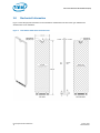
Intel® Solid-State Drive DC S3500 Series M.2 Product Specification Addendum Capacity: − 80GB, 120GB, 340GB − − − − − − − Windows 7*, Windows 8*, Windows 8.1* Windows* Server 2012 R2*, Windows Server 2012* Windows* Server 2008* Enterprise 32/64bit SP2 Windows* Server 2008* R2 SP1 Windows* Server 2003* Enterprise 64bit SP2 Red Hat* Enterprise Linux* 5.5, 5.6, 6.1, 6.3, 7.0 SUSE* Linux Enterprise Server 10*, 11 SP1CentOS* 64bit 5.7, 6.3 − Intel® SSD Toolbox with Intel® SSD Optimizer Components: − Intel® 20nm NAND Flash Memory − Multi-Level Cell (MLC) Form Factor: – Type 2280-D5-BM: 22mm x 80mm – Z-Height 1.5mm x 1.5mm Read and Write IOPS1,2 (Full LBA Range, IOMeter* Queue Depth 32) − − − − Random 4KB3 Reads: Up to 67,000 IOPS Random 4KB Writes: Up to 14,500 IOPS Random 8KB3 Reads: Up to 45,000 IOPS Random 8KB Writes: Up to 7,300 IOPS Bandwidth Performance1 − Sustained Sequential Read: Up to 470 MB/s4 − Sustained Sequential Write: Up to 320 MB/s Latency (average sequential) − Read: 50 µs (TYP) − Write: 65 µs (TYP) Quality of Service5, 6 AES 256-bit Encryption Compliance Product Ecological Compliance Power − RoHS* − Active: Up to 3.8W (TYP) − Idle: 500 mW − Power on to Ready after planned Shutdown: Typical 2 Sec. Weight: 11 grams ± 1 grams − SATA Revision 3.0; compatible with SATA 6Gb/s, 3Gb/s and 1.5Gb/s interface rates − ATA-ACS2 Rev-7; includes SCT (Smart Command Transport) and device statistics log support − SSD-enhanced SMART ATA feature set − Native Command Queuing (NCQ) command set − Data set management Trim command − SATAIO M.2 Card Format Version 11 Altitude7 − Operating: -1,000 to 10,000 ft − Operating8: -10,000 to 15,000 ft − Non-operating: -1,000 to 40,000 ft Power Management − − − − 1. 2. 3. 4. 5. 6. 7. 8. 9. 10. 3.3V Only SATA Interface Power Management Enhanced power-loss data protection DIPM and Hot plug/removal not Supported Temperature − − − − − Read/Write: 500 µs / 5 ms (99.9%) Compatibility Operating: 0° C to 70° C Non-Operating9: -55° C to 95° C Temperature monitoring and logging Thermal throttling Shock (operating and non-operating): 1,000 G/0.5 msec Vibration − Operating: 2.17 GRMS (5-700 Hz) − Non-Operating: 3.13 GRMS (5-800 Hz) Reliability − Uncorrectable Bit Error Rate (UBER): 1 sector per 10^17 bits read − Mean Time Between Failures (MTBF): 2 million hours − End-to-End data protection Endurance Rating10: − 80GB: Up to 45TB − 120GB: Up to 70TB − 340GB: Up to 180TB Certifications and Declarations − UL*, CE*, C-Tick*, BSMI*, KCC*, Microsoft WHCK*, VCCI*, SATA-IO Performance values vary by capacity and form factor Performance specifications apply to both compressible and incompressible data 4KB = 4,096 bytes; 8KB = 8,192 bytes MB/s = 1,000,000 bytes/second Based on Random 4KB QD=1 workload, measured as the time taken for 99.9 percent of commands to finish the round-trip from host to drive and back to host Measurement taken once the workload has reached steady state but including all background activities required for normal operation and data reliability Altitude pressure is simulated in a test chamber; excludes soft error Extended operation at a higher altitude might impact reliability Please contact your Intel representative for details on the non-operating temperature range Based on JESD218 standard Order number: 331061-002US Intel® Solid-State Drive DC S3500 Series (M.2) Ordering Information Contact your local Intel sales representative for ordering information. INFORMATION IN THIS DOCUMENT IS PROVIDED IN CONNECTION WITH INTEL PRODUCTS. NO LICENSE, EXPRESS OR IMPLIED, BY ESTOPPEL OR OTHERWISE, TO ANY INTELLECTUAL PROPERTY RIGHTS IS GRANTED BY THIS DOCUMENT. EXCEPT AS PROVIDED IN INTEL'S TERMS AND CONDITIONS OF SALE FOR SUCH PRODUCTS, INTEL ASSUMES NO LIABILITY WHATSOEVER AND INTEL DISCLAIMS ANY EXPRESS OR IMPLIED WARRANTY, RELATING TO SALE AND/OR USE OF INTEL PRODUCTS INCLUDING LIABILITY OR WARRANTIES RELATING TO FITNESS FOR A PARTICULAR PURPOSE, MERCHANTABILITY, OR INFRINGEMENT OF ANY PATENT, COPYRIGHT OR OTHER INTELLECTUAL PROPERTY RIGHT. UNLESS OTHERWISE AGREED IN WRITING BY INTEL, THE INTEL PRODUCTS ARE NOT DESIGNED NOR INTENDED FOR ANY APPLICATION IN WHICH THE FAILURE OF THE INTEL PRODUCT COULD CREATE A SITUATION WHERE PERSONAL INJURY OR DEATH MAY OCCUR. Intel may make changes to specifications and product descriptions at any time, without notice. Designers must not rely on the absence or characteristics of any features or instructions marked "reserved" or "undefined." Intel reserves these for future definition and shall have no responsibility whatsoever for conflicts or incompatibilities arising from future changes to them. The information here is subject to change without notice. Do not finalize a design with this information. Software and workloads used in performance tests may have been optimized for performance only on Intel microprocessors. Performance tests, such as SYSmark and MobileMark, are measured using specific computer systems, components, software, operations and functions. Any change to any of those factors may cause the results to vary. You should consult other information and performance tests to assist you in fully evaluating your contemplated purchases, including the performance of that product when combined with other products. The products described in this document may contain design defects or errors known as errata which may cause the product to deviate from published specifications. Current characterized errata are available on request. Intel Non-Volatile Memory Solutions Group (NSG) states that, through our Software Legal Compliance (SWLC) process, we have examined and evaluated firmware and software components that may accompany this Intel Solid-State Drive product, including embedded SSD firmware and any Intel-provided drivers. We conclude that there are no Open Source elements contained in these components. For more information about our SWLC process, please contact your Intel Representative. Contact your local Intel sales office or your distributor to obtain the latest specifications and before placing your product order. Copies of documents which have an order number and are referenced in this document, or other Intel literature, may be obtained by calling 1-800-548-4725, or go to: http://www.intel.com/design/literature.htm Intel and the Intel logo are trademarks of Intel Corporation in the U.S. and other countries. *Other names and brands may be claimed as the property of others. Copyright © 2015 Intel Corporation. All rights reserved. Product Specification Addendum 2 January 2015 331061-002US Intel® Solid-State Drive DC S3500 Series (M.2) Contents 1.0 Overview .......................................................................................................................................................................................................... 5 2.0 2.2 2.3 2.4 2.5 2.6 2.7 2.8 2.9 Product Specifications............................................................................................................................................................ 6 Performance ................................................................................................................................................................................ 6 Electrical Characteristics ....................................................................................................................................................... 8 Environmental Conditions .................................................................................................................................................... 9 Product Regulatory Compliance ..................................................................................................................................... 10 Reliability ................................................................................................................................................................................... 10 Temperature Sensor ............................................................................................................................................................ 11 Thermal Considerations ..................................................................................................................................................... 11 Hot Plug Support ................................................................................................................................................................... 11 3.0 Mechanical Information ......................................................................................................................................................................... 12 4.0 Pin and Signal Descriptions ................................................................................................................................................................. 13 5.0 References ................................................................................................................................................................................................... 14 Appendix A: IDENTIFY DEVICE Command Data ....................................................................................................................................... 15 Tables Table 1: Table 2: Table 3: Table 4: Table 5: Table 6: Table 7: Table 8: Table 9: Table 10: Table 11: Table 12: Table 13: Table 14: User Addressable Sectors ........................................................................................................................................................ 6 Random Read/Write Input/Output Operations Per Second (IOPS) ...................................................................... 6 Random Read/Write IOPS Consistency ............................................................................................................................. 6 Sequential Read and Write Bandwidth............................................................................................................................... 7 Latency .............................................................................................................................................................................................. 7 Quality of Service.......................................................................................................................................................................... 7 Operating Voltage for M.2 Form Factor ............................................................................................................................. 8 Power Consumption for M.2 Form Factor......................................................................................................................... 8 Temperature, Shock, Vibration for Intel® SSD DC S3500 Series M.2 Form Factor ........................................ 9 Product Regulatory Compliance.......................................................................................................................................... 10 Reliability Specifications ......................................................................................................................................................... 10 Serial ATA, M.2 and Socket 2 Pin-out ............................................................................................................................... 13 Standards References .............................................................................................................................................................. 14 Returned Sector Data ............................................................................................................................................................... 15 Figures Figure 1: Intel® SSD DC S3500 Series M.2 Dimensions ............................................................................................................... 12 January 2015 331061-002US Product Specification Addendum 3 Intel® Solid-State Drive DC S3500 Series (M.2) Revision History Revision 001 002 Description Date Initial release November 2014 • Updated description and value of word 106 in Appendix A’s Returned Sector Data table. • Updated M.2 dimensions graphic (figure 1) in section 3.0, "Mechanical Information." January 2015 Related Document Title Intel® Solid-State Drive DC S3500 Series Product Specification Product Specification Addendum 4 Link http://www.intel.com/content/dam/www/public/us/en/documents/product-specifi cations/ssd-dc-s3500-spec.pdf January 2015 331061-002US Intel® Solid-State Drive DC S3500 Series (M.2) 1.0 Overview This document describes the specifications and capabilities of the Intel® Solid-State Drive (SSD) Data Center (DC) S3500 Series specific to the M.2 Form Factor. The Intel SSD DC S3500 Series delivers leading performance and Quality of Service combined with world-class reliability for Serial Advanced Technology Attachment (SATA) interface-enabled computers in three capacities: 80GB, 120GB and 340GB in the M.2 Form Factor. By combining 20nm Intel® NAND Flash Memory technology with SATA 6 Gb/s interface support, the Intel SSD DC S3500 Series M.2 delivers sequential read speeds of up to 470 MB/s and sequential write speeds of up to 320 MB/s. Intel SSD DC S3500 Series delivers Quality of Service of 500 µs for random 4KB reads measured at a queue depth of 1. Intel SSD DC S3500 Series M.2 offers these key features: • • • • • • • • • • • • Standard Endurance Technology Higher IO and throughput performance Consistent IO latency Enhanced power-loss data protection features End-to-End data protection Thermal throttling Temperature Sensor Inrush current management Low power Higher reliability Temperature monitor and logging Power loss protection capacitor self-test January 2015 331061-002US Product Specification Addendum 5 Intel® Solid-State Drive DC S3500 Series (M.2) 2.0 Product Specifications 2.1 Capacity Table 1: User Addressable Sectors Unformatted Capacity Intel SSD DC S3500 Series (Total User Addressable Sectors in LBA Mode) 80GB1 156,301,4882 120GB 234,441,648 340GB 664,212,528 Notes: 1. 1GB = 1,000,000,000 bytes; 1 sector = 512 bytes 2. LBA count shown represents total user storage capacity and will remain the same throughout the life of the drive. 2.2 Performance Table 2: Random Read/Write Input/Output Operations Per Second (IOPS) Specification1 Unit Random 4KB Read (up to)1 Intel SSD DC S3500 Series 80GB 120GB 340GB IOPS 67,0003 67,000 67,000 Random 4KB Write (up to) IOPS 8,300 12,000 14,500 Random 8KB Read (up to)2 IOPS 38,000 45,000 45,000 Random 8KB Write (up to) IOPS 4,200 6,100 7,300 Notes: 1. 4KB = 4,096 bytes 2. 8KB = 8,192 bytes 3. Performance measured using IOMeter* with Queue Depth 32. Measurements are performed on a full Logical Block Address (LBA) span of the drive. Table 3: Random Read/Write IOPS Consistency Specification1 Unit Random 4KB Read (up to)2 Intel SSD DC S3500 Series 80GB 120GB 340GB % 903 90 95 Random 4KB Write (up to) % 85 90 90 Random 8KB Read (up to)3 % 90 90 95 Random 8KB Write (up to) % 84 90 90 Notes: 1. Performance consistency measured using IOMeter* based on Random 4KB QD=32 workload, measured as the (IOPS in the 99.9th percentile slowest 1-second interval)/(average IOPS during the test). Measurements are performed on a full Logical Block Address (LBA) span of the drive once the workload has reached steady state but including all background activities required for normal operation and data reliability. 2. 4KB = 4,096 bytes 3. 8KB = 8,192 bytes Product Specification Addendum 6 January 2015 331061-002US Intel® Solid-State Drive DC S3500 Series (M.2) Table 4: Sequential Read and Write Bandwidth Intel SSD DC S3500 Series Specification Unit 80GB 120GB 340GB Sequential Read (SATA 6Gb/s)1 MB/s 340 440 480 Sequential Write (SATA 6Gb/s)1 MB/s 110 160 355 Note: 1. Performance measured using IOMeter* with 128 KB (131,072 bytes) of transfer size with Queue Depth 32. Table 5: Latency Intel SSD DC S3500 Series Specification 80GB, 120GB 340GB Read 50 µs 50 µs Write 65us 65us Power On to Ready2 2.0 s 3.0 s Latency1 (TYP) Notes: 1. Device measured using IOMeter. Latency measured using 4 KB (4,096 bytes) transfer size with Queue Depth equal to 1 on a sequential workload. 2. Power On To Ready time assumes proper shutdown. Time varies if shutdown is not preceded by STANDBY IMMEDIATE command. Table 6: Quality of Service Intel SSD DC S3500 Series Specification Unit Queue Depth=1 Queue Depth=32 80GB, 120GB 340GB 80GB, 120GB 340GB Quality of Service1,2 (99.9%) Reads ms 0.5 0.5 5 5 Writes ms 5 0.5 15 10 Reads ms 5 5 5 10 Writes ms 15 10 20 20 Quality of Service1, 2 (99.9999%) Notes: 1. Device measured using IOMeter. Quality of Service measured using 4KB (4,096 bytes) transfer size on a random workload on a full Logical Block Address (LBA) span of the drive once the workload has reached steady state but including all background activities required for normal operation and data reliability. 2. Based on Random 4KB QD=1, 32 workloads, measured as the time taken for 99.9(or 99.9999) percentile of commands to finish the round-trip from host to drive and back to host. January 2015 331061-002US Product Specification Addendum 7 Intel® Solid-State Drive DC S3500 Series (M.2) 2.3 Electrical Characteristics Table 7: Operating Voltage for M.2 Form Factor Intel SSD DC S3500 Series Electrical Characteristics 80 GB 120 GB 340 GB Operating Voltage for 3.3V (±5%) Min 3.13V Max 3.47V Inrush Current (Typical Peak) 1 1.2 A, < 1 s PLI Capacitor Charge Voltage2 Average 34 Volts Note: 1. Measured from initial device power supply application. 2. This is the voltage stored in the onboard capacitors used to save data held in the DRAM to NAND in the event of an unplanned power loss. As the electronic components are exposed, care must be taken not to allow the M.2 drive to touch other electronic devices if removed from the circuit until the capacitors have fully discharged. Allow 10 minutes for full discharge. Table 8: Power Consumption for M.2 Form Factor Specification Active Write - RMS Average Active Write - Burst Unit 1 2 Intel SSD DC3500 Series 80GB 120GB 340GB W 1.9 2.3 3.8 W 2.1 2.5 4.5 Active Write - MAX Burst 3 W 3.7 4.2 5.9 Active Read - RMS Average 4 W 1.7 1.9 2.0 Active Read - Burst 5 W 1.9 2.1 2.4 W 3.4 3.6 3.6 W 0.5 0.5 0.5 Active Read - MAX Burst 6 Idle Notes: 1. The workload equates 128 KB (131,072 bytes) Queue Depth equal to 32 sequential writes. RMS (Root Mean Squared) Average Power is measured using Agilent Power Analyzer over a 100 ms sample period with PLI capacitor charge enabled. 2. The workload equates 128 KB (131,072 bytes) Queue Depth equal to 32 sequential writes. RMS (Root Mean Squared) Burst Power is measured using Agilent Power Analyzer over a 500 µs sample period with PLI capacitor charge disabled. 3. The workload equates 128 KB (131,072 bytes) Queue Depth equal to 32 sequential writes. RMS (Root Mean Squared) Max Burst power is measured using Agilent Power Analyzer over a 500 µs sample period with PLI capacitor charge enabled. Pulse is 0.25% of total time. 4. The workload equates 128 KB (131,072 bytes) Queue Depth equal to 32 sequential reads. RMS (Root Mean Squared) average power is measured using Agilent Power Analyzer over a 100 ms sample period with PLI capacitor charge enabled. 5. The workload equates 128 KB (131,072 bytes) Queue Depth equal to 32 sequential reads. RMS (Root Mean Squared) burst power is measured using Agilent Power Analyzer over a 500 µs sample period with PLI capacitor charge disabled. 6. The workload equates 128 KB (131,072 bytes) Queue Depth equal to 32 sequential reads. RMS (Root Mean Squared) Max Burst power is measured using Agilent Power Analyzer over a 500 µs sample period with PLI capacitor charge enabled. Pulse is approximately 0.25% of total time. Product Specification Addendum 8 January 2015 331061-002US Intel® Solid-State Drive DC S3500 Series (M.2) 2.4 Environmental Conditions Table 9: Temperature, Shock, Vibration for Intel SSD DC S3500 Series M.2 Form Factor Temperature PCB Temperature1 Operating Non-operating2 Temperature Gradient3 Operating Non-operating Range 0 – 70 oC -55 – 95 oC 30 oC/hr (Typical) 30 oC/hr (Typical) Thermal Throttling Full Performance Temperature Range Reduced Performance Temperature4 0 – 59 oC 60 -70 oC Humidity Operating Non-operating 5 – 95 % 5 – 95 % Shock and Vibration Range Shock5 Operating Non-operating 1,000 G at 0.5 msec 1,000 G at 0.5 msec Vibration6 Operating Non-operating 2.17 GRMS (5-700 Hz) 3.13 GRMS (5-800 Hz) Notes: 1. PCB temperature is best represented by the onboard temperature sensor data reported by the SMART BEh/C2h attributes. 2. Please contact your Intel representative for details on the non-operating temperature range. 3. Temperature gradient measured without condensation. 4. Thermal throttling (reduction of read/write performance helps to control device temperature). 5. Shock specifications assume the SSD is mounted securely with the input shock pulse applied to the drive-mounting screws. Stimulus may be applied in the X±, Y± or Z± axis. Shock specification is measured using the amplitude value (G) and the duration value (msec) of the shock pulse. 6. Vibration specifications assume the SSD is mounted securely with the input vibration applied to the drive-mounting screws. Stimulus may be applied in the X, Y or Z axis. Vibration specification is measured using RMS value. January 2015 331061-002US Product Specification Addendum 9 Intel® Solid-State Drive DC S3500 Series (M.2) 2.5 Product Regulatory Compliance Intel SSD DC S3500 Series meets or exceeds the regulatory or certification requirements in the following table: Table 10: Product Regulatory Compliance Title Region For Which Conformity Declared Description TITLE 47-Telecommunications CHAPTER 1— FEDERAL COMMUNMICATIONS COMMISSION PART 15 — RADIO FREQUENCY DEVICES ICES*-003, Issue 4 Interference-Causing Equipment Standard Digital Apparatus FCC Part 15B Class B USA CA/CSA-CEI/IEC CISPR 22-10 (Ref. CISPR 22:2008). Canada IEC* 55024 Information Technology Equipment — Immunity characteristics— Limits and methods of measurement CISPR24:2010 EN-55024: 2010 and its amendments European Union IEC* 55022 Information Technology Equipment — Radio disturbance Characteristics— Limits and methods of measurement CISPR22:2008 (Modified) EN-55022: 2010 and its amendments European Union EN-60950-1 2nd Edition Information Technology Equipment — Safety — Part 1: General Requirements USA/Canada UL/CSA EN-60950-1 2nd Edition Information Technology Equipment — Safety — Part 1: General Requirements USA/Canada 2.6 Reliability Intel SSD DC S3500 Series meets or exceeds SSD endurance and data retention requirements as specified in the JESD218 standard. Reliability specifications are listed in the following table: Table 11: Reliability Specifications Parameter Value Uncorrectable Bit Error Rate (UBER) Uncorrectable bit error rate will not exceed one sector in the specified number of bits read. In the unlikely event of a non-recoverable read error, the SSD will report it as a read failure to the host; the sector in error is considered corrupt and is not returned to the host. < 1 sector per 1017 bits read Mean Time Between Failures (MTBF) Mean Time Between Failures is estimated based on Telcordia* methodology and demonstrated through Reliability Demonstration Test (RDT). 2 million hours Power On/Off Cycles Power On/Off Cycles is defined as power being removed from the SSD, and then restored. Most host systems remove power from the SSD when entering suspend and hibernate as well as on a system shutdown. 24 per day Insertion Cycles1 Data Retention The time period for retaining data in the NAND at maximum rated endurance. Product Specification Addendum 10 N/A 3 months power-off retention once SSD reaches rated write endurance at 40 °C January 2015 331061-002US Intel® Solid-State Drive DC S3500 Series (M.2) Parameter Endurance Rating2 The number of drive writes such that the SSD meets the requirements according to the JESD2182 standard and JESD219 workload. Value 80 GB: Up to 45 TB 120 GB: Up to 70 TB 340 GB: Up to 180 TB Notes: 1. The M.2 Standard does not support Hot plug operations and therefore does not specify Insertion cycles 2. Refer to JESD218 standard table 1 for UBER, FFR and other Enterprise SSD endurance verification requirements. UBER design and majority of life target is 1E-17. Endurance verification acceptance criterion based on establishing < 1E-16 at 60% confidence. 2.7 Temperature Sensor The Intel SSD DC S3500 Series has an onboard temperature sensor with an accuracy of +/-2C over a range of -20C to +80C which can be monitored using two SMART attributes: Airflow Temperature (BEh) and Device Internal Temperature (C2h). The M.2 product will report the same value for both SMART attributes. 2.8 Thermal Considerations Because there is no enclosure on the device, the Intel SSD DC S3500 Series M.2 form factor requires thermal considerations in both device location and airflow design within the system environment. The system design must guarantee that the M.2 SSD does not exceed the PCB temperature specification (as defined in Table 9) by providing the proper amount of forced airflow. As temperatures approach the PCB maximum temperature specification (as defined in Table 9), thermal throttling will activate, reducing the total power consumed, which has the effect of slowing write performance to help reduce operating temperature (read performance may also be reduced). As the PCB temperature lowers, the throttling operation deactivates and the M.2 SSD will return to normal operating performance after reaching the full performance temperature range. 2.9 Hot Plug Support Hot plug is not supported in the M.2 Specification. However, the DC S3500 M.2 can support hot plug operations when used with an interposer design that electrically supports hot plug operations. User Data is protected from planned or unplanned power loss by the Enhanced Power Management technology on the DC S3500 Series. January 2015 331061-002US Product Specification Addendum 11 Intel® Solid-State Drive DC S3500 Series (M.2) 3.0 Mechanical Information Figure 1 shows the physical information for the Intel SSD DC S3500 Series M.2 form factor type 2280-D5-BM. All dimensions are in millimeters. Figure 1: Intel SSD DC S3500 Series M.2 Dimensions Product Specification Addendum 12 January 2015 331061-002US Intel® Solid-State Drive DC S3500 Series (M.2) 4.0 Pin and Signal Descriptions Table 12: Serial ATA, M.2 and Socket 2 Pin-out Pin Function Function Pin 74 3.3V GND 75 72 3.3V GND 73 70 3.3V GND 71 68 N/C GND 69 x Module Key M N/C 67 x Module Key M Module Key M x x Module Key M Module Key M x x x Module Key M Module Key M 58 Reserved for MFG_CLOCK Module Key M x 56 Reserved for MFG_DATA GND 57 54 N/C N/C 55 52 N/C N/C 53 50 N/C GND 51 48 N/C SATA-A+ 49 46 N/C SATA-A- 47 44 N/C GND 45 42 N/C SATA-B- 43 40 N/C SATA-B+ 41 38 DEVSLP (I) GND 39 36 N/C N/C 37 34 N/C N/C 35 32 N/C GND 33 30 N/C N/C 31 28 N/C N/C 29 26 N/C GND 27 24 N/C N/C 25 22 N/C N/C 23 20 N/C GND 21 x Module Key B Module Key B x x Module Key B Module Key B x x Module Key B Module Key B x x Module Key B Module Key B x 10 DAS/DSS#(I/O) N/C 11 8 N/C N/C 9 6 N/C N/C 7 4 3.3V N/C 5 2 3.3V GND 3 GND 1 January 2015 331061-002US Product Specification Addendum 13 Intel® Solid-State Drive DC S3500 Series (M.2) 5.0 References The following table identifies the standards information referenced in this document. Table 13: Standards References Date Title Location 2013 PCI Express M.2 Specification, Revision 1.0 http://www.pcisig.com/specifications/pciex press/M.2_Specification/ July 2012 Solid-State Drive (SSD) Requirements and Endurance Test Method (JESD219) http://www.jedec.org/standards-document s/results/jesd219 Sept 2010 Solid-State Drive (SSD) Requirements and Endurance Test Method (JESD218) http://www.jedec.org/standards-document s/docs/jesd218/ June 2009 RoHS* http://qdms.intel.com/ Click Search MDDS Database and search for material description datasheet August 2009 ACS-2-ATA/ATAPI Command Set 2 Specification http://www.t13.org/ June 2009 Serial ATA Revision 3.0 http://www.sata-io.org/ Dec 2008 VCCI http://www.vcci.jp/vcci_e/ May 2006 SFF-8223, 2.5-inch Drive w/Serial Attachment Connector http://www.sffcommittee.org/ May 2005 SFF-8201, 2.5-inch drive form factor http://www.sffcommittee.org/ International Electrotechnical Commission EN 61000 1995 4-2 (Electrostatic discharge immunity test) 1996 4-3 (Radiated, radio-frequency, electromagnetic field immunity test) 1995 4-4 (Electrical fast transient/burst immunity test) 1995 4-5 (Surge immunity test) 1997 4-6 (Immunity to conducted disturbances, induced by radiofrequency fields) 1994 http://www.iec.ch/ 4-11 (Voltage Variations, voltage dips, short interruptions and voltage variations immunity tests) 1995 ENV 50204 (Radiated electromagnetic field from digital radio telephones) Product Specification Addendum 14 http://www.dbicorporation.com/radimmun. htm/ January 2015 331061-002US Intel® Solid-State Drive DC S3500 Series (M.2) Appendix A: IDENTIFY DEVICE Command Data Table 14: Returned Sector Data Word F = Fixed V = Variable X = Both Default Value Description 0 X 0040h General configuration bit-significant information 1 X 3FFFh Obsolete - Number of logical cylinders (16,383) 2 V C837h Specific configuration 3 X 0010h Obsolete - Number of logical heads (16) 4-5 X 0h 6 X 003Fh 7-8 V 0h Reserved for assignment by the CompactFlash* Association (CFA) Retired Retired Obsolete - Number of logical sectors per logical track (63) 9 X 0h 10-19 F varies 20-21 X 0h Retired 22 X 0h Obsolete Serial number (20 ASCII characters) 23-26 F varies Firmware revision (8 ASCII characters) 27-46 F varies Model number (Intel® Solid-State Drive) 47 F 8001h 7:0—Maximum number of sectors transferred per interrupt on multiple commands 48 F 4000h Trusted Computing Feature Set 49 F 2F00h Capabilities 50 F 4000h Capabilities 51-52 X 0h 53 F 0007h Words 88 and 70:64 valid 54 X 3FFFh Obsolete - Number of logical cylinders (16,383) 55 X 0010h Obsolete - Number of logical heads (16) 56 X 003Fh Obsolete - Number of logical sectors per logical track (63) 57-58 X FC1000FBh 59 F B101 60-62 V 120GB: 0DF94B80h Obsolete Obsolete Number of sectors transferred per interrupt on multiple commands 80GB: 0950F8B0h Total number of user-addressable sector 340GB: 0FFFFFFFh 63 X 0007h Multi-word DMA modes supported/selected 64 F 0003h PIO modes supported 65 F 0078h Minimum multiword DMA transfer cycle time per word 66 F 0078h Manufacturer’s recommended multiword DMA transfer cycle time 67 F 0078h Minimum PIO transfer cycle time without flow control 68 F 0078h Minimum PIO transfer cycle time with IORDY flow control 69 F 4030h Additional Supported 70 F 0000h Reserved 71-74 F 0h 75 F 001Fh Queue depth 76 F 850Eh Serial ATA capabilities 77 F 0006h Reserved for future Serial ATA definition January 2015 331061-002US Reserved for IDENTIFY PACKET DEVICE command Product Specification Addendum 15 Intel® Solid-State Drive DC S3500 Series (M.2) Word F = Fixed V = Variable X = Both Default Value Description 78 F 0040h Serial ATA features supported 79 V 0040h Serial ATA features enabled 80 F 03FCh Major version number 81 F 0110h Minor version number 82 F 746Bh Command set supported 83 F 7501h Command sets supported 84 F 6163h Command set/feature supported extension 85 X 7469h Command set/feature enabled 86 X B401h Command set/feature enabled 87 X 6163h Command set/feature default 88 X 407Fh Ultra DMA Modes 89 F 0002h Time required for security erase unit completion 90 F 0002h Time required for enhanced security erase completion 91 V 0h 92 V 0FFFEh 93 X 0h Hardware reset result: the contents of bits (12:0) of this word shall change only during the execution of a hardware reset 94 V 0h Vendor’s recommended and actual acoustic management value 95 F 0h Stream minimum request size 96 V 0h Streaming transfer time - DMA Current advanced power management value Master Password Revision Code 97 V 0h Streaming access latency - DMA and PIO 98-99 F 0h Streaming performance granularity 100-103 V 120GB: 0DF94BB0h 80GB: 0950F8B0h Maximum user LBA for 48-bit address feature set 340GB: 27971430h 104 V 0h Streaming transfer time - PIO 105 V 0006h Maximum number of 512-byte blocks of LBA Range Entries per DATA SET MANAGEMENT command 106 F 6003h Default Physical sector size / logical sector size. 0004h to reflect 512Bytes/Sector Can be changed to 107 F 0h 108-111 F varies Inter-seek delay for ISO-7779 acoustic testing in microseconds 112-115 F 0h Reserved for world wide name extension to 128 bits 116 V 0h Reserved for technical report 117-118 F 0h Words per logical sector 119 F 405Ch Supported settings 120 X 401Ch Command set/feature enabled/supported 121-126 F 0h Reserved 127 X 0h Removable Media Status Notification feature set support Unique ID 128 X 0021h Security status 129 V 001Ch Vendor-specific 130-159 X 0h Vendor-specific 160 X 0h CompactFlash Association (CFA) power mode 1 161-167 X 0h Reserved for assignment by the CFA 168 X 0003h Reserved for assignment by the CFA Product Specification Addendum 16 January 2015 331061-002US Intel® Solid-State Drive DC S3500 Series (M.2) Word F = Fixed V = Variable X = Both 169 X Default Value 0001h Description Data set management Trim attribute support 170-175 F 0h 176-205 V Varies Reserved for assignment by the CFA Current media serial number 206 X 003Dh SCT Command Transport 207-208 F 0000h Reserved 209 X 4000h Alignment of logical blocks within a physical block 210-211 V 0000h Write-Read-Verify Sector Count Mode 3 (DWord) 212-213 F 0000h Write-Read-Verify Sector Count Mode 2 (DWord) 214 X 0000h NV Cache Capabilities 215-216 V 0000h NV Cache Size in Logical Blocks (DWord) 217 F 0001h Nominal media rotation rate 218 V 0000h Reserved 219 F 0000h NV Cache Options 220 V 0000h Write-Read-Verify feature set 221 X 0000h Reserved 222 F 101Fh Transport major version number 223 F 0000h Transport minor version number 224-229 F 0000h Reserved 230-233 X 0000h Extended Number of User Addressable Sectors (QWord) 234 F 0001h Minimum number of 512-byte data blocks per DOWNLOAD MICROCODE command for mode 03h 235 F FFFFh Maximum number of 512-byte data blocks per DOWNLOAD MICROCODE command for mode 03h 236-254 X 0000h Reserved 255 V 52A5 Integrity word Notes: F = Fixed. The content of the word is fixed and does not change. For removable media devices, these values may change when media is removed or changed. V = Variable. The state of at least one bit in a word is variable and may change depending on the state of the device or the commands executed by the device. X = F or V. The content of the word may be fixed or variable. January 2015 331061-002US Product Specification Addendum 17