1
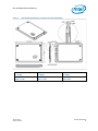
Intel® Solid-State Drive DC S3700 Series
Product Specification
Capacity: 2.5-inch: 100GB, 200GB, 400GB, 800GB
1.8-inch: 200GB, 400GB
Components:
− Intel® 25nm NAND Flash Memory
− High Endurance Technology (HET) Multi-Level Cell
(MLC)
Form Factors: 2.5-inch and 1.8-inch
Read and Write IOPS1,2 (Full LBA Range, IOMeter* Queue
Depth 32)
− Random 4KB3 Reads: Up to 75,000 IOPS
− Random 4KB Writes: Up to 36,000 IOPS
1.
2.
3.
4.
5.
6.
7.
8.
9.
10.
11.
12.
− Random 8KB3 Reads: Up to 47,500 IOPS
− Random 8KB Writes: Up to 20,000 IOPS
Bandwidth Performance1
− Sustained Sequential Read: Up to 500 MB/s4
− Sustained Sequential Write: Up to 460 MB/s
Endurance: 10 drive writes per day5 for 5 years
Latency (average sequential)
− Read: 50 µs (TYP)
− Write: 65 µs (TYP)
Quality of Service6,8
− Read/Write: 500 µs (99.9%)
Performance Consistency7,8
Read/Write: Up to 90%/90% (99.9%)
AES 256-bit Encryption
Altitude (simulated)
– Operating: -1,000 to 10,000 ft
– Operating9: 10,000 to 15,000 ft
– Non-operating: -1,000 to 40,000 ft
Product Ecological Compliance
− RoHS*
Compliance
− SATA Revision 3.0; compatible with SATA 6Gb/s, 3Gb/s
and 1.5Gb/s interface rates
− ATA/ATAPI command Set – 2 (ACS-2); includes SCT
(Smart Command Transport) and device statistics log
support
− Enhanced SMART ATA feature set
− Native Command Queuing (NCQ) command set
− Data set management Trim command
Power Management
− 2.5-inch: 5V or 12V SATA Supply Rail10
− 1.8-inch: 3.3V SATA Supply Rail
− SATA Interface Power Management
− OS-aware hot plug/removal
− Enhanced power-loss data protection
Power11
− Active: Up to 6 W (TYP)
− Idle: 650 mW
Weight:
− 2.5” 200, 400, 800GB: 73.6 grams ± 2 grams
− 2.5” 100GB: 70 grams ± 2 grams
− 1.8” 200, 400GB: 38 grams ± 2 grams
Temperature
− Operating: 0o C to 70o C
− Non-Operating12: -55o C to 95o C
− Temperature monitoring and logging
− Thermal throttling
Shock (operating and non-operating):
− 1,000 G/0.5 msec
Vibration
− Operating: 2.17 GRMS (5-700 Hz)
− Non-operating: 3.13 GRMS (5-800 Hz)
Reliability
− Uncorrectable Bit Error Rate (UBER):
1 sector per 10^17 bits read
− Mean Time Between Failures (MTBF):
2 million hours
− End-to-End data-path protection
Certifications and Declarations
− UL*, CE*, C-Tick*, BSMI*, KCC*, Microsoft* WHCK*,
VCCI*, SATA-IO*
Compatibility
− Windows* 7 and Windows* 8
− Windows* Server 2012
− Windows* Server 2008 Enterprise 32/64bit SP2
− Windows* Server 2008 R2 SP1
− Windows* Server 2003 Enterprise R2 64bit SP2
− Red Hat* Enterprise Linux* 5.5, 5.6, 6.1, 6.3
− SUSE* Linux* Enterprise Server 10, 11 SP1
− CentOS* 64bit 5.7, 6.3
− Intel® SSD Toolbox with Intel® SSD Optimizer
Performance values vary by capacityandformfactor
Performance specifications apply to both compressible and incompressible data
4KB = 4,096 bytes; 8KB = 8,192 bytes.
MB/s = 1,000,000 bytes/second
Based on JESD218 standard. For 200GB 1.8 inches drive, it is 9.8 drives write per day.
Based on Random 4KB QD=1 workload, measured as the time taken for 99.9 percentile of commands to finish the round-trip from host to drive and back to host
Based on Random 4KB QD=32 workload, measured as the (IOPS in the 99.9th percentile slowest 1-second interval)/(average IOPS during the test)
Measurement taken once the workload has reached steady state but including all background activities required for normal operation and data reliability
Extended operation at a higher altitude might impact reliability.
Defaults to 12V, if both 12V and 5V are present
Based on 5V supply; refer to Table 7 for more details
Please contact your Intel representative for details on the non-operating temperature range
Order Number: 328171-010US
Ordering Information
Contact your local Intel sales representative for ordering information.
INFORMATION IN THIS DOCUMENT IS PROVIDED IN CONNECTION WITH INTEL PRODUCTS. NO LICENSE, EXPRESS OR IMPLIED, BY ESTOPPEL OR OTHERWISE, TO ANY
INTELLECTUAL PROPERTY RIGHTS IS GRANTED BY THIS DOCUMENT. EXCEPT AS PROVIDED IN INTEL'S TERMS AND CONDITIONS OF SALE FOR SUCH PRODUCTS,
INTEL ASSUMES NO LIABILITY WHATSOEVER AND INTEL DISCLAIMS ANY EXPRESS OR IMPLIED WARRANTY, RELATING TO SALE AND/OR USE OF INTEL PRODUCTS
INCLUDING LIABILITY OR WARRANTIES RELATING TO FITNESS FOR A PARTICULAR PURPOSE, MERCHANTABILITY, OR INFRINGEMENT OF ANY PATENT, COPYRIGHT OR
OTHER INTELLECTUAL PROPERTY RIGHT.
A "Mission Critical Application" is any application in which failure of the Intel Product could result, directly or indirectly, in personal injury or death. SHOULD YOU
PURCHASE OR USE INTEL'S PRODUCTS FOR ANY SUCH MISSION CRITICAL APPLICATION, YOU SHALL INDEMNIFY AND HOLD INTEL AND ITS SUBSIDIARIES,
SUBCONTRACTORS AND AFFILIATES, AND THE DIRECTORS, OFFICERS, AND EMPLOYEES OF EACH, HARMLESS AGAINST ALL CLAIMS COSTS, DAMAGES, AND
EXPENSES AND REASONABLE ATTORNEYS' FEES ARISING OUT OF, DIRECTLY OR INDIRECTLY, ANY CLAIM OF PRODUCT LIABILITY, PERSONAL INJURY, OR DEATH
ARISING IN ANY WAY OUT OF SUCH MISSION CRITICAL APPLICATION, WHETHER OR NOT INTEL OR ITS SUBCONTRACTOR WAS NEGLIGENT IN THE DESIGN,
MANUFACTURE, OR WARNING OF THE INTEL PRODUCT OR ANY OF ITS PARTS.
Intel may make changes to specifications and product descriptions at any time, without notice. Designers must not rely on the absence or characteristics of any features or
instructions marked "reserved" or "undefined." Intel reserves these for future definition and shall have no responsibility whatsoever for conflicts or incompatibilities
arising from future changes to them. The information here is subject to change without notice. Do not finalize a design with this information.
Software and workloads used in performance tests may have been optimized for performance only on Intel microprocessors. Performance tests, such as SYSmark and
MobileMark, are measured using specific computer systems, components, software, operations and functions. Any change to any of those factors may cause the results to
vary. You should consult other information and performance tests to assist you in fully evaluating your contemplated purchases, including the performance of that product when combined with other products.
The products described in this document may contain design defects or errors known as errata which may cause the product to deviate from published specifications.
Current characterized errata are available on request.
Contact your local Intel sales office or your distributor to obtain the latest specifications and before placing your product order.
Copies of documents which have an order number and are referenced in this document, or other Intel literature, may be obtained by calling 1-800-548-4725, or go to:
http://www.intel.com/design/literature.htm
Low Halogen applies only to brominated and chlorinated flame retardants (BFRs/CFRs) and PVC in the final product. Intel components as well as purchased components
on the finished assembly meet JS-709 requirements, and the PCB/substrate meet IEC 61249-2-21 requirements. The replacement of halogenated flame retardants
and/or PVC may not be better for the environment.
Intel and the Intel logo are trademarks of Intel Corporation in the U.S. and other countries.
*Other names and brands may be claimed as the property of others.
Copyright © 2015 Intel Corporation. All rights reserved.
Product Specification
2
January 2015
328171-010US
Intel® Solid-State Drive DC S3700 Series
Contents
Revision History ........................................................................................................................................................................ 4
Terms and Acronyms................................................................................................................................................................ 5
1.0
Overview....................................................................................................................................................................... 6
2.0
Product Specifications............................................................................................................................................... 7
2.1
2.2
2.3
2.4
2.5
2.6
2.7
2.8
2.9
Capacity ......................................................................................................................................................................................... 7
Performance ................................................................................................................................................................................ 7
Electrical Characteristics........................................................................................................................................................ 9
Environmental Conditions ................................................................................................................................................. 11
Product Regulatory Compliance ..................................................................................................................................... 12
Reliability ................................................................................................................................................................................... 12
Temperature Sensor............................................................................................................................................................. 13
Power Loss Capacitor Test ................................................................................................................................................ 13
Hot Plug Support ................................................................................................................................................................... 13
3.0
Mechanical Information ......................................................................................................................................... 14
4.0
Pin and Signal Descriptions .................................................................................................................................. 16
4.1
4.2
4.3
4.4
5.0
2.5-inch Form Factor Pin Locations .............................................................................................................................. 16
1.8-inch Form Factor Pin Locations .............................................................................................................................. 16
Connector Pin Signal Definitions .................................................................................................................................... 17
Power Pin Signal Definitions............................................................................................................................................. 17
Supported Command Sets..................................................................................................................................... 19
5.1
5.2
5.3
5.4
5.5
5.6
5.7
5.8
5.9
5.10
5.11
5.12
ATA General Feature Command Set ............................................................................................................................. 19
Power Management Command Set............................................................................................................................... 19
Security Mode Feature Set ................................................................................................................................................ 20
SMART Command Set ......................................................................................................................................................... 20
Device Statistics ...................................................................................................................................................................... 27
SMART Command Transport (SCT) ............................................................................................................................... 28
Data Set Management Command Set .......................................................................................................................... 28
Host Protected Area Command Set .............................................................................................................................. 28
48-Bit Address Command Set ......................................................................................................................................... 29
General Purpose Log Command Set............................................................................................................................. 29
Native Command Queuing ................................................................................................................................................ 29
Software Settings Preservation ....................................................................................................................................... 29
6.0
Certifications and Declarations ............................................................................................................................ 30
7.0
References................................................................................................................................................................. 31
Appendix A: IDENTIFY DEVICE Command Data ............................................................................................................... 32
January 2015
328171-010US
Product Specification
3
Intel® Solid-State Drive DC S3700 Series
Revision History
Date
Revision
October 2012
001
Initial release
November 2012
002
Updated Power On to Ready specification for 800 GB capacity
February 2013
003
Updated: OS Compatibility; Certifications and Declarations; Power Pin Signal Definitions;
SMART Attributes descriptions
March 2013
004
Edited for clarity
April 2013
005
Updated Device Identify Table; SMART Attribute Definition. Endurance spec for 1.8-inch
200 GB drive, voltage spec
June 2013
006
Added X,Y, Z dimension in section 3.0
007
Page 1: Compliance, Changed from ATA8-ACS2 to ATA9-ACS2
Table 14: Changed Endurance Rating Value
Table 18: Changed SMART Attribute E9h, PW and Threshold values to 1.
Section 5.4.1.1: Added User Notes and changed step 6 in Use Case 2.
Appendix A: Changes to Words 59-62, 80, 81, 89, 90, 129-159, 176-205 and 255.
April 2014
008
Page 1: Compliance, Changed from ATA9-ACS2 to ATA/ATAPI Command Set - 2 (ACS-2)
Table 9: Added footnotes
Table 10: Footnote corrections
Table 11: Title correction
Appendix A: Changed Default Value of Word 105 from 0004h to 0006h
September 2014
009
Page 1: Altitude spec change with added footnote (note 9).
Table 14: Updated footnote for Reliability table
Table 18: Updated SMART attribute B8h description and changed threshold values
January 2015
010
In Section 5.6, added clarification to word 106 of Identify Device Command and SCT
command process to change the reported value.
March 2014
Product Specification
4
Description
January 2015
328171-010US
Intel® Solid-State Drive DC S3700 Series
Terms and Acronyms
Term
Definition
ATA
Advanced Technology Attachment
CRC
Cyclic Redundancy Check
DAS
Device Activity Signal
DMA
Direct Memory Access
ECC
Error Correction Code
EXT
Extended
FPDMA
First Party Direct Memory Access
GB
Gigabyte
Note: The total usable capacity of the SSD may be less than the total physical capacity because a
small portion of the capacity is used for NAND flash management and maintenance purposes.
Gb
Gigabit
HDD
Hard Disk Drive
HET
High Endurance Technology
KB
Kilobyte
I/O
Input/Output
IOPS
Input/Output Operations Per Second
ISO
International Standards Organization
LBA
Logical Block Address
MB
Megabyte (1,000,000 bytes)
MLC
Multi-level Cell
MTBF
Mean Time Between Failures
NCQ
Native Command Queuing
NOP
No Operation
PB
Petabyte
PBW
Peta Bytes Written
PCB
Printed Circuit Board
PIO
Programmed Input/Output
RDT
Reliability Demonstration Test
RMS
Root Mean Square
SATA
Serial Advanced Technology Attachment
SCT
SMART
SSD
SMART Command Transport
Self-Monitoring, Analysis and Reporting Technology
An open standard for developing hard drives and software systems that automatically monitors the
health of a drive and reports potential problems.
Solid-State Drive
TB
Terabyte
TB
Tera Bytes Written
TYP
UBER
January 2015
328171-010US
Typical
Uncorrectable Bit Error Rate
Product Specification
5
Intel® Solid-State Drive DC S3700 Series
1.0
Overview
This document describes the specifications and capabilities of the Intel® SSD DC S3700 Series.
The Intel SSD DC S3700 Series delivers leading performance and Quality of Service combined with
world-class reliability and endurance for Serial Advanced Technology Attachment (SATA)-based
computers in four capacities: 100GB, 200GB, 400GB and 800GB.
By combining 25nm Intel® NAND Flash Memory technology with SATA 6Gb/s interface support, the
Intel SSD DC S3700 Series delivers sequential read speeds of up to
500 MB/s and sequential write speeds of up to 460 MB/s. Intel SSD DC S3700 Series delivers
Quality of Service of 500 µs for random 4KB reads and writes measured at a queue depth of 1
(see Table 6).
The Intel SSD DC S3700 Series also includes High Endurance Technology (HET), which combines
NAND silicon enhancements and SSD NAND management techniques to extend the write endurance
of an SSD, leading to lifetime endurance levels of 10 drive writes per day for 5 years.
The industry-standard 2.5-inch form factor enables interchangeability with existing hard disk drives
(HDDs) and native SATA HDD drop-in replacement with the enhanced performance, reliability,
ruggedness, and power savings offered by an SSD.
Intel SSD DC S3700 Series offers these key features:
•
High Endurance Technology (HET)
•
High I/O and throughput performance
•
Consistent I/O latency
•
Enhanced power-loss data protection
•
End-to-End data-path protection
•
Thermal throttling
•
Temperature Sensor
•
Inrush current management
•
Low power
•
High reliability
•
Enhanced ruggedness
•
Temperature monitor and logging
•
Power loss protection capacitor self-test
Product Specification
6
January 2015
328171-010US
Intel® Solid-State Drive DC S3700 Series
2.0
Product Specifications
2.1
Capacity
Table 1:
User Addressable Sectors
Intel® SSD DC S3700 Series
Unformatted Capacity
(Total User Addressable Sectors in LBA Mode)
100GB
195,371,568
200GB
390,721,968
400GB
781,422,768
800GB
1,562,824,368
Notes:
1GB = 1,000,000,000 bytes; 1 sector = 512 bytes.
LBA count shown represents total user storage capacity and will remain the same throughout the life of the drive.
The total usable capacity of the SSD may be less than the total physical capacity because a small portion of the capacity is used for NAND flash
management and maintenance purposes.
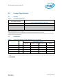
2.2
Performance
Table 2:
Random Read/Write Input/Output Operations Per Second (IOPS)
Intel SSD DC S3700 Series
Specification1
Unit
100 GB
200 GB (2.5”/1.8”)
400 GB (2.5”/1.8”)
800 GB
Random 4KB Read (up to)2
IOPS
75,000
75,000 / 75,000
75,000 / 75,000
75,000
Random 4KB Write (up to)
IOPS
19,000
32,000 / 29,000
36,000 / 36,000
36,000
Random 8KB Read (up to)3
IOPS
47,500
47,500 / 47,500
47,500 / 47,500
47,500
Random 8KB Write (up to)
IOPS
9,500
16,500 / 14,500
19,500 / 19,500
20,000
Notes:
1. Performance measured using IOMeter* with Queue Depth 32. Measurements are performed on a full Logical Block Address (LBA) span of the
drive.
2. 4KB = 4,096 bytes
3. 8KB = 8,192 bytes
January 2015
328171-010US
Product Specification
7
Intel® Solid-State Drive DC S3700 Series
Table 3:
Random Read/Write IOPS Consistency
Intel SSD DC S3700 Series
Specification1
Unit
100 GB
200 GB (2.5”/1.8”)
400 GB (2.5”/1.8”)
800 GB
Random 4KB Read (up to)2
%
90
90
90
90
Random 4KB Write (up to)
%
85
90
90
90
Random 8KB Read (up to)3
%
90
90
90
90
Random 8KB Write (up to)
%
85
90
90
90
Notes:
1. Performance consistency measured using IOMeter* based on Random 4KB QD=32 workload, measured as the
(IOPS in the 99.9th
percentile slowest 1-second interval)/(average IOPS during the test). Measurements are performed on a full Logical Block Address (LBA) span
of the drive once the workload has reached steady state but including all background activities required for normal operation and
data reliability.
2. 4KB = 4,096 bytes
3. 8KB = 8,192 bytes
Table 4:
Sequential Read and Write Bandwidth
Intel® SSD DC S3700 Series
Specification
Unit
100GB
200GB
400GB
800GB
Sequential Read (SATA 6Gb/s)1
MB/s
500
500
500
500
Sequential Write (SATA 6Gb/s)1
MB/s
200
365
460
460
Notes:
1. Performance measured using IOMeter* with 128KB (131,072 bytes) of transfer size with Queue Depth 32.
Table 5:
Latency
Intel SSD DC S3700 Series
Specification
100, 200 and 400GB
800 GB
Read
50 µs
50 µs
Write
65 µs
65 µs
2.0 s
3.0 s
Latency1 (TYP)
2
Power On to Ready
Notes:
1. Device measured using IOMeter. Latency measured using 4 KB (4,096 bytes) transfer size with Queue Depth equal to 1 on a sequential
workload.
2. Power On To Ready time assumes proper shutdown. Time varies if shutdown is not preceded by STANDBY IMMEDIATE command.
Product Specification
8
January 2015
328171-010US
Intel® Solid-State Drive DC S3700 Series
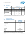
Table 6:
Quality of Service
Intel SSD DC S3700 Series
Specification
Queue Depth=1
Unit
Queue Depth=32
100GB
200/400/800
GB
100GB
200/400/800
GB
Quality of Service1,2 (99.9%)
Reads
ms
0.5
0.5
1
1
Writes
ms
0.5
0.5
15
10
Reads
ms
10
5
10
5
Writes
ms
10
5
20
20
Quality of Service 1,2 (99.9999%)
Notes:
1. Device measured using IOMeter. Quality of Service measured using 4 KB (4,096 bytes) transfer size on a random workload on a full Logical
Block Address (LBA) span of the drive once the workload has reached steady state but including all background activities required for normal
operation and data reliability.
2. Based on Random 4KB QD=1, 32 workloads, measured as the time taken for 99.9(or 99.9999) percentile of commands to finish the
round-trip from host to drive and back to host.
2.3
Electrical Characteristics
Table 7:
Operating Voltage for 2.5-inch Form Factor
Intel® SSDDC S3700 Series
Electrical Characteristics
100, 200, 400 and 800GB
5 V Operating Characteristics:
Operating Voltage range
Rise time (Max/Min)
Fall time (Min)2
Noise level
Min Off time3
Inrush Current (Typical Peak) 1
5 V (±5%)
1 s / 1 ms
1 ms
500 mV pp 10 Hz – 100 KHz
50 mV pp 100 KHz – 20 MHz
500 ms
1.0 A, < 1 s
12 V Operating Characteristics:
Operating Voltage range
Rise time (Max/Min)
Fall time (Min)2
Noise level
Min Off time3
Inrush Current (Typical Peak) 1
12 V (±10%)
1 s / 1 ms
1 ms
1000 mV pp 10 Hz – 100 KHz
100 mV pp 100 KHz – 20 MHz
500 ms
1.0 A, < 1 s
Notes:
1. Measured from initial device power supply application
2. Fall time needs to be equal or better than minimum in order to guarantee full functionality of enhanced power loss management
3. The drive needs to be powered off for at least 500msec before powering on
January 2015
328171-010US
Product Specification
9
Intel® Solid-State Drive DC S3700 Series
Table 8:
Power Consumption for 2.5-inch Form Factor (5V Supply)
Intel SSD DC S3700 Series
Specification
Unit
100GB
200GB
400GB
800GB
Active Write - RMS Average 1
W
2.8
4.2
5.2
5.8
Active Write - RMS Burst 2
W
3.1
4.6
7.7
8.2
Idle
W
0.6
0.6
0.6
0.6
Notes:
1. The workload equates 128KB (131,072 bytes) Queue Depth equal to 32 sequential writes. Root Mean Squared (RMS) average power is
measured using scope trigger over a 100 ms sample period
2. The workload equates 128KB (131,072 bytes) Queue Depth equal to 32 sequential writes. Root Mean Squared (RMS) burst power is measured
using scope trigger over a 500 µs sample period
Table 9:
Power Consumption for 2.5-inch Form Factor (12V Supply)
Intel SSD DC S3700 Series
Specification
Unit
100GB
200GB
400GB
800GB
Active Write - RMS Average1
W
2.9
4.4
5.4
6.0
Active Write - RMS Burst2
W
3.3
4.8
7.6
8.2
Idle
W
0.8
0.8
0.8
0.8
Notes:
1. The workload equates 128KB (131,072 bytes) Queue Depth equal to 32 sequential writes. Root Mean Squared (RMS) average power is
measured using scope trigger over a 100 ms sample period
2. The workload equates 128KB (131,072 bytes) Queue Depth equal to 32 sequential writes. Root Mean Squared (RMS) burst power is measured
using scope trigger over a 500 µs sample period
Table 10:
Operating Voltage for 1.8-inch Form Factor
Intel® SSD DC S3700 Series
Electrical Characteristics
200 and 400GB
Operating Voltage for 3.3 V (±5%)
Min
Max
Rise time (Max/Min)
Fall time (Min)2
Noise level
Min Off time3
Inrush Current (Typical Peak) 1
3.13 V
3.47 V
1 s / 1 ms
1 ms
300 mV pp 10 Hz – 100 KHz
500 mV pp 100 KHz – 20 MHz
500 ms
1.2 A, < 1 s
Notes:
1. Measured from initial device power supply application
2. Fall time needs to be equal or better than minimum in order to guarantee full functionality of enhanced power loss management
3. The drive needs to be powered off for at least 500msec before powering on
Product Specification
10
January 2015
328171-010US
Intel® Solid-State Drive DC S3700 Series
Table 11:
Power Consumption for 1.8-inch Form Factor
Specification1
Unit
Intel SSD DC S3700 Series
200GB
400GB
Active Write - RMS Average @ 3.3V
W
4.3
5.3
Active Write - RMS Burst @ 3.3V
W
4.7
7.9
Idle @ 3.3V
W
0.6
0.6
Notes:
1. The workload equates 128KB (131,072 bytes) Queue Depth equal to 32 sequential writes. Root Mean Squared (RMS) power is measured
using scope trigger over a 100 ms sample period.
2.4
Environmental Conditions
Table 12:
Temperature, Shock, Vibration
Temperature
Range
Case Temperature
0 – 70 oC
Operating
Non-operating
1
-55 – 95 oC
Temperature Gradient2
Operating
30 oC/hr (Typical)
Non-operating
30 oC/hr (Typical)
Humidity
Operating
5 – 95 %
Non-operating
5 – 95 %
Shock and Vibration
Range
Shock3
Operating
1,000 G (Max) at 0.5 msec
Non-operating
1,000 G (Max) at 0.5 msec
Vibration4
Operating
2.17 GRMS (5-700 Hz) Max
Non-operating
3.13 GRMS (5-800 Hz) Max
Notes:
1. Please contact your Intel representative for details on the non-operating temperature range.
2. Temperature gradient measured without condensation.
3. Shock specifications assume the SSD is mounted securely with the input vibration applied to the drive-mounting screws. Stimulus may be
applied in the X, Y or Z axis. Shock specification is measured using Root Mean Squared (RMS) value.
4. Vibration specifications assume the SSD is mounted securely with the input vibration applied to the drive-mounting screws. Stimulus may be
applied in the X, Y or Z axis. Vibration specification is measured using RMS value.
January 2015
328171-010US
Product Specification
11
Intel® Solid-State Drive DC S3700 Series
2.5
Product Regulatory Compliance
Intel® SSD DC S3700 Series meets or exceeds the regulatory or certification requirements in the following table:
Table 13:
Product Regulatory Compliance Specifications
Title
TITLE 47-Telecommunications CHAPTER 1—
FEDERAL COMMUNMICATIONS COMMISSION PART
15 — RADIO FREQUENCY DEVICES
ICES-003, Issue 4 Interference-Causing Equipment
Standard Digital Apparatus
Region For Which
Conformity Declared
Description
FCC Part 15B Class B
USA
CA/CSA-CEI/IEC CISPR 22:02. This is CISPR
22:1997 with Canadian Modifications
Canada
IEC 55024 Information Technology Equipment —
Immunity characteristics— Limits and methods of
measurement CISPR24:2010
EN-55024: 1998 and its amendments
European Union
IEC 55022 Information Technology Equipment —
Radio disturbance Characteristics— Limits and
methods of measurement CISPR24:2008 (Modified)
EN-55022: 2006 and its amendments
European Union
EN-60950-1 2nd Edition
Information Technology Equipment —
Safety — Part 1: General Requirements
USA/Canada
UL/CSA EN-60950-1 2nd Edition
Information Technology Equipment —
Safety — Part 1: General Requirements
USA/Canada
2.6
Reliability
Intel SSD DC S3700 Series meets or exceeds SSD endurance and data retention requirements as specified in the
JESD218 standard. Reliability specifications are listed in the following table:
Table 14:
Reliability Specifications
Parameter
Value
Uncorrectable Bit Error Rate (UBER)
Uncorrectable bit error rate will not exceed one sector in the
specified number of bits read. In the unlikely event of a
non-recoverable read error, the SSD will report it as a read failure
to the host; the sector in error is considered corrupt and is not
returned to the host.
< 1 sector per 1017 bits read
Mean Time Between Failures (MTBF)
Mean Time Between Failures is estimated based on Telcordia*
methodology and demonstrated through Reliability
Demonstration Test (RDT).
Product Specification
12
2 million hours
January 2015
328171-010US
Intel® Solid-State Drive DC S3700 Series
Parameter
Value
Power On/Off Cycles
Power On/Off Cycles is defined as power being removed from the
SSD, and then restored. Most host systems remove power from
the SSD when entering suspend and hibernate as well as on a
system shutdown.
Insertion Cycles
SATA/power cable insertion/removal cycles.
Data Retention
The time period for retaining data in the NAND at maximum rated
endurance.
Endurance Rating
While running JESD218 standard1 and based on JESD219 workload.
24 per day
50 on SATA cable
500 on backplane
3 months power-off retention once SSD
reaches rated write endurance at 40 °C
100GB: 1.83 PBW
200GB: 3.65 PBW
400GB: 7.30 PBW
800GB: 14.60 PBW
Note:
1
Refer to JESD218 standard table 1 for UBER, FFR and other Enterprise SSD endurance verification requirements. UBER design and majority of
life target is 1E-17. Endurance verification acceptance criterion based on establishing <1E-16 at 60 confidence.
2.7
Temperature Sensor
The Intel® SSD DC S3700 Series has an internal temperature sensor with an accuracy of +/-2C over a
range of -20C to +80C which can be monitored using two SMART attributes: Airflow Temperature
(BEh) and Device Internal Temperature (C2h).
For more information on supported SMART attributes, see Table 19 “SMART Attributes” on page 20.
2.8
Power Loss Capacitor Test
The Intel SSD DC S3700 Series supports testing of the power loss capacitor, which can be
monitored using the following SMART attribute: (175, AFh).
2.9
Hot Plug Support
Hot Plug insertion and removal is supported in the presence of a proper connector and appropriate
operating system (OS), as described in the SATA 3.0 specification.
This product supports asynchronous signal recovery and issues an unsolicited COMINIT when first
mated with a powered connector to guarantee reliable detection by a host system without hardware
device detection.
January 2015
328171-010US
Product Specification
13
Intel® Solid-State Drive DC S3700 Series
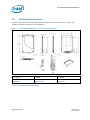
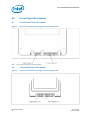
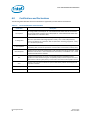
3.0
Mechanical Information
Figures 1 and 2 show the physical package information for the Intel® SSD DC S3700 Series in the 2.5- and
1.8-inch form factors. All dimensions are in millimeters.
Figure 1.
Intel SSD DC S3700 Series, 2.5-inch Form Factor Dimensions
X – Length -- *
Y - Width
Z - Height
100.45 Max
69.85 +/- 0.25
7.0 +0/-0.5
* - does not include 0.3 connector protrusion
Product Specification
14
January 2015
328171-010US
Intel® Solid-State Drive DC S3700 Series
Figure 2:
Intel® SSD DC S3700 Series, 1.8-inch Form Factor Dimensions
X - Length
Y - Width
Z - Height
78.50 +/- 0.60
54.0 +/- 0.25
5.0 +/- 0.35
January 2015
328171-010US
Product Specification
15
Intel® Solid-State Drive DC S3700 Series
4.0
Pin and Signal Descriptions
4.1
2.5-inch Form Factor Pin Locations
Figure 3:
Layout of 2.5-inch Form Factor Signal and Power Segment Pins
Note:
2.5-inch connector supports built in latching capability.
4.2
1.8-inch Form Factor Pin Locations
Figure 4:
Layout of 1.8-inch Form Factor Signal and Power Segment Pins
Product Specification
16
January 2015
328171-010US
Intel® Solid-State Drive DC S3700 Series
4.3
Connector Pin Signal Definitions
Table 15:
Serial ATA Connector Pin Signal Definitions—2.5- and 1.8-inch Form Factors
Pin
Function
S1
Ground
S2
A+
S3
A-
S4
Ground
S5
B-
S6
B+
S7
Ground
Definition
1st mate
Differential signal pair A
1st mate
Differential signal pair B
1st mate
Note: Key and spacing separate signal and power segments.
4.4
Power Pin Signal Definitions
Table 16:
Serial ATA Power Pin Definitions—2.5-inch Form Factors
Pin1
Function
P12
Not connected
(3.3 V Power)
P22
Not connected
(3.3 V Power)
2
Not connected
3,4
P3
Definition
Mating Order
--nd
(3.3 V Power; pre-charge)
2 Mate
Ground
Ground
1st Mate
P53
Ground
Ground
1st Mate
P63
Ground
Ground
1st Mate
P73,5
V5
5 V Power
1st Mate
3,5
V5
5 V Power
2nd Mate
P93,5
V5
5 V Power
2nd Mate
P103
Ground
Ground
1st Mate
P116
DAS/DSS
Device Activity Signal/Disable Staggered
Spin-up
2nd Mate
P123,4
Ground
Ground
1st Mate
P137
V12
12 V Power
1st Mate
P147
V12
12 V Power
2nd Mate
P157
V12
12 V Power
2nd Mate
P4
P8
Notes:
1. All pins are in a single row, with a 1.27 mm (0.050-inch) pitch.
2. Pins P1, P2 and P3 are connected together, although they are not connected internally to the device. The host may put 3.3 V on these pins.
3. The mating sequence is:
• ground pins P4-P6, P10, P12 and the 5V power pin P7
4.
5.
6.
7.
• signal pins and the rest of the 5V power pins P8-P9
Ground connectors P4 and P12 may contact before the other 1st mate pins in both the power and signal connectors to discharge ESD in
a suitably configured backplane connector.
Power pins P7, P8, and P9 are internally connected to one another within the device.
The host may ground P11 if it is not used for Device Activity Signal (DAS).
Pins P13, P14 and P15 are internally connected to one another within the device. The host may put 12 V on these pins.
January 2015
328171-010US
Product Specification
17
Intel® Solid-State Drive DC S3700 Series
Table 17:
Serial ATA Power Pin Definitions—1.8-inch Form Factors
Definition
Mating Order1
Pin
Function
P12
V33
3.3 V Power
2nd Mate
P22
V33
3.3 V Power, per-charge
2nd Mate
P33
Ground
--
1st Mate
P43
Ground
--
1st Mate
P54
V5
5 V Power; not connected.
1st Mate
P64
V5
5 V Power; not connected.
2nd Mate
P75
DAS/DSS
Device Activity Signal/Disable Staggered
Spin-up
2nd Mate
Key
Key
P86
Optional
Manufacturing Test Pin
2nd Mate
P96
Optional
Manufacturing Test Pin
2nd Mate
NC
NC
Notes:
1. All mate sequences assume zero angular offset between connectors.
2. P1 and P2 are internally connected to one another within the device.
3. Ground connectors P3 and P4 may contact before the other 1st mate pins in both the power and signal connectors to discharge ESD in
a suitably configure backplane connector.
4. Pins P5 and P6 are not connected internally to the device but there is an option to connect through a zero ohm stuffing resistor. The host may
put 5V on these pins.
5. The host may ground P7 if it is not used for Device Activity Signal (DAS).
6. P8 and P9 should not be connected by the host.
Product Specification
18
January 2015
328171-010US
Intel® Solid-State Drive DC S3700 Series
5.0
Supported Command Sets
Intel® SSD DC S3700 Series supports all mandatory ATA (Advanced Technology Attachment)
commands defined in the ATA8-ACS specification described in this section.
5.1
ATA General Feature Command Set
The Intel SSD DC S3700 Series supports the ATA General Feature command set (non- PACKET),
which consists of:
− EXECUTE DEVICE DIAGNOSTIC
− SET FEATURES
− IDENTIFY DEVICE
Note: See Appendix A, “IDENTIFY DEVICE Command Data” on page 30 for details on the sector data
returned after issuing an IDENTIFY DEVICE command.
Intel SSD DC S3700 Series also supports the following optional commands:
−
−
−
−
−
−
−
−
−
−
−
−
−
−
−
−
READ DMA
WRITE DMA
READ SECTOR(S)
READ VERIFY SECTOR(S)
READ MULTIPLE
SEEK
SET FEATURES
WRITE SECTOR(S)
SET MULTIPLE MODE1
WRITE MULTIPLE
FLUSH CACHE
READ BUFFFER
WRITE BUFFER
NOP
DOWNLOAD MICROCODE
WRITE UNCORRECTABLE EXT
1. The only multiple supported will be multiple 1
5.2
Power Management Command Set
Intel SSD DC S3700 Series supports the Power Management command set, which consists of:
−
−
−
−
−
−
January 2015
328171-010US
CHECK POWER MODE
IDLE
IDLE IMMEDIATE
SLEEP
STANDBY
STANDBY IMMEDIATE
Product Specification
19
Intel® Solid-State Drive DC S3700 Series
5.3
Security Mode Feature Set
Intel SSD DC S3700 Series supports the Security Mode command set, which
consists of:
−
−
−
−
−
−
5.4
SECURITY SET PASSWORD
SECURITY UNLOCK
SECURITY ERASE PREPARE
SECURITY ERASE UNIT
SECURITY FREEZE LOCK
SECURITY DISABLE PASSWORD
SMART Command Set
Intel® SSD DC S3700 Series supports the SMART command set, which consists of:
−
−
−
−
−
−
−
−
−
−
−
5.4.1
SMART READ DATA
SMART READ ATTRIBUTE THRESHOLDS
SMART ENABLE/DISABLE ATTRIBUTE AUTOSAVE
SMART SAVE ATTRIBUTE VALUES
SMART EXECUTE OFF-LINE IMMEDIATE
SMART READ LOG SECTOR
SMART WRITE LOG SECTOR
SMART ENABLE OPERATIONS
SMART DISABLE OPERATIONS
SMART RETURN STATUS
SMART ENABLE/DISABLE AUTOMATIC OFFLINE
SMART Attributes
The following table lists the SMART attributes supported by the Intel SSD DC S3700 Series and the
corresponding status flags and threshold settings.
Table 18:
SMART Attributes
ID
Attribute
Status Flags
Threshold
SP
EC
ER
PE
OC
PW
1
1
0
0
1
0
0 (none)
1
1
0
0
1
0
0 (none)
1
1
0
0
1
0
0 (none)
1
1
0
0
1
1
10
Re-allocated Sector Count
05h
Raw value: shows the number of retired blocks since
leaving the factory (grown defect count).
Normalized value: beginning at 100, shows the percent
remaining of allowable grown defect count.
Power-On Hours Count
09h
Raw value: reports power-on time, cumulative over the
life of the SSD, integer number in hour time units.
Normalized value: always 100.
0Ch
Power Cycle Count
Raw value: reports the cumulative number of power
cycle events over the life of the device.
Normalized value: always 100.
AAh
Available Reserved Space (See Attribute E8)
Product Specification
20
January 2015
328171-010US
Intel® Solid-State Drive DC S3700 Series
ID
Attribute
Status Flags
Threshold
SP
EC
ER
PE
OC
PW
ABh
Program Fail Count
Raw value: shows total count of program fails.
Normalized value: beginning at 100, shows the percent
remaining of allowable program fails.
1
1
0
0
1
0
0 (none)
ACh
Erase Fail Count
Raw value: shows total count of erase fails.
Normalized value: beginning at 100, shows the percent
remaining of allowable erase fails.
1
1
0
0
1
0
0 (none)
AEh
Unexpected Power Loss
Also known as “Power-off Retract Count” per magnetic-drive terminology.
Raw value: reports number of unclean shutdowns, cumulative over the life of the SSD.
An “unclean shutdown” is the removal of power without
STANDBY IMMEDIATE as the last command (regardless
of PLI activity using capacitor power).
Normalized value: always 100.
1
1
0
0
1
0
0 (none)
AFh
Power Loss Protection Failure
Last test result as microseconds to discharge cap, saturates at max value. Also logs minutes since last test and
lifetime number of tests.
Raw value:
Bytes 0-1: Last test result as microseconds to discharge
cap, saturates at max value. Test result
expected in range 25 <= result <= 5000000, lower indicates specific error code.
Bytes 2-3: Minutes since last test, saturates at max
value.
Bytes 4-5: Lifetime number of tests, not incremented on power cycle, saturates at max value.
Normalized value: set to 1 on test failure or 11 if the
capacitor has been tested in an excessive temperature
condition, otherwise 100.
1
1
0
0
1
1
10
B7h
SATA Downshift Count
Raw value: reports number of times SATA interface
selected lower signaling rate due to error.
Normalized value: always 100.
1
1
0
0
1
0
0 (none)
B8h
End-to-End Error Detection Count
Raw value: reports number of LBA tag mismatches in
end-to-end data protection path.
Normalized value: always 100.
1
1
0
0
1
1
90
BBh
Uncorrectable Error Count
Raw value: shows the number of errors that could
not be recovered using Error
Correction Code (ECC).
Normalized value: always 100.
1
1
0
0
1
0
0 (none)
January 2015
328171-010US
Product Specification
21
Intel® Solid-State Drive DC S3700 Series
ID
Attribute
Status Flags
Threshold
SP
EC
ER
PE
OC
PW
1
0
0
0
1
0
0 (none)
1
1
0
0
1
0
0 (none)
1
0
0
0
1
0
0 (none)
0
1
0
0
1
0
0 (none)
1
1
0
0
1
0
0 (none)
1
1
0
0
1
0
0 (none)
1
1
0
0
1
0
0 (none)
Temperature - Airflow Temperature (Case)
Raw value: reports SSD case temperature statisBEh
tics.
Bytes 0-1: Current case temperature, Celsius
Byte 2: Recent min case temperature, Celsius
Byte 3: Recent max case temperature, Celsius
Bytes 4-5: Over temperature counter. Number of times
sampled temperature exceeds drive max operating
temperature specification.
Normalized value: 100 – case temperature in C degrees
Power-Off Retract Count (Unsafe Shutdown Count)
C0h
Raw value: reports the cumulative number of unsafe
(unclean) shutdown events over the life of the device. An
unsafe shutdown occurs whenever the device is
powered off without STANDBYIMMEDIATE being the
last command.
Normalized value: always 100.
Temperature - Device Internal Temperature
C2h
Raw value: Reports internal temperature of the SSD in
degrees Celsius. Temperature reading is the value direct
from the printed circuit board (PCB) sensor without
offset.
Normalized value: 150 – device temperature in C
degrees, 100 if device temperature less than 50.
Pending Sector Count
C5h
Raw value: number of current unrecoverable read
errors that will be re-allocated on next write.
Normalized value: always 100.
CRC Error Count
C7h
Raw value: shows total number of encountered SATA
interface cyclic redundancy check (CRC) errors.
Normalized value: always 100.
Host Writes
E1h
Raw value: reports total number of sectors written by the
host system. The raw value is increased by 1 for every
65,536 sectors (32MB) written by the host.
Normalized value: always 100.
Timed Workload Media Wear
E2h
Raw value: measures the wear seen by the SSD (since
reset of the workload timer, attribute E4h), as a
percentage of the maximum rated cycles. Divide the raw
value by 1024 to derive the percentage with 3 decimal
points.
Normalized value: always 100.
Product Specification
22
January 2015
328171-010US
Intel® Solid-State Drive DC S3700 Series
ID
Attribute
Status Flags
Threshold
SP
EC
ER
PE
OC
PW
1
1
0
0
1
0
0 (none)
1
1
0
0
1
0
0 (none)
1
1
0
0
1
1
10
1
1
0
0
1
1
1
1
1
0
0
1
0
0 (none)
1
1
0
0
1
0
0 (none)
1
1
0
0
1
0
0 (none)
Timed Workload Host Read/Write Ratio
Raw value: shows the percentage of I/O operations that
are read operations (since reset of the workload timer,
attribute E4h). Reported as integer percentage from 0 to
100.
E3h
Normalized value: always 100.
Timed Workload Timer
Raw value: measures the elapsed time (number of
minutes since starting this workload timer).
E4h
Normalized value: always 100.
Available Reserved Space
Raw value: reports number of reserve blocks remaining.
Normalized value: begins at 100 , which corresponds
to 100 percent availability of the reserved space. The
threshold value for this attribute is 10 percent
availability.
E8h
Media Wearout Indicator
Raw value: always 0.
Normalized value: reports the number of cycles the
NAND media has undergone. Declines linearly from 100
to 1 as the average erase cycle count increases from 0 to
the maximum rated cycles.
E9h
Once the normalized value reaches 1, the number will
not decrease, although it is likely that significant
additional wear can be put on the device.
Thermal Throttle Status
Raw value: reports Percent Throttle Status and Count
of
events
Byte 0: Throttle status reported as integer percentage.
Bytes 1-4: Throttling event count. Number of times
thermal throttle has activated. Preserved over power cycles.
Byte 5: Reserved.
Normalized value: always 100.
EAh
Total LBAs Written
Raw value: reports the total number of sectors written
by the host system. The raw value is increased by 1 for
every 65,536 sectors (32MB) written by the host.
F1h
Normalized value: always 100.
Total LBAs Read
F2h
Raw value: reports the total number of sectors read by
the host system. The raw value is increased by 1 for
every 65,536 sectors (32MB) read by the host.
Normalized value: always 100.
January 2015
328171-010US
Product Specification
23
Intel® Solid-State Drive DC S3700 Series
Table 19:
SMART Attribute Status Flags
Status Flag
Description
Value = 0
Value = 1
SP
Self-preserving attribute
Not a self-preserving attribute
Self-preserving attribute
EC
Event count attribute
Not an event count attribute
Event count attribute
ER
Error rate attribute
Not an error rate attribute
Error rate attribute
PE
Performance attribute
Not a performance attribute
Performance attribute
OC
Online collection attribute
Collected only during offline
activity
Collected during both offline and
online activity
PW
Pre-fail warranty attribute
Advisory
Pre-fail
5.4.1.1
Timed Workload Endurance Indicators
Timed Workload Media Wear Indicator — ID E2h
This attribute tracks the drive wear seen by the device during the last wear timer loop, as a
percentage of the maximum rated cycles. The raw value tracks the percentage up to 3 decimal
points. This value should be divided by 1024 to get the percentage.
For example: if the raw value is 4450, the percentage is 4450/1024 = 4.345%. The raw value is held
at FFFFh until the wear timer (attribute E4h) reaches 60 (minutes) after a SMART EXECUTE OFFLINE
IMMEDIATE (B0h/D4h) subcommand 40h to the SSD. The normalized value is always set to 100 and
should be ignored.
Timed Workload Host Reads Percentage — ID E3h
This attribute shows the percentage of I/O operations that are read operations during the last
workload timer loop. The raw value tracks this percentage and is held at FFFFh until the workload
timer (attribute E4h) reaches 60 (minutes). The normalized value is always set to 100 and should be
ignored.
Workload Timer — ID E4h
This attribute is used to measure the time elapsed during the current workload. The attribute is
reset when a SMART EXECUTE OFFLINE IMMEDIATE (D4h) subcommand 40h is issued to the drive.
The raw value tracks the time in minutes and has a maximum value of 2^32 = 4,294,967,296 minutes
(8,171 years). The normalized value is always set to 100 and should be ignored.
Product Specification
24
January 2015
328171-010US
Intel® Solid-State Drive DC S3700 Series
User Notes
•
Sending a SMART EXECUTE OFFLINE IMMEDIATE (B0h/D4h) subcommand 40h to the SSD
resets and starts all three attributes (Media Wear Indicator, Attribute E2h, Host Reads
Percentage, Attribute E3h, and the Workload timer, Attribute E4h) to FFFFh.
•
The Attribute raw values are held at FFFFh until the Workload timer (Attribute E4h) reaches a
total of 60 (minutes) of power on time. After 60 minutes, the Timed Workload data is made
available.
•
After the Workload timer (E4h) reaches 60 (minutes), the Timed Workload data is saved every
minute so only 59 seconds of data is lost if power is removed without receiving ATA STANDBY
IMMEDIATE. Accumulated data is not reset due to power loss.
•
Upon power up, the attributes hold a snapshot of their last saved values for 59 seconds and
live data is available after 60 seconds, once the initial one hour interval is completed.
Example Use Cases
The Timed Workload Endurance attributes described in this section are intended to be used to
measure the amount of media wear that the drive is subjected to during a timed workload.
Ideally, the system that the drive is being used in should be capable of issuing SMART commands.
Otherwise, provisions have been provided to allow the media wear attributes to be persistent so
the drive can be moved to a SMART capable system to read out the drive wear attribute values.
Use Case 1 – With a System Capable of SMART Commands
1.
2.
3.
On a SMART capable system issue the SMART EXECUTE OFF-LINE IMMEDIATE (D4h)
sub-command 40h to reset the drive wear attributes.
Run the workload to be evaluated for at least 60 minutes. Otherwise the drive wear attributes
will not be available.
Read out the drive wear attributes with the SMART READ DATA (D0h) command.
Use Case 2 – With a System Not Capable of SMART Commands
1.
2.
3.
4.
5.
6.
January 2015
328171-010US
On a SMART capable system, issue the SMART EXECUTE OFF-LINE IMMEDIATE (D4h)
sub-command 40h to reset the drive wear attributes.
Move the drive to the system where the workload will be measured (and not capable of
SMART commands).
Run the workload to be evaluated for at least 60 minutes. Otherwise the drive wear attributes
will not be available.
Do a clean system power down by issuing the ATA STANDBY IMMEDIATE command prior to
shutting down the system. This will store all the drive wear SMART attributes to persistent
memory within the drive.
Move the drive to a SMART capable system.
Read out the drive wear attributes with the SMART READ DATA (D0h) command within 59
seconds after power-up.
Product Specification
25
Intel® Solid-State Drive DC S3700 Series
Example Calculation of Drive Wear
The following is an example of how the drive wear attributes can be used to evaluate the impact of a
given workload. The Host Writes SMART attribute (E1h) can also be used to calculate the amount of
data written by the host during the workload by reading this attribute before and after running the
workload. This example assumes that the steps shown in “Example Use Cases” on page 18 were
followed to obtain the following attribute values:
•
Timed Workload Media Wear (E2h) has a raw value of 16. Therefore, the percentage wear =
16/1024 = 0.016%.
•
Timed Workload Host Read/Write Ratio (E3h) has a normalized value of 80, indicating that
80% of operations were reads.
•
Workload Timer (E4h) has a raw value of 500. Therefore the workload ran for 500 minutes.
•
Host Writes Count (E1h) had a raw value of 100,000 prior to running the workload and a value
of 130,000 at the end of the workload. Therefore, the number of sectors written by the host
during the workload was 30,000 * 65,535 = 1,966,050,000 sectors or 1,966,050,000 *
512/1,000,000,000 = 1,007 GB.
The following conclusions can be made for this example case:
The workload took 500 minutes to complete with 80% reads and 20% writes. A total of 1,007 GB
of data was written to the device, which increased the media wear in the drive by 0.016%. At this
point in time, this workload is causing a wear rate of 0.016% for every 500 minutes, or
0.00192%/hour.
5.4.2
SMART Logs
Intel® SSD DC S3700 Series implements the following Log Addresses: 00h, 02h, 03h, 06h, and 07h.
Intel DC S3700 Series implements host vendor specific logs (addresses 80h-9Fh) as read and write
scratchpads, where the default value is zero (0). Intel SSD DC S3700 Series does not write any
specific values to these logs unless directed by the host through the appropriate commands.
Intel DC S3700 Series also implements a device vendor specific log at address A9h as a read-only
log area with a default value of zero (0).
Product Specification
26
January 2015
328171-010US
Intel® Solid-State Drive DC S3700 Series
5.5
Device Statistics
In addition to the SMART attribute structure, statistics pertaining to the operation and health of the
Intel SSD DC S3700 Series can be reported to the host on request through the Device Statistics log
as defined in the ATA specification.
The Device Statistics log is a read-only GPL/SMART log located at read log address 0x04 and is
accessible using READ LOG EXT, READ LOG DMA EXT or SMART READ LOG commands.
The following table lists the Device Statistics supported by the Intel SSD DC S3700 Series.
Table 20:
Device Statistics Log
Page
0x00
Offset
-0x08
0x10
0x18
0x01 – General Statistics
0x06 – Transport Statistics
0x07 – Solid State Device Statistics
January 2015
328171-010US
-0Ch
09h
E1h
0x08
Num Reported Uncorrectable Errors
BBh
0x10
Num Resets Between Command Acceptance and
Completion
--
0x00
Device Statistics Information Header
--
0x08
Current Temperature
--
0x10
Average Short Term Temperature
--
0x18
Average Long Term Temperature
--
0x20
Highest Temperature
--
0x28
Lowest Temperature
--
0x30
Highest Average Short Term Temperature
--
0x38
Lowest Average Short Term Temperature
--
0x40
Highest Average Long Term Temperature
--
0x48
Lowest Average Long Term Temperature
--
0x50
Time in Over-Temperature
--
0x58
Specified Maximum Operating Temperature
--
0x60
Time in Under-Temperature
--
0x68
Specified Minimum Operating Temperature
--
0x08
Number of Hardware Resets
--
0x10
Number of ASR Events
--
0x18
Number of Interface CRC Errors
0x20
0x30
0x05 – Temperature Statistics
List of Supported Pages
Equivalent SMART attribute
(if applicable)
Power Cycle Count
Power-On Hours
Logical Sectors Written
Num Write Commands – incremented by one for
every host write
Logical Sectors Read
Num Read Commands – incremented by one for
every host read
0x28
0x04 – General Error Statistics
Description
0x08
Percentage Used Endurance Indicator
-F2h
--
-E9h
Note: This device statistic
counts from 1 to 150
Product Specification
27
Intel® Solid-State Drive DC S3700 Series
5.6
SMART Command Transport (SCT)
With SMART Command Transport (SCT), a host can send commands and data to an SSD and receive
status and data from an SSD using standard write/read commands to manipulate two SMART Logs:
− Log Address E0h ("SCT Command/Status") — used to send commands and retrieve status
− Log Address E1h ("SCT Data Transfer") — used to transport data
Intel® SSD DC S3700 Series supports the following standard SCT actions:
− Write Same — Intel DC S3700 Series implements this action code as described in the ATA
specification.
− Error Recovery Control — Intel DC S3700 Series accepts this action code, and will store and
return error-recovery time limit values.
− Feature Control – Intel DC S3700 Series supports feature code 0001h (write cache) feature
code 0002h (write cache reordering), and feature code 0003h (time interval for temperature
logging). It also supports D000h(Power Safe Write Cache capacitor test interval),
(D001h(read/write power governor mode), D002h(read/write thermal governor mode),
D003h(read power governor burst power), D004h(read power governor average power).
− Data table command – Intel DC S3700 Series supports data table command as specified in
ATA8-ACS2. This will read out temperature logging information in
table ID 0002h.
− Read Status Support – Intel DC S3700 Series supports read status log.
− SCT command 0xD801with State=0, Option=1, ID Word 106 can be used to change from
0x6003 to 0x4000 (4KB physical sector size to 512B physical sector size support change).
5.7
Data Set Management Command Set
Intel SSD DC S3700 Series supports the Data Set Management command set Trim attribute, which
consists of:
− DATA SET MANAGEMENT
5.8
Host Protected Area Command Set
Intel SSD DC S3700 Series supports the Host Protected Area command set, which consists of:
−
−
−
−
READ NATIVE MAX ADDRESS
SET MAX ADDRESS
READ NATIVE MAX ADDRESS EXT
SET MAX ADDRESS EXT
Intel SSD DC S3700 Series also supports the following optional commands:
−
−
−
−
SET MAX SET PASSWORD
SET MAX LOCK
SET MAX FREEZE LOCK
SET MAX UNLOCK
Product Specification
28
January 2015
328171-010US
Intel® Solid-State Drive DC S3700 Series
5.9
48-Bit Address Command Set
Intel SSD DC S3700 Series supports the 48-bit Address command set, which
consists of:
−
−
−
−
−
−
−
−
−
−
−
5.10
FLUSH CACHE EXT
READ DMA EXT
READ NATIVE MAX ADDRESS EXT
READ SECTOR(S) EXT
READ VERIFY SECTOR(S) EXT
SET MAX ADDRESS EXT
WRITE DMA EXT
WRITE MULTIPLE EXT
WRITE SECTOR(S) EXT
WRITE MULTIPLE FUA EXT
WRITE DMA FUA EXT
General Purpose Log Command Set
Intel® SSD DC S3700 Series supports the General Purpose Log command set, which consists of:
− READ LOG EXT
− WRITE LOG EXT
5.11
Native Command Queuing
Intel SSD DC S3700 Series supports the Native Command Queuing (NCQ) command set, which
includes:
− READ FPDMA QUEUED
− WRITE FPDMA QUEUED
Note:
5.12
With a maximum Queue Depth set to 32.
Software Settings Preservation
Intel SSD DC S3700 Series supports the SET FEATURES parameter to enable/disable the
preservation of software settings.
January 2015
328171-010US
Product Specification
29
Intel® Solid-State Drive DC S3700 Series
6.0
Certifications and Declarations
The following table describes the Device Certifications supported by the Intel SSD DC S3700 Series.
Table 21:
Device Certifications and Declarations
Certification
Description
Low Voltage DIRECTIVE 2006/95/EC OF THE EUROPEAN PARLIAMENT AND OF THE COUNCIL
CE Compliant
UL Recognized
of 12 December 2006, and EMC Directive 2004/108/EC OF THE EUROPEAN PARLIAMENT AND
OF THE COUNCIL of 15 December 2004.
Underwriters Laboratories, Inc. Bi-National Component Recognition; UL 60950-1, 2nd Edition,
2007-03-27 (Information Technology Equipment - Safety - Part 1: General Requirements)
CSA C22.2 No. 60950-1-07, 2nd Edition, 2007-03 (Information Technology Equipment - Safety Part 1: General Requirements)
C-Tick Compliant
Compliance with the Australia/New Zealand Standard AS/NZS3548 and Electromagnetic
Compatibility (EMC) Framework requirements of the Australian Communication Authority (ACA).
BSMI Compliant
Compliance to the Taiwan EMC standard CNS 13438: Information technology equipment - Radio
disturbance Characteristics - limits and methods of measurement, as amended on June 1, 2006,
is harmonized with CISPR 22: 2005.04.
KCC
Compliance with paragraph 1 of Article 11 of the Electromagnetic Compatibility Control
Regulation and meets the Electromagnetic Compatibility (EMC) Framework requirements of the
Radio Research Laboratory (RRL) Ministry of Information and Communication Republic of Korea.
VCCI
Voluntary Control Council for Interface to cope with disturbance problems caused by personal
computers or facsimile.
RoHS Compliant
WEEE
Product Specification
30
Restriction of Hazardous Substance Directive
Directive on Waste Electrical and Electronic Equipment
January 2015
328171-010US
Intel® Solid-State Drive DC S3700 Series
7.0
References
The following table identifies the standards information referenced in this document.
Table 22:
Standards References
Date
Title
Location
July 2012
Solid-State Drive (SSD) Requirements and Endurance Test
Method (JESD219)
http://www.jedec.org/standards-documents/
results/jesd219
Sept 2010
Solid-State Drive (SSD) Requirements and Endurance Test
Method (JESD218)
http://www.jedec.org/standards-documents/
docs/jesd218/
Dec 2008
VCCI
http://www.vcci.jp/vcci_e/
June 2009
RoHS
Click Search MDDS Database and search
http://qdms.intel.com/
for material description datasheet
August 2009
ACS-2-ATA/ATAPI Command Set 2 Specification
http://www.t13.org/
June 2009
Serial ATA Revision 3.0
http://www.sata-io.org/
May 2006
SFF-8223, 2.5-inch Drive w/Serial Attachment Connector
http://www.sffcommittee.org/
May 2005
SFF-8201, 2.5-inch drive form factor
http://www.sffcommittee.org/
International Electrotechnical Commission EN 61000
1995
4-2 (Electrostatic discharge immunity test)
1996
4-3 (Radiated, radio-frequency, electromagnetic field
immunity test)
1995
4-4 (Electrical fast transient/burst immunity test)
1995
4-5 (Surge immunity test)
1997
4-6 (Immunity to conducted disturbances, induced by radiofrequency fields)
1994
http://www.iec.ch/
4-11 (Voltage Variations, voltage dips, short interruptions
and voltage variations immunity tests)
1995
ENV 50204
(Radiated electromagnetic field from digital radio
telephones)
January 2015
328171-010US
http://www.dbicorporation.com/radimmun.h
tm/
Product Specification
31
Intel® Solid-State Drive DC S3700 Series
Appendix A: IDENTIFY DEVICE Command Data
Table 23:
Word
0
Returned Sector Data
F = Fixed
V = Variable
X = Both
X
Default Value
0040h
Description
General configuration bit-significant information
1
X
3FFFh
Obsolete - Number of logical cylinders (16,383)
2
V
C837h
Specific configuration
Obsolete - Number of logical heads (16)
3
X
0010h
4-5
X
0h
6
X
003Fh
7-8
V
0h
Reserved for assignment by the CompactFlash* Association (CFA)
9
X
0h
Retired
10-19
F
varies
20-21
X
0h
Retired
22
X
0h
Obsolete
23-26
F
varies
Firmware revision (8 ASCII characters)
27-46
F
varies
Model number (Intel® Solid-State Drive)
47
F
8001h
7:0—Maximum number of sectors transferred per interrupt on multiple
commands
48
F
4000h
Trusted Computing Feature Set
49
F
2F00h
Capabilities
Capabilities
Retired
Obsolete - Number of logical sectors per logical track (63)
Serial number (20 ASCII characters)
50
F
4000h
51-52
X
0h
53
F
0007h
Words 88 and 70:64 valid
54
X
3FFFh
Obsolete - Number of logical cylinders (16,383)
55
X
0010h
Obsolete - Number of logical heads (16)
Obsolete - Number of logical sectors per logical track (63)
Obsolete
56
X
003Fh
57-58
X
FC1000FBh
59
F
BF01
60-61
V
100GB: 0BA52230h
200GB: 0FFFFFFFh
400GB: 0FFFFFFFh
800GB: 0FFFFFFFh
62
X
0h
63
X
0007h
Multi-word DMA modes supported/selected
64
F
0003h
PIO modes supported
65
F
0078h
Minimum multiword DMA transfer cycle time per word
66
F
0078h
Manufacturer’s recommended multiword DMA transfer cycle time
67
F
0078h
Minimum PIO transfer cycle time without flow control
68
F
0078h
Minimum PIO transfer cycle time with IORDY flow control
69
F
4030h
Additional Supported
70
F
0000h
71-74
F
0h
75
F
001Fh
Queue depth
76
F
850Eh
Serial ATA capabilities
Product Specification
32
Obsolete
Number of sectors transferred per interrupt on multiple commands
Total number of user-addressable sector
Obsolete
Reserved
Reserved for IDENTIFY PACKET DEVICE command
January 2015
328171-010US
Intel® Solid-State Drive DC S3700 Series
Word
F = Fixed
V = Variable
X = Both
Default Value
Description
77
F
0006h
Reserved for future Serial ATA definition
78
F
0040h
Serial ATA features supported
79
V
0040h
Serial ATA features enabled
80
F
03FCh
Major version number
81
F
0110h
Minor version number
82
F
746Bh
Command set supported
83
F
7501h
Command sets supported
84
F
6163h
Command set/feature supported extension
85
V
7469h
Command set/feature enabled
86
V
B401h
Command set/feature enabled
87
V
6163h
Command set/feature default
88
V
407Fh
Ultra DMA Modes
89
F
0002h
Time required for security erase unit completion
90
F
0002h
Time required for enhanced security erase completion
91
V
0h
92
V
0FFFEh
93
X
0h
Hardware reset result: the contents of bits (12:0) of this word shall
change only during the execution of a hardware reset
94
V
0h
Vendor’s recommended and actual acoustic management value
95
F
0h
Stream minimum request size
96
V
0h
Streaming transfer time - DMA
97
V
0h
Streaming access latency - DMA and PIO
98-99
F
0h
Streaming performance granularity
100-103
V
100GB: 0BA52230h
200GB: 1749F1B0h
400GB: 2E9390B0h
800GB: 5D26CEB0h
104
V
0h
Current advanced power management value
Master Password Revision Code
Maximum user LBA for 48-bit address feature set
Streaming transfer time - PIO
105
V
0006h
Maximum number of 512-byte blocks of LBA Range Entries per DATA
SET MANAGEMENT command
106
F
6003h
Default Physical sector size / logical sector size.
0004h to reflect 512Bytes/Sector.
107
F
0h
108-111
F
varies
112-115
F
0h
116
V
0h
Reserved for technical report
117-118
F
0h
Words per logical sector
119
F
405Ch
Supported settings
Command set/feature enabled/supported
Inter-seek delay for ISO-7779 acoustic testing in microseconds
Unique ID
Reserved for world wide name extension to 128 bits
120
F
401Ch
121-126
F
0h
127
X
0h
128
V
0021h
Security status
Reserved
Removable Media Status Notification feature set support
129
V
1Ch
Vendor-specific
130-139
X
0h
Vendor-specific
140-149
X
0h
Disable Logical Error Field
January 2015
328171-010US
Can be changed to
Product Specification
33
Intel® Solid-State Drive DC S3700 Series
Word
F = Fixed
V = Variable
X = Both
Default Value
Description
150-159
X
0h
Vendor-specific
160
X
0h
CompactFlash Association (CFA) power mode 1
161-167
X
0h
Reserved for assignment by the CFA
168
X
3h
169
X
0001h
170-175
F
0h
176-205
X
Varies
Current media serial number
206
X
003Dh
SCT Command Transport
207-208
F
0000h
Reserved
Reserved for assignment by the CFA
Data set management Trim attribute support
Reserved for assignment by the CFA
209
X
4000h
Alignment of logical blocks within a physical block
210-211
V
0000h
Write-Read-Verify Sector Count Mode 3 (DWord)
212-213
F
0000h
Write-Read-Verify Sector Count Mode 2 (DWord)
214
X
0000h
NV Cache Capabilities
215-216
V
0000h
NV Cache Size in Logical Blocks (DWord)
217
F
0001h
Nominal media rotation rate
218
V
0000h
Reserved
219
F
0000h
NV Cache Options
220
V
0000h
Write-Read-Verify feature set
221
X
0000h
Reserved
222
F
101Fh
Transport major version number
223
F
0000h
Transport minor version number
224-229
F
0000h
Reserved
230-233
X
0000h
Extended Number of User Addressable Sectors (QWord)
234
F
0001h
Minimum number of 512-byte data blocks per DOWNLOAD MICROCODE
command for mode 03h
235
F
FFFFh
Maximum number of 512-byte data blocks per DOWNLOAD
MICROCODE command for mode 03h
236-254
X
0000h
Reserved
255
V
Varies
Integrity word
Notes:
F = Fixed. The content of the word is fixed and does not change. For removable media devices, these values may change when media is removed
or changed.
V = Variable. The state of at least one bit in a word is variable and may change depending on the state of the device or the commands executed
by the device.
X = F or V. The content of the word may be fixed or variable.
Product Specification
34
January 2015
328171-010US