1
Intel® Core™ i7 Processor Family for
LGA2011 Socket
Datasheet – Volume 1 of 2
Supporting Desktop Intel® Core™ i7-4960X Extreme Edition Processor
Series for the LGA2011 Socket
Supporting Desktop Intel® Core™ i7-49xx and i7-48xx Processor Series
for the LGA2011 Socket
May 2014
329366-002
By using this document, in addition to any agreements you have with Intel, you accept the terms set forth below.
INFORMATION
SALE AND/OR USE
IN THIS
OF INTEL
DOCUMENT
PRODUCTS
IS PROVIDED
INCLUDING
IN CONNECTION
LIABILITY OR WITH
WARRANTIES
Intel® PRODUCTS.
RELATING TO
NO FITNESS
LICENSE,FOR
Express*
A PARTICULAR
OR IMPLIED,
PURPOSE,
BY ESTOPPEL
MERCHANTABILITY,
OR OTHERWISE,
OR INFRINGEMENT
TO ANY INTELLECTUAL
OF ANY PROPERTY
PATENT, COPYRIGHT
RIGHTS ISOR
GRANTED
OTHER INTELLECTUAL
BY THIS DOCUMENT.
PROPERTY
EXCEPT
RIGHT.
AS PROVIDED IN INTEL'S TERMS AND CONDITIONS OF SALE FOR SUCH PRODUCTS, INTEL ASSUMES NO LIABILITY WHATSOEVER, AND INTEL DISCLAIMS ANY Express* OR IMPLIED WARRANTY, RELATING TO
You may not use or facilitate the use of this document in connection with any infringement or other legal analysis concerning Intel
products described herein. You agree to grant Intel a non-exclusive, royalty-free license to any patent claim thereafter drafted
which includes subject matter disclosed herein.
INFORMATION IN THIS DOCUMENT IS PROVIDED IN CONNECTION WITH INTEL PRODUCTS. NO LICENSE, EXPRESS OR IMPLIED,
BY ESTOPPEL OR OTHERWISE, TO ANY INTELLECTUAL PROPERTY RIGHTS IS GRANTED BY THIS DOCUMENT. EXCEPT AS
PROVIDED IN INTEL'S TERMS AND CONDITIONS OF SALE FOR SUCH PRODUCTS, INTEL ASSUMES NO LIABILITY WHATSOEVER
AND INTEL DISCLAIMS ANY EXPRESS OR IMPLIED WARRANTY, RELATING TO SALE AND/OR USE OF INTEL PRODUCTS INCLUDING
LIABILITY OR WARRANTIES RELATING TO FITNESS FOR A PARTICULAR PURPOSE, MERCHANTABILITY, OR INFRINGEMENT OF ANY
PATENT, COPYRIGHT OR OTHER INTELLECTUAL PROPERTY RIGHT.
A "Mission Critical Application" is any application in which failure of the Intel Product could result, directly or indirectly, in personal
injury or death. SHOULD YOU PURCHASE OR USE INTEL'S PRODUCTS FOR ANY SUCH MISSION CRITICAL APPLICATION, YOU
SHALL INDEMNIFY AND HOLD INTEL AND ITS SUBSIDIARIES, SUBCONTRACTORS AND AFFILIATES, AND THE DIRECTORS,
OFFICERS, AND EMPLOYEES OF EACH, HARMLESS AGAINST ALL CLAIMS COSTS, DAMAGES, AND EXPENSES AND REASONABLE
ATTORNEYS' FEES ARISING OUT OF, DIRECTLY OR INDIRECTLY, ANY CLAIM OF PRODUCT LIABILITY, PERSONAL INJURY, OR DEATH
ARISING IN ANY WAY OUT OF SUCH MISSION CRITICAL APPLICATION, WHETHER OR NOT INTEL OR ITS SUBCONTRACTOR WAS
NEGLIGENT IN THE DESIGN, MANUFACTURE, OR WARNING OF THE INTEL PRODUCT OR ANY OF ITS PARTS.
Intel may make changes to specifications and product descriptions at any time, without notice. Designers must not rely on the
absence or characteristics of any features or instructions marked "reserved" or "undefined". Intel reserves these for future
definition and shall have no responsibility whatsoever for conflicts or incompatibilities arising from future changes to them. The
information here is subject to change without notice. Do not finalize a design with this information.
The products described in this document may contain design defects or errors known as errata which may cause the product to
deviate from published specifications. Current characterized errata are available on request.
No computer system can provide absolute security under all conditions. Intel® Trusted Execution Technology (Intel® TXT) requires
a computer system with Intel® Virtualization Technology, an Intel TXT-enabled processor, chipset, BIOS, Authenticated Code
Modules and an Intel TXT-compatible measured launched environment (MLE). The MLE could consist of a virtual machine monitor,
an OS or an application. In addition, Intel TXT requires the system to contain a TPM v1.2, as defined by the Trusted Computing
Group and specific software for some uses. For more information, see http://www.intel.com/technology/security/
Hyper-Threading Technology requires a computer system with a processor supporting HT Technology and an HT Technology
enabled chipset, BIOS and operating system. Performance will vary depending on the specific hardware and software you use. For
more information including details on which processors support HT Technology, see
http://www.intel.com/products/ht/hyperthreading_more.htm.
Enabling Execute Disable Bit functionality requires a PC with a processor with Execute Disable Bit capability and a supporting
operating system. Check with your PC manufacturer on whether your system delivers Execute Disable Bit functionality.
Intel® Virtualization Technology requires a computer system with an enabled Intel® processor, BIOS, virtual machine monitor
(VMM) and, for some uses, certain computer system software enabled for it. Functionality, performance or other benefits will vary
depending on hardware and software configurations and may require a BIOS update. Software applications may not be compatible
with all operating systems. Please check with your application vendor.
Intel® Turbo Boost Technology requires a PC with a processor with Intel Turbo Boost Technology capability. Intel Turbo Boost
Technology performance varies depending on hardware, software and overall system configuration. Check with your PC
manufacturer on whether your system delivers Intel Turbo Boost Technology. For more information, see
http://www.intel.com/technology/turboboost/.
64-bit computing on Intel architecture requires a computer system with a processor, chipset, BIOS, operating system, device
drivers and applications enabled for Intel® 64 architecture. Performance will vary depending on your hardware and software
configurations. Consult with your system vendor for more information.
Δ Intel processor numbers are not a measure of performance. Processor numbers differentiate features within each processor
family, not across different processor families. See http://www.intel.com/products/processor%5Fnumber/ for details.
I2C is a two-wire communications bus/protocol developed by Philips. SMBus is a subset of the I2C bus/protocol and was developed
by Intel. Implementations of the I2C bus/protocol may require licenses from various entities, including Philips Electronics N.V. and
North American Philips Corporation.
Intel, Intel, Enhanced Intel® SpeedStep® Technology, Intel® 64 Technology, Intel® Virtualization Technology (Intel® VT),
Intel® VT-d, Intel® Turbo Boost Technology, Intel® Hyper-Threading Technology (Intel® HT Technology), Intel® Streaming SIMD
Extensions (Intel® SSE) Intel Core, and the Intel logo are trademarks of Intel Corporation in the U. S. and/or other countries.
*Other names and brands may be claimed as the property of others.
Copyright © 2014, Intel Corporation. All rights reserved.
2
Datasheet
Table of Contents
1
Introduction .............................................................................................................. 8
1.1
Processor Feature Details ..................................................................................... 9
1.2
Supported Technologies ..................................................................................... 10
1.3
Interfaces ........................................................................................................ 10
1.3.1 System Memory Support ......................................................................... 10
1.3.2 PCI Express* ......................................................................................... 11
1.3.3 Direct Media Interface Gen 2 (DMI2)......................................................... 12
1.3.4 Platform Environment Control Interface (PECI) ........................................... 13
1.4
Power Management Support ............................................................................... 13
1.4.1 Processor Package and Core States........................................................... 13
1.4.2 System States Support ........................................................................... 13
1.4.3 Memory Controller.................................................................................. 13
1.4.4 PCI Express* ......................................................................................... 13
1.5
Thermal Management Support ............................................................................ 13
1.6
Package Summary............................................................................................. 14
1.7
Terminology ..................................................................................................... 14
1.8
Related Documents ........................................................................................... 16
2
Interfaces................................................................................................................ 18
2.1
System Memory Interface .................................................................................. 18
2.1.1 System Memory Technology Support ........................................................ 18
2.1.2 System Memory Timing Support............................................................... 18
2.2
PCI Express* Interface....................................................................................... 19
2.2.1 PCI Express* Architecture ....................................................................... 19
2.2.2 PCI Express* Configuration Mechanism ..................................................... 20
2.3
Direct Media Interface 2 (DMI2) / PCI Express* Interface ....................................... 21
2.3.1 DMI2 Error Flow ..................................................................................... 21
2.3.2 Processor / PCH Compatibility Assumptions................................................ 21
2.3.3 DMI2 Link Down..................................................................................... 21
2.4
Platform Environment Control Interface (PECI) ...................................................... 21
3
Technologies ........................................................................................................... 23
3.1
Intel® Virtualization Technology (Intel® VT) ......................................................... 23
3.1.1 Intel® VT-x Objectives ............................................................................ 23
3.1.2 Intel® VT-x Features .............................................................................. 24
3.1.3 Intel® VT-d Objectives ............................................................................ 24
3.1.4 Intel® Virtualization Technology Processor Extensions ................................. 25
3.2
Security Technologies ........................................................................................ 26
3.2.1 Intel® Advanced Encryption Standard New Instructions
(Intel® AES-NI) Instructions .................................................................... 26
3.2.2 Execute Disable Bit................................................................................. 26
3.3
Intel® Hyper-Threading Technology (Intel® HT Technology).................................... 26
3.4
Intel® Turbo Boost Technology ........................................................................... 27
3.4.1 Intel® Turbo Boost Operating Frequency ................................................... 27
3.5
Enhanced Intel® SpeedStep® Technology............................................................. 27
3.6
Intel® Advanced Vector Extensions (Intel® AVX) ................................................... 28
4
Power Management ................................................................................................. 30
4.1
Advanced Configuration and Power Interface (ACPI) States Supported ..................... 30
4.1.1 System States ....................................................................................... 30
4.1.2 Processor Package and Core States........................................................... 30
4.1.3 Integrated Memory Controller (IMC) States................................................ 32
4.1.4 Direct Media Interface Gen 2 (DMI2) / PCI Express* Link States ................... 32
4.1.5 G, S, and C State Combinations ............................................................... 33
Datasheet
3
4.2
4.3
4.4
Processor Core / Package Power Management .......................................................33
4.2.1 Enhanced Intel® SpeedStep® Technology ..................................................33
4.2.2 Low-Power Idle States.............................................................................34
4.2.3 Requesting Low-Power Idle States ............................................................35
4.2.4 Core C-states .........................................................................................36
4.2.5 Package C-States ...................................................................................37
4.2.6 Package C-State Power Specifications........................................................40
System Memory Power Management ....................................................................40
4.3.1 CKE Power-Down ....................................................................................41
4.3.2 Self-Refresh ...........................................................................................41
4.3.3 DRAM I/O Power Management ..................................................................42
Direct Media Interface 2 (DMI2) / PCI Express* Power Management .........................42
5
Thermal Management Specifications ........................................................................43
6
Signal Descriptions ..................................................................................................44
6.1
System Memory Interface Signals ........................................................................44
6.2
PCI Express* Based Interface Signals ...................................................................45
6.3
Direct Media Interface Gen 2 (DMI2) / PCI Express* Port 0 Signals...........................47
6.4
Platform Environment Control Interface (PECI) Signal .............................................47
6.5
System Reference Clock Signals ..........................................................................47
6.6
Joint Test Action Group (JTAG) and Test Access Point (TAP) Signals..........................47
6.7
Serial Voltage Identification (SVID) Signals ...........................................................48
6.8
Processor Asynchronous Sideband and Miscellaneous Signals...................................48
6.9
Processor Power and Ground Supplies ..................................................................51
7
Electrical Specifications ...........................................................................................52
7.1
Processor Signaling ............................................................................................52
7.1.1 System Memory Interface Signal Groups....................................................52
7.1.2 PCI Express* Signals...............................................................................52
7.1.3 Direct Media Interface Gen 2 (DMI2) / PCI Express* Signals .........................52
7.1.4 Platform Environmental Control Interface (PECI) .........................................53
7.1.5 System Reference Clocks (BCLK{0/1}_DP, BCLK{0/1}_DN) .........................53
7.1.6 Joint Test Action Group (JTAG) and Test Access
Port (TAP) Signals...................................................................................54
7.1.7 Processor Sideband Signals ......................................................................54
7.1.8 Power, Ground and Sense Signals .............................................................54
7.1.9 Reserved or Unused Signals .....................................................................59
7.2
Signal Group Summary.......................................................................................59
7.3
Power-On Configuration (POC) Options .................................................................62
7.4
Absolute Maximum and Minimum Ratings..............................................................62
7.4.1 Storage Conditions Specifications..............................................................63
7.5
DC Specifications ...............................................................................................64
7.5.1 Voltage and Current Specifications ............................................................64
7.5.2 Die Voltage Validation .............................................................................66
7.5.3 Signal DC Specifications ..........................................................................67
8
Processor Land Listing .............................................................................................72
9
Package Mechanical Specifications......................................................................... 115
10
Boxed Processor Specifications.............................................................................. 116
10.1 Introduction .................................................................................................... 116
10.2 Boxed Processor Contents................................................................................. 116
4
Datasheet
Figures
1-1
1-2
2-1
2-2
4-1
4-2
4-3
7-1
7-2
7-3
Processor Platform Block Diagram Example............................................................. 9
PCI Express* Lane Partitioning and Direct Media Interface Gen 2 (DMI2) .................. 12
PCI Express* Layering Diagram........................................................................... 19
Packet Flow through the Layers........................................................................... 20
Idle Power Management Breakdown of the Processor Cores..................................... 34
Thread and Core C-State Entry and Exit ............................................................... 34
Package C-State Entry and Exit ........................................................................... 38
Input Device Hysteresis ..................................................................................... 53
Voltage Regulator (VR) Power-State Transitions .................................................... 57
VCC Overshoot Example Waveform...................................................................... 66
Tables
1-1
1-2
1-3
4-1
4-2
4-3
4-4
4-5
4-6
4-7
4-8
4-9
4-10
6-1
6-2
6-3
6-4
6-5
6-6
6-7
6-8
6-9
6-10
6-11
6-12
6-13
6-14
7-1
7-2
7-3
7-4
7-5
7-6
7-7
7-8
7-9
Datasheet
Terminology ..................................................................................................... 14
Processor Documents......................................................................................... 16
Public Specifications .......................................................................................... 17
System States .................................................................................................. 30
Package C-State Support.................................................................................... 31
Core C-State Support......................................................................................... 31
System Memory Power States ............................................................................. 32
DMI2 / PCI Express* Link States ......................................................................... 32
G, S and C State Combinations ........................................................................... 33
Coordination of Thread Power States at the Core Level ........................................... 35
P_LVLx to MWAIT Conversion.............................................................................. 35
Coordination of Core Power States at the Package Level ......................................... 38
Package C-State Power Specifications .................................................................. 40
Memory Channel DDR0, DDR1, DDR2, DDR3......................................................... 44
Memory Channel Miscellaneous ........................................................................... 45
PCI Express* Port 1 Signals ................................................................................ 45
PCI Express* Port 2 Signals ................................................................................ 45
PCI Express* Port 3 Signals ................................................................................ 46
PCI Express* Miscellaneous Signals ..................................................................... 46
DMI2 and PCI Express Port 0 Signals ................................................................... 47
Platform Environment Control Interface (PECI) Signals ........................................... 47
System Reference Clock (BCLK{0/1}) Signals ....................................................... 47
Joint Test Action Group (JTAG) and Test Access Port (TAP) Signals .......................... 47
Serial Voltage Identification (SVID) Signals........................................................... 48
Processor Asynchronous Sideband Signals ............................................................ 48
Miscellaneous Signals ........................................................................................ 50
Power and Ground Signals .................................................................................. 51
Power and Ground Lands.................................................................................... 54
Serial Voltage Identification (SVID) Address Usage ................................................ 57
VR12.0 Reference Code Voltage Identification (VID) Table ...................................... 58
Signal Description Buffer Types ........................................................................... 59
Signal Groups ................................................................................................... 59
Signals with On-Die Termination ......................................................................... 62
Power-On Configuration Option Lands .................................................................. 62
Processor Absolute Minimum and Maximum Ratings ............................................... 63
Storage Condition Ratings .................................................................................. 63
5
7-10
7-11
7-12
7-13
7-14
7-15
7-16
7-17
7-18
7-19
7-20
8-1
8-2
6
Voltage Specifications.........................................................................................64
Current Specifications ........................................................................................65
VCC Overshoot Specifications ..............................................................................66
DDR3 and DDR3L Signal DC Specifications ............................................................67
PECI DC Specifications .......................................................................................68
System Reference Clock (BCLK{0/1}) DC Specifications..........................................68
SMBus DC Specifications.....................................................................................69
Joint Test Action Group (JTAG) and Test Access Point (TAP) Signals DC Specifications.69
Serial VID Interface (SVID) DC Specifications ........................................................69
Processor Asynchronous Sideband DC Specifications...............................................70
Miscellaneous Signals DC Specifications ................................................................70
Land List by Land Name .....................................................................................73
Land List by Land Number...................................................................................94
Datasheet
Revision History
Revision
Number
001
002
Description
•
Initial release
•
Chapter , "1 Introduction 9,"
— Section 1.3.1, “System Memory Support” corrected DDR3 DRAM technologies
supported
Date
September 2013
May 2014
§
Datasheet
7
Introduction
1
Introduction
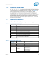
The Intel® Core™ i7 processor family for LGA2011 socket are the next generation of
64-bit, multi-core desktop processors built on 22-nanometer process technology. Based
on the low-power/high-performance Intel® Core™ i7 processor micro-architecture, the
processor is designed for a two-chip platform instead of to the traditional three-chip
platforms (processor, Memory Controller Hub, and Platform Controller Hub). The twochip platform consists of a processor and the Platform Controller Hub (PCH) enabling
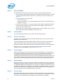
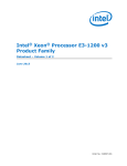
higher performance, easier validation, and improved x-y footprint. Refer to Figure 1-1
for a platform block diagram.
The processor features per socket, up to 40 lanes of PCI Express* 3.0 links capable of
8.0 GT/s, and 4 lanes of DMI2/PCI Express* 2.0 interface with a peak transfer rate of
5.0 GT/s. The processor supports up to 46 bits of physical address space and a 48-bit
virtual address space.
Included in this family of processors is an integrated memory controller (IMC) and
integrated I/O (IIO) (such as PCI Express* and DMI2) on a single silicon die. This single
die solution is known as a monolithic processor.
The Datasheet - Volume 1 covers DC electrical specifications, land and signal
definitions, differential signaling specifications, interface functional descriptions, power
management descriptions, and additional feature information pertinent to the
implementation and operation of the processor on its platform. Volume 2 provides
register information. Refer to the Related Documents section for access to Volume 2.
Note:
Throughout this document, the Intel® Core™ i7 processor family for LGA2011 socket
may be referred to as “processor”.
Note:
Throughout this document, the Intel® Core™ i7-49xx processor series for the LGA2011
socket refers t the Intel® Core™ i7-4930K processor.
Note:
Throughout this document, the Intel® Core™ i7-48xx processor series for the LGA2011
socket refers to the Intel® Core™ i7-4820K processor.
Note:
Throughout this document, the Intel® X79 Chipset Platform Controller Hub may be
referred to as “PCH”.
Note:
Some processor features are not available on all platforms. Refer to the processor
specification update for details.
8
Datasheet
Introduction
DDR3
DDR3
DDR3
Processor Platform Block Diagram Example
DDR3
Figure 1-1.
ethernet
SATA
Processor
BIOS
PCIe*
DMI2
PCIe*
PCH
PCIe*
x4
PCIe*
...
x1
PCIe*
x16
x16
x8
1.1
Processor Feature Details
• Up to 6 execution cores
• Each core supports two threads (Intel® Hyper-Threading Technology), up to
12 threads per socket
• 32KB instruction and 32-KB data first-level cache (L1) for each core
• 256KB shared instruction/data mid-level (L2) cache for each core
• Up to 15MB last level cache (LLC): up to 2.5MB per core instruction/data last level
cache (LLC), shared among all cores
Datasheet
9
Introduction
1.2
Supported Technologies
• Intel® Virtualization Technology (Intel® VT)
• Intel® Virtualization Technology (Intel® VT) for Directed I/O (Intel® VT-d)
• Intel® Virtualization Technology (Intel® VT) Processor Extensions
• Intel® 64 Architecture
• Intel® Streaming SIMD Extensions 4.1 (Intel® SSE4.1)
• Intel® Streaming SIMD Extensions 4.2 (Intel® SSE4.2)
• Intel® Advanced Vector Extensions (Intel® AVX)
• Intel® AVX Floating Point Bit Depth Conversion (Float 16)
• Intel® Hyper-Threading Technology
• Execute Disable Bit
• Intel® Turbo Boost Technology
• Enhanced Intel® SpeedStep® Technology
1.3
Interfaces
1.3.1
System Memory Support
• Supports four DDR3 channels
• Unbuffered DDR3 DIMMs supported
• Independent channel mode or lockstep mode
• Data burst length of eight cycles for all memory organization modes
• Memory DDR3 data transfer rates of 1066 MT/s, 1333 MT/s, 1600 MT/s, and
1866 MT/s
• 64-bit wide channels
• DDR3 standard I/O Voltage of 1.5 V
• 1-Gb, 2-Gb and 4-Gb DDR3 DRAM technologies supported for these devices:
— UDIMMs x8, x16
• Up to 4 ranks supported per memory channel, 1, 2, or 4 ranks per DIMM
• Open with adaptive idle page close timer or closed page policy
• Per channel memory test and initialization engine can initialize DRAM to all logical
zeros or a predefined test pattern
• Minimum memory configuration: independent channel support with 1 DIMM
populated
• Command launch modes of 1n/2n
• Improved Thermal Throttling
• Memory thermal monitoring support for DIMM temperature using two memory
signals, MEM_HOT_C{01/23}_N
10
Datasheet
Introduction
1.3.2
PCI Express*
• The PCI Express* port(s) are fully-compliant with the PCI Express* Base
Specification, Revision 3.0 (PCIe 3.0)
• Support for PCI Express* 3.0 (8.0 GT/s), 2.0 (5.0 GT/s), and 1.0 (2.5 GT/s)
• Up to 40 lanes of PCI Express* interconnect for general purpose PCI Express*
devices at PCIe* 3.0 speeds that are configurable for up to 10 independent ports
• 4 lanes of PCI Express* at PCIe* 2.0 speeds when not using DMI2 port (Port 0),
also can be downgraded to x2 or x1
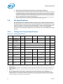
• Negotiating down to narrower widths is supported, see Figure 1-2:
— x16 port (Port 2 and Port 3) may negotiate down to x8, x4, x2, or x1
— x8 port (Port 1) may negotiate down to x4, x2, or x1
— x4 port (Port 0) may negotiate down to x2, or x1
— When negotiating down to narrower widths, there are caveats as to how lane
reversal is supported
• Address Translation Services (ATS) 1.0 support
• Hierarchical PCI-compliant configuration mechanism for downstream devices
• Traditional PCI style traffic (asynchronous snooped, PCI ordering)
• PCI Express* extended configuration space. The first 256 bytes of configuration
space aliases directly to the PCI compatibility configuration space. The remaining
portion of the fixed 4-KB block of memory-mapped space above that (starting at
100h) is known as extended configuration space.
• PCI Express* Enhanced Access Mechanism – accessing the device configuration
space in a flat memory mapped fashion
• Automatic discovery, negotiation, and training of link out of reset
• Supports receiving and decoding 64 bits of address from PCI Express*:
— Memory transactions received from PCI Express* that go above the top of
physical address space (when Intel VT-d is enabled, the check would be against
the translated Host Physical Address (HPA)) are reported as errors by the
processor.
— Outbound access to PCI Express* will always have address bits 63:46 cleared
• Re-issues Configuration cycles that have been previously completed with the
Configuration Retry status
• Power Management Event (PME) functions
• Message Signaled Interrupt (MSI and MSI-X) messages
• Degraded Mode support and Lane Reversal support
• Static lane numbering reversal and polarity inversion support
• Support for PCIe* 3.0 atomic operation, PCIe 3.0 optional extension on atomic
read-modify-write mechanism
Datasheet
11
Introduction
Figure 1-2.
PCI Express* Lane Partitioning and Direct Media Interface Gen 2 (DMI2)
Port 0
DMI / PCIe
Transaction
Port 1
(IOU2)
PCIe
Port 2
(IOU0)
PCIe
Transaction
Port 3
(IOU1)
PCIe
Transaction
Transaction
Link
Link
Link
Link
Physical
Physical
Physical
Physical
0…3
0…3
4…7
0…3
4…7
8…11
12..15
0…3
4…7
8…11
12..15
X4
X4
X4
X4
X4
X4
X4
X4
X4
X4
X4
DMI
Port 1a
Port 1b
Port 2a
Port 2b
Port 2c
Port 2d
Port 3a
Port 3b
Port 3c
Port 3d
X8
X8
X8
X8
X8
Port 1a
Port 2a
Port 2c
Port 3a
Port 3c
X16
Port 2a
1.3.3
X16
Port 3a
Direct Media Interface Gen 2 (DMI2)
• Serves as the chip-to-chip interface to the PCH
• The DMI2 port supports x4 link width and only operates in a x4 mode when in DMI2
• Operates at PCI Express* 1.0 or 2.0 speeds
• Transparent to software
• Processor and peer-to-peer writes and reads with 64-bit address support
• APIC and Message Signaled Interrupt (MSI) support. Will send Intel-defined “End of
Interrupt” broadcast message when initiated by the processor.
• System Management Interrupt (SMI), SCI, and SERR error indication
• Static lane numbering reversal support
• Supports DMI2 virtual channels VC0, VC1, VCm, and VCp
12
Datasheet
Introduction
1.3.4
Platform Environment Control Interface (PECI)
The PECI is a one-wire interface that provides a communication channel between a
PECI client (the processor) and a PECI master (the PCH). Refer to the Processor
Thermal Mechanical Specifications and Design Guide for additional details on PECI
services available in the processor (Refer to the Related Documents section).
• Supports operation at up to 2 Mbps data transfers
• Link layer improvements to support additional services and higher efficiency over
PECI 2.0 generation
• Services include processor thermal and estimated power information, control
functions for power limiting, P-state and T-state control, and access for Machine
Check Architecture registers and PCI configuration space (both within the processor
package and downstream devices)
• Single domain (Domain 0) is supported
1.4
Power Management Support
1.4.1
Processor Package and Core States
• Advance Configuration and Power Interface (ACPI) C-states as implemented by the
following processor C-states:
— Package: PC0, PC1/PC1E, PC2, PC3, PC6 (Package C7 is not supported)
— Core: CC0, CC1, CC1E, CC3, CC6, CC7
• Enhanced Intel SpeedStep Technology
1.4.2
System States Support
• S0, S1, S3, S4, S5
1.4.3
Memory Controller
• Multiple CKE power-down modes
• Multiple self-refresh modes
• Memory thermal monitoring using MEM_HOT_C01_N and MEM_HOT_C23_N signals
1.4.4
PCI Express*
• L1 ASPM power management capability; L0s is not supported
1.5
Thermal Management Support
• Digital Thermal Sensor with multiple on-die temperature zones
• Adaptive Thermal Monitor
• THERMTRIP_N and PROCHOT_N signal support
• On-Demand mode clock modulation
• Fan speed control with DTS
• Two integrated SMBus masters for accessing thermal data from DIMMs
• New Memory Thermal Throttling features using MEM_HOT_C{01/23}_N signals
Datasheet
13
Introduction
1.6
Package Summary
The processor socket type is noted as LGA2011. The processor package is a
52.5 x 45 mm FC-LGA package (LGA2011). Refer to the Processor Thermal Mechanical
Specification and Design Guide (see Related Documents section) for the package
mechanical specifications.
1.7
Terminology
Table 1-1.
Terminology (Sheet 1 of 3)
Term
ACPI
14
Description
Advanced Configuration and Power Interface
ASPM
Active State Power Management
CCM
Continuous Conduction Mode
DCM
Discontinuous Conduction Mode
DDR3
Third generation Double Data Rate SDRAM memory technology that is the successor
to DDR2 SDRAM
DMA
Direct Memory Access
DMI
Direct Media Interface
DMI2
Direct Media Interface Gen 2
DTS
Digital Thermal Sensor
Enhanced Intel
SpeedStep®
Technology (EIST)
Allows the operating system to reduce power consumption when performance is not
needed.
EPT
Extended Page Tables
ESD
Electro-Static Discharge
Execute Disable Bit
The Execute Disable bit allows memory to be marked as executable or nonexecutable when combined with a supporting operating system. If code attempts to
run in non-executable memory, the processor raises an error to the operating
system. This feature can prevent some classes of viruses or worms that exploit buffer
overrun vulnerabilities and can thus help improve the overall security of the system.
See the Intel® 64 and IA-32 Architectures Software Developer's Manuals for more
detailed information.
Functional Operation
Refers to the normal operating conditions in which all processor specifications,
including DC, AC, system bus, signal quality, mechanical, and thermal are satisfied.
IHS
Integrated Heat Spreader. A component of the processor package used to enhance
the thermal performance of the package. Component thermal solutions interface with
the processor at the IHS surface.
IIO
The Integrated I/O Controller. An I/O controller that is integrated in the processor
die.
IMC
The Integrated Memory Controller. A Memory Controller that is integrated in the
processor die.
Intel® 64 Technology
64-bit memory extensions to the IA-32 architecture. Further details on Intel 64
architecture and programming model can be found at
http://developer.intel.com/technology/intel64/.
Intel® ME
Intel® Management Engine (Intel® ME)
Intel® Turbo Boost
Technology
Intel® Turbo Boost Technology is a way to automatically run the processor core faster
than the marked frequency if the part is operating under power, temperature, and
current specifications limits of the Thermal Design Power (TDP). This results in
increased performance of both single and multi-threaded applications.
Intel® Virtualization
Technology (Intel® VT)
Processor virtualization, which when used in conjunction with Virtual Machine Monitor
software, enables multiple robust independent software environments inside a single
platform.
Datasheet
Introduction
Table 1-1.
Terminology (Sheet 2 of 3)
Term
Datasheet
Description
Intel® VT-d
Intel® Virtualization Technology (Intel® VT) for Directed I/O. Intel VT-d is a hardware
assist, under system software (Virtual Machine Manager or operating system)
control, for enabling I/O device virtualization. Intel VT-d also brings robust security
by providing protection from errant DMAs by using DMA remapping, a key feature of
Intel VT-d.
IOV
I/O Virtualization
Jitter
Any timing variation of a transition edge or edges from the defined Unit Interval (UI).
JTAG
Joint Test Action Group
LGA2011-0 Socket
The LGA2011-0 land FCLGA package mates with the system board through this
surface mount, LGA2011-0 contact socket.
LLC
Last Level Cache
MCH
Memory Controller Hub
NCTF
Non-Critical to Function: NCTF locations are typically redundant ground or noncritical reserved; thus, the loss of the solder joint continuity at end of life conditions
will not affect the overall product functionality.
NEBS
Network Equipment Building System. NEBS is the most common set of environmental
design guidelines applied to telecommunications equipment in the United States.
PCH
Platform Controller Hub. The next generation chipset with centralized platform
capabilities including the main I/O interfaces along with display connectivity, audio
features, power management, manageability, security, and storage features.
PCI Express*
PCI Express* Generation 2.0/3.0
PCI Express* 2
PCI Express* Generation 2.0
PCI Express* 3
PCI Express* Generation 3.0
PCU
Power Control Unit
PECI
Platform Environment Control Interface
PLE
Pause Loop Exiting
Processor
The 64-bit, single-core or multi-core component (package)
Processor Core
The term “processor core” refers to silicon die itself that can contain multiple
execution cores. Each execution core has an instruction cache, data cache, and
256-KB L2 cache. All execution cores share the L3 cache. All DC and AC timing and
signal integrity specifications are measured at the processor die (pads), unless
otherwise noted.
QoS
Quality of Service
Rank
A unit of DRAM corresponding four to eight devices in parallel. These devices are
usually, but not always, mounted on a single side of a DDR3 DIMM.
SCI
System Control Interrupt. Used in Advanced Configuration and Power Interface
(ACPI) protocol.
SMBus
System Management Bus. A two-wire interface through which simple system and
power management related devices can communicate with the rest of the system. It
is based on the principals of the operation of the I2C* two-wire serial bus from
Philips* Semiconductor.
SSE
Intel® Streaming SIMD Extensions (Intel® SSE)
STD
Suspend-to-Disk
STR
Suspend-to-RAM
SVID
Serial Voltage Identification
TAC
Thermal Averaging Constant
TAP
Test Access Port
TCC
Thermal Control Circuit
TDP
Thermal Design Power
TLP
Transaction Layer Packet
TSOD
Thermal Sensor on DIMM
UDIMM
Unbuffered Dual In-line Module
15
Introduction
Table 1-1.
Terminology (Sheet 3 of 3)
Term
Uncore
Unit Interval
Description
The portion of the processor comprising the shared cache, IMC, HA, PCU, and UBox.
Signaling convention that is binary and unidirectional. In this binary signaling, one bit
is sent for every edge of the forwarded clock, whether it be a rising edge or a falling
edge. If a number of edges are collected at instances t1, t2, tn,...., tk then the UI at
instance “n” is defined as:
UI
1.8
n
=t
n
–t
n
–1
VCC
Processor core power supply
VCCD_01, VCCD_23
Variable power supply for the processor system memory interface. VCCD is the
generic term for VCCD_01, VCCD_23.
VID
Voltage Identification
VM
Virtual Machine
VMM
Virtual Machine Monitor
VPID
Virtual Processor ID
VR
Voltage Regulator
VRD
Voltage Regulator Down
VRM
Voltage Regulator Module
VSS
Processor ground
x1
Refers to a Link or Port with one Physical Lane
x16
Refers to a Link or Port with sixteen Physical Lanes
x4
Refers to a Link or Port with four Physical Lanes
x8
Refers to a Link or Port with eight Physical Lanes
Related Documents
Refer to the following documents for additional information.
Table 1-2.
16
Processor Documents
Document
Document Number /
Location
Intel® Core™ i7 Processor Family for LGA2011 Socket Datasheet – Volume 2 of
2
329367
Intel® Core™ i7 Processor Families for the LGA2011-0 Socket Thermal
Mechanical Specifications and Design Guide
329368
IIntel® Core™ i7 Processor Family for LGA2011 Socket Specification Update
326199
Datasheet
Introduction
Table 1-3.
Public Specifications
Document
Document Number / Location
Advanced Configuration and Power Interface Specification 3.0
http://www.acpi.info
PCI Local Bus Specification 3.0
http://www.pcisig.com/specifications
PCI Express Base Specification - Revision 2.1 and 1.1
PCI Express Base Specification - Revision 3.0
http://www.pcisig.com
System Management Bus (SMBus) Specification, Revision 2.0
http://smbus.org/
DDR3 SDRAM Specification
http://www.jedec.org
Low (JESD22-A119) and High (JESD-A103) Temperature Storage Life
Specifications
http://www.jedec.org
Intel®
64 and IA-32 Architectures Software Developer’s Manuals
• Volume 1: Basic Architecture
• Volume 2A: Instruction Set Reference, A-M
• Volume 2B: Instruction Set Reference, N-Z
• Volume 3A: System Programming Guide
• Volume 3B: System Programming Guide
Intel® 64 and IA-32 Architectures Optimization Reference Manual
http://www.intel.com/products/proce
ssor/manuals/index.htm
Intel® Virtualization Technology Specification for Directed I/O
Architecture Specification
http://download.intel.com/technolog
y/computing/vptech/Intel(r)_VT_for_
Direct_IO.pdf
National Institute of Standards and Technology NIST SP800-90
http://csrc.nist.gov/publications/Pubs
SPs.html
§
Datasheet
17
Interfaces
2
Interfaces
This chapter describes the functional behaviors supported by the processor. Topics
covered include:
• System Memory Interface
• PCI Express* Interface
• Direct Media Interface 2 (DMI2) / PCI Express* Interface
• Platform Environment Control Interface (PECI)
2.1
System Memory Interface
2.1.1
System Memory Technology Support
The Integrated Memory Controller (IMC) supports DDR3 protocols with four
independent 64-bit memory channels and supports 1 unbuffered DIMM per channel.
2.1.2
System Memory Timing Support
The IMC supports the following DDR3 Speed Bin, CAS Write Latency (CWL), and
command signal mode timings on the main memory interface:
• tCL = CAS Latency
• tRCD = Activate Command to READ or WRITE Command delay
• tRP = PRECHARGE Command Period
• CWL = CAS Write Latency
• Command Signal modes = 1n indicates a new command may be issued every clock
and 2n indicates a new command may be issued every 2 clocks. Command launch
mode programming depends on the transfer rate and memory configuration.
18
Datasheet
Interfaces
2.2
PCI Express* Interface
This section describes the PCI Express* 3.0 interface capabilities of the processor. See
the PCI Express* Base Specification for details of PCI Express* 3.0.
2.2.1
PCI Express* Architecture
Compatibility with the PCI addressing model is maintained to ensure that all existing
applications and drivers operate unchanged. The PCI Express* configuration uses
standard mechanisms as defined in the PCI Plug-and-Play specification.
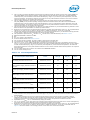
The PCI Express* architecture is specified in three layers – Transaction Layer, Data Link
Layer, and Physical Layer. The partitioning in the component is not necessarily along
these same boundaries. Refer to the following figure for the PCI Express* Layering
Diagram.
Figure 2-1.
PCI Express* Layering Diagram
Transaction
Transaction
Data Link
Data Link
Physical
Physical
Logical Sub-Block
Logical Sub-Block
Electrical Sub-Block
Electrical Sub-Block
RX
TX
RX
TX
PCI Express* uses packets to communicate information between components. Packets
are formed in the Transaction and Data Link Layers to carry the information from the
transmitting component to the receiving component. As the transmitted packets flow
through the other layers, the packets are extended with additional information
necessary to handle packets at those layers. At the receiving side, the reverse process
occurs and packets get transformed from their Physical Layer representation to the
Data Link Layer representation and finally (for Transaction Layer Packets) to the form
that can be processed by the Transaction Layer of the receiving device.
Datasheet
19
Interfaces
Figure 2-2.
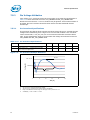
Packet Flow through the Layers
Framing
Sequence
Number
Header
Date
ECRC
LCRC
Framing
Transaction Layer
Data Link Layer
Physical Layer
2.2.1.1
Transaction Layer
The upper layer of the PCI Express* architecture is the Transaction Layer. The
Transaction Layer's primary responsibility is the assembly and disassembly of
Transaction Layer Packets (TLPs). TLPs are used to communicate transactions, such as
read and write, as well as certain types of events. The Transaction Layer also manages
flow control of TLPs.
2.2.1.2
Data Link Layer
The middle layer in the PCI Express* stack, the Data Link Layer, serves as an
intermediate stage between the Transaction Layer and the Physical Layer.
Responsibilities of Data Link Layer include link management, error detection, and error
correction.
The transmission side of the Data Link Layer accepts TLPs assembled by the
Transaction Layer, calculates and applies data protection code and TLP sequence
number, and submits them to Physical Layer for transmission across the Link. The
receiving Data Link Layer is responsible for checking the integrity of received TLPs and
for submitting them to the Transaction Layer for further processing. On detection of TLP
error(s), this layer is responsible for requesting retransmission of TLPs until information
is correctly received, or the Link is determined to have failed. The Data Link Layer also
generates and consumes packets that are used for Link management functions.
2.2.1.3
Physical Layer
The Physical Layer includes all circuitry for interface operation, including driver and
input buffers, parallel-to-serial and serial-to-parallel conversion, PLL(s), and impedance
matching circuitry. It also includes logical functions related to interface initialization and
maintenance. The Physical Layer exchanges data with the Data Link Layer in an
implementation-specific format, and is responsible for converting this to an appropriate
serialized format and transmitting it across the PCI Express* Link at a frequency and
width compatible with the remote device.
2.2.2
PCI Express* Configuration Mechanism
The PCI Express* link is mapped through a PCI-to-PCI bridge structure.
PCI Express* extends the configuration space to 4096 bytes per-device/function, as
compared to 256 bytes allowed by the Conventional PCI Specification. PCI Express*
configuration space is divided into a PCI-compatible region (which consists of the first
256 bytes of a logical device's configuration space) and an extended PCI Express*
region (which consists of the remaining configuration space). The PCI-compatible
20
Datasheet
Interfaces
region can be accessed using either the mechanisms defined in the PCI specification or
using the enhanced PCI Express* configuration access mechanism described in the PCI
Express* Enhanced Configuration Mechanism section.
The PCI Express* Host Bridge is required to translate the memory-mapped PCI
Express* configuration space accesses from the host processor to PCI Express*
configuration cycles. To maintain compatibility with PCI configuration addressing
mechanisms, it is recommended that system software access the enhanced
configuration space using 32-bit operations (32-bit aligned) only.
See the PCI Express* Base Specification for details of both the PCI-compatible and PCI
Express* Enhanced configuration mechanisms and transaction rules.
2.3
Direct Media Interface 2 (DMI2) / PCI Express*
Interface
Direct Media Interface 2 (DMI2) connects the processor to the Platform Controller Hub
(PCH). DMI2 is similar to a four-lane PCI Express* supporting a speed of 5 GT/s per
lane. Refer to Section 6.3 for additional details.
Note:
Only DMI2 x4 configuration is supported.
2.3.1
DMI2 Error Flow
DMI2 can only generate SERR in response to errors, never SCI, SMI, MSI, PCI INT, or
GPE. Any DMI2 related SERR activity is associated with Device 0.
2.3.2
Processor / PCH Compatibility Assumptions
The processor is compatible with the PCH and is not compatible with any previous Intel
Memory Controller Hub (MCH) and Integrated Controller Hub (ICH) products.
2.3.3
DMI2 Link Down
The DMI2 link going down is a fatal, unrecoverable error. If the DMI2 data link goes to
data link down, after the link was up, then the DMI2 link hangs the system by not
allowing the link to retrain to prevent data corruption. This is controlled by the PCH.
Downstream transactions that had been successfully transmitted across the link prior
to the link going down may be processed as normal. No completions from downstream,
non-posted transactions are returned upstream over the DMI2 link after a link down
event.
2.4
Platform Environment Control Interface (PECI)
The Platform Environment Control Interface (PECI) uses a single wire for self-clocking
and data transfer. The bus requires no additional control lines. The physical layer is a
self-clocked one-wire bus that begins each bit with a driven, rising edge from an idle
level near zero volts. The duration of the signal driven high depends on whether the bit
value is a logic ‘0’ or logic ‘1’. PECI also includes variable data transfer rate established
with every message. In this way, it is highly flexible even though underlying logic is
simple.
Datasheet
21
Interfaces
The interface design was optimized for interfacing to Intel processor and chipset
components in both single processor and multiple processor environments. The single
wire interface provides low board routing overhead for the multiple load connections in
the congested routing area near the processor and chipset components. Bus speed,
error checking, and low protocol overhead provides adequate link bandwidth and
reliability to transfer critical device operating conditions and configuration information.
§§
22
Datasheet
Technologies
3
Technologies
This chapter covers the following technologies:
• Intel® Virtualization Technology (Intel® VT)
• Security Technologies
• Intel® Hyper-Threading Technology (Intel® HT Technology)
• Intel® Turbo Boost Technology
• Enhanced Intel® SpeedStep® Technology
• Intel® Advanced Vector Extensions (Intel® AVX)
3.1
Intel® Virtualization Technology (Intel® VT)
Intel® Virtualization Technology (Intel® VT) makes a single system appear as multiple
independent systems to software. This allows multiple, independent operating systems
to run simultaneously on a single system. Intel VT comprises technology components
to support virtualization of platforms based on Intel architecture microprocessors and
chipsets.
• Intel® Virtualization Technology (Intel® VT) for Intel® 64 and IA-32 Intel®
Architecture (Intel® VT-x) adds hardware support in the processor to improve
the virtualization performance and robustness. Intel VT-x specifications and
functional descriptions are included in the Intel® 64 and IA-32 Architectures
Software Developer’s Manual, Volume 3B and is available at
http://www.intel.com/products/processor/manuals/index.htm
• Intel® Virtualization Technology (Intel® VT) for Directed I/O
(Intel® VT-d) adds processor and uncore implementations to support and
improve I/O virtualization performance and robustness. The Intel VT-d specification
and other Intel VT documents can be referenced at
http://www.intel.com/technology/virtualization/index.htm
3.1.1
Intel® VT-x Objectives
Intel VT-x provides hardware acceleration for virtualization of IA platforms. Virtual
Machine Monitor (VMM) can use Intel VT-x features to provide improved reliable
virtualized platforms. By using Intel VT-x, a VMM is:
• Robust: VMMs no longer need to use para-virtualization or binary translation. This
means that off-the-shelf operating systems and applications can be run without any
special steps.
• Enhanced: Intel VT enables VMMs to run 64-bit guest operating systems on IA x86
processors.
• More reliable: Due to the hardware support, VMMs can now be smaller, less
complex, and more efficient. This improves reliability and availability and reduces
the potential for software conflicts.
• More secure: The use of hardware transitions in the VMM strengthens the isolation
of VMs and further prevents corruption of one VM from affecting others on the
same system.
Datasheet
23
Technologies
3.1.2
Intel® VT-x Features
The processor core supports the following Intel VT-x features:
• Extended Page Tables (EPT)
— hardware assisted page table virtualization.
— eliminates VM exits from guest operating system to the VMM for shadow pagetable maintenance.
• Virtual Processor IDs (VPID)
— Ability to assign a VM ID to tag processor core hardware structures (such as,
TLBs).
— This avoids flushes on VM transitions to give a lower-cost VM transition time
and an overall reduction in virtualization overhead.
• Guest Preemption Timer
— Mechanism for a VMM to preempt the execution of a guest operating system
after an amount of time specified by the VMM. The VMM sets a timer value
before entering a guest.
— The feature aids VMM developers in flexibility and Quality of Service (QoS)
guarantees.
• Descriptor-Table Exiting
— Descriptor-table exiting allows a VMM to protect a guest operating system from
internal (malicious software based) attack by preventing relocation of key
system data structures like IDT (interrupt descriptor table), GDT (global
descriptor table), LDT (local descriptor table), and TSS (task segment selector).
— A VMM using this feature can intercept (by a VM exit) attempts to relocate
these data structures and prevent them from being tampered by malicious
software.
• Pause Loop Exiting (PLE)
— PLE aims to improve virtualization performance and enhance the scaling of
virtual machines with multiple virtual processors
— PLE attempts to detect lock-holder preemption in a VM and helps the VMM to
make better scheduling decisions
3.1.3
Intel® VT-d Objectives
The key Intel VT-d objectives are domain-based isolation and hardware-based
virtualization. A domain can be abstractly defined as an isolated environment in a
platform to which a subset of host physical memory is allocated. Virtualization allows
for the creation of one or more partitions on a single system. This could be multiple
partitions in the same operating system, or there can be multiple operating system
instances running on the same system – offering benefits such as system
consolidation, legacy migration, activity partitioning, or security.
24
Datasheet
Technologies
3.1.3.1
Intel® VT-d Features Supported
The processor supports the following Intel VT-d features:
• Root entry, context entry, and default context
• Support for 4-K page sizes only
• Support for register-based fault recording only (for single entry only) and support
for MSI interrupts for faults
— Support for fault collapsing based on Requester ID
• Support for both leaf and non-leaf caching
• Support for boot protection of default page table
— Support for non-caching of invalid page table entries
• Support for hardware based flushing of translated but pending writes and pending
reads upon IOTLB invalidation
• Support for page-selective IOTLB invalidation
• Support for ARI (Alternative Requester ID – a PCI SIG ECR for increasing the
function number count in a PCIe* device) to support I/O Virtualization (IOV)
devices
• Improved invalidation architecture
• End point caching support (ATS)
• Interrupt remapping
3.1.4
Intel® Virtualization Technology Processor Extensions
The processor supports the following Intel VT processor extension features:
• Large Intel VT-d Pages
— Adds 2MB and 1GB page sizes to Intel VT-d implementations
— Matches current support for Extended Page Tables (EPT)
— Ability to share processor EPT page-table (with super-pages) with Intel VT-d
— Benefits:
• Less memory foot-print for I/O page-tables when using super-pages
• Potential for improved performance – due to shorter page-walks, allows
hardware optimization for IOTLB
• Transition latency reductions expected to improve virtualization performance
without the need for VMM enabling. This reduces the VMM overheads further and
increase virtualization performance.
Datasheet
25
Technologies
3.2
Security Technologies
3.2.1
Intel® Advanced Encryption Standard New Instructions
(Intel® AES-NI) Instructions
These instructions enable fast and secure data encryption and decryption, using the
Advanced Encryption Standard (Intel AES-NI) which is defined by FIPS Publication
number 197. Since Intel AES-NI is the dominant block cipher, and it is deployed in
various protocols, the new instructions will be valuable for a wide range of applications.
The architecture consists of six instructions that offer full hardware support for Intel
AES-NI. Four instructions support the Intel AES-NI encryption and decryption, and the
other two instructions support the Intel AES-NI key expansion. Together, they offer a
significant increase in performance compared to pure software implementations.
The Intel AES-NI instructions have the flexibility to support all three standard Intel
AES-NI key lengths, all standard modes of operation, and even some nonstandard or
future variants.
Beyond improving performance, the Intel AES-NI instructions provide important
security benefits. Since the instructions run in data-independent time and do not use
lookup tables, the instructions help in eliminating the major timing and cache-based
attacks that threaten table-based software implementations of Intel AES-NI. In
addition, these instructions make AES simple to implement, with reduced code size.
This helps reducing the risk of inadvertent introduction of security flaws, such as
difficult-to-detect side channel leaks.
3.2.2
Execute Disable Bit
The Intel Execute Disable Bit functionality can help prevent certain classes of malicious
buffer overflow attacks when combined with a supporting operating system.
• Allows the processor to classify areas in memory by where application code can
execute and where it cannot.
• When a malicious worm attempts to insert code in the buffer, the processor
disables code execution, preventing damage and worm propagation.
3.3
Intel® Hyper-Threading Technology (Intel® HT
Technology)
The processor supports Intel® Hyper-Threading Technology (Intel® HT Technology)
that allows an execution core to function as two logical processors. While some
execution resources such as caches, execution units, and buses are shared, each
logical processor has its own architectural state with its own set of general-purpose
registers and control registers. This feature must be enabled using the BIOS and
requires operating system support.
For more information on Intel Hyper-Threading Technology, see
http://www.intel.com/products/ht/hyperthreading_more.htm.
26
Datasheet
Technologies
3.4
Intel® Turbo Boost Technology
Intel Turbo Boost Technology is a feature that allows the processor to opportunistically
and automatically run faster than its rated operating frequency if it is operating below
power, temperature, and current limits. The result is increased performance in multithreaded and single threaded workloads. It should be enabled in the BIOS for the
processor to operate with maximum performance.
3.4.1
Intel® Turbo Boost Operating Frequency
The processor’s rated frequency assumes that all execution cores are running an
application at the thermal design power (TDP). However, under typical operation, not
all cores are active. Therefore, most applications are consuming less than the TDP at
the rated frequency. To take advantage of the available TDP headroom, the active cores
can increase their operating frequency.
To determine the highest performance frequency amongst active cores, the processor
takes the following into consideration:
• number of cores operating in the C0 state
• estimated current consumption
• estimated power consumption
• die temperature
Any of these factors can affect the maximum frequency for a given workload. If the
power, current, or thermal limit is reached, the processor will automatically reduce the
frequency to stay with its TDP limit.
Note:
Intel Turbo Boost Technology is only active if the operating system is requesting the P0
state. For more information on P-states and C-states, refer to Chapter 4.
3.5
Enhanced Intel® SpeedStep® Technology
The processor supports Enhanced Intel SpeedStep® Technology as an advanced means
of enabling very high performance while also meeting the power-conservation needs of
the platform.
Enhanced Intel SpeedStep Technology builds upon that architecture using design
strategies that include the following:
• Separation between Voltage and Frequency Changes. By stepping voltage up
and down in small increments separately from frequency changes, the processor is
able to reduce periods of system unavailability that occur during frequency change.
Thus, the system is able to transition between voltage and frequency states more
often, providing improved power/performance balance.
• Clock Partitioning and Recovery. The bus clock continues running during state
transition, even when the core clock and Phase-Locked Loop are stopped, which
allows logic to remain active. The core clock can also restart more quickly under
Enhanced Intel SpeedStep Technology.
For additional information on Enhanced Intel SpeedStep® Technology, refer to
Section 4.2.1.
Datasheet
27
Technologies
3.6
Intel® Advanced Vector Extensions (Intel® AVX)
Intel Advanced Vector Extensions (Intel AVX) is a new 256-bit vector SIMD extension of
Intel Architecture. The introduction of Intel AVX started with the 2nd Generation Intel®
Core™ processor family. Intel AVX accelerates the trend of parallel computation in
general purpose applications like image, video and audio processing, engineering
applications (such as 3D modeling and analysis), scientific simulation, and financial
analysts.
Intel AVX is a comprehensive ISA extension of the Intel 64 Architecture. The main
elements of Intel AVX are:
• Support for wider vector data (up to 256-bit) for floating-point computation
• Efficient instruction encoding scheme that supports 3 operand syntax and
headroom for future extensions
• Flexibility in programming environment, ranging from branch handling to relaxed
memory alignment requirements
• New data manipulation and arithmetic compute primitives, including broadcast,
permute, fused-multiply-add, and so on
• Floating point bit depth conversion (Float 16)
• A group of 4 instructions that accelerate data conversion between 16-bit
floating point format to 32-bit and vice versa.
• This benefits image processing and graphical applications allowing
compression of data so less memory and bandwidth is required.
The key advantages of Intel AVX are:
• Performance – Intel AVX can accelerate application performance using data
parallelism and scalable hardware infrastructure across existing and new
application domains:
— 256-bit vector data sets can be processed up to twice the throughput of 128-bit
data sets
— Application performance can scale up with the number of hardware threads and
number of cores
— Application domain can scale out with advanced platform interconnect fabrics
• Power Efficiency – Intel AVX is extremely power efficient. Incremental power is
insignificant when the instructions are unused or scarcely used. Combined with the
high performance that it can deliver, applications that lend themselves heavily to
using Intel AVX can be much more energy efficient and realize a higher
performance-per-watt.
• Extensibility – Intel AVX has built-in extensibility for the future vector extensions:
— Operating System context management for vector-widths beyond 256 bits is
streamlined
— Efficient instruction encoding allows unlimited functional enhancements:
• Vector width support beyond 256 bits
• 256-bit Vector Integer processing
• Additional computational and/or data manipulation primitives
28
Datasheet
Technologies
• Compatibility – Intel AVX is backward compatible with previous ISA extensions
including Intel SSE4:
— Existing Intel SSE applications/library can:
• Run unmodified and benefit from processor enhancements
• Recompile existing Intel® SSE intrinsic using compilers that generate
Intel AVX code
• Inter-operate with library ported to Intel AVX
— Applications compiled with Intel AVX can inter-operate with existing Intel SSE
libraries.
§§
Datasheet
29
Power Management
4
Power Management
This chapter provides information on the following power management topics:
• Advanced Configuration and Power Interface (ACPI) States Supported
• Processor Core / Package Power Management
• System Memory Power Management
• Direct Media Interface 2 (DMI2) / PCI Express* Power Management
4.1
Advanced Configuration and Power Interface
(ACPI) States Supported
The ACPI states supported by the processor are described in this section.
4.1.1
System States
Table 4-1.
System States
State
G0/S0
G1/S3-Cold
G1/S4
G2/S5
G3
4.1.2
Description
Full On
Suspend-to-RAM (STR). Context saved to memory.
Suspend-to-Disk (STD). All power lost (except wakeup on PCH).
Soft off. All power lost (except wakeup on PCH). Total reboot.
Mechanical off. All power removed from system.
Processor Package and Core States
The following table lists the package C-state support as: 1) the shallowest core C-state
that allows entry into the package C-state, 2) the additional factors that will restrict the
state from going any deeper, and 3) the actions taken with respect to the Ring Vcc, PLL
state, and LLC.
Table 4-3 lists the processor core C-states support.
30
Datasheet
Power Management
Table 4-2.
Package C-State Support
Retention and
PLL-Off
LLC
Fully
Flushed
Notes1
No
No
2
VccMin
Freq = MinFreq
PLL = ON
No
2
•
•
PCIe/PCH and Remote Socket
Snoops
PCIe/PCH and Remote Socket
Accesses
Interrupt response time
requirement
DMI Sidebands
Configuration Constraints
at least
one Core
in C3
•
•
•
•
Core C-State
Snoop Response Time
Interrupt Response Time
Non Snoop Response Time
Vcc = retention
PLL = OFF
No
2, 3, 4
CC6–CC7
•
•
•
•
LLC ways open
Snoop Response Time
Non Snoop Response Time
Interrupt Response Time
Vcc = retention
PLL = OFF
No
2, 3, 4
Package CState
Core
States
PC0 – Active
CC0
Limiting Factors
N/A
•
PC2 –
Snoopable
Idle
•
CC3–CC7
PC3 – Light
Retention
PC6 Deeper
Retention
•
Notes:
1.
Package C7 is not supported.
2.
All package states are defined to be "E" states – such that the states always exit back into the LFM point
upon execution resume
3.
The mapping of actions for PC3, and PC6 are suggestions – microcode will dynamically determine which
actions should be taken based on the desired exit latency parameters.
4.
CC3/CC6 will all use a voltage below the VccMin operational point. The exact voltage selected will be a
function of the snoop and interrupt response time requirements made by the devices (PCIe* and DMI) and
the operating system.
Table 4-3.
Core C-State Support
Core C-State
Datasheet
Global Clock
PLL
L1/L2 Cache
Core VCC
Context
CC0
Running
On
Coherent
Active
Maintained
CC1
Stopped
On
Coherent
Active
Maintained
CC1E
Stopped
On
Coherent
Request LFM
Maintained
CC3
Stopped
On
Flushed to LLC
Request Retention
Maintained
CC6
Stopped
Off
Flushed to LLC
Power Gate
Flushed to LLC
CC7
Stopped
Off
Flushed to LLC
Power Gate
Flushed to LLC
31
Power Management
4.1.3
Integrated Memory Controller (IMC) States
Table 4-4.
System Memory Power States
State
Description
Power Up/Normal Operation
CKE asserted. Active Mode, highest power consumption.
CKE Power Down
Opportunistic, per rank control after idle time:
• Active Power Down (APD) (default mode)
— CKE de-asserted. Power savings in this mode, relative to active idle
state is about 55% of the memory power. Exiting this mode takes
3 – 5 DCLK cycles.
• Pre-charge Power Down Fast Exit (PPDF)
— CKE de-asserted. DLL-On. Also known as Fast CKE. Power savings in
this mode, relative to active idle state is about 60% of the memory
power. Exiting this mode takes 3 – 5 DCLK cycles.
• Pre-charge Power Down Slow Exit (PPDS)
— CKE de-asserted. DLL-Off. Also known as Slow CKE. Power savings in
this mode, relative to active idle state is about 87% of the memory
power. Exiting this mode takes 3 – 5 DCLK cycles until the first
command is allowed and 16 cycles until first data is allowed.
• Register CKE Power Down:
— IBT-ON mode: Both CKEs are de-asserted, the Input Buffer
Terminators (IBTs) are left “on”.
— IBT-OFF mode: Both CKEs are de-asserted, the Input Buffer
Terminators (IBTs) are turned “off”.
Self-Refresh
CKE de-asserted. In this mode, no transactions are executed and the system
memory consumes the minimum possible power. Self-refresh modes apply to
all memory channels for the processor.
• IO-MDLL Off: Option that sets the IO master DLL off when self-refresh
occurs.
• PLL Off: Option that sets the PLL off when self-refresh occurs.
4.1.4
Direct Media Interface Gen 2 (DMI2) / PCI Express* Link
States
Table 4-5.
DMI2 / PCI Express* Link States
State
Note:
32
Description
L0
Full on – Active transfer state.
L1
Lowest Active State Power Management (ASPM) – Longer exit latency.
L1 is only supported when the DMI2/PCI Express* port is operating as a PCI Express* port.
Datasheet
Power Management
4.1.5
G, S, and C State Combinations
Table 4-6.
G, S and C State Combinations
4.2
Global (G)
State
Sleep
(S) State
Processor
Core
(C) State
Processor
State
System
Clocks
G0
S0
C0
Full On
On
Full On
G0
S0
C1/C1E
Auto-Halt
On
Auto-Halt
G0
S0
C3
Deep Sleep
On
Deep Sleep
G0
S0
C6/C7
Deep Power
Down
On
G1
S3
Power off
—
Off, except RTC
Suspend to RAM
G1
S4
Power off
—
Off, except RTC
Suspend to Disk
G2
S5
Power off
—
Off, except RTC
Soft Off
G3
N/A
Power off
—
Power off
Hard off
Description
Deep Power Down
Processor Core / Package Power Management
While executing code, Enhanced Intel SpeedStep® Technology optimizes the processor
frequency and core voltage based on workload. Each frequency and voltage operating
point is defined by ACPI as a P-State. When the processor is not executing code, it is
idle. A low-power idle state is defined by ACPI as a C-state. In general, lower power CStates have longer entry and exit latencies.
4.2.1
Enhanced Intel® SpeedStep® Technology
The following are the key features of Enhanced Intel SpeedStep® Technology:
• Multiple frequency and voltage points for optimal performance and power
efficiency. These operating points are known as P-States.
• Frequency selection is software controlled by writing to processor MSRs. The
voltage is optimized based on temperature, leakage, power delivery loadline, and
dynamic capacitance.
— If the target frequency is higher than the current frequency, VCC is ramped up
to an optimized voltage. This voltage is signaled by the SVID Bus to the voltage
regulator. Once the voltage is established, the PLL locks on to the target
frequency.
— If the target frequency is lower than the current frequency, the PLL locks to the
target frequency, then transitions to a lower voltage by signaling the target
voltage on the SVID Bus.
— All active processor cores share the same frequency and voltage. In a multicore processor, the highest frequency P-state requested amongst all active
cores is selected.
— Software-requested transitions are accepted at any time. The processor has a
new capability from the previous processor generation; it can preempt the
previous transition and complete the new request without waiting for this
request to complete.
• The processor controls voltage ramp rates internally to ensure glitch-free
transitions.
• Because there is low transition latency between P-states, a significant number of
transitions per second are possible.
Datasheet
33
Power Management
4.2.2
Low-Power Idle States
When the processor is idle, low-power idle states (C-states) are used to save power.
More power savings actions are taken for numerically higher C-States. However, higher
C-states have longer exit and entry latencies. Resolution of C-states occurs at the
thread, processor core, and processor package level. Thread level C-states are
available if Intel Hyper-Threading Technology is enabled. Entry and exit of the C-states
at the thread and core level are shown in Figure 4-2.
Figure 4-1.
Idle Power Management Breakdown of the Processor Cores
T h re a d 0
T h re a d 1
T h re a d 0
C o r e 0 S ta te
T h re a d 1
C o r e N S ta te
P r o c e s s o r P a c k a g e S ta te
Figure 4-2.
Thread and Core C-State Entry and Exit
C0
MWAIT(C1), HLT
MWAIT(C1), HLT
(C1E Enabled)
C1
C1E
MWAIT(C7),
P_LVL4 I/O Read
MWAIT(C3),
P_LVL2 I/O Read
C3
MWAIT(C6),
P_LVL3 I/O Read
C6
C7
While individual threads can request low-power C-states, power saving actions only
take place once the core C-state is resolved. Core C-states are automatically resolved
by the processor. For thread and core C-states, a transition to and from C0 is required
before entering any other C-state.
34
Datasheet
Power Management
Table 4-7.
Coordination of Thread Power States at the Core Level
Processor Core
C-State
Thread 0
Thread 1
C0
C1
C3
C6
C7
C0
C0
C0
C0
C0
C0
C1
C0
C11
C11
C11
C11
C3
C0
C11
C3
C3
C3
C6
C0
C11
C3
C6
C6
C7
C0
C11
C3
C6
C7
Note:
1.
If enabled, the core C-state will be C1E if all actives cores have also resolved a core C1 state or higher.
4.2.3
Requesting Low-Power Idle States
The core C-state will be C1E if all actives cores have also resolved a core C1 state or
higher.
The primary software interfaces for requesting low-power idle states are through the
MWAIT instruction with sub-state hints and the HLT instruction (for C1 and C1E).
However, software may make C-state requests using the legacy method of I/O reads
from the ACPI-defined processor clock control registers, referred to as P_LVLx. This
method of requesting C-states provides legacy support for operating systems that
initiate C-state transitions using I/O reads.
For legacy operating systems, P_LVLx I/O reads are converted within the processor to
the equivalent MWAIT C-state request. Therefore, P_LVLx reads do not directly result in
I/O reads to the system. The feature, known as I/O MWAIT redirection, must be
enabled in the BIOS.
Note:
The P_LVLx I/O Monitor address needs to be set up before using the P_LVLx I/O read
interface. Each P-LVLx is mapped to the supported MWAIT(Cx) instruction as shown in
the following table.
Table 4-8.
P_LVLx to MWAIT Conversion
P_LVLx
MWAIT(Cx)
Notes
P_LVL2
MWAIT(C3)
P_LVL3
MWAIT(C6)
C6. No sub-states allowed.
P_LVL4
MWAIT(C7)
C7. No sub-states allowed.
The BIOS can write to the C-state range field of the PMG_IO_CAPTURE Model Specific
Register (MSR) to restrict the range of I/O addresses that are trapped and emulate
MWAIT like functionality. Any P_LVLx reads outside of this range do not cause an I/O
redirection to MWAIT(Cx) like request. The reads fall through like a normal I/O
instruction.
Note:
Datasheet
When P_LVLx I/O instructions are used, MWAIT substates cannot be defined. The
MWAIT substate is always zero if I/O MWAIT redirection is used. By default, P_LVLx I/O
redirections enable the MWAIT 'break on EFLAGS.IF’ feature which triggers a wakeup
on an interrupt even if interrupts are masked by EFLAGS.IF.
35
Power Management
4.2.4
Core C-states
The following are general rules for all core C-states, unless specified otherwise:
• A core C-state is determined by the lowest numerical thread state (such as, Thread
0 requests C1E while Thread 1 requests C3, resulting in a core C1E state). See
Table 4-6.
• A core transitions to C0 state when:
— an interrupt occurs.
— there is an access to the monitored address if the state was entered using an
MWAIT instruction.
• For core C1/C1E, and core C3, an interrupt directed toward a single thread wakes
only that thread. However, since both threads are no longer at the same core
C-state, the core resolves to C0.
• An interrupt only wakes the target thread for both C3 and C6 states. Any interrupt
coming into the processor package may wake any core.
4.2.4.1
Core C0 State
The normal operating state of a core where code is being executed.
4.2.4.2
Core C1/C1E State
C1/C1E is a low-power state entered when all threads within a core execute a HLT or
MWAIT(C1/C1E) instruction.
A System Management Interrupt (SMI) handler returns execution to either Normal
state or the C1/C1E state. See the Intel® 64 and IA-32 Architecture Software
Developer’s Manual, Volume 3A/3B: System Programmer’s Guide for more information.
While a core is in C1/C1E state, it processes bus snoops and snoops from other
threads. For more information on C1E, see Section 4.2.5.2.
4.2.4.3
Core C3 State
Individual threads of a core can enter the C3 state by initiating a P_LVL2 I/O read to
the P_BLK or an MWAIT(C3) instruction. A core in C3 state flushes the contents of its
L1 instruction cache, L1 data cache, and L2 cache to the shared L3 cache, while
maintaining its architectural state. All core clocks are stopped at this point. Because the
core caches are flushed, the processor does not wake any core that is in the C3 state
when either a snoop is detected or when another core accesses cacheable memory.
4.2.4.4
Core C6 State
Individual threads of a core can enter the C6 state by initiating a P_LVL3 I/O read or an
MWAIT(C6) instruction. Before entering core C6, the core saves its architectural state
to a dedicated SRAM. Once complete, a core will have its voltage reduced to zero volts.
In addition to flushing core caches, the core architecture state is saved to the uncore.
Once the core state save is completed, core voltage is reduced to zero. During exit, the
core is powered on and its architectural state is restored.
4.2.4.5
Core C7 State
Individual threads of a core can enter the C7 state by initiating a P_LVL4 I/O read to
the P_BLK or by an MWAIT(C7) instruction. Core C7 and core C7 substate are the same
as Core C6. The processor does not support LLC flush under any condition.
36
Datasheet
Power Management
4.2.4.6
Delayed Deep C-States
The Delayed Deep C-states (DDCst) feature on this processor replaces the “C-state
auto-demotion” scheme used in the previous processor generation. Deep C-states are
defined as CC3 through CC7 (refer to Table 4-3 for supported deep C-states).
The Delayed Deep C-states are intended to allow a staged entry into deeper C-states
whereby the processor enters a lighter, short exit-latency C-state (core C1) for a period
of time before committing to a long exit-latency deep C-state (core C3 and core C6).
This is intended to allow the processor to get past the cluster of short-duration idles,
providing each of those with a very fast wake-up time, but to still get the power benefit
of the deep C-states on the longer idles.
4.2.5
Package C-States
The processor supports C0, C1/C1E, C2, C3, and C6 power states. The following is a
summary of the general rules for package C-state entry. These apply to all package
C-states unless specified otherwise:
• A package C-state request is determined by the lowest numerical core C-state
amongst all cores.
• A package C-state is automatically resolved by the processor depending on the
core idle power states and the status of the platform components.
— Each core can be at a lower idle power state than the package if the platform
does not grant the processor permission to enter a requested package C-state.
— The platform may allow additional power savings to be realized in the
processor.
• For package C-states, the processor is not required to enter C0 before entering any
other C-state.
The processor exits a package C-state when a break event is detected. Depending on
the type of break event, the processor does the following:
• If a core break event is received, the target core is activated and the break event
message is forwarded to the target core.
— If the break event is not masked, the target core enters the core C0 state and
the processor enters package C0.
— If the break event is masked, the processor attempts to re-enter its previous
package state.
• If the break event was due to a memory access or snoop request.
— But the platform did not request to keep the processor in a higher package
C-state, the package returns to its previous C-state.
— And the platform requests a higher power C-state, the memory access or snoop
request is serviced and the package remains in the higher power C-state.
The package C-states fall into two categories: independent and coordinated.
C0/C1/C1E are independent, while C2/C3/C6 are coordinated.
Starting with the 2nd Generation Intel® Core™ processor family, package C-states are
based on exit latency requirements that are accumulated from the PCIe* devices, PCH,
and software sources. The level of power savings that can be achieved is a function of
the exit latency requirement from the platform. As a result, there is no fixed
relationship between the coordinated C-state of a package, and the power savings that
will be obtained from the state. Coordinated package C-states offer a range of power
savings that is a function of the guaranteed exit latency requirement from the platform.
Datasheet
37
Power Management
There is also a concept of Execution Allowed (EA). When EA status is 0, the cores in a
socket are in C3 or a deeper state; a socket initiates a request to enter a coordinated
package C-state. The coordination is across all sockets and the PCH.
Table 4-9 shows an example of a dual-core processor package C-state resolution.
Figure 4-3 summarizes package C-state transitions with package C2 as the interim
between PC0 and PC1 prior to PC3 and PC6.
Table 4-9.
Coordination of Core Power States at the Package Level
Core 1
Package C-State
C0
C1
C3
C6
C0
C0
C0
C0
C0
C1
C0
C11
C11
C11
C3
C0
C11
C3
C3
C6
C0
C11
C3
C6
Core 0
Note:
1.
The package C-state will be C1E if all actives cores have resolved a core C1 state or higher.
Figure 4-3.
Package C-State Entry and Exit
C1
C0
C2
C3
4.2.5.1
C6
Package C0 State
The normal operating state for the processor. The processor remains in the normal
state when at least one of its cores is in the C0 or C1 state or when the platform has
not granted permission to the processor to go into a low-power state. Individual cores
may be in lower power idle states while the package is in C0 state.
38
Datasheet
Power Management
4.2.5.2
Package C1/C1E State
No additional power reduction actions are taken in the package C1 state. However, if
the C1E substate is enabled, the processor automatically transitions to the lowest
supported core clock frequency, followed by a reduction in voltage. Autonomous power
reduction actions that are based on idle timers, can trigger depending on the activity in
the system.
The package enters the C1 low-power state when:
• At least one core is in the C1 state.
• The other cores are in a C1 or lower power state.
The package enters the C1E state when:
• All cores have directly requested C1E using MWAIT(C1) with a C1E sub-state hint.
• All cores are in a power state lower that C1/C1E but the package low-power state is
limited to C1/C1E using the PMG_CST_CONFIG_CONTROL MSR.
• All cores have requested C1 using HLT or MWAIT(C1) and C1E auto-promotion is
enabled in POWER_CTL.
No notification to the system occurs upon entry to C1/C1E.
4.2.5.3
Package C2 State
Package C2 state is an intermediate state which represents the point at which the
system level coordination is in progress. The package cannot reach this state unless all
cores are in at least C3.
The package will remain in C2 when:
• it is awaiting for a coordinated response
• the coordinated exit latency requirements are too stringent for the package to take
any power saving actions
If the exit latency requirements are high enough the package will transition to C3 or C6
state depending on the state of the cores.
4.2.5.4
Package C3 State
A processor enters the package C3 low-power state when:
• At least one core is in the C3 state.
• The other cores are in a C3 or lower power state, and the processor has been
granted permission by the platform.
• L3 shared cache retains context and becomes inaccessible in this state.
• Additional power savings actions, as allowed by the exit latency requirements,
include putting PCIe* links in L1, the uncore is not available, further voltage
reduction can be taken.
In package C3 state, the ring will be off and as a result no accesses to the LLC are
possible. The content of the LLC is preserved.
Datasheet
39
Power Management
4.2.5.5
Package C6 State
A processor enters the package C6 low-power state when:
• At least one core is in the C6 state.
• The other cores are in a C6 or lower power state, and the processor has been
granted permission by the platform.
• L3 shared cache retains context and becomes inaccessible in this state.
• Additional power savings actions, as allowed by the exit latency requirements,
include putting PCIe* links in L1, the uncore is not available, further voltage
reduction can be taken.
In package C6 state, all cores have saved their architectural state and have had their
core voltages reduced to zero volts. The LLC retains context, but no accesses can be
made to the LLC in this state; the cores must break out to the internal state package
C2 for snoops to occur.
4.2.6
Package C-State Power Specifications
The following table lists the processor package C-state power specifications for various
processor SKUs.
The C-state power specification is based on post-silicon validation results. The
processor case temperature is assumed at 50 °C for all C-states. Most of the idle power
is attributed to the significant increase in higher speed I/O interfaces for the processor
(PCIe*, DDR3).
Table 4-10. Package C-State Power Specifications
TDP SKUs1
C1E (W)2
C3 (W)3
C6 (W)3
53
28
13
53
28
13
6-Core
130W (6-core)
4-Core
130W (4-core)
Notes:
1.
SKUs are subject to change. Contact your Intel Field Representative to obtain the latest SKU information.
2.
Package C1E power specified at TCASE = 60 oC
3.
Package C3/C6 power specified at TCASE = 50 oC
4.3
System Memory Power Management
The DDR3 power states can be summarized as the following:
• Normal operation (highest power consumption).
• CKE Power-Down: Opportunistic, per rank control after idle time. There may be
different levels.
— Active Power-Down.
— Pre-charge Power-Down with Fast Exit.
— Pre-charge power Down with Slow Exit.
• Self-Refresh: In this mode no transaction is executed. The DDR consumes the
minimum possible power.
40
Datasheet
Power Management
4.3.1
CKE Power-Down
The CKE input land is used to enter and exit different power-down modes. The memory
controller has a configurable activity timeout for each rank. When no reads are present
to a given rank for the configured interval, the memory controller will transition the
rank to power-down mode.
The memory controller transitions the DRAM to power-down by de-asserting CKE and
driving a NOP command. The memory controller will tri-state all DDR interface lands
except CKE (de-asserted) and ODT while in power-down. The memory controller will
transition the DRAM out of power-down state by synchronously asserting CKE and
driving a NOP command.
When CKE is off, the internal DDR clock is disabled and the DDR power is significantly
reduced.
The DDR defines three levels of power-down:
• Active power-down: This mode is entered if there are open pages when CKE is deasserted. In this mode the open pages are retained. Existing this mode is 3 – 5
DCLK cycles.
• Pre-charge power-down fast exit: This mode is entered if all banks in DDR are precharged when de-asserting CKE. Existing this mode is 3 – 5 DCLK cycles. Difference
from the active power-down mode is that when waking up all page-buffers are
empty.
• Pre-charge power-down slow exit: In this mode the data-in DLLs on DDR are off.
Existing this mode is 3 – 5 DCLK cycles until the first command is allowed, but
about 16 cycles until first data is allowed.
4.3.2
Self-Refresh
The Power Control Unit (PCU) may request the memory controller to place the DRAMs
in self-refresh state. Self-refresh per channel is supported. The BIOS can put the
channel in self-refresh if software remaps memory to use a subset of all channels. Also,
processor channels can enter self-refresh autonomously without a PCU instruction
when the package is in a package C0 state.
4.3.2.1
Self-Refresh Entry
Self-refresh entrance can be either disabled or triggered by an idle counter. Idle
counter always clears with any access to the memory controller and remains clear as
long as the memory controller is not drained. As soon as the memory controller is
drained, the counter starts counting. When it reaches the idle-count, the memory
controller will place the DRAMs in self-refresh state.
Power may be removed from the memory controller core at this point. But VCCD supply
(1.5V or 1.35V) to the DDR I/O must be maintained.
Datasheet
41
Power Management
4.3.2.2
Self-Refresh Exit
Self-refresh exit can be either a message from an external unit (PCU in most cases, but
also possibly from any message-channel master) or as reaction for an incoming
transaction.
Here are the proper actions on self-refresh exit:
• CK is enabled, and four CK cycles driven.
• When proper skew between Address/Command and CK are established, assert
CKE.
• Issue NOPs for tXSRD cycles.
• Issue ZQCL to each rank.
• The global scheduler will be enabled to issue commands.
4.3.2.3
DLL and PLL Shutdown
Self-refresh, according to configuration, may be a trigger for master DLL shut-down
and PLL shut-down. The master DLL shut-down is issued by the memory controller
after the DRAMs have entered self-refresh.
The PLL shut-down and wake-up is issued by the PCU. The memory controller gets a
signal from the PLL indicating that the memory controller can start working again.
4.3.3
DRAM I/O Power Management
Unused signals are tri-stated to save power. This includes all signals associated with an
unused memory channel.
The I/O buffer for an unused signal should be tri-stated (output driver disabled); the
input receiver (differential sense-amp) should be disabled. The input path must be
gated to prevent spurious results due to noise on the unused signals (typically handled
automatically when input receiver is disabled).
4.4
Direct Media Interface 2 (DMI2) / PCI Express*
Power Management
Active State Power Management (ASPM) support using L1 state; L0s is not supported.
§§
42
Datasheet
Thermal Management Specifications
5
Thermal Management
Specifications
The processor requires a thermal solution to maintain temperatures within operating
limits. Any attempt to operate the processor outside these limits may result in
permanent damage to the processor and potentially other components within the
system. Maintaining the proper thermal environment is key to reliable, long-term
system operation.
A complete solution includes both component and system-level thermal management
features. Component-level thermal solutions can include active or passive heatsinks
attached to the processor Integrated Heat Spreader (IHS). Typical system-level
thermal solutions may consist of system fans combined with ducting and venting.
This section provides data necessary for developing a complete thermal solution. For
more information on designing a component-level thermal solution, refer to the
Processor Thermal Mechanical Specifications and Design Guidelines (see Related
Documents section).
§§
Datasheet
43
Signal Descriptions
6
Signal Descriptions
This chapter describes the processor signals. The signals are arranged in functional
groups according to their associated interface or category.
6.1
System Memory Interface Signals
Table 6-1.
Memory Channel DDR0, DDR1, DDR2, DDR3
Signal Name
44
Description
DDR{0/1/2/3}_BA[2:0]
Bank Address: These signals define the bank which is the destination for
the current Activate, Read, Write, or PRECHARGE command.
DDR{0/1/2/3}_CAS_N
Column Address Strobe
DDR{0/1/2/3}_CKE[5:0]
Clock Enable
DDR{0/1/2/3}_CLK_DN[3:0]
DDR{0/1/2/3}_CLK_DP[3:0]
Differential Clocks to the DIMM: All command and control signals are
valid on the rising edge of clock.
DDR{0/1/2/3}_CS_N[9:0]
Chip Select: Each signal selects one rank as the target of the command
and address.
DDR{0/1/2/3}_DQ[63:00]
Data Bus: DDR3 Data bits.
DDR{0/1/2/3}_DQS_DP[17:00]
DDR{0/1/2/3}_DQS_DN[17:00]
Data strobe: This is a differential pair Data Strobe. Differential strobes
latch data for each DRAM. Different numbers of strobes are used
depending on whether the connected DRAMs are x4,x8. Driven with edges
in center of data, receive edges are aligned with data edges.
DDR{0/1/2/3}_MA[15:00]
Memory Address: Selects the Row address for Reads and writes, and the
column address for activates. Also used to set values for DRAM
configuration registers.
DDR{0/1/2/3}_ODT[5:0]
On-Die Termination: Enables DRAM on die termination during Data
Write or Data Read transactions.
DDR{0/1/2/3}_RAS_N
Row Address Strobe
DDR{0/1/2/3}_WE_N
Write Enable
Datasheet
Signal Descriptions
Table 6-2.
Memory Channel Miscellaneous
Signal Name
Description
DDR_RESET_C01_N
DDR_RESET_C23_N
System Memory Reset: Reset signal from processor to DRAM devices on the
DIMMs. DDR_RESET_C01_N is used for memory channels 0 and 1 while
DDR_RESET_C23_N is used for memory channels 2 and 3.
DDR_SCL_C01
DDR_SCL_C23
SMBus clock for the dedicated interface to the serial presence detect (SPD) and
thermal sensors (TSoD) on the DIMMs. DDR_SCL_C01 is used for memory
channels 0 and 1 while DDR_SCL_C23 is used for memory channels 2 and 3.
DDR_SDA_C01
DDR_SDA_C23
SMBus data for the dedicated interface to the serial presence detect (SPD) and
thermal sensors (TSoD) on the DIMMs. DDR_SDA_C1 is used for memory
channels 0 and 1 while DDR_SDA_C23 is used for memory channels 2 and 3.
DDR_VREFDQRX_C01
DDR_VREFDQRX_C23
Voltage reference for system memory reads: DDR_VREFDQRX_C01 is used for
memory channels 0 and 1 while DDR_VREFDQRX_C23 is used for memory
channels 2 and 3.
DDR_VREFDQTX_C01
DDR_VREFDQTX_C23
Voltage reference for system memory writes: DDR_VREFDQTX_C01 is used for
memory channels 0 and 1 while DDR_VREFDQTX_C23 is used for memory
channels 2 and 3. These signals are not connected and there is no functionality
provided on these two signals. The signals are unused by the processor.
DDR{01/23}_RCOMP[2:0]
System memory impedance compensation: Impedance compensation must be
terminated on the system board using a precision resistor.
DRAM_PWR_OK_C01
DRAM_PWR_OK_C23
Power good input signal used to indicate that the VCCD power supply is stable for
memory channels 0 and 1, and channels 2 and 3.
6.2
PCI Express* Based Interface Signals
Note:
PCI Express* Ports 1, 2, and 3 signals are receive and transmit differential pairs.
Table 6-3.
PCI Express* Port 1 Signals
Signal Name
Table 6-4.
Description
PE1A_RX_DN[3:0]
PE1A_RX_DP[3:0]
PCIe* Receive Data Input
PE1B_RX_DN[7:4]
PE1B_RX_DP[7:4]
PCIe Receive Data Input
PE1A_TX_DN[3:0]
PE1A_TX_DP[3:0]
PCIe Transmit Data Output
PE1B_TX_DN[7:4]
PE1B_TX_DP[7:4]
PCIe Transmit Data Output
PCI Express* Port 2 Signals (Sheet 1 of 2)
Signal Name
Datasheet
Description
PE2A_RX_DN[3:0]
PE2A_RX_DP[3:0]
PCIe Receive Data Input
PE2B_RX_DN[7:4]
PE2B_RX_DP[7:4]
PCIe Receive Data Input
PE2C_RX_DN[11:8]
PE2C_RX_DP[11:8]
PCIe Receive Data Input
PE2D_RX_DN[15:12]
PE2D_RX_DP[15:12]
PCIe* Receive Data Input
PE2A_TX_DN[3:0]
PE2A_TX_DP[3:0]
PCIe Transmit Data Output
PE2B_TX_DN[7:4]
PE2B_TX_DP[7:4]
PCIe Transmit Data Output
45
Signal Descriptions
Table 6-4.
PCI Express* Port 2 Signals (Sheet 2 of 2)
Signal Name
Table 6-5.
Description
PE2C_TX_DN[11:8]
PE2C_TX_DP[11:8]
PCIe Transmit Data Output
PE2D_TX_DN[15:12]
PE2D_TX_DP[15:12]
PCIe Transmit Data Output
PCI Express* Port 3 Signals
Signal Name
Table 6-6.
PE3A_RX_DN[3:0]
PE3A_RX_DP[3:0]
PCIe Receive Data Input
PE3B_RX_DN[7:4]
PE3B_RX_DP[7:4]
PCIe Receive Data Input
PE3C_RX_DN[11:8]
PE3C_RX_DP[11:8]
PCIe Receive Data Input
PE3D_RX_DN[15:12]
PE3D_RX_DP[15:12]
PCIe Receive Data Input
PE3A_TX_DN[3:0]
PE3A_TX_DP[3:0]
PCIe Transmit Data Output
PE3B_TX_DN[7:4]
PE3B_TX_DP[7:4]
PCIe Transmit Data Output
PE3C_TX_DN[11:8]
PE3C_TX_DP[11:8]
PCIe Transmit Data Output
PE3D_TX_DN[15:12]
PE3D_TX_DP[15:12]
PCIe Transmit Data Output
PCI Express* Miscellaneous Signals
Signal Name
46
Description
Description
PE_RBIAS
PCI RBIAS: This input is used to control PCI Express* bias currents. A 50 ohm
1% tolerance resistor must be connected from this land to VSS by the platform.
PE_RBIAS is required to be connected as if the link is being used even when PCIe*
is not used.
PE_RBIAS_SENSE
PCI RBIAS Sense: This signal provides dedicated bias resistor sensing to
minimize the voltage drop caused by packaging and platform effects.
PE_RBIAS_SENSE is required to be connected as if the link is being used even
when PCIe* is not used.
PE_VREF_CAP
PCI Express* Voltage Reference: PE_VREF_CAP is used to measure the actual
output voltage and comparing it to the assumed voltage. A 0.01 uF capacitor must
be connected from this land to VSS.
Datasheet
Signal Descriptions
6.3
Direct Media Interface Gen 2 (DMI2) / PCI
Express* Port 0 Signals
Table 6-7.
DMI2 and PCI Express Port 0 Signals
Signal Name
Description
DMI_RX_DN[3:0]
DMI_RX_DP[3:0]
DMI2 Receive Data Input
DMI_TX_DP[3:0]
DMI_TX_DN[3:0]
DMI2 Transmit Data Output
6.4
Platform Environment Control Interface (PECI)
Signal
Table 6-8.
Platform Environment Control Interface (PECI) Signals
Signal Name
Description
Platform Environment Control Interface: This signal is the serial sideband
interface to the processor and is used primarily for thermal, power and error
management.
PECI
6.5
System Reference Clock Signals
Table 6-9.
System Reference Clock (BCLK{0/1}) Signals
Signal Name
BCLK{0/1}_D[N/P]
6.6
Description
Reference Clock Differential input: These signals provide the PLL reference
clock differential input into the processor. 100 MHz typical BCLK0 is the system
clock and BCLK1 is the PCI Express* reference clock.
Joint Test Action Group (JTAG) and Test Access
Point (TAP) Signals
Table 6-10. Joint Test Action Group (JTAG) and Test Access Port (TAP) Signals (Sheet 1 of
2)
Signal Name
Datasheet
Description
BPM_N[7:0]
Breakpoint and Performance Monitor Signals: I/O signals from the processor
that indicate the status of breakpoints and programmable counters used for
monitoring processor performance. These are 100 MHz signals.
EAR_N
External Alignment of Reset: This signal is used to bring the processor up into
a deterministic state. This signal is pulled up on the die; refer to Table 7-6 for
details.
PRDY_N
Probe Mode Ready: This signal is a processor output used by debug tools to
determine processor debug readiness.
PREQ_N
Probe Mode Request: This signal is used by debug tools to request debug
operation of the processor.
TCK
Test Clock: This signal provides the clock input for the processor Test Bus (also
known as the Test Access Port).
TDI
Test Data In: This signal transfers serial test data into the processor. TDI
provides the serial input needed for JTAG specification support.
TDO
Test Data Out: This signal transfers serial test data out of the processor. TDO
provides the serial output needed for JTAG specification support.
47
Signal Descriptions
Table 6-10. Joint Test Action Group (JTAG) and Test Access Port (TAP) Signals (Sheet 2 of
2)
Signal Name
6.7
Description
TMS
Test Mode Select: This signal is a JTAG specification support signal used by
debug tools.
TRST_N
Test Reset: This signal resets the Test Access Port (TAP) logic. TRST_N must be
driven low during power on Reset.
Serial Voltage Identification (SVID) Signals
Table 6-11. Serial Voltage Identification (SVID) Signals
Signal Name
6.8
Description
SVIDALERT_N
Serial VID alert
SVIDCLK
Serial VID clock
SVIDDATA
Serial VID data out
Processor Asynchronous Sideband and
Miscellaneous Signals
Table 6-12. Processor Asynchronous Sideband Signals (Sheet 1 of 3)
Signal Name
48
Description
BIST_ENABLE
BIST Enable Strap: This input allows the platform to enable or disable built-in
self test (BIST) on the processor. This signal is pulled up on the die (refer to
Table 7-6 for details).
CAT_ERR_N
Catastrophic Error: This signal indicates that the system has experienced a fatal
or catastrophic error and cannot continue to operate. The processor will assert
CAT_ERR_N for nonrecoverable machine check errors and other internal
unrecoverable errors. It is expected that every processor in the system will wireOR CAT_ERR_N for all processors. Since this is an I/O signal, external agents are
allowed to assert this signal, which will cause the processor to take a machine
check exception. This signal is sampled after PWRGOOD assertion.
On the processor, CAT_ERR_N is used for signaling the following types of errors:
• Legacy MCERRs, CAT_ERR_N is asserted for 16 BCLKs.
• Legacy IERRs, CAT_ERR_N remains asserted until warm or cold reset.
CPU_ONLY_RESET
CPU Only Reset: Reserved, not used
ERROR_N[2:0]
Error: These are error status signals for integrated I/O (IIO) unit:
• Error_N0 – Hardware correctable error (no operating system or firmware
action necessary)
• Error_N1 – Non-fatal error (operating system or firmware action required to
contain and recover)
• Error_N2 – Fatal error (system reset likely required to recover)
MEM_HOT_C01_N
MEM_HOT_C23_N
Memory Throttle Control: MEM_HOT_C01_N and MEM_HOT_C23_N signals
have two modes of operation – input and output mode.
Input mode is externally asserted and is used to detect external events (such as
VR_HOT# from the memory voltage regulator) and causes the processor to
throttle the appropriate memory channels.
Output mode is asserted by the processor known as level mode. In level mode,
the output indicates that a particular branch of memory subsystem is hot.
MEM_HOT_C01_N is used for memory channels 0 and 1 while MEM_HOT_C23_N
is used for memory channels 2 and 3.
PMSYNC
Power Management Sync: A sideband signal to communicate power
management status from the Platform Controller Hub (PCH) to the processor.
Datasheet
Signal Descriptions
Table 6-12. Processor Asynchronous Sideband Signals (Sheet 2 of 3)
Signal Name
PROCHOT_N
PWRGOOD
Description
Processor Hot: PROCHOT_N will go active when the processor temperature
monitoring sensor detects that the processor has reached its maximum safe
operating temperature. This indicates that the processor Thermal Control Circuit
has been activated, if enabled. This signal can also be driven to the processor to
activate the Thermal Control Circuit. This signal is sampled after PWRGOOD
assertion.
If PROCHOT_N is asserted at the de-assertion of RESET_N, the processor will tristate its outputs.
Power Good: This is a processor input. The processor requires this signal to be a
clean indication that BCLK, VTTA/VTTD, VSA, VCCPLL, and VCCD_01, and VCCD_23
supplies are stable and within their specifications.
“Clean” implies that the signal will remain low (capable of sinking leakage
current), without glitches, from the time that the power supplies are turned on
until the supplies come within specification. The signal must then transition
monotonically to a high state.
PWRGOOD can be driven inactive at any time, but clocks and power must again
be stable before a subsequent rising edge of PWRGOOD. PWRGOOD transitions
from inactive to active when all supplies except VCC are stable. VCC has a VBOOT
of zero volts and is not included in PWRGOOD indication in this phase. However,
for the active to inactive transition, if any processor power supply (VCC, VTTA/VTTD,
VSA, VCCD, or VCCPLL) is about to fail or is out of regulation, the PWRGOOD is to be
negated.
The signal must be supplied to the processor. It is used to protect internal circuits
against voltage sequencing issues. It should be driven high throughout boundary
scan operation.
Note:
Datasheet
VCC has a VBOOT setting of 0.0V and is not included in the PWRGOOD
indication and VSA has a Vboot setting of 0.9V.
RESET_N
Reset: Asserting the RESET_N signal resets the processor to a known state and
invalidates its internal caches without writing back any of their contents. Some
PLL and error states are not effected by reset and only PWRGOOD forces them to
a known state.
SAFE_MODE_BOOT
Safe Mode Boot: Strap signal. SAFE_MODE_BOOT allows the processor to wake
up safely by disabling all clock gating. This allows BIOS to load registers or
patches if required. This signal is sampled after PWRGOOD assertion. The signal is
pulled down on the die (refer to Table 7-6 for details).
TEST[4:0]
Test: Test[4:0] must be individually connected to an appropriate power source or
ground through a resistor for proper processor operation.
THERMTRIP_N
Thermal Trip: Assertion of THERMTRIP_N indicates one of two possible critical
over-temperature conditions:
• The processor junction temperature has reached a level beyond which
permanent silicon damage may occur and
• The system memory interface has exceeded a critical temperature limit set by
BIOS.
Measurement of the processor junction temperature is accomplished through
multiple internal thermal sensors that are monitored by the Digital Thermal
Sensor (DTS). Simultaneously, the Power Control Unit (PCU) monitors external
memory temperatures using the dedicated SMBus interface to the DIMMs. If any
of the DIMMs exceed the BIOS defined limits, the PCU will signal THERMTRIP_N to
prevent damage to the DIMMs. Once activated, the processor will stop all
execution and shut down all PLLs.
To further protect the processor, its core voltage (VCC), VTTA, VTTD, VSA, VCCPLL,
VCCD supplies must be removed following the assertion of THERMTRIP_N. Once
activated, THERMTRIP_N remains latched until RESET_N is asserted. While the
assertion of the RESET_N signal may de-assert THERMTRIP_N, if the processor's
junction temperature remains at or above the trip level, THERMTRIP_N will again
be asserted after RESET_N is de-asserted. This signal can also be asserted if the
system memory interface has exceeded a critical temperature limit set by BIOS.
This signal is sampled after PWRGOOD assertion.
49
Signal Descriptions
Table 6-12. Processor Asynchronous Sideband Signals (Sheet 3 of 3)
Signal Name
Description
Intel®
TXT_AGENT
Trusted Execution Technology (Intel® TXT) Agent: This is a strap
signal:
0 = Default. The socket is not the Intel® TXT Agent.
1 = The socket is the Intel® TXT Agent.
In non-Scalable dual-processor (DP) platforms, the legacy socket (identified by
SOCKET_ID[1:0] = 00b) with Intel TXT Agent should always set the TXT_AGENT
to 1b.
On Scalable DP platforms the TXT AGENT is at the Node Controller.
This signal is pulled down on the die (refer to Table 7-6 for details).
TXT_PLTEN
Intel® Trusted Execution Technology (Intel® TXT) Platform Enable: This is
a strap signal:
0 = The platform is not Intel® TXT enabled. All sockets should be set to zero.
Scalable DP (sDP) platforms should choose this setting if the Node Controller
does not support Intel TXT.
1 = Default. The platform is Intel TXT enabled. All sockets should be set to one.
In a non-Scalable DP platform this is the default. When this is set, Intel TXT
functionality requires the user to explicitly enable Intel TXT using BIOS
setup.
This signal is pulled up on the die (refer to Table 7-6 for details).
Table 6-13. Miscellaneous Signals
Signal Name
BCLK_SELECT[1:0]
BCLK Select: These configuration straps are used to inform the processor that a
non-standard value for BCLK will be applied at reset. A "11" encoding on these
inputs informs the processor to run at DEFAULT BCLK = 100 MHz. These signals
have internal pull-up to VTT.
The encoding is as follows:
BCLK_SELECT1
BCLK_SELECT0
BCLK Selected
X
X
100 MHz (default)
1
1
100 MHz
1
0
125 MHz
0
1
Reserved
0
0
Reserved
CORE_VREF_CAP
A capacitor must be connected from this land.
CORE_RBIAS
This input is used to control bias currents.
CORE_RBIAS_SENSE
This signal provides dedicated bias resistor sensing to minimize the voltage drop
caused by packaging and platform effects.
PROC_SEL_N
Processor Selected: This output can be used by the platform to determine if the
installed processor is an Intel® Core™ i7 processor family for LGA2011 socket or a
future processor. There is no connection to the processor silicon for this signal.
This signal is also used by the VCCPLL and VTT rails to switch their output voltage to
support future processors.
RSVD
RESERVED: All signals that are RSVD must be left unconnected on the board.
Refer to Section 7.1.9 for details.
SKTOCC_N
Socket Occupied: SKTOCC_N is used to indicate that a processor is present. This
is pulled to ground on the processor package; there is no connection to the
processor silicon for this signal.
TESTHI_BH48
TESTHI_BF48
TESTHI_AT50
50
Description
Test High: TESTHI_XX signal must be pulled up on the board.
Datasheet
Signal Descriptions
6.9
Processor Power and Ground Supplies
Table 6-14. Power and Ground Signals
Signal Name
VCC
Description
Variable power supply for the processor cores, lowest level caches (LLC), ring
interface, and home agent. It is provided by a VRM/EVRD 12.0 compliant regulator
for each processor socket. The output voltage of this supply is selected by the
processor, using the serial voltage ID (SVID) bus.
Note:
VCC has a Vboot setting of 0.0 V and is not included in the PWRGOOD
indication.
VCC_SENSE
VSS_VCC_SENSE
VCC_SENSE and VSS_VCC_SENSE provide an isolated, low impedance connection
to the processor core power and ground. These signals must be connected to the
voltage regulator feedback circuit that insures the output voltage (that is,
processor voltage) remains within specification.
VSA_SENSE
VSS_VSA_SENSE
VSA_SENSE and VSS_VSA_SENSE provide an isolated, low impedance connection
to the processor system agent (VSA) power plane. These signals must be
connected to the voltage regulator feedback circuit that insures the output voltage
(that is, processor voltage) remains within specification.
VTTD_SENSE
VSS_VTTD_SENSE
VTTD_SENSE and VSS_VTTD_SENSE provide an isolated, low impedance
connection to the processor I/O power plane. These signals must be connected to
the voltage regulator feedback circuit that insures the output voltage (that is,
processor voltage) remains within specification.
VCCD_01 and VCCD_23
Variable power supply for the processor system memory interface. These signals
are provided by two VRM/EVRD 12.0 compliant regulators per processor socket.
VCCD_01 and VCCD_23 are used for memory channels 0, 1, 2, and 3 respectively.
The valid voltage of this supply (1.50V or 1.35V) is configured by BIOS after
determining the operating voltages of the installed memory. VCCD_01 and
VCCD_23 will also be referred to as VCCD.
Note:
VCCPLL
VSA
The processor must be provided VCCD_01 and VCCD_23 for proper
operation, even in configurations where no memory is populated. A
VRM/EVRD 12.0 controller is recommended, but not required.
Fixed power supply (1.7V) for the processor phased lock loop (PLL).
Variable power supply for the processor system agent units. These include logic
(non-I/O) for the integrated I/O controller, the integrated memory controller
(IMC), and the Power Control Unit (PCU). The output voltage of this supply is
selected by the processor, using the serial voltage ID (SVID) bus.
Note:
VSA has a Vboot setting of 0.9V.
VSS
Processor ground node.
VTTA
VTTD
Combined fixed analog and digital power supply for I/O sections of the processor,
Direct Media Interface Gen 2 (DMI2) interface, and PCI Express* interface. These
signals will also be referred to as VTT.
§§
§§
Datasheet
51
Electrical Specifications
7
Electrical Specifications
This chapter covers the following topics:
• Processor Signaling
• Signal Group Summary
• Power-On Configuration (POC) Options
• Absolute Maximum and Minimum Ratings
• DC Specifications
7.1
Processor Signaling
The processor includes 2011 lands that use various signaling technologies. Signals are
grouped by electrical characteristics and buffer type into various signal groups. These
include DDR3 (Reference Clock, Command, Control, and Data), PCI Express*, DMI2,
Platform Environmental Control Interface (PECI), System Reference Clock, SMBus,
JTAG and Test Access Port (TAP), SVID Interface, Processor Asynchronous Sideband,
Miscellaneous, and Power/Other signals. Refer to Table 7-5 for details.
7.1.1
System Memory Interface Signal Groups
The system memory interface uses DDR3 technology that consists of numerous signal
groups. These include Reference Clocks, Command Signals, Control Signals, and Data
Signals. Each group consists of numerous signals that may use various signaling
technologies. Refer to Table 7-5 for further details. Throughout this chapter the system
memory interface may be referred to as DDR3.
7.1.2
PCI Express* Signals
The PCI Express Signal Group consists of PCI Express* ports 1, 2, and 3, and PCI
Express miscellaneous signals. Refer to Table 7-5 for further details.
7.1.3
Direct Media Interface Gen 2 (DMI2) / PCI Express*
Signals
The Direct Media Interface Gen 2 (DMI2) sends and receives packets and/or commands
to the PCH. The DMI2 is an extension of the standard PCI Express Specification. The
DMI2/PCI Express Signals consist of DMI2 receive and transmit input/output signals
and a control signal to select DMI2 or PCIe* 2.0 operation for port 0. Refer to Table 7-5
for further details.
52
Datasheet
Electrical Specifications
7.1.4
Platform Environmental Control Interface (PECI)
PECI is an Intel proprietary interface that provides a communication channel between
Intel processors and chipset components to external system management logic and
thermal monitoring devices. The processor contains a Digital Thermal Sensor (DTS)
that reports a relative die temperature as an offset from Thermal Control Circuit (TCC)
activation temperature. Temperature sensors located throughout the die are
implemented as analog-to-digital converters calibrated at the factory. PECI provides an
interface for external devices to read processor temperature, perform processor
manageability functions, and manage processor interface tuning and diagnostics. Refer
to the Processor Thermal Mechanical Specifications and Design Guidelines (see Related
Documents section) for processor specific implementation details for PECI.
The PECI interface operates at a nominal voltage set by VTTD. The set of DC electrical
specifications shown in Table 7-14 is used with devices normally operating from a VTTD
interface supply.
7.1.4.1
Input Device Hysteresis
The PECI client and host input buffers must use a Schmitt-triggered input design for
improved noise immunity. Refer to Figure 7-1 and Table 7-14.
Figure 7-1.
Input Device Hysteresis
VTTD
Maximum VP
PECI High Range
Minimum VP
Minimum
Hysteresis
Valid Input
Signal Range
Maximum VN
Minimum VN
PECI Low Range
PECI Ground
7.1.5
System Reference Clocks (BCLK{0/1}_DP,
BCLK{0/1}_DN)
The processor core, processor uncore, PCI Express* and DDR3 memory interface
frequencies) are generated from BCLK{0/1}_DP and BCLK{0/1}_DN signals. The
processor maximum core frequency and DDR memory frequency are set during
manufacturing. It is possible to override the processor core frequency setting using
software. This permits operation at lower core frequencies than the factory set
maximum core frequency.
The processor core frequency is configured during reset by using values stored within
the device during manufacturing. The stored value sets the lowest core multiplier at
which the particular processor can operate. If higher speeds are desired, the
appropriate ratio can be configured using the IA32_PERF_CTL MSR (MSR 199h); Bits
[15:0].
Datasheet
53
Electrical Specifications
Clock multiplying within the processor is provided by the internal phase locked loop
(PLL) that requires a constant frequency BCLK{0/1}_DP, BCLK{0/1}_DN input, with
exceptions for spread spectrum clocking. DC specifications for the BCLK{0/1}_DP,
BCLK{0/1}_DN inputs are provided in Table 7-15.
7.1.5.1
PLL Power Supply
An on-die PLL filter solution is implemented on the processor. Refer to Table 7-10 for
DC specifications.
7.1.6
Joint Test Action Group (JTAG) and Test Access
Port (TAP) Signals
Due to the voltage levels supported by other components in the JTAG and Test Access
Port (TAP) logic, Intel recommends the processor be first in the TAP chain, followed by
any other components within the system. A translation buffer should be used to
connect to the rest of the chain, unless one of the other components is capable of
accepting an input of the appropriate voltage. Two copies of each signal may be
required with each driving a different voltage level.
7.1.7
Processor Sideband Signals
The processor includes asynchronous sideband signals that provide asynchronous
input, output or I/O signals between the processor and the platform or PHC.Details are
in Table 7-5.
All processor asynchronous sideband input signals are required to be asserted/deasserted for a defined number of BCLKs for the processor to recognize the proper signal
state.
7.1.8
Power, Ground and Sense Signals
Processors also include various other signals including power/ground and sense points.
Details are in Table 7-5.
7.1.8.1
Power and Ground Lands
All VCC, VCCPLL, VSA, VCCD, VTTA, and VTTD lands must be connected to their
respective processor power planes, while all VSS lands must be connected to the
system ground plane.
For clean on-chip power distribution, processors include lands for all required voltage
supplies. The lands are listed in Table 7-1.
Table 7-1.
54
Power and Ground Lands (Sheet 1 of 2)
Power and
Ground Lands
Number of
Lands
Comments
VCC
208
Each VCC land must be supplied with the voltage determined by the
SVID Bus signals. Table 7-3 defines the voltage level associated with
each core SVID pattern. VCC has a VBOOT setting of 0.0V.
VCCPLL
3
Each VCCPLL land is connected to a 1.70 V supply to power the Phase
Lock Loop (PLL) clock generation circuitry. An on-die PLL filter
solution is implemented within the processor.
Datasheet
Electrical Specifications
Table 7-1.
7.1.8.2
Power and Ground Lands (Sheet 2 of 2)
Power and
Ground Lands
Number of
Lands
Comments
VCCD_01
VCCD_23
51
Each VCCD land is connected to a switchable 1.50V and 1.35V supply
to provide power to the processor DDR3 interface. These supplies
also power the DDR3 memory subsystem. VCCD is also controlled by
the SVID Bus. VCCD is the generic term for VCCD_01, VCCD_23.
VTTA
14
VTTA lands must be supplied by a fixed 1.0V supply.
VTTD
19
VTTD lands must be supplied by a fixed 1.0V supply.
VSA
25
Each VSA land must be supplied with the voltage determined by the
SVID Bus signals, typically set at 0.940V. VSA has a VBOOT setting of
0.9V.
VSS
548
Ground
Decoupling Guidelines
Due to its large number of transistors and high internal clock speeds, the processor is
capable of generating large current swings between low and full power states. This may
cause voltages on power planes to sag below their minimum values if bulk decoupling is
not adequate. Large electrolytic bulk capacitors (CBULK) help maintain the output
voltage during current transients; such as transients when coming out of an idle
condition. Care must be used in the baseboard design to ensure that the voltages
provided to the processor remain within the specifications listed in Table 7-10. Failure
to do so can result in timing violations or reduced lifetime of the processor.
7.1.8.3
Voltage Identification (VID)
The reference voltage or the VID setting is set using the SVID communication bus
between the processor and the voltage regulator controller chip. The VID settings are
the nominal voltages to be delivered to the processor VCC, VSA, VCCD lands. Table 7-3
specifies the reference voltage level corresponding to the VID value transmitted over
serial VID. The VID codes will change due to temperature and/or current load changes
to minimize the power and to maximize the performance of the part. The specifications
are set so that a voltage regulator can operate with all supported frequencies.
Individual processor VID values may be calibrated during manufacturing such that two
processor units with the same core frequency may have different default VID settings.
The processor uses voltage identification signals to support automatic selection of VCC,
VSA, and VCCD power supply voltages. If the processor socket is empty (SKTOCC_N
high), or a “not supported” response is received from the SVID bus, the voltage
regulation circuit cannot supply the voltage that is requested; the voltage regulator
must disable itself or not power on. The Vout MAX register (30h) is programmed by the
processor to set the maximum supported VID code and if the programmed VID code is
higher than the VID supported by the VR, the VR will respond with a “not supported”
acknowledgement.
7.1.8.3.1
Serial Voltage Identification (SVID) Commands
The processor provides the ability to operate while transitioning to a new VID setting
and its associated processor voltage rails (VCC, VSA, and VCCD). This is represented by a
DC shift. It should be noted that a low-to-high or high-to-low voltage state change may
result in as many VID transitions as necessary to reach the target voltage. Transitions
above the maximum specified VID are not supported. The processor supports the
following VR commands:
• SetVID_fast (20mV/µs for VCC, 10mV/µs for VSA/VCCD),
Datasheet
55
Electrical Specifications
• SetVID_slow (5mV/µs for VCC, 2.5mV/µs for VSA/VCCD), and
• Slew Rate Decay (downward voltage only and it is a function of the output
capacitance time constant) commands. Table 7-3 includes SVID step sizes and DC
shift ranges. Minimum and maximum voltages must be maintained as shown in
Table 7-10.
The VRM or EVRD used must be capable of regulating its output to the value defined by
the new VID.
Power source characteristics must be ensured to be stable when the supply to the
voltage regulator is stable.
7.1.8.3.2
SetVID Fast Command
The SetVID-fast command contains the target VID in the payload byte. The range of
voltage is defined in the VID table. The VR should ramp to the new VID setting with a
fast slew rate as defined in the slew rate data register; typically, 10 to 20 mV/µs
depending on platform, voltage rail, and the amount of decoupling capacitance.
The SetVID-fast command is preemptive; the VR interrupts its current processes and
moves to the new VID. The SetVID-fast command operates on one VR address at a
time. This command is used in the processor for package C6 fast exit and entry.
7.1.8.3.3
SetVID Slow Command
The SetVID-slow command contains the target VID in the payload byte. The range of
voltage is defined in the VID table. The VR should ramp to the new VID setting with a
“slow” slew rate as defined in the slow slew rate data register. The SetVID_Slow is 1/4
slower than the SetVID_fast slew rate.
The SetVID-slow command is preemptive; that is, the VR interrupts its current
processes and moves to the new VID. This is the instruction used for normal P-state
voltage change. This command is used in the processor for the Intel Enhanced
SpeedStep Technology transitions.
7.1.8.3.4
SetVID Decay Command
The SetVID-Decay command is the slowest of the DVID transitions. It is only used for
VID down transitions. The VR does not control the slew rate; the output voltage
declines with the output load current only.
The SetVID-Decay command is preemptive; that is, the VR interrupts its current
processes and moves to the new VID.
7.1.8.3.5
SVID Power State Functions – SetPS
The processor has three power state functions and these states will be set seamlessly
with the SVID bus using the SetPS command. Based on the power state command, the
SetPS commands send information to the VR controller to configure the VR to improve
efficiency, especially at light loads. For example, typical power states are:
• PS(00h): Represents full power or active mode
• PS(01h): Represents a light load 5A to 20A
• PS(02h): Represents a very light load <5A
The VR may change its configuration to meet the processor power needs with greater
efficiency. For example, it may reduce the number of active phases, transition from
CCM (Continuous Conduction Mode) to DCM (Discontinuous Conduction Mode) mode,
56
Datasheet
Electrical Specifications
reduce the switching frequency or pulse skip, or change to asynchronous regulation.
For example, typical power states are 00h = run in normal mode; a command of
01h= shed phases mode, and an 02h=pulse skip.
The VR may reduce the number of active phases from PS(00h) to PS(01h) or PS(00h)
to PS(02h) for example. There are multiple VR design schemes that can be used to
maintain a greater efficiency in these different power states; work with your VR
controller suppliers for optimizations.
The SetPS command sends a byte that is encoded as to what power state the VR
should transition to.
If a power state is not supported by the controller, the slave should acknowledge with
command rejected (11b).
If the VR is in a low-power state and receives a SetVID command moving the VID up,
the VR exits the low-power state to normal mode (PS0) to move the voltage up as fast
as possible. The processor must re-issue the low-power state (PS1 or PS2) command if
it is in a low-current condition at the new higher voltage. See Figure 7-2 for VR power
state transitions.
Figure 7-2.
Voltage Regulator (VR) Power-State Transitions
PS0
PS1
7.1.8.3.6
PS2
SVID Voltage Rail Addressing
The processor addresses four different voltage rail control segments within VR12 (VCC,
VCCD_01, VCCD_23, and VSA). The SVID data packet contains a 4-bit addressing code.
Table 7-2.
Serial Voltage Identification (SVID) Address Usage
PWM Address (Hex)
Processor
00
Vcc
01
Vsa
02
VCCD_01
03
+1 not used
04
VCCD_23
05
+1 not used
Notes:
1.
Check with VR vendors for determining the physical address assignment method for their controllers.
2.
VR addressing is assigned on a per voltage rail basis.
Datasheet
57
Electrical Specifications
3.
4.
Table 7-3.
Dual VR controllers will have two addresses with the lowest order address, always being the higher phase
count.
For future platform flexibility, the VR controller should include an address offset, as shown with +1 not
used.
VR12.0 Reference Code Voltage Identification (VID) Table
Hex
VCC, VSA,
VCCD
Hex
VCC, VSA,
VCCD
Hex
VCC, VSA,
VCCD
VCC, VSA,
VCCD
Hex
00
0.00000
55
0.67000
78
0.84500
33
0.50000
56
0.67500
79
0.85000
9B
1.02000
BE
1.19500
E1
1.37000
9C
1.02500
BF
1.20000
E2
1.37500
34
0.50500
57
0.68000
7A
0.85500
9D
1.03000
C0
1.20500
E3
1.38000
35
0.51000
58
0.68500
7B
0.86000
9E
1.03500
C1
1.21000
E4
1.38500
36
0.51500
59
0.69000
7C
0.86500
9F
1.04000
C2
1.21500
E5
1.39000
37
0.52000
5A
0.69500
7D
0.87000
A0
1.04500
C3
1.22000
E6
1.39500
38
0.52500
5B
0.70000
7E
0.87500
A1
1.05000
C4
1.22500
E7
1.40000
1.40500
Hex
VCC, VSA,
VCCD
Hex
VCC, VSA,
VCCD
39
0.53000
5C
0.70500
7F
0.88000
A2
1.05500
C5
1.23000
E8
3A
0.53500
5D
0.71000
80
0.88500
A3
1.06000
C6
1.23500
E9
1.41000
3B
0.54000
5E
0.71500
81
0.89000
A4
1.06500
C7
1.24000
EA
1.41500
3C
0.54500
5F
0.72000
82
0.89500
A5
1.07000
C8
1.24500
EB
1.42000
3D
0.55000
60
0.72500
83
0.90000
A6
1.07500
C9
1.25000
EC
1.42500
3E
0.55500
61
0.73000
84
0.90500
A7
1.08000
CA
1.25500
ED
1.43000
3F
0.56000
62
0.73500
85
0.91000
A8
1.08500
CB
1.26000
EE
1.43500
40
0.56500
63
0.74000
86
0.91500
A9
1.09000
CC
1.26500
EF
1.44000
41
0.57000
64
0.74500
87
0.92000
AA
1.09500
CD
1.27000
F0
1.44500
42
0.57500
65
0.75000
88
0.92500
AB
1.10000
CE
1.27500
F1
1.45000
43
0.58000
66
0.75500
89
0.93000
AC
1.10500
CF
1.28000
F2
1.45500
44
0.58500
67
0.76000
8A
0.93500
AD
1.11000
D0
1.28500
F3
1.46000
45
0.59000
68
0.76500
8B
0.94000
AE
1.11500
D1
1.29000
F4
1.46500
46
0.59500
69
0.77000
8C
0.94500
AF
1.12000
D2
1.29500
F5
1.47000
47
0.60000
6A
0.77500
8D
0.95000
B0
1.12500
D3
1.30000
F6
1.47500
48
0.60500
6B
0.78000
8E
0.95500
B1
1.13000
D4
1.30500
F7
1.48000
1.48500
49
0.61000
6C
0.78500
8F
0.96000
B2
1.13500
D5
1.31000
F8
4A
0.61500
6D
0.79000
90
0.96500
B3
1.14000
D6
1.31500
F9
1.49000
4B
0.62000
6E
0.79500
91
0.97000
B4
1.14500
D7
1.32000
FA
1.49500
4C
0.62500
6F
0.80000
92
0.97500
B5
1.15000
D8
1.32500
FB
1.50000
4D
0.63000
70
0.80500
93
0.98000
B6
1.15500
D9
1.33000
FC
1.50500
4E
0.63500
71
0.81000
94
0.98500
B7
1.16000
DA
1.33500
FD
1.51000
4F
0.64000
72
0.81500
95
0.99000
B8
1.16500
DB
1.34000
FE
1.51500
50
0.64500
73
0.82000
96
0.99500
B9
1.17000
DC
1.34500
FF
1.52000
51
0.65000
74
0.82500
97
1.00000
BA
1.17500
DD
1.35000
52
0.65500
75
0.83000
98
1.00500
BB
1.18000
DE
1.35500
53
0.66000
76
0.83500
99
1.01000
BC
1.18500
DF
1.36000
54
0.66500
77
0.84000
9A
1.01500
BD
1.19000
E0
1.36500
Notes:
1.
00h = Off State
2.
VID Range HEX 01-32 are not used by the processor.
3.
For VID Ranges supported, see Table 7-10.
4.
VCCD is a fixed voltage of 1.35V or 1.5V.
58
Datasheet
Electrical Specifications
7.1.9
Reserved or Unused Signals
All Reserved (RSVD) signals must not be connected. Connection of these signals to VCC,
VTTA, VTTD, VCCD, VCCPLL, VSS, or to any other signal (including each other) can result in
component malfunction or incompatibility with future processors. See Chapter 8 for a
land listing of the processor and the location of all Reserved (RSVD) signals.
For reliable operation, always connect unused inputs or bi-directional signals to an
appropriate signal level. Unused active high inputs should be connected through a
resistor to ground (VSS). Unused outputs may be left unconnected; however, this may
interfere with some Test Access Port (TAP) functions, complicate debug probing, and
prevent boundary scan testing. A resistor must be used when tying bi-directional
signals to power or ground. When tying any signal to power or ground, a resistor will
also allow for system testability.
7.2
Signal Group Summary
Signals are grouped by buffer type and similar characteristics as listed in Table 7-5. The
buffer type indicates which signaling technology and specifications apply to the signals.
Table 7-4.
Signal Description Buffer Types
Signal
Description
Analog
Analog reference or output. May be used as a threshold voltage or for buffer
compensation
Asynchronous
Signal has no timing relationship with any system reference clock.
CMOS
CMOS buffers: 1.0V or 1.5V tolerant
DDR3
DDR3 buffers: 1.5V and 1.35V tolerant
DMI2
Direct Media Interface Gen 2 signals. These signals are compatible with PCI Express*
2.0 and 1.0 Signaling Environment AC Specifications.
Open Drain CMOS
Open Drain CMOS (ODCMOS) buffers: 1.0V tolerant
PCI Express*
PCI Express* interface signals. These signals are compatible with PCI Express 3.0
Signalling Environment AC Specifications and are AC coupled. The buffers are not
3.3-V tolerant. Refer to the PCI Express specification.
Reference
Voltage reference signal.
SSTL
Source Series Terminated Logic (JEDEC SSTL_15)
Note:
1.
Qualifier for a buffer type.
Table 7-5.
Signal Groups (Sheet 1 of 3)
Differential /
Single Ended
Buffer Type
Signals1
DDR3 Reference Clocks2
Differential
SSTL Output
DDR3 Command Signals
Single ended
Datasheet
DDR{0/1/2/3}_CLK_D[N/P][3:0]
2
SSTL Output
DDR{0/1/2/3}_BA[2:0]
DDR{0/1/2/3}_CAS_N
DDR{0/1/2/3}_MA[15:00]
DDR{0/1/2/3}_MA_PAR
DDR{0/1/2/3}_RAS_N
DDR{0/1/2/3}_WE_N
CMOS1.5v Output
DDR_RESET_C{01/23}_N
59
Electrical Specifications
Table 7-5.
Signal Groups (Sheet 2 of 3)
Differential /
Single Ended
Signals1
Buffer Type
DDR3 Control Signals2
CMOS1.5v Output
Single ended
DDR{0/1/2/3}_CS_N[9:0]
DDR{0/1/2/3}_ODT[5:0]
DDR{0/1/2/3}_CKE[5:0]
Reference Output
DDR_VREFDQTX_C{01/23}
Reference Input
DDR_VREFDQRX_C{01/23}
DDR{01/23}_RCOMP[2:0]
DDR3 Data Signals2
Differential
Single ended
SSTL Input/Output
DDR{0/1/2/3}_DQS_D[N/P][17:00]
SSTL Input/Output
DDR{0/1/2/3}_DQ[63:00]
SSTL Input
DDR{0/1/2/3}_PAR_ERR_N
DDR3 Miscellaneous Signals
Single ended
2
CMOS1.5v Input
DRAM_PWR_OK_C{01/23}
PCI Express* Port 1, 2, and 3 Signals
Differential
Differential
PCI Express* Input
PE1A_RX_D[N/P][3:0]
PE1B_RX_D[N/P][7:4]
PE2A_RX_D[N/P][3:0]
PE2B_RX_D[N/P][7:4]
PE2C_RX_D[N/P][11:8]
PE2D_RX_D[N/P][15:12]
PE3A_RX_D[N/P][3:0]
PE3B_RX_D[N/P][7:4]
PE3C_RX_D[N/P][11:8]
PE3D_RX_D[N/P][15:12]
PCI Express* Output
PE1A_TX_D[N/P][3:0]
PE1B_TX_D[N/P][7:4]
PE2A_TX_D[N/P][3:0]
PE2B_TX_D[N/P][7:4]
PE2C_TX_D[N/P][11:8]
PE2D_TX_D[N/P][15:12]
PE3A_TX_D[N/P][3:0]
PE3B_TX_D[N/P][7:4]
PE3C_TX_D[N/P][11:8]
PE3D_TX_D[N/P][15:12]
PCI Express* Miscellaneous Signals
Single ended
Analog Input
PE_RBIAS_SENSE
Reference Input/Output
PE_RBIAS
PE_VREF_CAP
DMI2/PCI Express* Signals
Differential
DMI2 Input
DMI_RX_D[N/P][3:0]
DMI2 Output
DMI_TX_D[N/P][3:0]
Platform Environmental Control Interface (PECI)
Single ended
PECI
PECI
System Reference Clock (BCLK{0/1})
Differential
CMOS1.0v Input
BCLK{0/1}_D[N/P]
SMBus
60
Datasheet
Electrical Specifications
Table 7-5.
Signal Groups (Sheet 3 of 3)
Differential /
Single Ended
Single ended
Signals1
Buffer Type
Open Drain CMOS
Input/Output
DDR_SCL_C{01/23}
DDR_SDA_C{01/23}
PEHPSCL
PEHPSDA
JTAG and TAP Signals
CMOS1.0v Input
Single ended
TCK, TDI, TMS, TRST_N
CMOS1.0v Input/Output
PREQ_N
CMOS1.0v Output
PRDY_N
Open Drain CMOS
Input/Output
BPM_N[7:0]
EAR_N
Open Drain CMOS Output
TDO
Serial VID Interface (SVID) Signals
Single ended
CMOS1.0v Input
SVIDALERT_N
Open Drain CMOS
Input/Output
SVIDDATA
Open Drain CMOS Output
SVIDCLK
Processor Asynchronous Sideband Signals
CMOS1.0v Input
BIST_ENABLE
PWRGOOD
PMSYNC
RESET_N
SAFE_MODE_BOOT
TXT_AGENT
TXT_PLTEN
Open Drain CMOS
Input/Output
CAT_ERR_N
MEM_HOT_C{01/23}_N
PROCHOT_N
Open Drain CMOS Output
ERROR_N[2:0]
THERMTRIP_N
Single ended
Miscellaneous Signals
N/A
Output
IVT_ID_N
SKTOCC_N
Power/Other Signals
Power / Ground
VCC, VTTA, VTTD, VCCD_01, VCCD_23,VCCPLL, VSA and VSS
Sense Points
VCC_SENSE
VSS_VCC_SENSE
VSS_VTTD_SENSE
VTTD_SENSE
VSA_SENSE
VSS_VSA_SENSE
Notes:
1.
Refer to Chapter 6 for signal description details.
2.
DDR{0/1/2/3} refers to DDR3 Channel 0, DDR3 Channel 1, DDR3 Channel 2 and DDR3 Channel 3.
Datasheet
61
Electrical Specifications
Table 7-6.
Signals with On-Die Termination
Signal Name
DDR{0/1}_PAR_ERR_N
DDR{2/3}_PAR_ERR_N
Pull-Up /
Pull-Down
Rail
Value
Units
Pull-Up
VCCD_01
65
Ω
Pul-Up
VCCD_23
65
Ω
TXT_AGENT
Pull-Down
VSS
2K
Ω
SAFE_MODE_BOOT
Pull-Down
VSS
2K
Ω
Pul-Up
VTT
2K
Ω
TXT_PLTEN
Pul-Up
VTT
2K
Ω
EAR_N
Pull-Up
VTT
2K
Ω
BIST_ENABLE
Notes
1
Notes:
1.
Refer to Table 7-17 for details on the RON (Buffer on Resistance) value for this signal.
7.3
Power-On Configuration (POC) Options
Several configuration options can be configured by hardware. The processor samples
its hardware configuration at reset, on the active-to-inactive transition of RESET_N, or
upon assertion of PWRGOOD (inactive-to-active transition). For specifics on these
options, refer to Table 7-7.
The sampled information configures the processor for subsequent operation. These
configuration options cannot be changed, except by another reset transition of the
latching signal (RESET_N or PWRGOOD).
Table 7-7.
Power-On Configuration Option Lands
Configuration Option
Output tri state
Execute BIST (Built-In Self Test)
Enable Intel® Trusted Execution Technology (Intel® TXT) Platform
Power-up Sequence Halt for ITP configuration
Enable Intel Trusted Execution Technology (Intel TXT) Agent
Enable Safe Mode Boot
Land Name
Notes
PROCHOT_N
1
BIST_ENABLE
2
TXT_PLTEN
3
EAR_N
3
TXT_AGENT
3
SAFE_MODE_BOOT
3
Notes:
1.
Output tri-state option enables Fault Resilient Booting (FRB). The RESET_N signal is used to latch
PROCHOT_N for enabling FRB mode.
2.
BIST_ENABLE is sampled at RESET_N de-assertion (on the falling edge).
3.
This signal is sampled after PWRGOOD assertion.
7.4
Absolute Maximum and Minimum Ratings
Table 7-8 specifies absolute maximum and minimum ratings. At conditions outside
functional operation condition limits, but within absolute maximum and minimum
ratings, neither functionality nor long-term reliability can be expected. If a device is
returned to conditions within functional operation limits after having been subjected to
conditions outside these limits, but within the absolute maximum and minimum
ratings, the device may be functional; however, with its lifetime degraded depending on
exposure to conditions exceeding the functional operation condition limits.
Although the processor contains protective circuitry to resist damage from ElectroStatic Discharge (ESD), precautions should always be taken to avoid high static
voltages or electric fields.
62
Datasheet
Electrical Specifications
Table 7-8.
Processor Absolute Minimum and Maximum Ratings
Symbol
Parameter
Min
Max
Unit
VCC
Processor core voltage with respect to
VSS
-0.3
1.4
V
VCCPLL
Processor PLL voltage with respect to
VSS
-0.3
2.0
V
VCCD
Processor I/O supply voltage for DDR3
(standard voltage) with respect to VSS
-0.3
1.85
V
VCCD
Processor I/O supply voltage for DDR3L
(low Voltage) with respect to VSS
-0.3
1.7
V
VSA
Processor SA voltage with respect to VSS
-0.3
1.4
V
VTTA
VTTD
Processor analog I/O voltage with
respect to VSS
-0.3
1.4
V
Notes1,2
Notes:
1.
For functional operation, all processor electrical, signal quality, mechanical, and thermal specifications must
be satisfied.
2.
Excessive overshoot or undershoot on any signal will likely result in permanent damage to the processor.
7.4.1
Storage Conditions Specifications
Environmental storage condition limits define the temperature and relative humidity
limits to which the device is exposed to while being stored in a Moisture Barrier Bag.
The specified storage conditions are for component level prior to board attach (see
notes in Table 7-9 for post board attach limits).
Table 7-9 specifies absolute maximum and minimum storage temperature limits that
represent the maximum or minimum device condition beyond which damage, latent or
otherwise, may occur. The table also specifies sustained storage temperature, relative
humidity, and time-duration limits. These limits specify the maximum or minimum
device storage conditions for a sustained period of time. At conditions outside sustained
limits, but within absolute maximum and minimum ratings, quality and reliability may
be affected.
Table 7-9.
Storage Condition Ratings
Symbol
Parameter
Min
Max
Unit
Tabsolute storage
The minimum/maximum device storage temperature
beyond which damage (latent or otherwise) may
occur when subjected to for any length of time.
-25
125
°C
Tsustained storage
The minimum/maximum device storage temperature
for a sustained period of time.
-5
40
°C
Tshort term storage
The ambient storage temperature (in shipping media)
for a short period of time.
-20
85
°C
RHsustained storage
The maximum device storage relative humidity for a
sustained period of time.
Timesustained storage
A prolonged or extended period of time; typically
associated with sustained storage conditions
Unopened bag, includes 6 months storage time by
customer.
0
30
months
Timeshort term storage
A short period of time (in shipping media).
0
72
hours
60% @ 24
°C
Notes:
1.
Storage conditions are applicable to storage environments only. In this scenario, the processor must not
receive a clock, and no lands can be connected to a voltage bias. Storage within these limits will not affect
the long-term reliability of the device. For functional operation, refer to the processor case temperature
specifications in the appropriate processor Thermal Mechanical Specifications and Design Guide (see
Related Documents section).
Datasheet
63
Electrical Specifications
2.
3.
4.
5.
7.5
These ratings apply to the Intel component and do not include the tray or packaging.
Failure to adhere to this specification can affect the long-term reliability of the processor.
Non-operating storage limits post board attach: Storage condition limits for the component once attached
to the application board are not specified. Intel does not conduct component level certification assessments
post board attach given the multitude of attach methods, socket types and board types used by customers.
Provided as general guidance only, Intel board products are specified and certified to meet the following
temperature and humidity limits (Non-Operating Temperature Limit: -40 °C to 70 °C and Humidity: 50% to
90%, non condensing with a maximum wet bulb of 28 °C).
Device storage temperature qualification methods follow JEDEC* High and Low Temperature Storage Life
Standards: JESD22-A119 (low temperature) and JESD22-A103 (high temperature).
DC Specifications
DC specifications are defined at the processor pads, unless otherwise noted.
DC specifications are only valid while meeting specifications for case temperature, clock
frequency, and input voltages. Care should be taken to read all notes associated with
each specification. For case temperature specifications, refer to the appropriate
processor Thermal Mechanical Specifications and Design Guide (see Related Documents
section).
7.5.1
Voltage and Current Specifications
Table 7-10. Voltage Specifications
Symbol
Parameter
Voltage
Plane
Min
Typ
Max
Unit
Notes1
VCC VID
VCC VID Range
—
0.6
—
1.35
V
2, 3
VRetention
VID
Retention Voltage
VID in package C3
and C6 states
—
—
0.65
—
V
2, 3
VCCLL
VCCTOB
VCCRipple
VVID_STEP
(Vcc, Vsa,
Vccd)
VCCPLL
VCC Loadline Slope
VCC
0.8
mΩ
3, 4, 7, 8,
11, 13, 18
VCC Tolerance Band
VCC
15
mV
3, 4, 7, 8,
11, 13, 18
VCC Ripple
Vcc
5
mV
3, 4, 7, 8,
11, 13, 18
VID step size during
a transition
PLL Voltage
VCCD
(VCCD_01,
VCCD_23)
I/O Voltage for
DDR3 (Standard
Voltage)
VTT (VTTA,
Uncore Voltage
VTTD)
VSA_VID
VSA
Vsa VID Range
System Agent
Voltage
—
—
5.0
—
mV
10
VCCPLL
0.955*VCCPLL_TYP
1.7
1.045*VCCPLL_TYP
V
11, 12, 13,
17
VCCD
0.95*VCCD_TYP
1.5
1.05*VCCD_TYP
V
11, 13, 14,
16, 17
VTT
0.957*VTT_TYP
1.00
1.043*VTT_TYP
V
3, 5, 9, 12,
13
VSA
0.6
0.940
1.25
V
2, 3, 14, 15
VSA
VSA_VID - 0.057
VSA_VID
VSA_VID + 0.057
V
3, 6, 12,
14, 19
Notes:
1.
Unless otherwise noted, all specifications in this table apply to all processors. These specifications are based on pre-silicon
characterization.
2.
Individual processor VID values may be calibrated during manufacturing such that two devices at the same speed may have
different settings.
3.
These voltages are targets only. A variable voltage source should exist on systems in the event that a different voltage is
required.
4.
The VCC voltage specification requirements are measured across the remote sense pin pairs (VCC_SENSE and
VSS_VCC_SENSE) on the processor package. Voltage measurement should be taken with a DC to 100 MHz bandwidth
oscilloscope limit (or DC to 20 MHz for older model oscilloscopes), using a 1.5 pF maximum probe capacitance, and 1 MΩ
minimum impedance. The maximum length of the ground wire on the probe should be less than 5 mm to ensure external
noise from the system is not coupled in the scope probe.
64
Datasheet
Electrical Specifications
5.
6.
7.
8.
9.
10.
11.
12.
13.
14.
15.
16.
17.
18.
19.
The VTTA, and VTTD voltage specification requirements are measured across the remote sense pin pairs (VTTD_SENSE and
VSS_VTTD_SENSE) on the processor package. Voltage measurement should be taken with a DC to 100 MHz bandwidth
oscilloscope limit (or DC to 20MHz for older model oscilloscopes), using a 1.5 pF maximum probe capacitance, and 1 MΩ
minimum impedance. The maximum length of the ground wire on the probe should be less than 5 mm to ensure external
noise from the system is not coupled in the scope probe.
The VSA voltage specification requirements are measured across the remote sense pin pairs (VSA_SENSE and
VSS_VSA_SENSE) on the processor package. Voltage measurement should be taken with a DC to 100 MHz bandwidth
oscilloscope limit (or DC to 20 MHz for older model oscilloscopes), using a 1.5 pF maximum probe capacitance, and 1 MΩ
minimum impedance. The maximum length of the ground wire on the probe should be less than 5 mm to ensure external
noise from the system is not coupled in the scope probe.
The processor should not be subjected to any static VCC level that exceeds the VCC_MAX associated with any particular current.
Failure to adhere to this specification can shorten processor lifetime.
Minimum VCC and maximum ICC are specified at the maximum processor case temperature (TCASE). ICC_MAX is specified at the
relative VCC_MAX point on the VCC load line. The processor is capable of drawing ICC_MAX for up to 5 seconds.
The processor should not be subjected to any static VTTA, VTTD level that exceeds the VTT_MAX associated with any particular
current. Failure to adhere to this specification can shorten processor lifetime.
This specification represents the VCC reduction or VCC increase due to each VID transition, see Section 7.1.8.3.
Baseboard bandwidth is limited to 20 MHz.
N/A
DC + AC + Ripple = Total Tolerance
For Power State Functions see Section 7.1.8.3.5.
VSA_VID does not have a loadline, the output voltage is expected to be the VID value.
VCCD tolerance at processor pins. Tolerance for VR at remote sense is ±3.3%*VCCD.
The VCCPLL, VCCD01, VCCD23 voltage specification requirements are measured across vias on the platform. Choose VCCPLL,
VCCD01, or VCCD23 vias close to the socket and measure with a DC to 100MHz bandwidth oscilloscope limit (or DC to 20 MHz
for older model oscilloscopes), using 1.5 pF maximum probe capacitance, and 1M Ω minimum impedance. The maximum
length of the ground wire on the probe should be less than 5 mm to ensure external noise from the system is not coupled in
the scope probe.
VCC has a Vboot setting of 0.0V and is not included in the PWRGOOD indication.
VSA has a Vboot setting of 0.9V.
Table 7-11. Current Specifications
Processor TDP / Core
Count
TDC (A)
Max (A)
Notes1
130W 6-core, 4-core
135
165
4, 5
ITT
I/O Termination Supply, Processor Current on
VTTA/VTTD
130W 6-core, 4-core
20
24
4, 5
ISA
System Agent Supply, Processor Current on
VSA
130W 6-core, 4-core
20
24
4, 5
ICCD_01
DDR3 Supply, Processor Current VCCD_01
130W 6-core, 4-core
3
4
4, 5
ICCD_23
DDR3 Supply, Processor Current VCCD_23
130W 6-core, 4-core
3
4
4, 5
ICCPLL
PLL Supply, Processor Current on VCCPLL
130W 6-core, 4-core
2
2
4, 5
130W 6-core, 4-core
—
0.5
4
Parameter Symbol and Definition
ICC
Core Supply, Processor Current on VCC
ICCD_01_23, ICCD_23_23 DDR3 Supply, Current
on VCCD_01/VCCD_23 in System S3 Standby
State
Notes:
1.
Unless otherwise noted, all specifications in this table apply to all processors. These specifications are based on final silicon
characterization.
2.
ICC_TDC (Thermal Design Current) is the sustained (DC equivalent) current that the processor is capable of drawing
indefinitely and should be used for the voltage regulator thermal assessment. The voltage regulator is responsible for
monitoring its temperature and asserting the necessary signal to inform the processor of a thermal excursion.
3.
Specification is at TCASE = 50 °C. Characterized by design (not tested).
4.
ICCD_01_MAX and ICCD_23_MAX refers only to the processor current draw and does not account for the current consumption by
the memory devices. Memory Standby Current is characterized by design and not tested.
5.
Minimum VCC and maximum ICC are specified at the maximum processor case temperature (TCASE). ICC_MAX is specified at the
relative VCC_MAX point on the VCC load line. The processor is capable of drawing ICC_MAX for up to 5 seconds. Refer to
Figure 7-3 for further details on the average processor current draw over various time durations.
Datasheet
65
Electrical Specifications
7.5.2
Die Voltage Validation
Core voltage (VCC) overshoot events at the processor must meet the specifications in
Table 7-12 when measured across the VCC_SENSE and VSS_VCC_SENSE lands.
Overshoot events that are < 10 ns in duration may be ignored. These measurements of
processor die level overshoot should be taken with a 100 MHz bandwidth limited
oscilloscope.
7.5.2.1
VCC Overshoot Specifications
The processor can tolerate short transient overshoot events where VCC exceeds the VID
voltage when transitioning from a high-to-low current load condition. This overshoot
cannot exceed VID + VOS_MAX (VOS_MAX is the maximum allowable overshoot above
VID). These specifications apply to the processor die voltage as measured across the
VCC_SENSE and VSS_VCC_SENSE lands.
Table 7-12. VCC Overshoot Specifications
Min
Max
Units
Figure
Notes
VOS_MAX
Symbol
Magnitude of VCC overshoot above VID
Parameter
—
65
mV
7-3
—
TOS_MAX
Time duration of VCC overshoot above VccMAX
value at the new lighter load
—
25
ms
7-3
—
Figure 7-3.
VCC Overshoot Example Waveform
VOS_MAX
Voltage [V]
VID + VOS_MAX
VccMAX (I1)
TOS_MAX
0
5
10
15
20
25
30
Time [us]
Notes:
1.
VOS_MAX is the measured overshoot voltage.
2.
TOS_MAX is the measured time duration above VccMAX(I1).
3.
Istep: Load Release Current Step, for example, I2 to I1, where I2 > I1.
4.
VccMAX(I1) = VID - I1*RLL + 15mV
66
Datasheet
Electrical Specifications
7.5.3
Signal DC Specifications
DC specifications are defined at the processor pads, unless otherwise noted.
DC specifications are only valid while meeting specifications for case temperature, clock
frequency, and input voltages. Care should be taken to read all notes associated with
each specification.
Table 7-13. DDR3 and DDR3L Signal DC Specifications
Symbol
IIL
Parameter
Input Leakage Current
Min
Typ
Max
Units
Notes1
-1.4
—
+1.4
mA
10
Data Signals
VIL
Input Low Voltage
—
—
0.43*VCCD
V
2, 3
VIH
Input High Voltage
0.57*VCCD
—
—
V
2, 4, 5
RON
DDR3 Data Buffer On
Resistance
21
—
31
Ω
6
Data ODT
On-Die Termination for Data
Signals
45
90
—
55
110
Ω
8
PAR_ERR_N ODT
On-Die Termination for
Parity Error Signals
59
—
72
Ω
—
(VCCD/ 2)* (RON
/(RON+RVTT_TERM))
—
V
2, 7
—
VCCD – ((VCCD/ 2)*
(RON/(RON+RVTT_TERM))
—
V
2, 5, 7
DDR3 Clock Buffer On
Resistance
21
—
31
Ω
6
RON
DDR3 Command Buffer On
Resistance
16
—
24
Ω
6
RON
DDR3 Reset Buffer On
Resistance
25
—
75
Ω
6
VOL_CMOS1.5v
Output Low Voltage, Signals
DDR_RESET_ C{01/23}_N
—
—
0.2*VCCD
V
1, 2
VOH_CMOS1.5v
Output High Voltage,
Signals
DDR_RESET_ C{01/23}_N
0.9*VCCD
—
—
V
1, 2
IIL_CMOS1.5v
Input Leakage Current
-100
—
+100
μA
1, 2
21
—
31
Ω
6
9, 12
Reference Clock Signals, Command, and Data Signals
VOL
VOH
Output Low Voltage
Output High Voltage
Reference Clock Signal
RON
Command Signals
Control Signals
RON
DDR3 Control Buffer On
Resistance
DDR01_RCOMP[0]
COMP Resistance
128.7
130
131.3
Ω
DDR01_RCOMP[1]
COMP Resistance
25.839
26.1
26.361
Ω
9, 12
DDR01_RCOMP[2]
COMP Resistance
198
200
202
Ω
9, 12
DDR23_RCOMP[0]
COMP Resistance
128.7
130
131.3
Ω
9, 12
DDR23_RCOMP[1]
COMP Resistance
25.839
26.1
26.361
Ω
9, 12
DDR23_RCOMP[2]
COMP Resistance
198
200
202
Ω
9, 12
DDR3 Miscellaneous Signals
VIL
Input Low Voltage
DRAM_PWR_OK_C{01/23}
—
—
0.55*VCCD +
0.2
V
2, 3,
11, 13
VIH
Input High Voltage
DRAM_PWR_OK_C{01/23}
0.55*VCCD
+ 0.3
—
—
V
2, 4, 5,
11, 13
Notes:
1.
Unless otherwise noted, all specifications in this table apply to all processor frequencies.
Datasheet
67
Electrical Specifications
2.
3.
4.
5.
6.
7.
8.
9.
10.
11.
12.
13.
The voltage rail VCCD which will be set to 1.50V or 1.35V nominal depending on the voltage of all DIMMs connected to the
processor.
VIL is the maximum voltage level at a receiving agent that will be interpreted as a logical low value.
VIH is the minimum voltage level at a receiving agent that will be interpreted as a logical high value.
VIH and VOH may experience excursions above VCCD. However, input signal drivers must comply with the signal quality
specifications.
This is the pull down driver resistance. Reset drive does not have a termination.
RVTT_TERM is the termination on the DIMM and not controlled by the processor. Refer to the applicable DIMM datasheet.
The minimum and maximum values for these signals are programmable by BIOS to one of the pairs.
COMP resistance must be provided on the system board with 1% resistors. DDR01_RCOMP[2:0] and DDR23_RCOMP[2:0]
resistors are terminated to VSS.
Input leakage current is specified for all DDR3 signals.
DRAM_PWR_OK_C{01/23} must have a maximum of 30 ns rise or fall time over VCCD * 0.55 +300mV and -200mV and the
edge must be monotonic.
The DDR01/23_RCOMP error tolerance is ±15% from the compensated value.
DRAM_PWR_OK_C{01/23}: Data Scrambling must be enabled for production environments. Disabling Data scrambling can be
used for debug and testing purposes only. Running systems with Data Scrambling off will make the configuration out of
specification. For details, refer to the processor Datasheet, Volume 2 of 2 (see Related Documents section).
Table 7-14. PECI DC Specifications
Symbol
Definition and Conditions
VIn
Input Voltage Range
VHysteresis
Hysteresis
Min
Max
Units
Figure
Notes1
-0.150
VTT
V
—
—
—
V
—
—
VN
Negative-edge threshold voltage
0.100 * VTT
0.275 * VTT
0.500 * VTT
V
7-1
2
VP
Positive-edge threshold voltage
0.550 * VTT
0.725 * VTT
V
7-1
2
ISOURCE
High level output source
VOH = 0.75 * VTT
-6.0
—
mA
—
—
ILeak+
High impedance state leakage to VTTD (Vleak =
VOL)
50
200
µA
—
3
RON
Buffer On Resistance
—
CBus
Bus capacitance per node
VNoise
Signal noise immunity above 300 MHz
Output Edge Rate (50 ohm to VSS, between VIL
and VIH)
20
36
Ω
N/A
10
pF
—
4, 5
0.100 * VTT
N/A
Vp-p
—
—
1.5
4
V/ns
—
—
Notes:
1.
VTTD supplies the PECI interface. PECI behavior does not affect VTTD minimum/maximum specification
2.
It is expected that the PECI driver will take into account the variance in the receiver input thresholds and be able to drive its
output within safe limits (-0.150V to 0.275*VTTD for the low level and 0.725*VTTD to VTTD+0.150V for the high level).
3.
The leakage specification applies to powered devices on the PECI bus.
4.
One node is counted for each client and one node for the system host. Extended trace lengths might appear as additional
nodes.
5.
Excessive capacitive loading on the PECI line may slow down the signal rise/fall times and consequently limit the maximum bit
rate at which the interface can operate.
Table 7-15. System Reference Clock (BCLK{0/1}) DC Specifications
Symbol
Parameter
VBCLK_diff_ih
VBCLK_diff_il
Vcross (abs)
Vcross(rel)
Min
Differential Input High Voltage
Differential
0.150
N/A
V
—
Differential Input Low Voltage
Differential
—
-0.150
V
—
Absolute Crossing Point
Relative Crossing Point
Max
Notes1
Signal
Unit
Figure
Single Ended
0.250
0.550
V
2, 4, 7
Single Ended
0.250 +
0.5*(VHavg –
0.700)
0.550 +
0.5*(VHavg –
0.700)
V
3, 4, 5
ΔVcross
Range of Crossing Points
Single Ended
N/A
0.140
V
VTH
Threshold Voltage
Single Ended
Vcross - 0.1
Vcross + 0.1
V
—
IIL
Input Leakage Current
N/A
—
1.50
μA
—
8
Cpad
Pad Capacitance
N/A
0.9
1.2
pF
—
—
6
—
Notes:
1.
Unless otherwise noted, all specifications in this table apply to all processor frequencies. These specifications are specified at
the processor pad.
2.
Crossing Voltage is defined as the instantaneous voltage value when the rising edge of BCLK{0/1}_DN is equal to the falling
edge of BCLK{0/1}_DP.
3.
VHavg is the statistical average of the VH measured by the oscilloscope.
68
Datasheet
Electrical Specifications
4.
5.
6.
7.
8.
The crossing point must meet the absolute and relative crossing point specifications simultaneously.
VHavg can be measured directly using “Vtop” on Agilent* and “High” on Tektronix oscilloscopes.
VCROSS is defined as the total variation of all crossing voltages as defined in Note 3.
The rising edge of BCLK{0/1}_DN is equal to the falling edge of BCLK{0/1}_DP.
For Vin between 0 and VIH.
Table 7-16. SMBus DC Specifications
Symbol
Parameter
VIL
Input Low Voltage
Min
Max
Units
—
0.3*VTT
V
VIH
Input High Voltage
0.7*VTT
—
V
VHysteresis
Hysteresis
0.1*VTT
—
V
VOL
Output Low Voltage
—
0.2*VTT
V
RON
Buffer On Resistance
4
14
Ω
IL
Leakage Current
50
200
μA
0.05
0.6
V/ns
Output Edge Rate (50 ohm to VTT, between VIL and VIH)
Notes
Table 7-17. Joint Test Action Group (JTAG) and Test Access Point (TAP) Signals DC
Specifications
Min
Max
Units
VIL
Symbol
Input Low Voltage
—
0.3*VTT
V
VIH
Input High Voltage
0.7*VTT
—
V
VIL
Input Low Voltage: PREQ_N
—
0.4*VTT
V
VIH
Input High Voltage: PREQ_N
0.8*VTT
—
V
VOL
Output Low Voltage
—
0.2*VTT
V
VHysteresis
Hysteresis
0.1*VTT
—
V
RON
Buffer On Resistance
BPM_N[7:0], PRDY_N, TDO
4
14
Ω
50
200
μA
0.05
—
V/ns
1, 2
0.2
1.5
V/ns
1
IIL
Parameter
Input Leakage Current
Input Edge Rate
Signals: BPM_N[7:0], EAR_N, PREQ_N, TCK, TDI,
TMS, TRST_N
Output Edge Rate (50 ohm to VTT)
Signal: BPM_N[7:0], PRDY_N, TDO
Notes
Note:
1.
These signals are measured between VIL and VIH.
2.
The signal edge rate must be met or the signal must transition monotonically to the asserted state.
Table 7-18. Serial VID Interface (SVID) DC Specifications
Symbol
Parameter
Min
Typ
Max
Units
VTT – 3%
1.0
VTT + 3%
V
Input Low Voltage
Signals SVIDDATA, SVIDALERT_N
—
—
0.4*VTT
V
1
VIH
Input High Voltage
Signals SVIDDATA, SVIDALERT_N
0.7*VTT
—
—
V
1
VOL
Output Low Voltage
Signals SVIDCLK, SVIDDATA
—
—
0.3*VTT
V
1
VHysteresis
Hysteresis
0.05*VTT
—
—
V
1
RON
Buffer On Resistance
Signals SVIDCLK, SVIDDATA
4
—
14
W
2
VTT
Processor I/O Voltage
VIL
IIL
Notes
Input Leakage Current
±50
—
±200
μA
3
Input Edge Rate
Signal: SVIDALERT_N
0.05
—
—
V/ns
4, 5
Output Edge Rate (50 ohm to VTT)
0.20
—
1.5
V/ns
4
Notes:
Datasheet
69
Electrical Specifications
1.
2.
3.
4.
5.
VTT refers to instantaneous VTT.
Measured at 0.31*VTT
Vin between 0V and VTT
These are measured between VIL and VIH.
The signal edge rate must be met or the signal must transition monotonically to the asserted state.
Table 7-19. Processor Asynchronous Sideband DC Specifications
Symbol
Parameter
Min
Max
Units
Notes
CMOS1.0v Signals
VIL_CMOS1.0v
Input Low Voltage
—
0.3*VTT
V
1, 2
VIH_CMOS1.0v
Input High Voltage
0.7*VTT
—
V
1, 2
VHysteresis
Hysteresis
0.1*VTT
—
V
1, 2
IIL_CMOS1.0v
Input Leakage Current
50
200
μA
1, 2
Open Drain CMOS (ODCMOS) Signals
VIL_ODCMOS
Input Low Voltage
Signals: MEM_HOT_C01/23_N, PROCHOT_N
—
0.3*VTT
V
1, 2
VIL_ODCMOS
Input Low Voltage
Signals: CAT_ERR_N
—
0.4*VTT
V
1,2
VIH_ODCMOS
Input High Voltage
0.7*VTT
—
V
1, 2
VOL_ODCMOS
Output Low Voltage
—
0.2*VTT
V
1, 2
VHysteresis
Hysteresis
Signals: MEM_HOT_C01/23_N, PROCHOT_N
—
0.1*VTT
V
1, 2
VHysteresis
Hysteresis
Signal: CAT_ERR_N
0.05*VTT
—
V
1, 2
ILeak
Input Leakage Current
50
200
μA
RON
Buffer On Resistance
4
14
W
1, 2
0.05
0.60
V/ns
3
0.2
1.5
V/ns
3
Units
Notes
Output Edge Rate
Signal:MEM_HOT_C{01/23}_N, ERROR_N[2:0],
THERMTRIP, PROCHOT_N
Output Edge Rate
Signal: CAT_ERR_N
Notes:
1.
This table applies to the processor sideband and miscellaneous signals specified in Table 7-5.
2.
Unless otherwise noted, all specifications in this table apply to all processor frequencies.
3.
These signals are measured between VIL and VIH.
Table 7-20. Miscellaneous Signals DC Specifications
Symbol
Parameter
Min
Typical
Max
IVT_ID_N Signal
VO_ABS_MAX
Output Absolute Maximum Voltage
—
1.10
1.80
V
IO
Output Current
—
—
0
μA
1
SKTOCC_N Signal
VO_ABS_MAX
Output Absolute Maximum Voltage
—
3.30
3.50
V
IOMAX
Output Max Current
—
—
1
mA
Notes:
4.
IVT_ID_N land is a no connect on the die.
70
Datasheet
Electrical Specifications
7.5.3.1
PCI Express* DC Specifications
The processor DC specifications for the PCI Express* are available in the PCI Express
Base Specification, Revision 3.0. This document will provide only the processor
exceptions to the PCI Express Base Specification, Revision 3.0.
7.5.3.2
DMI2/PCI Express* DC Specifications
The processor DC specifications for the DMI2/PCI Express* are available in the PCI
Express Base Specification, Revisions 2.0 and 1.0. This document will provide only the
processor exceptions to the PCI Express Base Specification, Revisions 2.0 and 1.0.
7.5.3.3
Reset and Miscellaneous Signal DC Specifications
For a power-on Reset, RESET_N must stay active for at least 3.5 millisecond after VCC
and BCLK{0/1} have reached their proper specifications. RESET_N must not be kept
asserted for more than 100 ms while PWRGOOD is asserted. RESET_N must be held
asserted for at least 3.5 millisecond before it is de-asserted again. RESET_N must be
held asserted before PWRGOOD is asserted. This signal does not have on-die
termination and must be terminated on the system board.
§§
Datasheet
71
Processor Land Listing
8
Processor Land Listing
This chapter provides the processor land lists. Table 8-1 is a listing of all processor
lands ordered alphabetically by land name. Table 8-2 is a listing of all processor lands
ordered by land number.
72
Datasheet
Processor Land Listing
Table 8-1.
Land List by Land Name
(Sheet 1 of 42)
Land
No.
Buffer
Type
Direction
BCLK0_DN
CM44
CMOS
I
BCLK0_DP
CN43
CMOS
I
BCLK1_DN
BA45
CMOS
BCLK1_DP
AW45
BIST_ENABLE
AT48
BPM_N[0]
AR43
BPM_N[1]
Land List by Land Name
(Sheet 2 of 42)
Land
No.
Buffer
Type
Direction
DDR0_CLK_DP[1]
CG23
SSTL
O
DDR0_CLK_DP[2]
CG21
SSTL
O
I
DDR0_CLK_DP[3]
CH22
SSTL
O
CMOS
I
DDR0_CS_N[0]
CN25
SSTL
O
CMOS
I
DDR0_CS_N[1]
CH26
SSTL
O
ODCMOS
I/O
DDR0_CS_N[2]
CC23
SSTL
O
AT44
ODCMOS
I/O
DDR0_CS_N[3]
CB28
SSTL
O
BPM_N[2]
AU43
ODCMOS
I/O
DDR0_CS_N[4]
CG27
SSTL
O
BPM_N[3]
AV44
ODCMOS
I/O
DDR0_CS_N[5]
CF26
SSTL
O
BPM_N[4]
BB44
ODCMOS
I/O
DDR0_CS_N[6]
CB26
SSTL
O
BPM_N[5]
AW43
ODCMOS
I/O
DDR0_CS_N[7]
CC25
SSTL
O
BPM_N[6]
BA43
ODCMOS
I/O
DDR0_CS_N[8]
CL27
SSTL
O
BPM_N[7]
AY44
ODCMOS
I/O
DDR0_CS_N[9]
CK28
SSTL
O
Land Name
Land Name
CAT_ERR_N
CC51
ODCMOS
I/O
DDR0_DQ[00]
CC7
SSTL
I/O
CPU_ONLY_RESET
AN43
ODCMOS
I/O
DDR0_DQ[01]
CD8
SSTL
I/O
DDR_RESET_C01_N
CB18
CMOS1.5
v
O
DDR0_DQ[02]
CK8
SSTL
I/O
CMOS1.5
v
O
DDR0_DQ[03]
CL9
SSTL
I/O
DDR0_DQ[04]
BY6
SSTL
I/O
CA7
SSTL
I/O
DDR_RESET_C23_N
73
Table 8-1.
AE27
DDR_SCL_C01
CY42
ODCMOS
I/O
DDR0_DQ[05]
DDR_SCL_C23
U43
ODCMOS
I/O
DDR0_DQ[06]
CJ7
SSTL
I/O
CL7
SSTL
I/O
DDR_SDA_C01
CW41
ODCMOS
I/O
DDR0_DQ[07]
DDR_SDA_C23
R43
ODCMOS
I/O
DDR0_DQ[08]
CB2
SSTL
I/O
DDR0_DQ[09]
CB4
SSTL
I/O
DDR0_DQ[10]
CH4
SSTL
I/O
DDR0_DQ[11]
CJ5
SSTL
I/O
DDR0_DQ[12]
CA1
SSTL
I/O
DDR0_DQ[13]
CA3
SSTL
I/O
DDR0_DQ[14]
CG3
SSTL
I/O
DDR0_DQ[15]
CG5
SSTL
I/O
DDR0_DQ[16]
CK12
SSTL
I/O
DDR0_DQ[17]
CM12
SSTL
I/O
DDR0_DQ[18]
CK16
SSTL
I/O
DDR0_DQ[19]
CM16
SSTL
I/O
DDR0_DQ[20]
CG13
SSTL
I/O
DDR0_DQ[21]
CL11
SSTL
I/O
DDR_VREFDQRX_C
01
BY16
DC
I
DDR_VREFDQRX_C
23
J1
DC
I
DDR_VREFDQTX_C
01
CN41
DC
O
DDR_VREFDQTX_C
23
P42
DC
O
DDR0_BA[0]
CM28
SSTL
O
DDR0_BA[1]
CN27
SSTL
O
DDR0_BA[2]
CM20
SSTL
O
DDR0_CAS_N
CL29
SSTL
O
DDR0_CKE[0]
CL19
SSTL
O
DDR0_CKE[1]
CM18
SSTL
O
DDR0_CKE[2]
CH20
SSTL
O
DDR0_CKE[3]
CP18
SSTL
O
DDR0_CKE[4]
CF20
SSTL
O
DDR0_CKE[5]
CE19
SSTL
O
DDR0_CLK_DN[0]
CF24
SSTL
O
DDR0_CLK_DN[1]
CE23
SSTL
O
DDR0_CLK_DN[2]
CE21
SSTL
O
DDR0_CLK_DN[3]
CF22
SSTL
O
DDR0_CLK_DP[0]
CH24
SSTL
O
DDR0_DQ[22]
CJ15
SSTL
I/O
DDR0_DQ[23]
CL15
SSTL
I/O
DDR0_DQ[24]
BY10
SSTL
I/O
DDR0_DQ[25]
BY12
SSTL
I/O
DDR0_DQ[26]
CB12
SSTL
I/O
DDR0_DQ[27]
CD12
SSTL
I/O
DDR0_DQ[28]
BW9
SSTL
I/O
DDR0_DQ[29]
CA9
SSTL
I/O
DDR0_DQ[30]
CH10
SSTL
I/O
Datasheet
Processor Land Listing
Table 8-1.
Land List by Land Name
(Sheet 3 of 42)
Land Name
Datasheet
Land
No.
Buffer
Type
Table 8-1.
Direction
Land Name
Land List by Land Name
(Sheet 4 of 42)
Land
No.
Buffer
Type
Direction
I/O
DDR0_DQ[31]
CF10
SSTL
I/O
DDR0_DQS_DN[11]
CL13
SSTL
DDR0_DQ[32]
CE31
SSTL
I/O
DDR0_DQS_DN[12]
CC11
SSTL
I/O
DDR0_DQ[33]
CC31
SSTL
I/O
DDR0_DQS_DN[13]
CB32
SSTL
I/O
DDR0_DQ[34]
CE35
SSTL
I/O
DDR0_DQS_DN[14]
CH32
SSTL
I/O
DDR0_DQ[35]
CC35
SSTL
I/O
DDR0_DQS_DN[15]
CE39
SSTL
I/O
DDR0_DQ[36]
CD30
SSTL
I/O
DDR0_DQS_DN[16]
CL39
SSTL
I/O
DDR0_DQ[37]
CB30
SSTL
I/O
DDR0_DQS_DN[17]
CF16
SSTL
I/O
DDR0_DQ[38]
CD34
SSTL
I/O
DDR0_DQS_DP[00]
CH8
SSTL
I/O
DDR0_DQ[39]
CB34
SSTL
I/O
DDR0_DQS_DP[01]
CF4
SSTL
I/O
DDR0_DQ[40]
CL31
SSTL
I/O
DDR0_DQS_DP[02]
CK14
SSTL
I/O
DDR0_DQ[41]
CJ31
SSTL
I/O
DDR0_DQS_DP[03]
CE11
SSTL
I/O
DDR0_DQ[42]
CL35
SSTL
I/O
DDR0_DQS_DP[04]
CC33
SSTL
I/O
DDR0_DQ[43]
CJ35
SSTL
I/O
DDR0_DQS_DP[05]
CJ33
SSTL
I/O
DDR0_DQ[44]
CK30
SSTL
I/O
DDR0_DQS_DP[06]
CD40
SSTL
I/O
DDR0_DQ[45]
CH30
SSTL
I/O
DDR0_DQS_DP[07]
CK40
SSTL
I/O
DDR0_DQ[46]
CK34
SSTL
I/O
DDR0_DQS_DP[08]
CC17
SSTL
I/O
DDR0_DQ[47]
CH34
SSTL
I/O
DDR0_DQS_DP[09]
CE7
SSTL
I/O
DDR0_DQ[48]
CB38
SSTL
I/O
DDR0_DQS_DP[10]
CC5
SSTL
I/O
DDR0_DQ[49]
CD38
SSTL
I/O
DDR0_DQS_DP[11]
CJ13
SSTL
I/O
DDR0_DQ[50]
CE41
SSTL
I/O
DDR0_DQS_DP[12]
CB10
SSTL
I/O
DDR0_DQ[51]
CD42
SSTL
I/O
DDR0_DQS_DP[13]
CD32
SSTL
I/O
DDR0_DQ[52]
CC37
SSTL
I/O
DDR0_DQS_DP[14]
CK32
SSTL
I/O
DDR0_DQ[53]
CE37
SSTL
I/O
DDR0_DQS_DP[15]
CC39
SSTL
I/O
DDR0_DQ[54]
CC41
SSTL
I/O
DDR0_DQS_DP[16]
CJ39
SSTL
I/O
DDR0_DQ[55]
CB42
SSTL
I/O
DDR0_DQS_DP[17]
CD16
SSTL
I/O
DDR0_DQ[56]
CH38
SSTL
I/O
DDR0_MA_PAR
CM26
SSTL
O
DDR0_DQ[57]
CK38
SSTL
I/O
DDR0_MA[00]
CL25
SSTL
O
DDR0_DQ[58]
CH42
SSTL
I/O
DDR0_MA[01]
CR25
SSTL
O
DDR0_DQ[59]
CK42
SSTL
I/O
DDR0_MA[02]
CG25
SSTL
O
DDR0_DQ[60]
CJ37
SSTL
I/O
DDR0_MA[03]
CK24
SSTL
O
DDR0_DQ[61]
CL37
SSTL
I/O
DDR0_MA[04]
CM24
SSTL
O
O
DDR0_DQ[62]
CJ41
SSTL
I/O
DDR0_MA[05]
CL23
SSTL
DDR0_DQ[63]
CL41
SSTL
I/O
DDR0_MA[06]
CN23
SSTL
O
DDR0_DQS_DN[00]
CG7
SSTL
I/O
DDR0_MA[07]
CM22
SSTL
O
DDR0_DQS_DN[01]
CE3
SSTL
I/O
DDR0_MA[08]
CK22
SSTL
O
DDR0_DQS_DN[02]
CH14
SSTL
I/O
DDR0_MA[09]
CN21
SSTL
O
DDR0_DQS_DN[03]
CD10
SSTL
I/O
DDR0_MA[10]
CK26
SSTL
O
DDR0_DQS_DN[04]
CE33
SSTL
I/O
DDR0_MA[11]
CL21
SSTL
O
DDR0_DQS_DN[05]
CL33
SSTL
I/O
DDR0_MA[12]
CK20
SSTL
O
O
DDR0_DQS_DN[06]
CB40
SSTL
I/O
DDR0_MA[13]
CG29
SSTL
DDR0_DQS_DN[07]
CH40
SSTL
I/O
DDR0_MA[14]
CG19
SSTL
O
DDR0_DQS_DN[08]
CE17
SSTL
I/O
DDR0_MA[15]
CN19
SSTL
O
DDR0_DQS_DN[09]
CF8
SSTL
I/O
DDR0_ODT[0]
CE25
SSTL
O
DDR0_DQS_DN[10]
CD4
SSTL
I/O
DDR0_ODT[1]
CE27
SSTL
O
74
Processor Land Listing
Table 8-1.
Land List by Land Name
(Sheet 5 of 42)
Land List by Land Name
(Sheet 6 of 42)
Land
No.
Buffer
Type
Direction
DDR0_ODT[2]
CH28
SSTL
O
DDR1_DQ[06]
CV2
SSTL
I/O
DDR0_ODT[3]
CF28
SSTL
O
DDR1_DQ[07]
CW3
SSTL
I/O
DDR0_ODT[4]
CB24
SSTL
O
DDR1_DQ[08]
DA7
SSTL
I/O
DDR0_ODT[5]
CC27
SSTL
O
DDR1_DQ[09]
DC7
SSTL
I/O
DDR0_PAR_ERR_N
CC21
SSTL
I
DDR1_DQ[10]
DC11
SSTL
I/O
DDR0_RAS_N
CE29
SSTL
O
DDR1_DQ[11]
DE11
SSTL
I/O
DDR0_WE_N
CN29
SSTL
O
DDR1_DQ[12]
CY6
SSTL
I/O
DDR01_RCOMP[0]
CA17
Analog
I
DDR1_DQ[13]
DB6
SSTL
I/O
DDR01_RCOMP[1]
CC19
Analog
I
DDR1_DQ[14]
DB10
SSTL
I/O
DDR01_RCOMP[2]
CB20
Analog
I
DDR1_DQ[15]
DF10
SSTL
I/O
DDR1_BA[0]
DB26
SSTL
O
DDR1_DQ[16]
CR7
SSTL
I/O
DDR1_BA[1]
DC25
SSTL
O
DDR1_DQ[17]
CU7
SSTL
I/O
DDR1_BA[2]
DF18
SSTL
O
DDR1_DQ[18]
CT10
SSTL
I/O
DDR1_CAS_N
CY30
SSTL
O
DDR1_DQ[19]
CP10
SSTL
I/O
DDR1_CKE[0]
CT20
SSTL
O
DDR1_DQ[20]
CP6
SSTL
I/O
DDR1_CKE[1]
CU19
SSTL
O
DDR1_DQ[21]
CT6
SSTL
I/O
DDR1_CKE[2]
CY18
SSTL
O
DDR1_DQ[22]
CW9
SSTL
I/O
DDR1_CKE[3]
DA17
SSTL
O
DDR1_DQ[23]
CV10
SSTL
I/O
DDR1_CKE[4]
CR19
SSTL
O
DDR1_DQ[24]
CR13
SSTL
I/O
I/O
Land Name
75
Table 8-1.
Land Name
Land
No.
Buffer
Type
Direction
DDR1_CKE[5]
CT18
SSTL
O
DDR1_DQ[25]
CU13
SSTL
DDR1_CLK_DN[0]
CV20
SSTL
O
DDR1_DQ[26]
CR17
SSTL
I/O
DDR1_CLK_DN[1]
CV22
SSTL
O
DDR1_DQ[27]
CU17
SSTL
I/O
DDR1_CLK_DN[2]
CY24
SSTL
O
DDR1_DQ[28]
CT12
SSTL
I/O
DDR1_CLK_DN[3]
DA21
SSTL
O
DDR1_DQ[29]
CV12
SSTL
I/O
DDR1_CLK_DP[0]
CY20
SSTL
O
DDR1_DQ[30]
CT16
SSTL
I/O
DDR1_CLK_DP[1]
CY22
SSTL
O
DDR1_DQ[31]
CV16
SSTL
I/O
DDR1_CLK_DP[2]
CV24
SSTL
O
DDR1_DQ[32]
CT30
SSTL
I/O
DDR1_CLK_DP[3]
DC21
SSTL
O
DDR1_DQ[33]
CP30
SSTL
I/O
DDR1_CS_N[0]
DB24
SSTL
O
DDR1_DQ[34]
CT34
SSTL
I/O
DDR1_CS_N[1]
CU23
SSTL
O
DDR1_DQ[35]
CP34
SSTL
I/O
DDR1_CS_N[2]
CR23
SSTL
O
DDR1_DQ[36]
CU29
SSTL
I/O
DDR1_CS_N[3]
CR27
SSTL
O
DDR1_DQ[37]
CR29
SSTL
I/O
DDR1_CS_N[4]
CU25
SSTL
O
DDR1_DQ[38]
CU33
SSTL
I/O
DDR1_CS_N[5]
CT24
SSTL
O
DDR1_DQ[39]
CR33
SSTL
I/O
DDR1_CS_N[6]
DA29
SSTL
O
DDR1_DQ[40]
DA33
SSTL
I/O
DDR1_CS_N[7]
CT26
SSTL
O
DDR1_DQ[41]
DD32
SSTL
I/O
DDR1_CS_N[8]
CR21
SSTL
O
DDR1_DQ[42]
DC35
SSTL
I/O
DDR1_CS_N[9]
DA27
SSTL
O
DDR1_DQ[43]
DA35
SSTL
I/O
DDR1_DQ[00]
CP4
SSTL
I/O
DDR1_DQ[44]
DA31
SSTL
I/O
DDR1_DQ[01]
CP2
SSTL
I/O
DDR1_DQ[45]
CY32
SSTL
I/O
DDR1_DQ[02]
CV4
SSTL
I/O
DDR1_DQ[46]
DF34
SSTL
I/O
DDR1_DQ[03]
CY4
SSTL
I/O
DDR1_DQ[47]
DE35
SSTL
I/O
DDR1_DQ[04]
CM4
SSTL
I/O
DDR1_DQ[48]
CR37
SSTL
I/O
DDR1_DQ[05]
CL3
SSTL
I/O
DDR1_DQ[49]
CU37
SSTL
I/O
Datasheet
Processor Land Listing
Table 8-1.
Land List by Land Name
(Sheet 7 of 42)
Land
No.
Buffer
Type
Direction
Land Name
DDR1_DQ[50]
CR41
SSTL
I/O
DDR1_DQ[51]
CU41
SSTL
I/O
DDR1_DQ[52]
CT36
SSTL
DDR1_DQ[53]
CV36
DDR1_DQ[54]
CT40
DDR1_DQ[55]
CV40
DDR1_DQ[56]
DE37
Land Name
Datasheet
Table 8-1.
Land List by Land Name
(Sheet 8 of 42)
Land
No.
Buffer
Type
Direction
DDR1_DQS_DP[12]
CT14
SSTL
I/O
DDR1_DQS_DP[13]
CU31
SSTL
I/O
I/O
DDR1_DQS_DP[14]
DC33
SSTL
I/O
SSTL
I/O
DDR1_DQS_DP[15]
CP38
SSTL
I/O
SSTL
I/O
DDR1_DQS_DP[16]
DB38
SSTL
I/O
SSTL
I/O
DDR1_DQS_DP[17]
CY14
SSTL
I/O
SSTL
I/O
DDR1_MA_PAR
DE25
SSTL
O
DDR1_DQ[57]
DF38
SSTL
I/O
DDR1_MA[00]
DC23
SSTL
O
DDR1_DQ[58]
DD40
SSTL
I/O
DDR1_MA[01]
DE23
SSTL
O
DDR1_DQ[59]
DB40
SSTL
I/O
DDR1_MA[02]
DF24
SSTL
O
DDR1_DQ[60]
DA37
SSTL
I/O
DDR1_MA[03]
DA23
SSTL
O
DDR1_DQ[61]
DC37
SSTL
I/O
DDR1_MA[04]
DB22
SSTL
O
DDR1_DQ[62]
DA39
SSTL
I/O
DDR1_MA[05]
DF22
SSTL
O
DDR1_DQ[63]
DF40
SSTL
I/O
DDR1_MA[06]
DE21
SSTL
O
DDR1_DQS_DN[00]
CT4
SSTL
I/O
DDR1_MA[07]
DF20
SSTL
O
DDR1_DQS_DN[01]
DC9
SSTL
I/O
DDR1_MA[08]
DB20
SSTL
O
DDR1_DQS_DN[02]
CV8
SSTL
I/O
DDR1_MA[09]
DA19
SSTL
O
DDR1_DQS_DN[03]
CR15
SSTL
I/O
DDR1_MA[10]
DF26
SSTL
O
DDR1_DQS_DN[04]
CT32
SSTL
I/O
DDR1_MA[11]
DE19
SSTL
O
DDR1_DQS_DN[05]
CY34
SSTL
I/O
DDR1_MA[12]
DC19
SSTL
O
DDR1_DQS_DN[06]
CR39
SSTL
I/O
DDR1_MA[13]
DB30
SSTL
O
DDR1_DQS_DN[07]
DE39
SSTL
I/O
DDR1_MA[14]
DB18
SSTL
O
DDR1_DQS_DN[08]
DE15
SSTL
I/O
DDR1_MA[15]
DC17
SSTL
O
DDR1_DQS_DN[09]
CR1
SSTL
I/O
DDR1_ODT[0]
CT22
SSTL
O
DDR1_DQS_DN[10]
DB8
SSTL
I/O
DDR1_ODT[1]
DA25
SSTL
O
DDR1_DQS_DN[11]
CT8
SSTL
I/O
DDR1_ODT[2]
CY26
SSTL
O
DDR1_DQS_DN[12]
CP14
SSTL
I/O
DDR1_ODT[3]
CV26
SSTL
O
DDR1_DQS_DN[13]
CR31
SSTL
I/O
DDR1_ODT[4]
CU27
SSTL
O
DDR1_DQS_DN[14]
DE33
SSTL
I/O
DDR1_ODT[5]
CY28
SSTL
O
DDR1_DQS_DN[15]
CT38
SSTL
I/O
DDR1_PAR_ERR_N
CU21
SSTL
I
DDR1_DQS_DN[16]
CY38
SSTL
I/O
DDR1_RAS_N
DB28
SSTL
O
DDR1_DQS_DN[17]
DB14
SSTL
I/O
DDR1_WE_N
CV28
SSTL
O
DDR1_DQS_DP[00]
CR3
SSTL
I/O
DDR2_BA[0]
R17
SSTL
O
DDR1_DQS_DP[01]
DE9
SSTL
I/O
DDR2_BA[1]
L17
SSTL
O
DDR1_DQS_DP[02]
CU9
SSTL
I/O
DDR2_BA[2]
P24
SSTL
O
DDR1_DQS_DP[03]
CU15
SSTL
I/O
DDR2_CAS_N
T16
SSTL
O
DDR1_DQS_DP[04]
CP32
SSTL
I/O
DDR2_CKE[0]
AA25
SSTL
O
DDR1_DQS_DP[05]
DB34
SSTL
I/O
DDR2_CKE[1]
T26
SSTL
O
DDR1_DQS_DP[06]
CU39
SSTL
I/O
DDR2_CKE[2]
U27
SSTL
O
DDR1_DQS_DP[07]
DC39
SSTL
I/O
DDR2_CKE[3]
AD24
SSTL
O
DDR1_DQS_DP[08]
DC15
SSTL
I/O
DDR2_CKE[4]
AE25
SSTL
O
DDR1_DQS_DP[09]
CT2
SSTL
I/O
DDR2_CKE[5]
AE23
SSTL
O
DDR1_DQS_DP[10]
DD8
SSTL
I/O
DDR2_CLK_DN[0]
Y24
SSTL
O
DDR1_DQS_DP[11]
CP8
SSTL
I/O
DDR2_CLK_DN[1]
Y22
SSTL
O
76
Processor Land Listing
Table 8-1.
Land List by Land Name
(Sheet 9 of 42)
Land
No.
Buffer
Type
Direction
DDR2_CLK_DN[2]
W21
SSTL
O
DDR2_CLK_DN[3]
W23
SSTL
O
DDR2_CLK_DP[0]
AB24
SSTL
DDR2_CLK_DP[1]
AB22
DDR2_CLK_DP[2]
AA21
DDR2_CLK_DP[3]
AA23
DDR2_CS_N[0]
AB20
Land Name
77
Table 8-1.
Land List by Land Name
(Sheet 10 of 42)
Land
No.
Buffer
Type
DDR2_DQ[28]
AA35
SSTL
I/O
DDR2_DQ[29]
W35
SSTL
I/O
O
DDR2_DQ[30]
AB32
SSTL
I/O
SSTL
O
DDR2_DQ[31]
AD32
SSTL
I/O
SSTL
O
DDR2_DQ[32]
AC13
SSTL
I/O
SSTL
O
DDR2_DQ[33]
AE13
SSTL
I/O
SSTL
O
DDR2_DQ[34]
AG11
SSTL
I/O
I/O
Land Name
Direction
DDR2_CS_N[1]
AE19
SSTL
O
DDR2_DQ[35]
AF10
SSTL
DDR2_CS_N[2]
AD16
SSTL
O
DDR2_DQ[36]
AD14
SSTL
I/O
DDR2_CS_N[3]
AA15
SSTL
O
DDR2_DQ[37]
AA13
SSTL
I/O
DDR2_CS_N[4]
AA19
SSTL
O
DDR2_DQ[38]
AB10
SSTL
I/O
DDR2_CS_N[5]
P18
SSTL
O
DDR2_DQ[39]
AD10
SSTL
I/O
DDR2_CS_N[6]
AB16
SSTL
O
DDR2_DQ[40]
V6
SSTL
I/O
DDR2_CS_N[7]
Y16
SSTL
O
DDR2_DQ[41]
Y6
SSTL
I/O
DDR2_CS_N[8]
W17
SSTL
O
DDR2_DQ[42]
AF8
SSTL
I/O
DDR2_CS_N[9]
AA17
SSTL
O
DDR2_DQ[43]
AG7
SSTL
I/O
DDR2_DQ[00]
T40
SSTL
I/O
DDR2_DQ[44]
U7
SSTL
I/O
DDR2_DQ[01]
V40
SSTL
I/O
DDR2_DQ[45]
W7
SSTL
I/O
DDR2_DQ[02]
P36
SSTL
I/O
DDR2_DQ[46]
AD8
SSTL
I/O
DDR2_DQ[03]
T36
SSTL
I/O
DDR2_DQ[47]
AE7
SSTL
I/O
DDR2_DQ[04]
R41
SSTL
I/O
DDR2_DQ[48]
R13
SSTL
I/O
DDR2_DQ[05]
U41
SSTL
I/O
DDR2_DQ[49]
U13
SSTL
I/O
DDR2_DQ[06]
R37
SSTL
I/O
DDR2_DQ[50]
T10
SSTL
I/O
I/O
DDR2_DQ[07]
U37
SSTL
I/O
DDR2_DQ[51]
V10
SSTL
DDR2_DQ[08]
AE41
SSTL
I/O
DDR2_DQ[52]
T14
SSTL
I/O
DDR2_DQ[09]
AD40
SSTL
I/O
DDR2_DQ[53]
V14
SSTL
I/O
DDR2_DQ[10]
AA37
SSTL
I/O
DDR2_DQ[54]
R9
SSTL
I/O
DDR2_DQ[11]
AC37
SSTL
I/O
DDR2_DQ[55]
U9
SSTL
I/O
DDR2_DQ[12]
AC41
SSTL
I/O
DDR2_DQ[56]
W3
SSTL
I/O
DDR2_DQ[13]
AA41
SSTL
I/O
DDR2_DQ[57]
Y4
SSTL
I/O
DDR2_DQ[14]
AF38
SSTL
I/O
DDR2_DQ[58]
AF4
SSTL
I/O
DDR2_DQ[15]
AE37
SSTL
I/O
DDR2_DQ[59]
AE5
SSTL
I/O
DDR2_DQ[16]
U33
SSTL
I/O
DDR2_DQ[60]
U3
SSTL
I/O
DDR2_DQ[17]
R33
SSTL
I/O
DDR2_DQ[61]
V4
SSTL
I/O
DDR2_DQ[18]
W29
SSTL
I/O
DDR2_DQ[62]
AF2
SSTL
I/O
DDR2_DQ[19]
U29
SSTL
I/O
DDR2_DQ[63]
AE3
SSTL
I/O
DDR2_DQ[20]
T34
SSTL
I/O
DDR2_DQS_DN[00]
T38
SSTL
I/O
DDR2_DQ[21]
P34
SSTL
I/O
DDR2_DQS_DN[01]
AD38
SSTL
I/O
DDR2_DQ[22]
V30
SSTL
I/O
DDR2_DQS_DN[02]
W31
SSTL
I/O
DDR2_DQ[23]
T30
SSTL
I/O
DDR2_DQS_DN[03]
AA33
SSTL
I/O
DDR2_DQ[24]
AC35
SSTL
I/O
DDR2_DQS_DN[04]
AC11
SSTL
I/O
DDR2_DQ[25]
AE35
SSTL
I/O
DDR2_DQS_DN[05]
AB8
SSTL
I/O
DDR2_DQ[26]
AE33
SSTL
I/O
DDR2_DQS_DN[06]
U11
SSTL
I/O
DDR2_DQ[27]
AF32
SSTL
I/O
DDR2_DQS_DN[07]
AC3
SSTL
I/O
Datasheet
Processor Land Listing
Table 8-1.
Datasheet
Land List by Land Name
(Sheet 11 of 42)
Buffer
Type
Table 8-1.
Land List by Land Name
(Sheet 12 of 42)
Land Name
Land
No.
DDR2_DQS_DN[08]
AB28
SSTL
I/O
DDR2_MA[15]
U25
SSTL
O
DDR2_DQS_DN[09]
W39
SSTL
I/O
DDR2_ODT[0]
Y20
SSTL
O
DDR2_DQS_DN[10]
AC39
SSTL
I/O
DDR2_ODT[1]
W19
SSTL
O
DDR2_DQS_DN[11]
T32
SSTL
I/O
DDR2_ODT[2]
AD18
SSTL
O
DDR2_DQS_DN[12]
AB34
SSTL
I/O
DDR2_ODT[3]
Y18
SSTL
O
DDR2_DQS_DN[13]
AD12
SSTL
I/O
DDR2_ODT[4]
AD22
SSTL
O
DDR2_DQS_DN[14]
AA7
SSTL
I/O
DDR2_ODT[5]
AE21
SSTL
O
AD20
SSTL
I
U17
SSTL
O
Direction
Land Name
Land
No.
Buffer
Type
Direction
DDR2_DQS_DN[15]
V12
SSTL
I/O
DDR2_PAR_ERR_N
DDR2_DQS_DN[16]
AD4
SSTL
I/O
DDR2_RAS_N
DDR2_DQS_DN[17]
AD28
SSTL
I/O
DDR2_WE_N
P16
SSTL
O
DDR2_DQS_DP[00]
V38
SSTL
I/O
DDR23_RCOMP[0]
U15
Analog
I
DDR2_DQS_DP[01]
AB38
SSTL
I/O
DDR23_RCOMP[1]
AC15
Analog
I
DDR2_DQS_DP[02]
U31
SSTL
I/O
DDR23_RCOMP[2]
Y14
Analog
I
DDR2_DQS_DP[03]
AC33
SSTL
I/O
DDR3_BA[0]
A17
SSTL
O
DDR2_DQS_DP[04]
AE11
SSTL
I/O
DDR3_BA[1]
E19
SSTL
O
DDR2_DQS_DP[05]
AC7
SSTL
I/O
DDR3_BA[2]
B24
SSTL
O
DDR2_DQS_DP[06]
W11
SSTL
I/O
DDR3_CAS_N
B14
SSTL
O
DDR2_DQS_DP[07]
AB4
SSTL
I/O
DDR3_CKE[0]
K24
SSTL
O
DDR2_DQS_DP[08]
AC27
SSTL
I/O
DDR3_CKE[1]
M24
SSTL
O
DDR2_DQS_DP[09]
U39
SSTL
I/O
DDR3_CKE[2]
J25
SSTL
O
DDR2_DQS_DP[10]
AB40
SSTL
I/O
DDR3_CKE[3]
N25
SSTL
O
DDR2_DQS_DP[11]
V32
SSTL
I/O
DDR3_CKE[4]
R25
SSTL
O
DDR2_DQS_DP[12]
Y34
SSTL
I/O
DDR3_CKE[5]
R27
SSTL
O
DDR2_DQS_DP[13]
AB12
SSTL
I/O
DDR3_CLK_DN[0]
J23
SSTL
O
DDR2_DQS_DP[14]
Y8
SSTL
I/O
DDR3_CLK_DN[1]
J21
SSTL
O
DDR2_DQS_DP[15]
T12
SSTL
I/O
DDR3_CLK_DN[2]
M20
SSTL
O
DDR2_DQS_DP[16]
AC5
SSTL
I/O
DDR3_CLK_DN[3]
K22
SSTL
O
DDR2_DQS_DP[17]
AC29
SSTL
I/O
DDR3_CLK_DP[0]
L23
SSTL
O
DDR2_MA_PAR
M18
SSTL
O
DDR3_CLK_DP[1]
L21
SSTL
O
DDR2_MA[00]
AB18
SSTL
O
DDR3_CLK_DP[2]
K20
SSTL
O
DDR2_MA[01]
R19
SSTL
O
DDR3_CLK_DP[3]
M22
SSTL
O
DDR2_MA[02]
U19
SSTL
O
DDR3_CS_N[0]
G19
SSTL
O
DDR2_MA[03]
T20
SSTL
O
DDR3_CS_N[1]
J19
SSTL
O
DDR2_MA[04]
P20
SSTL
O
DDR3_CS_N[2]
F14
SSTL
O
DDR2_MA[05]
U21
SSTL
O
DDR3_CS_N[3]
G15
SSTL
O
DDR2_MA[06]
R21
SSTL
O
DDR3_CS_N[4]
K18
SSTL
O
DDR2_MA[07]
P22
SSTL
O
DDR3_CS_N[5]
G17
SSTL
O
DDR2_MA[08]
T22
SSTL
O
DDR3_CS_N[6]
F16
SSTL
O
DDR2_MA[09]
R23
SSTL
O
DDR3_CS_N[7]
E15
SSTL
O
DDR2_MA[10]
T18
SSTL
O
DDR3_CS_N[8]
D16
SSTL
O
DDR2_MA[11]
U23
SSTL
O
DDR3_CS_N[9]
K16
SSTL
O
DDR2_MA[12]
T24
SSTL
O
DDR3_DQ[00]
B40
SSTL
I/O
DDR2_MA[13]
R15
SSTL
O
DDR3_DQ[01]
A39
SSTL
I/O
DDR2_MA[14]
W25
SSTL
O
DDR3_DQ[02]
C37
SSTL
I/O
78
Processor Land Listing
Table 8-1.
Table 8-1.
Land List by Land Name
(Sheet 14 of 42)
Land
No.
Buffer
Type
Direction
DDR3_DQ[03]
E37
SSTL
I/O
DDR3_DQ[47]
M10
SSTL
I/O
DDR3_DQ[04]
F40
SSTL
I/O
DDR3_DQ[48]
E7
SSTL
I/O
DDR3_DQ[05]
D40
SSTL
I/O
DDR3_DQ[49]
F6
SSTL
I/O
Land Name
79
Land List by Land Name
(Sheet 13 of 42)
Land Name
Land
No.
Buffer
Type
Direction
DDR3_DQ[06]
F38
SSTL
I/O
DDR3_DQ[50]
N7
SSTL
I/O
DDR3_DQ[07]
A37
SSTL
I/O
DDR3_DQ[51]
P6
SSTL
I/O
DDR3_DQ[08]
N39
SSTL
I/O
DDR3_DQ[52]
C7
SSTL
I/O
DDR3_DQ[09]
L39
SSTL
I/O
DDR3_DQ[53]
D6
SSTL
I/O
DDR3_DQ[10]
L35
SSTL
I/O
DDR3_DQ[54]
L7
SSTL
I/O
DDR3_DQ[11]
J35
SSTL
I/O
DDR3_DQ[55]
M6
SSTL
I/O
DDR3_DQ[12]
M40
SSTL
I/O
DDR3_DQ[56]
G3
SSTL
I/O
DDR3_DQ[13]
K40
SSTL
I/O
DDR3_DQ[57]
H2
SSTL
I/O
DDR3_DQ[14]
K36
SSTL
I/O
DDR3_DQ[58]
N3
SSTL
I/O
DDR3_DQ[15]
H36
SSTL
I/O
DDR3_DQ[59]
P4
SSTL
I/O
DDR3_DQ[16]
A35
SSTL
I/O
DDR3_DQ[60]
F4
SSTL
I/O
DDR3_DQ[17]
F34
SSTL
I/O
DDR3_DQ[61]
H4
SSTL
I/O
DDR3_DQ[18]
D32
SSTL
I/O
DDR3_DQ[62]
L1
SSTL
I/O
DDR3_DQ[19]
F32
SSTL
I/O
DDR3_DQ[63]
M2
SSTL
I/O
DDR3_DQ[20]
E35
SSTL
I/O
DDR3_DQS_DN[00]
B38
SSTL
I/O
DDR3_DQ[21]
C35
SSTL
I/O
DDR3_DQS_DN[01]
L37
SSTL
I/O
DDR3_DQ[22]
A33
SSTL
I/O
DDR3_DQS_DN[02]
G33
SSTL
I/O
DDR3_DQ[23]
B32
SSTL
I/O
DDR3_DQS_DN[03]
P28
SSTL
I/O
DDR3_DQ[24]
M32
SSTL
I/O
DDR3_DQS_DN[04]
B10
SSTL
I/O
DDR3_DQ[25]
L31
SSTL
I/O
DDR3_DQS_DN[05]
L11
SSTL
I/O
DDR3_DQ[26]
M28
SSTL
I/O
DDR3_DQS_DN[06]
J7
SSTL
I/O
DDR3_DQ[27]
L27
SSTL
I/O
DDR3_DQS_DN[07]
L3
SSTL
I/O
DDR3_DQ[28]
L33
SSTL
I/O
DDR3_DQS_DN[08]
G27
SSTL
I/O
DDR3_DQ[29]
K32
SSTL
I/O
DDR3_DQS_DN[09]
G39
SSTL
I/O
DDR3_DQ[30]
N27
SSTL
I/O
DDR3_DQS_DN[10]
K38
SSTL
I/O
DDR3_DQ[31]
M26
SSTL
I/O
DDR3_DQS_DN[11]
B34
SSTL
I/O
DDR3_DQ[32]
D12
SSTL
I/O
DDR3_DQS_DN[12]
M30
SSTL
I/O
DDR3_DQ[33]
A11
SSTL
I/O
DDR3_DQS_DN[13]
G11
SSTL
I/O
DDR3_DQ[34]
C9
SSTL
I/O
DDR3_DQS_DN[14]
M12
SSTL
I/O
DDR3_DQ[35]
E9
SSTL
I/O
DDR3_DQS_DN[15]
H6
SSTL
I/O
DDR3_DQ[36]
F12
SSTL
I/O
DDR3_DQS_DN[16]
K4
SSTL
I/O
DDR3_DQ[37]
B12
SSTL
I/O
DDR3_DQS_DN[17]
H28
SSTL
I/O
DDR3_DQ[38]
F10
SSTL
I/O
DDR3_DQS_DP[00]
D38
SSTL
I/O
DDR3_DQ[39]
A9
SSTL
I/O
DDR3_DQS_DP[01]
J37
SSTL
I/O
DDR3_DQ[40]
J13
SSTL
I/O
DDR3_DQS_DP[02]
E33
SSTL
I/O
DDR3_DQ[41]
L13
SSTL
I/O
DDR3_DQS_DP[03]
N29
SSTL
I/O
DDR3_DQ[42]
J9
SSTL
I/O
DDR3_DQS_DP[04]
D10
SSTL
I/O
DDR3_DQ[43]
L9
SSTL
I/O
DDR3_DQS_DP[05]
N11
SSTL
I/O
DDR3_DQ[44]
K14
SSTL
I/O
DDR3_DQS_DP[06]
K6
SSTL
I/O
DDR3_DQ[45]
M14
SSTL
I/O
DDR3_DQS_DP[07]
M4
SSTL
I/O
DDR3_DQ[46]
K10
SSTL
I/O
DDR3_DQS_DP[08]
E27
SSTL
I/O
Datasheet
Processor Land Listing
Table 8-1.
Land List by Land Name
(Sheet 15 of 42)
Land
No.
Buffer
Type
Direction
DDR3_DQS_DP[09]
E39
SSTL
I/O
DDR3_DQS_DP[10]
M38
SSTL
I/O
DDR3_DQS_DP[11]
D34
SSTL
DDR3_DQS_DP[12]
N31
DDR3_DQS_DP[13]
E11
DDR3_DQS_DP[14]
K12
DDR3_DQS_DP[15]
G7
Land Name
Datasheet
Table 8-1.
Land List by Land Name
(Sheet 16 of 42)
Land
No.
Buffer
Type
Direction
DMI_TX_DN[1]
E43
PCIEX
O
DMI_TX_DN[2]
D44
PCIEX
O
I/O
DMI_TX_DN[3]
E45
PCIEX
O
SSTL
I/O
DMI_TX_DP[0]
B42
PCIEX
O
SSTL
I/O
DMI_TX_DP[1]
C43
PCIEX
O
SSTL
I/O
DMI_TX_DP[2]
B44
PCIEX
O
SSTL
I/O
DMI_TX_DP[3]
C45
PCIEX
O
Land Name
DDR3_DQS_DP[16]
J3
SSTL
I/O
TXT_PLTEN
V52
CMOS
I
DDR3_DQS_DP[17]
F28
SSTL
I/O
DRAM_PWR_OK_C0
1
CW17
CMOS1.5
v
I
L15
CMOS1.5
v
I
DDR3_MA_PAR
B18
SSTL
O
DDR3_MA[00]
A19
SSTL
O
DRAM_PWR_OK_C2
3
DDR3_MA[01]
E21
SSTL
O
EAR_N
CH56
ODCMOS
I/O
DDR3_MA[02]
F20
SSTL
O
ERROR_N[0]
BD50
ODCMOS
O
DDR3_MA[03]
B20
SSTL
O
ERROR_N[1]
CB54
ODCMOS
O
DDR3_MA[04]
D20
SSTL
O
ERROR_N[2]
BC51
ODCMOS
O
DDR3_MA[05]
A21
SSTL
O
IVT_ID_N
AH42
DDR3_MA[06]
F22
SSTL
O
TXT_AGENT
AK52
CMOS
I
DDR3_MA[07]
B22
SSTL
O
MEM_HOT_C01_N
CB22
ODCMOS
I/O
DDR3_MA[08]
D22
SSTL
O
MEM_HOT_C23_N
E13
ODCMOS
I/O
DDR3_MA[09]
G23
SSTL
O
PE_RBIAS
AH52
PCIEX3
I/O
DDR3_MA[10]
D18
SSTL
O
PE_RBIAS_SENSE
AF52
PCIEX3
I
DDR3_MA[11]
A23
SSTL
O
PE_VREF_CAP
AJ43
PCIEX3
I/O
DDR3_MA[12]
E23
SSTL
O
PE1A_RX_DN[0]
E51
PCIEX3
I
DDR3_MA[13]
A13
SSTL
O
PE1A_RX_DN[1]
F52
PCIEX3
I
DDR3_MA[14]
D24
SSTL
O
PE1A_RX_DN[2]
F54
PCIEX3
I
DDR3_MA[15]
F24
SSTL
O
PE1A_RX_DN[3]
G55
PCIEX3
I
DDR3_ODT[0]
L19
SSTL
O
PE1A_RX_DP[0]
C51
PCIEX3
I
DDR3_ODT[1]
F18
SSTL
O
PE1A_RX_DP[1]
D52
PCIEX3
I
DDR3_ODT[2]
E17
SSTL
O
PE1A_RX_DP[2]
D54
PCIEX3
I
DDR3_ODT[3]
J17
SSTL
O
PE1A_RX_DP[3]
E55
PCIEX3
I
DDR3_ODT[4]
D14
SSTL
O
PE1A_TX_DN[0]
K42
PCIEX3
O
DDR3_ODT[5]
M16
SSTL
O
PE1A_TX_DN[1]
L43
PCIEX3
O
DDR3_PAR_ERR_N
G21
SSTL
I
PE1A_TX_DN[2]
K44
PCIEX3
O
DDR3_RAS_N
B16
SSTL
O
PE1A_TX_DN[3]
L45
PCIEX3
O
DDR3_WE_N
A15
SSTL
O
PE1A_TX_DP[0]
H42
PCIEX3
O
DMI_RX_DN[0]
E47
PCIEX
I
PE1A_TX_DP[1]
J43
PCIEX3
O
DMI_RX_DN[1]
D48
PCIEX
I
PE1A_TX_DP[2]
H44
PCIEX3
O
DMI_RX_DN[2]
E49
PCIEX
I
PE1A_TX_DP[3]
J45
PCIEX3
O
DMI_RX_DN[3]
D50
PCIEX
I
PE1B_RX_DN[4]
L53
PCIEX3
I
DMI_RX_DP[0]
C47
PCIEX
I
PE1B_RX_DN[5]
M54
PCIEX3
I
O
DMI_RX_DP[1]
B48
PCIEX
I
PE1B_RX_DN[6]
L57
PCIEX3
I
DMI_RX_DP[2]
C49
PCIEX
I
PE1B_RX_DN[7]
M56
PCIEX3
I
DMI_RX_DP[3]
B50
PCIEX
I
PE1B_RX_DP[4]
J53
PCIEX3
I
DMI_TX_DN[0]
D42
PCIEX
O
80
Processor Land Listing
Table 8-1.
Table 8-1.
Land List by Land Name
(Sheet 18 of 42)
Land
No.
Buffer
Type
Direction
PE1B_RX_DP[5]
K54
PCIEX3
I
PE2C_RX_DN[11]
PE1B_RX_DP[6]
J57
PCIEX3
I
PE2C_RX_DN[8]
PE1B_RX_DP[7]
K56
PCIEX3
I
PE2C_RX_DN[9]
PE1B_TX_DN[4]
K46
PCIEX3
O
PE2C_RX_DP[10]
AJ57
PCIEX3
I
PE1B_TX_DN[5]
L47
PCIEX3
O
PE2C_RX_DP[11]
AR57
PCIEX3
I
PE1B_TX_DN[6]
K48
PCIEX3
O
PE2C_RX_DP[8]
AH56
PCIEX3
I
PE1B_TX_DN[7]
L49
PCIEX3
O
PE2C_RX_DP[9]
AK58
PCIEX3
I
PE1B_TX_DP[4]
H46
PCIEX3
O
PE2C_TX_DN[10]
BB54
PCIEX3
O
PE1B_TX_DP[5]
J47
PCIEX3
O
PE2C_TX_DN[11]
BA51
PCIEX3
O
PE1B_TX_DP[6]
H48
PCIEX3
O
PE2C_TX_DN[8]
AY52
PCIEX3
O
PE1B_TX_DP[7]
J49
PCIEX3
O
PE2C_TX_DN[9]
BA53
PCIEX3
O
PE2A_RX_DN[0]
N55
PCIEX3
I
PE2C_TX_DP[10]
AY54
PCIEX3
O
PE2A_RX_DN[1]
V54
PCIEX3
I
PE2C_TX_DP[11]
AW51
PCIEX3
O
PE2A_RX_DN[2]
V56
PCIEX3
I
PE2C_TX_DP[8]
AV52
PCIEX3
O
PE2A_RX_DN[3]
W55
PCIEX3
I
PE2C_TX_DP[9]
AW53
PCIEX3
O
Land Name
81
Land List by Land Name
(Sheet 17 of 42)
Land Name
Land
No.
Buffer
Type
Direction
AU57
PCIEX3
I
AK56
PCIEX3
I
AM58
PCIEX3
I
PE2A_RX_DP[0]
L55
PCIEX3
I
PE2D_RX_DN[12]
AV58
PCIEX3
I
PE2A_RX_DP[1]
T54
PCIEX3
I
PE2D_RX_DN[13]
AT56
PCIEX3
I
PE2A_RX_DP[2]
T56
PCIEX3
I
PE2D_RX_DN[14]
BA57
PCIEX3
I
PE2A_RX_DP[3]
U55
PCIEX3
I
PE2D_RX_DN[15]
BB56
PCIEX3
I
PE2A_TX_DN[0]
AR49
PCIEX3
O
PE2D_RX_DP[12]
AT58
PCIEX3
I
PE2A_TX_DN[1]
AP50
PCIEX3
O
PE2D_RX_DP[13]
AP56
PCIEX3
I
PE2A_TX_DN[2]
AR51
PCIEX3
O
PE2D_RX_DP[14]
AY58
PCIEX3
I
PE2A_TX_DN[3]
AP52
PCIEX3
O
PE2D_RX_DP[15]
AY56
PCIEX3
I
PE2A_TX_DP[0]
AN49
PCIEX3
O
PE2D_TX_DN[12]
AY50
PCIEX3
O
PE2A_TX_DP[1]
AM50
PCIEX3
O
PE2D_TX_DN[13]
BA49
PCIEX3
O
PE2A_TX_DP[2]
AN51
PCIEX3
O
PE2D_TX_DN[14]
AY48
PCIEX3
O
PE2A_TX_DP[3]
AM52
PCIEX3
O
PE2D_TX_DN[15]
BA47
PCIEX3
O
PE2B_RX_DN[4]
AD54
PCIEX3
I
PE2D_TX_DP[12]
AV50
PCIEX3
O
PE2B_RX_DN[5]
AD56
PCIEX3
I
PE2D_TX_DP[13]
AW49
PCIEX3
O
PE2B_RX_DN[6]
AE55
PCIEX3
I
PE2D_TX_DP[14]
AV48
PCIEX3
O
PE2B_RX_DN[7]
AF58
PCIEX3
I
PE2D_TX_DP[15]
AW47
PCIEX3
O
PE2B_RX_DP[4]
AB54
PCIEX3
I
PE3A_RX_DN[0]
AH44
PCIEX3
I
PE2B_RX_DP[5]
AB56
PCIEX3
I
PE3A_RX_DN[1]
AJ45
PCIEX3
I
PE2B_RX_DP[6]
AC55
PCIEX3
I
PE3A_RX_DN[2]
AH46
PCIEX3
I
PE2B_RX_DP[7]
AE57
PCIEX3
I
PE3A_RX_DN[3]
AC49
PCIEX3
I
I
PE2B_TX_DN[4]
AJ53
PCIEX3
O
PE3A_RX_DP[0]
AF44
PCIEX3
PE2B_TX_DN[5]
AK54
PCIEX3
O
PE3A_RX_DP[1]
AG45
PCIEX3
I
PE2B_TX_DN[6]
AR53
PCIEX3
O
PE3A_RX_DP[2]
AF46
PCIEX3
I
PE2B_TX_DN[7]
AT54
PCIEX3
O
PE3A_RX_DP[3]
AA49
PCIEX3
I
PE2B_TX_DP[4]
AG53
PCIEX3
O
PE3A_TX_DN[0]
K50
PCIEX3
O
PE2B_TX_DP[5]
AH54
PCIEX3
O
PE3A_TX_DN[1]
L51
PCIEX3
O
PE2B_TX_DP[6]
AN53
PCIEX3
O
PE3A_TX_DN[2]
U47
PCIEX3
O
PE2B_TX_DP[7]
AP54
PCIEX3
O
PE3A_TX_DN[3]
T48
PCIEX3
O
PE2C_RX_DN[10]
AL57
PCIEX3
I
PE3A_TX_DP[0]
H50
PCIEX3
O
Datasheet
Processor Land Listing
Table 8-1.
Land Name
Datasheet
Land List by Land Name
(Sheet 19 of 42)
Land
No.
Buffer
Type
Direction
Table 8-1.
Land Name
Land List by Land Name
(Sheet 20 of 42)
Land
No.
Buffer
Type
Direction
PE3A_TX_DP[1]
J51
PCIEX3
O
PE3D_TX_DN[13]
AB44
PCIEX3
O
PE3A_TX_DP[2]
R47
PCIEX3
O
PE3D_TX_DN[14]
AA43
PCIEX3
O
PE3A_TX_DP[3]
P48
PCIEX3
O
PE3D_TX_DN[15]
P44
PCIEX3
O
PE3B_RX_DN[4]
AB50
PCIEX3
I
PE3D_TX_DP[12]
AA45
PCIEX3
O
PE3B_RX_DN[5]
AB52
PCIEX3
I
PE3D_TX_DP[13]
Y44
PCIEX3
O
PE3B_RX_DN[6]
AC53
PCIEX3
I
PE3D_TX_DP[14]
AC43
PCIEX3
O
PE3B_RX_DN[7]
AC51
PCIEX3
I
PE3D_TX_DP[15]
T44
PCIEX3
O
PE3B_RX_DP[4]
Y50
PCIEX3
I
PECI
BJ47
PECI
I/O
PE3B_RX_DP[5]
Y52
PCIEX3
I
PEHPSCL
BH48
ODCMOS
I/O
PE3B_RX_DP[6]
AA53
PCIEX3
I
PEHPSDA
BF48
ODCMOS
I/O
PE3B_RX_DP[7]
AA51
PCIEX3
I
PMSYNC
K52
CMOS
I
PE3B_TX_DN[4]
T52
PCIEX3
O
PRDY_N
R53
CMOS
O
PE3B_TX_DN[5]
U51
PCIEX3
O
PREQ_N
U53
CMOS
I/O
PE3B_TX_DN[6]
T50
PCIEX3
O
PROCHOT_N
BD52
ODCMOS
I/O
PE3B_TX_DN[7]
U49
PCIEX3
O
PWRGOOD
BJ53
CMOS
I
CK44
CMOS
I
PE3B_TX_DP[4]
P52
PCIEX3
O
RESET_N
PE3B_TX_DP[5]
R51
PCIEX3
O
RSVD
A53
PE3B_TX_DP[6]
P50
PCIEX3
O
RSVD
AB48
PE3B_TX_DP[7]
R49
PCIEX3
O
RSVD
AJ55
PE3C_RX_DN[10]
AH50
PCIEX3
I
RSVD
AL55
PE3C_RX_DN[11]
AJ49
PCIEX3
I
RSVD
AM44
PE3C_RX_DN[8]
AH48
PCIEX3
I
RSVD
AP48
PE3C_RX_DN[9]
AJ51
PCIEX3
I
RSVD
AR55
PE3C_RX_DP[10]
AF50
PCIEX3
I
RSVD
AU55
PE3C_RX_DP[11]
AG49
PCIEX3
I
RSVD
AV46
PE3C_RX_DP[8]
AF48
PCIEX3
I
RSVD
AY46
PE3C_RX_DP[9]
AG51
PCIEX3
I
RSVD
B46
PE3C_TX_DN[10]
U45
PCIEX3
O
RSVD
BC47
PE3C_TX_DN[11]
AB46
PCIEX3
O
RSVD
BD44
PE3C_TX_DN[8]
T46
PCIEX3
O
RSVD
BD46
PE3C_TX_DN[9]
AC47
PCIEX3
O
RSVD
BD48
PE3C_TX_DP[10]
R45
PCIEX3
O
RSVD
BE43
PE3C_TX_DP[11]
Y46
PCIEX3
O
RSVD
BE45
PE3C_TX_DP[8]
P46
PCIEX3
O
RSVD
BE47
PE3C_TX_DP[9]
AA47
PCIEX3
O
RSVD
BF46
PE3D_RX_DN[12]
AJ47
PCIEX3
I
RSVD
BG43
PE3D_RX_DN[13]
AR47
PCIEX3
I
RSVD
BG45
PE3D_RX_DN[14]
AP46
PCIEX3
I
RSVD
BH44
PE3D_RX_DN[15]
AR45
PCIEX3
I
RSVD
BH46
PE3D_RX_DP[12]
AG47
PCIEX3
I
RSVD
BJ43
PE3D_RX_DP[13]
AN47
PCIEX3
I
RSVD
BJ45
PE3D_RX_DP[14]
AM46
PCIEX3
I
RSVD
BK44
PE3D_RX_DP[15]
AN45
PCIEX3
I
RSVD
BL43
PE3D_TX_DN[12]
AC45
PCIEX3
O
RSVD
BL45
82
Processor Land Listing
Table 8-1.
Land List by Land Name
(Sheet 21 of 42)
Land Name
Buffer
Type
Direction
Land Name
Land List by Land Name
(Sheet 22 of 42)
Land
No.
Buffer
Type
Direction
RSVD
BM44
SVIDDATA
BR45
ODCMOS
I/O
RSVD
BM46
TCK
BY44
CMOS
I
RSVD
BN47
TDI
BW43
CMOS
I
RSVD
BP44
TDO
CA43
ODCMOS
RSVD
BP46
TEST0
DB4
O
RSVD
BR43
TEST1
CW1
O
RSVD
BR47
TEST2
F2
O
RSVD
BT44
TEST3
D4
O
RSVD
BU43
TEST4
BA55
RSVD
BY46
THERMTRIP_N
BL47
ODCMOS
O
RSVD
C53
TMS
BV44
CMOS
I
I
CA45
TRST_N
CT54
CMOS
RSVD
CD44
VCC
AG19
PWR
RSVD
CE43
VCC
AG25
PWR
RSVD
CF44
VCC
AG27
PWR
RSVD
CG11
VCC
AG29
PWR
RSVD
CP54
VCC
AG31
PWR
RSVD
CY46
VCC
AG33
PWR
RSVD
CY48
VCC
AG35
PWR
RSVD
CY56
VCC
AG37
PWR
RSVD
CY58
VCC
AG39
PWR
RSVD
D46
VCC
AG41
PWR
RSVD
D56
VCC
AL1
PWR
RSVD
DA57
VCC
AL11
PWR
RSVD
DB56
VCC
AL13
PWR
RSVD
DC55
VCC
AL15
PWR
RSVD
DD54
VCC
AL17
PWR
RSVD
DE55
VCC
AL3
PWR
RSVD
E53
VCC
AL5
PWR
RSVD
E57
VCC
AL7
PWR
RSVD
F46
VCC
AL9
PWR
RSVD
F56
VCC
AM10
PWR
RSVD
F58
VCC
AM12
PWR
RSVD
H56
VCC
AM14
PWR
RSVD
H58
VCC
AM16
PWR
RSVD
J15
VCC
AM2
PWR
RSVD
K58
VCC
AM4
PWR
RSVD
M48
VCC
AM6
PWR
RSVD
W15
VCC
AM8
PWR
Y48
SAFE_MODE_BOOT
DA55
SKTOCC_N
BU49
SVIDALERT_N
CR43
SVIDCLK
CB44
VCC
AN1
PWR
I
VCC
AN11
PWR
O
VCC
AN13
PWR
CMOS
I
VCC
AN15
PWR
ODCMOS
O
VCC
AN17
PWR
CMOS
O
I
RSVD
RSVD
83
Land
No.
Table 8-1.
Datasheet
Processor Land Listing
Table 8-1.
Land
No.
Buffer
Type
VCC
AN3
PWR
VCC
AN5
PWR
VCC
AN7
Land Name
Datasheet
Land List by Land Name
(Sheet 23 of 42)
Table 8-1.
Land List by Land Name
(Sheet 24 of 42)
Land
No.
Buffer
Type
VCC
AY6
PWR
VCC
AY8
PWR
PWR
VCC
BA1
PWR
Direction
Land Name
VCC
AN9
PWR
VCC
BA11
PWR
VCC
AP10
PWR
VCC
BA13
PWR
VCC
AP12
PWR
VCC
BA15
PWR
VCC
AP14
PWR
VCC
BA17
PWR
VCC
AP16
PWR
VCC
BA3
PWR
VCC
AP2
PWR
VCC
BA5
PWR
VCC
AP4
PWR
VCC
BA7
PWR
VCC
AP6
PWR
VCC
BA9
PWR
VCC
AP8
PWR
VCC
BB10
PWR
VCC
AU1
PWR
VCC
BB12
PWR
VCC
AU11
PWR
VCC
BB14
PWR
VCC
AU13
PWR
VCC
BB16
PWR
VCC
AU15
PWR
VCC
BB2
PWR
VCC
AU17
PWR
VCC
BB4
PWR
VCC
AU3
PWR
VCC
BB6
PWR
VCC
AU5
PWR
VCC
BB8
PWR
VCC
AU7
PWR
VCC
BE1
PWR
VCC
AU9
PWR
VCC
BE11
PWR
VCC
AV10
PWR
VCC
BE13
PWR
VCC
AV12
PWR
VCC
BE15
PWR
VCC
AV14
PWR
VCC
BE17
PWR
VCC
AV16
PWR
VCC
BE3
PWR
VCC
AV2
PWR
VCC
BE5
PWR
VCC
AV4
PWR
VCC
BE7
PWR
VCC
AV6
PWR
VCC
BE9
PWR
VCC
AV8
PWR
VCC
BF10
PWR
VCC
AW1
PWR
VCC
BF12
PWR
VCC
AW11
PWR
VCC
BF14
PWR
VCC
AW13
PWR
VCC
BF16
PWR
VCC
AW15
PWR
VCC
BF2
PWR
VCC
AW17
PWR
VCC
BF4
PWR
VCC
AW3
PWR
VCC
BF6
PWR
VCC
AW5
PWR
VCC
BF8
PWR
VCC
AW7
PWR
VCC
BG1
PWR
VCC
AW9
PWR
VCC
BG11
PWR
VCC
AY10
PWR
VCC
BG13
PWR
VCC
AY12
PWR
VCC
BG15
PWR
VCC
AY14
PWR
VCC
BG17
PWR
VCC
AY16
PWR
VCC
BG3
PWR
VCC
AY2
PWR
VCC
BG5
PWR
VCC
AY4
PWR
VCC
BG7
PWR
Direction
84
Processor Land Listing
Table 8-1.
Land Name
85
Land List by Land Name
(Sheet 25 of 42)
Land
No.
Buffer
Type
Direction
Table 8-1.
Land Name
Land List by Land Name
(Sheet 26 of 42)
Land
No.
Buffer
Type
VCC
BG9
PWR
VCC
BR11
PWR
VCC
BH10
PWR
VCC
BR13
PWR
VCC
BH12
PWR
VCC
BR15
PWR
VCC
BH14
PWR
VCC
BR17
PWR
VCC
BH16
PWR
VCC
BR3
PWR
VCC
BH2
PWR
VCC
BR5
PWR
VCC
BH4
PWR
VCC
BR7
PWR
VCC
BH6
PWR
VCC
BR9
PWR
VCC
BH8
PWR
VCC
BT10
PWR
VCC
BJ1
PWR
VCC
BT12
PWR
VCC
BJ11
PWR
VCC
BT14
PWR
VCC
BJ13
PWR
VCC
BT16
PWR
VCC
BJ15
PWR
VCC
BT2
PWR
VCC
BJ17
PWR
VCC
BT4
PWR
VCC
BJ3
PWR
VCC
BT6
PWR
VCC
BJ5
PWR
VCC
BT8
PWR
VCC
BJ7
PWR
VCC
BU1
PWR
VCC
BJ9
PWR
VCC
BU11
PWR
VCC
BK10
PWR
VCC
BU13
PWR
VCC
BK12
PWR
VCC
BU15
PWR
VCC
BK14
PWR
VCC
BU17
PWR
VCC
BK16
PWR
VCC
BU3
PWR
VCC
BK2
PWR
VCC
BU5
PWR
VCC
BK4
PWR
VCC
BU7
PWR
VCC
BK6
PWR
VCC
BU9
PWR
VCC
BK8
PWR
VCC
BV10
PWR
VCC
BN1
PWR
VCC
BV12
PWR
VCC
BN11
PWR
VCC
BV14
PWR
VCC
BN13
PWR
VCC
BV16
PWR
VCC
BN15
PWR
VCC
BV2
PWR
VCC
BN17
PWR
VCC
BV4
PWR
VCC
BN3
PWR
VCC
BV6
PWR
VCC
BN5
PWR
VCC
BV8
PWR
VCC
BN7
PWR
VCC
BY18
PWR
VCC
BN9
PWR
VCC
BY26
PWR
VCC
BP10
PWR
VCC
BY28
PWR
VCC
BP12
PWR
VCC
BY30
PWR
VCC
BP14
PWR
VCC
BY32
PWR
VCC
BP16
PWR
VCC
BY34
PWR
VCC
BP2
PWR
VCC
BY36
PWR
VCC
BP4
PWR
VCC
BY38
PWR
VCC
BP6
PWR
VCC
BY40
PWR
VCC
BP8
PWR
VCC
CA25
PWR
VCC
BR1
PWR
VCC
CA29
PWR
Direction
Datasheet
Processor Land Listing
Table 8-1.
Land Name
Datasheet
Land List by Land Name
(Sheet 27 of 42)
Land
No.
Buffer
Type
Direction
O
Table 8-1.
Land Name
Land List by Land Name
(Sheet 28 of 42)
Land
No.
Buffer
Type
VCC_SENSE
BW3
VCCD_23
N19
PWR
VCCD_01
CD20
PWR
VCCD_23
N21
PWR
VCCD_01
CD22
PWR
VCCD_23
N23
PWR
VCCD_01
CD24
PWR
VCCD_23
V16
PWR
VCCD_01
CD26
PWR
VCCD_23
V18
PWR
VCCD_01
CD28
PWR
VCCD_23
V20
PWR
VCCD_01
CJ19
PWR
VCCD_23
V22
PWR
VCCD_01
CJ21
PWR
VCCD_23
V24
PWR
VCCD_01
CJ23
PWR
VCCPLL
BY14
PWR
VCCD_01
CJ25
PWR
VCCPLL
CA13
PWR
VCCD_01
CJ27
PWR
VCCPLL
CA15
PWR
VCCD_01
CP20
PWR
VSA
AE15
PWR
VCCD_01
CP22
PWR
VSA
AE17
PWR
VCCD_01
CP24
PWR
VSA
AF18
PWR
VCCD_01
CP26
PWR
VSA
AG15
PWR
VCCD_01
CP28
PWR
VSA
AG17
PWR
VCCD_01
CW19
PWR
VSA
AH10
PWR
VCCD_01
CW21
PWR
VSA
AH12
PWR
VCCD_01
CW23
PWR
VSA
AH14
PWR
VCCD_01
CW25
PWR
VSA
AH16
PWR
VCCD_01
CW27
PWR
VSA
AH2
PWR
VCCD_01
DD18
PWR
VSA
AH4
PWR
VCCD_01
DD20
PWR
VSA
AH6
PWR
VCCD_01
DD22
PWR
VSA
AH8
PWR
VCCD_01
DD24
PWR
VSA
AJ1
PWR
VCCD_01
DD26
PWR
VSA
AJ11
PWR
VCCD_23
AC17
PWR
VSA
AJ13
PWR
VCCD_23
AC19
PWR
VSA
AJ3
PWR
VCCD_23
AC21
PWR
VSA
AJ5
PWR
VCCD_23
AC23
PWR
VSA
AJ7
PWR
VCCD_23
AC25
PWR
VSA
AJ9
PWR
VCCD_23
C15
PWR
VSA
B54
PWR
VCCD_23
C17
PWR
VSA
G43
PWR
VCCD_23
C19
PWR
VSA
G49
PWR
VCCD_23
C21
PWR
VSA
N45
PWR
N51
PWR
VCCD_23
C23
PWR
VSA
VCCD_23
G13
PWR
VSA_SENSE
VCCD_23
H16
PWR
VSS
A41
GND
VCCD_23
H18
PWR
VSS
A43
GND
VCCD_23
H20
PWR
VSS
A45
GND
VCCD_23
H22
PWR
VSS
A47
GND
VCCD_23
H24
PWR
VSS
A49
GND
VCCD_23
N15
PWR
VSS
A5
GND
VCCD_23
N17
PWR
VSS
A51
GND
AG13
Direction
O
86
Processor Land Listing
Table 8-1.
Land
No.
Buffer
Type
VSS
A7
GND
VSS
AA11
GND
VSS
AA29
VSS
VSS
VSS
VSS
VSS
VSS
Table 8-1.
Land List by Land Name
(Sheet 30 of 42)
Land
No.
Buffer
Type
VSS
AG1
GND
VSS
AG3
GND
GND
VSS
AG43
GND
AA3
GND
VSS
AG5
GND
AA31
GND
VSS
AG55
GND
AA39
GND
VSS
AG57
GND
AA5
GND
VSS
AG9
GND
AA55
GND
VSS
AH58
GND
AA9
GND
VSS
AJ15
GND
VSS
AB14
GND
VSS
AJ17
GND
VSS
AB36
GND
VSS
AK10
GND
VSS
AB42
GND
VSS
AK12
GND
VSS
AB6
GND
VSS
AK14
GND
VSS
AC31
GND
VSS
AK16
GND
VSS
AC9
GND
VSS
AK2
GND
VSS
AD26
GND
VSS
AK4
GND
VSS
AD34
GND
VSS
AK42
GND
VSS
AD36
GND
VSS
AK44
GND
VSS
AD42
GND
VSS
AK46
GND
VSS
AD44
GND
VSS
AK48
GND
VSS
AD46
GND
VSS
AK50
GND
VSS
AD48
GND
VSS
AK6
GND
VSS
AD50
GND
VSS
AK8
GND
VSS
AD52
GND
VSS
AL43
GND
VSS
AD6
GND
VSS
AL45
GND
VSS
AE29
GND
VSS
AL49
GND
VSS
AE31
GND
VSS
AL51
GND
VSS
AE39
GND
VSS
AL53
GND
VSS
AE43
GND
VSS
AM56
GND
VSS
AE47
GND
VSS
AN55
GND
VSS
AE49
GND
VSS
AN57
GND
VSS
AE51
GND
VSS
AP42
GND
VSS
AE9
GND
VSS
AP44
GND
VSS
AF12
GND
VSS
AP58
GND
VSS
AF16
GND
VSS
AR1
GND
VSS
AF20
GND
VSS
AR11
GND
VSS
AF26
GND
VSS
AR13
GND
VSS
AF34
GND
VSS
AR15
GND
VSS
AF36
GND
VSS
AR17
GND
VSS
AF40
GND
VSS
AR3
GND
VSS
AF42
GND
VSS
AR5
GND
VSS
AF54
GND
VSS
AR7
GND
VSS
AF56
GND
VSS
AR9
GND
VSS
AF6
GND
VSS
AT10
GND
Land Name
87
Land List by Land Name
(Sheet 29 of 42)
Direction
Land Name
Direction
Datasheet
Processor Land Listing
Table 8-1.
Land
No.
Buffer
Type
VSS
AT12
GND
VSS
AT14
GND
VSS
AT16
VSS
VSS
Table 8-1.
Land List by Land Name
(Sheet 32 of 42)
Land
No.
Buffer
Type
VSS
BD14
GND
VSS
BD16
GND
GND
VSS
BD2
GND
AT2
GND
VSS
BD4
GND
AT4
GND
VSS
BD54
GND
VSS
AT46
GND
VSS
BD56
GND
VSS
AT52
GND
VSS
BD6
GND
VSS
AT6
GND
VSS
BD8
GND
VSS
AT8
GND
VSS
BE49
GND
VSS
AU45
GND
VSS
BE51
GND
VSS
AU47
GND
VSS
BF42
GND
VSS
AU49
GND
VSS
BF44
GND
VSS
AU51
GND
VSS
BG47
GND
VSS
AV42
GND
VSS
BH58
GND
VSS
AV54
GND
VSS
BJ55
GND
Land Name
Datasheet
Land List by Land Name
(Sheet 31 of 42)
Direction
Land Name
VSS
AV56
GND
VSS
BJ57
GND
VSS
AW55
GND
VSS
BK42
GND
VSS
AW57
GND
VSS
BK46
GND
VSS
B36
GND
VSS
BK48
GND
VSS
B52
GND
VSS
BK50
GND
VSS
B6
GND
VSS
BK52
GND
VSS
B8
GND
VSS
BK54
GND
VSS
BB42
GND
VSS
BL1
GND
VSS
BB46
GND
VSS
BL11
GND
VSS
BB48
GND
VSS
BL13
GND
VSS
BB50
GND
VSS
BL15
GND
VSS
BB52
GND
VSS
BL17
GND
VSS
BB58
GND
VSS
BL3
GND
VSS
BC1
GND
VSS
BL49
GND
VSS
BC11
GND
VSS
BL5
GND
VSS
BC13
GND
VSS
BL7
GND
VSS
BC15
GND
VSS
BL9
GND
VSS
BC17
GND
VSS
BM10
GND
VSS
BC3
GND
VSS
BM12
GND
VSS
BC43
GND
VSS
BM14
GND
VSS
BC45
GND
VSS
BM16
GND
VSS
BC5
GND
VSS
BM2
GND
VSS
BC53
GND
VSS
BM4
GND
VSS
BC55
GND
VSS
BM6
GND
VSS
BC57
GND
VSS
BM8
GND
VSS
BC7
GND
VSS
BN43
GND
VSS
BC9
GND
VSS
BN45
GND
VSS
BD10
GND
VSS
BP58
GND
VSS
BD12
GND
VSS
BR53
GND
Direction
88
Processor Land Listing
Table 8-1.
Land
No.
Buffer
Type
VSS
BR57
GND
VSS
BT46
GND
VSS
BT48
VSS
VSS
Table 8-1.
Land List by Land Name
(Sheet 34 of 42)
Land
No.
Buffer
Type
VSS
CB48
GND
VSS
CB50
GND
GND
VSS
CB52
GND
BT50
GND
VSS
CB56
GND
BT52
GND
VSS
CB6
GND
VSS
BT54
GND
VSS
CB8
GND
VSS
BT56
GND
VSS
CC13
GND
VSS
BU45
GND
VSS
CC29
GND
VSS
BU51
GND
VSS
CC3
GND
VSS
BW1
GND
VSS
CC43
GND
VSS
BW11
GND
VSS
CC47
GND
VSS
BW13
GND
VSS
CC49
GND
VSS
BW15
GND
VSS
CC9
GND
VSS
BW17
GND
VSS
CD18
GND
VSS
BW5
GND
VSS
CD36
GND
Land Name
89
Land List by Land Name
(Sheet 33 of 42)
Direction
Land Name
VSS
BW7
GND
VSS
CD6
GND
VSS
BY24
GND
VSS
CE13
GND
VSS
BY4
GND
VSS
CE5
GND
VSS
BY42
GND
VSS
CE9
GND
VSS
BY58
GND
VSS
CF12
GND
VSS
BY8
GND
VSS
CF14
GND
VSS
C11
GND
VSS
CF30
GND
VSS
C13
GND
VSS
CF32
GND
VSS
C3
GND
VSS
CF34
GND
VSS
C33
GND
VSS
CF36
GND
VSS
C39
GND
VSS
CF38
GND
VSS
C41
GND
VSS
CF40
GND
VSS
C5
GND
VSS
CF42
GND
VSS
C55
GND
VSS
CF6
GND
VSS
CA11
GND
VSS
CG15
GND
VSS
CA19
GND
VSS
CG31
GND
VSS
CA27
GND
VSS
CG33
GND
VSS
CA31
GND
VSS
CG35
GND
VSS
CA33
GND
VSS
CG37
GND
VSS
CA35
GND
VSS
CG39
GND
VSS
CA37
GND
VSS
CG41
GND
VSS
CA39
GND
VSS
CG43
GND
VSS
CA41
GND
VSS
CG53
GND
VSS
CA5
GND
VSS
CG9
GND
VSS
CA55
GND
VSS
CH12
GND
VSS
CA57
GND
VSS
CH16
GND
VSS
CB16
GND
VSS
CH36
GND
VSS
CB36
GND
VSS
CH44
GND
VSS
CB46
GND
VSS
CH46
GND
Direction
Datasheet
Processor Land Listing
Table 8-1.
Land
No.
Buffer
Type
VSS
CH48
GND
VSS
CH50
GND
VSS
CH52
VSS
VSS
Table 8-1.
Land List by Land Name
(Sheet 36 of 42)
Land
No.
Buffer
Type
VSS
CN55
GND
VSS
CN57
GND
GND
VSS
CN7
GND
CH54
GND
VSS
CN9
GND
CH6
GND
VSS
CP12
GND
VSS
CJ11
GND
VSS
CP16
GND
VSS
CJ17
GND
VSS
CP36
GND
VSS
CJ29
GND
VSS
CP40
GND
VSS
CJ3
GND
VSS
CP42
GND
VSS
CJ43
GND
VSS
CP44
GND
VSS
CJ45
GND
VSS
CP46
GND
VSS
CJ47
GND
VSS
CP48
GND
VSS
CJ51
GND
VSS
CP50
GND
VSS
CJ9
GND
VSS
CP52
GND
VSS
CK10
GND
VSS
CP56
GND
VSS
CK36
GND
VSS
CR11
GND
VSS
CK4
GND
VSS
CR35
GND
VSS
CK6
GND
VSS
CR47
GND
VSS
CL17
GND
VSS
CR49
GND
VSS
CL43
GND
VSS
CR5
GND
VSS
CL5
GND
VSS
CR9
GND
VSS
CM10
GND
VSS
CT28
GND
VSS
CM14
GND
VSS
CT42
GND
VSS
CM30
GND
VSS
CU1
GND
VSS
CM32
GND
VSS
CU11
GND
VSS
CM34
GND
VSS
CU3
GND
VSS
CM36
GND
VSS
CU35
GND
VSS
CM38
GND
VSS
CU5
GND
VSS
CM40
GND
VSS
CV14
GND
VSS
CM42
GND
VSS
CV18
GND
VSS
CM6
GND
VSS
CV30
GND
VSS
CM8
GND
VSS
CV32
GND
VSS
CN11
GND
VSS
CV34
GND
VSS
CN13
GND
VSS
CV38
GND
VSS
CN15
GND
VSS
CV42
GND
VSS
CN17
GND
VSS
CV54
GND
VSS
CN3
GND
VSS
CV58
GND
VSS
CN31
GND
VSS
CV6
GND
VSS
CN33
GND
VSS
CW11
GND
VSS
CN35
GND
VSS
CW13
GND
VSS
CN37
GND
VSS
CW15
GND
VSS
CN39
GND
VSS
CW29
GND
VSS
CN5
GND
VSS
CW31
GND
VSS
CN53
GND
VSS
CW33
GND
Land Name
Datasheet
Land List by Land Name
(Sheet 35 of 42)
Direction
Land Name
Direction
90
Processor Land Listing
Table 8-1.
Land
No.
Buffer
Type
VSS
CW35
GND
VSS
CW37
GND
VSS
CW39
Land Name
91
Land List by Land Name
(Sheet 37 of 42)
Table 8-1.
Land List by Land Name
(Sheet 38 of 42)
Land
No.
Buffer
Type
VSS
DD38
GND
VSS
DD6
GND
GND
VSS
DE17
GND
Direction
Land Name
VSS
CW5
GND
VSS
DE41
GND
VSS
CW51
GND
VSS
DE53
GND
VSS
CW53
GND
VSS
DE7
GND
VSS
CW55
GND
VSS
DF12
GND
VSS
CW57
GND
VSS
DF36
GND
VSS
CW7
GND
VSS
DF42
GND
VSS
CY10
GND
VSS
DF44
GND
VSS
CY12
GND
VSS
DF46
GND
VSS
CY16
GND
VSS
DF48
GND
VSS
CY2
GND
VSS
DF50
GND
VSS
CY36
GND
VSS
DF52
GND
VSS
CY40
GND
VSS
DF8
GND
VSS
CY44
GND
VSS
E1
GND
VSS
CY50
GND
VSS
E29
GND
VSS
CY8
GND
VSS
E3
GND
VSS
D2
GND
VSS
E31
GND
VSS
D26
GND
VSS
E41
GND
VSS
D36
GND
VSS
E5
GND
VSS
D8
GND
VSS
F36
GND
VSS
DA11
GND
VSS
F42
GND
VSS
DA3
GND
VSS
F44
GND
VSS
DA41
GND
VSS
F48
GND
VSS
DA43
GND
VSS
F50
GND
VSS
DA45
GND
VSS
F8
GND
VSS
DA47
GND
VSS
G1
GND
VSS
DA5
GND
VSS
G25
GND
VSS
DA51
GND
VSS
G31
GND
VSS
DA9
GND
VSS
G35
GND
VSS
DB12
GND
VSS
G37
GND
VSS
DB2
GND
VSS
G41
GND
VSS
DB32
GND
VSS
G45
GND
VSS
DB36
GND
VSS
G47
GND
VSS
DB58
GND
VSS
G5
GND
VSS
DC3
GND
VSS
G51
GND
VSS
DC41
GND
VSS
G53
GND
VSS
DC5
GND
VSS
G57
GND
VSS
DD10
GND
VSS
G9
GND
VSS
DD12
GND
VSS
H10
GND
VSS
DD14
GND
VSS
H12
GND
VSS
DD34
GND
VSS
H14
GND
VSS
DD36
GND
VSS
H32
GND
Direction
Datasheet
Processor Land Listing
Table 8-1.
Land
No.
Buffer
Type
VSS
H34
GND
VSS
H38
GND
VSS
H40
VSS
VSS
Table 8-1.
Land List by Land Name
(Sheet 40 of 42)
Land
No.
Buffer
Type
VSS
P12
GND
VSS
P14
GND
GND
VSS
P26
GND
H52
GND
VSS
P30
GND
H54
GND
VSS
P32
GND
VSS
H8
GND
VSS
P38
GND
VSS
J11
GND
VSS
P40
GND
VSS
J27
GND
VSS
P54
GND
VSS
J31
GND
VSS
P56
GND
VSS
J33
GND
VSS
P8
GND
VSS
J39
GND
VSS
R11
GND
VSS
J41
GND
VSS
R29
GND
VSS
J5
GND
VSS
R3
GND
VSS
J55
GND
VSS
R31
GND
VSS
K2
GND
VSS
R35
GND
VSS
K26
GND
VSS
R39
GND
VSS
K28
GND
VSS
R5
GND
VSS
K30
GND
VSS
R55
GND
VSS
K34
GND
VSS
R7
GND
VSS
K8
GND
VSS
T28
GND
VSS
L25
GND
VSS
T4
GND
VSS
L29
GND
VSS
T42
GND
VSS
L41
GND
VSS
T6
GND
VSS
L5
GND
VSS
T8
GND
VSS
M34
GND
VSS
U35
GND
VSS
M36
GND
VSS
U5
GND
VSS
M42
GND
VSS
V26
GND
VSS
M44
GND
VSS
V28
GND
VSS
M46
GND
VSS
V34
GND
VSS
M50
GND
VSS
V36
GND
VSS
M52
GND
VSS
V42
GND
VSS
M8
GND
VSS
V44
GND
VSS
N13
GND
VSS
V46
GND
VSS
N33
GND
VSS
V48
GND
VSS
N35
GND
VSS
V50
GND
VSS
N37
GND
VSS
V8
GND
VSS
N41
GND
VSS
W13
GND
VSS
N43
GND
VSS
W33
GND
VSS
N47
GND
VSS
W37
GND
VSS
N49
GND
VSS
W41
GND
VSS
N5
GND
VSS
W43
GND
VSS
N53
GND
VSS
W45
GND
VSS
N9
GND
VSS
W47
GND
VSS
P10
GND
VSS
W5
GND
Land Name
Datasheet
Land List by Land Name
(Sheet 39 of 42)
Direction
Land Name
Direction
92
Processor Land Listing
Table 8-1.
Land List by Land Name
(Sheet 41 of 42)
Land List by Land Name
(Sheet 42 of 42)
Land
No.
Buffer
Type
VSS
W51
GND
VTTD
BV42
PWR
VSS
W53
GND
VTTD
BY20
PWR
VSS
W9
GND
VTTD
BY22
PWR
VSS
Y10
GND
VTTD
CA21
PWR
VSS
Y12
GND
VTTD
CA23
PWR
VSS
Y28
GND
VTTD_SENSE
BP42
VSS
Y30
GND
VSS
Y32
GND
VSS
Y36
GND
VSS
Y38
GND
VSS
Y40
GND
VSS
Y42
GND
VSS
Y56
GND
VSS_VCC_SENSE
BY2
O
VSS_VSA_SENSE
AF14
O
Land Name
93
Table 8-1.
VSS_VTTD_SENSE
BT42
VTTA
AE45
Direction
Land Name
Land
No.
Buffer
Type
Direction
O
O
PWR
VTTA
AE53
PWR
VTTA
AM48
PWR
VTTA
AM54
PWR
VTTA
AU53
PWR
VTTA
CA53
PWR
VTTA
CC45
PWR
VTTA
CG55
PWR
VTTA
CJ49
PWR
VTTA
CR45
PWR
VTTA
CR51
PWR
VTTA
DA49
PWR
VTTA
W49
PWR
VTTA
Y54
PWR
VTTD
AF22
PWR
VTTD
AF24
PWR
VTTD
AG21
PWR
VTTD
AG23
PWR
VTTD
AM42
PWR
VTTD
AT42
PWR
VTTD
AY42
PWR
VTTD
BD42
PWR
VTTD
BH42
PWR
VTTD
BK56
PWR
VTTD
BL51
PWR
VTTD
BM42
PWR
VTTD
BR55
PWR
VTTD
BU47
PWR
Datasheet
Processor Land Listing
Table 8-2.
Land
No.
Land Name
Table 8-2.
Buffer
Type
Direction
Land
No.
Land List by Land
Number (Sheet 2 of 42)
Land Name
Buffer
Type
Direction
A11
DDR3_DQ[33]
SSTL
I/O
AA55
VSS
GND
A13
DDR3_MA[13]
SSTL
O
AA7
DDR2_DQS_DN[14]
SSTL
A15
DDR3_WE_N
SSTL
O
AA9
VSS
GND
A17
DDR3_BA[0]
SSTL
O
AB10
DDR2_DQ[38]
SSTL
I/O
A19
DDR3_MA[00]
SSTL
O
AB12
DDR2_DQS_DP[13]
SSTL
I/O
A21
DDR3_MA[05]
SSTL
O
AB14
VSS
GND
A23
DDR3_MA[11]
SSTL
O
AB16
DDR2_CS_N[6]
SSTL
A33
DDR3_DQ[22]
SSTL
I/O
AB18
DDR2_MA[00]
SSTL
O
A35
DDR3_DQ[16]
SSTL
I/O
AB20
DDR2_CS_N[0]
SSTL
O
A37
DDR3_DQ[07]
SSTL
I/O
AB22
DDR2_CLK_DP[1]
SSTL
O
A39
DDR3_DQ[01]
SSTL
I/O
AB24
DDR2_CLK_DP[0]
SSTL
O
A41
VSS
GND
AB28
DDR2_DQS_DN[08]
SSTL
I/O
A43
VSS
GND
AB32
DDR2_DQ[30]
SSTL
I/O
A45
VSS
GND
AB34
DDR2_DQS_DN[12]
SSTL
I/O
A47
VSS
GND
AB36
VSS
GND
I/O
O
A49
VSS
GND
AB38
DDR2_DQS_DP[01]
SSTL
A5
VSS
GND
AB4
DDR2_DQS_DP[07]
SSTL
I/O
A51
VSS
GND
AB40
DDR2_DQS_DP[10]
SSTL
I/O
A53
RSVD
AB42
VSS
GND
A7
VSS
GND
A9
DDR3_DQ[39]
SSTL
I/O
I/O
AB44
PE3D_TX_DN[13]
PCIEX3
O
AB46
PE3C_TX_DN[11]
PCIEX3
O
I
AA11
VSS
GND
AB48
RSVD
AA13
DDR2_DQ[37]
SSTL
I/O
AB50
PE3B_RX_DN[4]
PCIEX3
AA15
DDR2_CS_N[3]
SSTL
O
AB52
PE3B_RX_DN[5]
PCIEX3
I
AA17
DDR2_CS_N[9]
SSTL
O
AB54
PE2B_RX_DP[4]
PCIEX3
I
AA19
DDR2_CS_N[4]
SSTL
O
AB56
PE2B_RX_DP[5]
PCIEX3
I
AA21
DDR2_CLK_DP[2]
SSTL
O
AB6
VSS
GND
AA23
DDR2_CLK_DP[3]
SSTL
O
AB8
DDR2_DQS_DN[05]
SSTL
I/O
AA25
DDR2_CKE[0]
SSTL
O
AC11
DDR2_DQS_DN[04]
SSTL
I/O
SSTL
I/O
Analog
I
AA29
VSS
GND
AC13
DDR2_DQ[32]
AA3
VSS
GND
AC15
DDR23_RCOMP[1]
AA31
VSS
GND
AC17
VCCD_23
PWR
AA33
DDR2_DQS_DN[03]
SSTL
I/O
AC19
VCCD_23
PWR
AA35
DDR2_DQ[28]
SSTL
I/O
AC21
VCCD_23
PWR
AA37
DDR2_DQ[10]
SSTL
I/O
AC23
VCCD_23
PWR
AA39
VSS
GND
AC25
VCCD_23
PWR
AA41
DDR2_DQ[13]
SSTL
I/O
AC27
DDR2_DQS_DP[08]
SSTL
I/O
AA43
PE3D_TX_DN[14]
PCIEX3
O
AC29
DDR2_DQS_DP[17]
SSTL
I/O
AA45
PE3D_TX_DP[12]
PCIEX3
O
AC3
DDR2_DQS_DN[07]
SSTL
I/O
AA47
PE3C_TX_DP[9]
PCIEX3
O
AC31
VSS
GND
AA49
PE3A_RX_DP[3]
PCIEX3
I
AC33
DDR2_DQS_DP[03]
SSTL
I/O
AC35
DDR2_DQ[24]
SSTL
I/O
AA5
Datasheet
Land List by Land
Number (Sheet 1 of 42)
VSS
GND
AA51
PE3B_RX_DP[7]
PCIEX3
I
AC37
DDR2_DQ[11]
SSTL
I/O
AA53
PE3B_RX_DP[6]
PCIEX3
I
AC39
DDR2_DQS_DN[10]
SSTL
I/O
94
Processor Land Listing
Table 8-2.
Land
No.
Land Name
Table 8-2.
Buffer
Type
Direction
Land
No.
Land List by Land
Number (Sheet 4 of 42)
Land Name
Buffer
Type
Direction
SSTL
O
CMOS1.5
v
O
AC41
DDR2_DQ[12]
SSTL
I/O
AE25
DDR2_CKE[4]
AC43
PE3D_TX_DP[14]
PCIEX3
O
AE27
DDR_RESET_C23_N
AC45
PE3D_TX_DN[12]
PCIEX3
O
AC47
PE3C_TX_DN[9]
PCIEX3
O
AE29
VSS
GND
AC49
PE3A_RX_DN[3]
PCIEX3
I
AC5
SSTL
I/O
AC51
PE3B_RX_DN[7]
PCIEX3
I
AC53
PE3B_RX_DN[6]
PCIEX3
I
AC55
PE2B_RX_DP[6]
PCIEX3
I
DDR2_DQS_DP[16]
I/O
AC7
DDR2_DQS_DP[05]
SSTL
AC9
VSS
GND
AD10
DDR2_DQ[39]
SSTL
I/O
AD12
DDR2_DQS_DN[13]
SSTL
I/O
AD14
DDR2_DQ[36]
SSTL
I/O
AD16
DDR2_CS_N[2]
SSTL
O
AD18
DDR2_ODT[2]
SSTL
O
AD20
DDR2_PAR_ERR_N
SSTL
I
AD22
DDR2_ODT[4]
SSTL
O
AD24
DDR2_CKE[3]
SSTL
O
AD26
VSS
GND
AD28
DDR2_DQS_DN[17]
SSTL
I/O
AD32
DDR2_DQ[31]
SSTL
I/O
AD34
VSS
GND
AD36
VSS
GND
AD38
DDR2_DQS_DN[01]
SSTL
I/O
AD4
95
Land List by Land
Number (Sheet 3 of 42)
DDR2_DQS_DN[16]
SSTL
I/O
AD40
DDR2_DQ[09]
SSTL
I/O
AD42
VSS
GND
AD44
VSS
GND
AD46
VSS
GND
AD48
VSS
GND
AD50
VSS
GND
AD52
VSS
GND
AD54
PE2B_RX_DN[4]
PCIEX3
I
AD56
PE2B_RX_DN[5]
PCIEX3
I
AD6
VSS
GND
AD8
DDR2_DQ[46]
SSTL
I/O
AE11
DDR2_DQS_DP[04]
SSTL
I/O
AE13
DDR2_DQ[33]
SSTL
I/O
AE15
VSA
PWR
AE17
VSA
PWR
AE19
DDR2_CS_N[1]
SSTL
O
AE21
DDR2_ODT[5]
SSTL
O
AE23
DDR2_CKE[5]
SSTL
O
DDR2_DQ[63]
SSTL
AE31
AE3
VSS
GND
AE33
DDR2_DQ[26]
SSTL
I/O
AE35
DDR2_DQ[25]
SSTL
I/O
AE37
DDR2_DQ[15]
SSTL
I/O
AE39
VSS
GND
AE41
DDR2_DQ[08]
SSTL
AE43
VSS
GND
AE45
VTTA
PWR
AE47
VSS
GND
AE49
VSS
GND
DDR2_DQ[59]
SSTL
AE5
AE51
VSS
GND
AE53
VTTA
PWR
I/O
I/O
I/O
AE55
PE2B_RX_DN[6]
PCIEX3
I
AE57
PE2B_RX_DP[7]
PCIEX3
I
I/O
AE7
DDR2_DQ[47]
SSTL
AE9
VSS
GND
AF10
DDR2_DQ[35]
SSTL
AF12
VSS
GND
AF14
VSS_VSA_SENSE
AF16
VSS
AF18
VSA
PWR
DDR2_DQ[62]
SSTL
AF2
I/O
O
GND
I/O
AF20
VSS
GND
AF22
VTTD
PWR
AF24
VTTD
PWR
AF26
VSS
GND
AF32
DDR2_DQ[27]
SSTL
AF34
VSS
GND
AF36
VSS
GND
AF38
DDR2_DQ[14]
SSTL
I/O
I/O
AF4
I/O
DDR2_DQ[58]
SSTL
AF40
VSS
GND
AF42
VSS
AF44
PE3A_RX_DP[0]
AF46
PE3A_RX_DP[2]
PCIEX3
I
AF48
PE3C_RX_DP[8]
PCIEX3
I
GND
PCIEX3
I
AF50
PE3C_RX_DP[10]
PCIEX3
I
AF52
PE_RBIAS_SENSE
PCIEX3
I
Datasheet
Processor Land Listing
Table 8-2.
Land
No.
Land Name
Buffer
Type
Direction
Table 8-2.
Land
No.
Land List by Land
Number (Sheet 6 of 42)
Land Name
Buffer
Type
Direction
AF54
VSS
GND
AH50
PE3C_RX_DN[10]
PCIEX3
I
AF56
VSS
GND
AH52
PE_RBIAS
PCIEX3
I/O
AF58
PE2B_RX_DN[7]
AH54
PE2B_TX_DP[5]
PCIEX3
O
AH56
PE2C_RX_DP[8]
PCIEX3
I
AH58
VSS
GND
AH6
VSA
PWR
AH8
VSA
PWR
PCIEX3
AF6
VSS
GND
AF8
DDR2_DQ[42]
SSTL
AG1
VSS
GND
AG11
DDR2_DQ[34]
SSTL
AG13
VSA_SENSE
AG15
VSA
AG17
AG19
I
I/O
I/O
AJ1
VSA
PWR
PWR
AJ11
VSA
PWR
VSA
PWR
AJ13
VSA
PWR
VCC
PWR
AJ15
VSS
GND
AG21
VTTD
PWR
AJ17
VSS
GND
AG23
VTTD
PWR
AJ3
VSA
AG25
VCC
PWR
AJ43
PE_VREF_CAP
PCIEX3
I/O
AG27
VCC
PWR
AJ45
PE3A_RX_DN[1]
PCIEX3
I
AG29
VCC
PWR
AJ47
PE3D_RX_DN[12]
PCIEX3
I
AG3
VSS
GND
AJ49
PE3C_RX_DN[11]
PCIEX3
I
AG31
VCC
PWR
AJ5
AG33
VCC
PWR
AJ51
PE3C_RX_DN[9]
PCIEX3
I
AG35
VCC
PWR
AJ53
PE2B_TX_DN[4]
PCIEX3
O
AG37
VCC
PWR
AJ55
RSVD
AG39
VCC
PWR
AJ57
PE2C_RX_DP[10]
PCIEX3
I
AG41
VCC
PWR
AJ7
O
AG43
VSS
AG45
PE3A_RX_DP[1]
PCIEX3
AG47
PE3D_RX_DP[12]
AG49
PE3C_RX_DP[11]
AG5
VSS
GND
VSA
VSA
PWR
PWR
PWR
AJ9
VSA
PWR
I
AK10
VSS
GND
PCIEX3
I
AK12
VSS
GND
PCIEX3
I
AK14
VSS
GND
AK16
VSS
GND
AG51
PE3C_RX_DP[9]
PCIEX3
I
AK2
VSS
GND
AG53
PE2B_TX_DP[4]
PCIEX3
O
AK4
VSS
GND
AG55
VSS
AK42
VSS
GND
AK44
VSS
GND
AK46
VSS
GND
AG57
Datasheet
Land List by Land
Number (Sheet 5 of 42)
GND
GND
VSS
GND
AG7
DDR2_DQ[43]
SSTL
AG9
VSS
GND
AK48
VSS
GND
AH10
VSA
PWR
AK50
VSS
GND
AH12
VSA
PWR
AK52
TXT_AGENT
AH14
VSA
PWR
AK54
PE2B_TX_DN[5]
AH16
VSA
PWR
AK56
AH2
VSA
PWR
AK58
AH4
VSA
PWR
I/O
CMOS
I
PCIEX3
O
PE2C_RX_DN[8]
PCIEX3
I
PE2C_RX_DP[9]
PCIEX3
I
AK6
VSS
GND
O
AK8
VSS
GND
PCIEX3
I
AL1
VCC
PWR
PE3A_RX_DN[2]
PCIEX3
I
AL11
VCC
PWR
PE3C_RX_DN[8]
PCIEX3
I
AL13
VCC
PWR
AH42
IVT_ID_N
AH44
PE3A_RX_DN[0]
AH46
AH48
96
Processor Land Listing
Table 8-2.
Land
No.
Land Name
Buffer
Type
Direction
Table 8-2.
Land
No.
Land List by Land
Number (Sheet 8 of 42)
Land Name
Buffer
Type
AL15
VCC
PWR
AN57
VSS
GND
AL17
VCC
PWR
AN7
VCC
PWR
AL3
VCC
PWR
AN9
VCC
PWR
AL43
VSS
GND
AP10
VCC
PWR
AL45
VSS
GND
AP12
VCC
PWR
AL49
VSS
GND
AP14
VCC
PWR
AL5
VCC
PWR
AP16
VCC
PWR
AL51
VSS
GND
AP2
VCC
PWR
AL53
VSS
GND
AP4
VCC
PWR
AL55
RSVD
AP42
VSS
GND
AL57
PE2C_RX_DN[10]
AP44
VSS
GND
PCIEX3
I
AL7
VCC
PWR
AP46
PE3D_RX_DN[14]
AL9
VCC
PWR
AP48
RSVD
AM10
VCC
PWR
AP50
AM12
VCC
PWR
AP52
AM14
VCC
PWR
AM16
VCC
PWR
AM2
VCC
AM4
Direction
PCIEX3
I
PE2A_TX_DN[1]
PCIEX3
O
PE2A_TX_DN[3]
PCIEX3
O
AP54
PE2B_TX_DP[7]
PCIEX3
O
AP56
PE2D_RX_DP[13]
PCIEX3
I
PWR
AP58
VSS
GND
VCC
PWR
AP6
VCC
PWR
AM42
VTTD
PWR
PWR
AM44
RSVD
AM46
PE3D_RX_DP[14]
AM48
VTTA
AM50
PE2A_TX_DP[1]
PCIEX3
AM52
PE2A_TX_DP[3]
PCIEX3
AM54
VTTA
AM56
VSS
AM58
PE2C_RX_DN[9]
AP8
VCC
AR1
VSS
GND
AR11
VSS
GND
AR13
VSS
GND
O
AR15
VSS
GND
O
AR17
VSS
GND
PWR
AR3
VSS
GND
AR43
BPM_N[0]
PCIEX3
I
PWR
I
I/O
I
AR45
PE3D_RX_DN[15]
PCIEX3
VCC
PWR
AR47
PE3D_RX_DN[13]
PCIEX3
I
AM8
VCC
PWR
AR49
PE2A_TX_DN[0]
PCIEX3
O
AN1
VCC
PWR
AR5
AN11
VCC
PWR
AR51
PE2A_TX_DN[2]
PCIEX3
O
AN13
VCC
PWR
AR53
PE2B_TX_DN[6]
PCIEX3
O
AN15
VCC
PWR
AR55
RSVD
AN17
VCC
PWR
AR57
PE2C_RX_DP[11]
PCIEX3
I
GND
AR7
VSS
CPU_ONLY_RESET
ODCMOS
I/O
AR9
VSS
GND
AN45
PE3D_RX_DP[15]
PCIEX3
I
AT10
VSS
GND
AN47
PE3D_RX_DP[13]
PCIEX3
I
AT12
VSS
GND
AN49
PE2A_TX_DP[0]
PCIEX3
O
AT14
VSS
GND
AT16
VSS
GND
VCC
PWR
VSS
AN43
AN5
VCC
PCIEX3
GND
ODCMOS
AM6
AN3
97
Land List by Land
Number (Sheet 7 of 42)
PWR
GND
AN51
PE2A_TX_DP[2]
PCIEX3
O
AT2
VSS
GND
AN53
PE2B_TX_DP[6]
PCIEX3
O
AT4
VSS
GND
AN55
VSS
VTTD
PWR
GND
AT42
Datasheet
Processor Land Listing
Table 8-2.
Land
No.
Land Name
Table 8-2.
Land List by Land
Number (Sheet 10 of
Buffer
Type
Direction
Land
No.
ODCMOS
I/O
AW11
VCC
PWR
AW13
VCC
PWR
AW15
VCC
PWR
PWR
Land Name
Buffer
Type
Direction
AT44
BPM_N[1]
AT46
VSS
AT48
BIST_ENABLE
AT52
VSS
AW17
VCC
AT54
PE2B_TX_DN[7]
PCIEX3
O
AW3
VCC
AT56
PE2D_RX_DN[13]
PCIEX3
I
AW43
BPM_N[5]
ODCMOS
I/O
AT58
PE2D_RX_DP[12]
PCIEX3
I
AW45
BCLK1_DP
CMOS
I
GND
CMOS
I
GND
PWR
AT6
VSS
GND
AW47
PE2D_TX_DP[15]
PCIEX3
O
AT8
VSS
GND
AW49
PE2D_TX_DP[13]
PCIEX3
O
AU1
VCC
PWR
AW5
AU11
VCC
PWR
AW51
AU13
VCC
PWR
AU15
VCC
PWR
VCC
PWR
PE2C_TX_DP[11]
PCIEX3
O
AW53
PE2C_TX_DP[9]
PCIEX3
O
AW55
VSS
GND
AU17
VCC
PWR
AW57
VSS
GND
AU3
VCC
PWR
AW7
VCC
PWR
AU43
BPM_N[2]
AW9
VCC
PWR
AU45
VSS
GND
AY10
VCC
PWR
AU47
VSS
GND
AY12
VCC
PWR
AU49
VSS
GND
AY14
VCC
PWR
ODCMOS
I/O
AU5
VCC
PWR
AY16
VCC
PWR
AU51
VSS
GND
AY2
VCC
PWR
AU53
VTTA
PWR
AY4
VCC
PWR
AU55
RSVD
AY42
VTTD
PWR
AU57
AU7
Datasheet
Land List by Land
Number (Sheet 9 of 42)
PE2C_RX_DN[11]
VCC
PCIEX3
AY44
BPM_N[7]
PWR
I
AY46
RSVD
ODCMOS
I/O
AU9
VCC
PWR
AY48
PE2D_TX_DN[14]
PCIEX3
O
AV10
VCC
PWR
AY50
PE2D_TX_DN[12]
PCIEX3
O
AV12
VCC
PWR
AY52
PE2C_TX_DN[8]
PCIEX3
O
AV14
VCC
PWR
AY54
PE2C_TX_DP[10]
PCIEX3
O
AV16
VCC
PWR
AY56
PE2D_RX_DP[15]
PCIEX3
I
AV2
VCC
PWR
AY58
PE2D_RX_DP[14]
PCIEX3
I
AV4
VCC
PWR
AY6
VCC
AV42
VSS
GND
AY8
VCC
PWR
AV44
BPM_N[3]
B10
DDR3_DQS_DN[04]
SSTL
I/O
AV46
RSVD
B12
DDR3_DQ[37]
SSTL
I/O
AV48
PE2D_TX_DP[14]
PCIEX3
O
B14
DDR3_CAS_N
SSTL
O
AV50
PE2D_TX_DP[12]
PCIEX3
O
B16
DDR3_RAS_N
SSTL
O
AV52
PE2C_TX_DP[8]
PCIEX3
O
B18
DDR3_MA_PAR
SSTL
O
AV54
VSS
B20
DDR3_MA[03]
SSTL
O
AV56
VSS
B22
DDR3_MA[07]
SSTL
O
AV58
PE2D_RX_DN[12]
B24
DDR3_BA[2]
SSTL
O
ODCMOS
I/O
GND
GND
PCIEX3
I
PWR
AV6
VCC
PWR
B32
DDR3_DQ[23]
SSTL
I/O
AV8
VCC
PWR
B34
DDR3_DQS_DN[11]
SSTL
I/O
AW1
VCC
PWR
B36
VSS
GND
98
Processor Land Listing
Table 8-2.
Land
No.
Table 8-2.
Buffer
Type
B38
DDR3_DQS_DN[00]
SSTL
I/O
BB8
VCC
PWR
B40
DDR3_DQ[00]
SSTL
I/O
BC1
VSS
GND
B42
DMI_TX_DP[0]
PCIEX
O
BC11
VSS
GND
B44
DMI_TX_DP[2]
PCIEX
O
BC13
VSS
GND
B46
RSVD
BC15
VSS
GND
B48
DMI_RX_DP[1]
PCIEX
I
BC17
VSS
GND
B50
DMI_RX_DP[3]
PCIEX
I
BC3
VSS
GND
B52
VSS
GND
BC43
VSS
GND
B54
VSA
PWR
BC45
VSS
GND
B6
VSS
GND
BC47
RSVD
B8
VSS
GND
BC5
Direction
Land
No.
Land List by Land
Number (Sheet 12 of
Land Name
Land Name
VSS
Buffer
Type
BA1
VCC
PWR
BC51
ERROR_N[2]
VCC
PWR
BC53
VSS
GND
BA13
VCC
PWR
BC55
VSS
GND
BA15
VCC
PWR
BC57
VSS
GND
BA17
VCC
PWR
BC7
VSS
GND
BA3
VCC
PWR
BC9
VSS
ODCMOS
GND
BA43
BPM_N[6]
ODCMOS
I/O
BD10
VSS
GND
BA45
BCLK1_DN
CMOS
I
BD12
VSS
GND
BA47
PE2D_TX_DN[15]
PCIEX3
O
BD14
VSS
GND
BA49
PE2D_TX_DN[13]
PCIEX3
O
BD16
VSS
GND
BD2
VSS
GND
VSS
GND
PWR
BA51
VCC
PWR
PE2C_TX_DN[11]
PCIEX3
O
BD4
BA53
PE2C_TX_DN[9]
PCIEX3
O
BD42
VTTD
BA55
TEST4
I
BD44
RSVD
I
BA57
PE2D_RX_DN[14]
BA7
VCC
PCIEX3
BD46
RSVD
PWR
BD48
RSVD
Direction
GND
BA11
BA5
99
Land List by Land
Number (Sheet 11 of
O
BA9
VCC
PWR
BD50
ERROR_N[0]
ODCMOS
O
BB10
VCC
PWR
BD52
PROCHOT_N
ODCMOS
I/O
BB12
VCC
PWR
BD54
VSS
GND
BB14
VCC
PWR
BD56
VSS
GND
BB16
VCC
PWR
BD6
VSS
GND
BB2
VCC
PWR
BD8
VSS
GND
BB4
VCC
PWR
BE1
VCC
PWR
BB42
VSS
GND
BE11
VCC
PWR
BB44
BPM_N[4]
BE13
VCC
PWR
BB46
VSS
GND
BE15
VCC
PWR
BB48
VSS
GND
BE17
VCC
PWR
BB50
VSS
GND
BE3
VCC
PWR
BB52
VSS
BE43
RSVD
BB54
PE2C_TX_DN[10]
PCIEX3
O
BE45
RSVD
BB56
PE2D_RX_DN[15]
PCIEX3
I
BE47
RSVD
BB58
VSS
GND
BE49
VSS
GND
BB6
VCC
PWR
BE5
VCC
PWR
ODCMOS
I/O
GND
Datasheet
Processor Land Listing
Table 8-2.
Land
No.
Datasheet
Land List by Land
Number (Sheet 13 of
Land Name
Buffer
Type
Direction
Table 8-2.
Land
No.
Land List by Land
Number (Sheet 14 of
Land Name
Buffer
Type
BE51
VSS
GND
BJ17
VCC
PWR
BE7
VCC
PWR
BJ3
VCC
PWR
BE9
VCC
PWR
BJ43
BF10
VCC
PWR
BJ45
RSVD
BF12
VCC
PWR
BJ47
PECI
PECI
BF14
VCC
PWR
BJ5
VCC
PWR
BF16
VCC
PWR
BJ53
PWRGOOD
BF2
VCC
PWR
BJ55
VSS
GND
BF4
VCC
PWR
BJ57
VSS
GND
BF42
VSS
GND
BJ7
VCC
PWR
BF44
VSS
GND
BJ9
VCC
PWR
BK10
VCC
PWR
BK12
VCC
PWR
BF46
RSVD
BF48
PEHPSDA
ODCMOS
I/O
RSVD
CMOS
BF6
VCC
PWR
BK14
VCC
PWR
BF8
VCC
PWR
BK16
VCC
PWR
PWR
BG1
VCC
PWR
BK2
VCC
BG11
VCC
PWR
BK4
VCC
PWR
BG13
VCC
PWR
BK42
VSS
GND
BG15
VCC
PWR
BK44
RSVD
BG17
VCC
PWR
BK46
VSS
GND
BG3
VCC
PWR
BK48
VSS
GND
BG43
RSVD
BK50
VSS
GND
BG45
RSVD
BK52
VSS
GND
BG47
VSS
GND
BK54
VSS
GND
BG5
VCC
PWR
BK56
VTTD
PWR
BG7
VCC
PWR
BK6
VCC
PWR
BG9
VCC
PWR
BK8
VCC
PWR
BH10
VCC
PWR
BL1
VSS
GND
BH12
VCC
PWR
BL11
VSS
GND
BH14
VCC
PWR
BL13
VSS
GND
BH16
VCC
PWR
BL15
VSS
GND
BH2
VCC
PWR
BL17
VSS
GND
BH4
VCC
PWR
BL3
VSS
GND
BH42
VTTD
PWR
BL43
RSVD
BH44
RSVD
BL45
RSVD
BL47
THERMTRIP_N
BL49
VSS
GND
BH46
RSVD
BH48
PEHPSCL
ODCMOS
I/O
BH58
VSS
GND
BL5
BH6
VCC
PWR
BL51
Direction
ODCMOS
VSS
GND
VTTD
PWR
GND
BH8
VCC
PWR
BL7
VSS
BJ1
VCC
PWR
BL9
VSS
GND
BJ11
VCC
PWR
BM10
VSS
GND
BJ13
VCC
PWR
BM12
VSS
GND
BJ15
VCC
PWR
BM14
VSS
GND
I/O
I
O
100
Processor Land Listing
Table 8-2.
Land
No.
Land Name
Buffer
Type
Direction
Table 8-2.
Land
No.
Land List by Land
Number (Sheet 16 of
Land Name
Buffer
Type
BM16
VSS
GND
BR57
VSS
GND
BM2
VSS
GND
BR7
VCC
PWR
BM4
VSS
GND
BR9
VCC
PWR
BM42
VTTD
PWR
BT10
VCC
PWR
BM44
RSVD
BT12
VCC
PWR
BM46
RSVD
BT14
VCC
PWR
BM6
VSS
GND
BT16
VCC
PWR
BM8
VSS
GND
BT2
VCC
PWR
BN1
VCC
PWR
BT4
VCC
PWR
BN11
VCC
PWR
BT42
VSS_VTTD_SENSE
BN13
VCC
PWR
BT44
RSVD
BN15
VCC
PWR
BT46
VSS
GND
BN17
VCC
PWR
BT48
VSS
GND
BN3
VCC
PWR
BT50
VSS
GND
BN43
VSS
GND
BT52
VSS
GND
BN45
VSS
GND
BT54
VSS
GND
BN47
RSVD
BT56
VSS
GND
VCC
PWR
BT6
VCC
PWR
BN7
VCC
PWR
BT8
VCC
PWR
BN9
VCC
PWR
BU1
VCC
PWR
BP10
VCC
PWR
BU11
VCC
PWR
BP12
VCC
PWR
BU13
VCC
PWR
BP14
VCC
PWR
BU15
VCC
PWR
BP16
VCC
PWR
BU17
VCC
PWR
BP2
VCC
PWR
BU3
VCC
PWR
BP4
VCC
PWR
O
BU43
RSVD
BU45
VSS
GND
BU47
VTTD
PWR
BU49
SKTOCC_N
BP42
VTTD_SENSE
BP44
RSVD
BP46
RSVD
BP58
VSS
GND
BU5
VCC
PWR
BP6
VCC
PWR
BU51
VSS
GND
O
BP8
VCC
PWR
BU7
VCC
PWR
BR1
VCC
PWR
BU9
VCC
PWR
BR11
VCC
PWR
BV10
VCC
PWR
BR13
VCC
PWR
BV12
VCC
PWR
BR15
VCC
PWR
BV14
VCC
PWR
BR17
VCC
PWR
BV16
VCC
PWR
BR3
VCC
PWR
BV2
VCC
PWR
BV4
VCC
PWR
BV42
VTTD
PWR
BV44
TMS
CMOS
RSVD
BR45
SVIDDATA
BR47
RSVD
ODCMOS
I/O
Direction
O
BN5
BR43
101
Land List by Land
Number (Sheet 15 of
BR5
VCC
PWR
BV6
VCC
PWR
BR53
VSS
GND
BV8
VCC
PWR
BR55
VTTD
PWR
BW1
VSS
GND
I
Datasheet
Processor Land Listing
Table 8-2.
Land
No.
Land Name
Buffer
Type
Direction
Table 8-2.
Land
No.
Land List by Land
Number (Sheet 18 of
Land Name
Buffer
Type
Direction
I/O
BW11
VSS
GND
C37
DDR3_DQ[02]
SSTL
BW13
VSS
GND
C39
VSS
GND
BW15
VSS
GND
C41
VSS
GND
VSS
GND
BW17
BW3
VCC_SENSE
C43
DMI_TX_DP[1]
PCIEX
O
O
C45
DMI_TX_DP[3]
PCIEX
O
I
C47
DMI_RX_DP[0]
PCIEX
I
C49
DMI_RX_DP[2]
PCIEX
I
BW43
TDI
CMOS
BW5
VSS
GND
BW7
VSS
GND
BW9
DDR0_DQ[28]
SSTL
I/O
C51
PE1A_RX_DP[0]
BY10
DDR0_DQ[24]
SSTL
I/O
C53
RSVD
BY12
DDR0_DQ[25]
SSTL
I/O
C55
VSS
GND
BY14
VCCPLL
PWR
C7
DDR3_DQ[52]
SSTL
I/O
BY16
DDR_VREFDQRX_C0
1
C9
DDR3_DQ[34]
SSTL
I/O
CA1
DDR0_DQ[12]
SSTL
I/O
CA11
VSS
GND
CA13
VCCPLL
PWR
CA15
VCCPLL
CA17
DDR01_RCOMP[0]
CA19
VSS
GND
CA21
VTTD
PWR
CA23
VTTD
PWR
CA25
VCC
PWR
CA27
VSS
GND
BY18
BY2
Datasheet
Land List by Land
Number (Sheet 17 of
VCC
DC
C5
I
PWR
VSS_VCC_SENSE
O
BY20
VTTD
PWR
BY22
VTTD
PWR
BY24
VSS
GND
BY26
VCC
PWR
BY28
VCC
PWR
BY30
VCC
PWR
BY32
VCC
PWR
BY34
VCC
PWR
BY36
VCC
PWR
BY38
VCC
PWR
BY4
VSS
GND
BY40
VCC
PWR
BY42
VSS
GND
BY44
TCK
CMOS
BY46
RSVD
BY58
VSS
GND
BY6
DDR0_DQ[04]
SSTL
BY8
VSS
GND
C11
VSS
GND
C13
VSS
GND
C15
VCCD_23
PWR
C17
VCCD_23
PWR
C19
VCCD_23
PWR
C21
VCCD_23
PWR
C23
VCCD_23
PWR
C3
VSS
GND
C33
VSS
GND
C35
DDR3_DQ[21]
SSTL
CA29
I/O
I/O
GND
PCIEX3
I
PWR
Analog
VCC
PWR
DDR0_DQ[13]
SSTL
CA31
VSS
GND
CA33
VSS
GND
CA35
VSS
GND
CA37
VSS
GND
CA39
VSS
GND
CA41
VSS
GND
CA43
TDO
ODCMOS
CA45
RSVD
CA3
I
VSS
I
I/O
O
CA5
VSS
GND
CA53
VTTA
PWR
CA55
VSS
GND
CA57
VSS
GND
CA7
DDR0_DQ[05]
SSTL
I/O
CA9
DDR0_DQ[29]
SSTL
I/O
CB10
DDR0_DQS_DP[12]
SSTL
I/O
CB12
DDR0_DQ[26]
SSTL
I/O
CB16
VSS
GND
CB18
DDR_RESET_C01_N
CMOS1.5
v
O
102
Processor Land Listing
Table 8-2.
Land
No.
CB2
Land Name
DDR0_DQ[08]
Table 8-2.
Buffer
Type
Direction
Land
No.
Land List by Land
Number (Sheet 20 of
Land Name
CAT_ERR_N
Buffer
Type
Direction
SSTL
I/O
CC51
ODCMOS
I/O
CB20
DDR01_RCOMP[2]
Analog
I
CC7
DDR0_DQ[00]
SSTL
I/O
CB22
MEM_HOT_C01_N
ODCMOS
I/O
CC9
VSS
GND
CB24
DDR0_ODT[4]
SSTL
O
CD10
DDR0_DQS_DN[03]
SSTL
CB26
DDR0_CS_N[6]
SSTL
O
CD12
DDR0_DQ[27]
SSTL
I/O
CB28
DDR0_CS_N[3]
SSTL
O
CD16
DDR0_DQS_DP[17]
SSTL
I/O
CB30
DDR0_DQ[37]
SSTL
I/O
CD18
VSS
GND
CB32
DDR0_DQS_DN[13]
SSTL
I/O
CD20
VCCD_01
PWR
CB34
DDR0_DQ[39]
SSTL
I/O
CD22
VCCD_01
PWR
CB36
VSS
GND
CD24
VCCD_01
PWR
CB38
DDR0_DQ[48]
SSTL
I/O
CD26
VCCD_01
PWR
I/O
CB4
DDR0_DQ[09]
SSTL
I/O
CD28
VCCD_01
PWR
CB40
DDR0_DQS_DN[06]
SSTL
I/O
CD30
DDR0_DQ[36]
SSTL
I/O
CB42
DDR0_DQ[55]
SSTL
I/O
CD32
DDR0_DQS_DP[13]
SSTL
I/O
CB44
SVIDCLK
ODCMOS
O
CD34
DDR0_DQ[38]
SSTL
I/O
CB46
VSS
GND
CD36
VSS
GND
CB48
VSS
GND
CD38
DDR0_DQ[49]
SSTL
I/O
CB50
VSS
GND
CD4
DDR0_DQS_DN[10]
SSTL
I/O
CB52
VSS
GND
CD40
DDR0_DQS_DP[06]
SSTL
I/O
SSTL
I/O
CB54
ERROR_N[1]
CD42
DDR0_DQ[51]
CB56
VSS
GND
CD44
RSVD
CB6
VSS
GND
CD6
VSS
GND
CB8
VSS
GND
CD8
DDR0_DQ[01]
SSTL
I/O
CC11
DDR0_DQS_DN[12]
SSTL
CE11
DDR0_DQS_DP[03]
SSTL
I/O
CC13
VSS
GND
CE13
VSS
GND
CC17
DDR0_DQS_DP[08]
SSTL
I/O
CE17
DDR0_DQS_DN[08]
SSTL
I/O
CC19
DDR01_RCOMP[1]
Analog
I
CE19
DDR0_CKE[5]
SSTL
O
CC21
DDR0_PAR_ERR_N
SSTL
I
CE21
DDR0_CLK_DN[2]
SSTL
O
CC23
DDR0_CS_N[2]
SSTL
O
CE23
DDR0_CLK_DN[1]
SSTL
O
CC25
DDR0_CS_N[7]
SSTL
O
CE25
DDR0_ODT[0]
SSTL
O
CC27
DDR0_ODT[5]
SSTL
O
CE27
DDR0_ODT[1]
SSTL
O
CC29
VSS
GND
CE29
CC3
VSS
GND
CE3
ODCMOS
O
I/O
DDR0_RAS_N
SSTL
O
DDR0_DQS_DN[01]
SSTL
I/O
CC31
DDR0_DQ[33]
SSTL
I/O
CE31
DDR0_DQ[32]
SSTL
I/O
CC33
DDR0_DQS_DP[04]
SSTL
I/O
CE33
DDR0_DQS_DN[04]
SSTL
I/O
CC35
DDR0_DQ[35]
SSTL
I/O
CE35
DDR0_DQ[34]
SSTL
I/O
CC37
DDR0_DQ[52]
SSTL
I/O
CE37
DDR0_DQ[53]
SSTL
I/O
CC39
DDR0_DQS_DP[15]
SSTL
I/O
CE39
DDR0_DQS_DN[15]
SSTL
I/O
CC41
DDR0_DQ[54]
SSTL
I/O
CE41
DDR0_DQ[50]
SSTL
I/O
CC43
VSS
GND
CE43
RSVD
CC45
VTTA
PWR
CE5
VSS
GND
CC47
VSS
GND
CE7
DDR0_DQS_DP[09]
SSTL
CC49
VSS
GND
CE9
VSS
GND
DDR0_DQS_DP[10]
SSTL
CF10
DDR0_DQ[31]
SSTL
CC5
103
Land List by Land
Number (Sheet 19 of
I/O
I/O
I/O
Datasheet
Processor Land Listing
Table 8-2.
Land
No.
Land Name
Buffer
Type
Direction
Table 8-2.
Land
No.
Land List by Land
Number (Sheet 22 of
Land Name
Buffer
Type
Direction
CF12
VSS
GND
CH16
VSS
GND
CF14
VSS
GND
CH20
DDR0_CKE[2]
SSTL
O
CF16
DDR0_DQS_DN[17]
SSTL
I/O
CH22
DDR0_CLK_DP[3]
SSTL
O
CF20
DDR0_CKE[4]
SSTL
O
CH24
DDR0_CLK_DP[0]
SSTL
O
CF22
DDR0_CLK_DN[3]
SSTL
O
CH26
DDR0_CS_N[1]
SSTL
O
CF24
DDR0_CLK_DN[0]
SSTL
O
CH28
DDR0_ODT[2]
SSTL
O
CF26
DDR0_CS_N[5]
SSTL
O
CH30
DDR0_DQ[45]
SSTL
I/O
CF28
DDR0_ODT[3]
SSTL
O
CH32
DDR0_DQS_DN[14]
SSTL
I/O
CF30
VSS
GND
CH34
DDR0_DQ[47]
SSTL
I/O
CF32
VSS
GND
CH36
VSS
GND
CF34
VSS
GND
CH38
DDR0_DQ[56]
SSTL
CF36
VSS
GND
CH4
DDR0_DQ[10]
SSTL
I/O
CF38
VSS
GND
CH40
DDR0_DQS_DN[07]
SSTL
I/O
DDR0_DQS_DP[01]
SSTL
CH42
DDR0_DQ[58]
SSTL
I/O
VSS
GND
CH44
VSS
GND
CF42
VSS
GND
CH46
VSS
GND
CF44
RSVD
CH48
VSS
GND
CH50
VSS
GND
CH52
VSS
GND
CH54
VSS
CH56
EAR_N
CF4
CF40
I/O
CF6
VSS
GND
CF8
DDR0_DQS_DN[09]
SSTL
I/O
I/O
CG11
RSVD
CG13
DDR0_DQ[20]
SSTL
CG15
VSS
GND
CG19
DDR0_MA[14]
SSTL
CG21
DDR0_CLK_DP[2]
CG23
DDR0_CLK_DP[1]
CG25
CG27
I/O
GND
ODCMOS
I/O
CH6
VSS
GND
O
CH8
DDR0_DQS_DP[00]
SSTL
SSTL
O
CJ11
VSS
GND
SSTL
O
CJ13
DDR0_DQS_DP[11]
SSTL
I/O
DDR0_MA[02]
SSTL
O
CJ15
DDR0_DQ[22]
SSTL
I/O
DDR0_CS_N[4]
SSTL
O
CJ17
VSS
GND
I/O
CG29
DDR0_MA[13]
SSTL
O
CJ19
VCCD_01
PWR
CG3
DDR0_DQ[14]
SSTL
I/O
CJ21
VCCD_01
PWR
CG31
VSS
GND
CJ23
VCCD_01
PWR
CG33
VSS
GND
CJ25
VCCD_01
PWR
CG35
VSS
GND
CJ27
VCCD_01
PWR
CG37
VSS
GND
CJ29
VSS
GND
CG39
VSS
GND
CJ3
VSS
GND
CG41
VSS
GND
CJ31
DDR0_DQ[41]
SSTL
I/O
CG43
VSS
GND
CJ33
DDR0_DQS_DP[05]
SSTL
I/O
DDR0_DQ[15]
SSTL
CJ35
DDR0_DQ[43]
SSTL
I/O
CG53
VSS
GND
CJ37
DDR0_DQ[60]
SSTL
I/O
CG55
VTTA
PWR
CJ39
DDR0_DQS_DP[16]
SSTL
I/O
CG7
DDR0_DQS_DN[00]
SSTL
CJ41
DDR0_DQ[62]
SSTL
I/O
CG9
VSS
GND
CJ43
VSS
GND
CH10
DDR0_DQ[30]
SSTL
CJ45
VSS
GND
CH12
VSS
GND
CJ47
VSS
GND
CH14
DDR0_DQS_DN[02]
SSTL
CJ49
VTTA
PWR
CG5
Datasheet
Land List by Land
Number (Sheet 21 of
I/O
I/O
I/O
I/O
104
Processor Land Listing
Table 8-2.
Land
No.
CJ5
CJ51
CJ7
Land Name
Buffer
Type
Direction
I/O
DDR0_DQ[11]
SSTL
VSS
GND
DDR0_DQ[06]
SSTL
I/O
Table 8-2.
Land
No.
CL9
Land List by Land
Number (Sheet 24 of
Land Name
Buffer
Type
Direction
I/O
DDR0_DQ[03]
SSTL
CM10
VSS
GND
CM12
DDR0_DQ[17]
SSTL
I/O
CJ9
VSS
GND
CM14
VSS
GND
CK10
VSS
GND
CM16
DDR0_DQ[19]
SSTL
I/O
CK12
DDR0_DQ[16]
SSTL
I/O
CM18
DDR0_CKE[1]
SSTL
O
CK14
DDR0_DQS_DP[02]
SSTL
I/O
CM20
DDR0_BA[2]
SSTL
O
CK16
DDR0_DQ[18]
SSTL
I/O
CM22
DDR0_MA[07]
SSTL
O
CK20
DDR0_MA[12]
SSTL
O
CM24
DDR0_MA[04]
SSTL
O
CK22
DDR0_MA[08]
SSTL
O
CM26
DDR0_MA_PAR
SSTL
O
CK24
DDR0_MA[03]
SSTL
O
CM28
DDR0_BA[0]
SSTL
O
CK26
DDR0_MA[10]
SSTL
O
CM30
VSS
GND
CK28
DDR0_CS_N[9]
SSTL
O
CM32
VSS
GND
CK30
DDR0_DQ[44]
SSTL
I/O
CM34
VSS
GND
CK32
DDR0_DQS_DP[14]
SSTL
I/O
CM36
VSS
GND
CK34
DDR0_DQ[46]
SSTL
I/O
CM38
VSS
GND
CK36
VSS
GND
DDR1_DQ[04]
SSTL
CK38
DDR0_DQ[57]
SSTL
CM40
VSS
GND
VSS
GND
CM42
VSS
GND
BCLK0_DN
CK4
105
Land List by Land
Number (Sheet 23 of
CM4
I/O
CK40
DDR0_DQS_DP[07]
SSTL
I/O
CM44
CK42
DDR0_DQ[59]
SSTL
I/O
CM6
CK44
RESET_N
CMOS
I
CK6
VSS
GND
VSS
CMOS
I/O
I
GND
CM8
VSS
GND
CN11
VSS
GND
CK8
DDR0_DQ[02]
SSTL
I/O
CN13
VSS
GND
CL11
DDR0_DQ[21]
SSTL
I/O
CN15
VSS
GND
CL13
DDR0_DQS_DN[11]
SSTL
I/O
CN17
VSS
GND
CL15
DDR0_DQ[23]
SSTL
I/O
CN19
DDR0_MA[15]
SSTL
O
CL17
VSS
GND
CN21
DDR0_MA[09]
SSTL
O
CL19
DDR0_CKE[0]
SSTL
O
CN23
DDR0_MA[06]
SSTL
O
CL21
DDR0_MA[11]
SSTL
O
CN25
DDR0_CS_N[0]
SSTL
O
CL23
DDR0_MA[05]
SSTL
O
CN27
DDR0_BA[1]
SSTL
O
O
CL25
DDR0_MA[00]
SSTL
O
CN29
DDR0_WE_N
SSTL
CL27
DDR0_CS_N[8]
SSTL
O
CN3
VSS
GND
CL29
DDR0_CAS_N
SSTL
O
CN31
VSS
GND
CL3
DDR1_DQ[05]
SSTL
I/O
CN33
VSS
GND
CL31
DDR0_DQ[40]
SSTL
I/O
CN35
VSS
GND
CL33
DDR0_DQS_DN[05]
SSTL
I/O
CN37
VSS
GND
CL35
DDR0_DQ[42]
SSTL
I/O
CN39
VSS
GND
CL37
DDR0_DQ[61]
SSTL
I/O
CN41
CL39
DDR0_DQS_DN[16]
SSTL
I/O
DDR_VREFDQTX_C0
1
CL41
DDR0_DQ[63]
SSTL
I/O
CL43
VSS
GND
CL5
VSS
GND
CL7
DDR0_DQ[07]
SSTL
I/O
CN43
BCLK0_DP
DC
O
CMOS
I
CN5
VSS
GND
CN53
VSS
GND
CN55
VSS
GND
Datasheet
Processor Land Listing
Table 8-2.
Land
No.
Land Name
Buffer
Type
Direction
Table 8-2.
Land
No.
Land List by Land
Number (Sheet 26 of
Land Name
Buffer
Type
Direction
I/O
CN57
VSS
GND
CR33
DDR1_DQ[39]
SSTL
CN7
VSS
GND
CR35
VSS
GND
CN9
VSS
GND
CR37
DDR1_DQ[48]
SSTL
I/O
CP10
DDR1_DQ[19]
SSTL
CR39
DDR1_DQS_DN[06]
SSTL
I/O
CP12
VSS
GND
CR41
DDR1_DQ[50]
SSTL
I/O
CP14
DDR1_DQS_DN[12]
SSTL
CR43
SVIDALERT_N
CMOS
I
CP16
VSS
GND
CR45
VTTA
PWR
GND
I/O
I/O
CP18
DDR0_CKE[3]
SSTL
O
CR47
VSS
CP2
DDR1_DQ[01]
SSTL
I/O
CR49
VSS
GND
CP20
VCCD_01
PWR
CR5
VSS
GND
CP22
VCCD_01
PWR
CR51
VTTA
PWR
CP24
VCCD_01
PWR
CR7
DDR1_DQ[16]
SSTL
CP26
VCCD_01
PWR
CR9
VSS
GND
CP28
VCCD_01
PWR
CP30
DDR1_DQ[33]
SSTL
I/O
CT10
DDR1_DQ[18]
SSTL
I/O
I/O
CT12
DDR1_DQ[28]
SSTL
I/O
CP32
DDR1_DQS_DP[04]
SSTL
I/O
CT14
DDR1_DQS_DP[12]
SSTL
I/O
CP34
DDR1_DQ[35]
SSTL
I/O
CT16
DDR1_DQ[30]
SSTL
I/O
CP36
VSS
GND
CT18
DDR1_CKE[5]
SSTL
O
CP38
DDR1_DQS_DP[15]
SSTL
I/O
CT2
DDR1_DQS_DP[09]
SSTL
I/O
I/O
CP4
Datasheet
Land List by Land
Number (Sheet 25 of
DDR1_DQ[00]
SSTL
CT20
DDR1_CKE[0]
SSTL
O
CP40
VSS
GND
CT22
DDR1_ODT[0]
SSTL
O
CP42
VSS
GND
CT24
DDR1_CS_N[5]
SSTL
O
CP44
VSS
GND
CT26
DDR1_CS_N[7]
SSTL
O
CP46
VSS
GND
CT28
VSS
GND
CP48
VSS
GND
CT30
DDR1_DQ[32]
SSTL
I/O
CP50
VSS
GND
CT32
DDR1_DQS_DN[04]
SSTL
I/O
CP52
VSS
GND
CT34
DDR1_DQ[34]
SSTL
I/O
CP54
RSVD
CP56
VSS
GND
CP6
DDR1_DQ[20]
SSTL
CP8
DDR1_DQS_DP[11]
SSTL
CR1
CT36
DDR1_DQ[52]
SSTL
I/O
CT38
DDR1_DQS_DN[15]
SSTL
I/O
I/O
CT4
DDR1_DQS_DN[00]
SSTL
I/O
I/O
CT40
DDR1_DQ[54]
SSTL
I/O
I/O
CT42
VSS
CT54
TRST_N
CMOS
I
DDR1_DQS_DN[09]
SSTL
CR11
VSS
GND
GND
CR13
DDR1_DQ[24]
SSTL
I/O
CT6
DDR1_DQ[21]
SSTL
I/O
CR15
DDR1_DQS_DN[03]
SSTL
I/O
CT8
DDR1_DQS_DN[11]
SSTL
I/O
CR17
DDR1_DQ[26]
SSTL
I/O
CU1
VSS
GND
CR19
DDR1_CKE[4]
SSTL
O
CU11
VSS
GND
CR21
DDR1_CS_N[8]
SSTL
O
CU13
DDR1_DQ[25]
SSTL
I/O
CR23
DDR1_CS_N[2]
SSTL
O
CU15
DDR1_DQS_DP[03]
SSTL
I/O
CR25
DDR0_MA[01]
SSTL
O
CU17
DDR1_DQ[27]
SSTL
I/O
CR27
DDR1_CS_N[3]
SSTL
O
CU19
DDR1_CKE[1]
SSTL
O
CR29
DDR1_DQ[37]
SSTL
I/O
CU21
DDR1_PAR_ERR_N
SSTL
I
CR3
DDR1_DQS_DP[00]
SSTL
I/O
CU23
DDR1_CS_N[1]
SSTL
O
CR31
DDR1_DQS_DN[13]
SSTL
I/O
CU25
DDR1_CS_N[4]
SSTL
O
106
Processor Land Listing
Table 8-2.
Land
No.
Land Name
Buffer
Type
Table 8-2.
Direction
Land
No.
Land List by Land
Number (Sheet 28 of
Land Name
Buffer
Type
CU27
DDR1_ODT[4]
SSTL
O
CW25
VCCD_01
PWR
CU29
DDR1_DQ[36]
SSTL
I/O
CW27
VCCD_01
PWR
VSS
GND
CW29
VSS
GND
CU31
DDR1_DQS_DP[13]
SSTL
I/O
CW3
DDR1_DQ[07]
SSTL
CU33
DDR1_DQ[38]
SSTL
I/O
CW31
VSS
GND
CU35
VSS
GND
CW33
VSS
GND
CU37
DDR1_DQ[49]
SSTL
I/O
CW35
VSS
GND
CU39
DDR1_DQS_DP[06]
SSTL
I/O
CW37
VSS
GND
CU41
DDR1_DQ[51]
SSTL
I/O
CW39
VSS
CU5
VSS
GND
CW41
DDR_SDA_C01
CU7
DDR1_DQ[17]
SSTL
CU3
I/O
CW5
VSS
GND
CU9
DDR1_DQS_DP[02]
SSTL
I/O
CW51
VSS
GND
DDR1_DQ[23]
SSTL
I/O
CW53
VSS
GND
CV12
DDR1_DQ[29]
SSTL
I/O
CW55
VSS
GND
CV14
VSS
GND
CW57
VSS
GND
CV16
DDR1_DQ[31]
SSTL
CW7
VSS
GND
CV18
VSS
GND
CW9
DDR1_DQ[22]
SSTL
DDR1_DQ[06]
SSTL
I/O
CY10
VSS
GND
DDR1_CLK_DN[0]
SSTL
O
CY12
VSS
GND
CV22
DDR1_CLK_DN[1]
SSTL
O
CY14
DDR1_DQS_DP[17]
SSTL
CV24
DDR1_CLK_DP[2]
SSTL
O
CY16
VSS
GND
CV26
DDR1_ODT[3]
SSTL
O
CY18
CV28
DDR1_WE_N
SSTL
O
CY2
CV30
VSS
GND
CV32
VSS
GND
CV34
VSS
GND
CV36
DDR1_DQ[53]
SSTL
CV20
CV38
I/O
I/O
Direction
I/O
GND
ODCMOS
CV10
CV2
107
Land List by Land
Number (Sheet 27 of
I/O
I/O
I/O
DDR1_CKE[2]
SSTL
VSS
GND
O
CY20
DDR1_CLK_DP[0]
SSTL
CY22
DDR1_CLK_DP[1]
SSTL
O
CY24
DDR1_CLK_DN[2]
SSTL
O
CY26
DDR1_ODT[2]
SSTL
O
O
VSS
GND
CY28
DDR1_ODT[5]
SSTL
O
CV4
DDR1_DQ[02]
SSTL
I/O
CY30
DDR1_CAS_N
SSTL
O
CV40
DDR1_DQ[55]
SSTL
I/O
CY32
DDR1_DQ[45]
SSTL
I/O
CV42
VSS
GND
CY34
DDR1_DQS_DN[05]
SSTL
I/O
CV54
VSS
GND
CY36
VSS
GND
CV58
VSS
GND
CY38
DDR1_DQS_DN[16]
SSTL
I/O
CV6
VSS
GND
CY4
DDR1_DQ[03]
SSTL
I/O
CV8
DDR1_DQS_DN[02]
SSTL
VSS
GND
CW1
TEST1
I/O
CY40
O
CY42
DDR_SCL_C01
CW11
VSS
GND
CY44
VSS
CW13
VSS
GND
CY46
RSVD
CW15
VSS
GND
CY48
RSVD
CW17
DRAM_PWR_OK_C0
1
CY50
VSS
CY56
RSVD
CY58
RSVD
CMOS1.5
v
CW19
VCCD_01
PWR
CW21
VCCD_01
PWR
CW23
VCCD_01
PWR
I
ODCMOS
I/O
GND
GND
CY6
DDR1_DQ[12]
SSTL
CY8
VSS
GND
I/O
Datasheet
Processor Land Listing
Table 8-2.
Land
No.
Land Name
Buffer
Type
Table 8-2.
Direction
Land
No.
Land List by Land
Number (Sheet 30 of
Land Name
Buffer
Type
D10
DDR3_DQS_DP[04]
SSTL
I/O
DA49
VTTA
PWR
D12
DDR3_DQ[32]
SSTL
I/O
DA5
VSS
GND
D14
DDR3_ODT[4]
SSTL
O
DA51
VSS
GND
D16
DDR3_CS_N[8]
SSTL
O
DA55
SAFE_MODE_BOOT
D18
DDR3_MA[10]
SSTL
O
DA57
RSVD
D2
Direction
CMOS
I
I/O
VSS
GND
DA7
DDR1_DQ[08]
SSTL
D20
DDR3_MA[04]
SSTL
O
DA9
VSS
GND
D22
DDR3_MA[08]
SSTL
O
DB10
DDR1_DQ[14]
SSTL
D24
DDR3_MA[14]
SSTL
O
DB12
VSS
GND
D26
VSS
GND
DB14
DDR1_DQS_DN[17]
SSTL
I/O
D32
DDR3_DQ[18]
SSTL
I/O
DB18
DDR1_MA[14]
SSTL
O
D34
DDR3_DQS_DP[11]
SSTL
I/O
D36
VSS
GND
D38
DDR3_DQS_DP[00]
SSTL
D4
TEST3
DB2
I/O
VSS
GND
DB20
DDR1_MA[08]
SSTL
O
I/O
DB22
DDR1_MA[04]
SSTL
O
O
DB24
DDR1_CS_N[0]
SSTL
O
D40
DDR3_DQ[05]
SSTL
I/O
DB26
DDR1_BA[0]
SSTL
O
D42
DMI_TX_DN[0]
PCIEX
O
DB28
DDR1_RAS_N
SSTL
O
D44
DMI_TX_DN[2]
PCIEX
O
DB30
DDR1_MA[13]
SSTL
O
D46
RSVD
DB32
VSS
GND
D48
DMI_RX_DN[1]
PCIEX
I
DB34
DDR1_DQS_DP[05]
SSTL
D50
DMI_RX_DN[3]
PCIEX
I
DB36
VSS
GND
D52
PE1A_RX_DP[1]
PCIEX3
I
DB38
DDR1_DQS_DP[16]
SSTL
D54
PE1A_RX_DP[2]
PCIEX3
I
DB4
SSTL
I/O
D56
D6
RSVD
DDR3_DQ[53]
TEST0
DB40
DDR1_DQ[59]
DB56
RSVD
I/O
I/O
O
SSTL
I/O
D8
VSS
GND
DB58
VSS
GND
DA11
VSS
GND
DB6
DDR1_DQ[13]
SSTL
DA17
DDR1_CKE[3]
SSTL
O
DB8
DDR1_DQS_DN[10]
SSTL
I/O
DA19
DDR1_MA[09]
SSTL
O
DC11
DDR1_DQ[10]
SSTL
I/O
DA21
DDR1_CLK_DN[3]
SSTL
O
DC15
DDR1_DQS_DP[08]
SSTL
I/O
DA23
DDR1_MA[03]
SSTL
O
DC17
DDR1_MA[15]
SSTL
O
DA25
DDR1_ODT[1]
SSTL
O
DC19
DDR1_MA[12]
SSTL
O
DA27
DDR1_CS_N[9]
SSTL
O
DC21
DDR1_CLK_DP[3]
SSTL
O
DA29
DDR1_CS_N[6]
SSTL
O
DC23
DDR1_MA[00]
SSTL
O
VSS
GND
DC25
DDR1_BA[1]
SSTL
O
DA31
DDR1_DQ[44]
SSTL
I/O
DC3
VSS
GND
DA33
DDR1_DQ[40]
SSTL
I/O
DC33
DDR1_DQS_DP[14]
SSTL
I/O
DA35
DDR1_DQ[43]
SSTL
I/O
DC35
DDR1_DQ[42]
SSTL
I/O
DA37
DDR1_DQ[60]
SSTL
I/O
DC37
DDR1_DQ[61]
SSTL
I/O
DA39
DDR1_DQ[62]
SSTL
I/O
DC39
DDR1_DQS_DP[07]
SSTL
I/O
DA41
VSS
GND
DC41
VSS
GND
DA43
VSS
GND
DC5
VSS
GND
DA45
VSS
GND
DC55
DA47
VSS
GND
DC7
DA3
Datasheet
Land List by Land
Number (Sheet 29 of
I/O
RSVD
DDR1_DQ[09]
SSTL
I/O
108
Processor Land Listing
Table 8-2.
109
Land List by Land
Number (Sheet 31 of
Table 8-2.
Land
No.
Land Name
Buffer
Type
Direction
Land
No.
DC9
I/O
Land List by Land
Number (Sheet 32 of
Land Name
Buffer
Type
Direction
DDR1_DQS_DN[01]
SSTL
DF42
VSS
GND
DD10
VSS
GND
DF44
VSS
GND
DD12
VSS
GND
DF46
VSS
GND
DD14
VSS
GND
DF48
VSS
GND
DD18
VCCD_01
PWR
DF50
VSS
GND
DD20
VCCD_01
PWR
DF52
VSS
GND
DD22
VCCD_01
PWR
DF8
VSS
GND
DD24
VCCD_01
PWR
E1
VSS
GND
DD26
VCCD_01
PWR
E11
DDR3_DQS_DP[13]
SSTL
I/O
DD32
DDR1_DQ[41]
SSTL
E13
MEM_HOT_C23_N
ODCMOS
I/O
DD34
VSS
GND
E15
DDR3_CS_N[7]
SSTL
O
DD36
VSS
GND
E17
DDR3_ODT[2]
SSTL
O
DD38
VSS
GND
E19
DDR3_BA[1]
SSTL
O
DD40
DDR1_DQ[58]
SSTL
E21
DDR3_MA[01]
SSTL
O
DD54
RSVD
E23
DDR3_MA[12]
SSTL
O
E27
DDR3_DQS_DP[08]
SSTL
I/O
E29
VSS
GND
I/O
I/O
DD6
VSS
GND
DD8
DDR1_DQS_DP[10]
SSTL
I/O
DE11
DDR1_DQ[11]
SSTL
I/O
E3
VSS
GND
DE15
DDR1_DQS_DN[08]
SSTL
I/O
E31
VSS
GND
DE17
VSS
GND
E33
DDR3_DQS_DP[02]
SSTL
I/O
DE19
DDR1_MA[11]
SSTL
O
E35
DDR3_DQ[20]
SSTL
I/O
DE21
DDR1_MA[06]
SSTL
O
E37
DDR3_DQ[03]
SSTL
I/O
DE23
DDR1_MA[01]
SSTL
O
E39
DDR3_DQS_DP[09]
SSTL
I/O
DE25
DDR1_MA_PAR
SSTL
O
E41
VSS
DE33
DDR1_DQS_DN[14]
SSTL
I/O
E43
DMI_TX_DN[1]
PCIEX
O
DE35
DDR1_DQ[47]
SSTL
I/O
E45
DMI_TX_DN[3]
PCIEX
O
DE37
DDR1_DQ[56]
SSTL
I/O
E47
DMI_RX_DN[0]
PCIEX
I
DE39
DDR1_DQS_DN[07]
SSTL
I/O
E49
DMI_RX_DN[2]
PCIEX
I
DE41
VSS
GND
E5
DE53
VSS
GND
E51
PE1A_RX_DN[0]
DE55
RSVD
E53
RSVD
VSS
GND
GND
PCIEX3
I
PCIEX3
I
DE7
VSS
GND
E55
PE1A_RX_DP[3]
DE9
DDR1_DQS_DP[01]
SSTL
I/O
E57
RSVD
DF10
DDR1_DQ[15]
SSTL
I/O
E7
DDR3_DQ[48]
SSTL
I/O
DF12
VSS
GND
E9
DDR3_DQ[35]
SSTL
I/O
DF18
DDR1_BA[2]
SSTL
O
F10
DDR3_DQ[38]
SSTL
I/O
DF20
DDR1_MA[07]
SSTL
O
F12
DDR3_DQ[36]
SSTL
I/O
DF22
DDR1_MA[05]
SSTL
O
F14
DDR3_CS_N[2]
SSTL
O
DF24
DDR1_MA[02]
SSTL
O
F16
DDR3_CS_N[6]
SSTL
O
DF26
DDR1_MA[10]
SSTL
O
F18
DDR3_ODT[1]
SSTL
DF34
DDR1_DQ[46]
SSTL
I/O
F2
TEST2
O
O
DF36
VSS
GND
F20
DDR3_MA[02]
SSTL
O
DF38
DDR1_DQ[57]
SSTL
I/O
F22
DDR3_MA[06]
SSTL
O
DF40
DDR1_DQ[63]
SSTL
I/O
F24
DDR3_MA[15]
SSTL
O
Datasheet
Processor Land Listing
Table 8-2.
Land
No.
Land Name
Buffer
Type
Table 8-2.
Direction
Land
No.
Land List by Land
Number (Sheet 34 of
Land Name
Buffer
Type
Direction
I/O
F28
DDR3_DQS_DP[17]
SSTL
I/O
G7
DDR3_DQS_DP[15]
SSTL
F32
DDR3_DQ[19]
SSTL
I/O
G9
VSS
GND
F34
DDR3_DQ[17]
SSTL
I/O
H10
VSS
GND
F36
VSS
GND
H12
VSS
GND
F38
DDR3_DQ[06]
SSTL
I/O
H14
VSS
GND
F4
DDR3_DQ[60]
SSTL
I/O
H16
VCCD_23
PWR
F40
DDR3_DQ[04]
SSTL
I/O
H18
VCCD_23
PWR
F42
VSS
GND
H2
DDR3_DQ[57]
SSTL
F44
VSS
GND
H20
VCCD_23
PWR
H22
VCCD_23
PWR
H24
VCCD_23
PWR
F46
RSVD
F48
VSS
F50
VSS
H28
DDR3_DQS_DN[17]
SSTL
F52
PE1A_RX_DN[1]
PCIEX3
I
H32
VSS
GND
F54
PE1A_RX_DN[2]
PCIEX3
I
H34
VSS
GND
F56
RSVD
H36
DDR3_DQ[15]
SSTL
F58
RSVD
GND
GND
H38
I/O
I/O
I/O
VSS
GND
DDR3_DQ[61]
SSTL
H40
VSS
GND
H42
PE1A_TX_DP[0]
PCIEX3
O
H44
PE1A_TX_DP[2]
PCIEX3
O
H46
PE1B_TX_DP[4]
PCIEX3
O
O
H48
PE1B_TX_DP[6]
PCIEX3
O
SSTL
O
H50
PE3A_TX_DP[0]
PCIEX3
O
DDR3_CS_N[0]
SSTL
O
H52
VSS
GND
DDR3_PAR_ERR_N
SSTL
I
H54
VSS
GND
G23
DDR3_MA[09]
SSTL
O
H56
RSVD
G25
VSS
GND
H58
RSVD
G27
DDR3_DQS_DN[08]
SSTL
I/O
H6
DDR3_DQS_DN[15]
SSTL
DDR3_DQ[56]
SSTL
I/O
H8
VSS
GND
J1
DDR_VREFDQRX_C2
3
F6
DDR3_DQ[49]
SSTL
F8
VSS
GND
G1
VSS
GND
G11
DDR3_DQS_DN[13]
SSTL
G13
VCCD_23
PWR
G15
DDR3_CS_N[3]
SSTL
G17
DDR3_CS_N[5]
G19
G21
G3
Datasheet
Land List by Land
Number (Sheet 33 of
G31
VSS
GND
G33
DDR3_DQS_DN[02]
SSTL
G35
VSS
GND
G37
VSS
GND
G39
DDR3_DQS_DN[09]
SSTL
G41
VSS
GND
G43
VSA
PWR
G45
VSS
GND
G47
VSS
GND
G49
VSA
PWR
G5
VSS
GND
G51
VSS
GND
G53
VSS
G55
PE1A_RX_DN[3]
G57
VSS
I/O
I/O
I/O
I/O
GND
I
DC
J11
VSS
GND
J13
DDR3_DQ[40]
SSTL
J15
RSVD
I/O
I/O
I
I/O
J17
DDR3_ODT[3]
SSTL
O
J19
DDR3_CS_N[1]
SSTL
O
J21
DDR3_CLK_DN[1]
SSTL
O
J23
DDR3_CLK_DN[0]
SSTL
O
J25
DDR3_CKE[2]
SSTL
O
J27
VSS
GND
J3
GND
PCIEX3
H4
DDR3_DQS_DP[16]
SSTL
J31
VSS
GND
J33
VSS
GND
J35
DDR3_DQ[11]
SSTL
I/O
I/O
110
Processor Land Listing
Table 8-2.
Land
No.
Land Name
Table 8-2.
Buffer
Type
Direction
Land
No.
I/O
Land List by Land
Number (Sheet 36 of
Land Name
Buffer
Type
Direction
J37
DDR3_DQS_DP[01]
SSTL
L11
DDR3_DQS_DN[05]
SSTL
I/O
J39
VSS
GND
L13
DDR3_DQ[41]
SSTL
I/O
J41
VSS
GND
L15
PE1A_TX_DP[1]
PCIEX3
O
CMOS1.5
v
I
J43
DRAM_PWR_OK_C2
3
J45
PE1A_TX_DP[3]
PCIEX3
O
L17
DDR2_BA[1]
SSTL
O
J47
PE1B_TX_DP[5]
PCIEX3
O
L19
DDR3_ODT[0]
SSTL
O
J49
PE1B_TX_DP[7]
PCIEX3
O
L21
DDR3_CLK_DP[1]
SSTL
O
L23
DDR3_CLK_DP[0]
SSTL
O
L25
VSS
GND
L27
DDR3_DQ[27]
SSTL
L29
VSS
GND
DDR3_DQS_DN[07]
SSTL
I/O
L31
DDR3_DQ[25]
SSTL
I/O
L33
DDR3_DQ[28]
SSTL
I/O
L35
DDR3_DQ[10]
SSTL
I/O
L37
DDR3_DQS_DN[01]
SSTL
I/O
L39
DDR3_DQ[09]
SSTL
I/O
L41
VSS
GND
L43
PE1A_TX_DN[1]
PCIEX3
O
L45
PE1A_TX_DN[3]
PCIEX3
O
L47
PE1B_TX_DN[5]
PCIEX3
O
L49
PE1B_TX_DN[7]
PCIEX3
O
J5
VSS
GND
J51
PE3A_TX_DP[1]
PCIEX3
O
J53
PE1B_RX_DP[4]
PCIEX3
I
J55
VSS
J57
PE1B_RX_DP[6]
GND
PCIEX3
I
J7
DDR3_DQS_DN[06]
SSTL
I/O
J9
DDR3_DQ[42]
SSTL
I/O
K10
DDR3_DQ[46]
SSTL
I/O
K12
DDR3_DQS_DP[14]
SSTL
I/O
K14
DDR3_DQ[44]
SSTL
I/O
K16
DDR3_CS_N[9]
SSTL
O
K18
DDR3_CS_N[4]
SSTL
O
VSS
GND
K20
DDR3_CLK_DP[2]
SSTL
O
K22
DDR3_CLK_DN[3]
SSTL
O
K24
DDR3_CKE[0]
SSTL
O
K26
VSS
GND
K28
VSS
GND
K30
VSS
GND
K32
DDR3_DQ[29]
SSTL
K34
VSS
GND
K36
DDR3_DQ[14]
SSTL
I/O
K38
DDR3_DQS_DN[10]
SSTL
I/O
K4
DDR3_DQS_DN[16]
SSTL
I/O
K40
DDR3_DQ[13]
SSTL
I/O
K42
PE1A_TX_DN[0]
PCIEX3
O
K44
PE1A_TX_DN[2]
PCIEX3
O
K46
PE1B_TX_DN[4]
PCIEX3
O
K48
PE1B_TX_DN[6]
PCIEX3
O
K50
PE3A_TX_DN[0]
PCIEX3
O
K2
111
Land List by Land
Number (Sheet 35 of
I/O
K52
PMSYNC
CMOS
I
K54
PE1B_RX_DP[5]
PCIEX3
I
K56
PE1B_RX_DP[7]
PCIEX3
I
K58
RSVD
K6
DDR3_DQS_DP[06]
SSTL
K8
VSS
GND
L1
DDR3_DQ[62]
SSTL
I/O
I/O
L3
L5
L51
VSS
I/O
GND
PE3A_TX_DN[1]
PCIEX3
O
L53
PE1B_RX_DN[4]
PCIEX3
I
L55
PE2A_RX_DP[0]
PCIEX3
I
L57
PE1B_RX_DN[6]
PCIEX3
I
L7
DDR3_DQ[54]
SSTL
I/O
I/O
L9
DDR3_DQ[43]
SSTL
M10
DDR3_DQ[47]
SSTL
I/O
M12
DDR3_DQS_DN[14]
SSTL
I/O
M14
DDR3_DQ[45]
SSTL
I/O
M16
DDR3_ODT[5]
SSTL
O
M18
DDR2_MA_PAR
SSTL
O
M2
DDR3_DQ[63]
SSTL
I/O
M20
DDR3_CLK_DN[2]
SSTL
O
M22
DDR3_CLK_DP[3]
SSTL
O
M24
DDR3_CKE[1]
SSTL
O
M26
DDR3_DQ[31]
SSTL
I/O
M28
DDR3_DQ[26]
SSTL
I/O
M30
DDR3_DQS_DN[12]
SSTL
I/O
M32
DDR3_DQ[24]
SSTL
I/O
M34
VSS
GND
M36
VSS
GND
Datasheet
Processor Land Listing
Table 8-2.
Land
No.
Land Name
Buffer
Type
Table 8-2.
Direction
Land
No.
Land List by Land
Number (Sheet 38 of
Land Name
Buffer
Type
Direction
M38
DDR3_DQS_DP[10]
SSTL
I/O
P18
DDR2_CS_N[5]
SSTL
O
M4
DDR3_DQS_DP[07]
SSTL
I/O
P20
DDR2_MA[04]
SSTL
O
M40
DDR3_DQ[12]
SSTL
I/O
P22
DDR2_MA[07]
SSTL
O
M42
VSS
GND
P24
DDR2_BA[2]
SSTL
O
M44
VSS
GND
P26
VSS
GND
M46
VSS
GND
P28
DDR3_DQS_DN[03]
SSTL
M48
RSVD
P30
VSS
GND
M50
VSS
GND
P32
VSS
GND
M52
VSS
GND
P34
DDR2_DQ[21]
SSTL
I/O
M54
PE1B_RX_DN[5]
PCIEX3
I
P36
DDR2_DQ[02]
SSTL
I/O
M56
PE1B_RX_DN[7]
PCIEX3
I
P38
VSS
GND
I/O
M6
DDR3_DQ[55]
SSTL
M8
VSS
GND
N11
DDR3_DQS_DP[05]
SSTL
N13
VSS
GND
N15
VCCD_23
PWR
N17
VCCD_23
PWR
N19
VCCD_23
PWR
N21
VCCD_23
PWR
N23
VCCD_23
PWR
N25
DDR3_CKE[3]
SSTL
O
N27
DDR3_DQ[30]
SSTL
I/O
N29
DDR3_DQS_DP[03]
SSTL
I/O
N3
I/O
DDR3_DQ[58]
SSTL
I/O
N31
DDR3_DQS_DP[12]
SSTL
I/O
N33
VSS
GND
N35
VSS
GND
N37
VSS
GND
N39
DDR3_DQ[08]
SSTL
N41
VSS
GND
N43
VSS
GND
N45
VSA
PWR
N47
VSS
GND
N49
VSS
GND
N5
VSS
GND
N51
VSA
PWR
N53
VSS
GND
N55
PE2A_RX_DN[0]
N7
Datasheet
Land List by Land
Number (Sheet 37 of
I/O
PCIEX3
I
DDR3_DQ[50]
SSTL
I/O
N9
VSS
GND
P10
VSS
GND
P12
VSS
GND
P14
VSS
GND
P16
DDR2_WE_N
SSTL
O
DDR3_DQ[59]
SSTL
P40
P4
VSS
GND
P42
DDR_VREFDQTX_C2
3
P44
I/O
I/O
DC
O
PE3D_TX_DN[15]
PCIEX3
O
P46
PE3C_TX_DP[8]
PCIEX3
O
P48
PE3A_TX_DP[3]
PCIEX3
O
P50
PE3B_TX_DP[6]
PCIEX3
O
P52
PE3B_TX_DP[4]
PCIEX3
O
P54
VSS
P56
VSS
GND
P6
DDR3_DQ[51]
SSTL
P8
VSS
GND
R11
VSS
GND
R13
DDR2_DQ[48]
SSTL
R15
DDR2_MA[13]
SSTL
O
R17
DDR2_BA[0]
SSTL
O
R19
DDR2_MA[01]
SSTL
O
R21
DDR2_MA[06]
SSTL
O
R23
DDR2_MA[09]
SSTL
O
R25
DDR3_CKE[4]
SSTL
O
R27
DDR3_CKE[5]
SSTL
O
R29
VSS
GND
R3
VSS
GND
R31
VSS
GND
R33
DDR2_DQ[17]
SSTL
R35
VSS
GND
R37
DDR2_DQ[06]
SSTL
R39
VSS
GND
GND
I/O
I/O
I/O
I/O
R41
DDR2_DQ[04]
SSTL
I/O
R43
DDR_SDA_C23
ODCMOS
I/O
R45
PE3C_TX_DP[10]
PCIEX3
O
R47
PE3A_TX_DP[2]
PCIEX3
O
112
Processor Land Listing
Table 8-2.
Land
No.
R49
R5
R51
Land Name
PE3B_TX_DP[7]
VSS
PE3B_TX_DP[5]
Buffer
Type
Direction
PCIEX3
O
GND
Table 8-2.
Land
No.
U3
Land List by Land
Number (Sheet 40 of
Land Name
Buffer
Type
Direction
DDR2_DQ[60]
SSTL
I/O
U31
DDR2_DQS_DP[02]
SSTL
I/O
SSTL
I/O
PCIEX3
O
U33
DDR2_DQ[16]
CMOS
O
R53
PRDY_N
U35
VSS
GND
R55
VSS
GND
U37
DDR2_DQ[07]
SSTL
I/O
R7
VSS
GND
U39
DDR2_DQS_DP[09]
SSTL
I/O
R9
DDR2_DQ[54]
SSTL
I/O
U41
DDR2_DQ[05]
SSTL
I/O
T10
DDR2_DQ[50]
SSTL
I/O
U43
DDR_SCL_C23
ODCMOS
I/O
T12
DDR2_DQS_DP[15]
SSTL
I/O
U45
PE3C_TX_DN[10]
PCIEX3
O
T14
DDR2_DQ[52]
SSTL
I/O
U47
PE3A_TX_DN[2]
PCIEX3
O
T16
DDR2_CAS_N
SSTL
O
U49
PE3B_TX_DN[7]
PCIEX3
O
T18
DDR2_MA[10]
SSTL
O
U5
T20
DDR2_MA[03]
SSTL
O
U51
PE3B_TX_DN[5]
T22
DDR2_MA[08]
SSTL
O
U53
PREQ_N
T24
DDR2_MA[12]
SSTL
O
U55
PE2A_RX_DP[3]
T26
DDR2_CKE[1]
SSTL
O
U7
T28
VSS
GND
U9
T30
DDR2_DQ[23]
SSTL
I/O
T32
DDR2_DQS_DN[11]
SSTL
T34
DDR2_DQ[20]
T36
DDR2_DQ[03]
T38
VSS
GND
PCIEX3
O
CMOS
I/O
PCIEX3
I
DDR2_DQ[44]
SSTL
I/O
DDR2_DQ[55]
SSTL
I/O
V10
DDR2_DQ[51]
SSTL
I/O
I/O
V12
DDR2_DQS_DN[15]
SSTL
I/O
SSTL
I/O
V14
DDR2_DQ[53]
SSTL
I/O
SSTL
I/O
V16
VCCD_23
PWR
I/O
V18
VCCD_23
PWR
V20
VCCD_23
PWR
V22
VCCD_23
PWR
V24
VCCD_23
PWR
DDR2_DQS_DN[00]
SSTL
VSS
GND
T40
DDR2_DQ[00]
SSTL
T42
VSS
GND
T44
PE3D_TX_DP[15]
PCIEX3
O
V26
VSS
GND
T46
PE3C_TX_DN[8]
PCIEX3
O
V28
VSS
GND
T4
I/O
T48
PE3A_TX_DN[3]
PCIEX3
O
V30
DDR2_DQ[22]
SSTL
I/O
T50
PE3B_TX_DN[6]
PCIEX3
O
V32
DDR2_DQS_DP[11]
SSTL
I/O
T52
PE3B_TX_DN[4]
PCIEX3
O
V34
VSS
GND
T54
PE2A_RX_DP[1]
PCIEX3
I
V36
VSS
GND
PE2A_RX_DP[2]
PCIEX3
I
V38
T56
113
Land List by Land
Number (Sheet 39 of
DDR2_DQS_DP[00]
SSTL
I/O
T6
VSS
GND
V4
DDR2_DQ[61]
SSTL
I/O
T8
VSS
GND
V40
DDR2_DQ[01]
SSTL
I/O
U11
DDR2_DQS_DN[06]
SSTL
I/O
V42
VSS
GND
U13
DDR2_DQ[49]
U15
DDR23_RCOMP[0]
U17
SSTL
I/O
V44
VSS
GND
Analog
I
V46
VSS
GND
DDR2_RAS_N
SSTL
O
V48
VSS
GND
U19
DDR2_MA[02]
SSTL
O
V50
VSS
GND
U21
DDR2_MA[05]
SSTL
O
V52
TXT_PLTEN
CMOS
I
U23
DDR2_MA[11]
SSTL
O
V54
PE2A_RX_DN[1]
PCIEX3
I
U25
DDR2_MA[15]
SSTL
O
V56
PE2A_RX_DN[2]
PCIEX3
I
U27
DDR2_CKE[2]
SSTL
O
V6
DDR2_DQ[40]
SSTL
I/O
U29
DDR2_DQ[19]
SSTL
I/O
V8
VSS
GND
Datasheet
Processor Land Listing
Table 8-2.
Land
No.
Land Name
Table 8-2.
Buffer
Type
Direction
Land
No.
I/O
W11
DDR2_DQS_DP[06]
SSTL
W13
VSS
GND
W15
RSVD
Land List by Land
Number (Sheet 42 of
Land Name
Buffer
Type
Direction
Y46
PE3C_TX_DP[11]
PCIEX3
O
Y48
RSVD
Y50
PE3B_RX_DP[4]
PCIEX3
I
PCIEX3
I
W17
DDR2_CS_N[8]
SSTL
O
Y52
PE3B_RX_DP[5]
W19
DDR2_ODT[1]
SSTL
O
Y54
VTTA
W21
DDR2_CLK_DN[2]
SSTL
O
Y56
VSS
GND
W23
DDR2_CLK_DN[3]
SSTL
O
Y6
DDR2_DQ[41]
SSTL
I/O
W25
DDR2_MA[14]
SSTL
O
Y8
DDR2_DQS_DP[14]
SSTL
I/O
W29
DDR2_DQ[18]
SSTL
I/O
W3
DDR2_DQ[56]
SSTL
I/O
W31
DDR2_DQS_DN[02]
SSTL
I/O
W33
VSS
GND
W35
DDR2_DQ[29]
SSTL
W37
VSS
GND
W39
DDR2_DQS_DN[09]
SSTL
W41
VSS
GND
W43
VSS
GND
W45
VSS
GND
W47
VSS
GND
W49
VTTA
PWR
W5
VSS
GND
W51
VSS
GND
W53
VSS
GND
W55
PE2A_RX_DN[3]
W7
DDR2_DQ[45]
I
I/O
VSS
GND
VSS
GND
Y12
VSS
Y14
DDR23_RCOMP[2]
Y16
§
I/O
SSTL
W9
PWR
I/O
PCIEX3
Y10
GND
Analog
I
DDR2_CS_N[7]
SSTL
O
Y18
DDR2_ODT[3]
SSTL
O
Y20
DDR2_ODT[0]
SSTL
O
Y22
DDR2_CLK_DN[1]
SSTL
O
Y24
DDR2_CLK_DN[0]
SSTL
O
Y28
VSS
GND
Y30
VSS
GND
Y32
VSS
GND
Y34
DDR2_DQS_DP[12]
SSTL
Y36
VSS
GND
Y38
VSS
GND
DDR2_DQ[57]
SSTL
Y40
VSS
GND
Y42
VSS
GND
Y44
PE3D_TX_DP[13]
Y4
Datasheet
Land List by Land
Number (Sheet 41 of
PCIEX3
I/O
I/O
O
114
Package Mechanical Specifications
9
Package Mechanical
Specifications
The processor is in a Flip-Chip Land Grid Array (FCLGA12) package that interfaces with
the baseboard using an LGA2011-0 socket. The package consists of a processor
mounted on a substrate land-carrier. An integrated heat spreader (IHS) is attached to
the package substrate and core and serves as the mating surface for processor
component thermal solutions, such as a heatsink. Refer to the Processor Thermal
Mechanical Specifications and Design Guidelines (see Related Documents section) for
complete details on the LGA2011-0 socket.
§§
Datasheet
115
Boxed Processor Specifications
10
Boxed Processor Specifications
10.1
Introduction
Intel boxed processors are intended for system integrators who build systems from
components available through distribution channels. The processors (LGA2011-0) are
offered as Intel boxed processors; however, the thermal solutions is sold separately.
Boxed processors do not include a thermal solution in the box. Intel offers boxed
thermal solutions separately through the same distribution channels. Refer to the
Processor Thermal Mechanical Specifications and Design Guidelines (see Related
Documents section) for a description of Boxed Processor thermal solutions.
10.2
Boxed Processor Contents
The Boxed processor and Boxed Thermal Solution contents are outlined below.
Boxed Processor
• Processor
• Installation and warranty manual
• Intel Inside Logo
Boxed Thermal Solution
• Thermal solution assembly
• Thermal interface material (pre-applied)
• Installation and warranty manual
§
116
Datasheet