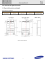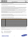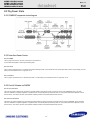
1
Rev. 1.0, Feb. 2012
MZMPC256HBGJ-00000
MZMPC128HBFU-00000
MZMPC064HBDR-00000
MZMPC032HBCD-00000
mSATA 6.0Gb/s MLC SSD
(NAND based Solid State Drive)
datasheet
SAMSUNG ELECTRONICS RESERVES THE RIGHT TO CHANGE PRODUCTS, INFORMATION AND
SPECIFICATIONS WITHOUT NOTICE.
Products and specifications discussed herein are for reference purposes only. All information discussed
herein is provided on an "AS IS" basis, without warranties of any kind.
This document and all information discussed herein remain the sole and exclusive property of Samsung
Electronics. No license of any patent, copyright, mask work, trademark or any other intellectual property
right is granted by one party to the other party under this document, by implication, estoppel or otherwise.
Samsung products are not intended for use in life support, critical care, medical, safety equipment, or
similar applications where product failure could result in loss of life or personal or physical harm, or any
military or defense application, or any governmental procurement to which special terms or provisions
may apply.
For updates or additional information about Samsung products, contact your nearest Samsung office.
All brand names, trademarks and registered trademarks belong to their respective owners.
ⓒ 2012 Samsung Electronics Co., Ltd. All rights reserved.
-1-
MZMPC256HBGJ-00000
MZMPC128HBFU-00000
MZMPC064HBDR-00000
MZMPC032HBCD-00000
Rev. 1.0
datasheet
SSD
Revision History
Revision No.
History
Draft Date
Remark
Editor
0.1
Preliminary version
Oct. 24. 2011
Preliminary
Phil LEE
0.2
Fixing performance value.
Modifying SMART attribute info.
Dec. 02. 2011
-
Phil LEE
1.0
Final version
Feb. 15. 2012
Final
Taehyun Yoon
-2-
MZMPC256HBGJ-00000
MZMPC128HBFU-00000
MZMPC064HBDR-00000
MZMPC032HBCD-00000
datasheet
Table Of Contents
1.0 General Description .................................................................................................................................................... 5
2.0 Mechanical Specification ........................................................................................................................................... 6
2.1 Physical dimensions and Weight ............................................................................................................................ 6
3.0 Product Specifications ............................................................................................................................................... 7
3.1 System Interface and Configuration ....................................................................................................................... 7
3.2 System Performance
..................................................................................................................... 7
3.3 Drive Capacity ........................................................................................................................................................ 7
3.4 Supply Voltage ....................................................................................................................................................... 7
3.5 System Power Consumption ................................................................................................................................. 7
3.6 System Reliability ................................................................................................................................................... 8
3.7 Environmental Specifications ................................................................................................................................. 8
4.0 Electrical Interface Specification ................................................................................................................................ 8
4.1 Serial ATA Interface connector............................................................................................................................... 8
4.2 Pin Assignments..................................................................................................................................................... 9
5.0 Frame Information Structure (FIS) ............................................................................................................................. 10
5.1 Register - Host to Device........................................................................................................................................ 10
5.2 Register - Device to Host........................................................................................................................................ 11
5.3 Data ........................................................................................................................................................................ 12
5.4 PIO Setup .............................................................................................................................................................. 12
5.5 DMA Activate - Device to Host ............................................................................................................................... 13
5.6 DMA Setup ............................................................................................................................................................. 13
5.7 Set Device Bits - Device to Host............................................................................................................................. 13
6.0 Shadow Register Block registers Description ............................................................................................................ 14
6.1 Command Register................................................................................................................................................. 14
6.2 Device Control Register.......................................................................................................................................... 14
6.2.1 Field / bit description ........................................................................................................................................ 14
6.3 Device / Head Register........................................................................................................................................... 14
6.3.1 Field / bit description ....................................................................................................................................... 14
6.4 Error Register ......................................................................................................................................................... 14
6.4.1 Field / bit description ........................................................................................................................................ 14
6.5 Features Register ................................................................................................................................................... 15
6.6 Cylinder High (LBA High) Register ......................................................................................................................... 15
6.7 Cylinder Low (LBA Mid) Register ........................................................................................................................... 15
6.8 Sector Number (LBA low) Register ........................................................................................................................ 15
6.9 Sector Count Register ............................................................................................................................................ 15
6.10 Status Register ..................................................................................................................................................... 15
6.10.1 Field / bit description ...................................................................................................................................... 15
7.0 Command Descriptions.............................................................................................................................................. 16
7.1 Supported ATA Commands.................................................................................................................................... 16
7.2 SECURITY FEATURE Set ..................................................................................................................................... 17
7.2.1 SECURITY mode default setting...................................................................................................................... 17
7.2.2 Initial setting of the user password................................................................................................................... 17
7.2.3 SECURITY mode operation from power-on..................................................................................................... 17
7.2.4 Password lost................................................................................................................................................... 17
7.3 SMART FEATURE Set (B0h) ................................................................................................................................. 17
7.3.1 Sub Command ................................................................................................................................................. 17
7.3.1.1 S.M.A.R.T. Read Attribute Values (subcommand D0h)............................................................................. 17
7.3.1.2 S.M.A.R.T. Read Attribute Thresholds (subcommand D1h) ...................................................................... 18
7.3.1.3 S.M.A.R.T. Enable/Disable Attribute Autosave (subcommand D2h) ......................................................... 18
7.3.1.4 S.M.A.R.T. Save Attribute Values (subcommand D3h) ............................................................................. 18
7.3.1.5 S.M.A.R.T. Execute Off-line Immediate (subcommand D4h) .................................................................... 18
7.3.1.6 S.M.A.R.T. Selective self-test routine ........................................................................................................ 19
7.3.1.7 S.M.A.R.T. Read Log Sector (subcommand D5h)..................................................................................... 20
7.3.1.8 S.M.A.R.T. Write Log Sector (subcommand D6h) ..................................................................................... 20
7.3.1.9 S.M.A.R.T. Enable Operations (subcommand D8h) .................................................................................. 20
7.3.1.10 S.M.A.R.T. Disable Operations (subcommand D9h) ............................................................................... 20
7.3.1.11 S.M.A.R.T. Return Status (subcommand DAh) ....................................................................................... 21
-3-
Rev. 1.0
SSD
MZMPC256HBGJ-00000
MZMPC128HBFU-00000
MZMPC064HBDR-00000
MZMPC032HBCD-00000
datasheet
7.3.1.12 S.M.A.R.T. Enable/Disable Automatic Off-line (subcommand DBh) ....................................................... 21
7.3.2 Device Attribute Data Structure........................................................................................................................ 22
7.3.2.1 Data Structure Revision Number ............................................................................................................... 22
7.3.2.2 Individual Attribute Data Structure ............................................................................................................. 23
7.3.2.3 Off-Line Data Collection Status ................................................................................................................. 24
7.3.2.4 Self-test execution status........................................................................................................................... 24
7.3.2.5 Total time in seconds to complete off-line data collection activity ............................................................. 24
7.3.2.6 Current segment pointer ............................................................................................................................ 24
7.3.2.7 Off-line data collection capability ............................................................................................................... 24
7.3.2.8 S.M.A.R.T. Capability ................................................................................................................................ 25
7.3.2.9 Error logging capability .............................................................................................................................. 25
7.3.2.10 Self-test failure check point...................................................................................................................... 25
7.3.2.11 Self-test completion time ......................................................................................................................... 25
7.3.2.12 Data Structure Checksum........................................................................................................................ 25
7.3.3 Device Attribute Thresholds data structure ..................................................................................................... 25
7.3.3.1 Data Structure Revision Number ............................................................................................................... 25
7.3.3.2 Individual Thresholds Data Structure......................................................................................................... 26
7.3.3.3 Attribute ID Numbers ................................................................................................................................. 26
7.3.3.4 Attribute Threshold .................................................................................................................................... 26
7.3.3.5 Data Structure Checksum.......................................................................................................................... 26
7.3.4 S.M.A.R.T. Log Directory ................................................................................................................................. 26
7.3.5 S.M.A.R.T. error log sector .............................................................................................................................. 27
7.3.5.1 S.M.A.R.T. error log version ...................................................................................................................... 27
7.3.5.2 Error log pointer ......................................................................................................................................... 27
7.3.5.3 Device error count ..................................................................................................................................... 27
7.3.5.4 Error log data structure .............................................................................................................................. 27
7.3.5.5 Command data structure ........................................................................................................................... 28
7.3.5.6 Error data structure.................................................................................................................................... 29
7.3.6 Self-test log structure ....................................................................................................................................... 30
7.3.7 Selective self-test log data structure ................................................................................................................ 30
7.3.8 Error reporting .................................................................................................................................................. 31
8.0 OOB signaling and Phy Power State ......................................................................................................................... 31
8.1 OOB signaling ........................................................................................................................................................ 31
8.1.1 OOB signal spacing ......................................................................................................................................... 31
8.2 Phy Power State..................................................................................................................................................... 32
8.2.1 COMRESET sequence state diagram ............................................................................................................. 32
8.2.2 Interface Power States..................................................................................................................................... 32
8.2.2.1 PHYRDY.................................................................................................................................................... 32
8.2.2.2 Partial......................................................................................................................................................... 32
8.2.2.3 Slumber ..................................................................................................................................................... 32
8.2.3 Partial/Slumber to PHYRDY............................................................................................................................. 32
8.2.3.1 Host Initiated.............................................................................................................................................. 32
8.2.3.2 Device Initiated .......................................................................................................................................... 32
8.2.4 PHYRDY to Partial/Slumber............................................................................................................................. 33
8.2.4.1 Host Initiated for Partial ............................................................................................................................. 33
8.2.4.2 Device Initiated for Partial.......................................................................................................................... 33
9.0 SATA II Optional Feature........................................................................................................................................... 34
9.1 Asynchronous Signal Recovery.............................................................................................................................. 34
10.0 Identify Device Data................................................................................................................................................. 35
11.0 Ordering Information ................................................................................................................................................ 37
12.0 Product Line up........................................................................................................................................................ 37
-4-
Rev. 1.0
SSD
MZMPC256HBGJ-00000
MZMPC128HBFU-00000
MZMPC064HBDR-00000
MZMPC032HBCD-00000
datasheet
Rev. 1.0
SSD
1.0 General Description
The NSSD(Nand based Solid State Drive) of Samsung Electronics fully consists of semiconductor devices using NAND Flash Memory which provide high
reliability and high performance for a storage media.
The NSSD doesn't have any moving parts such as platter(disk) and head media, which provides a better solution in a notebook PC and Tablet PC for a
storage device providing higher performance, reduced latencies, and a low power consumption in a small form factor. The NSSD could also provide rugged features in industrial PC with an extreme environment with a high MTBF.
For easy adoption, the NSSD has the same host interface with Hard Disk Drives and has a same physical dimension.
•Density
− 32/64/128/256GB is available
•Form Factor
− Full Mini PCIe type
− (29.85 ± 0.15 x 50.80 ± 0.15 x 3.75 ± 0.10)mm
•Host interface
− Serial ATA interface of 6.0Gbps
− Fully complies with ATA/ATAPI-7 Standard
(Partially Complies with ATA/ATAPI-8)
− Power Saving Modes: HIPM, DIPM (Partial / Slumber mode)
− Support NCQ : Up to 32 depth
− Synchronous Signal Recovery
•Performance
− Host transfer rate: 600 MB/s
− Sequential Read : Up to 500MB/s (32/64/128/256GB)
− Sequential Write : Up to 260MB/s (256GB), Up to 255MB/s (128GB),
Up to 170MB/s (64GB), Up to 90MB/s (32GB)
* Actual performance may vary depending on use conditions and
environment
* Notes :
1. Performance measured using IOmeter 2008 with queue depth 32
2. Measurements are performed on whole LBA range
3. Write cache enabled
4. 1MB/sec = 1,048,576 bytes/sec was used in sequential performance
•Power Consumption
− Active* : 911mA/3.007W
− Idle** : 27mA/0.087W
* Active power is measured during execution of Mobilemark 2007 in
Windows7
** DIPM enabled value
*** Environment
− System : Intel Core [email protected], DDR3 4GB
− OS : Windows 7 x64(script : Autoconfig 2.4.1)
− External 3.3V provided for mSATA
•Temperature
− Operating : 0°C to 70°C
*Measuring at the center of module’s top
•Shock
− Shock : 1500G, duration 0.5ms, Half Sine Wave
− Vibration : 7~800Hz, 3.08Grms, 30min/axis(X,Y,Z)
* Applicable only for cased product
•MTBF
− 1,500,000 Hours
•Weight (TBD)
− 32GB : Max 7g
− 64/128/256GB : Max 8g
•NSSD Functional Block Diagram
-5-
MZMPC256HBGJ-00000
MZMPC128HBFU-00000
MZMPC064HBDR-00000
MZMPC032HBCD-00000
Rev. 1.0
datasheet
SSD
2.0 Mechanical Specification
2.1 Physical dimensions and Weight
Physical dimensions and Weight
Model
Height (mm)
Width (mm)
Length (mm)
Weight (gram)
32/64/128/256GB
3.75 ± 0.10
29.85 ± 0.15
50.80 ± 0.15
32GB : Max 7g
64/128/256GB : Max 8g
[Figure 2-1] Physical dimension
-6-
MZMPC256HBGJ-00000
MZMPC128HBFU-00000
MZMPC064HBDR-00000
MZMPC032HBCD-00000
Rev. 1.0
datasheet
SSD
3.0 Product Specifications
3.1 System Interface and Configuration
• Burst read/write rate is 600 MB/sec (6.0 Gb/sec).
• Fully compatible with ATA-7 Standard
(Partially Complies with ATA/ATAPI-8)
3.2 System Performance
Read / Write
MZMPC032HBCD-00000
MZMPC064HBDR-00000
Sequential Read Sector
MZMPC128HBFU-00000
MZMPC256HBGJ-00000
Up to 500MB/s
Sequential Write Sector
Up to 90MB/s
Up to 170MB/s
Up to 255MB/s
Up to 260MB/s
* Actual performance may vary depending on use conditions and environment
* Note
1. Performance measured using IOMeter 2008 with queue depth 32
2. Measurements are performed on whole LBA range
3. Write cache enabled
4. 1MB/sec = 1,048,576 bytes/sec was used in sequential performance
3.3 Drive Capacity
MZMPC032HBCD-00000
MZMPC064HBDR-00000
MZMPC128HBFU-00000
MZMPC256HBGJ-00000
32 GB
64 GB
128 GB
256 GB
62,533,296
125,045,424
250,069,680
500,118,192
Unformatted Capacity
User-Addressable Sectors
Bytes per Sector
512 Bytes
NOTE :
1 Megabyte (MB) = 1 Million bytes; 1 Gigabyte (GB) = 1 Billion bytes
* Actual usable capacity may be less (due to formatting, partitioning, operating system, applications or otherwise)
3.4 Supply Voltage
Item
Requirements
3.3V + 5%
Allowable voltage
Allowable noise/ripple
100mV p-p or less
3.5 System Power Consumption
Power
Typical
Active*
911mA/3.007W
Idle**
27mA/0.087W
NOTE :
* Active power is measured during execution of Mobilemark 2007 in Windows7
** Idle power is measured on window7 idle status with DIPM on
*** Environment
- System : Dell E6420(Intel Core [email protected], DDR3 4GB)
- OS : Windows 7 x64(script : Autoconfig 2.4.1)
- DIPM/HIPM support
-7-
MZMPC256HBGJ-00000
MZMPC128HBFU-00000
MZMPC064HBDR-00000
MZMPC032HBCD-00000
Rev. 1.0
datasheet
SSD
3.6 System Reliability
MTBF
1,500,000 Hours
1. MTBF is Mean Time Between Failure. As same word, annual failure ratio is 0.4%
3.7 Environmental Specifications
Features
Operating
Non-Operating
Temperature
0°C to 70°C
-55°C to 95°C
Humidity
5% to 95%, non-condensing
Vibration
7~800Hz, 3.08Grms, 30min/axis(X,Y,Z)
Shock
1500G, duration 0.5ms, Half Sine Wave
Notes :
1. Temperature specification is following JEDEC standard; Expressed temperature must be measured right on the case
2. Humidity is measured in non-condensing
3. Test condition for shock : 0.5ms duration with half sine wave
4. Test condition for vibration : 10Hz to 2,000Hz, 15mins/axis on 3axis
4.0 Electrical Interface Specification
4.1 Serial ATA Interface connector
Drive Connector : PCIe type. 52pins
Pin # are marked as #1~#52 in the below dimension
-8-
MZMPC256HBGJ-00000
MZMPC128HBFU-00000
MZMPC064HBDR-00000
MZMPC032HBCD-00000
Rev. 1.0
datasheet
SSD
4.2 Pin Assignments
Pin#
Assignment
Description
Pin#
Assignment
Description
1
N/A
N/A
27
GND
Return Current Path
2
+3.3V
3.3V source
28
N/A
N/A
3
N/A
N/A
29
GND
Return Current Path
4
GND
Return Current Path
30
N/A
N/A
5
N/A
N/A
31
-A (port 1)
SATA Differential
RX- based on SSD
6
N/A
N/A
32
N/A
N/A
7
N/A
N/A
33
+A (port 1)
SATA Differential
RX+ based on SSD
8
N/A
N/A
34
GND
Return Current Path
9
GND
Return Current Path
35
GND
Return Current Path
10
N/A
N/A
36
Reserved
No Connect
11
N/A
N/A
37
GND
Return Current Path
12
N/A
N/A
38
Reserved
No Connect
13
N/A
N/A
39
+3.3V
3.3V Source
14
N/A
N/A
40
GND
Return Current Path
15
GND
Return Current Path
41
+3.3V
3.3V Source
16
N/A
N/A
42
N/A
N/A
17
N/A
N/A
43
N/A
N/A
18
GND
Return Current Path
44
N/A
N/A
19
N/A
N/A
45
Reserved
N/A
20
N/A
N/A
46
N/A
N/A
21
GND
Return Current Path
47
Reserved
N/A
22
N/A
N/A
48
N/A
N/A
23
+B(port 1)
SATA Differential
49
DA/DSS
Device Activity / Disable
Staggered Spin-up
24
+3.3V
3.3V Source
50
GND
Return Current Path
25
-B(port 1)
SATA Differential
51
Presence Detection
Shall be pulled to GND
by device
26
GND
Return Current Path
52
+3.3V
3.3V Source
-9-
MZMPC256HBGJ-00000
MZMPC128HBFU-00000
MZMPC064HBDR-00000
MZMPC032HBCD-00000
Rev. 1.0
datasheet
SSD
5.0 Frame Information Structure (FIS)
5.1 Register - Host to Device
3
3
2
1
0
9
2
2
2
2
2
2
8
7
6
5
4
3
2
1
2
1
1
1
1
1
1
1
1
0
9
8
7
6
5
4
3
2
C
R
R
1
1
1
0
9
8
7
6
4
3
2
Device
LBA High
LBA Mid
LBA Low
Features (exp)
LBA High (exp)
LBA Mid (exp)
LBA Low (exp)
Control
Reserved (0)
Sector Count (exp)
Sector Count
Reserved (0)
Reserved (0)
Reserved (0)
Reserved (0)
3
Reserved (0)
5
Command
1
4
2
Features
0
2
2
1
0
1
0
1
0
FIS Type (27h)
[Table 5-1] Register - Host to Device layout (48bit LBA mode, EXT commands, NCQ commands)
3
3
2
2
2
2
2
2
2
2
2
2
1
1
1
1
1
1
1
1
1
1
1
0
9
8
7
6
5
4
3
2
1
0
9
8
7
6
5
4
3
2
1
0
C
R
R
2
7
6
Reserved (0)
5
4
3
2
Command
Device/Head
Cylinder High
Cylinder Low
Sector Number
Reserved (0)
Reserved (0)
Reserved (0)
Reserved (0)
Control
Reserved (0)
Reserved (0)
Sector Count
Reserved (0)
Reserved (0)
Reserved (0)
Reserved (0)
3
4
8
Features
0
1
9
FIS Type (27h)
[Table 5-2] Register - Host to Device layout (CHS mode)
0
1
2
3
4
3
3
2
2
2
2
2
2
2
2
2
2
1
1
1
1
1
1
1
1
1
1
1
0
9
8
7
6
5
4
3
2
1
0
9
8
7
6
5
4
3
2
1
0
C
R
R
9
Reserved (0)
8
7
6
5
4
3
2
Features
Command
Device/LBA 27:24
LBA 23:16
LBA 15:8
LBA 7:0
Reserved (0)
Reserved (0)
Reserved (0)
Reserved (0)
Control
Reserved (0)
Reserved (0)
Sector Count
Reserved (0)
Reserved (0)
Reserved (0)
Reserved (0)
[Table 5-3] Register - Host to Device layout (28bit LBA mode)
- 10 -
FIS Type (27h)
MZMPC256HBGJ-00000
MZMPC128HBFU-00000
MZMPC064HBDR-00000
MZMPC032HBCD-00000
Rev. 1.0
datasheet
SSD
5.2 Register - Device to Host
3
3
2
2
2
2
2
2
2
2
2
2
1
1
1
1
1
1
1
1
1
1
1
0
9
8
7
6
5
4
3
2
1
0
9
8
7
6
5
4
3
2
1
0
R
I
S
4
7
6
Reserved (0)
5
4
3
2
Status
Device
LBA High
LBA Mid
LBA Low
Features (exp)
LBA High (exp)
LBA Mid (exp)
LBA Low (exp)
Reserved (0)
Reserved (0)
Sector Count (exp)
Sector Count
Reserved (0)
Reserved (0)
Reserved (0)
Reserved (0)
1
3
8
Error
0
2
9
1
0
1
0
1
0
FIS Type (34h)
[Table 5-4] Register - Device to Host layout (48bit LBA mode)
3
3
2
2
2
2
2
2
2
2
2
2
1
1
1
1
1
1
1
1
1
1
1
0
9
8
7
6
5
4
3
2
1
0
9
8
7
6
5
4
3
2
1
0
R
I
S
2
3
4
8
7
6
Reserved (0)
5
4
3
2
Error
Status
Device/Head
Cylinder High
Cylinder Low
Sector Number
Reserved (0)
Reserved (0)
Reserved (0)
Reserved (0)
Reserved (0)
Reserved (0)
Reserved (0)
Sector Count
Reserved (0)
Reserved (0)
Reserved (0)
Reserved (0)
0
1
9
FIS Type (34h)
[Table 5-5] Register - Device to Host layout (CHS mode)
0
1
2
3
4
3
3
2
2
2
2
2
2
2
2
2
1
0
9
8
7
6
5
4
3
2
1
2
1
1
1
1
1
1
1
1
0
9
8
7
6
5
4
3
2
R
I
S
1
1
1
0
9
Reserved (0)
8
7
6
5
4
3
2
Error
Status
Device/LBA 27:24
LBA 23:16
LBA 15:8
LBA 7:0
Reserved (0)
Reserved (0)
Reserved (0)
Reserved (0)
Reserved (0)
Reserved (0)
Reserved (0)
Sector Count
Reserved (0)
Reserved (0)
Reserved (0)
Reserved (0)
[Table 5-6] Register - Device to Host layout (28bit LBA mode)
- 11 -
FIS Type (34h)
MZMPC256HBGJ-00000
MZMPC128HBFU-00000
MZMPC064HBDR-00000
MZMPC032HBCD-00000
Rev. 1.0
datasheet
SSD
5.3 Data
3
3
2
2
2
2
2
2
2
2
2
2
1
1
1
1
1
1
1
1
1
0
9
8
7
6
5
4
3
2
1
0
9
8
7
6
5
4
3
2
R
R
R
Reserved (0)
0
Reserved (0)
1
1
1
0
9
8
7
6
Reserved (0)
5
4
3
2
1
0
1
0
1
0
FIS Type (48h)
...
N DWORDs of data
(minimum of DWORD - maximum of 2048 DWORDs
...
n
[Table 5-7] Register - Data FIS layout
5.4 PIO Setup
3
3
2
2
2
2
2
2
2
2
2
1
0
9
8
7
6
5
4
3
2
1
1
1
1
1
1
1
1
0
9
8
7
6
5
4
3
2
R
I
S
1
1
1
0
9
8
7
6
4
3
2
Device
LBA High
LBA Mid
LBA Low
Reserved (0)
LBA High (exp)
LBA Mid (exp)
LBA Low (exp)
E_ STATUS
Reserved (0)
Sector Count (exp)
Sector Count
Reserved (0)
Reserved (0)
3
Reserved (0)
5
Status
1
4
1
Error
0
2
2
FIS Type (34h)
Transfer Count
[Table 5-8] Register - PIO Setup layout (48bit LBA mode: Read/Write Sector EXT)
0
1
2
3
4
3
3
2
2
2
2
2
2
2
2
2
2
1
1
1
1
1
1
1
1
1
1
1
0
9
8
7
6
5
4
3
2
1
0
9
8
7
6
5
4
3
2
1
0
R
I
S
9
8
7
6
Reserved (0)
5
4
3
2
Error
Status
Device/Head
Cylinder High
Cylinder Low
Sector Number
Reserved (0)
Reserved (0)
Reserved (0)
Reserved (0)
E_ STATUS
Reserved (0)
Sector Count (exp)
Sector Count
Reserved (0)
Reserved (0)
Transfer Count
[Table 5-9] PIO Set up layout (CHS mode: Commands include PIO data transfer)
- 12 -
FIS Type (34h)
MZMPC256HBGJ-00000
MZMPC128HBFU-00000
MZMPC064HBDR-00000
MZMPC032HBCD-00000
Rev. 1.0
datasheet
SSD
5.5 DMA Activate - Device to Host
3
3
2
2
2
2
2
2
2
2
2
2
1
1
1
1
1
1
1
1
1
0
9
8
7
6
5
4
3
2
1
0
9
8
7
6
5
4
3
2
R
R
R
Reserved (0)
0
Reserved (0)
1
1
1
0
9
8
7
6
Reserved (0)
5
4
3
2
1
0
1
0
1
0
FIS Type (39h)
[Table 5-10] DMA Activate Layout (Write DMA/Write DMA Queued/Service)
5.6 DMA Setup
3
3
2
2
2
2
2
2
2
2
2
2
1
1
1
1
1
1
1
1
1
0
9
8
7
6
5
4
3
2
1
0
9
8
7
6
5
4
3
2
A
I
D
Reserved (0)
0
Reserved (0)
1
1
1
0
9
8
7
6
Reserved (0)
5
4
3
FIS Type (A1h)
0
1
2
TAG
0
2
Reserved (0)
3
DMA Buffer Offset
4
DMA Transfer Count
5
Reserved (0)
6
[Table 5-11] DMA Setup layout (NCQ, Read/Write FpDMA Queued)
5.7 Set Device Bits - Device to Host
0
1
3
3
2
2
2
2
2
2
2
2
2
2
1
1
1
1
1
1
1
1
1
0
9
8
7
6
5
4
3
2
1
0
9
8
7
6
5
4
3
2
R
Status Hi
R
Status Lo
N
I
R
Error
1
1
1
0
9
8
7
6
Reserved (0)
SActive 31:0
[Table 5-12] Set Device Bits layout (NCQ, Result of Read/Write FpDMA Queued commands)
- 13 -
5
4
3
2
FIS Type (A1h)
MZMPC256HBGJ-00000
MZMPC128HBFU-00000
MZMPC064HBDR-00000
MZMPC032HBCD-00000
Rev. 1.0
datasheet
SSD
6.0 Shadow Register Block registers Description
6.1 Command Register
This register contains the command code being sent to the device. Command execution begins immediately after this register is written. All other registers
required for the command must be set up before writing the Command Register.
6.2 Device Control Register
This register contains the command code being sent to the device. Command execution begins immediately after this register is written. All other registers
required for the command must be set up before writing the Command Register.
6.2.1 Field / bit description
7
6
5
4
3
2
1
0
HOB
-
-
-
-
SRST
nIEN
0
• HOB is defined by the 48bit Address feature set. A write to any Command register shall clear the HOB bit to zero.
• SRST is the host software reset bit. SRST=1 indicates that the drive is held reset and sets BSY bit in Status register. Setting SRST=0 re-enables the device.
• nIEN is the enable bit for the device Assertion of INTRQ to the host. When nIEN=0, and the device is selected by Drice select bit in DEVICE/HEAD register, device interrupt to
the host is enabled. When this bit is set, the "I’ bit in the Register Host to Device, PIO setup, Set Device Bits and DMA Set Up will be set, whether pending interrup is found or
not.
6.3 Device / Head Register
6.3.1 Field / bit description
The content of this register shall take effect when written.
7
6
5
4
3
2
1
0
-
L
-
DEV
HS3
HS2
HS1
HS0
• L : Binary encoded address mode select. When L=0, addressing is by CHS mode. When L=1, addressing is by LBA mode.
• DEV: Device select. Cleared to zero selects Device 0. Set to one selects Device1.
• HS3, HS2, HS1, HS0 : Head select bits. The HS3 through HS0 contain bits 24-27 of the LBA. At command completion, these bits are updated to reflect the current LBA bits
24-27.
6.4 Error Register
This register contains the command code being sent to the device. Command execution begins immediately after this register is written. All other registers
required for the command must be set up before writing the Command Register.
6.4.1 Field / bit description
7
6
5
4
3
2
1
0
ICRC
UNC
0
IDNF
0
ABRT
TKONF
AMNF
• ICRC: Interface CRC Error. CRC=1 indicates a CRC error has occurred on the data bus during a Ultra-DMA transfer.
• UNC: Uncorrectable Data Error. UNC=1 indicates an uncorrectable data error has been encountered.
• IDNF: ID Not Found. IDN=1 indicates the requested sector’s ID field cound not be found .
• ABRT: Aborted Command. ABT=1 indicates the requested command has been aborted due to a device status error or an invalid parameter in an output register.
• TKONF: Track 0 Not Found. T0N=1 indicates track 0 was not found during a Recalibrate command.
• AMNF: Address Mark Not Found. When AMN=1, it indicates that the data address mark has not been found after finding the correct ID field for the requested sector.
- 14 -
MZMPC256HBGJ-00000
MZMPC128HBFU-00000
MZMPC064HBDR-00000
MZMPC032HBCD-00000
Rev. 1.0
datasheet
SSD
6.5 Features Register
This register is command specific. This is used with the Set Features command, S.M.A.R.T. Function Set command.
6.6 Cylinder High (LBA High) Register
This register contains Bits 16-23. At the end of the command, this register is updated to reflect the current LBA Bits 16-23.
6.7 Cylinder Low (LBA Mid) Register
This register contains Bits 8-15. At the end of the command, this register is updated to reflect the current LBA Bits 8-15.
When 48-bit addressing commands are used, the "most recently written" content contains LBA Bits 8-15, and the "previous content" contains Bits 32-39
6.8 Sector Number (LBA low) Register
This register contains Bits 0-7. At the end of the command, this register is updated to reflect the current LBA Bits 0-7.
When 48-bit commands are used, the "most recently written" content contains LBA Bits 0-7, and the "previous content" contains Bits 24-31.
6.9 Sector Count Register
This register contains the number of sectors of data requested to be transferred on a read or write operation between the host and the device. If the value
in the register is set to 0, a count of 256 sectors (in 28-bit addressing) or 65,536 sectors (in 48-bit addressing) is specified.
If the register is zero at command completion, the command was successful. If not successfully completed, the register contains the number of sectors
which need to be transferred in order to complete the request.
The contents of the register are defined otherwise on some commands. These definitions are given in the command descriptions.
6.10 Status Register
This register contains the device status. The contents of this register are updated whenever an error occurs and at the completion of each command.
If the host reads this register when an interrupt is pending, it is considered to be the interrupt acknowledge. Any pending interrupt is cleared whenever this
register is read.
If BSY=1, no other bits in the register are valid. And read/write operations of any other register are negated in order to avoid the returning of the contesnts
of this register instead of the other registers’ contents.
6.10.1 Field / bit description
7
6
5
4
3
2
1
0
BSY
DRDY
DF
DSC
DRQ
CORR
IDX
ERR
• BSY : Busy. BSY=1 whenever the device is accessing the registers. The host should not read or write any registers when BSY=1. If the host reads any register when BSY=1,
the contents of the Status Register will be returned.
• DRDY : Device Ready. RDY=1 indicates that the device is capable of responding to a command. RDY will be set to 0 during power on until the device is ready to accept a
command.
• DF : Device Fault. DF=1 indicates that the device has detected a write fault condition. DF is set to 0 after the Status Register is read by the host.
• DSC : Device Seek Complete. DSC=1 indicates that a seek has completed and the device head is settled over a track. DSC is set to 0 by the device just before a seek begins.
When an error occurs, this bit is not changed until the Status Register is read by the
host, at which time the bit again indicates the current seek complete status.
When the device enters into or is in Standby mode or Sleep mode, this bit is set by device in spite of not spinning up.
• DRQ : Data Request. DRQ=1 indicates that the device is ready to transfer a word or byte of data between the host and the device. The host should not write the Command
register when DRQ=1.
• CORR : Corrected Data. Always 0.
• IDX : Index. IDX=1 once per revolution. Since IDX=1 only for a very short time during each revoltion, the host may not see it set to
1 even if the host is reading the Status Register continuously. Therefore the host should not attempt to use IDX for timing purposes.
• ERR : ERR=1 indicates that an error occurred during execution of the previous command. The Error Register should be read to determine the error type. The device sets
ERR=0 when the next command is received from the host.
- 15 -
MZMPC256HBGJ-00000
MZMPC128HBFU-00000
MZMPC064HBDR-00000
MZMPC032HBCD-00000
datasheet
Rev. 1.0
SSD
7.0 Command Descriptions
7.1 Supported ATA Commands
Command Name
Command Code
(Hex)
Command Name
Command Code
(Hex)
CHECK POWER MODE
E5h, 98h
SEEK
70h
DEVICE CONFIGURATION FREEZE LOCK
B1h/C1h
SET FEATURES
DEVICE CONFIGURATION IDENTIFY
B1h/C2h
SET MAX ADDRESS
DEVICE CONFIGURATION RESTORE
B1h/C0h
SET MAX ADDRESS EXT
37h
DEVICE CONFIGURATION SET
B1h/C3h
SET MAX FREEZE LOCK
F9h/04h
EFh
F9h/00h
DOWNLOAD MICROCODE
92h
SET MAX LOCK
F9h/02h
EXECUTE DEVICE DIAGNOSTIC
90h
SET MAX SET PASSWORD
F9h/01h
F9h/03h
FLUSH CACHE
E7h
SET MAX UNLOCK
FLUSH CACHE EXT
EAh
SET MULTIPLE MODE
ECh
SLEEP
E6h, 99h
SMART DISABLE OPERATIONS
B0h/D9h
IDENTIFY DEVICE
IDLE
E3h, 97h
IDLE IMMEDIATE
E1h, 95h
C6h
SMART ENABLE OPERATIONS
B0h/D8h
INITIALIZE DEVICE PARAMETERS
91h
SMART ENABLE/DISABLE ATTRIBUTE AUTOSAVE
B0h/D2h
READ BUFFER
E4h
Enable/Disable Auto-Offine
B0h/DBh
READ DMA EXT
25h
SMART EXECUTE OFF-LINE IMMEDIATE
B0h/D4h
READ DMA with Retry
C8h
SMART READ ATTRIBUTE THRESHOLDS
B0h/D1h
READ DMA without Retry
C9h
SMART READ DATA
B0h/D0h
READ LOG EXT
2Fh
SMART READ LOG
B0h/D5h
READ MULTIPLE
C4h
SMART RETURN STATUS
B0h/DAh
READ MULTIPLE EXT
29h
SMART SAVE ATTRIBUTE VALUES
B0h/D3h
READ NATIVE MAX ADDRESS
F8h
SMART WRITE LOG
B0h/D6h
READ NATIVE MAX ADDRESS EXT
27h
STANDBY
E2h, 96h
READ SECTORS EXT
24h
STANDBY IMMEDIATE
READ SECTORS with Retry
20h
WRITE BUFFER
E8
READ SECTORS without Retry
21h
WRITE DMA EXT
35
E0, 94
READ VERIFY SECTORS EXT
42h
WRITE DMA with Retry
CA
READ VERIFY SECTORS with Retry
40h
WRITE DMA without Retry
CB
READ VERIFY SECTORS without Retry
41h
WRITE LOG EXT
3F
SECURITY DISABLE PASSWORD
F6h
WRITE MULTIPLE
C5
SECURITY ERASE PREPARE
F3h
WRITE MULTIPLE EXT
39
SECURITY ERASE UNIT
F4h
WRITE SECTORS EXT
34
SECURITY FREEZE LOCK
F5h
WRITE SECTORS with Retry
30
SECURITY SET PASSWORD
F1h
WRITE SECTORS without Retry
31
SECURITY UNLOCK
F2h
- 16 -
MZMPC256HBGJ-00000
MZMPC128HBFU-00000
MZMPC064HBDR-00000
MZMPC032HBCD-00000
Rev. 1.0
datasheet
SSD
7.2 SECURITY FEATURE Set
The Security mode features allow the host to implement a securtity password system to prevent unauthorized access to the disk drive.
7.2.1 SECURITY mode default setting
The NSSD is shipped with master password set to 20h value(ASCII blanks) and the lock function disabled.
The system manufacturer/dealer may set a new master password by using the SECURITY SET PASSWORD command, without enableing the lock function.
7.2.2 Initial setting of the user password
When a user password is set, the drive automatically enters lock mode by the next powered-on
7.2.3 SECURITY mode operation from power-on
In locked mode, the NSSD rejects media access commands until a SECURITY UNLOCK command is successfully completed.
7.2.4 Password lost
If the user password is lost and High level security is set, the drive does not allow the user to access any data.
However, the drive can be unlocked using the master password.
If the user password is lost and Maxium security level is set, it is impossible to access data.
However, the drive can be unlocked using the ERASE UNIT command with the master password. The drive will erase all user data and unlock the drive.
7.3 SMART FEATURE Set (B0h)
The SMART Feature Set command provides access to the Attribute Values, the Attribute Thresholds, and other low level subcommands that can be used
for logging and reporting purposes and to accommodate special user needs. The SMART Feature Set command has several separate subcommands
which are selectable via the device's Features Register when the SMART Feature Set command is issued by the host. In order to select a subcommand
the host must write the subcommand code to the device's Features Register before issuing the SMART Feature Set command.
7.3.1 Sub Command
In order to select a subcommand the host must write the subcommand code to the device's Features Register before issuing the S.M.A.R.T. Function Set
command. The subcommands and their respective codes are listed below.
Subcommand
Code
Subcommand
Code
SMART READ DATA
D0h
SMART WRITE LOG
D6h
SMART READ ATTRIBUTE THRESHOLDS
D1h
SMART ENABLE OPERATIONS
D8h
SMART ENABLE/DISABLE ATTRIBUTE AUTOSAVE
D2h
SMART DISABLE OPERATIONS
D9h
SMART SAVE ATTRIBUTE VALUES
D3h
SMART RETURN STATUS
DAh
SMART EXECUTE OFF-LINE IMMIDIATE
D4h
SMART ENABLE/ DISABLE AUTOMATIC OFF-LINE
DBh
SMART READ LOG
D5h
7.3.1.1 S.M.A.R.T. Read Attribute Values (subcommand D0h)
This subcommand returns the device's Attribute Values to the host. Upon receipt of the S.M.A.R.T. Read Attribute Values subcommand from the host, the
device asserts BSY, saves any updated Attribute Values to the Attribute Data sectors, asserts DRQ, clears BSY, asserts INTRQ, and then waits for the
host to transfer the 512 bytes of Attribute Value information from the device via the Data Register.
- 17 -
MZMPC256HBGJ-00000
MZMPC128HBFU-00000
MZMPC064HBDR-00000
MZMPC032HBCD-00000
datasheet
Rev. 1.0
SSD
7.3.1.2 S.M.A.R.T. Read Attribute Thresholds (subcommand D1h)
This subcommand returns the device's Attribute Thresholds to the host. Upon receipt of the S.M.A.R.T. Read Attribute Thresholds subcommand from the
host, the device reads the Attribute Thresholds from the Attribute Threshold sectors and then waits for the host to transfer the 512 bytes of Attribute
Thresholds information from the device.
7.3.1.3 S.M.A.R.T. Enable/Disable Attribute Autosave (subcommand D2h)
This subcommand enables and disables the attribute auto save feature of the device. The S.M.A.R.T. Enable/Disable Attribute Autosave subcommand
allows the device to automatically save its updated Attribute Values to the Attribute Data Sector at the timing of the first transition to Active idle mode and
after 15 minutes after the last saving of Attribute Values. This subcommand causes the auto save feature to be disabled. The state of the Attribute
Autosave feature—either enabled or disabled—will be preserved by the device across the power cycle.
A value of 00h—written by the host into the device's Sector Count Register before issuing the S.M.A.R.T. Enable/Disable Attribute Autosave subcommand—will cause this feature to be disabled. Disabling this feature does not preclude the device from saving Attribute Values to the Attribute Data sectors
during some other normal operation such as during a power-up or a power-down.
A value of F1h—written by the host into the device's Sector Count Register before issuing the S.M.A.R.T. Enable/Disable Attribute Autosave subcommand—will cause this feature to be enabled. Any other nonzero value written by the host into this register before issuing the S.M.A.R.T. Enable/Disable
Attribute Autosave subcommand will not change the current Autosave status. The device will respond with the error code specified in Table 7-9:
“S.M.A.R.T. Error Codes” on page 30.
The S.M.A.R.T. Disable Operations subcommand disables the auto save feature along with the device's S.M.A.R.T. operations.
Upon the receipt of the subcommand from the host, the device asserts BSY, enables or disables the Autosave feature, clears BSY, and asserts INTRQ.
7.3.1.4 S.M.A.R.T. Save Attribute Values (subcommand D3h)
This subcommand causes the device to immediately save any updated Attribute Values to the device's Attribute Data sector regardless of the state of the
Attribute Autosave feature. Upon receipt of the S.M.A.R.T. Save Attribute Values subcommand from the host, the device asserts BSY, writes any updated
Attribute Values to the Attribute Data sector, clears BSY, and asserts INTRQ.
7.3.1.5 S.M.A.R.T. Execute Off-line Immediate (subcommand D4h)
This subcommand causes the device to immediately initiate the set of activities that collect Attribute data in an offline mode (off-line routine) or execute a
self-test routine in either captive or off-line mode. The LBA Low register shall be set to specify the operation to be executed.
LBA Low
Subcommand
00h
Execute S.M.A.R.T. off-line data collection routine immediately
01h
Execute S.M.A.R.T. Short self-test routine immediately in off-line mode
02h
Execute S.M.A.R.T. Extended self-test routine immediately in off-line mode
03h
Reserved
04h
Execute S.M.A.R.T. Selective self-test routine immediately in off-line mode
40h
Reserved
7Fh
Abort off-line mode self-test routine
81h
Execute S.M.A.R.T. short self-test routine immediately in captive mode
82h
Execute S.M.A.R.T. Extended self-test routine immediately in captive mode
84h
Execute S.M.A.R.T. selective self-test routine immediately in captive mode
C0h
Reserved
Off-line mode: The device executes command completion before executing the specified routine. During execution of the routine the device will not set BSY nor clear DRDY. If
the device is in the process of performing its routine and is interrupted by a new command from the host, the device will abort or suspend its routine and service the host within
two seconds after receipt of the new command. After servicing the interrupting command, the device will resume its routine automatically or not start its routine depending on
the interrupting command.
Captive mode: When executing self-test in captive mode, the device sets BSY to one and executes the specified self-test routine after receipt of the command. At the end of
the routine, the device sets the execution result in the Self-test execution status byte (see Table 7-1: “Device Attribute Data Structure” on page 23) and ATA registers and then
executes the command completion. See definitions below.
Status
Set ERR to one when the self-test has failed
Error
Set ABRT to one when the self-test has failed
LBA Low
Set to F4h when the self-test has failed
LBA High
Set to 2Ch when the self-test has failed
- 18 -
MZMPC256HBGJ-00000
MZMPC128HBFU-00000
MZMPC064HBDR-00000
MZMPC032HBCD-00000
datasheet
Rev. 1.0
SSD
7.3.1.6 S.M.A.R.T. Selective self-test routine
When the value in the LBA Low register is 4 or 132, the Selective self-test routine shall be performed. This selftest routine shall include the initial tests performed by the Extended self-test routine plus a selectable read scan. The host shall not write the Selective self-test log while the execution of a Selective
self-test command is in progress.
The user may choose to do read scan only on specific areas of the media. To do this, user shall set the test spans desired in the Selective self-test log and
set the flags in the Feature flags field of the Selective self-test log to indicate do not perform off-line scan. In this case, the test spans defined shall be read
scanned in their entirety. The Selective self-test log is updated as the self-test proceeds indicating test progress. When all specified test spans have been
completed, the test is terminated and the appropriate self-test execution status is reported in the SMART READ DATA response depending on the occurrence of errors. Figure on page 21 shows an example of a Selective selftest definition with three test spans defined. In this example, the test terminates
when all three test spans have been scanned.
After the scan of the selected spans described above, a user may wish to have the rest of media read scanned as an off-line scan. In this case, the user
shall set the flag to enable off-line scan in addition to the other settings. If an error occurs during the scanning of the test spans, the error is reported in the
self-test execution status in the SMART READ DATA response and the off-line scan is not executed. When the test spans defined have been scanned,
the device shall then set the offline scan pending and active flags in the Selective self-test log to one, the span under test to a value greater than five, the
self-test execution status in the SMART READ DATA response to 00h, set a value of 03h in the off-line data collection status in the SMART READ DATA
response and shall proceed to do an off-line read scan through all areas not included in the test spans. This off-line read scan shall completed as rapidly
as possible, no pauses between block reads, and any errors encountered shall not be reported to the host. Instead error locations may be logged for
future reallocation. If the device is powered-down before the off-line scan is completed, the off-line scan shall resume when the device is again powered
up. From power-up, the resumption of the scan shall be delayed the time indicated in the Selective self-test pending time field in the Selective self-test log.
During this delay time the pending flag shall be set to one and the active flag shall be set to zero in the Selective self-test log. Once the time expires, the
active flag shall be set to one, and the off-line scan shall resume. When the entire media has been scanned, the off-line scan shall terminate, both the
pending and active flags shall be cleared to zero, and the off-line data collection status in the SMART READ DATA response shall be set to 02h indicating
completion.
During execution of the Selective self-test, the self-test executions time byte in the Device SMART Data Structure may be updated but the accuracy may
not be exact because of the nature of the test span segments. For this reason, the time to complete off-line testing and the self-test polling times are not
valid. Progress through the test spans is indicated in the selective self-test log.
A hardware or software reset shall abort the Selective self-test except when the pending bit is set to one in the Selective self-test log (see 7.3.7). The
receipt of a SMART EXECUTE OFF-LINE IMMEDIATE command with 0Fh, Abort off-line test routine, in the LBA Low register shall abort Selective selftest regardless of where the device is in the execution of the command. If a second self-test is issued while a selective self-test is in progress, the selective self-test is aborted and the newly requested self-test is executed.
- 19 -
MZMPC256HBGJ-00000
MZMPC128HBFU-00000
MZMPC064HBDR-00000
MZMPC032HBCD-00000
datasheet
Rev. 1.0
SSD
7.3.1.7 S.M.A.R.T. Read Log Sector (subcommand D5h)
This command returns the indicated log sector contents to the host. Sector count sepcifies the number of sectors to be read from the specified log. The
log transfferred by the drive shall start at the first sector in the speicified log, regardless of the sector count requested. Sector nubmer indicates the log
sector to be returned as described in the following Table.
Log sector address
Content
00h
Log directory
RO
01h
SMART error log
RO
02h
Comprehensive SMART error log
RO
Reserved
RO
06h
SMART self-test log
RO
08h
Reserved
RO
04h-05h
09h
Selective self-test log
RW
Reserved
RO
80h-9Fh
Host vendor specific
R/W
A0h-FFh
Reserved
0Ah-7Fh
VS
RO - Log is read only by the host.
R/W - Log is read or written by the host.
VS - Log is vendor specific thus read/write ability is vendor specific.
7.3.1.8 S.M.A.R.T. Write Log Sector (subcommand D6h)
This command writes 512 bytes of data to the specified log sector. The 512 bytes of data are transferred at a command and the LBA Low value shall be
set to one. The LBA Low shall be set to specify the log sector address. If a Rea Only log sector is specified, the device returns ABRT error.
7.3.1.9 S.M.A.R.T. Enable Operations (subcommand D8h)
This subcommand enables access to all S.M.A.R.T. capabilities within the device. Prior to receipt of a S.M.A.R.T. Enable Operations subcommand, Attribute Values are neither monitored nor saved by the device. The state of S.M.A.R.T.—either enabled or disabled—will be preserved by the device across
power cycles. Once enabled, the receipt of subsequent S.M.A.R.T. Enable Operations subcommands will not affect any of the Attribute Values. Upon
receipt of the S.M.A.R.T. Enable Operations subcommand from the host, the device asserts BSY, enables S.M.A.R.T. capabilities and functions, clears
BSY, and asserts INTRQ.
7.3.1.10 S.M.A.R.T. Disable Operations (subcommand D9h)
This subcommand disables all S.M.A.R.T. capabilities within the device including the device's attribute auto save feature. After receipt of this subcommand the device disables all S.M.A.R.T. operations. Non self-preserved Attribute Values will no longer be monitored. The state of S.M.A.R.T.—either
enabled or disabled—is preserved by the device across power cycles. Note that this subcommand does not preclude the device's power mode attribute
auto saving.
Upon receipt of the S.M.A.R.T. Disable Operations subcommand from the host, the device asserts BSY, disables S.M.A.R.T. capabilities and functions,
clears BSY, and asserts INTRQ.
After receipt of the device of the S.M.A.R.T. Disable Operations subcommand from the host, all other S.M.A.R.T. subcommands—with the exception of
S.M.A.R.T. Enable Operations—are disabled, and invalid and will be aborted by the device—including the S.M.A.R.T. Disable Operations subcommand—
returning the error code as specified in Table 7-9: “S.M.A.R.T. Error Codes” on page 30.
Any Attribute Values accumulated and saved to volatile memory prior to receipt of the S.M.A.R.T. Disable Operations command will be preserved in the
device's Attribute Data Sectors. If the device is re-enabled, these Attribute Values will be updated, as needed, upon receipt of a S.M.A.R.T. Read Attribute
Values or a S.M.A.R.T. Save Attribute Values command.
- 20 -
MZMPC256HBGJ-00000
MZMPC128HBFU-00000
MZMPC064HBDR-00000
MZMPC032HBCD-00000
datasheet
Rev. 1.0
SSD
7.3.1.11 S.M.A.R.T. Return Status (subcommand DAh)
This subcommand is used to communicate the reliability status of the device to the host's request. Upon receipt of the S.M.A.R.T. Return Status subcommand the device asserts BSY, saves any updated Attribute Values to the reserved sector, and compares the updated Attribute Values to the Attribute
Thresholds.
If the device does not detect a Threshold Exceeded Condition, or detects a Threshold Exceeded Condition but involving attributes are advisory, the device
loads 4Fh into the LBA Mid register, C2h into the LBA High register, clears BSY, and asserts INTRQ.
If the device detects a Threshold Exceeded Condition for prefailure attributes, the device loads F4h into the LBA Mid register, 2Ch into the LBA High register, clears BSY, and asserts INTRQ. Advisory attributes never result in a negative reliability condition.
7.3.1.12 S.M.A.R.T. Enable/Disable Automatic Off-line (subcommand DBh)
This subcommand enables and disables the optional feature that cause the device to perform the set of off-line data collection activities that automatically
collect attribute data in an off-line mode and then save this data to the device's nonvolatile memory. This subcommand may either cause the device to
automatically initiate or resume performance of its off-line data collection activities or cause the automatic off-line data collection feature to be disabled.
This subcommand also enables and disables the off-line read scanning feature that cause the device to perform the entire read scanning with defect reallocation as the part of the off-line data collection activities.
The Sector Count register shall be set to specify the feature to be enabled or disabled:
Sector Count
00h
F8h
Feature Description
Disable Automatic Off-line
Enable Automatic Off-line
A value of zero written by the host into the device's Sector Count register before issuing this subcommand shall cause the automatic off-line data collection feature to be disabled. Disabling this feature does not preclude the device from saving attribute values to nonvolatile memory during some other normal operation such as during a power-on, during a power-off sequence, or during an error recovery sequence.
A value of F8h written by the host into the device's Sector Count register before issuing this subcommand shall cause the automatic Off-line data collection feature to be enabled.
Any other non-zero value written by the host into this register before issuing this subcommand is vendor specific and will not change the current Automatic Off-Line Data Collection and Off-line Read Scanning status. However, the device may respond with the error code specified in Table 7-9:
“S.M.A.R.T. Error Codes” on page 30.
- 21 -
MZMPC256HBGJ-00000
MZMPC128HBFU-00000
MZMPC064HBDR-00000
MZMPC032HBCD-00000
datasheet
Rev. 1.0
SSD
7.3.2 Device Attribute Data Structure
The following defines the 512 bytes that make up the Attribute Value information. This data structure is accessed by the host in its entirety using the
S.M.A.R.T. Read Attribute Values subcommand.
Byte
Descriptions
0~1
Data structure revision number
2~361
1st - 30th Individual attribute data
362
Off-line data collection status
363
Self-test execution status
364~365
Total time in seconds to complete off-line data collection activity
366
Vendor Specific
367
Off-line data collection capability
368-369
SMART capability
370
Error logging capability
7-1
Reserved
0
1=Device error logging supported
371
Self-test failure check point
372
Short self-test routine recommended polling time(in minutes)
373
Extended self-test routine recommended polling time(in minutes)
374-510
Reserved
511
Data structure checksum
[Table 7-1] Device Attribute Data Structure
7.3.2.1 Data Structure Revision Number
The Data Structure Revision Number identifies which version of this data structure is implemented by the device.
This revision number will be set to 0005h. This revision number identifies both the Attribute Value and Attribute
Threshold Data structures.
- 22 -
MZMPC256HBGJ-00000
MZMPC128HBFU-00000
MZMPC064HBDR-00000
MZMPC032HBCD-00000
datasheet
Rev. 1.0
SSD
7.3.2.2 Individual Attribute Data Structure
The following defines the 12 bytes that make up the information for each Attribute entry in the Device Attribute Data Structure.
Byte
0
Descriptions
Attribute ID number 01-FFh
Status flag
bit 0 (pre-failure/advisory bit)
bit 0 = 0 : If attribute value is less than the threshold, the drive is in advisory condtion.
Product life period may expired.
bit 0 = 1 : If attribut value is less than the threshold, the drive is in pre-failure condition.
The drive may have failure.
bit 1 (on-line data collection bit)
bit 1 = 0 : Attribute value will be changed during off-line data collection operation.
bit 1 = 1 : Attribute value will be changed during normal operation.
bit 2 (Performance Attribute bit)
bit 3 (Error rate Attribute bit)
bit 4 (Event Count Attribute bit)
bit 5 (Self-Preserving Attribute bit)
bit 6-15 Reserved
Attribute value 01h-FDh *1
00h, FEh, FFh = Not in use
01h = Minimum value
64h = Initial value
Fdh = Maximum value
1~2
3
4
Worst Ever normalized Attribute Value
(valid values from 01h-FEh)
5~10
Raw Attribute Value
Attribute specific raw data
(FFFFFFh - reserved as saturated value)
11
Reserved (00h)
*1 For ID = 199 CRC Error Count
Attribute ID Numbers: Any nonzero value in the Attribute ID Number indicates an active attribute. The device supports following Attribute ID Numbers.
ID
5
9
12
177
179
180
181
182
183
187
190
195
199
235
241
Attribute Name
Reallocated Sector Count
Power-on Hours
Power-on Count
Wear Leveling Count
Used Reserved Block Count(total)
Unused Reserved Block Count(total)
Program Fail Count(total)
Erase Fail Count(total)
Runtime Bad Count (total)
Uncorrectable Error Count
Airflow Temperature
ECC Error Rate
CRC Error Count
Power Recovery Count
Total LBA Written
- 23 -
MZMPC256HBGJ-00000
MZMPC128HBFU-00000
MZMPC064HBDR-00000
MZMPC032HBCD-00000
datasheet
Rev. 1.0
SSD
7.3.2.3 Off-Line Data Collection Status
The value of this byte defines the current status of the off-line activities of the device. Bit 7 indicates an Automatic Off-line Data Collection Status.
Bit 7 Automatic Off-line Data Collection Status
0
Automatic Off-line Data Collection is disabled.
1
Automatic Off-line Data Collection is enabled.
Bits 0–6 represent a hexadecimal status value reported by the device.
Value
Definition
0
Off-line data collection never started.
2
All segments completed without errors. In this case the current segment pointer is equal to the total segments required.
3
Off-line activity in progress.
4
Off-line data collection is suspended by the interrupting command.
5
Off-line data collecting is aborted by the interrupting command.
6
Off-line data collection is aborted with a fatal error.
7.3.2.4 Self-test execution status
Bit
0-3
4-7
Definition
Percent Self-test remaining. An approximation of the percent of the self-test routine remaining until completion given in ten
percent increments. Valid values are 0 through 9.
Current Self-test execution status.
0
The self-test routine completed without error or has never been run.
1
The self-test routine was aborted by the host.
2
The self-test routine was interrupted by the host with a hard or soft reset.
3
The device was unable to complete the self-test routine due to a fatal error or unknown test error.
4
The self-test routine was completed with an unknown element failure.
5
The self-test routine was completed with an electrical element failure.
6
The self-test routine was completed with a servo element failure.
7
The self-test routine was completed with a read element failure.
15
The self-test routine is in progress.
7.3.2.5 Total time in seconds to complete off-line data collection activity
This field tells the host how many seconds the device requires to complete the off-line data collection activity.
7.3.2.6 Current segment pointer
This byte is a counter indicating the next segment to execute as an off-line data collection activity. Because the number of segments is 1, 01h is always
returned in this field.
7.3.2.7 Off-line data collection capability
Bit
0
1
2
3
4
5
6
7
Definition
Execute Off-line Immediate implemented bit
0 S.M.A.R.T. Execute Off-line Immediate subcommand is not implemented
1 S.M.A.R.T. Execute Off-line Immediate subcommand is implemented
Enable/disable Automatic Off-line implemented bit
0 S.M.A.R.T. Enable/disable Automatic Off-line subcommand is not implemented
1 S.M.A.R.T. Enable/disable Automatic Off-line subcommand is implemented
Abort/restart off-line by host bit
0
The device will suspend off-line data collection activity after an interrupting command and resume it after a vendor
specific event
1 The device will abort off-line data collection activity upon receipt of a new command Bit Definition
Off-line Read Scanning implemented bit
0 The device does not support Off-line Read Scanning
1 The device supports Off-line Read Scanning
Self-test implemented bit
0 Self-test routing is not implemented
1 Self-test routine is implemented
Reserved (0)
Selective self-test routine is not implemented
0 Selective self-test routine is not implemented
1 Selective self-test routine is implemented
Reserved (0)
- 24 -
MZMPC256HBGJ-00000
MZMPC128HBFU-00000
MZMPC064HBDR-00000
MZMPC032HBCD-00000
datasheet
Rev. 1.0
SSD
7.3.2.8 S.M.A.R.T. Capability
This word of bit flags describes the S.M.A.R.T. capabilities of the device. The device will return 03h indicating that the device will save its Attribute Values
prior to going into a power saving mode and supports the S.M.A.R.T. ENABLE/DISABLE ATTRIBUTE AUTOSAVE command.
Bit
Definition
0
Pre-power mode attribute saving capability. If bit = 1, the device will save its Attribute Values prior to going into a power
saving mode (Standby or Sleep mode).
1
Attribute auto save capability. If bit = 1, the device supports the S.M.A.R.T. ENABLE/ DISABLE ATTRIBUTE AUTOSAVE
command.
2-15
Reserved (0)
7.3.2.9 Error logging capability
Bit
7-1
0
Definition
Reserved (0)
The Error Logging support bit. If bit = 1, the device supports the Error Logging
7.3.2.10 Self-test failure check point
This byte indicates the section of self-test where the device detected a failure.
7.3.2.11 Self-test completion time
These bytes are the minimum time in minutes to complete the self-test.
7.3.2.12 Data Structure Checksum
The Data Structure Checksum is the 2's compliment of the result of a simple 8-bit addition of the first 511 bytes in the data structure.
7.3.3 Device Attribute Thresholds data structure
The following defines the 512 bytes that make up the Attribute Threshold information. This data structure is accessed by the host in its entirety using the
S.M.A.R.T. Read Attribute Thresholds. All multibyte fields shown in these data structures follow the ATA/ATAPI-6 specification for byte ordering, that is,
that the least significant byte occupies the lowest numbered byte address location in the field.
The sequence of active Attribute Thresholds will appear in the same order as their corresponding Attribute Values.
Byte
Descriptions
0~1
Data structure revision number
2~361
1st - 30th Individual attribute data
362 ~ 379
Reserved
380 ~ 510
Vendor specific
511
Data structure checksum
[Table 7-2] Device Attribute Thresholds Data Structure
7.3.3.1 Data Structure Revision Number
This value is the same as the value used in the Device Attributes Values Data Structure.
- 25 -
MZMPC256HBGJ-00000
MZMPC128HBFU-00000
MZMPC064HBDR-00000
MZMPC032HBCD-00000
datasheet
Rev. 1.0
SSD
7.3.3.2 Individual Thresholds Data Structure
The following defines the 12 bytes that make up the information for each Threshold entry in the Device Attribute Thresholds Data Structure. Attribute
entries in the Individual Threshold Data Structure are in the same order and correspond to the entries in the Individual Attribute Data Structure.
Byte
Descriptions
0
Attribute ID Number (01h to FFh)
1
Attribute Threshold (for comparison with Attribute Values from 00h to FFh)
00h - "always passing" threshold value to be used for code test purposes
01h - minimum value for normal operation
FDh - maximum value for normal operation
FEh - invalid for threshold value
FFh - "always failing" threshold value to be used for code test purposes
2~11
Reserved (00h)
7.3.3.3 Attribute ID Numbers
Attribute ID Numbers supported by the device are the same as Attribute Values Data Structures.
7.3.3.4 Attribute Threshold
These values are preset at the factory and are not meant to be changeable. However, the host might use the "S.M.A.R.T. Write Attribute Threshold" subcommand to override these preset values in the Threshold sectors.
7.3.3.5 Data Structure Checksum
The Data Structure Checksum is the 2's compliment of the result of a simple 8-bit addition of the first 511 bytes in the data structure.
7.3.4 S.M.A.R.T. Log Directory
The following defines the 512 bytes that make up the S.M.A.R.T. Log Directory. The S.M.A.R.T. Log Directory is on S.M.A.R.T. Log Address zero and is
defined as one sector long.
Byte
Descriptions
0~1
S.M.A.R.T. Logging Version
2
Number of sectors in the log at log address 1
3
Reserved
4
Number of sectors in the log at log address 2
5
Reserved
...
510
Number of sectors in the log at log address 255
511
Reserved
[Table 7-3] S.M.A.R.T. Log Directory
The value of the S.M.A.R.T. Logging Version word shall be 01h. The logs at log addresses 80-9Fh are defined as 16 sectors long.
- 26 -
MZMPC256HBGJ-00000
MZMPC128HBFU-00000
MZMPC064HBDR-00000
MZMPC032HBCD-00000
datasheet
Rev. 1.0
SSD
7.3.5 S.M.A.R.T. error log sector
The following defines the 512 bytes that make up the S.M.A.R.T. error log sector. All multibyte fields shown in these data structures follow the ATA/ATAPI6 specifications for byte ordering.
Byte
Descriptions
0
S.M.A.R.T. error log version
1
Error log pointer
2-91
1st error log data structure
92-181
2nd error log data structure
182-271
3rd error log data structure
272-361
4th error log data structure
362-451
5th error log data structure
452-453
Device error count
454-510
Reserved
511
Data structure checksum
[Table 7-4] S.M.A.R.T. error log sector
7.3.5.1 S.M.A.R.T. error log version
This value is set to 01h.
7.3.5.2 Error log pointer
This points to the most recent error log data structure. Only values 1 through 5 are valid.
7.3.5.3 Device error count
This field contains the total number of errors. The value will not roll over.
7.3.5.4 Error log data structure
The data format of each error log structure is shown below.
Byte
n ~ n+11
Descriptions
1st command data structure
n+12 ~ n+23
2nd command data structure
n+24 ~ n+35
3rd command data structure
n+36 ~ n+47
4th command data structure
n+48 ~ n+59
5th command data structure
n+60 ~ n+89
Error data structure
[Table 7-5] Error log data structure
- 27 -
MZMPC256HBGJ-00000
MZMPC128HBFU-00000
MZMPC064HBDR-00000
MZMPC032HBCD-00000
datasheet
7.3.5.5 Command data structure
Data format of each command data structure is shown below.
Byte
Descriptions
n
Content of the Device Control register when the Command register was written
n+1
Content of the Features Control register when the Command register was written
n+2
Content of the Sector Count Control register when the Command register was written
n+3
Content of the LBA Low register when the Command register was written
n+4
Content of the LBA Mid register when the Command register was written
n+5
Content of the LBA High register when the Command register was written
n+6
Content of the Device/Head register when the Command register was written
n+7
Content written to the Command register
n+8
Timestamp
n+9
Timestamp
n+10
Timestamp
n+11
Timestamp
[Table 7-6] Command data structure
Timestamp shall be the time since power-on in milliseconds when command acceptance occurred. This timestamp may wrap around.
- 28 -
Rev. 1.0
SSD
MZMPC256HBGJ-00000
MZMPC128HBFU-00000
MZMPC064HBDR-00000
MZMPC032HBCD-00000
datasheet
7.3.5.6 Error data structure
Data format of error data structure is shown below.
Byte
Descriptions
n
Reserved
n+1
Content written to the Error register after command completion occurred.
n+2
Content written to the Sector Count register after command completion occurred.
n+3
Content written to the LBA Low register after command completion occurred.
n+4
Content written to the LBA Mid register after command completion occurred.
n+5
Content written to the LBA High register after command completion occurred.
n+6
Content written to the Device/Head register after command completion occurred.
n+7
Content written to the Status register after command completion occurred.
n+8 - n+26
Extended error information
n+27
State
n+28
Life Timestamp (least significant byte)
n+29
Life Timestamp (most significant byte)
[Table 7-7] Error data structure
Extended error information will be vendor specific.
State field contains a value indicating the device state when command was issued to the device.
Value
State
x0h
Unknown
x1h
Sleep
x2h
Standby
x3h
Active/Idle with BSY cleared to zero
x4h
Executing SMART off-line or self-test
x5h-xAh
Reserved
xBh-xFh
Vendor unique
The value of x is vendor specific and may be different for each state.
- 29 -
Rev. 1.0
SSD
MZMPC256HBGJ-00000
MZMPC128HBFU-00000
MZMPC064HBDR-00000
MZMPC032HBCD-00000
Rev. 1.0
datasheet
SSD
7.3.6 Self-test log structure
The following defines the 512 bytes that make up the Self-test log sector.
Byte
Byte
0~1
Data structure revision
n*24+2
Self-test number
n*24+3
Self-test execution status
n*24+4~n*24+5
Life timestamp
n*24+6
Self-test failure check point
n*24+7~n*24+10
LBA of first failure
n*24+11~n*24+25
Vendor specific
...
...
506~507
Vendor specific
508
Self-test log pointer
509~510
Reserved
511
Data structure checksum
[Table 7-8] Self-test log data structure
Note: N is 0 through 20
The data structure contains the descriptor of the Self-test that the device has performed. Each descriptor is 24 bytes long and the self-test data structure
is capable to contain up to 21 descriptors. After 21 descriptors has been recorded, the oldest descriptor will be overwritten with the new descriptor. The
self-test log pointer points to the most recent descriptor. When there is no descriptor, the value is 0. When there are descriptor(s), the value is 1 through
21.
7.3.7 Selective self-test log data structure
The Selective self-test log is a log that may be both written and read by the host. This log allows the host to select the parameters for the self-test and to
monitor the progress of the self-test. The following table defines the contents of the Selective self-test log which is 512 bytes long. All multi-byte fields
shown in these data structures follow the specifications for byte ordering.
Byte
Description
Read/Write
0-1
Data structure revision
R/W
2-9
Starting LBA for test span 1
R/W
10-17
Ending LBA for test span 1
R/W
18-25
Starting LBA for test span 2
R/W
26-33
Ending LBA for test span 2
R/W
34-41
Starting LBA for test span 3
R/W
42-49
Ending LBA for test span 3
R/W
50-57
Starting LBA for test span 4
R/W
58-65
Ending LBA for test span 4+
R/W
66-73
Starting LBA for test span 5
R/W
74-81
Ending LBA for test span 5
R/W
82-337
Reserved
Reserved
338-491
Vendor specific
Vendor specific
492-499
Current LBA under test
Read
500-501
Current span under test
Read
502-503
Feature flags
R/W
504-507
Vendor Specific
Vendor specific
508-509
Selective self test pending time
R/W
510
Reserved
Reserved
511
Data structure checksum
R/W
- 30 -
MZMPC256HBGJ-00000
MZMPC128HBFU-00000
MZMPC064HBDR-00000
MZMPC032HBCD-00000
Rev. 1.0
datasheet
SSD
7.3.8 Error reporting
The following table shows the values returned in the Status and Error Registers when specific error conditions are encountered by a device.
Error condition
Status Register
Error Register
A S.M.A.R.T. FUNCTION SET command was received by the device without the required key being
loaded into the LBA High and LBA Mid registers.
51h
04h
A S.M.A.R.T. FUNCTION SET command was received by the device with a subcommand value in the
Features Register that is either invalid or not supported by this
device.
51h
04h
A S.M.A.R.T. FUNCTION SET command subcommand other than S.M.A.R.T. ENABLE OPERATIONS
was received by the device while the device was in a "S.M.A.R.T. Disabled" state.
51h
04h
The device is unable to read its Attribute Values or Attribute Thresholds data structure
51h
10h or 04h
The device is unable to write to its Attribute Values data structure.
51h
10h or 40h
[Table 7-9] SMART Error Codes
8.0 OOB signaling and Phy Power State
8.1 OOB signaling
8.1.1 OOB signal spacing
There shall be three Out Of Band (OOB) signals used/detected by the Phy: COMRESET,COMINIT, and COMWAKE. Each burst is followed by idle periods (at common-mode levels), having durations as depicted in following Figure and Table. The COMWAKE OOB signaling is used to bring the Phy out
of a power-down state (Partial or Slumber)
Time
Value
T1
106.7 ns
T2
320 ns
- 31 -
MZMPC256HBGJ-00000
MZMPC128HBFU-00000
MZMPC064HBDR-00000
MZMPC032HBCD-00000
datasheet
Rev. 1.0
SSD
8.2 Phy Power State
8.2.1 COMRESET sequence state diagram
8.2.2 Interface Power States
8.2.2.1 PHYRDY
The Phy logic and main PLL are both on and active. The interface is
synchronized and capable of receiving and sending data.
8.2.2.2 Partial
The Phy logic is powered, but is in a reduced power state. Both signal lines on the interface are at a neutral logic state (common mode voltage). The exit
latency from this state shall be no longer than 10 us.
8.2.2.3 Slumber
The Phy logic is powered but is in a reduced power state. The exit latency from this state shall be no longer than 10 ms.
8.2.3 Partial/Slumber to PHYRDY
8.2.3.1 Host Initiated
The host may initiate a wakeup from the Partial or Slumber states by entering the power-on sequence at the “Host COMWAKE” point in the state
machine. Calibration and speed negotiation is bypassed since it has already been performed at power-on and system performance depends on quick
resume latency. The device, therefore, shall transmit ALIGNP primitives at the speed determined at power-on.
8.2.3.2 Device Initiated
The device may initiate a wakeup from the Partial or Slumber states by entering the power-on sequence at the “Device COMWAKE” point in the state
machine. Calibration and speed negotiation is bypassed since it has already been performed at power-on and system performance depends on quick
resume latency. The device, therefore, shall transmit ALIGNP primitives at the speed determined at power-on.
- 32 -
MZMPC256HBGJ-00000
MZMPC128HBFU-00000
MZMPC064HBDR-00000
MZMPC032HBCD-00000
datasheet
8.2.4 PHYRDY to Partial/Slumber
8.2.4.1 Host Initiated for Partial
8.2.4.2 Device Initiated for Partial
*For Slumber, the same sequence applies except PMREQ_PP is replaced with PMREQ_SP and Partial is replaced with Slumber.
- 33 -
Rev. 1.0
SSD
MZMPC256HBGJ-00000
MZMPC128HBFU-00000
MZMPC064HBDR-00000
MZMPC032HBCD-00000
datasheet
Rev. 1.0
SSD
9.0 SATA II Optional Feature
9.1 Asynchronous Signal Recovery
Phys may support asynchronous signal recovery for those applications where the usage model of device insertion into a receptacle does not apply. When
signal is lost, both the host and the device may attempt to recover the signal. A host or device shall determine loss of signal as represented by a transition
from PHYRDY to PHYRDYn, which is associated with entry into states LSI: NoCommErr or LS2:NoComm within the Link layer. Note that negation of
PHYRDY does not always constitute a loss of signal. Recovery of the signal is associated with exit from state LS2:NoComm. If the device attempts to
recover the signal before the host by issuing a COMINIT, the device shall return its signature following completion of the OOB sequence which included
COMINIT. If a host supports asynchronous signal recovery, when the host receives an unsolicited COMINIT, the host shall issue a COMRESET to the
device. When a COMRESET is sent to the device in response to an unsolicited COMINIT, the host shall set the Status register to 7Fh and shall set all
other Shadow Command Block Registers to FFh. When the COMINIT is received in response to the COMRESET which is associated with entry into state
HP2B:HR_AwaitNoCOMINIT, the Shadow Status register value shall be updated to either FFh or 80h to reflect that a device is attached.
- 34 -
MZMPC256HBGJ-00000
MZMPC128HBFU-00000
MZMPC064HBDR-00000
MZMPC032HBCD-00000
Rev. 1.0
datasheet
SSD
10.0 Identify Device Data
Word
32GB
64GB
128GB
256GB
0
0040h
0040h
0040h
0040h
General information
Description
1
3FFFh
3FFFh
3FFFh
3FFFh
Obsolete
2
C837h
C837h
C837h
C837h
Specific configuration
3
0010h
0010h
0010h
0010h
Obsolete
4-5
0000h
0000h
0000h
0000h
Retired
6
003Fh
003Fh
003Fh
003Fh
Obsolete
Reserved for the CompactFlash Association
7-8
0000h
0000h
0000h
0000h
9
0000h
0000h
0000h
0000h
Retired
10 -19
XXXXh
XXXXh
XXXXh
XXXXh
Serial Number (ATA string)
20 - 21
0000h
0000h
0000h
0000h
Retired
22
0000h
0000h
0000h
0000h
Obsolete
23 - 26
XXXXh
XXXXh
XXXXh
XXXXh
Firmware revision (ATA string)
27- 46
XXXXh
XXXXh
XXXXh
XXXXh
Model number
47
8010h
8010h
8010h
8010h
Number of sectors on multiple commands
48
4000h
4000h
4000h
4000h
Trusted Computing feature set options
49
2F00h
2F00h
2F00h
2F00h
Capabilities
50
4000h
4000h
4000h
4000h
Capabilities
51 - 52
0200h
0200h
0200h
0200h
Obsolete
Reserved
53
0007h
0007h
0007h
0007h
54
3FFFh
3FFFh
3FFFh
3FFFh
Obsolete
55
0010h
0010h
0010h
0010h
Obsolete
56
003Fh
003Fh
003Fh
003Fh
Obsolete
57
FC10h
FC10h
FC10h
FC10h
58
00FBh
00FBh
00FBh
00FBh
59
0110h
0110h
0110h
0110h
60
2EB0h
0AB0h
C2B0h
32B0h
61
03BAh
0774h
0EE7h
1DCFh
62
0000h
0000h
0000h
0000h
Obsolete
Multiple sector setting
Total number of user addressable logical sectors for 28-bit commands
63
0007h
0007h
0007h
0007h
Multi-word DMA transfer
64
0003h
0003h
0003h
0003h
Flow control PIO transfer modes supported
65
0078h
0078h
0078h
0078h
Minimum Multiword DMA transfer cycle time per word
66
0078h
0078h
0078h
0078h
Manufacturer's recommended Multiword DMA transfer cycle time
67
0078h
0078h
0078h
0078h
Minimum PIO transfer cycle time without flow control
68
0078h
0078h
0078h
0078h
Minimum PIO transfer cycle time with IORDY flow control
Addtional supported
69
0E00h
0E00h
0E00h
0E00h
70-74
0000h
0000h
0000h
0000h
Reserved
75
001Fh
001Fh
001Fh
001Fh
Queue depth
76
070Eh
070Eh
070Eh
070Eh
Serial ATA capabilites
Reserved for future Serial ATA definition
77
0004h
0004h
0004h
0004h
78
004Ch
004Ch
004Ch
004Ch
Serial ATA features supported
79
0040h
0040h
0040h
0040h
Seral ATA features enabled
80
01FCh
01FCh
01FCh
01FCh
Major version number
81
0039h
0039h
0039h
0039h
Minor version number
82
746Bh
746Bh
746Bh
746Bh
Commands and feature sets supported
83
7F01h
7F01h
7F01h
7F01h
Commands and feature sets supported
84
4163h
4163h
4163h
4163h
Commands and feature sets supported
Commands and feature sets supported or enabled
85
7469h
7469h
7469h
7469h
86
BC01h
BC01h
BC01h
BC01h
Commands and feature sets supported or enabled
87
4163h
4163h
4163h
4163h
Commands and feature sets supported or enabled
88
207Fh
207Fh
207Fh
207Fh
Ultra DMA transfer
- 35 -
MZMPC256HBGJ-00000
MZMPC128HBFU-00000
MZMPC064HBDR-00000
MZMPC032HBCD-00000
datasheet
Word
32GB
64GB
128GB
256GB
89
0003h
0003h
0003h
0003h
Rev. 1.0
SSD
Description
Time required for Normal Erase mode SECURITY ERASE UNIT command
90
0008h
0008h
0008h
0008h
Time required for an Enhanced Erase mode SECURITY ERASE UNIT command
91
0000h
0000h
0000h
0000h
Current advanced power management value
92
FFFEh
FFFEh
FFFEh
FFFEh
Master Password Revision Code
93
0000h
0000h
0000h
0000h
Hardware reset result
94
8000h
8000h
8000h
8000h
Current automatic acoustic management value
95
0000h
0000h
0000h
0000h
Stream Minimum Request Size
96
0000h
0000h
0000h
0000h
Streaming Transfer Time - DMA
97
0000h
0000h
0000h
0000h
Streaming Access Latency - DMA and PIO
98-99
0000h
0000h
0000h
0000h
Streaming Performance Granularity (DWord)
100
2EB0h
0AB0h
C2B0h
32B0h
Total Number of User Addressable Logical Sectors for 48-bit commands (QWord)
Total Number of User Addressable Logical Sectors for 48-bit commands (QWord)
101
03BAh
0774h
0EE7h
1DCFh
102-103
0000h
0000h
0000h
0000h
Total Number of User Addressable Logical Sectors for 48-bit commands (QWord)
104
0000h
0000h
0000h
0000h
Streaming Transfer Time - PIO
105
0004h
0004h
0004h
0004h
Maximum number of 512-byte data blocks of LBA Range Entries per DATA SET MANAGEMENT command
106
4000h
4000h
4000h
4000h
Physical sector size / logical sector size
107
5A87h
5A87h
5A87h
5A87h
Inter-seek delay for ISO 7779 standard acoustic testing
108
5002h
5002h
5002h
5002h
World wide name
109
5380h
5380h
5380h
5380h
World wide name
World wide name
110
4358h
4358h
4358h
4358h
111
4D30h
4D30h
4D30h
4D30h
World wide name
112-116
0000h
0000h
0000h
0000h
Reserved
117-118
0000h
0000h
0000h
0000h
Logical sector size (Dword)
Commands and feature sets supported
119
401Eh
401Eh
401Eh
401Eh
120
401Ch
401Ch
401Ch
401Ch
Commands and feature sets supported or enabled
121-126
0000h
0000h
0000h
0000h
Reserved for expanded supported and enabled settings
127
0000h
0000h
0000h
0000h
Obsolete
128
0021h
0021h
0021h
0021h
Security status
129-159
0000h
0000h
0000h
0000h
Vendor specific
160
0000h
0000h
0000h
0000h
CFA power mode
161-167
0000h
0000h
0000h
0000h
Reserved for the CompactFlash Association
168
0000h
0000h
0000h
0000h
Reserved
169
0001h
0001h
0001h
0001h
DATA SET MANAGEMENT is supported
170-205
0000h
0000h
0000h
0000h
Additional Product Identifier, Current media serial number (ATA string)
206
0000h
0000h
0000h
0000h
SCT Command Transport
207-208
0000h
0000h
0000h
0000h
Reserved for CE-ATA
209
0000h
0000h
0000h
0000h
Alignment of logical blocks within a physical block
210-211
0000h
0000h
0000h
0000h
Write-Read-Verify Sector Count Mode 3
212-213
0000h
0000h
0000h
0000h
Write-Read-Verify Sector Count Mode 2
214
0000h
0000h
0000h
0000h
NV Cache Capabilities
215-216
0000h
0000h
0000h
0000h
NV Cache Size in Logical Blocks (DWord)
217
0001h
0001h
0001h
0001h
Nominal media rotation rate
218
0000h
0000h
0000h
0000h
Reserved
219
0000h
0000h
0000h
0000h
NV Cache Options
220-221
0000h
0000h
0000h
0000h
Reserved
222
103Fh
103Fh
103Fh
103Fh
Transport major version number
223
0000h
0000h
0000h
0000h
Transport minor version number
224-233
0000h
0000h
0000h
0000h
Reserved for CE-ATA
234
0000h
0000h
0000h
0000h
Minimum number of 512-byte data blocks per DOWNLOAD MICROCODE command for mode 03h
235
0400h
0400h
0400h
0400h
Maximum number of 512-byte data blocks per DOWNLOAD MICROCODE command for mode 03h
236-254
0000h
0000h
0000h
0000h
Reserved
255
0EA5h
15A5h
9AA5h
1FA5h
Integrity word
- 36 -
MZMPC256HBGJ-00000
MZMPC128HBFU-00000
MZMPC064HBDR-00000
MZMPC032HBCD-00000
Rev. 1.0
datasheet
SSD
11.0 Ordering Information
MZ XXXXXXXXXX - XXXXX
1
2
3
4
5
6
1. Memory (M)
7
8
9 10 11 12 13 14 15 16 17 18
10. Flash Generation
M : 1st Generation
A : 2nd Generation
2. Module Classification
B : 3rd Generation
C : 4th Generation
Z : SSD
D : 5th Generation
3. FormFactor
11~12. NAND Density
M : SATA mSATA
CD : 64G DDP 2CE
DR : 128G QDP 4CE
FU : 256G ODP 8CE
GJ : 512G HDP 16CE
4. Line-Up
13. " - "
P : PM: PC/Client (2bit MLC)
14. Default
5. SSD CTRL
"0"
C : S4LJ204X01
15. HW revision
6~8. SSD Density
0 : No revision
1 : 1st revision
032 : 32GB
064 : 64GB
128 : 128GB
16. Packing type
256 : 256GB
0 : Bulk
9. NAND PKG + NAND Voltage
17~18. Customer
H : BGA (LF,HF)
00 : General
12.0 Product Line up
Part Number
Density
MZMPC256HBGJ-00000
256GB
MZMPC128HBFU-00000
128GB
MZMPC064HBDR-00000
64GB
MZMPC032HBCD-00000
32GB
Type
mSATA SSD
- 37 -
Remark