1
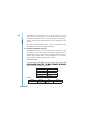
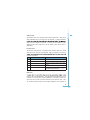
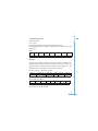
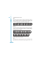
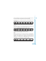
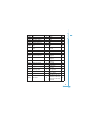
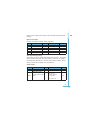
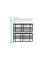
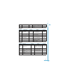
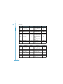
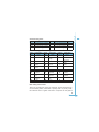
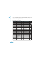
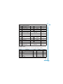
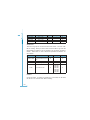
Chapter 5 Function and Software
Introducing Modbus Protocol
Format of the communication
Data Address Table and Application Details
of Acuvim II
73
This chapter will mainly discuss how to handle the meter via the
communication port using software. To master this chapter, you should
be familiar with Modbus and have read other chapters of this manual,
and you have generously mastered the function and application of this
product.
This chapter includes: Modbus protocol, format of communication and
data address table and Acuvim II application details.
5.1 Introducing Modbus Protocol
The Modbus RTU protocol is used for communication in Acuvim II. The
data format and error check met hods are defined in Modbus protocol.
The half duplex query and respond mode is adopt ed in Modbus protocol.
There is only one master device in the communication net. The others
are slave devices, waiting for the query of the master.
Transmission mode
which is compatible with Modbus RTU Mode*.
Coding System
Start bit
8-bit binary
1
Data bits
Parity
Stop bit
8
no parity
1
Error checking
CRC check
Framing
Address
8-Bits
Function
8-Bits
Data
N×8-Bits
Table5.1 Data Frame Format
74
Check
16-Bits
Address Field
The address field of a message frame contains eight bits. Valid slave
device addresses are in the range of 0~247 decimal. A master addresses
When the slave sends its response, it places its own address in this
address field of the response to let the master know which slave is
responding.
Function Field
The function code field of a message frame contains eight bits. Valid
codes are in the range of 1~255 decimal. When a message is sent from a
of action to perform.
Code
Meaning
Action
01
Read Relay Output Status
Obtain current status of Relay Output
02
Read Digital Input(DI) Status
Obtain current status of Digital Input
03
Read Data
Obtain current binary value in one or more
registers
05
Control Relay Output
Force Relay to a state of on or off
16
Press Multiple-Register
consecutive Multiple-Registers
Table5.2 Function Code
Data Field
range of 00 to FF hexadecimal. The data field of messages sent from
a master to slave devices contains additional information which the
slave must use to take the action defined by the function code. This
can include items like discrete and register addresses, the quantity of
75
items to be handled, and the count of actual data bytes in the field.
For example, if the master requests a slave to read a group of holding
and how many registers are to be read. If the master writes to a group
registers.
contains the data requested. If an error occurs, the field contains an
exception code that the master application can use to determine the
next action to be taken. The data field can be nonexistent (of zero
length) in certain kinds of messages.
Error Check Field
Messages include an error’s checking field that is based on a Cyclical
the entire message. It is applied regardless of any parity check method
bytes, containing a 16 bit binary value. The CRC value is calculated by
the transmitting device, which appends the CRC to the message.
The receiving device recalculates a CRC during receipt of the message,
and compares the calculated value to the actual value it received in the
begins of applying successive 8-bit bytes of the message to the current
contents of the register. Only the eight bits of data in each character are
used for generating the CRC. Start and stop bits, and the parity bit, do
76
not apply to the CRC. During generation of the CRC, each 8-bit character
is exclusive ORed with the register contents. Then the result is shifted in
value. If the LSB was a 0, no exclusive OR takes place. This process is
repeated until eight shifts have been performed. After the last (eighth)
shift, the next 8-bit byte is exclusive ORed with the register current
value, and the process repeats for eight more shifts as described above.
The final contents of the register, after all the bytes of the message
have been applied, is the CRC value. When the CRC is appended to the
byte.
5.2 Format of Communication
Explanation of frame
Addr
Fun
06H
03H
Data start Data start Data #of
reg hi
reg lo
regs hi
00H
00H
00H
Data #of
regs lo
21H
CRC 16
Hi
84H
CRC 16
Lo
65H
Table 5.3 Explanation of frame
In table5.3, the meaning of each abbreviated word is,
Addr: address of slave device
Fun: function code
Data start reg hi: start register address high byte
Data start reg lo: start register address low byte
Data #of reg hi: number of register high byte
Data #of reg lo: number of register low byte
CRC16 Hi: CRC high byte
CRC16 Lo: CRC low byte
77
1. Read Status of Relay
Function Code 01
This function code is used to read status of relay in Acuvim II.
1=On 0=Off
Relay1’s address is 0x0000, Relay2’s address is 0x0001, and so on.
The following query is to read relay status of Acuvim II with the address
of 17.
Query
Addr
Fun
11H
01H
Relay start Relay start Relay #of
reg hi
reg lo
regs hi
00H
00H
00H
Relay #of
regs lo
02H
CRC 16
Hi
BFH
CRC 16
Lo
5BH
Table 5.4 Read the status of Relay1 and Relay2 Query Message
Response
The Acuvim II response includes the Acuvim II address, function code,
quantity of data byte, the data, and error checking. An example
response to read the status of Relay1 and Relay2 is shown as Table5.5.
The status of Relay1 and Relay2 are responding to the last 2 bits of the
data.
Relay1: bit0
Relay2: bit1
Address
11H
Function code
01H
Byte count
01H
Data
02H
CRC high
D4H
CRC low
89H
Table 5.5 Relay status responds
The content of the data is:
7
0
MSB
6
0
5
0
4
0
3
0
Relay1 = OFF ( LSB ), Relay2=ON (Left to LSB )
78
2
0
1
1
0
0
LSB
2. Read the Status of DI
Function Code 02
1=On 0=Off
DI1’s address is 0x0000, DI2’s address is 0x0001, and so on.
The following query is to read the Status of 4 DIs of Acuvim II with the
address of 17.
Query
Addr
Fun
11H
02H
DI start
addr hi
00H
DI start
addr lo
00H
DI num
lo
04H
DI num hi
00H
CRC 16
Hi
7BH
CRC 16
Lo
59H
Table 5.6 Read 4 DIs Query Message
Response
The Acuvim II response includes the Acuvim II address, function code,
quantity of data characters, the data characters, and error checking. An
example response to read the status of 4 DIs are shown as Table 5.7. The
status of 4 DIs are responding to the last 4 bits of the data.
DI1: bit0; DI2: bit1; DI3: bit2; DI4: bit3.
Address
11H
Function code
02H
Byte count
01H
Data
03H
CRC high
E5H
CRC low
49H
Table 5.7 Read Status of DI
The content of the data is:
7
0
6
0
5
0
4
0
MSB
3
0
2
0
1
1
0
1
LSB
DI1=On, DI2=On, DI3=Off, DI4=Off.
79
3. Read Data (Function Code 03)
Query
This function allows the master to obtain the measurement results of
Acuvim II. Table5.8 is an example to read the 3 measured data (F, V1 and
V2) from slave device number 17, the data address of F is 4000H, 4001H;
V1's address is 4002H, 4003, and V2's address is 4004H, 4005H.
Addr
Fun
11H
03H
D a t a s t a r t D a t a s t a r t D a t a # o f Data #of CRC 16
addr hi
addr lo
regs hi
regs lo
regs Hi
40H
00H
00H
06H
D2H
CRC 16
regs Lo
98H
Table 5.8 Read F, V1, V2 Query Message
Response
The Acuvim II response includes the Acuvim II address, function code,
quantity of data byte, data, and error checking. An example response
to read F, V1 and V2 (F=42480000H (50.00Hz), V1=42C7CCCDH (99.9V),
V2=42C83333H (100.1V)) is shown:
Byte Data1 Data1 Data 2 Data2 Data3 Data3 Data4 Data4
count
hi
Lo
hi
lo
hi
lo
hi
lo
3H
0CH
42H
48H
00H
00H 42H
C7H CCH CDH
Addr Fun
11H
Data5
hi
42H
Data5
Lo
C8H
Data 6
hi
33H
Data6
lo
33H
CRC16
hi
CAH
CRC16
lo
7FH
Table 5.9 Read F, V1 and V2 Message
4. Control Relay (Function Code 05)
Query
This message forces a single relay either on or off. Any relay that exists
within the Acuvim II can be forced to be either status (on or off). The
80
data value FF00H will set the relay on and the value 0000H will turn it
off; all other values are illegal and will not affect that relay.
The example below is a request to the Acuvim II with the address of 17 to
turn on Relay1.
Addr
Fun
11H
05H
DO addr
hi
00H
DO addr
lo
00H
Value
hi
FFH
Value
lo
00H
CRC 16
Hi
8EH
CRC 16
Lo
AAH
Table5.10 Control Relay Query Message
Response
The normal response to the command request is to retransmit the
message as received after the relay status has been altered.
Addr
Fun
11H
05H
Relay addr Relay addr
hi
lo
00H
00H
Value
hi
FFH
Value
lo
00H
CRC
Hi
8EH
CRC
Lo
AAH
Table5.11 Control Relay Response Message
5. Preset / Reset Multi-Register (Function Code 16)
Query
Function 16 allows the user to modify the contents of a Multi-Register.
Some Registers of Acuvim II can have their contents changed by this
message. The example below is a request to an Acuvim II with the
address of 17 to preset Ep_imp as "17807783.3KWh", while its HEX value
is 0A9D4089H. Ep_imp data address is 0x4048 and 0x4049.
Addr
Fun
11H
10H
Data start
reg hi
40H
Data start
reg lo
48H
Data #of
reg hi
00H
Data #of
reg lo
02H
Byte
Count
04H
81
Value hi
0AH
Value Lo
9DH
Value hi
40H
Value lo
89H
CRC hi
F1H
CRC lo
6AH
Table5.12 Preset Multi-Register Query Message
Response
The normal response to a preset Multi-Register request includes the
Acuvim II address, function code, data start register, the number of
registers, and error checking.
Addr
11H
Fun
10H
Data start Data start
reg hi
reg lo
40H
48H
Data #of
reg hi
00H
Data #of
Reg lo
02H
CRC16
hi
D6H
CRC16
lo
8EH
Table5.13 Preset Multi-Register Response Message
5.3 Data Address Table and Application Details of Acuvim II
There are several rules to follow in using the meter:
1. Data type:
“bit” refers to binary.
“word” refers to 16-bit unsigned integer using one data address and 2
bytes of memory, it varies from 0 to 65535.
“int” refers to 16-bit integer using one data address and 2 bytes of
memory, it varies from -32768 to32767.
“dword” refers to 32-bit unsigned integer using two data addresses and 4
bytes of memory with high word at the front and low word at the end, it
varies from 0 to 4294967295. Rx=high word *65536+low word.
of memory, it varies from -1.175494E-38 to 3.402823E+38.
82
2. Relationship between communication value and numerical value.
The numerical value may not the communication value, it is important to
notice this. The following table shows how they respond to each other.
Parameters
Relationship
Numerical value equals to
System parameters
communication value
Run time
T=Rx/100
Numerical value equals to
Clock
communication value
Energy(primary)
Ep=Rx/10
Reactive energy(primary) Eq=Rx/10
Apparent energy(primary) Es=Rx/10
Energy(secondary)
Ep=Rx/1000
Reactive energy
Eq=Rx/1000
(secondary)
Apparent energy
Es=Rx/1000
(secondary)
frequency
F=Rx/100
Voltage
U=Rx X(PT1/PT2)/10
Current
I=Rx X(CT1/CT2)/1000
Power, demand
P=Rx X(PT1/PT2)X(CT1/CT2)
Q =Rx X(PT1/PT2)X(C T1/
Reactive power, demand
CT2)
Apparent power, demand S=Rx X(PT1/PT2)X(CT1/CT2)
Power factor
PF=Rx/1000
Unbalance factor
Unbl=(Rx/1000)X100
THD
THD=(Rx/10000) X 100%
Harmonics
HDn=(Rx/10000) X 100%
Total odd HD
HDo=(Rx/10000) X 100%
Total even HD
HDe=(Rx/10000) X 100%
Crest factor
CF=Rx/1000
K factor
KF=Rx/10
Unit
Format code
No unit
F1
Hour
Unit of
time
kWh
kvarh
KVA
KWh
F2
Kvarh
F8
F3
F4
F5
F6
F7
KVA
F9
Hz
V
A
W
F10
F11
F12
F13
var
F14
VA
No unit
No unit
No unit
No unit
No unit
No unit
No unit
No unit
F15
F16
F17
F18
F19
F20
F21
F22
F23
83
THFF
Phase angle
temperature
THFF=(Rx/10000) X 100%
Phase angle=Rx/10
Temperature= Rx/10
No unit
Degree
°C
F24
F25
F26
Important Note: Regions from “System parameters settings” to “AO
transforming parameter settings” are the regions that can be set and
1. Using function code 10H, one communication order can only modify
contents in one region, such as “System parameters settings”, ”System
status parameter”, “Date and Time table”, “Over-range alarming-Global
settings”, “Over-range alarming-Single settings”, “I/O Modules settings”.
It can not be accomplished in one communication order to modify
contents in both of two or more regions above.
2. Using function code 03H, there is no such rules described above.
System parameter setting
System parameters determine how the meter works. User should
understand them clearly by referring to chapter 3 and chapter 4.
Function code: 03H for reading, 10H for preset ting. Data t ype: wor d.
Format code: F1.
Address
1000H
1001H
1002H
1003H
1004H
1005H
1006H
84
Parameter
Default Range
Pass Word
0
0~9999
Communication Address
1
1~247
Baud Rate
19200 600~38400
Voltage Input Wiring Type
0
0:3LN,1:2LN,2:2LL,3:3LL
Current Input Wiring
0
0:3CT,1:1CT,2:2CT
Type
PT1 (High 16 bit)
0
50.0~500000.0
PT1 (Low 16 bit)
220.0
R/W
R/W
R/W
R/W
R/W
R/W
R/W
1007H
1008H
1009H
100aH
100bH
100cH
PT2
CT1
CT2
kWh pulse constant
kvarh pulse constant
LCD Back light Time
220.0
5
5
1
1
1
100dH
Demand Slid Window
Time
15
100fH
1010H
1011H
Demand calculating
mode
Clear demand memory
Max/Min clear
Run time clear
1012H
Current I1 direction
0
1013H
Current I2 direction
0
1014H
Current I3 direction
0
1015H
1016H
VAR/PF convention
Energy clear
0
0
1017H
Energy calculating mode
1
100eH
1
0
0x55
0
1019H
Reactive power
measuring mode
Energy display mode
101aH
Ethernet Module reset
0
101bH
SOE enable
0
1018H
50.0~400.0
1~50000
1,5
1~6000
1~6000
0-120
R/W
R/W
R/W
R/W
R/W
R/W
1~30
R/W
1:sliding window
2:thermal
Only 1 works
Only 0x0A works
Only 1 works
0: Positive
1: Negative
0: Positive
1: Negative
0: Positive
1: Negative
0:IEC,1:IEEE
Only 1 works
0:fundamental
1:full-wave
R/W
R/W
R/W
R/W
R/W
R/W
R/W
R/W
R/W
R/W
0
0:real,1:general
R/W
0
0:primary 1:secondary
0:none, 1:reset,
2:load default and reset
0:none; 1:AXM-IO11;
2:AXM-IO21; 3:AXM-IO31;
4:AXM-IO12; 5:AXM-IO22;
6:AXM-IO32;
R/W
R/W
R/W
85
101cH
Pulse counter clear
0
101dH
Basic parameter mode
0
0:none 1:AXM-IO11;
2:AXM-IO21; 3:AXM-IO31;
4:AXM-IO12; 5:AXM-IO22;
6:AXM-IO32;
0:secondary; 1:primary
R/W
R/W
System status parameter
“System status” indicates what events happened in the meter, what kinds
Flags should be cleared after being read by the controller, otherwise new
data will not be stored properly.
Function code: 03H for reading, 10H for writing. Data type: word.
Address
101eH~102dH
102eH
Parameter
Recording pointer
bj_st0-15
86
new data
Property
R/W
Bit0:new alarming or not
Bit1 new SOE or not
R
F1
0~15
R
F1
0~19
F2
0~999999999
R
R
R
Bit0: AXM-IO11;
Bit1:AXM-IO12;
B it 2:A XM -I O 21 ; B it 3:
A XM -I O 22 ; B it 4:A XM IO31; Bit5:AXM-IO32;
0:disconnected
1:connected
Expanded
IO Modules
connecting status
1037H
Temperature
1038H~103fH Reserved
Range
1
System status
102fH~ 1031H Reserved
Alarming group
1032H
number
1033H
SOE group number
1034H
Run time (high)
1035H
Run time (low)
1036H
Format code
F26
R
R
Please refer to chapter 3 and chapter 4 for more details about parameter
settings.
Date and Time table
Function code: 03H for reading, 10H for presetting.
Address
1040H
1041H
1042H
1043H
1044H
1045H
Parameter
Year
Month
Day
Hour
minute
second
Format code
F3
F3
F3
F3
F3
F3
Range
2000-2099
1-12
1-31
0-23
0-59
0-59
Property
R/W
R/W
R/W
R/W
R/W
R/W
Over-range alarming setting
This setting consists of global settings and single settings. The global
settings contain settings of all global variables. There are 16 groups of
records with the same format. Function code: 03H for reading, 10H for
writing. Please refer to chapter 4 for more details.
Global settings
Address
1046H
1047H
1048H
Parameter
Global alarming enable
Alarming channel enable
setting
Range
0:disable;1:enable
0:disable;1:enable
0~65535
Bit0:channel 1
1:enable; 0:disable
Bit1: channel 2
……
Bit15: channel 16
Property
R/W
R/W
R/W
87
0~255
1049H
Logical “And ” between
alarming setting
104aH
Alarming output to DO1
setting
104bH
104cH
104dH
1:enable;0:disable
Bit1: second logic switch
……
Bit7: eighth logic switch
0~65535
Bit0: channel 1 output
1:enable;0:disable
Bit1: channel 2 output
……
Bit15: channel 16 output
0~65535
The same as previous
0~65535
The same as previous
0~65535
The same as previous
Alarming output to DO2
setting
Alarming output to DO3
setting
Alarming output to DO4
setting
R/W
R/W
R/W
R/W
R/W
Single settings
Address
104eH
104fH
1050H
1051H
1052H
1053H~
109dH
88
Parameter
First group: parameter
code
First group: comparison
mode
First group: setting
value
First group: delay
First group: output to
relay
2nd to 16th group
Format code
F1
F1
F10~F18
F1
F1
Range
0~44
1 : m o r e , 2 :
equal,3:less
Related with
parameters
0~3000(*10ms)
0:none,1-8:
related relay
Same as the first
group
Property
R/W
R/W
R/W
R/W
R/W
R/W
Alarming parameter code table
Setting
Alarming
value
object
0
frequency
3
Vc
6
Ubc
Line current
9
of phase A
Average line
12
current
Power of
15
phase B
Reactive
18
power of
phase A
Reactive
21
power of all
Apparent
24
power of
phase C
27
PF of B
Voltage
30
unbalance
factor U_unbl
THD_V1(V1
33
or V12)
Average
36
THD_V
Alarming object
1
4
7
10
Va
Average phase voltage
Uca
Line current of phase
B
Alarming object
2
5
8
11
Vb
Uab
Average line voltage
Line current of phase
C
13
Neutral current
14
Power of phase A
16
Power of phase C
17
Power of all
19
Reactive power of
phase B
20
Reactive power of
phase C
22
Apparent power of
phase A
23
Apparent power of
phase B
25
Apparent power of all
26
PF of A
28
PF of C
29
PF
31
Current unbalance
factor I_unbl
32
Load characteristic(R/
L/C)
34
THD_V2(V2 or V31)
35
THD_V3(V3 or V23)
37
THD_I1
38
THD_ I2
41
AI1 sampling value
44
AI4 sampling value
39
THD_ I3
40
Average
THD_I
42
AI2 sampling
value
43
AI3 sampling value
89
I/O Modules settings
These settings are for some extended I/O modules, if there is no any
extended I/O modules, all the settings are of no use. Please check the
I/O connecting status before you do any settings. Function code: 03H for
reading, 10H for writing. Please refer to <<User’s manual of extended
I/O Modules>>for more details.
AXM-IO11
Address
Parameter
Default
109eH DI1-6 type
0
109fH DI pulse constant
Working mode of relay 1
10a0H
and 2
Output mode of relay 1
10a1H
and 2
10a2H Pulse width
0
0
Range
Bit0-DI1, Bit1-DI2
Bit2-DI3, Bit3-DI4
Bit4-DI5, Bit5-DI6
0-DI,1-pulse counter
1~65535
0-control output
1-alarming output
Property
R/W
R/W
R/W
0
0-latch, 1-momentary
R/W
50
50-3000ms
R/W
AXM-IO21
Address
90
Parameter
Default
10a3H DI7-10 type
0
10a4H DI pulse constant
0
10a5H Working mode of DO
0
10a6H DO pulse width
20
10a7H DO1 output
0
Range
Bit0-DI7, Bit1-DI8
Bit2-DI9, Bit3-DI10
0-DI,1-pulse counter
1~65535
0-pulse output
1-alarming output
20-1000ms
0-none
1-consumption power
2-gererating power
3-absorption reactive power
4-generating reactive power
Property
R/W
R/W
R/W
R/W
R/W
10a8H DO2 output
0
10a9H AO1,2 type
0
Same as above
0:0-20mA, 1:4-20mA,2:0-5V,
3:1-5V
R/W
R/W
AXM-IO31
Address
Parameter
Default
Range
Bit0-DI11,Bit1-DI12,
Bit2-DI13, Bit3-DI14
0-DI,1-pulse counter
1-65535
0-control output
1-alarming output
Property
10aaH DI11-14 type
0
10abH DI pulse constant
Wo r k i n g m o d e o f
10acH
relay 3 and 4
Output mode of
10adH
relay 3 and 4
10aeH Pulse width
0
0
0-latch, 1-momentary
R/W
50
R/W
10afH
0
50-3000ms
0:0-20mA, 1:4-20mA
2:0-5V, 3:1-5V
AI1,2 type
0
R/W
R/W
R/W
R/W
AXM-IO12
Address Parameter
Default
Range
Bit0-DI15,Bit1-DI16,
Bit2-DI17,Bit3-DI18,
Bit4-DI19, Bit5-DI20
0-DI,1-pulse counter
1-65535
0-control output
1-alarming output
Property
0
0-latch,1-momentary
R/W
50
50-3000ms
R/W
10b0H
DI15-20 type
0
10b1H
DI pulse constant (high)
Working mode of relay
5 and 6
Output mode of relay
5 and 6
Pulse width
0
10b2H
10b3H
10b4H
0
R/W
R/W
R/W
91
AXM-IO22
Address
Parameter
Default
10b5H
DI21-24 type
0
10b6H
0
10b8H
DI pulse constant
Wo r k i n g m o d e o f
DO3,4
DO Pulse width
20
10b9H
DO3 output
0
10baH
DO4 output
0
10bbH
AO3,4 type
0
10b7H
0
Range
Bit0-DI21,Bit1-DI22,
Bit2-DI23, Bit3-DI24
0-DI,1-pulse counter
1-65535
0-pulse output
1-alarming output
20-1000ms
0-none
1-consumption power
2-gererating power
3-absorption reactive
power
4-generating reactive
power
Same as above
0:0-20mA, 1:4-20mA,
2:0-5V, 3:1-5V
Property
R/W
R/W
R/W
R/W
R/W
R/W
R/W
AXM-IO32
Address
Default
Range
Bit0-DI25, Bit1-DI26
Bit2-DI27, Bit3-DI28
0-DI, 1-pulse counter
1-65535
0-control output
1-alarming output
Property
10bcH
DI25-28 type
0
10bdH
0
0
0-latch, 1-momentary
R/W
10c0H
DI pulse constant
Wo r k i n g m o d e o f
relay 7 and 8
Output mode of
relay 7 and 8
Pulse width
50
R/W
10c1H
AI3,4 type
0
50-3000
0:0-20m A , 1:4-20m A ,
2:0-5V, 3:1-5V
10beH
10bfH
92
Parameter
0
R/W
R/W
R/W
R/W
AO transforming select
Address
10c2H
10c3H
10c4H
10c5H
AO1
AO2
AO3
AO4
Parameter
transforming parameter
transforming parameter
transforming parameter
transforming parameter
Default
Refer
Refer
Refer
Refer
to
to
to
to
Range
following
following
following
following
table
table
table
table
R/W
R/W
R/W
R/W
AO transforming parameter settings
Setting Ttransforming
value
object
0
Frequency
3
Vc
6
Ubc
9
12
15
18
21
24
27
Line current of
phase A
Average line
current
Power of phase B
Reactive power
of phase A
Reactive power
of all
Apparent power
of phase C
PF of B
Setting
Transforming
value
object
1
Va
Average phase
4
voltage
Setting
value
2
5
Transforming
object
Vb
Uab
Average line
voltage
Line current of
phase C
7
Uca
8
10
Line current of
phase B
11
13
Neutral current
14
Power of phase A
16
Power of phase C
Reactive power
of phase B
Apparent power
of phase A
Apparent power
of all
PF of C
17
Power of all
Reactive power
of phase C
Apparent power
of phase B
19
22
25
28
20
23
26
PF of A
29
PF
Basic Analog measurements
There are two different modes to read basic analog measurements,
one is secondary mode, and another is primary mode. In primary mode,
the numerical value in register of Acuvim II is equal to the real physical
93
value. In secondary mode, the relationship between numerical value
in register and the real physical value is as following table. (Rx is the
numerical value in register of Acuvim II)
Function code: 03H for reading.
Address
4000H~4001H
4002H~4003H
4004H~4005H
4006H~4007H
4008H~4009H
400aH~400bH
400cH~400dH
400eH~400fH
4010H~4011H
4012H~4013H
4014H~4015H
4016H~4017H
4018H~4019H
401aH~401bH
401cH~401dH
401eH-401fH
4020H-4021H
4022H-4023H
4024H-4025H
4025H-4027H
4028H-4029H
94
Parameter
Frequency
Phase voltage V1
Phase voltage V2
Phase voltage V3
Average voltage Vavg
Line voltage V12
Line voltage V23
Line voltage V31
Average line voltage
Vlavg
Phase(line)current I1
Phase(line)current I2
Phase(line)current I3
Average current Iavg
Neutral current In
Phase A power Pa
Phase B power Pb
Phase C power Pc
System power Psum
Phase A reactive
power Qa
Phase B reactive
power Qb
Phase C reactive
power Qc
Code
F1
F1
F1
F1
F1
F1
F1
F1
Relationship
F = Rx
U=Rx×(PT1/PT2)
U=Rx×(PT1/PT2)
U=Rx×(PT1/PT2)
U=Rx×(PT1/PT2)
U=Rx×(PT1/PT2)
U=Rx×(PT1/PT2)
U=Rx×(PT1/PT2)
R
R
R
R
R
R
R
R
F1
U=Rx×(PT1/PT2)
R
F1
F1
F1
F1
F1
F1
F1
F1
F1
I=Rx×(CT1/CT2)
I=Rx×(CT1/CT2)
I=Rx×(CT1/CT2)
I=Rx×(CT1/CT2)
I=Rx×(CT1/CT2)
P=Rx×(PT1/PT2)×(CT1/CT2)
P=Rx×(PT1/PT2)×(CT1/CT2)
P=Rx×(PT1/PT2)×(CT1/CT2)
P=Rx×(PT1/PT2)×(CT1/CT2)
R
R
R
R
R
R
R
R
R
F1
Q=Rx×(PT1/PT2)×(CT1/CT2)
R
F1
F1
Q=Rx×(PT1/PT2)×(CT1/
CT2)
Q=Rx×(PT1/PT2)×(CT1/
CT2)
R
R
402aH-402bH
402cH-402dH
402eH-402fH
4030H-4031H
4032H-4033H
4034H-4035H
4036H-4037H
4038H-4039H
403aH-403bH
403cH-403dH
403eH-403fH
4040H-4041H
4042H-4043H
4044H-4045H
4046H-4047H
System reactive
power Qsum
Phase A Apparent
power Sa
Phase B Apparent
power Sb
Phase C Apparent
power Sc
System Apparent
power Ssum
Phase A power factor
PFa
Phase B power factor
PFb
Phase C power
factor PFc
System power factor
PFsum
Voltage unbalance
factor U_unbl
Current unbalance
factor I_unbl
Load
characteristic(L/C/R)
Power demand
Reactive Power
demand
Apparent power
demand
F1
Q=Rx×(PT1/PT2)×(CT1/
CT2)
R
F1
S=Rx×(PT1/PT2)×(CT1/CT2)
R
F1
S=Rx×(PT1/PT2)×(CT1/CT2)
R
F1
S=Rx×(PT1/PT2)×(CT1/CT2)
R
F1
S=Rx×(PT1/PT2)×(CT1/CT2)
R
F1
PF = Rx
R
F1
PF = Rx
R
F1
PF = Rx
R
F1
PF = Rx
R
F1
Unbalance = Rx × 100%
R
F1
Unbalance = Rx × 100%
R
F1
76.0/67.0/82.0(ASCII)
R
F1
P=Rx×(PT1/PT2)×(CT1/CT2)
R
F1
P=Rx×(PT1/PT2)×(CT1/CT2)
R
F1
P=Rx×(PT1/PT2)×(CT1/CT2)
R
Real time energy measurement
Data stored in this block can be preset or cleared.
Function code: 03H for reading, 10H for writing. Data type: dword.
95
It can be set as primary energy or secondary energy according to user.
Please refer to F7, F8, and F9 for more details about the relationship
between numerical value in register and the real physical value.
Address
4048H-4049H
404aH-404bH
404cH-404dH
404eH-404fH
4050H-4051H
4052H-4053H
4054H-4055H
4056H-4057H
4058H-4059H
Parameter
Energy IMP
Energy EXP
Reactive energy IMP
Reactive energy EXP
Energy TOTAL
Energy NET
Reactive energy TOTAL
Reactive energy NET
Apparent energy
Code
F4/F7
F4/F7
F5/F8
F5/F8
F4/F7
F4/F7
F5/F8
F5/F8
F6/F9
Range
0-999999999
0-999999999
0-999999999
0-999999999
0-999999999
0-999999999
0-999999999
0-999999999
0-999999999
Property
R/W
R/W
R/W
R/W
R/W
R/W
R/W
R/W
R/W
Harmonics:
THD, Harmonics, odd HD, even HD, Crest Factor, THFF, K factor etc are
all stored here. The data type is “word”. Voltage parameters refer to
line voltage when it is set to “2L L/3LL” and phase voltage for others.
Function code: 03H for reading.
Address
Parameter
code
The following are the THD of voltage and current
405aH THD_V1 of V1(V12)
F18
405bH THD_V1 of V2(V31)
F18
405cH THD_V1 of V3(V23)
F18
405dH Average THD_V
F18
405eH THD_I1
F18
405fH THD_I2
F18
4060H THD_I3
F18
4061H Average THD_I
F18
96
Range
Property
0~10000
0~10000
0~10000
0~10000
0~10000
0~10000
0~10000
0~10000
R
R
R
R
R
R
R
R
Voltage Harmonics, even HD, odd HD, Crest Factor
4062H- Harmonics of V1(V12)
nd
st
F19
407fH (the 2 to 31 )
4080H Odd HD of V1(V12)
F20
4081H Even HD of V1(V12)
F21
4082H Crest Factor of V1(V12)
F22
4083H THFF of V1(V12)
F24
4084HParameters of V2(V31)
Same
40a5H
40a6HParameters of V3(V23)
Same
40c7H
40c8H40e5H
40e6H
40e7H
40e8H
40e9H4109H
410aH412aH
Harmonics of I1 (the 2nd
st
to 31 )
Odd HD of I1
Even HD of I1
K Factor of I1
are shown as below
0~10000
R
0~10000
0~10000
0~65535
0~10000
R
R
R
R
as V1
R
as V1
R
F19
0~10000
R
F20
F21
F23
0~10000
0~10000
0~65535
R
R
R
Parameters of I2
Same as I1
R
Parameters of I3
Same as I1
R
MAX/MIN records
MAX/MIN value and stamp time. Function code: 03H for reading.
Address
4136H
4137H413cH
413dH
413eH4143H
4144H
Parameter
MAX of V1
Time stamp: yyyy:mm:dd:hh:
mm:ss
MAX of V2
Time stamp: yyyy:mm:dd:hh:
mm:ss
MAX of V3
Code
F11
Range
-32768~32767
Property
R
F3
time
R
F11
-32768~32767
R
F3
time
R
F11
-32768~32767
R
97
4145H414aH
414bH
414cH4151H
4152H
4153H4158H
4159H
415aH415fH
4160H
4161H4166H
4167H
4168H416dH
416eH
416fH4174H
4175H
4176H417bH
417cH
417dH4182H
4183H
4184H4189H
418aH
418bH4190H
4191H
98
Time stamp: yyyy:mm:dd:hh:
mm:ss
MAX of V12
Time stamp: yyyy:mm:dd:hh:
mm:ss
MAX of V23
Time stamp: yyyy:mm:dd:hh:
mm:ss
MAX of V31
Time stamp: yyyy:mm:dd:hh:
mm:ss
MAX of I1
Time stamp: yyyy:mm:dd:hh:
mm:ss
MAX of I2
Time stamp: yyyy:mm:dd:hh:
mm:ss
MAX of I3
Time stamp: yyyy:mm:dd:hh:
mm:ss
MAX of system power
Time stamp: yyyy:mm:dd:hh:
mm:ss
MAX of system reactive power
Time stamp: yyyy:mm:dd:hh:
mm:ss
MAX of system apparent power
Time stamp: yyyy:mm:dd:hh:
mm:ss
MAX of power factor
Time stamp: yyyy:mm:dd:hh:
mm:ss
MAX of frequency
F3
time
R
F11
-32768~32767
R
F3
time
R
F11
-32768~32767
R
F3
time
R
F11
-32768~32767
R
F3
time
R
F12
-32768~32767
R
F3
time
R
F12
-32768~32767
R
F3
time
R
F12
-32768~32767
R
F3
time
R
F13
-32768~32767
R
F3
time
R
F14
-32768~32767
R
F3
time
R
F15
-32768~32767
R
F3
time
R
F16
-32768~32767
R
F3
time
R
F10
-32768~32767
R
4192H4197H
4198H
4199H419eH
419fH
41a0H41a5H
41a6H
41a7H41acH
41adH
41aeH41b3H
41b4H
41b5H41baH
41bbH
41bcH41c1H
41c2H
41c3H41c8H
41c9H
41caH41cfH
41d0H
41d1H41d6H
41d7H
41d8H41ddH
41deH
Time stamp: yyyy:mm:dd:hh:
mm:ss
MAX of power demand
Time stamp: yyyy:mm:dd:hh:
mm:ss
MAX of reactive power demand
Time stamp: yyyy:mm:dd:hh:
mm:ss
MAX of apparent power demand
Time stamp: yyyy:mm:dd:hh:
mm:ss
MAX of voltage unbalance factor
Time stamp: yyyy:mm:dd:hh:
mm:ss
MAX of current unbalance factor
Time stamp: yyyy:mm:dd:hh:
mm:ss
MAX of V1(V12) THD
Time stamp: yyyy:mm:dd:hh:
mm:ss
MAX of V2(V31) THD
Time stamp: yyyy:mm:dd:hh:
mm:ss
MAX of V3(V23) THD
Time stamp: yyyy:mm:dd:hh:
mm:ss
MAX of I1 THD
Time stamp: yyyy:mm:dd:hh:
mm:ss
MAX of I2 THD
Time stamp: yyyy:mm:dd:hh:
mm:ss
MAX of I3 THD
F3
time
R
F13
-32768~32767
R
F3
time
R
F14
-32768~32767
R
F3
time
R
F15
-32768~32767
R
F3
time
R
F17
-32768~32767
R
F3
time
R
F17
-32768~32767
R
F3
time
R
F18
-32768~32767
R
F3
time
R
F18
-32768~32767
R
F3
time
R
F18
-32768~32767
R
F3
time
R
F18
-32768~32767
R
F3
time
R
F18
-32768~32767
R
F3
time
R
F18
-32768~32767
R
99
41dfHTime stamp: yyyy:mm:dd:hh:
F3
time
R
41e4H
mm:ss
41e5H~4293H are the address of previous parameters’ MIN having the same format
Sequence component
U1 (U12), I1 are consisting of real part and complex part. They have
positive sequence, negative sequence and zero sequence. Data type is
“int”. Function code: 03H for reading.
Address
Parameter
code
Range
property
Phase angle
All voltage and current’s phase angles corresponding to V1 (V12) are
stored here. You can find out the phase sequence according to them.
Data type is “word”. Function code: 03H for reading.
Address
42a0H
42a1H
42a2H
42a3H
100
phase
phase
phase
phase
Parameter
angle of V2 to V1
angle of V3 to V1
angle of I1 to V1
angle of I2 to V1
code
F25
F25
F25
F25
Range
0-3600
0-3600
0-3600
0-3600
property
R
R
R
R
42a4H
42a5H
42a6H
42a7H
42a8H
phase
phase
phase
phase
phase
angle
angle
angle
angle
angle
of
of
of
of
of
I3 to V1
V23 to V12
I1 to V12
I2 to V12
I3 to V12
F25
F25
F25
F25
F25
0-3600
0-3600
0-3600
0-3600
0-3600
R
R
R
R
R
Alarming records
There are 16 groups of records with the same format. Function code:
03H for reading, 10H for writing. Please refer to chapter 4 for more
details.
Address
42a9H
42aaH
42abH
42acH~42b2H
42b3H~42bcH
42bdH~42c6H
42c7H~42d0H
42d1H~42daH
42dbH~42e4H
42e5H~42eeH
42efH~42f8H
42f9H~4302H
4303H~430cH
430dH~4316H
4317H~4320H
4321H~432aH
432bH~4334H
Parameter
code
First group: alarming status
F1
First group: alarming
F1
parameter code
First group: over range or
F10-F18
reset value
First group: Time stamp:
F3
yyyy:mm:dd:hh:mm:ss:ms
Second group
Third group
Fourth group
Fifth group
Sixth group
Seventh group
Eighth group
Ninth group
Tenth group
Eleventh group
Twelfth group
Thirteenth group
Fourteenth group
Range
0~65535
property
R
0~44
R
Related with
parameters
R
R
101
4335H~433eH Fifteenth group
433fH~4348H Sixteenth group
Counting number of I/O Modules
DI are arranged according to expanded I/O module addresses, user can
check out the counting number of DI along with those modules. The
counting number of I/O modules will be stored in non-volatile memory
during power off. They can be cleared up via communication and panel.
Data type is “word”. Function code: 03H for reading.
Address
AXM-IO11
4349H-434aH
434bH-434cH
434dH-434eH
434fH-4350H
4351H-4352H
4353H-4354H
AXM-IO21
4355H-4356H
4357H-4358H
4359H-435aH
435bH-435cH
AXM-IO31
435dH-435eH
435fH-4360H
4361H-4362H
4363H-4364H
AXM-IO12
4365H-4366H
4367H-4368H
4369H-436aH
102
Parameter
DI1
DI2
DI3
DI4
DI5
DI6
pulse
pulse
pulse
pulse
pulse
pulse
counter
counter
counter
counter
counter
counter
code
property
F1
F1
F1
F1
F1
F1
0-4294967295
0-4294967295
0-4294967295
0-4294967295
0-4294967295
0-4294967295
R
R
R
R
R
R
DI7 pulse counter number
DI8 pulse counter number
DI9 pulse counter number
DI10 pulse counter number
F1
F1
F1
F1
0-4294967295
0-4294967295
0-4294967295
0-4294967295
R
R
R
R
DI11
DI12
DI13
DI14
number
number
number
number
F1
F1
F1
F1
0-4294967295
0-4294967295
0-4294967295
0-4294967295
R
R
R
R
DI15 pulse counter number
DI16 pulse counter number
DI17 pulse counter number
F1
F1
F1
0-4294967295
0-4294967295
0-4294967295
R
R
R
pulse
pulse
pulse
pulse
number
number
number
number
number
number
Range
counter
counter
counter
counter
436bH-436cH
436dH-436eH
436fH-4370H
AXM-IO22
4371H-4372H
4373H-4374H
4375H-4376H
4377H-4378H
AXM-IO32
4379H-437aH
437bH-437cH
437dH-437eH
437fH-4380H
DI18 pulse counter number
DI19 pulse counter number
DI20 pulse counter number
F1
F1
F1
0-4294967295
0-4294967295
0-4294967295
R
R
R
DI21
DI22
DI23
DI24
pulse
pulse
pulse
pulse
counter
counter
counter
counter
number
number
number
number
F1
F1
F1
F1
0-4294967295
0-4294967295
0-4294967295
0-4294967295
R
R
R
R
DI25
DI26
DI27
DI28
pulse
pulse
pulse
pulse
counter
counter
counter
counter
number
number
number
number
F1
F1
F1
F1
0-4294967295
0-4294967295
0-4294967295
0-4294967295
R
R
R
R
AI input value
The output of AI is mapped to the range of 0~4095 according to its
sampling value using some algorithm. Data type is “word”. Function
code: 03H for reading. Please refer to <<User’s manual of expanded I/O
modules>> for more details.
Address
4385H
4386H
4387H
4388H
AI1
AI2
AI3
AI4
Parameter
sampling value
sampling value
sampling value
sampling value
code
F1
F1
F1
F1
Range
0-4095
0-4095
0-4095
0-4095
property
R
R
R
R
AO output
The output of AO is the actual value of output. It will get a different unit
code: 03H for reading. Please refer to <<User’s manual of expanded I/O
modules>> for more details.
103
Address
438aH-438bH
438cH-438dH
438eH-438fH
4390H-4391H
Parameter
Value of A01
Value of A02
Value of A03
Value of A04
code
F1
F1
F1
F1
Range
property
R
R
R
R
SOE Records
There are 20 groups of records with the same format. Function code:
03H for reading. What you need to know is that the data is got from the
SOE enabled I/O module, if this I/O module is not connected, the data is
useless. Please refer to <<User’s manual of expanded I/O modules>> for
more details.
Address
4399H~439fH
43a0H
43a1H-4438H
4439H
Parameter
First group: time stamp:
yyyy:mm:dd:hh:mm:ss:
ms
First group: DI status
2nd to 20th group
I/O module of SOE
code
Range
property
F3
R
F1
R
R
F1
0:none;
1:AXM-IO11;
2:AXM-IO21;
3:AXM-IO31;
4:AXM-IO12;
5:AXM-IO22;
6:AXM-IO32
R
DI Status
Current DI status, if related I/O module isn’t connected, the DI status
will be set to 0. Function code: 02H for reading.
104
Address
AXM-IO11
0000H
0001H
0002H
0003H
0004H
0005H
AXM-IO21
0006H
0007H
0008H
0009H
AXM-IO31
000aH
000bH
000cH
000dH
AXM-IO12
000eH
000fH
0010H
0011H
0012H
0013H
AXM-IO22
0014H
0015H
0016H
0017H
AXM-IO32
0018H
Parameter
Range
Data type
DI1
DI2
DI3
DI4
DI5
DI6
1=ON,0=OFF
1=ON,0=OFF
1=ON,0=OFF
1=ON,0=OFF
1=ON,0=OFF
1=ON,0=OFF
bit
bit
bit
bit
bit
bit
DI7
DI8
DI9
DI10
1=ON,0=OFF
1=ON,0=OFF
1=ON,0=OFF
1=ON,0=OFF
bit
bit
bit
bit
DI11
DI12
DI13
DI14
1=ON,0=OFF
1=ON,0=OFF
1=ON,0=OFF
1=ON,0=OFF
bit
bit
bit
bit
DI15
DI16
DI17
DI18
DI19
DI20
1=ON,0=OFF
1=ON,0=OFF
1=ON,0=OFF
1=ON,0=OFF
1=ON,0=OFF
1=ON,0=OFF
bit
bit
bit
bit
bit
bit
DI21
DI22
DI23
DI24
1=ON,0=OFF
1=ON,0=OFF
1=ON,0=OFF
1=ON,0=OFF
bit
bit
bit
bit
DI25
1=ON,0=OFF
bit
105
0019H
001aH
001bH
DI26
DI27
DI28
1=ON,0=OFF
1=ON,0=OFF
1=ON,0=OFF
bit
bit
bit
Relay status
Function code: 01H for reading, 05H for controlling output.
Address
AXM-IO11
0000H
0001H
AXM-IO31
0002H
0003H
AXM-IO12
0004H
0005H
AXM-IO32
0006H
0007H
106
Parameter
Range
Data type
Relay1
Relay2
1=ON,0=OFF
1=ON,0=OFF
bit
bit
Relay3
Relay4
1=ON,0=OFF
1=ON,0=OFF
bit
bit
Relay5
Relay6
1=ON,0=OFF
1=ON,0=OFF
bit
bit
Relay7
Relay8
1=ON,0=OFF
1=ON,0=OFF
bit
bit