1
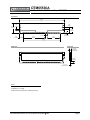
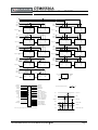
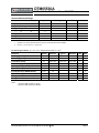
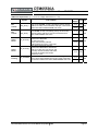
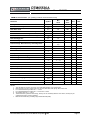
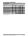
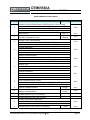
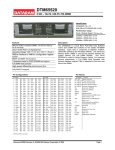
DTM65536A 2 GB - 240-Pin DDR2 Low Power FB-DIMM Identification DTM65536A 256Mx72 2GB 2Rx8 PC2-5300F-555-11-B0 Performance range Clock / Module Speed / CL-tRCD -tRP 333MHz / DDR2-667 / 5-5-5 267MHz / DDR2-533 / 4-4-4 200MHz / DDR2-400 / 3-3-3 Features Description 240-pin JEDEC-compliant DIMM, 133.35 mm wide by 30.35 mm high Data Transfer Rate: 5.3 Gigabytes/sec Operating Voltage: VDD = 1.8 V ±0.1; VCC = 1.5V ±0.1 SMBus interface to AMB for configuration register access MBIST and IBIST test functions Transparent mode for DDR2 SDRAM test support Full DIMM Heat Spreader High-speed differential point-to-point link Fully RoHS Compliant The DTM65536A is a Dual Rank PC2-5300 Fully Buffered 256MX72 ECC DIMM that conforms to the JEDEC FB-DIMM standard. Each rank is comprised of nine Hynix 128Mx8 DDR2 DRAMs. One IDT (Rev L4) Advanced Memory Buffer (AMB) is used as the interface between the system memory bus and DIMM DRAMs. One 2K-bit EEPROM is used for Serial Presence Detect. For improved thermal performance, a Full DIMM Heat Spreader with thermal interface material (TIM) is attached to the front and back of the DIMM. This is a reduced power module. Components have been tested and selected for this design with the lowest power consumption. Pin Configurations Pin Names Front side Back side 91 /PS9 121 VDD Pin Names 151 SN3 181 /SN9 211 /SS9 SCK, /SCK Function 1 VDD 31 PN3 61 /PN9 System Clock Input 2 VDD 32 /PN3 62 VSS 92 VSS 122 VDD 152 /SN3 182 VSS 212 VSS PN, /PN[13:0] Primary Northbound Data 3 VDD 33 VSS 63 PN10 93 PS5 123 VDD 153 VSS 183 SN10 213 SS5 PS, /PS[9:0] 4 VSS 34 PN4 64 /PN10 94 /PS5 124 VSS 154 SN4 184 /SN10 214 /SS5 SN. /SN[13:0] Secondary Northbound Data 5 VDD 35 /PN4 65 VSS 95 VSS 125 VDD 155 /SN4 185 VSS 215 VSS SS. /SS[9:0] Secondary Southbound Data 6 VDD 36 VSS 66 PN11 96 PS6 126 VDD 156 VSS 186 /SN11 216 SS6 SCL Serial Clock, EEPROM 7 VDD 37 PN5 67 /PN11 97 /PS6 127 VDD 157 SN5 187 /SN11 217 /SS6 SDA Serial Data, EEPROM 8 VSS 38 /PN5 68 VSS 98 VSS 128 VSS 158 /SN5 188 VSS 218 VSS /RESET AMB Reset Signal 9 VCC 10 VCC 39 40 VSS PN13 69 70 VSS PS0 99 PS7 100 /PS7 129 VCC 130 VCC 159 VSS 160 SN13 189 VSS 190 SS0 219 SS7 220 /SS7 VCC AMB Core Power and AMB Channel Interface Power (1.5 V) Primary Southbound Data 11 VSS 41 /PN13 71 /PS0 101 VSS 131 VSS 161 /SN13 191 /SS0 221 VSS 12 VCC 42 VSS 72 VSS 102 PS8 132 VCC 162 VSS 192 VSS 222 SS8 13 VCC 14 VSS 15 VTT 43 44 45 VSS RFU RFU 73 74 75 PS1 /PS1 VSS 103 /PS8 104 VSS 105 RFU2 133 VCC 134 VSS 135 VTT 163 VSS 164 RFU1 165 RFU1 193 SS1 194 /SS1 195 VSS 223 /SS8 224 VSS 225 RFU2 VDDSPD 16 VID1 46 VSS 76 PS2 106 RFU2 136 VID0 166 VSS 196 SS2 226 RFU2 VSS Ground 17 /RESET 47 VSS 77 /PS2 107 VSS 137 M_TEST 167 VSS 197 /SS2 227 VSS RFU Reserved For Future Use 18 VSS 48 PN12 78 VSS 108 VDD 138 VSS 168 SN12 198 VSS 228 SCK DNU Do Not Use 19 RFU2 49 /PN12 79 PS3 109 VDD 139 RFU2 169 /SN12 199 SS3 229 /SCK M_TEST Margin Test 20 RFU2 50 VSS 80 /PS3 110 VSS 140 RFU2 170 VSS 200 /SS3 230 VSS SA[2:0] Serial Address, EEPROM 21 VSS 51 PN6 81 VSS 111 VDD 141 VSS 171 SN6 201 VSS 231 VDD 22 PN0 52 /PN6 82 PS4 112 VDD 142 SN0 172 /SN6 202 SS4 232 VDD 23 /PN0 53 VSS 83 /PS4 113 VDD 143 /SN0 173 VSS 203 /SS4 233 VDD 24 VSS 54 PN7 84 VSS 114 VSS 144 VSS 174 SN7 204 VSS 234 VSS 25 PN1 55 /PN7 85 VSS 115 VDD 145 SN1 175 /SN7 205 VSS 235 VDD 26 /PN1 56 VSS 86 RFU1 116 VDD 146 /SN1 176 VSS 206 RFU1 236 VDD 27 VSS 57 PN8 87 RFU1 117 VTT 147 VSS 177 SN8 207 RFU1 237 VTT 28 PN2 58 /PN8 88 VSS 118 SA2 148 SN2 178 /SN8 208 VSS 238 VDDSPD 29 /PN2 59 VSS 89 VSS 119 SDA 149 /SN2 179 VSS 209 VSS 239 SA0 30 VSS 60 PN9 90 PS9 120 SCL 150 VSS 180 SN9 210 SS9 240 SA1 VDD VTT DRAM Power and AMB DRAM I/O Power (1.8 V) DRAM Address/Command/Clock Termination Power (VDD/2) SPD Power NOTE: M_TEST is not used Document 06560, Revision A, 16-Jul-09, Dataram Corporation © 2009 Page 1 DTM65536A 2 GB - 240-Pin DDR2 Low Power FB-DIMM Front view 133.35 [5.250] 30.35 [1.191] 9.50 [0.374] 3.00 [0.118] 17.30 [0.681] 5.00 [0.197] 5.18 [0.204] 67.00 [2.638] 51.00 [2.008] 2.50 Min [0.098 Min] 123.00 [4.843] Back view Side view 7.49 Max [0.295] Max (w/heatspreader) 4.00 Min [0.157] Min 1.27 ±.10 [0.0500 ±0.0040] Notes Tolerances on all dimensions except where otherwise indicated are ±.13 [.005]. All dimensions are expressed: millimeters [inches] Document 06560, Revision A, 16-Jul-09, Dataram Corporation © 2009 Page 2 DTM65536A 2 GB - 240-Pin DDR2 Low Power FB-DIMM /S1 /CS DM/RDQS DM/RDQS DM/RDQS DM/RDQS /CS DQS DQS /CS I/O [7:0] /CS /DQS DQS /DQS DQS /DQS I/O [7:0] /DQS /CS DM/RDQS /CS I/O [7:0] I/O [7:0] DM/RDQS DQ[63:56] I/O [7:0] DM/RDQS /DQS /CS DQS /DQS I/O [7:0] DM/RDQS I/O [7:0] DM/RDQS /DQS7 /CS /DQS3 DQS DM7 DQS7 /DQS DM3 DQ[31:24] I/O [7:0] DQ[55:48] DQS3 /CS /DQS /CS DQS /DQS I/O [7:0] DM/RDQS I/O [7:0] DM/RDQS /DQS6 /CS /DQS2 DQS DM6 DQS6 /DQS DM2 DQ[23:16] I/O [7:0] DQ[47:40] DQS2 DQS /DQS /CS DQS /DQS I/O [7:0] I/O [7:0] /CS I/O [7:0] DM/RDQS DQ[15:8] DM/RDQS /DQS5 /CS /DQS1 DQS DM5 DQS5 /DQS DM1 DQS1 DQS /DQS DQ[39:32] DQS /CS DQS /DQS I/O [7:0] DQS I/O [7:0] DM/RDQS DQR[7:0] /CS /DQS4 DM/RDQS /DQS0 DQS DM4 DQS4 /DQS DM0 DQS0 DM/RDQS /S0 DM8 DQS8 I/O [7:0] DM/RDQS /CS DQS /DQS /CS I/O [7:0] DM/RDQS CB[7:0] DQS /DQS /DQS8 SCL SDA SPD WP SA0 SA1 SA2 DQ0 -DQ63 PN0-PN13 VTT DQS0-DQS8 PS0-PS9 /DQS0-/DQS8 /PS0-/PS9 SN0-SN13 /SN0-/SN13 SS0-SS9 /SS0-/SS9 SCL SDA SA1- SA2 SA0 All address/command/control/clock CB0 -CB7 /PN0-/PN13 A M B /RESET SCK&/SCK DM0-DM8 /SO -> /CS (RANK 0) CKEO -> CKE (RANK 0) /S1 -> /CS (RANK 1) CKE1 -> CKE (RANK 1) ODT0 -> ODT (RANK 0) ODT1 -> ODT (RANK 1) BA0-BA2 (all SDRAMs) A0-A15 (all SDRAMs) /RAS (all SDRAMs) /CAS (all SDRAMs) /WE (all SDRAMs) VTT Terminators VCC AMB VDDSPD CK&/CK (all SDRAMs) VDD VREF SPD, AMB DRAMS, AMB DRAMS There are two physical copies of each address/command/control/clock VSS Document 06560, Revision A, 16-Jul-09, Dataram Corporation © 2009 DRAMS, SPD, AMB Page 3 DTM65536A 2 GB - 240-Pin DDR2 Low Power FB-DIMM Absolute Maximum Ratings Parameter Symbol Rating Unit Note Temperature, DDR2 DRAM Case TCase 0 to +95 C 1, 2 Temperature, Storage TSTG -55 to +100 C 1 VIN,VOUT -0.3 to 1.75 V 1 Voltage on VCC relative to VSS VCC -0.3 to 1.75 V 1 Voltage on VDD relative to VSS VDD -0.5 to 2.3 V 1 Voltage on VTT relative to VSS VTT -0.5 to 2.3 V 1 Power Dissipation PD 21 W 1 Voltage on any pin relative to VSS NOTES: 1. Operation at or above absolute maximum rating can adversely affect device reliability. 2. For 85 C < TCase ≤ 95 C, tREFI = 3.9 μs max. DC Operating Conditions (TA = 0 to 70 C, Voltage referenced to VSS = 0V) Parameter Symbol Minimum Typical Maximum AMB Supply Voltage VCC DDR2 Supply Voltage VDD Termination Voltage Unit Note 1.425 1.5 1.59 V 1.7 1.8 1.9 V VTT 0.48 x VDD 0.50 x VDD 0.52 x VDD V EEPROM Supply Voltage (SPD) VDDSPD 3.0 3.3 3.6 V Input High Voltage (SPD) VIH(DC) 2.1 VDDSPD V 1 Input Low Voltage (SPD) VIL(DC) 1.0 V 1 Input High Voltage (RESET/BFUNC) VIH(DC) 1.0 V 2 Input Low Voltage( RESET/BFUNC) VIL(DC) 0.5 V 1 Leakage Curent (RESET/BFUNC) IL -90 90 μA 2 Leakage Curent (Link) IL -5 5 μA Notes: 1. Applies to SMB and SPD bus signals. 2. Applies to AMB CMOS signal /RESET. Document 06560, Revision A, 16-Jul-09, Dataram Corporation © 2009 Page 4 DTM65536A 2 GB - 240-Pin DDR2 Low Power FB-DIMM Differential Transmitter Output Specification Symbol VTX-DIFFp-p_L(1) MIN MAX Units 900 1300 mV VTX-DIFFp-p_R(1) 800 --- mV VTX-DIFFp-p_S(1) 520 --- mV VTX-CM_L(1) --- 375 mV VTX-CM_S(1) 135 280 mV VTX-DE-3.5Ratio(1,2,3) VTX-DE-6-Ratio(1,2,3) -3 -4 dB -5 -7 dB VTX-CM-ACp-p L(1,4) --- 90 mV VTX-CM-ACp-p R(1,4) --- 80 mV VTX-CM-ACp-p S(1,4) --- 70 mV VTX-IDLE-SE(5,6) --- 50 mV VTX-IDLE-SEDC(5,6,7) VTX-IDLE-DIFFp-p(6) --- 20 mV --- 40 mV VTX-SE(1,7) -75 750 mV Minimum TX eye width, 3.2 and 4 Gb/s TTX-Eye-MIN(1,9,10) 0.7 --- UI Maximum TX deterministic jitter, 3.2 and 4 Gb/s TTX-DJ-DD(1,9,10,11) --- 0.2 UI TTX-PULSE(12) 0.85 --- UI TTX-RISE, TTXFALL(1) TTX-RF-MISMATCH 30 90 ps --- 20 ps RLTX-DIFF 8 --- dB RLTX-CM 6 --- dB RTX(13) 41 55 Ω 4 % Parameter Differential peak-to-peak output voltage for large voltage swing VTX-DIFFp-p =2 * | VTX-D+ - VTX-D- | Differential peak-to-peak output voltage for regular voltage swing VTX-DIFFp-p =2 * | VTX-D+ - VTX-D- | Differential peak-to-peak output voltage for small voltage swing VTX-DIFFp-p =2 * | VTX-D+ - VTX-D- | DC common code output voltage for large voltage swing Defined as: VTX-CM = DC(avg) of | VTX-D+ + VTX-D- |/2 DC common mode output voltage for small voltage swing Defined as: VTX-CM = DC(avg) of | VTX-D+ + VTX-D- |/2 De-emphasized differential output voltage ratio for -3.5 dB de-emphasis De-emphasized differential output voltage ratio for -6 dB deemphasis AC peak-to-peak common mode output voltage for large swing VTX-CM-AC = Max | VTX-D+ + VTX-D- |/2 - Min | VTXD+ + VTX-D- |/2 AC peak-to-peak common mode output voltage for regular swing VTX-CM-AC = Max | VTX-D+ + VTX-D- |/2 - Min | VTXD+ + VTX-D- |/2 AC peak-to-peak common mode output voltage for small swing VTX-CM-AC = Max | VTX-D+ + VTX-D- |/2 - Min | VTXD+ + VTX-D- |/2 Maximum single-ended voltage in EI condition, DC + AC Maximum single-ended voltage in EI condition, DC only Maximum peak-to-peak differential voltage in EI condition Single-ended voltage(w.r.t. VSS) on D+/D- Instantaneous pulse width Differential TX output rise/fall time Given by 20%-80% voltage levels Mismatch between rise and fall times Differential return loss Measured over 0.1 GHz to 2.4GHz Common mode return loss Measured over 0.1 GHz to 2.4GHz Transmitter termination resistance RTX-Match-DC D+/D- TX resistance difference RTX-Match-DC = 2*| RTX-D+ - RTX-D- |/( RTX-D+ + RTX-D- ) Bounds are applied separately to high and low output voltage states Lane-to-lane skew at TX LTX-SKEW 1(14,16) --- 100+3UI ps Lane-to-lane skew at TX LTX-SKEW 2(15,16) --- 100+2UI ps TTX-DRIFTRESYNC(17) TTX-DRIFTRESAMPLE(17) BER(18) --- 240 ps --- 120 ps --- 10-12 Maximum TX Drift (resync mode) Maximum TX Drift (resample mode only) Bit Error Ratio Document 06560, Revision A, 16-Jul-09, Dataram Corporation © 2009 Page 5 DTM65536A 2 GB - 240-Pin DDR2 Low Power FB-DIMM NOTES FOR TRANSMITTER OUTPUT SPECIFICATIONS: 1. Specified at the package pins into a timing and voltage compliance test load. Common-mode measurements to be performed using a 101010 pattern. 2. This is the ratio of the VTX-DIFFp-p of the second and following bits after a transition divided by the VTX-DIFFp-p of the first bit after a transition. 3. De-emphasis is disabled in the calibration state. 4. Includes all sources of AC common mode noise 5. Single-ended voltages below that value that are simultaneously detected on D+ and D- are interpreted as the Electrical Idle condition. 6. Specified at the package pins into a voltage compliance test load. Transmitters must meet both single-ended and differential output E1 specifications. 7. This specification, considered with VRX-IDLE-SE-DC, implies a maximum 15mV single-ended DC offset between Tx and Rx pins during the electrical idle condition. This in turn allows a ground offset between adjacent FB-DIMM agents of 26mV when worst-case termination resistance matching is considered. 8. The maximum value is specified to be at least (VTX-DIFFp-p L / 4) + VTX-CM L + (VTX-CM-ACp-p / 2) 9. This number does not include the effects of SSC or reference clock jitter. 10. These timing specifications apply to resync mode only. 11. Defined as the dual-dirac deterministic jitter as described in Section 4 of the JEDEC FB-DIMM High Speed Differential PTP Link Draft Spec rev 0.8. 12. Pulse width measured at 0V differential. 13. The termination small signal resistance; tolerance across voltages from 100mV to 400mV shall not exceed ±5: with regard to the average of the values measured at 100mV and at 400mV for that pin. 14. Lane to Lane skew at the Transmitter pins for an end component. 15. Lane to Lane skew at the Transmitter pins for an intermediate component (assuming zero Lane to Lane skew at the Receiver pins of the incoming PORT). 16. This is a static skew. A FB-DIMM component is not allowed to change its lane to lane phase relationship after initialization. 17. Measured from the reference clock edge to the center of the output eye. This specification is met across specified voltage and temperature ranges for a single component. Drift rate of change is significantly below the tracking capability of the receiver. 18. BER per differential lane. For a complete definition of Bit Error Ratio, refer to JEDEC's Compliance Methodology section. Document 06560, Revision A, 16-Jul-09, Dataram Corporation © 2009 Page 6 DTM65536A 2 GB - 240-Pin DDR2 Low Power FB-DIMM Differential Receiver Input Specification Parameter Differential peak-to-peak input voltage VRX-DIFFp-p =2 * | VRX-D+ - VRX-D- | Maximum single-ended voltage for EI condition, DC + AC Symbol VRX-DIFFp-p_L(1) MIN MAX Units 170 1300 mV VRX-IDLE-SE(2,3,4) --- 65 mV VRX-IDLE-SEDC(2,3,4,5) VRX-SE(4) --- 35 mV -300 900 mV Single-pulse peak differential input voltage Amplitude ratio between adjacent symbols 1100mV < VRX-DIFFp-p ≤1300mV Amplitude ratio between adjacent symbols VRX-DIFFp-p ≤1100mV Maximum RX inherent timing error, 3.2 and 4 Gb/s Maximum RX inherent deterministic timing error, 3.2 and 4 Gb/s Single-pulse width at zero-voltage crossing VRX-DIFF-PULSE(4,6) 85 --- mV VRX-DIFF-ADJRATIO-HI(4,7) VRX-DIFF-ADJRATIO(4,7) TRX-TJ-MAX(4,8,9) --- 3 --- 4 --- 0.4 UI TRX-DJ-DD(4,8,9,10) --- 0.3 UI TRX-PW-ZC(4,6) 0.55 --- UI Single-pulse width at minimum-level crossing Differential RX input rise/fall time, given by 20%-80% voltage levels Common mode of the input voltage Defined as: VRX-CM = DC(avg) of | VRX-D+ + VRX-D- |/2 AC peak-to-peak common mode of input voltage VRX-CMAC = Max | VRX-D+ + VRX-D- |/2 - Min | VRX-D+ + VRX-D- |/2 Ratio of VRX-CM-ACp-p to minimum VRX-DIFFp-p Differential return loss Measured over 0.1 GHz to 2.4GHz Common mode return loss Measured over 0.1 GHz to 2.4GHz RX termination resistance D+/D- RX resistance difference RRX-Match-DC = 2*| RRX-D+ - RRX-D- |/( RRX-D+ + RRX-D- ) Lane-to-lane PCB skew at RX Lane to Lane PCB skew at the Receiver that must be tolerated. Minimum RX Drift Tolerance TRX-PW-ML(4,6) 0.2 --- UI TRX-RISE,TRX-FALL 50 --- ps VRX-CM(1,11) 120 400 mV VRX-CM-ACp-p(1) --- 270 mV VRX-CM-EH-Ratio(12) --- 45 % RLRX-DIFF 9 --- dB RLRX-CM 6 --- dB Maximum single-ended voltage for EI condition, DC only Single-ended voltage (w.r.t. VSS) on D+/D- Minimum data tracking 3dB bandwidth Electrical idle entry detect time Electrical idle exit detect time Bit Error Ratio Document 06560, Revision A, 16-Jul-09, Dataram Corporation © 2009 RRX(13) 41 55 Ω RRX-Match-DC --- 4 % LRX-PCB-SKEW(14) --- 6 UI TRX-DRIFT(15) 400 --- ps FTRK(16) 0.2 --- MHz TEI-ENTRY DETECT(17) TEI-EXIT-DETECT --- 60 ns --- 30 ns BER(18) --- 10-12 Page 7 DTM65536A 2 GB - 240-Pin DDR2 Low Power FB-DIMM NOTES FOR RECEIVER INPUT SPECIFICATIONS: 1. Specified at the package pins into a timing and voltage compliant test setup. Note that signal levels at the pad are lower than at the pin. 2. Single-ended voltages below that value that are simultaneously detected on D+ and D- are interpreted as the Electrical Idle condition. Worst-case margins are determined by comparing EI levels with common mode levels during normal operation for the case with transmitter using small voltage swing (see RX Single-ended Electrical Idle Levels and RX Common Mode Levels). 3. Multiple lanes need to detect the EI condition before the device can act upon the EI detection. 4. Specified at the package pins into a timing and voltage compliance test setup. 5. This specification, considered with VTX-IDLE-SE-DC, implies a maximum 15mV single-ended DC offset between TX and RX pins during the electrical idle condition. This in turn allows a ground offset between adjacent FB-DIMM of 26mV when worstcase termination resistance matching is considered. 6. The single-pulse mask provides sufficient symbol energy for reliable RX reception. Each symbol complies with both the singlepulse mask and the cumulative eye mask (see RX Single-Pulse Min Width and Amplitude Mask, Pulse Shifted Early, and RX SinglePulse Min Width and Amplitude Mask, Pulse Shifted Late). 7. The relative amplitude ratio limit between adjacent symbols prevents excessive inter-symbol interference in the Rx. Each symbol must comply with the peak amplitude ratio with regard to both the preceding and subsequent symbols (see RX Maximum Adjacent Symbol Amplitude). 8. This number does not include the effects of SSC or reference clock jitter. 9. This number includes setup and hold of the RX sampling flop. 10. Defined as the dual-dirac deterministic timing error as described in Section 4.2.2 of the JEDEC FB-DIMM High-Speed Differential PTP Link Draft Spec, rev 0.8. 11. Allows for 15mV DC offset between transmit and receive devices. 12. The received differential signal satisfies both this ratio as well as the absolute maximum AC peak-to-peak common mode specification. For example, if VRX-DIFFp-p is 200mV, the maximum AC peak-to-peak common mode is the lesser of (200 mV * 0.45 = 90mV) and VRX-CM-ACp-p. 13. The termination small signal resistance; tolerance across voltages from 100mV to 400mV shall not exceed ±5∧ with regard to the average of the values measured at 100mV and at 400mV for that pin. 14. This number represents the lane-to-lane skew between TX and RX pins and does not include the transmitter output skew from the component driving the signal to the receiver. This is one component of the end-to-end channel skew in the AMB specification. 15. Measured from the reference clock edge to the center of the input eye. This specification is met across specified voltage and temperature ranges. Drift rate of change is significantly below the tracking capability of the receiver. 16. This bandwidth number assumes the specified minimum data transition density. Maximum jitter at 0.2MHz is 0.05UI. 17. The specified time includes the time required to forward the EI entry condition. 18. BER per differential lane. Document 06560, Revision A, 16-Jul-09, Dataram Corporation © 2009 Page 8 DTM65536A 2 GB - 240-Pin DDR2 Low Power FB-DIMM Advanced Memory Buffer FBD Timing/Electrical Parameter EI Assertion Pass-Through Timing Symbol tEI PROPAGATE tEID EI Deassertion Pass-Through Timing tEI EI Assertion Duration Bit Lock Interval Frame Lock Interval MIN MAX Units 4 CLKs tBitlock CLKs 100 CLKs tBITLOCK 119 Frames tFRAMELOCK 154 Frames Advanced Memory Buffer Latency Parameters Parameter CMD2DATA = 0x40 (Data Rate = 667) Symbol tC2D_AMB MIN MAX Units 16.2 19 ns CMD2DATA = 0x46 (Data Rate = 667) tC2D_AMB 17.7 20.5 ns tRESAMPLE tRESYNC 0.9 1.4 ns 1 2 3.2 ns 2 Resample Delay (6) Resync Delay (7,8,9) Notes NOTES: 1. tRESAMPLE is the delay from the southbound input to the southbound output, or the northbound input to the northbound output when in resample mode, measured from the center of the data eye. 2. tRESYNC is the delay from the southbound input to the southbound output, or the northbound input to the northbound output when in resync mode, measured from the center of the data eye. Document 06560, Revision A, 16-Jul-09, Dataram Corporation © 2009 Page 9 DTM65536A 2 GB - 240-Pin DDR2 Low Power FB-DIMM AMB Power Specification (TA = 0 to 70 C, Voltage referenced to VSS = 0V) Parameter Symbol Idle Current IDD_IDLE_0 Idle Current IDD_IDLE_1 Active Power Active Power Training Test Condition Power Value Unit Supply Single or last FBDIMM: L0 state, idle (0 BW); primary channel enabled, secondary channel disabled, CKE high; command and address lines stable, DDR2 SDRAM clock active. 1.5 V 1600 1.8 V 500 First FBDIMM: L0 state, idle (0 BW); primary and secondary channels enabled, CKE high; command and address lines stable, DDR2 SDRAM clock active. 1.5 V 2300 1.8 V 500 1.5 V 2900 1.8 V 1200 1.5 V 2400 1.8 V 500 1.5 V 2300 1.8 V 400 Active Power IDD_ACTIVE_1 L0 state, 50% DRAM BW, 67% read, 33% write, primary and secondary channels enabled, DRAM clock active, CKE HIGH. Active Power, Data Pass Through L0 state, 50% DRAM BW to downstream IDD_ACTIVE_2 DIMM, 67% read, 33% write, primary and secondary channels enabled, CKE HIGH, Command and address lines stable, DRAM clock active. IDD_TRAINING Primary and secondary channels enabled; 100% toggle on all channel lanes; DDR2 SDRAM devices idle (0 BW); CKE HIGH, command and address lines stable; DDR2 SDRAM clock active. Document 06560, Revision A, 16-Jul-09, Dataram Corporation © 2009 mA mA mA mA mA Page 10 DTM65536A 2 GB - 240-Pin DDR2 Low Power FB-DIMM DRAM AC Characteristics (AC operating conditions unless otherwise noted) Parameter Symbol Min Max Value Value Unit Row Cycle Time tRC 60 - ns Auto Refresh Row Cycle Time tRFC 127.5 - ns Row Active Time tRAS 45 70K ns Row Address to Column Address Delay tRCD 15 - ns Row Active to row Active Delay tRRD 7.5 - ns Column Address to Column Address Delay tCCD 2 - CLK Row Precharge time tRP 15 - ns Note tWR 15 - ns tDAL (tWR/ tCK) + (tRP/ tCK) - ns System Clock Cycle Time tCK 3000 8000 ps Clock High Level Width tCH 0.48 0.52 CLK Clock Low Level Width tCL 0.48 0.52 CLK DQ output access time from CK & /CK tAC -0.450 +0.450 ns DQS-Out edge to Clock Edge skew tDQSCK -0.400 +0.400 ns DQS-Out edge to Data-out edge skew tDQSQ - 0.240 ns Data-Out hold time from DQS tQH tHP - tQHS - ns Data hold skew factor tQHS - 0.340 ns 1 Clock Half Period tHP min (tCL , tCH) - ns 1 Input Setup Time (fast slew rate) tIS 0.200 - ns 2,3,5,6 Input Hold Time (fast slew rate) tIH 0.275 - ns 2,3,5,6 6 Write Recovery Time Auto Precharge Write Recovery + Precharge Time tIPW 0.6 - CLK Write DQS High Level Width tDQSH 0.35 - CLK Write DQS Low Level Width tDQSL 0.35 - CLK CLK to First Rising edge to DQS-In Input Pulse Width 1 tDQSS -0.25 +0.25 CLK Data-In Setup Time to DQS-In (DQ & DM) tDS 0.100 - ns 7 Data-In Hold Time to DQS-In (DQ & DM) tDH 0.175 - ns 7 NOTES: 1. 2. 3. 4. 5. 6. 7. This calculation accounts for tDQSQ(max), the pulse width distortion of on-chip and jitter. Data sampled at the rising edges of the clock: A0~A13, BA0~BA2, CKE, /S[1:0], /RAS, /CAS, /WE For command/address input slew rate > = 1.0V/ns For command/address input slew rate > = 0.5V/ns and <1.0V/ns CK,/CK slew rates are > = 1.0V/ns These Parameters guarantee device timing, but they are not necessarily tested on each device, and they may be guaranteed by design or tester correlation. Data latched at both rising and falling edges of Data Strobes (DQS) Document 06560, Revision A, 16-Jul-09, Dataram Corporation © 2009 Page 11 DTM65536A 2 GB - 240-Pin DDR2 Low Power FB-DIMM AC Operating Conditions (AC operating conditions unless otherwise noted) Parameter Symbol Min Max Value Value 0.35 - Unit Note CLK DQ Input Pulse Width tDIPW Read DQS Preamble Time tRPRE 0.9 1.1 CLK Read DQS Postamble Time tRPST 0.4 0.6 CLK Write DQS Preamble Hold Time tWPRE 0.35 - CLK Write DQS Postamble Time tWPST 0.4 0.6 CLK Mode Register Set Delay tMRD 2 - CLK Exit Self Refresh to Non-Read Command tXSNR tRFC + 10 - ns Exit Self Refresh to Read Command tXSRD 200 - CLK Average Periodic Refresh Interval tREFI - 7.8 μs 1 - 3.9 μs 2 NOTES: 1. For 0 C < TCase ≤ 85 C 2. For 85 C < TCase ≤ 95 C Document 06560, Revision A, 16-Jul-09, Dataram Corporation © 2009 Page 12 DTM65536A 2 GB - 240-Pin DDR2 Low Power FB-DIMM SERIAL PRESENCE DETECT MATRIX Byte# Function. Value Hex Number of Serial PD Bytes Written / SPD Device Size / CRC Coverage Bit 3 ~ Bit 0. SPD Bytes Used Bit 6 ~ Bit 4. SPD Bytes Total Bit 7. CRC Coverage - 176 256 Bytes 0-116 0x92 SPD Revision Rev. 1.1 0x11 Key Byte / DRAM Device Type DDR2 FBDIMM 0x09 0 1 2 3 Voltage Levels of this Assembly Bit 3 ~ Bit 0. Power Supply 1 Bit 7 ~ Bit 4. Power Supply 2 - 1.5V 1.8V 0x12 8 10 14 0x45 Bit 3 ~ Bit 0. Module Thickness (mm) Bit 4 ~ Bit 2. Module Height (mm) Bit 7, 6. Reserved 7<x<=8.0 30<x<=35 0 0x23 Bit 3 ~ Bit 0. Module Type Bit 7 ~ Bit 4. Reserved FB-DIMM 0 0x07 8-Bits 2-Rank 0 0x11 0 0 1 (MTB = 0.25ns) 4 (MTB = 0.25ns) 0x00 SDRAM Addressing Bit 1, 0. Number of Banks Bit 5 ~ Bit 3.Column Address Bits Bit 7 ~ Bit 5. Row Address Bits - 4 Module Physical Attributes 5 6 Module Type Module Organization 7 8 9 10 Bit 3 ~ Bit 0. SDRAM Device Width Bit 5 ~ Bit 3. Number of Ranks Bit 7, 6. Reserved Fine Timebase Dividend / Divisor Bit 3 ~ Bit 0. Fine Timebase (FTB) Dividend Bit 7 ~ Bit 4. Fine Timebase (FTB) Divisor Medium Timebase Dividend. Medium Timebase Divisor. 0x01 0x04 11 SDRAM Minimum Cycle Time (tCKmin). 3.0ns 0x0C 12 SDRAM Maximum Cycle Time (tCKmax). 8.0ns 0x20 13 SDRAM CAS Latencies Supported. Bit 3 ~ Bit 0. Minimum CL (clocks) Bit 7 ~ Bit 4. CL Range (clocks) - 3 3 0x33 14 SDRAM Minimum CAS Latency Time (tAAmin). 15.0ns 0x3C Document 06560, Revision A, 16-Jul-09, Dataram Corporation © 2009 Page 13 DTM65536A 2 GB - 240-Pin DDR2 Low Power FB-DIMM 15 SDRAM Write Recovery Times Supported Bit 3 ~ Bit 0. Minimum WR (clocks) Bit 7 ~ Bit 4. WR Range (clocks) - 16 SDRAM Write Recovery Time (tWR). 2 4 0x42 15.0ns 0x3C 2 4 0x42 0 4 0x40 SDRAM Write Latencies Supported 17 Bit 3 ~ Bit 0. Minimum WL (clocks) Bit 7 ~ Bit 4. WL Range (clocks) SDRAM Additive Latencies Supported. 18 Bit 3 ~ Bit 0. Minimum AL (clocks)Bit 7 ~ Bit 4. AL Range (clocks) - 19 SDRAM Minimum RAS to CAS Delay (tRCD). 15.0ns 0x3C 20 SDRAM Minimum Row Active to Row Active Delay (tRRD). 7.5ns 0x1E 21 SDRAM Minimum Row Precharge Time (tRP). 15.0ns 0x3C SDRAM Upper Nibbles for tRAS and tRC. 22 0x00 Bit 3 ~ Bit 0. tRAS Most Significant Nibble Bit 7 ~ Bit 4. tRC Most Significant Nibble - 23 SDRAM Minimum Active to Precharge Time (tRAS). 45.0ns 0xB4 24 SDRAM Minimum Active to Active/Refresh Time (tRC). SDRAM Minimum Refresh Recovery Time Delay (tRFC), (LSB). SDRAM Minimum Refresh Recovery Time Delay (tRFC), (MSB). SDRAM Minimum Internal Write to Read Command Delay (tWTR). SDRAM Minimum Internal Read to Precharge Command Delay (tRTP). 60.0ns 0xF0 127.5ns 0xFE 127.5ns 0x01 7.5ns 0x1E 7.5ns 0x1E Bit 0. BL = 4 Bit 1. BL = 8 Bit 6 ~ Bit 2.TBD Bit 7. Burst Chop - X X 0x03 Bit 0. 150 ohms ODT Bit 1. 75 ohms ODT Bit 2. 50 ohms ODT Bit 6 ~ Bit 3.TBD X X X 0x07 Bit 0. Weak Driver Bit 7 ~ Bit 1. TBD X 0x01 25 26 27 28 SDRAM Burst Lengths Supported 29 SDRAM Terminations Supported. 30 SDRAM Drivers Supported. 31 32 SDRAM Average Refresh Interval (tREFI) / Double Refresh mode bit / High Temperature self-refresh rate support indication. Bit 0 ~ Bit 3. Average Refresh Interval (tREFI) uS 7.8 Document 06560, Revision A, 16-Jul-09, Dataram Corporation © 2009 0xC2 Page 14 DTM65536A 2 GB - 240-Pin DDR2 Low Power FB-DIMM Bit 5, Bit 4. TBD Bit 6. High Temperature Self-Refresh Bit 7. Double Refresh Requirement - 33 34 35 36 37 38 39 40 41 42-74 Tcasemax Delta. Bit 3 ~ Bit 0. DT4R4W Delta, Subfield B: 0.4 °C Bit 7 ~ Bit 4. Tcasemax, Subfield A: 2 °C - 0 1-Required 1-Supported 0.8 10 61 Thermal Resistance of SDRAM Package. °C/W SDRAM Case Temperature Rise from Ambient due to Activate-Precharge minus 2.8 °C offset temperature (DT0). °C Bit 1, Bit 0. Reserved 0 Bit 7 ~ Bit 2. DT0 6 SDRAM Case Temperature Rise from Ambient due to 4.7 Precharge/Quiet Standby (DT2N/DT2Q). °C 0x52 0x7A 0x50 0x2F SDRAM Case Temperature Rise from Ambient due to Precharge Power-Down (DT2P). °C SDRAM Case Temperature Rise from Ambient due to Active Standby (DT3N). °C SDRAM Case Temperature Rise from Ambient due to Page Open Burst Read/DT4R4W Mode Bit (DT4R/DT4R4W Mode Bit). Bit 0. DT4R4W Mode Bit, Subfield B: 0.4 °C Bit 7 ~ Bit 1. DT4R, Subfield A: 0.4 °C - 0.585 0 15.2 0x4C SDRAM Case Temperature Rise from Ambient due to Burst Refresh (DT5B). °C SDRAM Case Temperature Rise from Ambient due to Bank Interleave Reads with Auto-Precharge (DT7). °C 18.5 0x25 5.85 20 UNUSED Reserved 0x27 0x27 0x28 0x00 75 QR Control. 0x00 76 QR ODT control for Rank 0 and rank 1 Reads and writes. 0x00 77 QR ODT1 and ODT2 control for reads. 0x00 FBD ODT Definition for Rank 2 and 3 Bit 1, Bit 0. Rank 2 Data DRAM ODT Bit 3, Bit 2. Rank 2 Ecc DRAM ODT Bit 5, Bit 4. Rank 3 Data DRAM ODT Bit 7, Bit 6. Rank 3 Ecc DRAM ODT - 78 Disabled Disabled Disabled Disabled 0x00 FBD ODT Definition for Rank 0 and 1 Bit 1, Bit 0. Rank 0 Data DRAM ODT Bit 3, Bit 2. Rank 0 Ecc DRAM ODT Bit 5, Bit 4. Rank 1 Data DRAM ODT Bit 7, Bit 6. Rank 1 Ecc DRAM ODT - 79 80 Reserved 81 Channel Protocols Supported, Least Significant Byte Document 06560, Revision A, 16-Jul-09, Dataram Corporation © 2009 150 Ohms Disabled 150 Ohms Disabled UNUSED 0x22 0x00 0x02 Page 15 DTM65536A 2 GB - 240-Pin DDR2 Low Power FB-DIMM Bit 0, DDR2 Base Non-ECC Protocol Bit 1. DDR2 Base ECC Protocol Bit 7 ~ Bit 2. TBD 82 Channel Protocols Supported, Most Significant Byte 0-Not Supported 1-Supported 0 UNUSED 0x00 Back-to-back Turnaround Cycles 83 84 85 86 87 88 89 90 91 92 93 94-97 Bit 1, Bit 0. Rank Read-to-Read Bit 3, Bit 2. Write-to-Read Bit 5, Bit 4. Read-to-Write Bit 7, Bit 6. TBD AMB Read Access Time for DDR2-800 (AMB.LINKPARNXT[1:0] = 11) Bit 3 ~ Bit 0. Read Access Fine Granularity (UI) Bit 7 ~ Bit 4. Read Access Coarse Granularity (tCK) AMB Read Access Time for DDR2-667 (AMB.LINKPARNXT[1:0] = 10) Bit 3 ~ Bit 0. Read Access Fine Granularity (UI) Bit 7 ~ Bit 4. Read Access Coarse Granularity (tCK) AMB Read Access Time for DDR2-533 (AMB.LINKPARNXT[1:0] = 01) Bit 3 ~ Bit 0. Read Access Fine Granularity (UI) Bit 7 ~ Bit 4. Read Access Coarse Granularity (tCK) Thermal Resistance of AMB Package from Top (Case) to Ambient ( Psi T-A AMB ). °C/W AMB Case Temperature Rise from Ambient due to AMB in Idle_0 State (DT AMB Idle_0). °C AMB Case Temperature Rise from Ambient due to AMB in Idle_1 State (DT AMB Idle_1). °C AMB Case Temperature Rise from Ambient due to AMB in Idle_2 State (DT AMB Idle_2). °C AMB Case Temperature Rise from Ambient due to AMB in Active_1 State (DT AMB Active_1). °C AMB Case Temperature Rise from Ambient due to AMB in Active_2 State (DT AMB Active_2). °C AMB Case Temperature Rise from Ambient due to AMB in L0s State (DT AMB L0s). °C Reserved 98 AMB Junction Temperature Maximum (Tjmax). °C 99 Reserved 100 Reserved 101 AMB Personality Bytes: Pre-initialization. Document 06560, Revision A, 16-Jul-09, Dataram Corporation © 2009 0 add-l clock 0 add-l clock 1 add-l clock 0 10 4 6 4 8 3 0x10 0x4A 0x46 0x38 21 0x2A 51 0x33 64 0x40 55 0x37 87 0x57 70 0x46 UNUSED 0x00 UNUSED 0x00 125 0x1F 0x0A UNUSED 0x00 0xA5 Page 16 DTM65536A 2 GB - 240-Pin DDR2 Low Power FB-DIMM 102 AMB Personality Bytes: Pre-initialization. 0x02 103 AMB Personality Bytes: Pre-initialization. 0xDA 104 AMB Personality Bytes: Pre-initialization. 0x66 105 AMB Personality Bytes: Pre-initialization. 0x97 106 AMB Personality Bytes: Pre-initialization. 0x9C 107 AMB Personality Bytes: Post-initialization. 0xDB 108 AMB Personality Bytes: Post-initialization. 0x36 109 AMB Personality Bytes: Post-initialization. 0x04 110 AMB Personality Bytes: Post-initialization. 0xAF 111-114 AMB Personality Bytes: Post-initialization. 0xE8 115 AMB Manufacturer’s JEDEC ID Code. 0x7F 116 AMB Manufacturer’s JEDEC ID Code. 0xB3 117 Module ID: Module Manufacturer’s JEDEC ID Code. 0x01 118 Module ID: Module Manufacturer’s JEDEC ID Code. 0x91 119 Module ID: Module Manufacturing Location. 0x01 120,121 Module ID: Module Manufacturing Location. 0x00 122-125 Module ID: Module Serial Number. 0x00 126 Cyclical Redundancy Code (CRC). 0x8B 127 Cyclical Redundancy Code (CRC). 0xAB 128-131 Module Part Number 0x20 132 Module Part Number D 0x44 133 Module Part Number A 0x41 134 Module Part Number T 0x54 135 Module Part Number A 0x41 136 Module Part Number R 0x52 137 Module Part Number A 0x41 138 Module Part Number M 0x4D 139 Module Part Number 140 Module Part Number 6 0x36 141 Module Part Number 5 0x35 142 Module Part Number 5 0x35 143 Module Part Number 3 0x33 144 Module Part Number 6 0x36 145 Module Part Number 0x20 0x20 146,147 Module Revision Code UNUSED 0x00 148,149 SDRAM Manufacturer’s JEDEC ID Code UNUSED 0x00 150-175 Manufacturer’s Specific Data UNUSED 0x00 176-255 Open for customer use UNUSED 0x00 Document 06560, Revision A, 16-Jul-09, Dataram Corporation © 2009 Page 17 DTM65536A 2 GB - 240-Pin DDR2 Low Power FB-DIMM DATARAM CORPORATION, USA Corporate Headquarters, P.O.Box 7528, Princeton, NJ 08543-7528; Voice: 609-799-0071, Fax: 609-799-6734; www.dataram.com All rights reserved. The information contained in this document has been carefully checked and is believed to be reliable. However, Dataram assumes no responsibility for inaccuracies. The information contained in this document does not convey any license under the copyrights, patent rights or trademarks claimed and owned by Dataram. No part of this publication may be copied or reproduced in any form or by any means, or transferred to any third party without prior written consent of Dataram. Document 06560, Revision A, 16-Jul-09, Dataram Corporation © 2009 Page 18