1
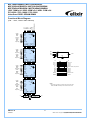
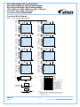
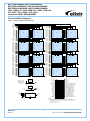
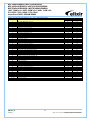
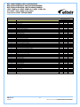
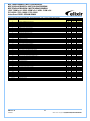
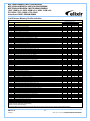
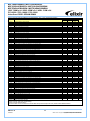
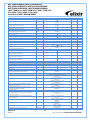
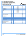
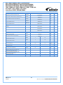
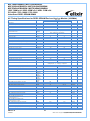
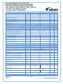
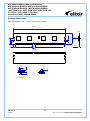
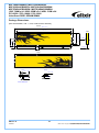
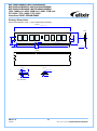
M2F1G64CBH4B5P/ M2F1G64CBH4B9P M2F(X)2G64CB88B7N / M2F(X)2G64CB88BHN M2F(X)4G64CB8HB5N / M2F(X)4G64CB8HB9N 1GB: 128M x 64 / 2GB: 256M x 64 / 4GB: 512M x 64 PC3-8500 / PC3-10600 / PC3-12800 Unbuffered DDR3 SDRAM DIMM Based on DDR3-1066/1333 128Mx16 (1GB) and DDR3-1066/1333/1600 256Mx8 (2GB/4GB) SDRAM B-Die Features •Performance: Speed Sort PC3-8500 PC3-10600 PC3-12800 -BE -CG -DG DIMM CAS Latency Unit 7 9 9 533 667 800 tck – Clock Cycle 1.875 1.5 1.25 ns fDQ – DQ Burst Frequency 1066 1333 1600 Mbps fck – Clock Frequency MHz • 240-Pin Dual In-Line Memory Module (UDIMM) •128Mx64 (1GB) / 256Mx64 (2GB) / 512Mx64 (4GB) DDR3 Unbuffered DIMM based on 256Mx8 DDR3 SDRAM B-Die devices. • Intended for 533MHz/667MHz/800MHz applications • Inputs and outputs are SSTL-15 compatible • VDD = VDDQ = 1.5V ±0.075V • SDRAMs have 8 internal banks for concurrent operation • Differential clock inputs • Data is read or written on both clock edges • DRAM DLL aligns DQ and DQS transitions with clock transitions. • Address and control signals are fully synchronous to positive clock edge • Nominal and Dynamtic On-Die Termination support • Halogen free product • Programmable Operation: - DIMM Latency: 6,7,8,9 - Burst Type: Sequential or Interleave - Burst Length: BC4, BL8 - Operation: Burst Read and Write • Two different termination values (Rtt_Nom & Rtt_WR) • 14/10/1 (row/column/rank) Addressing for 1GB • 15/10/1 (row/column/rank) Addressing for 2GB • 15/10/2 (row/column/rank) Addressing for 4GB • Extended operating temperature rage • Auto Self-Refresh option • Serial Presence Detect • Gold contacts •1GB: SDRAMs are in 96-ball BGA Package • 2GB: SDRAMs are in 78-ball BGA Package • 4GB: SDRAMs are in 78-ball BGA Package • RoHS compliance Description M2F1G64CBH4B5(9)P / M2F(X)2G64CB88B7N / M2F(X)4G64CB8HB5N / M2F(X)2G64CB88BHN / M2F(X)4G64CB8HB9N are 240-Pin Double Data Rate 3 (DDR3) Synchronous DRAM Unbuffered Dual In-Line Memory Module (UDIMM), organized as one rank of 128Mx64 (1GB) / 256Mx64 (2GB) and two ranks of 512Mx64 (4GB) high-speed memory array. Modules use four 128Mx16 (1GB) 96-ball BGA packaged devices, eight 256Mx8 (2GB) 78-ball BGA packaged devices and sixteen 256Mx8 (4GB) 78-ball BGA packaged devices. These DIMMs are manufactured using raw cards developed for broad industry use as reference designs. The use of these common design files minimizes electrical variation between suppliers. All Elixir DDR3 SDRAM DIMMs provide a high-performance, flexible 8-byte interface in a 5.25” long space-saving footprint. The DIMM is intended for use in applications operating of 533MHz/667MHz/800MHz clock speeds and achieves high-speed data transfer rates of 1066Mbps/1333Mbps/1600Mbps. Prior to any access operation, the device latency and burst/length/operation type must be programmed into the DIMM by address inputs A0-A13 (1GB) / A0-A14 (2GB/4GB) and I/O inputs BA0~BA2 using the mode register set cycle. The DIMM uses serial presence-detect implemented via a serial EEPROM using a standard IIC protocol. The first 128 bytes of SPD data are programmed and locked during module assembly. The remaining 128 bytes are available for use by the customer. REV 1.0 05/2010 1 © NANYA TECHNOLOGY CORPORATION NANYA reserves the right to change products and specifications without notice. M2F1G64CBH4B5P/ M2F1G64CBH4B9P M2F(X)2G64CB88B7N / M2F(X)2G64CB88BHN M2F(X)4G64CB8HB5N / M2F(X)4G64CB8HB9N 1GB: 128M x 64 / 2GB: 256M x 64 / 4GB: 512M x 64 PC3-8500 / PC3-10600 / PC3-12800 Unbuffered DDR3 SDRAM DIMM Ordering Information Part Number Speed Organization M2F1G64CBH4B5P-BE DDR3-1066 PC3-8500 533MHz (1.875ns @ CL = 7) M2F1G64CBH4B5P-CG DDR3-1333 PC3-10600 667MHz (1.5ns @ CL = 9) M2F2G64CB88B7N-BE DDR3-1066 PC3-8500 533MHz (1.875ns @ CL = 7) M2F2G64CB88B7N-CG DDR3-1333 PC3-10600 667MHz (1.5ns @ CL = 9) M2X2G64CB88B7N-DG DDR3-1600 PC3-12800 800MHz (1.25ns @ CL=9) M2F4G64CB8HB5N-BE DDR3-1066 PC3-8500 533MHz (1.875ns @ CL = 7) M2F4G64CB8HB5N-CG DDR3-1333 PC3-10600 667MHz (1.5ns @ CL = 9) M2X4G64CB8HB5N-DG DDR3-1600 PC3-12800 800MHz (1.25ns @ CL=9) M2F1G64CBH4B9P-BE DDR3-1066 PC3-8500 533MHz (1.875ns @ CL = 7) M2F1G64CBH4B9P-CG DDR3-1333 PC3-10600 667MHz (1.5ns @ CL = 9) M2F2G64CB88BHN-BE DDR3-1066 PC3-8500 533MHz (1.875ns @ CL = 7) M2F2G64CB88BHN-CG DDR3-1333 PC3-10600 667MHz (1.5ns @ CL = 9) M2X2G64CB88BHN-DG DDR3-1600 PC3-12800 800MHz (1.25ns @ CL=9) M2F4G64CB8HB9N-BE DDR3-1066 PC3-8500 533MHz (1.875ns @ CL = 7) M2F4G64CB8HB9N-CG DDR3-1333 PC3-10600 667MHz (1.5ns @ CL = 9) M2X4G64CB8HB9N-DG DDR3-1600 PC3-12800 800MHz (1.25ns @ CL=9) Power Leads 1.5V Gold Note 128Mx64 256Mx64 512Mx64 128Mx64 256Mx64 512Mx64 Pin Description Pin Name Description Pin Name Description CK0, CK1 Clock Inputs, positive line DQ0-DQ63 , Clock Inputs, negative line DQS0-DQS8 Data strobes Clock Enable - Data strobes complement CKE0, CKE1 Row Address Strobe Column Address Strobe , DM0-DM8 Data input/output Data Masks Temperature event pin Write Enable Reset pin Chip Selects VREFDQ , VREFCA A0-A9, A11, A13-A15 Address Inputs A10/AP Address Input/Auto-Precharge A12/ Address Input/Burst Chop VDDSPD Input/Output Reference SPD and Temp sensor power SA0, SA1 Serial Presence Detect Address Inputs Vtt Termination voltage BA0-BA2 SDRAM Bank Address Inputs VSS Ground ODT0, ODT1 Active termination control lines VDD Core and I/O power SCL Serial Presence Detect Clock Input NC No Connect SDA Serial Presence Detect Data input/output REV 1.0 05/2010 2 © NANYA TECHNOLOGY CORPORATION NANYA reserves the right to change products and specifications without notice. M2F1G64CBH4B5P/ M2F1G64CBH4B9P M2F(X)2G64CB88B7N / M2F(X)2G64CB88BHN M2F(X)4G64CB8HB5N / M2F(X)4G64CB8HB9N 1GB: 128M x 64 / 2GB: 256M x 64 / 4GB: 512M x 64 PC3-8500 / PC3-10600 / PC3-12800 Unbuffered DDR3 SDRAM DIMM DDR3 SDRAM Pin Assignment Pin 1 Front Pin VREFDQ 121 Back Pin Front Pin Back Pin Front Pin Back Pin Front Pin Back VSS 31 DQ25 151 VSS 61 A2 181 A1 91 DQ41 211 VSS DM5, 212 DQS14, TDQS14 NC, 213 , 2 VSS 122 DQ4 32 VSS 152 DM3,DQS12,T DQS12 62 VDD 182 VDD 92 VSS 3 DQ0 123 DQ5 33 153 NC, 63 CK1,NC 183 VDD 93 4 DQ1 124 VSS 34 DQS3 154 VSS 64 ,NC 184 CK0 94 DQS5 214 VSS 35 VSS 155 DQ30 65 VDD 185 95 VSS 215 DQ46 36 DQ26 156 DQ31 66 VDD 186 VDD 96 DQ42 216 DQ47 37 DQ27 157 VSS 67 VREFCA 187 , NC 97 DQ43 217 VSS 188 A0 98 VSS 218 DQ52 5 VSS 125 6 126 7 DQS0 127 DM0,DQS9, TDQS9 NC, VSS 158 CB4,NC 68 PAR_IN, NC 39 CB0,NC 159 CB5,NC 69 VDD 189 VDD 99 DQ48 219 DQ53 40 CB1,NC 160 VSS 70 A10/AP 190 BA1 100 DQ49 220 VSS 8 VSS 128 DQ6 38 9 DQ2 129 DQ7 10 DQ3 130 VSS VSS DM6, 221 DQS15, TDQS15 NC, 222 , 11 VSS 131 DQ12 41 VSS 161 DM8,DQS17, TDQS17,NC 71 BA0 191 VDD 101 VSS 12 DQ8 132 DQ13 42 162 NC,, , 72 VDD 192 102 13 DQ9 133 VSS 43 DQS8 163 VSS 73 193 103 DQS6 223 VSS 44 VSS 164 CB6,NC 74 194 VDD 104 VSS 224 DQ54 45 CB2,NC 165 CB7,NC 75 VDD 195 ODT0 105 DQ50 225 DQ55 VSS 46 CB3,NC 166 VSS 76 ,NC 196 A13 106 DQ51 226 VSS 137 DQ14 47 VSS 167 NC(TEST) 77 ODT1,NC 197 VDD 107 VSS 227 DQ60 18 DQ10 138 DQ15 48 VTT,NC 168 78 VDD 198 ,NC 108 DQ56 228 DQ61 19 DQ11 139 VSS 49 VTT,NC 169 CKE1/NC 79 ,NC 199 VSS 109 DQ57 229 VSS 140 DQ20 50 CKE0 170 VDD 80 VSS 200 DQ36 110 VSS 230 21 DQ16 141 DQ21 51 VDD 171 A15,NC 81 DQ32 201 DQ37 111 22 DQ17 142 VSS 52 BA2 172 A14 82 DQ33 202 VSS 112 DQS7 232 VSS VSS 233 DQ62 DQ58 234 DQ63 DQ59 235 VSS DM1, DQS10, 134 TDQS10 NC, 135 14 VSS 15 16 DQS1 136 17 VSS 20 VSS 23 VSS 143 DM2, DQS11, TDQS11 53 ERR_OUT 173 ,NC VDD 83 VSS DM4, 203 DQS13, 113 TDQS13 NC, 204 , 114 24 144 NC, 54 VDD 174 A12/ 84 25 DQS2 145 VSS 55 A11 175 A9 85 DQS4 205 VSS 115 26 VSS DM7, DQS16, TDQS16 NC, 231 , 146 DQ22 56 A7 176 VDD 86 VSS 206 DQ38 116 VSS 236 VDDSPD 27 DQ18 147 DQ23 57 VDD 177 A8 87 DQ34 207 DQ39 117 SA0 237 SA1 28 DQ19 148 VSS 58 A5 178 A6 88 DQ35 208 VSS 118 SCL 238 SDA 149 DQ28 59 A4 179 VDD 89 VSS 209 DQ44 119 SA2 239 VSS DQ24 150 DQ29 60 VDD 180 A3 90 DQ40 210 DQ45 120 VTT 240 VTT 29 30 VSS Note: CK1, , CKE1, and ODT1 are for 4GB modules only. REV 1.0 05/2010 3 © NANYA TECHNOLOGY CORPORATION NANYA reserves the right to change products and specifications without notice. M2F1G64CBH4B5P/ M2F1G64CBH4B9P M2F(X)2G64CB88B7N / M2F(X)2G64CB88BHN M2F(X)4G64CB8HB5N / M2F(X)4G64CB8HB9N 1GB: 128M x 64 / 2GB: 256M x 64 / 4GB: 512M x 64 PC3-8500 / PC3-10600 / PC3-12800 Unbuffered DDR3 SDRAM DIMM Input/Output Functional Description Symbol Type Polarity Function CK0, CK1 , Input Cross point The system clock inputs. All address and command lines are sampled on the cross point of the rising edge of CK and falling edge of . A Delay Locked Loop (DLL) circuit is driven from the clock inputs and output timing for read operations is synchronized to the input clock. CKE0, CKE1 Input Active High Activates the DDR3 SDRAM CK signal when high and deactivates the CK signal when low. By deactivating the clocks, CKE low initiates the Power Down mode or the Self Refresh mode. , Input Active Low Enables the associated DDR3 SDRAM command decoder when low and disables the command decoder when high. When the command decoder is disabled, new commands are ignored but previous operations continue, Rank 0 is selected by ; Rank 1 is selected by , , Input Active Low When sampled at the positive rising edge of CK and falling edge of , signals , , define the operation to be executed by the SDRAM. ODT0, ODT1 Input Active High Asserts on-die termination for DQ, DM, DQS, and signals if enabled via the DDR3 SDRAM mode register. DM0 – DM8 Input Active High The data write masks, associated with one data byte. In Write mode, DM operates as a byte mask by allowing input data to be written if it is low but blocks the write operation if it is high. In Read mode, DM lines have no effect. The data strobes, associated with one data byte, sourced with data transfers. In Write mode, the data strobe is sourced by the controller and is centered in the data window. In Read mode, the data strobe is sourced by the DDR3 SDRAM and is sent at the leading edge of the data window. signals are complements, and timing is relative to the cross point of respective DQS and . If the module is to be operated in single ended strobe mode, all signals must be tied on the system board to VSS and DDR3 SDRAM mode registers programmed appropriately. DQS0 – DQS8 – I/O Cross point BA0, BA1, BA2 Input - Selects which DDR3 SDRAM internal bank of four or eight is activated. Input - During a Bank Activate command cycle, defines the row address when sampled at the cross point of the rising edge of CK and falling edge of . During a Read or Write command cycle, defines the column address when sampled at the cross point of the rising edge of CK and falling edge of . In addition to the column address, AP is used to invoke autoprecharge operation at the end of the burst read or write cycle. If AP is high, autoprecharge is selected and BA0-BAn defines the bank to be precharged. If AP is low, autoprecharge is disabled. During a Precharge command cycle, AP is used in conjunction with BA0-BAn to control which bank(s) to precharge. If AP is high, all banks will be precharged regardless of the state of BA0-BAn inputs. If AP is low, then BA0-BAn are used to define which bank to precharge. A0 – A9 A10/AP A11 A12/ A13-A15 DQ0 – DQ63 Input - Data Input/Output pins. VDD, VDDSPD, VSS Supply - Power supplies for core, I/O, Serial Presence Detect, Temp sensor, and ground for the module. VREFDQ, VREFCA Supply - Reference voltage for SSTL15 inputs SDA I/O - This is a bidirectional pin used to transfer data into or out of the SPD EEPROM and temp sensor. A resistor must be connected from the SDA bus line to VDDSPD on the system planar to act as a pull up. SCL Input - This signal is used to clock data into and out of the SPD EEPROM and Temp sensor. SA0 – SA2 Input - Address pins used to select the Serial Presence Detect and Temp sensor base address. Output - The pin is reserved for use to flag critical module temperature. Input - This signal resets the DDR3 SDRAM REV 1.0 05/2010 4 © NANYA TECHNOLOGY CORPORATION NANYA reserves the right to change products and specifications without notice. M2F1G64CBH4B5P/ M2F1G64CBH4B9P M2F(X)2G64CB88B7N / M2F(X)2G64CB88BHN M2F(X)4G64CB8HB5N / M2F(X)4G64CB8HB9N 1GB: 128M x 64 / 2GB: 256M x 64 / 4GB: 512M x 64 PC3-8500 / PC3-10600 / PC3-12800 Unbuffered DDR3 SDRAM DIMM CK0 CKE0 ODT0 A[0:13]/BA[0:2] Functional Block Diagram [1GB – 1 Rank, 128Mx16 DDR3 SDRAMs] LDQS L LDM DQ[0:7] UDQS UDM DQ[8:15] DQS2 DM2 DQ[16:23] DQS3 DM3 DQ[24:31] LDQS L LDM DQ[0:7] UDQS UDM DQ[8:15] 240ohm +/-1% ZQ D0 CK CKE ODT A[0:13]/BA[0:2] DQS0 DM0 DQ[0:7] DQS1 DM1 DQ[8:15] 240ohm +/-1% ZQ SCL D1 CK CKE ODT A[0:13]/BA[0:2] LDQS L LDM DQ[0:7] UDQS UDM DQ[8:15] DQS6 DM6 DQ[48:55] DQS7 DM7 DQ[56:63] LDQS L LDM DQ[0:7] UDQS UDM DQ[8:15] Vtt VDDSPD VREFCA VREFDQ VDD VSS CK0 240ohm +/-1% ZQ D2 CK1 CK CKE ODT A[0:13]/BA[0:2] DQS4 DM4 DQ[32:39] DQS5 DM5 DQ[40:47] SCL A0 A1 A2 SA0 SA1 SPD SDA WP Vtt SPD / TS D0-D7 D0-D7 D0-D7 D0-D7, SPD, Temp sensor D0-D3 D0-D3 D4-D7 D4-D7 Temp Sensor D0-D7 240ohm +/-1% ZQ Notes : D3 CK CKE ODT A[0:13]/BA[0:2] 1. DQ wiring may differ from that shown however, DQ, DM, DQS, and relationships are maintained as shown. Vtt Vtt VDD REV 1.0 05/2010 5 © NANYA TECHNOLOGY CORPORATION NANYA reserves the right to change products and specifications without notice. M2F1G64CBH4B5P/ M2F1G64CBH4B9P M2F(X)2G64CB88B7N / M2F(X)2G64CB88BHN M2F(X)4G64CB8HB5N / M2F(X)4G64CB8HB9N 1GB: 128M x 64 / 2GB: 256M x 64 / 4GB: 512M x 64 PC3-8500 / PC3-10600 / PC3-12800 Unbuffered DDR3 SDRAM DIMM Functional Block Diagram [2GB – 1 Rank, 256Mx8 DDR3 SDRAMs] DQS0 DM0 DQS4 DM4 DM DQ0 DQ1 DQ2 DQ3 DQ4 DQ5 DQ6 DQ7 I/O I/O I/O I/O I/O I/O I/O I/O DQS 0 1 2 3 4 5 6 7 DM DQ32 DQ33 DQ34 DQ35 DQ36 DQ37 DQ38 DQ39 D0 ZQ DQS1 DM1 I/O I/O I/O I/O I/O I/O I/O I/O DQS 0 1 2 3 4 5 6 7 DM DQ40 DQ41 DQ42 DQ43 DQ44 DQ45 DQ46 DQ47 D1 ZQ DQS2 DM2 I/O I/O I/O I/O I/O I/O I/O I/O DQS 0 1 2 3 4 5 6 7 SA0 SA1 D2 ZQ I/O I/O I/O I/O I/O I/O I/O I/O DQS 0 1 2 3 4 5 6 7 SCL A0 A1 A2 D3 ZQ SPD SDA WP CKE0, A[13:0], , , , ODT0, BA[2:0], VTT DDR3 SDRAM CK 05/2010 D4 ZQ 0 1 2 3 4 5 6 7 I/O I/O I/O I/O I/O I/O I/O I/O DQS D5 ZQ 0 1 2 3 4 5 6 7 DM DQ56 DQ57 DQ58 DQ59 DQ60 DQ61 DQ62 DQ63 DDR3 SDRAM REV 1.0 DQS D6 ZQ DQS7 DM7 DM SCL I/O I/O I/O I/O I/O I/O I/O I/O DM DQ48 DQ49 DQ50 DQ51 DQ52 DQ53 DQ54 DQ55 DQS3 DM3 DQ24 DQ25 DQ26 DQ27 DQ28 DQ29 DQ30 DQ31 DQS DQS6 DM6 DM DQ16 DQ17 DQ18 DQ19 DQ20 DQ21 DQ22 DQ23 0 1 2 3 4 5 6 7 DQS5 DM5 DM DQ8 DQ9 DQ10 DQ11 DQ12 DQ13 DQ14 DQ15 I/O I/O I/O I/O I/O I/O I/O I/O VDD VDDSPD VDD/VDDQ VREFDQ VSS VREFCA BA0-BA2 A0-A13 CKE0 ODT0 CK0 I/O I/O I/O I/O I/O I/O I/O I/O 0 1 2 3 4 5 6 7 DQS D7 ZQ SPD D0-D7 D0-D7 D0-D7 D0-D7 BA0-BA2: SDRAMs D0-D7 A0-A13: SDRAMs D0-D7 : SDRAMs D0-D7 : SDRAMs D0-D7 CKE: SDRAMs D0-D7 : SDRAMs D0-D7 ODT: SDRAMs D0-D7 CK: SDRAMs D0-D7 : SDRAMs D0-D7 : SDRAMs D0-D7 Notes : 1. DQ-to-I/O wiring is shown as recommended but may be changed. 2. DQ/DQS/DQS/ODT/DM/CKE/S relationships must be maintained as shown. 3. For each DRAM, a unique ZQ resistor is connected to ground. The ZQ resistor is 240Ω±1%. 4. One SPD exists per module. 6 © NANYA TECHNOLOGY CORPORATION NANYA reserves the right to change products and specifications without notice. M2F1G64CBH4B5P/ M2F1G64CBH4B9P M2F(X)2G64CB88B7N / M2F(X)2G64CB88BHN M2F(X)4G64CB8HB5N / M2F(X)4G64CB8HB9N 1GB: 128M x 64 / 2GB: 256M x 64 / 4GB: 512M x 64 PC3-8500 / PC3-10600 / PC3-12800 Unbuffered DDR3 SDRAM DIMM Functional Block Diagram [4GB – 2 Ranks, 256Mx8 DDR3 SDRAMs] DQS0 DM0 DQ0 DQ1 DQ2 DQ3 DQ4 DQ5 DQ6 DQ7 DQS4 DM4 DM CS DQS I/O 0 I/O 1 I/O 2 I/O 3 D0 I/O 4 I/O 5 I/O 6 I/O 7 DQS DM CS DQS I/O 0 I/O 1 I/O 2 I/O 3 D8 I/O 4 I/O 5 I/O 6 I/O 7 ZQ DQS DQ32 DQ33 DQ34 DQ35 DQ36 DQ37 DQ38 DQ39 ZQ DQS1 DM1 DQ8 DQ9 DQ10 DQ11 DQ12 DQ13 DQ14 DQ15 DM CS DQS I/O 0 I/O 1 I/O 2 I/O 3 D1 I/O 4 I/O 5 I/O 6 I/O 7 DQS DM CS DQS I/O 0 I/O 1 I/O 2 I/O 3 D9 I/O 4 I/O 5 I/O 6 I/O 7 ZQ DQS DQ40 DQ41 DQ42 DQ43 DQ44 DQ45 DQ46 DQ47 ZQ DM I/O 0 I/O 1 I/O 2 I/O 3 I/O 4 I/O 5 I/O 6 I/O 7 CS DQS DQS D4 ZQ DM CS DQS I/O 0 I/O 1 I/O 2 I/O 3 D12 I/O 4 I/O 5 I/O 6 I/O 7 DQS DM CS DQS I/O 0 I/O 1 I/O 2 I/O 3 D13 I/O 4 I/O 5 I/O 6 I/O 7 DQS DM I/O 0 I/O 1 I/O 2 I/O 3 I/O 4 I/O 5 I/O 6 I/O 7 DQS ZQ DQS DQS D5 ZQ ZQ DQS6 DQS6 DM6 DM CS DQS I/O 0 I/O 1 I/O 2 I/O 3 D2 I/O 4 I/O 5 I/O 6 I/O 7 DQS DM CS DQS I/O 0 I/O 1 I/O 2 I/O 3 D10 I/O 4 I/O 5 I/O 6 I/O 7 ZQ DQS DQ48 DQ49 DQ50 DQ51 DQ52 DQ53 DQ54 DQ55 ZQ DQS3 DM3 DQ24 DQ25 DQ26 DQ27 DQ28 DQ29 DQ30 DQ31 CS DQS5 DM5 DQS2 DM2 DQ16 DQ17 DQ18 DQ19 DQ20 DQ21 DQ22 DQ23 DM I/O 0 I/O 1 I/O 2 I/O 3 I/O 4 I/O 5 I/O 6 I/O 7 DM CS DQS I/O 0 I/O 1 I/O 2 I/O 3 D6 I/O 4 I/O 5 I/O 6 I/O 7 DQS DM CS DQS I/O 0 I/O 1 I/O 2 I/O 3 D7 I/O 4 I/O 5 I/O 6 I/O 7 DQS ZQ CS DQS D14 ZQ DQS7 DM7 DM CS DQS I/O 0 I/O 1 I/O 2 I/O 3 D3 I/O 4 I/O 5 I/O 6 I/O 7 DQS DM I/O 0 I/O 1 I/O 2 I/O 3 I/O 4 I/O 5 I/O 6 I/O 7 ZQ CS DQS DQS DQ56 DQ57 DQ58 DQ59 DQ60 DQ61 DQ62 DQ63 D11 ZQ VDDSPD VDD/VDDQ VREFDQ VSS VREFCA BA0-BA2 A0-A13 CKE0 CKE1 ODT0 ODT1 CK0 CK1 DDR3 SDRAM CKE[1:0], A[13:0], , , , ODT[1:0], BA[2:0], [1:0] VTT DDR3 SDRAM CK SCL SA0 SA1 VDD SCL A0 A1 A2 SPD SDA WP ZQ DM CS DQS I/O 0 I/O 1 I/O 2 I/O 3 D15 I/O 4 I/O 5 I/O 6 I/O 7 DQS ZQ SPD D0-D15 D0-D15 D0-D15 D0-D15 BA0-BA2: SDRAMs D0-D15 A0-A13: SDRAMs D0-D15 : SDRAMs D0-D15 : SDRAMs D0-D15 : SDRAMs D0-D15 CKE: SDRAMs D0-D7 CKE: SDRAMs D8-D15 ODT: SDRAMs D0-D7 ODT: SDRAMs D8-D15 CK: SDRAMs D0-D7 : SDRAMs D0-D7 CK: SDRAMs D8-D15 : SDRAMs D8-D15 : SDRAMs D8-D15 Notes : 1. DQ-to-I/O wiring is shown as recommended but may be changed. 2. DQ/DQS/DQS/ODT/DM/CKE/S relationships must be maintained as shown. 3. For each DRAM, a unique ZQ resistor is connected to ground. The ZQ resistor is 240Ω±1%. 4. One SPD exists per module. REV 1.0 05/2010 7 © NANYA TECHNOLOGY CORPORATION NANYA reserves the right to change products and specifications without notice. M2F1G64CBH4B5P/ M2F1G64CBH4B9P M2F(X)2G64CB88B7N / M2F(X)2G64CB88BHN M2F(X)4G64CB8HB5N / M2F(X)4G64CB8HB9N 1GB: 128M x 64 / 2GB: 256M x 64 / 4GB: 512M x 64 PC3-8500 / PC3-10600 / PC3-12800 Unbuffered DDR3 SDRAM DIMM Serial Presence Detect [M2F1G64CBH4B5(9)P ,1GB – 1 Rank, 128Mx16 DDR3 SDRAMs] Byte 0 1 2 3 4 5 6 7 8 9 10 11 12 13 14 15 16 17 18 19 20 21 22 23 24 25 26 27 28 29 30 31 32 33 60 61 62 63 117 118 119-121 126 127 128-145 146 147 150-175 176-255 REV 1.0 05/2010 Serial PD Data Entry (Hex.) -BE -CG 92 92 10 10 0B 0B 02 02 03 03 11 11 00 00 02 02 03 03 52 52 01 01 08 08 0F 0C 00 00 1C 3C 00 00 69 69 78 78 69 69 50 3C 69 69 11 11 2C 20 95 89 00 00 05 05 3C 3C 3C 3C 01 01 90 68 83 83 05 05 00 00 00 00 0F 0F 01 01 02 02 00 00 83 83 0B 0B --73 0D F7 2E ----------- Description CRC range, EEPROM bytes, bytes used SPD revision DRAM device type Module type (form factor) SDRAM Device density and banks SDRAM device row and column count Module minimum nominal voltage Module ranks and device DQ count ECC tag and module memory Bus width Fine timebase dividend/divisor (in ps) Medium timebase dividend Medium timebase divisor Minimum SDRAM cycle time (tCKmin) Reserved CAS latencies supported CAS latencies supported Minimum CAS latency time (tAAmin) Minimum write recovery time (tWRmin) Minimum CAS-to-CAS delay (tRCDmin) Minimum Row Active to Row Active delay (tRRDmin) Minimum row Precharge delay (tRPmin) Upper nibble for tRAS and tRC Minimum Active-to-Precharge delay (tRASmin) Minimum Active-to-Active/Refresh delay (tRCmin) Minimum refresh recovery delay (tRFCmin) LSB Minimum refresh recovery delay (tRFCmin) MSB Minimum internal Write-to-Read command delay (tWTRmin) Minimum internal Read-to-Precharge command delay (tRTPmin) Minimum four active window delay (tFAWmin) LSB Minimum four active window delay (tFAWmin) MSB SDRAM device output drivers supported SDRAM device thermal and refresh options Module Thermal Sensor SDRAM Device Type Module height (nominal) Module thickness (Max) Raw Card ID reference DRAM address mapping edge connector Module manufacture ID Module manufacture ID Module manufacturer Information CRC CRC Module part number Module die revision Module PCB revision Manufacturer reserved Intel Extreme Memory Profile(XMP) 8 © NANYA TECHNOLOGY CORPORATION NANYA reserves the right to change products and specifications without notice. M2F1G64CBH4B5P/ M2F1G64CBH4B9P M2F(X)2G64CB88B7N / M2F(X)2G64CB88BHN M2F(X)4G64CB8HB5N / M2F(X)4G64CB8HB9N 1GB: 128M x 64 / 2GB: 256M x 64 / 4GB: 512M x 64 PC3-8500 / PC3-10600 / PC3-12800 Unbuffered DDR3 SDRAM DIMM Serial Presence Detect [M2F(X)2G64CB88B7N / M2F(X)2G64CB88BHN , 2GB – 1 Rank, 256Mx8 DDR3 SDRAMs] Byte 0 1 2 3 4 5 6 7 8 9 10 11 12 13 14 15 16 17 18 19 20 21 22 23 24 25 26 27 28 29 30 31 32 33 60 61 62 63 117 118 119-121 126 127 128-145 146 147 150-175 176-255 REV 1.0 05/2010 Serial PD Data Entry (Hex.) -BE -CG -DG 92 92 93 10 10 10 0B 0B 0B 02 02 02 03 03 03 19 19 19 00 00 00 01 01 01 03 03 03 52 52 52 01 01 01 08 08 08 0F 0C 0A 00 00 00 1C 3C 7E 00 00 00 69 69 64 78 78 78 69 69 64 3C 30 30 69 69 64 11 11 11 2C 20 18 95 89 7C 00 00 00 05 05 05 3C 3C 3C 3C 3C 3C 01 00 00 2C F0 F0 83 83 83 05 05 05 00 00 00 00 00 00 0F 0F 0F 01 01 01 01 01 01 01 01 01 83 83 83 0B 0B 0B ---47 05 FB 29 80 32 ---------------- Description CRC range, EEPROM bytes, bytes used SPD revision DRAM device type Module type (form factor) SDRAM Device density and banks SDRAM device row and column count Module minimum nominal voltage Module ranks and device DQ count ECC tag and module memory Bus width Fine timebase dividend/divisor (in ps) Medium timebase dividend Medium timebase divisor Minimum SDRAM cycle time (tCKmin) Reserved CAS latencies supported CAS latencies supported Minimum CAS latency time (tAAmin) Minimum write recovery time (tWRmin) Minimum CAS-to-CAS delay (tRCDmin) Minimum Row Active to Row Active delay (tRRDmin) Minimum row Precharge delay (tRPmin) Upper nibble for tRAS and tRC Minimum Active-to-Precharge delay (tRASmin) Minimum Active-to-Active/Refresh delay (tRCmin) Minimum refresh recovery delay (tRFCmin) LSB Minimum refresh recovery delay (tRFCmin) MSB Minimum internal Write-to-Read command delay (tWTRmin) Minimum internal Read-to-Precharge command delay (tRTPmin) Minimum four active window delay (tFAWmin) LSB Minimum four active window delay (tFAWmin) MSB SDRAM device output drivers supported SDRAM device thermal and refresh options Module Thermal Sensor SDRAM Device Type Module height (nominal) Module thickness (Max) Raw Card ID reference DRAM address mapping edge connector Module manufacture ID Module manufacture ID Module manufacturer Information CRC CRC Module part number Module die revision Module PCB revision Manufacturer reserved Intel Extreme Memory Profile(XMP) 9 © NANYA TECHNOLOGY CORPORATION NANYA reserves the right to change products and specifications without notice. M2F1G64CBH4B5P/ M2F1G64CBH4B9P M2F(X)2G64CB88B7N / M2F(X)2G64CB88BHN M2F(X)4G64CB8HB5N / M2F(X)4G64CB8HB9N 1GB: 128M x 64 / 2GB: 256M x 64 / 4GB: 512M x 64 PC3-8500 / PC3-10600 / PC3-12800 Unbuffered DDR3 SDRAM DIMM Serial Presence Detect [M2F(X)4G64CB8HB5N / M2F(X)4G64CB8HB9N , 4GB – 2 Ranks, 256Mx8 DDR3 SDRAMs] Byte 0 1 2 3 4 5 6 7 8 9 10 11 12 13 14 15 16 17 18 19 20 21 22 23 24 25 26 27 28 29 30 31 32 33 60 61 62 63 117 118 119-121 126 127 128-145 146 147 150-175 176-255 REV 1.0 05/2010 Serial PD Data Entry (Hex.) -BE -CG -DG 92 92 93 10 10 10 0B 0B 0B 02 02 02 03 03 03 19 19 19 00 00 00 09 09 09 03 03 03 52 52 52 01 01 01 08 08 08 0F 0C 0A 00 00 00 1C 3C 7E 00 00 00 69 69 64 78 78 78 69 69 64 3C 30 30 69 69 64 11 11 11 2C 20 18 95 89 7C 00 00 00 05 05 05 3C 3C 3C 3C 3C 3C 01 00 00 2C F0 F0 83 83 83 05 05 05 00 00 00 00 00 00 0F 0F 0F 11 11 11 01 01 01 01 01 01 83 83 83 0B 0B 0B ---68 2A D4 59 F0 42 ---------------- Description CRC range, EEPROM bytes, bytes used SPD revision DRAM device type Module type (form factor) SDRAM Device density and banks SDRAM device row and column count Module minimum nominal voltage Module ranks and device DQ count ECC tag and module memory Bus width Fine timebase dividend/divisor (in ps) Medium timebase dividend Medium timebase divisor Minimum SDRAM cycle time (tCKmin) Reserved CAS latencies supported CAS latencies supported Minimum CAS latency time (tAAmin) Minimum write recovery time (tWRmin) Minimum CAS-to-CAS delay (tRCDmin) Minimum Row Active to Row Active delay (tRRDmin) Minimum row Precharge delay (tRPmin) Upper nibble for tRAS and tRC Minimum Active-to-Precharge delay (tRASmin) Minimum Active-to-Active/Refresh delay (tRCmin) Minimum refresh recovery delay (tRFCmin) LSB Minimum refresh recovery delay (tRFCmin) MSB Minimum internal Write-to-Read command delay (tWTRmin) Minimum internal Read-to-Precharge command delay (tRTPmin) Minimum four active window delay (tFAWmin) LSB Minimum four active window delay (tFAWmin) MSB SDRAM device output drivers supported SDRAM device thermal and refresh options Module Thermal Sensor SDRAM Device Type Module height (nominal) Module thickness (Max) Raw Card ID reference DRAM address mapping edge connector Module manufacture ID Module manufacture ID Module manufacturer Information CRC CRC Module part number Module die revision Module PCB revision Manufacturer reserved Intel Extreme Memory Profile(XMP) 10 © NANYA TECHNOLOGY CORPORATION NANYA reserves the right to change products and specifications without notice. M2F1G64CBH4B5P/ M2F1G64CBH4B9P M2F(X)2G64CB88B7N / M2F(X)2G64CB88BHN M2F(X)4G64CB8HB5N / M2F(X)4G64CB8HB9N 1GB: 128M x 64 / 2GB: 256M x 64 / 4GB: 512M x 64 PC3-8500 / PC3-10600 / PC3-12800 Unbuffered DDR3 SDRAM DIMM Intel Extreme Memory Profile definition Serial Presence Detect [M2X2G64CB88B7N / M2X2G64CB88BHN , 2GB – 1 Rank, 256Mx8 DDR3 SDRAMs] Byte 176-177 178 179 180 181 182 183 184 185 186 187 188 189 190 191 192 193 194 195 196 197 198 199 200 201 202 203 204 205 206 207 208 209 210 211-218 219 220 221 222 223 224 225 226 227 228 229 230 231 232 233 234 235 236 237 238 239 240 241 242 243 244 245 246-253 254 Serial PD Data Entry (Hex.) -BE -CG -DG --OC4A --07 --12 --01 --08 --01 --0E --00 --2D --0A --5A --24 --00 --5A --5A --5A --78 --11 --18 --72 --20 --00 --00 --05 --3C --30 --00 --F0 --3C --00 --00 --10 --00 --2D -----00 --2D --0F --A5 --84 --00 --A5 --A5 --A5 --D2 --21 --EA --8F --37 --00 --C0 --08 --69 --54 --01 --A4 --69 --00 --00 --1C --00 --2D ------- Description Intel Extreme Memory Profile ID String Intel Extreme Memory Profile Organization Type Intel Extreme Memory Profile Revision Medium Timebase Dividend for Profile 1 Medium Timebase Divisor for Profile 1 Medium Timebase Dividend for Profile 2 Medium Timebase Divisor for Profile 2 RSVD 1 Module VDD Voltage Level for Profile 1 (Certified Settings) SDRAM Minimum Cycle Time (tCKmin) Minimum CAS Latency Time (tAAmin) CAS Latencies Supported, Least Significant Byte (CL MASK) CAS Latencies Supported, Most Significant Byte (CL MASK) Minimum CAS Write Latency Time (tCWLmin) Minimum Row Precharge Time (tRPmin) Minimum RAS# to CAS# Delay Time (tRCDmin) Minimum Write Recovery Time (tWRmin) Upper Nibbles for tRAS and tRC Minimum Active to Precharge Time (tRASmin), Least Significant Byte Minimum Active to Active/Refresh Time (tRCmin), Least Significant Byte Maximum tREFI Time (Average Periodic Refresh Interval) – LSB Maximum tREFI Time (Average Periodic Refresh Interval) - MSB Minimum Refresh Recovery Time (tRFCmin), Least Significant Byte Minimum Refresh Recovery Time (tRFCmin), Most Significant Byte Minimum Internal Read to Precharge Command Delay Time (tRTPmin) Minimum Row Active to Row Active Delay Time (tRRDmin) Upper Nibble for tFAW Minimum Four Activate Window Delay Time (tFAWmin) Minimum Internal Write to Read Command Delay Time (tWTRmin) Write to Read & Read to Write CMD Turn-around Time Pull-in Back to Back CMD Turn-around Time Pull-in System ADD/CMD Rate (1N or 2N mode) Auto Self Refresh Performance (Sub 1x Refresh and IDD6 Impacts) Memory Controller Voltage Level for Profile 1 RSVD Vendor Personality Byte for Profile 1 - RSVD Module VDD Voltage Level for Profile 2 (Extreme Settings) SDRAM Minimum Cycle Time (tCKmin) Minimum CAS Latency Time (tAAmin) CAS Latencies Supported, Least Significant Byte (CL MASK) CAS Latencies Supported, Most Significant Byte (CL MASK) Minimum CAS Write Latency Time (tCWLmin) Minimum Row Precharge Time (tRPmin) Minimum RAS# to CAS# Delay Time (tRCDmin) Minimum Write Recovery Time (tWRmin) Upper Nibbles for tRAS and tRC Minimum Active to Precharge Time (tRASmin), Least Significant Byte Minimum Active to Active/Refresh Time (tRCmin), Least Significant Byte Maximum tREFI Time (Average Periodic Refresh Interval) - LSB Maximum tREFI Time (Average Periodic Refresh Interval) - MSB Minimum Refresh Recovery Time (tRFCmin), Least Significant Byte Minimum Refresh Recovery Time (tRFCmin), Most Significant Byte Minimum Internal Read to Precharge Command Delay Time (tRTPmin) Minimum Row Active to Row Active Delay Time (tRRDmin) Upper Nibble for tFAW Minimum Four Activate Window Delay Time (tFAWmin) Minimum Internal Write to Read Command Delay Time (tWTRmin) Write to Read & Read to Write CMD Turn-around Time Pull-in Back to Back CMD Turn-around Time Pull-in System ADD/CMD Rate (1N or 2N mode) Auto Self Refresh Performance (Sub 1x Refresh and IDD6 Impacts) Memory Controller Voltage Level for Profile RSVD Vendor Personality Byte for Profile 2 - RSVD Note 1 1 1 1 1 1 2,4 2,4 2,4 2,4 2 2,4 2,4 2,4 2,4 2,4 2,4 2 2 2,4 2,4 2,4 2,4 2,4 2,4 2,4 2 2 2 2 2 2 3,4 3,4 3,4 3,4 3,4 3 3,4 3,4 3,4 3,4 3,4 3,4 3 3 3,4 3,4 3,4 3,4 3,4 3,4 3,4 3 3 3 3 3 3 3 3 1. Global Parameters used across all profiles 2. Utilized for Profile 1 (Enthusiast / Certified Settings) 3. Utilized for Profile 2 (Extreme Settings) 4. Parameter utilized in the same fashion as the standard DDR3 SPD byte with the exception that it may exceed the DDRx SDRAM datasheet REV 1.0 05/2010 11 © NANYA TECHNOLOGY CORPORATION NANYA reserves the right to change products and specifications without notice. M2F1G64CBH4B5P/ M2F1G64CBH4B9P M2F(X)2G64CB88B7N / M2F(X)2G64CB88BHN M2F(X)4G64CB8HB5N / M2F(X)4G64CB8HB9N 1GB: 128M x 64 / 2GB: 256M x 64 / 4GB: 512M x 64 PC3-8500 / PC3-10600 / PC3-12800 Unbuffered DDR3 SDRAM DIMM Serial Presence Detect [M2X4G64CB8HB5N / M2X4G64CB8HB9N , 4GB – 2 Ranks, 256Mx8 DDR3 SDRAMs] Byte 176-177 178 179 180 181 182 183 184 185 186 187 188 189 190 191 192 193 194 195 196 197 198 199 200 201 202 203 204 205 206 207 208 209 210 211-218 219 220 221 222 223 224 225 226 227 228 229 230 231 232 233 234 235 236 237 238 239 240 241 242 243 244 245 246-253 254 Serial PD Data Entry (Hex.) -BE -CG -DG --0C4A --07 --12 --01 --08 --01 --0E --00 --2D --0A --5A --24 --00 --5A --5A --5A --78 --11 --18 --72 --20 --00 --00 --05 --3C --30 --00 --F0 --3C --00 --00 --10 --00 --2D -----00 --2D --0F --A5 --84 --00 --A5 --A5 --A5 --D2 --21 --EA --8F --37 --00 --C0 --08 --69 --54 --01 --A4 --69 --00 --00 --1C --00 --2D ------- Description Intel Extreme Memory Profile ID String Intel Extreme Memory Profile Organization Type Intel Extreme Memory Profile Revision Medium Timebase Dividend for Profile 1 Medium Timebase Divisor for Profile 1 Medium Timebase Dividend for Profile 2 Medium Timebase Divisor for Profile 2 RSVD 1 Module VDD Voltage Level for Profile 1 (Certified Settings) SDRAM Minimum Cycle Time (tCKmin) Minimum CAS Latency Time (tAAmin) CAS Latencies Supported, Least Significant Byte (CL MASK) CAS Latencies Supported, Most Significant Byte (CL MASK) Minimum CAS Write Latency Time (tCWLmin) Minimum Row Precharge Time (tRPmin) Minimum RAS# to CAS# Delay Time (tRCDmin) Minimum Write Recovery Time (tWRmin) Upper Nibbles for tRAS and tRC Minimum Active to Precharge Time (tRASmin), Least Significant Byte Minimum Active to Active/Refresh Time (tRCmin), Least Significant Byte Maximum tREFI Time (Average Periodic Refresh Interval) – LSB Maximum tREFI Time (Average Periodic Refresh Interval) - MSB Minimum Refresh Recovery Time (tRFCmin), Least Significant Byte Minimum Refresh Recovery Time (tRFCmin), Most Significant Byte Minimum Internal Read to Precharge Command Delay Time (tRTPmin) Minimum Row Active to Row Active Delay Time (tRRDmin) Upper Nibble for tFAW Minimum Four Activate Window Delay Time (tFAWmin) Minimum Internal Write to Read Command Delay Time (tWTRmin) Write to Read & Read to Write CMD Turn-around Time Pull-in Back to Back CMD Turn-around Time Pull-in System ADD/CMD Rate (1N or 2N mode) Auto Self Refresh Performance (Sub 1x Refresh and IDD6 Impacts) Memory Controller Voltage Level for Profile 1 RSVD Vendor Personality Byte for Profile 1 - RSVD Module VDD Voltage Level for Profile 2 (Extreme Settings) SDRAM Minimum Cycle Time (tCKmin) Minimum CAS Latency Time (tAAmin) CAS Latencies Supported, Least Significant Byte (CL MASK) CAS Latencies Supported, Most Significant Byte (CL MASK) Minimum CAS Write Latency Time (tCWLmin) Minimum Row Precharge Time (tRPmin) Minimum RAS# to CAS# Delay Time (tRCDmin) Minimum Write Recovery Time (tWRmin) Upper Nibbles for tRAS and tRC Minimum Active to Precharge Time (tRASmin), Least Significant Byte Minimum Active to Active/Refresh Time (tRCmin), Least Significant Byte Maximum tREFI Time (Average Periodic Refresh Interval) - LSB Maximum tREFI Time (Average Periodic Refresh Interval) - MSB Minimum Refresh Recovery Time (tRFCmin), Least Significant Byte Minimum Refresh Recovery Time (tRFCmin), Most Significant Byte Minimum Internal Read to Precharge Command Delay Time (tRTPmin) Minimum Row Active to Row Active Delay Time (tRRDmin) Upper Nibble for tFAW Minimum Four Activate Window Delay Time (tFAWmin) Minimum Internal Write to Read Command Delay Time (tWTRmin) Write to Read & Read to Write CMD Turn-around Time Pull-in Back to Back CMD Turn-around Time Pull-in System ADD/CMD Rate (1N or 2N mode) Auto Self Refresh Performance (Sub 1x Refresh and IDD6 Impacts) Memory Controller Voltage Level for Profile RSVD Vendor Personality Byte for Profile 2 - RSVD Note 1 1 1 1 1 1 2,4 2,4 2,4 2,4 2 2,4 2,4 2,4 2,4 2,4 2,4 2 2 2,4 2,4 2,4 2,4 2,4 2,4 2,4 2 2 2 2 2 2 3,4 3,4 3,4 3,4 3,4 3 3,4 3,4 3,4 3,4 3,4 3,4 3 3 3,4 3,4 3,4 3,4 3,4 3,4 3,4 3 3 3 3 3 3 3 3 1. Global Parameters used across all profiles 2. Utilized for Profile 1 (Enthusiast / Certified Settings) 3. Utilized for Profile 2 (Extreme Settings) 4. Parameter utilized in the same fashion as the standard DDR3 SPD byte with the exception that it may exceed the DDRx SDRAM datasheet REV 1.0 05/2010 12 © NANYA TECHNOLOGY CORPORATION NANYA reserves the right to change products and specifications without notice. M2F1G64CBH4B5P/ M2F1G64CBH4B9P M2F(X)2G64CB88B7N / M2F(X)2G64CB88BHN M2F(X)4G64CB8HB5N / M2F(X)4G64CB8HB9N 1GB: 128M x 64 / 2GB: 256M x 64 / 4GB: 512M x 64 PC3-8500 / PC3-10600 / PC3-12800 Unbuffered DDR3 SDRAM DIMM Environmental Requirements Symbol Rating Units Note TOPR Module Operating Temperature Range (ambient) Parameter 0 to 55 °C 3 HOPR Operating Humidity (relative) 10 to 90 % 1 TSTG Storage Temperature (Plastic) -55 to 100 °C 1 HSTG Storage Humidity (without condensation) 5 to 95 % 1 PBAR Barometric Pressure (operating & storage) 105 to 69 K Pascal 1, 2 Note: 1. Stresses greater than those listed may cause permanent damage to the device. This is a stress rating only and device functional operation at or above the conditions indicated is not implied. Exposure to absolute maximum rating conditions for extended periods may affect reliability. 2. Up to 9850 ft. 3. The component maximum case temperature shall not exceed the value specified in the component spec. Absolute Maximum DC Ratings Symbol VDD VDDQ VIN, VOUT TSTG Parameter Rating Units Note Voltage on VDD pins relative to Vss -0.4 V ~ 1.975 V V 1, 3 Voltage on VDDQ pins relative to Vss -0.4 V ~ 1.975 V V 1, 3 Voltage on I/O pins relative to Vss -0.4 V ~ 1.975 V V 1 -55 to +100 °C 1, 2 Storage Temperature Note: 1. Stresses greater than those listed under “Absolute Maximum Ratings” may cause permanent damage to the device. This is a stress rating only and functional operation of the device at these or any other conditions above those indicated in the operational sections of this specification is not implied. Exposure to absolute maximum rating conditions for extended periods may affect reliability 2. Storage Temperature is the case surface temperature on the center/top side of the DRAM. For the measurement conditions, please refer to JESD51-2 standard. 3. VDD and VDDQ must be within 300 mV of each other at all times;and VREF must be not greater Operating temperature Conditions Symbol TOPER Rating Units Note Normal Operating Temperature Range Parameter 0 to 85 °C 1, 2 Extended Temperature Range 85 to 95 °C 1, 3 Note: 1. Operating Temperature TOPER is the case surface temperature on the center / top side of the DRAM. For measurement conditions, please refer to the JEDEC document JESD51-2. 2. The Normal Temperature Range specifies the temperatures where all DRAM specifications will be supported. During operation, the DRAM case temperature must be maintained between 0 to 85 °C under all operating conditions 3. Some applications require operation of the DRAM in the Extended Temperature Range between 85 °C and 95 °C case temperature. Full specifications are supported in this range, but the following additional conditions apply: a) Refresh commands must be doubled in frequency, therefore reducing the Refresh interval tREFI to 3.9 μs. It is also possible to specify a component with 1X refresh (tREFI to 7.8μs) in the Extended Temperature Range. Please refer to supplier data sheet and/or the DIMM SPD for option availability. b) If Self-Refresh operation is required in the Extended Temperature Range, then it is mandatory to either use the Manual Self-Refresh mode with Extended Temperature Range capability (MR2 A6 = 0b and MR2 A7 = 1b) or enable the optional Auto Self-Refresh mode (MR2 A6 = 1b and MR2 A7 = 0b). Please refer to the supplier data sheet and/or the DIMM SPD for Auto Self-Refresh option availability, Extended Temperature Range support and tREFI requirements in the Extended Temperature Range. REV 1.0 05/2010 13 © NANYA TECHNOLOGY CORPORATION NANYA reserves the right to change products and specifications without notice. M2F1G64CBH4B5P/ M2F1G64CBH4B9P M2F(X)2G64CB88B7N / M2F(X)2G64CB88BHN M2F(X)4G64CB8HB5N / M2F(X)4G64CB8HB9N 1GB: 128M x 64 / 2GB: 256M x 64 / 4GB: 512M x 64 PC3-8500 / PC3-10600 / PC3-12800 Unbuffered DDR3 SDRAM DIMM DC Electrical Characteristics and Operating Conditions Symbol VDD VDDQ Min Typ Max Units Notes Supply Voltage Parameter 1.425 1.5 1.575 V 1,2 Output Supply Voltage 1.425 1.5 1.575 V 1,2 Note: 1. Under all conditions VDDQ must be less than or equal to VDD. 2. VDDQ tracks with VDD. AC parameters are measured with VDD and VDDQ tied together. Single-Ended AC and DC Input Levels for Command and Address Symbol Parameter DDR3-1066 (-BE) Min. DDR3-1333 (-CG) Max. Min. DDR3-1600(-DG) Max. Min. Max. Units Note VIH.CA(DC) DC Input Logic High Vref + 0.100 VDD Vref + 0.100 VDD Vref + 0.100 VDD V 1 VIL.CA(DC) DC Input Logic Low VSS Vref - 0.100 VSS Vref - 0.100 VSS Vref - 0.100 V 1 VIH.CA(AC) AC Input Logic High Vref + 0.175 Note 2 Vref + 0.175 Note 2 Vref + 0.175 Note 2 V 1, 2 VIL.CA(AC) AC Input Logic Low Note 2 Vref - 0.175 Note 2 Vref - 0.175 Note 2 Vref - 0.175 V 1, 2 VIH.CA(AC150) AC Input Logic High Vref + 0.15 Note 2 Vref + 0.15 Note 2 Vref + 0.15 Note 2 V 1, 2 VIL.CA(AC150) AC Input Logic Low Note 2 Vref - 0.15 Note 2 Vref - 0.15 Note 2 Vref - 0.15 V 1, 2 0.49 x VDD 0.51 x VDD 0.49 x VDD 0.51 x VDD 0.49 x VDD 0.51 x VDD V 3, 4 VRefCA(DC) Reference Voltage for ADD, CMD Inputs Note: 1. For input only pins except RESET#. Vref = VrefCA(DC). 2. See “Overshoot and Undershoot Specifications” in the device datasheet. 3. The ac peak noise on VRef may not allow VRef to deviate from VRefDQ(DC) by more than +/-1% VDD (for reference: approx. +/- 15 mV). 4. For reference: approx. VDD/2 +/- 15 mV. Single-Ended AC and DC Input Levels for DQ and DM Symbol Parameter DDR3-1066 (-BE) Min. DDR3-1333 (-CG) Max. Min. DDR3-1600 (-DG) Max. Min. Max. Units Note 1 VIH.DQ(DC) DC Input Logic High Vref + 0.100 VDD Vref + 0.100 VDD Vref + 0.100 VDD V VIL.DQ(DC) DC Input Logic Low VSS Vref - 0.100 VSS Vref - 0.100 VSS Vref - 0.100 V 1 VIH.DQ(AC) AC Input Logic High Vref + 0.175 Note 2 Vref + 0.15 Note 2 Vref + 0.15 Note 2 V 1, 2, 5 VIL.DQ(AC) AC Input Logic Low Note 2 Vref - 0.175 Note 2 Vref - 0.15 Note 2 Vref - 0.15 V 1, 2, 5 0.49 x VDD 0.51 x VDD 0.49 x VDD 0.51 x VDD 0.49 x VDD 0.51 x VDD V 3, 4 VRefDQ(DC) Reference Voltage for DQ, DM Inputs Note: 1. For input only pins except RESET#. Vref = VrefDQ(DC). 2. See “Overshoot and Undershoot Specifications” in the device datasheet. 3. The ac peak noise on VRef may not allow VRef to deviate from VRefDQ(DC) by more than +/-1% VDD (for reference: approx. +/- 15 mV). 4. For reference: approx. VDD/2 +/- 15 mV. 5. Single-ended swing requirement for DQS, DQS# is 350 mV (peak to peak). Differential swing requirement for DQS - DQS# is 700 mV (peak to peak). REV 1.0 05/2010 14 © NANYA TECHNOLOGY CORPORATION NANYA reserves the right to change products and specifications without notice. M2F1G64CBH4B5P/ M2F1G64CBH4B9P M2F(X)2G64CB88B7N / M2F(X)2G64CB88BHN M2F(X)4G64CB8HB5N / M2F(X)4G64CB8HB9N 1GB: 128M x 64 / 2GB: 256M x 64 / 4GB: 512M x 64 PC3-8500 / PC3-10600 / PC3-12800 Unbuffered DDR3 SDRAM DIMM Operating, Standby, and Refresh Currents TCASE = 0 °C ~ 85 °C; VDDQ = VDD = 1.5V ± 0.075V [1GB – 1 Rank, 128Mx16 DDR3 SDRAMs] Symbol Parameter/Condition IDD0 IDD1 IDD2P0 IDD2P1 IDD2Q IDD2N IDD3P IDD3N IDD4R IDD4W IDD5B IDD6 IDD7 Operating One Bank Active-Precharge Current Operating One Bank Active-Read-Precharge Current Precharge Power-Down Current Slow Exit Precharge Power-Down Current Fast Exit Precharge Quiet Standby Current Precharge Standby Current Active Power-Down Current Active Standby Current Operating Burst Read Current Operating Burst Write Current Burst Refresh Current Self Refresh Current: Normal Temperature Range Operating Bank Interleave Read Current PC3-8500 (-BE) PC3-10600 (-CG) Unit 289 424 21 62 92 100 67 104 759 746 732 25 1148 310 456 21 69 104 113 74 118 922 899 746 25 1338 mA mA mA mA mA mA mA mA mA mA mA mA mA Operating, Standby, and Refresh Currents TCASE = 0 °C ~ 85 °C; VDDQ = VDD = 1.5V ± 0.075V [2GB – 1 Rank, 256Mx8 DDR3 SDRAMs] Symbol Parameter/Condition IDD0 IDD1 IDD2P0 IDD2P1 IDD2Q IDD2N IDD3P IDD3N IDD4R IDD4W IDD5B IDD6 IDD7 Operating One Bank Active-Precharge Current Operating One Bank Active-Read-Precharge Current Precharge Power-Down Current Slow Exit Precharge Power-Down Current Fast Exit Precharge Quiet Standby Current Precharge Standby Current Active Power-Down Current Active Standby Current Operating Burst Read Current Operating Burst Write Current Burst Refresh Current Self Refresh Current: Normal Temperature Range Operating Bank Interleave Read Current PC3-8500 (-BE) 577 725 33 104 167 182 114 236 1011 1028 1531 83 2590 PC3-10600 (-CG) 579 750 48 132 204 220 144 231 1302 1239 1507 56 2997 PC3-12800 (-DG) 609 790 51 143 185 243 158 255 1510 1438 1531 56 3062 PC3-10600 (-CG) 810 980 95 264 408 440 289 461 1533 1470 1737 113 3228 PC3-12800 (-DG) 864 1045 102 285 370 486 317 510 1765 1693 1786 113 3318 Unit mA mA mA mA mA mA mA mA mA mA mA mA mA Operating, Standby, and Refresh Currents TCASE = 0 °C ~ 85 °C; VDDQ = VDD = 1.5V ± 0.075V [4GB – 2 Ranks, 256Mx8 DDR3 SDRAMs] Symbol Parameter/Condition IDD0 IDD1 IDD2P0 IDD2P1 IDD2Q IDD2N IDD3P IDD3N IDD4R IDD4W IDD5B IDD6 IDD7 Operating One Bank Active-Precharge Current Operating One Bank Active-Read-Precharge Current Precharge Power-Down Current Slow Exit Precharge Power-Down Current Fast Exit Precharge Quiet Standby Current Precharge Standby Current Active Power-Down Current Active Standby Current Operating Burst Read Current Operating Burst Write Current Burst Refresh Current Self Refresh Current: Normal Temperature Range Operating Bank Interleave Read Current REV 1.0 05/2010 PC3-8500 (-BE) 813 961 66 209 333 364 228 472 1247 1264 1767 167 2826 Unit mA mA mA mA mA mA mA mA mA mA mA mA mA 15 © NANYA TECHNOLOGY CORPORATION NANYA reserves the right to change products and specifications without notice. M2F1G64CBH4B5P/ M2F1G64CBH4B9P M2F(X)2G64CB88B7N / M2F(X)2G64CB88BHN M2F(X)4G64CB8HB5N / M2F(X)4G64CB8HB9N 1GB: 128M x 64 / 2GB: 256M x 64 / 4GB: 512M x 64 PC3-8500 / PC3-10600 / PC3-12800 Unbuffered DDR3 SDRAM DIMM Standard Speed Bins DDR3-1066MHz Speed Bin CL-nRCD-nRP Parameter Internal read command to first data ACT to internal read or write delay time PRE command period ACT to ACT or REF command period ACT to PRE command period CWL=5 CL=5 CWL=6 CWL=5 CL=6 CWL=6 CWL=5 CL=7 CWL=6 CWL=5 CL=8 CWL=6 Supported CL Settings Supported CWL Settings Symbol tAA tRCD tRP tRC tRAS tCK(AVG) tCK(AVG) tCK(AVG) tCK(AVG) tCK(AVG) tCK(AVG) tCK(AVG) tCK(AVG) DDR3-1066 7-7-7 (-BE) Min 13.125 13.125 13.125 50.625 37.500 3.000 Reserved 2.500 Reserved Reserved 1.875 Reserved 1.875 6,7,8 5,6 Max 20.000 9*tREFI 3.300 3.300 <2.5 <2.5 8-8-8 (-BF) Min 15.000 15.000 15.000 52.500 37.500 3.000 Reserved 2.500 Reserved Reserved Reserved Reserved 1.875 6,8 5,6 Unit Max. 20.000 9*tREFI 3.300 3.300 <2.5 ns ns ns ns ns ns ns ns ns ns ns ns ns nCK nCK DDR3-1333MHz Speed Bin CL-nRCD-nRP Parameter Internal read command to first data ACT to internal read or write delay time PRE command period ACT to ACT or REF command period ACT to PRE command period CWL=5 CL=5 CWL=6 CWL=7 CWL=5 CL=6 CWL=6 CWL=7 CWL=5 CL=7 CWL=6 CWL=7 CWL=5 CL=8 CWL=6 CWL=7 CWL=5 CL=9 CWL=6 CWL=7 CWL=5 CL=10 CWL=6 CWL=7 Supported CL Settings Supported CWL Settings *: Optional REV 1.0 05/2010 Symbol tAA tRCD tRP tRC tRAS tCK(AVG) tCK(AVG) tCK(AVG) tCK(AVG) tCK(AVG) tCK(AVG) tCK(AVG) tCK(AVG) tCK(AVG) tCK(AVG) tCK(AVG) tCK(AVG) tCK(AVG) tCK(AVG) tCK(AVG) tCK(AVG) tCK(AVG) tCK(AVG) DDR3-1333 8-8-8 (-CF) Min 12.000 12.000 12.000 48.000 36.000 2.500 Reserved Reserved 2.500 Reserved Reserved Reserved 1.875 Reserved Reserved 1.875 1.500 Reserved Reserved 1.500 Reserved Reserved 1.500* 5,6,7,8,9 5,6,7 Max 20.000 9*tREFI 3.300 Reserved Reserved 3.300 Reserved Reserved Reserved <2.5 Reserved Reserved <2.5 <1.875 Reserved Reserved <1.875 Reserved Reserved <1.875* 9-9-9 (-CG) Min 13.125 13.125 13.125 49.125 36.000 Reserved Reserved Reserved 2.500 Reserved Reserved Reserved 1.875* Reserved Reserved 1.875 Reserved Reserved Reserved 1.500 Reserved Reserved 1.500* 6,7,8,9 5,6,7 Unit Max 20.000 9*tREFI Reserved Reserved Reserved 3.300 Reserved Reserved Reserved <2.5* Reserved Reserved <2.5 Reserved Reserved Reserved <1.875 Reserved Reserved <1.875* ns ns ns ns ns ns ns ns ns ns ns ns ns ns ns ns ns ns ns ns ns ns ns nCK nCK 16 © NANYA TECHNOLOGY CORPORATION NANYA reserves the right to change products and specifications without notice. M2F1G64CBH4B5P/ M2F1G64CBH4B9P M2F(X)2G64CB88B7N / M2F(X)2G64CB88BHN M2F(X)4G64CB8HB5N / M2F(X)4G64CB8HB9N 1GB: 128M x 64 / 2GB: 256M x 64 / 4GB: 512M x 64 PC3-8500 / PC3-10600 / PC3-12800 Unbuffered DDR3 SDRAM DIMM DDR3-1600MHz Speed Bin CL-nRCD-nRP Parameter Internal read command to first data ACT to internal read or write delay time PRE command period ACT to ACT or REF command period ACT to PRE command period CWL=5 CL=5 CWL=6 CWL=7 CWL=5 CL=6 CWL=6 CWL=7 CWL=5 CL=7 CWL=6 CWL=7 CWL=5 CL=8 CWL=6 CWL=7 CWL=5 CL=9 CWL=6 CWL=7 CWL=5 CL=10 CWL=6 CWL=7 Supported CL Settings Supported CWL Settings *: Optional REV 1.0 05/2010 DDR3-1600 9-9-9 (-DG) Min 11.25 11.25 11.25 46.25 35.000 2.500 Reserved Reserved 2.500 1.875* Reserved Reserved 1.875* Reserved Reserved 1.875 1.5 Reserved Reserved 1.500 Reserved Reserved 1.500* 6,7,8,9,10(11) 5,6,7,8 Symbol tAA tRCD tRP tRC tRAS tCK(AVG) tCK(AVG) tCK(AVG) tCK(AVG) tCK(AVG) tCK(AVG) tCK(AVG) tCK(AVG) tCK(AVG) tCK(AVG) tCK(AVG) tCK(AVG) tCK(AVG) tCK(AVG) tCK(AVG) tCK(AVG) tCK(AVG) tCK(AVG) Unit Max 20.000 9*tREFI 3.300 Reserved Reserved 3.300 <2.5* Reserved Reserved <2.5* Reserved Reserved <2.5 <1.875 Reserved Reserved <1.875 Reserved Reserved <1.875* ns ns ns ns ns ns ns ns ns ns ns ns ns ns ns ns ns ns ns ns ns ns ns nCK nCK 17 © NANYA TECHNOLOGY CORPORATION NANYA reserves the right to change products and specifications without notice. M2F1G64CBH4B5P/ M2F1G64CBH4B9P M2F(X)2G64CB88B7N / M2F(X)2G64CB88BHN M2F(X)4G64CB8HB5N / M2F(X)4G64CB8HB9N 1GB: 128M x 64 / 2GB: 256M x 64 / 4GB: 512M x 64 PC3-8500 / PC3-10600 / PC3-12800 Unbuffered DDR3 SDRAM DIMM AC Timing Specifications for DDR3 SDRAM Devices Used on Module (1066MHz) Parameter DDR3-1066 Symbol Min. Max. 8 - Units Notes Clock Timing Minimum Clock Cycle Time (DLL off mode) tCK (DLL_OFF) Average Clock Period tCK(avg) Average high pulse width tCH(avg) 0.47 0.53 tCK(avg) Average low pulse width tCL(avg) 0.47 0.53 tCK(avg) Refer to "Standard Speed Bins) ns ps Min.: tCK(avg)min + tJIT(per)min Absolute Clock Period tCK(abs) Absolute clock HIGH pulse width tCH(abs) 0.43 - tCK(avg) Absolute clock LOW pulse width tCL(abs) 0.43 - tCK(avg) Clock Period Jitter JIT(per) -90 90 ps Clock Period Jitter during DLL locking period JIT(per, lck) -80 80 ps Cycle to Cycle Period Jitter tJIT(cc) 180 180 ps Cycle to Cycle Period Jitter during DLL locking period JIT(cc, lck) 160 160 ps Duty Cycle Jitter tJIT(duty) - - ps Cumulative error across 2 cycles tERR(2per) -132 132 ps Cumulative error across 3 cycles tERR(3per) -157 157 ps Cumulative error across 4 cycles tERR(4per) -175 175 ps Cumulative error across 5 cycles tERR(5per) -188 188 ps Cumulative error across 6 cycles tERR(6per) -200 200 ps Cumulative error across 7 cycles tERR(7per) -209 209 ps Cumulative error across 8 cycles tERR(8per) -217 217 ps Cumulative error across 9 cycles tERR(9per) -224 224 ps Cumulative error across 10 cycles tERR(10per) -231 231 ps Cumulative error across 11 cycles tERR(11per) -237 237 ps Cumulative error across 12 cycles tERR(12per) -242 242 ps Cumulative error across n = 13, 14 . . . 49, 50 cycles Max.: tCK(avg)max + tJIT(per)max tERR(nper)min = (1 + 0.68ln(n)) * tJIT(per)min tERR(nper) tERR(nper)max = (1 + 0.68ln(n)) * tJIT(per)max ps ps Data Timing DQS, DQS# to DQ skew, per group, per access tDQSQ - 150 DQ output hold time from DQS, DQS# tQH 0.38 - DQ low-impedance time from CK, CK# tLZ(DQ) -600 300 ps DQ high impedance time from CK, CK# tHZ(DQ) - 300 ps Data setup time to DQS, DQS# referenced to Vih(ac) / Vil(ac) levels tDS(base) ps tCK(avg) 25 ps 75 ps 100 ps tDIPW 490 ps DQS,DQS# differential READ Preamble tRPRE 0.9 Note 19 tCK(avg) DQS, DQS# differential READ Postamble tRPST 0.3 Note 11 tCK(avg) DQS, DQS# differential output high time tQSH 0.38 - tCK(avg) DQS, DQS# differential output low time tQSL 0.38 - tCK(avg) DQS, DQS# differential WRITE Preamble tWPRE 0.9 - tCK(avg) DQS, DQS# differential WRITE Postamble tWPST 0.3 - tCK(avg) DQS, DQS# rising edge output access time from rising CK, CK# tDQSCK -300 300 tCK(avg) tLZ(DQS) -600 300 tCK(avg) tHZ(DQS) - 300 tCK(avg) Data setup time to DQS, DQS# referenced to Vih(ac) / Vil(ac) levels Data hold time from DQS, DQS# referenced to Vih(dc) / Vil(dc) levels DQ and DM Input pulse width for each input AC175 tDS(base) AC150 tDH(base) DC100 Data Strobe Timing DQS and DQS# low-impedance time (Referenced from RL - 1) DQS and DQS# high-impedance time (Referenced from RL + BL/2) DQS, DQS# differential input low pulse width tDQSL 0.45 0.55 tCK(avg) DQS, DQS# differential input high pulse width tDQSH 0.45 0.55 tCK(avg) DQS, DQS# rising edge to CK, CK# rising edge tDQSS -0.25 0.25 tCK(avg) DQS, DQS# falling edge setup time to CK, CK# rising edge tDSS 0.2 - tCK(avg) DQS, DQS# falling edge hold time from CK, CK# rising edge tDSH 0.2 - tCK(avg) REV 1.0 05/2010 18 © NANYA TECHNOLOGY CORPORATION NANYA reserves the right to change products and specifications without notice. M2F1G64CBH4B5P/ M2F1G64CBH4B9P M2F(X)2G64CB88B7N / M2F(X)2G64CB88BHN M2F(X)4G64CB8HB5N / M2F(X)4G64CB8HB9N 1GB: 128M x 64 / 2GB: 256M x 64 / 4GB: 512M x 64 PC3-8500 / PC3-10600 / PC3-12800 Unbuffered DDR3 SDRAM DIMM Command and Address Timing DLL locking time Internal READ Command to PRECHARGE Command delay Delay from start of internal write transaction to internal read command tDLLK 512 - nCK tRTPmin.: max(4nCK, 7.5ns) tRTP tRTPmax.: tWTRmin.: max(4nCK, 7.5ns) tWTR tWTRmax.: WRITE recovery time tWR 15 - ns Mode Register Set command cycle time tMRD 4 - nCK - nCK Mode Register Set command update delay tMOD ACT to internal read or write delay time tRCD PRE command period tRP ACT to ACT or REF command period tRC CAS# to CAS# command delay tCCD Auto precharge write recovery + precharge time tDAL(min) Multi-Purpose Register Recovery Time tMPRR ACTIVE to PRECHARGE command period tRAS ACTIVE to ACTIVE command period for 1KB page size tRRD tMODmin.: max(12nCK, 15ns) tMODmax.: 4 WR + roundup(tRP / tCK(avg)) nCK 1 - nCK Standard Speed Bins max(4nCK, 7.5ns) - tRRDmin.: max(4nCK, 10ns) ACTIVE to ACTIVE command period for 2KB page size tRRD Four activate window for 1KB page size tFAW 37.5 - ns Four activate window for 2KB page size tFAW 50 - ns tIS(base) 125 - ps tIH(base) 200 - ps 125+150 - ps tIPW 780 - ps Power-up and RESET calibration time tZQinit 512 - nCK Normal operation Full calibration time tZQoper 256 - nCK Normal operation Short calibration time tZQCS 64 - nCK Command and Address setup time to CK, CK# referenced to Vih(ac) / Vil(ac) levels Command and Address hold time from CK, CK# referenced to Vih(dc) / Vil(dc) levels Command and Address setup time to CK, CK# referenced to Vih(ac) / Vil(ac) levels Control and Address Input pulse width for each input tRRDmax.: tIS(base) AC150 Calibration Timing Reset Timing Exit Reset from CKE HIGH to a valid command tXPRmin.: max(5nCK, tRFC(min) + 10ns) tXPR tXPRmax.: - Self Refresh Timings Exit Self Refresh to commands not requiring a locked DLL Exit Self Refresh to commands requiring a locked DLL tXSDLL Minimum CKE low width for Self Refresh entry to exit timing tCKESR Valid Clock Requirement after Self Refresh Entry (SRE) or Power-Down Entry (PDE) Valid Clock Requirement before Self Refresh Exit (SRX) or Power-Down Exit (PDX) or Reset Exit tXSmin.: max(5nCK, tRFC(min) + 10ns) tXS tXSmax.: tXSDLLmin.: tDLLK(min) nCK tXSDLLmax.: tCKESRmin.: tCKE(min) + 1 nCK tCKESRmax.: tCKSREmin.: max(5 nCK, 10 ns) tCKSRE tCKSREmax.: tCKSRXmin.: max(5 nCK, 10 ns) tCKSRX tCKSRXmax.: - Power Down Timings Exit Power Down with DLL on to any valid command; Exit Precharge Power Down with DLL frozen to commands tXPmin.: max(3nCK, 7.5ns) tXP tXPmax.: - not requiring a locked DLL Exit Precharge Power Down with DLL frozen to commands requiring a locked DLL CKE minimum pulse width tCPDED Power Down Entry to Exit Timing tPD Timing of ACT command to Power Down entry tACTPDEN 05/2010 tXPDLLmax.: tCKEmin.: max(3nCK 5.625ns) tCKE Command pass disable delay REV 1.0 tXPDLLmin.: max(10nCK, 24ns) tXPDLL tCKEmax.: tCPDEDmin.: 1 tCPDEDmin.: - nCK tPDmin.: tCKE(min) tPDmax.: 9*tREFI tACTPDENmin.: 1 nCK 19 © NANYA TECHNOLOGY CORPORATION NANYA reserves the right to change products and specifications without notice. M2F1G64CBH4B5P/ M2F1G64CBH4B9P M2F(X)2G64CB88B7N / M2F(X)2G64CB88BHN M2F(X)4G64CB8HB5N / M2F(X)4G64CB8HB9N 1GB: 128M x 64 / 2GB: 256M x 64 / 4GB: 512M x 64 PC3-8500 / PC3-10600 / PC3-12800 Unbuffered DDR3 SDRAM DIMM tACTPDENmax.: Timing of PRE or PREA command to Power Down entry tPRPDEN Timing of RD/RDA command to Power Down entry tRDPDEN Timing of WR command to Power Down entry (BL8OTF, BL8MRS, BC4OTF) Timing of WRA command to Power Down entry (BL8OTF, BL8MRS, BC4OTF) Timing of WR command to Power Down entry (BC4MRS) Timing of WRA command to Power Down entry (BC4MRS) tPRPDENmin.: 1 tRDPDENmin.: RL+4+1 tWRPDENmin.: WL + 4 + (tWR / tCK(avg)) tWRPDENmax.: tWRAPDENmin.: WL+4+WR+1 tWRAPDEN tREFPDEN Timing of MRS command to Power Down entry tMRSPDEN nCK nCK tWRAPDENmax.: tWRPDENmin.: WL + 2 + (tWR / tCK(avg))tWRPDENmax.: tWRAPDENmin.: WL + 2 +WR + 1 tWRAPDEN Timing of REF command to Power Down entry nCK tRDPDENmax.: - tWRPDEN tWRPDEN nCK tPRPDENmax.: - tWRAPDENmax.: tREFPDENmin.: 1 nCK nCK nCK tREFPDENmax.: tMRSPDENmin.: tMOD(min) tMRSPDENmax.: - ODT Timings ODT high time without write command or with write command and BC4 ODT high time with Write command and BL8 Asynchronous RTT turn-on delay ODTH4min.: 4 ODTH4 nCK ODTH4max.: ODTH8min.: 6 ODTH8 nCK ODTH8max.: - tAONPD 2 8.5 ns tAOFPD 2 8.5 ns tAON -300 300 ps tAOF 0.3 0.7 tCK(avg) tADC 0.3 0.7 tCK(avg) tWLMRD 40 - nCK tWLDQSEN 25 - nCK tWLS 245 - ps tWLH 245 - ps Write leveling output delay tWLO 0 9 ns Write leveling output error tWLOE 0 2 ns (Power-Down with DLL frozen) Asynchronous RTT turn-off delay (Power-Down with DLL frozen) RTT turn-on RTT_Nom and RTT_WR turn-off time from ODTLoff reference RTT dynamic change skew Write Leveling Timings First DQS/DQS# rising edge after write leveling mode is programmed DQS/DQS# delay after write leveling mode is programmed Write leveling setup time from rising CK, CK# crossing to rising DQS, DQS# crossing Write leveling hold time from rising DQS, DQS# crossing to rising CK, CK# crossing REV 1.0 05/2010 20 © NANYA TECHNOLOGY CORPORATION NANYA reserves the right to change products and specifications without notice. M2F1G64CBH4B5P/ M2F1G64CBH4B9P M2F(X)2G64CB88B7N / M2F(X)2G64CB88BHN M2F(X)4G64CB8HB5N / M2F(X)4G64CB8HB9N 1GB: 128M x 64 / 2GB: 256M x 64 / 4GB: 512M x 64 PC3-8500 / PC3-10600 / PC3-12800 Unbuffered DDR3 SDRAM DIMM AC Timing Specifications for DDR3 SDRAM Devices Used on Module (1333MHz) Parameter DDR3-1333 Symbol Min. Max. 8 - Units Notes Clock Timing Minimum Clock Cycle Time (DLL off mode) tCK (DLL_OFF) Average Clock Period tCK(avg) Average high pulse width tCH(avg) 0.47 0.53 tCK(avg) Average low pulse width tCL(avg) 0.47 0.53 tCK(avg) Refer to "Standard Speed Bins) ns ps Min.: tCK(avg)min + tJIT(per)min Absolute Clock Period tCK(abs) Absolute clock HIGH pulse width tCH(abs) 0.43 - tCK(avg) Absolute clock LOW pulse width tCL(abs) 0.43 - tCK(avg) Clock Period Jitter JIT(per) -80 80 ps Clock Period Jitter during DLL locking period JIT(per, lck) -70 70 ps Cycle to Cycle Period Jitter tJIT(cc) 160 160 ps Cycle to Cycle Period Jitter during DLL locking period JIT(cc, lck) 140 140 ps Duty Cycle Jitter tJIT(duty) - - ps Cumulative error across 2 cycles tERR(2per) -118 118 ps Cumulative error across 3 cycles tERR(3per) -140 140 ps Cumulative error across 4 cycles tERR(4per) -155 155 ps Cumulative error across 5 cycles tERR(5per) -168 168 ps Cumulative error across 6 cycles tERR(6per) -177 177 ps Cumulative error across 7 cycles tERR(7per) -186 186 ps Cumulative error across 8 cycles tERR(8per) -193 193 ps Cumulative error across 9 cycles tERR(9per) -200 200 ps Cumulative error across 10 cycles tERR(10per) -205 205 ps Cumulative error across 11 cycles tERR(11per) -210 210 ps Cumulative error across 12 cycles tERR(12per) -215 215 ps Cumulative error across n = 13, 14 . . . 49, 50 cycles Max.: tCK(avg)max + tJIT(per)max tERR(nper)min = (1 + 0.68ln(n)) * tJIT(per)min tERR(nper) tERR(nper)max = (1 + 0.68ln(n)) * tJIT(per)max ps ps Data Timing DQS, DQS# to DQ skew, per group, per access tDQSQ - 125 DQ output hold time from DQS, DQS# tQH 0.38 - DQ low-impedance time from CK, CK# tLZ(DQ) -500 250 ps DQ high impedance time from CK, CK# tHZ(DQ) - 250 ps Data setup time to DQS, DQS# referenced to Vih(ac) / Vil(ac) levels Data setup time to DQS, DQS# referenced to Vih(ac) / Vil(ac) levels Data hold time from DQS, DQS# referenced to Vih(dc) / Vil(dc) levels DQ and DM Input pulse width for each input tDS(base) AC175 tDS(base) AC150 tDH(base) DC100 ps tCK(avg) - ps 30 ps 65 ps tDIPW 400 - ps DQS,DQS# differential READ Preamble tRPRE 0.9 Note 19 tCK(avg) DQS, DQS# differential READ Postamble tRPST 0.3 Note 11 tCK(avg) DQS, DQS# differential output high time tQSH 0.4 - tCK(avg) DQS, DQS# differential output low time tQSL 0.4 - tCK(avg) DQS, DQS# differential WRITE Preamble tWPRE 0.9 - tCK(avg) DQS, DQS# differential WRITE Postamble tWPST 0.3 - tCK(avg) DQS, DQS# rising edge output access time from rising CK, CK# tDQSCK -255 255 tCK(avg) tLZ(DQS) -500 250 tCK(avg) tHZ(DQS) - 250 tCK(avg) Data Strobe Timing DQS and DQS# low-impedance time (Referenced from RL - 1) DQS and DQS# high-impedance time (Referenced from RL + BL/2) DQS, DQS# differential input low pulse width tDQSL 0.45 0.55 tCK(avg) DQS, DQS# differential input high pulse width tDQSH 0.45 0.55 tCK(avg) DQS, DQS# rising edge to CK, CK# rising edge tDQSS -0.25 0.25 tCK(avg) DQS, DQS# falling edge setup time to CK, CK# rising edge tDSS 0.2 - tCK(avg) DQS, DQS# falling edge hold time from CK, CK# rising edge tDSH 0.2 - tCK(avg) REV 1.0 05/2010 21 © NANYA TECHNOLOGY CORPORATION NANYA reserves the right to change products and specifications without notice. M2F1G64CBH4B5P/ M2F1G64CBH4B9P M2F(X)2G64CB88B7N / M2F(X)2G64CB88BHN M2F(X)4G64CB8HB5N / M2F(X)4G64CB8HB9N 1GB: 128M x 64 / 2GB: 256M x 64 / 4GB: 512M x 64 PC3-8500 / PC3-10600 / PC3-12800 Unbuffered DDR3 SDRAM DIMM Command and Address Timing DLL locking time Internal READ Command to PRECHARGE Command delay Delay from start of internal write transaction to internal read command tDLLK 512 - nCK tRTPmin.: max(4nCK, 7.5ns) tRTP tRTPmax.: tWTRmin.: max(4nCK, 7.5ns) tWTR tWTRmax.: WRITE recovery time tWR 15 - ns Mode Register Set command cycle time tMRD 4 - nCK Mode Register Set command update delay tMOD ACT to internal read or write delay time tRCD PRE command period tRP ACT to ACT or REF command period tRC CAS# to CAS# command delay tCCD Auto precharge write recovery + precharge time tDAL(min) Multi-Purpose Register Recovery Time tMPRR ACTIVE to PRECHARGE command period tRAS ACTIVE to ACTIVE command period for 1KB page size tRRD tMODmin.: max(12nCK, 15ns) tMODmax.: 4 nCK WR + roundup(tRP / tCK(avg)) nCK 1 - nCK Standard Speed Bins tRRDmin.: max(4nCK, 6ns) tRRDmax.: tRRDmin.: max(4nCK, 7.5ns) ACTIVE to ACTIVE command period for 2KB page size tRRD Four activate window for 1KB page size tFAW 30 0 ns Four activate window for 2KB page size tFAW 45 0 ns tIS(base) 65 - ps tIH(base) 140 - ps 65+125 - ps tIPW 620 - ps Power-up and RESET calibration time tZQinit 512 - nCK Normal operation Full calibration time tZQoper 256 - nCK Normal operation Short calibration time tZQCS 64 - nCK Command and Address setup time to CK, CK# referenced to Vih(ac) / Vil(ac) levels Command and Address hold time from CK, CK# referenced to Vih(dc) / Vil(dc) levels Command and Address setup time to CK, CK# referenced to Vih(ac) / Vil(ac) levels Control and Address Input pulse width for each input tRRDmax.: tIS(base) AC150 Calibration Timing Reset Timing Exit Reset from CKE HIGH to a valid command tXPRmin.: max(5nCK, tRFC(min) + 10ns) tXPR tXPRmax.: - Self Refresh Timings Exit Self Refresh to commands not requiring a locked DLL Exit Self Refresh to commands requiring a locked DLL tXSDLL Minimum CKE low width for Self Refresh entry to exit timing tCKESR Valid Clock Requirement after Self Refresh Entry (SRE) or Power-Down Entry (PDE) Valid Clock Requirement before Self Refresh Exit (SRX) or Power-Down Exit (PDX) or Reset Exit tXSmin.: max(5nCK, tRFC(min) + 10ns) tXS tXSmax.: tXSDLLmin.: tDLLK(min) nCK tXSDLLmax.: tCKESRmin.: tCKE(min) + 1 nCK tCKESRmax.: tCKSREmin.: max(5 nCK, 10 ns) tCKSRE tCKSREmax.: tCKSRXmin.: max(5 nCK, 10 ns) tCKSRX tCKSRXmax.: - Power Down Timings Exit Power Down with DLL on to any valid command; tXPmin.: max(3nCK, 6ns) Exit Precharge Power Down with DLL frozen to commands tXP tXPmax.: - not requiring a locked DLL Exit Precharge Power Down with DLL frozen to commands requiring a locked DLL CKE minimum pulse width tCKE Command pass disable delay tCPDED Power Down Entry to Exit Timing tPD REV 1.0 05/2010 tXPDLLmin.: max(10nCK, 24ns) tXPDLL tXPDLLmax.: tCKEmin.: max(3nCK ,5.625ns) tCKEmax.: tCPDEDmin.: 1 tCPDEDmin.: - nCK tPDmin.: tCKE(min) 22 © NANYA TECHNOLOGY CORPORATION NANYA reserves the right to change products and specifications without notice. M2F1G64CBH4B5P/ M2F1G64CBH4B9P M2F(X)2G64CB88B7N / M2F(X)2G64CB88BHN M2F(X)4G64CB8HB5N / M2F(X)4G64CB8HB9N 1GB: 128M x 64 / 2GB: 256M x 64 / 4GB: 512M x 64 PC3-8500 / PC3-10600 / PC3-12800 Unbuffered DDR3 SDRAM DIMM tPDmax.: 9*tREFI Timing of ACT command to Power Down entry tACTPDEN Timing of PRE or PREA command to Power Down entry tPRPDEN Timing of RD/RDA command to Power Down entry tRDPDEN Timing of WR command to Power Down entry (BL8OTF, BL8MRS, BC4OTF) Timing of WRA command to Power Down entry (BL8OTF, BL8MRS, BC4OTF) Timing of WR command to Power Down entry (BC4MRS) Timing of WRA command to Power Down entry (BC4MRS) tACTPDENmin.: 1 tPRPDENmin.: 1 tRDPDENmin.: RL+4+1 tWRPDENmin.: WL + 4 + (tWR / tCK(avg)) tWRPDENmax.: tWRAPDENmin.: WL+4+WR+1 Timing of MRS command to Power Down entry tMRSPDEN nCK nCK tWRAPDENmax.: tWRPDENmin.: WL + 2 + (tWR / tCK(avg))tWRPDENmax.: tWRAPDENmin.: WL + 2 +WR + 1 tWRAPDEN tREFPDEN nCK tRDPDENmax.: - tWRAPDEN Timing of REF command to Power Down entry nCK tPRPDENmax.: - tWRPDEN tWRPDEN nCK tACTPDENmax.: - tWRAPDENmax.: tREFPDENmin.: 1 nCK nCK nCK tREFPDENmax.: tMRSPDENmin.: tMOD(min) tMRSPDENmax.: - ODT Timings ODT high time without write command or with write command and BC4 ODT high time with Write command and BL8 Asynchronous RTT turn-on delay ODTH4min.: 4 ODTH4 nCK ODTH4max.: ODTH8min.: 6 ODTH8 nCK ODTH8max.: - tAONPD 2 8.5 ns tAOFPD 2 8.5 ns tAON -250 250 ps tAOF 0.3 0.7 tCK(avg) tADC 0.3 0.7 tCK(avg) tWLMRD 40 - nCK tWLDQSEN 25 - nCK tWLS 195 - ps tWLH 195 - ps Write leveling output delay tWLO 0 9 ns Write leveling output error tWLOE 0 2 ns (Power-Down with DLL frozen) Asynchronous RTT turn-off delay (Power-Down with DLL frozen) RTT turn-on RTT_Nom and RTT_WR turn-off time from ODTLoff reference RTT dynamic change skew Write Leveling Timings First DQS/DQS# rising edge after write leveling mode is programmed DQS/DQS# delay after write leveling mode is programmed Write leveling setup time from rising CK, CK# crossing to rising DQS, DQS# crossing Write leveling hold time from rising DQS, DQS# crossing to rising CK, CK# crossing REV 1.0 05/2010 23 © NANYA TECHNOLOGY CORPORATION NANYA reserves the right to change products and specifications without notice. M2F1G64CBH4B5P/ M2F1G64CBH4B9P M2F(X)2G64CB88B7N / M2F(X)2G64CB88BHN M2F(X)4G64CB8HB5N / M2F(X)4G64CB8HB9N 1GB: 128M x 64 / 2GB: 256M x 64 / 4GB: 512M x 64 PC3-8500 / PC3-10600 / PC3-12800 Unbuffered DDR3 SDRAM DIMM AC Timing Specifications for DDR3 SDRAM Devices Used on Module (1600MHz) Parameter DDR3-1600 Symbol Min. Max. 8 - Units Notes Clock Timing Minimum Clock Cycle Time (DLL off mode) tCK (DLL_OFF) Average Clock Period tCK(avg) Average high pulse width tCH(avg) 0.47 0.53 tCK(avg) Average low pulse width tCL(avg) 0.47 0.53 tCK(avg) Refer to "Standard Speed Bins) ns ps Min.: tCK(avg)min + tJIT(per)min Absolute Clock Period tCK(abs) Absolute clock HIGH pulse width tCH(abs) 0.43 - tCK(avg) Absolute clock LOW pulse width tCL(abs) 0.43 - tCK(avg) Clock Period Jitter JIT(per) -70 70 ps Clock Period Jitter during DLL locking period JIT(per, lck) -60 60 ps Cycle to Cycle Period Jitter tJIT(cc) 140 140 ps Cycle to Cycle Period Jitter during DLL locking period JIT(cc, lck) 120 120 ps Duty Cycle Jitter tJIT(duty) - - ps Cumulative error across 2 cycles tERR(2per) -103 103 ps Cumulative error across 3 cycles tERR(3per) -122 122 ps Cumulative error across 4 cycles tERR(4per) -136 136 ps Cumulative error across 5 cycles tERR(5per) -147 147 ps Cumulative error across 6 cycles tERR(6per) -155 155 ps Cumulative error across 7 cycles tERR(7per) -163 163 ps Cumulative error across 8 cycles tERR(8per) -169 169 ps Cumulative error across 9 cycles tERR(9per) -175 175 ps Cumulative error across 10 cycles tERR(10per) -180 180 ps Cumulative error across 11 cycles tERR(11per) -184 184 ps Cumulative error across 12 cycles tERR(12per) -188 188 ps Cumulative error across n = 13, 14 . . . 49, 50 cycles Max.: tCK(avg)max + tJIT(per)max tERR(nper)min = (1 + 0.68ln(n)) * tJIT(per)min tERR(nper) tERR(nper)max = (1 + 0.68ln(n)) * tJIT(per)max ps ps Data Timing DQS, DQS# to DQ skew, per group, per access tDQSQ - 100 DQ output hold time from DQS, DQS# tQH 0.38 - DQ low-impedance time from CK, CK# tLZ(DQ) -450 225 ps DQ high impedance time from CK, CK# tHZ(DQ) - 225 ps Data setup time to DQS, DQS# referenced to Vih(ac) / Vil(ac) levels Data setup time to DQS, DQS# referenced to Vih(ac) / Vil(ac) levels Data hold time from DQS, DQS# referenced to Vih(dc) / Vil(dc) levels DQ and DM Input pulse width for each input tDS(base) AC175 tDS(base) AC150 tDH(base) DC100 ps tCK(avg) - ps 10 ps 45 ps tDIPW 360 - ps DQS,DQS# differential READ Preamble tRPRE 0.9 Note 19 tCK(avg) DQS, DQS# differential READ Postamble tRPST 0.3 Note 11 tCK(avg) DQS, DQS# differential output high time tQSH 0.4 - tCK(avg) DQS, DQS# differential output low time tQSL 0.4 - tCK(avg) DQS, DQS# differential WRITE Preamble tWPRE 0.9 - tCK(avg) DQS, DQS# differential WRITE Postamble tWPST 0.3 - tCK(avg) DQS, DQS# rising edge output access time from rising CK, CK# tDQSCK -255 255 tCK(avg) tLZ(DQS) -450 225 tCK(avg) tHZ(DQS) - 225 tCK(avg) Data Strobe Timing DQS and DQS# low-impedance time (Referenced from RL - 1) DQS and DQS# high-impedance time (Referenced from RL + BL/2) DQS, DQS# differential input low pulse width tDQSL 0.45 0.55 tCK(avg) DQS, DQS# differential input high pulse width tDQSH 0.45 0.55 tCK(avg) DQS, DQS# rising edge to CK, CK# rising edge tDQSS -0.27 0.27 tCK(avg) DQS, DQS# falling edge setup time to CK, CK# rising edge tDSS 0.18 - tCK(avg) DQS, DQS# falling edge hold time from CK, CK# rising edge tDSH 0.18 - tCK(avg) REV 1.0 05/2010 24 © NANYA TECHNOLOGY CORPORATION NANYA reserves the right to change products and specifications without notice. M2F1G64CBH4B5P/ M2F1G64CBH4B9P M2F(X)2G64CB88B7N / M2F(X)2G64CB88BHN M2F(X)4G64CB8HB5N / M2F(X)4G64CB8HB9N 1GB: 128M x 64 / 2GB: 256M x 64 / 4GB: 512M x 64 PC3-8500 / PC3-10600 / PC3-12800 Unbuffered DDR3 SDRAM DIMM Command and Address Timing DLL locking time Internal READ Command to PRECHARGE Command delay Delay from start of internal write transaction to internal read command tDLLK 512 - nCK tRTPmin.: max(4nCK, 7.5ns) tRTP tRTPmax.: tWTRmin.: max(4nCK, 7.5ns) tWTR tWTRmax.: WRITE recovery time tWR 15 - ns Mode Register Set command cycle time tMRD 4 - nCK Mode Register Set command update delay tMOD ACT to internal read or write delay time tRCD PRE command period tRP ACT to ACT or REF command period tRC CAS# to CAS# command delay tCCD Auto precharge write recovery + precharge time tDAL(min) Multi-Purpose Register Recovery Time tMPRR ACTIVE to PRECHARGE command period tRAS ACTIVE to ACTIVE command period for 1KB page size tRRD tMODmin.: max(12nCK, 15ns) tMODmax.: 4 nCK WR + roundup(tRP / tCK(avg)) nCK 1 - nCK Standard Speed Bins tRRDmin.: max(4nCK, 6ns) tRRDmax.: tRRDmin.: max(4nCK, 7.5ns) ACTIVE to ACTIVE command period for 2KB page size tRRD Four activate window for 1KB page size tFAW 30 - ns Four activate window for 2KB page size tFAW 40 - ns tIS(base) 45 - ps tIH(base) 120 - ps tIS(base) AC150 170 - ps tIPW 560 - ps Power-up and RESET calibration time tZQinit 512 - nCK Normal operation Full calibration time tZQoper 256 - nCK Normal operation Short calibration time tZQCS 64 - nCK Command and Address setup time to CK, CK# referenced to Vih(ac) / Vil(ac) levels Command and Address hold time from CK, CK# referenced to Vih(dc) / Vil(dc) levels Command and Address setup time to CK, CK# referenced to Vih(ac) / Vil(ac) levels Control and Address Input pulse width for each input tRRDmax.: Calibration Timing Reset Timing Exit Reset from CKE HIGH to a valid command tXPRmin.: max(5nCK, tRFC(min) + 10ns) tXPR tXPRmax.: - Self Refresh Timings Exit Self Refresh to commands not requiring a locked DLL Exit Self Refresh to commands requiring a locked DLL tXSDLL Minimum CKE low width for Self Refresh entry to exit timing tCKESR Valid Clock Requirement after Self Refresh Entry (SRE) or Power-Down Entry (PDE) Valid Clock Requirement before Self Refresh Exit (SRX) or Power-Down Exit (PDX) or Reset Exit tXSmin.: max(5nCK, tRFC(min) + 10ns) tXS tXSmax.: tXSDLLmin.: tDLLK(min) nCK tXSDLLmax.: tCKESRmin.: tCKE(min) + 1 nCK tCKESRmax.: tCKSREmin.: max(5 nCK, 10 ns) tCKSRE tCKSREmax.: tCKSRXmin.: max(5 nCK, 10 ns) tCKSRX tCKSRXmax.: - Power Down Timings Exit Power Down with DLL on to any valid command; tXPmin.: max(3nCK, 6ns) Exit Precharge Power Down with DLL frozen to commands tXP tXPmax.: - not requiring a locked DLL Exit Precharge Power Down with DLL frozen to commands requiring a locked DLL CKE minimum pulse width tCKE Command pass disable delay tCPDED Power Down Entry to Exit Timing tPD REV 1.0 05/2010 tXPDLLmin.: max(10nCK, 24ns) tXPDLL tXPDLLmax.: tCKEmin.: max(3nCK ,5ns) tCKEmax.: tCPDEDmin.: 1 tCPDEDmin.: - nCK tPDmin.: tCKE(min) 25 © NANYA TECHNOLOGY CORPORATION NANYA reserves the right to change products and specifications without notice. M2F1G64CBH4B5P/ M2F1G64CBH4B9P M2F(X)2G64CB88B7N / M2F(X)2G64CB88BHN M2F(X)4G64CB8HB5N / M2F(X)4G64CB8HB9N 1GB: 128M x 64 / 2GB: 256M x 64 / 4GB: 512M x 64 PC3-8500 / PC3-10600 / PC3-12800 Unbuffered DDR3 SDRAM DIMM tPDmax.: 9*tREFI Timing of ACT command to Power Down entry tACTPDEN Timing of PRE or PREA command to Power Down entry tPRPDEN Timing of RD/RDA command to Power Down entry tRDPDEN Timing of WR command to Power Down entry (BL8OTF, BL8MRS, BC4OTF) Timing of WRA command to Power Down entry (BL8OTF, BL8MRS, BC4OTF) Timing of WR command to Power Down entry (BC4MRS) Timing of WRA command to Power Down entry (BC4MRS) tACTPDENmin.: 1 tPRPDENmin.: 1 tRDPDENmin.: RL+4+1 tWRPDENmin.: WL + 4 + (tWR / tCK(avg)) tWRPDENmax.: tWRAPDENmin.: WL+4+WR+1 Timing of MRS command to Power Down entry tMRSPDEN nCK nCK tWRAPDENmax.: tWRPDENmin.: WL + 2 + (tWR / tCK(avg))tWRPDENmax.: tWRAPDENmin.: WL + 2 +WR + 1 tWRAPDEN tREFPDEN nCK tRDPDENmax.: - tWRAPDEN Timing of REF command to Power Down entry nCK tPRPDENmax.: - tWRPDEN tWRPDEN nCK tACTPDENmax.: - tWRAPDENmax.: tREFPDENmin.: 1 nCK nCK nCK tREFPDENmax.: tMRSPDENmin.: tMOD(min) tMRSPDENmax.: - ODT Timings ODT high time without write command or with write command and BC4 ODT high time with Write command and BL8 Asynchronous RTT turn-on delay ODTH4min.: 4 ODTH4 nCK ODTH4max.: ODTH8min.: 6 ODTH8 nCK ODTH8max.: - tAONPD 2 8.5 ns tAOFPD 2 8.5 ns tAON -225 225 ps tAOF 0.3 0.7 tCK(avg) tADC 0.3 0.7 tCK(avg) tWLMRD 40 - nCK tWLDQSEN 25 - nCK tWLS 165 - ps tWLH 165 - ps Write leveling output delay tWLO 0 7.5 ns Write leveling output error tWLOE 0 2 ns (Power-Down with DLL frozen) Asynchronous RTT turn-off delay (Power-Down with DLL frozen) RTT turn-on RTT_Nom and RTT_WR turn-off time from ODTLoff reference RTT dynamic change skew Write Leveling Timings First DQS/DQS# rising edge after write leveling mode is programmed DQS/DQS# delay after write leveling mode is programmed Write leveling setup time from rising CK, CK# crossing to rising DQS, DQS# crossing Write leveling hold time from rising DQS, DQS# crossing to rising CK, CK# crossing REV 1.0 05/2010 26 © NANYA TECHNOLOGY CORPORATION NANYA reserves the right to change products and specifications without notice. M2F1G64CBH4B5P/ M2F1G64CBH4B9P M2F(X)2G64CB88B7N / M2F(X)2G64CB88BHN M2F(X)4G64CB8HB5N / M2F(X)4G64CB8HB9N 1GB: 128M x 64 / 2GB: 256M x 64 / 4GB: 512M x 64 PC3-8500 / PC3-10600 / PC3-12800 Unbuffered DDR3 SDRAM DIMM Package Dimensions [M2F1G64CBH4B5P, 1GB – 1 Rank, 128Mx16 DDR3 SDRAMs] FRONT 133.35 +/- 0.15 2.7 Max. Detail B Detail A 5.175 30.00 +0.5/-0.15 17.30 9.50 3.0 (x4) SIDE 47.00 71.00 5.00 1.27 +0.07/-0.10 BACK 2.50 Detail B 4.00 3.80 Detail A 0.80 +/- 0.05 1.00 Pitch 1.50 +/- 0.10 Units: Millimeters REV 1.0 05/2010 27 © NANYA TECHNOLOGY CORPORATION NANYA reserves the right to change products and specifications without notice. M2F1G64CBH4B5P/ M2F1G64CBH4B9P M2F(X)2G64CB88B7N / M2F(X)2G64CB88BHN M2F(X)4G64CB8HB5N / M2F(X)4G64CB8HB9N 1GB: 128M x 64 / 2GB: 256M x 64 / 4GB: 512M x 64 PC3-8500 / PC3-10600 / PC3-12800 Unbuffered DDR3 SDRAM DIMM Package Dimensions [M2F1G64CBH4B9P, 1GB – 1 Rank, 128Mx16 DDR3 SDRAMs] FRONT 133.35 +/- 0.15 126 +/- 0.2 30.00 +0.5/-0.15 25.00 +/- 0.2 4.30Max. 9.50 17.30 SIDE 5. 175 Detail A 47.00 71.00 Detail B 1.27 + 0.07 - 0.1 5.00 BACK 2.50 Detail B 4.00 3.80 Detail A 0.8 0 +/- 0.05 1. 00 Pitch 1.50 +/- 0.10 Units: Millimeters REV 1.0 05/2010 28 © NANYA TECHNOLOGY CORPORATION NANYA reserves the right to change products and specifications without notice. M2F1G64CBH4B5P/ M2F1G64CBH4B9P M2F(X)2G64CB88B7N / M2F(X)2G64CB88BHN M2F(X)4G64CB8HB5N / M2F(X)4G64CB8HB9N 1GB: 128M x 64 / 2GB: 256M x 64 / 4GB: 512M x 64 PC3-8500 / PC3-10600 / PC3-12800 Unbuffered DDR3 SDRAM DIMM Package Dimensions [M2F(X)2G64CB88B7N, 2GB – 1 Rank, 256Mx8 DDR3 SDRAMs] FRONT 133.35 +/- 0.15 2.7 Max. Detail B Detail A 5.175 30.00 +0.5/-0.15 17.30 9.50 3.0 (x4) SIDE 47.00 71.00 5.00 1.27 +0.07/-0.10 BACK 2.50 Detail B 4.00 3.80 Detail A 0.80 +/- 0.05 1.00 Pitch 1.50 +/- 0.10 Units: Millimeters REV 1.0 05/2010 29 © NANYA TECHNOLOGY CORPORATION NANYA reserves the right to change products and specifications without notice. M2F1G64CBH4B5P/ M2F1G64CBH4B9P M2F(X)2G64CB88B7N / M2F(X)2G64CB88BHN M2F(X)4G64CB8HB5N / M2F(X)4G64CB8HB9N 1GB: 128M x 64 / 2GB: 256M x 64 / 4GB: 512M x 64 PC3-8500 / PC3-10600 / PC3-12800 Unbuffered DDR3 SDRAM DIMM [M2F(X)2G64CB88BHN, 2GB – 1 Rank, 256Mx8 DDR3 SDRAMs] FRONT 133.35 +/- 0.15 126 +/- 0.2 30.00 +0.5/-0.15 25.00 +/- 0.2 4.30Max. 9.50 17.30 SIDE 5. 175 Detail A 47.00 71.00 Detail B 1.27 + 0.07 - 0.1 5.00 BACK 2.50 Detail B 4.00 3.80 Detail A 0.8 0 +/- 0.05 1. 00 Pitch 1.50 +/- 0.10 Units: Millimeters REV 1.0 05/2010 30 © NANYA TECHNOLOGY CORPORATION NANYA reserves the right to change products and specifications without notice. M2F1G64CBH4B5P/ M2F1G64CBH4B9P M2F(X)2G64CB88B7N / M2F(X)2G64CB88BHN M2F(X)4G64CB8HB5N / M2F(X)4G64CB8HB9N 1GB: 128M x 64 / 2GB: 256M x 64 / 4GB: 512M x 64 PC3-8500 / PC3-10600 / PC3-12800 Unbuffered DDR3 SDRAM DIMM Package Dimensions [M2F(X)4G64CB8HB5N, 4GB – 2 Ranks, 256Mx8 DDR3 SDRAMs] FRONT 133.35 +/- 0.15 4.00 Max. Detail B Detail A 5.175 30.00 +0.5/-0.15 17.30 9.50 3.0 (x4) SIDE 47.00 71.00 5.00 1.27 +0.07/-0.10 BACK 2.50 Detail B 4.00 3.80 Detail A 0.80 +/- 0.05 1.00 Pitch 1.50 +/- 0.10 Units: Millimeters Note: Device position and scale are only for reference. REV 1.0 05/2010 31 © NANYA TECHNOLOGY CORPORATION NANYA reserves the right to change products and specifications without notice. M2F1G64CBH4B5P/ M2F1G64CBH4B9P M2F(X)2G64CB88B7N / M2F(X)2G64CB88BHN M2F(X)4G64CB8HB5N / M2F(X)4G64CB8HB9N 1GB: 128M x 64 / 2GB: 256M x 64 / 4GB: 512M x 64 PC3-8500 / PC3-10600 / PC3-12800 Unbuffered DDR3 SDRAM DIMM [M2F(X)4G64CB8HB9N, 4GB – 2 Ranks, 256Mx8 DDR3 SDRAMs] FRONT 133.35 +/- 0.15 126.00 +/- 0.2 30.00 +0.5/-0.15 25.00 +/- 0.2 5.60 Max 9.50 17.30 SIDE 5. 175 Detail A 47.00 71.00 Detail B 1.27 + 0.07 - 0.1 5.00 BACK 2.50 Detail B 4.00 3.80 Detail A 0.8 0 +/- 0.05 1. 00 Pitch 1.50 +/- 0.10 Units: Millimeters REV 1.0 05/2010 32 © NANYA TECHNOLOGY CORPORATION NANYA reserves the right to change products and specifications without notice. M2F1G64CBH4B5P/ M2F1G64CBH4B9P M2F(X)2G64CB88B7N / M2F(X)2G64CB88BHN M2F(X)4G64CB8HB5N / M2F(X)4G64CB8HB9N 1GB: 128M x 64 / 2GB: 256M x 64 / 4GB: 512M x 64 PC3-8500 / PC3-10600 / PC3-12800 Unbuffered DDR3 SDRAM DIMM Revision Log Rev Date Modification 0.1 01/2010 Preliminary Release 0.5 05/2010 Preliminary Release 2 1.0 05/2010 Official Release Nanya Technology Corporation Hwa Ya Technology Park 669 Fu Hsing 3rd Rd., Kueishan, Taoyuan, 333, Taiwan, R.O.C. Tel: +886-3-328-1688 Please visit our home page for more information: http://www.elixir-memory.com Printed in Taiwan © 2010 REV 1.0 05/2010 33 © NANYA TECHNOLOGY CORPORATION NANYA reserves the right to change products and specifications without notice.